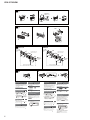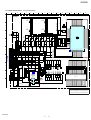
1
CDX-GT65UIW SERVICE MANUAL US Model Ver. 1.0 2011.07 • The tuner and CD sections have no adjustments. Model Name Using Similar Mechanism CDX-GT650UI Mechanism Type MG-101PM-188 Optical Pick-up Name DAX-25A SPECIFICATIONS AUDIO POWER SPECIFICATIONS CEA2006 Standard Power Output: 17 Watts RMS 4 at 4 Ohms < 1% THD+N SN Ratio: 80 dBA (reference: 1 Watt into 4 Ohms) Tuner section System requirements for using SensMe™ USB Player section Interface: USB (Full-speed) Maximum current: 500 mA Computer Power amplifier section Output: Speaker outputs Speaker impedance: 4 – 8 ohms Maximum power output: 52 W u 4 (at 4 ohms) FM General Tuning range: 87.5 – 107.9 MHz Antenna (aerial) terminal: External antenna (aerial) connector Intermediate frequency: 150 kHz Usable sensitivity: 10 dBf Selectivity: 75 dB at 400 kHz Signal-to-noise ratio: 70 dB (mono) Separation: 40 dB at 1 kHz Frequency response: 20 – 15,000 Hz Outputs: Audio outputs terminal (front/rear) Subwoofer output terminal (mono) Power antenna (aerial) relay control terminal Power amplifier control terminal Inputs: BUS control input terminal BUS audio input terminal Remote controller input terminal Antenna (aerial) input terminal Telephone ATT control terminal AUX input jack (stereo mini jack) USB signal input connector Power requirements: 12 V DC car battery (negative ground (earth)) Dimensions: Approx. 178 u 50 u 180 mm (7 1/8 u 2 u 7 1/8 in) (w/h/d) Mounting dimensions: Approx. 182 u 53 u 162 mm (7 1/4 u 2 1/8 u 6 1/2 in) (w/h/d) Mass: Approx. 1.3 kg (2 lb 14 oz) Supplied accessories: Card remote commander: RM-X151 Parts for installation and connections (1 set) AM Tuning range: 530 – 1,710 kHz Antenna (aerial) terminal: External antenna (aerial) connector Intermediate frequency: 25 kHz Sensitivity: 26 μV CD Player section Signal-to-noise ratio: 120 dB Frequency response: 10 – 20,000 Hz Wow and flutter: Below measurable limit Your dealer may not handle some of the above listed accessories. Please ask the dealer for detailed information. CPU/RAM – IBM PC/AT compatible machine – CPU: Intel Pentium III Processor 450 MHz or higher – RAM: 256 MB or more (For Windows XP), 512 MB or more (For Windows Vista or later) USB port OS Windows XP, Windows Vista, Windows 7 For details on compatible editions or Service Pack, visit the following support site: http://esupport.sony.com http://www.sony.com/mobileAV Monitor High color (16-bit) or more, 800 u 600 dots or more Other Internet connection Notes The following system environments are not supported. – Non IBM PC type computers, such as Macintosh, etc. – Homemade computers – OS upgraded computers – Multi-display environment – Multi-boot environment – Virtual machine environment Depending on the computer condition, operation may not be possible even with the recommended environment. Design and specifications are subject to change without notice. FM/AM COMPACT DISC PLAYER 9-893-248-01 2011G33-1 © 2011.07 Sony Corporation Published by Sony Techno Create Corporation CDX-GT65UIW For the State of California, USA only Perchlorate Material – special handling may apply, See www.dtsc.ca.gov/hazardouswaste/perchlorate Perchlorate Material: Lithium battery contains perchlorate HD RadioTM is a proprietary trademark of iBiquity Digital Corp. The “SAT Radio Ready” logo indicates that this product will control a satellite radio tuner module (sold separately). Please see your nearest authorized Sony dealer for details on the satellite radio tuner module. Please refer to the manuals included in the satellite radio tuner module. Sirius or XM Subscription required. “SAT Radio,” “SAT Radio Ready,” the SAT Radio and SAT Radio Ready logos and all related marks are trademarks of Sirius XM Radio Inc. and XM Satellite Radio Inc. ZAPPIN and Quick-BrowZer are trademarks of Sony Corporation. Gracenote, CDDB, MusicID, MediaVOCS, the Gracenote logo and logotype, and the ”Powered by Gracenote” logo are either registered trademarks or trademarks of Gracenote in the United States and/or other countries. 12 TONE ANALYSIS and its logo are trademarks of Sony Corporation. SensMe and the SensMe logo are trademarks or registered trademarks of Sony Ericsson Mobile Communications AB. Microsoft, Windows, Windows Vista and Windows Media and logos are trademarks or registered trademarks of Microsoft Corporation in the United States and/or other countries. This product contains technology subject to certain intellectual property rights of Microsoft. Use or distribution of this technology outside of this product is prohibited without the appropriate license(s) from Microsoft. Music recognition technology and related data are provided by Gracenote®. Gracenote is the industry standard in music recognition technology and related content delivery. For more information, please visit www.gracenote.com. iPhone®, iPod®, iPod classic®, iPod nano®, and iPod touch® are trademarks of Apple Inc., registered in the U.S. and other countries. CD, DVD, Blu-ray Disc, and music and videorelated data from Gracenote, Inc., copyright © 2000 to present Gracenote. Gracenote Software, copyright © 2000 to present Gracenote. One or more patents owned by Gracenote apply to this product and service. See the Gracenote website for a non-exhaustive list of applicable Gracenote patents. Apple, Macintosh and iTunes are trademarks of Apple Inc., registered in the U.S. and other countries. MPEG Layer-3 audio coding technology and patents licensed from Fraunhofer IIS and Thomson. CAUTION Use of controls or adjustments or performance of procedures other than those specified herein may result in hazardous radiation exposure. NOTES ON CHIP COMPONENT REPLACEMENT • Never reuse a disconnected chip component. • Notice that the minus side of a tantalum capacitor may be damaged by heat. FLEXIBLE CIRCUIT BOARD REPAIRING • Keep the temperature of soldering iron around 270 °C during repairing. • Do not touch the soldering iron on the same conductor of the circuit board (within 3 times). • Be careful not to apply force on the conductor when soldering or unsoldering. 2 CAUTION The use of optical instruments with this product will increase eye hazard. SAFETY-RELATED COMPONENT WARNING! COMPONENTS IDENTIFIED BY MARK 0 OR DOTTED LINE WITH MARK 0 ON THE SCHEMATIC DIAGRAMS AND IN THE PARTS LIST ARE CRITICAL TO SAFE OPERATION. REPLACE THESE COMPONENTS WITH SONY PARTS WHOSE PART NUMBERS APPEAR AS SHOWN IN THIS MANUAL OR IN SUPPLEMENTS PUBLISHED BY SONY. CDX-GT65UIW SECTION 1 SERVICING NOTES TABLE OF CONTENTS 1. 2. SERVICING NOTES ............................................. GENERAL .................................................................. 3. DISASSEMBLY 3-1. 3-2. 3-3. 3-4. 3-5. 3-6. 3-7. 3-8. 3-9. 3-10. 3-11. 3-12. 3-13. Disassembly Flow ........................................................... Cover ............................................................................... Panel (Sub) Block ........................................................... CD Mechanism Deck (MG-101PM-188) ....................... MAIN Board ................................................................... SERVO Board ................................................................. Chassis (T) Sub Assy ...................................................... Roller Arm Assy.............................................................. Chassis (OP) Assy ........................................................... Chucking Arm Sub Assy ................................................. Sled Motor Assy.............................................................. Optical Pick-up Section .................................................. Optical Pick-up ............................................................... 4. DIAGRAMS 4-1. 4-2. 4-3. 4-4. 4-5. 4-6. 4-7. 4-8. Printed Wiring Boards - MAIN Section - ....................... Schematic Diagram - MAIN Section (1/3) - ................... Schematic Diagram - MAIN Section (2/3) - ................... Schematic Diagram - MAIN Section (3/3) - ................... Printed Wiring Board - SUB Board - .............................. Schematic Diagram - SUB Board -................................. Printed Wiring Board - KEY Board -.............................. Schematic Diagram - KEY Board - ................................ 5. EXPLODED VIEWS 3 5 7 7 8 8 9 9 10 10 11 11 12 13 13 NOTES ON HANDLING THE OPTICAL PICK-UP BLOCK OR BASE UNIT The laser diode in the optical pick-up block may suffer electrostatic break-down because of the potential difference generated by the charged electrostatic load, etc. on clothing and the human body. During repair, pay attention to electrostatic break-down and also use the procedure in the printed matter which is included in the repair parts. The flexible board is easily damaged and should be handled with care. NOTES ON LASER DIODE EMISSION CHECK Never look into the laser diode emission from right above when checking it for adjustment. It is feared that you will lose your sight. If the optical pick-up block is defective, please replace the whole optical pick-up block. Never turn the semi-fixed resistor located at the side of optical pick-up block. optical pick-up 15 16 17 18 19 19 20 21 5-1. Main Section ................................................................... 28 5-2. Front Panel Section ......................................................... 29 5-3. CD Mechanism Section (MG-101PM-188) .................... 30 6. ELECTRICAL PARTS LIST .............................. 31 semi-fixed resistor Accessories are given in the last of the electrical parts list. UNLEADED SOLDER Boards requiring use of unleaded solder are printed with the leadfree mark (LF) indicating the solder contains no lead. (Caution: Some printed circuit boards may not come printed with the lead free mark due to their particular size) : LEAD FREE MARK Unleaded solder has the following characteristics. • Unleaded solder melts at a temperature about 40 °C higher than ordinary solder. Ordinary soldering irons can be used but the iron tip has to be applied to the solder joint for a slightly longer time. Soldering irons using a temperature regulator should be set to about 350 °C. Caution: The printed pattern (copper foil) may peel away if the heated tip is applied for too long, so be careful! • Strong viscosity Unleaded solder is more viscous (sticky, less prone to flow) than ordinary solder so use caution not to let solder bridges occur such as on IC pins, etc. • Usable with ordinary solder It is best to use only unleaded solder but unleaded solder may also be added to ordinary solder. 3 CDX-GT65UIW TEST DISCS Use following TEST DISC when this set confirms the operation and checks it. Part No. Description 3-702-101-01 4-225-203-01 YEDS-18 (for CD) PATD-012 (for CD) NOTE FOR THE 20-PIN CONNECTOR (CN901) Do not use alcohol to clean the 20-pin connector (CN901) connecting the front panel with the main body. Do not touch the connector directly with your bare hand. Poor contact may be caused. NOTE FOR REPLACEMENT OF THE USB CONNECTOR (CN971) AND THE AUX JACK (J901) To replace the USB connector and the AUX jack requires alignment. 1. Insert the USB connector and the AUX jack into the front panel. 2. Place the KEY board on the front panel and align the terminals of the USB connector and the AUX jack with the holes in the KEY board. 3. Solder four terminals of the connector and three terminals of the jack. KEY board NOTE FOR REPLACEMENT OF THE SERVO BOARD When repairing, the complete SERVO board should be replaced since any parts in the SERVO board cannot be repaired. NOTE FOR REPLACEMENT OF THE SENSOR BOARD When SENSOR board is defective, exchange the MECHANICAL BLOCK ASSY (P). EXTENSION CABLE AND SERVICE POSITION When repairing or servicing this set, connect the jig cable (extension cable (CD mecha)) as shown below. • AUX jack USB (socket) connector front panel Connect the MAIN board (CN701) and the SERVO board (CN401) with the jig cable. Jig cable: Part No. Description A-1818-424-A EXTENSION CABLE (CD MECHA) MAIN board (CN701) extention cable (CD mecha) SERVO board (CN401) 4 CDX-GT65UIW SECTION 2 GENERAL A This section is extracted from instruction manual. Satellite radio tuner (XM/SIRIUS)*4 *1 * 3 FRONT AUDIO OUT SUB OUT (MONO) SUB OUT (MONO) Syntoniseur radio satellite (XM/SIRIUS)*4 *1 FRONT AUDIO OUT REAR AUDIO OUT REMOTE IN*2 *1 RCA pin cord (not supplied). *2 Separate adaptor may be required. *3 BUS cable (not supplied). *4 not supplied. *1 BUS AUDIO IN *1 *2 *3 *4 from car antenna (aerial) desde la antena del automóvil REAR AUDIO OUT Fuse (10 A) Fusible (10 A) Blue/white striped Con rayas azules y blancas AMP REM Max. supply current 0.3 A Corriente máx. de alimentación de 0,3 A B White Blanco Black Negro Blue Azul Left Izquierdo White/black striped Con rayas blancas y negras BUS AUDIO IN Gray Gris Cable con terminales RCA (no suministrado). Puede requerirse un adaptador independiente. Cable de BUS (no suministrado). no suministrado. BUS CONTROL IN ANT REM Max. supply current 0.1 A Corriente máx. de alimentación de 0,1 A Light blue Azul celeste ATT Right Derecho Satellite radio tuner (XM/SIRIUS)* Sintonizador de radio por satélite (XM/SIRIUS)* Gray/black striped Con rayas grises y negras Orange/white striped Con rayas naranjas y blancas ILLUMINATION Green Verde BUS CONTROL IN * not supplied no suministrado Left Izquierdo Green/black striped Con rayas verdes y negras Purple Morado Right Derecho Red Rojo Yellow Amarillo Purple/black striped Con rayas moradas y negras Cautions This unit is designed for negative ground (earth) 12 V DC operation only. Do not get the leads under a screw, or caught in moving parts (e.g. seat railing). Before making connections, turn the car ignition off to avoid short circuits. Connect the yellow and red power supply leads only after all other leads have been connected. Run all ground (earth) leads to a common ground (earth) point. Be sure to insulate any loose unconnected leads with electrical tape for safety. The use of optical instruments with this product will increase eye hazard. Notes on the power supply lead (yellow) When connecting this unit in combination with other stereo components, the connected car circuit’s rating must be higher than the sum of each component’s fuse. When no car circuits are rated high enough, connect the unit directly to the battery. Connection example Notes ( -A) Be sure to connect the ground (earth) lead before connecting the amplifier. The alarm will only sound if the built-in amplifier is used. Note on satellite radio tuner ( -B) This unit does not support the XM radio tuner XMDSON100. Connection diagram To a metal surface of the car First connect the black ground (earth) lead, then connect the yellow and red power supply leads. To the power antenna (aerial) control lead or power supply lead of antenna (aerial) booster Notes It is not necessary to connect this lead if there is no power antenna (aerial) or antenna (aerial) booster, or with a manually-operated telescopic antenna (aerial). When your car has a built-in FM/AM antenna (aerial) in the rear/ side glass, see “Notes on the control and power supply leads.” To AMP REMOTE IN of an optional power amplifier This connection is only for amplifiers. Connecting any other system may damage the unit. To the interface cable of a car telephone To a car’s illumination signal Be sure to connect the black ground (earth) lead to a metal surface of the car first. To the +12 V power terminal which is energized in the accessory position of the ignition switch Notes If there is no accessory position, connect to the +12 V power (battery) terminal which is energized at all times. Be sure to connect the black ground (earth) lead to a metal surface of the car first. When your car has a built-in FM/AM antenna (aerial) in the rear/ side glass, see “Notes on the control and power supply leads.” To the +12 V power terminal which is energized at all times Be sure to connect the black ground (earth) lead to a metal surface of the car first. Notes on the control and power supply leads The power antenna (aerial) control lead (blue) supplies +12 V DC when you turn on the tuner. When your car has built-in FM/AM antenna (aerial) in the rear/side glass, connect the power antenna (aerial) control lead (blue) or the accessory power supply lead (red) to the power terminal of the existing antenna (aerial) booster. For details, consult your dealer. A power antenna (aerial) without a relay box cannot be used with this unit. Memory hold connection When the yellow power supply lead is connected, power will always be supplied to the memory circuit even when the ignition switch is turned off. Notes on speaker connection Before connecting the speakers, turn the unit off. Use speakers with an impedance of 4 to 8 ohms, and with adequate power handling capacities to avoid its damage. Do not connect the speaker terminals to the car chassis, or connect the terminals of the right speakers with those of the left speaker. Do not connect the ground (earth) lead of this unit to the negative (–) terminal of the speaker. Do not attempt to connect the speakers in parallel. Connect only passive speakers. Connecting active speakers (with built-in amplifiers) to the speaker terminals may damage the unit. To avoid a malfunction, do not use the built-in speaker leads installed in your car if the unit shares a common negative (–) lead for the right and left speakers. Do not connect the unit’s speaker leads to each other. Note on connection If speaker and amplifier are not connected correctly, “FAILURE” appears in the display. In this case, make sure the speaker and amplifier are connected correctly. Precauciones Esta unidad ha sido diseñada para alimentarse sólo con cc de 12 V de masa negativa. No coloque los cables debajo de ningún tornillo, ni los aprisione con partes móviles (p. ej. los raíles del asiento). Antes de realizar las conexiones, apague el automóvil para evitar cortocircuitos. Conecte los cables de fuente de alimentación amarillo y rojo solamente después de haber conectado los demás. Conecte todos los cables de conexión a masa a un punto común. Por razones de seguridad, asegúrese de aislar con cinta aislante los cables sueltos que no estén conectados. Notas sobre el cable de fuente de alimentación (amarillo) Cuando conecte esta unidad en combinación con otros componentes estéreo, la capacidad nominal del circuito conectado del automóvil debe ser superior a la suma del fusible de cada componente. Si no hay circuitos del automóvil con capacidad nominal suficientemente alta, conecte la unidad directamente a la batería. Ejemplo de conexiones Notas ( -A) Asegurese de conectar primero el cable de conexion a masa antes de realizar la conexion del amplificador. La alarma sonara unicamente si se utiliza el amplificador incorporado. Notas sobre el sintonizador de radio por satélite ( -B) Esta unidad no es compatible con el sintonizador de radio XM XMDSON100. Diagrama de conexión A una superficie metálica del automóvil Conecte primero el cable de conexión a masa negro, y después los cables amarillo y rojo de fuente de alimentación. Al cable de control de la antena motorizada o al cable de fuente de alimentación del amplificador de señal de la antena Notas Si no se dispone de antena motorizada ni de amplificador de antena, o se utiliza una antena telescópica accionada manualmente, no será necesario conectar este cable. Si el automóvil incorpora una antena de FM/AM en el cristal trasero o lateral, consulte “Notas sobre los cables de control y de fuente de alimentación”. A AMP REMOTE IN de un amplificador de potencia opcional Notas sobre los cables de control y de fuente de alimentación El cable de control de la antena motorizada (azul) suministrará cc de + 12 V cuando conecte la alimentación del sintonizador. Si el automóvil dispone de una antena de FM/AM incorporada en el cristal trasero o lateral, conecte el cable de control de antena motorizada (azul) o el cable de fuente de alimentación auxiliar (rojo) al terminal de alimentación del amplificador de antena existente. Para obtener más información, consulte a su distribuidor. Con esta unidad no es posible utilizar una antena motorizada sin caja de relé. Conexión para protección de la memoria Si conecta el cable de fuente de alimentación amarillo, el circuito de la memoria recibirá siempre alimentación, aunque apague el interruptor de encendido. Notas sobre la conexión de los altavoces Antes de conectar los altavoces, desconecte la alimentación de la unidad. Utilice altavoces con una impedancia de 4 a 8 Ω con la capacidad de potencia adecuada para evitar que se dañen. No conecte los terminales de altavoz al chasis del automóvil, ni conecte los terminales del altavoz derecho con los del izquierdo. No conecte el cable de conexión a masa de esta unidad al terminal negativo (–) del altavoz. No intente conectar los altavoces en paralelo. Conecte solamente altavoces pasivos. Si conecta altavoces activos (con amplificadores incorporados) a los terminales de altavoz, puede dañar la unidad. Para evitar fallas de funcionamiento, no utilice los cables de altavoz incorporados instalados en el automóvil si la unidad comparte un cable negativo común (–) para los altavoces derecho e izquierdo. No conecte los cables de altavoz de la unidad entre sí. Nota sobre la conexión Si el altavoz y el amplificador no están conectados correctamente, aparecerá “FAILURE” en la pantalla. Si es así, compruebe la conexión de ambos dispositivos. Esta conexión es sólo para amplificadores. La conexión de cualquier otro sistema puede dañar la unidad. Al cable de interfaz de un teléfono para automóvil A una señal de iluminación del automóvil Asegúrese de conectar primero el cable de conexión a masa negro a una superficie metálica del automóvil. Al terminal de alimentación de +12 V que recibe energía en la posición de accesorio del interruptor de encendido Notas Si no hay posición de accesorio, conéctelo al terminal de alimentación (batería) de +12 V que recibe energía sin interrupción. Asegúrese de conectar primero el cable de conexión a masa negro a una superficie metálica del automóvil. Si el automóvil incorpora una antena de FM/AM en el cristal trasero o lateral, consulte “Notas sobre los cables de control y de fuente de alimentación”. Al terminal de alimentación de +12 V que recibe energía sin interrupción Asegúrese de conectar primero el cable de conexión a masa negro a una superficie metálica del automóvil. 5 CDX-GT65UIW 2 1 Face the hook inwards. El gancho debe encontrarse en la parte interior. 1 2 3 Dashboard Tablero Claws Uñas A TOYOTA B NISSAN size 5 × max. 8 mm (7/32 × max. 5/16 in) Tamaño máx. 5 × 8 mm size 5 × max. 8 mm (7/32 × max. 5/16 in) Tamaño máx. 5 × 8 mm to dashboard/center console al tablero o consola central Bracket Soporte to dashboard/center console al tablero o consola central Bracket Soporte size 5 × max. 8 mm (7/32 × max. 5/16 in) Tamaño máx. 5 × 8 mm Bracket Soporte Bracket Soporte Existing parts supplied with your car Piezas existentes suministradas con su automóvil A Existing parts supplied with your car Piezas existentes suministradas con su automóvil B Precautions Choose the installation location carefully so that the unit will not interfere with normal driving operations. Avoid installing the unit in areas subject to dust, dirt, excessive vibration, or high temperatures, such as in direct sunlight or near heater ducts. Use only the supplied mounting hardware for a safe and secure installation. Mounting angle adjustment Adjust the mounting angle to less than 45°. How to detach and attach the front panel -A To detach Before detaching the front panel, be sure to press and . Press , then slide the hold front panel to the right, and gently pull out the left end of the front panel. Ajuste del ángulo de montaje Pinch both edges of the protection collar pull it out. , then . Insert both release keys together between the unit and the bracket until they click. Pull down the bracket , then pull up the unit to separate. Mounting example Warning if your car’s ignition has no ACC position Be sure to set the Auto Off function. For details, see the supplied Operating Instructions. The unit will shut off completely and automatically in the set time after the unit is turned off, which prevents battery drain. If you do not set the Auto Off function, press and hold until the display disappears each time you turn the ignition off. Extracción del marco de protección y del soporte Antes de instalar la unidad, retire el marco de protección y el soporte de esta. 1 Retire el marco de protección . Apriete ambos bordes del marco de protección y, a continuación, tire de él hacia fuera. 2 Retire el soporte . Inserte ambas llaves de liberación entre la unidad y el soporte hasta que encajen. Presione el soporte y, a continuación, levante la unidad para separar ambos elementos. RESET button Installation in the dashboard Notes Bend these claws outward for a tight fit, if necessary ( Make sure that the 4 catches on the protection collar engaged in the slots of the unit ( -3). Ajuste el ángulo de montaje a menos de 45°. Place the hole of the front panel onto the spindle on the unit, then lightly push the left side in. Before installing the unit, remove the protection collar and the bracket from the unit. 1 Remove the protection collar . Remove the bracket Precauciones Elija cuidadosamente el lugar de montaje de forma que la unidad no interfiera con las funciones normales de conducción. Evite instalar la unidad donde pueda quedar sometida a polvo, suciedad, vibraciones excesivas o altas temperaturas como, por ejemplo, a la luz solar directa o cerca de conductos de calefacción. Para realizar una instalación segura y firme, utilice solamente elementos de instalación suministrados. Before installing the unit, detach the front panel. -B To attach Removing the protection collar and the bracket 2 size 5 × max. 8 mm (7/32 × max. 5/16 in) Tamaño máx. 5 × 8 mm -2). are properly Ejemplo de montaje Instalación en el tablero Notas Si es necesario, doble las uñas hacia fuera para que encaje firmemente ( -2). Compruebe que los 4 enganches del marco de protección estén bien fijados en las ranuras de la unidad ( -3). Mounting the unit in a Japanese car You may not be able to install this unit in some makes of Japanese cars. In such a case, consult your Sony dealer. Note To prevent malfunction, install only with the supplied screws When the installation and connections are completed, be sure to press the RESET button with a ball-point pen, etc., after detaching the front panel. Forma de extraer e instalar el panel frontal Antes de instalar la unidad, extraiga el panel frontal. -A Para extraerlo Antes de extraer el panel frontal, asegúrese de mantener . Presione y, a presionado continuación, deslice el panel frontal hacia la derecha y tire suavemente de su extremo izquierdo. -B Para instalarlo Coloque el orificio del panel frontal en el eje de la unidad y, a continuación, presione ligeramente el lado izquierdo hacia adentro. Advertencia: si el encendido del automóvil no dispone de una posición ACC Asegúrese de ajustar la función de desconexión automática. Para obtener más información, consulte el manual de instrucciones suministrado. La unidad se apagará completa y automáticamente en el tiempo establecido después de que se desconecte la unidad, lo que evita que se desgaste la batería. Si no ha ajustado la función de desconexión automática, cada vez que mantenga presionado apague el interruptor de encendido, hasta que la pantalla desaparezca. Botón RESET Una vez finalizada la instalación y las conexiones, desmonte el panel frontal y presione el botón RESET con un bolígrafo o un objeto similar. Montaje de la unidad en un automóvil japonés . Es posible que no pueda instalar esta unidad en algunos automóviles japoneses. En tal caso, consulte a su distribuidor Sony. Nota Para evitar que se produzcan fallas de funcionamiento, realice la instalación solamente con los tornillos suministrados . 6 Notas acerca de la sintonización Si se sustituye la batería del vehículo, se cambian las conexiones o se restablece la unidad, se eliminará el ajuste de sintonización. Para obtener información sobre cómo ajustar la sintonización, consulte el manual de instrucciones suministrado. CDX-GT65UIW SECTION 3 DISASSEMBLY • This set can be disassembled in the order shown below. 3-1. DISASSEMBLY FLOW SET FRONT PANEL SECTION Note: Illustration of disassembly is omitted. 3-2. COVER (Page 7) 3-3. PANEL (SUB) BLOCK (Page 8) 3-4. CD MECHANISM DECK (MG-101PM-188) (Page 8) 3-5. MAIN BOARD (Page 9) 3-6. SERVO BOARD (Page 9) 3-7. CHASSIS (T) SUB ASSY (Page 10) 3-11. SLED MOTOR ASSY (Page 12) 3-8. ROLLER ARM ASSY (Page 10) 3-12. OPTICAL PICK-UP SECTION (Page 13) 3-9. CHASSIS (OP) ASSY (Page 11) 3-13. OPTICAL PICK-UP (Page 13) 3-10. CHUCKING ARM SUB ASSY (Page 11) Note: Follow the disassembly procedure in the numerical order given. 3-2. COVER 2 two bosses 1 screw (PTT2.6 u 6) 4 cover 3 three claws 2 two bosses 7 CDX-GT65UIW 3-3. PANEL (SUB) BLOCK 2 two claws 3 2 two claws 1 two screws (PTT2.6 u 6) 4 flexible flat cable (23 core) (CN102) 5 panel (sub) block 3-4. CD MECHANISM DECK (MG-101PM-188) 6 bracket (CD) 7 CD mechanism deck (MG-101PM-188) 1 screw (PTT2.6 u 6) 5 two screws (PTT2.6 u 4) 2 4 flexible flat cable (13 core) (CN402) 3 connector (CN701) 1 screw (PTT2.6 u 6) 8 CDX-GT65UIW 3-5. MAIN BOARD 1 fuse (blade type) (auto fuse) (10A/32V) (FU301) 3 screw (PTT2.6 u 8) 6 screw (PTT2.6 u 8) 2 three ground point screws (PTT2.6 u 6) 7 connection cord for automobile 3 screw (PTT2.6 u 8) 5 connector (CN408) 4 3-6. 8 MAIN board SERVO BOARD WHT RED BLK WHT RED BLK RED ORG BLU YEL GRY 3 toothed lock screw (M1.7 u 2.5) SERVO board 1 flexible flat cable (13 core) (CN471) 3 toothed lock screw (M1.7 u 2.5) 7 SERVO board 2 Remove the eleven solders. 6 optical pick-up (16 core) (CN101) 5 claw 4 claw CD mechanism deck – bottom side view – 9 CDX-GT65UIW 3-7. CHASSIS (T) SUB ASSY 1 two screws (M1.7 u 2.5) 1 two screws (M1.7 u 2.5) 3 chassis (T) sub assy 2 claw 3-8. ROLLER ARM ASSY 5 roller arm assy 4 gear (RA1) 1 spring (RAL) 3 washer 2 spring (RAR) 10 CDX-GT65UIW 3-9. CHASSIS (OP) ASSY 8 chassis (OP) assy 1 tension spring (KF) 5 6 two coil springs (damper) (natural) 7 coil spring (damper) (green) 4 slider (R) 3 lever (D) 2 gear (LE1) 3-10. CHUCKING ARM SUB ASSY 3 chucking arm sub assy 1 spring 2 Note 1: Have this portion receive the chassis. Note 1: Have this portion receive the chassis. Note 2: Be careful not to touch the turn table. 11 CDX-GT65UIW 3-11. SLED MOTOR ASSY 2 three serration screws (M2 u 3) 3 sled motor assy 1 spring turn table spring stand Note 2: Never remove these parts since they were adjusted. bearing (F) stand –ERWWRPVLGHYLHZ– Note 1: Place the stand with care not to touch the turn table. bearing (R) –ERWWRPVLGHYLHZ– 1RWHIRU$VVHPEO\ three serration screws (M2 u 3) sled motor assy Note 3: Take care to prevent the chassis from being bent when tightening the three machine screws. –ERWWRPVLGHYLHZ– 12 CDX-GT65UIW 3-12. OPTICAL PICK-UP SECTION 2 optical pick-up section 1 Note: Be careful not to touch the lens and hologram terminal when removing the optical pick-up section. – bottom side view – 3-13. OPTICAL PICK-UP 1 pan tapping screw (M1.4 u 2.5) 2 leaf spring (sub guide) 3 leaf spring (OP) 5 optical pick-up 4 lead screw assy Notes for Assembly Prevent the end of the leaf spring (sub guide) from being in contact with the OP slide base. CDX-GT65UIW – bottom side view – Prevent the end of the leaf spring (sub guide) from being in contact with the OP slide base. There is space at the end of the leaf spring (sub guide) to avoid contact with the slide. 13 13 CDX-GT65UIW SECTION 4 DIAGRAMS THIS NOTE IS COMMON FOR PRINTED WIRING BOARDS AND SCHEMATIC DIAGRAMS. (In addition to this, the necessary note is printed in each block.) For Printed Wiring Boards. For Schematic Diagrams. Note: • X : Parts extracted from the component side. • Y : Parts extracted from the conductor side. • W : Indicates side identified with part number. • f : Internal component. • : Pattern from the side which enables seeing. (The other layers’ patterns are not indicated.) Note: • All capacitors are in μF unless otherwise noted. (p: pF) 50 WV or less are not indicated except for electrolytics and tantalums. • All resistors are in Ω and 1/4 W or less unless otherwise specified. • f : Internal component. • C : Panel designation. Caution: Pattern face side: (Conductor Side) Parts face side: (Component Side) Parts on the pattern face side seen from the pattern face are indicated. Parts on the parts face side seen from the parts face are indicated. Caution: Pattern face side: (SIDE B) Parts face side: (SIDE A) Parts on the pattern face side seen from the pattern face are indicated. Parts on the parts face side seen from the parts face are indicated. • Indication of transistor. C Q These are omitted. B E CDX-GT65UIW • Circuit Boards Location SERVO board SENSOR board Note: The components identified by mark 0 or dotted line with mark 0 are critical for safety. Replace only with part number specified. • A : B+ Line. • Power voltages is dc 14.4V and fed with regulated dc power supply from ACC and BATT cords. • Voltages and waveforms are dc with respect to ground under no-signal (detuned) conditions. no mark : FM ( ): AM < > : CD PLAY * : Impossible to measure • Voltages are taken with VOM (Input impedance 10 M). Voltage variations may be noted due to normal production tolerances. • Waveforms are taken with a oscilloscope. Voltage variations may be noted due to normal production tolerances. • Circled numbers refer to waveforms. • Signal path. F : FM f : AM J : CD PLAY c : USB L : AUX IN g : BUS AUDIO IN MAIN board SUB board – Main unit – KEY board – Front panel – 14 14 CDX-GT65UIW 4-1. PRINTED WIRING BOARDS - MAIN Section - • See page 14 for Circuit Boards Location. 2 1 3 4 • : Uses unleaded solder. 5 6 7 8 9 10 11 J403 REAR L R JW212 I D119 CL061 JW265 R813 JW234 R815 C607 C606 C614 R605 C603 1 25 R606 IC601 26 L601 R702 C703 C604 D601 R608 27 R602 13 R607 R610 14 C611 R705 C612 JW334 JW400 R609 R603 JW262 JW299 CD MECHANISM DECK BLOCK (MG-101PM-188) (1/2) CN501 C609 C602 R604 JW301 R587 FB501JW399 R816 R709 R711 JW246 JW370 E E CL031 CL030 R707 E JC408 C613 C605 C710 A1 CL006 CL020 JC419 JW258 JW389 JL002 C600 8 JL003 JL004 Q802 D807 BCE JC366 R811 JL007 R858 R810 R592 JL001 JL008 JC261 R516 JW270 8 1 D806 R809 7 JL006 JC289 R807 JW297 JC281 14 JW523 JW351 R555 R529 JW266 JL005 1 R517 R812 JW350 JW261 JW392 R601 CL024 R565 R567 R568 JW317 S401 RESET CAM001 S501 (NOSE DETECT) R865 21 C517 R121 1-882-749- CL078 CL076 CL074 CL072 CL070 CL068 D116 IC403 L602 CL067 C103 CL026 R708 R557 (CHASSIS) (21) R122 A Note 1: When SERVO board is defective, exchange the complete mounted board. SUB BOARD (Page 19) CDX-GT65UIW C704 JC273 R586 R590 R401 B1 JW339 R528 JW267 JC265 R570 R541 CL008 CL022 L603 (NC) C518 C401 C615 D113 D112 JC106 2 1 C331 CL040 JW271 JC292 CL063 R542 JC295 3 4 JW336 JC268 CL081 R545 R611 C100 R512 R532 R580 R519 JW273 R533 R510 R513 R511 JC120 JW312 JW358 R514 JW375 JW329 R503 JW322 JW315 2 D109 1 R502 R505 R536 CL028 JW282 R543 C508 R806 R594 JW260 CL075 C101 JW288 JW253 CL079 D111 D107 JW330 CN101 CL073 CL069 CL064 23 D108 CL082 D106 CL066 22 D117 D118 D101 CL065 CAM003 JW344 JW345 (CHASSIS) D105 JW316 JC307 C442 D102 CL071 R419 R416 R418 R417 R420 R415 JW226 D104 CL077 C437 JW310 C436 R530 X502 D501 R539 R504 R509 R501 C502 C512 D103 C438 C514 JW332 G JW236 JC301 JW302 C203 JW387 C513 H JW216 JW318 1 0 JC290 R559 C507 R508 X501 C711 R710 JW342 JW279 C510 10 JC256 JC121 R561 R581 R585 R589 C263 TH801 R701 CL009 CL041 R595 Q502 JW272 R553 R535 JW335 JW363 JW356 JC131 JC291 C522 JW215 CL007 CL021 R591 CD MECHANISM DECK BLOCK (MG-101PM-188) (2/2) D802 JW294 JW367 JW207 JW235 R866 R540 JC262 CL010 JW398 JW237 IC501 CL011 CL023 IC801 13 C521 CL027 CL014 JW264 R804 R14 SERVO BOARD R430 JW340 D731 12 CL004 C523 81 JC260 D402 CL015 E R431 R13 SENSOR BOARD CL003 R716 JW355 L1 R599 R432 JC346 JW102 JW126 R593 R547 JW240 JC475 L405 CL017 CL012 JW529 JW214 CL018 CL029 CL013 CL025 Q501 JC469 C405 C28 X1 CN402 17 C504 D404 CL019 JW526 R713 JW353 2 R562 R571 R867 C27 R598 R577 R550 R526 R507 R538 D403 1 R544 R523 JW394 Q302 Q301 JW269 R527 ECB R433 R551 R583 R12 R575 R116 C520 JC257 JW147 R434 JW283 C25 R564 JW284 C26 C447 FB705 CL016 JC356 JW456 L301 D323 R323 CN701 B14 A14 JW268 30 JW148 JW341 R506 C333 C701 D324 R315 R324 R317 FB706 R546 JW352 JW281 C23 C16 C328 JC263 JW524 JW275 R534 JW343 R572 D303 R318 R596 JW533 C24 C22 JC274 R584 R531 ILLUMINATION D318 JC363 R522 JW319 AMP REM MAX 0.3A ANT REM MAX 0.1A C337 D321 R325 R319 FB704 JC418 JW349 JC282 JC302 JC362 JW354 C21 JC276 JW347 JW348 C306 FB801 D301 R316 JW393 FB401 C417 JW202 JW263 JW222 R320 Q303 31 CL002 CL001 R438 L402 JW357 R11 16 C418 D304 R429 R521 21 R500 R563 C403 C414 IC001 JW217 C415 20 C13 C9 C402 R310 C20 32 JW313 JW201 C336 R321 JW257 50 L8 1 F 4 C416 IC401 C19 L7 C12 C18 3 R808 FB802 7 D803 D320 D302 JW259 51 FB403 C444 C8 C17 5 JW369 FB402 C5 E C407 1 R3 C443 D Q409 C425 40 4 D307 C334 JW247 C312 C411 JC479 1 C429 L2 L6 BCE C419 C427 R16 JC123 D401 C409 ECB R2 R15 C413 JC267 1 CN408 TO CN301 C335 JW245 80 3 6 D801 R322 JW256 C308 JC103 1 D804 D322 R308 Q407 C1 JW365 8 8 3 C802 C313 C303 C327 R435 JC361 C6 1 FB409 R436 3 TO CN408 VDR408 JC264 C (CHASSIS) C424 1 C801 R805 BCE JW232 C408 16 D308 R305 C316 C420 JW231 R306 R423 1 JW296 C422 R404 Q405 VR1 L302 JW368 R1 R407 JC269 R405 BCE (CHASSIS) SUB OUT (MONO) JC271 JW230 Q401 C300 CAM002 BCE Q404 R424 R421 C321 C322 IC301 37 9 C301 JW219 R411 C318 C315 JW285 IC402 JW137 R426 Q402 Q403 R425 R412 FB826 19 2 JC116 ECB R427 ECB R413 JW138 R414 R410 B C305 36 JW250 R301 C302 C809 18 17 JW377 R409 JW293 C329 JW364 JW208 R422 CN301 C330 JW309 C426 C304 JW209 C421 C430 JW227 C323 C319 C423 JW225 C324 C320 C428 J801 (REMOTE IN) CN801 (BUS CONTROL IN) JW300 JC277 C412 R441 R304 J1 (ANTENNA IN) FU301 L R303 JW311 R JW362 L FRONT R302 R A (FRONT VIEW) AUDIO OUT BUS AUDIO IN 15 15 Note 2: When SENSOR board is defective, exchange the MECHANICAL BLOCK ASSY (P). CDX-GT65UIW 4-2. SCHEMATIC DIAGRAM - MAIN Section (1/3) - • See page 22 for IC Block Diagrams. 1 2 3 5 4 7 6 8 10 9 11 MAIN BOARD (1/3) IC301 A 14 IC B/D AMP-REM AUDIO+B(8.5V) SERVO+3.3V GND MECHA+6V PANEL+B VP CBU BU+B 29 30 31 32 33 34 35 36 37 D804 D801 R813 D803 C809 D802 6 1 1 22 C324 C322 R429 0 0.47 C300 220 R306 1 C320 L302 220 R303 2.2 220 R304 C315 220 47k DA2J10100L 1A4-A2 1A4-A2 1000p 0.22 1 C321 R310 D401 D303 D321 C328 C302 RKZ18B2KGP1 LRB751V-40T1G RKZ18B2KGP1 100 11 C802 470 25V 5 RKZ18B2KGP1 0.1 4 12 13 14 C401 0.1 RESET R858 220k DIAG C447 100 10V 13.7 Q409 DRC5114E0L MUTE DRIVE TEL D402 MC2836-T112-1 (Page 17) 16 16 BUS4 9 8 D403 MA2J1110GLS0 7 6 BUS3 BUS2 5 4 3 2 BUS1 1 MAIN BOARD (2/3) ILL+B DOOR_SW 10 ACC UNI_SI UNI_SO BU_IN UNI_SCK BUS_ON SYS_RST RCIN0 RCIN1 17 D404 MA2J1110GLS0 1 16 3 0 CDX-GT65UIW 330 6.3V IC402 BU33TD3WG-TR +3.3V REG C411 1 0.1 2 C407 3 IC402 C409 1000 10V 3 VOUT 4 NC VIN VSS IC B/D GND VIN (Page 18) 0 4.9 VOUT 2 NC 1 5 STB S401 3.3 4 4.9 FB802 H 3.1 R401 100k 16V RESET MAIN BOARD (3/3) 13.7 3.3 IC403 XC61CN2802NR RESET SIGNAL GENERATOR D807 RKZ18B2KGP1 FB801 STB IC403 Q303 2SC4154TP-1EF 0 TEL-ATT DETECT Q302 2SC4154TP-1EF ILL DETECT 47 0 C416 Q301 2SC4154TP-1EF ACC DETECT C403 330 6.3V 0 R816 1k 2 Q407 RT1P141M-TP-1 MUTE DRIVE 0.1 Q802 DRC5114E0L BACK-UP CHECK 0 0.6 C402 DATA_OUT GND BEEP 2.5 DATA_IN DATA_I/O 5.4 14 0.6 1.5 1.6 CLK 8 2.7 BU_CHECK VREF 0 5.4 BATT CLK_IN 3.2 BUS_IN 9 R324 22k 0.6 0 0.01 10 R318 10k R323 100k R812 0 C801 7 R811 0 330k 6 C331 4.7 50V FB401 J801 (REMOTE IN) 330k R807 0 RST 11 0 12 3.3 13 R316 4.7k C263 1 5 R810 0 FB826 R809 4 14 4.9 G 3 VCC IC801 IC801 BA8271F-E2 BUS INTERFACE 2 RST 1 BUS_ON IC B/D 4.9 R806 100 I2C_SCK F I2C_SIO 15 ILL 1 7 3 CN801 8P (BUS CONTROL IN) R815 15k D806 RKZ6.2B2KGP1 R805 1k 8 2 1k 0 1 R804 R808 C323 TH801 E R305 C327 47p 1 1 C319 2 FL+ 1 3 RL+ 1 4 RR+ C318 5 FR+ 22 25V AMP-REM C303 16 0.1 8 C337 GND BATT C301 0.22 100 6 R302 ANT-REM D304 100 15 D302 R301 7 4.7k 10k D ACC R325 R319 7 1A4-A2 8 ACC RKZ18B2KGP1 9 C308 C312 0.22 10 16V D301 FLGND ILLUMINATION 1A4-A2 14 10 R320 47k C304 0.22 D318 ANT REM MAX 0.1A 11 RL- D324 6 ATT DA2J10100L 12 RR- C336 3300 16V FR- TO CN301 RKZ18B2KGP1 13 D308 12 5 C313 C306 47 1 16V C305 0.22 R308 150 C330 0.22 RKZ18B2KGP1 4 FRONT RCH (–) 4.7k 1k D307 FRONT RCH (+) AMP REM MAX 0.3A R322 R321 1000p 13 D322 14 TEL-ATT RKZ18B2KGP1 15 ILL C335 REAR RCH (–) RKZ18B2KGP1 C D320 16 C329 0.22 47k +B TEST L301 250uH D323 11 17 1 3 REAR LCH (–) REAR RCH (+) +B 14.4 R317 10 18 C333 REAR LCH (+) +B 47k 2 FU301 10A 32V 1000p 9 R315 1 FRONT LCH (–) C334 FRONT LCH (+) 19 C316 CN301 16P +B 4.9 CRES 28 14.1 ANT-REM 27 14.4 RST 26 10.5 DIAG 25 6.1 P-GND4 24 3.3 OUT-FR23 8.5 STB 22 13.9 OUT-FR+ 21 13.9 VP1 20 3.2 OUT-RR19 7.2 P-GND3 18 3.2 OUT-RR+ 17 7.1 BEEP 16 14.4 IN-RR 15 7.1 IN-FR 14 7.1 S-GND 13 4.3 IN-FL 12 4.1 IN-RL 11 4.1 SVR 10 4.1 OUT-RL+ 9 4.1 P-GND1 8 4.4 OUT-RL7 7.2 VP2 6 7.2 OUT-FL+ 5 14.4 I2C_SCK 4 7.1 OUT-FL3 3.1 I2C_SIO 2 7.2 1 3.1 TAB IC301 TDF8556AJ/N3 I2C BUS CONTROLLED POWER AMP/MULTIPLE VOLTAGE REGULATOR B I 13 12 MAIN BOARD (3/3) (Page 18) CDX-GT65UIW 4-3. SCHEMATIC DIAGRAM - MAIN Section (2/3) - • See page 22 for waveforms. • See page 22 for IC Block Diagrams. • See page 26 for IC Pin Function Description. 2 1 3 5 4 7 6 8 10 9 11 13 12 14 (Page 16) MAIN BOARD (1/3) BUS4 10 VBUS_ON USB_OVER TEL ACC B DIAG STB A_ATT MAIN BOARD (2/3) 9 8 7 6 BUS2 5 4 3 2 BUS1 1 BUS3 1 A 0 100k 2.2k R564 R546 0 0 VBUS_ON C514 1000p 3.2 C512 1000p 91 KEYACK0 92 KEYACK1 R502 100 3.2 CDM_ON 38 R503 100 3.2 93 NCO 94 KEYIN1 95 KEYIN0 96 AVSS NCO 36 97 RC_IN0 98 AVRH FW_BUSY 34 FW_CLK 33 EJECT_OK DOOR_ING SYNC_OUT 100 SA_CLK SA_DA 2.6 3 R577 100k 3 R590 100k 0 R562 100k 3 R586 100k 0 R583 100k 0 R571 100k Z_MUTE R593 3.3 3.2 R595 100k 3.2 R594 100k CL002 CL001 CD_ON R592 100 BUSY CLK 0 0 R516 0 0 R517 0 RXD TXD R567 100k R565 100k 21 BUS5 4.9 4.7k R867 47p C520 47p C521 2.2k R522 2.2k R521 0 R563 100 1k R866 100k R545 0 0 Q502 DRC5114E0L LED DRIVER FB501 1000p C518 R541 0 R543 R527 1k 0 0 R555 R529 100 100k R528 R561 1 C510 R540 100k 1M R581 10M 100k 220k 0 10k R509 100k R536 R508 R533 X502 32.768kHz 100k R501 100k R519 R533 5.1 22p 18p 0 100 5.1 VDD RKZ6.8B2KGP1 R532 Q501 DRA5114E0L LED DRIVER 22 R610 3.3k 470 R602 C612 470 10V 18k R607 R865 0 (CHASSIS) 17 17 C507 C508 R542 R570 R580 BEEP EJECT_OK SYNC_OUT MC_TX DOOR_SW MC_RX BUS_ON SYS_RST BU_IN X501 7.92MHz RCIN1 RESET CNVSS UNI_SCK UNI_SI UNI_SO SIRCS LCD_CE C615 100 16V LCD_CLK S501 (NOSE DETECT) R609 2.2k R604 3.3k LCD_DATA C602 0.047 R512 C517 0 R603 2.2k R608 820 47uH 1 C611 L601 470 470 R605 R606 0.033 C606 D601 DB2441600L 4.7 D501 4.8 4.8 BUS6 1 C607 100k 5.1 VDD IC601 BD9070FP-E2 USB VBUS POWER CONTROL R513 R510 1k 470 HSDCTL INV OVP 5.1 0.8 0.8 IC601 100k 1k RT SYN/EN FB 0.7 IC B/D HSDSW TAB TAB 5.2 5.2 SW 19 18 17 16 15 14 SW 27 14.4 25 24 23 22 21 20 14.4 NCO HSDSW GND 10 11 12 13 NCO PGND 3 9 NCO 8 NCO 3.3 7 FLG 26 NCO 1.1 6 VIN 0.6 14.4 5 NCO 4 VREGB 6.3 3 PV_IN 2 PV_IN 1 C604 C614 100 25V 20 WAKE_UP I2C_SCK R514 CAM001 CDX-GT65UIW 100 CDM_ON R568 100k 0 MAIN BOARD (3/3) (Page 18) I2C_SIO H I 4 0 C605 0.1 G USB_ON 3.2 I2C_SIO I2C_SCK R598 3.3 3.1 BEEP 0 0 1.1 MC_TX 0 0 3.3 MC_RX 3.2 BUS_ON SYSRST 0 3.3 2.7 3 3 3.3 0.7 1.7 3.1 1.4 BUIN 10 11 12 13 14 15 16 17 18 19 20 21 22 23 24 25 26 27 28 29 30 RC_IN1 9 NMI 8 VCC1 7 OSCIN 6 VSS 5 OSCOUT 4 RESET 3 XOUT XIN 2 0.3 CNVSS 1 0 BYTE FW_TXD 31 UNISCK DOOR_SW FW_RXD 32 UNISI R511 1k 2 UNISO R611 470 1 3.2 3.3 NCO 35 1.5 3.3 SIRCS 3.2 0.01 1.6 100 C513 WAKE_UP 39 NOSE_SW R539 Z_MUTE 40 CD_ON 37 3.7 1 EPM 41 3.2 CNVSS C613 MODELNAME_SEL0 42 IC501 R5F3650KBDZ85FA SYSTEM CONTROLLOR 1000p JL001 L603 3.3 3 IC501 89 NCO 90 NCO C502 99 AVDD 0 100 LCD_CE L602 10uH MODELNAME_SEL1 43 LCD_CLK JL002 MODELNAME_SEL2 44 LCD_SO 8 JL008 R530 10k 100k 100 100k R584 0 MODELNAME_SEL3 45 3 7 GND R504 10k 19 R544 100k R531 0 3.3 0 3.3 CE 46 0 FLASH_W RCIN0 0.1 6 RXD C609 BU3.3V TXD JL003 USB_OVER 5 R505 10k BUSY JL004 C600 100 16V RXD JL005 47k 4 KEY0 USB_ON 3 TXD CLK SYNC_OUT BUSY JL006 R601 2 KEY1 47uH F CLK D731 BAT54ALT1G JL007 150p (NC) 1 C603 CN501 8P RESET R596 10k 10k R534 R500 100k R572 3.2 R506 100k C504 R575 100k 0 NCO 47 3.3 RESET USBON 50 SA_DATAIN 48 87 NCO 88 NCO SYS_RST 18 R587 100k SA_CLKOUT 49 83 ILL_IN 84 NCO 85 NCO 86 NCO E USB_OVR 0.01 EXTATT_XEN C522 81 RE-IN1 82 RE-IN0 NCO 3.2 TELATT 1k ATT R585 DIAG 0 VCC2 1k ILL C703 10 16V I2C_SCK 3.1 RE0 CL020 R591 ACC_IN RE1 F_AUX_ATT USB_D- 15 USB_D- 0.01 AMPSTB CL006 I2C_SIO 80 79 78 77 76 75 74 73 72 71 70 69 68 67 66 65 64 63 62 61 60 59 58 57 56 55 54 53 52 51 C523 CYRIL_SEL BU_IN CL007 NCO WAKE_UP CL008 VSS 0 3 100k R716 NCO R713 CL009 ILLUMI SEL USB_D+ CL010 B-OUT SEL 1 R575 100k USB_GND 16 R550 100k USB_GND 0 2 R551 100k BU_CHECK 17 0 BU_GND R507 100k 3 0 WAKEUP 18 3 BU_3.3V COLSW SEL 0.01 4 CL011 AREASEL3 USB_D+ C710 SYS_RST 19 EJECT_OK AREASEL2 CL021 A_ATT CL012 AREASEL1 CL022 X_FLASH 20 5 R526 100k CL041 0 EJECK_OK 21 Z_MUTE 0 0 R705 VBUS_ON 6 0 R702 7 SA_CLK R523 100k CL013 AREASEL0 D CL040 OPEN_REQ 22 NCO CL023 100 A_ATT CD_ON SA_DA R/S SW SEL Z_MUTE R710 8 C704 0.01 CL015 CL014 SP_CLK 23 CDM_ON FB706 CL016 NCO CL024 SP_DATA 24 9 CL017 INITCOL_SEL VBUS_ON NC 25 10 NC CL026 CL025 D_GND 26 11 TXD 3.3 0 CD_ON 12 RXD NCO CL027 CDM_ON R708 VDD_3.3V 27 13 DR_GND R538 100k CL003 CL028 NCO CL029 100 CL004 100 R707 DEBUG_1 R711 MC_RX FB705 DEBUG_2 MC_TX FB704 CL018 10k R709 100k CL019 100k C A_GND 28 14 DR_6V CL030 R559 CL031 10k 0 R599 100k R589 R701 C701 100 10V CN701 28P R535 C711 0.01 0.22 CD MECHANISM DECK BLOCK (MG-101PM-188) (1/2) 5 MAIN BOARD (3/3) (Page 18) CDX-GT65UIW 4-4. SCHEMATIC DIAGRAM - MAIN Section (3/3) - • See page 22 for waveforms. • See page 22 for IC Block Diagrams. 1 2 3 5 4 7 6 8 11 10 9 13 12 14 15 J403 6P MAIN BOARD (3/3) C426 11 A 100p R 12 13 R425 2 SUB_OUT 3 MAIN BOARD (1/3) 0 0 0 0 3 (Page 16) R422 10k R424 10k R405 10k 17 CN402 13P R404 220 R410 220 R423 220 R421 220 R407 220 AU_RR_CH 13 AU_GND 11 AU_GND 10 D SENSOR BOARD SERVO BOARD CD MECHANISM DECK BLOCK (MG-101PM-188) (2/2) AU_FL_CH 9 AU_RL_CH 8 AU_GND 7 AU-SUB_CH 6 AU_GND 5 AU_IN_LCH 4 AU_GND 3 AU_IN_RCH 2 AU_GND 1 R413 10k R427 1k C422 0 L405 0 R435 R436 0 0 10 50V C420 10 50V C425 10 50V C424 10 50V C413 10 50V R430 C405 0 3.9 3.9 3.9 3.9 3.9 3.6 L402 0 C415 220 16V C414 40 AU_OUT_SL BUS_LCH 1 39 AU_OUT_SR BUS_RCH 2 38 AU_OUT_RL TU_LCH 3 37 AU_OUT_RR TU_RCH 4 36 AU_OUT_FL AUX_LCH 5 35 AU_OUT_FR AUX_GND 6 34 AU_IN_FR AUX_RCH 7 33 AU_IN_FL 8 R431 0 3.6 R432 0 3.6 32 AU_IN_RR R433 0 3.6 31 AU_IN_RL R434 0 3.6 C417 C418 2.2 50V 2.2 50V 3.9 3.9 C419 10 50V 3.6 0.1 18 19 R438 10k DN DP2 EP1 EN 3.6 C429 1 3.6 C427 1 3.6 FB402 0 3.6 FB403 0 3.2 C436 1 0 C438 1 3.2 C437 0(1.3) C12 0.22 0(4.2) 1 3.1(2.9) 3.1(2.9) 9 11 8.5 C13 2.2 0(1.7) JW148 12 3.8 JW147 3.8 14 27 AU_OUT_RCH FP1 26 VCC(8.5V) 25 FIL 3.1 23 I2C_SIO 3.1 22 I2C_SCK 8.4 21 MUTE FN1 FN2 FP2 NCO NCO NCO 1 AMSELOUT2 32 AMRFIN 2 AMSELOUT1 31 AMRFDEC 3 AMIFAGC1 30 FMIN2 4 AMSELIN2 29 FMIN1 5 C9 0.1 10 6 7 8 9 10 15 C16 0.47 16 C17 0.1 0.3(1.9) 3(3.6) 17 3.9(5) 18 11 12 13 14 C18 19 12p 6.2 20 6.2 3 4MHz L1 3.3uH 15 16 AMSELIN1 28 GNDRF R419 2.2k C5 1000p 8.5(6.8) C19 0.01 8.5(6.8) C20 0.01 1.1(2.9) C21 1 PLLREF 26 AMRFAGC PLL 25 LOUT ROUT VCODEC 24 AMIFAGC2 VCC1 22 VREGSUP 21 MPXIN MPXOUT XTAL2 XTAL1 L7 560uH L8 560uH C23 0.01 2.2 C22 0.01 3.7 R11 4.7k C24 5.6 C25 3 4 VREF 20 SDA 19 2 0.1 1 6 SCL 18 R12 7.1 22 3.4 C26 0.1 C27 0.1 R13 3.1(3.3) R14 3.1(3.3) 100 100 R2 470k R16 0 C1 1000p R1 470k R418 12k R416 470 R420 0 CN101 23P D117 C442 1000p CL061 0.1 CL063 CL064 D119 RKZ6.8B2KGP1 D116 RKZ6.8B2KGP1 CL065 CL066 CL067 R415 470 CL068 D118 CL069 CL070 20 RE0 CL071 RE1 CL072 KEY1 CL073 KEY0 CL074 SIRCS CL075 LCD_DATA CL076 LCD_CE CL077 LCD_CLK CL078 1000p CL079 CL081 DOOR_SW R557 C103 0.1 21 CAM002 (CHASSIS) C101 0 USB_D- R122 0 USB_D+ R121 0 R116 0 CL082 D112 RKZ6.8B2KGP1 D113 RKZ6.8B2KGP1 23 USB_GND 22 USB_GND 21 USB_VBUS 20 USB_VBUS 19 D- 18 D+ 17 GND 16 KEY_GND 15 AUX_L 14 AUX_R 13 AUX_GND 12 RE_0 11 RE_1 10 KEY_1 9 KEY_0 8 SIRCS 7 LCD_DATA 6 LCD_CE 5 LCD_CLK 4 ILL(FP+B) 3 GND 2 DOOR_SW 1 DOOR_IND A SUB BOARD (Page 19) CAM003 D109 RKZ18B2KGP1 D111 RKZ6.8B2KGP1 D108 RKZ6.8B2KGP1 D107 RKZ6.8B2KGP1 D105 RKZ6.8B2KGP1 D104 RKZ6.8B2KGP1 BUS6 D103 RKZ6.8B2KGP1 D101 RKZ6.8B2KGP1 22 5 D102 RKZ6.8B2KGP1 ILL+B D106 RKZ6.8B2KGP1 (CHASSIS) BUS5 Note 1: When SERVO board is defective, exchange the complete mounted board. CDX-GT65UIW C6 15p J1 (ANTENNA IN) L2 2.2uH R3 0 4 (Page 17) R15 0 C28 47 16V 8.5 GNDD 17 C203 0.47 (Page 17) MAIN BOARD (2/3) VR1 C8 33p 0.1 R417 12k I BUS AUDIO IN L6 FM MIX C100 H R L GND 23 GNDAUD RSSI 0(1.2) 0(1.2) TEST 27 VCC2 F G 100p IC001 TEF6617T/V1/S470,518 PHASE LOCKED LOOP(PLL) IC001 X1 MAIN BOARD (2/3) 100p C430 IC B/D 28 AU_OUT_LCH 13 EP2 24 GND E DP1 30 AU_IN_SUB 29 NCO 8.5 LW319 2.2uH R414 1k C428 IC401 BD3467FV-E2 ELECTRONIC VOLUME C AU_FR_CH 12 R426 10k IC B/D 0 R411 10k REAR L 16 R409 10k 100p 0 Q405 RTAN140M-T111-1 MUTE 0 IC401 VDR408 (CHASSIS) R412 AUDIO OUT R JW137 GND 100p JW138 ) C408 100p C423 L JW126 SUB OUT (MONO) 1 Q404 RTAN140M-T111-1 MUTE 0 1 ( SUB_OUT Q403 RTAN140M-T111-1 MUTE 0 1 CN408 3P FB409 B Q401 Q402 RTAN140M-T111-1 RTAN140M-T111-1 MUTE MUTE 0 0 100p C412 JC264 0 15 0 C421 JW102 (Page 16) R441 0 C443 2 FRONT 14 C444 MAIN BOARD (1/3) 18 18 Note 2: When SENSOR board is defective, exchange the MECHANICAL BLOCK ASSY (P). CDX-GT65UIW 4-5. PRINTED WIRING BOARD - SUB Board - • See page 14 for Circuit Boards Location. 1 2 • 3 4-6. SCHEMATIC DIAGRAM - SUB Board - : Uses unleaded solder. 4 5 6 7 8 9 1 (Page 20) A A CN201 20P B 1 LED201 R205 K A K A R206 LED201, S201 Z LED202 (DISC SLOT INDICATOR) 10 CN201 S201 20 LED201, 202 K B 11 KEY BOARD CN901 S201 A D AUX-R 1 AUX-GND 2 KEY1 3 KEY0 4 KEY-GND 5 LCD-DATA 6 LCD-CE 7 GND-USB 8 VBUS-USB 9 B GND-LCDLED 10 (Page 21) D- (USB) 12 GND-LCDLED 11 D+ (USB) 13 LCD-CLK 14 SIRCS 15 31 1-874-474- E 3 4 5 SUB BOARD KEY BOARD CN901 B C 2 RE0 16 RE1 17 (31) C (Page 15) DOORSW 18 +B-LCDLED 19 AUX-L 20 MAIN BOARD CN101 1 AUX-R USB_GND USB_VBUS KEY1 USB_VBUS KEY0 LCD-DATA D- D- D+ D+ GND LCD-CE KEY_GND AUX-L AUX_L AUX-R AUX_R AUX_GND D- RE0 RE_0 D+ RE1 RE_1 LCD-CLK KEY1 KEY_1 SIRCS KEY0 KEY_0 RE0 SIRCS SIRCS RE1 LCD-DATA LCD_DATA LCD-CE LCD_CE LCD-CLK LCD_CLK DOORSW AUX-L ILL(FP+B) S201 GND Z DOOR_SW DOORSW A G 23 1 H I 31 (31) 1-874-474- CDX-GT65UIW 19 19 R205 2.2k Z R206 1.2k LED201 SML-D12V8WT86TN D LED202 SML-D12V8WT86TN (DISC SLOT INDICATOR) 23 F USB_GND DOOR_IND A MAIN BOARD (3/3) CN101 (Page 18) CDX-GT65UIW 4-7. PRINTED WIRING BOARD - KEY Board - 1 • See page 14 for Circuit Boards Location. 2 3 • : Uses unleaded solder. 4 5 6 7 8 9 KEY BOARD (COMPONENT SIDE) A S952 SEEK+ M> 2 3 4 1 1 36 IC984 S951 SOURCE OFF D978 K 12 3 S953 MODE LED990 (RING ILLUMINATION) S954 LED988 (LCD BACK LIGHT) 6 54 LCD901 LIQUID CRYSTAL DISPLAY A D976 45 6 E Q971 D975 3 21 B D979 S966 CAT PTY R990 E1Q977 C1 B2 B1 E2 C2 S957 COLOR LED986, 989 (KEY ILLUMINATION) LED986 12 3 LED989 12 3 S961 5 45 6 S964 ALBUM v 2 S965 V ALBUM 1 S962 SHUF 4 21 1-882-793- 45 6 S951 – 957, S960 – 966 S960 PAUSE 6 (21) LED986, 988 – 990 1 2 3 (BLU) C S963 REP 3 S959 SCRL DSPL 4 (GRN) S956 SEEK– .m R972 37 72 (RED) S955 ZAP C905 R971 D977 5 6 KEY BOARD (CONDUCTOR SIDE) R919 R928 1 R954 E R947 R916 R926 C983 R902 R981 C985 D982 K 2 R953 R952 R951 C981 R982 A C993 C986 R984 20 IC971 D911 D910 80 21 20 D907 11 CN901 D908 10 C904 D905 D904 S971 FRONT PANEL OPEN/CLOSE DETECT R997 R974 R983 4 CN971 S971 21 C995 1-882-793- R986 B SUB BOARD CN201 (Page 19) Note: Refer to the servicing notes “NOTE FOR REPLACEMENT OF THE USB CONNECTOR (CN971) AND THE AUX JACK (J901)” (See page x), if replacing the Ref. No. CN971 and the Ref. No. J901. 20 20 CN971 L921 1 S971 CDX-GT65UIW 1 D971 D902 R973 1 R985 4 1 D972 R975 IC981 R978 R988 R998 5 8 40 C984 R966 Q972 C1 E1 B2 B1 E2 C2 61 D981 5 R976 D906 41 C982 (VOLUME) 4 R959 R912 C903 60 PUSH ENTER/ SELECT R933 E1 C1 B2 B1 C2 E2 Q973 R911 R960 4 RE901 R987 R958 R900 J901 AUX R977 R910 R935 R901 R934 R918 FB903 R963 D903 R937 R964 R930 E2 B2 C1 Q976 R957 R965 Q975 C1 E1 B2 B1 E2 C2 R940 R999 R932 C2 B1 E1 R955 R968 FB902 FB901 R967 D909 R920 R989 R961 R962 D901 D Q974 C1 E1 B2 B1 E2 C2 R939 R956 (21) CDX-GT65UIW SCHEMATIC DIAGRAM - KEY Board 1 2 3 • See page 22 for IC Block Diagrams. 4 5 6 7 8 9 10 11 12 13 14 16 17 18 R977 22 4 S51 S50 S49 S15 S14 S48 S47 S46 S45 S44 S43 S42 S41 2.5 2.5 2.5 2.5 2.5 2.5 2.5 2.5 2.5 2.5 2.5 S43 S44 S45 S46 S47 S48 S49 S50 S51 S52 S53 S54 DI S25 23 79 P1/S1 S24 22 P2 S23 21 S35 2.5 S34 2.5 S33 2.5 S32 2.5 S31 2.5 S30 2.5 S29 2.5 S28 2.5 S27 2.5 S26 2.5 S25 2.5 S24 2.5 S23 2.5 S22 2.5 S21 2.5 2.5 2.5 S6 S14 2.5 S5 S13 S36 2.5 12 13 14 15 16 17 18 19 20 2.5 10 11 2.5 9 2.5 8 2.5 7 2.5 6 2.5 5 2.5 4 2.5 3 2.5 2 2.5 1 2.5 80 S37 2.5 S22 78 S21 24 S20 S26 S19 CL S18 77 S17 25 S16 S27 S15 CE 76 S14 26 S13 S28 S12 INH S11 75 S951 S952 SEEK+ 2Z 6 GND 2Y 5 S957 SEEK- COLOR S959 S960 S961 S962 S963 S964 S965 S966 PAUSE 6 5 SHUF 4 REP 3 ALBUM 2 ALBUM 1 CAT PTY 1 2 3 4 5 6 7 8 9 S20 S19 S18 S17 S16 S13 S12 S11 S10 S9 S8 S7 COM4 COM3 S28 COM2 COM1 S27 S26 S25 S24 S23 S22 S21 S20 S19 S18 S17 S16 S15 10 11 12 13 14 15 16 17 18 19 20 21 22 23 24 25 26 27 28 29 30 31 32 33 34 35 36 LCD901 5.1 LIQUID CRYSTAL DISPLAY PUSH ENTER/ SELECT 5 R959 820 R960 1k R961 1k R962 1.2k R963 1.5k R964 1.8k R965 2.2k 72 71 70 69 68 67 66 65 64 63 62 61 60 59 58 57 56 55 54 53 52 51 50 49 48 47 46 45 44 43 42 41 40 39 38 37 (VOLUME) R966 3.3k 0.3 0.3 R971 10k S29 2E 4 S956 ZAP S30 3 S955 S31 7 S954 S32 8 1E S953 S33 VCC 1Z R957 2.2k S34 1Y 2 R956 1.8k S35 R972 10k 1 R955 1.5k S64 C905 4.7 S971 FRONT PANEL OPEN/CLOSE DETECT S52 27 S36 I 5 2.5 S29 S37 D979 RKZ6.8B2KGP1 S55 S68/OSCI S10 74 S9 28 S8 S30 S7 VSS S6 73 S38 0.3 S53 29 VDD2 RE901 ROTARY ENCODER 2 0.3 R954 1.2k 1 IC971 1 2.5 S31 72 LCD-CLK R953 1k SOURCE OFF SCRL DSPL USB BUS SWITCH IC971 74LVC2G66DC-125 3 2.5 30 S38 2.5 MODE R999 10 2 IC B/D D978 DA2J10100L S56 S32 LIQUID CRYSTAL DISPLAY DRIVER IC981 LC75879PTH-US-H S39 4 S54 VDD1 S40 4 2 2.5 71 S41 D975 RKZ6.8B2KGP1 3 R952 1k 3 5 1 S57 31 S39 2.5 R976 22 L921 5 S55 S33 IC981 S42 SWITCH CONTROL S58 VDD S43 D972 RKZ6.8B2KGP1 0.5 D976 RKZ6.8B2KGP1 S56 70 S44 D971 RKZ6.8B2KGP1 2.5 32 S40 2.5 D910 RKZ6.8B2KGP1 R951 820 5.1 S59 S34 2.5 LCD-CE R975 470 D911 RKZ6.8B2KGP1 S57 S67 S4 R973 470 2.5 69 IC B/D LCD-DATA S60 33 2.5 R974 470 D977 RB501V-40TE-17 H S35 1000p C904 Q971 RT1P141C-TP-1 CN971 COM4 S45 20 68 S46 AUX-L 34 S47 19 D909 RKZ6.8B2KGP1 S36 S48 18 2.9 COM3 67 S12 17 DOORSW +B-LCDLED LCD-DATA 35 S49 16 RE1 3.2 S37 S3 15 RE0 LCD-CLK COM2 S11 SIRCS C981 0.1 66 2.5 14 C982 0.1 36 S2 13 LCD-CLK C983 0.022 S38 S1 12 C984 0.47 COM1 S50 G D- (USB) D+ (USB) C985 0.1 0 65 S9 (Page 19) 2.5 LCD-CE 37 S10 11 2.5 S39 S6 9 10 GND-LCDLED D907 RKZ6.8B2KGP1 R990 120 S64 S66 S5 VBUS-USB GND-LCDLED D908 RKZ6.8B2KGP1 R939 39 R982 1.5M 64 S4 8 D905 RKZ6.8B2KGP1 R989 56 -2 38 S55 GND-USB R937 56 1.7 S3 7 D904 RKZ6.8B2KGP1 R968 270 -1 3.3 S40 S56 6 D903 RKZ6.8B2KGP1 R932 56 -2 5.9 S65 63 S57 5 LCD-CE D902 RKZ6.8B2KGP1 R967 120 -1 2.5 S2 KEYGND LCD-DATA D901 RKZ6.8B2KGP1 R930 39 -2 S63 S58 4 R958 56 -1 2.5 S1 3 KEY0 C995 1000p R928 56 -2 COM4 S59 2 KEY1 R947 120 -1 R981 100 2.5 S60 AUX-GND R926 56 -2 R902 10k Q977 RT3CLLM LED DRIVE 2.5 COM3 S61 B SUB BOARD CN201 1 C993 1 -1 R901 10k Q976 RT3CLLM LED DRIVE S63 E AUX-R R978 100 -2 R940 10k Q975 RT3CLLM LED DRIVE COM2 39 S51 CN901 20P C903 0.1 R935 10k 2.5 40 S41 S52 D906 RKZ18B2KGP1 D -1 R920 33 COM1 S42 S64 Q974 RT3CLLM LED DRIVE 2.5 S63 62 R934 10k Q973 RT3CLLM LED DRIVE S62 61 S8 R933 10k 2.5 S53 R916 56 D982 DA2J10100L Q972 RT3CLLM LED DRIVE D981 RKZ6.2B2KGP1 R997 4.7k FB903 2.5 S61 S5 AUX 2.5 S60 S61 S62 C986 2.2 S59 2.5 R987 1k GND1 3 GND2 4 S54 FB902 R919 10 2.5 S58 4.7 1 VCC 2 OUT P4 4.9 R986 220 R918 56 60 59 58 57 56 55 54 53 52 51 50 49 48 47 46 45 44 43 42 41 IC984 RS-470 R985 100 2.5 2.5 IC984 REMOTE CONTROL RECEIVER S62 J901 R988 100 R984 100 R998 4.7k FB901 C R912 33 (BLU) LED986 SMLV56RGB1U1 (KEY ILLUMINATION) (RING ILLUMINATION) R911 10 (RED) LED990 SMLV56RGB1U1 (BLU) (RED) (GRN) R910 68 (GRN) B R983 100 P3 R900 82 S7 LED989 SMLV56RGB1U1 (KEY ILLUMINATION) (BLU) (GRN) (RED) (BLU) (GRN) LED988 SMLV56RGB1U1 (LCD BACKLIGHT) F 15 KEY BOARD A (RED) 4-8. Note: Refer to the servicing notes “NOTE FOR REPLACEMENT OF THE USB CONNECTOR (CN971) AND THE AUX JACK (J901)” (See page x), if replacing the Ref. No. CN971 and the Ref. No. J901. CDX-GT65UIW 21 21 CDX-GT65UIW • Waveforms • IC Block Diagrams – MAIN Board – – MAIN Board – IC001 TEF6617T/V1/S470, 518 1 IC501 qa (XOUT) IC301 TDF8556AJ/N5 TAB 1 2 I2C_SIO AMRFIN 1 FMIN1 4 30 AMIFAGC1 FM TUNER 29 AMSELIN2 2 IC501 qd (OSCOUT) 27 TESTCT AMRFAGC 7 26 VCOREF LOUT 8 3.5 Vp-p GNDAUD 10 OUTPUT PLL TUNING SYSTEM STEREO DECODER HIGH CUT SOFT MUTE NOISE BLANKER MPXIN 12 2 V/DIV, 50 nsec/DIV MPXOUT 13 RSSI 14 3 IC001 qh (XTAL1) 25 VCOLOOP 24 VCCVCO 23 GNDANA AMIFAGC 11 126 ns 6 VP2 OUT-RL– 7 RL 8 P-GND1 OUT-RL+ 9 VCC+8.5V 6 ROUT 9 OUT-FL+ 5 28 AMSELIN1 GNDRF 5 1 V/DIV, 20 ȝsec/DIV 4 I2C_SCK FL 31 AMOUT1 POWER SUPPLY SIGNAL IMPROVEMENT CONTROL BANDWIDTH CONTROL IN-RL 11 S-GND 13 PROTECTION/ DIAGNOSTIC IN-RR 15 I2C BUS 14 IN-FR 16 BEEP VP RR 18 P-GND3 OUT-RR– 19 21 GREGSUP 20 VP1 OUT-FR+ 21 FR 19 SDA OUT-FR– 23 18 SCL CHIP DETECT/ DIAGNOSTIC 17 GNDDIG XTAL1 16 12 IN-FL OUT-RR+ 17 22 VCC+8.5V 20 VREF+4V XTAL2 15 10 SVR MUTE FMIN2 3 30.5 Ps 32 AMOUT2 AM TUNER AMRFDEC 2 I2C BUS MUTE 2.9 Vp-p OUT-FL– 3 DIAG 25 STANDBY/ MUTE 22 STB TEMPERATURE PROTECTION 0.05 Vp-p 24 P-GND4 ENABLE LOGIC 26 RST ANT-REM 27 SWITCH AMP-REM 29 SWITCH 250 ns 0.05 V/DIV, 50 nsec/DIV 28 CRES 30 REGULATOR SERVO+3.3V 31 MECHA+6V 33 AUDIO+B (8.5V) 32 GND 34 PANEL+B VP 35 REFERENCE VOLTAGE BU+B 37 CDX-GT65UIW 22 22 REGULATOR 36 CBU LOAD DUMP PROTECTION BACK-UP SWITCH CDX-GT65UIW IC401 BD3467FV-E2 FADER BOOST FADER ATT A2 2 FADER BOOST B1 3 B2 4 FADER BOOST CP2 7 DP1 8 ISO GND AMP ISO GND AMP DN 9 DP2 10 EP1 11 ISO GND AMP ISO GND AMP EN 12 EP2 13 INPUT SELECTOR (2 SINGLE-END AND 4 STEREO ISO) CN 6 FADER BOOST FADER BOOST 39 OUTS FADER ATT 38 OUTR1 FADER ATT + FADER ATT + 37 OUTR2 36 OUTF1 FADER ATT 35 OUTF2 34 INF2 33 INF1 MAIN GAIN ADJUST ISO GND AMP INPUT GAIN CP1 5 40 OUTC MUTE FADER ATT 2ND ORDER LOW-PASS FILTER A1 1 FADER BOOST 32 INR2 ISO GND AMP 31 INR1 FP1 14 30 INS SUB GAIN ADJUST ISO GND AMP FN1 15 FN2 16 29 INC ISO GND AMP FP2 17 28 IG1 27 IG2 MIN 18 VCC SPA1 19 26 VCC 25 FIL 24 GND SPA2 20 I2C BUS LOGIC 23 SDA 22 SCL 21 MUTEB IC402 BU33TD3WG-TR VIN 1 VOLTAGE REFERENCE OVER CURRENT PROTECTION GND 2 STBY 3 THERMAL SHUTDOWN – + 5 VOUT 4 NC STANDBY 23 CDX-GT65UIW IC601 BD9070FP-E2 25 PVIN 24 PVIN OCP VREGB 1 PWM + – R VIN 2 DRV N.C. 3 N.C. 4 DRV LOGIC + + – ERR SCP S UVLO, TSD, OVP, OCP, SCP RT 7 SOFT START OSC 23 N.C. 22 21 20 19 SW SW N.C. FB 18 INV SLOPE PGND 5 GND 6 OCP + – OVP + – SCP OVP – + 17 OVP SYNC VREF VREG EN 8 HSDCTL 9 UVLO, TSD, HSD UVLO CONTROL LOGIC OCD FLG 10 HSDSW 12 HSDSW 13 IC801 BA8271F-E2 BUS ON SWITCH RST 2 RESET SWITCH BATT 3 BATTERY SWITCH CLK 4 VREF 5 DATA_I/O 6 GND 7 24 UVLO TSD CHARGE PUMP N.C. 11 BUS_ON 1 UVLO TSD 14 VCC 13 12 11 10 RST BUS_IN CLK_IN BU_CHECK 9 DATA_IN 8 DATA_OUT HSD UVLO HSD UVLO – + 16 VDD 15 VDD 14 N.C. CDX-GT65UIW – KEY Board – IC971 74LVC2G66DC-125 8 VCC 1Y 1 7 1E 1Z 2 6 2Z 2E 3 5 2Y GND 4 P2/S2 P1/S1 DI CL CE INH S69/OSCI VSS VDD2 VDD1 VDD S68 S67/COM4 COM3 COM2 COM1 S66 S65 S64 S63 IC981 LC75879PT-US-H 80 79 78 77 76 75 74 73 72 71 70 69 68 67 66 65 64 63 62 61 COMMON DRIVER CCB INTERFACE CLOCK GENERATOR SHIFT REGISTER 1 2 3 4 5 6 7 8 9 10 11 12 13 14 15 16 17 18 19 20 CONTROL REGISTER SEGMENT DRIVER & LATCH 60 59 58 57 56 55 54 53 52 51 50 49 48 47 46 45 44 43 42 41 S62 S61 S60 S59 S58 S57 S56 S55 S54 S53 S52 S51 S50 S49 S48 S47 S46 S45 S44 S43 21 22 23 24 25 26 27 28 29 30 31 32 33 34 35 36 37 38 39 40 S23 S24 S25 S26 S27 S28 S29 S30 S31 S32 S33 S34 S35 S36 S37 S38 S39 S40 S41 S42 P3/S3 P4/S4 P5/S5 P6/S6 P7/S7 P8/S8 S9 S10 S11 S12 S13 S14 S15 S16 S17 S18 S19 S20 S21 S22 25 CDX-GT65UIW • IC Pin Function Description MAIN BOARD IC501 R5F3650KBDZ85FA (SYSTEM CONTROLLER) Pin No. 1 2 3 4 5 6 7 8 9 10 11 Pin Name LCD_SO LCD_CLK NOSE_SW SIRCS UNISO UNISI UNISCK BYTE CNVSS XIN XOUT I/O O O I I O I O I I I O 12 RESET I 13 14 15 16 17 18 19 20 21 22 23 24 25 26 27 28 OSCOUT VSS OSCIN VCC1 NMI RC_IN1 BUIN SYSRST BUS_ON MC_RX DOOR_SW MC_TX DOOR_ING SYNC_OUT EJECT_OK BEEP O I I I I O O I I O O O O O 29 I2C_SCK O 30 I2C_SIO I/O 31 32 33 34 35, 36 37 38 39 40 41 42 43 44 45 46 47 48 49 50 FW_TXD FW_RXD FW_CLK FW_BUSY NCO CD_ON CDM_ON WAKE_UP Z_MUTE EPM MODELNAME_SEL0 MODELNAME_SEL1 MODELNAME_SEL2 MODELNAME_SEL3 CE NCO SA_DATAIN SA_CLKOUT USBON O I I O O I I O I O I I I I O O I O O 51 VBUS_ON I 52 53 54 USB_OVR EXTATT_XEN NCO I O O 26 Description Serial data output to the liquid crystal display driver Serial data transfer clock signal output to the liquid crystal display driver Front panel remove/attach detection switch input terminal “L”: front panel is attached SIRCS signal input from the remote control receiver Serial data output to the bus interface Serial data input from the bus interface Serial data transfer clock signal output to the bus interface External data bus width selection signal input terminal Processor mode selection signal input terminal Sub system clock signal input terminal (32.768 kHz) Sub system clock signal output terminal (32.768 kHz) System reset signal input from the reset signal generator and RESET switch “L”: reset For several hundreds msec. after the power supply rises, “L” is input, then it change to “H” Main system clock signal output terminal (7.92 MHz) Ground terminal Main system clock signal input terminal (7.92 MHz) Power supply terminal (+3.3V) Non-maskable interrupt signal input terminal Fixed at “H” in this unit Rotary commander shift key signal input terminal Back-up power detection signal input from the bus interface System reset signal output to the CD mechanism deck block “L”: reset VBUS power control signal output to the bus interface Serial data input from the CD mechanism deck block Front panel open/close detection switch input terminal “L”: front panel is closed Serial data output to the CD mechanism deck block LED drive signal output terminal for disc slot indicator “H”: LED on Frequency control signal output to the USB VBUS power control Eject OK signal output to the CD mechanism deck block Beep signal output to the power amplifier IIC communication serial clock signal output to the PLL, power amplifier and electrical volume IIC communication serial data input/output with the PLL, power amplifier and electrical volume Serial data output terminal for flash writing Serial data input terminal for flash writing Serial clock signal input terminal for flash writing Busy signal output terminal for flash writing Not used CD mechanism servo power control request signal input from the CD mechanism deck block CD mechanism deck power control request signal input from the CD mechanism deck block Wake-up signal output to the CD mechanism deck block Zero detection muting signal input from the CD mechanism deck block EPM signal output terminal Not used Model name selection signal input terminal Fixed at “L” in this unit Model name selection signal input terminal Fixed at “H” in this unit Model name selection signal input terminal Fixed at “L” in this unit Model name selection signal input terminal Fixed at “H” in this unit Chip enable signal output terminal Not used Not used Spectrum analyzer serial data input from the CD mechanism deck block Spectrum analyzer serial clock signal output to the CD mechanism deck block USB power control signal output to the USB VBUS power control VBUS power control request signal input from the CD mechanism deck block “H”: VBUS on USB over current detection signal input from the USB VBUS power control Not used Not used CDX-GT65UIW Pin No. 55 56 57 58 59 60 61 62 63 64 65 66 67 68 69 70 71 72 73 74, 75 76 77, 78 79, 80 81 82 83 84 to 90 91 92 93 94, 95 96 97 98 99 100 Pin Name F_AUX_ATT TELATT ACC_IN ATT DIAG AMPSTB CYRIL_SEL VCC2 NCO VSS ILLUMI SEL COLSW SEL NCO B-OUT SEL AREASEL3 AREASEL2 AREASEL1 AREASEL0 R/S SW SEL NCO INITCOL_SEL NCO DEBUG_1, DEBUG_2 RE-IN1 RE-IN0 ILL_IN NCO KEYACK0 KEYACK1 NCO KEYIN1, KEYIN0 AVSS RC_IN0 AVRH AVDD LCD_CE I/O I I I O I O I O I I O I I I I I I O I O O I I I O I I O I I O Description Front AUX input muting detection signal input terminal “H”: Front AUX input Telephone attenuator detection signal input terminal Accessory power detection signal input terminal Audio muting control signal output terminal Condition signal input from the power amplifier Standby signal output to the power amplifier Cyril selection signal input terminal Fixed at “L” in this unit Power supply terminal (+3.3V) Not used Ground terminal Key illumination voltage setting signal input terminal Fixed at “L” in this unit Key illumination color change function signal input terminal Fixed at “H” in this unit Not used Black out function setting signal input terminal Fixed at “L” in this unit Destination setting signal input terminal Fixed at “L” in this unit Destination setting signal input terminal Fixed at “L” in this unit Destination setting signal input terminal Fixed at “H” in this unit Destination setting signal input terminal Fixed at “L” in this unit REAR/SUB selection setting signal input terminal Fixed at “L” in this unit Not used Key illumination initial color setting signal input terminal Fixed at “H” in this unit Not used Not used Jog dial pulse signal input from the rotary encoder (B phase input) (for volume) Jog dial pulse signal input from the rotary encoder (A phase input) (for volume) Illumination detection signal input terminal Not used Key acknowledge detection signal input terminal for the rotary commander key entry Key acknowledge detection signal input terminal for the front panel key entry Not used Front panel key signal input terminal Ground terminal (for A/D converter) Rotary commander shift key input terminal Reference voltage terminal (+3.3V) (for A/D converter) Power supply terminal (+3.3V) (for A/D converter) Chip enable signal output to the liquid crystal display driver 27 CDX-GT65UIW SECTION 5 EXPLODED VIEWS Note: • -XX and -X mean standardized parts, so they may have some difference from the original one. • Items marked “*” are not stocked since they are seldom required for routine service. Some delay should be anticipated when ordering these items. 5-1. • The mechanical parts with no reference number in the exploded views are not supplied. • Color Indication of Appearance Parts Example: KNOB, BALANCE (WHITE) . . . (RED) Parts Color Cabinet’s Color The components identified by mark 0 or dotted line with mark 0 are critical for safety. Replace only with part number specified. MAIN SECTION 12 not supplied A #3 10 MG-101PM-188 #2 11 #3 C B #4 #5 FU301 #1 #4 #5 #4 9 A #3 8 not supplied not supplied 7 #1 D not supplied not supplied C B 6 not supplied #1 2 5 4 #1 front panel section 1 not supplied (SUB board) 5 D 3 Ref. No. Part No. Description 1 2 3 4 5 X-2176-199-1 3-246-441-02 1-834-627-11 3-260-247-01 3-042-244-01 LOCK ASSY BUTTON (EJECT) (Z) CABLE, FLEXIBLE FLAT (23 CORE) CUSHION (SUB PANEL) SCREW (T) 6 7 8 9 10 X-2547-696-1 X-2515-757-1 A-1839-940-A 3-376-464-11 1-839-377-11 PANEL (SUB) ASSY GEAR ASSY MAIN BOARD, COMPLETE SCREW (+PTT 2.6X6), GROUND POINT CONNECTION CORD FOR AUTOMOBILE (POWER) 28 Remark Ref. No. Part No. Description Remark 11 1-833-835-11 12 FU301 #1 #2 3-264-798-01 1-532-877-11 7-685-792-09 7-685-790-01 CONNECTION CORD FOR AUTOMOBILE (SUB OUT (MONO)) CAP FUSE (BLADE TYPE) (AUTO FUSE) (10A/32V) SCREW +PTT 2.6X6 (S) SCREW +PTT 2.6X4 (S) #3 #4 #5 7-685-793-09 7-685-794-09 7-685-134-19 SCREW +PTT 2.6X8 (S) SCREW +PTT 2.6X10 (S) SCREW +P 2.6X8 TYPE2 NON-SLIT CDX-GT65UIW 5-2. FRONT PANEL SECTION 58 57 56 not supplied (for FRONT PANEL) not supplied (KEY board) RE901 not supplied 57 not supplied 55 54 LCD901 not supplied J901 CN971 not supplied 54 51 53 52 Note: Refer to the servicing notes “NOTE FOR REPLACEMENT OF THE USB CONNECTOR (CN971) AND THE AUX JACK (J901)” (See page 4), if replacing the Ref. No. CN971 and the Ref. No. J901. Ref. No. Part No. Description 51 52 53 54 55 3-264-712-01 X-2581-982-1 X-2582-550-1 1-780-563-11 4-184-979-01 SPRING (OPEN) PANEL (SV) ASSY, FRONT KNOB ASSY (S) CONDUCTIVE BOARD, CONNECTION ILLUMINATOR (LCD) 56 57 X-2548-577-1 3-250-543-21 PANEL (SV) ASSY, BACK SCREW (+B P-TITE M2) Remark Ref. No. Part No. Description 58 CN971 J901 A-1839-937-A 1-842-336-11 1-842-936-11 PANEL COMPLETE ASSY, FRONT USB CONNECTOR ( ) JACK (SMALL TYPE) (DIA. 3.5) (AUX) Remark LCD901 RE901 1-811-223-11 1-487-023-22 DISPLAY PANEL, LIQUID CRYSTAL ROTARY ENCODER (PUSH ENTER/SELECT (VOLUME)) 29 CDX-GT65UIW 5-3. CD MECHANISM SECTION (MG-101PM-188) 101 102 108 not supplied not supplied 108 103 105 not supplied not supplied not supplied not supplied SENSOR board not supplied 104 not supplied not supplied not supplied not supplied 107 106 not supplied 106 109 Ref. No. 101 0 102 0 103 104 105 30 Part No. Description A-1795-758-A A-1284-705-A X-2149-672-1 2-626-869-31 3-686-458-21 MECHANICAL BLOCK ASSY (P) DAXEV08 OPTICAL PICK-UP (DAX-25A) (for SERVICE) SCREW (M2X3), SERRATION SCREW (P1.4), TAPPING Remark Ref. No. 106 107 108 109 Part No. Description 3-352-758-31 A-1836-527-A 2-134-636-71 1-838-286-11 SCREW (M1.7X2.5), TOOTHED LOCK SERVO BOARD, COMPLETE SCREW (M1.7X2.5) CABLE, FLEXIBLE FLAT (13 CORE) Remark CDX-GT65UIW SECTION 6 ELECTRICAL PARTS LIST Note: • Due to standardization, replacements in the parts list may be different from the parts specified in the diagrams or the components used on the set. • -XX and -X mean standardized parts, so they may have some difference from the original one. • Items marked “*” are not stocked since they are seldom required for routine service. Some delay should be anticipated when ordering these items. • RESISTORS All resistors are in ohms. METAL: Metal-film resistor. METAL OXIDE: Metal oxide-film resistor. F: nonflammable Ref. No. Part No. • CAPACITORS uF: μF • COILS uH: μH • SEMICONDUCTORS In each case, u: μ, for example: uA. . : μA. . , uPA. . , μPA. . , uPB. . : μPB. . , uPC. . , μPC. . , uPD. . : μPD. . Description Remark Ref. No. KEY When indicating parts by reference number, please include the board name. The components identified by mark 0 or dotted line with mark 0 are critical for safety. Replace only with part number specified. Part No. KEY BOARD ********** Description Remark < IC > IC971 IC981 IC984 < CAPACITOR > C903 C904 C905 C981 C982 1-100-597-91 1-162-964-11 1-114-331-11 1-100-597-91 1-100-597-91 CERAMIC CHIP CERAMIC CHIP CERAMIC CHIP CERAMIC CHIP CERAMIC CHIP 0.1uF 0.001uF 4.7uF 0.1uF 0.1uF 10% 10% 10% 10% 10% 25V 50V 10V 25V 25V C983 C984 C985 C986 C993 1-164-227-11 1-125-891-11 1-100-597-91 1-165-884-11 1-100-352-91 CERAMIC CHIP CERAMIC CHIP CERAMIC CHIP CERAMIC CHIP CERAMIC CHIP 0.022uF 0.47uF 0.1uF 2.2uF 1uF 10% 10% 10% 10% 20% 25V 10V 25V 6.3V 16V C995 1-162-964-11 CERAMIC CHIP 0.001uF 10% 50V 6-710-361-01 6-715-732-01 6-600-629-01 IC 74LVC2G66DC-125 IC LC75879PT-US-H IC RS-470 < COIL > L921 1-457-223-11 COMMON MODE CHOKE COIL < LED > < CONNECTOR > CN901 1-818-141-11 PLUG, CONNECTOR 20P < DIODE > D901 D902 D903 D904 D905 8-719-069-57 8-719-069-57 8-719-069-57 8-719-069-57 8-719-069-57 DIODE DIODE DIODE DIODE DIODE UDZSUSTE-176.8B UDZSUSTE-176.8B UDZSUSTE-176.8B UDZSUSTE-176.8B UDZSUSTE-176.8B D906 D907 D908 D909 D910 6-501-180-01 8-719-069-57 8-719-069-57 8-719-069-57 8-719-069-57 DIODE DIODE DIODE DIODE DIODE UDZW-TE17-18B UDZSUSTE-176.8B UDZSUSTE-176.8B UDZSUSTE-176.8B UDZSUSTE-176.8B D911 D971 D972 D975 D976 8-719-069-57 8-719-069-57 8-719-069-57 8-719-069-57 8-719-069-57 DIODE DIODE DIODE DIODE DIODE UDZSUSTE-176.8B UDZSUSTE-176.8B UDZSUSTE-176.8B UDZSUSTE-176.8B UDZSUSTE-176.8B D977 D978 D979 D981 D982 8-719-058-24 6-502-961-01 8-719-069-57 8-719-069-56 6-502-961-01 DIODE DIODE DIODE DIODE DIODE RB501V-40TE-17 DA2J10100L UDZSUSTE-176.8B UDZSUSTE-176.2B DA2J10100L < FERRITE BEAD > FB901 FB902 FB903 1-414-385-21 1-414-385-21 1-414-385-21 INDUCTOR, FERRITE BEAD INDUCTOR, FERRITE BEAD INDUCTOR, FERRITE BEAD LED986 LED988 LED989 LED990 6-503-357-01 6-503-357-01 6-503-357-01 6-503-357-01 LED LED LED LED SMLV56RGB1U1 (KEY ILLUMINATION) SMLV56RGB1U1 (LCD BACK LIGHT) SMLV56RGB1U1 (KEY ILLUMINATION) SMLV56RGB1U1 (RING ILLUMINATION) < TRANSISTOR > Q971 Q972 Q973 Q974 Q975 8-729-027-23 6-551-272-01 6-551-272-01 6-551-272-01 6-551-272-01 TRANSISTOR TRANSISTOR TRANSISTOR TRANSISTOR TRANSISTOR DTA114EKA-T146 RT3CLLM RT3CLLM RT3CLLM RT3CLLM Q976 Q977 6-551-272-01 6-551-272-01 TRANSISTOR TRANSISTOR RT3CLLM RT3CLLM < RESISTOR > R900 R901 R902 R910 R911 1-216-808-11 1-216-833-11 1-216-833-11 1-216-807-11 1-216-797-11 METAL CHIP METAL CHIP METAL CHIP METAL CHIP METAL CHIP 82 10K 10K 68 10 5% 5% 5% 5% 5% 1/10W 1/10W 1/10W 1/10W 1/10W R912 R916 R918 R919 R920 1-216-803-11 1-216-806-11 1-216-806-11 1-216-797-11 1-216-803-11 METAL CHIP METAL CHIP METAL CHIP METAL CHIP METAL CHIP 33 56 56 10 33 5% 5% 5% 5% 5% 1/10W 1/10W 1/10W 1/10W 1/10W R926 R928 R930 R932 R933 1-216-806-11 1-216-806-11 1-216-804-11 1-216-806-11 1-216-833-11 METAL CHIP METAL CHIP METAL CHIP METAL CHIP METAL CHIP 56 56 39 56 10K 5% 5% 5% 5% 5% 1/10W 1/10W 1/10W 1/10W 1/10W R934 R935 R937 R939 R940 1-216-833-11 1-216-833-11 1-216-806-11 1-216-804-11 1-216-833-11 METAL CHIP METAL CHIP METAL CHIP METAL CHIP METAL CHIP 10K 10K 56 39 10K 5% 5% 5% 5% 5% 1/10W 1/10W 1/10W 1/10W 1/10W 31 CDX-GT65UIW KEY Ref. No. MAIN Part No. Description R947 R951 R952 R953 R954 1-216-810-11 1-216-820-11 1-216-821-11 1-216-821-11 1-216-822-11 METAL CHIP METAL CHIP METAL CHIP METAL CHIP METAL CHIP 120 820 1K 1K 1.2K 5% 5% 5% 5% 5% 1/10W 1/10W 1/10W 1/10W 1/10W Remark R955 R956 R957 R958 R959 1-216-823-11 1-216-824-11 1-216-825-11 1-216-806-11 1-216-820-11 METAL CHIP METAL CHIP METAL CHIP METAL CHIP METAL CHIP 1.5K 1.8K 2.2K 56 820 5% 5% 5% 5% 5% 1/10W 1/10W 1/10W 1/10W 1/10W R960 R961 R962 R963 R964 1-216-821-11 1-216-821-11 1-216-822-11 1-216-823-11 1-216-824-11 METAL CHIP METAL CHIP METAL CHIP METAL CHIP METAL CHIP 1K 1K 1.2K 1.5K 1.8K 5% 5% 5% 5% 5% 1/10W 1/10W 1/10W 1/10W 1/10W R965 R966 R967 R968 R971 1-216-825-11 1-216-827-11 1-216-810-11 1-216-814-11 1-216-833-11 METAL CHIP METAL CHIP METAL CHIP METAL CHIP METAL CHIP 2.2K 3.3K 120 270 10K 5% 5% 5% 5% 5% 1/10W 1/10W 1/10W 1/10W 1/10W R972 R973 R974 R975 R976 1-216-833-11 1-216-817-11 1-216-817-11 1-216-817-11 1-216-801-11 METAL CHIP METAL CHIP METAL CHIP METAL CHIP METAL CHIP 10K 470 470 470 22 5% 5% 5% 5% 5% 1/10W 1/10W 1/10W 1/10W 1/10W R977 R978 R981 R982 R983 1-216-801-11 1-216-809-11 1-216-809-11 1-216-859-11 1-216-025-11 METAL CHIP METAL CHIP METAL CHIP METAL CHIP METAL CHIP 22 100 100 1.5M 100 5% 5% 5% 5% 5% 1/10W 1/10W 1/10W 1/10W 1/10W R984 R985 R986 R987 R988 1-216-025-11 1-216-025-11 1-216-033-00 1-216-821-11 1-216-809-11 METAL CHIP METAL CHIP METAL CHIP METAL CHIP METAL CHIP 100 100 220 1K 100 5% 5% 5% 5% 5% 1/10W 1/10W 1/10W 1/10W 1/10W R989 R990 R997 R998 R999 1-216-806-11 1-216-810-11 1-216-829-11 1-216-829-11 1-216-001-00 METAL CHIP METAL CHIP METAL CHIP METAL CHIP METAL CHIP 56 120 4.7K 4.7K 10 5% 5% 5% 5% 5% 1/10W 1/10W 1/10W 1/10W 1/10W Ref. No. Part No. Description A-1839-940-A MAIN BOARD, COMPLETE ********************* Remark 7-685-134-19 7-685-794-09 SCREW +P 2.6X8 TYPE2 NON-SLIT SCREW +PTT 2.6X10 (S) < CAPACITOR > C1 C5 C6 C8 C9 1-162-964-11 1-162-964-11 1-162-917-11 1-162-921-11 1-107-826-11 CERAMIC CHIP CERAMIC CHIP CERAMIC CHIP CERAMIC CHIP CERAMIC CHIP 0.001uF 0.001uF 15PF 33PF 0.1uF 10% 10% 5% 5% 10% 50V 50V 50V 50V 16V C12 C13 C16 C17 C18 1-127-715-11 1-100-742-91 1-125-891-11 1-107-826-11 1-162-916-11 CERAMIC CHIP CERAMIC CHIP CERAMIC CHIP CERAMIC CHIP CERAMIC CHIP 0.22uF 2.2uF 0.47uF 0.1uF 12PF 10% 20% 10% 10% 5% 16V 10V 10V 16V 50V C19 C20 C21 C22 C23 1-162-970-11 1-162-970-11 1-165-908-11 1-162-970-11 1-162-970-11 CERAMIC CHIP CERAMIC CHIP CERAMIC CHIP CERAMIC CHIP CERAMIC CHIP 0.01uF 0.01uF 1uF 0.01uF 0.01uF 10% 10% 10% 10% 10% 25V 25V 10V 25V 25V C24 C25 C26 C27 C28 1-107-826-11 1-107-826-11 1-107-826-11 1-107-826-11 1-126-947-11 CERAMIC CHIP CERAMIC CHIP CERAMIC CHIP CERAMIC CHIP ELECT 0.1uF 0.1uF 0.1uF 0.1uF 47uF 10% 10% 10% 10% 20% 16V 16V 16V 16V 35V C100 C101 C103 C203 C263 1-100-597-91 1-162-964-11 1-115-339-11 1-100-385-91 1-100-591-91 CERAMIC CHIP CERAMIC CHIP CERAMIC CHIP CERAMIC CHIP CERAMIC CHIP 0.1uF 0.001uF 0.1uF 0.47uF 1uF 10% 10% 10% 10% 25V 50V 50V 25V 25V C300 C301 C302 C303 C304 1-164-005-11 1-127-715-11 1-115-340-11 1-128-551-11 1-115-340-11 CERAMIC CHIP CERAMIC CHIP CERAMIC CHIP ELECT CERAMIC CHIP 0.47uF 0.22uF 0.22uF 22uF 0.22uF 10% 10% 20% 10% 25V 16V 25V 63V 25V < SWITCH > C305 C306 C308 C312 C313 1-115-340-11 1-165-908-11 1-127-715-11 1-124-233-11 1-126-947-11 CERAMIC CHIP CERAMIC CHIP CERAMIC CHIP ELECT ELECT 0.22uF 1uF 0.22uF 10uF 47uF 10% 10% 10% 20% 20% 25V 10V 16V 16V 35V S951 S952 S953 S954 S955 1-786-653-21 1-786-653-21 1-786-653-21 1-786-653-21 1-786-653-21 OFF) SWITCH, TACTILE (SOURCE, SWITCH, TACTILE (SEEK+, M >) SWITCH, TACTILE ( , MODE) SWITCH, TACTILE ( ) SWITCH, TACTILE (ZAP) C315 C316 C318 C319 C320 1-125-889-11 1-165-908-11 1-165-908-11 1-165-908-11 1-165-908-11 CERAMIC CHIP CERAMIC CHIP CERAMIC CHIP CERAMIC CHIP CERAMIC CHIP 2.2uF 1uF 1uF 1uF 1uF 10% 10% 10% 10% 10% 10V 10V 10V 10V 10V S956 S957 S959 S960 S961 1-786-653-21 1-786-653-21 1-786-653-21 1-786-653-21 1-786-653-21 SWITCH, TACTILE (SEEK−, . m) SWITCH, TACTILE (COLOR) SWITCH, TACTILE ( SCRL, DSPL) SWITCH, TACTILE (PAUSE, 6) SWITCH, TACTILE (5) C321 C322 C323 C324 C327 1-165-908-11 1-165-908-11 1-165-908-11 1-165-908-11 1-162-923-11 CERAMIC CHIP CERAMIC CHIP CERAMIC CHIP CERAMIC CHIP CERAMIC CHIP 1uF 1uF 1uF 1uF 47PF 10% 10% 10% 10% 5% 10V 10V 10V 10V 50V S962 S963 S964 S965 S966 1-786-653-21 1-786-653-21 1-786-653-21 1-786-653-21 1-786-653-21 SWITCH, TACTILE (SHUF, 4) SWITCH, TACTILE (REP, 3) SWITCH, TACTILE (ALBUM v, 2) SWITCH, TACTILE (V ALBUM, 1) SWITCH, TACTILE (CAT, PTY) C328 C329 C330 C331 C333 1-162-964-11 1-115-340-11 1-115-340-11 1-126-163-11 1-127-573-11 CERAMIC CHIP CERAMIC CHIP CERAMIC CHIP ELECT CERAMIC CHIP 0.001uF 0.22uF 0.22uF 4.7uF 1uF 10% 10% 10% 20% 10% 50V 25V 25V 50V 16V S971 1-798-032-11 C334 C335 C336 C337 1-163-009-91 1-163-009-91 1-116-894-11 1-165-319-11 CERAMIC CHIP CERAMIC CHIP ELECT CERAMIC CHIP 0.001uF 0.001uF 3300uF 0.1uF 10% 10% 20% 50V 50V 16V 50V SWITCH, DETECTION (FRONT PANEL OPEN/SLOSE DETECT) ************************************************************* 32 CDX-GT65UIW MAIN Ref. No. Part No. Description Part No. Description C401 1-107-826-11 CERAMIC CHIP 0.1uF 10% 16V Remark Ref. No. C615 1-125-972-61 ELECT 100uF 20% 16V Remark C402 C403 C405 C407 C408 1-107-826-11 1-128-057-11 1-216-864-11 1-107-826-11 1-163-251-11 CERAMIC CHIP ELECT SHORT CHIP CERAMIC CHIP CERAMIC CHIP 0.1uF 330uF 0 0.1uF 100PF 10% 20% 16V 6.3V 10% 5% 16V 50V C701 C703 C704 C710 C711 1-124-584-00 1-124-233-11 1-162-970-11 1-162-970-11 1-162-970-11 ELECT ELECT CERAMIC CHIP CERAMIC CHIP CERAMIC CHIP 100uF 10uF 0.01uF 0.01uF 0.01uF 20% 20% 10% 10% 10% 10V 16V 25V 25V 25V C409 C411 C412 C413 C414 1-126-926-11 1-128-057-11 1-163-251-11 1-126-964-11 1-107-826-11 ELECT ELECT CERAMIC CHIP ELECT CERAMIC CHIP 1000uF 330uF 100PF 10uF 0.1uF 20% 20% 5% 20% 10% 10V 6.3V 50V 50V 16V C801 C802 C809 1-162-970-11 1-126-941-11 1-165-319-11 CERAMIC CHIP 0.01uF ELECT 470uF CERAMIC CHIP 0.1uF 10% 20% 25V 25V 50V C415 C416 C417 C418 C419 1-126-934-11 1-124-589-11 1-124-257-00 1-124-257-00 1-126-964-11 ELECT ELECT ELECT ELECT ELECT 220uF 47uF 2.2uF 2.2uF 10uF 20% 20% 20% 20% 20% 16V 16V 50V 50V 50V CN101 CN301 CN402 CN408 CN701 1-770-530-31 1-774-701-21 1-818-174-11 1-564-506-11 1-842-487-12 CONNECTOR, FFC/FPC 23P PIN, CONNECTOR 16P CONNECTOR, FPC/FFC 13P PLUG, CONNECTOR 3P CONNECTOR, BOARD TO BOARD 28P C420 C421 C422 C423 C424 1-126-964-11 1-163-251-11 1-126-964-11 1-163-251-11 1-126-964-11 ELECT CERAMIC CHIP ELECT CERAMIC CHIP ELECT 10uF 100PF 10uF 100PF 10uF 20% 5% 20% 5% 20% 50V 50V 50V 50V 50V CN801 1-580-907-41 PLUG, CONNECTOR C425 C426 C427 C428 C429 1-126-964-11 1-163-251-11 1-165-908-11 1-163-251-11 1-165-908-11 ELECT CERAMIC CHIP CERAMIC CHIP CERAMIC CHIP CERAMIC CHIP 10uF 100PF 1uF 100PF 1uF 20% 5% 10% 5% 10% 50V 50V 10V 50V 10V C430 C436 C437 C438 C442 1-163-251-11 1-165-908-11 1-165-908-11 1-100-591-91 1-162-964-11 CERAMIC CHIP CERAMIC CHIP CERAMIC CHIP CERAMIC CHIP CERAMIC CHIP 100PF 1uF 1uF 1uF 0.001uF 5% 10% 10% 10% 10% 50V 10V 10V 25V 50V C443 C444 C447 C502 C504 1-165-908-11 1-165-908-11 1-124-584-00 1-162-964-11 1-127-715-11 CERAMIC CHIP CERAMIC CHIP ELECT CERAMIC CHIP CERAMIC CHIP 1uF 1uF 100uF 0.001uF 0.22uF 10% 10% 20% 10% 10% 10V 10V 10V 50V 16V C507 C508 C510 C512 C513 1-162-919-11 1-162-918-11 1-115-156-11 1-162-964-11 1-162-970-11 CERAMIC CHIP CERAMIC CHIP CERAMIC CHIP CERAMIC CHIP CERAMIC CHIP 22PF 18PF 1uF 0.001uF 0.01uF 5% 5% 10% 10% 50V 50V 10V 50V 25V C514 C517 C518 C520 C521 1-162-964-11 1-216-864-11 1-162-964-11 1-162-923-11 1-162-923-11 CERAMIC CHIP SHORT CHIP CERAMIC CHIP CERAMIC CHIP CERAMIC CHIP 0.001uF 0 0.001uF 47PF 47PF 10% 50V 10% 5% 5% 50V 50V 50V C522 C523 C600 C602 C603 1-162-970-11 1-162-970-11 1-125-972-61 1-165-176-11 1-164-217-11 CERAMIC CHIP CERAMIC CHIP ELECT CERAMIC CHIP CERAMIC CHIP 0.01uF 0.01uF 100uF 0.047uF 150PF 10% 10% 20% 10% 5% 25V 25V 16V 16V 50V C604 C605 C606 C607 C609 1-100-671-11 1-107-826-11 1-164-677-11 1-100-591-91 1-107-826-11 CERAMIC CHIP CERAMIC CHIP CERAMIC CHIP CERAMIC CHIP CERAMIC CHIP 4.7uF 0.1uF 0.033uF 1uF 0.1uF 20% 10% 10% 10% 10% 25V 16V 16V 25V 16V C611 C612 C613 C614 1-165-908-11 1-126-935-11 1-100-591-91 1-165-733-91 CERAMIC CHIP ELECT CERAMIC CHIP ELECT 1uF 470uF 1uF 100uF 10% 20% 10% 20% 10V 16V 25V 25V < CONNECTOR > < DIODE/SURGE ABSORBER > D101 D102 D103 D104 D105 8-719-069-57 8-719-069-57 8-719-069-57 8-719-069-57 8-719-069-57 DIODE DIODE DIODE DIODE DIODE UDZSUSTE-176.8B UDZSUSTE-176.8B UDZSUSTE-176.8B UDZSUSTE-176.8B UDZSUSTE-176.8B D106 D107 D108 D109 D111 8-719-069-57 8-719-069-57 8-719-069-57 6-501-180-01 8-719-069-57 DIODE DIODE DIODE DIODE DIODE UDZSUSTE-176.8B UDZSUSTE-176.8B UDZSUSTE-176.8B UDZW-TE17-18B UDZSUSTE-176.8B D112 D113 D116 D117 D118 8-719-069-57 8-719-069-57 8-719-069-57 1-805-043-11 1-805-043-11 DIODE UDZSUSTE-176.8B DIODE UDZSUSTE-176.8B DIODE UDZSUSTE-176.8B ABSORBER, CHIP SURGE ABSORBER, CHIP SURGE D119 D301 D303 D307 D308 8-719-069-57 6-501-180-01 6-502-643-01 6-501-180-01 6-502-961-01 DIODE DIODE DIODE DIODE DIODE UDZSUSTE-176.8B UDZW-TE17-18B 1A4-A2 UDZW-TE17-18B DA2J10100L D318 D320 D321 D322 D323 6-502-643-01 6-501-180-01 6-502-643-01 6-501-180-01 6-501-180-01 DIODE DIODE DIODE DIODE DIODE 1A4-A2 UDZW-TE17-18B 1A4-A2 UDZW-TE17-18B UDZW-TE17-18B D324 D401 D402 D403 D404 6-502-643-01 6-502-961-01 6-500-334-01 6-501-817-01 6-501-817-01 DIODE DIODE DIODE DIODE DIODE 1A4-A2 DA2J10100L MC2836-T112-1 MA2J1110GLS0 MA2J1110GLS0 D501 D601 D731 D801 D802 8-719-069-57 6-503-548-01 6-501-013-01 6-502-131-01 6-501-180-01 DIODE DIODE DIODE DIODE DIODE UDZSUSTE-176.8B DB2441600L BAT54ALT1G LRB751V-40T1G UDZW-TE17-18B D803 D804 D806 D807 6-501-180-01 6-501-180-01 8-719-069-56 6-501-180-01 DIODE DIODE DIODE DIODE UDZW-TE17-18B UDZW-TE17-18B UDZSUSTE-176.2B UDZW-TE17-18B 33 CDX-GT65UIW MAIN Ref. No. Part No. Description Remark Ref. No. Part No. Description Remark JC301 JC302 JC307 JC346 JC356 1-216-296-11 1-216-864-11 1-216-864-11 1-216-864-11 1-216-296-11 SHORT CHIP SHORT CHIP SHORT CHIP SHORT CHIP SHORT CHIP 0 0 0 0 0 JC361 JC362 JC363 JC366 JC408 1-216-864-11 1-216-864-11 1-216-864-11 1-216-296-11 1-216-296-11 SHORT CHIP SHORT CHIP SHORT CHIP SHORT CHIP SHORT CHIP 0 0 0 0 0 JC418 JC419 JC469 JC475 JC479 1-216-296-11 1-216-296-11 1-216-864-11 1-216-296-11 1-216-296-11 SHORT CHIP SHORT CHIP SHORT CHIP SHORT CHIP SHORT CHIP 0 0 0 0 0 < JUMPER RESISTOR/FERRITE BEAD > FB401 FB402 FB403 FB409 FB501 1-216-295-91 1-216-864-11 1-216-864-11 1-500-329-21 1-414-595-11 SHORT CHIP 0 SHORT CHIP 0 SHORT CHIP 0 INDUCTOR, FERRITE BEAD INDUCTOR, FERRITE BEAD FB704 FB705 FB706 FB801 FB802 1-414-595-11 1-414-595-11 1-414-595-11 1-414-595-11 1-414-595-11 INDUCTOR, FERRITE BEAD INDUCTOR, FERRITE BEAD INDUCTOR, FERRITE BEAD INDUCTOR, FERRITE BEAD INDUCTOR, FERRITE BEAD FB826 1-414-595-11 INDUCTOR, FERRITE BEAD < IC > IC001 IC301 IC401 IC402 IC403 6-714-162-01 6-715-848-21 6-714-623-01 6-717-694-01 6-709-458-01 IC IC IC IC IC TEF6617T/V1/S470, 518 TDF8556AJ/N5 BD3467FV-E2 BU33TD3WG-TR XC61CN2802NR IC501 IC601 IC801 6-718-034-01 6-714-602-01 6-703-884-01 IC R5F3650KBDZ85FA (for SERVICE) IC BD9070FP-E2 IC BA8271F-E2 < JACK > J1 J403 1-822-949-21 1-822-714-11 J801 1-566-822-81 JACK (ANT) (ANTENNA IN) JACK, PIN 6P (FRONT/REAR AUDIO OUT, BUS AUDIO IN) JACK (REMOTE IN) < JUMPER RESISTOR > JC103 JC106 JC116 JC120 JC121 1-216-296-11 1-216-864-11 1-216-296-11 1-216-296-11 1-216-295-91 SHORT CHIP SHORT CHIP SHORT CHIP SHORT CHIP SHORT CHIP 0 0 0 0 0 JC123 JC131 JC256 JC257 JC260 1-216-296-11 1-216-296-11 1-216-864-11 1-216-864-11 1-216-864-11 SHORT CHIP SHORT CHIP SHORT CHIP SHORT CHIP SHORT CHIP 0 0 0 0 0 JC261 JC262 JC263 JC264 JC265 1-216-864-11 1-216-295-91 1-216-295-91 1-216-864-11 1-216-296-11 SHORT CHIP SHORT CHIP SHORT CHIP SHORT CHIP SHORT CHIP 0 0 0 0 0 JC267 JC268 JC269 JC271 JC273 1-216-296-11 1-216-295-91 1-216-864-11 1-216-864-11 1-216-296-11 SHORT CHIP SHORT CHIP SHORT CHIP SHORT CHIP SHORT CHIP 0 0 0 0 0 JC274 JC276 JC277 JC281 JC282 1-216-295-91 1-216-296-11 1-216-295-91 1-216-296-11 1-216-296-11 SHORT CHIP SHORT CHIP SHORT CHIP SHORT CHIP SHORT CHIP 0 0 0 0 0 JC289 JC290 JC291 JC292 JC295 1-216-296-11 1-216-296-11 1-216-296-11 1-216-295-91 1-216-295-91 SHORT CHIP SHORT CHIP SHORT CHIP SHORT CHIP SHORT CHIP 0 0 0 0 0 34 < COIL > JW319 L1 L2 L6 L7 1-410-501-11 1-414-180-51 1-410-501-61 1-457-817-11 1-481-285-51 INDUCTOR INDUCTOR INDUCTOR COIL (FM MIX) INDUCTOR 2.2uH 3.3uH 2.2uH L8 L301 L302 L402 L405 1-481-285-51 1-456-617-11 1-216-295-91 1-216-864-11 1-216-295-91 INDUCTOR COIL, CHOKE SHORT CHIP SHORT CHIP SHORT CHIP 560uH L601 L602 L603 1-411-595-21 1-412-525-31 1-411-595-21 INDUCTOR INDUCTOR INDUCTOR 47uH 10uH 47uH 560uH 0 0 0 < TRANSISTOR > Q301 Q302 Q303 Q401 Q402 8-729-620-13 8-729-620-13 8-729-620-13 6-551-677-01 6-551-677-01 TRANSISTOR TRANSISTOR TRANSISTOR TRANSISTOR TRANSISTOR 2SC4154TP-1EF 2SC4154TP-1EF 2SC4154TP-1EF RTAN140M-T111-1 RTAN140M-T111-1 Q403 Q404 Q405 Q407 Q409 6-551-677-01 6-551-677-01 6-551-677-01 8-729-038-30 6-552-430-01 TRANSISTOR TRANSISTOR TRANSISTOR TRANSISTOR TRANSISTOR RTAN140M-T111-1 RTAN140M-T111-1 RTAN140M-T111-1 RT1P141M-TP-1 DRC5114E0L Q501 Q502 Q802 6-552-410-01 6-552-430-01 6-552-430-01 TRANSISTOR TRANSISTOR TRANSISTOR DRA5114E0L DRC5114E0L DRC5114E0L < RESISTOR > R1 R2 R3 R11 R12 1-216-853-11 1-216-853-11 1-216-864-11 1-216-829-11 1-216-009-91 METAL CHIP METAL CHIP SHORT CHIP METAL CHIP METAL CHIP 470K 470K 0 4.7K 22 5% 5% 1/10W 1/10W 5% 5% 1/10W 1/10W R13 R14 R15 R16 R116 1-216-809-11 1-216-809-11 1-216-864-11 1-216-864-11 1-216-295-91 METAL CHIP METAL CHIP SHORT CHIP SHORT CHIP SHORT CHIP 100 100 0 0 0 5% 5% 1/10W 1/10W R121 R122 R301 1-216-864-11 1-216-864-11 1-216-809-11 SHORT CHIP SHORT CHIP METAL CHIP 0 0 100 5% 1/10W CDX-GT65UIW MAIN Ref. No. Part No. Description Part No. Description R302 R303 1-216-809-11 1-216-182-00 METAL CHIP METAL CHIP 100 220 5% 5% 1/10W 1/8W Remark Ref. No. R509 R510 1-216-864-11 1-216-821-11 SHORT CHIP METAL CHIP 0 1K Remark R304 R305 R306 R308 R310 1-216-182-00 1-216-182-00 1-216-182-00 1-216-811-11 1-216-841-11 METAL CHIP METAL CHIP METAL CHIP METAL CHIP METAL CHIP 220 220 220 150 47K 5% 5% 5% 5% 5% 1/8W 1/8W 1/8W 1/10W 1/10W R511 R512 R513 R514 R516 1-216-821-11 1-216-821-11 1-216-845-11 1-216-845-11 1-216-864-11 METAL CHIP METAL CHIP METAL CHIP METAL CHIP SHORT CHIP 1K 1K 100K 100K 0 R315 R316 R317 R318 R319 1-216-841-11 1-216-829-11 1-216-841-11 1-216-833-11 1-216-833-11 METAL CHIP METAL CHIP METAL CHIP METAL CHIP METAL CHIP 47K 4.7K 47K 10K 10K 5% 5% 5% 5% 5% 1/10W 1/10W 1/10W 1/10W 1/10W R517 R519 R521 R522 R523 1-216-864-11 1-216-845-11 1-216-825-11 1-216-825-11 1-216-845-11 SHORT CHIP METAL CHIP METAL CHIP METAL CHIP METAL CHIP 0 100K 2.2K 2.2K 100K R320 R321 R322 R323 R324 1-216-841-11 1-216-821-11 1-249-425-11 1-216-845-11 1-216-837-11 METAL CHIP METAL CHIP CARBON METAL CHIP METAL CHIP 47K 1K 4.7K 100K 22K 5% 5% 5% 5% 5% 1/10W 1/10W 1/4W 1/10W 1/10W R526 R527 R528 R529 R530 1-216-845-11 1-216-809-11 1-216-845-11 1-216-864-11 1-218-871-11 METAL CHIP METAL CHIP METAL CHIP SHORT CHIP METAL CHIP R325 R401 R404 R405 R407 1-249-425-11 1-216-845-11 1-216-813-11 1-216-833-11 1-216-813-11 CARBON METAL CHIP METAL CHIP METAL CHIP METAL CHIP 4.7K 100K 220 10K 220 5% 5% 5% 5% 5% 1/4W 1/10W 1/10W 1/10W 1/10W R531 R532 R533 R534 R535 1-216-845-11 1-216-845-11 1-216-845-11 1-216-833-11 1-216-833-11 R409 R410 R411 R412 R413 1-216-833-11 1-216-813-11 1-216-833-11 1-216-864-11 1-216-833-11 METAL CHIP METAL CHIP METAL CHIP SHORT CHIP METAL CHIP 10K 220 10K 0 10K 5% 5% 5% 1/10W 1/10W 1/10W 5% 1/10W R536 R538 R539 R540 R541 R414 R415 R416 R417 R418 1-216-821-11 1-216-817-11 1-216-817-11 1-216-834-11 1-216-834-11 METAL CHIP METAL CHIP METAL CHIP METAL CHIP METAL CHIP 1K 470 470 12K 12K 5% 5% 5% 5% 5% 1/10W 1/10W 1/10W 1/10W 1/10W R419 R420 R421 R422 R423 1-216-825-11 1-216-295-91 1-216-813-11 1-216-833-11 1-216-813-11 METAL CHIP SHORT CHIP METAL CHIP METAL CHIP METAL CHIP 2.2K 0 220 10K 220 5% 1/10W 5% 5% 5% 1/10W 1/10W 1/10W R424 R425 R426 R427 R429 1-216-833-11 1-216-864-11 1-216-833-11 1-216-821-11 1-216-801-11 METAL CHIP SHORT CHIP METAL CHIP METAL CHIP METAL CHIP 10K 0 10K 1K 22 5% 1/10W 5% 5% 5% 1/10W 1/10W 1/10W R430 R431 R432 R433 R434 1-216-864-11 1-216-864-11 1-216-864-11 1-216-295-91 1-216-295-91 SHORT CHIP SHORT CHIP SHORT CHIP SHORT CHIP SHORT CHIP R435 R436 R438 R441 R500 1-216-864-11 1-216-864-11 1-216-833-11 1-216-864-11 1-216-833-11 R501 R502 R503 R504 R505 R506 R507 R508 5% 1/10W 5% 5% 5% 5% 1/10W 1/10W 1/10W 1/10W 5% 5% 5% 5% 1/10W 1/10W 1/10W 1/10W 100K 100 100K 0 10K 5% 5% 5% 1/10W 1/10W 1/10W 0.5% 1/10W METAL CHIP METAL CHIP METAL CHIP METAL CHIP METAL CHIP 100K 100K 100K 10K 10K 5% 5% 5% 5% 5% 1/10W 1/10W 1/10W 1/10W 1/10W 1-216-833-11 1-216-845-11 1-216-809-11 1-216-809-11 1-216-821-11 METAL CHIP METAL CHIP METAL CHIP METAL CHIP METAL CHIP 10K 100K 100 100 1K 5% 5% 5% 5% 5% 1/10W 1/10W 1/10W 1/10W 1/10W R542 R543 R544 R545 R546 1-216-864-11 1-216-864-11 1-216-809-11 1-216-845-11 1-216-825-11 SHORT CHIP SHORT CHIP METAL CHIP METAL CHIP METAL CHIP 0 0 100 100K 2.2K 5% 5% 5% 1/10W 1/10W 1/10W R547 R550 R551 R553 R555 1-216-845-11 1-216-845-11 1-216-845-11 1-216-845-11 1-216-864-11 METAL CHIP METAL CHIP METAL CHIP METAL CHIP SHORT CHIP 100K 100K 100K 100K 0 5% 5% 5% 5% 1/10W 1/10W 1/10W 1/10W R557 R559 R561 R562 R563 1-216-864-11 1-216-845-11 1-216-845-11 1-216-845-11 1-216-864-11 SHORT CHIP METAL CHIP METAL CHIP METAL CHIP SHORT CHIP 0 100K 100K 100K 0 5% 5% 5% 1/10W 1/10W 1/10W 0 0 0 0 0 R564 R565 R567 R568 R570 1-216-845-11 1-216-845-11 1-216-845-11 1-216-097-11 1-216-817-11 METAL CHIP METAL CHIP METAL CHIP METAL CHIP METAL CHIP 100K 100K 100K 100K 470 5% 5% 5% 5% 5% 1/10W 1/10W 1/10W 1/10W 1/10W SHORT CHIP SHORT CHIP METAL CHIP SHORT CHIP METAL CHIP 0 0 10K 0 10K 5% 1/10W 5% 1/10W R571 R572 R575 R577 R580 1-216-845-11 1-216-845-11 1-216-845-11 1-216-845-11 1-216-809-11 METAL CHIP METAL CHIP METAL CHIP METAL CHIP METAL CHIP 100K 100K 100K 100K 100 5% 5% 5% 5% 5% 1/10W 1/10W 1/10W 1/10W 1/10W 1-219-570-11 1-216-809-11 1-216-809-11 1-218-871-11 1-218-871-11 METAL CHIP METAL CHIP METAL CHIP METAL CHIP METAL CHIP 10M 100 100 10K 10K 5% 5% 5% 0.5% 0.5% 1/10W 1/10W 1/10W 1/10W 1/10W R581 R583 R584 R585 R586 1-216-857-11 1-216-845-11 1-216-845-11 1-216-821-11 1-216-845-11 METAL CHIP METAL CHIP METAL CHIP METAL CHIP METAL CHIP 1M 100K 100K 1K 100K 5% 5% 5% 5% 5% 1/10W 1/10W 1/10W 1/10W 1/10W 1-216-845-11 1-216-845-11 1-216-849-11 METAL CHIP METAL CHIP METAL CHIP 100K 100K 220K 5% 5% 5% 1/10W 1/10W 1/10W R587 R589 R590 1-216-845-11 1-216-833-11 1-216-845-11 METAL CHIP METAL CHIP METAL CHIP 100K 10K 100K 5% 5% 5% 1/10W 1/10W 1/10W 35 CDX-GT65UIW MAIN SENSOR Ref. No. SERVO SUB Part No. Description R591 R592 1-216-821-11 1-216-809-11 METAL CHIP METAL CHIP 1K 100 5% 5% 1/10W 1/10W Remark R593 R594 R595 R596 R598 1-216-809-11 1-216-845-11 1-216-845-11 1-216-845-11 1-216-809-11 METAL CHIP METAL CHIP METAL CHIP METAL CHIP METAL CHIP 100 100K 100K 100K 100 5% 5% 5% 5% 5% 1/10W 1/10W 1/10W 1/10W 1/10W R599 R601 R602 R603 R604 1-216-845-11 1-216-841-11 1-216-817-11 1-245-816-11 1-216-827-11 METAL CHIP METAL CHIP METAL CHIP METAL CHIP METAL CHIP 100K 47K 470 2.2K 3.3K 5% 5% 5% 0.5% 5% 1/10W 1/10W 1/10W 1/10W 1/10W R605 R606 R607 R608 R609 1-216-817-11 1-216-817-11 1-216-836-11 1-245-806-11 1-245-816-11 METAL CHIP METAL CHIP METAL CHIP METAL CHIP METAL CHIP 470 470 18K 820 2.2K 5% 5% 5% 0.5% 0.5% 1/10W 1/10W 1/10W 1/10W 1/10W R610 R611 R701 R702 R705 1-216-827-11 1-249-413-11 1-216-864-11 1-216-864-11 1-216-864-11 METAL CHIP CARBON SHORT CHIP SHORT CHIP SHORT CHIP 3.3K 470 0 0 0 5% 5% 1/10W 1/4W R707 R708 R709 R710 R711 1-216-809-11 1-216-864-11 1-216-845-11 1-216-809-11 1-216-809-11 METAL CHIP SHORT CHIP METAL CHIP METAL CHIP METAL CHIP 100 0 100K 100 100 5% 1/10W 5% 5% 5% 1/10W 1/10W 1/10W R713 R716 R804 R805 R806 1-216-845-11 1-216-864-11 1-216-821-11 1-216-821-11 1-216-809-11 METAL CHIP SHORT CHIP METAL CHIP METAL CHIP METAL CHIP 100K 0 1K 1K 100 5% 1/10W 5% 5% 5% 1/10W 1/10W 1/10W R807 R808 R809 R810 R811 1-216-851-11 1-216-864-11 1-216-851-11 1-216-864-11 1-216-864-11 METAL CHIP SHORT CHIP METAL CHIP SHORT CHIP SHORT CHIP 330K 0 330K 0 0 5% 1/10W 5% 1/10W R812 R813 R815 R816 R858 1-216-864-11 1-216-809-11 1-216-835-11 1-216-821-11 1-216-849-11 SHORT CHIP METAL CHIP METAL CHIP METAL CHIP METAL CHIP 0 100 15K 1K 220K R865 R866 R867 1-216-864-11 1-216-821-11 1-216-829-11 SHORT CHIP METAL CHIP METAL CHIP 0 1K 4.7K Ref. No. Part No. Description Remark < VIBRATOR > X1 1-814-302-11 QUARTZ CRYSTAL UNIT (4MHz) X501 1-814-207-21 VIBRATOR, CERAMIC (7.92MHz) X502 1-813-202-11 VIBRATOR, CRYSTAL (32.768kHz) ************************************************************* SENSOR BOARD ************* When SENSOR board is defective, exchange the MECHANICAL BLOCK ASSY (P). ************************************************************* A-1836-527-A SERVO BOARD, COMPLETE ********************** When SERVO board is defective, exchange the complete mounted board. ************************************************************* SUB BOARD ********** < CONNECTOR > CN201 1-818-142-11 SOCKET, CONNECTOR 20P < LED > LED201 LED202 6-502-193-11 6-502-193-11 LED SML-D12V8WT86TN (Z) LED SML-D12V8WT86TN (DISC SLOT INDICATOR) < RESISTOR > 1-786-826-11 1-786-458-11 5% 5% 5% 5% 5% 5% 1/10W 1/10W 1/10W 1/10W 1/10W 1/10W SWITCH, TACTILE (RESET) SWITCH, PUSH (1 KEY) (NOSE DETECT) < THERMISTOR > TH801 1-803-350-21 THERMISTOR, POSITIVE < VARISTOR > VDR408 1-804-988-21 VARISTOR, CHIP (1608) < SURGE ABSORBER > VR1 36 1-805-043-11 ABSORBER, CHIP SURGE 1-216-825-11 1-216-822-11 METAL CHIP METAL CHIP 2.2K 1.2K 5% 5% 1/10W 1/10W < SWITCH > S201 1-786-653-21 SWITCH, TACTILE (Z) ************************************************************* MISCELLANEOUS ************** < SWITCH > S401 S501 R205 R206 3 10 1-834-627-11 1-839-377-11 11 1-833-835-11 54 58 1-780-563-11 A-1839-937-A CABLE, FLEXIBLE FLAT (23 CORE) CONNECTION CORD FOR AUTOMOBILE (POWER) CONNECTION CORD FOR AUTOMOBILE (SUB OUT (MONO)) CONDUCTIVE BOARD, CONNECTION PANEL COMPLETE ASSY, FRONT 101 0 102 0 103 109 CN971 A-1795-758-A A-1284-705-A X-2149-672-1 1-838-286-11 1-842-336-11 MECHANICAL BLOCK ASSY (P) DAXEV08 OPTICAL PICK-UP (DAX-25A) (for SERVICE) CABLE, FLEXIBLE FLAT (13 CORE) USB CONNECTOR ( ) FU301 J901 LCD901 RE901 1-532-877-11 1-842-936-11 1-811-223-11 1-487-023-22 FUSE (BLADE TYPE) (AUTO FUSE) (10A/32V) JACK (SMALL TYPE) (DIA. 3.5) (AUX) DISPLAY PANEL, LIQUID CRYSTAL ROTARY ENCODER (PUSH ENTER/SELECT (VOLUME)) ************************************************************* CDX-GT65UIW Ref. No. Part No. Description Remark ACCESSORIES ************ 1-479-077-17 REMOTE COMMANDER (RM-X151) (Card remote commander) (Including BATTERY CASE LID) 2-548-729-01 LID, BATTERY CASE (for RM-X151) (Included in REMOTE COMMANDER) 3-264-798-01 CAP (1 piece) (for SUBOUT (MONO)) 4-294-067-11 MANUAL, INSTRUCTION (ENGLISH, SPANISH) 4-294-070-11 MANUAL, INSTRUCTION INSTALL (ENGLISH, SPANISH) ************************************************************* PARTS FOR INSTALLATION AND CONNECTIONS ************************************** 501 502 X-2548-178-1 1-839-377-11 503 504 505 4-276-003-01 4-168-810-02 3-934-325-01 FRAME ASSY, FITTING CONNECTION CORD FOR AUTOMOBILE (POWER) KEY (FRAME) (1 piece) COLLAR SCREW, +K (5X8) TAPPING (1 piece) 501 502 POWER CORD u1 FITTING FRAME ASSY u1 503 504 KEY (FRAME) u2 COLLAR u1 505 +K5 u8 u4 37 CDX-GT65UIW REVISION HISTORY Checking the version allows you to jump to the revised page. Also, clicking the version at the top of the revised page allows you to jump to the next revised page. Ver. Date 1.0 2011.07 Description of Revision New