1
CD-MD3000H/CD-MD3000W
SERVICE MANUAL
No. S0080CDMD300H
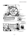
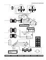
AUDIO TOWER SYSTEM
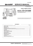
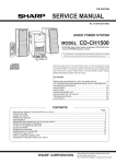
CD-MD3000H
MODEL
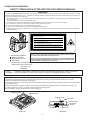
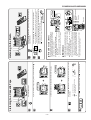
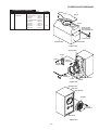
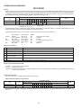
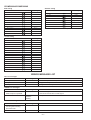
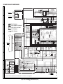
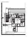
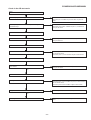
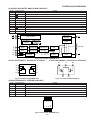
CD-MD3000H Audio Tower System consisting of CD-MD3000H (main
unit) and CP-RW5000H (speaker system).
AUDIO TOWER SYSTEM
Illustration: CD-MD3000H
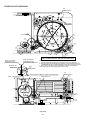
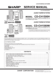
MODEL CD-MD3000W
CD-MD3000W Audio Tower System consisting of CD-MD3000W
(main unit) and CP-RW5000W (speaker system).
• In the interests of user-safety the set should be restored to its original
condition and only parts identical to those specified should be used.
Illustration: CD-MD3000W
• Note for users in U.K.
Recording and playback of any material may require consent
which SHARP is unable to give. Please refer particularly to the
provisions of Copyright Act 1956, the Dramatic and Musical
Prefomers Protection Act 1956, the Preformers Protection Acts
1963 and 1972 and to any subsequent statutory enactments and
orders.
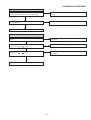
CONTENTS
Page
SAFETY PRECAUTION OF MD SECTION FOR SERVICE MANUAL .............................................................................. 2
SAFETY PRECAUTION OF CD SECTION FOR SERVICE MANUAL (FOR CD-MD3000H) ........................................... 3
IMPORTANT SERVICE NOTES (CD-MD3000H FOR U.K. ONLY) .................................................................................. 3
SAFETY PRECAUTION OF CD SECTION FOR SERVICE MANUAL (FOR CD-MD3000W) ............................................ 4
VOLTAGE SELECTION (FOR CD-MD3000W ONLY) ....................................................................................................... 4
SPECIFICATIONS ............................................................................................................................................................. 5
NAMES OF PARTS ........................................................................................................................................................... 6
OPERATION MANUAL ...................................................................................................................................................... 9
DISASSEMBLY ................................................................................................................................................................ 16
REMOVING AND REINSTALLING THE MAIN PARTS ................................................................................................... 20
CD CHANGER MECHANISM MAIN BASE PARTS ASSEMBLING/ADJUSTING PROCEDURE ................................... 23
ADJUSTMENT ................................................................................................................................................................. 30
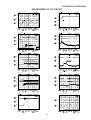
TEST MODE .................................................................................................................................................................... 32
EEPROM WRITING PROCEDURE ................................................................................................................................. 43
ERROR MESSAGE LIST ................................................................................................................................................. 44
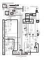
NOTES ON SCHEMATIC DIAGRAM .............................................................................................................................. 46
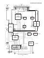
BLOCK DIAGRAM ........................................................................................................................................................... 47
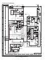
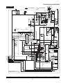
SCHEMATIC DIAGRAM .................................................................................................................................................. 54
WIRING SIDE OF P.W.BOARD ....................................................................................................................................... 70
TYPES OF TRANSISTOR AND LED ............................................................................................................................... 84
VOLTAGE ........................................................................................................................................................................ 84
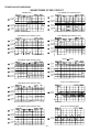
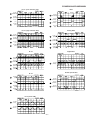
WAVEFORMS OF CD CIRCUIT ...................................................................................................................................... 85
WAVEFORMS OF MD CIRCUIT ..................................................................................................................................... 86
TROUBLESHOOTING ..................................................................................................................................................... 88
FUNCTION TABLE OF IC ................................................................................................................................................ 94
WIRING OF PRIMARILY SUPPLY LEADS (CD-MD3000H FOR U.K. ONLY) ............................................................... 109
LCD DISPLAY ................................................................................................................................................................. 110
PARTS GUIDE/EXPLODED VIEW/ PACKING METHOD (CD-MD3000H FOR U.K. ONLY)
SHARP CORPORATION
This document has been published to be used
for after sales service only.
The contents are subject to change without notice.
CD-MD3000H/CD-MD3000W
SAFETY PRECAUTION OF MD SECTION FOR SERVICE MANUAL
WARNINGS
The AEL (ACCESSIBLE EMISSION LEVEL) of the laser power output is less than class 1 but the laser component is capable of emitting
radiation exceeding the limit for class 1. Therefore it is important that the following precautions are observer during servicing to protect your
eyes against exposure to the laser beam.
1) When the unit case cover is removed and LOADING SW (SW 1956) is turned on and then PLAY SW (SW 1954 mechanism PWB) is turned
on in a few second.
The laser will light for several second to detect a disk.
2) The laser power output of the pickup unit and replacement service parts are all factory pre-set before shipment.
Do not attempt to re-adjust the laser pickup unit during replacement or servicing.
3) Under no circumstances stare into the pickup lens at any time.
4) If laser optical unit becomes faulty, replace the complete laser optical unit.
5) CAUTION-USE of controls or adjustments, or performance of procedures other than those specified herein may result in hazardous
radiation exposure.
CAUTION - INVISIBLE LASER RADIATION WHEN OPEN AND INTERLOCKS DEFEATED
AVOID EXPOSURE TO BEAM .
VARNING - OSYNLIG LASERSTR LNING N R DENNA DEL R …PPNAD OCH SP RRAR
R URKOPPLADE. STR LEN R FARLIG.
ADVARSEL - USYNLIG LASERSTR LING N R DEKSEL PNES OG SIKKERHEDSL S
BRYTES. UNNG EKSPONERING FOR STR LEN.
VARO! AVATTAESSA JA SUOJALUKITUS OHITETTAESSA OLET ALTTIINA
N KYM T…N LASERS TEILYLLE. L KATSO S TEESEN.
VARNING - OSYNLIG LASERSTR LING N R DENNA DEL R …PPNAD OCH SP RREN
R URKOPPLAD. BETRAKTA EJ STR LEN.
ADVARSEL - USYNLIG LASERSTR LING VED BNING N R SIKKERHEDSAFBRYDERE
ER UDE AF FUNKTION. UNDG UDSETTELSE FOR STR LING.
VAROITUS! LAITTEEN KÄYTTÄMINEN MUULLA KUIN TÄSSÄ KÄYTTÖOHJEESSA MAI
NITULLA TAVALLA SAATTAA ALTISTAA KÄYTTÄJÄN TURVALLISUUSLUOKAN 1
Laser Diode Properties
YLITTÄVÄLLE NÄKYMÄTTÖMÄLLE LASERSÄTEILYLLE.
● Material: GaAlAs
VARNING - OM APPARATEN ANVÄNDS PÅ ANNAT SÄTT ÄN I DENNA BRUKSANVISNI
● Wavelength: 785 nm
NG SPECIFICERAS. KAN ANVÄNDAREN UTSÄTTAS FÖR OSYNLIG LASERSTRÅLNING,
SOM ÖVERSKRIDER GRÄNSEN FÖR LASERKLASS 1.
● Pulse time:
Read mode: 0.8 mW Continuous
Write mode: max 10 mW 0.5S
min cycle 1.5S
Repetition
VARO !
VARNING!
Avattaessa ja suojalukitus ohitettaessa olet alttiina näkymättömälle lasersäteilylle. Älä katso säteeseen.
Osynlig laserstralning när denna del är öppnad och spärren är urkopplad. Betrakta ej strälen.
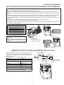
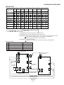
Precaution to be taken when replacing and servicing the laser pickup.
The following precautions must be observed during servicing to protect your eyesvagainst exposure to the laser.
Warning of possible eye damage when repairing:
If the AC power plug is connected when the inner cover of the unit is removed, the laser will light up during focus access (about
1 second) (Fig. 2-1).
During this operation, the laser will leak from the opening between the magnetic head and cartridge holder (Fig. 2-2).
In order to protect your eyes, you must not look at the laser during repair.
Before repairing, be sure to disconnect the AC power plug.
Magnetic Head
Optical Pickup
,,
Magnetic Head
Laser Beam
Cartridge Holder
Mechanism
Chassis
Spindle Motor
Figure 2-1
Optical Pickup
Figure 2-2
–2–
CD-MD3000H/CD-MD3000W
SAFETY PRECAUTION OF CD SECTION FOR SERVICE MANUAL (FOR CD-MD3000H)
WARNINGS
Precaution to be taken when replacing and servicing the Laser Pickup.
The AEL (Accessible Emission Level) of Laser Power Output for this model is specified to be lower than Class 1 Requirements.
However, the following precautions must be observed during servicing to protect your eyes against exposure to the Laser
beam.
(1) When the cabinet has been removed, the power is turned on without a compact disc, and the Pickup is on a position outer
than the lead-in position, the Laser will light for several seconds to detect a disc. Do not look into the Pickup Lens.
(2) The Laser Power Output of the Pickup inside the unit and replacement service parts have already been adjusted prior to
shipping.
(3) No adjustment to the Laser Power should be attempted when replacing or servicing the Pickup.
(4) Under no circumstances look directly into the Pickup Lens at any time.
(5) CAUTION - Use of controls or adjustments, or performance of procedures other than those specified herein may result in
hazardous radiation exposure.
CAUTION-INVISIBLE LASER RADIATION WHEN OPEN. DO NOT STARE INTO
BEAM OR VIEW DIRECTLY WITH OPTICAL INSTRUMENTS.
VARNING-OSYNLIG LASERSTRALNING NAR DENNA DEL AR OPPNAD. STIRRA
EJ IN I STRALEN OCH BETRAKTA EJ STRALEN MED OPTISKA INSTRUMENT.
ADVERSEL-USYNLIG LASERSTRALING VED ABNING. SE IKKE IND I
STRALEN-HELLER IKKE MED OPTISKE INSTRUMENTER.
VARO! AVATTAESSA OLET ALTTIINA NAKYMATON LASERSATEILYLLE.
ALA TUIJOTA SATEESEEN ALAKA KATSO SITA OPTISEN LAITTEEN LAPI.
VARNING-OSYNLIG LASERSTRALNING NAR DENNA DEL AR OPPNAD.
STIRRA EJ IN I STRALEN OCH BETRAKTA EJ STRALEN GENOM OPTISKT
INSTRUMENT.
ADVERSEL-USYNLIG LASERSTRALING NAR DEKSEL APNES. STIRR IKKE
INN I STRALEN ELLER SE DIREKTE MED OPTISKE INSTRUMENTER.
VAROITUS! LAITTEEN KÄYTTÄMINEN MUULLA KUIN TÄSSÄ
KÄYTTÖOHJEESSA MAINITULLA TAVALLA SAATTAA ALTISTAA
KÄYTTÄJÄN TURVALLISUUSLUOKAN 1 YLITTÄVÄLLE NÄKYMÄTTÖMÄLLE
LASERSÄTEILYLLE.
VARNING - OM APPARATEN ANVÄNDS PÅ ANNAT SÄTT ÄN I DENNA
BRUKSANVISNING SPECIFICERAS. KAN ANVÄNDAREN UTSÄTTAS FÖR
OSYNLIG LASERSTRÅLNING, SOM ÖVERSKRIDER GRÄNSEN FÖR
LASERKLASS 1.
(For U.K.)
Laser Diode Properties
Material: GaAIAs
Wavelength: 780 nm
Emission Duration: continuous
Laser Output: max. 0.6 mW
(Except for U.K.)
IMPORTANT SERVICE NOTES (CD-MD3000H FOR U.K. ONLY)
Before returning the unit to the customer after completion of a
repair or adjustment it is necessary for the following withstand
voltage test to be applied to ensure the unit is safe for the
customer to use.
Setting of Withstanding Voltage Tester and set.
Set name
WITHSTANDING
VOLTAGE TESTER
OUT
UNIT
set value
SHORT-CIRCUIT
AC POWER
SUPPLY CORD
Withstanding Voltage Tester
Test voltage
PROBE
AC
4,240 VPEAK
3,000 VRMS
Set time
6 secs
Set current (Cutoff current)
4 mA
Unit
Judgment
OK: The “GOOD” lamp lights.
NG: The “NG” lamp lights and the buzzer sounds.
CHASSIS SCREW
–3–
CONNECT THE PROBE
TO GND OF CHASSIS
SCREW
CD-MD3000H/CD-MD3000W
SAFETY PRECAUTION OF CD SECTION FOR SERVICE MANUAL (FOR CD-MD3000W)
WARNINGS
Precaution to be taken when replacing and servicing the Laser Pickup.
The AEL (Accessible Emission Level) of Laser Power Output for this model is specified to be lower than Class 1 Requirements.
However, the following precautions must be observed during servicing to protect your eyes against exposure to the Laser
beam.
(1) When the cabinet has been removed, the power is turned on without a compact disc, and the Pickup is on a position outer
than the lead-in position, the Laser will light for several seconds to detect a disc. Do not look into the Pickup Lens.
(2) The Laser Power Output of the Pickup inside the unit and replacement service parts have already been adjusted prior to
shipping.
(3) No adjustment to the Laser Power should be attempted when replacing or servicing the Pickup.
(4) Under no circumstances look directly into the Pickup Lens at any time.
(5) CAUTION - Use of controls or adjustments, or performance of procedures other than those specified herein may result in
hazardous radiation exposure.
CAUTION
Laser Diode Properties
Material: GaAIAs
Wavelength: 780 nm
Emission Duration: continuous
Laser Output: max. 0.6 mW
CAUTION-INVISIBLE LASER RADIATION WHEN OPEN. DO NOT STARE INTO
BEAM OR VIEW DIRECTLY WITH OPTICAL INSTRUMENTS.
VARNING-OSYNLIG LASERSTRALNING NAR DENNA DEL AR OPPNAD. STIRRA
EJ IN I STRALEN OCH BETRAKTA EJ STRALEN MED OPTISKA INSTRUMENT.
ADVERSEL-USYNLIG LASERSTRALING VED ABNING. SE IKKE IND I
STRALEN-HELLER IKKE MED OPTISKE INSTRUMENTER.
VARO! AVATTAESSA OLET ALTTIINA NAKYMATON LASERSATEILYLLE.
ALA TUIJOTA SATEESEEN ALAKA KATSO SITA OPTISEN LAITTEEN LAPI.
This Audio Tower System is classified as a CLASS 1 LASER product.
The CLASS 1 LASER PRODUCT label is located on the
rear cover.
VARNING-OSYNLIG LASERSTRALNING NAR DENNA DEL AR OPPNAD.
STIRRA EJ IN I STRALEN OCH BETRAKTA EJ STRALEN GENOM OPTISKT
INSTRUMENT.
ADVERSEL-USYNLIG LASERSTRALING NAR DEKSEL APNES. STIRR IKKE
INN I STRALEN ELLER SE DIREKTE MED OPTISKE INSTRUMENTER.
Use of controls, adjustments or performance of procedures other than those specified herein may result in hazardous radiation exposure.
As the laser beam used in this compact disc player is
harmful to the eyes, do not attempt to disassemble the
cabinet. Refer servicing to qualified personnel only.
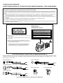
VOLTAGE SELECTION (FOR CD-MD3000W ONLY)
Before operating the unit on mains, check the preset voltage. If the voltage is different from your local voltage, adjust the voltage
as follows, Turn the selector with a screwdriver until the appropriate voltage number appears in the window (110 V, 127 V,
220 V or 230 V - 240 V AC).
QACCA0003AW00
QACCL0005AW00
QACCB0009AW00
QPLGA0003AWZZ
QACCE0008AW00
Figure 4 AC POWER SUPPLY CORD AND PLUG ADAPTOR
–4–
QPLGA0004AWZZ
CD-MD3000H/CD-MD3000W
FOR A COMPLETE DESCRIPTION OF THE OPERATION OF THIS UNIT, PLEASE REFER
TO THE OPERATION MANUAL.
SPECIFICATIONS
CD-MD3000H/CD-MD3000W
■ General (CD-MD3000H)
■ CD player
Power source
AC 230 V, 50 Hz
Type
Power consumption
Power on: 180 W
Power stand-by: 0.6 W (*)
Signal readout
Non-contact, 3-beam semiconductor laser pickup
D/A converter
1-bit D/A converter
Width: 200 mm (7-7/8")
Height: 352 mm (13-7/8")
Depth: 377 mm (14-7/8")
Frequency response
20 - 20,000 Hz
Dynamic range
90 dB (1 kHz)
Dimensions
Weight
10.3 kg (22.7 lbs.)
(*) This power consumption value is obtained when the demonstration mode is cancelled in the power stand-by mode.
■ General (CD-MD3000W)
6-disc multi-play compact disc changer player
■ MiniDisc
Type
MiniDisc recorder
Signal readout
Non-contact, 3-beam semiconductor laser pickup
Rotation speed
400 - 900 rpm CLV, Approx.
Error correction
ACIRC (Advanced Cross Interleave Reed-Solomon
Code)
Power source
AC 110/127/220/230 - 240 V, 50/60 Hz
Power consumption
180 W
Quantization
20-bit linear (A/D converter)
Dimensions
Width: 200 mm (7-7/8")
Height: 352 mm (13-7/8")
Depth: 377 mm (14-7/8")
Coding
ATRAC (Adaptive Transform Acoustic Coding)
Sampling frequency
44.1 kHz
10.9 kg (24.0 lbs.)
Recording method
Magnetic modulation overwrite method
Frequency response
20 - 20,000 Hz
D/A converter
1-bit D/A converter
Wow and flutter
Unmeasurable (less than 0.001% W. peak)
Signal/noise ratio
95 dB (1 kHz)
Dynamic range
90 dB (1 kHz)
Audio channel
Stereo: 2 channels
Monaural: 1 channel (playback only)
(long-time recording mode)
Weight
■ Amplifier (CD-MD3000H for U.K.)
Output power
RMS: 200 W (100 W + 100 W) (10 % T.H.D.)
Main speaker (woofer and tweeter); 80 W (40 W + 40 W)
Subwoofer; 120 W (60 W + 60 W)
RMS: 184 W (92 W + 92 W) (0.9 % T.H.D.)
Main speaker (woofer and tweeter); 74 W (37 W + 37 W)
Subwoofer; 110 W (55 W + 55 W)
Output terminals
Speakers: 6 ohms
Headphones: 16-50 ohms (recommended; 32 ohms)
Input terminals
Auxiliary: 500 mV/47 kohms
Digital input (optical)
■ Amplifier (CD-MD3000H except for U.K.)
Output power
PMPO: 668 W
MPO: 334 W (167 W + 167 W) (DIN 45 324)
Main speaker (woofer and tweeter): 134 W (67 W + 67 W)
■ Cassette deck
(CD-MD3000H for U.K./CD-MD3000W)
Frequency response
50 - 14,000 Hz (Normal tape)
Signal/noise ratio
50 dB (recording/playback)
Wow and flutter
0.3 % (WRMS)
■ Cassette deck (CD-MD3000H except for U.K.)
Subwoofer: 200 W (100 W + 100 W)
Frequency response
50 - 14,000 Hz (Normal tape)
RMS: 200 W (100 W + 100 W) (DIN 45 324)
Signal/noise ratio
50 dB (recording/playback)
Main speaker (woofer and tweeter): 80 W (40 W + 40 W)
Wow and flutter
0.3 % (DIN 45 511)
Subwoofer: 120 W (60 W + 60 W)
RMS: 184 W (92 W + 92 W) (DIN 45 500)
Main speaker (woofer and tweeter): 74 W (37 W + 37 W)
■ Tuner (CD-MD3000H for U.K.)
Frequency range
FM: 87.50 -108.00 MHz
AM: 522 - 1,620 kHz
Subwoofer: 110 W (55 W + 55 W)
Output terminals
Speakers: 6 ohms
Headphones: 16 - 50 ohms (recommended: 32 ohms)
Input terminals
■ Tuner (CD-MD3000H except for U.K.)
Frequency range
Auxiliary: 500 mV/47 kohms
FM: 87.5 -108 MHz
AM: 522 -1,620 kHz
Digital input (optical)
■ Amplifier (CD-MD3000W)
Output power
■ Tuner (CD-MD3000W)
Frequency range
MPO: 334 W (167 W + 167 W) (10 % T.H.D.)
FM: 88 -108 MHz
AM: 531 -1,602 kHz
Main speaker (woofer and tweeter): 134 W (67 W + 67 W)
CP-RW5000H/CP-RW5000W
Subwoofer: 200 W (100 W + 100 W)
RMS: 200 W (100 W + 100 W) (10 % T.H.D.)
Type
3-way type speaker system
5 cm (2") Tweeter
13 cm (5-1/4") Woofer
13 cm (5-1/4") Subwoofer
RMS: 184 W (92 W + 92 W) (0.9 % T.H.D.)
Maximum input power (Total)
200 W
Main speaker (woofer and tweeter): 74 W (37 W + 37 W)
Rated input power (Total)
100 W
Subwoofer: 110 W (55 W + 55 W)
Impedance
6 ohms
Speakers: 6 ohms
Dimensions
Width: 210 mm (8-1/4")
Height: 392 mm (15-7/16")
Depth: 345 mm (13-9/16")
Weight
5.1 kg (11.2 lbs.)/each
Main speaker (woofer and tweeter): 80 W (40 W + 40 W)
Subwoofer: 120 W (60 W + 60 W)
Output terminals
Headphones: 16 - 50 ohms (recommended: 32 ohms)
Input terminals
Auxiliary: 500 mV/47 kohms
Digital input (optical)
Specifications for this model are subject to change without
prior notice.
–5–
CD-MD3000H/CD-MD3000W
CD-MD3000H/CD-MD3000W
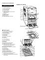
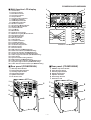
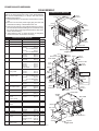
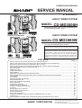
NAMES OF PARTS
■ Front panel
01.
02.
03.
04.
05.
06.
07.
08.
09.
10.
11.
Cassette Compartment
Volume Up/Demo Button
Volume Down Button
Timer Set Indicator
On/Stand-by Button
CD Direct Play Buttons (with Indicator)/
CD Eject Buttons
Disc Trays
Headphone Socket
MD Eject Button
MD Compartment
Control Panel Open/Close Button
1
2
3
9
10
4
5
6
11
7
8
Illustration: CD-MD3000H
■ Control panel
12.
13.
14.
15.
16.
17.
18.
19.
20.
CD/MD Play Mode Select Button
Equalizer Mode Select Button
Extra Bass Button
Name/Toc Edit Button
Delete Button
Menu Button
Display/Character Button
Jog Dial
Enter Button
21.
22.
23.
24.
25.
26.
27.
Tuner (Band) Button
MD Track Edit Button
CD Button
MD Button
CD MD One Touch Edit Button
MD Auto Mark Select Button
CD/MD Fast Reverse, Tape Fast Wind or
Tuning Down Button (with Indicator)
Stop Button (with Indicator)
Tape Reverse Play Button (with Indicator)
Tape Button
Auxiliary Button
MD Record Button
MD Record Mode Button
MD Record Speed Select Button
Tape Record Pause Button
CD/MD Fast Forward, Tape Fast Wind or
Tuning Up Button (with Indicator)
CD/MD Play or Pause, Tape Forward Play Button
(with Indicator)
28.
29.
30.
31.
32.
33.
34.
35.
36.
37.
12
13 14
17
18
19
20
15
16
21
22
30
23
31
24
32
25
33
26
34
27
35
28
36
29
37
–6–
CD-MD3000H/CD-MD3000W
■ Multi-function LCD display
01.
02.
03.
04.
05.
06.
07.
08.
09.
10.
11.
12.
13.
14.
15.
16.
17.
18.
19.
20.
21.
22.
23.
24.
25.
26.
27.
28.
29.
30.
31.
32.
33.
34.
35.
36.
37.
38.
CD Indicators
Function Indicator
Extra Bass Indicator
Timer Play Indicator
Sleep Indicator
Timer Recording Indicator
CD/MD Play Indicator
CD/MD Repeat Indicator
CD/MD Pause Indicator
FM Stereo Indicator
Tape Reverse Mode Indicator
FM Stereo Mode Indicator
Cassette Indicator
Level Meter
MD Indicator
Digital Source Indicator
Monaural Long-Play Mode Indicator
Disc Name Indicator
Auto Mark Indicator
Memory Indicator
Total Indicator
Track Name Indicator
Track Edit Indicator
Random Play Indicator
CD All Disc Play Indicator
Remain Indicator
Record Indicator
RDS Indicator (CD-MD3000H Only)
Radio Text Indicator (CD-MD3000H Only)
Clock Time Indicator (CD-MD3000H Only)
Dynamic PTY Indicator (CD-MD3000H Only)
Traffic Programme Indicator (CD-MD3000H Only)
TOC Indicator
Synchronised Recording Indicator
EON Indicator (CD-MD3000H Only)
Traffic Information Indicator (CD-MD3000H Only)
Programme Type Indicator (CD-MD3000H Only)
Traffic Announcement Indicator (CD-MD3000H Only)
7
1
8
9
2
3
4
10
5
11
13
6
18
19
20
21
14
15
22
23
24
25
26
16
17
27
28
29
30
31
32
12
33
34
35
36
37
38
Illustration: CD-MD3000H
■ Rear panel (CD-MD3000H)
■ Rear panel (CD-MD3000W)
01.
02.
03.
04.
05.
06.
01.
02.
03.
04.
05.
06.
07.
AM Loop Aerial Socket
FM 75 Ohms Aerial Socket
Auxiliary Input Sockets
Digital Input Socket
Speaker Terminals
AC Power Lead
1
FM/AM Loop Aerial Socket
Span Selector Switch
Auxiliary Input Sockets
Digital Input Socket
Speaker Terminals
AC Voltage Selector
AC Power Lead
1
5
5
2
2
3
3
4
6
4
6
7
–7–
CD-MD3000H/CD-MD3000W
■ Remote control (CD-MD3000H)
01.
02.
03.
04.
05.
06.
07.
08.
09.
10.
11.
12.
13.
14.
15.
16.
17.
18.
19.
20.
21.
22.
23.
24.
25.
26.
27.
28.
29.
30.
31.
32.
33.
Remote Control Transmitter
CD Button
MD Button
Tape Button
CD Direct Play Buttons
Clear Button
Memory Button
CD/MD Fast Reverse, Tape Fast Wind or
Preset Down Button
Enter Button
Stop Button
Menu Button
MD Record Button
MD Record Mode Button
Time Button
FM Stereo Mode Button
Control Panel Open/Close Button
Tuner (Band) Button
Auxiliary Button
On/Stand-by Button
RDS Programme Type/T
RDS EON Button
RDS ASPM (Auto Station Programme Memory) Button
RDS Display Mode Selector Button
CD/MD Play Mode Select Button
CD/MD Fast Forward, Tape Fast Wind or
Preset Up Button
CD/MD Play or Pause, Tape Play Button
Tape Reverse Mode Select Button
Tape Record Pause Button
Dimmer Button
Display Button
Equalizer Mode Select Button
Extra Bass Button
Volume Up or Down Buttons
1
17
2
18
3
19
4
20
5
21
6
22
7
23
8
24
9
25
10
26
11
27
12
28
13
29
14
30
15
31
16
32
33
■ Remote control (CD-MD3000W)
1
14
1. Remote Control Transmitter
2. CD Button
3. MD Button
4. Tape Button
5. CD Direct Play Buttons
6. Clear Button
7. Memory Button
8. CD/MD Fast Reverse, Tape Fast Wind or
Preset Down Button
9. Enter Button
10. Stop Button
11. MD Record Button
12. MD Record Mode Button
13. Control Panel Open/Close Button
14. Tuner (Band) Button
15. Auxiliary Button
16. On/Stand-by Button
17. Time Button
18. FM Stereo Mode Button
19. Display Button
20. Dimmer Button
21. CD/MD Play Mode Select Button
22. CD/MD Fast Forward, Tape Fast Wind or
Preset Up Button
23. CD/MD Play or Pause, Tape Play Button
24. Menu Button
25. Tape Record Pause Button
26. Tape Reverse Mode Select Button
27. Equalizer Mode Select Button
28. Extra Bass Button
29. Volume Up or Down Buttons
2
15
3
16
4
17
18
5
19
6
20
7
21
8
22
23
9
24
10
25
11
26
12
27
28
13
29
CP-RW5000H/CP-RW5000W
01.
02.
03.
4.
5.
6.
Tweeter
Woofer
Bass Reflex Duct
Subwoofer
Subwoofer Terminals
Main Speaker Terminals
1
4
2
5
3
–8–
6
CD-MD3000H/CD-MD3000W
OPERATION MANUAL
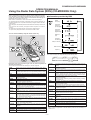
Using the Radio Data System (RDS) (CD-MD3000H Only)
RDS is a broadcasting service which a growing number of FM stations provide.
These FM stations send additional signals along with their regular programme
signals. They send their station names, and information about the type of
programme such as sports or music, etc.
When tuned to an RDS station, “RDS” and the station name will be displayed.
“TP” (Traffic Programme) will appear on the display when the received broadcast carries traffic information, and “TA” (Traffic Announcement) will appear whilst a traffic information is on air.
“EON” will appear whilst the EON (Enhanced Other Networks information) data is broadcast.
“PTYI” (Dynamic PTY Indicator) will appear whilst the Dynamic PTY station is
received.
“RT” (Radio Text) will appear whilst the unit receives the Radio text data.
“CT” (Clock Time) will appear whilst the unit receives the RDS CT data.
■ Information provided by RDS
Each time the DISP MODE button is pressed, the display will switch as follows:
Station
name (PS)
Programme
type (PTY)
(8 Languages)
Programme
type (PTY)
(English fixed)
You can control the RDS by using the remote control only.
Radio text
(RT)
Clock-time
and date (CT)
Date (for 3 seconds)
RDS clock time
Frequency
When you are tuning in to a station other than an RDS station or to an RDS station
which sends weak signal, the display will change in the following order:
NO PS
FM 98.80 MHz
Descriptions of the PTY (Programme Type) codes, TP (Traffic Programme) and
TA (Traffic Announcement)
You can search for and receive the following PTY, TP and TA signals.
NO PTY
NO RT
NO CT
SOCIAL
Programmes about people and things that influence them individually
or in groups. Includes: sociology, history, geography, psychology and
society.
RELIGION
Any aspect of beliefs and faiths, involving a God or Gods, the nature
of existence and ethics.
PHONE IN
Involving members of the public expressing their views either by phone
or at a public forum.
TRAVEL
Features and programmes concerned with travel to near and far destinations, package tours and travel ideas and opportunities. Not for
use for announcements about problems, delays, or roadworks affecting immediate travel where TP/TA should be used.
LEISURE
Programmes concerned with recreational activities in which the listener might participate.
Examples include, Gardening, Fishing, Antique collecting, Cooking,
Food & Wine, etc.
NEWS
Short accounts of facts, events and publicly expressed views, reportage and actuality.
AFFAIRS
Topical programme expanding or enlarging upon the news, generally
in different presentation style or concept, including debate, or analysis.
INFO
Programmes whose purpose is to impart advice in the widest sense.
SPORT
Programme concerned with any aspect of sport.
EDUCATE
Programme intended primarily to educate, of which the formal element is fundamental.
DRAMA
All radio plays and serials.
CULTURE
Programmes concerned with any aspect of national or regional culture, including language, theatre, etc.
JAZZ
Polyphonic, syncopated music characterised by improvisation.
SCIENCE
Programmes about the natural sciences and technology.
COUNTRY
VARIED
Used for mainly speech-based programmes usually of light-entertainment nature, not covered by other categories. Examples include: quizzes, panel games, personality interviews.
Songs which originate from, or continue the musical tradition of the
American Southern States.
Characterised by a straightforward melody and narrative story line.
NATION M
POP M
Commercial music, which would generally be considered to be of current popular appeal, often featuring in current or recent record sales
charts.
Current Popular Music of the Nation or Region in that country's language, as opposed to International 'Pop' which is usually US or UK
inspired and in English.
OLDIES
Music from the so-called “golden age” of popular music.
ROCK M
Contemporary modern music, usually written and performed by young
musicians.
FOLK M
EASY M
Current contemporary music considered to be “easy-listening”, as opposed to Pop, Rock or Classical, or one of the specialised music styles,
Jazz, Folk or Country. Music in this category is often but not always,
vocal, and usually of short duration.
Music which has its roots in the musical culture of a particular nation,
usually played on acoustic instruments. The narrative or story may be
based on historical events of the people.
DOCUMENT
Programme concerned with factual matters, presented in an investigative style.
TEST
LIGHT M
Classical music for general, rather than specialist appreciation. Examples of music in this category are instrumental music, and vocal or
choral works.
Broadcast when testing emergency broadcast equipment or receivers.
ALARM !
Emergency announcement made under exceptional circumstances
to give warning of events causing danger of general nature.
Performances of major orchestral works, symphonies, chamber music, etc., and including Grand Opera.
NONE
No programme type (receive only).
TP
Broadcasts which carry traffic announcements.
TA
Traffic announcements are being broadcast.
CLASSICS
OTHER M
Musical styles not fitting into any of the other categories. Particularly
used for specialist music of which Rhythm & Blues and Reggae are
examples.
WEATHER
Weather reports and forecasts and meteorological information.
FINANCE
Stock Market reports, commerce, trading, etc.
CHILDREN
For programmes targeted at a young audience, primarily for entertainment and interest, rather than where the objective is to educate.
Note:
When you select a programme in the EON stand-by mode, the unit will display “TI”
instead of “TA”.
–9–
CD-MD3000H/CD-MD3000W
Setting the Clock
5
Turn the jog dial to adjust the hour and within 2 minutes, press
the ENTER button.
● When the 12-hour display is selected, “AM” will change automatically to “PM”.
6
Turn the jog dial to adjust the minutes and within 2 minutes, press
the ENTER button.
● The hour will not advance even if minutes advance from “59” to “00”.
● The clock starts from “0” second. (Seconds are not displayed.)
The time display will disappear after a few seconds.
In this example, the clock is set for the 24-hour (0:00) display.
1
2
3
Press the ON/STAND-BY button to turn the power on.
Press the MENU button.
Turn the jog dial to select “CLOCK” and within 10 seconds, press
the ENTER button.
To confirm the time display:
[When the stand-by mode]
Press the DISPLAY button on the remote control.
The time display will appear for about 3 seconds.
[When the power is on]
Press the MENU button.
The time display will appear for about 10 seconds.
Note:
“CLOCK” will appear or time will flash at the push of the DISPLAY button when the AC
power supply is restored after a power failure or after unplugging the unit.
Reset the clock as follows.
To reset the clock:
4
Turn the jog dial to select the 24-hour or 12-hour display and
within 2 minutes, press the ENTER button.
“0:00”
→ The 24-hour display will appear. (0:00 - 23:59)
“AM 12:00” → The 12-hour display will appear. (AM 12:00 - PM 11:59)
“AM 0:00” → The 12-hour display will appear. (AM 0:00 - PM 11:59)
What is a MiniDisc?
[When time will flash]
1. Press the ON/STAND-BY button.
2. Press the MENU button.
3. Press the ENTER button.
4. Perform “Setting the Clock” from step 5.
[When “CLOCK” will appear]
Perform “Setting the Clock” from the beginning.
To change the 24-hour or 12-hour display:
1. Clear all the programmed contents.
[Refer to “If trouble occurs (reset)” on page 57 for details.]
2. Preform “Setting the clock” from the beginning.
MiniDisc System Limitations
The disc is stored in a cartridge. You can handle it easily without worrying about dust,
fingerprints, etc. However, dust entering the opening of the cartridge, dirt on the cartridge, warping, etc. may cause malfunctions. Please note the following.
■ To prevent recorded MiniDiscs from being
Even if the maximum recording time of a MiniDisc has not
been reached, “TOC FULL”
may be displayed.
erased accidentally
Slide the accidental erase prevention tab, located on the side of the MiniDisc, in the
direction indicated by the arrow.
● The MiniDisc will then be protected against accidental erasure.
Recordable
Recording
prevented
To add a recording to such a MiniDisc, slide the accidental erase prevention tab back
to its original position.
Even if the maximum recording time of a MiniDisc has not
been reached, “DISC FULL”
may be displayed.
Even if several short tracks
are erased, the remaining recording time may not show an
increase.
Two tracks may not be combined in editing.
■ Helpful tip when attaching a label
When attaching a label to a MiniDisc cartridge, be sure to note the following. If the label
is not attached properly, the MiniDisc may jam inside the unit and it may not be possible to remove it.
● If the label peels off or partially lifts away, replace it with a new one.
● Do not put a new label on top of an existing one.
● Attach the label only in the specified location.
The total of the recorded time
and time remaining on a disc
may not add up to the maximum possible recording time.
■ Types of discs
There are two types of discs: playback-only and recordable types.
● Playback-only MiniDisc:
This type of MiniDisc is used for commercially available
prerecorded music. This is the same kind of optical disc
as CDs. Playback is performed using an optical pickup.
(Recording and editing are not possible.)
● Recordable MiniDisc:
A Shutter will be used on
only one side (back).
If recorded tracks are fast reversed or fast forwarded, the
sound may skip.
This is a “raw disc” on which recording can be performed.
A magneto optical disc is used. Recordings are made
using a laser and magnetic field. Repeated recording is
possible.
Shutters will be used on
both sides.
– 10 –
In the MD system, the delimiter of the recording area
on a MiniDisc is programmed in a TOC. If partial erasing, recording and editing are repeated several times,
TOC information will fill up, even though the number
of tracks has not reached the limit (255 tracks), and
further recording will be impossible. (If you use the
all erase function, this MiniDisc can be used from
the beginning.)
If there is any flaw on the MiniDisc, that part is automatically excluded from the space available for recording. Therefore, the recording time becomes
shorter.
When the remaining recording time of a disc is displayed, short tracks less than 12 seconds long may
not be included in the total.
For MiniDiscs on which repeated recording and editing operations were performed, the COMBINE function may not work.
A track recorded from a CD (digital recording) and a
track recorded from a radio or other equipment (analogue recording) cannot be combined.
A cluster (about 2 seconds) is normally the minimum
unit of recording. So, even if a track is less than 2
seconds long, it will use about 2 seconds of space
on the disc. Therefore, the time actually available for
recording may be less than the remaining time displayed.
If there are scratches on discs, those sections will
be automatically avoided (no recording will be placed
in those sections). Therefore, the recording time will
be reduced.
A MiniDisc which has been recorded or edited repeatedly may skip during fast reverse or fast forward.
CD-MD3000H/CD-MD3000W
Error Messages
When an error message is displayed, proceed as follows:
Error messages
Meaning
BLANK DISC
● Nothing is recorded.
(Neither music nor disc name
is recorded.)
CAN'T COPY
● You tried to record from a
copy prohibited CD.
CAN'T EDIT
● A track cannot be edited.
CAN'T READ
( :Number or
symbol)
● The disc is damaged.
● TOC information cannot be
read.
● MiniDisc not specified.
CAN'T REC
● Recording cannot be performed correctly due to vibration or shock in the unit.
● The TOC information could
not be created properly due
to a mechanical shock or to
scratches on the disc.
CAN'T WRITE
● The disc is out of recording
space.
● The CD tray is not working
properly.
DISC FULL
E-CD 20
E-MD
( :Number or
symbol)
EDIT OVER
MD NO DISC
CD NO DISC
● A MiniDisc is not working
properly.
● You chose 32 or more tracks
for track editing.
● A MiniDisc has not been
loaded.
● The MiniDisc data cannot be
read.
● A CD has not been loaded.
● The CD data cannot be read.
Remedy
● Replace it with another disc.
● Replace the CD.
● Change the stop position of the
track and then try editing it.
● Replace it with another disc.
● Erase the disc and try recording again.
● Re-record or replace the
MiniDisc.
● Set this unit to the stand-by
mode and try to write the
TOC again. (Remove any
source of shock or vibration
whilst writing.)
● Replace the disc with another
recordable disc.
● Set this unit to the stand-by
mode and turn the power on
again.
● Set this unit to the stand-by
mode and turn the power on
again.
● Decrease the number of
tracks.
● Load a MiniDisc.
● Reload the MiniDisc.
● Load a CD.
● Reload the CD.
Meaning
Error messages
● The number of characters for
NAME FULL
the disc name or track name
exceeds 40.
NO SIGNAL
● Poor connection of the digital
cable.
● No output signal comes out
from the connected unit to
playback.
NOT AUDIO
● The data recorded on this
disc is not audio data.
OVER
● There is no space to make
CD editing on the disc.
PLAY MD
● You tried to record on a playback-only disc.
PROTECTED
● The disc is write protected.
TEMP OVER
TOC FORM
( :Number or
symbol)
TOC FULL
? DISC
Remedy
● Shorten the disc or track
name.
● Connect the digital cable
securely.
● Playback with the connected
unit.
● Select another track.
● Replace the disc.
● Replace it with a disc that has
enough time to record.
● Replace it with another recordable disc.
● Move the write protection tab
back to its original position.
● The temperature is too high. ● Set this unit to the stand-by
mode and wait for a whilst.
● TOC information recorded on ● Replace it with another disc.
the MD does not match the ● Erase the disc and try recordMiniDisc specifications or it
ing again.
cannot be read.
● There is no space left for re- ● Replace it with another recording track numbers.
cordable disc.
● There is no space left for re- ● Erase the needless characcording character informaters.
tion.
● The data contains an error.
● Replace it with another disc.
● MiniDisc not specified.
Troubleshooting Chart
Many potential “problems” can be resolved by the owner without calling a service technician. If something is wrong with this product, check the following before calling your
authorised SHARP dealer or service centre.
■ Cassette deck
■ General
Symptom
● The clock is not on time.
●
● When a button is pressed, the unit
●
does not respond.
●
● No sound is heard.
●
●
●
Possible cause
Did a power failure occur?
Reset the clock. (Refer to page 17.)
Set this unit to the power stand-by mode
and then turn it back on.
If the unit still malfunctions, reset it.
(Refer to page 57.)
Is the volume level set to “0”?
Are the headphones connected?
Are the speaker wires disconnected?
● Is the erase-protection tab removed?
● Cannot record tracks with proper
● Is it a normal tape?
●
●
●
●
●
sound quality.
Cannot erase completely.
Sound skipping.
Cannot hear treble.
Sound fluctuation.
Cannot remove the tape.
■ CD player
Symptom
● Playback does not start.
● Playback stops in the middle or is
not performed properly.
● Playback sounds are skipped, or
stopped in the middle of a track.
Possible cause
● The disc is loaded up-side down.
● The disc does not satisfy the standards.
● The disc is distorted or scratched.
■ MiniDisc
Possible cause
●
loaded, “NO DISC” or “CAN'T
READ” is displayed.
● Playback sounds are skipped.
Possible cause
● The stereo system is placed near the TV
secutively.
or computer.
● FM/AM loop aerial is not placed prop-
erly. Move the AC power lead away from
the aerial if located near.
■ Remote control
● The remote control does not op-
●
●
●
Possible cause
● Is the AC power lead of the stereo sys-
erate.
● Is the MiniDisc protected against acci●
● Even though a disc has been
Symptom
● Radio makes unusual noise con-
Symptom
Symptom
● A recording cannot be made.
(You cannot record on a metal or CrO2
tape.)
● Is there any slack? Is the tape stretched?
● Are the capstans, pinch rollers, or heads
dirty?
● If a power failure occurs during playback,
the heads remain engaged with the tape.
Do not open the compartment forcibly.
Wait until electricity resumes.
■ Tuner
● Is the unit located near excessive vibra-
tions?
● The disc is very dirty.
● Has condensation formed inside the
unit?
Possible cause
Symptom
● Cannot record.
●
●
●
●
dental erasure?
Did you try to make recording on a playback-only MiniDisc?
Can you see the "DISC FULL" or "TOC
FULL" message in the display?
The disc is very dirty.
Is the unit located near excessive vibrations?
Has condensation formed inside the
unit?
– 11 –
tem plugged in?
The battery polarity is not correct.
The batteries are dead.
Incorrect distance or angle.
Does the remote control sensor receive
strong light?
CD-MD3000H/CD-MD3000W
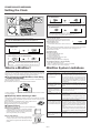
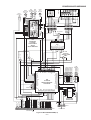
System Connections (For CD-MD3000W Only)
Setting the AC voltage selector
Connecting the AC power lead
Check the setting of the AC voltage selector located on the rear panel before plugging the unit into an AC socket. If necessary, adjust the selector to correspond to the
AC power voltage used in your area.
After making all connections, plug the unit. If you plug the unit first, the unit
will enter the demonstration mode
1
2
Notes:
Plug the AC power lead into an AC socket, after any connections.
Unplug the AC power lead from the AC socket if the unit will not be in use for a prolonged period of time.
Turn the selector with a screwdriver until the appropriate voltage number
appears in the window (110 V, 127 V, 220 V or 230 V - 240 V AC).
AC Plug Adaptor
In areas (or countries) where an AC socket as shown in illustration
is used, connect the unit using the AC plug adaptor supplied with the unit, as illustrated. The AC
plug adaptor is not included in areas where the AC wall socket and AC power plug
can be directly connected (see illustration ).
Note for users in Australia and New Zealand:
An AC plug adaptor is not supplied if the lead has an Australian Standard plug.
Setting the FM/AM span selector
(For CD-MD3000W Only)
The International Telecommunication Union (ITU) has established that member countries should maintain either a 100 kHz or a 50 kHz interval between broadcasting frequencies of FM stations and 10 kHz or 9 kHz for AM station. The illustration shows
the 50/9 kHz zones (regions 1 and 3), and the 100/10 kHz zone (region 2).
Before using the unit, set the SPAN SELECTOR switch (on the rear panel) to the
interval (span) of your area.
To change the tuning zone:
1
2
Press the ON/STAND-BY button to enter the stand-by mode.
Set the SPAN SELECTOR switch (on the rear panel) as follows.
For 50 kHz FM interval (9 kHz in AM) 50/9
For 100 kHz FM interval (10 kHz in AM) 100/10
3
Whilst pressing down the VOLUME button, press the ON/STANDBY button until "ALL CLEAR" appears.
Caution:
This operation will erase all data stored in memory including clock, timer settings,
tuner preset, and CD or MiniDisc programme.
– 12 –
Remote control × 1
– 13 –
Remote control × 1
Speaker wire for
SUBWOOFER terminals × 2
Black
Speaker wire for
MAIN terminals × 2
Black
Black
Speaker wire for
SUBWOOFER terminals × 2
Red
1
Remove the
battery cover.
2
Insert the batteries
as shown.
3
Replace the cover.
Battery installation of remote control
Blue
FM/AM loop aerial × 1
Use 2 “AA” size batteries (UM/SUM-3, R6, HP-7 or similar).
1
2
Speaker wire for
MAIN terminals × 2
Black
Red
FM aerial × 1
Accessories (FOR CD-MD3000W)
“AA” size battery
(UM/SUM-3, R6, HP-7 or similar) × 2
1
Blue
AM loop aerial × 1
Accessories (FOR CD-MD3000H)
“AA” size battery
(UM/SUM-3, R6, HP-7 or similar) × 2
1
(For
CD-MD3000H)
Connection cable
for digital recording
(not supplied)
Right speaker
AM loop
aerial
FM aerial
Span Selector
Switch
(CD-MD300W Only)
Black
Red
AC Voltage Selector
(CD-MD300W Only)
MD deck, digital tuners
or DAT decks
To the optical line
output socket
Right speaker
Blue
To the line
output socket
RCA lead
(not supplied)
Left speaker
VCR
TV
Wall socket
(AC 230 V, 50 Hz)
Left speaker
,,,
,,,
,,
,,,
,,,,,
,,,
,
,,,
,,,,,,
,,,
,,,,,,
,,,
,,,,,,
,,,
,,,,,,
FM aerial
(For
CD-MD3000W)
FM/AM Loop
Aerial Socket
System Connections
AM loop aerial
3
CD-MD3000H/CD-MD3000W
Press the DEMO
button to cancel
the demonstration
mode.
– 14 –
button to start playback.
Press the
6
Total playing time
8 cm (3”)
5
Total number of tracks
Means "disc
inside"
button to close the disc tray 1.
12 cm (5”)
You can place discs on the trays 2 - 6 by following steps 2 - 4.
4
Place the CD on the disc tray 1, label side up.
3
Press the DISC 1
Press the DISC 1
2
Press the ON/STANDBY button to turn the
power on.
button to open the disc tray 1.
Press the CD button.
2
1
Listening to a CD (CDs)
1
Turn on your System
The first time the unit is plugged in,
the unit will enter the demonstration
mode. You will see words scroll.
4
Press the
button to start playback.
Press the ON/STAND-BY button. Does the power turn on?
Now, you can enjoy the music.
The remote control can be used within the range shown below:
Face the remote control directly to the remote sensor on the unit.
■ Test of the remote control
3
Load a MiniDisc into the MD compartment, label side up.
2
Total playing
time
0.2 m - 6 m
(8" - 20')
Remote sensor
Total number
of tracks
Disc name
Press the MD button.
1
Listening to a MiniDisc
CD-MD3000H/CD-MD3000W
– 15 –
5
4
3
Press the
button to listen to side A, or the
... To listen to both sides.
... For endless repeat play of both sides.
... To listen to one side.
button for side B.
Press the REV. MODE button on the remote control to choose one side or
both sides.
PUSH EJECT
Load the cassette into the compartment with side A facing you.
PUSH EJECT
or
Maintenance
sound and tape jams. Clean these parts with a cotton
swab moistened with commercial head/pinch roller
cleaner or isopropyl alcohol.
● When cleaning the heads, pinch rollers, etc., unplug
the unit which contains high voltages.
● After long use, the deck’s heads and capstans may become magnetised, causing poor sound. Demagnetise
these parts once every 30 hours of playing/recording
time by using a commercial tape head demagnetiser.
Read the demagnetiser’s instructions carefully before
use.
● Clean the dust or stain on the CD pickup lens using a
commercial cleaning disc (brush type).
D
C
” will appear when an FM broadcast is in stereo.
If trouble occurs (reset)
● “
C
D
Erase head
Recording/Playback head
Capstan
Pinch roller
B
Cleaning disc
A
B
C
D
A
To receive an FM stereo transmission, press the ST-MODE button on the
remote control. The “ST” indicator lights up.
● Dirty heads, capstans or pinch rollers can cause poor
■
) button to tune into the desired station.
or ) button is pressed for more than 0.5 seconds, scanning will
start automatically and the tuner will stop at the first receivable broadcast station.
● When the TUNING (
Press the TUNING (
Press the TUNER (BAND) button repeatedly to select the desired frequency
band (FM or AM).
When this product is subjected to strong external interference (mechanical shock, excessive static electricity, abnormal supply voltage due to lightning, etc.) or if it is operated incorrectly, it may malfunction.
If such a problem occurs, do the following:
1. Press the ON/STAND-BY button to enter the power
stand-by mode.
button, press
2. Whilst pressing down the VOLUME
the ON/STAND-BY button until “ALL CLEAR” appears.
■
3
2
Open the cassette door by pushing the area marked “PUSH EJECT
2
”.
1
Press the TAPE button.
Listening to the Radio
1
Listening to a Cassette Tape
CD-MD3000H/CD-MD3000W
CD-MD3000H/CD-MD3000W
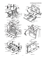
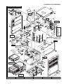
DISASSEMBLY
Caution on Disassembly
Follow the below-mentioned notes when disassembling
the unit and reassembling it, to keep it safe and ensure
excellent performance:
1. Take cassette tape, compact disc and mini disc out of the
unit.
2. Be sure to remove the power supply plug from the wall
outlet before starting to disassemble the unit.
3. Take off nylon bands or wire holders where they need to
be removed when disassembling the unit. After servicing
the unit, be sure to rearrange the leads where they were
before disassembling.
4. Take sufficient care on static electricity of integrated
circuits and other circuits when servicing.
CD-MD3000H/CD-MD3000W
Top Cabinet
Front Panel
(A1)x2
ø3x16mm
(A1)x2
ø3x16mm
(A1)x1
ø3x10mm
Side Panel
(Left)
CD-MD3000H/CD-MD3000W
STEP
REMOVAL
PROCEDURE
1. Screw ................ (A1) x5
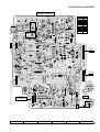
FIGURE
1
Top Cabinet
2
Side Panel(Left/Right) 1. Screw ................ (B1) x8
16-1
3
Rear Panel
1. Screw ................ (C1) x3
2. Screw ................ (C2) x8
(For CD-MD3000H)
2. Screw ................ (C2) x7
(For CD-MD3000W)
16-2
1. Flat Cable .......... (D1) x1
2. Screw ................ (D2) x4
3. Socket ............... (D3) x6
16-2
5
Sub Trans PWB
1. Screw ................ (E1) x3
2. Socket ............... (E2) x5
16-2
1. Flat Cable .......... (F1) x1
2. Screw ................ (F2) x2
3. Screw ................ (F3) x1
4. Socket ............... (F4) x2
5. Flat Cable .......... (F5) x1
16-2
1. Socket ............... (G1) x2
2. Screw ................ (G2) x1
2. Screw ................ (G3) x4
17-1
1. Socket ............... (H1) x1
(For CD-MD3000H)
1. Socket ............... (H1) x2
(For CD-MD3000W)
2. Screw ................ (H2) x2
17-1
7
8
MD Mechanism/
Relay PWB
Power PWB/
Speaker PWB
17-2
10
CD Switch PWB/
MD Switch PWB
1. Socket ............... (K1) x1
2. Screw ................ (K2) x6
3. Hook .................. (K3) x2
17-2
11
Switch PWB
1. Screw ................ (L1) x1
17-2
12
Headphones PWB
1. Screw ................ (M1) x1
2. Bracket .............. (M2) x1
17-2
1. Screw ................ (P1) x3
2. Screw ................ (P2) x2
17-2
Power PWB
(D2)x1
ø3x8mm
(D3)x1
Speaker PWB
(C1)x1
ø3x10mm
Front
Panel
CD-MD3000W
Only
(C2)x1
ø3x10mm
(C1)x2
ø3x10mm
CD-MD3000H
Only
(D2)x2 (F1)x1
ø3x8mm
CD PWB
(F2)x2
ø3x10mm
Rear Panel
(C2)x7
ø3x10mm
Power PWB
Speaker
PWB
Main PWB
(D3)x4
14
Motor PWB
1. Solder ................ (Q1) x2
17-2
15
CD Changer door
panel
1. Screw ................ (R1) x4
17-3
16
Control Panel
1. Screw ................ (S1) x6
17-3
17
Control PWB
1. Screw ................ (T1) x5
2. Socket ............... (T2) x1
17-4
18
Jog PWB
1. Screw ................ (U1) x5
17-4
19
LED B PWB
1. Screw ................ (V1) x3
17-4
20
Cassette holder
Cover
1. Open the cassette holder Cover
2. Screw ................ (W1) x4
3. Display Panel .... (W2) x1
4. Hook .................. (W3) x4
17-5
1. Screw ................ (X1) x4
2. Hook .................. (X2) x2
17-6
Display PWB/
LED A PWB
(F3)x1
ø3x8mm (D3)x1
(D2)x1
ø3x8mm
1. Open the cassette holder
2. Screw ................ (J1) x4
21
Tape
Mechanism PWB
Main
PWB
Tape Mechanism
CD Changer door
panel/
Control Panel
(D1)x1
(F4)x1
9
13
Rear Panel
CD-MD3000W Only
Figure 16-1
Front Panel
Main PWB
(B1)x4
ø3x10mm
Side Panel(Right) CD-MD3000H Only
4
6
(B1)x4
ø3x10mm
16-1
(E2)x3
Sub Trans
PWB
(F4)x1
(E2)x2
(F5)x1
(E1)x3
ø3x8mm
Lug Wire
Figure 16-2
– 16 –
MD Mechanism
CD-MD3000H/CD-MD3000W
Speaker
PWB
(G1)x2
(G2)x1
ø3x8mm
Control PWB
Control Panel B
(H2)x1
ø3x10mm
Power PWB
Jog PWB
(T1)x5
ø2.6x10mm
(H2)x1
ø3x10mm
Relay PWB
(V1)x2
ø2.6x10mm
MD Mechanism
(H1)x1
(V1)x1
ø2.6x10mm
(G3)x2
ø3x6mm
(H1)x1
CD-MD3000W
ONLY
(T2)x1
(U1)x5
ø2.6x10mm
Main Chassis
CD Changer
Block
LED B PWB
(G3)x2
ø3x6mm
LED Holder
Figure 17-1
Tape Mechanism
Cassette
Holder
Open
Front Panel
Control Panel A
Figure 17-4
(J1)x4
ø3x10mm
(W3)x4
MD Switch PWB
(K2)x1
ø3x10mm
CD Switch
PWB
Front Panel
Open
(K3)x1
Cassette
Holder Cover
Lug Wire
(K1)x1
(K2)x5
ø3x10mm
(W1)x4
ø2.6x12mm
(K3)x1
(P2)x1
ø3x20mm
(Q1)x2
CD Changer
Door Panel
Switch PWB
Motor
PWB
(P1)x3
ø3x10mm
(P2)x1
ø3x20mm
(W2)x1
Headphones
PWB
(L1)x1
ø2.6x10mm
(M1)x1 (M2)x1
ø3x10mm
Figure 17-5
Figure 17-2
CD Changer
Door Panel
Cassette
Holder Cover
(S1)x2
ø2.6x12mm
(R1)x1
ø2.6x10mm
(R1)x2
ø2.6x10mm
LED A
PWB
(X2)x1
(S1)x2
ø2.6x12mm
Display
PWB
(X1)x4
ø3x14mm
(S1)x2
ø2.6x12mm
Control Panel
(X2)x1
(R1)x1
ø2.6x10mm
Figure 17-6
Figure 17-3
– 17 –
CD-MD3000H/CD-MD3000W
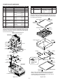
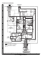
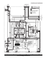
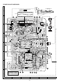
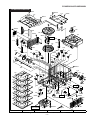
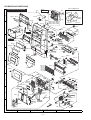
CD-MD3000H/CD-MD3000W (MD MECHANISM)
CD-MD3000H/CD-MD3000W (CD CHANGER MECHANISM UNIT)
STEP
REMOVAL
PROCEDURE
STEP
FIGURE
1
Top Cabinet
1. Screw ................ (A1) x5
2
Side Panel(Left/Right) 1. Screw ................ (B1) x8
16-1
3
Rear Panel
1. Screw ................ (C1) x3
2. Screw ................ (C2) x8
(For CD-MD3000H)
2. Screw ................ (C2) x7
(For CD-MD3000W)
16-2
1
16-1
4
Front Panel
1. Flat Cable .......... (D1) x1
2. Screw ................ (D2) x4
3. Socket ............... (D3) x6
16-2
5
CD Changer
Mechanism
1. Flat Cable .......... (Y1) x1
2. Screw ................ (Y2) x2
3. Screw ................ (Y3) x5
18-1
6
CD PWB
(Note)
1. Screw ................ (Z1) x4
2. Socket ............... (Z2) x4
3. Flat Wire ............ (Z3) x2
18-2
7
CD Mechanism
1. Screw ................ (ZZ1) x4
18-2
PROCEDURE
FIGURE
1. Screw ............ (AA1) x8
2. Flat Cable ...... (AA2) x3
3. Flexble PWB . (AA3) x1
4. Socket ........... (AA4) x2
18-3
REMOVAL
MD Mechanism/
MD Main PWB
Note:
After removing the connector for the optical pickup from the
connector, wrap the conductive aluminium foil around the
front end of connector remove to protect the optical pickup
from electrostatic damage.
Shield Case,Top
(AA1)x1
ø2x3mm
MD Mechanism
(AA)x1
ø2x3mm
(AA1)x1
ø2x3mm
Note:
After removing the connector for the optical pickup from the
connector, wrap the conductive aluminium foil around the
front end of connector remove to protect the optical pickup
from electrostatic damage.
Slide it in the direction of the arrow
after removing the screw (Y2).
CD Changer
Mechanism
Front Side
Shield Case,Side
(AA1)x1
ø2x3mm
(Y2)x1
ø3x10mm
CD PWB
Bottom Side
(Y3)x3
ø3x10mm
(Y2)x1
ø3x10mm
(Y1)x1
(Y3)x2
ø3x10mm
(AA4)x1
(AA2)x2
Main Chassis
(AA2)x1
Figure 18-1
(Z1)x4
ø3x10mm
(AA4)x1
(Z2)x2
(Z3)x1
(Z2)x1
(AA1)x2
ø1.7x3mm
Pull
(Z3)x1
CD PWB
(ZZ1)x4
ø2.6x10mm
(Z2)x1
(AA3)x1
Pull
Optical pickup
Flexible PWB
(Note 1)
MD Main PWB
(AA1)x1
ø2x3mm
CD Changer
Mechanism
(AA1)x1
ø2x2mm
Shield Case,Bottom
(Note 1) After removing the flexible PWB for optical pickup
from the connector wrap the front end of flexible PWB in
conductive aluminum foil so as to protect the optical pickup
from being damaged electrostatically.
CD Mechanism
Figure 18-3
Figure 18-2
– 18 –
CD-MD3000H/CD-MD3000W
CP-RW5000H/CP-RW5000W
STEP
1
REMOVAL
Woofer/Tweeter/
Sub Woofer
PROCEDURE
FIGURE
1. Net ................. (A1) x1
2. Front Panel ... (A2) x1
3. Screw ............ (A3) x4
4. Ring ............... (A4) x1
5. Catching holder .. (A5) x2
6. Screw ............ (A6) x2
7. Cover ............. (A7) x1
8. Screw ............ (A8) x2
9. Screw ............ (A9) x4
10. Cover ............. (A10) x1
19-1
(A1)x1
19-2
(A2)x1
19-3
Driver should
be pried away
from Speaker Box.
Screw Driver
Speaker Box
Bottom Side
Figure 19-1
Speaker Box
(A7)x1
(A5)x2
(A6)x2
ø3x10mm
(A8)x2
ø3x10mm
(A3)x4
ø4x16mm
(A4)x1
Tweeter
Woofer
Figure 19-2
Speaker Box
Top Side
Sub Woofer
(A10)x1
(A9)x4
ø4x20mm
Rear Side
Figure 19-3
– 19 –
CD-MD3000H/CD-MD3000W
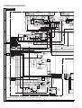
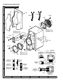
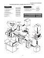
REMOVING AND REINSTALLING THE MAIN PARTS
MD MECHANISM SECTION
(A1)x1
ø1.7x5mm
For details about the procedure to remove the MD mechanism
from the main unit, refer to the Disassembly Procedure, Steps
1-7 in the main unit and also the MD section.
(Referring to page18)
Magnetic Head
Caution:
After pulling out the optical pickup connector, wrap the end
of the connector in conductive aluminium foil to prevent the
optical pickup from being destroyed by static electricity.
MD Mechanism
How to remove the magnetic head
(See Fig. 20-1)
1. Remove the screws (A1) x 1 pc.
Caution:
Take utmost care so that the magnetic head is not damaged
when it is mounted.
Figure 20-1
How to remove the MD loading motor PWB/MD
loading motor
(See Fig. 20-2)
1. Remove the screw (B1) x 1 pc.
2. Remove the Hoock (B2) x 3 pcs., and remove the MD
Loading PWB.
3. Remove the screw (B3) x 2 pcs., and remove the MD
Loading motor.
(B1)x1
ø1.7x6mm
MD Loading Motor
MD Loading Motor
PWB
(B2)x1
(B2)x2
(B3)x2
ø1.7x3mm
Figure 20-2
How to remove the MD sled motor/optical pickup
(See Fig. 20-3)
(C1)x1
ø1.4x5mm
1. Remove the screws (C1) x 3 pcs., and remove the MD sled
motor.
2. Remove the optical pickup.
(C1)x2
ø1.4x4.5mm
Washer
Optical
Pickup
Caution:
Be careful so that the gear is not damaged.
(The damaged gear emits noise during searching.)
MD Sled Motor
MD Mechanism
Switch PWB
Figure 20-3
– 20 –
CD-MD3000H/CD-MD3000W
How to remove the MD spindle motor
(See Fig. 21-1)
(D1)x3
ø1.4x3mm
1. Remove the screws (D1) x 3 pcs., and remove the MD
spindle motor.
MD Spindle Motor
Caution:
Be careful so that the gear is not damaged.
(The damaged gear emits noise during searching.)
Figure 21-1
CD MECHANISM SECTION
Perform steps 1 to 7 of the disassembly method to remove the
CD mechanism. (See page 18.)
(A1) x1
Stop Washer ø2.6 x6mm
(A3) x1
(A1) x1
ø2.6 x6mm
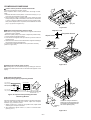
How to Remove the pickup (See Fig. 21-2.)
1. Remove the screws (A1)x 2 pcs., to remove shaft (A2)x 1
pc.
2. Remove stop washer (A3)x 1 pc., to remove gear (A4)x 1 pc.
3. Remove the pickup.
Pickup
CD
Mechanism
Note:
After removing the connector for the optical pickup from the
connector, wrap the conductive aluminium foil around the
front end of connector remove to protect the optical pickup
from electrostatic damage.
Shaft
(A2) x1
Gear
(A4) x1
Figure 21-2
CD CHANGER MECHANISM SECTION
Perform steps 1 to 5 of the disassembly method to remove the
CD changer mechanism. (See page 18.)
CD Changer Mechanism
(2)Changer Box,
Right
(1) Front Top Plate
How to Remove the tray motor/main cam motor
(See Fig. 21-3.)
1. Remove the screws (B1)x 4 pcs., to remove the CD PWB.
2. Remove the (1) front top plate, (2) changer box, left/right
and (3) disc trays 1~6. After that, disassemble as shown in
the figure.
3. Remove the screws (B2)x 4 pcs.
4. Remove the tray motor and main cam motor.
(2) Changer Box,
Left
Note:
The parts of (1), (2) and (3) correspond to the drawing Nos.
117, 102, 103 and 108 to 113 of the CD change mechanism
disassembly drawing.
Remove the screws of 117, 102 and 103, and the parts of (1),
(2) and (3) will be ready for removal and the screws of the tray
motor and main cam motor will be visible.
(3) Disc Tray,1~6
(B2)x4
ø2.6x4mm
CD PWB
(B1)x4
ø3x10mm
Main Cam Motor
Tray Motor
Figure 21-3
– 21 –
CD-MD3000H/CD-MD3000W
TAPE MECHANISM SECTION
Perform steps 1 to 4 and 9 of the disassembly method to
remove the tape mechanism.
How to remove the record/playback and erase
heads (See Fig. 22-1)
Erase
Head
1. When you remove the screws (A1) x 2 pcs., the recording/
playback head and three-dimensional head of the erasing
head can be removed.
Record/
Playback
Head
(A1)x2
Ø2 x 6mm
Figure 22-1
How to remove the pinch roller (See Fig. 22-2)
(Right)
(Left)
1. Carefully bend the pinch roller pawl in the direction of the
arrow <A>, and remove the pinch roller (B1) x1 pc., in the
direction of the arrow <B>.
Note:
When installing the pinch roller, pay attention to the spring
mounting position.
Pinch
Roller
Pawl
Pull
<A>
Pinch
Roller
Pawl
Pull
<A>
Pinch
Pull Roller Pull <B>
(B1)x1
<B>
Figure 22-2
How to remove the belt (See Fig. 22-3)
FF/REW Belt
(C2)x1
1. Remove the motor.
2. Remove the main belt (C1) x 1 pc., from the motor side.
3. Remove the FF/REW belt (C2) x 1 pc.
Motor
Main Belt
(C1)x1
Figure 22-3
How to remove the motor (See Fig. 22-4)
Motor
1. Remove the belt.
2. Remove the screws (D1) x 2 pcs., to remove the motor.
(D1)x2
Ø 2.6 x 5mm
Figure 22-4
FRONT PANEL SECTION
CD Changer
Door Panel
Perform steps 1 to 4 of the disassembly method to remove the
front panel.
(E1)x1
ø2.6x10mm
CD Changer
Door Panel
(F1)x2
ø2x5mm
Gear Box A
Control
Panel
Motor
How to remove the control panel motor
(See Fig. 22-5)
1. Remove the control panel.
2. Remove the screws (E1) x 6 pcs., to remove the CD changer
door panel.
3. Remove the screws (F1) x 2 pcs., to remove the control
panel motor.
(E1)x2
ø2.6x10mm
Gear Box B (E1)x3
ø2.6x10mm
Control Panel
Figure 22-5
– 22 –
Motor PWB
CD-MD3000H/CD-MD3000W
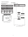
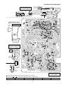
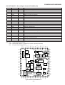
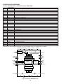
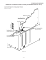
CD CHANGER MECHANISM MAIN BASE PARTS ASSEMBLING/ADJUSTING
PROCEDURE
Work content
Applied part No.
1. Motor assembly (x 2) mounting (screw x 4)
Assembly fig. No.
01/29
Fig.24
2. MT idle gear mounting (screw x 1)
25
Fig.24
3. MT system gear assembly
23/24/26/27
Fig.24
4. STB/tray drive system gear and others assembling/
mounting (screw x 3)
37/38/45/46 (53)/47/48
Fig.24
5. Tray big gear assembly
31
Fig.24
6. T.M SW PWB mounting (screw x 3)
7. STB holder assembling
Remarks
Gear positioning
Fig.25
03
Fig.24
8. STB drive gear L/R assembly mounting (screw x 2)
11 (10)/12 (10)
Fig.24
9. Tray joint gear R/tray drive gear R assembling
34/36
Fig.25
Gear positioning
10. Tray gear A/B assembling
32/33
Fig.25
Gear positioning
11. Lift gear B/C assembling
43/44
Fig.26
Gear positioning
12. MT idler gear F assembling, mode big gear
mounting (screw x 1)
28/41
Fig.26
13. Change box R mounting (screw x 4)
04
Fig.26
14. Lift gear A assembling
42
Fig.26
15. Change box L assembly mounting (screw x 4)
02/30/35
Fig.27
16. Lift cam assembling (shaft inserting)
40
Fig.27
Gear positioning
Fig.28
Check/adjustment
18. Top plate F/disc OB LEV. Mounting (screw x 6)
80
Fig.28
19. Trays 1 - 6 assembling
91/92/93/94/95/96
Fig.29
17. STB holder height adjusting
20. Top plate R mounting (screw x 6)
Gear positioning
––
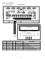
CD CHANGER MECHANISM PARTS LIST
Part name
No.
No.
Part name
01 (101)
MAIN BASE
40 (115)
LIFT CAM
02 (102)
CHANGE BOX L
41 (126)
MODE BIG GEAR
03 (147)
STB HOLDER
42 (127)
LIFT GEAR A
04 (103)
CHANGE BOX R
43 (128)
LIFT GEAR B
44 (129)
LIFT GEAR C
STB GEAR A
10 (119)
STB DRIVE GEAR A
45 (132)
11 (120)
STB DRIVE GEAR L
46 (104)
STB GEAR B
12 (122)
STB DRIVE GEAR R
47 (133-1)
STB GEAR C
20 (149)
STABILIZER FH
48 (133-3)
STB GEAR D
23 (141)
MT IDLER GEAR A
50 (145)
LIFT LEVER
24 (138)
MT IDLER GEAR B
51 (106)
TRAY LOCK LEVER
25 (137)
MT IDLER GEAR C
52 (118)
DISC OB LEVER
26 (140)
MT IDLER GEAR D
53 (105)
STB GEAR ANG.
27 (139)
MT IDLER GEAR E
28 (131)
MT IDLER GEAR F
80 (117)
TOP PLATE F
29 (MOB1,2)
MOTOR GEAR
81 (114)
TOP PLATE R
30 (143)
TRAY DRIVE GEAR F
31 (134)
TRAY BIG GEAR
91 (108)
TRAY 1
32 (135)
TRAY GEAR A
92 (109)
TRAY 2
33 (136)
TRAY GEAR B
93 (110)
TRAY 3
TRAY DRIVE GEAR R
94 (111)
TRAY 4
35 (144)
TRAY JOINT GEAR F
95 (112)
TRAY 5
36 (125)
TRAY JOINT GEAR R
96 (113)
TRAY 6
34 (124)
37 (142)
TRAY GEAR C
38 (130)
TRAY IDLER GEAR
The number of ( ) is the number of the parts guide.
– 23 –
CD-MD3000H/CD-MD3000W
12
STB DRIVE GEAR R
(ASS'Y)
48
STB GEAR D
01
MAIN BASE
03
STB HOLDER
24
29
29
23
26
10
STB DRIVE GEAR A
23
Mark position
25
27
45
STB GEAR A
53
STB GEAR ANG.
46
STB GEAR B
47
STB GEAR C
10
STB DRIVE GEAR A
11
STB DRIVE GEAR L
(ASS'Y)
37
38
TRAY GEAR C
TRAY IDLER GEAR
31
TRAY BIG GEAR
After assembling TRAY BIG GEAR, turn it in the arrow direction.
TRAY BIG GEAR ASSEMBLING POSITION
11(/12) (10)
STB DRIVE GEAR L(/R)
(ASS'Y)
46
STB GEAR B
47
STB GEAR C
53
STB GEAR ANG.
45
STB GEAR A
37
38
TRAY GEAR C
TRAY IDLER GEAR
Figure 24
– 24 –
31
TRAY BIG GEAR
CD-MD3000H/CD-MD3000W
24
29
29
23
26
23
25
27
Mark position
* This position becomes the
reference (stock) position
of the tray.
45
32
TRAY GEAR A
46
47
These holes must align.
10
11
Direct the recess part
(trapezoidal side) of the axis
35 in this direction.
38
37
31
34
TRAY DRIVE GEAR R
36
M T SW PWB
TRAY JOINT GEAR R
Scale: 2 magnifications
*2
33
TRAY
GEAR B
Scale: 2 magnifications
It must not rotate in contact
with the peripheral (hatched)
part of 31.
32
TRAY BIG GEAR SET POSITION
33
These holes must align.
*1: To position the axis part of 36, engage it with 38.
After assembling 32,
assemble 33.
*1 *2: When it is aligned as described in *1, the hatched part
(low gear-height part of gear) will be positioned in this position.
Note: After positioning the tray big gear in the set position, engage these gears.
34
TRAY DRIVE GEAR R
36
TRAY JOINT GEAR R
33
TRAY GEAR B
Figure 25
– 25 –
32
TRAY GEAR A
CD-MD3000H/CD-MD3000W
Mark position
(Assemble the mode big gear in this position.)
04
CHANGE BOX R
,,,,,,,,,,,,,,,,
,,,,,,,,,,,,,,,,
,,,,,,,,,,,,,,,,
,,,,,,,,,,,,,,,,
,,,,,,,,,,,,,,,,
,,,,,,,,,,,,,,,,
,,,,,,,,,,,,,,,,
,,,,,,,,,,,,,,,,
,,,,,,,,,,,,,,,,
,,,,,,,,,,,,,,,,
,,,,,,,,,,,,,,,,
,,,,,,,,,,,,,,,,
,,,,,,,,,,,,,,,,
,,,,,,,,,,,,,,,,
,,,,,,,,,,,,,,,,
,,,,,,,,,,,,,,,,
,,,,,,,,,,,,,,,,
,,,,,,,,,,,,,,,,
,,,,,,,,,,,,,,,,
,,,,,,,,,,,,,,,,
,,,,,,,,,,,,,,,,
,,,,,,,,,,,,,,,,
,,,,,,,,,,,,,,,,
,,,,,,,,,,,,,,,,
,,,,,,,,,,,,,,,,
,,,,,,,,,,,,,,,,
28
MT IDLER GEAR F
42
LIFT GEAR A
Note:
To assemble the mode
big gear, incline it,
bring it into contact with
the circumference and
put the center hole into
position since the
hatched part of the main
base is overlapped with
the circumference.
32
33
45
53
46
10
47
44
LIFT GEAR C
37
38
11
43
LIFT GEAR B
34
36
41
MODE BIG GEAR
Direct the short tooth
toward the center.
Scale: 2 magnifications
Scale: 2 magnifications
MODE BIG GEAR
LIFT GEAR A/B/C
ASSEMBLING POSITION
(A)
(B)
<Assembling method of lift gear>
After setting up the mode big gear in the
shown position, engage it with the STB gear A
(gear on the lower side) at the position (A),
and assemble them, turning it in the arrow direction
into the position (B). (The short tooth directs toward the
center of the mode big gear.)
42
LIFT GEAR A
41
MODE BIG GEAR
43
LIFT GEAR B
Figure 26
– 26 –
44
LIFT GEAR C
CD-MD3000H/CD-MD3000W
37°
Mark position
28
42
LIFT GEAR A
32
33
45
30
TRAY DRIVE GEAR F
46
10
47
11
41
43
TRAY JOINT GEAR F
(CHANGE BOX L ASS'Y) ASSEMBLING POSITION
LIFT CAM
44
40
LIFT CAM
Scale: 2 magnifications
Assembling procedure
1. Turn the mode big gear approx. 37 degrees in the arrow direction.
2. Assemble the change box L ass'y.
Note: At this time, the tray joint gear F must be located in the position shown in figure.
Moreover, the gear must be engaged securely.
3. After assembly, return the mode big gear to the initial position.
4. Assemble the lift cam.
Note: At this time, the lift cam (No.40) must be located in the position shown in figure 24.
02
CHANGE BOX L
Direct the recess part (trapezoidal side)
of the axis 35 in this direction.
35
TRAY JOINT GEAR F
*2
30
TRAY DRIVE GEAR F
35
TRAY JOINT GEAR F
*1: To position the axis part
of 35, engage it with 33.
*2: When it is aligned as
described in *1, the hatched part
40
(low gear-height part of gear)
will be positioned as shown.
LIFT CAM
Since this gear engagement is not
visually checked, verify that it does
not float when the gear box L is installed.
*1
Scale: 2 magnifications
During assembly, make the
O part visible in this direction.
Note: Among 4 ribs on the
circumference, one rib alone
is provided with O.
30
TRAY DRIVE GEAR F
35
TRAY JOINT GEAR F
Figure 27
– 27 –
CD-MD3000H/CD-MD3000W
80
TOP PLATE F
37°
Mark position
42
LIFT GEAR A
32
33
45
30
46
10
47
35
11
41
43
40
44
STB HOLDER HEIGHT ADJUSTING METHOD
When the height of
STB holder is high,
(Decrease the clearance.)
When the height of
STB holder is low,
(Increase the clearance.)
Bend this part.
240
OS LEVER
Adjusting procedure
1. Turn the mode big gear approx. 37 degrees in the arrow direction.
2. Viewing from the front side of the mechanism, verify that the guide ribs
(CHANGE BOX L/R and STB HOLDER) of tray are as tall as each other.
3. If they are not, bend the lever for adjustment. (Refer to the details.)
Note: Also apply the same adjustment on the R side.
,,
,,
,,
,,
,,
,,
,,
Bend this part to adjust the height of the STB holder.
Scale: 2 magnifications
Details
80
TOP PLATE F
40
Height of the rib
30
35
Figure 28
– 28 –
CD-MD3000H/CD-MD3000W
Mark position
Be sure to assemble the tray into this position.
91~96
TRAY1~TRAY6
Insert it along the guide of
the change box.
42
LIFT GEAR A
32
33
45
,,,,
,,,,
,,,,
46
10
47
30
TRAY No.1~6
Rear surface: Stamped.
Note: During insertion,
Do not accidentally rearrange
tray numbers.
35
11
41
43
40
44
Tray installing method: (After adjusting the height of the STB holder)
1. Turn the mode big gear to the mark position to lower the STB holder to the bottom area.
2. From the front side, install the tray. (Securely insert it to the lock position.)
Rear
side
,,
,,
,,
40
96
TRAY 6
95
TRAY 5
94
TRAY 4
93
TRAY 3
92
TRAY 2
91
TRAY 1
30
35
Figure 29
Measure to be taken when a disc cannot be removed due to a mechanism trouble
First, remove the mechanism unit section from the set, and check for the state of the disc.
(Remove the top plate R if necessary.)
<State of the disc>
(1) When the disc is in the normal PLAY (chucking) position -> Try to eject the disc by turning the mode big gear/tray big gear
manually.
* At this time, be sure to adjust the tray's position (height).
(2) When the disc is in the normal STOCK position -> Try to eject the disc by turning the tray big gear manually.
* At this time, be sure to adjust the tray's position (height).
(3) When the disc is not in the normal position -> The tray or disc is not in the normal position. (The tray or disc may catch
somewhere.)
Remove the TOP PLATE F/DISC OB lever.
Unlock the tray lock lever and pull out the tray which is not caught.
Move the caught tray or disc and remove the disc.
In case of (1) and (2), the mechanism is normal (defective circuit parts, etc.). However, it may stop somewhere.
This is the reason why you should try to turn the tray big gear first.
In case of (3), either of the big gears does not turn.
– 29 –
CD-MD3000H/CD-MD3000W
ADJUSTMENT
MECHANISM SECTION
Extension cable
• Driving Force Check
Type
Torque Meter
Specified Value
Play: TW-2412
1.
Over 80 g
Part No.
33 Pin extension
flat cable, 500mm
QCNWN6931AFZZ
• Torque Check
Torque Meter
Specified Value
Play: TW-2111
30 to 60 g.cm
Fast forward: TW-2231
60 to 120 g.cm
Rewind: TW-2231
60 to 120 g.cm
• Tape Speed
Test Tape
MTT-111
Adjusting
Point
Variable
resistor in
motor.
Specified
Value
3,000 ± 90 Hz
Instrument
Connection
Speaker
Terminal
CNP1
33
1
CD PWB-C
33
1
TAPE MECHANISM
33Pin extension flat cable
QCNWN6931AFZZ
1
33
MAIN PWB-A
Variable
Resistor
in motor
1
33
CNP901
Tape motor
Figure 30-1 ADJUSTMENT POINT
Figure 30-2 EXTENSION CABLE
– 30 –
CD-MD3000H/CD-MD3000W
TUNER SECTION
fL: Low-range frequency
fH: High-range frequency
CD-MD3000H
• AM IF/RF
Signal generator: 400 Hz, 30%, AM modulated
Display
Test Stage Frequency
CD-MD3000W
• AM IF/RF
Signal generator: 400 Hz, 30%, AM modulated
Setting/ Instrument
Adjusting Connection
Parts
Test Stage Frequency
Setting/ Instrument
Adjusting Connection
Parts
AM IF
450 kHz
1,620 kHz
T351
AM IF
450 kHz
1,602 kHz
T351
AM Band
Coverage
—
522 kHz
(fL): T306 *2
1.1 ± 0.1 V
AM Band
Coverage
—
522 kHz
(fL): T306 *2
1.1 ± 0.1 V
AM
Tracking
990 kHz
990 kHz
T302
AM
Tracking
990 kHz
990 kHz
T302
*1. Input: Antenna
*2. Input: Antenna
*1
Display
*1
Output: Speaker Terminal
Output: TP301
*1. Input: Antenna
*2. Input: Antenna
*1
*1
Output: Speaker Terminal
Output: TP301
• FM
Notes:
1: Description of the "FM IF Adjustment" is not carried on this
Manual. It is because the IF coil in the FM front end section
has been best adjusted in the factory so that its further
adjustment is not needed at the field. When replacing the
FM front end assembly, no adjustment is needed either.
2: The parts in the FM front end section are prepared in a
complete unit, so you can't obtain each part individually.
• FM RF
Signal generator: 1 kHz, 75 kHz dev., FM modulated
• FM Mute Level (FM ST MODE)
Signal generator: 1 kHz, 40 kHz dev., FM modulated
*1. Input: Antenna
*2. Input: Antenna
Frequency
98.00 MHz
(26 dBµV)
Adjusting
Parts
Display
98.00 MHz
Test Stage Frequency Frequency
Display
Instrument
Connection
VR351 *1
Setting/
Adjusting
Parts
Instrument
Connection
FM Band
Coverage
—
87.50 MHz (fL): T311
1.3 ± 50 mV
*1
FM RF
98.00 MHz
(10~30 dB)
98.0 MHz
*2
L312
Output: TP301
Output: Speaker Terminal
• FM Mute Level (FM ST MODE)
Signal generator: 1 kHz, 40 kHz dev., FM modulated
Input: SO301
Output: Speaker
Terminal
Frequency
98.00 MHz
*1. Adjust so that an output signal appears.
Adjusting
Parts
Display
98.00 MHz
(26 dBµV)
Instrument
Connection
VR351 *1
Input: CNP301
Output: Speaker
Terminal
*1. Adjust so that an output signal appears.
CD-MD3000H
CD-MD3000W
MAIN PWB
AM
TRACKING
CNP301
AM LOOP
ANTENNA
MAIN PWB
AM
TRACKING
AM BAND
COVERAGE fL
FM MUTE
LEVEL
T306
T302
CNP301
FM/AM LOOP
ANTENNA
T302
BF301
IC301
VR351
1
L312
SO301
FM
ANTENNA
TERMINAL
AM BAND
COVERAGE fL
9
T312
FM BAND
COVERAGE fL
FM RF
FE301
1
FM MUTE
LEVEL
T306
T311 VR351
FM IF
T351
T351
R345
AM IF
R345
TP301
TP301
Figure 31 ADJUSTMENT POINTS
– 31 –
AM IF
CD-MD3000H/CD-MD3000W
TEST MODE
Outline
While the unit is turned off, press the POWER key while holding down the VOLUME-DOWN and PANEL OP/CL keys to enter
the test mode selection mode. Then, the unit is started, the panel is opened, and the microcomputer's version/destination/span
is displayed. If the following data is entered from the keyboard while in the test mode selection mode, the unit directly enters
the specified test mode. This operation is applied to the main unit's keys only.
Character display
Item
Type Auxiliary display 1
Version • Destination
V
2
3
4
5
6
7
8
* • *
Number
Note
Auxiliary display
9 10
Left adjust in the first line
Span
Destination
Example: V1. 1_W:_9
In the destination display, a destination code (H/W/U/J) is displayed. For the span display, "9" means 9 kHz/50 kHz, and "10"
means 10/100 kHz. All pictures will disappear except the characters.
By pressing the specific key, you can enter the test mode whose functions are as follows:
System
CD
Tuner
MD
Menu display
INITIAL
SOFT_RESET
CD_TEST
TUN_PRESET
TUNER_TEST
MD_TEST
Shortcut Key
CD1 PLAY
CD2 PLAY
CD1 EJECT
CD4 EJECT
CD5 EJECT
CD
Model
ALL
ALL
ALL
ALL
ALL
ALL
Shipping status setting
Soft rest
CD test
Tuner test frequency preset
Tuner test
MD test
Outline of Test Mode
1
2
3
4
5
6
Name
Shipping status setting
Soft set setting
CD test
Tuner test
frequency preset
Tuner preset clear setting
MD test
Description
Sets up the unit for shipping.
Initializes the unit.
Performs tests such as the CD mechanism test, hardware test, and constant setting test.
Presets the test frequency.
Clears all presets.
Setting MD micro computer to test mode.
Shipping status setting test mode
Purpose: To set up the unit for shipping.
Function: Initialize all functions.
Operation: All settings are initialized, "FINISH" is displayed as in the sample display, and data entry is prohibited including data
to turn on or off the unit.
To exit the test mode
The unit returns to the normal operation through reset entry.
Table Character display for test mode 1
Character display
Item
Type
Test mode name
Set-Up Complete
Function
Auxiliary display
1
2
3
4
I
F
5
6
7
N
I
T
I
A L
I
N
I
S
H
8
9 10
Auxiliary display
Note
In the destination display, a destination code is displayed. For the span display, "9" means 9 kHz/50 kHz, and "10" means 10/
100 kHz.
– 32 –
CD-MD3000H/CD-MD3000W
2. Soft reset
Purpose: To initialize the unit.
Function: To initialize all functions.
Operation: "ALL CLEAR" is displayed, all functions are initialized, and the unit is turned on.
To exit the test mode
When the initialization through soft reset is complete, the unit is turned on.
Table Character display for test mode 2
Character display
Item
Reset operation
display
Type
Operation
Auxiliary display
1
2
3
A
L
L
4
5
6
7
8
9 10
C
L E
A
R
Auxiliary display
Note
3. CD test mode (If this test mode is not activated, refer to CD troubleshooting on page 89.)
In the CD test mode, each step can be performed even if the LID-SW is off. However, if you cannot obtain a focus in step
3 or if other kind of error handling starts, you cannot proceed to the following steps. In error handling, press the POWER key
to exit the test mode, or press the STOP key to prohibit operations other than returning to step 1.
(1) Step 1 mode
In the CD test mode, the following display appears, CD initialization is performed, and you are prompted for data.
Reset operation display / Operation
"CD_TEST"
After lighting up for one second
"T1___________0:00"
The keys you can press here and the resulting operations are as follows:
"POWER" ........... The test mode is turned off, the power is turned off, and the unit is placed in the normal stand-by mode.
"FWD" ................ While holding down this key, the pickup moves outward after returning to the innermost track.
"REV" ................. While holding down this key, the pickup moves inward after returning to the innermost track.
"PLAY" ............... Jumps to step 2.
"STOP" ............... Cancelled.
"TAPE REC" ...... Jumps to step 5.
* While the pickup is moving to the innermost track in the initialization, none of the keys except POWER is accepted. When PUIN SW ON cannot be detected in ten seconds, the unit stops the slide motor and shows the following error code. Then, you
can press the POWER key to exit the test mode, or the STOP key to return to step 1. You cannot perform other operations.
"E--CD01"
(2) Step 2 mode
When the "PLAY" key is pressed in the above mode, the laser is turned on. At this time, another operation must not be
performed.
Display
"T2___________0:00"
The keys you can press here and the resulting operations are as follows:
"POWER" ........... The test mode is turned off, the power is turned off, and the unit is placed in the normal stand-by mode.
"FWD" ................. While holding down this key, the pickup is moved outward.
"REV" .................. While holding down this key, the pickup is moved inward.
"PLAY" ................ Jumps to step 2.
"STOP" ............... Returns to step 1.
"TAPE REC" ....... Jumps to step 5.
(3) Step 3 mode
Performs focus search and turns on the focus servo.
Focus search is repeated until it is brought into focus.
Display
"T3___________0:00"
The keys you can press here and the resulting operations are as follows:
"POWER" ........... The test mode is turned off, the power is turned off, and the unit is placed in the normal stand-by mode.
"FF/FWD" ........... While holding down this key, the pickup is moved outward.
"REW/REV" ........ While holding down this key, the pickup is moved inward.
"PLAY" ................ Jumping to step 4 when a focus is obtained. Otherwise, data entry is prohibited.
"STOP" ............... Returns to step 1.
"TAPE REC" ....... Jumps to step 5.
* You should return to step 1 if it is out of focus after bringing it into focus.
– 33 –
CD-MD3000H/CD-MD3000W
(4) Step 4 mode
Rotate a disc.
Displayed string:
"T4___________0:00"
The clock display should always be "0:00".
The keys you can press here and the resulting operations are as follows:
"POWER" ........... The test mode is turned off, the power is turned off, and the unit is placed in the normal stand-by mode.
"FF/FWD" ........... While holding down this key, the pickup is moved outward.
"REW/REV" ........ While holding down this key, the pickup is moved inward.
"PLAY" ................ Jumps to step 5.
"STOP" ............... Returns to step 1.
"TAPE REC" ....... Jumps to step 5.
* You should return to step 1 if it is out of focus.
(5) Step 5 mode
Start playback. When the pickup reaches the outermost track, it does not stop. The LCD screen shows the replay time elapsed
as in the normal CD playback.
Display
"T5___________0:00"
The keys you can press here and the resulting operations are as follows:
"POWER" ........... The test mode is turned off, the power is turned off, and the unit is placed in the normal stand-by mode.
"FWD" ................. While holding down this key, the pickup is moved outward.
"REV" .................. While holding down this key, the pickup is moved inward.
"PLAY" ................ Canceled.
"STOP" ............... Returns to step 1.
* You should return to step 1 if it is out of focus.
Notes:
• In the test mode, TOC IL is not performed.
• Only the keys for adjusting the volume are accepted except the keys described.
4. Tuner test frequency preset
Purpose:
To preset a test frequency for an in-factory test.
Function:
To preset each preset number to the band and frequency shown in Table 34 based on the initial setting for the
destination.
Operation: To preset the band and frequency shown in the table below and turn the unit on with the following setting.
Function
Band
Tuning mode
Call preset number
Band's last preset channel
X-BASS
Preset equalizer
Tuner
FM monaural
Preset call selection
Preset number 1 frequency
See Table 34
Off
FLAT
For other functions, the value which was set when the unit was turned off last time is valid (last state).
To exit the test mode
After the frequency is preset and the set-up is done, the unit is turned on and normal operations start.
Table 34. TEST-TuSet preset frequencies
CH
1%
2
3
4
5
6%
7
8
9
10
11-40
BAND
FM
AM
CD-MD3000H
FM 87.5 MHz
FM 108.0 MHz
FM 90.0 MHz
FM 106.0 MHz
FM 98.0 MHz
AM 522 kHz
AM 1620 kHz
AM 603 kHz
AM 1404 kHz
AM 990 kHz
CD-MD3000W
FM 87.5 MHz
FM 108.0 MHz
FM 90.0 MHz
FM 106.0 MHz
FM 98.0 MHz
AM 531 kHz
AM 1602 kHz
AM 603 kHz
AM 1404 kHz
AM 990 kHz
– 34 –
Unused channels are indicated with "––".
"%" indicates the last channel for each band.
All FM bands are preset to FM monaural.
CD-MD3000H/CD-MD3000W
MD SECTION
Enter the test mode, adjust or set as shown in the following table according to the repair operations.
Execution item
required
Repair
operations
TEMP
basic
setting
Checking Writing the AUTO-YOBI
AUTOAUTO-FAB Writing the
EEPROM EEPROM
EEPROM
adjustment adjustment adjustment
setting
setting
setting
TEMP
EEPROM_SET TEST-CANCEL AUTO–YOBI AUTO–ADJ AUTO–FAB TEST-CANCEL TEST-PLAY TEST-REC
1
PICK replacement
2
3
4
5
6
Operation check
7
8
1
HEAD replacement
MECHANISM
replacement
MAIN PWB
assembly replacement
1
MD microcomputer
replacement
1
2
3
4
5
6
7
8
2
3
4
5
6
7
8
9
2
3
4
5
3
4
5
6
1
1
MD LSI replacement
2
RF IC replacement
1
2
3
4
5
6
7
8
9
EEPROM IC
replacement
1
2
3
4
5
6
7
8
9
number
1 to 8 and 9 indicate the order of inplementation.
" – " is an item that you don't have to execute.
The EEPROM writing result is shown at the end of the test mode
OK_EEPROM: "SET" and "YOBI COMPLETE" were written normally
WR_EEPROM: Although "SET" was written normally, it was not written in the "YOBI COMPLETE" state.
Peform "AUTO-YOBI" adjustment. After making a normal adjustment,
write the preliminary adjustment into the EEPROM.
NG_EEPROM: "SET" could not be written.
Check the connection between the MD microcomputer and the EEPROM.
Extension Cable
1
2
3
4
5
Type
Part No.
Extension PWB for servicing
Extension Connector (2 Pin)
Extension Cable (6 Pin)
Extension Cable (5 Pin)
Extension Cable (28 Pin)
RUNTK0532AFZZ
QCNWK0129AFZZ
QCNWK0130AFZZ
QCNWK0109AFZZ
QCNWK0108AFZZ
From Magnetic Head
2Pin extension connector
QCNWK0129AFZZ
From Optical
Pickup Unit
From mechanism
switch PWB
28Pin extension flat cable
Extension PWB for service
QCNWK0108AFZZ
(RUNTK0532AFZZ)
Fit the extension PWB for service to the mechanism
6Pin extension flat cable
QCNWK0130AFZZ
5Pin extension flat cable
QCNWK0109AFZZ
Figure 35
– 35 –
MD MAIN PWB
CD-MD3000H/CD-MD3000W
Operation/Input table for MD test mode 1
Button/Remoto
control input
[POWER]
O
Remoto
control
O
[EQ]
O
O
[X-BASS]
O
O
[PLAY]
O
O
[REV PLAY]
O
O
[TAPE REC]
[STOP]
O
O
O
O
[FF/CUE]
O
O
[REW/REV]
O
O
[JOG UP]
O
[JOG DOWN]
O
Main unit
[DISP/CHARACTER] O
O
[MENU]
[LOADING SW]
[MD EJECT]
O
O
O
O
Transmission
Pressing
Function
command
time
to MD
___
Single press Turning on/off the power of the set.
When the power of the set is in the on state, it is
turned off; when it is in the off state, it is turned on.
B2h
Single press Test mode menu feed. To the servo adjustment
mode (Feed of the menu for the adjustment and
EEPROM)
B4h
Single press Test mode menu feed. To the recording mode
(Feed of the menu mainly for the continuous
playback and continuous recording)
F2h
Single press Test mode menu feed. To other modes
(Feed of the menu of the INNER mode,
JUMP SELECT, etc.)
A8h
Single press Menu reverse feed in each mode.
(Effective in each test mode)
A2h
Single press Decision of the menu select or start of its execution.
A7h
Single press Cancellation of each test item and transition to the
menu select of one higher order
AAh
Single press 1) Outer periphery feed of the slide motor (FWD).
Continuous
Continued outer periphery feed
press
2) Execution of JUMP
3) Address set value UP
Others
ACh
Single press 1) Inner periphery feed of the slide motor (REV).
Continuous
Continued inner periphery feed
press
2) Execution of JUMP
3) Address set value DOWN
Others
F3h
___
1) Forced UNLOAD feed of a disc
2) Adjustment value +1
F4h
___
1) Forced LOAD feed of a disc
2) Adjustment value -1
F5h
Single press 1) Laser switching in the EJECT mode
2) Display switching during continuous playback
Others
1 F h + D 1 h Single press To the operation mode without auto adjustment
B5h
___
Execution of normal loading operation
B3h
Single press Execution of normal eject operation
1. Preparation for adjustment Test disc
Type
1
2
3
4
Test disc
High reflection disc TGYS1 (SONY) [for Playback]
Low reflection disc Recording minidisc
SONY 80 minutes disc is recommended.(example:PRISM 80)
Head Adjusting transparent
Low reflection disc Pre-adjustment disc [TEAC Test MD]
– 36 –
Part No.
RRCDT0101AFZZ
––––––––––––
RRCDT0103AFZZ
88GMMD-318 or
88GMMD-213AS
CD-MD3000H/CD-MD3000W
2. Test Mode
Test mode setting method
1. "MD TEST 1" ENTER.
(State A is changed to state B .)
2. Insert the playback-only disc 1 (high reflection disc) or the recordable disc 2 (low reflection disc). (State is changed to C.)
A tsm 1C
e
: TEST MODE
STOP state
represents version of MD microcomputer.
B EJECT
(When the MD STOP button is pressed in the C state, the indication A is
restored. To restore C again, press the EQUALIZER button.)
C AUT AJST
Entering the specific mode
Whenever the EQUALIZER button is pressed, the mode is changed.
AUTO YOBI
AUTO AJST
AUT AFB
(AUTO prelimirary adjustment)
(AUTO adjustment)
(Advanced FAB adjustment)
RST YOBI
(RESULT Y O B I )
MNU AJST
ERR DATA
EEPROM_SET
MAN AFB
(ERRER DATA)
(EEPROM setting)
(MANUAL advanced FAB adjustment)
(MANUAL adjustment)
RESULT
M N U
Y O B I
(MANUAL pre-adjustment)
Cancel of test mode
To restore the usual state once reset.
*Before pressing the MENU button, be sure to perform the AUTO preliminary adjustment and the AUTO adjustment. Make sure
that they return a "COMPLETE" result.
*When the data of EEPROM was changed or the preliminary adjustment was performed again, be sure to press the MENU button
to write data in the EEPROM.
(Data is written in the EEPROM by pressing the MENU button.)
*When changing the EEPROM settings, write them into the EEPROM and then enter the test mode again. Perform the AUTO
preliminary adjustment and the AUTO adjustment. Then, write those into the EEPROM.
• Test Mode
1. EJECT mode
• TEMP setting (of EEPROM setting)
• CONTROL setting (of EEPROM setting)
• Setting of laser power (record/playback power)
2. AUTO pre-adjustment mode
• Automatic pre-adjustment is performed.
3. AUTO adjustment mode
• Automatic adjustment is performed. (After adjustment the grating adjustment mode is set.)
• RESULT sub-mode
• RESULT mode (final adjustment)
• MANUAL pre-adjustment mode
• MANUAL adjustment mode
• MANUAL AFB adjustment mode
• ERROR DATA
• Therefore do not set this mode since it is not necessary for the service.
4. EEPROM setting mode
• Various coefficients of digital servo are changed manually.
5. TEST-PLAY mode
• Continuous playback from the specified address is performed.
• C1 error rate measurement, ADIP error rate measurement.
6. TEST-REC mode
• Continuous recording from the specified address is performed.
7. INNER mode
• The position where the INNER switch is turned on is measured.
1. EJECT mode
Setting Method
Step No.
Remarks
Display
Step 1
Test mode EJECT state
[__EJECT___]
Step 2
Press the DISP/CHARACTER button. Playback power output state
[ppw_______]
Step 3
Press the DISP/CHARACTER button. Rec power output state
[rpw_______]
Step 4
Press the DISP/CHARACTER button. Therefore do not set this mode since it is not necessary
[xpw_______]
for the service.
Step 5
Press the X-BASS button.
TEMP setting of EEPROM setting
[TEMP _
Step 6
Press the PLAY button.
CONTROL setting of EEPROM setting
Step
MD TEST
Mode
Check items
Pin 3 of IC1401
Result
Probable cause and remedy
1
Playback power output
[ppw]
DC0.2V
To check 2
–
DC1.5V
NG
Microcomputer may have recognized the PWB
as for playback-only. Perform check 1.
2
Recording power output DC1.8V
Check end
[rpw]
Below DC1.5V NG
–
Cannot enter
[rpw] mode
Microcomputer may have recognized the PWB
as for playback-only. Perform check 1.
–
NG
Perform check 2.
– 37 –
_
]
CD-MD3000H/CD-MD3000W
If "R/P WHICH?" appears, the mechanism and the PWB can be mismatched. Check whether the combination of the playing/
recording PWB and mechanism are appropriate.
If "R/P WHICH?" still appears, eject the disc and check as follows.
Check 1: Check the pin 100 line of IC1401 for defective soldering. Check the pin 93 line of IC1401 for short-circuit and defective
soldering (Also check the SW PWB).
Check 2: Check the pin 3 line of IC1401 for defective soldering and short-circuit with other patterns. Check that the pickup laser
is not broken.
Confirmation of pickup laser power
It is possible to confirm in the record/playback mode with the aid of laser power meter. However, since the laser power meter
measurement is characterized with dispersion, obtained data are used only for confirmation.
Reference data (at room temperature 25°C)
Playback: 0.72±0.1 mW
Record: 5.5±0.5 mW
Note: Never see directly the laser light. Otherwise your eyes are injured.
2. AUTO pre-adjustment mode (Low reflection disc only)
With the pre-adjustment disc (MMD-318)
Remarks
Setting Method
Step No.
Display
Step 1
Test mode STOP state
[tsm
Step 2
Press once the EQUALIZER button. AUTO adjustment menu
[AUTO_AJST_]
Step 3
Press once the REV PLAY button.
AUTO pre-adjustment menu
[_AUT_YOBI_]
Step 4
Press once the TAPE REC button.
• During automatic adjustment
HAo→ • • • • • • • • • →LAO
If adjustment is OK, Step 5.
If adjustment is NG, Step 6.
End of adjustment
Step 5
Step 6
•
changes as follows.
Grating adjustment,
adjustment value output
Press once the MD STOP button.
STEP 3 AUTO pre-adjustment menu
Adjustment value output
Press once the MD STOP button.
STEP 3 AUTO pre-adjustment menu
[
e
]
:______]
[_COMPLETE_]
[ Can't _ ADJ. ]
: Adjustment name
3. AUTO adjustment mode
Setting Method
Step No.
Remarks
Step 1
Test mode STOP state
The AUTO preliminary adjustment should have been completed.
[tsm
Step 2
Press once the EQUALIZER button.
AUTO adjustment menu
[AUTO_AJST_]
Step 3
Press once the TAPE REC button.
The slide moves to the innermost periphery, and automatic
adjustment is started.
• In case of high reflection disc
changes as follows.
PEG→HAG
• In case of low reflection disc
changes as follows.
PEG→LAG
If adjustment is OK, Step 4.
If adjustment is NG, Step 8.
[
For grating adjustment
STEP 5
STEP 2 AUTO adjustment
[_COMPLETE_]
End of adjustment
e
]
:______]
Step 4
Adjustment value output
Press the TAPE REC button.
Press the MD STOP button.
Step 5
Continuous playback (pit section) Confirmation of CI error
Continuous playback (groove section)
[s
[a
c
c
]
]
Step 6
Press the DISP/CHARACTER button. Conformation of ADIP error (High reflection disc STEP 7)
STEP 2 AUTO adjustment menu
Press the MD STOP button.
[a
a
]
Step 7
Continuous playback (pit section) Confirmation of Jitter
Continuous playback (groove section)
[s
[a
j
j
]
]
Step 8
Adjustment value output
Press the MD STOP button.
[ Can't _ ADJ. ]
STEP 2 AUTO adjustment menu
•
: Adjustment name,
: Measurement value,
4. AUTO AFB adjustment mode (Low reflection disc only)
: Address
Setting Method
Step No.
•
Display
Remarks
Test mode STOP state
Step 2
Press the EQUALIZER button two times. AUTO FAB adjustment menu
[_AUT _AFB__]
Step 3
Press the TAPE REC button.
The slide moves to the innermost periphery, and automatic
"PB_DISC_ _ _ " (HIGH reflection DISC)
[F A B
Step 4
Adjustment value output
Press the MD STOP button.
STEP 2 AUTO adjustment
[
,
,
: Measurement value
The AUTO preliminary adjustment should have been completed.
Display
Step 1
– 38 –
[tsm
_
e
_
]
]
_ _ _]
CD-MD3000H/CD-MD3000W
5. EEPROM setting mode
A) Focus setting
Setting Method
Step No.
•
Display
Step 1
Test mode STOP state
[tsm
e
]
Step 2
Press the EQUALIZER button eight times. [ E E P R O M_ S E T ]
Step 3
Press the TAPE REC button.
[__Focus___]
Step 4
Press the TAPE REC button.
[F G _ _ _ _ _ _
]
Step 5
Press the EQUALIZER button.
[F F 0 _ _ _ _ _
]
Step 6
Press the EQUALIZER button.
[F F 1 _ _ _ _ _
]
Step 7
Press the EQUALIZER button.
[F F 2 _ _ _ _ _
]
Step 8
Press the EQUALIZER button.
[F Z H L E V _ _
]
Step 9
Press the EQUALIZER button.
[F O K L E V h _
]
Step 10
Press the EQUALIZER button.
[F O K L E V L _
]
Step 11
Press the EQUALIZER button.
[F O S T n _ _ _
]
Step 12
Press the EQUALIZER button.
[D S C J G _ _ _
]
: Setting value
B) Spin setting
Setting Method
Step No.
•
Display
Step 1
Test mode STOP state
Step 2
Press the EQUALIZER button eight times. [ E E P R O M_ S E T ]
[tsm
e
]
Step 3
Press the TAPE REC button.
[__Focus___]
Step 4
Press the EQUALIZER button.
[_Spindle__]
Step 5
Press the TAPE REC button.
[S P G _ _ _ _ _
Step 6
Press the EQUALIZER button.
[S P G _ i n _ _
Step 7
Press the EQUALIZER button.
[S P G _ m i d _
]
Step 8
Press the EQUALIZER button.
[S P G _ o u t _
]
Step 9
Press the EQUALIZER button.
[S P 1 _ _ _ _ _
]
Step 10
Press the EQUALIZER button.
[S P 2 _ _ _ _ _
]
Step 11
Press the EQUALIZER button.
[S P 3 _ _ _ _ _
]
Step 12
Press the EQUALIZER button.
[S P 4 _ _ _ _ _
]
Step 13
Press the EQUALIZER button.
[S P 5 _ _ _ _ _
]
Step 14
Press the EQUALIZER button.
[S P D L I M _ _
]
Step 15
Press the EQUALIZER button.
[S P K L E V m _
]
]
]
: Setting value
C) Tracking setting
Step No.
Setting Method
Display
Step 1
Test mode STOP state
Step 2
Press the EQUALIZER button eight times. [ E E P R O M_ S E T ]
[tsm
e
]
Step 3
Press the TAPE REC button.
[__Focus___]
Step 4
Press the EQUALIZER button two times. [ _ T r a c k i n g _ ]
Step 5
Press the TAPE REC button.
[T G _ _ _ _ _ _
]
Step 6
Press the EQUALIZER button.
[T F 0 _ _ _ _ _
]
Step 7
Press the EQUALIZER button.
[T F 1 _ _ _ _ _
]
Step 8
Press the EQUALIZER button.
[T F 2 _ _ _ _ _
]
Step 9
Press the EQUALIZER button.
[F T 3 _ _ _ _ _
]
Step 10
Press the EQUALIZER button.
[S V C N T 4 _ _
Step 11
Press the EQUALIZER button.
[T R B L V o _ _
]
Step 12
Press the EQUALIZER button
[T R B L V t _ _
]
Step 13
Press the EQUALIZER button
[T R K L V o _ _
]
Step 14
Press the EQUALIZER button
[T R K L V t _ _
]
Step 15
Press the EQUALIZER button
[T D P W o _ _ _
]
Step 16
Press the EQUALIZER button
[T D P W t _ _ _
]
Step 17
Press the EQUALIZER button
[S L C T o _ _ _
]
Step 18
Press the EQUALIZER button
[S L C T t _ _ _
]
]
– 39 –
CD-MD3000H/CD-MD3000W
C) Tracking setting
Setting Method
Step No.
•
Display
Step 19
Press the EQUALIZER button.
[S L C T m _ _ _
]
Step 20
Press the EQUALIZER button.
[T C R S C 1 P _
]
Step 21
Press the EQUALIZER button.
[T C R S C 0 h _
]
Step 22
Press the EQUALIZER button.
[T C R S C 0 L _
]
Step 23
Press the EQUALIZER button.
[T C R S C H h _
]
Step 24
Press the EQUALIZER button.
[T C R S C H L _
]
Step 25
Press the EQUALIZER button.
[C O T L V p _ _
]
Step 26
Press the EQUALIZER button.
[C O T L V r _ _
]
Step 27
Press the EQUALIZER button.
[J P i n t _ _ _
]
Step 28
Press the EQUALIZER button.
[K I K 1 0 _ _ _
]
: Setting value
D) Sled setting
Setting Method
Step No.
•
Display
Step 1
Test mode STOP state
[tsm
e
]
Step 2
Press the EQUALIZER button eight times. [ E E P R O M_ S E T ]
Step 3
Press the TAPE REC button.
Step 4
Press the EQUALIZER button three times. [ _ _ _ S l e d _ _ _ ]
Step 5
Press the TAPE REC button.
[__Focus___]
[S L G _ _ _ _ _
]
Step 6
Press the EQUALIZER button.
[S L 2 _ _ _ _ _
]
Step 7
Press the EQUALIZER button.
[S L D L I M _ _
]
Step 8
Press the EQUALIZER button.
[S L D L E V _ _
]
Step 9
Press the EQUALIZER button.
[S L K L V k _ _
]
Step 10
Press the EQUALIZER button.
[S L K L V t _ _
]
Step 11
Press the EQUALIZER button.
[S L K L V m _ _
Step 12
Press the EQUALIZER button.
[S L B K M _ _ _
]
Step 13
Press the EQUALIZER button.
[S L K r i o _ _
]
Step 14
Press the EQUALIZER button.
[S L K r o i _ _
Step 15
Press the EQUALIZER button.
[S L K l i o _ _
]
Step 16
Press the EQUALIZER button.
[S L K l o i _ _
]
]
]
: Setting value
E) TEMP setting
Setting Method
Step No.
•
Display
Step 1
EJECT state
[__EJECT___ ]
Step 2
Press the X-BASS button.
[ T E M P_
: Setting value,
_
]
: Measurement value
F) CONTROL setting
Step No.
Setting Method
Display
Step 1
Test mode STOP state
[tsm
Step 2
Press the EQUALIZER button eight times. [ E E P R O M_ S E T ]
e
]
Step 3
Press the TAPE REC button.
Step 4
Press the EQUALIZER button five times. [ _ C o n t r o l _ _ ]
[__Focus___]
Step 5
Press the TAPE REC button.
[C O N T R L 1 _
Step 6
Press the EQUALIZER button.
[C O N T R L 2 _
]
Step 7
Press the EQUALIZER button.
[A D J T T M _ _
]
Step 8
Press the EQUALIZER button.
[H D E Q A D _ _
]
Step 9
Press the EQUALIZER button.
[L D E Q A D _ _
]
Step 10
Press the EQUALIZER button.
[G D E Q A D _ _
]
Step 11
Press the EQUALIZER button.
[H D E Q B C _ _
]
Step 12
Press the EQUALIZER button.
[L D E Q B C _ _
]
Step 13
Press the EQUALIZER button.
[G D E Q B C _ _
Step 14
Press the EQUALIZER button.
[H A L S G _ _ _
]
Step 15
Press the EQUALIZER button.
[L A L S G _ _ _
]
]
]
– 40 –
CD-MD3000H/CD-MD3000W
Setting Method
Step No.
•
Display
Step 16
Press the EQUALIZER button.
[G A L S G _ _ _
Step 17
Press the EQUALIZER button.
[H A L S O F S _
]
]
Step 18
Press the EQUALIZER button.
[L A L S O F S _
]
Step 19
Press the EQUALIZER button.
[G A L S O F S _
]
: Setting value
G) ADJUST setting
Setting Method
Step No.
•
Display
Step 1
Test mode STOP state
Step 2
Press the EQUALIZER button eight times. [ E E P R O M_ S E T ]
[tsm
e
]
Step 3
Press the TAPE REC button.
[__Focus___]
Step 4
Press the EQUALIZER button six times.
[A D J S E T _ _ _ _ ]
Step 5
Press the TAPE REC button.
[C O K _ _ _ _ _
Step 6
Press the EQUALIZER button.
[F A T _ _ _ _ _
]
Step 7
Press the EQUALIZER button.
[T A T _ _ _ _ _
]
Step 8
Press the EQUALIZER button.
[C A T _ _ _ _ _
]
Step 9
Press the EQUALIZER button.
[F A B _ _ _ _ _
]
Step 10
Press the EQUALIZER button.
[S T R _ _ _ _ _
]
Step 11
Press the EQUALIZER button.
[S F S _ _ _ _ _
]
Step 12
Press the EQUALIZER button.
[S T C _ _ _ _ _
]
]
: Setting value
6. TEST-PLAY mode
(For confirmation of the playback ability at the named address.)
Setting Method
Step No.
Remarks
Display
Step 1
Test mode STOP state
The AUTO preliminary adjustment should have been completed.
[tsm
Step 2
Press the X-BASS button.
TEST-PLAY menu
[TEST_PLAY_]
Step 3
Press once the DISP/CHARACTER button. ADDRESS setting (Target address initial value is indicated)
Press once the TAPE REC button.
[ADRES_0032]
Step 4
Continuous playback (pit section) (Address + C1 error indication)
Continuous playback (groove section) (Address + C1 error indication)
[s
[a
c
c
]
]
Step 5
Press once the DISP/CHARACTER button. (Address + ADIP error indication)
Continuous playback (groove section) (HIGH reflection STEP 6)
[a
a
]
Step 6
Continuous playback (pit section) Address + Jitter
Continuous playback (groove section)
[s
[a
j
j
Step 7
Press once the MD STOP button.
[TEST_PLAY_]
TEST-PLAY menu
e
]
]
]
• Whenever the X-BASS button is pressed in the address setting mode, the address changes as follows.
0 0 3 2 → 0 3 C 0 → 0 7 0 0 → 0 8 A 0 → 0 9 5 0 → 0 0 3 2 → …………
7. TEST-REC mode
With recording mini disk (For confirmation of the playback ability at the named address.)
Setting Method
Step No.
Remarks
Display
Step 1
Test mode STOP state
The AUTO preliminary adjustment should have been completed.
[tsm
Step 2
Press twice the X-BASS button.
TEST-REC menu
[TEST_REC__]
e
]
Step 3
Press once the DISP/CHARACTER button. ADDERS setting (indication of address initial value)
[a0032_pw
Step 4
Press once the TAPE REC button. Continuous recording
[a
Step 5
Press once the MD STOP button. TEST-REC menu
[TEST_REC__]
]
_pw
]
• Whenever the X-BASS button is pressed in the address setting mode, the address changes as follows.
0 0 3 2 → 0 3 C 0 → 0 7 0 0 → 0 8 A 0 → 0 9 5 0 → 0 0 3 2 → …………
8. INNER mode
Step No.
Remarks
Step 1
Test mode STOP state
Step 2
Press the MD PLAY button.
Step 3
Press once the TAPE REC button. INNER switch position measurement
(SUBQ address and C1 error are also indicated.)
Step 4
•
Setting Method
Press once the MD STOP button.
: Address
Display
[tsm
INNER menu
e
]
[__INNER__]
INNER menu
[s
c
[__INNER__]
– 41 –
]
CD-MD3000H/CD-MD3000W
Lead-in switch position measurement mode
A
Insert the high reflection test disk TGYS1.
Note: Adjust the lead-in switch position within the range of FF85 FFD2.
1. Measure the lead-in switch position. Loosen the screw (A1) x 1 pc.
which fixes the mechanism switch PWB.
2. When the lead-in switch is located FF85 or less, tighten the screw
while pressing the PWB in the direction of the arrow A. When FFD2
or more, to direction B. Measure the lead-in switch position again.
After position adjustment is completed, fix the PWB with the screw
(A1) x 1 pc.(shown in Figure 42-1)
B
(A1) X1
Figure 42-1
Magnetic head
Magnetic head mounting position check
• Check the mounting position whenever the magnetic head and the
optical pickup are replaced.
Tangential direction
• Move the optical pickup to the center to adjust the position easily.
Objective lens
1. Set the adjusting transparent disc 3.
2. Press down the magnetic head up shift arm by hand to raise the
magnetic head.
3. View the set from above to check whether the magnetic head aligns
with the optical pickup objective lens.
4. Check that the magnetic head moves up and down smoothly.
(shown in Figure 42-2)
Radiai
Head up- shift arm
Figure 42-2
Rotating the loading motor forcibly
The loading motor can be rotated forcibly by rotating the JOG UP/
DOWN knob while STOP or EJECT in the test mode appears on the
display.
Mechanism Adjustment
1. Optical pickup grating inspecting method
2
3
4 Pin of IC1201
GND (TP1202)
11Pin of IC1201
EOUT (TP1253)
100K
470p
GND CH1
470p
12 Pin of IC1201
FIN (TP1253)
1
a
OSILLOSCOPE
100K
X
CH2
Y
b
LISSAJOUS'S WAVEFORM
Less than a:b = 4:1
2
Figure 42-3 Optical Pickup Grating Deviation
Measuring Method
1
After auto adjustment (COMPLETE appears) in the test mode (auto)
using the high reflection MD disc TGYS1, adjust the Lissajou's
waveform (x-y) of EOUT to FOUT.
1. Slightly loosen the 3 screws of the spindle motor, adjust while
observing the Lissajou's waveform.
2. After adjustment, tighten screws 1, 2, and 3 in numerical order.
(See Fig. 42-4.)
3
adjusting
hole
Check the Lissajou's waveform,
shifting the mounting position with
a screwdriver (to be fitted into the
disc motor adjusting hole).
Figure 42-4
– 42 –
CD-MD3000H/CD-MD3000W
EEPROM WRITING PROCEDURE
EEPROM DATA LIST (Version : 02)
Focus setting
EEPROM (IC1402) writing procedure
1. Method for setting the reference temperature value
(This setting should be performed quickly at a room
temperature, between 21°C and 29°C when the PWB is not
hot.)
Item indication
(1) When replacing the EEPROM, wait until it has cooled down.
(2) Connect the main unit using the single MD main PWB.
(3) Enter the test mode as shown on page 38.
"EJECT"
(4) Press the X-BASS button.
"
"TEMP
:Measured temperature,
: Temperature setting
(5) Find the temperature correction value for the current ambient
temperature on the following table. Adjust the temperature
correction value using the JOG UP/DOWN knob.
Setting
FG
B1
H
FF0
10
H
FF1
70
H
FF2
E0
H
FZHLEV
ED
H
FOKLEVh
07
H
FOKLEVL
09
H
FOSTn
2C
H
DSCJG
14
H
Spin setting
Ambient temperature
correction
+ 21.0 °C ~ + 23.2 °C
-1
+ 23.3 °C ~ + 26.8 °C
±0
+ 26.9 °C ~ + 29.0 °C
+1 H
Item indication
H
H
An example: When ambient temperature is 22°C and measured
temperature is 7AH
Temperature setting = 7A H - 01 H
= 79 H
* When the measured temperature fluctuates between
two values, take lower one (if temperature fluctuates
between 7AH and 79H, take 79H).
(6) Press the MENU button and write the temperature setting into
the EEPROM.
2. Method for making settings other than the reference
temperature
Setting
SPG
10
SPG—in
5C
H
SPG—mid
48
H
SPG—out
38
H
SP1
10
H
SP2
93
H
SP3
ED
H
SP4
EE
H
SP5
20
H
SPDLIM
64
H
SPKLEVm
15
H
H
Tracking setting
Item indication
(1) Install the MD main PWB in the mechanism, and connect it to
the main unit.
(2) Enter the test mode as shown on page 38, and insert a disc.
"AUTO AJST"
(3) Press the EQALIZER button seven times.
"EEPROM SET"
(4) Set the value according to the EEPROM DATA LIST using the
JOG knob.
(5) Press the MENE button, and the settings will be written into the
EEPROM.
(6) Enter the test mode again, perform an "AUTO YOBI adjustment",
and write the results into the EEPROM.
– 43 –
Setting
TG
6B
H
TF0
10
H
TF1
6B
H
TF2
F0
H
FT3
08
H
SVCNT4
01
H
TRBLVo
68
H
TRBLVt
50
H
TRKLVo
60
H
TRKLVt
2E
H
TDPWo
67
H
TDPWt
21
H
SLCTo
00
H
SLCTt
50
H
SLCTm
53
H
TCRSCIP
16
H
TCRSC0h
00
H
TCRSC0L
FA
H
TCRSCHh
02
H
TCRSCHL
02
H
COTLVP
05
H
COTLVr
15
H
JPint
00
H
KIK10
64
H
CD-MD3000H/CD-MD3000W
Sled setting
ADJUST setting
Item indication
Setting
Item indication
Setting
SLG
3E
H
COK
58
H
SL2
10
H
FAT
C0
H
SLDLIM
7F
H
TAT
3E
H
SLDLEV
12
H
CAT
40
H
SLKLVk
55
H
FAB
*(6 4
H
SLKLVt
2E
H
STR
0B
H
SLKLVm
55
H
SFS
0D
H
SLBKm
08
H
STC
0D
H
SLKrio
60
H
SLKroi
68
H
SLKlio
68
H
SLKlio
60
H
Note: * A change is made after AFB adjustment.
Control setting
Item indication
Setting
CONTRL1
08
H
CONTRL2
02
H
ADJTTM
14
H
HDEQAD
92
H
LDEQAD
8E
H
GDEQAD
91
H
MDEQBC
8C
H
LDEQBC
8F
H
GDEQBC
8A
H
HALSG
11
H
LALSG
11
H
GALSG
11
H
HALSOFS
FC
H
LALSOFS
00
H
GALSOFS
00
H
AJST
00
H
ERROR MESSAGE LIST
CD error messages
Errors
Pickup mechanism error
Tray error
Changer mechanism error
Messages
E-CD01
E-CD20
E-CD10
Remarks
Slide motor operation error (PU-IN SW detection NG)
Tray open/close operation error
Changer mechanism operation error
TUNER error messages
Errors
Relation to RDS
EON reception impossible
PLL UN LOCK
Messages
WEAK SIG
Frequency
indicator
flashing
Remarks
When switching to an EON station,
it cannot be received due to weak signal.
Reception error or PLL control error
TAPE error messages
Errors
You tried to record on a tape
removing the recording
prevention tabs.
TAPE mechanism error
Remarks
Messages
'PROTECTED'
E-TA01
Mechanism initialize abnormal end
– 44 –
)
CD-MD3000H/CD-MD3000W
MD error messages
Messages
Errors
Communication with MD is impossible.
There are no tracks on the disc.
When digitally recording from a copy-inhibited source.
'MD?'
'BLANK MD'
'CAN' T COPY'
Error occurs during edit operation.
Audio memory over during recording
SD write error occurs continuously.
Focus pull-in process time over.
Track search process timer over.
'CAN' T EDIT'
'CAN' T REC'
There is no free area on the disc when recording.
EEPROM readout checksum error.
Loading mechanism operation error.
'DISC FULL'
'E-MD80'
'E-MD**'
'CANT READ'
The number of characters for the name information exceeds 100. 'NAME FULL'
It is decided that there is no MD.
'MD NO DISC'
A track other than audio is played back.
'NOT AUDIO'
You tried to record on or edit a playback-only MD.
You tried to record on or edit a recordable MD which is
write-protected.
High temperature is detected.
P-TOC information readout is not completed.
'PLAY MD'
'PROTECTED'
There is no space for slot during recording/editing
There is no space for slot when inputting the name information.
It is judged abnormal during UTOC write test.
Signal is not synchronized when recording using the digital input
U-TOC information readout is not completed.
'TOC FULL'
'TOC FULL*'
'E-MD41'
'NO SIGNAL'
'CAN' T READ*'
Abnormal data DISC detection.
TOC FORM **
UTOC write is not normally completed.
It is detected that it is a disc other than audio MD.
The track to be edited is in the write protection mode.
'CANT WRITE'
'? DISC
'TR. Protect'
'TEMP OVER
'CANT READ*'
– 45 –
Remarks
* indicates detail factor.
f: Focus error
r: READ ERR
s: Search time over
w: SD write time over
** indicates operation state.
(Error code)
1*: Recording head up
2*: Recording head down
f*: EJECT
If it occurs continuously, it is
described in the operation manual
that repair should be referred to a
dealer.
Displayed when playback sound is
not output.
* indicates detail factor.
a: Servo adjustment error
f: Focus error
s: Search time over
r: READ ERR
* is a sector number.
** is an error number.
* indicates detail factor.
u: UTOC READ ERR
* indicates detail factor.
L*: Loop
a_: Address error
t_: FTNO>LTNO
CD-MD3000H/CD-MD3000W
NOTES ON SCHEMATIC DIAGRAM
• Resistor:
To differentiate the units of resistors, such symbol as K and
M are used: the symbol K means 1000 ohm and the symbol
M means 1000 kohm and the resistor without any symbol is
ohm-type resistor. Besides, the one with “Fusible” is a fuse
type.
• Capacitor:
To indicate the unit of capacitor, a symbol P is used: this
symbol P means pico-farad and the unit of the capacitor
without such a symbol is microfarad. As to electrolytic
capacitor, the expression “capacitance/withstand voltage” is
used.
(CH), (TH), (RH), (UJ): Temperature compensation
(ML): Mylar type
(P.P.): Polypropylene type
• Schematic diagram and Wiring Side of P.W.Board for this
model are subject to change for improvement without prior
notice.
REF. NO
DESCRIPTION
• The indicated voltage in each section is the one measured
by Digital Multimeter between such a section and the chassis with no signal given.
1. In the tuner section,
( ) indicates AM
< > indicates FM stereo
2. In the main section, a tape is being played back.
3. In the deck section, a tape is being played back.
( ) indicates the record state.
4. In the power section, a tape is being played back.
5. In the CD section, the CD is stopped.
• Parts marked with “
”(
) are important for
maintaining the safety of the set. Be sure to replace these
parts with specified ones for maintaining the safety and
performance of the set.
POSITION
REF. NO
DESCRIPTION
POSITION
NSW1
PICKUP IN
ON—OFF
SW763
CD
ON—OFF
SO801
VOLTAGE SELECTOR
(CD-MD3000W Only)
230-240V
SW764
MD
ON—OFF
SW767
TRACK EDIT
ON—OFF
SW701
POWER
ON—OFF
SW772
EQUALIZER MODE
ON—OFF
SW705
OPEN/CLOSE
ON—OFF
SW773
X-BASS
ON—OFF
SW710
PANEL OPEN/CLOSE
ON—OFF
SW774
DISPLAY/CHARACTER
ON—OFF
SW711
VOLUME DOWN
ON—OFF
SW775
MENU
ON—OFF
SW712
VOLUME UP
ON—OFF
SW776
NAME TOC EDIT
ON—OFF
SW720
CD 1 EJECT
ON—OFF
SW777
DELETE
ON—OFF
SW721
CD 2 EJECT
ON—OFF
SW778
ENTER
ON—OFF
SW722
CD 3 EJECT
ON—OFF
SW780
MD EJECT
ON—OFF
CD/MD
ON—OFF
ON—OFF
SW723
CD 4 EJECT
ON—OFF
SW781
SW724
CD 5 EJECT
ON—OFF
SW782
MD RECORD
SW725
CD 6 EJECT
ON—OFF
SW783
PLAY MODE
ON—OFF
SW901
SPAN SELECTOR
(CD-MD3000W Only)
9 kHz/50 kHz
SW1930
WRITE PRO
ON—OFF
SW1931
DISC MEDIA
ON—OFF
SW1932
LOADING
ON—OFF
SW1933
RECORD
ON—OFF
SW1934
PLAY
ON—OFF
SW1936
LEAD IN
ON—OFF
SWB101
DISC DETECT 1
ON—OFF
SWB102
DISC DETECT 2
ON—OFF
SWB103
DISC DETECT 3
ON—OFF
SWB104
MODE 1
ON—OFF
SWB105
MODE 2
ON—OFF
SWB106
MODE 3
ON—OFF
SWB107
MODE 4
ON—OFF
SWB108
MODE 5
ON—OFF
SWB109
TRAY 1
ON—OFF
SWB110
TRAY 2
ON—OFF
SW730
CD 1 PLAY
ON—OFF
SW731
CD 2 PLAY
ON—OFF
SW732
CD 3 PLAY
ON—OFF
SW733
CD 4 PLAY
ON—OFF
SW734
CD 5 PLAY
ON—OFF
SW735
CD 6 PLAY
ON—OFF
SW750
HIGH/NORMAL
ON—OFF
SW751
RECORD/MODE
ON—OFF
SW752
AUTO MARKER
ON—OFF
SW753
FAST REVERSE
ON—OFF
SW754
FAST FORWARD
ON—OFF
SW755
TAPE RECORD
ON—OFF
SW756
PLAY/PAUSE
ON—OFF
SW757
STOP
ON—OFF
SW758
PLAY
ON—OFF
SW760
AUX
ON—OFF
SW761
TAPE
ON—OFF
SW762
TUNER
ON—OFF
– 46 –
X1
16.934MHz
FOO
TRO
VREF
RFGC
TEBC
SEL
AVDD3
FMO
DMO
DVSS
DVDD
TESIN
XVSS
XI
XO
XVDD
LPF
IC2
TC9490F
SERVO/SIGNAL
CONTROL
– 47 –
PDO
PVDD
/UHSO
/HSO
SBSY
SFSY
DATA
CLCK
SBOK
DVSS
DVDD
IPF
DOUT
AOUT
LRCK
BCK
CNP1
TO MAIN PWB
Figure 47 BLOCK DIAGRAM (1/7)
NC
NC
TO MAIN PWB
1
2
3
4
5
6
7
IC7
1 2 3 4 5 6 CNS11
SWB101
SWB102
SWB103
Q5
+B
C
F
B
A
E
VREF
+5V
SWITCHING
GND(D)
TRAY_A
TRAY_B
TRAY_C
IC5
BA5939S
FOCUS/
TRACKING/
SPIN/
SLED DRIVER
SWB104
SWB105
SWB106
SWB107
SWB108
SWB109
SWB110
1
2
3
4
5
6
7
1
2
3
4
5
6
7
1
2
3
4
5
6
7
8
C
F
B
A
E
1/2V
+5V
TR–
TR+
FO+
FO–
GND
PD
VR
LD
LTOH41M1
TR–
ACTUATOR
FO–
FO+
TR+
+
–
+
–
+
–
+
–
+
–
A
TRAY SWITCH
IC7
74VHC08F
INVERTOR
NC
14
13
12
11
10
9
8 NC
VCC
LD
MON
GND
E
B
F
C
1/2VCC
PICKUP UNIT
M
GND(D)
CANA_A
CANA_B
CANA_C
CANA_D
CANA_E
CANB_A
CANB_B
1
2
3
4
5
6
7
8
–
TR–
TR+
FO+
FO–
GND
PD
VR
LD
M
+
MOB2
TRAY
MOTOR
1 2 3 4 5 6 7 8 9 10 11 12 13 14 15 16
BIAS
1 2 3 4 5 6 7 8 9 10 11 12 13 14 15 16
VCC
LOADING1
VREFSW
BIAS
PREVCC
POWVCC
BIAS
SBAD 12
TEO 11
TEN 10
TEB 9
SEL 8
LDO 7
MDI 6
TNI 5
TPI 4
FPI 3
FNI 2
VCC 1
VCC
LOADING2
–
13 GVSW
14 VRO
15 FEO
16 FEN
17 RFRP
18 RFIS
19 RFGO
20 RFGC
21 AGCI
22 RFO
23 RFN
24 GND
BIAS
–
SL+ +
SL–
NM1
NM2
SPINDLE SLED
MOTOR MOTOR
GND
32
31
30
29
28
27
26
25
24
23
22
21
20
19
18
17
POWVCC
PREVCC
MUTE
LEVEL
SHIFT LEVEL
SHIFT
LEVEL SHIFT
BIAS
IC5
SP+ +
SP–
M
TEZI
TEI
SBAD
FEI
RFRP
RFZI
RFCT
AVDD
RFI
SLCO
AVSS
VCOF
PVREF
LPFO
LPFN
TMAX
LEVEL SHIFT
LEVEL
SHIFT LEVEL
SHIFT
+
M
DVSS
RO
DVDD
DVR
LO
DVSS
ZDET
VSS
BUS0
BUS1
BUS2
BUS3
BUCK
/CCE
/RST
VDD
+B
32 31 30 29 28 27 26 25 24 23 22 21 20 19 18 17
GND
PU-IN
–
TRAY_A
CANA_A
CANA_B
CANA_C
CANA_D
CANA_E
CANB_A
CANB_B
49
50
51
52
53
54
55
NC
56
57
58
59
60
61
62
63
+B 64
SWITCHING
REGULATOR
+B
NSW1
PICKUP IN
48 47 46 45 44 43 42 41 40 39 38 37 36 35 34 33
3.3V
MOB1
MAIN CAM
MOTOR
9
8
7
6
5
4
3
2
1
33
CD_+B
32
31
CD_GND
30
29
CD_R-CH
28
27
GND
26
PU-IN
25
CD_L-CH
24
23
BUS0
22
21
BUS1
20
CD/CD-RW_SEL
19
BUS2
18
BUS3
17
BUCK
16
/CCE
15
/RST
14
13 NC CD FUNC
12
TRAY_C
11
TRAY_B
10
CD-MD3000H/CD-MD3000W
Q4
IC6
IC6
TA2147F
SERVO PRE
AMP.
DZ2
Q1
Q3
CAM
SWITCH
NC
CD-MD3000H/CD-MD3000W
VSM
+B
1
Q301
5
1 2
VT
L354
L.P.F
4 5 8 9 17 19 20 18
REG
IN GND
AM ANTENNA
16
FM/AM MPX
VCC
SD
IF OUT
L
R
AM OSC.
FM +B
X352
4.5MHz
20 1
22
SWITCHING
IF IN
VD301
FM MONO/ST
FMOSC
+B
Q351
15 16 11 10 13 12
8
X IN X OUT IC302
LC72131
PLL (TUNER)
FM 7
3
4
DI
CE
SWITCHING
9
21
5 6
DO
Q360
CL
T306
T302
STEREO
A_+B
AM RF
MONO/ST
IN
10K(B)
L341
BALUN
+B
OUT
IN
IC303
FM MUTE
LA1832S
LEVEL
FM IF DET./FM IF MPX./AM IF
AM OSC
VR351
24 23 22 21 7 13 6 10
11 12
14 15
CNP301
1
2
AM LOOP
ANTENNA
3
OUT
OUT
1
2
QT21
FM IF IN
4
FM
OSC
3
1 CF352
3
AFC
AM RF IN
2 6 7
AMP.
AM IF
T351
X351
456kHz
FE301
FM FRONT END
FM IF
1 CF302 3
AM IN
FM IN
8
FM IF
AMP.
FM IF
1 CF301 3
CF351
FM IF
SO301
FM ANTENNA
TERMINAL
Q371
SWITCHING
ICT21
LC72722
RDS DECORDER
2 4
3
6
FM IF
T312
XT21
4.332MHz
15 14 13
VSSD
VDDD
XOUT XIN
MPX CE
IN
VSSA DI
CL
VDDA DO
24 23 22 21 20
7
12
FOR CD-MD3000H
8
1 2
FM MUTE
LEVEL
VR351
10K(B)
Q302
A_+B
AM OSC.
T306
X351
456kHz
CF351
FM IF
24 23 22 21 7 13 6 10
11 12
14 15
L
R
FM OSC.
+B
VD301
FM +B
X352
4.5MHz
20 1
Q360
FM
22
SWITCHING
IF IN
AM ANTENNA
T302
AM OSC
OUT
OSC. BUFF
16
FM/AM MPX
IN
VCC
OUT
IC303
LA1832S
FM IF DET./FM IF MPX./AM IF
FM MONO/ST
AM RF
IN GND
SD
VD303
VD302
4 5 8 9 17 19 20 18
REG
MONO/ST
T311
FM RF L312
3
OUT
FM OSC.
+B
15 16 11 10 13 12
IC302
LC72131
PLL (TUNER)
Q351
8
X IN X OUT
7
3
CE
SWITCHING
+B
4
5 6
21
DO
7
FM IF IN
CL
2 3 4 5
9
STEREO
1
DI
1 BF301 3
2
IN
FM/AM
LOOP
ANTENNA
1
2
3
VSM
1 CF352
3
AFC
AM RF IN
1
2
3
VT
AM
IC301
TA7358AP
FM FRONT END
+B
AM IF
FM IF
T351
1 CF302 3
AM IN
FM IN
BAND PASS
CNP303 FILTER
IF OUT
FM
Q371
SWITCHING
FOR CD-MD3000W
Figure 48 BLOCK DIAGRAM (2/7)
– 48 –
9
CD-MD3000H/CD-MD3000W
TO MICOM SECTION
VSM
C2B_DO
C2B_CE
C2B_DI
C2B_CL
S-MUTE
PB_MUTE
TAPE_L
X W V U T
R O
l
Q507
TO MICOM
SECTION
REC_R-CH
Q508
8
4 7
VSM
REC_L-CH
+B
-B
1
–
2 3
+
+
–
5 6
CD_L
IC503
NJM4558M
OPE AMP.
g
i
CD_R
MD_LCH
C2B_DO
4
C2B_CL
C2B_DI
C2B_CE
k
8
11
MD_RCH
1
2
1
IC501
BU4066BCF
IC502
LC75341
AUDIO PROCESSOR
3 10 5 6
TO MICOM
SECTION
12 13
CD/MD_L
CD/MD_R 13 R1
CD
TUNER_R 14 R2
TUNER
TAPE_R 15
AUX_R
16
DECK
L3 10
R4
AUX
L4 9
LTRE
LBASS
LOUT
VREF
–
+
+B
LIN
–
+
22
RBASS
ROUT
+
–
21
RTRE
+
–
R_CH
IC502
RIN
–
+
20
CCB
INTERFACE
TAPE_L
Q504
Q503
AUX_L
CD-R_SEL
Q
IC501
BU4066BCF
INPUT
SELECTOR
7
REC_L-CH
6
5
4
VSS 3
23 VDD
CE
CLK
DI
24
TUNER_L
LSEL0 8
RSEL0
+
–
19
11
–
+
18
L2
R3
+
–
17
L1 12
2
1
L-CH
JK501
AUX INPUT
R-CH
IC102
BA3126N
HAED
SELECTOR
1
9
2
8
3
7
SYSTEM MUTE
R_CH
A_-B
Q509
A_+B
SWITCHING
Q501
L_CH
f
d
a
TO MICOM
SECTION
CNP102
TAPE_L-CH
1
TAPE_R-CH 2
FROM
A_GND
3 MAIN PWB
REC_R-CH
4
CNS940
REC_L-CH
5
REC_MUTE
6
REC_CONT
7
REC_BIAS
REC MUTE
8
Q119
L-CH
4
+B
5
Q502
6
REC MUTE
Q120
SWITCHING
Q101
Q102
A_+10V
M_+10V
R-CH
L-CH R-CH
RECORD/
PLAYBACK
HEAD
1
2
3
4
5
6
1
2
3
4
5
6
1
2
3
4
5
6
7
CNP101
ERASE
1
M_GND
2
T2_R1
3
T2_R2
4
A_GND
5
T2_L2
6
T2_L1
7
23
22
21
19
–
+
Hich=T1
+
–
1
L-CH
BIAS OSC.
2
3
18
6
16
15
9
ALC
10
–
+
Hich=CHROME
+
–
IC101
4
17
Nor/CrO2
24
ERASE
HEAD
7
8
13
14
RIPPLE Vcc
ALC
11
GND
12
IC101
AN7345K
PLAYBACK AND
RECORD/PLAYBACK AMP.
Q116
Q114
Q115
SWITCHING
Figure 49 BLOCK DIAGRAM (3/7)
– 49 –
A TO POWER
C SECTION
CD-MD3000H/CD-MD3000W
FROM
MD PWB
CNP921
CD_LRCK 1
CD_BCK 2
D_GND 3
CD_DATA 4
CNP920
MD_RCH 28
MD_A_GND 27
MD_LCH 26
AD_GND 25
REC_RCH 24
MD_A_GND 23
REC_LCH 22
A_+B(MD) 21
LOAD_SW 20
PCONTO 19
D_+B(MD) 18
D_+B(MD) 17
D_GND(MD) 16
D_GND(MD) 15
D_GND(MD) 14
D_GND(MD) 13
DSTB 12
MDDATA 11
KDATA 10
SERCH 9
MDDSCK 8
SID 7
RESET 6
P_DOWN 5
NC 4
BACKUP 3
GND 2
1
CNP975
FROM
CD PWB
2
CD DOUT 1
TO AUDIO
SECTION
CAM SW
B-FP SW
TUNER CL
CE
CST SW
DEST_IN
SPAN
CLK
DATA
LCK1
LCK2
CD MUTE
TUNER DI
K-DATA/TX
MD-DSCK
MD-DATA/RX
KEY 4
KEY 3
KEY 0
AVDD A
Vref 0
RESET
Q901
+B
3
IC905
2
1
IC905
KIA7042AP
RESET
SOLENOID DRIVER
+B
Q905
CD_+B
CD_+B
11
11
12
12
10
9
8
7
6
5
4
3
2
12 1
RUN_PUL
Q907
+B
+B
RUN PULSE
Q908
CAM-SW
+B
MOTOR DRIVER
Q909
MOTOR
+5V
CST-SW
SIDE-A
SIDE-B
g
i
O Q P X
U V W T R
TO AUDIO SECTION
Figure 50 BLOCK DIAGRAM (4/7)
– 50 –
d
f
c
a
A_GND
R CH
A_GND
A_GND
A_+10V
A_+10V
CD_GND
CD_GND
CD +B
12
1
L CH
SENSOR OUT 1
2
PLAY SW
3
+MTR 4
NC 5
NC 6
7
+5V SENSOR
8
– COM
9
CST_SW 10
SOL
Q906
R_CH
FFC970
1
+SOL
F_REC
R_REC
+B
L_CH
CASSETTE
SWITCH
+B +B
A_+B
A_-B
–
51 52 53 54 55 56 57 58 59 60 61 62 63 64 65 66 67 68 69 70
C2B_DI
C2B_CE
C2B_DO
C2B_CL
S-MUTE
+
50
PB_MUTE
CD-R_SEL
CD_MUTE
VSM
M
M
49
CD_R
TAPE
MOTOR
49 SP RLY
50 POWER KEY
48 PROTECT
CD_L
PLAY
SWITCH
47 SYS STOP
MD RESET
AVref1
44 REMOCON
45 JOG-A
MD SERCH
42 XT1
43 RESET
IC901
IX0354AW
SYSTEM
MICROCOMPUTER
LEVEL_R
41 XT2
TUNER DO
26 LCD DB7
40 VSS
X902
32.768kHz
LCD DB4
38 X2
39 X1
D_+B
TEST/Vpp
28 POWER RLY
27 N.C.
VSM
+B
Q953
37 VDD
36 C FUTA OP
+B
X901
8MHz
LEVEL_L
Q952
30 LCD R/W
29 LCD RS
AVSS
34 SYS MUTE
35 C FUTA CL
+B
LCD DB5
32 TIMER LCD
33 BACK LED CONT
LCD DB6
30 29 28 27 26 25 24 23 22 21 20 19 18 17 16 15 14 13 12 11
31 LCD E
CNP970
SOLENOID
SW901
SPAN
SELECTOR
50/9
100/10
NC
+B
46 JOG-B
TO CD PWB
1
2
3
CD-MD3000W
ONLY
CNP901
GND 33
FH_C-SW_B 32
FH_C-SW_A 31
FH_A-SW_E 30
FH_A-SW_D 29
FH_A-SW_C 28
FH_A-SW_B 27
FH_A-SW_A 26
FH_T-SW_A 25
FH_T-SW_B 24
FH_T-SW_C 23
CD-SW 22
NC 21
CD_RES 20
CD_CCE 19
CD_BUCK 18
CD_BUS3 17
CD_BUS2 16
CD-RW 15
CD_BUS1 14
T-MO_REV 13
CD_BUS0 12
T-MO_FOR 11
CD_L 10
PU-IN 9
A_GND 8
C-MO_REV 7
CD_R 6
C-MO_FOR 5
CD_GND 4
CD_GND 3
2
1
UNA901
DIGITAL
INPUT
Vcc 14
13
12
11
10
9
8
1
2
3
4
5
6
7 GND
KEY 1
KEY 2
TO MD
PWB
FROM
CD PWB
CNP925
CD_DATA 4
CD_LRCK 3
CD_BCK 2
D_GND 1
IC921
74HCT00F
DIGITAL SIGNAL
SWITCH
1 2 3 4 5 6 7 8 91
CD-MD3000H/CD-MD3000W
DIG_SEL
IC912
BU2092F
OUTPUT
EXPANDER
VDD 18
VSS
OE 17
DATA
SW12 16
CLK
LCK
SW11 15
NC
SW10 14
NC
SW9 13
NC
SW8 12
NC
SW7 11
CD-R_SEL SW5 10
+B
+B
+B
IC702
OUTPUT EXPANDER
BU2092F
13 Q8
12 Q7
11 Q6
10 Q5
+B
CD PICK IN 94
CD RW 93
CD RESET 92
FH A-SW A
FH A-SW B
LED_6
LED754
LED755
LED_5
LED756
LED757
LED_4
LED_3
LED_1
CD CCE 86
FH C-SW A 85
FH C-SW B
84
FH A-SW C
FH A-SW D
FH A-SW E
CD-R CLK
MD SID
LED758
LED759
CD BUS2 89
CD BUS3 88
CD BUCK 87
MD DSTB
CD-R DATA
Q708
LED772~
LED7775,
LED786
LED770
+B
SW750~SW758
+B
CD BUS1 90
81 FH T-SW A
MD LOAD SW
Q720
Q722
Q724
SW711,SW712,
SW720~SW725
+B
LED_EG
LED_1
LED_2
LED_3
LED_4
LED_5
FH M B- 98
83 FH T-SW C
82 FH T-SW B
TUNER CL
Q721
FH M B+ 97
CD BUS0 91
TUNER DO
SW710,SW780,
SW730~SW735
11
Q723
LED_2
T-SOL
T-MOTOR
DEST_OUT1
DEST_OUT2
VDD
RUN PULSE
A-FP SW
CAM SW
B-FP SW
3 REC BIAS
2 REC
1 PB MUTE
Q1 6
VSS 100
REC MUTE 99
FH M A- 96
FH M A+ 95
CNS720
A_+B
1
D_+B
2
D_GND
3
REMOCON
4
POW_KEY
5
POW_IND
6
DATA
7
CK
8
LCK
9
KEY1
10
KEY0
Q2 7
Q3 8
Q4 9
+B
Q725
1 2 3
SW701
POWER
LCK 4
Q0 5
IC702
14 Q9
RX701
REMOTE
SENSOR
+B
18 VDD VSS 1
__
17 OE DATA 2
16 Q11 CLOCK 3
15 Q10
2 11 10 9 8 7 6 5 4 3 2 1
LED731
1
2
3
4
5
6
7
8
9
SW760~SW764,
SW767,SW782
SW783,
SW772~SW778
CNS770
A_+B
7
KEY2
6
KEY3
5
KEY4
4
D_GND
3
2 JOG-A
JOG-B
1
JOG701
JOG DIAL
83
CNP931
+B
1 A_+B
+B
2 D_+B
3 D_GND
4 REMOCON
5 POW_KEY
6 POW_IND
7 DATA
8 CK
9 LCK
10 KEY1
11 KEY0
82
81
D_+B
69 70 71 72 73 74 75 76 77 78 79 80
IC913
KIA7805P
VOLTAGE REGULATOR
+B
1
IC913
CNP934
1 JOG-B
2 JOG-A
3 D_GND
3
+B
+B
KEY4
KEY3
KEY2
A_+B
4
5
6
7
2
+B
D_GND
D_GND
LED735,LED737,
LED738
8 7 6 5 4 3 2 1
l m
j
TO AUDIO
SECTION
k
D GND
D +B
SCL
SDA
IC701
TA7291S
LOADING
MOTOR
DRIVER
OPEN_SW
D_GND
CLOSE_SW
TO POWER PWB
Figure 51 BLOCK DIAGRAM (5/7)
– 51 –
SW705
OPEN/CLOSE
PNL_OP
MOTOR_+
CNP102 TO DECK SECTION
1
5
1 2 3 4 5 6 7 8 9
CNS940
CNP701
VLCD
1
VSS
2
VDD
3
4
5
LCD720
LCD DISPLAY
REC_RCH
REC_LCH
TAPE_R
TAPE_L
REC_BIAS
REC_CONT
REC_MUTE
REC_LCH
REC_RCH
A_GND
TAPE_R
TAPE_L
AC_RLY CTL POWER_RLY
A_-B
D_+B
D_+B
FAN_CTL
SP_DET
SP_RLY
UN_SW 5V
1 2 3 4 5 6 7 8
9
10
11 GND
12 GND
13 GND
8 9 10 11 12 13 14 15
BI960
BI950
CD_GND
CD_GND
CD_+B
CD_+B
M_GND
M_GND
M_+B
M_+B
FAN
PROTECT
SP_RLY
+B
Q707
DIMMER
A +B
PNL_CL
MOTOR_–
M
MO700
CONTROL
PANEL MOTOR
CD-MD3000H/CD-MD3000W
MO201
FAN
MOTOR
M
MO200
FAN
MOTOR
M
JK701
HEADPHONES
+
+
Q212
+
FAN MOTOR
DRIVER
FAN MOTOR
DRIVER
CD-MD3000W
ONLY
Q200
Q210
+
+
+
Q215
Q811
FAN PROTECT
CD-MD3000W
ONLY
RY202
SP L-CH
GND
MAIN
SP L-CH
FOR CD-MD3000H: AC 230V, 50Hz
FOR CD-MD3000W: AC 110/127/220/
230-240V, 50/60Hz
SP L-CH
GND
SP L-CH SUB
SO201
WOOFER SPEAKER
SP R-CH
TERMINALS
GND
SP R-CH
AC POWER
SUPPLY
CORD
SP R-CH
GND
MAIN
SP R-CH
L802
LINE
FILTER
Q209
RY801
CD-MD3000W
ONLY
RY201
CD-MD3000H
ONLY
SO801
VOLTAGE
SELECTOR
M+10V
F807
T3.15A L 250V
110V
127V
220V
230-240V
Q211
T801
MAIN POWER
TRANSFOMER
15
Q207
T.F.
14
–
Ch2
T802
SUB POWER
TRANSFORMER
Q208
+
+B
13
Q203
F805
T3.15A L 250V
F806
T3.15A L 250V
12
D812~D815
+B
D808~D811
D817
4
Ch1
D804~D807
5
-B
F804
T5A L 250V
7
6
+B
–
3
1
3
IC808
KIA7805P
CONSTANT VOLTAGE
REGULATOR
+B
F803
T5A L 250V
HIGH
Out
Ch2
IC808
D816
Q204
F802
T2.5A L 250V
+B
F801
T2A L 250V
8
-B
F808
T2A L 250V
9
-B
–Vcc
IC202
STK40204(2Ch)
POWER AMP.
10
+Vcc
11
Out
Ch2
2
+
+B
-B
2
+B
1
LOW
-B
MICON +5V
15
–
Ch2
Q806
VOLTAGE
REGULATOR
Q206
14
13
RELAY
DRIVER Q807
Q205
+
12
-B
+B
Q801
6
6
5
4
CNP806 1 2 3 4 5 6 7 8 9 10 11 12 13 14 15
D_GND
D_GND
CNP807
FAN_CTL
SP_DET
SP_RLY
UN_SW +5V
1
+B
A_+10V +B
CD_GND
CD_GND
CD_+B
CD_+B
M_GND
M_GND
M_10V
M_10V +B
3
2
+B
+B
VOLTAGE
REGULATOR
TO MAIN PWB
Figure 52 BLOCK DIAGRAM (6/7)
IC803
NJM431L
VOLTAGE
REGULATOR
VOLTAGE
REGULATOR
Q809
1 2 3 4 5 6 7 8 9 10 11 12 13
– 52 –
Q810
+B
5
-B
3
2
A
M_+10V
3
4
–
IC803
A_+10V
2
IC203
Q803
1
3
AC_RLY CTL
–
Q805
Q812
-8V -B
+5V
+5V
GND
GND
GND
8
+
+B
7
+
1
2
L-CH
A_GND2
R-CH
A_GND
A_GND
A_+10V +B
–
Ch1
Out
Ch1
IC802
IC203
KIA4558P
OPE AMP.
-B
Q202
7
1
Q813
+B
+Vcc
IC201
STK40271(2Ch)
POWER AMP.
Out
Ch2 10
–Vcc 9
8
IC802
KIA7810AP
VOLTAGE
REGULATOR
Q201
11
C
TO DECK SECTION
+
CD-MD3000H/CD-MD3000W
GND
R OUT
L OUT
AA GND
AD GND
L IN
AA GND
R IN
AVCC
PCONTO
LOADSW
DVDD
DVDD
D GND
D GND
DSTB
D GND
D GND
MDDATA
KDATA
SERCH
MD-ST
DSCK
RESET
DIG IN
BACKUP
DIG OUT
D GND
CDDATA
CDBCLK
CDLRCK
P DOWN
TO MAIN UNIT
TO MAIN UNIT
1 2 3 4 5 6 7 8 9 10 11 12 13 14 15 16 17 18 19 20 21 22 23 24 25 26 27 28
CN1501
CN1502
1 2 3 4
59 58 57
67
8
29
6
30
5
L R
26 24
IC1702
NJM431U
REGULTOR
IC1402
58X2402T
EEPROM
1
66
A/D
D/A
CONVERTER CONVERTER
+3.2V
DOUT DIN
+3.2V
IC1202
IX2474AF
4M-BIT
DRAM
32
~
~
64 IX
29
36
~
5
26
9 11
~
IC1201
LR37814
ENDEC/ATRAC
XL1201
33.8688MHz
L R
3 5
3
98
+3.2V
IC1401
IX0349AW
MD SYSTEM
MICROCOMPUTER
AUDIO OUT
+3.2V
70 34 25 12 20 33 21 32 31
AUDIO IN
BACKUP
MECHANISM
+4.75~5.25V
2
IC1701
UDA1345
AD/DA
CONVERTER
15
19
18
42
2 5 13
ADDATA 73
65 XO
DADATA 74
3 EFMI
+2.6V
3
+3.2V
IC1802
XC62FP262P
REGULATOR
+3.2V
2
3
IC1801
XC62EP32
REGULATOR
MECHANISM
+4.75~5.25V
37
EFMO
+3.2V
RF1~RF4 SIGNAL
4
LASER
DIODE
MONITOR
DIODE
RF4
IC1601
M56788FP
MOTOR DRIVER
10 12
SW1932
LOADING
SW1933
RECODE
LIGHT
RECEIVING
SECTION
RF
SW1934
PLAY
LIGHT
RECEIVING
SECTION
ERROR
SIGNAL
SW1936
LEAD IN
M901
MD SPINDLE
MOTOR
SW1931
DISC MEDIA
MD PICKUP UNIT
MAGNETIC
HEAD
(RECORD)
15
SW1930
WRITE PRO
RF3
RF1
RF2
E-F SIGNAL A-B SIGNAL
1
29 40
F
A
B
E
FOCUS
MD
TRACKING
IC1300
74ACT02T
HEAD
DRIVER
~
+4.75~5.25V
IC1101
IR3R58M
RF SIGNAL
PROCESSOR
M
M902
MD SLED MOTOR
M
M
M903
MD LOADING
MOTOR
Figure 53 BLOCK DIAGRAM (7/7)
– 53 –
MECHANISM
+4.75~5.25V
CD-MD3000H/CD-MD3000W
CD-MD3000H
FM SIGNAL
AM LOOP
ANTENNA
SO301
FM ANTENNA
TERMINAL
AM SIGNAL
1 2
0V
8
7
6
5
L341
BALUN
0V
0V
C390
0.001
C321
100/16
D301
DS1SS133
7V
R369
82
C345
0.022
D302
DS1SS133
2.4V
0V
C346
0.022
C338
0.001
1.8V
VT 4
F OUT 3
GND 2
IF OUT 1
0V
D303
DS1SS133
TP301
VT
D304
DS1SS133
C347
0.022
2
T306
3
R348
680
4.7V
D352
DS1SS133
VDD 17 4.7V
4.1V
10 MO/ST IO2 13
4.7V
11 ST IND IF IN 12
R376
1K
3.6V
0V
IC302
LC72131
PLL(TUNER)
2
R380
1.5K C392
0.001
Q360
2SB562 C
SWITCHING
3
R336
10K
VR351
10K(B)
L351
100µH
R393
1K
+B
C352
10/50
2V
1 FM IF IN AM OSC OUT 24
4.6V
2 AM MIX OUT AM OSC IN 23
2V
3 REG
C350
0.047
+B
1
C398
100/16
R353
270
4.6V
C357 3.9V
7 STEREO
8 FM DET
R354
3.9K
R359
1.8K
MPX IN 16
RT34
56K
CT23
10/50
5V
VDDA
CE MPXIN
SYR VREF
CL
DI
MO/ST 13
3.6V
C374
0.022
C371
1/50
R357
470K
C373
0.022
R363
1.2K
R364
1.2K
1
2.4V
1.8V
AMP.
5V
+B
SWITCHING
QT21
KTC3199 GR
R370
1K
ICT21
LC72722
RDS DECORDER
0V
RT30
1K
0V
RT29
1K
0V
21 22 23 24
RT28
1K 0V
0V
1.2V
1.2V
TP302
C368
1/50
3
Q351
KRC104 M
2.4V
2.4V
2.4V
0V
VSSA
FLOUT
DO
T2
T6
2.4V
RT35
220K
CT28
100/16
RT36
220K
C2B_DO
C2B_CL
C2B_DI
C2B_CE
RDS-ID
T3
T4
VSSD
CT27
22P(CH) +B
CT29
0.022
R356
1K
2V
IC303
LA1832S
FM IF DET./FM MPX./
AM IF
CT22
5 4 0.022 3 2 1
7 6
15 16 17 18 19 20
RT37
220K
+B
5V
2.3V
13 14
0V
T5
XOUT
VDDD
XIN
LT22
2.2µH
XT21
4.332MHz
12 11 10 9 8
CT25
560P
T1
CIN
2.4V
G
0.5V
CT26
22P(CH)
RT32
10K
CT24
0.022
17 2.1V
R361
4.7K
CT36
0.022
CT21
100/16
T7
SYNC
RT39
220K
0V
DT31
DS1SS133
+B
X351
456 kHz
10 IF OUT
PHASE
(FM/AM)
L354
LOW PASS
FILTER
2
RT33
56K
LT21
2.2µH
R355
3.3K
0.001
R350
2.7K
C367
1/50
9 VCC
12
+B
CT37
0.1
H
2.5V
C366
6 SD
C356 2.2/50 3.4V 11 PHASE
0.001
C355
R-CH OUT 15
C358
22P
1/50
L-CH OUT 14
(CH)
3.4V
C396
100/16
C395
0.022
C320
0.047
TO AUDIO SECTION
P63 10-A
C399
0.022
+B
DZ351
DZ5.1BSB
4.7V
MPX VCO
R389
3.9K
+B
+B
4.7V
C354 0.022
FM IF CF351
L352
100µH
F
C2B_DI
C2B_DO
C2B_CL
C2B_CE
D_GND
VSM
A_+B
TUN_L
A_GND
TUN_R
C363 0.022
C364 4.7/50
C365 0.022
2.3V
4 AM IF IN AM LOW CUT 19
2.1V
0V
5 GND FM/AM OUT 18
3
C343
33P(CH)
0V
2V
C353 0.022
R358
8.2K
C362
3.3/50
C361
0.022
R352
1K
VSM 20
2
CF352
E
F
G
H
I
J
K
L
M
N
4.6V
FM AFC 22
AM RF IN 21 0.3V
T351
AM IF
R392
270
R391
270
L353
1mH
3V
2.4V
C319
0.1
C370
1/50
FM
MUTE
LEVEL
R351
5.6K
C351
0.022
R377
47K
E
C331
0.047
C342
0.022
+B
+B
C387
0.022
R395
47K
C330
18P(CH)
VD301
SVC348S
FM IF
R378
82K
R360
4.7K
T302
R323
68K
1
C380
R379
2.2K +B 10/50
7 FM FM IN 16
0V
8 MW AM IN 15
C385
9 MUTE NC 14 0V 0.01
4.7V
3.5V
10V
CF302
C394
47/16
2.3V
0.1V
9.2V
10V
0.8V
AIN 19
0.8V
PD 18
6 DO
Q301
2SC380 O
FM IF AMP.
R381
10K
C393
1/50
4 DI
5 CL
C334
18P(CH)
0.07V
R346
330
C397
0.022
C335
330P
(CH)
8.3V
R349
33 0.8V
C332
0.022
R372
1K
R384
5.6K
R383
5.6K
+B
1 X IN X OUT 22
0V
VSS 21 0V
2
1.3V
0V
3 CE AOUT 20
0V
R385
5.6K
R382
150
2.3V
2.3V
0V
Q371
KTA1266 GR
SWITCHING
C391
47/16
R399
10K
D
X352
4.5 MHz
C382
15P
(CH)
+B
R347
6.8K
R362 C372
4.7K 1/50
R374
1K
4.7V
0V
C311
100P(CH)
C312
100P
(CH)
C310
100P(CH)
C
C2B_CE
R373
1K
C2B_DI
C2B_CL
C2B_DO R371
4.7V 4.7K
C381
12P(CH)
C384
0.001
C386
330P(CH)
+B
AM BAND
COVERAGE fL
VT_CK
L342
2.2µH
+B
AM OSC.
CF301 FM IF
1
C323
0.022
AM ANT.
R344
470
C339
100P(CH)
R345
4.7K
IC303
LA1832S
C341
0.1
C337
0.022
RT26
1K
MAIN PWB-A1(1/3)
• NOTES ON SCHEMATIC DIAGRAM can be found on page 46.
1
AM TRACKING
fL
FE301
FM FRONT END
ANT
GND
GND
VCC
D305
DS1SS133
D306
DS1SS133
C389
0.001
B
1 2
D311
DS1SS133
D312
DS1SS133
A
C301
0.001
C302
0.001
C320
0.047
CNP301
2
3
4
Figure 54 SCHEMATIC DIAGRAM (1/16)
– 54 –
5
6
CD-MD3000H/CD-MD3000W
CD-MD3000W
FM
AM SIGNAL
LOOP
ANTENNA
1 2 3
CNP303
1 2 3
D310
DS1SS133
+B
C321
100/16
C345
0.022
C346
0.022
0.1V
1.8V
Q302
KTC3194 Y
OSC BUFF
C318
100P(CH)
VD303
SVC211C
C384
0.001
R373
1K
C2B_DO
R371
4.7V 4.7K
Q371
KTA1266 GR
SWITCHING
C391
47/16
R385
5.6K
R383
5.6K
R374
1K
C382
15P(CH)
C310
100P
(CH)
R372
1K
R379
2.2K
4.7V
VDD 17
2.3V
7 FM FM IN 16
3.5V
8 MW AM IN 15 0V
4.1V
C385
9 MUTE NC 14
0.01
3.6V
4.7V
10 MO/ST IO2 13
4.7V
11 ST IND IF IN 12 0V
IC302
LC72131
PLL(TUNER)
VD301
SVC348S
R325
47K
3
CF302
FM IF
10.7MHz
R323
68K
+B
R351
5.6K
C351
0.022
L353
1mH
C352
10/50
2V 1 FM IF IN AM OSC OUT 24 3V
4.6V
4.6V
2 AM MIX OUT AM OSC IN 23
2V
REG
C350
0.047
+B
3
CF352
1
C370
1/50
+B
DZ351
DZ5.1BSB
+B
C395
0.022
R391
390
C355
22P
(CH)
C364
4.7/50
C365
0.022
C366
0.001
C367 R350
1/50 2.7K
4.7V
7 STEREO
R353
CF351 270 2.5V
8 FM DET
FM IF C399
X351
0.022 4.6V
2.1V 456kHz
9 VCC MPX VCO 17
C398
R356
100/16
2V
1K
3.9V
C356
0.001
C357
2.2/50
L352
100µH
C319
0.1
C396
100/16
VSM
A_+B
TUN_L
A_GND
TUN_R
R389
3.9K
+B
C320
0.047
TO AUDIO SECTION
P63 10-A
K
L
M
N
C2B_DI
C2B_DO
C2B_CL
C2B_CE
D_GND
C354
0.022
C363
0.022
IC303
LA1832S
AM LOW
2.3V
4 AM IF IN CUT 19 2.1V
3 R352 0V
FM/AM 18
5 GND
1K
OUT
4.7V
C353
6 SD
0.022
2
+B
2V
C343
33P
(CH)
C361
0.022
2.4V
FM AFC 22
0.3V
AM RF IN 21
VSM 20 0V
AM IF
R358
8.2K
C362
3.3/50
T351
+B
E
F
G
H
I
J
FM
MUTE
LEVEL
VR351
10K(B)
R393
1K
AM IF
R392
390
C331
0.047
C342
0.022
C386
330P
(CH)
+B
C332
0.022
R336
10K
R377
47K
R395
47K
C330
18P(CH)
C334
18P(CH)
1
2
C380
10/50
L351
100µH
R378
82K
R360
4.7K
C397
T302
AM
ANTENNA
C339
100P
(CH)
C387
0.022
R376
1K
Q360
2SB562 C
SWITCHING
T306
AM OSC.
2.3V
0.022
1 X IN X OUT 22
R381
0V 2 NC VSS 21 0V
10K
1.3V
0V
3 CE AOUT 20
C393
0V
C394
4 DI
1/50
47/16
0V
R380
5 CL
1.5K
C392
0.8V
AIN 19
0.001
4.7V
6 DO PD 18 0.8V
10V
10V
R382
150
C323
0.022
AM BAND
COVERAGE fL
C335
330P(CH)
0.1V
R384
5.6K
D304
DS1SS133
+B
C337
0.022
2.3V
IC302
D352
DS1SS133
9.2V
R399
10K
0V
4.7V
C2B_CE
C2B_DI
C2B_CL
C311
100P(CH)
C312
100P
(CH)
D303
DS1SS133
C347
0.022
C381
12P(CH)
X352
4.5MHz
C338
0.001
+B
VT_CK
+B
D302
DS1SS133
R309
10K
L342
2.2µH
+B
D301
DS1SS133
T311
FM BAND
COVERAGE fL
C324
4P(CH)
+B
R345
4.7K
C341
0.1
T311
T312
FM IF
C313
22P
(CH)
TP301
R302
7 2.9V
10
8 3.6V
C326
3.6V
9
18P(CH)
FM OSC.
BAND
PASS
FILTER
R359
1.8K
R357
470K
10 IF OUT MPX IN 16
C374
0.015
3.4V
C368
11 PHASE
1/50
1.2V
R-CH OUT 15
1.2V
L-CH OUT 14
PHASE
3.4V
MO/ST 13 3.6V
12
(FM/AM)
C371
R355
C358
1/50
1/50
R361
8.2K
3.3K
C373
0.015
R363
1.2K
IC303
LA1832S
FM IF DET./FM MPX./AM IF
R364
1.2K
R354
3.9K
2
1
SWITCHING
3
Q351
KRC104 M
R370
1K
MAIN PWB-A1(1/3)
7
8
9
AM TRACKING fL
R369
1K
C304
0.01
C306
0.001
R311
C305
R313100K
5P(CH)
33K
VD302
SVC211C C325
15P(CH)
C327
0.1
R322
680
R327
33
0.8V
C317
0.001
C390
0.001
L312
1
2 BF301
3
C303
10P(CH)
1 0.8V
2 1.6V
3 3.6V
4 1.6V
5 0V
6 3.6V
R362 C372
8.2K 1/50
C389
0.001
FMRF
C308
5P(CH)
C309
0.001
C316
0.1
R314
22
C314
0.0047
C315
0.0047
D306
DS1SS133
D305
DS1SS133
D311
DS1SS133
D312
DS1SS133
C301
0.001
IC301
TA7358AP
FM FRONT END
FM SIGNAL
AM FM/AM
10
Figure 55 SCHEMATIC DIAGRAM (2/16)
– 55 –
11
12
CD-MD3000H/CD-MD3000W
MAIN PWB-A1 (3/3)
C957
150P(CH)
RELAY PWB-A2
A
FROM CD PWB
CNS11B
P60 1-F
0V
1
2
3
4
5
6
7
8
0V
9
EX-DATA
0V
0V
EX-CLK R1031 1K
R1007 1K
0V
LCK1
R1008 1K
1.1V
R1141
1K
CNP925
CD_DATA 4
CD_LRCK 3
CD_BCK 2
D_GND 1
+B
FROM MD PWB
CW1502B
P69 12-E
IC912
BU2092F
C958
390P
C950
150P
(CH)
C970
5V +B
VSS
VDD 18
0V
0.1
DATA
OE 17
0V
R1032 1K
CLK
SW12 16 0V
R1052 1K
LCK
SW11 15 2.8V
R1051 1K
CD-SW
SW10 14
0V
R1050 1K
NC
SW9 13
0V
R1023 1K
NC
SW8 12
NC
SW7 11 P_CONT
CD-R_SEL SW5 10 LCD_RESET
CNP921
CD_LRCK 1
CD_BCK 2
D_GND 3
CD_DATA 4
IC912
BU2092F
OUTPUT
EXPANDER
DIG_SEL
AUX_SEL
FAN
PNL_OP
PNL_CL
R1048
10K
+B
FM SIGNAL
3
4.4V
R1002
100K
D907
DS1SS133
C904
0.01
C906
0.1
D902
DS1SS133
CASSETTE
SWITCH
CST_SW
10
F_REC
R_REC
12
11
11.4V
C913
2.2/50
2
R1012
0V
1
1K
2 Q907
KRC107 M RUN PULSE
3
0V
5V
1 0V
10
9
11
12
12
8
7
6
5
4
3
2
1
R1068
10K
10K
10K
10K
10K
10K
R1105A
1K RUN_PUL
1K
1K SOL
1K MOTOR
1K
1K REC_BIAS
R908
R907
R906
R905
R904
R902
0V T-MOTOR
0V T-SOL
5V VDD
0V DEST_OUT2
LCD-E/CDR-CLK (4.6V)
MD SID
LCD-RW/CDR-DATA (4.8V)
MD DSTB
TUNER CL 0V
TUNER DO 4.8V
MD LOAD SW
K-DATA/TX
TUNER DI 0V
MD-DSCK
1K
1K
LCD-E R1118A 1K
FH_A-SW_E R988
FH_A-SW_D R987
R1088 5.6K
R1087 5.6K
R1086 5.6K
MDDATA
KDATA
+B
0V
L910
47H
C912
47/16
RUN_PUL
R1133
470
CAM-SW
MOTOR DRIVER
+B
R1014 MOTOR DRIVER
100K
MOTOR
3
11.3V
+B
11.4V
11.3V
Q908
2SB561 C R1015
820
2
A_GND
0V
0V 1
Q909
KRC107 M
+B
CST-SW
SIDE-A
SIDE-B
g h i
O Q X Y U V W T R S
d c
b a
P63 7-H
P63 12-C
TO AUDIO SECTION
H
1 2 3 4 5 6 7 8 9 10 11 12 13 14 15
BI960
TO POWER
PWB CNP806
CD-MD3000H: P64 1-C
CD-MD3000W: P66 1-C
• NOTES ON SCHEMATIC DIAGRAM can be found on page 46.
2
5V RUN PULSE
5V CAM SW
5V B-FP SW
5V A-FP SW
0V CE
5V CST SW
0V DEST_IN
SPAN
0V DATA
CD MUTE
MD RESET
AVref1 5V
MD-DATA/RX
R963 1K
R945 100
R927 100
MDDSCKR967 1K
C2B_DI R968 1K
C2B_DOR969 1K
C2B_CL R970 1K
LOAD_SWR971 1K
DSTB R972 1K
LCD-RWR1119A 1K
SID R974 220
+B
P63 8-H
1
5V FH
0.2V FH
SOL
3
0V
11.3V
D910
DS1SS133
CNP970
12
0.2V FH
L CH
A_GND
R CH
A_GND
A_GND
A_+10V
A_+10V
CD_GND
CD_GND
CD_+B
CD_+B
M_GND
M_GND
M_+B
M_+B
TAPE
MOTOR
1
11.3V
R_CH
A_GND2
L_CH
–
+5V SENSOR
–COM
M
M
1
R1011
100K
+B
SOLENOID DRIVER
Q906
KRC107 M
A_+B
+
NC
NC
1
2
3
4
5
6
7
8
9
5V
5V FH
0.2V FH
+B
Q905
2SB561 C
PB_MUTE
CD-R_SEL
VSM
AUX_SEL
C2B_DI
C2B_CE
C2B_DO
C2B_CL
S-MUTE
D_GND
PLAY
SWITCH
+SOL
SENSOR OUT
PLAY SW
+MTR
0V C
+B
C907
10/50
CD_L
A_GND
CD_R
G
FFC970
0V C
+B
0V
SOLENOID
TX
RESET
RX
1K
SERCH R962
KEY1 R954
C964
0.1/50
R1121
39K
D901
DS1SS133
R1013
47K
TAPE MECHANISM
ASSEMBLY (1/2)
5V C
R1120A
1.5K
+B
TAPE
MECHANISM
PWB-H
R1106
R1107
R1108
R1109
1K
1K
1K
1K
1K
1K
R915
R914
R913
R912
R911
R910
1K
1K
1K
1K
1K
0V LCK1
0V LCK2
0V TEST/Vpp
(0.3V) LCD DB4
0V CLK
MD SERCH
AVSS 0V
0V
0V
1K
1K
KEY2 R955 1K
KEY3 R956 1K
KEY4 R957 1K
LEVEL_LR958 1K
VSM R959 1K
LEVEL_RR960 1K
+B
2 0V
0V 1
77 FH A-SW D 0.2V
R1099
47K
R1003
4.7K
IC905
KIA7042AP
RESET
3 IC905 1
5V
5V
0V C
R1074
3.3K
R900
2.7K
RESET
Q901
KRC102 M C905
5V 3.3/50
2
C903
0.1/50
F
KEY0 R953
POWER
R1046
12K
D906
DS1SS133
5V
0V CD
0V C
C917 51 52 53 54 55 56 57 58 59 60 61 62 63 64 65 66 67 68 69 70 71 72 73 74 75 76 77 78
0.1/50
C945 C916
0.1 0.1/50
C998
22/10
R1001
47K
5V CD
80 FH A-SW A 0.2V
79 FH A-SW B 0.2V
78 FH A-SW C 0.2V
76 FH A-SW E 0.2V
54 KEY 1 5V
55 KEY 2 5V
3
0V
0V
0V F
R1075
3.3K
L901
100µH
50 POWER KEY 5V
53 KEY 0 5V
R1062
3.3K
33
JOG-B 5V
SYS STOP 5V
PROTECT 5V
49 SP RLY 5V
R946
1K
+B
C901
1000/6.3
REMOCON 5V
JOG-A 5V
51 AVDD A 5V
52 Vref0 5V
VSM 0.3V
R1066
10K
RESET 4.4V
KEY 4 5V
R943
1K
X1 2.3V
R1060
100K
R1065
10K
D905
DS1SS133
9
8
7
6
5
4
3
2
1
RX_IN
JOG-A
JOG-B
RES 43
R944 1K 44
R965 1K
45
R966 1K
46
R947 1K 47
R948 1K
48
R995 1K
5V RE
0V
IC901
3 REC BIAS 0V
IX0354AW 2 REC 0V
SYSTEM 1 PB_MUTE 5V
MICROCOMPUTER
30 LCD R/W (4.7V)
29 LCD RS (4.5V)
28 POWER RLY 0.8V
VSS 0V 27 N.C.
XT2 2.8V 26 LCD DB7 (1.3V)
42 XT1 2V 25 LCD DB6 (2.5V)
X2 2.6V
R1058
100K
E
D
D
4 DEST_OUT1 0V
36 C FUTA OP 0.2V
10K
10K
10K
10K
10K
CNP1
P60 1-D
34 SYS MUTE 5V
35 C FUTA CL 5V
KEY 3 5V
C943
0.1
R1044
22K
CD_RES
CD_CCE
CD_BUCK
CD_BUS3
CD_BUS2
CD-RW
CD_BUS1
T-MO_REV
CD_BUS0
T-MO_FOR
CD_L
PU-IN
A_GND
C-MO_REV
CD_R
C-MO_FOR
CD_GND
CD_GND
CD_+B
CD_+B
31 LCD E (4.6V)
32 TIMER LCD 5V
33 BACK LED CONT 5V
38
C942 X901
18P 8MHz
39
(CH)
R941 40
330K
C941
X902
41
22P
32.768KHz
(CH)
PROTECT
SP_RLY
TO CD PWB
1K
1K
1K
1K
1K
37 VDD 5V
C902
0.1
5V BACK UP
D
R932
R933
R934
R935
R936
(2.5V) LCD DB5
P-CLOSE
P-OPEN
CNP901
GND
FH_C-SW_B
FH_C-SW_A
FH_A-SW_E
FH_A-SW_D
FH_A-SW_C
FH_A-SW_B
FH_A-SW_A
FH_T-SW_A
FH_T-SW_B
FH_T-SW_C
CD-SW
R921
R920
R919
R918
R917
R991
1K
DIMMER
R1036
5.6K
33
32
31
30
29
28
27
26
25
24
23
22
21 NC
20
19
18
17
16
15
14
13
12
11
10
NC
D952
DS1SS133
30 29 28 27 26 25 24 23 22 21 20 19 18 17 16 15 14 13 12 11 10 9 8 7 6 5 4 3
R1035
5.6K
MD SIGNAL
1
50/9
SW901
SPAN 100/10
SELECTOR
R1053
R1054
R1055
R1056
R1057
CD SIGNAL
C936
100P(CH)
C995
100P(CH)
RECORD SIGNAL
FFC901
CD-MD3000W
ONLY
+B
PLAYBACK SIGNAL
C
R1033
10K
R1124A
10K
B
R1022
47K
+B
4
Figure 56 SCHEMATIC DIAGRAM (3/16)
– 56 –
5
6
CD-MD3000H/CD-MD3000W
2F
T
ER
FROM CD PWB
R1183
100mA
CNP975
CD_DIGI_IN
R1027
10K
R1048
0K
R1026
10K
DZ902
MTZJ3.0A
(2.6V)
(5V)
(2.4V)
+B
(5V)
CD-R_SEL
D952
DS1SS133
CD-MD3000W
ONLY
(2.6V)
(0V)
UNA901
DIGITAL
INPUT
C979
0.1
L912
2.2µH
IC921
74HCT00F
DIGITAL
SIGNAL
SWITCH
(5V)
Vcc 14
(0.5V)
13
(0.5V)
12
(5V)
11
(0.5V)
10
(4.3V)
9
8
1
2
3
4
5
6
7 GND
C974
0.1
C972
1/50
C976
0.1
C977
100P
(CH)
(5V)
R1067
100mA
1K
1K SOL
1K MOTOR
1K
1K REC_BIAS
1K REC_CONT
1K PB_MUTE
+B
C914
0.1
MD_RCH
MD_A_GND
MD_LCH
AD_GND
REC_RCH
MD_A_GND
REC_LCH
A_+B(MD)
LOAD_SW
PCONTO
D_+B(MD)
D_+B(MD)
D_GND(MD)
D_GND(MD)
D_GND(MD)
D_GND(MD)
DSTB
MDDATA
KDATA
SERCH
MDDSCK
SID
RESET
P_DOWN
0V DEST_OUT2
0V T-SOL
0V T-MOTOR
R907
R906
R905
R904
R902
R903
R901
5
4
3
2
1
0V VSS 100
R916 1K REC_MUTE
1K C-MO_FOR
1K C-MO_REV
1K T-MO_FOR
1K T-MO_REV
1K
1K
1K
1K
1K
1K
1K
1K
1K
1K
1K
1K
1K
1K
99
5V REC MUTE R996
0V FH M B– 98
D911
1N4004S
MDDATA
C952
10/50
C951
10/50
1K
1K
1K
FH_A-SW_B R985 1K
FH_A-SW_A R984 1K
FH_A-SW_C R986
FH_A-SW_E R988
FH_A-SW_D R987
R974 220
SID
LCD-E R1118A 1K
74 75 76 77 78 79 80
R1069
10K
C955
10/50
R1078
120
R1145
18K
R1080
1K
R1039
470K
Q953
2SC1740 SR
C999
680P
R1079
1K
DSTB
R1041
10K
R1040
10K
R1077
120
R1089
5.6K
R1090
5.6K
Q952
2SC1740 SR
R1043
10K
C956
10/50
0.2V FH T-SW A 81
R1028
27K
R997
0V FH M B+ 97
R998
0V FH M A– 96
R999
0V FH M A+ 95
R928
5V CD PICK IN 94
R949
5V CD RW 93
R982
0V CD RESET 92
R976
0V CD BUS0 91
R977
0V CD BUS1 90
R978
0V CD BUS2 89
R979
0V CD BUS3 88
R980
5V CD BUCK 87
R981
5V CD CCE 86
R989
5V FH C-SW A 85
R990
0.2V FH C-SW B 84
R994
0.2V FH T-SW C 83
R993
5V FH T-SW B 82
R992
R1042
470K
LCD-E/CDR-CLK (4.6V)
6
MD SID
7
CNS11B
P60 1-F
1
2
3
CNP920
D951
DS1SS133
(2.4V)
C973
0.1/25
C975
1/50
C971
0.1
R1122A
100
R1024
10K
1
2
L911
2.2µH
CW1501
28
28
27
26
25
24
23
22
21
20
19
18
17
16
15
14
13
12
11
10
TO
MD PWB
CN1501
P69 12-G
9
8
7
6
5
BACKUP NC 4
3
2
1
1
BI922B
1
2
3
3
2
1
+B
CNP931
R1093
5.6K
D_+B
+B
+B
+B
R1096
27K
R1094
5.6K
R1092
5.6K
+B
+B
IC913
C1004
0.1
2 0V
R1098
1.5K
+B
3
C1006
47/50
C1003
47/50
8.6V
1
C1005
0.1
5V
IC913
KIA7805P
VOLTAGE REGULATOR
RX_IN
POWER
LED-TIMER
R1095
27K
R1084
5.6K
R1088
R1087
R1086
R1085
5.6K
5.6K
5.6K
5.6K
BI922A
EX-DATA
EX-CLK
LCK2
KEY1
KEY0
R1097
1.5K
JOG-B
JOG-A
D_GND
KEY4
KEY3
KEY2
+B
1
2
3
4
5
6
7
8
9
10
11
1
2
3
4
5
6
7
A_+B
D_+B
D_GND
REMOCON
POW_KEY
POW_IND
FROM
DISPLAY PWB
DATA
CK
CNS720
LCK
P58 6-E
KEY1
KEY0
JOG-B
JOG-A
D_GND
KEY4
KEY3
KEY2
A_+B
FROM
JOG PWB
CNS770
P59 7-H
CNP934
CNP935
+B
1 2 3 4 5 6 7 8 9 10 11 12 13
2 13 14 15
BI960
7
BI950
BI940
CNS940
MD_RCH
MD_LCH
A_GND
REC_RCH
R762
6.8K
f
j
n
k
R768
2.2
(1/2W)
R763
2.7K
FROM
A_+B
DISPLAY PWB
D_GND
CNS702
D_+B
P58 6-C
SCL
SDA
IC701
TA7291S
LOADING
MOTOR DRIVER
P-OPEN
P-CLOSE
C714
47/16
PNL_CL
DIMMER
R768
CD-MD3000H
ONLY
1
2
3
4
5
OPEN_SW
CLOSE_SW
D_GND
MOTOR_+
MOTOR_–
CNP933
1 2
8 7 6 5 4 3 2 1
TO DECK SECTION CNP102 P62 2-A
8
REC_LCH
TAPE_L
TAPE_R
A_–B
8 7 6 5 4 3 2 1
I m
TO POWER
PWB CNP807
CD-MD3000H: P64 1-D
CD-MD3000W: P66 1-D
C
C
REC_BIAS
REC_CONT
REC_MUTE
REC_LCH
REC_RCH
A_GND
TAPE_R
TAPE_L
D_+B
D_+B
GND
GND
GND
M_GND
M_+B
M_+B
FAN_CTL FAN
SP_DET PROTECT
SP_RLY SP_RLY
UN_SW 5V
D_GND
D_GND
AC_RLY CTL
A_–B
POWER_RLY
1 2 3 4 5 6 7 8 9
LCD-E
LCD-RW
PNL_OP
3V
1V
IC701
0V
11.4V
1.3V
0.5V
+B
10K
10K
0.5V
R1017
R1016
+B
1V
+B
1
2
3
4
5
6
9
TO AUDIO SECTION
P63 12-H
TO AUDIO
SECTION
P63 10-H
10
Figure 57 SCHEMATIC DIAGRAM (4/16)
– 57 –
11
12
FROM
MOTOR
PWB
CNP741
P59 8-B
CD-MD3000H/CD-MD3000W
DISPLAY PWB-B1
+B
BI705B
BI705A
LED735
LNG995PF
LED738
LNG995PF
A
LED737
1
LNG995PF
2
R789
150
R790
330
1
+B
+B
2
LED A PWB-B2
B
Q707
CNP701
0.8V KTC3203 Y
0.2V
1
5V
0.1V
5V
3.1V
3.4V
LCD720
LCD DISPLAY
1
2
3
4
5
R788
330
VLCD
VSS
VDD
SCL
SDA
R749
1K
R748
10K
0.1V
+B
L701
2.2µH
C716
2.2/50
C704
10P
C705
10P
L702
2.2µH
C706
0.022
5
R730
R731
C
BI702
DIMMER
1
A_+B
2
D_GND
3
VDD
4
SCL
5
SDA
6
CNS702
1
2
3
4
5
6
TO MAIN PWB
CNP935
P57 12-G
1K
1K
CD SWITCH PWB-B3
+B
+B
5V
8.8V
8.8V
+B
11
9.8V
R706 1K
LED755
K5052UL
R705 1K
LED_4
+B
11
LED_EG
1
2
3
4
5
6
10V
2 9.8V
LED_1
LED_2
LED_3
LED_4
LED_5
CNP721
R728
15K
R720
6.8K
R710
4.7K
R707
2.7K
R726
2.2K
R733
1.8K
R792
2.7K
R736
33K
R729
15K
R721
6.8K
SW734 SW733
CD 5
CD 4
PLAY
PLAY
SW732
CD 3
PLAY
R711
4.7K
R708
2.7K
R791
2.7K
R712
2.2K
SW731 SW730
CD 2
CD 1
PLAY PLAY
1
2
SW710
PANEL
OPEN/CLOSE
BI722A
BI722B
SW724 SW723 SW722 SW721 SW720 SW711 SW712
CD 5
CD 4
CD 3
CD 2
CD 1 VOLUME VOLUME
EJECT EJECT EJECT EJECT EJECT DOWN
UP
R723
1.8K
SW735
CD 6
PLAY
CNS720
BI720
A_+B
1
D_+B
2
D_GND
3
REMOCON
4
POW_KEY
TO MAIN PWB
5
POW_IND
CNP931
6
DATA
P57 12-E
7
CK
8
LCK
9
KEY1
10
10
KEY0
1
2
3
4
5
6
7
8
9
1
R735
33K
SW725
CD 6
EJECT
C709
47/25
+B
1.8V
0.3V
0V KRA102 M
LED756
K5052UL
R704 1K
2
LED757
K5052UL
9.8V
LED_3
LED758
K5052UL
LED_2
LED_1 LED759
K5052UL
1
G
+B
3 Q720
1
LED_5
R702 1K
R703 1K Q722
KRA102 M
Q724
KRA102 M
R701 1K
F
1K
1K
0V R715
1 2 3
10V
0V 3
10V
10V
2
0V R714
C707
100P
1
2 9.8V
10V
2 9.8V
3 0V
9.8V
1K
+B
1
10V
2
0V R713
3 0V
0V 3
1
0V
LED754
K5052UL
0V
18 VDD VSS 1
__
17 OE DATA 2
0V
16 Q11 CLOCK 3
0V
15 Q10 LCK 4
0V
Q0 5
14 Q9
0V
Q1 6
13 Q8
0V
Q2 7
12 Q7
0V
Q3 8
11 Q6
0V
Q4 9
10 Q5
0V
R750
100
LED_6
3
IC702
5V
Q721
KRA102 M
Q723
KRA102 M
E
Q725
KRA102 M
D
R747
1K
SW701
POWER
LED731
HLMP1700
IC702
OUTPUT
EXPANDER
BU2092F
RX701
REMOTE
SENSOR
C708 0V
0.022 5V
C703
0.022
SW780
MD EJECT
1
2
MD SWITCH
PWB-B10
H
• NOTES ON SCHEMATIC DIAGRAM can be found on page 46.
1
2
3
4
Figure 58 SCHEMATIC DIAGRAM (5/16)
– 58 –
5
6
CD-MD3000H/CD-MD3000W
BI740B
BI740A
MOTOR PWB-B7
CNP933
P57 12-G
OPEN_SW
CLOSE_SW
D_GND
MOTOR_+
MOTOR_–
1
2
3
4
5
SWITCH PWB-B8
+
–
C715
0.1
1
2
3
4
CNP207
CD-MD3000H
P65 12-C
CD-MD3000W
P67 12-C
M
MO700
CONTROL
PANEL MOTOR
FM SIGNAL
HEADPHONES PWB-B9
JK701
HEADPHONES
BI730
CNS730
TO POWER
PWB
1
2
3
4
RA711
150
L705
2.2µH
C711
100P
(CH)
C710
RA710
100P(CH)
150
CONTROL PWB-B4
LED786
K5052UL
R787
1K
CNP775
CNS773
R772
1K
R767
1K
2
1
CNS772 BI772
1
1
2
2
3
3
4
4
5
5
6
6
BI771A
4
3
2
1
2
<
+B
R752
1.2K
BI773
>>
LED773
K5052UL
LED772
K5052UL
LED770
L934MBC5
1
2
<<
LED774
K5052UL
R776
1K
LED B PWB-B6
>II
LED775
K5052UL
R780
1K
1
2
SW705
OPEN/CLOSE
BI741
CNS741
1
2
3
4
5
TO MAIN PWB
1
2
3
1
2
3
R755
1.5K
R758
1.8K
R764
2.2K
R769
3.9K
R773
4.7K
SW751 SW752
SW753
SW754
SW750
FAST
FAST
HIGH/ RECORD AUTO
MARKER
MODE
REVERSE
FORWARD
NORMAL
3
1.3V
R761 10V
330
10V 1 Q708
KRA102 M
LED_EG
LED_1
LED_2
LED_3
LED_4
LED_5
<<
R753
1.2K
SW760
AUX
R756
1.5K
R759
1.8K
R765
2.2K
SW761 SW762
TAPE TUNER
SW763
CD
R754 R757 R760
1.2K 1.5K 1.8K
R766
2.2K
SW755
TAPE
RECORD
O
>>
R770
3.9K
R774
4.7K
R777
8.2K
SW756
PLAY/
PAUSE
R778
8.2K
R781
18K
SW757
STOP
SW758
PLAY
<
>II
R782
18K
R785
47K
SW767
SW782
TRACK
MD
EDIT
RECORD
SW764 SW781
MD
CD/MD
+B
+B
BI771B
1
2
3
4
+B
TO MAIN
PWB
CNP934
P57 12-F
7
6
5
4
3
2
1
CNS770
7
7
6
5
4
3
2
1
BI770
A_+B
KEY2
KEY3
KEY4
D_GND
JOG-A
JOG-B
C713
0.001
R771
3.9K
R779
8.2K
R783
18K
SW775
SW777 SW778
SW776
SW772
SW783
SW774
SW773
MENU
DELETE ENTER
NAME
PLAY EQUALIZER X-BASS
DISPLAY
TOC EDIT
MODE
MODE
CHARACTER
JOG701
JOG DIAL
C712
0.001
8
R775
4.7K
9
JOG PWB-B5
10
Figure 59 SCHEMATIC DIAGRAM (6/16)
– 59 –
11
12
CD-MD3000H/CD-MD3000W
A
CD SIGNAL
B
+B
TO RELAY PWB
P56 1-A
R79
100
R80
100
R81
100
TP1
TP2
TP3
TP4
CORE2
NC
1.6V
3.3V
NC
NC
5V
R15
330
C27
0.0047
R25
5.6K
R28
47K
0.015
C20
47P
R27
47K
G
+
7 6 5 4 3 2 1
IC7
74VHC08F
INVERTOR
8 9 10 11 12 13 14
NC
C68
0.022
CD PWB-C
• The numbers 1 to 17 are waveform numbers shown in page 85.
• NOTES ON SCHEMATIC DIAGRAM can be found on page 46.
1
2
RF
R32
15K
+B
H
C30
47/10
C51
100/10
C18
R29
100K
R30
12 2.2M
1 2 3 4 5 6 7 8 9 10 11 12 13 14 15 16
0.
TP10
1.7V 0.033(ML)
TEZI 32
1.7V
TEI 31
0.7V
SBAD 30
1.7V
FEI 29
1.7V
C22
RFRP 28
1.7V 0.033(ML)
RFZI 27
1.7V
R31
RFCT 26
10K
3.3V
AVDD 25
1.7V
C23 0.01
RFI 24
1.6V
C24
SLCO 23
0.0027
0V
AVSS 22
1V
C25
VCOF 21
1.7V
0.01
PVREF 20
3.3V
LPFO 19
1V
LPFN 18
0V
C26
TMAX 17
PDO
DVSS
SBOK
CLCK
DATA
SFSY 0V
SBSY 0V
/HSO
/UHSO
PVDD
13
TP9
1
SEL
TEBC
RFGC
VREF
1.7V TRO
FOO
1.7V
5
IC2
TC9490F
SERVO/SIGNAL
CONTROL
0.
C19
0.047
C21
0.001
1.7V
3.3V
0V
1.8V
1.3V
1.7V
6
7
C28
0.022
C29
0.022
C14
0.022
C12
33P
X1
16.934MHz
R17
1K
0V
3.3V
0V
1.7V
15
1V
0V
3
4
5
6
16
ZDET 0V
VSS 0V
BUS0 0V
BUS1 0V
BUS2 0V
BUS3 0V
BUCK 4.8V
/CCE 4.8V
/RST 4.8V
VDD 5.1V
14
0V
0V
CNP925
1
2
3
4
DZ1
MTZJ5.1A
17
4 11
TP5
CLCK
DATA
1
2
F
C3
0.022
CNS11B
BI11
1
2
DVSS 0V
RO 1.5V
DVDD 3.1V
DVR 1.5V
LO 1.5V
DVSS
NC
49
50
C4
C6
51
100/10
10/16
52
C5
53
10/16
54
C64
55
NC
0.001
56
1K 57
BUS0 R7
1K 58
BUS1 R8
1K 59
BUS2 R9
1K 60
BUS3 R10
1K 61
BUCK R11
1K 62
/CCE R12
R13
1K
63
64
3.1V
XVDD
1.4V XO
1.3V XI
0V XVSS
TESIN
DVDD
DVSS
DMO
FMO
AVDD3
C2
0.022
TRAY_A
CANA_A
CANA_B
CANA_C
CANA_D
CANA_E
CANB_A
CANB_B
GND
CNS11A
CNP975
C65
0.001
48 47 46 45 44 43 42 41 40 39 38 37 36 35 34 33
1
TO MAIN PWB
P57 12-A
R19
1M
DOUT 2.6V
IPF 0V
DVDD 3.3V
E
R14
82
TP7 TP8
C16
0.047
C15
0.047
R21 C17
5.6K 0.047
TP6
C13
0.022
9
8
7
6
5
4
3
2
1
C11
33P
BCK
LRCK
AOUT
CNP901
P56 1-E
C10
0.022
R6
120
+B
C1
100/10
R18
100
0V
2.6V
0V
2.6V
TO MAIN PWB
R92
47K
CORE1 R91
47K
C8
0.022
D
R16
100
C92
470P
L1
0.82µH
33
CD_+B
32
31
CD_GND
30
29
CD_R-CH
28
27
GND
26
PU-IN
25
CD_L-CH
24
23
BUS0
22
21
BUS1
20
CD/CD-RW_SEL
19
BUS2
18
BUS3
17
BUCK
16
/CCE
15
/RST
14
NC 13
CD FUNC
12
TRAY_C
11
TRAY_B
10
C7
100/10
33
CNP1
C91
470P
C
C31
220/10
+B
FFC901
3
4
Figure 60 SCHEMATIC DIAGRAM (7/16)
– 60 –
5
6
CD-MD3000H/CD-MD3000W
C95 100P
C94 100P
C93
100P
GND(D)
CANA_A
CANA_B
CANA_C
CANA_D
CANA_E
CANB_A
CANB_B
CNP2
1
2
3
4
5
6
7
8
GND(D)
CAMA_A
CAMA_B
CAMA_C
CAMA_D
CAMA_E
CAMB_A
CAMB_B
C99 100P
C96 100P
C58 100P
C59 100P
C60
100P
SWB104 MODE1
SWB105 MODE2
SWB106 MODE3
SWB107 MODE4
SWB108 MODE5
SWB109 TRAY1
SWB110 TRAY2
8
C97 100P
C98 100P
GND(D)
1
TRAY_A
2
TRAY_B
3
TRAY_C
4
R75
10K
TRAY SWITCH
PWB-F
FW2
1
1
8
FW3
CNP3
1
1
GND(D)
TRAY_A
TRAY_B
TRAY_C
4
4
CAM SWITCH PWB-G
SWB101
DISC DETECT 1
SWB102
DISC DETECT 2
SWB103
DISC DETECT 3
R76
10K
R78
8.2K
Q5
4V KRA102 M
C38 SWITCHING
10/50
2.3V
27P
R35
1K
R36
2.2K
24
R39
10K
R37
33K
2.7V
8
IC6
TA2147F
SERVO PRE
AMP.
SWITCHING
R52
560
9
6
5
4
3
2
1
6
5
4
3
2
1
CNP6
CNS6A
Q4
KTA1266 GR
C67
0.001
1
2
3
4
5
6
7
8
1
2
3
4
5
6
7
8
1
2
3
4
5
6
7
8
6
5
4
3
2
1
6
5
4
3
2
1
M
MOB1
MAIN CAM
MOTOR
M
MOB2
TRAY MOTOR
+
SP+
SP–
–
SL+
+
SL–
PU-IN –
GND
M
NM1
SPINDLE
MOTOR
M
NM2
SLED
MOTOR
NSW1
PICKUP IN
CD MOTOR
PWB-E
TR+
TR–
TR+
FO+
FO–
GND
PD
VR
LD
FO+
FO–
TR–
ACTUATOR
LTOH41M1
1/2VCC
R48
10
C
R53
68K
R54
C
47K
F
B
R55
68K R56 A
68K E
R57
VREF
47K
+5V
1
2
3
4
5
6
7
1
2
3
4
5
6
7
CNP7
CNS7A
+B
+B
1
2
3
4
5
6
7
8
+
–
CNS5B
10
1.5V
SBAD 12
0V
TEO 11
1.7V
TEN 10
1.7V
FEN
TEB 9
0V
RFRP
SEL 8
2.7V
RFIS
LDO 7
0V
RFGO
MDI 6
1.7V
RFGC
TNI 5
1.7V
AGCI
TPI 4 1.7V
RFO
FPI 3
1.7V
RFN
FNI 2 0V
GND IC6 VCC 1
R44
68K
TR–
TR+
FO+
FO–
GND
PD
VR
LD
CNP5
CNS5A
1.7V C36
0.7V
R74
8.2K
–
1
2
3
4
+
R73
8.2K
R72
10K
TE
C47
100/10
1.7V
C41
0.1(ML)
18
1.7V
19
1.2V
20
2.4V
21
1.1V
22
1.7V
23
0V
R43
820
C43
0.022
C44
220/10
Q1
2SC1740 R
16
0.8V
17
1.7V
R71
10K
3.3V
C42
0.0068
TP12
R42
56K
C40
0.1(ML)
4V
13 GVSW
1.7V
14 VRO
1.7V
15 FEO
1.7V
C39
3.9P
C34
22P
R41
3.3K
R40
100
C51
100/10
C33
0.022
BIAS
LOADING2
VCC
8.6V
8.6V
1.7V
1.7V
8.6V
0V
0V
4.3V
4.3V
0V
4V
4V
4V
4V
1.7V
1.7V
3
R46
1.2K
C32
0.022
SP+
SP–
SL+
SL–
PU-IN
GND
1 2 3 4 5 6 7 8 9 10 11 12 13 14 15 16
R45
8.2K
TP14
FE
IC5
1
2
3
4
1
2
3
4
5
6
7
1
2
3
4
5
6
7
F
C
F
B
A
E
1/2V
+5V
B
A
E
GND
CNS7B
2
C50
0.1
LEVEL
SHIFT LEVEL
SHIFT
LEVEL SHIFT
BIAS
POWVCC
PREVCC
BIAS
VREFSW
LOADING1
VCC
BIAS
LEVEL SHIFT
LEVEL
SHIFT LEVEL
SHIFT
MUTE
PREVCC
POWVCC
BIAS
32 31 30 29 28 27 26 25 24 23 22 21 20 19 18 17
CNP4
C49
0.1
4V
8.6V
1.7V
1.7V
4V
4V
4V
8.6V
0V
7V
8.6V
0V
4.3V
4.3V
0V
0V
R49
1.2K
R50
1.2K
DZ2
MTZJ3.9B
C37
0.022
4V
L7
0.82µH
C46
0.022
0.3V
3.3V
IC5
BA5939S
FOCUS/
TRACKING/
SPIN/
SLED DRIVER
CNS6B
CNP6A
R38
1K 4V
CNS4
L2
0.82µH
C45
C48
470/10 100/10
+B
R47
10K
REGULATOR
Q3
2SD2012
8.6V
220/10
R77
8.2K
MON
LD
VCC
PICKUP UNIT
7
8
9
10
Figure 61 SCHEMATIC DIAGRAM (8/16)
– 61 –
11
12
+
–
+
–
+
–
+
–
+
–
CD-MD3000H/CD-MD3000W
P57 9-H
CNS940 FROM
MAIN PWB
TO POWER SECTION
CD-MD3000H: P64 1-G
CD-MD3000W: P66 1-G
CNP102
C134
47/25
0V
1
C141
1/50
11.3V
11.3V
R155
33K
C132
220/16
2
1
6.8V
13 Vcc
GND 12
R148
4.7
C133
0.039(ML)
C137
0.0082
(PP)
R143
82
R141 R139 C135
22K 0.047(ML)
47K
Q114 SWITCHING
2SA1015 GR
0V
C131 4V
0V
14 RIPPLE ALC 11
22/50
0V
C130
1/50
C138
0.0033
R109
15K
C124
0.022
16
+B
0V
R134
100 R132
1.5K C122
270P
R130
R150
1K
6.8K
R128
68K
R-CH
15
R138
10K 3.3V
C126
22/50
0.5V
17
IC101
AN7345K
PLAYBACK AND
RECORD/PLAYBACK
AMP.
9
18
0V
0V
R114
1K
6
19
R135
100
0.5V
8
7
24
1
R129
1K
R131
6.8K
C116
3.3/50
0V
C118
0.022 R125
5.6K
C119
1/50
4
2
R133
1.5K
R149
15K
0V
1.9V
23
C127
0.0033
C121
270P
5
3
R137
10K
C129
1/50
3.3V
C125
22/50
0V
R124
R126
5.6K
20
15K
C120
1/50
1.9V
21
C112
R120
560P
3.9K
R116
R118
56
100K
0.5V
22
C108
C106
C110
330P
0V
47/25 0.033
D
Nor/CrO2
ALC 10
C123
0.022
3.7V
R136
10K
IC101
3.7V
3 0V
Q119
DTC363 TS
REC MUTE
3
1
Q120
0V
DTC363 TS
2
REC MUTE
–
56K
+
Hich=CHROME
+
56K
–
R154
47K
0V
R156
33K
R144
220
L104
330µH
0V
0V
+B
0V
0V
11.3V
2
B
C
Q115
KRC104 M
R153 R147
4.7K
47K
+B
–
112K
+
Hich=T1
+
112K
–
C140
1/50
3
+B
BIAS OSC.
Q116
KTC3203 Y
SWITCHING
+B
+B
0V
A_+10V
A_GND
A
M_+11V
BIAS_GND
A B C D
TAPE_L-CH
TAPE_R-CH
A_GND
REC_R-CH
REC_L-CH
REC_MUTE
REC_CONT
REC_BIAS
1 2 3 4 5 6 7 8
R127
15K
R121
3.9K
R119
100K
0.5V
0V
C109
330P
0V
R115
1K
C113
560P
R117
56
C107
0.033 C111
47/25
L-CH
4
5
R101
1K
3
Q101
KRA107 M
R102
2.2K
L-CH
0V
2
C105
560P
C102
180P
R103 C103
2.2K 10/16
0V
3
0V
2
0V
0V
1
0V
F
1
10V
C104
560P
0V
R-CH
IC102
BA3126N
HAED
SELECTOR
10V
9V
6
7
R104
5.6K
0V
8
0V
0V
0V
9
SWITCHING
+B
R105
100
SWITCHING
Q102
KTC3199 GR
E
CNP101
PLAYBACK SIGNAL
T2_L2
T2_L1
POWER PWB-D1 (2/2)
T2_R2
A_GND
ERASE
M_GND
T2_R1
C101
180P
1 2 3 4 5 6 7
1 2 3 4 5 6 7
G
RECORD SIGNAL
1 2 3 4 5 6
1 2 3 4 5 6
RECORD/
PLAYBACK
HEAD
ERASE R-CH L-CH
HEAD
H
• NOTES ON SCHEMATIC DIAGRAM can be found on page 46.
1
2
3
TAPE MECHANISM
ASSEMBLY(1/2)
4
Figure 62 SCHEMATIC DIAGRAM (9/16)
– 62 –
5
6
CD-MD3000H/CD-MD3000W
JK501
TO TUNER SECTION
CD-MD3000H: P54 1-F
CD-MD3000W: P55 7-F
AUX
INPUT
L-CH R-CH
C562
0.1
C599
0.001
J
MAIN PWB-A1 (2/3)
VSM
R550
39K
R549
39K
CHASSIS
GND
TUN_L
A_GND
TUN_R
A_+B
C2B_CE
C2B_DI
C2B_CL
C2B_DO
D_GND
L M N K H E G F I
FM SIGNAL
C541 C540
390P 390P
RECORD SIGNAL
L502
2.2µH
CD SIGNAL
+B
L501
2.2µH
R547
2.2K
MD SIGNAL
R548
2.2K
C574
2.2/50
C573
2.2/50
R591
47K
R592
47K
X VSM
W C2B_DO
V C2B_CE
U C2B_DI
T C2B_CL
S D_GND
R S-MUTE
Q CD-R_SEL
O PB_MUTE
S-MUTE
+B
R544
47K
13
10
11
CD
-B
C532
100P(CH)
R540
10K
0V
C550
22/50
5 +
6 –
R542
1.5K R541
1.5K
0V
2 –
3 +
0V
C533
47P
(CH)
12
C535
0.1
IC503
0V
C551
22/50
L1
TUNER
L2
9
DECK
AUX
L4
8
7
L3
LSEL0
LIN
5V
R529
3.9K
C564
0.1
R507
22K
5V
5V
C511
0.1
C513
0.1
C515
0V
C509
10/50
C563
10/50
6
5
4
R533 0.0027(ML)
3.9K
5V
R531 C517
3.9K 1/50
5V
C519
AUX_L
1/50
5V
C521
5V
TAPE_L 1/50
C523
5V
TUNER_L 1/50
C525
5V
CD/MD_L 1/50
LOUT
LBASS
LTRE
VSS
3
C534
47P
(CH)
IC502
LC75341
AUDIO PROCESSOR
R3
14
R1
15
R2
16
R4
RIN
RSEL0
RTRE
ROUT
RBASS
VREF
–
+
0V
DI
0V
–
+
CE
CCB
INTERFACE
+
–
2
17
IC502
LC75341
–
+
1
18
19
+
–
0V
CLK
VDD
20
+
–
+B
21
22
–
+
23
+
–
24
C537
0.1
C536
10/50
10V
+B
R538
1K
R552
47K
4 8.2V
7
0V 2
0V
C566
22/50
1
3 3.6V
0V
+B
8 10V
1
3.6V 3
0V
R582
22K
1
0V
0V 2
R539
10K
C531
IC503 100P(CH)
NJM4558M
OPE AMP.
Q507
DTC363 TS
R536
47K
Q508
DTC363 TS
R526
1K
C529
10/50
5V
C510
10/50
R528
2.2K
C512
5V
0.1
C514
R530
0.1
10V
3.9K
C516
0.0027(ML)
5V
R532
R534
5V
3.9K
3.9K
C518
1/50
5V
C520
1/50 AUX_R
5V
C522
1/50 TAPE_R
5V
C524
1/50 TUNER_R
5V
C526
CD/MD_R
1/50
5V
C528
1/50
R525
1K
R524
1K
R543
47K
+B
PB_MUTE
+B
+B
C527
1/50
R551
47K
R535
47K
R537
1K
C530
10/50
R527
2.2K
-B
C503
22/50
7
h g
DZ502
MTZJ8.2B
2 1
i
f
TO MICROCOMPUTER SECTION
P57 10-H
TO MICROCOMPUTER SECTION
P56 4-H
8
-B
MD_LCH
MD_RCH
+B
R522
330
R517 R516
1K
47K
(7.6V) 2
1
Q503
(7.6V)
KRA107 M
(0V) 3
9
10
Figure 63 SCHEMATIC DIAGRAM (10/16)
– 63 –
j
k
TAPE_L
TAPE_R
A_GND
(6V) 3
REC_RCH
MD_RCH
(-6V)
-B
(0V)
IC501
BU4066BCF
INPUT
SELECTOR
R523
330
1
A_-B
(0V)
MD_LCH
1
(-6V)
Q504
KRC107 M
R512
8.2K
L_CH
A_GND2
R_CH
A_+B
R513
1.2K
a b c d e
TO MICROCOMPUTER SECTION
P56 6-H
(0V)
R514
1.2K
Q502
KTC3199 GR
SYSTEM MUTE
R502
330
R501
330
0V
11
(7.6V)
CD_R
Q501
KTC3199 GR
0V
8
R511
8.2K
0V
(0V) 4
A_GND
0V
7
0.7V
CD_L
C501 C502
0.001 0.001
0.7V
R504
2.2K
R515
4.7K
(-6V) 2
14
A_GND
SYSTEM MUTE
SWITCHING
REC_LCH
5 3 6 9 12 10 13 2
R503
2.2K
C565
0.1
C506
47/25
C508
0.1
C507
47/25
(0V)
(-6V)
(0V)
(-6V)
(0V)
(6V)
1
2.6V
C598
2 2.6V 0.0027
(0V)
C597
0.0027
(6V)
Q509
KRA107 M
CD/MD
3 0V
l m n
TO MICROCOMPUTER SECTION
P57 10-H
11
12
TO MICROCOMPUTER SECTION
P56 5-H
D508
DS1SS133
D507
DS1SS133
PLAYBACK SIGNAL
CD-MD3000H/CD-MD3000W
R225
10K
4.6V
0V
R248
56K
Ch1
Out
C236
15P
R246
820
C234
1/50
0V
8
R256
0.1(1W)
R258
10K
C240 R260 2
1K
0.022 4.6V
0V
0V
Q204
KTC3199 GR
+B
1
2
3
4
5
6
7
8
9
TO MAIN
PWB
BI960
P56 6-H
10
11
12
13
14
15
D
CNP807
1
2
3
4
5
6
7
8
9
TO MAIN
PWB
BI950
P57 8-H
10
11
12
13
L-CH
A_GND2
R-CH
A_GN
A_GND
A_+10V +B
A_+10V +B
CD_GND
CD_GND
CD_+B
CD_+B
M_GND
M_GND
M_10V +B
M_10V
A_GND2
+B
+B
+
–
0V
R277
330
C230
0.15
3
5
7
R241
6
0V
68K
R236 4
-8.2V C248
1.8K
+B 0.022
C220
10/50 C247
47/50
R238
68K
R237
68K
C222
0.015(ML)
R233
100K
R234
100K
IC203
KIA4558P
OPE AMP.
–
+
0V
1.8K
C219
10/50
C226
220P(CH)
C225
220P(CH)
C221
0.015(ML)
+B
+B
+B
-B
FAN_CTL
SP_DET
SP_RLY
UN_SW 5V
D_GND
D_GND
AC_RLY CTL
-8V -B
+5V
+5V
GND
GND
GND
+B
3
2
Q812
KRC107 M
1
C844
3.3/50
Q801
2SD2012
(11.1V)
(5.1V)
+B
R802
6.2K
R809
22K
C802
0.022
+B
Q813
KRA107 M
1
3
2
+B
E
2
0V
C212
R228
C211
C207
0.15(ML) 0.15(ML) 8.2K
0.15
R227
C217
R217
100P(CH)
18K R221 4.7K 8.2K
R235
C213 0.022
R211
18K
8
0V
C218
100P(CH)
+B
C229
0.15
C
+B
R242
68K
CNP806
C208
0.15
+B
C250
C249 0.022
47/25
0V R240
1K
1
C228
2.2/50
R239 C227
1K 2.2/50
8.4V
IC203
R212
18K
C214
0.022
R222
R218 4.7K
18K
C811
0.001
(5.9V)
(6.5V)
Q803
KTC3199 GR
(0V)
RP801
(11.1V)
3 IC803 1
2 (6.5V)
(2.5V)
R804
4.7K
+B
R808
220
C801
0.022
+B
1
-B
+B
+B
+B
Q805
VOLTAGE
REGULATOR KTC2026
+B
11.3V
C807
0.047
(ML)
R806
22K
C810
22/50
10V
+B
VOLTAGE
REGULATOR
R803
22K
Q809
2SD2012
8.6V
+B
17V
Q810
KTC3199 GR
9.8V
R821
R820
470
470
C840
C839
100/16 0.022
3
C814
47/25
17V +B
C838 9.2V 9.2V
220/16
C837
0.022
R807
22K
+B
0.7
R836
270
LED801
K5052UL
+B
G
RP807
17V
12V
IC802
0V 2
C815
0.1
1
2
3
4
5
6
7
8
+B
-B
+B
1
C816
0.1
IC802
KIA7810AP
VOLTAGE
REGULATOR
RP803
0.7
R822
1.5K
+B
1
2
3
4
5
6
7
8
17V
C819
470/25
A_+10V
A_GND
M_+10V
BIAS_GND
C817
6800/25
B
C
D
DZ804
MTZJ10B
-B
DZ803
MTZJ9.1B
A
TO DECK
SECTION
P62 3-A
2
3
4
5
6
7
8
BI804
C818
6800/16
CNS804
CNP805
IC803
NJM431L
VOLTAGE
REGULATOR
F
+B
R813
1.5K
-19.5V
Q806
-9V
KTA1046 Y
R830
100 -8.3V VOLTAGE
C820
REGULATOR
0.047
(ML) C821
100/25
C822
10/50
-B
+B
H
• NOTES ON SCHEMATIC DIAGRAM can be found on page 46.
1
2
3
4
Figure 64 SCHEMATIC DIAGRAM (11/16)
– 64 –
5
31V
R215
22K
FR252
100
Fusible
R250
1K
+Vc
6 7
0V
-30V
C238
100/50
30V
-0.2V
-0.2V
0V
0V
5
4
C251 R278
47/50 56K
Q201
KTC3199 GR
-B
Q206
KTC3199 GR
C232
0.0015
R244
1K
R262
56K
R261
56K
4.6V
R201
1K
4.6V
0V
R205
56K
C203
47/50
D205
DS1SS133
Q205
KTC3199 GR
R231
1K
D201
DS1SS133
R209 C205
1K
15P -0.2V
-0.2V
R203
820
0V
-36V
R229 0V
0.22(2W)
R223
0.1
(1W)
FR213 100
Fusible
C201
220P
3
2
1
15
0V
+
Ch2
Out
0V
R219
0.22(2W)
C224 37V
10/50
C223
10/50 -37V
14
13
0V
B
12
C209
100/50
C215
0.022
R202
1K
R224
0.1 R232
(1W) 1K
C216
0.022
R226 0V 0V
10K
Q202
KTC3199 GR
D202
DS1SS133
R206 R210 FR214
56K 1K
100
Fusible
R204
820
C204
47/50
Ch1
Ch2
11
10
9
8
7
R230 0V
0.22(2W)
-35V
C206
15P
–Vcc
+Vcc
6
4.6V
5
R216
22K 0V Ch1
Out
R220
0.22(2W)
C202
220P
4
C210
100/50
3
-0.2V
-0.2V
2
36V
–
1
–
A
–
+
IC201
STK40271(2Ch)
POWER AMP.
Ch1
+
CD-MD3000H
6
CD-MD3000H/CD-MD3000W
-0.2V
R249 C235
1K
15P
+B
R268
330(1/2W)
RY201
0V
R265
4.7(1/2W)
0.1V
R253
1K
0V
R283
470K
C258
100/16
8.6V
0V
Q212 0V
2SA562 Y C200
FAN MOTOR
47/16
+B
DRIVER
SPEAKER PWB-D3
R291 C269 C273
6.8 0.01 0.01
-
C267 C271
L203 R289 0.01 0.01
0.29µH 6.8
+
+
L201
0.29µH R285 C259 C263
6.8 0.01 0.01
R287
6.8
R290
6.8
D208
DS1SS133
C261
0.01
C268
0.01
1
2
2
1
2
3
4
R276
22K
R275
22K
RY202
1
M
FROM
HEADPHONES
PWB
CNS730
P57 8-C
+
-
C265
0.01
C272
0.01
+
SP L-CH
GND
MAIN
SP L-CH
SP L-CH
GND
SP L-CH
SO201
SPEAKER
TERMINALS
SP R-CH SUB
WOOFER
GND
SP R-CH
SP R-CH
GND
MAIN
SP R-CH
C277
0.001
C278
0.001
C266
0.01
C264
0.01
C282
0.001
L202
0.29µH
C279
0.001
1 2 3 4 5
1 2 3 4 5
-B
F803
T5A L 250V
D817 TS6B04GM
C831
0.022
C832
0.022
+B1
1
2
3
4
5
1
2
3
4
5
When Servicing, pay attention as the
area enclosed by this line (
) is
directly connected with AC main voltage.
F804
T5A L 250V
1
1
2
2
-B
D805
R834 1N4004S
56
D806
1N4004S
+B
R835
56
C826
0.047
C827
0.047
F801
T2A L 250V
-B
D808
2A02M
D809
2A02M
D811
2A02M
D810
2A02M
T.F.
C828
F802
0.047(ML) T2.5A L250A
C829
0.047(ML)
RY801
T801
MAIN POWER
TRANSFOMER
+B
D802
1N4004S
+B
RELAY DRIVER
0.2V
+B
Q807
KTC3199 GR
0V
R814
100 0.8V
R815
47K
C823
100/16
C824
0.047(ML)
8
+B
C825
1000/6.3
IC808
KIA7805AP
CONSTANT VOLTAGE
REGULATOR
D812
IC808
1N4004S
D815 C835
KIA7805AP
1N4004S 0.047
+B
3
1
(ML)
5.7V 2 10V
D813
1N4004S D814
1N4004S
C830
T802
470/35
SUB POWER
D818
TRANSFORMER
DS1SS133
L802
LINE FILTER
AC POWER
SUPPLY
CORD(239)
AC 230V,
50Hz
0.7V
+B2
F808
T2A L 250V
CNP803
D804
1N4004S
D807
1N4004S
D819
DS1SS133
-B
1
2
3
4
5
1
2
3
4
5
(251)
F805
T3.15A L 250V
F806
T3.15A L 250V
C833
0.022
C834
0.022
(251)
D816 TS6B04GM
C836
0.0047
1 2 3 4 5
+B
7
R288 C262
6.8 0.01
R286 C260
6.8 0.01
F807
T3.15A L 250V
BI808
C254
3300/63
C255
2200/50
1
2
3
4
5
6
7
8
CNP801
CNS808
1
2
3
4
5
6
7
8
CNP802
CNP203
C245
0.1(ML)
R271
4.7(1/2W)
C280
0.001
C281
0.001
C253
3300/63
C252
2200/50
BI201A
BI201B
L204 R292
C274
0.29µH 6.8 C270
0.01 0.01
C246
0.1(ML)
R272
4.7(1/2W)
9
10
Figure 65 SCHEMATIC DIAGRAM (12/16)
– 65 –
SUB TRANS PWB-D2
11
MO200
FAN
MOTOR
R200
100
COR801
0V
0.8V
0.8V
D207
DS1SS133
C243
0.1(ML)
0V
R266
C244
4.7(1/2W) 0.1(ML)
R251
10K
0V
R284
1K
C257
10/50
R273
22K
R269
330(1/2W)
R267
330(1/2W)
R213
100
Q211
KTC3199 GR
R299
Q210
D210
3.9K
DS1SS133 KTC3199 GR 8.2V
R274
22K
C256 R280
47/50 56K
RP805
2.2
+B
DZ201
MTZJ5.6B
R207
2.7(1/2W)
CNP204
R281
12(1/2W)
2
4V
0V
CNS200
0V
0V
1
+
4.6V
0V
3
2.7V
R254
R270
10K Q209 330(1/2W)
KTC3199 GR
0V
R257 Q203
10K KTC3199 GR
Q200
KRC102 M
CNP207
0V
-0.2V
R245
820
C231
0.0015
R247
56K
R243
C233
1K Q208
1/50
KTC3199 GR
D206
DS1SS133 4.6V
0V
4.6V
0V
FM SIGNAL
15
R264
56K
C239
0.022
D204
DS1SS133
-30V
D203
R259
DS1SS133
1K
+B
14
R263
56K
Ch2
Out
1K
0V
0V
0V
FR251
100Fusible
R255
0.1(1W)
4.6V
0V
13
C237
100/50
R298 R297
R260 22K 22K
204
99 GR
12
Q207
KTC3199 GR
6
W)
10 11
9
C242
10/50
C241
10/50 -31V
31V
8
Ch2
–
–Vcc
+Vcc
POWER PWB-D1 (1/2)
IC202
STK40204(2Ch)
POWER AMP.
+
IC202
12
CD-MD3000H/CD-MD3000W
0V
4.6V
R225
10K
Ch1
Out
31V
0V
-30V
C238
100/50
30V
-0.2V
C232 -0.2V
220P
+V
6 7
R215
22K
R256
0.1(1W)
FR252
100
Fusible
R250
1K
R246
820
C234
1/50
0V
R258
10K
C240 R260
1K
0.022 4.6V
0V
0V
Q204
KTC3199 GR
C251 R278
47/50 56K
Q201
KTC3199 GR
-B
0V
5
4
C236
15P
R248
56K
Q206
KTC3199 GR
4.6V
0V
4.6V
0V
R201
1K
R244
R262 1K
56K
R261
56K
D201
DS1SS133
Q205
KTC3199 GR
R231
1K
R209 C205
1K
15P -0.2V
R203
820
0V
-0.2V
-36V
R229 0V
0.22(2W)
R223
0.1
(1W)
FR213 100
Fusible
C201
220P
R205
56K
C203
47/50
D205
DS1SS133
3
2
1
15
0V
+
Ch2
Out
0V
R219
0.22(2W)
C224 37V
10/50
C223
10/50 -37V
14
13
0V
B
12
C209
100/50
C215
0.022
R202
1K
R224
0.1 R232
(1W) 1K
C216
0.022
R226 0V 0V
10K
Q202
KTC3199 GR
D202
DS1SS133
R206 R210 FR214
100
56K 1K
Fusible
R204
820
C204
47/50
Ch1
Ch2
11
10
9
8
7
R230 0V
0.22(2W)
-35V
C206
15P
–Vcc
+Vcc
6
4.6V
5
R216
22K 0V Ch1
Out
R220
0.22(2W)
C202
220P
4
C210
100/50
3
-0.2V
-0.2V
2
36V
–
1
–
A
–
+
IC201
STK40271(2Ch)
POWER AMP.
Ch1
+
CD-MD3000W
+B
TO MAIN
PWB
BI960
P56 6-H
10
11
12
13
14
15
D
CNP807
TO MAIN
PWB
BI950
P57 8-H
1
2
3
4
5
6
7
8
9
10
11
12
13
L-CH
A_GND2
R-CH
A_GN
A_GND
A_+10V +B
A_+10V +B
CD_GND
CD_GND
CD_+B
CD_+B
M_GND
M_GND
M_10V +B
M_10V
5
+
–
0V
R277
330
C230
0.15
7
R241
0V
68K
R236 4
-8.2V C248
1.8K
0.022
+B
C220
10/50 C247
6
47/50
R238
68K
R237
68K
C222
0.015(ML)
R233
100K
R234
100K
IC203
KIA4558P
OPE AMP.
+B
+B
0V
R235
1.8K
C219
10/50
C213
0.022
C226
220P(CH)
C225
220P(CH)
C221
0.015(ML)
+B
+B
+B
-B
FAN_CTL
SP_DET
SP_RLY
UN_SW 5V
D_GND
D_GND
AC_RLY CTL
-8V -B
+5V
+5V
GND
GND
GND
+B
3
2
Q812
KRC107 M
1
C844
3.3/50
Q801
2SD2012
(11.1V)
(5.1V)
+B
C804
1000
/6.3
R809
22K
C802
0.022
+B
Q813
KRA107 M
1
3
2
+B
E
3
C207
0.15
A_GND2
–
+
+B
C229
0.15
1
2
3
4
5
6
7
8
9
8
0V
C218
2
100P(CH) 0V
C212
R228
C211
0.15(ML) 0.15(ML) 8.2K
R221 R227
C217
R217
100P(CH)
4.7K 8.2K
18K
R211
18K
CNP806
+B
R242
68K
C
C208
0.15
+B
C250
C249 0.022
47/25
0V R240
1K
1
C228
2.2/50
R239 C227
1K 2.2/50
8.4V
IC203
R212
18K
C214
0.022
R222
R218 4.7K
18K
R802
6.2K
(5.9V)
+B
(11.1V)
C811
0.001
RP801
R808
220
(6.5V)
3 IC803 1
(6.5V)
2
(2.5V)
(0V)
Q803
C801
KTC3199 GR 0.022
R804
4.7K
C818
6800/16
F
+B
-B
+B
+B
+B
Q805
VOLTAGE
REGULATOR KTC2026
17V
+B
C807
0.047
(ML)
R806
22K
C810
22/50
R836
270
10V
+B
VOLTAGE
REGULATOR
R803
22K
Q809
2SD2012
8.6V
+B
17V Q810
KTC3199 GR
R821
R820
470
470 C839
C840
100/16 0.022
9.8V
3
C814
47/25
17V +B
C838 9.2V 9.2V
220/16
C837
0.022
R807
22K
+B
0.7
12V
LED801
K5052UL
+B
G
RP807
11.3V
IC802
0V 2
C815
0.1
1
2
3
4
5
6
7
8
+B
-B
+B
+B
1
C816
0.1
IC802
KIA7810AP
VOLTAGE
REGULATOR
RP803
0.7
R822
1.5K
+B
1
2
3
4
5
6
7
8
17V
C819
470/25
B
C
D
A_+10V
A_GND
M_+10V
BIAS_GND
C817
6800/25
A
DZ804
MTZJ10B
-B
DZ803
MTZJ9.1B
TO DECK
SECTION
P62 3-A
1
2
3
4
5
6
7
8
BI804
CNP805
CNS804
IC803
NJM431L
VOLTAGE
REGULATOR
+B
R813
1.5K
-19.5V
Q806
-9V
KTA1046 Y
R830
100 -8.3V VOLTAGE
C820
REGULATOR
0.047
(ML) C821
100/25
C822
10/50
-B
+B
H
• NOTES ON SCHEMATIC DIAGRAM can be found on page 46.
1
2
3
4
Figure 66 SCHEMATIC DIAGRAM (13/16)
– 66 –
5
6
CD-MD3000H/CD-MD3000W
R267
330(1/2W)
C256 R280
47/50 56K
RP805
2.2
+B
R269
330
(1/2W)
Q215
KTA1271 Y
R252
1.8(1/2W)
DZ201
MTZJ6.2B
R207
10(1/2W)
R299
R284
Q210
8.2V 390
1K KTC3199 GR
D210
R273 DS1SS133
22K
0V
C257
10/50
Q212 0V
R283 0V
2SA562 Y C200
470K
FAN MOTOR
47/16
0.8V
0.8V
Q211
KTC3199 GR
C245
0.1(ML)
R271
4.7(1/2W)
1
2
3
4
5
6
7
8
C254
3300/63
C255
2200/50
F803
T5A L 250V
1
2
3
4
5
1
2
3
4
5
220V
127V
C831
0.022
F804
T5A L 250V
C832
0.022
110V
-B
C826
0.047
D806
1N4004S
C827
0.047
+
CNP205
CNS205
CNS730
P59 8-C
SP L-CH
GND
MAIN
SP L-CH
SP L-CH
GND
SP L-CH
SO201
SPEAKER
TERMINALS
SP R-CH SUB
WOOFER
GND
SP R-CH
SP R-CH
GND
MAIN
SP R-CH
D802
1N4004S
F801
T2A L 250V
2
3
3
4
5
4
5
230-240V
220V
127V
110V
C836
0.0047
RY801
T801
MAIN POWER
TRANSFOMER
C828
F802
0.047(ML) T2.5A L250A
C829
0.047(ML)
RELAY DRIVER
0V
0.8V
R815
47K
+B
IC808
KIA7805AP +B
3
5.7V
C824
0.047(ML)
C825
1000/6.3
2
1
10V
0.7V
0.2V
+B
IC808
KIA7805AP
CONSTANT VOLTAGE
REGULATOR
Q807
KTC3199 GR
R814
100
1
2
(251)
D811
2A02M
D810
2A02M
D809
2A02M
8
L802
LINE FILTER
D815
D812
1N4004S 1N4004S
D813
D814
1N4004S
1N4004S
C830
470/35
D818
DS1SS133
7
FROM
HEADPHONES
PWB
-B
D808
2A02M
C823
100/16
+
9
(251)
D805
1N4004S
1
T.F.
CNP803
F808
T2A L 250V
D807
D804
1N4004S 1N4004S
1
2
3
4
5
1
2
3
4
5
-B
R835
56
M
SO801
VOLTAGE
SELECTOR
D819
DS1SS133
F805
T3.15A L 250V
F806
T3.15A L 250V
D817 TS6B04GM
+B1
R834
56
2
1
2
3
4
5
6
7
8
CNP801
+B
C833
0.022
C834
0.022
230-240V
1 2 3 4 5
-B
+B
1
2
1 2 3 4 5
D816 TS6B04GM
B
+
L202
0.29µH
CNP802
BI808
+
L204
0.29µH
1
MO200
FAN
MOTOR
1 2 3 4 5
CNP203
CNS808
+
L201
0.29µH
D208
DS1SS133
C246
0.1(ML)
R272
4.7(1/2W)
C253
3300/63
C252
2200/50
L203
0.29µH
M
BI201A
BI201B
0V
0V
SPEAKER PWB-D3
0V
0.1V
R253
1K
R254
R270
10K Q209 330(1/2W)
KTC3199 GR
R265
4.7(1/2W)
D207
DS1SS133
R266
C244
4.7(1/2W) 0.1(ML)
C243
0.1(ML)
R276
22K
R275
22K
RY202
2
1
2
3
4
COR801
RY201
R251
10K
R214
8.2(1/2W)
DRIVER
R268
330(1/2W)
R213
100
C258
100/16 +B
8.6V
0V
1
2
+
0V
C842
100/10
1
CNP204
0V
2
3
D821 4.6V
1 0V
DS1SS133
0V
CNS200
0V
0V
R800
22K
2.7V
R296
220K
11.2V
MO201
FAN
MOTOR
CNP207
0V
4V
11.2V
DZ299
Q811
MTZJ3.9B KRC107 M
R264
56K
4.6V
Q200
KTC3203 Y
R295
1K
+B
R208
270
R257 Q203
10K KTC3199 GR
R247
56K
R243
C233
1K Q208
1/50
KTC3199 GR
D206
DS1SS133 4.6V
0V
R200
270
0V
C231
220P
R274
22K
4.6V
0V
FM SIGNAL
15
R249 C235
1K
15P -0.2V
R245
820
0V
-0.2V
-30V
D203
R259
DS1SS133
1K
+B
14
R263
56K
Ch2
Out
R255
0.1(1W)
C239
0.022
D204
DS1SS133
204
199 GR
0V
0V
FR251
100Fusible
R298 R297
0V
13
C237
100/50
0 R260 22K 22K
1K
2 4.6V
0V
12
Q207
KTC3199 GR
6
W)
10 11
9
C242
10/50
C241
10/50 -31V
31V
8
Ch2
–
–Vcc
+Vcc
POWER PWB-D1 (1/2)
IC202
STK40204(2Ch)
POWER AMP.
+
IC202
AC POWER
SUPPLY CORD(239)
AC 110/127/220/230-240V,
50/60Hz
C835
0.047
(ML)
T802
SUB POWER
TRANSFORMER
10
Figure 67 SCHEMATIC DIAGRAM (14/16)
– 67 –
SUB TRANS PWB-D2
11
12
R1124
DISC TP1133 2.2K DISC
27
21
TCGI
BOUT
20
22
23
25
24
R1121
39K
C1124
0.22
R1122
12K
C1125
1
L1101
10µH
SYRS
SYRDX
2.6V
FIN
EIN
3.2V
R1118
330K
R1105
1.2K
R/P
EFMMON
26 27
R1116
47K
R1117
47K
C1266
27P(CH)
SGAIN
R1125
2.2K DTEMP
26
DGND
TEST2
X176KO
FODRF
FODRR
TRDRF
TRDRR
SLDRF
SLDRR
SPDRF
SPDRR
19
AOUT
TCGO
FOUT
18
R1265
22K
C1122
1
A3
A2
A1
17
R1120
270K
16
EOUT
FSW
FIN
EIN
ESW
15
30
R1262
22K
R1264
22K
AVCC1
EFMI
AGND1
AVCC2
VREF
WBI
TCG
AIN
BIN
EIN
FIN
VBAT
VDD1
R/P
FN
TP
FP
TN
C1107
0.033
R1102
10K
TP1113
TP1115
TP1117
TP1118
TP1119
TP1120
TP1121
TP1122
TP1123
4
28 27 26 25 24 23 22 21 20 19 18 17 16 15 14 13 12 11 10 9 8 7 6 5 4 3 2 1
16
LDVAR
LDON
TP1107
TP1108
TP1109
TP1110
TP1111
TP1112
30
TP1105
TP1106
TP1104
TP1103
WBO
VCC2 29
OPICPW
28
SW
MODE
14
15
GND2 31
BPF
R1261
22K
R1263
22K
C1265
270P(CH)
ASW
AIN
EOUT
RF2
RF3
RF4
RF1
AIN
ADIPO 32
C1264
270P(CH)
AGC
R1266
22K
WBO-I
TP1135
C1262
270P(CH)
ADIP
BIAS
L1100
0.47µH
C1100
4.7
R1100
27
C1121
0.22
EFMO-I
1
2
EFMO-I
3
4
5
C1261
C1211
6
270P(CH) WBO-I
0.1
7
TP1250
TCG
8
AOUT-IN TP1251
9
BOUT-IN TP1252
10
EOUT-IN TP1253
11
FOUT-IN TP1254
12
13
14
15
C1200
16
R1200
1
17
100K
R1201 18
FODRF
100K
R1202
FODRR
19
120K
TRDRF
20
R1203
TRDRR
21
120K
R1204
SLDRF
22
82K
SLDRR R1205
23
R1206
SPDRF 82K
24
62K
SPDRR
25
R1207
62K
TP1136
REFO
AOUT
11 BSW
R1112
82K
12
R1113 BOUT
560K
13
31
TP1100
TP1101
TP1102
34
ADIPNF 33
3.2V
R1101
1
D
C1123
0.1
35
TP1201
C1201
10
C1263
270P(CH)
DIFF
R1115
330K
C
36
ADAGC
IC1101
IR3R58M
RF SIGNAL
PROCESSOR
100 99
14
ADAGI
AGC
RF4
REFI
TP1202
TP1116
37
SW
10 BIN
BIN
38
DCNF
EFMO
39
RAA3
RAA2
R1119
220K
C1118
0.47
C1119
0.47
40
VCC1 EFMAGC
BIAS
NIN
GND1
41
TCG
AOUT-IN
BOUT-IN
EOUT-IN
FOUT-IN
B
42
R1123
12K
6
C1111 TP1130
1
7
R1110
560K
8
R1111
82K
9
43
RFADD SGAIN
DTEMP
5
44
C1117
1
and
3 RF3
C1110
1
45
PITG
1+2
1 RF1 R
4
46
PIN
47
3+4
48
1234
2 RF2
C1115
0.1
C1116
1
R1114
12K
C1114
0.1
C1113
1
TP1131
C1112
5P(CH)
A
SYRS
SYRD
SYWR
CD-MD3000H/CD-MD3000W
CN1101
FLEXIBLE
PWB
M901
MD SPINDLE
MOTOR
TP1602
TP1603
8 11 10
C1613
0.015
R1624
6.8K
MDDATA
R1461
10K
Q1402
UN2113
Q1403
3
UN2213
3
2
2
1
1
3
4
R1430
10K
INNSW
5
6
TP1409 SYD7
13
R1424
47K
• NOTES ON SCHEMATIC DIAGRAM can be found on page 46.
Figure 68 SCHEMATIC DIAGRAM (15/16)
– 68 –
TP1420 FOK
R/P
TP1405 SGAIN
SYRS
SYRD
SYWR
SBO
SBCK
DISC
31 32 33 34 35 36 37 38 39 40 41 42 43 44 45 46
• The numbers 1 to 36 are waveform numbers shown in page 86-87.
2
TP1406
TP1407
TP1408
SBO
SBCK
DISC
R/P
FOK
FLASH L
SGAIN
SYRS
SYRD
SYWR
FRASH H
DINT
SFSY
ST-ID
SERCH
MDRSW
CDB SEL
DSENSE
P-DOWN
HDON
EEPRO
HFON
EEPK
EEPD
H
1
TP1404
TP1402
TP1403
GND
TEST-K
TESTK1
MINF
DTEMP
AVCK1
AVCK2
AVCK3
TEST0
TEST1
TEST2
RAST
P/R
AVCC
VREF
IC1401
IX0349AW
MD SYSTEM
MICROCOMPUTER
KDATA
DSCK
DSTB
TP1451
C1405 C1404
R1407
680P 0.047
3.3K
C1406
680P
R1414
220K
R1415
1K
TP1401
TP1422
VSS
MCCK
VCC
MDDATA
KDATA
DSCK
DSTB
TP1630
F+ F-
42
C1601
41
820P
40
TRDRF
39
VBS1
38
TRDRR
IN137
OUT1
36
VM1TN
35
VM1+
TP
34
GND
VM2+ 33 FP
32
VM2FN
31
OUT2
30
GND
29
FODRR
IN228
IN2+ 27
FODRF
MUTE1 26
MUTE2 25
R1606
SS.GND 24
10K
VREF
23
VREFO 22
VREF
C1607
1
R1418
1K
LOADING
T+ T-
REG+
REGB
+
1.25V IN1+
R1623
22K
R1463
10K
12
UNLOCK
BYTE
CNVSS
STID OUT
SEACH OUT
RESET
STID
LEAD IN
SLD+
SLDSPSP+
8 R1406
10K
7
6
5
A0 VCC
A1 WP
A2 SCL
VSS SDA
4M/16M
64M
LDVAR
ADJS
CIN
C1604
820P
+
1
2
3
4
5
6
C1615
R1620 0.015
15K
R1621
R1622 6.8K
22K
–
TP1941 LEAD IN
1
1 1
TP1942
2
TP1946
3
TP1945
4
TP1943
5
TP1944
6 6
6
CW1932
TP1600
TP1601
–
M
SW1936
LEAD IN
TP1400
+
M
MD MECHANISM
SWITCH PWB-K1
CN1402
M902
MD SLED
MOTOR
9
CN1932
G
1 CH3IN
2 OUT3
IN33
4 VBS2
5 Vm2
C1610 6 NC
4.7
7 GND
C1619
8 VM3- IN3+
330P(CH)
9
10
VM3+
11 GND
12 VM4+
13 VM4R1618
14 VM5+
15K
15 VM516 OUT5
SLDRR
17 IN5SLDRF
18 IN5+
C1655
0.015 19 IN4+
20 IN421 OUT4
SPDRR
SPDRF
C1612
0.0056
MD LOADING
MOTOR PWB-K2
R1600
6.8K
C1603 C1602
820P
820P
R1605
10K
R1601
6.8K
VREF
LD–
M903
MD LOADING
MOTOR
R1616
10K
IC1601
LD+
1
2
3
4
C1403
0.1
R1617
10K
M
C1611
0.0056
LEAD IN
+
R1403
470
MINF
HDON
IC1601
M56788FP
MOTOR DRIVER
SW1934
PLAY
IC1402
58X2402T
EEPROM
R1408
3.3K
C1606
10
D1402
1SS355
R1405
100K
GND
C1304
220P
(CH)
HDON
TP1606
LOADING
MINF
LOADING
MINF
C1402
0.022
R1933
270
TP1303
GND
VCC
HDON
R1300
8.2
R/P
SW1933
RECORD
17
R1460
10K
R1417
1K
SW1932
LOADING
TP1541
TP1542
TP1543
TP1605
1
2
3
4 TRY5 TRY+
1 2 3 4 5 6 7
100 99 98 97 96 95 94 93 92 91 90 89 88 87 86 85
1
2
3
4
TP1421
5
6
7
8
9
10
11
12
13
14
15
16
17
18
19
20
21
22
23
DSENSE 24
25
26
27
28
29
30
LD+
LD-
1
1 1
2
3
4
5 5
5
CW1931
7
LD+
LDR/P
TP1975
MINF TP1974
GND TP1973
TP1972
TP1971
LOADING
TP1604
F
R1932
120
14 13 12 11 10 9 8
IC1302
CPH5608
HEAD DRIVER
CN1401
CN1931
SW1930
WRITE PRO
C1407
0.047
R1304
150
8
7
6
5
R1420
1K
TP1302
IC1300
74ACT02T
HEAD DRIVER
1 D1 G1 5
S 4
2 D2 G2 3
R1930
390
EFMO
MINF
F+ F- T+ T-
2
L1300
4.7µH
29
R1401
2.7K
1
R1931
560
D2
S2
S2
G2
5 4 3
MD PICKUP UNIT
SW1931
DISC MEDIA
D1
S1
S1
G1
R1614
100K
C1303
1
MAGNETIC
HEAD
(RECORD)
5
1
2
3
4
C1301
0.027
C1302
10
7
6
1
2
R1301
10
IC1301
FTD2005
HEAD DRIVER
TP1301
C1300
47P(CH)
D1300
SBE803
E
1
2
8
CN1300
1 LDOUT VCC
2 EXT.C GND
3 APC
LDON
4 LVV
LDVAR
TP1300
28
TP1330
R1612
150K
F+ F- T+ T-
SW
+2.8V
B
LVVOUT
APCOUT
LDVCC
DGND
DGND
LDON
LDVAR
A
COM
I/V
RF1
F
E
I/V
RF3
I/V
RF4
VCC
AGND
MP/R
I/V
RF2
APCIN
DGND
LVVIN
FT.COIL T+
F+
F.COIL T-
28 27 26 25 24 23 22 21 20 19 18 17 16 15 14 13 12 11 10 9 8 7 6 5 4 3 2 1
CD-MD3000H/CD-MD3000W
MD MAIN PWB-J
TP1202
21
IC1201
LR37814
ENDEC/ATRAC
X700KO
DADATA
ADDATA
DFCK
BCLK
LRCK
R1211
220
C1206
0.1
R1212
47
C1207
1
C1208
12P(CH)
C1210
22P
(CH)
R1215
1M
R1217
150
XL1201
33.8688MHz
C1209 R1214
12P(CH) 10K
R1219
47K
R1222
47K
R1221
47K
TP1210
R1210
220
TP1213
TP1207
A4
A5
A6
A7
A8
TP1203
5 4 3 2 1
16 17 18 19 20
Q1807
2SD601 AR
R1441
47K
C1713
0.01
TP1533
3
2
1
5
IC1801
XC62EP32
REGULATOR
3
R1435
10K
Q1702
2SA1162 G R1714
12
Q1701
UN2213
R1711
12
3
2
R1708
R1712
1
1K
27K
R1520
47K
Q1803
UN221N
L1600
1µH
C1230
1
7
L1502
4.7µH
8
R1517
47
R1231
10K
C1502
330P(CH)
9
R1518
47
10
Figure 69 SCHEMATIC DIAGRAM (16/16)
– 69 –
11
CW1502A
CW1502B
R1532
3.3K
R1533
1K R1534
1K
R1535
1K R1536
1K
R1537
220 R1538
220
C1507
0.047
TP1507
TP1508
D.GND
TP1509
TP1510
TP1511
TP1512
TP1519
TP1520
TP1521
TP1522
TP1523
TP1524
TP1525
TP1526
R1521
120
1
CW1501
TP1513
TP1514
TP1515
TP1516
TP1517
TP1518
R1515
1.8K
R1516
1.8K
C1509
100P(CH)
C1616
100/10
3
Q1806
1 UN221N
R1523
47K
R1524
1kohm at 100MHz
LOADIN
R1539
120
C1506
100P(CH)
LOADIN
2
2
R1805
270
R1511
5.6K
1
TP1607
C1501
1
R1513
5.6K
P.GND
3
C1804
2.2
R1802
56K
R1803
33K
R1808
1.8K
C1802
10
4
TP1801
C1503
0.33
L1501
1µH
Q1805
C1803 2SA1314
C
100/10
DOUT
R1529
220
PDOWN
Q1501
UN2214
RESET
3
2
1
TP1501
STID
TP1502
DSCK
SERCH TP1503
KDATA TP1504
MDDATA TP1505
DSTB TP1506
1430
0K
R1230
10K
33
DIGOUT
GND
DIGIN
BACKUP
PDOWN
RESET
MD-ST
DSCK
SERCH
KDATA
MDDATA
DSTB
D.GND
D.GND
D.GND
D.GND
DVDD
DVDD
PCONT0
LOAD SW
AVCC
L IN
AA.GND
R IN
AD.GND
L OUT
AA.GND
R OUT
28
2
26
1
1
2
3
4
5
6
7
8
9
10
11
12
13
14
15
16
17
18
19
20
21
22
23
24
25
26
27
28
27
R1540
1kohm at 100MHz
12
28
TO MAIN PWB CNP920 P57 12-C
4
R1510
1K
C1505 R1526
0.047 6.8K
3
R1811
1
1
BACKUP
TP1800
VREF3.2V
TO
RELAY
PWB
CNP921
P56 1-B
DIN
BACKUP
1
2
3
4
CN1501
C1712
10/16
BACKUP
R1527
47K
R1809
1
R1806
1
R1804 R1807
27K
390
36
FL1503
1 CDLRCK
CDBCK
2
GND
3
4 CDDATA
CN1502
L3MODE
TP1704
TP1706
C1715
0.1
C1741
820P
R1512
1kohm at 100MHz
C1806
1
1
TP1531 2
L1552
TP1532
3
0.47µH
4
FL1502
L1554
0.47µH
TP1702
2
Q1804
2SA1242 Y
TP1530
R1528
1kohm at 100MHz
1
C1716
47/4
34
35
FL1501~FL1503:
EMI FILTER
L1551
FL1501
0.47µH
2
C1805
1
TP1409 SYD7
SYD6
SYD5
SYD4
1
R1710
330P
(CH)
IC1802
C1801
10
2
L3CLK
IC1702
NJM431U
REGULATOR
1
C1800
220/4
3
3
R1801
270
Q1800
UN2214
IC1802
XC62FP26P
REGULATOR
UCON3.2V
Q1801
2SA1162 G
SYSD4
L3DATA
VREFD
VSSO
VOUTL
VDDO
VOUTR
AVDD
AVSS
MC2
MP5
DATAI
DATAO
WS
BCK
MP4
C1707
1
3
C1702
R1705
0.001
2
820
R1704
3.3K
AA.GND
AA.GND
TP1415
C1409
1
R1703
1K
1
C1711
47/4
VREF3.2V
R1444
10K
D1401
SB00703Q
R1701
39K
TP1411
TP1412
TP1413
PCNT0
R1440
100 TP1414
2 43 44 45 46 47 48 49 50
SYRS
SYRD
SYWR
C1705
0.1
C1706
L1701 0.01 R1707
10µH
330P
L1702 (CH)
10µH
TP1701
Q1700
2SD601 AR
C1701
47/4
AA.GND
R1702
30K
Q1802
UN2214
SLOT5
SLOT4
SLOT3
SLOT2
SLOT1
SYSD0
SYSD1
SYSD2
SYSD3
C1708
0.01
C1700
47/4
PCNT0
L3CLK
L3MODE
L3DATA
GND
INNER
VCC
CRTRG SW
80
79
78
77
76
75
74
73
72
71
70
69
68
67
66
65
64
63
62
61
60
59
58
57
56
55
54
53
52
51
R1443
1K
C1411
0.022
XRST
C/N
5/3
DFS1
DFS0
DAPON
SBSY
A/B
LDON
LAST
PCNT0
TP1700
1 2 3 4 5 6 7 8 9 10 11 12 13 14
ADMUT
TP1410
AVCK3
TEST0
TEST1
TEST2
RAST
MUTE
LDLD+
VSSA
VDDA
VINL
VREFA
VINR
VADCN
VADCP
MC1
MP1
VDDD
VSSD
SYSCLK
MP2
MP3
VREF3.2V
SYRS
SYRD
SYWR
FRASH H
SYSD7
SYSD6
SYSD5
ER
IC1701
UDA1345
AD/DA CONVERTER
C1710
10/16
TP1406
TP1407
TP1408
C1704
47/4
28 27 26 25 24 23 22 21 20 19 18 17 16 15
C1750
820P
9 88 87 86 85 84 83 82 81
R1716
100K
TP1703
TP1705
C1709
0.01
C1703
0.1
L1200
4.7µH
23
DFCK
DADATA
ADDATA
LRCK
BCLK
OE
CAS
I/O3
I/O4
GND
11 12 13 14 15
L1202
0.47µH
A4
A5
A6
A7
A8
25
A4
A5
A6
A7
A8
24
A9
RAS
WE
I/O2
I/O1
VCC
A3
A2
A1
A0
10 9 8 7 6
IC1202
IX2474AF
4MBIT
D-RAM
22
A9
A3
A2
A1
A0
C1203
1
C1714
1
A3
A2
A1
A0
C1202
1
TP1205
TP1206
TP1208
A9
26 27 28 29 30 31 32 33 34 35 36 37 38 39 40 41 42 43 44 45 46 47 48 49 50
5 19
L1201
0.47µH
SPDRR
RAA3
RAA2
RAA1
RAA0
RAA10
VDD2
RAA4
RAA5
RAA6
RAA7
RAA8
RAOEX
DGND
RACASX
RAD2
RAD3
RAA9
RARASX
RAWEX
RAD1
RAD0
RAA11
ACRCER
PLCK
EFMO
DGND
TEST2
X176KO
FODRF
FODRR
TRDRF
TRDRR
SLDRF
SLDRR
SPDRF
DADATA
ADDATA
DFCK
BCLK
LRCK
DGND
PLLBVC
DOUT
DIN
XO
XI
DGND
VDD1
VPD
VXI
CDBCLK
CDLRCK
CDDATA
DIN2
DILOCK
TEST1
TEST0
TCRS
75
74
73
72
71
70
69
68
67
66
65
64
63
62
61
60
59
58
57
56
55
54
53
52
51
TP1214
32
18
20
TP1212
TP1211
AVCC1
EFMI
AGND1
AVCC2
VREF
WBI
TCG
AIN
BIN
EIN
FIN
VBAT
VDD1
FEMON
SYRS
SYRDX
SYWRX
SYD7
SYD6
SYD5
SYD4
SYD3
SYD2
SYD1
SYD0
RSTX
DGND
VDD2
DINTX
MCCK
COUT
SENSE
FOK
SFSY
SBSY
SBO
SBCK
TEMON
TOTMON
EFMMON
100 99 98 97 96 95 94 93 92 91 90 89 88 87 86 85 84 83 82 81 80 79 78 77 76
1
2
3
4
5
6
7
8
9
10
11
12
13
14
15
16
17
18
19
20
21
22
23
24
25
MD SIGNAL
CD SIGNAL
PLAYBACK SIGNAL
RECORD SIGNAL
6
TP1209
SYRS
SYRD
SYWR
SYD7
SYD6
SYD5
SYD4
SYD3
SYD2
SYD1
SYD0
TP1204
XRST
R1208
220
DINT
R1232 MCCK
12K CIN
R1209 DSENSE
100
FOK
TP1215 SFSY
TP1216 SBSY
TP1217 SBO
SBCK
C1205
1
TP1218
C1232
0.001
C1204
0.047
CD-MD3000H/CD-MD3000W
DISPLAY PWB-B1
C716
A
B
CNS702
GY 6
GY
5
GY
4
GY 3
GY 2
RD 1
BI702
6
L702
R731
1
R730
C
L701
CNP935
R788
C706
C704
C705
BI705A
RD
2
WH
CNP701
4 2
5 3 1
Q707
E C B
1
CD-MD3000H
P75 1-A
CD-MD3000W
P76 1-A
TO MAIN PWB
R748 R749
D
RD
WH
5
1
2
1
LED A PWB-B2
LED738
LED735
LED737
R790
LCD720
BI705B
R789
CNP933 TO MAIN PWB
5 4 3 2 1
CNS741
SW705
OPEN/
CLOSE
5
1
1 RD
WH
GY
3
BI741
1
3
BI740A
GY
WH
GY
WH
RD
C715
BI740B
F
CD-MD3000H
P74 5-A
CD-MD3000W
P76 5-A
SWITCH PWB-B8
MO700
CONTROL
PANEL
MOTOR
TO MAIN PWB
CNP970
MOTOR PWB-B7
FFC970
12
1
G
RECORD/
PLAYBACK
HEAD
PWB
1
2
3
4
5
6
ERASE
HEAD
1 3 5 7 9 11
2 4 6 8 10 12
WH
6 YL
5 BL
4
BK
3 PK
BK
2
1
WH
WH
YL
BK
BL
PK
7
6
5
4
3
2
BK 1
WH
TO POWER PWB
CNP101
TAPE MECHANISM
PWB-H
CD-MD3000H
P79 7-G
CD-MD3000W
P81 7-G
+
CD-MD3000H
P74 4-A
CD-MD3000W
P76 4-A
E
SOLENOID
TAPE MECHANISM ASSEMBLY
TAPE MOTOR
H
1
2
3
4
Figure 70 WIRING SIDE OF P.W.BOARD (1/14)
– 70 –
5
6
CD-MD3000H/CD-MD3000W
JOG PWB-B5
CONTROL PWB-B4
SW758
PLAY
R781
R783
R777
R779
SW756
PLAY/
PAUSE
LED773
LED772
SW753
FAST
REVERSE
LED775
LED786 R769
SW755
TAPE
RECORD
SW754
FAST
FORWARD
LED774
SW776
NAME
TOC EDIT
SW751
RECORD
MODE
R755
SW752
AUTO
MARKER
SW767
TRACK
EDIT
R766
SW775
MENU
SW772
EQUALIZER
MODE
R785
R778
SW782
MD
RECORD
R782
R770
R774
SW774
DISPLAY/
CHARACTER
SW750
HIGH/
NORMAL
R752
SW781
CD/MD
SW764
MD
JOG701
JOG DIAL
R775
R758
SW778
ENTER
R773
R764
SW777
DELETE
R771
COLOR TABLE
BR
BROWN
RD(R)
RED
OR
ORANGE
YL
YELLOW
GR
GREEN
BL
BLUE
VL
VIOLET
GRAY
GY
WH(W)
WHITE
BLACK
BK
PINK
PK
SW757
STOP
SW783
PLAY
MODE
SW761
TAPE
SW762
TUNER
SW760
AUX
R754
C712
Q708
2
R761
BI773
1
1
R760
1
1
4 7
1
1
4
JK701
HEADPHONES
BI770
BI771B
2
2 CNP775
TO MAIN PWB CNP934
CD-MD3000H
P74 2-A
CD-MD3000W
P76 2-A
LED770
LED B PWB-B6
CD-MD3000H
P74 3-A
CD-MD3000W
P76 3-A
CNP931 TO MAIN
PWB
HEADPHONES
PWB-B9
WH
WH
WH
WH
WH
WH
WH
WH
WH
WH
RD
C708
3 2 1
R701
R702
Q723
C703
LED756
SW701
POWER
LED757
R711
LED758
R726
LED759
BI722B
1
RD
WH
2
SW725
CD6
EJECT
R712
R723
R735
C707
3
2
1
R708
LED755
SW735
CD6
PLAY
SW724
CD5
EJECT
SW734
CD5
PLAY
SW723
CD4
EJECT
SW733
CD4
PLAY
SW722
CD3
EJECT
SW732
CD3
PLAY
SW721
CD2
EJECT
SW731
CD2
PLAY
SW720
CD1
EJECT
SW730
CD1
PLAY
BI722A
2
1
RD
SW710
PANEL
OPEN/
CLOSE
SW780
MD
EJECT
WH
R706
R714
R792
R729
R705
18
15
R721
R736
LED754
R728
R704
10
BI720 1
CNS730
3 2 1
3 2 1
11
IC702
R710
3
Q724
R713
1
R703
1 2
9
R750
R747
R791
SW711
VOLUME
DOWN
Q721
R720
R733
SW712
VOLUME
UP
1
2
3
5
Q725
RX701
R707
Q722
CNP721
6 5 4 3 2 1
Q720
1 2 3 4
CNP207 CD-MD3000H
P79 7-C
TO POWER CD-MD3000W
PWB
P81 7-C
LED731
R715
CD SWITCH
PWB-B3
BI730
4
C709
2
3
C710
1
CNS720 11
10 9 8 7 6 5 4 3 2 1
1
L705
C711
1
7 6 5 4 3 2 1
RA710
CNS770
RA711
GY
WH
GY
WH
GY
WH
RD
RD
WH
GY
WH
6 5 4 3 2 1
WH
GY
WH
RD
CNS772
1 2 CNS773
WH
GY
WH
RD
WH
GY
WH
GY
WH
RD
RD
WH
6
R757
C713
3
BI771A
BI772
R787
R780
R776
R772
R767
R759
R756
R753
SW763
CD
R765
SW773
X-BASS
MD SWITCH PWB-B10
7
8
9
10
Figure 71 WIRING SIDE OF P.W.BOARD (2/14)
– 71 –
11
12
CD-MD3000H/CD-MD3000W
CD-MD3000H: P74 6-H
CD-MD3000W: P76 6-H
TO MAIN PWB CNP901
CD PWB-C
FFC901
33
1
C49
CNP1
8 10 12 14 16 18 20 22 24 26 28 30 32
B Q5
E
48
R45
10
C40
IC6
20
R76
C47
CNP5
15
Q4
B C E
5
24
R40
R54
R53
1
R51
1
2
3
4
5
6
7
8
C32
R55
C43
C44
R56
Q1
C60
C58
C33
8
7
R50
CNP7
E C B
12
C41
R37
R35
R49
TE
1
13
R39
R36
C36
C68
R27
C34
C20
5 10
C30
C42
R48
RF
C23
IC7
R46
C21
TP9
C22
R31
C29
C25
R32
TP6
1 R57
2
3
4
5
6
7
CNP3 4 3 2 1
FW3
CNP921
P82 6-C
H
SWB102
DISC DETECT2
1
2
3
4
4
1
SWB103
DISC DETECT3
CAM
SWITCH
PWB-G
CNP925
4
3
2
1
1
RELAY
PWB-A2
SWB101
DISC DETECT1
CNS11B 1 2 1 2 3 4 CNS11A
TO MAIN PWB CNP975
CD-MD3000H
P75 10-H
CD-MD3000W
P77 10-H
FROM
MD MAIN PWB
CW1502B
4
12 5 7 6
BK
WH
PK
YL
BK
WH
13
G
C24
R25
C26
C51
CORE2
R80
C97
R30
14
1
FE
R42
TP14
C45
C99
C95
C96
F
C98
8
7
6
5
4
3
2
1
CNP2
R28
C13
R81
DATA
R29
R79
1617
TP5
E
C94
20
CLCK
R15
3
2
14
15
4
11
C67
R44
15
C18
C7
BK
WH
BK
WH
PK
YL
6
C93
33
32
25
10
BI11
C16
TP7
R21
IC2
1
2
3
4
5
6
C48
35
30
5
1
IC5
CNP6
R47
TP8
40
60
64
1
R73
C65
45
55
D
R74
L7 R43
50
R41
49
C8
C27
C12
R17
C2
R19
R10
R12
DZ1
C14
C11
X1
C4
TP10
C10
R13
17
16
L2
R18
C6
C5
R9
R11
C3
C
C64
R16
C1
17
18
19
20
21
22
23
24
25
26
27
28
29
30
31
32
R75
C28
R14
16
15
14
13
12
11
10
9
8
7
6
5
4
3
2
1
C46
C38
R77
R6
R71
R38
R92
R78
C37
R8 R7
R72
C92
L1
C50
Q3
B C E
C15
R91
C91
C
C31
CORE1
DZ2
CNP4
B
4 6
9 11 13 15 17 19 21 23 25 27 29 31 33
C19
2
4
3
2
1
7
C17
3 5
C39
1
C59
A
• The numbers 1 to 17 are waveform numbers shown in page 85.
1
2
3
4
Figure 72 WIRING SIDE OF P.W.BOARD (3/14)
– 72 –
5
6
8
9
10
CD-MD3000H/CD-MD3000W
MOB2
TRAY MOTOR
MOB1
MAIN CAM MOTOR
CNS4
4
3
2
1
BR
RD
OR
YL
NM2
SLED
MOTOR
+
CNS6B
BL
GY
GY
GY
GY
GY
1
2
3
4
5
6
1
2
3
4
5
6
NM1
SPINDLE
MOTOR
CNP6A
1
2
3
4
5
6
-
CNS6A
NSW1
PICKUP IN
+
CD MOTOR PWB-E
CNS5A
1
2
3
4
5
6
7
8
CNS5B
RD
GY
GY
GY
GY
GY
GY
GY
CNS7A
1
2
3
4
5
6
7
PICKUP UNIT
1
2
3
4
5
6
7
8
CNS7B
RD
WH
WH
WH
WH
WH
WH
1
2
3
4
5
6
7
7 6 5 4 3 2 1
COLOR TABLE
8 7 6 5 4 3 2 1
8
BR
FW2
8
SWB110
TRAY2
SWB109
TRAY1
1
BROWN
RD(R)
RED
OR
ORANGE
YL
YELLOW
GR
GREEN
BL
BLUE
VL
VIOLET
GY
GRAY
WH(W)
WHITE
BK
BLACK
PK
PINK
7
8
9
SWB107
MODE4
SWB108
MODE5
TRAY SWITCH
PWB-F
SWB106
MODE3
SWB104
MODE1
SWB105
MODE2
1
10
Figure 73 WIRING SIDE OF P.W.BOARD (4/14)
– 73 –
11
12
CD-MD3000H/CD-MD3000W
CD-MD3000H
FROM DISPLAY PWB
P70 6-C
CNS702
TO TAPE
MECHANISM PWB
P70 5-F
FROM JOG PWB
P71 11-E
CNS770
CNP807
FROM
CD SWITCH PWB
P71 10-E
CNS720
R1065
A
FROM MOTOR PWB
P70 2-E
CNP741
FFC970
1
12
13 12 11 10 9 8 7 6 5 4 3 2 1
BI950
R1036
E
R1051
9 8
10
IC701
7 6 5 4
3 2 1
R762
R1032
R1027
R1052
R1026
R1048
R1024
R908
R905
R911
R1068
C
C50
Q509
R903
R916
85
R982
R977
CNP901
R998
R999
R996
C1003
R997
R928
32 30 28 26 24 22 20 18 16 14 12 10 8
33 31 29 27 25 23 21 19 17 15 13 11 9
R1090
R1089
R1088
R1087
R1086
R1085
R1084
R1092
R1093
R1094
R993
R992
R984
R985
R986
R987
R988
R949
R978
R979
R981
6 4
7
R1028
R1095
MAIN PWB-A1
H
1
28
CW1501
1
FFC901
TO MD PWB
CN1501 P82 3-A
1
2
3
CNP1
4
Figure 74 WIRING SIDE OF P.W.BOARD (5/14)
– 74 –
5
P72 3-A
TO CD PWB
6
5
R1097
R970
R974
R1119A
R901
R902
90
80 81
R969
R967
R945 R927
75
R968
R971
1
100
95
70
R904
5
65
C964
R960
R963
R1060
R1075
R1099
R972
R1062
G
10
IC901
60
R958
C1004
R976
55
C916
R910
15
R907
45
R959
R962
R921
R920
R919
R918
C942
50
51
R501
R932
R935
R1055
C998
R915
C914
20
R989
F
35 25
R914
R990
R994
B
IC913
3 2 1
C1005
31 30
40
C1006
R934
R980
C
R912
R917
R1118A
E
R1058
R1121
Q953
C902
R941
R913
R933
X902
C917
R1112
E
C943
R1042 R955
C
X901
R1008
R1016
R1017
C941
R1041
B
R1040
R1043
Q952
R991
R936
R944
R943
R900
R1056
R1039
R957
R956
E
R1057
R1120A
R1069
R1074
R1124A
C956
C955
R1007
CNP935
1 2 3 4 5 6
R906
1 3 5 7 9 11 13 15 17 19 21 23 25 27
2 4 6 8 10 12 14 16 18 20 22 24 26 28
CNP920
R1031
BK
WH
R1109
5
IC912
R1050
C714
1
15 18
R1023
R768
C958
9
D952
R1145
E
C957
C950
R1141
CNP933
1 2 3 4 5
C952
3
C
C970
C901
D911
1
B
3
Q909
R1014
R1015
Q908
R763
B1922B
2
Q907
C936
D
1
B
Q906
R1012
1 2 3
C
C995
R1035
R948
R947
R995
R953
C951
R1078
Q905
C907
C905
R1080
C999
R1077
L901
R954
R946
R1079
R1022
C
R1013
IC905
1 2 3
C912
C913
3 2 1
R1044
R1046
R1106
R1107
CNP931
R1003
D910
D907
1 2 3 4 5 6 7 8 9 10 11
CNP970
12 10 8 6 4 2
11 9 7 5 3 1
L910
R1002
Q901
C906
D906
3 2 1
R1053
C945
R1054
R1133
R1011
C904
R1108
R1001
R1066
C903
D905
R1105A
D901
D902
1 2 3 4 5 6 7
CNP934
R965
R966
B
TO POWER PWB
P79 12-E
CD-MD3000H/CD-MD3000W
R350
C332
CT28
D304
D303
D302
C330
C390
D306
D305
D311
D312
C384
C381
X352
11 10 9 8 7 6 5 4 3 2 1
IC302
R360
Q371
C389
R378
C301
C392
R379
R380
BR
C380
12 13 14 15 16 17 18 19 20 21 22
C355
R395
C397
R345
R381
R393
R377
COLOR TABLE
C302
RT35
RT28 RT26 CT29
L351
D352
LT22
XT21
R382
C393
C387
C382
R385
R399
RT29
B
C
E
C394
C385
C391
Q360
CT27
C347
R344
R383
CT26
CT25
C323
C342
R336
C346
CF302
R349
E C B
ICT21
RT30
3 2 1 CF301
R371
R372
C312
C311
R373
R374
C310
L352
C320
RT39
RT32
CT36
DT31
6 7 8
5
C345
R348
R376
T351
1 2 3 4 5 6 7 8 9 10 11 12
CT22
RT33
R346
R352
1
CF352
L342
C319
1 2 3 4
Q301
E C B
SO301
FM
ANTENNA
TERMINAL
C321
R369
C341
C370
R550
R548 C540
BLUE
VL
VIOLET
GY
GRAY
WH(W)
WHITE
BK
BLACK
PK
PINK
C541
R549
R547
JK501
AUX IN
L-CH
D507
C599
C525
R529
GREEN
BL
C507
C973
L911
C979
8
14
10
C975
C972
L912
C976
CNP975
2 1
1
UNA901
DIGITAL
INPUT
7
C971
1
1
R1067
4
1
2
3
5
R1134
ZD902
IC921
C974
C565
R523
C536
BI940
ZD502
R1122A
C977
C535
R522
C508
R1083
8
C523
C551
R551
C517
C533
R531
R541
R537 C519
5
C506
R1135
R1098
C530
8
YELLOW
R-CH
D508
C531
R533
R540
R515
R1097
C550
R539
14
10
3
2
1
IC503 C537
12
IC501
8
Q507
10
13
R516
1
5
YL
GR
R420
C532 C534
7
IC502
C524
R535
Q508
ORANGE
C515
15
C527
R536
3
2
1
RED
OR
C513
R532 C520
R552
R542
C526
C516
5
C518
R512
20
1
3
CNS940
BK
8 7 6 5 4 3 2 1
P79 12-G
CNP102 TO POWER PWB
7
8
9
WH
WH
GY
WH
GY
WH
GY
WH
RD
B1922A
33
BROWN
RD(R)
C562
C564
R534
R538
1
2
3
3
2
1
C511
C514
Q504
C521
R543
C529
1
1
R1096
Q503
5 3
2
24
R530
R517
R514
R511
R513
R582
R507
C566
6 4
R544
C510
C502
C503
L501
C573
C512
C598
B C E
R528
1 2 3
Q509
Q502
C509
C563
R591
C522
C528
C597
C501
R504
E C B
R503
Q501
R592
R525
C574
R502
R501
R524
R526
L502
R527
2
1
CNP301
VD301
FE301
3
2
AM LOOP
ANTENNA
L341
T312
R384
CF351
24 23 22 21 20 19 18 17 16 15 14 13
RT36
RT37
3
R347
E
LT21
1
2
C351
C352
C353
R353
C398
CT24
R351
C363
C350
C366
C399
C356
C354
C358
R391 R359
C396
C395
DZ351
C
R392
CT37
RT34
QT21
B
CT23
CT21
C371 R389
C365
12 11 10 9 8 7 6 5 4 3 2 1
R354
C357
R361
R363
C361
X351 13 14 15 16 17 18 19 20 21 22 23 24
R355
C373
C374
C372
C362
IC303
R357
R364
R362
Q351
3 2 1
L353
R358
C343
C368
R356
VR351
TP302
C338
2
1
C386
L354
T302
D301
C337
FM MUTE
LEVEL
C334
C367
T306
C331
C335
C339
BI960
R323
R370
151413121110 9 8 7 6 5 4 3 2 1
C364
TO POWER PWB
P79 12-D
CNP806
CNS11B
FROM CD PWB
P72 2-G
10
Figure 75 WIRING SIDE OF P.W.BOARD (6/14)
– 75 –
11
12
CD-MD3000H/CD-MD3000W
CD-MD3000W
TO TAPE
MECHANISM PWB
P70 5-F
FROM JOG PWB
P71 11-E
CNS770
FROM DISPLAY PWB
P70 6-C
CNS702
FROM
CD SWITCH PWB
P71 10-D
CNS720
13 12 11 10 9 8 7 6 5 4 3 2 1
BI950
C906
R1002
C
Q905
B
3
R1051
R1105A
R1109
1
5
IC912
C970
10
3 2 1
R762
R1032
R1027
R1052
R1026
R1048
CNP935
R1118A
R906
R908
Q509
R916
R977
C1003
R996
R998
R993
R992
R984
R985
R986
R987
R902
R999
R980
R978
R979
R981
R901
C
C50
R903
R982
R974
R970
CNP901
R997
R928
32 30 28 26 24 22 20 18 16 14 12 10 8
33 31 29 27 25 23 21 19 17 15 13 11 9
6 4
7
R1090
R1089
R1088
R1087
R1086
R1085
R1084
R1092
R1093
R1094
R1028
R1095
MAIN PWB-A1
1
2
FFC901
CW1501
CN1501
1
1
28
H
TO MD PWB
P82 3-A
3
5 3
R988
CNP1
4
Figure 76 WIRING SIDE OF P.W.BOARD (7/14)
– 76 –
5
P72 3-A
TO CD PWB
6
R1097
R968
D952
R976
90
85
80 81
R1119A
R967
75
R949
70
R969
R960
95
R945 R927
C964
R963
1
100
D951
R1068
5
65
R1060
R1099
R1075
10
R904
IC901
R989
55
E
R907
15
60
G
R915
C914
20
45
R958
R959
R972
R921
R920
R919
R918
C942
35 25
C916
F
R962
50
51
R914
R990
R994
C998
C1004
R910
R911
40
B
C1005
31 30
E
C
R934
R932
C941
IC913
3 2 1
R917
R1033
R941
R912
R1007
C1006
R501
R933
R935
R936
C902
R913
R905
R1124A
R944
R943
R1008
R1016
X902
R971
E
R1121
C943
R1058
C
R991
R1017
X901
C917
B
R1031
1 2 3 4 5 6
Q953
R1041
R1112
Q952
R1043
E
R1040
R1120A
R1062
C958
9
R1024
R1057
R900
R1039
R1056
R957
R1042 R956
R955
R1055
C955
R1074
C957
CNP920
C956
R1069
7 6 5 4
E Q908
C950
IC701
R763
1 3 5 7 9 11 13 15 17 19 21 23 25 27
2 4 6 8 10 12 14 16 18 20 22 24 26 28
WH
C
R1050
C952
9 8
D911
R1145
1
B
3
Q909
R1014
R1015
15 18
R1023
R1080
C999
B1922B
BK
2
R1141
C714
1 2 3
1
Q907
CNP933
1 2 3 4 5
C936
D
C912
D910
E
R1035
C907
C995
R947
R1036
R995
R948
L901
R954
R946
C905
C901
C951
R1078
R1013
R1022
R1079
R1077
R953
R1046
R1012
3 2 1
IC905
Q906
1 2 3
C913
L910
CNP931
R1003
R1011
D907
R1044
C
CNP970
12 10 8 6 4 2
11 9 7 5 3 1
Q901
1 2 3 4 5 6 7 8 9 10 11
R1106
D906
3 2 1
R1053
C945
R1054
R1133
R1107
R1108
R1001
R1065
C903
D905
C904
R965
R966
1
D901
D902
1 2 3 4 5 6 7
CNP934
R1066
B
FFC970
12
FROM MOTOR PWB
P70 2-E
CNP741
A
TO POWER PWB
P81 12-E
CNP807
CD-MD3000H/CD-MD3000W
D304
D303
D301
AM 3
GND 2
FM 1
C303
C304
D302
C330
C323
VD301
C305
C342
C306
C314
Q302
R311
C321
T312
VD302
C327
C390
C345
C309
L312
C308
D310
C315
R309
R369
C352
COLOR TABLE
D306
C301
C384
C381
C387
C382
R378
C386
R376
X352
R371
R372
C312
C311
R373
R374
C310
IC302
R360
Q371
SW901
IC502
R550
R548 C540
R592
VIOLET
GY
GRAY
WH(W)
WHITE
BK
BLACK
PK
PINK
SW901
SPAN
SELECTOR
50/9
R-CH
C541
R549
R547
R591
BLUE
VL
JK501
AUX IN
L-CH
C525
D508
C599
R529
C562
C973
L911
C979
8
10
C975
1
2
3
UNA901
DIGITAL
INPUT
5
1
L912
C976
C977
R1134
R1067
C971
7
R1135
R1083
ZD902
IC921
C972
C519
C507
R1122A
14
CNP975
2 1
C536
BI940
ZD502
C508
R523
R537
C551
R531
R522
C974
C565
C517
C523
C506
R533
IC503
C537
1
C531
R1098
C535
C530
8
8
4
R539
R540
5
R551
C533
R541
C527
C518
R512
C524
IC501
14
3
2
1
C550
1
10
R532 C520
R552
R542
C526
C528
5
Q507
12
R515
R1097
GREEN
BL
R420
10
15
R516
8
YELLOW
C515
C532 C534
1
YL
GR
C513
R534
R538
5 3
1
2
3
5
13
3
2
1
7
L501
ORANGE
100/10
C564
20
R1096
2
Q503
6 4
1
C511
C514
Q508
Q504
3
2
1
24
C516
R517
R514
R511
1003
C573
RED
OR
D507
R535
R513
R582
R507
C566
C503
C509
C563
C512
R530
R536
R504
C502
C521
R543
C529
C598
B C E
R528
1 2 3
Q509
Q502
R544
C510
R503
E C B
C597
C501
1
1
3
B1922A
8 7 6 5 4 3 2 1
CNS940
P81 12-G
CNP102 TO POWER PWB
7
8
9
WH
33
BK
WH
GY
WH
GY
WH
GY
WH
RD
5
R525
R526
C522
R502
R501
Q501
7
R524
L502
C574
BROWN
RD(R)
C389
11 10 9 8 7 6 5 4 3 2 1
C302
R395
R383
D352
C397
12 13 14 15 16 17 18 19 20 21 22
C355
Q360
R399
C380
D311
R393
R377
R384
R379
L351
C392
R380
R381
L342
C391
R385
E C B
B
C
E
C393
D312
R345
C394
R382
C341
L352
C385
D305
BR
T351
R527
FM/AM
ANTENNA
3 2 1
R313
C317
C316
C318
R336
C346
R325
C347
C313
R351
CF302
C363
VD303
3
2
1
C398
CNP301
BF301
R314
B
C
E
R327
C320
C319
R391
R392
C396
C395
C370
CF352
CF351
R359
R389
C350
C353
R352
C358
R353
C371
DZ351
C351
C356
C354
C373
R355 R354
C357
R361
R363
C366
12 11 10 9 8 7 6 5 4 3 2 1
C338
9 8 7 6 5 4 3 2 1
R358
C343
R356
C368
C399
C374
C372
1
2
3
T302
IC301
R302
C324 R322
C361
X351 13 14 15 16 17 18 19 20 21 22 23 24
C365
T311
L353
C362
IC303
R357
R364
R362
Q351
C334
VR351
TP302
3 2 1
C332
R350
C337
FM MUTE
LEVEL
C326
C325
C367
T306
C331
C335
C339
BI960
R323
151413121110 9 8 7 6 5 4 3 2 1
C364
R370
TO POWER PWB
P81 12-C
CNP806
CNS11B
FROM CD PWB
P72 2-G
10
Figure 77 WIRING SIDE OF P.W.BOARD (8/14)
– 77 –
11
12
CD-MD3000H/CD-MD3000W
SO201
SPEAKER TERMINALS
CD-MD3000H
MAIN
SUB WOOFER
SPEAKER
PWB-D3
MAIN
R-CH GND R-CH GND L-CH GND L-CH GND
A
C263
BI201B
1
RD
WH
GY
WH
GY
WH
GY
WH
8
C271
C259
C281
L202
B
R289
R285
C267
L204
C282
C278
C269
R291
C261
R287
L201
R292 C270
R288
C273
C265
L203
C272
C274
C279
C277
C268
C280
R286
C264
C266
C262
R290
C260
AC POWER SUPPLY CORD
AC230V, 50Hz
BLUE - BROWN : QACCB0011AW00
BLUE - BROWN : QACCE0010AW00
When Servicing, pay attention as the
area enclosed by this line (
) is
directly connected with AC main voltage.
BROWN
BLUE
C
1
BL
GY
WH
GY
WH
RD
CNP801
2
1
RD
D
(243)
(243)
CNS808
5
4
3
2
1
2
T801
MAIN POWER
TRANSFORMER
L802
LINE FILTER
RD
BL
BK
BL
RD
RD
WH
GY
WH
GY
BL
RD
E
OR
YL
BK
YL
F806
T3.15A L 250V
C836
OR
BI808
T802
F807
SUB POWER
TRANSFORMER T3.15A L 250V
2
3
4
5
5
C834
1
1
5 4 3 2 1
C833
RY801
D816
F
F805
T3.15A L 250V
SUB TRANS
PWB-D2
F804
T5A L 250V
CNS804
C832
2
R834
D804
BI804
D806
D805
D807
C826
C827
RD
WH
GY
WH
GY
WH
GY
WH
1
2
3
4
5
6
7
8
C829
D810
D809
8
F802
T2.5A L 250V
D808
1
2
3
4
5
F801
T2A L 250V
C828
CNP803
F808
T2A L 250V
1
1
D811
R835
D802
4
3
C831
1 2 3
5
F803
T5A L 250V
D817
IC808
C824
C823
R815
C825
Q807
BC E
R814
G
D813
D812
D819
D818
C835
D814
C830
CNP802
D815
H
1
2
3
4
Figure 78 WIRING SIDE OF P.W.BOARD (9/14)
– 78 –
5
6
CD-MD3000H/CD-MD3000W
POWER PWB-D1
COLOR TABLE
BR
BROWN
RD(R)
RED
D204
R258
R234
R211
R218
C212
R222
C227
R235
R217
D205
DZ803
R813
C820
Q812
1
2
Q813 3
3
1
1
2
3
2
4
5
6
7
8
9
10
11
12
13
C844
B
C
E
R830
Q200
C818
8
R144
R134
DZ201
1
2
1 RD
2
BR
MO200
FAN MOTOR
C140
Q120
3
1
2
10
Figure 79 WIRING SIDE OF P.W.BOARD (10/14)
– 79 –
R104
C141
R154
R156
R150
R126
R124
CNP204
C258
Q119
2 1 3
R200
B CE
R299
B CE
Q212
11
CNP102
E
C
B
R130
R129
R127
C131
R137
C132
C130
9
P74 6-A
C200
R283
Q210
R207
C129
R153
Q115
1 2 3
Q114
R149
R138
IC102
R116
C105 C103
C102
P70 4-G
7
6
5
4
3
2
1
R117
R101 C101 C107
C123
C111
R103
C119
R125
R135
R115 R119
R131
R102
C118 C116
R121
R133
1
C127
C113
C109
2
5
10
12
1
C121
3
C125
4
IC101
5
6
20
15 13
7
24
C138
C108
8
C122
R128
9
R114
R132
C104
R109
C124
C126
C106
R118
R136
R120
C120
C112
C110
R105
FROM
TAPE MECHANISM
ASSEMBLY
(HEAD PLATE BLOCK)
CNP101
L104
R141
R148
C133
R139
C135
C134
Q102
E CB
R147
R155
Q101
1 2 3
C137
TO
MAIN PWB
BI950
3
2
1
R143
Q116
E CB
CNP806
R227
C211
C213
C217
R239
TO
MAIN PWB
BI960
P75 8-A
CNP807
C203
R216
FR213
R236
C248
C207
8 7 6 5
R221
R281
Q806
C819
IC203
1
2
3
4
5
6
7
8
9
10
11
12
13
14
15
CNS200
D201
C247
1 2 3 4
C219
R203
B
R225
C
E
Q205
Q201
BCE
R278
ECB
C251
Q206
C229 R277
R241
R201
C201
R229
C205
R219
15
C249
C822
LED801
R205
C209
R212
C218
C220
C223
C214
5
R240
C210
C224 C208
FR214
R220
1
R226
C228
R242
C230
C220
R204
IC201
C202
D202
R202
RP805
E
C802
C
B Q801
C810
R806
C221
C226
C225
R237
R253
C222
C231
R243
R233
FR251
FR252
R215
Q204
D206
C233
R245
C821
R804
C807
C817
CNP805 RP801
C206
C215
DZ804
R802
C840
R822
RP803
R809
RP807
R821
C839
R820
C811R836
Q805
C801
R209
R231
R223
R261
C253
Q803 B C E
7
C237
BK
PK
R238
C241
15
10
B C E Q810
E
C
B
C242
C250
C837
8
7
6
5
4
3
2
1
Q211
R206
R262
C814
R803
Q809
E
C
B
Q202
E
C
B
R230
C254
C815
3
2
1
10
ORANGE
YELLOW
GREEN
BLUE
VIOLET
GRAY
WHITE
BLACK
PINK
C204
C216
R807
R224
R232
R210
C234
C238
5
C257
C816
C838
R213
R251
R254
R269
OR
YL
GR
BL
VL
GY
WH(W)
R246
1
D203
R270
C246
R267
IC802
R276
R272
3
2
1
CNP207
4
3
2
1
R284
RY202
CNP203
5
4
3
2
1
IC803
FROM CNS730
P71 12-E
HEADPHONES PWB
8
Q209
B
C
E
D210
D208
R268
BI201A
C245
C256
R275
IC202
R257
R263
C239
R264
B CE
R249
Q203
R247
B
C235
C
E B
E
C C
R280
B E
D207
1
R808
RD
WH
GY
WH
GY
WH
GY
WH
R298
R297
R255
R259
R273
R266
C244
R271
B
C
E
Q207
R274
C240
C255
C236
Q208
C252
R250
R260
R256
RY201
R244
C232
R248
C243
R265
1
2
3
4
5
6
7
8
FROM
MAIN PWB
CNS940
P75 8-H
12
CD-MD3000H/CD-MD3000W
CD-MD3000W
SO201
SPEAKER TERMINALS
MAIN
SUB WOOFER
MAIN
R-CH GND R-CH GND L-CH GND L-CH GND
L201
A
SPEAKER
PWB-D3
B
L204
BI201B
1
L202
8
WH
GY
WH
GY
WH
GY
WH
RD
L203
AC POWER SUPPLY CORD
AC 110V,127V,220V,230-240V,
50/60Hz
C
BLACK
WHITE
SO801
VOLTAGE
SELECTOR
127V
110V
220V
230-240V
1
2
3
4
1
5
D
(243)
OR
GY
WH
GY
WH
RD
WH
RD
BR
BL
CNS808
5
4
3
2
1
2
CNP801
(243)
L802
LINE FILTER
T801
MAIN POWER
TRANSFORMER
3
RD
WH
GY
WH
GY
4
RD
BL
BK
BL
RD
OR
WH
RD
5
BR
BL
E
OR
YL
BK
YL
F806
T3.15A L 250V
C836
OR
BI808
T802
SUB POWER
TRANSFORMER
2
3
4
5
5
C834
1
1
5 4 3 2 1
C833
RY801
D816
F
F805
T3.15A L 250V
SUB TRANS
PWB-D2
F804
T5A L 250V
C832
D817
3
CNS804
2
R834
D804
D806
D805
BI804
F801
T2A L 250V
C826
C827
RD
WH
GY
WH
GY
WH
GY
WH
1
2
3
4
5
6
7
8
C829
D810
D809
8
F802
T2.5A L 250V
D808
1
2
3
4
5
1
D807
F808
T2A L 250V
1
C828
CNP803
D802
4
D811
R835
5
F803
T5A L 250V
C831
G
R814
1 2 3
C824
IC808
C825
Q807
BC E
R815
C823
D813
D812
D819
D818
C835
D814
C830
CNP802
D815
H
1
2
3
4
Figure 80 WIRING SIDE OF P.W.BOARD (11/14)
– 80 –
5
6
CD-MD3000H/CD-MD3000W
POWER PWB-D1
Q215
FR252
R202
C222
R211
R222
Q200
R208
C140
10
Figure 81 WIRING SIDE OF P.W.BOARD (12/14)
– 81 –
11
CNP102
Q120
3
1
2
1
2
3
4
5
6
7
8
CNP205
1
R214
2
R104
C141
R154
R156
R150
R126
R124
R200
DZ201
CNP204
1
2
CNS200
R153
B CE
R299
B CE
Q212
R130
R144
Q210
Q119
2 1 3
R155
R129
R127
C131
R137
C132
R138
9
E
C
B
MO200
FAN MOTOR
C200
R283
R207
Q114
C129
R134
C102
8
R296
R147
C130
FROM
TAPE MECHANISM
ASSEMBLY
(HEAD PLATE BLOCK)
C134
CNP101
7
6
5
4
3
2
1
R116
C135
R117
IC102
C133
Q115
1 2 3
R101 C101 C107
R149
C123
C111
R103
C119
R125
R135
R115 R119
R131
R102
C118 C116
R121
R133
1
C127
C109
C113
2
5
10 12 C121
1
3
C125
4
IC101
5
6
20
15 13
7
24
C138
C108
8
C122
R128
9
R114
R132
C104
R109
C126 C124
C106
R118
R136
R120
C120
C112
C110
R105
L104
R141
R148
R139
C105 C103
C137
Q102
E CB
P76 6-A
B
C
E
C258
R143
Q101
1 2 3
TO
MAIN PWB
BI950
1
RD
2
BR
FROM
MAIN PWB
CNS940
P77 8-H
CNS205
C820
Q812
1
2
Q813 3
3
1
1
2
3
2
4
5
6
7
8
9
10
11
12
13
C844
R813
CNP806
R218
C212
R240
D205
R830
R227
C211
R235
R217
C227
DZ803
R236
C248
C207
TO
MAIN PWB
BI960
P77 8-A
CNP807
R203
8 7 6 5
R221
C219
C229 R277
C213
R241
R239
C217
C818
P70 4-G
IC203
R295
Q806
C819
B
C
E
C249
C247
1 2 3 4
C214
R216
FR213
R201
C201
R229
15
B
R225
C
D201
E
Q205
Q201
BCE
R278
ECB
C251
Q206
C817
RP801
C203
R205
C209
1
2
3
4
5
6
7
8
9
10
11
12
13
14
15
R212
C218
C220
C223
C220
5
R242
C230
C210
C224 C208
FR214
R230
R220
1
R226
C228
C202
IC201
R204
D202
R252
E
C802
C
B Q801
R233
R253
C822
C810
R806
LED801
C221
C226
C225
R237
R243
R234
D204
D203
Q207
C231
Q211
Q208
R245
C821
R804
R209
R231
R223
R261
C807
RP803
R809
RP807
DZ804
C840
R822
R802
Q805
C233
C237
RP805
R808
C811
CNP805
C206
C205
R219
R803
Q809
C839
R821
R820
R836
IC803
C801
C253
Q116
E CB
7
R238
C241
15
10
Q803 B C E
8
7
6
5
4
3
2
1
D821
C242
C250
B C E Q810
3
2
1
Q202
E
C
B
R206
R262
C814
C837
E
C
B
B
C
E
1 2 3 Q811
C204
C216
R224
R232
R210
C254
C815
C838
R213
R251
R254
R269
10
C235
E
C
B
C842
C238
C257
C816
E
C
B
B
C
E
5
R257
C239
B CE
Q203
R247
R280
C215
3
2
1
R270
C246
R267
R284
IC802
CNP203
R276
R272
R807
4
3
2
1
RY202
CNP207
CNS730 P71 12-E
5
4
3
2
1
Q209
B
C
E
D210
D208
R268
BI201A
C245
R263
R264
R249
C256
R275
C234
R215
R259
R800
R246
FR251
R255
COLOR TABLE
BR
BROWN
RD(R)
RED
OR
ORANGE
YL
YELLOW
GR
GREEN
BL
BLUE
VL
VIOLET
GRAY
GY
WH(W)
WHITE
BLACK
BK
PINK
PK
E
C
B
DZ299
1
R258
R297
D207
1
8
FROM
HEADPHONES PWB
R298
R273
R266
C244
R271
IC202
D206
R274
B
C
E
C240
C252
RY201
C255
RD
WH
GY
WH
GY
WH
GY
WH
C236
R250
R260
R256
Q204
C243
R265
R244
C232
R248
1
RD
2
BR
MO201
FAN MOTOR
12
CD-MD3000H/CD-MD3000W
2
1
CD-MD3000H CNP920 TO MAIN PWB
P74 3 - H
CD-MD3000W
P76 3 - H
A
1
BK
MAGNETIC HEAD(34)
(RECORD)
BK
28
CW1501
TP1133
TP1201
TP1202
C1211
TP1250
TP1251
C1266
TP1253
TP1118
R1101
45
51
TP1519
C1715
6
5
TP1210
30
TP1208
1
5
15
20
42
25
WH
PK
BK
YL
FL1501
FL1502
1
1
CW1932
8
10
11
1
TP1607
TP1123
TP1120
16
TP1630
TP1135
C1203
TP1136
15
9
6
6
TP1600
10
20
40
IC1202
11
TP1203
TP1101
CK3
C1741
R1710
15
50
TP1205
21
TP1601
R1217
C1209
6
R1215
TP1213
R1214
C1207 C1208
TP1214 22
21
1
20
TP1206
25
TP1400
35
TP1116
TP1100
TP1102
2
40
R1624
C1655
TP1211
TP1119
TP1117
TP1103
MD MAIN PWB-J
(BOTTOM VIEW)
55
35
R1222
R1221
R1219
TP1212
R1100
10
TP1131
TP1111
TP1110
TP1115
TP1109
TP1108
TP1105
TP1106
TP1107
60
R1210
R1206
C1100
TP1104
65
IC1201
30
CK1
R1211
75
80
20
25
26
TP1215
TP1207
76
85
6
5
32
18
TP1423
TP1204
15
TP1200
28
90
1
CW1931
TP1209
70
10
C1200
CN1101
TP1112
TP1254
TP1130
85
C1205
1
TP1407
TP1216
81
TP1408
80
R1441
TP1217
5
TP1252
1
F
100
1
C1201
R1208
R1207
14
75
5
CN1402
70
51
TP1404
FL1503
C1405
65
60
5
TP1604
TP1602
55
1
TP1605
85
50
CK25
5
CK2 TP1603
TP1409
TP1542
TP1218
TP1406
R1209
R1123
90
IC1401
45
C1204
E
CK27
TP1541
95
40
TP1405
R1125
TP1420
R1124
R1430
R1122
13
17
7
CK26
CN1401
5
CK28
TP1415
100
C1407
10
TP1801
TP1402
C1107
R1707
TP1511
R1539
CK29
TP1451
R1414
15
12
CK30
C1610
R1460
C1404
R1105
TP1113
C1708
TP1413
35
R1461
CNP921
P72 2 - H
TO RELAY PWB
TP1412
1
20
WH
PK
BK
YL
TP1523
R1540
TP1700
C1402
R1418 R1417
30
31
25
R1463
31
1
1
TP1403
5
C1403
C1806
H
28
CW1502B
TP1704
TP1421
4
1
2
3
1 2 3 4
TP1706
TP1411
TP1401
IC1802
34
35
C1705
TP1410
R1408
R1415
TP1800
TP1422
IC1402 8
1
C1406
R1406
TP1303
30
5
R1809
C1801
G
20
CW1502A
C1703
C1750
TP1302
D
C1709
TP1530
TP1532
14
10
25
TP1414
CN1502
1
4
TP1533
IC1601
1
TP1521
TP1522
5
Q1804
29
3
IC1701
C1713
R1804
3
TP1520
4
TP1122
2
4
1 2 3 4
TP1531
R1518
TP1506
R1300
C1502
5
TP1508
3
8
5
R1517 R1524
R1702
1
36
TP1526
R1529 R1527
L1502
R1526
R1520
TP1516
R1701
15
C1507
TP1505 L1501
R1523
TP1501
TP1705
TP1510
C1505
TP1504
TP1703
C1804
TP1606
TP1502
R1807
R1811
TP1503
2
2
R1512
1
TP1525
R1521
C1805
C
D1300
3
5
1
TP1524
28
TP1514
27
26
CN1501
TP1507 TP1509 TP1512 R1528
TP1515
IC1801
TP1330
4
IC1302
IC1301
C1300
C1301
R1301
28
1
TP1518
TP1517
TP1300
2 1
TP1513
TP1301
R1510
R1532
R1533
R1534
R1535
R1536
R1537
R1538
TP1543
TP1702
28
TP1701
B
CN1300
1
33
TP1121
1
23 24 22 16
3
4
Figure 82 WIRING SIDE OF P.W.BOARD (13/14)
– 82 –
5
6
CD-MD3000H/CD-MD3000W
MD LOADING
MOTOR PWB-K2
BK
M903
MD LOADING
MOTOR
RD
TP1971
TP1972
R1932
TP1973
SW1934
PLAY
SW1932
LOADING
CN1931
SW1933
RECORD
C1707
C1503
Q1702
L1702
R1708
R1711
C1714
C1302
L1300
C1701
C1803
R1714
R1304
R1716
R1712
L1701
L1554
C1716
C1710
C1606
C1304
C1702
R1705
Q1701
C1704
C1712
R1704
IC1702
R1515
R1511
3 2 1
Q1700
R1703
C1506
C1509
R1516
R1513
L1551
FLEXIBLE
PWB
TP1975
TP1974
L1552
MD PICKUP UNIT
5
R1933
SW1931
DISC MEDIA
R1930
SW1930
WRITE PRO
R1931
1
C1800
C1700
C1711
IC1300
C1706
C1501
1
7
R1612
Q1501
5
Q1801
R1808
R1614
10
Q1800
Q1805
R1805
8
C1802
Q1803
R1806
R1801
C1303
Q1802
R1407
Q1806
Q1402 Q1403
R1405
R1803
R1802
14
D1401
C1409
R1444
R1435
R1622
TP1946
SW1936
LEAD IN
R1623
R1265
IC1101
5
35
40 45
1
36
37
48
C1115
C1118
C1117
R1111
15
10
C1112
C1111
C1110 R1110R1112
20
C1113
R1114
M901
MD SPINDLE
MOTOR
R1115
R1113
13
12
30
R1119
C1230
R1120
24
25
C1114
C1119
R1118
R1117 R1116
C1116
R1231 R1230
C1611
R1616
BK
C1261
R1264
R1261
C1601
C1122 R1121 C1124
R1204
R1202
R1203
R1600
L1100
C1121
R1200
R1201
TP1943
RD
C1265
C1262
R1266
L1202
C1210
C1206
XL1201
R1102
C1123
TP1944
C1125
C1264
R1262
L1200
6
R1617
C1612
CN1932
L1201
C1202
1
C1607
R1601R1605 C1604
C1613
R1618 R1620
C1615
C1619
C1602 C1603 R1606
L1600
OR
M902
MD SLED
MOTOR
R1263
C1263
C1232
C1616
R1205
R1212
TP1945
R1232
L1101
R1621
TP1941
BL
R1401
MD MECHANISM
SWITCH PWB-K1
R1443
C1411
Q1807
R1403
D1402
R1420
R1424
R1440
MD MAIN PWB-J
(TOP VIEW)
: Through-hole where the top and bottom patterns are connected.
• The numbers 1 to 36 are waveform numbers shown in page 86 and 87.
7
8
9
10
Figure 83 WIRING SIDE OF P.W.BOARD (14/14)
– 83 –
11
12
CD-MD3000H/CD-MD3000W
TYPES OF TRANSISTOR AND LED
C
2SA1015 GR
2SA562 Y
2SB561 C
FRONT
2SB562 C
2SC1740 R
VIEW
2SC380 O
(CD-MD3000H Only)
E C B DTC363 TS
E
B
(S) (G) (D) KRA102 M
2SA1242 Y
(1) (2) (3) KRA107 M
B
KRC102 M
(3)
KRC104 M
C
TOP
KRC107 M
(2)
VIEW
E
KTA1046 Y
(1)
KTA1266 GR
KTC2026
2SA1162 G
KTC3194 Y
2SD601 AR
(CD-MD3000W Only)
UN2113
KTC3203 Y
UN2213
KTC3199 GR
UN2214
UN221N
FRONT
VIEW
FRONT
VIEW
TOP VIEW
FRONT
VIEW
B C E
HLMP1700
K5052UL
L934MBC5
LNG995PF
2SD2012
5
4
FRONT
VIEW
B
C
E
2SA1314 C
1
2
3
SVC211C
SVC348S
DS1SS133
TOP VIEW
3
TOP
VIEW
1
2
1:Cathode
2:Cathode
3:Anode
4:No Contact
5:Anode
TOP
VIEW
SB00703Q
SBE803
1N4004S
1SS355
VOLTAGE
IC1101
PIN
NO.
1
2
3
4
5
6
7
8
9
10
11
12
13
14
15
16
17
18
19
20
21
22
23
24
25
26
27
28
29
30
31
32
33
34
35
36
37
38
39
40
41
42
43
44
45
46
47
48
VOLTAGE
0.7V
0.7V
0.7V
0.7V
1.3V
1.3V
1.3V
1.3V
1.3V
1.3V
1.3V
1.3V
1.3V
1.3V
1.3V
1.3V
1.3V
1.3V
1.3V
1.3V
1.3V
1.3V
1.3V
0.7V
1.5V
0V
3.2V (0V)
2.6V
2.6V
1.3V
0V
1.3V
1.3V
0V
1.3V
1.3V
1.3V
1.3V
0V
2.6V
1.6V
0V
1.3V
1.1V
0.7V
1.3V
0.7V
0V
PIN
NO.
1
2
3
4
5
6
7
8
9
10
11
12
13
14
15
16
17
18
19
20
21
22
23
24
25
26
27
28
29
30
31
32
33
34
35
36
37
38
39
40
41
42
43
44
45
46
47
48
49
50
IC1201
PIN
NO.
51
52
53
54
55
56
57
58
59
60
61
62
63
64
65
66
67
68
69
70
71
72
73
74
75
76
77
78
79
80
81
82
83
84
85
86
87
88
89
90
91
92
93
94
95
96
97
98
99
100
IC1601
IC1202
VOLTAGE
VOLTAGE
1.3V
2.6V
1.3V
0V
2.6V
1.3V
1.3V
1.3V
1.3V
1.3V
1.3V
1.3V
2.6V
2.6V
0V
0V
1.6V
1.6V
1.6V
1.6V
1.6V
1.6V
1.6V
1.6V
1.6V
0.7V
0.7V
0.7V
1.7V
1.3V
3.2V
0.7V
1.1V
1.1V
1.1V
1.1V
2.3V
0V
2.5V
1.8V
1.9V
1.3V
2.3V
3.1V
1.8V
1.3V
1.3V
3.0V
2.6V
1.4V
1.6V
0V
0V
0V
3.2V
0V
3.2V
3.2V
3.2V
3.2V
0V
2.5V
0V
1.0V
1.0V
1.6V
1.6V
0V
0V
1.6V
1.6V
1.6V
0V
0V
1.6V
1.6V
1.6V
0V
3.2V
3.2V
3.2V
3.2V
0V
0V
1.6V
3.2V
3.2V
0V
3.2V
0.2V
0V
0V
0V
0V
0.1V
0V
0V
3.2V
3.2V
0V
PIN
NO.
1
2
3
4
5
6
7
8
9
10
11
12
13
14
15
16
17
18
19
20
VOLTAGE
1.3V
1.8V
3.1V
2.3V
1.3V
1.7V
0.7V
0.7V
0.7V
3.2V
0.7V
1.1V
1.1V
1.1V
1.1V
2.3V
2.5V
1.8V
1.9V
0V
IC1300
PIN
NO.
1
2
3
4
5
6
7
8
9
10
11
12
13
14
VOLTAGE
(2.6V)
(2.6V)
(0.1V)
(2.6V)
(2.6V)
(0.1V)
(0V)
(1.4V)
(0.1V)
(2.6V)
(1.4V)
(0.1V)
(2.6V)
(5.0V)
IC1301
PIN
NO.
1
2
3
4
5
6
7
8
VOLTAGE
(5.0V)
(1.4V)
(1.4V)
(2.5V)
(2.5V)
(1.4V)
(1.4V)
(5.0V)
PIN
NO.
1
2
3
4
5
6
7
8
9
10
11
12
13
14
15
16
17
18
19
20
21
22
23
24
25
26
27
28
29
30
31
32
33
34
35
36
37
38
39
40
41
42
VOLTAGE
1.6V
1.6V
1.6V
5.0V
5.0V
0V
0V
1.6V
2.5V
2.5V
0V
2.5V
2.5V
2.5V
2.5V
1.6V
1.6V
1.6V
1.2V
1.2V
1.6V
1.6V
1.6V
0V
3.2V
3.2V
1.6V
1.6V
0V
1.6V
2.5V
2.5V
0V
2.5V
2.5V
1.6V
1.6V
5.0V
5.0V
1.6V
5.0V
0.9V
IC1302
PIN VOLTAGE
NO.
1 (1.5V)
2 (1.5V)
3 (2.5V)
4 (0V)
5 (2.5V)
(
):REC MODE
– 84 –
PIN
NO.
1
2
3
4
5
6
7
8
9
10
11
12
13
14
15
16
17
18
19
20
21
22
23
24
25
26
27
28
29
30
31
32
33
34
35
36
37
38
39
40
41
42
43
44
45
46
47
48
49
50
IC1401
PIN
NO.
0V
51
0V
52
0V
53
0.4V
54
0V
55
0V
56
3.2V
57
0V
58
0V
59
0V
60
0V
61
3.2V
62
1.5V
63
0V
64
1.6V
65
3.2V
66
3.2V
67
3.2V
68
3.2V
69
0V
70
0V
71
3.2V
72
0V
73
0V
74
2.9V
75
3.2V
76
3.2V
77
0V
78
3.2V
79
3.2V
80
1.5V
81
0V
82
2.6V
83
0.8V
84
3.2V
85
3.2V
86
0V
87
0V
88
0V (3.2V)
89
3.2V
90
0V
91
0V
92
0V
93
3.2V
94
3.2V
95
3.2V
96
0V
97
0V
98
0.1V
99
0V
100
VOLTAGE
IC1702
IC1402
VOLTAGE
0V
0V
0V
0.2V
0V
0V
0V
0V
0V
0V
0V
3.2V
3.2V
0V
3.2V
3.2V
3.2V
0V
0V
3.1V
0V
0V
0V
3.2V
3.2V
0V
0V
0V
0V
3.2V
0V
0V
0V
3.2V
0V
3.2V
3.2V
3.2V
2.0V
1.8V
2.2V
1.5V
0.7V
0V
0V
0V
0V
3.2V
3.2V
0V
PIN
NO.
1
2
3
4
5
6
7
8
VOLTAGE
0V
0V
0V
0V
3.2V
3.2V
3.2V
3.2V
IC1701
PIN
NO.
1
2
3
4
5
6
7
8
9
10
11
12
13
14
15
16
17
18
19
20
21
22
23
24
25
26
27
28
VOLTAGE
0V
3.2V
1.6V
1.6V
1.6V
0V
3.2V
0V
0V
3.2V
0V
3.2V
3.2V
3.2V
3.2V
0V
1.6V
0V
0V
0V
0V
0V
0V
0V
0V
1.6V
PIN
NO.
1
2
3
VOLTAGE
2.46V
0V
3.85V
IC1801
PIN
NO.
1
2
3
4
5
VOLTAGE
0V
5.0V
3.2V
3.1V
0V
IC1802
PIN
NO.
1
2
3
VOLTAGE
0V
3.2V
2.6V
CD-MD3000H/CD-MD3000W
WAVEFORMS OF CD CIRCUIT
STOP
NO DISC FOCUS SEARCH
1
PLAY
FOO
IC2 33pin
12
2
IC5 2pin
3
TMAX
IC2 17pin
FO+
13
SBOK
IC2 8pin
FO-
IC5 1pin
14
DMO
IC2 41pin
0.2µs
0.2µs
FOCUS SEARCH
STOP
TOC IL
6
4
TEI
IC2 31pin
SEL
IC2 38pin
5
PLAY
11
TRO
IC2 34pin
FEI
IC2 29pin
6
15
TEI
FMO
IC2 40pin
IC2 31pin
2.00div
0.2µs
0.2µs
STOP
5
PLAY
CUE
6
FEI
IC2 29pin
7
11
SBAD
TRO
IC2 34pin
IC2 30pin
8
TEI
IC2 31pin
RFO
15
IC6 22pin
FMO
IC2 40pin
0.2µs
STOP
5
0.2µs
PLAY
REVIEW
6
FEI
IC2 29pin
9
RFGO
11
IC6 19pin
10
TEI
IC2 31pin
TRO
IC2 34pin
15
RFRP
FMO
IC2 40pin
IC6 17pin
0.2µs
STOP
6
0.2µs
PLAY
TCD-782 TNO-02 PLAYBACK
TEI
IC2 31pin
16
11
TRO
LO
IC2 53pin
IC2 34pin
7
17
SBAD
IC2 30pin
RO
IC2 50pin
0.2µs
0.2µs
– 85 –
CD-MD3000H/CD-MD3000W
WAVEFORMS OF MD CIRCUIT
POWER ON
1
TOC READ (Low reflection disc)
4
TP1122
(F+)
6
TP1207
(TEMON)
TP1518
(RESET)
2
TP1510
(MD-ST)
10
TP1603
(SP+)
3
TP1800
(3.2V)
11
TP1602
(SP-)
TOC READ (High reflection disc)
TOC READ (Low reflection disc)
4
TP1122
(F+)
4
TP1122
(F+)
5
TP1212
(FEMON)
6
TP1207
(TEMON)
6
TP1207
(TEMON)
10
TP1603
(SP+)
TP1451
7 (ADJUST)
11
TP1602
(SP-)
STOP > PLAY
TOC READ (High reflection disc)
4
TP1122
(F+)
4
TP1122
(F+)
5
TP1212
(FEMON)
5
TP1212
(FEMON)
6
TP1207
(TEMON)
12 (DSENSE)
TP1422
TP1451
7 (ADJUST)
13
TP1420
(FOK)
PLAY (Low reflection disc)
TOC READ (Low reflection disc)
4
TP1122
(F+)
6
TP1207
(TEMON)
8
TP1601
(SLD+)
9
TP1600
(SLD-)
14
TP1201
(EFMMON)
PLAY (Low reflection disc)
TOC READ (High reflection disc)
4
TP1122
(F+)
6
TP1207
(TEMON)
8
TP1601
(SLD+)
9
TP1600
(SLD-)
15
– 86 –
TP1135
(ADIPO)
CD-MD3000H/CD-MD3000W
PLAY (Low reflection disc)
14
TP1201
(EFMMON)
6
TP1207
(TEMON)
16
TP1121
(T+)
17
TP1421
(CIN)
REC
28 (RECTP1300
HEAD)
29
TP1302
(EFMO)
30
TP1105
(LDVAL)
31
TP1113
(R/P)
Analog REC
PLAY (High reflection disc)
14
TP1201
(EFMMON)
6
TP1207
(TEMON)
16
TP1121
(T+)
17
TP1421
(CIN)
18
IC1201 72
(DFCK)
32
IC1201 73
(ADDATA)
20
IC1201 71
(BCLK)
21
IC1201 70
(LRCK)
PLAY
18
IC1201 72
(DFCK)
19
IC1201 74
(DADATA)
20
IC1201 71
(BCLK)
21
IC1201 70
(LRCK)
Digital REC
33
TP1515
(DIGIN)
Double speed REC
PLAY
22
IC1202 3
(WE)
34
TP1530
(CDLRCK)
23
IC1202 17
(CAS)
35
TP1531
(CDBCK)
24
IC1202 1
(I/01)
36
TP1533
(CDDATA)
25
IC1202 6
(A0)
PLAY(1kHz 0dB)
26
TP1524
(L OUT)
27
TP1526
(R OUT)
– 87 –
CD-MD3000H/CD-MD3000W
TROUBLESHOOTING
CD SECTION
When the CD does not function
When the CD section does not operate when the objective lens of the optical pickup is dirty, this section may not operate. Clean
the objective lens, and check the playback operation. When this section does not operate even after the above step is taken, check
the following items.
Remove the cabinet and follow the troubleshooting instructions.
"Track skipping and/or no TOC (Table Of Contents) may be caused by build up of dust other foreign matter on the laser pickup
lens. Before attempting any adjustment make certain that the lens is clean. If not, clean it as mentioned below."
Turn the power off.
Gently clean the lens with a lens cleaning tissue and a small amount of isopropyl alcohol.
Do not touch the lens with the bare hand.
Dust gradually accumulates on the objective lens during use, and it may degrade performance. To avoid this problem, use a
cleaning disc designed for CD optical pickup lenses.
HOW TO USE
1. Using the brush in the cleaner cap, apply 1 or 2 drops of the cleaning fluid to the brush on the CD cleaner disc which has
the mark next to it.
2. Place the CD cleaner disc onto the CD disc tray with the brush side down, then press the play button.
3. You will hear music for about 20 seconds and the CD player will automatically stop. If it continues to turn, press the stop
button.
CAUTION
The CD lens cleaner should be effective for 30~50 operations, however if the brushes become worn out earlier then please
replace the cleaner disc.
If the CD cleaner brushes become very wet then wipe off any excess fluid with a soft cloth.
Do not drink the cleaner fluid or allow it to come in contact with the eyes. In the event of this happening then drink and /
or rinse with clean water and seek medical advice.
The CD cleaner disc must not be used on car CD players or on computer CD-ROM drives.
All rights reserved. Unauthorized duplicating, broadcasting and renting this product is prohibited by law.
Cleaner Liquid
Cleaning Disc
PARTS CODE: UDSKA0004AFZZ
– 88 –
CD-MD3000H/CD-MD3000W
Check in the CD test mode.
STEP 1
Does the display "E-CD01" appear?
Yes
No
Does the pickup move to the inner/outer position using the
'UP'/'DOWN' key?
Check the line of PU-IN SW.
Check from pin 2 of CNP6 via pin 25 of CNP1 to pin 94 of
IC901.
No
Check the line of the slide control.
Check from pins 3 and 4 of CNP6 via pins 17, 18 and 22 of
IC5 to pin 40 of IC2.
No
Check from pins 7 and 8 of CNP5 via Q4 and pins 6 and 7 of
IC6 to pin 38 of IC2.
No
Check from pins 3 and 4 of CNP5 via pins 1, 2 and 6 of IC5 to
pins 29 and 33 of IC2.
Check from pins 1, 3 and 4 of CNP7 to pins 2 and 3 of IC6.
Yes
STEP 2
Laser ON?
Yes
STEP 3
Focus search?
Yes
STEP 4
Focus search?
No
Check from pins 5 and 6 of CNP6 via pins 19, 20 and 21 of
IC5 to pin 41 of IC2.
Yes
STEP 5
Tracking servo?
No
Yes
RF signal
Check from pins 1 and 2 of CNP5 via pins 3, 4 and 5 of IC5 to
pins 31 and 34 of IC2.
Check from pins 2 and 5 of CNP7 to pins 4 and 5 of IC6.
Check from pins 21, 22 and 23 of IC6 to pin 24 of IC2.
No
Yes
AUDIO signal
No
– 89 –
Check from pins 50 and 53 of IC2 to pins 24 and 28 of
CNP1.
CD-MD3000H/CD-MD3000W
MD SECTION
When MD fails to operate
If the objective lens of optical pickup is contaminated, MD may fail to operate. At first, clean the objective lens to check playback
operation. If MD fails persistently to operate, perform checks as follows.
If dust or foreign substance is accumulated on the pickup lens, playback is disturbed and indication of TOC (content of tracks) may
be disabled. Before adjusting check that the lens is clean. If the lens is contaminated, treat it as follows.
Turn off power supply, impregnate the lens cleaning paper with a small quantity of isopropyl alcohol, and gently wipe the lens with
it with due care so that the lens is not damaged. At this time do not touch the lens directly with your finger.
Is disc loading normal?
No
Check as stated in item "disc Loading is not normal".
Yes
Is playback state set when the MD PLAY/PAUSE button is
pressed?
No
Check as stated in item "Playback state cannot be set".
Yes
Is audio output normal?
No
Check as stated in item "Audio playback circuit".
Yes
Is record and playback operations normal?
No
Check as stated in item "Record and playback operations".
• Playback state cannot be set.
Is it impossible to set both high reflection disc and low
reflection disc to playback state?
Check as stated in item "TEST mode check".
No
No
Yes
Only the high reflection disc cannot be played back.
Only the low reflection disc cannot be played back.
Yes
Yes
Is 1.3V to 1.6V applied to the pin 93 of IC1401 with the high
reflection disc inserted?
Is 1.6V to 1.9V (record enabled) or 2.0V to 2.3V (record disabled)
applied to the pin 93 of IC1401with the low reflection disc inserted?
Yes
No
Yes
No
Check SW1931 loading motor PWB, and CN1931.
After re adjustment check as stated in item "Normal playback".
• Audio playback circuit
When sound is not output although the playback time display advances during playback in the normal mode.
Is audio output waveform observed on the pins 24 and 26 of
IC1701?
No
Check the pins 70, 71, 72 and 74 of IC1201, and the pins
12, 16, 17, and 19 of IC1701.
Yes
Is audio output waveform observed on the pins 26 and 28 of
CN1501?
No
Yes
Check the main PWB.
– 90 –
Check connection between IC1701 and CN1501.
CD-MD3000H/CD-MD3000W
• Disc loading is not normal.
Is disc loaded when it is inserted?
Yes
No
Is +5V to +6V applied to the pins 17 and 18 of CN1501?
No
Check the power PWB, Main PWB, and
CN1501.
Yes
Is pulse input in the pin 6 of CN1501 when reset power supply
is turned on?
Check the Main PWB and CN1501.
No
Yes
Is +3.2V applied to the pin 62 of IC1401?
No
Check the periphery of Q1804 and
IC1401.
Yes
Check IC1201.
Is pulse of 8.4672MHz applied to the pin 15 of IC1401?
No
Yes
Check IC1401.
Is pulse output from the pin 34 of IC1401?
No
Yes
Check CN1401,CN1931 and SW1932.
Is the pin 5 of CN1401 set to H state?
No
Yes
Check IC1401.
Is change observed on the pin 19 or 20 of IC1601?
No
No
Yes
Is change observed on the pin 12 or 13 of IC1601?
Check CN1401,CN1931 and IC1601.
No
Yes
Check M903
Yes
Is ejection performed when the MD taking-out button is
pressed?
No
Yes
Disc retracts soon after completion of disc ejection.
Yes
Check SW1932.
– 91 –
CD-MD3000H/CD-MD3000W
• Normal playback
When it has been confirmed that EEPROM value is normal in the TEST mode
Is initialization performed normally when high reflection disc is
played back?
Does the playback time display advance?
Yes
No
No
Check IC1201.
Does disc rotate normally?
No
Yes
Is lead-in switch turned on in the TEST mode when the pickup is on
the innermost periphery? (Is the pin 63 of IC1401 on L level?)
No
Check SW1936, soldered joints of mechanism switch PWB, and
periphery of pin 6 of CN1932.
Check the position as stated in item "Lead-in switch position
measurement mode".
• Record and playback operations
Insert the low reflection disc, and after verifying the audio output in the normal mode playback set the record/playback TEST mode.
Is recording performed after displaying TEST REC?.
Check whether the disc is record-prohibited.
No
Yes
Is RF waveform output to the pin 1 of IC1201 or TP1201
when playback is performed after recording?
Yes
No
Does the level of pins 3,26 and 39 of IC1401 in record state
differ from that in playback state?
No
Check periphery of IC1401.
Yes
Does RF pattern appear on the pin 50 of IC1201 during
recoading?
Check for IC1201 soldering failure.
No
Yes
Check IC1300 to 1302 and periphery of CN1300.
Is output waveform given to the pins 22 and 24 of CN1501 in
AUX input record in the Normal mode?
Check the main PWB.
No
Yes
Is input waveform given to the pins 3 and 5 of IC1701?
Check connection between IC1701 and CN1501.
No
Yes
Check the periphery of IC1701, and the pins 70, 71, 72, and
73 of IC1201.
– 92 –
CD-MD3000H/CD-MD3000W
• The spindle motor does not rotate.
Is waveform output from the pins 24 and 25 of IC1201 in the step
4 of AUTO auxiliary adjustment mode of TEST mode?
No
Check the pins 24 and 25 of IC1201, soldering of peripheral circuit,
and parts.
Yes
Is waveform output from the pins 9 and 10 of IC1601 and the pins
5 and 6 of CN1402?
No
Check IC1601, CN1402, and soldering of mechanism switch PWB.
Yes
Replace with a spindle motor (complete).
• The sled motor does not rotate.
Do the pins 22 and 23 of IC1201 change with the
button?
/
Yes
Check the waveform of pins 22 and 23 of IC1201, peripheral parts,
and soldering.
No
Do the pins 14 and 15 of IC1601 and the pins 3 and 4 of CN1402
change with the
/
button?
No
Check IC1601 and soldering of CN1402.
Yes
Does voltage of the + and - terminals on the sled motor
change with the
/
button?
No
Yes
Replace the sled motor.
– 93 –
Check the soldering connected to the sled motor and for
disconnection.
CD-MD3000H/CD-MD3000W
FUNCTION TABLE OF IC
IC2 VHiTC9490F/-1: Servo/Signal Control (TC9490F) (1/2)
Pin No.
Function
Terminal Name Input/Output
1
BCK
Output
Bit clock output terminal. 32fs, 48fs or 64fs can be selected by command.
2
LRCK
Output
L/R channel clock output terminal. L channel: "L", R channel: "H".
the output polarity can be inverted by command.
3
AOUT
Output
Audio data output terminal. MSB/LSB fast can be selected by command.
4
DOUT
Output
Digital out output terminal. Up to double speed can be output.
5*
IPF
Output
Correction flag output terminal. When the correction impossible symbol appears if the AOUT
output corresponds to the C2 correction output: "H".
6
VDD3
—
Digital 3.3V power supply terminal.
Digital GND terminal.
7
VSS3
—
8*
SBOK
Output
9*
CLCK
Input/Output
10*
DATA
Output
Subcodes P-W data output terminal.
11*
SFSY
Output
Playback system frame sync signal output terminal.
12*
SBSY
Output
Subcode block sync output terminal.
In the S1 position when the subcode sync is detected: "H".
13
14*
/HSO
/UHSO
Output
Output
Playback speed mode flag output terminal.
—
Subcode Q data CRCC decision result output terminal. When the decision result is OK: "H".
Clock input/output terminal for subcodes P-W data reading.
The input/output polarity can be selected by command.
/UHSO
/HSO
H
H
Normal speed playback
Playback speed
H
L
Double speed playback
L
L
4-time speed playback
—
—
—
15
PVDD3
3.3V power supply terminal for PLL system.
16
PDO
Output
EFM signal/PLCK signal phase error signal output terminal.
17
TMAX
Output
TMAX detection result output terminal.
TMAX detection result
Longer than the specified period
TMAX output
"PVDD3"
Within the specified period
"Hi-z"
Shorter than the specified period
"AVSS3"
18
LPFN
Input
19
LPFO
Output
20
PVREF
—
21
VCOF
Output
Filter terminal for VCO.
22
AVSS3
—
Analog GND terminal.
23
SLCO
Output
24
RFI
25
AVDD3
26
RFCT
Input
27
RFZI
Input
Input terminal for RFRP signal zero crossing.
28
RFRP
Input
RF ripple signal terminal.
29
FEI
Input
Focus error signal input terminal.
30
SBAD
Input
Sub-beam addition signal input terminal.
31
TEI
Input
Tracking error input terminal. Fetch when the tracking servo is on.
32
TEZI
Input
33
FOO
Output
Focus equalizer output terminal.
34
TRO
Output
Tracking equalizer output terminal.
35
VREF
—
36
RFGC
Output
RF amplitude adjustment control signal output terminal.
37
TEBC
Output
Tracking balance control signal output terminal.
38
SEL
Output
APC circuit ON/OFF signal output terminal.
When the laser is on, UHS="L": "Hi-z", UHS="H": "H" output.
Input
—
Amp's inversion input terminal for PLL system low-pass filter.
Amp's output terminal for PLL system low-pass filter.
VREF terminal only for PLL system.
DAC output terminal for data slice level generation.
RF signal input terminal. Zin can be selected by command.
Analog 3.3V power supply terminal.
RFRP signal center level input terminal.
Input terminal for tracking error signal zero crossing.
Analog reference power supply terminal.
In this unit, the terminal with asterisk mark (*) is (open) terminal which is not connected to the outside.
– 94 –
CD-MD3000H/CD-MD3000W
IC2 VHiTC9490F/-1: Servo/Signal Control (TC9490F) (2/2)
Pin No.
Function
Terminal Name Input/Output
39
AVDD3
40
FMO
Output
—
Analog 3.3V power supply terminal.
Feed equalizer output terminal.
41
DMO
Output
Disc equalizer output terminal.
42
VSS3
—
43
VDD3
—
44
TESIN
Input
45
XVSS3
46
XI
Input
47
XO
Output
48
XVDD3
—
49
DVSS3
—
50
RO
51
DVDD3
52
DVR
53
LO
54
DVSS3
55*
ZDET
Output
56
VSS5
—
57-60
BUS0-BUS3
61
BUCK
Input
Clock input terminal for microcomputer interface.
62
/CCE
Input
Chip enable signal input terminal for microcomputer interface.
In case of "L", BUS3-0 are active.
63
/RST
Input
Reset signal input terminal. Reset: "L".
64
VDD5
—
Digital GND terminal.
Digital 3.3V power supply terminal.
Test input terminal. Usually "L" fixed.
—
GND terminal for system clock oscillation circuit.
System clock oscillation circuit input terminal.
System clock oscillation circuit output terminal.
3.3V power supply terminal for system clock oscillation circuit.
GND terminal for D/A converter.
Output
R channel data normal rotation output terminal.
—
3.3V power supply terminal for D/A converter.
—
Reference voltage terminal.
Output
L channel data normal rotation output terminal.
—
D/A converter section GND terminal.
1-bit D/A converter 0 detection flag output terminal.
GND terminal for microcomputer interface.
Input/Output
Data input/output terminal for microcomputer interface.
5V power supply terminal for microcomputer interface.
XVDD3
XO
XI
XVSS3
TESIN
VDD3
VSS3
DMO
FMO
AVDD3
SEL
TEBC
RFGC
VREF
TRO
FOO
In this unit, the terminal with asterisk mark (*) is (open) terminal which is not connected to the outside.
Note: AI/F: Analog input/output terminal
3-5I/F: Terminal with a built-in 3-5 interface (5V system input/output terminal)
3I/F: 3V system input/output terminal
48
47
46
45
44
43
42
41
40
39
38
37
36
35
34
33
32 TEZI
DVSS3 49
+
Clock
generator
RO 50
31 TEI
PWM
D/A
DVDD3 51
30 SBAD
LPF
DVR 52
29 FEI
1-bit
DAC
Servo control
+
A/D
28 RFRP
LO 53
DVSS3 54
27 RFZI
+
ZDET 55
ROM
Address
circuit
VSS5 56
26 RFCT
Digital equalizer
adjustment circuit
25 AVDD3
RAM
24 RFI
BUS0 57
Correction
circuit
BUS1 58
Data
slicer
CLV
servo
23 SLCO
16K RAM
BUS2 59
22 AVSS3
Synchronizing
signal guarantee
EFM demodulation
BUS3 60
Microcomputer
interface
/CCE 62
/RST 63
21 VCOF
Digital
out
Audio output
circuit
BUCK 61
VCO
20 PVREF
19 LPFO
Sub-code
demodulation
circuit
PLL
TMAX
+
18 LPFN
17 TMAX
6
7
8
9
10
11
12
13
14
15
16
SBOK
CLCK
DATA
SFSY
SBSY
/HSO
/UHSO
PVDD3
PDD
AOUT
5
VSS3
LRCK
4
VDD3
3
IPF
2
DOUT
1
BCK
VDD5 64
Figure 95 BLOCK DIAGRAM OF IC
– 95 –
CD-MD3000H/CD-MD3000W
IC6 VHiTA2147F/-1:Servo Pre Amp. (TA2147F)
Pin No.
Terminal Name
Function
Input/Output
1
VCC
—
2
FNI
Input
3.3V power supply terminal
Main beam amp input terminal
3
FPI
Input
Main beam amp input terminal
4
TPI
Input
Sub-beam amp input terminal
5
TNI
Input
Sub-beam amp input terminal
6
MDI
Input
Monitor photodiode amplifier input terminal
7
LDO
Output
8
SEL
Input
Laser diode amp output terminal
APC circuit ON/OFF signal, LDO terminal control input terminal and bottom/peak
detection frequency switching terminal
APC circuit
SEL
9
TEBC
10
11
LDO
GND
OFF
Connection to VCC via 1kΩ
Hi-z
ON
Control signal output
VCC
ON
Control signal output
Input
Tracking error balance adjustment signal input terminal
• TEBC input voltage
TEN
Input
Tracking error signal generation amp antiphase input terminal
TEO
Output
Tracking error signal generation amp output terminal
12
RFDC
Output
RF signal peak detection output terminal
13
GVSW
Input
AGC, FE, TE amp gain switching terminal
Mode
GVSW
GND
14
VRO
Output
15
FEO
Output
16
FEN
Input
17
RFRP
18
RFRPIN
19
CD-RW
Hi-z
CD-DA
VCC
CD-CA
Reference voltage (VRO) output terminal • VCC=3.3V: VRO=1/2 VCC
Focus error signal generation amp output terminal
Focus error signal generation amp antiphase input terminal
Output
Signal generation amp output terminal for track count
Input
Signal generation amp input terminal for track count
RFGO
Output
RF signal amplitude adjustment amp output terminal
20
RFGC
Input
21
AGCIN
Input
22
RFO
Output
23
RFN
Input
24
GND
—
RF amplitude adjustment control signal input terminal • RFGC input voltage
RF signal amplitude adjustment amp input terminal
RF signal generation amp output terminal
RF signal generation amp input terminal
TNI
TPI
FPI
FNI
VCC
11
10
9
8
7
6
5
4
3
2
1
20K
20K
40p
3K
14
15
16
17
18
19
20
21
22
23
24
30K
40K
3K
20K
180K
180K
240K
15p
240K
15p
BOTTOM
PEAK
20K
20K
13
10p
40p
60k
2K
1.3V
12K
12K
15K
50u
20K
20K
40K
40K
20K
20K
PIN
VCTRL
VCC
HiZ
GND
60k
2K
50K
14K
10p
20µ
20K
15K
50K
PEAK
80K
MDI
80K
LDO
x0.5
x2
SEL
1
TEB
x0.5
x2
TEN
K
TEO
1K
RFDC
12
GND terminal
GVSW
VRO
FEO
FEN
RFRP
RFRPIN
RFGO
RFGC
AGCIN
RFO
RFN
GND
Figure 96 BLOCK DIAGRAM OF IC
– 96 –
SEL
TEB
RFGC
GVSW
(APC_SW)
(TE_BAL)
(AGC_Gain)
(CD/RW)
APC ON
-50%
+12dB
APC ON
0%
+6dB
(0dB)
0dB
RW
APC OFF
(LDO=H)
+50%
DA
(0dB)
DA
(+12dB)
CD-MD3000H/CD-MD3000W
IC901 RH-iX0354AWZZ: System Microcomputer (IX0354AW) (1/2)
Port Name
Pin No.
Input/Output
Function
1
P60/A16
Output
Cassette playback mute
2
P62/A18
Output
Recording output (Cassette)
3
P61/A17
Output
Recording bias output (Cassette)
4
P63/A19
Output
Span output for destination 1
5
P64/RD
Output
Cassette operation motor output
6
P65/WR
Output
Cassette solenoid output
7
P66/WAIT
Output
Span output for destination 2
8
P67/ASTB
Input
Pulse for tape running check
9
VDD
Input
To be connected to VDD
10
P100/T15/TO5
Input
A side foolproof switch
11
P101/T16/TO6
Input
B side foolproof switch
12
P102/T17/TO7
Input
Cassette CAM switch
13
P103/T18/TO8
Input
Cassette detection switch
14
P30/TO0
Output
15
P31/TO1
Input
16
P32/TO2
Output
17
P33/T11
Input
18
P34/T12
Output
Expanded IC control signal
19
P35/T100
Output
Expanded IC control signal
20
P36/T101
Output
Expanded IC control signal
21
P37
Output
22
TEST/Vpp
23*
Tuner chip enable
Destination input
CD mute
Tuner span select
Expanded IC control signal
Input
Not used
P90
Output
Not used
24*
P91
Output
Not used
25*
P92
Output
Not used
26*
P93
Output
Not used
27*
P94
Output
Not used
28
P06/INTP6
Output
POWER relay control
29*
P120/RTP0
Output
Not used
30*
P121/RTP1
Output
Not used
31*
P122/RTP2
Output
Not used
32
P123/RTP3
Output
LED output for timer
33
P124/RTP4
Output
LCD backlight control
34
P125/RTP5
Output
System mute output
35
P126/RTP6
Input
Panel close switch
36
P127/RTP7
Input
Panel open switch
37
VDD
Input
Connected to VDD
38
X2
Output
8 MHz sera - lock
39
X1
Input
8 MHz sera - lock
40
VSS
Input
Ground potertial to be connected to VSS
41
XT2
Output
32.768 kHz crystal
42
XT1
Input
32.768 kHz crystal
43
RESET
Input
Reset input
44
P00/INTP0
Input
Remote control signal input
45
P01/INTP1
Input
JOG A input
46
P02/INTP2/NMI
Input
JOG B input
47
P03/INTP3
Input
Power failure detection
48
P04/INTP4
Input
Speaker abnormal detection
49
P05/INTP5
Output
50
P95
51
AVDD
Input
—
Speaker relay
POWER key input
Analog power supply
In this unit, the terminal with asterisk mark (*) is (open) terminal which is not connected to the outside.
– 97 –
CD-MD3000H/CD-MD3000W
IC901 RH-iX0354AWZZ: System Microcomputer (IX0354AW) (2/2)
Pin No.
Port Name
Input/Output
—
Function
52
AVref0
Analog reference potential 0
53
P10/ANI0
Input
Key input 0 (AD port)
54
P11/ANI1
Input
Key input 1 (AD port)
55
P12/ANI2
Input
Key input 2 (AD port)
56
P13/ANI3
Input
Key input 3 (AD port)
57
P14/ANI4
Input
Key input 4 (AD port)
58
P15/ANI5
Input
Not used
59
P16/ANI6
Input
Tuner state input
60
P17/ANI7
Input
Not used
61
AVSS
62
P130/ANO0
Input
—
MD serch output
63
P131/ANO1
Output
MD reset output
64
AVref1
Input
Analog reference potential 1
65
P70/RxD2/SI2
Input
MD data input
66
P71/TxD2/SO2
Output
K data output
67
P72/ASCK2/SCK2
Input
MD DSCK output
68
P20/RxD1/SI1
Input
Tuner data input
69
P21/TxD1/SO1
Output
Tuner data output
70
P22/ASCK1/SC
Output
Tuner clock output
71
P23/PCL
Intput
MD load switch
72
P24/BUZ
Intput
MD DSTB input
73
P25/SI0/SDA0
Output
LCD read/write
74
P26/SO0
Output
MD SID output
75
P27/SCK0/SCL0
Output
LCD clock
76
P80/A0
Input
CAM A switch e
77
P81/A1
Input
CAM A switch d
78
P82/A2
Input
CAM A switch c
79
P83/A3
Input
CAM A switch b
80
P84/A4
Input
CAM A switch a
81
P85/A5
Input
TRAY identification switch a
82
P86/A6
Input
TRAY identification switch b
83
P87/A7
Input
TRAY identification switch c
84
P40/AD0
Input
CAM C switch b
85
P41/AD1
Input
86
P42/AD2
Output
CD LSI chip enable
87
P43/AD3
Output
CD LSI clock
88
P44/AD4
Input/Output
CD LSI data input/output
89
P45/AD5
Input/Output
CD LSI data input/output
90
P46/AD6
Input/Output
CD LSI data input/output
91
P47/AD7
Input/Output
CD LSI data input/output
92
P50/A8
Output
CD LSI reset
93
P51/A9
Output
CD LSI RW switching
94
P52/A10
Input
CD pickup inner switch input
95
P53/A11
Output
Tray motor forward rotation
96
P54/A12
Output
Tray motor reverse rotation
97
P55/A13
Output
CAM motor forward rotation
98
P56/A14
Output
CAM motor reverse rotation
99
P57/A15
Output
100
VSS
Input
Analog GND
CAM C switch a
TAPE REC mute
Ground potertial connected to VSS
– 98 –
CD-MD3000H/CD-MD3000W
IC702 VHiBU2092F/-1: Output Expander (BU2092F)
Pin No.
Port Name
Input/Output
Function
1
VSS
Input
GND
2
DATA
Input
Serial data input
3
CLOCK
Input
Serial clock input
4
LCK
Input
Latch clock input
5
Q0
Output
Panel LED
6
Q1
Ourput
Stop LED
7
Q2
Output
< LED
8
Q3
Output
>> LED
9
Q4
Output
<< LED
10
Q5
Output
> I I LED
11
Q6
Output
CD 6 LED
12
Q7
Output
CD 5 LED
13
Q8
Output
CD 4 LED
14
Q9
Output
CD 3 LED
15
Q10
Output
CD 2 LED
16
Q11
Output
CD 1 LED
17
OE
Output
Output enable
18
VDD
Input
Power supply
IC912 VHiBU2092F/-1: Output Expander (BU2092F)
Pin No.
Port Name
Input/Output
Function
1
VSS
Input
GND
2
DATA
Input
Serial data input
3
CLK
Input
Serial clock input
4
LCK
5
Q0
Output
For CD power control
6*
Q1
Output
Not used
7*
Q2
Output
Not used
8*
Q3
Output
Not used
9
Q4
Output
Not used
10*
Q5
Output
Not used
11*
Q6
Output
Panel control switch
12
Q7
Output
Panel control output close
13
Q8
Output
Panel control output open
Input
Latch clock input
14
Q9
Output
Fan motor ON/OFF
15
Q10
Output
Not used
16
Q11
Output
Not used
17
OE
Output
Output enable
18
VDD
Input
Power supply
In this unit, the terminal with asterisk mark (*) is (open) terminal which is not connected to the outside.
– 99 –
CD-MD3000H/CD-MD3000W
ICT21 VHiLC72722/-1: RDS Decorder (LC72722) (For CD-MD3000H Only)
Port Name
Pin No.
Input/Output
Function
1
VREF
Output
Reference voltage output (Vdda/2)
2
MPXIN
Input
3
VDDA
—
Analog power supply (+5V)
4
VSSA
—
Analog ground
5
FLOUT
6
CIN
Input
Subcarrier input (comparator input)
7
T1
Input
Test input (This pin must always be connected to ground.)
8
T2
Input
Test input (standby control)
0: Normal operation 1: standby state (crystal oscillator stopped)
9*
T3 (RDCL)
Input/Output (*)
Test I/O (RDS clock output)
10*
T4 (RDDA)
Input/Output (*)
Test I/O (RDS data output)
11*
T5 (RSFT)
Input/Output (*)
Test I/O (soft-decision control data output)
12
XOUT
Output
Crystal oscillator output (4.332/8.664 MHz)
13
XIN
14
VDDD
—
Digital power supply (+5V)
15
VSSD
—
Digital ground
16*
T6
(ERROR/57K/TP/BE1)
17*
T7
Input/Output (*)
(CORREC/ARI-ID/TA/BE0)
Test I/O (error correction status, SK detection, TA, error block count outputs)
18*
SYNC
Block synchronization detection output
19*
RDS-ID
Output
RDS detection output
20
DO
Output
Data output
21
CL
Input
Clock input
22
DI
Input
Data input
23
CE
Input
Chip enable
24
SYR
Input
Synchronization and RAM address reset (active high)
Baseband (multiplexed0 signal input
Output
Subcarrier output (fulter output)
Input
Crystal oscillator input (external reference signal input)
Input/Output (*)
Input/Output (*)
Test I/O (error status, regenerated carrier, TP, error block count outputs)
Serial data interface (CCB)
In this unit, the terminal with asterisk mark (*) is (open) terminal which is not connected to the outside.
(*): Normaly the output pin. Used as an I/O pin in test mode, which is not available to user applications.
VREF
FLOUT
1
5
CIN
6
+
Vdda 3
REFERENCE
VOLTAGE
_
Vssa 4
MPXIN 2
DO
CL
DI
CE
CLOCK
RECOVERY
(1187.5Hz)
ANTIALIASING
FILTER
CCB
57kHz
BPF
(SCF)
DATA
DECODER
SMOOTHING
FILTER
RAM
(24 BLOCK DATA)
ERROR CORRECTION
(SOFT DECISION)
SYNC/EC CONTROLLER
CLK(4.332MHz)
T1 7
T3 to T7
9~11,
16,17
T2 8
MEMORY CONTROL
TEST
14 Vddd
15 Vssd
VREF
20
21
22
23
PLL
(57kHz)
OSC/DIVIDER
13
12
XIN
XOUT
Figure 100 BLOCK DIAGRAM OF IC
– 100 –
SYNC
DETECT-1
SYNC
DETECT-2
19 RDS-ID
18 SYNC
24 SYR
CD-MD3000H/CD-MD3000W
IC1101 VHiiR3R58M/-1:RF Signal Processor (IR3R58M)
Function
Pin No.
1
Terminal Name
RF1
RF signal input terminal 1. Input of RF signal output of pickup
2
RF2
RF signal input terminal 2. Input of RF signal output of pickup
3
RF3
RF signal input terminal 3. Input of RF signal output of pickup
4
RF4
RF signal input terminal 4. Input of RF signal output of pickup
5
REFI
Reference voltage amplifier input terminal
6
REFO
Reference voltage amplifier output terminal
7
AOUT
Output terminal 1 of signal amplifier for servo (focus servo system)
8
ASW
Output terminal 2 of signal amplifier for servo (focus servo system)
9
AIN
Reverse input terminal of signal amplifier for servo (focus servo system)
10
BIN
Reverse input terminal of signal amplifier for servo (focus servo system)
11
BSW
Output terminal 2 of signal amplifier for servo (focus servo system)
12
BOUT
Output terminal 1 of signal amplifier for servo (focus servo system)
13
EOUT
Output terminal 1 of signal amplifier for servo (tracking servo system)
14
ESW
Output terminal 2 of signal amplifier for servo (tracking servo system)
15
EIN
Reverse input terminal of signal amplifier for servo (tracking servo system)
16
FIN
Reverse input terminal of signal amplifier for servo (tracking servo system)
17
FSW
Output terminal 2 of signal amplifier for servo (tracking servo system)
18
FOUT
Output terminal 1 of signal amplifier for servo (tracking servo system)
19
EOUT
Output terminal 1 of signal amplifier for servo (tracking servo system)
20
BOUT
Output terminal 1 of signal amplifier for servo (focus servo system)
21
AOUT
Output terminal 1 of signal amplifier for servo (focus servo system)
22
TCGO
Group mode: Track cross detection signal amplifier output terminal
23
TCGI
Group mode: Track cross detection signal amplifier input terminal
24
RFADD
Resistance addition output terminal of RF1 - RF4
25
DTEMP
Chip temperature detection terminal
26
SGAIN
Switch section control terminal of amplifier for servo
27
DISC
Pit mode, groove mode selecting control terminal
28*
OPICPW
Power output terminal for OPIC
29
VCC2
Power supply terminal of digital section and power section
30*
WBO
Comparator output terminal for binary coded ADIP signal
31
GND2
GND terminal of digital section and power section
32
ADIPO
ADIP signal preamplifier output terminal
33*
ADIPNF
ADIP signal AGC amplifier output terminal
34
ADAGC
Smoothing capacitor connection terminal for ADIP signal AGC
35
ADAGI
ADIP signal AGC amplifier input terminal
36
2-1
Differential signal of RF1, RF2
37
EFMO
RF signal AGC amplifier output terminal
38
DCNF
Smoothing capacitor connection terminal for RF signal AGC amplifier reference voltage
39
EFMAGC
Smoothing capacitor connection terminal for RF signal AGC
40
VCC1
Analog section power supply terminal
41
BIAS
Bias input terminal
42
GND1
Analog section GND terminal
43
NIN
RF signal AGC amplifier reverse input terminal
44
PITG
Pit mode: Ground terminal
45
3+4
Groove mode: Resistance addition output terminal of RF3 and RF4
46
PIN
RF signal AGC amplifier non-reverse input terminal
47
1+2
Groove mode: Resistance addition output terminal of RF1 and RF2
48
1234
Pit mode: Resistance addition output terminal of RF1 - RF4
In this unit, the terminal with asterisk mark (*) is (open) terminal which is not connected to the outside.
– 101 –
CD-MD3000H/CD-MD3000W
RF2 2
RF3 3
RF4 4
1+2
PIN
3+4
PITG
NIN
GND1
BIAS
VCC1
EFMAGC
DCNF
EFMO
48
47
46
45
44
43
42
41
40
39
38
37
36 2-1
RESISTOR & SW
RF1 1
1234
IC1101 VHiiR3R58M/-1:RF Signal Processor (IR3R58M)
35 ADAGI
EFM AGC
34 ADAGC
DIFF
33 ADIPNF
ADIP AGC
REFI 5
32 ADIPO
BIAS
31 GND2
REFO 6
AOUT 7
30 WBO
BPF
29 VCC2
ASW 8
AIN 9
SW
MODE
BIN 10
28 OPICPW
27 DISC
15
16
17
18
19
20
21
22
23
24
FOUT
EOUT
BOUT
AOUT
TCGO
TCGI
RFADD
14
FSW
13
FIN
25 DTEMP
EIN
BOUT 12
ESW
26 SGAIN
EOUT
BSW 11
Figure 102-1 BLOCK DIAGRAM OF IC
FEMON
DADATA
ADDATA
DFCK
BCLK
LRCK
DGND
PLLBVC
DOUT
DIN
XO
XI
DGND
VDD1
VPO
VXI
CDBCLK
CDLRCK
CDDATA
DIN2
DILOCK
TEST1
TEST0
TCRS
X700KO
IC1201 VHiLR37814/-1: Endec/Atrac (LR37814)
75 74 73 72 71 70 69 68 67 66 65 64 63 62 61 60 59 58 57 56 55 54 53 52 51
LR37814
1 2 3 4 5 6 7 8 9 10 11 12 13 14 15 16 17 18 19 20 21 22 23 24 25
EFMMON
AVCC1
EFM1
AGND1
AVCC2
VREF
WBI
TCG
AIN
BIN
EIN
FIN
VBAT
VDD1
DGND
TEST2
X176KO
FODRF
FODRR
TRDRF
TRDRR
SLDRF
SLDRR
SPDRF
SPDRR
TOTMON
TEMCN
SBCK
SBO
SBSY
SFSY
FCK
SENSE
COUT
MCCK
DINIX
VDD2
DGND
RSTX
SYD0
SYD1
SYD2
SYD3
SYD4
SYD5
SYD6
SYD7
SYWRX
SYRDX
SYRS
76
77
78
79
80
81
82
83
84
85
86
87
88
89
90
91
92
93
94
95
96
97
98
99
100
Figure 102-2 BLOCK DIAGRAM OF IC
– 102 –
50
49
48
47
46
45
44
43
42
41
40
39
38
37
36
35
34
33
32
31
30
29
28
27
26
EFMO
PLCK
ACRCEF
RAA11
RAD0
RAD1
RAWEX
RARASX
RAA9
RAD3
RAD2
RACASX
DGND
RACEX
RAA8
RAA7
RAA6
RAA5
RAA4
VDD2
RAA10
RAA0
RAA1
RAA2
RAA3
CD-MD3000H/CD-MD3000W
IC1201 VHiLR37814/-1: Endec/Atrac (LR37814) (1/2)
Pin No.
Terminal Name Input/Output
1*
EFMMON
2
AVCC1
3
EFMI
4
AGND1
–
Analog GND
5
AVCC2
–
Analog power supply (for servo system, ADIP system 1bit AD)
6
VREF
Input
7
WBI
Input
ADIP wobble signal
8
TCG
Input
Track cross signal
9
AIN
Input
Focus error signal A
10
BIN
Input
Focus error signal B
11
EIN
Input
Tracking error signal E
12
FIN
Input
Tracking error signal F
13
VBAT
Input
14
VDD1
–
Internal digital power supply
15
DGND
–
Digital GND
16
TEST2
17*
X176KO
Output
Clock output. f=176.4KHz (4fs)
18
FODRF
Output
Focus servo forward output. PWM.
19
FODRR
Output
Focus servo reverse output. PWM.
20
TRDRF
Output
Tracking servo forward output. PWM.
21
TRDRR
Output
Tracking servo reverse output. PWM.
22
SLDRF
Output
Slide servo forward output. PWM.
23
SLDRR
Output
Slide servo reverse output. PWM.
24
SPDRF
Output
Spindle servo forward output. PWM.
25
SPDRR
Output
Spindle servo reverse output.
26
RAA3
Output
Address output to external D-RAM. ADR3
27
RAA2
Output
Address output to external D-RAM. ADR2
28
RAA1
Output
Address output to external D-RAM. ADR1
29
RAA0
Output
Address output to external D-RAM. ADR0 (LSB)
30*
RAA10
Output
31
VDD2
–
32
RAA4
Output
Address output to external D-RAM. ADR4
33
RAA5
Output
Address output to external D-RAM. ADR5
34
RAA6
Output
Address output to external D-RAM. ADR6
35
RAA7
Output
Address output to external D-RAM. ADR7
36
RAA8
Output
Address output to external D-RAM. ADR8
37
RAOEX
Output
Data output enable signal output to external D-RAM
38
DGND
39
RACASX
40
RAD2
Input/Output
Data input and output with external D-RAM. D2
41
RAD3
Input/Output
Data input and output with external D-RAM. D3 (MSB)
42
RAA9
Output
Address output to external D-RAM. ADR9
43
RARASX
Output
Low address strobe signal output to external D-RAM
44
RAWEX
Output
Data write enable signal output to external D-RAM
45
RAD1
Input/Output
Data input and output with external D-RAM. D1
46
RAD0
Input/Output
Data input and output with external D-RAM. D0 (LSB)
47*
RAA11
Output
Address output to external D-RAM. ADR11 (MSB 64 Mbit)
48*
ACRCER
Output
CRC error flag monitor output of ADIP
49*
PLCK
Output
Playback mode: EFM PLL clock output
50
EFM0
Output
Recording mode: EFM signal output. Playback mode: C1F (C1 error flag) monitor output.
51*
X700KO
Output
Clock output. f=705.6KHz
Output
–
Input
Input
–
Output
Function
EFM monitor output
Analog power supply (for EFM system 8AD, 8DA)
EFM signal input from RF amplifier
Reference voltage input for RF amplifier
Power voltage detection signal for constant voltage servo
Input for test. Connected to GND if used normally
Address output to external D-RAM. ADR10 (MSB)
Power supply for interface
Digital GND
Column address strobe signal output to external D-RAM
In this unit, the terminal with asterisk mark (*) is (open) terminal which is not connected to the outside.
– 103 –
CD-MD3000H/CD-MD3000W
IC1201 VHiLR37814/-1: Endec/Atrac (LR37814) (2/2)
Pin No.
Terminal Name Input/Output
Function
52*
TCRS
Output
53
TEST0
Input
Input for test. Connected to GND if used normally.
54
TEST1
Input
Input for test. Connected to GND if used normally.
55
DILOCK
56
DIN2
Input/Output
Digital input signal. Expansion port 0.
57
CDDATA
Input/Output
Data input for dubbing. Expansion output port 1.
58
CDLRCK
Input/Output
LR clock input for dubbing. Expansion output port 2.
59
CDBCLK
Input/Output
Bit clock input for dubbing. Expansion output port 3.
60
VXI
Input
61*
VPO
Output
62
VDD1
–
Internal digital power supply
63
DGND
–
Digital GND
64
XI
Input
65
XO
Output
66
DIN
Input
67
DOUT
Output
Digital output signal
68
PLLBVG
Output
For Internal PLL. Terminal for external capacitor
69
DGND
–
70
LRCK
Output
L-ch, R-ch selection output of music data
71
BCLK
Output
Shift lock of music data
72
DFCK
Output
73
ADDATA
Input
74
DADATA
Output
Sound data output.
75*
FEMON
Output
Focus error signal monitor output. Series resistance 10 - 100KΩ built-in
76*
TOTMON
Output
Total signal monitor output. Series resistance 10 - 100KΩ built-in
77*
TEMON
Output
Tracking error signal monitor output. Series resistance 10 - 100KΩ built-in
78
SBCK
79
SBO
Output
DIN subcode serial data. Expansion port 5.
80
SBSY
Output
DIN subcode block synchronous signal. Expansion port 6.
81
SFSY
Output
DIN subcode frame synchronous signal. Expansion port 7.
82
FOK
Output
Focus OK detection signal. “0”: focus OK
83
SENSE
Output
Servo condition detection signal
84
COUT
Output
Track cross signal output
85
MCCK
Output
Clock output for microcomputer
86
DINTX
Output
Interrupt request output terminal to system computer interface
87
VDD2
–
88
DGND
–
89
RSTX
Input
90
SYD0
Input/Output
Output
Input/Output
Track cross signal
DIN lock detection
PLL clock input for variable pitch
PLL phase error output for variable pitch
Transmit circuit input. 33.8688MHz
Transmit circuit input. 33.8688MHz
Digital input signal
Digital GND
Clock for AD/DA converter digital filter. 256Fs.
Sound data input.
DIN subcode read clock. Expansion port 4.
Power supply for interface
Digital GND
Chip reset input. Reset by L. (Note)
Data bus terminal of system computer interface (LSB)
91~96
SYD1~SYD6
Input/Output
Data bus terminal of system computer interface
97
SYD7
Input/Output
Data bus terminal of system computer interface (MSB)
98
SYWRX
Input
Resister write pulse input of system computer interface
99
SYRDX
Input
Resister read pulse input of system computer interface
100
SYRS
Input
Resister selection input of system computer interface
In this unit, the terminal with asterisk mark (*) is (open) terminal which is not connected to the outside.
Note: Set RSTX to L when turning on the power or after turning on the power.
– 104 –
CD-MD3000H/CD-MD3000W
IC1202 RH-iX2474AFZZ: 4Mbit D-RAM (IX2474AF)
Function
Pin No.
Terminal Name
1, 2
I/O1, I/O2
Data input/Data output
3
WE
Write enable
4
RAS
Row address storobe
5
A9
Address input
6-9
A0-A3
Address input
10
Vcc
Power (3.3V)
11-15
A4-A8
Address input
16
OE
Output enable
17
CAS
Column address storobe
18, 19
I/O3, I/O4
Data input/Data output
20
GND
Ground
RAS 4
Write Clock
Generator
Clock Generator
CAS 17
CBR Refresh
Counter
Data Input
Buffer
SELF Refresh
Timer
MN42V4400 Only
A0 5
Row Address
Buffer
Row Decoder
Word Driver
A9 15
Row Address
Buffer
Column Decoder
Sense Amp.
VSS 20
CAS 17
On ChipVBB
Generator
3 WE
1
2
DQ0~DQ3
18
19
Memory
Cell
I/O
Selection
VBB
Data Output
Buffer
16 OE
Figure 105-1 BLOCK DIAGRAM OF IC
IC1301 VHiFTD2005/-1: Head Driver (FTD2005)
G2 5
4 G1
S2 6
3 S1
S2 7
2 S1
D2 8
1 D1
IC1302 VHiCPH5608/-1: Head Driver (CPH5608)
Figure 105-2 BLOCK DIAGRAM OF IC
G1
S
G2
5
4
3
Function
Terminal Name
1-3
A0~A2
4
VSS
Ground
5
SDA
Serial data input/output
6
SCL
Serial clock input
7
WP
Write protect
8
VCC
Power supply
2
D2
Figure 105-3 BLOCK DIAGRAM OF IC
IC1402 VHi58X2402T-1: EEPROM (58X2402T)
Pin No.
1
D1
Device address
WP
SCL
SDA
A2
VSS
5
A1
6
VCC
7
A0
8
1
2
3
4
Figure 105-4 BLOCK DIAGRAM OF IC
– 105 –
CD-MD3000H/CD-MD3000W
IC1401 RH-iX0349AWZZ: MD System Microcomputer (IX0349AW) (1/2)
Pin No.
Terminal Name Input/Output
1
4M/16M
Input
4M/16M DRAM selection input
2
64M
Input
64M DRAM selection input
Function
3
LDVAR
Output
LDVAR (laser power adjustment output)
4*
ADJS
Output
ADJS (for automatic adjustment step check)
5
CIN
Input
6*
NC
– (Output)
7
UNLOCK
Input
8
BYTE
Input
GND
9
CNVss
Input
GND
10*
STID OUT
Output
11*
SEACH OUT
Output
12
RESET
Input
CIN (track count signal input)
Not used
ERR input (UNLOCK of MD LSI monitor PLL)
ST-ID output
MD search output
RESET input
13*
NC
–
Clock output
14
Vss
–
GND
15
MCCK
Input
EXTAL (8.4672MHz)
16
Vcc
–
17
P85
Input
Input output port P85
18
DINT
Input
DINT (Interrupt input from MD-LSI)
19
SFSY
Input
Subcode communication frame synchro Interrupt input
20
ST-ID
Input
ST-ID input (MD-ON)
21
SERCH
Input
CD search input (Synchronous REC interrupt input)
22
MDRMUT
Output
23*
NC
Output
24
DSENSE
Input
DSENSE (servo sense input from MD-LSI)
25
P-DOWN
Input
P-DOWN (blackout detection)
26
HD ON
Output
HDON (magnetic head power ON/OFF output)
27
EEPRO
Output
EEPROM protect release output
28
HFON
Output
HFON
29
EEPK
Output
EEPROM serial clock output
30
EEPD
Input/Output
EEPROM data input output
31
MD DATA
32
K DATA
Input
33
DSCK
Input
34
DSTB
Output
35*
NC
Output
36
SBO
37
SBCK
38
DISC
Output
DISC
39
R/P
Output
R/P output (REC/PLAY selection)
40
FOK
Input
FOK (focus servo condition monitor input)
41
FLASH L
Input
Flash write selection
42
SGAIN
Output
SGAIN
43
SYRS
Output
MD LSI resister select signal output
44
SYRD
Output
SYRD (MD-LSI read signal output)
45
SYWR
Output
SYWR (MD-LSI write signal output)
46
FLASH H
47
Output
Input
Output
+3.15V
MD RMUT output (MOTOR DRIVER MUTE)
Not used
MD computer data input output
System computer data input
System computer clock input
DSTB (system computer communication possible and during communication)
Not used
Subcode serial data input
Subcode communication serial clock output
Input
Flash write selection
SYS D7
Input/Output
SYS D7 (data bus 7)
48
SYS D6
Input/Output
SYS D6 (data bus 6)
49
SYS D5
Input/Output
SYS D5 (data bus 5)
50
SYS D4
Input/Output
SYS D4 (data bus 4)
51
SYS D3
Input/Output
SYS D3 (data bus 3)
In this unit, the terminal with asterisk mark (*) is (open) terminal which is not connected to the outside.
– 106 –
CD-MD3000H/CD-MD3000W
IC1401 RH-iX0349AWZZ: MD System Microcomputer (IX0349AW) (2/2)
Pin No.
Terminal Name Input/Output
52
SYS D2
Input/Output
SYS D2 (data bus 2)
53
SYS D1
Input/Output
SYS D1 (data bus 1)
54
SYS D0
Input/Output
SYS D0 (data bus 0)
55*
P37
Output
Input output port P37
56*
P36
Output
Input/output port P36
57*
P35
Output
Input/output port P35
58*
P34
Output
Input/output port P34
59*
P33
Output
Input/output port P33
60*
P32
Output
Input/output port P32
61
P31
Input
Input/output port P31
62
Vcc
Input
+3.15V
63
INNSW
Input
Pick most inner periphery detection input
–
Function
64
GND
65
L3 DATA
66
L3 MODE
Output
L3 MODE (soft serial communication, 2 mode presence, LSB first)
67
L3 CLK
Output
L3 CLK (soft serial communication, 2 mode presence, LSB first)
68*
P24
Output
Input output port P24
69*
P23
Output
Input output port P23
70
PCNT0
Output
PCNT0 output
Output
GND
L3 DATA (soft serial communication, 2 mode presence, LSB first)
71*
LAST
Output
LAST
72
LD ON
Output
LDON output (H : ON)
73
A/B
74
SBSY
75*
DAP ON
Output
DAPON output (for CK)
76*
DFS0
Output
DFS0 output
77*
DFS1
Output
78
P12
Input
Input output port P12
79
P11
Input
Input/output port P11
80
XRST
Output
81*
AD MUTE
Output
ADMUTE output (for CK)
82
LD+
Output
Loading motor + side control output
83
LD-
Output
Loading motor - side control output
84*
MUTE
Output
MUTE output
85*
RAST
Output
RAST
86*
TEST2
Input
TEST 2
87*
TEST1
Input
TEST 1
88*
TEST0
Input
TEST 0
89
AVCK3
Input
AVCK3 (motor driver power monitor input)
90
AVCK2
Input
AVCK2 (AD/DA section 3.1 V monitor input)
91
AVCK1
Input
AVCK1 (head circuit power monitor input)
92
DTEMP
Input
DTEMP (temperature detection input)
93
MINF
Input
MINF (disc type/REC input/mecha position)
94*
TEST K1
Input
TEST K1
95*
TEST K2
Input
TEST K2
96
GND
–
GND
97*
NC
–
Not used
98
VREF
–
+3.15V
99
AVcc
–
+3.15V
100
PR
Input
ANLPTR output. ADC/DAC selection input.
Input
Subcode communication block synchro input.
Input
DFS1 output
XRST (system reset output)
Playback/recording unit setting input
In this unit, the terminal with asterisk mark (*) is (open) terminal which is not connected to the outside.
– 107 –
CD-MD3000H/CD-MD3000W
IC1701 VHiUDA1345/-1: AD/DA Converter (UDA1345)
Pin No.
Terminal Name
1
VSSA(ADC)
2
VDDA(ADC)
AD converter analog power
3
VINL
AD converter input (left)
4
Vref(A)
AD converter reference voltage
5
VINR
AD converter input (right)
6
VADCN
AD converter reference voltage N
Function
AD converter analog ground
7
VADCP
AD converter reference voltage P
8*
MC1
Mode control 1 (Pulled-down)
9*
MP1
Multi-purpose pin 1
10
VDDD
Digital power
11
VSSD
Digital ground
12
SYSCLK
System clock 256fs, 384fs, 512fs
13
MP2
Multi-purpose pin 2
14
MP3
Multi-purpose pin 3
15
MP4
Multi-purpose pin 4
16
BCK
Bit clock input
17
WS
Word select input
18
DATAO
Data output
19
DATAI
Data input
20*
MP5
Multi-purpose pin 5 (Pulled-down)
21*
MC2
Mode control 2 (Pulled-down)
22
AVSS(DAC)
DA converter analog ground
23
AVDD(DAC)
DA converter analog power
24
VOUTR
DA converter output (right)
25
VDDO
Opeamp power
26
VOUTL
DA converter output (left)
27
VSSO
Opeamp ground
28
Vref(D)Input
AD converter reference voltage
In this unit, the terminal with asterisk mark (*) is (open) terminal which is not connected to the outside.
VDDA(ADC) VSSA(ADC) VADCP
2
VINL
3
1
6
Vref(A)
4
0dB/6dB
switch
UDA1345
VDDD
VSSD
7
VADCN
10
ADC
5
VINR
8
21
MC1
20
MP5
13
14
MP2
ADC
DECMATION FILTER
11
MC2
DC-CANCELLATION FILTER
DATAO
BCK
WS
DATAI
18
16
17
19
DIGITAL
INTERFACE
MP1
9
DSP FEATURES
L3-BUS
INTERFACE
15
MP3
MP4
12
SYSCLK
24
VOUTR
INTERPOLATION FILTER
NOISE SHAPER
DAC
VOUTL
DAC
26
25
VDDO
28
27
22
23
VSSO VDDA(DAC) VSSA(DAC) Vref(D)
Figure 108 BLOCK DIAGRAM OF IC
– 108 –
CD-MD3000H/CD-MD3000W
WIRING OF PRIMARILY SUPPLY LEADS (CD-MD3000H FOR U.K. ONLY)
If any one of the bands shown in Figure 109 is removed some
reason, be sure replace it to the original position and same
appearance as before.
Sub Trans PWB
Nylon Band(233)
92LNBAND1318A
Browm
Lug Terminal(243)
92LLUG1746A
Bushing(216)
LBSHC0002AWZZ
Blue
AC Power Supply Cord(239)
QACCE0010AW00
Rear Panel
Figure 109
– 109 –
CD-MD3000H/CD-MD3000W
LCD DISPLAY
LCD710: RUNTZ0020AWZZ
L
R
LCD PANEL
80seg+4com
Pin No. Pin Name
I/O
Connect to
SDA
SCL
VDD
VSS
VLCD
PCF8533U/2
SA0,A0,A1,A2 connect to VSS
Description
1
VLCD
—
Power supply
LCD supply voltage
2
VSS
—
Power supply
Logic ground
3
VDD
—
Power supply
Supply voltage (5V)
4
SCL
I
MPU
I C-bus serial clock input
5
SDA
I/O
MPU
I C-bus serial data input/output
2
2
– 110 –
CD-MD3000H/CD-MD3000W
PARTS GUIDE
AUDIO TOWER SYSTEM
MODEL
CD-MD3000H
CD-MD3000H Audio Tower System consisting of CD-MD3000H (main
unit) and CP-RW5000H (speaker system).
AUDIO TOWER SYSTEM
MODEL CD-MD3000W
CD-MD3000W Audio Tower System consisting of CD-MD3000W
(main unit) and CP-RW5000W (speaker system).
“HOW TO ORDER REPLACEMENT PARTS”
To have your order filled promptly and correctly, please furnish the
following information.
1. MODEL NUMBER
2. REF. No.
3. PART NO.
4. DESCRIPTION
For U.S.A. only
Contact your nearest SHARP Parts Distributor to order.
For location of SHARP Parts Distributor,
Please call Toll-Free;
1-800-BE-SHARP
MARK: SPARE PARTS-DELIVERY SECTION
Explanation of capacitors/resistors parts codes
Capacitors
Resistors
VCC ....................... Ceramic type
VCK ........................ Ceramic type
VCT ........................ Semiconductor type
VC • • MF ............... Cylindrical type (without lead wire)
VC • • MN ............... Cylindrical type (without lead wire)
VC • • TV ................ Square type (without lead wire)
VC • • TQ ............... Square type (without lead wire)
VC • • CY ............... Square type (without lead wire)
VC • • CZ ............... Square type (without lead wire)
VC • • • • • • • • • J .. The 13th character represents capacity difference.
("J" ±5%, "K" ±10%, "M" ±20%, "N" ±30%,
"C" ±0.25 pF, "D" ±0.5 pF, "Z" +80-20%.)
VRD ....................... Carbon-film type
VRS ........................ Carbon-film type
VRN ....................... Metal-film type
VR • • MF ............... Cylindrical type (without lead wire)
VR • • MN ............... Cylindrical type (without lead wire)
VR • • TV ................ Square type (without lead wire)
VR • • TQ ............... Square type (without lead wire)
VR • • CY ............... Square type (without lead wire)
VR • • CZ ............... Square type (without lead wire)
VR • • • • • • • • • J .. The 13th character represents error.
("J" ±5%, "F" ±1%, "D" ±0.5%.)
If there are no indications for the electrolytic capacitors, error is ±20%.
If there are no indications for other parts, the resistors are ±5%
carbon-film type.
NOTE:
Parts marked with “
” are important for maintaining the safety of the set.
Be sure to replace parts with specified ones for maintaining the safety and performance of the set.
CD-MD3000H/CD-MD3000W
NO.
PRICE
RANK
PARTS CODE
DESCRIPTION
CD-MD3000H/CD-MD3000W
INTEGRATED CIRCUITS
IC2
IC5
VHITC9490F/-1
VHIBA5939S/-1
J
J
IC6
IC7
IC101
VHITA2147F/-1
VHI74VHC08F-1
VHIAN7345K/-1
J
J
J
IC102
IC201
IC202
IC203
IC301
VHIBA3126N/-1
VHISTK40271-1
VHISTK40204-1
VHIKIA4558P-1
VHITA7358AP-1
J
J
J
J
J
IC302
IC303
VHILC72131/-1
VHILA1832S/-1
J
J
IC501
IC502
IC503
IC701
IC702
IC802
IC803
IC808
VHIBU4066BCF1
VHILC75341/-1
VHINJM4558M-1
VHITA7291S/-1
VHIBU2092F/-1
VHIKIA7810AP1
VHINJM431L/-1
VHIKIA7805AP1
J
J
J
J
J
J
J
J
IC901
RH-IX0354AWZZ
J
IC905
IC912
IC913
IC921
IC1101
IC1201
IC1202
IC1300
IC1301
IC1302
IC1401
VHIKIA7042AP1
VHIBU2092F/-1
VHIKIA7805AP1
VHI74VHC00F-1
VHIIR3R58M/-1
VHILR37814/-1
RH-IX2474AFZZ
VHI74ACT02T-1
VHIFTD2005/-1
VHICPH5608/-1
RH-IX0349AWZZ
J
J
J
J
J
J
J
J
J
J
J
IC1402
IC1601
IC1701
IC1702
IC1801
IC1802
ICT21
VHI58X2402T-1
VHIM56788FP-1
VHIUDA1345/-1
VHINJM431U/-1
VHIXC62EP32-1
VHIXC62FP26P1
VHILC72722/-1
J
J
J
J
J
J
J
AX Servo/Signal Control,TC9490F
AH Focus/Tracking/Spin/
Sled Driver,BA5939S
AM Servo Pre Amp.,TA2147F
AE Invertor,74VHC08F
AM Playback and Record/
Playback Amp.,AN7345K
AF Head Selector,BA3126N
AZ Power AMP.,STK40271
AX Power AMP.,STK40204
AC Ope Amp.,KIA4558P
AG FM Front End,TA7358AP
[CD-MD3000W Only]
AP PLL (Tuner),LC72131
AN FM IF Det./FM Mpx./AM IF,
LA1832S
AD Input Selector,BU4066BCF
AM Audio Processor,LC75341
AC Ope Amp.,NJM4558M
AH Loading Motor Driver,TA7291S
AM Output Expander,BU2092F
AF Voltage Regulator,KIA7810AP
AE Voltage Regulator,NJM431L
AF Constant Voltage Regulator,
KIA7805AP
AY System Microcomputer,
IX0354AW
AC Reset,KIA7042AP
AM Output Expander,BU2092F
AF Voltage Regulator,KIA7805AP
AE Digital Signal Switch,74VHC00F
AM RF Signal Processor,IR3R58M
BH Endec/Atrac,LR37814
BF 4Mbit D-RAM,IX2474AF
AE Head Driver,74ACT02T
AG Head Driver,FTD2005
AH Head Driver,CPH5608
AY MD System Microcomputer,
IX0349AW
AF EEPROM,58X2402T
AX Motor Driver,M56788FP
AU AD/DA Converter,UDA1345
AE Regulator,NJM431U
AE Regulator,XC62EP32
AG Regulator,XC62FP26P
AY RDS Decorder,LC72722
[CD-MD3000H Only]
TRANSISTORS
Q1
Q3
Q4
Q5
Q101
Q102
Q114
Q115
Q116
Q119,120
Q200
VS2SC1740R/-1
VS2SD2012//-1
VSKTA1266GR-1
VSKRA102M//-1
VSKRA107M//-1
VSKTC3199GR-1
VS2SA1015GR-1
VSKRC104M//-1
VSKTC3203Y/-1
VSDTC363TS/-1
VSKRC102M//-1
J
J
J
J
J
J
J
J
J
J
J
AB
AD
AB
AC
AE
AB
AB
AC
AC
AC
AC
Q200
VSKTC3203Y/-1
J
AC
Q201~211
Q212
Q215
Q301
VSKTC3199GR-1
VS2SA562-Y/-1
VSKTA1271Y/-1
VS2SC380-O/-1
J
J
J
J
AB
AC
AC
AC
Q302
VSKTC3194Y/-1
J
AD
Q351
Q360
Q371
Q501,502
Q503
Q504
VSKRC104M//-1
VS2SB562-C/-1
VSKTA1266GR-1
VSKTC3199GR-1
VSKRA107M//-1
VSKRC107M//-1
J
J
J
J
J
J
AC
AD
AB
AB
AE
AC
Silicon,NPN,2SC1740 R
Silicon,NPN,2SD2012
Silicon,PNP,KTA1266 GR
Digital,PNP,KRA102 M
Digital,PNP,KRA107 M
Silicon,NPN,KTC3199 GR
Silicon,PNP,2SA1015 GR
Digital,NPN,KRC104 M
Silicon,NPN,KTC3203 Y
Digital,NPN,DTC363 TS
Digital,NPN,KRC102 M
[CD-MD3000H]
Silicon,NPN,KTC3203 Y
[CD-MD3000W]
Silicon,NPN,KTC3199 GR
Silicon,PNP,2SA562 Y
Sillicon,PNP,KTA1271 Y
Silicon,NPN,2SC380 O
[CD-MD3000H Only]
Silicon,NPN,KTC3194 Y
[CD-MD3000W Only]
Digital,NPN,KRC104 M
Silicon,PNP,2SB562 C
Silicon,PNP,KTA1266 GR
Silicon,NPN,KTC3199 GR
Digital,PNP,KRA107 M
Digital,NPN,KRC107 M
NO.
PRICE
RANK
PARTS CODE
Q507,508
Q509
Q707
Q708
Q720~725
Q801
Q803
Q805
Q806
Q807
Q809
Q810
Q811
VSDTC363TS/-1
VSKRA107M//-1
VSKTC3203Y/-1
VSKRA102M//-1
VSKRA102M//-1
VS2SD2012//-1
VSKTC3199GR-1
VSKTC2026//-1
VSKTA1046Y/-1
VSKTC3199GR-1
VS2SD2012//-1
VSKTC3199GR-1
VSKRC107M//-1
J
J
J
J
J
J
J
J
J
J
J
J
J
AC
AE
AC
AC
AC
AD
AB
AF
AC
AB
AD
AB
AC
Q812
Q813
Q901
Q905
Q906,907
Q908
Q909
Q952,953
Q1402
Q1403
Q1501
Q1700
Q1701
Q1702
Q1800
Q1801
Q1802
Q1803
Q1804
Q1805
Q1806
Q1807
QT21
VSKRC107M//-1
VSKRA107M//-1
VSKRC102M//-1
VS2SB561-C/-1
VSKRC107M//-1
VS2SB561-C/-1
VSKRC107M//-1
VS2SC1740SR-1
VSUN2113///-1
VSUN2213///-1
VSUN2214///-1
VS2SD601AR/-1
VSUN2213///-1
VS2SA1162G/-1
VSUN2214///-1
VS2SA1162G/-1
VSUN2214///-1
VSUN221N///-1
VS2SA1242Y/-1
VS2SA1314C/-1
VSUN221N///-1
VS2SD601AR/-1
VSKTC3199GR-1
J
J
J
J
J
J
J
J
J
J
J
J
J
J
J
J
J
J
J
J
J
J
J
AC
AE
AC
AC
AC
AC
AC
AB
AB
AB
AB
AC
AB
AB
AB
AB
AB
AB
AE
AD
AB
AC
AB
D201~208
D210
D301~306
D310
VHDDS1SS133-1
VHDDS1SS133-1
VHDDS1SS133-1
VHDDS1SS133-1
J
J
J
J
AB
AB
AB
AB
D311,312
D352
D507,508
D802
1 D804~807
1 D808~811
D812~815
1 D816,817
D818,819
D821
VHDDS1SS133-1
VHDDS1SS133-1
VHDDS1SS133-1
VHD1N4004S/-1
VHD1N4004S/-1
VHD2A02M+++-X
VHD1N4004S/-1
VHDTS6B04GM-1
VHDDS1SS133-1
VHDDS1SS133-1
J
J
J
J
J
J
J
J
J
J
AB
AB
AB
AB
AB
AC
AB
AP
AB
AB
D901,902
D905~907
D910
D911
D951
VHDDS1SS133-1
VHDDS1SS133-1
VHDDS1SS133-1
VHDDS1N404S-1
VHDDS1SS133-1
J
J
J
J
J
AB
AB
AB
D952
D1300
D1401
D1402
DT31
VHDDS1SS133-1
VHDSBE803//-1
VHDSB00703Q-1
VHD1SS355//-1
VHDDS1SS133-1
J
J
J
J
J
AB
AD
AB
AB
AB
DZ1
DZ2
DZ201
VHEMTZJ5R1A-1
VHEMTZJ3R9B-1
VHEMTZJ5R6B-1
J
J
J
AB
AC
AD
DZ201
VHEMTZJ6R2B-1
J
AC
DZ299
VHEMTZJ3R9B-1
J
AC
DZ351
DZ502
DZ803
DZ804
DZ902
VHEDZ5R1BSB-1
VHEMTZJ8R2B-1
VHEMTZJ9R1B-1
VHEMTZJ100B-1
VHEMTZJ3R0A-1
J
J
J
J
J
AC
AC
AB
AB
AB
DESCRIPTION
Digital,NPN,DTC363 TS
Digital,PNP,KRA107 M
Silicon,NPN,KTC3203 Y
Digital,PNP,KRA102 M
Digital,PNP,KRA102 M
Silicon,NPN,2SD2012
Silicon,NPN,KTC3199 GR
Silicon,NPN,KTC2026
Sillicon,PNP,KTA1046 Y
Silicon,NPN,KTC3199 GR
Silicon,NPN,2SD2012
Silicon,NPN,KTC3199 GR
Digital,NPN,KRC107 M
[CD-MD3000W Only]
Digital,NPN,KRC107 M
Digital,PNP,KRA107 M
Digital,NPN,KRC102 M
Silicon,PNP,2SB561 C
Digital,NPN,KRC107 M
Silicon,PNP,2SB561 C
Digital,NPN,KRC107 M
Silicon,NPN,2SC1740 SR
Digital,PNP,UN2113
Digital,NPN,UN2213
Digital,NPN,UN2214
Silicon,NPN,2SD601 AR
Digital,NPN,UN2213
Silicon,PNP,2SA1162 G
Digital,NPN,UN2214
Silicon,PNP,2SA1162 G
Digital,NPN,UN2214
Digital,NPN,UN221 N
Silicon,PNP,2SA1242 Y
Silicon,PNP,2SA1314 C
Digital,NPN,UN221 N
Silicon,NPN,2SD601 AR
Silicon,NPN,KTC3199 GR
[CD-MD3000H Only]
DIODES
–1–
AB
Silicon,DS1SS133
Silicon,DS1SS133
Silicon,DS1SS133
Silicon,DS1SS133
[CD-MD3000W Only]
Silicon,DS1SS133
Silicon,DS1SS133
Silicon,DS1SS133
Silicon,1N4004S
Silicon,1N4004S
Silicon,2A02M
Silicon,1N4004S
Silicon,TS6B04GM
Silicon,DS1SS133
Silicon,DS1SS133
[CD-MD3000W Only]
Silicon,DS1SS133
Silicon,DS1SS133
Silicon,DS1SS133
Silicon,DS1N404S
Silicon,DS1SS133
[CD-MD3000W Only]
Silicon,DS1SS133
Silicon,SBE803
Silicon,SB00703Q
Silicon,1SS355
Silicon,DS1SS133
[CD-MD3000H Only]
Zener,5.1V,MTZJ5.1A
Zener,3.9V,MTZJ3.9B
Zener,5.6V,MTZJ5.6B
[CD-MD3000H]
Zener,6.2V,MTZJ6.2B
[CD-MD3000W]
Zener,3.9V,MTZJ3.9B
[CD-MD3000W Only]
Zener,5.1V,DZ5.1BSB
Zener,8.2V,MTZJ8.2B
Zener,9.1V,MTZJ9.1B
Zener,10V,MTZJ10B
Zener,3V,MTZJ3.0A
CD-MD3000H/CD-MD3000W
NO.
LED731
LED735
LED737,738
LED754~759
LED770
LED772~775
LED786
LED801
PRICE
RANK
PARTS CODE
DESCRIPTION
NO.
VHPHLMP1700-1
VHPLNG995PF-1
VHPLNG995PF-1
VHPK5052UL/-1
VHPL934MBC5-1
VHPK5052UL/-1
VHPK5052UL/-1
VHPK5052UL/-1
J
J
J
J
J
J
J
J
AC
AT
AT
AD
AL
AD
AD
AD
LED,Red,HLMP1700
LED,Blue,LNG995PF
LED,Blue,LNG995PF
LED,Red,K5052UL
LED,White,L934MBC5
LED,Red,K5052UL
LED,Red,K5052UL
LED,Red,K5052UL
BF301
RFILR0008AWZZ
J
CF301
CF302
CF302
CF351
CF352
FL1501~1503
L354
RFILF0072AFZZ
RFILF0072AFZZ
RFILF0124AFZZ
RFILF0003AWZZ
RFILA0009AWZZ
RFILN0001AWZZ
RFILL0001AWZZ
J
J
J
J
J
J
J
AE Band Pass Filter
[CD-MD3000W Only]
AG FM IF [CD-MD3000H Only]
AG FM IF [CD-MD3000H]
AD FM IF,10.7 MHz [CD-MD3000W]
AK FM IF
AE AM IF
AD EMI Filter
AE Low Pass Filter
[CD-MD3000H Only]
X1
X351
X352
X901
X902
XL1201
XT21
TRANSFORMERS
T312
T351
1 T801
1 T801
1 T802
1 T802
RCILA0062AWZZ
RCILB0066AWZZ
RCILB0065AWZZ
J
J
J
RCILI0017AWZZ
RCILI0019AWZZ
RTRNP0325AWZZ
RTRNP0347AWZZ
RTRNP0313AWZZ
RTRNP0346AWZZ
J
J
J
J
J
J
AC AM Antenna
AD AM Oscillation
AC FM Oscillation
[CD-MD3000W Only]
AB FM IF [CD-MD3000W Only]
AD AM IF
BG Power [CD-MD3000H]
Power [CD-MD3000W]
AN Power [CD-MD3000H]
Power [CD-MD3000W]
VP-DHR82M0000
VP-DHR82M0000
VP-MK331K0000
RCILZ0137AFZZ
RCILR0056AWZZ
RBLN-0001AWZZ
VP-DH2R2K0000
VP-DH101K0000
VP-DH102K0000
VP-DH2R2K0000
VP-XH2R2K0000
VP-XH2R2K0000
RCILZ0021AWZZ
VP-DH101K0000
VP-YF470K0000
VP-DH2R2K0000
VPBNNR47K0000
VPBNN100K0000
VPBNN4R7K0000
VPBNNR47K0000
RCILC0358AFZZ
RCILZ0016AWZZ
VPBNN4R7K0000
VPBNNR47K0000
VPBNNR47K0000
RCILZ0016AWZZ
VPBNN100K0000
VP-XH2R2K0000
RCILZ2134SCZZ
RCILZ2134SCZZ
RCILZ2134SCZZ
RCILZ2134SCZZ
J
J
J
J
J
J
J
J
J
J
J
J
J
J
J
J
J
J
J
J
J
J
J
J
J
J
J
J
J
J
J
J
AB
AB
AB
AA
AB
AD
AB
AB
AB
AB
AB
AB
AF
AB
AB
AB
AC
AC
AC
AC
AC
AD
AC
AC
AC
AD
AC
AB
J
AC 10 kohm (B),Semi-VR
[FM Mute Level]
COILS
L1,2
L7
L104
L201~204
L312
L341
L342
L351,352
L353
L501,502
L701,702
L705
1 L802
L901
L910
L911,912
L1100
L1101
L1200
L1201,1202
L1300
L1501
L1502
L1551,1552
L1554
L1600
L1701,1702
LT21,22
R1512
R1524
R1528
R1540
0.82 µH,Playback PLL
0.82 µH,Playback PLL
330 µH,Choke
0.29 µH
FM RF [CD-MD3000W Only]
Balun [CD-MD3000H Only]
2.2 µH,Peaking
100 µH,Choke
1 mH,Choke
2.2 µH,Peaking
2.2 µH,Choke
2.2 µH,Choke
Line Filter
100 µH,Choke
47 µH,Choke
2.2 µH,Peaking
0.47 µH
10 µH
4.7 µH
0.47 µH
4.7 µH,Choke
1 µH
4.7 µH
0.47 µH
0.47 µH
1 µH
10 µH
2.2 µH,Choke [CD-MD3000H Only]
Impeder,1 kohm at 100 MHz
Impeder,1 kohm at 100 MHz
Impeder,1 kohm at 100 MHz
Impeder,1 kohm at 100 MHz
VARIABLE RESISTOR
VR351
RVR-M0026AWZZ
VARIABLE CAPACITORS
VD301
VD302,303
VHCSVC348S/-1
VHCSVC211C/-1
J
J
DESCRIPTION
VIBRATORS
FILTERS
T302
T306
T311
PRICE
RANK
PARTS CODE
AK Variable Capacitance,SVC348S
AG Variable Capacitance,SVC211C
[CD-MD3000W Only]
–2–
RCRSP0005AWZZ
92LCRSTL1425A
RCRSP0002AWZZ
RCRM-0038AFZZ
RCRSP0011AWZZ
RCRSC0001AWZZ
RCRSP0010AWZZ
J
J
J
J
J
J
J
AF
AF
AH
AD
AC
AL
AH
Crystal,16.934 MHz
Crystal,456 kHz
Crystal,4.5 MHz
Ceramic,600 kHz
Crystal,32.768 kHz
Crystal,33.8688 MHz
Crystal,4.332 MHz
[CD-MD3000H Only]
J
J
J
J
J
J
J
J
J
J
J
J
J
J
J
J
J
J
J
J
J
J
J
J
J
J
J
J
J
J
J
J
J
J
J
J
J
J
J
J
J
J
J
J
J
J
J
J
J
J
J
J
J
J
J
J
J
J
J
J
J
J
J
J
J
J
J
J
AB
AA
AB
AC
AB
AA
AA
AA
AA
AA
AB
AB
AB
AA
AA
AB
AA
AA
AA
AA
AA
AA
AB
AC
AA
AA
AA
AA
AB
AA
AB
AA
AA
AC
AC
AA
AB
AB
AB
AA
AA
AA
100 µF,10V,Electrolytic
0.022 µF,25V
100 µF,10V,Electrolytic
10 µF,16V,Electrolytic
100 µF,10V,Electrolytic
0.022 µF,25V
0.022 µF,25V
15 pF,50V
22 pF,50V
0.022 µF,25V
0.047 µF,50V
0.033 µF,50V,Mylar
0.047 µF,50V
47 pF,50V
0.001 µF,50V
0.033 µF,50V,Mylar
0.01 µF,16V
0.0027 µF,16V
0.01 µF,16V
0.015 µF,6.3V
0.0047 µF,16V
0.022 µF,25V
47 µF,10V,Electrolytic
220 µF,10V,Electrolytic
0.022 µF,25V
22 pF,50V
27 pF,50V
0.022 µF,25V
10 µF,50V,Electrolytic
3.9 pF,50V
0.1 µF,50V,Mylar
0.0068 µF,16V
0.022 µF,25V
220 µF,10V,Electrolytic
470 µF,10V,Electrolytic
0.022 µF,25V
100 µF,10V,Electrolytic
0.1 µF,50V
100 µF,10V,Electrolytic
100 pF,50V
0.001 µF,50V
0.001 µF,50V
0.022 µF,50V
470 pF,50V
100 pF,50V
180 pF,50V
10 µF,16V,Electrolytic
560 pF,50V
0.033 µF,25V
330 pF,50V
47 µF,25V,Electrolytic
560 pF,50V
3.3 µF,50V,Electrolytic
0.022 µF,50V
1 µF,50V,Electrolytic
270 pF,50V
0.022 µF,25V
22 µF,50V,Electrolytic
0.0033 µF,50V
1 µF,50V,Electrolytic
22 µF,50V,Electrolytic
220 µF,16V,Electrolytic
0.039 µF,50V,Mylar
47 µF,25V,Electrolytic
0.047 µF,50V,Mylar
0.0082 µF,100V,Polypropylene
0.0033 µF,50V
1 µF,50V,Electrolytic
CAPACITORS
C1
C2,3
C4
C5,6
C7
C8
C10
C11
C12
C13,14
C15~17
C18
C19
C20
C21
C22
C23
C24
C25
C26
C27
C28,29
C30
C31
C32,33
C34
C36
C37
C38
C39
C40,41
C42
C43
C44
C45
C46
C47,48
C49,50
C51
C58~60
C64,65
C67
C68
C91,92
C93~99
C101,102
C103
C104,105
C106,107
C108,109
C110,111
C112,113
C116
C118
C119,120
C121,122
C123,124
C125,126
C127
C129,130
C131
C132
C133
C134
C135
C137
C138
C140,141
VCEAZA1AW107M
VCTYMN1EF223Z
VCEAZA1AW107M
VCEAZA1CW106M
VCEAZA1AW107M
VCTYMN1EF223Z
VCTYMN1EF223Z
VCCSMN1HL150J
VCCSMN1HL220J
VCTYMN1EF223Z
VCKYPA1HF473Z
VCQYKA1HM333J
VCKYPA1HF473Z
VCCSMN1HL470J
VCKYMN1HB102K
VCQYKA1HM333J
VCTYMN1CY103K
VCTYMN1CX272K
VCTYMN1CY103K
VCTYMN0JY153M
VCTYMN1CX472K
VCTYMN1EF223Z
VCEAZA1AW476M
VCEAZA1AW227M
VCTYMN1EF223Z
VCCSMN1HL220J
VCCSMN1HL270J
VCTYMN1EF223Z
VCEAZA1HW106M
VCCSMN1HL3R9C
VCQYKA1HM104K
VCTYMN1CX682K
VCTYMN1EF223Z
VCEAZA1AW227M
VCEAZA1AW477M
VCTYMN1EF223Z
VCEAZA1AW107M
VCTYPA1HF104Z
VCEAZA1AW107M
VCKYMN1HB101K
VCKYBT1HB102K
VCKYPA1HB102K
VCTYPA1HF223Z
VCKYMN1HB471J
VCKYMN1HB101K
VCKYPA1HB181K
VCEAZA1CW106M
VCKYPA1HB561K
VCTYPA1EX333K
VCCSPA1HL331J
VCEAZA1EW476M
VCKYPA1HB561K
VCEAZA1HW335M
VCKYPA1HF223Z
VCEAZA1HW105M
VCKYPA1HB271K
VCTYPA1EX223K
VCEAZA1HW226M
VCKYPA1HB332K
VCEAZA1HW105M
VCEAZA1HW226M
VCEAZA1CW227M
VCQYKA1HM393K
VCEAZA1EW476M
VCQYKA1HM473K
VCQPKA2AA822J
VCKYPA1HB332K
VCEAZA1HW105M
AB
AA
AA
AC
AA
AA
AA
AB
AA
AB
AB
AB
AA
AA
AB
AA
AB
AB
AC
AB
AB
AB
AA
AA
AB
CD-MD3000H/CD-MD3000W
NO.
C200
C201,202
C203,204
C205,206
C207,208
C209,210
C211,212
C213,214
C215,216
C217,218
C219,220
C221,222
C223,224
C225,226
C227,228
C229,230
C231,232
C231,232
C233,234
C235,236
C237,238
C239,240
C241,242
C243~246
C247
C248
C249
C250
C251
C252
C253,254
C255
C256
C257
C258
C259
C260
C261
C262
C263
C264
C265
C266
C267
C268
C269
C270
C271
C272~274
C277~282
C301
C302
C303
C304
C305
C306
C308
C309
C310~312
C313
C314,315
C316
C317
C318
C319
C320
C321
C323
C324
C325
C326
C327
C330
C331
C332
C334
C335
C337
C338
C339
C341
C342
PRICE
RANK
PARTS CODE
VCEAZA1CW476M
VCCSPA1HL221J
VCEAZA1HW476M
VCCSPA1HL150J
VCFYHA1HA154J
VCEAZA1HW107M
VCQYKA1HM154K
VCKYPA1HF223Z
VCKZPA1HF223Z
VCCCPA1HH101J
VCEAZA1HW106M
VCQYKA1HM153K
VCEAZA1HW106M
VCCCPA1HH221J
VCEAZA1HW225M
VCFYHA1HA154J
VCCSPA1HL221J
VCKYPA1HB152K
VCEAZA1HW105M
VCCSPA1HL150J
VCEAZA1HW107M
VCKZPA1HF223Z
VCEAZA1HW106M
VCQYKA1HM104K
VCEAZA1HW476M
VCKYPA1HF223Z
VCEAZA1EW476M
VCQYKA1HM223K
VCEAZA1HW476M
VCEAZW1HW228M
RC-EZ0027AWZZ
VCEAZW1HW228M
VCEAZA1HW476M
VCEAZA1HW106M
VCEAZA1CW107M
VCKYBT1HB103K
VCKYPA1HF103Z
VCKYBT1HB103K
VCKYPA1HF103Z
VCKYBT1HB103K
VCKYPA1HF103Z
VCKYBT1HB103K
VCKYPA1HF103Z
VCKYBT1HB103K
VCKYPA1HF103Z
VCKYBT1HB103K
VCKYPA1HF103Z
VCKYBT1HB103K
VCKYPA1HF103Z
VCKYPA1HB102K
VCKYCY1HB102K
VCKYCY1HB102K
VCCCCY1HH100D
VCKYCY1HB103K
VCCCCY1HH5R0C
VCKYBT1HB102K
VCCCCY1HH5R0C
VCKYCY1HB102K
VCCCCY1HH101J
VCCCCY1HH220J
VCKYCY1HB472K
VCKYCY1EF104Z
VCKYCY1HB102K
VCCCCY1HH101J
VCTYPA1EX104K
VCTYPA1EX473K
VCEAZA1CW107M
VCKYCY1EB223K
VCCCCY1HH4R0C
VCCCCY1HH150J
VCCCCY1HH180J
VCKYCY1EF104Z
VCCCCY1HH180J
VCKYPA1HF473Z
VCKYCY1EB223K
VCCCCY1HH180J
VCCCCY1HH331J
VCKYCY1EB223K
VCKYCY1HB102K
VCCCCY1HH101J
VCKYCY1EF104Z
VCKYCY1EB223K
J
J
J
J
J
J
J
J
J
J
J
J
J
J
J
J
J
J
J
J
J
J
J
J
J
J
J
J
J
J
J
J
J
J
J
J
J
J
J
J
J
J
J
J
J
J
J
J
J
J
J
J
J
J
J
J
J
J
J
J
J
J
J
J
J
J
J
J
J
J
J
J
J
J
J
J
J
J
J
J
J
J
AB
AA
AB
AA
AC
AC
AB
AB
AA
AA
AB
AB
AB
AA
AB
AC
AA
AA
AB
AA
AC
AA
AB
AB
AB
AB
AB
AB
AB
AH
AN
AH
AB
AB
AC
AB
AB
AB
AB
AB
AB
AB
AA
AA
AA
AA
AA
AA
AA
AA
AA
AA
AA
AA
AA
AA
AA
AB
AA
AC
AB
AA
AA
AA
AA
AA
AB
AB
AA
AA
AB
AA
AA
AA
AB
DESCRIPTION
47 µF,16V,Electrolytic
220 pF,50V
47 µF,50V,Electrolytic
15 pF,50V
0.15 µF,50V,Thin Film
100 µF,50V,Electrolytic
0.15 µF,50V,Mylar
0.022 µF,50V
0.022 µF,50V
100 pF (CH),50V
10 µF,50V,Electrolytic
0.015 µF,50V,Mylar
10 µF,50V,Electrolytic
220 pF (CH),50V
2.2 µF,50V,Electrolytic
0.15 µF,50V,Thin Film
220 pF,50V [CD-MD3000W]
0.0015 µF,50V [CD-MD3000H]
1 µF,50V,Electrolytic
15 pF,50V
100 µF,50V,Electrolytic
0.022 µF,50V
10 µF,50V,Electrolytic
0.1 µF,50V,Mylar
47 µF,50V,Electrolytic
0.022 µF,50V
47 µF,25V,Electrolytic
0.022 µF,50V,Mylar
47 µF,50V,Electrolytic
2200 µF,50V,Electrolytic
3300 µF,63V,Electrolytic
2200 µF,50V,Electrolytic
47 µF,50V,Electrolytic
10 µF,50V,Electrolytic
100 µF,16V,Electrolytic
0.01 µF,50V[CD-MD3000H Only]
0.01 µF,16V[CD-MD3000H Only]
0.01 µF,50V[CD-MD3000H Only]
0.01 µF,16V[CD-MD3000H Only]
0.01 µF,50V[CD-MD3000H Only]
0.01 µF,16V[CD-MD3000H Only]
0.01 µF,50V[CD-MD3000H Only]
0.01 µF,16V[CD-MD3000H Only]
0.01 µF,50V[CD-MD3000H Only]
0.01 µF,16V[CD-MD3000H Only]
0.01 µF,50V[CD-MD3000H Only]
0.01 µF,16V[CD-MD3000H Only]
0.01 µF,50V[CD-MD3000H Only]
0.01 µF,16V[CD-MD3000H Only]
0.001 µF,50V [CD-MD3000H Only]
0.001 µF,50V
0.001 µF,50V [CD-MD3000H Only]
10 pF (CH),50V[CD-MD3000W Only]
0.01 µF,50V [CD-MD3000W Only]
5 pF (CH),50V [CD-MD3000W Only]
0.001 µF,50V [CD-MD3000W Only]
5 pF (CH),50V [CD-MD3000W Only]
0.001 µF,50V [CD-MD3000W Only]
100 pF (CH),50V
22 pF (CH),50V[CD-MD3000W Only]
0.0047 µF,50V [CD-MD3000W Only]
0.1 µF,25V [CD-MD3000W Only]
0.001 µF,50V [CD-MD3000W Only]
100 pF (CH),50V[CD-MD3000W Only]
0.1 µF,25V
0.047 µF,25V
100 µF,16V,Electrolytic
0.022 µF,25V
4 pF (CH),50V [CD-MD3000W Only]
15 pF (CH),50V [CD-MD3000W Only]
18 pF (CH),50V [CD-MD3000W Only]
0.1 µF,25V [CD-MD3000W Only]
18 pF (CH),50V
0.047 µF,50V
0.022 µF,25V
18 pF (CH),50V
330 pF (CH),50V
0.022 µF,25V
0.001 µF,50V
100 pF (CH),50V
0.1 µF,25V
0.022 µF,25V
NO.
C343
C345~347
C350
C351
C352
C353,354
C355
C356
C357
C358
C361
C362
C363
C364
C365
C366
C367,368
C370~372
C373,374
C373,374
C380
C381
C382
C384
C385
C386
C387
C389,390
C391
C392
C393
C394
C395
C396
C397
C398
C399
C501,502
C503
C506,507
C508
C509,510
C511~514
C515,516
C517~528
C529,530
C531,532
C533,534
C535
C536
C537
C540,541
C550,551
C562
C563
C564,565
C566
C573,574
C597,598
C599
C703
C704,705
C706
C707
C708
C709
C710,711
C712
C713
C714
C715
C716
C801,802
C807
C810
C811
C814
C815,816
C817
C818
C819
C820
–3–
PRICE
RANK
PARTS CODE
VCCCCY1HH330J
VCKYCY1EB223K
VCKYCY1CB473K
VCKYCY1EB223K
VCEAZA1HW106M
VCKYCY1EB223K
VCCCCY1HH220J
VCKYCY1HB102K
VCEAZA1HW225M
VCEAZA1HW105M
VCKYCY1EB223K
VCEAZA1HW335M
VCKYCY1EB223K
VCEAZA1HW475M
VCKYCY1EB223K
VCKYCY1HB102K
VCEAZA1HW105M
VCEAZA1HW105M
VCKYCY1EB223K
VCKYCY1HB153K
VCEAZA1HW106M
VCCCCY1HH120J
VCCCCY1HH150J
VCKYCY1HB102K
VCKYCY1HB103K
VCCCCY1HH331J
VCKYCY1EB223K
VCKYCY1HB102K
VCEAZA1CW476M
VCKYCY1HB102K
VCEAZA1HW105M
VCEAZA1CW476M
VCKYCY1EB223K
VCEAZA1CW107M
VCKYCY1EB223K
VCEAZA1CW107M
VCKYCY1EB223K
VCKYCY1HB102K
VCEAZA1HW226M
VCEAZA1EW476M
VCKYCY1EF104Z
VCEAZA1HW106M
VCFYHA1HA104J
VCQYKA1HM272K
VCEAZA1HW105M
VCEAZA1HW106M
VCCCCY1HH101J
VCCCCY1HH470J
VCKYCY1EF104Z
VCEAZA1HW106M
VCKYCY1EF104Z
VCKYCY1HB391K
VCEAZA1HW226M
VCKYCY1EF104Z
VCEAZA1HW106M
VCKYCY1EF104Z
VCEAZA1HW226M
VCEAZA1HW225M
VCKYCY1HB272K
VCKYCY1HB102K
VCTYBT1EF223Z
VCCSPA1HL100J
VCKYPA1HF223Z
VCKYBT1HB101K
VCTYBT1EF223Z
VCEAZA1EW476M
VCCCPA1HH101J
VCKYBT1HB102K
VCKYPA1HB102K
VCEAZA1CW476M
VCTYPA1CX104K
VCEAEA1HW225M
VCKYPA1HF223Z
VCQYKA1HM473K
VCEAZA1HW226M
VCKYPA1HB102K
VCEAZA1EW476M
VCFYHA1HA104J
VCEAZW1EW688M
VCEAZW1CW688M
VCEAZV1EW477M
VCQYKA1HM473K
J
J
J
J
J
J
J
J
J
J
J
J
J
J
J
J
J
J
J
J
J
J
J
J
J
J
J
J
J
J
J
J
J
J
J
J
J
J
J
J
J
J
J
J
J
J
J
J
J
J
J
J
J
J
J
J
J
J
J
J
J
J
J
J
J
J
J
J
J
J
J
J
J
J
J
J
J
J
J
J
J
J
AA
AB
AA
AB
AB
AB
AA
AA
AB
AB
AB
AB
AB
AB
AB
AA
AB
AB
AB
AA
AB
AA
AA
AA
AA
AA
AB
AA
AB
AA
AB
AB
AB
AC
AB
AC
AB
AA
AB
AB
AA
AB
AB
AA
AB
AB
AA
AA
AA
AB
AA
AA
AB
AA
AB
AA
AB
AB
AA
AA
AA
AA
AB
AA
AA
AB
AA
AA
AA
AB
AB
AB
AB
AB
AB
AA
AB
AB
AL
DESCRIPTION
33 pF (CH),50V
0.022 µF,25V
0.047 µF,16V
0.022 µF,25V
10 µF,50V,Electrolytic
0.022 µF,25V
22 pF (CH),50V
0.001 µF,50V
2.2 µF,50V,Electrolytic
1 µF,50V,Electrolytic
0.022 µF,25V
3.3 µF,50V,Electrolytic
0.022 µF,25V
4.7 µF,50V,Electrolytic
0.022 µF,25V
1000 pF,50V
1 µF,50V,Electrolytic
1 µF,50V,Electrolytic
0.022 µF,25V [CD-MD3000H]
0.015 µF,50V [CD-MD3000W]
10 µF,50V,Electrolytic
12 pF (CH),50V
15 pF (CH),50V
1000 pF,50V
0.01 µF,50V
330 pF (CH),50V
0.022 µF,25V
1000 pF,50V
47 µF,16V,Electrolytic
1000 pF,50V
1 µF,50V,Electrolytic
47 µF,16V,Electrolytic
0.022 µF,25V
100 µF,16V,Electrolytic
0.022 µF,25V
100 µF,16V,Electrolytic
0.022 µF,25V
0.001 µF,50V
22 µF,50V,Electrolytic
47 µF,25V,Electrolytic
0.1 µF,25V
10 µF,50V,Electrolytic
0.1 µF,50V,Thin Film
0.0027 µF,50V,Mylar
1 µF,50V,Electrolytic
10 µF,50V,Electrolytic
100 pF (CH),50V
47 pF (CH),50V
0.1 µF,25V
10 µF,50V,Electrolytic
0.1 µF,25V
390 pF,50V
22 µF,50V,Electrolytic
0.1 µF,25V
10 µF,50V,Electrolytic
0.1 µF,25V
22 µF,50V,Electrolytic
2.2 µF,50V,Electrolytic
0.0027 µF,50V
0.001 µF,50V
0.022 µF,25V
10 pF,50V
0.022 µF,50V
100 pF,50V
0.022 µF,25V
47 µF,25V,Electrolytic
100 pF (CH),50V
0.001 µF,50V
0.001 µF,50V
47 µF,16V,Electrolytic
0.1 µF,16V
2.2 µF,50V,Electrolytic
0.022 µF,50V
0.047 µF,50V,Mylar
22 µF,50V,Electrolytic
0.001 µF,50V
47 µF,25V,Electrolytic
0.1 µF,50V,Thin Film
6800 µF,25V,Electrolytic
6800 µF,16V,Electrolytic
470 µF,25V,Electrolytic
AB 0.047 µF,50V,Mylar
CD-MD3000H/CD-MD3000W
NO.
C821
C822
C823
C824
C825
C826~829
C830
C831~834
C835
1 C836
C837
C838
C839
C840
C842
C844
C901
C902
C903
C904
C905
C906
C907
C912
C913
C914
C916,917
C936
C941
C942
C943
C945
C950
C951,952
C955,956
C957
C958
C964
C970,971
C972
C973,974
C975
C976
C977
C979
C995
C998
C999
C1003
C1004,1005
C1006
C1012
C1013
C1100
C1107
C1110
C1111
C1112
C1113
C1114,1115
C1116,1117
C1118,1119
C1121
C1122
C1123
C1124
C1125
C1200
C1201
C1202,1203
C1204
C1205
C1206
C1207
C1208,1209
C1210
C1211
C1230
C1232
C1261~1265
C1266
PRICE
RANK
PARTS CODE
VCEAZA1EW107M
VCEAZA1HW106M
VCEAZA1CW107M
VCQYKA1HM473K
VCEAZA0JW108M
VCFYHA1HA224J
VCEAZV1VW477M
VCFYHA1HA224J
VCQYKA1HM473K
RC-KZ002LAWZZ
VCKYPA1HF223Z
VCEAZA1CW227M
VCEAZA1CW107M
VCKYPA1HF223Z
VCEAZA1AW107M
J
J
J
J
J
J
J
J
J
J
J
J
J
J
J
AB
AB
AC
AB
AC
AC
AD
AC
AB
AE
AB
AC
AC
AB
AB
VCEAZA1HW335M
VCEAZA0JW108M
VCKYCY1EF104Z
VCEAZA1HW104M
VCKYCY1HB103K
VCEAZA1HW335M
VCKYCY1EF104Z
VCEAZA1HW106M
VCEAZA1CW476M
VCEAZA1HW225M
VCKYCY1EF104Z
VCKYCY1EF104Z
VCCCCY1HH101J
VCCCCY1HH220J
VCCCCY1HH180J
VCKYCY1EF104Z
VCKYCY1EF104Z
VCCCCY1HH151J
VCEAZA1HW106M
VCEAZA1HW106M
VCCCCY1HH151J
VCKYCY1HB391K
VCTYPA1HF104Z
VCKYCY1EF104Z
VCEAZA1HW105M
VCKYCY1EF104Z
VCEAZA1HW105M
VCKYCY1EF104Z
VCCCCY1HH101J
VCKYCY1EF104Z
VCCCCY1HH101J
RC-GZA226AF1A
VCKYCY1HB681K
VCEAZA1HW476M
VCKYCY1EF104Z
VCEAZA1HW476M
VCKYBT1HB102K
VCTYBT1EF223Z
RC-KZ0003AWZZ
VCKYCY1CB333K
VCKYTV0JB105K
VCKYTV1CF105Z
VCCCCY1HH5R0C
VCKYTV0JB105K
VCKYCY1CB104K
VCKYTV0JB105K
VCKYTV1CB474K
VCKYTV1CB224K
VCKYTV0JB105K
VCKYCY1CB104K
VCKYTV1CB224K
VCKYTV1CF105Z
VCKYTV1CF105Z
RC-KZ0002AWZZ
VCKYTV1CF105Z
VCKYCY1CB473K
VCKYTV1CF105Z
VCKYCY1CB104K
VCKYTV1CF105Z
VCCCCY1HH120J
VCCCCY1HH220J
VCKYCY1EF104Z
VCKYTV1CF105Z
VCKYTV1HB102K
VCCCCY1HH271J
VCCCCY1HH270J
J
J
J
J
J
J
J
J
J
J
J
J
J
J
J
J
J
J
J
J
J
J
J
J
J
J
J
J
J
J
J
J
J
J
J
J
J
J
J
J
J
J
J
J
J
J
J
J
J
J
J
J
J
J
J
J
J
J
J
J
J
J
J
J
J
J
AB
AC
AA
AB
AA
AB
AA
AB
AB
AB
AA
AA
AA
AA
AA
AA
AA
AA
AB
AB
AA
AA
AB
AA
AB
AA
AB
AA
AA
AA
AA
AB
AA
AB
AA
AB
AA
AA
AE
AA
AD
AB
AA
AD
AB
AD
AC
AB
AD
AB
AB
AB
AB
AE
AB
AA
AB
AB
AB
AA
AA
AA
AB
AA
AA
AA
DESCRIPTION
NO.
100 µF,25V,Electrolytic
10 µF,50V,Electrolytic
100 µF,16V,Electrolytic
0.047 µF,50V,Mylar
1000 µF,6.3V,Electrolytic
0.22 µF,50V,Thin Film
470 µF,35V,Electrolytic
0.22 µF,50V,Thin Film
0.047 µF,50V,Mylar
0.0047 µF,250V,Ceramic
0.022 µF,50V
220 µF,16V,Electrolytic
100 µF,16V,Electrolytic
0.022 µF,50V
100 µF,10V,Electrolytic
[CD-MD3000W Only]
3.3 µF,50V,Electrolytic
1000 µF,6.3V,Electrolytic
0.1 µF,25V
0.1 µF,50V,Electrolytic
0.01 µF,50V
3.3 µF,50V,Electrolytic
0.1 µF,25V
10 µF,50V,Electrolytic
47 µF,16V,Electrolytic
2.2 µF,50V,Electrolytic
0.1 µF,25V
0.1 µF,25V
100 pF (CH),50V
22 pF (CH),50V
18 pF (CH),50V
0.1 µF,25V
0.1 µF,25V
150 pF (CH),50V
10 µF,50V,Electrolytic
10 µF,50V,Electrolytic
150 pF (CH),50V
390 pF,50V
0.1 µF,50V
0.1 µF,25V
1 µF,50V,Electrolytic
0.1 µF,25V
1 µF,50V,Electrolytic
0.1 µF,25V
100 pF (CH),50V
0.1 µF,25V
100 pF (CH),50V
22 µF,10V,Electrolytic
680 pF,50V
47 µF,50V,Electrolytic
0.1 µF,25V
47 µF,50V,Electrolytic
0.001 µF,50V
0.022 µF,25V
4.7 µF,10V
0.033 µF,16V
1 µF,6.3V
1 µF,16V
5 pF (CH),50V
1 µF,6.3V
0.1 µF,16V
1 µF,6.3V
0.47 µF,16V
0.22 µF,16V
1 µF,6.3V
0.1 µF,16V
0.22 µF,16V
1 µF,16V
1 µF,16V
10 µF,10V
1 µF,16V
0.047 µF,16V
1 µF,16V
0.1 µF,16V
1 µF,16V
12 pF (CH),50V
22 pF (CH),50V
0.1 µF,25V
1 µF,16V
0.001 µF,50V
270 pF (CH),50V
27 pF (CH),50V
PRICE
RANK
PARTS CODE
DESCRIPTION
C1300
C1301
C1302
C1303
C1304
C1402
C1403
C1404
C1405,1406
C1407
C1409
C1411
C1501
C1502
C1503
C1505
C1506
C1507
C1509
C1601~1604
C1606
C1607
C1610
C1611,1612
C1613
C1615
C1616
C1619
C1655
C1700,1701
C1702
C1703
C1704
C1705
C1706
C1707
C1708,1709
C1710
C1711
C1712
C1713
C1714
C1715
C1716
C1741
C1750
C1800
C1801,1802
C1803
C1804
C1805,1806
CT21
VCCCTV1HH470J
VCKYCY1CB273K
RC-KZ0002AWZZ
VCKYTV1CF105Z
VCCCTV1HH221J
VCKYCY1CB223K
VCKYCY1EF104Z
VCKYCY1CB473K
VCKYCY1HB681K
VCKYCY1CB473K
VCKYTV1CF105Z
VCKYCY1CB223K
VCKYTV1CF105Z
VCCCTV1HH331J
VCKYTQ1CB334K
VCKYCY1CB473K
VCCCCY1HH101J
VCKYCY1CB473K
VCCCCY1HH101J
VCCSCY1HL821J
RC-KZ0002AWZZ
VCKYTV1CF105Z
RC-KZ0003AWZZ
VCKYCY1HB562K
VCKYCY1EB153K
VCKYCY1EB153K
VCEAPS107AF1A
VCCCCY1HH331J
VCKYCY1EB153K
VCEAPS476AF0G
VCKYCY1HB102K
VCKYCY1EF104Z
VCEAPS476AF0G
VCKYCY1EF104Z
VCKYTV1HF103Z
VCKYTV1CF105Z
VCKYTV1HF103Z
RC-EZ1620AFZZ
VCEAPS476AF0G
RC-EZ1620AFZZ
VCKYTV1HF103Z
VCKYTV1CF105Z
VCKYTV1CB104K
VCEAPS476AF0G
VCCSCY1HL821J
VCCSCY1HL821J
VCEAPS227AF0G
RC-KZ0002AWZZ
VCEAPS107AF1A
VCKYTQ1CF225Z
VCKYTV1CF105Z
VCEAZA1CW107M
J
J
J
J
J
J
J
J
J
J
J
J
J
J
J
J
J
J
J
J
J
J
J
J
J
J
J
J
J
J
J
J
J
J
J
J
J
J
J
J
J
J
J
J
J
J
J
J
J
J
J
J
AA
AA
AE
AB
AA
AA
AA
AA
AA
AA
AB
AA
AB
AA
AC
AA
AA
AA
AA
AA
AE
AB
AE
AA
AA
AA
AD
AA
AA
AC
AA
AA
AC
AA
AA
AB
AA
AC
AC
AC
AA
AB
AA
AC
AA
AA
AC
AE
AD
AB
AB
AC
CT22
CT23
VCKYCY1CB223K J
VCEAZA1HW106M J
AA
AB
CT24
CT25
CT26,27
CT28
VCKYCY1EB223K
VCKYCY1HB561K
VCCCCY1HH220J
VCEAZA1CW107M
J
J
J
J
AB
AA
AA
AC
CT29
CT36
CT37
R1707
R1710
VCKYCY1CB223K
VCKYCY1CB223K
VCKYCY1EF104Z
VCCCCY1HH331J
VCCCCY1HH331J
J
J
J
J
J
AA
AA
AA
AA
AA
47 pF (CH),50V
0.027 µF,16V
10 µF,10V
1 µF,16V
220 pF (CH),50V
0.022 µF,16V
0.1 µF,25V
0.047 µF,16V
680 pF,50V
0.047 µF,16V
1 µF,16V
0.022 µF,16V
1 µF,16V
330 pF (CH),50V
0.33 µF,16V
0.047 µF,16V
100 pF (CH),50V
0.047 µF,16V
100 pF (CH),50V
820 pF,50V
10 µF,10V
1 µF,16V
4.7 µF,10V
0.0056 µF,50V
0.015 µF,25V
0.015 µF,25V
100 µF,10V,Electrolytic
330 pF (CH),50V
0.015 µF,25V
47 µF,4V,Electrolytic
0.001 µF,50V
0.1 µF,25V
47 µF,4V,Electrolytic
0.1 µF,25V
0.01 µF,50V
1 µF,16V
0.01 µF,50V
10 µF,16V,Electrolytic
47 µF,4V,Electrolytic
10 µF,16V,Electrolytic
0.01 µF,50V
1 µF,16V
0.1 µF,16V
47 µF,4V,Electrolytic
820 pF,50V
820 pF,50V
220 µF,4V,Electrolytic
10 µF,10V
100 µF,10V,Electrolytic
2.2 µF,16V
1 µF,16V
100 µF,16V,Electrolytic
[CD-MD3000H Only]
0.022 µF,16V [CD-MD3000H Only]
10 µF,50V,Electrolytic
[CD-MD3000H Only]
0.022 µF,25V [CD-MD3000H Only]
560 pF,50V [CD-MD3000H Only]
22 pF (CH),50V [CD-MD3000H Only]
100 µF,16V,Electrolytic
[CD-MD3000H Only]
0.022 µF,16V [CD-MD3000H Only]
0.022 µF,16V [CD-MD3000H Only]
0.1 µF,25V [CD-MD3000H Only]
330 pF (CH),50V
330 pF (CH),50V
J
J
J
J
J
J
J
J
J
J
J
J
J
AA
AA
AB
AB
AA
AA
AA
AA
AA
AA
AA
AA
AA
0 ohm,Jumper,ø1.4×3.5mm,Ivory
0 ohm,Jumper,0.8×1.55mm,Green
100 ohm,1/4W,Fusible
100 ohm,1/4W,Fusible
120 ohms,1/4W
1 kohm,1/8W
82 ohms,1/6W
330 ohms,1/6W
100 ohm,1/8W
1 kohm,1/8W
100 ohm,1/8W
1 Mohm,1/8W
5.6 kohms,1/8W
RESISTORS
1 FR213,214
1 FR251,252
R6
R7~13
R14
R15
R16
R17
R18
R19
R21
–4–
VRD-MN2BD000C
VRS-CY1JB000J
VRG-ST2EC101J
VRG-ST2EC101J
VRD-ST2EE121J
VRD-MN2BD102J
VRD-ST2CD820J
VRD-ST2CD331J
VRD-MN2BD101J
VRD-MN2BD102J
VRD-MN2BD101J
VRD-MN2BD105J
VRD-MN2BD562J
CD-MD3000H/CD-MD3000W
NO.
R25
R27
R28
R29
R30
R31
R32
R35
R36
R37
R38
R39
R40
R41
R42
R43
R44
R45
R46
R47
R48
R49,50
R51
R53
R54
R55,56
R57
R71,72
R73,74
R75,76
R77,78
R79
R80
R81
R91,92
R101
R102,103
R104
R105
R109
R114,115
R116,117
R118,119
R120,121
R124,125
R126,127
R128
R129,130
R131
R132,133
R134,135
R136~138
R139
R141
R143
R144
R147
R148
R149
R150
R153,154
R155,156
R200
R200
R201,202
R203,204
R205,206
R207
R207
R208
R209,210
R211,212
R213
R214
R215,216
R217,218
R219,220
R221,222
R223,224
R225,226
R227,228
R229,230
PRICE
RANK
PARTS CODE
VRD-MN2BD562J
VRD-ST2CD473J
VRD-MN2BD473J
VRD-MN2BD104J
VRD-MN2BD225J
VRD-MN2BD103J
VRD-MN2BD153J
VRD-MN2BD102J
VRD-MN2BD222J
VRD-MN2BD333J
VRD-ST2CD102J
VRD-MN2BD103J
VRD-MN2BD101J
VRD-MN2BD332J
VRD-MN2BD563J
VRD-MN2BD821J
VRD-MN2BD683J
VRD-MN2BD822J
VRD-MN2BD122J
VRD-MN2BD103J
VRD-ST2EE100J
VRD-ST2CD122J
VRD-MN2BD683J
VRD-MN2BD683J
VRD-MN2BD473J
VRD-MN2BD683J
VRD-MN2BD473J
VRD-MN2BD103J
VRD-MN2BD822J
VRD-ST2CD103J
VRD-MN2BD822J
VRD-MN2BD101J
VRD-ST2CD101J
VRD-MN2BD101J
VRD-MN2BD473J
VRD-ST2CD102J
VRD-ST2CD222J
VRD-ST2CD562J
VRD-ST2CD101J
VRD-ST2CD153J
VRD-ST2CD102J
VRD-ST2CD560J
VRD-ST2CD104J
VRD-ST2CD392J
VRD-ST2CD562J
VRD-ST2CD153J
VRD-ST2CD683J
VRD-ST2CD102J
VRD-ST2CD682J
VRD-ST2CD152J
VRD-ST2CD101J
VRD-ST2CD103J
VRD-ST2CD223J
VRD-ST2CD473J
VRD-ST2EE820J
VRD-ST2EE221J
VRD-ST2CD472J
VRD-ST2CD4R7J
VRD-ST2CD153J
VRD-ST2CD682J
VRD-ST2CD473J
VRD-ST2CD333J
VRD-RT2HD271J
VRD-ST2EE101J
VRD-ST2CD102J
VRD-ST2CD821J
VRD-ST2CD563J
VRD-RT2HD100J
VRD-RT2HD120J
VRD-RT2HD271J
VRD-ST2CD102J
VRD-ST2CD183J
VRD-ST2CD101J
VRD-RT2HD8R2J
VRD-ST2CD223J
VRD-ST2CD183J
VRN-VV3DAR22J
VRD-ST2CD472J
VRN-VV3AAR10J
VRD-ST2CD103J
VRD-ST2CD822J
VRN-VV3DAR22J
J
J
J
J
J
J
J
J
J
J
J
J
J
J
J
J
J
J
J
J
J
J
J
J
J
J
J
J
J
J
J
J
J
J
J
J
J
J
J
J
J
J
J
J
J
J
J
J
J
J
J
J
J
J
J
J
J
J
J
J
J
J
J
J
J
J
J
J
J
J
J
J
J
J
J
J
J
J
J
J
J
J
AA
AA
AA
AA
AA
AA
AA
AA
AA
AA
AA
AA
AA
AA
AA
AA
AA
AA
AA
AA
AA
AA
AA
AA
AA
AA
AA
AA
AA
AA
AA
AA
AA
AA
AA
AA
AA
AA
AA
AA
AA
AA
AA
AA
AA
AA
AA
AA
AA
AA
AA
AA
AA
AA
AA
AA
AA
AA
AA
AA
AA
AA
AA
AA
AA
AA
AA
AA
AA
AA
AA
AA
AA
AA
AA
AA
AC
AA
AB
AA
AA
AC
DESCRIPTION
5.6 kohms,1/8W
47 kohms,1/6W
47 kohms,1/8W
100 kohm,1/8W
2.2 Mohms,1/8W
10 kohm,1/8W
15 kohms,1/8W
1 kohm,1/8W
2.2 kohms,1/8W
33 kohms,1/8W
1 kohm,1/6W
10 kohm,1/8W
100 ohm,1/8W
3.3 kohms,1/8W
56 kohms,1/8W
820 ohms,1/8W
68 kohms,1/8W
8.2 kohms,1/8W
1.2 kohms,1/8W
10 kohm,1/8W
10 ohm,1/4W
1.2 kohms,1/6W
68 kohms,1/8W
68 kohms,1/8W
47 kohms,1/8W
68 kohms,1/8W
47 kohms,1/8W
10 kohm,1/8W
8.2 kohms,1/8W
10 kohm,1/6W
8.2 kohms,1/8W
100 ohm,1/8W
100 ohm,1/6W
100 ohm,1/8W
47 kohms,1/8W
1 kohm,1/6W
2.2 kohms,1/6W
5.6 kohms,1/6W
100 ohm,1/6W
15 kohms,1/6W
1 kohm,1/6W
56 ohms,1/6W
100 kohm,1/6W
3.9 kohms,1/6W
5.6 kohms,1/6W
15 kohms,1/6W
68 kohms,1/6W
1 kohm,1/6W
6.8 kohms,1/6W
1.5 kohms,1/6W
100 ohm,1/6W
10 kohm,1/6W
22 kohms,1/6W
47 kohms,1/6W
82 ohms,1/4W
220 ohms,1/4W
4.7 kohms,1/6W
4.7 ohms,1/6W
15 kohms,1/6W
6.8 kohms,1/6W
47 kohms,1/6W
33 kohms,1/6W
270 ohms,1/2W [CD-MD3000W]
100 ohm,1/4W [CD-MD3000H]
1 kohm,1/6W
820 ohms,1/6W
56 kohms,1/6W
10 ohm,1/2W [CD-MD3000W]
12 ohms,1/2W [CD-MD3000H]
270 ohms,1/2W [CD-MD3000W Only]
1 kohm,1/6W
18 kohms,1/6W
100 ohm,1/6W
8.2 ohms,1/2W [CD-MD3000W Only]
22 kohms,1/6W
18 kohms,1/6W
0.22 ohms,2W
4.7 kohms,1/6W
0.1 ohm,1W
10 kohm,1/6W
8.2 kohms,1/6W
0.22 ohms,2W
NO.
R231,232
R233,234
R235,236
R237,238
R239,240
R241,242
R243,244
R245,246
R247,248
R249,250
R251
R252
R253
R254
R255,256
R257,258
R259,260
R261~264
R265,266
R267~270
R271,272
R273~276
R277
R278
R280
R281
R283
R284
R285~292
R295
R296
R297,298
R299
R299
R302
R309
R311
R313
R314
R322
R323
R325
R327
R336
R344
R345
R346
R347
R348
R349
R350
R351
R352
R353
R354
R355
R356
R357
R358
R359
R360
R361,362
R361,362
R363,364
R369
R369
R370
R371
R372~374
R376
R377
R378
R379
R380
R381
R382
R383~385
R389
R391,392
R391,392
R393
R395
–5–
PRICE
RANK
PARTS CODE
VRD-ST2CD102J
VRD-ST2CD104J
VRD-ST2CD182J
VRD-ST2CD683J
VRD-ST2CD102J
VRD-ST2CD683J
VRD-ST2CD102J
VRD-ST2CD821J
VRD-ST2CD563J
VRD-ST2CD102J
VRD-ST2CD103J
VRD-RT2HD1R8J
VRD-ST2CD102J
VRD-ST2CD103J
VRN-VV3AAR10J
VRD-ST2CD103J
VRD-ST2CD102J
VRD-ST2CD563J
VRD-RT2HD4R7J
VRD-RT2HD331J
VRD-RT2HD4R7J
VRD-ST2CD223J
VRD-ST2CD331J
VRD-ST2CD563J
VRD-ST2CD563J
VRD-RT2HD120J
VRD-ST2CD474J
VRD-ST2CD102J
VRD-ST2EE6R8J
VRD-ST2CD102J
VRD-ST2CD224J
VRD-ST2CD223J
VRD-ST2CD391J
VRD-ST2CD392J
VRD-ST2CD100J
VRD-ST2CD103J
VRS-CY1JB104J
VRS-CY1JB333J
VRD-ST2CD220J
VRS-CY1JB271J
VRS-CY1JB683J
VRS-CY1JB473J
VRD-ST2CD330J
VRD-ST2CD103J
VRD-ST2CD471J
VRD-ST2CD472J
VRS-CY1JB331J
VRS-CY1JB682J
VRS-CY1JB681J
VRD-ST2CD330J
VRS-CY1JB272J
VRD-ST2CD562J
VRS-CY1JB102J
VRS-CY1JB271J
VRS-CY1JB392J
VRS-CY1JB332J
VRS-CY1JB102J
VRS-CY1JB474J
VRS-CY1JB822J
VRS-CY1JB182J
VRD-ST2CD472J
VRS-CY1JB472J
VRS-CY1JB822J
VRS-CY1JB122J
VRD-ST2CD820J
VRD-ST2EE821J
VRD-ST2CD102J
VRS-CY1JB472J
VRS-CY1JB102J
VRS-CY1JB102J
VRS-CY1JB473J
VRS-CY1JB823J
VRS-CY1JB222J
VRS-CY1JB152J
VRS-CY1JB103J
VRD-ST2EE151J
VRS-CY1JB562J
VRS-CY1JB392J
VRD-ST2EE271J
VRD-ST2EE391J
VRS-CY1JB102J
VRS-CY1JB473J
J
J
J
J
J
J
J
J
J
J
J
J
J
J
J
J
J
J
J
J
J
J
J
J
J
J
J
J
J
J
J
J
J
J
J
J
J
J
J
J
J
J
J
J
J
J
J
J
J
J
J
J
J
J
J
J
J
J
J
J
J
J
J
J
J
J
J
J
J
J
J
J
J
J
J
J
J
J
J
J
J
J
AA
AA
AA
AA
AA
AA
AA
AA
AA
AA
AA
AA
AA
AA
AB
AA
AA
AA
AA
AA
AA
AA
AA
AA
AA
AA
AA
AA
AA
AA
AA
AA
AA
AA
AA
AA
AA
AA
AA
AA
AA
AA
AA
AA
AA
AA
AA
AA
AA
AA
AA
AA
AA
AA
AA
AA
AA
AA
AA
AA
AA
AA
AA
AA
AA
AA
AA
AA
AA
AA
AA
AA
AA
AA
AA
AA
AA
AA
AA
AA
AA
AA
DESCRIPTION
1 kohm,1/6W
100 kohm,1/6W
1.8 kohms,1/6W
68 kohms,1/6W
1 kohm,1/6W
68 kohms,1/6W
1 kohm,1/6W
820 ohms,1/6W
56 kohms,1/6W
1 kohm,1/6W
10 kohm,1/6W
1.8 ohms,1/2W [CD-MD3000W Only]
1 kohm,1/6W
10 kohm,1/6W
0.1 ohm,1W
10 kohm,1/6W
1 kohm,1/6W
56 kohms,1/6W
4.7 ohms,1/2W
330 ohms,1/2W
4.7 ohms,1/2W
22 kohms,1/6W
330 ohms,1/6W
56 kohms,1/6W
56 kohms,1/6W
12 ohms,1/2W [CD-MD3000H Only]
470 kohms,1/6W
1 kohm,1/6W
6.8 ohms,1/4W [CD-MD3000H Only]
1 kohm,1/6W [CD-MD3000W Only]
220 kohms,1/6W [CD-MD3000W Only]
22 kohms,1/6W
390 ohms,1/6W [CD-MD3000W]
3.9 kohms,1/6W [CD-MD3000H]
10 ohm,1/6W [CD-MD3000W Only]
10 kohm,1/6W [CD-MD3000W Only]
100 kohm,1/16W [CD-MD3000W Only]
33 kohms,1/16W [CD-MD3000W Only]
22 ohms,1/6W [CD-MD3000W Only]
270 ohms,1/16W [CD-MD3000W Only]
68 kohms,1/16W
47 kohms,1/16W [CD-MD3000W Only]
33 ohms,1/6W [CD-MD3000W Only]
10 kohm,1/6W
470 ohms,1/6W [CD-MD3000H Only]
4.7 kohms,1/6W
330 ohms,1/16W [CD-MD3000H Only]
6.8 kohms,1/16W [CD-MD3000H Only]
680 ohms,1/16W [CD-MD3000H Only]
33 ohms,1/6W [CD-MD3000H Only]
2.7 kohms,1/16W
5.6 kohms,1/6W
1 kohm,1/16W
270 ohms,1/16W
3.9 kohms,1/16W
3.3 kohms,1/16W
1 kohm,1/16W
470 kohms,1/16W
8.2 kohms,1/16W
1.8 kohms,1/16W
4.7 kohms,1/6W
4.7 kohms,1/16W [CD-MD3000H]
8.2 kohms,1/16W [CD-MD3000W]
1.2 kohms,1/16W
82 ohms,1/6W [CD-MD3000H]
820 ohms,1/4W [CD-MD3000W]
1 kohm,1/6W
4.7 kohms,1/16W
1 kohm,1/16W
1 kohm,1/16W
47 kohms,1/16W
82 kohms,1/16W
2.2 kohms,1/16W
1.5 kohms,1/16W
10 kohm,1/16W
150 ohms,1/4W
5.6 kohms,1/16W
3.9 kohms,1/16W
270 ohms,1/4W [CD-MD3000H]
390 ohms,1/4W [CD-MD3000W]
1 kohm,1/16W
47 kohms,1/16W
CD-MD3000H/CD-MD3000W
NO.
R399
R501,502
R503,504
R507
R511,512
R513,514
R515,516
R517
R522,523
R524~526
R527,528
R529~534
R535,536
R537,538
R539,540
R541,542
R543,544
R547,548
R549,550
R551,552
R582
R591,592
R701~706
R707,708
R710,711
R712
R713~715
R720,721
R723
R726
R728,729
R730,731
R733
R735,736
R747
R748
R749
R750
R752~754
R755~757
R758~760
R761
R762
R763
R764~766
R767
R768
R769~771
R772
R773~775
R776
R777~779
R780
R781~783
R785
R787
R788
R789
R790
R791,792
R800
R802
R803
R804
R806,807
R808
R809
R813
R814
R815
R820,821
R822
R828,829
R830
R834,835
R836
R900
R901~903
R904
R905,906
R907
R908
PRICE
RANK
PARTS CODE
VRD-ST2CD103J
VRD-ST2CD331J
VRS-CY1JB222J
VRS-CY1JB223J
VRS-CY1JB822J
VRS-CY1JB122J
VRS-CY1JB473J
VRS-CY1JB102J
VRD-ST2EE331J
VRD-ST2CD102J
VRS-CY1JB222J
VRS-CY1JB392J
VRS-CY1JB473J
VRS-CY1JB102J
VRS-CY1JB103J
VRS-CY1JB152J
VRS-CY1JB473J
VRS-CY1JB222J
VRS-CY1JB393J
VRS-CY1JB473J
VRS-CY1JB223J
VRS-CY1JB473J
VRD-ST2CD102J
VRD-ST2CD272J
VRD-ST2CD472J
VRD-ST2CD222J
VRD-ST2CD102J
VRD-ST2CD682J
VRD-ST2CD182J
VRD-ST2CD222J
VRD-ST2CD153J
VRD-ST2CD102J
VRD-ST2CD182J
VRD-ST2CD333J
VRD-ST2CD102J
VRD-ST2CD103J
VRD-ST2CD102J
VRD-ST2CD101J
VRD-ST2CD122J
VRD-ST2CD152J
VRD-ST2CD182J
VRD-ST2CD331J
VRS-CY1JB682J
VRS-CY1JB272J
VRD-ST2CD222J
VRD-ST2CD102J
VRD-RT2HD2R2J
VRD-ST2CD392J
VRD-ST2CD102J
VRD-ST2CD472J
VRD-ST2CD102J
VRD-ST2CD822J
VRD-ST2CD102J
VRD-ST2CD183J
VRD-ST2CD473J
VRD-ST2CD102J
VRD-ST2CD331J
VRD-ST2EE151J
VRD-ST2EE331J
VRD-ST2CD272J
VRD-ST2CD223J
VRD-ST2CD622J
VRD-ST2CD223J
VRD-ST2CD472J
VRD-ST2CD223J
VRD-ST2CD221J
VRD-ST2CD223J
VRD-ST2CD152J
VRD-ST2CD101J
VRD-ST2CD473J
VRD-ST2CD471J
VRD-ST2CD152J
VRD-ST2CD223J
VRD-ST2CD101J
VRD-RT2HD560J
VRD-ST2EE271J
VRS-CY1JB272J
VRD-ST2CD102J
VRS-CY1JB102J
VRD-ST2CD102J
VRS-CY1JB102J
VRD-ST2CD102J
J
J
J
J
J
J
J
J
J
J
J
J
J
J
J
J
J
J
J
J
J
J
J
J
J
J
J
J
J
J
J
J
J
J
J
J
J
J
J
J
J
J
J
J
J
J
J
J
J
J
J
J
J
J
J
J
J
J
J
J
J
J
J
J
J
J
J
J
J
J
J
J
J
J
J
J
J
J
J
J
J
J
AA
AA
AA
AA
AA
AA
AA
AA
AA
AA
AA
AA
AA
AA
AA
AA
AA
AA
AA
AA
AA
AA
AA
AA
AA
AA
AA
AA
AA
AA
AA
AA
AA
AA
AA
AA
AA
AA
AA
AA
AA
AA
AA
AA
AA
AA
AA
AA
AA
AA
AA
AA
AA
AA
AA
AA
AA
AA
AA
AA
AA
AA
AA
AA
AA
AA
AA
AA
AA
AA
AA
AA
AA
AA
AA
AA
AA
AA
AA
AA
AA
AA
DESCRIPTION
10 kohm,1/6W
330 ohms,1/6W
2.2 kohms,1/16W
22 kohms,1/16W
8.2 kohms,1/16W
1.2 kohms,1/16W
47 kohms,1/16W
1 kohm,1/16W
330 ohms,1/4W
1 kohm,1/6W
2.2 kohms,1/16W
3.9 kohms,1/16W
47 kohms,1/16W
1 kohm,1/16W
10 kohm,1/16W
1.5 kohms,1/16W
47 kohms,1/16W
2.2 kohms,1/16W
39 kohms,1/16W
47 kohms,1/16W
22 kohms,1/16W
47 kohms,1/16W
1 kohm,1/6W
2.7 kohms,1/6W
4.7 kohms,1/6W
2.2 kohms,1/6W
1 kohm,1/6W
6.8 kohms,1/6W
1.8 kohms,1/6W
2.2 kohms,1/6W
15 kohms,1/6W
1 kohm,1/6W
1.8 kohms,1/6W
33 kohms,1/6W
1 kohm,1/6W
10 kohm,1/6W
1 kohm,1/6W
100 ohm,1/6W
1.2 kohms,1/6W
1.5 kohms,1/6W
1.8 kohms,1/6W
330 ohms,1/6W
6.8 kohms,1/16W
2.7 kohms,1/16W
2.2 kohms,1/6W
1 kohm,1/6W
2.2 ohms,1/2W [CD-MD3000H Only]
3.9 kohms,1/6W
1 kohm,1/6W
4.7 kohms,1/6W
1 kohm,1/6W
8.2 kohms,1/6W
1 kohm,1/6W
18 kohms,1/6W
47 kohms,1/6W
1 kohm,1/6W
330 ohms,1/6W
150 ohms,1/4W
330 ohms,1/4W
2.7 kohms,1/6W
22 kohms,1/6W [CD-MD3000W Only]
6.2 kohms,1/6W
22 kohms,1/6W
4.7 kohms,1/6W
22 kohms,1/6W
220 ohms,1/6W
22 kohms,1/6W
1.5 kohms,1/6W
100 ohm,1/6W
47 kohms,1/6W
470 ohms,1/6W
1.5 kohms,1/6W
22 kohms,1/6W
100 ohm,1/6W
56 ohms,1/2W
270 ohms,1/4W
2.7 kohms,1/16W
1 kohm,1/6W
1 kohm,1/16W
1 kohm,1/6W
1 kohm,1/16W
1 kohm,1/6W
–6–
NO.
PARTS CODE
R910~913
R914~917
R918~921
R927
R928
R932,933
R934
R935,936
R941
R943,944
R945
R946~948
R949
R953,954
R955~959
R960
R962
R963
R965,966
R967
R968~970
R971
R972
R974
R976~981
R982
R984~988
R989
R990
R991
R992~994
R995
R996~998
R999
R1001
R1002
R1003
R1007
R1008
R1011
R1012
R1013
R1014
R1015
R1016,1017
R1022
R1023
R1024
R1026,1027
R1028
R1031,1032
R1033
R1035,1036
R1039
R1040,1041
R1042
R1043
R1044
R1046
R1048
R1050~1052
R1053~1057
R1058
R1060
R1062
R1065,1066
R1067
R1068,1069
R1074
R1075
R1077,1078
R1079,1080
R1083
R1084~1090
R1092~1094
R1095
R1096
R1097,1098
R1099
R1100
R1101
R1102
VRS-CY1JB102J
VRD-ST2CD102J
VRS-CY1JB102J
VRS-CY1JB101J
VRS-CY1JB102J
VRS-CY1JB102J
VRD-ST2CD102J
VRS-CY1JB102J
VRS-CY1JB334J
VRS-CY1JB102J
VRS-CY1JB101J
VRD-ST2CD102J
VRS-CY1JB102J
VRD-ST2CD102J
VRS-CY1JB102J
VRD-ST2CD102J
VRS-CY1JB182J
VRS-CY1JB102J
VRD-ST2CD102J
VRS-CY1JB182J
VRD-ST2CD102J
VRS-CY1JB102J
VRD-ST2CD102J
VRS-CY1JB221J
VRS-CY1JB102J
VRD-ST2CD102J
VRS-CY1JB102J
VRD-ST2CD102J
VRS-CY1JB102J
VRD-ST2CD102J
VRS-CY1JB102J
VRD-ST2CD102J
VRS-CY1JB102J
VRD-ST2CD102J
VRS-CY1JB473J
VRS-CY1JB104J
VRD-ST2CD472J
VRS-CY1JB102J
VRD-ST2CD102J
VRS-CY1JB104J
VRS-CY1JB102J
VRD-ST2CD473J
VRS-CY1JB104J
VRS-CY1JB821J
VRS-CY1JB103J
VRS-CY1JB473J
VRS-CY1JB102J
VRS-CY1JB103J
VRS-CY1JB103J
VRS-CY1JB273J
VRS-CY1JB102J
VRS-CY1JB103J
VRS-CY1JB562J
VRS-CY1JB474J
VRS-CY1JB103J
VRS-CY1JB474J
VRS-CY1JB103J
VRS-CY1JB223J
VRS-CY1JB123J
VRS-CY1JB103J
VRS-CY1JB102J
VRS-CY1JB103J
VRS-CY1JB104J
VRS-CY1JB104J
VRS-CY1JB332J
VRS-CY1JB103J
RCILC0353AFZZ
VRD-ST2CD103J
VRD-ST2CD332J
VRS-CY1JB332J
VRD-ST2CD121J
VRS-CY1JB102J
RCILC0353AFZZ
VRS-CY1JB562J
VRS-CY1JB562J
VRS-CY1JB103J
VRD-ST2CD103J
VRS-CY1JB122J
VRD-ST2CD473J
VRS-TQ2BB270J
VRS-CY1JB1R0J
VRS-CY1JB103J
PRICE
RANK
J
J
J
J
J
J
J
J
J
J
J
J
J
J
J
J
J
J
J
J
J
J
J
J
J
J
J
J
J
J
J
J
J
J
J
J
J
J
J
J
J
J
J
J
J
J
J
J
J
J
J
J
J
J
J
J
J
J
J
J
J
J
J
J
J
J
J
J
J
J
J
J
J
J
J
J
J
J
J
J
J
J
AA
AA
AA
AA
AA
AA
AA
AA
AA
AA
AA
AA
AA
AA
AA
AA
AA
AA
AA
AA
AA
AA
AA
AA
AA
AA
AA
AA
AA
AA
AA
AA
AA
AA
AA
AA
AA
AA
AA
AA
AA
AA
AA
AA
AA
AA
AA
AA
AA
AA
AA
AA
AA
AA
AA
AA
AA
AA
AA
AA
AA
AA
AA
AA
AA
AA
AB
AA
AA
AA
AA
AA
AB
AA
AA
AA
AA
AA
AA
AA
AA
AA
DESCRIPTION
1 kohm,1/16W
1 kohm,1/6W
1 kohm,1/16W
100 ohm,1/16W
1 kohm,1/16W
1 kohm,1/16W
1 kohm,1/6W
1 kohm,1/16W
330 kohms,1/16W
1 kohm,1/16W
100 ohm,1/16W
1 kohm,1/6W
1 kohm,1/16W
1 kohm,1/6W
1 kohm,1/16W
1 kohm,1/6W
1.8 kohms,1/16W
1 kohm,1/16W
1 kohm,1/6W
1.8 kohms,1/16W
1 kohm,1/6W
1 kohm,1/16W
1 kohm,1/6W
220 ohms,1/16W
1 kohm,1/16W
1 kohm,1/6W
1 kohm,1/16W
1 kohm,1/6W
1 kohm,1/16W
1 kohm,1/6W
1 kohm,1/16W
1 kohm,1/6W
1 kohm,1/16W
1 kohm,1/6W
47 kohms,1/16W
100 kohm,1/16W
4.7 kohms,1/6W
1 kohm,1/16W
1 kohm,1/6W
100 kohm,1/16W
1 kohm,1/16W
47 kohms,1/6W
100 kohm,1/16W
820 ohms,1/16W
10 kohm,1/16W
47 kohms,1/16W
1 kohm,1/16W
10 kohm,1/16W
10 kohm,1/16W
27 kohms,1/16W
1 kohm,1/16W
10 kohm,1/16W [CD-MD3000H Only]
5.6 kohms,1/16W
470 kohms,1/16W
10 kohm,1/16W
470 kohms,1/16W
10 kohm,1/16W
22 kohms,1/16W
12 kohms,1/16W
10 kohm,1/16W
1 kohm,1/16W
10 kohm,1/16W
100 kohm,1/16W
100 kohm,1/16W
3.3 kohms,1/16W
10 kohm,1/16W
Tip Solid Induction,100mA
10 kohm,1/6W
3.3 kohms,1/6W
3.3 kohms,1/16W
120 ohms,1/6W
1 kohm,1/16W
Tip Solid Induction,100mA
5.6 kohms,1/16W
5.6 kohms,1/16W
10 kohm,1/16W
10 kohm,1/6W
1.2 kohms,1/16W
47 kohms,1/6W
27 ohms,1/8W
1 ohm,1/16W
10 kohm,1/16W
CD-MD3000H/CD-MD3000W
NO.
R1105
R1105A
R1106~1109
R1110
R1111,1112
R1113
R1114
R1115
R1116,1117
R1118
R1118A,1119A
R1119
R1120
R1120A
R1121
R1122
R1122A
R1123
R1124
R1124A
R1125
R1133
R1141
R1145
R1200,1201
R1202,1203
R1204,1205
R1206,1207
R1208
R1209
R1210,1211
R1212
R1214
R1215
R1217
R1219
R1221,1222
R1230,1231
R1232
R1261~1266
R1300
R1301
R1304
R1401
R1403
R1405
R1406
R1407,1408
R1414
R1415
R1417,1418
R1420
R1424
R1430
R1435
R1440
R1441
R1443
R1444
R1460,1461
R1463
R1510
R1511
R1513
R1515,1516
R1517,1518
R1520
R1521
R1523
R1526
R1527
R1529
R1532
R1533~1536
R1537,1538
R1539
R1600,1601
R1605,1606
R1612
R1614
R1616,1617
R1618
PRICE
RANK
PARTS CODE
VRS-CY1JB122J
VRD-ST2CD103J
VRS-CY1JB103J
VRS-CY1JB564F
VRS-CY1JB823F
VRS-CY1JB564F
VRS-CY1JB123J
VRS-CY1JB334F
VRS-CY1JB473F
VRS-CY1JB334F
VRS-CY1JB102J
VRS-CY1JB224J
VRS-CY1JB274J
VRS-CY1JB152J
VRS-CY1JB393J
VRS-CY1JB123J
VRD-ST2CD101J
VRS-CY1JB123J
VRS-CY1JB222J
VRS-CY1JB103J
VRS-CY1JB222J
VRD-ST2CD471J
VRD-ST2CD102J
VRS-CY1JB183J
VRS-CY1JB104F
VRS-CY1JB124F
VRS-CY1JB823J
VRS-CY1JB623J
VRS-CY1JB221J
VRS-CY1JB101J
VRS-CY1JB221J
VRS-CY1JB470J
VRS-CY1JB103J
VRS-CY1JB105J
VRS-CY1JB151J
VRS-CY1JB473J
VRS-CY1JB473J
VRS-CY1JB103F
VRS-CY1JB123J
VRS-CY1JB223J
VRS-TV2AB8R2J
VRS-CY1JB100J
VRS-TV2AB151J
VRS-CY1JB272J
VRS-CY1JB471J
VRS-CY1JB104J
VRS-CY1JB103J
VRS-CY1JB332J
VRS-CY1JB224J
VRS-CY1JB102J
VRS-CY1JB102J
VRS-CY1JB102J
VRS-CY1JB473J
VRS-CY1JB103J
VRS-CY1JB103J
VRS-CY1JB101J
VRS-CY1JB473J
VRS-CY1JB102J
VRS-CY1JB103J
VRS-CY1JB103J
VRS-CY1JB103J
VRS-CY1JB102J
VRS-CY1JB562J
VRS-CY1JB562J
VRS-CY1JB182J
VRS-CY1JB470J
VRS-CY1JB473J
VRS-CY1JB121J
VRS-CY1JB473J
VRS-CY1JB682J
VRS-CY1JB473J
VRS-CY1JB221J
VRS-CY1JB332J
VRS-CY1JB102J
VRS-CY1JB221J
VRS-CY1JB121J
VRS-CY1JB682F
VRS-CY1JB103F
VRS-CY1JB154F
VRS-CY1JB104F
VRS-CY1JB103J
VRS-CY1JB153J
J
J
J
J
J
J
J
J
J
J
J
J
J
J
J
J
J
J
J
J
J
J
J
J
J
J
J
J
J
J
J
J
J
J
J
J
J
J
J
J
J
J
J
J
J
J
J
J
J
J
J
J
J
J
J
J
J
J
J
J
J
J
J
J
J
J
J
J
J
J
J
J
J
J
J
J
J
J
J
J
J
J
AA
AA
AA
AA
AA
AA
AA
AA
AA
AA
AA
AA
AA
AA
AA
AA
AA
AA
AA
AA
AA
AA
AA
AA
AA
AA
AA
AA
AA
AA
AA
AA
AA
AA
AA
AA
AA
AA
AA
AA
AA
AA
AA
AA
AA
AA
AA
AA
AA
AA
AA
AA
AA
AA
AA
AA
AA
AA
AA
AA
AA
AA
AA
AA
AA
AA
AA
AA
AA
AA
AA
AA
AA
AA
AA
AA
AA
AA
AA
AA
AA
AA
DESCRIPTION
1.2 kohms,1/16W
10 kohm,1/6W
10 kohm,1/16W
560 kohms,1/16W
82 kohms,1/16W
560 kohms,1/16W
12 kohms,1/16W
330 kohms,1/16W
47 kohms,1/16W
330 kohms,1/16W
1 kohm,1/16W
220 kohms,1/16W
270 kohms,1/16W
1.5 kohms,1/16W
39 kohms,1/16W
12 kohms,1/16W
100 ohm,1/6W
12 kohms,1/16W
2.2 kohms,1/16W
10 kohm,1/16W
2.2 kohms,1/16W
470 ohms,1/6W
1 kohm,1/6W
18 kohms,1/16W
100 kohm,1/16W
120 kohms,1/16W
82 kohms,1/16W
62 kohms,1/16W
220 ohms,1/16W
100 ohm,1/16W
220 ohms,1/16W
47 ohms,1/16W
10 kohm,1/16W
1 Mohm,1/16W
150 ohms,1/16W
47 kohms,1/16W
47 kohms,1/16W
10 kohm,1/16W
12 kohms,1/16W
22 kohms,1/16W
8.2 ohms,1/10W
10 ohm,1/16W
150 ohms,1/10W
2.7 kohms,1/16W
470 ohms,1/16W
100 kohm,1/16W
10 kohm,1/16W
3.3 kohms,1/16W
220 kohms,1/16W
1 kohm,1/16W
1 kohm,1/16W
1 kohm,1/16W
47 kohms,1/16W
10 kohm,1/16W
10 kohm,1/16W
100 ohm,1/16W
47 kohms,1/16W
1 kohm,1/16W
10 kohm,1/16W
10 kohm,1/16W
10 kohm,1/16W
1 kohm,1/16W
5.6 kohms,1/16W
5.6 kohms,1/16W
1.8 kohms,1/16W
47 ohms,1/16W
47 kohms,1/16W
120 ohms,1/16W
47 kohms,1/16W
6.8 kohms,1/16W
47 kohms,1/16W
220 ohms,1/16W
3.3 kohms,1/16W
1 kohm,1/16W
220 ohms,1/16W
120 ohms,1/16W
6.8 kohms,1/16W
10 kohm,1/16W
150 kohms,1/16W
100 kohm,1/16W
10 kohm,1/16W
15 kohms,1/16W
NO.
R1620
R1621
R1622,1623
R1624
R1701
R1702
R1703
R1704
R1705
R1708
R1711
R1712
R1714
R1716
R1801
R1802
R1803
R1804
R1805
R1806
R1807
R1808
R1809
R1811
R1930
R1931
R1932
R1933
RA710,711
RP801
RP803
RP805
RP807
RT26
RT28~30
RT32
RT33,34
RT35~37
RT39
PRICE
RANK
PARTS CODE
VRS-CY1JB153J
VRS-CY1JB682J
VRS-CY1JB223J
VRS-CY1JB682J
VRS-CY1JB393J
VRS-CY1JB303J
VRS-CY1JB102F
VRS-CY1JB332F
VRS-CY1JB821J
VRS-CY1JB102J
VRS-TV2AB120J
VRS-CY1JB273J
VRS-TV2AB120J
VRS-CY1JB104J
VRS-CY1JB271J
VRS-CY1JB563F
VRS-CY1JB333F
VRS-CY1JB391J
VRS-CY1JB271J
VRS-TQ2BB1R0J
VRS-CY1JB273J
VRS-CY1JB182J
VRS-TQ2BB1R0J
VRS-TQ2BB1R0J
VRS-TV2AB391J
VRS-TV2AB561J
VRS-TV2AB121J
VRS-TV2AB271J
VRD-ST2CD151J
RH-QX0011AWZZ
RH-QX0002AWZZ
RH-QX0003AWZZ
RH-QX0002AWZZ
VRS-CY1JB102J
VRS-CY1JB102J
VRS-CY1JB103J
VRS-CY1JB563J
VRS-CY1JB224J
VRS-CY1JB224J
J
J
J
J
J
J
J
J
J
J
J
J
J
J
J
J
J
J
J
J
J
J
J
J
J
J
J
J
J
J
J
J
J
J
J
J
J
J
J
DESCRIPTION
AA
AA
AA
AA
AA
AA
AA
AA
AA
AA
AA
AA
AA
AA
AA
AA
AA
AA
AA
AA
AA
AA
AA
AA
AA
AA
AA
AA
AA
AG
AK
AK
AK
AA
AA
AA
AA
AA
AA
15 kohms,1/16W
6.8 kohms,1/16W
22 kohms,1/16W
6.8 kohms,1/16W
39 kohms,1/16W
30 kohms,1/16W
1 kohm,1/16W
3.3 kohms,1/16W
820 ohms,1/16W
1 kohm,1/16W
12 ohms,1/10W
27 kohms,1/16W
12 ohms,1/10W
100 kohm,1/16W
270 ohms,1/16W
56 kohms,1/16W
33 kohms,1/16W
390 ohms,1/16W
270 ohms,1/16W
1 ohm,1/8W
27 kohms,1/16W
1.8 kohms,1/16W
1 ohm,1/8W
1 ohm,1/8W
390 ohms,1/10W
560 ohms,1/10W
120 ohms,1/10W
270 ohms,1/10W
150 ohms,1/6W
Posistor,0.23 ohms
Posistor,0.7 ohms
Posistor,2.2 ohms
Posistor,0.7 ohms
1 kohm,1/16W [CD-MD3000H Only]
1 kohm,1/16W [CD-MD3000H Only]
10 kohm,1/16W [CD-MD3000H Only]
56 kohms,1/16W [CD-MD3000H Only]
220 kohms,1/16W [CD-MD3000H Only]
220 kohms,1/16W [CD-MD3000H Only]
AL
AF
Connector Ass’y,6/4/2Pin
Connector Ass’y,8/8Pin
Connector Ass’y,6/6Pin
Connector Ass’y,2/2Pin
Connector Ass’y,11/11Pin
Connector Ass’y,2/2Pin
Connector Ass’y,4/4Pin
Connector Ass’y,3/3Pin
Connector Ass’y,5/5Pin
Connector Ass’y,7/7Pin
Connector Ass’y,4/4Pin
Connector Ass’y,6/6Pin
Connector Ass’y,2/2Pin
Connector Ass’y,8/8Pin
Connector Ass’y,5/5Pin
Connector Ass’y,3/3Pin
Connector Ass’y,8/8Pin
Socket,13Pin
Socket,15Pin
Socket,28Pin
Plug,2Pin
Socket,5Pin
Socket,6Pin
Socket,28Pin
Socket,4Pin
Socket,5Pin
Socket,6Pin
Socket,33Pin
Socket,8Pin
Socket,4Pin
Plug,4Pin
Plug,8Pin
Plug,6Pin
Plug,6Pin
Plug,7Pin
Plug,7Pin
Plug,8Pin
Plug,5Pin
Plug,2Pin
Plug,2Pin [CD-MD3000W Only]
OTHER CIRCUITRY PARTS
BI11/CNS11A/B QCNWN1660AWZZ J
BI201A/B
QCNWN1658AWZZ J
BI702/CNS702 QCNWN1823AWZZ J
BI705A/B
QCNWN1674AWZZ J
BI720/CNS720 QCNWN1665AWZZ J
BI722A/B
QCNWN1685AWZZ J
BI730/CNS730 QCNWN1675AWZZ J
BI740A/B
QCNWN1673AWZZ J
BI741/CNS741 QCNWN1666AWZZ J
BI770/CNS770 QCNWN1667AWZZ J
BI771A/B
QCNWN1684AWZZ J
BI772/CNS772 QCNWN1683AWZZ J
BI773/CNS773 QCNWN1682AWZZ J
BI804/CNS804 QCNWN1657AWZZ J
BI808/CNS808 QCNWN1655AWZZ J
BI922A/B
QCNWN1719AWZZ J
BI940/CNS940 QCNWN1661AWZZ J
BI950
QCNCW010NAWZZ J
BI960
QCNCW010QAWZZ J
CN1101
QCNCWYK28AFZZ J
CN1300
QCNCM970BAFZZ J
CN1401
QCNCWXC05AFZZ J
CN1402
QCNCWXC06AFZZ J
CN1501
QCNCWYR28AWZZ J
CN1502
QCNCM970DAFZZ J
CN1931
QCNCWXC05AFZZ J
CN1932
QCNCWXC06AFZZ J
CNP1
QCNCWZF33AWZZ J
CNP2
QCNCW026HAWZZ J
CNP3
QCNCW026DAWZZ J
CNP4
92LCONE4P53254 J
CNP5
QCNCM704HAWZZ J
CNP6
92LCONE6P53253 J
CNP6A
92LCONE6P53254 J
CNP7
QCNCM704GAWZZ J
CNP101
QCNCM704GAFZZ J
CNP102
QCNCM704HAFZZ J
CNP203
92LCONE5P5268 J
CNP204
92LCONE2P53254 J
CNP205
92LCONE2P53254 J
–7–
AD
AH
AD
AE
AE
AG
AG
AE
AG
AD
AF
AE
AF
AC
AE
AH
AD
AC
AD
AF
AE
AC
AD
AF
AC
AC
AC
AC
AC
AC
AC
AC
AC
AD
AB
AB
CD-MD3000H/CD-MD3000W
NO.
CNP207
CNP301
CNP303
CNP701
CNP721
CNP775
CNP801
CNP801
CNP802
CNP803
CNP805
CNP806
CNP807
CNP901
CNP920
CNP921
CNP925
CNP931
CNP933
CNP934
CNP935
CNP970
CNP975
CNS4
CNS5A/B
CNS6A/B
CNS7A/B
CNS200
CNS205
PRICE
RANK
PARTS CODE
92LCONE4P53254 J
92LCONE2P5268 J
92LCONE3P5268 J
QCNCWZG05AWZZ J
92LCONE6P53254 J
92LCONE2P53253 J
QCNCM049BAWZZ J
QCNCM049EAWZZ J
QCNCM051EAWZZ J
QCNCM035EAWZZ J
92LCONE8P5268 J
QCNCM010QAWZZ J
QCNCM010NAWZZ J
QCNCWZF33AWZZ J
QCNCWYW28AWZZJ
92LCONPB4BPHK J
92LCONE4P53253 J
92LCONPB11BPHK J
92LCONE5P53253 J
92LCONE7P53253 J
92LCONPB6BPHK J
QCNCWZG12AWZZ J
92LCONPB2BPHK J
QCNWN1692AWZZ J
QCNWN1690AWZZ J
QCNWN1668AWZZ J
QCNWN1689AWZZ J
QCNWN1659AWZZ J
QCNWN1861AWZZ J
AC
AB
AC
AB
AC
AB
AC
AD
AD
AD
AC
AF
AK
AC
AB
AC
AB
AC
AB
AC
AB
AD
AG
AF
AF
AC
COR801
CORE1
CORE2
CW1501
CW1502A/B
CW1931
CW1932
1 F801
1 F802
1 F803,804
1 F805,806
1 F807
RCORF0015AWZZ
RCORF0015AWZZ
RCORF0015AWZZ
QCNWN6770AFM1
QCNWN1515AWZZ
QCNWN1512AWZZ
QCNWN1513AWZZ
92LFUSET202E
92LFUSET252E
92LFUSET502E
92LFUSET402E
92LFUSET312E
J
J
J
J
J
J
J
J
J
J
J
J
AB
AB
AB
AR
AK
AC
AC
AC
AD
AC
AD
AD
1 F808
FE301
FFC901
FFC970
FW2
FW3
JK501
JK701
JOG701
LCD720
M901
M902
M903
MO200
MO201
92LFUSET202E
RTUNS0016AWZZ
QCNWN1672AWZZ
QCNWN1686AWZZ
QCNWN1691AWZZ
QCNWN1693AWZZ
92LJACKL1776A
QJAKM0010AWZZ
QSW-Z0011AWZZ
RUNTZ0020AWZZ
RMOTV0025AWZZ
92LMTR3167BASY
92LMTR3167AASY
RMOTV0027AWZZ
RMOTV0027AWZZ
J
J
J
J
J
J
J
J
J
J
J
J
J
J
J
AC
AX
AF
AE
AD
AC
AF
AF
AG
BC
AV
AP
AN
AM
AM
MO700
MOB1
MOB2
NM1
NM2
NSW1
RX701
1 RY201,202
1 RY801
SO201
SO301
1 SO801
RMOTV0027AWZZ
92LMTR3435DASY
92LMTR3435DASY
92LMTR2996CASY
92LMTR1854BASY
QSW-F9001AW01
VHLN64H380A-1
RRLYD0004AWZZ
RRLYD0001SJZZ
QTANA0806AWZZ
QTANC0103AWZZ
QSOCE0008AWZZ
J
J
J
J
J
J
J
J
J
J
J
J
AM
AM
AM
AS
AP
AD
AK
AP
AQ
AG
AD
AH
SW701
SW705
SW710
SW711
SW712
SW720
SW721
SW722
SW723
SW724
92LSWICH1401AT
QSW-B0002AWZZ
92LSWICH1401AT
92LSWICH1401AT
92LSWICH1401AT
92LSWICH1401AT
92LSWICH1401AT
92LSWICH1401AT
92LSWICH1401AT
92LSWICH1401AT
J
J
J
J
J
J
J
J
J
J
AC
AF
AC
AC
AC
AC
AC
AC
AC
AC
DESCRIPTION
NO.
Plug,4Pin
Plug,2Pin [CD-MD3000H Only]
Plug,3Pin [CD-MD3000W Only]
Socket,5Pin
Plug,6Pin
Plug,2Pin
Plug,2Pin [CD-MD3000H]
Plug,5Pin [CD-MD3000W]
Plug,5Pin
Plug,5Pin
Plug,8Pin
Plug,15Pin
Plug,13Pin
Socket,33Pin
Socket,28Pin
Plug,4Pin
Plug,4Pin
Plug,11Pin
Plug,5Pin
Plug,7Pin
Plug,6Pin
Socket,12Pin
Plug,2Pin
Connector Ass’y,4Pin
Connector Ass’y,8/8Pin
Connector Ass’y,6/6Pin
Connector Ass’y,7/7Pin
Connector Ass’y,2Pin
Connector Ass’y,2Pin
[CD-MD3000W Only]
Core
Core
Core
Flat Cable,28Pin
Connector Ass’y,4/4Pin
Flat Cable,5Pin
Flat Cable,6Pin
Fuse,T2A L 250V
Fuse,T2.5A L 250V
Fuse,T5A L 250V
Fuse,T3.15A L 250V
Fuse,T3.15A L 250V
[CD-MD3000H Only]
Fuse,T2A L 250V
FM Front End [CD-MD3000H Only]
Flat Cable,33Pin
Flat Cable,12Pin
Flat Wire,8Pin
Flat Wire,4Pin
Jack,AUX
Jack,Headphones
Switch,Push Type [Jog Dial]
LCD Display
MD Spindle Motor Ass’y
MD Sled Motor Ass’y
MD Loading Motor Ass’y
Motor,Air Cooling Fan
Motor,Air Cooling Fan
[CD-MD3000W Only]
Motor,Control Panel
Main Cam Motor Ass’y
Tray Motor Ass’y
Motor with Chassis [Spindle]
Motor with Gear [Sled]
Switch,Push Type [Pickup In]
Remote Sensor,N64H380A
Relay
Relay
Terminal,Speaker
Antenna Terminal [CD-MD3000H Only]
Switch,Slide Type [Voltage
Selector] [CD-MD3000W Only]
Switch,Key Type [Power]
Switch,Lever Type [Open/Close]
Switch,Key Type [Panel Open/Close]
Switch,Key Type [Volume Down]
Switch,Key Type [Volume Up]
Switch,Key Type [CD1 Eject]
Switch,Key Type [CD2 Eject]
Switch,Key Type [CD3 Eject]
Switch,Key Type [CD4 Eject]
Switch,Key Type [CD5 Eject]
–8–
PRICE
RANK
PARTS CODE
DESCRIPTION
SW725
SW730
SW731
SW732
SW733
SW734
SW735
SW750
SW751
SW752
SW753
SW754
SW755
SW756
SW757
SW758
SW760
SW761
SW762
SW763
SW764
SW767
SW772
SW773
SW774
SW775
SW776
SW777
SW778
SW780
SW781
SW782
SW783
SW901
92LSWICH1401AT
92LSWICH1401AT
92LSWICH1401AT
92LSWICH1401AT
92LSWICH1401AT
92LSWICH1401AT
92LSWICH1401AT
92LSWICH1401AT
92LSWICH1401AT
92LSWICH1401AT
92LSWICH1401AT
92LSWICH1401AT
92LSWICH1401AT
92LSWICH1401AT
92LSWICH1401AT
92LSWICH1401AT
92LSWICH1401AT
92LSWICH1401AT
92LSWICH1401AT
92LSWICH1401AT
92LSWICH1401AT
92LSWICH1401AT
92LSWICH1401AT
92LSWICH1401AT
92LSWICH1401AT
92LSWICH1401AT
92LSWICH1401AT
92LSWICH1401AT
92LSWICH1401AT
92LSWICH1401AT
92LSWICH1401AT
92LSWICH1401AT
92LSWICH1401AT
QSW-S0024AWZZ
J
J
J
J
J
J
J
J
J
J
J
J
J
J
J
J
J
J
J
J
J
J
J
J
J
J
J
J
J
J
J
J
J
J
AC
AC
AC
AC
AC
AC
AC
AC
AC
AC
AC
AC
AC
AC
AC
AC
AC
AC
AC
AC
AC
AC
AC
AC
AC
AC
AC
AC
AC
AC
AC
AC
AC
AE
SW1930
SW1931
SW1932
SW1933
SW1934
SW1936
SWB101
SWB102
SWB103
SWB104
SWB105
SWB106
SWB107
SWB108
SWB109
SWB110
UNA901
QSW-P0011AWZZ
QSW-P0012AWZZ
QSW-M0007AWZZ
QSW-M0007AWZZ
QSW-M0007AWZZ
QSW-M0157AFZZ
QSW-P9005AWZZ
QSW-P9005AWZZ
QSW-P9005AWZZ
QSW-P9003AWZZ
QSW-P9003AWZZ
QSW-P9003AWZZ
QSW-P9003AWZZ
QSW-P9003AWZZ
QSW-P9004AWZZ
QSW-P9004AWZZ
VHPGP1F32R/-1
J
J
J
J
J
J
J
J
J
J
J
J
J
J
J
J
J
AD
AD
AD
AD
AD
AD
AD
AD
AD
AD
AD
AD
AD
AD
AE
AE
AP
Switch,Key Type [CD6 Eject]
Switch,Key Type [CD1 Play]
Switch,Key Type [CD2 Play]
Switch,Key Type [CD3 Play]
Switch,Key Type [CD4 Play]
Switch,Key Type [CD5 Play]
Switch,Key Type [CD6 Play]
Switch,Key Type [High/Normal]
Switch,Key Type [Record/Mode]
Switch,Key Type [Auto Marker]
Switch,Key Type [Fast Reverse]
Switch,Key Type [Fast Forward]
Switch,Key Type [Tape Record]
Switch,Key Type [Play/Pause]
Switch,Key Type [Stop]
Switch,Key Type [Play]
Switch,Key Type [AUX]
Switch,Key Type [Tape]
Switch,Key Type [Tuner]
Switch,Key Type [CD]
Switch,Key Type [MD]
Switch,Key Type [Track Edit]
Switch,Key Type [Equalizer Mode]
Switch,Key Type [X-BASS]
Switch,Key Type [Display Character]
Switch,Key Type [Menu]
Switch,Key Type [Name TOC Edit]
Switch,Key Type [Delete]
Switch,Key Type [Enter]
Switch,Key Type [MD Eject]
Switch,Key Type [CD/MD]
Switch,Key Type MD [Record]
Switch,Key Type [Play Mode]
Switch,Slide Type [Span Selector]
[CD-MD3000W Only]
Switch,Push Type [Write Pro]
Switch,Push Type [Disc Media]
Switch,Push Type [Loading]
Switch,Push Type [Record]
Switch,Push Type [Play]
Switch,Slide Type [Lead In]
Switch,Push Type[Disc Detect 1]
Switch,Push Type[Disc Detect 2]
Switch,Push Type[Disc Detect 3]
Switch,Push Type [Mode 1]
Switch,Push Type [Mode 2]
Switch,Push Type [Mode 3]
Switch,Push Type [Mode 4]
Switch,Push Type [Mode 5]
Switch,Push Type [Tray 1]
Switch,Push Type [Tray 2]
Terminal,Digital Input
J
J
J
J
J
J
J
J
J
J
J
J
J
J
J
J
J
J
J
J
J
J
J
J
J
J
J
AH
AH
AH
AK
AE
AC
AC
AC
AB
AB
AC
AC
AB
AC
AB
AB
AC
AC
AC
AG
AC
AG
AF
AG
AC
AS
BM
Drive Chassis (A)
Drive Chassis (B)
Cartridge Holder Ass’y
Slider Lever Ass’y
Arm,Holder
Plate,Switch
Arm,H/A Shift
Lever,Cam Plate
Spring,Loading
Spring,Grip
Spring,Shaft
Spring,Loading Arm
Spring,Shift Arm
Gear,Loading (A)
Gear,Middle (A)
Gear,Middle (B)
Gear,Middle (C)
Gear,Middle (D)
Rack,Grip
Drive Shaft Ass’y
Shaft,Pickup Slide
Cover,Shield,Top
Cover,Shield,Side
Cover,Shield,Bottom
Cushion,Shield Cover
Magnetic Head
MD Pickup Unit Ass’y
MD MECHANISM PARTS
2
3
4
5
7
8
9
10
12
14
15
16
17
18
19
20
21
22
24
27
28
30
31
32
33
34
1 35
LCHSM0089AWZZ
LCHSM0090AWZZ
LHLDX3007AWM1
MLEVF0051AWM1
MLEVF0046AWFW
MLEVF0047AWFW
MLEVF0048AWFW
MLEVP0095AWZZ
MSPRD0132AWFJ
MSPRP0030AWFJ
MSPRP0031AWFJ
MSPRT0031AWFJ
MSPRT0032AWFJ
NGERH0085AWZZ
NGERH0086AWZZ
NGERH0087AWZZ
NGERH0088AWZZ
NGERH0089AWZZ
NGERR0004AWZZ
NSFTD0006AWM1
NSFTM0019AWFW
PCOVS3029AWFW
PCOVS3033AWFW
PCOVS3031AWFW
PCUSG0045AWZZ
RCILH0113AFZZ
RCTRH8198AFZZ
CD-MD3000H/CD-MD3000W
NO.
36
501
502
503
504
505
506
507
509
510
511
512
513
M901
M902
M903
SW1930
SW1931
SW1932
SW1933
SW1934
SW1936
PARTS CODE
MSPRT0034AWFJ
LX-BZ0040AWZZ
LX-BZ0046AWZZ
LX-BZ0800AFZZ
LX-BZ0883AFZZ
LX-JZ0020AWZZ
LX-JZ0022AWZZ
LX-JZ0024AWZZ
XBPSD20P03K00
XSPSN17P03K00
XWSSD14-05000
LX-BZ0846AFZZ
LX-JZ0025AWZZ
RMOTV0025AWZZ
92LMTR3167BASY
92LMTR3167AASY
QSW-P0011AWZZ
QSW-P0012AWZZ
QSW-M0007AWZZ
QSW-M0007AWZZ
QSW-M0007AWZZ
QSW-M0157AFZZ
J
J
J
J
J
J
J
J
J
J
J
J
J
J
J
J
J
J
J
J
J
J
PRICE
RANK
DESCRIPTION
AB
AB
AB
AA
AB
AB
AB
AB
AB
AB
AA
AB
AB
AV
AP
AN
AD
AD
AD
AD
AD
AD
Spring,Ground
Screw,ø1.4×1.5mm
Screw,ø2×2mm
Screw,ø1.4×2.5mm
Screw,ø1.7×5mm
Screw,ø1.4×3mm
Screw,ø1.7×6mm
Screw,ø1.4×4.5mm
Screw,ø2×3mm
Screw,ø1.7×3mm
Washer,ø1.4×0.5mm
Screw,ø1.7×3mm
Screw,ø1.4×5mm
MD Spindle Motor Ass’y
MD Sled Motor Ass’y
MD Loading Motor Ass’y
Switch,Push Type [Write Pro]
Switch,Push Type [Disc Media]
Switch,Push Type [Loading]
Switch,Push Type [Record]
Switch,Push Type [Play]
Switch,Slide Type [Lead In]
CD MECHANISM PARTS
301
302
303
304
305
1 306
306- 1
306- 2
306- 3
307
308
701
702
703
704
NM1
NM2
NSW1
NGERH0011AWZZ
NGERH0012AWZZ
MLEVP0080AWZZ
NSFTM0020AWFW
92LMCUSN1524A
92LHPC1LXASY
————
NGERR0043AFZZ
MSPRC0961AFZZ
PCUSG0001AWSA
PCUSG0004AWSA
XBSSD26P06000
XHBSD20P05000
XBBSD20P03000
LX-WZ1070AFZZ
92LMTR2996CASY
92LMTR1854BASY
QSW-F9001AW01
J
J
J
J
J
J
J
J
J
J
J
J
J
J
J
J
J
AC
AC
AC
AD
AD
BD
—
AC
AA
AD
AD
AA
AA
AA
AA
AS
AP
AD
Gear,Middle
Gear,Drive
Rail,Guide
Shaft,Guide
Cushion
Pickup Unit Ass’y
Pickup Unit (Not Replacement Item)
Gear,Rack
Spring,Rack
Cushion
Cushion
Screw,ø2.6×6mm
Screw,ø2×5mm
Screw,ø2×3mm
Washer,ø1.5×ø3.8×0.25mm
Motor with Chassis [Spindle]
Motor with Gear [Sled]
Switch,Push Type [Pickup In]
CHANGER MECHANISM PARTS
101
102
103
104
105
106
107
108
109
110
111
112
113
114
115
116
117
118
119
120
121
122
123
124
125
126
127
128
129
130
131
132
133
133- 1
133- 2
133- 3
LCHSM0106AWZZ
PGIDM0033AWZZ
PGIDM0034AWZZ
NGERH0121AWZZ
PGIDM0035AWZZ
MLEVP0098AWZZ
MSPRP0040AWFW
GCOVA1317AWZZ
GCOVA1318AWZZ
GCOVA1319AWZZ
GCOVA1320AWZZ
GCOVA1321AWZZ
GCOVA1322AWZZ
LPLTP0010AWZZ
MCAMP0009AWZZ
NSFTT0057AWFD
LPLTP0009AWZZ
MLEVP0099AWZZ
NGERH0098AWZZ
NGERH0099AWZZ
MLEVF0055AWFW
NGERH0100AWZZ
MSPRT0040AWFJ
NGERH0111AWZZ
NGERH0113AWZZ
NGERH0116AWZZ
NGERH0117AWZZ
NGERH0118AWZZ
NGERH0119AWZZ
NGERH0115AWZZ
NGERH0106AWZZ
NGERH0120AWZZ
NSFTT0055AWM1
NGERH0122AWZZ
NSFTT0055AWFD
NGERH0123AWZZ
J
J
J
J
J
J
J
J
J
J
J
J
J
J
J
J
J
J
J
J
J
J
J
J
J
J
J
J
J
J
J
J
J
J
J
J
AQ
AH
AG
AC
AH
AB
AD
AF
AF
AF
AF
AF
AF
AG
AE
AE
AH
AB
AC
AC
AC
AC
AB
AC
AF
AH
AC
AB
AF
AC
AC
AB
AH
Main Base
Change Box,L
Change Box,R
Gear,STB B
Bracket,STB Gear
Lever,Tray Lock
Spring,Tray Lock Lever
Tray 1
Tray 2
Tray 3
Tray 4
Tray 5
Tray 6
Top Plate,R
Cam,Lift
Shaft,Lift Cam
Top Plate,F
Lever,Disc OB
Gear,STB Drive,L/R
Gear,STB Drive,L
Lever,OS,L/R
Gear,STB Drive,R
Spring,OS Lever
Gear,Tray Drive,R
Gear,Tray Joint,R
Gear,Mode Big
Gear,Lift A
Gear,Lift B
Gear,Lift C
Gear,Tray Idler
Gear,MT Idler,F
Gear,STB A
STB Gear Ass’y
Gear,STB C
Shaft,STB Gear
Gear,STB D
NO.
134
135
136
137
138
139
140
141
142
143
144
145
146
147
148
149
150
151
152
801
802
803
804
805
806
807
808
MOB1
MOB2
PRICE
RANK
PARTS CODE
NGERH0108AWZZ
NGERH0109AWZZ
NGERH0110AWZZ
NGERH0103AWZZ
NGERH0102AWZZ
NGERH0105AWZZ
NGERH0104AWZZ
NGERH0101AWZZ
NGERH0114AWZZ
NGERH0107AWZZ
NGERH0112AWZZ
MLEVP0097AWZZ
NSFTT0056AWFD
LHLDZ1270AWZZ
PMAGF0001AWZZ
LHLDM1011AWZZ
92LNBAND1318A
QCNCW025DAWZZ
QCNCW025HAWZZ
XBPSD26P04000
XEBSD20P07000
XEBSD20P10000
XHBSD20B05000
LX-EZ0005AWFD
LX-EZ0026AWFD
LX-JZ0105AFFN
XEBSD30P10000
92LMTR3435DASY
92LMTR3435DASY
J
J
J
J
J
J
J
J
J
J
J
J
J
J
J
J
J
J
J
J
J
J
J
J
J
J
J
J
J
AK
AB
AC
AB
AC
AB
AB
AD
AB
AC
AF
AB
AC
AH
AF
AD
AA
AB
AC
AA
AB
AA
AA
AA
AA
AM
AM
DESCRIPTION
Gear,Tray Big
Gear,Tray A
Gear,Tray B
Gear,MT Idler,C
Gear,MT Idler,B
Gear,MT Idler,E
Gear,MT Idler,D
Gear,MT Idler,A
Gear,Tray C
Gear,Tray Drive,F
Gear,Tray Joint,F
Lever,Left
Shaft,Lift Lever
Holder,STB
Magnet
STB
Nylon Band,80mm
Holder,Flat Wire,4Pin
Holder,Flat Wire,8Pin
Screw,ø2.6×4mm
Screw,ø2×7mm
Screw,ø2×10mm
Screw,ø2×5mm
Screw,ø2.6×10mm
Screw,ø2×9mm
Screw,ø1.7×5mm
Screw,ø3×10mm
Main Cam Motor Ass’y
Tray Motor Ass’y
CABINET PARTS
201
201- 1
201- 2
201- 3
201- 4
201- 5
201- 6
201- 7
201- 8
201- 9
201-10
201-11
201-12
201-13
201-14
201-15
201-16
201-17
201-18
201-19
201-20
201-21
201-22
201-23
201-24
201-25
201-26
201-27
201-28
201-29
201-30
201-31
201-32
201-33
201-34
201-35
201-36
201-37
201-38
201-39
201-40
201-41
201-43
201-44
201-46
201-47
202
202- 1
202- 2
–9–
92LCAB3442AASY
————
GCOVA1314AWSA
GCOVA1329AWSA
GDORF0080AWSA
GDORF0081AWSA
GDORF0084AWSA
GDORF0085AWSA
GDORF0086AWSA
GDORF0087AWSA
GDORF0088AWSA
HDECQ0597AWSA
HDECQ0633AWSA
MLOKC0005AWZZ
JKNBZ0724AWSA
JKNBZ0726AWSA
JKNBZ0735AWSA
JKNBZ0741AWSA
LANGK0210AWFW
LHLDS1005AWZZ
LHLDS1006AWZZ
LHLDZ1271AWSA
LHLDZ1276AWZZ
MLIFP0008AWZZ
MSPRC0029AWFJ
MSPRD0140AWFJ
MSPRD0141AWFJ
PCOVA1323AWSA
PCUSG0053AWSA
LHLDZ1272AWZZ
PSHEM0010AWZZ
PSHEM0009AWZZ
MSPRZ0010AWFJ
JKNBK0080AWSA
PCOVU1004AWZZ
LHLDZ1265AWZZ
LHLDZ1266AWZZ
PSHEP0041AWZZ
LHLDZ1269AWZZ
HDECQ0606AWSA
GDORF0064AWSH
MSPRT0022AWZZ
JKNBZ0733AWSA
PSPAS0016AWZZ
PSHEP0050AWSA
PSPAZ0024AWZZ
92LCAB3435BASY
GITAS0077AWSA
PCUSG0022AWZZ
J
J
J
J
J
J
J
J
J
J
J
J
J
J
J
J
J
J
J
J
J
J
J
J
J
J
J
J
J
J
J
J
J
J
J
J
J
J
J
J
J
J
J
J
J
J
J
J
—
AF
AG
AD
AD
AD
AD
AD
AD
AK
AM
AC
AF
AG
AF
AK
AB
AC
AC
AD
AC
AD
AB
AC
AB
AB
AB
AC
AG
AC
AC
AC
AG
AD
AN
AF
AB
AF
AC
AP
AB
Front Panel Ass’y
Front Panel (Not Replacement Item)
Cover,Changer Door Panel, Bottom
Cover,Cassette Holder
Cassette Holder
Door,Changer 1
Door,Changer 2
Door,Changer 3
Door,Changer 4
Door,Changer 5
Door,Changer 6
Panel,Changer Door
Decoration Plate,Center Window
Cassette Lock
Button,Power
Button,CD Play
Button,Control Eject
Button,CD Eject
Bracket,Headphones Support
Holder,Saft,Left
Holder,Saft,Right
Holder,Changer Door
Holder,Cassette Lock
Damper
Spring,Cassette Lock
Spring,Cassette Up
Spring,Changer Door
Cover,Remote Sensor
Cushion,Center Panel
Holder,Switch
Shield Sheet,Tape Head
Earth Sheet,Display PWB
Spring,Display PWB
Knob,Jog
Cover,LCD
Holder,LED,A
Holder,LED,B
Sheet,LCD
Holder,LCD
Decoration Plate,MD Door
MD Door
Spring,MD Door
Button,MD Eject
Spacer,MD Unit Bracket
Filter
Spacer,LCD
Side Panel Ass’y,Left
Side Panel,Left
Cushion,Leg
CD-MD3000H/CD-MD3000W
NO.
PRICE
RANK
PARTS CODE
203
203- 1
203- 2
204
205
205- 1
205- 2
205- 3
205- 4
205- 5
205- 6
205- 7
205- 8
205- 9
205-10
205-11
205-12
205-13
205-14
205-15
205-16
206
206- 1
206- 2
206- 3
206- 4
206- 5
206- 6
206- 7
207
92LCAB3435CASY
GITAS0078AWSA
PCUSG0022AWZZ
GCAB-1188AWSA
92LPNL3442AASY
GCOVA1311AWSA
GCOVA1312AWSA
GCOVA1313AWSA
GDORF0093AWSA
HDECQ0601AWSA
HDECQ0602AWSA
HDECQ0603AWSA
HDECQ0604AWSA
JKNBZ0737AWSA
JKNBZ0734AWSA
JKNBZ0730AWSA
JKNBZ0738AWSA
JKNBZ0732AWSA
MSPRD0142AWFJ
LHLDZ1274AWZZ
LHLDZ1268AWZZ
GEAR3435AASY1
LHLDZ1261AWZZ
LHLDZ1262AWZZ
PSPAZ0023AWZZ
NGERH0097AWZZ
NGERH0124AWZZ
NGERW0013AWZZ
NGERW0014AWZZ
GITAR0646AWSA
J
J
J
J
J
J
J
J
J
J
J
J
J
J
J
J
J
J
J
J
J
J
J
J
J
J
J
J
J
J
207
GITAR0647AWSA
J
207
GITAR0648AWSA
J
207
GITAR0689AWSA
J
207
GITAR0690AWSA
J
207
GITAR0691AWSA
J
208
HDECQ0636AWSA J
208
HDECQ0637AWSA J
209
210
211
LANGK0197AWFW J
LANGK0253AWFW J
LANGK0199AWFW J
211
LANGK0258AWFW J
212
213
214
215
1 216
217
217
217
LANGK0200AWFW
LANGK0204AWFW
LANGK0205AWFW
LANGT0042AWFW
LBSHC0002AWZZ
LCHSM0105AWFW
J
J
J
J
J
J
LCHSM0126AWFW J
LCHSM0126AWFW J
218
219
220
1 222
223
224
LCHSZ0017AWFW
LHLDK9001AW00
QCNWN1730AWZZ
92LRDAT1468B
PREFL0006AWSA
LANGK0255AWFW
J
J
J
J
J
J
225
226
227
228
229
1 230
1 231
1 232
233
234
236
238
1 239
MSPRD0108AWFJ
NBRGC0003AWZZ
NFANP0001AWZZ
PCUSG0008AWZZ
PCUSG0022AWZZ
PRDAR0163AWFW
PRDAR0164AWFW
PRDAR0165AWFW
92LNBAND1318A
92LCAUT1706B
PSLDM3075AWFW
PSPAS0003AWZZ
QACCA0003AW00
J
J
J
J
J
J
J
J
J
J
J
J
J
DESCRIPTION
NO.
Side Panel Ass’y,Right
AP Side Panel,Right
AB Cushion,Leg
AN Top Cabinet
Control Panel Ass’y
AN Control Panel A
AB Indicator A,Button
AB Indicator B,Button
AN Control Panel B
AM Decoration Plate,Outer Window
AG Outer Window
AG Inner Window
AG Ring,Jog Knob
AF Button,Function
AH Button,Control
AG Button,Play Mode
AG Button,Menu
AE Button,Enter
AD Spring,Control Panel
AC Holder,LED E
AC Holder,LED,D
Gear Ass’y
AE Gear Box A
AC Gear Box B
AC Spacer,Warm Gear
AC Gear,Reduc.A
AF Gear,Reduc.B
AC Gear,Warm
AF Gear,Warm Wheel
AP Rear Panel [CD-MD3000H Except
for U.K.] [Serial No.~010×××××]
Rear Panel [CD-MD3000H for
U.K.] [Serial No.~010×××××]
Rear Panel [CD-MD3000W]
[Serial No.~010×××××]
Rear Panel [CD-MD3000H Except
for U.K.] [Serial No.011×××××~]
Rear Panel [CD-MD3000H for
U.K.] [Serial No.011×××××~]
Rear Panel [CD-MD3000W]
[Serial No.011×××××~]
AP Decoration Plate,Display
Window [CD-MD3000H]
Decoration Plate,Display
Window [CD-MD3000W]
AG Bracket,Center Support
Bracket,Fan Motor Support
AF Bracket,Heat Sink Support
[Serial No.~010×××××]
Bracket,Heat Sink Support
[Serial No.011×××××~]
AE Bracket,PWB Support
AF Bracket,MD Support,Left
AF Bracket,MD Support,Right
AC Bracket,Power PWB/Main PWB
AD Bushing,AC Power Supply Cord
AW Main Chassis [CD-MD3000H]
[Serial No.~010×××××]
AW Main Chassis [CD-MD3000W]
AW Main Chassis [CD-MD3000H]
[Serial No.011×××××~]
AN Chassis,Bottom
AB Poly Core Tie
Lead Wire with Lug
AE Heat Sink,Sub C
AG Illumination Plate
Bracket,Fan Motor Support
[CD-MD3000W Only]
AC Spring,Fan Motor
AC Bearing Metal
AD Rotary Fan
AB Cushion,Gum
AB Cushion,Leg
AP Heat Sink,Main
AS Heat Sink,Sub A
AH Heat Sink,Sub B
AA Nylon Band,80mm
AA Label,Laser
Shield Plate,Power PWB
AC Spacer,Fan Motor Support Bracket
AL AC Power Supply Cord
[CD-MD3000W]
PRICE
RANK
PARTS CODE
1 239
QACCB0009AW00 J
AL
1 239
QACCB0011AW00 J
AS
1 239
QACCE0008AW00 J
AG
1 239
QACCE0010AW00 J
AK
1 239
QACCL0005AW00
J
AN
1 240
241
242
1 243
244
QFSHD0001AWZZ
92LCSPR1431C
PSLDM3076AWFW
92LLUG1746A
TSPC-0772AWZZ
J
J
J
J
J
AB
AA
245
246
247
TCAUS0028AWZZ
92LCAUT1706A1
92LLABL1204C
J
J
J
AB
AC
AA
248
249
PCOVZ1016AWZZ J
92LPANEL713A
J
AB
250
250- 1
250- 2
250- 3
250- 4
250- 5
250- 6
250- 7
250- 8
250- 9
601
602
603
604
605
606
607
608
609
610
611
612
613
614
615
616
617
618
619
620
621
622
623
KMECB0016AWZZ
92PF513-853
92PF525-332
92PF567-647
92PFF19U92PF514-133
92PF514-134
92PFF19S92PFD58M92PF765-286
LX-BZ0880AFZZ
LX-BZ2222AXZZ
LX-EZ0028AWFN
LX-HZ0082AFZZ
LX-JZ0010AFFD
XBBSD20P05000
XEBSD26P10000
XEBSD30P10000
XEBSD30P14000
XEBSD30P20000
XESSD26P12000
XESSD30P10000
XESSN26P12000
XJBSD30P08000
XJBSD30P10000
XJBSD30P14000
XJBSF30P10000
XJBSF30P16000
XJSSD30P10000
XWHSD32-10130
XBPSD30P06KS0
LX-JZ0022AFFD
XHBSD30P06000
– 10 –
J
J
J
J
J
J
J
J
J
J
J
J
J
J
J
J
J
J
J
J
J
J
J
J
J
J
J
J
J
J
J
J
J
AA
BD
AC
AB
AC
AA
AA
AA
AA
AA
AA
AA
AB
AA
AA
AA
AA
AA
AA
AA
AA
AA
AA
AA
DESCRIPTION
AC Power Supply Cord
[CD-MD3000W]
AC Power Supply Cord
[CD-MD3000H ]
AC Power Supply Cord
[CD-MD3000W]
AC Power Supply Cord
[CD-MD3000H]
AC Power Supply Cord
[CD-MD3000W]
Holder,Fuse
Spring,Ring
Shield Plate,Phone
Lug,Terminal
Label,Specifications [CDMD3000W for Thailand Only]
Caution Label,Class 3B
Label,Class 3
Label,Made In Malaysia
[CD-MD3000W Only]
Cover,AC Protection
Panel,Made In Malaysia
[CD-MD3000W Only]
Tape Mechanism Ass’y
Head Plate Block
Motor with Pulley [Tape]
Tape Mechanism PWB Ass’y
Belt,Main
Pinch Roller,Right
Pinch Roller,Left
Belt,FF/REW
Gear,Cam
Solenoid
Screw,ø2×2.2mm
Screw,Special
Screw,ø2.6×12mm
Screw,ø4×8mm
Screw,ø3×10mm
Screw,ø2×5mm
Screw,ø2.6×10mm
Screw,ø3×10mm
Screw,ø3×14mm
Screw,ø3×20mm
Screw,ø2.6×12mm
Screw,ø3×10mm
Screw,ø2.6×12mm
Screw,ø3×8mm
Screw,ø3×10mm
Screw,ø3×14mm
Screw,ø3×10mm
Screw,ø3×16mm
Screw,ø3×10mm
Washer,ø3.2×ø13×1.0mm
Screw,ø3×6mm
Screw,ø3×10mm
Screw,ø3×6mm
ACCESSORIES/PACKING PARTS (CD-MD3000H)
1
2
3
4
5
6
7
8
9
10
11
SPAKC1073AWZZ
TINSZ0609AWZZ
TLABZ0607AWZZ
TLABZ0822AWZZ
QANTL0005AWZZ
SPAKA0268AWZZ
SPAKC1083AWZZ
SSAKA0007AWZZ
SSAKH0038AWZZ
TGAN-3170UMZZ
TINSE0328AWZZ
TINSE0329AWZZ
TLABN0112AWZZ
TLABZ0605AWZZ
TLABZ0823AWZZ
J
J
J
J
J
J
J
J
J
J
J
J
J
J
J
12
13
14
14- 1
15
TLABZ0835AWZZ
92LFANT1535A
RRMCG0244AWSA
GFTAB1030AWSA
TLABE0447AWZZ
J
J
J
J
J
AY Packing Case [Except for U.K.]
AP Operation Manual [Except for U.K.]
AB Label,GEA,Unit [Except for U.K.]
Label,Feature [Except for U.K.]
AG AM Loop Antenna
Packing Add.,Front/Rear
Packing Case [For U.K.]
AB Polyethylene Bag,Accessories
AE Polyethylene Bag,Unit
AE Warranty Card
AF Operation Manual [For U.K.]
AC Quick Guide [For U.K.Only]
AA Label,Serial Number
AB Label,Saving Energy
Label,Feature,CD Changer
[For U.K. Only]
Label,Feature,Unit
AF FM Antenna
AT Remote Control
Battery Lid,Remote Control
Label,Bar Code
CD-MD3000H/CD-MD3000W
NO.
PRICE
RANK
PARTS CODE
DESCRIPTION
NO.
ACCESSORIES/PACKING PARTS (CD-MD3000W)
1
1
QANTL0009AWZZ
QPLGA0003AWZZ
QPLGA0004AWZZ
SPAKA0268AWZZ
SPAKC1074AWZZ
SSAKA0007AWZZ
SSAKH0038AWZZ
TGANE0011AW56
TINSZ0610AWZZ
TLABE0448AWZZ
TLABE0469AWZZ
TLABG0002AWZZ
TLABN0112AWZZ
TLABS0276AWZZ
TLABS0290AWZZ
TLABZ0620AWZZ
TLABZ0821AWZZ
J
J
J
J
J
J
J
J
J
J
J
J
J
J
J
J
J
TLABZ0823AWZZ
J
TLABZ0835AWZZ
TLSTS0016AWZZ
92LBAG1770A
J
J
J
92LBAG760C
J
92LFANT1746A
J
92LGCARD1266E1 J
92LLABL1507B
J
RRMCG0250AWSA J
GFTAB1030AWSA J
92LPWB3442MANS J
92LPWB3443MANS J
92LPWB3442DPLS J
AH AM Loop Antenna
AF Adaptor,AC Plug [CD-MD3000W Only]
AF Adaptor,AC Plug [CD-MD3000W Only]
Packing Add.,Front/Rear
Packing Case
AB Polyethylene Bag,Accessories
AE Polyethylene Bag,Unit
Warranty Card
Operation Manual
Label,Bar Code
Label,Bar Code
AB Label,Hong Kong[CD-MD3000W Only]
AA Label,Serial Number,Packing Case
Label,Safety [For Hong Kong Only]
Label,CPA [CD-MD3000W Only]
AB Label,Saving Energy,Unit
Label,Feature [Except for
Australia/New Zealand]
Label,Feature,CD Changer
[For Australia/New Zealand]
Label,Feature,Unit
SS List [CD-MD3000W Only]
AB Polyethylene Bag,AC Power
Supply Cord [CD-MD3000W Only]
AA Polyethylene Bag,AC Plug
Adaptor [CD-MD3000W Only]
AD FM Antenna
AC Guarantee Card [CD-MD3000W Only]
AA Label,Made In Malaysia,Packing
Case [CD-MD3000W Only]
Remote Control
Battery Lid,Remote Control
—
—
—
PWB-C
PWB-C
PWB-D1~3
92LPWB3442CDUS J
92LPWB3443CDUS J
92LPWB3442PWRS J
—
—
—
PWB-D1~3
92LPWB3443PWRS J
—
PWB-E
PWB-F
PWB-G
PWB-H
PWB-J
PWB-K1,2
QPWBF0027AWZZ
QPWBF0644AWZZ
QPWBF0645AWZZ
92PF567-647
92LPWB3272MDSS
QPWBF0554AWZZ
AD
AD
AC
—
—
AD
J
J
J
J
J
J
Main/Relay [CD-MD3000H]
Main/Relay [CD-MD3000W]
Display/LED A/LED B/
CD Switch/Control/Jog/Motor/
Switch/Headphones/MD Switch
(Combined Ass’y)
CD [CD-MD3000H]
CD [CD-MD3000W]
Power/Sub Trans/Speaker
(Combined Ass’y)
[CD-MD3000H]
Power/Sub Trans/Speaker
(Combined Ass’y)
[CD-MD3000W]
CD Motor (PWB Only)
Tray Switch (PWB Only)
Cam Switch (PWB Only)
Tape Mechanism
MD Main
MD Mechanism Switch/
MD Loading Motor (PWB Only)
SPEAKER BOX PARTS
701
702
703
704
705
706
707
708
709
92L0517-01C
92LJ1934A
92LJ1933A
92LJ2773TA
92LJ2772WA
92LJ9802
92LJ9802BK
92LJ2776WB
92LE5870
J
J
J
J
J
J
J
J
J
710
711
712
713
714
92LE3192RBA
92LJ9763B
92LJ3093L
92LJ3093C
92LP5890
J
J
J
J
J
714
92LP5891
J
715
716
717
718
719
720
SP601,602
SP603,604
SP605,606
92LF1078
92LF1080
92LF166540ASH
92LF2017A
92LL9763B
92LJ3041B
RSPA10002AW6W
RSPA00002AW6T
VSP0013WB476A
J
J
J
J
J
J
J
J
J
J
J
J
J
J
J
J
J
J
J
AL
AH
AG
AP
AN
CB
BK
BK
AZ
BT
88GMMD-318
J
BF
AL
AL
AH
AG
AF
AC
AD
AN
AF
AC
AK
AB
AB
AK
AD
AU
AU
AY
Speaker Box Ass’y
Front Panel Ass’y
Net Frame Ass’y
Ring,Tweeter
Ring,Woofer
Catching Holder,Top
Catching Holder,Bottom
Panel,Sub Woofer
Speaker Cord Ass’y,Woofer with
Capacitor
Speaker Cord Ass’y,Sub Woofer
Cushion,Speaker Cord
Speaker Terminal,Woofer
Speaker Terminal,Sub Woofer
Label,Specifications
[CP-RW5000H]
Label,Specifications
[CP-RW5000W]
Screw,ø3×10mm
Screw,ø3×10mm
Screw,ø4×16mm
Screw,ø4×20mm
Felt
Felt
Woofer
Tweeter
Sub Woofer
ACCESSORIES/PACKING PARTS
1
2
3
3-1
3- 2
92LN1892B
92LN1892T
92LT7809
92LD2576BBK
92LD2583RB
J
J
J
J
J
4
5
92LV1054C
92LV5840
J
J
OTHER SERVICE PARTS
QCNWK0108AFZZ
QCNWK0109AFZZ
QCNWK0129AFZZ
QCNWK0130AFZZ
QCNWN6931AFZZ
RRCDT0101AFZZ
RRCDT0103AFZZ
RUNTK0532AFZZ
UDSKA0004AFZZ
88GMMD-213AS
DESCRIPTION
CP-RW5000H/CP-RW5000W
P.W.B. ASSEMBLY (Not Replacement Item)
PWB-A1,2
PWB-A1,2
PWB-B1~10
PRICE
RANK
PARTS CODE
Extension Flat Cable (28Pin)
Extension Flat Cable (5Pin)
Extension Connector (2Pin)
Extension Flat Cable (6Pin)
Extension Flat Cable (33Pin)
Test Disc,High Reflection
Head Adjusting Transparent Disc
Extension PWB for Service
CD Pickup Lens Cleaner Disc
Low Reflection Disc,
Pre-Adjustment Mini Disc
(TEAC Test MD)
Low Reflection Disc,
Pre-Adjustment Mini Disc
(TEAC Test MD)
– 11 –
Packing Add.,Bottom,Speaker
Packing Add.,Top,Speaker
AM Speaker Cord Ass’y
AC Speaker Wire for Main Terminals
AC Speaker Wire for Sub Woofer
Terminals
Polyethylene Bag,Speaker
Center Pad,Speaker
CD-MD3000H/CD-MD3000W
CD-MD3000H/CD-MD3000W
30
A
509
509
7
12
16
512
4
B
509
21
C
20
5
19
36
10
33x2
18
33x2
512x2
8
D
509
E
22
2
31
M903
SW1934
SW1932 SW1933
PWB-K2
SW1931
SW1930
PWB-J
504
34
17
506
9
510x2
F
27
3
28
506x2
506
509
24
SW1936
PWB-K1
G
35
M901
14
503
M902
15
501x2
511
505x3
507
507
32
513
502
H
1
2
3
4
Figure 12 MD MECHANISM EXPLODED VIEW
– 12 –
5
6
CD-MD3000H/CD-MD3000W
CD-MD3000H/CD-MD3000W
306-2
A
306
306-1
306-3
701
704
B
701
304
C
302
301
702
D
303
703x2
E
NM1
F
307
NM2
308
305x2
G
NSW1
H
PWB-E
1
2
3
4
Figure 13 CD MECHANISM EXPLODED VIEW
– 13 –
5
6
CD-MD3000H/CD-MD3000W
CD-MD3000H/CD-MD3000W
803x3
803x2
114
117
803x2
A
803x3
806
B
148
802x3
106x6
116
126
803x2
802x2
107
152
147
806
PWB-F
145
C
149
118x2
146
124
115
125
134
143
102
803
144
803
138
123
127
142
120
D
130
141
807
132
805
133-1
139
131
140
137
805
141
119
121
133-2
804
803x2
E
133
119
113
136
121
128
129
135
F
804
122
805
112
123
111
PWB-G
133-3
151
101
104
110
105
G
109
801x4
MOB1
PWB-C
MOB2
803x2
803x3
802x2
808x4
803
108
H
805x4
CD
MECHANISM
1
2
103
150
3
4
Figure 14 CD CHANGER MECHANISM EXPLODED VIEW
– 14 –
5
6
CD-MD3000H/CD-MD3000W
BELT CONNECTION
CD-MD3000H/CD-MD3000W
TAPE
MECHANISM
201
FF/REW Clutch
220
612x4
A
619
201-13
201-30 201-4
FF/REW
Belt
201-24
Tape
Motor
250
201-25
201-22
602 250-1, 250-2, 250-3,
250-4, 250-5, 250-6,
250-7, 250-8, 250-9
201-23
Main Belt
Flywheel
Flywheel
608x3
609x4
B
614
201-32
201-39
PWB-B2
201-31
201-1
PWB-B1
201-46
223
C
201-40
PWB-B10
608
201-43
607
607
201-47
201-37
622
201-41
201-29
PWB-B8
614
201-38
PWB-B3
201-16
201-36
LCD720
608x4
608
201-18
201-34
201-35
PWB-B9
201-14
D
201-12
229x2
201-21
614x2
608x2
201-17
610x2
201-27
201-3
201-26x6
201-10
201-9
201-8
201-7
201-6
201-5
E
201-28x2
603x4
201-11
201-15
208
613x2
201-33
205-4
205-10
F
610
608
608x2
205-8
610
205-2x3
205
611x2
205-3x2
607
607x2
205-15x2
201-19
201-2
205-9
PWB-B4
607x5
G
205-1
607x2
205-13
607
205-12
205-11
607x5
206-6
607x2
PWB-B7
205-14
205-16
206-3 MO700
206-4
206-1
PWB-B5
PWB-B6
206-2
233
607
205-6
607
201-20
613x2
205-7
606x2
H
206-7
206-5
205-5
206
607x3
Note: Only the unit and consumale parts are supplied as parts supply for the Tape mechanism.
1
2
3
4
Figure 15 CABINET EXPLODED VIEW (1/2)
– 15 –
5
6
CD-MD3000H/CD-MD3000W
CD-MD3000H/CD-MD3000W
617
IC802
Q809
Q801Q805
A
236
204
618x2
232
615x4
617x5
Silicon
Grease
615
618x2
605
PWB-D1
222
Silicon
Grease
219
246
PWB-D3
614
B
202
617x2
IC201
616x2
Silicon
Grease
231
605
207
CD-MD3000H
ONLY
617
IC202
239
617x4
216
617x5
616x2
244
(Thailand
Only)
617
C
230
MO200
238
601
228
202-2
202-1
CD-MD3000H
ONLY
D
225
226
227
615x3
210
604x4
249
620x2
614x2
238
228
241 601
240x2
247
209
616x2
240x14
CD-MD3000W
ONLY
CD-MD3000W
ONLY
248
MO201
211
614x3
227
243x2
601
T801
245
215
601
CD-MD3000W
ONLY
E
614
224
241
PWB-D2
PWB-A1
614
623x2
242
212
621x2
614
213
605x4
614
217
201-44
F
614
203-1
PWB-A2
619
234
MD MECHANISM
619
201-44
214
G
621x2
614
203-2
218
H
1
2
617x4
608x5
CD CHANGER
MECHANISM
203
3
4
Figure 16 CABINET EXPLODED VIEW (2/2)
– 16 –
5
6
CD-MD3000H/CD-MD3000W
CP-RW5000H/CP-RW5000W
A
703
702
710
709
718x4
708
B
701
C
SP605(L-CH)
SP606(R-CH)
SP603(L-CH)
SP604(R-CH)
715x2
D
704
713
712
720x2
706x2
716x2
719
714
711
E
717x4
719
707x2
705
F
TWEETER
SP603(L-CH)
SP604(R-CH)
SP601(L-CH)
SP602(R-CH)
WOOFER
Capacitor SP601(L-CH)
SP602(R-CH)
BK
YL
BK
TWEETER
SP603(L-CH)
SP604(R-CH)
G
Capacitor
2.7µF,100V
Electrolytic
(N.P.)
BLUE
SPEAKER
TERMINAL
(712)
WOOFER
SP601(L-CH)
SP602(R-CH)
SUB WOOFER
SP605(L-CH)
SP606(R-CH)
SPEAKER
TERMINAL
SUB WOOFER
(713)
SPEAKER
TERMINAL
(712)
BK
(709)
RED
SPEAKER
TERMINAL
SUB WOOFER
(713)
BK
(710)
H
1
2
3
4
Figure 17 SPEAKER EXPLODED VIEW
– 17 –
5
SUB WOOFER
SP605(L-CH)
SP606(R-CH)
6
CD-MD3000H/CD-MD3000W
PACKING METHOD (CD-MD3000H FOR U.K. ONLY)
CP-RW5000H
CD-MD3000H
1. AM Loop Antenna
2. Packing Add., Front/Rear
3. Packing Case
4. Polyethylene Bag, Accessories
5. Polyethylene Bag, Unit
6. Warranty Card
7. Operation Manual
8. Quick Guide
9. Label, Serial Number
10. Label, Saving Energy
11. Label, Feature, CD Changer
12. Label, Feature, Unit
13. FM Antenna
14. Remote Control
15. Lable, Bar Code
16. Battery
1. Packing Add., Bottom, Speaker
2. Packing Add., Top, Speaker
3. Speaker Cord Ass'y
3-1. Speaker Wire for Main Terminals
3-2. Speaker Wire for Sub Woofer Terminals
4. Polyethylene Bag, Speaker
5. Center Pad, Speaker
QANTL0005AWZZ
SPAKA0268AWZZ
SPAKC1083AWZZ
SSAKA0007AWZZ
SSAKH0038AWZZ
TGAN-3170UMZZ
TiNSE0328AWZZ
TiNSE0329AWZZ
TLABN0112AWZZ
TLABZ0605AWZZ
TLABZ0823AWZZ
TLABZ0835AWZZ
92LFANT1535A
RRMCG0244AWSA
TLABE0447AWZZ
–––––––––––
92LN1892B
92LN1892T
92LT7809
92LD2576BBK
92LD2583RB
92LV1054C
92LV5840
Setting position of switches and knobs
Tape Mechanism
STOP
Cassette Holder
CLOSE
Control Panel
CLOSE
CP-RW5000H
(Left/Right)
3-1
4
2
5
8
3-2
6
3
7
1
16
Front
side of Speakers
14
13
CD-MD3000H
Fro
nt
Fro
nt
4
Top
1
10
9
11
5
2
12
FR
ON
T
Top
FR
ON
T
Bottom
15
3
– 18 –
CD-MD3000H/CD-MD3000W
–– MEMO ––
– 19 –
CD-MD3000H/CD-MD3000W
–– MEMO ––
– 20 –
CD-MD3000H/CD-MD3000W
COPYRIGHT
©
2000 BY SHARP CORPORATION
ALL RIGHTS RESERVED.
No part of this publication may be reproduced,
stored in a retrieval system, or transmitted in
any form or by any means, electronic, mechanical,
photocopying, recording, or otherwise, without
prior written permission of the publisher.
SHARP CORPORATION
Communication Systems Group
Quality & Reliability Control Center
Higashihiroshima, Hiroshima 739-0192, Japan
Printed in Japan
A0010-3829DS•HA•M
SG • SK • SA • SZ • EX