1
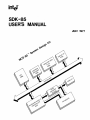
SDK-85
USER'S MANUAL
JULY 1977
SDK-as
System Design Kit
Users Manual
Manual Order Number 9800451 A
Copyright © 1977 I ntel Corporation
Intel Corporation, 3065 Bowers Avenue, Santa Clara, California 95051
The information in this manual is subject to change without
notice. Intel Corporation makes no warranty of any kind with
regard to this material, including, but not limited to, the implied
warranties of merchantability and fitness for a particular purpose.
I ntel Corporation assumes no responsibility for any errors that
may appear in this manual. Intel Corporation makes no commitment to update nor to keep current the information contained
in this manual.
No part of this manual may be copied or reproduced in any
form or by any means without the prior written consent
of I nte l Corporation.
The following are trademarks of I ntel Corporation and may be
used only to describe Intel Products.
ICE-3D
ICE-80
INSITE
INTEL
INTELLEC
LIBRARY MANAGER
MCS
MEGACHASSIS
MICROMAP
MULTIBUS
PROMPT
UPI
CONTENTS
CHAPTER 1
DESCRIPTION
· 1-1
CHAPTER 2
HOW TO ASSEMBLE THE KIT
GENERAL.
GETTING ORGANIZED
SELECTING TOOLS AND MATERIALS
UNPACKING AND SORTING PARTS
A REVIEW OF BASIC ASSEMBLY AND
SOLDERING TECHNIQUES
ASSEMBLY PROCEDURE.
2-1
2-1
2-2
2-3
2-6
· 2-7
CHAPTER 3
FINAL ASSEMBLY AND CHECKOUT
GENERAL.
STRAPPING OPTIONS
POWER SUPPLY WI RING.
INSTALLING LARGE IC DEVICES
STARTING THE FIRST TIME
WHAT IF IT DOESN'T? .
CONNECTING A TELETYPEWRITER
3-1
3-1
3-1
· 3-4
· 3-6
3-7
· 3-8
CHAPTER 4
OPERATING INSTRUCTIONS
WHAT IT DOES.
THE BUTTONS AND DISPLAYS
Reset
Substitute Memory
Examine Registers
Go
Single Step .
Vector Interrupt .
Program Debugging The Use of Breakpoints
Error Conditions - Illegal Key
Memory Substitution Errors
TELETYPEWRITER OPERATION
Console Commands.
Use of the Monitor for Programming
and Checkout .
Command Structure
Display Memory Command, D
Program Execute Command, G
Insert Instructions into RAM, I
Move Memory Command, M
Substitute Memory Command, S .
Examine/Modify CPU Registers
Command, X
Programming Debugging Breakpoint Facility.
Error Conditions - Invalid Characters.
Address Value Errors
4-12
4-13
4-13
4-13
CHAPTER 5
THE HARDWARE
OVERVIEW
SYSTEM COMPON ENTS
The 8085 CPU & The System Buses
The 8155.
The 8355 & 8755
The 8279.
The 8205.
SDK-85 MEMORY ADDRESSING.
INPUT/OUTPUT PORT AND
PERIPHERAL DEVICE ADDRESSING.
Accessing the 8279 Keyboard/Display
Controller
PROCESSOR INTERRUPT
ALLOCATION
THE SERIAL DATA INTERFACE.
CONVERTER CIRCUIT FOR
RS232C SERIAL PORT.
ADDITIONAL INTERFACES
4-1
4-1
4-2
4-2
· 4-4
· 4-6
4-8
4-9
CHAPTER 6
THE SOFTWARE
4-9
4-9
· 4-9
4-9
· 4-9
THE SDK-85 MONITOR.
PROGRAMMING HINTS
Stack Pointer
RAM-I/O Command Status Register (CSR)
Access to Monitor Routines
PROGRAMMING EXAMPLES
4-10
4-10
4-10
4-10
4-11
4-11
.4-12
5-1
5-1
5-1
5-1
5-2
5-2
5-2
5-3
5-5
5-5
5-7
5-7
5-8
5-8
6-1
6-1
6-1
6-1
6-1
6-1
APPENDIX A
MONITOR LISTING
APPENDIX B
DIAGRAMS
iii
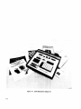
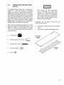
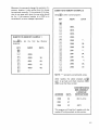
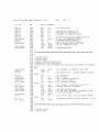
Figure 1-1. SDK-85 System Design Kit
'-0
CHAPTER 1
DESCRIPTION
The MCS-85 System Design Kit (SDK-85) contains
all the parts with which you can build a complete
8085 microcomputer system on a single board, and
a library of MCS-85 I iterature to help you learn to
use it. The finished computer has the following
built-in features:
SDK-as SPECIFICATIONS
Central Processor
CPU: 8085
Instruction Cycle: 1.3 microsecond
Tc{ 330 ns
• High-performance, 3~M Hz 8085 cpu (1.3 p.s
instruction cycle)
• Popu lar 8080A I nstruction Set
• Direct Teletypewriter Interface
• Interactive LED Display
• Large Wire-Wrap Area for
Circuit
Custom-Designed
• System Monitor Software in ROM
Memory
ROM; 2K bytes (expandable to 4K bytes)
8355 or 8755
RAM: 256 bytes (expandable to 512 bytes) 8155
Addressing: ROM 0000-07FF (expandable to OFFF
with an additional 8355 or 8755) RAM 200020FF (2800-28FF available with an additional
8155)
Input/Output
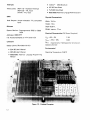
You can assemble the kit in as little as 3 to 5 hours,
depending upon your skill and experience at building
electronic kits. Only a 5 Volt power source capable
of delivering 1.3 Amperes is then needed to make
the computer operate, using its built-in display and
keyboard. If you wish to interface a Teletypewriter
to the SDK-85, you will also need a -10 Volt power
supply. After you have completed the basic kit,
you may expand both memory and I/O by adding
more RAM-I/O or ROM-I/O devices in the spaces
provided for that purpose. Other spaces are allocated
for bus expansion drivers and buffers that allow you
to address and use external devices located either
in the wire-wrap area of the board or off the board.
You can, for example, access up to 64K of external
memory via the expansion bus.
Parallel: 38 lines (expandable to 76 lines).
Serial: Through SI D/SOD ports of 8085. Software
generated baud rate.
Baud Rate: 110
Interfaces
Bus: All signals TTL compatible.
Parallel liD: All signals TTL compatible.
Serial I/O: 20 mA current loop TTY.
Note:
By populating the buffer area of the board,
you have access to all bus signals which
enable you to design custom system expansions into the kit's wire-wrap area.
1-1
Interrupts
Three Levels:
• Intellec®
(RST 7.5) - Keyboard Interrupt
(RST 6.5) - TTL Input
(lNTR) - TTL Input
DMA
MDS Brochure
• ICE-85 Data Sheet
• PL/M-80 Data Sheet
• 8085/8080 Assembly Language Reference Card
Physical Characteristics
Hold Request: Jumper selectable. TTL compatible
input.
Width: 12.0 in.
Height: 10 in.
Software
Depth 0.50 in.
System Monitor: Preprogrammed 8755 or 8355
ROM
Weight: approx. 12 oz.
Addresses: 0000-07 F F
I/O: Keyboard/Display or TTY (serial I/O)
Literature
Vce: +5V ± 5%
1.3A
VTTY : -10V ± 10%
0.3A
(VTTy required only if teletypewriter is to be connected to the kit)
Design Library (Provided with kit):
Environ mental
• SDK-85 User's Manual
• MCS-85 User's Manual
Operating Temperature: 0-55° C
• 8080/8085 Assembly Language Programming
Manual
Figure 1-2. Finished Computer
1-2
CHAPTER 2
HOW TO ASSEMBLE THE KIT
2-1
GENERAL
Don't unpack your parts yet. Do a little reading
first, and you may save yourself time and expense.
I
CAUTION
I
The metal-oxide-semiconductor (MOS)
devices in this kit are susceptible to static
electricity. Do not remove them from
the protective, black foam backing sheet
until you have read the precautions and
instructions in paragraph 2-4.
way, there won't be any surprises later. Take your
time. Don't rush, and don't skip over qualitychecking each step you perform. Desoldering,
removing, and replacing just one DIP component
because it was not oriented properly when first
installed will cost you more time than doublechecking all of them. Your objective is surely to
produce a working computer, not to win a race.
2-2
This manual was published only after the assembly
of several kits by a number of persons of varying
experience. In this chapter you will find virtually
everything you need to know to put together your
MCS-85 System Design Kit.
There are suggestions for laying out an efficient
work area. All of the tools and materials you need
are described in a checklist. There is a complete
and detailed parts list. Basic assembly and soldering
techniques are reviewed. Following the step-bystep assembly instructions in this chapter, you
can't go wrong.
If you're an experienced kitbuilder, you already
know that it's not a bad idea to read through this
entire chapter first, before starting the job. That
GETTING ORGANIZED
Before starting work, it's a good idea to plan and
organize your workplace. Be sure you have room
to accommodate this book, lying open, and also
the circuit board, along with tools and the hot
soldering pencil. Unless you have the cordless,
battery-powered soldering instrument, you'll want
to arrange its cord out of the way to keep from
accidentally pulling the soldering pencil off its
holder. A muffin pan, an egg carton, or some small
boxes cou Id be used to sort parts into, if you don't
have the traditional plastic, compartmented parts
boxes. It might be helpful, too, to write the part
values and reference designators on small cards as
you sort them, and put these with the parts for
quick identification. Arrange everything within
comfortable reach, and you'll do the job quickly
with little chance of errors.
2-1
2-3
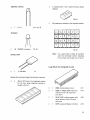
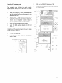
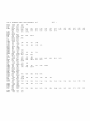
SELECTING TOOLS AND
MATERIALS
These tools and materials will be required to
assemble the kit:
o
o
o
o
o
Needle-nose pliers
Sma" Phillips screwdriver
Small diagonal cutters
Soldering pencil, not more than 30 watts,
with extra-small-diameter tip. (1/16 in. isn't
too sma".) You should also have a secure
holder for it.
Rosin-core solder, 60:40 (60% tin), sma"
diameter (,05 in, or less) wire
Note:
o
M
PHILLIPS
SCREWDRIVER
NEEDLE-NOSE
PLIERS
SOLDE~
Soldering paste is not needed. The
solder wi" contain sufficient flux.
Volt-Ohm-Mi"iammeter
DIAGONAL
CUTTERS
fr
11
It is also useful to have the following:
o
Soldering aid, with a small-tipped fork at one
end and a reamer at the other, to help in
coaxing component leads into holes and
manipulating sma" parts.
If you should happen to make a soldering error and
have to remove solder from joints, the job wi" be
made much, much easier if you have the following:
o
o
o
Solder sucking device, either the bulb variety
(shown) or the pump variety
Large-area desoldering tip for your soldering
pencil, to spread heat over several leads of an
I C device at the same time
Length of copper braid to sop up solder like a
sponge
Note:
2-2
It is extremely difficult to remove DIP
components using just a soldering
pencil.
I
01I
/\
U
SOLDER
SUCKER
VOL T-OHM-MILLIAMMETER
DESOLDERING
~
IP/."
~/
i
SOLDERING
AID
2-4
UNPACKING AND SORTING
PARTS
The MCS-85 System Design Kit is shipped skinpacked on a card that includes a conductive
backing to protect its metal-oxide-semiconductor
(MOS) devices from static charge. Don't remove the
four larger-size I ntel devices from the foam backing
until you have completed all of the instructions in
this chapter and are ready to place them on the
board. As a further protection against possible
damage, these four devices are to be installed in
sockets, rather than soldered on the board.
With a knife or sharp-pointed scissors, slit the film
around the edges of the small-parts bags in the
lower left corner of the skin-pack and remove
them. First, open the bag of hardware and check to
be sure you have:
D
9 rubber feet •
D
9 Nylon spacers, 7/16 in. long
D
9 screws, 3/4 in. long
D
18 Nylon washers
D
9 nuts
I
CAUTION
I
Don't remove the other components
from the skin-pack. The black foam
backing is an electrically conductive
material that protects the integratedcircuit devices from static electricity as
well as from physical damage to their
leads and ceramic substrates.
Underneath the two bags of small parts and
hardware will be found:
D
Red plastic window (covered with protective
paper)
D
Two strips of double-coated adhesive tape
RED PLASTIC
WINDOW
(FILTER)
~
@)MiMmnm@II@@My@
@
ADHESIVE
TAPE
@
2-3
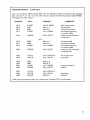
Next, open the bag of electrical parts and sort
them out by type and value. Give yourself plenty
of unobstructed work space and try not to let tiny
parts skitter away from you. The bag should yield
the following:
Resistor, 1 /2 Watt
o
100 Ohm (brownblack-brown)
R1
Resistors, 1/4 Watt
Resistors, 1 Watt
<mID
8
0
24 Ohm (redyellow-black)
R11, 14, 17,20,
23,26,2"1,30
0
47 Ohm (yellowviolet-black)
R5
0
200 Ohm (redblack-brown)
R33
0
6
270 Ohm (redviolet-brown)
R10, 13, 16, 19,
22,25
0
2
1k (1 ,OOO) 0 h m
(brown-black-red)
R4,31
0
1.6k Ohm (brownblue-red)
R3
Q
2.?k Oh~ (red-
R6
o
200 Ohm (red-blackbrown)
R34
o
430 Ohm (yelloworange-brown)
R35
Capacitor, tantalum
~==~®
o
)~====~
22 J.1.f, 15V
C1
Capacitor, mono
violet-red)
3k Oh m (orangeblack-redi
R7, 9,12,15,18,
21,24,28,29
0
3.9k Ohm (orangewhite-red)
R8
0
4.7k Ohm (yellowviolet-red)
R2
0
51 k Ohm (greenbrown-orange)
R32
9
0
o
2
1 J.1.f, 25V
C5,20
Resistor Color Code
Resistors are commonly identified by means
of a code using color bands. Each color represents a number.
The first three bands employ the color code
below:
Black
Brown
Red
Orange
Yellow
2·4
0
1
2
3
4
Green
Blue
Violet
Gray
White
5
6
7
8
9
The fourth band indicates percentage
tolerance of the resistor value.
First significant digit
Second significant digit
Number of following zeroes
Gold
= 5%; silver = 10% tolerance
Capacitor, ceramic
D
6 alphanumeric LED (light-emitting diode)
displays
051-6
D
D
7
0.1 J1 f
C11-16,18
2N2907 transistors
Q1-16
24 pushbutton switches, with keycaps labeled
Transistor
D
16
51-24
Note:
Crystal, clock
It's a good idea to check all switches
with the ohmmeter before installing.
If one is bad, you'll save a lot of work.
Large, 40-pin ICs (integrated circuits)
6.144 MHz
D
Y1
Besides the small-parts bags, the skin-pack contains:
D
4
40-pin DIP (dual in-line package) sockets
for the four large integrated circuits included in the kit
D
8085 microprocessor (cpu)
A 11
D
8355 (or 8755) ROM (read-only
memory) with I/O (input/output) ports
A 14
D
8155 RAM (random-access, readwrite memory) with I/O ports
and timer
A 16
D
8279 keyboard/display interface
A13
2-5
Small, 16-pi niCs
o
o
bottom or left-to-right, and to form the
leads of parts with values printed on them so
that the values are legible after assembly.
8205 address decoder
A10
74LS156 scan decoder
A12
I
CAUTION
I
Large-scale integrated circuits are fragile!
Dropping, twisting, or uneven pressure
may break them. The discharge of static
electricity can destroy them internally.
Leave them embedded in the conductivefoam backing sheet until ready to install
on the board. Never press down hard
upon, twist, or bend the larger devices.
Touch the exposed metal traces of the
board with your hand before inserting
one in its socKet. I he sOldenng ot large
devices directly on the circuit board is
not recommended.
2-5
3.
Fit each part in place and see that no undue
stress is placed on the leads. Double-check and
be sure you have the correct part inserted in
the correct holes, properly oriented. Don't
trim leads before soldering.
4.
When ready to solder, be sure your soldering
pencil is hot enough to melt solder quickly.
Then turn the board face-down on your work
surface. If necessary, hold the parts you are
about to solder in place while turning it over
so they won't fall out, and place something
under the board to hold the parts in position
while you solder on the back surface of the
board. Some people prefer to crimp the leads
to hold the parts in place. That's all right, too.
5.
Bring the point of your soldering pencil into
contact with the pad to be soldered, simultaneously also touchinq the lead.
6.
At once, touch the end of the solder wire to
the pad and lead, opposite the pencil tip. The
amount of time required to melt the solder
will depend upon the amount of foil surface
there is on the board to carry away heat by
conduction. The smallest pads will heat up in
less than a second with a 25- or 30-watt
pencil; large, ground-plane areas may require
over five seconds.
7.
The instant you see and feel the solder start to
melt, withdraw the solder wire from the joint.
Only a tiny drop of solder is needed to make a
good joint.
8.
The instant you see the solder draw into the
hole, become shiny, and spread smoothly over
the surface of both pad and lead, withdraw
the soldering pencil. It will take only a
moment for th is to hgppen after step 7.
9.
Don't reheat a joint unless there's something
wrong with it: not enough solder, too much
solder (causing a "bridge" to an adjacent pad
or trace), or a "cold solder joint," which
A REVIEW OF BASIC
ASSEMBLY AND SOLDERING
TECHNIQUES
The steps to producing a professional quality
assembled circuit board are:
1.
2.
Have your work area organized before starting
work, and keep it that way. (See paragraph
2-2.) Sort all parts into bins, cups, trays or
boxes so they wi!! be easily located by value
when needed.
To prepare a part for soldering, bend its leads
carefully with needle-nose pliers to make the
part fit exactly the way you want it to.
It is good practice to orient color-coded resistors so that the codes are readily read, top-to-
2-6
appears dull on the surface or does not
surround the lead completely and fill the hole.
Note:
A little rosin from the solder core,
remaining on the board, does no harm.
Don't try to clean it off.
10. CI ip off the excess length of lead that projects
beyond the solder "bead," within 1/8 inch of
the board. Save cut ends to use for strapping
optional connections. (See paragraph 3-2.)
I
WARNING
I
Avoid eye injury when clipping excess
lead ends. Hold lead end as you clip it,
so it can't fly up in your face.
There are two important conditions that govern
good soldering technique. They are:
1.
Use no more heat than absolutely the minimum that will make a solid joint.
2.
Use enough heat to cause solder to flow into
the hole in the board and around the lead
that's being soldered into it.
These conditions are both met simultaneously and
easily only if you are careful, have the proper tools,
and arrange your workplace so that the ci rcu it
board can lie flat while you apply steady, firm (but
not hard) pressure with the soldering pencil without
slipping. A small-diameter soldering tip is a must!
Likewise, small-diameter solder wire is essential to
achieving satisfactory results.
Note:
Do not apply soldering paste to the work.
Fluxing is not required in printed-circuit
soldering, as the boards and component
leads are plated or tinned to prevent oxidation of the copper.
Iight between the soldered pad and any adjacent
pads or traces that aren't supposed to be connected
to it, it might be well to slip a solder-sucker or wick
over the lead under examination, quickly remelt
the solder and draw off the excess.
2-6
ASSEMBLY PROCEDURE
Follow these instructions in order and make a
check mark in the box opposite each step when it
is completed.
o
First, place the board on your work surface,
lettered side up.
o
Install the nine rubber feet. Eight go around
the edge of the board, and one goes near the
middle of the board, to the left of the keyboard and display area. At each location, press
a nut into the recess in a rubber foot, string a
washer on a screw, and insert the screw
through the hole in the board from the top.
Place a spacer, then another
washer on the screw, then
place the nut and foot on
the end of the screw, and
tighten, with the screwdriver,
just enough to hold the foot
firmly.
,
I
o
•
I
I
@
I
I
Always inspect carefully for cold solder joints,
solder bridges, or (perish the thought!) I ifted traces
after each soldering operation. A good way to
check for solder bridges is to hold the newlysoldered connection up to a light. If you can't see
[
I
®
2-7
o
Install capacitor C1 near the top edge of the
board.
o
Solder C1 in place. Clip excess lead ends.
I
WARNING
":., I'~-=~ ~':~~':::" :~~l
::f:~~;t:.;:.-,~,,~ I
I
Avoid eye injury. Hold lead ends as you
clip them so they can't fly up at you.
Assembly of TTY Interface Area-
o
Install a 100 Ohm, 1/2 Watt resistor (brownblack-brown) at R 1.
o
Install a 4.7k Ohm resistor (yellow-violet-red)
at R2.
o
Install a 1.6k Ohm resistor (brown-blue-red)
at R3.
o
I nstall a 1k Ohm resistor (brown-black-red) at
o
~W{;f~,tF+Em~~"
GND _ _-,
ERS _ _ _ _ _
,
J7
A3
,,~
(9
,~
RI!.
.
C
_. __ .
.,
~ol
I
''''t:nr'''l..t:
I
o
Install a 47 Ohm resistor (yellow-violet-black)
at R5.
o
Install a 2.7k Ohm resistor (red-violet-red) at
R6.
o
Solder the six resistors in place, then clip their
excess lead ends.
o
Install a 430 Ohm resistor (yellow-orangebrown) at R35.
o
Install a 1 uf capacitor at C5, and solder and
clip it.
o
Solder these two resistors in place, then clip
their excess lead ends.
o
Install a 200 Ohm, 1 Watt resistor (red-blackbrown) at R34.
o
Install transistors 01 and 02, and solder and
clip them.
2-8
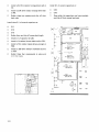
Assembly of Processing Area
The processing area includes the clock crystal,
address decoder, cpu, RAM-I/O and ROM-I/O areas,
and related components.
o
o
A 16, for the RAM-I/O device, an 8155.
Solder the three sockets in, and check carefully
for solder bridges.
LJLJ
J3
o
o
I nstall the crystal at Y1, with its leads bent so
that the device lies flat on the board in the
space outlined for it.
II
I
PORT!
.J
1PORT 0
Take a piece of scrap wire trimmed from a
component previously mounted on the board.
Bend it into the shape of a staple. I nstall it
over the crystal, to hold it firmly in place.
20
21
~
lO<
I
PORT 9
~
9
1-
11
PORT B
o
o
03
Solder the four connections just made.
28
30
Install three DIP sockets, crimping the corner leads
of each to hold in place, at:
13
A15
14
--,
"~~""'::Qi
Q
laC 0800H-OFFFH
31
32
PORT
011
G
r01 - - t
Dt-
PORTS 8H-BH
.--J 23H
33
I
.J
A 11, for the 8085 cpu.
I
PORT 21H
~
DS1
~£
C19
LJ
J5
I~I:-~~"~·j
-"""1
•
L:.....J
-""~~-"Ir"
--
·0
I
PORT 2BH
-1
--"
[!]
="~:=-~:"
-"r-.:::
_";,~;":.".-_
PORT 2AH
C-:""-I: "-.;;" _. _
~
1"-
I
-
...
~
.J
---
--
~ ",;; = "
"'"
_.-
.,.
._ ••
H
•__.,
-
~
--
;;:
..
-"
..
.-
.. '
~
I
.::011.-
."
A17
II
1
="
12
&~~
c=J C17
PORT 22H
A 14, for the PROM (ROM)-I/O device, an
8755 or 8355.
04
0 ~~O~
I nstall the 8205 address decoder at A 10 and
solder it.
8755 (8355)
o
o
10
PORT 29H
,
..J
RESET
VECT
INTR
SINGLE
STEP
GO
8155
laC 2800H-28FFH
PORTS 28H-2DH
17
18
ClK
19
C20
c=J
-c::J-c:::J-
R31
SUBST
MEM
EXAM
REG
R32
TIMER OUT/IN
~~
LJ
Q'"
NEXT
EXEC
:"" I -
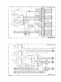
2-9
D
Install a 3k Ohm resistor (orange-black-red) at
R7.
Install 0.1 uf ceramic capacitors at:
D
Install a 3.9k Ohm resistor (orange-white-red)
at R8.
D
C16
D
C18
[]
Now solder the capacitors you have installed,
and clip off their excess lead ends.
D
Solder these two resistors and clip off their
lead ends.
I nstall three 0.1 uf ceramic capacitors at:
D
C1l
D
C12
C13
I
D
Solder them and clip off excess lead length.
PORT
D
Install a 1 uf capacitor at C20.
D
Install a 1k resistor (brown-black-red) at R31.
D
Install a 51 k resistor (green-brown-orange) at
R32.
D
D
Install a 200 Ohm resistor (red-black-brown)
at R33.
Solder these four components in place and
'"
CI3 lAID
--.J
10
CI2 c = J
8205
]
c=J R8'-'=_ _ _ _ _ _- '
II~ ~ moo::,
'0"'
PROM (ROM) 1/0 - - - .
A14
~
8
-.J
LJ
n
13
PORT
~T22H3r.3~
~T
PORTS 8H-BH
__
~
. . ;15;. . . .;1~6 c==tl~AM
A16
21H
J
lOC 0800H-0FFFH
L
32
1
8755(8355)
)
31
--.J13H
14 c = J C17
A15
I"
lOC
(
12
Dii~C~
]
2<1
30
11
10
PORTS 0-3
28
9
8755 (8355)
lOC 0000H- 07FFH
M
---,
AI3
I_r
Cl6c=J
9
I
M
--
I
~"~
PORT
CPU
IA~
11
KEYBO
~
r:!
6.144
MHZ
c:=J_ _ ---c::::J- -
I
h
ADDRESS
DECODER
VI
CRYSTAL
Cll
.:iT
D
..
0
LJLJ
~
1/0
28~;:H_20FFH
]
@~
I
_"9!:!/_
D[
~~ ~
~
1
PORTS 20H-25H
I
OSI
.----
:c:e
CI9
CA17
L-J
n
RESET
~
]
8155
lOC 2800H-28FFH
PORTS 28H-20H
;;;IIT 2BH
(
SINGLE
STEP
VECT
INTR
GO
....J
"I
PORT
.J
"I
2AH
PORT 2gH
-.J
17
18
ClK
19
C20
SUBS"!:
MEM
c=J
-c::::J-
131
--cD-
R32
EXAM
REG
TIllER OUT/IN
Ie:
LJ
2-10
:
()"''''U '
QI33
I
NEXT
EXEC
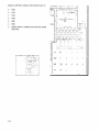
Assembly of Keyboard and Display Area
Find where the row of resistors, R9 through R30,
go. I nstall eight 3k resistors (orange-black-red) at:
o
o
o
R12
o
R18
o
o
o
R21
o
o
R9
R15
R24
h
J
.
lESS
DER
)
R28 (Careful-the location pattern changes
here! )
R29
Now solder all eight resistors in place and clip
their excess lead ends.
OL 'U
~ DATA BUS BUFF
)
.
uj
U I AS)
('
J ('
,~.vv
A.9 )
KEYBOARD AND
~~
]
--
J
OU'~ ~.
-.
DI:~::Y
KEYBOARD
LOC IS00H
1900H
DISPLAY
•
UI
0
.,.
u
CONTROlLER
,-,
S25
KEYBOARD:
::122
SEU~T
I
""23
I
124
11
9
10
03
J'
AI2~SC~~Sb~~ODERJ
27
A13
'~L.'~
12
04
DISPLAY DRIVERS
05
06
07
OS
09
J D~~D~ ~D~~D~~Ds~D~ p~
~
1
L __
.~~~@~~ ~
1J "g.'~b!~
;,bQ~fi ~b ~h~"
AD~S
~A-----'
r 01 - -
,
015,-
DDDD DO
L-D_S_l_ _ _ _ _ DISPLAYS _ _ _ _ _D_S6---.-'1
RESET
VEer
INTR
SINGLE
STEP
GO
SUBSr
MEM
NEXT
EXAM
REG
EXEC
0
S
H
4
SPH
A
5
SPL
6
7
PCL
PCH
0
•
2-11
Install six 270 Ohm resistors (red-violet-brown) at:
o
o
o
o
o
o
o
R10
R13
R16
R19
.
A7!DATA
1
DRESS
CODER
205
J
h
US-tis BUFF
]
110A~
U
R25
!,
i
I
.JI~
KEYBOARD AND
I
DISPLAY
~
25
n
74lS156
;
A12( SCAN DECODER~ '-;/
;~
U
""OA" .,::::, ooN,"O""
I ", C.
R22
", ;I
.
A~ , .. .vv
coo
9
::gg:
S25
II
Solder these six resistors and clip their excess
lead ends.
RESET
,EeT
0
INTR
l
~
SINGLE
STEP
SUBST
MEM
NEXT
GO
EXAM
REG
EXEC
8
H
4
SPH
5
SPl
6
PCH
7
PC l
0
0
2·12
Install eight 24 Ohm resistors (red-yellow-black) at:
o
R11
o
R14
o
o
o
o
o
R17
o
o
R20
R23
R26
A7rDATA-ius BUff
1~
DRESS
CODER
205
J
UA~ ,~_w
JAV
KEYBOARD AND
]
J
OU'~ ~.
..
l
74LS156
A12c! SCAN DECODER~
;~
•
A13
DI~~::Y
KEYBOARD
LOC 1800H
1900H
9
J UI
DISPLAY
~
25
--
,~ •• ,~
0
~
U
CONTROLLER
525
11
R27 (Again, note the change in location
pattern.)
R30
Solder these eight resistors and clip their
excess lead ends.
VECT
INTR
GO
SUBSr
MEM
EXAM
REG
NEXT
EXEC
8
A
H
4
SPH
5
SPL
6
PCH
7
PC L
o
o
2-13
Install fourteen 2N2907 transistors in two rows.
Position the seven transistors in the top row so that
their indexing tabs point upward and to the left, at:
D
03
D
04
D
05
D
06
D
D
07
'08
D
09
I
Position the seven transistors in the bottom row so
that their indexing tabs point down and to the
right, at:
D
010
D
011
D
012
D
013
D
014
D
015
D
016
D
Press all of the transistors down to about
1/8 inch from the surface of the board. Let
them stand approximately straight up. Then,
turn the board over and solder all of their
leads in place and trim the lead ends.
SUB 51
MEM
NEXT
EXAM
REG
EXEC
4
~
SPH
SPl
7
PC l
6
PCH
o
o
2-14
D
Install one of the 40-pin DIP sockets, for the
8279 Keyboard-Display Controller, at A 13,
and solder it in.
D
Install the 74LS156 scan decoder at A 12, and
solder it.
Be careful to orient the six alphanumeric LED
displays so that the decimal points are even with
the bottom of the digits and install at:
D
DS1
D
D
D
D
D
DS2
DS3
DS4
105
C
1
~RESS
OOOER
]
KEYBOARD AND
DS6
Note:
.
26
27
DS5
DISPLAY
~';bJ
A12 ~
25
«:%1.
Jf
",Y
~ f;i.
If these components are provided with long,
wirewrap leads, you will probably find it
easiest to insert, solder, and clip them one
at a time because of crowded quarters. The
order shown above with the board turned
bottomside up will be most convenient for
you if you hold the soldering pencil in your
left hand. If you s01der right-handed, you
may prefer to work from DS6 to DS1.
DSl
DISPLAYS
Note:
Don't install the red filter over the display
yet. h's a good idea to wait until after final
assembly and checkout to do this, on the
remote chance that you might have to
remove one of the character displays.
Install two 0.1 uf ceramic capacitors at:
D
C14
D
C15
D
Solder the leads and clip them off close to the
board.
RESET
VEer
INTR
SINGLE
STEP
GO
SUBSr
MEM
NEXT
EXAM
REG
EXEC
0
8
H
4
SPH
A
5
SPL
6
PCH
7
PCl
0
•
2-15
The easiest method of doing this is to insert each
button in its turn, bend its leads over on the back
of the board to hold it in place, and go on until all
buttons are in place, then solder all of them in one
pass, with the board lying flat on the work surface
and weighted down to make sure the switches are
uniformly held firmly against the front surface of
the board.
0
2·16
Install the twenty-four pushbutton switches
that make up the keyboard. Be sure each
button is rightside up and in its proper position
before soldering.
o
RESET
o
VECT
INTR
DC
OD
o
E
o
F
o
SINGLE
STEP
o
GO
0
8
0 9l
OA
o
B
o
SUBST
MEM
o
EXAM
REG
°SPH
°SPl
°pCH
7
°pCl
o
NEXT
o
EXEC
DO
01
02
o
0
H
4
All soldered in place
5
6
3
I
CHAPTER 3
FINAL ASSEMBLY AND CHECKOUT
3-1
GENERAL
Now that most of the components are soldered on
your circuit board, it's time to give your handiwork
a quick visual check to make sure all of the devices
are oriented correctly. The notched ends of the I Cs
should all be toward your left, and the decimal
points of the LED displays should be at the bottom
line of the characters.
It is recommended that the basic kit computer
be checked out using the procedure in this chapter
before adding any external options such as teletypewriter or expansion memory. It is well for you
to have the assurance that you have a working cpu
and display-keyboard before you add peripherals
to your system. It is therefore recommended that
you first wire the strapping options in Table 3-1
for the 8355 (or 8755) ROM-I/O that was furnished
with the kit (and contains the SDK-85 System
Monitor). Then install the strap in Table 3-2 for
keyboard operation, and in Table 3-4 for the basic
kit without expansion memory. (See paragraph 3-2.)
Paragraph 3-3 tells you how to hook up power to
the MCS-85 System Design Kit, and paragraph
3-4 tells you how to start it up and see if it's
working right. The subsequent paragraphs list the
add-on options you can use without inventing any
new ci rcu itry on the board or off.
3-2
STRAPPING OPTIONS
The MCS-85 System Design Kit will accept 8355
or 8755 ROM-I/O devices at positions A 14 and
A 15. These different devices are not completely
electrically interchangeable, so you must make the
strapping connections ~R Table 3-1, appropriate to
the type of device in each socket.
To make a strapping connection (jumper), bend a
short length of bare wire (such as the excess lead
end cut from a resistor) to fit between the two
holes you wish to strap together, insert the ends
of the wire in the holes, and solder them. Then
clip the remaining excess ends, just as you did with
the components. When you install a jumper and
solder it, be sure it doesn't touch any intervening
traces or pads. For normal operation of the
SDK-85, it is mandatory to strap the following:
1.
One of the three options in Table 3-1.
2.
One of the two options in Table 3-2.
3.
The two jumpers listed in Table 3-3.
4.
Either basic kit operation or one of several
expansion options listed in Table 3-4.
The keyboard-teletypewriter selection function may
be done with a miniature printed circuit-board
mount, single-pole, double-throw switch, S25, not
furnished in the kit, or may be strapped with
wire. Table 3-2 lists the connections. Table 3-3
lists keyboard strapping connections always made.
Table 3-4 lists the strapping connections that may
be used when the optional bus expansion driver
function is implemented. Tables 3-5 through 3-10
list all of the bus and port expansion connector
pinouts. Table 3-11 lists suggested connector types.
3-3
POWER SUPPLY WIRING
(See Figure 3-6.)
Connect a +5 Volt, regulated power supply with its
positive output at the +5V POWE R SUPPLY point
on the board. A 6-pin Molex connector will fit the
(Text continues on page 3-4.)
3-'
TABLE 3-1
ROM/PROM STRAPPING
Device
Location
A14
8755
8355
8755A
Figure 3-1 Figure 3-2a Figure 3-2b
No Straps
Required
A15
Strap
28-29
Strap
29-30
Strap
31-32
Strap
32-33
Figure 3-1 Strapping Options for 8355 ROMs
TABLE 3-2
TELETYPEWRITER-KEYBOARD
STRAPPING
TELETVPEWRITER
Figure 3-3
KEYBOARD
Figure 3-4
Strap 22-23
Strap 23-24
TABLE 3-3
DISABLING UNUSED KEYBOARD
CONTROLLER FUNCTIONS
Figure 3-5
Always strap 9-10.
Always strap 11-12.
Figure 3-2a Strapping Options for 8755 PROMS
Note: These two straps not usually removed,
since the MCS-85 System Design Kit
does not have SHIFT or CONTROL
keys on its keyboard. These straps
have no effect on operation of the
corresponding key functions on a
teletypewriter or other ASCII terminal
that is connected to the TTY interface.
They are provided for your use if you
wish to modify the SDK-85's keyboard functions and replace its monitor software with your own.
3-2
Figure 3-2b Strapping Options for 8755A PROMS
Figure 3-3 Teletypewriter Strapping Option
Figure 3-5 Disabling Unused Keyboard Controller
Functions
5 VOLT SUPPLY
Figure 3-4 Keyboard-Display Strapping Option
10 VOLT SUPPLY
Figure 3-6 Power Supply Connections
3-3
hole pattern on the board; if this connector is used,
parallel two pins on the +5V bus and three pins on
the GND bus. If you are going to use a teletypewriter, connect a -10 Volt power supply with its
negative output at the -10V point on the board.
Connect the positive side of the -10 Volt power
supply to the GND bus.
I
CAUTION
I
3-4
INSTALLING LARGE
IC DEVICES
When you've finished all soldering operations on
the board and are ready to fire it up, then it's time
to plug in the large ICs. Once more, please make
note of the precautions for handling these large
MOS devices.
(Text continues on page 3-6.)
Do not turn on power until instructed to do so.
TABLE 3-4
OPTIONAL BUS EXPANSION STRAPPING
I
AUGMENTED KIT
WITH EXPANSION
MEMORY
(Figure 3-8)
(Also See Paragraph 3-7.)
FUNCTION
BASIC KIT
WITHOUT EXPANSION
MEMORY
(Figure 3-7)
RST 6.5
Strap 3-5
HOLD
Strap 6-8
Strap 7-8 if no input is connected to
J 1-14. Leave 6, 7, and 8 not strapped
if input is to be supplied for this
function.
INTR
Strap 20-21
Strap 20-21 if no input is connected
to J 1-18. Leave 20-21 not strapped
if input is to be supplied for this
function.
Memory
Address
Locations
Leave 25-26-27 unstrapped.
Strap 25-26 if all memory locations
are external, i.e., addressed via bus
expansion drivers. * (See Figure 3-9.)
Strap 25-27 if only the upper 32k
(Locations 8000H-F F F F H) are
addressed via bus expansion drivers
and lower addresses (Locations
0000-7FFFH) are on basic kit areas
of board. (See Figure 3-10.)
I
Strap 3-4 if no input is connected to
J 1-20. Leave 3, 4, and 5 not stra pp ed
if input is to be supplied for this
restart function.
* Note: No devices may be installed in positions A 13, A 14, A 15, A 16, and A 17 if this option
is strapped.
3-4
RST6_5
RESET
ASTINI
r~
•
07
1
~ ~
o~." J
8212
A8 - A 15 ADDRESS
DRIVER
1
n:...
--'-___-. Y
A6
I
.9"
I
~ ~
AD
TTY
INTERFACE
8212
AO -A7 ADDRFSS
DRIVER
--'
Y1
'" j'
';12 c::::::J c."
c::::::J R8 r!
RESS
DECODER
8205
]
-c:::=r-- •
----
CPU
h
1
--
A13
0~
8085
!!)
VI
1
KEYBOARD DISPLAY CONTROLLER
LOC 1800H
1900H
Figure 3-7 Strapping Options for Basic Kit (No Bus Expansion)
~A~
74S00
KEYBOARD AND
h
i~
DISPLAY
A12JSC~tLS6~~ODERJ
27
0
...
v
A13
(I
U
~
'"
_________..... UI .
8279
KEYBOARD OISPLAY CONTROLLER
LOC 1800H
1900H
j
525
r -,
KEYBOARD:
>1.22
Figure 3-8 Strapping Options for Bus Expansion Control Lines
Figure 3-9 Strapping Options for all External
Memory
Figure 3-10 Strapping Options for Internal/
External Memory
3-5
I
CAUTION
I
Large-scale integrated circuits are fragile!
Dropping, twisting, or uneven pressure
may break them. The discharge of static
electricity can destroy them internally.
Leave them embedded in the conductivefoam backing sheet until ready to install
on the board. Never press down hard
upon, twist, or bend the larger devices.
Touch the exposed metal traces of the
board with your hand before inserting
one in its socket. The soldering of large
devices directly on the circuit board is
not recommended. if your Kit is provided with 8755 EPROM, do not remove
the opaque sticker covering the window.
Ultraviolet radiation including sunlight,
can erase the monitor software contained
in the device.
Inspect each IC to see that its leads are reasonably
straight. (It's okay for the device to be a bit bowlegged.) The forked end of the soldering aid is a
good tool for straightening bent leads. Carefully
place an I C on its intended socket, oriented properly, with one row of its pins resting lightly in
the socket holes. With your fingers or with the soldering aid, gently tease the other row of pins into
their socket holes. Be sure no single pins have escaped. Once all pins have started, press down
gently with fingers or with something flat to seat
the device in its socket.
Each device must be oriented properly in its socket
or it won't work. Every DIP device made has either
a notch of some kind or a dot at one end. On the
SDK-85 board, each notch or mark must face to
the left. The markings on the board indicate this
orientation. They also show which device type
goes where. (See the pictorials on pages 2-5 and
2-6.)
3-6
3-5
STARTING THE FIRST TIME
Once you are certain that all parts are properly
installed, the correct strapping options are soldered,
and the power supplies connected, you are ready
to start your MCS-85 System Design Computer.
Clear the surface of your work table of any tools
or wire that could come in contact with the underside of the circuit board and short it, and be sure
there aren't any wire clippings on top of the board
by accident.
Peel the coverings from the red window and lay it
on the display. (Don't stick it down yet.)
Energize the +5 Volt power supply.
8
Press the
button on the keyboard. The display
should respond by reading out "- 80 85."
If the above readout appears, go on to Chapter 4 of
this book and tryout each button and function.
Verify that each command produces the specified
result, and that all segments of each 7-segment
character display light.
Once you know the displays are all working right,
peel the backing from the two strips of doublesided tape and use them to stick the red window in
place.
3-6
WHAT IF IT DOESN'T?
If there is no response to the
8
command,
D
Use the multimeter to check for the presence
and proper polarity of +5 Volts on the board.
D
Check all of the strapping connections, and
be sure they are in the right places for the
configuration you chose.
D
Check carefully the seating of each and every
pin of each of the four large ICs. Be sure no
pins have accidentally bent over and missed
the socket.
D
Go back over the Chapter 2 assembly procedure and scan and check off all of the component values and all of the solder connections.
o
Check the orientation of all semiconductor
devices.
D
I nspect for solder bridges or loose solder
joints.
If all devices are properly soldered or firmly in
their sockets and still there's no result, it can be
presu med that there is a bad part somewhere. The
keyboard switches can be checked using the multimeter, as mentioned in Chapter 2. 1f all switches are
closing positively when pressed, and opening when
released, further effective troubleshooting can be
accomplished if you have a dual-trace oscilloscope
of at least 5 M Hz bandwidth, or a logic analyzer.
The numbers are:
(800) - 538-9311 when calling from outside
California
(800)- 672-3507 California only
Note:
TABLE 3-5
INTERFACE CONNECTOR J7
PIN ASSIGNMENTS
PIN
D
D
D
D
Pin 37 of cpu A 11 (8085) should show a
ciock output of 3.072 MHz (326 ns period).
. If it doesn't, there's something wrong with the
8085 or the crystal.
Pin 30 of A 11 should have a positive-going
pulse about 160 ns wide every J.1S or so. This
is the ALE pulse that indicates that the cpu is
executing instructions.
Pin 1 of address decoder A 10 (8~05) should
pulse. If not, your 8085 is probably bad.
If pin 1 of A 10 pulses, check pin 15 of A 10. If
A 10-15 doesn't follow A 10-1, or has bad output voltage levels, the 8205 is either bad or installed wrong.
If all else fails, call the Intel Service Hotline and
describe the results of the foregoing procedure.
14
-
15
-
2
3
16
4
17
~
18
-
19
-
6
7
-
20
-
21
-
8
-
9
22
-
-
10
23
11
24
12
25
13
MARKING
-
1
5
D
The Service Hotline is available to provide limited support to help you get
your kit running. If we can't help you
over the phone, you may be directed
to return your kit to us and we'll fix it
for a flat fee and send it back to you.
The Service Hotline is available Monday
through Friday, between 8 AM and
5 PM, Pacific time.
RXRX+
TXTX+
ASSIGNMENT
Open
Open
Open
Open
Open
Open
Open
Open
Open
Open
Open
Open
Ground
Open
Open
Open
Open
Open
Open
Open
Open
Receive Return (-)
Receive (+)
Transmit Return (-)
Transmit (+)
3-7
3-7
CONNECTING A
TELETYPEWRITER
If you wish to use a teletypewriter with your
SOK-85 computer, connect it at Interface Connector J7 as shown in Table 3-5. You may use either
a male connector or a female connector. (See
Table 3-11.) Only four pins of this connector
are assigned for Teletypewriter use; the remaining pins may be wire-wrapped to serve any
function you choose.
TABLE 3-6
BUS EXPANSION CONNECTOR J1 PIN ASSIGNMENTS
ASSIGNMENT
UI'IU
,..1\1,",
..I
L.
GNO
3
4
GNO
5
GNO
ASSIGNMENT
MARKING
....
-
1/0
OPEN
-
ClK
Buffered ClK
6
S1
Buffered S1
7
8
SO
Buffered SO
GNO
9
10
ALE
Buffered ALE
a
a
a
a
GNO
11
12
HLOA
Buffered H LOA
0
GNO
GNO
I
13
15
II
14
16
I
HOLD
I
Buffered HO LO
--
INTA/
Buffered I NTA
I
I
a
GNO
17
18
INTR
INTR
GNO
19
20
RST 6.5
Buffered RST 6.5
I
GNO
21
22
RST
Buffered RESET OUT
a
GNO
23
24
RSTIN/
RESET INPUT
I
GNO
25
26
07
Buffered 07
I/O
GNO
27
28
Buffered 06
I/O
GNO
29
30
Buffered 05
I/O
GNO
31
32
Buffered 04
I/O
GNO
33
34
Buffered 03
I/O
Buffered 02
I/O
Buffered D1
I/O
Buffered DO
I/O
GNO
GND
GND
3-8
PIN
PIN
I
II
en
:::>
en
36
«
~
«
a
38
I
I
DO
I
TABLE 3-7
BUS EXPANSION CONNECTOR J2 PIN ASSIGNMENTS
ASSIGNMENT
GND
PIN
PIN
1
2
MARKING
RDY
ASSIGNMENT
I/O
I
READY
-
0
RDI
Buffered WR
Buffered RD
8
101M
Buffered 101M
0
9
10
A15
Buffered A 15
0
GND
11
12
Buffered A 14
0
GND
13
14
Buffered A 13
0
GND
15
16
Buffered A 12
0
GND
17
18
Buffered A 11
0
GND
19
20
Buffered A 10
0
GND
3
4
WRI
GND
5
6
GND
7
GND
Cf)
0
GND
21
22
::)
Buffered A9
0
GND
23
24
Cf)
Cf)
Buffered A8
0
Buffered A7
0
Buffered A6
0
Buffered A5
0
en
w
a::::
0
0
GND
25
26
GND
27
28
GND
29
30
GND
31
32
Buffered A4
0
GND
33
34
Buffered A3
0
GND
35
36
Buffered A2
0
GND
37
38
Buffered A 1
0
GND
39
40
Buffered AO
0
«
AO
3-9
TABLE 3-8
I/O PORT CONNECTOR J3 PIN ASSIGNMENTS
PIN
PIN
Pl-6*
1
2
Pl-4
3
4
Pl-2
5
6
P1-0
7
8
PO-6
9
10
PO-4
11
12
PO-2
13
14
PO-O
15
16
P9-6
17
18
P9-4
19
20
P9-2
21
22
P9-0
23
24
P8-6
25
26
P8-4
27
ASSIGNMENT
P8-2
29
P8-0
31
32
GROUND
33
34
*Note:
3-10
28
"
ASSIGNMENT
MARKING
l
Pl-7
Pl-5
PORT 1
J
Pl-3
l
PO-7
J
PO-3
l
P9-7
J
l
P9-3
P1-1
PO-5
PORTO
PO-1
P9-5
PORT9
I
30
PORTS
P9-1
P8-7
I
J
1.
Pn-m stands for PORT n Bit m (e.g. P9-6 means PORT 9H Bit 6).
2.
Ports 0 & 1 are Ports A and B of 8355 (A 14).
3.
Ports 8 & 9 are Ports A and B of 8755 (A 15).
P8-5
P8-3
P8-1
GROUND
I
TABLE 3-9
I/O PORT CONNECTOR J4 PIN ASSIGNMENTS
PIN
PIN
MARKING
ASSIGNMENT
P23H-4
1
2
P23H-5
P23H-2
3
4
P23H-0
5
6
l
PORT 23H
J
P22H-6
7
8
P22H-4
9
10
P22H-2
11
12
P22H-0
13
14
P21 H-6
15
16
P21 H-4
17
18
P21 H-2
19
20
P21 H-O
21
22
OPEN
23
24
OPEN
GROUND
25
26
GROUND
ASSIGNMENT
Note:
Port 21 H is Port A
Port 22H is Port B
Port 23H is Port C
I
P23H-3
P23H-1
l
P22H-7
J
l
P22H-3
PORT 22H
PORT 21 H
J
P22H-5
P22H-1
P21 H-7
P21 H-5
P21 H-3
P21 H-1
of 8155 (A16).
3-11
TABLE 3-10
1/0 PORT AND TIMER CONNECTOR J5 PIN ASSIGNMENTS
PIN
PIN
MARKING
ASSIGNMENT
P2BH-4
1
2
P2BH-5
P2BH-2
3
4
P2BH-0
5
6
1
PORT 2BH
J
P2AH-6
7
8
P2AH-4
9
10
P2AH-2
11
12
P2AH-0
13
14
ASSIGNMENT
O')QU
I
a.
11::
I~
L.oJ I I-V
17
18
P29H-2
19
20
P29H-0
21
22
23
24
-
25
GROUND
i
I
Ii
26
l
P2AH-7
J
P2AH-3
P2AH-5
P2AH-1
-,
P29H-7
r
PORT 29H
P29H-5
J
P29H-3
P29H-1
Timer In
TIMER
OUT/IN
II
Port 29H is Port A }
Port 2AH is Port B
of expansion RAM 8155 (A 17).
Port 2BH is Port C
Timer is on the same 8155 (A 17).
3-12
P2BH-1
PORT 2AH
...10
""
P29H-4
Timer OUT
Note:
I
P2BH-3
i
GROUND
TABLE 3-11
SUGGESTED CONNECTOR TYPES
REFERENCE
DESIGNATION
FUNCTION
NO.OF
PINS
MFR.
MFR'S.
PART NO.
J1
Bus Expansion
40
3M
3432-4005
J2
Bus Expansion
40
3M
3432-4005
J3
I/O Ports
34
3M
3431-4005
J4
I/O Ports
26
3M
3429-4005
J5
I/O Ports and Timer
26
3M
3429-4005
J6
Not Used
J7
TTY Interface
Female}
.
Male
Optional
AMP
AMP
206584
206604
-
Power Supply
25
6
Molex
3-13
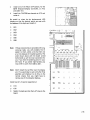
CHAPTER 4
OPERATING INSTRUCTIONS
4-1
WHAT IT DOES
The things you can do with the basic SDK-85 kit
are:
• Examine the contents of all memory and register locations
• Deposit program steps or data in RAM or
register locations
~
Execute programs
command
or
subroutines
upon
i.e., only the last four or the last two digits entered wi II be accepted.
As noted, the number system being used in the
SD K-85 is the hexadecimal, or base-16 number
system. Table 4-1 Iists the hexadecimal, decimal
(base 10), and binary (base two) equivalents. The
table also shows how each hex digit will appear in
the seven-segment LE D displays.
• Reset (start) the monitor upon command
TABLE 4-1
NUMBER SYSTEMS
• I nterrupt and start operation at a location
you specify upon command
You may select either the keyboard and display on
the board or a teletypewriter as the console device
by operating a switch or by placing a jumper wire
at the appropriate place on the board. (See Chapter
3.) Keyboard/display operation and teletypewriter
operation are described separately in the following
paragraphs.
Two of the keyboard buttons continue to function
in teletypewriter mode, as well as in keyboard/display mode. These are the
and the @ill keys.
8
4-2
THE BUTTONS AND DISPLAYS
Keyboard/display operation is done by pressing
keys on the keypad. Responses are displayed either
by echoing the key pressed or by prompting you
with a message or prompt. When the
button is
pressed, the monitor is ready to accept commands.
For numeric arguments, the valid range is from 1
to 4 hexadecimal digits for address information and
1 to 2 hex digits for register and memory data.
8
Longer numbers may be entered, but such numbers
will be evaluated modulo 2 16 or 2 8 respectively,
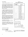
HEX
DECIMAL
BINARY
LED
DISPLAY
a
a
0000
L'
1
1
0001
2
2
0010
3
3
0011
4
4
0100
5
5
0101
6
6
0110
7
7
0111
8
8
1000
9
9
1001
A
10
1010
B
11
1011
C
12
1100
,--,
=,-,
'-I
,':1,:,,--,
,
,-,
'3
,-,-,
,-,,-,
/:,
,-
D
13
1101
,:1
E
14
1110
F
15
1111
,-,
,,
'-
,-,,-,-
4-1
Whenever the monitor expects a command, the display shows a dash ("_") at the left edge of the
address field (possibly along with an error message). When the monitor expects a parameter, a
decimal point wili be displayed at the right edge of
the field into which the argument will be placed. A
parameter will be either an address or a byte of
data which is used during the execution of a
command.
In the descriptions of the command modes, upper
case letters and numbers enclosed in boxes represent keyboard keys. Words or phrases in lower case
enclosed in brackets "<>" describe the nature of
Substitute Memory:
~ <address> E] «data» E]«data» ... ~
The substitute memory command allows you to
read the contents of ROM memory and to examine
and modify the contents of RAM memory
locations.
The address argument denotes the contents of the
memory address to be examined, and may be from
1 to 4 hex digits. If you enter longer numbers, only
the last 4 digits entered are used). As soon as the
number is terminated by the
key, the contents
B:.J
nf
th::.t Inl"::.tinn ::.ra chntAln Iin
+ho rI",+",
fiolrl
",1" .... 1"1
...................... " ' ' ' ' ......... .....,., """'.'" .... I I V V V I I
II
\"AUl.U
II""IU ,
~llv
The () in the Format Statement indicates an optional argument.
UIVII~
with a decimal point at the right edge of the field.
Entering a new number will cause that number to
be displayed in the data field; however, the contents of the memory location will not be changed
until an ~ or E] key is pressed.
Reset:
The
EJ key
causes a hardware reset, and starts
the monitor. The message iI-80 85" will be displayed across the address and data field of the display if you are in display-keyboard mode. If in
teletypewriter mode, the sign on message "SDK-85
VER X.X" will be printed. The monitor is ready to
accept a command after a reset, and saves no information about the state of any user program before
the reset.
4-2
Pressing B:J will place the contents displayed iii the
data field into the displayed memory address. Then
the address and contents of the next higher memory location will automatically be shown. Pressing
~ will place the contents displayed in the data
field into the memory address displayed in the address field, and will also terminate the command.
Pressing B:Jwhile the address FFFF is being displayed will cause address 0000 to be displayed.
Whenever the command changes the contents of a
memory location, it also verifies that the change
has occurred correctly. If the contents of the location do not agree with what the new value should
be (i.e., if the memory location is in ROM or is
nonexistent), an error message is generated.
SUBSTITUTE MEMORY EXAMPLE 2
Using ~ to enter a small program:
ADDR
KEY
DATA
~
MEM
SUBSTITUTE MEMORY EXAMPLE 1
sing ~
MEM to
U'
locations:
KEY
list
the
first
ADDR
few
Monitor
DATA
~
MEM
[I]
~
~
~
~
El
0000.
CD
0002.
[IJ
0020.
0
0
0200.
~
2000
**
rn
2000
03.
CD
2000
3E.
~
2001
**
G1J
2001
04.
2000.
0000
3E.
GrJ
2001
47.
0001
00.
~
2002
**
0002
32.
[I]
2002
OC.
0003
00.
eD
2002
CF.
~
NOTE: ** represents unpredictable values.
After loading the above program, use ~
again to go back and check locations 20002002 to see that they contain:
ADDRESS
DATA
CORRESPONDING
8085 ASSEMBLY
LANGUAGE
INSTRUCTIONS
2000
3E
MVI A, 47H
2001
47
2002
CF
RST 1
This program will load the A register with the
number 47 and jump back to the monitor.
4-3
Examine Registers:
~ <reg>
B:J «data» B:J «data»
TABLE 4-2
REGISTER DISPLAY SEQUENCE
... ~
KEY /DISPLA Y
CODE
The examine command allows you to display and
modify the contents of the 8085 CPU registers.
Pressing the·~ key blanks both the address and
data fields, and displays a decimal point at the right
edge of the address field. At this point, you must
press a register key (register names are denoted by
legends on the keyboard). Any other key will generate an error response.
If a register key is pressed, the name of the register
will appear in the address field, and the contents of
the register will appear in the data field, along
with a decimal point at the right hand edge.
Entering a number will cause the number to be
displayed in the data field; however, the contents
of the register will not be changed until an ~ or
key is pressed.
A
CPU register A
B
CPU register B
C
CPU register C
0
CPU register 0
E
CPU register E
F
CPU flags byte
I
interrupt mask
H
CPU register H
l
CPU register l
SPH
most significant byte of
stack poi nter
SPl
least significant byte of
stack pointer
PCH
most significant byte of
program counter
PCl
least significant byte of
program counter
B:J
B:J
Pressing
will place the contents displayed in the
data field into the register named in the address
field, then will display the name and contents of
the next register in sequence (See Table4-2). Pressing
~ will place the contents displayed in the data
field in the register named in the address field, and
will also terminate the command.
B:J
Pressing
while register PCl is being displayed
has the same effect as pressing ~ .
REGISTER
The flag byte contains the 8085 CPU's condition
flags.
The format for the flag byte is:
The format for the I register is the lower 4 bits of
the accumu lator following execution of a RIM
instruction. A "1" in an interrupt mask field denotes a masked condition. A "0" must be entered
to use that interrupt.
7
0
Islzlxl~lxlplxlcl
t ttL
I ~PARITV
I
CARRY
~.---------------AUXCARRy
' - - - - - - - - - - - - - - - - - - - - - - ZERO
' - - - - - - - - - - - - - SIGN
The format for the I register is:
7
X = UNDEFINED
0
I I I I I ~ 17~! 6~515~51
0
0
0
0
t'
i
INTERRUPT MASK
INTERRUPT ENABLE FLAG
4-4
For more information about the 8085's flags and
interrupt mask feature, consult the MCS-85 User's
Manual.
EXAMINE REGISTER EXAMPLE 1
EXAMINE REGISTER EXAMPLE 2
Using ~ to initialize the 8085's stack pointer
to 20C8:
Using ~ to examine the contents of the
8085's Registers:
KEY
ADDR
DATA
ADDR
KEY
DATA
~
fExAMl
~
REG
SPH
**
0
SPH
02.
SPH
20.
SPL
**
SPL
OC.
SPl
C8.
~
~
~
~
~
~
~
~
~
~
~
**
b
**
C
**
d
**
E
**
F
**
**
EJ
~ or
A
H
**
l
**
SPH
**
SPl
**
PCH
**
PCl
**
EJ
NOTE: ** represents the contents of the
register whose name is in the address
field of the display.
4-5
Go:
o
«address» ~
0
Pressing the
key causes the contents of the program counter (PCH and PCL) to be displayed in
the addressed field, along with a decimal point at
the right edge of the fieid. The program counter is
available for change, and any number entered (a
number is optional) becomes the new contents of
the program counter.
Pressing the ~ key transfers control of the CPU
to the address in the address field (contents of the
program counter). Before the transfer of control,
the address and data display fields are cleared, and
an 'E' is displayed at the left edge of the address
field.
Pressing any other key but ~ generates an error
message.
The monitor regains control of the CPU only after
a
or after execution of an RST 0, RST 1; or
JMP 0 instruction in program.
8
Note that because of the way the GO and SI NG LE
STEP commands are implemented in the Monitor,
Gand SJ~~E will not work unless the 8085's stack
pointer is pointing to an existing portion of RAM
memory. If at any time these two commands don't
seem to be working, set SPH to 20 and SPL to C8
using ~, then try it again. (Locations 20C8 to
20F F are reserved for the monitor program, therefore the stack pointer must be set to 20C8 or lower
so as not to interfere with the monitor.)
4-6
GO COMMAND EXAMPLE
Now you can execute the program you entered in Example 2 of the ~ command.
First, check to make sure the 3- location program is in memory, then the program will be
executed.
Recall that this small program loads the A
register with the nu mber 47 and restarts the
monitor. To verify that the A register now
holds 47 and to get more practice using ~
try the following sequence:
KEY
KEY
ADDR
DATA
COMMENTS
ADDR
DATA
COMMENT
47.
A reg now
I'EiAMl
fSiiBsTl
~
~
0002.
A
holds 47.
0020.
00.
A
0200.
2000.
~
~
~
~
Now A holds
2000
3E.
2001
47.
2002
CF.
o
MVI A, 47
**
****
0002.
RST 1
0020.
****
**
0200.
0002.
2000.
0020.
0200.
- 80
85
A
47
I'EiAMl
~
2000.
- 80
Run the small
Program again
85
Now A holds
47 again
NOTE: * * * * denotes "don't care" values
Now try placing other values in location 2001
using ~ and use ~ to execute the program
again, seeing how those values are loaded into
the A register after execution.
4-7
Single Step:
SJ~W «address»
EJ EJ ... ~
Pressing the S~~~~E key causes the contents of the
program counter (PCH and PCl) to be displayed
in the address field of the display along with a decimal point at the right hand edge of the field. The
data field contains the contents of the address
denoted by the contents of the program counter.
The program counter is made available for change,
and any number entered (a number is optional)
becomes the new contents of the program counter.
EJ
Pressing the
key causes the CPU to execute the
one instruction pointed to by the program
counter. After execution the monitor regains control of the CPU, and the address and data fields
show the new contents of the program counter
(address of next instruction to execute) and contents of the byte addressed by the program
counter, respectively. The decimal point is turned
on at the right hand edge of the address field, indicating that the program counter is available again.
If the ~ key is pressed, no instruction is executed.
The address displayed in the address field is made
the contents of the program counter and the single
step command is terminated. You may now examine or modify registers and memory locations to
verify program execution. Pressing the SJ~~~E key
takes you back to the single step mode, and subsequent pressing of the
key allows you to continue, instruction by instruction, through your
program.
EJ
4-8
Single stepping is implemented in the SOK-85
hardware by repeatedly interrupting the processor.
Since interrupts cannot be recognized during the
EI and 01 instructions of the 8085, single step will
not stop at either of these instructions.
SINGLE STEP EXAMPLE
Single stepping through the SOK-85 Monitor.
This is what you should see on the display:
KEY
ADDR
SINGLE
STEP
****
rn
DATA
**
000a.
EJ
EJ
OOOb.
E1
OOOC.
22
fNOOl
L.....J
OOOF.
r- r-
EJ
0010.
E1
ro
To resume full speed operation at this point,
do the following:
~
G
0010.
E1
~
- 80
85
Vector Interrupt:
G
The @[J key is similar to the
key in the respect
that it takes control away from the monitor and
gives it to another program. The interrupt key
causes immediate recognition of RST 7.5 interrupt
and control passes to location 3C in the monitor.
This location contains an unconditional branch to
instruction location 2004 in user RAM. You may
place any instruction you wish in Locations 2004
thru 2006 (e.g., a branch to a keyboard interrupt
routine). The monitor does not regain control without specific action (a
command, or a RST 0,
RST 1, orJMP 0 program instruction). In branching
back to the monitor, unless the RST 1 instruction is
executed, the monitor loses all past information
about the user program.
8
Since an interrupt is recognized by the hardware,
the monitor cannot clear the display; thus the display may remain unchanged after interrupt.
IMPORTANT: Two conditions must be satisfied
for the Vector Interrupt feature to be enabled:
1.
I nterrupts must be enabled (by executing an
EI instruction).
2.
RST 7.5 must be unmasked (mask reset by
the SI M instruction or by modifying the
1- Register).
To resume execution of the user program, press
The PC value of the next instruction appears
in the address field of the display. Then press ~
to continue execution.
G.
Error Conditions - Illegal Key
If a key is pressed which is illegal in its context
(e.g., a command key is pressed when the monitor
is expecting a number), the command is aborted
and an error message is generated. Th is message
takes the form "-Err", displayed in the address
field. The monitor is then ready to accept a command. The error message will be cleared when a
command key is pressed. Therefore, you can cancel
a command before you press
or ~ by pressing
any illegal key instead.
B:J
Memory Substitution Errors
If the substitute memory command determines
that the contents of a memory location were not
changed correctly (i.e. location is in ROM or is
nonexistent), the command is aborted and an error
message is generated. This message also takes the
form "-Err", displayed in the address field. The
monitor is then ready to accept a new command.
The error message will be cleared when a command
key is pressed.
4-3
TELETYPEWRITER OPERATION
Console Commands
Program Debugging - The Use of Breakpoints
Along with the "cold start" reset caused when the
button is pressed, the monitor also implements
a "warm start" procedure. Execution of an RST 1
instruction will cause the monitor to enter this
"warm start" routine. The monitor will display the
same message as a
(/-80 85'), but all registers
and user memory will be preserved in the state they
were in at the time of execution of the RST 1. No
system reset or initialization will be performed.
8
8
By placing RST 1 instructions at key RAM locations where you want to examine the CPU status,
you can break from your program and then examine and set memory locations and registers, or
single-step a portion of your program.
This portion of the SOK-85 monitor communicates
via a teletypewriter (console). Operation consists
of dialogue between the operator and the monitor
in the monitor's command language. After you
press the
button on the SOK-85 keypad, the
monitor begins the dialogue by typing a sign-on
message on the console ("MCS-85 Kit") and then
requests a command by typing a prompt character
("."). Commands are in the form of a single alphabetic character specifying the command, followed
by a list of numeric or alphabetic parameters.
Numeric parameters are entered as hexadecimal
numbers. The monitor recognizes the characters 0
through 9 and A through F as legal hexadecimal
digits. Longer numbers may be entered, but only
the last four digits will be retained.
8
4-9
The only command requiring an alphabetic parameter is the IIX" command. The nature of such
parameters will be discussed in the section explaining the command.
Display Memory Command, D:
o <low address>, <high address>
Selected areas of addressable memory may be
accessed and displayed by the 0 command. The
o command produces a formatted listing of the
memory contents between <low address> and
<high address>, inclusive, on the console. Each
line of the listing begins with the address of the
first memory location displayed on that line,
represented as 4 hexadecimal digits, followed by
up to 16 memory locations, each one represented
by 2 hexadecimal digits.
Use of the Monitor for Programming and Checkout
The monitor aiiows you to enter, check out, and
execute small programs. It contains facilities for
memory display and modification, 8085 CPU register display and modification, program loading from
the console device, and program initiation with a
breakpoint facility. I n addition, the 11[] key on the
keyboard may be used to initiate your own keyboard interrupt routine.
Command Structure
I n the following paragraphs, the monitor command
language is discussed. Each command is described,
and examples of its use are included for clarity.
Error conditions that may be encountered while
operating the monitor are described on page 4-13.
Program Execute Command, G:
G «entry point»
The monitor requires each command to be terminated by a carriage return. With the exception of
the liS" and 'X" commands, the command is not
acted upon until the carriage return is sensed.
Therefore, you may abort any command, before
entering the carriage return, by typing any illegal
character (such as RUBOUT).
Control of the CPU is transferred from the monitor to the user program by means of the program
execute command G. The entry point should be an
address in RAM which contains an instruction in
the program. If no entry point is specified, the
monitor uses, as an address, the value on top of
the stack when the monitor was entered.
Except where indicated otherwise, a single space is
synonymous with the comma for use as a delimiter.
Consecutive spaces or commas, or a space or
comma immediately following the command letter,
are illegal in all commands except the "X" command (see below).
G COMMAND EXAMPLE
G2000
Control is passed to location 2000.
Items enclosed in parentheses "( )11 are optional.
D COMMAND EXAMPLE
09,26
0009
EF
20
E1
22
F2
20
F5
0010
E1
22
ED
20
21
00
00
0020
05
C3
3F
00
C3
57
01
4-10
39
22
F4
20
21
ED
20
F9
C5
Insert Instructions into RAM, I:
I <address>
<data>
Single instructions, or an entire user program, are
entered into RAM with the I command. After
sensing the carriage return terminating the command line, the monitor waits for the user to enter a
string of hexadecimal digits (O to 9, A to F). Each
digit in the string is converted into its binary value,
and then loaded into memory, beginning at the
starting address specified and continuing into sequential memory locations. Two hexadecimal digits
are loaded into each byte of memory.
Separators between digits (spaces, commas, carriage returns) are ignored; illegal characters, however, will terminate the command with an error
message (see page 4-13). The character ESC or AL TMODE (which is echoed to the console as 1/$")
terminates the digit string.
I COMMAND EXAMPLE 1
Move Memory Command, M:
M <low address>, <high address>, <destination>
The M command moves the contents of memory
between <low address> and <high address> inclusive, to the area of RAM beginning at <destination>. The contents of the source field remain
undisturbed, unless the receiving field overlaps the
source field.
The move operation is performed on a byte-by-byte
basis, beginning at <low address>. Care should be
taken if <destination> is between <low address>
and <high address>. For example, if location 2010
contains 1A, the command M2010, 201 F 2011
will result in locations 2010 to 2020 containing
1/1 A 1A 1A ... ", and the original contents of memory will be lost.
The monitor will continue to move data until the
source field is exhausted, or until it reaches address
FFFF. If the monitor reaches FFFF without
exhausting the source field, it will move data into
this location, then stop.
12010
112233445566778899$
This command puts the following pattern into
RAM:
M COMMAND EXAMPLE
2010 11 22 33 44 55 66 77 88 99
M2010, 204F, 2050
64 bytes of memory are moved from 2010204F to 2050-208F by this command.
I COMMAND EXAMPLE 2
12040
123456789$
This command puts the following pattern into
RAM:
2040 12 34 56 78 90
Note that since an odd number of hexadecimal digits was entered initially, a zero was
appended to the digit string.
4-11
SUDstitute Memory Command, S:
X
TABLE 4-3
COMMAND REGISTER IDENTIFIERS
S <address> «data»
IDENTIFIER
The S command allows you to examine and optionally modify memory locations individually.
The command functions as follows:
1.
CODE
Type an S, followed by the hexadecimal address of the first memory location you wish to
examine, followed by a space or comma.
2.
The contents of the location are displayed,
followed by a dash (-).
REGISTER
A
Register A
B
Register B
C
Register C
0
Register 0
E
Register E
F
Flags byte
I nterrupt Mask
3.
To modify the contents of the location displayed, type in the new data, followed by a
space, comma, or carriage return. If you do
not wish to modify the location, type only
the space, comma, ~Uage;;tea.~,l. The
next higher memory location will automatically be displayed as in step (2).
4.
H
Register H
L
Register L
M
Registers H and L combined
S
Stack Pointer
P
Program Cou nter
Type a carriage return. The S command will
be terminated.
S
COMMAND EXAMPLE
S2050 AA- BB-CC 01-13 23-24
Location 2050, which contains AA, is unchanged, but location 2051 (which used to
contain BB) now contains CC, 2052 (which
used to contain 01) now contains 13, and
2053 (which used to contain 23) now contains 24.
The command operates as follows:
1.
Type an X, followed by a register identifier or
a carriage return.
2.
The contents of the register are displayed (two
hexadecimal digits for A, B, C, 0, E, F, I, H,
and L, four hexadecimal digits for M, S, & P),
followed by a dash (-).
3.
The register may be modified at this time by
typing the new value, followed by a space,
comma, or carriage return. If no modification
is desired, type only the space, comma, or
carriage return.
4.
If a space or comma is typed in step (3), the
next register in sequence will be displayed as
in step 2 (unless P was just displayed which
case the command is terminated). If a carriage
return is entered in step 3, the X command is
terminated.
Examine/Modify CPU Registers Command, X:
x «register identifier»
Display and modification of the CPU registers is
accomplished via the X command. The X command
uses <register identifier> to select the particular
register to be displayed. A register identifier is a
single alphabetic character denoting a register,
as defined in Table 4-3.
4·12
5.
If a carriage return is typed in step (1) above,
an annotated list of all registers and their contents is displayed.
Note: The bits in the flag byte (F) and interrupt mask (I) are encoded as follows:
Error Conditions - Invalid Characters
Each character is checked as it is entered from the
console. As soon as the monitor determines that
the last character entered is illegal in its context, it
aborts the command and issues an "*" to indicate
the error.
The format for the F register:
7
0
Islzlxl~lxlplxlcl
1
,
L
t
INVALID CHARACTER EXAMPLE
CARRY
~PARITY
~-------------- AUXCARRY
~---------------------ZERO
L...-_ _ _ _ _ _ _ _ _ _ _ _ _ _ _ _ _ _ _ _ _ _ _
SIGN
D2000,205G*
The character G was encountered in a parameter list where only hexadecimal digits and
delimiters are valid.
X = UNDEFINED
The format for the I register:
7
I
0
0
I a I a I a I ~ 17~ 16~515~ I
t' •
INTERRUPT MASK
INTERRUPT ENABLE FLAG
Address Value Errors
Note:
For more information on the 8085's interrupt masks, please consult the MCS-85
User's Manual.
Program Debugging - Breakpoint Facility
The monitor treats the RST 1 instruction (CF) as
a special sequence initiator. Upon execution of an
RST 1 instruction the monitor will automatically
save the complete CPU status and output the signon message "MCS-85 Kit" to the console. You may
at that time display the contents of the CPU status
register by initiating an "X" command. After
examining the machine status and making any
necessary changes you can resume execution of
the program by inputting "G" and Carriage Return
on the console. You can step through large portions of your program by inserting RST 1 instructions at key locations.
Some commands require an address pair of the
form <low address>, <high address>. If, on these
commands, the value of < low address> is greater
than or equal to the value of <high address>, the
action indicated by the command will be performed on the data at low address only. Addresses
are evaluated modulo 216. Thus, if a hexadecimal
address greater than F F F F is entered, on Iy the last
4 hex digits will be used. Another type of address
error may occur when you specify a part of
memory in a command which does not exist in the
hardware configuration you are using.
I n general, if a nonexistent portion of memory is
specified as the source field for an instruction, the
data fetched will be unpredictable. If a nonexistent
portion of memory is given as the destination field
in a command, the command has no effect.
4-13
CHAPTER 5
THE HARDWARE
5-1
OVERVIEW
This portion of the SDK-85 User's Manual should
provide you with sufficient knowledge to write
programs to exercise the basic system as well as
providing capability to use the basic kit as a nucleus around which you can build larger systems.
Figure 5-1 is a functional block diagram of the
SDK-85. The components enclosed in dashed boxes
have places in the SDK-85 printed circuit board,
but these are not needed for a minimum system
and are not included in the kit. I n addition, some
control lines have been omitted from the block
diagram for the sake of simplicity. The full SDK85 schematic diagrams have been included in an
append ix for you r reference.
medium-sized systems. The 8085 multiplexes its
data bus with the low 8 bits of its address bus.
The 8155 and 8355/8755 Memory I/O components
in the kit are designed to be compatible with this
bus structure, precluding the need for external bus
latches.
Four vectored interrupt inputs are available in
addition to the standard 8080A-type interrupt.
There is also a serial input and serial output data
line pair that is exercised under program control to
provide the SDK-85's simple teletype I/O.
The basic clock frequency of the 8085 in the kit is
3.072 MHz (internally divided by 2 from the 6.144
MHz crystal input).
The text to follow describes each of the elements
in the system:
5-2
SYSTEM COMPONENTS
The 8085 CPU & The System Buses
The 8085 CPU is an evolutionary enhancement of
I ntel's industry standard 8080A. It is 100% software compatible with the 8080A while offering the
benefits of single power supply, higher integration,
higher performance, and improved system timing.
The 8085 CPU is fully described in the Intel®
MCS-85™ User's Manual so a detailed description
wi II not be repeated here.
As the system block diagram shows, the 8085
derives its timing inputs directly from a crystal.
I n addition the 8085 drives the system with control signals available on-chip. No additional status
decoding circuitry is required for most small- to
The 8155
The 8155 is a highly integrated chip designed for
compatibility with the 8085's bus structure. !t contains 256 bytes of static RAM memory, 22 programmable I/O lines, and a 14-bit timer/counter.
The function of the 8155 is described in detail in
the Intel MCS-85 User's Manual.
One 8155 is included with the SDK-85 kit and
space for another has been provided on the circuit
board. The RAM memory in the 8155 is available
for storage of user programs as well as for temporary storage of information needed by system
programs.
The 8155's timer is used by the SqK-85 monitor's
Single Step routine to interrupt the processor following the execution of each instruction.
5-1
The 8355 & 8755
The 8279
The 8355 and 8755 are two more chips specially
designed for compatibility with 8085 systems. The
8355 contains 2048 bytes of mask programmed
read only memory (ROM) and 16 I/O lines. The
8755 has an identical function and pinout to the
8355, but contains ultraviolet erasable and reprogrammable read only memory (EPROM) instead of
the ROM.
The 8279 is a keyboard/display controller chip
that handles the interface between the 8085 and
the keypad and LED display on the SDK-85 board.
The 8279 refreshes the display from an internal
memory while scanning the keyboard to detect
keyboard inputs. The 8279 is described in detail
in the MeS-85 User's Manual.
The 8205
The SDK-85 contains either one 8355 or one 8755
that is programmed with the system monitor.
Space for a second 8755 or 8355 has been allocated
on the PC board.
I
CPU
ROM/IO (8355)
EPROM/IO (8755)
ADDRESS
DECODER
The basic SDK-85 also contains an 8205 chip (oneout-of-8 decoder) that decodes the 8085's memory
address bits to provide chip enables for the 8155,
the 8355/8755, and the 8279.
KEYBOARD DISPLAY
RAM/IO/COUNTER
I
ADDRESS
FIELD
1
1
I
I
I
SERIAL
IIOTO
TTY
INTERRUPT
INPUTS
L
;>."
I
I
I
I
II
flD
:1 ,1)-8755-;:1
I
J
;:'L
I
I
I
I
:I
II
8085
~I
1
SOK·85 KEYBOARD LAYOuT
RESET!
1
~~~~I
L
10 LINES
I,
I
'[t
I
8205
~ ~
II
IL
I
8355
~~
~,,~
r,;
~I
~-8155il
~I
8155
I
I
I
~
L
D
E
SINGLE GO
8
9
A
B
STEP
H
L
SUBST EXAM 4
5
6
7
MEM
REG SPH SPL PCH PCL
NEXT EXEC 0
1
2
Y
L
I
F
I
I
I
I
:.
r-----'
~
~
DATA
BUS
""7
{'r
1
8279
: :B :U~S ~IV tiJW l !'/ I~-r- -_L. . .i. .-I I_i_"./- - "I ~_'_
'I
---+--:' --'\J'::: : ::
~----'-'r-+-I------......--+--_ _----.-.-~I_ _ _ _ _ _r-r-_ _ _+-I__,j':l:1
I
I
CONT
1
;
I
I
I
1
I
,,:.
8212
:J~ :~:tES
~
V~ _ _ _ _ ~
I
-"~----'~
I
>: 3 x 8216
15
CONTROL
~~~ I~----+---~r------------~--------------~vn
r.. ____ ..I
' BUS
'"
71
1
r- - ~
L
_ _ ...
I
I
I
OPTIONAL. A PLACE HAS BEEN PROVIDED ON THE PC BOARD FOR THE DEVICE BUT THE
DEVICE IS NOT INCLUDED.
Figure 5-1 SDK-85 Functional Block Diagram
5-2
I
1~"LS"61
I~----~
.t.
rv
~NETC:C
I
10 LINES
i
FOR BUS EXPANSION
DATA
FIELD
TABLE 5-1
8205 CHIP ENABLES
OUTPUT
ACTIVE ADDRESS RANGE
SELECTED DEVICE
CSO
0000-07FF
8755/8355 MONITOR ROM (A14)
CS1
0800-0FFF
8755/8355 EXPANSION ROM (A 15)
CS2
1000-17FF
N/C
CS3
1800-1 FFF
8279 KEYBOARD/DISPLAY CONTROLLER (A13)
CS4
2000-27FF
8155 BASIC RAM (A16)
CS5
2800-2FFF
8155 EXPANSION RAM (A 17)
CS6
3000-37FF
N/C
CS7
3800-3FFF
N/C
= I C# on schematic diagram in Appendix
N/C = not connected - avilable for user expansion
AXX
5-3
SDK-85 MEMORY
ADDRESSING
Each memory/I/O chip in the basic SDK-85 System
of Figure 5-1 is enabled by a signal coming from
the 8205 address decoder. Table 5-1 lists each chip
enable output accompanied by the address space
over which it is active and the SDK-85 device that
is selected.
Note that the 8279 is really an input/output device
that is communicated with by the 8085 as though
it were a series of memory locations.
The above chip enable table can be expanded to
form a memory map that illustrates the active portions of the SDK memory (see Figure 5-2). Using
the terminology of Figure 5-2, the basic SDK-85
with no additional memory/I/O chips provides the
memory blocks marked MONITOR ROM and
BASIC RAM. You must confine your programs
to a subset of the space available in the BASIC
RAM, the remainder of BASIC RAM being required
for monitor storage locations. A list of the monitorreserved RAM locations is provided in Table 5-2.
Note that RAM memory locations 20C8 through
20D6 are places for 'jump instructions pointing to
the places in memory for the computer to go
following the execution of an RST 5 instruction, an
RST 6 instruction, an interrupt signal on the
RST 6.5 input, etc. If you do not use any of these
instructions or interrupt lines, then this RAM area
is available for other programming.
When you add an expansion 8155 in the space provided on the SDK-85 board, the RAM locations
shown in Figure 5-2 as EXPANSION RAM are
made available for programming. The monitor
reserves no space in the EXPANSION RAM, so
all 256 locations are avai!able for programming,
An extra 8355 or 8755 device when plugged into
the appropriate spot on the board gives you program memory space in the area denoted EXPANSION ROM in the memory map.
The areas marked "FOLD BACK" in Figure 5-2
indicate address space that is unused, but unavailable for expansion, because these locations are
multiple mappings of the basic locations.
5-3
TABLE 5-2
MONITOR-RESERVED RAM LOCATIONS
LOC.
20C8
User may place a JMP instr. to a RST 5 routine in
locs 20C8-20CA.
20CB
JMP to RST 6 routine
20CE
JMP to RST 6.5 routine (hardwired user interrupt)
20D1
JMP to RST 7 routine
20D4
JMP to "VECT I NTR" key routine
20D7-20E8
Loaded
by
user
Monitor Stack (temporary storage used by monitor)
20E9
E Register
20EA
D Register
20EB
C Register
20EC
B Register
20ED
Flags
20EE
A Register
20EF
L Register
20FO
H Register
20F1
I nterrupt Mask
20F2
Prog. Cntr. - Low byte
20F3
Prog. Cntr. - HI byte
20F4
Stack Ptr. - Low byte
20F5
Stack Ptr. - Hi byte
20F6
Current Address
20F8
Current Data
20F9-20FC
5-4
CONTENTS
\
storage for user register images
Output buffer & Temp Locs.
20FD
Register Pointer
20FE
I nput Buffer
20FF
8155 Command/Status REGISTER image (loaded by user)
MEMORY ADDRESS
FFFFl
I
MEMORY SPACE WHERE
EXPANSION BUFFERS
r
1
ARE ENABLED
8000 I-----~
7FFF
r~
OPEN
,.
ACTIVE 8205
CHIP ENABLE
3000
2FFF
is described in detail in the 8085 manual. The functional positioning of the optional latch, buffers,
and drivers in the SDK-85 system structure is
shown in Figure 5-1.
As Figure 5-2 indicates, the optional expansion
buffers leading to the SDK-85 board's prototyping
area are enabled only over the address range
8000-FFFF.
EXPANSION RAM (FOLD BACK)
2900
28FF
2800
27FF
2100
20FF
2000
lFFF
1800
17FF
EXPANSION RAM
(256 LOC.)
BASIC RAM (FOLD BACK)
BASIC RAM
(256 LOC.)
1900 - KEYBDIDISPLY CTLR
COMMAND LOC.
} CS5
}~
} CS3
1800 - KEYBDIDISPLY CTLR
DATA LOC.
OPEN (2K)
} CS2
EXPANSION ROM (2K)
} CS1
1000
OFFF
0800
07FF
MONITOR ROM (2K)
}C~
0000
Figure 5-2 SDK-85 Memory Map
Any of the areas marked "OPEN" in Figure 5-2 are
free for expansion. You may mount extra memory
chips in the wire-wrap area of the SDK-85 board
or on other circuit boards. The 8205 address
decoder has 3 uncommitted chip select lines to
allow the addition of three 2048-byte memory
blocks without additional decoding circuitry.
If you want to expand on the basic SDK-85 you
don't have to stick to the multiplexed-bus MCS 85
memory/I/O family. Mounting pads are present on
the circuit board that accommodate an 8212 latch
for address/data bus demultiplexing. To provide
the current drive capability to operate much larger
systems, spaces are also allocated for another 8212
to buffer the unmultiplexed half of the address and
five 8216 buffer/drivers to buffer the data bus, and
control signals. The function of these components
5-4
INPUT/OUTPUT PORT
AND PERIPHERAL
DEVICE ADDRESSING
As mentioned before, the 8155 and 8355/8755
that come with the SDK-85 Kit have on-board
input/output ports. These ports are accessed using
the I N and OUT instructions of the 8085. Each
individual port being referenced has a unique 8-bit
address. Table 5-3 contains all the port addresses
for an expanded SDK-85 containing two 8155's
and two 8355/8755's.
Please consult the MCS-85 User's Manual for the
use of the various special purpose registers referred
to in the table (Direction Registers, Command/
Status Registers, etc.), and for complete instructions for exercising the memory-I/O chips (8155/
8355/8755) .
Hardware Note: The timer/counter of the first
8155 (RAM) is dedicated as a timer. It is hardwired
to receive the 8085's system clock (3.072 MHz
ClK) as its count input. This timer is used by the
keyboard monitor's SI NG lE STEP function, so
you should beware of timer conflicts if you desire
to count and use the SI NG lE STEP function at
the same time. (See paragraph 6-2.)
Accessing the 8279 Keyboard/Display Controller
As was mentioned in the memory addressing sections, the 8279 is a peripheral chip that is selected
using memory-mapped I/O. Table 5-4 shows the
two memory locations that are used to communicate with the 8279. Consult the MCS-85 User's
Manual for detailed operating instructions.
5-5
TABLE 5-3
SDK-85 I/O PORT MAP
IpORTi
tl'b
e/~/~
FUNCTION
00
Monitor ROM PORT A
01
Monitor ROM PORT B
02
Monitor ROM PORT A
Data Direction Register
d
MSB
I
Aal A21 AI
deb
d.p.
LSB
IIl
AO
82 1 81 1 80
8a
a d .p.
9
f
03
Monitor ROM PO RT B
Data Direction Register
08
Expansion ROM PO RT A
09
Expansion ROM PO RT B
OA
Expansion ROM PORT A
Data Direction Register
OB
Expansion ROM PO RT B
Data Direction Register
20
BASIC RAM COMMAND/STATUS
Register
21
BASIC RAM PORT A
22
BASIC RAM PORT 8
23
BASIC RAM PORT C
ADDRESS FIELD
24
BASIC RAM Low Order Byte
of Ti mer Cou nt
11
25
BASIC RAM High Order Byte
of Ti mer Cou nt
28
EXPANSION RAM
COMMAND/STATUS Register
29
EXPANSION RAM PORT A
2A
EXPANSION RAM PORT B
2B
EXPANSION RAM PORT C
2C
EXPANSION RAM Low Order Byte
of Ti mer Cou nt
20
EXPANSION RAM High Order Byte
of Timer Count
The data format for character bytes being displayed by the 8279 is one bit corresponding to
each of the seven LED segments plus one bit for
the decimal point. Figure 5-3 shows the bit
configuration.
5-6
a
8279 DISPLAY
1-- ~~~g~;;:gN
e"
SEGMENT
Figure 5-3 Data Format
The hardware is designed so that writing a zero into
a bit position turns on the corresponding LE D
segment.
Example:
a "4" would be represented as
1001 1001 = 99 (Hex)
These are six active LED displays available for use.
They are configured in a four-place address field
and a two-place data field as in Figure 5-4.
1
2
1
3
1
4
DATA FIELD
[E]
1
Figure 5-4 Display Configuration
TABLE 5-4
ACCESSING THE 8279
KEYBOARD DISPLAY CONTROLLER
LOCATION
1800
1900
I
READ/
WRITE
I
FUNCTION
Read
Read Keyboard
FIFO
Write
Write Data to
Display
Read
Read Status
Word
Write
Write Command
Word
The display digits are stored within the 8279 display RAM in the locations listed in Table 5-5.
0
1
2
PURPOSE
Address digit 1
2
3
4
3
4
Data Digit
5
6
7
THE SERIAL DATA
INTERFACE
The SDK-85 has the capability of communicating
with a teletype, using the 8085 serial input and
serial output data lines (SI D and SOD respectively)
to send and receive the serial bit strings that encode
data characters.
TABLE 5-5
8279 DISPLAY RAM
LOCATION
5-6
1
2
UNUSED
UNUSED
To send data to the teletype, the 8085 must toggle
the SOD line in a set/reset fashion controlled by
software timing routines in the SD K-85 monitor.
I nput data is obtained by monitoring and timing
changes in the level of the SI D pin. Again, a monitor routine is called upon to do the job.
These teletype communications routines are accessible to the user.
5-5
PROCESSOR INTERRUPT
ALLOCATION
The 8085 has four Vector I nterrupt input pins in
addition to an 8080A-compatible interrupt input.
The name of each interrupt and its function in the
SDK-85 hardware is listed in Table 5-6.
The function of the on-chip interrupts is described
in detail in the 8085 Manual.
TABLE 5-6
8085 ON-CHIP INTERRUPT ALLOCATION
INPUT
Both subroutines communicate at a data rate of
110 baud, the standard rate for teletypewriters.
Since the 8085 serial input and output lines are
designed for communicating with other integrated
circuits, additional electronic circuitry is needed
before they can be connected to a terminal. The
TTY interface in the top right corner of the board
allows the SDK-85 to be connected to any teletype that uses 20 mA "current-loop" input and
output.
FUNCTION
RST 5.5
Ded icated to 8279
RST 6.5
Available User Interrupt
RST 7.5
I]lli button interrupt
TRAP
8155 Timer Interrupt
INTR
Available User Interrupt
5-7
5-7
CONVERTER CIRCUIT FOR
RS232C SERIAL PORT
If you are fortunate enough to have a CRT terminal that can operate at a 11 O-baud rate, and wish
to use it with the SDK-85 computer, you may
find that it is compatible only with RS232c"
voltage-level serial ports and not with current
loops. If this is the case,
1/
o
Wire the MC1488 and MC1489 converter
circuit (shown in Figure 5-5) into the wirewrap area of the SDK-85 board.
o
Remove R6, and connect the input line of
the converter circuit to its lower pad. (You
couid put a switch in this line if you wanted
to.)
o
Open both the TTY and KEYBOARD jumpers, and connect the output line of the converter to the middle pad, which is strapping
point 23. (If you are using a switch, one with
a center off position could be used.)
o
Connect your CRT as shown in Figure 5-5.
o
Connect the 3 different voltages to the
circuit.
5-8
ADDITIONAL INTERFACES
Additional interface considerations are discussed in
Intel Application Note AP-29; which also describes
a low-cost cassette tape-recorder interface, that
can be added to your SDK-85 kit. AP-29 can be
ordered by sending $1.00 to: Literature Department,
I ntel Corp., 3065 Bowers Ave., Santa Clara, Ca.
95051.
+5V
14
SID
CRT
TERMINAL
13
REMOVE
R6
S?
8085
,
MC1489
)
>
<
SOD
4
?
CONVERTER INPUT LINE
+(9 TO 15)V
GND
000000000000
:::J:::JCJ:::J:::JCJDDDDDD
OCDOCDCCCCCC
7
-(9 TO 15)V
20
2
3
330pF
MC1488
7
Figure 5-5 Modification for RS-232c Operation
5-8
CHAPTER 6
THE SOFTWARE
6-1
THE SDK-85 MONITOR
The SDK-85 monitor program provides utility
functions employing either a teletypewriter or the
kit's on-board keyboard and display as console.
The program resides in 2k (k = 1024) bytes of the
ROM memory, between location 0 and location
7 F F. the routines that service each console device are independent; the two devices do not function simultaneously. You may select either the
keyboard and display or the teletypewriter as the
console device by actuating a switch (not furnished)
or by changing strapping connections. Both can be
used to perform substantially the same tasks. (See
Chapter 4.)
6-2
PROGRAMMING HINTS
Stack Pointer
The 8085 makes use of a 16-bit internal register
called the Stack Pointer to point to an area of
memory called the stack. The 8085's stack is
used for saving many things, such as memory
addresses for returns from subroutines.
It is important always to define the stack pointer
at the beginning of your program to avoid storing
data in the wrong place. Locations 20C8 through
20D6 in RAM are reserved by the monitor for
jump instructions when all interrupts are used.
Thus, you should set the stack pointer initially at
20C8 (by the use of the program instruction
LXI SP, 20C8H (31 C8 20), the keyboard command
~ G1J(20) ~ (C8) ~, or the teletypewriter
"XS" command) in order to keep your own stack
clear of data and programs you want to protect.
If less than the full complement of interrupts is
utilized, some or all of the unused space above
20C8 can be allocated to stack as described above.
Remember that the stack must still occupy an unbroken string of contiguous memory locations.
RAM-I/O Command Status Register (CSR)
The basic 8155 command status register (port 20)
is used to set up the on-chip 1/0 ports and timer.
It can only be written to; it cannot be read. You
can write to this register in your programs, but
there is a precaution you should take: at any time
when you write to the CSR in the basic RAM, you
should also write the same pattern to RAM location
20FF. The reason is this: The SJ~~~E command causes
the monitor to change the CSR in order to set
up the timer for execution of the command. If it
is not told what value you previously put there (by
saving the value in 20FF), that value will inevitably
be overwritten and lost. Following each single step,
the monitor reads location 20F F, logically 0 Rs its
timer command to the content of that location, and
writes the CSR with the new command, thereby
retrieving your previous configuration.
Access to Monitor Routines
You may "borrow" several of the SDK-85 monitor
routines to simplify your programming task. Table
6-1 provides descriptions and calling addresses for
these routines.
6-3
PROGRAMMING EXAMPLES
The programming examples presented at the end of
this chapter demonstrate how to use the monitor
routines to operate the keyboard and display.
6-1
TABLE 6-1
MONITOR ROUTINE CALLING ADDRESSES
Ca iii ng Address
Mnemonic
07FD
CI
Description
Console Input
This routine returns a character (in ASCII code - see 8085/8080
reference card for codes) received from the teletype to the caller
in the A register. The A register and CPU condition codes are
affected by th is operation
07FA
co
Console Output
This routine transmits a character (in ASCII code), passed from
the caller in the C register, to the teletypewriter. The A and C
registers, and the CPU condition codes are affected.
05EB
CROUT
Carriage Return, Line Feed
CROUT sends carriage return and line feed characters to the
teletype. The contents of the A, B, and C registers are destroyed
and the CPU condition codes are affected.
06C7
NMOUT
Hex Number Printer
N~J10UT converts the a-bit unsigned integer in the A register
into 2 ASCII characters representing the 2 hex digits and prints
the two digits on the teletypewriter.
036E
UPDDT
Update Data
Update data field of the display. The contents of the A register
are displayed in hex notation in the data field of the display.
02E7
RDKBD
Read Keyboard
This routine waits until a character is entered on the hex keypad
and upon return places the value of the character in the A
register.
NOTE: For RDKBD to work correctly, you must first:
05F1
DELAY
1.
Unmask RST 5.5 using the SIM instruction.
2.
Enable interrupts using the E I instruction.
Time Delay
This routine takes the 16-bit contents of register pair DE and
counts down to zero, then returns to the calling program.
6-2
TABLE 6-1
MONITOR ROUTINE CALLING ADDRESSES (CONT'D)
Calling Address
Mnemonic
02B7
OUTPT
Description
Output Characters to Display
The routine sends characters to the display with the parameters
set up by registers A, B, Hand L.
Reg A = 0 = use address field
= 1 = use data field
Reg B = 0 = decimal point off
= 1 = decimal point at right edge of field
Reg H L = starting address of characters to to sent.
Character
Displayed
Hexadecimal memory
content pointed to
by the H L register
0
1
2
3
4
5
6
7
0
1
2
3
4
5
6
7
8
9
8
9
A
A
b
C
d
E
F
H
L
B
C
D
P
r
Blank
E
F
10
11
12
13
14
15
6-3
PROGRAM EXAMPLE - RDKBD
0
After executing
2000, the program waits until a key is pressed. Then the value of the key is placed
in the A register and the monitor is restarted. Use ~ to see that the key value is now in the A register.
LOC
CONTENTS
SYMBOLIC
2000
2001
2002
2003
2004
2005
31
C8
20
3E
08
30
LXI SP, 20C8H
SIM
; unmask interrupt
2006
FB
r-I
• ,..ro.""hln in+n ...... lln+
, CIIOUIC I I I L v l l U t J L
2007
2008
2009
200A
CD
E7
02
CF
CALL RDKBD
; read keyboard value
; into Reg A
RST 1
; break point, go back to monitor
COMMENTS
; define stack pointer
MVI A, 08H
CI
PROGRAM EXAMPLE - UPDDT
Display F F in data field of display.
LOC
CONTENTS
2000
2001
2002
2003
2004
2005
2006
2007
2008
31
C8
20
3E
FF
CD
6E
03
76
SYMBOLIC
LXI SP, 20C8H
; define stack pointer
MVI A, FFH
; load FF into Reg A
CALL UPDDT
; output Reg A to data field
HLT
; HALT
To change the display value use ~ to vary the content of location 2004.
6-4
COMMENTS
PROGRAM EXAMPLE - RDKBD, UPDDT
Putting the two preceding examples together into one program causes the display to show the key value.
LOC
CONTENTS
2000
2003
2005
2006
2007
200A
200D
31C820
3E08
30
FB
CDE702
CD6E03
C30620
SYMBOLIC
LXI SP, 20C8H
MVI A, 08H
SIM
LOOP: EI
CALL RDKBD
CALL UPDDT
JMP LOOP
COMMENTS
; define stack pointer
; unmask interrupt
; enable interrupt
; read keyboard value into Reg A
; output Reg A to data field
; keep looping
6-5
PROGRAM EXAMPLE - COUNTDOWN
The following program displays a count in the data field of the display. The count may be stopped by
pressing the @ill button. The count resumes when any other key (except
is pressed. The "E" in
the address field of the display signifies that a user program is executing.
B)
ADDRESS
CONTENTS
SYMBOLIC
2000
2001
2002
2003
2004
2005
2006
2007
2008
2009
200A
200B
200C
2000
200E
200F
2010
2011
2012
2013
2014
2015
2016
2017
31
80
20
3E
08
30
FB
78
3C
27
47
C5
CD
6E
03
16
18
CD
F1
05
C1
C3
06
20
2004
FB
EI
2005
2006
76
C9
HLT
RET
COMMENTS
LXI SP, 2080H
; INITIALIZE STACK POINTER.
MVI A, 08
; USE THE 8085's SIM INSTR TO
; ENAB LE THE VECT I NTR BUTTON.
S!M
LOOP: EI
MOV A, B
INR A
DAA
MOV B, A
PUSH B
CALL UPDDT
; INCREMENT AND ADJUST THE.COUNT
; FOR DECIMAL COUNTING.
; DISPLAY COUNT IN DATA FIELD OF
; DISPLAY.
MVI 0, 18H
CALL DELAY
POP B
JMP LOOP
; WAIT OUT A PROGRAMMABLE DELAY
; PERIOD BEFORE CONTINUING.
; GO BACK TO THE BEGINNING.
; CONTROL BRANCHES TO LOCATION
; 2004 WHEN VECT INTR IS PRESSED.
; WAIT HERE FOR KEY DEPRESSION.
; RESUME THE COUNT.
To execute the program, type in 82000~.
Try to stop the count right at 00 using the
@ill key.
Change the speed of the count by using ~ to vary the contents of location 2010.
6·6
PROGRAM EXAMPLE - FLASH HELP
Load into Locations 2000 through 2007 (use the Substitute Memory command) the following
data: 10, OE, 11, 12, 15,15,15,15. Then load and execute the following program (G2010~).
The display will flash JlHELP".
ADDRESS
DATA
SYMBOLIC
2010
2013
2015
2017
31C820
3E01
0600
210420
LXI SP, 20C8H
MVI A, 1
MVI B,O
LXI H, 2004H
201A
CDB702
CALL OUTPT
COMMENTS
; define stack pointer
; use data field
; no decimal indicator
; use characters starting
; at Location 2004
; output the two characters
; to data field
DPY:
20.1D
201F
2021
3EOO
0600
210020
MVI A,O
MVI B,O
LXI H, 2000H
; use address field
; no decimal indicator
; use characters starting
; at Location 2000
; output the four characters
; to address field
2024
CDB702
CALL OUTPT
2027
202A
11FFFF
CDF105
LXI D,OFFFFH*
CALL DELAY
; set up delay value
; time delay
202D
202F
2031
2034
3EOO
0600
210420
CDB702
MOV A, 0
MOV B, 0
LXI H, 2004H
CALL OUTPT
; output B LAN KS to
; Display
2037
203A
203D
11 FFFF
CDF105
C3iD20
LXI D,OFFFFH
CALL DELAY
JMP DPY
; time Delay
; REPEAT
* Delay time proportional to value. Any number from 1 through F F F F may be chosen.
6-7
APPENDIX A
MONITOR LISTING
ASM80 :F1:SDK85.SRC MOD85 MACROFILE XREF PRINT(:F3:SDK85.LST)
ISIS-II 8080/8085 MACRO ASSEMBLER, X108
LOC
OBJ
SEQ
SDK85
PAGE
SOURCE STATEMENT
1
;******************************************1******1**111111**11*1******
2
PROGRAM: SDK-85 MONITOR
3
VER 1.2
4
5
6
7
8
9
COPYRIGHT (C) 1977
INTEL CORPORATION
3065 BOWERS AVENUE
SANTA CLARA, CALIFORNIA
,
95051
10 ,.*********************************************************************.
11
12
13
14
15
16
17
18
19
20
21
ABSTRACT
THIS PROGRAM IS A SMALL MONITOR FOR THE INTEL 8085 KIT AND
PROVIDES A MINIMUM LEVEL OF UTILITY FUNCTIONS FOR THE USER EMPLOYING
EITHER AN INTER-ACTIVE CONSOLE (I.E. TELETYPE) OR THE KIT'S
KEYBOARD/LED DISPLAY. THE KEYBOARD MONITOR ALLOWS THE USER TO PERFORM
SUCH FUNCTIONS AS MEMORY AND REGISTER MANIPULATION, PROGRAM LOADING,
PROGRAM EXECUTION, INTERRUPTION OF AN EXECUTING PROGRAM, AND
SYSTEM RESET.
22
23
24
25
26
27
28
29
30
31
32
PROGRAM ORGANIZATION
======= ============
THE PROGRAM IS ORGANIZED AS FOLLOWS .1) COLD START ROUTINE (RESET)
2) WARM START - REGISTER SAVE ROUTINE
3) INTERRUPT VECTORS
4) KEYBOARD MONITOR
5) TTY MONITOR
6) LAYOUT OF RAM USAGE
33
34
35
36
37
38
39
40
41
42
43
44
45
46
47
48
49
50
51
52
THE KEYBOARD MONITOR BEGINS WITH THE COMMAND RECOGNIZER, FOLLOWED BY
THE COMMAND ROUTINE SECTION, UTILITY ROUTINE SECTION AND MONITOR
TABLES. THE COMMAND AND UTILITY ROUTINES ARE IN ALPHABETICAL ORDER
WITHIN THEIR RESPECTIVE SECTIONS.
THROUGHOUT THE KEYBOARD MONITOR, A COMMENT FIELD BEGINNING
WITH "ARG - " INDICATES A STATEMENT WHICH LOADS A VALUE INTO
A REGISTER AS AN ARGUMENT FOR A FUNCTION. WHEN THE DESIRED VALUE
LIST OF KEYBOARD MONITOR ROUTINES
==== == ======== ======= ========
CMMND
EXAM
GOCMD
SSTEP
SUEST
CLEAR
CLDIS
SDK85
ISIS-II 808018085 MACRO ASSEMBLER, Xl0S
LOC
OE]
PAGE
2
SOURCE STATEMENT
SEQ
CLDST
DISPC
ERH
GTHEX
HXDSP
ININT
I!,;SDG
NXTRG
OUTPT
RDKBD
RETF
RETT
RGLOC
RSTOR
SETRG
UPDAD
UP DDT
53
54
55
56
57
58
59
60
61
62
63
64
65
66
67
68
69
70
71
72
NAME
SDK85
,
73 ;******.*************~*****~************************** ******************
74
SET CONDITIONAL ASSEMBLY FLAG
75
76 ,
77 ;*******************~********************************* *****************
78
79
0000
80 WAITS
81
82
83
84
85
e6
2000
0017
0012
SET
o
;O=NO WAIT STPTES
WAIT STATE IS GENERATED FOR EVERY M CYCLE
;THE APPROPRIATE DELAY TIME MUST BE USED FOR
;TTY DELAY OR SET UP SINGLE
;STEP TIMER FOR EACH CASE
;l=A
,
,.*****************************************************1****************
87
88
89
90
91
92
93
,
,.******************************************************1*******'*******
97
;
MONITOR EQUATES
,
RAMST
EQU
2000H; START ADDRESS OF RAM - THIS PROGRAM ASSUMES
9l.J
THAT 256 EYTES OF RANDOM ACCESS MEMORY [EGIN AT THIS ADDRESS.
THE PROGRAM USES STORAGE AT THE END OF THIS SPACE FOR VARIABLES~
95
PROGRH! STACK
96
98 RNUSE
99
100
101 SKUJ
EQU
23
RAM USAGE - CURRENTLY, 23 BYTES ARE USED FOR
ISAV-ING REGISTERS AND VARIABLE~
EQU
18
M.ONITOR STACK USAGE
102
-
-
MAX OF 9 LEVELS
OOOF
103 UBRLN
EQU
15
5 USER BRANCHES
0000
0090
104
105 ADFLD
106 ADISP
EQU
EQU
0
90H
INDICATES USE OF ADDRESS FIELD OF DISPLAY
CONTROL CHARACTER TO INDICATE OUTPUT TO
IADDRESS FIELD OF DISPLAY
107
3 EYTES EACH
ISIS-II 8080/8085 MACRO ASSEMBLER, X108
LOC
1900
0011
0000
0020
0094
0001
1800
0001
0008
0080
OOCC
0000
20E9
0000
0010
OOFB
0040
0025
0024
0040
ooco
OOOE
20C8
00C5
OBJ
SEQ
108
109
110
1 11
112
113
114
115
116
117
118
119
120
121
122
123
124
125
126
127
128
129
130
1 31
132
133
134
135
136
137
138
139
140
141
142
143
144
145
146
147
148
149
150
151
152
153
154
155
156
157
158
159
160
161
162
SDK85
PAGE
3
SOURCE STATEMENT
ADDRESS FOR SENDING CONTROL CHARACTERS TO
/DISPLAY CHIP
COMMA FROM KEYBOARD
COMMA
EQU
11 H
INITIAL VALUE FOR COMMAND STATUS REGISTER
CSNIT
EQU
o
OUTPUT PORT FOR COMMAND STATUS REGISTER
EQU
CSR
20H
CONTROL CHARACTER TO INDICATE OUTPUT TO
DDISP
EQU
94H
/DATA FIELD OF DISPLAY
INDICATOR FOR DOT IN DISPLAY
DOT
EQU
1
ADDRESS FOR SENDING CHARACTERS TO DISPLAY
DSPLY
EQU
1800H
INDICATES USE OF DATA FIELD OF DISPLAY
EQU
DTFLD
1
MASK FOR TURNING ON DOT IN DISPLAY
DTMSK
08H
EQU
HIGH ORDER 1 INDICATES EMPTY INPUT BUFFER
EMPTY
EQU
80H
CONTROL CHARACTER TO SET DISPLAY OUTPUT TO
KBNIT
EQU
OCCH
/ALL ONES DURING BLANKING PERIOD
CONTROL CHAR. TO SET KEYBOARD/DISPLAY MODE
EQU
KMODE
a
; (2 KEY ROLLOVER, 8 CHARACTER LEFT ENTRY)
MNSTK
EQU
RAMST + 256 - RMUSE
;START OF MONITOR STACK
NODOT
EQU
a
INDICATOR FOR NO DOT IN DISPLAY
iNUMC - DEFINED LATER
NUMBER OF COMMANDS
iNUMRG - DEFINED LATER
NUMBER OF REGISTER SAVE LOCATIONS
PERIO
EQU
10H
PERIOD FROM KEYBOARD
PRMPT
EQU
OFBH
PROMPT CHARACTER FOR DISPLAY (DASH)
READ
EQU
40H
CONTROL CHARACTER TO INDICATE INPUT FROM
/KEYBOARD
TIMHI
EQU
OUTPUT PORT FOR HIGH ORDER BYTE OF TIMER VALUE
25H
EQU
TIMLO
24H
OUTPUT PORT FOR LOW ORDE~ BYTE OF TIMER VALUE
TMODE
EQU
40H
TIMER MODE - SQUARE WAVE, AUTO RELOAD
TSTRT
EQU
OCOH
START TIMER
EQU
UNMSK
OEH
UNMASK INPUT INTERRUPT
EQU
USRBR
RAMST + 256 - (RMUSE + SKLN + UBRLN)
; START OF USER
; /BRANCH LOCATIONS
IF
1-WAITS ;TIMER VALUE FOR SINGLE STEP IF NO WAIT STATE
TIMER
EQU
197
ENDIF
WAITS
iTIMER VALUE FOR SINGLE STEP IF ONE WAIT STATE INSERTE
IF
TIMER
EQU
237
ENDIF
CNTRL
EQU
1900H
;
,.**********************************************************************
MONITOR MACROS
;
;**********************************************************************
TRUE
MACRO
JC
ENDM
WHERE
WHERE
MACRO
JNC
ENDM
WHERE
WHERE
; BRANCH IF FUNCTION RETURNS TRUE
;
FALSE
,
BRANCH IF FUNCTION RETURNS FALSE
,
.**********************************************************************
ISIS-II 8080/8085 MACRO ASSEMBLER, xl08
LOC
OBJ
SEQ
0038
*****
163
164
*****
165
166
167
168
169 CLDBK:
170
*****
171
172
173
174
175
176
177
178
179
180
181
182
183
184
185
186
187
188
189
*****
190
191
192
193
*****
194
195
196
197
196
*****
199
200
201
202
203
204
*****
205
206
207
208
*1***
209
210
211
212
213
214
*****
215
216
QQ38 C3!)'!2Q
')1r'7
'-, I
0000 3EOO
0002 320019
0005 C3F'101
0008
0008
0008
OOOC
OOOF
0010
0011
0014
0017
0018
001B
001E
001F
0020
0021
22EF20
El
22F220
F5
El
22ED20
210000
39
22F420
21ED20
F9
C5
D5
C33FOO
0024
0024 C35701
0028
0028 C3C820
002C
002C C38E02
0030
0030 C3CB20
0034
0034 C3CE20
SDK85
PAGE
4
SOURCE STATEMENT
"RESET" KEY ENTRY POINT - COLD START
RST 0 ENTRY POINT
MVI
STA
JMP
RST
A,KMODE
CNTRL
CLDST
GET CONTROL CHARACTER
SET KEYBOARD/DISPLAY MODE
GO FINISH COLD START
THEN JUMP BACK HERE
ENTRY POINT - WARM START
ORG
8
SAVE REGISTERS
SHLD
LSAV
POP
H
ShLD
PSAV
PUSH
PSW
POP
H
SHLD
FSAV
LXI
H,O
DAD
SP
SHLD
SSAV
LXI
H,BSAV+l
SPHL
PUSH
8
PUSH
D
JMP
RES10
SAVE H & L REGISTERS
GET USER PROGRAM COUNTER FROM TOP OF STACK
/AND SAVE IT
SAVE FLIP/FLOPS & REGISTER A
CLEAR H & L
GET USER STACK POINTER
/AND SAVE IT
j SET STACK POINTER FOR SAVING
; /REMAINING REGISTERS
SAVE B & C
SAVE D & E
LEAVE ROOM FOR VECTORED ~NTERRUPTS
TIMER INTERRUPT (TRAP) ENTRY POINT (RST 4.5)
ORG
24H
JMP
STP25
BACK TO SINGLE STEP ROUTINE
RST 5 ENTRY POINT
ORG
JMP
28H
RSET5
i
BRANCH TO RST 5 LOCATION IN BAM
INPUT INTERRUPT ENTRY POINT (RST 5.5)
ORG
JMP
2CH
ININT
BRANCH TO INPUT INTERRUPT ROUTINE
RST 6 ENTRY POINT
ORG
JHP
3GIl
RSET6
; BRANCH TO RST 6 LOCATION IN RAM
HARD WIRED USER INTERRUPT ENTRY POINT (RST 6.5)
ORG
JMP
34H
RST65
BRANCH TO RST 6.5 LOCATION IN RAM
RST 7 ENTRY POINT
ORG
T\A'n
Ul-'.L
38H
D
T')
~
~I
,.,
Tl
'uJ.\r1Hv.L!
SDK85
ISIS-II 8080/8085 MACRO ASSEMBLER, X108
LOC
OBJ
003C
003C C3D420
003F
0040
0042
0045
0047
0048
20
E60F
32F120
3EOE
30
F3
0049 20
004A 07
004B DAFA03
004E AF
004F 0600
0051 21A603
0054
0057
0059
005B
CDB702
3E01
0600
21AA03
005E CDB702
0061 3E80
006332r'E20
0066 21E920
0069 F9
006A
006D
006F
0070
0072
210019
3690
25
36FB
CDE702
SEQ
218
219
220
221
222
223
224
225
226
227
228
229
230
231
232
233
234
235
236
237
238
239
240
241
242
243
244
245
246
247
248
249
250
251
252
253
254
255
256
257
258
259
260
261
262
263
264
265
266
267
268
269
270
271
272
PAGE
5
SOURCE STATEMENT
,
***** "VECTORED INTERRUPT" KEY ENTRY POINT (RST 7.5)
ORG
3CH
JMP
USINT
BRANCH TO USER INTERRUPT LOCATION IN RAM
RES10:
; CONTINUE SAVING
RIM
ANI
OFH
STA
ISAV
MVI
A,UNMSK
USER STATUS
GET USER INTERRUPT STATUS AND INTERRUPT MASK
KEEP STATUS & MASK BITS
SAVE INTERRUPT STATUS & MASK
UNMASK INTERRUPTS FOR MONITOR USE
SHl
DI
RIM
RLC
JC
GO
INTERRUPTS DISABLED WHILE MONITOR IS RUNNING
(EXCEPT WHEN WAITING FOR INPUT)
TTY OR KEYBOARD MONITOR ?
IS TTY CONNECTED ?
YES - BRANCH TO TTY MONITOR
NO - ENTER KEYBOARD MONITOR
,
,.**********************************************************************
BEGINNING OF KEYBOARD MONITOR CODE
,
,.**********************************************************************
OUTPUT SIGN-ON MESSAGE
XRA
A
ARG
USE ADDRESS FIELD OF DISPLAY
MVI
B,NODOT
ARG - NO DOT IN ADDRESS FIELD
LXI
H,SGNAD
ARG - GET ADDRESS OF ADDRESS FIELD PORTION OF
ISIGN-ON MESSAGE
CALL
OUTPT
OUTPUT SIGN-ON MESSAGE TO ADDRESS FIELD
MVI
A,DTFLD
ARG
USE DATA FIELD OF DISPLAY
MVI
B,NODOT
ARG - NO DOT IN DATA FIELD
LXI
H,SGNDT
ARG - GET ADDRESS OF DATA FIELD PORTION OF
ISIGN-ON MESSAGE
CALL
OUTPT
OUTPUT SIGN-ON MESSAGE TO DATA FIELD
MVI
A,EMPTY
STP.
IBUFF
SET INPUT BUFFER EMPTY FLAG
,
,.**********************************************************************
,
FUNCTION: CMMND - COMMAND RECOGNIZER
INPUTS: NONE
OUTPUTS: NONE
CALLS: RDKBD,ERR,SUBST,EXAM,GOCMD,SSTEP
DESTROYS: A,B,C,D,E,H,L,F/F'S
CMMND:
LXI
SPHL
H,MNSTK
LXI
MVI
DCR
MVI
CALL
H,CNTRL
M,ADISP
H
M,PRMPT
RDKBD
INITIALIZE MONITOR STACK POINTER
OUTPUT PROMPT CHARACTER TO DISPLAY
GET ADDRESS FOR CONTROL CHARACTER
OUTPUT CONTROL CHARACTER TO USE ADDRESS FIELD
ADDRESS FOR OUTPUT CHARACTER
OUTPUT PROMPT CHARACTER
READ KEYBOARD
ISIS-II 8080/8085 MACRO ASSEMBLER, X108
LOC
OBJ
0075 010400
0078 217803
007B
007C
007F
0080
0081
BE
CA8700
23
OD
C27BOO
SEQ
273
274
275 C!'-iD10:
276
277
278
279
280
281
0084 C31502
0087 217C03
008A OD
OOBB
008C
008D
008E
008F
0090
09
09
7E
23
66
6F
0091 E9
0092 0601
0094 CDD701
0097 CD4403
009A D21502
009D
OOAO
00A3
00A4
00A7
00A9
OOAC
OOAE
CD0903
CDFC02
7E
32F820
060i
CD6B03
0601
CD2B02
OOB 1 D2B800
00B4 CDFC02
SDK85
PAGE
6
SOURCE STATEMENT
LXI
LXI
B,NUMC
H,CMDTB
COUNTER FOR NUMBER OF COMMANDS IN C
GET ADDRESS OF COMMAND TABLE
CMP
JZ
INX
DCR
JNZ
M
RECOGNIZE THE COMMAND ?
YES - GO PROCESS IT
NO - NEXT COMMAND TABLE ENTRY
END OF TABLE ?
NO - GO CHECK NEXT ENTRY
YES - COMMAND UNKNOWN
DISPLAY ERROR MESSAGE AND GET ANOTHER COMMAND
CMD15
H
C
CMD10
JMP
ERR
282
283 CMD15:
284
H,CMDAD
LXI
GET ADDRESS OF COMMAND ADDRESS TABLE
DCR
285
C
ADJUST COMMAND COUNTER
286
; COUNTER ACTS AS POINTER TO COMMAND ADDRESS TABLE
DAD
B
ADD POINTER TO TABLE ADDRESS TWICE BECAUSE
287
288
DAD
B
TABLE HAS 2 EYTE ENTRIES
MOV
A,M
GET LOW ORDER BYTE OF COMMAND ADDRESS
289
INX
H
290
MOV
H,M
GET HIGH ORDER BYTE OF COMMAND ADDRESS IN H
291
MOV
L,A
PUT LOW ORDER BYTE IN L
292
; COMMAND ROUTINE ADDRESS IS NOW IN H & L
293
PCRL
BRANCH TO ADDRESS IN H & L
294
295 ,
296 j**********************************************************************
297
298
COMMAND ROUTINES
299 ,
3CO j**********************************************************************
301
FUNCTION: EXAM - EXAMINE AND MODIFY REGISTERS
302
INPUTS: NONE
303
OUTPUTS: NONE
304
CALLS: CLEAR,SETRG,ERR,RGNAM,RGLOC,UPDDT,GTHEX,NXTRG
305
30-6
DESTROYS: A,B,C,D,E,H,L,F/F'S
307 j
308 EXAM:
MVI
B,DOT
ARG - DOT IN ADDRESS FIELD OF DISPLAY
309
CALL
CLEAR
310
CLEAR DISPLAY
CALL
SETRG
311
GET REGISTER DESIGNATOR FROM KEYBOARD AND
312
j/SET REGISTER POINTER ACCORDINGLY
WAS CHARACTER A REGISTER DESIGNATOR?
313
314
FALSE
ERR
j NO - DISPLAY ERROR MSG. AND TERMINATE COMMAND
JNC
ERR
315+
316 EXM05:
CALL
RGNAt~
OUTPUT REGISTER NAME TO ADDRESS FIELD
317
CALL
RGLOC
318
GET REGISTER SAVE LOCATION IN H & L
MOV
A,M
GET REGISTER CONTENTS
319
STA
CURDT
320
STORE REGISTER CONTENTS AT CURRENT DATA
MVI
321
B,DOT
ARG - DOT IN DATA FIELD
CALL
322
UPDDT
UPDATE DATA FIELD OF DISPLAY
MVI
B,DTFLD
323
ARG - USE DATA FIELD OF DISPLAY
CALL
324
GTHEX
GET HEX DIGITS - WERE ANY DIGITS RECEIVED?
FALSE
325
EXM10
NO - DO NOT UPDATE REGISTER CONTENTS
326+
JNC
EXM10
CALL
327
YES - GET REGISTER SAVE LOCATION IN H & L
RGLOC
ISIS-II 8080/8085 MACRO ASSEMBLER, x108
LDC
OBJ
00B7 73
00B8
OOBA
OOBD
OOBF
00C2
FE10
CAE901
FE11
C21502
CDA802
00C5 DA9DOO
00C8 C3E901
OOCB
OOCE
00D1
00D3
CD0002
CDE702
FE10
CAECOO
00D6
00D9
OODB
OODE
OOEO
00E3
00E5
00E8
00E9
32FE20
0601
CDD701
0600
CD2B02
FE10
C21502
EB
22F220
OOEC
OOEE
OOF 1
00F2
00F4
00F7
OOFA
0600
CDD701
AF
0600
21A203
CDB702
C31B03
SEQ
SDK85
PAGE
7
SOURCE STATEMENT
UPDATE REGISTER CONTENTS
MOV
M,E
328
329 EXM10:
WAS LAST CHARACTER A PERIOD ?
CPI
PERIO
330
YES - CLEAR DISPLAY AND TERMINATE COMMAND
CLDIS
JZ
331
WAS LAST CHARACTER ',' ?
CPI
COMMA
332
NO - DISPLAY ERROR MSG. AND TERMINATE COMMAND
JNZ
ERR
333
YES - ADVANCE REGISTER POINTER TO
CALL
NXTRG
334
;/NEXT REGISTER
335
ANY MORE REGISTERS ?
336
YES - CONTINUE PROCESSING WITH NEXT REGISTER
TRUE
EXM05
337
JC
EXM05
338+
NO - CLEAR DISPLAY AND TERMINATE COMMAND
JMP
CLDIS
339
340 ,
341 ,.**********************************************************************
342
FUNCTION: GOCMD - EXECUTE USER PROGRAM
343
INPUTS: NONE
344
OUTPUTS: NONE
345
CALLS: DISPC,RDKBD,CLEAR,GTHEX,ERR,OUTPT
346
DESTROYS: A,B,C,D,E,H,L,F/F'S
347
348
349 GOCMD:
DISPLAY USER PROGRAM COUNTER
CALL
DISPC
350
READ FROM KEYBOARD
RDKBD
CALL
351
PERIO
IS CHARACTER A PERIOD ?
CPI
352
G10
YES - GO EXECUTE THE COMMAND
JZ
353
NO - ARG - CHARACTER IS STILL IN A
354
IBUFF
REPLACE CHARACTER IN INPUT BUFFER
STA
355
ARG - DOT IN ADDRESS FIELD
B,DOT
MVI
356
CLEAR
CLEAR DISPLAY
CALL
357
B,ADFLD
MVI
ARG - USE ADDRESS FIELD
358
CALL
GTHEX
GET HEX DIGITS
359
CPI
PERIO
WAS LAST CHARACTER A PERIOD ?
360
ERR
JNZ
NO - DISPLAY ERROR MSG. AND TERMINATE COMMAND
361
XCHG
PUT HEX VALUE FROM GTHEX TO H & L
362
HEX VALUE IS NEW USER PC
SHLD
PSAV
363
364 G10:
B,NODOT
YES
ARG - NO DOT IN ADDRESS FIELD
MVI
365
CALL
CLEAR
CLEAR DISPLAY
366
A
XRA
ARG - USE ADDRESS FIELD OF DISPLAY
367
MVI
B,NODOT
ARG - NO DOT IN ADDRESS FIELD
368
H,EXMSG
GET ADDRESS OF EXECUTION MESSAGE IN H & L
LXI
369
OUTPT
CALL
DISPLAY EXECUTION MESSAGE
370
JMP
RSTOR
; RESTORE USER REGISTERS INCL. PROGRAM COUNTER
371
;/I.E. BEGIN EXECUTION OF USER PROGRAM
372
373 ,
374 ,.**********************************************************************
375
FUNCTION: SSTEP - SINGLE STEP (EXECUTE ONE USER INSTRUCTION)
376
INPUTS: NONE
377
OUTPUTS: NONE
378
CALLS: DISPC,RDKBD,CLEAR,GTHEX,ERR
379
380
DESTROYS: A,B,C,D,E,H,L,F/F'S
381
382 SSTEP:
ISIS-II 8080/8085 MACRO ASSEMBLER, Xl08
LOC
OBJ
OOFD
0100
0103
0105
0108
010A
CD0002
CDE702
FE10
CAE901
FEll
CA2601
010D 32FE20
0110 0601
0112 CDD701
01150600
0117 CD2B02
011A
011 D
011E
0121
0123
D21502
EB
22F220
FE10
CAE901
0126 3AF120
0129 E608
012B 32FD20
012E 2AF220
0131 7E
0132 FEF3
0134 C23BOl
0137 AF
0138 C34201
013B FEFB
013D C24501
0140 3E08
0142 32FD20
0145 3E40
0147
0149
014B
014D
0150
0152
0154
D325
3EC5
D324
3AFF20
F6CO
D320
C31B03
0157 F5
0158 3AFF20
015B E63F
015D F640
015F D320
0161 Fl
0162 22EF20
SEQ
383
384
385
386
387
388
389
390
391
392
393
394
395
396+
397
398
399
400
401
402 STP20:
403
404
405
406
407
408
409
410
411
412 STP21:
413
414
415
416 STP22:
417
418 STP23:
419
420
421
422
423
424
425
426
427
428
429 STP25:
430
431
432
433
434
435
436
437
SDK85
PAGE
8
SOURCE STATEMENT
CALL
DISPC
DISPLAY USER PROGRAM COUNTER
CALL
RDKBD
READ FROM KEYBOARD
CPI
PERIO
WAS CHARACTER A PERIOD ?
JZ
CLDIS
YES - CLEAR DISPLAY AND TERMINATE COMMAND
CPI
COMMA
WAS LAST CHARACTER ',' ?
JZ
STP20
YES - GO SET TIMER
; NO - CHARACTER FROM KEYBOARD WAS NEITHER PERIOD NOR COMMA
STA
IBUFF
REPLACE THE CHARACTER IN THE INPUT BUFFER
B,DOT
MVI
ARG - DOT IN ADDRESS FIELD
CALL
CLEAR
CLEAR DISPLAY
MVI
B,ADFLD
ARG - USE ADDRESS FIELD OF DISPLAY
CALL
GTHEX
GET HEX DIGITS - WERE ANY DIGITS RECEIVED ?
FALSE
ERR
NO - DISPLAY ERROR MSG. AND TERMINATE COMMAND
JNC
ERR
XCHG
HEX VALUE FROM GTHEX TO H & L
SP.LD
PSAV
HEX VALUE IS NEW USER PC
CPI
PERIO
WAS LAST CHARACTER FROM GTHEX A PERIOD ?
JZ
YES - CLEAR DISPLAY AND TERMINATE COMMAND
CLDIS
NO - MUST HAVE BEEN A COMMA
LDA
ANI
STA
LHLD
MOV
CPI
JNZ
XRA
JMP
ISAV
08H
TEMP
PSAV
A,M
(DI)
STP21
A
GET USER INTERRUPT MASK
KEEP INTERRUPT STATUS
SAVE USER INTERRUPT STATUS
GET USER PC
GET USER INSTRUCTION
DI INSTRUCTION ?
NO
YES - RESET USER INTERRUPT STATUS
STP22
CPI
JNZ
MVI
STP23
A,08H
EI INSTRUCTION ?
NO
YES - SET USER INTERRUPT STATUS
STA
TEMP
SAVE NEW USER INTERRUPT STATUS
MVI
A,(TIMER SHR 8) OR TMODE ; HIGH ORDER BITS OF TIMER VALUE
; /OR'ED WITH TIMER MODE
TIMHI
A,TIMER AND OFFH ; LOW ORDER BITS OF TIMER VALUE
TIMLO
GET USER IMAGE OF WHAT'S IN CSR
USCSR
SET TIMER COMMAND BITS TO START TIMER
TSTRT
START TIMER
CSR
RSTOR
RESTORE USER REGISTERS
OUT
MVI
OUT
LDA
ORI
OUT
JMP
PUSH
LDA
ANI
ORI
OUT
POP
SHLD
(E I)
PSW
USCSR
3FH
40H
CSR
PSW
LSAV
BRANCH HERE WHEN TIMER INTERRUPTS AFTER
;/ONE USER INSTRUCTION
SAVE PSW
GET USER IMAGE OF WHAT'S IN CSR
CLEAR 2 HIGH ORDER BITS
SET TIMER STOP BIT
STOP TIMER
RETRIEVE PSW
SAVE H & L
ISIS-II 8080/8085 MACRO ASSEMBLER, X10S
LOC
OBJ
0165
0166
0169
016A
016B
016E
0171
0172
0175
0178
0179
017A
o 17B
017C
017E
0181
0182
0185
0187
0188
E1
22F220
F5
E1
22ED20
210000
39
22F420
21ED20
F9
C5
D5
20
E607
21FD20
E6
32F120
3EOE
30
C3FDOO
018B
018D
0190
0192
0601
CDD701
0600
CD2B02
0195 D21502
0198 EB
0199 22Fq20
019C
019E
01Al
01A3
01A6
01A9
01AA
01AD
OlAF
01B2
01B4
01B7
FEll
C2CFOl
0600
CD5F03
2AF620
7E
32F820
0601
CD6B03
0601
CD2B02
F5
01B8 D2C401
01BB 2AF620
01BE 73
SEQ
SDK85
PAGE
9
SOURCE STATEMENT
H
GET USER PROGRAM COUNTER FROM TOP OF STACK
POP
438
PSAV
SAVE USER PC
SHLD
439
PUSH
PSvl
440
441
POP
H
FSAV
SAVE FLIP/FLOPS AND A REGISTER
442
SHLD
H,O
CLEAR H & L
LXI
443
SP
GET USER STACK POINTER
DAD
444
SSAV
SAVE USER STACK POINTER
SHLD
445
H,BSAV+l
j SET MONITOR STACK POINTER FOR
446
LXI
j/SAVING REMAINING USER REGISTERS
SPHL
447
PUSH
B
SAVE B & C
448
PUSH
D
SAVE D & E
449
RIM
GET USER INTERRUPT MASK
450
ANI
01H
KEEP MASK BITS
451
H,TEMP
GET USER INTERRUPT STATUS
LXI
452
M
OR IT INTO MASK
ORA
453
ISAV
SAVE INTERRUPT STATUS & MASK
STA
454
A,UNMSK
UNMASK INTERRUPTS FOR MONITOR USE
MVI
455
SIM
456
GO GET READY FOR ANOTHER INSTRUCTION
JMP
SSTEP
457
458 ,
459 ,.**********************************************************************
460
461
FUNCTION: SUBST - SUBSTITUTE MEMORY
INPUTS: NONE
462
OUTPUTS: NONE
463
464
CALLS: CLEAR,GTHEX,UPDAD,UPDDT,ERR
465
DESTROYS: A,B,C,D,E,H,L,F/F'S
466 j
461 SUBST:
468
MVI
B,DOT
ARG - DOT IN ADDRESS FIELD
CALL
CLEAR
CLEAR THE DISPLAY
469
MVI
470
B,ADFLD
ARG - USE ADDRESS FIELD OF DISPLAY
CALL
471
GTHEX
GET HEX DIGITS - WERE ANY DIGITS RECEIVED?
FALSE
ERR
472
NO - DISPLAY ERROR MSG. AND TERMINATE COMMAND
ERR
JNC
473+
XCHG
474
ASSIGN HEX VALUE RETURNED BY GTHEX TO
SHLD
CUR AD
1 CURRENT ADDRESS
475
416 SUB05:
CPI
COMMA
WAS ',' THE LAST CHARACTER FROM KEYBOARD?
477
JNZ
SUB15
478
NO - GO TERMINATE THE COMMAND
MVI
B,NODOT
479
ARG - NO DOT IN ADDRESS FIELD
480
CALL
UPDAD
UPDATE ADDRESS FIELD OF DISPLAY
481
LHLD
CURAD
GET CURRENT ADDRESS IN H & L
A,M
482
MOV
GET DATA BYTE POINTED TO BY CURRENT ADDRESS
STA
CURDT
STORE DATA BYTE AT CURRENT DATA
483
484
MVI
B,DOT
ARG - DOT IN DATA FIELD
485
CALL
UPDDT
UPDATE DATA FIELD OF DISPLAY
486
MVI
B,DTFLD
ARG - USE DATA FIELD
487
CALL
GTHEX
GET HEX DIGITS - WERE ANY HEX DIGITS RECEIVED?
488
PUSH
(SAVE LAST CHARACTER)
PSW
FALSE
NO - LEAVE DATA UNCHANGED AT CURRENT ADDRESS
489
SUB10
490+
JNC
SUB10
491
LHLD
YES - GET CURRENT ADDRESS IN H & L
CURAD
MOV
STORE NEW DATA AT CURRENT ADDRESS
492
M,E
ISIS-II BOBO/808S
LOC
OBJ
~ACRO
ASSEMBLER, X108
SEQ
01C4 2AF620
01C7 23
OlCB 22F620
01CB F1
502
OlCC C39COl
503
504
505
506
507
50B
509
510
5 11
512
513
514
515
516
517
518
519
520
521
522
523
524
525
526
527
528
529
530
531
532
533
534
535
536
537
53B
539
540
541
542
543
544
545
546
547
OlCF FE10
OlDl C2l502
01D4 C3E901
01D7 AF
01D8
01DB
01DE
01EO
01E2
01E5
01EB
219A03
CDB102
3EOl
0600
219A03
CDB702
C9
PAGE
10
SOURCE STATEMENT
493
494
495
496
497
498 SUB10:
499
500
501
OlBF 7B
OlCO BE
01 C1 C2l502
SDKB5
MOV
CMP
JNZ
LHLD
INX
SHLD
POP
JMP
; MAKE SURE DATA WAS ACTUALLY STORED IN CASE
;/CURRENT ADDRESS IS IN ROM OR IS NON-EXISTANT
A,E
DATA TO A FOR COMPARISON
M
WAS DATA STORED CORRECTLY?
ERR
NO - DISPLAY ERROR MSG. AND TERMINATE COMMAND
CURAD
INCREMENT CURRENT ADDRESS
H
CURAD
PS\t./
RETRIEVE LAST CHARACTER
SUB05
SUB15:
CPI
JNZ
JMP
PERIO
ERR
CLDIS
WAS LAST CHARACTER'.' ?
NO - DISPLAY ERROR MSG. AND TERMINATE COMMAND
YES - CLEAR DISPLAY AND TERMINATE COMMAND
,
,.*********** •• ***************** •• *.* ••••••••• * •• * •••••• * •••• ** •••••••••
UTILITY ROUTINES
;
.•
, * ••••• ** ••••••••••• *.* •• * ••••••••••••• * •• *.** •••• * ••• ***.* ••••• *f."*
FUNCTION: CLEAR - CLEAR THE DISPLAY
INPUTS: B - DOT FLAG
1 MEANS PUT DOT IN ADDRESS FIELD OF DISPLAY
- 0 MEANS NO DOT
OUTPUTS: NONE
CALLS: OUTPT
DESTROYS: A,B,C,D,E,H,L,F/F'S
DESCRIPTION: CLEAR SENDS BLANK CHARACTERS TO BOTH THE ADDRESS FIELD
AND THE DATA FIELD OF THE DISPLAY. IF THE DOT FLAG IS
SET THEN A DOT WILL APPEAR AT THE RIGHT EDGE OF THE
ADDRESS FIELD.
CLEAR:
XRA
A
LXI
CALL
MVI
MVI
LXI
CALL
RET
H,BLNKS
OUTPT
A,DTFLD
B,NODOT
H,BLNKS
OUTPT
ARG
USE ADDRESS FIELD OF DISPLAY
ARG
FLAG FOR DOT IN ADDR. FIELD IS IN B
ARG
ADDRESS OF BLANKS FOR DISPLAY
OUTPUT BLANKS TO ADDRESS FIELD
USE DATA FIELD OF DISPLAY
ARG
ARG - NO DOT IN DATA FIELD
ARG - ADDRESS OF BLANKS FOR DISPLAY
OUTPUT BLANKS TO DATA FIELD
RETURN
,
,.f •••••••••••• * ••••• * •••• * •• *.* •••• * ••••••••••••••••••• 1 • • • • • • • * •••••••
FUNCTION: CLDIS - CLEAR DISPLAY AND TERMINATE COMMAND
INPUTS: NONE
OUTPUTS: NONE
CALLS: CLEAR
DESTROYS: A,B,C,D,E,H,L,F/F'S
DESCRIPTION: CLDIS IS JUMPED TO BY COMMAND ROUTINES WISHING TO
TERMINATE NORMALLY. CLDIS CLEARS THE DISPLAY AND
BRANCHES TO THE COMMAND RECOGNIZ&R.
SDK85
ISIS-II 8080/8085 MACRO ASSEMBLER, x108
LOC
OBJ
01E9 0600
01EB CDD701
01EE C36600
01F1
01F3
01F6
01F8
01FA
01FD
0200
0203
0206
0207
020A
020C
020F
0211
0214
3ECC
320019
3EOO
D320
32FF20
C30800
2AF220
22F620
7E
32F820
0601
CD5F03
0600
CD6B03
C9
SEQ
548
549
550
551
552
553
554
555
556
557
558
559
560
561
562
563
564
565
566
567
568
569
570
571
572
573
574
575
576
577
578
579
580
581
582
583
584
585
586
587
588
589
590
591
592
593
594
595
596
597
598
599
600
601
602
PAGE
11
SOURCE STATEMENT
CLDIS:
MVI
CALL
JMP
B,NODOT
CLEAR
CMMND
ARG - NO DOT IN ADDRESS FIELD
CLEAR THE DISPLAY
GO GET ANOTHER COMMAND
,
,.**********************************************************************
FUNCTION: CLDST - COLD START
INPUTS: NONE
OUTPUTS: NONE
CALLS: NOTHING
DESTROYS: A
DESCRIPTION: CLDST IS JUMPED TO BY THE MAIN COLD START PROCEDURE,
COMPLETES COLD START INITIALIZATION, AND JUMPS BACK
TO THE MAIN COLD START PROCEDURE.
CLDST:
MVI
STA
MVI
OUT
STA
JMP
,
A,KBNIT
CNTRL
A,CSNIT
CSR
USCSR
CLDBK
GET CONTROL CHARACTER
INITIALIZE KEYBOARD/DISPLAY BLANKING
INITIAL VALUE OF COMMAND STATUS REGISTER
INITIALIZE CSR
INITIALIZE USER CSR VALUE
BACK TO MAIN PROCEDURE
,.**********************************************************************
,
FUNCTION: DISPC - DISPLAY PROGRAM COUNTER
INPUTS: NONE
OUTPUTS: NONE
CALLS: UPDAD,UPDDT
DESTROYS: A,B,C,D,E,H,L,F/F'S
DESCRIPTION: DISPC DISPLAYS THE USER PROGRAM COUNTER IN THE ADDRESS
FIELD OF THE DISPLAY, WITH A DOT AT THE RIGHT EDGE
OF THE FIELD. THE BYTE OF DATA ADDRESSED BY THE PROGRAM
COUNTER IS DISPLAYED IN THE DATA FIELD OF THE DISPLAY.
DISPC:
LHLD
SHLD
MOV
STA
MVI
CALL
MVI
CALL
RET
PSAV
CUR AD
A,M
CURDT
B,DOT
UPDAD
B,NODOT
UPDDT
GET USER PROGRAM COUNTER
MAKE IT THE CURRENT ADDRESS
GET THE INSTRUCTION AT THAT ADDRESS
MAKE IT THE CURRENT DATA
ARG - DOT IN ADDRESS FIELD
UPDATE ADDRESS FIELD OF DISPLAY
ARG - NO DOT IN DATA FIELD
UPDATE DATA FIELD OF DISPLAY
;
,.**********************************************************************
FUNCTION: ERR - DISPLAY ERROR MESSAGE
INPUTS: NONE
OUTPUTS: NONE
CALLS: OUTPT
DESTROYS: A,B,C,D,E,H,L,F/F'S
ISIS-II 8080/8085 MACRO ASSEMBLER, X108
LOC
OBJ
0215
0216
0218
021B
021E
0220
0222
0225
0228
AF
0600
219E03
CDB702
3E01
0600
219A03
CDB702
C36600
022B
022D
022E
0231
OEOO
C5
110000
D5
0232 CDE702
0235 FE10
0237 D25502
023A D1
023B
f"'I"'ro.!":"",,",
VJ.J ';j L' V t::
SEQ
PAGE
SDK85
12
SOURCE STATEMENT
DESCRIPTION: ERR IS JUMPED TO BY COMMAND ROUTINES WISHING TO
603
TERMINATE BECAUSE OF AN ERROR.
604
ERR OUTPUTS AN ERROR MESSAGE TO THE DISPLAY AND
605
BRANCHES TO THE COMMAND RECOGNIZER.
606
607
608 ERR:
ARG - USE ADDRESS FIELD
XRA
A
609
ARG
NO DOT IN ADDRESS FIELD
610
MVI
B,NODOT
ARG
ADDRESS OF ERROR MESSP.G~
611
LXI
H,ERMSG
OUTPUT ERROR MESSAGE TO ADDRESS FIELD
612
CALL
OUTPT
ARG
USE DATA FIELD
MVI
A,DTFLD
613
MVI
B,NODOT
ARG - NO DOT IN DATA FIELD
614
H,BLNKS
ARG - ADDRESS OF BLANKS FOR DISPLAY
LXI
615
CALL
OUTPT
OUTPUT BLANKS TO DATA FIELD
616
GO GET A NEW COMMAND
JMP
CMMND
617
618 ;
619 ,.**********************************************************************
620
FUNCTION: GTHEX - GET HEX DIGITS
621
INPUTS: B - DISPLAY FLAG - 0 MEANS USE ADDRESS FIELD OF DISPLAY
622
- 1 MEANS USE DATA FIELD OF DISPLAY
623
OUTPUTS: A - LAST CHARACTER READ FROM KEYBOARD
624
DE - HEX DIGITS FROM KEYBOARD EVALUATED MODULO 2**16
625
626
CARRY - SET IF AT LEAST ONE VALID HEX DIGIT WAS READ
627
- RESET OTHERWISE
628
CALLS: RDKBD,INSDG,HXDSP,OUTPT
DESTROYS: A,B,C,D,E,H,L,F/F'S
629
DESCRIPTION: GTHEX ACCEPTS A STRING OF HEX DIGITS FROM THE KEYBOARD,
630
DISPLAYS THEM AS THEY ARE RECEIVED, AND RETURNS THEIR
631
VALUE AS A 16 BIT INTEGER. IF MORE THAN 4 HEX DIGITS
632
ARE RECEIVED, ONLY THE LAST 4 ARE USED. IF THE DISPLAY
633
FLAG IS SET, THE LAST 2 HEX DIGITS ARE DISPLAYED IN THE
634
DATA FIELD OF THE DISPLAY. OTHERWISE, THE LAST 4 HEX
635
DIGITS ARE DISPLAYED IN THE ADDRESS FIELD OF THE
636
DISPLAY. IN EITHER CASE, A DOT WILL BE DISPLAYED AT THE
637
RIGHTMOST EDGE OF THE FIELD. A CHARACTER WHICH IS NOT
638
A HEX DIGIT TERMINATES THE STRING AND IS RETURNED AS
639
AN OUTPUT OF THE FUNCTION. IF THE TERMINATOR IS NOT
640
A PERIOD OR A COMMA THEN ANY HEX DIGITS WHICH MAY HAVE
641
642
BEEN RECEIVED ARE CONSIDERED TO BE INVALID. THE
FUNCTION RETURNS A FLAG INDICATING WHETHER OR NOT ANY
643
644
VALID EEX DIGITS WERE RECEIVED.
645 ;
646 GTHEX;
MVI
RESET HEX DIGIT FLAG
C,O
647
SAVE DISPLAY AND HEX DIGIT FLAGS
648
PUSH
B
SET HEX VALUE TO ZERO
D,O
LXI
649
PUSH
SAVE HEX VALUE
D
650
651 GTH05:
CALL
RDKBD
READ KEYBOARD
652
CPI
10H
IS CHARACTER A HEX DIGIT?
653
JNC
GTH20
NO
654
GO CHECK FOR TERMINATOR
YES - ARG - NEVI HEX DIGIT IS IN A
655
POP
ARG - RETRIEVE HEX VALUE
656
D
.,...",
"1\"
l.diLL
:I (~S E Ii T "'Vl,T I)ICIT IN HEX \1 i'\~UE
6::;7
..Lnt....>J.,Iu
-
l'
~,-.,r-
J.1.i,..1"
SDK85
ISIS-II 8080/8085 MACRO ASSEMBLER, X108
LOC
OBJ
023E C1
023F OE01
0241
0242
0243
0244
0245
C5
D5
78
OF
D24902
0248 53
0249 CD6C02
024C
024D
024F
0252
78
0601
CDB702
C33202
0255
0256
0257
0259
025C
025E
D1
C1
FE11
CA6702
FE10
CA6702
0261110000
0264 C3F702
0267
0268
0269
026A
026B
47
79
OF
78
C9
026C 7A
026D OF
026E OF
SEQ
658
659
660
661
662
663
664
665
666
667
668
669
670
671
672
673
674
675
676
677
678
679
680
681
682
683
684
685
686
687
688
689
690
691
692
693
694
695
696
697
698
699
700
701
702
703
704
705
706
707
708
709
710
711
712
PAGE
13
SOURCE STATEMENT
POP
MVI
B
C,1
PUSH
PUSH
MOV
RRC
JNC
B
D
MOV
D,E
A,B
GTH10
; RETRIEVE DISPLAY FLAG
, SET HEX DIGIT FLAG
;/(I.E. A HEX DIGIT HAS PEEN READ)
SAVE DISPLAY AND HEX DIGIT FLAGS
SAVE HEX VALUE
TEST DISPLAY FLAG
SHOULD ADDRESS FIELD OF DISPLAY BE USED?
YES - USE HEX VALUE AS IS
NO - ONLY LOW ORDER BYTE OF HEX VALUE SHOULD
IBE USED FOR DATA FIELD OF DISPLAY
PUT LOW ORDER BYTE OF HEX VALUE IN D
GTH10:
CALL
MOV
MVI
CALL
JMP
GTH20:
POP
POP
CPI
JZ
CPI
JZ
LXI
JMP
ARG - HEX VALUE TO BE EXPANDED IS IN D & E
EXPAND HEX VALUE FOR DISPLAY
ARG - ADDRESS OF EXPANDED HEX VALUE IN H & L
ARG - PUT DISPLAY FLAG IN A
A,B
ARG - DOT IN APPROPRIATE FIELD
B,DOr
OUTPUT HEX VALUE TO DISPLAY
OUTPT
; GO GET NEXT CHARACTER
GTH05
; LAST CHARACTER WAS NOT A HEX DIGIT
RETRIEVE HEX VALUE
D
RETRIEVE HEX DIGIT FLAG IN C
B
WAS LAST CHARACTER',' ?
COMMA
YES - READY TO RETURN
GTH25
NO - WAS LAST CHARACTER ' , ?
PERIO
YES - READY TO RETURN
GTH25
; NO - INVALID TERMINATOR - IGNORE ANY HEX DIGITS READ
SET HEX VALUE TO ZERO
D,O
RETURN FALSE
RETF
HXDSP
GTH25:
MOV
MOV
RRC
MOV
RET
,
B,A
A,C
A,B
SAVE LAST CHARACTER
SHIFT HEX DIGIT FLAG TO
;/CARRY BIT
; RESTORE LAST CHARACTER
; RETURN
,.**********************************************************************
FUNCTION: HXDSP - EXPAND HEX DIGITS FOR DISPLAY
INPUTS: DE - 4 HEX DIGITS
OUTPUTS: HL - ADDRESS OF OUTPUT BUFFER
CALLS: NOTHING
DESTROYS: A,H,L,FIF'S
DESCRIPTION: HXDSP EXPANDS EACH INPUT BYTE TO 2 BYTES IN A FORM
SUITABLE FOR DISPLAY BY THE OUTPUT ROUTINES. EACH INPUT
BYTE IS DIVIDED INTO 2 HEX DIGITS. EACH HEX DIGIT IS
PLACED IN THE LOW ORDER 4 BITS OF A BYTE WHOSE HIGH
ORDER 4 BITS ARE SET TO ZERO. THE RESULTING BYTE IS
STORED IN THE OUTPUT BUFFER. THE FUNCTION RETURNS THE
ADDRESS OF THE OUTPUT BUFFER.
HXDSP:
MOV
RRC
RRC
A,D
GET FIRST DATA BYTE
CONVERT 4 HIGH ORDER BITS
ITO A SINGLE CHARACTER
ISIS-II 8080/8085 MACRO ASSEMBLER, X108
LOC
OBJ
026F
0270
0271
0273
0276
0277
0278
027A
027B
OF
OF'
E60F
21F920
77
7A
E60F
23
77
uc."( v
"""'f"7r"o
r"'1T")
027D
027E
027F
0280
0281
0283
0284
0285
0286
0288
0289
028A
028D
OF
OF
OF
OF
E60F
23
77
7B
E60F
23
77
21F920
C9
r
SEQ
RRC
RRC
ANI
LXI
MOV
MOV
ANI
INX
MOV
....Inn
D
028E
028F
0290
0293
E5
F5
210019
3640
0295
0296
0297
0299
029C
029D
029E
25
7E
E63F
32FE20
F1
E1
C9
PAGE
14
SOURCE STATEMENT
713
714
715
716
717
718
719
720
721
l"JV V
723
724
725
726
727
728
729
730
731
732
733
734
735
736
131
738
139
740
741
142
143
744
745
746
747
748
749
750
751
752
753
754
755
156
757
758
759
760
161
762
763
764
765
766
767
SDK85
RRC
RRC
RRC
RRC
ANI
INX
MOV
MOV
ANI
INX
MOV
LXI
RET
OFH
H,OBUFF
H,A
A,D
OFH
H
M,A
A
1:'
n,
..
GET ADDRESS OF OUTPUT BUFFER
STORE CHARACTER IN OUTPUT BUFFER
GET FIRST DATA BYTE AND CONVERT 4 LOW ORDER
/EITS TO A SINGLE CHARACTER
NEXT BUFFER POSITION
STORE CHARACTER IN BUFFER
GET SECOND DATA BYTE
CONVERT 4 HIGH ORDER BITS
/TO A SINGLE CHARACTER
OFH
H
M,A
A,E
OFH
H
M,A
H,OBUFF
NEXT BUFFER POSITION
STORE CHARACTER IN BUFFER
GET SECOND DATA BYTE AND CONVERT LOW ORDER
/4 BITS TO A SINGLE CHARACTER
NEXT BUFFER POSITION
STORE CHARACTER IN BUFFER
RETURN ADDRESS OF OUTPUT BUFFER IN H & L
,
,.**********************************************************************
FUNCTION: ININT - INPUT INTERRUPT PROCESSING
INPUTS: NONE
OUTPUTS: NONE
CALLS: NOTHING
DESTROYS: NOTHING
DESCRIPTION: ININT IS ENTERED BY MEANS OF AN INTERRUPT VECTOR (IV2C)
WHEN THE READ KEYBOARD ROUTINE IS WAITING FOR A
CHARACTER AND THE USER HAS PRESSED A KEY ON THE
KEYBOARD (EXCEPT "RESET" OR "VECTORED INTERRUPT").
ININT STORES THE INPUT CHARACTER IN THE INPUT BUFFER AND
RETURNS CONTROL TO THE READ KEYBOARD ROUTINE.
ININT:
PUSH
PUSH
LXI
MVI
DeB
MOV
ANI
STA
POP
POP
RET
H
PSW
H,CNTRL
M,READ
H
A,M
3FH
IBUFF
PSW
H
SAVE H & L
SAVE F/F'S & REGISTER A
ADDRESS FOR CONTROL CHARACTER OUTPUT
OUTPUT CONTROL CHARACTER FOR READING
/FROM KEYBOARD
ADnRF,~~ FOR C:HARArTER TNPTlT
READ A CHARACTER
ZERO 2 HIGH ORDER BITS
STORE CHARACTER IN INPUT BUFFER
RESTORE F/F'S & REGISTER A
RESTORE H & L
,
.**********************************************************************
,
; FUNCTION: INSDG - INSERT HEX DIGIT
SDK85
ISIS-II 8080/8085 MACRO ASSEMBLER, x108
LOC
029F
0211.0
0211. 1
0211.2
0211.3
.0211.4
0211.5
0211.6
0211.7
0211.8
02AB
02AD
02BO
02B 1
02B4
OBJ
EB
29
29
29
29
85
6F
EB
C9
3AFD20
FEOC
D2F702
3C
32FD20
C3FA02
SEQ
768
769
770
771
772
773
774
775
776
777
778
779
780
781
782
783
784
785
786
787
788
789
790
791
792
793
794
795
796
797
798
799
800
801
802
803
804
805
806
807
808
809
810
811
812
813
814
815
816
817
818
819
820
821
822
PAGE
15
SOURCE STATEMENT
INPUTS: A - HEX DIGIT TO BE INSERTED
DE - HEX VALUE
OUTPUTS: DE - HEX VALUE WITH DIGIT INSERTED
CALLS: NOTHING
DESTROYS: A,F/F'S
DESCRIPTION: INSDG SHIFTS THE CONTENTS OF D & E LEFT 4 BITS
(1 HEX DIGIT) AND INSERTS THE HEX DIGIT IN A IN THE LOW
ORDER DIGIT POSITION OF THE RESULT. A IS ASSUMED TO
CONTAIN A SINGLE HEX DIGIT IN THE LOW ORDER 4 BITS AND
ZEROS IN THE HIGH ORDER 4 BITS.
INSDG:
XCHG
DAD
DAD
DAD
DAD
ADD
t-1OV
XCHG
RET
,
H
H
H
H
L
L,A
PUT D & E IN H & L
SHIFT H & L LEFT 4 BITS
INSERT LOW ORDER DIGIT
PUT H & L BACK IN D & E
,.**********************************************************************
FUNCTION: NXTRG - ADVANCE REGI·STER POINTER TO NEXT REGISTER
INPUTS: NONE
OUTPUTS: CARRY - 1 IF POINTER IS ADVANCED SUCCESSfULLY
o OTHERWISE
CALLS: NOTHING
DESTROYS: A,F/F'S
DESCRIPTION:
IF THE REGISTER POINTER POINTS TO THE LAST REGISTER IN
THE EXAMINE REGISTER SEQUENCE, THE POINTER IS NOT
CHANGED AND THE FUNCTION RETURNS FALSE. IF THE REGISTER
POINTER DOES NOT POINT TO THE LAST REGISTER THEN THE
POINTER IS ADVANCED TO THE NEXT REGISTER IN THE SEQUENCE
AND THE FUNCTION RETURNS TRUE.
;
NXTRG:
,
LDA
CPI
JNC
INR
STA
JMP
RGPTR
NUMRG-1
RETF
A
RGPTR
RETT
GET REGISTER POINTER
DOES POINTER POINT TO LAST REGISTER?
YES - UNABLE TO ADVANCE POINTER - RETURN FALSE
NO - ADVANCE REGISTER POINTER
SAVE REGISTER POINTER
RETURN TRUE
,.**********************************************************************
FUNCTION: OUTPT - OUTPUT CHARACTERS TO DISPLAY
INPUTS: A
DISPLAY FLAG
o = USE ADDRESS FIELD
1 = USE DATA FIELD
OUTPUT DOT AT RIGHT EDGE OF FIELD
B
DOT FLAG - 1
o NO DOT
HL - ADDRESS OF CHARACTERS TO BE OUTPUT
CALLS: NOTHING
DESTROYS: A,B,C,D,E,H,L,F/F'S
ISIS-II 8080/8085 MACRO ASSEMBLER, X108
LOC
OBJ
SEQ
SDK85
OUTPT SENDS CHARACTERS TO THE DISPLAY. THE ADDRESS
OF THE CHARACTERS IS RECEIVED AS AN ARGUMENT. EITHER
2 CHARACTERS ARE SENT TO THE DATA FIELD, OR 4 CHARACTERS
ARE SENT TO THE ADDRESS FIELD, DEPENDING ON THE
DISPLAY FLAG ARGUMENT. THE DOT FLAG ARGUMENT DETERMINES
WHETHER OR NOT A DOT (DECIMAL POINT) WILL BE SENT
ALONG WITH THE LAST OUTPUT CHARACTER.
02E7 OF
832
RRC
02B8 DAC202
02BB OE04
02BD 3E90
833
834
835
836
837
838
839
840
841
842
843
844
845
846
847
848
849
850
851
852
853
854
855
856
857
858
859
860
861
862
863
864
865
866
867
868
869
870
871
872
873
874
875
876
877
JC
MVI
MVI
OUT05
C,4
A,ADISP
JMP
OUT10
MVI
MVI
C,2
A,DDISP
STA
CNTRL
MOV
XCHG
LXI
ADD
MOV
MOV
MOV
DCR
JNZ
DCR
JNZ
ORI
A,M
02C2 OE02
02C4 3E94
02C6 320019
02C9
02CA
02CB
02CE
02CF
02DO
a 2D 1
02D2
02D3
02D6
02D7
02DA
7E
EB
218403
85
6F
7E
61
25
C2DC02
05
C2DC02
F608
02DC
02DD
02EO
a 2E 1
02E2
02E3
02E6
2F
320018
EB
23
aD
C2C902
C9
16
SOURCE STATEMENT
823
DESCRIPTION:
824
825
826
827
828
829
830 ;
831 OUTPT:
02BF C3C602
PAGE
USE DATA FIELD '
YES - GO SET UP TO USE DATA FIELD
NO - COUNT FOR ADDRESS FIELD
CONTROL CHARACTER FOR OUTPUT TO ADDRESS
/FIELD OF DISPLAY
OUT05:
COUNT FOR DATA FIELD
CONTROL CHARACTER FOR OUTPUT TO DATA FIELD
/OF DISPLAY
OUT10:
OUT15:
H,DSPTB
L
L,A
A,M
H,C
H
OUT20
B
OUT20
DTMSK
GET OUTPUT CHARACTER
SAVE OUTPUT CHARACTER ADDRESS IN D & E
GET DISPLAY FORMAT TABLE ADDRESS
USE OUTPUT CHARACTER AS A POINTER TO
/DISPLAY FORMAT TABLE
GET DISPLAY FORMAT CHARACTER FROM TABLE
TEST COUNTER WITHOUT CHANGING IT
IS THIS THE LAST CHARACTER ?
NO - GO OUTPUT CHARACTER AS IS
YES - IS DOT FLAG SET ?
NO - GO OUTPUT CHARACTER AS IS
YES - OR IN MASK TO DISPLAY DOT WITH
/LAST CHARACTER
OUT20:
CMA
STA
XCHG
INX
DCR
JNZ
RET
,
j ••••
DSPLY
H
C
OUT15
COMPLEMENT OUTPUT CHARACTER
SEND CHARACTER TO DISPLAY
RETRIEVE OUTPUT CHARACTER ADDRESS
NEXT OUTPUT CHARACTER.
ANY MORE OUTPUT CHARACTERS ?
YES - GO PROCESS ANOTHER CHARACTER
NO - RETURN
"t.*.** •••••• "", ••• ,., •••••• , ••• ,." •••••• , ••••••••••• , ••••••••
FUNCTION: RDKBD - READ KEYBOARD
INPUTS: NONE
OUTPUTS: A - CHARACTER READ FROM KEYBOARD
CALLS: NOTHING
DESTROYS: A,H,L,F/F'S
DESCRIPTION: RDKBD DETERMINES WHETHER OR NOT THERE IS A CHARACTER IN
THE INPUT BUFFER. IF NOT, THE FUNCTION ENABLES
INTERRUPTS AND LOOPS UNTIL THE INPUT INTERRUPT
ROUTINE STORES A CHARACTER IN THE BUFFER. WHEN
ISIS-II 8080/8085 MACRO ASSEMBLER, Xl08
LOC
OBJ
02E7 21FE20
02EA 7E
02EB
02EC
02EF
02FO
B7
F2F302
FE
C3E702
02F3 3680
02F5 F3
02F6 cg
02F7 37
02F8 3F
02F9 C9
02FA 37
o2FB C9
SEQ
878
879
880
881
882
883
884
885
886
887
888
889
890
891
892
893
894
895
896
897
898
899
900
901
902
903
904
905
906
907
908
909
910
91 1
912
913
914
915
916
917
918
919
920
921
922
923
924
925
926
927
928
929
930
931
932
SDK85
PAGE
17
SOURCE STATEMENT
THE BUFFER CONTAINS A CHARACTER, THE FUNCTION FLAGS
THE BUFFER AS EMPTY AND RETURNS THE CHARACTER
AS OUTPUT.
;
RDKBD:
LXI
MOV
ORA
JP
EI
JHP
H,IBUFF ; GET INPUT EUFFER ADDRESS
A,M
; GET BUFFER CONTENTS
; HIGH ORDER EIT = 1 MEANS BUFFER IS EMPTY
A
; IS A CHARACTER AVAILABLE?
RDK10
; YES - EXIT FROM LOOP
; NO - READY FOR CHARACTER FROM KEYEOARD
RDKBD
RDK10:
MVI
DI
RET
,
M,EMPTY
SET BUFFER EMPTY FLAG
RETURN WITH INTERRUPTS DISABLED
.**********************************************************************
,
FUNCTION: RETF
RETURN FALSE
INPUTS: NONE
OUTPUTS: CARRY
o (FALSE)
CALLS: NOTHING
DESTROYS: CARRY
DESCRIPTION: RETF IS JUMPED TO BY FUNCTIONS WISHING TO RETURN FALSE.
RETF RESETS CARRY TO 0 AND RETURNS TO THE CALLER OF
THE ROUTINE INVOKING RETF.
RETF:
STC
CMC
RET
SET CARRY TRUE
COMPLEMENT CARRY TO MAKE IT FALSE
,
,.**********************************************************************
FUNCTION: RETT
RETURN TRUE
INPUTS: NONE
OUTPUTS: CARRY
1 (TRUE)
CALLS: NOTHING
DESTROYS: CARRY
DESCRIPTION: RETT IS JUMPED TO BY ROUTINES WISHING TO RETURN TRUE.
RETT SETS CARRY TO 1 AND RETURNS TO THE CALLER OF
THE ROUTINE INVOKING RETT.
RETT:
STC
RET
SET CARRY TRUE
,
,.**********************************************************************
FUNCTION: RGLOC - GET REGISTER SAVE LOCATION
INPUTS: NONE
OUTPUTS: HL - REGISTER SAVE LOCATION
CALLS: NOTHING
DESTROYS: B,C,H,L,F/F'S
ISIS-II 8080/8085 MACRO ASSEMBLER, X108
LOC
02FC
02FF
0301
0304
0305
0306
OBJ
2AFD20
2600
01ED03
09
6E
2620
0308 C9
0309
030C
030E
030F
0310
0313
2AFD20
2600
29
29
01B903
09
0314
0315
0317
031A
AF
0600
CDB702
C9
SEQ
PAGE
SDK85
18
SOURCE STATEMENT
DESCRIPTION: RGLOC RETURNS THE SAVE LOCATION OF THE REGISTER
933
INDICATED BY THE CURRENT REGISTER POINTER VALUE.
934
935
936 RGLOC:
RGPTR
GET REGISTER POINTER
LHLD
937
MVI
H,O
lIN H & L
938
B,RGTBL
GET REGISTER SAVE LOCATION TABLE ADDRESS
LXI
939
DAD
B
POINTER INDEXES TABLE
940
MOV
L,M
GET LOW ORDER BYTE OF REGISTER SAVE LOC~
941
MVI
H,(RAMST SHR 8)
GET HIGH ORDER BYTE OF
942
IREGISTER SAVE LOCATION
943
RET
944
945 ;
946 ;* •••••••••••••••• * ••••••••••••••••••••••••••••••••••••••••••••••••••••
947
FUNCTION: RGNAM - DISPLAY REGISTER NAME
948
INPUTS: NONE
949
OUTPUTS: NONE
950
CALLS: OUTPT
951
DESTROYS: A,B,C,D,E,H,L,F/F'S
952
DESCRIPTION: RGNAM DISPLAYS, IN THE ADDRESS FIELD OF THE DISPLAY,
953
THE REGISTER NAME CORRESPONDING TO THE CURRENT
954
REGISTER POINTER VALUE.
955
956
957 RGNAM:
LHLD
RGPTR
GET REGISTER POINTER
958
MVI
H,O
959
DAD
H
MULTIPLY POINTER VALUE BY 4
960
DAD
H
;/(REGISTER NAME TABLE HAS 4 BYTE ENTRIES)
961
B,NMTBL ; GET ADDRESS OF START OF REGISTER NAME TABLE
LXI
962
DAD
B
; ARG - ADD TABLE ADDRESS TO POINTER - RESULT IS
963
964
;/ADDRESS OF APPROPRIATE REGISTER NAME IN H & L
XRA
A
ARG - USE ADDRESS FIELD OF DISPLAY
965
MVI
B,NODOT
966
ARG - NO DOT IN ADDRESS FIELD
CALL
OUTPT
OUTPUT REGISTER NAME TO ADDRESS FIELD
967
RET
968
969 ,
970 ; ••••••••••••••••••••••••••••••••••••••••••••••••••••••••••••••••••• * ••
971
FUNCTION: RSTOR - RESTOR USER REGISTERS
972
INPUTS: NONE
973
OUTPUTS: NONE
974
CALLS: NOTHING
975
DESTROYS: A,B,C,D,E,H,L,F/F'S
976
977 ; DESCRIPTION: RSTOR RESTORES ALL CPU REGISTERS, FLIP/FLOPS,
INTERRUPT STATUS, INTERRUPT MASK, STACK POINTER
978. ;
AND PROGRAM COUNTER FROM THEIR RESPECTIVE
979
980
SAVE LOCATIONS IN MEMORY. BY RESTORING THE PROGRAM
COUNTER, THE ROUTINE EFFECTIVELY TRANSFERS CONTROL TO
981
982
THE ADDRESS IN THE PROGRAM COUNTER SAVE LOCftTIO~.
983
984
THE TIMING OF THIS ROUTINE IS CRITICAL TO THE
CORRECT OPERATION OF THE SINGLE STEP ROUTINE.
985
986
IF ANY MODIFICATION CHANGES THE NUMBER OF CPU
~m"fT!'!7I!"'"
U .1. .t1 .1. .u ..;
"TT":I'''''''T"o,T""'IY''Oo
J.'t l.:J t.J .LJ
.c.. .LJ
"""""1
.1. U
~"Ir,....~"'T"'"T"'"
C, A
c., \,., U
i
l.:J
rTI""rT
1. l.L .L
.....
u
,..',...'·.rr,'TlIT,.....
1\ U U .1. ~ l~
.c,
f'T"'
1
..
"!" ....... '- . . . . . . . . . . . .
n
c., Pi
1
T""O
n. .c..
SDK85
ISIS-II 8080/8085 MACRO ASSEMBLER, xl08
LOC
OBJ
031B 3AF120
031E F618
0320 30
0321
0324
0326
0329
032A
3AF120
E608
CA2D03
FB
C33103
032D 37
032E D23103
0331
0334
0335
0336
0337
0338
033B
033C
033F
0340
0343
21E920
F9
Dl
Cl
Fl
2AF420
F9
2AF220
E5
2AEF20
C9
0344 CDE702
0347 FE10
0349 D2F702
034C D603
SEQ
988
989
990
991
992
993
994
995
996
997
998
999
1000
1001
1002
1003
1004
1005
1006
1007
1008
1009
1010
101 1
1012
1013
1014
1015
1016
1017
1018
1019
1020
1021
1022
1023
1024
1025
1026
1027
1028
1029
1030
1031
1032
1033
1034
1035
1036
1037
1038
1039
1040
1041
1042
PAGE
19
SOURCE STATEMENT
TIMER VALUE MUST BE ADJUSTED BY THE SAME NUMEER.
***** THIS IS ALSO THE ENTRY POINT FOR THE TTY MONITOR
TO RESTORE REGISTERS.
;
RSTOR:
LDA
ORI
ISAV
18H
GET USER INTERRUPT MASK
ENABLE SETTING OF INTERRUPT MASK AND
IRESET IV3C FLIP FLOP
SIM
RESTORE USER INTERRUPT MASK
RESTORE USER INTERRUPT STATUS
LDA
ISAV
GET USER INTERRUPT MASK
ANI
08H
SHOULD USER INTERRUPTS BE ENABLED ?
JZ
RSR05
NO - LEAVE INTERRUPTS DISABLED
EI
YES - ENABLE INTERRUPTS FOR USER PROGRAM
JMP
RSR1Q
STC
JNC
RSR10
RSR05:
DUMMY INSTRUCTIONS - WHEN SINGLE STEP ROUTINE
lIS BEING USED, THE TIMER IS RUNNING AND
IEXECUTE TIME FOR THIS ROUTINE MUST NOT
IVARY.
RSR10:
LXI
SPHL
POP
POP
POP
LHLD
SPHL
LHLD
PUSH
LHLD
RET
H,MNSTK
D
B
SET MONITOR STACK POINTER TO START OF STACK
IWHICH IS ALSO END OF REGISTER SAVE AREA
RESTORE REGISTERS
PS~I
SSAV
RESTORE USER STACK POINTER
PSAV
H
LSAV
PUT USER PROGRAM COUNTER ON STACK
RESTORE H & L REGISTERS
JUMP TO USER PROGRAM COUNTER
,
,.**********************************************************************
FUNCTION: SETRG - SET REGISTER POINTER
I~PUTS: NONE
OUTPUTS: CARRY
SET IF CHARACTER FROM KEYBOARD IS A REGISTER DESIGNATOR
RESET OTHERWISE
CALLS: RDKBD
DESTROYS: A,B,C,H,L,F/F'S
DESCRIPTION: SETRG READS A CHARACTER FROM THE KEYBOARD. IF THE
CHARACTER IS A REGISTER DESIGNATOR, IT IS CONVERTED TO
THE CORRESPONDING REGISTER POINTER VALUE, THE POINTER IS
SAVED, AND THE FUNCTION RETURNS 'TRUE'. OTHERWISE, THE
FUNCTION RETURNS 'FALSE'.
;
SETRG:
CALL
CPI
JNC
RDKBD
10H
RETF
SUI
3
READ FROM KEYBOARD
IS CHARACTER A DIGIT?
NO - RETURN FALSE - CHARACTER IS NOT A
IREGISTER DESIGNATOR
YES - TRY TO CONVERT REGISTER DESIGNATOR TO
I INDEX INTO REGISTER POINTER TABLE
ISIS-II 8G80/8085 MACRO ASSEMBLER, X108
LOC
OEJ
SEQ
034E
0351
0352
0354
0357
0358
0359
035C
DAF702
4F
0600
21AC03
09
7E
32FD20
C3FA02
1043
1044
1045
1046
1047
1048
1049
1050
1051
11"\[:""'"
IV:';':'
035F 2AF620
0362 EB
0363 CD6C02
0366 AF
0367 CDB7C2
036A C9
0368 3AF820
036E 57
036F CD6C02
0372 3E01
0374 CDB702
0377 C9
1053
1054
1055
1056
1057
1058
1059
1060
1061
1062
1063
1064
1065
1066
1067
1068
1069
1070
1071
1072
1073
1074
1075
1076
1077
1078
1079
10BO
1081
10B2
1083
10B4
1085
1086
1087
10B8
1089
1090
1091
1092
1093
1094
1095
1096
1097
SDK85
PAGE
20
SOURCE STATEMENT
JC
MOV
MVI
LXI
DAD
MOV
STA
JMP
,
RETF
C,A
B,O
H,RGPTE
B
A,M
RGPTR
RETT
WAS CONVERSION SUCCESSFUL?
NO - RETURN FALSE
INDEX TO B & C
GET ADDRESS OF REGISTER POINTER TABLE
INDEX POINTS INTO TABLE
GET REGISTER POINTER FROM TABLE
SAVE REGISTER POINTER
RETURN TRUE
,.**********************************************************************
FUNCTION: UPDAD - UPDATE ADDRESS FIELD OF DISPLAY
INPUTS: B - DOT FLAG - 1 MEANS PUT DOT AT RIGHT EDGE OF FIELD
a MEANS NO DOT
OUTPUTS: NONE
CALLS: HXDSP,OUTPT
DESTROYS: A,B,C,D,E,H,L,F/F'S
DESCRIPTION: UPDAD UPDATES THE ADDRESS FIELD OF THE DISPLAY USING
THE CURRENT ADDRESS.
UPDAD:
LHLD
XCHG
CALL
CURAD
XRA
A
CALL
RET
OUTPT
HXDSP
GET CURRENT ADDRESS
ARG - PUT CURRENT ADDRESS IN D & E
EXPAND CURRENT ADDRESS FOR DISPLAY
ARG
ADDRESS OF EXPANDED ADDRESS IS IN H & L
ARG - USE ADDRESS FIELD OF DISPLAY
ARG - DOT FLAG IS IN B
OUTPUT CURRENT ADDRESS TO ADDRESS FIELD
,
,.**********************************************************************
FUNCTION: UPDDT - UPDATE DATA FIELD OF DISPLAY
INPUTS: B - DOT FLAG - 1 MEANS PUT DOT AT RIGHT EDGE OF FIELD
o MEANS NO DOT
OUTPUTS: NONE
CALLS: HXDSP,OUTDT
DESTROYS: A,E,C,D,E,H,L,F/F'S
DESCRIPTION: UPDDT UPDATES THE DATA FIELD OF THE DISPLAY USING
THE CURRENT DATA BYTE.
UPDDT:
,
LDA
MOV
CALL
CURDT
j),A
HXDSP
MVI
A,DTFLD
CALL
RET
OUTPT
GET CURRENT DATA
ARG - PUT CURRENT DATA IN D
EXPAND CURRENT DATA FOR DISPLAY
ARG - ADDRESS OF EXPANDED DATA IS IN H & L
ARG - USE DATA FIELD OF DISPLAY
ARG - DOT FLAG IS IN B
OUTPUT CURRENT DATA TO DATA FIELD
;**********************************************************************
t-'iONITOR TABLES
ISIS-II 808018085 MACRO ASSEMBLER, 1108
LOC
0378
0379
037A
037B
0004
OBJ
12
13
14
15
SEQ
1098
1099
1 100
1 101
1 102
1 103
1104
1105
1106
1 107
1 108
1109
1110
SDK85
PAGE
21
SOURCE STATEMENT
,
,.***~************************************************* *****************
; COMMAND TABLE
;
COMMAND CHARACTERS AS
CMDTB:
DB
12H
DB
13H
14H
DB
DB
15H
EQU
$-CMDTB
RECEIVED FROM KEYBOARD
GO COMMAND
SUBSTITUTE MEMORY COMMAND
EXAMINE REGISTERS COMMAND
SINGLE STEP COMMAND
NUMBER OF COMMANDS
,
,.**********************************************************************
1 111
037C
037E
0380
0382
0000
0384
0385
0386
0387
0388
0005
0005
0389
038A
038B
0008
038C
038D
OOOA
038E
OOOB
038F
OOOC
0390
OOOD
0391
OOOE
0392
OOOF
FDOO
9200
8BOl
CBOO
F3
60
B5
F4
66
D6
D7
70
F'7
76
77
C7
93
E5
97
1 112 ; COMMAND ROUTINE ADDRESS TABLE
1 1 13 ; (MUST BE IN REVERSE ORDER OF COMMAND TABLE)
1 1 14 CMDAD:
1 115
DW
ADDRESS OF SINGLE STEP ROUTINE
SSTEP
1 116
ADDRESS OF EXAMINE REGISTERS ROUTINE
DW
EXAM
DW
SUBST
ADDRESS OF SUBSTITUTE MEMORY ROUTINE
1 1 17
1 118
DW
GOCMD
ADDRESS OF GO ROUTINE
1 1 19 ,
1120 ,.*************************.********************************************
1 121
1122 DSPTB:
TAELE FOR TRANSLATING CHARACTERS FOR OUTPUT
1 123
1124
DISPLAY
1125
FORMAT
CHARACTER
1126
======= =========
1127
EQU
1128 ZERO
$ - DSPTB
DB
1129
OF3H
o
DB
1130
60H
1
1 131
DB
OB5H
2
DB
1132
OF4H
3
DB
66H
4
1133
EQU
1134 FIVE
$ - DSPTB
EQU
$ - DSPTB
1135 LETRS
DB
OD6H
1136
5 AND S
DB
OD7H
1137
6
DB
1138
70H
7
EQU
1139 EIGHT
$ - DSPTB
1140
DB
8
OF7H
1 141
DB
76H
9
1142 LETRA
EQU
$ - DSPTB
DB
1143
77H
; A
1144 LETRB
EQU
$ - DSPTB
DB
1145
OC7H
; B (LOWER CASE)
1146 LETRC
EQU
$ - DSPTB
1147
DB
C
93H
1148 LETRD
EQU
$ - DSPTB
1149
DB
OE5H
; D (LOWER CASE)
EQU
1150 LETRE
$ - DSPTB
1 151
DB
E
97H
1152 LETRF
EQU
$ - DSPTE
ISIS-II 8080/8085 MACRO ASSEMBLER, x108
LOC
OBJ
SEQ
0393
0010
0394
0011
0395
0012
0396
0013
0397
0014
0398
0015
0399
17
1153
1154
1155
1156
1157
1158
1159
1160
1 16 1
1162
1163
1164
1165
1166
67
83
37
60
05
00
~
039A
039B
039C
039D
039E
039F
03AO
o3A 1
03A2
o3A 3
03A4
03A5
15
15
15
15
15
OE
14
14
OE
15
15
15
03A6
o 3A 7
03A8
03A9
03AA
03AB
15
15
08
00
08
05
SDK85
PAGE
22
SOURCE STATEMENT
LETRH
LETRL
LETRP
LETRI
LETRR
BLANK
,
DB
EQU
DB
EQU
DB
EQU
DB
EQU
DB
EQU
DB
EQU
DB
17H
$ - DSPTB
67H
;
$ - DSPTB
83H
;
$ - DSPTB
37H
;
$ - DSPTB
60H
$ - DSPTB
05H
$ - DSPTB
OOH
F
H
L
P
I
R (LOWER CASE)
BLANK
167 ;***************************************************** *****************
1168 ;
1169 ; MESSAGES FOR OUTPUT TO DISPLAY
1170
1171 BLNKS: DB
BLANK,BLANK,BLANK,BLANK
FOR ADDRESS OR DATA FIELD
1172 ERMSG:
DB
BLANK,LETRE,LETRR,LETRR
ERROR MESSAGE FOR ADDR. FIELD
1173 EXMSG:
DB
LETRE,BLANK,BLANK,BLANK
EXECUTION MESSAGE
1174
1175 SGNAD:
DB
BLANK,BLANK,EIGHT,ZERO
IFOR ADDRESS FIELD
SIGN ON MESSAGE (ADDR. FIELD)
1176 SGNDT:
DB
EIGHT,FIVE
SIGN ON MESSAGE (DATA FIELD)
03AC
03AD
03AE
03AF
03BO
06
09
OA
OB
OC
1177 j
1178 ,•••••••••••••••••••••••••••••••••••••••••••••••••••••••••••••••••••••••
1179
1180 RGPTB:
REGISTER POINTER TABLE
1 1 81
THE ENTRIES IN THIS TABLE ARE IN THE SAME ORDER
1182
AS THE REGISTER DESIGNATOR KEYS ON THE KEYBOARD.
EACH ENTRY CONTAINS THE REGISTER POINTER VALUE WHICH
1183
1184
CORRESPONDS TO THE REGISTER DESIGNATOR. REGISTER
1185
POINTER VALUES ARE USED TO POINT INTO THE REGISTER
1186
NAME TABLE (NMTBL) AND REGISTER SAVE LOCATION
1187
TABLE (RGTBL).
1188
1189
DB
6
INTERRUPT MASK
DB
1190
SPH
9
DB
1191
10
SPL
1192
DB
11
PCH
DB
1193
12
PCL
03E~
07
11('\11
I
I :J"
DB
7
;
H
ISIS-II 8080/8085 MACRO ASSEt-IBLER, x108
SDK85
PAGE
23
LOC
OBJ
SEQ
03B2
03B3
03B4
03B5
03B6
03B7
03B8
08
00
01
02
03
04
05
03B9
03BA
03BB
03BC
03BD
03BE
03BF
03CO
03C1
03C2
03C3
03C4
03C5
03C6
03C7
03C8
03C9
03CA
03CB
03CC
03CD
03CE
03CF
03DO
03D 1
03D2
03D3
03D4
03D5
03D6
03D7
03D8
03D9
03DA
03DB
03DC
03DD
03DE
03DF
03EO
03E1
03E2
03E3
15
15
15
OA
15
15
15
OB
15
15
15
OC
15
15
15
OD
15
15
15
OE
15
15
15
OF
15
15
15
13
15
15
15
10
15
15
15
11
15
05
12
10
15
05
12
DB
L
8
1195
A
DB
1196
0
B
DB
1197
C
DB
2
1198
DB
D
1199
3
DB
E
41200
DB
FLAGS
1201
5
1202 ;
1203 ,.**********************************************************************
1204
1205 NNTBL:
; REGISTER NAME TABLE
1206
; NAMES OF REGISTERS IN DISPLAY FORMAT
DB
BLANK,BLANK,BLANK,LETRA
1207
; A REGISTER
SOURCE STATEMENT
1208
DB
BLANK,BLANK,BLANK,LETRB
B REGISTER
1209
DB
BLANK,BLANK,BLANK,LETRC
C REGISTER
1210
DB
BLANK,BLANK,BLANK,LETRD
D REGISTER
1211
DB
BLANK,BLANK,BLANK,LETRE
E REGISTER
1212
DB
BLANK,BLANK,BLANK,LETRF
FLAGS
1213
DB
BLANK,BLANK,BLANK,LETRI
INTERRUPT MASK
1214
DB
BLANK,BLANK,BLANK,LETRH
H REGISTER
1215
DB
BLANK,BLANK,BLANK,LETRL
L REGISTER
1216
DB
BLANK,LETRS,LETRP,LETRH
STACK POINTER HIGH ORDER BYTE
1217
DB
BLANK,LETRS,LETRP,LETRL
STACK POINTER LOW ORDER EYTE
SDK85
ISIS-II 8080/8085 MACRO ASSEMBLER, X108
LOC
OEJ
03E4
03E5
03E6
03E7
03E8
03E9
03EA
03EE
03EC
11
15
12
OC
10
15
03ED
03EE
03EF
03FO
03F1
03F2
03F3
o3I<'4
03F5
03F6
03F7
03F8
03F9
OOOD
EE
EC
EB
EA
E9
ED
F1
FO
EF
F5
F4
F3
F2
SEQ
PAGE
SOURCE STATEMENT
COUNTER HIGH
1218
DB
BLANK,LETRP,LETRC,LETRH
PROGRA~
E~TE
1219
DB
BLANK,LETRP,LETRC,LETRL
PROGRAM COUNTER LOW BYTE
i 2
OC
11
1220 ,
1221 ,.*********************.** •• ***********************.** ••• ***************
1222
1??i
REGISTER SAVE LOCATION TABLE
ADDRESSES OF SAVE LOCATIONS OF REGISTERS IN THE ORDER IN WHICH
1224
THE REGISTERS ARE DISPLAYED BY THE EXAMINE COMMAND
1225
1226
1227 RGTBL:
ASAV AND OFFH
A REGISTER
1228
DB
B REGISTER
DB
BSJlV AND OFFH
1229
C REGISTER
CSAV AND OFFH
DB
1230
D REGISTER
DB
DSAV AND OFFH
1231
ESAV AND OFFH
E REGISTER
DB
1232
FSAV AND OFFH
FLAGS
DB
1233
INTERRUPT MASK
ISAV AND OFFH
DB
1234
HSAV AND OFFH
H REGISTER
DB
1235
LSAV AND OFFH
L REGISTER
DB
1236
SPHSV AND OFFH
STACK POINTER HIGH ORDER EYTE
DB
1237
SPLSV AND OFFH
STACK POINTER LOW ORDER BYTE
DB
1238
PCHSV AND OFFH
PROGRAM COUNTER HIGH ORDER BYTE
DB
1239
PCLSV AND OFFH
PROGRAM COUNTER LOW ORDER BYTE
DB
1240
EQU
($ - RGTBL)
NUMBER OF ENTRIES IN
1241 NUMRG
j IREGISTER SAVE LOCATION TABLE
1242
1243 ,
1244 j********'*********'*'*****'**********'****************.***************
1245 j**************'**********************'********************************
1246
1247
SDK-85 TTY MONITOR
1248 j
1249 j**'********************************************************** •••••••••
1250 .;*** ••• *.* ••• * •••••• *.**** •• * •••• ******** •• * •• * •• **.* •• *****.*.*** ••• *.
1251
1?52
1253
1254
1255
1256
1257
1258
1259
1260
1261
1262
126"i
1264
1265
ABSTRACT
========
THIS PROGRAM WAS ADAPTED, WITH FEW CHANGES, FROM THE SDK-80 MONITOR.
THIS PROGRAM RUNS ON THE 8085 BOARD AND IS DESIGNED TO PROVIDE
THE USER WITH A MINIMAL MONITOR. BY USING THIS PROGRAM,
THE USER CAN EXAMINE AND CHANGE MEMORY OR CPU REGISTERS, LOAD
A PROGRAM (IN ABSOLUTE HEX) INTO RAM, AND EXECUTE INSTRUCTIONS
ALREADY IN MEMORY. THE MONITOR ALSO PROVIDES THE USER WITH
ROUTINES FOR PERFORMING CONSOLE 1/0.
PROGRAM ORGANIZATION
ISIS-II 8080/8085 MACRO ASSEMBLER, Xl08
LOC
OBJ
SEQ
1266
1267
1268
1269
1270
1271
1272
1273
1274
1275
1276
1277
1278
1279
1280
1281
1282
1283
1284
1285
1286
1287
1288
1289
1290
1291
1292
1293
1294
1295
1296
1297
1298
1299
1300
1301
1302
1303
1304
1305
1306
1307
1308
1309
1310
1311
1312
1313
1314
1315
1316
1317
1318
1319
1320
SDK85
PAGE
25
SOURCE STATEMENT
=======
============
THE LISTING IS ORGANIZED IN THE FOLLOWING WAY. FIRST THE COMMAND
RECOGNIZER, WHICH IS THE HIGHEST LEVEL ROUTINE IN THE PROGRAM.
NEXT THE ROUTINES TO IMPLEMENT THE VARIOUS COMMANDS. FINALLY,
THE UTILITY ROUTINES WHICH ACTUALLY DO THE DIRTY WORK. WITHIN
EACH SECTION, THE ROUTINES ARE ORGANIZED IN ALPHABETICAL
ORDER, BY ENTRY POINT OF THE ROUTINE.
MACROS USED IN THE TTY MONITOR ARE DEFINED IN THE KEYBOARD MONITOR.
LIST OF FUNCTIONS
GETCM
DCMD
GCMD
ICMD
MCMD
SCMD
XCMD
CI
CNVBN
CO
CROUT
DELAY
ECHO
ERROR
FRET
GETCH
GETHX
GETNM
HILO
NMOUT
PRVAL
REGDS
RGADR
SRET
STHFO
STHLF
VALDG
VALDL
,
;***************~************************************* ************
MONITOR EQUATES
ISIS-II 8080/8085 MACRO ASSEMBLER, x108
LOC
001B
07FA
OOOD
001B
OOOF
OOFF
OOOA
0000
UJjJ
SEQ
1321
1322
1323
1324
1325
1326
1327
1328
1329
1330
1331
1332
1333
1334
1335
0080
0040
OOCO
001B
OOFF
0480
0480
0900
0240
PAGE
26
SlAt~MhNl
,.********************************** ••• * •• *.** •• ******.****.****.**
BRCHR
BRTAB
CR
ESC
HCHAR
INVRT
LF
LOWER
jLSGNON
jMNSTK
EQU
EQU
EQU
EQU
EQU
EQU
EQU
EQU
EQU
EQU
1BH
07FAH
ODH
lBH
OFH
OFFH
OAH
o
",,,,,-.r
;NCMDS
EQU
I~"':'" LI~
EQU
ur
1337
1338
1339
1340
1341
1342
1343
1344
1345
1346
1347
1348
1349
1350
1351
1352
1353
1354
1355
1356
1357
1358
1359
1360
1361
1362
1363
1364
1365
1366
1367
1368
1369
1370
1371
1372
1373
1374
1375
PRTYO
jRAMST
EQU
EOU
07FH
jRTABS
SSTRT
STOPB
STRT
TERM
UPPER
EQU
EQU
EQU
EQU
EQU
EQU
I.).)U
007F
S0UkC~
SDK85
i
11
80H
40H
OCOH
lBH
OFFH
CODE FOR BREAK CHARACTER (ESCAPE)
LOCATION OF START OF BRANCH TABLE IN ROM
CODE FOR CARRIAGE RETURN
CODE FOR ESCAPE CHARACTER
MASK TO SELECT LOWER HEX CHAR FROM BYTE
MASK TO INVERT HALF EYTE FLAG
CODE FOR LINE FEED
DENOTES LOWER HALF OF BYTE IN ICMD
LENGTH OF SIGNON MESSAGE - DEFINED LATER
START OF MONITOR STACK - DEFINED IN
/KEYBOARD MONITOR
NUMBER OF VALID COMMANDS - DEFINED LATER
MA3K FOR CHECKI~G MEMORY ADDR DI3PLAY
MASK TO CLEAR PARITY BIT FROM CONSOLE CHAR
START ADDRESS OF RAM - DEFINED IN
KEYbOARD MONITOR
SIZE OF ENTRY IN RTAE TABLE
SHIFTED START BIT
STOP BIT
UNSHIFTED START BIT
CODE FOR ICMD TERMINATING CHARACTER (ESCAPE)
DENOTES UPPER HALF OF EYTE IN ICMD
jDELAY VALUES IF NO WAIT STATE
IBTIM
OBTIM
TIM2
WAIT
IF
EQU
EQU
EQU
EQU
ENDIF
l-WAITS
1152
1152
2304
576
jINTER-BIT TIME DELAY
jOUTPUT INTER-BIT TIME DELAY
j2 BIT TIME DELAY
jDELAY UNTIL READY TO SAMPLE BITS
jDELAY VALUES IF ONE WAIT STATE
IBTIM
OETIM
TIM2
WAIT
IF
EQU
EOU
EQU
EOU
ENDIF
WAITS
928
928
1859
464
jINTER-BIT DELAY
jOUTPUT INTER-BIT TIME DELAY
j2 BIT TIME DELAY
;DELAY UNTIL READY TO SAMPLE BITS
;
,.*****************************.***********************************
RESTART ENTRY POINT
;
,.****************************************.************************
ISIS-II 8080/8085 MACRO ASSEMBLER, X108
LOC
OBJ
03FA 218C07
03FD 0614
03FF
0400
0403
0404
0405
4E
CDC405
23
05
C2FF03
0408
040B
040C
040E
0411
21E920
F9
OE2E
CDF805
C31404
0414
0417
041A
041B
041E
CD1F06
CDF805
79
010600
21AE07
SEQ
1376
1377
1378
1379
1380
1381
1382
1383
1384
1385
1386
1387
1388
1389
1390,
1391
1392
1393
1394
1395
1396
1397
1398
1399
1400
1401
1402
1403
1404
1405
1406
1407
1408
1409
1410
1 41 1
1412
1413
1414
1415
1416
1417
1418
1419
1420
1421
1422
1423
1424
1425
1426
1427
1428
1429
1430
SDK85
PAGE
27
SOURCE STATEMENT
.************************************************************
,
PRINT SIGNON MESSAGE
,
,.************************************************************
GO:
LXI
MVI
H,SGNON; GET ADDRESS OF SIGN ON MESSAGE
B,LSGNON
; COUNTER FOR CHARACTERS IN MESSAGE
MOV
CALL
INX
DCR
JNZ
C,M
CO
MSGL:
H
B
MSGL
FETCH NEXT CHAR TO C REG
SEND IT TO THE CONSOLE
POINT TO NEXT CHARACTER
DECREMENT BYTE COUNTER
RETURN FOR NEXT CHARACTER
,
,.*****************************************************************
COMMAND RECOGNIZING ROUTINE
,
,.*****************************************************************
FUNCTION: GETCM
INPUTS: NONE
OUTPUTS: NONE
CALLS: GETCH,ECHO,ERROR
DESTROYS: A,B,C,H,L,FIF'S
DESCRIPTION: GETCM RECEIVES AN INPUT CHARACTER FROM THE USER
AND ATTEMPTS TO LOCATE THIS CHARACTER IN ITS COMMAND
CHARACTER TABLE. IF SUCCESSFUL, THE ROUTINE
CORRESPONDING TO THIS CHARACTER IS SELECTED FROM
A TABLE OF COMMAND ROUTINE ADDRESSES, AND CONTROL
IS TRANSFERRED TO THIS ROUTINE.
IF THE CHARACTER
DOES NOT MATCH ANY ENTRIES, CONTROL IS PASSED TO
THE ERROR HANDLER.
GETCM:
H,MNSTK
LXI
SPHL
MVI
CALL
JfJlP
ECHO
GTC03
ALWAYS WANT TO RESET STACK PTR TO MONITOR
ISTARTING VALUE SO ROUtINES NEEDN'T CLEAN UP
PROMPT CHARACTER TO C
SEND PROMPT CHARACTER TO USER TERMINAL
WANT TO LEAVE ROOM FOR RST BRANCH
CALL
CALL
MOV
LXI
LXI
GETeH
ECHO
A,C
B,NCMDS
H,CTAB
GET COMMAND CHARACTER TO A
ECHO CHARACTER TO USER
PUT COMMAND CHARACTER INTO ACCUMULATOR
C CONTAINS LOOP AND INDEX COUNT
HL POINTS INTO COMMAND TABLE
C, '
.,
GTC03:
GTC05:
ISIS-II B080/B085 MACRO ASSEMBLER, x10B
SDK85
LOC
OBJ
SEQ
0421
0422
0425
0426
0427
042A
BE
CA2D04
23
OD
C22104
C31106
1431
1432
1433
1434
1435
1436
1437 GTC10:
CMP
JZ
INX
DCR
JNZ
JMP
M
143B
LXI
H,CADR
1439
1440
1441
1442
1443
1444
DAD
DAD
MOV
INX
MOV
B
B
042D 21A007
0430
0431
0432
0433
0434
ol! 3 S
0436
09
09
7E
23
66
1448
0437
0439
043C
043D
OE02
CD5B06
D1
E1
043E
0441
0442
0445
0446
CDEB05
7C
CDC706
7D
CDC706
0449
044B
044E
044F
0452
OE20
CDFB05
7E
CDC706
CDA006
GTC10
H
C
GTC05
ERROR
A,M
H
H,M
T
1446
1447
1449
1450
1451
1452
1453
1454
1455
1456
1457
1458
1459
1460
1461
1462
1463
1464
1465
1466
1467
1468
1469
1470
1471
1472
1473
1474
1475
1476
1477
147B
1479
14BO
0455 D25E04
1481
1482
1483
1484+
O!J5e C!:'EE05
1 J~ 85
28
SOURCE STATEMENT
6~
E9
PAGE
PCHL
COMPARE TABLE ENTRY AND CHARACTER
BRANCH IF EQUAL - COMMAND RECOGNIZED
ELSE, INCREMENT TABLE POINTER
DECREMENT LOOP COUNT
BRANCH IF NOT AT TABLE END
ELSE, COMMAND CHARACTER IS ILLEGAL
IF GOOD COMMAND, LOAD ADDRESS OF TABLE
/OF COMMAND ROUTINE ADDRESSES
ADD WHAT IS LEFT OF LOOP COUNT
ADD AGAIN - EACH ENTRY IN CADR IS 2 BYTES LONG
GET LSP OF ADDRESS OF TABLE ENTRY TO A
POINT TO NEXT BYTE IN TABLE
GET MSP OF ADDRESS OF TABLE ENTRY TO H
•
. . 'n
NEXT INSTRUCTION COMES FROM CCMMAND ROUTINE
,
,-****************1*111****11*****************1****************1********
COMMAND IMPLEMENTING RCUTINES
,
,-**111************1****1*************************1*********************
FUNCTION: DCMD
INPUTS: NONE
OUTPUTS: NONE
CALLS: ECHO,NMOUT,HILO,GETCM,CROUT,GETNM
DESTROYS: A,B,C,D,E,H,L,F/F'S
DESCRIPTION: DCMD IMPLEMENTS THE DISPLAY MEMORY (D) COMMAND
DC~1D
:
MVI
CALL
POP
POP
C,2
GETNM
GET 2 NUMBERS FROM INPUT STREAM
D
ENDING ADDRESS TO DE
STARTING ADDRESS TO HL
H
DCM05:
CALL
MOV
CALL
MOV
CALL
CROUT
A,H
NMOUT
A,L
NMOUT
MVI
CALL
MOV
CALL
CALL
C,' ,
ECHO
A,M
NMOUT
HILO
FALSE
JNC
DCM15
DCM15
ECHO CARRIAGE RETURN/LINE FEED
DISPLAY ADDRESS OF FIRST LOCATION IN LINE
ADDRESS IS 2 BYTES LONG
DCM10:
r'1T"1""TTfT\
v..i.t\..'
V J.
USE BLANK AS SEPARATOR
GET CONTENTS OF NEXT MEMORY LOCATION
DISPLAY CONTENTS
SEE IF ADDRESS OF DISPLAYED LOCATION IS
/GREATER THAN OR EQUAL TO ENDING ADDRESS
IF NOT, MORE TO DISPLAY
, CARRIAGE RETURN/LINE FEED Ie END LINE
ISIS-II 8080/8085 MACRO ASSEMBLER, X108
LOC
OBJ
045B C30804
045E 23
045F 7D
0460 E60F
0462 C24904
0465 C33E04
0468 CD2606
046B
046E
046F
0471
0474
0477
0478
0479
047A
D27D04
7A
FEOD
C21106
21F220
71
23
70
C38304
047D 7A
047E FEOD
0480 C21106
0483 C31B03
0486 OE01
0488 CD5B06
048B 3EFF
SEQ
SDK85
PAGE
29
SOURCE STATEMENT
GETCM
ALL DONE
JMP
1486
1487 DCM15:
INX
H
IF MORE TO GO, POINT TO NEXT LOC TO DISPLAY
1488
A,L
GET LOW ORDER BITS OF NEW ADDRESS
MOV
1489
ANI
NEWLN
SEE IF LAST HEX DIGIT OF ADDRESS DENOTES
1490
1ST ART OF NEW LINE
1491
JNZ
DCM10
NO - NOT AT END OF LINE
1492
JMP
DCM05
YES - START NEW LINE WITH ADDRESS
1493
1494
1495 ;
1496 ,.*****************************************************************
1497
1498
FUNCTION: GCMD
1499
INPUTS: NONE
1500
OUTPUTS: NONE
1501
CALLS: ERROR,GETHX,RSTTF
1502
DESTROYS: A,B,C,D,E,H,L,F/F'S
1503
1504
DESCRIPTION: GCMD IMPLEMENTS THE BEGIN EXECUTION (G) COMMAND.
1505
1506 GCMD:
CALL
GETHX
GET ADDRESS (IF PRESENT) FROM INPUT STREAM
1507
FALSE
1508
GCM05
BRANCH IF NO NUMBER PRESENT
JNC
GCM05
1509+
MOV
1510
A,D
ELSE, GET TERMINATOR
15 1 1
CPI
CR
SEE IF CARRIAGE RETURN
1512
JNZ
ERROR
ERROR IF NOT PROPERLY TERMINATED
LXI
H,PSAV ; WANT NUMBER TO REPLACE SAVE PGM COUNTER
1513
MOV
M,C
1514
INX
H
1515
MOV
H,B
1516
JMP
GCM10
1517
1518 GCH05:
MOV
A,D
1519
IF NO STARTING ADDRESS, MAKE SURE THAT
CPI
1520
CR
ICARRIAGE RETURN TERMINATED COMMAND
JNZ
ERROR
1521
ERROR IF NOT
1522 GCM10:
JMP
RSTOR
1523
RESTORE REGISTERS AND BEGIN EXECUTION
1524
(RSTOR IS IN KEYBOARD MONITOR)
1525
1526 ,
1527 ;*****************************************************************
1528
1529
FUNCTION: ICMD
1530
INPUTS: NONE
1531
OUTPUTS: NONE
1532
CALLS: ERROR,ECHO,GETCH,VALDL,VALDG,CNVBN,STHLF,GETNM,CROUT
1533
DESTROYS: A,B,C,D,E,H,L,F/F'S
1534
DESCRIPTION: ICMD IMPLEMENTS THE INSERT CODE INTO MEMORY (I) COMMAND.
1535
1536
1537 ICMD:
MVI
C, 1
1538
CALL
GETNM
GET SINGLE NUMBER FROM INPUT STREAM
1539
MVI
A,UPPER
1540
ISIS-II 8080/8085 MACRO ASSEMBLER, X108
LOC
OBJ
048D 32FD20
0490 D1
0491
0494
0495
0498
0499
049B
049E
CD1F06
4F
CDF805
79
FE1B
CAC704
CD7907
04A1 DA9104
04A4 CD5E07
04A7
04AA
04AD
04AE
04B1
04B4
04B5
04B8
D2Cl04
CDBB05
4F
CD3F07
3AFD20
B7
C2B904
13
04B9 EEFF
04BB 32FD20
04BE C39104
04C1 CD3407
04C4 C31106
04C7 CD3407
04CA CDEE05
04CD C30804
SEQ
OE03
CD5B06
C1
E1
D1
04D8 E5
04D9 62
04DA 6B
STA
POP
D
CALL
MOV
CALL
MOV
CPI
JZ
CALL
TRUE
JC
CALL
FALSE
GETCH
C,A
ECHO
A,C
TERM
ICM25
VALDL
ICM05
ICM05
VALDG
ICM20
TEMP
i::>::>::>+
JNl,;
ll,;M~U
1556
1557
1558
1559
1560
1561
1562
1563
1564
1565
1566
1567
1568
1569
1570
1571
1572
1573
1574
1575
1576
1577
1578
1579
1580
1581
1582
1583
CALL
CNVBN
C,A
STHLF
TEMP
30
TEMP WILL HOLD THE UPPER/LOWER HALF BYTE FLAG
ADDRESS OF START TO DE
GET A CHARACTER FROM INPUT STREAM
ECHO IT
PUT CHARACTER BACK INTO A
SEE IF CHARACTER IS A TERMTNATING CHARACTER
IF SO, ALL DONE ENTERING CHARACTERS
ELSE, SEE IF VALID DELIMITER
IF SO SIMPLY IGNORE THIS CHARACTER
ELSE, CHECK TO SEE IF VALID HEX DIGIT
IF NOT, BRANCH TO HANDLE ERROR CONDITION
D
CONVERT DIGIT TO BINARY
MOVE RESULT TO C
STORE IN APPROPRIATE HALF WORD
GET HALF BYTE FLAG
SET F/F'S
BRANCH IF FLAG SET FOR UPPER
IF LOWER, INC ADDRESS OF BYTE TO STORE IN
XRI
STA
JMP
INVRT
TEMP
ICM05
TOGGLE STATE OF FLAG
PUT NEW VALUE OF FLAG BACK
PROCESS NEXT DIGIT
CALL
JMP
STHFO
ERROR
ILLEGAL CHARACTER
MAKE SURE ENTIRE EYTE FILLED THEN ERROR
CALL
CALL
JMP
STHFO
CROUT
GETCM
HERE FOR ESCAPE CHARACTER - INPUT IS DONE
ADD CARRIAGE RETURN
t-1OV
CALL
LDA
ORA
JNZ
INX
A
ICM10
IeMl0:
ICM20:
ICM25:
;
,••••••••••••••••••••••••••••••••••••••••••••••••••••••••••••••••••
FUNCTION: MCMD
INPUTS: NONE
OUTPUTS: NONE
CALLS: GETCM,HILO,GETNM
DESTROYS: A,B,C,D,E,H,L,F/F'S
V~SCHIPTION: MeMD IMPLEMENTS THE MOVE DATA IN MEMORY (M)
COMMAND.
1585 ;
1586 MCMD:
1587
1588
1589
1590
1591
1592 MCM05:
1593
1594
1~1j~
PAGE
SOURCE STATEMENT
1541
1542
1543 ICHC5:
1544
1545
1546
1547
1548
1549
1550
1551
1552+
1553
1554
1~84
04DO
04D2
04D5
04D6
04D7
SDK85
MVI
CALL
POP
POP
POP
C,3
GETNM
B
H
D
GET 3 NUMBERS FROM INPVT STREAM
DESTINATION ADDRESS TO BC
ENDING ADDRESS TO HL
STARTING ADDRESS TO DE
PUSH
MOV
H
SAVE ENDING ADDRESS
MUV
L,l!:
H,D
SOURCE ADDRESS TO HL
ISIS-II 8080/8085 MACRO ASSEMBLER, xi08
SDK85
PAGE
31
SOURCE STATEMENT
LOC
OBJ
SEQ
04DB
04DC
04DD
04DE
04DF
04EO
04E1
04E2
04E5
04E6
04E7
7E
60
69
77
03
78
B1
CA0804
13
E1
CDA006"
A,M
GET SOURCE BYTE
MOV
1596
H,B
MOV
1597
L,C
DESTINATION ADDRESS TO HL
MOV
1598
MOVE BYTE TO DESTINATION
M,A
MOV
1599
B
INCREMENT DESTINATION ADDRESS
INX
1600
MOV
A,B
1601
TEST FOR DESTINATION ADDRESS OVERFLOW
ORA
C
1602
GETCM
IF SO, CAN TERMINATE COMMAND
JZ
1603
INCREMENT SOURCE ADDRESS
D
1604
INX
ELSE, GET BACK ENDING ADDRESS
H
POP
1605
SEE IF ENDING ADDR>=SOURCE ADDR
CALL
HILO
1606
GETCM
IF NOT, COMMAND IS DONE
FALSE
1607
GETCM
JNC
1608+
MOVE ANOTHER BYTE
JMP
MCM05
1609
1610
161 1 ;
1612 ,.******************************************************************
1613
1614
FUNCTION: SCMD
1615
INPUTS: NONE
1616
OUTPUTS: NONE
1617
CALLS: GETHX,GETCM,NMOUT,ECHO
1618
DESTROYS: A,B,C,D,E,H,L,F/F'S
1619
DESCRIPTION: SCMD IMPLEMENTS THE SUBSTITUTE INTO MEMORY (S) COMMAND.
1620
1621
1622 SCMD:
GET A NUMBER, IF PRESENT, FROM INPUT
CALL
GETHX
1623
B
PUSH
1624
GET NUMBER TO HL - DENOTES MEMORY LOCATION
POP
H
1625
1626 SCM05:
MOV
A,D
GET TERMINATOR
1627
, ,
1628
CPI
SEE IF SPACE
JZ
SCM10
YES - CONTINUE PROCESSING
1629
,,,
ELSE, SEE IF COMMA
CPI
1630
JNZ
GETCM
NO - TERMINATE COMMAND
1631
1632 SCM10:
MOV
A,M
GET CONTENTS OF SPECIFIED LOCATION TO A
1633
DISPLAY CONTENTS ON CONSOLE
CALL
NMOUT
1634
MVI
1635
C, ' - '
CALL
ECHO
USE DASH FOR SEPARATOR
1636
CALL
GETHX
GET NEW VALUE FOR M~MORY LOCATION, IF ANY
1637
FALSE
SCM15
IF NO VALUE PRESENT, BRANCH
1638
SCM15
JNC
1639+
1640
MOV
M,C
ELSE, STORE LOWER 8 BITS OF NUMBER ENTERED
1641 SCM15:
INX
H
1642
INCREMENT ADDRESS OF MEMORY LOCATION TO VIEW
JMP
1643
SCM05
1644
1645 ;
1646 ,.*****************************************************************
1647
1648
FUNCTION: XCMD
1649
INPUTS: NONE
1650
04EA D20804
04ED C3D804
04FO CD2606
04F3 C5
04F4 E1
04F5
04F6
04F8
04FB
04FD
7A
FE20
CA0005
FE2C
C20804
0500
0501
0504
0506
0509
7E
CDC706
OE2D
CDF805
CD2606
050C D21005
050F 71
0510 23
0511 C3F504
ISIS-II 8080/8085 MACRO ASSEMBLER, X108
LOC
OBJ
0514
0517
0518
05.1 B
051C
051E
0521
0524
CD1F06
4F
CDF805
79
FEOD
C22705
CDEA06
C30804
0527
0528
052B
052C
052D
052F
0532
0533
4F
CD1E07
C5
E1
OE20
CDF805
79
32FD20
0536
0539
053E
053E
0540
3AFD20
FE20
CA4305
FE2C
C20804
0543
0544
0545
0548
054B
7E
B7
C24E05
CDEB05
C30804
054E
054F
0550
0552
0553
0554
0555
0556
0557
0558
0559
055C
055D
055E
055F
0562
0563
0564
E5
5E
1620
23
46
D5
D5
E1
C5
7E
CDC706
F1
F5
B7
CA6705
2B
7E
CDC706
SEQ
SDK85
PAGE
32
SOURCE STATEMENT
OUTPUTS: NONE
1651
CALLS: GETCH,ECBO,REGDS,GETCM,ERROR,RGADR,NMOUT,CROUT,GETHX
1652
DESTROYS: A,E,C,D,E,H,L,F/F'S
1653
DESCRIPTION: XCND IMPLEMENTS THE REGISTER EXAMINE AND CHANGE (X)
1654
COMMAND.
1655
1656
1657 XCMD:
CALL
GETCH
GET REGISTER IDENTIFIER
1658
1659
MOV
r.;A
1660
1661
1662
1663
1664
1665
CALL
MOV
CPI
JNZ
CALL
JMP
ECHO
A,C
CR
XCH05
REGDS
GETCM
BRANCH IF NOT CARRIAGE RETURN
ELSE, DISPLAY REGISTER CONTENTS
THEN TERMINATE COMMAND
MOV
CALL
PUSH
POP
MVI
CALL
MOV
STA
C,A
RGADR
GET REGISTER IDENTIFIER TO C
CONVERT IDENTIFIER INTO RTAE TABLE ADDR
lbbb XCM05:
1667
1668
1669
1670
1671
1672
1673
1674
1675 XCM10:
1676
1677
1678
1679
1680
1681 XCM15:
1682
1683
1684
1685
1686
1687 XCM18:
1688
1689
1690
1691
1692
1693
1694
1695
1696
1697
1698
1699
1700
1701
1702
1703
1704
1705
LDA
CPI
JZ
CPI
JNZ
MOV
ORA
JNZ
CALL
JMP
PUSH
MOV
MVI
INX
MOV
PUSH
PUSH
POP
PUSH
MOV
CALL
POP
PUSH
ORA
JZ
DCX
MOV
CALL
ECHO IT
B
H
C,' ,
PUT POINTER TO REGISTER ENTRY INTO HL
ECHO
A,C
TEMP
ECHO SPACE TO USER
TEMP
GET TERMINATOR
SEE IF A ELANK
YES - GO CHECK POINTER INTO TAPLE
NO - SEE IF COMMA
NO - MUST BE CARRIAGE RETURN TO END COMMAND
, ,
XCM15
,,,
GETCM
PUT SPACE INTO TEMP AS DELIMITER
A,M
A
XCM18
CROUT
GETCM
SET F/F'S
BRANCH IF NOT AT END OF TAELE
ELSE, OUTPUT CARRIAGE RETURN LINE FEED
AND EXIT
PUT POINTER ON STACK
E,M
D,RAMST SHR 8
; ADDRESS OF SAVE LOCATION FROM TABLE
H
H
E,M
D
D
H
B
FETCH LENGTH FLAG FROM TABLE
SAVE ADDRESS OF SAVE LOCATION
H
MOVE ADDRESS TO HL
SAVE LENGTH FLAG
GET 8 BITS OF REGISTER FROM SAVE LOCATION
DISPLAY IT
GET BACK LENGTH FLAG
SAVE IT AGAIN
SET F/F'S
IF 8 BIT REGISTER, NOTHING MORE TO DISPLAY
ELSE, FOR 16 BIT REGISTER, GET LOWER 8 BITS
A,M
NMOUT
DISPLAY THEM
A,M
NMOUT
PSW
PSW
A
XO!20
ISIS-II 8080/8085 MACRO ASSEMBLER, x108
LOC
OBJ
0567 OE2D
0569 CDF805
056C CD2606
056F
0572
0573
0576
0577
0578
0579
057C
057D
D28705
7A
32FD20
F1
E1
B7
CA7E05
70
2B
057E 71
057F
0582
0583
0584
110300
E1
19
C33605
0587
0588
058B
058c
058D
7A
32FD20
D1
D1
C37F05
0590 F3
0591 D5
0592 20
0593 17
0594 DA9205
SEQ
SDK85
PAGE
33
SOURCE STATEMENT
1706 XCM20:
MVI
1707
C, ' - '
USE DASH AS SEPARATOR
CALL
ECHO
1708
SEE IF THERE IS A VALUE TO PUT INTO REGISTER
GETHX
CALL
1709
NO - GO CHECK FOR NEXT REGISTER
FALSE
XCM30
1710
JNC
XCM30
1711 +
MOV
A,D
1712
ELSE, SAVE THE TERMINATOR FOR NOW
STA
TEMP
1713
GET BACK LENGTH FLAG
POP
PSW
1714
PUT ADDRESS OF SAVE LOCATION INTO HL
POP
H
1715
SET F/F'S
ORA
A
1716
IF 8 BIT REGISTER, BRANCH
JZ
XCM25
1717
SAVE UPPER 8 BITS
MOV
M,B
1718
POINT TO SAVE LOCATION FOR LOWER 8 BITS
DCX
H
1719
1720 XCM25:
STORE ALL OF 8 BIT OR LOWER 1/2 OF 16 BIT REG
MOV
1721
M,C
1722 XCM27:
SIZE OF ENTRY IN RTAB TABLE
LXI
D,RTABS
1723
POINTER INTO REGISTER TABLE RTAB
POP
1724
H
ADD ENTRY SIZE TO POINTER
DAD
1725
D
JMP
DO NEXT REGISTER
XCM10
1726
1727 XCM30:
MOV
GET TERMINATOR
1728
A,D
STA
SAVE IN MEMORY
TEMP
1729
CLEAR STACK OF LENGTH FLAG AND ADDRESS
POP
D
1730
/OF SAVE LOCATION
POP
D
1731
GO INCREMENT REGISTER TABLE POINTER
JMP
XCM27
1732
1733
1734 ,
,
1735 .*****************************************************************
1736
1737
UTILITY ROUTINES
1738
1739
1740 ,
1741 ,.*****************************************************************
1742
1743
FUNCTION: CI
1744
INPUTS: NONE
1745
OUTPUTS: A - CHARACTER FROM TTY
1746
CALLS: DELAY
1747
DESTROYS: A,F/F'S
1748
DESCRIPTION: CI WAITS UNTIL A CHARACTER HAS BEEN ENTERED AT THE
1749
TTY AND THEN RETURNS THE CHARACTER, VIA THE A
1750
REGISTER, TO THE CALLING ROUTINE. THIS ROUTINE
1751
IS CALLED BY THE USER VIA A JUMP TABLE IN RAM.
1752
1753
1754 CI:
DI
1755
PUSH
D
SAVE DE
1756
1757 CI05:
RIM
GET INPUT BIT
1758
RJlL
INTO CARRY WITH IT
1759
JC
BRANCR IF NO START PIT
CI05
1760
SDK85
ISIS-II 8080/8085 MACRO ASSEMBLER, Xl08
LOC
OBJ
SEQ
0597
059A
059D
059E
114002
CDF105
C5
010800
1761
1762
1763
1764
1765
1766
1767
1768
1769
1770
1771
1772
1773
1774
1775
1776
if77
1778
1779
1780
1781
1782
1783
1784
1785
1786
1787
1788
1789
1790
1791
1792
1793
1794
1195
1196
1197
1198
1199
1800
1801
1802
1803
05Al
05A4
05A7
05A8
05A9
05AA
05AB
05AC
05AD
05BO
05B3
118004
CDF105
20
17
78
lF
47
OD
C2Al05
118004
CDF105
05B7
05B8
05B9
05BA
Cl
D1
FB
C9
t""r- ...... r
v:;uu
05BB
05BC
05BE
05CO
05Cl
05C3
~O
I U
79
D630
FEOA
FB
D607
C9
PAGE
SOURCE STATEMENT
LXI
CALL
PUSH
LXI
D,WAIT
DELAY
B
B,8
LXI
CALL
RIM
RAL
MOV
RAR
MOV
DCR
JNZ
LXI
CALL
HCv
POP
POP
EI
RET
D,IBTIM
DELAY
WAIT UNTIL MIDDLE OF BIT
SAVE BC
B<--O,
C<--/I BITS TO RECEIVE
CI10:
A,B
B,A
C
CllD
D,IBT"IM
DELAY
A,B
B
D
WAIT UNTIL MIDDLE OF NEXT BIT
GET THE BIT
INTO CARRY
GET PARTIAL RESULT
SHIFT IN NEXT DATA BIT
REPLACE RESULT
DEC COUNT OF BITS TO GO
BRANCH IF MORE LEFT
ELSE, WANT TO WAIT OUT STOP BIT
GE'! RESuLT
RESTORE SAVED REGISTERS
THAT'S IT
;
,•••••••••••••••••••••••••••••••••••••••••••••••••••••••••••••••••••
FUNCTION: CNVBN
INPUTS: C - ASCII CHARACTER
OUTPUTS: A - 0 TO F HEX
CALLS: NOTHING
DESTROYS: A,F/F'S
DESCRIPTION: CNVBN CONVERTS
CNVBN INTO ITS
DOES NOT CHECK
'0'-'9' OR 'A'-'F'
THE ASCII REPRESENTATION OF A HEX
CORRESPONDING BINARY VALUE. CNVBN
THE VALIDITY OF ITS INPUT.
;
CNVBN:
MOV
SUI
CPI
RM
SUI
RET
A,C
'0 '
10
7
SUBTRACT CODE FOR '0' FROM ARGUMENT
WANT TO TEST FOR RESULT OF a TO 9
IF SO, THEN ALL DONE
ELSE, RESULT BETWEEN 17 AND 23 DECIMAL
SO RETURN AFTER SUBTRACTING BIAS OF 1
1804 ;
1805
1806
1807
1808
1809
181 D
1811
j ••••••••••••••••••••••••••••••••••••••••••••••••••••••••••••••••••••••
FUNCTION: CO
INPUTS: C - CHARACTER TO OUTPUT TO TTY
OUTPUTS C - CHARACTER OU!PUT TO TTY
CALLS:
.:.J
1813
1814
1815
ELAY
.....
,
on, I1,....,
!
DESCRIP ION: CO SENDS ITS INPUT ARGUMENT TO THE TTY.
...... !7I
j
co:
~"T'I~
""-' ....J.!..t.:
,... .. ,,.
\w' J..
•
'I
......
~
~
ISIS-II 8080/8085 MACRO ASSEMBLER, X108
LOC
OBJ
SEQ
05C4
05C5
05C6
05C7
05C9
F3
C5
D5
3ECO
0607
05CB
05CC
05CF
05D2
05D3
05D4
05D5
05D7
05D8
05DA
05DB
05DE
05EO
05E1
05E4
05E7
05E8
05E9
05EA
30
118004
CDF105
79
1F
4F
3E80
1F
EE80
05
F2CB05
3E40
30
110009
CDF105
D1
C1
FE
C9
1816
1817
1818
1819
1820
1821
1822
1823
1824
1825
1826
1827
1828
1829
1830
1831
1832
1833
1834
1835
1836
1837
1838
1839
1840
1841
1842
1843
1844
1845
1846
1847
1848
1849
1850
1851
1852
1853
1854
1855
1856
1857
1858
1859
1860
1861
1862
1863
1864
1865
1866
1867
1868
1869
1870
05EB OEOD
05ED CDF805
05FO C9
SDK85
PAGE
35
SOURCE STATEMENT
DI
PUSH
PUSH
MVI.
MVI
B
D
A,STRT
B,7
SAVE BC
SAVE DE
START BIT MASK
B WILL COUNT BITS TO SEND
C005:
SIM
LXI
CALL
MOV
RAR
MOV
MVI
RAR
XRI
DCR
JP
MVI
SIM
LXI
CALL
POP
POP
EI
RET
D,OBTIM
DELAY
A,C
C,A
A,SSTRT
80H
B
C005
A,STOPB
D,TIM2
DELAY
SEND A BIT
WAIT FOR TTY TO HANDLE IT
PICK UP BITS LEFT TO SEND
LOW ORDER BIT TO CARRY
PUT REST BACK
SHIFTED ENABLE BIT
SHIFT IN DATA BIT
COMPLEMENT DATA BIT
DEC COUNT
SEND IF MORE BITS NEED TO BE SENT
ELSE, SEND STOP BIT
WAIT OUT PARITY BIT
D
B
RESTORE SAVED REGISTERS
ALL DONE
,
,
.*****************************************************************
FUNCTION CROUT
INPUTS: NONE
OUTPUTS: NONE
CALLS: ECHO
DESTROYS: A,B,C,F/F'S
DESCRIPTION: CROUT SENDS A CARRIAGE RETURN (AND HENCE A LINE
FEED) TO THE CONSOLE.
CROUT:
MVI
CALL
RET
C,CR
ECHO
,
.*******************************************************************
,
FUNCTION: DELAY
INPUTS: DE - 16 BIT INTEGER DENOTING NUMBER OF TIMES TO LOOP
OUTPUTS: NONE
CALLS: NOTHING
DESTROYS: A,D,E,F/F'S
DESCRIPTION: DELAY DOES NOT RETURN TO CALLER UNTIL INPUT ARGUMENT
IS COUNTED DOWN TO O.
ISIS-II 8080/8085 MACRO ASSEMBLER, Xl08
LOC
OBJ
05Fl
05F2
05F3
05F4
05F7
lB
7A
B3
C2Fl05
C9
SEQ
SDK85
PAGE
36
SOURCE STATEMENT
1871 DELAY:
DECREMENT INPUT ARGUMENT
DCX
D
1872
MOV
A,D
1873
ORA
E
1874
IF ARGUMENT NOT 0, KEEP GOING
JNZ
DELAY
1875
RET
1876
1877
1878 ;
,
1879 .1111111111111111111111111111111111111111111111111111111111111111111
1880
1881
05F8
05F9
r-§FB
05FC
05FF
41
3E1B
B8
C20106
OE24
0601
0604
0606
0607
060A
060C
CDC405
3EOD
B8
C20F06
OEOA
CDC405
060F 48
0610 C9
06110E2A
0613 CDF805
0616 CDEB05
1882
1883
1884
1885
1886
1887
1888
1889
1890
1891
1892
1893
1894
1895
1896
1897
1898
1899
1900
1901
1902
1903
1904
1905
1906
1907
1908
1909
1910
19 1 1
1912
1913
1914
1915
1916
1917
1918
1919
1920
1921
1922
1923
1924
1925
FUNCTION: ECHO
INPUTS: C - CHARACTER TO ECHO TO TERMINAL
OUTPUTS: C - CHARACTER ECHOED TO TERMINAL
CALLS: CO
DESTROYS: A,B,F/F'S
DESCRIPTION: ECHO TAKRS A STNnr~ ~HAR!C!E~ 1~ !NrCT ~N~, ~I~
THE MONITOR, SENDS THAT CHARACTER TO THE USER
TERMINAL. A CARRIAGE RETURN IS ECHOED AS A CARRIAGE
'RETURN LINE FEED, AND AN ESCAPE CHARACTER IS ECHOED AS $.
ECHO:
MOV
MVI
CMP
JNZ
MVI
B,C
A,ESC
B
ECH05
C, '$'
SAVE ARGUMENT
CALL
MVI
CMP
JNZ
MVI
CALL
CO
A,CR
B
ECH10
C,LF
CO
DO OUTPUT THROUGH MONITOR
SEE IF CHARACTER ECHOED WAS A CARRIAGE RETURN
NO - NO NEED TO TAKE SPECIAL ACTION
YES - WANT TO ECHO LINE FEED, TOO
MOV
RET
C,B
RESTORE ARGUMENT
SEE IF ECHOING AN ESCAPE CHARACTER
NO - BRANCH
YES - ECHO AS $
ECH05:
ECH10:
j
.1111111111111111111111111111111111111111111111111111111111111111111111
,
FUNCTION: ERROR
INPUTS: NONE
OUTPUTS: NONE
CALLS: ECHO,~RnOT,GRTCM
DESTROYS: A,B,C,F/F'S
DESCRIPTION: ERROR PRINTS THE ERROR CHARACTER (CURRENTLY AN ASTERISK)
ON THE CONSOLE, FOLLOWED BY A CARRIAGE RETURN-LINE FEED,
AND THEN RETURNS CONTROL TO THE COMMAND RECOGNIZER.
;
ERROR:
MVI
CALL
CALL
C,
!
I'
ECHO
CROUT
SEND • TO CONSOLE
SKIP TO BEGINNING OF NEXT LINE
ISIS-II 8080/8085 MACRO ASSEMBLER, x108
LOC
OEJ
0619 C30804
061C 37
061D 3F
061E C9
061F
0622
0624
0625
CD9005
E67F
4F
C9
SEQ
1926
1927
1928
1929
1930
1931
1932
1933
1934
1935
1936
1937
1938
1939
1940
1941
1942
1943
1944
1945
1946
1947
1948
1949
1950
1951
1952
1953
1954
1955
1956
1957
1958
1959
1960
1961
1962
1963
1964
1965
1966
1967
1968
1969
1970
1971
1972
1973
1974
1975
1976
1977
1978
1979
1980
SDK85
PAGE
37
SOURCE STATEMENT
JMP
GETCM
TRY AGAIN FOR ANOTHER COMMAND
,
,.**********************************************************************
FUNCTION: FRET
INPUTS: NONE
OUTPUTS: CARRY
ALWAYS 0
CALLS: NOTHING
DESTROYS: CARRY
DESCRIPTION: FRET IS JUMPED TO BY ANY ROUTINE THAT WISHES TO
INDICATE FAILURE ON RETURN. FRET SETS THE CARRY
FALSE, DENOTING FAILURE, AND THEN RETURNS TO THE
CALLER OF THE ROUTINE INVOKING FRET.
FRET:
STC
CMC
RET
FIRST SET CARRY TRUE
THEN COMPLEMENT IT TO MAKE IT FALSE
RETURN APPROPRIATELY
;
,.**********************************************************************
.
FUNCTION: GETCH
INPUTS: NONE
OUTPUTS: C - NEXT CHARACTER IN INPUT STREAM
CALLS: CI
DESTROYS: A,C,F/F'S
DESCRIPTION: GETCH RETURNS THE NEXT CHARACTER IN THE INPUT STREAM
TO THE CALLING PROGRAM.
GETCH:
CALL
ANI
MOV
RET
CI
PRTYO
C,A
GET CHARACTER FROM TERMINAL
TURN OFF PARITY BIT IN CASE SET BY CONSOLE
PUT VALUE IN C REGISTER FOR RETURN
,
;**********************************************************************
FUNCTION: GETHX
INPUTS: NONE
OUTPUTS: BC - 16 BIT INTEGER
D - CHARACTER WHICH TERMINATED THE INTEGER
CARRY - 1 IF FIRST CHARACTER NOT DELIMITER
- 0 IF FIRST CHARACTER IS DELIMITER
CALLS: GETCH,ECHO,VALDL,VALDG,CNVBN,ERROR
DESTROYS: A,E,C,D,E,F/F'S
DESCRIPTION: GETHX ACCEPTS A STRING OF HEX DIGITS FROM THE INPUT
STREAM AND RETURNS THEIR VALUE AS A 16 BIT BINARY
INTEGER. IF MORE THAN 4 HEX DIGITS ARE ENTERED,
ONLY THE LAST 4 ARE USED. THE NUMBER TERMINATES WHEN
ISIS-II 8080/8085 MACRO ASSEMBLER, X108
LaC
OBJ
SEQ
1981
1982
1983
1984
1985
1986
1987
1988
0626 E5
0627 210000
062A 1EOO
Ob2C
062F
0630
0633
CD1F06
4F
CDF805
CD7907
0636
0639
063A
063B
063C
063D
063E
063F
0642
D24506
51
E5
C1
E1
7B
B7
C23207
CA1C06
0645 CD5E07
0648
064B
064E
0650
0651
0652
0653
0654
0656
0657
0658
D21106
CDBB05
1EFF
29
29
29
29
0600
4F
09
C32C06
SDK85
PAGE
38
SOURCE STATEMENT
A VALID DELIMITER IS ENCOUNTERED. THE DELIMITER IS
ALSO RETURNED AS AN OUTPUT OF THE FUNCTION.
ILLEGAL
CHARACTERS (NOT HEX DIGITS OR DELIMITERS) CAUSE AN
ERROR INDICATION. IF THE FIRST (VALID) CHARACTER
ENCOUNTERED IN THE INPUT STREAM IS NOT A DELIMITER,
GETHX WILL RETURN WITH THE CARRY BIT SET TO 1;
OTHERWISE, THE CARRY BIT IS SET TO 0 AND THE CONTENTS
OF Be ARE UNDEFINED.
1989
1990 GETHX:
SAVE HL
PUSH
H
1991
INITIALIZE RESULT
LXI
H,O
1992
INITIALIZE DIGIT FLAG TO FALSE
MVI
E,O
1993
1994 GHX05:
CALL
GETCH
GET A CHARACTER
1995
MOV
C,A
1996
CALL
ECHO
ECHO THE CHARACTER
1997
CALL
VALDL
SEE IF DELIMITER
1998
FALSE
GHX10
NO - BRANCH
1999
2000+
JNC
GHX10
YES - ALL DONE, BUT WANT TO RETURN DELIMITER
2001
MOV
D,C
2002
PUSH
H
POP
B
MOVE RESULT TO BC
2003
2004
RESTORE HL
POP
H
MOV
A,E
GET FLAG
2005
2006
ORA
A
SET FIF'S
JNZ
SRET
IF FLAG NON-O, A NUMBER HAS BEEN FOUND
2007
2008
JZ
FRET
ELSE, DELIMITER WAS FIRST CHARACTER
2009 GHX10:
2010
CALL
VALDG
IF NOT DELIMITER, SEE IF DIGIT
2011
FALSE
ERROR
ERROR IF NOT A VALID DIGIT, EITHER
2012+
ERROR
JNC
2013
CALL
CNVBN
CONVERT DIGIT TO ITS BINARY VALUE
2014
MVI
E,OFFH
SET DIGIT FLAG NON-O
2015
DAD
H
*2
2016
H
DAD
*4
H
2017
DAD
*8
H
2018
DAD
*16
MVI
B,O
CLEAR UPPER 8 BITS OF BC PAIR
2019
2020
MOV
C,A
BINARY VALUE OF CHARACTER INTO C
2021
DAD
B
ADD THIS VALUE TO PARTIAL RESULT
2022
JMP
GHX05
GET NEXT CHARACTER
2023
2024 ;
,
2025 .*****************************************************************
2026
2027
2028
FUNCTION: GETNM
2029
INPUTS: C - COUNT OF NUMBERS TO FIND IN INPUT STREAM
2030
OUTPUTS: TOP OF STACK - NUMBERS FOUND IN R~VERSE ORDER (LAST ON TOP
OF STACK)
2031
CALLS: GETHX,HILO,ERROR
2032
DESTROYS: A,B,C,D,E,H,L,FIF'S
2033
2034
DESCRIPTION: GETNM FINDS A SPECIFIED COUNT OF NUMBERS. BETWEEN 1
2035
AND 3, INCLUSIVE, IN THE INPUT
ISIS-II 8080/8085 MACRO ASSEMBLER, x108
LOC
065B
065D
065E
0660
0661
OBJ
2E03
79
E603
C8
67
0662 CD2606
0665
0668
0669
066A
066B
066E
066F'
0611
0674
D21106
C5
2D
25
CA7706
7A
FEOD
CA1106
C36206
0677
0678
067A
067D
0680
0681
0682
7A
FEOD
C21106
01FFFF
7D
B7
CA8A06
0685 C5
0686 2D
0687 C28506
068A
068B
068C
068D
C1
D1
E1
CDA006
0690 D29506
0693 54
0694 5D
0695
0696
0697
0698
E3
D5
C5
E5
0699 3D
069A F8
069B E1
SEQ
2036
2037
2038
2039
2040
2041
2042 ,
2043 GETNM:
2044
2045
2046
2047
2048
2049 GNM05:
2050
2051
2052+
2053
2054
2055
2056
2057
2058
2059
2060
2061 GNM10:
2062
2063
2064
2065
2066
2067
2068
2069 GNM15:
2070
2071
2072
2073 GNM20:
2074
2075
2076
2077
2078
2079+
2080
2081
2082 GNM25:
2083
2084
2085
2086
2087 GNM30:
2088
2089
2090
SDK85
PAGE
39
SOURCE STATEMENT
STREAM AND RETURNS THEIR VALUES ON THE STACK.
IF 2
OR MORE NUMBERS ARE REQUESTED, THEN THE FIRST MUST BE
LESS THAN OR EQUAL TO THE SECOND, OR THE FIRST AND
SECOND NUMBERS WILL BE SET EQUAL. THE LAST NUMBER
REQUESTED MUST BE TERMINATED BY A CARRIAGE RETURN
OR AN ERROR INDICATION WILL RESULT.
MVI
MOV
ANI
RZ
HOV
L,3
A,C
3
CALL
FALSE
JNC
PUSH
DCR
DCR
JZ
MOV
CPI
JZ
JMP
GETHX
ERROR
ERROR
GET A NUMBER FROM INPUT STREAM
ERROR IF NOT THERE - TOO FEW NUMBERS
B
L
H
ELSE, SAVE NUMBER ON STACK
DECREMENT MAXIMUM ARGUMENT COUNT
DECREMENT ACTUAL ARGUMENT COUNT
BRANCH IF NO MORE NUMBERS WANTED
ELSE, GET NUMEER TERMINATOR TO A
SEE IF CARRIAGE RETURN
ERROR IF SO - TOO FEW NUMBERS
ELSE, PROCESS NEXT NUMBER
MOV
CPI
JNZ
LXI
MOV
ORA
JZ
A,D
CR
ERROR
B,OFFFFH
A,L
PUSH
DCR
JNZ
B
L
POP
POP
POP
CALL
FALSE
JNC
MOV
MOV
B
D
H
GET THE 3 ARGUMENTS OUT
HILO
GNM25
GNM25
D,H
E,L
SEE IF FIRST >= SECOND
NO - BRANCH
XTHL
PUSH
PUSH
PUSH
DCR
RM
POP
H,A
GNM10
A,D
CR
ERROR
GNM05
A
GNM20
PUT MAXIMUM ARGUMENT COUNT INTO L
GET THE ACTUAL ARGUMENT COUNT
FORCE TO MAXIMUM OF 3
IF 0, DON'T BOTHER TO DO ANYTHIING
ELSE, PUT ACTUAL COUNT INTO H
WHEN COUNT 0, CHECK LAST TERMINATOR
ERROR IF NOT CARRIAGE RETURN
; HL GETS LARGEST NUMBER
GET WHAT'S LEFT OF MAXIMUM ARG COUNT
CHECK FOR 0
IF YES, 3 NUMBERS WERE INPUT
IF NOT, FILL REMAINING ARGUMENTS WITH OFFFFH
GNM15
D
B
H
A
H
YES - MAKE SECOND EQUAL TO THE FIRST
PUT
PUT
PUT
PUT
FIRST ON STACK - GET RETURN ADDR
SECOND ON STACK
THIRD ON STACK
RETURN ADDRESS ON STACK
DECREMENT RESIDUAL COUNT
IF NEGATIVE, PROPER RESULTS ON STACK
ELSE, GET RETURN ADDR
ISIS-II 8080/8085 MACRO ASSEMBLER, Xl08
LOC
OEJ
069C E3
069D C39906
06AO
06A 1
06A2
06A3
06A4
06A5
06A8
06A9
06AA
06AB
06AE
06AF
06BO
06B2
06B3
06B4
06B6
06B1
06B8
06B9
06BA
06BB
a6BC
06BD
ObBE
06BF
06CO
C5
41
E5
7A
B3
CAC106
23
1C
B5
CAC106
El
D5
3EFF
AA
51
3EFF
AB
5F
13
7D
83
7C
8A
Dl
18
Cl
C9
06C 1
06C2
06C3
06C4
E1
78
Cl
C33207
SEQ
SDK85
PAGE
40
SOURCE STATEMENT
REPLACE TOP RESULT WITH RETURN ADDR
XTHL
2091
JMP
TRY AGAIN
2092
GNM30
2093
2094 ;
,
2095 .*******************-********'**""""*****"'*""*"**"*'*'**
2096
2097
?098
FUNCTION:
2099
2100
2101
2102
2103
2104
INPUTS: DE - 16 BIT INTEGER
HL - 16 BIT INTEGER
OUTPUTS: CARRY
a IF HL<DE
1 IF HL>=DE
CALLS: NOTHING
DESTROYS: F/F'S
<::lO~
V~~CHIPTIUN:
2106
2101
2108
2109
2110
2111
2112
2113
2114
2115
2116
2111
2118
2119
2120
2121
2122
2123
2124
2125
2126
2127
2128
2129
2130
2131
2132
2133
2134
2135
2136
2137
2138
2139
2140
2141
2142
2143
2144.
21l.15
HTCO
HILO COMPARES THE 2 16 BIT INTEGERS IN HL AND DE.
THE
INTEGERS ARE TREATED AS UNSIGNED NUMBERS. THE CARRY
BIT IS SET ACCORDING TO THE RESULT OF THE COMPARISON.
HILO:
PUSH
MOV
PUSH
MOV
ORA
JZ
INX
MOV
ORA
JZ
POP
PUSH
MVI
XRA
MOV
MVI
XRA
MOV
INX
MOV
ADD
MOV
ADC
POP
MOV
POP
RET
B
B,A
H
A,D
SAVE BC
SAVE A IN E REGISTER
SAVE HL PAIR
CHECK FOR DE = OOOOH
E
HIL05
H
A,H
L
HIL05
H
D
A,OFFH
WE'RE AUTOMATICALLY DONE IF IT IS
INCREMENT HL BY 1
WANT TO TEST FOR 0 RESULT AFTER
IINCREMENTING
IF SO, HL MUST HAVE CONTAINED OFFFFH
IF NOT, RESTORE ORIGINAL HL
SAVE DE
WANT TO TAKE 2'S COMPLEMENT OF DE CONTENTS
D
D,A
A,OFFH
E
E,A
D
2'S COMPLEMENT OF DE TO DE
A,L
E
ADD HL AND DE
A,H
D
D
A,B
B
THIS OPERATION SETS CARRY PROPERLY
RESTORE ORIGINAL DE CONTENTS
RESTORE ORIGINAL CONTENTS OF A
RESTORE ORIGINAL CONTENTS OF BC
RETURN WITH CARRY SET AS REQUIRED
HIL05:
POP
MOV
POP
JMP
H
A,B
B
SRET
IF HL CONTAINS OFFFFH, THEN CARRY CAN
10NLY BE SET TO 1
RESTORE ORIGINAL CONTENTS OF REGISTERS
SET CARRY AND RETURN
;
;**********************************************************************
;
ISIS-II 8080/8085 MACRO ASSEMBLER, X108
LOC
OBJ
06C7
06C8
06C9
06CA
06CB
06CC
06CD
06CF
06DO
06D3
06D6
06D7
06D9
06DA
06DD
06EO
06E1
E5
F5
OF
OF
OF
OF
E60F
4F
CDE206
CDF805
F1
E60F
4F
CDE206
CDF805
E1
C9
06E2
06E5
06E7
06E8
06E9
0600
09
4E
C9
21b407
SEQ
SDK85
PAGE
41
SOURCE STATEMENT
2146
FUNCTION: NMOUT
2147
2148
INPUTS: A - 8 BIT INTEGER
OUTPUTS: NONE
2149
CALLS: ECHO,PRVAL
2150
2151
DESTROYS: A,B,C,F/F'S
DESCRIPTIUN: NNMOUT CONVERTS THE 8 BIT, UNSIGNED INTEGER IN THE
2152
A REGISTER INTO 2 ASCII CHARACTERS. THE ASCII CHARACTERS
2153
2154
ARE THE ONES REPRESENTING THE 8 BITS. THESE TWO
CHARACTERS ARE SENT TO THE CONSOLE AT THE CURRENT PRINT
2155
POSITION OF THE CONSOLE.
2156
2157
2158 NHOUT:
PUSH
B
SAVE HL - DESTROYED BY PRVAL
2159
2160
PSvJ
SAVE ARGU~iENT
PUSH
2161
RRC
RRC
2162
RRC
2163
RRC
2164
GET UPPER 4 EITS TO LOW 4 BIT POSITIONS
HCHAR
2165
ANI
MASK OUT UPPER 4 BITS - WANT 1 HEX CHAR
2166
MOV
C,A
CALL
PRVJlL
CONVERT LOWER 4 BITS TO ASCII
2167
CALL
2168
SEND TO TERMINAL
ECHO
2169
POP
PSW
GET BACK A]GUMENT
ANI
HCHAR
MASK OUT UPPER 4 BITS - WANT 1 HEX CHAR
2170
HOV
2171
C,A
CALL
2172
PRVAL
CALL
ECHO
2173
POP
2174
H
RESTORE SAVED VALUE OF HL
RET
2175
2176
2177 ;
2178 ;************************************I*~*************I 1****************
2179
2180
2181
FUNCTION; PRVAL
2182
INPUTS: C - INTEGER, RANGE 0 TO F
2183
OUTPUTS: C - ASCII CHARACTER
2184
CALLS: NOTHING
2185
DESTROYS: B,C,H,L,F/F'S
2186
DESCRIPTION: PRVAL CONVERTS A NUMBER IN THE RANGE 0 TO F HEX TO
2187
THE CORRESPONDING ASCII CHARACTER, 0-9,A-F. PRVAL
2188
DOES NOT CHECK THE VALIDITY OF ITS INPUT ARGUMENT.
2189
2190 PRVAL:
LXI
2191
H,DIGTE
ADDRESS OF TABLE
2192
MVI
B,O
CLEAR HIGH ORDER BITS OF BC
DAD
B
2193
ADD DIGIT VALUE TO HL ADDRESS
2194
MOV
C,M
FETCH CHARACTER FROM MEMORY
RET
2195
2196
2197
2198 ,.*********~*************I*I***II***I*I*I************** **1********1***
2199
2200
ISIS-II BOBO/BOB5 MACRO ASSEMBLER, X10B
LOC
OBJ
SEQ
2201
2202
2203
2204
2205
2206
2207
220B
2209
06EA 21C407
06ED
06EE
06EF
06FO
06F3
06F6
4E
79
B7
C2F706
CDEB05
C9
06F7 CDFB05
06FA OE3D
06FC CDFB05
06FF 23
0700 5E
07011620
0703 23
0704 1A
0705 CDC706
070B 7E
0709 B7
070A CA1207
070D 1B
070E 1A
070F CDC706
0712
0714
0717
071B
OE20
CDFB05
23
C3ED06
SDKB5
PAGE
42
SOURCE STATEMENT
FUNCTION: REGDS
INPUTS: NONE
OUTPUTS: NONE
CALLS: ECHO,NMOUT,ERROR,CROUT
DESTROYS: A,B,C,D,E,H,L,F/F'S
DESCRIPTION: REGDS DISPLAYS THE CONTENTS OF THE REGISTER SAVE
LOCATIONS, IN FORMATTED FORM, ON THE CONSOLE. THE
DISPLAY lIS DRIVEN FROM A TABLE, RTAE, WHICH CONTAINS
TH~ REGISTER'S PRINT SYMBOL, SAVE LOCATION ADDRESS,
AND LENGTH (B OR 16 BITS).
2210
2211
2212 REGDS:
2213
2214 REG05:
LXI
H,RTAB
??1~
MOV
r.;M
2216
2217
221B
2219
2220
2221 REG10:
2222
2223
2224
2225
2226
2227
HOV
ORA
JNZ
CALL
RET
A,C
222B
2229
2230
2231
2232
2233
2234
2235
2236
2237 REG15:
CALL
MVI
CALL
INX
MOV
MVI
INX
LDAX
CALL
MOV
ORA
JZ
DCX
LDAX
CALL
LOAD HL WITH ADDRESS OF START OF TABLE
REG10
CROUT
TEST FOR 0 - END OF TABLE
IF NOT END, BRANCH
ELSE, CARRIAGE RETURN/LINE FEED TO END
/DISPLAY
ECHO
ECHO CHARACTER
A
C,
'='
OUTPUT EQUALS SIGN, I.E. A=
POINT TO START OF SAVE LOCATION ADDRESS
; GET LSP OF SAVE LOCATION ADDRESS TO E
E,M
D,RAMST SHR 8
; PUT MSP OF SAVE LOC ADDRESS INTO D
H
POINT TO LENGTH FLAG
GET CONTENTS OF SAVE ADDRESS
D
NMOUT
DISPLAY ON CONSOLE
A,M
GET LENGTH FLAG
A
SET SIGN F/F
IF 0, REGISTER IS 8 BITS
REG15
ELSE, 16 BIT REGISTER SO MORE TO DISPLAY
D
GET LOWER 8 BITS
D
DISPLAY THEM
NMOUT
ECHO
H
C,' ,
MVI
CALL
ECHO
2239
2240
INX
H
POINT TO START OF NEXT TABLE ENTRY
2241
JMP
REG05
DO NEXT REGISTER
2242
2243 ;
2244 ,.••••••••••••••••••••••••••••••••••••••••••••••••••• *************.
2245
2246
FUNCTION: RGADR
2247
224B
INPUTS: C - CHARACTER DENOTING REGISTER
OUTPUTS: BC - ADDRESS OF ENTRY IN RTAB CORRESPONDING TO REGISTER
2249
CALLS: ERROR
2250
DESTROYS: A,B,C,D,E,H,L,F/F'S
2251
DESCRIPTION: RGADR TAKES A SINGLE CHARACTER AS INPUT. THIS CHARACTER
2252
DENOTES A REGISTER. RGADR SEARCHES THE TABLE RTAB
2253
FOR A MATCH ON THE INPUT ARGUMENT. IF ONE OCCURS,
2254
RGADR RF.'T'TTRNS 'T'HJo~ AnTHIF'~~ OF' 'T'HF' Anrq:Il;'~C:: (\1<' TBE'
2255
223B
ISIS-II 8080/8085 MACRO ASSEMBLER, X108
LOC
OBJ
071B 21C407
071E 110300
0721
0722
0723
0726
0727
072A
072B
072E
072F
0730
0731
7E
B7
CA 11 06
B9
CA2E07
19
C32107
23
44
4D
C9
0732 37
0733 C9
0734 3AFD20
SEQ
2256
2257
2258
2259
2260
2261
2262
2263
2264
2265
2266
2267
2268
2269
2270
2271
2272
2273
2274
2275
2276
2277
2278
2279
2280
2281
2282
2283
2284
2285
2286
2287
2288
2289
2290
2291
2292
2293
2294
2295
2296
2297
2298
2299
2300
2301
2302
2303
2304
2305
2306
2307
2308
2309
2310
SDK85
PAGE
43
SOURCE STATEMENT
SAVE LOCATION CORRESPONDING TO THE REGISTER. THIS
ADDRESS POINTS INTO RTAB. IF NO MATCH OCCURS, THEN
THE REGISTER IDENTIFIER IS ILLEGAL AND CONTROL IS
PASSED TO THE ERROR ROUTINE.
;
RGADR:
LXI
LXI
H,RTAB
D,RTABS
HL GETS ADDRESS OF TABLE START
DE GET SIZE OF A TABLE ENTRY
MOV
ORA
JZ
CMP
JZ
DAD
JMP
A,M
GET REGISTER IDENTIFIER
CHECK FOR TABLE END (IDENTIFIER IS 0)
IF AT END OF TABLE, ARGUMENT IS ILLEGAL
ELSE, COMPARE TABLE ENTRY AND ARGUMENT
IF EQUAL, WE'VE FOUND WHAT WE'RE LOOKING FOR
ELSE, INCREMENT TABLE POINTER TO NEXT ENTRY
TRY AGAIN
RGA05:
A
ERROR
C
RGA10
D
RGA05
RGA10:
INX
MOV
MOV
RET
H
B,H
C,L
IF A MATCH, INCREMENT TABLE POINTER TO
/SAVE LOCATION ADDRESS
RETURN THIS VALUE
;
,••••••••••••••••••••••••••••••••••••••••••••••••••••••••••••••••••
FUNCTION: SRET
INPUTS: NONE
OUTPUTS: CARRY
CALLS: NOTHING
DESTROYS: CARRY
DESCRIPTION: SRET IS JUMPED TO BY ROUTINES WISHING TO RETURN SUCCESS.
SRET SETS THE CARRY TRUE AND THEN RETURNS TO THE
CALLER OF THE ROUTINE INVOKING SRET.
;
SRET:
STC
RET
SET CARRY TRUE
RETURN APPROPRIATELY
;
,••••••••••••••••••••••••••••••••••••••••••••••••••••••••••••••••••
FUNCTION: STHFO
INPUTS: DE - 16 BI~ ADDRESS OF BYTE TO BE STORED INTO
OUTPUTS: NONE
CALLS: STHLF
DESTROYS: A,B,C,H,L,F/F'S
DESCRIPTION: STHFO CHECKS THE HALF BYTE FLAG IN TEMP TO SEE IF
IT IS SET TO LOWER. IF SO, STHFO STORES A 0 TO
PAD OUT THE LOWER HALF OF THE ADDRESSED BYTE;
OTHERWISE, THE ROUTINE TAKES NO ACTION.
;
STHFO:
LDA
TEMP
GET HALF BYTE FLAG
ISIS-II 8080/8085 MACRO ASSEMBLER, X108
LOC
OBJ
SEQ
0737
0738
0739
073B
073E
B7
CO
OEOO
CD3F07
C9
2311
2312
2313
2314
2315
2316
2317
2318
2319
2320
2321
2322
2323
2324
2325
2326
2327
2328
2329
2330
2331
2332
2333
2334
2335
2336
2337
2338
2339
2340
2341
2342
2343
2344
2345
2346
2347
2348
2349
2350
2351
2352
2353
073F
0740
0741
0742
0744
0745
0748
0749
074C
074D
074F
0750
0751
D5
E1
79
E60F
4F
3AFD20
B7
C25207
7E
E6FO
B1
77
C9
0752
0753
0755
0756
0757
0758
0759
075A
075B
075C
075D
7E
E60F
47
79
OF
OF
OF
OF
BO
77
C9
235 1\
SDK85
PAGE
44
SOURCE STATEMENT
ORA
RNZ
MVI
CALL
RET
A
C,O
STHLF
SET F/F'S
IF SET TO UPPER, DON'T DO ANYTHING
ELSE, WANT TO STORE THE VALUE 0
DO IT
;
,.* ••••••••••••••• * ••••••••••••••••••••••••• " ••• ,., ••• , •• , ••• , •• ,'
FUNCTION: STHLF
INPUTS: C - 4 BIT VALUE TO BE STORED IN HALF BYTE
DE - 16 BIT ADDRESS OF BYTE TO BE STORED INTO
OUTPUTS: NONE
CALLS: NCT~!NC
DESTROYS: A,B,C,H,L,F/F'S
DESCRIPTION: STHLF TAKES THE 4 BIT VALUE IN C AND STORES IT IN
HALF OF THE EYTE ADDRESSED BY REGISTERS DE. THE
HALF BYTE USED (EITHER UPPER OR LOWER) IS DENOTED
BY THE VALUE OF THE FLAG IN TEMP. STHLF ASSUMES
THAT THIS FLAG HAS BEEN PREVIOUSLY SET
(NOMINALLY BY ICMD).
;
STHLF:
PUSH
POP
MOV
ANI
MOV
LDA
ORA
JNZ
MOV
ANI
ORA
MOV
RET
D
H
M,A
MOVE ADDRESS OF BYTE INTO HL
GET VALUE
FORCE TO 4 BIT LENGTH
PUT VALUE BACK
GET HALF BYTE FLAG
CHECK FOR LOWER HALF
BRANCH IF NOT
ELSE, GET BYTE
CLEAR LOWER 4 BITS
OR IN VALUE
PUT BYTE BACK
A,M
OFH
B,A
A;C
IF UPPER HALF, GET BYTE
CLEAR UPPER 4 BITS
SAVE BYTE IN B
GET VALUE
A,C
OFH
C,A
TEMP
A
STH05
A,M
OFOH
C
STH05:
MOV
ANI
MOV
MOV
RRC
RRC
RRC
RRC
ORA
MOV
RET
2355
ALIGN TO UPPER 4 BITS
2356
B
OR IN ORIGINAL LOWER 4 EITS
2357
M,A
PUT NEW CONFIGURATION BACK
2358
2359
2360
2361 ;
2362 ; ••• * ••••••••••••• , •••••• , ••••••••••• , •••••••••••••••• , •• , ••••••••
2363
2364
2365
FUNCTION: V!L~G
ISIS-II 8080/8085 MACRO ASSEMBLER, X108
LOC
075E
075F
0761
0764
0766
0769
076C
076E
0771
0773
0776
0779
077A
077C
077F
0781
0784
0786
0789
OBJ
79
FE30
FA1C06
FE39
FA3207
CA3207
FE41
FA1C06
FE47
F21C06
C33207
79
FE2C
CA3207
FEOD
CA3207
FE20
CA3207
C31C06
SEQ
2366
2367
2368
2369
2370
2371
2372
2373
2374
2375
2376
2377
2378
2379
2380
2381
2382
2383
2384
2385
2386
2387
2388
2389
2390
2391
2392
2393
2394
2395
2396
2397
2398
2399
2400
2401
2402
2403
2404
2405
2406
2407
2408
2409
2410
2411
2412
2413
2414
2415
2416
2417
2418
2419
2420
SDK85
PAGE
45
SOURCE STATEMENT
INPUTS: C - ASCII CHARACTER
OUTPUTS: CARRY - 1 IF CHARACTER REPRESENTS VALID HEX DIGIT
- 0 OTHERWISE
CALLS: NOTHING
DESTROYS: A,F/F'S
DESCRIPTION: VALDG RETURNS SUCCESS IF ITS INPUT ARGUMENT IS
AN ASCII CHARACTER REPRESENTING A VALID HEX DIGIT
(0-9,A-F), AND FAILURE OTHERWISE.
VALDG:
MOV
CPI
JM
CPI
JM
JZ
CPI
JM
CPI
JP
JMP
A,C
'0 '
FRET
'9 '
SRET
SRET
'A'
FRET
'G'
FRET
SRET
TEST CHARACTER AGAINST '0'
IF ASCII CODE LESS, CANNOT BE VALID DIGIT
ELSE, SEE IF IN RANGE '0'-'9'
CODE BETWEEN '0' AND '9'
CODE EQUAL '9'
NOT A DIGIT - TRY FOR A LETTER
NO - CODE BETWEEN '9' AND 'A'
NO
CODE GREATER THAN 'F'
OKAY - CODE IS 'A' TO 'F', INCLUSIVE
;
,.****************************************************************.*****
FUNCTION: VALDL
INPUTS: C - CHARACTER
OUTPUTS: CARRY
1 IF INPUT ARGUMENT VALID DELIMTER
- 0 OTHERWISE
CALLS: NOTHING
DESTROYS: A,FIF'S
DESCRIPTION: VALDL RETURNS SUCCESS IF ITS INPUT ARGUMENT IS A VALID
DELIMITER CHARACTER (SPACE, COMMA, CARRIAGE RETURN) AND
FAILURE OTHERWISE.
VALDL:
MOV
CPI
JZ
CPI
JZ
CPI
JZ
JMP
A,C
,,,
CHECK FOR COMMA
SRET
CR
SRET
CHECK FOR CARRIAGE RETURN
, ,
CHECK FOR SPACE
SRET
FRET
ERROR IF NONE OF THE ABOVE
,
,.*************** •• ***.***** •••• *.*****.*.*****.*******************
MONITOR TABLES
,
,.********* •• *.* •••• * ••• * •• ***.*.*** ••• ** ••• ** ••••••• * •••••••••••• *
ISIS-II 8080/8085 MACRO ASSEMBLER, X108
LOC
078C
078D
078E
0792
0796
079A
079E
OBJ
OD
OA
53444B2D
38352020
20564552
20312E32
OD
SDK85
PAGE
46
SOURCE STATEMENT
SE~
2421
2422 SGNON:
2423
DB
; SIGNON MESSAGE
CR,LF,'SDK-85
VER 1.2',CR,LF
EQU
$-SGNON
LENGTH OF SIGNON MESSAGE
DW
DW
DW
DW
DW
DW
DW
o
TABLE OF ADDRESSES OF COMMAND ROUTINES
DUMMY
079F 01'.
0014
07AO 0000
07A21405
07A4 F004
07A6 D004
07A8 8604
07AA 6804
07AC 3704
07AE
07AF
07BO
07B 1
07B2
07B3
0006
44
47
49
4D
53
58
07B4
07B5
07B6
07B7
07B8
07B9
07BA
07BB
07BC
07BD
07BE
07BF
07CO
07C 1
07C2
07C3
30
31
32
33
34
35
36
37
38
39
41
42
43
44
45
46
07C4
07C5
07C6
0003
07C7
07C8
41
EE
00
42
EC
2424
2425
2426
2427
2428
2429
2430
2431
2432
2433
2434
2435
2436
2437
2438
2439
2440
2441
2442
2443
2444
2445
2446
2447
2448
2449
2450
2451
2452
2453
2454
2455
2456
2457
2458
2459
2460
2461
2462
2463
2464
2465
2466
2467
2468
LSGNON
;
CADR:
XCMD
SCMD
MCMD
ICMD
GCMD
DCMD
CTAB:
NCMDS
;
DIGTB:
TABLE OF VALID COMMAND CHARACTERS
DB
DB
DB
DB
DB
DB
EQU
'I'
'M'
'S'
'X'
$-CTAB
NUMBER OF VALID COMMANDS
TABLE OF PRINT VALUES OF HEX DIGITS
DE
DB
DB
DB
DB
DB
DB
DB
DB
DB
DB
DB
DB
DB
DB
DB
RTAB:
RTABS
'D'
'G'
DB
DB
DB
EQU
DB
DB
'0 '
, 1'
'2 '
'3 '
'4 '
'5 '
'6 '
'7 '
'8 '
'9 '
'A'
'B'
'C'
'D'
'E'
'F'
; TABLE OF REGISTER INFORMATION
'A'
; REGISTER IDENTIFIER
ASAV AND OFFH
; ADDRESS OF REGISTER SAVE LOCATION
o
j LENGTH FLAG - 0=8 BITS, 1=16 BITS
$-RTAB ; SIZE OF AN ENTRY IN THIS TABLE
'B'
BSAV AND OFFH
ASSEMBLER, X108
~jACRO
LOC
OBJ
SEQ
07C9
07CA
07CB
07CC
07CD
07CE
07CF
07DO
07D1
07D2
07D3
07D4
07D5
07D6
07D7
07D8
07D9
07DA
07DE
07DC
07DD
07DE
07DF
07EO
07£1
07£2
07£3
07E4
07E5
07E6
07E7
07E8
07E9
00
43
Ef
00
44
EA
00
45
£9
00
46
ED
00
49
F1
00
48
DB
2469
0
DE
2470
'C'
DB
CSAV AND OFFH
2471
DB
a
2472
DB
'D'
2473
DB
DSAV AND OFFH
2474
DB
0
2475
DB
2476
'E'
DB
ESAV AND OFFH
2477
DB
2478
0
'F' ,
DE
2479
2480
DB
FSAV AND OFFH
2481
DB
0
2482
DB
'I'
DB
ISAV AND CFFH
2483
0
2484
DB
DE
2485
'H'
2486
DE
HSAV AND OFFH
DE
0
2487
2488
DE
'L'
LSAV AND OFFH
DB
2489
DE
0
2490
DE
2491
'M'
HSJI, V AND OFFH
DB
2492
DB
1
2493
DE
2494
'S'
DB
SSAV+1 AND OFFH
2495
DE
1
2496
DE
2497
'P'
DB
PSAV+1 AND OFFH
2498
DE
1
2499
DE
0
2500
; END OF TABU: NARKERS
DE
0
2501
2502
BRTAB
BRANCH TABL~ FOR USER ACCESSIBLE ROUTINES
ORG
2503
2504
Jr-;p
CO
TTY CONSOLE OUTPUT
2505
JMP
CI
TTY CONSOLE INPUT
2506
2507
2508 ,.****************w**************w*************~******* *****************
2509
IN THE FOLLOw ING LOCATIONS, THE USER HAY PLACE JUMP INSTRUCTIONS TO
2510
ROUTINES FOR HANDLING THE FOLLO\.JIt>iG: 2511
A) PST 5,6 & 7 INSTRUCTIONS
2512
B) HIi RD\; IRE 0 USER INTERRUPT (RST 6.5)
2513
C) KEYBOARD "VECTORED H1TERRUPT" KEY (RST 7 • 5)
2514
2515
liSPBR
ORG
START OF USE:R BRJI,NCt~ LOCATIONS
2516
2517
0,0,0
2518 RSET5: DE
JUMP TO RST 5 ROUTINE
Fa
00
4C
EF
00
4D
FO
01
53
F5
01
50
F3
01
00
00
07FA
07FA C3C405
07FD C39005
20C8
20C8
20C9
20CA
20CE
20CC
20CD
00
00
00
00
00
00
2519 RSET6:
SDK85
PAGE
ISIS-II 8080/S085
47
SOURCE STATEMENT
DB
0,0, C
JUMP TO RST 6 ROUTINE
ISIS-II 80BO/80B5 MACRO
ASSE~ELER,
Xl0B
SDI:
PAGE
B5
4P
LOC
OEJ
SEQ
20C£
20CF
20DO
20Dl
20D2
20D3
2'OD4
20D5
20D6
00
00
00
00
2520 RST65:
CE
0,0,0
JUNP TO RST 6.5
2521 RSET7:
DB
0,0,
JUMP TO RST 7 ROUTINE
2522 lJSINT:
DE
0,0,0
C'
(HAR~WIRED
USER INTERRUPT)
00
00
00
00
00
2523
2524
2525
------r
~0E.9
20E9
20EA
20EB
20EC
20ED
20EE
20EF
20FO
20F1
SOURCE STATEMENT
00
00
00
00
00
00
00
00
00
20F2 00
20F"3 00
20F4 00
20F5 00
20F6 0000
20FB 00
0004
20FD 00
20FE OC
20FF 00
PUBLIC SYMBOLS
EXTERNAL SYMBOLS
JUMP TO "VECTORED INTERRUPT" KEY ROUTINE
,
;****~v***************************************~*******~****************
L.,)£.i.J
,
2527
2528
2529
2530
2531
2532
2533
2534
2535
2536
2537
2538
2539
2540
2541
2542
2543
2544
2545
2546
2547
2548
2549
2550
2551
2552
2553
2554
2555
2556
2557
255e
2559
2560
2561
2562
2563
2564
;
.........
0.,) 1.
'1,..,-
-.,..
....................... - - - - -
. - - - .....
---
_
l'1 v.L:.:
.l. ....'
l\ 1:" U Co 1\ V L·U
11 C, H C:
L' V l\
J. 1 ..
.. - -
.c..
. . . . . . . . . - _ ..... -
-.-----
!-, V l'I ..1. .1 U 11
oJ l. .M V l\
;*~~************************************************** *****************
ORG
I-':NSTK
; STAllT OF MONITOR STACK
SAVE LOCATIONS FOR USER REGISTERS
ESAV:
DSAV:
CSAV:
BSAV:
FSAV:
ASAV:
LSAV:
HSAV:
ISAV:
PSAV:
PCLSV:
PCHSV:
SSAV:
SPLSV:
SPHSV:
DE
DB
DB
DE
DE
DB
Db
0
0
0
0
0
DE
0
0
0
0
DB
DE
0
0
DE
DE
0
r::E
0
E REGISTER
REGISTER
C REGISTER
B REGISTER
FLAGS
A REGISTER
L REGISTER
H REGISTER
INTERRUPT MASK
PROGRP.M COUNTER
LOW ORDER BYTE
flIGH ORDER BYTE
STACK POINTER
LOW ORDER BYTE
HIGH ORDER BYTE
D
;
;******************1**********1*******11************1******************
,
; MONITOR STORAGE LOCATIONS
CURAD:
CURDT:
OBUFF:
TEMP:
DW
DB
DS
0
0
4
RGPTR:
IBUFF;
USCSR:
DE
0
DE
G
DB
0
END
CURRENT ADDRESS
CURRENT DATA
OUTPUT BUFFER
TEMPORARY LOCATION FOR TTY MONITOR
TEMPORARY LOCATION FOR SINGLE STEP ROUTINE
REGISTER POINTER
INPUT EUH ER
USER SHOULD STORE IMAGE OF CSR HERE EACH TIME
/CSFi IS CHANGED. OTHERWISE, SINGLE STEP
IROUTINE WILL DESTROY CSR CONTENTS.
USER SYHBOLS
ISIS-II 8080/8085 MACRO ASSEMBLER, x108
ADFLD
BSAV
CLDST
CNTRL
CSAV
DCB 10
DOT
ECH10
ESAV
FIVE
GETCH
GNH10
GTC03
GTHEX
IBUFF
INSDG
LETRC
LETRP
MCM05
NMTBL
OUT05
PERIO
RDKBD
RETF
RGPTB
RSR05
SCM10
SKLN
STH05
STP23
TEMP
TRUE
USCSR
XCM05
XCM30
A
A
A
A
A
A
A
A
A
A
A
A
A
A
A
A
A
A
A
A
A
A
A
A
A
A
A
A
A
A
A
0000
20EC
01F1
1900
20EB
0449
0001
060F
20E9
0005
061F
0677
0414
022B
20FE
029F
OOOC
0012
04D8
03B9
02C2
0010
02E7
02F7
03AC
032D
0500
0012
0752
0145
20FD
+ 0000
A 20FF
A 0527
A 0587
ADISP
CADR
CLEAR
CNVBN
CSNIT
DCM15
DSAV
ECHO
ESC
FRET
GETCM
GNH15
GTC05
HCHAR
ICM05
INVRT
LETRD
LETRR
MCHD
NODOT
OUT10
PRMPT
READ
RETT
RGPTR
RSR10
SCM15
SPHSV
STHFO
STP25
TERM
TSTRT
USINT
XCM10
XCHD
ASSEMBLY COMPLETE,
A 0090
A 07AO
A 01D7
P- 05BB
A 0000
A 045E
A 20EA
A 05F8
A 001B
A 061C
A 0408
A 0685
A 0421
A OOOF
A 0491
A OOFF
A OOOD
A 0014
A 04DO
A 0000
A 02C6
A OOFB
A 0040
A 02FA
A 20FD
A 0331
A 0510
A 20F5
A 0734
A 0157
A 001B
A OOCO
A 20D4
A 0536
A 0514
NO ERRORS
ASAV
CI
CMD10
CO
CSR
DCMD
DSPLY
EIGHT
EXA~
FSAV
GETHX
GNM20
GTC10
HIL05
ICM10
ISAV
LETRE
LETRS
MNSTK
NUMC
OUT15
PRTYO
REG05
RGA05
RGTBL
RST65
SCMD
SPLSV
STHLF
STRT
TIM2
UBRLN
USRBR
XCM15
ZERO
SDK85
A
A
A
A
A
A
A
A
A
A
A
A
A
A
A
A
A
A
A
A
A
A
A
A
A
A
A
A
A
A
A
A
A
A
20EE
0590
007B
05C4
0020
0437
1800
0008
0092
20ED
0626
068A
042D
06C1
04B9
20F1
OOOE
0005
20E9
0004
02Cg
007F
06ED
0721
03ED
20CE
04FO
20F4
073F
OOCO
ogoo
OOOF
20C8
0543
0000
BLANK
CI05
CMD15
C005
CTAB
DDISP
DSPTB
EMPTY
EXM05
G10
GETNM
GNM25
GTH05
HILO
ICM20
KBNIT
LETRF
LF
MSGL
NUMRG
OUT20
PRVAL
REG10
RGA10
RMUSE
RSTOR
SETRG
SRET
STOPB
SUB05
TIMER
UNMSK
VALDG
XCM18
PAGE
A
A
A
A
A
A
A
A
A
A
A
A
A
A
A
A
A
A
A
A
A
A
A
A
A
A
A
A
A
A
A
A
A
A
0015
0592
0087
05CB
07AE
0094
0384
0080
009D
OOEC
065B
0695
0232
06AO
04C1
OOCC
OOOF
OOOA
03FF
OOOD
02DC
06E2
06F7
072E
0017
031B
0344
0732
0040
019C
00C5
OOOE
075E
054E
49
BLNKS
CI10
CMDAD
COMMA
CURAD
DELAY
DTFLD
ERMSG
EXM10
GCM05
GHX05
GNM30
GTH10
HSAV
ICM25
KMODE
LETRH
LOWER
NCMDS
NXTRG
OUTPT
PSAV
REG15
RGADR
RSET5
RTAB
SGNAD
SSAV
STP20
SUB10
TIMHI
UPDAD
VALDL
XCt120
A
A
A
A
A
A
A
A
A
A
A
A
A
A
A
A
A
A
A
A
A
A
A
A
A
A
A
A
A
A
A
A
A
A
039A
05A1
037C
0011
20F6
05F1
0001
039E
00B8
047D
062C
0699
0249
20FO
04C7
0000
0010
0000
0006
02A8
02B7
20F2
0712
071B
20C8
07C4
03A6
20F4
0126
01C4
0025
035F
0779
0567
BRCHR
CLDBK
CMDTB
CR
CURDT
DIGTB
DTMSK
ERR
EXMSG
GCM10
GHX10
GO
GTH20
HXDSP
ICMD
LETRA
LETRI
LSAV
NEWLN
OBTIM
PCHSV
RAMST
REGDS
RGLOC
RSET6
RTABS
SGNDT
SSTEP
STP21
SUB15
TIMLO
UPDDT
WAIT
XCM25
A
A
A
A
A
A
A
A
A
A
A
A
A
A
A
A
A
A
A
A
A
A
A
A
A
A
A
A
A
A
A
A
A
001B
0008
0378
OOOD
20F8
07B4
0008
0215
03A2
0483
0645
03FA
0255
026C
0486
OOOA
0013
20EF
OOOF
0480
20F3
2000
06EA
02FC
20CB
0003
03AA
OOFD
013B
01CF
0024
036B
0240
057E
BRTAB
CLDIS
CMMND
CROUT
DCM05
DISPC
ECH05
ERROR
FALSE
GCMD
GNM05
GOCHD
GTH25
IBTIM
ININT
LETRB
LETRL
LSGNON
NMOUT
OBUFF
PCLSV
RDK10
RES10
RGNAM
RSET7
SCM05
SGNON
SSTRT
STP22
SUBST
TMODE
UPPER
WAITS
XCM27
A
A
A
A
A
A
A
A
+
A
A
A
A
A
A
A
A
A
A
A
A
A
A
A
A
A
A
A
A
A
A
A
A
A
07FA
01E9
0066
05EB
043E
0200
0601
0611
0001
0468
0662
OOCB
0267
0480
028E
OOOB
0011
0014
06C7
20F9
20F2
02F3
003F
0309
20D1
04F5
078C
0080
0142
018B
0040
OOFF
0000
057F
PAGE
ISIS-II ASSEMBLER SYMBOL CROSS REFERENCE, xl08
ADFLD
ADISP
ASAV
BLANK
BLNKS
BRCHR
BRTAB
BSAV
CADR
CI
CI05
Cll0
CLDBK
CLDIS
CLDST
CLEAR
CMD10
CMD15
CMDAD
CMDTB
CMMND
CNTRL
CNVBN
CO
C005
COMMA
CR
CROUT
CSAV
CSNIT
CSR
CTAB
CURAD
CURDT
DCM05
DCM10
DCM15
DCMD
DDISP
DELAY
DIGTB
DISPC
DOT
DSAV
DSPLY
DSPTB
DTFLD
DTMSK
ECH05
ECH10
ECHO
EIGHT
EMPTY
10541
106/1
1228
11641/
1208
1214
530
1324#
1325#
184
1438
1754#
175711
176511
16911
331
168
310
275#
277
284
274
26411
1081/
1556
1390
1821#
110#
1326#
1471
1230
11111
1121/
1429
475
320
1470#
147611
1484
1465#
1131
1762
2191
350
115#
1231
116#
847
1162
117f1
118#
1896
1902
1422
2239
1139#
11911
358
269
2464
1171
1209
1214
534
2503
446
393
835
470
253911
1171
1209
1214
615
J 171
1209
1215
1229
2468
1171
1210
1215
1172
1210
1215
1173
1210
1216
1173
1211
1217
1173
1211
1218
1175
1211
1219
1175
1212
2406
2423
2423
1207
1212
1207
1212
1207
1213
1208
1213
1208
1213
117111
253711
242611
1960
17 60
1774
571
339
565#
357
280
283#
2506
386
400
507
54911
366
392
469
52711
1108
617
268
2013
1899
567
754
843
1904
2505
387
1520
1572
2536#
477
1662
1685
680
1855
435
2442
491
589
569
499
1086
501
2555#
1776
1824
1836
321
2535#
356
391
468
484
590
674
1128
1134
1135
1139
1142
1144
1146
1148
1150
1152
1154
1156
1158
1160
323
486
532
613
1090
1426
1478
1546
1636
1660
1672
1708
1856
18921/
1924
1997
2168
2173
2222
2224
1175
253
1176
891
11141/
11031{
552
167
1796#
181511
1832
332
1511
1485
2471
568
426
243511
481
483
1493
1492
1487#
2433
840
1767
2444#
383
309
2474
860
11221
1164
248
856
185411
551
1900
1925
2058
2219
2063
587
1065
2554#
187111
1875
58511
189811
190511
ISIS-II ASSEMBLER SYMBOL CROSS REFERENCE, x108
ERMSG
ERR
ERROR
ESAV
ESC
EXAM
EXM05
EXM10
EXMSG
FALSE
FIVE
FRET
FSAV
Gl0
GCM05
CCM10
GCMD
GETCH
GETCM
GETHX
GETNM
GHX05
GHX10
GNM05
GNM10
GNM15
GNM20
GNM25
GNM30
GO
GOCMD
GTC03
GTC05
GTC10
GTH05
GTH10
GTH20
GTH25
GTHEX
HCHAR
HIL05
HILO
HSAV
HXDSP
IBTIM
IBUFF
ICM05
ICM10
ICM20
ICM25
ICMD
ININT
INSDG
INVRT
ISAV
KBNIT
KMODE
611
282
1436
1232
1327/1
3081
316#
326
369
156#
1134#
19421
180
353
1509
117 2f1
315
1512
2477
1894
1116
338
314
1176
2008
442
364#
1518#
152~U
1506#
1425
1418#
1507
1467
1994#
2000
2049#
2056
2069#
2068
2079
2432
1544
1486
1623
1539
2022
2009#
2060
20611
2072
2073#
20871
2092
1385#
1118
1424#
1435
1437#
676
669#
677#
683
359
2165
2119
1606
2486
709#
1766
355
1552
1563#
13501
254
15431
156i
1555
1549
15371
202
657
13291
226
1201
12U
361
1569
396
1922#
473
2012
497
2052
506
2059
608!'
2064
2267
325
395
472
489
1483
1508
1554
1607
2378
1233
2383
2480
2385
2538#
1658
1573
1637
1588
19591
1995
1608
1990#
1665
1680
1686
1926
2483
2542#
333
1521
2
2534if
3291
11731
11::1'7
233
349#
1423
1430#
1432
651#
665
654
681
324
1328#
2115
1481
1235
671
PAGE
1603
1709
2043#
2410
1631
2050
20821
687ff
471
487
646#
760
883
2560#
994
999
1234
394
2170
2137#
2077
2492
1067
1775
390
1566
2541 ff
454
2109#
1088
1567/1
1~7::J#
2431
751#
779il
1564
403
566
166
1638
1710
1999
2011
2051
2078
ISIS-II ASSEMBLER SYMBOL CROSS REFERENCE, X108
LETRA
LETRB
LETRC
LETRD
LETRE
LETRF
LETRH
LETRI
LETRL
LETRP
LETRR
LETRS
LF
LOWER
LSAV
LSGNON
MCM05
MCMD
MNSTK
MSGL
NCMDS
NEWLN
NMOUT
NMTBL
NODOT
NUMC
NUMRG
NXTRG
OBTIM
OBUFF
OUT05
OUT10
OUT15
OUT20
OUTPT
PCHSV
PCLSV
PERIO
PRMPT
PRTYO
PRVAL
PSAV
RAMST
RDK10
RDKBD
READ
REG05
REG10
REG15
REGDS
RES10
RETF
RETT
RGA05
RGA10
RGADR
RGLOC
114U
1144#
114611
11481
11501/
115211
11541
116011
115611
1158#
11621/
1135#
13301/
133111
1207
1208
1209
1210
1172
1212
1214
1213
1215
1216
1172
1216
1903
1217
1217
1172
1217
2423
2423
437
1019
1236
2489
1010
1419
2530
1480
1634
1698
1705
2158//
249
365
368
479
370
531
535
352
360
2190#
398
137
406
942
384
652
175
1387
242411
15921/
15861/
12411
13881/
1609
2430
265
1393
1428
244U
1336/1
1490
1475
1473
962
125/1
244
110811
8441
864
855
252
2545#
9311
887
272
1301
221411
2218
2233
1664
188
686
811
1218
1219
1173
1211
1216
1218
1219
~218
1219
2540#
2230
2236
533
550
592
610
614
966
612
616
675
831t1
967
1071
1092
385
399
505
682
439
1690
586
2227
1017
1513
889
1037
1205//
273
807
334
1351f1
716
833
837
853
247
1239
1240
128#
129#
1337/1
2167
177
PAGE
124111
805#
1823
734
25561
8381
8421
85811
254411
330
271
1961
2172
363
124
8901
351
755
2241
88211
222111
2237#
2212#
22311
808
92U
226411
2271
2269
1668
318
227211
226111
327
90611
1051
936#
1039
1044
2498
254311
ISIS-II ASSEMBLER SYMBOL CROSS REFERENCE, xl08
RGNAM
RGPTB
RGPTR
RGTBL
RMUSE
RSET5
RSET6
RSET7
RSR05
RSR10
RST65
RSTOR
RTAB
RTABS
SCM05
317
1047
806
939
98#
197
207
217
1001
1003
212
371
2213
1723
SCM1C
.,t:."In
SCM15
SCMD
SDK85
SETRG
SGNAD
SGNDT
SGNON
SKLN
SPHSV
SPLSV
SRET
SSAV
SSTEP
SSTRT
STH05
STHFO
STHLF
STOPB
STP20
STP21
STP22
STP23
STP25
STRT
SUB05
SUB10
SUB15
SUBST
TEMP
TERM
TIM2
TIMER
TIMHI
TIMLO
TMODE
TRUE
TSTRT
UBRLN
UNMSK
UPDAD
UPDDT
1639
162611
iva::::. :;,
162211
71
311
245
250
1386
1011
1237
1238
2007
183
382#
13411
2342
1568
1558
1342#
388
409
411
414
192
1343#
4761
490
478
467#
405
1344#
135211
1401
13211
133#
1341
152#
135#
103#
1361/
480
322
957#
1180#
810
1227#
124
937
1241
137
PAGE
1050
2559/,.
2380
2495
2381
2546#
2386
2405
2407
2409
1541
1559
1565
1674
1676
1713
958
4
25181
25191
2521#
1004#
1006
2520#
427
2262
2263
1643
iG32*
1641f1
2429
10091/
993#
246211
1523
2466
2466#
10361
1175#
11761
242211
2424
137
25481
2547#
2141
445
457
1828
2348#
1571
2314
1833
4<12#
2291#
1015
1115
2309#
233411
4121
416#
4181
4291
1819
503
498#
504fl
1117
417
1548
1835
419
421
423
419
337
425
137
227
591
485
452
422
1551
455
1064#
593
1085#
1729
2310
2340
2557/1
ISIS-II ASSEMBLER SYMBOL CROSS REFERENCE, xl08
UPPER
USCSR
USINT
USRBR
VALDG
VALDL
WAI T
\'lAITS
XCM05
XCM10
XCM15
XCM18
XCM20
XCM25
XCM27
XCM30
XCMD
ZERO
1345/1
424
221
137#
1553
1550
1353#
80#
1663
1540
43'2
570
252211
2516
2010
1998
1761
139
237511
240211
1349
166611
16751/
1726
1678
1684
1702
1717
1722#
1711
1657#
1128#
168111
1687'#
1706#
172011
1732
1727#
2428
1175
CROSS REFERENCE COMPLETE
2561/1
PAGE
5
APPENDIX B
DIAGRAMS
............................
Ifo _.
II
...................................
0-
0
00
~--
A
____-t~~~~=t~~~~~~~~~==~~~A
--,
- A
4
4
2
D
c
D
J2" ~-\.C)
D
V,I
=--===tU e-""",
BF>Q;
c
.J1
!3 D0
----eoc
ElCl2
e'D~
~:gt
==----==.UiJ e-
B-Oo
07
INTEL CORPORATION, 3065 Bowers Avenue, Santa Clara, CA 95051 • (408) 246-7501
Printed in U.S.A/A-232/0777/5K/B L