1
T h i s P R O J E C TB O A R D A S C I I K E Y B O A R DE N C O D E Ru t r l i z e sT T L l o g i c T h e A S C I I K E Y B O A R DE N C O D E R
m a y b e u s e d t o p r o v i d ei n p u t st o a l l t y p e so f e q u r p m e n d
t e s i g n e dt o o p e r a t ew i t h A S C I I ( A m e r i c a nS t a n d a r d
Code for Information Interchange)rnputs Examples of such equipment are. T V typewriters,
m i n i - c o m p u t e r s , m r c r o - p r o c e s s oorrsa n y d e v r c ew h r c h r e q u i r e sA S C I Ie n c o d e ra l p h a - n u m e r i cc h a r a c t e r s
F e a t u r e so f t h e A S C I I K E Y B O A R DE N C O D E Ri n c l u d e .
R e p e a tk e y c o n t r o l sa l l c h a r a c t e r sa n d s y m b o l s
N e g a t i v e - g o r n go r p o s i t i v e - g o i n gd a t a v a l i d s t r o b e
Latch outputs (storeslast key code)
Shift and shift lockcapabrlrty
T r u e o r f a l s e A S C I Io u t o u t s
Six extra control kevs
la
:{
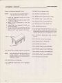
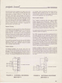
P h o t o g r a p hi s t h e c o m p l e t e dp r o l e c tw h e n b u r l tw r t h t h e r e c o m m e n d e dR a d i oS h a c k p a r t s T h i s p a c k a g e
c o n t a i n so n l y t h e P r i n t e dC i r c u i t B o a r d ,a n I n t e g r a t e dC i r c u i t a n d i n s t r u c t t o n s
iii
rt:
ASCII
ENCGIDEFI
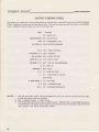
TABLE OF CONTENTS
1.
2.
3.
4.
5.
6.
7.
8.
9.
10.
11.
fntroduction
S p e c i f i c a t i o n. .s.
Description
Partslist
AssemblyofthePrintedCircuitBoard
P a r t s M o u n t i n .g.
Testing
T r o u b l e s h o o t i n. g
T h e o r y oOf p e r a t i o n
WaveForms
S c h e m a t iDc i a g r a m
....2
. .... 3
. .... 4
.......5
......6
.....6
... .. ... 11
....19
........22
...26
. .. .. . .. 27
ASCII KEYBOARD ENCODER PROJECTBOARD
INTRODUCTION
T h i s p a c k a g ec o n t a i n s a P r o j e c tB o a r d( P r i n t e dC i r c u i t
B o a r d ) ,a n I n t e g r a t e d C i r c u i t a n d l n s t r u c t i o n M a n u a l
for constructing an ASCII KeyboardEncoder.
The Instruction Manual provides a complete list of
parts needed to complete your project. lt also
provides theory of operation,assembly instructions
and diagrams to aid you in your project.
T h e A S C I I K e y b o a r d E n c o d e rc a n b e u s e d t o p r o v i d e
i n p u t s t o a l l t y p e s o f e q u i p m e n t d e s i g n e dt o o p e r a t e
w i t h A S C I I ( A m e r i c a n S t a n d a r dC o d ef o r I n f o r m a t i o n
lnterchange) inputs. Examples include T.V.
typewriters, mini-computers, micro-processors,
electric typewriters or anv device which requires
A S C I I e n c o d e da l p h a - n u m e r i c a lc h a r a c t e r s
T h r o u g h o u tt h i s m a n u a l y o u w i l l s e e s y m b o l ss u c h a s
8 , E o r H E X T h e l i n e a b o v et h e c h a r a c t e r sr e p r e s e n t s
N O T ( n e g a t i v e )l o g i c w h i c h i s t h e s t a t e o p p o s i t e o f
that without the bar HEX means "hexadecimal"
which is a number systemthat has a base of 16.
Note that this Project Board requires an external
p o w e r s o u r c e - 5 v o l t s D C a t a b o u t 5 O Om A S u c h a
power supply could be another Radio Shack Project
B o a r d , C a t a l o gN u m b e r 2 7 7 - 1 O 2 o r 2 7 7 - 1 1 2 O r i t
may be powered by the equipment to which you
connect the ASCII Keyboard Encoder.
RAD|OSHACK
^ DtVtStONOF TANDYCORPORAflON
E
U.S.A.:FORTWORTH,TEXAS76102
C A N A D A :B A R R I EO
, N T A R I OC. A N A D AL 4 M 4 W 5
T A NDY CORPORATION
AUSTRALIA
2 8 03 r 6V T C T 0 R
RToA
A0
RYDALME
NR
SE
W 2I16
' 8 7 6 S p - 2 8 4 7- 9 9 0 - 0 I 8 4
',)
BE
L GUI M
PARCINDUSTRIELt]E NANINNE
5 1 4 0N A N I N N E
UK
E I L S T ORNO A I ]
W S I O7 J N
W E O N E S E USRTYA f F S
P R I N T E DI N U S A
. --.*,-i:*:-
-
ASCII
ENGC'E'EF
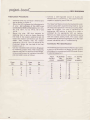
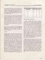
SPECIFICATIONS
l--
lnput Voltage:
MrN.
4.7
E
5.O
MAX.
5.5
UN|T
VoltsDC
Input Current:
4OO
450
50O
mA
Charactersper Minute Output:
*Note 1
833
CPM
nepeat Key Rate:
**Note 2
2oB
cPM
10
10
I
10
10
10
TTL Loads
TTL Loads
TTL Loads
TTL Loads
TTL Loads
TTL Loads
t
,l
-
Output Drives:
ASCIlTrueOutput:
Ascll ffid Output:
ST Output:
ST Output:
E Output:
E Output:
Outputs:
7-bitTrueASCII
z-uitffi6 Ascrl
1-bit E (6;5-le) External defined controt bit
1-bit E (Enable)Externaldefinedcontrol bit
1-ST Fallingedge clock
1-Si nising edge clock
;
I
Inputs:
+5.OVOLTS DC ! 2% load and line regulation,
50 mV peak-to-peak ripple
Ground
*Note 1 :
Specifiedwith l kHzclock frequencyand with 2 scan cyclesper keypressedand 2 scan cyclesper key
released.A scancycleis equalto 18 clockcycles.Thereforeminimum keytime = 18 x 4 x J- = 72
1kHz
ms = 13.8 characters per second.
**Note 2:
Specifiedwith 1 kHz clockfrequency.Repeatrate is 16 scancycleslongwhich is equalto 288 clock
cycles= 0.288 seconds= 3.472 charactersper second.
I
I
3
ASiCII
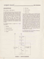
DESCRIPTION
5.
Shift Logic
R e f e rt o F i g u r e1 , B l o c kD i a g r a m .
6.
Output Latches
The ASCIIKeyboardEncoderusesthe scanprinciple
to reduce the amount of logic necessaryto fully
encodea 63 keytypewriterkeyboard.TheKeyboardis
w i r e d i n t o a m a t r i xc o n s i s t i n g
o f 1 6 c o l u m n sa n d 7
rows of keys.Sincethis typeof matrixcan handlea
Keyboard with 112 switches. there are many
locations that have no key. The keyboardscan
principle, which has been used on all recent
calculators,has the advantageof minimizedeffects
of key bounce.(Keybounceis that tendencyof a key
to chatter,or double-entry,
when pressedor when
released.
)
7.
Repeat Logic
The Keyboard Encoder is divided into 7 major
subsections:
1. Keyboard
2. KeyboardScanner
ENCC'E'EFI
The Keyboard together with the Scanner logic
supplies the Key PressedDetectorand the Encoder
L o g i c w i t h p u l s e s . T h e K e y P r e s s e dL o g i c w a i t s u n t i l
the key is released and then providesa strobe that
c l o c k s t h e e n c o d e d d a t a o u t o f t h e K e y b o a r dE n c o d e r .
The Encoder section generates the three most
significant ASCII bits and passes them on to the
O u t p u t L a t c h e s .l f a s h i f t i s r e q u e s t e d ,t h e S h i f t L o g i c
further modifies the encoded three bits to give a
s h i f t e d c h a r a c t e r .T h e f o u r l e a s t s i g n i fi c a n t b i t s o f t h e
ASCII encoded word are generated by the four-bit
binary counter controlling the scanner. The 7-bit
ASCII code is held in the data latchesuntil a new key
i s p r e s s e d ,a t w h i c h t i m e t h e p r o c e s ss t a r t s o v e r . T h e
r e p e a t l o g i c r e s p o n d st o t h e r e p e a t k e y w h i c h c a u s e s
the strobe command to turn off and on at
a p p r o x i m a t e l y 4 H z . . . w h i c h r e p e a t e d l yc l o c k s o u t
the data held in the latches.
3. Key PressedDetector
F o r a d e t a i l e d d e s c r i p t i o no f t h e T h e o r y o f O p e r a t i o n ,
refer to the back of this manual.
4. Encoder
KEYPRESSED
OETECTOR
F I G U R E1 .
4
B L O C KD I A G R A M
ASC|!
ENCC'E,EFI
PARTSLIST
T h i s p a c k a g e c o n t a i n s a c o m p l e t e c i r c u i t c a r d ( P r o j e c tB o a r d 2 7 7 - 1 1 7 1 r e a d y f o r p a r t s t o b e a d d e d . l t a l s o
c o n t a i n s I n t e g r a t e dC i r c u i t , R S 7 4 H 1 0 3 ( 2 1 ) T o c o n s t r u c t y o u r A S C I I K e y b o a r dE n c o d e r ,y o u w i l l n e e d t h e
f o l l o w i n g p a r t s . A l l p a r t s a r e a v a i l a b l ef r o m y o u r R a d i o S h a c k S t o r e .
NOTE:
T h e v o l t a g e r a t i n g s h o w n f o r c a p a c i t o r si s t h e m i n i m u m w o r k i n g v o l t a g e C a p a c i t o r so f t h e s a m e
c a p a c i t a n c ev a l u e w i t h a g r e a t e rw o r k i n g v o l t a g em a y b e u s e d A l s o n o t e t h a t r e s i s t o r sa r e l i s t e da s
1 / 4 - w a t t . 5 % " .b u t . r e s i s t o r s r a t e d a t 1 / 2 - w a t t , 1 O % w i l l w o r k
SYMBOL
DESCRIPTION
RADIOSHACK
CAT.NO.
SYMBOL
E+\
-l
A-
.l
I
10\
1\
-
272-131
272-14OO
272-14OO
272-131
272-131
272-131
14\
15\
RESISTORS
i*r
\
./
./
'// .
/
1
#
R\
R
n
8
8
'R10\
8K,1/4-wa*,svo
330 ohm, i /4-warr, so/o
lK, 1/ -watt,sYo
l K , 1 / 4 - w a t t ,5 %
1K, 1/4-watt, 5o/o
l K , 1 / 4 - w a t t ,5 %
1 K ,1 / 4 - w a n , 5 %
1K, 1/4-wart, 5o/o
1 K , 1 / - w a t r ,5 %
lK, 1/ 4-wan, 5o/o
1K,1/4-watr,sYo
27 1 -1300
271-1300
271-1300
27 1 -1300
27 1 -1300
271-1300
27 1 -1300
27 1 -1300
27 1 -1300
271-13OO.,.
271-1300
RADIOSHACK
CAT. NO.
276-1809
R S 7 4 2 OD, u a l ,4 - i n p u t
N A N DG a t e
276-1802
R S 7 4 O 4H, E X I n v e r t e r
276-1820
R S 7 4 1 9 3S
, ynchronous
4-bit up/down counter
276-1834
RS741
54, 16-line
Demultiolexer
R57473,Dual,J-K Flip-Flop276-1803
RS74O4,HEX Inverter
276-1802
RS74O2,Ouad,2-input
276-1811
N O RG a t e
276-1801
CAPACITORS
O 01 ptF,SOV,disc
3 . 3 1 t F1, O V T
, antalum
T
3.3uF, 1OV, antal-um
o oi prF5OV,disc
0 . 0 1p F 5OV,disc
o.otpr SOV,disc
DESCRIPTION
17 \
R S 7 4 1 OT, r i p l e ,3 - i n p u t
NAND Gate
276-1807
276-1809
KEYBOARD
\f\
63 Key Board
275-1422
O p t i o n afor
l HeepTest Module
I N T E G R A T ECDI R C U I T S
z+\
D
z3\
z
lZ5r v
r\
lA.
l8-
CONNECTOR
Included
R S 7 4 H 1 0 3D, u a l ,E d g e
T r i g g e r e Jd - K F l i p - F l o p
( R e c e i v ew
dith package)
R S 7 4 7 3 ,D u a l ,J - K F l i p - F l o p276-1803
276-1820
R S 7 4 19 3 . S v n c h r o n o u s
4-bit uo/down counter
RS747 5,14-bitBisrableLatclr2 7 6 -18 0 6
RS7475, 4-bit BistableLatch276-1806
R S 7 4 1 3D
, u a l ,4 - i n p u t
2t6-1815
S c h m i t tT r r g g e r
R 5 7 4 0 0 ,O u a d ,2 - i n p u t
276-1801
N A N DG a t e
R S 7 4 1 0T, n p l e 3
276-1801
, -input
N A N DG a t e
,/-\
,/
EdgeCard,44 contact
)(one needed)
276-1551
RESTSTOR
/
J
-/
180 ohm, i /4-warr, so/o
(nine needeo;
276-1300
L I G H TE M I T T I N G
DIODE
/-,
LED (nine needed)
2-/6-O90
ASCII
ENCC'ElEFI
A S S E M B L Y O F T H E P R I N T E DC I R C U I T B O A R D
Assembling of the Printed Board consists of
m o u n t i n g c o m p o n e n t s t o t h e B o a r d .T h e P A R T SL I S T
notes the parts you'll need The Board contains
l e t t e r i n g i d e n t i f y i n g w h e r e t h e c o m p o n e n t sa r e t o b e
m o u n t e d . A l s o i f a p p r o p r i a t e ,y o u ' l l s e e t h a t s o m e
outlines indicate the position or direction that a
component is to be mounted on the Board We
recommend that you mount the components in
g r o u p s - s u c h a s t h e r e s i s t o r s t, h e n t h e c a p a c i t o r s
and then the integrated circuits A step-by-step
assembly procedure is provided for each group of
components. As you mount each component check
off that step Efin the box.
Some Notes Before You Start
D u e t o t h e s m a l l f o i l a r e a a r o u n c it h e P r i n t e dC i r c u i t
Board holes and the small areasbetweenthe foils,
you will have to use utmost care to prevent solder
bridges between adjacent foil areas. Use only a
l o w - w a t t a g e s o l d e r i n gi r o n w i t h a s m a l l t i p . D O N O T
USE A SOLDER GUN. An ideal Solderinglron is
R a d i o S h a c k ' s R e c h a r g e a b l el r o n 1 6 4 - 2 0 7 5 1i;t h a s a
s m a l l t i p a n d w i l l n o t d a m a g e s e m i c o n d u c t o r sw i t h
leakage currents (a problem with some delicate
d e v i c e s ) .U s e o n l y a m i n i m u m a m o u n t o f s o l d e r ,a n d
d o n o t h e a t c o m p o n e n t s e x c e s s i v e l yw i t h s o l d e r i n g
i r o n .T r a n s i s t o r sa n d p r i n t e dc i r c u i t sc a n b e d a m a g e d
i f s u b j e c t e d t o e x c e s s i v ea m o u n t s o f h e a t
T h e P r i n t e d C i r c u i t B o a r d i s a d o u b l e - s i d e do n e , w i t h
p l a t e d - t h r o u g hh o l e s .T h i s m e a n s t h a t i n a n u m b e r o f
locations,the foil paths on the top of the Board are
connectedto the foil paths on the bottom - through
holes which have plating on the inside. This
p l a t e d - t h r o u g ht e c h n i q u e m e a n s y o u d o n ' t h a v e t o
s o l d e rc o m m o n f o i l a r e a so n B O T Hs i d e s- s o l d e r i n g
o n t h e b o t t o m s i d e o n l y n o r m a l l yw i l l b e a d e q u a t e
U s e a n o h m m e t e r t o c h e c kt h e p l a t e d - t h r o u g hh o l e s
f o r c o n t i n u i t y p r i o r t o a s s e m b l i n gt h e K e y b o a r d .
One last pointer - if you keep the tip of your iron
clean and coated with a f resh laverof melted solder,
y o u ' l l f i n d s o l d e r c o n n e c t i o n sm u c h e a s i e rt o m a k e
P e r i o d i c a l l yw i p e o f f t h e t i p o f y o u r i r o n o n a d a m p r a g
( o r " s o l d e r s p o n g e " )a n d m e l t a f r e s h l a y e r o f s o l d e r
over rt.
P a r t sM o u n t i n g
M o u n t t h e f o l l o w i n gr e s i s t o r s :
! R 1 , 6 8 K ( b l u e ,g r a y ,r e d )
! R2, 330 ohm (orange,orange,brown)
n R 3 , 1 K ( b r o w n ,b l a c kr e d )
, l a c k ,r e d )
n R4, 1K (brownb
tr R5, 1K (brown,black,red)
! R 6 , 1 K ( b r o w n ,b l a c k ,r e d )
t r R 7 , 1 K ( b r o w n ,b l a c k ,r e d )
! R8, 1K (brown.black,red)
! R 9 , 1 K ( b r o w n ,b l a c k ,r e d )
n R 1 O ,1 K ( b r o w n ,b l a c k ,r e d )
! R 11 , 1 K ( b r o w n b, l a c k r, e d )
!Turn the board over and solder.Trim off excess
l e a dl e n g t h
M o u n t t h e f o l l o w i n gc a p a c i i o r s :
NOTE:
C a p a c i t o r sC 2 a n d C 3 a r e p o l a r i t y
c o n s c i o u sW h e n i n s t a l l i n gc a p a c i t o rC
s2
and C3, observepolarity.With the dot on
t h e c a p a c i t ofra c i n gy o u ,t h e l e a do n y o u r
r i g h t i s p o s i t i v e( + )
f l C 1 , O 0 1 1 t F ,S O V ,D i s c
! C 2 , 3 3 g F , 1 O V ,T a n t a l u m
(Observe
polarity)
(Observp
eolarity)
! C 3 , 3 3 1 t F , l O V ,T a n t a l u m
! C4, O 01 1tF,5OV,Disc
n C5, O.O1prF, SOV,Disc
! C6, 0.01 prF,SOV,Disc
!Turn the board over and solder Trim off excess
l e a dl e n g t h .
-4
ru
0
NK]LHTE
D
o
-Q
m
{
FIGURE2. RESISTORAND CAPACITORMOUNTING
z
o
0
o
[l
!
ASCil
Mount the followingIntegratedCircuits:
424,R57475, 4-bit BistableLatch
NOTE:
DZs, R57475, 4-bit BistableLatch
Y o um a y w a n t t o u s e s o c k e t s f o r t h e l C ' s if so now is the time to mount them.
ENCC'E'EFI
f l 2 6 , R S 7 4 1 3 ,D u a l ,4 - i n p u t S c h m i t tT r i g g e r
1. Install the IntegratedCircuits (lC) in their
correctpositions.
2. The pins protrudethrough the holes in the
PrintedCircuitBoard.
3. NOTE: A dot or indentation at one end
i n d i c a t e sp i n 1 .
4. Ensure that the Integrated Circuits are
positionedproperly.
5. As you mount each lC, spreadthe end pins
slightlyto hold it in placeso you can turn the
Board over and solder the pins.
aZ7, RS74OO,
Ouad,2-input NAND Gate
llz8, RS741O,Triple,3-input NAND Gate
fl29, RS742O,Dual,4-inputNAND Gate
aZ1O, RS74O4.Hex Inverter
E Turn the boardover and cleanthe tip of your iron
beforesoldering.A cleantip, freshlycoatedwith
meltedsolderwill insurea goodconnection.Now
carefullysoldereach pin to its adjacentfoil area.
4211, RS74193, Synchronous 4-bit UplDown
Counter
Dot or
a z l 2 , R S 7 4 15 4 , 16 - l i n eD e m u l t i p l e x e r
4213, RS7473,Dual,J-K Flip-Flop
ZZ14, RS74O4.Hex Inverter
4215, RS74O2,Ouad, 2-input NOR Gate
aZ16, RS74OO,
Ouad,2-input NAND Gate
nT , RS74H103, DualEdge-triggered
J-K Flip-Flop
a Z 1 7 , R S 7 4 1 OT, r i p l e ,3 - i n p u tN A N DG a t e
NOTE:
aZ/
Checkthe positionof this lC carefully.lt is
already inserted in the Printed Circuit
Boardbut checkfor correctpositionbefore
solderingit in place.
R57473,Dual,J-K Flip-Flop
a23, RS74193, Synchronous 4-bit UplDown
Counter
4218, RS742O,Dual,4-input NAND Gate
ETurn the boardover and solder.
@
D
o
o
lrl
z
o
o
m
0
(o
F I G U R E3 . I C M O U N T I N G
!
AETCII ENCC'EIEFI
You are now ready to install the Keyboard to the
P r i n t e dC i r c u i t B o a r d .M o u n t a s f o l l o w s :
! Ensure that all of the pins on the Keyboardare
STRAIGHT!
nThe Keyboardcontainsthree plastic alignment
pins on its basewhich mate into alignmentholes
in the PrintedCircuitBoard Placethe Kevboard
with
keys
facing
a
f
lat
Position
the
the
down on
surface.
Printed Circuit Board (componentside down)
approximatelythree inches above Keyboard.
V i s u a l l ya l i g n B o a r da l i g n m e n h
t o l e sw i t h p l a s t i c
alignmentpins on Keyboardbase.Gently lower
the Board onto the Keyboardmaking sure the
alignment holes in the Board mate with the
alignmentpins on the Keyboardbase.Checkthat
ALL Keyboardpins protrudethroughthe holeson
the PrintedCircuitBoard.
10
! Solder one pin at each corner - press the Board
f i r m l y d o w n a g a i n s t t h e K e y b o a r da s y o u d o t h i s .
T h i s w a y y o u ' l l b e s u r e e a c h p i n e x t e n d sw e l l i n t o
the appropriate hole and that the Board and
K e y b o a r dm a t e f l a t C o n t i n u e t o s o l d e r a l l p i n s .
This completes the component assembly of the
Printed Circuit Board. We suggest you check over
y o u r w o r k t o e n s u r e t h a t a l l s o l d e rj o i n t s a r e c l e a n
a n d s h i n y a n d t h a t n o n e o f t h e f o i l h a s p u l l e du p f r o m
the Board due to excessive heat Double check to
ensure all component connections are solderedto
the foil and that no solder has flowed across
(between)foil paths.
T o e n s u r e o p t i m u m c i r c u i t p e r f o r m a n c ea n d t o m a k e
your work neat,you may want to "deflux" the Board
T o r e m o v e a n y r o s i n r e s i d u e ,a p p l y o r d i n a r y r u b b i n g
alcohol to the Board and rub off with a clean cloth
ASC||
ENCC|E'EFI
TESTING
LED Cathode ldentification
T o t e s t t h e A S C I I K e y b o a r dE n c o d e ry o u ' l l n e e d s o m e
f o r m o f d i s p l a y t h a t v e r i fi e s t h e c o d e s .l f y o u h a v e t h i s
e q u i p m e n t a v a i l a b l e ,u s e i t t o t e s t y o u r E n c o d e r .S e e
Connector Pin ldentification on page 12 for pin
c o n fi g u r a t i o n .
Due to the reluctance of manufacturers to
standardizethe methodof cathodeand anodelead
identification,we urge you to test each LED before
installing. This can be done in the following
manner: With two 1-1/2 volt batteriesconnected
in seriesforming a 3-volt power supply,connecta
resistor- any valuefrom 1OOohmsto 47Oohmsto the positiveside of the batteries.
lf you do not havea systemthat acceptsASCIIcodes
for testingwe suggestyou buildyour own. Fabricate
the Heep Test Module using Figure 4 and the
fabricationprocedures.We show the LED's and
resistorsas they should mount on the connector:
however,you can mount these componentson an
external breadboardaccordingto the schematic
shown with the illustration(Figure4).
Test the LED'sby connectingone lead of the LEDto
the negativesideof the batteriesand the other leadto
the resistorwhich is connectedto the positiveside.
lf the LED lights,the lead connectedto the negative
side is the cathode. lf it does not light, reversethe
LED leadsto identifythe cathode.
100oHM
TO
470oHM
LED TESTDIAGRAM
11
@
ASCII
Fabrication Procedures
fJ
X
n
n
!
Carefullybend the connector'sletteredpins
(up)as shown in Figure4.
Mount the LED'sbetweenthe followingpairs
of pins: (All cathodes of the LED's are
connectedto oDD numberedpins.)2-3,4-5,
6 - 7 , 8 - 9 , 1 0 - 1 1 , 1 2 - 1 3 , 1 4 - 1 5 ,1 6 - 1 7 a n d
18 - 19 .
M o u n t t h e n i n e , 1 8 0 o h m r e s i s t o r sb y
solderingthem to pins as shown. Bend the
free lead of the resistorsolderedto pin 18
toward the resistorconnectedto pin 16 and
solder. Then continue with the resistor
s o l d e r e dt o 1 6 t o 1 4 , 1 4 t o 1 2 ,a n d s o o n a s
illustrated.Solder the free lead of the final
r e s i s t o tr o p i n 1 .
Use any insulatedsmallwire (22to 30 gauge)
for followingjumper wires. After measuring
distancerequired,cut wires to correctlength,
removesmall amountof insulationfrom each
end and solderwires as follows:
Connect a well-regulated source of S-volts DC
b e t w e e n P i n 1 ( + )a n d P i n Z ( - ) .T h e s u p p l ys h o u l d b e
c a p a b l e o f s u p p l y i n g a b o u . t5 O Om A .
T h e H e e p T e s t M o d u l e c h e c k s t h e K e y b o a r dE n c o d e r
o u t p u t s u s i n g L E D ' s ( L i g h t E m i t t i n g D i o d e ' s ) .U s i n g
t h e o u t p u t p i n s s p e c i fi ed i n t h e O u t p u t C o d i n g T a b l e ,
( p a g e 15 ) a l o g i c a l 1 ( o r t r u e ) i s i n d i c a t e d b y t h e
appropriateLED lighting. A logical O (or false) is
indicated by the appropriate LED nor lighting
P e r f o r m y o u r t e s t s u s i n g t h e t e s t p r o c e d u r e sa l o n g
with the Output Coding Table. The output codes
s h o u l d m a t c h u p w i t h t h e L E Dd i s p l a y l f y o u d o n ' t g e t
correct indicationsrefer to Troubleshooting.
Connector Pin ldentification
Thefollowingchartcorrelates
the ASClloutputcodes
to pins on the PrintedCircuitBoard Youcan usethis
informationfor connectingthe ASCIIEncoderOutput
to externalequipment.
ASCII
PC BOARD
OUTPUT
PIN
CODE
NUMBER
12
From
Pin
To
Pin
From
Pin
To
Pin
3
5
7
9
11
21
L
P
R
U
13
15
17
19
B
E
F
K
ENCC'DEFT
20
21
22
23
24
25
26
E
ST
J
H
D
C
T
S
N
M
X
ASCII
P CB O A R D
OUTPUT
PIN
CODE
NUMBER
20
21
7
T
7
25
T"
E
ST
K
F
E
B
U
R
P
L
21
ASCII
BLUE
J U M P E R S( 4 }
ENCG'EIEFI
+5.0 VDC
l80a
180cl
1 8 0s ,
1 8 0s l
I
t 8 00
I
1 8 0s ,
1 8 0s ,
1 8 00
IED
L^.,^
S C H E X I A I I CD I A G R A A I
RED
J U M P E R S( 5 )
NOTE:
F I G U R E4 .
Be sure to coat the tip of your
soldering iron with a layer of melted
solder before soldering the component
leads and wires to the connector
terminals.
H E E PT E S T M O D U L E
13
@
ASCII
TESTPROCEDURE
1. Installthe Heep Test Module on the Printed
CircuitBoard.
2. Connect +S-volt DC power to pin 1 of test
moduleconnector.
3. Connect ground return to pin Z of test
module.
4. Perform test using Output Code Table and
observe test module LED indications.The
followingis a descriptionand explanationon
how to use the tableand how to interpretthe
test moduleindications.
Lookingat the OutputCodingTable,youseethereare
two separategroupsof output codingidentifiedas
NORMALand SHIFT.Theseare two separatetests.
First,you check the output codesof the Encoderin
the NORMAL mode (not in SHIFT LOCK).After
completingthe NORMALmode checks,depressthe
SHIFTLOCKkey and checkthe outputcodesof the
Encoderin the SHIFTmode.
F. the next monitors and represents23 output
codes,
G. the next monitors and represents22,
H. the next monitors and represents21,
L the next monitors and represents20
F o r a n e x a m p l e , l e t ' s p r e s s t h e f i r s t k e y ( E S C ) .N o t e
t h a t a c c o r d i n gt o O u t p u t C o d i n gT a b l et h a t E o u t p u t i s
O , 2 6 i s 1 , 2 5 i s 1 , 2 a i s 1 , 2 3i S 1 , 2 2 i s1 , 2 ' i s 1 a n d 2 0i s
0 . W h e n y o u p r e s s t h e k e y E S C ,t h e f i r s t L E D o n t h e
H e e p T e s t M o d u l e s h o u l d l i g h t . R e l e a s et h e k e y a n d
the first light should go off.
5.
6.
A. Thef irst LEDlightswhen a keyis pressedand
stayson until you releasethe key at which
time the LEDgoes off (not lighted).
B. The next LED monitors and representsE
output codesand lightswhen E outputcode
. is 1 and doesnot lightwhen E outputcodeis
7.
o.
14
i
I
N o w c h e c k t o s e e i f t h e o u t p u t c o d e i s c o r r e c t .D o t h i s
by checking the LED's against the Output Coding
Table. You should have the next (secondfrom left)
LED off (E),the next six LED's on and the last (far
right) LED off.
The Heep Test module has nine LED's.With the
keyboard toward you, let's identify the LED's.
Startingon the leftgoingto the right,the LED'sareas
follows:
C. The next LED monitors and represents 26
output codes,
D. the next monitors and represents25 output
codes,
E. the next monitors and represents2a output
codes,
ENGC'E'EFI
8.
9.
10.
Perform NORMAL mode test. With the
keyboard in NORMAL (press and release
S H I F Tt o e n s u r e t h a t k e y b o a r di s n o t i n S H I F T
L O C K ) d e p r e s st h e k e y so n e a t a t i m e a s c a l l e d
out in the Output Coding Table. Verify the
output codes from the Heep Test Module by
checking against the Output Coding Table
Perform SHIFT mode test. Depress the
S H I F T L O C K k e y a n d r e l e a s e .Y o u a r e n o w i n
S H I F Tm o d e D e p r e s st h e k e y s o n e a t a t i m e a s
called out in the Output Coding Table.Check
t h e o u t p u t c o d e r e s p o n s ea s c a l l e d o u t i n t h e
t a b l e a n d a s i n d r c a t e db y t h e L E D ' so f t h e H e e p
Test Module.
P r e s s S H I F T k e y a n d r e l e a s e .T h i s t a k e s y o u
out of shift mode.
Disconnect the +S-volt DC power f rom pin 1
of Heep Test Module.
Disconnect the ground return from pin Z of
the Heep Test Module.
Remove the Heep Test Module from the
Printed Circuit Board.
l
I
@
ASCII
ENGclElEFI
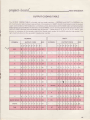
O U T P U TC O D I N G T A B L E
T h e O U T P U TC O D I N G T A B L E i s d i v i d e d i n t o t w o m a j o r s e c t i o n s- N O R M A L a n d S H I F T I n N O R M A L , t h e
l e f t - h a n d c o l u m n l i s t s t h e l o w e r c a s e s y m b o l so f t h e k e y b o a r d I. n S H I F T t, h e l e f t - h a n dc o l u m n l i s t st h e m a r k e d
u p p e r c a s e s y m b o l s o f t h e k e y b o a r d o r u n m a r k e d s y m b o l a b b r e v i a t i o n so f t h e A S C I I C o d e . U n m a r k e d s y m b o l
a b b r e v i a t i o n sa r e p r e c e d e db y a n a s t e r i s k( * ) i n t h e S Y M B O Lc o l u m n a n d a r e e x p l a i n e df o l l o w i n gt h i s t a b l e .T h e
O U T P U TC O D E c o l u m n s a r e s u b - d i v i d e di n t o 8 s e c t i o n s- t h e s e b e i n g E , 2 6 , 2 5 , 2 4 , 2 3 , 2 2 , 2 1a, n d 2 0 .T h i s
d i v i s i o n i s i n d i c a t i v e o f t h e e n c o d e r o u t D U t b i t s . t s e s i d ee a c h s v m b o l i s t h e A S C I I c o d e f o r t h a t s v m b o l . T h e
r i g h t - h a n d c o l u m n s l i s t t h e e q u i v a l e n th e x a d e c i m a ln u m b e r .
I
h
NORMAL
HEX
O U T P U TC O D E
SYMBOL
E
,l
SHIFT
26
2 5 24
23 22
E
2 1 20
HEX
O U T P U TC O D E
SYMBOL
26
25
24
23
22
2 1 20
o o
1
o
1
1
1
0 2E
o
1
o o o o
1 21
o o
1
0
o o
1
o
22
U
o
1
o
n
o
1
1
23
24
ESC
q1
1
1
1
1
o
7E
1
Or o
1
1
o o o
1
JI
2
c o
1
I
I
0
o
1
o
32
J
o o
1
1
o o
a
I
1 33
4
o o
1
1
o
I
o o
34
s
a
o
1
o o
1
o o
5
0
o
1
o
I
o
35
o/
/o
0
0
1
o o
1
n
1
6
o o
1
1
o
1
1
o
36
&
o
1
o o
1
1
o
-l
o o
1
1
o
I
1
I
o
O
1
o
I
1
I
8
o
1
1
o o o
0
o
1
o
1
0
o
o o
1
1
1
o o
o
1
o o
1
29
o
jo o
1
1
o o o o
20
o
1
o
I
o o
o
0
BACKSPACE
BREAK
TAB
1
I
3l
30
o
1
2D
1
1
0
1
o
3A
o
1
I
1
o
5E
o o
0
o o o o
,|
o o
o o
1 39
1
\
(
38
I
q 0 o o
1
1
0 08
*
*
o o
1
o9
28
1
0
0
o o o
o o
1
1
1
1
o
1 3D
:1.
0
0
1
0
1
o
1
0 2A
SO
o
0
0
o
1
1
1
o
o o o
0
1
o o
1
1
o o o o o 60
0
o o o
*BS
o o o o o0
1
o o
27
0
SPACE
*HT
o
I
,l
26
1
1
o o
OE
0 08
1 09
15
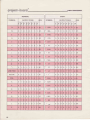
ASCII
NORMAL
SYMBOL
SHIFT
HEX
O U T P U TC O D E
E 26 2 5 24 23 22
SYMBOL
O U T P U TC O D E
E
2 1 20
26
HEX
2 s 24 2 3 2 2 2 1 20
o
o
1
o
1
o o o
1 51
* SOH
o o o o o o o
1
o1
W
o
'l
o
1
o
1
1
1 57
*
BEL
o o o o o
1
1
1
07
E
o
1
0
o o
1
o
1 45
*
ENO
o o o o o
1
o
1
o5
R
o
1
o
1
o o
1
o
52
*
STX
0
o o o
0
o
1
o o2
T
o
1
o
1
o
1
0
o
54
*
EOT
0
o
o
0
1
o
0 o4
o
1
o
1
1
o 0
1
59
o o o o
1
o o
1
o9
o
1
o
1
o
1
o
1 55
o
1
o5
o
1
o o
1
o o
1 49
o9
o
o
1
o
0
1
1
1 4F
P
o
1
o
1
o o o o
t
o
1
o
1
1
o
1
o
1
o
1
1
1
o o
5C
*FF
o o o o
1
o
1
o
OA
*LF
DELETE
0
1
1
1
1
1
1
1 7F
CTRL
1
0
o o
0
o
0
1
A
o
1
o o o o o
1 41
S
o
1
o
1 53
D
o
F
0
1
0
G
0
1
0
H
o
J
K
U
L I N EF E E D
16
ENCCIEIEFI
1
'l
HT
*
HT
*sl
50
5B
o1
ENO
NUL
'y'T
*
*
*
0
o o o o o
1
0
o o o
1
o o
1
o
0
o
1
1
1 OF
o
0
1
o o o o o o oo
o o o o
1
o
1
0
o o o
I
1
o o
OC
0
o o o
1
o
1
o
OA
0
o
1
1
1
1 2F
soH
1
o o o o o o
1 01
SOH
o o o o o o o
1
ETX
o
0
0
o
1
1 03
1
o
o1
o
0
1
o o o
1
o o
44
EOT
0
o o o o
1
o o o4
0
o
1
1
o
46
* ACK
0
o
0
o
0
I
1
o
0
0
1
1
1 47
BEL
0
0
o
0
o
1
1
1 07
1
o o
1
o o o
0
o o o
1
o o o
o
1
0
o
1
o
1
0 4A
o o o o
1
o
1
0 OA
0
1
0
o
1
o
1
1 48
o o o o
1
o
1
1 OB
1
48
*BS
LF
+VT
0
o
1 OB
06
08
ASCII
SHIFT
NORMAL
CODE
OUTPUT
SYMBOL
E 26
24 23 22 2 1
o
1
o
0
1
1
o o
o
0
1
1
1
o
1
1 3B
@
o
1
o o o o
0
0 40
l
0
1
1
o
1 5D
CLEAR
1
o
o o o
1
0 o2
H E R EI S
1
o o
n
0
o
I
1
L BLANK
"l
o
0
0
0
Z
o
1
o
1
X
o
I
o
\-
o
1
V
o
B
1
0
1
4C
*FF
T
CR
* srx
o3
-
1
o o o4
*
I
o
o
5A
1
I
o o o
58
0
o
0
o
1
1
43
ETX
1
o
"l
o
1
1
o
56
n
1
o o o o
1
o
42
N
0
'l
0
o
4E
M
U
1
o o
0
0
1
o o
0
SPACE
R BLANK
o
1
1
1
I
1
o
o
1
1
o o
1
o
1
1
o
1
0
1
1
0
o
1
o o
1
o
0
o o
1
1
I
2', 23
22
2 1 20
1
1
o o oc
o o
I
o
1
o
1
o
1
o o
0
o o
1
1
28
60
o o o 0
1
1
0
1 OD
o o
0
0
1
o o2
n
o o
1
1
1
1
EOT
1
0
U
o o o o
o3
1
o o o4
o o o o
1
U
1
o
o o o o
I
o
0
o o8
o o o
0
n
o
1
1 03
ACK
o
o
0
o
1
1
o
06
STX
o o o
0
o 0
1
o
UZ
*BS
*so
4D
25
o o o o
ETX
LF
*
HEX
O U T P U TC O D E
SYMBOL
2(
25
,l
I
lo
HEX
E 26
L
ENGc'ElEFI
CR
0
o
0
0
o o
OA
'l
1
1
0 OE
0
1
1
o
1 OD
o o
2C
o o
1
1
1
1
o
0 3C
1
0 2E
o o
1
1
1
1
1
0 3E
1
1 2F
o o
I
1
1
1
1
1 3F
tJ
o 20
o o o o o
0
U
U
o
1
1
0
1 05
o5
7
*
NUL
* ENO
1
0
0
0
0
oo
17
ASiCII
ENCCIEIEFI
OUTPUTCODINGTABLE
The following is a definitionof symbolabbreviationsof ASCIIcode in the SHIFTmodeof the OUTPUTCODING
TABLE.Physicallythe keysare not identifiedas such.They are the samekeysthat are usedin the NORMAL
mode. NORMAL mode key labelsare noted in bold face type.
ESC
= ESCAPE
SO = SHIFTOUT
n
BACK SPACE BS = BACK SPACE
TAB
O, CTRL, A
W. G
R B L A N K ,E , U
TAB
HT = HORIZONTAL
SOH=STARTOFHEADING
BEL= RINGSTHE BELL
E N O= E N O U I R Y
B.R, CLEAR STX = STARTOF TEXT
HERE lS, C, S
ETX= END OF TEXT
L BLANK, T, D
EOT= ENDOF TRANSMISSION
O
S l = S H I F Tl N
(SPACEP
I
NUL=NULL
W=VERTICALTAB
[,K
/, L FF = |ORM FEEDTO TOP OF
NEXTPAGE
Z, LINE FEED,J
LF = LIVEFEED
V,F ACK=ACKNOWLEDGE
M, ]
CR = CARRIAGERETURNTo
NOTES: 1. Left and right SHIFT,SHIFTLOCKand REPEATkeys are only used for internal control of logic
circuits.No output codesare available.
2. Key n actuallyoutputs I eSCtt coding..
3. The following six keys do not have an ASCIIcoding: BREAK,CTRL,CLEAR,HERElS and two
unmarkedkeys.Thesekeys may be used as control keysfor externalf unctions.Referto How to
Use E Output in the Theoryof Operationsection.
18
ASiCII
TROUB LESHOOTING
Negativeor FalseASCII:
lf you checkedyour KeyboardEncoderby connecting
it to a TV typewriter and typed RADIOSHACK and
obtain the following W display:-)i 60*,7) <4
insteadof RADIOSHACK,troubleexistsbetweenthe
Encoder and the equipment it is connectedto.
Incorrectdatasuchas this indicatesthatthe Encoder
is supplyingtypeddata into a systemthat isdesigned
to acceptASCIIin a code oppositeof that which you
have connected into it. Notice that the Encoder
providesboth true and false ASCIIdata. lf the typed
wordsare displayedlikesymbolicnewsprintcursing,
then you confusedyour outputs.The ASCIIcodefor
(HEX41 ).Thisis in trueform.
the letterA is 1O0OOO1
Somesystemsrequirea false statement.A "false" A
is in code01 1 1 1 1O,or HEX3E.lf you pressthe keyA
and a " >" is printed, then you have reversedthe
ASCIIstatement.All ASCIIoutputpins are marked.
For example,20 or F, or 25or 2d.The symbolfortrue
ASCIIoutputsis a number2 with a powerexponent
that does not have a bar over it. In otherwords,20is a
true statement.A false statement is shown with a
bar. 26 is a false statement.The output codingchart
shows true ASCll. lf you want to know what the false
's.
's
ASCIIcodeis, changeall 1 to 0's and allO'sto1 lf
the system requires false ASCII data, use outputs
with a bar over it. lf the system requirestrue ASCII
data, use outputswithout a bar. ForfalseASCIIdata,
use connectorpins L, P, R, U, B, E, F and K. Fortrue
ASCIIdata useconnectorpins M, N, S, T, C, D, H, and
J.
Construction Problems:
lf you haveproblemswith the Encoderand you know
it is connectedto the systemproperlyand the proper
code source is selected,then you must troubleshoot
the Encoder.Firstensurethat all integratedcircuits
(lC's) are installedproperly.Pin 1 of all lC's are
positionedto the left when viewedwith the keyboard
toward you.
Second.ensure each lC is in its proper mounting
place. lt's easy to install a RS74OOin the RS74O2
position.They look the same and only their part
n u m bersare different.In otherwords,makesurethat
27 is in Z7's placeand not somewhereelse.Noteon
the Schematicthat Z1 looksexactlylike 213 or 22.
They even have the same functional pin outputs.
ENGC,EIEFI
Lookingat the lC list at the bottomof the schematic,
n o t e t h a t z 1 i s l i s t e da s R S 7 4 H 1 0 3a, n d 2 2 a n d 2 1 3
are listedas RS7473.lf you installaRS7473intoZl',s
place, the ST (strobe) output will not operate
correctly. Do not substitute a Rs7473 for a
RS74Hl O3. lt's all rightto put a RS74H103inZ2or
23 position,but don't put a RS7473 in placeot Z1l
Third,checkthat C2 and C3 capacitorsare installed
correctly. capacitor c3 forms the systems master
oscillator, while C2 performs a power-up clear
function. Note that the two Tantalumcapacitors(C2
and C3) havea color dot on them. When facingthe
dot, the positiveterminal is on the right side of the
capacitor.Thesecapacitorsare electrolyticand must
be properlyinstalled.
Fourth,checkfor solderbridgesor shortsbetweenlC
pins (an easy place for a short to form) or shorts
between copperruns. Checkfor cold solderjoints.A
cold solder joint is the most common soldering
problem. Sometimes the joint feels strong, but
electricallythey are deador open.A coldsolderjoint
is usuallydull gray in colorand grainy.A goodjoint is
bright and shiny. A cold solder is due to applying
solderto the solderingiron ratherthan the junction.
The solder flows off the tip and surroundsthe
componentleadon its pad.Sincethe leadandpadare
not up to solderingtemperature,the solder cools
quickly and gives a bad, ugly joint. The oppositeof a
cold solder joint is a burnt or broken printed circuit
run. The copperon a PrintedCircuit Boardis applied
by heatand heatcan take it rightoff again.TheASCII
Encoder Project Board is double-sided, with
plated-throughholes.Notethereare copperruns and
pads on both sidesof the board.lt is not necessaryto
apply solderto componentson the top (component)
side of the board.Soldercomponentson one side of
the board only. Each hole has copper plating
completely through it and makes electrical
connectionon both sidesof the board. Excessiveheat
can lift a pad, breaking its plating and, therefore.
opening partof the circuit not visibleto you. lf you f ind
that a hole has opened, repair it. Suck out all the
solderin the holeand inserta fine pieceof wire allthe
way through the hole. lf an lC or the keyboardis on
the otherside,push wire intothe holeas far as it will
go. Leavea 1" tail on the wire on the backsideand
apply solderto the wire and the lead.Melt the solder
on both the wire and the componentlead.Capillary
actionwill suckthe solderupthroughthe hole.When
the solder has cooledlay the free end of the wire on
19
ASiCII
the brokencopperrun or the pad and solderit. Cutoff
the excesswire. Once you have confirmedthat you
have repairedthe hole,protectthe wire and looserun
or the pad with epoxy or some non-conductive
cementor glue.
Step-by-Step Troubleshooting:
Thereare four main stepsin troubleshooting:
Step 1.
Step 2.
Step 3.
Step 4.
Verifythe problem.
lsolatethe problem.
lsolatethe component.
Repairthe problem.
Step 1. Verify the Problem. Step 1 is easy.You
have been doing just that. Now that you know the
problem exists and is real, move to step 2.
Step 2. lsolate the problem. To isolate the
problem you must know the system. Read the
detailedTheoryOf Operation.After you haveread it,
read it again and study it. There are seven main
sections to the ASCII Keyboard Encoder. ls the
problem a Scanning problem? ls it a Keyboard
problem?ls it a Key PressedDetectorproblem?ls it a
Latch problem?lsolatethe section.For an example,
let's saythe keyboardis puttingout goodcodesuntil a
number key is pressed.Pressa letterand everything
is fine, then press a number key and nothing
happens.What's wrong? lt can't be the Scanner
becausethe Scanner controls all keys,not just the
letter keys. lt could be that on the keyboardevery
number key is bad. Most likelythe problemis along
the Keyboardline marked"c" or anythingline "c"
feeds.This includesresistorR6,NANDgatesZl8 and
217. You have now isolatedthe problemto a logical
area. Now move to step 3.
Step 3. lsolate the component. Youmust isolate
the componentthat is causingthe problem.Notethat
ENGC'E'EFI
the colonand semi-colonkeysare alsoon line "c" .lf
these keys are pressed and the proper output is
provided,the problem is probablya broken printed
circuit foil path or an open feed-through.lf the
system is still defective,check the Vcc junction of
resistorR6. ls 5 volts present?lf it is. checkthe other
side of RGfor 5 volts.lf 5 volts is here,pressa number
key. Did the voltagedrop?lf it did.pressthe restof the
number keys.lf everynumber keyproducesa voltage
changeat junction"c" of RGwhen pressed.then the
Keyboardis okay and so is R6. A rare problem is a
shortedresistorR6 or a soldersplashwhich would
not allow the voltageat line "c" to drop.Thebestway
to check this problemis to use a logic analyzeror
oscilloscopeinsteadof a voltmeter.
Since nothing happens on the output connector
when a number key is pressed,the problemmust be
within the Key Pressed Detector. You have
eliminatedthe Keyboardand R6 as the problem.
What next?Lookingat the Schematicyou seethat the
Key PressedDetector (21) is fed by 218, part of 215
and part oI 214. Keyboardlines "a", "b", "d", "e",
"f" and "9" are satisfactorybecause when keys
associatedwith these lines are pressed,an output is
produced.This leavespin 5 of Zl 8. Lookingat pin 5 of
218 you find that the pin is bent and is not even
soldered! You have isolated the component. Now
move to step 4.
Step 4. Repair the Problem. Step 4 is easy to
implement.You straightenthe pin and carefully
insert it in the proper hole and solder it. Checkto
make sure the encoderworks properlynow. lf it does,
your work is finished. lf the problemstill exists,you
must replace218 since there is an internalopen
withinthis lC.
Thefollowingchartwill helpyou isolatethe problems
and specificcomponent.
TROUBLESHOOTING
CHART
IC
20
MAJOR SECTION
P R O B A B L EC A U S E / I N D I C A T I O N
z1
Key pressed detector
1 . Strobe (ST)output never changesstates.
2 . Strobe output cycles(repeats)whenkey pressed.
z2
Keyboardscanner
1 . Outputs never change.
2 . Keyboardnot scanned.
3 . Problemwith key presseddetector.
ASICII
IC
MAJOR SECTION
ENCC'EIEFI
P R O B A B L EC A U S E , / I N D I C A T I O N
23
Keyboardscanner
1 Outputsneverchange.
2 Keyboardnot scanned.
3 Defectiveboard.
24
Output latches
1. The four ASCIIoutput bits 20,21,22,23 neverchange.
Z5
Output latches
1. The three ASCII output bits 24, 25,26 never change.
ZG Keyboardscannerand encoder
27
Keyboardscanner,key pressed
detector,and encoder
ZB
Encoder
Zg
Shift logic
1 . Defective board (does not oscillate).
2 . Problems with output bits 25 or f1
1 Problemwith output bits 24 and 26.
2 Problemwith strobeoutput and repeat.
3 No output when key pressed.
' t . Problem with output bits 23 or 24.
2. lncorrect shift coding on bits 2a or 25
1. Problem with output bits 2a or 26.
2. Incorrectshift coding on output bits 24 or 25.
Z1O Repeatlogic,encoder,shift
logic and key presseddetector
1 No repeatfunction.
2 No ST output.
3 No shift codes.
211 Repeatlogic
1 . Problemwith stobe output.
2 . No repeatfunction.
212 Kevboardscanner
1. Deadboard.
2. One or more columnsdead.
2 1 3 S h i f tl o g i c
1 . Shift problem.
2 . shift lock problem.
214 Key presseddetector,latch
and shift logic
1. Problemwith key presseddetector.
2. Problemwith output latches.
3. Problemwith shift logic.
215 Key pressedlogic and shift
logic
1. Problemwith key presseddetector.
2. Problemwith shift logic.
2 1 6 S h i f tl o g i c
1. Problemwith shift logic.
Z17 Encoderlogic
1. Problemwith encoderlogic.
Z18 Key presseddetector
1. Problemwith key presseddetector.
21
ASCII
THEORYOF OPERATION
The following is a detailedTheoryOf Operationof the
ASCII KeyboardEncoderand its associatedcircuitry.
Referto the SchematicDiagramandWaveformChart
while readingthis Theory.
Scanner
The Scannercircuitryis made up of 76,23, 22 and
212. Partof ZGis usedas the master oscillatorf or the
rest of the system.23, togetherwilhZ,2,forms a base
18 counter. Z3 supplies BCD data to Keyboard
Scanner Decoder 212 and generatesthe four least
significantdigits of the ASCII code. 22 supplies
"housekeeping"pulsetrains(signalsthat contribute
to proper operationof the system)for use during
Keyboard Disable Time.
Operationof the Scanner circuits is rather straight
forward.26 oscillatesatapproximately
1 kHzwiththe
components(c3 and R2) as shown. Lookingat the
WaveformChart, the pulse train at line A is what
couldbe expectedat pin 8 of 26. Inverter,214 pins 1
and 2, inverts the clock pulse train and it looks like
line B on the WaveformChart.This pulse train is
appliedto z.3,a counter.While Z3 counts from O to
15, it appliesdata to 212 and to Ouad Latch24.The
output lines of 212 go low for one clockcycle.For
example,pin 1 of 212 goeslow during zerotime as
shown on line C of the WaveformChart.Duringthe
next clock cycle,pin 2 of 212 goes low as shown on
line D of the chart. Line E on the WaveformChart
shows the output on pin 17 of 212. The pulseson
212's output labeledD-0throughDTE lread "not DO
through not D15") and specificallythe clock(CLK)
time during these output pulses are called
"Keyboard Scan Time". Notice that outputs O
through 15 are tied to the Keyboard.During
Keyboard Scan Time, one of these outputs is low
and the Keyboardis being scanned.
As previouslymentioned,there is a time when the
Keyboardis not scanned.This housekeepingtime is
labeled KEYBOARD DISABLE time on the
WaveformChart. Notice,on the WaveformChartthe
relationship between lines E, F and G. When DT-S
goesbackhigh counterZ3 is in transistionf rom count
15 to count 0. This transitionperiodcausesthe high
at pin 12 of 22, as shown on WaveformCharttine F.
This pin stayshigh for one clockcycle.22pin l2 now
causes22 pin 9 to go high for one clockcyclewhich is
22
ENCC'E'EFI
shown on line G of the chart.Thattime when either
22 pin 12 or pin 9 is high is calledKeyboardDisable
Time.
Noticethat lineH is highwhenevereitherZ2pin12or
pin 9 is high. Line H showsthe outputof 27 pin 11.
During this high logic level,Z3is commandedto
ignore clock pulseson its input, pin 5. 212 is also
disabledpreventingany of its outputpinsfrom going
low during Keyboard Disable Time.
Keyboard and Key Pressed Detector
The Keyboard consistsof 63 keys,electricallywired
into a matrixof 16 columnsby 7 rows.The columns
are connectedto KeyboardScanner,212,while the
rows are connectedto the KeyboardDetector and to
the Row Encoder.The Detector consistsof 218 and
21.The Row Encoder,which will be discussedlater.
consistsof 217.
The operationof the Key PressedDetector, as its
name implies,detectswhen a key is pressedon the
Keyboard,and gives an indicationto the external
circuitry that new data has been sent to the data
latches.
Each Keyboardcircle on the schematic,which is a
representationof the Keyboard,consistsof a single
pole.singlethrow, normallyopenswitch.Onesideof
the switch is connectedto a column, and therefore
212. The other side of this switch is connectedto a
row line, and thereforeto one of the inputsof 21B.
Whenever a key is pressed.the switch is closed
which makes an electicalconnectionfrom one of
212's outputstoone of the inputsof 218.Sinceoneof
212's outputs is low during Keyboard Scan Time,
t h a t l o w i s a p p l i e dt o Z 1 8 .A l o w o n p i n s2 , 1 , S o r 4 o t
2 1 8 w i l l c a u s ea h i g h a t p i n 6 . A l o w o n p i n s 1 3 , 1 2 ,
1 Oo r 9 o f 2 1 8 w i l l c a u s ea h i g ha t p i n 8 . S i n c ea l l r o w s
of the Keyboardare connectedto 218. when any key
is pressed.eitherpin 6 or pin 8 of Zl8will go high.pin
6 of 218 is connectedto pin 8 of 215. Pin 8 of Zl8 is
connectedto pin 9 of 215.215 and part of 214 are
connectedin such a way that a high is outputtedby
214. pin 1O,wheneverZlSoutputsa high.Theaction
of a key pressed(switchclosure)placesa low at 218's
input as shown on line I of the WaveformChart.The
resultinghigh on pin 1Oof 214 is shownon lineJ (the
line fabeled"Z1pin 14",which isconnectedtopin1O
of 2141.The high shown on line J starts the Key
Pressed Detector action.
ASCII
Noticefine K on the chart.Zl pin 12 will go high on
the fallingedgeof the cTRsignal.ThisFlip-Flopstores
the Key Pressedcommand until the Keyboard is
disabledduring Keyboard Disabled Time. During
this time, on the rising edge of 22 pin 9, 21 pin 9
storesthe K line data.Thisstorageis shownon lineL
of the Waveform Chart.
Duringthe positivepulse shown on line G, the next
time the 6iR signalgoeslow, Flip-Flop21 pin 12goes
back low. lf the key is still pressedduringthe next
KeyboardScan Time, 21 pin 12 will onceagaingo
high. As a matterof fact, line K will repeatitselfso
longas the keyis helddown.But,noticethat lineL on
t h e c h a r ti s s t i l lh i g h .S o l o n ga s t h e k e yi s h e l dd o w n ,
l i n e L w i l l s t a y h i g h .T h e h i g h o n l i n e L , c a u s e st h e
repeatcounterto clear.lt also causesthe "Strobe"
l i n et o g o h i g hw h i c h r e m a i n sh i g hs o l o n ga s t h e k e y
is held down.
When the key is released,during Key Released
Time, Z'l pin 9 goes back low during Keyboard
DisableTime. When this happens,the Strobeline
goes back low, and the Keyboard is readied for
anotherkey closure.
Encoder
The last three bits of the ASCIIcodeare encodedby
hardwire logic. 217 forms the encoderfor these
bits.Whenevera keyis pressed,a low pulsef rom212
i s r o u t e dt o Z l T . A n y t i m ea l o w i s s e n s e do n t h e i n p u t
of 217, one or moreof its outputswill go high.Notice
on the schematicthat each Keyboardrow is labeled
with a lower case letter. Find row "a" on the
schematic.This row hasthe BACKSPACE.TAB,and
LINE FEEDkeys connectedto it. Followline "a" up
until it ends.Noticeit only goesto the Key Pressed
Detector and not to EncoderZ17.fhis meansthat if
any key is pressedon the "a" line, the Key Pressed
Detector will operateas mentionedbefore,but the
outputsof the Encoderwill not change.lf you follow
row "b", which has the SpaceBarand negativesign
keys on it, you'll find it too goes to the Key Pressed
Detector, but it also goesto 217 pin 10. When any
k e yo n t h e " b " l i n ei s p r e s s e da, l o w p u l s ef r o m Z l 2 i s
r o u t e dt o Z 1 7 p i n 1 0 ,w h i c h m a k e sp i n 8 g o h i g h .T h e
followingtable shows the relationshipbetweenthe
row inputsto the Encoderand the resultingoutputs.
ENCC'EIEFT
I N P U TT O D E C O D E RDECODER
{217}OUTPUT
ROW IABEL
a
b
c
d
e
f
g
PIN 6
PIN 8
PIN 12
ooo
010
011
100
101
"t11
ooo
Shift and Shift Lock Circuitry
The Shift and Shift Lock circuitry consists of
Flip-Flops713, partof NOR GateZ15,and the Shift
Modify networkconsistingof NAND Gates28,29,
and Z7 and the otherhalf of 26. BasicallyZ15 stores
the Shlft and Shift Lock instructions
while the other
gates mentionedmodifythe three most significant
bits of the ASCII code to give a shifted character.
Noticeon the Keyboardthat someof the symbolsand
numbershave other symbolsprintedone abovethe
other. In the normalor unshiftedmode,the codefor
the lower number or symbol is printed.When an
upper case symbol is needed,a Shift or Shift Lock
operation must be performed. The difference
between a Shift and Shift Lock is rather minor. To
shift a character,you must hold down the shift key
beforeor at the same time as you pressthe desired
key. In Shift Lock, the shift modeis acruatedall the
time. To unlockthe Shift Lock, you must pressand
releaseone of the two shift keys.
A Shift operationoccurswhen one of the two shift
keys are pusheddown. Noticethat one side of the
shift keys are tied to groundwhile the other side is
tied to Z'14 pin 5. When the key is pressed,pin 5 of
714 goeslow which causespin 6 to go high. The c-lx
p u l s et r a i nc a u s e s Z l 3p i n l 2 t o g o h i g h . P i n12 s t a y s
high as long as one of the shift keysis helddown. lf
pin 12 will go backlow.Assuming
the key is released,
the shift key is held down, pin 3 of 215 will be high.
Z15 controlsthe lowergates.When its outputis high
a normal or unshiftedmode is selected.When its
output is low, a shiftedmode is selected.Any highon
input of 215 causesits outputpin,pin 1, to go low.A
Shift operationthereforecauses215's outputto go
low.
23
ASCII
In the normal mode,a high out of 215, pin 1, causes
Z9 and Z8 to be disabled.This causesdata, listed in
the encoder table, to be routed to the two NAND
Gates,27 and the other half of 26. The data is then
sent to the three data latches in 25.
In the shifted mode,215 pin 1 is low, which disables
the three NAND Gatesin 216. NANDGatesZ9 and Z8
now become active.Thesethree Gates do two major
things. First they decode incoming data. Secondly,
they modifythe three higher ASCIIbits, if the proper
conditions are met. One Gate will be analyzedto
show you the operationof these Gates.In order for
pin 8 of Z9 to go low, four conditionsmust be met.
First,217 pin 12 mustbe low.Second,217pin 8 must
be low. Third, there must be a Shift command.
Fourth, one of the keys in the "O" column must be
pressed.Lookingat the decoderchart, we find three
rows will be encodedto producea low on pin 12 and
pin 8 at the sametime. Theencoderrows are "a" , "d"
and "9". Lookingatthe KeyboardMatrix,there is only
one key in the "O" colu-mn that has a shifted
character,that being tfre "d" key.Therefore,when
you pressthe @ key and a shift (or shift lock)key,you
will meet the four conditionsnecessaryto causeZ9
pin 8 to go low. When this pin goes low, the outputat
27 pin 6 and 26 pin 6 will go high. What happensin
terms of code modifyingis the three higherorderbits
of the ASCIIcodefor @ (1O0)willbe modifiedto be
the three bit codefor the "r" symbol(11O).
The following Tableshows row linecodesat the latch
inputs during the Normal and Shifted mode.
(NORMAL)
UNSHTFTED
27, Pin 6
26, Pin 6
27, Pin 3
SHIFTED
27, Pin 6
*Only during 1 10Othrough 1 1 1 1 of the 4 least significantbits
**Only during OOOO
of the 4 least significantbits
24
ENCC'E EFI
26, Pin 6
27, Pin 3
@
ASCll
The shift lock circuit modifies the codes just as the
shift function. The method of holding the shift lock
instructions is slightly different in Flip-Flop213.
W h e n t h e " S h i f t L o c k " k e y i s p r e s s e d .F l i p - F l o p2 1 3
pin 9 goes high. When the Shift Lockkey is released,
p i n 9 o f 2 1 3 s t a y s h i g h . T h i s F l i p - F l o ps t a y s i n t h i s
state until one of the Shift Keys is pressed At that
t i m e , p i n 9 w i l l g o t o O , a n d u n l o c kt h e S h i f t f u n c t i o n .
N o t i c et h a t t h e S h i f t L o c k i s t i e d t o Z 1 5 i n t h e s a m e
m a n n e r a s S h i f t f u n c t i o n . T h e r e f o r e ,i t o p e r a t e s t h e
Shift circuitsin the same wav.
Repeat Circuitry
The RepeatCircuitrycounts the number of Keyboard
scans and pulsesthe Strobe output Z11 is a counter
which provides a square wave output to Strobe
NAND Gale 27. The counter counts 16 Keyboard
scans for a cycleof the strobeoutput. lf the CLK is set
a t 1 k H z ,t h e n t h e f r e q u e n c ya t p i n 5 o f 7 1 1 i s 5 5 . 5 H z .
T h e f r e q u e n c yo I 2 1 1 p i n 7 i s 3 4 7 H z , w h i c h i s t h e
specified Repeat rate.
l f y o u w i s h t o i n c r e a s et h e s c a n r a t e , y o u c a n r e p l a c e
capacitorC3 with a 1 pF cafacitor. You may further
experiment with other capacitor values to satisfy
y o u r i n d i v i d u a lr e q u i r e m e n t s .
ENCC'EIEFI
turn sends a store command to the output latches
Whatever data is present at the "D" inputs of the
o u t p u t l a t c h e s ,w h e n i t s c L K i n p u t g o e s h i g h , w i l l b e
stored and outputted at the O and O pins
How to Use E Output
The E output is used for keys that have no ASCII
c o d i n g . T h e r e a r e s i x o f t h e s e k e y s ; B R E A K ,C T R L ,
C L E A R ,H E R El S a n d t w o u n m a r k e d k e y s .T h e s e k e y s
may be used as control keys for externalfunctions A
code is assigned to these keys to allow them to be
o u t p u t t e d o n t h e s a m e b u s s a s t h e A S C I I c o d e s .T h e E
output allows external decoding of these keys
T w o a p p r o a c h e sc a n b e u s e d t o a c c o m p l i s ht h i s O n e
m e t h o d i s s h o w n i n F i g u r e5 .
f h e 7 4 4 2 r e c e i v e s t h e l e a s t t h r e e s i g n i fi c a n t b i t s o f
t h e o u t p u t l a t c h e s f r o m t h e k e y b o a r d .W h e n E g o e s
l o w , t h e 7 4 4 2 g i v e sa l o w o n o n e o f i t s o u t p u t s .T h i s i s
inverted by one of the 74O4's and applied to one of
the J inputs of the 7473 flip-flops. When the key is
r e l e a s e d ,t h e S T l i n e g o e s l o w a n d s e t s t h e O o u t p u t
of one of the flip-flops which in turn powers some
external logic.lf we want to clear all of the f lip-flops,
t h e C L E A Rk e y m a y b e p r e s s e dw h i c h r e s e t sa l l o f t h e
7473's when that kev is released.
Output Latches
The Output Latches, 24 and 25, store the 4 bit
c o l um n c o d e f r o m 2 3 , a n d t h e 3 b i t r o w c o d ef r o m t h e
E n c o d e r , t o f o r m t h e A S C I I C o d e .W h e n e v e r a k e v i s
pressed, the Key Pressed Detector sends a pulse to
2 1 6 p i n 1 . T h i sp u l s e i s N A N D e dw i t h t h e C L Ka n d i t i n
RS740/t
Another method to allow the E output to provide
external decoding of the keys is shown in Figure 6.
T h i s m e t h o d u s e s t h e e c o n o m i c a l 7 4 O OO u a d g a t e s
a s l a t c h e sa n d a 7 4 O 4 i n v e r t e ri s n o t u s e d .l t r e s p o n d s
t o a k e y i m m e d i a t e l y s i n c e t h e S T k e y b o a r do u t p u t i s
not used.
RS7400
157173
I O E X I E R N A If.U N C T I O N S
I O E X I E R N A I I. U N C I I O N S
F I G U R E5 .
E X T E R N A LD E C O D I N G
( M E T H O D1 )
F I G U R E6 .
E X T E R N A LD E C O D I N G
( M E T H O D2 )
25
r
I
I
I
I
N
o
@
prlru^L^-'
I
KEYBOARDI
DTSABLE
I
KEY PRESSED
BOt2
ol23t5A
15A
lrllll
I
A
rlll
crK -,rl-fL,rL,r\Wpt-t-,rLrt-,r\FfL_J-LJ-t-f\
c
B
crK --r-lfi-t--rtffi
m
c
66',
J
D
DI
o
!
D!s
€
m
'n
F z2prNr2
o
v
3
o
G z2PrNe
I
H z?PrNrr
I zrgPrN. ---{
T
{
J zrPlN 14
H
rl
I
BO15ABO
r1
8ot5AB
ltrlr
tr-rr-rrnrth-,r-rnnn
\-n-,nJl.d
h-l--].r-t-J
h-r-lF-l-t-t
Ft-r--r
h-r-
r-til
Fl-,(-t
hf
f-\
Tl
1.(-l----fFl-l--f
K
zrprNr2
F---|-|_1ts-+t+
L
zrprNe
l
M z16PtN
3
tsA
rtlltl
\fuLrt
l+F-J--1-{I--J--_1-ft-tf+'r-l-t
lt
ll
+t--l-t{F--J-\t--5lf\--f
-
KEYRETEASED
1-1
-I#F-L+ID
o
g
m
z
o
0
o
Il
!
(
EOGT
C0illtCTOB-
?1,,,-n,
.lE
26
-lI
OF
^
l/- c , 4
Ir '{'
25
25
,l'./ ge
llow'
0
vcc
A S C irl ( E Y 8 0 A Rt C
0 ',S
USr
t { 0 T t s u t { r t s so r H t n w r sst P r c rrft 0
I
A [ [ N E S I S T O RASB E I / 4 W A T T
txP8tssrD tr{ oHMs lx = 10001
2
ARE II{ MICROTARAOS
CAPACIIONS
{9f = PIC0fARADS)
Rtf
DTS
zr
22, zr3
2 3 ,z f l
2 4 .z 5
26
z?,216
28,zD
2 9 .z l 8
z l 0 ,z r 4
212
zts
Vcc
I C I Y P T Ptil lr0
4
Rs74Ht0t
4
Rs7473
t6
nst4rg3
ns1475
5
t4
RS74t3
t4
RS7400
t4
RS74l0
Rst420
t4
Rsl404
t4
BSt4l54
24
l4
Rs7402
SPANEGATE .
F I G U R E8 .
A S C I I K E Y B O A R DE N G O D E RS C H E M A T I CD I A G R A M
i+J\
'402
Gl{0
P|l{ ilo
ll
ll
8
12
I
I
I
1
7
12
1
--fi>'sov
lrA,
f t
0l
--Doov
)\'
i
)