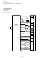
1
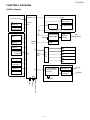
TopPage
FO-IS125N
SERVICE MANUAL
No. 00ZFIS125NSME
FACSIMILE
MODEL FO-IS125N
MODEL
FO-IS125N
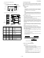
SELECTION CODE DESTINATION
U.S.A.
U
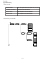
CONTENTS
CHAPTER 1. GENERAL DESCRIPTION
[1] Caution........................................................... 1-1
[2] Specifications ................................................. 1-3
[3] Operation panel.............................................. 1-5
[4] Transmittable documents ............................... 1-6
[5] Installation ...................................................... 1-7
[6] Clearing paper jams ..................................... 1-11
CHAPTER 2. ADJUSTMENTS
[1] Adjustments ................................................... 2-1
[2] Diagnostics and service soft switch ............... 2-7
[3] Troubleshooting ........................................... 2-56
[4] Error code table............................................ 2-57
CHAPTER 5. CIRCUIT DESCRIPTION
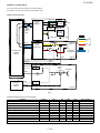
[1] Circuit description ..........................................5-1
[2] Circuit description of control PWB .................5-2
[3] Circuit description of power supply PWB......5-26
[4] Circuit description of CIS unit ......................5-27
[5] Circuit description of
operation panel PWB...................................5-27
[6] Data flow chart.............................................5-28
[7] Troubleshooting ...........................................5-29
CHAPTER 3. MECHANICAL DESCRIPTION
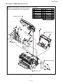
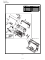
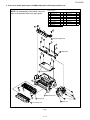
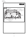
[1] Mechanical description................................... 3-1
[2] Disassembly and assembly procedures....... 3-13
CHAPTER 6. CIRCUIT SCHEMATICS AND PARTS
LAYOUT
[1] Control PWB circuit .......................................6-1
[2] Power Supply PWB circuit...........................6-16
[3] High Voltage PWB circuit.............................6-18
[4] Operation Panel/
Hook Switch PWB circuit .............................6-21
CHAPTER 4. DIADRAMS
[1] Block diagram ................................................ 4-1
[2] Wiring diagram ............................................... 4-2
[3] Point-to-point diagram.................................... 4-3
CHAPTER 7. OTHER
[1] Protocol .........................................................7-1
[2] Power on sequence.......................................7-2
[3] Rewriting version up the FLASH ROM ..........7-3
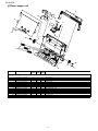
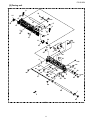
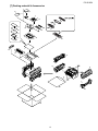
Parts Guide
Parts marked with "
" are important for maintaining the safety of the set. Be sure to replace these parts with specified ones for maintaining the
safety and performance of the set.
This document has been published to be used for
after sales service only.
The contents are subject to change without notice.
FO-IS125N
CHAPTER 1. GENERAL DESCRIPTION
FO-IS125N
Service Manual
[1] Caution
1. Laser caution
This laser facsimile is a class 1 laser product that complies with 21CFR 1040.10 and 1040.11 of the CDRH or IEC60825-1 standard. This means that
this machine dose not produce a hazardous laser radiation. The use of controls, adjustments or performance of procedures other than those specified
herein may result in hazardous radiation exposure.
This laser radiation isn't a danger to the skin, but when an exact focusing of the laser beam is achieved on the eyes retina, there is danger of spot
damage to the retina.
The following cautions must be observed to avoid exposure of the laser beam to your eyes at the time of servicing.
1) When a problem in the laser optical unit has occurred, the whole optical unit must be exchanged as a unit, not an individual part.
2) Do not look into the machine with the main switch turned on after removing the toner/developer unit and drum cartridge.
3) Do not look into the laser beam exposure slit of the laser optical unit with the connector connected when removing and installing the optical system.
4) The cover of Laser Printer Unit contains the safety interlock switch.
Do not defeat the safety interlock by inserting wedges or other items into the switch slot.
Laser Wave Length
Laser Pulse Times
Laser Output Power
: 780 nm +15/-10 nm
: 12.00 µs/7 mm
: 0.15 mW ± 0.04mW
2. Life of consumable
Section
Toner cartridge
Drum cartridge
Paper feed
Fuser
Paper transport
Unit
Part
Replacement cartridge (FO-25ND)
Replacement cartridge (FO-25DR)
Transfer roller (Refer to the P/G No. 1-27)
(NROLR2565XHZZ)
Fusing unit (Refer to the P/G No. 6-901)
(CFRM-2265XH04)
Feed roller (Refer to the P/G No. 3-25)
(NROLR2562XHZZ)
FO-IS125N
Estimated Life
3,000 prints (at Letter/5% chart)
20,000 prints (at Letter/5% chart)
50,000 prints
Replaced by
User
User
Service Engineer
50,000 prints
Service Engineer
Cleaning as needed
-
5 years or 50,000 prints of early either
-
1–1
FO-IS125N
3. Caution for Battery replacement
(French)
ATTENTION
Il y a danger d'explosion s' il y a remplacement incorrect
de la batterie. Remplacer uniquement avec une batterie du
même type ou d'un type recommandé par le constructeur.
Mettre au rébut les batteries usagées conformément aux
instructions du fabricant.
(Swedish)
VARNING
Explosionsfare vid felaktigt batteribyte.
Använd samma batterityp eller en ekvivalent
typ som rekommenderas av apparattillverkaren.
Kassera använt batteri enligt fabrikantens
instruktion.
(German)
Achtung
Explosionsgefahr bei Verwendung inkorrekter Batterien.
Als Ersatzbatterien dürfen nur Batterien vom gleichen Typ oder
vom Hersteller empfohlene Batterien verwendet werden.
Entsorgung der gebrauchten Batterien nur nach den vom
Hersteller angegebenen Anweisungen.
(Danish)
ADVARSEL !
Lithiumbatteri-Eksplosionsfare ved fejlagtig håndtering.
Udskiftning må kun ske med batteri af samme fabrikat og type.
Levér det brugte batteri tilbage til leverandoren.
(English)
Caution !
Danger of explosion if battery is incorrectly replaced.
Replace only with the same or equivalent type
recommended by the equipment manufacturer.
Discard used batteries according to manufacturer's instructions.
(Finnish)
VAROITUS
Paristo voi räjähtää, jos se on virheellisesti asennettu.
Vaihda paristo ainoastaan laitevalmistajan suosittelemaan
tyyppiin. Hävitä käytetty paristo valmistajan ohjeiden mukaisesti.
4. Precautions for using Lead-Free Solder
1. Employing lead-free solder
This model employs lead-free solder.
This is indicated by the "LF" symbol printed on the PWB and in the service manual.
The suffix letter indicates the alloy type of the solder.
Example:
Indicates lead-free solder of tin, silver and copper.
2. Using lead-free solder
When repairing a PWB with the "LF" symbol, only lead-free solder should be used. (Using normal tin/lead alloy solder may
result in cold soldered joints and damage to printed patterns.)
As the melting point of lead-free solder is approximately 40°C higher than tin/lead alloy solder, it is recommended that a
dedicated bit is used, and that the iron temperature is adjusted accordingly.
3. Soldering
As the melting point of lead-free solder (Sn-Ag-Cu) is higher and has poorer melting point (flow), to prevent damage to the
land of the PWB, extreme care should be taken not to leave the bit in contact with the PWB for an extended period of time.
Remove the bit as soon as a good flow is achieved.
The high content of tin in lead free solder will cause premature corrosion of the bit.
To reduce wear on the bit, reduce the temperature or turn off the iron when it is not required.
Leaving different types of solder on the bit will cause contamination of the different alloys, which will alter their
characteristics, making good soldering more difficult.
It will be necessary to clean and replace bits more often when using lead-free solder. To reduce bit wear, care should be
taken to clean the bit thoroughly after each use.
1–2
FO-IS125N
[2] Specifications
Print specifications
Toner cartridge yield* (continuous printing, 5% page coverage, letter paper):
Drum cartridge yield* (continuous printing, 5% page coverage, letter paper):
Paper tray capacity:
Initial starter cartridge (included with machine): Approx. 1500 pages
Replacement cartridge (FO-25ND): Approx. 3000 pages
Initial starter cartridge (included with machine): 20,000 pages (average)
Replacement cartridge (FO-25DR): 20,000 pages (average)
Letter: Approx. 250 sheets (20-lb. copier paper at room temperature; maximum stack height should
not be higher than the line on the tray)
Legal: 100 sheets
Recommended paper weight: 20-lb. Copy Bond
Printer type:
Laser
Print resolution:
600 x 600 dpi (dots per inch)
Effective printing width:
8.2" (208 mm) max.
PC print speed:
12 ppm (pages per minute)
*The yields may vary depending on coverage and operating conditions.
Fax specifications
Memory capacity*:
Modem speed:
Transmission time*:
Compatibility:
Compression scheme:
Applicable telephone line:
Reception modes:
Scanning resolution:
Approximately 500 average pages
33,600 bps with auto fallback to lower speeds.
Approx. 3 seconds
ITU-T (CCITT) Super G3, G3 mode
MR, MH, MMR
Public switched telephone network
AUTO, MANUAL
Horizontal: 203 lines/inch (8 lines/mm)
Vertical:
Standard: 98 lines/inch (3.85 lines/mm)
Fine /Halftone: 196 lines/inch (7.7 lines/mm)
Super fine: 391 lines/inch (15.4 lines/mm)
Halftone (grayscale):
64 levels
Contrast control:
Automatic/Dark selectable
*Based on Sharp Standard Chart at standard resolution, excluding time for protocol signals (i.e.,ITU-T phase C time only).
Network and general specifications
Automatic document feeder:
Input document size:
Effective scanning width:
Storable transmission destinations:
Telephone function:
Copy function:
Network interface:
Network frame type:
Network protocol:
Supported operating systems:
Scan to E-mail:
Scan to Network Folder:
Global Address Search:
User authentication:
File formats:
Display:
Power requirements:
Power consumption:
Operating temperature:
Humidity:
Letter/A4: 30 sheets max. (20-lb. paper)
Legal: 5 sheets max.
Automatic feeding:
Width: 5.8" to 8.5" (148 to 216 mm)
Length (30 sheets): 5.5" to 11" (140 to 279 mm)
Length (5 sheets): 5.5" to 14" (140 to 356 mm)
Manual feeding:
Width: 2.75" to 8.5" (70 to 216 mm)
Length: 5.5" to 14" (140 to 356 mm)
8.2" (208 mm) max.
Rapid Keys: 36
Speed Dial numbers: 114
Yes (cannot be used if power fails)
Single/Multi/Sort (up to 99 copies per page)
10 Base-T, 100 Base-TX
IEEE802.2/IEEE802.3 Ethernet II
TCP/IP
Windows® 2000, XP, Vista
(Printer driver also supports Windows® Server 2003)
Yes
Yes
Yes (requires LDAP server)
Yes
TIFF (G4), PDF (G4)
LCD display, 20 digits x 2 lines
120 V AC, 60 Hz
Standby: 8.6 W, Maximum: 690 W
50 - 86°F (10 - 30°C)
25 - 85% RH
1–3
FO-IS125N
Dimensions (without attachments):
Weight (with attachments):
Width: 16.8" (426 mm)
Depth: 16.1" (410 mm)
Height: 8.2" (208 mm)
Approx. 15.6 lbs. (7.1 kg)
As a part of our policy of continuous improvement, SHARP reserves the right to make design and specification changes for product improvement
without prior notice. The performance specification figures indicated are nominal values of production units. There may be some deviations from
these values in individual units.
Tradmark information
• Microsoft, Windows and Internet Explorer are trademarks of Microsoft Corporation in the U.S.A. and other countries.
1–4
FO-IS125N
[3] Operation panel
1 2 3 4
SPEAKER
HOLD
5 6
8 9 10 11 12 13 14
7
SPEED DIAL REDIAL
GLOBAL ADDRESS
FUNCTION
RECEPTION
RESOLUTION
RELEASE
INFO
SYMBOL
15
16
Note: Affix the Rapid Key labels as shown above.
1. SPEAKER key: Press to listen to the line and fax tones
through the speaker when faxing. Note: This is not a
speakerphone. It cannot be used for speaking.
2. HOLD key: Press to put a phone call on hold.
3. SPEED DIAL key: Press to select a fax or e-mail
destination stored in a 3-digit Speed Dial number.
4. REDIAL key: Press to automatically redial the last
number dialed.
5. SCAN TO E-MAIL key: Press to send a document to
an e-mail recipient.
6. SCAN TO FOLDER key: Press to send a document to
a folder on a computer on the same network as the machine,
or to an FTP server.
7. Display: This displays messages to help you operate
the machine.
8. GLOBAL ADDRESS key: Press to search for a
destination in a global address book on an LDAP server.
9. LINE IN USE light key: This lights up when the machine
is using the phone line to send or receive a fax.
10. SECURE key: Press to set up and use the security
functions of the machine.
11. RECEPTION key: Press to select the reception mode
(AUOT or MANUAL) for receiving faxes. The selected mode
will appear the the display.
12. FUNCTION key: Press this key followed by the arrow
keys to select special functions and settings.
Letter keys
1 23
5
4
DEL
B'CAST
6
INFO
DUPLEX
17 18 19 20 21 22
23
13. COPY/HELP key: When a document is in the feeder,
press to make a copy. At any other time, press to print the
Help List.
14. STOP key: Press to cancel an operation before it is
completed.
15. Number key: Use these keys to dial numbers, and enter
numbers when storing transmission destinations.
16. Rapid keys/Letter keys: A fax number, e-mail
address, on network folder can be stored in each of these keys
for one-touch selection (attach the Rapid Key labels). When
entering text, the keys are used as letter keys.
17. BROADCAST key: Press to send to multiple fax or email destinations.
18. INFO key: Press to check various types of machine
information.
19. DUPLEX key: Use to scan two-sided documents for
transmission and copying.
20. RESOLUTION key: When a document
is in the feeder, press to adjust the scanning resolution for
transmission.
21. RELEASE key: When a fax has been received to
memory instead of being printed out because the Secure Fax
function has been activated, press this key to enter the Secure
code and print out the fax.
22. START key: Press after dialing to send a fax.
23. Arrow key: Use to scroll through and select settings,
and to search for stored destinations.
1. DEL key: Press to delete the character marked by the
cursor. When the cursor is to the right of a line of text, press to
backspace and clear characters. (The cursor can be moved by
pressing
or
.) To delete all entered characters, hold
down until all characters are cleared.
2. Caps Lock key: Press to enter upper case letters. Press
again to return to lower case letter entry.
3. SHIFT key: Hold down while pressing a letter key to
temporarily change case.
4. Letter keys: Use to enter letters.
5. @ key, .com key: Press to conveniently enter "@" and
".com" when entering an e-mail address.
6. SYMBOL key: Hold down while pressing a letter key to
enter the symbol that appears on the right side of the key.
1–5
FO-IS125N
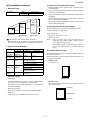
[4] Transmittable documents
4. Cautions on Transmitting Documents
1. Document Sizes
Normal size
Width
Length
148 - 216 mm
140 - 297 mm
(Max.)
(Max.)
A4 size
(Min.)
356mm
•
Ink, glue, and correcting fluid on documents must be dry before the
documents can be transmitted.
•
All clips, staples and pins must be removed from documents before
transmission.
•
Patched (taped) documents should be copied first on a copier and
then the copies used for transmission.
•
All documents should be fanned before insertion into the feeder to
prevent possible double feeds.
Number of pages that can be placed into the feeder at as follows:
Letter/A4: 30 sheets max. (20lb. paper)
216mm
[Normal size]
Legal: 5 sheets max.
216mm
[Special size]
Use document carrier sheet for smaller documents.
•
Documents written in yellow, greenish yellow, or light blue ink cannot be transmitted.
5. Automatic Document Feeder Capacity
297mm
140mm
70mm
[Special size]
•
•
Temperature: 50 ~ 86°F (10 ~ 30°C)
•
Humidity: 25 ~ 85%
NOTE: •
When you need to send or copy more pages than the
feeder limit, place additional pages in feeder when last
page in feeder is being scanned.
•
Place additional pages carefully and gently in feeder. If
force is used, double-feeding or a document jam may
result.
With special sizes, only one sheet can be fed into the machine at a
time. Insert next page into feeder as current page is being scanned.
2. Paper Thickness & Weight
Weight
indication
Thickness
indication
Document
size
Indication
Metric system
indication
Metric system
indication
Document size
Range
Number of
ADF sheets
Document size
Weight
Paper
quality
Kind
Product specifications
Lower Limit
Upper Limit
52g/m2
80g/m2
0.06mm
6. Readable Width & Length
The readable width and length of a document are slightly smaller than
the actual document size.
0.1mm
Note that characters or graphics outside the effective document scanning range will not be read.
Minimum (148mm x 70mm)
A4 (210mm x 297mm)
Letter (216mm x 279mm)
Legal (216mm x 356mm)
Minimum ~ Letter/A4 size 30sheets
Legal 5 sheets
More than 90 kg
Below 135 kg 1 sheet
Paper of fine quality/bond paper/
Kent paper
•
Readable width
8.2” (208mm), max
3. Document Types
•
Readable width
Normal paper
Documents handwritten in pencil (No. 2 lead or softer), fountain
pen, ball-point pen, or felt-tipped pen can be transmitted.
•
This is the length of the document sent minus 0.16”(4mm) from the
top and bottom edges.
Documents of normal contrast duplicated by a copying machine
can also be transmitted.
•
Diazo copy (blue print)
•
Diazo copy documents of a normal contrast may be transmitted.
•
Carbon copy
Readable length
0.16"(4mm)
Readable length
A carbon copy may be transmitted if its contrast is normal.
0.16"(4mm)
1–6
FO-IS125N
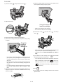
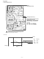
[5] Installation
3. Attaching the tray
1) Attach the paper tray.
1. Site selection
Take the following points into consideration when selecting a site for
this model.
ENVIRONMENT
•
The machine must be installed on a level surface.
•
Keep the machine away from air conditioners, heaters, direct sunlight, and dust.
•
Provide easy access to the front, back, and sides of the machine.
In particular, keep the area in front of the machine clear, or the original document may jam as it comes out after scanning.
•
The temperature should be between 50 - 86°F (10 - 30°C).
•
The humidity should be between 25% and 80% (without condensation).
ELECTRICITY
AC 120 V, 60Hz, grounded AC (3-prong) outlet is required.
2) Attach the document feeder tray and the received document tray.
Caution!
•
Connection to a power source other than that specified will cause
damage to the equipment and is not covered under the warranty.
•
If your area experiences a high incidence of lightning or power
surges, we recommend that you install a surge protector for the
power and telephone lines. Surge protectors can be purchased at
most telephone specialty stores.
Insert the trays at an
angle and rotate back.
If the machine is moved from a cold to a warm place...
Condensation may form on the reading glass if machine is moved from
a cold to a warm place, this will prevent proper scanning of documents
for transmission. Turn on the power and wait approximately 2 hours
before using machine.
TELEPHONE JACK
A standard telephone jack must be located near the machine. This is
the telephone jack commonly used in most homes and offices.
•
The language is unclear in this part. Perhaps it could say:
3) Attach the document exit tray.
"Plugging the fax machine into a jack which is not a standard analog telephone jack, may result in damage to the machine or your
telephone system."
After inserting the tray,
flip out the extension.
2. Connecting the handset
1–7
FO-IS125N
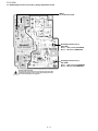
4. Connecting the power cord
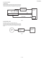
7. Connecting the machine to your network
Plug the power cord into a 120 V, 60 Hz, grounded AC (3-prong) outlet.
To use the Scan to E-mail and Scan to Folder functions, and to use the
machine as a printer, you must connect the machine to an Ethernet
network. In addition, to use Scan to E-mail, the network must have an
Internet connection. A typical setup is shown below.
•
Do not plug the power cord into any other kind of outlet. This will
damage the machine and is not covered under the warranty.
The machine is connected using an Ethernet cable (not included).
Please purchase a 10Base-T/100Base-TX straight-through (regular)
cable.
Connect one end of the cable to the LAN port on the machine. Connect the other end to a LAN port on your switch or hub.
Cable/DSL
modem
Internet
LAN cable
WAN port
LAN cable
LAN cable
5. Connecting the telephone line cord
LAN cable
LAN ports
(Hub/Switch)
Insert one end of the line cord into the socket on the back of the
machine marked TEL. LINE. Insert the other end into a wall telephone
socket.
Router
•
If you are uncertain which port to connect the cable to, see the
manual for the router, switch or hub.
•
The connections can be made with all devices powered on.
To communicate on your network, the machine must have an IP
address. To set the machine’s IP address and configure other network settings.
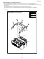
8. Installing the toner cartridge and drum cartridge
The laser printer in the machine uses a toner cartridge and a drum cartridge.
•
The starter toner cartridge included with the machine can print
approximately 1500 letter-size pages at 5% page coverage.
•
When replacing the toner cartridge, use a SHARP FO-25ND toner
cartridge. One cartridge can print about 3000 letter-size pages at
5% coverage.
•
The drum cartridge can print approximately 20,000 letter-size
pages. When replacing the drum cartridge, use a SHARP FO25DR drum cartridge.
Follow the steps below to install the toner cartridge and the drum cartridge.
Note: The quality of the toner cartridge is guaranteed for 18 months
after the date of manufacture indicated on the package. The quality of
the drum cartridge is guaranteed for 24 months after the date of manufacture indicated on the package.
The machine is initially set for tone dialing. If you are on a pulse dial
line, change the “DIAL MODE” setting.
6. Affixing the rapid key labels
1) Open the top cover of the machine.
Affix each strip of Rapid Key labels above each row of letter keys as
shown in the panel illustration.
Caution! The fusing unit inside the print compartment becomes
very hot during operation. Do not touch the inside of the print compartment after the machine has been in operation.
1–8
FO-IS125N
2) Press the release (
1
) and open the front cover (
2
7) Grasp the cartridge handle and insert the toner cartridge into the
print compartment, sliding it along the guides.
).
2
1
3) Open the side cover.
Grasp this handle to
insert the cartridge.
•
Make sure the cartridge “clicks” into place.
•
Do not touch the roller in the toner cartridge.
8) Close the side cover (
cover (
3
1
), the front cover (
2
), and the top
).
4) Remove the new drum cartridge from its packaging.
3
5) Insert the drum cartridge into the print compartment, sliding it along
the guides.
Grasp this
handle to
push the
cartridge in.
1
2
•
Make sure the side cover is completely closed. Otherwise, light
may enter the print compartment and damage the drum.
•
The display will show: [TONER EXCHANGED?] / [1 = NEW, 2 =
OLD]
9) If you installed a new toner cartridge, press
•
Do not touch or allow other objects to contact the drum (the
green cylinder). This may damage the drum. If fingerprints, dust,
or other contaminants get on the drum, wipe it gently with a
clean cloth.
•
Exposure to light for more than several minutes will damage the
drum. Be sure to insert the drum cartridge promptly into the
machine.
•
If you find it necessary to leave the cartridge out of the machine
for more than several minutes, wrap the cartridge in black
paper.
to select NEW
(this will reset the toner counter to zero).
•
If you temporarily removed and then replaced an old toner cartridge for maintenance or other reason,
press to con-
tinue using the previous toner count. (Note: Be sure to press
or the machine will not alert you when the toner cartridge is out of toner.)
10)Press
6) Remove the new toner cartridge from its packaging. Shake the cartridge side to side four or five times to distribute the toner evenly
within the cartridge.
START
.
11)If you installed a new drum cartridge, reset the drum counter as
explained below.
1–9
FO-IS125N
9. Resetting the drum counter
3) Push the paper plate back.
Each time you install a new drum cartridge, follow the steps below to
reset the drum counter to zero.
1) Press
and then
INFO
2) Press
until [LIFE] appears in the display.
, then
until [CLEAR DRUM COUNTER]
appears.
•
3) Press
START
.
10. Manually resetting the toner counter
When a new toner cartridge is installed, the toner counter is reset in
Step 9 on the previous page. The procedure below is normally not necessary; however, it can be used in the event that you need to reset the
toner counter manually.
1) Press
and then
INFO
2) Press
until [LIFE] appears in the display.
, then
until [CLEAR TONER COUNTER]
appears.
3) Press
START
.
11. Loading printing paper
You can load letter or legal size paper in the paper tray.
Maximum number of sheets
(20-lb. copy bond paper at room temperature)
Letter: Approx. 250 sheets
Legal size: 100 sheets
Caution! Do not use the blank side of paper that has already been
printed on.
1) Fan the paper, and then tap the edges against a flat surface to
even the stack.
2) Pull the paper plate forward
1
adjust it to the width of the paper
the tray, print side up
3
1
. Squeeze the paper guide and
. Insert the stack of paper into
2
.
3
2
•
Maximum stack height should not be higher than the line on the
paper guide.
1 – 10
If you loaded legal size paper (or you changed the paper size),
change the paper size setting as explained.
FO-IS125N
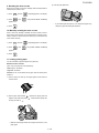
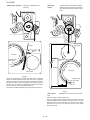
[6] Clearing paper jams
4) Close the operation panel, pressing down firmly on both sides to
make sure it clicks into place.
1. Clearing a jammed document
If the original document doesn’t feed properly during transmission or
copying, or [DOCUMENT JAMMED] appears in the display, first try
pressing
START
. If the document doesn't feed out, remove it as
explained below.
1) Open the operation panel.
2. Clearing jammed printing paper
1) Open the top cover of the machine.
2) Rotate the lever so that it points straight up and pull it up (
Remove the document (
2
1
).
).
2
•
1
Caution! The fusing unit inside the print compartment becomes
very hot during operation. Do not touch the inside of the print
compartment after the machine has been in operation.
2) Press the release (
1
) and open the front cover (
2
).
2
1
3) Make sure the left end of the roller is inserted correctly in its holder
(
1
), and then push the right end of the roller down (
rotate the lever back down (
3
2
) and
2
).
1
1
3) Push the two heater roller release levers down to release the
heater roller.
2
3
1 – 11
FO-IS125N
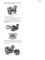
4) If the jammed paper is protruding from the front of the machine,
gently pull it out. Take care not to tear the paper or leave any torn
pieces of paper in the print compartment.
•
If this clears the jam, go to Step 5.
•
If you are unable to clear the jam in this way, go to Step 4.
•
Take care not to touch or allow other objects to contact the drum
(the green cylinder). This may damage the drum.
5) If the jammed page cannot be pulled out directly, open the side
cover and rotate the white knob in the direction shown to feed out
the jammed paper.
6) After the jammed paper has been removed, push the two heater
roller release levers back up (
1
), close the side cover (
you opened it), close the front cover (
top cover (
4
2
) (if
) and then the close the
3
).
3
1
2
1 – 12
FO-IS125N
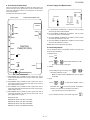
CHAPTER 2. ADJUSTMENTS
FO-IS125N
Service Manual
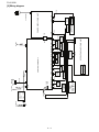
[1] Adjustments
1. General description
Since the following adjustments and settings are provided for this
model, make adjustments and/or setup as necessary.
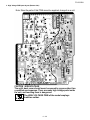
2. Adjustments of output voltage (FACTORY ONLY)
1. Install the power supply unit in the machine.
2. Set the recording paper and document.
3. When the document is loaded, power is supplied to the output
lines. Confirm that outputs are within the limits below.
Output
CNPW
CNLNJ
CNTEL
CNSP
CNLAN
2.1. Output voltage settings
10
CONTROL PWB(TOP SIDE)
CNFM
CNSL
CNTXM
CNMM
CNPM
CNLSR
CNHV
CNCIS
CNPOUT
CNRTH
CNPIN
CNPN
CNTNR
23.04V~24.96V
+24VMAIN
23.04V~24.96V
(INTERLOCK
SWITCH OFF: 0V)
Ach
STAND BY 4.3V~5.9V
RATED
Connector
1
Voltage limits
+24VSUB
4.3V~6.3V
CNPW
Pin No.
CN3
1
+24VSUB
2
MG
3
MG
4
+24VMAIN
5
+24VMAIN
6
DG
7
Ach(4VD)
8
DG
9
HEATER ON
10
ZC
Connector
CN5
Pin No.
POWER SUPPLY PWB(TOP SIDE)
10
CN3
1
CN1
CN2 2
1
INTERLOCK
SWITCH
2
3 1
1
+24VMAIN
2
N.C.
3
+24VS
Connector
1
AC NEUTRAL
2
N.C.
3
AC LIVE
Pin No.
FUSING UNIT
2–1
CN1
Pin No.
Connector
CN5
THERMAL
FUSE-2
1
CN2
1
+24VSUB
2
+24VMAIN
FO-IS125N
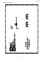
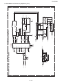
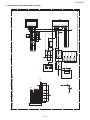
3. High voltage power check
3.1. General
Note: Since the parts of this PWB cannot be supplied, change it as a unit.
CAUTION
DO NOT TOUCH!
(VR1, VR51)
CAUTION HIGH VOLTAGE AREA MAX. 4000V (THICK LINE)
CAUTION
DO NOT TOUCH!
(VR31)
CAUTION - HIGH VOLTAGE
The unit's back cover should never be opened by
anyone other than a qualified serviceperson.
There are many high voltage parts inside the unit,
and touching them is dangerous.
CAUTION HIGH VOLTAGE AREA MAX. 4000V (THICK LINE)
CAUTION - HIGH VOLTAGE
The unit's back cover should never be opened by
anyone other than a qualified serviceperson.
There are many high voltage parts inside the unit,
and touching them is dangerous.
2–2
FO-IS125N
3.2. MC Voltage Check Point
GND (-)
(J3 or Chassis Frame)
MC Voltage Check Point (-)
(There is danger of an electric shock!)
Use Measuring instrument:
Input Resistance : more than 100 MΩ
Maximum Voltage : more than 2 kV
VOLTAGE
MC : - 950 V ± 20 V (PRINTING)
MC : - 850 V ± 20 V (CLEANING)
CAUTION - HIGH VOLTAGE
The unit's back cover should never be opened by anyone other than
a qualified serviceperson. There are many high voltage parts inside
the unit, and touching them is dangerous.
1) MC Voltage
Time(s)
Type
Tolerance
-570V
± 67V
-950V
± 20V
-1330V ± 67V
Voltage(v)
300Hz
2–3
FO-IS125N
3.3. TC Voltage Check Point
GND (-)
(J3 or Chassis Frame)
TC Voltage Check Point (+)
(There is danger of an electric shock!)
Use High Voltage Tester:
Requirement of Measuring instrument:
Input Resistance : more than 100 MΩ
Maximum Voltage : more than 5 kV
VOLTAGE
TC (+) : + 3600 V ± 72 V (PRINTING)
TC (-) : - 500 V ± 50 V (CLEANING)
CAUTION - HIGH VOLTAGE
The unit's back cover should never be opened by anyone other than
a qualified serviceperson. There are many high voltage parts inside
the unit, and touching them is dangerous.
1) TC Voltage
Voltage(v)
Type
Tolerance
-3980V
-3600V
-3220V
Time(s)
300Hz
2–4
± 72V
FO-IS125N
3.4. SV/DV Voltage Check Point and SV (-) Voltage Adjustment Volume
GND (-)
(J3 or Chassis Frame)
DV Voltage Check Point (+)
VOLTAGE
DV (+) : + 300 V ± 5 V (CLEANING)
DV (-) : - 200 V ± 5 V (PRINTING)
SV Voltage Check Point (+)
VOLTAGE
SV (+) : + 300 V ± 15 V (CLEANING)
SV (-) : - 400 V ± 15 V (PRINTING)
CAUTION - HIGH VOLTAGE
The unit's back cover should never be opened by anyone other than
a qualified serviceperson. There are many high voltage parts inside
the unit, and touching them is dangerous.
2–5
FO-IS125N
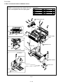
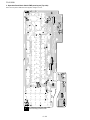
4. IC Protectors Replacement
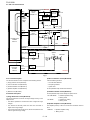
5. Power Supply Unit Replacement
ICPs (IC Protectors) are installed to protect the Optical (LSU) unit,
Printer motor drive circuit, Solenoid drive circuit and Scanner motor
drive circuit. ICPs protect various ICs and electronic circuits from an
overcurrent condition.
[SECONDARY]
The location of ICPs are shown below:
F2
CN3
F101
[PRIMARY]
F500/F501/F600:Bottom side
F1
F301
T1
TRANSFORMER
CNLAN
CNPN
CNPOUT
CNTNR
F300:Top side
1
1) F1 (K7135AS007): AC250V/10A is installed in order to protect
overcurrent by heater circuit breakdown.
CNSP
CNPIN
2) F2 (K7144AR005): HTM250V/4A is installed in order to protect
overcurrent by primary circuit breakdown.
CNTEL
3) F101 (K7144AR005): HTM250V/4A is installed in order to protect
overcurrent by breakdown of +24V line.
CNRTH
4) F301 (K7144AR002): HTM250V/2A is installed in order to protect
overcurrent by breakdown of Ach line.
CNCIS
CNHV
CNLSR
Caution: Don’t use fuse except for rating above.
CONTROL
PWB(TOP SIDE)
6. Volume Adjustment
You can adjust the volume of the speaker, handset, and ringer using
the up and down arrow keys.
1. Speaker volume
F300
1) Press
CNPM
2) Press
F500
CNMM
F600
CNTXM
F501
CNSL
•
CNLNJ
SPEAKER
.
or
to select HIGH, MIDDLE, or LOW.
To turn off the speaker, press again.
2. Handset
CNFM
1) When talking through the handset, press
CNPW
or
to
select HIGH, MIDDLE, or LOW.
•
1) F300 (KAB5002 251) is installed in order to protect IC’s from an
overcurrent generated in the IC302 circuit. If F300 is open, replace
it with a new one.
Note: The volume reverts to MIDDLE each time you replace
the handset.
3. Ringer
2) F500 (KAB2402 402) is installed in order to protect IC’s from an
overcurrent generated in the Printer motor drive circuit. If F500 is
open, replace it with a new one.
1) Press
or
OFF. (Make sure
3) F501 (KAB5002 321) is installed in order to protect IC’s from an
overcurrent generated in the Solenoid driver circuit. If F501 is open,
replace it with a new one.
to select HIGH, MIDDLE, LOW or
SPEAKER
has not been pressed, the handset is
not lifted, and a document is not loaded in the feeder.)
•
4) F600 (KAB3202 801) is installed in order to protect IC’s from an
overcurrent generated in the Scanner motor drive circuit. If F5 is
open, replace it with a new one.
The ringer will ring once at the selected level.
2) If you selected “OFF OK?” to turn off the ringer, press
Replacement parts
KAB3202 801 (Sharp code: QFS-L1037YCZZ)
KAB5002 251 (Sharp code: QFS-L2021XHZZ)
KAB2402 402 (Sharp code: QFS-L2025XHZZ)
KAB5002 321 (Sharp code: QPRTR2001XHZZ)
2–6
START
.
FO-IS125N
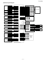
[2] Diagnostics and service soft switch
1. Entering the diagnostic mode
2. Diagnostic items description
2.1. SOFT SWITCH MODE
9
Press FUNCTION
display will appear alternately.
8
7 , and the following
In this mode, the soft switches are set and the soft switch list is printed.
2.1.1 Operation
: ROM version
ROM:TF78
Soft switch mode screen
Then press the START key.
Select the desired item with the UP key and the DOWN key or select
with the rapid key.
Enter the mode with the START key.
SOFT SWITCH MODE
SW123=00100100
(Diag • specifications)
FUNCTION
UP
9
8
DIAG MODE
7
ROM:TF78
COUNTRY NAME
Switch No.
1 2 3 4 5 6 7 8: Data No.
START
START
SOFT SWITCH MODE
START
ROM & RAM CHECK
2.1.2 Switch number selection and data setting
START
AGING MODE
START
PANEL KEY TEST
1. Enter three digits of a soft switch number to set the switch number.
Of a switch number of unexacting soft switch is entered, key error
buzzer sounds to reject the input.
START
CHECK PATTERN
START
SIGNAL SEND MODE
START
SIGNAL SEND MODE2
START
MEMORY CLEAR
START
SHADING MODE
START
AUTO FEEDER MODE
START
FLASH MEM. CHECK
START
MEMORY SET MODE
START
CIS ADJUST
START
SHARP CHART MODE
START
5% CHART
START
ASF AGING
START
PASSCODE LIST
START
LIFE SET MODE
START
LIFE CLR MODE
SW12 =
SW1 =
SW =
[2] key
[1] key
SW123=00100100
[3] key
Cursor position
2. Press [START] key moves the cursor to the data number 1 of the
former soft switch. If the switch number is the final, pressing
[START] key will exit the soft switch mode.
SW124=00000000
SW123=01100000
[START] key
SW125=00000000
[START] key
3. Data number selection
a) Pressing [>] or [#] key moves the cursor to the right. If the cursor
is on data number 8, pressing [>] or [#] key shifts the cursor to data
number 1 of the next switch number. If the switch number is the
final, pressing [>] or [#] key will exit the soft switch mode.
SW123=01100000
SW123=01100000
[>] or [#] key
SW124=00000000
With the cursor on data 8
[>] or [#] key
[>] or [#] key
SW124=00000000
b) Pressing [<] or [ ] key moves the cursor to the left. If the cursor
is on data number 1, pressing [<] or [ ] key shifts the cursor to
data number 8 of the former switch number. If the switch number is
001, pressing [<] or [ ] key do not move the cursor.
DOWN
SW124=00000000
SW124=00000000
[<] or [ ] key
SW123=01100000
With the cursor on data 1
[<] or [ ] key
[<] or [ ] key
SW123=01100000
c) Pressing [UP] or [4] key moves the cursor to the data number 1
of the next soft switch. If the switch number is 001, pressing [UP] or
[4] key shifts the cursor to data number 1.
SW125=00000000
SW124=00000000
[UP] or [4] key
SW123=01100000
[UP] or [4] key
d) Pressing [DOWN] or [6] key moves the cursor to the data number 1 of the former soft switch. If the switch number is the final,
pressing [down] or [6] key will exit the soft switch mode.
SW123=01100000
SW124=00000000
[DOWN] or [6] key
2–7
SW125=00000000
[DOWN] or [6] key
FO-IS125N
2.4. PANEL KEY TEST
e) Pressing [8] key moves the cursor to the data number 1 of the
10th former soft switch.
SW103=00000000
SW113=00011010
SW123=01100000
[8] key
This is used to check whether each key is normally operated or not.
After the test, the test result will be printed.
[8] key
Press any key except [STOP] key. At this time, the name of each key
will be displayed every push of the key.
f) Pressing [2] key moves the cursor to the data number 1 of the
10th next soft switch.
[2] key
PANEL KEY TEST
SW143=01100000
SW133=01000000
SW123=01100000
1
[2] key
[1] key
[2]Key
2.1.3 Data setting
2
Press the [1] key, and the data to the position of the cursor will be
changed to 1.
Press the [0] key, and the data to the position of the cursor will be
changed to 0.
To finish this mode, press [STOP] key
2.1.4 Outputting method of soft switch list
2.1.5 Storage of data
ALL KEY OK !!
In the following cases, the data if the soft switches set will be stored.
It is shifted to set the next soft switch by pressing [START] key.
•
If is shifted to set the former soft switch with the [<] or [UP] or [4]
key.
•
It is shifted to set the next soft switch with the [>] or [DOWN] or [6]
key.
•
If is shifted to set the 10th former soft switch with the [8] key.
•
It is shifted to set the 10th next soft switch with the [2] key.
Then the screen will be all displayed in black (refer to (2))and the test
result will be printed.
b) If any key skipped, the following message will be displayed.
KEY ERROR !!
2.2. ROM & RAM CHECK
A key name that is not pressed yet is displayed so that this test can be
continued.
To check the sum value of Firmware or RAM.
No.
1
2
Main
Device
ROM
(PROGRAM FLASH)
SDRAM
Go to a) or b).
a) When all keys can be inputted, the following message will be displayed.
In the soft switch mode, press [COPY/HELP] key, and the soft switch
list will be printed.
•
..... (other key)
SPEAKER
[SPEAKER] key
Alarm Buzzer
1 time <Short
sound>
3 times <Short
sounds>
At that time, pressing the [STOP] key will exit this mode. And the result
will be printed.
Remarks
After pressing the [STOP] key, the whole black screen appears and
the LED lights.
2.2.1 Display
DIAG MODE
ROM & RAM CHECK
WAIT A MOMENT
SDRAM : OK
Start checking by
pressing [START] key
2.5. CHECK PATTERN
PRINTING
1 sheet of check patterns is printed.
2.2.2 Result printing
DIAG MODE
CHECK PATTERN
After checking, the results print starts.
2.3. AGING MODE
A total of 10 sheets of check patterns are printed at 1-hour intervals.
This mode is exited when executed to the end (after 9 hours) or by
pressing the [STOP] key.
DIAG MODE
AGING MODE
Start by pressing
the [START] key
1 sheet of check pattern is printed
AGING MODE
Display during the aging
mode interval
2–8
Start by pressing the
[START] key
PRINTING
FO-IS125N
2.6. SIGNAL SEND MODE
2.8. MEMORY CLEAR
The specified signals are transmitted in the following sequence to
check the modem.
Clear the back-up memory including the soft switches, registration
data. After executing this mode, the memory clear report is printed.
1. Press the [START] key, and no signals with the loop state starts.
Note: The printer/scanner life information is not cleared.
[1]
[2]
[3]
[4]
[5]
[6]
No signals (making the loop)
14400BPS (V. 17)
12000BPS (V. 17)
9600BPS (V. 17)
7200BPS (V. 17)
9600BPS (V. 29)
[7]
[8]
[9]
[10]
[11]
[12]
7200BPS (V. 29)
4800BPS (V. 27ter)
2400BPS (V. 27ter)
300BPS (FLAG)
2100Hz (CED)
1100Hz (CNG)
Start by pressing
the [START] key
DIAG MODE
MEMORY CLEAR
MEMORY CLEARING
PRINTING
2.9. SHADING MODE
Shading waveforms are stored.
DIAG MODE
SIGNAL SEND MODE
Set a shading sheet and press the [START] key to start shading.
[START] Key
[START] Key
[START] Key
V. 17
CML ON
SIG SEND MODE
Start by pressing
the [START] key
DIAG MODE
SHADING MODE
14400bps
TOTAL SHADING
[START] Key
[START] Key
V. 17
7200bps
V. 17
[START] Key
9600bps
V. 17
[START] Key
9600bps
Inserting and discharging the document can check the auto feeder.
[START] Key
[START] Key
V. 29
2.10. AUTO FEEDER MODE
12000bps
V. 29
V. 27ter
7200bps
1. The information of document sensor (A4 sensor) and ORG sensor
is displayed when the documents are inserted to the Auto Feeder.
Press the [START] key, and feeding documents is started.
4800bps
[START] Key
[START] Key
2100 Hz (CED TONE)
[START] Key
V. 27ter
FLAG (300bps)
2400bps
[START] Key
DIAG MODE
AUTO FEEDER MODE
1100 Hz (CNG)
[START] key without document
AUTO FEEDER MODE
A4 (A4
)
1
2. Press [STOP] key to exit the mode.
1. When pressing the [START] key, it turns into the no-signal state
(make loop). Then signals are sent in the following order by pressing the [START] key.
No signals (making the loop)
33600bps (V. 34bis)
31200bps (V. 34bis)
28800bps (V. 34)
26400bps (V. 34)
24000bps (V. 34)
21600bps (V. 34)
19200bps (V. 34)
[9]
[10]
[11]
[12]
[13]
[14]
[15]
[16]
[17]
[START] Key
V. 34
24000bps
[START] Key
28800bps
V. 34
V. 34
21600bps
[START] Key
V. 34
12000bps
[START] Key
V. 34
9600bps
V. 34
[START] Key
V. 8
ANSam
[START] Key
V. 34
14400bps
V. 21
Be sure to clear the memory after execution.
DIAG MODE
FLASH MEM. CHECK
[START] key
FLASH CHECK
PRESS START or STOP
[START] key
Start
WAIT A MOMENT
33600bps
[START] Key
PRINTING
31200bps
19200bps
[START] Key
16800bps
[START] Key
[START] Key
V. 34
The result is printed after completion of check.
[START] Key
[START] Key
V. 34
Read/write of the flash memory is checked.
16800bps (V. 34)
14400bps (V. 34)
12000bps (V. 34)
9600bps (V. 34)
7200bps (V. 34)
4800bps (V. 34)
2400bps (V. 34)
0-300bps (V. 21)
ANSam
V. 34
CML ON
V. 34
2.11. FLASH MEM. CHECK
[START] Key
[START] Key
[START] Key
26400bps
AUTO FEEDER MODE
(
)
1
Used to display the number of fed sheets.
A V.34 & V.8 related signal send mode. The check of the modem and
other devices is performed by sending these specific signals.
V. 34
AUTO FEEDER MODE
A4 (A4
ORG)
1
Only the sensor that is activated is displayed.
2.7. SIGNAL SEND MODE2
DIAG MODE
SIGNAL SEND MODE2
AUTO FEEDER MODE
(
)
0
Set document
2. Pressing the [START] key during transmitting CNG signal, or pressing the [STOP] key will stop the output of signal and exit the mode.
[1]
[2]
[3]
[4]
[5]
[6]
[7]
[8]
[START] key
without document
V. 34
7200bps
[START] Key
0 - 300bps
V. 34
4800bps
[START] Key
2400bps
2. When pressing the [START] after sending the ANSam signal or the
[STOP] key while executing the mode, the signal output is stopped
and the indication before starting the next mode (MEMORY
CLEAR) appears.
2–9
Next daig mode
[STOP] key
FO-IS125N
2.12. MEMORY SET MODE
2.17. PASSCODE LIST
It is possible to read or write the memory contents.
Used to print the passcode (SECURE FAX, etc.).
When 8 digits of physical address are entered, the data of that address
is displayed.
When 2 digits of data are entered after entering 8 digits of address and
a key is pressed, the contents can be rewritten.
2.18. LIFE SET MODE
Rewriting is enabled only in the range of addresses 00000000 to
007FFFFF.
A mode for checking or setting the life value of each operation. Enter
the count value (10-digit number) of the set life using the numeric keypad.
If the memory is rewritten, the machine may malfunction.
DIAG MODE
MEMORY SET MODE
DIAG MODE
LIFE MODE
[START/MEMORY] key
MEMORY SET MODE
xxxxxxxx= [ ]
[START] Key
Address entry screen
LIFE=0000000099
[DOWN] Key
The contents of the memory are displayed
in hex number and character code.
[DOWN] Key
LIFE=0000000231
[DOWN] Key
[START] Key
DRUM
LIFE=0000000231
[DOWN] Key
Press the [STOP] key on the address entry screen to exit the mode.
[START] Key
LIFE=0000000231
TONER PAGE
[DOWN] Key
2.13. CIS ADJUST
[START] Key
DOT COUNT=1234567890
TONER DOTCOUNT
In this mode, the position of Scanner motor is moved from the home
position up to the specified value. And document reading lamp is
turned on.
This counter shows the printer usage status (number of printed sheets
after starting use, etc.). The counter cannot be reset by normal memory clear. Therefore, if the memory contents on the control PWB are
destroyed when repairing it, this counter setting must be cleared in
addition to normal memory clear.
DIAG MODE
CIS ADJUST
[START] key
Press the [STOP] key to exit the mode.
CIS ADJUST MODE
[START] key
2.19. LIFE CLR MODE
The motor will move to the specified position and the reading lamp is lit on.
A mode for clearing the life value.
Press the [STOP] key to exit the mode.
2.14. SHARP CHART MODE
DIAG MODE
LIFE CLR MODE
SHARP CHART is printed continuously.
Start by pressing the
[START] key
[START] Key
SHARP CHART AGING
TOTAL PAGE
1
CLEARED
[DOWN] Key
[START] Key
[DOWN] Key
[START] Key
SCAN
2.15. 5% CHART
CLEARED
PRINT
5% CHART is printed continuously.
[DOWN] Key
Start by pressing the
[START] key
5% CHART AGING
TOTAL PAGE
1
CLEARED
[START] Key
DRUM
[DOWN] Key
Press the [STOP] key for interruption.
CLEARED
[START] Key
TONER
When clearing "TONER",
"TONER PAGE" and
"TONER DOT COUNT" are
also cleared.
2.16. ASF AGING
The recording paper is fed continuously.
Start by pressing the
[START] key
[START] Key
ALL
Press the [STOP] key for interruption.
DIAG MODE
ASF AGING
JAM=0000000001
[START] Key
PRINT
• Change of memory contents: 2-digit entry in hex number
• Move down the address of the referenced memory by one: [<] or [UP] key
• Move up the address of the referenced memory by one: [>] or [DOWN] key
• Dump list print: [COPY/HELP] key
• Back to the address entry screen: [STOP] key
DIAG MODE
5% CHART
[START] Key
SCAN JAM
Character
Hex
number code
DIAG MODE
SHARP CHART MODE
[START] Key
SCAN
Entry of memory address (8 digits)
MEMORY SET MODE
1234ABCD=4C [L]
PRINTING
Start by pressing
the [START] key
DIAG MODE
PASSCODE LIST
ASF AGING
Press the [STOP] key for interruption.
2 – 10
CLEARED
FO-IS125N
3. How to make soft switch setting
To enter the soft switch mode, press the following key entries in sequence.
Press FUNCTION 9
8
7
START
START
0
0
1
DATA No. 1 2 3 4 5 6 7 8
SW001 = 0 0 0 0 0 0 0 0
SW001 = 1 0 0 0 0 0 0 0
SW001 = 1 0 0 0 0 0 0 0
SW001 = 1 0 0 0 0 0 0 0
SW001 = 1 0 0 0 0 0 0 0
Press 1 or 0 key.
Press
or < key.
Press
or > key.
Bit1 - 8 are set.
Press
SW002 = 0 0 0 0 0 0 0 0
SW300 = 0 0 0 0 0 0 0 0
START
key during setting.
Soft SW002 - SW300 are set.
To finish the settings halfway between
SW001 and SW300, press the STOP
key. In this case, the setting being done
to the SW No. on display will be nullified
while settings done to the preceding
SW No. remain in effect.
When the COPY/HELP key is pressed, the
contents of soft switches are printed.
The soft switch mode is terminated.
2 – 11
FO-IS125N
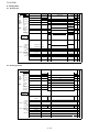
4. Soft switch description
4.1. Soft switch
SW
NO.
DATA
NO.
ITEM
Receive mode
SW
1
SW
2
SW
3
1
2
3
4
5
6
7
8
1
2
3
4
5
6
7
8
1
2
3
4
5
6
7
SW
4
8
1
2
3
4
5
6
7
8
1
2
3
4
5
No.1
No.2
Reserved
Reserved
Reserved
Reserved
Sort copy function
Reserved
Forced 4800BPS reception
CED tone signal interval
Yes (Sort)
No
Yes
No.2
No.3
Reserved
Reserved
Reserved
Footer print
Reserved
Reserved
CSI transmission
Action when RTN is received
Reserved
Pulse format
DIS receive acknowledgement during G3 transmission
Non-modulation carrier for V29
transmission mode
Default file format for network scan
Protocol monitor
Line monitor
Reserved
Sender's information transmit
Reserved
Reserved
H2 mode
ECM mode
ECM MMR mode
Signal transmission level
Switch setting and function
1
0
AUTO
MANU.
0
0
0
1
75ms
0
0
500ms
0
1
No
750ms
1
0
1000ms
1
1
Yes
No
Not transmitted
No communication error
Transmitted
Communication error
N+1
Twice
Yes
N
NSF: Once
DIS: Twice
No
PDF
Yes
Yes
TIFF
No
No
No
Yes
No
No
No
Yes
Yes
Yes
Binary input
No. = 8 4 2 1
2 3 4 5 (Data No.)
EX 1 1 0 1
SW
5
Initial
setting
0
0
1
0
0
0
0
0
0
Remarks
RECEPTION
key
OPTION
0
0
0
0
0
0
0
0
0
0
1
0
0
0
0
0
0
0
0
0
0
0
0
0
1
1
0
1
e-mail setting
eg. -13dBm
6
7
8
Reserved
Reserved
Key tone
Off
On
2 – 12
0
1
0
OPTION
FO-IS125N
SW
NO.
DATA
NO.
1
2
3
4
Switch setting and function
ITEM
1
Initial
setting
0
1
0
1
0
Recall interval (FAX)
Binary input
No. = 8 4 2 1
1 2 3 4 (Data No.)
EX 0 1 0 1
Remarks
Setting:
N = 1 to 9
eg. 3 minutes
SW
6
5
6
7
8
Recall times (FAX)
0
0
1
1
Binary input
No. = 8 4 2 1
5 6 7 8 (Data No.)
EX 0 0 1 1
Setting:
N = 1 to 9
eg. 5 times
SW
7
SW
8
SW
9
SW
10
SW
11
1
2
3
4
5
6
7
8
1
2
3
4
5
6
7
8
1
2
3
4
5
6
7
8
1
2
3
4
5
Reserved
Reserved
Dial mode
Reserved
Reserved
CNG detection
Number of CNG detection
Time format
Modem speed(Except V.34 mode)
Pulse
Tone
Yes
3 pulses
24hours
No
2 pulses
12hours-AM/PM
No.2
No. 3
0
0
0
1
0
1
0
0
V.29 9600bps
V.29 7200bps
V.27ter 4800bps
V.27ter 2400bps
Reserved
Reserved
Reserved
Reserved
Reserved
Reserved
Reserved
Reserved
Reserved
Polling key setting
Polling security
Date format
Reserved
Reserved
Reserved
Reserved
Reserved
Communication results printout
Yes
Yes
Month-Day-Year
Reserved
Activate receive fax to e-mail
3
4
5
6
7
8
Activate secure receive
Reserved
Reserved
Call restriction
Reserved
Reserved
On
Off
On
Off
2 – 13
No. 4
1
1
0
0
No
No
Day-Month-Year
No. 6
0
0
0
1
1
Error Only
Error/Memory
Transmission
Not Printed
Every Time
6
7
8
1
2
No. 1
0
0
0
0
0
0
0
1
0
1
0
0
No. 7
0
0
1
0
1
No. 8
1
0
0
0
0
1
0
0
0
0
0
0
0
1
1
0
0
1
0
1
1
0
0
0
0
0
OPTION
ENTRY mode
OPTION
0
0
1
0
0
0
0
0
0
0
0
Fax to e-mail/
Folder
SECURITY
SECURITY
FO-IS125N
SW
NO.
DATA
NO.
1
2
Switch setting and function
ITEM
1
Reserved
Reserved
25sec
0
1
5sec
1
0
5sec
1
0
100ms
110ms
120ms
135ms
140ms
150ms
180ms
200ms
No. 1
0
0
0
0
1
1
1
1
No. 4
0
0
0
0
1
1
1
1
No. 2
0
0
1
1
0
0
1
1
No. 5
0
0
1
1
0
0
1
1
33/67
No. 3
0
1
0
1
0
1
0
1
No. 6
0
1
0
1
0
1
0
1
800ms
840ms
880ms
900ms
1000ms
Not used
Not used
Not used
No. 1
0
0
0
0
1
1
1
1
No. 2
0
0
1
1
0
0
1
1
No
No. 3
0
1
0
1
0
1
0
1
EOL detection timer
SW
12
3
4
5
6
7
8
No. 3
No. 4
70ms
90ms
95ms
100ms
110ms
120ms
140ms
150ms
DTMF OFF time
4
5
6
7
8
SW
14
SW
15
SW
16
13sec
0
0
Reserved
Reserved
Reserved
Reserved
DTMF ON time
1
2
3
SW
13
1
2
3
4
5
6
7
8
1
2
3
4
5
6
7
8
1
2
3
4
5
6
7
8
0
Make/Break ratio in DP
Reserved
Inter digit pause time
Change to PB from DP by "
Reserved
Reserved
Reserved
Reserved
Reserved
Reserved
Reserved
Reserved
Reserved
Reserved
Reserved
Reserved
Reserved
Reserved
Reserved
Reserved
Reserved
Reserved
Reserved
Reserved
40/60
" Key
Yes
2 – 14
Initial
setting
0
0
0
0
0
0
0
0
0
0
1
1
0
1
0
1
0
0
0
0
1
0
0
0
0
0
1
1
0
0
0
0
0
0
0
0
0
0
0
0
0
Remarks
FO-IS125N
SW
NO.
SW
17
SW
18
SW
19
SW
20
SW
21
SW
22
DATA
NO.
1
2
3
4
5
6
7
8
1
2
3
4
5
6
7
8
1
2
3
4
5
6
7
8
1
2
3
4
5
6
7
8
1
2
3
4
5
6
7
8
Switch setting and function
ITEM
Reserved
Reserved
Reserved
Reserved
Reserved
Reserved
Automatic reduce of receive
Reserved
Reserved
Reserved
Reserved
Reserved
Reserved
Reserved
Reserved
Reserved
Reserved
Reserved
Reserved
Reserved
Reserved
Reserved
Reserved
Send hold
DTMF output level (High)
1
100%
Auto
Yes
No
Binary input
16 8 4 2 1
1 2 3 4 5 (Data No.)
EX 0 1 1 0 1
eg. Signal transmission level is set to -10dBm
No. =
Reserved
Reserved
Reserved
DTMF output level (Low)
Binary input
16 8 4 2 1
1 2 3 4 5 (Data No.)
EX 1 0 0 0 1
eg. Signal transmission level is set to -10dBm
No. =
Reserved
Reserved
Reserved
Dial tone detection frequency
280 - 520Hz
380 - 500Hz
300 - 600Hz
Reserved
Reserved
Reserved
Reserved
Reserved
1
2
3
Busy tone detection frequency
4
5
6
7
8
0
520 - 640Hz
300 - 600Hz
380 - 500Hz
520 - 640Hz
Reserved
Reserved
Reserved
2 – 15
No. 1
0
0
1
0
0
1
1
1
No. 4
0
0
1
1
No. 2
0
0
0
1
1
0
1
1
No. 5
0
1
0
1
No. 3
0
1
0
0
1
1
0
1
Initial
setting
1
0
0
0
0
0
0
0
1
0
1
0
0
0
0
0
0
0
0
0
0
1
0
0
0
1
1
0
1
0
0
0
1
0
0
0
1
0
0
0
0
0
1
0
0
0
0
0
Remarks
OPTION
SECURITY
FO-IS125N
SW
NO.
DATA
NO.
Switch setting and function
ITEM
1
Initial
setting
0
Number of rings for auto-receive
(0:No ring receive)
SW
23
SW
24
SW
25
SW
26
SW
27
SW
28
Binary input
No. = 8 4 2 1
1 2 3 4 (Data No.)
EX 0 1 0 0
1
2
3
4
eg. Number of rings for auto-receive is set to 1.
Distinctive ring
5
6
7
8
1
2
3
4
5
6
7
8
1
2
3
4
5
6
7
8
1
2
3
4
5
6
7
8
1
2
3
4
5
6
7
8
1
2
3
4
5
6
7
8
0
1
0
0
No. 5
0
0
1
0
1
0
1
OFF
STD
RING1
RING2
RING3
RING4
RING5
Reserved
Reserved
Reserved
Reserved
Reserved
Reserved
Reserved
Reserved
Reserved
Reserved
Reserved
Reserved
Reserved
Reserved
Reserved
Reserved
Reserved
Reserved
Reserved
Reserved
Reserved
Reserved
Reserved
Reserved
Reserved
Reserved
Reserved
Reserved
Reserved
Reserved
Reserved
Reserved
Reserved
Reserved
Reserved
Reserved
Reserved
Reserved
Reserved
Reserved
2 – 16
No. 6
0
0
0
1
1
0
0
No. 7
0
0
0
0
0
1
1
No. 8
0
1
0
0
0
0
0
0
0
0
0
0
0
0
0
0
1
1
0
0
0
0
0
0
0
0
0
0
0
0
0
0
0
0
0
0
0
0
0
0
0
0
0
0
0
0
0
0
0
0
0
Remarks
FO-IS125N
SW
NO.
SW
29
SW
30
SW
31
SW
32
SW
33
SW
34
SW
35
DATA
NO.
1
2
3
4
5
6
7
8
1
2
3
4
5
6
7
8
1
2
3
4
5
6
7
8
1
2
3
4
5
6
7
8
1
2
3
4
5
6
7
8
1
2
3
4
5
6
7
8
1
2
3
4
5
6
7
8
ITEM
Switch setting and function
1
Reserved
Reserved
Reserved
Reserved
Reserved
Reserved
Reserved
Reserved
Reserved
Reserved
Reserved
Reserved
Reserved
Reserved
Reserved
Reserved
Reserved
Reserved
Reserved
Reserved
Reserved
Reserved
Reserved
Reserved
Reserved
Reserved
Reserved
Reserved
Reserved
Reserved
Reserved
Reserved
Reserved
Reserved
Reserved
Reserved
Reserved
Reserved
Reserved
Reserved
Reserved
Reserved
Reserved
Reserved
Reserved
Reserved
Reserved
Reserved
Reserved
Reserved
Reserved
Reserved
Reserved
Reserved
Reserved
Reserved
2 – 17
0
Initial
setting
0
0
0
0
0
0
0
0
0
0
0
0
0
0
0
0
1
1
1
0
0
0
0
0
0
0
1
1
0
0
0
0
0
0
0
0
0
0
0
0
0
0
0
0
0
0
0
0
1
1
1
1
0
1
0
0
Remarks
FO-IS125N
SW
NO.
SW
36
DATA
NO.
1
2
3
4
5
6
7
8
1
2
SW
37
3
4
Switch setting and function
ITEM
Reserved
Reserved
Reserved
Reserved
Reserved
Reserved
Reserved
Reserved
Delay timer before line connect in
auto dial
Delay timer after line connect in auto
dial
1
No. 1
No. 2
No. 3
No. 4
Calling time
No. 5
No. 6
5
6
CNG timing
SW
38
SW
39
SW
40
7
8
1
2
3
4
5
6
7
8
1
2
3
4
5
6
7
8
1
2
3
4
5
6
7
8
1
2
SW
41
3
4
5
6
7
8
Dial tone detection (before auto dial)
Busy tone detection (after auto dial)
Recall control (for FCC Part68)
Reserved
Reserved
Reserved
Reserved
Reserved
Reserved
Reserved
Reserved
Reserved
Reserved
Reserved
Reserved
Reserved
Reserved
Reserved
Reserved
Reserved
Reserved
Reserved
Paper Size
No. 7
No. 8
On
On
On
No. 7
No. 8
Reserved
Dial pause
Line density selection
Activity report print
Daylight saving
Print setting of received fax for Fax
to e-mail
Reserved
0sec
0
0
1.7sec
0
0
45sec
0
0
3.5sec
0
0
0
1.5sec
0
1
3.0sec
0
1
90sec
0
1
1.5sec
0
1
LETTER
0
0
A4
0
1
4sec
STANFINE
DARD
No. 3
0
0
No. 4
0
1
Yes (When memory full)
No
Print at error
3.0sec
1
0
3.6sec
1
0
55sec
1
0
3.0sec
1
0
Off
Off
Off
LEGAL
1
0
2sec
S-FINE
Initial
setting
0
0
0
0
0
0
0
0
0
0
4.0sec
1
1
0
0
0
0
0
0
0
1
1
0
0
0
0
0
0
0
0
0
0
0
0
0
0
0
0
0
1
1
LETTER
1
1
STANDARD
1
1
0
1
No (First data is cleared when
memory full)
Yes
Always print
0
0
0
0
0
0
0
1
0
0
2 – 18
Remarks
OPTION
OPTION
LETTER/
LEGAL only
OPTION
FINE/STANDARD only
OPTION
OPTION
Fax to e-mail/
Folder
FO-IS125N
SW
NO.
SW
42
DATA
NO.
1
2
3
4
No. 3
No. 4
Speaker volume
7
8
1
2
3
4
5
6
7
8
1
2
3
No. 5
No. 6
SW
46
SW
47
4
5
6
7
8
1
2
3
4
5
6
7
8
1
2
3
4
5
6
7
8
1
2
3
4
5
6
7
8
OFF
0
0
LOW
0
0
Reserved
Reserved
Reserved
Reserved
Reserved
Reserved
Reserved
Reserved
Reserved
Reserved
Reserved
Reserved
Reserved
CI signal min. off time
0
LOW
0
1
LOW
0
1
MIDDLE
1
0
MIDDLE
1
0
HIGH
1
1
HIGH
1
1
Initial
setting
0
0
0
1
0
1
0
0
0
0
0
1
0
0
0
0
0
0
0
No. 4
0
0
0
0
1
1
1
1
200ms
300ms
350ms
400ms
500ms
700ms
1200ms
Not used
SW
44
SW
45
1
Reserved
Reserved
Ringer volume
5
6
SW
43
Switch setting and function
ITEM
Reserved
Reserved
Reserved
Reserved
Reserved
Reserved
Reserved
Reserved
Reserved
Reserved
Reserved
Reserved
Reserved
Reserved
Reserved
Reserved
Reserved
Reserved
Reserved
Reserved
Reserved
Reserved
Reserved
Reserved
Reserved
Reserved
2 – 19
No. 5
0
0
1
1
0
0
1
1
No. 6
0
1
0
1
0
1
0
1
1
0
1
0
1
0
0
0
1
0
0
0
0
0
0
0
0
0
0
1
0
0
1
0
1
1
0
0
0
Remarks
FO-IS125N
SW
NO.
SW
48
SW
49
SW
50
SW
51
SW
52
SW
53
SW
54
DATA
NO.
1
2
3
4
5
6
7
8
1
2
3
4
5
6
7
8
1
2
3
4
5
6
7
8
1
2
3
4
5
6
7
8
1
2
3
4
5
6
7
8
1
2
3
4
5
6
7
8
1
2
3
4
5
6
7
8
ITEM
Switch setting and function
1
Reserved
Reserved
Reserved
Reserved
Reserved
Reserved
Reserved
Reserved
Reserved
Reserved
Reserved
Reserved
Reserved
Reserved
Reserved
Reserved
Reserved
Reserved
Reserved
Reserved
Reserved
Reserved
Reserved
Reserved
Reserved
Reserved
Reserved
Reserved
Reserved
Reserved
Reserved
Reserved
Reserved
Reserved
Reserved
Reserved
Reserved
Reserved
Reserved
Reserved
Reserved
Reserved
Reserved
Reserved
Reserved
Reserved
Reserved
Reserved
Reserved
Reserved
Reserved
Reserved
Reserved
Reserved
Reserved
Reserved
2 – 20
0
Initial
setting
0
0
1
0
0
1
0
0
0
0
0
0
0
0
0
0
0
0
1
1
0
1
1
0
0
0
1
1
0
1
1
0
1
1
0
0
1
0
0
0
1
1
0
0
1
0
0
0
0
0
0
0
0
0
0
0
Remarks
FO-IS125N
SW
NO.
SW
55
SW
56
SW
57
SW
58
SW
59
SW
60
SW
61
DATA
NO.
1
2
3
4
5
6
7
8
1
2
3
4
5
6
7
8
1
2
3
4
5
6
7
8
1
2
3
4
5
6
7
8
1
2
3
4
5
6
7
8
1
2
3
4
5
6
7
8
1
2
3
4
5
6
7
8
Switch setting and function
ITEM
Reserved
Reserved
Digital cable equalizer for reception
Reserved
Reserved
Reserved
Reserved
Reserved
Reserved
Reserved
Reserved
Reserved
CNG detection time after ringing
1
Yes
No
No. 5
No. 6
20sec
0
0
10sec
0
1
30sec
1
0
No limit
1
1
No. 4
No. 5
60min.
0
0
30min.
0
1
5min.
1
0
1min.
1
1
Reserved
Reserved
Reserved
Reserved
Reserved
Pop server access interval
Reserved
Reserved
Reserved
Reserved
Reserved
Reserved
Reserved
Reserved
Reserved
Reserved
CED detection time
MH fixed
Reserved
Reserved
Reserved
Reserved
Reserved
Reserved
Reserved
Reserved
Reserved
Reserved
Reserved
Reserved
Reserved
Reserved
Reserved
Reserved
Reserved
Reserved
Reserved
Reserved
Reserved
Reserved
Reserved
0
500ms
Yes
1000ms
No
2 – 21
Initial
setting
0
0
0
0
1
0
0
0
0
1
0
0
0
0
0
0
0
0
0
1
0
0
0
0
0
1
0
0
0
0
0
0
0
0
0
0
0
0
0
0
0
0
0
0
0
0
0
0
0
0
0
0
0
0
0
0
Remarks
FO-IS125N
SW
NO.
SW
62
SW
63
SW
64
SW
65
SW
66
SW
67
SW
68
DATA
NO.
1
2
3
4
5
6
7
8
1
2
3
4
5
6
7
8
1
2
3
4
5
6
7
8
1
2
3
4
5
6
7
8
1
2
3
4
5
6
7
8
1
2
3
4
5
6
7
8
1
2
3
4
5
6
7
8
Switch setting and function
ITEM
Digital cable equalizer for transmission
Reserved
Reserved
Reserved
Reserved
Reserved
Reserved
Reserved
Reserved
Reserved
Reserved
Reserved
Reserved
Reserved
Reserved
Reserved
Reserved
Reserved
Reserved
Reserved
Reserved
Reserved
Reserved
Reserved
Reserved
Reserved
Reserved
Reserved
Reserved
Reserved
Reserved
Reserved
Reserved
Reserved
Reserved
Reserved
Reserved
Reserved
Reserved
Reserved
Reserved
Reserved
Reserved
Reserved
Reserved
Reserved
Reserved
Reserved
Reserved
Reserved
Reserved
Reserved
Reserved
Reserved
Reserved
Reserved
1
Effective
0
Not effective
Initial
setting
0
0
0
0
0
0
0
0
0
1
0
0
0
1
0
0
0
0
0
0
0
0
0
0
1
0
0
0
0
1
0
0
0
1
0
1
1
0
0
0
0
0
0
0
0
0
0
0
0
0
0
0
1
0
0
0
2 – 22
Remarks
FO-IS125N
SW
NO.
SW
69
SW
70
SW
71
SW
72
SW
73
SW
74
SW
75
DATA
NO.
1
2
3
4
5
6
7
8
1
2
3
4
5
6
7
8
1
2
3
4
5
6
7
8
1
2
3
4
5
6
7
8
1
2
3
4
5
6
7
8
1
2
3
4
5
6
7
8
1
2
3
4
5
6
7
8
ITEM
Switch setting and function
1
Reserved
Reserved
Reserved
Reserved
Reserved
Reserved
Reserved
Reserved
Reserved
Reserved
Reserved
Reserved
Reserved
Reserved
Reserved
Reserved
Reserved
Reserved
Reserved
Reserved
Reserved
Reserved
Reserved
Reserved
Reserved
Reserved
Reserved
Reserved
Reserved
Reserved
Reserved
Reserved
Reserved
Reserved
Reserved
Reserved
Reserved
Reserved
Reserved
Reserved
Reserved
Reserved
Reserved
Reserved
Reserved
Reserved
Reserved
Reserved
Reserved
Reserved
Reserved
Reserved
Reserved
Reserved
Reserved
Reserved
2 – 23
0
Initial
setting
0
0
0
0
0
0
0
0
0
0
0
0
1
0
0
1
0
0
0
0
0
0
0
0
0
0
0
0
0
0
0
0
0
0
0
0
1
0
0
1
0
0
0
0
0
0
0
0
0
1
0
0
0
0
0
0
Remarks
FO-IS125N
SW
NO.
SW
76
SW
77
SW
78
SW
79
SW
80
SW
81
SW
82
DATA
NO.
1
2
3
4
5
6
7
8
1
2
3
4
5
6
7
8
1
2
3
4
5
6
7
8
1
2
3
4
5
6
7
8
1
2
3
4
5
6
7
8
1
2
3
4
5
6
7
8
1
2
3
4
5
6
7
8
Switch setting and function
ITEM
Reserved
Reserved
Reserved
Reserved
Reserved
Reserved
Reserved
Reserved
Reserved
Reserved
Reserved
Error criterion
Toner empty print
Reserved
Drum life over
Reserved
Reserved
Reserved
Reserved
Reserved
Reserved
Reserved
Reserved
Reserved
Reserved
Reserved
Reserved
Reserved
Reserved
Reserved
Reserved
Reserved
Reserved
Reserved
Reserved
Reserved
Reserved
Reserved
Reserved
Reserved
Reserved
Reserved
Reserved
Reserved
Reserved
Reserved
Reserved
Reserved
Reserved
Reserved
Reserved
Reserved
Reserved
Reserved
Reserved
Reserved
1
0
10~20%
Print
5~10%
Not print
Printer error
Printer warning
2 – 24
Initial
setting
0
0
0
0
0
0
0
0
0
0
0
0
0
0
0
0
0
0
0
0
0
0
0
0
0
0
0
0
0
0
0
0
0
0
0
0
0
0
0
0
0
0
0
0
0
0
0
0
0
0
1
0
0
0
0
0
Remarks
FO-IS125N
SW
NO.
SW
83
SW
84
SW
85
SW
86
SW
87
SW
88
SW
89
DATA
NO.
1
2
3
4
5
6
7
8
1
2
3
4
5
6
7
8
1
2
3
4
5
6
7
8
1
2
3
4
5
6
7
8
1
2
3
4
5
6
7
8
1
2
3
4
5
6
7
8
1
2
3
4
5
6
7
8
ITEM
Switch setting and function
1
Reserved
Reserved
Reserved
Reserved
Reserved
Reserved
Reserved
Reserved
Reserved
Reserved
Reserved
Reserved
Reserved
Reserved
Reserved
Reserved
Reserved
Reserved
Reserved
Reserved
Reserved
Reserved
Reserved
Reserved
Reserved
Reserved
Reserved
Reserved
Reserved
Reserved
Reserved
Reserved
Reserved
Reserved
Reserved
Reserved
Reserved
Reserved
Reserved
Reserved
Reserved
Reserved
Reserved
Reserved
Reserved
Reserved
Reserved
Reserved
Reserved
Reserved
Reserved
Reserved
Reserved
Reserved
Reserved
Reserved
2 – 25
0
Initial
setting
0
0
0
0
0
0
0
0
0
0
0
0
0
0
0
0
0
0
0
0
0
0
0
0
0
0
0
0
0
0
0
0
0
0
0
0
0
0
0
0
0
0
1
0
0
0
0
0
0
0
0
0
0
0
0
0
Remarks
FO-IS125N
SW
NO.
SW
90
SW
91
SW
92
SW
93
SW
94
SW
95
SW
96
DATA
NO.
1
2
3
4
5
6
7
8
1
2
3
4
5
6
7
8
1
2
3
4
5
6
7
8
1
2
3
4
5
6
7
8
1
2
3
4
5
6
7
8
1
2
3
4
5
6
7
8
1
2
3
4
5
6
7
8
ITEM
Switch setting and function
1
Reserved
Reserved
Reserved
Reserved
Reserved
Reserved
Reserved
Reserved
Reserved
Reserved
Reserved
Reserved
Reserved
Reserved
Reserved
Reserved
Reserved
Reserved
Reserved
Reserved
Reserved
Reserved
Reserved
Reserved
Reserved
Reserved
Reserved
Reserved
Reserved
Reserved
Reserved
Reserved
Reserved
Reserved
Reserved
Reserved
Reserved
Reserved
Reserved
Reserved
Reserved
Reserved
Reserved
Reserved
Reserved
Reserved
Reserved
Reserved
Reserved
Reserved
Reserved
Reserved
Reserved
Reserved
Reserved
Reserved
2 – 26
0
Initial
setting
0
0
0
0
0
0
0
0
1
0
1
0
0
0
0
1
0
0
0
1
0
1
0
0
0
1
0
1
0
1
0
1
0
1
0
0
1
0
0
0
0
0
1
0
0
1
0
0
1
1
0
0
0
0
1
0
Remarks
FO-IS125N
SW
NO.
SW
97
SW
98
SW
99
SW
100
SW
101
SW
102
SW
103
DATA
NO.
1
2
3
4
5
6
7
8
1
2
3
4
5
6
7
8
1
2
3
4
5
6
7
8
1
2
3
4
5
6
7
8
1
2
3
4
5
6
7
8
1
2
3
4
5
6
7
8
1
2
3
4
5
6
7
8
ITEM
Switch setting and function
1
Reserved
Reserved
Reserved
Reserved
Reserved
Reserved
Reserved
Reserved
Reserved
Reserved
Reserved
Reserved
Reserved
Reserved
Reserved
Reserved
Reserved
Reserved
Reserved
Reserved
Reserved
Reserved
Reserved
Reserved
Reserved
Reserved
Reserved
Reserved
Reserved
Reserved
Reserved
Reserved
Reserved
Reserved
Reserved
Reserved
Reserved
Reserved
Reserved
Reserved
Reserved
Reserved
Reserved
Reserved
Reserved
Reserved
Reserved
Reserved
Reserved
Reserved
Reserved
Reserved
Reserved
Reserved
Reserved
Reserved
2 – 27
0
Initial
setting
0
1
1
0
1
1
0
0
0
1
0
0
1
0
0
0
0
1
0
1
0
0
1
0
0
1
1
0
0
1
0
0
0
1
1
0
1
0
0
0
0
0
0
0
0
0
0
0
0
0
0
0
0
0
0
0
Remarks
FO-IS125N
SW
NO.
SW
104
SW
105
SW
106
SW
107
SW
108
SW
109
SW
110
DATA
NO.
1
2
3
4
5
6
7
8
1
2
3
4
5
6
7
8
1
2
3
4
5
6
7
8
1
2
3
4
5
6
7
8
1
2
3
4
5
6
7
8
1
2
3
4
5
6
7
8
1
2
3
4
5
6
7
8
ITEM
Switch setting and function
1
Reserved
Reserved
Reserved
Reserved
Reserved
Reserved
Reserved
Reserved
Reserved
Reserved
Reserved
Reserved
Reserved
Reserved
Reserved
Reserved
Reserved
Reserved
Reserved
Reserved
Reserved
Reserved
Reserved
Reserved
Reserved
Reserved
Reserved
Reserved
Reserved
Reserved
Reserved
Reserved
Reserved
Reserved
Reserved
Reserved
Reserved
Reserved
Reserved
Reserved
Reserved
Reserved
Reserved
Reserved
Reserved
Reserved
Reserved
Reserved
Reserved
Reserved
Reserved
Reserved
Reserved
Reserved
Reserved
Reserved
2 – 28
0
Initial
setting
0
0
0
0
0
0
0
0
1
0
1
1
0
0
0
0
0
0
1
0
1
1
1
0
0
0
0
1
0
0
0
0
0
0
0
0
0
1
0
0
1
1
0
0
0
1
0
0
0
0
0
0
0
1
0
0
Remarks
FO-IS125N
SW
NO.
SW
111
SW
112
SW
113
SW
114
SW
115
SW
116
SW
117
DATA
NO.
1
2
3
4
5
6
7
8
1
2
3
4
5
6
7
8
1
2
3
4
5
6
7
8
1
2
3
4
5
6
7
8
1
2
3
4
5
6
7
8
1
2
3
4
5
6
7
8
1
2
3
4
5
6
7
8
ITEM
Switch setting and function
1
Reserved
Reserved
Reserved
Reserved
Reserved
Reserved
Reserved
Reserved
Reserved
Reserved
Reserved
Reserved
Reserved
Reserved
Reserved
Reserved
Reserved
Reserved
Reserved
Reserved
Reserved
Reserved
Reserved
Reserved
Reserved
Reserved
Reserved
Reserved
Reserved
Reserved
Reserved
Reserved
Reserved
Reserved
Reserved
Reserved
Reserved
Reserved
Reserved
Reserved
Reserved
Reserved
Reserved
Reserved
Reserved
Reserved
Reserved
Reserved
Reserved
Reserved
Reserved
Reserved
Reserved
Reserved
Reserved
Reserved
2 – 29
0
Initial
setting
0
0
1
1
0
0
0
0
1
0
0
1
0
1
0
0
0
0
0
1
1
0
1
0
0
0
0
0
0
0
0
0
1
1
1
0
0
0
0
0
0
0
1
0
0
0
1
1
0
0
0
0
0
0
0
0
Remarks
FO-IS125N
SW
NO.
SW
118
SW
119
SW
120
SW
121
SW
122
SW
123
SW
124
DATA
NO.
1
2
3
4
5
6
7
8
1
2
3
4
5
6
7
8
1
2
3
4
5
6
7
8
1
2
3
4
5
6
7
8
1
2
3
4
5
6
7
8
1
2
3
4
5
6
7
8
1
2
3
4
5
6
7
8
ITEM
Switch setting and function
1
Reserved
Reserved
Reserved
Reserved
Reserved
Reserved
Reserved
Reserved
Reserved
Reserved
Reserved
Reserved
Reserved
Reserved
Reserved
Reserved
Reserved
Reserved
Reserved
Reserved
Reserved
Reserved
Reserved
Reserved
Reserved
Reserved
Reserved
Reserved
Reserved
Reserved
Reserved
Reserved
Reserved
Reserved
Reserved
Reserved
Reserved
Reserved
Reserved
Reserved
Reserved
Reserved
Reserved
Reserved
Reserved
Reserved
Reserved
Reserved
Reserved
Reserved
Reserved
Reserved
Reserved
Reserved
Reserved
Reserved
2 – 30
0
Initial
setting
0
0
0
0
0
0
0
0
0
0
0
0
0
0
0
0
0
0
0
1
0
0
1
1
0
0
0
0
0
0
0
0
0
0
1
0
1
0
1
0
0
1
1
0
0
0
0
0
0
0
0
0
0
0
0
0
Remarks
FO-IS125N
SW
NO.
SW
125
SW
126
SW
127
SW
128
SW
129
SW
130
SW
131
DATA
NO.
1
2
3
4
5
6
7
8
1
2
3
4
5
6
7
8
1
2
3
4
5
6
7
8
1
2
3
4
5
6
7
8
1
2
3
4
5
6
7
8
1
2
3
4
5
6
7
8
1
2
3
4
5
6
7
8
ITEM
Switch setting and function
1
Reserved
Reserved
Reserved
Reserved
Reserved
Reserved
Reserved
Reserved
Reserved
Reserved
Reserved
Reserved
Reserved
Reserved
Reserved
Reserved
Reserved
Reserved
Reserved
Reserved
Reserved
Reserved
Reserved
Reserved
Reserved
Reserved
Reserved
Reserved
Reserved
Reserved
Reserved
Reserved
Reserved
Reserved
Reserved
Reserved
Reserved
Reserved
Reserved
Reserved
Reserved
Reserved
Reserved
Reserved
Reserved
Reserved
Reserved
Reserved
Reserved
Reserved
Reserved
Reserved
Reserved
Reserved
Reserved
Reserved
2 – 31
0
Initial
setting
0
0
0
0
0
0
0
0
0
0
0
0
0
0
0
0
0
0
0
0
0
0
0
0
0
1
0
0
1
0
0
0
0
1
0
0
1
1
0
0
0
0
0
0
0
0
0
0
0
0
0
0
0
0
0
0
Remarks
FO-IS125N
SW
NO.
SW
132
SW
133
SW
134
SW
135
SW
136
SW
137
SW
138
DATA
NO.
1
2
3
4
5
6
7
8
1
2
3
4
5
6
7
8
1
2
3
4
5
6
7
8
1
2
3
4
5
6
7
8
1
2
3
4
5
6
7
8
1
2
3
4
5
6
7
8
1
2
3
4
5
6
7
8
ITEM
Switch setting and function
1
Reserved
Reserved
Reserved
Reserved
Reserved
Reserved
Reserved
Reserved
Reserved
Reserved
Reserved
Reserved
Reserved
Reserved
Reserved
Reserved
Reserved
Reserved
Reserved
Reserved
Reserved
Reserved
Reserved
Reserved
Reserved
Reserved
Reserved
Reserved
Reserved
Reserved
Reserved
Reserved
Reserved
Reserved
Reserved
Reserved
Reserved
Reserved
Reserved
Reserved
Reserved
Reserved
Reserved
Reserved
Reserved
Reserved
Reserved
Reserved
Reserved
Reserved
Reserved
Reserved
Reserved
Reserved
Reserved
Reserved
2 – 32
0
Initial
setting
0
0
0
1
1
0
0
1
0
1
0
0
0
0
0
0
1
1
1
1
1
0
0
0
0
0
0
0
0
0
0
0
0
0
0
0
0
0
0
0
0
0
0
0
0
0
0
0
0
0
0
0
0
0
0
0
Remarks
FO-IS125N
SW
NO.
SW
139
SW
140
SW
141
SW
142
SW
143
SW
144
DATA
NO.
1
2
3
4
5
6
7
8
1
2
3
4
5
6
7
8
1
2
3
4
5
6
7
8
1
2
3
4
5
6
7
8
1
2
3
4
5
6
7
8
1
2
3
4
5
6
7
8
ITEM
Reserved
Reserved
Reserved
Reserved
Reserved
Reserved
Reserved
Reserved
Reserved
Reserved
Reserved
Reserved
Reserved
Reserved
Reserved
Reserved
Reserved
Reserved
Reserved
Reserved
Reserved
Reserved
Reserved
Reserved
Reserved
Reserved
Reserved
Reserved
Reserved
Reserved
Reserved
Reserved
Reserved
Reserved
Reserved
Reserved
Reserved
Reserved
Reserved
Reserved
Connect configuration for LAN controller
Switch setting and function
1
Default (Auto)
Full duplex 100M
Full duplex 10M
Auto
Half duplex 100M
Half duplex 10M
Reserved
Reserved
Reserved
Reserved
Reserved
2 – 33
0
No. 1
0
0
0
0
1
1
No. 2
0
0
1
1
0
0
No. 3
0
1
0
1
0
1
Initial
setting
0
0
0
0
0
0
0
0
0
0
0
0
0
0
0
0
0
0
0
0
0
0
0
0
1
0
0
1
0
0
0
0
0
1
1
0
0
0
0
0
0
0
0
0
0
0
0
0
Remarks
FO-IS125N
SW
NO.
DATA
NO.
Switch setting and function
ITEM
1
Initial
setting
0
1 - 15 seconds
Detect time of LAN link on
SW
145
SW
146
SW
147
SW
148
Binary input
No. = 8 4 2 1
1 2 3 4 (Data No.)
EX 0 1 0 0 = 4seconds
1
2
3
4
0
0
0
0
Note: "0 0 0 0" = 1 UGEQPF
1 - 15 seconds
Detect time of LAN link off
5
6
7
8
1
2
3
4
5
6
7
8
1
2
3
4
5
6
7
8
Binary input
No. = 8 4 2 1
5 6 7 8 (Data No.)
EX 0 1 0 0 = 4seconds
0
0
0
0
0
Note: "0 0 0 0" = 1 UGEQPF
Reserved
Default resolution for network scan
No. 2
No. 3
Standard
0
0
Fine
S-Fine
0
1
1
0
0
1
0
0
0
0
0
0
0
0
0
0
0
0
0
Reserved
Reserved
Reserved
Reserved
Reserved
Reserved
Reserved
Reserved
Reserved
Reserved
Reserved
Reserved
Reserved
DST start time-Month (1-12)
OPTION
Binary input
No. = 8 4 2 1
1 2 3 4 (Data No.)
EX 0 0 1 1
1
2
3
4
0
0
1
1
Set value: 1~12
DST start time-Week
5
6
7
8
Remarks
No. 5
No. 6
No. 7
No. 8
1st
week
0
0
0
1
2 – 34
2st
week
0
0
1
0
3st
week
0
0
1
1
4st
week
0
1
0
0
Last
week
0
1
0
1
OPTION
0
0
1
0
FO-IS125N
SW
NO.
DATA
NO.
Switch setting and function
ITEM
1
DST start time-Day of week
SW
149
No. 1
0
0
0
0
1
1
1
Sunday
Monday
Tuesday
Wednesday
Thursday
Friday
Saturday
1
2
3
No. 2
0
0
1
1
0
0
1
Initial
setting
0
No. 3
0
1
0
1
0
1
0
OPTION
0
0
0
DST start time-Hour
Binary input
16 8 4 2 1
4 5 6 7 8 (Data No.)
EX 0 0 0 1 0
Set value: 0~23
No. =
4
5
6
7
8
0
0
0
1
0
1
0
1
1
DST end time-Month (1-12)
SW
150
Binary input
No. = 8 4 2 1
1 2 3 4 (Data No.)
EX 1 0 1 1
1
2
3
4
OPTION
Set value: 1~12
DST end time-Week
No. 5
No. 6
No. 7
No. 8
5
6
7
8
1st
week
0
0
0
1
DST end time-Day of week
SW
151
Remarks
Sunday
Monday
Tuesday
Wednesday
Thursday
Friday
Saturday
1
2
3
2st
week
0
0
1
0
No. 1
0
0
0
0
1
1
1
3st
week
0
0
1
1
No. 2
0
0
1
1
0
0
1
4st
week
0
1
0
0
No. 3
0
1
0
1
0
1
0
Last
week
0
1
0
1
OPTION
0
0
0
1
OPTION
0
0
0
DST end time-Hour
Binary input
4
5
6
7
8
1
2
3
4
SW
152
No. =
16 8 4 2 1
4 5 6 7 8 (Data No.)
EX 0 0 0 0 1
Set value: 0~23
FTP mode set
User control
Authentication method
Authorized transmission
To be authenticated
5
6
Notice to the sender
7
8
Enable
Yes
Login name & password
Yes
Fax and Fax only
e-mail
No. 5
0
0
No. 6
0
1
After
After
auth.
auth.
and
after
sending
fax
No. 7
0
0
No. 8
0
1
2 – 35
Disable
No
User number
No
e-mail
Fax and
only
e-mail
1
1
0
1
No
After
notice
auth.
1
0
1
1
0
0
0
0
1
0
0
0
0
SECURITY
SECURITY
SECURITY
SECURITY
0
0
SECURITY
0
0
FO-IS125N
SW
NO.
DATA
NO.
ITEM
Automatic elimination
SW
153
SW
154
SW
155
SW
156
1
2
3
4
5
6
7
8
1
2
3
4
5
6
7
8
1
2
3
4
5
6
7
8
1
2
3
4
5
6
7
8
1
2
3
SW
157
4
5
6
7
8
Search method by right and left key
Warning when login fails
Reserved
Reserved
Reserved
Reserved
Reserved
Reserved
Reserved
Reserved
Reserved
Reserved
Reserved
Reserved
Reserved
Reserved
Reserved
Reserved
Reserved
Reserved
Reserved
Reserved
Reserved
Reserved
Reserved
Reserved
Reserved
Reserved
Reserved
Reserved
V.34 mode function
V.34 mode function in case of manual communication
V.34 control channel communication speed
Reserved
Reserved
Reserved
Reserved
Reserved
V.34 mode transmission speed
No. 1
No. 2
Fax data
Enable
Switch setting and function
1
0
After 3
After 24
Not
After 3
hours
hours
deleted
hours
0
0
1
1
0
1
0
1
All data
Disable
Initial
setting
SECURITY
On
On
Off
Off
0
0
0
0
0
0
0
0
0
0
0
0
0
0
0
0
0
0
0
0
0
0
0
0
0
1
1
0
1
0
0
0
1
1
2400bps
1200bps
0
0
0
0
0
0
Sending speed = 2400(bps) x n
Example:
SW
158
1
2
3
4
2400(bps) x 12 = 28800(bps)
2400(bps) is set for N=0. 33600(bps) is set for N=15.
1
1
1
0
V.34 mode receiving speed
Receving speed = 2400(bps) x n
5
6
7
8
Example:
2400(bps) x 12 = 28800(bps)
2400(bps) is set for N=0. 33600(bps) is set for N=15.
2 – 36
Remarks
1
1
1
0
OPTION
FO-IS125N
SW
NO.
SW
159
SW
160
SW
161
SW
162
SW
163
SW
164
SW
165
DATA
NO.
1
2
3
4
5
6
7
8
1
2
3
4
5
6
7
8
1
2
3
4
5
6
7
8
1
2
3
4
5
6
7
8
1
2
3
4
5
6
7
8
1
2
3
4
5
6
7
8
1
2
3
4
5
6
7
8
ITEM
Switch setting and function
1
Reserved
Reserved
Reserved
Reserved
Reserved
Reserved
Reserved
Reserved
Reserved
Reserved
Reserved
Reserved
Reserved
Reserved
Reserved
Reserved
Reserved
Reserved
Reserved
Reserved
Reserved
Reserved
Reserved
Reserved
Reserved
Reserved
Reserved
Reserved
Reserved
Reserved
Reserved
Reserved
Reserved
Reserved
Reserved
Reserved
Reserved
Reserved
Reserved
Reserved
Reserved
Reserved
Reserved
Reserved
Reserved
Reserved
Reserved
Reserved
Reserved
Reserved
Reserved
Reserved
Reserved
Reserved
Reserved
Reserved
2 – 37
0
Initial
setting
0
0
0
0
0
0
0
0
0
0
0
0
0
0
0
0
0
1
0
0
0
1
1
0
1
0
0
0
0
0
0
0
0
0
0
0
0
0
1
0
0
1
0
0
0
0
0
0
1
1
0
1
0
0
0
0
Remarks
FO-IS125N
SW
NO.
SW
166
SW
167
SW
168
SW
169
SW
170
SW
171
SW
172
DATA
NO.
1
2
3
4
5
6
7
8
1
2
3
4
5
6
7
8
1
2
3
4
5
6
7
8
1
2
3
4
5
6
7
8
1
2
3
4
5
6
7
8
1
2
3
4
5
6
7
8
1
2
3
4
5
6
7
8
ITEM
Switch setting and function
1
Reserved
Reserved
Reserved
Reserved
Reserved
Reserved
Reserved
Reserved
Reserved
Reserved
Reserved
Reserved
Reserved
Reserved
Reserved
Reserved
Reserved
Reserved
Reserved
Reserved
Reserved
Reserved
Reserved
Reserved
Reserved
Reserved
Reserved
Reserved
Reserved
Reserved
Reserved
Reserved
Reserved
Reserved
Reserved
Reserved
Reserved
Reserved
Reserved
Reserved
Reserved
Reserved
Reserved
Reserved
Reserved
Reserved
Reserved
Reserved
Reserved
Reserved
Reserved
Reserved
Reserved
Reserved
Reserved
Reserved
2 – 38
0
Initial
setting
1
0
0
0
1
0
0
0
0
1
0
1
0
0
0
0
0
0
0
0
0
0
0
0
0
0
0
0
0
0
0
0
0
0
0
0
0
0
0
0
0
0
0
0
0
0
0
0
0
0
0
0
0
0
0
0
Remarks
FO-IS125N
SW
NO.
SW
173
SW
174
SW
175
SW
176
SW
177
SW
178
SW
179
DATA
NO.
1
2
3
4
5
6
7
8
1
2
3
4
5
6
7
8
1
2
3
4
5
6
7
8
1
2
3
4
5
6
7
8
1
2
3
4
5
6
7
8
1
2
3
4
5
6
7
8
1
2
3
4
5
6
7
8
ITEM
Switch setting and function
1
Reserved
Reserved
Reserved
Reserved
Reserved
Reserved
Reserved
Reserved
Reserved
Reserved
Reserved
Reserved
Reserved
Reserved
Reserved
Reserved
Reserved
Reserved
Reserved
Reserved
Reserved
Reserved
Reserved
Reserved
Reserved
Reserved
Reserved
Reserved
Reserved
Reserved
Reserved
Reserved
Reserved
Reserved
Reserved
Reserved
Reserved
Reserved
Reserved
Reserved
Reserved
Reserved
Reserved
Reserved
Reserved
Reserved
Reserved
Reserved
Reserved
Reserved
Reserved
Reserved
Reserved
Reserved
Reserved
Reserved
2 – 39
0
Initial
setting
0
0
0
0
0
0
0
0
0
0
0
0
0
0
0
0
0
0
0
0
0
0
0
0
0
0
0
0
0
0
0
0
0
0
0
0
0
0
0
0
0
0
0
0
0
0
0
0
0
1
0
1
0
0
0
0
Remarks
FO-IS125N
SW
NO.
SW
180
SW
181
SW
182
SW
183
SW
184
SW
185
SW
186
DATA
NO.
1
2
3
4
5
6
7
8
1
2
3
4
5
6
7
8
1
2
3
4
5
6
7
8
1
2
3
4
5
6
7
8
1
2
3
4
5
6
7
8
1
2
3
4
5
6
7
8
1
2
3
4
5
6
7
8
ITEM
Switch setting and function
1
Reserved
Reserved
Reserved
Reserved
Reserved
Reserved
Reserved
Reserved
Reserved
Reserved
Reserved
Reserved
Reserved
Reserved
Reserved
Reserved
Reserved
Reserved
Reserved
Reserved
Reserved
Reserved
Reserved
Reserved
Reserved
Reserved
Reserved
Reserved
Reserved
Reserved
Reserved
Reserved
Reserved
Reserved
Reserved
Reserved
Reserved
Reserved
Reserved
Reserved
Reserved
Reserved
Reserved
Reserved
Reserved
Reserved
Reserved
Reserved
Reserved
Reserved
Reserved
Reserved
Reserved
Reserved
Reserved
Reserved
2 – 40
0
Initial
setting
0
0
0
0
0
0
0
0
0
0
0
0
0
1
1
0
0
0
0
1
0
0
0
0
0
0
0
0
1
1
0
0
0
0
0
0
0
0
0
1
0
1
0
0
1
0
0
1
1
0
1
1
0
0
0
1
Remarks
FO-IS125N
SW
NO.
SW
187
SW
188
SW
189
SW
190
SW
191
SW
192
SW
193
DATA
NO.
1
2
3
4
5
6
7
8
1
2
3
4
5
6
7
8
1
2
3
4
5
6
7
8
1
2
3
4
5
6
7
8
1
2
3
4
5
6
7
8
1
2
3
4
5
6
7
8
1
2
3
4
5
6
7
8
ITEM
Switch setting and function
1
Reserved
Reserved
Reserved
Reserved
Reserved
Reserved
Reserved
Reserved
Reserved
Reserved
Reserved
Reserved
Reserved
Reserved
Reserved
Reserved
Reserved
Reserved
Reserved
Reserved
Reserved
Reserved
Reserved
Reserved
Reserved
Reserved
Reserved
Reserved
Reserved
Reserved
Reserved
Reserved
Reserved
Reserved
Reserved
Reserved
Reserved
Reserved
Reserved
Reserved
Reserved
Reserved
Reserved
Reserved
Reserved
Reserved
Reserved
Reserved
Reserved
Reserved
Reserved
Reserved
Reserved
Reserved
Reserved
Reserved
2 – 41
0
Initial
setting
0
1
0
0
1
1
0
1
0
0
1
0
0
1
0
0
0
1
1
0
0
0
1
0
0
1
0
1
0
1
1
0
0
0
0
0
1
1
0
0
0
0
0
0
0
0
0
1
0
1
0
1
0
0
0
0
Remarks
FO-IS125N
SW
NO.
SW
194
SW
195
SW
196
SW
197
SW
198
SW
199
SW
200
DATA
NO.
1
2
3
4
5
6
7
8
1
2
3
4
5
6
7
8
1
2
3
4
5
6
7
8
1
2
3
4
5
6
7
8
1
2
3
4
5
6
7
8
1
2
3
4
5
6
7
8
1
2
3
4
5
6
7
8
ITEM
Switch setting and function
1
Reserved
Reserved
Reserved
Reserved
Reserved
Reserved
Reserved
Reserved
Reserved
Reserved
Reserved
Reserved
Reserved
Reserved
Reserved
Reserved
Reserved
Reserved
Reserved
Reserved
Reserved
Reserved
Reserved
Reserved
Reserved
Reserved
Reserved
Reserved
Reserved
Reserved
Reserved
Reserved
Reserved
Reserved
Reserved
Reserved
Reserved
Reserved
Reserved
Reserved
Reserved
Reserved
Reserved
Reserved
Reserved
Reserved
Reserved
Reserved
Reserved
Reserved
Reserved
Reserved
Reserved
Reserved
Reserved
Reserved
2 – 42
0
Initial
setting
0
0
1
1
0
0
0
0
0
1
0
1
0
0
1
1
1
0
1
0
0
0
1
1
0
1
1
0
1
0
0
0
1
1
0
1
0
1
0
1
0
0
0
0
1
1
0
0
0
0
1
1
0
0
1
0
Remarks
FO-IS125N
SW
NO.
SW
201
l
SW
210
SW
211
l
SW
221
SW
222
SW
223
SW
224
SW
225
SW
226
DATA
NO.
1
2
3
4
5
6
7
8
1
2
3
4
5
6
7
8
1
2
3
4
5
6
7
8
1
2
3
4
5
6
7
8
1
2
3
4
5
6
7
8
1
2
3
4
5
6
7
8
1
2
3
4
5
6
7
8
ITEM
Switch setting and function
1
Reserved
Reserved
Reserved
Reserved
Reserved
Reserved
Reserved
Reserved
Reserved
Reserved
Reserved
Reserved
Reserved
Reserved
Reserved
Reserved
Reserved
Reserved
Reserved
Reserved
Reserved
Reserved
Reserved
Reserved
Reserved
Reserved
Reserved
Reserved
Reserved
Reserved
Reserved
Reserved
Reserved
Reserved
Reserved
Reserved
Reserved
Reserved
Reserved
Reserved
Reserved
Reserved
Reserved
Reserved
Reserved
Reserved
Reserved
Reserved
Reserved
Reserved
Reserved
Reserved
Reserved
Reserved
Reserved
Reserved
2 – 43
0
Initial
setting
0
0
0
1
0
1
0
0
0
0
0
0
0
0
0
0
0
0
0
0
1
1
1
1
0
0
0
0
0
0
1
0
1
1
0
0
0
0
0
0
1
1
1
1
1
1
0
1
1
0
0
1
0
0
1
1
Remarks
FO-IS125N
SW
NO.
SW
227
SW
228
l
SW
229
SW
230
SW
231
SW
232
SW
233
l
SW
238
SW
239
l
SW
240
DATA
NO.
1
2
3
4
5
6
7
8
1
2
3
4
5
6
7
8
1
2
3
4
5
6
7
8
1
2
3
4
5
6
7
8
1
2
3
4
5
6
7
8
1
2
3
4
5
6
7
8
1
2
3
4
5
6
7
8
ITEM
Switch setting and function
1
Reserved
Reserved
Reserved
Reserved
Reserved
Reserved
Reserved
Reserved
Reserved
Reserved
Reserved
Reserved
Reserved
Reserved
Reserved
Reserved
Reserved
Reserved
Reserved
Reserved
Reserved
Reserved
Reserved
Reserved
Reserved
Reserved
Reserved
Reserved
Reserved
Reserved
Reserved
Reserved
Reserved
Reserved
Reserved
Reserved
Reserved
Reserved
Reserved
Reserved
Reserved
Reserved
Reserved
Reserved
Reserved
Reserved
Reserved
Reserved
Reserved
Reserved
Reserved
Reserved
Reserved
Reserved
Reserved
Reserved
2 – 44
0
Initial
setting
0
1
0
0
0
1
1
0
0
0
1
0
0
0
0
1
0
1
1
0
0
0
0
0
0
0
0
0
1
0
1
1
0
0
0
0
0
0
0
0
0
0
0
1
0
1
0
0
0
0
0
0
0
0
0
0
Remarks
FO-IS125N
SW
NO.
SW
241
SW
242
SW
243
SW
244
SW
245
SW
246
SW
247
l
SW
249
DATA
NO.
1
2
3
4
5
6
7
8
1
2
3
4
5
6
7
8
1
2
3
4
5
6
7
8
1
2
3
4
5
6
7
8
1
2
3
4
5
6
7
8
1
2
3
4
5
6
7
8
1
2
3
4
5
6
7
8
ITEM
Reserved
Reserved
Reserved
Reserved
Reserved
Reserved
Reserved
Reserved
Reserved
Reserved
Reserved
Reserved
Reserved
Reserved
Reserved
Pre-heat timing
Reserved
Reserved
Reserved
Reserved
Reserved
Reserved
Reserved
Reserved
Reserved
Reserved
Reserved
Reserved
Reserved
Reserved
Reserved
Reserved
Reserved
Reserved
Reserved
Reserved
Reserved
Reserved
Reserved
Reserved
Reserved
Reserved
Reserved
Reserved
Reserved
Reserved
Reserved
Reserved
Reserved
Reserved
Reserved
Reserved
Reserved
Reserved
Reserved
Reserved
Switch setting and function
1
After closing data file
2 – 45
0
Receiving print request
Initial
setting
0
0
1
1
0
0
1
0
1
0
1
0
1
0
1
0
0
0
0
0
0
0
0
0
0
0
0
0
1
1
0
0
0
0
1
0
0
0
0
1
1
0
0
0
0
0
1
1
0
0
0
0
0
0
0
0
Remarks
FO-IS125N
SW
NO.
SW
250
SW
251
l
SW
255
SW
256
l
SW
257
SW
258
SW
259
SW
260
SW
261
DATA
NO.
1
2
3
4
5
6
7
8
1
2
3
4
5
6
7
8
1
2
3
4
5
6
7
8
1
2
3
4
5
6
7
8
1
2
3
4
5
6
7
8
1
2
3
4
5
6
7
8
1
2
3
4
5
6
7
8
ITEM
Switch setting and function
1
Reserved
Reserved
Reserved
Reserved
Reserved
Reserved
Reserved
Reserved
Reserved
Reserved
Reserved
Reserved
Reserved
Reserved
Reserved
Reserved
Reserved
Reserved
Reserved
Reserved
Reserved
Reserved
Reserved
Reserved
Reserved
Reserved
Reserved
Reserved
Reserved
Reserved
Reserved
Reserved
Reserved
Reserved
Reserved
Reserved
Reserved
Reserved
Reserved
Reserved
Reserved
Reserved
Reserved
Reserved
Reserved
Reserved
Reserved
Reserved
Reserved
Reserved
Reserved
Reserved
Reserved
Reserved
Reserved
Reserved
2 – 46
0
Initial
setting
0
0
1
1
1
1
0
0
1
1
1
1
1
1
1
1
1
0
1
0
1
1
1
1
1
0
1
0
1
0
1
0
0
0
1
0
1
0
0
0
0
1
0
1
0
0
0
0
0
1
1
0
0
1
0
0
Remarks
FO-IS125N
SW
NO.
SW
262
SW
263
SW
264
SW
265
SW
266
SW
267
SW
268
DATA
NO.
1
2
3
4
5
6
7
8
1
2
3
4
5
6
7
8
1
2
3
4
5
6
7
8
1
2
3
4
5
6
7
8
1
2
3
4
5
6
7
8
1
2
3
4
5
6
7
8
1
2
3
4
5
6
7
8
ITEM
Switch setting and function
1
Reserved
Reserved
Reserved
Reserved
Reserved
Reserved
Reserved
Reserved
Reserved
Reserved
Reserved
Reserved
Reserved
Reserved
Reserved
Reserved
Reserved
Reserved
Reserved
Reserved
Reserved
Reserved
Reserved
Reserved
Reserved
Reserved
Reserved
Reserved
Reserved
Reserved
Reserved
Reserved
Reserved
Reserved
Reserved
Reserved
Reserved
Reserved
Reserved
Reserved
Reserved
Reserved
Reserved
Reserved
Reserved
Reserved
Reserved
Reserved
Reserved
Reserved
Reserved
Reserved
Reserved
Reserved
Reserved
Reserved
2 – 47
0
Initial
setting
0
0
1
0
1
0
0
0
0
1
0
1
0
0
0
0
0
0
0
1
0
1
0
0
0
0
0
1
1
0
0
0
0
0
1
1
1
1
0
0
0
0
0
1
1
0
1
0
0
0
1
0
1
0
0
0
Remarks
FO-IS125N
SW
NO.
SW
269
SW
270
SW
271
SW
272
SW
273
SW
274
SW
275
l
SW
290
DATA
NO.
1
2
3
4
5
6
7
8
1
2
3
4
5
6
7
8
1
2
3
4
5
6
7
8
1
2
3
4
5
6
7
8
1
2
3
4
5
6
7
8
1
2
3
4
5
6
7
8
1
2
3
4
5
6
7
8
ITEM
Switch setting and function
1
Reserved
Reserved
Reserved
Reserved
Reserved
Reserved
Reserved
Reserved
Reserved
Reserved
Reserved
Reserved
Reserved
Reserved
Reserved
Reserved
Reserved
Reserved
Reserved
Reserved
Reserved
Reserved
Reserved
Reserved
Reserved
Reserved
Reserved
Reserved
Reserved
Reserved
Reserved
Reserved
Reserved
Reserved
Reserved
Reserved
Reserved
Reserved
Reserved
Reserved
Reserved
Reserved
Reserved
Reserved
Reserved
Reserved
Reserved
Reserved
Reserved
Reserved
Reserved
Reserved
Reserved
Reserved
Reserved
Reserved
2 – 48
0
Initial
setting
0
0
0
0
0
0
0
0
0
0
0
1
0
0
0
0
0
0
0
0
0
0
0
0
0
0
0
1
0
1
0
0
0
0
0
0
0
0
0
0
0
0
0
0
0
0
1
0
1
1
1
1
1
1
1
1
Remarks
FO-IS125N
SW
NO.
SW
291
SW
292
SW
293
SW
294
SW
295
SW
296
SW
297
DATA
NO.
1
2
3
4
5
6
7
8
1
2
3
4
5
6
7
8
1
2
3
4
5
6
7
8
1
2
3
4
5
6
7
8
1
2
3
4
5
6
7
8
1
2
3
4
5
6
7
8
1
2
3
4
5
6
7
8
ITEM
Switch setting and function
1
Reserved
Reserved
Reserved
Reserved
Reserved
Reserved
Reserved
Reserved
Reserved
Reserved
Reserved
Reserved
Reserved
Reserved
Reserved
Reserved
Reserved
Reserved
Reserved
Reserved
Reserved
Reserved
Reserved
Reserved
Reserved
Reserved
Reserved
Reserved
Reserved
Reserved
Reserved
Reserved
Reserved
Reserved
Reserved
Reserved
Reserved
Reserved
Reserved
Reserved
Reserved
Reserved
Reserved
Reserved
Reserved
Reserved
Reserved
Reserved
Reserved
Reserved
Reserved
Reserved
Reserved
Reserved
Reserved
Reserved
2 – 49
0
Initial
setting
1
0
1
0
1
1
1
1
1
1
1
1
1
0
1
0
1
1
1
1
1
0
1
0
1
1
1
1
1
0
1
0
1
0
1
0
1
0
1
0
0
0
0
1
1
0
0
0
0
0
0
1
1
0
0
0
Remarks
FO-IS125N
SW
NO.
SW
298
SW
299
l
SW
290
DATA
NO.
1
2
3
4
5
6
7
8
1
2
3
4
5
6
7
8
ITEM
Switch setting and function
1
Reserved
Reserved
Reserved
Reserved
Reserved
Reserved
Reserved
Reserved
Reserved
Reserved
Reserved
Reserved
Reserved
Reserved
Reserved
Reserved
2 – 50
0
Initial
setting
0
0
0
1
0
0
0
1
0
0
0
0
0
0
0
0
Remarks
FO-IS125N
4.2. Soft switch function description
SW3 No. 8 Default file format for network scan
SW1 No. 1, No. 2 Receive mode
SW setting the default of the compression format and the file type
required for generating the image data from network scanned data.
Used to select the reception mode (AUTO or MANUAL) for receiving
faxes.
SW4 No. 1 Protocol monitor
Used for sort copy.
Normally set to "0". If set to "1", communication can be checked, in
case of troubles, without using a G3 tester or other tools. When communication FSK data transmission or reception is made, the data is
taken into buffer. When communication is finished, the data analyzed
and printed out. When data is received with the line monitor (SW-4 No.
8) set to "1" the reception level is also printed out.
SW1 No. 8 Reserved
SW4 No. 2 Line monitor
SW2 No. 1 Forced 4800bps reception
Normally set to "0". If set to "1", the transmission speed and the reception level are displayed on the LCD. Used for line tests.
SW1 No. 3 ~ No. 6 Reserved
SW1 No. 7 Sort copy function
SW4 No. 3 Reserved
When line conditions warrant that receptions take place at 4800 BPS
repeatedly.
It may improve the success of receptions by setting at 4800BPS. This
improves the receiving document quality and reduces handshake time
due to fallback during training.
SW4 No. 4 Sender’s information transmit
When it is set at 0, sender’s name, sending page number and so on
are automatically printed in the recording paper on the receiving side
during transmission. Thus, the sender can be known on the receiving
side.
SW2 No. 2, No. 3 CED tone signal interval
For international communication, the 2100Hz CED tone may act as an
echo suppressor switch, causing a communication problem. Though
this soft switch is normally set to "0", it should be set to "1" so as to
change the time between CED tone and DIS signal from 75ms to
500ms to eliminate the communication problem caused by echo.
SW4 No. 5, No. 6 Reserved
SW4 No. 7 H2 mode
SW2 No. 4 ~ No. 6 Reserved
Used to determine reception of H2 mode (15 sec transmission mode).
When set to OFF, H2 mode reception is inhibited even though the
transmitting machine has H2 mode function.
SW2 No. 7 Footer print
SW4 No. 8 ECM mode
When set to "1", the date of reception, the sender machine No, and the
page No. are automatically recorded at the end of reception.
Used to determine ECM mode function.
SW5 No. 1 ECM MMR mode
SW2 No. 8 Reserved
MMR (Modified MR) selects presence of the compression function.
SW5 No. 2 ~ No. 5 Signal transmission level
SW3 No. 1 Reserved
Used to control the signal transmission level in the range of -0dB to 31dB.
SW3 No. 2 CSI transmission
SW5 No. 6, No. 7 Reserved
CSI signal contains the sender’s phone number registered in the
machine. If this switch is set to "1", no sender’s name will be printed at
the receiving side.
SW-5 No. 8 Key tone
SW3 No. 3 Action when RTN is received
Used to select whether or not to sound the key tone.
The operation is set when the RTN signal is received in the G3 transmission mode.
SW6 No. 1 ~ No. 4 Recall interval (FAX)
SW3 No. 4 Reserved
Choice is made for a recall interval for speed and rapid dial numbers.
Use a binary number to program this. If set to 0 accidentally, 1 will be
assumed.
SW3 No. 5 Pulse format
SW6 No. 5 ~ No. 8 Recall times (FAX)
Used to set the pulse number when actually dialing for the dialed number (N).
Choice is made as to how many recall times should be made. Use a
binary number to program this.
SW3 No. 6 DIS receive acknowledgement during G3 transmission
SW7 No. 1, No. 2 Reserved
Used to make a choice of whether reception of NSF (DIS) is acknowledged after receiving two NSFs (DISs) or receiving one NSF (two
DISs). It may be useful for overseas communication to avoid an echo
suppression problem, if set to 1.
SW7 No. 3 Dial mode
Switch the type according to the telephone circuit connected to the
facsimile.
SW3 No. 7 Non-modulation carrier for V29 transmission mode
SW7 No. 4, No. 5 Reserved
Though transmission of a non-modulated carrier is not required for
transmission by the V29 modem according to the CCITT recommendation, it may be permitted to send a non-modulated carrier before the
image signal to avoid an echo suppression problem. It may be useful
for overseas communication to avoid an echo suppression problem, if
set to 1.
SW7 No. 6 CNG detection
When setting to "1", the CNG signal detection function.
2 – 51
FO-IS125N
SW7 No. 7 Number of CNG detection
SW12 No. 3, No. 4 EOL (End of Line) detection timer
Used for detection of CNG in 2 or 3 pulses.
Used to make a choice of whether to use the 25-second or 13-second
timer for detection of End of line This is effective to override communication failures with some facsimile models that have longer End of line
detection.
SW7 No. 8 Time format
When this switch is set to "0", time is displayed in 12-hour system.
When set to "1", 24-hour system.
SW12 No. 5 ~ No. 8 Reserved
SW8 No. 1 ~ No. 4 Modem Speed (Except V.34 mode)
Used to determine the initial modem speed. The default is
14400BPS(V.17). It may be necessary to program it to a slower speed
when frequent line fallback is encountered, in order to save the time
required for the fallback procedure.
SW13 No. 1 ~ No. 3 DTMF ON time
Used to set the ON time of the DTMF signal when setting the tone dial.
SW13 No. 4 ~ No. 6 DTMF OFF time
SW8 No. 5 ~ No. 8 Reserved
Used to set the OFF time of the DTMF signal when setting the tone
dial.
SW13 No. 7 Make/Bread ratio in DP
SW9 No. 1 ~ No. 5 Reserved
Used to set the pulse make/break ratio when setting the pulse dial.
SW13 No. 8 Reserved
SW-9 No. 6 Polling key setting
Used to specify whether to enable or disable the polling key.
SW-9 No. 7 Polling security
SW14 No. 1 ~ No. 3 Inter digit pause time
Used to specify whether to allow the polling request from the other
party's machine without conditions or to allow only the request from
the authorized other party's machine.
Used to set the pause time between the dial data when setting the
pulse dial.
SW14 No. 4 Change to PB from DP by "
SW9 No. 8 Date format
"key
Used to set the function for switching to the tone dial by entering "
to ON or OFF when setting the pulse dial.
Used to select date display/print formats.
0: DAY-Month-Year
"
SW14 No. 5 ~ No. 8 Reserved
1: Month-Day-Year
SW10 No. 1 ~ No. 5 Reserved
SW15 No. 1 ~ No. 8 Reserved
SW10 No. 6 ~ No. 8 Communication results printout
SW16 No. 1 ~ No. 8 Reserved
It is possible to obtain communication results after each transaction.
Normally, the switch is set (No. 6: 0, No. 7: 0, No. 8: 1) so that the
communication result is produced only a communication error is
encountered. If No. 6 was set to 1, No. 7 was set to 1 and No. 8 was
set to 0, the communication result will be produced every time a communication is done, even if the communication was successful. If No. 6
was set to 0, No. 7 to 1 and No. 8 to 0, the communication result will
be produced every transmission. Setting No. 6 to 1 No. 7 to 0 and No.
8 to 0 will disable this function. No transaction report will be printed. If
No. 6 was set to 0, No. 7 to 0 and No. 8 to 0, the communication result
is produced only after a memory transmission or when a communication error is encountered.
SW17 No. 1 ~ No. 6 Reserved
SW17 No. 7 Automatic reduce of receive
If set to 1, it is reduced automatically when receiving.
SW18 No. 1 ~ No. 8 Reserved
SW19 No. 1 ~ No. 7 Reserved
SW11 No. 1 Reserved
SW19 No. 8 Send hold
SW11 No. 2 Activate receive fax to e-mail
Set the send hold function to ON or OFF.
The receive fax to e-mail function ON/OFF is set.
SW20 No. 1 ~ No. 5 DTMF output level (High)
SW11 No. 3 Activate secure receive
To set the level to output high group DTMF signals. -15 to 0 dBm
(0.5dBm unit)
The Secure receive function ON/OFF is set.
SW20 No. 6 ~ No. 8 Reserved
SW11 No. 4, No. 5 Reserved
SW21 No. 1 ~ No. 5 DTMF output level (Low)
SW11 No. 6 Call Restriction
To set the level to output low group DTMF signals. -15 to 0 dBm
(0.5dBm unit)
Used to set the call restriction function to ON or OFF.
SW11 No. 7, No.8 Reserved
SW21 No. 6 ~ No. 8 Reserved
SW12 No. 1, No. 2 Reserved
SW22 No. 1 ~ No. 3 Dial tone detection frequency
To select frequency range of signals to be detected as Dial Tone.
2 – 52
FO-IS125N
SW22 No. 4, No. 5 Busy tone detection frequency
SW41 No. 3, No. 4 Line density selection
To select frequency range of signals to be detected as Busy Tone.
Used to set the transmission mode which is automatically selected
when the Resolution key is not pressed. In the copy mode, however,
the fine mode is automatically selected unless the Resolution key is
manually set to another mode.
SW22 No. 6 ~ No. 8 Reserved
SW41 No. 5 Activity report print
SW23 No.1 ~ No. 4 Number of rings for auto-receive (0: No ring
receive)
This soft switch is used to select: whether or not to print out the activity
report when the memory is full. An activity report can be printed when
the following key entry command is mode.
When the machine is set in the auto receive mode, the number of rings
before answering can be selected. It may be set from zero to nine
rings using a binary number. If the soft switch was set to 1, a direct
connection is made to the facsimile. If it was above 9, receive rings are
set to 9.
"FUNCTION ", "↓", "↓", "→"
After producing the activity report, all the data in the memory will be
cleared. When the switch function is set to "0" (no), the data in the
memory will be deleted from the oldest as it reaches the maximum
memory capacity.
SW23 No.5 ~ No. 8 Distinctive ring
When the ringing setting is turned off, all of the CI signal are received.
When any of the standard, and ring patterns 1 through 5 is selected for
the ringing setting, only the selected CI signal is received.
SW41 No. 6 Daylight saving
The daylight saving function ON/OFF is set.
CI signal patterns
The CI signal patterns consists of the standard pattern, and ring patterns 1 through 7. The standard pattern is the conventional one.
SW41 No. 7 Print setting of received fax for Receive Fax to e-mail
SW24 ~ SW36 No. 1 ~ No. 8 Reserved
0: Received FAX is always printed when Receive Fax to e-mail function worked.
SW37 No. 1, No. 2 Delay timer before line connect in auto dial
1: Received FAX is printed only transfer error when Receive Fax to email function worked.
Set a time period between start of dial operation and line connection in
the auto dial mode.
SW41 No. 8 Reserved
This soft switch is used to select before.
SW37 No. 3, No. 4 Delay timer after line connect in auto dial
SW42 No. 1, No. 2 Reserved
Set a time period between dial-up line connection and dial data transmission in the auto dial mode.
SW37 No. 5, No. 6 Calling time
SW42 No. 3, No. 4 Ringer volume
Set the call time for dialing in the auto dial mode.
The calling sound volume of CI signal receiving is set.
SW37 No. 7, No. 8 CNG timing
SW42 No. 5, No. 6 Speaker volume
Set a time period between dialing in the auto dial mode and CNG signal transmission.
The line monitor volume is set.
SW42 No. 7, No. 8 Reserved
SW38 No. 1 Dial tone detection (before auto dial)
When set to "1", a number is dialed after detecting the dial tone.
SW43 No. 1 ~ No. 8 Reserved
SW38 No. 2 Busy tone detection (after auto dial)
When set to "1", the busy tone is detected after dialing a number.
SW44 No. 1 ~ No. 3 Reserved
SW38 No. 3 Recall control (for FCC part68)
Recalling fixed only one time when dialing was unsuccessful without
detecting busy tone signal.
SW44 No. 4 ~ No. 6 CI signal min. OFF time
Used to set the min. OFF time criterion of the CI signal.
SW38 No. 4 ~ No. 8 Reserved
SW44 No. 7, No. 8 Reserved
SW39 No. 1 ~ No. 8 Reserved
SW45 No. 1 ~ No. 8 Reserved
SW40 No. 1 ~ No. 6 Reserved
SW46 ~ SW54 No. 1 ~ No. 8 Reserved
SW40 No. 7, No. 8 Paper size
SW55 No. 1, No. 2 Reserved
The paper size is set.
SW41 No. 1 Reserved
SW55 No. 3 Digital cable equalizer for reception
Digital cable equalizer for reception
SW41 No. 2 Dial pause
0: OFF
Pauses can be inserted between telephone numbers of direct dial connection. Selection of 4 sec or 2 sec pause is available.
1: ON
2 – 53
FO-IS125N
SW55 No. 4 ~ No. 8 Reserved
SW78 ~ SW143 No. 1 ~ No. 8 Reserved
SW56 No. 1 ~ No. 4 Reserved
SW144 No. 1 ~ No. 3 Connect configuration for LAN controller
Used to set the communication speed when connecting to LAN.
SW144 No. 4 ~ No. 8 Reserved
SW56 No. 5, No. 6 CNG detection time after ringing
CNG detection time after completion of ringing.
SW145 No. 1 ~ No. 4 Detect time of LAN link ON
SW56 No. 7, No. 8 Reserved
Used to change the link ON detection time setting when inserting the
LAN cable.
SW57 No. 1 ~ No. 3 Reserved
SW145 No. 5 ~ No. 8 Detect time of LAN link OFF
Used to change the link OFF detection time setting when inserting the
LAN cable.
SW57 No. 4, No. 5 Pop server access interval
Set the access interval to the Pop server.
SW146 No. 1 Reserved
SW58 No. 1 ~ No. 7 Reserved
SW146 No. 2, No. 3 Default resolution for network scan
SW58 No. 8 CED detection time
Used to set the default resolution for network scan.
It is effective to change the CED auto detection time setting if detection
error often occurs.
SW146 No. 4 ~ No. 8 Reserved
SW59 No. 1 MH fixed
SW147 No. 1 ~ No. 8 Reserved
1: Both transmission and reception are forcibly fixed to MH.
0: Adjusted to the performance of the other party's machine.
SW148 No. 1 ~ No. 4 DST start time-Month (1~12)
SW59 No. 2 ~ No. 8 Reserved
Used to set the start month of SW-41 No. 6 Summer time (Daylight
saving).
SW60 No.1 ~ No. 8 Reserved
SW148 No. 5 ~ No.8 DST start time-Week
Used to set the start week of SW-41 No. 6 Summer time (Daylight saving).
SW61 No. 1 ~ No. 8 Reserved
SW149 No. 1 ~ No. 3 DST start time-Day of week
Used to set the start day of week of SW-41 No. 6 Summer time (Daylight saving).
SW62 No. 1 Digital cable equalizer for transmission
Digital cable equalizer for transmission
0: OFF
SW149 No. 4 ~ No. 8 DST start time-Hour
1: ON
Used to set the start hour of SW-41 No. 6 Summer time (Daylight saving).
SW62 No. 2 ~ No. 8 Reserved
SW150 No. 1 ~ No. 4 DST end time-Month (1~12)
Used to set the end month of SW-41 No. 6 Summer time (Daylight
saving).
SW63 ~ SW76 No. 1 ~ No. 8 Reserved
SW150 No. 5 ~ No. 8 DST end time-Week
SW77 No. 1 ~ No. 3 Reserved
Used to set the end week of SW-41 No. 6 Summer time (Daylight saving).
SW77 No. 4 Error criterion
SW151 No. 1 ~ No. 3 DST end time-Day of week
Used to select error criterion for sending back RTN when receiving
image data.
Used to set the end day of week of SW-41 No. 6 Summer time (Daylight saving).
SW77 No. 5 Toner empty print
SW151 No. 4 ~ No. 8 DST end time-Hour
Used to specify whether or not to cancel printing when "Toner Empty"
is displayed.
Used to set the end hour of SW-41 No. 6 Summer time (Daylight saving).
SW77 No. 6 Reserved
SW152 No. 1 FTP mode set
Used to display the selection screen for FTP mode Passive/Active
when setting up an FTP client.
SW77 No. 7 Drum life over
SW152 No. 2 User control
Used to set whether or not to cancel printing when "Drum life over" is
displayed.
Used to enable the user control function.
SW152 No. 3 Authorized method
SW77 No. 8 Reserved
Select an authentication method when the user control function is
enabled.
2 – 54
FO-IS125N
SW152 No. 4 Authorized transmission
Used to enable the authorized transmission function.
SW152 No. 5, No. 6 To be authenticated
Used to select the communication mode using the authorized transmission function.
SW152 No. 7, No. 8 Notice to the sender
Used to select the result notification method to the sender using the
authorized transmission function.
SW153 No. 1, No. 2 Automatic elimination
Used to set the elimination time of the communication data using the
authorized transmission function.
SW153 No. 3 Search method by right and left key
Used to set the display items when displaying the other party using the
right and left keys.
SW153 No. 4 Warning when login fails
Used to specify whether or not to give warning when login fails for the
third time in a raw with the user control function enabled.
SW153 No. 5 ~ No. 8 Reserved
SW154 ~ SW156 No. 1 ~ No. 8 Reserved
SW157 No. 1 V.34 mode function
Used to select the V.34 mode for communication when set to “1” communication method is V.34 mode.
SW157 No. 2 V.34 mode function in case of manual communication
Used to select whether the V.34 mode is made valid when automatically transmitting/receiving.
SW157 No. 3 V.34 control channel communication speed
Used to select the control channel communication speed for V.34
mode.
SW157 No. 4 ~ No. 8 Reserved
SW158 No. 1 ~ No. 4 V.34 mode transmission speed
Used to determine the initial modem speed when communication
method is V.34 transmission mode.
SW158 No. 5 ~ No. 8 V.34 mode receiving speed
Used to determine the initial modem speed when communication
method is V.34 reception mode.
SW159 ~ SW241 No. 1 ~ No. 8 Reserved
SW242 No. 1 ~ No. 7 Reserved
SW242 No. 8 Pre-heat timing
Used to select whether to start pre-heat when starting reception or to
start it after the print data is ready.
SW243 ~ SW300 No. 1 ~ No. 8 Reserved
2 – 55
FO-IS125N
[3] Troubleshooting
•
Slow down the transmission speed SOFT SWITCH SW5-2, 3, 4, 5.
Refer to the following actions to troubleshoot any of the problems
mentioned in 1-4.
•
Replace the LIU PWB.
•
Replace the control PWB.
•
If transmission problems still exist on the machine, use the following format and check the related matters.
May be used in case [2] [3].
[1] A communication error occurs.
May be used in all cases.
[2] Image distortion produced.
[3] Unable to do overseas communication.
May be used in all cases.
[4] Communication speed slow due to FALLBACK.
•
In crease the transmission level SOFT SWITCH SW5-2, 3, 4, 5.
May be used in case [1] [2] [3].
•
Decrease the transmission level SOFT SWITCH SW5-2, 3, 4, 5.
May be used in case [3].
•
Apply line equalization SOFT SWITCH SW5-2, 3, 4, 5.
May be used in case [1] [2] [3] [4].
TO:
ATT:
Ref.No. :
CC:
ATT:
Date
:
Dept
:
Sign
:
FM:
From: Mr.
Our customer
Other party
Problem mode
***** Facsimile communication problem *****
Fax Tel No.:
Name
Address
Contact person
Name
Address
Contact person
Line: Domestic / international
Reception / Transmission
Frequency:
Confirmation
item
Our customer
A1
A2
Ref.No.:
Date:
Model:
G3
Automatic reception / Manual reception
Automatic dialing / Manual dialing / Others
% ROM version:
Other party
B1
B2
C1
D2
C2
E1
E2
Our service
D1
Other party's service
Comment
Countermeasure
**** Please attach the G3 data and activity report on problem. ****
* Please complete this report before calling the "TAC" hotline if problem still occurs.
2 – 56
Tel No.
Fax No.
Model name
Tel No.
Fax No.
Model name
Phase: A, B, C, D.
Please mark problem with an X.
No problem is: 0.
A1 A2 B1 B2 C1 C2 D1 D2 E1 E2
Transmission level setting is (
customer
Transmission level (
) dBm
Reception level (
) dBm
By level meter at B1 and B2
) dB at our
FO-IS125N
[4] Error code table
1. Communication error code table
1.1. G3 Transmission
Code
0
1
Final received signal
Incomplete signal frame
NSF, DIS
2
3
4
CFR
FTT
MCF
5
6
7
8
PIP or PIN
RTN or RTP
No signal or DCN
-
11
-
12
13
-
Error Condition (Receiver side)
Cannot recognize bit stream after flag
Cannot recognize DCS signal by echo etc.
Cannot recognize NSS signal (FIF code etc.)
Disconnects line during reception (carrier missing etc.)
Disconnects line by fall back
Disconnects line during reception of multi page
Cannot recognize NSS, DCS signal in the case of mode change
The line is hung up without replying to telephone request from the receiving party.
Cannot recognize NSS, DCS signal after transmit RTN or RTP signal.
No response in receiver side or DCN signal received* (transmitter side)
Owing to error in some page the error could not be corrected although the specified number of
error retransmissions were attempted.
Error occurred after or while reception by the remote (receiving) machine was revealed to be
impossible.
Error occurred just after fallback.
Error occurred after a response to retransmission end command was received.
1.2. G3 Reception
Code
0
1
Final received signal
Incomplete signal frame
NSS, DCS
2
3
4
5
6
7
8
9
10
11
NSC, DTC
EOP
EOM
MPS
PR1-Q
No signal or DCN
-
12
13
-
Error Condition (Receiver side)
Cannot recognize bit stream after flag
Cannot recognize CFR or FTT signal
Disconnects line during transmission (line error)
Cannot recognize NSS signal (FIF code etc.)
Cannot recognize MCF, PIP, PIN, RTN, RTP signal
Cannot recognize MCF, PIP, PIN, RTN, RTP signal in the case of mode change
The line is hung up without replying to communication request.
Cannot recognize PIP, PIN signal in the case of TALK request
No response in transmitter (cannot recognize DIS signal) or DCN signal received* (receiver side)
Error occurred upon completion of reception of all pages.
Error occurred when mode was changed or Transmission/Reception switching was performed.
Error occurred during partial page or physical page reception.
Error occurred after or during inquiry from the remote (transmitting) machine as to whether reception is possible or not.
Error occurred during or just after fallback.
Error occurred after the retransmission end command was received.
2 – 57
FO-IS125N
Service
CHAPTER 3. MECHANICAL DESCRIPTION
FO-IS125N
[1] Mechanical description
Manual
3.2. Automatic document feed
1) The structure with secure paper feed of the transfer roller and
secure separation of the separation rubber system is employed.
The transfer roller is circular as to be rotated only when the paper
feed roller is driven with the 2-step paper feed clutch mechanism.
Moreover, the separation securely done by running the paper feed
and transfer rollers more slowly than the feed roller/
1. Facsimile block
1.1. Document feed block and diagram
Separate rubber
2) Document separation system:
Document
Front sensor
Separation rubber/speed reduction ratio/roller backlash separation
system.
Sub feed plate
ORG sensor
Last document
Send feed roller
Exit Pinch roller
Separate rubber
Feed roller
Back roller
First document
CIS
Exit roller
Feedroller
Fig. 1
Fig. 3
2. Document feed operation
3.3. Loading the documents
1) As shown in Fig.1, the document set in the hopper (the front sensor
is on) is fed with the let out roller and paper feed roller which rotate
together with the pulse motor.
1) Make sure that the documents are of suitable size and thickness,
and free from creases, folds, curls, wet glue, wet ink, clips, staples
and pins.
2) When a specified number of pulses are received from the document sensor after the document lead edge is sensed, scanning will
be started.
2) Place documents face down in the hopper.
3) When a specified number of pulses are received from the document sensor after the document rear edge is sensed, scanning will
be ended to discharge the document to the tray.
4) If the front sensor is on (the document is set up in the hopper), the
next document is supplied and fed nearly when the last document
is completely read and discharged. If the front sensor is off (no document is set up in the hopper), the drive will be stopped when the
document is discharged to the tray.
•
Adjust the document guides to the document width.
•
Align the top edge of documents and gently place them into the
hopper. The first page under the stack will be taken up by the
feed roller to get ready for transmission.
NOTE: 1) Curled edge of documents, if any, must be straighten out.
2) Do not load the documents of different sizes and/or thicknesses together.
3.4. Documents applicable for automatic feed
3. Hopper mechanism
3.1. General view
Weight
indication
Thickness
indication
Document
size
Indication
Metric system
indication
Metric system
indication
Document size
Range
Number of
ADF sheets
Document size
Weight
Paper
quality
Kind
Fig. 2
The hopper is used to align documents with the document guides
adjusted to the paper width.
NOTE: Adjust the document guides before and after inserting the document.
Product specifications
Lower Limit
Upper Limit
52g/m2
80g/m2
0.06mm
0.1mm
Minimum (148mm x 70mm)
A4 (210mm x 297mm)
Letter (216mm x 279mm)
Legal (216mm x 356mm)
Minimum ~ Letter/A4 size 30sheets
Legal 5 sheets
More than 90 kg
Below 135 kg 1 sheet
Paper of fine quality/bond paper/
Kent paper
NOTE: Double-side coated documents and documents on facsimile
recording paper should be inserted manually.
Documents corresponding to a paper weight heavier than 90 kg and
lighter than 135 kg are acceptable for manual feed.
Documents heavier than 135 kg in terms of the paper weight must be
duplicated on a copier to make it operative in the facsimile.
3–1
FO-IS125N
4. Paper path
Exit roller
Exit Pinch roller
POsensor
Backup roller
Send feed roller
Separation rubber
Front sensor
Document
input
Print
exit
Paper
Optical
unit (LSU)
Toner
cartridge
Back roller
Exit Pinch roller
Document exit
Exit roller
CIS
Feed roller
Drum
Pick up roller
Heat roller
cartridge
Temperature fuse/
P-IN sensor
Thermistor
Regist roller
Transfer roller
Fig. 4
3–2
FO-IS125N
5. Components layout
19
18
20
16
6
14
15
8
7
4
1
2
3
5
17
21
22
13
11
12
9
10
Fig. 5
No.
1
2
3
4
5
6
7
8
9
10
11
PARTS NAME
No.
12
13
14
15
16
17
18
19
20
21
22
Exit pinch roller
Exit roller
CIS
Back roller
Feed roller
Send feed roller
Front sensor
Separation rubber
Pickup roller
P-IN sensor
Regist roller
3–3
PARTS NAME
Drum cartridge
Transfer roller
Optical unit (LSU)
Toner cartridge
Backup roller
Heat roller
Exit pinch roller
Exit roller
PO sensor
Temperature fuse
Thermistor
FO-IS125N
6. Switch/Sensor layout
5
6
7
8
4
9
3
1
2
Fig. 6
No.
1
2
3
4
5
6
PARTS NAME
P-IN sensor
Interlock switch
Toner cartridge sensor
Paper out sensor
Thermistor
Temperature fuse 216°C
TYPE
Microcircuit
Microcircuit
Microcircuit
Photo transistor
Thermistor
Thermal fuse
7
Temperature fuse 152°C
Thermal fuse
8
9
Front sensor
ORG sensor
Microcircuit
Microcircuit
DESCRIPTION
When this switch is turned on, paper transport.
Detects the opening or closing of the Front Cover.
Detects when the Toner Cartridge is set.
Detects when the paper is fed out.
Detects the temperature on the heat roller.
When the heat roller temperature rises abnormally, this fuse cuts off the power
relay power line (+24 V line).
When the heat roller temperature rises abnormally, this fuse cuts off the heater
lamp power line.
When the document is set up in the hopper, the front sensor is on.
When the ORG sensor is on, the document is fed and scanning will be started.
3–4
FO-IS125N
7. Print process
7.1. Image forming process
Normal paper is used as print paper. A laser beam is used to expose
on the OPC surface to form latent electrostatic images, which are
developed into visible images (toner images) and are transferred on
paper. The basic operation is composed of the five processes: charging, exposure, development, transfer, and cleaning.
7.2. System diagram (1)
High Voltage Power Supply Unit
FU-EARTH
100MOHM
Heat roller
100V
Heater lamp
Paper
DC: -400V
Supply
Roller
Voltage
Developing roller
DC: +300V
Cleaning
print
Separation
electrode
Paper
Photoconductor
drum (OPC)
DC: +3600V (D6 Cathode)
TC
Supply roller
Transfer
charge
roller
Print
SV
Laser Scanning Unit
Main
charger
brush
DC: -200V
Development
Roller
Voltage
Pressure roller
Laser
beam
4.7MOH M 4.7MOHM
DV
Transfer Charger
Roller Voltage
Toner
DC: -500V
cleaning
DC: -950V
AC: -570V <--> -1330V
MC
Main Charger
brush Voltage
Fig. 7
7.3. System diagram (2)
FAX
ENGINE
22
High Voltage PWB Unit
TCON
Constant
voltage
control
circuit
IC100
Oscillation
circuit
B1
Transformer
HV(+)
Rectifier
circuit
Feedback circuit
21
MCON
Constant
voltage(-)
circuit
Oscillation
circuit
B51
Transformer
Feedback circuit
27
PWMSIN
PWM
control
circuit
250MΩ
TC
HV(-)
Rectifier
circuit
Constant
voltage(+)
circuit
Fig. 8
3–5
Transfer Roller
OPC DRUM
HV(-)
Rectifier
circuit
Short
protection
circuit
Constant
voltage
control
circuit
Logic
circuit
LASER MFP
110MΩ
CONTROL PWB
Separation electrode
SV
DV
Short
circuit
MC
FU-EARTH
Supply Roller
Developing Roller
Doctor
Charger Roller
Heat Roller
Pressure Roller
FO-IS125N
7.4. Image forming process diagram
Scanning
mirror
High voltage
circuit
Mirror
Main charger
brush
Exposure
Lens
Laser diode
Toner
Cleaning, Charge
Development
cleaning
Developing
roller
Paper exit
Fusing
Separation
Transfer
Separation
sheet
Heat roller
Pressure roller
High voltage
circuit
Transfer roller
High voltage circuit
Heater lamp
Fig. 9
3–6
Paper feed roller
Paper tray
Paper
FO-IS125N
7.5. Functions and operations of major parts
7.5.2 Developing unit
Latent electrostatic images formed by laser beam on the OPC drum
are developed to visible images by the developing unit. Toner is filled
in the developing unit.
Paper
Optical unit(LSU)
a. Developing roller
The developing roller is made of silicon and has a high electric resistance. It is flexible and is in close contact with the OPC drum. Toner on
the developing roller is attached to latent electrostatic images on the
OPC drum to form visible images on the OPC drum.
7
2
A voltage of DC-220V is applied the developing roller.
5
b. Doctor
The doctor is in close contact with the developing roller. It adjusts toner
quantity on the developer roller surface.
The doctor is made of conductive material.
Toner
c. Toner supply roller
3
1
6
Toner is supplied to the developing roller by the sponge roller which is
connected to the developing roller.
4
7.5.3 Transfer charger roller
Fig. 10
1
2
3
4
Developing roller
Doctor
Toner supply roller
Transfer roller
5
6
7
The transfer charger roller is made of urethane and has a high electric
resistance. It is flexible and is in close contact with the OPC drum.
Separation sheet
OPC drum
Main charger brush
A high voltage of AC 760V (P-P) and DC +3600V are applied to
charge.
It positively charges paper transported from the paper feed section,
which transfers negatively charged toner on the OPC drum onto the
paper.
7.5.1 OPC drum unit
The OPC drum is charged and latent electrostatic images are formed
on it and developed into visible toner images.
7.5.4 Separation sheet
a. OPC drum
This sheet is connected to the drum ground. It discharges paper which
was positively charged in the transfer section to reduce the potential
difference with the OPC drum to reduce static electricity between the
paper and the OPC drum, thus facilitating separation of paper.
Latent electrostatic images are formed and developed into toner
images on the OPC drum.
Organic Photo Conductor is used. The OPC surface is charged negatively by the main charger brush.
When the OPC is exposed to laser beam, the electric resistance of the
exposed section falls and electric charge is generated in the OPC. As
a result, electric charge on the OPC surface is removed. This principle
is used to form latent electrostatic images.
OPC layer
CTL (Charge transfer layer)
CGL (Charge generation layer)
Aluminum layer
Fig. 11
b. Main charger brush
The main charger brush charges the OPC drum surface. It is composed of brush fiber, and is in the shape of a roller. A high voltage of
AC 760V (P-P) and DC-950V are applied to charge the brush.
The main charger brush is in contact with the OPC drum. BY applying
electric charge to the OPC drum, the OPC drum is charged to about
DC-900V.
3–7
FO-IS125N
7.6. Image forming operation
STEP 1 (Cleaning, Charging):
STEP 2 (Exposure):
Residual toner the OPC drum is
stirred and negative charges are
scattered evenly on the OPC
drum. (The OPC drum surface is
evenly charged.)
Laser beam scanning light corresponding to
the print data is radiated on the OPC drum.
Positive and negative charges are generated in the OPC drum CGL
exposed with the laser beam.
Positive charges generated in the CGL are attracted toward the OPC
drum surface (negative charges), and negative charges toward the
aluminum layer (positive charges).
The main charger is a rotating brush roller.
Therefore, the positive and negative charges neutralize each other in
the laser-exposed area of the OPC drum surface and the aluminum
layer, decreasing the potential of the OPC drum surface.
The main charger removes residual toner from the OPC drum by its
rotating sweeping action and causes it to stick to the brush.
At the same time, a high voltage of -950V is applied to the main
charger roller to generate a discharge of electricity between the roller
and the OPC drum, generating positive and negative charges. The
negative charges are attracted to the OPC drum, and evenly distributed on the OPC drum. (The OPC drum surface is evenly charged.)
The area which is not exposed to laser beam has no change, and the
OPC drum surface remains negatively charged to keep a high potential. As a result, latent electrostatic images are formed on the OPC
drum.
Laser beam
Main
charger
brush
Exposed area
Non-exposed area
Residual
toner
CTL
CGL
Aluminum layer
(Drum base)
AC760V
(P-P)
OPC drum
CTL
Aluminum layer (drum base)
CGL
DC-950V
CTL
CGL
Aluminum layer
(Drum base)
Fig. 12
Fig. 13
3–8
FO-IS125N
STEP 3 (Development):
On the other hand, when an area of OPC drum which was not
exposed to the laser beam and did not lose its charge comes in contact with the developing roller, any residual toner attached to the OPC
drum is transferred to the developing roller which is more positively
charged.
Toner is attached to the latent electrostatic images on the OPC drum to form
visible images.
As a result, unnecessary toner on the OPC drum is collected by the
developing unit.
The operating principle for that case is contrary to that for transfer of
toner from the developing roller to the OPC drum surface. (The electric
field energy direction is contrary.)
STEP 4 (Transfer):
Visible images of toner on the OPC drum are
transferred to the paper.
: Toner (Negatively charged)
Aluminum layer
(Drum base)
CTL
CGL
-400V
Toner
supply
roller
DC-200V
Exposed area
(exposed
to laser beam)
Non-exposed area
(Not exposed to
laser beam)
CTL
CGL
OPC drum
DC
-200V
Paper
Aluminum layer
(Drum base)
Developing roller
OPC drum
Fig. 14
Toner is transported to the scraper area by the toner supply roller and
the developing roller. The quantity of toner to be transported to the
doctor section is controlled by the scraper. Toner transported to the
doctor section is then passed between the developing roller and the
doctor to form a thin toner layer on the developing roller by the pressure applied by the doctor.
When toner passes between the developing roller and the doctor, it is
charged negatively by friction.
Transfer roller
When an area of OPC drum which was exposed to laser beam and
lost its charge comes in contact with the developing roller, toner moves
from the developing roller to the OPC drum surface.
DC+3600V
AC760V(P-P)
The principle of toner movement from the developing roller to the OPC
drum surface is as follows.
The bias voltage of DC-220V is applied to the developing roller. Toner
is charged negatively by the difference (electrical energy) between the
bias voltage and the OPC drum surface potential and is attracted to
the OPC drum surface which is positively charged.
Fig. 15
The high voltage of DC+3600V plus AC760V (P-P) is applied to the
transfer roller to generate electric discharge between the roller and the
OPC drum, generating positive and negative charges. Positive
charges are attracted to the OPC drum and attached to the paper
transported between the transfer roller and the OPC drum. Therefore
the paper has a strong positive charge.
At that time, the potential of the area of the OPC drum which was
exposed to the laser beam and lost its charge is higher than that of the
developing roller.
Negatively charged toner on the OPC drum is attracted by the paper
which is positively charged, and the visible images of toner are transferred onto the paper.
3–9
FO-IS125N
STEP 5 (Paper separation):
The paper is separated from the
OPC drum.
STEP 6 (Discharge):
The drum surface is discharged to facilitate
cleaning of the drum surface. (The remaining
toner is easily collected by the main charger
roller.)
Main charger
roller (brush)
Paper
Separation
sheet
OPC drum
AC760V
(P-P)
Aluminum layer
(Drum base)
Residual
toner
CGL
CTL
DC-950V
OPC drum
Transfer roller
Fig. 16
There is an electrostatic force between the paper which is positively
charged in transfer operation and the OPC drum which is negatively
charged. The positive charge on the paper is released to the separation electrode, which is the same potential as the aluminum layer of
the OPC drum, to reduce the potential difference between the OPC
drum and the paper, reducing the electrostatic force.
Aluminum layer
(Drum base)
CGL
CTL
This operation facilitates separation of the paper from the OPC drum.
Fig. 17
STEP 7 (Cleaning):
Residual toner on the OPC drum is removed.
The main charger is a rotating brush roller.
The main charger removes residual toner from the OPC drum by its
rotating sweeping action and causes it to stick to the brush. The main
charger brush is in close contact with the mesh-type brush cleaning
plate which removes toner and paper dust from the main charger
brush mechanically.
3 – 10
FO-IS125N
7.7. OPC drum surface potential
7.7.1 Transition of OPC drum surface potential by print
operation
Laser
beam
-250V
OPC surface potential (-V)
-950V
Dark
area
potential
Toner
attachment
potential
-180V
Developing
bias
OPC drum surface potential (-V)
7.7.2 OPC drum surface potential and developing bias
voltage in development
Start
During
developing
Dark area
potential
Developing
bias
Light area potential
Time (OPC drum rotation angle)
Light area
potential
Charging/
cleaning
Exposure Residual
Transfer
toner collection
/Developing
Charging
Timer(OPC drum rotating angle)
Fig. 19
Fig. 18
3 – 11
Stop
FO-IS125N
8. Timing chart
8.1. Print process
PRINT PROCESS
Signal
Name
MCON
Signal
PWMSIN
Signal
TCON
Signal
Pre-Printing period
Soft Control
max 5.0sec
PMD
(Polygon motor)
MM
(Main motor)
MC
(Main charger)
DC
MC
(Superposing)
(Duty)
After Printing period
Printing period
3.0sec
One or more page printing
AC
DC
5sec
TC (Transfer
Charger)
SV
(Supply Roller
Voltage)
5sec
2sec
Laser Lighting
(discharge)
Lighting
Lighting
Printing
High Voltage
Power Supply Unit
MC Output
MC
(Main charger)
GND
Voltage MC
TC Output
TC (Transfer
Charger)
Voltage TC(+)
GND
Voltage TC(-)
SV Output
SV (Supply
Roller Voltage)
Voltage SV(+)
GND
Voltage SV(-)
DC(-950V)+AC(760Vp-p)
DC(+3600V)+AC(760Vp-p)
DC(-500V)
DC(+300V)
DC(-280V)
1
CLEANING
CLEANING
PRINTING
8.2. Cleaning process
CLEANING PROCESS
Soft Control
MCON
Signal
PWMSIN
Signal
TCON
Signal
3.0sec
max 5.0sec
PMD
(Polygon motor)
MM
(Main motor)
MC
(Main charger)
DC
MC
(Superposing)
(Duty)
7sec
TC (Transfer
Charger)
SV
(Supply Roller
Voltage)
Laser Lighting
(discharge)
Lighting
High Voltage
Power Supply Unit
MC Output
MC
(Main charger)
GND
DC(-850V)
Voltage MC
TC Output
TC (Transfer
Charger)
Voltage TC(+)
GND
SV Output
Voltage TC(-)
DC(-500V)
SV (Supply
Roller Voltage)
Voltage SV(+)
DC(+300V)
GND
Voltage SV(-)
CLEANING
3 – 12
FO-IS125N
[2] Disassembly and assembly procedures
•
This chapter mainly describes the disassembly procedures. For the assembly procedures, reverse the disassembly procedures.
•
Easy and simple disassembly/assembly procedures of some parts and units are omitted. For disassembly and assembly of such parts and units,
refer to the Parts List.
•
The numbers in the illustration, the parts list and the flowchart in a same section are common to each other.
•
To assure reliability of the product, the disassembly and the assembly procedures should be performed carefully and deliberately.
1. Top cabinet
Parts list (Fig. 1)
NOTE: For disassembly of the inside of the unit,
refer to the exploded view in the parts guide.
2
No.
Part name
Mechanism unit
2
Screw (3x10)
4
3
Screw (3x8)
2
4
Hook
6
5
Connector
1
6
Top cabinet
1
3
2
4
2
3
4
2
4
4
6 Top cabinet
4
4
5
Control PWB
1 Mechanism unit
Fig.1
3 – 13
Qty
1
1
FO-IS125N
2. Motor cover/Handset holder unit/Bottom cabinet
Parts list (Fig. 2)
NOTE: For disassembly of the inside of the unit,
refer to the exploded view in the parts guide.
No.
Qty
No.
1
Mechanism unit
1
6
Connector
2
Screw (3x10)
1
7
Handset holder unit
1
3
Hook
2
8
Screw (3x10)
5
4
Motor cover
1
9
Screw (2.6x8)
1
5
Screw (3x10)
3
10
Bottom cabinet
1
5
5
Part name
Part name
Qty
1
7 Handset holder unit
8
5
8
8
Control
PWB
8
6
Open
8
Left cover
Push
Power Supply
PWB
Front
9
Rear
1 Mechanism unit
Open
Stop wire
Left cover
Screwdriver
4 Motor cover
10 Bottom cabinet
Front
3
4 Motor cover
3
Rear
2
9 Bottom cabinet
Fig.2
3 – 14
FO-IS125N
3. Paper hopper unit/PWB’s/Operation panel unit
NOTE: For disassembly of the inside of the unit,
refer to the exploded view in the parts guide.
Parts list (Fig. 3)
No.
Operation panel unit 17
8
8
10
9
Part name
1
9
Flat cable
Part name
Qty
1
2
Screw (3x10)
2
10
Connector
12
3
Paper hopper unit
1
11
Control PWB unit
1
4
Screw (3x8)
2
12
Screw (3x6)
3
5
Screw with washer (4x6)
1
13
Screw (3x10)
1
6
Connector
4
14
Connector
1
7
Power supply PWB unit
1
15
High voltage PWB unit
1
8
Screw (3x10)
4
16
Screw with washer (3x10)
1
17
Operation panel unit
1
2
10
3 Paper hopper unit
10
2
16
5
6
Earth cable
6
11 Control
PWB unit
No.
Mechanism unit
8
10
10
Qty
1
4 6
4
7 Power Supply
PWB unit
15 High Voltage PWB unit
14
13
1 Mechanism unit
Fig.3
3 – 15
FO-IS125N
4. Paper hopper
Parts list (Fig. 4)
No.
Qty
No.
1
Paper hopper unit
Part name
1
7
Rotation plate
Part name
Qty
2
Screw with washer (3x10)
2
8
Paper pad
1
3
RP release spring
1
9
Coil spring
3
4
RP release gear, right
1
10
A4 paper guide
1
5
RP release gear, left
1
11
Paper hopper
1
6
RP release plate
1
1
10
7
6
8
2
5
9
4
6
2
11
4 , 5
3
Fig.4
3 – 16
1 Paper hopper unit
FO-IS125N
5. Front cover unit/PU guide upper unit/PWB plate/Optical unit/Fusing unit/Drive unit
NOTE: For disassembly of the inside of the unit,
refer to the exploded view in the parts guide.
4
Parts list (Fig. 5)
No.
Qty
No.
1
Mechanism unit
Part name
1
9
Screw (3x10)
Part name
Qty
2
Hook
1
10
Optical unit
1
3
Front cover unit
1
11
Hook
2
4
Screw (3x10)
2
12
Special screw (3x12)
2
5
PU guide upper unit
1
13
Fusing unit
1
6
Screw (3x10)
4
14
Screw (3x10)
4
7
Screw (3x6)
1
15
Drive unit
1
8
PWB plate
1
4
4
6
5 PU guide upper unit
6
6
7
8 PWB plate
9
9
10 Optical unit
2
12
11
11
1 Mechanism unit
12
13 Fusing unit
14
15 Drive unit
3 Front cover unit
Fig.5
3 – 17
FO-IS125N
6. Wire treatment
Parts list (Fig. 6)
No.
1
Part name
Band (100mm)
TOP VIEW
Control PWB unit
Power supply PWB unit
AC cord
Speaker
cable
(CNSP)
Fan motor
cable (CNFM)
Hook switch
cable (CNTEL)
Paper out sensor
cable (CNPOUT)
P-IN sensor
cable (CNPIN)
Solenoid cable (CNSL)
Scanner motor
cable (CNTXM)
Interlock
switch cable
(CN2)
Thermal fuse
cable (CN5)
Printer motor
cable (CNMM)
Thermistor
cable (CNRTH)
Panel earth
Panel
cable
cable
(CNPN)
Toner cartridge
cable (CNTNR)
1
Optical unit
cable (CNPM)
1
1
Optical unit
cable (CNLSR)
High voltage cable (CNHV)
CIS cable (CNCIS)
Fig.6
3 – 18
Fusing unit
cable (CN1)
AC cord
earth cable
Qty
4
FO-IS125N
CHAPTER 4. DIADRAMS
FO-IS125N
Service Manual
[1] Block diagram
Scanner Unit
Document Sensor
CIS
200dpi, B/W
Fax Controller
CX95410-12Z
Operation Panel Unit
LED
LCD
20chr. x 2lines
Scanner
AFE
Decoder
Stepper Motor
(Scanner Motor)
Key Matrix 70keys
Sense
Printer Engine
OPTICAL UNIT
(LSU)
LAN Controller
LAN9118-MT
25MHz
High Voltage
PWB Unit
SDRAM
CON
Select
(3bit)
Decoder
SPI
ADC
Sensors
Stepper Motor
(Printer Motor)
LAN
(Ethernet)
SDRAM
32MB
Power Supply
PWB Unit
Fuser Unit
Heater Lamp
Thermistor
RJ-45
Integrated
Magnetics
Serial Flash-1 (ROM)
2MB
Serial Flash-2 (Data1)
2MB
Serial Flash-3 (Data2)
2MB
Serial Flash-4 (Data3)
2MB
Serial Flash-5 (Data4)
2MB
Silicon DAA Block
Solenoid
for Pick-up
SPI
Fan Motor
V.34 Fax Modem
Host Side Device
CX95110
RTC
28.224MHz
Lithium Battery (+3V)
32.768kHz
24MHz
4–1
Line Side Device
CX20548-11Z
PSTN
Handset IA
CX20548-12Z
Handset
HANDSET
CNHJ
CNTEL
HOOK SWITCH
PWB
CNPN
19PIN
CNSP
2PIN
SPEAKER
4–2
3PIN
HIGH
VOLTAGE
PWB UNIT
TONER
CARTRIDGE
SENSOR
CN1
POUT
SENSOR
4PIN
CIS
7PIN
5PIN
FRONT SENSOR
ORG SENSOR
INTERLOCK
SWITCH
P-IN
SENSOR
2PIN
LSU-M
CNLCD1
3PIN
FAN
MOTOR
CNPN
19PIN
SCANNER
MOTOR
OPERATION PANEL PWB UNIT
14PIN
LCD(20x2)
PRINTER
MOTOR
4PIN
2PIN
CNFM
SOLENOID
4PIN
CNSL
AC 120V/60Hz
FUSING UNIT
(HEATER LAMP)
THERMISTOR
2PIN
CN1
THERMAL
FUSE
THERMAL
FUSE-2
3PIN
CN5
POWER SUPPLY PWB UNIT
CN2
CNPW 10PIN CN3
CNLNL
TEL LINE
CNMM CNTXM
5PIN
CNPM
OPTICAL UNIT (LSU)
LSU-L
8PIN
CNCIS CNHV CNLSR
CONTROL PWB UNIT
CNTEL
CNPIN
5PIN
2PIN
CNTNR CNPOUT CNRTH
CNLAN
8PIN
ROUTER
2PIN
CN4
FO-IS125N
[2] Wiring diagram
FO-IS125N
[3] Point-to-point diagram
CNCIS
1
2
3
4
5
6
7
CNCIS
1
2
3
4
5
6
7
AO
GND
VDD
SI
CLK
GLED
VLED
SP+
SP-
SPEAKER
SP+
SP-
1
2
CNSP
1
2
SCANNER
MOTOR
MA+
MB+
MAMB-
1
2
3
4
CNTXM
1
2
3
4
MA+
MB+
MAMB-
PRINTER
MOTOR
MA+
MB+
MAMB-
1
2
3
4
CNMM
1
2
3
4
MA+
MB+
MAMB-
FAN
MOTOR
VFM+
N.C.
VFM-
1
2
3
CNFM
1
2
3
VFM+
N.C.
VFM-
THERMISTOR
RTH1
RTH2
1
2
CNRTH
1
2
RTH1
RTH2
P-IN SENSOR
/PIN
GND
1
2
CNPIN
1
2
/PIN
GND
1
2
3
CNPOUT
1
/POUT
2
GND
3
POUT1_AN
PAPER OUT
SENSOR
/POUT
GND
POUT1_AN
+24V
/SLON
1
2
CNSL
1
2
+24V
/SLON
TONER
CARTRIDGE
SENSOR
/TCT2
GND0
/TCT1
/TCT0
GND1
GND2
1
2
3
4
5
6
CNTNR
1
2
3
4
5
6
/TCT2
GND0
/TCT1
/TCT0
GND1
GND2
HIGH
VOLTAGE
PWB UNIT
PGND
PWMSIN
MCON
TCON
+24V
CNHV
1
2
3
4
5
CNPN
1
2
3
4
5
6
7
8
9
10
11
12
13
14
15
16
17
18
19
CNPN
1
2
3
4
5
6
7
8
9
10
11
12
13
14
15
16
17
18
19
KEN3
KEN2
KEN1
KEN0
ORGSNS
FRSNS
LCDE
/SEN0
/SEN1
/SEN2
/SEN3
/SEN4
/SEN5
/SEN6
RS
+3.3V
DG
LEDON
/LCDRES
ADG
TELOUT
TELIN
nRHS
+3.3V
CNTEL
1
2
3
4
5
CNTEL
1
2
3
4
5
ADG
TELOUT
TELIN
nRHS
+3.3V
DB7
DB6
DB5
DB4
DB3(N.C.)
DB2
DB1(N.C.)
DB0(N.C.)
E
R/W
RS
VO
+3.3V
DG
CNLCD1
1
2
3
4
5
6
7
8
9
10
11
12
13
14
LCD UNIT
OPERATION
PANEL
PWB UNIT
CNLAN
SOLENOID
CN1
1
2
3
4
5
KEN3
KEN2
KEN1
KEN0
/ORGSNS
/FRSNS
LCDE
/SEN0
/SEN1
/SEN2
/SEN3
/SEN4
/SEN5
/SEN6
RS
PNLVCC
DG
/LEDON
/LCDRES
HOOK SWITCH PWB UNIT
PGND
PWMSIN
MCON
TCON
+24V
ETHER NET
CONTROL PWB UNIT
CIS
AO
GND
VDD
SI
CLK
GLED
VLED
+24VSUB
MG
MG
+24VMAIN
+24VMAIN
DG
V4D
DG
/HLON
/ZC
CNPW
1
2
3
4
5
6
7
8
9
10
CN3
1
2
3
4
5
6
7
8
9
10
+24VSUB
MG
MG
+24VMAIN
+24VMAIN
DG
Ach
DG
HEATER ON
ZC
1
2
CN2
+24VSUB
+24VMAIN
1
2
+24VSUB INTERLOCK
SWITCH
+24VMAIN
1
2
3
CN5
+24VMAIN
N.C.
+24VS
1
2
3
+24VMAIN
N.C.
+24VS
THERMAL
FUSE-2
1
2
3
CN1
N
N.C.
L
1
2
3
N
N.C.
L
FUSING
UNIT
POWER SUPPLY PWB UNIT
DGND
-S/H
-VIDEO
-LDEN
DGND
+5V
DGND
-HSYNC
CNLSR
1
2
3
4
5
6
7
8
1
2
3
4
5
6
7
8
DGND
-S/H
-VIDEO
-LDEN
DGND
+5V
DGND
-HSYNC
CLK
-READY
-START
GND
+24V
CNPM
1
2
3
4
5
1
2
3
4
5
CLK
-READY
-START
GND
+24V
4–3
OPTICAL
UNIT
(LSU)
FO-IS125N
CHAPTER 5. CIRCUIT DESCRIPTION
FO-IS125N
Service Manual
[1] Circuit description
1. General description
The compact design of the control PWB is obtained by using Fax
Engine (CX95410-12Z) in the main control section and high density
printing of surface mounting parts. Each PWB is independent according to its function as shown in Fig. 1.
2. PWB configuration
AC CORD
FAN
HIGH VOLTAGE PWB
ETHERNET
HEATER
LAMP
POWER
SUPPLY
PWB
OPTICAL UNIT (LSU)
MAIN MOTOR
TONER C/T SENSOR
CONTROL
PWB
LINE CABLE
FUSING UNIT
THERMISTOR
HANDSET
HOOK
SWITCH
PWB
SPEAKER
SOLENOID
SCANNER
MOTOR
CIS
OPERATION
PANEL PWB
LCD
Fig. 1
2.1. Control PWB
2.3. Panel PWB
The control PWB controls peripheral PWBs, mechanical parts, transmission, and performs overall control of the unit.
The panel PWB allows input of the operation keys.
2.4. High voltage PWB
2.2. Power supply PWB
This PWB provides the high voltage to printer process units.
This PWB provides voltages of ACH(+4.2V~+5.9V) and +24V to the
another PWB.
2.5. LCD Unit
This PWB controls the LCD display.
5–1
FO-IS125N
[2] Circuit description of control PWB
•
CX95410 Fax Engine Controller: 176-pin LQFP
1. General description
CX20548 Codec (IA): 16-pin QFN
The control PWB is composed of the following blocks.
2. System Function
1.1. Main control block
i)
1) Controller block
2) Memory block
3) Modem block
1.2. Printer control block
iii) Copy: Simultaneous scan and print operations provide a copy
function, which includes support for image scaling (expansion
to 400% and reduction to 25%).
1.3. LAN control block
1.4. Power section
iv) GPIOs: General purpose inputs/outputs (GPIOs) are provided
that may be used to support common interfaces such as an
operator panel. Nine GPIOs are available as inputs that can
interrupt the ARC CPU. Three GPIOs are available with hardware timers for fail-safe operations.
1.5. TEL line interface block
2. Description of each block
2.1. Main control block
v) Fax Modem: The embedded fax modem function provides
synchronous 14400 bps half-duplex modem with error detection and DTMF generation/reception. It provides fax transmission/reception from regular PSTN lines, PBX, or private lines,
when interfaced to DAA (Data Access Arrangement) circuitry
via the Conexant CX20548 Integrated Analog device. The
modem can operate at any standard V.17 data speed up to
14400 bps as well as in V.21 and V.23 modes. The modem is
designed for use in Group 3 facsimile machines. It satisfies the
requirements specified in ITU-T recommendations V.17, V.29,
V.27 ter and V.21 Channel 2, and meets the signaling requirements of T.30. It also performs HDLC framing according to T.30
at all speeds.
Main control block consisting of FAX ENGINE (CX95410-12Z) with
32bit microprocessor core, SDRAM (256Mbit), FLASH (16Mbit), FAX
MODEM, etc., controls scanning, images processing, FAX communication, user interface, Ethernet interface etc.and printer controlling.
2.1.1 Controller block
1) CX95410-12Z (IC100): pin-176 QFP (Fax Engine)
1. Feature
•
32-bit CPU provides convenient functional customization
1.5 MHz 16-bit ADC with a 3-channel integrated AFE
•
Embedded Image Processing DSP
- Bad pixel correction
- Dark level and shading correction
- Linearization
- Resolution conversion
- Sharpening
- Error diffusion
- Background removal
- JBIG compression/decompression
•
FlexIO supports a variety of system configurations
Processing of SCAN video signal and its A/D conversion.
- CIS control
- Scanner AFE control
- Direct thermal, thermal transfer, inkjet and laser print engine
direct control
- Motor control
•
ITU-T V.17 facsimile modem function, with T.30, T.4, T.6, T.42
support
•
Sleep mode to reduce power consumption
•
Real Time Clock with Battery Backup
•
High-speed UART with hardware flow control and IrDA support
•
High-speed SPI interface for serial flash memory
•
2-channel, 16 kHz delta-sigma modulator
•
Optional voice compression/decompression for Digital Telephone Answering Machine (DTAM) application
•
Optional full-duplex speakerphone function
•
3.3V single power supply or 3.3V/1.25V dual supply operation
Scan: Scanner control signals are provided by FlexIO port and
dedicated I/O to support common CIS scanners. Analog scan
sensor data is digitized through this interface using the integrated ADC.
ii) Print: Printer control signals are provided by a FlexIO port to
support common direct thermal, thermal transfer, and inkjet
print mechanisms. GPIOs with hardware timers are available
for fail-safe thermal operation.
4) Scanner I/F block
•
Compact lead-free (Pb-free) package
5–2
FO-IS125N
CX95410-12Z (IC100) Terminal Description
Pin
No.
1
2
3
4
5
Pad
No.
1
2
3
4
5
Side Pin Signal Name
PWRDWNn
BATRSTn
PLL_VSS
PLL_VDD
XIN/EXTCLK
Pad Signal
Name
pwrdwnn
bat_rstn
pllvss
pllvdd
xin
L
L
L
L
L
6
7
8
9
10
11
12
6
7
8
9
10
11
12
13
14
15
16
17
18
19
20
21
22
23
24
25
26
27
28
29
30
31
32
33
34
35
36
37
38
39
40
41
42
43
44
45
46
47
48
49
50
51
52
53
54
13
14
15
16
17
19
20
21
22
23
24
25
26
27
28
29
30
31
32
33
35
36
37
38
39
40
41
43
44
45
46
47
49
50
51
52
53
54
55
56
57
58
Pad
Type
I
I
GND
PWR
I
pcb00rtc
pcb00rtc
pvsnnn
pvdnnn
plx43
L
L
L
L
L
L
L
XOUT
JTAG_CPU_TCK
JTAG_CPU_TDI
JTAG_CPU_TDO
JTAG_CPU_TMS
RESETn
TEST_MODE/RCOSC
xout
jtag_tck
jtag_tdi
jtag_tdo
jtag_tms
resetn
test_mode/rcosc
O
I
I
O
I
B
I
plx43
plbgp
plbgp
plbgp
plbgp
plbgp
pldosc24
L
L
L
L
L
L
L
L
L
L
L
L
L
L
L
L
L
L
L
L
L
L
L
L
L
L
L
L
L
L
L
L
B
B
B
B
B
B
B
B
B
B
GPIO[0]
GPIO[1]
GPIO[2]
VDD
VSS
VDDO
GPIO[3]
GPIO[4]
GPIO[5]
GPIO[6]
GPIO[7]
VDD
VSS
GPIO[8]
GPIO[9]
GPIO[10]
GPIO[11]
GPIO[12]
VDD
VSS
VDDO
GPIO[13]
GPIO[14]
GPIO[15]
GPIO[16]
GPIO[17]
ADC_VSS
MADC_IN[0]
MADC_IN[1]
MADC_IN[2]
MADC_IN[3]
ADC_VDDO
ADC_VREF
ADC_RBIAS
ADC_IN
VREG_CTRL
VREG_ENABLE
GPIO[18]
GPIO[19]
GPIO[20]
GPIO[21]
GPIO[22]
gpio[0]
gpio[1]
gpio[2]
vdd
vss
vddo
gpio[3]
gpio[4]
gpio[5]
gpio[6]
gpio[7]
vdd
vss
gpio[8]
gpio[9]
gpio[10]
gpio[11]
gpio[12]
vdd
vss
vddo
gpio[13]
gpio[14]
gpio[15]
gpio[16]
gpio[17]
dvss
afe_madcin0
afe_madcin1
afe_madcin2
afe_madcin3
avddh
afe_vref
afe_rbias
afe_sadcin
vctrl12
vreg_en
gpio[18]
gpio[19]
gpio[20]
gpio[21]
gpio[22]
B
B
B
PWR
GND
PWR
B
B
B
B
B
PWR
GND
B
B
B
B
B
PWR
GND
PWR
B
B
B
B
B
GND
I
I
I
I
PWR
plbgp
plbgp
plbgp
pvdcnn
pvscnn
pvdnpo
plbgp
plbgp
plbgp
plbgp
plbgp
pvdcnn
pvscnn
plbgp
plbgp
plbgp
plbgp
plbgp
pvdcnn
pvscnn
pvdnpo
plbgp
plbgp
plbgp
plbgp
plbgp
pvsnnn
pcb00w
pcb00w
pcb00w
pcb00w
pvdnnn
pvdnnn
pvdnnn
pdb00w
pcb00w
pcd10u2
plbgp
plbgp
plbgp
plbgp
plbgp
I
O
I
B
B
B
B
B
Pad Cell
5–3
Def. Drv. Str. Hys PU / PD
Description
I/O
(def.)
I
H
Battery Power Down Indication
I
H
Battery Reset
PLL Ground
1.25V PLL Power
I
Crystal/Oscillator Input (1060 MHz)
O
Crystal Output
I
PU
ARC JTAG clock
I
PU
ARC JTAG data in.
O
5
ARC JTAG data out
I
PU
ARC JTAG test mode
I
5
H
PU
Reset (active low)
I
Test Mode/Low Power
Oscillator for HSSD (24 MHz)
I
PGM, 3.5 PGM
General Purpose I/O
I
PGM, 3.5 PGM
General Purpose I/O
I
PGM, 3.5 PGM PGM General Purpose I/O
1.25V Core Power
Core Ground
3.3V Power
I
PGM, 3.5 PGM
General Purpose I/O
I
PGM, 3.5 PGM
General Purpose I/O
I
PGM, 3.5 PGM
General Purpose I/O
I
PGM, 3.5 PGM
General Purpose I/O
I
PGM, 3.5 PGM
General Purpose I/O
1.25V Core Power
Core Ground
I
PGM, 3.5 PGM
General Purpose I/O
I
PGM, 3.5 PGM
General Purpose I/O
I
PGM, 3.5 PGM PGM General Purpose I/O
I
PGM, 3.5 PGM
General Purpose I/O
I
PGM, 3.5 PGM PGM General Purpose I/O
1.25V Core Power
Core Ground
3.3V Power
I
PGM, 3.5 PGM PGM General Purpose I/O
I
PGM, 3.5 PGM PGM General Purpose I/O
I
PGM, 3.5 PGM PGM General Purpose I/O
I
PGM, 3.5 PGM
General Purpose I/O
I
PGM, 3.5 PGM
General Purpose I/O
ADC Digital Core Ground
I
Monitor ADC Input 0
I
Monitor ADC Input 1
I
Monitor ADC Input 2
I
Monitor ADC Input 3
3.3V Analog Power
B
Voltage Reference
B
Reference Bias
I
Scanner ADC Input
O
Voltage Regulator control
I
Voltage Regulator Enable
I
PGM, 3.5 PGM PGM General Purpose I/O
I
PGM, 3.5 PGM
General Purpose I/O
I
PGM, 3.5 PGM
General Purpose I/O
I
PGM, 3.5 PGM
General Purpose I/O
I
PGM, 3.5 PGM
General Purpose I/O
FO-IS125N
CX95410-12Z (IC100) Terminal Description
Pin
No.
55
56
57
58
59
60
61
62
63
64
65
66
67
68
69
70
71
72
73
74
75
76
77
78
79
80
81
82
83
84
85
86
87
88
Pad
No.
59
60
62
63
66
68
69
70
71
72
73
74
75
76
77
78
79
80
81
82
83
85
86
87
88
89
90
91
92
93
94
95
96
97
Side Pin Signal Name
B
B
B
B
B
B
B
B
B
B
B
B
B
B
B
B
B
B
B
B
B
B
B
B
B
B
B
B
B
B
B
B
B
B
89
90
91
92
93
94
95
96
97
98
99
100
101
102
103
104
105
106
107
108
109
110
111
98
99
100
101
102
103
104
105
106
108
109
110
111
112
113
114
115
116
117
118
119
120
121
R
R
R
R
R
R
R
R
R
R
R
R
R
R
R
R
R
R
R
R
R
R
R
GPIO[23]
GPIO[24]
VDDO
VSS
VDD
GPIO[25]
GPIO[26]
GPIO[27]
GPIO[28]
GPIO[29]
GPIO[30]
GPIO[31]
GPIO[32]
VDD
VSS
GPIO[33]
GPIO[34]
GPIO[35]
GPIO[36]
GPIO[37]
GPIO[38]
VDDO
VSS
VSS
VDD
GPIO[39]
GPIO[40]
GPIO[41]
GPIO[42]
GPIO[43]
GPIO[44]
GPIO[45]
VDDO
VSS
Pad Signal
Name
gpio[23]
gpio[24]
vddo
vsso
vdd
gpio[25]
gpio[26]
gpio[27]
gpio[28]
gpio[29]
gpio[30]
gpio[31]
gpio[32]
vdd
vss
gpio[33]
gpio[34]
gpio[35]
gpio[36]
gpio[37]
gpio[38]
vddo
vsso
vss
vdd
gpio[39]
gpio[40]
gpio[41]
gpio[42]
gpio[43]
gpio[44]
gpio[45]
vddo
vsso
Pad
Type
B
B
PWR
GND
PWR
B
B
B
B
B
B
B
B
PWR
GND
B
B
B
B
B
B
PWR
GND
GND
PWR
B
B
B
B
B
B
B
PWR
GND
GPIO[46]
GPIO[47]
GPIO[48]
GPIO[49]
GPIO[50]
GPIO[51]
GPIO[52]
VDDO
VSS
VDD
GPIO[53]
GPIO[54]
GPIO[55]
GPIO[56]
GPIO[57]
GPIO[58]
GPIO[59]
GPIO[60]
GPIO[61]
GPIO[62]
GPIO[63]
GPIO[64]
GPIO[65]
gpio[46]
gpio[47]
gpio[48]
gpio[49]
gpio[50]
gpio[51]
gpio[52]
vddo
vsso
vdd
gpio[53]
gpio[54]
gpio[55]
gpio[56]
gpio[57]
gpio[58]
gpio[59]
gpio[60]
gpio[61]
gpio[62]
gpio[63]
gpio[64]
gpio[65]
B
B
B
B
B
B
B
PWR
GND
PWR
B
B
B
B
B
B
B
B
B
B
B
B
B
Pad Cell
plbgp
plbgp
pvdnpo
pvsnno
pvdcnn
plbgp
plbgp
plbgp
plbgp
plbgp
plbgp
plbgp
plbgp
pvdcnn
pvscnn
plbgp
plbgp
plbgp
plbgp
plbgp
plbgp
pvdnpo
pvsnno
pvscnns
pvdcnn
plbgp
plbgp
plbgp
plbgp
plbgp
plb99n8
plb99n8
pvdnpo
pvsnno_
vddo2core
plb99n8
plb99n8
plbgp
plbgp
plbgp
plbgp
plbgp
pvdnpo
pvsnno
pvdcnn
plbgp
plbgp
plbgp
plbgp
plbgp
plbgp
plbgp
plbgp
plbgp
plbgp
plbgp
plbgp
plbgp
5–4
Def.
I/O
I
I
I
I
I
I
I
I
I
I
I
I
I
I
I
I
I
I
I
I
I
I
I
Drv. Str. Hys PU / PD
Description
(def.)
PGM, 3.5 PGM
General Purpose I/O
PGM, 3.5 PGM
General Purpose I/O
3.3V Power
I/O Ground
1.25V Core Power
PGM, 3.5 PGM
General Purpose I/O
PGM, 3.5 PGM PGM General Purpose I/O
PGM, 3.5 PGM
General Purpose I/O
PGM, 3.5 PGM
General Purpose I/O
PGM, 3.5 PGM
General Purpose I/O
PGM, 3.5 PGM
General Purpose I/O
PGM, 3.5 PGM
General Purpose I/O
PGM, 3.5 PGM
General Purpose I/O
1.25V Core Power
Core Ground
PGM, 3.5 PGM
General Purpose I/O
PGM, 3.5 PGM PGM General Purpose I/O
PGM, 3.5 PGM
General Purpose I/O
PGM, 3.5 PGM PGM General Purpose I/O
PGM, 3.5 PGM PGM General Purpose I/O
PGM, 3.5 PGM PGM General Purpose I/O
3.3V Power
I/O Ground
Core Ground
1.25V Core Power
PGM, 3.5 PGM PGM General Purpose I/O
PGM, 3.5 PGM
General Purpose I/O
PGM, 3.5 PGM
General Purpose I/O
PGM, 3.5 PGM PGM General Purpose I/O
PGM, 3.5 PGM
General Purpose I/O
PGM, 5
PGM
General Purpose I/O / DIBn
PGM, 5
PGM
General Purpose I/O / DIBp
3.3V Power
I/O Ground
I
I
I
I
I
I
I
PGM, 5
PGM, 5
PGM, 3.5
PGM, 3.5
PGM, 3.5
PGM, 3.5
PGM, 3.5
PGM
PGM
PGM
PGM
PGM PGM
PGM
PGM
I
I
I
I
I
I
I
I
I
I
I
I
I
PGM, 3.5
PGM, 3.5
PGM, 3.5
PGM, 3.5
PGM, 3.5
PGM, 3.5
PGM, 3.5
PGM, 3.5
PGM, 3.5
PGM, 3.5
PGM, 3.5
PGM, 3.5
PGM, 3.5
PGM
PGM
PGM
PGM
PGM
PGM
PGM
PGM
PGM
PGM
PGM
PGM
PGM
PGM
PGM
PGM
PGM
PGM
General Purpose I/O / DIBn
General Purpose I/O / DIBp
General Purpose I/O
General Purpose I/O
General Purpose I/O
General Purpose I/O
General Purpose I/O
3.3V Power
I/O Ground
1.25V Core Power
General Purpose I/O
General Purpose I/O
General Purpose I/O
General Purpose I/O
General Purpose I/O
General Purpose I/O
General Purpose I/O
General Purpose I/O
General Purpose I/O
General Purpose I/O
General Purpose I/O
General Purpose I/O
General Purpose I/O
FO-IS125N
CX95410-12Z (IC100) Terminal Description
Pin
No.
112
113
114
115
116
117
118
119
120
121
122
123
124
125
126
127
128
129
130
131
132
133
134
135
136
137
138
139
140
141
142
143
144
145
146
147
148
149
150
Pad
No.
122
123
125
126
127
128
129
130
131
132
133
134
135
137
138
140
141
142
143
144
145
146
147
148
149
150
151
152
154
155
156
157
158
159
160
161
162
163
164
Side Pin Signal Name
R
R
R
R
R
R
R
R
R
R
R
R
R
R
R
R
R
R
R
R
R
T
T
T
T
T
T
T
T
T
T
T
T
T
T
T
T
T
T
151
152
153
154
155
156
157
158
159
160
161
162
163
164
165
166
167
168
165
166
167
168
169
171
172
173
174
175
176
177
178
179
180
182
184
185
T
T
T
T
T
T
T
T
T
T
T
T
T
T
T
T
T
T
VDDO
VSS
VDD
GPIO[66]
GPIO[67]
GPIO[68]
GPIO[69]
GPIO[70]
GPIO[71]
DQ[0]
DQ[1]
DQ[2]
DQ[3]
VDDO
VSS
VDD
DQ[4]
DQ[5]
DQ[6]
DQ[7]
DQ[15]
DQ[14]
DQ[13]
DQ[12]
DQ[11]
DQ[10]
VDDO
VSS
VDD
DQ[9]
DQ[8]
DQM[1]
DQM[0]
SDRAM_CLK
VDD
VSS
CKE
WEn
CASn
Pad Signal
Name
vddo
vsso
vdd
gpio[66]
gpio[67]
gpio[68]
gpio[69]
gpio[70]
gpio[71]
dq[0]
dq[1]
dq[2]
dq[3]
vddo
vsso
vdd
dq[4]
dq[5]
dq[6]
dq[7]
dq[15]
dq[14]
dq[13]
dq[12]
dq[11]
dq[10]
vddo
vsso
vdd
dq[9]
dq[8]
dqm[1]
dqm[0]
sdram_clk
vdd
vss
cke
wen
casn
Pad
Type
PWR
GND
PWR
B
B
B
B
B
B
B
B
B
B
PWR
GND
PWR
B
B
B
B
B
B
B
B
B
B
PWR
GND
PWR
B
B
O
O
O
PWR
GND
O
O
O
Pad Cell
pvdnpo
pvsnno
pvdcnn
plbgp
plbgp
plbgp
plbgp
plbgp
plbgp
plb03
plb03
plb03
plb03
pvdnpo
pvsnno
pvdcnn
plb03
plb03
plb03
plb03
plb03
plb03
plb03
plb03
plb03
plb03
pvdnpo
pvsnno
pvdcnn
plb03
plb03
plb03
plb03
plb03
pvdcnn
pvscnn
plb03
plb03
plb03
RASn
BA[0]
BA[1]
VDD
VSS
VDDO
ADDR[0]
ADDR[1]
ADDR[2]
ADDR[3]
ADDR[12]
ADDR[11]
ADDR[10]
VDD
VSS
VDDO
ADDR[9]
ADDR[8]
rasn
ba[0]
ba[1]
vdd
vss
vddo
m_addr[0]
m_addr[1]
m_addr[2]
m_addr[3]
m_addr[12]
m_addr[11]
m_addr[10]
vdd
vss
vddo
m_addr[9]
m_addr[8]
O
O
O
PWR
GND
PWR
O
O
O
O
O
O
O
PWR
GND
PWR
O
O
plb03
plb03
plb03
pvdcnn
pvscnn
pvdnpo
plb03
plb03
plb03
plb03
plb03
plb03
plb03
pvdcnn
pvscnn
pvdnpo
plb03
plb03
5–5
Def.
I/O
Drv. Str. Hys PU / PD
(def.)
I
I
I
I
I
I
I
I
I
I
PGM, 3.5
PGM, 3.5
PGM, 3.5
PGM, 3.5
PGM, 3.5
PGM, 3.5
8
8
8
8
I
I
I
I
I
I
I
I
I
I
8
8
8
8
8
8
8
8
8
8
I
I
O
O
O
8
8
8
8
8
O
O
O
8
8
8
O
O
O
8
8
8
O
O
O
O
O
O
O
8
8
8
8
8
8
8
O
O
8
8
PGM PGM
PGM
PGM
PGM
PGM
PGM
Description
3.3V Power
I/O Ground
1.25V Core Power
General Purpose I/O
General Purpose I/O
General Purpose I/O
General Purpose I/O
General Purpose I/O
General Purpose I/O
SDRAM Data
SDRAM Data
SDRAM Data
SDRAM Data
3.3V Power
I/O Ground
1.25V Core Power
SDRAM Data
SDRAM Data
SDRAM Data
SDRAM Data
SDRAM Data
SDRAM Data
SDRAM Data
SDRAM Data
SDRAM Data
SDRAM Data
3.3V Power
I/O Ground
1.25V Core Power
SDRAM Data
SDRAM Data
SDRAM Data Mask
SDRAM Data Mask
SDRAM Clock
1.25V Core Power
Core Ground
SDRAM Clock Enable
SDRAM Write Enable
SDRAM Column Address
Select
SDRAM Row Address Select
SDRAM Bank Active
SDRAM Bank Active
1.25V Core Power
Core Ground
3.3V Power
SDRAM Address
SDRAM Address
SDRAM Address
SDRAM Address
SDRAM Address
SDRAM Address
SDRAM Address
1.25V Core Power
Core Ground
3.3V Power
SDRAM Address
SDRAM Address
FO-IS125N
CX95410-12Z (IC100) Terminal Description
Pin
No.
169
170
171
172
173
174
175
176
Pad
No.
186
187
188
189
190
191
192
193
Side Pin Signal Name
T
T
T
T
T
T
T
T
ADDR[7]
ADDR[6]
ADDR[5]
ADDR[4]
RTC_VDDO
RTC_VSS
RTC_XIN
RTC_XOUT
Pad Signal
Name
m_addr[7]
m_addr[6]
m_addr[5]
m_addr[4]
rtcvddo
rtcvsso
rtc_xin
rtc_xout
Pad
Type
O
O
O
O
PWR
GND
I
O
Pad Cell
Def.
I/O
O
O
O
O
plb03
plb03
plb03
plb03
pcb00rtc
pvsnnn
pcb00rtc
pcb00rtc
2.1.2 Memory block
Drv. Str. Hys PU / PD
(def.)
8
8
8
8
I
O
Description
SDRAM Address
SDRAM Address
SDRAM Address
SDRAM Address
3.3V Battery Power
Battery Ground
32 kHz Crystal/Oscillator input
32 kHz Crystal output
4) V.34 Half-Duplex Mode (SSF336)
The SSF336 modem satisfies the requirements specified in ITU-T
Recommendation V.34 half-duplex and meets the binary signaling
requirements of V.8 and T.30 with Annex F.
1) SST25VF016B (IC200): pin-8 SOIC (FLASH MEMORY)
16Mbit FLASH Memory.
Firmware for Fax Engine is stored in this device. All of the entry data,
user setting and so on are also stored.
5) Features
•
2) EDS2516AFTA-75-E (IC202): pin-54 TSOP (SDRAM)
256Mbit (4M x 16bit x 4bank) Synchronous DRAM.
2-wire half-duplex fax modem modes with send and receive
data rates up to 14,400 bps
- V.17, V.29, V.27 ter, and V.21 Channel 2
On power on sequence, the program stored in FLASH memory
(IC200) is loaded into this device. Then, this device is used as a program execution memory. It is also used as various work memories and
communication buffer etc.
- Short train option in V.17 and V.27 ter
•
HDLC support at all speeds
- Flag generation, 0-bit stuffing, ITU CRC-16 or CRC-32 calculation and generation
3) SST25VF016B (IC201, IC203, IC204, IC206): pin-8 SOIC
(FLASH MEMORY)
- Flag detection, 0-bit deletion, ITU CRC-16 or CRC-32 check
sum error detection
4 pieces of Flash memory are stored the image data of Fax sending
and receiving. Each device has 16Mbit of capacitor.
- FSK flag pattern detection during high-speed receiving
•
Tone modes and features
- Programmable single or dual tone generation
2.1.3 MODEM block
- DTMF receiver
1) MODEM
- Tone detection with three programmable tone detectors
The block is mainly composed of the G3 FAX modem CX95110
(IC1000), and is provided with the following modem function.
•
Auto-dial and auto-answer control
1) G3 FAX modem
•
Receive dynamic range:
- -3 dBm to -43 dBm for V.17, V.29, V.27 ter and V.21 Channel 2
The modem satisfies the requirements specified in ITU-T Recommendations V.17, V.29, V.27 ter, and V.21, and meets the binary
signaling requirements of T.30. Internal HDLC support eliminates
the need for an external serial input/output (SIO) device in the DTE
for products incorporating error detection and T.30 protocol. Themodem can perform HDLC framing per T.30 at all data speeds.
CRC generation/checking along with zero insertion/deletion
enhances SDLC/HDLC frame operations. Two FSK (V.21 Channel
1 and V.21 Channel 2) flag pattern detectors facilitate FSK detection during high-speed reception. The modem features a programmable DTMF transmitter/receiver and three programmable tone
detectors.
2) External Handset Support (Optional)
The modem can also provide access to the telephone line from an
external handset, when connected via a Conexant CX20548 Line
Side Device.
•
Caller ID (V.23, 1200 bps Rx) Demodulation
•
ADPCM Voice Mode (Conexant proprietary)
•
Programmable RLSD turn-on and turn-off thresholds
•
Programmable transmit level: -4 to -15 dBm
•
Digital speaker output to monitor received signal
•
Two 16-byte FIFO data buffers for burst data transfer with
extension up to 255 bytes
•
V.21 Channel 1 Flag detect
•
V.21 Channel 2 Flag detect
•
Support for external handset (voice conversation)
•
+3.3 V only operation
•
32-pin QFN package (HSD)
•
Typical power consumption
- Requires use of CX20548 LSD
3) SmartDAA
The SmartDAA system-powered DAA operates reliably without
drawing power from the line, unlike line-powered DAAs that operate poorly when line current is insufficient due to long lines or poor
line conditions. Enhanced features such as monitoring of local
extension status without going off-hook are also supported. Incorporating Conexant’s proprietary Digital Isolation Barrier (DIB)
design and other innovative DAA features such as Digital PBX line
protection and status reporting, the SmartDAA architecture simplifies application design, minimizes layout area, and reduces component cost.
- Normal mode: 264 mW
- Sleep mode: 59.4 mW
- Deep Sleep mode: 16.5 mW
•
5–6
PRAM download capability
FO-IS125N
6) Distinguishing Features (SSF336)
•
2-wire V.34 half-duplex fax modem mode with send and receive
data rates up to 33,600 bps
System side powered DAA operates under poor line current
supply conditions
•
Wake-on-ring
•
Automatic Rate Adaptation (ARA) in V.34 half-duplex
•
Ring detection
•
PSTN session starting
•
Line polarity reversal detection
- V.8 and V.8bis signaling
•
Line current loss detection
•
Receive dynamic range: -9 dBm to -43 dBm for V.34 half-duplex
•
Pulse dialing
•
7) SmartDAA Features
•
Line-in-use detection—detects while on-hook
•
Minimum support component count and cost
•
Extension pick-up detection—detects while off-hook
•
Eliminates costly line transformers, relays, and opto-isolators
•
Remote hang-up detect—for efficient call termination
•
Enables single, worldwide board configurations
•
Meets world-wide DC V-I Masks requirements
•
Digital PBX line protection
8) Configurations, Signaling Rates, and Data Rates
Configuration
Modulation
Carrier Frequency
(Hz) ± 0.01%
Note 2
Note 2
Note 2
Note 2
Note 2
Note 2
Note 2
Note 2
Note 2
Note 2
Note 2
Note 2
Note 2
Note 2
1700/420
1080/1750
1800
1800
1800
1800
1700
1700
1700
1800
1800
1750
Data Rate (bps) ±
0.01%
33600
31200
28800
26400
24000
21600
19200
16800
14400
12000
9600
7200
4800
2400
1200/75
Up to 300
14400
12000
9600
7200
9600
7200
4800
4800
2400
300
Symbol Rate
(Symbols/Sec.)
3429 only
3200 min
3000 min
2800 min
2800 min
2400 min
Note 2
Note 2
Note 2
Note 2
Note 2
Note 2
Note 2
2400 only
1200
300
2400
2400
2400
2400
2400
2400
2400
1600
1200
300
Bits/Symbol
Data
Note 2
Note 2
Note 2
Note 2
Note 2
Note 2
Note 2
Note 2
Note 2
Note 2
Note 2
Note 2
Note 2
Note 2
1
1
6
5
4
3
4
3
2
3
2
1
Bits/Symbol
TCM
Note 2
Note 2
Note 2
Note 2
Note 2
Note 2
Note 2
Note 2
Note 2
Note 2
Note 2
Note 2
Note 2
Note 2
0
0
1
1
1
1
0
0
0
0
0
0
V. 34 33600 TCM
TCM
V. 34 31200 TCM
TCM
V. 34 28800 TCM
TCM
V. 34 26400 TCM
TCM
V. 34 24000 TCM
TCM
V. 34 21600 TCM
TCM
V. 34 19200 TCM
TCM
V. 34 16800 TCM
TCM
V. 34 14400 TCM
TCM
V. 34 12000 TCM
TCM
V. 34 9600 TCM
TCM
V. 34 7200 TCM
TCM
V. 34 4800 TCM
TCM
V. 34 2400 TCM
TCM
V. 23 1200/75
FSK
V. 21
FSK
V. 17 14400 TCM
TCM
V. 17 12000 TCM
TCM
V. 17 9600 TCM
TCM
V. 17 7200 TCM
TCM
V. 29 9600
QAM
V. 29 7200
QAM
V. 29 4800
QAM
V. 27 ter 4800
DPSK
V. 27 ter 2400
DPSK
V. 21 Channel 2
FSK
Notes:
1. Modulation legend:
TCM: Trellis-Coded Modulation
QAM: Quadrature Amplitude Modulation PCM: Pulse Coded Modulation
FSK: Frequency Shift Keying
DPSK: Differential Phase Shift Keying
2. Adaptive; established during handshake:
Symbol Rate (Baud)
V. 34 Low Carrier Frequency (Hz)
V. 34 High Carrier Frequency (Hz)
2400
1600
1800
2800
1680
1867
3000
1800
2000
3200
1829
1920
3429
1959
1959
5–7
Constellation Points
Note 2
Note 2
Note 2
Note 2
Note 2
Note 2
Note 2
Note 2
Note 2
Note 2
Note 2
Note 2
Note 2
Note 2
—
—
128
64
32
16
16
8
4
8
4
—
FO-IS125N
9) CX95110 (IC1000) Terminal description
Pin Name
Pin No.
Pin I/O
I/O Type
Crystal/Clock Signals
OSC
XTALI/CLKIN
31
I
XTALO
32
O
RESETn
10
I
IRQ
8
O
GP
CSn
1
I
GPH
SDI
2
O
SDO
3
I
SCK
4
I
GPIO0
GPIO1
GPIO2
GPIO3
GPIO4
11
12
13
18
19
I/O
I/O
I/O
I/O
I/O
GPIO Signals
GPH
GPH
GPH
GPH
GPH
RIn
9
O
Ring Indicator Signal
GP
SDAA_PWM
22
O
SDAA_RCREF
30
I
OSC
Host Control Signals
GPH
Signal Description
Crystal/Oscillator In. The modem must be connected to
an external crystal/oscillator circuit consisting of a 28.224
MHz crystal/oscillator.
Label
Crystal
Oscillator
XTALI/CLKIN
XTALI
CLKIN
Crystal Out. The modem must be connected to an external
crystal circuit consisting of a 28.224 MHz crystal. Do not
connect when using an oscillator.
Label
Crystal
Oscillator
XTALO/NC
XTALO
NC
Reset. RESETn low holds the modem in the reset state.
RESETn going high releases the modem from the reset
state and initiates normal operation using power turn-on
(default) values. If RESETn is asserted during normal operation, RESETn must be held low for at least 3 µs. During
power-on, RESETn must be held low for at least 10 ms
after VDDO (+3.3 V) is within operating limits. The modem
is ready to be accessed by the host 320 ms after bit 2 of
register $2E is set to a 1.
Interrupt Request. Interrupt generated by modem DSP
sources. The polarity is programmable. When it is active
low, the signal can be connected with other active low,
open-drain IRQ sources to form a single interrupt request in
a wire-OR configuration. In that configuration, an external
pull-up resistor to +3.3V is required on the line, and should
be located near the receiver of IRQ.
Chip Select. The active low CSn input selects and enables
the HSD for serial data transfer between the HSD and the
host over the SPI interface.
Serial Peripheral Interface (SPI)
GPH
Serial Data Input. Output data from modem to host controller (SPI master).
GPH
Serial Data Output. Input data to modem from host controller (SPI master).
GPH
Serial Data Clock. SPI input clock.
General Purpose I/O 0. Hysteresis input with a bus holder.
General Purpose I/O 1. Hysteresis input with a bus holder.
General Purpose I/O 2. Hysteresis input with a bus holder.
General Purpose I/O 3. Hysteresis input with a bus holder.
General Purpose I/O 4. Hysteresis input with a bus holder.
Ring Indicator. The RIn output follows the ringing signal
coming out of the DSP’s ring qualification block with a low
level (0 V) during the ON time, and a high level (+3.3 V)
during the OFF time.
Speaker Interface Signals
GP
Speaker Output. Analog or digital speaker output signal for
line monitoring function. An external speaker driver is
needed. If no used, tie to ground through a 75 kΩ resistor.
SmartDAA Interface Signals
SSD RC Oscillator Reference. Connect to VDDO through
a 240 kΩ resistor.
5–8
FO-IS125N
Pin Name
Pin No.
Pin I/O
I/O Type
Line Interface Signals
-
P_DIBn
14
I/O
P_DIBp
15
I/O.
S_DIBn
20
I/O
S_DIBp
21
I/O
EYESYNC
24
O
EYECLK
25
O
GPH
EYEXY/
SWCFG2
23
I/O
PLB03
XCLK/SWCFG1
26
I/O
PLB03
YCLK/SWCFG0
27
I/O
PLB03
VDD
5, 29
-
VDDO
VSS-VSSO
7, 17
6, 16, 28
-
-
PADDLE
33
-
-
-
Signal Description
SSD DIB Negative. Provides clock and power to the LSD,
and transfers data, control and status information between
the SSD and the external LSD through the DIB for connection to the telephone line.
SSD DIB Positive. Provides clock and power to the LSD,
and transfers data, control and status information between
the SSD and the external LSD through the DIB for connection to the telephone line
Handset Interface Signals
Handset DIB Negative. Transfers data, control and status
information between the SSD and the external LSD for connection to an optional handset.
Handset DIB Positive. Transfers data, control and status
information between the SSD and the external LSD for connection to an optional handset.
Diagnostic/Config
GPH
Power/GND Pins
-
Note: All pins have neither internal pull-up or pull-down resistors.
5–9
Serial Eye Pattern Strobe. EYESYNC is a strobe for loading the D/A converters on an external eye pattern circuit.
Serial Eye Pattern Clock. EYECLK is an output clock for
use by the serial-to-parallel converters on an external eye
pattern circuit.
Serial Eye Pattern X/Y Output/Software Config Bit 2.
EYEXY is a serial output containing two 11-bit diagnostic
words (EYEX and EYEY) for display on an oscilloscope X
axis (EYEX) and Y axis (EYEY), using an external eye pattern circuit. EYEX is the first word clocked out; EYEY follows. Each word is 8-bits. EYEXY is clocked by the rising
edge of EYECLK. This serial digital data must be converted
to parallel digital form by a serial-to-parallel converter, and
then to analog form by two digital-to-analog (D/A) converters.
This pin can also be used as SWCFG2, a configuration
input. During reset, the pin is three-stated and the value on
this pin is stored in the SWCONFIG register. An external
pull-up or pull-down resistor of about 75 kΩ is recommended to set the value.
X Clock/Software Config Bit 1. Output clock at 70.56
MHz. It can be turned off at any time by setting bit 1 of register $2E.
During reset, this pin functions the same as SWCFG2.
Y Clock/Software Config Bit 0. Output clock at 28.224
MHz. It can be turned off at any time by setting bit 0 of register $2E.
During reset, this pin functions the same as SWCFG2.
Supply Voltage for Digital Circuits. +1.2 V from internal
regulator. The VDD pins must be decoupled to VSS-VSSO.
Supply Voltage for I/O Circuits. Connect to +3.3 V.
Ground for the Digital Circuits and I/O Circuits. Connect
to digital ground.
Paddle Ground. The PADDLE, a conductive surface
located on the bottom of the package, is connected internally to VSS-VSSO ground.
FO-IS125N
2.1.4 Scanner I/F block
1) CIS I/F block
The CIS is controlled by Fax Engine (IC100), and the output video signal from CIS is input into AFE block of Fax Engine (IC100). CIS LED is
controlled through LED driving circuit (Q600) by Fax Engine (IC100).
LED Driving
circuit Q600
CIS
52 Fax Engine
(IC100)
LED
Image sensor
Video signal
CLK
37
SI
53
47
AFE
BLOCK
Fig. 2
2) Scanner Motor control
A3967SLBTR-T (IC600): pin-24 (Scanner Motor Driver)
The scanner motor is driven by this Motor Driver which is the constant
current motor driver with bipolar, chopper system the rotation speed
and its timing of the scanner motor are controlled by Fax Engine
(IC100).
Scanner
Motor
Motor Driver
(IC600)
(IC12)IC12
)
Fig. 3
5 – 10
Fax Engine
(IC100)
FO-IS125N
2.2. Printer control block
Fax Engine (IC100) controls each component of Laser Beam Printer
(LBP) as follows.
1) Main Motor control
2) Pickup Motor control
3) Fuser control
4) High Voltage Generator control
5) Laser Scanning control
6) Sensor monitor
2.2.1 Signal connection
3.3 V/5 V/ 24 V Control
3.3 V Control
nZC
Flex-0
Flex-0 HLON
DRV
Limit Temp.
COMP
RTH
FAX ENGINE
(IC100)
OSC1
GPO
FAN
DRV
nMEN
Flex-0 STEP
Heater
Lamp
LATCH
F.F.
MADC_IN
GPO
AC Power
Motor
Driver
FUSER
Thermister
FAN
MA+
MAMB+
MB-
STEPPER
MOTOR
OSC2
MADC_IN
nDOP
GPO PUS
GPI
COMP
+24V
Door SW
(Interlock)
DRV
Solenoid
nPOUT
P_OUT
from FUSER
nPIN
GPI
TCT0
TCT1
GPI
MADC_IN
MADC_IN
TCT2
GPO TC/BIASON
GPO MCON
PWM
Flex-0
Flex-2
Flex-0
Flex-2
GPI
GPO
Flex-2
Flex-2
LDEN
nLDEN
OPEN nPMCLK
COLLECTOR
nHSYNC
PMRDY
nPMRDY
PMD
PDATA
S_nH
Fig. 4
5 – 11
Toner C/T
DETECT SW
H/V-U
HSYNC
PMCLK
P_IN
nPMD
OPEN
COLLECTOR
nPDATA
nS_H
LSU
LBP ENGINE
24MHz
FO-IS125N
2.2.2 Signal assignment to the Printer CPU pins
Control unit
LSU
High voltage
Sensor
Fusing
Main motor
Solenoid
Fan
Power supply
Mechanism control CPU
Signal
I/O
Pin No.
PMCLK
O
FlexIO0B[0]
LDEN
O
FlexIO2A[4]
S_nH
O
FlexIO2A[5]
PDATA
O
FlexIO2B[0]
HSYNC
I
FlexIO2B[4]
PMD
O
GPIO[03]
PMREADY
I
GPIO[24]
MCON
O
GPIO[05]
TC/BSON
O
GPIO[06]
PWM
O
FlexIO0B[1]
nPIN
I
GPIO[19]
nPOUT
I
GPIO[18]
nDOP
I
GPIO[01]
TCT0
I
GPIO[23]
TCT1
I
MADC_IN[2]
TCT2
I
MADC_IN[1]
nHLON
O
FlexIO0B[3]
RTH
I
MADC_IN[0]
nMEN
O
GPIO[04]
STEP
O
FlexIO0B[2]
PUS
O
GPIO[07]
FAN
O
GPIO[00]
nZC
I
FlexIO0A[2]
Description
Polygon motor clock
Laser circuit driving signal
APC circuit sample signal
Laser on signal
Laser main scanning syncronism signal
Polygon motor driving signal
Polygon motor turn syncronism detection
Charge control
Transfer/DC bias control
Clock for high voltage control clock PWM
Main unit paper feed detection (Paper-In)
Paper eject detection (Paper-Out/fusing section)
Door open/close detection (front and right doors)
Toner cartridge identification
Heater lamp ON/OFF control
Thermistor analog input (temperature detection)
Excitation enable
Step clock
Solenoid ON/OFF control
Fan ON/OFF control
AC zero-cross signal input
b) The laser beam drive block
1) Main Motor control: Control the rotation of Main Motor and its
mechanism
The timing of the signals is controlled in accordance with the
specifications of Optical unit (LSU). Fax Engine (IC100) outputs
the print data ("PDATA") synchronized in the horizontal synchronous signal ("SYNC") from Optical unit (LSU).
Main Motor is the stepper motor and drives the whole of the mechanism of LBP. Main Motor is driven in 2-phase excitation by the
driver (IC500: A3982SLB). The driver circuit is provided with the
fuse (F500) to shut the motor power supply for the safety.
6) Sensor monitor: Monitor each sensor
2) Pickup Solenoid drive: Drive a solenoid for paper pickup
Fax Engine controls the timing of the printing action with the following sensor information, and detect the paper jam, the paper empty
and the paper size.
Pickup Solenoid drives the pickup mechanism of print paper. The
driver circuit is provided with the fuse (F501) to shut power supply
for the safety. Fax Engine controls the timing to pickup the paper
with watching the paper sensor.
a) P-IN: Detect carriage position of the paper
b) P-OUT: Detect carriage position of the paper
3) Fuser control: Control the temperature of the fuser unit
c) TCT2~0: Detect the toner cartridge setting
The heater lamp is controlled ON/OFF to adjust the temperature of
the fusing unit. The heater lamp is driven by the driver (Q900). The
temperature of the fusing unit is monitored with the thermistor. The
fuser control circuit is provided with the safety circuit to stop to light
the heater lamp automatically when the thermistor detection temperature rises over unusual high temperature.
4) High Voltage Generator control: Control high voltage supplied to
LBP
• Main charger voltage to the drum unit
• Developing bias voltage to the toner unit
• Transfer charger voltage to the transfer roller
The high voltage outputted from High Voltage unit is controlled with
PWM and ON/OFF signals ("MCON" and "TCON").
5) Laser Scanning control: Control Optical unit (LSU) to expose the
OPC drum.
The laser beam scanning light expose the OPC drum corresponding to the print data. The circuit of Optical unit (LSU) is composed
with the scanning motor drive block and the laser beam drive block.
a) The control of the scanning motor drive block
The scanning motor is controlled by the clock of 2659Hz
("PMCLK") and ON/OFF signal ("PMD"). Optical unit (LSU)
replies by the ready when the rotation of the motor becomes
stable. The initialization of the laser beam control is started after
the stable rotation of the scanning motor is confirmed.
5 – 12
FO-IS125N
2.2.3 Hardware controlled protection function
Device
Heater lamp (fusing
device)
1
Protective action
The heater lamp is
forcibly turned off
when the temperature
of the fusing device
(thermistor value)
exceeds the upper
limit.
Laser (LSU)
1
When the cover is
open, the power supply to the laser system
circuits is shut off.
3
The sampling of S/H
signal is disabled
unless the VIDEO signal is active (laser on).
Circuit description
The circuit forcibly turns off
(resets) the control signal of the
heater lamp when the thermistor
value reaches 238 ± 6 °C. To turn
on the heater lamp again, it is necessary to reset all system or
power down once. In other words,
once the protective action is performed, the protection is not canceled automatically even if the
temperature detected by the thermistor decreases.
Equipped with a regulator circuit
for producing the laser system
power (+5 V) supplied to the LSU
from +24 V power supply interrupted by the interlock.
Equipped with a circuit for
enabling output of the S/H signal
when the VIDEO signal is
received.
Purpose
Avoiding the abnormally
high temperature of the
fusing device.
Status to be activated
The protection is activated
when F/W is out of control, the
microcomputer ADC is defective, or other abnormality
occurred. Normally, the heater
lamp is turned on/off by monitoring the temperature using
F/W.
Avoiding the exposure to
laser beam.
Malfunction due to the digital
system circuit failure.
Avoiding abnormally high
output of the laser.
When F/W under development is defective or runs out
of control, the protection is
activated. Normally, each signal is controlled following the
sequence by F/W.
A fuse is installed in the following power supply lines: Optical unit (LSU) laser, Main motor, Pickup motor
5 – 13
FO-IS125N
2.3. LAN control block
The diagram shown above, describes a typical system configuration of
the LAN9118-MT in a typical embedded environment.
LAN Control Block is composed with LAN controller LAN9118MT(IC800) and integrated magnetics LAN jack.
2.3.1 LAN9118-MT (IC800) Hardware description
The LAN9118-MT is a general purpose, platform independent, Ethernet controller. The LAN9118-MT consists of four major functional
blocks. The four blocks are:
General description
•
10/100 Ethernet PHY
The SMSC LAN9118-MT integrated 10/100 MAC/PHY controller is a
peripheral chip that performs the function of translating parallel data
from a host controller into Ethernet packets. The LAN9118-MT Ethernet MAC/PHY controller is designed and optimized to function in an
embedded environment. All communication is performed with programmed I/O transactions using the simple SRAM-like host interface
bus.
•
10/100 Ethernet MAC
•
RX/TX FIFOs
•
Host Bus Interface (HBI)
2.3.2 Description of pin functions
Table 2, "Default
Ethernet Settings", below.
Table 1 Host Bus Interface Signals
Table 2 Default Ethernet Setting
5 – 14
FO-IS125N
Table 3 LAN Interface Signals
Table 4 Serial EEPROM Interface Signals
5 – 15
FO-IS125N
Table 5 System and Power Signals (1/2)
5 – 16
FO-IS125N
Note 1
Note 1
Note 1
Note 1
Table 5 System and Power Signals (2/2)
5 – 17
FO-IS125N
2.4. Power section
The Control PWB requires multi voltage (+3.3V, +5V, +24V, +24VH).
V4D, +24V and +24VH are supplied from the power supply unit.
+3.3V are generated by the regulator (IC900) on the Control PWB.
INT5V is generated by regulator (IC302) on the Control PWB, is the
exclusive use as interlocking power for Optical unit (LSU).
Its structure is as shown below.
Power Supply
Unit
Control PWB
+24VH(*)
+24VH
+24V (**)
+24V
Ach
KIA7805API/P (IC302)
+5V
TA48033BF (IC900)
+3.3V
(*) Supplied always regardless of door open/close.
(**) Supplied only when door is close.
Fig. 5
5 – 18
FO-IS125N
2.5. TEL line interface block
PDIB_N
PDIB_P
Line Side
Device
CX20548-11Z
Digital
Isolation
Barrier
(DIB)
RAC
BLOCK B
BLOCK A
SURGE
PROTECTION
CIRCUIT
TAC
RXI
EIO
DIODE
BRIDGE
AGND_LSD
ACTIVE
CHOKE
TXO
AGND_LSD
SDIB_N
SDIB_P
Line Side
Device
CX20548-12Z
TEL.LIN
AGND_LSD
HANDSET
MIC IN
TAC
EIO
HANDSET
SPEAKER OUT
Host Side Device
MODEM
CX95110
ADG
BLOCK C
TELLINEMUTE
TELMUTE
SDAA_PWM
L.P.F.
Speaker
Amp
SPEAKER
DELSIG
Gain
BLOCK E
CI
BZOUT
Fax Engine
Controller
CX95410
L.P.F.
SPMUTE
BLOCK D
Fig. 6
2.5.1 Circuit description
2) TEL line interface circuit (BLOCK B)
The TEL line interface circuit is composed of the following 5 blocks.
It has the following functions.
1) Surge protection circuit (BLOCK A)
•
2) TEL line interface circuit (BLOCK B)
•
Dial pulse generation
3) Handset interface circuit (BLOCK C)
•
Hybrid circuit
4) Speaker amplifier circuit (BLOCK D)
IC1100 (CX20548-11Z) controls these functions
5) Modem circuit (BLOCK E)
3) Handset interface circuit (BLOCK C)
2.5.2 Block description
IC1200 (CX20548-12Z) controls Telephone Speach circuit.
On-hook status detection
1) Surge Protection circuit (BLOCK A)
TEL LINE MUTE:
This circuit protects the circuit from the surge voltage occurring on the
telephone line.
TEL MUTE:
H: Handset speaker muting
L: Muting cancel
H: Handset mic muting
L: Muting cancel
•
The AR1101 protects the circuit from the 300V or higher line surge
voltages.
4) Speaker amplifier circuit (BLOCK D)
•
The AR1102 and AR1103 protect the circuit from the 500V or
higher vertical surge voltage.
The amplifier (IC1001) of TEL line monitor and the Buzzer sound is
done.
•
The VA1100 protect the Q1100, Q1101, Q1102 and Q1103 from the
330V or higher line surge voltage.
SPMUTE:
5 – 19
H: Speaker amplifier muting
L: Muting cancel
FO-IS125N
5) Modem circuit (BLOCK E)
The control of the FAX communication by IC1000 (CX95110).
The detection of CI signal, and the line monitor signal is mode.
(Example: Fax signal send)
PDIB_N
PDIB_P
Line Side
Device
CX20548-11Z
Digital
Isolation
Barrier
(DIB)
RAC
BLOCK B
BLOCK A
SURGE
PROTECTION
CIRCUIT
TAC
RXI
DIODE
BRIDGE
TEL.LIN
AGND_LSD
ACTIVE
CHOKE
EIO
TXO
Analog
AGND_LSD
SDIB_N
SDIB_P
Line Side
Device
CX20548-12Z
AGND_LSD
TX/RX
TX
HANDSET
MIC IN
TAC
RX
Digital
EIO
HANDSET
SPEAKER OUT
Host Side Device
MODEM
CX95110
ADG
BLOCK C
TELLINEMUTE
TELMUTE
SDAA_PWM
L.P.F.
Speaker
Amp
SPEAKER
DELSIG
Gain
BLOCK E
CI
BZOUT
Fax Engine
Controller
CX95410
L.P.F.
SPMUTE
BLOCK D
Fig. 7
CX20548 LSD GPIO DC Electrical Characteristics
Parameter
Input Voltage
Symbol
VIN
Min.
-0.30
Typ.
-
Max.
3.465
Units
V
V
Input Voltage Low
VIL
-
-
1.0
Input Voltage High
VIH
1.6
-
-
V
Output Voltage Low
VOL
0
-
0.33
V
Output Voltage High
VOH
2.97
-
-
Input Leakage Current
-10
10
Output Leakage Current (High Impedance)
-10
10
GPIO Output Sink Current at 0.33 V maximum
2.4
GPIO Output Source Current at 2.97 V minimum
2.4
GPIO Rise Time/Fall Time
20
100
Test Conditions unless otherwise stated: DVDD = +3.3V +5%; TA = 0°C to 70°C; external load = 50 pF
5 – 20
V
µA
µA
mA
mA
ns
Test Conditions
DVDD = +3.465V
FO-IS125N
CX20548 (IC1100, IC1200) Terminal description
Pin Name
Pin No.
Pin I/O
PWR
15
PWR
VC
3
REF
AVDD
2
PWR
DVDD
1
PWR
PADDLE (AGND)
17
AGND_LSD
DIBP
14
I/O
DIBN
16
I/O
RAC, TAC
4, 5
I, I
EIC
11
O
EIO
10
O
EIF
9
I
RXI
6
I
TXO
8
O
TXF
7
I
I/O Type
Signal Description
System Interface Signals
PWR
Unregulated Power Output. Unregulated power output
from the internal rectifier, connect to AGND_LSD through
C870.
REF
Output Middle Reference Voltage. Connect to
AGND_LSD through C844, which must be placed close to
pin 3. Use a short path and a wide trace to AGND_LSD pin.
PWR
Analog Power Output. Provides external connection point
for decoupling. (AVDD is routed internally to LSD analog
circuits.). Connect to AGND_LSD through C828. C828
must be placed close to pins 2.
PWR
Digital Power Output. Provides external connection point
for decoupling. Connect to AGND_LSD through C830.
Place C830 near pin 1.
AGND_LSD
Paddle Analog Ground. The conductive surface located
on the bottom of the package is connected internally to
device analog ground. Connect to AGND_LSD.
DIB Interface Signals
I/O
DIB Positive. Positive terminal of DIB, connect to secondary of DIB transformer.
I/O
DIB Negative. Negative terminal of DIB, connect to secondary of DIB transformer.
TIP and RING Interface Signals
Ia, a
RING DC Coupled and TIP DC Coupled. Un-rectified voltage from telephone line used to detect ring.
Connect RAC to the diode bridge DC node (RING) through
R802 (connects to pin 4).
Connect TAC to the diode bridge DC node (TIP) through
R804 (connects to pin 5).
Oa
Electronic Inductor Capacitor. Electronic inductor filtering
capacitor. Connect to AGND_LSD through C858.
Oa
Electronic Inductor Output. Calculated voltage is applied
to this output to control off-hook and DC VI mask operation.
Connect to base of Q804.
Ia
Electronic Inductor Feedback. Connect to emitter of
Q804 through R826.
Ia
Receive Analog Input. Receiver operational amplifier
inverting input. AC coupled to the Bridge_CC node through
R810 (connects to pin 6) and C810 in series. R810 and
C810 must be placed very close to pin 6. The length of the
PCB trace connecting R810 to the RXI pin must be kept at
an absolute minimum.
Oa
Transmit Output. Outputs transmit signal and impedance
matching signal; connect to base of transistor Q802.
Ia
Transmit Feedback. Connect to emitter of transistor Q802
Not Used
It/Ot12
General Purpose I/O. Leave open if not used.
GPIO
1
I/O
Notes:
1. I/O types*:
Ia
Analog input
It
Digital input*
Oa
Analog output
Ot12
Digital output*
AGND_LSD
Isolated LSD Analog Ground (isolated from the host system ground)
*See CX20548 LSD GPIO DC Electrical Characteristics. (Page 5-20).
2. Refer to applicable reference design for exact component placement and values.
5 – 21
FO-IS125N
3. Printer mechanism control block
3.1. Unit control
3.1.1 High voltage unit control
The high voltage unit outputs the following voltages:
•
Main charger voltage (DC-950V + AC760V peak to peak)
•
Transfer charger voltage (DC+3600V + AC760V peak to peak)
•
Developing bias voltage (DC-200V)
The following signals are outputted from the CPU and Logic to control the above voltages.
•
MCON
This signal is to turn on/off the main charger.
When this signal is outputted.
As a result, the main charger voltage is outputted to the secondary
side of the transformer (B51).
•
TCON
This signal is to turn on/off the transfer charger and the developing
bias voltage.
•
PWMSIN
This signal is to control the main charger voltage and the transfer
charger voltage. The PWM pulse of about 300Hz is outputted.
This pulse waveform adds the AC component to the main charger
voltage and the transfer charger voltage.
By changing the pulse duty of this signal, the main charger voltage
and the transfer charger voltage are controlled.
3.1.2 Electrical connection
FAX
ENGINE
IC100
22
High Voltage PWB Unit
TCON
Constant
voltage
control
circuit
Oscillation
circuit
B1
Transformer
LASER MFP
HV(+)
Rectifier
circuit
Feedback circuit
21
MCON
27
Constant
voltage(-)
circuit
Oscillation
circuit
B51
Transformer
Feedback circuit
PWMSIN
PWM
control
circuit
TC
HV(-)
Rectifier
circuit
Constant
voltage(+)
circuit
Fig. 8
5 – 22
Transfer Roller
OPC DRUM
HV(-)
Rectifier
circuit
Short
protection
circuit
Constant
voltage
control
circuit
250MΩ
110MΩ
CONTROL PWB
Separation electrode
SV
DV
Short
circuit
MC
FU-EARTH
Supply Roller
Developing Roller
Doctor
Charger Roller
Heat Roller
Pressure Roller
FO-IS125N
3.1.3 Laser scanning unit
1) Signal functions
This unit controls the laser beam power and laser beam scanning.
PMCLK
Clock signal for driving the scanning motor. (2659.57Hz)
PMD
Scanning motor ON/OFF signal.
HSYNC
This signal is outputted when the laser beam scanned by the laser
beam sensor signal is sensed by sensor (Photo diode).
Used for the left margin control.
VIDEO
This signal is used to control the laser diode emitting.
Not only when the laser beam is emitted to perform the LEND process, but also when the laser beam is emitted as image data, Fax
Engine (IC100) controls and the signal is outputted from video terminal.
The control is performed with the signals inputted outputted to or from
the CPU and Logic circuit.
Laser scanning unit (LSU)
Laser start
position sensor
Scan
Photodiode
Lens
Lens
Laser
2) Laser beam power control
The laser beam power is controlled in the laser scanning unit.
This circuit functions to keep the laser beam output power at a constant level.
Lens
The laser beam output is monitored with photo diode for monitor.
When the laser beam output rises above the specified value, the
impedance of photo diode is decreased to decrease the monitor
input voltage of the laser diode control IC.
LD PWB
Polygon mirror
Laser diode
Polygon motor
Fig. 9
Then the laser diode drive voltage is decreased to decrease the
laser beam output to the specified level.
Laser Scanning Unit (LSU)
When the laser beam output is decreased below the specified
level, the contrary operation are performed.
LD PWB
Amp.
nHSYNC
3) Timing of scanning
Laser
8
4
nVIDEO
nS/H
3
+5V
6
GND
1, 5, 7
2
ON
OFF
Effective printing width
Effective width of printing data
16.26mm
27.88µs
Laser diode driver
nLDEN
Laser
Photodiode
216mm
370.34µs
Laser
1.0µ s max.
1 LINE
328.95mm
564.0µs
Non-Active
nHSYNC
Active
Laser diode
>3.75mm
>6.43µs
F-number/Focal Length:104.7mm
VIDEO CLK:13.7774MHz
Polygon rotation speed/Rotation speed:26595.7min-1
Fig. 11
a) Scanning motor interface
Polygon motor
Motor driver
CLOCK
nREADY
2
3
GND
4
+24V
5
Terminal
CLOCK
nREADY
I/O
Input
Output
3
nSTART
Input
4
5
GND
+24V
-
Motor
1
nSTART
Pin No.
1
2
Polygon motor
Polygon mirror
Fig. 10
5 – 23
Function
Clock input
Motor rotation detect signal
"L": Synchronous
"OPEN": Asynchronous
Motor control signal
"L": Start
"OPEN": Stop
GND
Power supply (+24V)
FO-IS125N
3.1.4 Fusing unit control
b) Laser Drive circuit operation timing
The fusing section is heated by the heater lamp (500W). The heater
lamp is controlled (turned on/off) to keep the optimum temperature.
The following signals are outputted by the CPU and Logic circuit for
control.
Laser drive circuit/LD Drive Circuit
nHSYNC
nLDEN
Laser OFF time/LD OFF Time
nVIDEO
1) Signal functions
3µs following/Less than 3µs
•
nS/H
This signal is to turn on/off the heater lamp. When this signal is
outputted turn on triac TRA1. Then an AC power is supplied to
the heater lamp to turn on the heater lamp.
Laser output
Settling time/Settling Time
3ms above/More than 3ms
APC correction time/Auto Power Control Time
10µs above/More than 10µs
•
Fig. 12
IN
CLOCK
24V
Min 10 ms
0V
Min 10 ms
2) Protect against overheat
H
L
Min 0.1s
Though the heater lamp ON signal (HLON-) is normal, if triac TRA1
are kept ON, overheat may result.
Min 0.1s
H
nSTART
OUT
CHECK
signal monitoring
nREADY
nREADY
Speed
Jitter etc.
L
To prevent against this, temperature fuses are used.
UNLOCK
Asynchronous
LOCK
Min 1s
synchronous
Starting time (Max 0.5s)
When the fusing roller surface temperature exceeds about 214
degrees C, the temperature fuse blows off to open the +24V power
line which drives the power relay RL1, opening the power line for
the photo triac TRA1. Therefore, the power is not supplied to the
heater lamp.
Min 10 ms
UNCHECK
CHECK
Min 1s
GO
A temperature fuse is also provided in the heater lamp power line.
In case of overheating, the heater lamp power line is opened
directly.
STOP
Fig. 13
d) Laser Drive circuit interface
Pin No.
4
Terminal
nLDEN
I/O
Input
2
nS/H
Input
3
nVIDEO
Input
1
5
7
6
8
GND
GND
GND
+5V
nHSYNC
RHT
This is the output signal of the thermistor which detects the surface temperature of the heat roller. It is inputted to the CPU. The
heater lamp is turned on/off depending on the value of RTH voltage.
c) Each signal injection timing of the scanner motor
DC24V
HLON
Output
(Opencollector)
3) Timing of temperature detection and heater control
As shown by the following timings, four values of software thermistor voltage are input as A/D conversion values. The mean value
of two medians among these four is regarded as the newest thermistor value (temperature).
Function
Signal enables Laser driven
"H" : Disable
"L" : Enables
APC control signal
"H": Hold
"L": Sampling
Laser control signal
"H": Laser OFF
"L": Laser ON
GND
GND
GND
Power supply (+5V)
Horizontal synchronize signal
"H": Asynchronous
"L": Synchronous
•
The value is compared with the temperature (200°C) control
value every 100 ms.
•
If the value is higher than 200°C, the heater becomes OFF. If
lower, the heater becomes ON.
•
The heater ON timing is in accordance with the timing of Power
Zero Cross interrupt.
Heater ON/OFF Control
Heater ON/OFF Control
T (x 10ms)
Inputting thermistor values
Timings of thermistor value input and heater control
Fig. 14
4) Heater control (Temperature control)
Control method
a) Base machine printing (Copy, List, Receiving)
5 – 24
•
Temperature control is started when data to be printed are
produced (or when slips are to be prepared).
•
Temperature is controlled at 200 °C. (Heater OFF over 200
°C. Heater ON below 200 °C.)
•
After printing, temperature is not controlled. (Heater is not
turned ON.)
•
Fan motor starts revolving from the beginning of temperature
control and stops 120 seconds after printing is finished.
FO-IS125N
b) PC printing
•
Temperature control is started when PC starts printing.
•
Temperature is controlled at 200 °C. (Heater OFF over 200
°C. Heater ON below 200 °C.
•
After printing, temperature is not controlled.
•
Fan motor starts revolving from the beginning of temperature
control and stops 120 seconds after printing is finished.
Temperature control is not started from the start of printing
because the first copying time should be within 28 seconds.
In case of PC printing
(Single sheet/continuous)
200°C
Printing finished
Printing started
Temperature control started
HLON
OFF
FAN
Fig. 15
3.1.5 Electrical connection
Heater lamp:
Thermistor:
Temperature fuse
1 (152°C):
Temperature fuse
2 (216°C):
The 500W halogen lamp is used.
Thermistor of chip type with good response is
used to respond to rapid heating of the heat
roller.
Temperature fuse 1 is installed to the fusing
cover. It blows off when the ambient temperature of the fusing cover rises abnormally
(152°C).
Temperature fuse 2 is in close contact with the
heat roller. It blows off when the heat roller temperature rises abnormally high (216°C).
The heat roller surface temperature is maintained to the optimum level
by controlling ON/OFF of the heater lamp according to the temperature data (voltage) from the thermistor. The heat roller surface temperature is controlled to 200°C. Two temperature fuses are provided to
protect the heat machine from an abnormally high temperature in the
fusing section. The heater lamp is lighted by the AC power.
CNPW/CN3
CONTROL PWB
FAX
ENGINE
(IC100) 29
POWER PWB
Q400
HLON
HLON
CN1
3 L
PC2
Temperature
fuse 1 (152°C)
TRA1
1 RESET
IC401
Heater
lamp
RL1
+
+3.3V
+3.3V
Temperature
fuse 2 (216°C)
CN1
1 N
CN4
3 ACN
1 ACL
CNRTH
1 +5V
2 RTH
Thermistor
+24VS +24VMAIN
CN5
1 +24VMAIN
3 +24VS
40 RTH
Fig. 16
5 – 25
FO-IS125N
[3] Circuit description of power supply PWB
5. +24V output circuit block
This power supply unit has the function to convert the AC120V (50/
60Hz) to DC24V, and provide these outputs to the control PWB. The
following explains the function of each block. (See Fig. 17)
This circuit block rectifies and smoothes the high-frequency pulse voltage provided by the transformer, and provides the DC24V output to
the control PWB. The output voltage is adjusted by the variable resistor(VR101).
1. Filter circuit block
This circuit reduces the outgoing noise through the input lines which is
generated in the power supply unit, and prevents the invasion of the
noise from the lines. (the excessive surge such as the thunder is prevented by the varitstor (Z1).)
6. +24V MAIN output circuit block
This circuit block supplies DC24V output to control PWB through a
connector (CN2) from 24V provided by the transformer.
2. Rectification and smoothing circuit block
7. +24VS circuit block
This circuit rectifies and smoothes the AC input, and provides the DC
voltage to the switching circuit block.
This circuit block supplies DC24V output to +24VS through a connector (CN5) from 24V MAIN.
3. Switching circuit block
8. AC output circuit block
This circuit converts the DC voltage (provided from the Rectification
and smoothing circuit block) to the high-frequency pulse voltage by
FET (Q1)’s switching (on/off repeat), and provides the energy to the
transformer (T1). It discharges the energy (charged during the FET
ON time) to the secondary side during the FET OFF time through the
secondary windings. The output voltages on the secondary side provided by the energy depend on the ratio of the winding turns (primary:
secondary) etc.
This circuit block supplies AC output from AC input to control PWB
through the optical-isolator (PC2) and the power-relay (RL1) by signals (+24VS /HEATER ON).
9. Zero cross circuit block
This circuit block rectifies the AC input, and provides the ZC signal to
control PWB through the photo-coupler (PC3).
4. Control circuit block
This circuit block controls the output voltage by transmitting the
detected 24V voltage to the primary control circuit through the photocoupler (PC1). In case of the over-current, this circuit reduces providing the energy to the transformer. In case of the over-voltage, this circuit reduces providing the energy to the transformer by letting the
Power-Zener (D104; connected between the 24V output voltage and
GND) into the short mode and letting the over-current protection circuit
work.
(7) +24VS CIRCUIT
BLOCK
CN5
POWER RELAY
AC OUT
+24VS
(8) AC OUTPUT
CIRCUIT BLOCK
HEATER ON
OPTICAL ISOLATOR
(6) +24V MAIN OUTPUT
CIRCUIT BLOCK
+24V MAIN
TRANSFORMER
INPUT
(1) FILTER
CIRCUIT
BLOCK
(2) RECTIFICATION
AND SMOOTHING
CIRCUIT BLOCK
(3) SWITCHING
CIRCUIT
BLOCK
CN2
(5) +24V CIRCUIT
BLOCK
+24V SUB
Ach
(4) CONTROL
CIRCUIT BLOCK
PHOTO-COUPLER
GND
(9) ZERO CROSS
CIRCUIT BLOCK
ZC
Fig. 17
5 – 26
FO-IS125N
[4] Circuit description of CIS unit
2. Waveforms
1. CIS
The following clock is supplied from IC100 (CX95110) of the control
board, and VO is output.
Cis is an image sensor which puts the original paper in close contact
with the full-size sensor for scanning, being a monochromatic type with
the pixel number of 1,728 dots and the main scanning density of 8
dots/mm.
Approx. 5ms
Approx. 3.3V
ΦT
0V
2µs
It is composed of sensor, rod lens, LED light source, light-conductive
plate, control circuit and so on, and the reading line and focus are previously adjusted as the unit.
CISCLK
Due to the full-size sensor, the focus distance is so short that the set is
changed from the light weight type to the compact type.
VO
0.6V~2.6V
(White original paper)
Fig.18
[5] Circuit description of operation panel PWB
1. Operational description
2) LCD
The LCD display density is not controlled. Other lines are included
E/RS/VO signals.
1) Operation panel PWB
The operation panel PWB consists of 70 keys.
3) LED
This PWB includes the four KEN lines (5bit) and the seven /SEN
lines (7bit). The four KEN lines are controlled by CX95410-12Z
(Fax Engine) on control PWB and the seven SEN lines return signals to Fax Engine control PWB. Four KEN signals are inputted to
decorder owing to make Y signal.
The LED on this PWB is also controlled by LEDON (1bit signal)
from control PWB.
2. Block diagram
KEY MATRIX
/SEN[6:0]
Y[9:0]
KEN[3:0]
Decorder
LCD
DATA[3:0]
E/RS/VO/3.3V
+3.3 V
R
LED
LED ON
(From IC100)
B
C
E
DG
Fig. 19
5 – 27
FO-IS125N
[6] Data flow chart
1. COPY
Control PWB
Fax Engine
(IC100)
1
CIS
2
4
Laser Scan
Unit
Printing
3
SDRAM
(IC202)
2. FAX/SEND
Control PWB
CIS
Fax Engine
(IC100)
1
2
5
SDRAM
(IC202)
6
Fax Modem
(IC1000)
3
7
LSD
(Line Side Device)
(IC1100)
TEL LINE
PSTN
Flash
(IC201, IC203, IC204, IC206)
4
3. FAX RECEIVE
Control PWB
PSTN
TEL LINE
LSD
1
(Line Side Device)
(IC1100)
Fax
2
Modem
(IC1000)
Fax Engine
(IC100)
3
7
6
Laser Scan
Unit
4
SDRAM
(IC202)
5
Printing
Flash
(IC201, IC203,
IC204, IC206)
4. NET WORK (Print)
Control PWB
Ethernet
1
LAN
Controller
(IC800)
2
Fax Engine
(IC100)
3
5
Laser Scan
Unit
4
SDRAM
(IC202)
5. NET WORK (Scan)
Control PWB
CIS
1
Fax Engine
(IC100)
2
4
LAN
5
Controller
(IC800)
3
SDRAM
(IC202)
5 – 28
Ethernet
Printing
FO-IS125N
[7] Troubleshooting
1. Printer error table
LASER ERROR
The Fax Engine detected the optical unit (LSU) error.
THERMISTER ERROR
Thermistor error was detected.
HEATER HIGH
High temperature error was detected.
HEATER LOW
Low temperature error was detected.
2. Troubleshooting of control PWB
1
LASER ERROR
LSU Error
Scanning-motor Error
IC100 (Fax Engine)
CNPM
(Connector)
Q300 (Transistor)
IC301
R313
Optical Error
(Laser)
+5V-Regulator Circuit
fail
IC302
(Regulator IC)
F300 (fuse)
R312
D300 (Diode)
C305,C306,C307
Control signal fail
IC100
(Fax Engine)
CNLSR
(Connector)
IC300, IC301
R,C around above
ICs
A
Q301
5 – 29
FO-IS125N
A
2
L100
IC100 (40pin, 44pin)
(Fax Engine)
THERMISTER
ERROR
CNRTH (Connector)
C, R on route
of CNRTH-40pin of IC100
D101 (Diode)
3
HEATER HIGH
Fuser Temp.
too High
Temp. detect
Error
IC100 (Fax Engine)
CNRTH (Connector)
Other parts on route
of CNRTH-IC100
Heater control Error
/HLON signal
IC100 (Fax Engine)
CNPW-9pin/10pin
B
Q400
B
4
HEATER LOW
Fuser Temp.
too Low
Temp. detect
Error
IC100 (Fax Engine)
CNRTH (Connector)
C, R on route
of CNRTH-IC100
CNPW-9pin/10pin
IC401, Q400
Heater control
Error
No detect zerocross
signal (/ZC)
IC100 (Fax Engine)
CNPW-10pin
C, R on route
of CNPW(10pin)-IC21
5 – 30
/HLON signal
IC100 (Fax Engine)
Safety circuit
IC400 (Comparator)
R, C around above
IC400
IC401
R, C around above
ICs
A
Q100
2SA2059
1
C142
10u (2012)
DG
C143
1000p
1
2
VBAT
<BAT RESET-2> <BAT RESET-1>
TP111
TP112
DG
DG
L101
0 (1608)
B
6–1
D100
0 (RB751S-40)
K
A
PLLVDD
R117
100K
C134
10u (2012)
DG
R119
C138
N.M. (2012)
2
PLLVDD
C139
18p
X101
24MHz
DG
DG
C
1M
1
R125
R124
1.2K
C140
22p
0
TP113
C141
N.M.
DG
D
TP108
2.2K
33
TP110
R116
C129
0.1u
nRESET
R123
TP109
+3.3V
C136
0.1u
R115
0
C107
0.1u
C106
0.1u
C104
0.1u
C103
0.1u
100
R102
R101
100
R100
0
(7-2G)
(10-3E)
(2-1B)
(2-1B)
(2-2B)
(3-3A)
(10-3B)
(10-4A)
(10-3B)
(3-5A)
(12-1F)
(10-1F)
(3-6A)
(3-4A)
(8-4H)
(8-2E)
(8-2E)
(2-1G,5-5A,6-3B)
nFRSNS
LDEN
nLANRES
nLANINT
nLANPME
nMANRES
(2-5D,10-4B)
(2-6A,10-4B)
(2-6D,10-4B)
(2-1A,2-6A)
(10-4B)
(7-2B)
DELSIG
SPI0SEL2
SPI0SEL1
SPI0SEL0
HSYNC
CI
nMDMINT
nMDMRES
PDATA
nRHS
SPMUTE
S_nH
SPI_CLK
SPI_MI
SPI_MO
SPI_SS0
SPI_SS1
nORGSNS
Main Control Block (1/2)
RTH
(4-6A)
(5-1B) nTCT2
(5-2B) nTCT1
VCORE
R113
0
MS1
MS2
nTMEN
CIS_CLK
LEDON
C126
10p
8p
(6-3B)
(6-3B)
(6-3B)
(6-5A)
(7-2H)
2
8
7
6
5
33
DG
100
R122
X100
32.768KHz
R106
33
DG
C121
C118
0.1u
R121
100x4
PMCLK
HVPWM
MMSTEP
nHLON
TMSTEP
100x4
C
(3-2A)
(4-2B)
(5-5A)
(4-4F)
(6-3B)
C122
1u (1608)
C120
0.1u
C115
0.1u
C128
0.1u
BR112
C116
0.1u
C135
0.1u
100x4
1
2
3
4
8
7
6
5
1 2 3 4
C137
8
7
6
5
100x4
BR110
1 2 3 4
1000p
1
2
3
4
8
7
6
5
100
BR101
100x4
8 7 6 5
C127
0.1u
(2-6D) SDRA[12:0]
BR109
R104
C100
8 7 6 5
(3-2A)
PMD
(5-5A)
nMMEN
(4-2B)
MCON
(4-2B) TC/BSON
PUS
(5-4F)
+3.3V
10K
BR111
C113
0.1u
DQ[14]
DQ[13]
DQ[12]
DQ[11]
DQ[10]
VDDO
VSS
VDD
DQ[9]
DQ[8]
DQM[1]
DQM[0]
SDRAM_CLK
VDD
VSS
CKE
WEn
CASn
RASn
BA[0]
BA[1]
VDD
VSS
VDDO
ADDR[0]
ADDR[1]
ADDR[2]
ADDR[3]
ADDR[12]
ADDR[11]
ADDR[10]
VDD
VSS
VDDO
ADDR[9]
ADDR[8]
ADDR[7]
ADDR[6]
ADDR[5]
ADDR[4]
RTC_VDDO
RTC_VSS
RTC_XIN
RTC_XOUT
R120
C102
C
0.1u
DG
<for Boot ROM>
C105
0.1u
BR100
100x4
FANON
nDOP
nZC
SDRA0
SDRA1
SDRA2
SDRA3
SDRA12
1
2
3
4
C110
0.1u
133
134
135
136
137
138
139
140
141
142
143
144
145
146
147
148
149
150
151
152
153
154
155
156
157
158
159
160
161
162
163
164
165
166
167
168
169
170
171
172
173
174
175
176
0.1u
132
131
130
129
128
127
126
125
124
123
122
121
120
119
118
117
116
115
114
113
112
111
110
109
108
107
106
105
104
103
102
101
100
99
98
97
96
95
94
93
92
91
90
89
SDRD0
SDRD1
SDRD2
SDRD3
SDRD4
SDRD5
SDRD6
SDRD7
C130
100x4
DQ[15]
DQ[7]
DQ[6]
DQ[5]
DQ[4]
VDD
VSS
VDDO
DQ[3]
DQ[2]
DQ[1]
DQ[0]
GPIO[71]
GPIO[70]
GPIO[69]
GPIO[68]
GPIO[67]
GPIO[66]
VDD
VSS
VDDO
GPIO[65]
GPIO[64]
GPIO[63]
GPIO[62]
GPIO[61]
GPIO[60]
GPIO[59]
GPIO[58]
GPIO[57]
GPIO[56]
GPIO[55]
GPIO[54]
GPIO[53]
VDD
VSS
VDDO
GPIO[52]
GPIO[51]
GPIO[50]
GPIO[49]
GPIO[48]
GPIO[47]
GPIO[46]
(2-6D) SDRD[15:0]
(3-5G)
(4-2F)
(9-5C)
B
1
2
3
4
8
7
6
5
C109
0.1u
0.1u
100x4
C133
VBAT
SDRA11
SDRA10
SDRA9
SDRA8
SDRA7
SDRA6
SDRA5
SDRA4
BR107
100x4
PWRDWNn
BATRSTn
PLL_VSS
PLL_VDD
XIN/EXTCLK
XOUT
JTAG_CPU_TCK
JATG_CPU_TDI
JATG_CPU_TDO
JTAG_CPU_TMS
RESETn
TEST_MODE/RCOSC
GPIO[0]
GPIO[1]
GPIO[2]
VDD
VSS
VDDO
GPIO[3]
GPIO[4]
GPIO[5]
GPIO[6]
GPIO[7]
VDD
VSS
GPIO[8]
GPIO[9]
GPIO[10]
GPIO[11]
GPIO[12]
VDD
VSS
VDDO
GPIO[13]
GPIO[14]
GPIO[15]
GPIO[16]
GPIO[17]
ADC_VSS
MADC_IN[0]
MADC_IN[1]
MADC_IN[2]
MADC_IN[3]
ADC VDDO
B
TP114
TP115
TP116
TP117
(1-3G) VCTRL
1
2
3
4
8
7
6
5
1
2
3
4
5
6
7
8
9
10
11
12
13
14
15
16
17
18
19
20
21
22
23
24
25
26
27
28
29
30
31
32
33
34
35
36
37
38
39
40
41
42
43
44
4
8
7
6
5
BR102
2.2M
3
1
2
3
4
BR104
1
2
3
4
R111
SDRCLK
(2-4H)
(2-4H) SDRUDQM
(2-4D) SDRLDQM
(2-4H) SDRCLKE
nSDRWE
(2-4D)
(2-4D) nSDRCAS
(2-4D) nSDRRAS
(2-4D) SDRBA0
(2-4D) SDRBA1
2
SDRD15
SDRD14
SDRD13
SDRD12
SDRD11
SDRD10
SDRD9
SDRD8
1
A
<TCK>
<TDI>
<TDO>
<TMS>
E
6
C
FO-IS125N
FO-IS125N
CHAPTER 6. CIRCUIT SCHEMATICS ANDService
PARTSManual
LAYOUT
[1] Control PWB circuit
1. Main Control Block (1a/12)
D
R1
470p
+3.3V
5
VCORE
IC100
CX95410-12Z
FAX ENGINE
TP107
C
0
AK
DG
AK
FO-IS125N
2. Main Control Block (1b/12)
E
F
G
H
Main Control Block (2/2)
LDEN
nLANRES
nLANINT
nLANPME
nMANRES
(3-4A)
(8-4H)
(8-2E)
(8-2E)
(2-1G,5-5A,6-3B)
1/12
6
R126
10K
VCORE
+3.3V
C101
1000p
C100
70p
C104
0.1u
DG
+3.3V
5
96
95
94
93
92
91
90
89
VCORE
VSS
VDDO
GPIO[52]
GPIO[51]
GPIO[50]
GPIO[49]
GPIO[48]
GPIO[47]
GPIO[46]
LAN_D[15:7] (7-6F,8-1A)
88
87
86
85
84
83
82
81
80
79
78
77
76
75
74
73
72
71
70
69
68
67
66
65
64
63
62
61
60
59
58
57
56
55
54
53
52
51
50
49
48
47
46
45
AVDD
1
BR103
8
7
6
5
1
2
3
4
33x4
R103
C111
0.1u
C112
0.1u
1
2
3
4
33
TP103
0.1u
7.50K-F
1000p
R112
C125
1000p
LAN_AD6
LAN_AD5
LAN_AD4
LAN_AD3
LAN_AD2
LAN_AD1
LAN_AD0
8
7
6
5
(7-5A)
ALE
nLANWR (8-4H)
nLANRD (8-4H)
nLANCS (8-4H)
LCDE/nLCDCS (7-2B)
nPANELCS (7-4F)
nLCDRES (7-1B)
N.M.
100
10K
R110
C124
C123
BR108
R107
C119
0.1u
TP104
TP105
L100
2 (1608)
1
2
3
4
0
R108
R109
4
(7-6A,8-1C)
100x4
R105
TP101
TP102
LAN_D15
LAN_D14
LAN_D13
LAN_D12
LAN_D11
LAN_D10
LAN_D9
LAN_D8
LAN_D7
8
7
6
5
LAN_AD[6:0]
8
7
6
5
C114
0.1u
C117
0.1u
BR105
33x4
BR106
100x4
0
UARTTX
(5-1F)
PMRDY
nTCT0
BZOUT
CIS_SP
CIS_LED
nPIN
nPOUT
(3-1A)
(5-2B)
(10-2E)
(6-6A)
(6-5A)
(5-3F)
(5-2F)
VCTRL
CIS_AIN
(1-1A)
(6-6A)
3
R114
37
38
39
40
41
42
43
44
TP106
1
2
3
4
C108
0.1u
GPIO[15]
GPIO[16]
GPIO[17]
ADC_VSS
MADC_IN[0]
MADC_IN[1]
MADC_IN[2]
MADC_IN[3]
ADC_VDDO
VSS
VDDO
GPIO[45]
GPIO[44]
GPIO[43]
GPIO[42]
GPIO[41]
GPIO[40]
GPIO[39]
VDD
VSS
VSS
VDDO
GPIO[38]
GPIO[37]
GPIO[36]
GPIO[35]
GPIO[34]
GPIO[33]
VSS
VDD
GPIO[32]
GPIO[31]
GPIO[30]
GPIO[29]
GPIO[28]
GPIO[27]
GPIO[26]
GPIO[25]
VDD
VSS
VDDO
GPIO[24]
GPIO[23]
GPIO[22]
GPIO[21]
GPIO[20]
GPIO[19]
GPIO[18]
VREG_ENABLE
VREG_CTRL
ADC_IN
ADC_RBIAS
ADC_VREF
N.M. (1608)
2
VG
TP108
VCORE
C131
C132
10u (2012)
0.1u
+3.3V
VG
DG
33
D101
1SS302
AVDD
K
AK
DG
R123
A
K
AK
D103
1SS302
K
A
A
D102
N.M. (1SS302)
VG
RTH
(4-6A)
(5-1B) nTCT2
(5-2B) nTCT1
(
) nTMEN
(6-5A) CIS_CLK
(7-2H) LEDON
AK
2
0 (1608)
R118
1
E
F
G
6–2
H
1
2
3
4
5
6
SPI0SEL0
SPI0SEL1
SPI0SEL2
R202
TP200
R200
A
(1-6D,2-6A) SPI_SS0
(1-6D)
(1-6D)
(1-6D)
(2-1D) nFLCS4
(2-1D) nFLCS3
(2-1D) nFLCS2
(2-1D) nFLCS1
(2-1D) nROMCS
(1-6D,10-4B) SPI_MI
(1-6D,2-1A) SPI_SS0
Memory Block
0
N.M.
DG
CE#
SO
WP#
VSS
VDD
HOLD#
SCK
SI
8
7
6
5
CE#
SO
WP#
VSS
VDD
HOLD#
SCK
SI
8
7
6
5
CE#
SO
WP#
VSS
VDD
HOLD#
SCK
SI
8
7
6
5
CE#
SO
WP#
VSS
VDD
HOLD#
SCK
SI
8
7
6
5
CE#
SO
WP#
VSS
TP206
BR200
10Kx4
1
2
3
4
B
DG
C215
0.1u
8
7
6
5
DG
C204
0.1u
R204
4.7K
DG
C200
0.1u
TP202
8
16
4
5
6
1
2
3
GND
VCC
E1
E2
E3
A0
A1
A2
O0
O1
O2
O3
O4
O5
O6
O7
15
14
13
12
11
10
9
7
+3.3V
TP203
DG
C
R201
100
DG
C214
0.1u
+3.3V
DG
C211
0.1u
+3.3V
C205
0.1u
+3.3V
+3.3V
IC207
74VHC138FT
VDD
HOLD#
SCK
SI
IC206
SST25VF016B
Flash-4
FLASH(DATA4)
1
2
3
4
IC204
SST25VF016B
Flash-3
FLASH(DATA3)
1
2
3
4
IC203
SST25VF016B
Flash-2
FLASH(DATA2)
1
2
3
4
IC201
SST25VF016B
Flash-1
FLASH(DATA1)
1
2
3
4
TP209
TP211
TP207
+3.3V
1 2 3 4
8 7 6 5
+3.3V
DG
TP213
DG
TP212
DG
TP205
DG
TP204
TP201
IC200
SST25VF016B (ROM)
Flash-0
FLASH ROM
5
6
7
8
BR201
100x4
4
3
2
1
to Flash-4
to Flash-3
to Flash-2
to Flash-1
to Flash-0
(1-6D,10-4B)
SPI_CLK
SPI_MO
(1-6D,10-4B)
D
nFLCS4
nFLCS3
nFLCS2
nFLCS1
nROMCS
2
(2-3A)
(2-4A)
(2-4A)
(2-5A)
(2-6A)
SDRA10
SDRA0
SDRA1
SDRA2
SDRA3
OUT
IC208
PST421A380N
(1-4A) SDRLDQM
(1-4A)
nSDRWE
(1-4A) nSDRCAS
(1-4A) nSDRRAS
SDRBA0
(1-4A)
(1-4A)
SDRBA1
(1-6A)
SDRD[15:0]
(1-3A)
SDRA[12:0]
D
3
C
E
V4D
DG
C212
0.1u
SDRD7
SDRD5
SDRD6
SDRD3
SDRD4
SDRD1
SDRD2
SDRD0
E
C206
0.1u
C208
0.1u
C202
0.1u
TP208
F
DG
VDD
DQ0
VDDQ
DQ1
DQ2
VSSQ
DQ3
DQ4
VDDQ
DQ5
DQ6
VSSQ
DQ7
VDD
LDQM
/WE
/CAS
/RAS
/CS
BA0
BA1
A10/AP
A0
A1
A2
A3
VDD
C213
1u
R213
2.2K
+3.3V
DG
VSS
DQ15
VSSQ
DQ14
DQ13
VDDQ
DQ12
DQ11
VSSQ
DQ10
DQ9
VDDQ
DQ8
VSS
NC
UDQM
CLK
CKE
NC
A11
A9
A8
A7
A6
A5
A4
VSS
TP210
R212
N.M.
54
53
52
51
50
49
48
47
46
45
44
43
42
41
40
39
38
37
36
35
34
33
32
31
30
29
28
IC202
C203
0.1u
EDS2516AFTA-75-E
256Mbit SDRAM
/RES
1
2
3
4
5
6
7
8
9
10
11
12
13
14
15
16
17
18
19
20
21
22
23
24
25
26
27
DG
F
IC205
N.M.
(BD45385G)
C207
0.1u
C201
0.1u
+3.3V
4
GND VOUT
B
5
VCC
M/R
1
VDD
GND
1
SUB
2
6–3
3
A
SDRD8
SDRD10
SDRD9
SDRD12
SDRD11
SDRD14
SDRD13
SDRD15
G
(1-2B,4-5E)
C210
27p
R206
10K
+3.3V
nMANRES (1-6E,5-5A,6-3B)
nRESET
C209
0.1u
+3.3V
G
H
SDRUDQM (1-6A)
SDRCLK
(1-6A)
SDRCLKE (1-6A)
H
SDRA12
SDRA11
SDRA9
SDRA8
SDRA7
SDRA6
SDRA5
SDRA4
2/12
1
2
3
4
5
6
FO-IS125N
3. Memory Block (2/12)
6–4
1
2
3
4
5
6
PMD
A
(1-3G) PMRDY
(1-1D)
(1-1D) PMCLK
(1-6D) HSYNC
(1-6D) LDEN
(1-6D) PDATA
(1-6D)
S_nH
DG
DG
R306
10K
R303
10K
R314
DG
DG
7
14
3
4
3
1
13
MG
4
5
Q300
RN1702
12
14
3
R308
DG
B
6
Q301
RN1702
3
1
10
9
DG
7
8 R305
R302
3.3K
C
C308
N.M.
6
1
MG
R311
10K
+3.3V
100
10
INT5V
DG
C309
N.M.
R313
DG
33
R310
100K
D
5
4
3
+24V
TP308
1
2
MG
10
TP302
TP301
TP300
-START
+24V
GND
TP305
5
4
3
2
1
DG
TP303
INT5V
CNPM
A2001WV2-5PE
-READY
CLK
R307
1K
INT5V
TP307
TP306
DG
C304
33p
R309
IC300C
TC74VHCT00AFT
14
INT5V
L300
0 (MMZ1005Y102C)
DG
4
5
R300
IC301A
HD74LV1GW14ASCE
100
C303
0.1u
INT5V
DG
7
14
INT5V
IC301B
HD74LV1GW14ASCE
100
7
11
R304
100
5
4
IC300B
TC74VHCT00AFT
IC300D
TC74VHCT00AFT
DG
R301
10K
2
1
IC300A
TC74VHCT00AFT
INT5V
2
Optical Unit (LSU) Block
N.M.
C300
D
N.M.
C301
C
N.M.
C302
B
2
E
E
8
7
6
5
4
3
2
1
-HSYNC
DGND
+5V
DGND
-LDEN
8
7
6
5
4
3
2
1
+24V
F
GND
VCC
2
5
FANON
2
DG
C310
0.1u
+3.3V
1
F300
KAB5002 251 NA29
(1-1D)
IC301C
HD74LV1GW14ASCE
CNLSR
B8B-PH-K-S
-VIDEO
-S/H
DGND
F
C
G
DG
C305
0.1u/50V (1608)
R312
47 (2W)
MG
E
B
Q302
RT5N234C
G
K
A
A
1
K
IC302
3
D300
1SS352
3
2
1
A
H
+
CNFM
A2001WV2-3P
C306
22u/16V
VFM-
NC
VFM+
KIA7805API/P
2
Vin
Vout
GND
TP304
D301
1SS352
+24V
H
3
2
1
C307
0.1u
INT5V
I
I
3/12
1
2
3
4
5
6
FO-IS125N
4. Optical Unit (LSU) Block (3/12)
1
2
3
4
5
A
(1-1E) RTH
MCON
(1-1D) TC/BSON
(1-1D)
(1-1D) HVPWM
DG
R404
4.7K
R402
2.2K
+3.3V
B
R403
C407
1000p
150K
C401
0.1u/50V (1608)
C408
1000p
TP403
DG
DG
C406
1000p
3
2
+
-
C
R413
DG
DG
N.M.
4
TP409
5
3
1
TP407
MG
1M
2
+24V
R405
1
TP402
TP400
+24V
TCON
MCON
PWMSIN
D
RTH2
RTH1
R401
2.2K
D
5
4
3
2
1
+3.3V
2
1
CNHV
A2001WV2-5P
+3.3V
PGND
R400
7.50K-F
IC400A
LM393L-S08
C400
0.1u
TP405
+24VH
8
4
6
C
Printer Control (Fuser & High Voltage) Block
B
2
1
(1-2B,2-2G)
nRESET
CNRTH
B2B-PH-K-M
E
C403
1000p
E
DG
DG
(1-1D) nDOP
(1-1D) nHLON
C404
1000p
6
1
2
7
F
CLR
CLK
D
PR
GND
VCC
Q
Q
R406
2.2K
4
8
3
5
IC401
TC7WH74FK
F
R412
G
1M
7
DG
+
-
+24VH
TP404
IC400B
LM393L-S08
+3.3V
DG
C402
0.1u
+3.3V
TP401
G
8
6–5
4
A
5
6
B
C
TP408
TP406
Q400
RN2406
E
R409
100K
DG
H
R410
5.6K
R407
30K
+24VH
H
C405
0.1u
DG
R411
4.7K
R408
20K
+24V
HLON (9-5D)
I
I
4/12
1
2
3
4
5
6
FO-IS125N
5. Printer Control (Fuser & High Voltage) Block (4/12)
6–6
1
2
3
4
5
6
nMMEN
A
(1-6E,2-1G,6-3B)
nMANRES
(1-1D)
(1-1D) MMSTEP
nTCT1
nTCT2
(1-3E)
(1-3E)
B
nTCT0
DG
(1-3G)
MG
R502
10K
MG
C516
N.M.
N.M. (1608)
R506
MG
TP502 3.75v
->1.5A
+3.3V
C517
1000p
MG
C512
10u (2012)
R504
30K
R503
20K
MG
TP501
TP500
MG
C510
0.22u/16V (1608)
C504
1000p
INT5V
C519
N.M.
R500
10K
+3.3V
DG
+3.3V
VDD
ROSC
VREG
REF
MS1
RESET
DIR
C
1 2 3 4
3
100
100
N.M.
R511
R512
6
7
18
19
9
8
2
4
1
N.M.
MG
R505
D
TP508
TP507
TP506
DG
C511
0.1u/50V (1608)
N.M.
0.22 (1W)
C505
MG
MG
F500
KAB2402 402 NA29
2
1
MG
0.22 (1W)
C501
N.M. (1608)
R501
C500
C502
0.1u/50V (1608)
10
22
21
24
23
R510
PGND
PGND
PGND
PGND
CP2
CP1
SENSE2
OUT2B
OUT2A
VBB2
VCP
VBB1
OUT1B
OUT1A
SENSE1
ENABLE
STEP
8 7 6 5
C518
1000p
BR500
10Kx4
C513
0.1u
15
14
11
17
12
13
20
5
16
IC500
A3982SLB
MOTOR DRIVER
Printer Control (Main Motor & Sensors) Block
6
5
4
3
2
1
+
GND2
TCT2
GND1
TCT1
GND0
TCT0
E
6
5
4
3
2
1
CNTNR
B4B-PH-K-R (B6B-PH-K-R)
MG
C503
100u/50V(105C)
+24V
E
F
nPIN
PUS
UARTTX (1-3G)
F
(1-3G) nPOUT
(1-3G)
(1-1D)
MG
0.01u/50V (1608)
C506
D
0.01u/50V (1608)
C507
C
0.01u/50V (1608)
C508
B
D500
HZU6.2B2
0.01u/50V (1608)
C509
A
DG
C515
1000p
MG
E
G
CNMM
B4B-PH-K-S
D501
1SS301
MB-
MA-
MB+
MA+
Q500
RT5N234C
B
C
4
3
2
1
G
F501
DG
H
INT5V
DG
TP505
CS of
Ext-ROM for
CHECKER
100
TP504
TP503
KAB5002 321 NA29
2
1
R508
+24V
DG
R509
10K
+3.3V
C514
1000p
+3.3V
R507
10K
4
3
2
1
H
1
2
3
2
1
2
1
POUT1__AN
GND
POUT
GND
CNPOUT
B3B-PH-K-S
CNPIN
B2B-PH-K-R
PIN
SLON
+24V
CNSL
B2B-PH-K-S
2
1
I
I
3
2
1
2
1
5/12
1
2
3
4
5
6
FO-IS125N
6. Printer Control (Main Motor & Sensors) Block (5/12)
1
2
3
4
5
CISVDD
CIS_CLK
A
MS1/MS2
L/L
Full
H/L
Half
L/H
Quarter
H / H Eighth
(1-3G) CIS_LED
(1-1D)
(1-3G) CIS_SP
(1-3G) CIS_AIN
R604
10K
1K
TP607
MS2
B
DG
DG
nMANRES
(1-6E,2-1G,5-5A)
(1-1D) nTMEN
DG
VG
B
0
TP600
R609
+3.3V
DG
MG
R616
10K
R603
MG
R619
30K
C
TP613
VG
MG
MG
R620
30K
C615
680p
1.43V
MG
0.71V
C609
1000p
TP611
7
6
5
4
3
2
VLED
GLED
CLK
SI
VDD
GND
AO
CNCIS
A2001WV2-7PE
DG
0 (1608)
VCC
RC2
RC1
PFD
REF
SLEEP
RESET
PGND
PGND
PGND
PGND
SENSE2
OUT2B
OUT2A
VBB2
VBB1
OUT1B
OUT1A
SENSE1
ENABLE
DIR
MS2
MS1
STEP
D600
HZU6.2B2
14
C616
680p
2
23
24
1
3
22
15
11
13
12
TP610
10
TP609
C618
0.1u
R607
TP601
1
D
6
7
18
19
8
4
9
5
20
21
16
17
MG
R618
C610
0.22 (2012)
R613
C607
IC600
A3967SLB
SCANNER MOTOR DRIVER
VG
C606
N.M.
TP608
DG
TP605
TP604
TP603
CISVDD
+24V
TP602
C605
N.M. (1608)
TP612
+3.3V
MG
C619
N.M.
C617
10u (2012)
R612
N.M. (1608)
MG
R617
3.3K
R614
12K
+3.3V
10
R621
33
BR600
10Kx4
+3.3V
0 (1608)
for ROHM CIS
R608
N.M. (220 (2W))
R615
13K
MG
Q600
2SC2712GR
C604
N.M.
L600
R601
N.M.
10
TP606
C603
N.M.
Entry to CHECKER-mode
(1-1D)
MS1
TMSTEP
R611
10K
(1-1D)
(1-1D)
R610
R605
10K
VG
C600
N.M.
R600
C
E
6
4
3
2
1
5
6
7
8
CNCIS
Scanner I/F Block
2
MG
1
0.22 (2012)
N.M.
MG
E
MG
F600
KAB3202 801 NA29
C608
0.1u/50V (1608)
N.M.
E
+24V
+3.3V
F
MG
F
0.01u/50V (1608)
D
0.01u/50V (1608)
C611
C
0.01u/50V (1608)
C612
B
0.01u/50V (1608)
C613
6–7
C614
A
4
3
2
+
MB-
MA-
MB+
MA+
CNTXM
A2001WV2-4PE
N.M. (1608)
C601
100u/25V
R606
1
DG
R602
10 (1608)
VG
4
3
2
1
CISVDD
G
C602
0.1u
G
H
H
6/12
1
2
3
4
5
6
FO-IS125N
7. Scanner I/F Block (6/12)
1
2
3
4
A
UART-RX for Checker
nSEN5
(7-5I)
RS
nSEN3
(7-5E)
nSEN1
(7-5I)
LCDE/nLCDCS
(7-5I)
(1-3G)
DG
C702
N.M.
B
(1-3G) nLCDRES
KEN1
KEN3
DG
R700
10K
(1-6D) nORGSNS
(7-4E) KEN[3:0]
TP700
OE
LE
RS/LCDA0
KEN1/LCDCL
1
11
GND
VCC
1Q
2Q
3Q
4Q
5Q
6Q
7Q
8Q
DG
N.M.
C703
(1-3G) ALE
1D
2D
3D
4D
5D
6D
7D
8D
N.M.
C704
5
2
3
4
5
6
7
8
9
19
18
17
16
15
14
13
12
10
20
R704
DG
0
BR702
33Kx4
C700
0.1u
+3.3V
+3.3V
C
R707
N.M.
C706
LAN_AD6
LAN_AD5
LAN_AD4
LAN_AD3
LAN_AD2
LAN_AD1
LAN_AD0
N.M.
C707
IC700
74VHC573FT
N.M.
C708
(1-4G,8-1C)
LAN_AD[6:0]
1000p
C705
8
7
6
5
N.M.
C709
10K
1
2
3
4
C719
1000p
DG
DG
3
5
7
9
TP706
TP708
TP710
D
DG
R708
0
TP718
19
17
TP716 15
TP714 13
TP712 11
1
TP704
8
7
6
5
SEN6
SEN4
SEN2
SEN0
FRSNS
KEN0
KEN2
LEDON
(7-2B)
(8-6B)
18
16
14
12
10
8
6
4
2
E
C718
1000p
+3.3V
DG
TP717
TP715
TP713
TP711
TP709
TP707
TP705
TP703
R703
33K
+3.3V
KEN[3:0] (7-3B)
RS
LAN_A[7:1]
PNLVCC
LCDRES
DG
RS
SEN5
SEN3
SEN1
LCDE
ORGSNS
KEN1
KEN3
CNPN
HLW19S-2C7
KEN3
KEN2
KEN1
KEN0
LAN_A7
LAN_A6
LAN_A5
LAN_A4
LAN_A3
LAN_A2
LAN_A1
TP702
BR700
33x4
R709
33
R702
N.M.
+3.3V
R706
10K
1
2
3
4
N.M.
C710
+3.3V
4
3
2
1
6
R705
0
BR703
33Kx4
DG
KEN0/LCDSD
(1-3G) nPANELCS
(1-4G,8-1C)
LAN_D[15:7]
N.M.
C711
User I/F Block
N.M.
C712
5
6
7
8
F
F
N.M.
E
1000p
C713
D
N.M.
C714
C
N.M.
C715
B
N.M.
C716
6–8
C717
+3.3V
(7-4E)
KEN[3:0]
G
(7-5I)
nSEN4
nSEN6
(7-5I)
nSEN2
(7-5I)
(7-5I)
nSEN0
G
DG
H
10
20
18
16
14
12
9
7
5
3
GND
VCC
1Y1
1Y2
1Y3
1Y4
2Y1
2Y2
2Y3
2Y4
1
19
2
4
6
8
11
13
15
17
H
TP701
1G
2G
1A1
1A2
1A3
1A4
2A1
2A2
2A3
2A4
DG
LEDON (1-1D)
IC701
SN74LV244APW
+3.3V
C701
0.1u
(1-6D)
nFRSNS UART-TX for Checker
KEN0
KEN2
LAN_D15
LAN_D14
LAN_D13
LAN_D12
LAN_D11
LAN_D10
LAN_D9
LAN_D8
R701
10K
A
nSEN6
nSEN5
nSEN4
nSEN3
nSEN2
nSEN1
nSEN0
I
I
7/12
1
2
3
4
5
6
FO-IS125N
8. User I/F Block (7/12)
1
2
3
4
A
5
6
7
8
+3.3V
5
6
7
8
+3.3V
BR803
10Kx4
BR802
10Kx4
4
3
2
1
4
3
2
1
B
LAN_D15
LAN_D14
LAN_D13
LAN_D12
LAN_D11
LAN_D10
LAN_D9
LAN_D8
LAN_D7
TP823
C816
0.1u
C814
0.1u
C809
0.1u
C807
0.1u
+3.3V
1
2
3
4
26
27
28
29
30
31
32
33
34
35
36
37
38
39
40
41
42
43
44
45
46
47
48
49
50
BR804
10Kx4
8
7
6
5
D26
GND_IO
VDD_IO
D25
D24
D23
D22
D21
GND_IO
VDD_IO
D20
D19
D18
D17
D16
GND_IO
VDD_IO
D15
D14
D13
D12
GND_IO
VDD_IO
D11
D10
+3.3V
C
TP800
TP801
C819
0.1u
TP802
IC800
LAN9118 Rev.A
LAN CONTROLLER
LAN_AD6
LAN_AD5
LAN_AD4
LAN_AD3
LAN_A7
LAN_A6
LAN_A5
LAN_A4
LAN_A3
LAN_A2
LAN_A1
C820
0.1u
5
(7-6E) LAN_A[7:1]
D
DG
BR805
10Kx4
5
6
7
8
C821
0.01u
LAN_AD2
LAN_AD1
LAN_AD0
R812
10K
TP821
330
R802
R800
1M
4
3
2
1
+3.3V
R821
C805
10u (2012)
R801
100
C801
33
33
R816
10K
LANVC
18p
15p
+3.3V
E
R817
10K
R811
N.M.
100
99
98
97
96
95
94
93
92
91
90
89
88
87
86
85
84
83
82
81
80
79
78
77
76
DG
C815
1u
C813
C812
C808
0.1u
(1-6E)
F
R805
1K
BR801
10Kx4
6800p (1608)
DG
C822
0.01u
6800p (1608)
3
C818
4
L800
DLW21SN670SQ2
1
2
DG
+3.3V
C817
C811
1000p
R806
12.4K-F (2012)
DG
1u
1u
nLANPME (1-6E)
nLANINT
TP814
TP810
C810
R804
0 (2012)
10u (2012)
Digital GND
LANVDD
Digital Vcc
DG
LANVC
TP803
X800
25MHz
GPIO2/nLED3
GPIO1/nLED2
GPIO0/nLED1
VDD_IO
GND_IO
nRESET
nCS
nWR
nRD
VDD_A
VSS_A
VDD_A
VSS_A
EXRES1
VSS_A
VDD_A
NC
TPI+
TPIVDD_A
VSS_A
TPO+
TPOVSS_A
FIFO_SEL
R813
N.M.
R818
DG
2
1
C800
F
8
7
6
5
1
2
3
4
25
24
23
22
21
C806
20
19
0.1u
18
17
16
15
14
13
R803
12
11 TP804 12.0K-F (2012)
10
9
8
C802
10u (2012)
7
C803
6
0.01u
5
4
3
C804
2
0.01u
1
TP822
TP809
LANVDD
G
3
L801
DLW21SN670SQ2
1
2
4
100
100
TP806
TP807
TP808
R825
R824
G
TP805
R808
D27
D28
D29
D30
D31
VDD_IO
GND_IO
A1
A2
A3
A4
A5
A6
A7
VSS_REF
RBIAS
ATEST
VDD_REF
VDD_PLL
XTAL1
XTAL2
VSS_PLL
VDD_CORE
VREG
GND_CORE
D9
D8
D7
GND_IO
VDD_IO
D6
D5
D4
D3
GND_IO
VDD_IO
D2
D1
D0
VDD_CORE
GND_CORE
EEDIO
EECS
EECLK
PME
NC
IRQ
NC
SPEED_SEL
NC
51
52
53
54
55
56
57
58
59
60
61
62
63
64
65
66
67
68
69
70
71
72
73
74
75
49.9-F (1608)
E
DG
R809
10.0-F (1608)
D
49.9-F (1608)
R815
C823
0.022u
TP819
TP813
nLANRES
nLANCS
nLANWR
nLANRD
H
8
7
1CT : 1CT
DG
1000pF 2kV
R819
0.1u (2012)
R822
0 (2012)
11
FG1
4 x 75 ohm
+3.3V
GREEN
1CT : 1CT
9
CHASSIS GND
6 RD-
5 RCT
4 RD+
3 TD-
2 TCT
1 TD+
CNLAN
SI-80005-F
(1-6D)
(1-3G)
(1-3G)
(1-3G)
H
SPEED 100
10
6
C
49.9-F (1608)
R814
49.9-F (1608)
R807
I
LINK/ACT
I
1
R820
DG
N.M. (2012)
8
7
6
RX-
5
4
3
RX+
2
TX-
TX+
YELLOW
8/12
R823
0 (2012)
12
LAN Control Block
(1-5G,7-6F)
LAN_D[15:7]
B
(1-4G,7-6A)
LAN_AD[6:0]
13
6–9
14
A
1
2
3
4
5
6
FO-IS125N
9. LAN Control Block (8/12)
1
2
3
4
5
6
10
9
8
7
6
5
4
3
2
1
A
C905
100u/50V
CNPW
9176B-10L-PT1
DG
+
V4D
10
9
8
7
6
5
4
3
2
1
C902
0.1u
ZC
HLON
DG
V4D
DG
+24V MAIN
+24V MAIN
MG
MG
+24V_SUB
A
TP907
D902
SS16
MG
3
K
1
B
IN
OUT
DG
C903
10u (2012)
100
V4D
C901
10u (2012)
R901
+24V
+24VH
IC900
TA48033BF
D901 1SS352
K
A
DG
TP906
TP905
TP901
TP900
Power Supply Block
+3.3V
C
C904
1u
TP910
R900
10K
+3.3V
C
+3.3V
TP911
<Side A>
nZC
MG
E
Q900
RN1406
C
B
D
D
HLON (4-4I)
DG
E
DG
R902
33K
DG
TP903
<Side A>
DG
FG2
F
R905
K
F
MG
VBT
TP908
<Side A>
N.M. (1608)
+3.3V
D900
RB715F
N.M. (1608)
R903
A2
DG
TP904
<Side B>
BAT900
CR2032 (Vertical)
DG
TP902
<Side A>
E
+
B
GND
6 – 10
2
A1
A
VBT
TP909
<Side B>
DG
R904
VBAT
G
N.M. (1608)
G
FG3
R906
N.M. (1608)
MG
H
H
I
I
9/12
1
2
3
4
5
6
FO-IS125N
10. Power Supply Block (9/12)
1
2
3
4
5
A
(1-6D)
nMDMINT
0
DG
DG
Open C
+3.3V
R1008
C1004
10u (2012)
10K
(1-6D) CI
(1-6D) nMDMRES
R1007
(1-6D) SPI_SS1
(1-6D,2-6A) SPI_MI
(1-6D,2-6D) SPI_MO
SPI_CLK
+3.3V
(1-6D,2-5D)
C1002
0.01u
DG
B
C1003
0.1u
DG
C1001
15p
33
0
DG
CSn
SDI
SDO
SCK
VDD
VSS-VSSO
VDDO
IRQ
R1000
150
R1011
1
2
3
4
5
6
7
8
R1003
150
X1000
28.224000MHz
C1000
39p
+3.3V
R1002
240K
6
10K
R1023
N.M.
R1001
2
1
10K
R1012
C1006
0.1u
C
+3.3V
TP1010
TP1021
TP1017
HOST SIDE
DEVICE
IC1000
CX95110
DG
D
DG
D
EXRLY (11-1E)
TELMUTE (12-5G)
(1-6D)
DELSIG
+3.3V
(1-3G) BZOUT
N.M.
R1010
C1005
0.1u
N.M.
TP1007
TP1008
0 (1608)
0 (1608)
R1009
R1005
R1006
TP1004
TP1005
TELINMUTE (12-3E)
PDIB_P (11-4B)
PDIB_N (11-4B)
24
23
22
21
20
19
18
17
TP1000
TP1009
EYESYNC
EYEXY/SWCFG2
SDAA_PWM
S_DIBp
S_DIBn
GPIO4
GPIO3
VDDO
TP1001
TP1002
TP1003
32
31
30
29
28
27
26
25
XTALO
XTALI/CLKIN
SDAA_RCREF
VDD
VSS-VSSO
EYCLK/SWCFG0
EYCLK/SWCFG1
EYECLK
RIn
RESETn
GPIO0
GPIO1
GPIO2
P_DIBn
P_DIBp
VSS-VSSO
9
10
11
12
13
14
15
16
10K
R1013
Host Side Device (HSD) Block
10K
R1014
PADDLE (VSS-VSSO digital ground)
C
E
ADG
C1014
4700pF
DG
E
C
ADG
R1021
1K
C1011
0.01u-K
C1009
1u-K (1608)
B
Q1000
RN1406
SPOUT
SDIB_P
SDIB_N
TP1012
TP1006
R1019
20K
TP1015
TP1016
E
200
TP1011
R1018
F
(1-6D) SPMUTE
R1020
220K
R1017
30K
R1025
ADG
C1017
0.022uF
R1024
1.3K
F
+3.3V
0
R1016
100K
R1015
C1007
ADG
3
2
4
+
-
G
220K
220p
IC1001
MC34119
C1012
1u (1608)
TP1018
1
B
R1022
4.7K
6
G
ADG
7
6 – 11
8
A
5
C1015
330p
C1013
0.1u
DG
2
1
CNSP
10/12
H
A2001WV2-2PE
TP1020
TP1019
C1010
330p
C1016
330p
ADG
C1008
10u (2012)
+3.3V
H
1
2
3
4
5
6
FO-IS125N
11. Host Side Device (HSD) Block (10/12)
6 – 12
1
2
3
4
5
6
A
PDIB_P
(10-3D)
(11-2E) L2
(11-3E) T1
PDIB_N
(10-3D)
E
B
EX-T1
2
4
6
1
3
5
2
4
6
CNTLJ
N.M. (R41-6813A)
1
3
5
CNLNJ
R41-6813A
C1108
150p
DG
C1109
150p
0 (1608)
R1100
DG
1
0 (1608)
R1110
S
4
C
16
12
AGND_LSD
1
14
2
D
DVDD
DIBP
AVDD
PWR
DIBN
TEST
T2 (11-1E)
L1 (11-3E)
AGND_LSD
D
E
GPIO
TXF
TXO
EIF
EIO
RXI
EIC
TAC
RAC
100 (1608)
(11-2D) T2
(11-2E) L2
(11-2D) L1
(11-2E) T1
TP1108
E
(10-2D) EXRLY
TP1111
AR1102
RA501P-C6
TP1110
REC1100
S1ZB60
TP1113
TP1112
DG
E
B
2
R1113
3.01-F (1608)
R1106
280-F (5025)
+24VH
C
F
K
R1118
9.1-F (3225)
R1115
3.01-F (1608)
TP1105
G
R1108
280-F (5025)
TP1104
2
1
5
4
L2
L1
M
B
G
C
3
RLY1100
N.M.(OUAZ-SH-124DZ,405)
R1119
N.M. (0(1608))
AGND_LSD
Q1101
2SC4548
R1107
280-F (5025)
D1101
N.M.(1SS352)
A
ARG
C1114
N.M. (470p/250V (4520))
Q1100
2SC4548
AGND_LSD
Q1104
N.M.(RN1406)
TP1114
AR1103
RA501P-C6
C1113
470p/250V (5728)
C1112
470p/250V (5728)
R1117
110 (1608)
Q1103
2SC4548
TP1103
TP1101
TP1102
C1104
0.01u/250V (2012)
1
L1100
MMZ1608Y 102B(1608)
L1101
MMZ1608Y 102B(1608)
1
2
F
TP1115
VA1100
TND05V-331KT( TND05V-331KB)
AGND_LSD
AR1101
RA391P-V6
TP1109
TP1107
7
13
TP1106
TP1100
R1111
R1104
237K-F (2012)
C1106
0.047u/250V (3216)
AGND_LSD
8
9
R1103
6.81M-F (2012)
C1102
0.1u-K (1608)
TP1118
10
6
TP1116
TP1117
11
5
4
R1101
6.81M-F (2012)
TNV (Telephone Network Voltage) circuits.
IC1100
CX20548-11Z
LSD
C1111
0.1u-K (1608)
C1110
0.1u-K (1608)
TP1120
C1107
47p/50V (1608)
AGND_LSD
C1105
0.1u-K (1608)
C1103
0.1u-K (1608)
15
AGND_LSD
TP1119
EX-T2
T1100
MODEM-SMAR
2
3
R1102
150K-F (1608)
AGND_LSD
SmartDAA4 Line Side Device (LSD) Block
C
VC
3
+
B
EP
17
-
A
Q1102
2SC4548
R1109
280-F (5025)
H
H
11/12
1
2
3
4
5
6
FO-IS125N
12. SmartDAA4 Line Side Device (LSD) Block (11/12)
6 – 13
1
2
3
4
5
6
R1214
3.01K-F(1608)
+3.3V
DG
A
VSS
VDD
4
8
ADG
+3.3V
+3.3V
C1210
DG
C1221
10u (2012)
C1227
0.1u
IC1201C +24VA
HA17358AFEL
(10-4E)
SDIB_P
SDIB_N
(10-4E)
R1206
3.01K-F(1608)
+3.3V
1
14
2
15
16
12
B
N.M. (1608)
N.M. (1608)
C1228
0 (1608)
TXF
TXO
EIF
EIO
RXI
EIC
TAC
RAC
ADG
R1203
10K
C
13
7
8
9
10
6
ADG
C
11 C1207
5
4
R1221
0 (1608)
GPIO
C1226
0 (1608)
R1227
DG
C1223
0.1u
DVDD
DIBP
AVDD
PWR
DIBN
TEST
R1226
SVC
C1222
0.1u
DG
DG
DG
C1213
0.1u
R1210
0
0.1u
R1204
150K-F (1608)
IC1200
CX20548-12Z
HANDSET CODEC
Handset Codec Block
VC
3
EP
B
R1225
4.7K
R1224
1K
39K
R1229
(12-3B)
R1215
ADG
+3.3V
TP1200
0.1u
SVC
C1203
D
ADG
C1224
10u (2012)
C1216
1u-K (1608)
10K
D
+24VH
C1225
0.1u
VREF
R1234
N.M. (3216)
R1231
0 (3216)
TP1206
R1217
C1212
N.M.
13K
ADG
1K
TP1203
R1208
3.3K
ADG
+
E
(12-5I)
(12-4H)
(1-6D)
C1231
10u/50V
ADG
ADG
C1233
0.1u
6
5
R1211
C1211
R1233
1K
+3.3V
R1201
C1201
C1206
N.M.
1
C1215
N.M.
ADG
C1217
N.M.
TELOUT
TELIN
nRHS
+24VA
(10-2D) TELINMUTE
R1212
VREF
2.2u (1608)
IC1201A
HA17358AFEL
E
-
+
17
7
DG
E
+3.3V
C
F
R1237
0
B
R1213
3.3K
6
IC1202A
TC7PA53FU
1 1
4 C
3
0
ADG
ADG
TP1201
ADG
1
2
3
4
5
G
ADG
R1220
150 (3225)
R1207
39K
ADG
C1202
N.M.
R1205
10K
G
TP1205
VREF
R1235
N.M. (3216)
TP1202
ADG
5
GND
VDD
H
2
ADG
C1230
0.1u
+3.3V
D1200
1SS352
+3.3V
(12-1F)
C1200
10u (2012)
R1202
510
TELIN
ADG
R1232
100 (3216)
+24VA
IC1202B
TC7PA53FU
ADG
C1220
2200pF (1608)
C1219
2.2u (1608)
ADG
H
ADG
C1209
2200pF
C1214
1u/50V (2012)
C1205
0.01u (1608)
Q1200
KTC3198GR-AT
TELMUTE (10-2D)
R1209
N.M.
R1219
0
CNTEL
A2001WV2-5P
R1218
N.M.
TP1204
IC1201B
HA17358AFEL
ADG
Q1201
RN1406
C1218
N.M.
82K
390p
ADG
C1208
N.M.
2
3
C1204
N.M.
470K
22p
F
R1200
2.2K
A
K
-
+
A
12/12
I
TELOUT (12-2F)
I
1
2
3
4
5
6
FO-IS125N
13. Handset Codec Block (12/12)
FO-IS125N
F300
14. Control PWB parts layout (Top side)
The CONTROL PWB of the model employs lead-free solder.
6 – 14
FO-IS125N
F501
F600 F500
15. Control PWB parts layout (Bottom side)
The CONTROL PWB of the model employs lead-free solder.
6 – 15
1
2
3
4
0R7A193F20A
0.22
NTPA74R0
A
0.22
B
ERA15-06
10K
ERA15-06
ERA15-06
TLP363JF
0.01
10
10
C
2SK3561
10
330K
330K 330K
AC250V/4A
NOTE:
Safety-critical unit.
ENE241D-10AD-TE-B
ERA15-06
220P
N.M.
ERA15-06
10K
39K
39K
220/200
BL02RN1
MA8330
180K
33
180K
18K
ERA15-06
2SC4097
0.01
220
33K
3300P
560
MA111
4700P
TM1261
D
6.8K
100
5
G5PA-1
0.01
0.01
169D1
ERB84-010
EC31QS03L
EC31QS03L
ERB84-010
1000P
E
N.M.
N.M.
G5PA-1
TZP30B
SN8LP-240JA
MA111
PS2581AL1
E
N.M.
AC250V/10A
D
33/35
N.M.
100
PS2581AL1
MA8068
N.M.
F
N.M.
0.1
N.M.
2SC4081
330K
1K
6
8.2K
560
F
AC250V/4A
5.6K
47K
Power Supply PWB Circuit
22K
MA8091
39K
39K
PS2581AL1
680
MA111
100P
4.7K
4.7K
4.7K
4.7K
5.6K
10K
MA111
1000/35
330/16
C
5.6K
0.01
TLP363JF
12K
5K
1K
PS2581AL1
B
6.8K
5.6K
N.M.
10K
0.1
10K
0.01
6 – 16
G
XP6501
G
AC250V/2A
ERA83-006
N.M.
A
H
H
1
2
3
4
5
6
FO-IS125N
[2] Power Supply PWB circuit
1. Power Supply PWB circuit
N.M.
56/35
150
FO-IS125N
2. Power Supply PWB parts layout (Top side)
The POWER SUPPLY PWB of the model employs lead-free solder.
3. Power Supply PWB parts layout (Bottom side)
The POWER SUPPLY PWB of the model employs lead-free solder.
6 – 17
H
6 – 18
G
H
1
1
F
2
2
A
3
3
4
E
G
Note: Since the parts of this PWB cannot be supplied, change it as a unit.
F
4
D
E
5
C
D
5
B
C
6
NOTE:
Safety-critical unit.
B
6
High Voltage PWB Circuit
A
FO-IS125N
[3] High Voltage PWB circuit
1. High Voltage PWB circuit
FO-IS125N
2. High voltage PWB parts layout (Top side)
Note: Since the parts of this PWB cannot be supplied, change it as a unit.
CAUTION - HIGH VOLTAGE
The unit's back cover should never be opened by anyone other than
a qualified serviceperson. There are many high voltage parts inside
the unit, and touching them is dangerous.
The HIGH VOLTAGE PWB of the model employs
lead-free solder.
6 – 19
FO-IS125N
3. High Voltage PWB parts layout (Bottom side)
Note: Since the parts of this PWB cannot be supplied, change it as a unit.
CAUTION - HIGH VOLTAGE
The unit's back cover should never be opened by anyone other than
a qualified serviceperson. There are many high voltage parts inside
the unit, and touching them is dangerous.
The HIGH VOLTAGE PWB of the model employs
lead-free solder.
6 – 20
1
2
3
4
C2
N.M.
A
+3.3V
R10
120(2125)
C1
N.M.
KEN3
KEN2
KEN1
KEN0
DG
1
2
5
3
4
C4
N.M.
PH1
ORGSNS
SG206S
C3
N.M.
/SEN6
/SEN5
/SEN4
/SEN3
/SEN2
/SEN1
DG
B
R9
100(2125)
C5
N.M.(33uF/16V)
ORGSNS
+
+3.3V
C6
0.1u
GND
VCC
A
B
C
D
Y0
Y1
Y2
Y3
Y4
Y5
Y6
Y7
Y8
Y9
1
1
1
1
1
1
1
1
1
C
1
2
3
4
5
6
7
9
10
11
DEL
SW30
B
SW51
G
SW41
PH2
FRSNS
1S094
FRSNS
2
2
2
2
C
1
1
1
1
B'CAST
SW62
N
SW52
H
SW42
Y
2
2
2
CNHJ
4pin
1
2
3
4
1
1
1
1
SW23
INFO
SW63
M
SW53
J
SW43
U
SW33
T
2
1
SW32
2
SW13
2
2
2
D
D
C24
N.M.
2
2
2
2
2
Reception
SW31
SW22
1
>(right)
1
2
SPEAKER
SECURE
SW3_1
SW3_2
<(left)
2
2
1
1
1
Stop
SW21
SW21
2
SW12
Function
SW11
2
SW2_1
2
ADDRESS
1
SW2_2
HOLDER
2
1
SW1_1
2
GLOBAL
SW1_2
SCAN TO
IC1
HC42(LS145)
DECODER
8
16
15
14
13
12
1
2
/SEN0
3
6 – 21
4
6
B
Operation Panel/Hook Switch PWB Circuit
A
C21
N.M.
1
1
1
1
1
1
1
2
2
2
2
2
2
2
C22
N.M.
DUPLEX
SW64
@
SW54
K
SW44
I
SW34
Resolution
SW24
UP
SW14
Shift
SW4
P
SW65
.com
SW55
L
SW45
O
SW35
RELEASE
SW25
DOWN
SW15
Start
SW5
2
2
2
2
2
2
2
1
SW6_2
2
SW26
HOLD
SW16
SW6_1
2
2
2
1
1
1
1
REDIAL
SW66
V
SW56
F
SW46
R
SW36
2
2
2
2
SPEED DIAL
1
1
1
SCANTO EMAIL
F
2
2
1
1
2
L6
N.M. (R-5C)
2
L3
0 (1608)
L5
N.M. (R-5C)
1
2
1
L2
0 (1608)
ADG
C23
N.M.
F
TELOUT
TELIN
1
1
1
1
1
1
1
1
2
2
2
2
2
2
2
2
TELOUT
TELIN
nRHS
Space
SW67_2
SW67_1
C
SW57
D
SW47
E
SW37
#
SW27
0
SW17
*
SW7
7
SW8
ADG
;/:
SW68
X
SW58
S
SW48
W
SW38
9
SW28
8
SW18
+3.3V
1
1
1
1
1
1
1
2
2
2
2
2
2
2
1
1
1
1
1
1
1
//\
G
1
2
3
4
5
2
2
2
2
2
2
2
+3.3V
SW69
Z
SW59
A
SW49
Q
SW39
6
SW29
5
SW19
4
SW9
SW1
ADG
R1
CNTEL
10K(1608)
A2001WV2-5P
G
C25
0.1u
SW50
SYMBOL
SW61
3
SW40
2
SW20
1
SW10
2
2
2
2
2
~/^
SW70
COPY
H
HOOK
DETECT
2
Caps Lock
SW60
2
R16
1K(1608)
1
1
Caps Lock
SW60_2
1
2
1
1
1
1
1
H
nRHS
1/2
Note: Since the parts of PWB cannot be supplied, change it as a unit.
E
L1
0 (1608)
L4
N.M. (R-5C)
1
2
1
HOOK SW HANDSET MJ PWB
1
1
1
1
1
1
1
E
1
2
3
4
5
6
FO-IS125N
[4] Operation Panel/Hook Switch PWB circuit
1. Operation Panel/Hook Switch PWB circuit (1/2)
1
2
3
4
5
6
C
1
2
3
4
5
6
7
8
9
10
11
12
13
14
15
16
17
18
19
A
CNPN
HLW19S-2C7
C8
N.M.
C9
N.M.
LEDON
DG
C7
N.M.
RS/LCDA0
B
LCDE/nLCDCS
/SEN0
/SEN1
/SEN2
/SEN3
/SEN4
/SEN5
/SEN6
ORGSNS
FRSNS
B
DG
E
+3.3V
C
C11
N.M.
+3.3V
R6
47(2125)
Q1
RN1406
R2
N.M.
KEN3
KEN2
KEN1
KEN0
LEDON
nLCDRES
C
LCDE/nLCDCS
7
14
2
1
CNFG1
N.M.(A2001WR2-2P)
D
1
2
IC2A
R13
DG
C10
0.1u
+3.3V
D
DG
3
11
13
9
0
N.M. (74LV14A)
2
1
CNFG2
N.M.(A2001WR2-2P)
IC2C
N.M.(74LV14A)
Operation Panel/Hook Switch PWB Circuit
B
1
6 – 22
2
8
6
N.M. (74LV14A)
IC2B
5
IC2A
C12
N.M.(33u/16V)
+
DG
R12
10K
R11
1K
C13
N.M.(4.7uF/25V)
DG
C17
N.M.
C19
N.M.
DG
2
1
KEN2
KEN3
3
5
6
7
8
9
KEN1
DG
C14
100pF
100
4
R15
10
11
12
13
14
7
6
KEN0
RS/LCDA0
+
C15
N.M.
N.M.
N.M.
C18
N.M.
R7
KEN0
C16
N.M.
R5
KEN1
5
4
R4
LCDE/nLCDCS
N.M.
R3
RS/LCDA0
2
1
3
R8
N.M.
+3.3V
G
nLCDRES
N.M.
F
DB7
DB6
DB5
DB4
DB3
DB2
DB1
DB0
E
R/W
RS
VO
3.3V
DG
SI
SCL
CS
A0
RES
VDD
VSS
9619S-14A-GF
N.M.
H
2/2
E
F
G
H
Note: Since the parts of PWB cannot be supplied, change it as a unit.
N.M.(74LV14A)
4
N.M.(74LV14A)
10
N.M.(74LV14A)
12
N.M.(74LV14A)
R14
0
C20
N.M.
+3.3V
E
CNLCD2
CNLCD1
A
1
2
3
4
5
6
FO-IS125N
2. Operation Panel/Hook Switch PWB circuit (2/2)
LED
CL-197SYG
FO-IS125N
3. Operation Panel/Hook Switch PWB parts layout (Top side)
Note: Since the parts of PWB cannot be supplied, change it as a unit.
The OPERATION PANEL/HOOK SWITCH PWB
of the model employs lead-free solder.
6 – 23
FO-IS125N
4. Operation Panel/Hook Switch PWB parts layout (Bottom side)
Note: Since the parts of PWB cannot be supplied, change it as a unit.
The OPERATION PANEL/HOOK SWITCH PWB
of the model employs lead-free solder.
6 – 24
FO-IS125N
CHAPTER 7. OTHER
FO-IS125N
Service Manual
[1] Protocol
Transmitter side
(Document inserted into
document sensor during
standby)
Receive side
G3 communication
CED
To recording
position
CED
NSF
NSF
CSI
CSI
DIS
DIS
TSI
Document inserted to
the reading position
TSI
(DCS)
NSS
NSS
(DCS)
TCF
TCF
CFR
IMAGE
SIGNAL
IMAGE
SIGNAL
CFR
1st page
RTC
RTC
Next page insert
command
Cut line printed
MPS
MPS
MCF
IMAGE
SIGNAL
IMAGE
SIGNAL
MCF
RTC
RTC
EOP
EOP
Cut line printed
MCF
MCF
DCN
DCN
Recording paper ejected
7–1
Document ejected
FO-IS125N
[2] Power on sequence
START
CPU initialized
D-RAM initialized
Gate array initialized
PC I/F initialized
NO
When option board is connected.
START+STOP key ?
YES
“MEMORY CLEAR”
“EXECUTE ?” display
COPY key ?
YES
NO
1 key ?
YES
NO
NO
Other key ?
“PLEASE WAIT A MOMENT”
display
“PLEASE WAIT A MOMENT”
display
Memory clear
Memory clear
System initialized
System initialized
YES
STAND-BY
PROCESS CHECK MODE
7–2
FO-IS125N
[3] Rewriting version up the FLASH ROM
1. Preparations
Before updating the firmware, please make sure that you can browse the embedded Web Page by input the device IP address into the URL box of the
browser.
The example of connection is below:
Cable/DSL
modem
Internet
LAN cable
WAN port
LAN cable
LAN cable
LAN cable
LAN ports
(Hub/Switch)
Router
2. Operations
1. Press Function key,
key, 8 key, 7 key and # key. “FIRMWARE VERSION UP” is displayed on the upper LCD.
Then press 2 key. “FIRMWARE UPDATE/PRESS START KEY” is displayed on the LCD.
Then press START key. “FIRMWARE UPDATE/WATING FOR DATA” is displayed on the LCD.
2. Open Web browser and enter http://IP address of the machine/maint.htm in the edit box for URL and press Enter key.
Then the below page will be shown.
7–3
FO-IS125N
3. Click Firmware Update in the menu pane. Then the below page will be shown. If it says that the machine is not ready, please retry from step 1.
4. Click Browse button, choice the new firmware file and click Open button. Then the below page will b shown.
5. Click Update button. Then “DO NOT POWER DOWN!/UPDATING” is displayed on the LCD. A few minutes later, the below page will be shown.
7–4
FO-IS125N
6. A few minutes later, the device will restart automatically.
7. After the machine restarts, the below page will be shown.
7–5
FO-IS125N
PartsGuide
PARTS GUIDE
No. 00ZFIS125NSME
FACSIMILE
MODEL FO-IS125N
MODEL
FO-IS125N
SELECTION CODE DESTINATION
U.S.A.
U
CONTENTS
[1]
Cabinet,etc.
[7]
Packing material & Accessories
[2]
Operation panel unit/Document
guide upper unit
[8]
Control PWB unit
[9]
Power supply PWB unit
[3]
Scanner frame unit
[10] High voltage PWB unit
[4]
Paper happer unit
[5]
Printer drive unit
[6]
Fusing unit
[11] Operation panel PWB unit
[12] Hook switch PWB unit
INDEX
Parts marked with " " are important for maintaining the safety of the set. Be sure to replace these
parts with specified ones for maintaining the safety and performance of the set.
This document has been published to be used
for after sales service only.
The contents are subject to change without notice.
FO-IS125N
[1] Cabinet,etc.
B2
B7
B2
63
67
B7
15
B2
B2
14
16
58
B7
B2
B2
4
53
55
B7
52
B2
49
70
6
W1
B11
B7
B2
49 52
B7
7
1
B2
B2
B6
2
B2
48
51
B2
B7
B2
54
B2
B2
B1
B2
5
59
B2
57
B2
B10
61
50
33
B1
B8
B2
37
B2
39
69
B2
B2
B5 B5
B2
45
34
60
42
B10
43
36
38
68
62
34
B4
42
35
47
32
44
11
66
B2
3
32
46
B2
B2
41
B2
B10
30
12
13
40
12
11
B9
65
56
10
64
19
B3
8
24
21
29
28
27
18
22
23
21
10
B3
26
25
20
10
10
31
17
2
9
B2
FO-IS125N
NO.
PARTS CODE
PRICE NEW PART
RANK MARK RANK
DESCRIPTION
[1] Cabinet,etc.
!
!
!
!
1
2
3
4
5
6
7
8
9
10
11
12
13
14
15
16
17
18
19
20
21
22
23
24
25
26
27
28
29
30
31
32
33
34
35
36
37
38
39
40
41
42
43
44
45
46
47
48
49
50
51
52
53
54
55
56
57
58
59
60
61
62
63
64
65
66
67
68
69
70
B1
B2
B3
B4
B5
B6
B7
B8
B9
B10
B11
W1
DCEKP420DXH01
DCEKC582XXH01
CROLR2566XH01
GCABA2493XHSA
GCABB2494XHSA
MLEVP2441XHZA
QCNWN307DXHZZ
GCABB2495XHSA
GCOVA2566XHZZ
GLEGG2089XHZZ
MSPRC3576XHZZ
NROLP2334XHZA
NSFTZ2402XHZA
CCNWN346CXH01
GCABA2496XHSA
MSPRP3123XHZZ
GCOVA2565XHZZ
LHLDZ2295XHZZ
LHLDZ2296XHZA
MLEVP2442XHZZ
MSPRC3522XHZZ
MSPRC3700XHZZ
MSPRC3714XHZZ
MSPRD3550XHZZ
MSPRD3701XHZZ
NGERH2677XHZZ
NROLR2565XHZZ
PBRS-2083XHZZ
PGIDM2702XHZZ
DUNTK425DXHZZ
LBNDJ2006XHZZ
LBSHP2161XHZZ
LFRM-2287XHZZ
MSPRC3590XHZZ
MSPRC3698XHZZ
MSPRD3545XHZZ
NFANP2005XHZZ
NGERH2746XHZZ
NGERH2747XHZZ
NGERH2748XHZZ
NROLR2564XHZZ
PGIDM2687XHZZ
PGIDM2688XHZZ
QCNWN310DXHZZ
QCNWN314DXHZZ
QCNWN315DXHZZ
QSW-B2307SCZA
CROLR2567XH01
MSPRD3699XHZZ
NGERH2466XHZZ
NGERH2749XHZZ
NROLP2332XHZA
PGIDM2744XHZZ
PGIDM2745XHZZ
PRDAR2081XHZZ
GCOVA2567XHZZ
LPLTM3477XHZZ
MARMP2051XHZZ
QACCD2107XHZZ
QCNWN308DXHZZ
RDENT2237XHZZ
RDENT2239XHZZ
TLABH719KXHZZ
PWIR-2038XHZZ
PBRS-2084XHZZ
TLABH871KXHZZ
TLABS870KXHZZ
PGUMM2225XHZZ
PSHEP4002XHZZ
PSHEP3997XHZZ
XEBS730P08000
XEBS730P10000
LX-BZ2321XHZ7
LX-BZ2327XHZ7
XEBS730P34000
LX-BZ2222XHZ7
XHBS730P08000
LX-BZ2282XHZ7
XEBS726P08000
XHBS730P06000
XEBS730P12000
XWHS740-08100
AL
CA
AP
AM
AH
AE
AF
BA
AL
AE
AE
AC
AK
AP
AY
AC
AY
AE
AE
AE
AD
AD
AD
AE
AC
AE
AY
AP
AE
BT
AA
AE
BA
AE
AD
AE
AY
AD
AE
AD
AP
AE
AE
AF
AH
AH
AG
AP
AD
AE
AD
AL
AP
AL
AF
AL
AQ
AE
AQ
AF
BH
BF
AE
AQ
AM
AF
AD
AG
AE
AE
AC
AC
AE
AF
AD
AD
AB
AE
AE
AC
AC
AA
N
N
N
N
N
N
N
N
N
N
N
N
N
N
N
N
N
N
N
N
N
N
N
N
N
N
N
N
N
N
N
N
N
N
N
N
N
N
N
N
N
N
N
N
N
N
N
N
N
N
N
N
N
E
E
C
C
C
C
C
D
C
C
C
C
C
C
D
C
C
C
C
C
C
C
C
C
C
C
C
C
C
E
C
C
C
C
C
C
B
C
C
C
C
C
C
C
C
C
C
C
C
C
C
C
C
C
C
C
C
C
E
C
E
E
D
C
C
D
D
C
C
C
C
C
C
C
C
C
C
C
C
C
C
C
Hook switch PWB unit
Control PWB unit (within ROM)
PU roller ass'y
Handset holder, top
Handset holder, bottom
Hook switch lever
Hook switch cable
Bottom cabinet
Motor cover
Leg rubber
Pinch roller spring
Pinch roller
Pinch roller shaft
Speaker ass'y
Top cabinet
Speaker holder lever spring
Front cover
Transfer roller holder,right
Transfer roller holder,left
Lock lever
Transfer spring
Transfer term spring
Transfer earth spring
Left cover stopper spring
Lock lever spring
PTR gear
Transfer roller
Transfer brush
Left cover stopper
Optical unit (LSU)
Band (100mm)
Regist roller bearing
Printer frame
DV press spring
Regist earth spring
TC stopper spring
Fan
Release gear
PU gear
Regist gear
Regist roller
DV press guide
TC stopper
P-IN sensor cable
Optical unit cable (CNLSR)
Optical unit cable (CNPM)
P-IN sensor
PO roller ass'y
Pinch roller spring
Idler gear,32Z
PO roller gear
Pinch roller
Exit guide lower
Exit guide upper
Radiation sheet
Left cover
PWB plate
Stop arm
AC cord ass'y
High voltage cable
Power supply PWB unit
High voltage PWB unit
Stack label
Stop wire
TR brush B
Left cover label
Caution label
Damper rubber
Protection sheet
Exit guide sheet
Screw (3x8)
Screw (3x10)
Screw (3x12)
Screw (Special)
Screw (3x34)
Screw (3x10)
Screw (3x8)
Screw (4x6)
Screw (2.6x8)
Screw (3x6)
Screw (3x12)
Washer
3
FO-IS125N
[2] Operation panel unit/Document guide upper unit
33
901
10
5
19
1
35
5
7
24
B3
B2
8
6
18
B3
B2
12
38
B2
22
B3
13
27
B3
34
2
11
3
30
4
16
9
B2
14
11
15
31
32
23
26
B1
25
B2
B1
21
20
B1
28
4
29
17
FO-IS125N
NO.
PARTS CODE
PRICE NEW PART
RANK MARK RANK
DESCRIPTION
[2] Operation panel unit/Document guide upper unit
1
2
3
4
5
6
7
8
9
10
11
12
13
14
15
16
17
18
19
20
21
22
23
24
25
26
27
28
29
30
31
32
33
34
35
38
B1
B2
B3
901
LPLTG3469XHZZ
LPLTP3175XHZA
LPLTP3257XHZL
LPLTP3257XHZR
LPLTP3492XHZZ
MLEVP2444XHZZ
MLEVP2445XHZZ
MSPRD3632XHZZ
MSPRD3685XHZZ
MSPRD3399XHZZ
MSPRD3687XHZZ
MSPRD3704XHZZ
MSPRD3721XHZZ
MSPRD3722XHZZ
NROLP2332XHZA
PGIDM2740XHZZ
PBRS-2086XHZZ
GCASP2204XHZZ
GCASP2205XHZZ
JBTN-2538XHSD
JBTN-2541XHSB
JBTN-2544XHSF
JBTN-2607XHSA
JBTN-2608XHSA
JBTN-2609XHSA
QCNTM2062XHZZ
QCNTM2063XHZZ
QCNTM2064XHZZ
QCNWN306DXHZZ
RLCUB2011XHZZ
DCEKP418DXH01
PTPEH2149XHZZ
HPNLH2472XHSA
QCNWN365CXHZZ
PSPO-2029XHZZ
PSHEP4001XHZZ
XEBS720P06000
XEBS726P08000
XEBS730P10000
(Unit)
CCASP2204XH01
AL
AD
AE
AE
AE
AE
AE
AE
AD
AE
AC
AC
AD
AD
AL
AM
AG
AS
AM
AF
AH
AQ
AL
AM
AM
AM
AQ
AL
AQ
BA
BA
AD
AL
AD
AD
AC
AC
AE
AC
BS
N
N
N
N
N
N
N
N
N
N
N
N
N
N
N
N
N
N
N
N
N
N
N
N
N
N
N
N
N
N
N
N
N
C
C
C
C
C
C
C
C
C
C
C
C
C
C
C
C
C
D
D
C
C
C
C
C
C
C
C
C
C
B
E
C
D
C
C
C
C
C
C
Separate rubber
Separate plate
Sub feed plate,left
Sub feed plate,right
Feed plate
Original sensor lever
Front sensor lever
Front sensor lever spring
Separate spring
Send feed spring
PO pinch roller spring
Original sensor lever spring
Sub feed spring, left
Sub feed spring, right
Pinch roller
Document guide upper
Static brush
Panel case
Sub panel case
Start key
Cursor key
Qwerty key
12 key
Function key
Copy key
12 key rubber
Qwerty key rubber
Copy key rubber
Panel cable
LCD unit
Operation panel PWB unit
Double tape
Decoration panel
Earth cable
LCD sponge
Qwerty rubber sheet
Screw (2x6)
Screw (2.6x8)
Screw (3x10)
E
Operation panel unit
5
FO-IS125N
[3] Scanner frame unit
29
B2
B2
30
24
22
B2 37
10
26
28
19
11
B1
B5
18
39
31
27
25
16
23
17
B4
36
32
B1
33
B5
1
3
B1
40
12
B1
18
8
35
2
34
B3
14
15
13
9
21
20
5
B2
7
4
6
B2
5
6
FO-IS125N
NO.
PARTS CODE
PRICE NEW PART
RANK MARK RANK
DESCRIPTION
[3] Scanner frame unit
1
2
3
4
5
6
7
8
9
10
11
12
13
14
15
16
17
18
19
20
21
22
23
24
25
26
27
28
29
30
31
32
33
34
35
36
37
39
40
B1
B2
B3
B4
B5
CFRM-2285XH01
LFRM-2285XHZZ
LPLTM3470XHZZ
NGERH2639XHZZ
NGERH2702XHZZ
NGERH2718XHZZ
NGERH2720XHZZ
RMOTS2213XHZZ
CROLP2499XH01
LBSHP2174XHZZ
LFRM-2284XHZZ
LHLDZ2322XHZA
LHLDZ2323XHZZ
MSPRC3742XHZZ
MSPRC3743XHZZ
MSPRC3689XHZZ
MSPRC3725XHZZ
MSPRP3717XHZZ
NGERH2410XHZZ
NGERH2636XHZZ
NGERH2641XHZZ
NGERH2734XHZZ
NGERP2318XHZZ
NROLR2549XHZZ
NROLR2562XHZZ
NROLR2563XHZZ
NSFTP2394XHZZ
PGIDM2741XHZZ
PGIDM2742XHZL
PGIDM2743XHZR
PSPAZ2309XHZZ
QCNWN309DXHZZ
QCNWN313DXHZZ
QSW-M2343XHZZ
RUNTZ2147XHZZ
LPLTP3493XHZZ
QCNWN320DXHZZ
QCNWN365CXHZZ
PWIR-2038XHZZ
XEBS730P10000
LX-BZ2222XHZ7
XEBS720P10000
LX-BZ2205XHZ7
XEBS726P08000
AZ
AH
AF
AF
AH
AP
AP
AV
AM
AE
BA
AE
AK
AD
AD
AE
AD
AF
AB
AF
AE
AD
AD
AU
AL
AH
AF
AG
AE
AE
AD
AL
AH
AN
BM
AD
AF
AD
AQ
AC
AD
AE
AE
AE
N
N
N
N
N
N
N
N
N
N
N
N
N
N
N
N
N
N
N
N
N
N
N
E
C
C
C
C
C
C
B
C
C
C
C
C
C
C
C
C
C
C
C
C
C
C
C
C
C
C
C
C
C
C
C
C
C
B
C
C
C
C
C
C
C
C
C
TX drive frame unit
TX drive frame
Radiator plate
Reduction gear,16/28Z
Reduction gear,19/25Z
Reduction gear,20/77Z
Reduction gear,25/30Z
Scanner motor
Exit roller ass'y
Back roller bearing
Scanner frame
CIS holder, left
CIS holder, right
CIS spring,left
CIS spring,right
Earth spring
Pinion gear spring
Panel lock lever spring
Idler gear,28Z
Document PO gear,21Z
Back gear,19Z
Send roller gear
Pinion gear
Back roller
Feed roller
Send roller
Feed roller shaft
Document guide lower
Hopper guide, left
Hopper guide, right
Send roller spacer
Interlock switch cable
CIS cable
Interlock switch
CIS
Scnner R plate
Earth cable
Earth cable
Stop wire
Screw (3x10)
Screw (3x10)
Screw (2x10)
Screw
Screw (2.6x8)
7
FO-IS125N
[4] Paper happer unit
4
11
14
2
13
3
1
12
5
B1
8
6
B1
9
7
10
NO.
PARTS CODE
PRICE NEW PART
RANK MARK RANK
DESCRIPTION
[4] Paper happer unit
1
2
3
4
5
6
7
8
9
10
11
12
13
14
B1
LPLTG3476XHZZ
LPLTM2924XHFW
LPLTP3475XHZZ
LPLTP3483XHZZ
MSPRC3702XHZZ
MSPRC3703XHZZ
MSPRT3718XHZZ
NGERH2365AXZZ
NGERH2754XHZZ
PGIDM2746XHZZ
PGIDM2747XHZZ
PSEL-2015XHZZ
TLABH717KXHZZ
PSHEP3988XHZZ
LX-BZ2222XHZ7
AQ
AQ
AE
AP
AC
AD
AD
AD
AE
AV
AF
AB
AE
AD
AD
N
N
N
N
N
N
N
N
N
N
N
C
C
C
C
C
C
C
C
C
C
C
C
D
C
C
Separate pad
Rotation plate
Separate plate
Release plate
Separate spring
Coil spring
RP release spring
RP release gear,left
RP release gear, right
Paper hopper
A4 paper guide
Paper pad
Paper limit label
Separate sheet
Screw (3x10)
8
FO-IS125N
[5] Printer drive unit
14
B2
B5
13
10
11
9
4
18
15
17
33
34
5
B2
3
34
1
32
30
21
27
6
7
24
19
8
23
B1
25
B4
B4
35
B4
B3
901
9
29
12
20
2
16
28
31
26
22
FO-IS125N
NO.
PARTS CODE
PRICE NEW PART
RANK MARK RANK
DESCRIPTION
[5] Printer drive unit
1
2
3
4
5
6
7
8
9
10
11
12
13
14
15
16
17
18
19
20
21
22
23
24
25
26
27
28
29
30
31
32
33
34
35
B1
B2
B3
B4
B5
901
LFRM-2286XHZZ
LPLTM3471XHZZ
MLEVP2409XHZZ
MLEVP2446XHZZ
MSPRC2735XHZZ
MSPRC3528XHZZ
MSPRC3690XHZZ
MSPRC3691XHZZ
MSPRC3692XHZZ
MSPRC3694XHZZ
MSPRC3695XHZZ
MSPRC3696XHZZ
MSPRC3697XHZZ
MSPRP3693XHZZ
MSPRT3712XHZZ
MSPRT3713XHZZ
NGERH2458XHZZ
NGERH2670XHZZ
NGERH2735XHZZ
NGERH2736XHZZ
NGERH2737XHZZ
NGERH2738XHZZ
NGERH2739XHZZ
NGERH2742XHZZ
NGERH2743XHZZ
NGERH2744XHZZ
NGERH2745XHZZ
NGERH2755XHZZ
NGERH2756XHZZ
NGERH2757XHZZ
NSFTP2422XHZZ
PMAGE2056XHZC
QCNWN317DXHZZ
QSW-Z2237XHZB
RMOTS2214XHZZ
LX-BZ2138XHZ7
LX-BZ2222XHZ7
LX-BZ2241XHZ7
XEBS730P10000
XHBS730P08000
(Unit)
CFRM-2286XH01
AW
AQ
AE
AE
AC
AE
AD
AD
AD
AF
AF
AD
AD
AF
AC
AD
AB
AE
AE
AE
AD
AD
AD
AD
AD
AD
AD
AD
AD
AE
AD
AQ
AF
AL
BA
AD
AD
AD
AC
AB
BM
N
N
N
N
N
N
N
N
N
N
N
N
N
N
N
N
N
N
N
N
N
N
N
N
N
N
N
N
N
N
C
C
C
C
C
C
C
C
C
C
C
C
C
C
C
C
C
C
C
C
C
C
C
C
C
C
C
C
C
C
C
B
C
C
B
C
C
C
C
C
Printer drive frame
Printer drive bracket
Planet lever B
ASF release lever
Planet gear spring
Latch gear spring
OPC earth spring
Coupling spring
DV terminal spring
FU earth spring
TC terminal spring
SV terminal spring
TC earth spring
MC terminal spring
RP lever spring
Clutch spring
Planet gear
Sun gear
Reduction gear, 73/19Z
Reduction gear, 52/15Z
Reduction gear, 60/28Z
Reduction gear, 37/18Z
Reduction gear, 40/19Z
Reduction gear, 31/15Z
Coupling gear
Idler gear, 24Z
Idler gear, 20Z
Latch gear, 29Z
Latch gear, 60Z
Reduction gear, 43/26Z
Coupling shaft
Solenoid
Toner sensor cable
Toner sensor
Printer motor
Screw
Screw (3x10)
Screw
Screw (3x10)
Screw (3x8)
E
Printer drive unit
10
FO-IS125N
[6] Fusing unit
8
19
14
41
15
B3
30
39
10
17
40
8
41
33
38
22
31
24
13
B5
36
B5
39
4
23
1
3
2
32
B5
23
11
32
B5
N1
B4
34
20
16
B2
35
B1
B4
27
28
N1
21
37
B2 N1
B2
9
6
12
34
B4
25
B4
29
7
5
26
901
11
FO-IS125N
NO.
PARTS CODE
PRICE NEW PART
RANK MARK RANK
DESCRIPTION
[6] Fusing unit
1
2
3
4
5
6
7
8
9
10
11
12
13
14
15
16
17
19
20
21
22
23
24
25
26
27
28
29
30
31
32
33
34
35
36
37
38
39
40
41
B1
B2
B3
B4
B5
N1
901
LHLDZ2297XHZZ
PSHEP3853XHZZ
PSPO-2024XHZZ
QFS-T2027XHZZ
LBNDJ2006XHZZ
LBSHP2162XHZZ
LBSHP2167XHZZ
LBSHP2168XHZZ
LFRM-2265XHZZ
LFRM-2266XHZZ
LPLTP3348XHZZ
LPLTP3376XHZZ
MLEVP2411XHZZ
MLEVP2412XHZZ
MLEVP2413XHZZ
MSPRC3528XHZZ
MSPRC3531XHZZ
MSPRD3529XHZZ
MSPRK3549XHZZ
MSPRK3590XHZZ
MSPRP3535XHZZ
MSPRT3594XHZZ
NGERH2576XHZA
NGERH2582XHZA
NGERH2678XHZA
NGERH2679XHZZ
NGERH2680XHZZ
NROLP2536XHZZ
NROLR2539XHZZ
PSHEZ3864XHZZ
PTME-2081XHZZ
QCNWN312DXHZZ
QCNWN316DXHZZ
QFS-T2019XHZZ
RDTCT2002XHZZ
RLMPU2015XHZA
TCAUH2041XHZZ
TLABH351JXHZZ
VHPSG2482A+-1
MSPRC3530XHZZ
LX-BZ0956XHZ7
LX-BZ2138XHZ7
LX-BZ2222XHZ7
XBPS730P08KS0
XEBS730P10000
XNGS730-18000
(Unit)
CFRM-2265XH04
AE
AG
AG
AQ
AA
AE
AK
AE
AU
AV
AG
AK
AF
AF
AF
AE
AE
AE
AF
AE
AE
AE
AF
AD
AG
AE
AE
BD
BD
AG
AF
AF
AH
AQ
AS
BE
AG
AD
AN
AD
AE
AD
AD
AB
AC
AD
BV
N
N
N
N
N
C
C
C
A
C
C
C
C
C
C
C
C
C
C
C
C
C
C
C
C
C
C
C
C
C
C
C
C
C
C
C
C
C
A
B
B
D
D
B
C
C
C
C
C
C
C
Fuse holder
Fuse sheet
Fuse sponge
Fuse-2
Band (100mm)
Heat roller bearing 1
Heat roller bearing 2
FU bearing
FU frame,rear
FU frame,front
FU terminal
FU AC terminal
FU release lever,right
FU release lever,left
FU sensor lever
Rachet gear spring
FU earth spring
FU sensor lever spring
Fuse bar 1
Fuse bar 2
Earth spring
Separating pawl spring
Idler gear,21Z
Idler gear,15Z
Heat roller gear
Idler gear,27Z
Idler gear,28Z
Heat roller
FU roller
Photo sheet
Separating pawl
Paper out sensor cable
FU AC cord
Fuse-1
Thermistor
Heater
Heat caution
FU release label
Photo sensor
FU pinch spring
Screw
Screw
Screw (3x10)
Screw (3x8)
Screw (3x10)
Nut (M3)
E
Fusing unit
12
FO-IS125N
[7] Packing material & Accessories
10
26
9
8
27
10
24
19
3
18
28
19
29
4
1
22
2
23
21
5
7
20
25
13
17
15
14
11
16
12
13
FO-IS125N
NO.
PARTS CODE
PRICE NEW PART
RANK MARK RANK
DESCRIPTION
[7] Packing material & Accessories
1
2
3
4
5
7
8
9
10
11
12
13
14
15
16
17
18
19
20
21
22
23
24
25
26
27
28
29
UDSKA2072XHZZ
TCADH3943XHZZ
TLABP720KXHZZ
TCADH3984XHZZ
TGANE2417XHZZ
SSAKA2003XHZZ
LPLTP3486XHSA
LPLTP3487XHSA
SPAKP420DXHZZ
SPAKP274HXHZZ
SPAKC508HXHTZ
SPAKA504HXHZZ
SPAKA505HXHZZ
SPAKA506HXHZZ
SPAKA507HXHZZ
SPAKA509HXHZZ
SPAKA529HXHZZ
SPAKA623HXHZZ
DUNTK245DXHPW
LPLTP3442XHSA
SSAKA596HXHZZ
DUNT-423KXH01
PSHEZ3867XHZZ
DUNT-424KXH01
LPLTP3084XHZC
LPLTP3088XHZC
QCNWG202DXHFW
QCNWG370BXHZZ
AX
AG
AF
AF
AD
AA
AG
AF
AF
AQ
AY
AH
AH
AH
AH
AG
AF
AD
AX
AQ
AD
BT
AE
BV
AH
AM
AP
AL
N
N
N
N
N
N
N
N
N
N
N
N
N
N
N
N
N
N
N
N
N
D
D
D
D
D
D
C
C
D
D
D
D
D
D
D
D
D
D
E
C
D
S
C
S
C
C
C
C
CD-ROM
Setup guide
Rapid key labels
Quick reference guide
Warranty sheet
Polyethylene bag
Document exit tray 1
Document exit tray 2
Polyethylene bag
Vinyl cover
Packing case
Packing add., top, left
Packing add., top, right
Packing add., bottom, left
Packing add., bottom, right
Pad A
PadB
Drum protection
Handset
Paper tray
Polethylene bag
Drum cartridge (Initial starter cartridge)
Shading sheet
Toner cartridge (Initial starter cartridge)
Received document tray
Document feeder tray
Handset cord
Telephone line cord
B
B
B
B
C
C
C
C
C
C
C
C
C
C
C
C
C
C
C
C
C
C
C
C
C
C
C
C
C
C
C
C
C
C
C
C
C
C
C
C
C
C
C
C
C
C
C
C
C
C
C
C
C
C
Varistor(RA-391P-V6-2)
Varistor(RA-501P-C6)
Varistor(RA-501P-C6)
Battery(CR2032T34)
Block resistor(100Ω x4)
Block resistor(100Ω x4)
Block resistor(100Ω x4)
Block resistor(33Ω x4)
Block resistor(100Ω x4)
Block resistor(33Ω x4)
Block resistor(100Ω x4)
Block resistor(100Ω x4)
Block resistor(100Ω x4)
Block resistor(100Ω x4)
Block resistor(100Ω x4)
Block resistor(100Ω x4)
Block resistor(100Ω x4)
Block resistor(10KΩ x4)
Block resistor(100Ω x4)
Block resistor(100Ω x4)
Block resistor(10KΩ x4)
Block resistor(33Ω x4)
Block resistor(33KΩ x4)
Block resistor(33KΩ x4)
Block resistor(10KΩ x4)
Block resistor(10KΩ x4)
Block resistor(10KΩ x4)
Block resistor(10KΩ x4)
Block resistor(10KΩ x4)
Capacitor(25WV 470PF)
Capacitor(25WV 1000PF)
Capacitor(16WV 0.1µ F)
Capacitor(16WV 0.1µ F)
Capacitor(16WV 0.1µ F)
Capacitor(16WV 0.1µ F)
Capacitor(16WV 0.1µ F)
Capacitor(16WV 0.1µ F)
Capacitor(16WV 0.1µ F)
Capacitor(16WV 0.1µ F)
Capacitor(16WV 0.1µ F)
Capacitor(16WV 0.1µ F)
Capacitor(16WV 0.1µ F)
Capacitor(16WV 0.1µ F)
Capacitor(16WV 0.1µ F)
Capacitor(16WV 0.1µ F)
Capacitor(16WV 0.1µ F)
Capacitor(16WV 0.1µ F)
Capacitor(16WV 0.1µ F)
Capacitor(16WV 0.1µ F)
Capacitor(16WV 0.1µ F)
Capacitor(25WV 8PF)
Capacitor(10WV 1µ F)
Capacitor(25WV 1000PF)
Capacitor(16WV 0.1µ F)
[8] Control PWB unit
1
2
3
4
5
6
7
8
9
10
11
12
13
14
15
16
17
18
19
20
21
22
23
24
25
26
27
28
29
30
31
32
33
34
35
36
37
38
39
40
41
42
43
44
45
46
47
48
49
50
51
52
53
54
VHVRA391PV6-1
VHVRA501PC6-1
VHVRA501PC6-1
UBATL2234XHZZ
VRS-CG1JF101J
VRS-CG1JF101J
VRS-CG1JF101J
VRS-CG1JF330J
VRS-CG1JF101J
VRS-CG1JF330J
VRS-CG1JF101J
VRS-CG1JF101J
VRS-CG1JF101J
VRS-CG1JF101J
VRS-CG1JF101J
VRS-CG1JF101J
VRS-CG1JF101J
VRS-CG1JF103J
VRS-CG1JF101J
VRS-CG1JF101J
VRS-CG1JF103J
VRS-CG1JF330J
VRS-CG1JF333J
VRS-CG1JF333J
VRS-CG1JF103J
VRS-CG1JF103J
VRS-CG1JF103J
VRS-CG1JF103J
VRS-CG1JF103J
VCKYCZ1EB471K
VCKYCZ1EB102K
VCKYCZ1CF104Z
VCKYCZ1CF104Z
VCKYCZ1CF104Z
VCKYCZ1CF104Z
VCKYCZ1CF104Z
VCKYCZ1CF104Z
VCKYCZ1CF104Z
VCKYCZ1CF104Z
VCKYCZ1CF104Z
VCKYCZ1CF104Z
VCKYCZ1CF104Z
VCKYCZ1CF104Z
VCKYCZ1CF104Z
VCKYCZ1CF104Z
VCKYCZ1CF104Z
VCKYCZ1CF104Z
VCKYCZ1CF104Z
VCKYCZ1CF104Z
VCKYCZ1CF104Z
VCCCCZ1EH8R0D
VCKYCY1AF105Z
VCKYCZ1EB102K
VCKYCZ1CF104Z
AE
AG
AG
AF
AA
AA
AA
AC
AA
AC
AA
AA
AA
AA
AA
AA
AC
AC
AA
AA
AC
AC
AC
AC
AC
AC
AC
AC
AC
AD
AA
AB
AB
AB
AB
AB
AB
AB
AB
AB
AB
AB
AB
AB
AB
AB
AB
AB
AB
AB
AA
AC
AA
AB
14
[AR1101]
[AR1102]
[AR1103]
[BAT900]
[BR100]
[BR101]
[BR102]
[BR103]
[BR104]
[BR105]
[BR106]
[BR107]
[BR108]
[BR109]
[BR110]
[BR111]
[BR112]
[BR200]
[BR201]
[BR500]
[BR600]
[BR700]
[BR702]
[BR703]
[BR801]
[BR802]
[BR803]
[BR804]
[BR805]
[C100]
[C101]
[C102]
[C103]
[C104]
[C105]
[C106]
[C107]
[C108]
[C109]
[C110]
[C111]
[C112]
[C113]
[C114]
[C115]
[C116]
[C117]
[C118]
[C119]
[C120]
[C121]
[C122]
[C123]
[C124]
FO-IS125N
NO.
PARTS CODE
PRICE NEW PART
RANK MARK RANK
DESCRIPTION
[8] Control PWB unit
55
56
57
58
59
60
61
62
63
64
65
66
67
68
69
70
71
72
73
74
75
76
77
78
79
80
81
82
83
84
85
86
87
88
89
90
91
92
93
94
95
96
97
98
99
100
101
102
103
104
105
106
107
108
109
110
111
112
113
114
115
116
117
118
119
120
121
122
123
124
125
126
127
128
129
130
131
132
133
134
135
136
137
138
139
VCKYCZ1EB102K
VCCCCZ1EH100D
VCKYCZ1CF104Z
VCKYCZ1CF104Z
VCKYCZ1CF104Z
VCKYCZ1CF104Z
VCKYCZ1CF104Z
VCKYTV1AF106Z
VCKYCZ1CF104Z
VCKYTV1AF106Z
VCKYCZ1CF104Z
VCKYCZ1CF104Z
VCKYCZ1EB102K
VCCCCZ1EH180J
VCCCCZ1EH220J
VCKYTV1AF106Z
VCKYCZ1EB102K
VCKYCZ1CF104Z
VCKYCZ1CF104Z
VCKYCZ1CF104Z
VCKYCZ1CF104Z
VCKYCZ1CF104Z
VCKYCZ1CF104Z
VCKYCZ1CF104Z
VCKYCZ1CF104Z
VCKYCZ1CF104Z
VCKYCZ1CF104Z
VCCCCZ1EH270J
VCKYCZ1CF104Z
VCKYCZ1CF104Z
VCKYCZ0JF105Z
VCKYCZ1CF104Z
VCKYCZ1CF104Z
VCKYCZ1CF104Z
VCCCCZ1EH330J
VCKYCY1HF104Z
VCEAEA1CW226M
VCKYCZ1CF104Z
VCKYCZ1CF104Z
VCKYCZ1CF104Z
VCKYCY1HF104Z
VCKYCZ1CF104Z
VCKYCZ1EB102K
VCKYCZ1EB102K
VCKYCZ1CF104Z
VCKYCZ1EB102K
VCKYCZ1EB102K
VCKYCZ1EB102K
VCKYCY1HF104Z
RC-EZ3133XHZZ
VCKYCZ1EB102K
VCKYCY1HB103K
VCKYCY1HB103K
VCKYCY1HB103K
VCKYCY1HB103K
VCKYCY1CF224Z
VCKYCY1HF104Z
VCKYTV1AF106Z
VCKYCZ1CF104Z
VCKYCZ1EB102K
VCKYCZ1EB102K
VCKYCZ1EB102K
VCKYCZ1EB102K
VCEAGA1EW107M
VCKYCZ1CF104Z
VCKYCY1HF104Z
VCKYCZ1EB102K
VCKYCY1HB103K
VCKYCY1HB103K
VCKYCY1HB103K
VCKYCY1HB103K
VCKYCZ1HB681K
VCKYCZ1HB681K
VCKYTV1AF106Z
VCKYCZ1CF104Z
VCKYCZ1CF104Z
VCKYCZ1CF104Z
VCKYCZ1EB102K
VCKYCZ1EB102K
VCKYCZ1EB102K
VCKYCZ1EB102K
VCCCCZ1EH150J
VCCCCZ1EH180J
VCKYTV1AF106Z
VCKYCZ1CB103K
AA
AA
AB
AB
AB
AB
AB
AC
AB
AC
AB
AB
AA
AA
AA
AC
AA
AB
AB
AB
AB
AB
AB
AB
AB
AB
AB
AA
AB
AB
AC
AB
AB
AB
AC
AA
AA
AB
AB
AB
AA
AB
AA
AA
AB
AA
AA
AA
AA
AE
AA
AA
AA
AA
AA
AB
AA
AC
AB
AA
AA
AA
AA
AB
AB
AA
AA
AA
AA
AA
AA
AA
AA
AC
AB
AB
AB
AA
AA
AA
AA
AC
AA
AC
AA
N
C
C
C
C
C
C
C
C
C
C
C
C
C
C
C
C
C
C
C
C
C
C
C
C
C
C
C
C
C
C
C
C
C
C
C
C
C
C
C
C
C
C
C
C
C
C
C
C
C
C
C
C
C
C
C
C
C
C
C
C
C
C
C
C
C
C
C
C
C
C
C
C
C
C
C
C
C
C
C
C
C
C
C
C
C
Capacitor(25WV 1000PF)
Capacitor(25WV 10PF)
Capacitor(16WV 0.1µ F)
Capacitor(16WV 0.1µ F)
Capacitor(16WV 0.1µ F)
Capacitor(16WV 0.1µ F)
Capacitor(16WV 0.1µ F)
Capacitor(10WV 10µ F)
Capacitor(16WV 0.1µ F)
Capacitor(10WV 10µ F)
Capacitor(16WV 0.1µ F)
Capacitor(16WV 0.1µ F)
Capacitor(25WV 1000PF)
Capacitor(25WV 18PF)
Capacitor(25WV 22PF)
Capacitor(10WV 10µ F)
Capacitor(25WV 1000PF)
Capacitor(16WV 0.1µ F)
Capacitor(16WV 0.1µ F)
Capacitor(16WV 0.1µ F)
Capacitor(16WV 0.1µ F)
Capacitor(16WV 0.1µ F)
Capacitor(16WV 0.1µ F)
Capacitor(16WV 0.1µ F)
Capacitor(16WV 0.1µ F)
Capacitor(16WV 0.1µ F)
Capacitor(16WV 0.1µ F)
Capacitor(25WV 27PF)
Capacitor(16WV 0.1µ F)
Capacitor(16WV 0.1µ F)
Capacitor(6.3WV 1µ F)
Capacitor(16WV 0.1µ F)
Capacitor(16WV 0.1µ F)
Capacitor(16WV 0.1µ F)
Capacitor(25WV 33PF)
Capacitor(50WV 0.1µ F)
Capacitor(16WV 22µ F)
Capacitor(16WV 0.1µ F)
Capacitor(16WV 0.1µ F)
Capacitor(16WV 0.1µ F)
Capacitor(50WV 0.1µ F)
Capacitor(16WV 0.1µ F)
Capacitor(25WV 1000PF)
Capacitor(25WV 1000PF)
Capacitor(16WV 0.1µ F)
Capacitor(25WV 1000PF)
Capacitor(25WV 1000PF)
Capacitor(25WV 1000PF)
Capacitor(50WV 0.1µ F)
Capacitor(50WV 100µ F)
Capacitor(25WV 1000PF)
Capacitor(50WV 0.01µ F)
Capacitor(50WV 0.01µ F)
Capacitor(50WV 0.01µ F)
Capacitor(50WV 0.01µ F)
Capacitor(16WV 0.22µ F)
Capacitor(50WV 0.1µ F)
Capacitor(10WV 10µ F)
Capacitor(16WV 0.1µ F)
Capacitor(25WV 1000PF)
Capacitor(25WV 1000PF)
Capacitor(25WV 1000PF)
Capacitor(25WV 1000PF)
Capacitor(25WV 100µ F)
Capacitor(16WV 0.1µ F)
Capacitor(50WV 0.1µ F)
Capacitor(25WV 1000PF)
Capacitor(50WV 0.01µ F)
Capacitor(50WV 0.01µ F)
Capacitor(50WV 0.01µ F)
Capacitor(50WV 0.01µ F)
Capacitor(50WV 680PF)
Capacitor(50WV 680PF)
Capacitor(10WV 10µ F)
Capacitor(16WV 0.1µ F)
Capacitor(16WV 0.1µ F)
Capacitor(16WV 0.1µ F)
Capacitor(25WV 1000PF)
Capacitor(25WV 1000PF)
Capacitor(25WV 1000PF)
Capacitor(25WV 1000PF)
Capacitor(25WV 15PF)
Capacitor(25WV 18PF)
Capacitor(10WV 10µ F)
Capacitor(16WV 0.01µ F)
15
[C125]
[C126]
[C127]
[C128]
[C129]
[C130]
[C131]
[C132]
[C133]
[C134]
[C135]
[C136]
[C137]
[C139]
[C140]
[C142]
[C143]
[C200]
[C201]
[C202]
[C203]
[C204]
[C205]
[C206]
[C207]
[C208]
[C209]
[C210]
[C211]
[C212]
[C213]
[C214]
[C215]
[C303]
[C304]
[C305]
[C306]
[C307]
[C310]
[C400]
[C401]
[C402]
[C403]
[C404]
[C405]
[C406]
[C407]
[C408]
[C502]
[C503]
[C504]
[C506]
[C507]
[C508]
[C509]
[C510]
[C511]
[C512]
[C513]
[C514]
[C515]
[C517]
[C518]
[C601]
[C602]
[C608]
[C609]
[C611]
[C612]
[C613]
[C614]
[C615]
[C616]
[C617]
[C618]
[C700]
[C701]
[C705]
[C713]
[C718]
[C719]
[C800]
[C801]
[C802]
[C803]
FO-IS125N
NO.
PARTS CODE
PRICE NEW PART
RANK MARK RANK
DESCRIPTION
[8] Control PWB unit
!
140
141
142
143
144
145
146
147
148
149
150
151
152
153
154
155
156
157
158
159
160
161
162
163
164
165
166
167
168
169
170
171
172
173
174
175
176
177
178
179
180
181
182
183
184
185
186
187
188
189
190
191
192
193
194
195
196
197
198
199
200
201
202
203
204
205
206
207
208
209
210
211
212
213
214
215
216
217
218
219
220
221
222
223
224
VCKYCZ1CB103K
VCKYTV1AF106Z
VCKYCZ1CF104Z
VCKYCZ1CF104Z
VCKYCZ1CF104Z
VCKYCZ1CF104Z
VCKYTV1AF106Z
VCKYCZ1EB102K
VCKYCZ0JF105Z
VCKYCZ0JF105Z
VCKYCZ1CF104Z
VCKYCZ0JF105Z
VCKYCZ1CF104Z
VCKYCY1HB682K
VCKYCY1HB682K
VCKYCZ1CF104Z
VCKYCZ1CF104Z
VCKYCZ1CB103K
VCKYCZ1CB103K
VCKYCZ1CB223K
VCKYTV1AF106Z
VCKYCZ1CF104Z
VCKYTV1AF106Z
VCKYCZ0JF105Z
RC-EZ3133XHZZ
VCCCCZ1EH390J
VCCCCZ1EH150J
VCKYCZ1CB103K
VCKYCZ1CF104Z
VCKYTV1AF106Z
VCKYCZ1CF104Z
VCKYCZ1CF104Z
VCCCCZ1EH221J
VCKYTV1AF106Z
VCKYCY1AB105K
VCCCCZ1HH331J
VCKYCZ1CB103K
VCKYCY1AF105Z
VCKYCZ1CF104Z
VCKYCZ1EB472K
VCCCCZ1HH331J
VCCCCZ1HH331J
VCKYCZ1CB223K
VCKYCY1CB104K
VCKYCY1CB104K
RC-KZ3127XHZZ
VCKYCY1CB104K
VCKRTN2EX473K
VCCCCY1HH470J
VCCCCZ1EH151J
VCCCCZ1EH151J
VCKYCY1CB104K
VCKYCY1CB104K
RC-KZ3132XHZZ
RC-KZ3132XHZZ
VCKYTV1AF106Z
VCCCCZ1EH220J
VCKYCY1AB225K
VCKYCY1HB103K
VCKYCZ1CF104Z
VCKYCZ1EB222K
VCKYCZ1CF104Z
VCKYCZ1EB391K
VCKYCZ1CF104Z
VCKYTV1HF105Z
VCKYCY1AB105K
VCKYCY1AB225K
VCKYCY1HB222K
VCKYTV1AF106Z
VCKYCZ1CF104Z
VCKYCZ1CF104Z
VCKYTV1AF106Z
VCKYCZ1CF104Z
VCKYCZ1CF104Z
VCKYCZ1CF104Z
VCEAGA1HW106M
VCKYCZ1CF104Z
QCNCM2666XH0G
QCNCM2694XH0C
QCNCM2694XH0E
QJAKZ2090XHZZ
QJAKZ2087XH0B
QCNCM7014SC0H
QCNCM7014SC0D
QCNCM2401SC0B
AA
AC
AB
AB
AB
AB
AC
AA
AC
AC
AB
AC
AB
AA
AA
AB
AB
AA
AA
AB
AC
AB
AC
AC
AE
AD
AC
AA
AB
AC
AB
AB
AB
AC
AB
AC
AA
AC
AB
AA
AC
AC
AB
AB
AB
AD
AB
AD
AA
AA
AA
AB
AB
AG
AG
AC
AA
AB
AA
AB
AB
AB
AD
AB
AA
AB
AB
AA
AC
AB
AB
AC
AB
AB
AB
AA
AB
AE
AE
AE
AT
AD
AB
AB
AA
N
N
N
N
N
N
N
C
C
C
C
C
C
C
C
C
C
C
C
C
C
C
C
C
C
C
C
C
C
C
C
C
C
C
C
C
C
C
C
C
C
C
C
C
C
C
C
C
C
C
C
C
C
C
C
C
C
C
C
C
C
C
C
C
C
C
C
C
C
C
C
C
C
C
C
C
C
C
C
C
C
C
C
C
C
C
C
C
C
C
C
C
Capacitor(16WV 0.01µ F)
Capacitor(10WV 10µ F)
Capacitor(16WV 0.1µ F)
Capacitor(16WV 0.1µ F)
Capacitor(16WV 0.1µ F)
Capacitor(16WV 0.1µ F)
Capacitor(10WV 10µ F)
Capacitor(25WV 1000PF)
Capacitor(6.3WV 1µ F)
Capacitor(6.3WV 1µ F)
Capacitor(16WV 0.1µ F)
Capacitor(6.3WV 1µ F)
Capacitor(16WV 0.1µ F)
Capacitor(50WV 6800PF)
Capacitor(50WV 6800PF)
Capacitor(16WV 0.1µ F)
Capacitor(16WV 0.1µ F)
Capacitor(16WV 0.01µ F)
Capacitor(16WV 0.01µ F)
Capacitor(16WV 0.022µ F)
Capacitor(10WV 10µ F)
Capacitor(16WV 0.1µ F)
Capacitor(10WV 10µ F)
Capacitor(6.3WV 1µ F)
Capacitor(50WV 100µ F)
Capacitor(25WV 39PF)
Capacitor(25WV 15PF)
Capacitor(16WV 0.01µ F)
Capacitor(16WV 0.1µ F)
Capacitor(10WV 10µ F)
Capacitor(16WV 0.1µ F)
Capacitor(16WV 0.1µ F)
Capacitor(25WV 220PF)
Capacitor(10WV 10µ F)
Capacitor(10WV 1µ F)
Capacitor(50WV 330PF)
Capacitor(16WV 0.01µ F)
Capacitor(10WV 1µ F)
Capacitor(16WV 0.1µ F)
Capacitor(25WV 4700PF)
Capacitor(50WV 330PF)
Capacitor(50WV 330PF)
Capacitor(16WV 0.022µ F)
Capacitor(16WV 0.1µ F)
Capacitor(16WV 0.1µ F)
Capacitor(250WV 0.01µ F)
Capacitor(16WV 0.1µ F)
Capacitor(250WV 0.047µ F)
Capacitor(50WV 47PF)
Capacitor(25WV 150PF)
Capacitor(25WV 150PF)
Capacitor(16WV 0.1µ F)
Capacitor(16WV 0.1µ F)
Capacitor(250WV 470PF)
Capacitor(250WV 470PF)
Capacitor(10WV 10µ F)
Capacitor(25WV 22PF)
Capacitor(10WV 2.2µ F)
Capacitor(50WV 0.01µ F)
Capacitor(16WV 0.1µ F)
Capacitor(25WV 2200PF)
Capacitor(16WV 0.1µ F)
Capacitor(25WV 390PF)
Capacitor(16WV 0.1µ F)
Capacitor(50WV 1µ F)
Capacitor(10WV 1µ F)
Capacitor(10WV 2.2µ F)
Capacitor(50WV 2200PF)
Capacitor(10WV 10µ F)
Capacitor(16WV 0.1µ F)
Capacitor(16WV 0.1µ F)
Capacitor(10WV 10µ F)
Capacitor(16WV 0.1µ F)
Capacitor(16WV 0.1µ F)
Capacitor(16WV 0.1µ F)
Capacitor(50WV 10µ F)
Capacitor(16WV 0.1µ F)
Connector(7pin)
Connector(3pin)
Connector(5pin)
Jack
Jack
Connector(8pin)
Connector(4pin)
Connector(2pin)
16
[C804]
[C805]
[C806]
[C807]
[C808]
[C809]
[C810]
[C811]
[C812]
[C813]
[C814]
[C815]
[C816]
[C817]
[C818]
[C819]
[C820]
[C821]
[C822]
[C823]
[C901]
[C902]
[C903]
[C904]
[C905]
[C1000]
[C1001]
[C1002]
[C1003]
[C1004]
[C1005]
[C1006]
[C1007]
[C1008]
[C1009]
[C1010]
[C1011]
[C1012]
[C1013]
[C1014]
[C1015]
[C1016]
[C1017]
[C1102]
[C1103]
[C1104]
[C1105]
[C1106]
[C1107]
[C1108]
[C1109]
[C1110]
[C1111]
[C1112]
[C1113]
[C1200]
[C1201]
[C1203]
[C1205]
[C1207]
[C1209]
[C1210]
[C1211]
[C1213]
[C1214]
[C1216]
[C1219]
[C1220]
[C1221]
[C1222]
[C1223]
[C1224]
[C1225]
[C1227]
[C1230]
[C1231]
[C1233]
[CNCIS]
[CNFM]
[CNHV]
[CNLAN]
[CNLNJ]
[CNLSR]
[CNMM]
[CNPIN]
FO-IS125N
NO.
PARTS CODE
PRICE NEW PART
RANK MARK RANK
DESCRIPTION
[8] Control PWB unit
!
!
225
226
227
228
229
230
231
232
233
234
235
236
237
238
239
240
241
242
243
244
245
246
247
248
249
250
251
252
253
254
255
256
257
258
259
260
261
262
263
264
265
266
267
268
269
270
271
272
273
274
275
276
277
278
279
280
281
282
283
284
285
286
287
288
289
290
291
292
293
294
295
296
297
298
299
300
301
302
303
304
305
306
307
308
309
QCNCM2666XH0E
QCNCW2556SC1I
QCNCM7014SC0C
QCNCM2743XH1J
QCNCM2442SC0B
QCNCM7014SC0B
QCNCM2666XH0B
QCNCM2694XH0E
QCNCM2401SC0D
QCNCM2666XH0D
VRS-CY1JB000J
VHD1SS302F+-1
VHD1SS302F+-1
VHD1SS352F+-1
VHD1SS352F+-1
RH-EX2502XHZZ
VHD1SS301++-1
RH-EX2502XHZZ
VHDRB715F//-1
VHD1SS352F+-1
VHDSS16////-1
VHD1SS352F+-1
QFS-L2021XHZZ
QFS-L2025XHZZ
QPRTR2001XHZZ
QFS-L1037YCZZ
DROM-582XXH01
VHI25V016CS-1
VHIEDS2516A-1
VHI25V016CS-1
VHI25V016CS-1
VHI25V016CS-1
VHIVHC138FT-1
VHI421A380N-1
VHIVHCT00AT-1
RH-IX2457XHZZ
RH-IX2461XHZZ
VHILM393LS+-1
VHI7WH74FKF-1
RH-IX2447XHZZ
VHIA3967SLB-1
VHI74VH573T-1
RH-IX2411XHZZ
VHILAN9118+-1
VHI48033BF+-1
VHIMC34119L-1
RH-IX2346XHZZ
VHITC7PA53F-1
VRS-CY1JB2R0J
VRS-CY1JB000J
VRS-CZ1JB000J
VRS-CZ1JB000J
RCILF2220XHZZ
RCILF2220XHZZ
RCILZ0285AFZZ
RCILZ0285AFZZ
VS2SA2059++-1
VSRN1702F++-1
VSRN1702F++-1
VSRT5N234CT-1
VSRN2406YF+-1
VSRT5N234CT-1
VS2SC2712GR-1
VSRN1406F++-1
VSRN1406F++-1
VS2SC4548++-1
VS2SC4548++-1
VS2SC4548++-1
VS2SC4548++-1
VSKTC3198GR-1
VSRN1406F++-1
VRS-CZ1JB101J
VRS-CZ1JB000J
VRS-CZ1JB101J
VRS-CZ1JB330J
VRS-CZ1JB101J
VRS-CZ1JB000J
VRS-CZ1JB101J
VRS-CZ1JB101J
VRS-CZ1JB103J
VRS-CZ1JB000J
AE
AG
AA
AF
AB
AD
AD
AE
AC
AD
AA
AF
AF
AF
AF
AC
AD
AC
AF
AF
AF
AF
AE
AE
AF
AD
AZ
AX
AF
AX
AX
AX
AF
AF
AF
AG
AH
AE
AF
AX
AW
AG
AG
BA
AF
AN
AG
AG
AD
AA
AA
AA
AF
AF
AB
AB
AH
AF
AF
AD
AF
AD
AB
AF
AF
AF
AF
AF
AF
AD
AF
AA
AA
AA
AA
AA
AA
AA
AA
AA
AA
N
N
N
N
N
N
N
N
N
N
N
N
N
N
N
N
N
N
N
N
N
N
N
N
N
C
C
C
C
C
C
C
C
C
C
C
B
B
B
B
B
B
B
B
B
B
B
A
A
A
A
B
E
B
B
B
B
B
B
B
B
B
B
B
B
B
B
B
B
B
B
B
B
B
B
B
B
C
C
C
C
C
C
C
C
B
B
B
B
B
B
B
B
B
B
B
B
B
B
B
C
C
C
C
C
C
C
C
C
C
Connector(5pin)
Connector(19pin)
Connector(3pin)
Connector(10pin)
Connector(2pin)
Connector(2pin)
Connector(2pin)
Connector(5pin)
Connector(4pin)
Connector(4pin)
Resistor(1/16W 0Ω ± 5%)
Diode(1SS302)
Diode(1SS302)
Diode(1SS352)
Diode(1SS352)
Zener diode(HZU6.2B2)
Diode(1SS301)
Zener diode(HZU6.2B2)
Diode(RB715F)
Diode(1SS352)
Diode(SS16)
Diode(1SS352)
IC protector(KAB5002 251)
IC protector(KAB2402 402)
IC protector(KAB5002 321)
IC protector(KAB3202 801)
IC (Supplied with RKITE2001XHZZ)(CX95410-12Z)
Service IC, Flash ROM(16MB) (Ver.: TF78C)
IC(SST25VF016B)
IC(EDS2516AFTA-75-E)
IC(SST25VF016B)
IC(SST25VF016B)
IC(SST25VF016B)
IC(TC74VHC138FT)
IC(PST421A380NR)
IC(TC74VHCT00AFT)
IC(74LV1GW14ASCE-E)
IC(KIA7805API/P)
IC(LM393L)
IC(TC7WH74FK)
IC(A3982SLB)
IC(A3967SLBTR-T)
IC(TC74VHC573FT)
IC(SN74LV244APWR)
IC(LAN9118-MT)
IC(TA48033BF)
IC (Supplied with RKITE2001XHZZ)(CX95110)
IC(MC34119L)
IC (Supplied with RKITE2001XHZZ)(CX20548-11Z)
IC (Supplied with RKITE2001XHZZ)(CX20548-12Z)
IC(HA17358AFEL)
IC(TC7PA53FU)
Resistor(1/16W 2.0Ω ± 5%)
Resistor(1/16W 0Ω ± 5%)
Resistor(1/16W 0Ω ± 5%)
Resistor(1/16W 0Ω ± 5%)
Coil(DLW21SN670SQ2)
Coil(DLW21SN670SQ2)
Coil(MMZ1608Y102B)
Coil(MMZ1608Y102B)
Transistor(2SA2059)
Transistor(RN1702)
Transistor(RN1702)
Transistor(RT5N234C)
Transistor(RN2406)
Transistor(RT5N234C)
Transistor(2SC2712GR)
Transistor(RN1406)
Transistor(RN1406)
Transistor(2SC4548)
Transistor(2SC4548)
Transistor(2SC4548)
Transistor(2SC4548)
Transistor(KTC3198GR)
Transistor(RN1406)
Resistor(1/16W 100Ω ± 5%)
Resistor(1/16W 0Ω ± 5%)
Resistor(1/16W 100Ω ± 5%)
Resistor(1/16W 33Ω ± 5%)
Resistor(1/16W 100Ω ± 5%)
Resistor(1/16W 0Ω ± 5%)
Resistor(1/16W 100Ω ± 5%)
Resistor(1/16W 100Ω ± 5%)
Resistor(1/16W 10KΩ ± 5%)
Resistor(1/16W 0Ω ± 5%)
17
[CNPM]
[CNPN]
[CNPOUT]
[CNPW]
[CNRTH]
[CNSL]
[CNSP]
[CNTEL]
[CNTNR]
[CNTXM]
[D100]
[D101]
[D103]
[D300]
[D301]
[D500]
[D501]
[D600]
[D900]
[D901]
[D902]
[D1200]
[F300]
[F500]
[F501]
[F600]
[IC100]
[IC200]
[IC201]
[IC202]
[IC203]
[IC204]
[IC206]
[IC207]
[IC208]
[IC300]
[IC301]
[IC302]
[IC400]
[IC401]
[IC500]
[IC600]
[IC700]
[IC701]
[IC800]
[IC900]
[IC1000]
[IC1001]
[IC1100]
[IC1200]
[IC1201]
[IC1202]
[L100]
[L101]
[L300]
[L600]
[L800]
[L801]
[L1100]
[L1101]
[Q100]
[Q300]
[Q301]
[Q302]
[Q400]
[Q500]
[Q600]
[Q900]
[Q1000]
[Q1100]
[Q1101]
[Q1102]
[Q1103]
[Q1200]
[Q1201]
[R100]
[R101]
[R102]
[R103]
[R104]
[R105]
[R106]
[R108]
[R109]
[R110]
FO-IS125N
NO.
PARTS CODE
PRICE NEW PART
RANK MARK RANK
DESCRIPTION
[8] Control PWB unit
310
311
312
313
314
315
316
317
318
319
320
321
322
323
324
325
326
327
328
329
330
331
332
333
334
335
336
337
338
339
340
341
342
343
344
345
346
347
348
349
350
351
352
353
354
355
356
357
358
359
360
361
362
363
364
365
366
367
368
369
370
371
372
373
374
375
376
377
378
379
380
381
382
383
384
385
386
387
388
389
390
391
392
393
394
VRS-CZ1JB225J
VRS-CZ1JB752F
VRS-CZ1JB000J
VRS-CZ1JB000J
VRS-CZ1JB222J
VRS-CZ1JB104J
VRS-CY1JB000J
VRS-CZ1JB105J
VRS-CZ1JB103J
VRS-CZ1JB330J
VRS-CZ1JB330J
VRS-CZ1JB330J
VRS-CZ1JB122J
VRS-CZ1JB000J
VRS-CZ1JB103J
VRS-CZ1JB101J
VRS-CZ1JB000J
VRS-CZ1JB472J
VRS-CZ1JB103J
VRS-CZ1JB222J
VRS-CZ1JB332J
VRS-CZ1JB103J
VRS-CZ1JB100J
VRS-CZ1JB103J
VRS-CZ1JB101J
VRS-CZ1JB101J
VRS-CZ1JB103J
VRS-CZ1JB102J
VRS-CZ1JB101J
VRS-CZ1JB100J
VRS-CZ1JB104J
VRS-CZ1JB103J
VRS-HT3DA470J
VRS-CZ1JB330J
VRS-CZ1JB101J
VRS-CZ1JB752F
VRS-CZ1JB222J
VRS-CZ1JB222J
VRS-CZ1JB154J
VRS-CZ1JB472J
VRS-CZ1JB105J
VRS-CZ1JB222J
VRS-CZ1JB303J
VRS-CZ1JB203J
VRS-CZ1JB104J
VRS-CZ1JB562J
VRS-CZ1JB472J
VRS-CZ1JB105J
VRS-CZ1JB103J
VRS-HT3AAR22J
VRS-CZ1JB103J
VRS-CZ1JB203J
VRS-CZ1JB303J
VRS-HT3AAR22J
VRS-CZ1JB103J
VRS-CZ1JB101J
VRS-CZ1JB103J
VRS-CZ1JB101J
VRS-CZ1JB101J
VRS-CZ1JB100J
VRS-CY1JB100J
VRS-CZ1JB100J
VRS-CZ1JB103J
VRS-CZ1JB103J
VRS-CY1JB000J
VRS-CY1JB000J
VRS-CZ1JB102J
VRS-CZ1JB103J
VRS-TV2ABR22J
VRS-CZ1JB123J
VRS-CZ1JB133J
VRS-CZ1JB103J
VRS-CZ1JB332J
VRS-TV2ABR22J
VRS-CZ1JB303J
VRS-CZ1JB303J
VRS-CZ1JB330J
VRS-CZ1JB103J
VRS-CZ1JB103J
VRS-CZ1JB333J
VRS-CZ1JB000J
VRS-CZ1JB000J
VRS-CZ1JB103J
VRS-CZ1JB103J
VRS-CZ1JB000J
AA
AC
AA
AA
AD
AA
AA
AD
AA
AA
AA
AA
AA
AA
AA
AA
AA
AA
AA
AD
AA
AA
AA
AA
AA
AA
AA
AA
AA
AA
AA
AA
AA
AA
AA
AC
AD
AD
AD
AA
AD
AD
AD
AD
AA
AA
AA
AD
AA
AA
AA
AD
AD
AA
AA
AA
AA
AA
AA
AA
AA
AA
AA
AA
AA
AA
AA
AA
AC
AD
AC
AA
AA
AC
AD
AD
AA
AA
AA
AA
AA
AA
AA
AA
AA
N
N
N
N
C
C
C
C
C
C
C
C
C
C
C
C
C
C
C
C
C
C
C
C
C
C
C
C
C
C
C
C
C
C
C
C
C
C
C
C
C
C
C
C
C
C
C
C
C
C
C
C
C
C
C
C
C
C
C
C
C
C
C
C
C
C
C
C
C
C
C
C
C
C
C
C
C
C
C
C
C
C
C
C
C
C
C
C
C
Resistor(1/16W 2.2MΩ ± 5%)
Resistor(1/16W 7.5KΩ ± 1%)
Resistor(1/16W 0Ω ± 5%)
Resistor(1/16W 0Ω ± 5%)
Resistor(1/16W 2.2KΩ ± 5%)
Resistor(1/16W 100KΩ ± 5%)
Resistor(1/16W 0Ω ± 5%)
Resistor(1/16W 1MΩ ± 5%)
Resistor(1/16W 10KΩ ± 5%)
Resistor(1/16W 33Ω ± 5%)
Resistor(1/16W 33Ω ± 5%)
Resistor(1/16W 33Ω ± 5%)
Resistor(1/16W 1.2KΩ ± 5%)
Resistor(1/16W 0Ω ± 5%)
Resistor(1/16W 10KΩ ± 5%)
Resistor(1/16W 100Ω ± 5%)
Resistor(1/16W 0Ω ± 5%)
Resistor(1/16W 4.7KΩ ± 5%)
Resistor(1/16W 10KΩ ± 5%)
Resistor(1/16W 2.2KΩ ± 5%)
Resistor(1/16W 3.3KΩ ± 5%)
Resistor(1/16W 10KΩ ± 5%)
Resistor(1/16W 10Ω ± 5%)
Resistor(1/16W 10KΩ ± 5%)
Resistor(1/16W 100Ω ± 5%)
Resistor(1/16W 100Ω ± 5%)
Resistor(1/16W 10KΩ ± 5%)
Resistor(1/16W 1KΩ ± 5%)
Resistor(1/16W 100Ω ± 5%)
Resistor(1/16W 10Ω ± 5%)
Resistor(1/16W 100KΩ ± 5%)
Resistor(1/16W 10KΩ ± 5%)
Resistor(2W 47Ω ± 5%)
Resistor(1/16W 33Ω ± 5%)
Resistor(1/16W 100Ω ± 5%)
Resistor(1/16W 7.5KΩ ± 1%)
Resistor(1/16W 2.2KΩ ± 5%)
Resistor(1/16W 2.2KΩ ± 5%)
Resistor(1/16W 150KΩ ± 5%)
Resistor(1/16W 4.7KΩ ± 5%)
Resistor(1/16W 1MΩ ± 5%)
Resistor(1/16W 2.2KΩ ± 5%)
Resistor(1/16W 30KΩ ± 5%)
Resistor(1/16W 20KΩ ± 5%)
Resistor(1/16W 100KΩ ± 5%)
Resistor(1/16W 5.6KΩ ± 5%)
Resistor(1/16W 4.7KΩ ± 5%)
Resistor(1/16W 1MΩ ± 5%)
Resistor(1/16W 10KΩ ± 5%)
Resistor(1W 0.22Ω ± 5%)
Resistor(1/16W 10KΩ ± 5%)
Resistor(1/16W 20KΩ ± 5%)
Resistor(1/16W 30KΩ ± 5%)
Resistor(1W 0.22Ω ± 5%)
Resistor(1/16W 10KΩ ± 5%)
Resistor(1/16W 100Ω ± 5%)
Resistor(1/16W 10KΩ ± 5%)
Resistor(1/16W 100Ω ± 5%)
Resistor(1/16W 100Ω ± 5%)
Resistor(1/16W 10Ω ± 5%)
Resistor(1/16W 10Ω ± 5%)
Resistor(1/16W 10Ω ± 5%)
Resistor(1/16W 10KΩ ± 5%)
Resistor(1/16W 10KΩ ± 5%)
Resistor(1/16W 0Ω ± 5%)
Resistor(1/16W 0Ω ± 5%)
Resistor(1/16W 1KΩ ± 5%)
Resistor(1/16W 10KΩ ± 5%)
Resistor(1/10W 0.22Ω ± 5%)
Resistor(1/16W 12KΩ ± 5%)
Resistor(1/16W 13KΩ ± 5%)
Resistor(1/16W 10KΩ ± 5%)
Resistor(1/16W 3.3KΩ ± 5%)
Resistor(1/10W 0.22Ω ± 5%)
Resistor(1/16W 30KΩ ± 5%)
Resistor(1/16W 30KΩ ± 5%)
Resistor(1/16W 33Ω ± 5%)
Resistor(1/16W 10KΩ ± 5%)
Resistor(1/16W 10KΩ ± 5%)
Resistor(1/16W 33KΩ ± 5%)
Resistor(1/16W 0Ω ± 5%)
Resistor(1/16W 0Ω ± 5%)
Resistor(1/16W 10KΩ ± 5%)
Resistor(1/16W 10KΩ ± 5%)
Resistor(1/16W 0Ω ± 5%)
18
[R111]
[R112]
[R113]
[R115]
[R116]
[R117]
[R118]
[R119]
[R120]
[R121]
[R122]
[R123]
[R124]
[R125]
[R126]
[R201]
[R202]
[R204]
[R206]
[R213]
[R300]
[R301]
[R302]
[R303]
[R304]
[R305]
[R306]
[R307]
[R308]
[R309]
[R310]
[R311]
[R312]
[R313]
[R314]
[R400]
[R401]
[R402]
[R403]
[R404]
[R405]
[R406]
[R407]
[R408]
[R409]
[R410]
[R411]
[R412]
[R500]
[R501]
[R502]
[R503]
[R504]
[R505]
[R507]
[R508]
[R509]
[R510]
[R511]
[R600]
[R602]
[R603]
[R604]
[R605]
[R607]
[R609]
[R610]
[R611]
[R613]
[R614]
[R615]
[R616]
[R617]
[R618]
[R619]
[R620]
[R621]
[R700]
[R701]
[R703]
[R704]
[R705]
[R706]
[R707]
[R708]
FO-IS125N
NO.
PARTS CODE
PRICE NEW PART
RANK MARK RANK
DESCRIPTION
[8] Control PWB unit
395
396
397
398
399
400
401
402
403
404
405
406
407
408
409
410
411
412
413
414
415
416
417
418
419
420
421
422
423
424
425
426
427
428
429
430
431
432
433
434
435
436
437
438
439
440
441
442
443
444
445
446
447
448
449
450
451
452
453
454
455
456
457
458
459
460
461
462
463
464
465
466
467
468
469
470
471
472
473
474
475
476
477
478
479
VRS-CZ1JB330J
VRS-CZ1JB105J
VRS-CZ1JB101J
VRS-CZ1JB331J
VRS-TV2AB123F
VRS-TV2AB000J
VRS-CZ1JB102J
VRSTV2AB1242F
VRSCY1JB49R9F
VRSCY1JB49R9F
VRS-CY1JB100F
VRS-CZ1JB103J
VRSCY1JB49R9F
VRSCY1JB49R9F
VRS-CZ1JB103J
VRS-CZ1JB103J
VRS-CZ1JB330J
VCKYTV1HF104Z
VRS-CZ1JB330J
VRS-TV2AB000J
VRS-TV2AB000J
VRS-CZ1JB101J
VRS-CZ1JB101J
VRS-CZ1JB103J
VRS-CZ1JB101J
VRS-CZ1JB333J
VRS-CZ1JB151J
VRS-CZ1JB244J
VRS-CZ1JB151J
VRS-CY1JB000J
VRS-CY1JB000J
VRS-CZ1JB103J
VRS-CZ1JB000J
VRS-CZ1JB000J
VRS-CZ1JB103J
VRS-CZ1JB103J
VRS-CZ1JB103J
VRS-CZ1JB224J
VRS-CZ1JB104J
VRS-CZ1JB303J
VRS-CZ1JB000J
VRS-CZ1JB203J
VRS-CZ1JB224J
VRS-CZ1JB102J
VRS-CZ1JB472J
VRS-CZ1JB103J
VRS-CZ1JB132J
VRS-CZ1JB201J
VRS-CY1JB000J
VRSTV2AB6814F
VRS-CY1JB154F
VRSTV2AB6814F
VRSTV2AB2373F
VRS-TX2HD281F
VRS-TX2HD281F
VRS-TX2HD281F
VRS-TX2HD281F
VRS-CY1JB000J
VRS-CY1JB101J
VRSCY1JB3R01F
VRSCY1JB3R01F
VRS-CY1JB111J
VRS-TW2ED9R1F
VRS-CZ1JB222J
VRS-CZ1JB474J
VRS-CZ1JB511J
VRS-CZ1JB103J
VRS-CY1JB154F
VRS-CZ1JB103J
VRSCY1JB3011F
VRS-CZ1JB393J
VRS-CZ1JB332J
VRS-CZ1JB000J
VRS-CZ1JB823J
VRS-CZ1JB102J
VRS-CZ1JB332J
VRSCY1JB3011F
VRS-CZ1JB393J
VRS-CZ1JB133J
VRS-CZ1JB000J
VRS-TW2ED151J
VRS-CY1JB000J
VRS-CZ1JB102J
VRS-CZ1JB472J
VRS-CY1JB000J
AA
AD
AA
AA
AC
AA
AA
AC
AG
AG
AC
AA
AG
AG
AA
AA
AA
AA
AA
AA
AA
AA
AA
AA
AA
AA
AA
AD
AA
AA
AA
AA
AA
AA
AA
AA
AA
AA
AA
AD
AA
AD
AA
AA
AA
AA
AD
AA
AA
AC
AC
AC
AC
AD
AD
AD
AD
AA
AA
AC
AC
AB
AC
AD
AD
AB
AA
AC
AA
AA
AD
AA
AA
AD
AA
AA
AA
AD
AC
AA
AB
AA
AA
AA
AA
N
N
N
N
N
N
N
N
N
N
N
N
N
N
N
N
N
C
C
C
C
C
C
C
C
C
C
C
C
C
C
C
C
C
C
C
C
C
C
C
C
C
C
C
C
C
C
C
C
C
C
C
C
C
C
C
C
C
C
C
C
C
C
C
C
C
C
C
C
C
C
C
C
C
C
C
C
C
C
C
C
C
C
C
C
C
C
C
C
C
C
C
C
C
C
C
C
C
C
C
C
C
Resistor(1/16W 33Ω ± 5%)
Resistor(1/16W 1MΩ ± 5%)
Resistor(1/16W 100Ω ± 5%)
Resistor(1/16W 330Ω ± 5%)
Resistor(1/10W 12KΩ ± 1%)
Resistor(1/10W 0Ω ± 5%)
Resistor(1/16W 1KΩ ± 5%)
Resistor(1/10W 12.4KΩ ± 1%)
Resistor(1/16W 49.9Ω ± 1%)
Resistor(1/16W 49.9Ω ± 1%)
Resistor(1/16W 10Ω ± 1%)
Resistor(1/16W 10KΩ ± 5%)
Resistor(1/16W 49.9Ω ± 1%)
Resistor(1/16W 49.9Ω ± 1%)
Resistor(1/16W 10KΩ ± 5%)
Resistor(1/16W 10KΩ ± 5%)
Resistor(1/16W 33Ω ± 5%)
Capacitor(50WV 0.1µ F)
Resistor(1/16W 33Ω ± 5%)
Resistor(1/10W 0Ω ± 5%)
Resistor(1/10W 0Ω ± 5%)
Resistor(1/16W 100Ω ± 5%)
Resistor(1/16W 100Ω ± 5%)
Resistor(1/16W 10KΩ ± 5%)
Resistor(1/16W 100Ω ± 5%)
Resistor(1/16W 33KΩ ± 5%)
Resistor(1/16W 150Ω ± 5%)
Resistor(1/16W 240KΩ ± 5%)
Resistor(1/16W 150Ω ± 5%)
Resistor(1/16W 0Ω ± 5%)
Resistor(1/16W 0Ω ± 5%)
Resistor(1/16W 10KΩ ± 5%)
Resistor(1/16W 0Ω ± 5%)
Resistor(1/16W 0Ω ± 5%)
Resistor(1/16W 10KΩ ± 5%)
Resistor(1/16W 10KΩ ± 5%)
Resistor(1/16W 10KΩ ± 5%)
Resistor(1/16W 220KΩ ± 5%)
Resistor(1/16W 100KΩ ± 5%)
Resistor(1/16W 30KΩ ± 5%)
Resistor(1/16W 0Ω ± 5%)
Resistor(1/16W 20KΩ ± 5%)
Resistor(1/16W 220KΩ ± 5%)
Resistor(1/16W 1KΩ ± 5%)
Resistor(1/16W 4.7KΩ ± 5%)
Resistor(1/16W 10KΩ ± 5%)
Resistor(1/16W 1.3KΩ ± 5%)
Resistor(1/16W 200Ω ± 5%)
Resistor(1/16W 0Ω ± 5%)
Resistor(1/10W 6.8MΩ ± 1%)
Resistor(1/16W 150KΩ ± 1%)
Resistor(1/10W 6.8MΩ ± 1%)
Resistor(1/10W 237KΩ ± 1%)
Resistor(1/2W 280Ω ± 1%)
Resistor(1/2W 280Ω ± 1%)
Resistor(1/2W 280Ω ± 1%)
Resistor(1/2W 280Ω ± 1%)
Resistor(1/16W 0Ω ± 5%)
Resistor(1/16W 100Ω ± 5%)
Resistor(1/16W 3.01KΩ ± 1%)
Resistor(1/16W 3.01KΩ ± 1%)
Resistor(1/16W 110Ω ± 5%)
Resistor(1/4W 9.1Ω ± 1%)
Resistor(1/16W 2.2KΩ ± 5%)
Resistor(1/16W 470KΩ ± 5%)
Resistor(1/16W 510Ω ± 5%)
Resistor(1/16W 10KΩ ± 5%)
Resistor(1/16W 150KΩ ± 1%)
Resistor(1/16W 10KΩ ± 5%)
Resistor(1/16W 3.01KΩ ± 1%)
Resistor(1/16W 39KΩ ± 5%)
Resistor(1/16W 3.3KΩ ± 5%)
Resistor(1/16W 0Ω ± 5%)
Resistor(1/16W 82KΩ ± 5%)
Resistor(1/16W 1KΩ ± 5%)
Resistor(1/16W 3.3KΩ ± 5%)
Resistor(1/16W 3.01KΩ ± 1%)
Resistor(1/16W 39KΩ ± 5%)
Resistor(1/16W 13KΩ ± 5%)
Resistor(1/16W 0Ω ± 5%)
Resistor(1/4W 150Ω ± 5%)
Resistor(1/16W 0Ω ± 5%)
Resistor(1/16W 1KΩ ± 5%)
Resistor(1/16W 4.7KΩ ± 5%)
Resistor(1/16W 0Ω ± 5%)
19
[R709]
[R800]
[R801]
[R802]
[R803]
[R804]
[R805]
[R806]
[R807]
[R808]
[R809]
[R812]
[R814]
[R815]
[R816]
[R817]
[R818]
[R819]
[R821]
[R822]
[R823]
[R824]
[R825]
[R900]
[R901]
[R902]
[R1000]
[R1002]
[R1003]
[R1005]
[R1006]
[R1007]
[R1008]
[R1011]
[R1012]
[R1013]
[R1014]
[R1015]
[R1016]
[R1017]
[R1018]
[R1019]
[R1020]
[R1021]
[R1022]
[R1023]
[R1024]
[R1025]
[R1100]
[R1101]
[R1102]
[R1103]
[R1104]
[R1106]
[R1107]
[R1108]
[R1109]
[R1110]
[R1111]
[R1113]
[R1115]
[R1117]
[R1118]
[R1200]
[R1201]
[R1202]
[R1203]
[R1204]
[R1205]
[R1206]
[R1207]
[R1208]
[R1210]
[R1211]
[R1212]
[R1213]
[R1214]
[R1215]
[R1217]
[R1219]
[R1220]
[R1221]
[R1224]
[R1225]
[R1226]
FO-IS125N
NO.
PARTS CODE
PRICE NEW PART
RANK MARK RANK
DESCRIPTION
[8] Control PWB unit
!
480
481
482
483
484
485
486
487
488
489
490
491
492
493
901
VRS-CY1JB000J
VRS-CZ1JB103J
VRS-TP2BD000J
VRS-TP2BD101J
VRS-CZ1JB102J
VRS-CZ1JB000J
RH-DX1721AFZZ
RTRND2180XHZZ
VHVTND5V331-1
RCRSA2233XHPZ
RCRSP2238XHZZ
RCRSP2237XHZZ
RCRSP2194XHZZ
RKITE2001XHZZ
(Unit)
DCEKC582XXH01
AA
AA
AA
AA
AA
AA
AF
AL
AF
AG
AH
AK
AL
BQ
CA
N
C
C
C
C
C
C
B
B
B
B
B
B
B
B
Resistor(1/16W 0Ω ± 5%)
Resistor(1/16W 10KΩ ± 5%)
Resistor(1/8W 0Ω ± 5%)
Resistor(1/8W 100Ω ± 5%)
Resistor(1/16W 1KΩ ± 5%)
Resistor(1/16W 0Ω ± 5%)
Diode bridge(S1ZB60)
Transformer(82154R)
Varistor(TND05V-331KT)
Crystal(32.768kHz)
Crystal(24MHz)
Crystal(25MHz)
Crystal(28.2240MHz)
IC kit
N
E
Control PWB unit (within ROM)
C
C
C
C
C
C
C
C
C
C
C
C
C
C
C
C
C
C
C
C
C
C
C
C
C
C
B
B
B
B
B
B
B
B
B
B
B
B
B
B
B
B
B
B
B
A
A
A
A
C
C
C
C
C
C
C
C
C
C
C
C
C
C
C
C
C
C
Ferrite beads(BL02RN1)
Film capacitor(275WV 0.22µ F)
Film capacitor(275WV 0.22µ F)
Electrolytic capacitor(200WV 220µ F)
Ceramic capacitor(3300PF)
Ceramic capacitor(0.01µ F)
Ceramic capacitor(1KWV 220PF)
Ceramic capacitor(50WV 0.01µ F)
Ceramic capacitor(50WV 4700PF)
Capacitor(50WV 100PF)
Ceramic capacitor(0.01µ F)
Ceramic capacitor(50WV 0.01µ F)
Electrolytic capacitor(35WV 1000µ F)
Electrolytic capacitor(35WV 33µ F)
Ceramic capacitor(50WV 0.1µ F)
Ceramic capacitor(1KWV 1000PF)
Electrolytic capacitor(35WV 56µ F)
Electrolytic capacitor(16WV 330µ F)
Ceramic capacitor(50WV 0.1µ F)
Ceramic capacitor(50WV 0.01µ F)
Ceramic capacitor(50WV 0.01µ F)
Connector(3pin)
Connector(2pin)
Connector(10Pin)
Connector(3pin)
Connector(3pin)
Zener diode(MA8330)
Diode(MA111)
Zener diode(MA8091)
Diode(MA111)
Diode(MA111)
Diode(ERA15-06)
Diode(ERA15-06)
Diode(ERA15-06)
Diode(ERA15-06)
Diode(ERA15-06)
Diode(ERA15-06)
Diode(ERB84-010)
Diode(ERB84-010)
Zener diode(TZP30B)
Zener diode(MA8068)
Diode(ERA83-006)
Diode(EC31QS03L)
Diode(EC31QS03L)
Diode(MA111)
Fuse(AC250V/10A)
Fuse(AC250V/4A)
Fuse(AC250V/4A)
Fuse(AC250V/2A)
Heat sink
Heat sink
Wire(7.5mm)
Wire(20mm)
Wire(7.5mm)
Wire(20mm)
Wire(15mm)
Wire(15mm)
Wire(15mm)
Wire(5mm)
Wire(7.5mm)
Wire(5mm)
Wire(7.5mm)
Wire(7.5mm)
Wire(15mm)
Wire(7.5mm)
Wire(7.5mm)
Wire(7.5mm)
N
N
[R1227]
[R1229]
[R1231]
[R1232]
[R1233]
[R1237]
[REC1100]
[T1100]
[VA1100]
[X100]
[X101]
[X800]
[X1000]
[9] Power supply PWB unit
1
2
3
4
5
6
7
8
9
10
11
12
13
14
15
16
17
18
19
20
21
22
23
24
25
26
27
28
29
30
31
32
33
34
35
36
37
38
39
40
41
42
43
44
45
46
47
48
49
50
51
52
53
54
55
56
57
58
59
60
61
62
63
64
65
66
67
0KYL5051AQ001
0KYC2131QS224
0KYC2131QS224
0KYC3160KS221
0KYC1384QS332
0KYC1076QQ103
0KYC10A9RQ221
0KYC1330EC103
0KYC1330EC472
0KYC1131EC101
0KYC1076QQ103
0KYC1330EC103
0KYC30A0DQ102
0KYC30A0DQ330
0KYC1133EC104
0KYC10A9RQ102
0KYC30A0DQ560
0KYC30A0BQ331
0KYC1133EC104
0KYC1330EC103
0KYC1330EC103
0KYK2051AQ002
0KYK2061AQ002
0KYK2014LQ010
0KYK2051AQ002
0KYK2148LS005
0KYD4103AC041
0KYD2116AC008
0KYD4103AC013
0KYD2116AC008
0KYD2116AC008
0KYD1057AQ006
0KYD1057AQ006
0KYD1057AQ006
0KYD1057AQ006
0KYD1057AQ006
0KYD1057AQ006
0KYD3101AA010
0KYD3101AA010
0KYD4145AA005
0KYD4103AC008
0KYD2066AQ006
0KYD20Q0AQ003
0KYD20Q0AQ003
0KYD2116AC008
0KYK7135AS007
0KYK7144AR005
0KYK7144AR005
0KYK7144AR002
0KY0MPS902200
0KY0MPS902200
0KYW0000AQ007
0KYW0000AQ020
0KYW0000AQ007
0KYW0000AQ020
0KYW0000AQ015
0KYW0000AQ015
0KYW0000AQ015
0KYW0000AQ005
0KYW0000AQ007
0KYW0000AQ005
0KYW0000AQ007
0KYW0000AQ007
0KYW0000AQ015
0KYW0000AQ007
0KYW0000AQ007
0KYW0000AQ007
AE
AK
AK
AT
AG
AL
AG
AC
AC
AC
AL
AC
AR
AG
AC
AH
AG
AK
AC
AC
AC
AG
AF
AN
AG
AG
AE
AE
AG
AE
AE
AF
AF
AF
AF
AF
AF
AL
AL
AK
AE
AH
AL
AL
AE
AN
AL
AL
AN
AF
AF
AC
AC
AC
AC
AC
AC
AC
AC
AC
AC
AC
AC
AC
AC
AC
AC
N
N
N
N
N
N
N
N
N
N
N
N
N
N
N
N
20
[BEA1]
[C1]
[C2]
[C5]
[C6]
[C7]
[C8]
[C9]
[C10]
[C11]
[C17]
[C22]
[C102]
[C103]
[C105]
[C108]
[C151]
[C301]
[C501]
[C502]
[C503]
[CN1]
[CN2]
[CN3]
[CN4]
[CN5]
[D2]
[D4]
[D5]
[D6]
[D7]
[D10]
[D11]
[D12]
[D13]
[D51]
[D52]
[D101]
[D102]
[D104]
[D110]
[D151]
[D301]
[D302]
[D501]
[F1]
[F2]
[F101]
[F301]
[HS1]
[HS2]
[J1]
[J2]
[J3]
[J4]
[J5]
[J6]
[J7]
[J8]
[J101]
[J102]
[J103]
[J104]
[J105]
[J106]
[J107]
[J108]
FO-IS125N
NO.
PARTS CODE
PRICE NEW PART
RANK MARK RANK
DESCRIPTION
[9] Power supply PWB unit
68
69
70
71
72
73
74
75
76
77
78
79
80
81
82
83
84
85
86
87
88
89
90
91
92
93
94
95
96
97
98
99
100
101
102
103
104
105
106
107
108
109
110
111
112
113
114
115
116
117
118
119
120
121
122
123
124
125
126
127
128
129
130
131
!
901
0KYW0000AQ007
0KYW0000AQ010
0KYW0000AQ015
0KYL1179JL193
0KYL1120RS400
0KYD7102AR4R0
0KYH7152AS001
0KYH7151AS001
0KYH7152AS001
0KYT3561KL001
0KYT4097CC002
0KYT4081CC002
0KYT1020NC001
0KYR3126TC184
0KYR3126TC184
0KYR3116VC183
0KYR3133AC561
0KYR3123TC221
0KYR3113VC333
0KYR3113VC101
0KYR3113VC682
0KYR3116VC822
0KYR3113VC223
0KYR3113VC561
0KYR3113VC681
0KYR3133AC330
0KYR3062UQ100
0KYR3133AC100
0KYR3133AC100
0KYR3123TC151
0KYR3123TC393
0KYR3123TC393
0KYR3123TC393
0KYR3123TC393
0KYR3123TC103
0KYR3123TC103
0KYR3133AC334
0KYR3133AC334
0KYR3133AC334
0KYR3113VC102
0KYR3113VC101
0KYR3113VC334
0KYR3116VC123
0KYR3116VC682
0KYR3116VC102
0KYR3133AC562
0KYR3133AC562
0KYR3133AC562
0KYR3133AC562
0KYR3133AC472
0KYR3133AC472
0KYR3133AC472
0KYR3133AC472
0KYR3113VC103
0KYR3113VC103
0KYR3113VC103
0KYR3113VC473
0KYK3104AL001
0KYM1108AZ001
0KYM1108AZ001
0KYL2100DS169
0KYD5107AL002
0KYR8054EQ502
0KYD7112AR002
(Unit)
RDENT2237XHZZ
N
C
C
C
C
C
B
B
B
B
B
B
B
B
C
C
C
C
C
C
C
C
C
C
C
C
C
C
C
C
C
C
C
C
C
C
C
C
C
C
C
C
C
C
C
C
C
C
C
C
C
C
C
C
C
C
C
C
B
C
C
B
B
C
B
Wire(7.5mm)
Wire(10mm)
Wire(15mm)
Coil(0R7A193F20A)
Coil(SN8LP-240JA)
NTC thermistor(NTPA74R0)
Optical isolater(PS2581AL1)
Optical isolater(TLP363JF)
Optical isolater(PS2581AL1)
FET(2SK3561)
Transistor(2SC4097)
Transistor(2SC4081)
Transistor(XP6501)
Resistor(1/8W 180KΩ )
Resistor(1/8W 180KΩ )
Resistor(1/10W 18KΩ )
Resistor(1/4W 560Ω )
Resistor(1/8W 220Ω )
Resistor(1/10W 33KΩ )
Resistor(1/10W 100Ω )
Resistor(1/10W 6.8KΩ )
Resistor(1/10W 8.2KΩ )
Resistor(1/10W 22KΩ )
Resistor(1/10W 560Ω )
Resistor(1/10W 680Ω )
Resistor(1/4W 33Ω )
Resistor(1/6W 10Ω )
Resistor(1/4W 10Ω )
Resistor(1/4W 10Ω )
Resistor(1/8W 150Ω )
Resistor(1/8W 39KΩ )
Resistor(1/8W 39KΩ )
Resistor(1/8W 39KΩ )
Resistor(1/8W 39KΩ )
Resistor(1/8W 10KΩ )
Resistor(1/8W 10KΩ )
Resistor(1/4W 330KΩ )
Resistor(1/4W 330KΩ )
Resistor(1/4W 330KΩ )
Resistor(1/10W 1KΩ )
Resistor(1/10W 100Ω )
Resistor(1/10W 330KΩ )
Resistor(1/10W 12KΩ )
Resistor(1/10W 6.8KΩ )
Resistor(1/10W 1KΩ )
Resistor(1/4W 5.6KΩ )
Resistor(1/4W 5.6KΩ )
Resistor(1/4W 5.6KΩ )
Resistor(1/4W 5.6KΩ )
Resistor(1/4W 4.7KΩ )
Resistor(1/4W 4.7KΩ )
Resistor(1/4W 4.7KΩ )
Resistor(1/4W 4.7KΩ )
Resistor(1/10W 10KΩ )
Resistor(1/10W 10KΩ )
Resistor(1/10W 10KΩ )
Resistor(1/10W 47KΩ )
Relay(G5PA-1)
Screw
Screw
Transformer(169D1)
Triode AC semiconductor switch(TM1261)
Variable resistor(1/10W 5KΩ )
Transient voltage surge suppressor(ENE241D-10AD-TE
BH
N
E
Power supply PWB unit
BF
N
E
High voltage PWB unit
B
B
Photo transistor(SG206S)
Photo transistor(GP1S094HCZ)
E
Operation panel PWB unit
C
Hook switch
E
Hook switch PWB unit
AC
AC
AC
AS
AU
AN
AL
AW
AL
AT
AG
AF
AG
AB
AB
AC
AC
AC
AC
AC
AC
AC
AC
AC
AC
AC
AL
AC
AC
AC
AC
AC
AC
AC
AC
AC
AC
AC
AC
AC
AC
AC
AC
AC
AC
AC
AC
AC
AC
AC
AC
AC
AC
AC
AC
AC
AC
AU
AE
AE
BA
AS
AG
AK
N
N
N
N
N
N
N
N
N
N
N
N
N
N
N
N
N
N
N
N
N
N
N
N
N
N
N
N
N
N
N
N
N
N
N
N
N
N
N
N
N
N
N
N
[J109]
[J110]
[J111]
[L1]
[L3]
[NTC1]
[PC1]
[PC2]
[PC3]
[Q1]
[Q2]
[Q101]
[Q501]
[R2]
[R3]
[R5]
[R6]
[R7]
[R8]
[R9]
[R10]
[R11]
[R12]
[R13]
[R17]
[R19]
[R20]
[R21]
[R22]
[R23]
[R51]
[R52]
[R53]
[R54]
[R58]
[R59]
[R71]
[R72]
[R73]
[R101]
[R102]
[R103]
[R105]
[R106]
[R107]
[R111]
[R113]
[R115]
[R116]
[R501]
[R502]
[R503]
[R504]
[R505]
[R506]
[R507]
[R508]
[RL1]
[SR1]
[SR2]
[T1]
[TRA1]
[VR1]
[Z1]
[10] High voltage PWB unit
RDENT2239XHZZ
!
[11] Operation panel PWB unit
1
2
901
VHPSG206S//-1
VHPGP1S094HCZ
(Unit)
DCEKP418DXH01
AG
AG
BA
N
[12] Hook switch PWB unit
1
901
QSW-Z2271SCZZ
(Unit)
DCEKP420DXH01
AE
AL
N
21
[PH1]
[PH2]
FO-IS125N
INDEX
PARTS CODE
[ C
CCASP2204XH01
CCNWN346CXH01
CFRM-2265XH04
CFRM-2285XH01
CFRM-2286XH01
CROLP2499XH01
CROLR2566XH01
CROLR2567XH01
[ D
DCEKC582XXH01
"
DCEKP418DXH01
"
DCEKP420DXH01
"
DROM-582XXH01
DUNT-423KXH01
DUNT-424KXH01
DUNTK245DXHPW
DUNTK425DXHZZ
[ G
GCABA2493XHSA
GCABA2496XHSA
GCABB2494XHSA
GCABB2495XHSA
GCASP2204XHZZ
GCASP2205XHZZ
GCOVA2565XHZZ
GCOVA2566XHZZ
GCOVA2567XHZZ
GLEGG2089XHZZ
[ H
HPNLH2472XHSA
[ J
JBTN-2538XHSD
JBTN-2541XHSB
JBTN-2544XHSF
JBTN-2607XHSA
JBTN-2608XHSA
JBTN-2609XHSA
[ L
LBNDJ2006XHZZ
"
LBSHP2161XHZZ
LBSHP2162XHZZ
LBSHP2167XHZZ
LBSHP2168XHZZ
LBSHP2174XHZZ
LFRM-2265XHZZ
LFRM-2266XHZZ
LFRM-2284XHZZ
LFRM-2285XHZZ
LFRM-2286XHZZ
LFRM-2287XHZZ
LHLDZ2295XHZZ
LHLDZ2296XHZA
LHLDZ2297XHZZ
LHLDZ2322XHZA
LHLDZ2323XHZZ
LPLTG3469XHZZ
LPLTG3476XHZZ
LPLTM2924XHFW
LPLTM3470XHZZ
LPLTM3471XHZZ
LPLTM3477XHZZ
LPLTP3084XHZC
LPLTP3088XHZC
LPLTP3175XHZA
LPLTP3257XHZL
LPLTP3257XHZR
LPLTP3348XHZZ
LPLTP3376XHZZ
LPLTP3442XHSA
LPLTP3475XHZZ
LPLTP3483XHZZ
LPLTP3486XHSA
LPLTP3487XHSA
LPLTP3492XHZZ
No.
PRICE NEW PART
RANK MARK RANK
PARTS CODE
LPLTP3493XHZZ
LX-BZ0956XHZ7
LX-BZ2138XHZ7
"
LX-BZ2205XHZ7
LX-BZ2222XHZ7
"
"
"
"
LX-BZ2241XHZ7
LX-BZ2282XHZ7
LX-BZ2321XHZ7
LX-BZ2327XHZ7
[ M ]
MARMP2051XHZZ
MLEVP2409XHZZ
MLEVP2411XHZZ
MLEVP2412XHZZ
MLEVP2413XHZZ
MLEVP2441XHZA
MLEVP2442XHZZ
MLEVP2444XHZZ
MLEVP2445XHZZ
MLEVP2446XHZZ
MSPRC2735XHZZ
MSPRC3522XHZZ
MSPRC3528XHZZ
"
MSPRC3530XHZZ
MSPRC3531XHZZ
MSPRC3576XHZZ
MSPRC3590XHZZ
MSPRC3689XHZZ
MSPRC3690XHZZ
MSPRC3691XHZZ
MSPRC3692XHZZ
MSPRC3694XHZZ
MSPRC3695XHZZ
MSPRC3696XHZZ
MSPRC3697XHZZ
MSPRC3698XHZZ
MSPRC3700XHZZ
MSPRC3702XHZZ
MSPRC3703XHZZ
MSPRC3714XHZZ
MSPRC3725XHZZ
MSPRC3742XHZZ
MSPRC3743XHZZ
MSPRD3399XHZZ
MSPRD3529XHZZ
MSPRD3545XHZZ
MSPRD3550XHZZ
MSPRD3632XHZZ
MSPRD3685XHZZ
MSPRD3687XHZZ
MSPRD3699XHZZ
MSPRD3701XHZZ
MSPRD3704XHZZ
MSPRD3721XHZZ
MSPRD3722XHZZ
MSPRK3549XHZZ
MSPRK3590XHZZ
MSPRP3123XHZZ
MSPRP3535XHZZ
MSPRP3693XHZZ
MSPRP3717XHZZ
MSPRT3594XHZZ
MSPRT3712XHZZ
MSPRT3713XHZZ
MSPRT3718XHZZ
[ N ]
NFANP2005XHZZ
NGERH2365AXZZ
NGERH2410XHZZ
NGERH2458XHZZ
NGERH2466XHZZ
NGERH2576XHZA
NGERH2582XHZA
NGERH2636XHZZ
]
2-901
1-14
6-901
3-1
5-901
3-9
1-3
1-48
BS
AP
BV
AZ
BM
AM
AP
AP
N
1-2
8-901
2-31
11-901
1-1
12-901
8-252
7-23
7-25
7-20
1-30
CA
CA
BA
BA
AL
AL
AZ
BT
BV
AX
BT
N
N
N
N
N
N
N
N
N
1-4
1-15
1-5
1-8
2-18
2-19
1-17
1-9
1-56
1-10
AM
AY
AH
BA
AS
AM
AY
AL
AL
AE
N
N
N
N
N
N
N
N
N
C
D
C
D
D
D
C
C
C
C
2-33
AL
N
D
2-20
2-21
2-22
2-23
2-24
2-25
AF
AH
AQ
AL
AM
AM
N
N
N
N
N
N
C
C
C
C
C
C
1-31
6-5
1-32
6-6
6-7
6-8
3-10
6-9
6-10
3-11
3-2
5-1
1-33
1-18
1-19
6-1
3-12
3-13
2-1
4-1
4-2
3-3
5-2
1-57
7-26
7-27
2-2
2-3
2-4
6-11
6-12
7-21
4-3
4-4
7-8
7-9
2-5
AA
AA
AE
AE
AK
AE
AE
AU
AV
BA
AH
AW
BA
AE
AE
AE
AE
AK
AL
AQ
AQ
AF
AQ
AQ
AH
AM
AD
AE
AE
AG
AK
AQ
AE
AP
AG
AF
AE
N
N
N
N
N
E
C
E
E
E
C
C
C
]
N
E
E
E
E
E
E
E
S
S
E
E
]
]
]
]
N
N
N
N
N
N
N
N
N
N
N
N
N
N
N
N
N
N
N
N
C
C
C
C
C
C
C
C
C
C
C
C
C
C
C
C
C
C
C
C
C
C
C
C
C
C
C
C
C
C
C
C
C
C
C
C
C
22
No.
PRICE NEW PART
RANK MARK RANK
3-36
6-B1
5-B1
6-B2
3-B4
1-B6
3-B2
4-B1
5-B2
6-B3
5-B3
1-B8
1-B3
1-B4
AD
AE
AD
AD
AE
AD
AD
AD
AD
AD
AD
AE
AE
AF
N
1-58
5-3
6-13
6-14
6-15
1-6
1-20
2-6
2-7
5-4
5-5
1-21
5-6
6-16
6-41
6-17
1-11
1-34
3-16
5-7
5-8
5-9
5-10
5-11
5-12
5-13
1-35
1-22
4-5
4-6
1-23
3-17
3-14
3-15
2-10
6-19
1-36
1-24
2-8
2-9
2-11
1-49
1-25
2-12
2-13
2-14
6-20
6-21
1-16
6-22
5-14
3-18
6-23
5-15
5-16
4-7
AE
AE
AF
AF
AF
AE
AE
AE
AE
AE
AC
AD
AE
AE
AD
AE
AE
AE
AE
AD
AD
AD
AF
AF
AD
AD
AD
AD
AC
AD
AD
AD
AD
AD
AE
AE
AE
AE
AE
AD
AC
AD
AC
AC
AD
AD
AF
AE
AC
AE
AF
AF
AE
AC
AD
AD
N
1-37
4-8
3-19
5-17
1-50
6-24
6-25
3-20
AY
AD
AB
AB
AE
AF
AD
AF
N
N
N
N
N
N
N
N
N
N
N
N
N
N
N
N
N
N
N
N
N
N
N
N
N
N
N
N
N
N
N
N
N
C
C
C
C
C
C
C
C
C
C
C
C
C
C
C
C
C
C
C
C
C
C
C
C
C
C
C
C
C
C
C
C
C
C
C
C
C
C
C
C
C
C
C
C
C
C
C
C
C
C
C
C
C
C
C
C
C
C
C
C
C
C
C
C
C
C
C
C
C
C
B
C
C
C
C
C
C
C
FO-IS125N
PARTS CODE
NGERH2639XHZZ
NGERH2641XHZZ
NGERH2670XHZZ
NGERH2677XHZZ
NGERH2678XHZA
NGERH2679XHZZ
NGERH2680XHZZ
NGERH2702XHZZ
NGERH2718XHZZ
NGERH2720XHZZ
NGERH2734XHZZ
NGERH2735XHZZ
NGERH2736XHZZ
NGERH2737XHZZ
NGERH2738XHZZ
NGERH2739XHZZ
NGERH2742XHZZ
NGERH2743XHZZ
NGERH2744XHZZ
NGERH2745XHZZ
NGERH2746XHZZ
NGERH2747XHZZ
NGERH2748XHZZ
NGERH2749XHZZ
NGERH2754XHZZ
NGERH2755XHZZ
NGERH2756XHZZ
NGERH2757XHZZ
NGERP2318XHZZ
NROLP2332XHZA
"
NROLP2334XHZA
NROLP2536XHZZ
NROLR2539XHZZ
NROLR2549XHZZ
NROLR2562XHZZ
NROLR2563XHZZ
NROLR2564XHZZ
NROLR2565XHZZ
NSFTP2394XHZZ
NSFTP2422XHZZ
NSFTZ2402XHZA
[ P ]
PBRS-2083XHZZ
PBRS-2084XHZZ
PBRS-2086XHZZ
PGIDM2687XHZZ
PGIDM2688XHZZ
PGIDM2702XHZZ
PGIDM2740XHZZ
PGIDM2741XHZZ
PGIDM2742XHZL
PGIDM2743XHZR
PGIDM2744XHZZ
PGIDM2745XHZZ
PGIDM2746XHZZ
PGIDM2747XHZZ
PGUMM2225XHZZ
PMAGE2056XHZC
PRDAR2081XHZZ
PSEL-2015XHZZ
PSHEP3853XHZZ
PSHEP3988XHZZ
PSHEP3997XHZZ
PSHEP4001XHZZ
PSHEP4002XHZZ
PSHEZ3864XHZZ
PSHEZ3867XHZZ
PSPAZ2309XHZZ
PSPO-2024XHZZ
PSPO-2029XHZZ
PTME-2081XHZZ
PTPEH2149XHZZ
PWIR-2038XHZZ
"
[ Q ]
QACCD2107XHZZ
QCNCM2401SC0B
QCNCM2401SC0D
QCNCM2442SC0B
QCNCM2666XH0B
QCNCM2666XH0D
No.
PRICE NEW PART
RANK MARK RANK
3-4
3-21
5-18
1-26
6-26
6-27
6-28
3-5
3-6
3-7
3-22
5-19
5-20
5-21
5-22
5-23
5-24
5-25
5-26
5-27
1-38
1-39
1-40
1-51
4-9
5-28
5-29
5-30
3-23
1-52
2-15
1-12
6-29
6-30
3-24
3-25
3-26
1-41
1-27
3-27
5-31
1-13
AF
AE
AE
AE
AG
AE
AE
AH
AP
AP
AD
AE
AE
AD
AD
AD
AD
AD
AD
AD
AD
AE
AD
AD
AE
AD
AD
AE
AD
AL
AL
AC
BD
BD
AU
AL
AH
AP
AY
AF
AD
AK
1-28
1-65
2-17
1-42
1-43
1-29
2-16
3-28
3-29
3-30
1-53
1-54
4-10
4-11
1-68
5-32
1-55
4-12
6-2
4-14
1-70
2-38
1-69
6-31
7-24
3-31
6-3
2-35
6-32
2-32
1-64
3-40
AP
AM
AG
AE
AE
AE
AM
AG
AE
AE
AP
AL
AV
AF
AG
AQ
AF
AB
AG
AD
AE
AC
AE
AG
AE
AD
AG
AD
AF
AD
AQ
AQ
N
N
N
1-59
8-224
8-233
8-229
8-231
8-234
AQ
AA
AC
AB
AD
AD
N
N
N
N
N
N
N
N
N
N
N
N
N
N
N
N
N
N
N
N
N
N
N
N
N
N
N
N
N
N
N
N
N
N
N
N
N
N
N
N
N
N
N
N
N
PARTS CODE
C
C
C
C
C
C
C
C
C
C
C
C
C
C
C
C
C
C
C
C
C
C
C
C
C
C
C
C
C
C
C
C
C
C
C
C
C
C
C
C
C
C
QCNCM2666XH0E
QCNCM2666XH0G
QCNCM2694XH0C
QCNCM2694XH0E
"
QCNCM2743XH1J
QCNCM7014SC0B
QCNCM7014SC0C
QCNCM7014SC0D
QCNCM7014SC0H
QCNCW2556SC1I
QCNTM2062XHZZ
QCNTM2063XHZZ
QCNTM2064XHZZ
QCNWG202DXHFW
QCNWG370BXHZZ
QCNWN306DXHZZ
QCNWN307DXHZZ
QCNWN308DXHZZ
QCNWN309DXHZZ
QCNWN310DXHZZ
QCNWN312DXHZZ
QCNWN313DXHZZ
QCNWN314DXHZZ
QCNWN315DXHZZ
QCNWN316DXHZZ
QCNWN317DXHZZ
QCNWN320DXHZZ
QCNWN365CXHZZ
"
QFS-L1037YCZZ
QFS-L2021XHZZ
QFS-L2025XHZZ
QFS-T2019XHZZ
QFS-T2027XHZZ
QJAKZ2087XH0B
QJAKZ2090XHZZ
QPRTR2001XHZZ
QSW-B2307SCZA
QSW-M2343XHZZ
QSW-Z2237XHZB
QSW-Z2271SCZZ
[ R ]
RC-EZ3133XHZZ
"
RCILF2220XHZZ
"
RCILZ0285AFZZ
"
RC-KZ3127XHZZ
RC-KZ3132XHZZ
"
RCRSA2233XHPZ
RCRSP2194XHZZ
RCRSP2237XHZZ
RCRSP2238XHZZ
RDENT2237XHZZ
"
RDENT2239XHZZ
"
RDTCT2002XHZZ
RH-DX1721AFZZ
RH-EX2502XHZZ
"
RH-IX2346XHZZ
RH-IX2411XHZZ
RH-IX2447XHZZ
RH-IX2457XHZZ
RH-IX2461XHZZ
RKITE2001XHZZ
RLCUB2011XHZZ
RLMPU2015XHZA
RMOTS2213XHZZ
RMOTS2214XHZZ
RTRND2180XHZZ
RUNTZ2147XHZZ
[ S ]
SPAKA504HXHZZ
SPAKA505HXHZZ
SPAKA506HXHZZ
SPAKA507HXHZZ
SPAKA509HXHZZ
C
C
C
C
C
C
C
C
C
C
C
C
C
C
C
B
C
C
C
C
C
C
C
C
C
C
C
C
C
C
C
C
E
C
C
C
C
C
23
No.
PRICE NEW PART
RANK MARK RANK
8-225
8-217
8-218
8-219
8-232
8-228
8-230
8-227
8-223
8-222
8-226
2-26
2-27
2-28
7-28
7-29
2-29
1-7
1-60
3-32
1-44
6-33
3-33
1-45
1-46
6-34
5-33
3-37
2-34
3-39
8-250
8-247
8-248
6-35
6-4
8-221
8-220
8-249
1-47
3-34
5-34
12-1
AE
AE
AE
AE
AE
AF
AD
AA
AB
AB
AG
AM
AQ
AL
AP
AL
AQ
AF
AF
AL
AF
AF
AH
AH
AH
AH
AF
AF
AD
AD
AD
AE
AE
AQ
AQ
AD
AT
AF
AG
AN
AL
AE
8-104
8-164
8-281
8-282
8-283
8-284
8-185
8-193
8-194
8-489
8-492
8-491
8-490
1-61
9-901
1-62
106-36
8-486
8-240
8-242
8-275
8-268
8-265
8-261
8-262
8-493
2-30
6-37
3-8
5-35
8-487
3-35
AE
AE
AF
AF
AB
AB
AD
AG
AG
AG
AL
AK
AH
BH
BH
BF
BF
AS
AF
AC
AC
AG
AG
AX
AG
AH
BQ
BA
BE
AV
BA
AL
BM
N
N
N
N
7-13
7-14
7-15
7-16
7-17
AH
AH
AH
AH
AG
N
N
N
N
N
N
N
N
N
N
N
N
N
N
N
N
N
N
N
N
N
N
N
N
N
N
N
N
N
N
N
N
N
N
N
N
N
N
N
C
C
C
C
C
C
C
C
C
C
C
C
C
C
C
C
C
C
C
C
C
C
C
C
C
C
C
C
C
C
A
A
A
A
A
C
C
A
C
C
C
C
C
C
C
C
C
C
C
C
C
B
B
B
B
E
E
E
E
B
B
B
B
B
B
B
B
B
B
B
B
B
B
B
B
D
D
D
D
D
FO-IS125N
PARTS CODE
SPAKA529HXHZZ
SPAKA623HXHZZ
SPAKC508HXHTZ
SPAKP274HXHZZ
SPAKP420DXHZZ
SSAKA2003XHZZ
SSAKA596HXHZZ
[ T ]
TCADH3943XHZZ
TCADH3984XHZZ
TCAUH2041XHZZ
TGANE2417XHZZ
TLABH351JXHZZ
TLABH717KXHZZ
TLABH719KXHZZ
TLABH871KXHZZ
TLABP720KXHZZ
TLABS870KXHZZ
[ U ]
UBATL2234XHZZ
UDSKA2072XHZZ
[ V ]
VCCCCY1HH470J
VCCCCZ1EH100D
VCCCCZ1EH150J
"
VCCCCZ1EH151J
"
VCCCCZ1EH180J
"
VCCCCZ1EH220J
"
VCCCCZ1EH221J
VCCCCZ1EH270J
VCCCCZ1EH330J
VCCCCZ1EH390J
VCCCCZ1EH8R0D
VCCCCZ1HH331J
"
"
VCEAEA1CW226M
VCEAGA1EW107M
VCEAGA1HW106M
VCKRTN2EX473K
VCKYCY1AB105K
"
VCKYCY1AB225K
"
VCKYCY1AF105Z
"
VCKYCY1CB104K
"
"
"
"
VCKYCY1CF224Z
VCKYCY1HB103K
"
"
"
"
"
"
"
"
VCKYCY1HB222K
VCKYCY1HB682K
"
VCKYCY1HF104Z
"
"
"
"
VCKYCZ0JF105Z
"
"
"
"
VCKYCZ1CB103K
"
"
"
No.
PRICE NEW PART
RANK MARK RANK
7-18
7-19
7-12
7-11
7-10
7-7
7-22
AF
AD
AY
AQ
AF
AA
AD
N
N
N
7-2
7-4
6-38
7-5
6-39
4-13
1-63
1-66
7-3
1-67
AG
AF
AG
AD
AD
AE
AE
AF
AF
AD
N
N
8-4
7-1
AF
AX
8-188
8-56
8-136
8-166
8-189
8-190
8-68
8-137
8-69
8-196
8-172
8-82
8-89
8-165
8-51
8-175
8-180
8-181
8-91
8-118
8-215
8-187
8-174
8-205
8-197
8-206
8-52
8-177
8-183
8-184
8-186
8-191
8-192
8-110
8-106
8-107
8-108
8-109
8-122
8-123
8-124
8-125
8-198
8-207
8-153
8-154
8-90
8-95
8-103
8-111
8-120
8-85
8-148
8-149
8-151
8-163
8-139
8-140
8-157
8-158
AA
AA
AC
AC
AA
AA
AA
AA
AA
AA
AB
AA
AC
AD
AA
AC
AC
AC
AA
AB
AA
AD
AB
AB
AB
AB
AC
AC
AB
AB
AB
AB
AB
AB
AA
AA
AA
AA
AA
AA
AA
AA
AA
AA
AA
AA
AA
AA
AA
AA
AA
AC
AC
AC
AC
AC
AA
AA
AA
AA
N
D
D
D
D
D
D
D
N
N
N
N
N
D
D
D
D
D
D
D
D
D
D
N
B
D
N
N
N
PARTS CODE
"
"
VCKYCZ1CB223K
"
VCKYCZ1CF104Z
"
"
"
"
"
"
"
"
"
"
"
"
"
"
"
"
"
"
"
"
"
"
"
"
"
"
"
"
"
"
"
"
"
"
"
"
"
"
"
"
"
"
"
"
"
"
"
"
"
"
"
"
"
"
"
"
"
"
"
"
"
"
"
"
"
"
"
"
"
"
"
"
"
"
VCKYCZ1EB102K
"
"
C
C
C
C
C
C
C
C
C
C
C
C
C
C
C
C
C
C
C
C
C
C
C
C
C
C
C
C
C
C
C
C
C
C
C
C
C
C
C
C
C
C
C
C
C
C
C
C
C
C
C
C
C
C
C
C
C
C
C
C
24
No.
8-167
8-176
8-159
8-182
8-32
8-33
8-34
8-35
8-36
8-37
8-38
8-39
8-40
8-41
8-42
8-43
8-44
8-45
8-46
8-47
8-48
8-49
8-50
8-54
8-57
8-58
8-59
8-60
8-61
8-63
8-65
8-66
8-72
8-73
8-74
8-75
8-76
8-77
8-78
8-79
8-80
8-81
8-83
8-84
8-86
8-87
8-88
8-92
8-93
8-94
8-96
8-99
8-113
8-119
8-129
8-130
8-131
8-142
8-143
8-144
8-145
8-150
8-152
8-155
8-156
8-161
8-168
8-170
8-171
8-178
8-199
8-201
8-203
8-209
8-210
8-212
8-213
8-214
8-216
8-31
8-53
8-55
PRICE NEW PART
RANK MARK RANK
AA
AA
AB
AB
AB
AB
AB
AB
AB
AB
AB
AB
AB
AB
AB
AB
AB
AB
AB
AB
AB
AB
AB
AB
AB
AB
AB
AB
AB
AB
AB
AB
AB
AB
AB
AB
AB
AB
AB
AB
AB
AB
AB
AB
AB
AB
AB
AB
AB
AB
AB
AB
AB
AB
AB
AB
AB
AB
AB
AB
AB
AB
AB
AB
AB
AB
AB
AB
AB
AB
AB
AB
AB
AB
AB
AB
AB
AB
AB
AA
AA
AA
C
C
C
C
C
C
C
C
C
C
C
C
C
C
C
C
C
C
C
C
C
C
C
C
C
C
C
C
C
C
C
C
C
C
C
C
C
C
C
C
C
C
C
C
C
C
C
C
C
C
C
C
C
C
C
C
C
C
C
C
C
C
C
C
C
C
C
C
C
C
C
C
C
C
C
C
C
C
C
C
C
C
FO-IS125N
PARTS CODE
"
"
"
"
"
"
"
"
"
"
"
"
"
"
"
"
"
"
VCKYCZ1EB222K
VCKYCZ1EB391K
VCKYCZ1EB471K
VCKYCZ1EB472K
VCKYCZ1HB681K
"
VCKYTV1AF106Z
"
"
"
"
"
"
"
"
"
"
"
"
"
"
VCKYTV1HF104Z
VCKYTV1HF105Z
VHD1SS301++-1
VHD1SS302F+-1
"
VHD1SS352F+-1
"
"
"
VHDRB715F//-1
VHDSS16////-1
VHI25V016CS-1
"
"
"
VHI421A380N-1
VHI48033BF+-1
VHI74VH573T-1
VHI7WH74FKF-1
VHIA3967SLB-1
VHIEDS2516A-1
VHILAN9118+-1
VHILM393LS+-1
VHIMC34119L-1
VHITC7PA53F-1
VHIVHC138FT-1
VHIVHCT00AT-1
VHPGP1S094HCZ
VHPSG206S//-1
VHPSG2482A+-1
VHVRA391PV6-1
VHVRA501PC6-1
"
VHVTND5V331-1
VRS-CG1JF101J
"
"
"
"
"
"
"
"
No.
8-67
8-71
8-97
8-98
8-100
8-101
8-102
8-105
8-114
8-115
8-116
8-117
8-121
8-132
8-133
8-134
8-135
8-147
8-200
8-202
8-30
8-179
8-126
8-127
8-62
8-64
8-70
8-112
8-128
8-138
8-141
8-146
8-160
8-162
8-169
8-173
8-195
8-208
8-211
8-412
8-204
8-241
8-236
8-237
8-238
8-239
8-244
8-246
8-243
8-245
8-253
8-255
8-256
8-257
8-259
8-270
8-267
8-264
8-266
8-254
8-269
8-263
8-272
8-276
8-258
8-260
11-2
11-1
6-40
8-1
8-2
8-3
8-488
8-5
8-6
8-7
8-9
8-11
8-12
8-13
8-14
8-15
PRICE NEW PART
RANK MARK RANK
AA
AA
AA
AA
AA
AA
AA
AA
AA
AA
AA
AA
AA
AA
AA
AA
AA
AA
AB
AD
AD
AA
AA
AA
AC
AC
AC
AC
AC
AC
AC
AC
AC
AC
AC
AC
AC
AC
AC
AA
AA
AD
AF
AF
AF
AF
AF
AF
AF
AF
AX
AX
AX
AX
AF
AF
AG
AF
AW
AF
BA
AE
AN
AG
AF
AF
AG
AG
AN
AE
AG
AG
AF
AA
AA
AA
AA
AA
AA
AA
AA
AA
N
N
N
N
N
N
N
N
N
N
N
N
PARTS CODE
C
C
C
C
C
C
C
C
C
C
C
C
C
C
C
C
C
C
C
C
C
C
C
C
C
C
C
C
C
C
C
C
C
C
C
C
C
C
C
C
C
B
B
B
B
B
B
B
B
B
B
B
B
B
B
B
B
B
B
B
B
B
B
B
B
B
B
B
B
B
B
B
B
C
C
C
C
C
C
C
C
C
"
"
"
"
VRS-CG1JF103J
"
"
"
"
"
"
VRS-CG1JF330J
"
"
VRS-CG1JF333J
"
VRS-CY1JB000J
"
"
"
"
"
"
"
"
"
"
"
VRS-CY1JB100F
VRS-CY1JB100J
VRS-CY1JB101J
VRS-CY1JB111J
VRS-CY1JB154F
"
VRS-CY1JB2R0J
VRSCY1JB3011F
"
VRSCY1JB3R01F
"
VRSCY1JB49R9F
"
"
"
VRS-CZ1JB000J
"
"
"
"
"
"
"
"
"
"
"
"
"
"
"
"
"
VRS-CZ1JB100J
"
"
"
VRS-CZ1JB101J
"
"
"
"
"
"
"
"
"
"
"
"
"
"
"
"
25
No.
8-16
8-17
8-19
8-20
8-18
8-21
8-25
8-26
8-27
8-28
8-29
8-8
8-10
8-22
8-23
8-24
8-235
8-278
8-316
8-374
8-375
8-424
8-425
8-443
8-452
8-476
8-479
8-480
8-405
8-370
8-453
8-456
8-445
8-462
8-277
8-464
8-471
8-454
8-455
8-403
8-404
8-407
8-408
8-279
8-280
8-301
8-305
8-309
8-312
8-313
8-323
8-326
8-390
8-391
8-394
8-427
8-428
8-435
8-467
8-474
8-485
8-332
8-339
8-369
8-371
8-300
8-302
8-304
8-306
8-307
8-325
8-334
8-335
8-338
8-344
8-365
8-367
8-368
8-397
8-416
8-417
8-419
PRICE NEW PART
RANK MARK RANK
AA
AC
AA
AA
AC
AC
AC
AC
AC
AC
AC
AC
AC
AC
AC
AC
AA
AA
AA
AA
AA
AA
AA
AA
AA
AA
AA
AA
AC
AA
AA
AB
AC
AC
AD
AA
AA
AC
AC
AG
AG
AG
AG
AA
AA
AA
AA
AA
AA
AA
AA
AA
AA
AA
AA
AA
AA
AA
AA
AA
AA
AA
AA
AA
AA
AA
AA
AA
AA
AA
AA
AA
AA
AA
AA
AA
AA
AA
AA
AA
AA
AA
N
N
N
N
N
N
C
C
C
C
C
C
C
C
C
C
C
C
C
C
C
C
C
C
C
C
C
C
C
C
C
C
C
C
C
C
C
C
C
C
C
C
C
C
C
C
C
C
C
C
C
C
C
C
C
C
C
C
C
C
C
C
C
C
C
C
C
C
C
C
C
C
C
C
C
C
C
C
C
C
C
C
C
C
C
C
C
C
FO-IS125N
PARTS CODE
VRS-CZ1JB102J
"
"
"
"
"
"
VRS-CZ1JB103J
"
"
"
"
"
"
"
"
"
"
"
"
"
"
"
"
"
"
"
"
"
"
"
"
"
"
"
"
"
"
"
VRS-CZ1JB104J
"
"
"
VRS-CZ1JB105J
"
"
"
VRS-CZ1JB122J
VRS-CZ1JB123J
VRS-CZ1JB132J
VRS-CZ1JB133J
"
VRS-CZ1JB151J
"
VRS-CZ1JB154J
VRS-CZ1JB201J
VRS-CZ1JB203J
"
"
VRS-CZ1JB222J
"
"
"
"
"
VRS-CZ1JB224J
"
VRS-CZ1JB225J
VRS-CZ1JB244J
VRS-CZ1JB303J
"
"
"
"
VRS-CZ1JB330J
"
"
"
"
"
"
"
No.
8-337
8-376
8-401
8-438
8-469
8-477
8-484
8-308
8-318
8-324
8-328
8-331
8-333
8-336
8-341
8-358
8-360
8-364
8-366
8-372
8-373
8-377
8-381
8-387
8-388
8-392
8-393
8-406
8-409
8-410
8-418
8-426
8-429
8-430
8-431
8-440
8-461
8-463
8-481
8-315
8-340
8-354
8-433
8-317
8-350
8-357
8-396
8-322
8-379
8-441
8-380
8-473
8-421
8-423
8-348
8-442
8-353
8-361
8-436
8-314
8-329
8-346
8-347
8-351
8-458
8-432
8-437
8-310
8-422
8-352
8-362
8-384
8-385
8-434
8-303
8-319
8-320
8-321
8-343
8-386
8-395
8-411
PRICE NEW PART
RANK MARK RANK
AA
AA
AA
AA
AA
AA
AA
AA
AA
AA
AA
AA
AA
AA
AA
AA
AA
AA
AA
AA
AA
AA
AA
AA
AA
AA
AA
AA
AA
AA
AA
AA
AA
AA
AA
AA
AA
AA
AA
AA
AA
AA
AA
AD
AD
AD
AD
AA
AD
AD
AC
AC
AA
AA
AD
AA
AD
AD
AD
AD
AD
AD
AD
AD
AD
AA
AA
AA
AD
AD
AD
AD
AD
AD
AA
AA
AA
AA
AA
AA
AA
AA
PARTS CODE
C
C
C
C
C
C
C
C
C
C
C
C
C
C
C
C
C
C
C
C
C
C
C
C
C
C
C
C
C
C
C
C
C
C
C
C
C
C
C
C
C
C
C
C
C
C
C
C
C
C
C
C
C
C
C
C
C
C
C
C
C
C
C
C
C
C
C
C
C
C
C
C
C
C
C
C
C
C
C
C
C
C
26
No.
PRICE NEW PART
RANK MARK RANK
"
VRS-CZ1JB331J
VRS-CZ1JB332J
"
"
"
VRS-CZ1JB333J
"
VRS-CZ1JB393J
"
VRS-CZ1JB472J
"
"
"
"
VRS-CZ1JB474J
VRS-CZ1JB511J
VRS-CZ1JB562J
VRS-CZ1JB752F
"
VRS-CZ1JB823J
VRS-HT3AAR22J
"
VRS-HT3DA470J
VRS-TP2BD000J
VRS-TP2BD101J
VRS-TV2AB000J
"
"
VRS-TV2AB123F
VRSTV2AB1242F
VRSTV2AB2373F
VRSTV2AB6814F
"
VRS-TV2ABR22J
"
VRS-TW2ED151J
VRS-TW2ED9R1F
VRS-TX2HD281F
"
"
"
VS2SA2059++-1
VS2SC2712GR-1
VS2SC4548++-1
"
"
"
VSKTC3198GR-1
VSRN1406F++-1
"
"
VSRN1702F++-1
"
VSRN2406YF+-1
VSRT5N234CT-1
"
[ X ]
XBPS730P08KS0
XEBS720P06000
XEBS720P10000
XEBS726P08000
"
"
XEBS730P08000
XEBS730P10000
"
"
"
"
XEBS730P12000
XEBS730P34000
XHBS730P06000
XHBS730P08000
"
XNGS730-18000
XWHS740-08100
8-413
8-398
8-330
8-382
8-466
8-470
8-389
8-420
8-465
8-472
8-327
8-349
8-356
8-439
8-478
8-459
8-460
8-355
8-311
8-345
8-468
8-359
8-363
8-342
8-482
8-483
8-400
8-414
8-415
8-399
8-402
8-447
8-444
8-446
8-378
8-383
8-475
8-457
8-448
8-449
8-450
8-451
8-285
8-291
8-294
8-295
8-296
8-297
8-298
8-292
8-293
8-299
8-286
8-287
8-289
8-288
8-290
AA
AA
AA
AA
AA
AA
AA
AA
AD
AD
AA
AA
AA
AA
AA
AD
AB
AA
AC
AC
AD
AA
AA
AA
AA
AA
AA
AA
AA
AC
AC
AC
AC
AC
AC
AC
AB
AC
AD
AD
AD
AD
AH
AB
AF
AF
AF
AF
AD
AF
AF
AF
AF
AF
AF
AD
AD
6-B4
2-B1
3-B3
1-B9
2-B2
3-B5
1-B1
1-B2
2-B3
3-B1
5-B4
6-B5
1-B11
1-B5
1-B10
1-B7
5-B5
6-N1
1-W1
AB
AC
AE
AE
AE
AE
AC
AC
AC
AC
AC
AC
AC
AD
AC
AB
AB
AD
AA
[ 0 ]
0KY0MPS902200
"
0KYC1076QQ103
"
9-50
9-51
9-6
9-11
AF
AF
AL
AL
N
N
N
N
N
N
N
N
N
N
N
N
N
N
N
N
N
N
N
N
N
N
N
C
C
C
C
C
C
C
C
C
C
C
C
C
C
C
C
C
C
C
C
C
C
C
C
C
C
C
C
C
C
C
C
C
C
C
C
C
C
C
C
C
C
B
B
B
B
B
B
B
B
B
B
B
B
B
B
B
C
C
C
C
C
C
C
C
C
C
C
C
C
C
C
C
C
C
C
C
C
C
C
FO-IS125N
PARTS CODE
0KYC10A9RQ102
0KYC10A9RQ221
0KYC1131EC101
0KYC1133EC104
"
0KYC1330EC103
"
"
"
0KYC1330EC472
0KYC1384QS332
0KYC2131QS224
"
0KYC30A0BQ331
0KYC30A0DQ102
0KYC30A0DQ330
0KYC30A0DQ560
0KYC3160KS221
0KYD1057AQ006
"
"
"
"
"
0KYD2066AQ006
0KYD20Q0AQ003
"
0KYD2116AC008
"
"
"
0KYD3101AA010
"
0KYD4103AC008
0KYD4103AC013
0KYD4103AC041
0KYD4145AA005
0KYD5107AL002
0KYD7102AR4R0
0KYD7112AR002
0KYH7151AS001
0KYH7152AS001
"
0KYK2014LQ010
0KYK2051AQ002
"
0KYK2061AQ002
0KYK2148LS005
0KYK3104AL001
0KYK7135AS007
0KYK7144AR002
0KYK7144AR005
"
0KYL1120RS400
0KYL1179JL193
0KYL2100DS169
0KYL5051AQ001
0KYM1108AZ001
"
0KYR3062UQ100
0KYR3113VC101
"
0KYR3113VC102
0KYR3113VC103
"
"
0KYR3113VC223
0KYR3113VC333
0KYR3113VC334
0KYR3113VC473
0KYR3113VC561
0KYR3113VC681
0KYR3113VC682
0KYR3116VC102
0KYR3116VC123
0KYR3116VC183
0KYR3116VC682
0KYR3116VC822
0KYR3123TC103
"
0KYR3123TC151
0KYR3123TC221
No.
9-16
9-7
9-10
9-15
9-19
9-8
9-12
9-20
9-21
9-9
9-5
9-2
9-3
9-18
9-13
9-14
9-17
9-4
9-32
9-33
9-34
9-35
9-36
9-37
9-42
9-43
9-44
9-28
9-30
9-31
9-45
9-38
9-39
9-41
9-29
9-27
9-40
9-129
9-73
9-131
9-75
9-74
9-76
9-24
9-22
9-25
9-23
9-26
9-125
9-46
9-49
9-47
9-48
9-72
9-71
9-128
9-1
9-126
9-127
9-94
9-87
9-108
9-107
9-121
9-122
9-123
9-90
9-86
9-109
9-124
9-91
9-92
9-88
9-112
9-110
9-83
9-111
9-89
9-102
9-103
9-97
9-85
PRICE NEW PART
RANK MARK RANK
AH
AG
AC
AC
AC
AC
AC
AC
AC
AC
AG
AK
AK
AK
AR
AG
AG
AT
AF
AF
AF
AF
AF
AF
AH
AL
AL
AE
AE
AE
AE
AL
AL
AE
AG
AE
AK
AS
AN
AK
AW
AL
AL
AN
AG
AG
AF
AG
AU
AN
AN
AL
AL
AU
AS
BA
AE
AE
AE
AL
AC
AC
AC
AC
AC
AC
AC
AC
AC
AC
AC
AC
AC
AC
AC
AC
AC
AC
AC
AC
AC
AC
N
N
N
N
N
N
N
N
N
N
N
N
N
N
N
N
N
N
N
N
N
N
N
N
N
N
N
N
N
N
N
N
N
N
N
N
N
N
N
N
PARTS CODE
C
C
C
C
C
C
C
C
C
C
C
C
C
C
C
C
C
C
B
B
B
B
B
B
B
B
B
B
B
B
B
B
B
B
B
B
B
B
B
B
B
B
B
C
C
C
C
C
B
A
A
A
A
C
C
B
C
C
C
C
C
C
C
C
C
C
C
C
C
C
C
C
C
C
C
C
C
C
C
C
C
C
0KYR3123TC393
"
"
"
0KYR3126TC184
"
0KYR3133AC100
"
0KYR3133AC330
0KYR3133AC334
"
"
0KYR3133AC472
"
"
"
0KYR3133AC561
0KYR3133AC562
"
"
"
0KYR8054EQ502
0KYT1020NC001
0KYT3561KL001
0KYT4081CC002
0KYT4097CC002
0KYW0000AQ005
"
0KYW0000AQ007
"
"
"
"
"
"
"
"
0KYW0000AQ010
0KYW0000AQ015
"
"
"
"
0KYW0000AQ020
"
27
No.
9-98
9-99
9-100
9-101
9-81
9-82
9-95
9-96
9-93
9-104
9-105
9-106
9-117
9-118
9-119
9-120
9-84
9-113
9-114
9-115
9-116
9-130
9-80
9-77
9-79
9-78
9-59
9-61
9-52
9-54
9-60
9-62
9-63
9-65
9-66
9-67
9-68
9-69
9-56
9-57
9-58
9-64
9-70
9-53
9-55
PRICE NEW PART
RANK MARK RANK
AC
AC
AC
AC
AB
AB
AC
AC
AC
AC
AC
AC
AC
AC
AC
AC
AC
AC
AC
AC
AC
AG
AG
AT
AF
AG
AC
AC
AC
AC
AC
AC
AC
AC
AC
AC
AC
AC
AC
AC
AC
AC
AC
AC
AC
N
N
N
N
N
N
N
N
N
N
N
N
N
N
N
N
N
N
N
N
N
C
C
C
C
C
C
C
C
C
C
C
C
C
C
C
C
C
C
C
C
C
C
B
B
B
B
C
C
C
C
C
C
C
C
C
C
C
C
C
C
C
C
C
C
C
EndPage
FO-IS125N
COPYRIGHT © 2007 BY SHARP CORPORATION
ALL RIGHTS RESERVED.
No Part of this publication may be reproduced,
stored in a retrieval system, or transmitted in
any from or by any means, electronic, mechanical,
photocopying , recording, or otherwise, without
prior written permission of the publisher.
SHARP CORPORATION
Communication Systems Group
Customer Satisfaction Promotion Center
Higashihiroshima, Hiroshima 739-0192, Japan
A0709-PDF•DS•SA•T