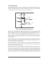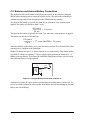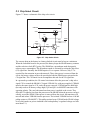
1
Jackrabbit (BL1800) C-Programmable Single-Board Computer User’s Manual 019–0067 • 050515–F Jackrabbit (BL1800) User’s Manual Part Number 019-0067 • 050515–F • Printed in U.S.A. ©2000–2005 Z-World Inc. • All rights reserved. Z-World reserves the right to make changes and improvements to its products without providing notice. Trademarks Rabbit is a registered trademark of Rabbit Semiconductor. Rabbit 2000 is a trademark of Rabbit Semiconductor. Dynamic C and Z-World are registered trademarks of Z-World Inc. Z-World, Inc. 2900 Spafford Street Davis, California 95616-6800 USA Telephone: (530) 757-3737 Fax: (530) 753-5141 www.zworld.com Jackrabbit (BL1800) TABLE OF CONTENTS Chapter 1. Introduction 1 1.1 Features .................................................................................................................................................1 1.2 Development and Evaluation Tools......................................................................................................2 1.3 How to Use This Manual ......................................................................................................................3 1.3.1 Additional Product Information ....................................................................................................3 1.3.2 Online Documentation ..................................................................................................................3 1.4 CE Compliance .....................................................................................................................................4 1.4.1 Design Guidelines .........................................................................................................................5 1.4.2 Interfacing the Jackrabbit to Other Devices..................................................................................5 Chapter 2. Hardware Setup 7 2.1 Development Kit Contents....................................................................................................................7 2.2 Development Hardware Connections ...................................................................................................8 2.2.1 Attach Jackrabbit to Prototyping Board........................................................................................9 2.2.2 Connect Programming Cable ......................................................................................................10 2.2.3 Connect Power ............................................................................................................................11 2.3 Run a Sample Program .......................................................................................................................12 2.3.1 Troubleshooting ..........................................................................................................................12 2.4 Where Do I Go From Here? ...............................................................................................................13 2.4.1 Technical Support .......................................................................................................................13 Chapter 3. Subsystems 15 3.1 Jackrabbit Pinouts ...............................................................................................................................16 3.1.1 Headers........................................................................................................................................16 3.2 Digital Inputs/Outputs.........................................................................................................................17 3.2.1 Digital Inputs...............................................................................................................................17 3.2.2 Digital Outputs............................................................................................................................18 3.2.3 Bidirectional I/O .........................................................................................................................20 3.3 A/D Converter.....................................................................................................................................21 3.4 D/A Converters ...................................................................................................................................23 3.4.1 DA1 .............................................................................................................................................24 3.4.2 DA0 .............................................................................................................................................26 3.5 Serial Communication ........................................................................................................................28 3.5.1 RS-232 ........................................................................................................................................28 3.5.2 RS-485 ........................................................................................................................................28 3.5.3 Programming Port .......................................................................................................................30 3.6 Memory...............................................................................................................................................31 3.6.1 SRAM .........................................................................................................................................31 3.6.2 Flash EPROM .............................................................................................................................31 3.7 Other Hardware...................................................................................................................................32 3.7.1 External Interrupts.......................................................................................................................32 3.7.2 Clock Doubler .............................................................................................................................32 3.7.3 Spectrum Spreader ......................................................................................................................33 User’s Manual Chapter 4. Software Reference 35 4.1 An Overview of Dynamic C............................................................................................................... 35 4.2 Sample Programs................................................................................................................................ 37 4.3 Jackrabbit Function Calls ................................................................................................................... 38 4.3.1 I/O Drivers.................................................................................................................................. 38 4.3.2 Serial Communication Drivers ................................................................................................... 42 4.4 Upgrading Dynamic C ....................................................................................................................... 43 4.4.1 Patches and Bug Fixes................................................................................................................ 43 4.4.2 Add-On Modules ........................................................................................................................ 43 Appendix A. Specifications 45 A.1 Electrical and Mechanical Specifications.......................................................................................... 46 A.1.1 Exclusion Zone .......................................................................................................................... 48 A.1.2 Headers ...................................................................................................................................... 49 A.2 Jumper Configurations ...................................................................................................................... 50 A.3 Conformal Coating ............................................................................................................................ 52 A.4 Use of Rabbit 2000 Parallel Ports ..................................................................................................... 53 Appendix B. Prototyping Board 57 B.1 Prototyping Board Overview............................................................................................................. 58 B.1.1 Prototyping Board Features ....................................................................................................... 59 B.2 Mechanical Dimensions and Layout ................................................................................................. 60 B.3 Using the Prototyping Board ............................................................................................................. 61 B.3.1 Demonstration Board................................................................................................................. 62 B.3.2 Prototyping Board...................................................................................................................... 64 Appendix C. Power Management 67 C.1 Power Supplies .................................................................................................................................. 67 C.2 Batteries and External Battery Connections...................................................................................... 70 C.2.1 Battery Backup Circuit .............................................................................................................. 71 C.2.2 Power to VRAM Switch ............................................................................................................ 72 C.2.3 Reset Generator.......................................................................................................................... 72 C.3 Chip Select Circuit............................................................................................................................. 73 Notice to Users 75 Index 77 Schematics 79 Jackrabbit (BL1800) 1. INTRODUCTION The Jackrabbit is a high-performance, C-programmable singleboard computer with a compact form factor. A Rabbit® 2000 microprocessor operating at 29.5 MHz provides fast data processing. 1.1 Features • 29.5 MHz clock • 24 CMOS-compatible I/O • 3 analog channels: 1 A/D input, 2 PWM D/A outputs • 4 high-power outputs (factory-configured as 3 sinking and 1 sourcing) • 4 serial ports (2 RS-232 or 1 RS-232 with RTS/CTS, 1 RS-485, and 1 CMOScompatible) • 6 timers (five 8-bit timers and one 10-bit timer) • 128K SRAM, 256K flash EPROM • Real-time clock • Watchdog supervisor • Voltage regulator • Backup battery Appendix A provides detailed specifications for the Jackrabbit. User’s Manual 1 Three Jackrabbit models are available. Their standard features are summarized in Table 1. Table 1. Jackrabbit Features Model Features BL1800 Full-featured controller with switching voltage regulator. BL1810 BL1800 with 14.7 MHz clock, 128K flash EPROM, linear voltage regulator, sinking outputs sink up to 200 mA, sourcing output sources up to 100 mA, RS-232 serial ports rated for 1 kV ESD BL1820 BL1810 with 3 additional digital I/O, no RS-485, no backup battery. Throughout this manual, the term Jackrabbit refers to all three Jackrabbit models in Table 1; individual models are referred to specifically according to the model number in Table 1. 1.2 Development and Evaluation Tools A complete Development Kit, including a Prototyping Board and Dynamic C development software, is available for the Jackrabbit. The Development Kit puts together the essentials you need to design an embedded microprocessor-based system rapidly and efficiently. See the Jackrabbit (BL1800) Getting Started Manual for complete information on the Development Kit. 2 Jackrabbit (BL1800) 1.3 How to Use This Manual This user’s manual is intended to give users detailed information on the Jackrabbit. It does not contain detailed information on the Dynamic C development environment or the Rabbit 2000® microprocessor. Most users will want more detailed information on some or all of these topics in order to put the Jackrabbit to effective use. 1.3.1 Additional Product Information Introductory information about the Jackrabbit and its associated Development Kit and Prototyping Board will be found in the printed Jackrabbit (BL1800) Getting Started Manual, which is also provided on the accompanying CD-ROM in both HTML and Adobe PDF format. We recommend that any users unfamiliar with Z-World products, or those who will be using the Prototyping Board for initial evaluation and development, begin with at least a read-through of the Getting Started manual. In addition to the product-specific information contained in the Jackrabbit (BL1800) Getting Started Manual and the Jackrabbit (BL1800) User’s Manual (this manual), several higher level reference manuals are provided in HTML and PDF form on the accompanying CD-ROM. Advanced users will find these references valuable in developing systems based on the Jackrabbit: • Dynamic C User’s Manual • Dynamic C Function Reference Manual • Rabbit 2000 Microprocessor User’s Manual 1.3.2 Online Documentation The online documentation is installed along with Dynamic C, and an icon for the documentation menu is placed on the workstation’s desktop. Double-click this icon to reach the menu. If the icon is missing, use your browser to find and load default.htm in the docs folder, found in the Dynamic C installation folder. The latest versions of all documents are always available for free, unregistered download from our Web sites as well. User’s Manual 3 1.4 CE Compliance Equipment is generally divided into two classes. CLASS A CLASS B Digital equipment meant for light industrial use Digital equipment meant for home use Less restrictive emissions requirement: less than 40 dB µV/m at 10 m (40 dB relative to 1 µV/m) or 300 µV/m More restrictive emissions requirement: 30 dB µV/m at 10 m or 100 µV/m These limits apply over the range of 30–230 MHz. The limits are 7 dB higher for frequencies above 230 MHz. Although the test range goes to 1 GHz, the emissions from Rabbitbased systems at frequencies above 300 MHz are generally well below background noise levels. The Jackrabbit single-board computer has been tested and was found to be in conformity with the following applicable immunity and emission standards. The BL1810 and BL1820 single-board models are also CE qualified as they are sub-versions of the Jackrabbit . Boards that are CE-compliant have the CE mark. NOTE: Earlier versions of the Jackrabbit sold before 2002 that do not have the CE mark are not CE-complaint. Immunity The Jackrabbit series of single-board computers meets the following EN55024/1998 immunity standards. • EN61000-4-3 (Radiated Immunity) • EN61000-4-4 (EFT) • EN61000-4-6 (Conducted Immunity) Additional shielding or filtering may be required for a heavy industrial environment. Emissions The Jackrabbit series of single-board computers meets the following emission standards with the Rabbit 2000 spectrum spreader turned on and set to the normal mode. The spectrum spreader is only available with Rev. C or higher of the Rabbit 2000 microprocessor. This microprocessor is used in all Jackrabbit series boards that carry the CE mark. • EN55022:1998 Class B • FCC Part 15 Class B In order for the Jackrabbit boards to meet these EN55022:1998 Class B standards, you must add ferrite absorbers to the serial I/O cables used for RS-232 and RS-485 serial communication. Depending on your application, you may need to add ferrite absorbers to the 4 Jackrabbit (BL1800) digital I/O cables. Your results may vary, depending on your application, so additional shielding or filtering may be needed to maintain the Class B emission qualification. NOTE: If no ferrite absorbers are fitted, the Jackrabbit boards will still meet EN55022:1998 Class A requirements as long as the spectrum spreader is turned on. The spectrum spreader is on by default for Jackrabbit models BL1810 and BL1820. The spectrum spreader is off by default for the Jackrabbit model BL1800, and must be turned on with at least one wait state in order for the BL1800 model to be CE-compliant. Section 3.7.3 provides further information about the spectrum spreader and its use, and includes information on how to add a wait state. 1.4.1 Design Guidelines Note the following requirements for incorporating the Jackrabbit series of single-board computers into your application to comply with CE requirements. General • The power supply provided with the Development Kit is for development purposes only. It is the customer’s responsibility to provide a CE-compliant power supply for the end-product application. • When connecting the Jackrabbit single-board computer to outdoor cables, the customer is responsible for providing CE-approved surge/lightning protection. • Z-World recommends placing digital I/O or analog cables that are 3 m or longer in a metal conduit to assist in maintaining CE compliance and to conform to good cable design practices. Z-World also recommends using properly shielded I/O cables in noisy electromagnetic environments. • When installing or servicing the Jackrabbit, it is the responsibility of the end-user to use proper ESD precautions to prevent ESD damage to the Jackrabbit. Safety • For personal safety, all inputs and outputs to and from the Jackrabbit series of singleboard computers must not be connected to voltages exceeding SELV levels (42.4 V AC peak, or 60 V DC). Damage to the Rabbit 2000 microprocessor may result if voltages outside the design range of 0 V to 5.5 V DC are applied directly to any of its digital inputs. • The lithium backup battery circuit on the Jackrabbit single-board computer has been designed to protect the battery from hazardous conditions such as reverse charging and excessive current flows. Do not disable the safety features of the design. 1.4.2 Interfacing the Jackrabbit to Other Devices Since the Jackrabbit series of single-board computers is designed to be connected to other devices, good EMC practices should be followed to ensure compliance. CE compliance is ultimately the responsibility of the integrator. Additional information, tips, and technical assistance are available from your authorized Z-World distributor, and are also available on our Web site at www.zworld.com. User’s Manual 5 6 Jackrabbit (BL1800) 2. HARDWARE SETUP This chapter describes the Jackrabbit board in more detail, and explains how to set up and use the accompanying Prototyping Board. NOTE: This chapter (and this manual) assume that you have the Jackrabbit Development Kit. If you purchased a Jackrabbit board by itself, you will have to adapt the information in this chapter and elsewhere to your test and development setup. 2.1 Development Kit Contents The Jackrabbit Development Kit contains the following items: • BL1810 single-board computer. • Prototyping Board. • AC adapter, 12 V DC, 1 A. (Included only with Development Kits sold for the North American market. A header plug leading to bare leads is provided to allow overseas users to connect their own power supply with a DC output of 7.5–25 V.) NOTE: The linear voltage regulator becomes rather hot for voltages above 15 V. • 10-pin header to DE9 programming cable with integrated level-matching circuitry. • Dynamic C CD-ROM, with complete product documentation on disk. • This Getting Started manual. • A bag of accessory parts for use on the Prototyping Board. • Screwdriver. • Rabbit 2000 Processor Easy Reference poster. • Registration card. User’s Manual 7 2.2 Development Hardware Connections There are three steps to connecting the Prototyping Board for use with Dynamic C and the sample programs: 1. Attach the Jackrabbit to the Prototyping Board. 2. Connect the programming cable between the Jackrabbit and the workstation PC. 3. Connect the power supply to the Jackrabbit. 8 Jackrabbit (BL1800) 2.2.1 Attach Jackrabbit to Prototyping Board J4 GND PA0 PA2 PA4 PA6 GND PB0 PB2 PB4 PB6 WDO GND PE6 PE4 PE2 PE0 HV0 HV2 K GND To attach the Jackrabbit board to the Prototyping Board, turn the Jackrabbit board over so that the battery is facing up. Plug the pins from headers J4 and J5 on the bottom side of the Jackrabbit board into the header sockets at J2 and J6 on the Prototyping Board as indicated in Figure 1. VCC +RAW Battery J5 PD3 PD5 PD7 GND 485+ VCC SM1 STAT PD2 PD4 PD6 GND 485 VCC SM0 IOBEN S4 PD1 PD0 PWR DA1 DA0 DS6 AGND AD0 DS7 PC7 PC6 Z-World, Inc. DS8 PC5 PC4 S5 RESET PC3 PC2 GND PC1 VBAT TXC TXB PC0 GND RXC RXB JACKRABBIT PROTOTYPING BOARD /RST GND VCC J6 J6 S3 DS5 DS4 GND RXC TXC PC1 DS3 PC3 PC5 PC7 AGND S2 DA1 PD1 PD3 PD5 PD7 GND 485+ VCC SM1 STAT VBAT GND DS2 VCC RXB TXB PC0 DS1 PC2 PC4 PC6 AD0 S1 DA0 PD0 PD2 PD4 PD6 GND 485 VCC SM0 IOBEN GND /RST HV3 K Buzzer GND HV1 GND HV2 PE1 GNDPE0 HV0 PE3 PE5 PE7 PCLK R3 Jackrabbit Board + GND S4 PB4PE4 PB5PE2 S3 S2 S1 PB2GND PB3PE6 PB7 DS8 PB5 PB3 PB1 GND PA6PB6 WDO PA7 DS7 DS6 DS5 DS4 PA7 PA3PB0 PA4PB2 PA1 PA6 PA2GND DS3 PA5 PA0 PA4 DS2 PA3 PA2 PA5PB4 J2 J2 PA1 PA0 DS1 VCC GND VCC PA1 PA3 PA5 PA7 GND PB1 PB3 PB5 PB7 PCLK PE7 PE5 PE3 PE1 GND HV1 HV3 +RAW VCC Prototyping Board Figure 1. Attach Jackrabbit Board to Prototyping Board NOTE: It is important that you line up the pins on headers J4 and J5 of the Jackrabbit board exactly with the corresponding pins of header sockets J2 and J6 on the Prototyping Board. The header pins may become bent or damaged if the pin alignment is offset, and the Jackrabbit might not work. Permanent electrical damage to the may also result if a misaligned Jackrabbit is powered up. Press the Jackrabbit’s pins firmly into the Prototyping Board headers. User’s Manual 9 2.2.2 Connect Programming Cable The programming cable connects the Jackrabbit to the PC running Dynamic C to download programs and to monitor the Jackrabbit during debugging. Connect the 10-pin connector of the programming cable labeled PROG to header J3 on the Jackrabbit board as shown in Figure 2. Be sure to orient the marked (usually red) edge of the cable towards pin 1 of the connector. (Do not use the DIAG connector, which is used for a normal serial connection.) NOTE: Use only the programming cable that has a red shrink wrap around the RS-232 level converter (Z-World part number 101-0513), which is supplied with the Development Kit. Other Z-World programming cables might not be voltage-compatible or their connector sizes may be different. U4 RS-232 U1 J4 JACKRABBIT BOARD GNDVIN GND J1 J2 GND PA0 PA2 PA4 PA6 GND PB0 PB2 PB4 PB6 WDO GND PE6 PE4 PE2 PE0 HV0 HV2 K GND VCC PA1 PA3 PA5 PA7 GND PB1 PB3 PB5 PB7 PCLK PE7 PE5 PE3 PE1 GND HV1 HV3 +RAW VCC JP1 U5 U3 SRAM Rabbit 2000 U6 Y3 RS-485 J5 VCC RXB TXB PC0 PC2 PC4 PC6 AD0 DA0 PD0 PD2 PD4 PD6 GND 485 VCC SM0 IOBEN GND /RST GND RXC TXC PC1 PC3 PC5 PC7 AGND DA1 PD1 PD3 PD5 PD7 GND 485+ VCC SM1 STAT VBAT GND RESET J3 JACKRABBIT Z-World, Inc. Colored side lines up with pin 1 PROG Programming connector Diagnostic connector PROTOTYPING BOARD DIAG To PC COM port Figure 2. Power and Programming Cable Connections to Jackrabbit Board Connect the other end of the programming cable to a COM port on your PC. NOTE: Some PCs now come equipped only with a USB port. It may be possible to use an RS-232/USB converter with the programming cable supplied with the Jackrabbit Development Kit. An RS-232/USB converter is available through the Z-World Web store. 10 Jackrabbit (BL1800) 2.2.3 Connect Power When all other connections have been made, you can connect power to the Jackrabbit. Hook up the connector from the wall transformer to header J1 on the Jackrabbit board as shown in Figure 2. The orientation of this connector is not important since the VIN (positive) voltage is the middle pin, and GND is available on both ends of the three-pin header J1. Plug in the wall transformer. The Jackrabbit board and the Prototyping Board are ready to be used. NOTE: A RESET button is provided on the Prototyping Board (see Figure 1) to allow hardware reset without disconnecting power. To power down the Jackrabbit, unplug the power connector from J1. You should disconnect power before making any circuit adjustments in the prototyping area, changing any connections to the board, or removing the Jackrabbit from the Prototyping Board. 2.2.3.1 Overseas Development Kits Development kits sold outside North America include a header connector that may be connected to 3-pin header J1 on the Jackrabbit. The connector may be attached either way as long as it is not offset to one side. The red and black wires from the connector can then be connected to the positive and negative connections on your power supply. The power supply should deliver 7.5 V–25 V DC at 5 W. User’s Manual 11 2.3 Run a Sample Program If you already have Dynamic C installed, you are now ready to test your programming connections by running a sample program. If you are using a USB port to connect your computer to the Jackrabbit, choose Options > Project Options and select “Use USB to Serial Converter” under the Communications tab. Find the file PONG.C, which is in the Dynamic C SAMPLES folder. To run the program, open it with the File menu (if it is not still open), compile it using the Compile menu, and then run it by selecting Run in the Run menu. The STDIO window will open and will display a small square bouncing around in a box. This program shows that the CPU is working. 2.3.1 Troubleshooting If Dynamic C appears to compile the BIOS successfully, but you then receive a communication error message when you compile and load the sample program, it is possible that your PC cannot handle the higher program-loading baud rate. Try changing the maximum download rate to a slower baud rate as follows. • Locate the Serial Options dialog in the Dynamic C Options > Project Options > Communications menu. Select a slower Max download baud rate. If a program compiles and loads, but then loses target communication before you can begin debugging, it is possible that your PC cannot handle the default debugging baud rate. Try lowering the debugging baud rate as follows. • Locate the Serial Options dialog in the Dynamic C Options > Project Options > Communications menu. Choose a lower debug baud rate. If there are any other problems: • Check to make sure you are using the PROG connector, not the DIAG connector, on the programming cable. • Check both ends of the programming cable to ensure that they are firmly plugged into the PC and the programming port on the Jackrabbit. • Ensure that the Jackrabbit is firmly and correctly installed in its connectors on the Prototyping Board. • Select a different COM port within Dynamic C. From the Options menu, select Project Options, then select Communications. Select another COM port from the list, then click OK. Press <Ctrl-Y> to force Dynamic C to recompile the BIOS. If Dynamic C still reports it is unable to locate the target system, repeat the above steps until you locate the active COM port. 12 Jackrabbit (BL1800) 2.4 Where Do I Go From Here? If everything appears to be working, we recommend the following sequence of action: 1. Run all of the sample programs described in the Jackrabbit (BL1800) Getting Started Manual to get a basic familiarity with Dynamic C and the Jackrabbit’s capabilities. 2. For further development, refer to this Jackrabbit (BL1800) User’s Manual for details of the board’s hardware components. A documentation icon should have been installed on your workstation’s desktop; click on it to reach the documentation menu. You can create a new desktop icon that points to default.htm in the docs folder in the Dynamic C installation folder. 3. For advanced development topics, refer to the Dynamic C User’s Manual, also in the online documentation set. 2.4.1 Technical Support NOTE: If you purchased your Jackrabbit through a distributor or through a Z-World partner, contact the distributor or partner first for technical support. If there are any problems at this point: • Use the Dynamic C Help menu to get further assistance with Dynamic C. • Check the Z-World/Rabbit Semiconductor Technical Bulletin Board at www.zworld.com/support/bb/. • Use the Technical Support e-mail form at www.zworld.com/support/questionSubmit.shtml. User’s Manual 13 14 Jackrabbit (BL1800) 3. SUBSYSTEMS Chapter 3 describes the principal subsystems and their use for the Jackrabbit. • Digital Inputs/Outputs • A/D Converter • D/A Converters • Serial Communication • Memory Figure 3 shows these Rabbit-based subsystems designed into the Jackrabbit. BL1800 Digital Inputs Programming Port 32 kHz 15 MHz osc osc Digital Outputs RS-232 RS-485 SRAM Flash RABBIT 2000 HighPower Outputs ® A/D Converter Analog Outputs Figure 3. Jackrabbit Subsystems User’s Manual 15 3.1 Jackrabbit Pinouts Figure 4 shows the pinout for headers J4 and J5, which carry the signals associated with the Jackrabbit subsystems. J5 J4 GND PA0 PA2 PA4 PA6 GND PB0 PB2 PB4 PB6 WDO GND PE6 PE4 PE2 PE0 HV0 HV2 K GND VCC PA1 PA3 PA5 PA7 GND PB1 PB3 PB5 PB7 PCLK PE7 PE5 PE3 PE1 GND HV1 HV3 +RAW VCC VCC RXB TXB PC0 Legend PC2 Bidirectional I/O PC4 One-Direction PC6 I/O AD0 DA0 PD0 PD2 PD4 PD6 GND 485 VCC SM0 IOBEN GND /RST GND RXC TXC PC1 PC3 PC5 PC7 AGND DA1 PD1 PD3 PD5 PD7 GND 485+ VCC SM1 STAT VBAT GND Figure 4. Pinout for Jackrabbit Headers J4 and J5 3.1.1 Headers Standard Jackrabbit models are equipped with two 2 × 20 IDC headers (J4 and J5) with a 2 mm pitch. 16 Jackrabbit (BL1800) 3.2 Digital Inputs/Outputs 3.2.1 Digital Inputs The Jackrabbit has six CMOS-level digital inputs, PB0–PB5, each of which is pulled up to +5 V as shown in Figure 5. The BL1820, which does not have RS-485, has one additional CMOS-level digital input, PC1. Vcc 47 kW Rabbit 2000 Microprocessor GND Figure 5. Digital Inputs The actual switching threshold is approximately 2.40 V. Anything below this value is a logic 0, and anything above is a logic 1. NOTE: Since the voltage limits on the inputs to the Rabbit 2000 microprocessor are 0 to 5.5 V DC, the end user must ensure that the voltage applied to any I/O pin is within these limits. User’s Manual 17 3.2.2 Digital Outputs The Jackrabbit has four CMOS-level digital outputs, PB6–PB7, PCLK, and IOBEN. Four high-power outputs, HV0–HV3, are also available—HV0–HV2 can each sink up to 1 A (200 mA for the BL1810 and BL1820) at 30 V, and HV3 can source up to 500 mA (100 mA for the BL1810 and BL1820) at 30 V. The BL1820, which does not have RS-485, has one additional CMOS-level digital output, PC0. HV0HV2 SINKING OUTPUTS +K Current Flow PE[02] HV3 SOURCING OUTPUT +K Current Flow PE3 Figure 6. Jackrabbit High-Power Digital Outputs The common power supply for the four high-power outputs is called K, and is available on header J4. Connect K to the power supply that powers the load, which is usually a separate power supply to that used for the Jackrabbit, and must be no more than 30 V because of the power limitations of the resistors used in the sourcing output circuit. The K connection performs two functions. 1. K supplies power to the sinking/sourcing transistors used in the high-power circuits. 2. A diode-capacitor combination in the circuit “snubs” voltage transients when inductive loads such as relays and solenoids are driven. 18 Jackrabbit (BL1800) 3.2.2.1 Configurable High-Power Output (HV3) HV3, shown schematically in Figure 7, is factory-configured to be a sourcing output. K R55 R50 100 kW Q25 PE3 R48 HV3 (sinking 0W option) C27 100 nF 470 W Q28 C28 100 nF MMBT4401 R52 1.8 kW R51 MMBT3906 1.8 kW R56 0W HV3 (sourcing) D24 Figure 7. Configurable High-Current Output When used as a sourcing output, HV3 is switched to K when PE3 on the Rabbit 2000 goes high, and the two transistors shown in Figure 7 are turned on. The maximum sourcing current is 100 mA (BL1810 and BL1820) or 500 mA (BL1800), and the maximum K is 30 V. This voltage limit on K arises because R51 and R52 at the base of Q28 can each dissipate 500 mW for a total of 1 W. The 30 V limit then constrains the sinking outputs as well because K is common to all four high-current outputs. User’s Manual 19 HV3 can also be reconfigured as a sinking output. To do so, remove the 0 Ω surfacemounted resistor R56, and solder on a 0 Ω surface-mounted resistor or jumper wire at R55. If you plan to drive inductive loads, add a diode at D21. Figure 8 shows the location of these components. J4 J5 VCC RXB TXB PC0 PC2 PC4 PC6 AD0 DA0 PD0 PD2 PD4 PD6 GND 485 VCC SM0 IOBEN GND /RST GND RXC TXC PC1 PC3 PC5 PC7 AGND DA1 PD1 PD3 PD5 PD7 GND 485+ VCC SM1 STAT VBAT GND Battery C27 D24 VCC PA1 PA3 PA5 PA7 GND PB1 PB3 PB5 PB7 PCLK PE7 PE5 PE3 PE1 GND HV1 HV3 +RAW VCC GND PA0 PA2 PA4 PA6 GND PB0 PB2 PB4 PB6 WDO GND PE6 PE4 PE2 PE0 HV0 HV2 K GND R55 R56 D21 Figure 8. Changing HV3 to a Sinking Output 3.2.3 Bidirectional I/O The Jackrabbit has 14 CMOS-level bidirectional I/O: PA0–PA7, PD0, PD3, PD6–PD7, and PE4–PE5. The BL1820, which does not have RS-485, has one additional bidirectional I/O, PD5. 20 Jackrabbit (BL1800) 3.3 A/D Converter The analog-to-digital (A/D) converter, shown in Figure 9, compares the DA0 voltage to AD0, the voltage presented to the converter. DA0 therefore cannot be used for the digitalto-analog (D/A) converter when the A/D converter is being used. Vcc R34 51.1 kW AD0 R31 10 kW 9 R35 200 W DA0 Vcc R33 200 W 10 13 12 R32 51.1 kW DA0 too low – LM324 8 0W + – LM324 + R36 14 R30 0W PE7 PE6 DA0 too high Figure 9. Schematic Diagram of A/D Converter The A/D converter transforms the voltage at DA0 into a 20 mV window centered around DA0. For example, if DA0 is 2.0 V, the window in the A/D converter would be 1.990 V to 2.010 V. If AD0 > 2.010 V, PE7 would read high and PE6 would read low. If 1.990 V < AD0 < 2.010 V, PE7 would read low and PE6 would read low. This is the case when the A/D input is exactly the same as DA0. If AD0 < 1.990 V, PE7 would read low and PE6 would read high. PE6 can be imagined to be a “DA0 voltage is too high” indicator. If DA0 is larger than the analog voltage presented at AD0, then PE6 will be true (high). If this happens, the program will need to reduce the DA0 voltage. PE7 can be imagined to be a “DA0 voltage is too low” indicator. If DA0 is smaller than the analog voltage presented at AD0, then PE7 will be true (high). If this happens, the program will need to raise the DA0 voltage. The A/D input, AD0, is the same as DA0 only when PE6 and PE7 are low. Because the A/D converter circuit uses a 20 mV window, the accuracy is ±10 mV. DA0 can range from 0.1 V to 2.8 V, which represents 270 steps of ±10 mV. This is better than 8-bit accuracy. Since the D/A converter is able to change the DA0 output in 3.88 mV steps, there are 697 steps over the range from 0.1 V to 2.8 V. This represents a resolution of more than 9 bits. User’s Manual 21 There is a 10 kΩ resistor, R31, connected between Vcc and AD0. This resistor should provide an appropriate voltage divider bias for a variety of common thermistors so that they can be connected directly between AD0 and ground. The A/D converter load is the 10 kΩ resistor connected to Vcc. Remove R31 if a smaller load is desired—this will lead to a very high input impedance for the A/D converter. The A/D converter has no reference voltage. There is a relative accuracy between measurements, but no absolute accuracy. This is because Vcc can vary ±5%, the pulse-width modulated outputs might not reach the full 0 V and 5 V rails out of the Rabbit 2000 microprocessor, and the gain resistors used in the circuit have a 1% tolerance. For these reasons, each Jackrabbit needs to be calibrated individually, with the constants held in software, to be able to rely on an absolute accuracy. The Jackrabbit is sold without this calibration support. The algorithm provided to perform the conversion does a successive approximation search for the analog voltage. This takes an average of 150 ms, and a maximum of 165 ms, with a 14.7 MHz Jackrabbit. 22 Jackrabbit (BL1800) 3.4 D/A Converters Two digital-to-analog (D/A) converter outputs, DA0 and DA1, are supplied on the Jackrabbit. These are shown in Figure 10. The D/A converters have no reference voltage. Although they may be fairly accurate from one programmed voltage to the next, they do not have absolute accuracy. This is because Vcc can change ±5%, the PWM outputs might not achieve the full 0 V and 5 V rail out of the processor, and the gain resistors in the circuit have a 1% tolerance. The D/A converters therefore need individual calibration, with the calibration constants held in software before absolute accuracy can be relied on. The Jackrabbit is sold without such calibration. Vcc R29 1 MW R26 DA0 82.5 kW 1 – LM324 + R20 1.1 kW R22 2 PD2 10 kW R21 3 R27 C20 255 kW 100 nF 110 kW PD1 R28 DA1 100 kW 7 R25 1.1 kW – LM324 + 6 R24 5 C22 100 nF 100 kW PD4 Figure 10. Schematic Diagram of D/A Converters Note that DA0 is used to provide a reference voltage for the A/D converter and is unavailable for D/A conversion when the A/D converter is being used. Pulse-width modulation (PWM) is used for the D/A conversion. This means that the digital signal, which is either 0 V or 5 V, is a train of pulses. This means that if the signal is taken to be usually at 0 V (or ground), there will be 5 V pulses. The voltage will be 0 V for a given time, then jump to 5 V for a given time, then back to ground for a given time, then back to 5 V, and so on. A hardware filter in the circuit consisting of a resistor and capacitor averages the 5 V signal and the 0 V signal over time. Therefore, if the time that the signal is at 5 V is equal to the time the signal is 0 V, the duty cycle will be 50%, and the average signal will be 2.5 V. If the time at 5 V is only 25% of the time, then the average voltage will be 1.25 V. Thus, the software needs to only vary the time the signal is at 5 V with respect to the time the signal is at 0 V to achieve any desired voltage between 0 V and 5 V. User’s Manual 23 It is very easy to do pulse-width modulation with the Rabbit 2000 microprocessor because of the chip’s architecture. 3.4.1 DA1 The op amp supporting DA1 converts pulse-width modulated signals to an analog voltage between 0 V and 5 V. A digital signal that varies with time is fed from PD4. The resolution of the DA1 output depends on the smallest increment of time to change the on/off time (the time between 5 V and 0 V). The Jackrabbit uses the Rabbit 2000’s Port D control registers to clock out the signal at a timer timeout. The timer used is timer B. Timer B has 10 bits of resolution so that the voltage can be varied in 1/1024 increments. The resolution is thus about 5 mV (5 V/1024). R28 is present solely to balance the op amp input current bias. R25 helps to achieve a voltage close to ground for a 0% duty cycle. A design constraint dictates how fast timer B must run. The hardware filter has a resistorcapacitor filter that averages the 0 V and 5 V values. Its effect is to smooth out the digital pulse train. It cannot be perfect, and so there will be some ripple in the output voltage. The maximum signal decay between pulses will occur when DA1 is set to 2.5 V. This means the pulse train will have a 50% duty cycle. The maximum signal decay will be 2.5 V × 1 – e –t ⎞ ⎛ ------⎝ RC⎠ where RC = 0.01 s for 14.7 MHz Jackrabbits, and t is the pulse on or off time (not the length of the total cycle). Timer B is driven at the Rabbit 2000 frequency divided by 2. The frequency achievable with a 14.7 MHz clock is (14.7 MHz/2)/1024 = 7.17 kHz. This is a period of 1/f = 139 µs. For a 50% duty cycle, half of the period will be high (70 µs at 5 V), and half will be low (70 µs at 0 V). Thus, a 14.7 MHz Jackrabbit has t = 70 µs. Based on the standard capacitor discharge formula, this means that the maximum voltage change will be 2.5 V × 1 – e 70 µs⎞ ⎛ –---------------⎝ 0.01 s ⎠ = 17.4 mV This is less than a 20 mV peak-to-peak ripple. The DA1 output can be less than 100 mV for a 0% duty cycle and above 3.5 V for a 100% duty cycle. Because of software limitations on the low side and hardware limitations on the high side, the duty cycle can only be programmed from 12% to 72%. The low limitation allows the software to perform other tasks as well as maintain the PWM for the D/A converters. The high limitation is simply the maximum voltage obtainable with the LM324 op amp used in the circuit. Anything outside the 12%–72% range gets output as 24 Jackrabbit (BL1800) either a 0% or a 100% duty cycle. The duty cycle is programmed as the high-time count of 1024 total counts of the Rabbit 2000’s timer B. Thus, 256 counts would be 25% of 1024 counts, and corresponds to a 25% duty cycle. Table 2 lists typical DA1 voltages measured for various duty cycle values with a load larger than 1 MΩ. Table 2. Typical DA1 Voltages for Various Duty Cycles Duty Cycle (%) Voltage (V) Programmed Count 0 0.002 0–122 12 0.620 123 25 1.242 256 50 2.483 512 72 3.567 742 100 3.567 743–1024 It is important to remember that the DA1 output voltage will not be realized instantaneously after programming in a value. There is a settling time because of the RC time constant (R24 × C22), which is 10 ms. For example, the voltage at any given time is V = VP – (VP – VDA1)e(-t/RC) (EQ 1) where V is the voltage at time t, VP is the programmed voltage, VDA1 is the last DA1 output voltage from the D/A converter, and RC is the time constant (10 ms). The settling will be within 99.326% (or within about 21 mV for a 3 V change in voltage) after five time constants, or 50 ms. Six time constants, 60 ms, will allow settling to within 99.75% (or to within about 8 mV for a 3 V change in voltage). Seven time constants, 70 ms, will allow settling to within 99.91% (or to within about 3 mV for a 3 V change in voltage). An LM324 op amp, which can comfortably source 10 mA throughout the D/A converter range, drives the D/A converter output. If the output voltage is above 1 V, the D/A converter can comfortably sink 10 mA. Below 1 V, the D/A converter can only sink a maximum of 100 µA. To summarize, DA1 is provided uncalibrated, can be programmed with a resolution of 5 mV and a peak-to-peak ripple less than 20 mV over the range from 0.7 V to 3.5 V and 0 V. The settling time to within 21 mV is 50 ms. User’s Manual 25 3.4.2 DA0 The op amp supporting DA0 translates a 12%–88% duty cycle to an analog voltage range of 0 V to 3 V. The software operates only within this duty cycle; a duty cycle less than 12% is rounded down to 0%, and any duty cycle above 88% is rounded up to 100%. DA0 uses a voltage divider that consists of R21 and R27 and a gain-offset circuit that consists of R26 and R29 to achieve the output range of 0 V to 3 V within the software duty cycle. The DA0 output can be less than 100 mV for a 0% duty cycle and above 3.0 V for a 100% duty cycle. The duty cycle is programmed as the high-time count of 1024 total counts of the Rabbit 2000’s timer B. Thus, 256 counts would be 25% of 1024 counts, and corresponds to a 25% duty cycle. Table 3 lists typical DA0 voltages measured for various duty cycle values with a load larger than 1 MΩ. Table 3. Typical DA0 Voltages for Various Duty Cycles Duty Cycle (%) Voltage (V) Programmed Count 0 0.074 0–122 12 0.076 123 25 0.530 256 50 1.467 512 75 2.406 768 88 2.875 901 100 3.345 902–1024 It is important to remember that the DA0 output voltage will not be realized instantaneously after programming in a value. There is a settling time because of the RC time constant (R21 || R27 × C20), which is 7.68 ms. For example, the voltage at any given time is V = VP – (VP – VDA0)e(-t/RC) (EQ 2) where V is the voltage at time t, VP is the programmed voltage, VDA0 is the last DA0 output voltage from the D/A converter, and RC is the time constant (7.68 ms). The settling will be within 99.326% (or within about 21 mV for a 3 V change in voltage) after five time constants, or 38 ms. Six time constants, 46 ms, will allow settling to within 99.75% (or to within about 8 mV for a 3 V change in voltage). Seven time constants, 54 ms, will allow settling to within 99.91% (or to within about 3 mV for a 3 V change in voltage). The settling time is reduced somewhat by precharging capacitor C20 with pulse-width modulation from PD2. 26 Jackrabbit (BL1800) The resolution of the DA0 output depends on the smallest increment of time to change the on/off time (the time between 5 V and 0 V). The Jackrabbit uses the Rabbit 2000’s Port D control registers to clock out the signal at a timer timeout. The timer used is timer B. Timer B has 10 bits of resolution so that the voltage can be varied in 1/1024 increments. The resolution is thus about 3.88 mV for the DA0 output voltage range of 0 V to 3 V in the 12%–88% duty cycle. An LM324 op amp, which can comfortably source 10 mA throughout the D/A converter range, drives the D/A converter output. If the output voltage is above 1 V, the D/A converter can comfortably sink 10 mA. Below 1 V, the D/A converter can only sink a maximum of 100 µA. The peak-to-peak ripple on DA0 is less than 3 mV. There is a way to get rid of the ripple for very small periods of time. To do that, simply program the PWM port from a PWM output to a high-impedance input. This will allow the capacitor to hold the voltage subject only to leakage currents, which add up to about 1 µA. This will cause the capacitor to change voltage at the rate of 10 V per second, or 10 mV per millisecond. Practically, this means that the PWM can stop for about 1 ms (seven 1024-count D/A converter cycles on a 14.7 MHz processor clock) with a voltage movement of less than 10 mV. To summarize, DA0 is provided uncalibrated, can be programmed with a resolution of 3.88 mV and a peak-to-peak ripple less than 3 mV over the range from 0.1 V to 2.8 V and at 3.35 V. The settling time to within 3 mV is 54 ms. User’s Manual 27 3.5 Serial Communication The Jackrabbit has two RS-232 (3-wire) serial channels, one RS-485 serial channel, and one synchronous CMOS serial channel. 3.5.1 RS-232 The Jackrabbit’s two RS-232 serial channels are connected to an RS-232 transceiver, U4, an industry-standard MAX232 chip. U4 provides the voltage output, slew rate, and input voltage immunity required to meet the RS-232 serial communication protocol. Basically, the chip translates the Rabbit 2000’s 0 V to +Vcc signals to ±10 V. Note that the polarity is reversed in an RS-232 circuit so that +5 V is output as –10 V and 0 V is output as +10 V. U4 also provides the proper line loading for reliable communication. The Rabbit 2000 serial port B signals are presented as RS-232 compliant signals TXB (serial port B transmit) and RXB (serial port B receive) on header J5. The Rabbit 2000 serial port C signals are presented as RS-232 compliant signals TXC (serial port C transmit) and RXC (serial port C receive) on header J5. The maximum baud rate for each RS-232 serial channel is 115,200 bps. RS-232 can be used effectively at this baud rate for distances up to 15 m. Because two RS-232 transmit and two RS-232 receive lines are available, one serial channel can be used for serial transmit and receive, and the other serial channel can be used as a general digital I/O for RTS/CTS handshaking. Although the present release of Dynamic C does not support RTS/CTS handshaking in its libraries, it is possible to write your own software. 3.5.2 RS-485 The Jackrabbit has one RS-485 serial channel, which is connected to the Rabbit 2000 serial port D through U6, an RS-485 transceiver. U6 supports the RS-485 serial communication protocol. The chip’s slew rate limiters provide for a maximum baud rate of 250,000 bps. The half-duplex communication uses the Rabbit 2000’s PD5 pin to control the data enable on the communication line. The Jackrabbit can be used in an RS-485 multidrop network. Connect the RS-485+ to RS-485+ and RS-485– to RS-485– using single twisted-pair wires (nonstranded, tinned) as shown in Figure 11. 28 Jackrabbit (BL1800) U4 RS-232 U1 J4 GNDVIN GND J1 J2 VCC PA1 PA3 PA5 PA7 GND PB1 PB3 PB5 PB7 PCLK PE7 PE5 PE3 PE1 GND HV1 HV3 +RAW VCC GND PA0 PA2 PA4 PA6 GND PB0 PB2 PB4 PB6 WDO GND PE6 PE4 PE2 PE0 HV0 HV2 K GND U5 U3 SRAM Rabbit 2000 U6 RS-485 Y3 J5 VCC RXB TXB PC0 PC2 PC4 PC6 AD0 DA0 PD0 PD2 PD4 PD6 GND 485 VCC SM0 IOBEN GND /RST GND RXC TXC PC1 PC3 PC5 PC7 AGND DA1 PD1 PD3 PD5 PD7 GND 485+ VCC SM1 STAT VBAT GND Ground recommended RESET J3 JACKRABBIT Z-World, Inc. U4 RS-232 U1 J4 GNDVIN GND J1 J2 GND PA0 PA2 PA4 PA6 GND PB0 PB2 PB4 PB6 WDO GND PE6 PE4 PE2 PE0 HV0 HV2 K GND VCC PA1 PA3 PA5 PA7 GND PB1 PB3 PB5 PB7 PCLK PE7 PE5 PE3 PE1 GND HV1 HV3 +RAW VCC U5 U3 SRAM Rabbit 2000 U6 RS-485 Y3 J5 VCC RXB TXB PC0 PC2 PC4 PC6 AD0 DA0 PD0 PD2 PD4 PD6 GND 485 VCC SM0 IOBEN GND /RST GND RXC TXC PC1 PC3 PC5 PC7 AGND DA1 PD1 PD3 PD5 PD7 GND 485+ VCC SM1 STAT VBAT GND RESET J3 JACKRABBIT Z-World, Inc. U4 RS-232 U1 J4 GNDVIN GND J1 J2 GND PA0 PA2 PA4 PA6 GND PB0 PB2 PB4 PB6 WDO GND PE6 PE4 PE2 PE0 HV0 HV2 K GND VCC PA1 PA3 PA5 PA7 GND PB1 PB3 PB5 PB7 PCLK PE7 PE5 PE3 PE1 GND HV1 HV3 +RAW VCC U5 U3 SRAM Rabbit 2000 U6 Y3 RS-485 J5 VCC RXB TXB PC0 PC2 PC4 PC6 AD0 DA0 PD0 PD2 PD4 PD6 GND 485 VCC SM0 IOBEN GND /RST GND RXC TXC PC1 PC3 PC5 PC7 AGND DA1 PD1 PD3 PD5 PD7 GND 485+ VCC SM1 STAT VBAT GND RESET J3 JACKRABBIT Z-World, Inc. Figure 11. Multidrop Jackrabbit Network User’s Manual 29 The Jackrabbit comes with a 220 Ω termination resistor and 681 Ω bias resistors already installed, as shown in Figure 12. U4 RS-232 U1 J4 bias 485+ termination 485 bias R18 681 W R17 220 W 6 U6 7 R16 681 W GNDVIN GND J1 J2 GND PA0 PA2 PA4 PA6 GND PB0 PB2 PB4 PB6 WDO GND PE6 PE4 PE2 PE0 HV0 HV2 K GND VCC PA1 PA3 PA5 PA7 GND PB1 PB3 PB5 PB7 PCLK PE7 PE5 PE3 PE1 GND HV1 HV3 +RAW VCC U5 U3 SRAM Rabbit 2000 R16 U6 Y3 RS-485 J3 JACKRABBIT Z-World, Inc. J5 VCC RXB TXB PC0 PC2 PC4 PC6 AD0 DA0 PD0 PD2 PD4 PD6 GND 485 VCC SM0 IOBEN GND /RST R18 GND RXC TXC PC1 PC3 PC5 PC7 AGND DA1 PD1 PD3 PD5 PD7 GND 485+ VCC SM1 STAT VBAT GND RESET R17 Figure 12. RS-485 Termination and Bias Resistors The load these bias and termination resistors present to the RS-485 transceiver (U6) limits the number of Jackrabbits in a multidrop network to one master and nine slaves, unless the bias and termination resistors are removed. When using more than 10 Jackrabbits in a multidrop network, leave the 681 Ω bias resistors in place on the master Jackrabbit, and leave the 220 Ω termination resistors in place on the Jackrabbit at each end of the network. 3.5.3 Programming Port The Jackrabbit has a 10-pin program header labeled J3. The programming port uses the Rabbit 2000’s serial port A for communication. The Rabbit 2000 startup-mode pins (SMODE0, SMODE1) are presented to the programming port so that an externally connected device can force the Jackrabbit to start up in an external bootstrap mode. The programming port is used to start the Jackrabbit in a mode where the Jackrabbit will download a program from the port and then execute the program. The programming port transmits information to and from a PC while a program is being debugged. The Jackrabbit can be reset from the programming port. The Rabbit 2000 status pin is also presented to the programming port. The status pin is an output that can be used to send a general digital signal. The clock line for serial port A is presented to the programming port, which makes fast serial communication possible. 30 Jackrabbit (BL1800) 3.6 Memory 3.6.1 SRAM The Jackrabbit is designed to accept 32K to 512K of SRAM packaged in an SOIC case. Standard Jackrabbit models come with 128K of SRAM. A factory-installed option for 512K of SRAM is available. Figure 13 shows the locations and the jumper settings for the jumpers at JP1 used to set the SRAM size. The “jumpers” are 0 Ω surface-mounted resistors. SRAM 128K 512K JP1 JP1 3 2 1 3 2 1 U4 RS-232 U1 J4 GNDVIN GND J1 J2 GND PA0 PA2 PA4 PA6 GND PB0 PB2 PB4 PB6 WDO GND PE6 PE4 PE2 PE0 HV0 HV2 K GND VCC PA1 PA3 PA5 PA7 GND PB1 PB3 PB5 PB7 PCLK PE7 PE5 PE3 PE1 GND HV1 HV3 +RAW VCC JP1 U5 U3 SRAM U6 Y3 RS-485 J5 VCC RXB TXB PC0 PC2 PC4 PC6 AD0 DA0 PD0 PD2 PD4 PD6 GND 485 VCC SM0 IOBEN GND /RST GND RXC TXC PC1 PC3 PC5 PC7 AGND DA1 PD1 PD3 PD5 PD7 GND 485+ VCC SM1 STAT VBAT GND RESET J3 JACKRABBIT Z-World, Inc. Figure 13. Jackrabbit Jumper Settings for SRAM Size NOTE: For ordering or other information involving the factory-installed 512K SRAM option, call your Z-World Sales Representative at (530)757-3737. No 0 Ω surface-mounted resistors are installed at JP1 for 32K SRAM. 3.6.2 Flash EPROM The Jackrabbit is also designed to accept 128K to 512K of flash EPROM packaged in a TSOP case. NOTE: Z-World recommends that any customer applications should not be constrained by the sector size of the flash memory since it may be necessary to change the sector size in the future. A Flash Memory Bank Select jumper configuration option exists at JP3 with 0 Ω surfacemounted resistors for Jackrabbit boards labeled 175-0255. This option, used in conjunction with some configuration macros, allows Dynamic C to compile two different co-resident programs for the upper and lower halves of the 256K flash in such a way that both programs start at logical address 0000. This is useful for applications that require a resident download manager and a separate downloaded program. See Technical Note 218, Implementing a Serial Download Manager for a 256K Flash, for details. User’s Manual 31 3.7 Other Hardware 3.7.1 External Interrupts Jackrabbit boards that carry the CE mark have external interrupts available on digital inputs PE4 and PE5. 3.7.2 Clock Doubler Jackrabbit BL1810 and BL1820 models take advantage of the Rabbit 2000 microprocessor’s internal clock doubler. A built-in clock doubler allows half-frequency crystals to be used to reduce radiated emissions. The 14.7 MHz frequency is generated using a 7.37 MHz resonator. The clock doubler is disabled automatically in the BIOS for crystals or resonators with a frequency above 12.9 MHz. The clock doubler may be disabled if 14.7 MHz clock speeds are not required. Disabling the Rabbit 2000 microprocessor’s internal clock doubler will reduce power consumption and further reduce radiated emissions. The clock doubler is disabled with a simple change to the BIOS as described below. 1. Open the BIOS source code file, RABBITBIOS.C in the BIOS directory. 2. Change the line #define CLOCK_DOUBLED 1 // // // // set to 1 to double clock if Rabbit 2000: crystal <= 12.9024 MHz, Rabbit 3000: crystal <= 26.7264 MHz, or to 0 to always disable clock doubler to read as follows. #define CLOCK_DOUBLED 0 3. Save the change using File > Save. 32 Jackrabbit (BL1800) 3.7.3 Spectrum Spreader Jackrabbit boards that carry the CE mark have a Rabbit 2000 microprocessor that features a spectrum spreader, which helps to mitigate EMI problems. By default, the spectrum spreader is on automatically for Jackrabbit BL1810 and BL1820 boards that carry the CE mark when used with Dynamic C 7.32 or later versions, but the spectrum spreader may also be turned off or set to a stronger setting. The means for doing so is through a simple change to the following BIOS line in a way that is similar to the clock doubler described above. #define ENABLE_SPREADER 1 // Set to 0 to disable spectrum spreader // 1 to enable normal spreading, or // 2 to enable strong spreading. NOTE: The spectrum spreader is off by default for Jackrabbit BL1800 models, and needs to be enabled for them to be CE-compliant. To allow the flash memory and RAM chips to accommodate the occasional higher frequencies associated with the spectrum spreader being turned on for the Jackrabbit BL1800 models only, you will need at least one wait state for both the flash memory and the RAM. The strong spectrum-spreading setting is not needed for any Jackrabbit board. The number of wait states is specified in the following code from the LIB\BOARDTYPES library. (There are 0 wait states by default.) #ifndef #define #endif #ifndef #define #endif NUM_RAM_WAITST NUM_RAM_WAITST 0 NUM_FLASH_WAITST NUM_FLASH_WAITST 0 There is no spectrum spreader functionality for Jackrabbit boards that do not carry the CE mark or when using any Jackrabbit with a version of Dynamic C prior to 7.30. User’s Manual 33 34 Jackrabbit (BL1800) 4. SOFTWARE REFERENCE To develop and debug programs for the Jackrabbit (and for all other Z-World and Rabbit Semiconductor hardware), you must install and use Dynamic C. It runs on an IBM-compatible PC and is designed for use with Z-World single-board computers and other devices based on the Rabbit microprocessor. This chapter provides a tour of the major features of Dynamic C with respect to the Jackrabbit. 4.1 An Overview of Dynamic C Dynamic C has been in use worldwide since 1989. It is specially designed for programming embedded systems, and features quick compile and interactive debugging. A complete reference guide to Dynamic C is contained in the Dynamic C User’s Manual. You have a choice of doing your software development in the flash memory or in the data SRAM included on the Jackrabbit. The flash memory and SRAM options are selected with the Options > Project Options > Compiler menu. The advantage of working in RAM is to save wear on the flash memory, which is limited to about 100,000 write cycles. The disadvantage is that the code and data might not both fit in RAM. NOTE: An application can be developed in RAM, but cannot run standalone from RAM after the programming cable is disconnected. All standalone applications can only run from flash memory. NOTE: Do not depend on the flash memory sector size or type. Due to the volatility of the flash memory market, the Jackrabbit and Dynamic C were designed to accommodate flash devices with various sector sizes. Developing software with Dynamic C is simple. Users can write, compile, and test C and assembly code without leaving the Dynamic C development environment. Debugging occurs while the application runs on the target. Alternatively, users can compile a program to an image file for later loading. Dynamic C runs on PCs under Windows 95, 98, 2000, NT, Me, and XP. Programs can be downloaded at baud rates of up to 460,800 bps after the program compiles. User’s Manual 35 Dynamic C has a number of standard features: • Full-feature source and/or assembly-level debugger, no in-circuit emulator required. • Royalty-free TCP/IP stack with source code and most common protocols. • Hundreds of functions in source-code libraries and sample programs: X Exceptionally fast support for floating-point arithmetic and transcendental functions. X RS-232 and RS-485 serial communication. X Analog and digital I/O drivers. X I2C, SPI, GPS, file system. X LCD display and keypad drivers. • Powerful language extensions for cooperative or preemptive multitasking • Loader utility program to load binary images into Z-World targets in the absence of Dynamic C. • Provision for customers to create their own source code libraries and augment on-line help by creating “function description” block comments using a special format for library functions. • Standard debugging features: X Breakpoints—Set breakpoints that can disable interrupts. X Single-stepping—Step into or over functions at a source or machine code level, µC/OS-II aware. X Code disassembly—The disassembly window displays addresses, opcodes, mnemonics, and machine cycle times. Switch between debugging at machine-code level and source-code level by simply opening or closing the disassembly window. X Watch expressions—Watch expressions are compiled when defined, so complex expressions including function calls may be placed into watch expressions. Watch expressions can be updated with or without stopping program execution. X Register window—All processor registers and flags are displayed. The contents of general registers may be modified in the window by the user. X Stack window—shows the contents of the top of the stack. X Hex memory dump—displays the contents of memory at any address. X STDIO window—printf outputs to this window and keyboard input on the host PC can be detected for debugging purposes. printf output may also be sent to a serial port or file. 36 Jackrabbit (BL1800) 4.2 Sample Programs Sample programs are provided in the Dynamic C SAMPLES folder. The various folders contain specific sample programs that illustrate the use of the corresponding Dynamic C libraries. For example, the sample program PONG.C demonstrates the output to the Dynamic C STDIO window. The SAMPLES\JACKRAB folder contains sample programs that illustrate features unique to the Jackrabbit. Follow the instructions included with the sample program to connect the Jackrabbit and the other hardware identified in the instructions. To run a sample program, open it with the File menu (if it is not still open), then compile and run it by selecting Run in the Run menu (or press F9). The Jackrabbit must be in Program Mode (programming cable is attached to programming port as shown in Figure 2) and must be connected to a PC using the programming cable. The sample programs for the Jackrabbit are described in detail in the Jackrabbit (BL1800) Getting Started Manual. More complete information on Dynamic C is provided in the Dynamic C User’s Manual. User’s Manual 37 4.3 Jackrabbit Function Calls 4.3.1 I/O Drivers The Jackrabbit contains four high-power digital output channels, two D/A converter output channels, and one A/D converter input channel. These I/O channels can be accessed using the functions found in the JRIO.LIB library. 4.3.1.1 Initialization The function jrioInit() must be called before any other function from the JRIO.LIB library. This function initializes the digital outputs and sets up the driver for the analog input/outputs. The digital outputs correspond to the Rabbit processor’s port E bits 0–3, and the analog I/O uses timer B; bits 1, 2, and 4 of port D; and bits 6 and 7 of port E. The function void jrioInit() initializes the I/O drivers for Jackrabbit. In particular, it sets up parallel port D bits 1, 2, and 4 for analog output, port E bits 0–3 for digital output, and starts up the pulse-width modulation routines for the A/D and D/A channels. Note that these routines can consume up to 20% of the CPU’s processing power; the routines use timer B and the B1 and B2 match registers. 4.3.1.2 Digital Output The Jackrabbit contains four high-power digital output drivers, HV0–HV3, on header J4. These can be turned on and off with the following functions from the library JRIO.LIB. K VCC R3 3 Buzzer + K AD0 VCC PD0 GND AD0 RT1 +RAW PE4 POT 1 2 R1 HV0 JP2 Prototyping Board Cut LS1 Top Side BZR NOTE: Failure to do this could lead to the destruction of the Rabbit 2000 microprocessor and other components once the Jackrabbit is connected to the Prototyping Board. Cut gray trace as shown COIL(-) CAUTION: Remember to cut the trace between K and Vcc inside the outline for header JP2 on the top side of the Prototyping Board if you are supplying K from a separate power supply. An exacto knife, a precision grinder tool, or a screwdriver may be used to cut through the traces as shown in Figure 14. JP2 HV0, HV1, and HV2 are open-collector sinking outputs, and are able to sink up to 1 A (200 mA for the Jackrabbit and BL1820) from a 30 V source connected to the K line on header J4. HV3 is a sourcing output that is able to source up to 500 mA (100 mA for the BL1810 and BL1820) from a 30 V source connected to the K line. Figure 14. Cut Trace on Prototyping Board When Vcc and K Are Different 38 Jackrabbit (BL1800) void digOut(int channel, int value); sets the state of a digital output bit. jrioInit must be called first. channel is the output channel number (0-3 on the Jackrabbit). value is the output value (0 or 1). void digOn(int channel); sets the state of a digital output bit to on (1). jrioInit must be called first. channel is the output channel number (0–3 on the Jackrabbit). void digOff(int channel); sets the state of a digital output bit to off (0). jrioInit must be called first. channel is the output channel number (0–3 on the Jackrabbit). NOTE: See the sample program JRIOTEST.C for an example of using the digital output functions. 4.3.1.3 Analog Output The two analog output channels on the Jackrabbit (DA0 and DA1 on header J5) are controlled by a pulse-width modulation (PWM) driver. This requires the use of some fraction of the CPU cycles when the driver is running (up to 20% when both D/A channels are used). A voltage is selected by giving a value from 0 to 1024 to the driver, corresponding roughly to 0.1 V to 3.5 V on DA0. Because of the PWM interrupt frequency, the PWM driver can provide a continuous range of voltage output in the range from 0.1 V to 3.0 V for DA0, and 0.6 V to 3.6 V for DA1. These ranges can be specified with the constants PWM_MIN, PWM_MAX0, and PWM_MAX1. In other words, setting channel DA0 to the value PWM_MIN will output 0.1 V, and setting it to PWM_MAX0 will output 3.0 V. Similarly, setting DA1 to PWM_MIN will output 0.6 V, and setting it to PWM_MAX1 will output 3.6 V. Values below PWM_MIN will be rounded down to 0, and values above PWM_MAX0 (PWM_MAX1 for DA1) will be rounded up to 1024. The output channels can also be set in an “always on” or “always off” mode, which does not require CPU cycles. The “always on” mode is set by requesting an output value of 1024, and will provide about 3.4 V on channel DA0, and 3.6 V on DA1. The “always off” mode is selected by asking for a value of 0, and provides an output of around 0.1 V on DA0 and 0.0 V on DA1. See Table 4 for a summary of the possible analog output voltages corresponding to values given in the anaOut function. User’s Manual 39 Table 4. Typical Analog Output Voltages Corresponding to Values in anaOut Function Channel 0 PWM_MIN PWM_MAX 1024 DA0 0.08 V 0.08 V 2.875 V 3.4 V DA1 0.004 V 0.63 V 3.6 V 3.6 V The output value is set using the following function. void anaOut(int channel, int value); sets the state of an analog output channel. jrioInit must be called first. channel is the output channel number (0 or 1 on the Jackrabbit). value is an integer from 0–1024 that corresponds to an output voltage as shown in Table 4. NOTE: See the sample program JRIOTEST.C for examples of using the anaOut function. Effect of Interrupts on Analog I/O The stability of the voltage output (and hence the voltage input determination as well) depends on the ability of the driver to respond quickly to interrupt requests. Dynamic C debugging, use of the printf function, or any serial communications can disrupt the pulse-width modulation utilized by the driver and cause fluctuations in the voltage outputs. Avoid using serial communications or printf statements during portions of your program where the voltage must remain steady. Also be aware that debugging and running Dynamic C in polling mode will cause fluctuations. Finally, be certain to disable the PWM drivers by setting the output values to 0 or 1024 when you are done using them to free up the CPU. Calibration of Values to Voltages The analog output channels on the Jackrabbit can be more accurately calibrated for each individual Jackrabbit in the following manner (calibration of DA0 is assumed in this example, calibration of DA1 would proceed similarly): • Set desired channel output to PWM_MIN. • Measure voltage Vmin on DA0. • Set desired channel output to PWM_MAX0. • Measure voltage Vmax on DA0. • A linear relation between input value and voltage can now be calculated: 40 Jackrabbit (BL1800) V max – V min m = --------------------------------------------------------------------PWM_MAX0 – PWM_MIN b = V max – m × PWM_MAX0 voltage = m × value + b 4.3.1.4 Analog Input The analog input channel on the Jackrabbit (AD0 on header J5) works by varying analog output channel DA0 until its voltage matches the input voltage on AD0. DA0 obviously cannot be used while an input voltage is being measured, although channel DA0 is still available. The value returned corresponds to the value that DA0 required to match the input voltage (you would call anaOut(0,value) for DA0 to provide that same voltage). If the value returned is negative, then the function considers the value suspect for some reason (most likely a failure of the DA0 voltage to settle quickly). The value can be taken as is, or another measurement can be done. void anaIn(int channel, int *value); Analog input for the Jackrabbit analog input channel (AD0). jrioInit must be called first. channel is the input channel number (0 only on the Jackrabbit). An integer between 0 and 1024 will be returned in value, corresponding to a voltage obtained if output channel DA0 was set to that value. If a value is found, but the voltage has not appeared to fully settle, the value will be negative (but equal in magnitude to the found voltage) to allow remeasurement if desired. NOTE: See sample program JRIOTEST.C for an example of the use of anaIn. Two versions of the analog input function are available: the standard function, listed above, that does not return until the measurement has been made, and a cofunction version that can be called from within a costatement. This cofunction version allows other tasks to be performed while the voltage match is being made. The voltage measurement will take ten calls of the cofunction version to make a measurement. void cof_anaIn(int channel, int *value); The parameters are identical to those described above for anaIn. NOTE: See sample program JRIO_COF.C for an example of the use of cof_anaIn. User’s Manual 41 4.3.2 Serial Communication Drivers Library files included with Dynamic C provide a full range of serial communications support. The RS232.LIB library provides a set of circular-buffer-based serial functions. The PACKET.LIB library provides packet-based serial functions where packets can be delimited by the 9th bit, by transmission gaps, or with user-defined special characters. Both libraries provide blocking functions, which do not return until they are finished transmitting or receiving, and nonblocking functions, which must be called repeatedly until they are finished. For more information, see the Dynamic C Function Reference Manual and Technical Note 213, Rabbit 2000 Serial Port Software. 4.3.2.1 RS-485 Serial Communication Drivers The JR485.LIB library in the Dynamic C LIB/JRABLIB directory contains three RS-485 drivers for use with the Jackrabbit. These drivers are used with the drivers for Serial Port D in the RS232.LIB library because serDopen uses PC0 (TXD) and PC1 (RXD), which are connected to pin 4 and pin 1 of the SP483EN RS-485 chip at U6. This chip is half duplex, requiring pin 3 (Data Enable) to be high for pins 6 and 7 to act as outputs, and low for those pins to act as inputs. Parallel Ports D and E on the Rabbit 2000 are double-buffered to provide precisely timed updating of the output pins. Each port is divided into an upper and a lower nibble. All bits of each nibble must be updated simultaneously. Each nibble may be updated constantly at a rate of perclk/2 or on a match of a selected timer (Timer A1, B1, or B2). The bits used to select the update rate for each nibble are left random at power-up. If a mode other than perclk/2 is selected, the bits of a particular port will not update on a simple writing to the port’s data register. In particular, PD5, the RS-485 transmitter control, will not set the RS-485 transmitter enable unless the upper nibble of Port D is configured properly. The JR485Init function in Dynamic C release 6.16 has provision to disable the special clocking features associated with the high nibble of Port D. This effectively disables digital-to-analog (D/A) converter output channel DA1, the low-resolution D/A converter channel, which also uses PD4. Channel DA0 has its PWM output clocked separately with the low nibble, and so is not affected. Because the analog-to-digital converter uses D/A channel DA0, analog-to-digital conversion is not affected. There are three RS-485 serial drivers. void Jr485Init(); Sets up parallel port D pins for RS-485 use. void Jr485Tx(); Sets pin 3 (DE) of the SP483EN chip high to disable Rx and enable Tx. void Jr485Rx(); Resets pin 3 (DE) of the SP483EN chip low to disable Tx and enable Rx. 42 Jackrabbit (BL1800) 4.4 Upgrading Dynamic C 4.4.1 Patches and Bug Fixes Dynamic C patches that focus on bug fixes are available from time to time. Check the Web site • www.zworld.com/support/ for the latest patches, workarounds, and bug fixes. The default installation of a patch or bug fix is to install the file in a directory (folder) different from that of the original Dynamic C installation. Z-World recommends using a different directory so that you can verify the operation of the patch without overwriting the existing Dynamic C installation. If you have made any changes to the BIOS or to libraries, or if you have programs in the old directory (folder), make these same changes to the BIOS or libraries in the new directory containing the patch. Do not simply copy over an entire file since you may overwrite a bug fix; of course, you may copy over any programs you have written. Once you are sure the new patch works entirely to your satisfaction, you may retire the existing installation, but keep it available to handle legacy applications. 4.4.2 Add-On Modules Dynamic C installations are designed for use with the board they are included with, and are included at no charge as part of our low-cost kits. Z-World offers add-on Dynamic C modules for purchase, including the popular µC/OS-II real-time operating system, as well as PPP, Advanced Encryption Standard (AES), and other select libraries. In addition to the Web-based technical support included at no extra charge, a one-year telephone-based technical support module is also available for purchase. User’s Manual 43 44 Jackrabbit (BL1800) APPENDIX A. SPECIFICATIONS Appendix A provides the specifications for the Jackrabbit. User’s Manual 45 A.1 Electrical and Mechanical Specifications Figure A-1 shows the mechanical dimensions for the Jackrabbit. 3.5 (89) 3.3 (84) 0.9 (58) 2.5 (64) 2.28 0.2 (0.5) (23) 0.15 dia, 4x (15) 0.96 0.96 J4 (25) 0.59 0.59 (14) 0.53 0.53 (4) J5 3.5 (15) (25) (14) (89) Please refer to the Jackrabbit footprint diagram later in this appendix for precise header locations. 2.5 (64) Figure A-1. Jackrabbit Dimensions NOTE: All measurements are in inches followed by millimeters enclosed in parentheses. All dimensions have a manufacturing tolerance of ±0.01" (0.25 mm). 46 Jackrabbit (BL1800) Table A-1 lists the electrical, mechanical, and environmental specifications for the Jackrabbit boards. Table A-1. Jackrabbit Board Specifications Parameter BL1800 BL1810 BL1820 Microprocessor Rabbit 2000 @ 29.5 MHz Rabbit 2000 @ 14.7 MHz Flash EPROM 256K (supports 128K–512K) 128K (supports 128K–512K) 128K (supports 32K–512K) SRAM Backup Battery Digital Inputs Digital Outputs 3 V lithium coin type, 950 mA·h, supports real-time clock and SRAM None 6, CMOS-level 7, CMOS-level 4 CMOS-level plus 4 high-power outputs—3 sink up to 1 A and 30 V each, 1 sources up to 500 mA Configurable I/O 4 CMOS-level plus 4 high-power outputs—3 sink up to 200 mA and 30 V each, 1 sources up to 100 mA 14 CMOS-level: 8 are bytewide, 6 are by bit 5 CMOS-level plus 4 high-power outputs—3 sink up to 200 mA and 30 V each, 1 sources up to 100 mA 15 CMOS-level: 8 are bytewide, 7 are by bit One low-grade A/D input—input range 0.1 V to 2.8 V, 9-bit resolution, 8-bit accuracy, 10 samples/s Analog Inputs Two 9-bit filtered and buffered PWM outputs, one 0.1–2.8 V DC, one 0.7–3.5 V DC, update rate 50 Hz Analog Outputs Up to four serial ports: Serial Ports • • • two RS-232 or one RS-232 (with CTS/RTS) rated at 15 kV ESD one RS-485 rated at 15 kV ESD (RS-485 driver not installed on BL1820) one 5 V CMOS-compatible programming port Two serial ports (A and B) can be clocked. Serial Rate Max. burst rate = CLK/32 (async) Max. sustained rate = CLK/64 Connectors Two 2 × 20, 2 mm IDC headers Real-Time Clock Timers Yes Five 8-bit timers (four cascadable from the first) and one 10-bit timer with two match registers Watchdog/Supervisor Power Operating Temperature Yes 8–40 V DC, 1.2 W max., switching regulator 7.5–25 V DC, 100 mA, linear regulator –40°C to +70°C Humidity 5% to 95%, noncondensing Board Size 2.50" × 3.50" × 0.76" 2.50" × 3.50" × 0.63" 2.50" × 3.50" × 0.94" (64 mm × 89 mm × 19 mm) (64 mm × 89 mm × 24 mm) (64 mm × 89 mm × 16 mm) User’s Manual 47 A.1.1 Exclusion Zone It is recommended that you allow for “exclusion zones” around the Jackrabbit when the Jackrabbit is incorporated into an assembly that includes other components. These “exclusion zones” that you keep free of other components and boards will allow for sufficient air flow, and will help to minimize any electrical or EMI interference between adjacent boards. Figure A-2 shows the “exclusion zones.” (15) 0.60 3.0 (76) 3.0 (76) Exclusion Zones 2.6 0.25 (66) (6) 0.9 (23) J5 2.6 (66) (15) (10) J4 0.40 (3) 0.60 0.9 (23) 0.12 (6) (10) (10) 0.25 (3) 0.40 0.40 0.12 0.25 (6) Figure A-2. Jackrabbit “Exclusion Zones” 48 Jackrabbit (BL1800) A.1.2 Headers The Jackrabbit has 0.1" IDC headers at J1 (1 × 3) and J2 (2 × 2) for the power supply and an external battery connection. There are 2 mm IDC headers at J3 (2 × 5 programming port) and at J4 and J5 (2 × 20 Rabbit subsystems) for physical connection to other boards or ribbon cables. Figure A-3 shows the Jackrabbit footprint for the “motherboard” into which the Jackrabbit is plugged in. These values are relative to one of the mounting holes. J4 (53.3) 2.100 (46.3) 1.823 (12.7) J1 (11.1) J2 0.500 Jackrabbit Footprint 0.438 (81.3) 3.200 J5 2.284 (58.0) 2.400 (61.0) 2.600 (66.0) (2.1) 0.485 (12.3) (1.3) 0.084 0.051 (5.1) 0.200 J3 0.755 (19.2) 0.790 (20.1) 0.900 (22.9) Figure A-3. User Board Footprint for Jackrabbit User’s Manual 49 A.2 Jumper Configurations Figure A-4 shows the header and jumper locations used to configure the various Jackrabbit options. Top Side JP3 JP2 C27 Battery CAUTION D21 R55 R56 D24 Bottom Side JP1 R16 R17 R18 JACKRABBIT Z-World, Inc. Figure A-4. Location of Jackrabbit Configurable Positions 50 Jackrabbit (BL1800) Table A-2 lists the configuration options. 0 Ω surface mount resistors are used for all the header positions. Table A-2. Jackrabbit Jumper Configurations Header JP1 JP2 JP3 — — Description SRAM Size Pins Connected n.c. 32K 1–2 128K 2–3 512K 1–2 128K/256K 2–3 512K 1–2 Normal Mode 2–3 Bank Mode Flash Memory Size Flash Memory Bank Select HV3 Sinking/Sourcing RS-485 Bias and Termination Resistors (not installed on BL1820) Factory Default × × × D21 Sinking R55 R56 Sourcing × R17 Termination resistor × R16 Bias resistors R18 × NOTE: Header JP3 is available only on Jackrabbit boards labeled 175-0255. These boards were introduced in 2003. User’s Manual 51 A.3 Conformal Coating The areas around the crystal oscillator and the battery backup circuit on the Jackrabbit have had the Dow Corning silicone-based 1-2620 conformal coating applied. The conformally coated areas are shown in Figure A-5. The conformal coating protects these highimpedance circuits from the effects of moisture and contaminants over time, and helps to maintain the accuracy of the real-time clock. Conformally coated area Figure A-5. Jackrabbit Areas Receiving Conformal Coating Any components in the conformally coated area may be replaced using standard soldering procedures for surface-mounted components. A new conformal coating should then be applied to offer continuing protection against the effects of moisture and contaminants. NOTE: For more information on conformal coatings, refer to Technical Note 303, Conformal Coatings. 52 Jackrabbit (BL1800) A.4 Use of Rabbit 2000 Parallel Ports Figure A-6 shows the use of the Rabbit 2000 parallel ports. The Jackrabbit has 27 generalpurpose digital inputs/outputs available on headers J4 and J5—15 are bidirectional (one of which is used by the RS-485 chip on BL1800 and BL1810 models), seven are inputs only (one of which is used by the RS-485 chip on BL1800 and BL1810 models), and five are outputs only (one of which is used by the RS-485 chip on BL1800 and BL1810 models), as shown in Figure A-6. PA0PA7 Port A 2x RS-232, 1x RS-485, CMOS synchronous serial Serial Ports PB0 PB5 PB6 PB7 PD0, PD3, PD6, PD7 Port B Port D JACKRABBIT Port E RAM Flash Real-Time Clock Watchdog D/A Converters PE4PE5 DA0 DA1 6 Timers PCLK IOBENB Misc. Outputs Slave Port Clock Doubler A/D Converter AD0 Backup Battery Programming Port High-Power Outputs HV0HV3 Figure A-6. Jackrabbit Subsystems User’s Manual 53 The ports on the Rabbit 2000 microprocessor used in the Jackrabbit are configurable, and so the factory defaults can be reconfigured. Table A-3 lists the Rabbit 2000 factory defaults and the alternate configurations. Table A-3. Jackrabbit Pinout Configurations Pin Rabbit 2000 Factory Default PA0–PA7 Parallel I/O 54 Alternate Use Jackrabbit Use Slave port data bus SD0– SD7 PB1 (CLKA) is connected to J3 (programming port) PB0 Input Serial port clock CLKB PB1 Input Serial port clock CLKA PB2 Input Slave port write /SWR PB3 Input Slave port read /SRD PB4 Input PB5 Input Slave port address lines SA1–SA0 PB6 Output PB7 Output Slave port attention line /SLAVEATTN PC0 Output TXD Connected to RS-485 IC Tx input PC1 Input RXD Connected to RS-485 IC Rx output PC2 Output TXC Connected to RS-232 IC Tx input PC3 Input RXC Connected to RS-232 IC Rx output PC4 Output TXB Connected to RS-232 IC Tx input PC5 Input RXB Connected to RS-232 IC Rx output PC6 Output TXA PC7 Input RXA Connected to programming port Jackrabbit (BL1800) Table A-3. Jackrabbit Pinout Configurations (continued) Pin Rabbit 2000 Factory Default Alternate Use Jackrabbit Use PD0 PD1 Connected to control DA0 PD2 Connected to control DA0 PD3 Bitwise or parallel programmable I/O, can be driven or opendrain output ATXB output Connected to control DA1 PD5 ARXB input Connected to RS-485 IC data enable input PD6 ATXA output PD7 ARXA input PE0 I0 output or INT0A input HV0 output control PE1 I1 output or INT1A input HV1 output control PE2 I2 output HV2 output control PE3 I3 output HV3 output control PD4 PE4 Bitwise or parallel programmable I/O I4 output or external INT0B input PE5 I5 output or external INT1B input PE6 I6 output Connected to A/D comparator output PE7 I7 output or slave port chip select /SCS Connected to A/D comparator output PCLK Peripheral clock Output IOBEN I/O buffer enable Output WDO Watchdog output Single low pulse output STAT Status Output Connected to programming port As shown in Table A-3, pins PE4 and PE5 can instead be used as external INT0B and INT1B interrupts. Pins PD6 and PD7 can instead be used to access Serial Port A on the Rabbit 2000 microprocessor. Pins PB0 and PB1 can instead be used to access the clock on Serial Port B and Serial Port A of the Rabbit 2000 microprocessor. The four output-only pins are located on PB6–PB7, PCLK, and IOBEN. PB7 can also be used with the slave port of the Rabbit 2000 microprocessor. The primary function of PCLK is as a peripheral clock or a peripheral clock ÷ 2, but PCLK can instead be used as a digital output. Similarly, IOBENB is an I/O buffer enable, but can instead be used as a digital output. STAT and WDO also have limited uses as digital outputs. User’s Manual 55 56 Jackrabbit (BL1800) APPENDIX B. PROTOTYPING BOARD Appendix B describes the features and accessories of the Prototyping Board, and explains the use of the Prototyping Board to demonstrate the Jackrabbit and to build prototypes of your own circuits. User’s Manual 57 B.1 Prototyping Board Overview The Prototyping Board included in the Development Kit makes it easy to connect a Jackrabbit board to a power supply and a PC workstation for development. It also provides some basic I/O peripherals (switches and LEDs), as well as a prototyping area for more advanced hardware development. For the most basic level of evaluation and development, the Prototyping Board can be used without modification. As you progress to more sophisticated experimentation and hardware development, modifications and additions can be made to the board without modifying or damaging the Jackrabbit board itself. The Prototyping Board is shown below in Figure B-1, with its main features identified. Jackrabbit Connectors User LEDs R3 3 2 1 S1 GND AD0 PE4 POT K AD0 PD0 S2 DS3 S3 DS4 DS5 N.O. COM Extension Headers /RST User Switches S4 PWR GND DS7 VBAT GND Z-World, Inc. DS8 DS9 STAT IOBEN S5 SM1 SM0 JACKRABBIT PROTOTYPING BOARD RESET VCC VCC DS6 J6 485+ PD5 PD4 GND PD3 PD2 PD7 PD1 PD0 PD6 DA1 DA0 485 AGND GND PC5 PC7 PC3 PC2 AD0 PC1 PC0 PC6 TXC PC4 GND RXC TXB J7 RXB RXC VCC TXC RXB RS-232 Signal Header GND TXB J1 5 9 Prototyping Area N.C. DS2 DS1 VCC JP2 BZR RN1 GND S4 S3 S2 S1 DS8 DS7 DS6 DS5 DS4 DS3 +RAW RT1 HV3 HV0 JP1 DS1 J5DS2 6 1 J4 + R1 HV1 GND HV2 COIL(+) GND PB5 HV0 COIL(-) PE1 PB4 PE0 VCC PE3 PB3 PE2 +RAW PE5 PB2 PE4 GND PE7 PA7 PE6 K PB7 PB5 PA6 GND PB3 PCLK PA5 WDO PB1 PA3 PB4 PA4 PB6 PA7 GND PA6 PA5 PA2 PB2 PA3 PA4 PA1 PB0 PA1 PA2 PA0 GND VCC PA0 J3 GND J2 LS1 Buzzer Power LED Reset Switch Figure B-1. Prototyping Board 58 Jackrabbit (BL1800) B.1.1 Prototyping Board Features • Power LED—The power LED lights whenever power is connected to the Prototyping Board. • Reset Switch—A momentary-contact, normally open switch is connected directly to the Jackrabbit’s /RESET_IN pin. Pressing the switch forces a hardware reset of the system. • I/O Switches and LEDs—Four momentary-contact, normally open switches are connected to the PB2–PB5 pins of the Rabbit 2000 microprocessor on the Jackrabbit, and may be read as inputs by sample applications. Four LEDs are connected to the PA1–PA4 pins of the of the Rabbit 2000 microprocessor on the Jackrabbit, and may be driven as output indicators by sample applications. • Prototyping Area—A generous prototyping area has been provided for the installation of through-hole components. Several areas for surface-mount devices are also available. (Note that there are SMT device pads on both top and bottom of the Prototyping Board.) • Extension Headers—The complete pin sets of the Jackrabbit are duplicated at these two sets of headers. Developers can solder wires directly into the appropriate holes, or, for more flexible development, 40-pin header strips can be soldered into place. See Figure B-7 for the header pinouts. • RS-232—Two 3-wire or one 5-wire RS-232 serial port are available on the Prototyping Board. Refer to the Prototyping Board schematic (090-0088) for additional details. A 10-pin 0.1-inch spacing header strip is installed at J1 to permit connection of a ribbon cable leading to a standard DE-9 serial connector. User’s Manual 59 JACKRABBIT PROTOTYPING BOARD Z-World, Inc. DS7 GND VBAT STAT SM1 VCC J6 DS5 N.C. DS2 (80) S1 DS1 K AD0 HV3 GND HV2 RT1 PE4 POT GND AD0 PD0 3.15 S2 DS3 BZR VCC HV1 PB5 HV0 +RAW S3 DS4 RN1 GND PB4 PE0 JP2 PE1 PB3 PE2 1 2 R1 COIL(-) COIL(+) 3 J2 R3 LS1 VCC PE3 PB2 PE4 +RAW PE5 PA7 PE6 K PE7 PA6 GND GND PB7 PB5 PA3 PB4 PCLK PB3 PA2 PB2 PA5 WDO PB1 PA1 PB0 PA4 PB6 PA7 GND PA6 PA0 GND PA5 PA3 PA4 PA1 PA2 HV0 S4 DS6 N.O. COM GND S4 S3 JP1 VCC PA0 J3 GND Buzzer PWR DS8 DS9 S5 RESET /RST GND IOBEN SM0 VCC S2 S1 GND 485+ DS8 PD7 485 DS7 PD5 PD6 GND PD4 DS6 DS5 DS4 PD3 DS3 J5DS2 DS1 PD2 PC7 PC6 5 PD1 PC5 PC4 6 1 J4 PD0 PC3 PC2 9 AGND PC1 PC0 DA1 TXC TXB DA0 RXC RXB GND AD0 GND J7 RXB TXB VCC TXC RXC COIL(-) PA7 PA5 PA3 PA1 PB0 PA1 GND PA0 PA6 PA4 PA2 PA0 DS3 DS2 DS1 VCC GND PB2 PA2 GND JP1 PB1 PB4 PA3 DS6 PB3 WDOPA5 DS7 DS4 PB7 GND PA6 DS8 DS5 PCLK PE6 PA7 PB6 PA4 PE7 PE4 PB2 PB5 PE5 S1 S3 S2 PE1 PE0 PB4 S4 PE2 PB3 GND HV0 PB5 PE3 HV1 BZR GND K GND HV0 VCC HV2 GND J3 AD0 HV3 +RAW VCC COIL(+) PD0 JP2 POT K PE4 6 J4 1 9 5 N.O. N.C. COM J1 SM1 VCC /RST GND IOBEN SM0 VCC PC6 RXB TXB GND J7 VCC RXB AD0 TXB DA0 TXC PC7 PD0 RXC AGND PD2 PC4 DA1 PC0 PD1 PD4 PC2 PD3 PD6 PC1 PD5 GND PC3 PD7 PC5 GND 485- STAT 485+ GND VBAT 60 +RAW J1 B.2 Mechanical Dimensions and Layout Figure B-2 shows the mechanical dimensions and layout for the Jackrabbit Prototyping Board. Top Side + (102) 4.00 Bottom Side TXC RXC Figure B-2. Jackrabbit Prototyping Board Jackrabbit (BL1800) GND B.3 Using the Prototyping Board The Prototyping Board is actually both a demonstration board and a prototyping board. As a demonstration board, it can be used to demonstrate the functionality of the Jackrabbit right out of the box without any modifications to either board. There are no jumpers or dip switches to configure or misconfigure on the Prototyping Board so that the initial setup is very straightforward. Once you have looked at the basic sample programs described in the Jackrabbit (BL1800) Getting Started Manual, solder the headers included in the bag of spare parts onto the Prototyping Board. Solder a 10-pin header to the top side at location J1. Solder the additional headers shown in Figure B-3 onto the bottom side. S2 S3 S4 PD5 PD7 GND 485+ VCC SM1 STAT VBAT GND PD2 PD4 PD6 GND 485 VCC SM0 IOBEN GND /RST R3 2 1 GND AD0 POT PE4 S1 S1 PD3 PD0 DS5 S3 DS4 N.O. S5 Z-World, Inc. S4 PWR RESET DS8 DS9 JACKRABBIT PROTOTYPING BOARD DS7 DS6 J6 RXC J7 RXB GND TXC TXB J1 N.C. COM 5 9 DS3 J1 S2 DS2 K AD0 DS8 PD1 DA0 PD0 DS1 DS7 DA1 AD0 VCC JP2 BZR DS6 AGND PC6 RN1 DS5 PC7 PC4 GND DS4 PC5 PC2 DS3 + +RAW RT1 HV0 JP1 PC3 PC0 DS1 PC1 TXB J5DS2 TXC RXB 6 1 GND RXC VCC J4 3 Buzzer R1 COIL(+) HV3 COIL(-) HV1 VCC GND GND HV2 +RAW PE1 PB5 HV0 GND PE3 PB4 PE0 K PE5 PB3 PE2 PB5 PA3 PB4 PE7 PB3 PA2 PB2 PB2 PE4 PB1 PA1 PB0 PA7 PE6 GND PA0 GND PB7 PA7 PA6 GND PA5 PA6 PCLK PA3 PA4 PA5 WDO PA1 PA2 PA4 PB6 VCC PA0 J3 GND J2 LS1 Top Side JP1 Bottom Side VCC PA1 PA3 PA5 PA7 GND PB1 PB3 PB5 PB7 PCLK PE7 PE5 PE3 PE1 GND HV1 HV3 VCC +RAW J3 COIL(+) COIL(-) WDOPA5 PB6 PA4 PB4 PA3 PB2 PA2 PB0 PA1 GND PA0 DS7 DS6 DS5 DS4 DS3 DS2 DS1 GND GND PA6 DS8 PA0 PE6 PA7 S1 PA2 PE4 PB2 S2 PA4 PE2 PB3 S3 PA6 PE0 PB4 S4 JP1 HV0 PB5 GND +RAW JP2 K BZR VCC HV2 GND AD0 GND PD0 K POT HV0 PE4 JP2 J4 6 J4 1 9 (not included in Development Kit) 5 N.C. N.O. COM GND J1 PC5 PC3 PC1 TXC DA0 AD0 PC6 PC4 PC2 PC0 TXB VCC PC7 PD0 RXB AGND PD2 J7 DA1 PD4 RXC GND PD1 PD6 RXC PD3 VCC GND SM0 PD5 IOBEN 485- VCC GND PD7 SM1 /RST GND STAT 485+ GND VBAT RXB TXB TXC Figure B-3. Where to Solder Additional Headers User’s Manual 61 B.3.1 Demonstration Board A relay, a thermistor, four additional LEDs, and a serial cable are included in a bag of parts to further allow exploration of the Jackrabbit‘s operation. The SPDT relay handles 120 V at 5 A with a 12 V activating coil. The layout to accept this relay is included on the top side of the Prototyping Board. Note that the relay coil connections need to be wired to one of the sinking high-power outputs (HV0–HV2) of the Jackrabbit. Install the relay on the bottom side of the Prototyping Board, as shown in Figure B-4. Connect: Relay +12 V to COIL(+) HVx to COIL(-) K to +RAW Bottom Side [COIL(+) and COIL(-) spacing is 0.1" (2.5 mm)] J3 PA2 PA0 PA4 GND PA3 DS1 VCC PA5 PA6 DS2 PA1 PA7 GND PA0 DS3 PB0 PA1 PB2 PA2 DS4 PB1 PB3 PB4 PA3 DS5 GND PB5 PB6 PA4 DS8 PB7 S1 DS6 PE6 PA7 S2 DS7 PE4 PB2 S3 WDOPA5 PE5 PE2 PB3 S4 GND PA6 PE3 PE0 PB4 PE7 PE1 HV0 PB5 PCLK HV1 GND GND JP1 +RAW JP2 K BZR VCC HV2 GND GND AD0 K PD0 HV3 VCC +RAW COIL(-) COIL(+) POT HV0 PE4 6 J4 1 9 5 N.C. N.O. COM GND J1 VCC RXB TXB J7 PC0 RXC GND TXC RXC PC1 AD0 PC4 DA0 PC6 PD0 PC2 AGND PD2 PC3 DA1 PD4 PC5 PD1 PD6 PC7 PD3 VCC PD5 SM0 GND IOBEN PD7 VCC 485- SM1 GND GND STAT /RST 485+ GND VBAT RXB TXB TXC Relay Contacts [0.156" (4 mm) spacing] Figure B-4. Installation of Relay on Prototyping Board NOTE: COIL(+) must be connected to a 12 V power supply when using the relay. This is the nominal voltage supplied as +RAW when the transformer supplied with the Development Kit is used, and in this case you may connect COIL(+) to +RAW. If you use another power supply, connect COIL(+) to +12 V if +RAW is different. NOTE: If you do use the transformer supplied with the Development Kit for COIL(+), be aware that its voltage may be as high as 16 V at low current draws. This needs to be taken into consideration if you plan to use a 12 V relay in critical applications. 62 Jackrabbit (BL1800) User’s Manual R3 LS1 3 2 R1 + Thermistor S1 PD0 GND AD0 1 K AD0 BZR VCC JP2 RT1 PE4 POT +RAW DS1 S2 DS2 DS3 S3 DS4 S4 } PWR Add Dev Kit LEDs } DS5 Existing LEDs S1 Figure B-5. Thermistor and Potentiometer Locations DS6 Unlike the CMOS-level signals on header J3, the programming port on the Jackrabbit board, the signals on header J1 on the Prototyping Board are full RS-232 level signals without needing the CMOS to RS-232 converter that is present in the programming cable. The RS-232 level signals are processed via the MAX232 transceiver chip, U4, on the Jackrabbit board to Serial Ports B and C of the Rabbit 2000. The CMOS-level signals on the programming port are connected to Serial Port A. HV0 DS7 The serial cable included in the parts bag can be used to connect the Jackrabbit’s RS-232 outputs from header J1 on the Prototyping Board to an available PC serial port. 10 kW Potentiometer DS8 DS9 The LEDs can be mounted in positions DS5–DS8, shown in Figure B-6, to display the complete status for Parallel Port A. Buzzer DS1 If the 10 kΩ potentiometer is removed, the change in A/D converter readings with temperature will be larger. COIL(-) The thermistor has a nominal room-temperature resistance of about 10 kΩ, which drops to about 6 kΩ at 40°C. Once you solder the thermistor onto the RT1 pads (see Figure B-5) on the Prototyping Board, the A/D converter readings on AD0 will change with temperature. Figure B-6. LED Location 63 B.3.2 Prototyping Board To maximize the availability of Jackrabbit resources, the demonstration hardware (LEDs, switches, potentiometer, buzzer) on the Prototyping Board may be disconnected. This is done by cutting the traces seen between and within the silk-screen outline of headers JP1 and JP2 on the Prototyping Board. Figure B-6 shows the 16 places where cuts should be made. An exacto knife or high-speed precision grinder tool like a Dremel® tool would work nicely to cut the traces. Alternatively, if safety is a major concern, a small standard screwdriver may be carefully and forcefully used to wipe through the PCB traces. Cut Cut all gray traces shown Cut Cut R3 3 + 2 K AD0 JP2 BZR PD0 GND AD0 1 PE4 POT +RAW RT1 HV0 VCC HV3 GND Buzzer R1 HV1 GND HV2 COIL(+) GND PB5 HV0 S4 S3 S2 S1 DS8 DS7 DS6 DS5 DS4 DS3 JP1 DS2 DS1 COIL(-) PE1 PB4 PE0 VCC PE3 PB3 PE2 +RAW PE5 PB2 PE4 GND PE7 PA7 PE6 K PB7 PA6 GND PB5 PCLK PB3 PA3 PB4 PA5 WDO PB1 PA2 PB2 PA4 PB6 PA7 GND PA5 PA6 PA3 PA4 PA1 PB0 PA1 PA2 PA0 GND VCC PA0 J3 Top Side GND J2 LS1 Cut Figure B-6. Where to Cut Traces to Permanently Disable Demonstration Hardware on Prototyping Board Jumpers across the appropriate pins on headers JP1 and JP2 can be used to reconnect specific demonstration hardware later if needed. Each pin is labeled on the PCB to facilitate placing the jumpers. The jumper positions are summarized in Table B-1. Table B-1. Prototyping Board Jumper Settings Header JP1 Pins Pins Description 1–2 Buzzer 5–6 PA2 to LED DS3 3–5 K to +5 V 7–8 PA3 to LED DS4 5–6 K to +RAW 9–10 PA4 to LED DS5 7–8 Potentiometer or Thermistor 11–12 PA5 to LED DS6 9–10 Interrupt Enable 13–14 PA6 to LED DS7 Header JP2 15–16 PA7 to LED DS8 17–18 PB2 to switch S1 Pins 64 Description Header JP2 (continued) Description 1–2 PA0 to LED DS1 19–20 PB3 to switch S2 3–4 PA1 to LED DS2 21–22 PB4 to switch S3 Jackrabbit (BL1800) Once the LEDs, resistors, and switches are disconnected as described above, the user has a Jackrabbit board with connection points conveniently brought out to labeled points at headers J3 and J7 on the Prototyping Board. Small to medium circuits can be prototyped using pointto-point wiring with 20 to 30 AWG wire between the prototyping area and the holes at locations J3 and J7. Note that the pinouts at locations J3 and J7 on the top side of the Prototyping Board (shown in Figure B-7) are a mirror image of the Jackrabbit board pinouts. J7 J3 VCC PA1 PA3 PA5 PA7 GND PB1 PB3 PB5 PB7 PCLK PE7 PE5 PE3 PE1 GND HV1 HV3 +RAW VCC GND PA0 PA2 PA4 PA6 GND PB0 PB2 PB4 PB6 WDO GND PE6 PE4 PE2 PE0 HV0 HV2 K GND GND RXC TXC PC1 PC3 PC5 PC7 AGND DA1 PD1 PD3 PD5 PD7 GND 485+ VCC SM1 STAT VBAT GND VCC RXB TXB PC0 PC2 PC4 PC6 AD0 DA0 PD0 PD2 PD4 PD6 GND 485 VCC SM0 IOBEN GND /RST Figure B-7. Jackrabbit I/O Pinout on Prototyping Board (top side) A user-supplied DE9 connector can be added as shown in Figure B-3. The signals are brought out to location J5 on the top side of the Prototyping Board. There are six independent surface-mount 14- to 16-pin SOIC pads and fourteen 3- to 5-pin SOT23 pads. Each component has every one of its pin pads connected to a hole in the prototyping area. The layout is such that there is another SOIC or SOT23 pad directly on the other side of the PCB from the SOIC or SOT23 pads. However, each layout location is routed to its unique set of connection holes. Because the traces are very thin, carefully determine which set of holes is connected to which surface-mount pad. There are several standard 0805 passive-component surface-mount pads. These pads are not routed to wiring holes so wire must be soldered directly to the component. In addition, there is a large generic array of wide traces connected to large holes. This is provided as an additional area for surface-mount passive components. There is a moderate amount of 0.1” arrayed through-hole prototyping area (about 137 holes) for mounting through-hole components. Thus, many circuits requiring special circuitry external to the Jackrabbit can be prototyped and tested with the Prototyping Board. If additional prototyping space is needed, install 40-pin headers at locations J3 and J7 on the top side of the Prototyping Board to connect to sockets that you would install at J3 and J7 on the top side of a second Prototyping Board. User’s Manual 65 66 Jackrabbit (BL1800) APPENDIX C. POWER MANAGEMENT C.1 Power Supplies Power is supplied to the Jackrabbit board from an external source through either header J1 or header J4. J1 is a 3-pin straight header with a pitch of 0.1". Vin is on pin 2 between ground on pins 1 and 3. The symmetry allows for a 3-pin cable to be connected either way. The Jackrabbit board itself is protected against reverse polarity by a Shottky diode at D2 as shown in Figure C-1. The Shottky diode has a low forward voltage drop, 0.3 V, which keeps the minimum DCIN required to power the Jackrabbit lower than a normal silicon diode would allow. LINEAR POWER SUPPLY +RAW DCIN POWER IN J1 1 2 3 Vcc D2 1N5819 1 7805 U1 C1 10 µF 3 C2 100 nF 2 SWITCHING POWER SUPPLY 14 15 8 1 12 LM2575 U2 Vcc 7 17 18 10 2 1 4 330 µH D1 L1 1N5819 3 C3 330 µF Figure C-1. Jackrabbit Power Supply Schematic The external power, +RAW, is provided to any daughterboard connected to the Jackrabbit via pin 38 of header J4. +RAW is not protected against reversed polarity, such as could happen if the cable was connected to header J1 offset by one pin. This absence of protection is intentional so as to provide the maximum possible voltage to any daughterboard connected to the Jackrabbit. Capacitor C1 provides surge current protection for the voltage regulator, and allows the external power supply to be located some distance away from the Jackrabbit board. A switching power supply or a linear power supply option is provided, depending on the Jackrabbit model. User’s Manual 67 The linear voltage regulator is simply a fixed-voltage regulator with a ±5% voltage output tolerance as the temperature changes. The regulator has a small heat sink, which increases the maximum external input voltage. Higher external input voltages increase the voltage dropped by the regulator. The Vcc coming out of the regulator is always 5 V. The power necessarily dissipated by the regulator can be calculated if both the external input voltage and the current drawn by the Jackrabbit board and daughterboards connected to the Jackrabbit board are known. The current provided by the high-power output drivers does not have to be included if a separate power supply is connected to K so that power does not come from Vcc. The linear regulator maintains its output voltage to within ±5% as long as the heat sink is dissipating less than 2 W. The regulator will operate outside its specifications when the heat sink is dissipating 2 W to 3.3 W. Thermal shutdown turns the regulator off above 3.3 W. Figure C-2 shows the power operating curves. 350 3.3 W __________ (DCIN 5 V) 250 2W __________ (DCIN 5 V) 200 Undervoltage dropout area Current (mA) 300 150 100 50 5 Thermal shutdown Regulated within specifications 10 15 Regulated outside specifications 20 25 30 35 DCIN (V) Figure C-2. 7805 Linear Regulator Power Operating Curve The Jackrabbit operating at 14.7 MHz with no loading at the outputs typically consumes 105 mA when the programming cable is connected, and 95 mA when the programming cable is not connected. This means that DCIN can safely be from 7.5 V to 25 V. An additional 50 mA is available for a daughterboard, but the voltage regulation would suffer slightly. 68 Jackrabbit (BL1800) The switching voltage regulator is used when there is a need for an additional range in the external input voltage or when lower power consumption is desired. The input voltage range is from 8 V to 40 V. Figure C-3 shows typical power operating curves for both the linear regulator (BL1810 and BL1820) and the switching regulator (BL1800) for a nonloaded Jackrabbit operating at 14.7 MHz with the programming cable connected. 125 Linear regulator (BL1810 and BL1820 @ 14.7 MHz) Current (mA) 100 Switching regulator (BL1800 @ 29.49 MHz) 75 50 25 0 5 10 15 20 25 30 35 40 DCIN (V) Figure C-3. Typical Jackrabbit Current Consumption User’s Manual 69 C.2 Batteries and External Battery Connections The soldered-in 950 mA·h lithium coin cell provides power to the real-time clock and SRAM when external power is removed from the circuit. This allows the Jackrabbit to continue to keep track of time and preserves the SRAM memory contents. The drain on the battery is typically less than 20 µA when there is no external power applied. The battery can last more than 5 years: 950 mA·h ------------------------ = 5.4 years. 20 µA The drain on the battery is typically less than 4 µA when there external power is applied. The battery can last for its full shelf life: 950 mA·h ------------------------ = 27 years (shelf life = 10 years). 4 µA Since the shelf life of the battery is 10 years, the battery can last for its full shelf life when external power is applied to the Jackrabbit. Header J2, shown in Figure C-4, allows external access to the battery. This header makes it possible to connect an external 3 V power supply while replacing the soldered-in 3 V lithium coin-type battery. This allows the Jackrabbit SRAM and real-time clock to retain data while the battery is being replaced. EXT BATT J2 1 2 R1 VBAT 100 W 3 4 Figure C-4. External Battery Connections at Header J2 Alternatively, header J2 can be used to accommodate an external battery. In this case, be sure to cut out the soldered-in battery on the Jackrabbit to prevent discharging the external battery into a dead battery. 70 Jackrabbit (BL1800) C.2.1 Battery Backup Circuit Figure C-5 shows the Jackrabbit battery backup circuitry. VRAM R12 0W MMBT5088LT1 Q1 3V VBAT R13 R10 4.3 MW R14 1.3 kW R15 D80 R80 0W D81 R81 0W D82 R82 0W Figure C-5. Jackrabbit Battery Backup Circuit Resistor R12, shown in Figure C-5, is typically not stuffed on the Jackrabbit board. VRAM and Vcc are equal when power is supplied to the Jackrabbit. R13 prevents any catastrophic failure of Q1 from allowing unlimited current to enter the soldered-in battery. Resistors R14 and R15 make up a voltage divider between the battery voltage and the temperature-compensation voltage at the anode of diode D80. This voltage divider biases the base of Q1 to about 2.6 V. VBE on Q1 is about 0.55 V. Therefore, VRAM is about 2.05 V. These voltages vary with temperature. VRAM varies the least because temperature-compensation diodes D80–D82 will offset the variation with temperature of Q1 VBE. R80– R82 may be stuffed instead of the corresponding D80–D82 to provide the optimum temperature compensation. Resistor R10 provides a minimum load to the regulator circuit. User’s Manual 71 The battery-backup circuit serves two purposes: • It reduces the battery voltage to the real-time clock, thereby reducing the current consumed by the real-time clock and lengthening the battery life. • It ensures that current can flow only out of the battery to prevent charging the battery. C.2.2 Power to VRAM Switch The VRAM switch, shown in Figure C-6, allows the soldered-in battery to provide power when the external power goes off. The switch provides an isolation between Vcc and the battery when Vcc goes low. This prevents the Vcc line from draining the battery. VCC R43 VRAM 0W Q23 FDV302P /RES R46 22 kW R45 10 kW Q24 MMBT3904 Figure C-6. VRAM Switch Transistor Q23 is needed to provide a very small voltage drop between Vcc and VRAM (<100 mV, typically 10 mV) so that the processor lines powered by Vcc will not have a significantly different voltage than VRAM. When the Jackrabbit is not resetting (pin 2 on U21 is high), the /RES line will be high. This turns on Q24, causing its collector (pin 3) to go low. This turns on Q23, allowing VRAM to nearly equal Vcc. When the Jackrabbit is resetting, the /RES line will go low. This turns off Q23 and Q24, providing an isolation between Vcc and VRAM. The battery backup circuit keeps VRAM from dropping below 2 V. C.2.3 Reset Generator The Jackrabbit uses a reset generator, U21, to reset the Rabbit 2000 microprocessor when the voltage drops below the voltage necessary for reliable operation. The Jackrabbit does not have a reset output presented to the headers. The reset generator has a reset input that can be used to force the Jackrabbit to reset. This input is available on headers J3 and J5, and also on pads directly below header J5. The two pads allow a screwdriver to be used to short the pads, forcing a reset. 72 Jackrabbit (BL1800) C.3 Chip Select Circuit Figure C-7 shows a schematic of the chip select circuit. VRAM R37 /CSRAM Q21 /CS1 Q20 R39 VRAM R42 /RES R41 D20 C23 Q22 R40 Figure C-7. Chip Select Circuit The current drain on the battery in a battery-backed circuit must be kept at a minimum. When the Jackrabbit board is not powered, the battery keeps the SRAM memory contents and the real-time clock (RTC) going. The SRAM has a powerdown mode that greatly reduces power consumption. This powerdown mode is activated by raising the chip select (CS) signal line. Normally the SRAM requires Vcc to operate. However, only 2 V is required for data retention in powerdown mode. Thus, when power is removed from the circuit, the battery voltage needs to be provided to both the SRAM power pin and to the CS signal line. The CS control circuit accomplishes this task for the CS signal line. In a powered-up condition, the CS control circuit must allow the processor’s chip select signal /CS1 to control the SRAM’s CS signal /CSRAM. So, with power applied, /CSRAM must be the same signal as /CS1, and with power removed, /CSRAM must be held high (but only needs to be battery voltage high). Q20 and Q21 are MOSFET transistors with opposing polarity. They are both turned on when power is applied to the circuit. They allow the CS signal to pass from the processor to the SRAM so that the processor can periodically access the SRAM. When power is removed from the circuit, the transistors will turn off and isolate /CSRAM from the processor. The isolated /CSRAM line has a 100 kΩ pullup resistor to VRAM (R37). This pullup resistor keeps /CSRAM at the VRAM voltage level (which under no power condition is the backup battery’s regulated voltage at a little more than 2 V). User’s Manual 73 Transistors Q20 and Q21 are of opposite polarity so that a rail-to-rail voltages can be passed. When the /CS1 voltage is low, Q20 will conduct. When the /CS1 voltage is high, Q21 will conduct. It takes time for the transistors to turn on, creating a propagation delay. This delay is typically very small, about 10 ns to 15ns. The signal that turns the transistors on is a high on the processor’s reset line, /RES. When the Jackrabbit is not in reset, the reset line will be high, turning on N-channel Q20 and Q22. Q22 is a simple inverter needed to turn on Q21, an P-channel MOSFET. When a reset occurs, the /RES line will go low. This will cause C23 to discharge through R42 and R40. This small delay (about 160 µs) ensures that there is adequate time for the processor to write any last byte pending to the SRAM before the processor puts itself into a reset state. When coming out of reset, CS will be enabled very quickly because D20 conducts to charge capacitor C23. 74 Jackrabbit (BL1800) NOTICE TO USERS Z-WORLD PRODUCTS ARE NOT AUTHORIZED FOR USE AS CRITICAL COMPONENTS IN LIFESUPPORT DEVICES OR SYSTEMS UNLESS A SPECIFIC WRITTEN AGREEMENT REGARDING SUCH INTENDED USE IS ENTERED INTO BETWEEN THE CUSTOMER AND Z-WORLD PRIOR TO USE. Life-support devices or systems are devices or systems intended for surgical implantation into the body or to sustain life, and whose failure to perform, when properly used in accordance with instructions for use provided in the labeling and user’s manual, can be reasonably expected to result in significant injury. No complex software or hardware system is perfect. Bugs are always present in a system of any size. In order to prevent danger to life or property, it is the responsibility of the system designer to incorporate redundant protective mechanisms appropriate to the risk involved. All Z-World products are 100 percent functionally tested. Additional testing may include visual quality control inspections or mechanical defects analyzer inspections. Specifications are based on characterization of tested sample units rather than testing over temperature and voltage of each unit. Z-World products may qualify components to operate within a range of parameters that is different from the manufacturer’s recommended range. This strategy is believed to be more economical and effective. Additional testing or burn-in of an individual unit is available by special arrangement. User’s Manual 75 76 Jackrabbit (BL1800) INDEX A E A/D converter ................. 21, 22 additional information Getting Started manual ....... 3 online documentation .......... 3 electrical specifications ......... 47 EMI spectrum spreader feature . 33 exclusion zones ..................... 48 external interrupts ................. 32 B hardware connections ............. 8 power supply ..................... 11 programming cable ........... 10 hardware reset ....................... 11 headers .................................. 16 high-power outputs ......... 18, 19 power supplies current consumption ......... 69 voltage regulators .............. 67 linear regulator .............. 68 programming cable Jackrabbit connections ...... 10 programming port ................. 30 Prototyping Board ........... 57, 58 adding additional headers . 61 dimensions ........................ 60 expansion area .................. 59 features ........................ 58, 59 how to disable demonstration hardware ....................... 64 installing relay .................. 62 jumper configurations ....... 64 LEDs ................................. 63 pinout ................................ 65 prototyping area ................ 65 thermistor .......................... 63 J R Jackrabbit dimensions ........................ 46 electrical specifications ..... 47 jumper configurations ..... 50, 51 HV3 sinking/sourcing ....... 51 JP1 (SRAM size) ........ 31, 51 JP2 (flash memory size) .... 51 JP3 (flash memory bank select) ......................... 31, 51 jumper locations ................ 50 Prototyping Board ............. 64 RS-485 bias and termination resistors ......................... 51 Rabbit 2000 parallel ports 53, 54 reset ....................................... 11 reset generator ....................... 72 RS-232 .................................. 28 RS-485 .................................. 28 termination and bias resistors ................................ 30 F backup battery ................. 70, 71 chip select circuit .............. 72 external battery connections .............................. 70 features .................................... 1 Prototyping Board ....... 58, 59 flash memory ........................ 31 C H C language ............................ 35 CE compliance ........................ 4 design guidelines ................. 5 clock doubler ........................ 32 conformal coating ................. 52 current consumption ............. 69 D D/A converters 23, 24, 25, 26, 27 Development Kit ................. 2, 7 digital I/O .............................. 17 configurable high-power output ........................... 19, 20 configurable I/O ................ 20 high-power outputs ........... 18 inputs only ......................... 17 outputs only ....................... 18 digital inputs switching threshold ........... 17 dimensions Jackrabbit .......................... 46 Prototyping Board ............. 60 Dynamic C ............................ 35 standard features ............... 36 debugging ...................... 36 telephone-based technical support .......................... 43 upgrades and patches ........ 43 USB port settings .............. 12 User’s Manual M manuals ................................... 3 P S sample programs ................... 42 PONG.C ............................ 12 serial communication ............ 28 programming port ............. 30 RS-232 .............................. 28 RS-485 .............................. 28 RS-485 network ................ 29 RS-485 termination and bias resistors ......................... 30 pinout Jackrabbit .......................... 16 Prototyping Board ............. 65 77 software analog input .......................41 anaIn ..............................41 cof_anaIn .......................41 analog output .....................39 anaOut ...........................40 board initialization .............38 jrioInit ............................38 digital output .....................38 digOff ............................39 digOn .............................39 digOut ............................39 I/O drivers .........................38 libraries JRIO.LIB .......................38 PACKET.LIB ................42 RS232.LIB .....................42 sample programs ...............37 BL1800 ..........................37 PONG.C ........................37 serial communication ........42 Jr485Init .........................42 Jr485Rx .........................42 Jr485Tx ..........................42 78 specifications .........................47 Jackrabbit exclusion zones ..............48 header footprint .............49 headers ...........................49 relative pin 1 locations ..49 spectrum spreader .................33 SRAM ...................................31 subsystems ......................15, 53 T technical support ...................13 U USB/serial port converter ......10 Dynamic C settings ...........12 Jackrabbit (BL1800) SCHEMATICS 090-0092 Jackrabbit Schematic www.zworld.com/documentation/schemat/090-0092.pdf 090-0088 Jackrabbit Prototyping Board Schematic www.zworld.com/documentation/schemat/090-0088.pdf 090-0128 Programming Cable Schematic www.zworld.com/documentation/schemat/090-0128.pdf The schematics included with the printed manual were the latest revisions available at the time the manual was last revised. The online versions of the manual contain links to the latest revised schematic on the Web site. You may also use the URL information provided above to access the latest schematics directly. User’s Manual 79