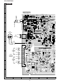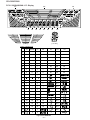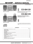
1
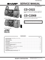
CD-C622/C2900
SERVICE MANUAL
No. S3908CDC622//
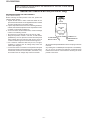
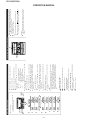
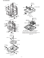
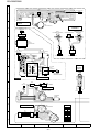
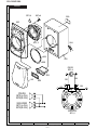
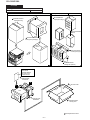
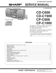
CD-C622
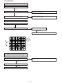
CD-C622 mini component system consisting of CD-C622 mini
component system, CP-C622 and rear (GBOXS0021AWM1) speaker
system.
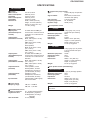
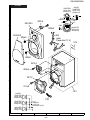
CD-C2900
Illustration: CD-C622
CD-C2900 mini component system consisting of CD-C2900 mini
component system and CP-C2900 speaker system.
• In the interests of user-safety the set should be restored to its
original condition and only parts identical to those specified be
used.
Illustration: CD-C2900
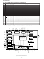
CONTENTS
Page
IMPORTANT SERVICE NOTES (For U.S.A. Only) ........................................................................................................... 2
SPECIFICATIONS .............................................................................................................................................................. 3
NAMES OF PARTS ........................................................................................................................................................... 4
OPERATION MANUAL ...................................................................................................................................................... 6
QUICK GUIDE ................................................................................................................................................................... 7
DISASSEMBLY .................................................................................................................................................................. 9
REMOVING AND REINSTALLING THE MAIN PARTS ................................................................................................... 12
ADJUSTMENT ................................................................................................................................................................. 13
NOTES ON SCHEMATIC DIAGRAM .............................................................................................................................. 15
WAVEFORMS OF CD CIRCUIT ...................................................................................................................................... 16
BLOCK DIAGRAM ........................................................................................................................................................... 17
SCHEMATIC DIAGRAM / WIRING SIDE OF P.W.BOARD .............................................................................................. 20
VOLTAGE ........................................................................................................................................................................ 41
TROUBLESHOOTING (CD SECTION) ........................................................................................................................... 42
FUNCTION TABLE OF IC ................................................................................................................................................ 47
FL DISPLAY ...................................................................................................................................................................... 54
REPLACEMENT PARTS LIST/EXPLODED VIEW
PACKING OF THE SET (For U.S.A. Only)
SHARP CORPORATION
–1–
This document has been published to be used
for after sales service only.
The contents are subject to change without notice.
CD-C622/C2900
FOR A COMPLETE DESCRIPTION OF THE OPERATION OF THIS UNIT, PLEASE REFER
TO THE OPERATION MANUAL.
IMPORTANT SERVICE NOTES (For U.S.A. Only)
BEFORE RETURNING THE AUDIO PRODUCT
(Fire & Shock Hazard)
Before returning the audio product to the user, perform the
following safety checks.
1. Inspect all lead dress to make certain that leads are not
pinched or that hardware is not lodged between the chassis
and other metal parts in the audio product.
2. Inspect all protective devices such as insulating materials,
cabinet, terminal board, adjustment and compartment covers
or shields, mechanical insulators etc.
3. To be sure that no shock hazard exists, check for leakage
current in the following manner.
* Plug the AC line cord directly into a 120 volt AC outlet.
* Using two clip leads, connect a 1.5k ohm, 10 watt resistor
paralleled by a 0.15µF capacitor in series with all exposed
metal cabinet parts and a known earth ground, such as
conduit or electrical ground connected to earth ground.
* Use a VTVM or VOM with 1000 ohm per volt, or higher,
sensitivity to measure the AC voltage drop across the
resistor (See diagram).
* Connect the resistor connection to all exposed metal parts
having a return path to the chassis (antenna, metal cabinet,
screw heads, knobs and control shafts, escutcheon, etc.)
and measure the AC voltage drop across the resistor.
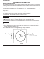
VTVM
AC SCALE
1.5k ohms
10W
0.15 µ F
TO EXPOSED
METAL PARTS
TEST PROBE
CONNECT TO
KNOWN EARTH
GROUND
All check must be repeated with the AC line cord plug connection
reversed.
Any reading of 0.3 volt RMS (this corresponds to 0.2 milliamp.
AC.) or more is excessive and indicates a potential shock
hazard which must be corrected before returning the audio
product to the owner.
–2–
CD-C622/C2900
SPECIFICATIONS
CD-C622/C2900
General
Power source:
Power consumption:
(CD-C622)
Power consumption:
(CD-C2900)
Dimensions:
Weight:
Amplifier section
Output power:
(CD-C622 Except for
Canada)
Output power:
(CD-C622 For Canada)
Output power:
(CD-C2900 Except for
Canada)
Output power:
(CD-C2900 For Canada)
Output terminals:
(CD-C622)
Output terminals:
(CD-C2900)
Input terminal:
Tuner section
Frequency range:
Compact disc player section
Type:
3-disc multi-play compact disc
player
Signal readout:
Non-contact, 3-beam semiconductor laser pickup
D/A Converter:
1-bit D/A converter
Frequency response:
20 - 20,000 Hz
Dynamic range:
90 dB (1 kHz)
AC 120 V, 60 Hz
Stand-by; 0.3 W
Power on; 95 W
Stand-by; 0.3 W
Power on; 100 W
Width; 10-5/8" (270 mm)
Height; 11-13/16" (300 mm)
Depth; 13-13/16" (351 mm)
13.7 lbs. (6.2 kg)
Front speaker section
CP-C622
Type:
40 watts minimum RMS per
channel into 4 ohms from 60 Hz
to 20 kHz, 10 % total harmonic
distortion
Front speakers;
MPO; 108 W (54 W + 54 W)
(10 % T.H.D.)
RMS; 60 W (30 W + 30 W)
(10 % T.H.D.)
Rear speakers;
MPO; 36 W (18 W + 18 W)
(10 % T.H.D.)
RMS; 20 W (10 W + 10 W)
(10 % T.H.D.)
50 watts minimum RMS per
channel into 6 ohms from 60 Hz
to 20 kHz, 10 % total harmonic
distortion
MPO; 180 W (90 W + 90 W)
(10 % T.H.D.)
RMS; 100 W (50 W + 50 W)
(10 % T.H.D.)
Front speakers; 6 ohms
Rear Speakers; 16 ohms
Headphones; 16-50 ohms
(recommended; 32 ohms)
Speakers; 6 ohms
Headphones; 16-50 ohms
(recommended; 32 ohms)
Video/Auxiliary (audio signal);
500 mV/47 kohms
Maximum input power:
Rated input power:
Impedance:
Dimensions:
Weight:
2-way type [5-1/4" (13 cm)
woofer and super tweeter]
60 W
30 W
6 ohms
Width; 8-11/16" (220 mm)
Height; 11-13/16" (300 mm)
Depth; 8-9/16" (217 mm)
5.7 lbs. (2.6 kg)/each
CP-C2900
Type:
Maximum input power:
Rated input power:
Impedance:
Dimensions:
Weight:
3-way type [5" (13 cm) woofer,
2" (5 cm) tweeter and super
tweeter]
100 W
50 W
6 ohms
Width; 7-7/8" (200 mm)
Height; 11-13/16" (300 mm)
Depth; 10" (256 mm)
6.4 lbs. (2.9 kg)/each
Rear speaker section (CD-C622 Only)
GBOXS0021AWM1
Type:
Maximum input power:
Rated input power:
Impedance:
Dimensions:
Weight:
FM; 87.5 - 108 MHz
AM; 530 - 1,720 kHz
4" (10 cm) full range speaker
20 W
10 W
16 ohms
Width; 6-3/4" (170 mm)
Height; 6-3/4" (170 mm)
Depth; 3-1/2" (88 mm)
0.9 lbs. (0.4 kg)/each
Specifications for this model are subject to change without
prior notice.
Cassette deck section
Frequency response:
50 - 14,000 Hz (Normal tape)
Signal/noise ratio:
55 dB (TAPE 1, playback)
50 dB (TAPE 2, recording/
playback)
Wow and flutter:
0.15 % (WRMS)
–3–
CD-C622/C2900
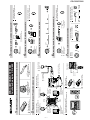
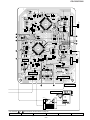
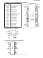
NAMES OF PARTS
CD-C622/C2900
3
4 5
1
2
6
7
8
9
10
11
12 13 14
Front Panel
1. Disc Number Selector Buttons
2. Disc Tray
3. Multi-function Indicator
4. Disc Skip Button
5. Open/Close Button
6. Extra Bass Indicator
7. FM Stereo Mode Indicator
8. FM Stereo Indicator
9. (CD) Repeat Indicator
10. (CD) Play Indicator
11. (CD) Pause Indicator
12. Spectrum Analyzer/ Volume Level Indicator
13. (TAPE 2) Racord INdicator
14. (CD) Disc Number Indicators
15. (CD/TUNER) Memory Indicator
16. Timer Indicator
17. Sleep Indicator
15
16
17
18. (TAPE 2) Record Pause Button
19. (CD) Track Down/Review Button
(TUNER) Preset Down Button
(TAPE 2) Rewind Button
20. (CD) Track Up/Cue Button
(TUNER) Preset Up Button
(TAPE 2) Fast Forward Button
21. Timer/Sleep Button
22. Clock Button
23. Timer Set Indicator
24. Power Button
25. Equalizer Mode Selector Button
26. Dimmer Button
27. Extra Bass/Demo Mode Button
28. Headphones Socket
29. Function Selector Buttons
30. Memory/Set Button
31. (CD/TAPE) Stop Button
32. (TAPE) Play Button
(CD) Play/Repeat Button
33. Tuning and Time Up/Cue Buttons
34. Volume Up/Down Buttons
18 19
20
21
22
23
24
25
26
27
28 29 30 31 32 33 34
35
36
35. (TAPE 1) Cassette Compartment
36. (TAPE 2) Cassette Compartment
Rear Panel
1. CD Digital Output Socket
2. AC Power Input Socket
3. FM/AM Loop Aerial Socket
4. Video/Auxiliary (Audio Signal) Input Sockets
5. Front Speaker Terminals (CD-C622 Only)
6. Rear Speaker Terminals (CD-C622)
6. Speaker Terminals (CD-C2900)
1
3
4
5
2
6
(Illistration: CD-C622)
–4–
CD-C622/C2900
Front Speaker
1
CP-C622
1. Super Tweeter
2. Woofer
3. Bass Reflex Ducts
4. Speaker Wire
2
4
3
1
CP-C2900
1. Super Tweeter
2. Tweeter
3. Woofer
4. Bass Reflex Ducts
5. Speaker Wire
2
3
4
5
Rear Speaker (CD-C622 Only)
GBOXS0021AWM1
1. Full Range Speaker
2. Speaker Wire
1
2
CD-C622/C2900
1
Remote Control
1. Remote Control Transmitter LED
CD Control section
2. Disc Number Select Buttons
3. Memory Button
4. Pause Button
5. Clear Button
6. Track Down/Review Button
7. Track Up/Cue Button
8. Disc Skip Button
9. Play/Repeat Button
10. Stop Button
11. Random Button
2
8
3
9
4
5
6
7
10
Tuner control section
12. Preset Up/Down Buttons:
11
12
13 14 15 16 17 18
Tape control section
13. (TAPE 1) Play Button
14. (TAPE 2) Record Pause Button
15. (TAPE 1/2) Stop Button
16. (TAPE 2) Play Button
17. (TAPE 2) Rewind Button
18. (TAPE 2) Fast Forward Button
19
20
21
22
Common section
19. Equalizer Mode Selector Button
20. Function Selector Buttons
21. Power Button
22. Extra Bass Button
23. Volume Up/Down Buttons
–5–
23
–6–
9
8
7
6
5
4
3
2
AM 12:00
POWER
MEMORY/
SET
CLOCK
AM 0:00
0:00
TUNING/
TIME
(
)
In this example, the clock is set for the
12-hour (AM 12:00) system.
(Main unit operation)
SETTING THE CLOCK
or
) button to adjust the hour.
or
) button to adjust the
The clock starts operating from "0" seconds. (Seconds are not
displayed.)
Press the MEMORY/SET button.
Press the TUNING/TIME (
or
) button once to advance
the time by 1 minute. Hold it down to change the time in 5
minute intervals.
The hour setting will not advance even if minutes advance from
"59" to "00".
Press the TUNING/TIME (
minutes.
Press the MEMORY/SET button.
Press the TUNING/TIME (
or
) button once to advance
the time by 1 hour. Hold it down to advance continuously.
When the 12-hour display is selected, "AM" will change automatically to "PM".
Press the TUNING/TIME (
Press the MEMORY/SET button.
Press the TUNING/TIME ( or ) button to select the time
display mode.
"AM 12:00" → The 12-hour display will appear.
(AM 12:00 - PM 11:59)
"AM 0:00" → The 12-hour display will appear.
(AM 0:00 - PM 11:59)
"0:00"
→ The 24-hour display will appear.
(0:00 - 23:59)
Note that this can only be set when the unit is first installed
or it has been reset.
Within 5 seconds, press the MEMORY/SET button.
Press the CLOCK button.
Press the POWER button to enter the stand-by mode.
2 Perform steps 1 - 9 above.
COMPUTER", on page 19.
1 Perform steps 1 - 2 in the section "RESETTING THE MICRO-
To change the time display mode:
Press the CLOCK button.
The time display will appear for about 5 seconds.
To see the time display:
3 Perform steps 6 - 9 above.
2 Within 5 seconds, press the MEMORY/SET button.
1 Press the CLOCK button.
To change the clock time:
Note:
In the event of a power failure or when the AC power lead is
disconnected, the clock display will go out.
When the AC power supply is restored, the clock display will
flash on and off to indicate the time when the power failure
occurred or when the AC power lead was disconnected.
If this happens, follow the procedure below to change the clock
time.
9
7
8
5
6
1
2
3
4
1,2
2
RESETTING THE MICROCOMPUTER
Whilst pressing down the
button and the
button, hold down the POWER button for at least 1 second.
Press the POWER button to enter the stand-by mode.
Caution:
The operation explained above will erase all data stored in
memory including clock and timer settings, and tuner and CD
presets.
1
2
Reset the microcomputer under the following conditions:
To erase all of the stored memory contents (clock and timer
settings, and tuner and CD presets).
If the display is not correct.
If the operation is not correct.
CD-C622/C2900
OPERATION MANUAL
FM/AM loop antenna x 1
Antena de cuadro de
FM/AM x 1
–7–
Black
Negro
Black
Negro
Front speaker (Left)
Altavoz delantero
(Izquierdo)
Red
Rojo
Wire with the
white line
Cable con la
línea blanca
Rear speaker (Left)
Altavoz trasero (Izquierdo)
POWER
POWER
Turning the power on and off
Conexión y desconexión de la alimentación
Front speaker (Right)
Altavoz delantero
(Derecho)
Red
Rojo
Wire with the
white line
Cable con la
línea blanca
Rear speaker (Right)
Altavoz trasero (Derecho)
Speaker connection
Conexión de los altavoces
15
15
Remote Sensor
Sensor remoto
AC 120 V, 60 Hz
120 V de CA, 60 Hz
8” - 20’ (0.2m - 6m)
0,2m - 6m
Batteries are not included.
Las pilas no están incluidas.
2 “AA” batteries
Dos pilas “AA”
Remote control
Controlador remoto
FM Antenna
Antena de FM
AM Loop Antenna
Antena de cuadro
de AM
AC power cord x 1
Cable de alimentación
de CA x 1
Antenna connection
Conexión de las antenas
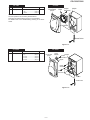
2 Preparation for use / Preparación para su uso
Remote control x 1
Controlador remoto x 1
1 Check the supplied accessories / Compruebe los accesorios suministrados
MINI COMPONENT SYSTEM
Quick Guide/Guía rápida CD-C622
TAPE 2
To stop the playback
Para detener la reproducción
To stop the playback
Para detener la reproducción
TAPE 2
VOLUME
Volume
Volumen
Extra bass (X-BASS)
Graves extra (X-BASS)
7 Sound control / Control del sonldo
Load the disc to be
recorded.
Introduzca el disco
que va a grabar.
SOFT-2
FLAT
SOFT-1
HEAVY-1
VOCAL
HEAVY-2
Pre-programmed equalizer
Ecualizador preprogramado
CD recording
starts.
La grabación de
CD empieza.
To stop the playback
Para detener la reproducción
6 Recording from CDs / Grabaciones de discos CD
5 Listening to the radio / Audición de la radio
TAPE 1
4 Listening to a tape / Audición de una cinta
Label facing up
Etiqueta hacia arriba
3 Listening to a CD / Audición de discos CD
CD-C622/C2900
–8–
Black
Negro
Red
Rojo
Black
Negro
Red
Rojo
Front speaker
(Left)
Altavoz delantero
(Izquierdo)
POWER
POWER
Turning the power on and off
Conexión y desconexión de la alimentación
Front speaker
(Right)
Altavoz delantero
(Derecho)
Speaker connection
Conexión de los altavoces
15
15
Remote Sensor
Sensor remoto
AC 120 V, 60 Hz
120 V de CA, 60 Hz
8” - 20’ (0.2m - 6m)
0,2m - 6m
Batteries are not included.
Las pilas no están incluidas.
2 “AA” batteries
Dos pilas “AA”
Remote control
Controlador remoto
FM Antenna
Antena de FM
AM Loop Antenna
Antena de cuadro
de AM
AC power cord x 1
Cable de alimentación
de CA x 1
Antenna connection
Conexión de las antenas
2 Preparation for use / Preparación para su uso
Remote control x 1
Controlador remoto x 1
FM/AM loop antenna x 1
Antena de cuadro de
FM/AM x 1
1 Check the supplied accessories / Compruebe los accesorios suministrados
MINI COMPONENT SYSTEM
Quick Guide/Guía rápida CD-C2900
TAPE 2
To stop the playback
Para detener la reproducción
To stop the playback
Para detener la reproducción
TAPE 2
VOLUME
Volume
Volumen
SOFT-2
FLAT
SOFT-1
HEAVY-1
VOCAL
HEAVY-2
Pre-programmed equalizer
Ecualizador preprogramado
CD recording
starts.
La grabación de
CD empieza.
Extra bass (X-BASS)
Graves extra (X-BASS)
7 Sound control / Control del sonldo
Load the disc to be
recorded.
Introduzca el disco
que va a grabar.
To stop the playback
Para detener la reproducción
6 Recording from CDs / Grabaciones de discos CD
5 Listening to the radio / Audición de la radio
TAPE 1
4 Listening to a tape / Audición de una cinta
Label facing up
Etiqueta hacia arriba
3 Listening to a CD / Audición de discos CD
CD-C622/C2900
CD-C622/C2900
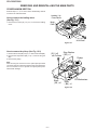
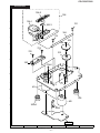
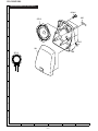
DISASSEMBLY
Caution on Disassembly
Follow the below-mentioned notes when disassembling
the unit and reassembling it, to keep it safe and ensure
excellent performance:
1. Take cassette tape and compact disc out of the unit.
2. Be sure to remove the power supply plug from the wall
outlet before starting to disassemble the unit.
3. Take off nylon bands or wire holders where they need be
removed when disassembling the unit. After servicing
the unit, be sure to rearrange the leads where they were
before disassembling.
4. Take suffcient care on static electricity of integrated
circuits and other circuits when servicing.
(Illustration: CD-C622)
CD-C622/C2900
Top Cabinet
(A1)x2
ø3x12mm
(B2)x1
(B1)x1
ø3x8mm
CD-C622/C2900
STEP
REMOVAL
PROCEDURE
FIGURE
1
Top Cabinet
1. Screw ..................... (A1) x4
9-1
2
Side Panel
(Left/right)
1. Screw ..................... (B1) x6
2. Hook ....................... (B2) x2
9-1
3
CD Player Unit/
CD Tray Cover
1. Turn on the power supply,
open the disc tray, take out
the CD cover, and close.
(Note 1)
2. Hook ....................... (C1) x3
3. Hook ....................... (C2) x2
4. Socket .................... (C3) x3
9-2
Back Board
(with Digital
Output PWB)
1. Screw ..................... (D1) x5
9-2
Main PWB
1. Screw .....................
2. Socket ....................
3. Flat Wire .................
4. Tip Wire ..................
5. Flat Cable ..............
4
5
Side Panel
(Right)
(A1)x2
ø3x12mm
Side Panel
(Left)
Back Board
(B2)x1
(B1)x4
ø3x8mm
(B1)x1
ø3x8mm
Figure 9-1
(C3) x3
(E1) x3
(E2) x4
(E3) x1
(E4) x1
(E5) x1
10-1
CD Tray Cover
(C2) x1
Pull
Hook
( C1) x3
1
1
6
Front Panel
1. Screw ..................... (F1) x1
10-1
7
Display PWB/
Switch PWB
1. Socket .................... (G1) x1
2. Screw ..................... (G2) x12
10-2
8
Tape Mechanism 1. Open the cassette holder.
2. Screw...................... (H1) x5
10-2
9
Headphones PWB 1. Screw ..................... (J1) x1
2. Support Bracket ..... (J2) x1
10-2
10
Turntable
1. Screw ..................... (K1) x1
2. Cover ..................... (K2) x1
10-3
11
Disc Tray
1. Screw ..................... (L1) x2
2. Guide ..................... (L2) x2
10-3
12
CD Servo PWB
(Note 2)
1. Screw ..................... (M1) x1
2. Socket .................... (M2) x4
10-4
13
CD Changer
Mechanism
1. Screw ..................... (N1) x4
10-5
14
CD Mechanism
1. Screw ..................... (P1) x1
10-5
2
CD Player
Unit
( C2 ) x1
Back Board
Main PWB
(D1)x5
ø3x8mm
Figure 9-2
LOCK
LEVER
Note 1:
How to open the changer manually. (Fig. 9-3)
1. Change, turn fully the lock lever in the arrow direction
through the hole on the loading chassis bottom in this state.
After that, push forward the CD player base.
Note 2:
1. After removing the connector for the optical pickup fromthe
connector wrap the conductive aluminium foil around the
front end of connector so as to protect the optical pickup
from electrostatic damage.
Figure 9-3
–9–
CD-C622/C2900
(E1)x1
ø3x10mm
( M1 ) x1
ø3 x10mm
Front Panel
(E2)x2
(E3)x1
(E5)x1
CD Servo PWB
( M2 ) x2
(E2)x2
(E4)x1
(G1)x1
( M2 ) x2
CD Player Unit
(E1)x2
ø3x8mm
Figure 10-4
(F1)x1
ø3x8mm
Main PWB
( N1 ) x4
ø3 x12mm
Figure 10-1
( P1 ) x1
ø2.6 x10mm
(G1)x1
Switch PWB
Front Panel
Shift Lever
(G2)x2
ø3x10mm
CD Changer
Mechanism
Display PWB
(G2)x10
ø3x10mm
Headphones
PWB
Open
Cassette
Holder
(J2)x1
(J1)x1
ø3x10mm
Tape Mechanism
(H1)x5
ø3x10mm
CD Player Base
Figure 10-2
Figure 10-5
( K1 ) x1
ø3 x10mm
( K2 ) x1
Washer
Turntable
Disc Tray
( L1 ) x1
ø3 x10mm
( L2 ) x1
( L1 ) x1
ø3 x10mm
CD Player Unit
CD Mechanism
Care when installing the CD changer mechanism.
Install the CD changer mechanism on the CD player base after
the shift lever has been set in the highest position.
( L2 ) x1
Figure 10-3
– 10 –
CD-C622/C2900
CP-C622
STEP
1
REMOVAL
Front Speaker
CP-C622
PROCEDURE
FIGURE
1. Front Panel ............ (A1) x1
2. Tip .......................... (A2) x2
3. Screw ..................... (A3) x4
11-1
Front Panel
(A1)x1
(A3)x4
ø4x12mm
Piezo
(A2)x2
Note:
The rear speakers can be easily disassembled.
Therefore the disassembling method is not discribed.
For details refer to the disassembling drawing in the Parts
Guide.
Woofer
Screw Driver
Figure 11-1
CP-C2900
STEP
1
CP-C2900
REMOVAL
PROCEDURE
Front Speaker
1. Front Panel ............
2. Tip ..........................
3. Screw .....................
4. Screw .....................
5. Screw .....................
FIGURE
(A1) x1
(A2) x2
(A3) x2
(A4) x2
(A5) x4
11-2
Front Panel
(A1)x1
Super
Tweeter
Tweeter
(A3)x2
ø3x10mm
(A2)x2
(A4)x2
ø3x10mm
(A5)x4
ø4x14mm
Woofer
Screw Driver
Figure 11-2
– 11 –
CD-C622/C2900
REMOVING AND REINSTALLING THE MAIN PARTS
CD MECHANISM SECTION
Perform steps 1, 2, 3, 13 and 14 of the disassembly method
to remove the CD mechanism.
Loading / Up
/ Down Motor
How to remove the loading motor
(See Fig. 12-1)
Motor
PWB
1. Remove the screws (A1) x 2 pcs., to remove the loading
motor.
( A1 ) x2
ø2.6 x5mm
Figure 12-1
How to remove the pickup (See Fig. 12-2)
Stop Washer
( B1 ) x2
( B3 ) x1
ø2.6 x6mm
1. Remove the screws (B1) x 2 pcs., to remove the shaft (B2).
2. Remove the stop washer (B3) x 1 pc., to remove the gear
(B4).
3. Remove the pickup.
Pickup
Note
After removing the connector for the optical pickup fromthe
connector wrap the conductive aluminium foil around the front
end of connector so as to protect the optical pickup from
electrostatic damage.
Shaft
( B2 ) x1
CD Mechanism
Gear
( B4 ) x1
Figure 12-2
– 12 –
CD-C622/C2900
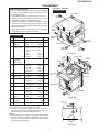
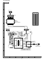
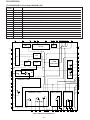
ADJUSTMENT
• FM RF
Signal generator: 1 kHz, 75 kHz dev., FM modulated
MECHANISM SECTION
• Driving Force Check
Torque Meter
Test Stage Frequency Frequency
Display
Specified Value
Play: TW-2412
Tape 1: Over 80 g
Tape 2: Over 80 g
• Torque Check
Torque Meter
Specified Value
Tape 1
Play: TW-2111
Tape 2
30 to 60 g. cm
Fast forward: TW-2231
—
60 to 120 g.cm
Rewind: TW-2231
—
60 to 120 g.cm
Normal
speed
Adjusting
Point
Specified
Value
MTT-111
Volume in
motor.
(MM1)
3,000 ±
30 Hz
—
87.50 MHz L303(fL):
3.4 V ± 50 mV
RF
98.00 MHz 98.00 MHz L302
(10-30 dB)
Test
Stage
Instrument
Connection
Speaker
terminal
(Load
resistance:
8 ohms)
fL: Low-range frequency
fH: High-renge frequency
• AM IF/RF
Signal generator: 400 Hz, 30%, AM modulated
Frequency Frequency
Display
Adjusting
Parts
Instrument
Connection
Detection 10.7 MHz
98.00 MHz
T352
IF
98.00 MHz
T301(Turn Input: Pin 1 of
the core of IC301
transformer Output: TP302
T352 fully
counterclookwise.)
10.7 MHz
Input: Pin 1 of
IC303
Output: TP302
• VCO Frequency
Frequency
Display
Frequency
Test Stage Frequency
Frequency
Display
Setting/ Instrument
Adjusting Connection
Parts
IF
450 kHz
1,720 kHz
T351
Band
Coverage
—
530 kHz
(fL): T333 *2
1.1 ± 0.1 V
Tracking
990 kHz
990 kHz
(fL): T331
98.00 MHz
(60 dB)
*1
98.00 MHz
Adjusting
Parts
VR351*
Instrument
Connection
Pin 13, Pin 21
and ground
of IC303
* Adjust for 76 kHz ± 200 Hz.
Notes:
After preparing the test circuit shown in Fig 13-2, connect the
Pin 13 , Pin 21 and ground of the IC303 with test circuit, and
measure the Value.
At this time, apply a standard unmodulated signal input and
adjust the VCO.
*1
Output: TP302
Output: TP301
TAPE MECHANISM
Pin 13 of IC303
G
MM 1
Motor
Pin 21 of IC303
D
FET : 2SK19 or 2SK54
TO FREQUENCY
COUNTER
S
10 kΩ
Volume in motor
MAIN PWB
L301
1
Figure 13-2
IC301
L303
CNP301
AM LOOP
ANTENNA
L302
FM RF
T301
FM IF
FM BAND
COVERAGE fL
T351
T331
TP301
AM TRACKING
fL
1
T333
T352
R340
AM BAND
COVERAGE fL
21
AM IF
IC303
13
*2
Output: TP301
Output: Speaker terminal
TUNER SECTION
*1. Input: Antenna,
*2. Input: Antenna,
*1
• Detection
Signal generator: 10.7 MHz, FM sweep generator
• Tape Speed
Test Tape
Band
Coverage
*1. Input: Antenna,
*2. Input: Antenna,
30 to 60 g.cm
Instrument
Connection
Serring/
Adjusting
Point
VR351
VCO
FM DET
TP302
Figure 13-1 ADJUSTMENT POINTS
– 13 –
CD-C622/C2900
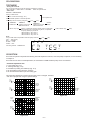
TEST MODE
• Setting the test mode
Any one of test mode can be set by pressing several keys as follows.
<REC. PAUSE> + <DISC. SKIP> + <POWER>
TEST: CD operation test
• TEST mode
Function — CD test mode
Setting of TEST mode
Indication of CD TST mode (Fig. 14-1)
IL is not performed.
OPEN/CLOSE operation is manual operation.
The pickup can be moved by using the (
<MEMORY>
LASER ON
<MEMORY>
Tracking on the spot.
SERVO OFF PLAY
<PLAY> key input
) or (
) key.
<MEMORY>
Tracking on the spot.
SERVO ON PLAY
<STOP>
STOP
TOC. IL is performed, and the ordinary PLAY is performed.
If the following key is pressed during PLAY, it is possible
to specify directly any Track No.
<Disc Number 1> key: Track 4
<Disc Number 2> key: Track 9
<Disc Number 3> key: Track 15
Note:
Only in STOP state it is possible to slide the pickup with the (
VOL. --- Last memory
BAL. --- CENTER
R.GEQ. --- FLAT
X-BAS --- OFF
1
2
) or (
Press <STOP> key.
Stop
) key.
3
Canceling method - POWER OFF
Figure 14-1
CD SECTION
Since this CD system incorporates the following automatic adjustment function, when the pickup is replaced, it is not necessary
to readjust it.
Since this CD unit does not need adjustment, the combination of PWB and laser pickup unit is not restricted.
• Automatic adjustment item
1. Focus offset (Fig. 14-2)
2. Tracking offset (Fig. 14-3)
3. E/F balance (tracking error balance) (Fig. 14-4)
4. RF level AGC function (HF level: constant)
5. RF level automatic follow-up of the tracking gain
This automatic adjustment is performed each time a disc is changed. Therefore,
each disc is played back using the optimal settings.
Enlarged
View
10ms
0.50 V
IC1 20 FE
0.1s
0.50 V
IC1 20 FE
FOCUS
OFF-SET
ADJUST
10ms
0.50 V
IC1 7 TE
0.1s
0.50 V
IC1 7 TE
TRACKING
OFF-SET
1 ADJUST
TRACKING
OFF-SET
1 ADJUST
2
2
Figure 14-3
Figure 14-2
TRACKING/
ERROR
BARANCE
1 ADJUST
200 ms
1V/diV
IC 1 15
TO
200 ms
1V/diV
IC 1 7
TE
2
Figure 14-4
– 14 –
CD-C622/C2900
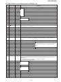
NOTES ON SCHEMATIC DIAGRAM
• Resistor:
To differentiate the units of resistors, such symbol as K and
M are used: the symbol K means 1000 ohm and the symbol
M means 1000 kohm and the resistor without any symbol is
ohm-type resistor. Besides, the one with “Fusible” is a fuse
type.
• Capacitor:
To indicate the unit of capacitor, a symbol P is used: this
symbol P means micro-micro-farad and the unit of the
capacitor without such a symbol is microfarad. As to
electrolytic capacitor, the expression “capacitance/withstand
voltage” is used.
(CH), (TH), (RH), (UJ): Temperature compensation
(ML): Mylar type
(P.P.): Polypropylene type
• Schematic diagram and Wiring Side of P.W.Board for this
model are subject to change for improvement without prior
notice.
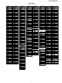
REF. NO
DESCRIPTION
• The indicated voltage in each section is the one measured
by Digital Multimeter between such a section and the chassis with no signal given.
1. In the tuner section,
( ) indicates AM
< > indicates FM stereo
2. In the main section, a tape is being played back.
3. In the deck section, a tape is being played back.
( ) indicates the record state.
4. In the power section, a tape is being played back.
5. In the CD section, the CD is stopped.
• Parts marked with “
”(
) are important for
maintaining the safety of the set. Be sure to replace these
parts with specified ones for maintaining the safety and
performance of the set.
POSITION
REF. NO
DESCRIPTION
POSITION
SW1
OPEN/CLOSE
ON—OFF
SW714
TUNER/BAND
ON—OFF
SW2
MECHA UP
ON—OFF
SW715
VIDEO
ON—OFF
SW3
DISC NUMBER
ON—OFF
SW716
TAPE
ON—OFF
SW4
PICKUP IN
ON—OFF
SW717
CD
ON—OFF
SW701
POWER
ON—OFF
SW722
FF
ON—OFF
SW703
CLOCK
ON—OFF
SW723
TUNING UP
ON—OFF
SW704
TIMER/SLEEP
ON—OFF
SW724
TUNING DOWN
ON—OFF
SW705
DISC 1
ON—OFF
SW725
PLAY
ON—OFF
SW706
DISC 2
ON—OFF
SW726
VOLUME DOWN
ON—OFF
SW707
DISC 3
ON—OFF
SW727
VOLUME UP
ON—OFF
SW708
DISC SKIP
ON—OFF
SW728
X-BASS/DEMO
ON—OFF
SW709
OPEN/CLOSE
ON—OFF
SW729
EQUALIZER
ON—OFF
SW710
REV
ON—OFF
SW730
DIMMER
ON—OFF
SW711
REC PAUSE
ON—OFF
SWM 3
FOOL PROOF
ON—OFF
SW712
MEMORY/SET
ON—OFF
SWM 4
F.A.S.
ON—OFF
SW713
STOP
ON—OFF
SWM 5
CAM
ON—OFF
FRONT VIEW
FRONT
VIEW
E C B
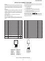
(S) (G) (D)
(1) (2) (3)
KTA1266 GR
2SA1015 GR
2SA1318
2SC3331
2SC535 C
KRA102 M
KRA109 M
KRC102 M
KRC104 M
KRC107 M
KTA1271 Y
KTA1273 Y
KTA1274 Y
KTD2058 Y
KTC3200 GR
KTC3203 Y
L1154GT4
SLI342YCB
SLI342DCB
SLI342UCB
SLI342YCJ
Figure 15 TYPES OF TRANSISTOR AND LED
– 15 –
CD-C622/C2900
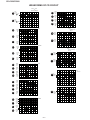
WAVEFORMS OF CD CIRCUIT
STOP
FOCUS
1
2
PLAY
SERCH
5ms
0.50 V
IC1 20 F.E
5ms
5.0 V
IC1 54 DRF
0.5ms
10.0 V
JP+
7
0.5ms
10.0 V
JP-
8
0.5ms
0.50 V
JP
9
0.5ms
1.00 V
TE
3
1
3
6
PLAY
CUE
0.5ms
1.00 V
HF
4
0.5ms
5.0 V
HFL
1
5
0.5ms
5.0 V
TES
3
3
0.5ms
1.00 V
HF
NORMAL DISC
TN0=01
10
20ms
1.00 V
SPO
11
20ms
2.00 V
CLV+
2
REVIEW
PLAY
TCD-712 (140mm)
TN0=01
4
5
0.5ms
5.0 V
HFL
1
0.5ms
5.0 V
TES
3
6
50ms
10.0 V
JP+
7
50ms
10.0 V
JP-
8
50ms
0.50 V
JP
9
2
0.5ms
10.0 V
JP+
7
0.5ms
10.0 V
JP-
8
0.5ms
0.50 V
JP
9
0.5ms
1.00 V
TE
6
50ms
10.0 V
JP+
7
50ms
10.0 V
JP-
8
50ms
0.50 V
JP
9
50ms
1.00 V
TE
50ms
1.00 V
SPO
11
50ms
2.00 V
CLV+
CUE
PLAY
TCD-712
12
50ms
1.00 V
TE
6
10
5s
100mV
SLD
1
12
0.5s
100mV
SLD
REVIEW
1
– 16 –
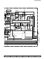
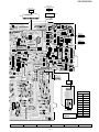
– 17 –
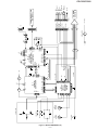
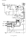
Figure 17 BLOCK DIAGRAM (1/3)
M
M
PICKUP IN
SW4
M1
SPINDLE
MOTOR
M2
SLED
MOTOR
TRACKING COIL
FOCUS COIL
15
16
26
27
6
7
4
5
23
1
2
3
4
20 25
8 ~ 14 21 22 29 ~ 35
IC3
M63001FP
FOCUS/
TRACKING/
SPIN/SLED
DRIVER
1 2 7
36
28
39
38
37
20
40
24
18
42
41
30 31 54
15 16 27 23 29
FIN2
FIN1
E
F
IC1
LA9241M
SERVO AMP.
64
VCC1
62
LD0
TO
FD
SPO
NC
SLD
22
JP– 32
Q52
CV+ 40
SLC 43
SL1 44
~
Q1
SL–
SL+
DRF
PU-IN SW
+B5
+B1
SL+. SL–. DRF
6
23 36 41 43
+5V
51 62 ~ 64
20 JP–
53 ~ 58
27
37
38
39
40
31
CONT2 25
CONT1 24
LCHO
LVSS
RVSS
RCHO
26 33 38 39 46
RES. CQCK. COIN
SQOUT. RWC. WRQ
10 EFMIN
12 CLV+
IC2
LC78622NE
SERVO/SIGNAL
11
CONTROL
9 EFMO
2
4
8
44
XOUT
45
XL1
XIN
CL, DAT, SELIAL CONTROL/CE
51 52 53
+B1
~
+5V
CL
DAT
CE
VVDD
VDD
LVDD
RVDD
XVDD
PICKUP UNIT
+4.3V
Q51
2
1
BI1B
Q81
+5V
CNS10
9
8
7
6
5
4
3
2
1
+7.3V (B1)
MECHA UP
GND (D)
DISK NO.
OPEN/CLOSE
GND (D)
M–
M+
GND (M)
CNP10
9
8
7
6
5
4
3
2
1
10
SOLM1
M3
LOADING
TO MAIN
SECTION
M
SW1
OPEN/CLOSE
SW3
DISC No.
SW2
MECHA UP
TO MAIN SECTION
(TO IC601)
10 GND (D)
1
2
3
4
5
6
CNP11
REGULATOR
2
1
BI1A
3
2
1
CNP99
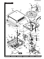
CD-C622/C2900
CD-C622/C2900
SWM3
FOOL PROOF
SWM4
F.A.S
SOLM1
SOLENOID
AM LOOP
FM
ANTENNA ANTENNA
L301
IC301
TA7358AP
FM FRONT END
1
FM B.P.F
FM IF
6
+B4
+B4
CF301
T301
SWM5
CAM
9
4
5
8
7
L302
T351
FM IF IN
FM OSC
FM RF
VR351
MPX VCO ADJ
AM IF
T352
CF351
1 3
AM MIX
21
20
6
5
AM IF GND FM+B FM DET
IC303
LA1805
FM/AM IF MPX.
22
15
13
VCO MO/ST
L 9
R 10
MPX IN
DET OUT
7
STEREO
FM/AM
16
17
11
Q350
Q343
FM/AM
SWITCHING
AM BAND
COVERAGE
+B7
20
22
1
OSC
15
3
11
4
CL
5
IC302
LC72131
PLL (TUNER)
7
FM +B
16
DI
VT
CE
X352
4.5MHz
FM IN
T333
AM IN
T331
AM OSC IN
OSC BUFF
23
AM+B
24
AM RF IN
FMOSC
Q302
AM TRACKING
MONO/ST
FM DET
L303
1 IC704
2
3
DO
3
FM
OSC
2
VOLTAGE
REGURATER
6
+B4
17
21
10
FM
Q344
SWITCHING
JK601
VIDEO/AUX
L
AUX
R
TAPE
CNS11
FROM CD SECTION
CNP11
TAPE 1
PB HEAD
TUNER
1
2
3
CD
IC101
AN7345K
PLAYBACK AND RECORD
/PLAYBACK AMP.
L(T1) 1
R(T1) 24
L-CH
R-CH
REC
P.B
L-CH
TAPE 2
R-CH
REC PB HEAD
SWITCHING
Q103~Q106
P.B.
13
L(T2) 2
R(T2) 23
4 L
21 R
L NF 3
R NF 4
20
T1/T2
L REC 9 REC
R REC 16
H/N
NOR/
HIGH
10
5
16
4
17
3
18
2
IC601
M62439SP
AUDIO PROCESSOR
13 R
8 L
19
1 20
9
+B4
PB
Q121
Q122
REC
MUTING
L REC
R
8 L NF
17 R NF
10 ALC
7
18
REF 14
12
L
R
L
R
L
R
L
R
5
POP REDUCE 6
AC BIAS
–B4
11
T1/T2
15
19
T1/T2
SWITCHING
SWITCHING
Q107
Q108
Q111
Q109
SWITCHING
BIAS
OCS
ERASE
HEAD
Q110
Q128
L104
SWITCHING
BAIS
Q124
L103
Q126
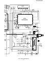
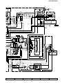
Figure 18 BLOCK DIAGRAM (2/3)
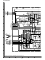
– 18 –
BAIS
CD-C622/C2900
SWM3
PROOF
SWM4
F.A.S
SOLM1
ENOID
FL701
DISPLAY
M
SWM5
CAM
Q702
Q703
1 2 3 4 ~ 15 16 ~ 25 26 ~ 28
29 ~ 36
37 38 39
MM1
TAPE MOTOR
R351
VCO ADJ
Q705
Q706
Q707
MONO/ST
15
3
CO MO/ST
L 9
R 10
51 52 53 54 55 56 57 58 59 60 61 62 63 64 65 66 67 68 69 70 71 72 73 74 75 76 77 78 79 80
FM/AM
11
+B7
Q343
AM
TCHING
1 IC704
2
3
+B7
1
RX701 3
2
50
49
48
47
46 VDD
45
44
43
42
41
40
39
38
37
36
35
34 AVDD
33
32
31
+B7
IC701
IX0280AW
SYSTEM CONTROL
MICROCOMPUTER
VDD
N
VDD
81
82
83
84
85
86
87
88
89
90
91
92
93
94
95
96
97
98
99
100
30 29 28 27 26 25 24 23 22 21 20 19 18 17 16 15 14 13 12 11 10 9 8 7 6 5 4 3 2 1
AGE
ATER
+B4
UNSWITCH
+B7
MEMORY
BACK UP
+B5
KEY
SW701
~SW730
TO CD
SECTION
+B7
PHM1
XL701
4.19MHz
M
Q960
Q704
+B1
M901
FAN MOTOR
+B5
–B4
Q908
P
ESSOR
13 R
14
10
8 L
Q601
Q602
IC901
STK40704
POWER AMP.
Q603
Q604
–B
1 2
+B
3
+B1
REC
UTING
+B4
+7.3V
15
D801
Q824
REAR
SPEAKER
T801
POWER
F802 TRONSFORMER
4A/125V
622
ONLY
FRONT
SPEAKER
F803
4A/125V
Q822
+12V(ANALOG)
SO901
SPEAKER
TERMINAL
FRONT
6 L-OUT
7 R-OUT
VOLTAGE
REGULATOR
Q121
Q122
JK970
HEADPHONES
RL901
VOLTAGE
REGULATOR
RL801
D803~D806
+B5
+B2
+12V(MOTOR)
+5.6V
Q821
Q823
VOLTAGE
REGULATOR
AC POWER
SUPPLY CORD
T.F
VOLTAGE
REGULATOR
ZD801
D807
~D809
Q801
F805
2A/250V
AC 120V, 60Hz
T1/T2
+B6
+5V
Q802
BAIS
+B7
UNSWITCH
Q803
D810~D813
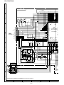
Figure 19 BLOCK DIAGRAM (3/3)
– 19 –
T802
POWER
TRONSFORMER
CD-C622/C2900
A
C30
0.1/50
C31
220/6.3
C29
4.7/50
44
C27
0.001
R41
47K
C18
0.47/50
C12
0.1
SLOF
R40
5.6K
R43
56K
C24
2.2P
42
R38
470
HF
TP1
C23
0.0027
40
39
38
37
TES
36
TOFF
35
TGL
34
JP+
SL+
JP–
SL–
R42
47K
C25 R39
27P 1K
43
41
R44
33K
C26
0.033
HFL
SLD
29 30 31 32
33
6
C22
220P
R36
220K
C21
0.0033
R33 R32
1.2K 10K
R34
3.3K
VREF
SLOF
5
REF
SPO
R29
56K
FE–
SPG
R28
10K
C16
0.0047
R23
10K
C20
47/16
NC
R19
1K
45
C19
1/50
S.Q.R
FE1
REF
–
FA–
AGND
SP
REF
SPI
–
C13
330P
R27 R31
39K 1.2K
R25
1.5K
C17
0.001
R30
6.8K
CV+
CV–
+
R24
47K
1
R26
82K
C14
0.01
REF
SLEO
SP–
24 25 26
27 28
FD– FA
FE
17 18 19 20 21 22 23
C11 R18
0.1 15K
R45
4.7K
CLK
DEF
CE
CL
LATOH
+
DAT
FSS
DRF
VR
REF1
LF2
PHI
+
+
+
+
REF
–
–
REF
4
JP+
JPCLO
SLOF SLOF
OR
10
+
RFSM
RF
–
REF
REF +
CV+
–
–
–
REF
+
JP–
–
C10
180P
VCC2
R46
560
BHI
LDO
VCC1
+
+
–
–
JP
FSC
REF FOSTA
TO
GEN
REF
+
GEN
REF
+
TD
SLC
–
CV–
+
FSTA REF
JP
–
R21 R20
1.5K 1K
3
+
+
REF
–
R22
820
8/12CM
RFS–
+
GEN
SLI
CL
+
TGL1
+
FO–
TR–
ACTUATOR
FSTA
REF
VCC
THDL GL
+
FO+
TR–
TR+
FO+
FO–
GND
PD
VR
LD
REF
THD
TD–
R17
33K
LASER
C28
0.1
46
DGND
2FREQ
+
14 JP
TO +
15
FD
16
8
FSC
CE
SLOF
+
TR+
D
13
IC1
LA9241M
SERVO AMP.
EFBAL
FOSTA
TOSTA
REF
–
1
2
3
4
5
6
7
8
11
VCR
–
CNS1B
C2
0.01
+
–
–
C7
0.1/50 TH
10
C8
0.068
12
DRF
TBC 47
–
LT0H30M1
R15
R14
12K
27K
R16
3.3K
K
E
A
B
F
VCR
VCR
REF –
R10 C5
2.2K 0.033
8 TESI
C6
0.033
9 SCI
R12
100
R13 C9
1K 0.047
5
4
3
2
1
HFL
+
C
–
NC 48
+
R11
6.8K
DEF
REF
+
C54
0.001
55 54 53 52 51 50 49
FE1
VCR
REF –
6 TE–
7 TE
56
2
+
R9
100K
57
–
–
5 TB
R8
15K
58
REF
REF
A
F
C
59
+
3
4 F
C4
0.1/50
TE
LD
MON
K
E
B
LD GND
61 60
RF
–
CNS1A
–
1 FIN2
REF –
2 FIN1
EREF –
–
1
2
3
4
5
CNP1
1
2
3
4
5
64 63 62
LDS
9
K
A
B
E
F
–
B
5
4
3
2
1
+
K
E
A
B
F
R1
22
C3
1/50
C33
0.47/50
C32
0.01
C1
47/16
Q1
2SA1318
C34
0.33/50
R2
1K
C15
0.01
7
R35
220K
C57
0.001
GND
C35
1/50
PICKUP UNIT
TR–
TR+
FO+
FO–
M1
SPINDLE
MOTOR
G
M2
SLED
MOTOR
SW4
PICKUP
IN
M
M
–
+
–
6
5
4
3
2
1
6
5
4
3
2
1
TR+
TR–
12
14
15 SL–
16 SL+
17 SLD
18 VCC1
19 STANDBY
C55
100/16
20 Vref
+B
R56
6.8K
CNP3
6
5
4
3
2
1
FO–
13
CD_GND
6
5
4
3
2
1
CNS3A
CNS3B
CNP3A
+
FO (GAIN)
FO+
10
11 GND
C36
100/16
CD MOTOR PWB-C
LD_M– 41
21 MUTE
+B
VCC4 40
M+ 39
M– 38
SOL– 37
SOL+ 36
35
+B
34
33
GND 32
31
30
+B
C82
100/16
C77
100/16
+B
29
VCC3 28
+B
SP+ 27
SP– 26
SPO 25
(SPN)VCC2 24
SOLD 23
SOL– 22
+B
+B
SP+
SP–
SL_+
SL_–
CD_PUIN
SLD–
CNS2B CNS2A
TR– 1
1
1
TR+ 2
2
2
FO+ 3
3
3
FO– 4
4
4
GND 5
5
5
PD
6
6
6
VR
7
7
7
LD
8
8
8
LD
CNP2
LD_M+ 42
FD
RWC(DSP)
WRQ(DSP)
CO IN(DSP)
SQ OUT(DSP)
CQ CK(DSP) R47
10K
RES(DSP)
DRF(ASP)
D_GND
C37
0.022
SLD+
PD
C76
0.022
TO
IC3
M63001FP
FOCUS/TRACKING/SPIN
/SLED DRIVER
1
2
3
4
5
6
7
8
9
E
F
D1
+B 1SS133
R37
82K
CNP12 1 2
3 4 5 6 7 8 9 10
CNS12
P29 12 - B
TO DISPLAY PW
H
• NOTES ON SCHEMATIC DIAGRAM can be found on page 15.
1
2
3
4
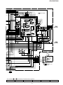
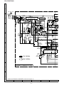
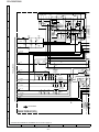
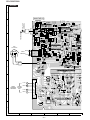
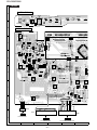
Figure 20 SCHEMATIC DIAGRAM (1/10)
– 20 –
5
6
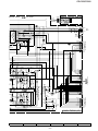
CD-C622/C2900
R57 1K
R58 1K
R59 1K
C49
100P(CH)
C48
100P
C47
100P(CH)
C44
100P(CH)
C46
100P
(CH)
R60
1K
C38
0.01
C45
100P(CH)
CD SIGNAL
R61 1K
R62 1K
R63 1K
+B
+B
C42
15P
24 25 26 27 28 29 30 31
CNP11
D82
1SS133
C74
220P
TO MAIN PWB
+B
R66
220
R64
22
C75
0.001
C50
0.022
CD_LCH
P24 1 - B
CNS11
Q52
KTC3203 Y
R55
+B
C43 100
330/6.3
R65
1K
L61
0.82µH
+B
32
A_GND
C73
220P
1
2
3
4
5
6
L-CH
D-GND
+7V
+12V
ZD61
MTZJ5.6B
R74
100K
R71 C71 R73
2.7K 10/50 100K
TEST3
NC
DOUT
DIGITAL
OUT
R72
2.7K
R-CH
A_GND
CD_RCH
C52
100/16
TEST4 33
C72
10/50
+5V
RVSS 39
34
CONT5
NC
EMPH
NC
C2F
NC
CONT4
CONT3
EXTERNAL
OUTPUT
R93
220
44
LVSS 38
LCHO
37
LVDD 36
MUTEL
NC 35
IC2
LC78622NE
SERVO/SIGNAL
CONTROL
17 18 19 20 21 22 23
45
C51
100/16
XOUT
SYNC-DETECT
EFM DEMODULATE
PCK
NC
FSEQ
NC
VDD
JP_
JP+
EFMIN
11
XVSS 46
XL1
16.934 MHz
D81
1SS133
WRQ
SBCK
SFSY
NC
FSX NC
RWC
4FS
DIGITAL
FILTER
VSS
EFMO
TOFF
TGL
C22
220P
COIN
SQOUT
VVDD
FR
SLICE
LEVEL
CONTROL
TEST2
11
CLV+
CLV
12
CLV_ DIGITAL
13
SERVO
V/P
14
HLF
15
SERVO
TES COMMAND
16
10
C41
12P
XVDD 43
MUTER
NC 42
RVDD 41
RCHO
40
ERROR COERECT
FLAG CONTROL
CONT2
R53
1.2K
2KX8
RAM
CONT1
6
7
8
9
X-TAL
GENERATOR
1BIT @DAC
VCO CLOCK
OSC CONTROL
4 VVSS
5 ISET
C40
0.047
R52
27K
EFLG
NC 48
SBSY 47
NC
XIN
3 PDO
C39 R50
0.047 680
SUB-CODE
µ-COM
INTERFACE
C83
0.022
1
2 TA1
R51
3.3M
/CQCK
16M
NC
TEST11 NC
/RES
/CS
TEST5
4M
TEST1
DEF1
PW
NC
49
64 63 62 61 60 59 58 57 56 55 54 53 52 51 50
+B
R88 1.2K
R89 1.2K
R90 220
R91 1K
+B
+B
R54
330
C56
0.022
+B
BI1A
BI1B
2
1
2
1
+B
CNP99
+B
C57
0.001
+B
P25 10 - B
CNS99
TO DIGITAL
OUTPUT PWB
3
2
1
+B
33
+B
+B
R82
390
D92
1SS133
R83
390
R80
820
2
CD SERVO PWB-B
R81
820
3
D93
1SS133 1
SOLM2
SOLENOID
R84
2.2K
LOCK
D91
1SS133
Q51
KRC102 M
BIM05
1
2
3
4
5
6
1
SOL+
2
SOL–
3
M–
M+
4
GND(D)
5
DISC NO. 6
OPEN CLOSE 7
GND(D)
8
MECHA UP 9
10
10 GND(D)
CNP10
CNS10
1
2
3
4
5
CD_D_NO 6
7
8
9
SLD–
–
M
+
M3
T/T
UP/DOWN
LOADING
SW1
OPEN
CLOSE
SENSOR PWB-D
SW2
MECHA UP
1
2
PCCL
PUIN SW
CO IN(DSP)
SQ OUT(DSP)
CQ CK(DSP) R47
10K
RES(DSP)
DRF(ASP)
D_GND
C37
0.022
SLD+
M–
M+
1
2
DISC NO
SW3
DISC NUMBER
CNS5
OP/CLOS
DISC NO.
UP/DOWN
3 4 5 6 7 8 9 10 11 12 13 14 15
CNS12
P29 12 - B
TO DISPLAY PWB
• The numbers 1 to 12 are waveform numbers shown in page 16.
7
8
9
10
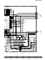
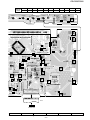
Figure 21 SCHEMATIC DIAGRAM (2/10)
– 21 –
11
12
CD-C622/C2900
VD303
C318 SCV211C
22P(CH)
2
TP301
R312
680
C338
100P
C316
100P
C393
1/50
Q302
2SC535 C
OSC BUFF
+B
R380
1.5K
C381
12P(CH)
D305
1SS133
AM SIGNAL
MAIN PWB-A1(1/3)
G
H
• NOTES ON SCHEMATIC DIAGRAM can be found on page 15.
1
2
3
4
Figure 22 SCHEMATIC DIAGRAM (3/10)
– 22 –
5
6
IC302
IO1 IF IN
BO4 IO2
PD
CL
DI A IN
NC VSS
CE A OUT
1 2 3 4 5 6 7 8 9 10 11
R374 1K
R373 1K
R372 1K
R371 1K
D304
1SS133
X IN X OUT
X352
4.5MHz
22 21 20 19 18 17 16 15 14 13 12
C382
15P(CH)
FM SIGNAL
ZD
MTZ
R379
2.2K
C392
0.001
E
R381
10K
C369
47/25
C383
0.022
NC AM IN
NC NC
C384
0.001
R317
820
R316
4.7K
BO1 FM IN
4.4V
0.7V
C335
560P AM OSC
AM BAND
COVERAGE fL
DO VDD
FM IF
R323
68K
C334
22P(UJ)
3
C313
0.022
R314
10K
1
R320
10K
0V
F
C330
8.2P(UJ)
C331
0.047
C332
0.022
C314
10/16
C319
0.022
VD331
SVC348S
T333
C317
C306
18P(CH) 3.9P(UJ)
L303
R311
220K
AM ANT
T331
+B
FM OSC.
T301
C312
0.001
C307
0.0047
D
7 8 9
CF301
R303
100K
R302
22
FM BAND
COVERAGE fL
R306
C305
10
15P(CH)
C310
0.001
VD302
SCV211C
C302
10P(CH)
R305 C303
0.01
82
D302
1SS133
D303
1SS133
C304
4.7P(CH)
1 2 3 4 5 6
L301
B.P.F
C
IC301
TA7358AP
FM FRONT END
R301
33K
R304
82 C301
82P
B
1
2
3
C308
0.0047
C311
0.022
1
2
3
AM TRACK
fL
C315
6.8P(UJ)
C309
4.7P(UJ)
L302
FM RF
FM ANT
D301 1SS133
AM LOOP ANT
CNP301
A
CD-C622/C2900
NC VCO
R361
10K
0.015
R375
1.2K
C357
3.3/50
FM/AM
SWITCHING
Q343
11
12
KRA109 M
3 8.4V
4.4V
2
1 5.1V
C366
1/50
C365
1/50
C367
1/50
D342
1SS133
L343
100µH
VR351
6.8K(B)
VCO
R362
390
R369
2.2K
R350
47K
C358
0.0015
R352
15K
13
AM
/FM
DET
TUN OUT
IND
L CH
MPX
–IN
R CH
FM–
M/ST
C364
9 10
C363
0.015
2
1 CF351 3
+B
15 14
16
5 6 7 8
R356
10K
C360
0.022
R365
680
C395
0.022
IO1 IF IN
BO4 IO2
NC AM IN
NC NC
BO1 FM IN
7 16 15 14 13 12
6 7 8 9 10 11
IC302
LC72131
PLL(TUNER)
R379
2.2K
ZD351
MTZJ5.1B
+B
CHASSIS
GND
2 10.9V
1
11V
+B A_+12V
TUN_R
A_GND
TUN_L
Q344
KRA102 M
3 0.2V
DO
CLK
DI
CE
D_GND
7
8
9
10
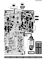
Figure 23 SCHEMATIC DIAGRAM (4/10)
– 23 –
11
10
18
2
19
20
21
22
23
24
12
P25 12 - C
TO MAIN/DECK SECTION
R381
10K
C369
47/25
C383
0.022
R349
1.5K
C353
0.018
4
C361
22/25
C356
3.3/50
C355
220P
C354
220P
FM/AF IF MPX.
IC303
LA1805
T351
17
18
AM
IF
GND
ST
IND
FM
DET
20 19
2 3
R359
3.9K
Q350
2SC3331
AM IF
R317
820
DO VDD
C350
220/10
24 23 22 21
C359
0.022
0
R348
33K
FM DET.
C335
560P AM OSC.
1
+B
+B
R340
5.6K
R360
220K
C351
0.0022
R321
120
AM BAND
COVERAGE fL
338
00P
TP302
R347
3.9K
C337
10/16
T352
FM IF AM
IN OSC
AM
+B
AM
RF
FM
AM +B
MIX
C334
22P(UJ)
VD331
SVC348S
T333
C349
0.022
+B
AM ANT.
T331
C333
0.022
C331
0.047
C330
8.2P(UJ)
AM TRACKING
fL
CD-C622/C2900
A
RECORD SIGNAL
PLAYBACK SIGNAL
FM SIGNAL
R625
22K
C629
22/25
R629
560(1/2W)
11
C112
330P 24
C114
330P
23
22
C154
47/16
C122
1/50
21
20
18
19
R121
100K
C117
0.033
R119
56
0V
4
6
5
C113
330P
7
C121
1/50
R125
5.6K
C119
560P
R131
33K
R135
622:5.6K
2900:8.2K
H
• NOTES ON SCHEMATIC DIAGRAM can be found on page 15.
3
4
Figure 24 SCHEMATIC DIAGRAM (5/10)
– 24 –
5
8
6
R139 560
R117
1K
C115
47/25
3
C129 470P
2
R137
6.8K
C131
0.001
1
Hich=
C128
3.3/50
C111
330P
R111
10K
2
17
–
Q103 ~ Q108: SWITCHING
1
0V
C130
C132
0.001
470P
R140 560
R142
R136
622:5.6K
2900:8.2K
R126
5.6K
Q122
2SC333
0V
+ 112K
Hich=T1
+
112K
–
C107
0.001
0.7V
Q107
2SC3331
0V
Q103
0V KTC3200 GR
G
0V
0V
R105
3.3K
R103
2.2K
0V
Q108
2SC3331
R110
4.7K
Q105
0V KTC3200 GR
0.7V
C105
180P
0V
0V
C108 0.001
R108
47K
0.7V
R104
0V 2.2K
R106
3.3K
0.7V
Q106
KTC3200 GR
R109
4.7K
0V
R118
1K
0V
R107
47K
1
2
3
4
5
6
7
Q104
KTC3200 GR
CNP102
C106
180P
C120
560P
R138
6.8K
C101
0.001
R170
680
R134
68K
R120
56
C118
0.033
R122
100K
C116
47/25
R172
220K
C156
3.3/50
Q113
3
2SC3331
Q111
R169
KRC104 M
680
R102
1K
C102
0.001
Q114
2SC3331
R171
220K
C127
0.022
Q109
2SA1318
MUTING
C153
100/16
R101
1K
CNS102
12
R174
5.6K
R124
3.9K
0V
2
1
R173
5.6K
C155
3.3/50
8.6V
R115
4.7K
L-CH
L-CH
C6
4.7
13
R132
33K
Q110
KRC104 M
3.4V
0V
2
3
1
R114
10K
R112
10K
1 TAPE1_R 1
2 A_GND
2
3 TAPE1_L 3
R-CH
14
R175
1K
R123
3.9K
Q109 ~ Q111: SWITCHING
9.3V
M_GND
ERASE
TAPE2_R2
A_GND
TAPE2_R1
TAPE2_L1
TAPE2_L2
15
C6
4.7
M_GND
CNP101
CNS101
C622
0.1/50
R155
150
A_GND
9.3V
1
2
3
4
5
6
7
16
1.5K
1.5K
1.5K
1.5K
0.033
0.22
A_12V
R113
10K
F
17
R608
R606
R604
R602
C612
C614
R628
22K
C627
22/25
C109
0.047
TAPE2
RECORD/
PLAYBACK HEAD
ERASE
HEAD
18
R610
10K
R623
5.6K
ZD601
MTZJ2.4B
3.4V
10
14
TAPE1
PLAYBACK HEAD
R-CH
19
R
3
2
E
R614
10K
20
R622
10K
A_GND
2
C617
10/50
C619
0.022
R618
2.2K
Q602
2SC3331
C634
0.0047
10
2900 ONLY
622 ONLY
C624
0.001
1
2
3
4
5
6
7
8
9
C616
4.7P
C620
10/50
C618
C626
0.001
Q604
2SC3331
L
1
C623
0.001
0V
P26 1 - E
TO POWER SECTION
13
Q601
2SC3331 R617
2.2K
R646 100K
12
R636
330
R616
3.9K
R619
2.2K
R620
2.2K
C621
0.1/50
1.5K
1.5K
1.5K
1.5K
0.033
C613
0.22
R612
15K
R615
3.9K
C
Q603
2SC3331
C625
0.001
C635
0.0047
R609
622:1.5K
2900:2.2K
R621
10K
R635
330
D
R607
C605 R605
4.7/50 R603
C603
R601
4.7/50
C611
C615
2900 ONLY
0.22
R611
R613
330
10K
+B
CD_+B
+B
CD_GND
R639
47K
C601
4.7/50
+B
IC601
M62439SP
AUDIO PROCESSOR
1
2
3
4
5
6
R645
100K
CNS11
1 R-CH
2 A_GND
L-CH
3
CD_GND
4
+7V
5
+12V
6
P21 12 - C
TO CD SERVO PWB
CNP11
B
BI601
+B
CD-C622/C2900
DIGITAL OUTPUT PWB-A6
CD SIGNAL
P21 12 - D
+B
CNP99
TO CD
SERVO PWB
CNS99
D_OUT 1
1
3
3
+4.3V
+B
2
2
2
L99
3
1
1
2.2µH
CD GND
IC99
C99 C98
100/10 0.022
BI99
+B
R633
22K
IC601
M62439SP
AUDIO PROCESSOR
+B
19
18
17
16
15
14
R608
R606
R604
R602
C612
C614
1.5K
1.5K
1.5K
1.5K
0.033
0.22
C602
4.7/50
C606
4.7/50
R640 47K
R626
12
11
R629
560(1/2W)
L-CH
R634
22K
JK601
VIDEO
IN
R-CH
C630
0.022
TUN_R
A_GND
TUN_L
R624
330
DO
CE
DI
CL
D_GND
A_12V
R638
220K
C616
4.7P
C620
10/50
C618
0.022
ZD602
MTZJ2.4B
R623
5.6K
ZD601
MTZJ2.4B
2.2K
C628
0.22
–B
C631
390P
C632
390P
D601
1SS133
D602
1SS133
R641
47K
C604
4.7/50
13
R610
10K
R632
22K
R642
47K
R630
560(1/2W)
0
20
R612
15K
1
2
3
4
5
6
7
8
9
R631
22K
R637
220K
18
2
19
20
21
22
23
24
P23 12 - F
TO TUNER SECTION
RECORD SIGNAL
10
–B
–B
R175
1K
8
C128
3.3/50
7
0.0033
R141
56
C139
C119
560P
R131
33K
R139 560
C129 470P
R125
5.6K
ALC
10
C141
1/50
R145
10K
L103
100µH
11.7V
R162
47K
REC/PLAY
D_GND
11.6V
0V
+B
0V 1
2
3
0V
11.6V
Q126
KRC104 M
BIAS
R160
150/1/2W
+B
–B
M_12V
SPA_SIG
–15V
+5V
M_12V
R166
47K
R135
622:5.6K
2900:8.2K
BIAS OSC 0V
Q128
KTC3203 Y
C150
0.0039(ML)
C151
0.027
(ML)
0V
–15V
VF1
–VF
VF2
+5V
SP_DET
SP_RLY
–B
0V
R168
12
10
11
12
13
14
15
16
17
18
19
20
21
CNP701
+B
R167
100K
1
2
3
4
5
6
7
8
9
CNS701
P28 1 - D
TO DISPLAY PWB
C146
220/10
13
ALC GND
11 12
C133
22/25
R137
6.8K
C131
0.001
C121
1/50
C127
0.022
113
30P
9
C135 0.068
6
5
14
R164
4.7K
56K
Hich=CHROME
+
56K
–
15
SWITCHING
Q124
2SA1015 GR
16
–
+
112K
ich=T1
112K
R123
3.9K
17
IC101
AN7345K
PLAYBACK AND
RECORD/PLAYBACK AMP.
18
19
–
+
4
C145
22/25
C130
C132
0.001
470P
R140 560
R142
C136
56
0.068
C140
0.0033
C142
1/50
R136
622:5.6K
2900:8.2K
R138
6.8K
R134
68K
20
SPN_P
HI_CUT
S_MUTE
SP_DET
SP_RLY
T_T1 T2
T_BIAS
R158
220
Vcc
21
VF1
C134
22/25
C122
1/50
CLK
DO
CE
DI
A_GND
R157
220K
-VP
VF2
RIPPLE
114
30P
R146
10K
C154
47/16
C156
3.3/50
R124
3.9K
R126
5.6K
R153
0V
10K
0.7V
Q121
0V
2SC3331
MUTING
Nor/CrO2
Q114
2SC3331
R132
33K
3.3/50
R170
680
C120
560P
R156
Q122
220K
2SC3331
R154
0V
10K
0.7V
0V
C152
47/25
+B
P26 1 - E
TO POWER SECTION
REC_R
MUTING
R172
220K
REC_L
R174
5.6K
7
6
17
15
16
8
4
5
L104
330µH
MAIN PWB-A1(2/3)
7
8
9
10
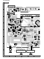
Figure 25 SCHEMATIC DIAGRAM (6/10)
– 25 –
11
12
CD-C622/C2900
+
IC901
STK4074B
POWER AMP
Ch2
7
8
9
C902
220P
R
Q905
2SC3331
C917
47/50
D903
1SS133
15
47P
D906
1SS133
D904
1SS133
Q907
2SC3331
C920
0.022
R918
820
Q904
2SC3331
R929
1K
R925
0.1(1W)
3
C905
220P
R903
100K
A_GND
R902
68K
2
C
R926
0.1 (1W)
C921
0.022
R931
10K
R905
1K
R904
68K
L
R901
100K
1
C901
1/50
R917
56K
R916
1K
C912
100/50
R930 R928
10K 1K
C904
10/50
C907
10/50
R913
100 (1/4W)
Fusible
R921
22K
C916
15P
C911
100/50
13 C923 14
12
47P
Fusible
B
11
10 C915
R912
100(1/4W)
R938
56K
Ch2
Out
6
R939
56K
Ch1
Out
5
C924
15P
NC
4
Q906
2SC3331
NC
3
C918 R923
47/50
R924 56K
1K
+Vcc
2
R922
820
–Vcc
1
Ch1
–
–Vcc
+
(2Ch)
–
A
C93
0.
(M
R936 R93
4.7
56K
C938
47/50
+B
R907
1K
C903
1/50
+B
4
5
SP_DET
SP_RLY
+B
+B
R830
680 (2W)
–15V
+B1
R966
22K
–B
14
15
16
17
CD_GND
Q822
VOLTAGE
KIA7806P REGULATOR
3
1
D832 2
1SS133
D833
1SS133
D805
1N4004S
C829
3300
ZD801
MTZJ6.2A
R801
12K
R802
47
C803
47/50
Z
M
R803
47K
C827
0.1
(ML)
Q80
KTA127
VOLTA
REGULA
+B
M_GND
–VF
VF2
VF1
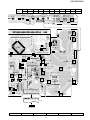
G
FM SIGNAL
MAIN PWB-A1(3/3)
H
• NOTES ON SCHEMATIC DIAGRAM can be found on page 15.
1
D806
1N4004S
D804
1N4004S
C802
100/35
C826
47/25
C828
0.1
(ML)
R825
33
C824
0.047(ML)
R832
22K
C825
22/25
R827
22K
+B
VOLTAGE
REGULATOR
Q824
KIA7812P
3
1
2
D803
1N4004S
P29 12 - E
TO DISPLAY PWB
CNS806
13
A_GND
CD_+B
+B
R831
3.3(1/2W)
+B
A_12V
+B2
C833
0.1
(ML)
12
D_GND
C832
0.1(ML)
11
D820
1SS133
+B
D821
1SS133
+5V
R837
10K
10
VOLTAGE
REGULATOR
Q823
KTD2058 Y
+B
Q821
AN78L05
1
3
2
+B
C831
47/25
8
M_12V
C821
0.047(ML)
7
9
F
C909
2200/50
C910
2200/50
C830
47/25
P24 2 - D, P25 12 - G
TO MAIN SECTION
6
E
D801
TS6B04
–B
D
2
3
4
Figure 26 SCHEMATIC DIAGRAM (7/10)
– 26 –
5
6
1
2
3
4
A
CN
CNP804
R960
22(1/2W)
2
2
1
1
R942
4.7K
WTM801
R949
330(1/2W)
C956
100/50
C936 C937
0.1 0.1
(ML) (ML)
Q908
3
KRC107 M
R936 R934 R937
4.7
4.7
56K
C938
47/50
+B
M901
FAN MOTOR
HEADPHONES PWB-A5
1
2
3
4
5
+B
JK970
HEADPHONES
5
FW801
8
7
6
5
4
3
2
1
D907
2 1SS133
1
M
1
C954
100/50
R938
56K
Q906
2SC3331
R939
56K
+B
R941
4.7K
RL901
R924
1K
56K
C924
15P
+B
R961
15K
C960
10/50
R946
330(1/2W)
15
D960
C961
1SS133 47/50
R963
1K
R962
68K
Q960
2SC3331
+B
C923 14
47P
CNS804
CD-C622/C2900
SP_REAR_L-CH
SP_REAR_R-CH
16 OHMS/CH
SP_REAR_L-CH_GND
SP_REAR_R-CH_GND
SP_L-CH
SP_R-CH
SP_L-CH_GND
SP_R-CH_GND
6 OHMS/CH
622 ONLY
SO901
SPEAKER
TERMINAL
+B
+B
2900 ONLY
F802
4.0A/125V
C808 C807
0.047 0.047
D801
TS6B04GM
D805
1N4004S
F805
2.0A/250V
C804
R806 47/50
2.2K
R802
47
ZD801
MTZJ6.2A
Q801
KTA1274 Y
VOLTAGE
REGULATOR
1
2
1
2
D809
1N4004S
2900
ONLY
RL801
SO801
AC POWER
AC INPUT SUPPLY CORD
AC 120V/60Hz
T.F
T801
POWER TRANSFORMER
D818
1SS133
+B
+B
3
CNP806
R808
220
C814
10/16
+5V
AC _RLY_CON
UN_SW_5V
D_GND
D815
1SS133
1
2
3
4
Q802
2 KRC107 M
1
C815
1000/6.3
R801
12K
P29 12 - E
TO DISPLAY PWB
CNS806
C802
100/35
R803
47K
C803
47/50
ZD802
MTZJ30B
1
2
3
4
5
6
7
8
C801
0.0047
D804
1N4004S
1
2
3
4
5
6
7
8
CNP802
CNP801
D806
1N4004S
T802
Q803
AN78L05
3
1
2
D810
1SS133
D811
1SS133
D816
C810
1SS133 470/25
D813
1SS133
D812
1SS133
C809
0.047(ML)
+B
D803
1N4004S
C806 C805
0.047 0.047
C811 220/50
C812 220/50
D807
1N4004S
D808
1N4004S
C813
220/50
+B2
CNS801
–B
2900 ONLY
D802
1SS133
CNS802
F803
4.0A/125V
POWER TRANSFORMER
POWER PWB-A2
7
8
9
10
Figure 27 SCHEMATIC DIAGRAM (8/10)
– 27 –
11
12
CD-C622/C2900
A
DISPLAY PWB-A3
R721
100K
R722
100K
Q705
2SC3331
4 5 6 7 8 9 10 11 12 13 14 15 16 17 18 19 20 21 22 23 24 25 26 27 28 29 30 31 32 33
R723
100K
Q707
2SC3331
Q706
2SC3331
P9
81 82 83 84 85 86 87 88 89 90 91 92 93 94 95 96 97
80
C702
1/50
R708
1K
R707
1K
C720
47/50
R706
1K
G10
G09
G08
G07
G06
G05
G04
P22
P21
P20
P19
P18
P17
P16
P15
P14
P13
P12
P11
P10
P09
P08
P07
P06
P05
P04
P03
P02
P01
G11
1 2 3
P8
P7
P6
P5
P4
P3
P2
P1
P11
P10
G9
G8
G7
G6
G5
G4
B
F
F
F
FL701
FL DISPLAY
79 VLOAD
78 P11
77 P12
80 P10
1 VDD
CNS701
76 P13
VF2
SPN_P
HI_CUT
S.MUTE
SP_DET
SP_RLY
T_T1 T2
T_BIAS
REC/PLAY
D_GND
12V M
SPA SIG
–15V
5V
P25 12 - E
CNP701
TO MAIN PWB
D
73 P16
CD
72 P17
IC701
IX0280AW
SYSTEM CONTROL
MICROCOMPUTER
71 P18
70 P19/DIST1
69 P20/DIST2
68 P21/DIST3
67 P22/DIST4
R701
1K
R702 1K
R703 1K
10
R705
1K
11
12
66 NC DISTOUT
CD D
DIST0
DIST0
65 SPN_P
64 SP_DET
L:DEMOSTART
H:ECOSTART
63 SPRLY
62
CD D
61 HI-CUT
13
CD D
CD
60
R709
1K
14
R716
33
15
16
17
59
58 S MUTE
57
19
R712 22K
R713 1K
R714 1K
R715 1K
–B
20
+B
21
52 REC/PLAY
56
+B
18
30 T2 RUN
51 AC RLY-CON
55 DIST0
54 T_T1T2
53 T-BIAS
52
51
AVDD
C
74 P15
1
2
3
4
5
6
7
8
9
FPA
TIFAS
CAM SW
VDD
T_MOT
T_SOL
TIMER LED
U/D SW
DNO SW
VSS
REMOCON
SYS STOP
O/C SW
PUIN SW
CLK
DO
CE
DI
A_GND
VF1
VLOAD (–VP)
75 P14
C557
270P
R558
68K
C559
0.0027
R553 C553
12K 0.0027
R568 2
220K
3
R570
220K
5
6
R564
390K
R556
33K
D551
1SS133
R574
330
D554
1SS133
4
1
C566
2.2/50
D555
1SS133
8
7
C567
2.2/50
C551
270P
IC563
KIA4558P
OPE AMP.
SPEANA3
R578
100K +B
+B
SPEANA2
R579
100K
+B 12V
Q702
KTA1273 Y
0V
12V
TAPE MECHANISM
PWB-E
G
MM1
TAPE MOTOR
2
PHM1
4 RUN PALS
SENSOR
1
3
SWM3
F.P.
CNPM2
SWM4
F.A.S
SOLM1
SOLENOID
SWM5
CAM
FWM2
IC562
KIA4558P
OPE AMP.
R758
1.2K
R759
10K
C568
2.2/50
8
7
1
2
3
4
5
6
7
8
9
10
11
12
R738
R739
R740
R741
C705
47/25
+B
+B
ZD551
MTZJ6.2C
+B
+B
+B
0V D716
1SS133
12V
+B
+B
CNPM1
M
FWM1 2+
–
C562
0.022
R573
560K
1
1 2 3 4 5 6 7 8
BI701
1 MOTOR
2
3 GND
4
+12V
5
6 T2 RUN
7
FPA
8
9
T1 RUN
10
SOLENOID
11
CAM SW
12
LED7
+B
CNSM1
H
• NOTES ON SCHEMATIC DIAGRAM can be found on page 15.
1
2
R755
10K
R756
10K
R757
10K
R753
10K
R754
10K
MOTOR
GND
+12V
T2 RUN
FPA
T1FAS
SOLENOID
CAM SW
R561
15K
5
6
R580
100K
R566
2.2M
R567 270K
Q703
KTA1271 Y
12V
C569
0.022
R560
470K
–B D556
1SS133 SPEANA1 +B
4
C563
0.022
F
2
C556 C561 R572
0.0068 0.022 2.2M 3
10K
+B
R760
10K
+B
R555 C555
56K 0.0068
+B
R752
+B
R750
10K
R575
330
R562
390K
R551
10K
R749
10K
–B
–B
R748
10K
+B
+B
E
1K
10K
1K
1K
2.2K
2.2K
1.8K
1K
1K
LED722
R747 SLI342UCJ
10K
R730
R731
R732
R733
R734
R735
R736
R737
1K
1K
1K
R727
10K
R724
10K
R726
10K
R720
10K
R719
10K
50 49 48 47 46 45 44 43 42 41 40 39 38 37 36 35 34
R717
10K
3
4
Figure 28 SCHEMATIC DIAGRAM (9/10)
– 28 –
5
6
LED71
F
F
F
25 26 27 28 29 30 31 32 33 34 35 36
37 38 39
1
2
3
4
5
6
7
8
9
1
2
3
4
5
6
7
8
9
10
10
11
11
12
12
13
13
C706
1/50
C709
0.022
P1
P11
P10
G9
G8
G7
G6
G5
G4
G3
G2
G1
89 90 91 92 93 94 95 96 97 98 99 100
DO
DI
CE
CLK
LCK1
1 VDD
+B
1
2
3
4
5
6
7
8
9
R778
R777
R776
R775
R774
C710
220/10
1K
1K
1K
1K
1K
14
R772
1K
R771 1K
15
CD DSP RWC
C707
IC701
RESET 10
15P
IX0280AW
X2 11
XL701
C708
TEM CONTROL
X1 12
4.19 MHz 18P
ROCOMPUTER
VPP 13
14
R770
1K
CD DSP WRQ 15
0
0
L:DEMOSTART
H:ECOSTART
VDD 16
PCCL 17
CD DSP COIN
SQOUT
CD DSP CQCK
CD DSP RES
FRF(DRF)
SLD+
SLD–
30 T2 RUN
AVSS
SPEANA3
SPEANA2
SPEANA1
AVDD
KEYIN1
KEYIN2
KEYIN3
U/D SW
DNO SW
VSS
REMOCON
SYS STOP
O/C SW
PUIN SW
LAY
Y-CON
BI702
14
15
RWC(DSP)
WRQ(DSP)
CO IN(DSP)
SQ OUT(DSP)
CQ CK(DSP)
RES(DSP)
DRF(ASP)
D_GND
SLD+
SLD–
PUIN SW
OPEN/CLOSE
DISC NO
UP/DOWN
PCCL
CNP12
P21 7 - H
TO CD SERVO PWB
G10
G09
G08
G07
G06
G05
G04
G03
G02
G01
P01
G11
CD-C622/C2900
CNS12
R780
10K
+B
R769 1K
R768 1K
R767 1K
R766 1K
R765 1K
R764 1K
18
19
20
21
22
R763
R762
23
24
1K
1K
25
26
27
28
29
30
+B
D722
1SS133
LED717
7
SLI342YCJ
R787
R786
STOP
PLAY
DISC2
DISC3
9
LED706
RS706
LED707
L1154GT4
Q10
Q9
Q8
Q7
Q6
Q5
LCK
Q0
Q1
Q2
Q3
Q4
CLOCK
IC703
470
SLI342YCB
BU2092F
INPUT/OUTPUT EXPANDER
NIGHT RIDER 7
NIGHT RIDER 6
DISC OPEN
SKIP /CLOSE
1K
1K
1
8
DISC1
RD07
RD09
3.9K
6.8K
SW707 SW708 SW709
LED705
SLI342DCB
+B
470
470
470
470
470
1 2 3 4 5 6 7 8 9
LED701
L1154GT4 RS701
RS702
NIGHT RIDER 2
LED703
RS703
NIGHT RIDER 3 SLI342DCB
LED704
RS704
NIGHT RIDER 4 SLI342UCB
RS705
NIGHT RIDER 5
+B
SLI342YCJ
RD05
RD06
2.2K
3.3K
SW705 SW706
8
FW702
POWER
LED716
8
RD02 SW703 RD03 SW704 RD04
1.5K
1.2K
1.8K
TIMER/
CLOCK
SLEEP
CD
NIGHT RIDER 1
RD01
820
SW701
TAPE
LED702
SLI342YCB
STOP TUNER/ VIDEO
BAND
47/25
REC MEMORY/
PAUSE SET
RD16
RD13 RD14
RD15
3.9K
1.8K
2.2K
3.3K
SW713 SW714 SW715 SW716 SW717
OE
Q11
18 17 16 15 14 13 12 11 10
C718
REV
+B
RS707
470
C719
0.022
1.2K
VOLUME VOLUME X-BASS/ EQUAL DIMMER
DOWN UP
DEMO
IZER
+B
RD11 RD12
1.2K
1.5K
SW711 SW712
+B
+B
C715
47/25
C714
0.022
RD27
RD28
3.9K
6.8K
SW728 SW729 SW730
+B
RD10
820
SW710
+B
+B
VDD
PLAY
1 2 3
+B
+B
RS711
1.5K
R798
100
REMOTE
SENSOR
VSS
TUNING TUNING
UP
DOWN
RX701
DATA
FF
RD25
RD26
2.2K
3.3K
SW726 SW727
+B
RS712
RD21
RD22
RD23
RD24
820
1.2K
1.5K
1.8K
SW722 SW723 SW724 SW725
C713
0.022
D720
1SS133 D719
1SS133
1 +5V
2 AC_RLY CON
3 UN_SW 5V
4 D_GND
CNS806
SWITCH PWB-A4
+B
3
2
C722
10/50
C711
0.01
1
R797
100K
+B
IC704
KIA7042AP
RESET
5V BACK UP
D723
1SS133
Q704
KRC102 M C712
3.3/50
3
2
1
D718
1SS133
C723
0.1/50
D717
1SS133
L702
100µH
R795
4.7K
R750
10K
R751
3.3K
+B
R755
10K
R756
10K
R757
10K
R753
10K
R754
10K
D721
1SS133
R711
4.7K
+B
2
1
2
3
4
BI703
+B
1
+B
+B
+B
+B
+B
10
Figure 29 SCHEMATIC DIAGRAM (10/10)
– 29 –
11
12
CNP806
R745
1K
P27 7 - G
TO POWER PWB
R744
1K
1K
1K
R742
R743
1K
10K
1K
1K
R738
R739
R740
R741
R749
10K
1K
1K
10K
R748
10K
R736
R737
42 41 40 39 38 37 36 35 34 33 32 31
CD-C622/C2900
CD-C622
A
FC7
R374
R373
R372
R371
R939
R929
D904
C923
C369
ZD351
E C B
RL901
Q904
D907
1 2 3
R830
R949
R946
R966
C910
C909
D801
Q908
H
3
C611
C826
C831
2
D906
R937
C937
C821
C918
E C B
R942
D82
Q821 3
C830
C920
C917
C921
R941
R934
2
R620
R907
R922
C915
R931
C912
C936
1
R640
ZD602
R646
Q604
C626
R613
C621
R628
C625
R352
R913
R936
C938
G
R605
R350
C364
C366
X352
R348
C353
R349
C911
C907
R928
R917
R918
C916
R916
C924
R921
R923
R924
Q907 E C B
R925
–
1 2 3 Q343
C313
R306
R312
R311
C317
C306
C311
C359
C338
C604
C960
C904 R912
R930
R-CH
C620
R617
R618
R622
E C B
R619
Q6
R636
R616 C634 C624
R614
C62
1 2 3 4 5 6 7 8 9 10 11 12 13 14 15
R926
3
–
R645
Q601
E C B
C
R642 C612
C623
Q603 E C B
R903
R615
Q905
+
R621
R604
R606
R901
C903 C905
C902
R902
R904
C901
R905
D903
4
R-CH
FRONT
6 OHMS
MIN.
L-CH
C358
C635
VR351
VCO
R602
D305
D304
IC901
C954
+
IC6
R601
R635
C956
L-CH
1 2 3 4 5
C367
Q906 B C E
1
F
R603
R611
20 19 18 17 16
C350
R938
–
R361
R375
R962
B C E
R639
R641
D342
C357
C355
Q350
D960
R961
R-CH
SO901
SPEAKER
TERMINAL
R963
E C B
C603
C961
–
Q960
+
8
REAR R-CH
12 OHMS
MIN.
L-CH
C356
R360
R629
R362
24 23 22 21 20 19 18 17 16 15 14 13
R347
L343
R379
IC303
C333
TP302
6
+
R381
1 2 3 4 5 6 7 8 9 10 11 12
R960
5
L-CH
7
E
C381
C316
C393
R380
C392
C363
C361
IC302
C383
22 21 20 19 18 17 16 15 14 13 12
B C E
1 2
CNP804
C360
R340
C632
R632 C631
D601
D602
C630
BR
R365
R356
1 2 3 4 5 6 7 8 9 10 11
C354
C351
R634 R359
CNS804
2
1
1
2
3
CF351
C337
T352
L303
T351
C349
R631
RD
1
2
3
T333
R633
JK601
VIDEO IN
L-CH
R316
C312
C330
CF301
R323
R321
VD331
C334
Q302
R369
C382 R317
C365
C309
R301
C310
C332
T331
R314
R303
VD302
C335
D
C384
VD303
C318
C331 R320
R-CH
C305
C301
D303
D302
D301
Q344
3 2 1
B C E
C307
M901
FAN MOTOR
IC301
1 2 3 4 5 6 7 8 9
L302
C308
C395
FM ANTENNA
C
C304
R302
C303 T301
R304
3
2
1
3
2
1
C315
CNP301
L301
AM LOOP
ANTENNA
R305
B
C302
C319
C314
MAIN PWB-A1
4
Figure 30 WIRING SIDE OF P.W.BOARD (1/11)
– 30 –
5
6
CD-C622/C2900
P39 12 - D
TO CD SERVO PWB
CNP11
P35 8 - H
TO DISPLAY PWB
CNS701
CNS11
1 2 3 4 5 6
RD
BL
BL
BL
BL
BL
FC701
1
R164 E
C
B
R115
R162
F805
2A/250V
IC101
R155
P38 4 - D
CNS101
TO TAPE MECHANISM
TAPE1 HEAD
R123
C119
R121
R125
R131
C127
C128
C131
C133
C139
R137
C129
C141
TO TAPE MECHANISM
TAPE2 HEAD
C117
R102 C111
C121
R139
R141
C135
R171
C155
R175
R157
C145
Q113
5 4 3 2 1
C102
Q107 R107
C105
R112
C142
WTM801
1
2
3
4
5
6
7
8
9
10
11
12
P38 5 - D
CNS102
R135
R145
R134 C154
Q121
R174
R138
24
23
22
21
20
19
18
17
16
15
14
13
Q124
C151
L104
L103
R110
C113
R122
R111
C118
C156
R170
F802
4A/125V
F803
4A/125V
D821
3 2 1
Q111
R169
E C B
R158
R173
B C E
P38 1 - B
CNS802
TO POWER
TRANSFORMER
D806
D805
D804
D803
Q823
R801
Q824
ZD801
C804
Q801
3
ZD802
C812
R837
E
C
B
C811
R806
R830
C833
COLOR TABLE
BR
C803
1
2
1
FW801
R802
R825
C824
5
C802
R803
C813
D833
C832
3
Q822
C831
B
C827
C828
C918
C826
1
2
R827
R832
C821
C830
B
C
E
C825
D832
C923
D820
Q821 3 2 1
R922
R923
12 13 14 15
R831
C829
R907
R921
R924
R172
R625
5
E
C
B
1 2 3 4 5 6 7 8
CNP802
R620
3 C905
C122
Q122 B C E
C134
R142
R154
C136
R140
R153
Q114
R640
ZD602
R646
C605
Q604
03
C626
623
R626
C114
C132
C130
C620
R617
R618
C601
C618
R622
E C B
C629
R619
Q602
R636
C622
R616 C634 C624
R614
C627
B C E
R628
C625
645
R608
C628
C116
R126
R132
R136
R156
C602
C112
C140
C614
Q126
1 2 3
R109
CNP102
C153
1
R108
Q108 C101 CNP101
2
3 E C
1
B
4
2
C108
5
3
6
E
C
B
R118
R101
7
C107
R120
R117 C115
R119
C120
R124
R624
R604
R606
R642 C612
R638
R630
C606
R602
R637
C619
IC601
20 19 18 17 16 15 14 13 12 11
5
4
BI601
6
1 2 3 4 5 6 7 8 9 10
R601
R106
Q106 B C E
R104
Q104 B C E
R103
Q103 B C E
R105
Q105 B C E
R607
R603 C613
R611
C152
ZD601
R623
R605
C611
R639
R641
2
C617
R609
R629
C615
ZD351
C369
L343
1 3 5 7 9 11 13 15 17 19 21
2 4 6 8 10 12 14 16 18 20
CNP701
1
R610
C616
R612
Q110
3 2 1
R113
C109
R160
R146
C146
R356
B C E
B C E
R166
R365
Q109
Q128
R167
R168
C106
C150
R369
R114
21
D807
JK970
HEADPHONES
D808
D809
HEADPHONES
PWB-A5
D801
BROWN
RD(R)
RED
OR
ORANGE
YL
YELLOW
GR
GREEN
BL
BLUE
VL
VIOLET
GY
GRAY
WH(W)
WHITE
BK
BLACK
PK
PINK
D962
D961
7
8
9
10
Figure 31 WIRING SIDE OF P.W.BOARD (2/11)
– 31 –
11
12
CD-C622/C2900
CD-C2900
A
FC701
R374
R373
R372
R371
G
R939
1
C937
R934
R925
C611
R620
C918
C
C808
1 2 3
R830
R949
R946
D907
C910
C909
Q908
D801
H
2
R609
C369
Q904
R966
1
R640
ZD602
R646
Q604
C923
E C B
RL901
C936
R929
D904
C826
C831
2
R937
R938
D906
C920
C917
E C B
C821
R922
C915
C921
R941
R942
D820
Q821 3 2
C830
R930
R931
C912
C938
R926
R913
Q905
–
C911
C907
R928
R917
R918
C916
R916
C924
R921
R923
R924
C904 R912
D903
R-CH
C626
C960
IC901
D960
R961
4
3
–
R907
1 2 3 4 5 6 7 8 9 10 11 12 13 14 15
R936
+
C620
R617
R618
R622
E C B
R619
Q60
R636
R616 C634 C624
R614
C627
B C E
R901
C903 C905
C902
R902
R904
C901
R905
Q907 E C B
R-CH
FRONT
6 OHMS
MIN.
L-CH
ZD351
R635
R962
F
SO901
SPEAKER
TERMINAL
R628
C623
Q603 E C B
R903
R615
Q906 B C E
+
E C B
C
C6
R642 C612
C625
R621
R963
L-CH
R605
R350
C364
VR351
VCO
R352
C355
R604
R606
R645
Q601
C635
TP302
B C E
C366
X352
R348
C353
R349
R375
C604
C603
Q350
1 2 3 Q343
C313
R306
R312
R311
C317
C306
C311
C337
E C B
IC60
R602
D305
D304
C358
1 2 3 4 5 6
R601
C367
C357
R603
R611
20 19 18 17 16 1
C350
R960
C961
Q960
E
R361
24 23 22 21 20 19 18 17 16 15 14 13
C356
R360
R639
R641
D342
IC303
R347
R629
R362
1 2 3 4 5 6 7 8 9 10 11 12
C333
R340
C632
R632 C631
D601
D602
C630
BR
R381
L343
R379
C354
C351
R634 R359
1 2
CNP804
C381
C316
C393
R380
C392
C363
C361
IC302
C383
22 21 20 19 18 17 16 15 14 13 12
R613
C621
C338
T333
T352
1
2
3
CF351
C360
C349
R631
CNS804
2
1
1
2
3
L303
T351
C359
C330
CF301
R323
R321
VD331
R633
RD
R316
C312
R303
VD302
C335
D
R365
R356
1 2 3 4 5 6 7 8 9 10 11
C365
C309
R301
C310
C332
T331
R314
C334
Q302
R369
C382 R317
C384
VD303
C318
C331 R320
R-CH
JK601
VIDEO IN
L-CH
C305
C301
D303
D302
D301
Q344
3 2 1
B C E
C307
M901
FAN MOTOR
IC301
1 2 3 4 5 6 7 8 9
L302
C308
C395
FM ANTENNA
C
C304
R302
C303 T301
R304
3
2
1
3
2
1
C315
CNP301
L301
AM LOOP
ANTENNA
R305
B
C302
C319
C314
MAIN PWB-A1
3
4
Figure 32 WIRING SIDE OF P.W.BOARD (3/11)
– 32 –
5
6
CD-C622/C2900
P39 12 - D
TO CD SERVO PWB
CNP11
P37 8 - H
TO DISPLAY PWB
CNS701
CNS11
1 2 3 4 5 6
RD
BL
BL
BL
BL
BL
FC701
1
R155
C102
Q107 R107
Q124
C151
L104
R168
C106
C150
C105
CNS102
TO TAPE MECHANISM
TAPE2 HEAD
P38 4 - D
CNS101
TO TAPE MECHANISM
TAPE1 HEAD
C117
R102 C111
C121
R123
C119
R121
R125
R131
C127
C128
C131
C141
P38 5 - D
C133
C139
R137
C129
R139
R141
C135
R171
R135
R145
R134 C154
C155
R175
C142
WTM801
R157
C145
5 4 3 2 1
F805
2A/250V
1
2
3
4
5
6
7
8
9
10
11
12
Q113
R138
IC101
C118
C156
R170
F803
4A/125V
R831
D821
F802
4A/125V
R620
R162
R169
E C B
R158
R173
B C E
P40 2 - B
CNS802
TO POWER
TRANSFORMER
C806
D806
D804
R801
C805
D805
Q823
Q824
COLOR TABLE
C802
R803
C804
Q801
3
ZD802
C812
R837
E
C
B
C811
R806
R830
C833
D807
JK970
HEADPHONES
D808
D809
C807
C808
BR
ZD801
C813
1
2
1
FW801
R802
R825
5
C803
Q822
D833
C832
3
D832
C831
C826
1
2
R827
C827
C828
C918
C824
R832
C821
C830
B
C
E
C825
D803
D820
Q821 3 2 1
R922
C923
R172
Q604
C829
12 13 14 15
R923
E
C
B
1 2 3 4 5 6 7 8
CNP802
R907
R921
R924
Q122 B C E
C134
R142
R154
C136
R140
R153
R625
5
C626
C905
C122
R174
R640
ZD602
R646
C605
C114
C132
C130
R626
C620
R617
R618
C601
C618
R622
E C B
C629
R619
Q602
R636
C622
R616 C634 C624
R614
C627
B C E
R628
C625
23
03
R126
R132
R136
R156
C602
R608
C116
24
23
22
21
20
19
18
17
16
15
14
13
Q121
C614
C628
R642 C612
C120
R124
R624
R604
C606
R602
R606
C112
C113
R630
20 19 18 17 16 15 14 13 12 11
Q114
R601
R637
C619
IC601
R638
1 2 3 4 5 6 7 8 9 10
R164 E
C
B
R115
R109
CNP102
C153
1
R108
Q108 C101 CNP101
2
3 E C
1
B
4
2
C108
5
3
6
E C B
R118
R101
7
C107
R120
R117 C115
R119
R122
R111
6
Q126
1 2 3
3 2 1
Q111
L103
R110
R146
C146
R607
R603 C613
R611
45
BI601
C615
R623
R605
C611
R639
R641
2
C152
R106
Q106 B C E
R104
Q104 B C E
R103
Q103 B C E
R105
Q105 B C E
ZD601
R609
R629
C617
ZD351
C369
L343
1 3 5 7 9 11 13 15 17 19 21
2 4 6 8 10 12 14 16 18 20
CNP701
1
R610
C616
R612
R113
C109
R160
C140
R356
Q110
3 2 1
B C E
R166
R365
Q109
B C E
Q128
R167
R112
R369
R114
21
HEADPHONES
PWB-A5
D801
BROWN
RD(R)
RED
OR
ORANGE
YL
YELLOW
GR
GREEN
BL
BLUE
VL
VIOLET
GY
GRAY
WH(W)
WHITE
BK
BLACK
PK
PINK
D962
D961
7
8
9
10
Figure 33 WIRING SIDE OF P.W.BOARD (4/11)
– 33 –
11
12
CD-C622/C2900
CD-C622
COLOR
TABLE
SWITCH PWB-A4
A
RS707
B
SW708
DISC
SKIP
RD09
LED705
RS711
LED706
LED707 RS706
IC703
SW709
OPEN/CLOSE
9
C719
C718
RS712
10
RS704
LED704
RS703
RS705
1
18
DISPLAY PWB-A3
39 38 37
RD28
SW729
EQUALIZER
R721
R722
R708 R723
C709
ZD551
25
C707
C708
R744
R757
RD24
BI701 C705
BI703
1 R724
8
4
E
C
B
R786
SW726
VOLUME
DOWN
B
C
E
R760
R759
15
1
Q702
Q703
RD
WH
GY
WH
GY
RD
BL
BL
BL
BL
BL
BL
BL
BL
BL
BL
BL
BL
BL
BL
1 2 3 4 5 6 7 8 9 10 11 1213 14 15
WH
GY
WH
G
12 11 10 9 8 7 6 5 4 3 2 1
CNS12
CNSM1
CNP806
P38 1 - D
TO POWER PWB
H
CNP12
P39 12 - B
TO CD SERVO PWB
1
2
3
CNPM1
P38 6 - A
TO TAPE MECHANISM PWB
4
Figure 34 WIRING SIDE OF P.W.BOARD (5/11)
– 34 –
5
6
R743
R764
R763
R762
R777
R776
R775
R772
R770
R769
R768
R767
R766
R765
D716
LED717 LED716
BI702
CNS806
40
35
SW725
PLAY
R758
RD22
RD23
SW723
TUNING
UP
SW724
TUNING
DOWN
1 2 3 4
6
15
C710
R574
R561
R575
RD21
C563
R556
RD25
10
XL701
SW722
FF
F
1
65
IC701
30 31
C561
SW727
VOLUME
UP
RD26
5
R567
C569
70
20
R771
C568
R580
R573
C562
5
6
7
8
R560
R558
D551
R551
1
R774
D556
IC562
C559
R570
R568
C556
C555
D722
R555
R553
R707
R706
R716
Q707
85 75
95
100
R778
Q704
90
E C B
D717
5 R564
6
7
8
C553
R572 4
3
2
1
R566
81 80
R756
C723
R797
D718
C722
R579
C567
R727
Q706 E
C
E
B
C
B
3 2 1
D555
D554
C551 D721
RD27
Q705
L702
IC563
4
3
2
C557 1
E
C706
C720
C712
R562
R578
C566
IC704
1
2
3
R749
SW728
X-BASS/
DEMO
R795
C711
C713
D723
R750
D719
D720
SW730
DIMMER
D
25 24 23 22 21 20 19
FL701
R711
C
36 35 34 33 32 31 30 29 28 27 26
CD-C622/C2900
COLOR
TABLE
R D (R )
RED
LED703
LED704
RS703
YL
OR
LED702
BL
VL
GY
WH ( W)
BK
PK
BLUE
VIOLET
GRAY
WHITE
BLACK
PINK
GR
ORANGE YELLOW GREEN
RD07
704
BR
BROWN
SW707
DISC 3
LED701
RS701
SW706
DISC 2
SW705
DISC 1
FW702
RS702
1
8
RD06
RD05
25 24 23 22 21 20 19 18 17 16 15 14 13 12 11 10 9 8 7 6 5 4
SW704
TIMER/
SLEEP
3 2 1
LED722
70
R720
R736
R737
R739
R741
R740
R742
RD10
R733
R734
RD13
R745
R748
R747
RD12
R752
R753
R754
R751
R713
R712
SW716
TAPE
R714
SW714
TUNER/
BAND
RD14
CNS701
2 4 6 8 10 12 14 16 18 20
1 3 5 7 9 11 13 15 17 19 21
R786
1
SW717
CD
RD16
R780
R760
Q702
SW701
POWER
R719
SW711
REC PAUSE
R715
R787
R758
RD01
SW712
MEMORY/
SET
LED717 LED716
E
C
B
R705
SW710
REV
RD11
R743
R744
R757
R756
R755
R764
R763
R762
R735
R738
SW713
STOP
SW725
PLAY
RD02
R709
30 31
XL701
C714
FW702
R701
8
40
25
35
C702
707
708
45
C715
20
51
50
55
15
3 2 1
R702
IC701
60
R732
R731
R730
10
65
R726
95
5
SW703
CLOCK
85 75
R703
R717
90
RD04
RX701
81 80
100
1
RD03
R798
FL701
RD15
R724
SW715
VIDEO
1
21
RD
FC701
1
CNSM1
CNP701
P31 8 - A
TO MAIN PWB
B
7
8
9
10
Figure 35 WIRING SIDE OF P.W.BOARD (6/11)
– 35 –
11
12
CD-C622/C2900
CD-C2900
COLOR
TABLE
SWITCH PWB-A4
A
RS707
B
SW708
DISC
SKIP
RD09
LED705
RS711
LED706
LED707 RS706
IC703
SW709
OPEN/CLOSE
9
C719
C718
RS712
10
RS704
LED704
RS703
RS705
1
18
DISPLAY PWB-A3
39 38 37
RD28
SW729
EQUALIZER
R721
R722
R708 R723
C709
Q707
ZD551
25
BI701 C705
BI703
R760
Q702
1 R724
8
4
E
C
B
R786
SW726
VOLUME
DOWN
B
C
E
1 2 3 4 5 6 7 8 9 10 11 1213 14 15
RD
WH
GY
WH
GY
RD
BL
BL
BL
BL
BL
BL
BL
BL
BL
BL
BL
BL
BL
BL
CNS806
WH
GY
WH
G
12 11 10 9 8 7 6 5 4 3 2 1
CNS12
CNSM1
CNP806
P40 1 - D
TO POWER PWB
H
CNP12
P39 12 - B
TO CD SERVO PWB
1
2
3
CNPM1
P38 6 - A
TO TAPE MECHANISM PWB
4
Figure 36 WIRING SIDE OF P.W.BOARD (7/11)
– 36 –
5
6
R743
R744
R757
RD24
R759
15
R756
R764
R763
R762
R777
R776
R775
R772
R778
D716
LED717 LED716
Q703
BI702
1
1 2 3 4
40
35
SW725
PLAY
R758
RD22
RD23
SW723
TUNING
UP
SW724
TUNING
DOWN
RD25
15
C710
R574
R561
R575
RD21
C563
R556
6
XL701
SW722
FF
F
1
10
30 31
C561
SW727
VOLUME
UP
RD26
65
IC701
C707
C708
R770
R769
R768
R767
R766
R765
5
6
7
8
R560
R558
D551
R551
5
R567
R580
R573
C562
D556
IC562
R568
C556
C555
D722
R555
R553
C569
70
20
R771
C568
D555
C559
R570
5 R564
6
7
8
C553
R572 4
3
2
1
R566
1
R774
D717
85 75
95
100
E C B
3 2 1
81 80
90
L702
IC563
R707
R716
R706
R727
Q706 E
C
E
B
C
B
C723
D718
R797
Q704
R579
C567
R562
R578
C566
D554
C551 D721
RD27
Q705
C720
C712
4
3
2
C557 1
E
C706
C722
1
2
3
R749
SW728
X-BASS/
DEMO
R795
C711
C713
D723
R750 IC704
D719
D720
SW730
DIMMER
D
25 24 23 22 21 20 19
FL701
R711
C
36 35 34 33 32 31 30 29 28 27 26
CD-C622/C2900
COLOR
TABLE
R D (R )
BROWN
RED
LED703
LED704
RS703
RD07
704
BR
YL
OR
ORANGE YELLOW GREEN
LED702
BL
GR
BLUE
VIOLET
WH ( W)
BK
PK
WHITE
BLACK
PINK
GRAY
SW707
DISC 3
LED701
RS701
GY
VL
SW706
DISC 2
SW705
DISC 1
FW702
RS702
1
8
RD06
RD05
25 24 23 22 21 20 19 18 17 16 15 14 13 12 11 10 9 8 7 6 5 4
SW704
TIMER/
SLEEP
3 2 1
LED722
70
R720
R736
R737
R739
R741
R740
R742
RD10
R733
R734
RD13
R745
R748
R747
RD12
R752
R753
R754
R751
R713
R712
SW716
TAPE
R714
SW714
TUNER/
BAND
RD14
CNS701
2 4 6 8 10 12 14 16 18 20
1 3 5 7 9 11 13 15 17 19 21
R786
1
SW717
CD
RD16
R780
R760
Q702
SW701
POWER
R719
SW711
REC PAUSE
R715
R787
R758
RD01
SW712
MEMORY/
SET
LED717 LED716
E
C
B
R705
SW710
REV
RD11
R743
R744
R757
R756
R755
R764
R763
R762
R735
R738
SW713
STOP
SW725
PLAY
RD02
R709
30 31
XL701
C714
FW702
R701
8
40
25
35
C702
707
708
45
C715
20
51
50
55
15
3 2 1
R702
IC701
60
R732
R731
R730
10
65
R726
95
5
SW703
CLOCK
85 75
R703
R717
90
RD04
RX701
81 80
100
1
RD03
R798
FL701
RD15
R724
SW715
VIDEO
1
RD
21
FC701
1
CNSM1
CNP701
P33 8 - A
TO MAIN PWB
B
7
8
9
10
Figure 37 WIRING SIDE OF P.W.BOARD (8/11)
– 37 –
11
12
CD-C622/C2900
SWM3
F. P.
A
FWM2
FWM1
PHM1
4
3
BK
WH
BK
WH
SOLM1
SOLENOID
(254-8)
+
TAPE MECHANISM
PWB-E
B
TO DISPLAY PWB
CNSM1
P34 5 - H, P36 5 - H
SWM4
F. A. S
CNPM2
-
1
2
R
12 11 10 9 8 7 6 5 4 3 2 1
CNPM1
1 2
2 1
MM1
TAPE MOTOR(254-7)
SWM5
CAM
TAPE MECHANISM
ASSEMBLY
P31 10 - E
TO MAIN PWB
CNP802
TAPE 2
RECORD/PLAYBACK
HEAD(254-6)
TAPE 1
PLAYBACK HEAD(254-6)
CNS802
ERASE HEAD(254-5)
RD
BL
RD
YL
YL
BR
BK
BR
1 2 3 4 5 6 7 8
WH
WH
BK
GY
GY
BK
1234567
CNP101
P31 12 - C, P33 12 - C
TO MAIN PWB
RL801
CNP102
P31 12 - B, P33 12 - B
TO MAIN PWB
2
CNP801
C815
3
2
1
CNS801
2
1
T802
POWER TRANSFORMER
Q803
D816
C814
C810
SO801
D810
D811
D813
AC POWER
SUPPLAY CORD
C809
E
DIGITAL
OUTPUT
PWB-A6
AC POWER
INPUT
AC120/60Hz
D812
1
2
3
POWER PWB-A2
IC99
CNP806
1
2
3
4
Q802
3
2
1
R808
D815
D818
D802
1
WH
PK
BK
WH
YL
BL
CNS102
321
P34 2 - H
TO DISPLAY PWB
CNS806
CNS101
PK
BK
WH
BL
RD
D
PK
WH
BL
GY
T801
POWER
TRANSFORMER
C
YL
BK
PK
L99
CD-C622
CNS5
SW2
MECHA UP
2
1
C99
SW3
DISC NUMBER
2
1
C98
3 BI99
1
SENSOR PWB-D
SW1
OPEN/CLOSE
F
M3
T/T UP/DOWN LOADING
OR
BR
WH
GY
WH
GY
WH
GY
WH
RD
CNS99 3 2 1
1
-
SOLENOID
SOLM2
BIM5
CNS10
10
9
8
7
6
5
4
3
2
1
+
6
G
CD MOTOR PWB-C
+
M2
SLIDE MOTOR
COLOR TABLE
BR
1
2
3
4
5
6
RD
WH
GY
WH
GY
WH
CNP3A
1
2
3
4
5
6
1
2
3
4
5
6
CNS3A
RED
OR
ORANGE
YL
YELLOW
GR
GREEN
SW4
PICK UP IN
CNS3B
3
VIOLET
GRAY
WHITE
BK
BLACK
PK
PINK
-
2
BLUE
VL
GY
M1
DISC MOTOR
1
BL
WH (W)
+
H
BROWN
R D (R )
4
Figure 38 WIRING SIDE OF P.W.BOARD (9/11)
– 38 –
5
6
R93
50
1 CNP12
2
CNS12
11
L61
R91
R89
R35
R36
C29
R71
R90
R73
C22
C30
6
7
8
9
C73
R88
C24
15 14 13 12 11 10
R54
R55
2
C50
C74
R74
17
C28
D1
C72
R65
20
16
3
32
15
C23
C57
30
10
R43
R40
R39
R41
C56
R44
C25
33
25
R52
R38
R42
4
5
1
35
BI1B
IC2
C40
C26
R72
60
P34 3 - H, P36 3 - H
TO DISPLAY PWB
40
64
1
R53
R50
5
55
R51
C27
4
45
C39
3
C43
R63
C48
D81
48
C83
C41
C42
C44
C49
C45
R58
XL1
49
D82
R60
C38
C46
C47
R59
R57
C37
R47
R62
R61
CD-C622/C2900
R45
49
6
R30
R31
1
CNP11
4 3 2
R28
C16
R27
R19
R24
C11
5
R18
R17
R16
R14
R81
R80
R83
R21
D93
R22
R11
C5
R29
R20
C9
R10
5
CNP1
4
3
2
R8
C14
R82
R13
D92
C6
C7
R12
3 2 1
R15
R9
1
C4
C54
C8
R25
7
Q51
R26
R23
C15
17
C10
8
C17
R2
C13
16
2
BI1A
B C E
C75
C52
20
15
CNP99
3 2 1
10
ZD61
R64
1
C2
Q52
32
25
6
C1
33
R66
5
1
35
30
R32
IC1
R33
60
64
R1
C51
C19
40
C18
C12
45
55
C20
E C B
Q1
C3
9
R34
C21
50
R46
5
48
CNS11
P31 9 - A, P33 9 - A
TO MAIN PWB
C33
C34
C31
C32
C71
2
C55
21
C76
R84
R56
1
C77
1
2
3
4
5
6
7
8
5
IC3
30
25
C35
10
15
20
CNP2
40
35
CNP10
R37
42
1 2 3 4 5 6 7 8 9 10
5
6
4
3
2
1
22
C36
C82
CNP3
D91
10
1
CD SERVO PWB-B
PICKUP UNIT(306)
CNS1A
1
2
3
4
5
CNS1B
BK
WH
PK
YL
BL
1
2
3
4
5
6
7
8
BL
PK
WH
YL
BK
GY
RD
WH
GY
WH
GY
WH
GY
WH
1
2
3
4
5
1
2
3
4
5
6
7
8
CNS2A
CNS2B
• The numbers 1 to 12 are waveform numbers shown in page 16.
7
8
9
10
Figure 39 WIRING SIDE OF P.W.BOARD (10/11)
– 39 –
11
12
CD-C622/C2900
CD-C2900
A
P33 10 - E
TO MAIN PWB
CNP802
B
COLOR TABLE
BR
RD
BL
RD
YL
YL
BR
BK
BR
1 2 3 4 5 6 7 8 CNS802
C
T801
POWER
TRANSFORMER
BL
RD
BROWN
RD(R)
RED
OR
ORANGE
YL
YELLOW
GR
GREEN
BL
BLUE
VL
VIOLET
GY
GRAY
WH ( W)
WHITE
BK
BLACK
PK
PINK
D
Q802
3
2
1
3
2
1
C814
F
1
2
1
CNP801
2
CNS801
C801
RL801
C815
T802
POWER TRANSFORMER
Q803
CNP806
1
2
3
4
E
R808
D815
D818
D802
P36 2 - H
TO DISPLAY PWB
CNS806
D816
SO801
C810
AC POWER
INPUT
AC120 60Hz
D810
D811
D812
D813
AC POWER
SUPPLAY CORD
C809
G
POWER PWB-A2
H
1
2
3
4
Figure 40 WIRING SIDE OF P.W.BOARD (11/11)
– 40 –
5
6
CD-C622/C2900
VOLTAGE
IC1
PIN VOLTAGE
NO.
1 2.5V
2 2.5V
3 2.5V
4 2.5V
5 2.5V
6 2.5V
7 2.5V
8 2.5V
9 2.5V
10 2.5V
11 2.5V
12 2.5V
13 2.5V
14 2.5V
15 2.5V
16 2.5V
17 2.5V
18 2.5V
19 2.5V
20 2.5V
21 2.5V
22 0V
23 2.5V
24 2.5V
25 2.5V
26 2.5V
27 2.5V
28 2.5V
29 2.5V
30 2.3V
31 2.3V
32 0V
33 0V
34 5.0V
35 5.0V
36 0V
37 0V
38 5.0V
39 0V
40 0V
41 1.6V
42 2.4V
43 2.4V
44 2.4V
45 0V
46 2.5V
47 2.5V
48 0V
49 0V
50 2.4V
51 4.6V
52 4.6V
53 0V
54 0V
55 5.0V
56 5.0V
57 2.5V
58 2.5V
59 1.0V
60 1.0V
61 2.2V
62 4.2V
63 0V
64 5.0V
IC2
PIN VOLTAGE
NO.
1 0V
2 0V
3 0V
4 0V
5 1.9V
6 5.0V
7 0V
8 0V
9 2.5V
10 2.4V
11 0V
12 0V
13 0V
14 5.0V
15 0V
16 0V
17 5.0V
18 5.0V
19 0V
20 0V
21 2.5V
22 0V
23 5.0V
24 0V
25 0V
26 0V
27 0V
28 0V
29 0V
30 5.0V
31 2.5V
32 0V
33 0V
34 0V
35 5.0V
36 4.6V
37 1.9V
38 0V
39 0V
40 1.9V
41 4.6V
42 5.0V
43 5.0V
44 2.1V
45 2.1V
46 0V
47 0.1V
48 2.3V
49 0V
50 2.5V
51 0V
52 2.5V
53 0V
54 0V
55 0V
56 4.6V
57 4.6V
58 4.7V
59 0V
60 2.3V
61 2.3V
62 0V
63 0V
64 0V
IC3
PIN VOLTAGE
NO.
1 2.5V
2 2.6V
3 2.9V
4 3.3V
5 3.3V
6 3.3V
7 3.3V
8 0V
9 0V
10 0V
11 0V
12 0V
13 0V
14 0V
15 3.3V
16 3.3V
17 3.0V
18 7.2V
19 5.0V
20 2.5V
21 0V
22 0V
23 0V
24 7.2V
25 2.5V
26 3.3V
27 3.3V
28 11.2V
29 0V
30 0V
31 0V
32 0V
33 0V
34 0V
35 0V
36 5.3V
37 5.3V
38 3.3V
39 3.3V
40 7.2V
41 0.1V
42 0.1V
IC101
PIN VOLTAGE
NO.
1 0V (0V)
2 0V (0V)
3 0.5V (0.5V)
4 4.3V (4.3V)
5 0.2V (0.3V)
6 1.3V (1.3V)
7 0V (0V)
8 0.6V (0.6V)
9 4.1V (4.1V)
10 4.0V (4.0V)
11 0V (0V)
12 0V (0V)
13 8.1V (8.1V)
14 4.8V (4.8V)
15 0V (0V)
16 4.1V (4.1V)
17 0.6V (0.6V)
18 0V (0V)
19 2.5V (2.6V)
20 0.2V (0.3V)
21 4.3V (4.3V)
22 0.5V (0.5V)
23 0V (0V)
24 0V (0V)
IC301
PIN VOLTAGE
NO.
1 0.9V (0V)
2 1.6V (0V)
3 6.0V (0.4V)
4 1.6V (0V)
5 0V (0V)
6 6.0V (0.3V)
7 5.2V (0.2V)
8 5.9V (0.3V)
9 6.0V (0.3V)
IC562
PIN VOLTAGE
NO.
1 0.2V
2 0.2V
3 0.2V
4 –9.8V
5 0V
6 0V
7 0V
8 6.2V
IC563
PIN VOLTAGE
NO.
1 0.2V
2 0.2V
3 0.2V
4 –9.8V
5 0.2V
6 0.2V
7 0.2V
8 6.2V
IC703
PIN VOLTAGE
NO.
1 0V
2 0V
3 0.2V
4 0V
5 9.8V
6 9.8V
7 9.8V
8 9.9V
9 9.8V
10 9.8V
11 9.8V
12 0.5V
13 0.5V
14 0.5V
15 9.8V
16 9.8V
17 0V
18 5.0V
IC302
PIN VOLTAGE
NO.
1 2.5V (2.5V)
2 0V (0V)
3 0V (0V)
4 0V (0V)
5 4.5V (4.5V)
6 4.5V (4.5V)
7 0.2V (11.9V)
8 0V (0V)
9 0V (0V)
10 0V (0V)
11 5.1V (5.1V)
12 0V (0V)
13 0V (0V)
14 0V (0V)
15 0V (2.5V)
16 2.5V (0V)
17 5.1V (5.1V)
18 0.9V (0.9V)
19 0.9V (0.9V)
20 1.3V (1.1V)
21 0V (0V)
22 2.5V (2.5V)
IC601
PIN VOLTAGE
NO.
1 0V
2 0V
3 0V
4 0V
5 0V
6 0V
7 0V
8 0V
9 0V
10 2.7V
11 0.2V
12 –2.7V
13 0V
14 0V
15 0V
16 0V
17 0V
18 0V
19 0V
20 0V
IC704
PIN VOLTAGE
NO.
1 5.0V
2 0V
3 5.0V
– 41 –
IC303
PIN VOLTAGE
NO.
1 1.6V (1.6V)
2 1.6V (1.6V)
3 7.1V (8.1V)
4 0.2V (0.6V)
5 1.6V (1.6V)
6 0V (0V)
7 5.1V (5.1V)
8 0V (0V)
9 2.3V (2.3V)
10 2.3V (2.3V)
11 6.4V (8.1V)
12 0.9V (0.9V)
13 1.1V (2.1V)
14 1.8V (1.6V)
15 2.2V (1.3V)
16 1.7V (1.7V)
17 1.6V (1.7V)
18 1.6V (1.6V)
19 0.4V (0.5V)
20 7.1V (8.1V)
21 7.1V (8.1V)
22 1.7V (1.7V)
23 1.7V (1.7V)
24 1.7V (1.7V)
(CD-C622)
IC901
PIN VOLTAGE
NO.
1 –30.4V
2 –30.4V
3 30.5V
4 0V
5 0V
6 0V
7 0V
8 –29.4V
9 29.4V
10 –0.1V
11 –0.1V
12 –28.0V
13 –0.1V
14 0.1V
15 0V
(CD-C2900)
IC901
PIN VOLTAGE
NO.
1 –31.6V
2 –31.6V
3 31.8V
4 0V
5 0V
6 0V
7 0V
8 –30.5V
9 30.5V
10 –0.2V
11 –0.2V
12 –29.1V
13 –0.2V
14 0.2V
15 0V
IC701
PIN VOLTAGE
PIN VOLTAGE
NO.
NO.
51 4.6V
1 4.7V
52 4.6 V
2 4.7V
53 0V
3 4.7V
54 4.6V
4 0V
55 0V
5 0V
56 0V
6 0V
57 0V
7 0V
58 4.5V
8 0V
9 0V
59 4.7V
60 4.6V
10 5.0V
61 0V
11 2.3V
62 4.9V
12 2.3V
63 4.9V
13 0V
14 4.7V
64 4.9V
65 4.9V
15 0V
66 –27.5V
16 4.7V
17 0V
67 –27.5V
68 –27.5V
18 4.7V
69 –27.5V
19 0V
70 –27.5V
20 4.7V
71 –27.5V
21 4.7V
22 0V
72 –27.5V
73 –27.5V
23 0V
74 –27.5V
24 0V
25 0V
75 –27.5V
26 0V
76 –27.2V
27 0V
77 –24.6V
28 0V
78 –27.5V
29 0V
79 –27.5V
30 0V
80 –24.6V
31 4.9V
81 –22.0V
32 4.9V
82 –22.0V
33 4.9V
83 –24.7V
34 4.7V
84 –27.2V
35 5.0V
85 –27.2V
36 0V
86 –27.3V
37 0V
87 –21.4V
38 4.9V
88 –22.0V
39 4.8V
89 –24.7V
40 0V
90 –24.7V
41 0V
91 –24.7V
42 0V
92 –24.7V
43 3.5V
93 –24.7V
44 11.2V
94 –24.7V
45 11.2V
95 –24.7V
46 4.7V
96 –24.7V
47 4.7V
97 –24.7V
48 4.7V
98 –24.7V
49 4.7V
99 –24.7V
50 0V
100 –24.7V
Q821
PIN VOLTAGE
NO.
1 11.2V
2 6.2V
3 1.2V
Q822
PIN VOLTAGE
NO.
1 18.0V
2 1.3V
3 7.2V
Q823
PIN VOLTAGE
NO.
1 11.9V
2 17.2V
3 11.2V
Q824
PIN VOLTAGE
NO.
1 18.0V
2 0V
3 12.0V
CD-C622/C2900
TROUBLESHOOTING (CD SECTION)
When the CD does not function
When the CD section does not operate When the objective lens of the optical pickup is dirty,this section may not operate.Clean
the objective lens,and check the playback operation.When this section does not operate even after the above step is taken,check
the following items.
Remove the cabinet and follow the troubleshooting instructions.
"Track skipping and/or no TOC (Table Of Contents) may be caused by build up of dust other foreign matter on the laser pickup
lens. Before attempting any adjustment make certain that the lens is clean. If not, clean it as mentioned below."
Turn the power off.
Gently clean the lens with a lens cleaning tissue and a small amount of isopropyl alcohol.
Do not touch the lens with the bare hand.
Dust gradually accumulates on the objective lens during use, and it may degrade performance.
To avoid this problem, use a cleaning disc designed for CD optical pickup lenses.
HOW TO USE
1. Using the brush in the cleaner cap, apply 1 or 2 drops of the cleaning fluid to the brush on the CD cleaner disc which has
the mark next to it.
2. Place the CD cleaner disc onto the CD disc tray with the brush side down, then press the play button.
3. You will hear musicfor about 20 seconds and the CD player will automatically stop. If it continues to turn, press the stop button.
CAUTION
The CD lens cleaner should be effective for 30 - 50 operations, however if the brushes become worn out earlier then please
replace the cleaner disc.
If the CD cleaner brushes become very wet then wipe off any excess fluid with a soft cloth.
Do not drink the cleaner fluid or allow it to come in contact with the eyes. in the event of this happening then drink and / or
rinse with clean water and seek medical advice.
The CD cleaner disc must not be used on car CD player or on computer CD ROM drives.
All rights reserved. Unauthorized duplicating, broadcasting and renting product is prohibited by law.
Cleaning Disc
PARTS CODE:
UDSKA0004AFZZ
Cleaner Liquid
Figure 42
– 42 –
CD-C622/C2900
• When the turntable fails to stop.
5V
Is from 2.5V
5 V till 2.5V down pulse (approx. 300 ms)
0V
No
input into the IC701 pin 21 when the turntable is rotating?
Check the SWM3 and the wiring from the IC701 pin 21 to the
SWM3.
Yes
Is there following voltage input on the IC701 pin 21 in the
specific state?
When the CD mechanism is moved up: 0V
In other states: 4.3V
No
Check the MECHA UP SW and the wiring from the IC701 pin
21 to the MECHA UP SW.
Yes
Check IC2 pin26 Q91 and Q93 and the periphery.
Yes
IC701 defective.
• When turntable fails to move.
Is there following voltage input on the IC701 pin 21 in the
specific state?
When the CD mechanism is moved up: 0V
In other states: 4.3V
No
Check the MECHA UP SW and the wiring from the IC701 pin
21 to the MECHA UP SW.
Yes
Is L output from the IC2 pin 26 during SEC when the disc skip
switch is pressed?
Check the wiring of IC2 pin 26 and Q93 pin 2.
No
OK
Yes
IC2 defective.
Is 4V output from the Q91 emitter during operation stated
above?
No
Yes
Check turntable motor and turntable mechanism.
– 43 –
Check Q91, Q93 and the periphery.
CD-C622/C2900
• When the CD tray fails to open or close.
Is there following voltage input in specific state of IC701 pin 19?
Open state: 0V
Close state: 0V
Intermediate state between open state and close state: 4.3V
Check the OPEN CLOSE SW and the wiring from the IC701
pin 19 to the OPEN CLOSE SW.
No
Yes
Is H output to IC2 pin 24 or 25 for 7 seconds when the OPEN/
CLOSE key is pressed?IC91 is defective. Replace it.
Check the wiring of the IC2 pins 24 and 25, IC91 pins 1 and 3.
No
OK
IC2 defective.
Yes
Is 4V output between IC91 pins 3 and 7 during operation
stated above?
Check the periphery of IC91.
No
OK
Yes
IC91 defective.
Check the loading motor (M1) and the loading mechanism.
• The CD function will not work.
The CD operating keys don't work.
Yes
Check the CD, DSP, power supply, and 16.93 MHz clock, and
reset terminal.
Yes
Check the waveform of SCK, SO (DATA) and SI (COMM).
Yes
See if the pick-up is in the pick-up in PICKUP IN SW position.
Yes
Focus search is
performed two
times when play
operation is done
without disc.
0.5s
0.50 V
IC1 16 FD
If the items mentioned above are OK, check the main
microcomputer IC701.
• The CD operating keys work.
0.5s
0.50 V
IC1 7 TE
Check the Focus - HF system.
1
Playback can be performed without a disc.
2
Figure 44
Yes
Does the pick-up move up and down twice?
Yes
Focus search OK
No
Does the output waveform of IC1(16)(FD) match that shown in
Fig. 44?
Check the area around IC5-CNP2.
Yes
No
Check the IC1(50)(CLK) line, 4MHz.
Check the microcomputer data on pins (51)(CL), (52)(DAT)
and (53)CE.
– 44 –
CD-C622/C2900
• Playback can only be performed when a disc is
loaded.
Is the Focus servo active? (Can you hear it working?)
No
Check the laser diode driver.
Check the area around IC1(16) - (21) (focus servo circuit).
No
If the disc is not turning, the DRF
should not change to "H".
Yes
Yes
Does the DRF signal change from "L" to "H"?
Check the spin system.
Yes
Yes
No
Is HF waveform normal (see the Fig.45-1, 2)?
Check the periphery of
IC1 pins 41 and 42.
Level is abnormal.
Yes
Yes
Check the spin system.
Waveform is unstable.
Check the tracking system.
HF
1.0V/DIV
0.5µsec/DIV(DC)
(When playing
back the disc)
Waveform in case of
normal play-back
0.5s
1.00 V
IC1 16 FD
0.5s
10.0 V
IC2 13 CLV+
2
1
3
0.5s
10.0 V
IC1 54 DRF
4
0.5s
2.00 V
IC1 7 TE
Figure 45-1
Figure 45-2
• Check the tracking system.
Check waveform of IC1 pin 7 (TE).
The waveform shown in
Fig.45-3 appears, and nodisc state appears soon.
Play is possible in
TEST mode.
Yes
Yes
Data cannot be read.
Tracking servo is
inoperative.
Yes
Although IL is possible,
play is impossible.
Yes
Yes
Check the periphery of IC 1
pin 8 to pin 15, and IC 5 to
CNP2.
Normal jump is impeded,
and the program top
cannot be reached.
Check the VCO-PLL system.
5ms
1.00 V
IC1 7 TE
4
5 ms
5.0 V
IC1 54 DRF
3
Figure 45-3
– 45 –
Yes
Check the periphery
of IC 1 pin 14.
CD-C622/C2900
• Checking the spin system.
Play operation is performed without disc.
Yes
Yes
The turntable rotates a little.
The spin driver circuit is normal.
No
Yes
The turntable fails to rotate or rotates at high speed.
Check the periphery of IC1 pins 23 to 27, pin 39, and pin 40, IC2
pin 12 and pin 13, IC5 to CNP3.
• Checking the VCO-PLL system
Play operation is performed when disc exits.
Yes
Although HF waveform is normal, TOC data cannot be read.
Yes
Check PDO waveform (Fig. 46).
Abnormal
Check the IC1 pins 43 and 44, IC2 pins 3, 5, 7, 10, and 11.
Stop --> Play
As VCO frequency is locked at
4.32 M Hz, voltage
of PDO rises and
stabili- zes.
0.5s
1.00 V
IC2 3 PDO
2
0.5s
1.00 V
IC2 16 FD
3
Figure 46
• Although HF waveform is normal and the time
indication is normal, no sound is emitted.
No
Check IC 2 pin 48 (EFLG).
Yes
Check IC2 pins 37, 40.
Abnomal
Check IC 401 and POWER AMP IC 801.
– 46 –
Usually, the number of pulses of flawless disc is 100 pulses/sec
or less.
CD-C622/C2900
FUNCTION TABLE OF IC
IC1 VHiLA9241M/-1: Servo Amp. (LA9241M) (1/2)
Pin No.
Function
Port Name
1
FIN2
Connection pin for photodiode of pickup.
RF signal is generated through addition with FIN pin, and FE signal is generated through subtraction.
2
FIN1
Connection pin for photodiode of pickup.
3
E
Connection pin for photodiode of pickup. TE signal is generated through subtraction with F pin.
4
F
Connection pin for photodiode of pickup.
5
TB
Pin for input of DC component of TE signal.
6
TE-
Pin to connect gain setting resistor of TE signal to TE signal.
7
TE
TE signal output pin.
8
TESI
TES (Track error sense) comparator input pin. TE signal is band-passed and input.
9
SCI
Input pin for shock detection.
10
TH
Pin to set time constant of tracking gain.
11*
TA
TA amplifier output pin.
12
TD-
Pin to compose tracking phase compensation constant between TD and VR pins.
13
TD
Pin to set tracking phase compensation.
14
JP
Pin to set amplitude of tracking jump signal (kick pulse).
15
TO
Tracking control signal output pin.
16
FD
Focusing control signal output pin.
17
FD-
Pin to compose focusing phase compensation constant between FD and FA pins.
18
FA
Pin to compose focusing phase compensation constant between FD-/FA-pins.
19
FA-
Pin to compose focusing phase compensation constant between FA and FE pins.
20
FE
Output pin of FE signal.
21
FE-
Pin to connect gain setting resistor of FE signal across TE pin.
22
AGND
GND for analog signal.
23
NC
No connect.
24
SPI
Spindle amplifier input.
25
SPG
Pin to connect gain setting resistor in the 12cm mode of spindle.
26
SP-
Pin to connect spindle phase compensation constant together with SPD pin.
27
SPD
Spindle control signal output pin.
28
SLEQ
Pin to connect thread phase compensation constant.
29
SLD
Thread control signal output pin.
30
SL-
Input pin of thread feed signal from micro computer.
31
SL+
Input pin of thread feed signal from micro computer.
32
JP-
Input pin of tracking jump signal from DSP.
33
JP+
Input pin of tracking jump signal from DSP.
34
TGL
Input pin of tracking gain control signal from DSP. TGL = Gain low at "H"
35
TOFF
Input pin of tracking off control signal from DSP. TOFF = Off at "H"
36
TES
Output pin of TES signal to DSP.
37
HFL
(HIGH FREQUENCY LEVEL) is used to judge whether main beam is positioned on the bit or on the mirror.
38
SLOF
Thread servo off control input pin.
39
CV-
Pin to input CLV error signal from DSP.
40
CV+
Pin to input CLV error signal from DSP.
41
RFSM
RF output pin.
42
RFS-
Pin to set gain of RF and set 3T compensation constant together with RFSM pin.
43
SLC
(SLICE LEVEL CONTROL) is the output pin to control of the level of the data slice with RF waveform DSP.
44
SLI
Input pin to control the level of data slice with DSP.
45
DGND
GND pin in the digital system.
46
FSC
Output pin for focus search smoothening capacitor.
47
TBC
(Tracking Balance Control) Pin to set EF balance variable range.
48*
NC
No connect.
49
DEF
Defect detection output pin of disk.
50
CLK
Reference clock input pin. 4.23MHz of DSP is input.
In this unit, the terminal with asterisk mark (*) is (open) terminal which is not connected to the outside.
– 47 –
CD-C622/C2900
IC1 VHiLA9241M/-1:Servo Amp.(LA9241M) (2/2)
Pin No.
Function
Port Name
51
CL
Micro computer command clock input pin.
52
DAT
Micro computer command data input pin.
53
CE
Micro computer command chip enable input pin.
54
DRF
(DETECT RF) RF level detection output.
55
FSS
(Focus Serch Select) Pin to switch focus search mode. (± search/+ search for reference voltage)
56
VCC2
VCC pin for servo system and digital system.
57
REFI
Pin to connect pass control for reference voltage.
58
VR
Reference voltage output pin.
59
LF2
Pin to set defect detection time constant of disk.
60
PH1
Pin to connect capacitor for peak hold of RF signal.
61
BH1
Pin to connect capacitor for bottom hold of RF signal.
62
LDD
APC circuit output pin.
63
LDS
APC circuit output pin.
64
VCC1
RF system VCC pin.
LDS
63
VCC1
64
LDD
62
BH1
61
PH1
60
APC
FIN2
1
FIN1
2
3
F
4
TB
5
TE-
6
TE
7
TESI
8
SCI
9
VR
58
REFI
57
VCC2
56
FSS DRF CE DAT CL CLK
55 54 53 52 51 50
DEF
49
REF
RF DET
48 NC
47 TBC
VCA
I/V
E
LP2
59
46 FSC
BAL
µ-COM
VCA
45 DGND
SLC
INTER FACE
44 SLI
43 SLC
42 RFS-
TE
41 RFSM
RF AMP
40 CV+
39 CV-
T.SERVO & T.LOGIC
38 SLOF
TH 10
37 HFL
36 TES
TA 11
35 TOFF
34 TGL
TD- 12
F.SERVO & F.LOGIC
SPINDLE SERVO
33 JP+
SLED SERVO
TD 13
JP 14
TO 15
FD 16
17
FD-
18
FA
19
FA-
20
FE
21
22 23
NC
FE- AGND SP
24
SPI
Figure 48 BLOCK DIAGRAM OF IC
– 48 –
25
SPG
26
SP-
27
SPD
28
SLEQ
29
SLD
30 31
SL- SL+
32
JP-
CD-C622/C2900
IC2 VHiLC78622N-1: Servo/Signal Control (LC78622NE) (1/2)
Pin
No.
Terminal Name Input/Output
Function
1
DEFI
Input
Defect detection signal (DFF) input terminal. (When this terminal is not used, connect it to 0V.)
2
TAI
Input
For PLL Input terminal for test. Pull-down resistor built in. Be sure to connect this terminal to 0V.
3
PDO
4
VVSS
—
5
ISET
Input
6
VVDD
—
7
FR
8
VSS
9
EFMO
Output
10
EFMIN
Input
11
TEST2
Input
12
CLV+
Outout
13
CLV-
Output
Output for disc motor control. 3-value output is enabled according to command.
14
V/P
Output
Rough servo/phase control automatic selection monitor output terminal.
"H": Rough servo, "L": Phase servo
15
HLF
Intput
Track detection signal input terminal. Schmidt input.
16
TES
Input
Tracking error signal input terminal. Schmidt input.
17
TOFF
18
19
Output
Input
—
Phase comparison output terminal for external VCO control.
Grounding terminal for built-in VCO. Be sure to connect this terminal to 0V.
Resistor connection terminal for adjustment of PDO output current.
Power terminal for built-in VCO.
For VCO frequency range adjustment.
Digital system grounding terminal. Be sure to connect this terminal to 0V.
For slice level control EFM signal output terminal.
EFM signal input terminal.
Input terminal for test. Pull-down resistor built-in. Be sure to connect this terminal to 0V.
Output for disc motor control. 3-value output is enabled according to command.
Output
Tracking OFF output terminal.
TGL
Output
Output terminal for tracking gain selection. "L": Gain raising.
JP+
Output
Output for track jump control. 3-value output is enabled according to command.
20
JP-
Output
Output for track jump control. 3-value output is enabled according to command.
21*
PCK
Output
Clock monitor terminal for EFM data play-back. Phase lock: 4.3218 MHz.
22*
FSEQ
Output
Sync signal detection output terminal.
When the sync signal detected from the EFM signal coincides with the internally generated sync
signal: "H"
23
VDD
24
CONT1
Input/Output General-use input/output terminal 1.
25
CONT2
Input/Output General-use input/output terminal 2.
26
CONT3
Input/Output General-use input/output terminal 3.
27
CONT4
Input/Output General-use input/output terminal 4.
28*
CONT5
Input/Output General-use input/output terminal 5.
29*
EMPH/CONT6
Output
Deemphasis monitor terminal. "H": Deemphasis disc play-back. General-use output terminal 6.
30*
C2F
Output
C2 flag output terminal.
31
DOUT
Output
Digital OUT output terminal. (EIAJ format)
32*
TEST3
Input
Input terminal for test. Pull-down resistor built-in. Be sure to connect this terminal to 0V.
33
TEST4
Input
Input terminal for test. Pull-down resistor built-in. Be sure to connect this terminal to 0V.
34
PCCL
Input
General-use input/output command recognition terminal. Pull-down resistor built in.
When this terminal is used for the same function as that of LC78622E, open or connect this
terminal to 0V.
H: Only the general-use input/output port command is controllable.
L: All command controls are enabled.
35*
MUTEL/CONT7
36
LVDD
—
37
LCHO
Output
38
LVSS
—
39
RVSS
—
40
RCHO
Output
41
RVDD
—
42*
MUTER/CONT8
43
XVDD
—
44
XOUT
Output
16.9344 MHz crystal oscillator connection terminal.
45
XIN
Input
16.9344 MHz crystal oscillator connection terminal.
46
XVSS
—
Output
Output
—
Digital system power terminal.
L channel 1-bit DAC
Control with serial data command from microcomputer.
When this terminal is not used, set it as an input terminal
and connect to 0V or set it as an output terminal and
open.
Mute output terminal for L channel. General-use output terminal 7.
Power terminal for L channel.
L channel output terminal.
Grounding terminal for L channel. Be sure to connect this terminal to 0V.
R channel 1-bit DAC
Grounding terminal for R channel. Be sure to connect this terminal to 0V.
R channel output terminal.
Power terminal for R channel.
Mute output terminal for R channel. General-use output terminal 8.
Power terminal for crystal oscillation.
Grounding terminal for crystal oscillation. Be sure to connect this terminal to 0V.
In this unit, the terminal with asterisk mark (*) is (open) terminal which is not connected to the outside.
– 49 –
CD-C622/C2900
IC2 VHiLC78622N-1: Servo/Signal Control (LC78622NE) (2/2)
Pin
No.
Terminal Name Input/Output
Function
47*
SBSY
Output
Sub-code clock sync signal output terminal.
48*
EFLG
Output
C1, C2, single, double correction monitor terminal.
49*
PW
Output
Sub-code P, Q, R, S, T, U, and W output terminal.
50*
SFSY
Output
Sub-code frame sync signal output terminal. Falling occurs when the sub-code is in standby state.
Input
Sub-code read clock input terminal. Schmidt input (When this terminal is not used, connect it to 0V.)
51
SBCK
52*
FSX
Output
7.35 kHz sync signal (frequency-divided from crystal oscillation) output terminal.
53
WRQ
Output
Sub-code Q output standby output terminal.
54
RWC
55
SQOUT
56
COIN
Input
Command input terminal from microcomputer.
57
CQCK
Input
Command input taking-in clock or sub-code taking-out (from SQOUT) clock input terminal.
Schmidt input
58
RES
Input
LSI resetting input terminal. When power is turned on, once "L" is set.
59*
TEST11
Output
Output terminal for test. Use this terminal in open state (usually "L" output).
60*
16M
Output
16.9344 MHz output terminal.
61
4.2M
Output
4.2336 MHz output terminal.
62
TEST5
Input
Input terminal for test. Pull-down resistor built-in. Be sure to connect this terminal to 0V.
63
CS
Input
Chip selection input terminal. Pull-down resistor built-in.
In noncontrol state connect this terminal to 0V.
64
TEST1
Input
Input terminal for test. Pull-down resistor is not provided. Be sure to connect this terminal to 0V.
Input
Read/Write control input terminal. Schmidt input.
Output
Sub-code Q output terminal.
Note: The same potential must be supplied to the power terminals (VDD, VVDD, LVDD, RVDD, XVDD).
DEFI
EFMIN
FSEQ
Slice level
control
Vss
VDD
TAI
TST11
TEST1
TEST2
TEST3
TEST4
TEST5
PCK
FR
I SET
PDO
VVDD
VVss
EFMO
In this unit, the terminal with asterisk mark (*) is (open) terminal which is not connected to the outside.
RAM address
generator
2K x 8bit
RAM
VCO colck oscillation
clock control
Sync detection
EFM demodulation
Interpolation mute
C2F
Bilingual
Digital OUT
CLV+
CLV-
CLV
Digital servo
Flag processing of C1/C2
error detection and correction
Digital
attenuator
V/P
PW
SBCK
SBSY
SFSY
CS
WRQ
SQOUT
Subcode division
QCRC
X4 oversampling
digital filter
µCOM
Interface
1bitDAC
CQCK
Figure 50 BLOCK DIAGRAM OF IC
– 50 –
MUTEL/CONT8
LVss
LVDD
LCHO
RCHO
EFLG
EMPH/CONT6
TGL
PCCL
CONT1
CONT2
CONT3
CONT4
CONT5
JPJP+
RES
RWC
HFL
TES
TOFF
L.P.F
XTAL system timing
generator
General-use port
RVss
RVDD
MUTER/CONT7
Servo commander
16M
4.2M
XVss
FSX
XIN
XOUT
XVDD
COIN
DOUT
CD-C622/C2900
IC3 VHiM63001FP-1: Focus/Tracking/Spin/Slide Driver (M63001FP)
1
2
3
4
5
6
7
8-14
15
16
17
18
19
20
21
22
23
24
25
26
27
28
29-35
36
37
38
39
40
41
42
Terminal
Name
Function
IN2IN1AIN1BOUT1OUT1+
OUT2OUT2+
GND
OUT3+
OUT3IN3VCC1
STANDBY
VRFE
MUTE
IN5IN5+
VCC2
IN4OUT4OUT4+
VCC3
GND
OUT5+
OUT5OUT6+
OUT6VCC4
IN6IN6+
CH2 inverted input.
CH1 inverted input.
CH1 output offset control.
CH1 inverted output.
CH1 non-inverted output.
CH2 inverted output.
CH2 non-inverted output.
GND
CH3 non-inverted output.
CH3 inverted output.
CH3 inverted input.
Power supply 1 (CH1, CH2, CH3)
STANDBY signal input.
CH1-CH4 Reference voltage input.
Mute signal input (CH6).
CH5 inverted input.
CH5 non-inverted input.
Power supply 2 (CH4).
CH4 inverted input.
CH4 inverted output.
CH4 non-inverted output.
Power supply 3 (CH5).
GND
CH5 non-inverted output.
CH5 inverted output.
CH6 non-inverted output.
CH6 inverted output.
Power supply 4 (CH6).
CH6 inverted input.
CH6 non-inverted input.
IN2–
1
42
IN6+
IN1A–
2
41
IN6–
IN1B–
3
40
VCC4
OUT1–
4
39
OUT6–
OUT1+
5
38
OUT6+
OUT2–
6
37
OUT5–
OUT2+
7
36
OUT5+
1
–IN A
2
+IN A
3
VEE
4
A
–
+
+
B
–
8
VCC
7
OUT E
6
–IN B
5
+IN B
GND
INB1 3
18 INB2
INC1 4
17 INC2
IND1 5
TONE1 6
TONEL1 7
OUT1 8
GND 9
Vcc 10
M62439FP
19 INA2
34
11
32
GND
31
13
30
14
29
15
28
VCC3
OUT3–
16
27
OUT4+
IN3–
17
26
OUT4–
VCC1
18
25
IN4–
STANDBY
19
24
VCC2
VTEF
20
23
IN5+
21
22
IN5–
MUTE
16 IND2
15 TONE2
14 TONEL2
13 OUT2
12 Vss
11 CONT
Figure 51 BLOCK DIAGRAM OF IC
– 51 –
33
OUT3+
20 REC OUT2
INA1 2
9
12
IC601 VHiM62439SP-1: Audio Processor (M62439SP)
REC OUT1 1
35
10
IC562,563 VHiKiA4558P-1: (KIA4558P)
OUT A
8
M63001FP
Pin No.
CD-C622/C2900
IC701 RH-iX0280AWZZ:System Microcomputer (IX0280AW) (1/2)
Pin No.
Port Name
Terminal Name
Input/Output
1
VDD
VDD
—
2*
P37
ENA
Output
3
P36
DO
Input
4
P35
DI
Output
DATA OUTPUT
5
P34
CE
Output
CE OUTPUT
6
P33
CLK
Output
CLOCK OUTPUT
7,8*
P32, P31
LCK1, LCK2
Output
9
P30
RWC
Output
10
RESET
RESET
11
X2
X2
Output
MAIN CLOCK
12
X1
X1
Input
MAIN CLOCK
13
Vpp
VPP
—
POWER SUPPLY TERMINAL
14*
XT2
XT2
—
OPEN
15
P04
WRQ
Input
16
VDD
VDD
—
17
P27
PCCL
Output
CD DSP PCCL
18
P26
COIN
Outout
CD DSP COMAND
19
P25
SQOUT
Input
20
P24
CQCK
Output
21
P23
DSP RES
Output
22
P22
FRF (DRF)
Input
23
P21
SLD+
Output
CD SLIDE MOTOR +
24
P20
SLD-
Output
CD SLIDE MOTOR -
25
AVss
AVSS
—
ANALOG GROUND
26
ANI7
SPEANA3
Input
27
ANI6
SPEANA2
Input
SPEANA DATA INPUT 1 KHz
28
ANI5
SPEANA1
Input
SPEANA DATA INPUT 63 Hz
29*
ANI4
TUN SM
Input
TUNER SIGNAL METER INPUT
30
ANI3
T2 RUN
Input
TAPE2 RUN PULSE INPUT
31-33
ANI2-ANI0
KEYIN3-KEYIN1
Input
34
AVDD
AVDD
35
AVREF
AVREF
36
P03
PUIN SW
Input
CD PUIN SWITCH
37
P02
O/C SW
Input
CD OPEN/CLOSE SWITCH
38
INTP1
SYS STOP
Input
SYSTEM STOP INPUT
39
INTP0
REMOCON
Input
REMOCON INPUT
40
Vss
VSS
41
P74
DNO SW
Input
CD DISC NO. SWITCH
42
P73
U/D SW
Input
CD UP/DOWN SWITCH
43
P72
TIMER LED
Output
TIMER LED CONTROL
44
P71
T_SOL
Output
TAPE SOLENOID CONTROL
45
P70
T_MOT
Output
TAPE MOTOR CONTROL
46
VDD
VDD
47
P127
48
P126
49
Input
Function
(+) POWER SUPPLY
DOLBY PROLOGIC ENABLE TERMINAL
DATA INPUT
CD DSP READ WRITE CONTROL
RESET
CD DSP WRITE REQUEST
(+) POWER SUPPLY
CD DSP CODE Q OUT
CD DSP CLOCK
CD DSP RESET
CD RF LEVEL DETECTION
SPEANA DATA INPUT 16 KHz
KEY INPUT
—
ANALOG VDD
—
ANALOG REF VOLTAGE
—
GROUND VOLTAGE
—
(+) POWER SUPPLY
CAM SW
Input
TAPE CAM SWITCH
TIFAS
Input
TAPE1 FULL AUTOSTOP PULSE INPUT
P125
FPA
Input
TAPE2 A-SIDE FULL PROOF
50
P124
H/P
51
P123
AC RLY_CONT
52
P122
REC/PLAY
Output
TAPE REC/PLAY CHANGE
53
P121
T_BIAS
Output
TAPE Record bias control
54
P120
T_T1T2
Output
TAPE T1/T2 CHANGE
55
P117
DISTO
Input
DISTINATION INPUT
Input
HEADPHONE INPUT
Output
AC RELAY CONTROL
In this unit, the terminal with asterisk mark (*) is (open) terminal which is not connected to the outside.
– 52 –
CD-C622/C2900
IC701 RH-iX0280AWZZ:System Microcomputer (IX0280AW) (2/2)
Pin No.
Port Name
Terminal Name
Input/Output
56
P116
KEY JOG A
Input
KEY JOG INPUT A
57
P115
KEY JOG B
Input
KEY JOG INPUT B
58
P114
S MUTE
Output
59*
P113
C MUTE
Output
CENTER MUTE
60*
P112
SR MUTE
Output
SURROUND MUTE
61
P111
HI-CUT
Output
HI-CUT OUTPUT
62*
P110
POWER
Output
POWER OUTPUT
63
P107
SPRLY
Output
SPEAKER OUTPUT RELAY CONTROL
Function
SYSTEM MUTE
64
P106
SP_DET
Input
SPEAKER OUTPUT DETECTION
65
P105
SPN_P
Input
TUNER SPAN CHANGE
66*
P104
DISTOUT
Output
DISTINATION OUTPUT
67
P103/FIP32
DIAT4/P22
Input/Output
FL DISPLAY SEGMENT DRIVER
DISTINATION INPUT
68
P102/FIP31
DIAT3/P21
Input/Output
FL DISPLAY SEGMENT DRIVER
DISTINATION INPUT
69
P101/FIP30
DIAT2/P20/P15
Input/Output
FL DISPLAY SEGMENT DRIVER
DISTINATION INPUT
70
P100/FIP29
DIAT1/P19/P16
Input/Output
FL DISPLAY SEGMENT DRIVER
DISTINATION INPUT
71-78
FIP28-FIP21 P18/P13-P11/P7
79
VLOAD
VLOAD
80-100
FIP20-FIP0
P10/P6-G1/9G
Output
—
Output
FL DISPLAY SEGMENT DRIVER
FL DRIVER (–) POWER SUPP, –30V
FL DISPLAY SEGMENT DRIVER
In this unit, the terminal with asterisk mark (*) is (open) terminal which is not connected to the outside.
– 53 –
CD-C622/C2900
FL701 VVKBJ685GNK-1: FL Display
11G
9G
10G
SI
S1
S5 S4
S3
S2
CO
Dp
B7 B6 B5
B4
B3
B1
B1
B2
1G
2G
3G
4G
5G
6G
7G
8G
a
h
B7
B8
B9
B10
B11
B12
B13
B14
B21
B20
B19
B18
B17
B16
B15
j
f
B6
B5
b
k
g
m
n
r
B4
B3
B2
e
p
c
d
B1
[ 1G~8G ]
[ 10G ]
ANODE CONNECTION
1G
2G~6G
7G
8G
9G
10G
11G
P1
Dp
Dp
Dp
Dp
S1
S1
S1
P2
d
d
d
d
B1
B1
B1
P3
c
c
c
c
B2
B2
B2
P4
n
n
n
n
B3
B3
B3
P5
p
p
p
p
B4
B4
B4
P6
r
r
r
r
B5
B5
B5
P7
e
e
e
e
B6
B6
B6
P8
m
m
m
m
B7
B7
B7
P9
g
g
g
g
B8
co
P10
B9
P11
b
b
b
b
B10
P12
k
k
k
k
B11
P13
j
j
j
j
B12
P14
h
h
h
h
B13
P15
f
f
f
f
P16
a
a
a
a
B15
P17
S2
S2
S2
S2
B16
P18
S3
S3
S3
S3
B17
P19
S4
S4
S4
S4
B18
P20
S5
S5
S5
S5
B19
(LOWER)
B14
P21
B20
P22
B21
Figure 54 FL DISPLAY
– 54 –
B2
B3
B4
B5 B6 B7
CD-C622/C2900
PARTS GUIDE
CD-C622
MODEL
CD-C622 mini component system consisting of CD-C622 mini
component system, CP-C622 and rear (GBOXS0021AWM1) speaker
system.
CD-C2900
CD-C2900 mini component system consisting of CD-C2900 mini
component system and CP-C2900 speaker system.
“HOW TO ORDER REPLACEMENT PARTS”
To have your order filled promptly and correctly, please furnish the
following information.
1. MODEL NUMBER
2. REF. No.
3. PART NO.
4. DESCRIPTION
For U.S.A. only
Contact your nearest SHARP Parts Distributor to order.
For location of SHARP Parts Distributor,
Please call Toll-Free;
1-800-BE-SHARP
MARK: SPARE PARTS-DELIVERY SECTION
Explanation of capacitors/resistors parts codes
Capacitors
Resistors
VCC ....................... Ceramic type
VCK ........................ Ceramic type
VCT ........................ Semiconductor type
VC • • MF ............... Cylindrical type (without lead wire)
VC • • MN ............... Cylindrical type (without lead wire)
VC • • TV ................ Square type (without lead wire)
VC • • TQ ............... Square type (without lead wire)
VC • • CY ............... Square type (without lead wire)
VC • • CZ ............... Square type (without lead wire)
VC • • • • • • • • • J .. The 13th character represents capacity difference.
("J" ±5%, "K" ±10%, "M" ±20%, "N" ±30%,
"C" ±0.25 pF, "D" ±0.5 pF, "Z" +80-20%.)
VRD ....................... Carbon-film type
VRS ........................ Carbon-film type
VRN ....................... Metal-film type
VR • • MF ............... Cylindrical type (without lead wire)
VR • • MN ............... Cylindrical type (without lead wire)
VR • • TV ................ Square type (without lead wire)
VR • • TQ ............... Square type (without lead wire)
VR • • CY ............... Square type (without lead wire)
VR • • CZ ............... Square type (without lead wire)
VR • • • • • • • • • J .. The 13th character represents error.
("J" ±5%, "F" ±1%, "D" ±0.5%.)
If there are no indications for the electrolytic capacitors, error is ±20%.
If there are no indications for other parts, the resistors are ±5%
carbon-film type.
NOTE:
Parts marked with “
” are important for maintaining the safety of the set.
Be sure to replace parts with specified ones for maintaining the safety and performance of the set.
– 55 –
CD-C622/C2900
NO.
PRICE
RANK
PARTS CODE
DESCRIPTION
CD-C622/C2900
INTEGRATED CIRCUITS
IC1
IC2
VHILA9241M/-1
VHILC78622N-1
J
J
IC3
VHIM63001FP-1
J
IC101
VHIAN7345K/-1
J
IC301
IC302
IC303
IC562,563
IC601
IC701
VHITA7358AP-1
VHILC72131/-1
VHILA1805//-1
VHIKIA4558P-1
VHIM62439SP-1
RH-IX0280AWZZ
J
J
J
J
J
J
IC703
IC704
IC901
VHIBU2092F/-1
VHIKIA7042AP1
VHISTK4074B-1
J
J
J
AS Servo Amp.,LA9241M
AY Servo/Signal Control,
LC78622NE
AX Focus/Tracking/Spin/Slide
Driver,M63001FP
AM Playback and Record/Playback
Amp.,AN7345K
AG FM Front End,TA7358AP
AP PLL (Tuner),LC72131
AM FM/AF IF MPX.,LA1805
AC Ope Amp.,KIA4558P
AG Audio Processor,M62439SP
AQ System Control Microcomputer,
IX0280AW
AM Input/Output Expander,BU2092F
AC Reset,KIA7042AP
AP Power Amp.,STK4074B
VS2SA1318//-1
VSKRC102M//-1
VSKTC3203Y/-1
VSKTC3200GR-1
VS2SC3331//-1
VS2SA1318//-1
VSKRC104M//-1
VS2SC3331//-1
VS2SC3331//-1
VS2SA1015GR-1
VSKRC104M//-1
VSKTC3203Y/-1
VS2SC535-C/-1
VSKRA109M//-1
VSKRA102M//-1
VS2SC3331//-1
VS2SC3331//-1
VSKTA1273Y/-1
VSKTA1271Y/-1
VSKRC102M//-1
VS2SC3331//-1
VSKTA1274Y/-1
VSKRC107M//-1
VHIAN78L05/-1
J
J
J
J
J
J
J
J
J
J
J
J
J
J
J
J
J
J
J
J
J
J
J
J
AC
AC
AC
AC
AB
AC
AC
AB
AB
AB
AC
AC
AC
AC
AC
AB
AB
AE
AC
AC
AB
AE
AC
AE
Q821
VHIAN78L05/-1
J
AE
Q822
Q823
Q824
Q904~907
Q908
Q960
VHIKIA7806P-1
VSKTD2058Y/-1
VHIKIA7812P-1
VS2SC3331//-1
VSKRC107M//-1
VS2SC3331//-1
J
J
J
J
J
J
AG
AF
AE
AB
AC
AB
Silicon,PNP,2SA1318
Digital,NPN,KRC102 M
Silicon,NPN,KTC3203 Y
Silicon,NPN,KTC3200 GR
Silicon,NPN,2SC3331
Silicon,PNP,2SA1318
Digital,NPN,KRC104 M
Silicon,NPN,2SC3331
Silicon,NPN,2SC3331
Silicon,PNP,2SA1015 GR
Digital,NPN,KRC104 M
Silicon,NPN,KTC3203 Y
Silicon,NPN,2SC535 C
Digital,PNP,KRA109 M
Digital,PNP,KRA102 M
Silicon,NPN,2SC3331
Silicon,NPN,2SC3331
Silicon,PNP,KTA1273 Y
Silicon,PNP,KTA1271 Y
Digital,NPN,KRC102 M
Silicon,NPN,2SC3331
Silicon,PNP,KTA1274 Y
Digital,NPN,KRC107 M
Constant Voltage Regulator,
AN78L05
Constant Voltage Regulator,
AN78L05
Voltage Regulator,KIA7806P
Silicon,NPN,KTD2058 Y
Voltage Regulator,KIA7812P
Silicon,NPN,2SC3331
Digital,NPN,KRC107 M
Silicon,NPN,2SC3331
VHD1SS133//-1
VHD1SS133//-1
VHD1SS133//-1
VHD1SS133//-1
VHD1SS133//-1
VHD1SS133//-1
VHD1SS133//-1
VHD1SS133//-1
VHD1SS133//-1
VHDTS6B04GM-1
VHD1SS133//-1
VHD1N4004S/-1
VHD1SS133//-1
VHD1SS133//-1
VHD1SS133//-1
VHD1SS133//-1
VHD1SS133//-1
VHD1SS133//-1
VHD1SS133//-1
VHD1SS133//-1
VHPL1154GT4-1
J
J
J
J
J
J
J
J
J
J
J
J
J
J
J
J
J
J
J
J
J
AA
AA
AA
AA
AA
AA
AA
AA
AA
AP
AA
AB
AA
AA
AA
AA
AA
AA
AA
AA
AB
Silicon,1SS133
Silicon,1SS133
Silicon,1SS133
Silicon,1SS133
Silicon,1SS133
Silicon,1SS133
Silicon,1SS133
Silicon,1SS133
Silicon,1SS133
Silicon,TS6B04GM
Silicon,1SS133
Silicon,1N4004S
Silicon,1SS133
Silicon,1SS133
Silicon,1SS133
Silicon,1SS133
Silicon,1SS133
Silicon,1SS133
Silicon,1SS133
Silicon,1SS133
LED,Green,L1154GT4
DIODES
D1
D81,82
D91~93
D301~305
D342
D551
D554~556
D601,602
D716~723
D801
D802
D803~809
D810~813
D815,816
D818
D820,821
D832,833
D903,904
D906,907
D960~962
LED701
DESCRIPTION
J
J
J
J
J
J
J
J
J
J
J
J
J
J
J
J
AC
AC
AC
AC
AC
AB
AC
AC
AG
AK
AD
AC
AC
AB
AA
AB
LED,Orange,SLI342YCB
LED,Yellow,SLI342DCB
LED,Red,SLI342UCB
LED,Yellow,SLI342DCB
LED,Orange,SLI342YCB
LED,Green,L1154GT4
LED,Yellow,SLI342YCJ
LED,Red,SLI342UCJ
Silicon,SVC211C,Variable Cap
Variable Capacitance,SVC348S
Zener,5.6V,MTZJ5.6B
Zener,5.1V,MTZJ5.1B
Zener,6.2V,MTZJ6.2C
Zener,2.4V,MTZJ2.4B
Zener,6.2V,MTZJ6.2A
Zener,30V,MTZJ30B
J
J
AD FM IF,10.7 MHz
AE AM IF
RCILI0017AWZZ
RCILA0052AWZZ
RCILB0058AWZZ
RCILI0015AWZZ
RCILI0016AWZZ
RTRNP0241AWZZ
RTRNP0244AWZZ
RTRNP0239AWZZ
J
J
J
J
J
J
J
J
AB
AE
AC
AE
AC
BE
BE
AP
FM IF
AM Antenna
OSC,AM
AM IF
FM Detection
Power [622]
Power [2900]
Power
VP-XHR82K0000
VP-DH2R2K0000
VP-DH101K0000
VP-MK331K0000
RCILF0001AWZZ
RCILR0029AWZZ
RCILB0060AWZZ
VP-DH101K0000
VP-DH101K0000
J
J
J
J
J
J
J
J
J
AC
AB
AB
AB
AC
AA
AC
AB
AB
0.82 µH,Choke
2.2 mmH,Peaking
100 µH,Choke
330 µH,Choke
FM Band Pass Filter
FM RF
OSC,FM
100 µH,Choke
100 µH,Choke
J
AC 6.8 kohms (B),Semi-VR [VCO]
PARTS CODE
LED702
LED703
LED704
LED705
LED706
LED707
LED716,717
LED722
VD302,303
VD331
ZD61
ZD351
ZD551
ZD601,602
ZD801
ZD802
VHPSLI342YCB1
VHPSLI342DCB1
VHPSLI342UCB1
VHPSLI342DCB1
VHPSLI342YCB1
VHPL1154GT4-1
VHPSLI342YCJ1
VHPSLI342UCJ1
VHCSVC211C/-1
VHCSVC348S/-1
VHEMTZJ5R6B-1
VHEMTZJ5R1B-1
VHEMTZJ6R2C-1
VHEMTZJ2R4B-1
VHEMTZJ6R2A-1
VHEMTZJ300B-1
RFILF0124AFZZ
92LFILTA1768A
FILTERS
CF301
CF351
TRANSFORMERS
TRANSISTORS
Q1
Q51
Q52
Q103~106
Q107,108
Q109
Q110,111
Q113,114
Q121,122
Q124
Q126
Q128
Q302
Q343
Q344
Q350
Q601~604
Q702
Q703
Q704
Q705~707
Q801
Q802
Q803
PRICE
RANK
NO.
!
!
!
T301
T331
T333
T351
T352
T801
T801
T802
COILS
L61
L99
L103
L104
L301
L302
L303
L343
L702
VARIABLE RESISTOR
VR351
RVR-M0025AWZZ
VIBRATORS
X352
XL1
XL701
RCRSP0002AWZZ J
RCRSP0005AWZZ J
RCRSP0003AWZZ J
AH Crystal,4.5 MHz
AF Crystal,16.934 MHz
AH Crystal,4.19 MHz
CAPACITORS
C1
C2
C3
C4
C5,6
C7
C8
C9
C10
C11,12
C13
C14,15
C16
C17
C18
C19
C20
C21
C22
C23
C24
C25
C26
C27
C28
–1–
VCEAZA1CW476M
VCKYTV1HB103K
VCEAZA1HW105M
VCEAZA1HW104M
VCTYPA1CX333K
VCEAZA1HW104M
VCTYPA1CX683K
VCTYPA1CX473K
VCCSTV1HL181J
VCTYPA1CX104K
VCKYTV1HB331K
VCKYTV1HB103K
VCKYTV1HB472K
VCKYTV1HB102K
VCEAZA1HW474M
VCEAZA1HW105M
VCEAZA1CW476M
VCKYTV1HB332K
VCCSPA1HL221J
VCKYTV1HB272K
VCCSTV1HL2R2C
VCCSTV1HL270J
VCTYPA1CX333K
VCKYTV1HB102K
VCTYPA1CX104K
J
J
J
J
J
J
J
J
J
J
J
J
J
J
J
J
J
J
J
J
J
J
J
J
J
AB
AA
AB
AB
AA
AB
AA
AA
AA
AB
AA
AA
AA
AA
AB
AB
AB
AA
AA
AA
AA
AA
AA
AB
47 µF,16V,Electrolytic
0.01 µF,50V
1 µF,50V,Electrolytic
0.1 µF,50V,Electrolytic
0.033 µF,16V
0.1 µF,50V,Electrolytic
0.068 µF,16V
0.047 µF,16V
180 pF,50V
0.1 µF,16V
330 pF,50V
0.01 µF,50V
0.0047 µF,50V
0.001 µF,50V
0.47 µF,50V,Electrolytic
1 µF,50V,Electrolytic
47 µF,16V,Electrolytic
0.0033 µF,50V
220 pF,50V
0.0027 µF,50V
2.2 pF,50V
27 pF,50V
0.033 µF,16V
0.001 µF,50V
0.1 µF,16V
CD-C622/C2900
NO.
C29
C30
C31
C32
C33
C34
C35
C36
C37
C38
C39,40
C41
C42
C43
C44~47
C48
C49
C50
C51,52
C54
C55
C56
C57
C71,72
C73,74
C75
C76
C77
C82
C83
C98
C99
C101,102
C105
C106
C107,108
C109
C111~114
C115,116
C117,118
C119,120
C121,122
C127
C128
C129,130
C131,132
C133,134
C135,136
C139,140
C141,142
C145
C146
C150
C151
C152
C153
C154
C155,156
C301
C302
C303
C304
C305
C306
C307,308
C309
C310
C311
C312
C313
C314
C315
C316
C317
C318
C319
C330
C331
C332,333
C334
C335
C337
PARTS CODE
VCEAZA1HW475M
VCEAZA1HW104M
VCEAZA0JW227M
VCKYTV1HB103K
VCEAZA1HW474M
VCEAZA1HW334M
VCEAZA1HW105M
VCEAZA1CW107M
VCKZPA1HF223Z
VCKYTV1HB103K
VCTYPA1CX473K
VCCSPA1HL120J
VCCSPA1HL150J
VCEAZA0JW337M
VCCCTV1HH101J
VCCSPA1HL101J
VCCCTV1HH101J
VCKYTV1EF223Z
VCEAZA1CW107M
VCKYTV1HB102K
VCEAZA1CW107M
VCKYTV1EF223Z
VCKYBT1HB102K
VCEAZA1HW106M
VCKYTV1HB221K
VCKYTV1HB102K
VCKZPA1HF223Z
VCEAZA1CW107M
VCEAZA1CW107M
VCTYBT1EF223Z
VCKZPA1HF223Z
VCEAZA1AW107M
VCKYMN1HB102K
VCKYBT1HB181K
VCKYMN1HB181K
VCKYMN1HB102K
VCKZPA1HF473Z
VCKYMN1HB331K
VCEAZA1EW476M
VCTYPA1EX333K
VCKYMN1HB561K
VCEAZA1HW105M
VCTYMN1EF223Z
VCEAZA1HW335M
VCKYMN1HB471K
VCKYMN1HB102K
VCEAZA1EW226M
VCTYPA1CX683K
VCTYMN1CX332K
VCEAZA1HW105M
VCEAZA1EW226M
VCEAZA1AW227M
VCQPKA2AA392J
VCQYKA1HM273K
VCEAZA1EW476M
VCEAZA1CW107M
VCEAZA1CW476M
VCEAZA1HW335M
VCKYMN1HB820K
VCCCMN1HH100J
VCTYMN1CY103N
VCCCMN1HH4R7C
VCCCMN1HH150J
VCCCMN1HH180J
VCTYMN1CX472K
VCCUMN1HJ4R7D
VCKYMN1HB102K
VCTYMN1EF223Z
VCKYMN1HB102K
VCTYMN1EF223Z
VCEAZA1CW106M
VCCUMN1HJ6R8D
VCKYBT1HB101K
VCCUMN1HJ3R9K
VCCCMN1HH220J
VCTYMN1EF223Z
VCCUMN1HJ8R2D
VCKZPA1HF473Z
VCTYMN1EF223Z
VCCUMN1HJ220J
VCCSPA1HL561J
VCEAZA1CW106M
J
J
J
J
J
J
J
J
J
J
J
J
J
J
J
J
J
J
J
J
J
J
J
J
J
J
J
J
J
J
J
J
J
J
J
J
J
J
J
J
J
J
J
J
J
J
J
J
J
J
J
J
J
J
J
J
J
J
J
J
J
J
J
J
J
J
J
J
J
J
J
J
J
J
J
J
J
J
J
J
J
J
PRICE
RANK
DESCRIPTION
AB
AB
AC
AA
AB
AB
AB
AC
AA
AA
AA
AA
AA
AC
AA
AA
AA
AA
AC
AA
AC
AA
AA
AB
AA
AA
AA
AC
AC
AA
AA
AB
AA
AA
AA
AA
AA
AA
AB
AA
AA
AB
AA
AB
AA
AA
AB
AA
AA
AB
AB
AC
AB
AB
AB
AC
AB
AB
AA
AA
AA
AA
AA
AA
AA
AA
AA
AA
AA
AA
AC
AB
AA
AA
AA
AA
AA
AA
AA
AA
AA
AC
4.7 µF,50V,Electrolytic
0.1 µF,50V,Electrolytic
220 µF,6.3V,Electrolytic
0.01 µF,50V
0.47 µF,50V,Electrolytic
0.33 µF,50V,Electrolytic
1 µF,50V,Electrolytic
100 µF,16V,Electrolytic
0.022 µF,50V
0.01 µF,50V
0.047 µF,16V
12 pF,50V
15 pF,50V
330 µF,6.3V,Electrolytic
100 pF (CH),50V
100 pF,50V
100 pF (CH),50V
0.022 µF,25V
100 µF,16V,Electrolytic
0.001 µF,50V
100 µF,16V,Electrolytic
0.022 µF,25V
0.001 µF,50V
10 µF,50V,Electrolytic
220 pF,50V
0.001 µF,50V
0.022 µF,50V
100 µF,16V,Electrolytic
100 µF,16V,Electrolytic
0.022 µF,25V
0.022 µF,50V
100 µF,10V,Electrolytic
0.001 µF,50V
180 pF,50V
180 pF,50V
0.001 µF,50V
0.047 µF,50V
330 pF,50V
47 µF,25V,Electrolytic
0.033 µF,25V
560 pF,50V
1 µF,50V,Electrolytic
0.022 µF,25V
3.3 µF,50V,Electrolytic
470 pF,50V
0.001 µF,50V
22 µF,25V,Electrolytic
0.068 µF,16V
0.0033 µF,16V
1 µF,50V,Electrolytic
22 µF,25V,Electrolytic
220 µF,10V,Electrolytic
0.0039 µF,100V,Polypropylene
0.027 µF,50V,Mylar
47 µF,25V,Electrolytic
100 µF,16V,Electrolytic
47 µF,16V,Electrolytic
3.3 µF,50V,Electrolytic
82 pF,50V
10 pF (CH),50V
0.01 µF,16V
4.7 pF (CH),50V
15 pF (CH),50V
18 pF (CH),50V
0.0047 µF,16V
4.7 pF (UJ),50V
0.001 µF,50V
0.022 µF,25V
0.001 µF,50V
0.022 µF,25V
10 µF,16V,Electrolytic
6.8 pF (UJ),50V
100 pF,50V
3.9 pF (UJ),50V
22 pF (CH),50V
0.022 µF,25V
8.2 pF (UJ),50V
0.047 µF,50V
0.022 µF,25V
22 pF (UJ),50V
560 pF,50V
10 µF,16V,Electrolytic
NO.
–2–
PRICE
RANK
PARTS CODE
C338
C349
C350
C351
C353
C354
C355~357
C358
C359,360
C361
C363,364
C365~367
C369
C381
C382
C383
C384
C392
C393
C395
C551
C553
C555,556
C557
C559
C561~563
C566~568
C569
C601~606
C611,612
C613~615
C616
C617
C618,619
C620
C621,622
VCKYMN1HB101K
VCTYMN1EF223Z
VCEAZA1AW227M
VCTYMN1CX222K
VCTYMN0JY183M
VCKYMN1HB221K
VCEAZA1HW335M
CPU100V1500PJ
VCTYMN1EF223Z
VCEAZA1EW226M
VCTYPA1EX153K
VCEAZA1HW105M
VCEAZA1EW476M
VCCCMN1HH120J
VCCCMN1HH150J
VCTYMN1EF223Z
VCKYPA1HB102K
VCKYMN1HB102K
VCEAZA1HW105M
VCTYMN1EF223Z
VCKYMN1HB271K
VCTYMN1CX272K
VCTYMN1CX682K
VCKYMN1HB271K
VCTYMN1CX272K
VCTYMN1EF223Z
VCEAZA1HW225M
VCTYMN1EF223Z
VCEAZA1HW475M
VCTYPA1EX333K
VCFYHA1HA224J
VCCSMN1HL4R7K
VCEAZA1HW106M
VCTYMN1EF223Z
VCEAZA1HW106M
VCEAZA1HW104M
J
J
J
J
J
J
J
J
J
J
J
J
J
J
J
J
J
J
J
J
J
J
J
J
J
J
J
J
J
J
J
J
J
J
J
J
AA
AA
AC
AA
AA
AA
AB
AC
AA
AB
AA
AB
AB
AA
AA
AA
AA
AA
AB
AA
AA
AA
AA
AA
AA
AA
AB
AA
AB
AA
AC
AA
AB
AA
AB
AB
C623
C624~626
C627
C628
C629
C630
C631,632
C634,635
C702
C705
C706
C707
C708
C709
C710
C711
C712
C713
C714
C715
C718
C719
C720
C722
C723
C801
VCKYMN1HB102K
VCKYMN1HB102K
VCEAZA1EW226M
VCFYHA1HA224J
VCEAZA1EW226M
VCTYMN1EF223Z
VCKYMN1HB391K
VCKYMN1CX472K
VCEAZA1HW105M
VCEAZA1EW476M
VCEAZA1HW105M
VCCSMN1HL150J
VCCSMN1HL180J
VCTYBT1EF223Z
VCEAZA1AW227M
VCTYMN1CY103N
VCEAZA1HW335M
VCTYMN1EF223Z
VCTYBT1EF223Z
VCEAZA1EW476M
VCEAZA1EW476M
VCTYMN1EF223Z
VCEAZA1HW476M
VCEAZA1HW106M
VCEAZA1HW104M
RC-KZ001LAWZZ
J
J
J
J
J
J
J
J
J
J
J
J
J
J
J
J
J
J
J
J
J
J
J
J
J
J
AA
AA
AB
AC
AB
AA
AA
AB
AB
AB
AA
AA
AA
AC
AA
AB
AA
AA
AB
AB
AA
AB
AB
AB
AB
C802
C803,804
C805~808
C809
C810
C811~813
C814
VCEAZA1VW107M
VCEAZA1HW476M
VCKZPA1HF473Z
VCQYKA1HM473K
VCEAZA1EW477M
VCEAZA1HW227M
VCEAZA1CW106M
J
J
J
J
J
J
J
AC
AB
AA
AB
AD
AC
AC
C815
C821
C824
C825
C826
C827,828
C829
C830,831
C832,833
C901
VCEAZA0JW108M
VCQYKA1HM473K
VCQYKA1HM473K
VCEAZA1EW226M
VCEAZA1EW476M
VCQYKA1HM104K
VCEAZW1EW338M
VCEAZA1EW476M
VCQYKA1HM104K
VCEAZA1HW105M
J
J
J
J
J
J
J
J
J
J
AC
AB
AB
AB
AB
AB
AG
AB
AB
AB
DESCRIPTION
100 pF,50V
0.022 µF,25V
220 µF,10V,Electrolytic
0.0022 µF,16V
0.018 µF,6.3V
220 pF,50V
3.3 µF,50V,Electrolytic
0.0015 µF,100V,Polypropylene
0.022 µF,25V
22 µF,25V,Electrolytic
0.015 µF,25V
1 µF,50V,Electrolytic
47 µF,25V,Electrolytic
12 pF 5(CH),50V
15 pF (CH),50V
0.022 µF,25V
0.001 µF,50V
0.001 µF,50V
1 µF,50V,Electrolytic
0.022 µF,25V
270 pF,50V
0.0027 µF,16V
0.0068 µF,16V
270 pF,50V
0.0027 µF,16V
0.022 µF,25V
2.2 µF,50V,Electrolytic
0.022 µF,25V
4.7 µF,50V,Electrolytic
0.033 µF,25V
0.22 µF,50V,Thin Film
4.7 pF,50V
10 µF,50V,Electrolytic
0.022 µF,25V
10 µF,50V,Electrolytic
0.1 µF,50V,Electrolytic
[2900 Only]
0.001 µF,50V [622 Only]
0.001 µF,50V
22 µF,25V,Electrolytic
0.22 µF,50V,Thin Film
22 µF,25V,Electrolytic
0.022 µF,25V
390 pF,50V
0.0047 µF,16V
1 µF,50V,Electrolytic
47 µF,25V,Electrolytic
1 µF,50V,Electrolytic
15 pF,50V
18 pF,50V
0.022 µF,25V
220 µF,10V,Electrolytic
0.01 µF,16V
3.3 µF,50V,Electrolytic
0.022 µF,25V
0.022 µF,25V
47 µF,25V,Electrolytic
47 µF,25V,Electrolytic
0.022 µF,25V
47 µF,50V,Electrolytic
10 µF,50V,Electrolytic
0.1 µF,50V,Electrolytic
0.0047 µF,250VAC,Ceramic
[2900 Only]
100 µF,35V,Electrolytic
47 µF,50V,Electrolytic
0.047 µF,50V [2900 Only]
0.047 µF,50V,Mylar
470 µF,25V,Electrolytic
220 µF,50V,Electrolytic
10 µF,16V,Electrolytic
[2900 Only]
1000 µF,6.3V,Electrolytic
0.047 µF,50V,Mylar
0.047 µF,50V,Mylar
22 µF,25V,Electrolytic
47 µF,25V,Electrolytic
0.1 µF,50V,Mylar
3300 µF,25V
47 µF,25V,Electrolytic
0.1 µF,50V,Mylar
1 µF,50V,Electrolytic
CD-C622/C2900
NO.
PRICE
RANK
PARTS CODE
C902
C903
C904
C905
C907
C909,910
C911,912
C915
C916
C917,918
C920,921
C923
C924
C936,937
C938
C954
VCCSPA1HL221J
VCEAZA1HW105M
VCEAZA1HW106M
VCCSPA1HL221J
VCEAZA1HW106M
VCEAZW1HW228M
VCEAZA1HW107M
VCCSPA1HL470J
VCCSPA1HL150J
VCEAZA1HW476M
VCKZPA1HF223Z
VCCSPA1HL470J
VCCSPA1HL150J
VCQYKA1HM104K
VCEAZA1HW476M
VCEAZA1HW107M
J
J
J
J
J
J
J
J
J
J
J
J
J
J
J
J
C956
VCEAZA1HW107M J
C960
C961
VCEAZA1HW106M J
VCEAZA1HW476M J
DESCRIPTION
AA
AB
AB
AA
AB
AH
AC
AA
AA
AB
AA
AA
AA
AB
AB
AC
220 pF,50V
1 µF,50V,Electrolytic
10 µF,50V,Electrolytic
220 pF,50V
10 µF,50V,Electrolytic
2200 µF,50V,Electrolytic
100 µF,50V,Electrolytic
47 pF,50V
15 pF,50V
47 µF,50V,Electrolytic
0.022 µF,50V
47 pF,50V
15 pF,50V
0.1 µF,50V,Mylar
47 µF,50V,Electrolytic
100 µF,50V,Electrolytic
[622 Only]
AC 100 µF,50V,Electrolytic
[622 Only]
AB 10 µF,50V,Electrolytic
AB 47 µF,50V,Electrolytic
RESISTORS
R1
R2
R8
R9
R10
R11
R12
R13
R14
R15
R16
R17
R18
R19
R20
R21
R22
R23
R24
R25
R26
R27
R28
R29
R30
R31
R32
R33
R34
R35,36
R37
R38
R39
R40
R41,42
R43
R44
R45
R46
R47
R50
R51
R52
R53
R54
R55
R56
R57
R58~60
R61~63
R64
R65
R66
R71,72
R73,74
R80,81
R82,83
VRS-TV2AB000J
VRS-TV2AB220J
VRD-ST2CD102J
VRS-TV2AB153J
VRS-TV2AB104J
VRS-TV2AB222J
VRD-ST2CD682J
VRD-ST2CD101J
VRS-TV2AB102J
VRS-TV2AB273J
VRS-TV2AB123J
VRS-TV2AB332J
VRS-TV2AB333J
VRS-TV2AB153J
VRD-ST2CD102J
VRS-TV2AB102J
VRS-TV2AB152J
VRS-TV2AB821J
VRS-TV2AB103J
VRS-TV2AB473J
VRS-TV2AB152J
VRS-TV2AB823J
VRS-TV2AB393J
VRS-TV2AB103J
VRS-TV2AB563J
VRS-TV2AB682J
VRS-TV2AB122J
VRS-TV2AB103J
VRS-TV2AB122J
VRS-TV2AB332J
VRS-TV2AB224J
VRD-ST2CD823J
VRS-TV2AB471J
VRD-ST2CD102J
VRS-TV2AB562J
VRS-TV2AB473J
VRS-TV2AB563J
VRS-TV2AB333J
VRS-TV2AB472J
VRS-TV2AB561J
VRD-ST2CD103J
VRS-TV2AB681J
VRD-ST2CD335J
VRS-TV2AB273J
VRS-TV2AB122J
VRD-ST2CD331J
VRD-ST2CD101J
VRS-TV2AB682J
VRD-ST2CD102J
VRS-TV2AB102J
VRD-ST2CD102J
VRS-TV2AB220J
VRD-ST2CD102J
VRS-TV2AB221J
VRD-ST2CD272J
VRS-TV2AB104J
VRD-ST2CD821J
VRS-TV2AB391J
J
J
J
J
J
J
J
J
J
J
J
J
J
J
J
J
J
J
J
J
J
J
J
J
J
J
J
J
J
J
J
J
J
J
J
J
J
J
J
J
J
J
J
J
J
J
J
J
J
J
J
J
J
J
J
J
J
J
AA
AA
AA
AA
AA
AA
AA
AA
AA
AA
AA
AA
AA
AA
AA
AA
AA
AA
AA
AA
AA
AA
AA
AA
AA
AA
AA
AA
AA
AA
AA
AA
AA
AA
AA
AA
AA
AA
AA
AA
AA
AA
AA
AA
AA
AA
AA
AA
AA
AA
AA
AA
AA
AA
AA
AA
AA
AA
0 ohm,Jumper,1.25×2mm,Green
22 ohms,1/10W
1 kohm,1/6W
15 kohms,1/10W
100 kohm,1/10W
2.2 kohms,1/10W
6.8 kohms,1/6W
100 ohm,1/6W
1 kohm,1/10W
27 kohms,1/10W
12 kohms,1/10W
3.3 kohms,1/10W
33 kohms,1/10W
15 kohms,1/10W
1 kohm,1/6W
1 kohm,1/10W
1.5 kohms,1/10W
820 ohms,1/10W
10 kohm,1/10W
47 kohms,1/10W
1.5 kohms,1/10W
82 kohms,1/10W
39 kohms,1/10W
10 kohm,1/10W
56 kohms,1/10W
6.8 kohms,1/10W
1.2 kohms,1/10W
10 kohm,1/10W
1.2 kohms,1/10W
3.3 kohms,1/10W
220 kohms,1/10W
82 kohms,1/6W
470 ohms,1/10W
1 kohm,1/6W
5.6 kohms,1/10W
47 kohms,1/10W
56 kohms,1/10W
33 kohms,1/10W
4.7 kohms,1/10W
560 ohms,1/10W
10 kohm,1/6W
680 ohms,1/10W
3.3 Mohms,1/6W
27 kohms,1/10W
1.2 kohms,1/10W
330 ohms,1/6W
100 ohm,1/6W
6.8 kohms,1/10W
1 kohm,1/6W
1 kohm,1/10W
1 kohm,1/6W
22 ohms,1/10W
1 kohm,1/6W
220 ohms,1/10W
2.7 kohms,1/6W
100 kohm,1/10W
820 ohms,1/6W
390 ohms,1/10W
NO.
R84
R88,89
R90
R91
R93
R101
R102
R103,104
R105,106
R107,108
R109,110
R111,112
R113,114
R115
R117,118
R119,120
R121,122
R123,124
R125,126
R131,132
R134
R135,136
R135,136
R137
R138
R139,140
R141,142
R145,146
R153,154
R155
R156
R157
R158
R160
R162
R164
R166
R167
R168
R169
R170
R171,172
R173,174
R175
R301
R302
R303
R304,305
R306
R311
R312
R314
R316
R317
R320
R321
R323
R340
R347
R348
R349
R350
R352
R356
R359
R360
R361
R362
R365
R369
R371~374
R375
R379
R380
R381
R551
R553
R555
R556
R558
R560
R561
–3–
PRICE
RANK
PARTS CODE
VRD-ST2CD222J
VRD-ST2CD122J
VRD-ST2CD221J
VRD-ST2CD102J
VRS-TV2AB221J
VRD-MN2BD102J
VRD-ST2CD102J
VRD-MN2BD222J
VRD-MN2BD332J
VRD-MN2BD473J
VRD-MN2BD472J
VRD-ST2CD103J
VRD-MN2BD103J
VRD-MN2BD472J
VRD-MN2BD102J
VRD-ST2CD560J
VRD-MN2BD104J
VRD-MN2BD392J
VRD-MN2BD562J
VRD-MN2BD333J
VRD-MN2BD683J
VRD-MN2BD562J
VRD-MN2BD822J
VRD-MN2BD682J
VRD-ST2CD682J
VRD-MN2BD561J
VRD-MN2BD560J
VRD-MN2BD103J
VRD-MN2BD103J
VRD-ST2EE151J
VRD-ST2CD224J
VRD-MN2BD224J
VRD-ST2EE221J
VRD-ST2EE151J
VRD-MN2BD473J
VRD-MN2BD472J
VRD-MN2BD473J
VRD-MN2BD104J
VRD-MN2BD120J
VRD-MN2BD681J
VRD-ST2CD681J
VRD-MN2BD224J
VRD-MN2BD562J
VRD-ST2CD102J
VRD-MN2BD333J
VRD-ST2CD220J
VRD-MN2BD104J
VRD-MN2BD820J
VRD-MN2BD100J
VRD-MN2BD224J
VRD-MN2BD681J
VRD-MN2BD103J
VRD-MN2BD472J
VRD-ST2EE821J
VRD-ST2CD103J
VRD-MN2BD121J
VRD-MN2BD683J
VRD-ST2CD562J
VRD-MN2BD392J
VRD-MN2BD333J
VRD-MN2BD152J
VRD-ST2CD473J
VRD-MN2BD153J
VRD-ST2CD103J
VRD-MN2BD392J
VRD-MN2BD224J
VRD-MN2BD103J
VRD-ST2EE391J
VRD-ST2EE681J
VRD-MN2BD222J
VRD-MN2BD102J
VRD-ST2CD122J
VRD-MN2BD222J
VRD-MN2BD152J
VRD-ST2CD103J
VRD-MN2BD103J
VRD-ST2CD123J
VRD-ST2CD563J
VRD-MN2BD333J
VRD-ST2CD683J
VRD-ST2CD474J
VRD-ST2CD153J
J
J
J
J
J
J
J
J
J
J
J
J
J
J
J
J
J
J
J
J
J
J
J
J
J
J
J
J
J
J
J
J
J
J
J
J
J
J
J
J
J
J
J
J
J
J
J
J
J
J
J
J
J
J
J
J
J
J
J
J
J
J
J
J
J
J
J
J
J
J
J
J
J
J
J
J
J
J
J
J
J
J
AA
AA
AA
AA
AA
AA
AA
AA
AA
AA
AA
AA
AA
AA
AA
AA
AA
AA
AA
AA
AA
AA
AA
AA
AA
AA
AA
AA
AA
AA
AA
AA
AA
AA
AA
AA
AA
AA
AA
AA
AA
AA
AA
AA
AA
AA
AA
AA
AA
AA
AA
AA
AA
AA
AA
AA
AA
AA
AA
AA
AA
AA
AA
AA
AA
AA
AA
AA
AA
AA
AA
AA
AA
AA
AA
AA
AA
AA
AA
AA
AA
AA
DESCRIPTION
2.2 kohms,1/6W
1.2 kohms,1/6W
220 ohms,1/6W
1 kohm,1/6W
220 ohms,1/10W
1 kohm,1/8W
1 kohm,1/6W
2.2 kohms,1/8W
3.3 kohms,1/8W
47 kohms,1/8W
4.7 kohms,1/8W
10 kohm,1/6W
10 kohm,1/8W
4.7 kohms,1/8W
1 kohm,1/8W
56 ohms,1/6W
100 kohm,1/8W
3.9 kohms,1/8W
5.6 kohms,1/8W
33 kohms,1/8W
68 kohms,1/8W
5.6 kohms,1/8W [622]
8.2 kohms,1/8W [2900]
6.8 kohms,1/8W
6.8 kohms,1/6W
560 ohms,1/8W
56 ohms,1/8W
10 kohm,1/8W
10 kohm,1/8W
150 ohms,1/4W
220 kohms,1/6W
220 kohms,1/8W
220 ohms,1/4W
150 ohms,1/4W
47 kohms,1/8W
4.7 kohms,1/8W
47 kohms,1/8W
100 kohm,1/8W
12 ohms,1/8W
680 ohms,1/8W
680 ohms,1/6W
220 kohms,1/8W
5.6 kohms,1/8W
1 kohm,1/6W
33 kohms,1/8W
22 ohms,1/6W
100 kohm,1/8W
82 ohms,1/8W
10 ohm,1/8W
220 kohms,1/8W
680 ohms,1/8W
10 kohm,1/8W
4.7 kohms,1/8W
820 ohms,1/4W
10 kohm,1/6W
120 ohms,1/8W
68 kohms,1/8W
5.6 kohms,1/6W
3.9 kohms,1/8W
33 kohms,1/8W
1.5 kohms,1/8W
47 kohms,1/6W
15 kohms,1/8W
10 kohm,1/6W
3.9 kohms,1/8W
220 kohms,1/8W
10 kohm,1/8W
390 ohms,1/4W
680 ohms,1/4W
2.2 kohms,1/8W
1 kohm,1/8W
1.2 kohms,1/6W
2.2 kohms,1/8W
1.5 kohms,1/8W
10 kohm,1/6W
10 kohm,1/8W
12 kohms,1/6W
56 kohms,1/6W
33 kohms,1/8W
68 kohms,1/6W
470 kohms,1/6W
15 kohms,1/6W
CD-C622/C2900
NO.
R562
R564
R566
R567
R568
R570
R572
R573
R574,575
R578~580
R601
R602
R603~605
R606~608
R609
R609
R610
R611
R612
R613,614
R615,616
R617~620
R621,622
R623
R624
R625
R626
R628
R629,630
R631~634
R635,636
R637,638
R639~642
R645,646
R701,702
R703
R705~708
R709
R711
R712
R713~715
R716
R717
R719,720
R721~723
R724
R726,727
R730~732
R733,734
R735
R736,737
R738
R739
R740~744
R745
R747,748
R749,750
R751
R752~754
R755~757
R758
R759,760
R762~772
R774~778
R780
R786,787
R795
R797
R798
R801
R802
R803
R806
R808
R825
R827
R830
R831
R832
R837
R901
R902
PRICE
RANK
PARTS CODE
VRD-MN2BD394J
VRD-MN2BD394J
VRD-MN2BD225J
VRD-MN2BD274J
VRD-MN2BD224J
VRD-MN2BD224J
VRD-MN2BD225J
VRD-MN2BD564J
VRD-ST2EE331J
VRD-MN2BD104J
VRD-MN2BD152J
VRD-ST2CD152J
VRD-MN2BD152J
VRD-ST2CD152J
VRD-ST2CD152J
VRD-ST2CD222J
VRD-MN2BD103J
VRD-ST2CD331J
VRD-MN2BD153J
VRD-MN2BD103J
VRD-MN2BD392J
VRD-MN2BD222J
VRD-MN2BD103J
VRD-ST2CD562J
VRD-MN2BD331J
VRD-MN2BD223J
VRD-MN2BD222J
VRD-MN2BD223J
VRD-RT2HD561J
VRD-MN2BD223J
VRD-MN2BD331J
VRD-MN2BD224J
VRD-MN2BD473J
VRD-ST2CD104J
VRD-MN2BD102J
VRD-ST2CD102J
VRD-ST2CD102J
VRD-MN2BD102J
VRD-MN2BD472J
VRD-ST2CD223J
VRD-ST2CD102J
VRD-ST2CD330J
VRD-MN2BD103J
VRD-MN2BD103J
VRD-MN2BD104J
VRD-MN2BD103J
VRD-MN2BD103J
VRD-MN2BD102J
VRD-ST2CD222J
VRD-ST2CD182J
VRD-MN2BD102J
VRD-ST2CD102J
VRD-MN2BD103J
VRD-MN2BD102J
VRD-ST2CD102J
VRD-ST2CD103J
VRD-MN2BD103J
VRD-ST2CD332J
VRD-ST2CD103J
VRD-MN2BD103J
VRD-MN2BD122J
VRD-MN2BD103J
VRD-ST2CD102J
VRD-ST2CD102J
VRD-ST2CD103J
VRD-ST2CD102J
VRD-MN2BD472J
VRD-MN2BD104J
VRD-ST2CD101J
VRD-ST2CD123J
VRD-ST2EE470J
VRD-ST2CD473J
VRD-ST2CD222J
VRD-ST2CD221J
VRD-ST2CD330J
VRD-ST2CD223J
VRS-VV3DA681J
VRD-RT2HD3R3J
VRD-ST2CD223J
VRD-ST2CD103J
VRD-ST2CD104J
VRD-ST2CD683J
J
J
J
J
J
J
J
J
J
J
J
J
J
J
J
J
J
J
J
J
J
J
J
J
J
J
J
J
J
J
J
J
J
J
J
J
J
J
J
J
J
J
J
J
J
J
J
J
J
J
J
J
J
J
J
J
J
J
J
J
J
J
J
J
J
J
J
J
J
J
J
J
J
J
J
J
J
J
J
J
J
J
AA
AA
AA
AA
AA
AA
AA
AA
AA
AA
AA
AA
AA
AA
AA
AA
AA
AA
AA
AA
AA
AA
AA
AA
AA
AA
AA
AA
AA
AA
AA
AA
AA
AA
AA
AA
AA
AA
AA
AA
AA
AA
AA
AA
AA
AA
AA
AA
AA
AA
AA
AA
AA
AA
AA
AA
AA
AA
AA
AA
AA
AA
AA
AA
AA
AA
AA
AA
AA
AA
AA
AA
AA
AA
AA
AA
AC
AA
AA
AA
AA
AA
DESCRIPTION
NO.
390 kohms,1/8W
390 kohms,1/8W
2.2 Mohms,1/8W
270 kohms,1/8W
220 kohms,1/8W
220 kohms,1/8W
2.2 Mohms,1/8W
560 kohms,1/8W
330 ohms,1/4W
100 kohm,1/8W
1.5 kohms,1/8W
1.5 kohms,1/6W
1.5 kohms,1/8W
1.5 kohms,1/6W
1.5 kohms,1/6W [622]
2.2 kohms,1/6W [2900]
10 kohm,1/8W
330 ohms,1/6W
15 kohms,1/8W
10 kohm,1/8W
3.9 kohms,1/8W
2.2 kohms,1/8W
10 kohm,1/8W
5.6 kohms,1/6W
330 ohms,1/8W
22 kohms,1/8W
2.2 kohms,1/8W
22 kohms,1/8W
560 ohms,1/2W
22 kohms,1/8W
330 ohms,1/8W
220 kohms,1/8W
47 kohms,1/8W
100 kohm,1/6W
1 kohm,1/8W
1 kohm,1/6W
1 kohm,1/6W
1 kohm,1/8W
4.7 kohms,1/8W
22 kohms,1/6W
1 kohm,1/6W
33 ohms,1/6W
10 kohm,1/8W
10 kohm,1/8W
100 kohm,1/8W
10 kohm,1/8W
10 kohm,1/8W
1 kohm,1/8W
2.2 kohms,1/6W
1.8 kohms,1/6W
1 kohm,1/8W
1 kohm,1/6W
10 kohm,1/8W
1 kohm,1/8W
1 kohm,1/6W
10 kohm,1/6W
10 kohm,1/8W
3.3 kohms,1/6W
10 kohm,1/6W
10 kohm,1/8W
1.2 kohms,1/8W
10 kohm,1/8W
1 kohm,1/6W
1 kohm,1/6W
10 kohm,1/6W
1 kohm,1/6W
4.7 kohms,1/8W
100 kohm,1/8W
100 ohm,1/6W
12 kohms,1/6W
47 ohms,1/4W
47 kohms,1/6W
2.2 kohms,1/6W
220 ohms,1/6W
33 ohms,1/6W
22 kohms,1/6W
680 ohms,2W
3.3 ohms,1/2W
22 kohms,1/6W
10 kohm,1/6W
100 kohm,1/6W
68 kohms,1/6W
!
R903
R904
R905
R907
R912,913
R916
R917
R918
R921
R922
R923
R924
R925,926
R928,929
R930,931
R934
R936
R937
R938,939
R941,942
R946
R949
R960
R961
R962
R963
R966
RD01
RD02
RD03
RD04
RD05
RD06
RD07
RD09
RD10
RD11
RD12
RD13
RD14
RD15
RD16
RD21
RD22
RD23
RD24
RD25
RD26
RD27
RD28
RS701~703
RS704,705
RS706
RS707
RS711
RS712
PRICE
RANK
PARTS CODE
VRD-ST2CD104J
VRD-ST2CD683J
VRD-MN2BD102J
VRD-MN2BD102J
VRG-ST2EC101J
VRD-ST2CD102J
VRD-ST2CD563J
VRD-ST2CD821J
VRD-ST2CD223J
VRD-ST2CD821J
VRD-ST2CD563J
VRD-ST2CD102J
VRN-VV3AAR10J
VRD-ST2CD102J
VRD-ST2CD103J
VRD-ST2EE4R7J
VRD-ST2CD563J
VRD-ST2EE4R7J
VRD-ST2CD563J
VRD-ST2CD472J
VRD-RT2HD331J
VRD-RT2HD331J
VRD-RT2HD220J
VRD-ST2CD153J
VRD-ST2CD683J
VRD-ST2CD102J
VRD-ST2EE223J
VRD-ST2CD821J
VRD-MN2BD122J
VRD-MN2BD152J
VRD-MN2BD182J
VRD-MN2BD222J
VRD-MN2BD332J
VRD-ST2CD392J
VRD-MN2BD682J
VRD-MN2BD821J
VRD-MN2BD122J
VRD-ST2CD152J
VRD-ST2CD182J
VRD-ST2CD222J
VRD-MN2BD332J
VRD-MN2BD392J
VRD-ST2CD821J
VRD-ST2CD122J
VRD-ST2CD152J
VRD-ST2CD182J
VRD-MN2BD222J
VRD-ST2CD332J
VRD-MN2BD392J
VRD-MN2BD682J
VRD-MN2BD471J
VRD-ST2CD471J
VRD-MN2BD471J
VRD-ST2CD471J
VRD-ST2CD152J
VRD-MN2BD122J
J
J
J
J
J
J
J
J
J
J
J
J
J
J
J
J
J
J
J
J
J
J
J
J
J
J
J
J
J
J
J
J
J
J
J
J
J
J
J
J
J
J
J
J
J
J
J
J
J
J
J
J
J
J
J
J
AA
AA
AA
AA
AB
AA
AA
AA
AA
AA
AA
AA
AA
AA
AA
AA
AA
AA
AA
AA
AA
AA
AA
AA
AA
AA
AA
AA
AA
AA
AA
AA
AA
AA
AA
AA
AA
AA
AA
AA
AA
AA
AA
AA
AA
AA
AA
AA
AA
AA
AA
AA
AA
AA
AA
DESCRIPTION
100 kohm,1/6W
68 kohms,1/6W
1 kohm,1/8W
1 kohm,1/8W
100 ohm,1/4W,Fusible
1 kohm,1/6W
56 kohms,1/6W
820 ohms,1/6W
22 kohms,1/6W
820 ohms,1/6W
56 kohms,1/6W
1 kohm,1/6W
0.1 ohm,1W
1 kohm,1/6W
10 kohm,1/6W
4.7 ohms,1/4W
56 kohms,1/6W
4.7 ohms,1/4W
56 kohms,1/6W
4.7 kohms,1/6W
330 ohms,1/2W
330 ohms,1/2W
22 ohms,1/2W
15 kohms,1/6W
68 kohms,1/6W
1 kohm,1/6W
22 kohms,1/4W
820 ohms,1/6W
1.2 kohms,1/8W
1.5 kohms,1/8W
1.8 kohms,1/8W
2.2 kohms,1/8W
3.3 kohms,1/8W
3.9 kohms,1/6W
6.8 kohms,1/8W
820 ohms,1/8W
1.2 kohms,1/8W
1.5 kohms,1/6W
1.8 kohms,1/6W
2.2 kohms,1/6W
3.3 kohms,1/8W
3.9 kohms,1/8W
820 ohms,1/6W
1.2 kohms,1/6W
1.5 kohms,1/6W
1.8 kohms,1/6W
2.2 kohms,1/8W
3.3 kohms,1/6W
3.9 kohms,1/8W
6.8 kohms,1/8W
470 ohms,1/8W
470 ohms,1/6W
470 ohms,1/8W
470 ohms,1/6W
1.5 kohms,1/6W
1.2 kohms,1/8W
OTHER CIRCUITRY PARTS
BI1B
QCNWN1473AWZZ J
BI99/CNS99
QCNWN1382AWZZ J
BI601/CNS11 QCNWN1380AWZZ J
BI701/CNSM1 QCNWN1386AWZZ J
BI702/CNS12 QCNWN1381AWZZ J
BI703/CN806 QCNWN1391AWZZ J
BIM5/CNS10/CNS5 QCNWN1184AWZZ J
CNP1
92LCONE5P53253 J
CNP2
QCNCM705HAFZZ J
CNP3
92LCONE6P53253 J
CNP3A
92LCONE6P53254 J
CNP10
QCNCM705KAWZZ J
CNP11
QCNCM704FAWZZ J
CNP12
QCNCM704QAWZZ J
CNP99/BI1A
QCNCM704CAWZZ J
CNP101
92LCONE3P53253 J
CNP102
92LCONE7P53253 J
CNP301
92LCONE3P5268 J
CNP701
QCNCWZG21AWZZ J
CNP801
QCNCM042BAWZZ J
CNP802
QCNCM035HAWZZ J
CNP804
92LCONE2P53253 J
CNP806
QCNCM705DAFZZ J
–4–
AF
AF
AF
AG
AL
AF
AL
AB
AB
AC
AC
AC
AC
AG
AC
AB
AC
AG
AC
AB
AB
AB
Connector Ass’y,2Pin
Connector Ass’y,3/3Pin
Connector Ass’y,6/6Pin
Connector Ass’y,8/12Pin
Connector Ass’y,15/15Pin
Connector Ass’y,4/4Pin
Connector Ass’y,6/10/2Pin
Plug,5Pin
Plug,8Pin
Plug,6Pin
Plug,6Pin
Plug,10Pin
Plug,6Pin
Plug,15Pin
Plug,3/2Pin
Plug,3Pin
Plug,7Pin
Plug,3Pin
Socket,21Pin
Plug,2Pin
Plug,8Pin
Plug,2Pin
Plug,4Pin
CD-C622/C2900
NO.
!
!
!
PRICE
RANK
PARTS CODE
DESCRIPTION
CNPM1
CNPM2
CNS1A/B
CNS2A/B
CNS3A/B
CNS701
CNS804
F802,803
F805
FC701
FL701
FW702
FW801
FWM1
FWM2
IC99
QCNCM932MAFZZ
QCNCM030BAWZZ
QCNWN1181AWZZ
QCNWN1182AWZZ
QCNWN1183AWZZ
QCNCWZF21AWZZ
QCNWN1389AWZZ
QFS-D402CSJNI
QFS-D202DSJNI
QCNWN1383AWZZ
VVKBJ685GNK-1
QCNWN1387AWZZ
QCNWN1388AWZZ
QCNWN1274AWZZ
QCNWN0338AWZZ
VHPGP1F32T/-1
J
J
J
J
J
J
J
J
J
J
J
J
J
J
J
J
AE
AB
AK
AH
AG
AF
AC
AD
AD
AB
AV
AF
AD
AC
AD
AP
JK601
JK970
M1
M2
M3
QSOCJ0213AWZZ
QJAKM0010AWZZ
92LMTR1858CASY
92LMTR1854BASY
RMOTV0373AFZZ
J
J
J
J
J
AE
AF
AS
AP
AL
M901
MM1(204-7)
PHM1
RL801
RL901
RX701
SO801
SO901
SO901
SOLM1(204-8)
SOLM2
SW1
SW2
92LMTR1810A
RMOTV0006AWM1
VHPI31535CD-1
RRLYD0001SJZZ
RRLYD0004AWZZ
VHLN63H380A-1
QSOCA0209AWZZ
QTANA0413AWZZ
QTANA0803AWZZ
RPLU-0002AWZZ
RPLU-0002AWZZ
QSW-P0004AWZZ
QSW-F0001AWZZ
J
J
J
J
J
J
J
J
J
J
J
J
J
AK
AR
AG
AQ
AP
AK
AH
AF
AH
AH
AH
AE
AD
SW3
SW4
SW701
SW703
SW704
QSW-P0005AWZZ
QSW-F9001AW01
92LSWICH1401AT
92LSWICH1401AT
92LSWICH1401AT
J
J
J
J
J
AD
AD
AC
AC
AC
SW705
SW706
SW707
SW708
SW709
92LSWICH1401AT
92LSWICH1401AT
92LSWICH1401AT
92LSWICH1401AT
92LSWICH1401AT
J
J
J
J
J
AC
AC
AC
AC
AC
SW710
SW711
SW712
92LSWICH1401AT J
92LSWICH1401AT J
92LSWICH1401AT J
AC
AC
AC
SW713
SW714
92LSWICH1401AT J
92LSWICH1401AT J
AC
AC
SW715
SW716
SW717
SW722
SW723
SW724
92LSWICH1401AT
92LSWICH1401AT
92LSWICH1401AT
92LSWICH1401AT
92LSWICH1401AT
92LSWICH1401AT
J
J
J
J
J
J
AC
AC
AC
AC
AC
AC
SW725
SW726
92LSWICH1401AT J
92LSWICH1401AT J
AC
AC
SW727
SW728
92LSWICH1401AT J
92LSWICH1401AT J
AC
AC
SW729
SW730
SWM3(204-9)
SWM4(204-10)
SWM5(204-11)
WTM801
92LSWICH1401AT
92LSWICH1401AT
92LM-SW1676A
QSW-F9003AWZZ
92LM-SW1658A
QCNCW012EAWZZ
J
J
J
J
J
J
AC
AC
AC
AG
AB
AC
Plug,12Pin
Pin Holder
Connector Ass’y,5/5Pin
Connector Ass’y,8/8Pin
Connector Ass’y,6/6Pin
Socket,21Pin
Connector Ass’y,2Pin
Fuse,4A/125V
Fuse,2A/250V
Flat Cable,21Pin
FL Display
Flat Wire,8Pin
Flat Wire,5Pin
Flat Wire,2Pin
Flat Wire,2Pin
Optical Fiber Data Link,
GP1F32T
Jack,Video In
Jack,Headphones
Motor with Chassis [Disc]
Motor with Gear [Slide]
Motor with Worm Pulley
[T/T Up/Down Loading]
Motor,Air Cooling Fan
Motor with Pulley [Tape]
Photo Interrupter
Relay
Relay
Remote Sensor,N63H380A
Socket,AC Input
Terminal,Speaker [2900]
Terminal,Speaker [622]
Solenoid Ass’y [Tape]
Solenoid Ass’y [CD]
Switch,Push Type [Open/Close]
Switch,Leaf/Skeleton Type
[Mecha Up]
Switch,Push Type [Disc Number]
Switch,Leaf Type [Pickup In]
Switch,Key Type [POWER]
Switch,Key Type [CLOCK]
Switch,Key Type
[TIMER/SLEEP]
Switch,Key Type [DISC 1]
Switch,Key Type [DISC 2]
Switch,Key Type [DISC 3]
Switch,Key Type [DISC SKIP]
Switch,Key Type
[OPEN/CLOSE]
Switch,Key Type [REV]
Switch,Key Type [REC PAUSE]
Switch,Key Type
[MEMORY/SET]
Switch,Key Type [STOP]
Switch,Key Type
[TUNER/BAND]
Switch,Key Type [VIDEO]
Switch,Key Type [TAPE]
Switch,Key Type [CD]
Switch,Key Type [FF]
Switch,Key Type [TUNING UP]
Switch,Key Type
[TUNING DOWN]
Switch,Key Type [PLAY]
Switch,Key Type
[VOLUME DOWN]
Switch,Key Type [VOLUME UP]
Switch,Key Type
[X-BASS/DEMO]
Switch,Key Type [EQUALIZER]
Switch,Key Type [DIMMER]
Switch,Leaf Type [Fool Proof]
Switch,Leaf Type [F.A.S]
Switch,Leaf Type [CAM]
Plug,5Pin
J
J
J
J
AC
AC
AC
AE
Gear,Middle
Gear,Drive
Rail,Guide
Shaft,Guide
CD MECHANISM PARTS
301
302
303
304
NGERH0011AWZZ
NGERH0012AWZZ
MLEVP0010AWZZ
NSFTM0002AWFW
NO.
!
PRICE
RANK
PARTS CODE
305
306
306- 1
92LM-CUSN1524A J
92LHPC1MASY
J
————
306- 2
306- 3
701
702
703
704
M1
M2
SW4
NGERR0043AFZZ
MSPRC0961AFZZ
XBSSD26P06000
XHBSD20P05000
XBBSD20P03000
LX-WZ1070AFZZ
92LMTR1858CASY
92LMTR1854BASY
QSW-F9001AW01
J
J
J
J
J
J
J
J
J
DESCRIPTION
AC Cushion
BG Pickup Unit Ass’y
— Pickup Unit
(Not Replacement Item)
AC Gear,Rack
AA Spring,Rack
AA Screw,ø2.6×6mm
AA Screw,ø2×5mm
AA Screw,ø2×3mm
AA Washer,ø1.5×ø3.8×0.25mm
AS Motor with Chassis [Disc]
AP Motor with Gear [Side]
AD Switch,Leaf Type [Pickup In]
CABINET PARTS
!
201
202
203
GCAB-1044AWSA
GCAB-1052AWSA
GITAR0422AWSA
J
J
J
203
GITAR0423AWSA
J
203
203
GITAR0434AWSA
GITAR0435AWSA
J
J
203
GITAR0436AWSA
J
203
204
204- 1
204- 2
204- 3
204- 4
204- 5
204- 6
GITAR0437AWSA
92LMEC2744AS1
NBLTK0011AWZZ
NBLTK0012AWZZ
NBLTK0030AWZZ
NROLY0002AWZZ
RHEDA0001AWZZ
92LMRPH1746A
J
J
J
J
J
J
J
J
204- 7(MM1)
204- 8(SOLM1)
204- 9(SWM3)
204-10(SWM4)
204-11(SWM5)
205
206
207
208
209
210
211
212
213
214
215
216
217
218
219
221
222
223
226
227
228
229
230
231
232
233
234
235
236
237
238
239
240
241
242
243
244
244
244- 1
RMOTV0006AWM1
RPLU-0002AWZZ
92LM-SW1676A
QSW-F9003AWZZ
92LM-SW1658A
LANGK0163AWFW
LCHSM0082AWFW
LANGF0032AWZZ
PCUSG0022AWZZ
PRDAR0130AWFW
LCHSZ0010AWZZ
LCHSZ0011AWZZ
PRDAR0127AWFW
LHLDZ1140AWZZ
LHLDZ1141AWZZ
LHLDZ1213AWZZ
MLEVP0066AWZZ
MLEVP0067AWZZ
MLEVP0068AWZZ
MLEVP0070AWZZ
MSPRC0020AWFJ
MSPRC0024AWFW
MSPRD0044AWFJ
NBLTK0033AWZZ
LHLDZ1228AWZZ
NGERH0064AWZZ
NGERH0065AWZZ
NGERK0003AWZZ
NGERK0004AWZZ
NGERK0005AWZZ
92LN-BAND1318A
NGERW0006AWZZ
NPLYD0002AWZZ
NROLP0009AWZZ
NTNT-0018AWSA
PCUSG0022AWZZ
LHLDZ1229AWZZ
QFSHD0001AWZZ
QLUGP0001AWZZ
92LCAUT1472A
MSPRD0093AWFJ
92LCAB3022AS1
92LCAB3071AS1
————
J
J
J
J
J
J
J
J
J
J
J
J
J
J
J
J
J
J
J
J
J
J
J
J
J
J
J
J
J
J
J
J
J
J
J
J
J
J
J
J
J
J
J
244- 2
HDECQ0410AWSA J
–5–
AM CD Player Base
AP Top Cabinet
AH Back Board [622 For U.S.A./
Central America]
Back Board [622 Except for
U.S.A./Canada]
AH Back Board [622 For Canada]
AH Back Board [2900 For U.S.A./
Central America]
Back Board [2900 Except for
U.S.A./Canada]
AN Back Board [2900 For Canada]
BK Tape Mechanism Ass’y
AC Belt,Main,Tape 1
AB Belt,Main,Tape 2
AC Belt,Sub
AF Pinch Roller Ass’y
AG Head,Erase
AM Head,Record/Playback
[Tape 1/Tape 2]
AR Motor with Pulley [Tape]
AH Solenoid Ass’y [Tape]
AC Switch,Leaf Type [Fool Proof]
AG Switch,Leaf Type [F.A.S]
AB Switch,Leaf Type [CAM]
AB Bracket,Fan Support
AP Main Chassis
AC Support,T/T Lock Lever
AB Cushion,Leg
AM Heat Sink,Main
AM Chassis,Loading
AG Chassis,CD Mechanism
AM Heat Sink,Sub
AB Guide
AB Support,Pitch
AE Holder,FL
AE Lever,Shift
AC Lever,Lock
AB Lever,Change
AB Lever,T/T Lock
AB Spring,T/T Lock Lever
AB Spring,Solenoid
AB Spring,Lock Lever
AC Belt,Drive
AC Holder,LED,A
AD Gear,Cam
AB Gear,Turntable
AC Gear,Drive
AB Gear,Bevel
AB Gear,Loading
AA Nylon Band,80mm
AC Gear,Worm Wheel
AC Pulley
AB Roller
AK Turntable
AB Cushion,Leg
AC Holder,LED,B
AB Holder,Fuse
AC Lug
AA Label,Fuse Caution
AB Spring,Cassette,Tape 2
BB Front Panel Ass’y [622]
AK Front Panel Ass’y [2900]
— Front Panel
(Not Replacement Item)
AH Panel,AMP. [622]
CD-C622/C2900
NO.
PRICE
RANK
PARTS CODE
244- 2
244- 3
244- 4
244- 5
244- 5
244- 6
244- 7
244- 8
244- 9
244- 9
244-10
244-11
244-12
244-13
244-14
244-15
244-16
244-17
244-18
244-19
244-19
244-20
244-21
244-22
245
245- 1
HDECQ0465AWSA
HDECQ0411AWSA
HDECQ0412AWSA
HDECQ0413AWSA
HDECQ0413AWSB
HDECQ0414AWSA
HDECQ0415AWSA
HDECQ0417AWSA
HDECQ0418AWSA
HDECQ0418AWSB
HDECQ0419AWSA
HDECQ0420AWSA
HDECQ0457AWSA
HDECQ0458AWSA
JKNBZ0557AWSA
JKNBZ0558AWSA
JKNBZ0559AWSA
JKNBZ0560AWSA
JKNBZ0561AWSA
JKNBZ0563AWSA
JKNBZ0563AWSB
JKNBZ0565AWSA
JKNBZ0567AWSA
JKNBZ0570AWSA
92LMEC3022CTS1
————
J
J
J
J
J
J
J
J
J
J
J
J
J
J
J
J
J
J
J
J
J
J
J
J
J
AB
AE
AC
AF
AB
AD
AD
AE
AH
AB
AF
AE
AC
AC
AE
AE
AE
AE
AF
AG
AB
AD
AF
AD
AM
—
245- 2
245- 3
246
246- 1
GCOVA1221AWSA J
HDECQ0408AWSA J
92LMEC3022CTS2 J
————
AH
AD
AM
—
246- 2
246- 3
247
248
249
249- 1
GCOVA1222AWSA
HDECQ0409AWSA
MLIFP0006AWZZ
MSPRD0092AWFJ
92LCAB3022BS1
————
J
J
J
J
J
AH
AD
AE
AB
AL
—
249- 2
250
250- 1
PCUSG0022AWZZ J
92LCAB3022CS1
J
————
AB
AL
—
250- 2
251
251- 1
PCUSG0022AWZZ J
92LCOV3022AS1
J
————
AB
AM
—
251- 2
251- 3
251- 4
252
92LBADGE1671A J
GCOVA1224AWSA J
GCOVA1225AWSA J
LANGF0039AWFW1 J
AC
253
254
255
255- 1
LANGK0170AWFW J
PCOVZ1013AWZZ J
92LHOLD3022AS1 J
————
AC
AB
AB
—
255- 2
255- 3
256
257
258
601
602
603
604
605
606
607
608
609
610
611
612
613
614
615
616
617
620
621
PMAGF0001AWZZ
92LSUPT1749D
LHLDZ1204AWSA
92LCSPR1431C
NFANP0001AWZZ
LX-EZ0005AWFD
XJBSF30P08000
LX-JZ0002AWFD
XESSD30P10000
XJBSD30P14000
XJBSD30P10000
LX-TZ0019AFZZ
LX-JZ0039AFFD
XBPSD26P05JSO
XEBSD26P12000
XEBSD30P10000
XEBSD30P12000
LX-JZ0010AFFD
LX-HZ0082AFZZ
XBBSD20P04000
XJBSD30P08000
XEBSF30P12000
XJSSF30P10000
XWHJZ62-09510
AF
AA
AD
AA
AD
AA
AA
AA
AA
AA
AA
AB
AA
AB
AA
AA
AA
AA
AA
AA
AA
AA
AA
AB
J
J
J
J
J
J
J
J
J
J
J
J
J
J
J
J
J
J
J
J
J
J
J
J
AC
DESCRIPTION
NO.
Panel,AMP. [2900]
Volume Ring
Operation Ring,A
Operation Ring,B [622]
Operation Ring,B [2900]
Center Cap,Operation
Cover,LED
Panel,Center Cap
Decoration Panel [622]
Decoration Panel [2900]
Decoration,Play Knob
Decoration,Stop Knob
Decoration Panel,Play
Decoration Panel,Stop
Knob,Disc No.
Knob,Open/Close/Disc Skip
Knob,Power
Knob,X-BASS
Knob,Operation
Knob,FF/REW/Tuning [622]
Knob,FF/REW/Tuning [2900]
Knob,Timer/Sleep/Clock
Knob,Volume
Knob,Dimmer/Equalizer
Cassette Holder Ass’y,Tape 1
Holder,Cassette,Tape 1
(Not Replacement Item)
Cover,Cassette,Tape 1
Panel,Cassette,Tape 1
Cassette Holder Ass’y,Tape 2
Holder,Cassette,Tape 2
(Not Replacement Item)
Cover,Cassette,Tape 2
Panel,Cassette,Tape 2
Damper
Spring,Cassette,Tape 1
Side Panel Ass’y,Left
Side Panel,Left
(Not Replacement Item)
Cushion,Leg
Side Panel Ass’y,Right
Side Panel,Right
(Not Replacement Item)
Cushion,Leg
CD Tray Cover Ass’y
Cover,CD Tray
(Not Replacement Item)
Badge,SHARP
Cover,CD Tray Panel,Left
Cover,CD Tray Panel,Right
Bracket,Power Transformer
Support
Bracket,Headphones Support
Cover,Wire
Stabilizer Ass’y
Stabilizer
(Not Replacement Item)
Magnet
Bracket,Magnet
Bracket,Stabilizer
Ring,Spring
Rotary Fan
Screw,Special
Screw,ø3×8mm
Screw,ø3×10mm
Screw,ø3×10mm
Screw,ø3×14mm
Screw,ø3×10mm
Screw,Special
Screw,ø3×12mm
Screw,ø2.6×5mm
Screw,ø2.6×12mm
Screw,ø3×10mm
Screw,ø3×12mm
Screw,ø3×10mm
Screw,ø4×8mm
Screw,ø2×4mm
Screw,ø3×8mm
Screw,ø3×12mm
Screw,ø3×10mm
Washer,ø6.2×ø10×0.9mm
–6–
PRICE
RANK
PARTS CODE
DESCRIPTION
PACKING PARTS (FOR CANADA ONLY)
SPAKA0203AWZZ
SPAKA0211AWZZ
SPAKC0729AWZZ
J
J
J
SPAKC0745AWZZ
J
SPAKC0755AWZZ
SPAKC0756AWZZ
J
J
SPAKP0013AWZZ1 J
92LBAG1460C1
J
92L16-01-0002
J
92L17-01-0001
J
92L411-0108
J
92L412-0125
J
92L416-0060
J
92L70032001600
J
92L71525003200
92L720BPC46200
J
J
92L720TPC46200
J
AH Packing Add.,Unit [622]
Packing Add.,Unit [2900]
Packing Case [622 Except for
Canada]
Packing Case [2900 Except for
Canada]
Packing Case [622 For Canada]
Packing Case
[2900 For Canada]
AC Polyethylene Bag,Unit
AB Polyethylene Bag,Operation
Manual
Polyethylene Bag,Rear Speaker
[622 Only]
Packing Add.,Rear Speaker
[622 Only]
AC Polyethylene Bag,Front Speaker
[622]
Packing Add.,Front Speaker
[622]
Center Pad,Front Speaker
[622 Only]
AC Polyethylene Bag,Front Speaker
[2900]
AC Sheet,Front Speaker [2900 Only]
AM Packing Add.,Bottom,Front
Speaker [2900]
AM Packing Add.,Top,Front Speaker
[2900]
ACCESSORIES
!
QACCD0015AW00 J
!
QACCD0020AWZZ J
QANTL0007AWZZ
TINSE0234AWZZ
J
J
TINSE0242AWZZ
J
TINSK0079AWZZ
J
TINSK0080AWZZ
J
TINSZ0391AWZZ
J
TINSZ0392AWZZ
J
TINSZ0406AWZZ
J
TINSZ0407AWZZ
J
TLABR1024AWZZ
TLABR1025AWZZ
TLABZ0502AWZZ
TLABZ0503AWZZ
TLABZ0523AWZZ
TLABZ0524AWZZ
RRMCG0177AWSA
GFTAB1022AWSA
J
J
J
J
J
J
J
J
AM AC Power Supply Cord
[For Canada]
AN AC Power Supply Cord
[Except for Canada]
AK FM/AM Loop Antenna
AE Operation Manual
[622 For U.S.A.]
AE Operation Manual
[2900 For U.S.A.]
AG Operation Manual
[622 For Canada]
AG Operation Manual
[2900 For Canada]
AB Quick Guide
[622 For U.S.A Only]
Operation Manual
[622 Except for U.S.A/Canada]
Operation Manual [2900 Except
for U.S.A./Canada]
AB Quick Guide
[2900 for U.S.A. Only]
Label,Bar Code [2900]
Label,Bar Code [622]
Feature Label,Tape 1 [622]
Feature Label,Tape 2 [622]
Feature Label,Tape 1 [2900]
Feature Label,Tape 2 [2900]
AS Remote Control
Battery Lid,Remote Control
P.W.B. ASSEMBLY (Not Replacement Item)
PWB-A1~6
92LPWB3022MANS J
PWB-A1~6
92LPWB3071MANS J
PWB-B
PWB-C
PWB-D
PWB-E
92LPWB3022CDUS
QPWBF0027AWZZ
QPWBF0341AWZZ
QPWBF0106AWZZ
—
J
J
J
J
Main/Power/Display/Switch/
Headphones/Digital Output
(Cobined Ass'y) [622]
— Main/Power/Display/Switch/
Headphones/Digital Output
(Cobined Ass'y) [2900]
— CD Servo
AD CD Motor (PWB Only)
AB Sensor (PWB Only)
AF Tape Mechanism (PWB Only)
J
AZ
OTHER SERVICE PART
UDSKA0004AFZZ
CD Pickup Lens Cleaner
CD-C622/C2900
NO.
PRICE
RANK
PARTS CODE
DESCRIPTION
NO.
CP-C622
SPEAKER BOX PARTS FRONT SPEAKER
901
902
903
904
905
906
907
908
909
SP1,2
SP3,4
92L121-0162
92L051-0070
92L312-0073
92L291-0079
92L316-0068
92L394-0045
92L372-0025
92L394-0049
92L351-0322
92L265-0021
92L124-0019
J
J
J
J
J
J
J
J
J
J
J
AU Net Frame Ass’y
Cabinet Ass’y
AU Front Panel
Speaker Cord
Duct Pipe
AC Port Cushion
AB Screw,ø4×12mm
AB Cushion,Wire
AB Label,Specification
AY Woofer
AC Piezo
GBOXS0021AWM1
SPEAKER BOX PARTS REAR SPEAKER
(CD-C622 ONLY)
901
902
903
904
905
SP1,2
92L02-02-0001
92L03-02-0001
92L06-01-0001
92L09-01-0001
92L15-01-0001
92L08-01-0001
J
J
J
J
J
J
AR Net Frame Ass’y
AP Bottom Cabinet
Speaker Cord
AC Screw,ø3×14mm
Label,Parts Code
AS Speaker,Full-range
J
J
J
J
J
J
J
J
J
J
J
J
J
J
J
BD
AU
AU
AR
AR
AL
AD
AC
CP-C2900
SPEAKER BOX PARTS
901
902
903
904
905
906
907
908
909
910
911
912
SP1,2
SP3,4
SP5,6
92L10002290010
92L200L0290010
92L200R0290010
92L201L0290010
92L201R0290010
92L3141PC46210
92L44210310100
92LPCAT1XL12
92L411B930100P1
92L44010213300
92LB840140B1
92L6000C290000
VSP0013WB396A
VSP0050TBM26A
92L303R0300110
AH
BA
AR
AN
Cabinet Ass’y
Front Panel,Left
Front Panel,Right
Net Frame Ass’y,Left
Net Frame Ass’y,Right
Speaker Cord Ass’y
Cushion Wire
Catching Holder
Screw,ø3×10mm
Port Cushion
Screw,ø4×14mm
Label,Specifications
Woofer
Tweeter
Super Tweeter
–7–
PARTS CODE
PRICE
RANK
DESCRIPTION
CD-C622/C2900
CD-C622/C2900
306-2
A
306
306-1
701
306-3
B
304
701
302
704
C
702
702
301
D
303
703x2
703x2
E
M1
F
305
M2
305x2
G
SW4
H
PWB-C
1
2
3
4
Figure 8 CD MECHANISM EXPLODED VIEW
8 ––
–– 63
5
6
CD-C622/C2900
CD-C622/C2900
622
249
249-1
A
203
602x10
604x2
PWB-A4
602
2900
203
239
PWB-A3
B
604x10
215
249-2
602x2
FL701
244
C
227
PWB-A5
244-7
244-8
244-6
244-14
604
253 240x6
605x2
244-18
244-16
244-4
244-19
IC901
244-20
606x2
244-17
244-15
D
PWB-A6
244-5
244-13
244-11
PWB-A1
608
Silicon
grease
244-22
Q823
Q824
244-12
244-10
209
244-21
241
606x3
Silicon
grease
Q822
PWB-E
244-9 244-3
604x5
E
247
212
244-1
204(204-1, 204-2, 204-3,
204-4, 204-5, 204-6,
204-7, 204-8, 204-9,
204-10, 204-11)
244-2
245
614x4
247
245-1
F
PWB-A2
602
252
252
245-2
208x2
616
246-1
M901
205
257
248
615x2
246-2
258
G
613x2
602
245-3
243
602
246-3
246
H
206
233
1
2
250-1
613
250
242
3
250-2
4
Figure 9 CABINET EXPLODED VIEW (1/2)
–– 64
9 ––
5
6
CD-C622/C2900
CD-C622/C2900
256
620
255
A
255-3
255-2
617x2
255-1
621
202
237
B
219
SW3
236
C
236
221
236
251-3
617x2
251-2
251-1
251
251-4
D
201
603
223
CD
MECHANISM
607
E
610
229
213
611
207
236x2
616
226
214
230
217
231
236
231
228
601
F
607
235
234
254
216
218
SW2
213
238
232
G
609x2
236
210
611 211
M3
222
612x4
PWB-B
H
611
1
PWB-D
236
2
3
4
Figure 10 CABINET EXPLODED VIEW (2/2)
65 –
–– 10
–
SOLM2
5
6
CD-C622/C2900
CP-C622
A
907x4
SP3,4
909
903
B
C
904
SP1,2
908
D
902
908
PIEZO
SP3,4
E
905
901
BK
RD
906
BK
RD
F
PIEZO
SP3(L-CH)
SP4(R-CH)
G
WOOFER
SP1(L-CH)
SP2(R-CH)
WOOFER
SP1,2
H
1
2
3
4
Figure 11 SPEAKER EXPLODED VIEW (1/3)
66 ––
–– 11
5
6
CD-C622/C2900
CP-C2900
TWEETER
SP3(L-CH)
SP4(R-CH)
A
C1,2
Capacitor
SP5,6
902,903
RED
B
SUPER
TWEETER
SP5(L-CH)
SP6(R-CH)
BK
YE
BK
RED
909x2
WOOFER
SP3(L-CH)
SP4(R-CH)
BK
906
904,905
908x2
(with
Capacitor C1,2)
C
912
D
908x2
SP3,4
E
909x2
907
SP1,2
F
911x4
901
G
SUPER
TWEETER
SP5(L-CH)
SP6(R-CH)
910
TWEETER
SP3(L-CH)
SP4(R-CH)
H
C1,2
Capacitor
2.2µF,50V,
Electrolytic (N.P.)
WOOFER
SP1(L-CH)
SP2(R-CH)
1
2
3
4
Figure 12 SPEAKER EXPLODED VIEW (2/3)
67 ––
–– 12
5
6
CD-C622/C2900
GBOXS0021AWM1 (CD-C622 ONLY)
904x6
A
905
SP1,2
B
903
C
901
902
SP1,2
D
E
F
G
H
1
2
3
4
Figure 13 SPEAKER EXPLODED VIEW (3/3)
68 ––
–– 13
5
6
CD-C622/C2900
PACKING OFF THE SET (For U.S.A. Only)
CP-C622
Setting position of switches and knobs
Tape Mechanism
STOP
Front Speaker(L/R)
UNIT
CP-C622
92L411-0108
Polyethylene Bag
SPAKP0013AWZZ1
Polyethylene bag
SPAKA0203AWZZ
Packing Add.,(Left/Right)
Bottom
92L412-0125
Packing Add.,
(Top/Bottom)
92L416-0060
Center Pad
B
A
Rear Speaker(L/R)
GBOXS0021AWM1
FM/AM Loop Antenna
Quick Guide
Operation Manual
AC Power Cord
Remote Control
92L16-01-0002
Polyethylene Bag
92LBAG1460C1
Polyethylene Bag.,
Accessories
B
92L17-01-0001
Packing Add.,
(Top/Bottom)
A
C
TOP
T
ON
FR
BOTTOM SIDE
FRONT OF SIDE
SPEAKERS
Bar Code Label
C
CK
BA
SPAKC0729AWZZ
Packing Case
Not Replacement Item
–– 14
14
69 ––
CD-C622/C2900
CP-C2900
Setting position of switches and knobs
Tape Mechanism
STOP
Front Speaker (L/R)
UNIT
CP-C2900
92L70032001600
Polyethylene Bag
SPAKP0013AWZZ1
Polyethylene bag
92L71525003200
Sheet
SPAKA0211AWZZ
Packing Add.,(Left/Right)
Bottom
92L720TPC46200
Packing Add.,(Top)
92L720BPC46200
Packing Add.,(Bottom)
A
FM/AM Loop Antenna
Quick Guide
Operation Manual
AC Power Cord
Remote Control
92LBAG1460C1
Polyethylene Bag.,
Accessories
B
Bar Code Label
A
CK
BA
TOP
T
ON
FR
FRONT OF SIDE
SPEAKERS
SPAKC0745AWZZ
Packing Case
Not Replacement Item
70 –
–– 15
–
B
CD-C622/C2900
—MEMO—
–– 16
71 ––
CD-C622/C2900
COPYRIGHT © 1999 BY SHARP CORPORATION
ALL RIGHTS RESERVED.
No part of this publication may be reproduced,
stored in a retrieval system, or transmitted in
any form or by any means, electronic, mechanical,
photocopying, recording, or otherwise, without
prior written permission of the publisher.
SHARP CORPORATION
Communication Systems Group
Quality & Reliability Control Center
Higashihiroshima, Hiroshima 739-0192, Japan
Printed in Japan
A9903-2627NS•HA•M
SC • SL • LAG
– 72 –