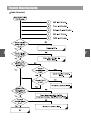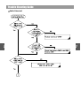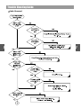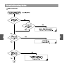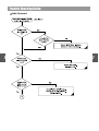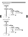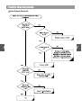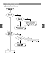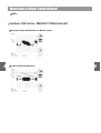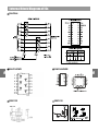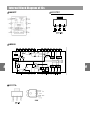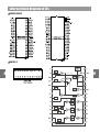
1
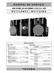
9CD8304700
Service Manual
DVD MINI SYSTEM
XD-615[R]/616[R]/618[R]
XD-625[R]/626[R]/628[R]
XD-625/626/628[R]
TEMPO
ECHO
KEY CON
XD-615/616/618[R]
DAEWOO DAT CO., LTD.
AUG. 2006
DVD MINI SYSTEM
XD-615[R]/616[R]/618[R]
XD-625[R]/626[R]/628[R]
Table of Contents
SAFETY PRECAUTIONS ........................................ 1
SPECIFICATIONS, ADJUSTMENT ......................... 2
LOCATION OF USERS CONTROLS ...................... 3
Front Panel
Display
Rear Panel
Remote Controller
CONNECTING TO EQUIPMENT ............................. 4
Connecting to TV
Connecting to Speaker
Connecting to the Supplied FM/AM(MW) Antennas
Connecting the Microphone for KARAOKE
FIRMWARE DOWNLOAD METHOD ...................... 5
Preparing the Firmware Upgrade
Activating the Firmware Upgrade
Starting Update
Read the Disc or USB Card,
Checksum Check and Update New Firmware.
Completed Update.
Check the Update Version.
CODE FREE METHOD & EEPROM RESET ........... 6
TROUBLE SHOOTING GUIDE ............................... 7
WAVEFORM OF MAJOR CHECK METHOD .......... 8
INTERNAL BLOCK DIAGRAM OF ICs ................... 9
EXPLODED VIEW AND
MECHANICAL PARTS LIST ................................. 10
Mechanical Exploded View : XD-615/ 616, XD-625/ 626
Mechanical Parts List : XD-615/ 616, XD-625/ 626
WIRING DIAGRAM ................................................ 11
BLOCK DIAGRAM ................................................ 12
SCHEMATIC DIAGRAM ........................................ 13
Front Section : XD-615/ 616/ 625/ 626
Function/ Tape Section : XD-615/ 616/ 625/ 626
Video/ Analogue Section : XD-615/ 616/ 625/ 626
Digital Amp : XD-615/ 616/ 625/ 626
Scart Section(Only for EU Version) : XD-615/ 616/ 625/ 626
Mic Section : XD-615/ 616/ 625/ 626
DVD Processor : XD-615/ 616/ 625/ 626
Motor/ Pickup Section : XD-615/ 616/ 625/ 626
SMPS Section : XD-615/ 616/ 625/ 626
P.C.B PATTERN LAYOUT .................................... 14
MPEG : XD-615/ 616/ 625/ 626
FRONT : XD-615/ 616, XD-625/ 626
SMPS : XD-615/ 616/ 625/ 626
Amp : XD-615/ 616/ 625/ 626
Main : XD-615/ 616/ 625/ 626
Mic : XD-615/ 616/ 625/ 626
ELECTRICAL PARTS LIST ................................... 15
Electrical Parts List
Electrical Parts List [Option List]
1
2
3
4
5
6
7
Safety Precautions
WARNING: TO PREVENT FIRE OR ELECTRIC SHOCK, DO NOT EXPOSE
THIS APPLIANCE TO RAIN OR MOISTURE.
CAUTION
RISK OF ELECTRIC SHOCKS
DO NOT OPEN
CAUTION :TO REDUCE THE RISK OF ELECTRIC SHOCK, DO NOT
REMOVE COVER (OR BACK). NO USER SERVICEABLE PARTS
INSIDE.
REFER SERVICING TO QUALIFIED SERVICE PERSONNEL.
THIS SYMBOL IS INTENDED TO ALERT THE USER TO THE
PRESENCE OF UNINSULTED "DANGEROUS VOLTAGE"
WITHIN THE PRODUCT'S ENCLOSURE THAT MAY BE
SUFFICIENT MAGNITUDE TO CONSTITUTE A RISK OF
ELECTRIC SHOCK TO PERSONS.
THIS SYMBOL IS INTENDED TO ALERT THE USER TO THE
PRESENCE OF IMPORTANT OPERATING AND MAINTENANCE
(SERVICING) INSTRUCTIONS IN THE LITERATURE
ACCOMPANYING THE APPLIANCE.
8
CAUTION
TO PREVENT ELECTRIC SHOCK, DO NOT USE THIS POLARIZED AC
PLUG WITH AN EXTENSION CORD, RECEPTACLE OR OTHER OUTLET
UNLESS THE BLADES CAN BE FULLY INSERTED TO PREVENT BLADE
EXPOSURE.
9
LASER SAFETY
THIS UNIT EMPLOYS A LASER. ONLY QUALIFIED SERVICE PERSONNEL
SHOULD REMOVE THE COVER OR ATTEMPT TO SERVICE THIS DEVICE
DUE TO POSSIBLE EYE INJURY.
10
11
12
CAUTION : USE OF ANY CONTROLS, ADJUSTMENTS, OR PROCEDURES
OTHER THAN THOSE SPECIFIED HEREIN MAY RESULT IN HAZARDOUS
RADIATION EXPOSURE.
CAUTION : TO PREVENT ELECTRIC SHOCK, MATCH WIDE BLADE OF
PLUG TO WIDE SLOT, FULLY INSERT.
ATTENTION : POUR EVITER LES CHOCS ELECTRIQUES, INTRODUIRE
LA LAME LA PLUS LARGE DE LA FICHE DANS LA BORNE CORRESPONDANTE DE LA PRISE ET POUSSER JUSQU'AU FOND.
Important Safety Instructions
13
14
15
- All the safety and operating instructions should be read before
the appliance is operated.
- The safety and operating instructions should be retained for
future reference.
- All warnings on the appliance and in the operating instructions
should be adhered to.
- All operating and use instructions should be followed.
1. Water and Moisture - The appliance should not be used near
water - for example, near a bathtub, washbowl, kitchen sink,
1
laundry tub, in a wet basement, or near a swimming pool,
and the like.
2. Carts and Stands - The appliance
PORTABLE CART
should be used only with a cart or
stand that is recommended by th
manufacturer.
3. An appliance and cart combination
should be moved with care. Quick
stops, excessive force, and uneven
surfaces may cause the appliance
and cart combination to overturn.
Figure 2
4. Wall or Ceiling Mounting - The appliance should be mounted to a wall or
ceiling only as recommended by the manufacturer.
5. Ventilation - The appliance should be situated so that its
location or position does not interfere with its proper
ventilation. For example, the appliance should not be situated
on a bed, sofa, rug, or similar surface that may block the
ventilation openings; or, placed in a built-in installation, such
as a bookcase or cabinet that may impede the flow of air
through the ventilation openings.
6. Heat - The appliance should be situated away from heat
sources such as radiators, heat registers, stoves, or other
appliances (including amplifiers) that produce heat.
7. Power Sources - The appliance should be connected to a
power supply only of the type described in the operating
instructions or as marked on the appliance.
8. Grounding or Polarization - The precautions that should be
taken so that the grounding or polarization means of an
appliance is not defeated.
9. Power - Cord Protection - Power-supply cords should be
routed so that they are not likely to be walked on or pinched
by items placed upon or against them, paying particular
attention to cords at plugs, convenience receptacles, and the
point where they exit from the appliance.
10.Protective Attachment Plug - If the appliance is equipped with
an attachment plug having overload protection. This is a
safety feature. See Instruction Manual for replacement or
resetting of protective device. If replacement of the plug is
required, be sure the service technician has used a
replacement plug specified by the manufacturer that has the
same overload protection as the original plug.
11.Cleaning - The appliance should be cleaned only as
recommended by the manufacturer.
12.Power Lines - An outdoor antenna should be located away
from power lines.
2
3
4
5
6
7
8
9
10
11
12
13
14
15
1
2
3
4
5
6
7
8
Safety Precautions
1
13.Outdoor Antenna Grounding - If an outside antenna is
connected to the receiver be sure the antenna system is
grounded so as to provide some protection against voltage
surges and built-up static charges. Article 810 of the National
Electrical Code, ANSI/NFPA 70, provides information with
regard to proper grounding of the mast and supporting
structure, grounding of the lead-in wire to an antenna-dis
charge unit, size of grounding conductors,location of antennadischarge unit, connection to grounding electrodes and
requirements for the grounding electrode. See Figure 1.
EXAMPLE OF ANTENNA
GROUNDING
ANTENNA LEAD
IN WIRE
GROUND CLAMP
ANTENNA DISCHARGE UNIT
(NEC SECTION 810-20)
ELECTRIC
SERVICE
EQUIPMENT
GROUNDING CONDUCTORS
(NEC SECTION 810-21)
GROUND CLAMPS
NEC - NATIONAL ELECTRICAL CODE
POWER SERVICE GROUNDING
ELECTRODE SYSTEM
(NEC ART 250 PART H)
14.Non-use Periods - The power cord of the appliance should be
unplugged from the outlet when left unused for a long period
of time.
15.Object and Liquid Entry - Care should be taken so that objects
do not fall and liquids are not spilled into the enclosure through
openings.
16.Damage Requiring Service - The appliance should be
serviced by qualified service personnel when:
a) The power-supply cord or the plug has been damaged; or
b) Objects have fallen, or liquid has been spilled into the
appliance; or
c) The appliance has been exposed to rain; or
d) The appliance does not appear to operate normally or
exhibits a marked change in performance; or
e) The appliance has been dropped, or the enclosure
damaged.
17.Servicing - The user should not attempt to service the
appliance beyond that described in the operating instructions.
All other servicing should be referred to qualified service
personnel.
2
3
4
5
6
7
8
9
9
10
10
11
11
12
12
13
13
14
14
15
15
1
Specifications
1
General Specifications
2
3
4
5
6
7
8
9
Model
Operating Voltage
Power Consumption
Model
Set
Speaker
XD-615/ 616/ 625/ 626
AC 100V ~ 240V (50/ 60Hz)
Operating 45 Watt
XD-615/ 616/ 625/ 626
275 x 363.3 x 317.5 / 6.15Kg
AS-61VDS : 199 x 251 x 327 / 3.6Kg x 2EA
AS-61WDS : 199 x 280 x 327 / 4.6Kg x 2 EA
XD-618/ 628
AC 230V (50Hz)
Operating 100 Watt
XD-618/ 628
275 x 363.3 x 317.5 / 6.2Kg
AS-62NYS : 230 x 458 x 390 / 6.1Kg x 2EA
Audio Section
POWER OUTPUT at 10 % THD (RMS)
THD (Total Harmonic Distortion)
Input Sen. / Impedance @ 1KHz, 47 K ohms
Output Level / Impedance @ 1KHz
Frequency Response (Analogue)
S/N Ratio IHF-A Weighted
At 1KHz, 6 ohms
At 1KHz, 8 ohms
At 1KHz, 10 W
VIDEO
Tape Rec
at 1W : VIDEO -3 dB
VIDEO
XD-615/625 : 50W / XD-616/626 : 65W
XD-618/628 : 150W
0.10 %
400 mV ± 30 mV / 47K
400 mV ± 30 mV / 2.2K
20 Hz ~ 20 KHz
60 dB
Video Section
Input Sen./Impedance
Output Level/Impedance
Frequency Response
Crosstalk
S/N Ratio
Composite Video (Video)
1 Vp-p / 75 ohm
Composite 75 ohm
1 Vp-p / 75 ohm
S-Video (Y/C) 75 ohm (DVD only)
1 Vp-p / 0.286 Vp-p
Component Out(Y/ Cb/ Cr) : Option 1V p-p / 0.7 Vp-p / 0.7 Vp-p
Ref 500 KHz
@1 MHz
45 dB
DVD
60 dB
±0.5 dB
±0.5 dB
±0.5 dB
±0.5 dB
5 Hz ~ 5.7 MHz
40 dB
2
3
4
5
6
7
8
9
Tuner Section
10
Item
Tuning Range
11
12
13
14
15
Scanning Frequency
Interval
Usable Sensitivity,
75 ohms
S/N Ratio
@1mV IHF-A FILTER
USA Version
Australia/Europe Version
USA Version
Australia/Europe Version
S/N = FM 30dB/MW 20dB, USA Version
S/N = FM 26dB/MW 20dB, Australia/Europe Version
FM Mono USA Version
FM Mono Australia/Europe Version
USA Version
Australia / Europe Version
FM
87.5 ~ 108.0 MHz
87.5 ~ 108.0 MHz
100 KHz
50 KHz
2 uV (17.2dBf)
3 uV (20.8dBf)
60 dB
60 dB
Stereo 65 dB
Stereo 63 dB
MW(AM)
530 ~ 1,710 KHz
522 ~ 1,620 KHz
10 KHz
9 KHz
75 dBuV
75 dBuV
45 dB
45 dB
Tape Section
Tape Speed
Frequency Response
S/N Ratio (with Filter)
Channel Separation
THD (Total Harmonic Distortion)
Wow & Flutter (JIS/WTD)
TCC-112, Normal
1KHz = 0dB
TCC-140 / AUX
MTT-141
Playback, TCC-142
TCC-112
3000 ±3%
150 Hz ~ 8KHz
Playback 50dB / Recording 45dB
40dB
1.5 %
0.2 ±0.35%
10
11
12
13
14
15
1
Adjustments
1
2
2
3
3
4
4
5
5
6
6
7
7
8
8
9
9
10
10
11
11
12
12
13
13
14
14
15
15
1
Location of Users Controls
1
Front Panel : XD-615/616/618[R]
2
3
1
4
2
3
15
4
5
5
16
6
10
11
12
17
13
7
8
6
18
19
20
14
9
22
21
7
8
9
Front Panel : XD-625/626/628[R]
12
1
2
3
4
18
10
11
12
5
19
6
20
7
13
15
23
9
24
14
22
8
13 14 15 16 17
2
3
4
5
6
7
8
9
10
11
1. Disc tray
2. Display
3. STANDBY/ON button with lamp
4. DISC CHANGE button
5. DEMO button
6. Tape RECORD button
7. FUNCTION : DVD, TUNER(FM/AM),
TAPE1/2 and AUX/DIGITAL button
8. USB jack
9. PHONES jack
10. PAUSE ( II ) button
11. STOP ( ) button
12. PLAY ( ) button
13. FAST REVERSE (
)/
FAST FORWARD (
) buttons
14. SKIP PREV (
)/
SKIP NEXT (
) buttons
(
) buttons
15. OPEN/CLOSE
16. DISC 1/2/3 buttons
17. MULTI JOG dial
18. MASTER VOLUME Control
19. Mic. VOLUME Control
20. Microphone 1/2 jacks
21. TAPE 1 EJECT button
22. TAPE 2 EJECT button
25
21
1. Disc tray
2. Display
3. STANDBY/ON button with lamp
4. DISC CHANGE button
5. DEMO button
6. Tape RECORD button
7. FUNCTION : DVD, TUNER(FM/AM),
TAPE1/2 and AUX/DIGITAL button
8. USB jack
9. PHONES jack
10. PAUSE ( II ) button
11. STOP ( ) button
12. PLAY ( ) button
13. ENTER button
14. TEMPO button
15. KEY button
16. Direction(
) buttons
17. Number(0~9) buttons
18. OPEN/CLOSE ( ) buttons
19. DISC 1/2/3 buttons
20. MULTI JOG dial
21. MASTER VOLUME Control
22. Mic. VOLUME Control
23. Microphone 1/2 jacks
24. TAPE 1 EJECT button
25. TAPE 2 EJECT button
10
11
12
13
14
15
1
Location of Users Controls
1
Display
2
1
2
3 4 5
6
3
3
4
7
5
8
9
10
11
12
13
14
15
1. Sound Mode indicator
2. Multi-Function Information Displaying Area
3. MIC indicator
4. REPEAT indicator
5. ALL/1 indicator
6. DISC indicator
7. Media indicator
8. PROGRESSIVE SCAN Mode indicator
9. Tape RECORD indicator
10. RDS indicator
6
7
16
17
18
11. PBC(Playback Control) indicator
12. DRC indicator
13. UBS indicator
14. EQ indicator
15. FM STEREO indicator
16. Lock indicator
17. Disc/Tape Play indicator
18. Disc Tray indicator
8
9
4
5
6
7
8
Rear Panel
9
10
11
1
2
12
3
5
4
6
13
2
11
7
8
9
14
10
1. FM ANTENNA connector
2. AM(MW) ANTENNA connectors
3. COMPONENT VIDEO OUTPUT
Y/Pb/Pr jacks
4. MONITOR OUT jack
5. S-VIDEO OUT jack
6. COAXIAL INPUT jack
7. AUX INPUT jacks
8. LINE OUTPUT jacks
9. SUB WOOFER OUTPUT jacks
10. SPEAKER connectors
11. SCART jack (Optional)
12. Power cord
10
11
12
13
14
12
15
15
1
Location of Users Controls
1
Remote Controller
2
2
3
3
4
4
1
2
5
5
6
9
7
6
10
7
14
8
11
12
13
15
8
9
10
11
12
13
14
15
16
17
20
18
19
22
24
23
28
27
32
31
36
26
30
21
25
29
33
37
34
35
40
38
39
1. STAND BY/ON button
2. PROGRESSIVE button
3. DISC CHANGE button
4. OPEN/CLOSE( ) button
5. DVD/TV SYS(PAL/NTSC: DVD only) button
6. TUNER button
7. TAPE 1/2 button
8. AUX button
9. Number(0~9) buttons
10. GO TO/DEVICE button
11. MUTE button
12. UBS button
13. RECORD( ) button
14. ENTER button
15. Direction(
) button
16. SETUP button
17. MENU/RETURN( ) button
18. SKIP PREV ( ) button
19. STOP ( ) button
20. PLAY( ) button
21. SKIP NEXT ( ) button
22. FAST REVERSE ( ) button
23. SLOW button
24. PAUSE button
25. FAST FORWARD ( ) button
26. REPEAT/RDS MODE button
27. A-B REPEAT/PTY SEARCH button
28. AUTO MEMORY button
29. DISPLAY/FM MODE button
30. EQ button
31. TEMPO button
32. ECHO button
33. KEY CON button
34. AUDIO button
35. SUBTITLE/MPX button
36. ANGLE/DIGEST button
37. TITLE/PBC button
38. ZOOM button
39. SLEEP button
40. VOLUME -/+ buttons
3
4
5
6
7
8
9
10
11
12
13
14
15
1
Connecting to Equipment
1
Connecting to TV
2
21-Pin SCART Cable(not included) to 21-pin SCART input terminal on TV
SCART Specification(Europe model only) : Composite and Component Video output(DVD, Video)Audio L/R
Output(DVD only)
2
3
3
4
4
for EU version: optional
5
5
6
6
7
8
9
10
11
12
If the TV or monitor is equipped with an S video input, make the S video connection in addition to the normal video
connection. The S video connection will provide higher quality picture playback.
8
Connecting speakers
Before connecting
This machine is designed to reproduce optimum sound quality when speakers with the specified impedance below
are connected. Please check the following information and choose speakers with appropriate impedance for the
connections.
Front speakers(L/R) :
XD-615/616/625/626[R] : 6 ohms min. per speaker
XD-618/628[R] : 8 ohms min. per speaker
To prevent damage to circuits, never short-circuit the positive (+) and negative (-) speaker wires.
Do not connect the speaker cable to the L and R connectors at the same time and do not connect more than one
speaker to the same speaker connectors.
Right speaker
9
10
11
12
Left speaker
13
Subwoofer speaker
(User Option)
14
15
7
NO!
NO!
NO!
R
L
R
L
13
14
15
1
Connecting to Equipment
Connecting the supplied FM/MW(AM) antennas
2
1
2
3
3
4
4
5
5
6
6
7
8
9
10
11
Adjusting the position of the FM antenna
While listening to an FM program, extend the antenna and move it in various directions until the clearest signal is
received, then secure the antenna with push pins in the position with the least distortion.
Adjusting the position of the AM(MW) antenna
While listening to a AM(MW) program, set the antenna in the direction and position where you receive the clearest
sound.
Put it as far away as possible from the unit, TVs, speakers, cables, and power cords.
Connecting the microphone for KARAOKE
Plugging a dynamic microphone to sing along with CD, VCD, DVD
or AUX(also while recording).
Connect the plugs securely.
7
8
9
10
11
12
12
13
13
14
14
15
15
1
Firmware Download Method
1
Preparing the Firmware Upgrade
2
3
1. Write a disc to Update file by PC Writing Program.
2. A size of dummy folder is more than 10M bite. (ex : font_dw, attached picture)
3. Put Firmware file in a disc or USB Card.
• Filename : A61L5_ 16.ROM
6
7
8
9
3
4
4
5
2
Note : Before using the USB devices, make sure
there is no disc on the machine. USB
function works only under the condition
that the display shows “NO DISC” or
“STOP” at DVD function mode.
Activating the Firmware Upgrade
<Update by CD-R>
1. Open the Door of DVD Receiver.
2. Insert the Update Disc into the Disc Tray.
3. Close the Door, then DVD Receiver reads the disc,
and Update the Firmware itself.
<Update by USB>
1. Insert the USB Card while the disc is stopped, and
Update the Firmware itself.
5
6
7
8
9
10
10
11
11
12
13
Starting Update.
1. Detect the Update Disc.
2. Display for Update Version.
• Basic Version : XD- 615/ 616/618, XD- 625/ 626/628 ( A61L5_ 16. ROM )
12
13
14
14
15
15
1
Firmware Download Method
1
Read the Disc or USB Card, Checksum Check and Update New Firmware.
2
1. Automatically open the Door, after Read from Disc. (Disc only)
2. Take a disc out of a Tray. (Disc only)
2
3
3
4
4
5
5
6
6
7
8
Completed Update.
1. Automatically Video Output off, after Complete Update.
2. Remove the USB Card.
3. Press Power Button twice(off on)
4. The system is working.
7
8
9
9
10
10
11
12
Check the Update Version.
1. Open the Door of UNIT.
2. Press Audio Button or Subtitle Button.
• Audio Button : Check for MPEG Firmware Version.
• Subtitle Button : Check for Loader Firmware Version.
11
12
13
13
14
14
15
Caution
• While updating, if the door opened or closed by touch, or power button is pressed, the Flash Memory
will be damaged (Same as USB).
• Must be press “Default” or “Reset” on the Setup Menu, Finished Update New Firmware.
15
1
Code Free Method & EEPROM Reset
1
Preparing the Code Free Method
2
3
4
5
6
7
1. Press “Open” button.
2. Press “Setup” button.
3. Press Number button.
(5 4 2 5)
4. You can see window for Code Free.
5. Press “Enter”, or “Right Arrow”
button.
6. Select Region Number.
7. Press “Left Arrow” button.
8. If you Press “Setup”, The Setting of
Code Free is finished.
2
3
4
5
6
7
8
8
9
9
10
11
12
13
14
15
XD-610/620 Series EEPROM Reset
Use Only this case : change Flash Memory
1. Door Open.
2. Press Setup Key.
3. Press Number Key(2-5-8-0)
4. Display as follows,
“EEPROM CLEAR TWICE POWER ON/OFF”
Power off Power on Power off Power on.
Notice
Check Region Code.
Check Video Mode.
10
11
12
13
14
15
1
Trouble Shooting Guide
1
Basic Operating
2
2
3
3
4
4
5
5
6
6
7
7
8
8
9
9
10
10
11
11
12
12
13
13
14
14
15
15
1
Trouble Shooting Guide
1
Initial Operating
2
2
3
3
4
4
5
5
6
6
7
7
8
8
9
9
10
10
11
11
12
12
13
13
14
14
15
15
1
Trouble Shooting Guide
1
Initial Operating
2
2
3
3
4
4
5
5
6
6
7
7
8
8
9
9
10
10
11
11
12
12
13
13
14
14
15
15
1
Trouble Shooting Guide
1
Audio Abnormal
2
2
3
3
4
4
5
5
6
6
7
7
8
8
9
9
10
10
11
11
12
12
13
13
14
14
15
15
1
Trouble Shooting Guide
1
Audio Abnormal
2
2
3
3
4
4
5
5
6
6
7
7
8
8
9
9
10
10
11
11
12
12
13
13
14
14
15
15
1
Trouble Shooting Guide
1
Audio Abnormal
2
2
3
3
4
4
5
5
6
6
7
7
8
8
9
9
10
10
11
11
12
12
13
13
14
14
15
15
1
Trouble Shooting Guide
1
Audio Abnormal
2
2
3
3
4
4
5
5
6
6
7
7
8
8
9
9
10
10
11
11
12
12
13
13
14
14
15
15
1
Trouble Shooting Guide
1
Audio Abnormal
2
2
3
3
4
4
5
5
6
6
7
7
8
8
9
9
10
10
11
11
12
12
13
13
14
14
15
15
1
Trouble Shooting Guide
1
Audio Abnormal
2
2
3
3
4
4
5
5
6
6
7
7
8
8
9
9
10
10
11
11
12
12
13
13
14
14
15
15
1
Trouble Shooting Guide
1
Audio Abnormal
2
2
3
3
4
4
5
5
6
6
7
7
8
8
9
9
10
10
11
11
12
12
13
13
14
14
15
15
1
Trouble Shooting Guide
1
Audio Line Out Abnormal
2
2
3
3
4
4
5
5
6
6
7
7
8
8
9
9
10
10
11
11
12
12
13
13
14
14
15
15
1
Trouble Shooting Guide
1
Audio Line Out Abnormal
2
2
3
3
4
4
5
5
6
6
7
7
8
8
9
9
10
10
11
11
12
12
13
13
14
14
15
15
1
Trouble Shooting Guide
1
Audio Line Out Abnormal
2
2
3
3
4
4
5
5
6
6
7
7
8
8
9
9
10
10
11
11
12
12
13
13
14
14
15
15
1
Trouble Shooting Guide
1
Audio Control Abnormal
2
2
3
3
4
4
5
5
6
6
7
7
8
8
9
Audio Control Abnormal
9
10
10
11
11
12
12
13
13
14
14
15
15
1
Trouble Shooting Guide
1
Video Output Abnormal
2
2
3
3
4
4
5
5
6
6
7
7
8
8
9
9
10
10
11
11
12
12
13
13
14
14
15
15
1
Trouble Shooting Guide
1
Mechanical Control Abnormal
2
2
3
3
4
4
5
5
6
6
7
7
8
8
9
9
10
10
11
11
12
12
13
13
14
14
15
15
1
Trouble Shooting Guide
1
Mechanical Control Abnormal
2
2
3
3
4
4
5
5
6
6
7
7
8
8
9
9
10
10
11
11
12
12
13
13
14
14
15
15
1
Waveforms of Major Check Method
1
Test Point : DVD Test Disc MDVD-W111 TRACK2 Color Bar
2
Audio Out Signal Waveform
DAC Output Signal Waveform
2
3
3
4
4
5
5
6
6
7
Optical Output Audio Data Signal waveform
PWM Output Waveform During Normal Play
7
8
8
9
9
10
10
11
Serial Data Output Waveform During Normal Play
11
12
12
13
13
14
14
15
15
1
Waveforms of Major Check Method
1
Test Point : DVD Test Disc MDVD-W111 TRACK2 Color Bar
2
Pr Output Data Waveform in Component Output
2
3
3
4
4
5
5
6
6
7
Pb Output Data Waveform in Component Output
7
8
8
9
9
10
10
11
11
Y Output Data Waveform in Component Output
12
12
13
13
14
14
15
15
1
Waveforms of Major Check Method
MPEG
2
2
3
1
Test Point : DVD Test Disc MDVD-W111 TRACK2 Color Bar
3
Composite Output Data Waveform in Monitor Output
4
4
5
5
6
6
7
7
8
S-Video Output Data Waveform
8
9
9
10
10
11
11
12
12
13
13
14
14
15
15
1
Internal Block Diagram of ICs
1
74HC244
2
2
3
3
4
4
5
5
6
6
7
7
8
8
74HC14PWR
74HCU04PWR
9
9
10
10
11
11
12
12
13
2SB1132
2SK3018
13
14
14
15
15
1
Internal Block Diagram of ICs
BA6287F
1
LD1117DT
2
2
3
3
4
4
5
5
6
AM5888
6
7
7
8
8
9
9
10
10
11
11
12
LD1117A
12
13
13
14
14
15
15
1
Internal Block Diagram of ICs
1
M29W160DB
2
2
3
3
4
4
5
5
6
6
7
7
8
MM1623
8
9
9
10
10
11
11
12
12
13
13
14
14
15
15
1
Internal Block Diagram of ICs
1
PCF8574
2
2
3
3
4
4
5
5
6
6
7
7
8
PT6315
8
9
9
10
10
11
11
12
12
13
13
14
14
15
15
1
Internal Block Diagram of ICs
STA308A
1
M12L64164A
2
2
3
4
5
6
7
7
8
STA505
8
9
9
10
10
11
11
12
12
13
13
14
14
15
15
1
Internal Block Diagram of ICs
1
V6309
2
2
3
3
4
4
5
5
6
6
BD3401KS2(Bi)
7
7
8
8
9
9
10
10
11
11
12
12
13
13
14
14
15
15
1
Internal Block Diagram of ICs
1
ES8380FCA
2
2
3
3
4
4
5
5
6
6
7
7
8
8
9
9
10
10
11
11
12
M24C04
12
13
13
14
14
15
15
1
APPENDIX - ELECTRICAL PART LIST
1
XD-615/ 616/618/ 625/ 626/628
2
3
4
5
6
7
8
9
10
11
12
13
14
15
ASS'Y
LOC
PART-CODE
PART-NAME
PART-DESC
Q'TY
MAIN
10000
9CDC080100
PCB MAIN ASS'Y
XD-610 MAIN ASS'Y
MAIN
B400
9CD6502500
PCB MAIN
231.5X194X1.6T
1
MAIN
MAIN
MAIN
MAIN
MAIN
MAIN
MAIN
MAIN
MAIN
MAIN
MAIN
MAIN
MAIN
MAIN
MAIN
MAIN
MAIN
MAIN
MAIN
MAIN
MAIN
MAIN
MAIN
MAIN
MAIN
MAIN
MAIN
MAIN
MAIN
MAIN
MAIN
MAIN
MAIN
MAIN
MAIN
MAIN
CF251 CF252 CF253 CF254 CF255 CF256
CF265 CF266 CF267 CF268 CF269 CF270
CN403
CN406
CN601
CN602
CN902
CW402
CW404
CW405
CW601
CW602
HD401 HD402 HD603 HD604
HD403
HQ251 HQ254
HQ252 HQ253 HQ255
HQ404 HQ407
HQ405 HQ406 HQ409 HQ605 HQ644
HQ408
HQ601 HQ602 HQ647 HQ648 HQ649 HQ650
HQ604 HQ606
HQ645
HQ646
IC251
IC401
IC402
IC403
IC405 IC406 IC407 IC409 IC601
IC408
IC410
IC602
J251
J252
J254
L601 L602 L631 L632
L641
TU001
5P1H101MF9728837000
9728837100
9738835000
9728838700
9728836700
9CD6268700
9CD6268500
9728836900
2503-WS-03
2503-WS-07
DZDS160--D1SR156--TZRA102S-TZRC107S-TZRA107S-TZRC231S-TZTD1304-TZTC3875STZTD1304-T2SA2071-T2SC5824-1MM1623--1BD3401KS2
1PCF8574AP
174HCU04PW
1NJM4558M1BA4560F-1LD1117S33
1BA3126N-9736329600
9736328100
9736329500
5LC333K804
5L0503K643
9737653301
LC FILTER
CONN AS
CONN AS
CONN AS
CONN AS
CONN AS
WAFER
WAFER
CONN AS
WAFER
WAFER
DIODE SW CHIP
DIODE RECTIFIER
TR CHIP
TR CHIP
TR CHIP
TR CHIP
TR CHIP
TR CHIP
TR CHIP
TR CHIP
TR CHIP
IC
IC
IC
IC
IC
IC
IC
IC
JACK
JACK S-VIDEO
JACK
COIL CHOKE
COIL BIAS OSC
TUNER MODULE
CFI 06B 1H 101MF
UL1007 #24 4P P2.0 250MM Board-in
UL1007 #26 8P P2.0 250MM Board-in
UL 2851 #28X2C0 3P 260MM
UL2851,1533 #28X4CO 6P+7P 270MM
UL1007 #24 8P P2.0 150MM Board-in
52806-2210
52806-2010
UL1007 #26 7P P2.0 270MM Shield
3P 2.5MM
7P 2.5MM
KDS160 (KDS511)
1SR156-400 TE25
KRA102S
KRC107S
KRA107S
KRC231S
KTD1304
KTC3875Y
KTD1304
2SA2071
2SC5824
MM1623
BD3401KS2
PCF8574APWR
SN74HCU04PWR TSSOP
NJM4558M
BA4560F
LD1117AS33TR SOT-223
BA3126N
JACK_RGB_RCA305
R102-D04KA-07
JACK_RCA-619A-01-01
33MH K
SM-10F 5.04MH
KST-ML000MV0-J69L(USA)
1
1
1
1
1
1
1
1
1
1
1
1
1
1
1
1
1
1
1
1
1
1
1
1
1
1
1
1
1
1
1
1
1
1
1
1
MIC
11000
9CDC079800
PCB MIC ASS'Y
XD-610 MIC ASS'Y
MIC
MIC
MIC
MIC
MIC
MIC
MIC
B200
CW405
HD201
HQ201 HQ202
IC201 IC203
J201 J202
VR201
9CD6501800
2001-WS-07
DZDS160--TZTC3875S1NJM4558M9736329400
5V1503728B
PCB MIC
WAFER
DIODE SW CHIP
TR CHIP
IC
JACK MIC
VR ROTARY
139X247X1.6T(2*3)
7P 2.0MM
KDS160 (KDS511)
KTC3875Y
NJM4558M
PJ-603A
RK09K1110AV8
PCB MPEG ASS'Y
XD-610 MPEG ASS'Y
9CDC080000
1
1
1
1
1
1
1
MPEG
12000
MPEG
MPEG
MPEG
MPEG
MPEG
MPEG
MPEG
MPEG
MPEG
MPEG
B500
CN301
CW301
CW302
CW303
CW403
CW406
CW501
CW502
HA501 HA510
9CD6502100
9728838000
9CD6273600
2001-WS-12
2001-WS-06
2001-WS-04
2001-WS-08
9CD6268700
9CD6267800
HRTT8330J
PCB MPEG
CONN FFC
WAFER
WAFER
WAFER
WAFER
WAFER
WAFER
WAFER
R ARRAY CHIP
160X130X1.6T
FFC P=0.5X24PX195MM D
JSYO.5S-5S-24PWB
12P 2.0MM
6P 2.0MM
4P 2.0MM
8P 2.0MM
52806-2210
52806-1310
1/16 33X4 OHM 1608
1
1
1
1
1
1
1
1
1
1
MPEG
MPEG
MPEG
MPEG
HA502 HA503 HA504 HA505 HA506
HA507 HA508 HA509
HD302 HD303 HD304 HD305 HD503
HD501 HD502
HL304 HL305
HRTT8100J
DZDS160--D1SR156--5LF100K859
R ARRAY CHIP
DIODE SW CHIP
DIODE RECTIFIER
CHIP COIL
1/16 10X4 OHM 1608
KDS160 (KDS511)
1SR156-400 TE25
10UH 2012
1
1
1
1
MPEG
MPEG
MPEG
MPEG
MPEG
MPEG
MPEG
MPEG
MPEG
MPEG
MPEG
MPEG
MPEG
MPEG
MPEG
HL501 HL502 HL503 HL504 HL505 HL509
HL510 HL511 HL512 HL513 HL515 HL516
HL517 HL518 HL519
HQ301 HQ302
HQ303
HQ304 HQ305
HQ306
IC303
IC501
IC502
IC503
IC504
IC505
IC506
IC508
IC509
XC501
CHIP BEAD
TR CHIP
TR CHIP
FET CHIP
TR CHIP
IC
IC
IC
IC
IC
IC
IC
IC
IC
X-TAL
FB 60 OHM 100MHZ 2012
2SB1132
KTC3875Y
2SK3018
KRC111S
BA6287F DRIVER
ES8380 MPEG DECODER
M12L128168A SDRM(128M) (ESMT)
M29W160DB FLASH(16M)
M24C04MN S0P
LD1117ADT33 DPAK
LD1117ADT-R DPAK
RESET IC, V6309 MSP3B
AM5888S Motor Driver
27MHZ HC-49/US (RADIAL/SMD)
1
1
1
1
1
1
1
1
1
1
1
1
1
1
1
5LX600K841
T2SB1132T1
TZTC3875ST2SK3018-TZRC111S-1BA6287F-1ES8380FCA
1L128168AE
1M29W160EB
1M24C04MN1LD1117A33
1LD1117A-R
1V6309MSP3
1AM5888S-5XJ27M000E
2
3
4
5
6
7
8
9
10
11
12
13
14
15
1
2
3
4
5
6
7
8
APPENDIX - ELECTRICAL PART LIST
ASS'Y
LOC
10
11
12
13
14
15
PART-NAME
PART-DESC
FRONT
13000
9CDC080500
PCB FRONT ASS'Y
XD-620 FRONT ASS'Y
FRONT
FRONT
FRONT
FRONT
FRONT
FRONT
FRONT
FRONT
FRONT
FRONT
FRONT
FRONT
FRONT
FRONT
FRONT
FRONT
FRONT
FRONT
FRONT
FRONT
FRONT
FRONT
FRONT
FRONT
FRONT
FRONT
FRONT
FRONT
B700
CN702
CN703
CN704
CN903
CW702
CW703
CW704
FD701
HD702 HD703 HD704 HD705
HD706
HQ701 HQ703
HQ702
HQ704
HQ705 HQ706 HQ707
HQ708 HQ709 HQ710
IC701
IC702
IC703
IC704
IC705
IC706
LD701
LD702 LD703 LD704 LD705
RV701
VR701 VR702
XC701
10
9CD6505600
9728837600
9728837400
9728837700
9728836600
9CD6267800
9CD6268500
9CD6261600
D25-1121FN
DZDS160--D1SR156--TZTD1304-TZRA111S-TZRA107S-T2SA2071-TZRC107S-1PT6315--1M24C04MN1HK381B-DW
1V6309MSP3
13776XD610
174HC244PW
DMT463SRTT
DMT-463UBD
RV14172225SH1224375
5XJ16R000C
9CD4210000
PCB FRONT
CONN FFC
CONN FFC
CONN FFC
CONN AS
WAFER
WAFER
WAFER
VFD
DIODE SW CHIP
DIODE RECTIFIER
TR CHIP
TR CHIP
TR CHIP
TR CHIP
TR CHIP
IC
IC
IC
IC
IC
IC
LED
LED
R SEMI FIXED
SW ENCODER
X-TAL
CUSHION VFD
247X163X1.6T
FFC P=1.0X13PX240MM C
FFC P=1.0X20PX220MM R
FFC P=1.25X16PX120MM D
UL1007 #26 11P P2.0 300MM Board-in
52806-1310
52806-2010
52492-1620
VFD25-1121FN
KDS160 (KDS511)
1SR156-400 TE25
KTD1304
KRA111S
KRA107S
2SA2071
KRC107S
PT6315
M24C04MN S0P
HK381BT-DW
RESET IC, V6309 MSP3B
M37762 BASIC Version
SN74HC244PW
MT-463SRT/W60/TR1
MT-463UBD/W60
1/10 2.2K OHM B V6EK-PV1S
RE0123PVB25FINB 1-2-24 PCE
JWT-16.000-US
EVA T4.5
H/P
H/P
H/P
H/P
H/P
H/P
H/P
9CDC080600
B701
CF701 CF702
CN701
HL701
J701
J702
SMPS
9
PART-CODE
1
9CD6501701
5P1H101MF9728837200
5LX600K841
9736325300
9736329300
PCB HP ASS'Y
XD-620 HP ASS'Y
PCB H/P
LC FILTER
CONN AS
CHIP BEAD
JACK H/P
JACK USB
FR-1, HP XD-620
CFI 06B 1H 101MF
UL1007 #26 8P P2.0 70MM Board-in
FB 60 OHM 100MHZ 2012
HTJ-035-18A (H/P)
USAF-046N-WP-01
Q'TY
1
1
1
1
1
1
1
1
1
1
1
1
1
1
1
1
1
1
1
1
1
1
1
1
1
1
1
2
0
1
1
1
1
1
9CDC080200
PCB SMPS ASS'Y
XD-610 SMPS ASS'Y
SMPS
SMPS
SMPS
B900
AC901
CC901 CC911
9CD6502200
9736915700
CCXB3A102K
PCB SMPS
CORD AC
C CERA
139X197X1.6T
KE-112 H03VVH2-F 5A 250V 2.18M
1KV B 1000PF K (FORMING)
1
1
1
SMPS
SMPS
SMPS
SMPS
SMPS
SMPS
SMPS
SMPS
SMPS
SMPS
SMPS
SMPS
SMPS
SMPS
CC902 CC903 CC906 CC908 CC909 CC910
CC912 CC914 CC916
CC904
CC905
CC907 CC913 CC915
CC917 CC918
CC919
CE904
CE906 CE907
CM901
CW901
CW902
CW903
CW981
CX901
CCFF1H104Z
CCXB3A103K
CL1GB1102K
CCXB3A471K
CL1GB1101K
CL1GB1102K
CEXN4D331P
CEXD1H331B
CMXK2J333J
2001-WS-06
2001-WS-08
2001-WS-11
9CD6290900
CL1BB3334K
C CERA
C CERA
C CERA (Y-CAP)
C CERA
C CERA (Y-CAP)
C CERA (Y-CAP)
C ELECTRO
C ELECTRO
C MYLAR
WAFER
WAFER
WAFER
WAFER
C CERA (X-CAP)
HIKF 50V 0.1MF Z (FORMING)
1KV B 0.01MF K (FORMING)
250V 102PF Y-1
1KV B 470PF K (FORMING)
250V 100PF Y-1
250V 102PF Y-1
400V 300UF LHS
50V RL(LK) 330MF (10X20)
MC 630V 0.033MF J
6P 2.0MM
8P 2.0MM
11P 2.0MM
3.96 2P VH-02A(White)
275V 334(X-CAP) 436D
1
1
1
1
1
1
1
1
1
1
1
1
1
1
SMPS
SMPS
SMPS
SMPS
SMPS
SMPS
SMPS
SMPS
SMPS
SMPS
SMPS
SMPS
SMPS
SMPS
SMPS
SMPS
SMPS
SMPS
SMPS
SMPS
SMPS
SMPS
SMPS
SMPS
SMPS
D901 D902 D906 D907 D909 D910
D912 D913 D920 D925 D940
D903
D904
D908
D914 D915 D916 D917 D918
D923
D926
DZ905
DZ911
DZ912
DZ924
F901
IC901
IC902 IC905
IC903
IC904
IC907 IC908 IC909 IC910
L901 L908 L909 L910
L905
L906 L907
PT901
PT902
PT903
Q901
R901
DHER108G-DSR106---DTS10P06GDMBR20150C
DSR310---DSR106---DSR310---DP6KE200ADZTZ18B--DZTZ4R7B-DZTZ4R3B-5FFPS5022S
1LNK353P-1TL431A--1TOP245Y-1TOP248Y-1ET1103--5LC220K864
5LF203N865
5LC339N863
5TMW015972
5TMW034971
5TMW028970
TZTC3198YRS01Y104J-
DIODE(UFR)
DIODE(Schottky)
DIODE(Bridge)
DIODE(Schottky)
DIODE(Schottky)
DIODE(Schottky)
DIODE(Schottky)
DIODE(TVS)
DIODE ZENER
DIODE ZENER
DIODE ZENER
FUSE MINIATURE
IC(Switching)
IC(Shunt Regulator)
IC(Switching)
IC(Switching)
IC(Photocoupler)
COIL CHOKE
COIL LINE FILTER
COIL CHOKE
TRANS POWER
TRANS POWER
TRANS POWER
TR
R METAL OXIDE FILM
HER108G(UF4007)
SR106
TS10P06G
MBR20150CT
SR310
SR106
SR310
P6KE200A
MTZ-18B 52MM TAPPING
MTZ-4.7B 52MM TAPPING
MTZ-4.3B 52MM TAPPING
250V 5.0A TL
LNK353P
TL431
TOP-245Y
TOP-248Y
ET1103
22uH(1A)
KS-2930A1 LINE FILTER
3,3uH(5A)
EE1614 H
EE2834V_12P
EE2828
KTC3198Y (2SC5343) AUTO
1W 100K OHM J
1
1
1
1
1
1
1
1
1
1
1
1
1
1
1
1
1
1
1
1
1
1
1
1
1
2
3
4
5
6
7
8
9
10
11
12
13
14
15
1
APPENDIX - ELECTRICAL PART LIST
1
XD-615/ 616/ 625/ 626
2
3
4
5
ASS'Y
SMPS
SMPS
SMPS
SMPS
SMPS
SMPS
SMPS
SMPS
SMPS
SMPS
SMPS
SMPS
SMPS
SMPS
SMPS
SMPS
SMPS
SMPS
SMPS
LOC
R906
R907
R912
R913
R914
R921
R923
R930
R931
R937
R938
R946
R948
R957
TH901
VA901
10
20
30
XD-618/ 628
6
PART-CODE
RN-AZ1122F
RN-AZ1002F
RS02Y104JRS02Y104JRD01Y470JRS01Y101JRS01Y103JRS02Y563JRS01Y470JRN-AZ1122F
RN-AZ1002F
RD-2Y471JRD-2Y561JRD-2Y561JDNTC-3D15F
D1NR10D471
9CD0915600
9CD4411200
9CD4411400
PART-NAME
R METAL FILM
R METAL FILM
R METAL OXIDE FILM
R METAL OXIDE FILM
R CARBON FILM
R METAL OXIDE FILM
R METAL OXIDE FILM
R METAL OXIDE FILM
R METAL OXIDE FILM
R METAL FILM
R METAL FILM
R CARBON FILM
R CARBON FILM
R CARBON FILM
THERMISTER
VARISTOR
PLATE IC
HEAT SINK S1
HEAT SINK S3
PART-DESC
1/6 11.2K OHM F(1%)
1/6 10K OHM F(1%)
2W 100K OHM J
2W 100K OHM J
1W 47 OHM J
1W 100 OHM J
1W 10K OHM J
2W 56K OHM J
1W 47 OHM J
1/6 11.2K OHM F(1%)
1/6 10K OHM F(1%)
1/2 470 OHM J
1/2 560 OHM J
1/2 560 OHM J
NTC-3D15F
1NR10D471
AL-EXT
AL-EXT
Q'TY
1
1
1
1
1
1
1
1
1
1
1
1
1
1
1
1
1
1
1
2
3
4
5
6
7
7
8
8
9
9
10
10
11
11
12
12
13
13
14
14
15
15
APPENDIX - ELECTRICAL PART LIST
1
APPENDIX - ELECTRICAL PART LIST
1
XD-615/ 616/ 625/ 626
2
3
4
AMP
AMP
AMP
AMP
AMP
AMP
AMP
AMP
AMP
AMP
AMP
AMP
AMP
AMP
B800
CM860 CM861
CN861
CN802
CN901
CW861 CW862
HL860 HL861
IC860
IC861 IC862
IC863
J801
L860 L861L862 L863
10
9CDC080100
PCB AMP ASS'Y
XD-610 MAIN ASS'Y
9CD6502400
CMXK1J684J
9728837900
9728837800
9728836800
9CD6268700
5LX601K843
1STA308A-174HC14PWR
1STA505--9736329700
5LC220K866
9CD4410800
PCB AMP
C MYLAR
CONN FFC
CONN FFC
CONN AS
WAFER
CHIP BEAD
IC
IC
IC
JACK SPEAKER
COIL LPF
HEAT SINK AMP
220X115X1.6T(1*2)
MC 63V 0.68MF J
FFC P=1.0X22PX330MM D
FFC P=1.0X22PX140MM C
UL1007 #24 6P P2.0 200MM
52806-2210
FB 600 OHM 100MHZ 2012
STA308A DDX
SN74HC14PWR TSSOP
STA505 PWM AMP
JACK_SPK_PTB-408S
22UH LPF Digital Amp PI 13mm
AL-EXT
REMOCON AS
AM-67D
9CDM064300
REMOCON
AM-67D
REMOCON 12000
5
REMOCON 10
1
1
1
1
1
1
1
1
1
1
1
1
1
1
2
3
4
5
XD-618/ 628
6
6
7
7
8
8
9
9
10
10
11
11
12
12
13
13
14
15
XD-618/ 628 Fan Option List
MAIN
MAIN
MAIN
MAIN
MAIN
FAN
NAME
CONN WAFER
C Electro
CHIP RES
TR
TR
DC Fan
Loc
CW201
CE285
HR283
HQ256
HQ257
Q'ty
1
1
1
1
1
1
S/N
2503-WS-02
CEXF1E221V
HRF8100JCA
TZRC231S-TZRA107S-9738101700
DESCRIPTION
2P 2.5MM
25V 220uF
1/8 10 OHM J 2012
KRC231S
KRA107S
SP602512M-03(DC12V, 0.11A)
Remark
14
15
Use in RH-435
1
APPENDIX - ELECTRICAL PART LIST
1
2
2
3
3
4
4
5
5
6
6
7
7
8
8
9
9
10
10
11
11
12
12
13
13
14
14
15
15
1
2
3
4
APPENDIX - ELECTRICAL PART LIST[OPTION LISTS]
1. SCART JACK OPTION LIST.
NO
NAME
LOC
1 FFC Wafer
CN201
2 PCB ASS'Y
Q'TY
S/N
1 9CD6264700
1 9CDC080300
DESCRIPTION
52045-1645
XD-610 SCART ASS'Y
2. TUNER MODULE OPTION LIST.
NO
NAME
LOC
1 TUNER MODULE TU001
2 TUNER MODULE TU001
3 TUNER MODULE TU001
4 ANT LOOP
5 ANT FM
Q'TY
1
1
1
1
1
DESCRIPTION
KST-ML000MV0-J69L(USA)
KST-ML104MV1-J69L(Europe)
KST-ML006MV1-J69L(JAPAN)
S0160BL-25
1.2M PIG TAIL BLK
S/N
9737653301
9737653401
9737653501
9736807100
9736806000-1
W/O Scart
X
X
With Scart
O
O
2006-08-26
REMARK
1
2
3
4
REMARK
Shield Type
5
5
6
6
7
7
8
9
10
11
12
13
14
15
4. SMPS Option list
NO
NAME
1 DIODE(Zener)
2 DIODE(Zener)
LOC
DZ911
DZ911
Q'TY
1
1
S/N
DZTZ18B--DZTZ22B---
DESCRIPTION
UZ18BSB
UZ22BSB
XD-615/625 XD-616/626
O
X
X
O
REMARK
5. AMP Option list
NO
NAME
1 IC
2 IC
LOC
IC863
IC863
Q'TY
1
1
S/N
1STA505--1STA506---
DESCRIPTION
XD-615/625 XD-616/626
O
X
X
O
REMARK
STA505
STA506
6. XD-62X RDS Option list
NO
NAME
LOC
1 R CHIP
HR008/009
2 C CHIP CERA
HC004/005
3 WIRE JUMPER
JW704
Q'TY
2
2
1
S/N
HRFT101JBA
HCQK101JBA
W581GY7595
DESCRIPTION
1/10 100 OHM J 1608
50V CH 100PF J 1608
AWG22 1/0.65 SN 7.5 AUTO
RDS
O
O
O
NO RDS
X
X
X
REMARK
MAIN PCB
MAIN PCB
FRONT PCB
7. XD-61X RDS Option list
NO
NAME
LOC
1 R CHIP
HR008/009
2 C CHIP CERA
HC004/005
3 WIRE JUMPER
JW714
4 WIRE JUMPER
JW745
5 WIRE JUMPER
JW748
Q'TY
2
2
1
1
1
S/N
HRFT101JBA
HCQK101JBA
W581GY7595
W581GY1005
W581GY12J5
DESCRIPTION
1/10 100 OHM J 1608
50V CH 100PF J 1608
AWG22 1/0.65 SN 7.5 AUTO
AWG22 1/0.65 SN 10 AUTO
AWG22 1/0.65 SN 12.5 AUTO
RDS
O
O
O
O
O
NO RDS
X
X
X
X
X
REMARK
MAIN PCB
MAIN PCB
FRONT PCB
FRONT PCB
FRONT PCB
8. AC CORD Option list
NO
NAME
1 AC CORD
2 AC CORD
3 AC CORD
4 AC CORD
5 AC CORD
6 AC CORD
7 AC CORD
LOC
————
————
————
————
————
————
————
Q'TY
1
1
1
1
1
1
1
S/N
9736913700
9736913800
9736913900
9736914000
9736914100
9736914200
9736915700
DESCRIPTION
KE-21,H03VVH2-F 1900MM WITH STOPPER
KE-01PÅêNISPT-2 18AWG 10A
9. OTHER Option list
NO
NAME
1 CONN FFC
2 CONN FFC
LOC
CN703
CN703
Q'TY
1
1
S/N
9728837500
9728837400
DESCRIPTION
P=1.0X20PX250MM
P=1.0X20PX220MM
BUYER
EUROPE
AMERICA
ENGLAND
AUSTRALLIA
ARGENTINA
BRAZIL
SRI LANKA
KE-112 H03VVH2-F 5A 250V 2.18M
XD-61X
O
X
XD-62X
X
O
REMARK
8
9
10
11
12
13
14
15