1
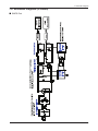
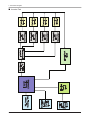
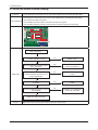
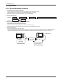
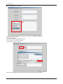
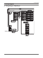
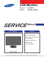
LCD-Monitor Chassis :LS19MYN Model :943NW / 943NWX SERVICE TFT-LCD Monitor Manual Contens 1. Precautions 2. Product specifications 3. Disassembly and Reassemble 4. Troubleshooting 5. Exploded View & Part List 6. Wiring Diagram 7. Schematic Diagram 943NW / 943NWX Refer to the service manual in the GSPN (see the rear cover) for the more information. Contents 1. Precautions............................................................................................................... 1-1 1-1. Safety Precautions.......................................................................................................... 1-1 1-2. Servicing Precautions...................................................................................................... 1-2 1-3. Static Electricity Precautions........................................................................................... 1-2 1-4. Installation Precautions................................................................................................... 1-3 2. Product specifications............................................................................................. 2-1 2-1. Feature & Specifications.................................................................................................. 2-1 2-2. Spec Comparison to the Old Models............................................................................... 2-2 2-3. Accessories..................................................................................................................... 2-3 2-4. Accessories (Sold separately)......................................................................................... 2-3 3. Disassembly and Assembly.................................................................................... 3-1 3-1. SIMPLE STAND Disassembly......................................................................................... 3-1 3-2. HAS STAND Disassembly............................................................................................... 3-4 4. Troubleshooting....................................................................................................... 4-1 4-1. Troubleshooting............................................................................................................... 4-1 4-2. When the Power Does Not Turn On................................................................................ 4-2 4-3. When the screen is blank (Analog).................................................................................. 4-4 4-4. Error Examples and Actions............................................................................................ 4-7 4-5. Adjustment....................................................................................................................... 4-8 5. Exploded View & Part List....................................................................................... 5-1 5-1. SIMPLE STAND Exploded View...................................................................................... 5-1 5-2. SIMPLE STAND Parts List............................................................................................... 5-3 5-3. HAS STAND Exploded View .................................................................................................. 5-9 5-4. HAS STAND Parts List................................................................................................... 5-11 6. Wiring Diagram......................................................................................................... 6-1 6-1. Wiring Diagram - Main Board.......................................................................................... 6-1 6-2. Wiring Diagram - IP Board............................................................................................... 6-2 6-3. Connector Functions....................................................................................................... 6-3 6-4. Cables............................................................................................................................. 6-3 7. Schematic Diagram.................................................................................................. 7-1 7-1. Circuit Descriptions.......................................................................................................... 7-1 7-2. Schematic Diagrams (Scaler Part).................................................................................. 7-2 7-3. Schematic Diagrams (Power Flowchart)......................................................................... 7-2 7-4. Schematic Diagrams (IP Board)...................................................................................... 7-3 7-5. Schematic Diagrams (Main PBA)................................................................................... 7-3 GSPN (Global Service Partner Network) Area Web Site North America http://service.samsungportal.com Latin America http://latin.samsungportal.com CIS http://cis.samsungportal.com Europe http://europe.samsungportal.com China http://china.samsungportal.com Asia http://asia.samsungportal.com Mideast & Africa http://mea.samsungportal.com This Service Manual is a property of Samsung Electronics Co.,Ltd. Any unauthorized use of Manual can be punished under applicable International and/or domestic law. © 2007 Samsung Electronics Co.,Ltd. All rights reserved. Printed in Korea P/N: BN82-00288A-00 3. Disassembly and Assembly 3. Disassembly and Assembly This section describes the disassembly and reassembly sequences for this monitor. Warning:As this monitor has parts that are sensitive to static electricity, be careful when handling them. 3-1. SIMPLE STAND Disassembly Caution: 1. Turn the monitor off before beginning the disassembly process. 2. Disassemble the monitor carefully as directed in the following procedures. 3. W hen disassembling the monitor, do not use any metal tools except for the provided jig. Description Photo Screws 1. Place a soft cloth on the table and place the monitor onto it with the front part facing downwards. Hold the monitor set with one hand and hold and pull the stand body backwards with the other hand to remove the stand body from the monitor set. Caution : : If you do not tilt the stand and use too much force to remove it, the connection pin may break. 2. ① Turn the monitor over and insert your hands into the top of the monitor at the center and separate the front cover in the direction of the arrow as shown in the figure. ② Separate the sides of the front cover up to the directed line as shown in the figure. ① ② 3. Turn the monitor over again to remove the back cover. 3-1 3. Disassembly and Assembly Description Photo Screws 4. Remove the SHIELD-LAMP using the provided JIG. Caution: The SHIELD-LAMP is sharp. 5. Remove the LVDS, LAMP wire, FUNCTION cable, and SPEAKER cable, and then remove the SHIELD-COVER. LVDS LAMP WIRE FUNCTION 6. Remove the LCD panel.. 7. Remove the four (4) screws shown in the figure. 8. Remove the four (4) screws shown in the figure and remove the Bracket support. 3-2 3. Disassembly and Assembly Description Photo Screws 9. Remove the main PCB and IP boards from the SHIELD-cover. ※ The assembly is in the reverse order of disassembly. 3-3 3. Disassembly and Assembly 3-2. HAS STAND Disassembly Description Photo 1. If the Stopper PIN at the back of the stand is not removed, place a soft cloth on the table and place the monitor on it, and then hold the monitor set and remove the Stopper PIN at the back of the stand. 2. T urn the monitor over. Remove the two (2) screws that hold the stand in place and then remove the stand. Caution: W hen removing the screws, hold the stand body with one hand so that the stand does not fall. 3. The following steps are the same as steps 2 to 9 for disassembling the SIMPLE stand. ※ The assembly is in the reverse order of disassembly. 3-4 Screws 5. Exploded View & Part List 5. Exploded View & Part List M0027 BN63-03965A T0514 M0081 T0003 M0081 M0215 M0174 M0006 M0003 M0013 5-1. SIMPLE STAND Exploded View (LS19MYNKFZ/XBM) 5-1 5. Exploded View & Part List 5-1-1. LS19MYNKFZ/XBM Parts List (943NWX) Location No. Code No. Description & Specification Q’ty SA/SNA T0003 BN96-07592B ASSY COVER P-FRONT;[Mckinley]LS19MYW,ABS 1 S.A M0215 BN07-00462A LCD-PANEL;M190A1-L07 1 S.A M0174 BN44-00121K IP BOARD;PWI1904SJ(J),MCKINLEY 943NW/BW, 1 S.A M0081 6003-000115 SCREW-TAPTITE;BH,+,B,M3,L6,ZPC(BLK),SWRC 2 S.A M0081 6003-001439 SCREW-TAPTITE;BH,+,-,S,M4,L8,ZPC(WHT),SW 1 S.N.A T0514 BN61-03557A BRACKET-SUPPORT;2043BW/NW[Mckinley],SPTE 1 S.N.A M0006 BN96-06381R ASSY SHIELD P-COVER;943NW(CMO PANEL),SEC 1 S.N.A BN63-03965A SHIELD-LAMP;943BW/NW,SPTE,T0.3,(Wide) 1 S.N.A M0013 BN96-06380N ASSY COVER P-REAR;LS19MYN,HIPS HB,BK26,S 1 S.A M0003 BN96-06388A ASSY STAND P;-,943BW,-,SECC T2.0,-,- 1 S.A M0027 BN96-06672A ASSY STAND P-BASE;LS17MY,ABS HB,BK26,H/G 1 S.A 5-2 Remark 5. Exploded View & Part List 5-2. LS19MYNKFZ/XBM Parts List Service Bom (SA: SERVICE AVAILABLE, SNA: SERVICE NOT AVAILABLE) Level Location No. Code No. Description & Specification LS19MYNKFZ/XBM 943NWX,SAL1/S19B8-LMY,19,LCDMO,ECUADOR Q’ty SA/SNA Remark 0.1 M0002 BN90-01584A ASSY COVER REAR;LS19MYNKBZ/XSF,CMO PANEL 1 S.N.A ..2 M0013 BN96-06380N ASSY COVER P-REAR;LS19MYN,HIPS HB,BK26,S 1 S.A ...3 M0113 BN61-01581A BRACKET-VESA;BI17/19BS,SECC,T1.0 2 S.N.A ...3 M0006 BN63-03940A COVER-REAR SUB;2043BW/NW,HIPS HB,BK26 1 S.N.A ...3 M0006 BN63-03982G COVER-REAR;943BW/NW,HIPS HB,BK26,CMO,SIM 1 S.N.A ...3 M0126 BN73-00162A RUBBER-PANEL;943BW/ NW,RUBBER,BLACK,(Wide 6 S.N.A ...3 M0126 BN73-00164A RUBBER-PANEL;LS19MYW,RUBBER,BLACK 3 S.N.A 0.1 M0001 BN90-01631A ASSY COVER FRONT;LS19MYNKFZ/XBG,CMO PANE 1 S.N.A ..2 T0003 BN96-07592B ASSY COVER P-FRONT;[Mckinley]LS19MYW, ABS 1 S.A ...3 CCM1 BN63-02183D COVER-SHEET;Rhcm,PE Vinyl,T0.05,680mm,20 0.5 S.N.A ...3 M0112 BN63-04551B COVER-FRONT;[Mckinley]LS19MYW,ABS HB,T2. 1 S.N.A ...3 M0130 BN67-00209A LENS LED;Mckinley,PC CLEAR,TP15(TP-1020) 1 S.N.A 1 S.A S.N.A ...3 M0175 BN96-06485B ASSY BOARD P-TOUCH FUNCTION;Mckinley,CT5 ....4 M0014 BN94-01772C ASSY PCB MAIN-FUNCTION PCB,BN9;LS17MY* 1 .....5 M2893 BN39-01007A LEAD CONNECTOR;Mckinley,UL1571#30,5 to 5 1 S.A .....5 BN61-03552A GUIDE-CONTROL;2043BW/NW,ABS HB,GR70 1 S.N.A .....5 BN74-00011A TAPE-FUNCTION TAPE;DOUBLE FACE TAPE,Poly 1 S.N.A .....5 BN74-00012A TAPE-FUNCTION TAPE;DOUBLE FACE TAPE,Poly 1 S.N.A .....5 T0174 BN97-02132L ASSY SMD;LS17MY* 1 S.N.A ......6 CD1 0406-001172 DIODE-TVS;CDS3C30GTH,48/-/50V,SMD 1 S.A ......6 CD2 0406-001172 DIODE-TVS;CDS3C30GTH,48/-/50V,SMD 1 S.A ......6 L0405 0601-002461 LED;SMD,InGaN Blue,1.6X3.2X1.1mm,468nm,1 1 S.A 1 S.A ......6 U1 1209-001706 IC-SENSOR;TS08N,MLF,32P,5x5mm,PLASTIC ,5V ......6 R110 2007-000081 R-CHIP;2.7Kohm,5%,1/10W,TP,1608 1 S.A ......6 R110 2007-000081 R-CHIP;2.7Kohm,5%,1/10W,TP,1608 1 S.A ......6 R110 2007-000105 R-CHIP;200Kohm,5%,1/10W,TP,1608 1 S.A ......6 R110 2007-000107 R-CHIP;470Kohm,5%,1/10W,TP,1608 1 S.A ......6 R110 2007-000123 R-CHIP;1.5Kohm,5%,1/10W,TP,1608 1 S.A ......6 R110 2007-000123 R-CHIP;1.5Kohm,5%,1/10W,TP,1608 1 S.A ......6 C120 2203-000257 C-CER,CHIP;10nF,10%,50V,X7R,TP,1608 1 S.A ......6 C120 2203-005065 C-CER,CHIP;1000nF,+80-20%,10V,Y5V,1608 1 S.A ......6 C120 2203-005065 C-CER,CHIP;1000nF,+80-20%,10V,Y5V,1608 1 S.A 3711-006471 CONNECTOR-HEADER;BOX,5P,1R,1mm,SMDA,AU, 1 S.A ......6 CN906 5-3 5. Exploded View & Part List ......6 PCB BN41-00947A 0.1 M0112 ..2 PCB SUB-FUNCITION;Mckinley function,FR-4 1 S.N.A BN91-01877A ASSY SHIELD;MCKINLEY 19,LS19MYW 1 S.N.A BN63-03965A SHIELD-LAMP;943BW/NW,SPTE,T0.3,(Wide) 1 S.N.A 0.1 M0107 BN91-02069A ASSY LCD-CTZ;LS19MYN* 1 S.N.A ..2 M0215 BN07-00462A LCD-PANEL;M190A1-L07 1 S.A 0.1 M0017 BN91-02070A ASSY CHASSIS-CTZ;LS19MYNKB/XSF 1 S.N.A ..2 M0081 6003-000115 SCREW-TAPTITE;BH,+,B,M3,L6,ZPC(BLK),SW RC 2 S.A ..2 M0081 6003-000115 SCREW-TAPTITE;BH,+,B,M3,L6,ZPC(BLK),SW RC 1 S.A ..2 M0081 6003-001439 SCREW-TAPTITE;BH,+,,S,M4,L8,ZPC(WHT),SW 1 S.N.A ..2 M0174 BN44-00121K IP BOARD;PWI1904SJ(J),MCKINLEY 943NW/ BW, 1 S.A ..2 T0514 BN61-03557A BRACKET-SUPPORT;2043BW/ NW[Mckinley],SPTE 1 S.N.A ..2 M0014 BN94-01702A ASSY PCB MAIN-CTZ;LS19MYNKB/XSF 1 S.A ...3 T0245 0202-001608 SOLDER-WIRE FLUX;LFC7-107,D0.8,99.3Sn/0. 0.003 S.N.A 1 S.A ...3 CN101 3701-001219 CONNECTOR-DSUB;15P,3R,FEMALE,ANGLE, AUF ...3 CN600 3711-004261 HEADER-BOARD TO BOARD;BOX,12P,1R,2mm,ANG 1 S.A ...3 T0174 BN97-02079A ASSY SMD;LS19MYNKB/XSF 1 S.N.A 0.457 S.N.A ....4 SUB05 0202-001477 SOLDER-CREAM;LST309-M,,D20~45um,96.5Sn/ ....4 D108 0401-001056 DIODE-SWITCHING;MMBD4148SE,100V,200m A,SO 1 S.A ....4 D109 0401-001056 DIODE-SWITCHING;MMBD4148SE,100V,200m A,SO 1 S.A ....4 D110 0401-001056 DIODE-SWITCHING;MMBD4148SE,100V,200m A,SO 1 S.A ....4 D600 0402-001614 DIODE-RECTIFIER;S1G,400V,1A,DO-214AC,TP 1 S.A ....4 D601 0402-001614 DIODE-RECTIFIER;S1G,400V,1A,DO-214AC,TP 1 S.A ....4 ZD104 0403-001411 DIODE-ZENER;-,5.49-5.73V,200mW,SOD323,T 1 S.A ....4 ZD105 0403-001411 DIODE-ZENER;-,5.49-5.73V,200mW,SOD323,T 1 S.A ....4 ZD202 0403-001411 DIODE-ZENER;-,5.49-5.73V,200mW,SOD323,T 1 S.A ....4 ZD203 0403-001411 DIODE-ZENER;-,5.49-5.73V,200mW,SOD323,T 1 S.A ....4 ZD204 0403-001411 DIODE-ZENER;-,5.49-5.73V,200mW,SOD323,T 1 S.A ....4 ZD601 0403-001411 DIODE-ZENER;-,5.49-5.73V,200mW,SOD323,T 1 S.A ....4 ZD201 0406-001061 DIODE-TVS;MMQA5V6T3,5.32/5.6/5.88V,24W,S 1 S.A 1 S.A ....4 Q203 0501-000445 TR-SMALL SIGNAL;KTC3875SY,NPN,150mW,SOT ....4 Q204 0501-000445 TR-SMALL SIGNAL;KTC3875SY,NPN,150mW,SOT 1 S.A ....4 Q601 0501-000445 TR-SMALL SIGNAL;KTC3875SY,NPN,150mW,SOT 1 S.A ....4 Q202 0501-002080 TR-SMALL SIGNAL;2SC2412K,NPN,200mW,S C-59 1 S.A 5-4 5. Exploded View & Part List ....4 Q205 0501-002080 TR-SMALL SIGNAL;2SC2412K,NPN,200mW,S C-59 1 S.A ....4 Q207 0501-002080 TR-SMALL SIGNAL;2SC2412K,NPN,200mW,S C-59 1 S.A ....4 Q409 0505-001165 FET-SILICON;SI3443BDV,P,-20V,+-4.4A,65mo 1 S.A ....4 IC112 1103-001410 IC-EEPROM;S-24CS08AFJ-TB1GE,8Kbit,1Kx8, 1 S.A ....4 T0087 1203-003695 IC-POSI.FIXED REG.;NCP1117ST33T3G,SOT22 1 S.A ....4 T0087 1203-003696 IC-POSI.FIXED REG.;NCP1117DT18T5G,DPA K,3 1 S.A ....4 IC109 1205-003364 IC-LCD CONTROLLER;SE717MLF,PQFP,128P,20 1 S.A ....4 R110 2007-000074 R-CHIP;100ohm,5%,1/10W,TP,1608 1 S.A ....4 R110 2007-000074 R-CHIP;100ohm,5%,1/10W,TP,1608 1 S.A ....4 R110 2007-000074 R-CHIP;100ohm,5%,1/10W,TP,1608 1 S.A ....4 R110 2007-000074 R-CHIP;100ohm,5%,1/10W,TP,1608 1 S.A ....4 R110 2007-000074 R-CHIP;100ohm,5%,1/10W,TP,1608 1 S.A ....4 R110 2007-000074 R-CHIP;100ohm,5%,1/10W,TP,1608 1 S.A ....4 R110 2007-000074 R-CHIP;100ohm,5%,1/10W,TP,1608 1 S.A ....4 R110 2007-000074 R-CHIP;100ohm,5%,1/10W,TP,1608 1 S.A ....4 R110 2007-000074 R-CHIP;100ohm,5%,1/10W,TP,1608 1 S.A ....4 R110 2007-000074 R-CHIP;100ohm,5%,1/10W,TP,1608 1 S.A ....4 R110 2007-000074 R-CHIP;100ohm,5%,1/10W,TP,1608 1 S.A ....4 R110 2007-000074 R-CHIP;100ohm,5%,1/10W,TP,1608 1 S.A ....4 R110 2007-000074 R-CHIP;100ohm,5%,1/10W,TP,1608 1 S.A ....4 R110 2007-000074 R-CHIP;100ohm,5%,1/10W,TP,1608 1 S.A ....4 R110 2007-000074 R-CHIP;100ohm,5%,1/10W,TP,1608 1 S.A ....4 R110 2007-000074 R-CHIP;100ohm,5%,1/10W,TP,1608 1 S.A ....4 R110 2007-000074 R-CHIP;100ohm,5%,1/10W,TP,1608 1 S.A ....4 R110 2007-000074 R-CHIP;100ohm,5%,1/10W,TP,1608 1 S.A ....4 R110 2007-000080 R-CHIP;2Kohm,5%,1/10W,TP,1608 1 S.A ....4 R110 2007-000080 R-CHIP;2Kohm,5%,1/10W,TP,1608 1 S.A ....4 R110 2007-000082 R-CHIP;3.3Kohm,5%,1/10W,TP,1608 1 S.A ....4 R110 2007-000082 R-CHIP;3.3Kohm,5%,1/10W,TP,1608 1 S.A ....4 R110 2007-000083 R-CHIP;3Kohm,5%,1/10W,TP,1608 1 S.A ....4 R110 2007-000083 R-CHIP;3Kohm,5%,1/10W,TP,1608 1 S.A ....4 R110 2007-000084 R-CHIP;4.7Kohm,5%,1/10W,TP,1608 1 S.A ....4 R110 2007-000084 R-CHIP;4.7Kohm,5%,1/10W,TP,1608 1 S.A ....4 R110 2007-000088 R-CHIP;7.5Kohm,5%,1/10W,TP,1608 1 S.A ....4 R110 2007-000090 R-CHIP;10Kohm,5%,1/10W,TP,1608 1 S.A ....4 R110 2007-000090 R-CHIP;10Kohm,5%,1/10W,TP,1608 1 S.A ....4 R110 2007-000090 R-CHIP;10Kohm,5%,1/10W,TP,1608 1 S.A ....4 R110 2007-000090 R-CHIP;10Kohm,5%,1/10W,TP,1608 1 S.A ....4 R110 2007-000090 R-CHIP;10Kohm,5%,1/10W,TP,1608 1 S.A ....4 R110 2007-000090 R-CHIP;10Kohm,5%,1/10W,TP,1608 1 S.A ....4 R110 2007-000090 R-CHIP;10Kohm,5%,1/10W,TP,1608 1 S.A ....4 R110 2007-000090 R-CHIP;10Kohm,5%,1/10W,TP,1608 1 S.A ....4 R110 2007-000090 R-CHIP;10Kohm,5%,1/10W,TP,1608 1 S.A ....4 R110 2007-000090 R-CHIP;10Kohm,5%,1/10W,TP,1608 1 S.A ....4 R110 2007-000090 R-CHIP;10Kohm,5%,1/10W,TP,1608 1 S.A ....4 R110 2007-000090 R-CHIP;10Kohm,5%,1/10W,TP,1608 1 S.A ....4 R110 2007-000090 R-CHIP;10Kohm,5%,1/10W,TP,1608 1 S.A 5-5 5. Exploded View & Part List ....4 R110 2007-000090 R-CHIP;10Kohm,5%,1/10W,TP,1608 1 S.A ....4 R110 2007-000090 R-CHIP;10Kohm,5%,1/10W,TP,1608 1 S.A ....4 R110 2007-000090 R-CHIP;10Kohm,5%,1/10W,TP,1608 1 S.A ....4 R110 2007-000090 R-CHIP;10Kohm,5%,1/10W,TP,1608 1 S.A ....4 R110 2007-000102 R-CHIP;100Kohm,5%,1/10W,TP,1608 1 S.A ....4 R110 2007-000124 R-CHIP;2.2Kohm,5%,1/10W,TP,1608 1 S.A ....4 R110 2007-000309 R-CHIP;10ohm,5%,1/10W,TP,1608 1 S.A ....4 R110 2007-000309 R-CHIP;10ohm,5%,1/10W,TP,1608 1 S.A ....4 R110 2007-000821 R-CHIP;390ohm,1%,1/10W,TP,1608 1 S.A ....4 R110 2007-000821 R-CHIP;390ohm,1%,1/10W,TP,1608 1 S.A ....4 R110 2007-001044 R-CHIP;56ohm,5%,1/10W,TP,1608 1 S.A ....4 R110 2007-001044 R-CHIP;56ohm,5%,1/10W,TP,1608 1 S.A ....4 R110 2007-001164 R-CHIP;75ohm,1%,1/10W,TP,1608 1 S.A ....4 R110 2007-001164 R-CHIP;75ohm,1%,1/10W,TP,1608 1 S.A ....4 R110 2007-001164 R-CHIP;75ohm,1%,1/10W,TP,1608 1 S.A ....4 C120 2203-000236 C-CER,CHIP;0.1nF,5%,50V,C0G,1608 1 S.A ....4 C120 2203-000236 C-CER,CHIP;0.1nF,5%,50V,C0G,1608 1 S.A ....4 C120 2203-000236 C-CER,CHIP;0.1nF,5%,50V,C0G,1608 1 S.A ....4 C120 2203-000257 C-CER,CHIP;10nF,10%,50V,X7R,TP,1608 1 S.A ....4 C120 2203-000257 C-CER,CHIP;10nF,10%,50V,X7R,TP,1608 1 S.A ....4 C120 2203-000257 C-CER,CHIP;10nF,10%,50V,X7R,TP,1608 1 S.A ....4 C120 2203-000384 C-CER,CHIP;0.015nF,5%,50V,C0G,1608 1 S.A ....4 C120 2203-000626 C-CER,CHIP;0.022nF,5%,50V,C0G,1608 1 S.A ....4 C120 2203-000626 C-CER,CHIP;0.022nF,5%,50V,C0G,1608 1 S.A ....4 C120 2203-000626 C-CER,CHIP;0.022nF,5%,50V,C0G,1608 1 S.A ....4 C120 2203-000888 C-CER,CHIP;4.7nF,10%,50V,X7R,1608 1 S.A ....4 C120 2203-000888 C-CER,CHIP;4.7nF,10%,50V,X7R,1608 1 S.A ....4 C120 2203-000888 C-CER,CHIP;4.7nF,10%,50V,X7R,1608 1 S.A ....4 C120 2203-000888 C-CER,CHIP;4.7nF,10%,50V,X7R,1608 1 S.A ....4 C120 2203-000888 C-CER,CHIP;4.7nF,10%,50V,X7R,1608 1 S.A ....4 C120 2203-000888 C-CER,CHIP;4.7nF,10%,50V,X7R,1608 1 S.A ....4 C120 2203-005005 C-CER,CHIP;100nF,10%,16V,X7R,1608 1 S.A ....4 C120 2203-005005 C-CER,CHIP;100nF,10%,16V,X7R,1608 1 S.A ....4 C120 2203-005005 C-CER,CHIP;100nF,10%,16V,X7R,1608 1 S.A ....4 C120 2203-005005 C-CER,CHIP;100nF,10%,16V,X7R,1608 1 S.A ....4 C120 2203-005005 C-CER,CHIP;100nF,10%,16V,X7R,1608 1 S.A ....4 C120 2203-005005 C-CER,CHIP;100nF,10%,16V,X7R,1608 1 S.A ....4 C120 2203-005005 C-CER,CHIP;100nF,10%,16V,X7R,1608 1 S.A ....4 C120 2203-005005 C-CER,CHIP;100nF,10%,16V,X7R,1608 1 S.A ....4 C120 2203-005005 C-CER,CHIP;100nF,10%,16V,X7R,1608 1 S.A ....4 C120 2203-005005 C-CER,CHIP;100nF,10%,16V,X7R,1608 1 S.A ....4 C120 2203-005005 C-CER,CHIP;100nF,10%,16V,X7R,1608 1 S.A ....4 C120 2203-005005 C-CER,CHIP;100nF,10%,16V,X7R,1608 1 S.A ....4 C120 2203-005005 C-CER,CHIP;100nF,10%,16V,X7R,1608 1 S.A ....4 C120 2203-005005 C-CER,CHIP;100nF,10%,16V,X7R,1608 1 S.A ....4 C120 2203-005005 C-CER,CHIP;100nF,10%,16V,X7R,1608 1 S.A ....4 C120 2203-005005 C-CER,CHIP;100nF,10%,16V,X7R,1608 1 S.A ....4 C120 2203-005005 C-CER,CHIP;100nF,10%,16V,X7R,1608 1 S.A ....4 C120 2203-005005 C-CER,CHIP;100nF,10%,16V,X7R,1608 1 S.A ....4 C120 2203-005005 C-CER,CHIP;100nF,10%,16V,X7R,1608 1 S.A ....4 C120 2203-005005 C-CER,CHIP;100nF,10%,16V,X7R,1608 1 S.A 5-6 5. Exploded View & Part List ....4 C120 2203-005005 C-CER,CHIP;100nF,10%,16V,X7R,1608 1 S.A ....4 C120 2203-005005 C-CER,CHIP;100nF,10%,16V,X7R,1608 1 S.A ....4 C120 2203-005005 C-CER,CHIP;100nF,10%,16V,X7R,1608 1 S.A ....4 C120 2203-005005 C-CER,CHIP;100nF,10%,16V,X7R,1608 1 S.A ....4 C120 2203-005005 C-CER,CHIP;100nF,10%,16V,X7R,1608 1 S.A ....4 C120 2203-005005 C-CER,CHIP;100nF,10%,16V,X7R,1608 1 S.A ....4 C120 2203-005005 C-CER,CHIP;100nF,10%,16V,X7R,1608 1 S.A ....4 C120 2203-005005 C-CER,CHIP;100nF,10%,16V,X7R,1608 1 S.A ....4 C120 2203-005005 C-CER,CHIP;100nF,10%,16V,X7R,1608 1 S.A ....4 C120 2203-005005 C-CER,CHIP;100nF,10%,16V,X7R,1608 1 S.A ....4 C120 2203-005005 C-CER,CHIP;100nF,10%,16V,X7R,1608 1 S.A ....4 C120 2203-005005 C-CER,CHIP;100nF,10%,16V,X7R,1608 1 S.A ....4 C120 2203-005005 C-CER,CHIP;100nF,10%,16V,X7R,1608 1 S.A ....4 C120 2203-005005 C-CER,CHIP;100nF,10%,16V,X7R,1608 1 S.A ....4 C120 2203-005005 C-CER,CHIP;100nF,10%,16V,X7R,1608 1 S.A ....4 C120 2203-005005 C-CER,CHIP;100nF,10%,16V,X7R,1608 1 S.A ....4 C120 2203-005005 C-CER,CHIP;100nF,10%,16V,X7R,1608 1 S.A ....4 C120 2203-005005 C-CER,CHIP;100nF,10%,16V,X7R,1608 1 S.A ....4 C120 2203-005005 C-CER,CHIP;100nF,10%,16V,X7R,1608 1 S.A ....4 C120 2203-005005 C-CER,CHIP;100nF,10%,16V,X7R,1608 1 S.A ....4 C120 2203-005065 C-CER,CHIP;1000nF,+80-20%,10V,Y5V,1608 1 S.A ....4 C120 2203-005065 C-CER,CHIP;1000nF,+80-20%,10V,Y5V,1608 1 S.A ....4 C120 2203-005065 C-CER,CHIP;1000nF,+80-20%,10V,Y5V,1608 1 S.A ....4 C120 2203-005437 C-CER,CHIP;10000nF,+80-20%,10V,Y5V,3216 1 S.A ....4 C231 2402-001128 C-AL,SMD;100μF,20%,16V,-,TP,6.3X5.7mm 1 S.A ....4 C629 2402-001128 C-AL,SMD;100μF,20%,16V,-,TP,6.3X5.7mm 1 S.A ....4 C639 2402-001128 C-AL,SMD;100μF,20%,16V,-,TP,6.3X5.7mm 1 S.A 1 S.A ....4 X202 2801-003667 CRYSTAL-SMD;14.31818MHz,30ppm,28AAN,16p ....4 T0568 3301-001407 BEAD-SMD;30ohm,1608,300mA,TP,,,0.4ohm 1 S.N.A ....4 T0568 3301-001407 BEAD-SMD;30ohm,1608,300mA,TP,,,0.4ohm 1 S.N.A ....4 CN400 3708-001150 CONNECTOR-FPC/FFC/PIC;30P,1mm,SMDA,SN,Y 1 S.A ....4 T0077 BN41-00877A PCB MAIN;Mckinley,CEM-3 Silver,2,MP1.0,1 1 S.N.A 1 S.N.A ....4 M0018 BN97-02035A ASSY MICOM;Mckinley,LMY19NS,MX25L1005 ,20 .....5 IC115 1107-001614 IC-FLASH MEMORY;MX25L1005,1Mbit,1Mx1Bit, 1 S.N.A ..2 M0251 BN96-02854N ASSY CABLE P;Fininfarina,FLAT CABLE,-,15 1 S.A ASSY SHIELD P-COVER;943NW(CMO PANEL),SEC 1 S.N.A ..2 M0006 BN96-06381R ...3 T0073 AA63-01141C GASKET-EMI;42D5,T1.5,10,40,Fabric 4 S.N.A AA65-00011C CLAMPER CORE-WIRE;ALL MODEL,NYLON 66,V2, 1 S.N.A ...3 BN61-02429D STUD-PEM;PNB,M2.8,D7,L20,ZPC(SIL),SUM2 4L 1 S.N.A ...3 BN61-03573F BRACKET-SUPPORT STAND;LS19MYW,SECC,T1.6, 1 S.N.A ...3 BN61-03594A SPRING ETC-STAND;Mckinley,SUS304,T0.3,SI 1 S.N.A SHIELD-COVER;LS19MYW,SECC,T0.8,BOE Panel 1 S.N.A ...3 T0527 ...3 M0107 BN63-03962D 0.1 M0113 BN92-02621Z ASSY P/MATERIAL;LS19MYWKBA/XSF* 1 S.N.A ..2 T0376 6902-000061 BAG AIR;LDPE,T0.2,L1000,W500,TRP,,, 0.005 S.N.A ..2 T0524 6902-000241 BAG PE;NITRON/HDPE,T0.5/T0.012,W600,L600 1 S.N.A 5-7 5. Exploded View & Part List ..2 T0376 6902-000379 BAG AIR;LDPE,T0.2,W1000,L1800,TRP,-,-- 0.001 S.N.A ..2 T0003 6902-000604 BAG WRAPPING;LDPE,T0.02,W500,L10000,T RP, 0.79 S.N.A ..2 M0081 6902-000609 BAG ROLL;LDPE,T0.05,W2400,L1000,TRP,-,- 0.017 S.N.A 0.1 M0019 BN92-03163N ASSY LABEL;LS17MYAKB/XAZ 1 S.N.A 0.1 M0003 BN92-03351E ASSY BOX;LS19MYNKFZ/XBM 1 S.N.A BN69-02296A BOX-02,MONITOR;943NWX-Simple,CB,SY01,A1 1.02 S.N.A ..2 0.1 M0045 BN92-03437B ASSY ACCESSORY;LS19MYNKFZ/XBM 1 S.N.A ..2 M0003 BN96-06388A ASSY STAND P;-,943BW,-,SECC T2.0,-,- 1 S.A ...3 BN63-03985A COVER-STAND FRONT;LS19MYW,HIPS HB,BK26,S 1 S.N.A ...3 BN63-03992A COVER-STAND REAR;LS19MYW,HIPS HB,BK26,Si 1 S.N.A ...3 T0022 BN96-06383A ASSY HINGE P-SIMPLE;943BW,SPCC, HGI,T2.0 1 S.N.A ...3 T0524 6902-000675 BAG PE;LDPE,T0.05,W200,L250,PINK,28,-,3 1 S.N.A 4 S.A ...3 M0081 6003-000282 SCREW-TAPTITE;BH,+,,B,M3,L8,ZPC(BLK),SW ..2 M0027 BN96-06672A ASSY STAND P-BASE;LS17MY,ABS HB,BK26,H/G 1 S.A ...3 T0524 6902-000110 BAG PE;LDPE,T0.05,W250,L400,TRP,28,2 1 S.N.A ...3 CIS4 BN61-01717A HOLDER-STAND;BIZET,NI PLT,CH,+,M4,L11(5) 1 S.N.A ...3 CCM1 BN63-02183K COVER-SHEET;Rhcm,PE Vinyl,T 0.05,250MM,2 0.25 S.N.A BN63-04210A COVER-STAND BASE;943BW,743B,743BM,AB S,HB 1 S.N.A BN96-06529A ASSY HOLDER P-WIRE;MCKINLEY,ABS HB,BK26 1 S.N.A ...3 T0004 ...3 ....4 6902-000336 BAG ZIPPER;LDPE,T0.05,W70,L80,TRP,-,-- 1 S.N.A ....4 M0114 BN61-03555A HOLDER-WIRE;MCKINLEY,ABS HB,BK26 1 S.N.A ...3 T0132 BN73-00077A RUBBER FOOT;MATISSE,BUMPON,Ф13.5,T2. 0,6 4 S.N.A BN96-07639B ASSY ACCESSORYCABLE&MANUAL;LS19MYNKFZ/X 1 S.A ..2 ...3 T0268 3903-000085 CBF-POWER CORD;DT,US,BP3/YES,I(IEC C13/C 1 S.A ...3 T0524 6902-000110 BAG PE;LDPE,T0.05,W250,L400,TRP,28,2 1 S.N.A AA68-03727A MANUAL FLYER-01,WARRANTY CARD;All,SAMSUN 1 S.N.A BN63-02368A CLOTH;LS07BTT,SUEDE,0.6,160,120 1 S.N.A 1 S.N.A ...3 T0175 ...3 ...3 M0215 BN96-06906A ASSY MANUAL PIB+QSG;943NW,943NWX,MOJO 8 ....4 CCM1 BN59-00666A S/W DRIVER-02,IB;943NW,943NWs,W/ W,SyncMa 1 S.N.A ....4 QSG BN68-01377A MANUAL FLYER-QSG;2043BW,SyncMaster,W/ W,M 1 S.N.A ..2 M0114 BN39-00244G CBF SIGNAL;D-sub cable,15P/15P,20276N,15 1 S.A 5-8 1. Precautions 1. Precautions 1-1. Safety Precautions Follow these safety, servicing and ESD precautions to prevent damage and to protect against potential hazards such as electrical shock. 1-1-1. Warnings 1. For continued safety, do not attempt to modify the circuit board. 2. Disconnect the AC power and DC power jack before servicing. 1-1-2. Servicing the LCD Monitor 1. When servicing the LCD Monitor, Disconnect the AC line cord from the AC outlet. 2. It is essential that service technicians have an accurate voltage meter available at all times. Check the calibration of this meter periodically. 1-1-3. Fire and Shock Hazard Before returning the monitor to the user, perform the following safety checks: 1. Inspect each lead dress to make certain that the leads are not pinched or that hardware is not lodged between the chassis and other metal parts in the monitor. 2. Inspect all protective devices such as nonmetallic control knobs, insulating materials, cabinet backs, adjustment and compartment covers or shields, isolation resistorcapacitor networks, mechanical insulators, etc. 3. Leakage Current Hot Check (Figure 1-1): WARNING : Do not use an isolation transformer during this test. Use a leakage current tester or a metering system that complies with American National Standards Institute (ANSI C101.1, Leakage Current for Appliances), and Underwriters Laboratories (UL Publication UL1410, 59.7). (READING SHOULD) NOT BE ABOVE 0.5mA LEAKAGE CURRENT TESTER DEVICE UNDER TEST TEST ALL EXPOSED METAL SURFACES 2-WIRE CORD *ALSO TEST WITH PLUG REVERSED (USING AC ADAPTER PLUG AS REQUIRED) EARTH GROUND Figure 1-1. Leakage Current Test Circuit 4. With the unit completely reassembled, plug the AC line cord directly into a 120V AC outlet. With the unit’s AC switch first in the ON position and then OFF, measure the current between a known earth ground (metal water pipe, conduit, etc.) and all exposed metal parts, including: metal cabinets, screwheads and control shafts. The current measured should not exceed 0.5 milliamp. Reverse the power-plug prongs in the AC outlet and repeat the test. 1-1-4. Product Safety Notices Some electrical and mechanical parts have special safetyrelated characteristics which are often not evident from visual inspection. The protection they give may not be obtained by replacing them with components rated for higher voltage, wattage, etc. Parts that have special safety characteristics are identified by on schematics and parts lists. A substitute replacement that does not have the same safety characteristics as the recommended replacement part might create shock, fire and/or other hazards. Product safety is under review continuously and new instructions are issued whenever appropriate. 1-1 1. Precautions 1-2. Servicing Precautions WARNING: An electrolytic capacitor installed with the wrong polarity might explode. Caution: Before servicing units covered by this service manual, read and follow the Safety Precautions section of this manual. If unforeseen circumstances create conflict between the following servicing precautions and any of the Note: safety precautions, always follow the safety precautions. 1-2-1 General Servicing Precautions 1. Always unplug the unit’s AC power cord from the AC power source and disconnect the DC Power Jack before attempting to: (a) remove or reinstall any component or assembly, (b) disconnect PCB plugs or connectors, (c) connect a test component in parallel with an electrolytic capacitor. 2. Some components are raised above the printed circuit board for safety. An insulation tube or tape is sometimes used. The internal wiring is sometimes clamped to prevent contact with thermally hot components. Reinstall all such elements to their original position. 3. After servicing, always check that the screws, components and wiring have been correctly reinstalled. Make sure that the area around the serviced part has not been damaged. 4. Check the insulation between the blades of the AC plug and accessible conductive parts (examples: metal panels, input terminals and earphone jacks). 5. Insulation Checking Procedure: Disconnect the power cord from the AC source and turn the power switch ON. Connect an insulation resistance meter (500 V) to theblades of the AC plug. The insulation resistance between each blade of the AC plug and accessible conductive parts (see above) should be greater than 1 megohm. 6. Always connect a test instrument’s ground lead to the instrument chassis ground before connecting the positive lead; always remove the instrument’s ground lead last. 1-3. Static Electricity Precautions Some semiconductor (solid state) devices can be easily damaged by static electricity. Such components are commonly called Electrostatically Sensitive Devices (ESD). Examples of typical ESD are integrated circuits and some field-effect transistors. The following techniques will reduce the incidence of component damage caused by static electricity. 1. Immediately before handling any semiconductor components or assemblies, drain the electrostatic charge from your body by touching a known earth ground. Alternatively, wear a discharging wrist-strap device. To avoid a shock hazard, be sure to remove the wrist strap before applying power to the monitor. 2. After removing an ESD-equipped assembly, place it on a conductive surface such as aluminum foil to prevent accumulation of an electrostatic charge. 3. Do not use freon-propelled chemicals. These can generate electrical charges sufficient to damage ESDs. 4. Use only a grounded-tip soldering iron to solder or desolder ESDs. 5. Use only an anti-static solder removal device. Some solder removal devices not classified as “anti-static” can generate electrical charges sufficient to damage ESDs. 6. Do not remove a replacement ESD from its protective package until you are ready to install it. Most replacement ESDs are packaged with leads that are electrically shorted together by conductive foam, aluminum foil or other conductive materials. 7. Immediately before removing the protective material from the leads of a replacement ESD, touch the protective material to the chassis or circuit assembly into which the device will be installed. Caution: Be sure no power is applied to the chassis or circuit and observe all other safety precautions. 8. Minimize body motions when handling unpackaged replacement ESDs. Motions such as brushing clothes together, or lifting your foot from a carpeted floor can generate enough static electricity to damage an ESD. 1-2 1. Precautions 1-4. Installation Precautions 1. For safety reasons, more than two people are required for carrying the product. 2. Keep the power cord away from any heat emitting devices, as a melted covering may cause fire or electric shock. 3. Do not place the product in areas with poor ventilation such as a bookshelf or closet. The increased internal temperature may cause fire. 4. Bend the external antenna cable when connecting it to the product. This is a measure to protect it from being exposed to moisture. Otherwise, it may cause a fire or electric shock. 5. Make sure to turn the power off and unplug the power cord from the outlet before repositioning the product. Also check the antenna cable or the external connectors if they are fully unplugged. Damage to the cord may cause fire or electric shock. 6. Keep the antenna far away from any high-voltage cables and install it firmly. Contact with the highvoltage cable or the antenna falling over may cause fire or electric shock. 7. When installing the product, leave enough space (10cm) between the product and the wall for ventilation purposes. A rise in temperature within the product may cause fire. 1-3 1. Precautions Memo 1-4 2. Product specifications 2. Product specifications 2-1. Feature & Specifications Model 943NW / 943NWX Feature � Panel Specifications: 300 cd/m2, 5 ms, CR 1000:1, 170/160 (CR>10) � DPMS : <1W � TCO’03 � Off-Timer function for reducing standby power usages � Windows Vista authentication � Picture;a screen size desire � Supported Color Effect: Black and white/Sepia/Aqua/Green Specifications Item LCD Panel Description TFT-LCD panel, RGB vertical stripe, normally white transmissive, 19” wide Viewable 0.258(H) mm x 0.258(V) mm pixel pitch Scanning Frequency Horizontal : 30 kHz ~ 81 kHz (Automatic) Vertical: 56 Hz ~ 75 Hz(WSXGA+ : 60Hz) Display Colors 16.7 Million colors Maximum resolution Horizontal: 1440 Pixels Vertical: 900 Pixels Input Signal Analog Input Sync Signal Seperate H/V sync, Composite H/V, Sync-on-Green Level: TTL level Maximum Pixel Clock rate 137 Mhz Active Display (Horizontal/Vertical) 408.24(H) x 255.15(V) AC power voltage & Frequency AC 110V~130V, 60Hz & AC, 200V~240V 50Hz Power Consumption 38 W (Max) Dimensions Set (W x D x H) 439 x 68.4 x 290 mm [Without Stand] SIMPLE STAND HAS STAND Weight (Set/Package) SIMPLE STAND 439 x 185 x 368 mm [With Stand] 439 x 65.5 x 290 mm [Without Stand] 439 x 190 x 357.3mm [With Stand] Set : 3.5 kg [Without Stand], 3.8 kg [With Stand] Package : 5.1 Kg HAS STAND Set : 3.5 kg [Without Stand], 5.0 kg [With Stand] Package : 6.55 Kg Environmental Considerations Operating Temperature: 10˚C ~ 50˚C(50˚F ~ 122˚F) Operating Humidity : 10% ~ 90% Operating Temperature: -20˚C ~ 45˚C(-4˚F ~ 113˚F) Operating Humidity: 5% ~ 90% Note: Designs and specifications are subject to change without prior notice. 2-1 2. Product specifications 2-2. Spec Comparison to the Old Models Model Mckinley(943NW / 943NWX) Mendel(931BW) 19” 19” 1440 x 900 1440 x 900 Analog / DVI Digital with HDCP Analog / Digital with HDCP Response Time 5ms(W to B) 4ms(G to G) Viewing Angle 170/160(CR>10) 160/160(CR>10) 300cd/m² 300cd/m² Contrast 1000:1 700:1 MagicBright 7 step 7 step Magic Color Color Effect Magic Bright3 Magic Tune (Premium) Magic Color Magic Bright3 Magic Tune (Premium) Design Size Resolution Input Brightness Feature *Color Effect - Grey scale: Images are displayed in a grey tone on the screen. - Green: Images are displayed in a green tone on the screen. - Aqua: Images are displayed in a blue tone on the screen. - Sepia: Images are displayed in a brown tone on the screen. Image Size : If the resolution is not wide resolution, this option allows the screen size to be selected as normal or wide. 2-2 2. Product specifications 2-3. Accessories Product Description Ccde. No Quick Setup Guide BH68-00376L Warranty Card (Not available in all locations) BH68-00633B User’s Guide, Monitor Driver, Natural Color Pro Software BN59-00585A D-Sub(15 Pin) Cable BN39-00244G Power Cord 3903-000082 Remark Samsung Electronics Service center 2-4. Accessories (Sold separately) Product Description Ccde. No Remark DVI Cable BN39-00246K Samsung Electronics Service center 2-3 2. Product specifications Memo 2-4 7. Schematic Diagram 7. Schematic Diagram 7-1. Circuit Descriptions Location Scaler IC200 Flash Memory IC201 Function Remark Besides the ADC, LVDS, and scaling part, an MCU is embedded as well. All of them are integrated into one chip. SE556M-LF Stores the MCU program embedded in the scaler. It is of a flash type and rewritable. MX25LV512 IC203 Stores the OSD and various timing values. 24C08 IC202 The memory to which DIGITAL DDC data is input 24C02 Regulator An IC that receives DC voltage inputs. It is used in circuits that stabilize the DC voltage. NCP117DT18T5G APL1117-33VC 7-1 7. Schematic Diagram 7-2. Schematic Diagrams (Scaler Part) SE717M-LF (PC)ANALOG R G B HSYNC VSYNC Display Processing Engine 8Bit LVDS Panel Interface Interface Engine Clock Generator OSD P A N E L MCU +5 ISP 14.318MHz XTAL 3.3V Regulator +5 Function Key 1MB Flash 24C08 EEPROM 1.8V Regulator +5 Inverter 7-3. Schematic Diagrams (Power Flowchart) 5V Panel IP IP Board Board 5V IC 601 (NCP1117ST33T3G) IC 602 (NCP1117DT1815G) 7-2 3.3V IC 201 (MX25L1005MC) 3.3V IC 203 (AT24C08) 3.3V 1.8V IC 200 Scaler 7. Schematic Diagram 7-4. Schematic Diagrams (IP Board) SMPS Part 7-3 7. Schematic Diagram Inverter Part 7-4 GND_4 5.6V ZD104 AGND ZD105 5.6V C3 A2 C4 D109 100OHM R120 4.7NF C112 AGND OUT VSYNC OUT CHK_DSUB OUT BLU+ OUT HSYNC RED+ GRNSOG GRN+ BLU- OUT DDC_SDA_VGA OUT DDC_SCL_VGA OUT REDOUT OUT OUT OUT OUT SDR3.3 +3.3V AVDC3.3 1 IN MGND1 2 AGND C630 100NF 16V GND OUT 3 OUT AGND C628 100NF 16V AGND +5V_IP_3 IC601 AGND C629 TP1 AGND AGND 100NF 16V 100NF 16V 100NF 16V AGND C627 C626 AGND C637 100NF 16V S1G 400V D600 +5V_IP C623 VDVI +3.3V S1G 400V D601 3 AGND 1 ADJ VIN VOUT C640 C639 +1.8V AGND 5.6V ZD601 AGND 100UF 100NF 105'C 16V 16V AGND 2 NCP1117DT18T5G IC602 +1.8V AGND AGND AGND AGND AGND AGND AGND AGND AGND AGND AGND AGND AGND AGND AGND +3.3V 100UF 105'C 16V NCP1117ST33T3G +5V_IP AGND AGND AGND AGND AGND R225 100KOHM S G AGND 100NF 16V R212 R213 100OHM 100OHM R252 100OHM S-24CS08AFJ-TB-1GE 8 VCC VCC 7 WC /WC 6 SCL SCL 5 SDA VSS SDA 1 NC 2 NC 3 E2 4 IC203 C234 6 5 4 C B 2 KTC3875S-Y R215 10KOHM GND_5 GND_6 GND_7 MGND1 MGND2 CN600 CN_S_012_G2 AGND 100NF R602 16V 10KOHM C610 KEY2_OUT KEY1_OUT LED_G +3.3V BL_EN BL_ADJ_ANALOG +5V_IP_1 +5V_IP_2 R600 GND_8 7.5KOHM GND_9 +14V BL_ADJ_PWM AGND AGND 12 11 10 9 1 8 7 6 5 4 3 2 1 1 E C AGND B 2 E +3.3V E C X201 2 C204 10NF 100NF 50V 16V AGND AGND C218 AGND C211 22PF 50V R232 R226 10KOHM IN BL_EN AGND R217 10KOHM LVB1P LVB2M LVB2P DDCD_SCL REXT AVDD_33 LVBCKP LVB3M LVB3P NC RX2N GND RX1P RX1N LVA1P LVA2M AVDD_33 AVDD_18 LVA1M LVA0P IC200 LVA0M RXCKN RXCKP VDDP GND GND RX0N RX0P NC LVBCKM RX2P Scaler : SE757MH-LF LVB1M LVB0M GND BYPASS LVB0P AVDD_33 LVACKP LVA3M LVA3P BIN0P GIN0M GIN0P SOGIN0 I2C_MDA/GPIO_P11 MODE GPIO_P23/PWM1 DDCA_SCL DDCA_SDA VSYNC0 HSYNC0 REFP REFM GND RIN0P R250 R251 R245 100OHM 100OHM 100OHM CS SO WP 102 101 100 99 98 97 96 95 94 93 92 91 90 89 88 87 86 85 84 83 82 81 80 79 78 77 76 75 74 73 72 71 70 69 68 67 66 65 VDDP VCC SI IC201 GND WP# SCLK SO HOLD# CS# 8 7 6 5 AGND LVA0M LVA0P LVA1M LVA1P LVA2M LVA2P LVACKM LVACKP LVA3M LVA3P LVB0M LVB0P LVB1M LVB1P LVB2M LVB2P LVBCKM LVBCKP LVB3M LVB3P F_PROTECT OUT OUT OUT OUT OUT OUT OUT OUT OUT OUT OUT OUT OUT OUT OUT OUT OUT OUT OUT OUT OUT AGND C212 100NF 16V VDDC 10KOHM AGND IN SCK IN SDI C206 100NF +3.3V VCC_F HOLD SCLK SI R612 AGND MX25L1005MC-12G 1 2 3 4 R214 10KOHM GND_10 R255 100OHM IN BL_ADJ_ANALOG OUT KEY2 OUT KEY1 IN LED_GREEN CSZ IN SDO IN F_PROTECT IN SDR3.3 AGND +3.3V +1.8V AGND C208 1UF 10V OUT BL_ADJ_ANALOG 7-3 7. Schematic Diagrams Scaler : SE657MRH-LF VDDP VDDP NC GND GND NC VDDP GND GPO_P03/PWM3 VDDC GPO[7] GPO[6] LVA2P LVACKM BIN0M RIN0M E C R218 3KOHM R219 4.7KOHM DDCD_SDA ZD204 5.6V 100NF 10NF 5.6V 5.6V 50V 16V AGND AGND AGND AGND AGND IN BL_ADJ_PWM AGND 100NF 16V C209 KTC3875S-Y Q204 C207 2 B 10UF 10V +5V_IP +5V_IP R271 10KOHM GPIO_P16 GPIO_P15 GPIO_P14/PWM0 GND C205 C221 ZD203 ZD202 IN WR_PROTECT OUT MCL OUT MDA R233 10KOHM AGND AGND 1 R223 4.7KOHM 100OHM 10OHM 10OHM C210 22PF 50V R230 R273 14.31818MHZ AGND B KTC3875S-Y AVDC1.8 +1.8V R209 3.3KOHM +1.8V R208 3.3KOHM R601 10KOHM Q601 KTC3875S-Y +14V +5V_IP +3.3V 1 2 AGND 3KOHM Q203 C220 10V 1UF 3 2 3 BL_EN OUT R234 4 4.7KOHM 5 DDC_SDA_DVI IN 6 AGND DDC_SCL_DVI IN 7 +3.3V 8 VDVI R235 9 RX2+ IN 390OHM 10 RX2- IN 11 12 RX1+ IN 13 RX1- IN 14 15 RX0+ IN 16 RX0- IN 17 18 RXC+ IN 19 RXC- IN AVDC3.3 20 21 22 BLU- IN 23 BLU+ IN 24 GRN- IN 25 C213 GRN+ IN 26 100NF SOG IN 16V 27 RED- IN C228 28 IN RED+ 1UF 29 10V C229 30 100PF 50V 31 32 HSYNC IN 33 VSYNC IN 34 DDC_SDA_VGA IN 35 DDC_SCL_VGA IN 36 LED_GREEN OUT 37 38 MDA IN Q201 R216 100OHM +5V_EDID Inverter & Function Connector NC_1 NC_2 E2 VSS D D Q206 D D SI3443BDV 1 2 3 OUT EDID_PROTECT +5V_PANEL LVB2P LVB2M LVB1P LVB1M LVB0P LVB0M IN IN IN IN IN IN C230 100NF 16V LVA0P LVA0M LVB3P LVB3M LVBCKP LVBCKM IN IN IN IN IN IN IN LVA1P IN LVA1M LVA3P LVA3M LVACKP LVACKM LVA2P LVA2M IN IN IN IN IN IN OUT 1 2 AGND +5V_IP R222 10KOHM AGND 30 LVB2P LVB2M LVB1P LVB1M LVB0P LVB0M LVA0P LVA0M LVB3P LVB3M LVBCKP LVBCKM LVA1P LVA1M R224 Q205 10KOHM AGND 2SC2412K-Q +3.3V_DIODE R126 10KOHM +3.3V 22PF 50V 15PF 50V AGND C115 56OHM R122 C116 56OHM R121 2 4.7NF 4.7NF 10NF 4.7NF 4.7NF C107 C108 C109 C110 C111 1 4.7NF C106 AGND 100PF 50V 100PF 50V Q202 C613 C614 C617 C618 C619 C620 C621 C622 C638 C635 C636 C117 100NF 16V BAV99 BAV99 BAV99 R123 2KOHM 100OHM 100OHM 390OHM 100OHM 100OHM R113 R114 R116 R117 R118 D108 100OHM 100OHM R207 R111 R206 100OHM C202 C201 AGND 100NF 100NF 100NF 100NF 100NF 100NF 100NF 100NF 100NF 100NF 100NF 100NF 100NF 100NF 100NF 100NF 100NF 100NF 100NF 100NF 16V 16V 16V 16V 16V 16V 16V 16V 16V 16V 16V 16V 16V 16V 16V 16V 16V 16V 16V 16V C632 C631 C641 C612 VDDP D110 C125 100NF 16V 10KOHM R131 C124 100NF 16V +3.3V AGND AVDC1.8 +1.8V AGND R125 10KOHM 2 BD102 1 75OHM R119 2 75OHM R115 BD101 1 75OHM 10KOHM R130 R112 AGND C603 C604 C601 C605 C600 VDDC AGND 5 15 10 14 6 1 11 7 2 12 8 3 13 9 4 +1.8V MGND1 MGND2 C2 A1 C1 ZD201 +3.3V_DIODE IN 2SC2412K-Q PANEL_EN MGND2 29 28 27 26 25 24 23 22 21 20 19 18 17 16 15 14 13 12 11 10 LVA3P LVA3M LVACKP LVACKM LVA2P LVA2M C231 100UF 105'C 16V BL_ADJ_PWM GPIO_P07 SCK 2 GPIO_P06 SDI 1 GPIO_P02/SAR3 GPIO_P22 1 +3.3V GPIO_P00/SAR1 GPIO_P04 R270 2KOHM GPIO_P17/SAR0 GPIO_P41 R229 NC GPIO_P42 AGND NC GPIO_P27/PWM2 +5V_PANEL NC GPIO_P24 1 NC GND 1 2 3 4 5 6 7 8 9 VDDP VDDC MGND1 GND VDDP 10KOHM VDDP GPO[4] +5V_IP GPIO_P25 GPO[2] R236 GPIO_P43 GPO[0] +5V_PANEL GPIO_P12/PWM3 VDDP CN400 RST VDDP (Main PBA) XOUT VDDP CN101 GND_3 1 2 XIN I2C_MCL/GPIO_P10 MCL IN Analgo Part 1 2 VDDP VDDP This Document can not be used without Samsungs authorization. 1 2 2 1 VDDC SDO 2 GPIO_P26/PWM2 CSZ 1 GND NC 3 1 R253 10KOHM GND 7-5. Schematic Diagrams 2 1 3 1 1 2 R210 10KOHM GPIO_P01/SAR2 GPIO_P05 OUT OUT OUT OUT IN OUT SDO CSZ SCK SDI CHK_DSUB WR_PROTECT E R211 10KOHM VCTRL 3 1 PANEL_EN CHK_DVI KEY1 HDCP_HOTPLUG KEY2 OUT IN IN OUT IN 128 127 126 125 124 123 122 121 120 119 118 117 116 115 114 113 112 111 110 109 108 107 106 105 104 103 VDDC GND C GND E NC B C 39 40 41 42 43 44 45 46 47 48 49 50 51 52 53 54 55 56 57 58 59 60 61 62 63 64 B SMAW200A-12P 4. Troubleshooting 4. Troubleshooting 4-1. Troubleshooting 1. Set custom mode as follows before beginning a repair. • Resolution: 1440 x 900 • V-frequency: 60 Hz 2. If the screen is blank, check whether the power cord is connected correctly. 3. The circuits to check: • When the raster does not appear: The Function PCB, Main PCB, I/P PBA • When 5V is generated but a blank screen is displayed: Main PCB • When 5V is not generated: I/P PBA 4. “Press the MENU button and hold down the, “ factory mode. (Enter, Source)” button for more than five (5) seconds to return the monitor to 4-1 4. Troubleshooting 4-2. When the Power Does Not Turn On Symptom - When turning on the Power button after connecting the power cable, the LED at the front of the monitor does not operate. - When turning on the Power button after connecting the power cable, the LED at the front of the monitor does not operate. Major checkpoints - Check the IP board power fuse and the IP board output power. - Check the connections for the IP board and the Main board inside the monitor. - Check the Main board power part and also check whether there is any abnormal output at any of the other output terminals. CN 600 IC 601 IC 602 Yes Is DC 5V measured at pins 5, 6 of the CN600 connector when pins 3, 4 are 0V? Check the connection status for the function assy. No Replace the IP board. Yes Diagnostics IIs DC 3.3V measured at pin 3 of IC601 when pin 1 is DC 5V? No Check the circuits related to IC601. No Check the circuits related to IC602. Yes Is DC 1.8V measured at pin 2 of IC602 when pin 3 is DC 5V? Yes Check and replace the IP board. Caution 4-2 Make sure to disconnect the power before working on the IP board. 4. Troubleshooting 4-2-1. Circuit diagrams when the power does not turn on 4-3 4. Troubleshooting 4-3. When the screen is blank (Analog) Symptom - LEven though the LED power turns on, the screen is blank when connecting the VGA cable. - Even though the LED power turns on, the screen is blank when connecting the VGA cable. Major checkpoints - Check the D-sub cable connections. - Check whether the LVDS cable is connected correctly to the panel. - Check whether the lamp connector of the panel is connected correctly to the IP board. CN 400 X 201 IC 200 R111, R114, R118 Check the signal cables and their connections. Yes ① Is X201 oscillating correctly? No Check and replace the circuits related to X201. No Check the R111, R114, and R118 input terminals. No Check the circuits related to IC200. No Check the circuits related to CN400. No Check the +5V_Panel signal and the BL_EN signal. Yes ② Do the RGB inputs appear at R111, R114, and R118? Yes Diagnostics Do the ③ Hsync and ④ Vsync waveforms appear at pins 32, 33 of IC200, respectively? Yes Do output signals appear at pins 8 to 30 of CN400? Yes Is DC 5V measured at pins 1, 2, and 3 of the CN400? Yes Check and replace the panel. Caution 4-4 Make sure to disconnect the power before working on the IP board. 4. Troubleshooting 4-3-1. When a blank screen is displayed (Analog) ② ① 3 4 4-5 4. Troubleshooting 4-3-2. Waveforms when no screen is displayed (Analog) ① ④ 4-6 ③ 4. Troubleshooting 4-4. Error Examples and Actions Error Appearance Symptoms and Actions Symptom:DVI signals are not recognized. Cause: This error occurs because the PC cannot recognize the mode information since the DVI DDC is not input to the monitor. Action: Input the DVI DDC. Symptom:A full white screen is displayed regardless of the signals when turning on the monitor. Cause: This error occurs when only lamp power is supplied and the video signals are not input to the panel due to an LVDS cable connection error. Action: Replace the LVDS cable or connect the cable correctly so that the video signals can be supplied to the panel. Remarks *On how to input DDC, refer to the training manual. * A Full White pattern is a feature of a TN panel when no video signals are supplied. 4-7 4. Troubleshooting 4-5. Adjustment 4-5-1. Service Adjustment Conditions 1. Precautions before a Service Adjustment 1) Check whether the devices for the service adjustment are operating normally. 2) Secure a space that is sufficiently wide for disassembling the monitor. 3) Prepare a soft mat on which the monitor will be disassembled. 2. Entering Service Mode Entering: Exiting: Menu Power OFF Brightness 0 Contrast 0 Hold down the Enter button for five (5) seconds. Power ON 3. Basic Service Items to Perform after Replacing a Board 1) Check the PC color adjustment status. 2) Input DDC (input both of Analog and Digital). 3) Check whether the appropriate MCU code for the model is input. 4) Hard power the monitor off after entering service mode and performing a reset. 4. DDC EDIT Data Input 1) Use when updating the AD board code. 2) Download the WinDDC program, DDC Input program, and Hex and DDC files appropriate to the model through the Quality Control department of Samsung Electronics. Install the jig and input the data, as shown in the figure. Monitor needing adjustment Parallel Connector (25P Cable) 4-8 MTI-2031 DDC Manger Connect Monitor (Signal Cable) 4. Troubleshooting 4-5-2. Service Function Specifications Checking the Code Version 1. Check the MCU code version and checksum after entering SVC Mode. 2. Entering SVC Mode - Adjust the Brightness and Contrast values to 0. - Hold down the Enter button for five (5) seconds. - The SVC Function OSD is displayed. - To exit the SVC Function, turn the power off. 3. Safe Mode - When the input signal is higher than the supported frequency of the product, safe mode gives users some time (one minute) to change the video card settings to the Recommended Mode settings. Panel information Select the Auto Auto option Select the PixelShift option. Country Scaler Vender Micom version Micom checksum Service Mode (Moving around) 1. Press the + button to move to other items. 4-9 4. Troubleshooting 2. Press the - button to change the setting to On or Off. When replacing the panel After replacing the panel, move to the Panel item and hold down the Menu button for five (5) seconds. The Ch. No is incremented by 1 and then both the On Time and Cycle are set to 0. This number is incremented by 1. 4-10 4. Troubleshooting Inputting the DDC Data 1 2 3 4 5 Use the DDC Manager MTI-2050 version or later. 1) Click the Open [F5] icon. 2) Select a port. 3) Open a DDC file. 4) Select a date and click the OK [Save] button. 5) Click the Next [OK] button. 6 6) Enter the serial number and then press the Enter button ※ When inputting digital data after inputting analog data, repeat steps 2 to 5. 4-11 4. Troubleshooting Inputting the MCU Data 1 1) Check the following options. - Manufacture: MSTAR - Device Type:TSUM16_ROM128K_ext_flash - Communication Port: DSUB15 (Analog) - External Memory: PMC25LV010E 2 2) Click the LoadFile button, select an MCU code file, and then click the Open [O] button. 4-12 4. Troubleshooting 3 3) Click the Auto Program button. 4) When programming and verification are complete, hard power the monitor off and then on again. 4-13 4. Troubleshooting Memo 4-14 6. Wiring Diagram 6. Wiring Diagram 6-1. Wiring Diagram - Main Board Lamp wire for Panel LVDS for Panel VGA Input 6-1 6. Wiring Diagram 6-2. Wiring Diagram - IP Board LVDS Connector (Connect to Panel) 3711-003847 IP board 3708-001150 EEPROM Flash memory Scaler SE717M-LF 3701-001219 Function Connector (Connect to IP-Board) RGB Connector (PConnect to PC) 6-2 6. Wiring Diagram 6-3. Connector Functions Connector CN600 Functions Supplies 5V from the power board to the main board and transmits the PWM output from the power board to the inverter. *When a problem occurs: The No Power and Blank Screen errors may occur. CN1 ~ CN4 In Transmits the lamp current (6mA ~ 7mA) generated in the inverter to the lamp of the panel. * When a problem occurs: The Blank Screen error may occur. CN101 Connects the function board. * When a problem occurs: The No LED screen and Function failure errors may occur. CN400 Transmits the LVDS signals from the main board to the panel. * When a problem occurs: The Blank screen and No Power errors may occur. 6-4. Cables Use LVDS 30P FFC cable Code BN96-02854J Photo 6-3 6. Wiring Diagram Memo 6-4