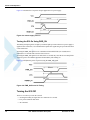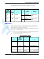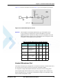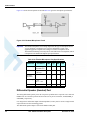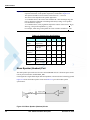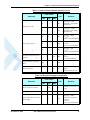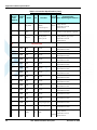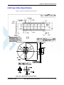
1
Technical Information
Motorola G30 Developer’s Guide
Module Hardware Description
DECEMBER 15, 2009
6802986C55-A
SPECIFICATIONS SUBJECT TO CHANGE WITHOUT NOTICE
Notice
While reasonable efforts have been made to assure the accuracy of this document, Motorola, Inc. assumes no liability resulting
from any inaccuracies or omissions in this document, or from use of the information obtained herein. The information in this
document has been carefully checked and is believed to be entirely reliable. However, no responsibility is assumed for
inaccuracies or omissions. Motorola, Inc. reserves the right to make changes to any products described herein and reserves the
right to revise this document and to make changes from time to time in content hereof with no obligation to notify any person of
revisions or changes. Motorola, Inc. does not assume any liability arising out of the application or use of any product, software, or
circuit described herein; neither does it convey license under its patent rights or the rights of others.
It is possible that this publication may contain references to, or information about Motorola products (machines and programs),
programming, or services that are not announced in your country. Such references or information must not be construed to mean
that Motorola intends to announce such Motorola products, programming, or services in your country.
Copyrights
This instruction manual, and the Motorola products described in this instruction manual may be, include or describe copyrighted
Motorola material, such as computer programs stored in semiconductor memories or other media. Laws in the United States and
other countries preserve for Motorola and its licensors certain exclusive rights for copyrighted material, including the exclusive
right to copy, reproduce in any form, distribute and make derivative works of the copyrighted material. Accordingly, any
copyrighted material of Motorola and its licensors contained herein or in the Motorola products described in this instruction
manual may not be copied, reproduced, distributed, merged or modified in any manner without the express written permission of
Motorola. Furthermore, the purchase of Motorola products shall not be deemed to grant either directly or by implication, estoppel,
or otherwise, any license under the copyrights, patents or patent applications of Motorola, as arises by operation of law in the sale
of a product.
Computer Software Copyrights
The Motorola and 3rd Party supplied Software (SW) products described in this instruction manual may include copyrighted
Motorola and other 3rd Party supplied computer programs stored in semiconductor memories or other media. Laws in the United
States and other countries preserve for Motorola and other 3rd Party supplied SW certain exclusive rights for copyrighted
computer programs, including the exclusive right to copy or reproduce in any form the copyrighted computer program.
Accordingly, any copyrighted Motorola or other 3rd Party supplied SW computer programs contained in the Motorola products
described in this instruction manual may not be copied (reverse engineered) or reproduced in any manner without the express
written permission of Motorola or the 3rd Party SW supplier. Furthermore, the purchase of Motorola products shall not be deemed
to grant either directly or by implication, estoppel, or otherwise, any license under the copyrights, patents or patent applications of
Motorola or other 3rd Party supplied SW, except for the normal non-exclusive, royalty free license to use that arises by operation
of law in the sale of a product.
VENDOR COPYRIGHT
Apache Software Foundation Copyright 2004-2005 All Rights Reserved
Usage and Disclosure Restrictions
License Agreements
The software described in this document is the property of Motorola, Inc. and its licensors. It is furnished by express license
agreement only and may be used only in accordance with the terms of such an agreement.
Copyrighted Materials
Software and documentation are copyrighted materials. Making unauthorized copies is prohibited by law. No part of the software
or documentation may be reproduced, transmitted, transcribed, stored in a retrieval system, or translated into any language or
computer language, in any form or by any means, without prior written permission of Motorola, Inc.
High Risk Materials
Components, units, or third-party products used in the product described herein are NOT fault-tolerant and are NOT designed,
manufactured, or intended for use as on-line control equipment in the following hazardous environments requiring fail-safe
controls: the operation of Nuclear Facilities, Aircraft Navigation or Aircraft Communication Systems, Air Traffic Control, Life
Support, or Weapons Systems (High Risk Activities"). Motorola and its supplier(s) specifically disclaim any expressed or implied
warranty of fitness for such High Risk Activities.
Trademarks
MOTOROLA and the Stylized M Logo are registered in the US Patent & Trademark Office. All other product or service names are
the property of their respective owners.
© Copyright 2009 Motorola, Inc.
This page intentionally left blank.
Table of Contents
Manual Scope . . . . . . . . . . . . . . . . . . . . . . . . . . . . . . . . . . . . . . . . . . . . . . . . . . . . . . . . . . . . . . . . . . . .ix
Target Audience . . . . . . . . . . . . . . . . . . . . . . . . . . . . . . . . . . . . . . . . . . . . . . . . . . . . . . . . . . . . . . . . . .ix
Manual Organization . . . . . . . . . . . . . . . . . . . . . . . . . . . . . . . . . . . . . . . . . . . . . . . . . . . . . . . . . . . . . . .ix
Applicable Documents . . . . . . . . . . . . . . . . . . . . . . . . . . . . . . . . . . . . . . . . . . . . . . . . . . . . . . . . . . . . .ix
Regulatory Requirements . . . . . . . . . . . . . . . . . . . . . . . . . . . . . . . . . . . . . . . . . . . . . . . . . . . . . . . . . . . x
Regulatory Statement (Safety). . . . . . . . . . . . . . . . . . . . . . . . . . . . . . . . . . . . . . . . . . . . . . . . . . . . . . . . x
FCC Notice to Users . . . . . . . . . . . . . . . . . . . . . . . . . . . . . . . . . . . . . . . . . . . . . . . . . . . . . . . . . . . . . . . x
Precautions. . . . . . . . . . . . . . . . . . . . . . . . . . . . . . . . . . . . . . . . . . . . . . . . . . . . . . . . . . . . . . . . . . . . . . .xi
Antenna and Transmission Safety Precautions . . . . . . . . . . . . . . . . . . . . . . . . . . . . . . . . . . . . . . . . . . .xi
Standards . . . . . . . . . . . . . . . . . . . . . . . . . . . . . . . . . . . . . . . . . . . . . . . . . . . . . . . . . . . . . . . . . . . . . . . xii
Contact Us . . . . . . . . . . . . . . . . . . . . . . . . . . . . . . . . . . . . . . . . . . . . . . . . . . . . . . . . . . . . . . . . . . . . . xiii
Text Conventions. . . . . . . . . . . . . . . . . . . . . . . . . . . . . . . . . . . . . . . . . . . . . . . . . . . . . . . . . . . . . . . . xiii
Field Service . . . . . . . . . . . . . . . . . . . . . . . . . . . . . . . . . . . . . . . . . . . . . . . . . . . . . . . . . . . . . . . . . . . . xv
General Safety . . . . . . . . . . . . . . . . . . . . . . . . . . . . . . . . . . . . . . . . . . . . . . . . . . . . . . . . . . . . . . . . . . . xv
Caring for the Environment. . . . . . . . . . . . . . . . . . . . . . . . . . . . . . . . . . . . . . . . . . . . . . . . . . . . . . . . .xvi
Limitation of Liability . . . . . . . . . . . . . . . . . . . . . . . . . . . . . . . . . . . . . . . . . . . . . . . . . . . . . . . . . . . . xvii
Warranty Notification . . . . . . . . . . . . . . . . . . . . . . . . . . . . . . . . . . . . . . . . . . . . . . . . . . . . . . . . . . . . xvii
How to Get Warranty Service? . . . . . . . . . . . . . . . . . . . . . . . . . . . . . . . . . . . . . . . . . . . . . . . . . . . . xviii
Claiming . . . . . . . . . . . . . . . . . . . . . . . . . . . . . . . . . . . . . . . . . . . . . . . . . . . . . . . . . . . . . . . . . . . . . xviii
Conditions . . . . . . . . . . . . . . . . . . . . . . . . . . . . . . . . . . . . . . . . . . . . . . . . . . . . . . . . . . . . . . . . . . . . . .xix
What is Not Covered by the Warranty . . . . . . . . . . . . . . . . . . . . . . . . . . . . . . . . . . . . . . . . . . . . . . . .xix
Installed Data. . . . . . . . . . . . . . . . . . . . . . . . . . . . . . . . . . . . . . . . . . . . . . . . . . . . . . . . . . . . . . . . . . . . xx
Out of Warranty Repairs . . . . . . . . . . . . . . . . . . . . . . . . . . . . . . . . . . . . . . . . . . . . . . . . . . . . . . . . . . . xx
Revision History . . . . . . . . . . . . . . . . . . . . . . . . . . . . . . . . . . . . . . . . . . . . . . . . . . . . . . . . . . . . . . . . .xxi
Chapter 1:
Introduction . . . . . . . . . . . . . . . . . . . . . . . . . . . . . . . . . . . . . . . . . . . . . . . . . . . . . . . . . . . . . 1
Product Specifications . . . . . . . . . . . . . . . . . . . . . . . . . . . . . . . . . . . . . . . . . . . . . . . . . . . . . . . . . . . . . . 2
Regulatory and Approvals . . . . . . . . . . . . . . . . . . . . . . . . . . . . . . . . . . . . . . . . . . . . . . . . . . . . . . . . . . . 6
European Union Directives Conformance Statement . . . . . . . . . . . . . . . . . . . . . . . . . . . . . . . . . . . 6
CFR 47 Part 15.19 specifies label requirements . . . . . . . . . . . . . . . . . . . . . . . . . . . . . . . . . . . . . . . 6
CFR 47 Part 15.21 Information to user . . . . . . . . . . . . . . . . . . . . . . . . . . . . . . . . . . . . . . . . . . . . . . 7
CFR 47 Part 15.105 Information to the user . . . . . . . . . . . . . . . . . . . . . . . . . . . . . . . . . . . . . . . . . . 7
Chapter 2:
Hardware Interface Description . . . . . . . . . . . . . . . . . . . . . . . . . . . . . . . . . . . . . . . . . . . . . 9
Architecture Overview . . . . . . . . . . . . . . . . . . . . . . . . . . . . . . . . . . . . . . . . . . . . . . . . . . . . . . . . . . . . . 9
Baseband . . . . . . . . . . . . . . . . . . . . . . . . . . . . . . . . . . . . . . . . . . . . . . . . . . . . . . . . . . . . . . . . . . . . 10
RF Block . . . . . . . . . . . . . . . . . . . . . . . . . . . . . . . . . . . . . . . . . . . . . . . . . . . . . . . . . . . . . . . . . . . . 10
Operating Modes . . . . . . . . . . . . . . . . . . . . . . . . . . . . . . . . . . . . . . . . . . . . . . . . . . . . . . . . . . . . . . . . . 11
Power Supply. . . . . . . . . . . . . . . . . . . . . . . . . . . . . . . . . . . . . . . . . . . . . . . . . . . . . . . . . . . . . . . . . . . . 12
Power Supply Design . . . . . . . . . . . . . . . . . . . . . . . . . . . . . . . . . . . . . . . . . . . . . . . . . . . . . . . . . . . 12
Power Consumption . . . . . . . . . . . . . . . . . . . . . . . . . . . . . . . . . . . . . . . . . . . . . . . . . . . . . . . . . . . . 14
Power On/Off Operation . . . . . . . . . . . . . . . . . . . . . . . . . . . . . . . . . . . . . . . . . . . . . . . . . . . . . . . . . . . 15
Turning the G30 On . . . . . . . . . . . . . . . . . . . . . . . . . . . . . . . . . . . . . . . . . . . . . . . . . . . . . . . . . . . . 15
Power Supply Turn-on . . . . . . . . . . . . . . . . . . . . . . . . . . . . . . . . . . . . . . . . . . . . . . . . . . . . . . . . 15
Turning the G30 On Using PWR_ON . . . . . . . . . . . . . . . . . . . . . . . . . . . . . . . . . . . . . . . . . . . . 16
December 15, 2009
G30 - Module Hardware Description
i
Table of Contents
Turning the G30 Off . . . . . . . . . . . . . . . . . . . . . . . . . . . . . . . . . . . . . . . . . . . . . . . . . . . . . . . . . . . . 16
Turning the G30 Off Using PWR_ON . . . . . . . . . . . . . . . . . . . . . . . . . . . . . . . . . . . . . . . . . . . . 17
Power Loss shut down . . . . . . . . . . . . . . . . . . . . . . . . . . . . . . . . . . . . . . . . . . . . . . . . . . . . . . . . 17
Turning the G30 Off Using AT+MRST . . . . . . . . . . . . . . . . . . . . . . . . . . . . . . . . . . . . . . . . . . . 17
Low Power Mode. . . . . . . . . . . . . . . . . . . . . . . . . . . . . . . . . . . . . . . . . . . . . . . . . . . . . . . . . . . . . . . . . 18
Activating Low Power Mode . . . . . . . . . . . . . . . . . . . . . . . . . . . . . . . . . . . . . . . . . . . . . . . . . . . . . 18
Serial Interface During Low Power Mode . . . . . . . . . . . . . . . . . . . . . . . . . . . . . . . . . . . . . . . . . . . 18
Terminating Low Power Mode . . . . . . . . . . . . . . . . . . . . . . . . . . . . . . . . . . . . . . . . . . . . . . . . . . . 19
Temporary Termination of Low Power Mode . . . . . . . . . . . . . . . . . . . . . . . . . . . . . . . . . . . . . . 20
Permanent termination of Low Power Mode . . . . . . . . . . . . . . . . . . . . . . . . . . . . . . . . . . . . . . . 21
Real Time Clock . . . . . . . . . . . . . . . . . . . . . . . . . . . . . . . . . . . . . . . . . . . . . . . . . . . . . . . . . . . . . . . . . 22
Serial Interfaces . . . . . . . . . . . . . . . . . . . . . . . . . . . . . . . . . . . . . . . . . . . . . . . . . . . . . . . . . . . . . . . . . . 23
UART . . . . . . . . . . . . . . . . . . . . . . . . . . . . . . . . . . . . . . . . . . . . . . . . . . . . . . . . . . . . . . . . . . . . . . . 23
Serial Peripheral Interface (SPI) . . . . . . . . . . . . . . . . . . . . . . . . . . . . . . . . . . . . . . . . . . . . . . . . . . . 24
Flashing and Data Logging . . . . . . . . . . . . . . . . . . . . . . . . . . . . . . . . . . . . . . . . . . . . . . . . . . . . . . 25
I2C Bus Interface . . . . . . . . . . . . . . . . . . . . . . . . . . . . . . . . . . . . . . . . . . . . . . . . . . . . . . . . . . . . . . 26
SIM Interface . . . . . . . . . . . . . . . . . . . . . . . . . . . . . . . . . . . . . . . . . . . . . . . . . . . . . . . . . . . . . . . . . . . . 27
External SIM Card . . . . . . . . . . . . . . . . . . . . . . . . . . . . . . . . . . . . . . . . . . . . . . . . . . . . . . . . . . . . . 28
External SIM Connection . . . . . . . . . . . . . . . . . . . . . . . . . . . . . . . . . . . . . . . . . . . . . . . . . . . . . . 28
External SIM Design Guidelines . . . . . . . . . . . . . . . . . . . . . . . . . . . . . . . . . . . . . . . . . . . . . . . . 28
Embedded SIM . . . . . . . . . . . . . . . . . . . . . . . . . . . . . . . . . . . . . . . . . . . . . . . . . . . . . . . . . . . . . . . . 29
eSIM Connection . . . . . . . . . . . . . . . . . . . . . . . . . . . . . . . . . . . . . . . . . . . . . . . . . . . . . . . . . . . . 29
Audio Interface . . . . . . . . . . . . . . . . . . . . . . . . . . . . . . . . . . . . . . . . . . . . . . . . . . . . . . . . . . . . . . . . . . 30
Handset Microphone Port . . . . . . . . . . . . . . . . . . . . . . . . . . . . . . . . . . . . . . . . . . . . . . . . . . . . . . . . 30
Headset Microphone Port . . . . . . . . . . . . . . . . . . . . . . . . . . . . . . . . . . . . . . . . . . . . . . . . . . . . . . . . 31
Differential Speaker (Handset) Port . . . . . . . . . . . . . . . . . . . . . . . . . . . . . . . . . . . . . . . . . . . . . . . . 32
Mono Speaker (Headset) Port . . . . . . . . . . . . . . . . . . . . . . . . . . . . . . . . . . . . . . . . . . . . . . . . . . . . 34
Headset Detection . . . . . . . . . . . . . . . . . . . . . . . . . . . . . . . . . . . . . . . . . . . . . . . . . . . . . . . . . . . . . . 35
Digital Audio Interface . . . . . . . . . . . . . . . . . . . . . . . . . . . . . . . . . . . . . . . . . . . . . . . . . . . . . . . . . . 36
Voiceband Audio . . . . . . . . . . . . . . . . . . . . . . . . . . . . . . . . . . . . . . . . . . . . . . . . . . . . . . . . . . . . 36
Operating Modes . . . . . . . . . . . . . . . . . . . . . . . . . . . . . . . . . . . . . . . . . . . . . . . . . . . . . . . . . . . . . . 37
Basic Mode . . . . . . . . . . . . . . . . . . . . . . . . . . . . . . . . . . . . . . . . . . . . . . . . . . . . . . . . . . . . . . . . . 37
Advanced Mode . . . . . . . . . . . . . . . . . . . . . . . . . . . . . . . . . . . . . . . . . . . . . . . . . . . . . . . . . . . . . 38
Audio Programming Interface . . . . . . . . . . . . . . . . . . . . . . . . . . . . . . . . . . . . . . . . . . . . . . . . . . . . 39
Audio Algorithms . . . . . . . . . . . . . . . . . . . . . . . . . . . . . . . . . . . . . . . . . . . . . . . . . . . . . . . . . . . . 39
Gain Control . . . . . . . . . . . . . . . . . . . . . . . . . . . . . . . . . . . . . . . . . . . . . . . . . . . . . . . . . . . . . . . . 40
Audio Design . . . . . . . . . . . . . . . . . . . . . . . . . . . . . . . . . . . . . . . . . . . . . . . . . . . . . . . . . . . . . . . . . 40
Analog Ground . . . . . . . . . . . . . . . . . . . . . . . . . . . . . . . . . . . . . . . . . . . . . . . . . . . . . . . . . . . . . . 41
A/D Interface . . . . . . . . . . . . . . . . . . . . . . . . . . . . . . . . . . . . . . . . . . . . . . . . . . . . . . . . . . . . . . . . . . . . 42
Power Supply A/D . . . . . . . . . . . . . . . . . . . . . . . . . . . . . . . . . . . . . . . . . . . . . . . . . . . . . . . . . . . . . 42
General Purpose A/D . . . . . . . . . . . . . . . . . . . . . . . . . . . . . . . . . . . . . . . . . . . . . . . . . . . . . . . . . . . 43
Controls and Indicators Interface. . . . . . . . . . . . . . . . . . . . . . . . . . . . . . . . . . . . . . . . . . . . . . . . . . . . . 44
Reset . . . . . . . . . . . . . . . . . . . . . . . . . . . . . . . . . . . . . . . . . . . . . . . . . . . . . . . . . . . . . . . . . . . . . . . . 45
VREF Reference Regulator . . . . . . . . . . . . . . . . . . . . . . . . . . . . . . . . . . . . . . . . . . . . . . . . . . . . . . 45
VRTC . . . . . . . . . . . . . . . . . . . . . . . . . . . . . . . . . . . . . . . . . . . . . . . . . . . . . . . . . . . . . . . . . . . . . . . 46
Wakeup Out . . . . . . . . . . . . . . . . . . . . . . . . . . . . . . . . . . . . . . . . . . . . . . . . . . . . . . . . . . . . . . . . . . 46
Antenna Detection . . . . . . . . . . . . . . . . . . . . . . . . . . . . . . . . . . . . . . . . . . . . . . . . . . . . . . . . . . . . . 47
GPRS Detection . . . . . . . . . . . . . . . . . . . . . . . . . . . . . . . . . . . . . . . . . . . . . . . . . . . . . . . . . . . . . . . 48
General Purpose I/O . . . . . . . . . . . . . . . . . . . . . . . . . . . . . . . . . . . . . . . . . . . . . . . . . . . . . . . . . . . . 48
Antenna Interface. . . . . . . . . . . . . . . . . . . . . . . . . . . . . . . . . . . . . . . . . . . . . . . . . . . . . . . . . . . . . . . . . 49
Chapter 3:
ii
Electrical and Environmental Specifications. . . . . . . . . . . . . . . . . . . . . . . . . . . . . . . . . . 51
Absolute Maximum Ratings . . . . . . . . . . . . . . . . . . . . . . . . . . . . . . . . . . . . . . . . . . . . . . . . . . . . . . . . 51
Operating Parameters. . . . . . . . . . . . . . . . . . . . . . . . . . . . . . . . . . . . . . . . . . . . . . . . . . . . . . . . . . . . . . 52
G30 - Module Hardware Description
December 15, 2009
Table of Contents
Supply/power Pins . . . . . . . . . . . . . . . . . . . . . . . . . . . . . . . . . . . . . . . . . . . . . . . . . . . . . . . . . . . . . 52
Digital Pins . . . . . . . . . . . . . . . . . . . . . . . . . . . . . . . . . . . . . . . . . . . . . . . . . . . . . . . . . . . . . . . . . . . 52
Audio Pins . . . . . . . . . . . . . . . . . . . . . . . . . . . . . . . . . . . . . . . . . . . . . . . . . . . . . . . . . . . . . . . . . . . 56
ADC Pins . . . . . . . . . . . . . . . . . . . . . . . . . . . . . . . . . . . . . . . . . . . . . . . . . . . . . . . . . . . . . . . . . . . . 59
Environmental Specifications . . . . . . . . . . . . . . . . . . . . . . . . . . . . . . . . . . . . . . . . . . . . . . . . . . . . . . . 61
Application Interface Specifications . . . . . . . . . . . . . . . . . . . . . . . . . . . . . . . . . . . . . . . . . . . . . . . . . . 61
Chapter 4:
Mechanical Specifications . . . . . . . . . . . . . . . . . . . . . . . . . . . . . . . . . . . . . . . . . . . . . . . . 71
Board Dimensions . . . . . . . . . . . . . . . . . . . . . . . . . . . . . . . . . . . . . . . . . . . . . . . . . . . . . . . . . . . . . . . . 71
LGA Tape & Reel Specification . . . . . . . . . . . . . . . . . . . . . . . . . . . . . . . . . . . . . . . . . . . . . . . . . . . . . 73
Interface Connector Specifications . . . . . . . . . . . . . . . . . . . . . . . . . . . . . . . . . . . . . . . . . . . . . . . . . . . 74
Mating Connector . . . . . . . . . . . . . . . . . . . . . . . . . . . . . . . . . . . . . . . . . . . . . . . . . . . . . . . . . . . . . 75
U.FL Connector Specifications . . . . . . . . . . . . . . . . . . . . . . . . . . . . . . . . . . . . . . . . . . . . . . . . . . . . . . 76
Mating Connector . . . . . . . . . . . . . . . . . . . . . . . . . . . . . . . . . . . . . . . . . . . . . . . . . . . . . . . . . . . . . 77
G30 Mounting . . . . . . . . . . . . . . . . . . . . . . . . . . . . . . . . . . . . . . . . . . . . . . . . . . . . . . . . . . . . . . . . . . . 78
Layout Recommendation. . . . . . . . . . . . . . . . . . . . . . . . . . . . . . . . . . . . . . . . . . . . . . . . . . . . . . . . . . . 79
Soldering Footprint . . . . . . . . . . . . . . . . . . . . . . . . . . . . . . . . . . . . . . . . . . . . . . . . . . . . . . . . . . . . 79
RF Recommendation . . . . . . . . . . . . . . . . . . . . . . . . . . . . . . . . . . . . . . . . . . . . . . . . . . . . . . . . . . . 80
Soldering Re-flow . . . . . . . . . . . . . . . . . . . . . . . . . . . . . . . . . . . . . . . . . . . . . . . . . . . . . . . . . . . . . . . . 80
Chapter 5:
Service and Testing. . . . . . . . . . . . . . . . . . . . . . . . . . . . . . . . . . . . . . . . . . . . . . . . . . . . . . 81
Ordering Information. . . . . . . . . . . . . . . . . . . . . . . . . . . . . . . . . . . . . . . . . . . . . . . . . . . . . . . . . . . . . . 81
Service . . . . . . . . . . . . . . . . . . . . . . . . . . . . . . . . . . . . . . . . . . . . . . . . . . . . . . . . . . . . . . . . . . . . . . . . . 81
Who to Contact? . . . . . . . . . . . . . . . . . . . . . . . . . . . . . . . . . . . . . . . . . . . . . . . . . . . . . . . . . . . . . . 82
Required Query Information . . . . . . . . . . . . . . . . . . . . . . . . . . . . . . . . . . . . . . . . . . . . . . . . . . . . . 82
Testing a Standalone Unit . . . . . . . . . . . . . . . . . . . . . . . . . . . . . . . . . . . . . . . . . . . . . . . . . . . . . . . . . . 84
Test Setup . . . . . . . . . . . . . . . . . . . . . . . . . . . . . . . . . . . . . . . . . . . . . . . . . . . . . . . . . . . . . . . . . . . . 84
Test Procedure . . . . . . . . . . . . . . . . . . . . . . . . . . . . . . . . . . . . . . . . . . . . . . . . . . . . . . . . . . . . . . . . 85
Acronyms and Abbreviations
Index
December 15, 2009
G30 - Module Hardware Description
iii
Table of Contents
This page intentionally left blank.
iv
G30 - Module Hardware Description
December 15, 2009
List of Figures
2-1
2-2
2-3
2-4
2-5
2-6
2-7
2-8
2-9
2-10
2-11
2-12
2-13
2-14
2-15
2-16
2-17
2-18
2-19
2-20
2-21
2-22
2-23
3-1
3-2
4-1
4-2
4-3
4-4
4-5
4-6
4-7
4-8
4-9
G30 Block Diagram . . . . . . . . . . . . . . . . . . . . . . . . . . . . . . . . . . . . . . . . . . . . . . . . . . . . . . . . . . 9
Transmission Power Drops. . . . . . . . . . . . . . . . . . . . . . . . . . . . . . . . . . . . . . . . . . . . . . . . . . . . 13
Power Supply Turn-on . . . . . . . . . . . . . . . . . . . . . . . . . . . . . . . . . . . . . . . . . . . . . . . . . . . . . . . 16
PWR_ON Power On Timing . . . . . . . . . . . . . . . . . . . . . . . . . . . . . . . . . . . . . . . . . . . . . . . . . . 16
PWR_ON Power Off Timing . . . . . . . . . . . . . . . . . . . . . . . . . . . . . . . . . . . . . . . . . . . . . . . . . . 17
ATS24 Operation . . . . . . . . . . . . . . . . . . . . . . . . . . . . . . . . . . . . . . . . . . . . . . . . . . . . . . . . . . . 18
CTS Signal During Sleep Mode . . . . . . . . . . . . . . . . . . . . . . . . . . . . . . . . . . . . . . . . . . . . . . . . 19
WKUPI Signal Operation . . . . . . . . . . . . . . . . . . . . . . . . . . . . . . . . . . . . . . . . . . . . . . . . . . . . . 20
Serial Interface Data . . . . . . . . . . . . . . . . . . . . . . . . . . . . . . . . . . . . . . . . . . . . . . . . . . . . . . . . . 21
UART Interface Signals . . . . . . . . . . . . . . . . . . . . . . . . . . . . . . . . . . . . . . . . . . . . . . . . . . . . . . 23
RI Behavior When Receiving a Call . . . . . . . . . . . . . . . . . . . . . . . . . . . . . . . . . . . . . . . . . . . . 24
G30 External SIM Interface . . . . . . . . . . . . . . . . . . . . . . . . . . . . . . . . . . . . . . . . . . . . . . . . . . . 28
G30 eSIM Interface . . . . . . . . . . . . . . . . . . . . . . . . . . . . . . . . . . . . . . . . . . . . . . . . . . . . . . . . . 29
Audio Interface Topology. . . . . . . . . . . . . . . . . . . . . . . . . . . . . . . . . . . . . . . . . . . . . . . . . . . . . 30
Handset Microphone Circuit. . . . . . . . . . . . . . . . . . . . . . . . . . . . . . . . . . . . . . . . . . . . . . . . . . . 31
Headset Microphone Circuit. . . . . . . . . . . . . . . . . . . . . . . . . . . . . . . . . . . . . . . . . . . . . . . . . . . 32
Differential Speaker Circuit . . . . . . . . . . . . . . . . . . . . . . . . . . . . . . . . . . . . . . . . . . . . . . . . . . . 33
Single-ended Speaker Circuit . . . . . . . . . . . . . . . . . . . . . . . . . . . . . . . . . . . . . . . . . . . . . . . . . . 33
Mono Speaker (Headset) Circuit . . . . . . . . . . . . . . . . . . . . . . . . . . . . . . . . . . . . . . . . . . . . . . . 34
I2S BUS Format . . . . . . . . . . . . . . . . . . . . . . . . . . . . . . . . . . . . . . . . . . . . . . . . . . . . . . . . . . . . 37
Voiceband Mode PCM Bus Coding Format. . . . . . . . . . . . . . . . . . . . . . . . . . . . . . . . . . . . . . . 37
Audio Programming Interface . . . . . . . . . . . . . . . . . . . . . . . . . . . . . . . . . . . . . . . . . . . . . . . . . 39
WKUPO Operation. . . . . . . . . . . . . . . . . . . . . . . . . . . . . . . . . . . . . . . . . . . . . . . . . . . . . . . . . . 47
G30 - 70 Pin Connector Quick Integration Connections . . . . . . . . . . . . . . . . . . . . . . . . . . . . . 62
G30 - 81 Pin LGA Interface Quick Integration Connections . . . . . . . . . . . . . . . . . . . . . . . . . . 63
G30 Mechanical Characteristics - 81 Pin LGA Interface. . . . . . . . . . . . . . . . . . . . . . . . . . . . . 71
G30 Mechanical Characteristics - B2B Connector (70 Pin). . . . . . . . . . . . . . . . . . . . . . . . . . . 72
LGA Tape & Reel Specification. . . . . . . . . . . . . . . . . . . . . . . . . . . . . . . . . . . . . . . . . . . . . . . . 73
G30 Interface Connector. . . . . . . . . . . . . . . . . . . . . . . . . . . . . . . . . . . . . . . . . . . . . . . . . . . . . . 74
Mating Connector Dimensions . . . . . . . . . . . . . . . . . . . . . . . . . . . . . . . . . . . . . . . . . . . . . . . . . 75
U.FL Connector Dimensions . . . . . . . . . . . . . . . . . . . . . . . . . . . . . . . . . . . . . . . . . . . . . . . . . . 76
U.FL Mating Connector . . . . . . . . . . . . . . . . . . . . . . . . . . . . . . . . . . . . . . . . . . . . . . . . . . . . . . 77
G30 Mounting Area . . . . . . . . . . . . . . . . . . . . . . . . . . . . . . . . . . . . . . . . . . . . . . . . . . . . . . . . . 78
G30 Soldering Footprint (Top View) . . . . . . . . . . . . . . . . . . . . . . . . . . . . . . . . . . . . . . . . . . . . 79
5-1
Test Setup . . . . . . . . . . . . . . . . . . . . . . . . . . . . . . . . . . . . . . . . . . . . . . . . . . . . . . . . . . . . . . . . . 85
December 15, 2009
G30 - Module Hardware Description
v
List of Tables
1-1
Product Specifications . . . . . . . . . . . . . . . . . . . . . . . . . . . . . . . . . . . . . . . . . . . . . . . . . . . . . . . . 2
2-1
2-2
2-3
2-4
2-5
2-6
2-7
2-8
2-9
2-10
2-11
2-12
2-13
2-14
2-15
2-16
2-17
2-18
2-19
2-20
2-21
2-22
3-1
3-2
3-3
3-4
3-5
3-6
3-7
3-8
3-9
3-10
3-11
3-12
3-13
G30 Operating Modes. . . . . . . . . . . . . . . . . . . . . . . . . . . . . . . . . . . . . . . . . . . . . . . . . . . . . . . .
Power Supply Signals . . . . . . . . . . . . . . . . . . . . . . . . . . . . . . . . . . . . . . . . . . . . . . . . . . . . . . . .
Recommended Power Supply Filtering . . . . . . . . . . . . . . . . . . . . . . . . . . . . . . . . . . . . . . . . . .
G30 Current Ratings . . . . . . . . . . . . . . . . . . . . . . . . . . . . . . . . . . . . . . . . . . . . . . . . . . . . . . . . .
SPI Interface Connections . . . . . . . . . . . . . . . . . . . . . . . . . . . . . . . . . . . . . . . . . . . . . . . . . . . .
Data Logging and SW Upgrading Application Connector. . . . . . . . . . . . . . . . . . . . . . . . . . . .
I2C Interface Connections . . . . . . . . . . . . . . . . . . . . . . . . . . . . . . . . . . . . . . . . . . . . . . . . . . . .
SIM Interface Signals . . . . . . . . . . . . . . . . . . . . . . . . . . . . . . . . . . . . . . . . . . . . . . . . . . . . . . . .
Handset Microphone Port Specifications . . . . . . . . . . . . . . . . . . . . . . . . . . . . . . . . . . . . . . . . .
Headset Microphone Port Specifications . . . . . . . . . . . . . . . . . . . . . . . . . . . . . . . . . . . . . . . . .
Speaker Port Specifications . . . . . . . . . . . . . . . . . . . . . . . . . . . . . . . . . . . . . . . . . . . . . . . . . . .
Mono Speaker Port Specifications . . . . . . . . . . . . . . . . . . . . . . . . . . . . . . . . . . . . . . . . . . . . . .
Digital Audio modes. . . . . . . . . . . . . . . . . . . . . . . . . . . . . . . . . . . . . . . . . . . . . . . . . . . . . . . . .
Basic Mode Audio Paths . . . . . . . . . . . . . . . . . . . . . . . . . . . . . . . . . . . . . . . . . . . . . . . . . . . . .
Advanced Mode Commands. . . . . . . . . . . . . . . . . . . . . . . . . . . . . . . . . . . . . . . . . . . . . . . . . . .
Speech Processing Features . . . . . . . . . . . . . . . . . . . . . . . . . . . . . . . . . . . . . . . . . . . . . . . . . . .
Gain Control Features. . . . . . . . . . . . . . . . . . . . . . . . . . . . . . . . . . . . . . . . . . . . . . . . . . . . . . . .
Supply A/D Specifications . . . . . . . . . . . . . . . . . . . . . . . . . . . . . . . . . . . . . . . . . . . . . . . . . . . .
GPAD Specifications . . . . . . . . . . . . . . . . . . . . . . . . . . . . . . . . . . . . . . . . . . . . . . . . . . . . . . . .
Controls and Indicators. . . . . . . . . . . . . . . . . . . . . . . . . . . . . . . . . . . . . . . . . . . . . . . . . . . . . . .
VREF Specifications . . . . . . . . . . . . . . . . . . . . . . . . . . . . . . . . . . . . . . . . . . . . . . . . . . . . . . . .
Antenna Interface Specifications . . . . . . . . . . . . . . . . . . . . . . . . . . . . . . . . . . . . . . . . . . . . . . .
Maximum Ratings . . . . . . . . . . . . . . . . . . . . . . . . . . . . . . . . . . . . . . . . . . . . . . . . . . . . . . . . . .
Input Characteristics . . . . . . . . . . . . . . . . . . . . . . . . . . . . . . . . . . . . . . . . . . . . . . . . . . . . . . . . .
Output Characteristics . . . . . . . . . . . . . . . . . . . . . . . . . . . . . . . . . . . . . . . . . . . . . . . . . . . . . . .
Input Characteristics . . . . . . . . . . . . . . . . . . . . . . . . . . . . . . . . . . . . . . . . . . . . . . . . . . . . . . . . .
Output Characteristics . . . . . . . . . . . . . . . . . . . . . . . . . . . . . . . . . . . . . . . . . . . . . . . . . . . . . . .
Pad Pull-up and Pull-down Characteristics . . . . . . . . . . . . . . . . . . . . . . . . . . . . . . . . . . . . . . .
Audio Transmit Path Characteristics . . . . . . . . . . . . . . . . . . . . . . . . . . . . . . . . . . . . . . . . . . . .
Microphone Supply Characteristics . . . . . . . . . . . . . . . . . . . . . . . . . . . . . . . . . . . . . . . . . . . . .
G30 Low Power Single-ended Audio Receive Path Characteristics . . . . . . . . . . . . . . . . . . . .
G30 High Power Differential Audio Receive Path Characteristics . . . . . . . . . . . . . . . . . . . . .
Input Characteristics . . . . . . . . . . . . . . . . . . . . . . . . . . . . . . . . . . . . . . . . . . . . . . . . . . . . . . . . .
Environmental Ratings . . . . . . . . . . . . . . . . . . . . . . . . . . . . . . . . . . . . . . . . . . . . . . . . . . . . . . .
Interface Specifications . . . . . . . . . . . . . . . . . . . . . . . . . . . . . . . . . . . . . . . . . . . . . . . . . . . . . .
4-1
4-2
4-3
G30 interface connector option . . . . . . . . . . . . . . . . . . . . . . . . . . . . . . . . . . . . . . . . . . . . . . . . 74
Interface Connector Specifications. . . . . . . . . . . . . . . . . . . . . . . . . . . . . . . . . . . . . . . . . . . . . . 74
U.FL Connector Specifications . . . . . . . . . . . . . . . . . . . . . . . . . . . . . . . . . . . . . . . . . . . . . . . . 76
December 15, 2009
G30 - Module Hardware Description
11
12
13
14
24
26
27
27
31
32
34
35
36
38
38
40
40
43
43
44
46
50
51
52
52
52
54
56
56
57
58
59
59
61
63
vii
Preface
Manual Scope
This manual provides the electrical, mechanical and environmental requirements for properly
integrating the G30 module in a host application.
This manual gives a complete set of hardware features and functions that may be provided by
G30. The availability of any feature or function, which is described in this manual, depends on
the hardware revision and software version of a specific G30 model.
The parameters and values provided in this manual are defined under typical conditions. These
values may vary when subject to different conditions, such as SW version, network status,
application settings and environmental conditions.
Target Audience
This manual is intended for all members of the integration team who are responsible for
integrating the G30 module into the host OEM device, including representatives from hardware,
software and RF engineering disciplines.
Manual Organization
This manual contains the following chapters:
• Chapter 1 —introduces the G30 unit and provides important safety instructions.
• Chapter 2 —provides a detailed hardware description of the blocks and components
comprising the G30.
• Chapter 3 —describes the pin assignments for G30 connectors.
• Chapter 4 —describes G30 mechanical specifications and requirements.
• Chapter 5 —provides contact information for Motorola Service Support and Customer
Assistance.
Applicable Documents
• G30 Developer's Kit - 6802986C48
• G30 AT Commands - 6802986C33
December 15, 2009
G30 - Module Hardware Description
ix
Regulatory Requirements
Regulatory Requirements
The Federal Communications Commission (FCC) requires application for certification of digital
devices in accordance with CFR Title 47, Part 2 and Part 15. This includes MPE calculation. As
the G30 modem is not a standalone transceiver but is an integrated module, the G30 cannot be
tested by itself for EME certification. It is, however, the integrator’s responsibility to have the
completed device tested for EME certification.
Caution:
Unauthorized repairs or modifications could result in permanent damage to the
equipment and void your warranty and your authority to operate this device under
Part 15 of the FCC Rules.
Regulatory Statement (Safety)
The following safety precautions must be observed during all phases of the operation, usage,
service or repair of any cellular terminal or mobile incorporating the G30 module. Manufacturers
of the cellular terminal are advised to convey the following safety information to users and
operating personnel, and to incorporate these guidelines into all manuals supplied with the
product. Failure to comply with these precautions violates safety standards of design,
manufacture and intended use of the product. Motorola assumes no liability for customer failure
to comply with these precautions.
• G30 module should not be assembled when voltage is supplied (applicable for 70 pin
connector model only)
• G30 module must be operated at the voltages described in the technical documentation
• G30 module must not be mechanically nor electrically changed. Use of connectors should
follow the guidance of the technical documentation
• G30 module is designed to meet the EMC requirements of EN 301 489-07
• When integrating the G30 module into a system, Motorola recommends testing the system to
EN 301 489-07
• You must not remove any label from the G30 module
• Systems using the G30 module are subject to mandatory EMC/RF/Safety (including EME)
testing under R&TTE directive 1999/5/EC (to://www.newapproach.org/Directives/). Other
directives, such, 2002/95/EC (RoHS), WEEE Directive 2002/96/EC should also apply to a
system using the G30 module.
FCC Notice to Users
Motorola has not approved any changes or modifications to this device by the user. Any changes
or modifications could void the user's authority to operate the equipment. See 47 CFR Sec. 15.21.
This device complies with part 15 of the FCC Rules. Operation is subject to the following two
conditions: (1) This device may not cause harmful interference, and (2) this device must accept
any interference received, including interference that may cause undesired operation. See 47 CFR
Sec. 15.19(3).
If your mobile device or accessory has a USB connector, or is otherwise considered a computer
peripheral device whereby it can be connected to a computer for purposes of transferring data,
then it is considered a Class B device and the following statement applies:
x
G30 - Module Hardware Description
December 15, 2009
Preface
This equipment has been tested and found to comply with the limits for a Class B digital device,
pursuant to part 15 of the FCC Rules. These limits are designed to provide reasonable protection
against harmful interference in a residential installation. This equipment generates uses and can
radiate radio frequency energy and, if not installed and used in accordance with the instructions,
may cause harmful interference to radio communications. However, there is no guarantee that
interference will not occur in a particular installation. If this equipment does cause harmful
interference to radio or television reception, which can be determined by turning the equipment
off and on, the user is encouraged to try to correct the interference by one or more of the
following measures:
• Reorient or relocate the receiving antenna.
• Increase the separation between the equipment and the receiver.
• Connect the equipment to an outlet on a circuit different from that to which the receiver is
connected.
This device complies with Part 15 of the FCC Rules. Operation is subject to the following two
conditions:
(1) This device may not cause harmful interference.
(2) This device must accept any interference received, including interference that may cause
undesired operation.
Precautions
Interface connector and some of the module circuits are not shielded. Be sure to take appropriate
precautionary measures in order to avoid ESD while handling the module. ESD can damage the
G30 modules. Integrators need to design ESD protection on all external interfaces.
Antenna and Transmission Safety Precautions
User Operation
Do not operate your unit when a person is within 8 inches (20 centimeters) of the antenna. A
person or object within 8 inches (20 centimeters) of the antenna could impair call quality and may
cause the phone to operate at a higher power level than necessary.
Important:
The unit must be installed in a manner that provides a minimum separation distance
of 20 cm or more between the antenna and persons and must not be co-located or
operate in conjunction with any other antenna or transmitter to satisfy FCC RF
exposure requirements for mobile transmitting devices.
Important:
To comply with the FCC RF exposure limits and satisfy the categorical exclusion
requirements for mobile transmitters, the requirements described in the following
section, “Antenna Installation” , must be met.
December 15, 2009
G30 - Module Hardware Description
xi
Standards
Antenna Installation
• The antenna installation must provide a minimum separation distance of 20 cm from users
and nearby persons and must not be co-located or operating in conjunction with any other
antenna or transmitter.
• Antenna installation should be done by a professional installer and should meet all FCC
requirement as given in FCC part 15.
• Combined cable loss and antenna gain
• R&TTE requirements
• 900 MHz GSM band: The combined cable loss and antenna gain must not exceed
4.08 dBi
• 1800 MHz DCS band: The combined cable loss and antenna gain must not exceed
9.47 dBi
• FCC requirements
• 800 MHz cellular band: The combined cable loss and antenna gain must not exceed
2.85 dBi
• 1900 MHz PCS band: The combined cable loss and antenna gain must not exceed
2.5 dBi
OEM installers must be provided with antenna installation instruction and transmitter operating
conditions for satisfying RF exposure compliance.
Section 15.203 - Antenna Requirements
An intentional radiator shall be designed to ensure that no antenna other than that furnished by the
responsible party shall be used with the device. The use of a permanently attached antenna or of
an antenna that uses a unique coupling to the intentional radiator shall be considered sufficient to
comply with the provisions of this Section. The manufacturer may design the unit so that a
broken antenna can be replaced by the user, but the use of a standard antenna jack or electrical
connector is prohibited. This requirement does not apply to carrier current devices or to de-vices
operated under the provisions of Sections 15.211, 15.213, 15.217, 15.219, or 15.221. Further, this
requirement does not apply to intentional radiators that must be professionally installed, such as
perimeter protection systems and some field disturbance sensors, or to other intentional radiators
which, in accordance with Section 15.31(d), must be measured at the installation site. However,
the installer shall be responsible for ensuring that the proper antenna is employed so that the
limits in this Part are not exceeded.
Standards
Electromagnetic Compatibility: Principles and Applications by David A Weston, published by
Marcel Dekker, Inc., 270 Madison Avenue, New York, NY 10016 USA.
GSM 07.07 - prETS 300 916, Digital cellular telecommunication system (Phase 2+); AT
command set for GSM Mobile Equipment (ME), Version 5.2.0 or higher, Reference
RE/SMG-040707QR1.
GSM 07.05, Digital cellular telecommunication system (Phase 2+); Use of Data Terminal
Equipment - Data Circuit terminating; Equipment (DTE-DCE) interface for Short Message
Service (SMS) and Cell Broadcast Service (CBS), Version 5.3.0, August, 1997, Reference
TS/SMG-040705QR2.
xii
G30 - Module Hardware Description
December 15, 2009
Preface
GSM 03.40, Digital cellular telecommunication system (Phase 2+); Technical realization of the
Short Message Service (SMS) Point-to-Point (PP), Version 5.3.0, July 1996, Reference
TS/SMG-040340QR2.
GSM 04.11 Digital cellular telecommunication system (Phase 2+); Point-to-Point (PP) Short
Message Service (SMS) support on mobile radio interface, Version 5.1.0, March 1996, Reference
TS/SMG-030411QR.
GSM 03.38, Digital cellular telecommunication system (Phase 2+); Alphabets and
language-specific information, Version 5.3.0, July 1996, Reference TS/SMG-040338QR2.
GSM 11.10-1, Digital cellular telecommunication system (Phase 2); Mobile Station (MS)
Conformance specification; Part 1: Conformance specification. Draft pr ETS 300 607-1, March
1998, Reference RE/SMG-071110PR6-1.
GSM Specifications are orderable from Global Engineering Documents, 15 Inverness Way East,
Englewood, Colorado 80112-5704 USA 303-792-2181 800-624-3974.
ETSI Standard PCS - 11.10-1.
GSM 02.30 Supplementary services.
GSM 03.90 USSD stage 2.
GSM 11.14 SIM toolkit.
ITU-T V.25ter
GSM Data Adapter for Motorola Handsets, AT command reference, Rev 2, June 9 1997.
ETSI standard SMG31.
GSM 05.02.
ETSI 07.60.
ETSI 0.7.07 Ver. 7.5.0.
Contact Us
We at Motorola want to make this guide as helpful as possible. Keep us informed of your
comments and suggestions for improvements.
For general contact, technical support, report documentation errors and to order manuals, use this
email address:
[email protected]
Motorola appreciates feedback from the users of our information.
Text Conventions
The following special paragraphs are used in this guide to point out information that must be read.
This information may be set-off from the surrounding text, but is always preceded by a bold title
in capital letters:
Note
Note: Presents additional, helpful, noncritical information that you can use.
December 15, 2009
G30 - Module Hardware Description
xiii
Text Conventions
Warning
Warning:
Presents information to warn you of a potentially hazardous situation in which there
is a possibility of personal injury.
Important
Important:
Presents information to help you avoid an undesirable situation
or provides additional information to help you understand a topic or concept.
Caution
Caution:
xiv
Presents information to identify a situation in which damage to software, stored
data, or equipment could occur, thus avoiding
the damage.
G30 - Module Hardware Description
December 15, 2009
Preface
Field Service
For Field Service requests, use this email address:
[email protected]
General Safety
Remember!. . . safety depends on you!
The following general safety precautions must be observed during all phases of operation,
service, and repair of the equipment described in this manual. Failure to comply with these
precautions or with specific warnings elsewhere in this manual violates safety standards of
design, manufacture, and intended use of the equipment. Motorola, Inc. assumes no liability for
the customer’s failure to comply with these requirements. The safety precautions listed below
represent warnings of certain dangers of which we are aware. You, as the user of this product,
should follow these warnings and all other safety precautions necessary for the safe operation of
the equipment in your operating environment.
Ground the instrument
To minimize shock hazard, the equipment chassis and enclosure must be connected to an
electrical ground. If the equipment is supplied with a three-conductor AC power cable, the power
cable must be either plugged into an approved three-contact electrical outlet or used with a
three-contact to two-contact adapter. The three-contact to two-contact adapter must have the
grounding wire (green) firmly connected to an electrical ground (safety ground) at the power
outlet. The power jack and mating plug of the power cable must meet International
Electrotechnical Commission (IEC) safety standards.
Note: Refer to “Grounding Guideline for Cellular Radio Installations”–Motorola part no.
68P081150E62.
Do not operate in an explosive atmosphere
Do not operate the equipment in the presence of flammable gases or fumes. Operation of any
electrical equipment in such an environment constitutes a definite safety hazard.
Do not service or adjust alone
Do not attempt internal service or adjustment unless another person, capable of rendering first aid
is present.
Keep away from live circuits
Operating personnel must:
• not remove equipment covers. Only Factory Authorized Service Personnel or other qualified
maintenance personnel may remove equipment covers for internal subassembly, or
component replacement, or any internal adjustment
December 15, 2009
G30 - Module Hardware Description
xv
Caring for the Environment
• not replace components with power cable connected. Under certain conditions, dangerous
voltages may exist even with the power cable removed
• always disconnect power and discharge circuits before touching them
Do not substitute parts or modify equipment
Because of the danger of introducing additional hazards, do not install substitute parts or perform
any unauthorized modification of equipment. Contact Motorola Warranty and Repair for service
and repair to ensure that safety features are maintained.
Dangerous procedure warnings
Warnings, such as the example below, precede potentially dangerous procedures throughout this
manual. Instructions contained in the warnings must be followed. You should also employ all
other safety precautions that you deem necessary for the operation of the equipment in your
operating environment.
Warning example:
Warning:
Dangerous voltages, capable of causing death, are present in this equipment. Use
extreme caution when handling, testing,
and adjusting.
Caring for the Environment
The following information is provided to enable regulatory compliance with the European Union
(EU) Directive 2002/96/EC Waste Electrical and Electronic Equipment (WEEE) when using
Motorola equipment in EU countries.
Disposal of Motorola equipment in EU countries
Please do not dispose of Motorola equipment in landfill sites.
In the EU, Motorola in conjunction with a recycling partner will ensure that equipment is
collected and recycled according to the requirements of EU environmental law.
Please contact the Customer Network Resolution Center (CNRC) for assistance. The 24 hour
telephone numbers are listed at
http://mynetworksupport.motorola.com
Select Customer Network Resolution Center contact information.
Alternatively if you do not have access to CNRC or the internet, contact the Local Motorola
Office.
xvi
G30 - Module Hardware Description
December 15, 2009
Preface
Disposal of Motorola equipment in non-EU countries
In non-EU countries, dispose of Motorola equipment in accordance with national and regional
regulations.
Turkey
$UWLFOH RI WKH (XURSHDQ 8QLRQ (8 'LUHFWLYH (& :DVWH (OHFWULFDO DQG (OHFWURQLF
(TXLSPHQW :(((
7KH *RYHUQPHQW RI 7XUNH\ UHTXHVWV D VWDWHPHQW RI FRQIRUPLW\ ZLWK WKH ((( UHJXODWLRQ
EH SURYLGHG ZLWK WKLV HTXLSPHQW 7KLV VWDWHPHQW RI ((( FRQIRUPLW\ LQ 7XUNLVK LV (((
<|QHWPHOL÷LQH 8\JXQGXU
Limitation of Liability
The Products are not designed, intended, or authorized for use as components in systems intended
for surgical implant into the body; in other applications intended to support or sustain life; for the
planning, construction, maintenance, operation or use of any nuclear facility; for the flight,
navigation, communication of aircraft or ground support equipment; or in any other application in
which the failure of the Product could create a situation where personal injury or death may occur.
If CUSTOMER should use any Product or provide any Product to a third party for any such use,
CUSTOMER hereby agrees that MOTOROLA is not liable, in whole or in part, for any claims or
damages arising from such use, and further agrees to indemnify and hold MOTOROLA harmless
from any claim, loss, cost or damage arising from such use.
EXCEPT AS SPECIFICALLY STATED ABOVE, THE PRODUCTS ARE PROVIDED "AS IS"
AND MOTOROLA MAKES NO OTHER WARRANTIES EXPRESS, IMPLIED,
STATUTORY, OR OTHERWISE REGARDING THE PRODUCTS. MOTOROLA
SPECIFICALLY DISCLAIMS ANY IMPLIED WARRANTIES OF MERCHANTABILITY
AND FITNESS FOR A PARTICULAR PURPOSE, OR ARISING FROM A COURSE OF
DEALING OR USAGE OF TRADE.
Under no circumstances shall MOTOROLA be liable to CUSTOMER or any other party for any
costs, lost revenue or profits or for any other special, incidental or consequential damages, even if
MOTOROLA has been informed of such potential loss or damage. And in no event shall
MOTOROLA's liability to CUSTOMER for damages of any nature exceed the total purchase
price CUSTOMER paid for the Product at issue in the dispute, except direct damages resulting
from patent and/or copyright infringement, which shall be governed by the "INDEMNITY"
Section of this Agreement.
The preceding states MOTOROLA's entire liability for MOTOROLA's breach or failure to
perform under any provision of this Agreement.
Warranty Notification
Motorola guarantees to you, the original purchaser, the OEM module and accessories which you
have purchased from an authorized Motorola dealer (the “Products”), to be in conformance with
the applicable Motorola specifications current at the time of manufacture for a term of fifteen (15)
months from Product manufacture date (Warranty Term).
December 15, 2009
G30 - Module Hardware Description
xvii
How to Get Warranty Service?
You must inform Motorola of the lack of conformity to the applicable specifications of any of the
Products within a period of two (2) months from the date on which you detect a defect in
material, workmanship or lack of conformity and in any event within a term not to exceed the
Warranty Term, and must immediately submit the Product for service to Motorola's Authorized
Repair or Service Center. Motorola shall not be bound by Product related statements not directly
made by Motorola nor any warranty obligations applicable to the seller.
A list of the Motorola Call Center numbers is enclosed with this Product.
During the Warranty term, Motorola will, at its discretion and without extra charge, as your
exclusive remedy, repair or replace your Product which does not comply with this warranty; or
failing this, to reimburse the price of the Product but reduced to take into account the use you
have had of the Product since it was delivered. This warranty will expire at the end of the
Warranty Term.
This is the complete and exclusive warranty for a Motorola OEM module and accessories and in
lieu of all other warranties, terms and conditions, whether express or implied.
Where you purchase the product other than as a consumer, Motorola disclaims all other
warranties, terms and conditions express or implied, such as fitness for purpose and satisfactory
quality.
In no event shall Motorola be liable for damages nor loss of data in excess of the purchase price
nor for any incidental special or consequential damages* arising out of the use or inability to use
the Product, to the full extent such may be disclaimed by law.
This Warranty does not affect any statutory rights that you may have if you are a consumer, such
as a warranty of satisfactory quality and fit for the purpose for which products of the same type
are normally used under normal use and service, nor any rights against the seller of the Products
arising from your purchase and sales contract.
(*)including without limitation loss of use, loss of time, loss of data, inconvenience, commercial
loss, lost profits or savings.
How to Get Warranty Service?
In most cases the authorized Motorola dealer which sold and/or installed your Motorola OEM
module and original accessories will honor a warranty claim and/or provide warranty service.
Alternatively, for further information on how to get warranty service please contact Customer
care group (refer to “Service and Testing” ).
Claiming
In order to claim the warranty service you must return the OEM module and/or accessories in
question to Motorola's Authorized Repair or Service Center in the original configuration and
packaging as supplied by Motorola. Please avoid leaving any supplementary items like SIM
cards. The Product should also be accompanied by a label with your name, address, and telephone
number; name of operator and a description of the problem.
In order to be eligible to receive warranty service, you must present your receipt of purchase or a
comparable substitute proof of purchase bearing the date of purchase. The module should also
clearly display the original compatible electronic serial number (IMEI) and mechanic serial
number [MSN]. Such information is contained with the Product.
You must ensure that all and any repairs or servicing is handled at all times by a Motorola
Authorized Service Center in accordance with the Motorola Service requirements.
xviii
G30 - Module Hardware Description
December 15, 2009
Preface
In some cases, you may be requested to provide additional information concerning the
maintenance of the Products by Motorola Authorized Service Centers only, therefore it is
important to keep a record of any previous repairs, and make them available if questions arise
concerning maintenance.
Conditions
This warranty will not apply if the type or serial numbers on the Product has been altered, deleted,
duplicated, removed, or made illegible. Motorola reserves the right to refuse free-of-charge
warranty service if the requested documentation can not be presented or if the information is
incomplete, illegible or incompatible with the factory records.
Repair, at Motorola's option, may include reflashing of software, the replacement of parts or
boards with functionally equivalent, reconditioned or new parts or boards. Replaced parts,
accessories, batteries, or boards are warranted for the balance of the original warranty time
period. The Warranty Term will not be extended. All original accessories, batteries, parts, and
OEM module equipment that have been replaced shall become the property of Motorola.
Motorola does not warrant the installation, maintenance or service of the products, accessories,
batteries or parts.
Motorola will not be responsible in any way for problems or damage caused by any ancillary
equipment not furnished by Motorola which is attached to or used in connection with the
Products, or for operation of Motorola equipment with any ancillary equipment and all such
equipment is expressly excluded from this warranty.
When the Product is used in conjunction with ancillary or peripheral equipment not supplied by
Motorola, Motorola does not warrant the operation of the Product/peripheral combination and
Motorola will not honor any warranty claim where the Product is used in such a combination and
it is determined by Motorola that there is no fault with the Product. Motorola specifically
disclaims any responsibility for any damage, whether or not to Motorola equipment, caused in
any way by the use of the OEM module, accessories, software applications and peripherals
(specific examples include, but are not limited to: batteries, chargers, adapters, and power
supplies) when such accessories, software applications and peripherals are not manufactured and
supplied by Motorola.
What is Not Covered by the Warranty
This warranty is not valid if the defects are due to damage, misuse, tampering, neglect or lack of
care and in case of alterations or repair carried out by unauthorized persons.
The following are examples of defects or damage not covered by this product warranty
1. Defects or damage resulting from use of the Product in other than its normal and customary
manner.
2. Defects or damage from misuse, access to incompatible sources, accident or neglect.
3. Defects or damage from improper testing, operation, maintenance, installation, adjustment,
unauthorized software applications or any alteration or modification of any kind.
4. Breakage or damage to antennas unless caused directly by defects in material or
workmanship.
5. Products disassembled or repaired other than by Motorola in such a manner as to adversely
affect performance or prevent adequate inspection and testing to verify any warranty claim.
December 15, 2009
G30 - Module Hardware Description
xix
Installed Data
6. Defects or damage due to range, coverage, availability, grade of service, or operation of the
cellular system by the cellular operator.
7. Defects or damage due to moist, liquid or spills of food.
8. Control unit coil cords in the Product that are stretched or have the modular tab broken.
9. All plastic surfaces and all other externally exposed parts that are scratched or damaged due
to customer normal use.
Depending on operating conditions and your usage habits, wear and tear might take place of
components including mechanical problems related to Product housing, paint, assembly,
sub-assemblies, displays and keyboards and any accessories which are not part of the Product's
in-box configuration. The rectification of faults generated through wear and tear and the use of
consumable items like batteries beyond their Optimum Performance Time as indicated in the
product manual is considered to be your responsibility and therefore Motorola will not provide
the free Warranty repair service for these items
Installed Data
Please make and retain a note of all data you have inserted into your Product for example names,
addresses, phone numbers, user and access codes, notes etc. before submitting your Product for a
Warranty service as such data may be deleted or erased as part of the repair or service process.
Please note if you have downloaded material onto your product, these may be deleted or erased as
part of the repair process or testing process. Motorola shall not be responsible for such matters.
The repair or testing process should not affect any such material that was installed by Motorola
on your Product as a standard feature.
Out of Warranty Repairs
If you request Motorola to repair your Product any time after the Warranty term or where this
warranty does not apply due to the nature of the defect or fault, then Motorola may in its
discretion carry out such repairs subject to you paying Motorola its fees for such a repair or it may
refer you to an authorized third party to carry out such repairs.
xx
G30 - Module Hardware Description
December 15, 2009
Preface
Revision History
Manual Number
6802986C55-A
Manual Title
G30 - Module Hardware Description
Version Information
The following table lists the manual version, date of version, and remarks about
the version.
Revision History
Version
A
December 15, 2009
Date Issue
December 15, 2009
Remarks
Initial Release
G30 - Module Hardware Description
xxi
Revision History
This page intentionally left blank.
xxii
G30 - Module Hardware Description
December 15, 2009
Chapter 1: Introduction
The G30 is the newest member of Motorola's embedded cellular modules family.
Designed with quad band GSM capabilities, which supports four GSM bands 850/900/1800/1900 MHz, and with GPRS multislot class 10, G30 can operate on any
GSM/GPRS network to provide voice and data communications.
The G30 is similar to a condensed cellular phone core, which can be integrated into any system or
product that needs to transfer voice or data information over a cellular network. Thus, it
significantly enhances the system's capabilities, transforming it from a standalone, isolated
product to a powerful high-performance system with global communications capabilities.
The G30 is designed as a complete GSM communications solution with all the controls,
interfaces and features to support a broad range of applications:
• A powerful audio interface
• A large set of indicators and control signals
• Several advanced power-saving modes
• A variety of serial communications solutions.
All these features and interfaces are easily controlled and configured using a versatile AT
command interface that provides full control over the G30 operation.
The G30 comes with several hardware configurations (models) that gives the development
engineer the option to select the best cost effective solution for their application.
The hardware configuration is the combination of the following factors:
• User interface: 81 pin LGA interface for solder mounting, or 70 pin connector interface with
screw mounting
• Memory: 64Mb/16Mb or 128Mb/32Mb Flash/PSRAM internal memory
• RF Interface: U.FL connector or SMT pad (part of the LGA module)
• SIM interface: External SIM card interface, or internal Embedded SIM (eSIM)
The G30 series was designed for Zero time, Zero effort integration, getting you to market faster
than ever. The G30 features both an 81 pin LGA interface form factor and an optional 70-pin B2B
connector for various design possibilities. The optional connectorized platform maintains the
same mounting design as the award winning G24 module, so you can leverage the G30’s rich
feature set but remain with your connectorized design. The G30 Series also shares a unified
software interface with the G24 family, including compatible AT commands and TCP/IP stacks.
December 15, 2009
G30 - Module Hardware Description
1
Product Specifications
Product Specifications
Important:
For safety regulations and requirements, see “Regulatory Requirements” on page x,
“Regulatory Statement (Safety)” on page x and “Antenna and Transmission Safety
Precautions” on page xi in “Preface” .
Note: Motorola reserves the right to change the specifications without prior notice.
Table 1-1: Product Specifications
Product Features
Operating systems:
GSM 850/GSM 900
DCS 1800/PCS 1900
Physical Characteristics
2
Size (with 3 mm connector):
24.4x40x.3.5mm
Mounting:
SMT (LGA module) or two Ø2.4 mm holes (70 pin connector interface model)
Weight:
<6 grams
G30 - Module Hardware Description
December 15, 2009
Table 1-1: Product Specifications (Cont.)
Environmental
Operational temperature:
-30°C to +85°C
Storage temperature:
-40°C to +85°C
Performance
Operating voltage:
3.3 - 4.2 V
Current consumption:
In AT mode: < 1.6 mA @ DRX9 (Sleep mode)
Maximum Tx output power:
GSM 850/GSM 900: Power class 4 (33 ± 2dBm)
DCS 1800/PCS 1900: Power class 1 (30 ± 2 dBm)
GSM 850/GSM 900: GPRS 2 slot up (33 ± 2 dBm)
DCS 1800/PCS 1900: GPRS 2 slot up (30 ± 2 dBm)
Interfaces
Connectors:
81 pins LGA interface or via a single 70 pin connector
RF U.FL or via SMT pads
SIM Card:
External SIM connectivity
1.8 V / 3.0 V SIM Card support
Embedded SIM
Connectivity:
UART:
BR from 2400 bps to 230400 bps
Auto BR up to 230400 bps
I2C (Master, M2M Zone only):
I2S or SPI (Master data logging only, AT command selection)
RTC supply:
RTC supply output/Backup voltage supply input
Reset:
External Reset input
Data Features
GPRS:
Multislot Class 10
DL up to 85.6 Kbit/s
UL up to 42.8 Kbit/s
Mobile station class B
CS1 to CS 4 supported
Internal TCP/IP
Embedded FTP
CSD:
CS data calls (Transparent / Non-Transparent) up to 9.6
kbps
Modem type V.32, V.110
SMS:
MO/MT Text and PDU modes
Cell broadcast (SMS CB)
Reception of SMS during circuit-switched calls
Reception of SMS via GSM or GPRS
Voice Features
Telephony
Digital/Analog audio
Headset Mode
December 15, 2009
G30 - Module Hardware Description
3
Product Specifications
Table 1-1: Product Specifications (Cont.)
Handset Mode
Hands Free Mode
Ringer Mode
Supporting Midi files
Vocoders
EFR/HR/FR/AMR
DTMF support
Audio control:
4
Echo canceller, noise reduction, side tone and gain control,
Tx / Rx digital filter control
G30 - Module Hardware Description
December 15, 2009
Table 1-1: Product Specifications (Cont.)
GSM Supplementary Service
Call Hold/Resume (CH)
Call Waiting (CW)
Multi-Party (MTPY)
Call Forwarding (CF)
Call Divert
Explicit Call Transfer (ECT)
Call Barring (CB)
Call Completion to Busy
Subscriber (CCBS)
Advice of Charge (AoC)
Calling Line Identification
Presentation (CLIP)
Calling Line Identification
Restriction (CLIR)
Connected Line
Identification Presentation
(COLP)
Unstructured Supplementary
Services Data (USSD)
Network Identify and Time
Zone (NITZ)
Character Set
GSM
GSM default alphabet (GSM03.38)
HEX
Character strings consist only of hexadecimal numbers
from 00 to FF; e.g. "032FE6" equals three 8-bit characters
with decimal values 3, 47 and 230; no conversions to the
original ME character set shall be done
IRA
International Reference Alphabet (ITU-T T.50)
8859-1
ISO 8859 Latin 1 character set
UCS2
16-bit universal multiple-octet coded character set
(USO/IEC10646); UCS2 character strings are converted to
hexadecimal numbers from 0000 to FFFF. Only the strings
found in quotation marks are UCS2 coded, the rest of
commands or responses, remains in IRA alphabet
AT Command Set
GSM 07.05
GSM 07.07
Motorola proprietary AT
commands
December 15, 2009
G30 - Module Hardware Description
5
Regulatory and Approvals
Regulatory and Approvals
•
•
•
•
•
•
•
R&TTE
GCF
FCC/CE
PTCRB
IC
RoHS
Anatel Brazil
European Union Directives Conformance Statement
Hereby, Motorola declares that this product is in compliance with
• The essential requirements and other relevant provisions of
Directive 1999/5/EC
• All other relevant EU Directives
IMEI: 350034/40/394721/9
0682
Type: G30
Product
Approval
Number
The above gives an example of a typical Product Approval Number.
You can view your product's Declaration of Conformity (DoC) to Directive 1999/5/EC (the
R&TTE Directive) at www.motorola.com/rtte - to find your DoC, enter the product Approval
Number from your product's label in the "Search" bar on the Web site.
Important:
The following paragraphs must be addressed by the integrator to ensure their host is
in compliance to the G30 FCC grant and/or the FCC grant of the host device.
CFR 47 Part 15.19 specifies label requirements
The following text may be on the product, user's manual, or container.
This device complies with Part 15 of the FCC Rules. Operation is subject to the following two
conditions: (1) this device may not cause harmful interference, and (2) this device must accept
any interference received, including interference that may cause undesired operation.
6
G30 - Module Hardware Description
December 15, 2009
CFR 47 Part 15.21 Information to user
The user's manual or instruction manual for an intentional or unintentional radiator shall caution
the user that changes or modifications not expressly approved by the party responsible for
compliance could void the user's authority to operate the equipment. In cases where the manual is
provided only in a form other than paper, such as on a computer disk or over the Internet, the
information required by this section may be included in the manual in that alternative form,
provided the user can reasonably be expected to have the capability to access information in that
form.
CFR 47 Part 15.105 Information to the user
(b) For a Class B digital device or peripheral, the instructions furnished the user shall include the
following or similar statement, placed in a prominent location in the text of the manual:
Note: This equipment has been tested and found to comply with the limits for a Class B digital
device, pursuant to Part 15 of the FCC Rules. These limits are designed to provide
reasonable protection against harmful interference in a residential installation. This
equipment generates, uses and can radiate radio frequency energy and, if not installed and
used in accordance with the instructions, may cause harmful interference to radio
communications. However, there is no guarantee that interference will not occur in a
particular installation. If this equipment does cause harmful interference to radio or
television reception, which can be determined by turning the equipment off and on, the
user is encouraged to try to correct the interference by one or more of the following
measures:
- Reorient or relocate the receiving antenna.
- Increase the separation between the equipment and receiver.
- Connect the equipment into an outlet on a circuit different from that to which the
receiver is connected.
- Consult the dealer or an experienced radio/TV technician for help.
December 15, 2009
G30 - Module Hardware Description
7
Regulatory and Approvals
This page intentionally left blank.
8
G30 - Module Hardware Description
December 15, 2009
Chapter 2: Hardware Interface Description
The following paragraphs describe in details the hardware requirements for properly interfacing
and operating the G30 module.
Architecture Overview
Figure 2-1 below illustrates the primary functional components of the G30.
SPI/I2S/DAI
Interface
Capture External
ADC Compare Interupt
GPIO I2C
RXD_DAI
TXD_DAI
CLK_DAI
WA0_DAI
SCL
SDA
GPIOx
81-pin LGA/70-pin Connector Interface
ADC1
ADC2
VMEM
SSC/I2S
Handset
Microphone
Headset
Speaker
Headset
Microphone
Handset/Loud
Speaker
Power
Supply
GPIO
ADC
I2C
Capture
Compare
ExtInt
Voice
band
HDST_SPKR
External
Bus
Unit
GSM/GPRS
Single Chip
MIC_HDST, AGND2
Audio Amplifier
SPKR_N
VCC
Address
MCU
PA
Control
DSP
ADC
VC1, VC2
VRAMP
TXON_PA, VMODE_EN
NTC
VRF0
VRF1
VRF2
PA
TX 850/900
VRTC
RF
PMU
Peripherals Supply
Transceiver
Power
Management
Unit
RF Supply
Baseband Supply
Power-on
External
Reset
Data
RF
Timing
SPKR_P
RAM/ROM
Coin Cell
(Backup)
MCP Memory
NOR/PSRAM
Control and Clock
MIC, AGND1
TX 1800/1900
RX 850
RX 850/900
PWR_ON
RESET_IN
RF Matching
RX 900
RX 1800/1900
RX 1800
ANT
LNA
RF Matching
SIM
Card
UART
RX 1900
RTC
SAW Filters/Duplexer
eSIM
VSIM
SIM_IO
SIM_CLK
SIM_RST
RXD
RTS
DCD
DSR
TXD
CTS
DTR
RI
32kHz
XTAL
50 Ohm
Antenna
Interface
26MHz
XTAL
Antenna
Switch
4-Bands GSM FEM
eSIM_RESET
Embedded
SIM
SIM
Card
Serial
Interface
Figure 2-1: G30 Block Diagram
December 15, 2009
G30 - Module Hardware Description
9
Architecture Overview
The G30 consists of the following blocks:
Baseband
The baseband IC is combined with the RF transceiver and the power management unit (PMU).
This chipset provides all baseband and low power RF band functionality for GPRS/GSM, and
includes:
• Micro-controller Unit (MCU) for system and user code execution.
• Digital Signal Processor (DSP) for voice and data processing.
• Serial communications interfaces.
• UART
• SPI for data logging/I2S
• SIM card
• I2C (via M2M Zone Platform)
• Power Management IC (PMIC).
• Internal regulators
• External VRTC regulator
• Voltage reference (applies for 70 pin connector interface model only)
• Analog audio interface management.
• Handset
• Headset
• Hands Free
• General purpose and dedicated A/D signals.
• A/D
• Voltage sensor
• Temperature sensor
• Real Time Clock (RTC) subsystem.
• RF transceiver.
The G30 base band system provides all necessary interfaces for hardware or software designing
and debugging, which are available by means of the 81 board to board pads or the 70 pin
connector interface.
RF Block
The G30 RF section is designed with minimum discrete parts, making it more reliable.
The RF block consists of:
• RF Transceiver/Receiver block in the same single chip IC as the MCU
• 2 Rx Filters
• RF power amplifier and Front End Module in single chip IC
10
G30 - Module Hardware Description
December 15, 2009
Chapter 2: Hardware Interface Description
Operating Modes
G30 incorporates several operating modes. Each operating mode is different in the active features
and interfaces.
Table 2-1 summarizes the general characteristics of the G30 operating modes and provides
general guidelines for operation.
Table 2-1: G30 Operating Modes
Mode
Description
Features
Not Powered
VCC supply is disconnected.
VRTC is disconnected.
The G30 is Off.
Any signals connected to the interface connector must be set tri-state.
RTC Mode
Valid VRTC supply.
VCC supply is disconnected.
The G30 Interfaces are Off. Only the internal
RTC timer is operating. Any signals connected to the interface connector must be set
tri-stated.
Off Mode
Valid VCC supply.
RESET_IN signal is enabled (low).
The G30 Interfaces are Off. Only the internal
RTC timer is operating. Any signals
connected to the interface connector must be
set tri-stated.
In this mode, the G30 waits for PWR_ON
signal to turn ON.
Idle Mode
RESET_IN signal is disabled (high).
CTS and DSR signals are enabled (low).
The G30 is fully active, registered to the
GSM network and ready to communicate.
This is the default power-up mode.
Sleep Mode
RESET_IN signal is high.
CTS signal is disabled.
The G30 is in low power mode.
The application interfaces are disabled, but,
G30 continues to monitor the GSM network.
CSD call or
GPRS data
RESET_IN signal is high.
TXEN signal is high.
A GSM voice or data call is in progress.When
the call terminates, G30 returns to the last
operating state (Idle or Sleep).
December 15, 2009
G30 - Module Hardware Description
11
Power Supply
Power Supply
The G30 power supply must be a single external DC voltage source of 3.3V to 4.2V. The power
supply must be able to sustain the voltage level during a GSM transmit burst current surge, which
may reach 2.0A.
The G30 interface contacts for the main power supply, are described in Table 2-2. All these
contacts must be used for proper operation.
Table 2-2: Power Supply Signals
Pin #
(81 pin LGA
interface)
Pin #
(70 pin
connector
interface)
65, 67-77
1-4
GND
Main ground connection for G30
module.
78, 79
5-8
VCC
DC supply input for G30 module.
VIN = 3.3 V to 4.2 V
IRMS = 350 mA during multislot
transmission
IMAX = 2 A during transmit
bursts
Signal Name
Description
Power Supply Design
Special care must be taken when designing the power supply of the G30. The single external DC
power source indirectly supplies all the digital and analog interfaces, but also directly supplies the
RF power amplifier (PA). Therefore, any degradation in the power supply performance, due to
losses, noises or transients, will directly affect the G30 performance.
The burst-mode operation of the GSM transmission and reception, draws instantaneous current
surges from the power supply, which causes temporary voltage drops of the power supply level.
The transmission bursts consume the most instantaneous current, and therefore cause the largest
voltage drop. If the voltage drops are not minimized, the frequent voltage fluctuations may
degrade the G30 performance.
12
G30 - Module Hardware Description
December 15, 2009
Chapter 2: Hardware Interface Description
Figure 2-2 illustrates the power supply behavior during GSM transmission.
Figure 2-2: Transmission Power Drops
Note: 1 TX slot is shown.
It is recommended that the voltage drops during a transmit burst will not exceed 300mV,
measured on the G30 interface connector. In any case, the G30 supply input must not drop below
the minimum operating level during a transmit burst. Dropping below the minimum operating
level may result in a low voltage detection, which will initiate an automatic power-off.
To minimize the losses and transients on the power supply lines, it is recommended to follow
these guidelines:
• Use a 1000 uF, or greater, low ESR capacitor on the G30 supply inputs. The capacitor should
be located as near to the G30 interface connector as possible.
• Use low impedance power source, cabling and board routing.
• Use cabling and routing as short as possible.
• Filter the G30 supply lines using filtering capacitors, as described in Table 2-3.
Table 2-3: Recommended Power Supply Filtering
Capacitor
December 15, 2009
Usage
Description
1000 uF
GSM Transmit current
serge
Minimizes power supply
losses during transmit
bursts.
Use maximum possible
value.
10 nF, 100 nF
Digital switching noise Filters digital logic noises
from clocks and data sources.
8.2 pF, 10 pF
1800/1900 MHz GSM
bands
Filters transmission EMI.
33 pF, 39 pF
850/900 MHz GSM
bands
Filters transmission EMI.
G30 - Module Hardware Description
13
Power Supply
Power Consumption
Table 2-4 specifies typical G30 current consumption ratings in various operating modes. The
current ratings refer to the overall G30 current consumption over the VCC supply.
Table 2-4: G30 Current Ratings
Parameter
14
Description
Conditions
Min
Typ
Max
Unit
IOFF
RTC mode
90
µA
IIDLE
Idle mode
28
mA
ISLEEP
Low power mode
1.6
mA
DRx
9
G30 - Module Hardware Description
December 15, 2009
Chapter 2: Hardware Interface Description
Power On/Off Operation
The G30 power on and off process includes two primary phases, which are indicated at the
interface connector by the hardware input signal RESET_IN, and the output signal CTS.
The RESET_IN is usually an input signal to the G30, and its main function is to initiate HW reset
to the G30. However, this signal can also serve as "live indication" signal, and indicate whether
G30 is powered on or off.
Note: When RESET_IN is used as "Live Indication", verify that the signal is connected to an
input device (via a input buffer), with NO pull-up or pull-down resistors.
When this signal is enabled (low), G30 is powered-off. When it is disabled (high), G30 is
powered-on.
The CTS signal indicates the serial communications interface (UART) status. When this signal is
high, the G30 serial interface is disabled. When it is low, the serial interface is enabled, and G30
is ready to communicate.
When G30 is powered on, and after the CTS is enabled (Low) and once all G30 internal tests are
done, the G30 initiates a "SIM READY" message via the UART serial interface.
For more information, refer to "G30 AT Commands Reference Manual, P/N 6802986C33".
Important:
Applying voltage to ADC lines before power up is forbidden and may cause G30
power up issues.
Important:
Do not operate the G30 out of its electrical or environmental limits. Refer to the
specifications chapter for details of these limits.
Turning the G30 On
When the G30 power supply is stable above the minimum operating level and G30 is powered
off, only the internal RTC timer is active.
When G30 is turned on, by any of the methods described below, it will first perform an automatic
internal system-test, during which basic functions are verified. The system-test duration is
typically 1600 milliseconds. When the system-test has completed G30 resumes normal operation.
During the internal system-test process G30 may toggle several interface signals, which are
visible to the application. These signals do not represent any valid state or data, and should be
ignored by the customer application until the system-test has completed.
Power Supply Turn-on
When connecting the power supply for the first time, or when reconnecting it after a power
supply loss, G30 will power-on. The G30 is turned-on automatically when external power is
applied above the minimum operating level.
December 15, 2009
G30 - Module Hardware Description
15
Power On/Off Operation
Figure 2-3 illustrates the G30 power on upon application of a power supply.
Figure 2-3: Power Supply Turn-on
Turning the G30 On Using PWR_ON
The PWR_ON input signal is set high by an internal pull-up resistor whenever a power supply is
applied to G30. Therefore, it is recommended to operate this signal using an open collector/drain
circuit connection.
Asserting the PWR_ON signal low for a minimum of 600 milliseconds (0.6 seconds) and a
maximum of 1.5 seconds will cause the G30 to turn-on.
Asserting the PWR_ON signal low for more than 1.5 seconds may cause the G30 to interpret the
signal as a power-off command, and turn off immediately after turning on.
Figure 2-4 illustrates the power-on process using the PWR_ON signal.
Figure 2-4: PWR_ON Power On Timing
Turning the G30 Off
There are several ways to turn the G30 off:
• Asserting the PWR_ON signal low for a minimum of 3 seconds.
• Low power automatic shut down.
• AT command.
16
G30 - Module Hardware Description
December 15, 2009
Chapter 2: Hardware Interface Description
Turning the G30 Off Using PWR_ON
The PWR_ON signal is set high using an internal pull up resistor when power is applied to G30.
Asserting the PWR_ON signal low for a minimum of 3 seconds will turn G30 off. This will
initiate a normal power-off process, which includes disabling of all applications interfaces
(UART, SIM card, audio, etc.) and closing the network connection.
Figure 2-5 illustrates the power-off timings when using the PWR_ON signal.
Figure 2-5: PWR_ON Power Off Timing
Power Loss shut down
A low power shut down occurs when G30 senses the external power supply is below the minimal
operating limit. The module will respond by powering down automatically without notice.
This form of power-down is not recommended for regular use since the unexpected power loss
may result in loss of data.
Turning the G30 Off Using AT+MRST
The AT+MRST command initiates a G30 system reset operation, which powers off the G30. This
command emulates the PWR_ON signal operation for power off.
December 15, 2009
G30 - Module Hardware Description
17
Low Power Mode
Low Power Mode
The G30 incorporates an optional low power mode, called Sleep Mode, in which it operates in
minimum functionality, and therefore draws significantly less current. During low power mode
the G30 network connection is not lost. G30 continues to monitor the GSM network constantly
for any incoming calls or data.
During low power mode, all of the G30 interface signals are inactive and are kept in their
previous state, prior to activating low power mode. To save power, all the G30 internal clocks and
circuits are shut down, and therefore serial communications is limited.
Activating Low Power Mode
By default, the G30 powers on in Idle mode. In this mode the G30 interfaces and features are
functional and the module is fully active.
Low power mode is activated by the ATS24 command. The value set by this command
determines the inactive state duration required by G30, in seconds, after which G30 will enter
sleep mode.
For example:
ATS24 = 1 activates low power mode after 1 second of inactivity.
ATS24 = 5 activates low power mode after 5 seconds of inactivity.
ATS24 = 0 disables low power mode (default).
Figure 2-6 illustrates the ATS24 command operation.
Figure 2-6: ATS24 Operation
Important:
G30 will not enter low power mode in any case when there is data present on the
serial interface or incoming from the GSM network or an internal system task is
running. Only when processing of any external or internal system task has
completed, and G30 is inactive for the duration of ATS24, it will enter low power
mode.
Serial Interface During Low Power Mode
During low power mode the G30 serial interfaces are disabled. This is indicated by the CTS
signal high state.
18
G30 - Module Hardware Description
December 15, 2009
Chapter 2: Hardware Interface Description
The G30 wakes up periodically from low power mode to page the GSM network for any
incoming calls or data. After this short paging is completed, G30 returns to low power mode.
During this short awake period, the serial interfaces are enabled and communications with the
module is possible.
The CTS signal is alternately enabled and disabled synchronously with the network paging cycle.
CTS is enabled whenever G30 awakes to page the network. This indicates the G30 serial
interfaces are active (see Figure 2-7).
Figure 2-7: CTS Signal During Sleep Mode
The periodical enabling and disabling of the CTS signal during low power mode can be
controlled by the AT+MSCTS command.
Setting AT+MSCTS=1 permanently disables the serial interface during low power mode, even
during a network page by G30. The CTS signal is disabled, and therefore the serial interfaces are
blocked.
Terminating Low Power Mode
Terminating the low power mode, or wake-up, is defined as the transition of the G30 operating
state from Sleep mode to Idle mode. There are several ways to wake-up G30 from low power
mode as described below.
Important:
December 15, 2009
During power saving mode the G30 internal clocks and circuits are disabled, in
order to minimize power consumption. When terminating the power saving mode,
and switching to Idle mode, G30 requires a minimal delay time to reactivate and
stabilize its internal circuits before it can respond to application data.
This delay is typically of 15 milliseconds, and is also indicated by the CTS signal
inactive (high) state. The delay guarantees that data on the serial interface is not lost
or misinterpreted.
G30 - Module Hardware Description
19
Low Power Mode
Temporary Termination of Low Power Mode
Temporary termination of low power mode occurs when G30 switches from Sleep mode to Idle
mode for a defined period, and then returns automatically to Sleep mode.
Low power mode may be terminated temporarily by several sources, some of which are user
initiated and others are initiated by the system.
Using the WKUPI signal
The WKUPI signal is an active low input, that is set high by default. By asserting this signal low
the application can wake-up G30 from low power mode and switch to Idle mode.
G30 will remain in Idle mode, awake and fully active, as long as WKUPI signal remains low.
When this signal is disabled and set high again, G30 will return to Sleep mode automatically,
according to the ATS24 settings (see Figure 2-8).
Figure 2-8: WKUPI Signal Operation
The WKUPI signal is the recommended method to temporarily wake-up G30 from low power
mode. It provides the application full control of the G30 operating mode and guarantees that data
on the serial interface will not be lost or misinterpreted.
The WKUPI signal must be used to wake up G30 from low power mode if the serial interface has
been disabled by the AT+MSCTS command.
Incoming Network Data
During low power mode, G30 continues monitoring the GSM network for any incoming data,
message or voice calls.
When G30 receives an indication from the network that an incoming voice call, message or data
is available, it automatically wakes up from low power mode to alert the application. When G30
has completed to process all the tasks related to the incoming data, it will automatically return to
low power mode according to the ATS24 settings.
Depending on the type of network indication and the application settings, G30 may operate in
several methods, which are configurable by AT commands, to alert the application of the
incoming data:
• Enable the WKUPO signal to wake-up the application from low power.
• Send data to the application over the serial interface.
• Enable the serial interface's Ring Indicator (RI) signal.
20
G30 - Module Hardware Description
December 15, 2009
Chapter 2: Hardware Interface Description
Data on the Serial interface
While G30 is temporarily awake in Idle mode, data may be transmitted on the serial interface. In
case data is being transmitted in any direction, G30 will not return to low power mode. This is
regardless of the original wake-up reason or source. G30 will remain awake while data is
transferred.
Only when the serial interface transfer is completed and the data has been processed, G30 will
return to low power mode automatically, according to the ATS24 settings (see Figure 2-9).
Figure 2-9: Serial Interface Data
Permanent termination of Low Power Mode
The G30 low power mode is enabled and disabled by the ATS24 command.
To permanently terminate the G30 low power mode, the ATS24 = 0 command must be used.
Setting ATS24 = 0 disables the currently active low power mode and switches G30 to Idle mode.
G30 will not return to low power mode until an ATS24 > 0 commands is set again.
This command can be sent only when the serial interface is active.
In case the serial interface is disabled, it must first be activated before sending this command. To
reactivate the serial interface, a temporary termination of the low power mode is required, as
described in “Temporary Termination of Low Power Mode” on page 20.
Following the temporary low power mode termination, the serial interface will activate and the
ATS24 = 0 command can be received by G30.
December 15, 2009
G30 - Module Hardware Description
21
Real Time Clock
Real Time Clock
G30 incorporates a Real Time Clock (RTC) mechanism that performs many internal functions,
one of which is keeping time. The RTC subsystem is embedded in the PMU and operates in all of
the G30 operating modes (Off, RTC, Idle, Sleep), as long as power is supplied above the
minimum operating level.
The G30 time and date can be set using the following methods:
• Automatically retrieved from the GSM network.
In case G30 is operated in a GSM network that supports automatic time zone updating, it will
update the RTC with the local time and date upon connection to the network. The RTC will
continue to keep the time from that point.
• Using the AT+CCLK command.
Setting the time and date manually by this AT commands overrides the automatic network
update.
Once the time and date are manually updated, the RTC timer will keep the time and date
synchronized regardless of the G30 operating state.
When the power supply is disconnected from G30 and no voltage is supplied to the VRTC pin,
the RTC timer will reset and the current time and date will be lost. On the next G30 power-up the
time and date will need to be set again automatically or manually.
Note: A 47uF capacitor should be connected between ground and VRTC signal (pin 62 of the
81-pin LGA interface/pin 60 of the 70-pin connector).
22
G30 - Module Hardware Description
December 15, 2009
Chapter 2: Hardware Interface Description
Serial Interfaces
G30 includes three completely independent serial communications interfaces, which may be used
by the application for several purposes.
UART
The G30 UART is a standard 8-signal bus. The primary UART is used for all the communications
with G30 - AT commands interface, GPRS data and CSD data, programming and software
upgrades.
The UART signals are active low CMOS level signals. For standard RS232 communications with
a PC, an external transceiver is required.
G30 is defined as a DCE device, and the user application is defined as the DTE device. These
definitions apply for the UART signals naming conventions, and the direction of data flow, as
described in Figure 2-10.
Figure 2-10: UART Interface Signals
The G30 UART supports baud rates 300, 600, 1200, 2400, 4800, 9600, 19200, 38400, 57600,
115200, and 230400 bps.
Auto baud rate detection is supported for baud rates up to 230400 bps.
All flow control handshakes are supported: hardware, software, or none.
Parity bit and Stop bit definitions are also supported.
The UART default port configuration is 8 data bits, 1 stop bit and no parity, with hardware flow
control and auto baud rate detect enabled.
Important:
December 15, 2009
The G30 UART will not send data over the serial interface in case the DTR and/or
RTS input signals are disabled (set high). Therefore, regardless of the handshake
method, it is still required to enable these signals for proper operation, by asserting
them low.
G30 - Module Hardware Description
23
Serial Interfaces
When G30 receives a call, the RI signal (Ring Indication), initiates pulse indication to the host.
The RI behavior is shown in Figure 2-11.
Figure 2-11: RI Behavior When Receiving a Call
Serial Peripheral Interface (SPI)
The G30 provides a synchronous SPI-compatible serial interface, used for data logging only,
implemented with the synchronous serial controller hardware block of the G30. The SPI is a
master-slave protocol: the module runs as a SPI master device.
The SPI interface includes basically the following signals to transmit and receive data and to
synchronize them:
• MOSI (master output, slave input) signal which is an output for the module while it runs as
SPI master;
• MISO (master input, slave output) signal which is an input for the module while it runs as
SPI master;
• Clock signal which is an output for the module while it runs as SPI master;
• Optional chip select signal which is an output for the module while it runs as SPI master;
• Input Interrupt request SPI_IRQ.
Note: The SPI interface is internally connected to the I2S digital audio interface, and is
controlled by means of software settings. Hence SPI interface is available only if the I2S
digital audio interface is disabled.
The SPI interface can be used as a data event logger by connecting SPI signals to an external
SPI-UART dedicated interface, and enabling the data logging interface by SW.
Note: In case that the M2M zone platform is being used, the SPI interface can be configured as
GPIOs, disabling the I2S digital audio and SPI interface.
The board to board pins related to SPI interface description are given in Table 2-5:
Table 2-5: SPI Interface Connections
24
Pin #
(81 pin LGA
interface)
Pin #
(70 pin
connector
interface)
7
62
G30
Signal Name
SPI_IRQ
G30
I/O
Function
I
SPI Interrupt Input
I/O
Capture/Compare
I/O
GPIO
G30 - Module Hardware Description
Remarks
Generic digital interfaces
voltage domain.
Output driver class C.
PU/PD class B.
Value at reset: T/PD.
December 15, 2009
Chapter 2: Hardware Interface Description
Table 2-5: SPI Interface Connections (Cont.)
Pin #
(81 pin LGA
interface)
Pin #
(70 pin
connector
interface)
60
68
63
70
45
66
61
64
G30
Signal Name
SPI_MOSI
SPI_CS
SPI_CLK
SPI_MISO
G30
I/O
Function
O
Remarks
SPI sync data (MOSI)
Short to pin 5
Generic digital interfaces
voltage domain.
Output driver class D.
PU/PD class B.
Value at reset: T.
SPI chip select
Short to pin 58
Generic digital interfaces
voltage domain.
Output driver class D.
PU/PD class B.
Value at reset: T.
SPI Clock
Short to Pin 57
Generic digital interfaces
voltage domain.
Output driver class D.
PU/PD class B.
Value at reset: T.
SPI sync data (MISO)
Short to pin 55
Generic digital interfaces
voltage domain.
Output driver class D.
PU/PD class B.
Value at reset: T.
O
O
I
Flashing and Data Logging
In the event of logging or reflashing the module SW, the host must provide access to several I/O
lines especially when using the 81 pin LGA interface version.
The G30 SPI interface is used for data logging, and therefore, it is recommended that the host
application will have the ability to support it.
In addition, in order to support G30 SW upgrade, the host application must have access to the
G30 UART signals (TXD, RXD only).
In order to support both data logging, and SW upgrade, it is recommended to use a single header
connector that will contain all required signals with additional SPI indication, VCC and GND
signals.
Note: When a header can’t be implemented due to engineering constrains (lack of place), the
host application should support sufficient soldering pads or test points for wire-up.
December 15, 2009
G30 - Module Hardware Description
25
Serial Interfaces
It is recommended to implement the above in accordance with the following table:
Table 2-6: Data Logging and SW Upgrading Application
Connector
Application Header
Connector Pinout
Pin #
(81 pin LGA
interface)
Pin #
(70 pin
connector
interface)
68-77
1-4
GND
1
78-79
5-8
VCC
9
7
62
SPI_IRQ
10
27
25
RESET_IN
3
45
66
SPI_CLK
2
60
68
SPI_MOSI
8
61
64
SPI_MISO
6
63
70
SPI_CS
4
43
21
TXD
5
44
11
RXD
7
SPI connection
indication
11
Flashing connection indication
12
G30
Signal Name
Note: Recommended application connector: SAMTEC TSM-106-02-S-DV-LC 12 pin.
I2C Bus Interface
The module provides an I2C bus interface which includes a serial data line and a clock line on the
board to board pins. The G30 I2C acts as master only. The I2C bus interface is available to the
user only with M2M Zone Platform.
The I2C signals are pulled-up, using internal 4.7 kOhm resistors.
Note: Do not connect any pull-up resistors when using signals as I2C interface.
Note: The I2C Bus interface can only be activated by M2M Zone Platform. Otherwise, the I2C
signals are configured as GPIOs.
26
G30 - Module Hardware Description
December 15, 2009
Chapter 2: Hardware Interface Description
The board to board pins related to I2C bus interface description is given in Table 2-7:
Table 2-7: I2C Interface Connections
Pin #
(81 pin LGA
interface)
Pin #
(70 pin
connector
interface)
33
34
34
G30
Signal Name
GPIO4/SCL
GPIO3/SDA
32
G30
I/O
Function
O
I2C bus clock line
I/O
GPIO
I/O
I2C bus data line
I/O
GPIO
Remarks
I2C interface voltage
domain.
PU drain.
Value at reset: T/OD.
I2C interface voltage
domain.
PU drain.
Value at reset: T/OD.
SIM Interface
The G30 incorporates a SIM interface, which conforms to the GSM 11.11 and GSM 11.12
standards, that are based on the ISO/IEC 7816 standard. These standards define the electrical,
signaling and protocol specifications of a GSM SIM card.
Both 1.8 V and 3 V SIM types are supported; activation and deactivation with automatic voltage
switch from 1.8 V to 3 V is implemented.
G30 is designed to support two SIM card options with the same SIM signals: External SIM card,
or an on board Embedded SIM (eSIM), depending on the G30 model.
Table 2-8 details the SIM interface signals.
Table 2-8: SIM Interface Signals
December 15, 2009
Pin #
(81 pin LGA
interface)
Pin #
(70 pin
connector
interface)
20
48
VSIM
2.85V/1.8V Supply to the SIM
21
44
SIM_RST
Active low External SIM reset
signal
22
52
SIM_IO
Serial input and output data
23
46
SIM_CLK
Serial 3.25 MHz clock
59
50
SIM_PD_n
Active low SIM card presence
detection
4
56
eSIM_RESET
Active low Embedded SIM reset
signal
Signal Name
G30 - Module Hardware Description
Description
27
SIM Interface
External SIM Card
G30 does not incorporate an on-board SIM card tray for SIM placement. The external SIM must
be located on the user application board, external to the G30. The G30 SIM interface includes all
the necessary signals, which are routed to the interface connector, for a direct and complete
connection to an external SIM.
G30 supports dynamic detection of the SIM card, through a dedicated SIM detection signal. G30
will detect a SIM card insertion or removal upon power up or during operation by the transitions
on the SIM_PD_N signal.
External SIM Connection
Figure 2-12 illustrates a typical external SIM interface connection to G30. This connection type is
implemented on the G30 Developer Board, using an FCI SIM tray, PN 7111S1615A05.
Figure 2-12: G30 External SIM Interface
External SIM Design Guidelines
The SIM interface and signals design is extremely important for proper operation of G30 and the
SIM card. There are several design guidelines that must be followed to achieve a robust and
stable design that meets the required standards and regulations.
• Using the SIM detection signal, SIM_PD_N, is mandatory in case the SIM card is accessible
to the user and may be removed during G30 operation. To avoid any damage to the SIM or
G30, the SIM interface signals must be deactivated before the SIM card contacts are
mechanically removed from the SIM tray contacts. Therefore, the SIM_PD_N detection
signal must be disabled before the SIM is removed from its tray.
• The SIM should be located, and its signals should be routed, away from any possible EMI
sources, such as the RF antenna and digital switching signals.
• The SIM interface signals length should not exceed 100 mm between the G30 interface
connector and the SIM tray. This is to meet with EMC regulations and improve signal
integrity.
28
G30 - Module Hardware Description
December 15, 2009
Chapter 2: Hardware Interface Description
• To avoid crosstalk between the SIM clock and data signals (SIM_CLK and SIM_DIO), it is
recommended to rout them separately on the application board, and preferably isolated by a
surrounding ground plane.
• The SIM card signals should be protected from ESD using very low capacitance protective
elements (zener diodes, etc.).
• The G30 interface does not support SIM programming through the VPP signal. This signal
should not be connected to G30.
Embedded SIM
The G30 incorporates an Embedded SIM (depending on G30 model).
Embedded SIM (e.g. eSIM or chip SIM), is a secured micro controller IC, with the same pinout
interface, and the same operation as an external SIM card.
The eSIM main advantage is it robustness, making it an ideal solution for the M2M, and
automotive application.
Since an eSIM is actually an IC soldered on the G30, it can withstand wider temperature range
than a regular external SIM card that is usually made of plastic, and gets twisted and bowed at
high temperature, causing disconnection inside the SIM tray.
For the same reason, the eSIM is more durable to vibration then a regular external SIM card. Hard
vibration on an application with a SIM card socket may result in with an intermitted connection
between the SIM card socket and the SIM card.
Note: When Embedded SIM is used, it is recommended to connect the SIM_PD_n signal to
ground. However, in case the SIM detection is disabled by SW (+MSMPD command),
this signal can be left disconnected.
eSIM Connection
Figure 2-13 illustrates a typical eSIM interface connection to G30.
Figure 2-13: G30 eSIM Interface
Note: When Embedded SIM is used, SIM_RST signal must be connected to eSIM_RESET
signal via an optional 0 ohm resistor.
December 15, 2009
G30 - Module Hardware Description
29
Audio Interface
Audio Interface
The G30 audio interface supports several audio devices and operating modes.
The audio interface's operating modes, active devices, amplification levels and speech processing
algorithms are fully controlled by the host application, through advanced programming options
and a versatile AT commands set.
The G30 supports the following audio devices:
• Two single-ended and biased mono analog microphone inputs for use in a variety of modes.
• A single differential mono analog speaker output for use in a variety of modes.
• A digital serial interface using I2S coding.
• A single-ended mono analog speaker output for use in a variety of modes.
Figure 2-14 shows the audio interface topology.
Figure 2-14: Audio Interface Topology
Handset Microphone Port
The handset microphone port is the G30 power-up default active audio input for voice calls. It is
located on pin 51 at the G30 81 pin LGA interface, named MIC.
It is designed as a single-ended input and should be referenced to the G30 analog ground.
The microphone input includes all the necessary circuitry to support a direct connection to an
external microphone device. It incorporates an internal bias voltage of 2.0V through a 3kΩ
resistor, and has an impedance of 1kΩ.
30
G30 - Module Hardware Description
December 15, 2009
Chapter 2: Hardware Interface Description
Figure 2-15 shows the microphone circuit and Table 2-9 gives the microphone specifications.
Figure 2-15: Handset Microphone Circuit
Important:
The microphone circuit design depends on the type of microphone device.
A series capacitor is required in case a passive microphone is used, or the
application provides a separate bias voltage to an active microphone circuit.The
internal G30 biasing circuit may also be used with an active microphone, which
corresponds to the microphone port specifications.
Table 2-9: Handset Microphone Port Specifications
Parameter
Conditions
Input Voltage
No load
AT+MMICG=0
Gain
Programmable in
3 dB steps
Min
0
AC Input
Impedance
Bias voltage
Typ
Max
Unit
2.0
VPP
45
dB
1
RBIAS = 3.0 kΩ
IBIAS = 1 mA
1.8
Bias Current
2.0
kΩ
2.2
V
1
mA
Headset Microphone Port
The headset microphone port is designed for use with, but not limited to, a headset audio device.
It is located at pin 53 on the G30 81 pin LGA interface, named MIC_HDST.
It is designed as a single-ended input and should be referenced to the G30 analog ground.
The microphone input includes all the necessary circuitry to support a direct connection to a
headset microphone device. It incorporates an internal bias voltage of 2.0V through a 3.0kΩ
resistor, and has an impedance of 1kΩ.
December 15, 2009
G30 - Module Hardware Description
31
Audio Interface
Figure 2-16 shows the microphone circuit and Table 2-10 gives the microphone specifications.
Figure 2-16: Headset Microphone Circuit
Important:
The headset microphone circuit design depends on the type of microphone device.
A series capacitor is required in case a passive microphone is used, or the
application provides a separate bias voltage to an active microphone circuit.
The internal G30 biasing circuit may also be used with an active microphone, which
corresponds to the headset microphone port specifications.
Table 2-10: Headset Microphone Port Specifications
Parameter
Conditions
Input Voltage
No load
AT+MMICG=0
Gain
Programmable in
1 dB steps
Min
0
AC Input
Impedance
Bias voltage
Typ
Max
Unit
2.0
VPP
45
dB
1
RBIAS = 3.0 kΩ
IBIAS = 1 mA
1.8
2.0
Bias Current
kΩ
2.2
V
1
mA
Differential Speaker (Handset) Port
The analog differential speaker port is the G30 power-up default active output for voice calls and
DTMF tones. It is located at pins 48 and 49 on the G30 81 pin LGA interface, named SPKR_N
and SPKR_P respectively.
It is designed as a differential output with 8Ω impedance, but may also be used as a single-ended
output referenced to the G30 analog ground.
The differential speaker output is used for the handset audio path.
32
G30 - Module Hardware Description
December 15, 2009
Chapter 2: Hardware Interface Description
Figure 2-17 shows a differential speaker circuit, Figure 2-18 shows a single-ended speaker circuit
and Table 2-11 gives the speaker specifications.
Figure 2-17: Differential Speaker Circuit
Important:
For safety regulations it is important to place series resistors on the speaker output
lines, as illustrated in Figure 2-17. The resistors value should be R = 0Ω at the
design stage, but may be changed to a different value during audio safety testing, in
case speaker level limitation is required.
Figure 2-18: Single-ended Speaker Circuit
December 15, 2009
G30 - Module Hardware Description
33
Audio Interface
Important:
When implementing a single ended speaker design, it is required to place a series
capacitor and resistor on the speaker output line, as illustrated in Figure 2-18.
The capacitor should be of low tolerance with values of C = 10-22 uF.
The resistor value depends on the speaker application:
- For a handset device, the resistor value should be R = 0Ω at the design stage, but
may be changed to a different value during audio safety testing, in case speaker
level limitation is required.
- For a headset device, safety regulations require the resistors value to be R > 2RLΩ,
where RL is the speaker impedance (e.g. 32Ω).
For example, when using a 32Ω speaker the series resistance would be R > 64Ω.
Table 2-11: Speaker Port Specifications
Parameter
Conditions
Output
Voltage
No load
Single ended
Gain
Programmable in
3 dB steps
Min
Typ
-15
Max
Unit
2.7
VPP
+9
dB
AC Output
Impedance
8
Ω
DC Voltage
VCC/2
V
THD
8 Ω load
300 Hz - 4 kHz
Isolation
Speech, f> 4 kHz
1
60
%
dB
Mono Speaker (Headset) Port
The mono speaker port can be used for voice calls and DTMF tones. It is located at pin 47 on the
G30 81 pin LGA interface, named HDST_SPK.
It is designed as a single-ended output with 32Ω impedance, referenced to the G30 analog ground.
Figure 2-19 shows the headset speaker circuit and Table 2-12 gives the headset speaker
specifications.
Figure 2-19: Mono Speaker (Headset) Circuit
34
G30 - Module Hardware Description
December 15, 2009
Chapter 2: Hardware Interface Description
Important:
When implementing a single ended loudspeaker design, it is required to place a
series capacitor and resistor on the alert output line, as illustrated in Figure 2-19.
The capacitor should be of low tolerance with values of C = 10-22 uF.
The resistor value should be R = 0Ω at the design stage, but may be changed to a
different value during audio safety testing, in case that alert level limitation is
required.
Table 2-12: Mono Speaker Port Specifications
Parameter
Conditions
Output Voltage
No load
Single ended
Gain
Programmable in
3 dB steps
Min
Typ
-18
Max
Unit
2.05
VPP
0
dB
AC Output
Impedance
32
Ω
DC Voltage
1.8
V
THD
Isolation
32 Ω load
300 Hz - 4 kHz
1
60
%
dB
Headset Detection
The G30 operates by default in the basic audio mode with the differential speaker (handset) audio
path, for DTMF tones, speech, rings, and alert tones active.
The headset (mono speaker) path is an alternate audio path in basic mode. It is designed for, but
not limited to, a personal hands-free audio device, a headset, using the headset microphone input
device and the headset speaker output device. When this path is selected, the differential speaker
is disabled, and all the audio sounds are passed through to the headset path.
The HDST_INT signal is used to switch between handset and headset audio paths in basic audio
mode. This signal is set high by default at power up. Asserting the HDST_INT signal low enables
the headset audio path and disables the handset path. Setting this signal high will disable the
headset path and enable the handset path.
The G30 supports dynamic switching between the handset and headset audio paths, during
operation and call handling.
Important:
December 15, 2009
The HDST_INT signal does not operate in advanced audio mode. This signal's
functionality is overridden by the AT+MAPATH command settings.
G30 - Module Hardware Description
35
Audio Interface
Digital Audio Interface
The G30 digital audio interface is a serial Pulse Code Modulation (PCM) bus, which uses linear
2's compliment coding. G30 is the PCM bus master, supplying the clock and sync signals to the
application.
The G30 digital interface is a 4 signal PCM bus, which includes a bit clock output signal for the
bus timing, a frame sync output signal for audio sampling timing, and serial data input and output
signals.
Important:
The PCM bus signals are shared internally by the analog audio interface and the
digital audio interface. Therefore, when using the analog audio interface the PCM
bus signals must be tri-stated or disconnected at the interface connector.
The digital audio interface supports 2 types of audio data formats, which define the PCM bus
configuration and data rates:
• Normal I2S mode.
• PCM mode.
The PCM bus configuration is defined by the audio data format that is sounded through the digital
audio path, as described in Table 2-13.
Table 2-13: Digital Audio modes
Audio Mode
Frame Sync
Sampling
Bit Clock
PCM
8 kHz
144 kHz
I 2S
8 kHz
512 kHz
Note: Switching between Audio Modes is done using AT+MAI2SY command. For detailed
information, refer to G30 AT Commands Reference Manual (P/N 6802986C33).
Voiceband Audio
This digital voice audio format is used for speech during voice calls and for mono rings and
alerts.
The I2S bus signal's configuration for voiceband audio is:
• I2S_CLK - 512 kHz serial clock
• I2S_FS - 8 kHz bit-wide frame-sync
• I2S_DOUT - 16-bit linear audio data output
• I2S_DIN - 16-bit linear audio data input
36
G30 - Module Hardware Description
December 15, 2009
Chapter 2: Hardware Interface Description
Figure 2-20 illustrates the I2S bus format.
Figure 2-20: I2S BUS Format
The PCM bus signal's configuration for voiceband audio is:
• PCM_CLK - 144 kHz serial clock
• PCM_FS - 8 kHz bit-wide frame-sync
• PCM_DOUT - 16-bit linear audio data output
• PCM_DIN - 16-bit linear audio data input
The 16-bit serial data is transferred in both directions after each sync signal's falling edge. The
sync signal pulse duration is two clock periods, after which the serial data is transferred in both
directions for 16 consecutive clock periods.
Following the 16-bit data transfer, the serial input and output data signals inactivate until the next
sync pulse, which occurs every 125 µS (8 kHz). It is recommended the serial data signals will be
High-Z during the inactive period.
Figure 2-21 illustrates the PCM bus format of the voiceband audio configuration.
Figure 2-21: Voiceband Mode PCM Bus Coding Format
Operating Modes
The G30 audio interface includes 2 modes of operation. Each operating mode defines the audio
input and output devices to be used for each audio sound type and their programmable settings.
Basic Mode
Basic audio mode is the G30 default power-up audio configuration. Several audio paths are
available in this mode, and their settings can be programmed through the AT command set.
December 15, 2009
G30 - Module Hardware Description
37
Audio Interface
Table 2-14 describes the available audio paths in Basic mode.
Table 2-14: Basic Mode Audio Paths
Audio Path
Input Signal
Output Signal
Description
Handset
MIC
SPKR_N, SPKR_P
Default audio path for speech and
DTMF tones and ring.
Headset
HDST_INT
HDST_SPK
Alternate path for headset device.
Enable by setting HDST_INT interface signal low.
Digital
PCM_DIN
PCM_DOUT
Enable digital path by
AT+MADIGITAL=1
Advanced Mode
Advanced audio mode utilizes G30's unique set of AT commands for advanced audio
programming. The expanded AT command set enables to define a specific audio path and setting,
which are not part of the default configuration, for each type of audio sound (speech, DTMF
tones, rings and alerts).
Unlike basic audio mode, which provides predefined audio paths, the advanced audio mode
provides full control over the G30 audio interface and its parameters, and differentiates between
each type of audio sound.
Table 2-15 describes the advanced mode audio programming features. These features are only a
part of the complete advanced audio AT command set.
Table 2-15: Advanced Mode Commands
Command
38
Description
AT+MAPATH
Sets the input device for voice, and the output
devices for voice, DTMF tones, rings and
alerts.
AT+MAFEAT
Enables and disables the speech processing
algorithms - Echo suppression, noise suppression and sidetone.
AT+MAVOL
Sets the gain (amplification) level of the
selected analog output device.
AT+MMICG
Sets the gain (amplification) level of the
selected analog input device.
AT+MMICV
Sets the MIC bias voltage.
AT+MADIGITAL
Switches between analog and digital audio
paths.
G30 - Module Hardware Description
December 15, 2009
Chapter 2: Hardware Interface Description
Audio Programming Interface
The G30 incorporates a unique audio programming interface, through AT commands, which
controls the following audio features:
• Audio Path - Defines the input and output devices for speech, DTMF tones, rings and alerts.
• Audio Gain - Defines the amplification (gain) level for input and output audio devices.
• Audio Algorithm - Defines the speech processing features for voice calls.
Figure 2-22 describes the audio programming interface options, which are defined by AT
commands.
Figure 2-22: Audio Programming Interface
Audio Algorithms
The G30 audio interface features advanced speech processing algorithms for echo suppression,
noise suppression and side-tone feedback.
Enabling or disabling the algorithms can be configured separately for each audio path and
operating mode through the AT command interface.
The G30 also supports full rate (FR), half rate (HR), enhanced full rate (EFR) and adaptive
multi-rate (AMR) speech coding algorithms, which are used by the GSM network. These
algorithms are configured and operated by the GSM network provider.
December 15, 2009
G30 - Module Hardware Description
39
Audio Interface
Table 2-16 gives the speech processing features.
Table 2-16: Speech Processing Features
Feature
Default
Setting
AT Command
Basic
Advanced
Echo Suppression
Noise Suppression
Sidetone
Description
ATS96
AT+MAFEAT
Disabled
Controls the echo and noise suppression.
ATS94
AT+MAFEAT
Enabled
Controls the sidetone.
Gain Control
The amplification (gain) level for each input and output device can be configured through AT
commands. Both basic and advanced audio modes provide AT commands to set the desired gain
levels for each audio path and audio sound type.
Table 2-17 gives the gain control features.
Table 2-17: Gain Control Features
Device
Basic
Advanced
AT+MMICG
AT+MMICG
Microphone
Headset Microphone
Mono Speaker
Default
Gain
Gain Command
AT+CLVL
Differential Speaker AT+CRSL
AT+MAVOL
Description
8
Sets input speech gain level.
8
Sets input speech gain level.
4
Sets voice and DTMF gain.
4
Sets rings and alerts gain.
Audio Design
The audio quality delivered by G30 is highly affected by the application audio design,
particularly when using the analog audio interface. Therefore, special care must be taken when
designing the G30 audio interface. Improper design and implementation of the audio interface
will result in poor audio quality.
Poor audio quality is a result of electrical interferences, or noises, from circuits surrounding the
audio interface. There are several possible sources for the audio noise:
• Transients and losses on the power supply
• EMI from antenna radiations
• Digital logic switching noise
40
G30 - Module Hardware Description
December 15, 2009
Chapter 2: Hardware Interface Description
Most of the audio noise originates from the GSM transmit burst current surges (217 Hz TDMA
buzz), which appear on the main power supply lines and antenna, but also indirectly penetrate the
internal application's supplies and signals. The noises are transferred into the G30's audio circuits
through the microphone input signals and then are amplified by the G30's internal audio
amplifiers.
To minimize the audio noise and improve the audio performance the microphone and speaker
signals must be designed with sufficient protection from surrounding noises.
The following guidelines should be followed to achieve best audio performance:
• Reference the microphone input circuits to the G30 AGND interface signal.
• If using single-ended audio outputs, they should be referenced to the G30 AGND interface
•
•
•
•
•
signal.
Keep the audio circuits away from the antenna.
Use RF filtering capacitors on the audio signals, as described in Table 2-3.
The audio signals should not be routed adjacent to digital signals.
Isolate the audio signals by a surrounding ground plane or shields.
Filter internal supplies and signals that may indirectly affect the audio circuits, from noises
and voltage drops.
Analog Ground
The G30 interface incorporates a dedicated analog ground contacts, AGND pads 52, 54 (of the 81
pin LGA interface), which are internally connected to the G30's ground. The AGND signal is
intended to provide a separate ground connection for the application's external audio devices and
circuits.
This signal provides an isolated ground connection directly from G30, which is separated from
the noisy digital ground of the application. It is recommended to connect this signal to analog
audio devices and circuits used by the application. Using a separate analog ground minimizes
audio noises and improves the audio circuit's immunity from external interferences.
December 15, 2009
G30 - Module Hardware Description
41
A/D Interface
A/D Interface
The G30 includes 3 Analog to Digital Converter (ADC) signals with 12-bit resolution, for
environmental and electrical measurements. The ADC signals measure an analog DC voltage
level on their inputs which is converted to a 12-bit digital value for further processing by G30 or
the user application.
The A/D signals operation and reporting mechanism is defined by the AT+MADCM command.
Each A/D can be defined to provide several reports:
• A single measurement.
A single A/D measurement will take place and will be reported upon activation of the AT
command.
• An automatic periodical measurement.
The A/D measures its input signal at a rate that is defined by the user application. Every
measurement will generate an unsolicited message over the serial interface.
• An automatic periodical measurement with predefined limits.
The A/D measures its input signal at a rate that is defined by the user. The user also defines
upper and/or lower limits for the A/D measurements. Each measurement is compared to
these limits, and an unsolicited message is generated only if these limits are exceeded.
Important:
In case the defined periodical measurement rate is equal to, or shorter than, the
defined sleep mode delay settings (ATS24), G30 will not enter low power mode.
Important:
Applying voltage to ADC lines before power up is forbidden and may cause G30
power up issues.
Important:
If some ADC signals are not used, a 47 kOhm pull-down resistor to GND must be
connected for each of the unused ADC lines.
Power Supply A/D
The main power supply (VCC) is constantly monitored internally by the G30 through a dedicated
A/D signal, which is not accessible on the interface connector.
The measured VCC level can be read and monitored by the user application through the
AT+MADCM command, which returns the measured VCC level in Volts times 1000.
For example, a measured supply level of 3.65 Volts will be presented as 3650 by the MADCM
command.
42
G30 - Module Hardware Description
December 15, 2009
Chapter 2: Hardware Interface Description
Important:
During GSM transmissions the power supply may suffer voltage drops. This can
cause frequent and wide changes in the power supply A/D measurements. This
should be taken into account when designing and operating the G30 power supply
A/D interface.
Table 2-18 gives the supply A/D specifications.
Table 2-18: Supply A/D Specifications
Parameter
Conditions
Measurement
Range
Min
Typ
3.0
Resolution
10
Max
Unit
5.18
V
mV
General Purpose A/D
The G30 provides 2 general purpose A/D (GPAD) signals for customer application use. Each A/D
signal can monitor a separate external voltage and report its measured level independently to the
application, through the AT command interface.
The GPAD signals measure a DC voltage level of 0 - 1.92 V, which is converted internally to a
12-bit digital value. The user application can monitor the A/D voltage level through the
AT+MADCM command, which returns the measured DC level in Volts times 100.
For example, a measured analog DC level of 1.75 Volts will be presented as 175 by the MADCM
command.
Table 2-19 gives the GPAD specifications.
Table 2-19: GPAD Specifications
Pin #
(81 pin
LGA
interface)
Pin #
(70 pin
connector
interface)
36
37
ADC1
I
Analog-to-Digital
Converter Input
Resolution: 12 bits
Voltage span: 0V-1.92V
35
43
ADC2
I
Analog-to-Digital
Converter Input
Resolution: 12 bits
Voltage span: 0V-1.92V.
December 15, 2009
G30
Signal Name
G30
I/O
Function
G30 - Module Hardware Description
Remarks
43
Controls and Indicators Interface
Controls and Indicators Interface
The G30 incorporates several interface signals for controlling and monitoring the module's
operation. The following paragraphs describes these signals and their operation.
Table 2-20 gives a description of the controls and indicators signals.
Table 2-20: Controls and Indicators
Pin #
(81 pin
LGA
interface)
Pin #
(70 pin
connector
interface)
27
25
RESET_IN
OC
External reset input
External reset signal
voltage domain.
-
27
VREF
O
Reference voltage supply
(Typ. 2.85V)
Max current source
30mA.
62
60
VRTC
I/O
Real Time Clock Supply
Output/Input
VRTC = 2.0 V (typical)
2mA
Connect a 47uF capacitor
to ground.
14
26
WKUPO
I/O
GPIO (M2M Zone only)
O
Wake-Up Out
Generic digital interfaces
voltage domain.
Output driver class F.
PU/PD class B.
I/O
Interrupt
I
Wake-Up In
I/O
GPIO (M2M Zone only)
O
Antenna Detect
I/O
GPIO (M2M Zone only)
O
GPRS
25
13
16
44
16
41
49
G30
Signal Name
WKUPI
ANT_DET
GPRS
G30
I/O
Function
Remarks
Generic digital interfaces
voltage domain.
Output driver class C.
PU/PD class B.
Generic digital interfaces
voltage domain.
Output driver class F.
PU/PD class B.
Generic digital interfaces
voltage domain.
Output driver class F.
PU/PD class B.
80
28
GPIO1
I/O
GPIO
Generic digital interfaces
voltage domain.
Output driver class F.
PU/PD class B.
Value at reset: T.
81
30
GPIO2
I/O
GPIO
Generic digital interfaces
voltage domain.
Output driver class F.
PU/PD class B.
34
32
GPIO3/SDA
I/O
I2C bus data line (M2M Zone
only)
I/O
GPIO
I2C interface
voltage domain.
PU drain.
G30 - Module Hardware Description
December 15, 2009
Chapter 2: Hardware Interface Description
Table 2-20: Controls and Indicators (Cont.)
Pin #
(81 pin
LGA
interface)
Pin #
(70 pin
connector
interface)
33
34
G30
Signal Name
GPIO4/SCL
G30
I/O
Function
O
I2C bus clock line (M2M
Zone only)
I/O
GPIO
Remarks
I2C interface
voltage domain.
PU drain.
Value at reset: T/OD.
1
36
GPIO5
I/O
GPIO
Generic digital interfaces
voltage domain.
Output driver class F.
PU/PD class B.
2
38
GPIO6
I/O
GPIO
Generic digital interfaces
voltage domain.
Output driver class F.
PU/PD class B.
5
40
GPIO7
I/O
GPIO
Generic digital interfaces
voltage domain.
Output driver class F.
PU/PD class B.
6
42
GPIO8
I/O
GPIO
Generic digital interfaces
voltage domain.
Output driver class F.
PU/PD class B.
GPIO9
I/O
GPIO
Generic digital interfaces
voltage domain.
Output driver class F.
PU/PD class B.
12
Reset
To reset the module, RESET_IN must be used (see Table 2-20). This pin performs an external
reset, also called hardware reset. Driving the RESET_IN pin low causes an asynchronous reset of
the entire device except for the Real Time Clock block (RTC). The device then enters its
power-on reset sequence.
Note: As an external reset input, it is recommended that RESET_IN signal will be connected
via a push button, or an open-drain transistor, or an open-collector transistor. In this way,
when RESET_IN signal is not used, It will be at High-Z state. In any case, it is forbidden
to connect this signal directly to any input voltage level.
VREF Reference Regulator
The G30 incorporates a regulated voltage output, VREF. The regulator provides a 2.85V output
for use by the customer application. This regulator can source up to 30 mA of current to power
any external digital circuits.
December 15, 2009
G30 - Module Hardware Description
45
Controls and Indicators Interface
Important:
The VREF regulator is powered from the G30's main power supply, and therefore
any current sourced through this regulator originates from the G30 VCC supply.
The overall VCC current consumed by G30 is directly affected by the VREF
operation. The G30 current consumption rises with respect to the current sourced
through VREF.
Table 2-21 gives the VREF specifications.
Table 2-21: VREF Specifications
Parameter
Min
Typ
Max
Unit
-3%
2.8
+3%
V
IOUT
30
mA
Load regulation
7
mV
Line regulation
10
mV
VOUT
PSRR
Conditions
IOUT = 30 mA
50 Hz - 20 kHz
35
dB
VRTC
The G30 incorporates a real time block and is operated by the VRTC power located on pin 62 of
the 81-pin LGA interface, or pin 60 of the 70-pin connector interface. For detailed explanation,
refer to “Real Time Clock” on page 22.
Note: A 47uF capacitor should be connected between ground and VRTC signal (pin 62 of the
81-pin LGA interface/pin 60 of the 70-pin connector).
Wakeup Out
Some applications incorporate their own power saving mode, in which they operate with minimal
functionality, including disabling of interfaces and serial communications.
The wakeup-out (WKUPO) signal is an active low output, which is designed to support a low
power mode feature in the host application. This signal is used by G30 to indicate that it requires
to communicate with the host application through the serial interface, due to an incoming call or
data, or an unsolicited event. Applications that incorporate a low power mode should use this
signal as an indication to switch from low power mode to normal operation, and activate the serial
interface.
The wakeup-out mechanism, using the WKUPO signal, is controlled by 2 AT commands (see
Figure 2-23):
• ATS102 - Defines the delay time in milliseconds that G30 will wait, after asserting the
WKUPO signal low, before sending data on the serial interface. This delay is required to
allow the application enough time to reactivate from low power mode and switch to normal
mode.
If ATS102=0, which is the default value, the WKUPO signal and mechanism is disabled.
46
G30 - Module Hardware Description
December 15, 2009
Chapter 2: Hardware Interface Description
In case the serial interface incorporates hardware flow control signals, the data will be sent
according to their state, after the ATS102 delay time has expired.
• ATS100 - Defines the application minimal wakeup duration, in seconds, for a single wakeup
event. This time definition is required to avoid frequent unnecessary wakeup events and
consequent ATS102 delays.
The application may return to low power mode after the serial interface has been inactive for
the duration set by ATS100. This duration is measured from the last data sent or received on
the serial interface.
Figure 2-23: WKUPO Operation
The following guidelines apply to the wakeup-out mechanism:
• G30 will set the WKUPO signal low to indicate that in has data to send through the serial
interface.
• G30 will start sending the data to the application after the delay defined by ATS102.
• The WKUPO signal will remain low while data is being sent to the host application.
• The host application should keep its serial interface active, and not switch to low power
mode, while the WKUPO signal is low.
• G30 will set the WKUPO signal high when it has completed sending the data.
• The application serial interface must stay active, and not switch to low power mode, for the
duration set by ATS100, after WKUPO is set high.
• G30 will not set the WKUPO signal low if it needs to send additional data during the
ATS100 delay time.
• The application may switch to low power mode after the WKUPO signal is set high and the
serial interface has been inactive for the duration set by ATS100.
Antenna Detection
The G30 incorporates an internal antenna detection circuit, which senses the physical connection
and removal of an antenna or antenna circuit on the G30 antenna connector. The antenna
detection state is reported to the application through the ANT_DET output signal, and may also
be queried by the ATS97 command.
The detection circuit senses DC resistance to ground on the G30 antenna connector.
December 15, 2009
G30 - Module Hardware Description
47
Controls and Indicators Interface
A DC resistance below 100kohm (+10%) is defined as a valid antenna connection, and the
ANT_DET output signal is set high.
Note: Antenna detect indicator is valid after 2 second from power-up only.
GPRS Detection
The GPRS output signal indicates the network GPRS connection status. When G30 is connected
to a GPRS network, this signal is enabled. When G30 is not connected to the GPRS network this
signal is disabled.
General Purpose I/O
The G30 incorporates 9 general purpose IO signals in the 81 pin LGA interface, or 8 general
purpose IO signals in the 70 pin connector interface for the user application. Each GPIO signal
may be configured and controlled by AT command. These signals may be used to control or set
external application circuits, or to receive indications from the external application.
48
G30 - Module Hardware Description
December 15, 2009
Chapter 2: Hardware Interface Description
Antenna Interface
Important:
G30 has two basic hardware models that are differ from one another in the antenna
interface.
The first uses antenna interface with a U.FL connector, and the second uses RF B2B
pads in accordance with the table below.
When a U.FL connector module is used, the RF B2B pads are not connected, but the
design guidelines must be followed.
The board to board SMD pad 66 (ANT signal) has an impedance of 50Ω and it provides the RF
antenna interface (see table below). The two pads close to the ANT pin (pads 52 and 54) are
ground pads and must be used to provide the connection of the RF antenna to the grounding
plane.
Pin #
(81 pin
LGA
interface)
Pin #
(70 pin
connector
interface)
66
NA
ANT
I/O
RF antenna
50Ω nominal impedance.
(Applicable for G30 without U.FL connector
model)
65,67
NA
GND
N/A
RF isolated Ground
Route Ground according
to “RF Recommendation” on page 80.
NA
ANT
I/O
RF Antenna (U.FL connector)
50Ω nominal impedance.
(Applicable for G30 with
U.FL connector model)
Caution:
G30
Signal Name
G30
I/O
Function
Remarks
A RF keepout area exists near the RF ANT pad of the LGA interface. Verify this
area is left in-routed. Any use may result in permanent damage to the module.
Special layout design rules must be followed, refer to “Layout Recommendation”
on page 79.
If the module is soldered on a customized board, special care must be taken on the layout design
for the RF antenna pad which needs to be designed for 50Ω impedance and suitable copper keep
out must be implemented below the RF test point.
The antenna or antenna application must be installed properly to achieve best performance.
December 15, 2009
G30 - Module Hardware Description
49
Antenna Interface
Table 2-22 gives the antenna interface specifications.
Table 2-22: Antenna Interface Specifications
Parameter
GSM 850
GSM 900
DCS 1800
PCS 1900
Gain
Conditions
Specifications
TX
824 - 849 MHz
RX
869 - 894 MHz
TX
880 - 915 MHz
RX
925 - 960 MHz
TX
1710 - 1785 MHz
RX
1805 - 1880 MHz
TX
1850 - 1910 MHz
RX
1930 - 1990 MHz
For antenna gain refer to
“Antenna Installation”
Impedance
50Ω
VSWR
Less than: 2.5:1
It is the Integrator's responsibility to design the antenna or antenna assembly used with the G30.
This will highly affect the RF performance of the G30 (dropped calls, battery consumption etc.).
The following guidelines should be followed:
• Make sure that the antenna or antenna assembly matches the Antenna Interface
Specifications.
• Use low loss RF cable and connectors keeping cable runs to a minimum.
50
G30 - Module Hardware Description
December 15, 2009
Chapter 3: Electrical and Environmental Specifications
Absolute Maximum Ratings
Table 3-1 gives the maximum electrical characteristics of the G30 interface signals.
Caution:
Exceeding the values may result in permanent damage to the module.
Table 3-1: Maximum Ratings
Limit Values
Description
Name
Min
Module Supply
(AC Max = 0.35 Vpp)
VCC
Max
-0.15 V
4.5 V
Generic digital interfaces
-0.30 V
3.60 V
I2C interface
-0.30 V
3.60 V
SIM interface
-0.30 V
3.60 V
RESET_IN signal
0.15 V
2.5 V
-0.15 V
3.0 V
Audio pins
ADC pins
December 15, 2009
G30 - Module Hardware Description
51
Operating Parameters
Operating Parameters
Supply/power Pins
Table 3-2: Input Characteristics
Limit Values
Supply Description
Name
Min
Typ
Max
Module Supply
VCC
3.3 V
3.8 V
4.2 V
RTC Supply
VRTC
1.86 V
2.0 V
2.14 V
Table 3-3: Output Characteristics
Limit Values
Supply Description
SIM Supply
Name
Min
Typ
Max
1.75 V
1.80 V
1.85V
2.76 V
2.85 V
2.94 V
VSIM
RTC Supply
VRTC
1.86 V
2.00 V
2.14 V
Reference voltage supply
VREF
2.76 V
2.85 V
2.94 V
Digital Pins
Table 3-4: Input Characteristics
Limit Values
Voltage Domain
Parameter
Unit
Min
Typ
L-level input
-0.20
0.55
V
Voltage Domain =
VIO = 2.85 V
H-level input
2.05
3.30
V
Voltage Domain =
VIO = 2.85 V
Generic digital
interfaces
52
Remarks
Max
G30 - Module Hardware Description
December 15, 2009
Chapter 3: Electrical and Environmental Specifications
Table 3-4: Input Characteristics (Cont.)
Limit Values
Voltage Domain
Parameter
Unit
Min
I2C interface
Typ
Remarks
Max
L-level input
-0.30
0.82
V
In accordance with
I2C bus specification.
H-level input
2.05
3.30
V
In accordance with
I2C bus specification.
Hysteresis
0.15
V
In accordance with
I2C bus specification.
0.37
V
VSIM = 1.80 V
0.60
V
VSIM = 2.85 V
1.22
V
VSIM = 1.80 V
1.95
V
VSIM = 2.85 V
L-level input
SIM interface
H-level input
L-level input
0.37
V
RESET_IN signal
H-level input
December 15, 2009
1.6
G30 - Module Hardware Description
V
53
Operating Parameters
Table 3-5: Output Characteristics
Limit Values
Voltage Domain
Parameter
Unit
Min
Generic digital
interfaces
I2C interface
54
Typ
Remarks
Max
L-level output
for output driver
class B slow
0.00
0.80
V
IOL = +15.0 mA
L-level output
for output driver
class B
0.00
0.35
V
IOL = +5.0 mA
L-level output
for output driver
class C
0.00
0.35
V
IOL = +4.0 mA
L-level output
for output driver
class D
0.00
0.35
V
IOL = +2.0 mA
L-level output
for output driver
class E and F
0.00
0.35
V
IOL = +1.5 mA
H-level output
for output driver
class B slow
2.05
2.85
V
IOH = -15.0 mA
H-level output
for output driver
class B
2.05
2.85
V
IOH = -5.0 mA
H-level output
for output driver
class C
2.05
2.85
V
IOH = -4.0 mA
H-level output
for output driver
class D
2.05
2.85
V
IOH = -2.0 mA
H-level output
for output driver
class E and F
2.05
2.85
V
IOH = -1.5 mA
V
IOL = +3.0 mA
L-level output
0.00
0.40
G30 - Module Hardware Description
December 15, 2009
Chapter 3: Electrical and Environmental Specifications
Table 3-5: Output Characteristics (Cont.)
Limit Values
Voltage Domain
Parameter
Unit
Min
Typ
Remarks
Max
0.00
0.20
V
VSIM = 1.80 V
IOL = +1.0 mA
0.00
0.35
V
VSIM = 1.80 V
IOL = +1.5 mA
0.00
0.20
V
VSIM = 2.85 V
IOL = +1.0 mA
0.00
0.35
V
VSIM = 2.85 V
IOL = +1.5 mA
L-level output
SIM interface
1.60
1.80
V
VSIM = 1.80 V
IOH = -1.0 mA
1.45
1.80
V
VSIM = 1.80 V
IOH = -1.5 mA
2.65
2.85
V
VSIM = 2.85 V
IOH = -1.0 mA
2.50
2.85
V
VSIM = 2.85 V
IOH = -1.5 mA
H-level output
December 15, 2009
G30 - Module Hardware Description
55
Operating Parameters
Table 3-6: Pad Pull-up and Pull-down Characteristics
Limit Values
Voltage Domain
Parameter
Unit
Min
Generic digital
interfaces
or
SIM interface
Typ
Remarks
Max
Pull-up input
current for pull
class A
-450
uA
Pull-up input
current for pull
class B
-100
uA
Pull-up input
current for pull
class C
-30
uA
Pull-down input
current for pull
class A
450
uA
Pull-down input
current for pull
class B
100
uA
Pull-down input
current for pull
class C
30
uA
Audio Pins
Table 3-7: Audio Transmit Path Characteristics
Limit Values
Parameter
Unit
Min
Typ
Differential input voltage
50
Input capacitance
5
Signal to distortion
56
1.03
Differential input impedance
Remarks
Max
Vpp
kΩ
10
65
G30 - Module Hardware Description
pF
dB
December 15, 2009
Chapter 3: Electrical and Environmental Specifications
Table 3-7: Audio Transmit Path Characteristics (Cont.)
Limit Values
Parameter
Unit
Min
Typ
Remarks
Max
75
dB
Gain stage = +12dB
Bandwidth = 300-3900Hz
(GSM mode)
72
dB
Gain stage = +12dB
Bandwidth = 300-7000Hz
(WAMR mode)
dB
Gain stage = +24dB
UVDD(t) =
2.5V+0.15V•sin(2π•1kHz•t)
62
dB
Gain stage = +18dB
UVDD(t) =
2.5V+0.15V•sin(2π•1kHz•t)
45
dB
Gain stage = +0dB
UVDD(t) =
2.5V+0.15V•sin(2π•1kHz•t)
dB
UTX(t) = 1.075V+
URX(t) =
0.775V•sin(2π•1kHz•t)
Signal-to-noise ratio
66
Power supply rejection
85
Cross talk (between Rx and Tx
channel)
Cut-off frequency of anti-alias
filter
-65
16
kHz
Absolute gain drift
±2
%
Variation due to change in
supply,
temperature and life time.
Table 3-8: Microphone Supply Characteristics
Limit Values
Parameter
Unit
Min
Output voltage of pin VMIC
Typ
2.20
Microphone supply current
Power supply rejection of microphone supply
December 15, 2009
Remarks
Max
V
2.0
75
G30 - Module Hardware Description
Settable to: 1.8 V, 2.0 V, 2.2
V typ.
mA
dB
Gain stage = +0dB in
crosstalk free conditions at
board level
UVDD(t) =
2.6V+0.10V•sin(2π•1kHz•t)
57
Operating Parameters
Table 3-9: G30 Low Power Single-ended Audio Receive Path Characteristics
Limit Values
Parameter
Unit
Min
Maximum single-ended output
voltage
1.65
Typ
1.85
2.05
Vpp
Internal output resistance
1.7
4
Ω
Output load resistance
16
Single-ended output load capacitance
Signal to noise
Signal to distortion
10
Absolute gain drift
58
nF
70
80
dB
Load = 16Ω, Gain stage =
+0dB,
Input signal = 0dBFS, Code
0, A-weighted
60
70
dB
Load = 16Ω, Gain stage =
+0dB,
Input signal = 0dBFS
60
70
dB
Load = 16Ω, Gain stage =
+0dB,
Input signal = -1dBFS
dB
Load = 16Ω, Gain stage =
+0dB,
Input signal = -6dBFS
dB
Gain stage = +0dB,
UVDD(t) =
2.5V+0.15V•sin(2π•1kHz•t)
60
Passband ripple
66
0.5
Stopband attenuation
Full scale single-ended open
circuit voltage.
Ω
60
Power supply rejection
Remarks
Max
50
±2
G30 - Module Hardware Description
dB
f < 0.45 fs
dB
f > 0.55 fs
%
Variation due to change in
supply,
temperature and life time.
December 15, 2009
Chapter 3: Electrical and Environmental Specifications
Table 3-10: G30 High Power Differential Audio Receive Path Characteristics
Limit Values
Parameter
Unit
Min
Typ
Remarks
Max
Maximum differential output
voltage
10.4
Vpp
Output load resistance
8
Ω
Overdrive
Gain stage = +9dB
Single-ended output load capacitance
10
nF
Inductive load
400
uH
Between output pins and
GND with series resistance
dB
Load = 16Ω, Gain stage =
+0dB,
Input signal = 0dBFS, Code
0, A-weighted
Signal to noise
70
80
Signal to distortion
50
dB
Load = 8Ω, 350mW
Power supply rejection
60
dB
1kHz
ADC Pins
Table 3-11: Input Characteristics
Limit Values
Parameter
Unit
Min
Resolution
Remarks
Max
12
Bits
Differential linearity error
±0.5
LSB
Integral linearity error
±4
LSB
Offset error
±10
LSB
ADC input = 0V
Absolute gain drift
±2
%
Variation due to change in
supply, temperature and life
time.
1.92
V
4
Hz
Input voltage span
Throughput rate
December 15, 2009
Typ
0
G30 - Module Hardware Description
With current ADC SW
driver.
59
Operating Parameters
Table 3-11: Input Characteristics (Cont.)
Limit Values
Parameter
Unit
Min
Input resistance
Internal voltage
288
0.46
Input leakage current
480
0.48
Remarks
Max
MΩ
With respect to AGND.
If mode OFF is selected.
kΩ
With respect to AGND.
Variation due to process tolerances and change in supply, temperature, and life
time.
0.50
V
With respect to AGND.
Variation due to process tolerances and change in supply, temperature, and life
time.
0.1
uA
1
Input resistance in measurement
mode
60
Typ
672
G30 - Module Hardware Description
December 15, 2009
Chapter 3: Electrical and Environmental Specifications
Environmental Specifications
Table 3-12 gives the environmental operating conditions of the G30 module.
Caution:
Exceeding the values may result in permanent damage to the module.
Table 3-12: Environmental Ratings
Parameter
Min
Max
Unit
Ambient Operating
Temperature
-30
85
°C
Storage Temperature
-40
85
°C
ESD
Conditions
At antenna connector
Contact
Air
At interface pads/connector
±8
± 15
±1
KV
Application Interface Specifications
Table 3-13 summarizes the DC electrical specifications of the application interface connector
signals.
Important:
Interface signals that are not used by the customer application must be left
unconnected. G30 incorporates the necessary internal circuitry to keep unconnected
signal in their default state. Do not connect any components to, or apply any voltage
on, signals that are not used by the application.
Important:
Signals that are defined as "Do Not Use", or DNU, must remain externally
unconnected in any case. These signals are reserved for future use.
Figure 3-1 and Figure 3-2 give a brief description of the 70 pins connector and the 81 pin LGA
interface irrespectively for quick integration.
December 15, 2009
G30 - Module Hardware Description
61
Application Interface Specifications
70 Pin
MOLEX
connector
GND
1
2
GND
GND
3
4
GND
VCC
5
6
VCC
VCC
UART
Transceiver
Typ 2.85Vdc
Max 3.3Vdc Input
8
9
10
NC
RXD
11
12
NC
DSR
13
14
CTS
15
16
NC
WKUPI
Regulator
DCD
17
18
RXD_DAI
DTR
19
20
TXD_DAI
TXD
21
22
CLK_DAI
RI
WA0_DAI
23
24
RESET_IN
25
26
2.85Vdc/Imax30mA VREF
27
28
GPIO1
NC
29
30
GPIO2
NC
NC
31
32
GPIO3/SDA
33
34
NC
35
36
GPIO5
37
38
GPIO6
ON/OFF
control
AUDIO
Inteface
GPIO4/SCL
39
40
GPIO7
ANT_DET
41
42
GPIO8
ADC2
SIM_RST
43
44
NC
45
46
SIM_CLK
NC
GPRS
47
48
VSIM
49
50
SIM_PD_n
51
52
SIM_IO
54
HDST_SPK
53
HDST_INT
55
MIC_HDST
57
56
58
AGND
59
60
MIC
61
62
SPKR_N
63
64
SPKR_P
65
66
SPKR_N
67
68
SPKR_P
69
70
Digital
Audio
WKUPO
NC
PWR_ON
Host
VCC
VCC
7
RTS
ADC1
G30 VCC
3.3V – 4.2V
External SIM
connection
2x100nF
NC (eSIM_RESET)
VRTC
NC
47uF
Output : 2V 4mA
Input : connect
CoinCell
SPI_IRQ
SPI_MISO
SPI_CLK
SPI Logger
SPI_MOSI
SPI_CS
Figure 3-1: G30 - 70 Pin Connector Quick Integration Connections
62
G30 - Module Hardware Description
December 15, 2009
Chapter 3: Electrical and Environmental Specifications
Output : 2V 4mA
Input : connect
CoinCell
TXD
RTS
GND
G30 VCC
3.3V – 4.2V
UART
Transceiver
Typ 2.85Vdc
Max 3.3Vdc
Input
CTS
RXD
NC
SPI_CLK
HDST_SPK
SPKR_N
HDST_INT
SPKR_P
AGND
MIC
RXD_DAI
AGND
MIC_HDST
CLK_DAI
WA0_DAI
TXD_DAI
SPI_MOSI
SIM_PD_n
SPI_MISO
SPI_CS
VRTC
NC
ANT
GND
GND
AUDIO
Inteface
Digital
Audio
47uF
GND
DTR
GND
DSR
GND
DCD
GND
GND
RI
GND
GND
ADC2
ADC1
GPIO3/SDA
GPIO4/SCL
GND
GND
NC
NC
VCC
VCC
NC
NC
RESET_IN
NC
WKUPI
NC
NC
PWR_ON
NC
GPRS
WKUPO
GPIO9
SPI_IRQ
GPIO8
NC
GPIO6
GPIO5
SIM_IO
SIM_CLK
SIM_RST
2x100nF
ON/OFF
control
VSIM
ANT_DET
NC
NC
NC
GPIO2
NC
NC
NC
NC (eSIM_RESET)
GPIO7
GPIO1
External SIM
connection
Figure 3-2: G30 - 81 Pin LGA Interface Quick Integration Connections
Note: Refer to “Interface Connector Specifications” on page 74.
Table 3-13: Interface Specifications
Pin No.
(81 pin @70 Pin
LGA
Conn.
interface)
1
2
36
38
3
4
Name
GPIO5
GPIO6
I/O
I/O
I/O
Function
Value @
Characteristics
Reset (See “Operating Parameters”)
GPIO
Generic digital interfaces (Typ. 2.85V)
I
voltage domain.
H
Output driver class F.
100K PU
PU/PD class B.
GPIO
Generic digital interfaces (Typ. 2.85V)
I
voltage domain.
H
Output driver class F.
100K PU
PU/PD class B
Not Connected
56
December 15, 2009
eSIM_RESET I
Embedded SIM reset T
G30 - Module Hardware Description
If eSIM is being used short this pin to
pin 21
63
Application Interface Specifications
Table 3-13: Interface Specifications (Cont.)
Pin No.
(81 pin @70 Pin
LGA
Conn.
interface)
5
6
7
40
42
62
Name
GPIO7
GPIO8
GPIO
I/O
GPIO
Generic digital interfaces (Typ. 2.85V)
I
voltage domain.
H
Output driver class F.
100K PU
PU/PD class B.
I
SPI Interrupt Input
I/O
Capture/Compare
I/O
GPIO
SPI_IRQ
GPIO9
41
26
I/O
GPIO
I/O
GPIO (M2M Zone
only)
O
Antenna Detect
I/O
GPIO (M2M Zone
only)
O
Wake-Up Out
ANT_DET
WKUPO
15
49
17
19
64
Generic digital interfaces (Typ. 2.85V)
I
voltage domain.
H
Output driver class F.
100K PU
PU/PD class B.
Generic digital interfaces (Typ. 2.85V)
voltage
domain.
L - No
Antenna Output driver class F.
H - Valid PU/PD class B.
Antenna
H
Generic digital interfaces (Typ. 2.85V)
voltage domain.
Output driver class F.
PU/PD class B.
GPIO (M2M Zone
only)
GPRS
O
18
I
H
100K PU
Generic digital interfaces (Typ. 2.85V)
voltage domain.
Output driver class C.
PU/PD class B.
Not Connected
I/O
16
Value @
Characteristics
Reset (See “Operating Parameters”)
Not Connected
12
14
Function
Generic digital interfaces (Typ. 2.85V)
I
voltage domain.
H
Output driver class F.
100K PU
PU/PD class B.
I/O
8-11
13
I/O
GPRS
L - Valid
GPRS
connection
H - No
GPRS
connection
Generic digital interfaces (Typ. 2.85V)
voltage domain.
Output driver class F.
PU/PD class B.
Not Connected
53
PWR_ON
I
Power-on/off input
T/PD
RTC interface. (2.0V typ.)
Use OC circuit only
Not Connected
G30 - Module Hardware Description
December 15, 2009
Chapter 3: Electrical and Environmental Specifications
Table 3-13: Interface Specifications (Cont.)
Pin No.
(81 pin @70 Pin
LGA
Conn.
interface)
20
21
22
23
48
44
52
46
Name
VSIM
O
SIM_RST
I/O
SIM_CLK
16
34
Value @
Characteristics
Reset (See “Operating Parameters”)
SIM supply output
VSIM = 1.80 V typical
if SIM card = 1.8V type
or
VSIM = 2.85 V typical
if SIM card = 3.0V type
External SIM reset
L
SIM interface
voltage domain (VSIM).
Output driver class E.
PU/PD class B.
SIM data
SIM interface
H
voltage domain (VSIM).
4.7K PU Output driver class E.
PU/PD class B.
SIM clock
I/O
Interrupt
I
Wake-Up In
WKUPI
L
SIM interface
voltage domain (VSIM).
Output driver class E.
PU/PD class B.
I
H
100K PU
Generic digital interfaces (Typ. 2.85V)
voltage domain.
Output driver class C.
PU/PD class B.
Not Connected
25
RESET_IN
28-32
33
O
Function
Not Connected
26
27
O
SIM_IO
24
25
I/O
OC
External reset input
I
H
19K PU
External reset signal
voltage domain. Use OC circuit only
Not Connected
34
32
O
I2C bus clock line
(M2M Zone only)
I/O
GPIO
I/O
I2C bus data line
(M2M Zone only)
I/O
GPIO
I
H
100K PU
GPIO4/SCL
GPIO3/SDA
I
H
100K PU
I2C interface
voltage domain.
PU drain.
Value at reset: T/OD.
I2C interface
voltage domain.
PU drain.
35
43
ADC2
I
Analog-to-Digital
Converter Input
L
Resolution: 12 bits
Voltage span: 0V-1.92V
36
37
ADC1
I
Analog-to-Digital
Converter Input
L
Resolution: 12 bits
Voltage span: 0V-1.92V
December 15, 2009
G30 - Module Hardware Description
65
Application Interface Specifications
Table 3-13: Interface Specifications (Cont.)
Pin No.
(81 pin @70 Pin
LGA
Conn.
interface)
37
38
39
40
41
42
43
44
45
23
17
13
19
9
15
21
11
66
46
47
66
Name
I/O
O
Ring Indicator
I/O
GPIO (M2M Zone
only)
O
Data Carrier Detect
RI
DCD
DSR
DTR
RTS
CTS
SPI_CLK
H
Generic digital interfaces (Typ. 2.85V)
voltage domain.
Output driver class D.
PU/PD class B.
H
Generic digital interfaces (Typ. 2.85V)
voltage domain.
Output driver class B.
PU/PD class B
I
Generic digital interfaces (Typ. 2.85V)
I
voltage domain.
Data terminal ready H
Output driver class C.
100K PU
PU/PD class B.
I
Ready to send
Generic digital interfaces (Typ. 2.85V)
voltage domain.
4.7K PU
Output driver class F.
PU/PD class C.
Clear To Send
Generic digital interfaces (Typ. 2.85V)
voltage domain.
Output driver class E.
PU/PD class C.
Transmitted Data
O
Received Data
O
SPI Clock
Short to Pin 57
L
Generic digital interfaces (Typ. 2.85V)
voltage domain.
Output driver class B slow.
PU/PD class A.
Data Set Ready
I
RXD
Value @
Characteristics
Reset (See “Operating Parameters”)
O
O
TXD
Function
Generic digital interfaces (Typ. 2.85V)
voltage domain.
200K PU
Output driver class E.
PU/PD class C.
T
Generic digital interfaces (Typ. 2.85V)
voltage domain.
Output driver class E.
PU/PD class C.
T
Generic digital interfaces (Typ. 2.85V)
voltage domain.
Output driver class D.
PU/PD class B.
Not Connected
54
HDST_SPK
O
Low power single-ended
analog audio output
G30 - Module Hardware Description
Used in handset or
in headset mode
December 15, 2009
Chapter 3: Electrical and Environmental Specifications
Table 3-13: Interface Specifications (Cont.)
Pin No.
(81 pin @70 Pin
LGA
Conn.
interface)
Name
I/O
Function
Value @
Characteristics
Reset (See “Operating Parameters”)
48
63,67
SPKR_N
O
High power differential
analog audio output
Used in ring tones or
in hands free mode
49
65,69
SPKR_P
O
High power differential
analog audio output
Used in ring tones or
in hands free mode
I
Headset detection
input
I
External interrupt
input
50
55
HDST_INT
Generic digital interfaces (Typ. 2.85V)
voltage domain.
Output driver class E.
PU/PD class B.
51
61
MIC
I
Headset microphone
analog bias
Single ended supply output
and signal input for Handset
microphone.
Used in handset or
in hands free mode
52
59
AGND1
I
Handset microphone
analog reference
Local ground
of the Handset microphone
53
57
MIC_HDST
I
Headset microphone
analog bias
Single ended supply output
and signal input for microphone. Used
in headset mode
54
59
AGND2
I
Headset microphone
analog reference
Local ground
of the Headset microphone
I
I2S receive data
Short to pin 61
Generic digital interfaces (Typ. 2.85V)
voltage domain.
Output driver class D.
PU/PD class B.
O
I2S word alignment
T
Short to pin 60
Generic digital interfaces (Typ. 2.85V)
voltage domain.
Output driver class D.
PU/PD class B.
O
I2S clock
Short to pin 45
T
Generic digital interfaces (Typ. 2.85V)
voltage domain.
Output driver class D.
PU/PD class B.
O
I2S transmit data
Short to pin 63
T
Generic digital interfaces (Typ. 2.85V)
voltage domain.
Output driver class D.
PU/PD class B.
OD/L
SIM interface
voltage domain.
Output driver class E.
PU/PD class B.
T
Generic digital interfaces (Typ. 2.85V)
voltage domain.
Output driver class D.
PU/PD class B
55
56
57
58
59
60
18
24
22
20
50
68
December 15, 2009
RXD_DAI
WA0_DAI
CLK_DAI
TXD_DAI
SIM_PD_n
SPI_MOSI
I
SIM present detect
O
SPI sync data
(MOSI)
Shorted to pin 56
47K PU
G30 - Module Hardware Description
67
Application Interface Specifications
Table 3-13: Interface Specifications (Cont.)
Pin No.
(81 pin @70 Pin
LGA
Conn.
interface)
Name
Function
Value @
Characteristics
Reset (See “Operating Parameters”)
Generic digital interfaces (Typ. 2.85V)
voltage domain.
Output driver class D.
PU/PD class B.
61
64
SPI_MISO
I
SPI sync data
(MISO)
Shorted to pin 55
62
60
VRTC
I/0
Real Time Clock
Supply Output/Input
VRTC = 2.0 V (typical) 2mA
Connect a 47uF capacitor to ground.
O
SPI chip select
Short to pin 58
Generic digital interfaces
voltage domain (Typ. 2.85V).
Output driver class D.
PU/PD class B.
63
70
SPI_CS
64
47K PU
T
Not Connected
65
1,2,3,4
GND
NA
Ground
GND pins are internally
shorted between them.
66
N.C
ANT
I/O
RF antenna
50 Ohm nominal impedance
67
1,2,3,4
GND
NA
Ground
GND pins are internally
shorted between them.
68
1,2,3,4
GND
NA
Ground
GND pins are internally
shorted between them.
69
1,2,3,4
GND
NA
Ground
GND pins are internally
shorted between them.
70
1,2,3,4
GND
NA
Ground
GND pins are internally
shorted between them.
71
1,2,3,4
GND
NA
Ground
GND pins are internally
shorted between them.
72
1,2,3,4
GND
NA
Ground
GND pins are internally
shorted between them.
73
1,2,3,4
GND
NA
Ground
GND pins are internally
shorted between them.
74
1,2,3,4
GND
NA
Ground
GND pins are internally
shorted between them.
75
1,2,3,4
GND
NA
Ground
GND pins are internally
shorted between them.
76
1,2,3,4
GND
NA
Ground
GND pins are internally
shorted between them.
77
1,2,3,4
GND
NA
Ground
GND pins are internally
shorted between them.
78
5,6,7,8
VCC
I
Voltage Supply Input
VCC pins are internally
shorted between them.
79
5,6,7,8
VCC
I
Voltage Supply Input
VCC pins are internally
shorted between them.
80
68
I/O
28
GPIO1
I/O
GPIO
Generic digital interfaces (Typ. 2.85V)
I
voltage domain.
H
Output driver class F.
100K PU
PU/PD class B.
G30 - Module Hardware Description
December 15, 2009
Chapter 3: Electrical and Environmental Specifications
Table 3-13: Interface Specifications (Cont.)
Pin No.
(81 pin @70 Pin
LGA
Conn.
interface)
81
Name
I/O
Function
Value @
Characteristics
Reset (See “Operating Parameters”)
30
GPIO2
I/O
GPIO
Generic digital interfaces (Typ. 2.85V)
I
voltage domain.
H
Output driver class F.
100K PU
PU/PD class B.
27
VREF
O
Reference voltage
supply
2.85V
82-89
Not Connected
RF TP
Not Connected – Refer to “RF Recommendation” on
page 80.
Max current source 30mA
Note: PU - Pull up, PD - Pull down, I - Input, H - High logic state, L - Low logic state, OC -
open collector, O - Output, NA - Not Applicable
December 15, 2009
G30 - Module Hardware Description
69
Application Interface Specifications
This page intentionally left blank.
70
G30 - Module Hardware Description
December 15, 2009
Chapter 4: Mechanical Specifications
Board Dimensions
Figure 4-1 and Figure 4-2 describe the G30 mechanical characteristics.
Figure 4-1: G30 Mechanical Characteristics - 81 Pin LGA Interface
December 15, 2009
G30 - Module Hardware Description
71
Board Dimensions
Figure 4-2: G30 Mechanical Characteristics - B2B Connector (70 Pin)
72
G30 - Module Hardware Description
December 15, 2009
Chapter 4: Mechanical Specifications
LGA Tape & Reel Specification
Figure 4-3 shows LGA Tape & Reel specification.
56.0
56.8
62.2
Figure 4-3: LGA Tape & Reel Specification
December 15, 2009
G30 - Module Hardware Description
73
Interface Connector Specifications
Interface Connector Specifications
The G30 uses a single 70-pin, 0.5 mm pitch, board to board connector for the application
interface, as described in Table 4-1.
Table 4-1: G30 interface connector option
G30 Connector
Molex 53748-0708
Mating Connector
Molex 52991-0708
Stacking Height
3.0 mm
Figure 4-4 shows the G30 interface connector.
Figure 4-4: G30 Interface Connector
Table 4-2 describes the G30 interface connector characteristics.
Table 4-2: Interface Connector Specifications
74
Parameter
53748 (3.0 mm)
Contacts
70
Rows
2
Pitch
0.5 mm
Maximum Current
500 mA
Maximum Voltage
50 V
Contact Resistance
50 mΩ maximum
Insulation
Resistance
100 MΩ minimum
Durability
50 mated cycles
maximum
Stacking Height
3.0 mm
Mates with
Molex 52991-0708
G30 - Module Hardware Description
December 15, 2009
Chapter 4: Mechanical Specifications
Mating Connector
The mating connector incorporate the same electrical and mechanical characteristics as the
corresponding G30 interface connectors, which are described in Table 4-2.
Figure 4-5 provides a reference drawing of the mating connectors mechanical dimensions.
Figure 4-5: Mating Connector Dimensions
For more information on the G30 mating connector, please refer to the Molex web site at
http://www.molex.com/molex/index.jsp.
December 15, 2009
G30 - Module Hardware Description
75
U.FL Connector Specifications
U.FL Connector Specifications
The G30 uses a standard U.FL receptacle connector for the radio interface.
Figure 4-6 shows the U.FL connector dimensions.
Figure 4-6: U.FL Connector Dimensions
Table 4-3 describes the U.FL connector characteristics.
Table 4-3: U.FL Connector Specifications
Parameter
76
Specifications
Characteristic
Impedance
50 Ohms
Frequency Range
DC to 6 GHz
VSWR (mated pair)
1.30 max DC to 3 GHz
1.40 max 3 to 6 GHz (cable dependent)
Insertion Loss
(connectors only)
0.24 dB max DC to 6 GHz
G30 - Module Hardware Description
December 15, 2009
Chapter 4: Mechanical Specifications
Table 4-3: U.FL Connector Specifications (Cont.)
Parameter
Specifications
Rated voltage
60 VAC (rms) - standard receipt (Styles
A, B)
Dielectric
Withstanding
Voltage
200 VAC, 50 Hz for 1 min (at sea level)
Insulation
Resistance
500 Megaohms min
Contact Resistance
(connectors only)
20 milliohms max (Center)
10 milliohms max (Outer, Plug)
10 milliohms max (Outer, Receptacle)
Durability
30 cycles - standard receipt (Styles A,
B)
Disengagement
Force
2N min perpendicular
4N min orthogonal
Center Contact
Retention force
0.15N min
Tape/Reel
Packaging
(receptacle)
12mm carrier per EIA-481
Operating
Temperature
40°C to + 90°C
Mating Connector
The RF mating connector should be a standard U.FL plug connector or cable assembly, which
corresponds to the G30 U.FL connector specifications.
Only Hirose U.FL mating cable may be mated with G30. A family of Hirose mating cables are
available.
Such a cable assembly example is the Hirose U.FL-LP-040 is U.FL-R-SMT, which is illustrated
in Figure 4-7.
Figure 4-7: U.FL Mating Connector
December 15, 2009
G30 - Module Hardware Description
77
G30 Mounting
For more details regarding Hirose mating cable assemblies, refer to
http://www.hirose.co.jp/cataloge_hp/e32119372.pdf.
G30 Mounting
Note: This section applies to G30 70 pin connector Model only.
The G30 incorporates 2 mechanical holes for installing the module onto the application board.
The holes are 2.4 millimeters in diameter, which accommodates several types of mechanical
elements.
Several mechanical approaches may be applied to mount and fasten G30 to the application board.
Using M2 screws with suitable washers to mount the module onto spacers, a bracket or chassis is
a recommended design.
Special attention must be paid to the area surrounding the G30 mounting holes. A grounding pad
of 4.4 millimeters in diameter surrounds these holes. The diameter and area of this pad must not
be exceeded by any mechanical or electrical element. Several electrical components, which are
not shielded, are located near the holes. These components must not be in contact with the
mounting elements or with other parts of the application board, and care must be taken to avoid
any damage.
Figure 4-8 depict the G30 mounting area.
Figure 4-8: G30 Mounting Area
The holes are used for mechanical mounting of G30 to the application board but also for
grounding support. Using conductive elements to install G30, significantly improves the overall
grounding of the module and therefore improves the G30 performance and stability.
It is required to use screws or other mechanical elements to fasten G30 to the application board,
but it is highly recommended to use conductive elements to improve the module's performance.
The preferred mounting screw head types are:
• "Allen" head with a champer - the best choice.
• "Star" head - good.
• "Philips" head - may cause damage to nearby components.
78
G30 - Module Hardware Description
December 15, 2009
Chapter 4: Mechanical Specifications
Layout Recommendation
Note: This section applies to G30 LGA Model only.
Soldering Footprint
Figure 4-9 gives a layout recommendation for the G30.
Figure 4-9: G30 Soldering Footprint (Top View)
Note:
• Routing signals other then GND (Ground) within inner soldering footprint area of G30
(under G30) is not recommended.
• Vias inside pads are not recommended.
• Verify GND pads are well tied to ground plane layer by vias.
December 15, 2009
G30 - Module Hardware Description
79
Soldering Re-flow
RF Recommendation
Note: The restrictions below are valid for both U.FL connector and RF PAD.
• Avoid ANY routing below RF Test-Point Round circle, and RF pad, Pin-66.
• Keep the RF TP area and its clearance area cleared from Routing and GND (internal layers
also), at least 0.45mm below the G30.
• RF PAD must be connected with a 50 ohm controlled impedance Line.
• Keep the RF PAD area cleared from GND (internal layers also), at least 0.45mm below the
G30.
• Cover all Pads area with inner GND Layer below the 0.45mm routing clearance.
Soldering Re-flow
G30 LGA recommended soldering re-flow condition are max 237 C for 5 second duration.
Note: Any G30 LGA removal must be performed according to IPC-7711 standard "Rework of
Electronic Assemblies" chap 3.9.1 or 3.9.2 regarding “BGA/CSP Removal”. The
IPC-7711 can be found at www.ipc.org.
80
G30 - Module Hardware Description
December 15, 2009
Chapter 5: Service and Testing
Ordering Information
G30 different hardware models are given in the following table for ordering purposes:
premium
advanced
basic
Tier
dummy*
Model No.
U.FL
eSIM
70 Pin
F9000AAA
-
-
-
F9100AAA
+
-
-
F9200AAA
+
-
+
F9300AAA*
-
+
-
F9400AAA*
+
+
-
F9500AAA*
+
+
+
F9000ABA
-
-
-
F9100ABA
+
-
-
F9200ABA
+
-
+
F9300ABA
-
+
-
F9400ABA
+
+
-
F9500ABA
+
+
+
F9000ZZZ
-
-
-
Note: * Dummy module is used by customer’s factory for automatic pick and place
adjustments/training. The dummy module includes the PCB and shields only, in the
81-pin LGA interface form factor.
Service
This section provides contact information for any possible queries that may arise, for example:
• Have questions?
•
•
•
•
December 15, 2009
Having trouble getting the Developer Board set up?
Technical questions?
Configuration questions/problems?
Technical operating problems?
G30 - Module Hardware Description
81
Service
• Need documentation?
Who to Contact?
The Customer Care Group is ready to assist you on integration issues.
Direct Customer
Use this following email address to contact customer assistance:
[email protected]
Note: The support services provided by Motorola are subject to the agreement between the
customer and Motorola and may be at an additional charge to the customer. Motorola will
inform the customer in advance of any such charge.
Indirect Customer
Please contact your Motorola licensed distributor.
Required Query Information
Every new call/problem report, directly from a Direct Customer or from a distributor, should be
directed to the help desk email address noted above in “Who to Contact?” . It is recommended to
report each individual issue in a separate email. The following information is required when
reporting a problem:
• Customer name and address
• Customer contact information for this request, including:
– Name
– Telephone
– Fax number
– Mobile number
– Email address
• Product name (G30)
• Software version of the unit (ATI8 command) or model number
• PCB version (located on the PCB near the RF connector)
• Severity of the problem
• Problem description, including:
– Operator name
– Type of SIM card (for example, Test, Pre-paid, or 3v)
– Setup Configuration (such as Developer Board, handset, host, connections, and so on)
– Detailed scenario from startup
– Log of all the commands and the responses, beginning from startup
• Answers to the following questions:
– Was the same scenario tested on the Developer Board and the PC to reproduce the problem?
– How many units do you have, and how many of them have this problem?
– How often does the problem recur?
In addition to the information requested above, send the following AT commands and the
HyperTerminal log with the responses:
• AT+CMEE=2 // to get textual error message
• AT+CPIN? // to get SIM card status
• AT+CREG? // to see if the TXVR is registered to the network
• AT+CSQ // to get the signal strength (RX level)
• AT+CGSN // to read the IMEI number of the unit
82
G30 - Module Hardware Description
December 15, 2009
Chapter 5: Service and Testing
•
•
December 15, 2009
ATI8I9 // to get the software version of the TXVR
AT+CMER=0,0,1,1 // to get messages and indicators from the handset display to the DTE
G30 - Module Hardware Description
83
Testing a Standalone Unit
Testing a Standalone Unit
This section describes how to perform a G30 functionality test, whose purpose is to:
• Introduce the user to the G30
• Explain how to work with the G30 unit
• Describe how to evaluate basic G30 features
The test setup provides a wide platform through which a G30 unit can be evaluated. The specific
test procedure described below covers only a few of the G30’s many features. Using this setup,
you can perform several additional tests on the G30.
The test is performed using two modems, one of which is the G30. The modems communicate
with each other through a single computer, which also controls their operation.
The test requires knowledge about the operation of the G30 Developer’s Kit, terminal
applications and AT commands. Refer to relevant documentation for assistance.
To perform the test, you need the following:
• A G30 OEM cellular engine unit
• A G30 Developer's Kit
• A desktop or laptop computer, which includes:
– A free serial communications port (RS232)
– A connected and active line modem (internal or external)
– A terminal application (such as HyperTerminal)
Test Setup
To Setup the G30 Test
Follow this procedure (Figure 5-1) to set up your equipment before performing the test:
1. Verify that the computer you intend to use for the test is equipped with a working
line modem
You can use a second G30 unit instead of the line modem. When doing so, you must repeat
the setup procedure that follows for the additional G30.
2. Set up the G30 and the Developer Board as described in “Initial Setup” in
“Chapter 2: Developer Board and Interfaces Description” in the “G30 Developer’s Kit”
(Motorola part no. 6802986C48)
3. Verify that the G30 has adequate reception from the local GSM network
4. Connect the Developer Board’s RS232 port to the computer’s serial port
5. Open a terminal application window (such as HyperTerminal) and configure it to operate
with the serial port occupied by the G30
84
G30 - Module Hardware Description
December 15, 2009
Chapter 5: Service and Testing
6. Open a second terminal window and configure it to operate with the serial port occupied by
the line modem
Computer
To telephone line
wall outlet
Line Modem
(internal or external)
Serial
Port
Serial
Cable
Serial
Port
Developer Board
with G30 unit
RS232
Port
Figure 5-1: Test Setup
Test Procedure
To Perform the G30 Test
Follow the procedure below to perform the G30 test:
1. Verify that the line modem is functioning and communicating with the computer by entering
the AT command at in the modem’s terminal window
This common AT command prompts a properly working modem to reply OK.
2. Verify that the G30 is functioning and communicating with the computer by performing the
following AT commands in the G30 terminal window:
• ati7 —prompts G30 identification
The G30 will reply G30 OEM Module.
• ati8 —prompts the G30 software version
3. Make a CSD call from the G30 to the line modem or the reverse using the atd and ata
commands in the appropriate window
4. Verify that a connection between the two modems is established
5. Select any file to transfer between the two modems
The file can be any existing file, or a new file created specifically for the test.
6. Send the file either from the G30, or to the G30, through the terminal application using the
terminal application’s send/receive file options
7. When the file transfer is complete, use the ath command in any of the terminal windows to
terminate the call
This step completes the test. You can now continue to perform additional tests using the same
setup, or change the setup as required.
December 15, 2009
G30 - Module Hardware Description
85
Testing a Standalone Unit
This page intentionally left blank.
86
G30 - Module Hardware Description
December 15, 2009
Acronyms and Abbreviations
Abbreviation
Full Name
A
A AMR
Adaptive Multi Rate
A AOC
Advice of Charge
B BR
Baud Rate
B bps
Bits Per Second
C CSD
Circuit Switched Data
C CTS
Clear to Send
D DCD
Data Carrier Detect
D DCE
Data Communication Equipment (such as modems)
D DCS
Digital Cellular System (GSM in the 1800MHz band)
D DOC
Department of Communications (Canada)
D DRX
Discontinuos Reception
D DSP
Digital Signal Processor
D DSR
Data Set Ready
D DTE
Data Terminal Equipment (such as terminals, PCs and so on)
D DTMF
Dual Tone MultiFrequency
D DTR
Data Terminal Ready
D DTX
Discontinuos Transmission
E EFR
Enhanced Full Rate
E EGPRS
Enhanced General Packet Radio Service
E EGSM
Extended Global System for Mobile Communications
E EIRP
Effective Isotropic Radiated Power
B
C
D
E
December 15, 2009
G30 - Module Hrdware Description
Acr & Abbr-1
Abbreviation
Full Name
E EMC
Electromagnetic Compatibility
E EOTD
Enhanced Observed Time Difference
E EPOS
Electronic Point of Sale
E ERP
Effective Radiated Power
E ESD
Electrostatic Discharge
E ETSI
European Telecommunication Standards Institute
F FCC
Federal Communications Commission (U.S.)
F FR
Full Rate
F FTA
Full Type Approval
G GCF
GSM Certification Forum
G GPIO
General Purpose Input/Output
G GPRS
General Packet Radio Service
G GSM
Global System for Mobile Communications
H HR
Half Rate
F
G
H
I
I
IC
Integrated Circuit
L
L LNA
Low-noise Amplifier
M MMCX
Miniature Micro Coax
M MO
Mobile Originated
M MT
Mobile Terminated
O OEM
Original Equipment Manufacturer
P PCB
Printed Circuit Board
P PCL
Power Class Level
P PCM
Pulse Code Modulation
P PCS
Personal Communication System (also known as GSM 1900)
P PD
Pull Down
P PDA
Personal Data Assistant
M
O
P
Acr & Abbr-2
G30 - Module Hrdware Description
December 15, 2009
Acronyms and Abbreviations
Abbreviation
Full Name
P PDU
Packet Data Unit
P PLL
Phase-locked Loop
P PTCRB
PCS-1900 Type Certification Review Board (GSM North America)
P PU
Pull Up
R R&TTE
Radio and Telecommunications Terminal Equipment
R RMS
Root Mean Square
R RI
Ring Indicator
R RTS
Request To Send
S SAR
Specific Absorption Rate
S SIM
Subscriber Identity Module
S SMS
Short Message Service
S SPI
Serial Peripheral Interface
T TDMA
Time Division Multiple Access
T TIS
Transmitter Isotropic Sensitivity
T TRP
Transmitter Radiated Power
R
S
T
December 15, 2009
G30 - Module Hrdware Description
Acr & Abbr-3
Abbreviation
Full Name
U
U UART
Universal Asynchronous Receiver Transmitter
U USB
Universal Serial Bus
U USSD
Unstructured Supplementary Services Data
V VCC
Voltage Common Collector
V VSWR
Voltage Standing Wave Ratio
V
Acr & Abbr-4
G30 - Module Hrdware Description
December 15, 2009
Index
A
Antenna Installation, xii
Approvals
Regulatory, 6
B
Block Diagram Description, 9
E
Environmental
Specifications, 3
G
G30
Abbreviations, 2
Antenna Installation, xii
Block Diagram Description, 9
Product Specifications, 2
Regulatory Approvals, 6
Safety Precautions, xi
Standards, xii
Terms and Abbreviations, 2
Testing, 84
User Operation, xi
O
Organization of Manual, xxi
P
Physical Specifications, 2
Precautions, xi
Product Specifications, 3
R
Regulatory Approvals, 6
S
Safety Precautions, xi
Specifications, 2
Environmental, 3
Physical, 2
Standards, xii
T
Terms, 2
Testing, 84
Test Procedure, 85
Test Setup, 84
U
User Operation, xi
December 15, 2009
G30 - Module Hardware Description
Index-1
Index
Index-2
U-U
G30 - Module Hardware Description
December 15, 2009
MOTOROLA and the Stylized M Logo are registered in the US Patent & Trademark Office.
All other product or service names are the property of their respective owners.
©Copyright 2007 Motorola, Inc.
Java™Technology and/or J2ME™: Java and all other Java–based marks are trademarks or registered
trademarks of Sun Microsystems, Inc. in the U.S. and other countries.
UNIX® : UNIX is a registered trademark of The Open Group in the United States and other countries.
@6802986C55@
6802986C55-A