1
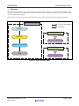
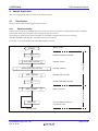
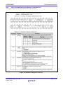
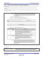
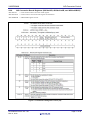
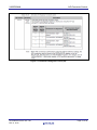
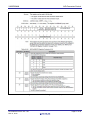
APPLICATION NOTE
V850E2/MN4
A/D Converter Control
R01AN0923EJ0100
Rev.1.00
Feb 13, 2012
Introduction
This document explains how to set up the A/D converter (ADC) and also gives an outline of the operation and describes
the procedures for using a sample program. The sample program converts the scan list of channel group (CG) 0 by
using the software trigger in one-shot mode. The number of times conversion of the scan list is repeated can be set from
one to four per CG in a specific register for a given channel, but is set to one in the sample program. Having finished
converting the scan list, the sample program turns on an LED to reflect the result.
Target Device
V850E2/MN4 Microcontrollers
Contents
1.
Overview ........................................................................................................................................... 2
2.
Usage Environment........................................................................................................................... 4
3.
Software ............................................................................................................................................ 5
4.
Sample Application............................................................................................................................ 6
R01AN0923EJ0100 Rev.1.00
Feb 13, 2012
Page 1 of 26
V850E2/MN4
1.
A/D Converter Control
Overview
This sample program converts the scan list of CG0 by using the software trigger in one-shot mode. The number of times
conversion of the scan list is repeated can be set from one to four per CG in a specific register for a given channel, but is
set to one in the sample program.
An A/D conversion flow is given below. See section 4.1 “Flow Charts” for the details of the individual operations.
Main loop processing
: Flow of processing
: Interrupt
Set ADC
Conversion end
Interrupt processing
Interrupt
Start ADC
Conversion end Interrupt
Await end of conversion
Conversion end
Interrupt processing
Interrupt
End
Conversion end Interrupt
Figure 1.1 A/D Conversion Flow
R01AN0923EJ0100 Rev.1.00
Feb 13, 2012
Page 2 of 26
V850E2/MN4
1.1
A/D Converter Control
Initialization
The general registers and functional pins are initialized.
<Port setup>
•
•
•
•
Port n function control expansion registers (PFCEn)
Port n function control registers (PFCn)
Port n mode control registers (PMCn)
Port n mode registers (PMn)
1.2
Basic Operation of the A/D Converter
This section describes the basic procedure of A/D conversion.
1. To optimize the start-up time between power being turned on and the start of conversion, adjust the stabilization
time setting in the ADC stabilization counter register (ADCAnCNT).
2. To enable the A/D converter (set ADCAnCTL0.ADCAnCE to 1 ), switch the power on and set up the resolution, the
ADCAn clock, the trigger mode, the conversion mode, the interrupt generation, the channel group, and other
settings in the following registers.
- ADCAnCTL1 register
- ADCAnCGi registers
- ADCAnIOCi registers
- ADCAnTSELi registers
3. To check that a result of A/D conversion is within a certain value range, enable the conversion result limit
comparison function for the desired channels (ADCAnCTL2.ADCAnRCKm) with upper and lower limits, and
specify the lower limit in the ADCAnLL register and the upper limit in the ADCAnUL register.
4. To discharge the capacitor in the common sample-and-hold circuit before the conversion, set
ADCAnCTL1.ADCAnDISC to 1 to enable the discharge function.
5. To enable or disable the buffer amplifier, set ADCAnCTL1.ADCAnBPC.
6. To enable the ADC, set ADCAnCTL0.ADCAnCE to 1. After the stabilization time has elapsed after power is turned
on or after the standby mode is exited, the A/D converter is ready for A/D conversion.
7. Depending on the specified trigger mode, A/D conversion is started by a given channel group (CG).
- Software trigger (setting ADCAnTRGi.ADCAnSTTi to 1)
- Hardware trigger (input signals ADCAnTTRGi)
If the A/D conversion of multiple CGs is triggered, the order of A/D conversion depends on the priority of the CGs.
8. When the A/D conversion on the channel specified by the ADCAnIOCi register end, the A/D conversion end
interrupt (INTADCAnTi) for the given channel is generated.
9. Read the results from the A/D conversion result registers, ADCAnLCR, ADCAnDBiCR, and ADCAnCmCR.
10. Monitor the following registers.
- ADCAnSTR1: To check whether the result of A/D conversion has been overwritten before being read according to
the field of application.
- ADCAnSTR0: To check whether the result of A/D conversion is within a specified range (only if the conversion
result limit comparison function is enabled).
11. To set the A/D converter again, disable the A/D converter by setting ADCAnCTL0.ADCAnCE to 0.
R01AN0923EJ0100 Rev.1.00
Feb 13, 2012
Page 3 of 26
V850E2/MN4
2.
A/D Converter Control
Usage Environment
This section explains the circuit diagram and development environment to run this sample program.
2.1
Circuit Diagram
See “V850E2/MN4 Target Board User Manual: QB-V850E2MN4DUAL-TB (R20UT0683XJ)” for the details of the
circuit diagram.
The main hardware resource used in this sample program is the A/D conversion pin (ANI00).
The LEDs are connected to port 13. The P13_7 pin is used for LED1. The P13_6 pin is used for LED2
2.2
Development Environment
It is necessary to install the tools that are listed below to run the sample program.
• CubeSuite+
The integrated development environment CubeSuite+ from Renesas Electronics provides various software development
tools that are necessary for the user to develop applications. The user can use these tools seamlessly and easily in
various development stages including coding, assembly, compilation, debugging using an emulator or simulator, and
flash programming.
• MINICUBE
MINICUBE is a general-purpose in-circuit emulator from Renesas Electronics which adopts the JTAG interface system.
It allows the user to debug an onboard real processor and provides highly transparent and stable emulation
functionalities. An adapter is required to connect a TB board to MINICUBE.
• Multi
Green Hills software, Inc. integrated development tool suit.
• IAR Embedded Workbench
IAR Systems integrated development tool suit.
R01AN0923EJ0100 Rev.1.00
Feb 13, 2012
Page 4 of 26
V850E2/MN4
3.
A/D Converter Control
Software
This section describes the organization of the compressed files to be downloaded.
3.1
File Organization
The compressed files to be downloaded consist of the files that are listed below.
File Name
(Tool Structure)
crtE.s
startup.s
V850E2MN4.dir
V850E2_MN4 ADC.ld
vector.s
adc.h
main.c
initial.c
adc_control.c
interrupt.c
Description
Common
Source File
Hardware initialization processing
Link directive file
Vector table
Variable and function declarations
Main processing
Software initialization processing
A/D converter control
Interrupt processing
R01AN0923EJ0100 Rev.1.00
Feb 13, 2012
●
●
●
●
●
CubeSuite+
File
●
●
Multi File
●
●
●
Page 5 of 26
V850E2/MN4
4.
A/D Converter Control
Sample Application
This section explains the A/D conversion of this sample program.
4.1
Flow Charts
The flow charts of this sample program are given below.
4.1.1
Main Processing
The main processing sets up and then starts A/D conversion. The A/D conversion is repeated and its state is indicated
by the LEDs. When A/D conversion ends, the signal for LED1 is inverted.
Overwriting of a result of A/D conversion before it is read leads to the generation of an error interrupt
(INTADCAnTERR) indicating this, and LED2 is turned on in response.
See section 4.1.2 for the details of the individual transfer processing.
START
Start program
Disable maskable interrupts
SYSTEM_INITIAL
APPLICATION_INITIAL
ADC_INITIAL
EI
Initialize system
Initialize software
Initialization
DI
Initialize A/D converter
Enable maskable interrupts
Start conversion
Main processing
ADC_START
DISPLAY
Control LEDs according to
conversion state
Infinite loop
Figure 4.1 Main Processing Flowchart
R01AN0923EJ0100 Rev.1.00
Feb 13, 2012
Page 6 of 26
V850E2/MN4
4.1.2
A/D Converter Control
Interrupt Processing Flow
When A/D conversion ends or an A/D conversion error occurs, interrupt processing is executed accordingly.
Conversion end
interrupt
INTADCA0I0
Conversion error
interrupt
INTADCA0ERR
Store conversion data
in RAM
Turn of LED2
Invert LED1
Stop conversion
Restart conversion
End of processing
End of processing
Figure 4.2 Interrupt Processing
R01AN0923EJ0100 Rev.1.00
Feb 13, 2012
Page 7 of 26
V850E2/MN4
4.2
A/D Converter Control
Register Setup
This section explains how to set up the relevant registers according to the flow charts shown in section 4.1. The
registers described below must be configured to control the A/D converter.
4.2.1
Port Setup
The LEDs are connected to port 13. The pertinent control registers must be set up as shown in the table below. The
P13_7 pin is used for LED1. The P13_6 pin is used for LED2.
Macro
PORT
Pin
P13_6
P13_7
PMC
0
0
PFCE
0
0
PFC
0
0
PM
0
0
Corresponding function
Port mode, output
Port mode, output
Setting examples
/* P13_6: LED2; port mode; output*/
/* P13_7: LED1; port mode; output*/
PFCE13 = 0x0000;
PFC13 = 0x0000;
PMC13 = 0x0000;
PM13 = 0x0000;
4.2.2
A/D Converter Stabilization Counter Register (ADCAnCNT)
This register specifies the stabilization time of the A/D converter.
Figure 4.3 ADCAnCNT Register Format
Setting example
ADCA0CNT = 0xff;
/* stabilization counter */
R01AN0923EJ0100 Rev.1.00
Feb 13, 2012
Page 8 of 26
V850E2/MN4
4.2.3
A/D Converter Control
A/D Converter Mode Control Register 1 (ADCAnCTL1)
This register specifies the conversion mode and controls the conversions.
Figure 4.4 ADCAnCTL1 Register Format (1/3)
R01AN0923EJ0100 Rev.1.00
Feb 13, 2012
Page 9 of 26
V850E2/MN4
A/D Converter Control
Figure 4.5 ADCAnCTL1 Register Format (2/3)
R01AN0923EJ0100 Rev.1.00
Feb 13, 2012
Page 10 of 26
V850E2/MN4
A/D Converter Control
Figure 4.6 ADCAnCTL1 Register Format (3/3)
Setting example
ADCA0CTL1 = 0x00028001;
R01AN0923EJ0100 Rev.1.00
Feb 13, 2012
/* no detection of hard edge;
right aligned conversion result;
software trigger;
one shot mode;
discharge on;
keep conversion result after read-out;
10bit resolution mode;
ADCATCNV0,1,2=L means no conversion;
ADCATCNV0,1,2=H means running conversion;
1/2 A/D Frequency configuration */
Page 11 of 26
V850E2/MN4
4.2.4
A/D Converter Control
A/D Converter Channel Group Register i (ADCAnCGi)
This register creates a scan list for the corresponding CG. The channels specified in the scan list are converted in
ascending order.
In addition, ADCAnCG0.ADCAnDIAG can be used to enable or disable the diagnosis of A/D conversion that uses the
reference voltage signal (ADDIAGOUT).
Figure 4.7 ADCAnCGi Register Format
Setting example
ADCA0CG0 = 0x00000001;
R01AN0923EJ0100 Rev.1.00
Feb 13, 2012
/* conversion of ADDIAGOUT(AVdd) is not available;
ANI00 conversion */
Page 12 of 26
V850E2/MN4
4.2.5
A/D Converter Control
A/D Converter Interrupt Control Register i (ADCAnIOCi)
The A/D conversion end interrupt INTADCAnTi can be generated when the A/D conversion of a certain channel has
been completed.
This register specifies the channels for which the interrupt INTADCAnTi is generated on the completion of A/D
conversion.
If ADCAnIOCi is cleared to 0000 0000H, the interrupt INTADCAnTi is automatically generated on the completion of
A/D conversion of CGi.
Figure 4.8 ADCAnIOCi Register Format
Setting example
ADCA0IOC0 = 0x00000001;
R01AN0923EJ0100 Rev.1.00
Feb 13, 2012
/* ADCATINT0 does not output at the end of channel diag conversion;
ADCATINT0 output at the end of channel 00 (CG0) conversion */
Page 13 of 26
V850E2/MN4
4.2.6
A/D Converter Control
A/D Converter Mode Control Register 0 (ADCAnCTL0)
This register enables or disables the A/D converter. In addition, it specifies the number of repetitions in the one-shot
conversion mode and whether to generate error interrupt requests when an A/D conversion is overwritten before it is
read.
Figure 4.9 ADCAnCTL0 Register Format (1/2)
R01AN0923EJ0100 Rev.1.00
Feb 13, 2012
Page 14 of 26
V850E2/MN4
A/D Converter Control
Figure 4.10 ADCAnCTL0 Register Format (2/2)
Setting example
ADCA0CTL0 = 0x0080;
/* ADCATERR which is generated by ADCA0LCR register overwrite admitted;
ADCATERR which is generated by ADCA0DBiCR register overwrite admitted;
ADCATERR which is generated by ADCA0CmCR register overwrite admitted;
A/D Controller enable ON;
1-time conversion of CG0 scanlist(channel 00) */
R01AN0923EJ0100 Rev.1.00
Feb 13, 2012
Page 15 of 26
V850E2/MN4
4.2.7
A/D Converter Control
A/D Converter Software Trigger Register i (ADCAnTRGi)
This trigger register is the trigger register for starting the A/D conversion of CGi.
Figure 4.11 ADCAnTRGi Register Format
Setting example
ADCA0TRG0 = 0x01;
/* conversion start */
R01AN0923EJ0100 Rev.1.00
Feb 13, 2012
Page 16 of 26
V850E2/MN4
4.2.8
A/D Converter Control
A/D Conversion Result Registers (ADCAnLCR, ADCAnCmCR, and ADCAnDBiCR)
ADCAnLCR
― A/D converter latest conversion result register
ADCAnCmCR
― A/D converter conversion result register for channel m
ADCAnDBiCR ― DMA buffer register of CGi
Figure 4.12 ADCAnLCR Register Format (1/2)
R01AN0923EJ0100 Rev.1.00
Feb 13, 2012
Page 17 of 26
V850E2/MN4
A/D Converter Control
Figure 4.13 ADCAnLCR Register Format (2/2)
R01AN0923EJ0100 Rev.1.00
Feb 13, 2012
Page 18 of 26
V850E2/MN4
A/D Converter Control
Figure 4.14 ADCAnCmCR Register Format (1/2)
R01AN0923EJ0100 Rev.1.00
Feb 13, 2012
Page 19 of 26
V850E2/MN4
A/D Converter Control
Figure 4.15 ADCAnCmCR Register Format (2/2)
R01AN0923EJ0100 Rev.1.00
Feb 13, 2012
Page 20 of 26
V850E2/MN4
A/D Converter Control
Figure 4.16 ADCAnDBiCR Register Format (1/2)
R01AN0923EJ0100 Rev.1.00
Feb 13, 2012
Page 21 of 26
V850E2/MN4
A/D Converter Control
Figure 4.17 ADCAnDBiCR Register Format (2/2)
Setting examples
adc_result[0] = ADCA0LCR;
adc_result[1] = ADCA0C00CR;
adc_result[2] = ADCA0DB0CR;
R01AN0923EJ0100 Rev.1.00
Feb 13, 2012
/* read converted result */
/* read converted result */
/* read converted result */
Page 22 of 26
V850E2/MN4
4.3
A/D Converter Control
Function Specifications
This section describes the specifications for the functions that are used by the sample program.
4.3.1
Main Processing (main.c)
[Function Name]
[Function]
[Arguments]
[Return Value]
[Startup Method]
[SFRs Used]
[Calling Function]
[Variables]
[File Name]
[Notes]
4.3.2
main ()
Calls necessary initialization functions before entering an infinite loop.
None
None
Enters the main function after hardware initialization.
None
None
None
main.c
None
Software Initialization Processing (initial.c)
[Function Name]
[Function]
[Arguments]
[Return Value]
[Startup Method]
[SFRs Used]
[Calling Function]
[Variables]
[File Name]
[Notes]
port_initial()
Sets up ports and their mode.
None
None
Call
PFCE13, PFC13, PMC13, PM13
main()
None
initial.c
None
[Function Name]
[Function]
[Arguments]
[Return Value]
[Startup Method]
[SFRs Used]
[Calling Function]
[Variables]
[File Name]
[Notes]
cg_initial()
Initializes the special clock frequency control register.
None
None
Call
SFRCTL3
main()
None
initial.c
None
R01AN0923EJ0100 Rev.1.00
Feb 13, 2012
Page 23 of 26
V850E2/MN4
A/D Converter Control
[Function Name]
[Function]
[Arguments]
[Return Value]
[Startup Method]
[SFRs Used]
[Calling Function]
[Variables]
[File Name]
[Notes]
hbus_initial()
Initializes the AHB bus
None
None
Call
ETARCFG0, ETARADRS0, ETARMASK0
main()
None
initial.c
None
[Function Name]
[Function]
[Arguments]
[Return Value]
[Startup Method]
[SFRs Used]
[Calling Function]
[Variables]
[File Name]
[Notes]
board_initial()
Sets up the initial state of the LEDs.
None
None
Call
P13
main()
None
initial.c
None
[Function Name]
[Function]
[Arguments]
[Return Value]
[Startup Method]
[SFRs Used]
[Calling Function]
[Variables]
[File Name]
[Notes]
ram_initial()
Sets up the initial state of the user RAM.
None
None
Call
None
main()
adc_result[]
initial.c
None
R01AN0923EJ0100 Rev.1.00
Feb 13, 2012
Page 24 of 26
V850E2/MN4
4.3.3
Control Processing (adc_control.c)
[Function Name]
[Function]
[Arguments]
[Return Value]
[Startup Method]
[SFRs Used]
[Calling Function]
[Variables]
[File Name]
[Notes]
4.3.4
A/D Converter Control
adc_initial()
Sets up the operation of the ADC.
None
None
Call
ICADCA0ERR, ICADCA0I0, ADCA0CNT, ADCA0CTL1, ADCA0CG0,
ACA0IOC0, ADCA0TSEL0, ADCA0CTL2, ADCA0LL, ADCA0UL, ADCA0CTL0,
ADCA0TRG0
main()
None
adc_control.c
None
Interrupt Processing (interrupt.c)
[Function Name]
[Function]
[Arguments]
[Return Value]
[Startup Method]
[SFRs Used]
[Calling Function]
[Variables]
[File Name]
[Notes]
int_adca0i0()
Processes A/D conversion end interrupt.
None
None
Request INTADCA0I0 is present in an unmasked state.
ADCA0LCR, ADCA0TRG0, ADCA0C00CR, ADCA0DB0CR, P13
None
adc_result[]
interrupt.c
None
[Function Name]
[Function]
[Arguments]
[Return Value]
[Startup Method]
[SFRs Used]
[Calling Function]
[Variables]
[File Name]
[Notes]
int_adca0err()
Processes A/D conversion error interrupt.
None
None
Request INTADCA0ERR is present in an unmasked state.
P13, ADCA0CTL0
None
None
interrupt.c
None
R01AN0923EJ0100 Rev.1.00
Feb 13, 2012
Page 25 of 26
V850E2/MN4
A/D Converter Control
Website and Support
Renesas Electronics Website
http://www.renesas.com/
Inquiries
http://www.renesas.com/inquiry
All trademarks and registered trademarks are the property of their respective owners.
R01AN0923EJ0100 Rev.1.00
Feb 13, 2012
Page 26 of 26
Revision Record
Rev.
1.00
Date
Feb 13, 2012
Description
Page
Summary
—
First edition issued
A-1
General Precautions in the Handling of MPU/MCU Products
The following usage notes are applicable to all MPU/MCU products from Renesas. For detailed usage notes on the
products covered by this manual, refer to the relevant sections of the manual. If the descriptions under General
Precautions in the Handling of MPU/MCU Products and in the body of the manual differ from each other, the
description in the body of the manual takes precedence.
1. Handling of Unused Pins
Handle unused pins in accord with the directions given under Handling of Unused Pins in the manual.
⎯ The input pins of CMOS products are generally in the high-impedance state. In operation with an
unused pin in the open-circuit state, extra electromagnetic noise is induced in the vicinity of LSI, an
associated shoot-through current flows internally, and malfunctions occur due to the false
recognition of the pin state as an input signal become possible. Unused pins should be handled as
described under Handling of Unused Pins in the manual.
2. Processing at Power-on
The state of the product is undefined at the moment when power is supplied.
⎯ The states of internal circuits in the LSI are indeterminate and the states of register settings and
pins are undefined at the moment when power is supplied.
In a finished product where the reset signal is applied to the external reset pin, the states of pins
are not guaranteed from the moment when power is supplied until the reset process is completed.
In a similar way, the states of pins in a product that is reset by an on-chip power-on reset function
are not guaranteed from the moment when power is supplied until the power reaches the level at
which resetting has been specified.
3. Prohibition of Access to Reserved Addresses
Access to reserved addresses is prohibited.
⎯ The reserved addresses are provided for the possible future expansion of functions. Do not access
these addresses; the correct operation of LSI is not guaranteed if they are accessed.
4. Clock Signals
After applying a reset, only release the reset line after the operating clock signal has become stable.
When switching the clock signal during program execution, wait until the target clock signal has
stabilized.
⎯ When the clock signal is generated with an external resonator (or from an external oscillator)
during a reset, ensure that the reset line is only released after full stabilization of the clock signal.
Moreover, when switching to a clock signal produced with an external resonator (or by an external
oscillator) while program execution is in progress, wait until the target clock signal is stable.
5. Differences between Products
Before changing from one product to another, i.e. to one with a different type number, confirm that the
change will not lead to problems.
⎯ The characteristics of MPU/MCU in the same group but having different type numbers may differ
because of the differences in internal memory capacity and layout pattern. When changing to
products of different type numbers, implement a system-evaluation test for each of the products.
Notice
1.
All information included in this document is current as of the date this document is issued. Such information, however, is subject to change without any prior notice. Before purchasing or using any Renesas
Electronics products listed herein, please confirm the latest product information with a Renesas Electronics sales office. Also, please pay regular and careful attention to additional and different information to
be disclosed by Renesas Electronics such as that disclosed through our website.
2.
Renesas Electronics does not assume any liability for infringement of patents, copyrights, or other intellectual property rights of third parties by or arising from the use of Renesas Electronics products or
technical information described in this document. No license, express, implied or otherwise, is granted hereby under any patents, copyrights or other intellectual property rights of Renesas Electronics or
others.
3.
You should not alter, modify, copy, or otherwise misappropriate any Renesas Electronics product, whether in whole or in part.
4.
Descriptions of circuits, software and other related information in this document are provided only to illustrate the operation of semiconductor products and application examples. You are fully responsible for
the incorporation of these circuits, software, and information in the design of your equipment. Renesas Electronics assumes no responsibility for any losses incurred by you or third parties arising from the
use of these circuits, software, or information.
5.
When exporting the products or technology described in this document, you should comply with the applicable export control laws and regulations and follow the procedures required by such laws and
regulations. You should not use Renesas Electronics products or the technology described in this document for any purpose relating to military applications or use by the military, including but not limited to
the development of weapons of mass destruction. Renesas Electronics products and technology may not be used for or incorporated into any products or systems whose manufacture, use, or sale is
prohibited under any applicable domestic or foreign laws or regulations.
6.
Renesas Electronics has used reasonable care in preparing the information included in this document, but Renesas Electronics does not warrant that such information is error free. Renesas Electronics
7.
Renesas Electronics products are classified according to the following three quality grades: "Standard", "High Quality", and "Specific". The recommended applications for each Renesas Electronics product
assumes no liability whatsoever for any damages incurred by you resulting from errors in or omissions from the information included herein.
depends on the product's quality grade, as indicated below. You must check the quality grade of each Renesas Electronics product before using it in a particular application. You may not use any Renesas
Electronics product for any application categorized as "Specific" without the prior written consent of Renesas Electronics. Further, you may not use any Renesas Electronics product for any application for
which it is not intended without the prior written consent of Renesas Electronics. Renesas Electronics shall not be in any way liable for any damages or losses incurred by you or third parties arising from the
use of any Renesas Electronics product for an application categorized as "Specific" or for which the product is not intended where you have failed to obtain the prior written consent of Renesas Electronics.
The quality grade of each Renesas Electronics product is "Standard" unless otherwise expressly specified in a Renesas Electronics data sheets or data books, etc.
"Standard":
Computers; office equipment; communications equipment; test and measurement equipment; audio and visual equipment; home electronic appliances; machine tools;
personal electronic equipment; and industrial robots.
"High Quality": Transportation equipment (automobiles, trains, ships, etc.); traffic control systems; anti-disaster systems; anti-crime systems; safety equipment; and medical equipment not specifically
designed for life support.
"Specific":
Aircraft; aerospace equipment; submersible repeaters; nuclear reactor control systems; medical equipment or systems for life support (e.g. artificial life support devices or systems), surgical
implantations, or healthcare intervention (e.g. excision, etc.), and any other applications or purposes that pose a direct threat to human life.
8.
You should use the Renesas Electronics products described in this document within the range specified by Renesas Electronics, especially with respect to the maximum rating, operating supply voltage
range, movement power voltage range, heat radiation characteristics, installation and other product characteristics. Renesas Electronics shall have no liability for malfunctions or damages arising out of the
use of Renesas Electronics products beyond such specified ranges.
9.
Although Renesas Electronics endeavors to improve the quality and reliability of its products, semiconductor products have specific characteristics such as the occurrence of failure at a certain rate and
malfunctions under certain use conditions. Further, Renesas Electronics products are not subject to radiation resistance design. Please be sure to implement safety measures to guard them against the
possibility of physical injury, and injury or damage caused by fire in the event of the failure of a Renesas Electronics product, such as safety design for hardware and software including but not limited to
redundancy, fire control and malfunction prevention, appropriate treatment for aging degradation or any other appropriate measures. Because the evaluation of microcomputer software alone is very difficult,
please evaluate the safety of the final products or system manufactured by you.
10. Please contact a Renesas Electronics sales office for details as to environmental matters such as the environmental compatibility of each Renesas Electronics product. Please use Renesas Electronics
products in compliance with all applicable laws and regulations that regulate the inclusion or use of controlled substances, including without limitation, the EU RoHS Directive. Renesas Electronics assumes
no liability for damages or losses occurring as a result of your noncompliance with applicable laws and regulations.
11. This document may not be reproduced or duplicated, in any form, in whole or in part, without prior written consent of Renesas Electronics.
12. Please contact a Renesas Electronics sales office if you have any questions regarding the information contained in this document or Renesas Electronics products, or if you have any other inquiries.
(Note 1)
"Renesas Electronics" as used in this document means Renesas Electronics Corporation and also includes its majority-owned subsidiaries.
(Note 2)
"Renesas Electronics product(s)" means any product developed or manufactured by or for Renesas Electronics.
http://www.renesas.com
SALES OFFICES
Refer to "http://www.renesas.com/" for the latest and detailed information.
Renesas Electronics America Inc.
2880 Scott Boulevard Santa Clara, CA 95050-2554, U.S.A.
Tel: +1-408-588-6000, Fax: +1-408-588-6130
Renesas Electronics Canada Limited
1101 Nicholson Road, Newmarket, Ontario L3Y 9C3, Canada
Tel: +1-905-898-5441, Fax: +1-905-898-3220
Renesas Electronics Europe Limited
Dukes Meadow, Millboard Road, Bourne End, Buckinghamshire, SL8 5FH, U.K
Tel: +44-1628-585-100, Fax: +44-1628-585-900
Renesas Electronics Europe GmbH
Arcadiastrasse 10, 40472 Düsseldorf, Germany
Tel: +49-211-65030, Fax: +49-211-6503-1327
Renesas Electronics (China) Co., Ltd.
7th Floor, Quantum Plaza, No.27 ZhiChunLu Haidian District, Beijing 100083, P.R.China
Tel: +86-10-8235-1155, Fax: +86-10-8235-7679
Renesas Electronics (Shanghai) Co., Ltd.
Unit 204, 205, AZIA Center, No.1233 Lujiazui Ring Rd., Pudong District, Shanghai 200120, China
Tel: +86-21-5877-1818, Fax: +86-21-6887-7858 / -7898
Renesas Electronics Hong Kong Limited
Unit 1601-1613, 16/F., Tower 2, Grand Century Place, 193 Prince Edward Road West, Mongkok, Kowloon, Hong Kong
Tel: +852-2886-9318, Fax: +852 2886-9022/9044
Renesas Electronics Taiwan Co., Ltd.
13F, No. 363, Fu Shing North Road, Taipei, Taiwan
Tel: +886-2-8175-9600, Fax: +886 2-8175-9670
Renesas Electronics Singapore Pte. Ltd.
1 harbourFront Avenue, #06-10, keppel Bay Tower, Singapore 098632
Tel: +65-6213-0200, Fax: +65-6278-8001
Renesas Electronics Malaysia Sdn.Bhd.
Unit 906, Block B, Menara Amcorp, Amcorp Trade Centre, No. 18, Jln Persiaran Barat, 46050 Petaling Jaya, Selangor Darul Ehsan, Malaysia
Tel: +60-3-7955-9390, Fax: +60-3-7955-9510
Renesas Electronics Korea Co., Ltd.
11F., Samik Lavied' or Bldg., 720-2 Yeoksam-Dong, Kangnam-Ku, Seoul 135-080, Korea
Tel: +82-2-558-3737, Fax: +82-2-558-5141
© 2012 Renesas Electronics Corporation. All rights reserved.
Colophon 1.1