1
S/M No. : TCP099FEF0
Service Manual
TV/DVD Combination
CHASSIS : CP-099F
Model : DDT-21H9ZZF
DDT-21H9ZZR
DDT-21H9ZZF
DDT-21H9ZZR
DAEWOO ELECTRONICS CO., LTD
http : //svc.dwe.co.kr
May. 2002
Service Manual CP-099F
Contents
1- Main Features ------------------------------------------------------------------------------------------------------------------------1-1 Specifications ------------------------------------------------------------------------------------------------------------------1-2 Channel table -------------------------------------------------------------------------------------------------------------------1-3 ATSS sorting method ----------------------------------------------------------------------------------------------------------
4
4
6
8
2- Safety instruction ----------------------------------------------------------------------------------------------------------------------
9
3- Alignment instructions --------------------------------------------------------------------------------------------------------------3-1 Microcontroller configuration : Service mode ----------------------------------------------------------------------------3-2 Service mode navigation -----------------------------------------------------------------------------------------------------3-3 Microcontroller configuration : Option bits -------------------------------------------------------------------------------3-4 TV set Alignment -------------------------------------------------------------------------------------------------------------3-4-1 The adjustment of screen -----------------------------------------------------------------------------------------------3-4-2 The adjustment of focus -------------------------------------------------------------------------------------------------3-4-3 The adjustment of white balance --------------------------------------------------------------------------------------3-5 The adjustment of geometry -------------------------------------------------------------------------------------------------3-5-1 The adjustment of vertical center --------------------------------------------------------------------------------------3-5-2 The adjustment of vertical size -----------------------------------------------------------------------------------------3-5-3 The adjustment of vertical slope ---------------------------------------------------------------------------------------3-5-4 The adjustment of S-correction ----------------------------------------------------------------------------------------3-5-5 The adjustment of horizontal center -----------------------------------------------------------------------------------3-5-6 The adjustment of horizontal width -----------------------------------------------------------------------------------3-5-7 The adjustment of pincusion -------------------------------------------------------------------------------------------3-5-7-1 The adjustment of parabola -----------------------------------------------------------------------------------------3-5-7-2 The adjustment of corner --------------------------------------------------------------------------------------------3-5-7-3 The adjustment of H.parabola ---------------------------------------------------------------------------------------3-5-7-4 The adjustment of H.bow --------------------------------------------------------------------------------------------3-5-7-5 The adjustment of EW TRAPEZIUM -----------------------------------------------------------------------------3-6 The adjustment of RF AGC --------------------------------------------------------------------------------------------------3-7 Setting the conditions for finished products --------------------------------------------------------------------------------
10
10
10
11
11
11
11
11
11
11
12
12
12
12
13
13
13
13
13
14
14
14
14
4- IC description ------------------------------------------------------------------------------------------------------------------------4-1 VCT383XA TV signal processor - Teletext decoder with embedded 8 bit - Controller --------------------------4-1-1 Block diagram of the VCT ---------------------------------------------------------------------------------------------4-1-2 TV-signal Processor -----------------------------------------------------------------------------------------------------4-1-3 -Controller ---------------------------------------------------------------------------------------------------------------4-1-4 Teletext Features ---------------------------------------------------------------------------------------------------------4-1-5 Display OSD Features ---------------------------------------------------------------------------------------------------4-1-6 Audio Features -----------------------------------------------------------------------------------------------------------4-1-7 General Features ---------------------------------------------------------------------------------------------------------4-1-8 Data Capture --------------------------------------------------------------------------------------------------------------4-1-9 Data Capture Features ---------------------------------------------------------------------------------------------------4-1-10 TV processor version and -Controller capacity -------------------------------------------------------------------4-1-11 IC marking and version ------------------------------------------------------------------------------------------------4-1-12 Pinning -------------------------------------------------------------------------------------------------------------------4-2 MSP341 x Multistandard Sound Processor --------------------------------------------------------------------------------4-2-1 Basic Features of the MSP341x ----------------------------------------------------------------------------------------4-2-1-1 Demodulator and NICAM Decoder Section ----------------------------------------------------------------------4-2-1-2 DSP-Section (Audio Baseband Processing) -----------------------------------------------------------------------
15
15
15
15
16
16
17
17
17
17
17
18
18
18
21
21
21
22
-1-
Service Manual CP-099F
4-2-1-3 Analogue Section -----------------------------------------------------------------------------------------------------4-2-1-4 NICAM plus FM/AM-Mono ----------------------------------------------------------------------------------------4-2-1-5 German 2-Carrier System (DUAL FM System) ------------------------------------------------------------------4-3 TDA9886 IIC-bus controlled single/multi standard algnment-free IF-PLL -------------------------------------------4-3-1 DISCRIPTION -----------------------------------------------------------------------------------------------------------4-3-2 FEATURES ---------------------------------------------------------------------------------------------------------------4-3-3 PINNING -----------------------------------------------------------------------------------------------------------------4-4 TDA894xJ Stereo Audio Amplifer -----------------------------------------------------------------------------------------4-1-1 Features -------------------------------------------------------------------------------------------------------------------4-5 TDA835xJ Vertical Amplifier -----------------------------------------------------------------------------------------------4-5-1 TDA8358J ----------------------------------------------------------------------------------------------------------------4-6 TEA5101B ---------------------------------------------------------------------------------------------------------------------4-7 24C16 - 16 Kb EEPROM ----------------------------------------------------------------------------------------------------4-8 STR - F6654 -------------------------------------------------------------------------------------------------------------------4-8-1 General description ------------------------------------------------------------------------------------------------------4-8-2 Features -------------------------------------------------------------------------------------------------------------------4-8-3 Block diagram ------------------------------------------------------------------------------------------------------------4-8-4 Pins description ----------------------------------------------------------------------------------------------------------4-8-5 Control part electrical characteristics ---------------------------------------------------------------------------------4-8-6 MOSFET electrical chatacteristics ------------------------------------------------------------------------------------5- Circuit description --------------------------------------------------------------------------------------------------------------------5-1 Block diagram -----------------------------------------------------------------------------------------------------------------5-2 IF section -----------------------------------------------------------------------------------------------------------------------5-2-1 Picture IF Amplifier -----------------------------------------------------------------------------------------------------5-2-2 Tuner and VIF-AGC -----------------------------------------------------------------------------------------------------5-2-3 VIF-AGC detector -------------------------------------------------------------------------------------------------------5-2-4 Frequency phase-Locked Loop(FPLL) detector ---------------------------------------------------------------------5-2-5 VCO and divider ---------------------------------------------------------------------------------------------------------5-2-6 Digital acquisition help and AFC --------------------------------------------------------------------------------------5-2-7 Video demodulator and amplifier --------------------------------------------------------------------------------------5-2-8 Sound carrier trap --------------------------------------------------------------------------------------------------------5-2-9 SIF amplifier --------------------------------------------------------------------------------------------------------------5-2-10 AGC detector -----------------------------------------------------------------------------------------------------------5-2-11 Single reference QSS mixer -------------------------------------------------------------------------------------------5-2-12 AM demodulator -------------------------------------------------------------------------------------------------------5-2-13 FM demodulator and acquisition help -------------------------------------------------------------------------------5-2-14 Audio amplifier and mute time constant ----------------------------------------------------------------------------5-2-15 I2C-bus transceiver and MAD (module address) ------------------------------------------------------------------5-2-16 Internal voltage stabilizer ---------------------------------------------------------------------------------------------5-3 Video - VCT description -----------------------------------------------------------------------------------------------------5-3-1 Introduction ---------------------------------------------------------------------------------------------------------------5-3-2 Video Front-end ----------------------------------------------------------------------------------------------------------5-3-3 Input Selector -------------------------------------------------------------------------------------------------------------5-3-4 Clamping ------------------------------------------------------------------------------------------------------------------5-3-5 Automatic Gain control -------------------------------------------------------------------------------------------------5-3-6 Digitally Controlled Clock Oscillator ---------------------------------------------------------------------------------5-3-7 Analogue Video Output -------------------------------------------------------------------------------------------------5-3-8 Adaptive Comb Filter (VCT3834A only) ----------------------------------------------------------------------------5-3-9 Color Decoder ------------------------------------------------------------------------------------------------------------5-3-10 Horizontal Scaler (VCT3834A only) --------------------------------------------------------------------------------5-3-11 Video Sync Processing -------------------------------------------------------------------------------------------------5-3-12 Display Processing -----------------------------------------------------------------------------------------------------5-3-13 Chroma Transient Improvement ---------------------------------------------------------------------------------------2-
22
22
22
25
25
25
25
27
27
29
29
30
32
32
32
32
33
33
34
34
35
35
36
36
36
36
36
36
37
37
37
37
37
38
38
38
38
39
39
39
39
39
39
39
39
39
39
40
40
40
40
41
41
Service Manual CP-099F
5-3-14 Video Back-end ---------------------------------------------------------------------------------------------------------5-3-15 CRT Measurement and Control --------------------------------------------------------------------------------------5-3-16 Average Beam Current Limiter ---------------------------------------------------------------------------------------5-3-17 Analogue RGB Insertion ----------------------------------------------------------------------------------------------5-3-18 Fast-Blank Monitor ----------------------------------------------------------------------------------------------------5-3-19 Vertical and East/West Deflection ------------------------------------------------------------------------------------5-3-20 EHT Compensation ----------------------------------------------------------------------------------------------------5-3-21 Reset Function ----------------------------------------------------------------------------------------------------------5-3-22 Standby and Power-On ------------------------------------------------------------------------------------------------5-4 Microcontroller ----------------------------------------------------------------------------------------------------------------5-4-1 Introduction ---------------------------------------------------------------------------------------------------------------5-4-2 CPU ------------------------------------------------------------------------------------------------------------------------5-4-3 -Controller I/O pin configuration and function ---------------------------------------------------------------------5-4-4 Tuning ---------------------------------------------------------------------------------------------------------------------5-4-5 Over Current Protection -------------------------------------------------------------------------------------------------5-5 Teletext Display ---------------------------------------------------------------------------------------------------------------5-6 Sound processing --------------------------------------------------------------------------------------------------------------5-6-1 Analogue sound IF - input section -------------------------------------------------------------------------------------5-6-2 Quadrature Mixers -------------------------------------------------------------------------------------------------------5-6-3 Phase and AM discrimination ------------------------------------------------------------------------------------------5-6-4 NICAM decoder ---------------------------------------------------------------------------------------------------------5-6-5 DSP section ---------------------------------------------------------------------------------------------------------------5-6-6 Sound Mode switching --------------------------------------------------------------------------------------------------5-7 Sound amplification -----------------------------------------------------------------------------------------------------------5-7-1 Power amplifier ----------------------------------------------------------------------------------------------------------5-7-2 Mode selection -----------------------------------------------------------------------------------------------------------5-8 Vertical deflection -------------------------------------------------------------------------------------------------------------5-8-1 Flyback voltage ----------------------------------------------------------------------------------------------------------5-8-2 Protection -----------------------------------------------------------------------------------------------------------------5-8-3 Guard circuit --------------------------------------------------------------------------------------------------------------5-8-4 Damping resistor ---------------------------------------------------------------------------------------------------------5-8-5 EAST-WEST Amplifier (TDA8358J) ---------------------------------------------------------------------------------5-9 Power supply (STR F6654) --------------------------------------------------------------------------------------------------5-9-1 STR-F6654 general desctrption ----------------------------------------------------------------------------------------5-9-2 Power supply primary part operations --------------------------------------------------------------------------------5-10 TV start-up, TV normal run and stand by mode operations -----------------------------------------------------------5-10-1 TV start-up operations -------------------------------------------------------------------------------------------------5-10-2 TV normal run and stand-by mode operations ---------------------------------------------------------------------5-11 DVD Loder -------------------------------------------------------------------------------------------------------------------5-11-1 Mechanism --------------------------------------------------------------------------------------------------------------5-11-2 Electirical Troubleshooting Guide -----------------------------------------------------------------------------------5-11-3 Circuit --------------------------------------------------------------------------------------------------------------------6. Service Parts list ----------------------------------------------------------------------------------------------------------------------7. Different Parts List By CRT ---------------------------------------------------------------------------------------------------------8. Exploded View ------------------------------------------------------------------------------------------------------------------------9. Printed Circuit Board ----------------------------------------------------------------------------------------------------------------10. Schematic Diagram ------------------------------------------------------------------------------------------------------------------
-3-
41
41
41
41
41
42
42
42
42
42
42
42
42
43
43
43
44
44
44
44
44
44
44
45
45
45
45
45
45
46
46
46
46
46
46
49
49
50
53
53
57
59
64
73
74
76
79
Service Manual CP-099F
1- Main Features
1-1 Specifications
TV standard
Sound system
Power consumption
Sound Output Power
Speaker
Teletext system
Aerial input
Channel coverage
Tuning system
Visual screen
Channel indication
Porgram Selection
Aux. terminal
Remote Control Unit
CD/DVD
PAL - SECAM B/G D/K, PAL, I/II, SECAM L/L’
NICAM B/G, I, D/K, L,
FM 2Carrier B/G, D/K
69W approx
TV MODE : 3W min + 3W min
DVD MODE : 3W min + 3W min
5W 8 ohm x2
10 page memory FASTEXT (FLOF or TOP)
75 ohm unbalanced
Off-air channels, S-cable channels and hyperband
frequency synthesiser tuning system
51 Cm
On Screen Display
100 programs (00~99)
EURO SCART (AV1) : Auto / Video In and Out, R/G/B In, Slow and
Fast switching.
AUDIO OUT : DVD COAXIAL OUT and RCA Audio OUT at back of cabinet.
AV2 : RCA Video In and Audio In on side of cabinet.
EARPHONE : Jack on side of cabinet.
R-52B02
Laser
Semiconductor laser, wavelength 650nm
Signal system
PAL 625/50, NTSC 525/60
Frequency response (audio)
20 - 20,000Hz
Signal-to-noise ratio(audio)
More than 60dB (1kHz)
Signal-to-noise ratio(video)
More than 60dB (ABEX 50% white pattern)
Dynamic range (audio)
60dB
Harmonic distortion(audio)
0.3% (1kHz)
-4-
Service Manual CP-099F
Service Manual CP-099F
EURO SCART
Pin
1
2
3
4
5
6
7
8
9
10
11
12
13
14
15
16
17
18
19
20
21
Signal Description
Audio out (linked with 3)
Audio In (linked with 6)
Audio out (linked with 1)
Audio Earth
Blue Earth
Audio In (linked with 2)
Blue In
Slow (Function) Switching
Green Earth
NC
Green In
NC
Red Earth
NC
Red In
Rapid Blanking, Switching
Video Earth
Rapid Blanking Earth
Video Out
Video In
Common Earth
Matching value
0.5Vrms, lmp < 1k (RF 60% MOD)
0.5Vrms, lmp < 10k
0.5Vrms, lmp < 1k (RF 60% MOD)
0.5Vrms, lmp < 10k
0.7Vp-p 10%, lmp 75
TV : 0~2V, AV 16/9 : 4.5~7 V, AV 4/3 : 9.5~12 V, lmp > 10k
0.7Vp-p 10%, lmp 75
0.7Vp-p 10%, lmp 75
0.7Vp-p 10%, lmp 75
Logic 0 : 0~0.4V, Logic 1 : 1~3V, lmp 75
1.0Vp-p 10%, lmp 75
1.0Vp-p 10%, lmp 75
AV2 (RCA AUDIO-VIDEO INPUT)
1
2
3
VIDEO IN
L IN
R IN
1Vpp 3dB, Impedance 75ohm
0.5Vrms, Impedance > 10kohm
0.5Vrms, Impedance > 10kohm
-5-
Service Manual CP-099F
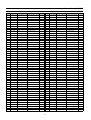
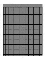
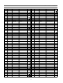
1-2 Channel table
FREQUENCY TABLE
CH
C01
C02
C03
C04
C05
C06
C07
C08
C09
C10
C11
C12
C13
C14
C15
C16
C17
C18
C19
C20
C21
C22
C23
C24
C25
C26
C27
C28
C29
C30
C31
C32
C33
C34
C35
C36
C37
C38
C39
C40
C41
C42
C43
C44
C45
C46
C47
C48
C49
C50
C51
C52
C53
C54
C55
C56
C57
EUROPE CCIR
46.25
48.25
55.25
62.25
175.25
182.25
189.25
196.25
203.25
210.25
217.25
224.25
53.75
82.25
183.75
192.25
201.25
471.25
479.25
487.25
495.25
503.25
511.25
519.25
527.25
535.25
543.25
551.25
559.25
567.25
575.25
583.25
591.25
599.25
607.25
615.25
623.25
631.25
639.25
647.25
655.25
663.25
671.25
679.25
687.25
695.25
703.25
711.25
719.25
727.25
735.25
743.25
751.25
759.25
FRANCE
55.75 (L’)
60.5 (L’)
63.75 (L’)
176.00
184.00
192.00
200.00
208.00
216.00
189.25 (LUX)
69.25 (L’)
76.25 (L’)
83.25 (L’)
90.25
97.25
471.25
479.25
487.25
495.25
503.25
511.25
519.25
527.25
535.25
543.25
551.25
559.25
567.25
575.25
583.25
591.25
599.25
607.25
615.25
623.25
631.25
639.25
647.25
655.25
663.25
671.25
679.25
687.25
695.25
703.25
711.25
719.25
727.25
735.25
743.25
751.25
759.25
-6-
GB(IRELAND)
47.75
53.75
61.75
175.25
183.25
191.25
199.25
207.25
215.25
223.25
231.25
239.25
247.25
49.75
57.75
65.75
77.75
85.75
471.25
479.25
487.25
495.25
503.25
511.25
519.25
527.25
535.25
543.25
551.25
559.25
567.25
575.25
583.25
591.25
599.25
607.25
615.25
623.25
631.25
639.25
647.25
655.25
663.25
671.25
679.25
687.25
695.25
703.25
711.25
719.25
727.25
735.25
743.25
751.25
759.25
EAST OIRT
49.75
59.25
77.25
85.25
93.25
175.25
183.25
191.25
199.25
207.25
215.25
223.25
471.25
479.25
487.25
495.25
503.25
511.25
519.25
527.25
535.25
543.25
551.25
559.25
567.25
575.25
583.25
591.25
599.25
607.25
615.25
623.25
631.25
639.25
647.25
655.25
663.25
671.25
679.25
687.25
695.25
703.25
711.25
719.25
727.25
735.25
743.25
751.25
759.25
Service Manual CP-099F
CH
C58
C59
C60
C61
C62
C63
C64
C65
C66
C67
C68
C69
C70
C71
C72
C73
C74
C75
C76
C77
S01
S02
S03
S04
S05
S06
S07
S08
S09
S10
S11
S12
S13
S14
S15
S16
S17
S18
S19
S20
S21
S22
S23
S24
S25
S26
S27
S28
S29
S30
S31
S32
S33
S34
S35
S36
S37
S38
S39
S40
S41
EUROPE CCIR
767.25
775.25
783.25
791.25
799.25
807.25
815.25
823.25
831.25
839.25
847.25
855.25
863.25
69.25
76.25
83.25
90.25
97.25
59.25
93.25
105.25
112.25
119.25
126.25
133.25
140.25
147.25
154.25
161.25
168.25
231.25
238.25
245.25
252.25
259.25
266.25
273.25
280.25
287.25
294.25
303.25
311.25
319.25
327.25
335.25
343.25
351.25
359.25
367.25
375.25
383.25
391.25
399.25
407.25
415.25
423.25
431.25
439.25
447.25
455.25
463.25
FRANCE
767.25
775.25
783.25
791.25
799.25
807.25
815.25
823.25
831.25
839.25
847.25
855.25
863.25
104.75
116.75
128.75
140.75
152.75
164.75
176.75
188.75
200.75
212.75
224.75
236.75
248.75
260.75
272.75
284.75
296.75
136.00
160.00
303.25
311.25
319.25
327.25
335.25
343.25
351.25
359.25
367.25
375.25
383.25
391.25
399.25
407.25
415.25
423.25
431.25
439.25
447.25
455.25
463.25
GB(IRELAND)
767.25
775.25
783.25
791.25
799.25
807.25
815.25
823.25
831.25
839.25
847.25
855.25
863.25
103.25
111.25
119.25
127.25
135.25
143.25
151.25
159.25
167.25
255.25
263.25
271.25
279.25
287.25
295.25
303.25
311.25
319.25
327.25
335.25
343.25
351.25
359.25
367.25
375.25
383.25
391.25
399.25
407.25
415.25
423.25
431.25
439.25
447.25
455.25
463.25
-7-
EAST OIRT
767.25
775.25
783.25
791.25
799.25
807.25
815.25
823.25
831.25
839.25
847.25
855.25
863.25
105.25
112.25
119.25
126.25
133.25
140.25
147.25
154.25
161.25
168.25
231.25
238.25
245.25
252.25
259.25
266.25
273.25
280.25
287.25
294.25
303.25
311.25
319.25
327.25
335.25
343.25
351.25
359.25
367.25
375.25
383.25
391.25
399.25
407.25
415.25
423.25
431.25
439.25
447.25
455.25
463.25
Service Manual CP-099F
1-3 ATSS sorting method
The TV set sweeps all the TV bands from beginning of VHF to end of UHF. The TV controlling software for each
program checks if a VPS CNI code is transmitted ( this system exists for German, Swiss and Austrian transmissions).
If no VPS CNI code is found, then the system check if a CNI code is transmitted as part of the teletext transmission
( Packet 8/30 format 1 ). If such a code ( VPS or teletext ) is found and if this code is in the ATSS list, the program is
automatically named.
If the transmission does not have VPS CNI, and no teletext service is availab le, then there is no possibility of the
program being automatically named.
The programs found are then sorted in 4 groups :
Group I : It contains all the pro grams from the selected country and named by the TV controlling software. Within this
group the sorting order is fixed by the ATSS list.
Group II : It contains all the pro grams with a strong signal strength which are not listed in group I.
Group III : It contains all the pro grams with a weak signal strength which are not listed in group I.
Group IV : If two or more programs with the same code are found, only the strongest ( or if they have the same level
the one with the lowest frequency) is listed in group I, II or III. The others are listed in group IV.
Program
number
1
2
...
n
n+1
...
m
m+1
...
p
p+1
...
q
q+1
....
99
0
Group
Program
number
1
...
m
m+1
...
p
p+1
...
q
q+1
....
99
0
Skip
Group I
Group II
Group III
Group IV
not used
Group
Skip
Group II
Group III
Group IV
not used
Special case : Country selection = Others
Special case : France
Note : If two programs with the same name but a different code ar e found these two programs are listed in
group I, II or III ( e.g. Regional pro gram SW3 in Germany ).
The sorting order within group II, III, and IV is based on the channel frequency. The Program with the lowest
frequency is allocated the first rank in its group, and so forth until the last program of the group which has the
highest frequency.
Special case : France
If France is selected, the TV controlling software swee ps all TV bands with France system selected firstly
( positi ve video modulation) and the second time with Europe system selected ( nega tive video modulation).
Special case : Switzerland
If Switzerland is selected the TV controlling software swee ps all TV bands with Europe system selected firstly
(ne ga tive video modulation) and the second time with France system selected ( positive video modulation).
-8-
Service Manual CP-099F
Special case : GB
Note for setellite receiver users : Before starting ATSS turn On your satellite receiver and tune “ SKY NEWS ”.
If GB is selected the TV controlling software seeks for programs only in UHF ( C21 to C70 ).
The sorting order is :
1 - BBC1
2 - BBC2
3 - ITV
4 - CH4
5 - CH5
6 - NEWS
If two or more “ identical” programs ( same name but different code e.g. BBC1 and BBC1 Scotland ) are found
the f ollowing programs in the list will be shifted up. (1 - BBC1, 2 - BBC1, 3 - BBC2, 4 -ITV, 5 - CH4, 6 - CH5,
7 - NEWS, ..)
If one of the program above is not found, the associated program number remains empty
( freq.=467.25 Mhz - Skip selected - no name - system=GB).
example A : 1 - BBC1, 2 - BBC2, 3 - ITV , 4 - ----, 5 - CH5, 6 - NEW S , ...
example B ( if 2 BBC1 found ) : 1 - BBC1, 2 - BBC1, 3 - BBC2, 4 - IT V, 5 - -----, 6 - CH5, 7 -NEWS, ...
2 - Safety instruction
WARNING: Only competent service personnel may carry out work involving the testing or repair of this equipment.
X-RAY RADIATION PRECAUTION
1. Excessive high voltage can produce potentially hazardous X-RAY RADIATION. To avoid such hazards, the high
voltage must not exceed the specified limit. The nominal value of the high voltage of this receiver is
27.5 KV (21”) at max beam current. The high voltage must not, under any circumstances.
exceed 31 KV (21"). Each time a receiver requires servicing, the high voltage should be checked.
It is important to use an accurate and reliable high voltage meter.
2. The only source of X-RAY Radiation in this TV receiver is the picture tube. For continued X-RAY RADIATION
protection, the replacement tube must be exactly the same type tube as specified in the parts list.
SAFETY PRECAUTION
1. Potentials of high voltage are present when this receiver is operating. Operation of the receiver outside the cabinet
or with the back board removed involves a shock hazard from the receiver.
1) Servicing should not be attempted by anyone who is not thoroughly familiar with the precautions necessary
when working on high voltage equipment.
2) Discharge the high potential of the picture tube before handling the tube. The picture tube is highly evacuated
and if broken, glass fragments will be violently expelled.
2. If any Fuse in this TV receiver is blown, replace it with the FUSE specified in the Replacement Parts List.
3. When replacing a high wattage resistor ( metal oxide film resistor) in the circuit board, keep the resistor
10 mm away from circuit board.
4. Keep wires away from high voltage or high temperature components.
5. This receiver must operate under AC 230 volts, 5O Hz. NEVER connect to DC supply or any other power or
frequency.
PRODUCT SAFETY NOTICE
Many electrical and mechanical parts in this equipment have special safety-related characteristics.
These characteristics are often passed unnoticed by a visual inspection and the X-RAY RADIATION protection
afforded by them cannot necessarily be obtained by using replacement components rated for higher voltage,
wattage, etc. Replacement parts which have these special safety characteristics are identified in this manual and its
supplements, electrical components having such features are identified by designated symbol on the parts list.
Before replacing any of these components, read the parts list in this manual carefully. The use of substitutes
replacement parts which do not have the same safety characteristics as specified in the parts list may create X-RAY
Radiation.
-9-
Service Manual CP-099F
LASER SAFETY
This unit employs a laser Only gualified service personal should remove the cover or attempt to service this device
due to possible eye injury.
CAUTION : Use of any controls, adjustments, or procedures other than those specified herein may result in hazardous
radiation exposure.
3 - Alignment instructions
3-1 Microcontroller con figuration : Service mode
To switch the TV set into service mode please see instruction below.
1 - Select pr. number 91
2 - Adjust sharpness to minimum and exit all menu.
3 - Quickly press the key sequence : RED - GREEN - menu
To software version is displayed beside the word Service, e.g. “ FACTORY V0.00”.
To exit SERVICE men u press TV/AV/DVE key or POWER OFF
3-2 Service mode navigation
NAME
POWER
PR UP
PR DOWN
VOL UP
VOL DOWN
CURSOR
CURSOR
TV MENU
MENU/PBC
OPEN/COLSE
ZOOM
SETUP
PAUSE
SKIP-F:NEXT
SKIP-B:PREVIOUS
FAST-F / SLOW
FAST-R / SLOW
REPEAT
A-B REPEAT
PLAY
STOP
RANDOM
ANGLE
PROGRAM
AUDIO
SUBTITLE
OK / ENTER
RECALL / DISPLAY
TITLE
SLEEP
TV/AV/DVD
NORMAL
MUTE(SYMBOL)
CLEAR
ADD
SERCH
SOUND MODE
0
1
2
3
4
5
6
7
8
9
ASPECT
AFTER SVC MODE
STAND BY <=>
POWER ON
PR UP
PR DOWN
REGION SELECT
TUNER SELECT
SUB-BRT UP
SUB-BRT DOWN
SHIPPING
BUYER SELECT
P.DRIVE G BIAS G. DRIVE TRAPEZIUM +
TRAPEZIUM H PARA +
B.DRIVE +
R DRIVE +
CONER CONER +
G.DRIVE +
H.PARA R.BIAS R.BIAS +
G.BIAS +
H-WIDTH PARABOLA TXT OPTION
SCREEN
B.DRIVE 4:3, 16:9
SVC OFF
DVD ON/OFF
CRT OPTION
AGC AGC +
B.BIAS B.BIAS +
H.CENTER V.SLOPE +
V.CENTER +
V.SIZE +
V.SLOPE V.CENTER V.SIZE H.WIDTH +
H.CENTER +
PARABOLA +
NORMAL MODE
-10-
DVD ON/OFF
SVC OFF
4:3, 16:9
V-SLOPE
V-CENTER
V-SIZE
H-WIDTH
H-CENTER
PARABOLA
SERVICE MODE
Service Manual CP-099F
3-3 Microcontroller con figuration : Option bits
These option bits are availa ble from Service mode. Please refer to previous page's diagram of the AFTER SERVICE state.
The table below shows the options availa ble ;
B7
B6
B5
B4
B3
B2
B1
B0
TOP text
FASTEXT
Tuner options
1
00 PHILIPS CRT
Aspect
Buyer
off
/FLOF off
00 = Philips
10 THOMSON CRT
option
option
TOP text
FASTEXT
0
11 = Daewoo, Samsung
on
(FLOF) on 11 SAMSUNG CRT
REGION SELECT : Go to SERVICE MODE and push the REGION SELECT key.
DVD UPGRADE : Go to SERVICE MODE and push DVD ON , SVC OFF. Then insert the UPGRADE CD.
Upgrde is doing automatically.
For a while, push the power switch off after screen is twinkled.
Then switch on, upgrde is done perfectly.
3-4 TV set Alignment
CAUTION ) All of the below keys are SERVICE MODE'S keys.
Please refer to AFTER SERVICE MODE diagram p.p10.
3-4-1- The adjustment of screen
- Go to SERVICE MODE and adjust SUB BRIGHT at below datas.
(Setting data -- Philips CRT : 30, Thomson CRT : ?, Samsung CRT : ?)
In case of mass production in the factory, keeping the setting data value to EEPROM MASTER IC for setting of sub-bright.
- Press the SCREEN key on the service remote control so that make the horizontal line.
- Adjust the screen volume of the FBT so that the horizontal line may be minimum light.
- Press the SCREEN key on the SVC remocon to release SCREEN mode.
3-4-2- The adjustment of focus
- Apply PAL RETMA pattern.
- Adjust with the focus volume on the FBT until you get the most clear resolution line on the screen.
3-4-3- The adjustment of white balance
- Go to SERVICE MODE.
- Adjust with G DVR +/-,B DVR +/- keys so that only G,B bars in the low beam on the instrument may be located in the
center.
- The reference coordinates are X=288, Y=301
3-5 The adjustment of geometry
3-5-1- The adjustment of vertical center
- Apply PAL RETMA pattern.
- Go to SERVICE MODE.
- Press V-CEN+ or V-CEN- key and "VERT CENT" OSD will be displayed.
- Adjust with V-CEN+/V-CEN- keys so that the center mark of the CRT may be located on the horizontal line in the middle of
the pattern. In case of no center mark, adjust with V-CEN+/V-CEN- keys to obtain a vertical symmetric pattern.
-11-
Service Manual CP-099F
3-5-2- The adjustment of vertical size
- Apply PAL RETMA pattern.
- Go to SERVICE MODE.
- Press V-SIZE+ or V-SIZE- key and "VERT SIZE" OSD will be displayed.
- Adjust with V-SIZE+/V-SIZE- keys so that the upper and the lower '+' marks of the RETMA pattern may be located at the
boundaries of the screen.
3-5-3- The adjustment of vertical slope
- Apply PAL RETMA pattern.
- Go to SERVICE MODE.
- Press V-SLOPE+ or V-SLOPE- key and "V. LINEAR" OSD will be displayed.
- Referring to the upper side and lower side, adjust with V-SLOPE+/V-SLOPE- keys so that RETMA pattern may
be symmetrical.
- In case of mass production in the factory, keeping the default value is recommended for the adjustment of V-SLOPE.
Ddfault value : -00005
3-5-4- The adjustment of S-correction
- Apply PAL CROSS HATCH pattern.
- Go to SERVICE MODE.
- Press S-CUR+ or S-CUR- key and "S CORRECT" OSD will be displayed.
- Adjust with S-CUR + or S-CUR- keys so that the upper, the lower and the middle size of the CROSS HATCH pattern
may be same size.
- In case of mass production in the factory, keeping the default value is recommended for the adjustment of S-correction.
Ddfault value : -00020
3-5-5- The adjustment of horizontal center
- Apply PAL RETMA pattern.
- Go to SERVICE MODE.
- Press H-CENTER+ or H-CENTER- key and "HOR CEN" OSD will be displayed.
- Referring to the both side scales, adjust with H-CONTER+/H-CNETER- keys so that RETMA pattern may be symmetrical.
-12-
Service Manual CP-099F
3-5-6- The adjustment of horizontal width
Adjust Horizontal width only CRT of non pin pree and don't adjust Horizontal width CRT of pin free.
- Apply PAL RETMA pattern.
- Go to SERVICE MODE.
- Press H-WIDTH+/H-WIDTH- key and "H WIDTH" OSD will be displayed.
- Referring to the both side scales, adjust with H-WIDTH+/H-WIDTH- keys so that RETMA pattern may be OVER Scan 10%.
3-5-7- The adjustment of pincusion
Adjust Pincushion only CRT of non pin free and don't adjust Pincusion CRT of pin free.
3-5-7-1 The adjustment of parabola
- Apply PAL CROSS HATCH pattern.
- Go to SERVICE MODE.
- Press PARA or PARA key and "PARABOLA" OSD will be displayed.
- Adjust Parabola Width with PARA or PARA key.
3-5-7-2 The adjustment of corner
- Apply PAL CROSS HATCH pattern.
- Go to SERVICE MODE.
- Press COR-T or COR-T
key and "CORNER" OSD will be displayed.
- Adjust Parabola Corner with COR-T or COR-T key.
- In case of mass production in the factory, keeping the default value is recommended for the adjustment of CORNER.
Default Value : +00000
3-5-7-3 The adjustment of H.parabola
- Apply PAL CROSS HATCH pattern.
- Go to SERVICE MODE.
- Press H.PARALL or H.PARALL key and "HOR PARAL" OSD will be displayed.
- Adjust Parabola Corner with H.PARALL or H.PARALL key.
- In case of mass production in the factory, keeping the default value is recommended for the adjustment of CORNER.
Default Value : +00022
-13-
Service Manual CP-099F
3-5-7-4 The adjustment of H.bow
- Apply PAL CROSS HATCH pattern.
- Go to SERVICE MODE.
- Press H.BOW or H.BOW key and "H.BOW" OSD will be displayed.
- Adjust Parabola Width with H.BOW or H.BOW key.
- In case of mass production in the factory, keeping the default value is recommended for the adjustment of H.bow
Ddfault value : -00000
3-5-7-5 The adjustment of EW TRAPEZIUM
- Apply PAL CROSS HATCH pattern.
- Go to SERVICE MODE.
- Press EW TRAPEZ or EW TRAPEZ key and "EW TRAPEZ" OSD will be displayed.
- Adjust Parabola Width with EW TRAPEZ or EW TRAPEZ key.
- In case of mass production in the factory, keeping the default value is recommended for the adjustment of EW TRAPEZ
Ddfault value : +00060
3-6 The adjustment of RF AGC
- Apply PAL signal of 60 2dB V of RF level.
- Connect the probe of the oscilloscope to the P101 #3pin (TUNER AGC INPUT)
- Go to SERVICE MODE.
- Adjust with the COR-B UP/DOWN keys on the service remote control so that the DC voltage may have the value reducde by
1.0 0.2Vdc from
- In case of mass production in the factory, keeping the default value is recommended for the adjustment of AGC
Default value : 14
3-7 Setting the conditions for finished products
- Go to SERVICE MODE.
- Press the upper SHIPPING key on the SVC MODE REMOCON to set the conditions for the finished products.
For the reference, the predesignated values are as follows.
PICTURE
SOUND
NR
BALANCE
VOLUME
Pr.
Wake up
Child Lock
NORMAL-1
NORMAL
Off
Center
21/63
-14-
01
Off
Off
Service Manual CP-099F
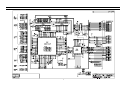
4 - IC description
4-1 VCT383XA TV signal processor - Teletext decoder with embedded 8 bit - Controller.
2
VIN
CIN
2
3
4
Video
Front-end
Comb
Filter
Color
Decoder
Panorama
Scaler
Video
VOUT
DMA
RDY
3
Display
Processor
Pict.Improv
BE
TPU
2
I2C
MSync
Color, Prio
VSync
8
SENSE
RSW
GNDM
VRD
XREF
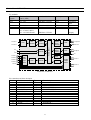
VERT
EW
PROT
HOUT
HFLB
VCT 38xx
GNDD
VSUPD
GNDAF
VSUPAF
SGND
VRT
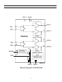
4-1-1- Block diagram of the VCT
Video
Back-end
Audio
CPU
4
RGBIN
VSUPAB
GNDAB
2
AOUT
3
AIN
2
I2C Mmaster
RGBOUT
SVM
I 2C
8-bit PWM
24 kB ROM
14-bit PWM
3 kB
15:1 Mux
10-bit ADC
1 kB
CPU RAM
OSD RAM
2 Timer
Reset
Logic
RESQ
Clock
Oscillator
XTAL1
TEST
2 CapCom
Watchdog
96 kB
CPU ROM
24 IO Ports
31
ADB, DB, CB
CLK20
4-1-2- TV-signal Processor
Four composite video inputs, two S-VHS inputs
Analogue YC r C b input
Composite video monitor
Multistandard colour decoder ( 1 crystal )
Multistandard sync decoder
Black-line detector
Adaptive 2H comb filter Y/C separator
-15-
GNDP1
GNDS
VSUPS
12
VSUPP1
Text RAM
Pxy
16 kB
XTAL2
Service Manual CP-099F
-16-
Service Manual CP-099F
High-level command language
FLOF (Fastext), and TOP support
10 pages memory on chip (10kB)
4-1-5- Display OSD Features
3kB OSD RAM on chip
WST level 1.5 compliant
WST level 2 parallel attributes
32 foreground/background colours
programmable colour look-up table
1024 mask programmable characters
17 national languages
(Latin, Cyrillic and Greek character sets)
Character matrix 10x10
4-color mode for user font
4-1-6- Audio Features
Three mono inputs
Two mono outputs
Programmable channel select
Volume control for one mono channel
4-1-7- General Features
Submicron CMOS technology
Low-power standby mode
Single 20.25 MHz crystal
64-pin PSDIP package
4-1-8- Data Capture
The Video Front End section takes in the analogue Composite Video and Blanking Signal (CVBS), and from this
extracts the required data, which is then decoded and stored in memory.
The extraction of the data is performed in the digital domain. The first stage is to select and convert the analogue
CVBS signal into a digital form. This is done using 8 bit ADC sampling at 20.25 Mhz.
The digital data services transmitted in the VBI are selected and acquired separately form the video part. This is done
by the use of an adaptive data slicer. The following data types can be extracted : 625 line World System Teletext
(WST), VPS, WSS. The data is acquired and decoded by the teletext decoder (TPU), then stored in an SRAM lnterface.
4-1-9- Data Capture Features
Video Signal Quality detector
Data Capture for 625 line WST
Data Capture for VPS data (PDC system A)
Data Capture for Wide Screen Signalling (WSS) bit decoding
Real-time capture and decoding for WST Teletext in Hardware, to enable optimised microprocessor throughout
10 page memory stored On-Chip
-17-
Service Manual CP-099F
• Inventory of transmitted Teletext pages stored in the Page Table
Signal quality detector for WST data
Comprehensive Teletext language coverage
Full Field Vertical Blanking Interval (VBI) data capture of WST data
4-1-10- TV processor version and -Controller capacity
IC version
8 bit -controller
ROM size
RAM size
PAL decoder
SECAM decoder
NTSC decoder
Picture improvement
Teletext page memory
Adaptive Comb filter
Panorama Scaler
VCT 3834A
96k
1k
10 pages
4-1-11- IC marking and version
Chassis
IC marking
CP-099F
OSD languages
GB, France, Germany,
Italy, Belgium, Spain,
Austria, Poland,
Switzerland, Denmark,
Finland, Netherlands,
Norway, Sweden,
Ireland, Hungary,
Czech Republic, Others
English, French,
German, Italian,
Spanish, Dutch,
Danish, Finnish,
Norwegian, Swedish,
Greek, Polish,
Hungarian
Romanian, Russian.
VCT3834
Text
ATSS countries
Pan-European Latin.
Cyrillic, Greek.
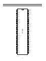
4-1-12- Pinning
PSDIP
64-pin
1
2
3
4
5
6
7
8
9
10
11
12
13
Pin Name
Type
KEY1
KET2
ST-BY 5V
GND
PWR-L
SB LED
OCP
IR INPUT
MUTE-L
SLOW SW
V OUT
VRT
S GND
IN
IN
SUPPLY
SUPPLY
OUT
OUT
IN
IN
OUT
IN
NOT USED
IN
SUPPLY
Short Description
GROUND PORT
LOW-SMPS ON, HIGH-SMPS IN STAND BY MODE
HIGH-RED, LOW-GREEN
OVER CURRENT PROTECTION INPUT
LOW-MUTE HIGH, HIGH-MUTE LOW
SCART SLOW SWITCH INPUT
REFERENCE VOLTAGE TOP
SINAL GROUND FOR ANALOG INPUT
-18-
Service Manual CP-099F
PSDIP
64-pin
14
15
16
17
18
19
20
21
22
23
24
25
26
27
28
29
30
31
32
33
34
35
36
37
38
39
40
41
42
43
44
45
46
47
48
49
50
51
52
53
54
55
56
57
58
59
60
61
62
63
64
Pin Name
Type
GND
B+ 5V
Cb IN
C1 IN
C2/Cr IN
IF V IN
SCART V IN
RCA V IN
DVD Y IN
TEST
H OUT
B+ 3.3V
GND
FBL IN
R IN
G IN
B IN
VPROT
SAFETY
HFLB
VERTQ
VERT
EW
SENSE
GND
RSW1
RSW2
SVM OUT
R OUT
G OUT
B OUT
B+ 5V
GND
VRD
XREF
A IN3
A IN2
A IN1
A OUT2
A OUT1
ST-BY 3.3V
GND
OSC
OSC
RESET
SCL
SDA
DVD CLK
DATA OUT
DATA IN
DVD CS
SUPPLY
SUPPLY
IN
NOT USED
IN
IN
IN
IN
IN
NOT USED
OUT
SUPPLY
SUPPLY
IN
IN
IN
IN
IN
SUPPLY
IN
OUT
OUT
OUT
IN
SUPPLY
OUT
OUT
OUT
OUT
OUT
OUT
SUPPLY
SUPPLY
IN
IN
IN
IN
IN
OUT
OUT
SUPPLY
SUPPLY
OUT
IN
IN
OUT
IN/OUT
IN
OUT
IN
IN
Short Description
ANALOG COMPONENT Cb INPUT
ANALOG CHROMA 1 INPUT
ANALOG CHROMA 2 INPUT/ANALOG COMPONENT Cr INPUT
IF VIDEO SIGNAL INPUT
SCART VIDEO SIGNAL INPUT
RCA VIDEO SIGNAL INPUT
DVD LUMINANCE(Y) COMPONENT INPUT
HORIZONTAL DRIVE OUTPUT
FAST BLANK INPUT
ANALOG RED INPUT
ANALOG GREEN INPUT
ANALOG BLUE INPUT
VETICAL PROTECTION INPUT
SAFETY INPUT
HORIZONTAL FLYBACK INPUT
DIFFERENTIAL VERTICAL SAWTOOTH OUTPUT
DIFFERENTIAL VERTICAL SAWTOOTH OUTPUT
VERTICAL PARABOLA OUTPUT
SENSE ADC INPUT
RANGE SWITCH1 FOR MESUREMENT ADC
RANGE SWITCH2 FOR MESUREMENT ADC
SCAN VELOCITY MODULATION OUTPUT
ANALOG RED OUTPUT
ANALOG GREEN OUTPUT
ANALOG BLUE OUTPUT
DAC REFERENCE
REFERENCE INPUT FOR RGB DACs
ANALOG AUDIO 3 INPUT
ANALOG AUDIO 2 INPUT
ANALOG AUDIO 1 INPUT
ANALOG AUDIO 2 OUTPUT
ANALOG AUDIO 1 OUTPUT
RESET INPUT
IIC BUS CLOCK
IIC BUS DATA
DVD CLOCK
DVD DATA OUT
DVD DATA IN
DVD CS
-19-
Service Manual CP-099F
KEY1
64
DVD CS
2
KEY2
63
DATA IN
3
ST-BY 5V
62
DATA OUT
4
GND
61
DVD CLK
5
PWR-L
60
SDA
6
SB LED
59
SCL
7
OCP
58
RESET
8
IR INPUT
57 OSC
9
MUTE-L
56 OSC
10
SLOW SW
55
GND
11
V OUT
54
ST-BY 3.3V
12
VRT
53 A OUT1
13
S GND
52 A OUT2
14
GND
51 A IN1
15
B+ 5V
16
Cb IN
17
C1 IN
18
C2/Cr IN
19
IF V IN
46 GND
20
SCART V IN
45 B+ 5V
21
RCA V IN
44 B OUT
22
DVD Y IN
43 G OUT
23
TEST
42 R OUT
24
H OUT
41 SVM OUT
25
B+ 3.3V
40 RSW2
26
GND
39 RSW1
27
FBL IN
38 GND
28
R IN
37 SENSE
29
G IN
36 EW
30
B IN
35 VERT
31
VPROT
34 VERTQ
32
SAFETY
33 HFLB
VCT 383X
1
-20-
50 AIN2
49 A IN3
48 XREF
47 VRD
Service Manual CP-099F
4-2 MSP341x Multistandard Sound Processor
The MSP 341x is designed as a single-chip Multistandard Sound Processor for applications in analogue and digital TV
sets, video recorders, and PC cards.
MSP 341x features :
- sound IF input
- No external filters required
- Stereo baseband input via integrated AD converters
- Two pairs of DA converters
- Two carrier FM or NICAM processing
- AVC : Automatic Volume Correction
- Bass, treble, volume processing
- Full SCART in/out matrix without restrictions
- Improved FM-identification
- Demodulator short programming
- Autodetection for terrestrial TV - sound standards
- Precise bit-error rate indication
- Automatic switching from NICAM to FM/AM or vice versa
- Improved NICAM synchronisation algorithm
- Improved carrier mute algorithm
- Improved AM-demodulation
- Reduction of necessary controlling
- Less external components
4-2-1- Basic Features of the MSP 341x
4-2-1-1 Demodulator and NICAM Decoder Section
The MSP 341x is designed to simultaneously perform digital demodulation and decoding of NICAM-coded TV stereo
sound, as well as demodulation of FM or AM mono TV sound. Alternatively, two carrier FM systems according to the
German terrestrial specs can be processed with the MSP 341x.
The MSP 341x facilitates profitable multistandard capability, offering the following advantages:
- Automatic Gain Control (AGC) for analogue input: input range: 0.10 - 3 Vpp
- integrated A/D converter for sound-IF input
- all demodulation and filtering is performed on chip and is individually programmable
- easy realisation of all digital NICAM standards (B/G, I, L and D/K)
- FM-demodulation of all terrestrial standards (include identification decoding)
- no external filter hardware is required
- only one crystal clock (18.432 MHz) is necessary
-21-
Service Manual CP-099F
- high deviation FM-mono mode (max. deviation: approx. ±360 kHz)
4-2-1-2 DSP-Section (Audio Baseband Processing)
- flexible selection of audio sources to be processed
- performance of terrestrial de-emphasise systems (FM, NICAM)
- digitally performed FM-identification decoding and de-emphasis
- digital baseband processing: volume, bass, treble
- simple controlling of volume, bass, treble
4-2-1-3 Analogue Section
- two selectable analogue pairs of audio baseband input (= two SCART inputs) input level: <2 V rms,
input impedance: >25
- one selectable analogue mono input (i.e. AM sound): Not used in this chassis
- two high-quality A/D converters, S/N-Ratio: >85 dB
- 20 Hz to 20 kHz bandwidth for SCART-to-SCART copy facilities
- loudspeaker: one pair of four-fold oversampled D/A converters. Output level per channel:
max. 1.4 Vrms output resistance: max. 5 . S/N-ratio: >85 dB at maximum volume Max.
noise voltage in mute mode: < 10 V (BW: 20 Hz... 16kHz)
- one pair of four-fold oversampled D/A converters supplying a pair of SCART-outputs.
output level per channel: max. 2 Vrms, output resistance: max. 0.5 , S/N-Ratio: >85 dB (20 Hz... 16 kHz)
4-2-1-4 NICAM plus FM/AM-Mono
According to the British, Scandinavian, Spanish, and French TV-standards, high-quality stereo sound is transmitted
digitally. The systems allow two high-quality digital sound channels to be added to the already existing
FM/AM-channel. The sound coding follows the format of the so-called Near Instantaneous Companding System
(NICAM 728). Transmission is performed using Differential Quadrature Phase Shift Keying (DQPSK. Table below
offers an overview of the modulation parameters.)
In the case of NICAM/FM (AM) mode, there are three different audio channels available: NICAM A, NICAM B, and
FM/AM-mono. NICAM A and B may belong either to a stereo or to a dual language transmission. Information about
operation mode and about the quality of the NICAM signal can be read by the controlling software via the control bus.
In the case of low quality (high bit error rate), the controlling software may decide to switch to the analogue FM/AMmono sound. Alternatively, an automatic NICAM-FM/AM switching may be applied.
4-2-1-5 German 2-Carrier System (DUAL FM System)
Since September 1981, stereo and dual sound programs have been transmitted in Germany using the 2-carrier system.
Sound transmission consists of the already existing first sound carrier and a second sound carrier additionally
containing an identification signal. More details of this standard are given in Tables below. For D/K very similar
system is used.
-22-
Service Manual CP-099F
TV standards
Position of sound
carrier (MHz)
5.5 / 5.7421875
5.5 / 5.85
L
I
D/K
6.5 / 5.85
6.0 / 6.552
6.5 / 6.2578125 D/K1
6.5 / 6.7421875 D/K2
6.5 / 5.85 D/K-NICAM
Sound IF 1
ADC
Sound IF 2
Sound modulation
Color system
Country
FM Stereo
FM-Mono / NICAM
PAL
PAL
AM-Mono / NICAM
FM-Mono / NICAM
FM Stereo
SECAM-L
PAL
SECAM-East
Germany
Scandinavia,
Spain
France
UK
USSR
FM-Mono / NICAM
Preprocessing
Demodulator
I2S1
Source Select
TV
system
B/G
B/G
Prescale
I2S2
SCART 1
SCART 2
SCART 3
SCART 4
DSP
SCART
Input
Select
ADC
Prescale
Hungary
Loudspeaker
Sound
Processing
DAC
Headphone
Sound
Processing
DAC
Loudspeaker
Subwoofer
Headphone
I 2S
DAC
DAC
SCART
Output
Select
SCART 1
MONO
SCART 2
Architecture of MSP341x
Pin connections and short description
Pin No.
Pin Name
1
AUDIO CLOCK OUT
2
NC
3
NC
4
VIDEO SW
5
PLAY LED
6
ADDRESS SEL
7
STAND BY
8
NC
9
SCL
10
SDA
11
IIC CLOCK
12
IIC SW
13
IIC DATA OUT
Type
Short description
OUT
OUT
IN
IN
VIDEO SWITCH
PLAY LED SELECT
IIC BUS ADDRESS
STAND BY
IN / OUT
IIC CLOCK
IIC SWITCH
IIC DATA OUT
OUT
-23-
Service Manual CP-099F
PSDIP
64-pin
14
15
16
17
18
19
20
21
22
23
24
25
26
27
28
29
30
31
32
33
34
35
36
37
38
39
40
41
42
43
44
45
46
47
48
49
50
51
52
53
54
55
56
57
58
59
60
61
62
63
64
Pin Name
IIC DATA IN
ADDRESS DATA
ADDRESS SWITCH
ADDRESS CLOCK
Vcc(5v)
Vss
IIC DIGITAL IN2
NC
NC
NC
RESET
H-P R OUT
H-P L OUT
VREF2
R OUT
L OUT
NC
SUB W OUT
NC
SC2 R OUT
SC2 L OUT
VREF1
SC1 R OUT
SC1 L OUT
VOL CAP A
Avcc(8v)
VOL CAP M
AHVss
AREF
SC4 L IN
SC4 R IN
ASGND4
SC3 L IN
SC3 R IN
ASGND2
SC2 L IN
SC2 R IN
ASGND1
SC1 L IN
SC1 R IN
VREFTOP
MONO IN
Avss
Avcc(5v)
IF INPUT1
IF COMMON
IF INPUT2
TESTEN
XTAL IN
XTAL OUT
TP
Type
Short Description
IN
IIC DATA IN
IN
IN
OUT
OUT
OUT
OUT
AUDIO R OUT
AUDIO L OUT
OUT
OUT
OUT
AV1 AUDIO R OUT
AV1 AUDIO L OUT
OUT
OUT
SCART AUDIO R OUT
SCART AUDIO L OUT
IN
IN
IN
IN
AV2 AUDIO L IN
AV2 AUDIO R IN
IN
IN
DVD AUDIO L IN
DVD AUDIO R IN
IN
IN
SCART AUDIO L IN
SCART AUDIO R IN
IN
IN
IF AUDIO IN
IN
IN
OUT
-24-
Service Manual CP-099F
4-3 TDA9886 IIC-bus controlled single/multi standard Alignment-free IF-PLL
4-3-1- DISCRIPTION
The TDA9885 is an alignment-free single standard(without positive modulation) vision and Sound IF signal PLL.
The TDA9886 is an alignment-free multistandard (PAL,SECAM and NTSC) vision and sound IF signal PLL
demodulator for positive and negative modulation including sound AM and FM processing.
4-3-2- FEATURES
- 5V Supply voltage.
- Gain controlled wide-band Vision Intermediate Frequency (VIF) amplifier (AC-coupled).
- Multistandard true synchronous demodulation with active carrier regeneration (very linear demodulation,good
intermodulation figures, reduced harmonics, excellent pulse response).
- Gated phase detector for L/L accent standard.
- Fully integrated VIF Voltage controlled Oscillator(VCO), alignment-free, frequencies switchable forall negative
and positive modulated standards via I2C-bus.
- Digital acquisition help, VIF frequencies of 33.4, 33.9, 38.0, 38.9, 45.75 and 58.75 MHz.
- 4 MHz reference frequency input [signal from Phase-Locked Loop (PLL) tuning system] or operating as crystal
oscillator.
- VIF Automatic Gain Control (AGC) detector for gain control, operating as peak sync detector for negative
modulated signals and as a peak white detector for positive modulated signals.
- Precise fully digital Automatic Frequency control (AFC) detector with 4-bit digital-to-analog converter ; AFC
bits via I2C-bus readable.
- TakeOver Point (TOP) adjustable via I2C-bus or alternatively with potentiometer.
- Fully integrated sound carrier trap for 4.5, 5.5, 6.0 and 6.5 MHz, controlled by FM-PLL oscillator.
- Sound IF (SIF) input for single reference Quasi Split Sound(QSS) mode (PLL controlled).
- SIF AGC for gain controlled SIF amplifier ; single reference QSS mixer able to operate in high Performance
single reference QSS mode and in intercarrier mode, switchable via I2C-bus.
- AM demodulator without extra reference circuit.
- alignment-free selective FM-PLL demodulator with high linearity and low noise.
- I2C-bus control for all functions.
- I2C-bus transceiver with pin programmable Module Address (MAD).
4-3-3 PINNING
SYMBOL PIN
VIF1
1
VIF2
2
OP1
3
FMPLL
4
DEEM
5
AFD
6
DGND
7
AUD
8
TOP
9
SDA
10
SCL
11
SLOMAD 12
DESCRIPTION
VIF differential input 1
VIF differential input 2
DVD Reset (open-collector)
FM-PLL for loop filter
de-emphasis output for capacitor
AF decoupling input for capacitor
digital ground
Audio output
Tuner AGC TakeOver point(TOP)
I2C-bus data input/output
I2C-bus clock input
sound intercarrier output and
MAD select
SYMBOL PIN
n.c
13
TAGC
14
REF
15
VAGC
16
CVBS
17
AGND
18
VPLL
19
Vp
20
AFC
21
OP2
22
SIF1
23
SIF2
24
-25-
DESCRIPTION
not connected
tuner AGC output
4MHz crystal or reference input
VIF-AGC for capacitor : note 1
Video output
analog ground
VIF-PLL for loop filter
supply voltage (+5V)
AFC output
output 2(open-collector)
SIF differential input 1
SIF differential input 2
-26-
SIF 1 23
SIF 2 24
20
Vp
SUPPLY
VIF-AGC
18
13
AGND n.c
TUNER AGC
VPLL
RC VCO
CAGC
SIF-AGC
3
OP1
OUTPUT
PROTS
22
OP2
11
SCL
or
TDA9886
DIGITAL VCO CONTROL
10
SDA
AFC
8
AUD
17 CVBS
FM-PLL filter
FMPLL
NARROW-BAND FM-PLL
DETECTOR
6
video output 2 V (p-p)
[1-1 V(p-p) without trap]
AFD
C AF
de-emphasis
network
AUDIO PROCESSING
5 DEEM
AND SWITCHI\ES
VIDEO TRAPS
4.5 to 6.5MHz
AFC DETECTOR
REF
4MHz
crystal
sound intercarrier output
and MAD slelct
7
12
DGND SIOMAD
I2C-BUS TRANSCEIVER
MAD
SINGLE REFERENCE QSS MIXER/
INTERCARRIER MIXER AND
AM-DEMODULATOR
VIF-PLL
19
VIF 1 1
VIF 2 2
9
CBL
TAGC
14
CAGC neg
VAGC
16
TOP
(1)
C VAGC pos
VIF-PLL
filter
external
reference
Service Manual CP-099F
Service Manual CP-099F
4-4 TDA894xJ Stereo Audio Amplifier
The TDA8944J is a dual-channel audio power amplifier with an output power of 2 x 5W
at an 8 load and a 12V supply. The circuit contains two Bridges Tied Load(BTL) amplifiers with an all-NPN output
stage and standby/mute logic. The TDA8944J comes in a 17-pin DIL power package.
4-4-1- Features
- Few external components
- Fixed gain
- Standby and mute mode
- No on/off switching pop noise
- low standby current
- High supply voltage ripple rejection
- Outputs short-circuit protected to ground, supply and across the load
- Thermally protected
Pin description
Pin
1
Symbol
OUT1-
2
3
4
GND1
Vcc1
OUT1+
5
6
7
8
9
10
11
n.c.
IN1+
n.c.
IN1IN2MODE
SVR
12
IN2+
Description
negative loudspeaker
terminal 1
ground channel 1
supply voltage channel 1
positive loudspeaker
terminal 1
not connected
positive input 1
not connected
negative input1
negative input2
mode selection input
half supply voltage
decoupling (ripple rejection)
positive input2
-27-
Service Manual CP-099F
VCC1 VCC2
3
16
1
IN1 IN1+
8
OUT1 -
6
4
OUT1 +
TDA8944J
17
IN2-
9
IN2+
12
14
VCC
MODE
SVR
10
11
STANDBY/
MUTE LOGIC
20
k
SHORT CIRCUIT
AND
TEMPERATURE
PROTECTION
20
k
2
GND1 GND2
MBK933
Block diagram TDA8944J
-28-
OUT2 -
OUT2 +
Service Manual CP-099F
4-5 TDA835xJ Vertical Amplifier
The TDA835xJ are power circuit for use in 90o and 110o colour deflection systems for field frequencies
of 25 to 200Hz and 16/9 picture tubes. The circuit provides a DC driven vertical deflection output circuit,
operating as a highly efficient class G system. Due to the full bridge output circuit the deflection coils can
be DC coupled.
The IC is constructed in a Low Voltage DMOS process that combines Bipolar, CMOS and DMOS devices.
MOS transistors are used in the output stage because of the absence of second breakdown.
4-5-1 TDA8358J
V i(pos)
1
V i(neg)
2
An East-West output stage is provided that is able to sink current
from the diode modulator circuit.
Features :
- Few external components
- Highly efficient fully DC-coupled vertical output bridge circuit
- Short rise and fall time of the vertical flyback switch
- Guard circuit
- Temperature (thermal) protection
- High EMC because of common mode inputs
- East-West output stage
I comp
V o(guard)
11
13
comp
Vp
Vp
3
VoB
4
V iEW
5
GND V
6
GND EW
7
VoEW
8
Vflb
9
VoA
10
Vo(guard
11
VM
12
I comp
13
V fib
9
3
guard
M5
D2
M2
D3
D1
10 V oA
V i(pos)
+V i(diff)
V i(sb)
-V i(diff)
1
M4
input/
feedback
12
VM
V i(neg) 2
+V i(diff)
V i(sb)
-V i(diff)
M1
4 V oB
M3
IiEW(top)
IiEW(bot)
M6
6
GNDv
-29-
78
7
GNDEW
V
oEW
TDA8358J
Service Manual CP-099F
4-6 TEA5101B
The TEA5101B includes three video amplifiers designed with a high voltage DMOS/bipolar technology. It drives
directly the three CRT cathodes. The device is protected against flashovers. Due to it's three cathode current output,
the TEA5101B can be used with voth parallel and sequential sampling applications.
Features
- BANDWIDTH : 10MHz TYPICAL
- RISE AND FALL TIME : 50ns TYPICAL
- CRT CATHODES CURRENT OUTPUTS FOR PARALLEL OR SEQUENTIAL CUT-OFF OR DIRVE ADJUSTTMENT
- FLASHOVER PROTECTION
- POWER DISSIPATION : 3.5W
- ESD PROTECTED
PIN CONNECTIONS
15
14
13
12
11
10
9
8
7
6
5
4
3
2
1
BLUE FEEDBACK
BLUE CATHODE CURRENT
BLUE OUTPUT
GREEN FEEDBACK
GREEN CATHODE CURRENT
GREEN OUTPUT
RED FEEDBACK
GROUND
RED OUTPUT
RED CATHODE CURRENT
Vpp HIGH VOLTAGE
RED INPUT
GREEN INPUT
Vcc LOW VOLTAGE
BLUE INPUT
Tab connected to Pin 8
PIN FUNCTION
No
1
Function
Blue Input
2
3
4
5
6
Vcc
Green Input
Red Input
Vpp
Red Cathode Current
7
Red Output
8
9
10
11
12
13
14
15
Ground
Red Feedback
Green Output
Green Cathode Current
Green Feedback
Blue Output
Blue Cathode Current
Blue Feedback
Description
Input of the "blue" amplifier. It is a virtual ground with 3.8V bias voltage
15 microamperes input bias current with 14k input resistance.
Low voltage power supply. typically 12V.
See Pin 1.
See Pin 1.
High voltage Power supply, typically 200V.
Provides the video processor with a copy of the DC current flowing into the red
cathode, for automatic cut-off or gain adjustment, If this control is not used,
Pin 6 must be grounded.
Output driving the red cathode. Pin 7 is internally protected against CRT arc
discharges by a diode limiting the output voltage to Vpp.
Also connected to the heatsink.
Output driving the feedback resistor network for the red amplifier.
See Pin 7.
See Pin 6.
See Pin 9.
See Pin 7.
See Pin 6.
See Pin 9.
-30-
Service Manual CP-099F
BLOCK DIAGRAM OF EACH CHANNEL
15 (12,9)
Vpp
5
40k
13
(10,7)
20k
0.8k
14
(11,6)
1k
2
1
(3,4)
35
35
350
REFERENCE
VOLTAGE
GND
8
-31-
Service Manual CP-099F
4-7 24C16 - 16 Kb EEPROM
*CAUTION
When you change this EEPROM IC, give attention blow.
You must wait displaying "MENU" on the screen after changed it.
And then you operate searching operation please.
features :
- 16 Kbit serial I2C bus EEPROM
- Single supply voltage : 4.5 V to 5.5 V
- 1 Million Erase/Write cycles (minimum)
- 40 year data retention (minimum)
Pin description
Pin No.
1, 2, 3
5
6
7
8
4
Name
E0, E1, E2
SDA
SCL
GND
Vcc
Vss
Description
Device address - not used
Serial Data/Address Input/Output
Serial clock
GROUND
GROUND
GROUND
The memory device is compatible with the I2C memory standard. This is a two wire serial interface that uses a
bi-directionnal data bus and serial clock. The memory carries a built-in 4-bit unique device type identifier code (1010)
in accordance with the I2C bus definition.
Serial Clock (SCL)
The SCL input is used to strobe all data in and out of the memory.
Serial Data (SDA)
The SDA pin is bi-directionnal, and is used to transfer data in or out of the memory
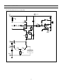
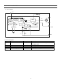
4-8 STR - F6654
4-8-1 General description
The STR-F6654 is an hybrid IC with a build-in MOSFET and control IC, designed for flyback converter type switch
mode power supply applications.
4-8-2 Features
- Small SIP fully isolated molded 5 pins package
- Man y protection functions :
* Pulse-by-pulse overcurrent protection (OCP)
* Over voltage protection with latch mode (OVP)
* Thermal protection with latch mode (TSD)
-32-
Service Manual CP-099F
4-8-3 Block diagram
4
VIN
R3
3 D
START
O.V.P
R4
LATCH
DRIVE
REG.
T.S.D
+ Vth(1)
Comp. 1
O.S.C
2 S
1
O.C.P/F/B
Vth(2)
Comp. 2
Rconst+
RconstC1
R2
R1
5 GND
4-8-4 Pins description
pin
1
name
Overcurrent / feedback
symbol
O.C.P./ F.B.
2
3
4
5
Source
Drain
Supply
Ground
S
D
VIN
GND
-33-
description
Input of over current detection signal and
feedback signal
MOSFET source
MOSFET drain
Input of power supply for control circuit
Ground
Service Manual CP-099F
4-8-5 Control part electrical characteristics
DESCRIPTION
Operation start voltage
Operation stop voltage
Circuit current in
operation
Circuit current in nonoperation
Maximum OFF time
Minimum time for input of
quaxi resonant signals
Minimum off time
O.C.P./F.B. terminal
threshold voltage 1
O.C.P./F.B. terminal
threshold voltage 2
O.C.P./F.B. terminal extraction
current
O.V.P. operation voltage
Latch Current sustaining voltage
Latch Current release voltage
Thermal shutdown operating
temperature
IC PIN
NUMBER
4-5
4-5
4-5
VIN (on)
VIN (off)
IIN (on)
MIN.
14.4
9
-
RATING
TYPE
16
10
-
MAX
17.6
11
30
4-5
IIN (off)
-
-
100
A
1-5
TOFF (max)
TTH (2)
45
-
-
55
1.0
sec
sec
1-5
TOFF (min)
VTH (1)
0.68
0.73
1.5
0.78
sec
V
1-5
VTH (2)
1.3
1.45
1.6
V
1-2
IOCP/FB
1.2
1.35
1.5
mA
4-5
4-5
4-5
-
VIN (OVP)
IIN (H)
VIN (La.off)
TJ (TSD)
20.5
6.6
140
22.5
-
24.5
400
8.4
-
V
A
V
0
C
MIN.
650
RATING
TYPE
-
MAX
-
-
-
300
1.15
250
0.95
SYMBOL
UNIT
V
V
mA
4-8-6 MOSFET electrical characteristics
DESCRIPTION
Drain-to-source breakdown
voltage
Drain leakage current
On-resistance
Switching time
Thermal resistance
IC PINS
NUMBER
3-2
3-2
3-2
3-2
-
SYMBOL
VDSS
IDSS
RDS (on)
tf
OCH -F
-34-
UNIT
V
A
nsec
C/W
0
Service Manual CP-099F
5- Circuit desription
5-1 Block diagram
35
Service Manual CP-099F
5-2 IF section
5-2-1 Picture IF Amplifier
The Picture IF signal (PIF) is fed through a SAW filter to the differential input (Pin 1-2) of the PIF amplifier.
This amplifier consists of three AC-coupled amplifier stages. Each differential amplifier is gain controlled by the
automatic gain control circuit (PIF-AGC). The output signal of the PIF amplifier is applied to the FPLL carrier
generation and the video demodulator.
5-2-2 Tuner and VIF-AGC
This block adapts the voltage, generated at the VIF/SIF-AGC detector, to the internal signal processing at VIF/SIF amplifier
and performs the tuner AGC control current generation. The onset of tuner AGC control current generation can be set either by
I2C-bus (see Table 23) or optional (in case that I2C-bus information cannot be stored) by a potentiometer at pin 9. The presence
of a potentiometer will automatically be detected and disables the I2C-bus setting.
Furthermore, derived from the AGC detector voltage, a comparator is used to test the corresponding VIF input level to be smaller than 200 . This information can be read out ('VIF HIGH LEVEL') via I2C-bus.
5-2-3 VIF-AGC detector
Gain control performed by sync-level detecion (negative modulation) or peak White detection (positive modulation).
For negative modulation the sync level voltage is stored at an interrated capacitor by means of a fast peak detector.
This voltage is compared with a reference voltage (nominal sync level) by a comparator which charges/discharges the (integraated) AGC capacitor for generation of the required VIF gain. The time constants for decreasing/increasing gain are nearly equal
and the total AGC reaction time is fast to cope with 'aeroplane fluttering'.
For positive modulation the white peak level voltage is compared with a reference voltage (nominal white level)by a comparator which charges (fast) or discharges (slow) the (external) AGC capacitor directly for generation of the required VIF gain.
This very large time constant for VIF gain increase in needed caused by the fact the peak whith level may appear only once in
a field. In order to reduce this time constant, an additional level detector increases the discharging current of the AGC capacitor
(fast mode) in the event of a decreasing VIF amplitude step controlled by the detected actual black level voltage. The threshold
level for fast mode AGC is typical-6 dB video amplitude.
The fast mode state also is transferred to the SIF AGC detector for speed-up. In case of missing peak white. pulses the VIF gain
increase is limited to typical +3 dB by comparing the detected actual black level voltage with a corresponding reference voltage.
5-2-4 Frequency Phase-Locked Loop(FPLL) detector
The VIF amplifier output signal is fed into a frequency detector and into a phase detector via a limiting amplifier for removing
the video AM. During acquisition the frequency detector produces a current proportional to the frequency difference between
the VIF and the VCO signal.
After frequency lock-in the phase detector produces a current proportional to the phase difference between the VIF and the VCO
signal. The currents from the frequency and phase detector are charged into the loop filter which control the VIF VCO and
locks it to the frequency and phase of the VIF carrier. For positive modulated VIF signal the charging currents are gated by composite sync in order to avoid signal distortion in case of overmodulation.
The gating depth is switchable via I2C-bus.
5-2-5 VCO and divider
The VCO of the VIF-FPLL operates as integrated low radiation oscillator at double the picture carrier frequency. The control
voltage required to tune the VCO to actually double the picture carrier frequency is generated at the loop filter by the frequency
Phase detector. The typical possible frequency range is about 50 to 140MHz.
The oscillator frequency is divided-by-two for providing two differential square wave signals with exactly 90 degrees phase difference, independent of the frequency, for use in the FPLL detectors, the video demodulator in the intercarrier mixer.
-36-
Service Manual CP-099F
5-2-6 Digital acquisition help and AFC
Each relaxation oscillator of the VIF-PLL and FM-PLL demodulator has a wide frequency range. To prevent false locking of the
PLL's and with respect to the catching range, the digital acquisition help provides an individual control until the VCO's frequency
is within the preselected standard and the PLL dependent lock-in window.
The in/out window control at FM-PLL is additionally be used to mete the audio stage (if auto mute is selected via I2C-bus control).
The principle working of the digital acquisition help is as follows : The PLL VCO output is connected to a down counter, which
start value is standard dependent predefined. The VCO frequency clocks the down counter for a fixed gate time. Thereafter the down
counter stop value is analysed. In case the stop value is higher (lower) than the expected value range, the VCO frequency is lower
(higher) than the wanted lock-in window frequency range. A positive (negative) control current is injected into the PLL loop filter
and consequently the VCO frequency will be increased (decreased) and a new counting cycle starts.
The gate time as well as the control logic of the acquisition help circuit is dependent on the precision of the reference signal at pin
15. Operation as crystal oscillator is possible as well as connecting this input via a serial capacitor to another reference frequency
source e.g. the tuning system oscillator.
The AFC signal is derived from the corresponding down counter stop value after a counting cycle. The last four bits are latched and
can be read out via I2C-bus (see Table 7). also the digital-to-analog converted value is given as current at pin 21.
5-2-7 Video demodulator and amplifier
The video demodulator is realized by a multiplier which is designed for low distortion and large bandwidth. The vision IF signal is
multiplied with the 'in phase' signal or the VIF-PLL VCO.
The demodulator output signal is fed into the video preamplifier via a level shift stage with integrated low-pass filter to achieve carrier
harmonic attenuation.
The preamplifiers output signal is fed to the VIF-AGC detector (see Section "VIF-AGC detector") and in case of sound trap mode
internally to the integrated sound carrier trap(see Section "Sound carrier trap".) The differential trap output signal is converted and
amplified by the following post-amplifier. The video output level at pin 17 is 2 V(p-p).
In case of bypass mode the preamplifiers output signal is fed direct through the post-amplifier to pin 17. The output video level is 1.1
V(p-p) for using an external sound trap with 10% loss over all. Noise clipping is provided in both cases.
5-2-8 Sound carrier trap
The sound carrier trap consists of a reference filter, a phase detector and the sound trap itself. A sound carrier reference signal is fed
into the reference low-pass filter and is shifted by nominal 90 degrees.
The phase detector compares the original reference signal with the signal shifted by the reference filter and proudces a DC voltage by
charging/discharging the capacitor with a current proportional to the phase difference between both signals, respectively to the frequency
error of the integrated filters. The DC voltage controls the frequency position of the reference filter and the sound trap. So the accurate
frequency position or the different standard is set by the sound carrier reference signal.
The sound trap itself is constructed of three separate traps to realize sufficient suppression of the first and second sound carrier.
5-2-9 SIF amplifier
The SIF amplifier consists of three AC-coupled differential stages. Gain control is performed by emitter degeneration, Total gain control
range is 66dB typical. The differential input impedance is typical 2k in parallel with 3 pF.
5-2-10 AGC detector
SIF gain control is performed by detection of the DC component of the AM demodulator output signal. This DC signal is directly corresponding to the SIF voltage at the output of the SIF amplifier so that a constant SIF signal is supplied to the AM demodulator and
the single reference QSS mixer.
By switching the gain of the input amplifier of the SIF AGC detector Via I2C-bus the internal SIF level for FM sound is 5.5 dB lower
than for AM sound. This is done to adapt the SIF-AGC characteristic. The adaption is optimal for picture-to-sound carrier ratio of 13 dB.
Via a comparator the integrated AGC capacitor is charged/discharged for generation of the required SIF gain. Due to AM sound the
AGC reaction time is slow (fc < 20 Hz for the closed AGC loop.) For reducing this AM sound time constant in the event of a decreasing
IF amplitude step, the charging/discharging current of the AGC capacitor is increased (fast mode), when the VIF-AGC detector (at
positive modulation mode) operates in fast mode, too. An additional circuit (threshold about +7 dB) ensures a very fast gain reduction
for a large increasing IF amplitude step.
-37-
Service Manual CP-099F
5-2-11 Single reference QSS mixer
With the present system a high performance Hi-Fi stereo sound processing can be achieved. For a simplified application without a
Sound IF SAW filter the single reference QSS mixer can be switched to the intercarrier mode by I2C-bus. This single reference QSS
mixer generates the 2nd FM TV sound intercarrier signal. It is realized by a linear multiplier Which multiplies the SIF amplifier
output signal and the VIF VCO signal (90 degrees output), which is locked to the picture carrier. By this way the QSS mixer operates
as quadrature mixer in case of intercarrier mode and provides suppression of the low frequency video signals.
The QSS mixer output signal is fed via a high/low-pass combination internally to the FM demodulator as well as via an operational
amplifier to the intercarrier output pin 12.
5-2-12 AM demodulator
The amplitude modulated SIF amplifier output signal is fed both to a two-stage limiting amplifier for removing the AM and to a linear
multiplier. The result of multiplication of the SIF signal with the limiter output signal is AM demodulation (passive synchronous
demodulator). The demodulator output signal is fed via a low-pass filter for attenuation of the carrier harmonics and via the input
amplifier of the SIF-AGC detector to the audio amplifier.
5-2-13 FM demodulator and acquisition help
Gain controlled FM amplifier and detector
The intercarrier signal from the intercarrier mixer is fed to the input of an AC coupled gain controlled amplifier with two stages.
The gain controlled output signal is fed to the phase detector of the narrow-band FM-PLL (FM demodulator). For good selectivity
and robustness against disturbance caused by the video signal, high linearity of the gain controlled FM amplifier and of the phase
detector as well as constant signal level are required. Gain control is done by means of an 'in phase' demodulator for the FM carrier
(from the output of the FM amplifier). The demodulation output is fed into a comparator for charging/discharging the integrated AGC
capacitor. This leads to a mean value AGC loop to control the gain of FM amplifier.
Narrow-band PLL
The FM demodulator is realized as a narrow-band PLL with external loop filter, which provides the necessary selectivity (bandwidth
about 100 kHz). To achieve good selectivity, a linear phase detector and constant input level are required. The gain controlled intercarrier
signal from the FM amplifer is fed to the phase Detector (PD). The PD controls via the loop filter the integated low radiation relaxation
oscillator. The designed frequency range is from 4 to 7 MHz.
The VCO within the FM-PLL is phase-locked with the incoming 2nd SIF. This 2nd SIF is frequency modulated (FM). On to this fact,
the VCO control voltage is superimposed by the AF voltage. Therefore the VCO tracks with the FM of the 2nd SIF. So the AF voltage
is present at the loop filter (about 5 mV RMS for 27 kHz FM deviation). This AF signal is fed via a buffer to the audio amplifier.
The correct locking of the PLL is supported by the digital acquisition help circuit (see Section "Digital acquisition help and AFC").
5-2-14 Audio amplifier and mute time constant
The audio amplifier and mute time constant
1. The AF preamplifier used for FM sound is an operational amplifier with internal feedback, high gain and high common mode
rejection. The AF voltage from the PLL demodulator (5 mV RMS for frequency deviation of 27 kHz) is amplified by 30 dB.
By use or a DC operating point control circuit (with external capacitor CAF), the AF preamplifier is decoupled from the PLL DC
voltage. The low-pass characteristic of the amplifier reduces the harmonics of the sound intercarrier signal at the AF output terminal.
For FM sound a switchable de-emphasis network (with external capacitor) is implemented between the peramplifier and the output
amplifier.
2. The AF output amplifier provides the required AF output level by a rail-to-rail output stage. A preceding stage makes use of an
input selector for switching between FM sound. AM sound and mute state. The gain can be switched betweem 10 dB (normal)
and 4 dB (reduced).
Switching to mute state is controlled automatically dependent on the digital acquisition help for the case the VCO of the FM-PLL
is not in the required frequency window. This is done by a time constant (fast for switching to mute state and slow (about 40 ms)
for switching to no-mute state)).
All switching functions are controlled via the I2C-bus :
AM sound, FM sound, forced mute
Auto mute enable, auto mute disable
De-emphasis off, de-emphasis on, 50 s , 75 s
Audio gain normal, audio gain reduced.
-38-
Service Manual CP-099F
5-2-15 I2C-bus transceivers and MAD (module address)
The TDA9886 is controlled via the 2-wire I2C-bus by a microprocessor. Two wires serial data(SDA) and serial clock (SCL) carry
information between the devices connected to the bus. The TDA9886 has an I2C-bus slave transceiver with auto-increment.
To avoid conflicts in a real application with other IC's providing similar or complementing functions, there are two
possible slave addresses available which can be selected by pin 12. A slave address is sent from the master to the slave receiver.
The slave address or the ICs given in Table 1. The circuit operates up to clock frequencies of 400 kHz.
Table 1
Slave address
A6
A5
A4
A3
A2
A1
A0
R/W
1
0
0
0
0
1
A0
1/0
The bit A0 is controlled via pin 12. When this pin is connected via a resistor (2.2 k ) to ground, second MAD (A0 = 0) is selected.
if not, first MAD (A0 = 1) is active.
The power-on preset is also dependent on the pin 12 application and can be chosen for NTSC (45.75 MHz) as default or NTSC
(58.75 MHz). By this way the device can be used as NTSC only device without I2C-bus.
5-2-16 Internal voltage stabilizer
The bandgap circuit internally generates a voltage of approximately 2.4 V, independent of supply voltage and temperature.
A voltage regulator circuit, connected to this voltage, produces a constant voltage of 3.55 V which is used as an internal reference
voltage.
5-3 Video - VCT description
5-3-1 Introduction
The VCT 38xxA includes complete video, display, and deflection processing.
All processing is done digitally, the video front-end and video back-end are interfacing to the analogue world.
Most functions can be controlled by software via I 2 C bus slave interface.
5-3-2 Video Front-end
This block provides the analogue interfaces to all video inputs and mainly carries out analogue-to-digital conversion for
the following digital video processing. Most of the functional blocks in the front-end are digitally controlled (clamping,
AGC, and clock-DCO). The control loops are closed by the Fast Processor (‘FP’) embedded in the video decoder
.
5-3-3 Input Selector
Up to seven analogue inputs can be connected. Four inputs are for input of composite video or S-VHS luma signal.
These inputs are clamped to the sync back porch and are amplified by a variable gain amplifier. Two chroma inputs can
be used for connection of S-VHS carrier-chrominance signal. These inputs are internally biased and have a fixed gain
amplifier.
5-3-4 Clamping
The composite video input signals are AC-coupled to the IC. The clamping voltage is stored on the coupling capacitors
and is generated by digitally controlled current sources. The clamping level is the back porch of the video signal.
S-VHS chrominance is also AC-coupled. The input pin is internally biased to the center of the ADC input range. Each
channel is sampled at 10.125 MHz with a resolution of 8 bit.
5-3-5 Automatic Gain Control
A digitally working automatic gain control adjusts the
magnitude of the selected baseband.
5-3-6 Digitally Controlled Clock Oscillator
The clock generation is also a part of the analogue front-end. The crystal oscillator is controlled digitally by the control
processor. The clock frequency can be adjusted within ±150 ppm. This adjustment is done in factory for every TV set.
5-3-7 Analogue Video Output
The input signal of the Luma ADC is available at the analogue video output pin (#11). The signal at this pin is buffered
by a source follower. The output voltage is 2 V. The magnitude is adjusted with an AGC in 8 steps together with the
main AGC.
-39-
Service Manual CP-099F
5-3-8 Adaptive Comb Filter (VCT3834A only)
The adaptive comb filter is used for high-quality luminance/chrominance separation for PAL or NTSC signals. The
comb filter improves the luminance resolution (bandwidth) and reduces interferences like cross-luminance and
cross-color artefacts. The adaptive algorithm can eliminate most of the mentioned errors without introducing new
artefacts or noise. The filter uses two line delays to process the information of three adjacent video lines. To have a
fixed phase relationship of the colour subcarrier in the three channels, the system clock (20.25 MHz) is fractionally
locked to the colour subcarrier. This allows the processing of all colour standards and substandards using a single
crystal frequency. The CVBS signal in the three channels is filtered at the subcarrier frequency by a set of bandpass/
notch filters. The output of the three channels is used by the adaptation logic to select the weighting that is used to
reconstruct the luminance/chrominance signal from the 4 bandpass/notch filter signals. By using soft mixing of the 4
signals switching artefacts of the adaption algorithm are completely suppressed. The comb filter uses the middle line as
reference, therefore, the comb filter delay is one line. If the comb filter is switched off, the delay lines are used to pass
the luma/ chroma signals from the A/D converters to the luma/ chroma outputs. Thus, the comb filter delay is always
one line.
5-3-9 Color Decoder
In this block, the standard luma/chroma separation and multi-standard colour demodulation is carried out. The colour
demodulation uses an asynchronous clock, thus allowing a unified architecture for all colour standards.
The colour killer uses the burst-phase/ burst-frequency measurement to identify a PAL/NTSC or SECAM colour signal.
For PAL/NTSC, the colour is switched off (killed) as long as the colour subcarrier PLL is not locked. For SECAM, the
killer is controlled by the toggle of the burst frequency. The burst amplitude measurement is used to switch-off the
colour if the burst amplitude is below a programmable threshold. Thus, colour will be killed for very noisy signals.
The colour amplitude killer has a programmable hysteresis.
The burst-frequency measurement is also used for automatic standard recognition (together with the status of horizontal
and vertical locking) thus allowing a completely independent search of the line and colour standard of the input signal.
The following standards can be distinguished:
PAL B,G,H,I; NTSC M; SECAM; NTSC 44; PAL M; PAL N; PAL 60. In AV mode or when Prg No 0 is selected all the
standards above are enabled by the controlling software. In INSTALL menu the controlling software enables PAL B,G,
H,I and SECAM detection. The colour standard for each program number is stored in EEPROM. Outside INSTALL
menu and for programmes numbers 1 to 99, the auto colour detection is disabled, the colour standard is recall from
EEPROM and forced.
5-3-10 Horizontal Scaler (VCT3834A only)
The 4:2:2 Y,C r ,C b signal from the colour decoder is processed by the horizontal scaler. The scaler block allows a
linear or nonlinear horizontal scaling of the input video signal in the range of 0.25 to 4. Nonlinear scaling, also called
“Panoramavision”, provides a geometrical distortion of the input picture. It is used to fit a picture with 4:3 format on a
16:9 screen by stretching the picture geometry at the borders. Also, the inverse effect can be produced by the scaler.
The scaler contains a programmable decimation filter, a 1-line FIFO memory, and a programmable interpolation filter.
5-3-11 Video Sync Processing
To extract the sync information from the video signal, a linear phase low-pass filter eliminates all noise and video
contents above 1 MHz. The sync is separated by a slicer; the sync phase is measured. A variable window can be
selected to improve the noise immunity of the slicer. The phase comparator measures the falling edge of sync, as well
as the integrated sync pulse. The sync phase error is filtered by a phase-locked loop that is computed by the Fast
Processor. All timing in the front-end is derived from a counter that is part of this PLL, and it thus counts synchronously to the video signal. A separate hardware block measures the signal back porch and also allows gathering the
maximum/minimum of the video signal. This information is processed by the FP and used for gain control and
clamping. For vertical sync separation, the sliced video signal is integrated. The FP uses the integrator value to derive
vertical sync and field information. The information extracted by the video sync processing is multiplexed onto the
hardware front sync signal (FSY) and is distributed to the rest of the video processing system.
The data for the vertical deflection, the sawtooth, and the East-West correction signal is calculated by the VCT 38xxA.
-40-
Service Manual CP-099F
5-3-12 Display Processing
In the display processing the conversion from digital YC r C b to analogue RGB is carried out.
In the luminance processing path, contrast and brightness adjustments and a variety of features, such as black-level
expansion, dynamic peaking and soft limiting, are provided. In the chrominance path, the C r C b signals are converted
to 4:4:4 format and filtered by a colour transient improvement circuit. The YC r C b signals are converted by a programmable matrix to RGB colour space. The digital OSD insertion circuit allows the insertion of a 5-bit OSD signal.
The OSD signals and the display clock are synchronised to the horizontal flyback.
5-3-13 Chroma Transient Improvement
The intention of this block is to enhance the chroma resolution. A correction signal is calculated by differentiation of
the colour difference signals. The differentiation can be selected according to the signal bandwidth, e.g. for PAL/NTSC/
SECAM or digital component signals, respectively. The amplitude of the correction signal is adjustable. Small noise
amplitudes in the correction signal are suppressed by an adjustable coring circuit. To eliminate ‘wrong colours’,which
are caused by over and undershoots at the chroma transition, the sharpened chroma signals are limited to a proper value
automatically.
5-3-14 Video Back-end
The digital RGB signals are converted to analogue RGBs using three video digital-to-analogue converters (DAC) with
10-bit resolution. An analogue brightness value is provided by three additional DACs. The adjustment range is 40 % of
the full RGB range. Controlling the white-drive/analogue brightness and also the external contrast and brightness
adjustments is done via the Fast Processor, located in the front-end. Control of the cutoff DACs is done via I 2 C bus
registers. Finally cutoff and blanking values are added to the RGB signals. Cutoff (dark current) is provided by three 9bit DACs. The adjustment range is 60 % of full scale RGB range. The analogue RGB-outputs are current outputs with
current-sink characteristics. The maximum current drawn by the output stage is obtained with peak white RGB. An
external half contrast signal can be used to reduce the output current of the RGB outputs to 50% . Cutoff and whitedrive current measurement are carried out during the vertical blanking interval. They always use the small bandwidth
setting.
5-3-15 CRT Measurement and Control
The display processor is equipped with an 8-bit ADC for all measuring purposes. The ADC is connected to the
SENSE input pin. Cutoff and white-drive current measurement are carried out during the vertical blanking interval.
5-3-16 Average Beam Current Limiter
The average beam current limiter (BCL) uses the SENSE input for the beam current measurement. The BCL uses a
different filter to average the beam current during the active picture. The filter bandwidth is approx. 2 kHz. The beam
current limiter has an automatic offset adjustment that is active two lines before the first cutoff measurement line. The
beam current limiter function is located in the front-end. The data exchange between the front-end and the back-end is
done via a single-wire serial interface. The beam current limiter allows the setting of a thresh-old current. If the beam
current is above the threshold, the excess current is low-pass filtered and used to attenuate the RGB outputs by
adjusting the white-drive multipliers for the internal (digital) RGB signals, and the analogue contrast multipliers for the
analogue RGB inputs, respectively. The lower limit of the attenuator is programmable, thus a minimum contrast can
always be set. During the tube measurement, the ABL attenuation is switched off. After the white-drive measurement
line it takes 3 lines to switch back to BCL limited drives and brightness.
5-3-17 Analogue RGB Insertion
The VCT 38xxA allows insertion of external analogue RGB signals. The RGB signal is key-clamped and inserted into
the main RGB by the Fast-Blank switch. The external RGB input can be overlaid or underlaid to the digital picture.
The external RGB signals can be adjusted independently as regards DC level (brightness) and magnitude (contrast). All
signals for analogue RGB insertion (RIN, GIN, BIN, FBLIN) must be synchronised to the horizontal flyback, otherwise a horizontal jitter will be visible. The VCT 38xxA has no means for timing correction of the analogue RGB input
signals. RGB signals are not digitalised and therefore cannot be processed by the picture scaler.
5-3-18 Fast-Blank Monitor
The presence of external analog RGB sources can be detected by means of a Fast-Blank monitor. With a special
monitor logic it is possible to detect if there is an external RGB source active and if it is a full screen insertion or only
a box. The monitor logic is connected directly to the FBLIN pin. The controlling software uses this information to
disable all picture format using display scaler.
-41-
Service Manual CP-099F
5-3-19 Vertical and East/West Deflection
The calculations of the vertical and East/West deflection waveforms is done by the internal Fast Processor (FP).
The algorithm uses a chain of accumulators to generate the required polynomial waveforms. To produce the deflection
waveforms, the accumulators are initialised at the beginning of each field. The initialisation values must be computed
by the TV control processor and ar e written to the front-end once.
5-3-20 EHT Compensation
The vertical waveform can be scaled according to the average beam current. This is used to compensate the effects of
electric high-tension changes due to beam current variations. EHT compensation for East/West deflection is done with
an offset corresponding to the average beam current.
5-3-21 Reset Function
Reset of all VDP functions is performed by the RESQ pin. When this pin becomes active, all internal registers and
counters are lost.
5-3-22 Standby and Power-On
The VDP does not have a standby mode. To disable all the analogue and digital video functions, it is necessary to
switch off the supplies for analogue front-end (VSUP AF ), analogue back-end (VSUP AB ) and digital circuitry
(VSUP D ).
5-4- Microcontroller
5-4-1 Introduction
The TV controller basically consists of the CPU, RAM, ROM, and a number of peripheral modules.
For instance:
– a memory banking module is included to allow access to more than 64 kB memory.
– a bootloader software is included to allow in-system-downloading of external code to Flash memory via the I 2 C
interface.
The TV controller runs the complete software necessary to control a TV set. The software includes control of the audio,
video, OSD, and text processors on chip, as well, as control of external devices like tuner or stereo decoder.
Communication between the TV controller and external devices is done either via I 2 C bus interface or via programmable port pins. The TV Controller is clocked with f OSC = f XTAL /2.
5-4-2 CPU
The CPU is fully compatible to WDC’s W65C02 micro-processor. The processor has 8-bit registers/accumulator, an 8bit data bus, and a 16-bit address bus.
5-4-3 - Controller I/O pin configuration and function
There exist different kinds of ports. The universal ports serve as digital I/O and have additional special input and output
functions. A subset of the universal ports serves as input for the analogue-to-digital converter.
- Controller I/O pin configuration and function table
pin
name
5
8
10
Power
IR
SC SW
9
6
1
2
7
Mute
LED
KEY 1
KEY 2
OCP
configuration
Stand by
TV ON
Push Pull High
Push Pull Low
High impedance
High impedance
High impedance
High impedance
Push Pull
High
High impedance
Push Pull
Low
High impedance
High impedance
High impedance
description
Switch OFF / ON SMPS
Interrupt input
SCART 1 slow switching –
ADC input
Low = Mute active
Keyboard input – ADC
input
Over Current Protection –
Switch the set to Std by if < 2.
To reduce power consumption in stand by mode all ports not used are configured in high impedance mode.
-42-
Service Manual CP-099F
5-4-4 Tuning
The AFC information is supplied by the demodulator IC, and becomes available on VCT pin 7 for controlling software.
The controlling software uses this information for tuner frequency tracking ( automatic following ). The AFC window
is typically between 50 KHz and 100 KHz.
The minimum frequency step of the tuner is 50 Khz.
This AFC function is disabled when a program is tuned using the direct frequency entry or after fine tuning adjustment.
Therefore it is recommended to tune channel with the TV search function ( manual or ATSS ) or using the direct
channel entry to enable the Automatic Frequency Control.
5-4-5 Over Current Protection
In case of overload, the collector voltage of TR Q801 will be rise. The voltage on pin 7 of microcontroller rises over
reference voltag e (about 1.5 V )The controlling software which continuously monitors this voltag e will switch the set to
stand by mode. To power on the set again the user must switch it off using the main power switch. Appropriate hysteresis guarantees a reliable operation.
5-5 Teletext Display
National character option bits C12, C13, C14 are transmitted in the page header of a given teletext pag e. The national
option bits are intended to change (or exchange) 13 characters within the G0 character set, according to the needs of
each national language. However, for Cyrillic and Greek languages, a major character set change (a change of character
mapping) needs to effected for correct display
These codes represent, for a given broadcaster, the intended language that the teletext page should be displayed in. As
there are only 3 bits, there are only 8 codes available to cover all the possible language combinations. This means that
for a received code there are several possibilities meanings, and therefore several possibilities for display.
This is not as bad as it first seems, as we use the user-selected OSD language to identify the intention of the broadcaster.
For example, a user wishing to see Russian teletext should select Russian OSD language, otherwise he would not have
correct teletext display on the TV.
The table below allows the reader to understand the relationship between selected OSD language (which is under user
control), the teletext language display (selected by national option bits in transmission page header) and the language
mapping (either Latin or Greek/Cyrillic)
An example: For Greek teletext display, (if national option code 1 1 1 is received from the broadcaster), the user should
select the Greek OSD language. Even if English, French, German, Italian, Spanish, Dutch, Danish, Finnish, Norwegian
or Swedish OSD languages are selected, the teletext will be correctly displayed.
However, if Polish, Hungarian, Czech, Slovakian, Rumanian or Russian OSD are selected, Latin font mapping is
selected. The consequence will be incorrect teletext display, with NO GREEK CHARACTERS DISPLAYED. Romanian national font options will be selected.
-43-
Service Manual CP-099F
OSD Language
C
12
English, French, 0
German, Italian, 0
Spanish, Dutch, 0
Danish, Finnish, 0
1
Norwegian,
Swedish, Greek 1
1
1
0
Polish,
0
Hungar ian,
0
Czech,
0
Slovakian,
1
Rumanial
1
1
1
0
Russian
0
0
0
1
1
1
1
C
13
0
0
1
1
0
0
1
1
0
0
1
1
0
0
1
1
0
0
1
1
0
0
1
1
C
14
0
1
0
1
0
1
0
1
0
1
0
1
0
1
0
1
0
1
0
1
0
1
0
1
Teletext Language
English
German
Swedish/Finnish
Italian
French
Spanish
Turkish
English
Polish
German
Hungarian
Lettish/Lithuanian
French
Serb/Croat/Slovenian
Czech/Slovak
Rumanian
English
German
Estonian
Lettish/Lithuanian
English
English
Czech/Slovak
Rumanian
ESC
Teletext Language
English
German
Swedish/Finnish
Italian
French
Spanish
Turkish
Greek
Polish
German
Hungarian
Lettish/Lithuanian
French
Serb/Croat/Slovenian
Czech/Slovak
Rumanian
Serbian/Montenegrin
German
Estonian
Lettish/Lithuanian
Russian/Bulgar ian
Ukrainian
Czech/Slovak
Rumanian
Mapping
Latin
Latin
Latin
Latin
Latin
Latin
Latin
Greek/Cyrillic
Latin
Latin
Latin
Latin
Latin
Latin
Latin
LatinRussian
Greek/Cyrillic
Latin
Latin
Latin
Greek/Cyrillic
Greek/Cyrillic
Latin
Latin
5-6 Sound processing
5-6-1 Analogue sound IF - input section
The input pins ANA_IN1+ and ANA_IN- offer the possibility to connect sound IF sources to the MSP 341xD. The
analogue-to-digital con version of the preselected sound IF signal is done by an A/D converter, whose output is used to
control an analogue automa tic gain circuit (AGC), providing an optimal level for a wide r ange of input levels.
5-6-2 Quadr ature Mixers
The digital input coming from the integrated A/D converter may contain audio information at a frequenc y range of
theoretically 0 to 9 MHz corresponding to the selected standards. By means of two programmable quadrature mixers,
two different audio sources ; for e xample, NICAM and FM-mono,may be shifted into baseband position.
5-6-3 Phase and AM discrimination
The filtered sound IF signals are demodulated by means of the phase and amplitude discr iminator block. On the output,
the phase and amplitude is a vailab le for further processing.
AM signals are derived from the amplitude information, whereas the phase information ser ves for FM and NICAM
demodulation.
5-6-4 NICAM decoder
In case of NICAM - mode, the phase samples are decoded according the DQPSK - coding scheme. The output of this
block contains the original NICAM bitstream.
5-6-5 DSP section
All audio baseband functions are performed by digital signal processing (DSP). The DSP section controls the source
and output selection, and the signals processing.
5-6-6 Sound Mode switching
In case of NICAM transmission, the controlling software reads the bit error rate and the operation mode from the
NICAM Decoder. When the set is in “Auto detection” mode ( default mode after ATSS ) the controlling software sets
automatically the sound mode ( NICAM mono, NICAM Dual 1 or NICAM Dual 2 ) depending on the transmitted
mode.
-44-
Service Manual CP-099F
In the case of 2 Carrier FM transmission, the controlling software read the transmission mode and the signal quality level
from the Stereo Detection Register. When the set is in “Auto detection” mode the controlling software automatically sets
the sound mode ( mono, Stereo, Dual 1, Dual 2 ) depending on the transmitted mode.
In “Auto detection” mode the controlling software evaluates the signal quality and automatically switches to the analogue
sound carrier 1, if the transmission quality is too poor. To avoid unwanted automatic switching the threshold levels
mono to stereo and stereo to mono are different.
In “forced mono “ mode ( Red OSD in status Display Window), the controlling software configures the MSP341xD to
demodulate the analogue (FM or AM) sound carrier 1, no matter the signal quality. The sound mode “ forced “ or “
Autodetect” is stored for each programme.
5-7 Sound amplification
The TDA8944J (TDA8946J) is a stereo BTL audio amplifier capable of delivering 2 x 5W output power to
an 8 W load at THD = 10%, using a 12 V power supply and an external heatsink. The voltage gain is fixed at 32dB.
With the three-level MODE input the device can be switched from ‘standby’ to ‘mute’ and to ‘operating’ mode.
The TDA 8944J outputs are protected by an internal thermal shutdown protection mechanism and short-circuit
protection.
5-7-1 Power amplifier
The power amplifier is a Bridge Tied Load (BTL) amplifier with an all-NPN output stage, capable of delivering a peak
output current of 1.5 A.
The BTL principle offers the following advantages :
- Lower peak value of the supply current.
- The ripple frequency on the supply voltage is twice the signal frequency.
- No DC-blocking capacitor
- Good low frequency performance
5-7-2 Mode selection
The TDA894xJ has several functional modes, which can be selected by applying the proper DC voltage to pin MODE.
Mute : In this mode the amplifier is DC biased but not operational (no audio output). This allows the input coupling
capacitors to be charged to avoid pop-noise. The device is in mute mode when 2.5 V < VMODE < (Vcc-1.5 V).
Operating : In this mode the amplifier is operating normally. The operating mode is activated at VMODE < 0.5 V.
5-8 Vertical deflection
The vertical driver circuit is a bridge configuration. The deflection coil is connected between the output amplifiers,
which are driven in phase opposition. The differential input circuit is voltage driven. The input circuit is especially
intended for direct connection to driver circuits which deliver symmetrical current signals, but is also suitable for
asymmetrical currents. The output current of these devices is converted to voltages at the input pins via resistors R303
and R304. The differential input voltage is compared with the output current through the deflection coils measured as
voltage across R311, which provides internal feedback information. The voltage across R311 is proportional to the
output current.
5-8-1 Flyback voltage
The flyback voltage is determined by an additional supply voltage Vflb. The principle of operation with two supply
voltages (class G) makes it possible to fix the supply voltage Vp optimum for the scan voltage and the second supply
voltage Vflb optimum for the flyback voltage. Using this method, very high efficiency is achieved. The supply voltage
Vflb is almost totally available as flyback voltage across the coil, this being possible due to the absence of a coupling
capacitor.
5-8-2 Protection
The output circuit has protection circuits for :
- Too high die temperature
- overvoltage of output stage A
-45-
Service Manual CP-099F
5-8-3 Guard circuit
The guard signal is not used.
5-8-4 Damping resistor
For HF loop stability a damping resistor (R313,R315) is connected across the deflection coil.
5-8-5 EAST-WEST Amplifier (TDA8358J)
The East-West amplifier is current driven. It can only sink currents of the diode modulator circuit. A feedback resistor
R305 is connected between the input and output of this inverting amplifier in order to convert the East-West correction
input into an output voltage.
5-9 Power supply (STR F6654)
5-9-1 STR-F6654 general description
The STR-F6654 is an hybrid IC with a build-in MOSFET and control IC, designed for flyback converter type switch
mode power supply applications.
5-9-2 Power supply primary part operations
An oscillator generates pulses signals which turn on and off a MOSFET transistor.
5-9-2-1 Start-up circuit : VIN
The start-up circuit is used to start and stop the operation of the control IC, by detecting a voltage appearing at VIN
pin (pin 4).
SMPS TRANS
3
D807
4
7
6
D809
C808
R809
D812
D806
C809
C807
D808
L803
R806
C810
Main AC voltage
3
4
Drain
Vin
STR-F6654
Ground
5
Fig : Power supply start-up circuit
When the power switch is pushed on, VIN increases slowly. During this time, C810 is charged through R806.
As soon as VIN reaches 16V, the STR-F6654 control circuit starts operating. Then, VIN is obtained by smoothing the
winding voltage which appears between pin6 and pin7 of the SMPS transformer.
-46-
Service Manual CP-099F
As this winding voltage does not increase to the set voltage immediately after the control circuit starts operating, VIN
starts dropping. However, as this winding voltage reaches the set value before VIN voltage drops to the shutdown
voltage (at 11V), the control circuit continues operating (see below VIN voltage at start-up). R809 resistor prevents that
VIN pin voltage varies according to the secondary side output current.
VIN must be set higher than the shutdown voltage (VIN (off) = 11Vmax) and lower than the O.V.P. (overvoltage
protection) operating voltage
(VOVP = 20.5Vmin)
5-9-2-2 STR-F6654 oscillating operation
7
-47-
Service Manual CP-099F
When the MOSFET is ON, the STR-F6654 internal capacitor C1 is charged at the constant voltage 6.5V.
At the same time, the voltage at pin 1 (OCP / FB) increases with the same waveform as the MOSFET drain current.
When the pin 1 voltage reaches the threshold voltage VTH1 = 0.73V, the STR-F6654 internal comparator 1 starts
operating. The STR-F6654 internal oscillator is inverted and the MOSFET turns OFF.
When the MOSFET turns OFF, charging of STR-F6654 internal capacitor C1 is released and C1 starts discharging
by the STR-F6654 internal resistance R1. So, C1 voltage starts falling in accordance with the gradient regulated by the
constant discharging time of C1 and R1. So, this means that the fixed time determined by C1 and R1 is the OFF-time
of the MOSFET.
When C1 voltage falls to around 3.7V, the STR-F6654 internal oscillator is reversed again and the MOSFET turns
ON. C1 is quickly charged to around 6.5V
The MOSFET continues to oscillate by repeating the above procedure.
5-9-2-3 STR-F6654 protection circuits
overcurrent protection function (OCP)
Overcurrent protection is performed pulse by pulse detecting at STR-F6654 pin 1 (OCP) the peak of the MOSFET
drain current in every pulse.
• latch circuit
This circuit sustains an output low from the STR-F6654 internal oscillator and stops operation of the power supply
when overvoltage protection (OVP) and thermal shutdown (TSD) circuit are under operation
• thermal shutdown circuit (TSD)
This circuit triggers the latch circuit when the frame temperature of STR-F6654 IC exceeds 140°C
• overvoltage protection circuit (OVP)
This circuit triggers the latch circuit when the Vin voltage exceeds 22V (typ.)
-48-
Service Manual CP-099F
5-10 TV start-up, TV normal run and stand by mode operations
5-10-1 TV start-up operations
* Schematic diagram for start-up operations
I802
STAND BY 4
CONTROLLER
5
4
Photo
coupler
1
Q516
Q517
SW01
POWER SW
5
T802
STAND BY
2 TRANS FORMER 11
D801~D804
(BRIDGE)
D806~D809
(BRIDGE)
I503
3.3 V
L501
I504
Reset
I801
SMPS
4 TRANS FORMER 10
3
3
I801
SMPS IC
I808
5V
L502
3
5V
5 POWER
15
5V
58 Reset
VCT 383X
8
54
25
3.3 V 3.3 V
I501
SCL
59
SDA
60
6
5
5V
45
I502
EEP ROM
* TV start-up and microcontroller initialization.
- When AC POWER is on, rectified voltage is applied to transformer. T802. That voltage is rectified by
D801, D802, D803, and D804. T802. transformer is controlled by I802 and makes DC 5V at pin 11.
- When POWER SWITCH(SW01) is pushed on, voltage (5V / 3.3V) are supplied at I501 (pin3, 15 /
25,54).
- Reset voltage is applied at RESET pin(58) of I501.
- Microcontroller(I501) starts a initial operation, POWER(pin5) is high. Then the secondary voltages of
the T801 are applied.
- The microcontroller consults I502 EEPROM via IIC bus to know the last TV set mode (normal run
mode or stand-by mode) before switchins off.
-49-
Service Manual CP-099F
If the TV set was on normal run mode before switching off, the microcontroller delivers horizontal drive
voltage at pin 24 picture appears on screen.
If the TV set was on stand-by mode before switching off, the microcontroller switches TV set to standby mode, decreasing power pin voltage (pin5)
5-10-2 TV normal run and stand-by mode operations
Depending on remote cnotrol commands, I501 microcontroller part pin 5 (power) is set to :
- low for normal run mode.
- high for stand-by mode.
a) TV on normal run mode
* I501 microcontroller part pin 5 (power) effect
I501 microcontroller part pin 5 (power) is connected to the following circuit :
ST-BY
5V
AC
INPUT
Y801
ON
ST-BY
5V
Low Q802
High
R827
R828
R555
Q503
Low
5
R557
T801
SMPS
Fig : I501 microcontroller part pin 5 (POWER) effect
-50-
I501
Service Manual CP-099F
On normal run mode, I501 microcontroller pin 5(power) is set to Low
- Q503 is unconducting So, Q802 is couducting.
- So, Q802 collector is connected to the ground and Y801 switch relay is couducting and T801 SMPS
Transformer is supply voltage +143V, S.B+, +12 V, +5 V.
*Power supply circuit diagram during TV set normal run
T802
STAND BY 5 V
11
I503
T801
SMPS
STAND BY 3.3 V
18
143 V
16
Sound B+
15
H.drive Trans
Transformer
I811
12 V
I810
8V
I806
2.5 V
I805
3.3 V
12
I807
5.3 V
10
I808
5V
13
Fig : Power supply operation during TV set normal run
* POWER SUPPLY Voltage during TV set normal run.
VIDEO
B+
VERTICAL
16.5V
180 10%
MAIN
B+
Pin 18
143 2V
12.0
1V
VERTICAL
45V
46
SOUND
B+
Pin 16
14.0 10%
2V
FBT VOLTAGE
H.V at max.
max Beam
beam cur rent
current
27.0 1kV
1100
50 A
at ib=1100 A
H.V
2kV
and less
SMPS TRANSFORMER VOLTAGE
TV 12V
DVD 5V
Pin 15
14.0 10%
Pin 12
8.5 1V
b) TV set on stand-by mode
* TV set circuit diagram on stand-by mode
-51-
SCREEN
VOLTAGE
850~
950DVC
HEATER
VOLTAGE
6.2+0.1
/-0.2Vrms
TV 5V
DVD 3.3V
Pin 10
8.5 1V
Pin 13
5.0 10%
AC
INPUT
5
I802
4
5
4
2
T801
ST-BY
TRANS
I804
Photo
Coupler
11
1
-52-
Low
Q802
SW01
ON
Fig : Power supply operation in stand - by mode
I501
microcontroller
5V
3.3 V
5V
3.3 V
5V
54
3
45
25
15
I503
Keymatrix
Q516
IQ01
DQ01
Remocon DQ02
IR
LED
8
I502
EEPROM
Service Manual CP-099F
Service Manual CP-099F
5-11 DVD LOADER
5-11-1 MECHANISM
• Top View(With Tray)
Procedure
Parts
Fixing Type
Starting No.
Holder
Clamp
2 Screws,
2 Locking Tabs
1
2
Clamp Assmbly
Disc
2 Locking Tabs
1, 2
3
Plate Clamp
5-11-1
1, 2, 3
4
Magnet Clamp
5-11-1
1, 2, 3, 4 5
Clamp Upper
5-11-1
Tray Disc
5-11-2
1, 6
1, 2, 6
6
8
Gear Assmbly
Feed
5-11-1
5-11-3
4 Screws,
1 Connector
1Locking Tabs
5-11-3
Gear Middle
1, 2, 6,
8, 9
10 Gear Assembly
Rack
1, 2, 7
11
1, 2, 7
12 Frame Assembly
1, 2
5-11-1
7 Bass Assembly
Sled
1, 2, 6, 8 9
5-11-3
1 Screw
5-11-3
Rubber Rear
13
Belt Loading
1, 2, 13 14
Gear Pulley
1, 2, 13, 14 15
Gear Loading
5-11-3
1 Screw
Bottom 5-11-4
1 Locking Tab
5-11-4
5-11-4
1 Locking Tab
5-11-4
1, 2, 7, 12, 16 Guide Up/Down
13, 14
• Bottom View
Figure
embly
1
1
• Top View(Without Tray)
Disass
5-11-4
1, 2, 13 17 PWB Assembly
Loading
1 Locking Tab
1 Hook
2 Screw
1, 2, 7, 12, 18
13, 14, 15,
16, 17
2 Locking Tabs
Bass Main
Bottom
5-11-4
5-11-4
Note
When reassembling, perform the procedure in
reverse order.
The Bottom on Disassembly column of above
Table indicates the part should be disassembled
at the Bottom side.
-53-
Service Manual CP-099F
DECK MECHANISM DISASSEMBLY
1. Holder Clamp (Fig. 5-11-1)
HOLDER CLAMP
PLATE CLAMP
CLAMP ASSEMBLY DISC
(A)
MAGNET CLAMP
CLAMP UPPER
(S1)
(S1)
HOLDER CLAMP
(Fig.A)
(L1)
BASE MAIN
HOLDER CLAMP
1) Release 2 Screws(S1).
2) Unhook 2 Locking Tabs(L1).
3) Lift up the Holder Clamp and then
separate it from the Base Main.
1-1. Clamp Assembly Disc
1) Place the Clamp Assembly Disc as
Fig. (A)
2) Lift up the Clamp Assembly Disc in
direction of arrow(A).
3) Separate the Clamp Assembly Disc from
the Holder Clamp.
1-1-1. Plate Clamp
1) Turn the Plate Clamp to
counterclockwise direction and then lift
up the Plate Clamp.
1-1-2. Magnet Clamp
1-1-3. Clamp Upper
(L1)
Fig. 5-11-1
2. Tray Disc (Fig. 5-11-2)
1) Insert and push a Driver in the
emergency eject hole(A) at the right
side, or put the Driver on the Lever(B) of
the Gear Emergency and pull the
Lever(B) in direction of arrow so that the
Tray Disc is ejected about 15~20mm.
2) Pull the Tray Disc until it is separated
from the Base Main completely.
TRAY DISC
BASE MAIN
EMERGENCY
EJECT HOLE
LEVER
(B)
BASE MAIN
BOTTOM SIDE VIEW
Fig. 5-11-2
-54-
Service Manual CP-099F
(C2)
GEAR ASSEMBLY FEED
GEAR MIDDLE
(S2)
GEAR ASSEMBLY RACK
(S2)
(S3)
(S2)
PICK UP
ASSEMBLY
GENERAL
BASE PU(OUTSERT)
(C1)
RUBBER REAR
PICK UP ASSEMBLY GENERAL
GEAR ASSEMBLY FEED
GEAR MIDDLE
MOTOR ASSEMBLY SPINDLE
GAER ASSEMBLY RACK
MOTOR ASSEMBLY SPINDLE
Fig. 5-11-3
3-2. Gear Middle
3. Base Assembly Sled (Fig. 5-11-3)
1) Release 4 Screw(S2).
3-3. Gear Assembly Rack
2) Disconnect the FFC Connector(C1)
1) Release the Scerw(S3)
3-1. Gear Assembly Feed
4. Rubber Rear (Fig. 5-11-3)
1) Unhook the Locking Tab(L2) in direction of arrow.
-55-
Service Manual CP-099F
GUIDE UP/DOWN
GEAR LOADING
(L6)
GEAR PULLEY
(L6)
(L4)
BASE
MAIN
BELT LOADING
PWB ASSEMBLY LOADING
(H1)
(L6)
(S5)
BASE MAIN
(A)
(A)
FRAME ASSEMBLY
UP/DOWN
(S4)
(L5)
GUIDE UP/DOWN
Fig.(5)
(C)
(B)
GUIDE UP/DOWN
GUIDE UP/DOWN
Fig.(C)
Fig. 5-11-4
5. Frame Assembly Up/Down
[Note]
Put the Base Main face down(Bottom Side)
1) Release the Screw(S4)
2) Unlock the Locking Tab(L3) in direction of arrow
and then lift up the Frame Assembly Up/Down to
separate it from the Base Main.
[Note]
¥ When reassembling move the Guide Up/Down in
direction of arrow(C) until it is positioned as Fig.(C).
¥ When reassembling insert (A) portion of the Frame
Assembly Up/Down in the (B) portion of the Guide
Up/Down as Fig.(B)
8. Gear Loading (Fig. 5-11-4)
9. Guide Up/Down (Fig. 5-11-4)
1) Move the Guide Up/Down in direction of arrow(A)
as Fig.(A)
2) Push the Locking Tab(L5) down and then lift up the
Guide Up/Down to separate it from the Base Main.
[Note]
When reassembling place the Guide Up/Down as
Fig.(C) and move it in direction arrow(B) until it is
locked by the Locking Tab(L5). And confirm the Guide
Up/Down as Fig.(A)
10. PWB Assembly Loading
[Note]
6. Belt Loading(Fig. 5-11-4)
Put the Base Main face down(Bottom Side)
1) Release 2 Screws(S5)
2) Unkool the Loading Motor Connector (C2) from the
Hook (H1) on the Base Main.
3) Unlock 2 Locking Tabs(L6) and separate the PWB
Assembly Loading from the Base Main.
[Note]
Put the Base Assembly Main on original position
(Top Side)
7. Gear pulley (Fig. 5-11-4)
1) Unlock the Locking Tab(L4) in direction of arrow(B)
and then separate the Gear Pulley from the Base
Main.
11. Base Main(Fig. 5-11-4)
-56-
Service Manual CP-099F
5-11-2 ELECTRICAL TROUBLESHOOTING GUIDE
A. Open/Close abnormal
OPEN/CLOSE ABNORMAL
Check Front.
YES (If OK)
Check the
connection of P5101.
YES
Check the connection of MD.
NO
Check IC501 Pins 13, 14.
YES
YES
Refer to SERVO part.
B. Video abnoraml
AUDIO ABNORMAL
Check Audio jack.
YES (If OK)
Check PLLFC of MPEG part.
YES (If OK)
Refer to Audio part.
YES (If OK)
Refer to MPEG part.
YES (If OK)
Replace B/D.
-57-
NO
Reconnect it.
Service Manual CP-099F
C. Picture abnoraml
PICTURE ABNORMAL
Check the disc.
Refer to Servo part
If OK
Check PLL IC of MPEG part
YES (If OK)
Check DSP
YES (If OK)
Check MPEG
YES (If OK)
Replace B/D
C. Disc Error
DISC ERROR
Check Disc
YES (If OK)
Refer to Servo part
YES (If OK)
Replace B/D
-58-
Service Manual CP-099F
5-11-3 SCHEMATIC DIAGRAM
5-11-3-1 AUDIO
59
Service Manual CP-099F
5-11-3-2 DRIVE & RF
60
Service Manual CP-099F
5-11-3-3 DSP
61
Service Manual CP-099F
5-11-3-4 MICOM
62
Service Manual CP-099F
5-11-3-5 MPEG
63
Service Manual CP-099F
6. Service Parts List
DDT-21H9ZZF / ZZR
CAUTION
"
"
R
" Parts recommended for stock.
" Safety critical component, Replace only with genuine Daewoo safety parts.
LOC PARTS CODE PARTS NAME
DESCRIPTION
ZZ100
48B5552B02
TRANSMITTER REMOCON R-52B02 (AAA)
ZZ110
PTACPWD572
ACCESSORY AS
00010
4850Q00910
BATTERY
ZZ120
PTBCSHD572
COVER BACK AS
DDT-21H9ZZF
M211
4852161301
COVER BACK
HIPS GY 21H9
M781
4857817610
CLOTH BLACK
REMARK
R
LOC PARTS CODE PARTS NAME
DESCRIPTION
I602
PTC2SW4422
HEAT SINK ASS`Y
1TDA8944J- + 7174300811
DDT-21H9ZZF
00001
1TDA8944J-
IC SOUND
TDA8944J
R03/NN
0000A
4857024422
HEAT SINK
AL EX
0000B
7174300811
SCREW TAPPTITE
TT2 RND 3X8 MFZN
IQ01
1KRT30----
IC PREAMP
KRT30
FELT 300X20X0.7
JPA1
4859200401
SOCKET RGB
YRS21-R1
ZZ130
PTPKCPD572
PACKING AS
DDT-21H9ZZF
JPA4
4859111850
JACK PIN BOARD
PH-JB-9614F
10
6520010100
STAPLE PIN
AUTO W65
M191A
7178301211
SCREW TAPTITE
TT2 WAS 3X12 MFZN
M801
4858061200
BOX CARTON
DW-3 21H9
M193
485AS00110
DVD ASSY
MGD301PDM
M811
4858199500
PAD
EPS 21H9
M221
4852221700
CABINET BOTTOM
FR HIPS BK 21H9
M821
4858215000
BAG P.E
PE FOAM t0.5x1200x1150
M221A
7178300811
SCREW TAPPTITE
TT2 WAS 3X8 MFZN
ZZ131
48519A7110
CRT GROUND NET
2101F-1015-1P
M221B
7178301212
SCREW TAPPTITE
TT2 WAS 3X12 MFZN BK
ZZ132
58G0000154
COIL DEGAUSSING
DC-21F1
M391
4853953700
BRKT EARTH
C512P-1/2M T0.2
ZZ140
PTCACAD572
CABINET AS
DDT-21H9ZZF
M392
4853953700
BRKT EARTH
C512P-1/2M T0.2
M111
4851115200
PANEL CONTROL ASSY
23285+49520+55463+48618
M721
4857249100
SHIELD CASE
ET T0.5 21L6
M201A
4856013300
SCREW CRT FIXING
30X80 BK
M722
4857249200
SHIELD BOTTOM
ET T0.4 21L6
M201B
4856013302
SCREW CRT FIXING
30X190 BK
M722A
7178301011
SCREW TAPPTITE
TT2 WAS 3X10 MFZN
M201C
4856215401
WASHER RUBBER
CR T1.0
P4601
4859293220
CONN WAFER
GF102-16S-TS
M211A
7172401612
SCREW TAPPTITE
TT2 TRS 4X16 MFZN BK
P502
4859235520
CONN WAFER
YW025-12
M281
4852823301
DOOR CD
ABS GY 21H9
P5501
4859293320
CONN WAFER
GF102-23S-TS
M281A
4855800018
LABEL(BADGE DVD)
NI+CR
PA460
4859200570
CONN FFC
K-16X150-1.00
M541
4855415800
SPEC PLATE
150ART P/E FILM (C/TV)
PA501
4850706S02
CONNECTOR
YH025-06+YBNH250+ULW=400
M561
48556175SD
MARK BRAND
SILVER DIA-CUTTING
PA510
4850712N01
CONNECTOR
YH025-12+GIL-S-12S+ULW200
SP601
7172401212
SCREW TAPPTITE
TT2 TRS 4X12 MFZNBK
R
PA550
4859200670
CONN FFC
K-23X100-1.00
SP602
7172401212
SCREW TAPPTITE
TT2 TRS 4X12 MFZNBK
R
PA803
4850712V11
CONNECTOR
YH025-12+YST025+ULW=200
V901
PTRTPWD572
CRT AS
DDT-21H9ZZF
PA804
4850709S01
CONNECTOR
YH025-09+YST025+ULW=200
PA401
4850704N07
CONNECTOR
SE100J+172792+USW=500
R564
RS01Y221J-
R M-OXIDE FILM
1W 220 OHM J
V901
4859634860
CRT
A51ERF135X70
SW01
5S40202144
SW PUSH
SPUL19
ZZ200
PTFMSJD572
MASK FRONT AS
DDT-21H9ZZF
U101
4859722630
TUNER VARACTOR
TECC2949PG35W
M201
4852080501
MASK FRONT
HIPS GY 21H9
X501
5XE20R250E
CRYSTAL QUARTZ
HC-49/U 20.2500MHZ 30PPM
ZZ202
PTSPPWD572
SPEAKER AS
DDT-21H9ZZF
X601
5XE18R432E
CRYSTAL QUARTZ
HC-49/U 18.43200MHZ 30PPM
PA601
4850703S52
CONNECTOR
YH025-03+35098+ULW=400
Z101
5PK3953M--
FILTER SAW
K3953M
PA602
4850703S52
CONNECTOR
YH025-03+35098+ULW=400
Z102
5PK9650M--
FILTER SAW
K9650M
SP601
4858313510
SPEAKER
SP-50110F05
Z501
5PYXT5R5MB
FILTER CERA
XT 5.5MB
SP602
4858313510
SPEAKER
SP-50110F05
ZZ200
PTMPJ2D572
PCB CHIP MOUNT B AS
DDT-21H9ZZF
R
ZZ290
PTMPMSD572
PCB MAIN MANUAL AS
DDT-21H9ZZF
IC101
1TDA9886T-
IC IF CHIP
TDA9886T
10
2193102005
SOLDER BAR
SN:PB=63:47 S63S-1320
ZZ200
PTMPJ0D572
PCB MAIN (RHU) AS
DDT-21H9ZZF
30
2291050616
FLUX SOLDER
JS-64T3
C542
CEXF1C471V
C ELECTRO
16V RSS 470MF (8X12)TP
40
2291050301
FLUX SOLVENT
IM-1000
C545
CEXF1C471V
C ELECTRO
16V RSS 470MF (8X12)TP
DQ01
DLH3PRG---
LED BLOCK
LH-3P-RG
C626
CEXF1C222V
C ELECTRO
16V RSS 2200MF (16X31.5) TP
DQ02
DLH3PRG---
LED BLOCK
LH-3P-RG
ZZ200
PTMPJBD572
PCB MAIN M-10 AS
DDT-21H9ZZF
I502
1CAT24C16P
IC MEMORY
CAT24WC16P
10
2TM18006BE
TAPE MASKING
6.2X500
I503
1LP295033-
IC REGULATOR
LP2950 3.3V
P601
485923162S
CONN WAFER
YW025-03 (STICK)
I504
1K1A7025AP
IC RESET
KIA7025AP
I601
1MSP3410V3
IC SOUND
MSP3410G-V3
R
R
P602
485923162S
CONN WAFER
YW025-03 (STICK)
ZZ200
PTMPJRD572
PCB MAIN RADIAL AS
DDT-21H9ZZF
-64-
REMARK
R
R
R
Service Manual CP-099F
LOC PARTS CODE PARTS NAME
DESCRIPTION
REMARK
LOC PARTS CODE PARTS NAME
DESCRIPTION
C101
CEXF1E470V
C ELECTRO
25V RSS 47MF (5X11) TP
C632
CMXM2A224J
C MYLAR
100V 0.22MF J
C103
CEXF1E470V
C ELECTRO
25V RSS 47MF (5X11) TP
C634
CMXM2A224J
C MYLAR
100V 0.22MF J
C109
CMXM2A224J
C MYLAR
100V 0.22MF J
C635
CMXM2A224J
C MYLAR
100V 0.22MF J
C110
CEXF1H478V
C ELECTRO
50V RSS 0.47MF (5X11) TP
C638
CEXF1E470V
C ELECTRO
25V RSS 47MF (5X11) TP
C111
CXCH1H180J
C CERA
50V CH 18PF J (TAPPING)
C640
CEXF1H220V
C ELECTRO
50V RSS 22MF (5X11) TP
C113
CEXF1E470V
C ELECTRO
25V RSS 47MF (5X11) TP
C641
CEXF1E470V
C ELECTRO
25V RSS 47MF (5X11) TP
C115
CEXF1H100V
C ELECTRO
50V RSS 10MF (5X11) TP
C642
CEXF1E470V
C ELECTRO
25V RSS 47MF (5X11) TP
C120
CEXF1H478V
C ELECTRO
50V RSS 0.47MF (5X11) TP
CQ02
CEXF1E470V
C ELECTRO
25V RSS 47MF (5X11) TP
C503
CXCH1H309C
C CERA
50V CH 3PF C
CQ04
CEXF1E470V
C ELECTRO
25V RSS 47MF (5X11) TP
C504
CXCH1H309C
C CERA
50V CH 3PF C
Q101
TKTC3198Y-
TR
KTC3198Y
C506
CEXF1E470V
C ELECTRO
25V RSS 47MF (5X11) TP
Q102
TKTC3198Y-
TR
KTC3198Y
C511
CEXF1H220V
C ELECTRO
50V RSS 22MF (5X11) TP
Q501
TKTC3198Y-
TR
KTC3198Y
C512
CEXF1H100V
C ELECTRO
50V RSS 10MF (5X11) TP
Q502
TKTC3198Y-
TR
KTC3198Y
C515
CEXF1E470V
C ELECTRO
25V RSS 47MF (5X11) TP
Q503
TKTC3198Y-
TR
KTC3198Y
C516
CEXF1H109V
C ELECTRO
50V RSS 1MF (5X11) TP
Q504
TKTA1266Y-
TR
KTA1266Y (TP)
C517
CEXF1H109V
C ELECTRO
50V RSS 1MF (5X11) TP
Q505
TKTA1266Y-
TR
KTA1266Y (TP)
C518
CEXF1H109V
C ELECTRO
50V RSS 1MF (5X11) TP
Q506
TKTA1266Y-
TR
KTA1266Y (TP)
C519
CEXF1H109V
C ELECTRO
50V RSS 1MF (5X11) TP
Q507
TKTC3198Y-
TR
KTC3198Y
C520
CEXF1H109V
C ELECTRO
50V RSS 1MF (5X11) TP
Q508
TKTA1266Y-
TR
KTA1266Y (TP)
C521
CEXF1H109V
C ELECTRO
50V RSS 1MF (5X11) TP
Q511
TKTC3198Y-
TR
KTC3198Y
C522
CEXF1H339V
C ELECTRO
50V RSS 3.3MF (5X11) TP
Q512
TKTC3198Y-
TR
KTC3198Y
C523
CBXF1H104Z
C CERA SEMI
50V F 0.1MF Z (TAPPING)
Q513
TKTA1266Y-
TR
KTA1266Y (TP)
C524
CEXF1E470V
C ELECTRO
25V RSS 47MF (5X11) TP
Q514
TKTC3198Y-
TR
KTC3198Y
C529
CEXF1E470V
C ELECTRO
25V RSS 47MF (5X11) TP
Q515
TKTC3198Y-
TR
KTC3198Y
C531
CEXF1E101V
C ELECTRO
25V RSS 100MF (6.3X11) TP
Q516
TKTC3198Y-
TR
KTC3198Y
C543
CEXF1E470V
C ELECTRO
25V RSS 47MF (5X11) TP
Q517
TKTC3198Y-
TR
KTC3198Y
C547
CEXF1E221V
C ELECTRO
25V RSS 220MF (8X11.5) TP
Q518
TKTC3198Y-
TR
KTC3198Y
C549
CEXF1H220V
C ELECTRO
50V RSS 22MF (5X11) TP
Q519
TKTC3198Y-
TR
KTC3198Y
C552
CEXF1E101V
C ELECTRO
25V RSS 100MF (6.3X11) TP
QQ01
TKTC3198Y-
TR
KTC3198Y
C554
CEXF1H100V
C ELECTRO
50V RSS 10MF (5X11) TP
QQ02
TKTC3198Y-
TR
KTC3198Y
C562
CEXF1E470V
C ELECTRO
25V RSS 47MF (5X11) TP
QQ04
TKTA1266Y-
TR
KTA1266Y (TP)
C563
CEXF1H100V
C ELECTRO
50V RSS 10MF (5X11) TP
SW02
5S50101Z90
SW TACT
THVV502GDA
C601
CEXF1E470V
C ELECTRO
25V RSS 47MF (5X11) TP
SW03
5S50101Z90
SW TACT
THVV502GDA
C603
CEXF1H220V
C ELECTRO
50V RSS 22MF (5X11) TP
SW04
5S50101Z90
SW TACT
THVV502GDA
C604
CXCH1H309C
C CERA
50V CH 3PF C
SW05
5S50101Z90
SW TACT
THVV502GDA
C605
CXCH1H309C
C CERA
50V CH 3PF C
SW06
5S50101Z90
SW TACT
THVV502GDA
C608
CEXF1E470V
C ELECTRO
25V RSS 47MF (5X11) TP
SW07
5S50101Z90
SW TACT
THVV502GDA
C610
CBXF1H104Z
C CERA SEMI
50V F 0.1MF Z (TAPPING)
SW08
5S50101Z90
SW TACT
THVV502GDA
C611
CEXF1H100V
C ELECTRO
50V RSS 10MF (5X11) TP
SW09
5S50101Z90
SW TACT
THVV502GDA
C612
CEXF1H109V
C ELECTRO
50V RSS 1MF (5X11) TP
SW10
5S50101Z90
SW TACT
THVV502GDA
C613
CEXF1H109V
C ELECTRO
50V RSS 1MF (5X11) TP
SW11
5S50101Z90
SW TACT
THVV502GDA
C614
CEXF1H109V
C ELECTRO
50V RSS 1MF (5X11) TP
X101
5XEX4R000C
CRYSTAL QUARTZ
HC-49/U 4.000MHZ 20PPM TP
C615
CEXF1H109V
C ELECTRO
50V RSS 1MF (5X11) TP
ZA01
5PXF1B471M
FILTER EMI
CFI 06 B 1H 470PF
C616
CEXF1H109V
C ELECTRO
50V RSS 1MF (5X11) TP
ZA02
5PXF1B471M
FILTER EMI
CFI 06 B 1H 470PF
C617
CEXF1H109V
C ELECTRO
50V RSS 1MF (5X11) TP
ZA03
5PXF1B471M
FILTER EMI
CFI 06 B 1H 470PF
C618
CBXF1H104Z
C CERA SEMI
50V F 0.1MF Z (TAPPING)
ZA04
5PXF1B471M
FILTER EMI
CFI 06 B 1H 470PF
C619
CEXF1H339V
C ELECTRO
50V RSS 3.3MF (5X11) TP
ZA07
5PXF1B471M
FILTER EMI
CFI 06 B 1H 470PF
C620
CEXF1H100V
C ELECTRO
50V RSS 10MF (5X11) TP
ZA08
5PXF1B471M
FILTER EMI
CFI 06 B 1H 470PF
C621
CEXF1H100V
C ELECTRO
50V RSS 10MF (5X11) TP
ZA09
5PXF1B471M
FILTER EMI
CFI 06 B 1H 470PF
C624
CEXF1E470V
C ELECTRO
25V RSS 47MF (5X11) TP
ZZ200
PTMPJAD572
PCB MAIN AXIAL AS
DDT-21H9ZZF
C625
CEXF1E470V
C ELECTRO
25V RSS 47MF (5X11) TP
10
2TM10006LB
TAPE MASKING
3M #232-MAP-C 6.2X2000M
C627
CBXF1H104Z
C CERA SEMI
50V F 0.1MF Z (TAPPING)
20
2TM14006LB
TAPE MASKING
3M #232 6.0X2000M
C630
CMXM2A224J
C MYLAR
100V 0.22MF J
A001
4859805593
PCB MAIN
330X246 T1.6
-65-
REMARK
Service Manual CP-099F
LOC PARTS CODE PARTS NAME
C102
CCZB1H102K
C104
CCZF1H103Z
C105
CCZB1H101K
C106
CCZF1H103Z
C107
CCZF1H103Z
C108
C CERA
DESCRIPTION
REMARK
LOC PARTS CODE PARTS NAME
CA01
CBZR1C152M
C CERA
50V F 0.01MF Z
CA02
CBZR1C152M
C CERA
16V Y5R 1500PF M (AXIAL)
C CERA
50V B 100PF K (AXIAL)
CA05
CCZB1H101K
C CERA
50V B 100PF K (AXIAL)
C CERA
50V F 0.01MF Z
CA06
CCZB1H101K
C CERA
50V B 100PF K (AXIAL)
C CERA
50V F 0.01MF Z
CA07
CCZB1H101K
C CERA
50V B 100PF K (AXIAL)
CBZR1C152M
C CERA
16V Y5R 1500PF M (AXIAL)
CA08
CCZB1H102K
C CERA
50V B 1000PF K (AXIAL)
C114
CCZF1H103Z
C CERA
50V F 0.01MF Z
CA11
CCZB1H471K
C CERA
50V B 470PF K (AXIAL)
C116
CCZF1H103Z
C CERA
50V F 0.01MF Z
CA12
CCZB1H471K
C CERA
50V B 470PF K (AXIAL)
C117
CCZB1H391K
C CERA
50V B 390PF K (AXIAL)
CA13
CCZB1H221K
C CERA
50V B 220PF K (AXIAL)
C118
CCZF1H103Z
C CERA
50V F 0.01MF Z
CA14
CCZB1H221K
C CERA
50V B 220PF K (AXIAL)
C119
CCZF1H103Z
C CERA
50V F 0.01MF Z
CQ01
CCZB1H221K
C CERA
50V B 220PF K (AXIAL)
C121
CZSL1H220J
C CERA
50V SL 22PF J (AXIAL)
CQ03
CCZF1H103Z
C CERA
50V F 0.01MF Z
C122
CCZF1H103Z
C CERA
50V F 0.01MF Z
D101
DBA282----
DIODE
BA282
C501
CCZB1H221K
C CERA
50V B 220PF K (AXIAL)
D102
D1N4148---
DIODE
1N4148 (TAPPING)
C502
CCZB1H221K
C CERA
50V B 220PF K (AXIAL)
D104
DUZ33B----
DIODE ZENER
UZ-33B
C505
CCZF1H103Z
C CERA
50V F 0.01MF Z
D501
D1N4148---
DIODE
1N4148 (TAPPING)
C507
CCZF1H103Z
C CERA
50V F 0.01MF Z
D502
D1N4148---
DIODE
1N4148 (TAPPING)
C508
CCZF1H223Z
C CERA
50V F 0.022MF Z
D503
D1N4148---
DIODE
1N4148 (TAPPING)
C509
CCZF1H223Z
C CERA
50V F 0.022MF Z
D504
D1N4148---
DIODE
1N4148 (TAPPING)
C510
CCZF1H223Z
C CERA
50V F 0.022MF Z
D505
D1N4148---
DIODE
1N4148 (TAPPING)
C513
CCZF1H473Z
C CERA
50V F 0.047MF Z
D506
D1N4148---
DIODE
1N4148 (TAPPING)
C514
CCZF1H103Z
C CERA
50V F 0.01MF Z
D507
D1N4148---
DIODE
1N4148 (TAPPING)
C525
CCZF1H103Z
C CERA
50V F 0.01MF Z
D508
D1N4148---
DIODE
1N4148 (TAPPING)
C530
CCZF1H103Z
C CERA
50V F 0.01MF Z
D509
DUZ5R6BM--
DIODE ZENER
UZ-5.6BM
C532
CCZF1H103Z
C CERA
50V F 0.01MF Z
D510
DUZ5R6BM--
DIODE ZENER
UZ-5.6BM
C533
CCZB1H333K
C CERA
50V B 0.033MF K AXL
D511
DUZ5R6BM--
DIODE ZENER
UZ-5.6BM
C534
CCZB1H333K
C CERA
50V B 0.033MF K AXL
D512
DUZ5R6BM--
DIODE ZENER
UZ-5.6BM
C535
CCZB1H333K
C CERA
50V B 0.033MF K AXL
D513
D1N4148---
DIODE
1N4148 (TAPPING)
C536
CCZB1H471K
C CERA
50V B 470PF K (AXIAL)
D514
D1N4148---
DIODE
1N4148 (TAPPING)
C537
CCZB1H101K
C CERA
50V B 100PF K (AXIAL)
D515
DUZ8R2BM--
DIODE ZENER
UZ-8.2BM
C538
CCZB1H471K
C CERA
50V B 470PF K (AXIAL)
D516
DUZ2R7B---
DIODE ZENER
UZ-2.7B
C539
CCZB1H101K
C CERA
50V B 100PF K (AXIAL)
D517
D1N4148---
DIODE
1N4148 (TAPPING)
C540
CCZB1H471K
C CERA
50V B 470PF K (AXIAL)
D601
D1N4148---
DIODE
1N4148 (TAPPING)
C541
CCZB1H101K
C CERA
50V B 100PF K (AXIAL)
DA13
DUZ5R6BM--
DIODE ZENER
UZ-5.6BM
C546
CCZF1H103Z
C CERA
50V F 0.01MF Z
J001
85801065GY
WIRE COPPER
AWG22 1/0.65 TIN COATING
C548
CCZF1H103Z
C CERA
50V F 0.01MF Z
J002
85801065GY
WIRE COPPER
AWG22 1/0.65 TIN COATING
C550
CCZF1H103Z
C CERA
50V F 0.01MF Z
J003
85801065GY
WIRE COPPER
AWG22 1/0.65 TIN COATING
C551
CBZR1C152M
C CERA
16V Y5R 1500PF M (AXIAL)
J004
85801065GY
WIRE COPPER
AWG22 1/0.65 TIN COATING
C555
CCZB1H101K
C CERA
50V B 100PF K (AXIAL)
J005
85801065GY
WIRE COPPER
AWG22 1/0.65 TIN COATING
C556
CCZB1H101K
C CERA
50V B 100PF K (AXIAL)
J006
85801065GY
WIRE COPPER
AWG22 1/0.65 TIN COATING
C557
CCZB1H101K
C CERA
50V B 100PF K (AXIAL)
J007
85801065GY
WIRE COPPER
AWG22 1/0.65 TIN COATING
C558
CCZB1H101K
C CERA
50V B 100PF K (AXIAL)
J008
85801065GY
WIRE COPPER
AWG22 1/0.65 TIN COATING
C560
CCZB1H151K
C CERA
50V B 150PF K (AXIAL)
J009
85801065GY
WIRE COPPER
AWG22 1/0.65 TIN COATING
C602
CCZF1H103Z
C CERA
50V F 0.01MF Z
J010
85801065GY
WIRE COPPER
AWG22 1/0.65 TIN COATING
C606
CZSL1H680J
C CERA
50V SL 68PF J (AXIAL)
J011
85801065GY
WIRE COPPER
AWG22 1/0.65 TIN COATING
C607
CZSL1H680J
C CERA
50V SL 68PF J (AXIAL)
J012
85801065GY
WIRE COPPER
AWG22 1/0.65 TIN COATING
C609
CCZF1H103Z
C CERA
50V F 0.01MF Z
J013
85801065GY
WIRE COPPER
AWG22 1/0.65 TIN COATING
C628
CBZR1C222M
C CERA
16V Y5R 2200PF M (AXIAL)
J014
85801065GY
WIRE COPPER
AWG22 1/0.65 TIN COATING
C629
CBZR1C222M
C CERA
16V Y5R 2200PF M (AXIAL)
J015
85801065GY
WIRE COPPER
AWG22 1/0.65 TIN COATING
C631
CCZB1H102K
C CERA
50V B 1000PF K (AXIAL)
J016
85801065GY
WIRE COPPER
AWG22 1/0.65 TIN COATING
C633
CCZB1H102K
C CERA
50V B 1000PF K (AXIAL)
J017
85801065GY
WIRE COPPER
AWG22 1/0.65 TIN COATING
C643
CCZB1H101K
C CERA
50V B 100PF K (AXIAL)
J018
85801065GY
WIRE COPPER
AWG22 1/0.65 TIN COATING
C644
CCZB1H101K
C CERA
50V B 100PF K (AXIAL)
J019
85801065GY
WIRE COPPER
AWG22 1/0.65 TIN COATING
-66-
C CERA
DESCRIPTION
50V B 1000PF K (AXIAL)
16V Y5R 1500PF M (AXIAL)
REMARK
Service Manual CP-099F
LOC PARTS CODE PARTS NAME
DESCRIPTION
REMARK
LOC PARTS CODE PARTS NAME
DESCRIPTION
J020
85801065GY
WIRE COPPER
AWG22 1/0.65 TIN COATING
J073
85801065GY
WIRE COPPER
AWG22 1/0.65 TIN COATING
J021
85801065GY
WIRE COPPER
AWG22 1/0.65 TIN COATING
J074
85801065GY
WIRE COPPER
AWG22 1/0.65 TIN COATING
J022
85801065GY
WIRE COPPER
AWG22 1/0.65 TIN COATING
J075
85801065GY
WIRE COPPER
AWG22 1/0.65 TIN COATING
J023
85801065GY
WIRE COPPER
AWG22 1/0.65 TIN COATING
J076
85801065GY
WIRE COPPER
AWG22 1/0.65 TIN COATING
J024
85801065GY
WIRE COPPER
AWG22 1/0.65 TIN COATING
J077
85801065GY
WIRE COPPER
AWG22 1/0.65 TIN COATING
J025
85801065GY
WIRE COPPER
AWG22 1/0.65 TIN COATING
J078
85801065GY
WIRE COPPER
AWG22 1/0.65 TIN COATING
J026
85801065GY
WIRE COPPER
AWG22 1/0.65 TIN COATING
J079
85801065GY
WIRE COPPER
AWG22 1/0.65 TIN COATING
J027
85801065GY
WIRE COPPER
AWG22 1/0.65 TIN COATING
J080
85801065GY
WIRE COPPER
AWG22 1/0.65 TIN COATING
J028
85801065GY
WIRE COPPER
AWG22 1/0.65 TIN COATING
J081
85801065GY
WIRE COPPER
AWG22 1/0.65 TIN COATING
J029
85801065GY
WIRE COPPER
AWG22 1/0.65 TIN COATING
J082
85801065GY
WIRE COPPER
AWG22 1/0.65 TIN COATING
J030
85801065GY
WIRE COPPER
AWG22 1/0.65 TIN COATING
J083
85801065GY
WIRE COPPER
AWG22 1/0.65 TIN COATING
J031
85801065GY
WIRE COPPER
AWG22 1/0.65 TIN COATING
J084
85801065GY
WIRE COPPER
AWG22 1/0.65 TIN COATING
J032
85801065GY
WIRE COPPER
AWG22 1/0.65 TIN COATING
J085
85801065GY
WIRE COPPER
AWG22 1/0.65 TIN COATING
J033
85801065GY
WIRE COPPER
AWG22 1/0.65 TIN COATING
J086
85801065GY
WIRE COPPER
AWG22 1/0.65 TIN COATING
J034
85801065GY
WIRE COPPER
AWG22 1/0.65 TIN COATING
J087
85801065GY
WIRE COPPER
AWG22 1/0.65 TIN COATING
J035
85801065GY
WIRE COPPER
AWG22 1/0.65 TIN COATING
J088
85801065GY
WIRE COPPER
AWG22 1/0.65 TIN COATING
J036
85801065GY
WIRE COPPER
AWG22 1/0.65 TIN COATING
J089
85801065GY
WIRE COPPER
AWG22 1/0.65 TIN COATING
J037
85801065GY
WIRE COPPER
AWG22 1/0.65 TIN COATING
J090
85801065GY
WIRE COPPER
AWG22 1/0.65 TIN COATING
J038
85801065GY
WIRE COPPER
AWG22 1/0.65 TIN COATING
J091
85801065GY
WIRE COPPER
AWG22 1/0.65 TIN COATING
J039
85801065GY
WIRE COPPER
AWG22 1/0.65 TIN COATING
J092
85801065GY
WIRE COPPER
AWG22 1/0.65 TIN COATING
J040
85801065GY
WIRE COPPER
AWG22 1/0.65 TIN COATING
J093
85801065GY
WIRE COPPER
AWG22 1/0.65 TIN COATING
J041
85801065GY
WIRE COPPER
AWG22 1/0.65 TIN COATING
J094
85801065GY
WIRE COPPER
AWG22 1/0.65 TIN COATING
J042
85801065GY
WIRE COPPER
AWG22 1/0.65 TIN COATING
J095
85801065GY
WIRE COPPER
AWG22 1/0.65 TIN COATING
J043
85801065GY
WIRE COPPER
AWG22 1/0.65 TIN COATING
J096
85801065GY
WIRE COPPER
AWG22 1/0.65 TIN COATING
J044
85801065GY
WIRE COPPER
AWG22 1/0.65 TIN COATING
J097
85801065GY
WIRE COPPER
AWG22 1/0.65 TIN COATING
J045
85801065GY
WIRE COPPER
AWG22 1/0.65 TIN COATING
J098
85801065GY
WIRE COPPER
AWG22 1/0.65 TIN COATING
J046
85801065GY
WIRE COPPER
AWG22 1/0.65 TIN COATING
J099
85801065GY
WIRE COPPER
AWG22 1/0.65 TIN COATING
J047
85801065GY
WIRE COPPER
AWG22 1/0.65 TIN COATING
J100
85801065GY
WIRE COPPER
AWG22 1/0.65 TIN COATING
J048
85801065GY
WIRE COPPER
AWG22 1/0.65 TIN COATING
J101
85801065GY
WIRE COPPER
AWG22 1/0.65 TIN COATING
J049
85801065GY
WIRE COPPER
AWG22 1/0.65 TIN COATING
J102
85801065GY
WIRE COPPER
AWG22 1/0.65 TIN COATING
J050
85801065GY
WIRE COPPER
AWG22 1/0.65 TIN COATING
J103
85801065GY
WIRE COPPER
AWG22 1/0.65 TIN COATING
J051
85801065GY
WIRE COPPER
AWG22 1/0.65 TIN COATING
J104
85801065GY
WIRE COPPER
AWG22 1/0.65 TIN COATING
J052
85801065GY
WIRE COPPER
AWG22 1/0.65 TIN COATING
J105
85801065GY
WIRE COPPER
AWG22 1/0.65 TIN COATING
J053
85801065GY
WIRE COPPER
AWG22 1/0.65 TIN COATING
J106
85801065GY
WIRE COPPER
AWG22 1/0.65 TIN COATING
J054
85801065GY
WIRE COPPER
AWG22 1/0.65 TIN COATING
J107
85801065GY
WIRE COPPER
AWG22 1/0.65 TIN COATING
J055
85801065GY
WIRE COPPER
AWG22 1/0.65 TIN COATING
J108
85801065GY
WIRE COPPER
AWG22 1/0.65 TIN COATING
J056
85801065GY
WIRE COPPER
AWG22 1/0.65 TIN COATING
J109
85801065GY
WIRE COPPER
AWG22 1/0.65 TIN COATING
J057
85801065GY
WIRE COPPER
AWG22 1/0.65 TIN COATING
J110
85801065GY
WIRE COPPER
AWG22 1/0.65 TIN COATING
J058
85801065GY
WIRE COPPER
AWG22 1/0.65 TIN COATING
J111
85801065GY
WIRE COPPER
AWG22 1/0.65 TIN COATING
J059
85801065GY
WIRE COPPER
AWG22 1/0.65 TIN COATING
J112
85801065GY
WIRE COPPER
AWG22 1/0.65 TIN COATING
J060
85801065GY
WIRE COPPER
AWG22 1/0.65 TIN COATING
J113
85801065GY
WIRE COPPER
AWG22 1/0.65 TIN COATING
J061
85801065GY
WIRE COPPER
AWG22 1/0.65 TIN COATING
J114
85801065GY
WIRE COPPER
AWG22 1/0.65 TIN COATING
J062
85801065GY
WIRE COPPER
AWG22 1/0.65 TIN COATING
J115
85801065GY
WIRE COPPER
AWG22 1/0.65 TIN COATING
J063
85801065GY
WIRE COPPER
AWG22 1/0.65 TIN COATING
J116
85801065GY
WIRE COPPER
AWG22 1/0.65 TIN COATING
J064
85801065GY
WIRE COPPER
AWG22 1/0.65 TIN COATING
J117
85801065GY
WIRE COPPER
AWG22 1/0.65 TIN COATING
J065
85801065GY
WIRE COPPER
AWG22 1/0.65 TIN COATING
J118
85801065GY
WIRE COPPER
AWG22 1/0.65 TIN COATING
J066
85801065GY
WIRE COPPER
AWG22 1/0.65 TIN COATING
J119
85801065GY
WIRE COPPER
AWG22 1/0.65 TIN COATING
J067
85801065GY
WIRE COPPER
AWG22 1/0.65 TIN COATING
J120
85801065GY
WIRE COPPER
AWG22 1/0.65 TIN COATING
J068
85801065GY
WIRE COPPER
AWG22 1/0.65 TIN COATING
J121
85801065GY
WIRE COPPER
AWG22 1/0.65 TIN COATING
J069
85801065GY
WIRE COPPER
AWG22 1/0.65 TIN COATING
J122
85801065GY
WIRE COPPER
AWG22 1/0.65 TIN COATING
J070
85801065GY
WIRE COPPER
AWG22 1/0.65 TIN COATING
J123
85801065GY
WIRE COPPER
AWG22 1/0.65 TIN COATING
J071
85801065GY
WIRE COPPER
AWG22 1/0.65 TIN COATING
J124
85801065GY
WIRE COPPER
AWG22 1/0.65 TIN COATING
J072
85801065GY
WIRE COPPER
AWG22 1/0.65 TIN COATING
J125
85801065GY
WIRE COPPER
AWG22 1/0.65 TIN COATING
-67-
REMARK
Service Manual CP-099F
LOC PARTS CODE PARTS NAME
DESCRIPTION
REMARK
LOC PARTS CODE PARTS NAME
DESCRIPTION
J126
85801065GY
WIRE COPPER
AWG22 1/0.65 TIN COATING
R115
RD-AZ101J-
R CARBON FILM
1/6 100 OHM J
J127
85801065GY
WIRE COPPER
AWG22 1/0.65 TIN COATING
R116
RD-AZ101J-
R CARBON FILM
1/6 100 OHM J
J128
85801065GY
WIRE COPPER
AWG22 1/0.65 TIN COATING
R117
RD-AZ101J-
R CARBON FILM
1/6 100 OHM J
J129
85801065GY
WIRE COPPER
AWG22 1/0.65 TIN COATING
R118
RD-AZ101J-
R CARBON FILM
1/6 100 OHM J
J130
85801065GY
WIRE COPPER
AWG22 1/0.65 TIN COATING
R119
RD-2Z332J-
R CARBON FILM
1/2 3.3K OHM J
J131
85801065GY
WIRE COPPER
AWG22 1/0.65 TIN COATING
R120
RD-AZ472J-
R CARBON FILM
1/6 4.7K OHM J
J132
85801065GY
WIRE COPPER
AWG22 1/0.65 TIN COATING
R121
RD-AZ101J-
R CARBON FILM
1/6 100 OHM J
J133
85801065GY
WIRE COPPER
AWG22 1/0.65 TIN COATING
R122
RD-AZ102J-
R CARBON FILM
1/6 1K OHM J
J134
85801065GY
WIRE COPPER
AWG22 1/0.65 TIN COATING
R501
RD-AZ101J-
R CARBON FILM
1/6 100 OHM J
J135
85801065GY
WIRE COPPER
AWG22 1/0.65 TIN COATING
R502
RD-AZ102J-
R CARBON FILM
1/6 1K OHM J
J136
85801065GY
WIRE COPPER
AWG22 1/0.65 TIN COATING
R503
RD-AZ101J-
R CARBON FILM
1/6 100 OHM J
J137
85801065GY
WIRE COPPER
AWG22 1/0.65 TIN COATING
R504
RD-AZ102J-
R CARBON FILM
1/6 1K OHM J
J138
85801065GY
WIRE COPPER
AWG22 1/0.65 TIN COATING
R505
RD-AZ101J-
R CARBON FILM
1/6 100 OHM J
J139
85801065GY
WIRE COPPER
AWG22 1/0.65 TIN COATING
R506
RD-AZ101J-
R CARBON FILM
1/6 100 OHM J
J140
85801065GY
WIRE COPPER
AWG22 1/0.65 TIN COATING
R508
RD-AZ101J-
R CARBON FILM
1/6 100 OHM J
J141
85801065GY
WIRE COPPER
AWG22 1/0.65 TIN COATING
R509
RD-AZ101J-
R CARBON FILM
1/6 100 OHM J
J142
85801065GY
WIRE COPPER
AWG22 1/0.65 TIN COATING
R510
RD-AZ473J-
R CARBON FILM
1/6 47K OHM J
J143
85801065GY
WIRE COPPER
AWG22 1/0.65 TIN COATING
R511
RD-AZ473J-
R CARBON FILM
1/6 47K OHM J
J144
85801065GY
WIRE COPPER
AWG22 1/0.65 TIN COATING
R512
RD-AZ222J-
R CARBON FILM
1/6 2.2K OHM J
J145
85801065GY
WIRE COPPER
AWG22 1/0.65 TIN COATING
R513
RD-AZ201J-
R CARBON FILM
1/6 200 OHM J
J146
85801065GY
WIRE COPPER
AWG22 1/0.65 TIN COATING
R514
RD-AZ473J-
R CARBON FILM
1/6 47K OHM J
J147
85801065GY
WIRE COPPER
AWG22 1/0.65 TIN COATING
R515
RD-AZ750J-
R CARBON FILM
1/6 75 OHM J
J148
85801065GY
WIRE COPPER
AWG22 1/0.65 TIN COATING
R516
RD-AZ750J-
R CARBON FILM
1/6 75 OHM J
J149
85801065GY
WIRE COPPER
AWG22 1/0.65 TIN COATING
R517
RD-AZ750J-
R CARBON FILM
1/6 75 OHM J
J150
85801065GY
WIRE COPPER
AWG22 1/0.65 TIN COATING
R518
RD-AZ103J-
R CARBON FILM
1/6 10K OHM J
J151
85801065GY
WIRE COPPER
AWG22 1/0.65 TIN COATING
R520
RD-AZ102J-
R CARBON FILM
1/6 1K OHM J
L101
5CPZ479K02
COIL PEAKING
4.7UH K (AXIAL 3.5MM)
R521
RD-AZ103J-
R CARBON FILM
1/6 10K OHM J
L102
5CPZ479K02
COIL PEAKING
4.7UH K (AXIAL 3.5MM)
R524
RD-AZ223J-
R CARBON FILM
1/6 22K OHM J
L501
5CPZ479K02
COIL PEAKING
4.7UH K (AXIAL 3.5MM)
R525
RD-AZ472J-
R CARBON FILM
1/6 4.7K OHM J
L502
5CPZ479K02
COIL PEAKING
4.7UH K (AXIAL 3.5MM)
R527
RD-AZ101J-
R CARBON FILM
1/6 100 OHM J
L503
5CPZ689K02
COIL PEAKING
6.8UH K (AXIAL 3.5MM)
R528
RD-AZ101J-
R CARBON FILM
1/6 100 OHM J
L504
5CPZ479K02
COIL PEAKING
4.7UH K (AXIAL 3.5MM)
R529
RD-AZ222J-
R CARBON FILM
1/6 2.2K OHM J
L505
5CPZ479K02
COIL PEAKING
4.7UH K (AXIAL 3.5MM)
R530
RD-AZ271J-
R CARBON FILM
1/6 270 OHM J
L506
5CPZ479K02
COIL PEAKING
4.7UH K (AXIAL 3.5MM)
R531
RD-AZ122J-
R CARBON FILM
1/6 1.2K OHM J
L507
5CPZ479K02
COIL PEAKING
4.7UH K (AXIAL 3.5MM)
R532
RD-AZ223J-
R CARBON FILM
1/6 22K OHM J
L508
5CPZ479K02
COIL PEAKING
4.7UH K (AXIAL 3.5MM)
R533
RD-AZ103J-
R CARBON FILM
1/6 10K OHM J
L601
5CPZ479K02
COIL PEAKING
4.7UH K (AXIAL 3.5MM)
R534
RD-AZ101J-
R CARBON FILM
1/6 100 OHM J
L602
5CPZ330K02
COIL PEAKING
33UH K (AXIAL 3.5MM)
R535
RD-AZ101J-
R CARBON FILM
1/6 100 OHM J
L604
5MC0000100
COIL BEAD
HC-3550
R536
RD-AZ682J-
R CARBON FILM
1/6 6.8K OHM J
R101
RD-AZ222J-
R CARBON FILM
1/6 2.2K OHM J
R537
RD-AZ682J-
R CARBON FILM
1/6 6.8K OHM J
R102
RD-AZ222J-
R CARBON FILM
1/6 2.2K OHM J
R538
RD-AZ330J-
R CARBON FILM
1/6 33 OHM J
R103
RD-AZ682J-
R CARBON FILM
1/6 6.8K OHM J
R539
RD-AZ101J-
R CARBON FILM
1/6 100 OHM J
R104
RD-AZ473J-
R CARBON FILM
1/6 47K OHM J
R540
RD-AZ221J-
R CARBON FILM
1/6 220 OHM J
R105
RD-AZ223J-
R CARBON FILM
1/6 22K OHM J
R541
RD-AZ330J-
R CARBON FILM
1/6 33 OHM J
R106
RD-AZ223J-
R CARBON FILM
1/6 22K OHM J
R542
RD-AZ101J-
R CARBON FILM
1/6 100 OHM J
R107
RD-AZ223J-
R CARBON FILM
1/6 22K OHM J
R543
RD-AZ221J-
R CARBON FILM
1/6 220 OHM J
R108
RD-AZ223J-
R CARBON FILM
1/6 22K OHM J
R544
RD-AZ330J-
R CARBON FILM
1/6 33 OHM J
R109
RD-AZ331J-
R CARBON FILM
1/6 330 OHM J
R545
RD-AZ101J-
R CARBON FILM
1/6 100 OHM J
R110
RD-AZ331J-
R CARBON FILM
1/6 330 OHM J
R546
RD-AZ221J-
R CARBON FILM
1/6 220 OHM J
R111
RD-AZ123J-
R CARBON FILM
1/6 12K OHM J
R547
RD-AZ181J-
R CARBON FILM
1/6 180 OHM J
R112
RD-AZ104J-
R CARBON FILM
1/6 100K OHM J
R548
RD-AZ181J-
R CARBON FILM
1/6 180 OHM J
R113
RD-AZ752J-
R CARBON FILM
1/6 7.5K OHM J
R549
RD-AZ181J-
R CARBON FILM
1/6 180 OHM J
R114
RD-AZ562J-
R CARBON FILM
1/6 5.6K OHM J
R550
RD-AZ220J-
R CARBON FILM
1/6 22 OHM J
-68-
REMARK
Service Manual CP-099F
LOC PARTS CODE PARTS NAME
DESCRIPTION
REMARK
LOC PARTS CODE PARTS NAME
DESCRIPTION
R551
RD-AZ102J-
R CARBON FILM
1/6 1K OHM J
RA15
RD-AZ101J-
R CARBON FILM
1/6 100 OHM J
R552
RD-AZ682J-
R CARBON FILM
1/6 6.8K OHM J
RQ01
RD-AZ101J-
R CARBON FILM
1/6 100 OHM J
R553
RD-AZ222J-
R CARBON FILM
1/6 2.2K OHM J
RQ02
RD-AZ153J-
R CARBON FILM
1/6 15K OHM J
R554
RD-AZ103J-
R CARBON FILM
1/6 10K OHM J
RQ03
RD-AZ122J-
R CARBON FILM
1/6 1.2K OHM J
R555
RD-AZ472J-
R CARBON FILM
1/6 4.7K OHM J
RQ04
RD-AZ122J-
R CARBON FILM
1/6 1.2K OHM J
R556
RD-AZ101J-
R CARBON FILM
1/6 100 OHM J
RQ05
RD-AZ103J-
R CARBON FILM
1/6 10K OHM J
R557
RD-AZ223J-
R CARBON FILM
1/6 22K OHM J
RQ07
RD-AZ181J-
R CARBON FILM
1/6 180 OHM J
R558
RD-AZ473J-
R CARBON FILM
1/6 47K OHM J
RQ08
RD-AZ221J-
R CARBON FILM
1/6 220 OHM J
R559
RD-AZ473J-
R CARBON FILM
1/6 47K OHM J
RQ09
RD-AZ331J-
R CARBON FILM
1/6 330 OHM J
R560
RD-AZ101J-
R CARBON FILM
1/6 100 OHM J
RQ10
RD-AZ471J-
R CARBON FILM
1/6 470 OHM J
R561
RD-AZ222J-
R CARBON FILM
1/6 2.2K OHM J
RQ12
RD-AZ181J-
R CARBON FILM
1/6 180 OHM J
R562
RD-AZ473J-
R CARBON FILM
1/6 47K OHM J
RQ13
RD-AZ221J-
R CARBON FILM
1/6 220 OHM J
R563
RD-AZ473J-
R CARBON FILM
1/6 47K OHM J
RQ14
RD-AZ331J-
R CARBON FILM
1/6 330 OHM J
R566
RD-AZ102J-
R CARBON FILM
1/6 1K OHM J
RQ15
RD-AZ471J-
R CARBON FILM
1/6 470 OHM J
R567
RD-AZ201J-
R CARBON FILM
1/6 200 OHM J
RQ16
RD-AZ181J-
R CARBON FILM
1/6 180 OHM J
R568
RD-AZ471J-
R CARBON FILM
1/6 470 OHM J
RQ17
RD-AZ331J-
R CARBON FILM
1/6 330 OHM J
R569
RD-AZ102J-
R CARBON FILM
1/6 1K OHM J
RQ18
RD-AZ181J-
R CARBON FILM
1/6 180 OHM J
R570
RD-AZ102J-
R CARBON FILM
1/6 1K OHM J
RQ19
RD-AZ102J-
R CARBON FILM
1/6 1K OHM J
R571
RD-AZ471J-
R CARBON FILM
1/6 470 OHM J
RQ20
RD-AZ102J-
R CARBON FILM
1/6 1K OHM J
R601
RD-AZ102J-
R CARBON FILM
1/6 1K OHM J
RQ21
RD-AZ103J-
R CARBON FILM
1/6 10K OHM J
R602
RD-AZ101J-
R CARBON FILM
1/6 100 OHM J
RQ22
RD-AZ102J-
R CARBON FILM
1/6 1K OHM J
R603
RD-AZ101J-
R CARBON FILM
1/6 100 OHM J
ZZ300
PTPWMSD572
PCB POWER MANUAL AS DDT-21H9ZZF
R604
RD-AZ102J-
R CARBON FILM
1/6 1K OHM J
10
2193102005
SOLDER BAR
SN:PB=63:47 S63S-1320
R605
RD-AZ102J-
R CARBON FILM
1/6 1K OHM J
30
2291050616
FLUX SOLDER
JS-64T3
R606
RD-AZ102J-
R CARBON FILM
1/6 1K OHM J
40
2291050301
FLUX SOLVENT
IM-1000
R607
RD-AZ102J-
R CARBON FILM
1/6 1K OHM J
C408
CMYH3C752J
C MYLAR
1.6KV BUP 7500PF J
R608
RD-AZ102J-
R CARBON FILM
1/6 1K OHM J
C409
CMYE2D304J
C MYLAR
200V PU 0.3MF J
R609
RD-AZ102J-
R CARBON FILM
1/6 1K OHM J
C411
CMYE2G273J
C MYLAR
400V PU 0.027MF J
R610
RD-AZ102J-
R CARBON FILM
1/6 1K OHM J
C412
CEYD1H689W
C ELECTRO
50V RHD 6.8MF (16X35.5)
R611
RD-AZ102J-
R CARBON FILM
1/6 1K OHM J
C413
CEYF2D101V
C ELECTRO
200V RSS 100MF (16X31.5)
R612
RD-AZ102J-
R CARBON FILM
1/6 1K OHM J
C801
CL1UC3474M
C LINE ACROSS
0.47MF 1J(UCVSNDF/SV)+Q/O
R613
RD-AZ102J-
R CARBON FILM
1/6 1K OHM J
C807
CEYN2G181P
C ELECTRO
400V LHS 180MF (25X35)
R614
RD-AZ133J-
R CARBON FILM
1/6 13K OHM J
C815
CH1BFE472M
C CERA AC
AC400V 4700PF M U/C/V
R615
RD-AZ472J-
R CARBON FILM
1/6 4.7K OHM J
C818
CCYR3A471K
C CERA
1KV R 470PF K 125 DE0705
R616
RD-AZ133J-
R CARBON FILM
1/6 13K OHM J
C819
CCYR3A471K
C CERA
1KV R 470PF K 125 DE0705
R617
RD-AZ472J-
R CARBON FILM
1/6 4.7K OHM J
C820
CEYF2D101V
C ELECTRO
200V RSS 100MF (16X31.5)
R621
RD-AZ562J-
R CARBON FILM
1/6 5.6K OHM J
D405
DDG3------
DIODE
DG3
R622
RD-AZ102J-
R CARBON FILM
1/6 1K OHM J
D406
DRGP30J---
DIODE
RGP30J
R623
RD-AZ102J-
R CARBON FILM
1/6 1K OHM J
D814
DRGP30J---
DIODE
RGP30J
RA01
RD-AZ473J-
R CARBON FILM
1/6 47K OHM J
D815
PTP2SW6900
HEAT SINK ASS`Y
DFMLG12S-- + 7174300811
RA02
RD-AZ473J-
R CARBON FILM
1/6 47K OHM J
00001
DFMLG12S--
DIODE
FML-G12S
RA03
RD-AZ750J-
R CARBON FILM
1/6 75 OHM J
0000A
4857026900
HEAT SINK
AL EX
RA04
RD-AZ101J-
R CARBON FILM
1/6 100 OHM J
0000B
7174300811
SCREW TAPPTITE
TT2 RND 3X8 MFZN
RA05
RD-AZ101J-
R CARBON FILM
1/6 100 OHM J
D816
PTP2SW6900
HEAT SINK ASS`Y
DFMLG12S-- + 7174300811
RA06
RD-AZ101J-
R CARBON FILM
1/6 100 OHM J
00001
DFMLG12S--
DIODE
FML-G12S
RA07
RD-AZ750J-
R CARBON FILM
1/6 75 OHM J
0000A
4857026900
HEAT SINK
AL EX
RA08
RD-AZ750J-
R CARBON FILM
1/6 75 OHM J
0000B
7174300811
SCREW TAPPTITE
TT2 RND 3X8 MFZN
RA09
RD-AZ750J-
R CARBON FILM
1/6 75 OHM J
D817
DRGP30J---
DIODE
RGP30J
RA10
RD-AZ333J-
R CARBON FILM
1/6 33K OHM J
D818
DRGP30J---
DIODE
RGP30J
RA11
RD-AZ113J-
R CARBON FILM
1/6 11K OHM J
I301
PTA2SW4422
HEAT SINK ASS`Y
1TDA8358J- + 7174301011
RA12
RD-AZ680J-
R CARBON FILM
1/6 68 OHM J
I301
1TDA8358J-
IC VERTICAL
TDA8358J
RA13
RD-AZ750J-
R CARBON FILM
1/6 75 OHM J
I301A
4857024422
HEAT SINK
AL EX
RA14
RD-AZ750J-
R CARBON FILM
1/6 75 OHM J
I301B
7174300811
SCREW TAPPTITE
TT2 RND 3X8 MFZN
R
-69-
REMARK
Service Manual CP-099F
LOC PARTS CODE PARTS NAME
DESCRIPTION
REMARK
LOC PARTS CODE PARTS NAME
T801
PTA2SW6110
HEAT SINK ASS`Y
1STRF6654 + 7174300811
I801
1STRF6654-
IC SMPS
STR-F6654
T802
50MST16A1-
TRANS SMPS
ST-16A1
I801A
4857026110
HEAT SINK
AL EX
Y801
5SC0101339
SW RELAY
SDT-S-105LMR
I801B
7174301011
SCREW TAPPTITE
TT2 RND 3X10 MFZN
ZZ200
PTPWJ0D572
PCB POWER ODD SHAPE DDT-21H9ZZF
I802
1TNY253P--
IC
TNY253P
C309
CEXF2A470C
C ELECTRO
100V RUS 47MF (10X16) TP
I803
1KP1010C--
IC PHOTO COUPLER
KP-1010C
C404
CEXF2E100V
C ELECTRO
250V RSS 10MF (10X20) TP
I804
1KP1010C--
IC PHOTO COUPLER
KP-1010C
C804
CEXF2W100V
C ELECTRO
450V RSS 10MF (13X20) TP
I805
PTB3SW1203
HEAT SINK ASS`Y
1LD1117A33 + 1K1A7806P1 + 7174300811
C821
CEXF1C102V
C ELECTRO
16V RSS 1000MF (10X20) TP
00001
1LD1117A33
IC REGULATOR
LD1117A 3.3V
C822
CEXF1C102C
C ELECTRO
16V RUS 1000MF (10X20) TP
0000A
4857031203
HEAT SINK
AL 6063S
C823
CEXF1C102C
C ELECTRO
16V RUS 1000MF (10X20) TP
0000B
7174300811
SCREW TAPPTITE
TT2 RND 3X8 MFZN
C824
CEXF1C102V
C ELECTRO
16V RSS 1000MF (10X20) TP
0000C
1K1A7806P1
IC REGULATOR
KIA7806API
C834
CEXF1C471C
C ELECTRO
16V RUS 470MF (10X12.5)TP
0000D
1K1A7805P1
IC REGULATOR
KIA7805API
C844
CEXF1C102V
C ELECTRO
16V RSS 1000MF (10X20) TP
I806
1LD1117A25
IC REGULATOR
LD1117A 2.5V
C848
CEXF1C102V
C ELECTRO
16V RSS 1000MF (10X20) TP
I809
1DP142----
IC ERROR AMP
DP142
C904
CEXF2E100V
C ELECTRO
250V RSS 10MF (10X20) TP
I810
1L7808CV--
IC REGULATOR
L7808CV
C908
CBXB3D102K
C CERA SEMI
2KV BL(N) 1000PF K (T)
I811
1L7812CV--
IC REGULATOR
10W 3.3 OHM J TRIPOD
C909
CEXF2E100V
C ELECTRO
250V RSS 10MF (10X20) TP
I901
PTB2SW5403
HEAT SINK ASS`Y
1TEA5101B- + 7174300811
I901
1TEA5101B-
IC VIDEO AMP
TEA5101B
I901A
4857025403
HEAT SINK
I901B
7174300811
JPA2
JPA3
R
R
50M4445B1-
TRANS SMPS
DESCRIPTION
I801
TSM-4445B1
F802
5FWML4022L
FUSE
WIDE TL 250V 4A CASE
ZZ200
PTPWJBD572
PCB POWER M-10 AS
DDT-21H9ZZF
AL050P-H24 T=2
10
2TM18006BE
TAPE MASKING
6.2X500
SCREW TAPPTITE
TT2 RND 3X8 MFZN
E001
4856310300
EYE LET
BSR T0.2 (R1.6)
4859105450
JACK PIN BOARD
YSC03P-4120-9S
E002
4856310300
EYE LET
BSR T0.2 (R1.6)
4859105240
JACK PHONE
LGT1516-0100
E004
4856310300
EYE LET
BSR T0.2 (R1.6)
L401
58H0000073
COIL H-LINEARITY
TRL-131B
E006
4856310600
EYE LET
BSR T0.2 (R2.3)
L402
58C0000122
COIL CHOKE
CH-401B
E007
4856310600
EYE LET
BSR T0.2 (R2.3)
L802
5PLF24A3--
FILTER LINE
LF-24A3
E008
4856310600
EYE LET
BSR T0.2 (R2.3)
M232
4852328701
PANEL AV
ABS GY 21L6
E009
4856310600
EYE LET
BSR T0.2 (R2.3)
M232A
7178301011
SCREW TAPPTITE
TT2 WAS 3X10 MFZN
E010
4856310300
EYE LET
BSR T0.2 (R1.6)
M352
4853535500
HOLDER CORD
NYLON 66
E011
4856310600
EYE LET
BSR T0.2 (R2.3)
M381
4853818500
FRAME POWER
FR HIPS BK 21H9
E012
4856310600
EYE LET
BSR T0.2 (R2.3)
M381A
7178301212
SCREW TAPPTITE
TT2 WAS 3X12 MFZN BK
E013
4856310300
EYE LET
BSR T0.2 (R1.6)
P401
4859242420
CONN WAFER
YFW800-04
E014
4856310600
EYE LET
BSR T0.2 (R2.3)
P5101
4859235520
CONN WAFER
YW025-12
E015
4856310300
EYE LET
BSR T0.2 (R1.6)
P801
4859287320
CONN WAFER
MKS2822-6-10-202
E016
4856310300
EYE LET
BSR T0.2 (R1.6)
P802
4859242220
CONN WAFER
YFW800-02
E017
4856310300
EYE LET
BSR T0.2 (R1.6)
P803
4859235520
CONN WAFER
YW025-12
E019
4856310300
EYE LET
BSR T0.2 (R1.6)
PA502
4850712V08
CONNECTOR
YH025-12+YBNH250+ULW=300
E021
4856310300
EYE LET
BSR T0.2 (R1.6)
PA901
4850704S03
CONNECTOR
YH025-04+YST025+ULW=300
E022
4856310300
EYE LET
BSR T0.2 (R1.6)
PWC1
PTWBSW7410
CORD POWER ASS`Y
906111+HOUSING+TUBE+17700
E023
4856310300
EYE LET
BSR T0.2 (R1.6)
PW000
4859906111
CORD POWER
M5206+H03VVH2-F=2250
E024
4856310300
EYE LET
BSR T0.2 (R1.6)
PW001
4857417700
TERM CLAMP
PT-01-T3
E025
4856310600
EYE LET
BSR T0.2 (R2.3)
Q402
PTN2SW4500
HEAT SINK ASS`Y
T2SD2578-- + 7174300811
E026
4856310600
EYE LET
BSR T0.2 (R2.3)
00001
T2SD2578--
TR
2SD2578
E027
4856310300
EYE LET
BSR T0.2 (R1.6)
0000A
4857024500
HEAT SINK
AL EX B/K
E028
4856310600
EYE LET
BSR T0.2 (R2.3)
E029
4856310600
EYE LET
BSR T0.2 (R2.3)
E030
4856310600
EYE LET
BSR T0.2 (R2.3)
R
R
0000B
7174300811
SCREW TAPPTITE
TT2 RND 3X8 MFZN
R801
RX10T339J-
R CEMENT
10W 3.3 OHM J TRIPOD
R802
DPC7R0M290
POSISTOR
2322 662 96709
E033
4856310600
EYE LET
BSR T0.2 (R2.3)
R811
RF02Y158K-
R FUSIBLE
2W 0.15 OHM K
E034
4856310600
EYE LET
BSR T0.2 (R2.3)
R823
RS02Y688JS
R M-OXIDE FILM
2W 0.68 OHM J SMALL
E035
4856310600
EYE LET
BSR T0.2 (R2.3)
R919
RS01Y399J-
R M-OXIDE FILM
1W 3.9 OHM J
E036
4856310600
EYE LET
BSR T0.2 (R2.3)
SCT01
4859304130
SOCKET CRT
ISHG93S
E037
4856310300
EYE LET
BSR T0.2 (R1.6)
T401
50D10A2---
TRANS DRIVE
TD-10A2
E038
4856310300
EYE LET
BSR T0.2 (R1.6)
T402
50H0000235
FBT
1352.5060
E039
4856310300
EYE LET
BSR T0.2 (R1.6)
R
R
-70-
REMARK
Service Manual CP-099F
LOC PARTS CODE PARTS NAME
DESCRIPTION
REMARK
LOC PARTS CODE PARTS NAME
DESCRIPTION
P501
485923192S
CONN WAFER
YW025-06 (STICK)
R413
RN02B479JS
R METAL FILM
2W 4.7 OHM J SMALL
P804
485923522S
CONN WAFER
YW025-09 (STICK)
R414
RN02B151JS
R METAL FILM
2W 150 OHM J SMALL
P901
485923172S
CONN WAFER
YW025-04 (STICK)
R415
RN02B151JS
R METAL FILM
2W 150 OHM J SMALL
ZZ200
PTPWJRD572
PCB POWER RADIAL AS
DDT-21H9ZZF
R416
RN02B151JS
R METAL FILM
2W 150 OHM J SMALL
C303
CEXF1E221V
C ELECTRO
25V RSS 220MF (8X11.5) TP
R806
RN02B683JS
R METAL FILM
2W 68K OHM J SMALL
C304
CBXF1H104Z
C CERA SEMI
50V F 0.1MF Z (TAPPING)
R818
RN02B369JS
R METAL FILM
2W 3.6 OHM J SMALL
C305
CEXF2C229V
C ELECTRO
160V RSS 2.2MF (8X11.5)TP
R819
RN02B159JS
R METAL FILM
2W 1.5 OHM J SMALL
C306
CMXM2A224J
C MYLAR
100V 0.22MF J
R829
RN02B150JS
R METAL FILM
2W 15 OHM J SMALL
C307
CCXF1H473Z
C CERA
50V F 0.047MF Z (TAPPING)
R830
RN02B109JS
R METAL FILM
2W 1 OHM J SMALL
C310
CMXM2A104J
C MYLAR
100V 0.1MF J (TP)
R907
RN02B683JS
R METAL FILM
2W 68K OHM J SMALL
C311
CMXM2A473J
C MYLAR
100V 0.047MF J (TP)
R908
RN02B683JS
R METAL FILM
2W 68K OHM J SMALL
C401
CCXB2H222K
C CERA
500V B 2200PF K (TAPPING)
R909
RN02B683JS
R METAL FILM
2W 68K OHM J SMALL
C402
CEXF1H100V
C ELECTRO
50V RSS 10MF (5X11) TP
Z601
5PXF1B471M
FILTER EMI
CFI 06 B 1H 470PF
C403
CCXB1H102K
C CERA
50V B 1000PF K (TAPPING)
Z602
5PXF1B471M
FILTER EMI
CFI 06 B 1H 470PF
C405
CMXM2A104J
C MYLAR
100V 0.1MF J (TP)
ZA05
5PXF1B471M
FILTER EMI
CFI 06 B 1H 470PF
C406
CCXB2H101K
C CERA
500V B 100PF K (TAPPING)
ZA06
5PXF1B471M
FILTER EMI
CFI 06 B 1H 470PF
C410
CEXF2C339C
C ELECTRO
160V RUS 3.3MF (8X11.5) TP
ZZ200
PTPWJAD572
PCB POWER AXIAL AS
DDT-21H9ZZF
C636
CEXF1H479V
C ELECTRO
50V RSS 4.7MF (5X11) TP
10
2TM10006LB
TAPE MASKING
3M #232-MAP-C 6.2X2000M
C637
CEXF1H479V
C ELECTRO
50V RSS 4.7MF (5X11) TP
20
2TM14006LB
TAPE MASKING
3M #232 6.0X2000M
C802
CCXF3A472Z
C CERA
1KV F 4700PF Z (T)
A001
4859813711
PCB POWER
246X246 T1.6
C803
CCXF3A472Z
C CERA
1KV F 4700PF Z (T)
C301
CCZF1H103Z
C CERA
50V F 0.01MF Z
C805
CCXB2H101K
C CERA
500V B 100PF K (TAPPING)
C302
CCZF1H103Z
C CERA
50V F 0.01MF Z
C806
CBXF1H104Z
C CERA SEMI
50V F 0.1MF Z (TAPPING)
C308
CCZB1H681K
C CERA
50V B 680PF K (AXIAL)
C808
CCXF3A472Z
C CERA
1KV F 4700PF Z (T)
C813
CBZR1C152M
C CERA
16V Y5R 1500PF M (AXIAL)
C809
CCXF3A472Z
C CERA
1KV F 4700PF Z (T)
C814
CCZB1H102K
C CERA
50V B 1000PF K (AXIAL)
C810
CEXF1E470V
C ELECTRO
25V RSS 47MF (5X11) TP
C827
CCZF1H103Z
C CERA
50V F 0.01MF Z
C811
CEXF1H479V
C ELECTRO
50V RSS 4.7MF (5X11) TP
C829
CCZF1H103Z
C CERA
50V F 0.01MF Z
C816
CCXB2H101K
C CERA
500V B 100PF K (TAPPING)
C831
CCZF1H103Z
C CERA
50V F 0.01MF Z
C817
CCXF1H473Z
C CERA
50V F 0.047MF Z (TAPPING)
C832
CCZF1H103Z
C CERA
50V F 0.01MF Z
C825
CEXF1E470V
C ELECTRO
25V RSS 47MF (5X11) TP
C835
CCZF1H103Z
C CERA
50V F 0.01MF Z
C833
CEXF1H220V
C ELECTRO
50V RSS 22MF (5X11) TP
C837
CCZF1H103Z
C CERA
50V F 0.01MF Z
C836
CEXF1E101V
C ELECTRO
25V RSS 100MF (6.3X11) TP
C839
CCZF1H103Z
C CERA
50V F 0.01MF Z
C838
CEXF1E101V
C ELECTRO
25V RSS 100MF (6.3X11) TP
C841
CCZF1H103Z
C CERA
50V F 0.01MF Z
C840
CEXF1E101V
C ELECTRO
25V RSS 100MF (6.3X11) TP
C849
CCZF1H103Z
C CERA
50V F 0.01MF Z
C842
CBXF1H104Z
C CERA SEMI
50V F 0.1MF Z (TAPPING)
C851
CCZF1H103Z
C CERA
50V F 0.01MF Z
C843
CEXF1E101V
C ELECTRO
25V RSS 100MF (6.3X11) TP
C901
CCZB1H471K
C CERA
50V B 470PF K (AXIAL)
C845
CEXF1H479V
C ELECTRO
50V RSS 4.7MF (5X11) TP
C902
CCZB1H471K
C CERA
50V B 470PF K (AXIAL)
C850
CEXF1E101V
C ELECTRO
25V RSS 100MF (6.3X11) TP
C903
CCZB1H471K
C CERA
50V B 470PF K (AXIAL)
C905
CMXL2E104K
C MYLAR
250V MEU 0.1MF K
CA03
CCZB1H471K
C CERA
50V B 470PF K (AXIAL)
C906
CEXF1E470V
C ELECTRO
25V RSS 47MF (5X11) TP
CA04
CCZB1H471K
C CERA
50V B 470PF K (AXIAL)
L404
58CX430599
COIL CHOKE
AZ-9004Y 940K TP
D301
D1N4937G--
DIODE
1N4937G (TAPPING)
L804
58CX430599
COIL CHOKE
AZ-9004Y 940K TP
D302
D1N4937G--
DIODE
1N4937G (TAPPING)
Q401
TKTC3209Y-
TR
KTC3209Y
D303
D1N4937G--
DIODE
1N4937G (TAPPING)
Q801
TKSA1013Y-
TR
KSA1013Y (TP)
D304
DUZ22BM---
DIODE ZENER
UZ-22BM
Q802
TKTC3203Y-
TR
KTC3203-Y
D305
DUZ33B----
DIODE ZENER
UZ-33B
R311
RN02B159JS
R METAL FILM
2W 1.5 OHM J SMALL
D306
DUZ33B----
DIODE ZENER
UZ-33B
R313
RN02B151JS
R METAL FILM
2W 150 OHM J SMALL
D402
D1N4004S--
DIODE
1N4004S
R315
RN02B151JS
R METAL FILM
2W 150 OHM J SMALL
D403
D1N4937G--
DIODE
1N4937G (TAPPING)
R405
RN02B473JS
R METAL FILM
2W 47K OHM J SMALL
D404
D1N4937G--
DIODE
1N4937G (TAPPING)
R406
RN02B222JS
R METAL FILM
2W 2.2K OHM J SMALL
D801
DLT2A05G--
DIODE
LT2A05G (TP)
R409
RN02B222JS
R METAL FILM
2W 2.2K OHM J SMALL
D802
DLT2A05G--
DIODE
LT2A05G (TP)
R410
RN02B103JS
R METAL FILM
2W 10K OHM J SMALL
D803
DLT2A05G--
DIODE
LT2A05G (TP)
R411
RN02B479JS
R METAL FILM
2W 4.7 OHM J SMALL
D804
DLT2A05G--
DIODE
LT2A05G (TP)
-71-
REMARK
Service Manual CP-099F
LOC PARTS CODE PARTS NAME
DESCRIPTION
REMARK
LOC PARTS CODE PARTS NAME
DESCRIPTION
D805
DUZ5R6BM--
DIODE ZENER
UZ-5.6BM
J036
85801065GY
WIRE COPPER
AWG22 1/0.65 TIN COATING
D806
DLT2A05G--
DIODE
LT2A05G (TP)
J037
85801065GY
WIRE COPPER
AWG22 1/0.65 TIN COATING
D807
DLT2A05G--
DIODE
LT2A05G (TP)
J038
85801065GY
WIRE COPPER
AWG22 1/0.65 TIN COATING
D808
DLT2A05G--
DIODE
LT2A05G (TP)
J039
85801065GY
WIRE COPPER
AWG22 1/0.65 TIN COATING
D809
DLT2A05G--
DIODE
LT2A05G (TP)
J040
85801065GY
WIRE COPPER
AWG22 1/0.65 TIN COATING
D810
D1N4937G--
DIODE
1N4937G (TAPPING)
J041
85801065GY
WIRE COPPER
AWG22 1/0.65 TIN COATING
D811
D1N4937G--
DIODE
1N4937G (TAPPING)
J042
85801065GY
WIRE COPPER
AWG22 1/0.65 TIN COATING
D812
D1N4937G--
DIODE
1N4937G (TAPPING)
J043
85801065GY
WIRE COPPER
AWG22 1/0.65 TIN COATING
D813
D1N4937G--
DIODE
1N4937G (TAPPING)
J045
85801065GY
WIRE COPPER
AWG22 1/0.65 TIN COATING
D819
DRGP15J---
DIODE
RGP15J
J046
85801065GY
WIRE COPPER
AWG22 1/0.65 TIN COATING
D821
DUZ5R6BM--
DIODE ZENER
UZ-5.6BM
J047
85801065GY
WIRE COPPER
AWG22 1/0.65 TIN COATING
D823
D1N4937G--
DIODE
1N4937G (TAPPING)
J048
85801065GY
WIRE COPPER
AWG22 1/0.65 TIN COATING
D824
DUZ4R3B---
DIODE ZENER
UZ-4R3B
J049
85801065GY
WIRE COPPER
AWG22 1/0.65 TIN COATING
D825
D1N4148---
DIODE
1N4148 (TAPPING)
J050
85801065GY
WIRE COPPER
AWG22 1/0.65 TIN COATING
D828
DRGP15J---
DIODE
RGP15J
J051
85801065GY
WIRE COPPER
AWG22 1/0.65 TIN COATING
D901
DLT2A05G--
DIODE
LT2A05G (TP)
J052
85801065GY
WIRE COPPER
AWG22 1/0.65 TIN COATING
D902
D1N4937G--
DIODE
1N4937G (TAPPING)
J053
85801065GY
WIRE COPPER
AWG22 1/0.65 TIN COATING
DA01
DUZ5R6BM--
DIODE ZENER
UZ-5.6BM
J054
85801065GY
WIRE COPPER
AWG22 1/0.65 TIN COATING
J001
85801065GY
WIRE COPPER
AWG22 1/0.65 TIN COATING
L301
5CPZ100K04
COIL PEAKING
10UH 10.5MM K (LAL04TB)
J002
85801065GY
WIRE COPPER
AWG22 1/0.65 TIN COATING
L302
5CPZ100K04
COIL PEAKING
10UH 10.5MM K (LAL04TB)
J003
85801065GY
WIRE COPPER
AWG22 1/0.65 TIN COATING
L803
5MC0000100
COIL BEAD
HC-3550
J004
85801065GY
WIRE COPPER
AWG22 1/0.65 TIN COATING
L805
5MC0000100
COIL BEAD
HC-3550
J005
85801065GY
WIRE COPPER
AWG22 1/0.65 TIN COATING
L806
5CPZ109M04
COIL PEAKING
1UH 10.5MM M (LAL04TB)
J006
85801065GY
WIRE COPPER
AWG22 1/0.65 TIN COATING
R301
RN-4Z2701F
R METAL FILM
1/4 2.70K OHM F
J007
85801065GY
WIRE COPPER
AWG22 1/0.65 TIN COATING
R302
RN-4Z2701F
R METAL FILM
1/4 2.70K OHM F
J008
85801065GY
WIRE COPPER
AWG22 1/0.65 TIN COATING
R303
RD-AZ392J-
R CARBON FILM
1/6 3.9K OHM J
J009
85801065GY
WIRE COPPER
AWG22 1/0.65 TIN COATING
R304
RD-AZ392J-
R CARBON FILM
1/6 3.9K OHM J
J010
85801065GY
WIRE COPPER
AWG22 1/0.65 TIN COATING
R305
RD-AZ683J-
R CARBON FILM
1/6 68K OHM J
J011
85801065GY
WIRE COPPER
AWG22 1/0.65 TIN COATING
R306
RD-AZ272J-
R CARBON FILM
1/6 2.7K OHM J
J012
85801065GY
WIRE COPPER
AWG22 1/0.65 TIN COATING
R307
RD-AZ272J-
R CARBON FILM
1/6 2.7K OHM J
J013
85801065GY
WIRE COPPER
AWG22 1/0.65 TIN COATING
R308
RD-4Z474J-
R CARBON FILM
1/4 470K OHM J
J014
85801065GY
WIRE COPPER
AWG22 1/0.65 TIN COATING
R309
RD-4Z182J-
R CARBON FILM
1/4 1.8K OHM J
J015
85801065GY
WIRE COPPER
AWG22 1/0.65 TIN COATING
R310
RD-4Z159J-
R CARBON FILM
1/4 1.5 OHM J
J016
85801065GY
WIRE COPPER
AWG22 1/0.65 TIN COATING
R312
RD-4Z473J-
R CARBON FILM
1/4 47K OHM J
J017
85801065GY
WIRE COPPER
AWG22 1/0.65 TIN COATING
R401
RD-4Z472J-
R CARBON FILM
1/4 4.7K OHM J
J018
85801065GY
WIRE COPPER
AWG22 1/0.65 TIN COATING
R402
RD-AZ681J-
R CARBON FILM
1/6 680 OHM J
J019
85801065GY
WIRE COPPER
AWG22 1/0.65 TIN COATING
R403
RD-4Z272J-
R CARBON FILM
1/4 2.7K OHM J
J020
85801065GY
WIRE COPPER
AWG22 1/0.65 TIN COATING
R404
RD-4Z220J-
R CARBON FILM
1/4 22 OHM J
J021
85801065GY
WIRE COPPER
AWG22 1/0.65 TIN COATING
R407
RD-4Z273J-
R CARBON FILM
1/4 27K OHM J
J022
85801065GY
WIRE COPPER
AWG22 1/0.65 TIN COATING
R408
RD-4Z333J-
R CARBON FILM
1/4 33K OHM J
J023
85801065GY
WIRE COPPER
AWG22 1/0.65 TIN COATING
R412
RD-4Z220J-
R CARBON FILM
1/4 22 OHM J
J024
85801065GY
WIRE COPPER
AWG22 1/0.65 TIN COATING
R618
RD-2Z300J-
R CARBON FILM
1/2 30 OHM J
J025
85801065GY
WIRE COPPER
AWG22 1/0.65 TIN COATING
R619
RD-2Z300J-
R CARBON FILM
1/2 30 OHM J
J026
85801065GY
WIRE COPPER
AWG22 1/0.65 TIN COATING
R803
RD-2Z101J-
R CARBON FILM
1/2 100 OHM J
J027
85801065GY
WIRE COPPER
AWG22 1/0.65 TIN COATING
R804
RD-AZ102J-
R CARBON FILM
1/6 1K OHM J
J028
85801065GY
WIRE COPPER
AWG22 1/0.65 TIN COATING
R805
RD-AZ751J-
R CARBON FILM
1/6 750 OHM J
J029
85801065GY
WIRE COPPER
AWG22 1/0.65 TIN COATING
R807
RD-4Z272J-
R CARBON FILM
1/4 2.7K OHM J
J030
85801065GY
WIRE COPPER
AWG22 1/0.65 TIN COATING
R808
RD-4Z472J-
R CARBON FILM
1/4 4.7K OHM J
J031
85801065GY
WIRE COPPER
AWG22 1/0.65 TIN COATING
R809
RD-4Z100J-
R CARBON FILM
1/4 10 OHM J
J032
85801065GY
WIRE COPPER
AWG22 1/0.65 TIN COATING
R810
RD-4Z821J-
R CARBON FILM
1/4 820 OHM J
J033
85801065GY
WIRE COPPER
AWG22 1/0.65 TIN COATING
R812
RC-2Z824KP
R CARBON COMP
1/2 820K OHM K
J034
85801065GY
WIRE COPPER
AWG22 1/0.65 TIN COATING
R815
RC-2Z565KP
R CARBON COMP
1/2 5.6M OHM K
J035
85801065GY
WIRE COPPER
AWG22 1/0.65 TIN COATING
R821
RD-4Z102J-
R CARBON FILM
1/4 1K OHM J
-72-
REMARK
Service Manual CP-099F
LOC PARTS CODE PARTS NAME
R CARBON FILM
DESCRIPTION
R822
RD-4Z102J-
R824
RD-4Z363J-
R CARBON FILM
1/4 36K OHM J
R825
RD-AZ623J-
R CARBON FILM
1/6 62K OHM J
R826
RD-AZ472J-
R CARBON FILM
1/6 4.7K OHM J
R827
RD-AZ472J-
R CARBON FILM
1/6 4.7K OHM J
R828
RD-AZ473J-
R CARBON FILM
1/6 47K OHM J
R831
RD-2Z474J-
R CARBON FILM
1/2 470K OHM J
R901
RD-2Z102J-
R CARBON FILM
1/2 1K OHM J
R902
RD-2Z102J-
R CARBON FILM
1/2 1K OHM J
R903
RD-2Z102J-
R CARBON FILM
1/2 1K OHM J
R904
RD-AZ471J-
R CARBON FILM
1/6 470 OHM J
R905
RD-AZ471J-
R CARBON FILM
1/6 470 OHM J
R906
RD-AZ471J-
R CARBON FILM
1/6 470 OHM J
R910
RD-AZ472J-
R CARBON FILM
1/6 4.7K OHM J
R911
RD-AZ472J-
R CARBON FILM
1/6 4.7K OHM J
R912
RD-AZ472J-
R CARBON FILM
1/6 4.7K OHM J
R913
RD-AZ431J-
R CARBON FILM
1/6 430 OHM J
R914
RD-AZ431J-
R CARBON FILM
1/6 430 OHM J
R915
RD-AZ431J-
R CARBON FILM
1/6 430 OHM J
R916
RD-AZ272J-
R CARBON FILM
1/6 2.7K OHM J
R917
RD-AZ272J-
R CARBON FILM
1/6 2.7K OHM J
R918
RD-AZ272J-
R CARBON FILM
1/6 2.7K OHM J
R920
RD-2Z102J-
R CARBON FILM
1/2 1K OHM J
R921
RD-2Z105J-
R CARBON FILM
1/2 1M OHM J
R922
RD-4Z100J-
R CARBON FILM
1/4 10 OHM J
REMARK
LOC PARTS CODE PARTS NAME
1/4 1K OHM J
7. DIFFERENT PARTS LIST BY CRT
NO
LOC
1
2
3
4
5
6
7
8
9
10
11
12
13
14
15
16
V901
C408
C409
L401
L402
L403
J053
J017
J023
D406
C411
C412
R411
R413
R305
PART
NON PIN PREE
CRT
C MYLAR
C MYLAR
COIL H-LINEA
COIL CHOKE
COIL CHOKE
WIRE COPPER
WIRE COPPER
WIRE COPPER
DIODE
C MYLAR
C ELECTRO
R METAL FILM
R METAL FILM
R CORBON FILM
PHILPS 21”
PIN PREE
A51ERF135X70
1.6KV 7500PF
200V 0.3MF
TRF-131B
CH-401B
X
JUMPER
JUMPER
JUMPER
PGP30J
400V 0.027MF
50V 6.8MF RHD
2W 4.7
2W 4.7
1/6 68K
PHILIPS 21”
A51ERF135X80
1.6KV 6000PF
200V 0.33MF
NEW
X
CH-191A
X
X
X
X
JUMPER
X
X
X
X
-73-
DESCRIPTION
REMARK
Service Manual CP-099F
8. Exploded View
47
8-1 DDT-21H9ZZF
33 35
39 41 43
34 36 37 38 40 42 44
48
49
50
32
51
45 46
31
14
15
16
30
29
26 27
1
28
SCREW CRT FIXING AS
1
4856013300
4856215401
4852328701
7178301011
7172401212
4858304920
7178301011
48556175SD
7178301011
4854952001
4855546301
4852328501
4856716000
4854861801
4852080501
WASHER RUBBER
PANEL AV
SCREW TAPPTITE
SCREW TAPPTITE
SPEAKER
SCREW TAPPTITE
MARK BRAND
SCREW TAPPTITE
BUTTON CH
DECO SENSOR
PANEL CTRL
SPRING
BUTTON POWER
MASK FRONT
No
PART CODE
PART NAME
Q’ty
39
38
37
36
25
35
34
24
33
7174301011
4857027701
4853535500
7178301011
7174300811
4857026900
7174300811
4857031203
32
4853818500
7178301212
29 4857249100
21 22
31
30
28
23
27
26
20
25
24
19
23
17
22
12
21
4852823301
4855800018
4857249200
7178300811
4853953700
7174301011
4857023332
20
7178300811
4852221700
17 4856013302
SCREW CRT FIXING AS
16
CRT(21" FLAT)
19
13
18
18
15
14
13
12
11
9
8
10 11
51
50
49
48
47
46
2
3
4
5
6
7
45
44
43
42
41
74
7172401612
7172401612
4853535600
4855415800
4852161301
7174300811
4857024500
7174301011
4857024422
7174300811
4857026900
SCREW TAPPTITE
SCREW TAPPTITE
CLAMP CORD
SPEC PLATE
COVER BACK
SCREW TAPPTITE
HEAT SINK
SCREW TAPPTITE
HEAT SINK
SCREW TAPPTITE
HEAT SINK
6
1
1
1
1
1
1
2
1
1
1
TT2 TRS 4X16 MFZN BK
1+47
10
TT2 TRS 4X16 MFZN BK
47+FBT
9
NYLON 66 BLK 5280N
8
150ART P/E FILM
7
HIPS GY
6
TT2 RND 3X8 MFZN
5
AL EX BK
4
TT2 RND 3X10 MFZN
3
AL EX
2
TT2 RND 3X8 MFZN
AL EX
SCREW TAPPTITE
HEAT SINK
HOLDER AC CORD
SCREW TAPPTITE
SCREW TAPPTITE
HEAT SINK
SCREW TAPPTITE
HEAT SINK
POWER PCB
FRAME POWER
SCREW TAPPTITE
SHIELD CASE
DVD AS
DOOR CD
BADGE DVD
SHIELD BOTTOM
SCREW TAPPTITE
BRACKET EARTH
SCREW TAPPTITE
HEAT SINK
MAIN PCB
SCREW TAPPTITE
CABINET BOTTOM
1
1
1
2
1
1
3
1
1
1
4
1
1
1
1
1
3
2
2
1
1
3
1
2
1
2
4
1
2
8
2
5
1
4
2
1
1
1
1
1
40
TT2 RND 3X10 MFZN
AL EX
NYLON66 UL/CSA
TT2 WAS 3X10 MFZN
31+32
TT2 RND 3X8 MFZN
AL EX
TT2 RND 3X8 MFZN
AL 6063S
246X197Xt1.6
FR HIPS BK
TT2 WAS 3X12 MFZN BK
18+28
ET T0.5
ABS GY
Ni+Cr
ET T0.4
TT2 WAS 3X8 MFZN
25+28
PBP(C5212P-1/2M T0.2)
TT2 RND 3X10 MFZN
AL EX
330X246Xt1.6
TT2 WAS 3X8 MFZN
18+20
FR HIPS BK
5X30XL=190mm YL
5X30XL=80mm YL
CR T1.0
ABS GY
TT2 WAS 3X10 MFZN
TT2 TRS 4X12 MFZN BK
1+10
SP-50110F03
TT2 WAS 3X10 MFZN
1+4
SILVER DIA-CUTTING
TT2 WAS 3X10 MFZN
4+6
ABS GY
PMMA MILKY
HIPS GY
SWPA PIE0.5
ABS GY
HIPS GY
MATERIAL
REMARKS
Service Manual CP-099F
7. Exploded View
47
8-2 DDT-21H9ZZR
33 35
39 41 43
34 36 37 38 40 42 44
48
49
50
32
51
45 46
31
14
15
16
30
29
26 27
1
28
18 4852221700
SCREW TAPPTITE
HEAT SINK
HOLDER AC CORD
SCREW TAPPTITE
SCREW TAPPTITE
HEAT SINK
SCREW TAPPTITE
HEAT SINK
POWER PCB
FRAME POWER
SCREW TAPPTITE
SHIELD CASE
DVD AS
DOOR CD
BADGE DVD
SHIELD BOTTOM
SCREW TAPPTITE
BRACKET EARTH
SCREW TAPPTITE
HEAT SINK
MAIN PCB
SCREW TAPPTITE
CABINET BOTTOM
17 4856013302
SCREW CRT FIXING AS
16
CRT(21" FLAT)
15 4856013300
SCREW CRT FIXING AS
14 4856215401
WASHER RUBBER
PANEL AV
SCREW TAPPTITE
SCREW TAPPTITE
SPEAKER
SCREW TAPPTITE
MARK BRAND
SCREW TAPPTITE
BUTTON CH
DECO SENSOR
PANEL CTRL
SPRING
BUTTON POWER
MASK FRONT
1
1
1
2
1
1
3
1
1
1
4
1
1
1
1
1
3
2
2
1
1
3
1
2
1
2
4
1
2
8
2
5
1
4
2
1
1
1
1
1
PART NAME
Q’ty
40 7174301011
39 4857027701
38 4853535500
37 7178301011
36 7174300811
25
35 4857026900
34 7174300811
24
33 4857031203
32
31 4853818500
21 22
30 7178301212
29 4857249100
28
23
27 4852823301
26 4855800018
20
25 4857249200
24 7178300811
19
23 4853953700
17
22 7174301011
12
21 4857023332
20
19 7178300811
13
18
13 4852328701
12 7178301011
11 7172401212
9
51 7172401612
10 11
50 7172401612
49 4853535600
8
48 4855415800
47 4852161301
2
3
4
5
6
46 7174300811
7
45 4857024500
44 7174301011
43 4857024422
42 7174300811
41 4857026900
75
SCREW TAPPTITE
SCREW TAPPTITE
CLAMP CORD
SPEC PLATE
COVER BACK
SCREW TAPPTITE
HEAT SINK
SCREW TAPPTITE
HEAT SINK
SCREW TAPPTITE
HEAT SINK
6
1
1
1
1
1
1
2
1
1
1
TT2 TRS 4X16 MFZN BK
1+47
10 4858304920
TT2 TRS 4X16 MFZN BK
47+FBT
9 7178301011
NYLON 66 BLK 5280N
8 48556175SD
150ART P/E FILM
7 7178301011
HIPS GY
6 4854952101
TT2 RND 3X8 MFZN
5 4855546401
AL EX BK
4 4852328601
TT2 RND 3X10 MFZN
3 4856716000
AL EX
2 4854861901
TT2 RND 3X8 MFZN
AL EX
1 4852080501
No
PART CODE
TT2 RND 3X10 MFZN
AL EX
NYLON66 UL/CSA
TT2 WAS 3X10 MFZN
31+32
TT2 RND 3X8 MFZN
AL EX
TT2 RND 3X8 MFZN
AL 6063S
246X197Xt1.6
FR HIPS BK
TT2 WAS 3X12 MFZN BK
18+28
ET T0.5
ABS GY
Ni+Cr
ET T0.4
TT2 WAS 3X8 MFZN
25+28
PBP(C5212P-1/2M T0.2)
TT2 RND 3X10 MFZN
AL EX
330X246Xt1.6
TT2 WAS 3X8 MFZN
18+20
FR HIPS BK
5X30XL=190mm YL
5X30XL=80mm YL
CR T1.0
ABS GY
TT2 WAS 3X10 MFZN
TT2 TRS 4X12 MFZN BK
1+10
SP-50110F03
TT2 WAS 3X10 MFZN
1+4
SILVER DIA-CUTTING
TT2 WAS 3X10 MFZN
4+6
ABS GY
PMMA MILKY
HIPS GY
SWPA PIE0.5
ABS GY
HIPS GY
MATERIAL
REMARKS
Service Manual CP-099F
9. PRINTED CIRCUIT BOARD
9-1 DVD PCB (The upper)
76
Service Manual CP-099F
9-2 DVD PCB (The lower)
77
Service Manual CP-099F
9-3 POWER PCB
78
Service Manual CP-099F
9-4 MAIN PCB
79
Service Manual CP-099F
10. SCHEMATIC DIAGRAM
10-1 POWER / CRT
80
Service Manual CP-099F
10. SCHEMATIC DIAGRAM
10-2 PCB MAIN
81
686, AHYEON-DONG MAPO-GU
SEOUL, KOREA
C.P.O. BOX 8003 SEOUL, KOREA
TELEX : DWELEC K28177-8
CABLE : “DAEWOOELEC”
E-mail :[email protected]