1
FPGALink User Manual
(Verilog Edition)
c
2013
Chris McClelland/MakeStuff.eu
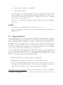
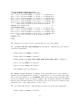
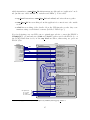
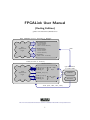
HOST COMPUTER (Linux, Windows or MacOSX)
FPGALink DLL
flWriteChannel(
uint8 channel,
uint32 count,
const uint8 *buffer)
Host
Application
Logic
flReadChannel(
uint8 channel,
uint32 count,
uint8 *buffer)
USB
flPlayXSVF(
const char *svfFile)
FPGA (Xilinx or Altera)
CommFPGA Module
h2fData_out[7:0]
h2fValid_out
h2fReady_in
FPGA
Application
Logic
FPGA < Host
Pipe
chanAddr_out[6:0]
f2hData_in[7:0]
f2hValid_in
f2hReady_out
Cypress FX2LP
or Atmel AVR
CommFPGA
FPGA > Host
Pipe
NeroJTAG
JTAG (TCK, TMS, TDI, TDO)
This work is licensed under the Creative Commons Attribution-ShareAlike 3.0 Unported License
1
Contents
1 Introduction
3
1.1
Justification . . . . . . . . . . . . . . . . . . . . . . . . . . . . . . . . .
3
1.2
Overview . . . . . . . . . . . . . . . . . . . . . . . . . . . . . . . . . . .
3
1.3
Document Conventions . . . . . . . . . . . . . . . . . . . . . . . . . . .
4
1.4
How to Get Help . . . . . . . . . . . . . . . . . . . . . . . . . . . . . .
4
1.5
Licences & Disclaimers . . . . . . . . . . . . . . . . . . . . . . . . . . .
5
2 Getting Started
6
2.1
Installation . . . . . . . . . . . . . . . . . . . . . . . . . . . . . . . . .
6
2.2
Supported Boards . . . . . . . . . . . . . . . . . . . . . . . . . . . . . .
7
2.2.1
Cypress FX2LP-Based Boards . . . . . . . . . . . . . . . . . . .
8
2.2.2
Atmel AVR-Based Boards . . . . . . . . . . . . . . . . . . . . .
9
2.3
The flcli Utility . . . . . . . . . . . . . . . . . . . . . . . . . . . . . . 10
2.4
Programming the FPGA . . . . . . . . . . . . . . . . . . . . . . . . . . 13
2.5
Interacting with the FPGA (Part 1) . . . . . . . . . . . . . . . . . . . . 15
2.6
Interacting with the FPGA (Part 2) . . . . . . . . . . . . . . . . . . . . 17
2.7
Summary . . . . . . . . . . . . . . . . . . . . . . . . . . . . . . . . . . 19
3 Host Application Development
3.1
3.2
20
Language Bindings . . . . . . . . . . . . . . . . . . . . . . . . . . . . . 20
3.1.1
C . . . . . . . . . . . . . . . . . . . . . . . . . . . . . . . . . . . 20
3.1.2
Python . . . . . . . . . . . . . . . . . . . . . . . . . . . . . . . . 21
3.1.3
Excel/VBA . . . . . . . . . . . . . . . . . . . . . . . . . . . . . 21
API Overview . . . . . . . . . . . . . . . . . . . . . . . . . . . . . . . . 21
3.2.1
Firmware Operations [FX2LP-Specific] . . . . . . . . . . . . . . 22
3.2.2
Connection Lifecycle Operations . . . . . . . . . . . . . . . . . . 22
2
3.2.3
Device Capabilities and Status Operations . . . . . . . . . . . . 23
3.2.4
NeroJTAG Operations . . . . . . . . . . . . . . . . . . . . . . . 23
3.2.5
CommFPGA Operations . . . . . . . . . . . . . . . . . . . . . . 23
3.2.6
Miscellaneous Operations . . . . . . . . . . . . . . . . . . . . . . 24
4 FPGA Application Development
25
4.1
FX2LP-Based Designs . . . . . . . . . . . . . . . . . . . . . . . . . . . 25
4.2
EPP-Based Designs . . . . . . . . . . . . . . . . . . . . . . . . . . . . . 27
4.3
Data-Valid-Ready Pipes . . . . . . . . . . . . . . . . . . . . . . . . . . 28
4.4
Build Infrastructure . . . . . . . . . . . . . . . . . . . . . . . . . . . . . 29
4.4.1
MacOSX . . . . . . . . . . . . . . . . . . . . . . . . . . . . . . . 29
4.4.2
Windows . . . . . . . . . . . . . . . . . . . . . . . . . . . . . . . 29
4.4.3
Linux . . . . . . . . . . . . . . . . . . . . . . . . . . . . . . . . 30
4.4.4
Specifying the JTAG Chain . . . . . . . . . . . . . . . . . . . . 30
4.4.5
Location Constraints . . . . . . . . . . . . . . . . . . . . . . . . 30
4.4.6
The xsvf2csvf Utility . . . . . . . . . . . . . . . . . . . . . . . 30
A Custom Boards
32
A.1 Minimus/EP2C5 . . . . . . . . . . . . . . . . . . . . . . . . . . . . . . 32
A.2 Minimus/Nexys2 . . . . . . . . . . . . . . . . . . . . . . . . . . . . . . 33
3
1
1.1
Introduction
Justification
Development kits for Field Programmable Gate Arrays (FPGAs) are ubiquitous, with
offerings from a plethora of manufacturers, with prices ranging from the tens of dollars
to well into the thousands, and featured FPGAs ranging from a few thousand logic
cells to a few million. Whereas the high-end boards tend to be PCIx plug-in cards, the
cheaper boards tend either to be designed around a USB interface chip (e.g Cypress
FX2LP, Atmel AVR, Microchip PIC or FTDI chip), or lack direct host interfacing
altogether, requiring a standalone JTAG cable for programming.
Unfortunately, even for those boards designed around a USB interface, there is a
general lack of good integrated solutions for exchanging arbitrary data between the
host computer and the FPGA, once it has been programmed.
1.2
Overview
FPGALink is an end-to-end, open-source, cross-platform solution designed to do a
couple of simple jobs, and do them well:
• Program an FPGA with JTAG, either from an onboard configuration source or
over USB.
• Allow the host and/or microcontroller to exchange arbitrary binary data with
the FPGA.
It provides a host-side API, firmware for several USB interface microcontrollers, and
128 addressable eight-bit read/write FIFOs on the FPGA side.
• On the host side there is a dynamic-link library with a straightforward API.
Library and example application binaries are provided for MacOSX (x64 &
x86), Windows (x64 & x86) and Linux (x64, x86, ARM & PowerPC). Bindings
are provided for C/C++, Python and Excel/VBA, but binding other languages
is straightforward.
• For the USB interface there are firmwares for the Cypress FX2LP (used on most
Digilent, KNJN, ZTEX and Opal Kelly boards) and Atmel AVR (used by some
AVNet and Digilent boards). Support for the FTDI chips is planned.
• The Cypress FX2LP firmware supports a synchronous FIFO interface with a
sustained bandwidth of around 42MiB/s. The Atmel AVR firmware supports
4
an asynchronous interface1 with a sustained bandwidth of around 1.2MiB/s.
Other microcontroller-to-FPGA protocols such as SPI are planned.
• For the FPGA there is a simple interface module which when instantiated in
your design gives the host a FIFO-style read/write interface, supporting up to
128 separate logical “channels” into your design. A couple of fully-functional
example designs are provided to get you started.
Everything is licensed under the GNU Lesser General Public Licence2 ; you are therefore free to distribute unmodified copies of FPGALink with your products. The library
has no commercial or hardware usage restrictions, so you can prototype your design
with an inexpensive devkit, and then use the same software tools on your custom-built
PCBs. In this way you can easily distribute updated FPGA designs to your customers
just as you would with regular firmware updates, with no special programming cables
required, making your FPGA truly “field-programmable”.
1.3
Document Conventions
Whilst describing interactive console sessions, I will use monospace bold for characters entered by a human and monospace regular for the computer’s responses.
Remember:
• 1MB = 1 megabyte = 106 bytes = 1,000,000 bytes.
• 1MiB = 1 mebibyte = 220 bytes = 1,048,576 bytes.
• 1Mb = 1 megabit = 106 bits = 1,000,000 bits.
• 1Mib = 1 mebibit = 220 bits = 1,048,576 bits.
1.4
How to Get Help
The only place you’re guaranteed to get a response to FPGALink-related queries is the
FPGALink Users Group at http://groups.google.com/group/fpgalink-users.
1
2
Actually IEEE 1284 in Enhanced Parallel Port mode.
http://www.gnu.org/copyleft/lesser.html
5
1.5
Licences & Disclaimers
The FPGALink library, firmware & Verilog code is licensed under the LGPLv33 :
c
Copyright 2009-2013
Chris McClelland
FPGALink is free software: you can redistribute it and/or modify it under
the terms of the GNU Lesser General Public License as published by the
Free Software Foundation, either version 3 of the License, or (at your
option) any later version.
FPGALink is distributed in the hope that it will be useful, but WITHOUT ANY WARRANTY; without even the implied warranty of MERCHANTABILITY or FITNESS FOR A PARTICULAR PURPOSE. See
the GNU Lesser General Public License for more details.
The FLCLI utility is licensed under the GPLv34 :
c
Copyright 2009-2013
Chris McClelland
FLCLI is free software: you can redistribute it and/or modify it under
the terms of the GNU General Public License as published by the Free
Software Foundation, either version 3 of the License, or (at your option)
any later version.
FLCLI is distributed in the hope that it will be useful, but WITHOUT
ANY WARRANTY; without even the implied warranty of MERCHANTABILITY or FITNESS FOR A PARTICULAR PURPOSE. See the GNU
General Public License for more details.
3
4
http://www.gnu.org/copyleft/lesser.html
http://www.gnu.org/copyleft/gpl.html
6
2
2.1
Getting Started
Installation
First, download the FPGALink binary distribution. This manual assumes you’re
using the fpgalink-20121216 release.
Linux:
Just download the binary distribution and unpack it into your home directory.
Things will work out-of-the-box on most modern distributions.
Separate sets of binaries for x64, x86, ARM and PowerPC architectures are
provided in the lin.* directories. For ARM there are two sets of binaries:
armel for the soft-float ABI and armhf for the hard-float ABI.
To grant regular users permission to access the USB devices you’ll be using,
you will need to add udev rules. First check which groups you’re in by running
“groups”, choose a group (I chose “users”) and then for each USB device (i.e,
each VID:PID), add a line to /etc/udev/rules.d/10-local.rules:
wotan$ sudo tee -a /etc/udev/rules.d/10-local.rules > /dev/null <<EOF
> ACTION=="add", SUBSYSTEM=="usb", \
> ATTR{idVendor}=="1d50", ATTR{idProduct}=="602b", \
> GROUP="users", MODE="0660"
> EOF
wotan$
Ensure the VID:PID is lowercase. You may need to restart the udev service
with sudo service udev restart, but you will definitely need to unplug and
reconnect the device(s) in order to activate the new permissions.
Windows:
You may need to install the VC++ 2010 redistributable package:
• For x86: vcredist x86.exe
• For x64: vcredist x64.exe
You will need to install a USB driver for your board:
• Uninstall any existing drivers for your device.
• Download Zadig, unpack it with 7-Zip and run zadig.exe.
• Select your device in the drop-down list.
7
• Select either “libusbK” or “WinUSB”.
• Click “Install Driver”.
Also, although it’s not strictly required, all the command-line examples in this
manual assume you’re using the MakeStuff Build Infrastructure. It’s also the
only supported build platform on Windows, so whilst you’re free to use something
else, you’re on your own if you do.
Separate sets of binaries for x64 and x86 architectures are provided in the win.*
directories.
MacOSX:
You just need to install libusbx-1.0.x and you’re good to go.
One set of universal binaries for x64 and x86 architectures is provided in the
darwin directory.
2.2
Supported Boards
By providing multiple “board support packages” (BSPs), FPGALink is able to support
several different FPGA development kits, based on Xilinx or Altera FPGAs and Atmel
AVR or Cypress FX2LP USB microcontrollers5 . The BSPs are implemented as a
hierarchy: at the top level there are one or more templates, which provide an abstract
description of the host-FPGA connection. Each template has one or more supported
boards, each of which can be thought of as a concrete instantiation of the template
for a given board: the actual FPGA device, its pinout, etc.
A pair of fully-functional examples is provided, with ready-to-go programming files
for each of the supported FPGA boards. The first example is cksum, which we will
play with in the next section, and the second is fifo. Both use various bits of board
I/O to provide some interaction and visual feedback:
• Eight slider-switches, providing eight bits of input data.
• Eight LEDs, providing visual feedback of an eight-bit binary value.
• Four seven-segment displays, wired with common cathodes and an anode for
each digit, providing visual feedback of a sixteen-bit hexadecimal value (and an
additional four-bit binary value via the four decimal point LEDs).
Obviously, not all of the supported FPGA boards include all of these I/O features,
5
Porting to other boards based on these components is usually fairly trivial; if you have such a
board, ask on the mailing list.
8
and may have other special requirements before the supplied examples will work.
However, the examples are written such that it’s possible to monitor their operation
in a limited way through the USB connection.
2.2.1
Cypress FX2LP-Based Boards
The Cypress FX2LP is a Hi-Speed (480Mb/s) USB interface. It is capable of transferring data between an FPGA and the host at about 42MiB/s, using an eight-bit
synchronous FIFO interface. Although fast and fairly cheap, it has a rather eccentric
internal architecture, so custom firmware development is not recommended.
Digilent Nexys3:
There are no special considerations for the Nexys3.
Digilent Nexys2 (500K & 1200K versions):
Separate BSPs are provided for the 500K and 1200K gate versions. Also, when
the Nexys2 “power select” jumper is set to “USB”, the FPGA is supplied with
power via a little FET on the board which is under software control. Therefore
before programming the FPGA it’s necessary to turn this FET on.
Digilent Atlys:
The Atlys has the requisite LEDs and switches, but does not have a display
of any kind, so on Atlys the provided examples map the seven-segment display
signals to the first twelve pins on the board’s VHDCI connector. Unless you
know exactly what you’re doing, please ensure you have nothing connected to
the VHDCI port before you begin.
KNJN Xylo-L:
Since the Xylo-L has no onboard peripherals, the provided examples map the
switches, LEDs and seven-segment displays to the board’s expansion connector
marked H4. Unless you know exactly what you’re doing, please ensure you have
nothing connected to the H4 port before you begin.
Digilent S3BOARD:
There is only partial support for the S3BOARD, because it does not include
a USB interface of any kind; instead, it is supplied with a parallel-port JTAG
cable. To use the S3BOARD with FPGALink, you will need an external FX2LP
board with the appropriate connections6 .
MakeStuff LX9:
The MakeStuff LX9 is intended to be a cheap, home-solderable, repurposable
6
FX2FPGA serves as a reference design, but suitable commercial boards are also available.
9
FPGA board incorporating a Xilinx XC6SLX9 FPGA, FX2LP, SDRAM, SDcard slot and 47 (or 51 if the SD-card slot is not needed) well-grounded FPGA
I/Os.
2.2.2
Atmel AVR-Based Boards
The USB-capable Atmel AVR8 microcontrollers (AT90USB* & ATMEGA*U*) are
very cheap, and they incorporate a Full-Speed (12Mb/s) USB interface. They are
capable of transferring data between an FPGA and the host at between 330KiB/s
and about 1.2MiB/s, using an eight-bit asynchronous EPP-style interface. Although
slower than the FX2LP, they are much more popular as general-purpose microcontrollers, and much easier to program, making custom firmware development fairly
straightforward.
Minimus/EP2C5 Board:
You can buy7 a Minimus ATMEGA32U2 board for £6, and an EP2C5 Mini
Board for £13. With suitable interconnects, the pair make up by far the cheapest
FPGALink-capable hardware solution.
Minimus/Nexys2 Board:
There is also a BSP for a Minimus board attached to a Nexys2-1200. It is
unlikely to be of interest because the Nexys2-1200 already has a superior FX2LPbased USB interface.
Both of these boards require custom wiring, which is described in Appendix A.
7
e.g from ModTraders and eBay, respectively
10
2.3
The flcli Utility
Since FPGALink is a library, you would normally just embed it into your application,
but in order to get you started, the FPGALink binary distribution includes flcli8 ,
a small command-line utility which provides access to some of the library’s features.
wotan$ lin.x64/rel/flcli -h
FPGALink Command-Line Interface Copyright (C) 2012 Chris McClelland
Usage: flcli [-qcbh] [-i <VID:PID>] [-j <portSpec>] -v <VID:PID>
[-d <S:MM:DD:PP>]... [-x <fileName>] [-a <actionString>]
Interact with an FPGALink device.
-i,
-j,
-v,
-d,
-q,
-x,
-a,
-c,
-b,
-h,
--ivp=<VID:PID>
--jtag=<portSpec>
--vp=<VID:PID>
--digport=<S:MM:DD:PP>
--query
--xsvf=<fileName>
--action=<actionString>
--cli
--benchmark
--help
vendor ID and product ID (e.g 04B4:8613)
JTAG port config (e.g D0234)
VID, PID and optional dev ID (e.g 1D50:602B:0001)
read/write digital port
query the JTAG chain
SVF, XSVF or CSVF file to load
a series of CommFPGA actions
start up an interactive CommFPGA session
enable benchmarking & checksumming
print this help and exit
--ivp=<VID:PID> [FX2LP-specific]
The FX2LP microcontroller has no onchip nonvolatile storage, so it loads its
firmware from an external EEPROM and/or has its firmware loaded over USB.
The flcli utility first tries to connect to the device specified by --vp; if it fails,
it tries to load firmware into the device specified by --ivp.
--jtag=<portSpec> [FX2LP-specific]
By default the FX2LP firmware’s JTAG interface is compatible with the wiring
on Digilent boards (TDO, TDI, TMS & TCK connected to port D bits 0, 2, 3 & 4
respectively.) If your board has different connections, you will need to specify
which port lines to use along with --ivp. The port specification is the port
(“A”, “C” or “D”) followed by four digits for the port bits to use for TDO, TDI,
TMS & TCK. For example, the Xylo-L board uses a JTAG port of “D1240” and
the MakeStuff LX9 uses “A7031”. Only bits 0, 1, 3 & 7 are available for JTAG
on port A.
--vp=<VID:PID>
The FPGALink device to connect. This may either be a regular <VID:PID> (e.g
1D50:602B) or it may include an additional device ID (e.g 1D50:602B:0006).
8
Unlike the rest of FPGALink, the flcli utility is licensed under the terms of the GNU General
Public License. See http://www.gnu.org/copyleft/gpl.html
11
The device ID may be used to distinguish between multiple FPGALink devices
sharing the same <VID:PID>.
--digport=<S:MM:DD:PP
Configure general-purpose port pins and data directions.
--query
Print an IDCODE for each device in the JTAG chain.
--xsvf
Play the specified .svf, .xsvf or .csvf file into the JTAG chain. This is
typically (but not necessarily) used for FPGA programming.
--action=<actionString>
Execute the semicolon-separated list of CommFPGA commands, for reading
and writing FPGA channels.
--cli
Start a command-line interface for executing CommFPGA commands.
--benchmark
Output a measured throughput (in MiB/s) and 16-bit checksum for each transfer.
The --cli and --action=<actionString> options support three commands, “r”
(read), “w” (write) and “q” (quit). The syntax of the read command is as follows:
r<channel> [<count> [<fileName>]]
channel:
The FPGA channel, 0-7F.
count:
How many bytes (in hex) to read from the FPGA channel, default 1.
fileName:
A binary file (in single or double-quotes) to write the FPGA’s data
to.
If you don’t specify a fileName, the FPGA’s data is printed to stdout as a hex dump.
12
The syntax of the write command is as follows:
w<channel> <byteSeq | fileName>
channel:
The FPGA channel, 0-7F.
byteSeq:
A sequence of hex bytes to be written to the FPGA channel,
e.g 0123456789abcdef.
fileName:
An existing binary file (in single or double-quotes) to dump into the
FPGA.
All numbers are in hexadecimal. Since a byte is two hex digits, the byteSeq must
have an even number of digits. Filenames must be quoted using single-quotes(’) or
double-quotes ("). You may put several read and/or write commands on one line,
separated by semicolons (;).
For example, w1 00;w2 00;w0 "datafile.dat";r1;r2 first writes 0x00 to channels
1 & 2, then writes the contents of datafile.dat to channel 0, and finally reads one
byte from channels 1 & 2.
13
2.4
Programming the FPGA
Using the flcli utility, we can now program the FPGA for the first time. Programming is done by playing a scripted set of JTAG operations into the FPGA’s JTAG
port.
TDO
Host
Computer
USB
USB
Interface
TDI
TMS
FPGA
TCK
You can program the FPGA like this:
wotan$ <PLATFORM>/rel/flcli -v <VID:PID> -i <VID:PID> -j <JTAG> -s \
-x hdl/apps/makestuff/swled/cksum/vhdl/csvf/<TEMPLATE>-<BOARD>.csvf
Attempting to open connection to FPGALink device 04B4:8613...
Loading firmware into 04B4:8613...
Awaiting renumeration......
Attempting to open connection to FPGLink device 04B4:8613 again...
The FPGALink device at 04B4:8613 scanned its JTAG chain, yielding:
0x01414093
0x05045093
Playing "hdl/apps/makestuff/swled/cksum/vhdl/csvf/fx2all-s3board.csvf" into the
JTAG chain on FPGALink device 04B4:8613...
wotan$
You will need to replace <PLATFORM>, <VID:PID>, <JTAG>, <TEMPLATE> and <BOARD>
in the above command-line with values appropriate for your specific host platform
and FPGA board:
<PLATFORM>
Your host platform. This will be one of win.x64, win.x86, osx, lin.x64,
lin.x86, lin.armhf, lin.armel or lin.ppc.
<VID:PID>
The correct vendor and product IDs for your board. For -i this will be:
• 1443:0005 for Nexys2
• 1443:0007 for Nexys3 & Atlys
• 04B4:8613 for Xylo-L & MakeStuff LX9
You can either set -v to the same as -i, or you can use the official FPGALink <VID:PID> of 1D50:602B. If you have multiple FPGALink devices
14
you can assign a different device ID to each, e.g “-v 1D50:602B:0002”, “-v
1D50:602B:0003”, etc.
<JTAG>
The correct FX2LP port connections for the FPGA’s four JTAG pins TDO,
TDI, TMS & TCK. This will be:
• D0234 for Digilent boards
• D1240 for Xylo-L
• A7031 for MakeStuff LX9
<TEMPLATE>
An identifier for how your board wires its FPGA to the outside world. This will
be fx2min, fx2all or epp.
<BOARD>
The name of your board, which will be one of nexys2-500, nexys2-1200,
nexys3, atlys, xylo-l, s3board, ep2c5 or lx9.
There are some caveats:
Nexys2 Users:
If your board’s “power select” jumper is set to “USB”, it will be necessary
to switch on the FPGA’s power by supplying an additional -p command-line
option.
AVR-Based Boards:
The -i <VID:PID> and -j <JTAG> options are only needed for FX2LP-based
boards. It is not needed for AVR-based boards because these parameters are
set at AVR firmware compile-time.
If successful, you should see the “Done” light on your board switch on, and “0000”
appear on your board’s seven-segment display. If your board does not have either of
these, don’t worry; as long as the flcli command completed without error, you can
proceed to the next section.
So what just happened? Well, flcli loaded new firmware if necessary (FX2LP-based
boards only), then powered up the FPGA (Nexys2 only), then scanned the board’s
JTAG chain for attached devices, and finally loaded a pre-built design file for the
cksum example into the FPGA.
15
In this case we used a .csvf file9 to program the FPGA, but FPGALink directly
supports the .svf files generated by the Xilinx and Altera tools, as well as the Xilinxspecific .xsvf format.
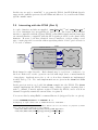
2.5
Interacting with the FPGA (Part 1)
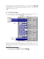
A couple of interface modules are supplied, “comm fpga fx2”10 and “comm fpga epp”11
for you to instantiate in your application’s Verilog code. The former has an external
interface compatible with the Cypress FX2LP’s slave FIFO signals and the latter has
an external interface compatible with the EPP signals provided by the Atmel AVR
firmware. However, both have identical internal interfaces, each providing a read
pipe, a write pipe and a seven-bit address specifying which of 128 logical channels is
to be read or written.
FPGA
CommFPGA Module
FPGA < Host
Pipe
USB
Interface
h2fData_out[7:0]
h2fValid_out
h2fReady_in
chanAddr_out[6:0]
FPGA > Host
Pipe
FPGA
Application
Logic
f2hData_in[7:0]
f2hValid_in
f2hReady_out
Each channel is eight bits wide. Each channel may be read from or written to by
the host. Each read or write operation can deal with single bytes or many hundreds
of megabytes. Applications are free to choose how these channels are implemented
in their Verilog code. Two such implementations are given in the cksum and fifo
examples.
In the previous section, we loaded the cksum example into the FPGA. The cksum
example implements the FPGA channels using ordinary registers, meaning that a
write to channel N merely updates register N inside the FPGA, and a read from
channel N typically returns the current value of register N.
You can see this by using flcli’s command-line mode (triggered by the -c option):
wotan$ <PLATFORM>/rel/flcli -v <VID:PID> -b -c
Attempting to open connection to FPGALink device 1D50:602B...
9
The CSVF format is similar to Xilinx’s XSVF, but it’s better suited for playback by small
microcontrollers, and is much more space-efficient.
10
hdl/libs/makestuff/comm fpga/fx2/verilog/comm fpga fx2.v.
11
hdl/libs/makestuff/comm fpga/epp/verilog/comm fpga epp.v.
16
Entering CommFPGA command-line mode:
> w1 00;w2 00;w0 cafebabef00d1e;r1;r2;r0 4
Wrote 1 bytes (checksum 0x0000) to channel 1 at 0.002709 MiB/s
Wrote 1 bytes (checksum 0x0000) to channel 2 at 0.003200 MiB/s
Wrote 7 bytes (checksum 0x045B) to channel 0 at 0.029408 MiB/s
Read 1 bytes (checksum 0x0004) from channel 1 at 0.004146 MiB/s
Read 1 bytes (checksum 0x005B) from channel 2 at 0.004607 MiB/s
Read 4 bytes (checksum 0x0000) from channel 0 at 0.017183 MiB/s
00 01 02 03 04 05 06 07 08 09 0A 0B 0C 0D 0E 0F
00000000 04 5B 00 00 00 00
.[....
> w1 ca;w2 fe;r1;r2
Wrote 1 bytes (checksum 0x00CA) to channel 1 at 0.002592 MiB/s
Wrote 1 bytes (checksum 0x00FE) to channel 2 at 0.004201 MiB/s
Read 1 bytes (checksum 0x00CA) from channel 1 at 0.004058 MiB/s
Read 1 bytes (checksum 0x00FE) from channel 2 at 0.004220 MiB/s
00 01 02 03 04 05 06 07 08 09 0A 0B 0C 0D 0E 0F
00000000 CA FE
..
> q
wotan$
The instructions accepted by the command-line are terse, but simple.
The “w1 00;w2 00;w0 cafebabef00d1e;r1;r2;r0 4” command line performs six
operations sequentially:
• Write single byte 0x00 to channel 1.
• Write single byte 0x00 to channel 2.
• Write seven bytes 0xCA, 0xFE, 0xBA, 0xBE, 0xF0, 0x0D, 0x1E to channel 0.
• Read one byte 0x04 from channel 1.
• Read one byte 0x2B from channel 2.
• Read four bytes from channel 0.
The cksum example maintains a running 16-bit checksum of the bytes written to
channel 0; the checksum itself is available on channels 1 & 2. Notice that the checksum
value read from channels 1 & 2 is 0x045B, which is the same as the checksum value
reported by flcli for the seven-byte transfer: the checksum calculated by flcli
matches the checksum calculated by the FPGA. The four reads from channel 0 just
return the state of the eight switches on the board.
The “w1 ca;w2 fe;r1;r2” command line performs four operations sequentially:
• Write single byte 0xCA to channel 1.
17
• Write single byte 0xFE to channel 2.
• Read one byte 0xCA from channel 1.
• Read one byte 0xFE from channel 2.
Channels 1 & 2 are implemented as the MSB & LSB of the 16-bit checksum register,
so values written may be read back.
You can see how this is implemented in the FPGA by taking a look at the Verilog12 :
1
So “w1 ca” writes a single byte to channel 1, which sets chanAddr in=0x01 and
h2fData in=0xCA, and drives h2fValid in high for one clock cycle, which writes the
value 0xCA to the LSB of the checksum register (preserving the MSB).
Similarly when you enter “r2”, it initiates a single byte read of channel 2, which sets
chanAddr in=0x02 and drives f2hReady in13 high for one clock cycle, causing the
MSB of the checksum register to be sampled and returned to the host.
Channel 0 is a little more interesting. Bytes written (e.g “w0 aa”) are displayed on
the eight board LEDs and also added to the running sixteen-bit checksum shown on
the seven-segment display. Conversely, reads return the current state of the eight
switches.
Notice that reads and writes never block: there is always data available in the read
pipe and there is always room available in the write pipe.
2.6
Interacting with the FPGA (Part 2)
In the previous section, we used the flcli utility to read and write simple registers implemented in the FPGA by the cksum example. The fifo example is more
interesting. You can load it like this:
wotan$ <PLATFORM>/rel/flcli -v <VID:PID> -i <VID:PID> -s \
-x hdl/apps/makestuff/swled/fifo/vhdl/csvf/<TEMPLATE>-<BOARD>.csvf
Attempting to open connection to FPGALink device 04B4:8614...
Loading firmware into 04B4:8614...
Awaiting renumeration.......
Attempting to open connection to FPGLink device 04B4:8614 again...
12
See hdl/apps/makestuff/swled/cksum/verilog/cksum rtl.v for the complete module.
Actually, since the value stored in a simple register like this is unaffected by a read operation,
it’s not necessary for this code to consider f2hReady in - it need only select the correct register value
with which to drive f2hData out, and do so continuously.
13
18
The FPGALink device at 04B4:8614 scanned its JTAG chain, yielding:
0x01414093
0x05045093
Playing "hdl/apps/makestuff/swled/fifo/vhdl/csvf/fx2all-s3board.csvf" into the
JTAG chain on FPGALink device 04B4:8614...
wotan$ <PLATFORM>/rel/flcli -v <VID:PID> -c
Attempting to open connection to FPGALink device 04B4:8614...
Entering CommFPGA command-line mode:
> r0 10;w0 01020408102040804020100804020100
00 01 02 03 04 05 06 07 08 09 0A 0B 0C 0D 0E 0F
00000000 00 01 02 03 04 05 06 07 08 09 0A 0B 0C 0D 0E 0F ................
> q
wotan$
Now, channel 0 is connected to a pair of FIFOs inside the FPGA, a read FIFO
and a write FIFO. Independent producer and consumer processes periodically insert
upcount data into the read FIFO and drain data from the write FIFO, respectively.
The speed at which these processes work is selectable by setting different values on
the eight switches: sw[7:4] controls the speed of the consumer and sw[3:0] controls
the speed of the producer.
Here’s the code14 :
1
When the host writes to channel 0, each byte is clocked into the write FIFO. When the
write FIFO fills up, h2fReady out is deasserted which tells the host to stop sending
until the consumer process has freed up some room for more data.
When the host reads from channel 0, each byte is clocked out of the read FIFO. When
the read FIFO empties, f2hValid out is deasserted to stop sending data to the host
until the producer process has inserted some more data into the FIFO.
When the example is first loaded, you will see the leftmost pair of digits on the sevensegment display incrementing, telling you how many bytes there are in the read FIFO.
When you issue the command r0 10, the host reads sixteen bytes from the read FIFO,
causing the count to decrement by sixteen. If there are as yet insufficient bytes in the
read FIFO to fulfill the request, the host blocks until bytes become available.
Similarly, the rightmost pair of digits on the seven-segment display tells you how many
bytes there are in the write FIFO. When you issue the command w0 010204081020408
04020100804020100, sixteen bytes are written to the write FIFO. The consumer process then begins to drain the data, displaying each byte in turn on the eight LEDs.
If there is as yet insufficient room in the write FIFO to fulfill the request, the host
blocks until enough room is available. This is not always noticeable because the
microcontrollers have additional bytes of FIFO space.
14
See hdl/apps/makestuff/swled/fifo/verilog/fifo rtl.v for the complete module.
19
If your board does not have a seven-segment display, you can read the current depth
of the write FIFO by reading from channel 1, and you can read the current depth of
the read FIFO by reading from channel 2.
2.7
Summary
In this chapter we used the flcli utility to program an FPGA with a couple of
pre-built examples, and to communicate with the data channels in the FPGA.
20
3
Host Application Development
The flcli utility is a great way to get started with FPGALink, and for simple testing
of the behaviour of your Verilog code, but sooner or later you will want to dive in and
write your own host-side applications. There is out-of-the-box support for C/C++,
Python and Excel/VBA, but the core library itself is just a C DLL, so calling into it
from other languages is straightforward15 .
In order to enable an application to communicate with potentially many FPGALink
devices, the library uses the concept of a “handle” to refer to an FPGALink device.
An opaque handle is returned when a connection is first established to a device, and
that handle is supplied for all subsequent operations on that device.
3.1
Language Bindings
There is obviously a significant cross-language semantic overlap in the API; the only
differences are those imposed by the languages themselves.
3.1.1
C
Because C has no concept of exceptions, wherever a function can fail, its return
value is just a status code; the actual result (if any) is provided in an “out” parameter
instead. An optional error message is also provided in an “out” parameter. Conversely,
wherever a function cannot fail, its return value (if any) is actually the result.
Each function that can fail will return FL SUCCESS on success, or something else on
failure. Each will also accept a pointer to a const char* which will be set to a
more or less meaningful message if an error occurs. The memory for this message is
dynamically allocated and must subsequently be deallocated by application code with
flFreeError(). If you do not wish to receive error messages you can just set this
parameter to NULL.
It’s useful to define a macro to handle this:
1
2
3
4
5
6
7
8
9
10
#define CHECK(x)
\
if ( status != FL_SUCCESS ) {
\
returnCode = x;
\
fprintf(stderr, "%s\n", error); \
flFreeError(error);
\
goto cleanup;
\
}
:
status = flWriteChannel(handle, 1000, 0x01, 1, &byte, &error);
CHECK(21);
15
Or at least it ought to be straightforward!
21
To get you started, there is an example in C for you to study in the examples/c
subdirectory. See examples/c/README for details of how to compile the code on your
platform.
3.1.2
Python
Python has exceptions, so the API in Python is written such that each function’s
return value (if any) is actually its result, with an exception thrown when an error
occurs.
Separate bindings are provided for Python2.x and Python3.x. These reside in the
examples/python subdirectory. The bindings are themselves executable, and offer
similar functionality to the C example. The Python binding may be imported into
your own code, or used from an interactive Python session. For more details, see
examples/python/README.
3.1.3
Excel/VBA
VBA has exceptions, so the API in VBA is written such that each function’s return
value (if any) is actually its result, with an exception thrown when an error occurs.
The examples/excel/fpgalink.xls spreadsheet incorporates the VBA binding, and
exposes a simple graphical user interface. Before opening it, please ensure you have
unpacked the FPGALink distribution to a local drive, not a network drive, otherwise
Excel will consider the FPGALink DLL to be untrusted and will refuse to load it.
3.2
API Overview
See http://www.swaton.ukfsn.org/apidocs/libfpgalink_8h.html for more detailed API documentation.
The library consists of five classes of functions:
• Firmware operations (FX2LP-specific)
• Connection lifecycle operations
• NeroJTAG operations (programming the FPGA)
• CommFPGA operations (interacting with the FPGA)
• Miscellaneous operations
Each will now be covered in turn; please refer also to the detailed API docs.
22
3.2.1
Firmware Operations [FX2LP-Specific]
The Cypress FX2LP USB interface has no internal nonvolatile storage for firmware.
On startup it typically loads firmware from an external serial EEPROM, which is
probably how your board works. You can easily load new firmware over USB, or
write your new firmware to the external EEPROM using these operations.
flLoadStandardFirmware():
Load standard FPGALink firmware into the FX2’s RAM.
flFlashStandardFirmware():
Flash standard FPGALink firmware into the FX2’s EEPROM, optionally appending an SVF, XSVF or CSVF initialisation stream and an FPGA initialisation stream.
flLoadCustomFirmware():
Load custom firmware from a .hex file into the FX2’s RAM.
flFlashCustomFirmware():
Flash a custom firmware from a .hex or .iic file into the FX2’s EEPROM.
flSaveFirmware():
Save existing EEPROM data to an .iic file.
3.2.2
Connection Lifecycle Operations
These two operations enable you to actually establish a connection to an FPGALink
device over USB.
flOpen():
Open a connection to the FPGALink device at the specified VID & PID.
flClose():
Close the connection to the FPGALink device.
23
3.2.3
Device Capabilities and Status Operations
These operations enable you to query the FPGALink device to find out what features it supports. Currently there are only two features: NeroJTAG for JTAGprogramming, and CommFPGA, for communicating with an already-programmed
FPGA.
flIsDeviceAvailable():
Check if a given device is actually connected to the system.
flIsNeroCapable():
Check to see if the device supports NeroJTAG.
flIsCommCapable():
Check to see if the device supports CommFPGA.
3.2.4
NeroJTAG Operations
The NeroJTAG operations enable you to examine the JTAG chain and program devices in the chain.
flScanChain():
Scan the JTAG chain and return an array of IDCODEs.
flPlayXSVF():
Play an SVF, XSVF or CSVF file into the JTAG chain.
3.2.5
CommFPGA Operations
The CommFPGA operations enable you to read from and write to up to 128 logical
“channels” implemented in the FPGA.
flIsFPGARunning():
Check to see whether or not the FPGA has been programmed.
flReadChannel():
Read bytes from the specified channel into the supplied buffer.
flWriteChannel():
Write bytes from the the supplied read-only buffer to the specified channel.
24
flAppendWriteChannelCommand():
Append a write command to the end of the write buffer.
flPlayWriteBuffer():
Play the write buffer into the FPGALink device immediately.
flCleanWriteBuffer():
Clean the write buffer (if any).
3.2.6
Miscellaneous Operations
Some operations are useful or just necessary, but don’t fit into the other four categories:
flInitialise():
Initialise the library. You must call this before any of the other functions.
flFreeError():
Free an error allocated when one of the other functions fails.
flSleep():
Sleep for the specified number of milliseconds.
flLoadFile():
Return a newly-allocated buffer with the specified binary file loaded into it.
flFreeFile():
Free a buffer previously returned by flLoadFile().
flPortAccess():
Access port lines on the USB interface microcontroller.
25
4
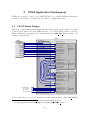
FPGA Application Development
Whilst it’s possible to write your own FPGA-side code, the FPGALink distribution
includes some useful tools and Verilog modules to simplify this task.
4.1
FX2LP-Based Designs
The most common data-transfer approach taken by the supported boards is to connect
17 FPGA I/O pins to the slave FIFO interface of a Cypress FX2LP microcontroller.
This configuration is supported by instantiating the comm fpga fx216 module, and
wiring17 it up like this:
FPGA
FX2LP
top_level
FIFOADR[0]
FIFOADR[1]
FD[7:0]
/SLRD
/SLOE
FLAGC
/SLWR
FLAGB
PKTEND
IFCLK
'0'
comm_fpga_fx2
fx2FifoSel_out
fx2Data_io
fx2Read_out
fx2GotData_in
fx2Write_out
fx2GotRoom_in
fx2PktEnd_out
'0'
FX2LP
external
signals
clk_in
reset_in
f2hData_in[7:0]
f2hValid_in
f2hReady_out
chanAddr_out[6:0]
h2fData_out[7:0]
h2fValid_out
h2fReady_in
DVR Pipe
(Master)
swled
h2fReady_out
h2fValid_in
h2fData_in[7:0]
chanAddr_in[6:0]
f2hReady_in
f2hValid_out
f2hData_out[7:0]
'0'
clk_in
reset_in
sseg_out[7:0]
anode_out[3:0]
led_out[7:0]
sw_in[7:0]
Peripherals:
4x 7-segs
8x LEDs
8x switches
DVR Pipe
(Slave)
App.ext
signals
Notice that there’s a top-level structural module (imaginatively called top level),
16
17
See hdl/libs/makestuff/comm fpga/fx2/verilog/comm fpga fx2.v.
See hdl/apps/makestuff/swled/templates/fx2all/verilog/top level.v
26
which instantiates a comm fpga fx2 infrastructure module and an “application” module (in this case called swled, for “switches and LEDs”). Notice that:
• top level instantiates comm fpga fx2 and swled, and wires them together.
• comm fpga fx2 knows nothing about the application’s connections to the outside
world.
• swled knows nothing of the details of how the USB interface works: they communicate using a well-defined contract (labelled “DVR Pipe”).
If you’re designing your own PCB, a more optimal approach is to connect the FX2LP’s
FIFOADR[0] to ground and wire /SLRD and /SLOE together outside the FPGA (i.e on
the PCB) rather than inside, in the top level module18 , thus saving two precious
FPGA I/Os:
FPGA
FX2LP
FIFOADR[0]
FIFOADR[1]
FD[7:0]
/SLRD
/SLOE
FLAGC
/SLWR
FLAGB
PKTEND
GND
IFCLK
comm_fpga_fx2
top_level
fx2FifoSel_out
fx2Data_io
fx2Read_out
fx2GotData_in
fx2Write_out
fx2GotRoom_in
fx2PktEnd_out
'0'
FX2LP
external
signals
clk_in
reset_in
f2hData_in[7:0]
f2hValid_in
f2hReady_out
chanAddr_out[6:0]
h2fData_out[7:0]
h2fValid_out
h2fReady_in
DVR Pipe
(Master)
swled
h2fReady_out
h2fValid_in
h2fData_in[7:0]
chanAddr_in[6:0]
f2hReady_in
f2hValid_out
f2hData_out[7:0]
'0'
18
clk_in
reset_in
sseg_out[7:0]
anode_out[3:0]
led_out[7:0]
sw_in[7:0]
Peripherals:
4x 7-segs
8x LEDs
8x switches
See hdl/apps/makestuff/swled/templates/fx2min/verilog/top level.v
27
DVR Pipe
(Slave)
App.ext
signals
This is the approach taken by the MakeStuff LX9 board. Notice that the comm fpga fx2
and swled modules are identical to those we used previously. The only changes are
in the PCB layout (only 15 FX2LP-FPGA signals as opposed to 17), and in the
top level structural module.
4.2
EPP-Based Designs
The Atmel AVR firmware implements the IEEE 1284 Enhanced Parallel Port protocol19 . This is implemented using comm fpga epp20 , wired21 like this:
FPGA
AT90USB162
top_level
comm_fpga_epp
eppData_io
eppAddrStb_in
eppDataStb_in
eppWrite_in
eppWait_out
PD[7:0]
PC4
PC5
PC6
PC7
50MHz
'0'
EPP
external
signals
clk_in
reset_in
f2hData_in[7:0]
f2hValid_in
f2hReady_out
chanAddr_out[6:0]
h2fData_out[7:0]
h2fValid_out
h2fReady_in
DVR Pipe
(Master)
swled
h2fReady_out
h2fValid_in
h2fData_in[7:0]
chanAddr_in[6:0]
f2hReady_in
f2hValid_out
f2hData_out[7:0]
'0'
clk_in
reset_in
sseg_out[7:0]
anode_out[3:0]
led_out[7:0]
sw_in[7:0]
Peripherals:
4x 7-segs
8x LEDs
8x switches
DVR Pipe
(Slave)
App.ext
signals
It uses fewer signals than the FX2LP’s synchronous FIFO interface, but it’s also
significantly slower. Since EPP is an asynchronous protocol, its signals are not synchronous to any particular clock, so the FPGA needs an arbitrary clock source for its
own operation.
19
See http://www.fapo.com/eppmode.htm
See hdl/libs/makestuff/comm fpga/fx2/verilog/comm fpga epp.v.
21
See hdl/apps/makestuff/swled/templates/epp/verilog/top level.v
20
28
The EPP protocol is not as efficient as the synchronous FIFO interface of the FX2LP,
but in any case the overall throughput of a system based on an Atmel AVR is limited
by the USB interface and not the EPP interface. This is because unlike the Hi-Speed
480Mb/s FX2LP, the AVRs are Full-Speed 12Mb/s devices. Observed throughput is
about 330KiB/s for the AVR firmware running single-buffered on an AT90USB162,
ATMEGA16U2, ATMEGA32U2 or similar, and about 1.2MiB/s for the firmware
running double-buffered on an AT90USB647, ATMEGA32U4 or similar.
Notice that the swled module is identical to the one in the two FX2LP configurations
shown previously. Now, not only has the PCB layout and top level module changed,
but the comm fpga fx2 module has been replaced with comm fpga epp.
4.3
Data-Valid-Ready Pipes
Notice that the two FX2LP configurations and the EPP configuration all use exactly the same application module, swled. This is possible because the comm fpga *
modules all have the same internal interface, even if their external interfaces differ
markedly. In this way, it’s possible to write application Verilog which can be made to
run on a variety of different FPGA boards, even though they have entirely different
designs.
comm_fpga_* modules
Host > FPGA
Pipe
Host < FPGA
Pipe
application module
h2fData_out[7:0]
h2fValid_out
h2fReady_in
h2fData_in[7:0]
h2fValid_in
h2fReady_out
chanAddr_out[6:0]
chanAddr_in[6:0]
f2hData_in[7:0]
f2hValid_in
f2hReady_out
f2hData_out[7:0]
f2hValid_out
f2hReady_in
Host is
Writing
Host is
Reading
This common internal interface is implemented using separate host-to-FPGA and
FPGA-to-host pipes, each of which follow the common data-valid-ready naming convention22 for FIFOs, plus a seven-bit channel address, which tells the application
module which channel is being read from or written to.
The h2f* pipe carries data from the host to the FPGA, and the f2h* pipe carries
data in the opposite direction, from the FPGA back to the host. Each pipe has three
signals, *Data and *Valid which are driven by the sender, and *Ready which is driven
by the receiver. The sender drives *Valid high in order to tell the receiver there’s
valid data on *Data, and the receiver can drive *Ready low in order to tell the sender
that it’s not ready to accept the data yet. The data on *Data is transferred from the
22
See http://inst.eecs.berkeley.edu/˜cs150/Documents/Interfaces.pdf
29
sender to the receiver if and only if both *Valid and *Ready are high on the rising
edge of the clock.
In practice, the swled application could be either cksum or fifo, discussed in sections
2.5 and 2.6 respectively. Obviously it’s not typical for two different FPGA applications
to have exactly the same interface to the outside world (i.e swled); in this case the two
different examples were contrived to share the same interface for illustrative purposes.
4.4
Build Infrastructure
In the hdl directory is a build infrastructure capable of synthesising Verilog code
into SVF files suitable for loading into an FPGA with FPGALink. Xilinx and Altera
FPGA toolchains are supported. The build infrastructure uses command-line tools
rather than the vendors’ Integrated Development Environments, but if you prefer to
work in an IDE, setting up a project is straightforward.
For Xilinx FPGAs, it’s necessary to install ISE WebPACK23 . For Altera FPGAs, it’s
necessary to install Quartus II Web Edition24 .
4.4.1
MacOSX
Unfortunately, neither Altera’s Quartus nor Xilinx’s ISE run on MacOSX, so you
will need to run either Windows or Linux in a virtual machine under VirtualBox or
Parallels.
4.4.2
Windows
The FPGA build infrastructure relies on some UNIX tools like make. Whilst it may
be possible to get builds working with 3rd-party UNIX tools for Windows, the only
officially supported set of tools are those available on the MakeStuff website25 .
For Xilinx FPGAs, you will need to create a “XILINX” environment variable, and set
it to the location of the ISE installation (e.g “C:/Xilinx/13.2/ISE DS/ISE”). No
further installation tasks are needed for Altera FPGAs.
23
From http://www.xilinx.com/support/download/index.htm
From https://www.altera.com/download/software/software/quartus-ii-we
25
See http://www.makestuff.eu/wordpress/?page_id=1489
24
30
Then from within a Console2 window, you can build the cksum example for the
Digilent Atlys like this:
chris@win7 echo $XILINX
C:/Xilinx/13.2/ISE_DS/ISE
chris@win7$ cd hdl/fx2/verilog/ex_cksum
chris@win7$ ls ../../platforms
atlys lx9 nexys2-1200 nexys2-500 nexys3
chris@win7$ make PLATFORM=atlys
4.4.3
s3board
xylo-l
Linux
For Xilinx FPGAs, you will need to create a “XILINX” environment variable, and set
it to the location of the ISE installation (e.g “/opt/Xilinx/13.2/ISE DS/ISE”). No
further installation tasks are needed for Altera FPGAs.
Then from within a terminal window, you can build the cksum example for the Digilent
Atlys like this:
chris@wotan echo $XILINX
/opt/Xilinx/13.2/ISE_DS/ISE
chris@wotan$ cd hdl/fx2/verilog/ex_cksum
chris@wotan$ ls ../../platforms
atlys lx9 nexys2-1200 nexys2-500 nexys3
chris@wotan$ make PLATFORM=atlys
4.4.4
s3board
xylo-l
Specifying the JTAG Chain
The Altera tools will only generate SVF files for a single-device JTAG chain, but the
Xilinx tools support JTAG chains with multiple devices. The JTAG chain and the
actual device to program is specified in the boards/*/board.batch files. All devices
except the one being programmed need BSDL descriptions so that the programming
algorithm can bypass them.
A future release of FPGALink will simplify this, and provide support for multi-device
chains with Altera FPGAs.
4.4.5
Location Constraints
For boards based on Xilinx FPGAs, the location constraints are specified in the
boads/*/board.ucf files. For boards based on Altera FPGAs, the location constraints are specified in the boards/*/board.qsf files.
4.4.6
The xsvf2csvf Utility
The CSVF format is very similar to Xilinx’s XSVF, except that it has a few simplifications and the JTAG bitmaps have been been reversed, making it better suited
31
for playback on small microcontrollers. It also has a simple run-length compression
scheme making the programming files smaller. You can generate a CSVF file from an
XSVF or SVF file using the xsvf2csvf utility.
32
A
Custom Boards
Most of the FPGA boards supported by FPGALink are ready-made, but in some
cases it’s useful to be able to wire an existing microcontroller board to an existing
FPGA board, or even design a composite board from scratch.
A.1
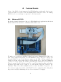
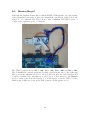
Minimus/EP2C5
By far the cheapest hardware solution for FPGALink-based applications, this is an
EP2C5 Mini Board attached to a Minimus AVR USB board:
To make one you will need an EP2C5 Mini Board and a Minimus AVR USB board.
The only modification necessary is to the Minimus board to allow it to draw power
from the EP2C5 board. To do this you must sever the USB +5V line, which is the
fourth one down on the USB connector in the picture above. Since the Minimus’s
connector is a Type A plug, the result is physically quite awkward if you don’t have a
Type A extension cable. Another option is to remove the plug altogether and replace
it with a cable with a Type A plug on one end and the other end soldered to the
Minimus. Thus, it becomes straightforward to connect the USB +5V power to the
P8 connector in the bottom left of the EP2C5 board, to make the whole thing draw
its power from USB, eliminating the need for an external +5V supply.
33
A.2
Minimus/Nexys2
Although the Digilent Nexys2 has a built-in FX2LP USB interface, in some circumstances it might be necessary to have two channels into the FPGA, either both to the
same PC, or to different PCs. Here’s how to wire a Minimus AVR USB board to a
couple of the expansion ports of a Nexys2:
The JTAG connections are TMS to PB0, TCK to PB1, TDI to PB2 and TDO to PB3.
The CommFPGA connections should be fairly clear from the photo: the eight data
lines go from the Minimus’s Port D to the top and bottom rows of the Nexys2’s JC1
connector, and the four control lines go to the top row of JD1. As before, the Minimus
needs to draw power from the Nexys2, so you will need to sever the USB +5V line,
which is the fourth one down on the USB connector in the picture above.
34