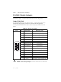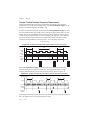
1
TM NI cDAQ -9138/9139 User Manual NI CompactDAQ cDAQ-9138/9139 Eight-Slot Stand-Alone Chassis with Integrated Controller NI cDAQ-9138/9139 User Manual June 2014 371042C-01 Support Worldwide Technical Support and Product Information ni.com Worldwide Offices Visit ni.com/niglobal to access the branch office Web sites, which provide up-to-date contact information, support phone numbers, email addresses, and current events. National Instruments Corporate Headquarters 11500 North Mopac Expressway Austin, Texas 78759-3504 USA Tel: 512 683 0100 For further support information, refer to the NI Services appendix. To comment on National Instruments documentation, refer to the National Instruments Web site at ni.com/info and enter the Info Code feedback. © 2012–2014 National Instruments. All rights reserved. Legal Information Limited Warranty This document is provided ‘as is’ and is subject to being changed, without notice, in future editions. For the latest version, refer to ni.com/manuals. NI reviews this document carefully for technical accuracy; however, NI MAKES NO EXPRESS OR IMPLIED WARRANTIES AS TO THE ACCURACY OF THE INFORMATION CONTAINED HEREIN AND SHALL NOT BE LIABLE FOR ANY ERRORS. NI warrants that its hardware products will be free of defects in materials and workmanship that cause the product to fail to substantially conform to the applicable NI published specifications for one (1) year from the date of invoice. For a period of ninety (90) days from the date of invoice, NI warrants that (i) its software products will perform substantially in accordance with the applicable documentation provided with the software and (ii) the software media will be free from defects in materials and workmanship. If NI receives notice of a defect or non-conformance during the applicable warranty period, NI will, in its discretion: (i) repair or replace the affected product, or (ii) refund the fees paid for the affected product. Repaired or replaced Hardware will be warranted for the remainder of the original warranty period or ninety (90) days, whichever is longer. If NI elects to repair or replace the product, NI may use new or refurbished parts or products that are equivalent to new in performance and reliability and are at least functionally equivalent to the original part or product. You must obtain an RMA number from NI before returning any product to NI. NI reserves the right to charge a fee for examining and testing Hardware not covered by the Limited Warranty. This Limited Warranty does not apply if the defect of the product resulted from improper or inadequate maintenance, installation, repair, or calibration (performed by a party other than NI); unauthorized modification; improper environment; use of an improper hardware or software key; improper use or operation outside of the specification for the product; improper voltages; accident, abuse, or neglect; or a hazard such as lightning, flood, or other act of nature. THE REMEDIES SET FORTH ABOVE ARE EXCLUSIVE AND THE CUSTOMER’S SOLE REMEDIES, AND SHALL APPLY EVEN IF SUCH REMEDIES FAIL OF THEIR ESSENTIAL PURPOSE. EXCEPT AS EXPRESSLY SET FORTH HEREIN, PRODUCTS ARE PROVIDED "AS IS" WITHOUT WARRANTY OF ANY KIND AND NI DISCLAIMS ALL WARRANTIES, EXPRESSED OR IMPLIED, WITH RESPECT TO THE PRODUCTS, INCLUDING ANY IMPLIED WARRANTIES OF MERCHANTABILITY, FITNESS FOR A PARTICULAR PURPOSE, TITLE OR NON-INFRINGEMENT, AND ANY WARRANTIES THAT MAY ARISE FROM USAGE OF TRADE OR COURSE OF DEALING. NI DOES NOT WARRANT, GUARANTEE, OR MAKE ANY REPRESENTATIONS REGARDING THE USE OF OR THE RESULTS OF THE USE OF THE PRODUCTS IN TERMS OF CORRECTNESS, ACCURACY, RELIABILITY, OR OTHERWISE. NI DOES NOT WARRANT THAT THE OPERATION OF THE PRODUCTS WILL BE UNINTERRUPTED OR ERROR FREE. In the event that you and NI have a separate signed written agreement with warranty terms covering the products, then the warranty terms in the separate agreement shall control. Copyright Under the copyright laws, this publication may not be reproduced or transmitted in any form, electronic or mechanical, including photocopying, recording, storing in an information retrieval system, or translating, in whole or in part, without the prior written consent of National Instruments Corporation. National Instruments respects the intellectual property of others, and we ask our users to do the same. NI software is protected by copyright and other intellectual property laws. Where NI software may be used to reproduce software or other materials belonging to others, you may use NI software only to reproduce materials that you may reproduce in accordance with the terms of any applicable license or other legal restriction. End-User License Agreements and Third-Party Legal Notices You can find end-user license agreements (EULAs) and third-party legal notices in the following locations: • Notices are located in the <National Instruments>\_Legal Information and <National Instruments> directories. • EULAs are located in the <National Instruments>\Shared\MDF\Legal\license directory. • Review <National Instruments>\_Legal Information.txt for information on including legal information in installers built with NI products. U.S. Government Restricted Rights If you are an agency, department, or other entity of the United States Government (“Government”), the use, duplication, reproduction, release, modification, disclosure or transfer of the technical data included in this manual is governed by the Restricted Rights provisions under Federal Acquisition Regulation 52.227-14 for civilian agencies and Defense Federal Acquisition Regulation Supplement Section 252.227-7014 and 252.227-7015 for military agencies. Trademarks Refer to the NI Trademarks and Logo Guidelines at ni.com/trademarks for more information on National Instruments trademarks. ARM, Keil, and µVision are trademarks or registered of ARM Ltd or its subsidiaries. LEGO, the LEGO logo, WEDO, and MINDSTORMS are trademarks of the LEGO Group. TETRIX by Pitsco is a trademark of Pitsco, Inc. FIELDBUS FOUNDATION™ and FOUNDATION™ are trademarks of the Fieldbus Foundation. EtherCAT® is a registered trademark of and licensed by Beckhoff Automation GmbH. CANopen® is a registered Community Trademark of CAN in Automation e.V. DeviceNet™ and EtherNet/IP™ are trademarks of ODVA. Go!, SensorDAQ, and Vernier are registered trademarks of Vernier Software & Technology. Vernier Software & Technology and vernier.com are trademarks or trade dress. Xilinx is the registered trademark of Xilinx, Inc. Taptite and Trilobular are registered trademarks of Research Engineering & Manufacturing Inc. FireWire® is the registered trademark of Apple Inc. Linux® is the registered trademark of Linus Torvalds in the U.S. and other countries. Handle Graphics®, MATLAB®, Real-Time Workshop®, Simulink®, Stateflow®, and xPC TargetBox® are registered trademarks, and TargetBox™ and Target Language Compiler™ are trademarks of The MathWorks, Inc. Tektronix®, Tek, and Tektronix, Enabling Technology are registered trademarks of Tektronix, Inc. The Bluetooth® word mark is a registered trademark owned by the Bluetooth SIG, Inc. The ExpressCard™ word mark and logos are owned by PCMCIA and any use of such marks by National Instruments is under license. The mark LabWindows is used under a license from Microsoft Corporation. Windows is a registered trademark of Microsoft Corporation in the United States and other countries. Other product and company names mentioned herein are trademarks or trade names of their respective companies. Members of the National Instruments Alliance Partner Program are business entities independent from National Instruments and have no agency, partnership, or joint-venture relationship with National Instruments. Patents For patents covering National Instruments products/technology, refer to the appropriate location: Help»Patents in your software, the patents.txt file on your media, or the National Instruments Patent Notice at ni.com/patents. Export Compliance Information Refer to the Export Compliance Information at ni.com/legal/export-compliance for the National Instruments global trade compliance policy and how to obtain relevant HTS codes, ECCNs, and other import/export data. WARNING REGARDING USE OF NATIONAL INSTRUMENTS PRODUCTS YOU ARE ULTIMATELY RESPONSIBLE FOR VERIFYING AND VALIDATING THE SUITABILITY AND RELIABILITY OF THE PRODUCTS WHENEVER THE PRODUCTS ARE INCORPORATED IN YOUR SYSTEM OR APPLICATION, INCLUDING THE APPROPRIATE DESIGN, PROCESS, AND SAFETY LEVEL OF SUCH SYSTEM OR APPLICATION. PRODUCTS ARE NOT DESIGNED, MANUFACTURED, OR TESTED FOR USE IN LIFE OR SAFETY CRITICAL SYSTEMS, HAZARDOUS ENVIRONMENTS OR ANY OTHER ENVIRONMENTS REQUIRING FAIL-SAFE PERFORMANCE, INCLUDING IN THE OPERATION OF NUCLEAR FACILITIES; AIRCRAFT NAVIGATION; AIR TRAFFIC CONTROL SYSTEMS; LIFE SAVING OR LIFE SUSTAINING SYSTEMS OR SUCH OTHER MEDICAL DEVICES; OR ANY OTHER APPLICATION IN WHICH THE FAILURE OF THE PRODUCT OR SERVICE COULD LEAD TO DEATH, PERSONAL INJURY, SEVERE PROPERTY DAMAGE OR ENVIRONMENTAL HARM (COLLECTIVELY, “HIGH-RISK USES”). FURTHER, PRUDENT STEPS MUST BE TAKEN TO PROTECT AGAINST FAILURES, INCLUDING PROVIDING BACK-UP AND SHUT-DOWN MECHANISMS. NI EXPRESSLY DISCLAIMS ANY EXPRESS OR IMPLIED WARRANTY OF FITNESS OF THE PRODUCTS OR SERVICES FOR HIGH-RISK USES. Contents Chapter 1 Getting Started with the cDAQ Chassis Safety Guidelines.............................................................................................................. 1-2 Safety Guidelines for Hazardous Locations ............................................................. 1-3 Special Conditions for Hazardous Locations Use in Europe ........................... 1-3 Electromagnetic Compatibility Guidelines ...................................................................... 1-4 Hardware Symbol Definitions .......................................................................................... 1-4 Unpacking......................................................................................................................... 1-5 Installing the NI cDAQ-9138/9139 for Windows ............................................................ 1-5 Installing the NI cDAQ-9138/9139 for LabVIEW Real-Time......................................... 1-9 Troubleshooting Network Communication in NI cDAQ-9138/9139 for LabVIEW Real-Time Chassis ............................................................................... 1-12 Wiring Power to the cDAQ Chassis ................................................................................. 1-13 Mounting the cDAQ Chassis............................................................................................ 1-15 Using the cDAQ Chassis on a Desktop .................................................................... 1-17 Mounting the cDAQ Chassis on a Panel .................................................................. 1-19 Mounting the cDAQ Chassis on a DIN Rail ............................................................ 1-20 Removing I/O Modules from the cDAQ Chassis ............................................................. 1-21 NI cDAQ Chassis Features............................................................................................... 1-22 Video (VGA) Port .................................................................................................... 1-22 USB Ports ................................................................................................................. 1-23 Ethernet Ports ........................................................................................................... 1-23 Ethernet LEDs .................................................................................................. 1-24 Ethernet Cabling ............................................................................................... 1-25 RS-232 Serial Port .................................................................................................... 1-26 RS-485/422 Serial Port ............................................................................................. 1-27 MXI-Express Port..................................................................................................... 1-27 DIP Switches ............................................................................................................ 1-28 RESET Button .......................................................................................................... 1-31 Power Button ............................................................................................................ 1-31 LEDs......................................................................................................................... 1-32 CMOS Battery and CMOS Reset Button ................................................................. 1-34 Chassis Grounding Screw......................................................................................... 1-35 CPU eXpansion Module (CXM) Connector ............................................................ 1-35 CFast SSD Module ................................................................................................... 1-35 Cables and Accessories .................................................................................................... 1-35 Using the cDAQ Chassis .................................................................................................. 1-37 C Series I/O Module ................................................................................................. 1-37 Parallel versus Serial DIO Modules ................................................................. 1-37 cDAQ Module Interface ........................................................................................... 1-38 STC3......................................................................................................................... 1-38 Processor and Ports................................................................................................... 1-39 © National Instruments | v Contents Chapter 2 Analog Input Analog Input Triggering Signals ...................................................................................... 2-1 Analog Input Timing Signals............................................................................................ 2-1 AI Sample Clock Signal ...........................................................................................2-2 Routing the Sample Clock to an Output Terminal ........................................... 2-2 AI Sample Clock Timebase Signal ........................................................................... 2-2 AI Convert Clock Signal Behavior For Analog Input Modules ............................... 2-2 Scanned Modules.............................................................................................. 2-3 Simultaneous Sample-and-Hold Modules ........................................................ 2-3 Sigma-Delta Modules ....................................................................................... 2-3 Slow Sample Rate Modules.............................................................................. 2-4 AI Start Trigger Signal ............................................................................................. 2-4 Using a Digital Source ...................................................................................... 2-5 Using an Analog Source ................................................................................... 2-5 Routing AI Start Trigger to an Output Terminal .............................................. 2-5 AI Reference Trigger Signal..................................................................................... 2-5 Using a Digital Source ...................................................................................... 2-6 Using an Analog Source ................................................................................... 2-6 Routing the Reference Trigger Signal to an Output Terminal.......................... 2-6 AI Pause Trigger Signal............................................................................................ 2-7 Using a Digital Source ...................................................................................... 2-7 Using an Analog Source ................................................................................... 2-7 Getting Started with AI Applications in Software............................................................ 2-7 Chapter 3 Analog Output Analog Output Data Generation Methods ........................................................................ 3-1 Software-Timed Generations .................................................................................... 3-1 Hardware-Timed Generations................................................................................... 3-2 Buffered Analog Output ................................................................................... 3-2 Analog Output Triggering Signals.................................................................................... 3-3 Analog Output Timing Signals ......................................................................................... 3-3 AO Sample Clock Signal .......................................................................................... 3-3 Routing AO Sample Clock to an Output Terminal........................................... 3-4 AO Sample Clock Timebase Signal ......................................................................... 3-4 AO Start Trigger Signal ............................................................................................ 3-4 Using a Digital Source ...................................................................................... 3-4 Using an Analog Source ................................................................................... 3-4 Routing AO Start Trigger Signal to an Output Terminal ................................. 3-4 AO Pause Trigger Signal .......................................................................................... 3-5 Using a Digital Source ...................................................................................... 3-5 Using an Analog Source ................................................................................... 3-5 vi | ni.com NI cDAQ-9138/9139 User Manual Minimizing Glitches on the Output Signal....................................................................... 3-6 Getting Started with AO Applications in Software .......................................................... 3-6 Chapter 4 Digital Input/Output and PFI Digital Input/Output ......................................................................................................... 4-1 Serial DIO versus Parallel DIO Modules ................................................................. 4-1 Static DIO ................................................................................................................. 4-1 Digital Input.............................................................................................................. 4-2 Digital Input Triggering Signals....................................................................... 4-2 Digital Input Timing Signals ............................................................................ 4-2 Digital Input Filters .......................................................................................... 4-6 Getting Started with DI Applications in Software............................................ 4-7 Change Detection Event ........................................................................................... 4-7 Routing Change Detection Event to an Output Terminal................................. 4-7 Change Detection Acquisition.......................................................................... 4-7 Digital Output ........................................................................................................... 4-8 Digital Output Data Generation Methods......................................................... 4-8 Digital Output Triggering Signals .................................................................... 4-9 Digital Output Timing Signals ......................................................................... 4-10 Getting Started with DO Applications in Software .......................................... 4-12 Digital Input/Output Configuration for NI 9401 ...................................................... 4-12 PFI .................................................................................................................................... 4-13 PFI Filters ................................................................................................................. 4-13 Chapter 5 Counters Counter Timing Engine .................................................................................................... 5-2 Counter Input Applications .............................................................................................. 5-3 Counting Edges......................................................................................................... 5-3 Single Point (On-Demand) Edge Counting ...................................................... 5-3 Buffered (Sample Clock) Edge Counting......................................................... 5-4 Controlling the Direction of Counting.............................................................. 5-4 Pulse-Width Measurement ....................................................................................... 5-5 Single Pulse-Width Measurement .................................................................... 5-5 Implicit Buffered Pulse-Width Measurement................................................... 5-6 Sample Clocked Buffered Pulse-Width Measurement ..................................... 5-6 Pulse Measurement................................................................................................... 5-7 Single Pulse Measurement................................................................................ 5-7 Implicit Buffered Pulse Measurement.............................................................. 5-7 Sample Clocked Buffered Pulse Measurement ................................................ 5-8 © National Instruments | vii Contents Semi-Period Measurement........................................................................................ 5-8 Single Semi-Period Measurement .................................................................... 5-9 Implicit Buffered Semi-Period Measurement...................................................5-9 Pulse versus Semi-Period Measurements ......................................................... 5-10 Frequency Measurement...........................................................................................5-10 Low Frequency with One Counter.................................................................... 5-11 High Frequency with Two Counters................................................................. 5-12 Large Range of Frequencies with Two Counters ............................................. 5-13 Sample Clocked Buffered Frequency Measurement ........................................ 5-14 Choosing a Method for Measuring Frequency ................................................. 5-15 Which Method Is Best?..................................................................................... 5-16 Period Measurement ................................................................................................. 5-18 Position Measurement............................................................................................... 5-19 Measurements Using Quadrature Encoders...................................................... 5-19 Channel Z Behavior .................................................................................................. 5-20 Measurements Using Two Pulse Encoders....................................................... 5-21 Buffered (Sample Clock) Position Measurement ............................................. 5-21 Two-Signal Edge-Separation Measurement ............................................................. 5-22 Single Two-Signal Edge-Separation Measurement .......................................... 5-22 Implicit Buffered Two-Signal Edge-Separation Measurement ........................ 5-23 Sample Clocked Buffered Two-Signal Separation Measurement .................... 5-23 Counter Output Applications ............................................................................................ 5-24 Simple Pulse Generation...........................................................................................5-24 Single Pulse Generation.................................................................................... 5-24 Single Pulse Generation with Start Trigger ...................................................... 5-25 Pulse Train Generation ............................................................................................. 5-25 Finite Pulse Train Generation ........................................................................... 5-26 Retriggerable Pulse or Pulse Train Generation................................................. 5-26 Continuous Pulse Train Generation .................................................................. 5-27 Buffered Pulse Train Generation ...................................................................... 5-28 Finite Implicit Buffered Pulse Train Generation .............................................. 5-28 Continuous Buffered Implicit Pulse Train Generation ..................................... 5-29 Finite Buffered Sample Clocked Pulse Train Generation ................................ 5-29 Continuous Buffered Sample Clocked Pulse Train Generation ....................... 5-30 Frequency Generation............................................................................................... 5-30 Using the Frequency Generator ........................................................................ 5-31 Frequency Division................................................................................................... 5-32 Pulse Generation for ETS ......................................................................................... 5-32 Counter Timing Signals .................................................................................................... 5-33 Counter n Source Signal ...........................................................................................5-33 Routing a Signal to Counter n Source .............................................................. 5-34 Routing Counter n Source to an Output Terminal ............................................ 5-34 Counter n Gate Signal............................................................................................... 5-34 Routing a Signal to Counter n Gate .................................................................. 5-34 Routing Counter n Gate to an Output Terminal ............................................... 5-35 viii | ni.com NI cDAQ-9138/9139 User Manual Counter n Aux Signal ............................................................................................... 5-35 Routing a Signal to Counter n Aux .................................................................. 5-35 Counter n A, Counter n B, and Counter n Z Signals ................................................ 5-35 Routing Signals to A, B, and Z Counter Inputs................................................ 5-35 Routing Counter n Z Signal to an Output Terminal ......................................... 5-36 Counter n Up_Down Signal ..................................................................................... 5-36 Counter n HW Arm Signal ....................................................................................... 5-36 Routing Signals to Counter n HW Arm Input .................................................. 5-36 Counter n Sample Clock Signal................................................................................ 5-36 Using an Internal Source .................................................................................. 5-37 Using an External Source ................................................................................. 5-37 Routing Counter n Sample Clock to an Output Terminal ................................ 5-37 Counter n Internal Output and Counter n TC Signals .............................................. 5-37 Routing Counter n Internal Output to an Output Terminal .............................. 5-37 Frequency Output Signal .......................................................................................... 5-37 Routing Frequency Output to a Terminal......................................................... 5-38 Default Counter/Timer Routing........................................................................................ 5-38 Counter Triggering ........................................................................................................... 5-38 Other Counter Features..................................................................................................... 5-39 Cascading Counters .................................................................................................. 5-39 Prescaling.................................................................................................................. 5-39 Synchronization Modes ............................................................................................ 5-39 80 MHz Source Mode....................................................................................... 5-40 External or Internal Source Less than 20 MHz ................................................ 5-40 Chapter 6 Digital Routing and Clock Generation Digital Routing ................................................................................................................. 6-1 Clock Routing................................................................................................................... 6-1 80 MHz Timebase .................................................................................................... 6-2 20 MHz Timebase .................................................................................................... 6-2 100 kHz Timebase .................................................................................................... 6-2 Appendix A Controller Operating System and Configuration Appendix B Where to Go from Here Appendix C NI Services Index © National Instruments | ix 1 Getting Started with the cDAQ Chassis The National Instruments CompactDAQ cDAQ-9138 stand-alone chassis with integrated controller features the 1.06 GHz Celeron processor. The National Instruments CompactDAQ cDAQ-9139 stand-alone chassis with integrated controller features the 1.33 GHz Intel Core i7 processor. The NI cDAQ-9138 and NI cDAQ-9139 are available as a Windows Embedded Standard 7 (WES7) or a LabVIEW Real-Time system. This chapter contains information about getting started with the cDAQ chassis with Windows and with LabVIEW Real-Time: • For NI cDAQ-9138/9139 for Windows, refer to the Installing the NI cDAQ-9138/9139 for Windows section • For NI cDAQ-9138/9139 for LabVIEW Real-Time, refer to the Installing the NI cDAQ-9138/9139 for LabVIEW Real-Time section The eight-slot cDAQ stand-alone chassis has a built-in controller with a number of standard interfaces and combines with C Series I/O modules to measure a broad range of analog and digital I/O signals that can be logged to the local hard drive. For specifications, refer to the specifications document for your cDAQ chassis. For module specifications, refer to the documentation included with your C Series I/O module(s) or go to ni.com/manuals. Note Go to ni.com/info and enter Info Code exswh5 for up-to-date information about supported NI devices for the cDAQ chassis. © National Instruments | 1-1 Chapter 1 Getting Started with the cDAQ Chassis Figure 1-1 shows the NI cDAQ-9138/9139 chassis. Figure 1-1. NI cDAQ-9138/9139 Chassis 1 2 3 4 5 6 7 18 17 16 15 1 2 3 4 5 6 7 8 9 10 14 13 12 11 10 POWER, DRIVE, STATUS, and USER1 LEDs Power Connector RS-485/422 Serial Port Grounding Screw CFast SSD Module Housing CMOS Reset Button CXM Expansion Module Connector Installed C Series Modules Module Slots USB Ports 1 through 4 9 8 11 USB Retention Standoff 12 RJ-45 Ethernet Ports 1 and 2, ACT/LINK and 10/100/1000 LEDs 13 MXI-Express Port and LINK LED 14 Video (VGA) Port 15 RS-232 Serial Port 16 Power Button 17 RESET Button 18 DISABLE RT, SAFE MODE, CONSOLE OUT, IP RESET, NO APP, and USER1 DIP Switches Safety Guidelines Refer to the Read Me First: Safety and Electromagnetic Compatibility document for important safety and electromagnetic compatibility information. To obtain a copy of this document online, visit ni.com/manuals and search for the document title. Caution Do not operate the NI cDAQ-9138/9139 chassis in a manner not specified in these operating instructions. Product misuse can result in a hazard. You can compromise the safety protection built into the product if the product is damaged in any way. If the product is damaged, return it to National Instruments for repair. Caution Because some C Series I/O modules may have more stringent certification standards than the NI cDAQ-9138/9139 chassis, the combined system may be limited by individual component restrictions. Refer to the specifications document for your cDAQ chassis for more details. Note This icon denotes that the component may be hot. Touching this component may result in bodily injury. Hot Surface 1-2 | ni.com NI cDAQ-9138/9139 User Manual Safety Guidelines for Hazardous Locations The NI cDAQ-9138/9139 chassis is suitable for use in Class I, Division 2, Groups A, B, C, D, T4 hazardous locations; Class 1, Zone 2, AEx nA IIC T4 and Ex nA IIC T4 hazardous locations; and nonhazardous locations only. Follow these guidelines if you are installing the NI cDAQ-9138/9139 chassis in a potentially explosive environment. Not following these guidelines may result in serious injury or death. Caution Do not disconnect the power supply wires and connectors from the chassis unless power has been switched off. Caution Substitution of components may impair suitability for Class I, Division 2. For Zone 2 applications, install the chassis in an enclosure rated to at least IP 54 as defined by IEC/EN 60529. Caution The USB ports require the NI Industrial USB extender cable, NI part number 152166-xx. The cable must be used in conduit to wire to a nonhazardous location. Do not disconnect the cable unless the cDAQ-9138/9139 is powered off or the area is known to be nonhazardous. Caution Special Conditions for Hazardous Locations Use in Europe This equipment has been evaluated as Ex nA IIC T4 Gc equipment under DEMKO 12 ATEX 1202658X. Each such chassis is marked II 3G and is suitable for use in Zone 2 hazardous locations, in ambient temperatures of 0 °C ≤ Ta ≤ 55 °C. You must make sure that transient disturbances do not exceed 140% of the rated voltage. Caution Caution The chassis shall be mounted in an ATEX certified enclosure with a minimum ingress protection rating of at least IP 54 as defined in IEC/EN 60529 and used in an environment of not more than Pollution Degree 2. Caution The enclosure must have a door or cover accessible only by the use of a tool. © National Instruments | 1-3 Chapter 1 Getting Started with the cDAQ Chassis Electromagnetic Compatibility Guidelines This product was tested and complies with the regulatory requirements and limits for electromagnetic compatibility (EMC) stated in the product specifications. These requirements and limits provide reasonable protection against harmful interference when the product is operated in the intended operational electromagnetic environment. This product is intended for use in residential, commercial and industrial locations. However, harmful interference may occur in some installations or when the product is connected to a peripheral device or a test object. To minimize interference with radio and television reception and prevent unacceptable performance degradation, install and use this product in strict accordance with the instructions in the product documentation. Furthermore, any modifications to the product not expressly approved by National Instruments could void your authority to operate it under your local regulatory rules. To ensure the specified EMC performance, install snap-on, ferrite bead (National Instruments part number 711849-01, included in the shipping kit) in accordance with the product installation instructions. Caution To ensure the specified EMC performance, operate this product only with shielded cables and accessories. Caution To ensure the specified EMC performance, do not connect the power input to a DC mains supply or to any supply requiring a connecting cable longer than 3 m (10 ft). A DC mains supply is a local DC electricity supply network in the infrastructure of a site or building. Caution Hardware Symbol Definitions The following symbols are marked on your cDAQ chassis. When this symbol is marked on a product, refer to the Safety Guidelines section for information about precautions to take. Caution At the end of the product life cycle, all products must be sent to a WEEE recycling center. For more information about WEEE recycling centers, National Instruments WEEE initiatives, and compliance with WEEE Directive 2002/96/EC on Waste and Electronic Equipment, visit ni.com/environment/ weee. EU Customers ⬉ᄤֵᙃѻક∵ᶧࠊㅵ⧚ࡲ⊩ ˄Ё ˅ Ёᅶ᠋ National Instruments ヺড়Ё⬉ᄤֵᙃѻકЁ䰤ࠊՓ⫼ᶤѯ᳝ᆇ⠽䋼ᣛҸ (RoHS)DŽ݇Ѣ National Instruments Ё RoHS ড়㾘ᗻֵᙃˈ䇋ⱏᔩ ni.com/ environment/rohs_chinaDŽ (For information about China RoHS compliance, go to ni.com/environment/rohs_china.) 1-4 | ni.com NI cDAQ-9138/9139 User Manual This device contains a long-life coin cell battery. If you need to replace it, use the Return Material Authorization (RMA) process or contact an authorized National Instruments service representative. For more information about compliance with the EU Battery Directive 2006/66/EC about Batteries and Accumulators and Waste Batteries and Accumulators, visit ni.com/ environment/batterydirective. Battery Directive Cd/Hg/Pb Unpacking The cDAQ chassis ships in an antistatic package to prevent electrostatic discharge (ESD). ESD can damage several components on the device. Caution Never touch the exposed pins of connectors. To avoid ESD damage in handling the device, take the following precautions: • Ground yourself with a grounding strap or by touching a grounded object. • Touch the antistatic package to a metal part of your computer chassis before removing the device from the package. Remove the device from the package and inspect it for loose components or any other signs of damage. Notify NI if the device appears damaged in any way. Do not install a damaged device in your computer or chassis. Store the device in the antistatic package when the device is not in use. Installing the NI cDAQ-9138/9139 for Windows (NI cDAQ-9138/9139 for Windows) The NI cDAQ-9138/9139 for Windows is shipped with preloaded Windows Embedded Standard 7 (WES7), LabVIEW (evaluation version), and NI-DAQmx driver software. The cDAQ chassis and C Series I/O module(s) are packaged separately. You will require a monitor, VGA cable, and computer mouse and keyboard to complete this installation process. You will also require number 1 and number 2 Phillips screwdrivers to install and set up the cDAQ chassis. Note Table 1-1 lists the earliest NI-DAQmx support version for each cDAQ chassis with Windows. © National Instruments | 1-5 Chapter 1 Getting Started with the cDAQ Chassis Table 1-1. NI cDAQ-9138/9139 for Windows NI-DAQmx Driver Software Support cDAQ Chassis NI-DAQmx Version Support NI cDAQ-9138 NI-DAQmx 9.5.1 and later NI cDAQ-9139 NI-DAQmx 9.5.1 and later The NI-DAQmx driver software preloaded onto your cDAQ chassis is available for download at ni.com/support. The documentation for NI-DAQmx is available from Start»All Programs»National Instruments»NI-DAQ. Other NI documentation is available from ni.com/manuals. Refer to Figure 1-1 while completing the following assembly steps. 1. Mount the cDAQ chassis to a panel, wall, or DIN rail, or attach the desktop mounting kit, as described in the Mounting the cDAQ Chassis section. 2. Connect a monitor to the cDAQ chassis video port with a compatible VGA cable. Refer to the Video (VGA) Port section for more information about this connector. 3. Power on the monitor. 4. Connect a computer keyboard and mouse to the bottom two USB ports on the cDAQ chassis. 5. Attach a ring lug to a 1.31 mm2 (16 AWG) or larger wire. Remove the ground screw from the ground terminal on the front panel. Attach the ring lug to the ground terminal and tighten the grounding screw to 0.5 N · m (4.4 lb · in.) of torque. Attach the other end of the wire to chassis safety ground using a method appropriate for the application, as shown in Figure 1-2. Refer to the Chassis Grounding Screw section for more information about earth ground. If you use shielded cabling to connect to a C Series I/O module with a plastic connector, you must attach the cable shield to the chassis grounding terminal using 1.31 mm2 (16 AWG) or larger wire. Use shorter wire for better EMC performance. Note 1-6 | ni.com NI cDAQ-9138/9139 User Manual Figure 1-2. Ring Lug Attached to Ground Terminal 38 -91 AQ DAQ cD NI ompact IC N Note Make sure that no I/O-side power is connected to the I/O module. If the chassis is in a nonhazardous location, the chassis power can be on when you install I/O modules. 6. Align the I/O module with a cDAQ chassis slot. The module slots are labeled 1 to 8, left to right. 7. Squeeze the latches and insert the I/O module into the module slot, and press firmly on the connector side of the I/O module until the latches lock the I/O module into place. Repeat these steps to install additional I/O modules. 8. Verify that the DISABLE RT DIP switch is in the ON position so that the chassis boots into the Windows operating system. Refer to the DIP Switches section for more information about the DISABLE RT DIP switch. Figure 1-3. DISABLE RT DIP Switch in ON Position ON DISABLE RT SAFE MODE CONSOLE OUT IP RESET NO APP USER1 OFF © National Instruments | 1-7 Chapter 1 9. Getting Started with the cDAQ Chassis Wire your external power source as outlined in the Wiring Power to the cDAQ Chassis section. The cDAQ chassis requires an external power supply that meets the specifications listed in the specifications document for your cDAQ chassis. 10. Turn on the external power supply. 11. Press the power button on the front panel of the cDAQ chassis. When the cDAQ chassis powers on, the Power LED lights and the controller runs a power-on self test (POST). When the POST is complete, the operating system is loaded. 12. Go through the steps on the Set Up Windows screen that opens on your monitor. Windows prepares your desktop. 13. Wire the C Series I/O module as indicated in the C Series module documentation, available from ni.com/manuals. 14. Self-test your chassis in Measurement & Automation Explorer (MAX) by double-clicking the MAX icon on the desktop to open MAX. Expand Devices and Interfaces, right-click NI cDAQ-<model number>, and select Self-Test. Self-test performs a brief test to determine successful chassis installation. 15. Run a Test Panel in MAX by expanding Devices and Interfaces» NI cDAQ-<model number>, right-clicking your C Series module, and selecting Test Panels to open a test panel for the selected module. If the test panel displays an error message, refer to ni.com/support. New users can view and use the Voltage - Continuous Input VI, available in the LabVIEW Example Finder. Experienced users can use the LabVIEW Sample Projects, Finite Measurement (NI-DAQmx) and Continuous Measurement and Logging (NI-DAQmx). Note When in use, the cDAQ chassis may become warm to the touch. This is normal. Note The network behavior is determined by the Windows network drivers. Refer to the Windows documentation for information about configuring IP settings. Note You can use the cDAQ chassis BIOS setup utility to configure the cDAQ chassis to start immediately when power is applied or to respond to the front-panel power button. Refer to the Power/Wake Configuration Submenu section of Appendix A, Controller Operating System and Configuration, for information about the different powerup behaviors you can configure. The power button is enabled by default so that the cDAQ chassis does not power on until the power button is pressed. 1-8 | ni.com NI cDAQ-9138/9139 User Manual Installing the NI cDAQ-9138/9139 for LabVIEW Real-Time The NI cDAQ-9138/9139 for LabVIEW Real-Time features a hard drive formatted for LabVIEW Real-Time. The cDAQ chassis and C Series I/O module(s) are packaged separately. You will need a host computer running Windows 8.1/8/7/Vista/XP (check your driver and ADE readme files for specific version compatibility). You will also require number 1 and number 2 Phillips screwdrivers to install and set up the cDAQ chassis. Refer to Figure 1-1 while completing the following assembly steps. 1. Install LabVIEW on your host computer, as described in the LabVIEW Installation Guide. 2. Install LabVIEW Real-Time on your host computer, as described in the LabVIEW Real-Time Module Release and Upgrade Notes. 3. Install NI-DAQmx on your host computer, as described in the Read Me First: NI-DAQmx and DAQ Device Installation Guide. Note Table 1-2 lists the earliest NI-DAQmx support version for each cDAQ chassis with LabVIEW Real-Time. Table 1-2. NI cDAQ-9138/9139 for LabVIEW Real-Time NI-DAQmx Driver Software Support cDAQ Chassis NI-DAQmx Version Support NI cDAQ-9138 NI-DAQmx 9.6 and later NI cDAQ-9139 NI-DAQmx 9.6 and later The NI-DAQmx driver software is included on the disk shipped with your kit and is available for download at ni.com/support. The documentation for NI-DAQmx is available after installation from Start»All Programs»National Instruments»NI-DAQ. Other NI documentation is available from ni.com/manuals. 4. Power on the host computer and connect it to an Ethernet network. 5. Mount the cDAQ chassis to a panel, wall, or DIN rail, or attach the desktop mounting kit, as described in the Mounting the cDAQ Chassis section. 6. Attach a ring lug to a 1.31 mm2 (16 AWG) or larger wire. Remove the ground screw from the ground terminal on the front panel. Attach the ring lug to the ground terminal and tighten the grounding screw to 0.5 N · m (4.4 lb · in.) of torque. Attach the other end of the wire to chassis safety ground using a method appropriate for the application, as shown in Figure 1-2. Refer to the Chassis Grounding Screw section for more information about earth ground. © National Instruments | 1-9 Chapter 1 Getting Started with the cDAQ Chassis If you use shielded cabling to connect to a C Series I/O module with a plastic connector, you must attach the cable shield to the chassis grounding terminal using 1.31 mm2 (16 AWG) or larger wire. Use shorter wire for better EMC performance. Note Make sure that no I/O-side power is connected to the I/O module. If the chassis is in a nonhazardous location, the chassis power can be on when you install I/O modules. Note 7. Align the I/O module with a cDAQ chassis slot. The module slots are labeled 1 to 8, left to right. 8. Squeeze the latches and insert the I/O module into the module slot, and press firmly on the connector side of the I/O module until the latches lock the I/O module into place. Repeat these steps to install additional I/O modules. 9. Verify that the DISABLE RT DIP switch is in the OFF position so that the chassis will boot into LabVIEW Real-Time. Refer to the DIP Switches section for more information about the DISABLE RT DIP switch. Figure 1-4. DISABLE RT DIP Switch in OFF Position ON DISABLE RT SAFE MODE CONSOLE OUT IP RESET NO APP USER1 OFF 10. Wire your external power source as outlined in the Wiring Power to the cDAQ Chassis section. The cDAQ chassis requires an external power supply that meets the specifications listed in the specifications document for your cDAQ chassis. 11. Turn on the external power supply. 12. Connect RJ-45 Ethernet port 1 on the cDAQ chassis to the same Ethernet network as the host computer with a shielded straight through Category 5 (CAT-5) or better shielded, twisted-pair Ethernet cable. To prevent data loss and to maintain the integrity of your Ethernet installation, do not use a cable longer than 100 m. Caution If you need to build your own cable, refer to the Ethernet Cabling section for information about Ethernet cable wiring connections. 13. Press the power button on the front panel of the cDAQ chassis. When the cDAQ chassis powers on, the Power LED lights and the controller runs a power-on self test (POST). When the POST is complete, the operating system is loaded. The cDAQ chassis attempts to initiate a DHCP network connection at powerup. If the cDAQ chassis is unable to obtain an IP address, it connects to the network with a link-local 1-10 | ni.com NI cDAQ-9138/9139 User Manual IP address with the form 169.254.x.x. The host computer communicates with the cDAQ chassis over a standard Ethernet connection. Note You can use the cDAQ chassis BIOS setup utility to configure the cDAQ chassis to start immediately when power is applied or to respond to the front-panel power button. Refer to the Power/Wake Configuration Submenu section of Appendix A, Controller Operating System and Configuration, for information about the different powerup behaviors you can configure. The power button is enabled by default so that the cDAQ chassis does not power on until the power button is pressed. Note You can configure the cDAQ chassis to launch an embedded stand-alone LabVIEW RT application each time you boot the controller. Refer to the Running a Stand-Alone Real-Time Application (RT Module) topic of the LabVIEW Help for more information about startup applications. Note After powerup, you can install software on the cDAQ chassis. For RT systems, you can also change the network settings using Measurement & Automation Explorer (MAX) on a host computer. 14. Wire the C Series I/O module as indicated in the C Series module documentation. 15. Launch Measurement & Automation Explorer (MAX) by double-clicking the MAX icon on the host computer desktop. Expand Remote Systems and select NI-cDAQ<model number>-<serial number>1. Click the System Settings tab and verify that the chassis has an Ethernet IP address and that System State reads Connected - No software installed. 16. Expand NI-cDAQ<model number>-<serial number>. Right-click Software and select Add/Remove Software. 17. In the window that opens, select NI-DAQmx, and then select Install the feature. Other required dependencies will be selected automatically. 18. Click Next to confirm the requested software features. 19. Click Next to install the software. After the installation completes, the cDAQ chassis reboots. 20. Click Finish. 21. In MAX, expand Remote Systems and select NI-cDAQ<model number>-<serial number>. Click the System Settings tab and verify that the System State reads Connected Running. 22. Self-test your chassis in MAX by expanding NI-cDAQ<model number>-<serial number>»Devices and Interfaces. Right-click NI cDAQ-<model number> and select Self-Test. Self-test performs a brief test to determine successful chassis installation. 1 The serial number listed in MAX is the last eight digits of the cDAQ chassis primary MAC address. © National Instruments | 1-11 Chapter 1 Getting Started with the cDAQ Chassis 23. Run a Test Panel in MAX by expanding NI-cDAQ<model number>-<serial number>» Devices and Interfaces»NI cDAQ-<model number>, right-clicking your C Series module, and selecting Test Panels to open a test panel for the selected module. If the test panel displays an error message, refer to ni.com/support. New users can view and use the Voltage - Continuous Input VI, available in the LabVIEW Example Finder. Experienced users can use the LabVIEW Sample Projects, LabVIEW Real-Time Control (NI-DAQmx) and LabVIEW Waveform Acquisition and Logging (NI-DAQmx). For information about configuring network settings, refer to the Configuring Network Settings book of the MAX Remote Systems Help. In MAX, click Help»Help Topics»Remote Systems. On the Contents tab, browse to LabVIEW Real-Time Target Configuration»Configuring Network Settings. Note For information about configuring the controller to launch an embedded stand-alone application at startup, refer to the LabVIEW Help. For more information about setting up the controller as an RT target, refer to the LabVIEW Help. For more information about configuring the controller in MAX, refer to the MAX Help. You can also change the network settings using Measurement & Automation Explorer (MAX) on a host computer. Troubleshooting Network Communication in NI cDAQ-9138/9139 for LabVIEW Real-Time Chassis If the controller cannot communicate with the network, you can use the IP RESET DIP switch to manually restore the controller to the default network settings. When you reboot the controller with the IP RESET DIP switch in the ON position, the controller attempts to connect to the network using DHCP. If the controller is unable to obtain an IP address, it connects to the network with a link-local IP address with the form 169.254.x.x. Complete the following steps to restore the controller to the default network settings. 1. Move the IP RESET DIP switch to the ON position. Figure 1-5. IP RESET DIP Switch in ON Position ON 2. 1-12 IP RESET OFF Push the RESET button to cycle power to the cDAQ chassis. | ni.com NI cDAQ-9138/9139 User Manual 3. Configure the IP and other network settings in MAX from the host computer. 4. Move the IP RESET DIP switch to the OFF position. Figure 1-6. IP RESET DIP Switch in OFF Position ON IP RESET OFF For more information about troubleshooting network communication, refer to the MAX Remote Systems Help topic in the Measurement & Automation Explorer Help. Wiring Power to the cDAQ Chassis The cDAQ chassis requires an external power source as described in the Power Requirements section of the specifications document for your cDAQ chassis. Some suggested NI power supplies are listed in Table 1-9. The cDAQ chassis filters and regulates the supplied power and provides power to all of the I/O modules. The cDAQ chassis has a primary power input, V1, and a secondary power input, V2. The POWER LED on the front panel identifies the power input in use. When the LED is lit green, V1 is in use; when the LED is lit yellow, V2 is in use. Do not connect V2 to a DC mains supply or to any supply requiring a connecting cable longer than 3 m (10 ft). A DC mains supply is a local DC electricity supply network in the infrastructure of a site or building. Caution Complete the following steps to connect a power source to the cDAQ chassis. 1. Make sure the power source is turned off. 2. Install the ferrite shipped with the cDAQ chassis across the negative and positive leads of the power source, approximately 50 to 75 mm (2 to 3 in.) from the ends of the leads near the cDAQ chassis, as shown in Figure 1-7. Figure 1-7. Installing the Ferrite on the Power Leads 3. Loosen the connector screws and remove the power screw terminal connector plug from the cDAQ chassis. Figure 1-8 shows the terminal screws, which secure the wires in the screw terminals, and the connector screws, which secure the connector plug on the front panel. © National Instruments | 1-13 Chapter 1 Getting Started with the cDAQ Chassis Figure 1-8. Power Screw Terminal Connector Plug 1 2 1 1 Connector Screws 2 Terminal Screw Do not tighten or loosen the terminal screws on the power connector while the power is on. Caution 4. Connect the positive lead of the primary power source to the V1 terminal of the power connector plug and tighten the terminal screw to 0.5 N · m (4.4 lb · in.) of torque. 5. Connect the negative lead of the primary power source to one of the C terminals of the power screw terminal connector plug and tighten the terminal screw to 0.5 N · m (4.4 lb · in.) of torque. 6. Optionally, you can connect the positive lead of a secondary power source to the V2 terminal and the negative lead to the other C terminal. 7. Install the power connector plug on the front panel of the cDAQ chassis and tighten the connector screws to 0.5 N · m (4.4 lb · in.) of torque. 8. Turn on the external power source(s). The cDAQ chassis uses V1 if the voltage across V1 and C is 9 V or greater. If the V1-to-C voltage drops below 9 V, the cDAQ chassis switches to V2. If the V2-to-C voltage is less than 9 V, operation may be interrupted. If the cDAQ chassis is using V1 and a secondary power source is connected to V2, there is a small leakage current on V2. The leakage current depends on the V2-to-C voltage. Refer to the Power Requirements section of the specifications document for your cDAQ chassis for nominal values of this leakage current. Note If the power source is connected to the power connector using long wiring with high DC resistance, the voltage at the power connector may be significantly lower than the specified voltage of the power source. The C terminals are internally connected to each other but are not connected to chassis ground. You can connect the C terminals to chassis ground externally. Refer to the Power Requirements section of the specifications document for your cDAQ chassis for information about the power supply input range. Refer to the Safety Voltages section of the specifications document for your cDAQ chassis for information about the maximum voltage from terminal to chassis ground. 1-14 | ni.com NI cDAQ-9138/9139 User Manual Mounting the cDAQ Chassis You can use the cDAQ chassis on a desktop or mount it to a panel, wall, DIN rail, or rack. For accessory ordering information, refer to the pricing section of the NI cDAQ-9138/9139 product page at ni.com. Note The cDAQ chassis was designed and tested in multiple mounting configurations. The varied mounting orientations or configurations can reduce the maximum allowable ambient temperature and can affect the accuracy of C Series I/O modules in the chassis. Visit ni.com/info and enter the Info Code cdaqmounting for more information about mounting and accuracy. The following sections contain instructions for the mounting methods. Before using any of these mounting methods, record the serial number from the side of the chassis. You may be unable to read the serial number after you have mounted the chassis. Caution You must mount the chassis horizontally on a flat, vertical, metallic surface using the NI panel mount kit, part number 781919-01, to achieve an allowable operating ambient temperature of 45 to 55 °C. Mounting the chassis in a different orientation or on a nonmetallic surface reduces the maximum allowable ambient temperature and can affect the measurement accuracy of modules in the chassis. Figure 1-9 shows the chassis mounted horizontally. Refer to the Mounting the cDAQ Chassis on a Panel section for complete panel mounting instructions. Measure the ambient temperature at each side of the chassis, 63.5 mm (2.5 in.) from the side and 50.8 mm (2 in.) forward from the rear of the chassis, as shown in Figure 1-10. For more information about how different mounting configurations can cause temperature derating, go to ni.com/info and enter the Info Code cdaqmounting. Figure 1-9. NI cDAQ-9138/9139 Mounted Horizontally with Panel Mount Kit NI cDAQ-9139 NI CompactDAQ Up © National Instruments | 1-15 Chapter 1 Getting Started with the cDAQ Chassis Figure 1-10. NI cDAQ-9138/9139 Temperature, Cooling, and Cabling Dimensions Cooling Outline 50.8 mm (2.00 in.) 88.1 mm (3.47 in.) Cooling Outline 50.8 mm (2.00 in.) Cabling Clearance 50.8 mm (2.00 in.) 29.2 mm (1.15 in.) Measure Ambient Temperature Here 50.8 mm (2.00 in.) 63.5 mm (2.50 in.) 50.8 mm (2.00 in.) Measure Ambient Temperature Here 63.5 mm (2.50 in.) 50.8 mm (2.00 in.) Your installation must meet the following requirements for space and cabling clearance, as shown in Figure 1-10: Caution 1-16 | • Allow 50.8 mm (2 in.) on the top and the bottom of the chassis for air circulation. • Allow 50.8 mm (2 in.) in front of modules for cabling clearance for common connectors, such as the 10-terminal, detachable screw terminal connector. ni.com NI cDAQ-9138/9139 User Manual Using the cDAQ Chassis on a Desktop Complete the following steps to install the NI desktop mount kit, part number 781988-01, on the cDAQ chassis. 9. Align one of the end brackets with the mounting hole at one of the ends of the chassis, as shown in Figure 1-11. Figure 1-11. Connecting the End Brackets to the Chassis 39 -91 AQ DAQ cD NI mpact NI Co 1 2 1 Mounting Holes 2 Captive Screw 10. Use a number 2 Phillips screwdriver to tighten the captive screw on the end bracket. 11. Repeat steps 9 and 10 to attach the other end bracket to the other end of the chassis. Note To achieve the highest accuracy when mounting the chassis in the desktop kit, NI recommends that you operate the chassis with the modules rotated forward, as shown in Figure 1-11. Visit ni.com/info and enter the Info Code cdaqmounting for more information about mounting and accuracy. © National Instruments | 1-17 Chapter 1 Getting Started with the cDAQ Chassis Figure 1-12 shows the dimensions of a chassis after the desktop mounting kit is installed. Figure 1-12. Dimensions of the cDAQ Chassis with Desktop Mounting Kit Installed 28.2 mm (1.11 in.) 28.1 mm (1.11 in.) NI cDAQ-9139 NI CompactDAQ 39.6 mm (1.56 in.) 127.2 mm (5.01 in.) 136.2 mm (5.36 in.) 1-18 | ni.com NI cDAQ-9138/9139 User Manual Mounting the cDAQ Chassis on a Panel Panel or wall mounting is the best method for applications that are subject to high shock and vibration. You can use the NI panel mount kit, part number 781919-01, to mount the cDAQ chassis on a flat surface. Complete the following steps. 1. Fasten the mounting plate to the chassis using a number 2 Phillips screwdriver and six M4 × 10 screws. National Instruments provides these screws with the panel mount kit. Tighten the screws to a maximum torque of 1.3 N · m (11.5 lb · in.). Figure 1-13. Installing the Mounting Plate on the cDAQ Chassis © National Instruments | 1-19 Chapter 1 Getting Started with the cDAQ Chassis Figure 1-14. Dimensions of the cDAQ Chassis with Mounting Plate Installed 406.4 mm (16.00 in.) 387.4 mm (15.25 in.) 22.2 mm (0.88 in.) 9.5 mm (0.38 in.) 7.2 mm (0.29 in.) 193.7 mm (7.63 in.) 193.7 mm (7.63 in.) 2.5 mm (0.10 in.) NI cDAQ-9139 NI CompactDAQ 114.3 mm (4.50 in.) 138.9 mm (5.47 in.) 25.4 mm (1.00 in.) 188.6 mm (7.43 in.) 108.9 mm (4.29 in.) 108.9 mm (4.29 in.) 58.2 mm (2.29 in.) 2. Fasten the mounting plate to the surface using the screwdriver and screws that are appropriate for the surface. The maximum screw size is M4 or number 8. 3. Optionally, you can use two additional screws to attach the mounting plate to the panel or wall permanently, preventing the chassis from being removed. Figure 1-15. Permanently Attaching the Mounting Plate to the Panel or Wall NI cDAQ-9139 NI CompactDAQ Mounting the cDAQ Chassis on a DIN Rail Use the DIN rail mounting method if you already have a DIN rail configuration or if you need to be able to remove the chassis quickly. You can order the NI DIN rail mount kit, part number 781987-01, to mount the chassis on a DIN rail. You need one clip for mounting the chassis on a standard 35 mm DIN rail. Complete the following steps to mount the chassis on a DIN rail. 1. 1-20 Fasten the DIN rail clip to the chassis using a number 2 Phillips screwdriver and three M4 × 10 screws. National Instruments provides these screws with the DIN rail mount kit. Tighten the screws to a maximum torque of 1.3 N · m (11.5 lb · in.). Make sure the DIN rail kit is installed as shown in Figure 1-16, with the larger lip of the DIN clip positioned | ni.com NI cDAQ-9138/9139 User Manual up. When the DIN rail kit is properly installed, the cDAQ chassis is centered on the DIN rail. Figure 1-16. Installing the DIN Rail Clip on the cDAQ Chassis 2. Insert one edge of the DIN rail into the deeper opening of the DIN rail clip, as shown in Figure 1-17, and press down firmly on the chassis to compress the spring until the clip locks in place on the DIN rail. Figure 1-17. DIN Rail Clip Parts Locator Diagram 1 2 3 1 DIN Rail Clip Caution 2 DIN Rail Spring 3 DIN Rail Remove the I/O modules before removing the chassis from the DIN rail. Removing I/O Modules from the cDAQ Chassis Complete the following steps to remove a C Series I/O module from the cDAQ chassis. 1. Make sure that no I/O-side power is connected to the I/O module. If the chassis is in a nonhazardous location, the chassis power can be on when you remove I/O modules. 2. Squeeze the latches on both sides of the module and pull the module out of the chassis. © National Instruments | 1-21 Chapter 1 Getting Started with the cDAQ Chassis NI cDAQ Chassis Features The cDAQ chassis features many ports, DIP switches, LEDs, a RESET button, and a power button. Refer to Figure 1-1 for the locations of these features on the cDAQ chassis. Video (VGA) Port The cDAQ chassis video (VGA) port, shown in Figure 1-1, outputs graphics using VESA standard VGA analog signaling. Use this port to connect a monitor to program the NI cDAQ-9138/9139 for Windows. Table 1-3 lists the video port pin locations and VGA signals. Table 1-3. Video Port Pin Locations Pinout 15 14 13 12 11 10 9 8 7 6 Pin Signal Name Signal Description 1 RED Red analog video signal 2 GREEN Green analog video signal 3 BLUE Blue analog video signal 4 No Connect — 5 GND Ground reference 6 RED RETURN Ground reference 5 7 GREEN RETURN Ground reference 4 8 BLUE RETURN Ground reference 2 9 PWR 5 V power for DDC 1 10 GND Ground return for power 11 No Connect — 12 DDC_D Data signal of serial communication 13 HSYNC Horizontal synchronization signal 14 VSYNC Vertical synchronization signal 15 DDC_C Clock signal of serial communication 3 Caution Do not hot-swap VGA devices while the cDAQ chassis is in a hazardous location or connected to high voltages. 1-22 | ni.com NI cDAQ-9138/9139 User Manual USB Ports The cDAQ chassis supports common USB mass-storage devices such as USB Flash drives and USB-to-IDE adapters formatted with FAT16 and FAT32 file systems. LabVIEW usually maps USB devices to the U:, V:, W:, or X: drive, starting with the U: drive if it is available. You can also use these ports to connect a computer keyboard and mouse for cDAQ-9138/9139 for Windows programming. Go to ni.com/info and enter Info Code exswh5 for up-to-date information about supported NI devices for the cDAQ chassis. Note For optimal performance, NI recommends that you use the upper two USB ports for high-throughput USB peripherals, such as mass storage devices or expansion I/O chassis. Go to ni.com/info and enter Info Code exyerk for information about best practices for data logging performance with the NI cDAQ-9138/9139. Refer to Figure 1-1 for the location of the four USB ports on the cDAQ chassis. Refer to Table 1-4 for USB pin locations and signal descriptions. Table 1-4. USB Port Pin Locations Pinout Pin 4 Pin 1 Pin Signal Name Signal Description 1 VCC Cable power (+5 V) 2 D- USB data- 3 D+ USB data+ 4 GND Ground Do not hot-swap USB devices while the cDAQ chassis is in a hazardous location or connected to high voltages. Caution Ethernet Ports The cDAQ chassis has two tri-speed RJ-45 Ethernet ports, shown in Figure 1-1. Refer to Figure 1-18 for Ethernet pin locations and signal descriptions. The Ethernet signal names are listed as Fast Ethernet signal name, RX/TX +/-, and then Gigabit Ethernet signal name, (RX/TX_x+/-). © National Instruments | 1-23 Chapter 1 Getting Started with the cDAQ Chassis Figure 1-18. Ethernet Port Pin Locations: Fast Ethernet Signals (Gigabit Ethernet Signals) 1 TX+ (TX_A+) 2 TX– (TX_A–) 3 RX+ (RX_B+) 4 No Connect (TX_C+) 5 No Connect (TX_C–) 6 RX– (RX_B–) 7 No Connect (RX_D+) 8 No Connect (RX_D–) Note Both Ethernet ports perform automatic crossover configuration so you do not need to use a crossover cable to connect to a host computer. (NI cDAQ-9138/9139 for Windows) Both Ethernet ports are enabled and configured as DHCP, to “obtain an IP address automatically,” by default. The Ethernet ports can be configured in the Windows Control Panel, under the Network and Internet category. Ethernet port 1 provides Wake-on-LAN functionality and AMT support. Ethernet port 1 remains powered when the chassis is in sleep mode. (NI cDAQ-9138/9139 for LabVIEW Real-Time) You must use Ethernet port 1 to configure the NI cDAQ-9138/9139 for LabVIEW Real-Time; you cannot configure the controller through Ethernet port 2. To use Ethernet port 2, you must assign a static IP address to the port using MAX. The IP address must be on a different subnet than the IP address of Ethernet port 1. You cannot use DHCP with Ethernet port 2. For more information about using Ethernet port 2, go to ni.com/info and enter the Info Code dualenet. Ethernet LEDs Each Ethernet port has two LEDs—ACT/LINK and 10/100/1000. Refer to Table 1-5 for information about the Ethernet ACT/LINK and 10/100/1000 LAN connector LEDs. Table 1-5. Ethernet LED Indications LED ACT/ LINK LED Color LED State — Off Green Solid Flashing 1-24 | ni.com Indication LAN link not established LAN link established Activity on LAN NI cDAQ-9138/9139 User Manual Table 1-5. Ethernet LED Indications (Continued) LED 10/100/ 1000 LED Color LED State Yellow Solid 1,000 Mbit/s data rate selected Green Solid 100 Mbit/s data rate selected — Off 10 Mbit/s data rate selected Indication Ethernet Cabling Table 1-6 shows the shielded Ethernet cable wiring connections for both straight through and crossover cables. Table 1-6. Ethernet Cable Wiring Connections Connector 2 Pin Connector 1 Straight Through Crossover 1 white/orange white/orange white/green 2 orange orange green 3 white/green white/green white/orange 4 blue blue blue 5 white/blue white/blue white/blue © National Instruments | 1-25 Chapter 1 Getting Started with the cDAQ Chassis Table 1-6. Ethernet Cable Wiring Connections (Continued) Connector 2 Pin Connector 1 Straight Through Crossover 6 green green orange 7 white/brown white/brown white/brown 8 brown brown brown Connector 1 Pin 1 Connector 2 Pin 8 Pin 1 Pin 8 RS-232 Serial Port The cDAQ chassis has an RS-232 serial port, shown in Figure 1-1, to which you can connect devices such as displays or input devices. Use the Serial VIs to read from and write to the serial port. Refer to the LabVIEW Help for information about the Serial VIs. Refer to Figure 1-19 for pin locations and signal descriptions. Figure 1-19. RS-232 Serial Port Pin Locations DSR RTS CTS RI/WAKE 6 7 8 9 1 2 3 4 5 DCD RXD TXD DTR GND You can use the Ring Indicator (RI/WAKE) on pin 9 to wake the chassis from a low power state. You can drive RI/WAKE with logic-level signals where a high level greater than 2.4 V signals a wake event. 1-26 | ni.com NI cDAQ-9138/9139 User Manual RS-485/422 Serial Port The cDAQ chassis has an RS-485/422 serial port, COM 2, accessible through a 10-position RJ-50 modular jack. The shield of the RJ-50 connector is isolated from the chassis, enabling you to use shielded cables while maintaining isolation. The RS-485/422 serial port is shown in Figure 1-1. Refer to Figure 1-20 for pin locations and signal descriptions. Figure 1-20. RS-485/422 Serial Port Pin Locations 1 No Connect 2 TXD– 3 TXD+ 4 No Connect 5 No Connect 6 RXD– 7 RXD+ 8 No Connect 9 No Connect 10 Isolated GND COM 2 is designed to operate in four-wire (RS-422) or two-wire mode. NI offers a DIN rail-mountable screw terminal adapter (NI part number 778674-01) that you can use to connect termination resistors to COM 2. Cable adapters for the 10-position modular jacks are available from NI. Part numbers 182845-01, -02, and -03 are 1, 2, and 3 m cable adapters for connecting the 10-position modular jack to a 9-position D-SUB plug. Go to ni.com/info and enter Info Code exswh5 for up-to-date information about supported NI devices for the NI cDAQ-9138/9139 chassis. MXI-Express Port You can use the cDAQ chassis MXI-Express port, shown in Figure 1-1, to connect to a MXI-Express chassis. The NI cDAQ-9138/9139 for Windows chassis support all NI MXI-Express chassis. Currently, the NI cDAQ-9138/9139 for LabVIEW Real-Time chassis support the RIO expansion chassis. Go to ni.com/info and enter Info Code exswh5 for up-to-date information about supported NI devices for the NI cDAQ-9138/9139 chassis. Complete the following steps to connect one or more cDAQ chassis to a MXI-Express device. 1. Make sure the MXI-Express device is configured and powered off. 2. Make sure the cDAQ chassis is powered off. 3. Connect the cDAQ chassis to the MXI-Express device using a x1 cable. Refer to Table 1-9 for MXI-Express cable lengths and part numbers. © National Instruments | 1-27 Chapter 1 Getting Started with the cDAQ Chassis 4. Power on the MXI-Express device. 5. Power on the cDAQ chassis. The MXI-Express port has one LINK LED. Refer to Table 1-8 for information about the MXI-Express LINK LED behavior. Do not connect MXI-Express devices to the cDAQ chassis while the chassis is powered on. The MXI-Express device may not be detected by the cDAQ chassis. Note DIP Switches The cDAQ chassis features six DIP switches, shown in Figure 1-1. Table 1-7. DIP Switches Switch DISABLE RT Description (NI cDAQ-9138/9139 for LabVIEW Real-Time) The position of the DISABLE RT determines the operating system the cDAQ chassis boots into. If the switch is in the OFF position, the chassis boots into LabVIEW RT. Move the switch to the ON position to boot the cDAQ chassis from an external drive. (NI cDAQ-9138/9139 for Windows) The position of the DISABLE RT determines the operating system the cDAQ chassis boots into. If the switch is the ON position, the chassis boots into Windows Embedded Standard 7 (WES7). If the switch is in the OFF position, the chassis does not boot into Windows. 1-28 | ni.com NI cDAQ-9138/9139 User Manual Table 1-7. DIP Switches (Continued) Switch SAFE MODE Description (NI cDAQ-9138/9139 for LabVIEW Real-Time) The position of the SAFE MODE switch determines whether the embedded LabVIEW Real-Time engine launches at startup. If the switch is in the OFF position, the LabVIEW Real-Time engine launches. If the switch is in the ON position at startup, the cDAQ chassis launches only the essential services required for updating its configuration and installing software. The LabVIEW Real-Time engine does not launch. If the software on the controller is corrupted, you must put the controller into safe mode and reformat the controller drive. You can put the controller into safe mode by powering it up either with the SAFE MODE switch in the ON position or with no software installed on the drive. Refer to the Measurement & Automation Explorer Help for more information about installing software on the controller and reformatting the drive on the controller. Keep the SAFE MODE switch in the OFF position during normal operation. (NI cDAQ-9138/9139 for Windows) NI recommends that you keep the SAFE MODE switch in the OFF position at all times. © National Instruments | 1-29 Chapter 1 Getting Started with the cDAQ Chassis Table 1-7. DIP Switches (Continued) Switch CONSOLE OUT Description (NI cDAQ-9138/9139 for LabVIEW Real-Time) The position of the CONSOLE OUT switch determines whether console input and output are redirected to the RS-232 serial port. If the switch is in the ON position, console input and output are redirected to the RS-232 serial port. If the switch is in the OFF position, the RS-232 serial port functions normally. With a serial-port terminal program, you can use console output to read the POST results, BIOS revision, IP addresses, and software installed on the cDAQ chassis. Use a null-modem cable to connect the RS-232 serial port on the chassis to a computer. Push the CONSOLE OUT switch to the ON position. Make sure that the serial-port terminal program is configured with the same settings as the RS-232 serial port. The RS-232 serial port in CONSOLE OUT mode has the following default configuration settings: • 9,600 bits per second • Eight data bits • No parity • One stop bit • No flow control You can use the BIOS setup menu to modify the CONSOLE OUT configuration settings for the RS-232 serial port. Keep the CONSOLE OUT switch in the OFF position during normal operation. (NI cDAQ-9138/9139 for Windows) NI recommends that you keep the CONSOLE OUT switch in the OFF position at all times. IP RESET (NI cDAQ-9138/9139 for LabVIEW Real-Time) Push the IP RESET switch to the ON position and reboot the controller to reset the IP address and other TCP/IP settings of the controller to the factory defaults. Refer to the Using the BIOS Setup Utility to Change Configuration Settings section of Appendix A, Controller Operating System and Configuration, for more information about resetting the IP address. You can also push this switch to the ON position to unlock a controller that was previously locked in MAX. (NI cDAQ-9138/9139 for Windows) NI recommends that you keep the IP RESET switch in the OFF position at all times. 1-30 | ni.com NI cDAQ-9138/9139 User Manual Table 1-7. DIP Switches (Continued) Switch NO APP Description (NI cDAQ-9138/9139 for LabVIEW Real-Time) Push the NO APP switch to the ON position to prevent a LabVIEW RT startup application from running at startup. If you want to permanently disable a LabVIEW RT application from running at startup, you must disable it in LabVIEW. To run an application at startup, push the NO APP switch to the OFF position, create an application using the LabVIEW Application Builder, and configure the application in LabVIEW to launch at startup. If you already have an application configured to launch at startup and you push the NO APP switch from ON to OFF, the startup application is automatically enabled. For more information about automatically launching VIs at startup and disabling VIs from launching at startup, refer to the Running a Stand-Alone Real-Time Application (RT Module) topic of the LabVIEW Help. (NI cDAQ-9138/9139 for Windows) NI recommends that you keep the NO APP switch in the OFF position at all times. USER1 (NI cDAQ-9138/9139 for LabVIEW Real-Time) You can define the USER1 switch for your application. To define the purpose of this switch in your embedded application, use the RT Read Switch VI in your LabVIEW RT embedded VI. For more information about the RT Read Switch VI, refer to the LabVIEW Help. (NI cDAQ-9138/9139 for Windows) NI recommends that you keep the USER1 switch in the OFF position at all times. RESET Button Pressing the RESET button, shown in Figure 1-1, resets the processor in the same manner as cycling power. Power Button Pressing the power button, shown in Figure 1-1, powers the cDAQ chassis on and off. If the cDAQ chassis becomes unresponsive, you can power it off by holding the power button down for 4 seconds. Refer to the Power/Wake Configuration Submenu section of Appendix A, Controller Operating System and Configuration, for information about configuring how the chassis responds to the power button. © National Instruments | 1-31 Chapter 1 Getting Started with the cDAQ Chassis LEDs The cDAQ chassis features four LEDs—POWER, DRIVE, STATUS, and USER1—on its front panel, two LEDs—ACT/LINK and 10/100/1000—near each Ethernet connector, and one LINK LED near the MXI-Express port. Refer to Figure 1-1 for the locations of the LEDs. Table 1-8 lists the LEDs and status indications. Table 1-8. LED Indications LED LINK POWER LED Color 1-32 | ni.com Indication Green Solid MXI-Express communication established Yellow Solid MXI-Express communication broken or no cable is connected Green Solid The cDAQ chassis is powered from the V1 input Yellow Solid The cDAQ chassis is powered from the V2 input Off The controller is not powered. Solid An internal drive is being accessed. — DRIVE LED State Yellow NI cDAQ-9138/9139 User Manual Table 1-8. LED Indications (Continued) LED LED Color STATUS Yellow LED State Indication 1 flash every few seconds Software error—The chassis is unconfigured. Use MAX to configure the chassis. Refer to the Measurement & Automation Explorer Help for information about configuring the chassis. 2 flashes every few seconds Software error—The chassis has detected an error in its software. This usually occurs when an attempt to upgrade the software is interrupted. Reinstall software on the chassis. Refer to the Measurement & Automation Explorer Help for information about installing software on the chassis. 3 flashes every few seconds Software error—The chassis is in safe mode because the SAFE MODE DIP switch is in the ON position or there is no software installed on the chassis. Refer to the DIP Switches section for information about the SAFE MODE DIP switch. 4 flashes every few seconds Software error—The software has crashed twice without rebooting or cycling power between crashes. This usually occurs when the chassis runs out of memory. Review your RT VI and check the memory usage. Modify the VI as necessary to solve the memory usage issue. Continuously flashing Software error—The chassis has detected an unrecoverable error. Contact National Instruments. Continuously flashing or solid Software error—The device may be configured for DHCP but unable to get an IP address because of a problem with the DHCP server. Check the network connection and try again. If the problem persists, contact National Instruments. © National Instruments | 1-33 Chapter 1 Getting Started with the cDAQ Chassis Table 1-8. LED Indications (Continued) LED STATUS USER1 LED Color LED State Indication Continuously flashing Hardware error—An internal power supply has failed. Check front-panel I/O, CXM, and C Series module connections for shorts. Remove any shorts and power cycle the controller. If the problem persists, contact National Instruments. Solid Hardware error—The cDAQ chassis internal temperature has exceeded a critical threshold. Ensure that the ambient operating temperature does not exceed the range specified in the Environmental section of the specifications document for your cDAQ chassis. If the problem persists, contact National Instruments. — Off Normal operation. Green/ yellow — This LED is controlled directly from your LabVIEW RT application You can define the USER1 LED to meet the needs of your application. To define the LED, use the RT LEDs VI in LabVIEW. For more information about the RT LEDs VI, refer to the LabVIEW Help. Red CMOS Battery and CMOS Reset Button The cDAQ chassis contains a CMOS battery, a lithium cell battery that stores the system clock information when the chassis is powered off. There is only a slight drain on the CMOS battery when power is applied to the cDAQ chassis power connector. The rate at which the CMOS battery drains when power is disconnected depends on the ambient storage temperature. For longer battery life, store the cDAQ chassis at a cooler temperature. Refer to the CMOS Battery section of the specifications document for your cDAQ chassis for the expected battery lifetime. The CMOS Battery Is Dead warning appears onscreen during the power-on self test if the battery is dead. The chassis still starts, but the system clock is reset to the date and time of the BIOS release. The battery is not user replaceable. If you need to replace the CMOS battery, contact National Instruments. The CMOS reset button, shown in Figure 1-1, resets the CMOS and the cDAQ chassis BIOS settings to factory default values. If the CMOS battery is dead, the CMOS reset button will not work. Refer to the Resetting the System CMOS and BIOS Settings section of Appendix A, Controller Operating System and Configuration, for information about resetting the CMOS and the BIOS settings to factory default values. 1-34 | ni.com NI cDAQ-9138/9139 User Manual Chassis Grounding Screw For EMC compliance, the cDAQ chassis must be connected to earth ground through the chassis ground, shown in Figure 1-1. The wire should be 1.31 mm2 (16 AWG) solid copper wire with a maximum length of 1.5 m (5 ft). Attach the wire to the earth ground of the facility’s power system. For more information about earth ground connections, refer to the KnowledgeBase document, Grounding for Test and Measurement Devices, by going to ni.com/info and entering the Info Code emcground. If you use shielded cabling to connect to a C Series I/O module with a plastic connector, you must attach the cable shield to the chassis grounding terminal using 1.31 mm2 (16 AWG) or larger wire. Use shorter wire for better EMC performance. Note CPU eXpansion Module (CXM) Connector In the future, the CXM connector will enable you to connect additional industry-standard I/O to the cDAQ chassis. CFast SSD Module The CFast SSD module is the solid state hard drive of the cDAQ chassis. Cables and Accessories Table 1-9 contains information about cables and accessories available for the cDAQ chassis. For a complete list of cDAQ chassis accessories and ordering information, refer to the pricing section of the NI cDAQ-913x product page at ni.com. Table 1-9. Cables and Accessories Accessory Part Number NI PS-15 power supply (24 VDC, 5 A, 100-120/200-240 VAC input) 781093-01 NI PS-10 desktop DC power supply (24 VDC, 5 A, 100-120/200-240 VAC input) 782698-01 NI desktop mount kit 781988-01 NI panel mount kit 781919-01 NI DIN rail mount kit 781987-01 NI rack mount kit with DIN rail 781989-01 NI 9910 sliding rack mount kit with DIN rail 779102-01 © National Instruments | 1-35 Chapter 1 Getting Started with the cDAQ Chassis Table 1-9. Cables and Accessories (Continued) Accessory Part Number CAT-5E Ethernet cable, shielded (2, 5, and 10 m lengths) 151733-02, 151733-05, 151733-10 Industrial USB extension with retention cable (0.5 and 2 m lengths) 152166-xx DIN rail-mountable screw terminal adapter (COM 2 termination resistor connection) 778674-01 Cable adapters for 10-position modular jacks (1, 2, and 3 m lengths) 182845-01, 182845-02, 182845-03 MXI-Express cables (1, 3, and 7 m lengths) 779500-01, 779500-03, 779500-07 Keyboard and mouse 779660-01 USB CD/DVD drive 778492-01 Flat panel touch screen 779560-01 Flat panel monitors 779559-01, 781002-01 To ensure the specified EMC performance, operate this product only with shielded cables and accessories. Caution Go to ni.com/info and enter Info Code exswh5 for up-to-date information about supported NI devices for the cDAQ chassis. 1-36 | ni.com NI cDAQ-9138/9139 User Manual Using the cDAQ Chassis The cDAQ chassis consists of four parts—C Series I/O module(s), the cDAQ module interface, the STC3, and the processor board—as shown in Figure 1-21. These components digitize signals, perform D/A conversions to generate analog output signals, measure and control digital I/O signals, and provide signal conditioning. Figure 1-21. Block Diagram Ethernet USB RS-485/422 C Series I/O Module cDAQ Module Interface STC3 Processor C Series I/O Module RS-232 VGA MXI Express C Series I/O Module National Instruments C Series I/O modules provide built-in signal conditioning and screw terminal, spring terminal, BNC, D-SUB, or RJ-50 connectors. A wide variety of I/O types are available, allowing you to customize the cDAQ chassis to meet your application needs. C Series I/O modules are hot-swappable and automatically detected by the cDAQ chassis. I/O channels are accessible using the NI-DAQmx driver software. Because the modules contain built-in signal conditioning for extended voltage ranges or industrial signal types, you can usually make your wiring connections directly from the C Series I/O modules to your sensors/actuators. C Series I/O modules can sometimes provide isolation from channel-to-earth ground and channel-to-channel. For more information about which C Series I/O modules are compatible with the cDAQ chassis, refer to the C Series Support in NI-DAQmx document by going to ni.com/info and entering the Info Code rdcdaq. Parallel versus Serial DIO Modules Digital I/O module capabilities are determined by the type of digital signals that the module is capable of measuring or generating. • Serial digital I/O modules are designed for signals that change slowly and are accessed by either software-timed or hardware-timed reads and writes. • Parallel digital I/O modules are for signals that change rapidly and are updated by either software-timed or hardware-timed reads and writes. For more information about digital I/O modules, refer to Chapter 4, Digital Input/Output and PFI. © National Instruments | 1-37 Chapter 1 Getting Started with the cDAQ Chassis cDAQ Module Interface The cDAQ module interface manages data transfers between the STC3 and the C Series I/O modules. The interface also handles autodetection, signal routing, and synchronization. STC3 The STC3 features independent high-speed data streams; flexible AI, AO, and DIO sample timing; triggering; PFI signals for multi-device synchronization; flexible counter/timers with hardware gating; digital waveform acquisition and generation; and static DIO. • • AI, AO, and DIO Sample Timing—The STC3 contains advanced AI, AO, and DIO timing engines. A wide range of timing and synchronization signals are available through the PFI lines. Refer to the following sections for more information about the configuration of these signals: – The Analog Input Timing Signals section of Chapter 2, Analog Input – The Analog Output Timing Signals section of Chapter 3, Analog Output – The Digital Input Timing Signals section of Chapter 4, Digital Input/Output and PFI – The Digital Output Timing Signals section of Chapter 4, Digital Input/Output and PFI Triggering Modes—The cDAQ chassis supports different trigger modes, such as start trigger, reference trigger, and pause trigger with analog, digital, or software sources. Refer to the following sections for more information: – The Analog Input Triggering Signals section of Chapter 2, Analog Input – The Analog Output Triggering Signals section of Chapter 3, Analog Output – The Digital Input Triggering Signals section of Chapter 4, Digital Input/Output and PFI – The Digital Output Triggering Signals section of Chapter 4, Digital Input/Output and PFI • Independent Data Streams—The cDAQ chassis supports seven independent high-speed data streams, which allow for up to seven simultaneous hardware-timed tasks, such as analog input, analog output, buffered counter/timers, and hardware-timed digital input/output. • PFI Signals—The PFI signals provide access to advanced features such as triggering, synchronization, and counter/timers. You can also enable a programmable debouncing filter on each PFI signal that, when enabled, samples the input on each rising edge of a filter clock. PFI signals are available through parallel digital input and output modules installed in up to two chassis slots. Refer to the PFI section of Chapter 4, Digital Input/Output and PFI, for more information. • Flexible Counter/Timers—The cDAQ chassis includes four general-purpose 32-bit counter/timers that can be used to count edges, measure pulse-widths, measure periods and frequencies, and perform position measurements (encoding). In addition, the counter/timers can generate pulses, pulse trains, and square waves with adjustable frequencies. You can access the counter inputs and outputs using parallel digital I/O modules installed in up to two slots. Refer to Chapter 5, Counters, for more information. 1-38 | ni.com NI cDAQ-9138/9139 User Manual Processor and Ports Refer to the specifications document for your cDAQ chassis for information about the processors on the cDAQ chassis. Refer to the NI cDAQ Chassis Features section for information about using the various ports on the cDAQ chassis. © National Instruments | 1-39 2 Analog Input To perform analog input measurements, insert a supported analog input C Series I/O module into any slot on the cDAQ chassis. The measurement specifications, such as number of channels, channel configuration, sample rate, and gain, are determined by the type of C Series I/O module used. For more information and wiring diagrams, refer to the documentation included with your C Series I/O modules. The cDAQ chassis has three AI timing engines, which means that three analog input tasks can be running at a time on a chassis. An analog input task can include channels from multiple analog input modules. However, channels from a single module cannot be used in multiple tasks. Multiple timing engines allow the cDAQ chassis to run up to three analog input tasks simultaneously, each using independent timing and triggering configurations. The three AI timing engines are ai, te0, and te1. Analog Input Triggering Signals A trigger is a signal that causes an action, such as starting or stopping the acquisition of data. When you configure a trigger, you must decide how you want to produce the trigger and the action you want the trigger to cause. The cDAQ chassis supports internal software triggering, external digital triggering, and analog triggering. Three triggers are available: Start Trigger, Reference Trigger, and Pause Trigger. An analog or digital trigger can initiate these three trigger actions. Up to two C Series parallel digital input modules can be used in any chassis slot to supply a digital trigger. To find your module triggering options, refer to the documentation included with your C Series I/O modules. For more information about using digital modules for triggering, refer to Chapter 4, Digital Input/Output and PFI. Refer to the AI Start Trigger Signal, AI Reference Trigger Signal, and AI Pause Trigger Signal sections for more information about the analog input trigger signals. Analog Input Timing Signals The cDAQ chassis features the following analog input timing signals: • AI Sample Clock Signal* • AI Sample Clock Timebase Signal • AI Start Trigger Signal* © National Instruments | 2-1 Chapter 2 Analog Input • AI Reference Trigger Signal* • AI Pause Trigger Signal* Signals with an * support digital filtering. Refer to the PFI Filters section of Chapter 4, Digital Input/Output and PFI, for more information. Refer to the AI Convert Clock Signal Behavior For Analog Input Modules section for AI Convert Clock signals and the cDAQ chassis. AI Sample Clock Signal A sample consists of one reading from each channel in the AI task. Sample Clock signals the start of a sample of all analog input channels in the task. Sample Clock can be generated from external or internal sources as shown in Figure 2-1. Figure 2-1. AI Sample Clock Timing Options PFI Analog Comparison Event Ctr n Internal Output PFI Analog Comparison Event 20 MHz Timebase 80 MHz Timebase AI Sample Clock Sigma-Delta Module Internal Output AI Sample Clock Timebase Programmable Clock Divider 100 kHz Timebase Routing the Sample Clock to an Output Terminal You can route Sample Clock to any output PFI terminal. Sample Clock is an active high pulse by default. AI Sample Clock Timebase Signal The AI Sample Clock Timebase signal is divided down to provide a source for Sample Clock. AI Sample Clock Timebase can be generated from external or internal sources. AI Sample Clock Timebase is not available as an output from the chassis. AI Convert Clock Signal Behavior For Analog Input Modules Refer to the Scanned Modules, Simultaneous Sample-and-Hold Modules, Sigma-Delta Modules, and Slow Sample Rate Modules sections for information about the AI Convert Clock signal and C Series analog input modules. 2-2 | ni.com NI cDAQ-9138/9139 User Manual Scanned Modules Scanned C Series analog input modules contain a single A/D converter and a multiplexer to select between multiple input channels. When the cDAQ Module Interface receives a Sample Clock pulse, it begins generating a Convert Clock for each scanned module in the current task. Each Convert Clock signals the acquisition of a single channel from that module. The Convert Clock rate depends on the module being used, the number of channels used on that module, and the system Sample Clock rate. The driver chooses the fastest conversion rate possible based on the speed of the A/D converter for each module and adds 10 µs of padding between each channel to allow for adequate settling time. This scheme enables the channels to approximate simultaneous sampling. If the AI Sample Clock rate is too fast to allow for 10 µs of padding, NI-DAQmx selects a conversion rate that spaces the AI Convert Clock pulses evenly throughout the sample. NI-DAQmx uses the same amount of padding for all the modules in the task. To explicitly specify the conversion rate, use the ActiveDevs and AI Convert Clock Rate properties using the DAQmx Timing property node or functions. Simultaneous Sample-and-Hold Modules Simultaneous sample-and-hold (SSH) C Series analog input modules contain multiple A/D converters or circuitry that allows all the input channels to be sampled at the same time. These modules sample their inputs on every Sample Clock pulse. Sigma-Delta Modules Sigma-delta C Series analog input modules function much like SSH modules, but use A/D converters that require a high-frequency oversample clock to produce accurate, synchronized data. Some sigma-delta modules in the cDAQ chassis automatically share a single oversample clock to synchronize data from all the modules that support an external oversample clock timebase when they all share the same task. (DSA modules are an example). The cDAQ chassis supports a maximum of two synchronization pulse signals configured for your system. This limits the system to two tasks with different oversample clock timebases. The oversample clock is used as the AI Sample Clock Timebase. While most modules supply a common oversample clock frequency (12.8 MHz), some modules, such as the NI 9234, supply a different frequency. When sigma-delta modules with different oversample clock frequencies are used in an analog input task, the AI Sample Clock Timebase can use any of the available frequencies; by default, the fastest available is used. The sampling rate of all modules in the system is an integer divisor of the frequency of the AI Sample Clock Timebase. When one or more sigma-delta modules are in an analog input task, the sigma-delta modules also provide the signal used as the AI Sample Clock. This signal is used to cause A/D conversion for other modules in the system, just as the AI Sample Clock does when a sigma-delta module is not being used. When sigma-delta modules are in an AI task, the chassis automatically issues a synchronization pulse to each sigma-delta modules that resets their ADCs at the same time. Because of the © National Instruments | 2-3 Chapter 2 Analog Input filtering used in sigma-delta A/D converters, these modules usually exhibit a fixed input delay relative to non-sigma-delta modules in the system. This input delay is specified in the C Series I/O module documentation. Slow Sample Rate Modules Some C Series analog input modules are specifically designed for measuring signals that vary slowly, such as temperature. Because of their slow rate, it is not appropriate for these modules to constrain the AI Sample Clock to operate at or slower than their maximum rate. When using such a module in the cDAQ chassis, the maximum Sample Clock rate can run faster than the maximum rate for the module. When operating at a rate faster than these slow rate modules can support, the slow rate module returns the same point repeatedly, until a new conversion completes. In a hardware-timed task, the first point is acquired when the task is committed. The second point is acquired after the start trigger as shown in Figure 2-2. Figure 2-2. Sample Clock Timing Example StartTrigger 1st A/D Conversion Data from A/D Conversion (Slow Module) 2nd A/D Conversion 3rd A/D Conversion B A C SampleClock Data Returned to AI Task A A A B B B C For example, if running an AI task at 1 kHz using a module with a maximum rate of 10 Hz, the slow module returns 100 samples of the first point, followed by 100 samples of the second point, etc. Other modules in the task will return 1,000 new data points per second, which is normal. When performing a single-point acquisition, no points are repeated. To avoid this behavior, use multiple AI timing engines, and assign slow sample rate modules to a task with a rate at or slower than their maximum rate. Refer to the C Series Support in NI-DAQmx document by going to ni.com/info and entering the Info Code rdcdaq. AI Start Trigger Signal Use the Start Trigger signal to begin a measurement acquisition. A measurement acquisition consists of one or more samples. If you do not use triggers, begin a measurement with a software command. Once the acquisition begins, configure the acquisition to stop in one of the following ways: • When a certain number of points has been sampled (in finite mode) • After a hardware reference trigger (in finite mode) • With a software command (in continuous mode) 2-4 | ni.com NI cDAQ-9138/9139 User Manual An acquisition that uses a start trigger (but not a reference trigger) is sometimes referred to as a posttriggered acquisition. That is, samples are measured only after the trigger. When you are using an internal sample clock, you can specify a default delay from the start trigger to the first sample. Using a Digital Source To use the Start Trigger signal with a digital source, specify a source and a rising or falling edge. Use the following signals as the source: • Any PFI terminal • Counter n Internal Output The source also can be one of several other internal signals on your cDAQ chassis. Refer to the Device Routing in MAX topic in the NI-DAQmx Help or the LabVIEW Help for more information. Using an Analog Source Some C Series I/O modules can generate a trigger based on an analog signal. In NI-DAQmx, this is called the Analog Comparison Event. When you use an analog trigger source for Start Trigger, the acquisition begins on the first rising edge of the Analog Comparison Event signal. Note Depending on the C Series I/O module capabilities, you may need two modules to utilize analog triggering. Routing AI Start Trigger to an Output Terminal You can route the Start Trigger signal to any output PFI terminal. The output is an active high pulse. AI Reference Trigger Signal Use Reference Trigger to stop a measurement acquisition. To use a reference trigger, specify a buffer of finite size and a number of pretrigger samples (samples that occur before the reference trigger). The number of posttrigger samples (samples that occur after the reference trigger) desired is the buffer size minus the number of pretrigger samples. Once the acquisition begins, the cDAQ chassis writes samples to the buffer. After the cDAQ chassis captures the specified number of pretrigger samples, the cDAQ chassis begins to look for the reference trigger condition. If the reference trigger condition occurs before the cDAQ chassis captures the specified number of pretrigger samples, the chassis ignores the condition. If the buffer becomes full, the cDAQ chassis continuously discards the oldest samples in the buffer to make space for the next sample. This data can be accessed (with some limitations) before the cDAQ chassis discards it. Refer to the KnowledgeBase document, Can a Pretriggered Acquisition be Continuous?, for more information. To access this KnowledgeBase, go to ni.com/info and enter the Info Code rdcanq. © National Instruments | 2-5 Chapter 2 Analog Input When the reference trigger occurs, the cDAQ chassis continues to write samples to the buffer until the buffer contains the number of posttrigger samples desired. Figure 2-3 shows the final buffer. Figure 2-3. Reference Trigger Final Buffer Reference Trigger Pretrigger Samples Posttrigger Samples Complete Buffer Using a Digital Source To use Reference Trigger with a digital source, specify a source and a rising or falling edge. Either PFI or one of several internal signals on the cDAQ chassis can provide the source. Refer to the Device Routing in MAX topic in the NI-DAQmx Help or the LabVIEW Help for more information. Using an Analog Source Some C Series I/O modules can generate a trigger based on an analog signal. In NI-DAQmx, this is called the Analog Comparison Event. When you use an analog trigger source, the acquisition stops on the first rising or falling edge of the Analog Comparison Event signal, depending on the trigger properties. Note Depending on the C Series I/O module capabilities, you may need two modules to utilize analog triggering. Routing the Reference Trigger Signal to an Output Terminal You can route Reference Trigger to any output PFI terminal. Reference Trigger is active high by default. 2-6 | ni.com NI cDAQ-9138/9139 User Manual AI Pause Trigger Signal You can use the Pause Trigger to pause and resume a measurement acquisition. The internal sample clock pauses while the external trigger signal is active and resumes when the signal is inactive. You can program the active level of the pause trigger to be high or low. Using a Digital Source To use the Pause Trigger, specify a source and a polarity. The source can be either from PFI or one of several other internal signals on your cDAQ chassis. Refer to the Device Routing in MAX topic in the NI-DAQmx Help or the LabVIEW Help for more information. Using an Analog Source Some C Series I/O modules can generate a trigger based on an analog signal. In NI-DAQmx, this is called the Analog Comparison Event. When you use an analog trigger source, the internal sample clock pauses when the Analog Comparison Event signal is low and resumes when the signal goes high (or vice versa). Note Depending on the C Series I/O module capabilities, you may need two modules to utilize analog triggering. Note Pause triggers are only sensitive to the level of the source, not the edge. Getting Started with AI Applications in Software You can use the cDAQ chassis in the following analog input applications: • Single-point acquisition • Finite acquisition • Continuous acquisition For more information about programming analog input applications and triggers in software, refer to the NI-DAQmx Help or the LabVIEW Help for more information. © National Instruments | 2-7 3 Analog Output To generate analog output, insert an analog output C Series I/O module in any slot on the cDAQ chassis. The generation specifications, such as the number of channels, channel configuration, update rate, and output range, are determined by the type of C Series I/O module used. For more information, refer to the documentation included with your C Series I/O module(s). On a single analog output C Series module, you can assign any number of channels to either a hardware-timed task or a software-timed (single-point) task. However, you cannot assign some channels to a hardware-timed task and other channels (on the same module) to a software-timed task. Any hardware-timed task or software-timed task can have channels from multiple modules in the same chassis. Analog Output Data Generation Methods When performing an analog output operation, you either can perform software-timed or hardware-timed generations. Hardware-timed generations must be buffered. Software-Timed Generations With a software-timed generation, software controls the rate at which data is generated. Software sends a separate command to the hardware to initiate each DAC conversion. In NI-DAQmx, software-timed generations are referred to as on-demand timing. Software-timed generations are also referred to as immediate or static operations. They are typically used for writing out a single value, such as a constant DC voltage. The following considerations apply to software-timed generations: • If any AO channel on a module is used in a hardware-timed (waveform) task, no channels on that module can be used in a software-timed task • You can configure software-timed generations to simultaneously update • Only one simultaneous update task can run at a time • A hardware-timed AO task and a simultaneous update AO task cannot run at the same time © National Instruments | 3-1 Chapter 3 Analog Output Hardware-Timed Generations With a hardware-timed generation, a digital hardware signal controls the rate of the generation. This signal can be generated internally on the chassis or provided externally. Hardware-timed generations have several advantages over software-timed acquisitions: • The time between samples can be much shorter • The timing between samples is deterministic • Hardware-timed acquisitions can use hardware triggering Hardware-timed AO operations on the cDAQ chassis must be buffered. Buffered Analog Output A buffer is a temporary storage in computer memory for generated samples. In a buffered generation, data is moved from a host buffer to the cDAQ chassis onboard FIFO before it is written to the C Series I/O modules. One property of buffered I/O operations is sample mode. The sample mode can be either finite or continuous: • Finite—Finite sample mode generation refers to the generation of a specific, predetermined number of data samples. After the specified number of samples is written out, the generation stops. • Continuous—Continuous generation refers to the generation of an unspecified number of samples. Instead of generating a set number of data samples and stopping, a continuous generation continues until you stop the operation. There are three different continuous generation modes that control how the data is written. These modes are regeneration, onboard regeneration, and non-regeneration: 3-2 – In regeneration mode, you define a buffer in host memory. The data from the buffer is continually downloaded to the FIFO to be written out. New data can be written to the host buffer at any time without disrupting the output. There is no limitation on the number of waveform channels supported by regeneration mode. – With onboard regeneration, the entire buffer is downloaded to the FIFO and regenerated from there. After the data is downloaded, new data cannot be written to the FIFO. To use onboard regeneration, the entire buffer must fit within the FIFO size. The advantage of using onboard regeneration is that it does not require communication with the main host memory once the operation is started, which prevents problems that may occur due to excessive bus traffic or operating system latency. There is a limit of 16 waveform channels for onboard regeneration. – With non-regeneration, old data is not repeated. New data must continually be written to the buffer. If the program does not write new data to the buffer at a fast enough rate to keep up with the generation, the buffer underflows and causes an error. There is no limitation on the number of waveform channels supported by non-regeneration. | ni.com NI cDAQ-9138/9139 User Manual Analog Output Triggering Signals Analog output supports two different triggering actions: AO Start Trigger and AO Pause Trigger. An analog or digital trigger can initiate these actions. Up to two C Series parallel digital input modules can be used in any chassis slot to supply a digital trigger. An analog trigger can be supplied by some C Series analog modules. Refer to the AO Start Trigger Signal and AO Pause Trigger Signal sections for more information about the analog output trigger signals. Analog Output Timing Signals The cDAQ chassis features the following AO (waveform generation) timing signals: • AO Sample Clock Signal* • AO Sample Clock Timebase Signal • AO Start Trigger Signal* • AO Pause Trigger Signal* Signals with an * support digital filtering. Refer to the PFI Filters section of Chapter 4, Digital Input/Output and PFI, for more information. AO Sample Clock Signal The AO sample clock (ao/SampleClock) signals when all the analog output channels in the task update. AO Sample Clock can be generated from external or internal sources as shown in Figure 3-1. Figure 3-1. Analog Output Timing Options PFI Analog Comparison Event PFI Analog Comparison Event 20 MHz Timebase AO Sample Clock Ctr n Internal Output AO Sample Clock Timebase Programmable Clock Divider 80 MHz Timebase 100 kHz Timebase © National Instruments | 3-3 Chapter 3 Analog Output Routing AO Sample Clock to an Output Terminal You can route AO Sample Clock to any output PFI terminal. AO Sample Clock is active high by default. AO Sample Clock Timebase Signal The AO Sample Clock Timebase (ao/SampleClockTimebase) signal is divided down to provide a source for AO Sample Clock. AO Sample Clock Timebase can be generated from external or internal sources, and is not available as an output from the chassis. AO Start Trigger Signal Use the AO Start Trigger (ao/StartTrigger) signal to initiate a waveform generation. If you do not use triggers, you can begin a generation with a software command. If you are using an internal sample clock, you can specify a delay from the start trigger to the first sample. For more information, refer to the NI-DAQmx Help. Using a Digital Source To use AO Start Trigger, specify a source and a rising or falling edge. The source can be one of the following signals: • A pulse initiated by host software • Any PFI terminal • AI Reference Trigger • AI Start Trigger The source also can be one of several internal signals on the cDAQ chassis. Refer to the Device Routing in MAX topic in the NI-DAQmx Help or the LabVIEW Help for more information. You also can specify whether the waveform generation begins on the rising edge or falling edge of AO Start Trigger. Using an Analog Source Some C Series I/O modules can generate a trigger based on an analog signal. In NI-DAQmx, this is called the Analog Comparison Event, depending on the trigger properties. When you use an analog trigger source, the waveform generation begins on the first rising or falling edge of the Analog Comparison Event signal, depending on the trigger properties. The analog trigger circuit must be configured by a simultaneously running analog input task. Note Depending on the C Series I/O module capabilities, you may need two modules to utilize analog triggering. Routing AO Start Trigger Signal to an Output Terminal You can route AO Start Trigger to any output PFI terminal. The output is an active high pulse. 3-4 | ni.com NI cDAQ-9138/9139 User Manual AO Pause Trigger Signal Use the AO Pause Trigger signal (ao/PauseTrigger) to mask off samples in a DAQ sequence. When AO Pause Trigger is active, no samples occur, but AO Pause Trigger does not stop a sample that is in progress. The pause does not take effect until the beginning of the next sample. When you generate analog output signals, the generation pauses as soon as the pause trigger is asserted. If the source of the sample clock is the onboard clock, the generation resumes as soon as the pause trigger is deasserted, as shown in Figure 3-2. Figure 3-2. AO Pause Trigger with the Onboard Clock Source Pause Trigger Sample Clock If you are using any signal other than the onboard clock as the source of the sample clock, the generation resumes as soon as the pause trigger is deasserted and another edge of the sample clock is received, as shown in Figure 3-3. Figure 3-3. AO Pause Trigger with Other Signal Source Pause Trigger Sample Clock Using a Digital Source To use AO Pause Trigger, specify a source and a polarity. The source can be a PFI signal or one of several other internal signals on the cDAQ chassis. You also can specify whether the samples are paused when AO Pause Trigger is at a logic high or low level. Refer to the Device Routing in MAX topic in the NI-DAQmx Help or the LabVIEW Help for more information. Using an Analog Source Some C Series I/O modules can generate a trigger based on an analog signal. In NI-DAQmx, this is called the Analog Comparison Event, depending on the trigger properties. © National Instruments | 3-5 Chapter 3 Analog Output When you use an analog trigger source, the samples are paused when the Analog Comparison Event signal is at a high or low level, depending on the trigger properties. The analog trigger circuit must be configured by a simultaneously running analog input task. Note Depending on the C Series I/O module capabilities, you may need two modules to utilize analog triggering. Minimizing Glitches on the Output Signal When you use a DAC to generate a waveform, you may observe glitches on the output signal. These glitches are normal; when a DAC switches from one voltage to another, it produces glitches due to released charges. The largest glitches occur when the most significant bit of the DAC code changes. You can build a lowpass deglitching filter to remove some of these glitches, depending on the frequency and nature of the output signal. Go to ni.com/support for more information about minimizing glitches. Getting Started with AO Applications in Software You can use the cDAQ chassis in the following analog output applications: • Single-point (on-demand) generation • Finite generation • Continuous generation • Waveform generation For more information about programming analog output applications and triggers in software, refer the LabVIEW Help or to the NI-DAQmx Help. 3-6 | ni.com Digital Input/Output and PFI 4 This chapter describes the digital input/output (DIO) and Programmable Function Interface (PFI) functionality available on the cDAQ chassis. Refer to the Digital Input/Output and PFI sections. Digital Input/Output To use digital I/O, insert a digital I/O C Series module into any slot on the cDAQ chassis. The I/O specifications, such as number of lines, logic levels, update rate, and line direction, are determined by the type of C Series I/O module used. For more information, refer to the documentation included with your C Series I/O module(s). Serial DIO versus Parallel DIO Modules Serial digital I/O modules have more than eight lines of digital input/output. They can be used in any chassis slot and can perform the following tasks: • Software-timed and hardware-timed digital input/output tasks Parallel digital I/O modules can be used in any chassis slot and can perform the following tasks: • Software-timed and hardware-timed digital input/output tasks • Counter/timer tasks (can be used in up to two slots) • Accessing PFI signal tasks (can be used in up to two slots) • Filter digital input signals Software-timed and hardware-timed digital input/output tasks have the following restrictions: • You cannot use parallel and serial modules together on the same hardware-timed task. • You cannot use serial modules for triggering. • You cannot do both static and timed tasks at the same time on a single serial module. • You can only do hardware timing in one direction at a time on a serial bidirectional module. To determine the capability of digital I/O modules supported by the cDAQ chassis, refer to the C Series Support in NI-DAQmx document by going to ni.com/info and entering the Info Code rdcdaq. Static DIO Each of the DIO lines can be used as a static DI or DO line. You can use static DIO lines to monitor or control digital signals on some C Series I/O modules. Each DIO line can be © National Instruments | 4-1 Chapter 4 Digital Input/Output and PFI individually configured as a digital input (DI) or digital output (DO), if the C Series I/O module being used allows such configuration. All samples of static DI lines and updates of static DO lines are software-timed. Digital Input You can acquire digital waveforms using either parallel or serial digital modules. The DI waveform acquisition FIFO stores the digital samples. The cDAQ chassis samples the DIO lines on each rising or falling edge of the DI Sample Clock signal. Digital Input Triggering Signals A trigger is a signal that causes an action, such as starting or stopping the acquisition of data. When you configure a trigger, you must decide how you want to produce the trigger and the action you want the trigger to cause. The cDAQ chassis supports three types of digital triggering: internal software digital triggering, external digital triggering, and internal digital triggering. Three triggers are available: Start Trigger, Reference Trigger, and Pause Trigger. An analog or digital trigger can initiate these three trigger actions. Up to two C Series parallel digital input modules can be used in any chassis slot to supply a digital trigger. To find your module triggering options, refer to the documentation included with your C Series I/O modules. For more information about using analog modules for triggering, refer to the Analog Input Triggering Signals section of Chapter 2, Analog Input, and the Analog Output Triggering Signals section of Chapter 3, Analog Output. Refer to the DI Start Trigger Signal, DI Reference Trigger Signal, and DI Pause Trigger Signal sections for more information about the digital input trigger signals. Digital Input Timing Signals The cDAQ chassis features the following digital input timing signals: • DI Sample Clock Signal* • DI Sample Clock Timebase Signal • DI Start Trigger Signal* • DI Reference Trigger Signal* • DI Pause Trigger Signal* Signals with an * support digital filtering. Refer to the PFI Filters section for more information. DI Sample Clock Signal Use the DI Sample Clock (di/SampleClock) signal to sample digital I/O on any slot using parallel digital modules, and store the result in the DI waveform acquisition FIFO. If the cDAQ chassis receives a DI Sample Clock signal when the FIFO is full, it reports an overflow error to the host software. 4-2 | ni.com NI cDAQ-9138/9139 User Manual A sample consists of one reading from each channel in the DI task. DI Sample Clock signals the start of a sample of all digital input channels in the task. DI Sample Clock can be generated from external or internal sources as shown in Figure 4-1. Figure 4-1. DI Sample Clock Timing Options PFI Analog Comparison Event Ctr n Internal Output PFI Analog Comparison Event DI Sample Clock Sigma-Delta Module Internal Output DI Sample Clock Timebase 20 MHz Timebase Programmable Clock Divider 80 MHz Timebase 100 kHz Timebase Routing DI Sample Clock to an Output Terminal You can route DI Sample Clock to any output PFI terminal. DI Sample Clock Timebase Signal The DI Sample Clock Timebase (di/SampleClockTimebase) signal is divided down to provide a source for DI Sample Clock. DI Sample Clock Timebase can be generated from external or internal sources. DI Sample Clock Timebase is not available as an output from the chassis. Using an Internal Source To use DI Sample Clock with an internal source, specify the signal source and the polarity of the signal. Use the following signals as the source: • AI Sample Clock • AO Sample Clock • Counter n Internal Output • Frequency Output • DI Change Detection Output Several other internal signals can be routed to DI Sample Clock. Refer to the Device Routing in MAX topic in the NI-DAQmx Help or the LabVIEW Help for more information. Using an External Source You can route the following signals as DI Sample Clock: • Any PFI terminal • Analog Comparison Event (an analog trigger) You can sample data on the rising or falling edge of DI Sample Clock. © National Instruments | 4-3 Chapter 4 Digital Input/Output and PFI Routing DI Sample Clock to an Output Terminal You can route DI Sample Clock to any output PFI terminal. The PFI circuitry inverts the polarity of DI Sample Clock before driving the PFI terminal. DI Start Trigger Signal Use the DI Start Trigger (di/StartTrigger) signal to begin a measurement acquisition. A measurement acquisition consists of one or more samples. If you do not use triggers, begin a measurement with a software command. Once the acquisition begins, configure the acquisition to stop in one of the following ways: • When a certain number of points has been sampled (in finite mode) • After a hardware reference trigger (in finite mode) • With a software command (in continuous mode) An acquisition that uses a start trigger (but not a reference trigger) is sometimes referred to as a posttriggered acquisition. That is, samples are measured only after the trigger. When you are using an internal sample clock, you can specify a delay from the start trigger to the first sample. Using a Digital Source To use DI Start Trigger with a digital source, specify a source and a rising or falling edge. Use the following signals as the source: • Any PFI terminal • Counter n Internal Output The source also can be one of several other internal signals on the cDAQ chassis. Refer to the Device Routing in MAX topic in the NI-DAQmx Help or the LabVIEW Help for more information. Using an Analog Source Some C Series I/O modules can generate a trigger based on an analog signal. In NI-DAQmx, this is called the Analog Comparison Event. When you use an analog trigger source for DI Start Trigger, the acquisition begins on the first rising edge of the Analog Comparison Event signal. Note Depending on the C Series I/O module capabilities, you may need two modules to utilize analog triggering. Routing DI Start Trigger to an Output Terminal You can route DI Start Trigger to any output PFI terminal. The output is an active high pulse. DI Reference Trigger Signal Use a reference trigger (di/ReferenceTrigger) signal to stop a measurement acquisition. To use a reference trigger, specify a buffer of finite size and a number of pretrigger samples (samples 4-4 | ni.com NI cDAQ-9138/9139 User Manual that occur before the reference trigger). The number of posttrigger samples (samples that occur after the reference trigger) desired is the buffer size minus the number of pretrigger samples. Once the acquisition begins, the cDAQ chassis writes samples to the buffer. After the cDAQ chassis captures the specified number of pretrigger samples, the chassis begins to look for the reference trigger condition. If the reference trigger condition occurs before the cDAQ chassis captures the specified number of pretrigger samples, the chassis ignores the condition. If the buffer becomes full, the cDAQ chassis continuously discards the oldest samples in the buffer to make space for the next sample. This data can be accessed (with some limitations) before the cDAQ chassis discards it. Refer to the KnowledgeBase document, Can a Pretriggered Acquisition be Continuous?, for more information. To access this KnowledgeBase, go to ni.com/info and enter the Info Code rdcanq. When the reference trigger occurs, the cDAQ chassis continues to write samples to the buffer until the buffer contains the number of posttrigger samples desired. Figure 4-2 shows the final buffer. Figure 4-2. Reference Trigger Final Buffer Reference Trigger Pretrigger Samples Posttrigger Samples Complete Buffer Using a Digital Source To use DI Reference Trigger with a digital source, specify a source and a rising or falling edge. Either PFI or one of several internal signals on the cDAQ chassis can provide the source. Refer to the Device Routing in MAX topic in the NI-DAQmx Help or the LabVIEW Help for more information. Using an Analog Source Some C Series I/O modules can generate a trigger based on an analog signal. In NI-DAQmx, this is called the Analog Comparison Event. When you use an analog trigger source, the acquisition stops on the first rising or falling edge of the Analog Comparison Event signal, depending on the trigger properties. Note Depending on the C Series I/O module capabilities, you may need two modules to utilize analog triggering. © National Instruments | 4-5 Chapter 4 Digital Input/Output and PFI Routing DI Reference Trigger Signal to an Output Terminal You can route DI Reference Trigger to any output PFI terminal. Reference Trigger is active high by default. DI Pause Trigger Signal You can use the DI Pause Trigger (di/PauseTrigger) signal to pause and resume a measurement acquisition. The internal sample clock pauses while the external trigger signal is active and resumes when the signal is inactive. You can program the active level of the pause trigger to be high or low. Using a Digital Source To use DI Pause Trigger, specify a source and a polarity. The source can be either from PFI or one of several other internal signals on your cDAQ chassis. Refer to the Device Routing in MAX topic in the NI-DAQmx Help or the LabVIEW Help for more information. Using an Analog Source Some C Series I/O modules can generate a trigger based on an analog signal. In NI-DAQmx, this is called the Analog Comparison Event. When you use an analog trigger source, the internal sample clock pauses when the Analog Comparison Event signal is low and resumes when the signal goes high (or vice versa). Note Depending on the C Series I/O module capabilities, you may need two modules to utilize analog triggering. Note Pause triggers are only sensitive to the level of the source, not the edge. Digital Input Filters When performing a hardware timed task, you can enable a programmable debouncing filter on the digital input lines of a parallel DIO module. All lines on a module must share the same filter configuration. When the filter is enabled, the chassis samples the inputs with a user-configured Filter Clock derived from the chassis timebase. This is used to determine whether a pulse is propagated to the rest of the system. However, the filter also introduces jitter onto the input signal. In NI-DAQmx, the filter is programmed by setting the minimum pulse width, Tp1, that will pass the filter, and is selectable in 25 ns increments. The appropriate Filter Clock is selected by the driver. Pulses of length less than 1/2 Tp will be rejected, and the filtering behavior of lengths between 1/2 Tp and 1 Tp are not defined because they depend on the phase of the Filter Clock relative to the input signal. 1 Tp is a nominal value; the accuracy of the chassis timebase and I/O distortion will affect this value. 4-6 | ni.com NI cDAQ-9138/9139 User Manual Figure 4-3 shows an example of low-to-high transitions of the input signal. High-to-low transitions work similarly. Assume that an input terminal has been low for a long time. The input terminal then changes from low to high, but glitches several times. When the filter clock has sampled the signal high on consecutive rising edges, the low-to-high transition is propagated to the rest of the circuit. Figure 4-3. Filter Example Digital Input P0.x 1 1 1 1 2 1 2 Filter Clock Filtered Input Getting Started with DI Applications in Software You can use the cDAQ chassis in the following digital input applications: • Single-point acquisition • Finite acquisition • Continuous acquisition For more information about programming digital input applications and triggers in software, refer to the NI-DAQmx Help or the LabVIEW Help for more information. Change Detection Event The Change Detection Event is the signal generated when a change on the rising or falling edge lines is detected by the change detection task. Routing Change Detection Event to an Output Terminal You can route ChangeDetectionEvent to any output PFI terminal. Change Detection Acquisition You can configure lines on parallel digital modules to detect rising or falling edges. When one or more of these lines sees the edge specified for that line, the cDAQ chassis samples all the lines in the task. The rising and falling edge lines do not necessarily have to be in the task. Change detection acquisitions can be buffered or nonbuffered: • Nonbuffered Change Detection Acquisition—In a nonbuffered acquisition, data is transferred from the cDAQ chassis directly to a PC buffer. • Buffered Change Detection Acquisition—A buffer is a temporary storage in computer memory for acquired samples. In a buffered acquisition, data is stored in the cDAQ chassis onboard FIFO then transferred to a PC buffer. Buffered acquisitions typically allow for much faster transfer rates than nonbuffered acquisitions because data accumulates and is transferred in blocks, rather than one sample at a time. © National Instruments | 4-7 Chapter 4 Digital Input/Output and PFI Digital Output To generate digital output, insert a digital output C Series I/O module in any slot on the cDAQ chassis. The generation specifications, such as the number of channels, channel configuration, update rate, and output range, are determined by the type of C Series I/O module used. For more information, refer to the documentation included with your C Series I/O module(s). With parallel digital output modules (formerly known as hardware-timed modules), you can do multiple software-timed tasks on a single module, as well as mix hardware-timed and software-timed digital output tasks on a single module. On serial digital output modules, (formerly known as static digital output modules), you cannot mix hardware-timed and software-timed tasks, but you can run multiple software-timed tasks. You may have a hardware-timed task or a software-timed task include channels from multiple modules, but a hardware-timed task may not include a mix of channels from both parallel and serial modules. Digital Output Data Generation Methods When performing a digital output operation, you either can perform software-timed or hardware-timed generations. Hardware-timed generations must be buffered. Software-Timed Generations With a software-timed generation, software controls the rate at which data is generated. Software sends a separate command to the hardware to initiate each digital generation. In NI-DAQmx, software-timed generations are referred to as on-demand timing. Software-timed generations are also referred to as immediate or static operations. They are typically used for writing out a single value. For software-timed generations, if any DO channel on a serial digital module is used in a hardware-timed task, no channels on that module can be used in a software-timed task. Hardware-Timed Generations With a hardware-timed generation, a digital hardware signal controls the rate of the generation. This signal can be generated internally on the chassis or provided externally. Hardware-timed generations have several advantages over software-timed acquisitions: • The time between samples can be much shorter. • The timing between samples is deterministic. • Hardware-timed acquisitions can use hardware triggering. Hardware-timed DO operations on the cDAQ chassis must be buffered. 4-8 | ni.com NI cDAQ-9138/9139 User Manual Buffered Digital Output A buffer is a temporary storage in computer memory for generated samples. In a buffered generation, data is moved from a host buffer to the cDAQ chassis onboard FIFO before it is written to the C Series I/O module(s). One property of buffered I/O operations is sample mode. The sample mode can be either finite or continuous: • Finite—Finite sample mode generation refers to the generation of a specific, predetermined number of data samples. After the specified number of samples is written out, the generation stops. • Continuous—Continuous generation refers to the generation of an unspecified number of samples. Instead of generating a set number of data samples and stopping, a continuous generation continues until you stop the operation. There are three different continuous generation modes that control how the data is written. These modes are regeneration, onboard regeneration, and non-regeneration: – In regeneration mode, you define a buffer in host memory. The data from the buffer is continually downloaded to the FIFO to be written out. New data can be written to the host buffer at any time without disrupting the output. – With onboard regeneration, the entire buffer is downloaded to the FIFO and regenerated from there. After the data is downloaded, new data cannot be written to the FIFO. To use onboard regeneration, the entire buffer must fit within the FIFO size. The advantage of using onboard regeneration is that it does not require communication with the main host memory once the operation is started, which prevents problems that may occur due to excessive bus traffic or operating system latency. Note Install parallel DO modules in slots 1 through 4 to maximize accessible FIFO size because using a module in slots 5 through 8 will reduce the accessible FIFO size. – With non-regeneration, old data is not repeated. New data must continually be written to the buffer. If the program does not write new data to the buffer at a fast enough rate to keep up with the generation, the buffer underflows and causes an error. Digital Output Triggering Signals Digital output supports two different triggering actions: DO Start Trigger and DO Pause Trigger. A digital or analog trigger can initiate these actions. Any PFI terminal can supply a digital trigger, and some C Series analog modules can supply an analog trigger. For more information, refer to the documentation included with your C Series I/O module(s). Refer to the DO Start Trigger Signal and DO Pause Trigger Signal sections for more information about the digital output trigger signals. © National Instruments | 4-9 Chapter 4 Digital Input/Output and PFI Digital Output Timing Signals The cDAQ chassis features the following DO timing signals: • DO Sample Clock Signal* • DO Sample Clock Timebase Signal • DO Start Trigger Signal* • DO Pause Trigger Signal* Signals with an * support digital filtering. Refer to the PFI Filters section for more information. DO Sample Clock Signal The DO Sample Clock (do/SampleClock) signals when all the digital output channels in the task update. DO Sample Clock can be generated from external or internal sources as shown in Figure 4-4. Figure 4-4. Digital Output Timing Options PFI Analog Comparison Event PFI Analog Comparison Event DO Sample Clock Ctr n Internal Output DO Sample Clock Timebase 20 MHz Timebase Programmable Clock Divider 80 MHz Timebase 100 kHz Timebase Routing DO Sample Clock to an Output Terminal You can route DO Sample Clock to any output PFI terminal. DO Sample Clock is active high by default. DO Sample Clock Timebase Signal The DO Sample Clock Timebase (do/SampleClockTimebase) signal is divided down to provide a source for DO Sample Clock. DO Sample Clock Timebase can be generated from external or internal sources, and is not available as an output from the chassis. DO Start Trigger Signal Use the DO Start Trigger (do/StartTrigger) signal to initiate a waveform generation. If you do not use triggers, you can begin a generation with a software command. If you are using an internal sample clock, you can specify a delay from the start trigger to the first sample. For more information, refer to the NI-DAQmx Help. 4-10 | ni.com NI cDAQ-9138/9139 User Manual Using a Digital Source To use DO Start Trigger, specify a source and a rising or falling edge. The source can be one of the following signals: • A pulse initiated by host software • Any PFI terminal • AI Reference Trigger • AI Start Trigger The source also can be one of several internal signals on the cDAQ chassis. Refer to the Device Routing in MAX topic in the NI-DAQmx Help or the LabVIEW Help for more information. You also can specify whether the waveform generation begins on the rising edge or falling edge of DO Start Trigger. Using an Analog Source Some C Series I/O modules can generate a trigger based on an analog signal. In NI-DAQmx, this is called the Analog Comparison Event, depending on the trigger properties. When you use an analog trigger source, the waveform generation begins on the first rising or falling edge of the Analog Comparison Event signal, depending on the trigger properties. The analog trigger circuit must be configured by a simultaneously running analog input task. Note Depending on the C Series I/O module capabilities, you may need two modules to utilize analog triggering. Routing DO Start Trigger Signal to an Output Terminal You can route DO Start Trigger to any output PFI terminal. The output is an active high pulse. DO Pause Trigger Signal Use the DO Pause Trigger signal (do/PauseTrigger) to mask off samples in a DAQ sequence. When DO Pause Trigger is active, no samples occur, but DO Pause Trigger does not stop a sample that is in progress. The pause does not take effect until the beginning of the next sample. When you generate digital output signals, the generation pauses as soon as the pause trigger is asserted. If the source of the sample clock is the onboard clock, the generation resumes as soon as the pause trigger is deasserted, as shown in Figure 4-5. Figure 4-5. DO Pause Trigger with the Onboard Clock Source Pause Trigger Sample Clock © National Instruments | 4-11 Chapter 4 Digital Input/Output and PFI If you are using any signal other than the onboard clock as the source of the sample clock, the generation resumes as soon as the pause trigger is deasserted and another edge of the sample clock is received, as shown in Figure 4-6. Figure 4-6. DO Pause Trigger with Other Signal Source Pause Trigger Sample Clock Using a Digital Source To use DO Pause Trigger, specify a source and a polarity. The source can be a PFI signal or one of several other internal signals on the cDAQ chassis. You also can specify whether the samples are paused when DO Pause Trigger is at a logic high or low level. Refer to the Device Routing in MAX topic in the NI-DAQmx Help or the LabVIEW Help for more information. Using an Analog Source Some C Series I/O modules can generate a trigger based on an analog signal. In NI-DAQmx, this is called the Analog Comparison Event, depending on the trigger properties. When you use an analog trigger source, the samples are paused when the Analog Comparison Event signal is at a high or low level, depending on the trigger properties. The analog trigger circuit must be configured by a simultaneously running analog input task. Note Depending on the C Series I/O module capabilities, you may need two modules to utilize analog triggering. Getting Started with DO Applications in Software You can use the cDAQ chassis in the following digital output applications: • Single-point (on-demand) generation • Finite generation • Continuous generation For more information about programming digital output applications and triggers in software, refer the LabVIEW Help or to the NI-DAQmx Help. Digital Input/Output Configuration for NI 9401 When you change the configuration of lines on a NI 9401 digital I/O module between input and output, NI-DAQmx temporarily reserves all of the lines on the module for communication to 4-12 | ni.com NI cDAQ-9138/9139 User Manual send the module a line configuration command. For this reason, you must reserve the task in advance through the DAQmx Control Task before any task has started. If another task or route is actively using the module, to avoid interfering with the other task, NI-DAQmx generates an error instead of sending the line configuration command. During the line configuration command, the output lines are maintained without glitching. PFI You can configure channels of a parallel digital module as Programmable Function Interface (PFI) terminals. Up to two digital modules can be used to access PFI terminals in a single chassis. You can configure each PFI individually as the following: • Timing input signal for AI, AO, DI, DO, or counter/timer functions • Timing output signal from AI, AO, DI, DO, or counter/timer functions PFI Filters You can enable a programmable debouncing filter on each PFI signal. When the filter is enabled, the chassis samples the inputs with a user-configured Filter Clock derived from the chassis timebase. This is used to determine whether a pulse is propagated to the rest of the circuit. However, the filter also introduces jitter onto the PFI signal. The following is an example of low-to-high transitions of the input signal. High-to-low transitions work similarly. Assume that an input terminal has been low for a long time. The input terminal then changes from low to high, but glitches several times. When the Filter Clock has sampled the signal high on N consecutive edges, the low-to-high transition is propagated to the rest of the circuit. The value of N depends on the filter setting, as shown in Table 4-1. Table 4-1. Selectable PFI Filter Settings Filter Clock Jitter Min Pulse Width* to Pass 112.5 ns (short) 80 MHz 12.5 ns 112.5 ns 100 ns 6.4 μs (medium) 80 MHz 12.5 ns 6.4 μs 6.3875 μs 2.56 ms (high) 100 kHz 10 μs 2.56 ms 2.55 ms Filter Setting Max Pulse Width* to Not Pass © National Instruments | 4-13 Chapter 4 Digital Input/Output and PFI Table 4-1. Selectable PFI Filter Settings (Continued) Filter Setting Custom Filter Clock Jitter User-configurable 1 Filter Clock period Min Pulse Width* to Pass Tuser Max Pulse Width* to Not Pass Tuser - (1 Filter Clock period) * Pulse widths are nominal values; the accuracy of the chassis timebase and I/O distortion will affect these values. On power up, the filters are disabled. Figure 4-7 shows an example of a low-to-high transition on an input that has a custom filter set to N = 5. Figure 4-7. PFI Filter Example PFI Terminal 1 Filter Clock Filtered Input 4-14 | ni.com 1 2 3 4 1 2 3 4 5 Filtered input goes high when terminal is sampled high on five consecutive filter clocks. 5 Counters The cDAQ chassis has four general-purpose 32-bit counter/timers and one frequency generator. The general-purpose counter/timers can be used for many measurement and pulse generation applications. Figure 5-1 shows the cDAQ chassis Counter 0 and the frequency generator. All four counters on the cDAQ chassis are identical. Figure 5-1. Chassis Counter 0 and Frequency Generator Input Selection Muxes Counter 0 Counter 0 Source (Counter 0 Timebase) Counter 0 Gate Counter 0 Internal Output Counter 0 Aux Embedded Ctr0 Counter 0 HW Arm FIFO Counter 0 A Counter 0 B (Counter 0 Up_Down) Counter 0 TC Counter 0 Z Counter 0 Sample Clock Input Selection Muxes Frequency Generator Frequency Output Timebase Freq Out Counters have eight input signals, although in most applications only a few inputs are used. For information about connecting counter signals, refer to the Default Counter/Timer Routing section. Each counter has a FIFO that can be used for buffered acquisition and generation. Each counter also contains an embedded counter (Embedded Ctrn) for use in what are traditionally two-counter measurements and generations. The embedded counters cannot be programmed independent of the main counter; signals from the embedded counters are not routable. © National Instruments | 5-1 Chapter 5 Counters Counter Timing Engine Unlike analog input, analog output, digital input, and digital output, the cDAQ chassis counters do not have the ability to divide down a timebase to produce an internal counter sample clock. For sample clocked operations, an external signal must be provided to supply a clock source. The source can be any of the following signals: • AI Sample Clock • AI Start Trigger • AI Reference Trigger • AO Sample Clock • DI Sample Clock • DI Start Trigger • DO Sample Clock • CTR n Internal Output • Freq Out • PFI • Change Detection Event • Analog Comparison Event Not all timed counter operations require a sample clock. For example, a simple buffered pulse width measurement latches in data on each edge of a pulse. For this measurement, the measured signal determines when data is latched in. These operations are referred to as implicit timed operations. However, many of the same measurements can be clocked at an interval with a sample clock. These are referred to as sample clocked operations. Table 5-1 shows the different options for the different measurements. Table 5-1. Counter Timing Measurements Implicit Timing Support Sample Clocked Timing Support Buffered Edge Count No Yes Buffered Pulse Width Yes Yes Buffered Pulse Yes Yes Buffered Semi-Period Yes No Buffered Frequency Yes Yes Buffered Period Yes Yes Measurement 5-2 | ni.com NI cDAQ-9138/9139 User Manual Table 5-1. Counter Timing Measurements (Continued) Implicit Timing Support Sample Clocked Timing Support Buffered Position No Yes Buffered Two-Signal Edge Separation Yes Yes Measurement Counter Input Applications The following sections list the various counter input applications available on the cDAQ chassis: • Counting Edges • Pulse-Width Measurement • Pulse Measurement • Semi-Period Measurement • Frequency Measurement • Period Measurement • Position Measurement Counting Edges In edge counting applications, the counter counts edges on its Source after the counter is armed. You can configure the counter to count rising or falling edges on its Source input. You also can control the direction of counting (up or down), as described in the Controlling the Direction of Counting section. The counter values can be read on demand or with a sample clock. Refer to the following sections for more information about edge counting options: • Single Point (On-Demand) Edge Counting • Buffered (Sample Clock) Edge Counting Single Point (On-Demand) Edge Counting With single point (on-demand) edge counting, the counter counts the number of edges on the Source input after the counter is armed. On-demand refers to the fact that software can read the counter contents at any time without disturbing the counting process. Figure 5-2 shows an example of single point edge counting. Figure 5-2. Single Point (On-Demand) Edge Counting Counter Armed SOURCE Counter Value 0 1 2 3 4 5 © National Instruments | 5-3 Chapter 5 Counters You also can use a pause trigger to pause (or gate) the counter. When the pause trigger is active, the counter ignores edges on its Source input. When the pause trigger is inactive, the counter counts edges normally. You can route the pause trigger to the Gate input of the counter. You can configure the counter to pause counting when the pause trigger is high or when it is low. Figure 5-3 shows an example of on-demand edge counting with a pause trigger. Figure 5-3. Single Point (On-Demand) Edge Counting with Pause Trigger Counter Armed Pause Trigger (Pause When Low) SOURCE Counter Value 0 0 1 2 3 4 5 Buffered (Sample Clock) Edge Counting With buffered edge counting (edge counting using a sample clock), the counter counts the number of edges on the Source input after the counter is armed. The value of the counter is sampled on each active edge of a sample clock and stored in the FIFO. The STC3 transfers the sampled values to host memory using a high-speed data stream. The count values returned are the cumulative counts since the counter armed event. That is, the sample clock does not reset the counter. You can configure the counter to sample on the rising or falling edge of the sample clock. Figure 5-4 shows an example of buffered edge counting. Notice that counting begins when the counter is armed, which occurs before the first active edge on Sample Clock. Figure 5-4. Buffered (Sample Clock) Edge Counting Counter Armed Sample Clock (Sample on Rising Edge) SOURCE Counter Value 0 1 2 3 4 3 Buffer 5 6 7 3 6 Controlling the Direction of Counting In edge counting applications, the counter can count up or down. You can configure the counter to do the following: • Always count up • Always count down 5-4 | ni.com NI cDAQ-9138/9139 User Manual • Count up when the Counter 0 B input is high; count down when it is low For information about connecting counter signals, refer to the Default Counter/Timer Routing section. Pulse-Width Measurement In pulse-width measurements, the counter measures the width of a pulse on its Gate input signal. You can configure the counter to measure the width of high pulses or low pulses on the Gate signal. You can route an internal or external periodic clock signal (with a known period) to the Source input of the counter. The counter counts the number of rising (or falling) edges on the Source signal while the pulse on the Gate signal is active. You can calculate the pulse width by multiplying the period of the Source signal by the number of edges returned by the counter. A pulse-width measurement will be accurate even if the counter is armed while a pulse train is in progress. If a counter is armed while the pulse is in the active state, it will wait for the next transition to the active state to begin the measurement. Refer to the following sections for more information about cDAQ chassis pulse-width measurement options: • Single Pulse-Width Measurement • Implicit Buffered Pulse-Width Measurement • Sample Clocked Buffered Pulse-Width Measurement Single Pulse-Width Measurement With single pulse-width measurement, the counter counts the number of edges on the Source input while the Gate input remains active. When the Gate input goes inactive, the counter stores the count in the FIFO and ignores other edges on the Gate and Source inputs. Software then reads the stored count. Figure 5-5 shows an example of a single pulse-width measurement. Figure 5-5. Single Pulse-Width Measurement GATE SOURCE Counter Value Latched Value 0 1 2 2 © National Instruments | 5-5 Chapter 5 Counters Implicit Buffered Pulse-Width Measurement An implicit buffered pulse-width measurement is similar to single pulse-width measurement, but buffered pulse-width measurement takes measurements over multiple pulses. The counter counts the number of edges on the Source input while the Gate input remains active. On each trailing edge of the Gate signal, the counter stores the count in the counter FIFO. The STC3 transfers the sampled values to host memory using a high-speed data stream. Figure 5-6 shows an example of an implicit buffered pulse-width measurement. Figure 5-6. Implicit Buffered Pulse-Width Measurement GATE SOURCE Counter Value 0 1 3 2 1 2 3 Buffer 3 2 3 2 Sample Clocked Buffered Pulse-Width Measurement A sample clocked buffered pulse-width measurement is similar to single pulse-width measurement, but buffered pulse-width measurement takes measurements over multiple pulses correlated to a sample clock. The counter counts the number of edges on the Source input while the Gate input remains active. On each sample clock edge, the counter stores the count in the FIFO of the last pulse width to complete. The STC3 transfers the sampled values to host memory using a high-speed data stream. Figure 5-7 shows an example of a sample clocked buffered pulse-width measurement. Figure 5-7. Sample Clocked Buffered Pulse-Width Measurement Pulse Source 2 2 4 2 2 3 Sample Clock Buffer Note 4 4 3 If a pulse does not occur between sample clocks, an overrun error occurs. For information about connecting counter signals, refer to the Default Counter/Timer Routing section. 5-6 | ni.com NI cDAQ-9138/9139 User Manual Pulse Measurement In pulse measurements, the counter measures the high and low time of a pulse on its Gate input signal after the counter is armed. A pulse is defined in terms of its high and low time, high and low ticks or frequency and duty cycle. This is similar to the pulse-width measurement, except that the inactive pulse is measured as well. You can route an internal or external periodic clock signal (with a known period) to the Source input of the counter. The counter counts the number of rising (or falling) edges occurring on the Source input between two edges of the Gate signal. You can calculate the high and low time of the Gate input by multiplying the period of the Source signal by the number of edges returned by the counter. Refer to the following sections for more information about cDAQ chassis pulse measurement options: • Single Pulse Measurement • Implicit Buffered Pulse Measurement • Sample Clocked Buffered Pulse Measurement Single Pulse Measurement Single (on-demand) pulse measurement is equivalent to two single pulse-width measurements on the high (H) and low (L) ticks of a pulse, as shown in Figure 5-8. Figure 5-8. Single (On-Demand) Pulse Measurement Counter Armed Gate Source Latched Value H L 1 2 3 4 5 6 7 1 2 3 4 5 6 7 8 9 10 7 10 Implicit Buffered Pulse Measurement In an implicit buffered pulse measurement, on each edge of the Gate signal, the counter stores the count in the FIFO. The STC3 transfers the sampled values to host memory using a high-speed data stream. The counter begins counting when it is armed. The arm usually occurs between edges on the Gate input but the counting does not start until the desired edge. You can select whether to read the high pulse or low pulse first using the StartingEdge property in NI-DAQmx. © National Instruments | 5-7 Chapter 5 Counters Figure 5-9 shows an example of an implicit buffered pulse measurement. Figure 5-9. Implicit Buffered Pulse Measurement Counter Armed Gate Source Buffer H L H L H L H L 4 2 4 2 4 4 4 2 4 4 6 2 4 4 6 2 2 4 2 2 Sample Clocked Buffered Pulse Measurement A sample clocked buffered pulse measurement is similar to single pulse measurement, but a buffered pulse measurement takes measurements over multiple pulses correlated to a sample clock. The counter performs a pulse measurement on the Gate. On each sample clock edge, the counter stores the high and low ticks in the FIFO of the last pulse to complete. The STC3 transfers the sampled values to host memory using a high-speed data stream. Figure 5-10 shows an example of a sample clocked buffered pulse measurement. Figure 5-10. Sample Clocked Buffered Pulse Measurement Counter Armed S2 S1 Gate Source Sample Clock Buffer 2 Note 2 HL 2 2 3 3 H L 2 2 3 3 If a pulse does not occur between sample clocks, an overrun error occurs. For information about connecting counter signals, refer to the Default Counter/Timer Routing section. Semi-Period Measurement In semi-period measurements, the counter measures a semi-period on its Gate input signal after the counter is armed. A semi-period is the time between any two consecutive edges on the Gate input. 5-8 | ni.com NI cDAQ-9138/9139 User Manual You can route an internal or external periodic clock signal (with a known period) to the Source input of the counter. The counter counts the number of rising (or falling) edges occurring on the Source input between two edges of the Gate signal. You can calculate the semi-period of the Gate input by multiplying the period of the Source signal by the number of edges returned by the counter. Refer to the following sections for more information about semi-period measurement options: • Single Semi-Period Measurement • Implicit Buffered Semi-Period Measurement Refer to the Pulse versus Semi-Period Measurements section for information about the differences between semi-period measurement and pulse measurement. Single Semi-Period Measurement Single semi-period measurement is equivalent to single pulse-width measurement. Implicit Buffered Semi-Period Measurement In implicit buffered semi-period measurements, on each edge of the Gate signal, the counter stores the count in the FIFO. The STC3 transfers the sampled values to host memory using a high-speed data stream. The counter begins counting when it is armed. The arm usually occurs between edges on the Gate input. You can select whether to read the first active low or active high semi period using the CI.SemiPeriod.StartingEdge property in NI-DAQmx. Figure 5-11 shows an example of an implicit buffered semi-period measurement. Figure 5-11. Implicit Buffered Semi-Period Measurement Counter Armed Starting Edge GATE SOURCE Counter Value Buffer 0 1 2 3 3 3 1 1 1 3 1 1 2 2 3 1 2 For information about connecting counter signals, refer to the Default Counter/Timer Routing section. © National Instruments | 5-9 Chapter 5 Counters Pulse versus Semi-Period Measurements In hardware, pulse measurement and semi-period are the same measurement. Both measure the high and low times of a pulse. The functional difference between the two measurements is how the data is returned. In a semi-period measurement, each high or low time is considered one point of data and returned in units of seconds or ticks. In a pulse measurement, each pair of high and low times is considered one point of data and returned as a paired sample in units of frequency and duty cycle, high and low time or high and low ticks. When reading data, 10 points in a semi-period measurement will get an array of five high times and five low times. When you read 10 points in a pulse measurement, you get an array of 10 pairs of high and low times. Also, pulse measurements support sample clock timing while semi-period measurements do not. Frequency Measurement You can use the counters to measure frequency in several different ways. Refer to the following sections for information about cDAQ chassis frequency measurement options: • Low Frequency with One Counter • High Frequency with Two Counters • Large Range of Frequencies with Two Counters • Sample Clocked Buffered Frequency Measurement 5-10 | ni.com NI cDAQ-9138/9139 User Manual Low Frequency with One Counter For low frequency measurements with one counter, you measure one period of your signal using a known timebase. You can route the signal to measure (fx) to the Gate of a counter. You can route a known timebase (fk) to the Source of the counter. The known timebase can be an onboard timebase, such as 80 MHz Timebase, 20 MHz Timebase, or 100 kHz Timebase, or any other signal with a known rate. You can configure the counter to measure one period of the gate signal. The frequency of fx is the inverse of the period. Figure 5-12 illustrates this method. Figure 5-12. Low Frequency with One Counter Interval Measured fx fx Gate fk Source 1 Single Period Measurement 2 3 … … N fk Period of fx = N fk Frequency of fx = fk N © National Instruments | 5-11 Chapter 5 Counters High Frequency with Two Counters For high frequency measurements with two counters, you measure one pulse of a known width using your signal and derive the frequency of your signal from the result. Counter 0 is always paired with Counter 1. Counter 2 is always paired with Counter 3. Note In this method, you route a pulse of known duration (T) to the Gate of a counter. You can generate the pulse using a second counter. You also can generate the pulse externally and connect it to a PFI terminal. You only need to use one counter if you generate the pulse externally. Route the signal to measure (fx) to the Source of the counter. Configure the counter for a single pulse-width measurement. If you measure the width of pulse T to be N periods of fx, the frequency of fx is N/T. Figure 5-13 illustrates this method. Another option is to measure the width of a known period instead of a known pulse. Figure 5-13. High Frequency with Two Counters Width of Pulse (T ) Pulse Pulse Gate 1 fx Source Pulse-Width Measurement 2 … Width of T = Pulse Frequency of fx = 5-12 | ni.com N fx N fx N T NI cDAQ-9138/9139 User Manual Large Range of Frequencies with Two Counters By using two counters, you can accurately measure a signal that might be high or low frequency. This technique is called reciprocal frequency measurement. When measuring a large range of frequencies with two counters, you generate a long pulse using the signal to measure. You then measure the long pulse with a known timebase. The cDAQ chassis can measure this long pulse more accurately than the faster input signal. Note Counter 0 is always paired with Counter 1. Counter 2 is always paired with Counter 3. You can route the signal to measure to the Source input of Counter 0, as shown in Figure 5-14. Assume this signal to measure has frequency fx. NI-DAQmx automatically configures Counter 0 to generate a single pulse that is the width of N periods of the source input signal. Figure 5-14. Large Range of Frequencies with Two Counters Signal to Measure (fx) Source Out Counter 0 Signal of Known Frequency (fk) Source Out Counter 1 Gate CTR_0_SOURCE (Signal to Measure) CTR_0_OUT (CTR_1_GATE) 0 1 2 3 … N Interval to Measure CTR_1_SOURCE Next, route the Counter 0 Internal Output signal to the Gate input of Counter 1. You can route a signal of known frequency (fk) to the Counter 1 Source input. Configure Counter 1 to perform a single pulse-width measurement. Suppose the result is that the pulse width is J periods of the fk clock. From Counter 0, the length of the pulse is N/fx. From Counter 1, the length of the same pulse is J/fk. Therefore, the frequency of fx is given by fx = fk * (N/J). © National Instruments | 5-13 Chapter 5 Counters Sample Clocked Buffered Frequency Measurement Sample clocked buffered point frequency measurements can either be a single frequency measurement or an average between sample clocks. Use CI.Freq.EnableAveraging to set the behavior. For buffered frequency, the default is True. A sample clocked buffered frequency measurement with CI.Freq.EnableAveraging set to True uses the embedded counter and a sample clock to perform a frequency measurement. For each sample clock period, the embedded counter counts the signal to measure (fx) and the primary counter counts the internal time-base of a known frequency (fk). Suppose T1 is the number of ticks of the unknown signal counted between sample clocks and T2 is the number of ticks counted of the known timebase as shown in Figure 5-15. The frequency measured is: fx = fk * (T1/T2) Figure 5-15. Sample Clocked Buffered Frequency Measurement (Averaging) Counter Armed S1 S2 S3 Gate (fx) 1 2 1 6 10 6 Source (fk) Sample Clock T1 T2 1 6 Buffer T1 T2 1 7 2 10 T1T2 1 7 2 10 1 6 When CI.Freq.EnableAveraging is set to false, the frequency measurement returns the frequency of the pulse just before the sample clock. This single measurement is a single frequency measurement and is not an average between clocks as shown in Figure 5-16. Figure 5-16. Sample Clocked Buffered Frequency Measurement (Non-Averaging) Counter Armed Gate Source Sample Clock Latched Values 6 4 6 6 4 6 6 4 6 With sample clocked frequency measurements, ensure that the frequency to measure is twice as fast as the sample clock to prevent a measurement overflow. 5-14 | ni.com NI cDAQ-9138/9139 User Manual Choosing a Method for Measuring Frequency The best method to measure frequency depends on several factors including the expected frequency of the signal to measure, the desired accuracy, how many counters are available, and how long the measurement can take. For all frequency measurement methods, assume the following: fx is the frequency to be measured if no error fk is the known source or gate frequency measurement time (T) is the time it takes to measure a single sample Divide down (N) is the integer to divide down measured frequency, only used in large range two counters fs is the sample clock rate, only used in sample clocked frequency measurements Here is how these variables apply to each method, summarized in Table 5-2. • One counter—With one counter measurements, a known timebase is used for the source frequency (fk). The measurement time is the period of the frequency to be measured, or 1/fx. • Two counter high frequency—With the two counter high frequency method, the second counter provides a known measurement time. The gate frequency equals 1/measurement time. • Two counter large range—The two counter larger range measurement is the same as a one counter measurement, but now the user has an integer divide down of the signal. An internal timebase is still used for the source frequency (fk), but the divide down means that the measurement time is the period of the divided down signal, or N/fx where N is the divide down. • Sample clocked—For sample clocked frequency measurements, a known timebase is counted for the source frequency (fk). The measurement time is the period of the sample clock (fs). © National Instruments | 5-15 Chapter 5 Counters Table 5-2. Frequency Measurement Methods Two Counter Variable fk Measurement time Max. frequency error Max. error % Sample Clocked One Counter Known timebase Known timebase 1 ---fs 1 ---fx fx fx × ------------------------------fx fk × ---- – 1 fs fx fx × --------------fk – fx fx ------------------------------fx fk × ---- – 1 fs fx --------------fk – fx High Frequency 1 ------------------------------gating period Large Range Known timebase gating period fk N ---fx fx fx × ------------------------N × fk – fx fk ---fx fx ------------------------N × fk – fx Note: Accuracy equations do not take clock stability into account. Refer to the specifications document for your cDAQ chassis for information about clock stability. Which Method Is Best? This depends on the frequency to be measured, the rate at which you want to monitor the frequency and the accuracy you desire. Take for example, measuring a 50 kHz signal. Assuming that the measurement times for the sample clocked (with averaging) and two counter frequency measurements are configured the same, Table 5-3 summarizes the results. Table 5-3. 50 kHz Frequency Measurement Methods Two Counter Sample Clocked One Counter High Frequency Large Range fx 50,000 50,000 50,000 50,000 fk 80 M 80 M 1,000 80 M Measurement time (mS) 1 .02 1 1 N — — — 50 Variable 5-16 | ni.com NI cDAQ-9138/9139 User Manual Table 5-3. 50 kHz Frequency Measurement Methods (Continued) Two Counter Variable Max. frequency error (Hz) Max. error % Sample Clocked One Counter High Frequency Large Range .638 31.27 1,000 .625 .00128 .0625 2 .00125 From this, you can see that while the measurement time for one counter is shorter, the accuracy is best in the sample clocked and two counter large range measurements. For another example, Table 5-4 shows the results for 5 MHz. Table 5-4. 5 MHz Frequency Measurement Methods Two Counter Sample Clocked One Counter High Frequency Large Range fx 5M 5M 5M 5M fk 80 M 80 M 1,000 80 M Measurement time (mS) 1 .0002 1 1 N — — — 5,000 Max. Frequency error (Hz) 62.51 333 k 1,000 62.50 Max. Error % .00125 6.67 .02 .00125 Variable Again the measurement time for the one counter measurement is lowest but the accuracy is lower. Note that the accuracy and measurement time of the sample clocked and two counter large range are almost the same. The advantage of the sample clocked method is that even when the frequency to measure changes, the measurement time does not and error percentage varies little. For example, if you configured a large range two counter measurement to use a divide down of 50 for a 50 k signal, then you would get the accuracy measurement time and accuracy listed in Table 5-3. But if your signal ramped up to 5 M, then with a divide down of 50, your measurement time is 0.01 ms, but your error is now 0.125%. The error with a sample clocked frequency measurement is not as dependent on the measured frequency so at 50 k and 5 M with a measurement time of 1 ms the error percentage is still close to 0.00125%. One of the disadvantages of a sample clocked frequency measurement is that the frequency to be measured © National Instruments | 5-17 Chapter 5 Counters must be at least twice the sample clock rate to ensure that a full period of the frequency to be measured occurs between sample clocks. • Low frequency measurements with one counter is a good method for many applications. However, the accuracy of the measurement decreases as the frequency increases. • High frequency measurements with two counters is accurate for high frequency signals. However, the accuracy decreases as the frequency of the signal to measure decreases. At very low frequencies, this method may be too inaccurate for your application. Another disadvantage of this method is that it requires two counters (if you cannot provide an external signal of known width). An advantage of high frequency measurements with two counters is that the measurement completes in a known amount of time. • Measuring a large range of frequencies with two counters measures high and low frequency signals accurately. However, it requires two counters, and it has a variable sample time and variable error % dependent on the input signal. Table 5-5 summarizes some of the differences in methods of measuring frequency. Table 5-5. Frequency Measurement Method Comparison Number of Measurements Returned Measures High Frequency Signals Accurately Measures Low Frequency Signals Accurately 1 1 Poor Good High frequency with two counters 1 or 2 1 Good Poor Large range of frequencies with two counters 2 1 Good Good Sample clocked (averaged) 1 1 Good Good Number of Counters Used Low frequency with one counter Method For information about connecting counter signals, refer to the Default Counter/Timer Routing section. Period Measurement In period measurements, the counter measures a period on its Gate input signal after the counter is armed. You can configure the counter to measure the period between two rising edges or two falling edges of the Gate input signal. 5-18 | ni.com NI cDAQ-9138/9139 User Manual You can route an internal or external periodic clock signal (with a known period) to the Source input of the counter. The counter counts the number of rising (or falling) edges occurring on the Source input between the two active edges of the Gate signal. You can calculate the period of the Gate input by multiplying the period of the Source signal by the number of edges returned by the counter. Period measurements return the inverse results of frequency measurements. Refer to the Frequency Measurement section for more information. Position Measurement You can use the counters to perform position measurements with quadrature encoders or two-pulse encoders. You can measure angular position with X1, X2, and X4 angular encoders. Linear position can be measured with two-pulse encoders. You can choose to do either a single point (on-demand) position measurement or a buffered (sample clock) position measurement. You must arm a counter to begin position measurements. Refer to the following sections for more information about the cDAQ chassis position measurement options: • Measurements Using Quadrature Encoders • Measurements Using Two Pulse Encoders • Buffered (Sample Clock) Position Measurement Measurements Using Quadrature Encoders The counters can perform measurements of quadrature encoders that use X1, X2, or X4 encoding. A quadrature encoder can have up to three channels—channels A, B, and Z. • X1 Encoding—When channel A leads channel B in a quadrature cycle, the counter increments. When channel B leads channel A in a quadrature cycle, the counter decrements. The amount of increments and decrements per cycle depends on the type of encoding—X1, X2, or X4. Figure 5-17 shows a quadrature cycle and the resulting increments and decrements for X1 encoding. When channel A leads channel B, the increment occurs on the rising edge of channel A. When channel B leads channel A, the decrement occurs on the falling edge of channel A. Figure 5-17. X1 Encoding Ch A Ch B Counter Value 5 • 6 7 7 6 5 X2 Encoding—The same behavior holds for X2 encoding except the counter increments or decrements on each edge of channel A, depending on which channel leads the other. Each cycle results in two increments or decrements, as shown in Figure 5-18. © National Instruments | 5-19 Chapter 5 Counters Figure 5-18. X2 Encoding Ch A Ch B Counter Value 5 • 6 7 8 9 9 7 8 6 5 X4 Encoding—Similarly, the counter increments or decrements on each edge of channels A and B for X4 encoding. Whether the counter increments or decrements depends on which channel leads the other. Each cycle results in four increments or decrements, as shown in Figure 5-19. Figure 5-19. X4 Encoding Ch A Ch B Counter Value 5 6 7 8 9 10 11 12 13 13 12 11 10 9 8 7 6 5 Channel Z Behavior Some quadrature encoders have a third channel, channel Z, which is also referred to as the index channel. A high level on channel Z causes the counter to be reloaded with a specified value in a specified phase of the quadrature cycle. You can program this reload to occur in any one of the four phases in a quadrature cycle. Channel Z behavior—when it goes high and how long it stays high—differs with quadrature encoder designs. You must refer to the documentation for your quadrature encoder to obtain timing of channel Z with respect to channels A and B. You must then ensure that channel Z is high during at least a portion of the phase you specify for reload. For instance, in Figure 5-20, channel Z is never high when channel A is high and channel B is low. Thus, the reload must occur in some other phase. In Figure 5-20, the reload phase is when both channel A and channel B are low. The reload occurs when this phase is true and channel Z is high. Incrementing and decrementing takes priority over reloading. Thus, when the channel B goes low to enter the reload phase, the increment occurs first. The reload occurs within one maximum timebase period after the reload phase becomes true. After the reload occurs, the counter continues to count as before. The figure illustrates channel Z reload with X4 decoding. 5-20 | ni.com NI cDAQ-9138/9139 User Manual Figure 5-20. Channel Z Reload with X4 Decoding Ch A Ch B Ch Z Max Timebase Counter Value 5 6 7 8 9 0 1 2 3 4 A=0 B=0 Z=1 Measurements Using Two Pulse Encoders The counter supports two pulse encoders that have two channels—channels A and B. The counter increments on each rising edge of channel A. The counter decrements on each rising edge of channel B, as shown in Figure 5-21. Figure 5-21. Measurements Using Two Pulse Encoders Ch A Ch B Counter Value 2 3 4 5 4 3 4 For information about connecting counter signals, refer to the Default Counter/Timer Routing section. Buffered (Sample Clock) Position Measurement With buffered position measurement (position measurement using a sample clock), the counter increments based on the encoding used after the counter is armed. The value of the counter is sampled on each active edge of a sample clock. The STC3 transfers the sampled values to host memory using a high-speed data stream. The count values returned are the cumulative counts since the counter armed event; that is, the sample clock does not reset the counter. You can route the counter sample clock to the Gate input of the counter. You can configure the counter to sample on the rising or falling edge of the sample clock. Figure 5-22 shows an example of a buffered X1 position measurement. © National Instruments | 5-21 Chapter 5 Counters Figure 5-22. Buffered Position Measurement Sample Clock (Sample on Rising Edge) Counter Armed Ch A Ch B Count Buffer 0 1 2 1 3 4 1 3 Two-Signal Edge-Separation Measurement Two-signal edge-separation measurement is similar to pulse-width measurement, except that there are two measurement signals—Aux and Gate. An active edge on the Aux input starts the counting and an active edge on the Gate input stops the counting. You must arm a counter to begin a two edge separation measurement. After the counter has been armed and an active edge occurs on the Aux input, the counter counts the number of rising (or falling) edges on the Source. The counter ignores additional edges on the Aux input. The counter stops counting upon receiving an active edge on the Gate input. The counter stores the count in the FIFO. You can configure the rising or falling edge of the Aux input to be the active edge. You can configure the rising or falling edge of the Gate input to be the active edge. Use this type of measurement to count events or measure the time that occurs between edges on two signals. This type of measurement is sometimes referred to as start/stop trigger measurement, second gate measurement, or A-to-B measurement. Refer to the following sections for more information about the cDAQ chassis edge-separation measurement options: • Single Two-Signal Edge-Separation Measurement • Implicit Buffered Two-Signal Edge-Separation Measurement • Sample Clocked Buffered Two-Signal Separation Measurement Single Two-Signal Edge-Separation Measurement With single two-signal edge-separation measurement, the counter counts the number of rising (or falling) edges on the Source input occurring between an active edge of the Gate signal and an active edge of the Aux signal. The counter then stores the count in the FIFO and ignores other edges on its inputs. Software then reads the stored count. 5-22 | ni.com NI cDAQ-9138/9139 User Manual Figure 5-23 shows an example of a single two-signal edge-separation measurement. Figure 5-23. Single Two-Signal Edge-Separation Measurement Counter Armed Measured Interval AUX GATE SOURCE Counter Value 0 0 0 0 1 2 3 4 5 6 7 Latched Value 8 8 8 8 Implicit Buffered Two-Signal Edge-Separation Measurement Implicit buffered and single two-signal edge-separation measurements are similar, but implicit buffered measurement measures multiple intervals. The counter counts the number of rising (or falling) edges on the Source input occurring between an active edge of the Gate signal and an active edge of the Aux signal. The counter then stores the count in the FIFO. On the next active edge of the Gate signal, the counter begins another measurement. The STC3 transfers the sampled values to host memory using a high-speed data stream. Figure 5-24 shows an example of an implicit buffered two-signal edge-separation measurement. Figure 5-24. Implicit Buffered Two-Signal Edge-Separation Measurement AUX GATE SOURCE Counter Value 1 2 3 1 3 Buffer 2 3 3 3 1 2 3 3 3 3 Sample Clocked Buffered Two-Signal Separation Measurement A sample clocked buffered two-signal separation measurement is similar to single two-signal separation measurement, but buffered two-signal separation measurement takes measurements over multiple intervals correlated to a sample clock. The counter counts the number of rising (or falling) edges on the Source input occurring between an active edge of the Gate signal and an active edge of the Aux signal. The counter then stores the count in the FIFO on a sample clock edge. On the next active edge of the Gate signal, the counter begins another measurement. The STC3 transfers the sampled values to host memory using a high-speed data stream. Figure 5-25 shows an example of a sample clocked buffered two-signal separation measurement. © National Instruments | 5-23 Chapter 5 Counters Figure 5-25. Sample Clocked Buffered Two-Signal Separation Measurement Sample Clock AUX GATE SOURCE Counter Value 1 2 3 1 2 3 Buffer 3 1 2 3 3 3 If an active edge on the Gate and an active edge on the Aux does not occur between sample clocks, an overrun error occurs. Note For information about connecting counter signals, refer to the Default Counter/Timer Routing section. Counter Output Applications The following sections list the various counter output applications available on the cDAQ chassis: • Simple Pulse Generation • Pulse Train Generation • Frequency Generation • Frequency Division • Pulse Generation for ETS Simple Pulse Generation Refer to the following sections for more information about the cDAQ chassis simple pulse generation options: • Single Pulse Generation • Single Pulse Generation with Start Trigger Single Pulse Generation The counter can output a single pulse. The pulse appears on the Counter n Internal Output signal of the counter. You can specify a delay from when the counter is armed to the beginning of the pulse. The delay is measured in terms of a number of active edges of the Source input. 5-24 | ni.com NI cDAQ-9138/9139 User Manual You can specify a pulse width. The pulse width is also measured in terms of a number of active edges of the Source input. You also can specify the active edge of the Source input (rising or falling). Figure 5-26 shows a generation of a pulse with a pulse delay of four and a pulse width of three (using the rising edge of Source). Figure 5-26. Single Pulse Generation Counter Armed SOURCE OUT Single Pulse Generation with Start Trigger The counter can output a single pulse in response to one pulse on a hardware Start Trigger signal. The pulse appears on the Counter n Internal Output signal of the counter. You can specify a delay from the Start Trigger to the beginning of the pulse. You also can specify the pulse width. The delay is measured in terms of a number of active edges of the Source input. You can specify a pulse width. The pulse width is also measured in terms of a number of active edges of the Source input. You can also specify the active edge of the Source input (rising and falling). Figure 5-27 shows a generation of a pulse with a pulse delay of four and a pulse width of three (using the rising edge of Source). Figure 5-27. Single Pulse Generation with Start Trigger GATE (Start Trigger) SOURCE OUT Pulse Train Generation Refer to the following sections for more information about the cDAQ chassis pulse train generation options: • Finite Pulse Train Generation • Retriggerable Pulse or Pulse Train Generation • Continuous Pulse Train Generation • Buffered Pulse Train Generation • Finite Implicit Buffered Pulse Train Generation © National Instruments | 5-25 Chapter 5 Counters • Continuous Buffered Implicit Pulse Train Generation • Finite Buffered Sample Clocked Pulse Train Generation • Continuous Buffered Sample Clocked Pulse Train Generation Finite Pulse Train Generation This function generates a train of pulses with programmable frequency and duty cycle for a predetermined number of pulses. With cDAQ chassis counters, the primary counter generates the specified pulse train and the embedded counter counts the pulses generated by the primary counter. When the embedded counter reaches the specified tick count, it generates a trigger that stops the primary counter generation. Figure 5-28. Finite Pulse Train Generation: Four Ticks Initial Delay, Four Pulses Counter Armed Source Enablex Ctrx Retriggerable Pulse or Pulse Train Generation The counter can output a single pulse or multiple pulses in response to each pulse on a hardware Start Trigger signal. The generated pulses appear on the Counter n Internal Output signal of the counter. You can route the Start Trigger signal to the Gate input of the counter. You can specify a delay from the Start Trigger to the beginning of each pulse. You also can specify the pulse width. The delay and pulse width are measured in terms of a number of active edges of the Source input. The initial delay can be applied to only the first trigger or to all triggers using the CO.EnableInitalDelayOnRetrigger property. The default for a single pulse is True, while the default for finite pulse trains is False. The counter ignores the Gate input while a pulse generation is in progress. After the pulse generation is finished, the counter waits for another Start Trigger signal to begin another pulse generation. For retriggered pulse generation, pause triggers are not allowed since the pause trigger also uses the gate input. Figure 5-29 shows a generation of two pulses with a pulse delay of five and a pulse width of three (using the rising edge of Source) with CO.EnableInitalDelayOnRetrigger set to the default True. 5-26 | ni.com NI cDAQ-9138/9139 User Manual Figure 5-29. Retriggerable Single Pulse Generation with Initial Delay on Retrigger Counter Load Values 4 3 2 1 0 2 1 0 4 3 2 1 0 2 1 0 GATE (Start Trigger) SOURCE OUT 5 3 5 3 Figure 5-30 shows the same pulse train with CO.EnableInitalDelayOnRetrigger set to the default False. Figure 5-30. Retriggerable Single Pulse Generation False Counter Load Values 4 3 2 1 0 2 1 0 4 3 2 1 0 2 1 0 GATE (Start Trigger) SOURCE OUT 5 3 2 3 Note The minimum time between the trigger and the first active edge is two ticks of the source. For information about connecting counter signals, refer to the Default Counter/Timer Routing section. Continuous Pulse Train Generation This function generates a train of pulses with programmable frequency and duty cycle. The pulses appear on the Counter n Internal Output signal of the counter. You can specify a delay from when the counter is armed to the beginning of the pulse train. The delay is measured in terms of a number of active edges of the Source input. You specify the high and low pulse widths of the output signal. The pulse widths are also measured in terms of a number of active edges of the Source input. You also can specify the active edge of the Source input (rising or falling). The counter can begin the pulse train generation as soon as the counter is armed, or in response to a hardware Start Trigger. You can route the Start Trigger to the Gate input of the counter. You also can use the Gate input of the counter as a Pause Trigger (if it is not used as a Start Trigger). The counter pauses pulse generation when the Pause Trigger is active. © National Instruments | 5-27 Chapter 5 Counters Figure 5-31 shows a continuous pulse train generation (using the rising edge of Source). Figure 5-31. Continuous Pulse Train Generation SOURCE OUT Counter Armed Continuous pulse train generation is sometimes called frequency division. If the high and low pulse widths of the output signal are M and N periods, then the frequency of the Counter n Internal Output signal is equal to the frequency of the Source input divided by M + N. For information about connecting counter signals, refer to the Default Counter/Timer Routing section. Buffered Pulse Train Generation The cDAQ chassis counters can use the FIFO to perform a buffered pulse train generation. This pulse train can use implicit timing or sample clock timing. When using implicit timing, the pulse idle time and active time changes with each sample you write. With sample clocked timing, each sample you write updates the idle time and active time of your generation on each sample clock edge. Idle time and active time can also be defined in terms of frequency and duty cycle or idle ticks and active ticks. On buffered implicit pulse trains the pulse specifications in the DAQmx Create Counter Output Channel are ignored so that you generate the number of pulses defined in the multipoint write. On buffered sample clock pulse trains the pulse specifications in the DAQmx Create Counter Output Channel are generated after the counters starts and before the first sample clock so that you generate the number of updates defined in the multipoint write. Note Finite Implicit Buffered Pulse Train Generation This function generates a predetermined number of pulses with variable idle and active times. Each point you write generates a single pulse. The number of pairs of idle and active times (pulse specifications) you write determines the number of pulses generated. All points are generated back to back to create a user defined pulse train. Table 5-6 and Figure 5-32 detail a finite implicit generation of three samples. 5-28 | ni.com NI cDAQ-9138/9139 User Manual Table 5-6. Finite Implicit Buffered Pulse Train Generation Sample Idle Ticks Active Ticks 1 2 2 2 3 4 3 2 2 Figure 5-32. Finite Implicit Buffered Pulse Train Generation SOURCE OUT 2 2 3 4 2 2 Counter Armed Continuous Buffered Implicit Pulse Train Generation This function generates a continuous train of pulses with variable idle and active times. Instead of generating a set number of data samples and stopping, a continuous generation continues until you stop the operation. Each point you write generates a single pulse. All points are generated back to back to create a user defined pulse train. Finite Buffered Sample Clocked Pulse Train Generation This function generates a predetermined number of pulse train updates. Each point you write defines pulse specifications that are updated with each sample clock. When a sample clock occurs, the current pulse (idle followed by active) finishes generation and the next pulse updates with the next sample specifications. Note When the last sample is generated, the pulse train continues to generate with these specifications until the task is stopped. Table 5-7 and Figure 5-33 detail a finite sample clocked generation of three samples where the pulse specifications from the create channel are two ticks idle, two ticks active, and three ticks initial delay. © National Instruments | 5-29 Chapter 5 Counters Table 5-7. Finite Buffered Sample Clocked Pulse Train Generation Sample Idle Ticks Active Ticks 1 3 3 2 2 2 3 3 3 Figure 5-33. Finite Buffered Sample Clocked Pulse Train Generation Counter Armed Sample Clock Counter Load Values 2 1 0 1 0 1 0 1 0 2 1 0 2 1 0 2 1 0 2 1 0 1 0 1 0 2 1 0 2 1 0 Source Out 3 2 2 2 3 3 3 3 2 2 3 3 There are several different methods of continuous generation that control what data is written. These methods are regeneration, FIFO regeneration, and non-regeneration modes. Regeneration is the repetition of the data that is already in the buffer. Standard regeneration is when data from the PC buffer is continually downloaded to the FIFO to be written out. New data can be written to the PC buffer at any time without disrupting the output. With FIFO regeneration, the entire buffer is downloaded to the FIFO and regenerated from there. Once the data is downloaded, new data cannot be written to the FIFO. To use FIFO regeneration, the entire buffer must fit within the FIFO size. The advantage of using FIFO regeneration is that it does not require communication with the main host memory once the operation is started, thereby preventing any problems that may occur due to excessive bus traffic. With non-regeneration, old data is not repeated. New data must be continually written to the buffer. If the program does not write new data to the buffer at a fast enough rate to keep up with the generation, the buffer underflows and causes an error. Continuous Buffered Sample Clocked Pulse Train Generation This function generates a continuous train of pulses with variable idle and active times. Instead of generating a set number of data samples and stopping, a continuous generation continues until you stop the operation. Each point you write specifies pulse specifications that are updated with each sample clock. When a sample clock occurs, the current pulse finishes generation and the next pulse uses the next sample specifications. 5-30 | ni.com NI cDAQ-9138/9139 User Manual Frequency Generation You can generate a frequency by using a counter in pulse train generation mode or by using the frequency generator circuit, as described in the Using the Frequency Generator section. Using the Frequency Generator The frequency generator can output a square wave at many different frequencies. The frequency generator is independent of the four general-purpose 32-bit counter/timer modules on the cDAQ chassis. Figure 5-34 shows a block diagram of the frequency generator. Figure 5-34. Frequency Generator Block Diagram 20 MHz Timebase ÷2 Frequency Output Timebase Frequency Generator FREQ OUT 100 kHz Timebase Divisor (1–16) The frequency generator generates the Frequency Output signal. The Frequency Output signal is the Frequency Output Timebase divided by a number you select from 1 to 16. The Frequency Output Timebase can be either the 20 MHz Timebase, the 20 MHz Timebase divided by 2, or the 100 kHz Timebase. The duty cycle of Frequency Output is 50% if the divider is either 1 or an even number. For an odd divider, suppose the divider is set to D. In this case, Frequency Output is low for (D + 1)/2 cycles and high for (D - 1)/2 cycles of the Frequency Output Timebase. Figure 5-35 shows the output waveform of the frequency generator when the divider is set to 5. Figure 5-35. Frequency Generator Output Waveform Frequency Output Timebase FREQ OUT (Divisor = 5) Frequency Output can be routed out to any PFI terminal. All PFI terminals are set to high-impedance at startup. The FREQ OUT signal also can be routed to many internal timing signals. In software, program the frequency generator as you would program one of the counters for pulse train generation. © National Instruments | 5-31 Chapter 5 Counters For information about connecting counter signals, refer to the Default Counter/Timer Routing section. Frequency Division The counters can generate a signal with a frequency that is a fraction of an input signal. This function is equivalent to continuous pulse train generation. Refer to the Continuous Pulse Train Generation section for detailed information. For information about connecting counter signals, refer to the Default Counter/Timer Routing section. Pulse Generation for ETS In the equivalent time sampling (ETS) application, the counter produces a pulse on the output a specified delay after an active edge on Gate. After each active edge on Gate, the counter cumulatively increments the delay between the Gate and the pulse on the output by a specified amount. Thus, the delay between the Gate and the pulse produced successively increases. The increase in the delay value can be between 0 and 255. For instance, if you specify the increment to be 10, the delay between the active Gate edge and the pulse on the output increases by 10 every time a new pulse is generated. Suppose you program your counter to generate pulses with a delay of 100 and pulse width of 200 each time it receives a trigger. Furthermore, suppose you specify the delay increment to be 10. On the first trigger, your pulse delay will be 100, on the second it will be 110, on the third it will be 120; the process will repeat in this manner until the counter is disarmed. The counter ignores any Gate edge that is received while the pulse triggered by the previous Gate edge is in progress. The waveform thus produced at the counter’s output can be used to provide timing for undersampling applications where a digitizing system can sample repetitive waveforms that are higher in frequency than the Nyquist frequency of the system. Figure 5-36 shows an example of pulse generation for ETS; the delay from the trigger to the pulse increases after each subsequent Gate active edge. Figure 5-36. Pulse Generation for ETS GATE OUT D1 D2 = D1 + ΔD D3 = D1 + 2ΔD For information about connecting counter signals, refer to the Default Counter/Timer Routing section. 5-32 | ni.com NI cDAQ-9138/9139 User Manual Counter Timing Signals The cDAQ chassis features the following counter timing signals: • Counter n Source Signal • Counter n Gate Signal • Counter n Aux Signal • Counter n A Signal • Counter n B Signal • Counter n Z Signal • Counter n Up_Down Signal • Counter n HW Arm Signal • Counter n Sample Clock Signal • Counter n Internal Output Signal • Counter n TC Signal • Frequency Output Signal In this section, n refers to the cDAQ chassis Counter 0, 1, 2, or 3. For example, Counter n Source refers to four signals—Counter 0 Source (the source input to Counter 0), Counter 1 Source (the source input to Counter 1), Counter 2 Source (the source input to Counter 2), or Counter 3 Source (the source input to Counter 3). Note All counter timing signals can be filtered. Refer to the PFI Filters section of Chapter 4, Digital Input/Output and PFI, for more information. Counter n Source Signal The selected edge of the Counter n Source signal increments and decrements the counter value depending on the application the counter is performing. Table 5-8 lists how this terminal is used in various applications. Table 5-8. Counter Applications and Counter n Source Application Purpose of Source Terminal Pulse Generation Counter Timebase One Counter Time Measurements Counter Timebase Two Counter Time Measurements Input Terminal Non-Buffered Edge Counting Input Terminal © National Instruments | 5-33 Chapter 5 Counters Table 5-8. Counter Applications and Counter n Source (Continued) Application Purpose of Source Terminal Buffered Edge Counting Two-Edge Separation Input Terminal Counter Timebase Routing a Signal to Counter n Source Each counter has independent input selectors for the Counter n Source signal. Any of the following signals can be routed to the Counter n Source input: • 80 MHz Timebase • 20 MHz Timebase • 100 kHz Timebase • Any PFI terminal • Analog Comparison Event • Change Detection Event In addition, TC or Gate from a counter can be routed to a different counter source. Some of these options may not be available in some driver software. Refer to the Device Routing in MAX topic in the NI-DAQmx Help or the LabVIEW Help for more information about available routing options. Routing Counter n Source to an Output Terminal You can route Counter n Source out to any PFI terminal. Counter n Gate Signal The Counter n Gate signal can perform many different operations depending on the application including starting and stopping the counter, and saving the counter contents. Routing a Signal to Counter n Gate Each counter has independent input selectors for the Counter n Gate signal. Any of the following signals can be routed to the Counter n Gate input: • Any PFI terminal • AI Reference Trigger • AI Start Trigger • AO Sample Clock • DI Sample Clock • DI Reference Trigger • DO Sample Clock 5-34 | ni.com NI cDAQ-9138/9139 User Manual • Change Detection Event • Analog Comparison Event In addition, a counter’s Internal Output or Source can be routed to a different counter’s gate. Some of these options may not be available in some driver software. Refer to the Device Routing in MAX topic in the NI-DAQmx Help or the LabVIEW Help for more information about available routing options. Routing Counter n Gate to an Output Terminal You can route Counter n Gate out to any PFI terminal. Counter n Aux Signal The Counter n Aux signal indicates the first edge in a two-signal edge-separation measurement. Routing a Signal to Counter n Aux Each counter has independent input selectors for the Counter n Aux signal. Any of the following signals can be routed to the Counter n Aux input: • Any PFI terminal • AI Reference Trigger • AI Start Trigger • Analog Comparison Event • Change Detection Event In addition, a counter’s Internal Output, Gate or Source can be routed to a different counter’s Aux. A counter’s own gate can also be routed to its Aux input. Some of these options may not be available in some driver software. Refer to the Device Routing in MAX topic in the NI-DAQmx Help or the LabVIEW Help for more information about available routing options. Counter n A, Counter n B, and Counter n Z Signals Counter n B can control the direction of counting in edge counting applications. Use the A, B, and Z inputs to each counter when measuring quadrature encoders or measuring two pulse encoders. Routing Signals to A, B, and Z Counter Inputs Each counter has independent input selectors for each of the A, B, and Z inputs. Any of the following signals can be routed to each input: • Any PFI terminal • Analog Comparison Event © National Instruments | 5-35 Chapter 5 Counters Routing Counter n Z Signal to an Output Terminal You can route Counter n Z out to any PFI terminal. Counter n Up_Down Signal Counter n Up_Down is another name for the Counter n B signal. Counter n HW Arm Signal The Counter n HW Arm signal enables a counter to begin an input or output function. To begin any counter input or output function, you must first enable, or arm, the counter. In some applications, such as a buffered edge count, the counter begins counting when it is armed. In other applications, such as single pulse-width measurement, the counter begins waiting for the Gate signal when it is armed. Counter output operations can use the arm signal in addition to a start trigger. Software can arm a counter or configure counters to be armed on a hardware signal. Software calls this hardware signal the Arm Start Trigger. Internally, software routes the Arm Start Trigger to the Counter n HW Arm input of the counter. Routing Signals to Counter n HW Arm Input Any of the following signals can be routed to the Counter n HW Arm input: • Any PFI terminal • AI Reference Trigger • AI Start Trigger • Analog Comparison Event • Change Detection Event A counter’s Internal Output can be routed to a different counter’s HW Arm. Some of these options may not be available in some driver software. Refer to the Device Routing in MAX topic in the NI-DAQmx Help or the LabVIEW Help for more information about available routing options. Counter n Sample Clock Signal Use the Counter n Sample Clock (CtrnSampleClock) signal to perform sample clocked acquisitions and generations. You can specify an internal or external source for Counter n Sample Clock. You also can specify whether the measurement sample begins on the rising edge or falling edge of Counter n Sample Clock. If the cDAQ chassis receives a Counter n Sample Clock when the FIFO is full, it reports an overflow error to the host software. 5-36 | ni.com NI cDAQ-9138/9139 User Manual Using an Internal Source To use Counter n Sample Clock with an internal source, specify the signal source and the polarity of the signal. The source can be any of the following signals: • DI Sample Clock • DO Sample Clock • AI Sample Clock (ai/SampleClock, te0/SampleClock, te1/SampleClock) • AI Convert Clock • AO Sample Clock • DI Change Detection output Several other internal signals can be routed to Counter n Sample Clock through internal routes. Refer to Device Routing in MAX in the NI-DAQmx Help or the LabVIEW Help for more information. Using an External Source You can route any of the following signals as Counter n Sample Clock: • Any PFI terminal • Analog Comparison Event You can sample data on the rising or falling edge of Counter n Sample Clock. Routing Counter n Sample Clock to an Output Terminal You can route Counter n Sample Clock out to any PFI terminal. The PFI circuitry inverts the polarity of Counter n Sample Clock before driving the PFI terminal. Counter n Internal Output and Counter n TC Signals The Counter n Internal Output signal changes in response to Counter n TC. The two software-selectable output options are pulse output on TC and toggle output on TC. The output polarity is software-selectable for both options. With pulse or pulse train generation tasks, the counter drives the pulse(s) on the Counter n Internal Output signal. The Counter n Internal Output signal can be internally routed to be a counter/timer input or an “external” source for AI, AO, DI, or DO timing signals. Routing Counter n Internal Output to an Output Terminal You can route Counter n Internal Output to any PFI terminal. Frequency Output Signal The Frequency Output (FREQ OUT) signal is the output of the frequency output generator. © National Instruments | 5-37 Chapter 5 Counters Routing Frequency Output to a Terminal You can route Frequency Output to any PFI terminal. Default Counter/Timer Routing Counter/timer signals are available to parallel digital I/O C Series modules. To determine the signal routing options for modules installed in your system, refer to the Device Routes tab in MAX. You can use these defaults or select other sources and destinations for the counter/timer signals in NI-DAQmx. Refer to Connecting Counter Signals in the NI-DAQmx Help or the LabVIEW Help for more information about how to connect your signals for common counter measurements and generations. Refer to Physical Channels in the NI-DAQmx Help or the LabVIEW Help for a list of default PFI lines for counter functions. Counter Triggering Counters support three different triggering actions: • Arm Start Trigger—To begin any counter input or output function, you must first enable, or arm, the counter. Software can arm a counter or configure counters to be armed on a hardware signal. Software calls this hardware signal the Arm Start Trigger. Internally, software routes the Arm Start Trigger to the Counter n HW Arm input of the counter. For counter output operations, you can use it in addition to the start and pause triggers. For counter input operations, you can use the arm start trigger to have start trigger-like behavior. The arm start trigger can be used for synchronizing multiple counter input and output tasks. When using an arm start trigger, the arm start trigger source is routed to the Counter n HW Arm signal. • Start Trigger—For counter output operations, a start trigger can be configured to begin a finite or continuous pulse generation. Once a continuous generation has triggered, the pulses continue to generate until you stop the operation in software. For finite generations, the specified number of pulses is generated and the generation stops unless you use the retriggerable attribute. When you use this attribute, subsequent start triggers cause the generation to restart. When using a start trigger, the start trigger source is routed to the Counter n Gate signal input of the counter. Counter input operations can use the arm start trigger to have start trigger-like behavior. • Pause Trigger—You can use pause triggers in edge counting and continuous pulse generation applications. For edge counting acquisitions, the counter stops counting edges while the external trigger signal is low and resumes when the signal goes high or vice versa. For continuous pulse generations, the counter stops generating pulses while the external trigger signal is low and resumes when the signal goes high or vice versa. When using a pause trigger, the pause trigger source is routed to the Counter n Gate signal input of the counter. 5-38 | ni.com NI cDAQ-9138/9139 User Manual Other Counter Features The following sections list the other counter features available on the cDAQ chassis. Cascading Counters You can internally route the Counter n Internal Output and Counter n TC signals of each counter to the Gate inputs of the other counter. By cascading two counters together, you can effectively create a 64-bit counter. By cascading counters, you also can enable other applications. For example, to improve the accuracy of frequency measurements, use reciprocal frequency measurement, as described in the Large Range of Frequencies with Two Counters section. Prescaling Prescaling allows the counter to count a signal that is faster than the maximum timebase of the counter. The cDAQ chassis offers 8X and 2X prescaling on each counter (prescaling can be disabled). Each prescaler consists of a small, simple counter that counts to eight (or two) and rolls over. This counter can run faster than the larger counters, which simply count the rollovers of this smaller counter. Thus, the prescaler acts as a frequency divider on the Source and puts out a frequency that is one-eighth (or one-half) of what it is accepting as shown in Figure 5-37. Figure 5-37. Prescaling External Signal Prescaler Rollover (Used as Source by Counter) Counter Value 0 1 Prescaling is intended to be used for frequency measurement where the measurement is made on a continuous, repetitive signal. The prescaling counter cannot be read; therefore, you cannot determine how many edges have occurred since the previous rollover. Prescaling can be used for event counting provided it is acceptable to have an error of up to seven (or one) ticks. Prescaling can be used when the counter Source is an external signal. Prescaling is not available if the counter Source is one of the internal timebases (80MHzTimebase, 20MHzTimebase, or 100kHzTimebase). Synchronization Modes The 32-bit counter counts up or down synchronously with the Source signal. The Gate signal and other counter inputs are asynchronous to the Source signal, so the cDAQ chassis synchronizes these signals before presenting them to the internal counter. Depending on how you configure your chassis, the cDAQ chassis uses one of two synchronization methods: • 80 MHz Source Mode • External or Internal Source Less than 20 MHz © National Instruments | 5-39 Chapter 5 Counters 80 MHz Source Mode In 80 MHz source mode, the chassis synchronizes signals on the rising edge of the source, and counts on the third rising edge of the source. Edges are pipelined so no counts are lost, as shown in Figure 5-38. Figure 5-38. 80 MHz Source Mode 80 MHz Source Synchronize Count External or Internal Source Less than 20 MHz With an external or internal source less than 20 MHz, the module generates a delayed Source signal by delaying the Source signal by several nanoseconds. The chassis synchronizes signals on the rising edge of the delayed Source signal, and counts on the following rising edge of the source, as shown in Figure 5-39. Figure 5-39. External or Internal Source Less than 20 MHz Source Synchronize Delayed Source Count 5-40 | ni.com Digital Routing and Clock Generation 6 This chapter describes the digital routing and clock routing circuitry on the cDAQ chassis. Refer to the Digital Routing and Clock Routing sections. Digital Routing The digital routing circuitry has the following functions: • Manages the flow of data between the bus interface and the acquisition/generation sub-systems (analog input, analog output, digital I/O, and the counters). The digital routing circuitry uses FIFOs (if present) in each sub-system to ensure efficient data movement. • Routes timing and control signals. The acquisition/generation sub-systems use these signals to manage acquisitions and generations. These signals can come from the following sources: • – Your C Series I/O modules – User input through the PFI terminals using parallel digital C Series I/O modules Routes and generates the main clock signals for the cDAQ chassis. To determine the signal routing options for C Series I/O module(s) installed in the cDAQ chassis, refer to the Device Routes tab in MAX. Clock Routing Figure 6-1 shows the clock routing circuitry of the cDAQ chassis. Figure 6-1. Clock Routing Circuitry 80 MHz Timebase 80 MHz Timebase ÷4 20 MHz Timebase ÷ 200 100 kHz Timebase © National Instruments | 6-1 Chapter 6 Digital Routing and Clock Generation 80 MHz Timebase You can use the 80 MHz Timebase as the Source input to the 32-bit general-purpose counter/timers. 20 MHz Timebase The 20 MHz Timebase normally generates many of the AI and AO timing signals. It can function as the Source input to the 32-bit general-purpose counter/timers. The 20 MHz Timebase is generated by dividing down the 80 MHz Timebase, as shown in Figure 6-1. 100 kHz Timebase You can use the 100 kHz Timebase to generate many of the AI and AO timing signals. It can also function as the Source input to the 32-bit general-purpose counter/timers. The 100 kHz Timebase is generated by dividing down the 20 MHz Timebase by 200, as shown in Figure 6-1. 6-2 | ni.com Controller Operating System and Configuration A This appendix covers the following topics regarding the NI cDAQ-9138/9139 integrated controller configurations: • Power-On Self Test (POST) Warning Messages • Restoring the Hard Drive to Factory Default Condition (Windows Only) • Installing an Operating System • Using the BIOS Setup Utility to Change Configuration Settings • Resetting the System CMOS and BIOS Settings Power-On Self Test (POST) Warning Messages The cDAQ chassis POST displays warning messages for specific issues onscreen. You can use the CONSOLE OUT DIP switch to send these warning messages through the RS-232 serial port. Note When a warning message is displayed, 10 additional seconds are added to the POST to give the user time to read the warning. The POST can display the following warning messages: • First Boot Detected—This warning is displayed at the first boot of the system after updating the BIOS firmware. This warning indicates that the BIOS settings have the default values. • BIOS Reset Detected—This warning is displayed when the CMOS reset button has been pushed. This warning indicates that the BIOS settings have the default values. • CMOS Battery Is Dead—This warning is displayed when the CMOS battery is dead and must be replaced. The BIOS settings are preserved even when the CMOS battery is dead, but that the system will boot very slowly because the BIOS cannot optimize boot time by saving specific system information to CMOS. • Front Panel Switches Set to Reserved State—This warning is displayed when the CMOS battery is dead and the DIP switches are configured to reset the CMOS and BIOS settings, as shown in Table A-1. This warning indicates that the BIOS settings have the default values. © National Instruments | A-1 Appendix A Controller Operating System and Configuration • Warning: Recovering from CPU Overtemp—This warning indicates that the thermal protection features of the cDAQ chassis shut down the system because of a high CPU temperature. • Warning: Recovering from Ambient Overtemp—This warning indicates that the thermal protection features of the cDAQ chassis shut down the system because of a high ambient temperature. Restoring the Hard Drive to Factory Default Condition (Windows Only) (NI cDAQ-9138/9139 for Windows) You can restore the hard drive of the cDAQ chassis to factory default condition either from a recovery partition on the hard drive or from the NI Embedded Controller OEM Re-Installation DVD shipped with the cDAQ chassis. In order to use the hard-drive recovery partition, you must press and hold <F4>, which allows you to enter the Acronis Recovery utility. In order to use the recovery DVD, you must connect an external DVD-ROM drive to one of the USB ports of the cDAQ chassis. For more information about restoring the hard drive to factory default condition, go to ni.com/info and enter the Info Code hdrecovery913x. Restoring the hard drive to factory default condition erases the contents of the hard drive. Back up any files you want to keep before restoring the hard drive. Note Installing an Operating System The cDAQ chassis is shipped with an operating system installed. You can use an external CD/DVD-ROM drive, connected to one of the USB ports, to install a different operating system such as Windows Embedded Standard 7 (WES7). For more information about installing an operating system on the NI cDAQ-9138/9139, go to ni.com/info and enter the Info Code hdrecovery913x. Using the BIOS Setup Utility to Change Configuration Settings The cDAQ chassis is shipped with configuration settings that work well for most applications. However, if your application requires different settings, you can use the BIOS setup utility to change settings. You can also use the BIOS setup utility to enable special controller functions. This section includes the following topics: • Launching the BIOS Setup Utility • Main Setup Menu • Advanced Setup Menu • LabVIEW RT Options Setup Menu A-2 | ni.com NI cDAQ-9138/9139 User Manual • Boot Setup Menu • Security Menu • Save & Exit Menu Changing BIOS settings can cause incorrect controller behavior, including failure to boot. In general, do not change a setting unless you are absolutely sure what the setting does. Refer to the Resetting the System CMOS and BIOS Settings section for information about restoring the default configuration settings. Launching the BIOS Setup Utility Complete the following steps to launch the BIOS setup utility: 1. Connect a VGA monitor to the video (VGA) port on the cDAQ chassis. 2. Connect a USB keyboard to one of the USB ports of the cDAQ chassis. 3. Power on or reboot the cDAQ chassis. 4. Hold down either the <F10> key or the <Del> key until the message Please select boot device: appears onscreen. 5. Use the Down Arrow key to select Enter Setup and press <Enter>. The setup utility loads after a short delay. The Main setup menu is displayed when you first enter the BIOS setup utility. Use the following keys to navigate through the BIOS setup utility: • Left Arrow, Right Arrow—Use these keys to move between the different setup menus. If you are in a submenu, these keys have no effect, and you must press <Esc> to leave the submenu first. (To use the arrows on the numeric keypad, you must turn off Num Lock.) • Up Arrow, Down Arrow—Use these keys to move between the options within a setup menu. (To use the arrows on the numeric keypad, you must turn off Num Lock.) • <Enter>—Use this key either to enter a submenu or to display all available settings for a highlighted configuration option. • <Esc>—Use this key to return to the parent menu of a submenu. At the top-level menus, this key serves as a shortcut to the Exit menu. • <+> and <->—Use these keys to cycle between all available settings for a selected configuration option. • <Tab>—Use this key to select time and date fields. • <F9>—Use this key to load the optimal default values for all BIOS configuration settings. The optimal default values are the same as the shipping configuration default values. • <F10>—Use this key to save settings and exit the BIOS setup utility. © National Instruments | A-3 Appendix A Controller Operating System and Configuration Main Setup Menu The most commonly accessed and modified BIOS settings are in the Main setup menu. The Main setup menu reports the following configuration information: • BIOS Version and Build Date—These values indicate the version of the controller BIOS and the date on which the BIOS was built. • Processor Type, Processor Base Frequency, and Processor Core—These values indicate the type of processor used in the controller, the speed of the processor, and the number of processor cores. • Total Memory—This value indicates the size of system RAM detected by the BIOS. The Main setup menu also includes the following settings: • System Date—This setting controls the date, which is stored in a battery-backed real-time clock. Most operating systems also include a way to change this setting. Use <+> and <-> in conjunction with <Enter> and <Tab> to change these values. • System Time—This setting controls the time of day, which is stored in a battery-backed real-time clock. Most operating systems also include a way to change this setting. Use <+> and <-> in conjunction with <Enter> and <Tab> to change these values. Advanced Setup Menu This menu contains BIOS settings that normally do not require modification. If you have specific problems such as unbootable disks or resource conflicts, you may need to examine these settings. Changing settings in this menu may result in an unstable or unbootable controller. If this happens, follow the procedures outlined in the Resetting the System CMOS and BIOS Settings section to restore BIOS settings to the factory defaults. Caution The Advanced setup menu includes the following settings and submenus: • SATA Configuration—Use this setting to access the SATA Configuration submenu. Refer to the SATA Configuration Submenu section for more information. • CPU Configuration—Use this setting to access the CPU Configuration submenu. Refer to the CPU Configuration Submenu section for more information. • Video Configuration—Use this setting to access the Video Configuration submenu. Refer to the Video Configuration Submenu section for more information. • Power/Wake Configuration—Use this setting to access the Power/Wake Configuration submenu. Refer to the Power/Wake Configuration Submenu section for more information. • USB Configuration—Use this setting to access the USB Configuration submenu. Refer to the USB Configuration Submenu section for more information. • Intel AMT Configuration—(NI cDAQ-9139) Use this setting to access the AMT Configuration submenu. Refer to the Intel AMT Configuration Submenu section for more information. A-4 | ni.com NI cDAQ-9138/9139 User Manual • Serial Port Configuration—Use this setting to access the Serial Port Configuration submenu. Refer to the Serial Port Configuration Submenu section for more information. • Serial Port Console Redirection—Use this setting to access the Serial Port Console Redirection submenu. Refer to the Serial Port Console Redirection Submenu section for more information. SATA Configuration Submenu Use this submenu to apply alternate settings to the hard disk drive (HDD) interfaces. Normally, you do not need to modify these settings, as the factory default settings provide the most compatible and optimal configuration possible. • SATA Mode Selection—This setting determines whether AHCI mode is enabled or disabled for the SATA port. Some operating systems, do not support AHCI mode. You can use this setting to disable AHCI mode and enable IDE mode so that non-compatible OSes function correctly. The default value is AHCI. • Onboard Storage—This item displays the onboard drive detected in the system. CPU Configuration Submenu Use this submenu to apply alternate settings to the CPU. Normally, you do not need to modify these settings, as the factory default settings provide the most compatible and optimal configuration possible. • Hyper-Threading—(NI cDAQ-9139) This setting enables or disables Intel Hyper-Threading technology. The default value is Disabled if the boot OS is LabVIEW Real-Time and Enabled for other boot OSes. Enabling Hyper-Threading increases performance for some applications by adding virtual CPU cores. Hyper-Threading can cause control algorithms to behave less deterministically. • Enabled CPU Cores—This setting selects the number of active CPU cores for the processor. Valid values are 2 and 1. The default value is 2. • Turbo Boost—(NI cDAQ-9139) This setting enables or disables Intel Turbo Boost technology. The default value is Disabled if the boot OS is LabVIEW Real-Time and Enabled for other boot OSes. Enabling Turbo Boost allows CPU cores to run at higher than their base frequency for short durations, while other cores are idle. Enabling Turbo Boost can cause control algorithms to behave less deterministically. • Hardware Prefetcher—This setting enables or disables CPU cache hardware prefetching. The default value is enabled. • Adjacent Cache Line Prefetch—This setting enables or disables prefetching of adjacent cache lines from memory to the CPU cache. The default value is enabled. © National Instruments | A-5 Appendix A Controller Operating System and Configuration Video Configuration Submenu Use this submenu to apply alternate settings to the video configuration. Normally, you do not need to modify these settings, as the factory default settings provide the most compatible and optimal configuration possible. • Primary Display—This setting specifies which video adapter the BIOS uses as the primary adapter if more than one adapter is present. To use an external video adapter as the primary graphics adapter, choose Add-in Board Video. The default value is Onboard Video. Power/Wake Configuration Submenu Use this submenu to apply alternate configurations to the power and wake features of the chipset and controller. Normally, you do not need to modify these settings, as the factory default settings provide the most compatible and optimal configuration possible. • DC Power Behavior—This setting specifies the power state that the controller should go to when DC power is applied to the system. Valid values are Stay Off and Turn On. The default is Stay Off. When set to Stay Off, the controller will go to the soft off power state after when DC power is applied. When set to Turn On, the controller will power on when DC power is applied. • Power Button Off Behavior—This setting specifies how the system responds to the power button. Valid options are Normal and Disabled. The default value is Normal. If the value is Normal, the system responds to the power button as defined by the OS. If the value is Disabled, pressing the power button has no effect when the system is on. When the system is in the soft off state, pushing the power button always powers on the system. • Ring Indicator Wake—This setting enables or disables the ability to wake a powered-off system using the Ring Indicator pin of the RS-232 Serial Port. The default value is Disabled. Refer to the RS-232 Serial Port section of Chapter 1, Getting Started with the cDAQ Chassis, for more information. USB Configuration Submenu Use this submenu to apply alternate configurations to the USB ports. Normally, you do not need to modify these settings, as the factory default settings provide the most compatible and optimal configuration possible. • USB Devices—This item lists the total number of devices detected in the system, categorized by device type. • Legacy USB Support—This setting specifies whether or not legacy USB support is enabled. Legacy USB support refers to the ability to use a USB keyboard and mouse during system boot or in a legacy operating system such as DOS. The default value is Disabled when booting LabVIEW Real-Time, Enabled when booting other OSes. • Overcurrent Reporting—This setting enables or disables OS notification of USB overcurrent events. The default value is Disabled. Hardware overcurrent protection is always active and cannot be disabled. A-6 | ni.com NI cDAQ-9138/9139 User Manual • Transfer Timeout—This setting specifies the number of seconds the POST waits for a USB mass storage device to complete a transaction. The default is 20 seconds. • Device Reset Timeout—This setting specifies the number of seconds the POST waits for a USB mass storage device to start. The default is 20 seconds. • Device Power-Up Delay—This setting specifies the maximum amount of time a device can take to properly report itself during the POST. The default value is Auto. Alternatively, a Manual override setting can be used to support very slow USB devices. In addition, the following option is available for each detected device if a USB mass storage device is present: • Emulation Type—This setting specifies how the BIOS presents the USB mass storage device to the system. This option can be used to present a USB mass storage device as a floppy, Zip, hard disk, or CD-ROM drive. The default is Auto, which allows the BIOS to treat small USB flash disk drives as floppy drives and larger USB flash disk drives as hard disk drives. Intel AMT Configuration Submenu (NI cDAQ-9139) Use this submenu to enable or disable the Intel Active Management Technology feature. Note Intel Active Management Technology is disabled by default. For information on how to enable, configure, and disable AMT, go to ni.com/info and enter the Info Code intelamt. • Management Engine Setup Prompt—This setting enables the Intel Management Engine Setup prompt during the POST. If this setting is enabled, pressing <Ctrl-P> during the POST starts the ME Setup utility. The default value is Disabled. • Unconfigure Management Engine—This setting enables the prompt during the POST to unconfigure the Management Engine on the next boot. The default value is Disabled. • USB-Based Configuration—This setting enables searching USB drives for AMT configuration files. If such files are found, the user is prompted during the POST to perform configuration using the information stored on the USB drive. The default value is Disabled. Serial Port Configuration Submenu Use this submenu to view the serial port configuration and enable or disable the onboard serial ports. Normally, you do not need to modify these settings, as the factory default settings provide the most compatible and optimal configuration possible. • COM 1 (RS-232)—This setting enables or disables the onboard RS-232 serial port. The default value is Enabled. • Device Settings—This item displays the current base address and interrupt request level (IRQ) information for the onboard RS-232 serial port. © National Instruments | A-7 Appendix A Controller Operating System and Configuration • COM 2 (RS-485/422)—This setting enables or disables the onboard RS-485/422 serial port. The default value is Enabled. • Device Settings—This item displays the current base address and interrupt request level (IRQ) information for the onboard RS-485/422 serial port. Serial Port Console Redirection Submenu Use this submenu to access configuration information related to console redirection. • COM1 Console Redirection—This item displays the current state of COM1 (RS-232) console redirection based on the state of the CONSOLE OUT switch. Refer to the Console Redirection Settings Submenu section for more information. • Console Redirection Settings—Use this setting to access the Console Redirection Settings submenu. This setting is enabled only if COM1 Console Redirection is enabled. Refer to the Console Redirection Settings Submenu section for more information. Console Redirection Settings Submenu Use this submenu to apply alternate configurations to the serial port related to console redirection. Normally, you do not need to modify these settings, as the factory default settings provide the most compatible and optimal configuration possible. • Terminal Type—This setting selects the terminal emulation type. Valid values are ANSI, VT100, VT100+, and VT-UTF8. The default value is ANSI. • Bits Per Second—This setting selects the serial port transmission speed (baud rate). Valid values are 9600, 19200, 57600, and 115200. The default value is 9600. • Data Bits—This setting selects the number of data bits per byte. Valid values are 7 and 8. The default value is 8. • Parity—This setting selects the parity bit type which can help detect some types of transmission errors. Valid values are None, Even, Odd, Mark (Always Send 1), and Space (Always Send 0). The default value is None. • Stop Bits—This setting selects the number of stop bits. Valid values are 1 and 2. The default value is 1. • Flow Control—This setting enables flow control to help prevent data loss from buffer overflows. Valid values are None and Hardware RTS/CTS. The default value is None. • Recorder Mode—This setting selects whether or not terminal display formatting characters are transmitted with the screen text. When Recorder Mode is Enabled, only the text characters are transmitted. The default value is Disabled. • 100x31 Resolution—This setting enables extended terminal resolution. The default value is Disabled. • Legacy OS Redirection—This setting selects the resolution (rows and columns) used for Legacy OS Redirection. Valid values are 80x24 and 80x25. The default value is 80x24. A-8 | ni.com NI cDAQ-9138/9139 User Manual LabVIEW RT Options Setup Menu (NI cDAQ-9138/9139 for LabVIEW Real-Time) Use this menu to configure boot options for LabVIEW RT if it is installed on the controller. If you are not using LabVIEW RT, you should leave these settings at default. Note The following settings temporarily override the behavior of the DIP switches. Refer to the DIP Switches section of Chapter 1, Getting Started with the cDAQ Chassis, for more information about the DIP switches. • Change Boot Config on Next Boot—This setting temporarily overrides the combined state of the LABVIEW RT and SAFE MODE switches. This setting selects whether the controller should boot LabVIEW RT, LabVIEW RT Safe Mode, or an installed OS such as Windows. The default is No. • Reset IP Address on Next Boot— This setting temporarily overrides the state of the IP RESET switch. The default is No. • Disable Startup VI on Next Boot— This setting temporarily overrides the state of the NO APP switch. The default is No. • LabVIEW RT Configuration Overrides—Use this setting to access the LabVIEW RT Configuration Overrides submenu. Refer to the LabVIEW RT Configuration Overrides Submenu section for more information. LabVIEW RT Configuration Overrides Submenu (NI cDAQ-9138/9139 for LabVIEW Real-Time) Use this submenu to override specific settings optimized for using LabVIEW RT. Normally, you do not need to modify these settings, as the factory default settings provide the most compatible and optimal configuration possible. Note When booting LabVIEW RT, certain options are automatically set to minimize system jitter and optimize LabVIEW RT performance. These settings can be manually overridden using the menu options described below but may result in an increase in overall system jitter, so care should be taken when enabling this setting on a Real Time system. • CPU Hyper Threading—(NI cDAQ-9139 for LabVIEW Real-Time) This setting allows overriding the optimal configuration for Intel Hyper-Threading technology when booting LabVIEW RT. Refer to the CPU Configuration Submenu section for more information. The default value is Use RT Default. • CPU Turbo Boost—(NI cDAQ-9139 for LabVIEW Real-Time) This setting allows overriding the optimal configuration for Intel Turbo Boost technology when booting LabVIEW RT. Refer to the CPU Configuration Submenu section for more information. The default value is Use RT Default. © National Instruments | A-9 Appendix A Controller Operating System and Configuration Boot Setup Menu Use this menu to configure settings related to the boot process and boot device priority. • Boot Settings Configuration—Use this setting to access the Boot Settings Configuration submenu. Refer to the Boot Settings Configuration Submenu section for more information. • SCSI Drive Boot—This setting specifies whether or not boot support is enabled for legacy mass storage devices, such as SCSI drives. When enabled, legacy mass storage controllers with boot support will be displayed in the Boot Option Priorities menu. The default value is Enabled. • PXE Network Boot—This setting specifies whether or not the PXE network boot agent is enabled. When enabled, the Intel Boot Agent will be displayed in the Boot Option Priorities menu, allowing you to boot from a PXE server on the local subnet. Note that the Intel Boot Agent device names are preceded by IBA GE Slot 00c9 v1310 in the Boot Option Priorities menu. The system must be restarted for this setting to take effect. The default value is Disabled. • Boot Option Priorities—When the DISABLE RT switch is set, these settings specify the order in which the BIOS checks for bootable devices, including the local hard disk drive, removable devices such as USB flash disk drives or USB CD-ROM drives, or the PXE network boot agent. The BIOS will first attempt to boot from the device associated with 1st Boot Device, followed by 2nd Boot Device, and 3rd Boot Device. If multiple boot devices are not present, the BIOS setup utility will not display all of these configuration options. To select a boot device, press <Enter> on the desired configuration option and select a boot device from the resulting menu. You can also disable certain boot devices by selecting Disabled. • When the DISABLE RT switch is not set, the only detectable boot options are LabVIEW RT and LabVIEW RT Safe Mode. Note Only one device of a given type is shown in this list. If more than one device of the same type exists, use the Device BBS Priorities submenus to re-order the priority of devices of the same type. The following submenus are displayed if one or more bootable devices of the corresponding type is present: • Hard Drive BBS Priorities—Use this setting to access the Hard Drive BBS Priorities submenu to re-order or disable bootable hard drive devices. Refer to the Hard Drive BBS Priorities Submenu section for more information. • CD/DVD ROM Drive BBS Priorities—Use this setting to access the CD/DVD ROM Drive BBS Priorities submenu to re-order or disable bootable CD/DVD ROM drive devices. Refer to the CD/DVD ROM Drive BBS Priorities Submenu section for more information. • Floppy Drive BBS Priorities—Use this setting to access the Floppy Drive BBS Priorities submenu to re-order or disable bootable floppy drive devices. Refer to the Floppy Drive BBS Priorities Submenu section for more information. A-10 | ni.com NI cDAQ-9138/9139 User Manual • Network Device BBS Priorities—Use this setting to access the Network Device BBS Priorities submenu to re-order or disable bootable network devices. Refer to the Network Device BBS Priorities Submenu section for more information. Boot Settings Configuration Submenu Use this submenu to apply alternate configurations to boot settings. Normally, you do not need to modify these settings, as the factory default settings provide the most compatible and optimal configuration. • Setup Prompt Timeout—This setting specifies the amount of time the system waits for a BIOS Setup menu keypress (the <F10> or <Delete> key) in units of a second. The default value is 2 for a delay of 2 seconds. • Bootup NumLock State—This setting specifies the power-on state of the keyboard NumLock setting. The default value is On. Hard Drive BBS Priorities Submenu • Boot Option #1, Boot Option #2, Boot Option #3—These settings specify the boot priority of hard drive devices. The highest priority device is displayed on the main Boot Option Priorities list. Optionally, each device can also be Disabled if the device should never be used as a boot device. CD/DVD ROM Drive BBS Priorities Submenu • Boot Option #1, Boot Option #2, Boot Option #3—These settings specify the boot priority of CD/DVD ROM drive devices. The highest priority device is displayed on the main Boot Option Priorities list. Optionally, each device can also be Disabled if the device should never be used as a boot device. Floppy Drive BBS Priorities Submenu • Boot Option #1, Boot Option #2, Boot Option #3—These settings specify the boot priority of floppy drive devices. The highest priority device is displayed on the main Boot Option Priorities list. Optionally, each device can also be Disabled if the device should never be used as a boot device. Network Device BBS Priorities Submenu • Boot Option #1, Boot Option #2, Boot Option #3—These settings specify the boot priority of network devices. The highest priority device is displayed on the main Boot Option Priorities list. Optionally, each device can also be Disabled if the device should never be used as a boot device. © National Instruments | A-11 Appendix A Controller Operating System and Configuration Security Menu Use this menu to enable BIOS security options. • Setup Administrator Password—This setting specifies a password that must be entered to access the BIOS Setup Utility. If only the Administrator’s password is set, then this only limits access to the BIOS setup utility and is only asked for when entering the BIOS setup utility. By default, no password is specified. • User Password—This setting specifies a password that must be entered to access the BIOS Setup Utility or to boot the system. If only the User’s password is set, then this is a poweron password and must be entered to boot or enter the BIOS setup utility. In the BIOS setup utility, the User has Administrator rights. By default, no password is specified. Save & Exit Menu The Save & Exit setup menu includes all available options for exiting, saving, and loading the BIOS default configuration. As an alternative to this screen, press <F9> to load optimal BIOS default settings and <F10> to save changes and exit setup. The Exit setup menu includes the following settings: • Save Changes and Reset—Any changes made to BIOS settings are stored in NVRAM. The setup utility then exits and reboots the controller. The <F10> key can also be used to select this option. • Discard Changes and Reset—Any changes made to BIOS settings during this session of the BIOS setup utility are discarded. The setup utility then exits and reboots the controller. The <Esc> key can also be used to select this option. • Save Changes—Changes made to BIOS settings during this session are committed to NVRAM. The setup utility remains active, allowing further changes. • Discard Changes—Any changes made to BIOS settings during this session of the BIOS setup utility are discarded. The BIOS setup continues to be active. • Restore Factory Defaults—This option restores all BIOS settings to the factory default. This option is useful if the controller exhibits unpredictable behavior due to an incorrect or inappropriate BIOS setting. Notice that any nondefault settings such as boot order, passwords, and so on, are also restored to their factory defaults. The <F9> key can also be used to select this option. • Save As User Defaults—This option saves a copy of the current BIOS settings as the User Defaults. This option is useful for preserving custom BIOS setup configurations. • Restore User Defaults—This option restores all BIOS settings to the user defaults. This option is useful for restoring previously preserved custom BIOS setup configurations. • Boot Override—This option lists all possible bootable devices and allows the user to override the Boot Option Priorities list for the current boot. If no changes have been made to the BIOS setup options, the system will continue booting to the selected device without first rebooting. If BIOS setup options have been changed and saved, a reboot will be required and the boot override selection will not be valid. A-12 | ni.com NI cDAQ-9138/9139 User Manual Resetting the System CMOS and BIOS Settings The cDAQ chassis BIOS configuration information is stored in a nonvolatile memory location that does not require a battery to preserve the settings. Additionally, the BIOS optimizes boot time by saving specific system information to memory backed up by a battery (CMOS). Complete the following steps to reset the CMOS and reset the BIOS settings to factory default values: 1. Disconnect power from the cDAQ chassis. 2. Press the CMOS reset button, shown in Figure 1-1, NI cDAQ-9138/9139 Chassis, and hold it for 1 second. 3. Reconnect power to the cDAQ chassis. The BIOS Reset Detected warning message appears onscreen. If the CMOS battery is dead, the CMOS reset button does not work. You must complete the following alternative steps to reset the CMOS and reset the BIOS settings to factory default values: 1. Disconnect power from the cDAQ chassis. 2. Configure the front-panel DIP switches as shown in Table A-1. Table A-1. DIP Switch Settings to Reset CMOS and BIOS Settings Configuration ON DISABLE RT SAFE MODE CONSOLE OUT IP RESET NO APP USER1 OFF Note Switch Position DISABLE RT ON SAFE MODE ON CONSOLE OUT OFF IP RESET OFF NO APP ON USER1 ON These DIP switch settings are only applicable when the CMOS battery is dead. 3. Reconnect power to the cDAQ chassis. The BIOS Reset Detected warning message appears onscreen. 4. Reset the DIP switches to their normal positions. © National Instruments | A-13 Where to Go from Here B This appendix lists where you can find example programs for the cDAQ chassis and C Series modules and relevant documentation. Example Programs NI-DAQmx software includes example programs to help you get started programming with the cDAQ chassis and C Series modules. Modify example code and save it in an application, or use examples to develop a new application, or add example code to an existing application. To locate NI software examples, go to ni.com/info and enter the Info Code daqmxexp. For additional examples, refer to ni.com/examples. To run examples without the device installed, use an NI-DAQmx simulated device. For more information, in Measurement & Automation Explorer (MAX), select Help»Help Topics» NI-DAQmx»MAX Help for NI-DAQmx and search for simulated devices. Related Documentation Each application software package and driver includes information about writing applications for taking measurements and controlling measurement devices. The following references to documents assume you have NI-DAQmx, LabVIEW 2012 or later, and where applicable, LabVIEW Real-Time 2012 and version 8.6.1 or later of other NI application software. NI cDAQ Chassis Documentation The NI cDAQ-9138/9139 for Windows Quick Start, packaged with your cDAQ chassis preloaded with Windows Embedded Standard 7 software, describes how to set up and install the cDAQ chassis and C Series I/O modules, and how to confirm that your device is operating properly. The NI cDAQ-9138/9139 for LabVIEW Real-Time Quick Start, packaged with your cDAQ chassis with its hard drive formatted for LabVIEW Real-Time, describes how to set up your host computer, install your NI-DAQmx for Windows software, install the cDAQ chassis and C Series I/O modules, and how to confirm that your device is operating properly. The NI cDAQ-9138 Specifications and NI cDAQ-9139 Specifications list all specifications for your cDAQ chassis. Go to ni.com/manuals and search for your cDAQ chassis. © National Instruments | B-1 Appendix B Where to Go from Here The NI cDAQ Chassis Calibration Procedure contains information for calibrating all National Instruments CompactDAQ chassis. Go to ni.com/manuals and search for your cDAQ chassis. C Series I/O Module Documentation and Specifications For module specifications, refer to the documentation included with your C Series I/O module or go to ni.com/manuals. NI-DAQmx The NI-DAQmx Readme lists which devices, ADEs, and NI application software are supported by this version of NI-DAQ. Select Start»All Programs»National Instruments»NI-DAQmx» NI-DAQ Readme. The NI-DAQmx Help contains API overviews, general information about measurement concepts, key NI-DAQmx concepts, and common applications that are applicable to all programming environments. Select Start»All Programs»National Instruments» NI-DAQmx»NI-DAQmx Help. LabVIEW If you are a new user, use the Getting Started with LabVIEW manual to familiarize yourself with the LabVIEW graphical programming environment and the basic LabVIEW features you use to build data acquisition and instrument control applications. Open the Getting Started with LabVIEW manual by selecting Start»All Programs»National Instruments»LabVIEW» LabVIEW Manuals or by navigating to the labview\manuals directory and opening LV_Getting_Started.pdf. Use the LabVIEW Help, available by selecting Help»LabVIEW Help in LabVIEW, to access information about LabVIEW programming concepts, step-by-step instructions for using LabVIEW, and reference information about LabVIEW VIs, functions, palettes, menus, and tools. Refer to the following locations on the Contents tab of the LabVIEW Help for information about NI-DAQmx: • Getting Started with LabVIEW»Getting Started with DAQ—Includes overview information and a tutorial to learn how to take an NI-DAQmx measurement in LabVIEW using the DAQ Assistant. • VI and Function Reference»Measurement I/O VIs and Functions»DAQmx - Data Acquisition VIs and Functions—Describes the LabVIEW NI-DAQmx VIs and functions. • Property and Method Reference»NI-DAQmx Properties—Contains the property reference. • Taking Measurements—Contains the conceptual and how-to information you need to acquire and analyze measurement data in LabVIEW, including common measurements, measurement fundamentals, NI-DAQmx key concepts, and device considerations. B-2 | ni.com NI cDAQ-9138/9139 User Manual LabVIEW Real-Time Use the Getting Started with the LabVIEW Real-Time Module document to learn how to develop a real-time project and VIs, set up RT targets, and build, debug, and deploy real-time applications. Open the Getting Started with the LabVIEW Real-Time Module document by selecting Start»All Programs»National Instruments»LabVIEW»LabVIEW Manuals or by navigating to the labview\manuals directory and opening RT_Getting_Started.pdf. The Real-Time Module Concepts book of the LabVIEW Help includes conceptual information about real-time programming techniques, application architectures, and Real-Time Module features you can use to create real-time applications. Refer to the Real-Time Module concepts before attempting to create a deterministic real-time application. .NET Languages without NI Application Software With the Microsoft .NET Framework, you can use NI-DAQmx to create applications using Visual C# and Visual Basic .NET without Measurement Studio. Refer to the NI-DAQmx Readme for specific versions supported. Training Courses If you need more help getting started developing an application with NI products, NI offers training courses. To enroll in a course or obtain a detailed course outline, refer to ni.com/training. Technical Support on the Web For additional support, refer to ni.com/support. Many DAQ specifications and user guides/manuals are available as PDFs. You must have Adobe Reader 7.0 or later (PDF 1.6 or later) installed to view the PDFs. Refer to the Adobe Systems Incorporated Web site at www.adobe.com to download Adobe Reader. Refer to the National Instruments Product Manuals Library at ni.com/manuals for updated documentation resources. © National Instruments | B-3 C NI Services National Instruments provides global services and support as part of our commitment to your success. Take advantage of product services in addition to training and certification programs that meet your needs during each phase of the application life cycle; from planning and development through deployment and ongoing maintenance. To get started, register your product at ni.com/myproducts. As a registered NI product user, you are entitled to the following benefits: • Access to applicable product services. • Easier product management with an online account. • Receive critical part notifications, software updates, and service expirations. Log in to your National Instruments ni.com User Profile to get personalized access to your services. Services and Resources • • Maintenance and Hardware Services—NI helps you identify your systems’ accuracy and reliability requirements and provides warranty, sparing, and calibration services to help you maintain accuracy and minimize downtime over the life of your system. Visit ni.com/ services for more information. – Warranty and Repair—All NI hardware features a one-year standard warranty that is extendable up to five years. NI offers repair services performed in a timely manner by highly trained factory technicians using only original parts at a National Instruments service center. – Calibration—Through regular calibration, you can quantify and improve the measurement performance of an instrument. NI provides state-of-the-art calibration services. If your product supports calibration, you can obtain the calibration certificate for your product at ni.com/calibration. System Integration—If you have time constraints, limited in-house technical resources, or other project challenges, National Instruments Alliance Partner members can help. To learn more, call your local NI office or visit ni.com/alliance. © National Instruments | C-1 Appendix C • • • You also can visit the Worldwide Offices section of ni.com/niglobal to access the branch office Training and Certification—The NI training and certification program is the most effective way to increase application development proficiency and productivity. Visit ni.com/training for more information. – The Skills Guide assists you in identifying the proficiency requirements of your current application and gives you options for obtaining those skills consistent with your time and budget constraints and personal learning preferences. Visit ni.com/ skills-guide to see these custom paths. – NI offers courses in several languages and formats including instructor-led classes at facilities worldwide, courses on-site at your facility, and online courses to serve your individual needs. Technical Support—Support at ni.com/support includes the following resources: – Self-Help Technical Resources—Visit ni.com/support for software drivers and updates, a searchable KnowledgeBase, product manuals, step-by-step troubleshooting wizards, thousands of example programs, tutorials, application notes, instrument drivers, and so on. Registered users also receive access to the NI Discussion Forums at ni.com/forums. NI Applications Engineers make sure every question submitted online receives an answer. – Software Support Service Membership—The Standard Service Program (SSP) is a renewable one-year subscription included with almost every NI software product, including NI Developer Suite. This program entitles members to direct access to NI Applications Engineers through phone and email for one-to-one technical support, as well as exclusive access to online training modules at ni.com/ self-paced-training. NI also offers flexible extended contract options that guarantee your SSP benefits are available without interruption for as long as you need them. Visit ni.com/ssp for more information. Declaration of Conformity (DoC)—A DoC is our claim of compliance with the Council of the European Communities using the manufacturer’s declaration of conformity. This system affords the user protection for electromagnetic compatibility (EMC) and product safety. You can obtain the DoC for your product by visiting ni.com/certification. For information about other technical support options in your area, visit ni.com/services, or contact your local office at ni.com/contact. You also can visit the Worldwide Offices section of ni.com/niglobal to access the branch office websites, which provide up-to-date contact information, support phone numbers, email addresses, and current events. C-2 | ni.com Index Symbols B <20 MHz source mode, 5-40 BIOS advanced setup menu, A-4 launching setup utility, A-3 main setup menu, A-4 resetting the settings, A-13 setup serial/parallel port configuration menu, A-8 utility, A-2 boot settings configuration submenu, A-11 setup menu, A-10 buffered edge counting, 5-4 hardware-timed generations analog output, 3-2 digital output, 4-9 position measurement, 5-21 two-signal edge-separation measurement, 5-23 buttons CMOS reset, 1-34 POWER, 1-31 RESET, 1-31 Numerics 10/100/1000 LEDs, 1-25 80 MHz source mode, 5-40 A accessories, 1-35 acquisitions, digital waveform, 4-2 ACT/LINK LEDs, 1-24 advanced setup menu (BIOS), A-4 analog input getting started with applications in software, 2-7 timing signals, 2-1 triggering, 2-1 analog input signals AI Convert Clock behavior, 2-2 AI Pause Trigger, 2-7 AI Reference Trigger, 2-5 AI Sample Clock, 2-2 AI Sample Clock Timebase, 2-2 AI Start Trigger, 2-4 analog output data generation methods, 3-1 getting started with applications in software, 3-6 glitches on the output signal, 3-6 timing signals, 3-3 triggering, 3-3 analog output signals AO Pause Trigger, 3-5 AO Sample Clock, 3-3 AO Sample Clock Timebase, 3-4 AO Start Trigger, 3-4 applications counter input, 5-3 counter output, 5-24 edge counting, 5-3 arm start trigger, 5-38 C C Series I/O module, 1-37 C Series module specifications, B-2 cables, 1-35 cascading counters, 5-39 CD/DVD ROM drive BBS priorities submenu, A-11 cDAQ chassis features, 1-22 installation and configuration (LabVIEW Real-Time), 1-9 installation and configuration (Windows Embedded Standard 7), 1-5 mounting, 1-15 NI cDAQ-9138/9139, 1-2 © National Instruments | I-1 Index removing I/O modules, 1-21 troubleshooting network communication, 1-12 unpacking, 1-5 using, 1-37 wiring power, 1-13 cDAQ module interface, 1-38 CFast SSD module, 1-35 channel Z behavior, 5-20 chassis grounding screw, 1-35 choosing frequency measurement, 5-15 CMOS battery, 1-34 reset button, 1-34 resetting the system CMOS, A-13 configuration using BIOS setup utility, A-2 CONSOLE OUT DIP switch, 1-30 console redirection settings submenu, A-8 continuous pulse train generation, 5-27 controller operating system and configuration, A-1 controlling counting direction, 5-3 counter signals Counter n A, 5-35 Counter n Aux, 5-35 Counter n B, 5-35 Counter n Gate, 5-34 Counter n HW Arm, 5-36 Counter n Internal Output, 5-37 Counter n Source, 5-33 Counter n TC, 5-37 Counter n Up_Down, 5-36 FREQ OUT, 5-37 Frequency Output, 5-37 counters, 5-1 cascading, 5-39 edge counting, 5-3 generation, 5-24 input applications, 5-3 other features, 5-39 output applications, 5-24 prescaling, 5-39 pulse train generation, 5-25 retriggerable single pulse generation, 5-26 I-2 | ni.com simple pulse generation, 5-24 single pulse generation, 5-24 with start trigger, 5-25 synchronization modes, 5-39 timing signals, 5-33 triggering, 5-38 counting edges, 5-3 CPU configuration submenu, A-5 eXpansion module (CXM) connector, 1-35 D data AO generation methods, 3-1 DO generation methods, 4-8 desktop mounting kit, 1-17 DI Sample Clock signal, 4-2 digital I/O change detection event, 4-7 configuration for NI 9401, 4-12 digital input, 4-2 digital output, 4-8 parallel versus serial DIO modules, 4-1 static DIO, 4-1 waveform acquisition, 4-2 digital input filters (parallel DIO modules only), 4-6 getting started with applications in software, 4-7 timing signals, 4-2 triggering, 4-2 digital input signals DI Pause Trigger, 4-6 DI Reference Trigger, 4-4 DI Sample Clock, 4-2 DI Sample Clock Timebase, 4-3 DI Start Trigger, 4-4 NI cDAQ-9138/9139 User Manual digital output data generation methods, 4-8 getting started with applications in software, 4-12 timing signals, 4-10 triggering, 4-9 digital output signals DO Pause Trigger, 4-11 DO Sample Clock, 4-10 DO Sample Clock Timebase, 4-10 DO Start Trigger, 4-10 DIN rail mounting, 1-20 DIP switches, 1-28 DISABLE RT DIP switch, 1-28 documentation related documentation, B-1 DRIVE LED, 1-32 E edge counting, 5-3 buffered, 5-4 on-demand, 5-3 sample clock, 5-4 single point, 5-3 edge-separation measurement buffered two-signal, 5-23 single two-signal, 5-22 electromagnetic compatibility guidelines, 1-4 encoders, quadrature, 5-19 encoding X1, 5-19 X2, 5-19 X4, 5-20 equivalent time sampling, 5-32 Ethernet 10/100/1000 LEDs, 1-25 ACT/LINK LEDs, 1-24 cabling, 1-25 ports, 1-23 external source less than 40 MHz, 5-40 F features, 1-22 features, counter, 5-39 filters digital input (parallel DIO modules only), 4-6 PFI, 4-13 floppy drive BBS priorities submenu, A-11 FREQ OUT signal, 5-37 frequency division, 5-32 generation, 5-31 generator, 5-31 measurement, 5-10 Frequency Output signal, 5-37 G generations analog output data, 3-1 buffered hardware-timed analog output, 3-2 digital output, 4-9 continuous pulse train, 5-27 digital output data, 4-8 frequency, 5-31 hardware-timed analog output, 3-2 digital output, 4-8 pulse for ETS, 5-32 pulse train, 5-25 retriggerable single pulse, 5-26 simple pulse, 5-24 single pulse, 5-24 single pulse with start trigger, 5-25 software-timed analog output, 3-1 digital output, 4-8 getting started AI applications in software, 2-7 AO applications in software, 3-6 DI applications in software, 4-7 DO applications in software, 4-12 guidelines electromagnetic compatibility, 1-4 safety, 1-2 © National Instruments | I-3 Index H hard drive BBS priorities submenu, A-11 hardware-timed generations analog output, 3-2 digital output, 4-8 I implicit buffered pulse-width measurement, 5-6 semi-period measurement, 5-9 installation cDAQ-9138/9139 for LabVIEW Real-Time, 1-9 cDAQ-9138/9139 for Windows, 1-5 operating system, A-2 Intel AMT configuration submenu, A-7 internal source less than 40 MHz, 5-40 IP RESET DIP switch, 1-30 L LabVIEW documentation, B-2 LabVIEW Real-Time configuration overrides submenu, A-9 documentation, B-3 Ethernet ports, 1-24 installation and configuration, 1-9 options setup menu, A-9 troubleshooting network communication, 1-12 launching the BIOS setup utility, A-3 LEDs, 1-32 LINK LED, 1-32 M main setup menu (BIOS), A-4 measurements buffered two-signal edge-separation, 5-23 choosing frequency, 5-15 frequency, 5-10 implicit buffered pulse-width, 5-6 implicit buffered semi-period, 5-9 period, 5-18 position, 5-19 I-4 | ni.com pulse-width, 5-5 semi-period, 5-8 single pulse-width, 5-5 single semi-period, 5-9 single two-signal edge-separation, 5-22 two-signal edge-separation, 5-22 using quadrature encoders, 5-19 using two pulse encoders, 5-21 measuring high frequency with two counters, 5-12 large range of frequencies using two counters, 5-13 low frequency, 5-11 menus boot setup, A-10 LabVIEW RT options setup, A-9 main setup, A-4 save and exit, A-12 security, A-12 minimizing glitches on the output signal, 3-6 mounting the chassis, 1-15 desktop, 1-17 DIN rail, 1-20 panel, 1-19 rack, 1-21 wall, 1-19 MXI-Express port, 1-27 N .NET languages documentation, B-3 network communication, troubleshooting, 1-12 device BBS priorities submenu, A-11 NI-DAQmx device documentation browser, B-2 documentation, B-2 NO APP DIP switch, 1-31 O on-demand edge counting, 5-3 operating system configuration, A-1 installation, A-2 output signals, minimizing glitches, 3-6 NI cDAQ-9138/9139 User Manual P panel mounting, 1-19 pause trigger, 5-38 period measurement, 5-18 PFI filters, 4-13 ports Ethernet, 1-23 MXI-Express, 1-27 overview, 1-39 RS-232 serial, 1-26 RS-485/422 serial, 1-27 USB, 1-23 video (VGA), 1-22 position measurement, 5-19 buffered, 5-21 POWER button, 1-31 LED, 1-32 power, wiring, 1-13 power/wake configuration submenu, A-6 power-on self test (POST) warning messages, A-1 prescaling, 5-39 processor, overview, 1-39 pulse encoders, 5-21 generation for ETS, 5-32 train generation, 5-25 continuous, 5-27 pulse-width measurement, 5-5 implicit buffered, 5-6 single, 5-5 Q quadrature encoders, 5-19 R rack mount kit, 1-21 reciprocal frequency measurement, 5-13 related documentation, B-1 removing I/O modules, 1-21 RESET button, 1-31 resetting the system CMOS and BIOS settings, A-13 restoring hard drive, A-2 retriggerable single pulse generation, 5-26 RS-232 serial port, 1-26 RS-485/422 serial port, 1-27 S SAFE MODE DIP switch, 1-29 safety guidelines, 1-2 hazardous locations use in Europe, 1-3 sample clock edge counting, 5-4 measurement, 5-21 SATA configuration submenu, A-5 save and exit menu, A-12 security menu, A-12 semi-period measurement, 5-8 implicit buffered, 5-9 single, 5-9 serial ports configuration submenu, A-7 console redirection submenu, A-8 RS-232, 1-26 RS-485/422, 1-27 simple pulse generation, 5-24 single point edge counting, 5-3 pulse generation, 5-24 retriggerable, 5-26 with start trigger, 5-25 pulse-width measurement, 5-5 semi-period measurement, 5-9 two-signal edge-separation measurement, 5-22 software-timed generations analog output, 3-1 digital output, 4-8 SSD factory default condition, A-2 module, 1-35 start trigger, 5-38 STATUS LED, 1-33 STC3, 1-38 © National Instruments | I-5 Index submenus boot settings configuration, A-11 CD/DVD ROM drive BBS priorities, A-11 console redirection settings, A-8 CPU configuration, A-5 floppy drive BBS priorities, A-11 hard drive BBS priorities, A-11 Intel AMT, A-7 LabVIEW RT configuration overrides, A-9 network device BBS priorities, A-11 power/wake configuration, A-6 SATA configuration, A-5 serial port configuration, A-7 serial port console redirection, A-8 USB configuration, A-6 video configuration, A-6 synchronization modes, 5-39 100 MHz source, 5-40 external source less than 40 MHz, 5-40 internal source less than 40 MHz, 5-40 system CMOS, A-1 T technical support, B-3 training, B-3 trigger arm start, 5-38 pause, 5-38 start, 5-38 two-signal edge-separation measurement, 5-22 buffered, 5-23 single, 5-22 I-6 | ni.com U unpacking, 1-5 USB configuration submenu, A-6 ports, 1-23 USER 1 DIP switch, 1-31 LED, 1-34 using the BIOS setup utility to change configuration settings, A-2 V video (VGA) port, 1-22 configuration submenu, A-6 W wall mounting, 1-19 Windows Embedded Standard 7 Ethernet ports, 1-24 installation and configuration, 1-5 restoring hard drive to factory default condition, A-2 wiring power, 1-13 X X1 encoding, 5-19 X2 encoding, 5-19 X4 encoding, 5-20