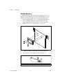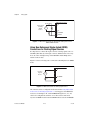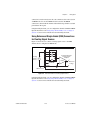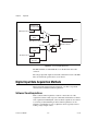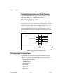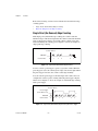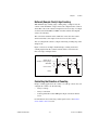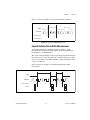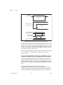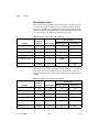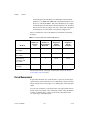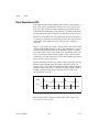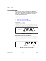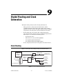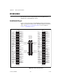
1
DAQ X Series
X Series User Manual
NI 632x/634x/635x/636x Devices
X Series User Manual
Français
Deutsch
ni.com/manuals
February 2012
370784D-01
Support
Worldwide Technical Support and Product Information
ni.com
Worldwide Offices
Visit ni.com/niglobal to access the branch office Web sites, which provide up-to-date contact information,
support phone numbers, email addresses, and current events.
National Instruments Corporate Headquarters
11500 North Mopac Expressway Austin, Texas 78759-3504 USA Tel: 512 683 0100
For further support information, refer to the Technical Support and Professional Services appendix. To comment
on National Instruments documentation, refer to the National Instruments Web site at ni.com/info and enter
the Info Code feedback.
© 2009–2012 National Instruments. All rights reserved.
Important Information
Warranty
X Series devices are warranted against defects in materials and workmanship for a period of one year from the date of shipment, as evidenced
by receipts or other documentation. National Instruments will, at its option, repair or replace equipment that proves to be defective during the
warranty period. This warranty includes parts and labor.
The media on which you receive National Instruments software are warranted not to fail to execute programming instructions, due to defects in
materials and workmanship, for a period of 90 days from date of shipment, as evidenced by receipts or other documentation. National Instruments
will, at its option, repair or replace software media that do not execute programming instructions if National Instruments receives notice of such defects
during the warranty period. National Instruments does not warrant that the operation of the software shall be uninterrupted or error free.
A Return Material Authorization (RMA) number must be obtained from the factory and clearly marked on the outside of the package before any
equipment will be accepted for warranty work. National Instruments will pay the shipping costs of returning to the owner parts which are covered by
warranty.
National Instruments believes that the information in this document is accurate. The document has been carefully reviewed for technical accuracy. In
the event that technical or typographical errors exist, National Instruments reserves the right to make changes to subsequent editions of this document
without prior notice to holders of this edition. The reader should consult National Instruments if errors are suspected. In no event shall National
Instruments be liable for any damages arising out of or related to this document or the information contained in it.
EXCEPT AS SPECIFIED HEREIN, NATIONAL INSTRUMENTS MAKES NO WARRANTIES, EXPRESS OR IMPLIED, AND SPECIFICALLY DISCLAIMS ANY WARRANTY OF
MERCHANTABILITY OR FITNESS FOR A PARTICULAR PURPOSE. CUSTOMER’S RIGHT TO RECOVER DAMAGES CAUSED BY FAULT OR NEGLIGENCE ON THE PART OF NATIONAL
INSTRUMENTS SHALL BE LIMITED TO THE AMOUNT THERETOFORE PAID BY THE CUSTOMER. NATIONAL INSTRUMENTS WILL NOT BE LIABLE FOR DAMAGES RESULTING
FROM LOSS OF DATA, PROFITS, USE OF PRODUCTS, OR INCIDENTAL OR CONSEQUENTIAL DAMAGES, EVEN IF ADVISED OF THE POSSIBILITY THEREOF. This limitation of
the liability of National Instruments will apply regardless of the form of action, whether in contract or tort, including negligence. Any action against
National Instruments must be brought within one year after the cause of action accrues. National Instruments shall not be liable for any delay in
performance due to causes beyond its reasonable control. The warranty provided herein does not cover damages, defects, malfunctions, or service
failures caused by owner’s failure to follow the National Instruments installation, operation, or maintenance instructions; owner’s modification of the
product; owner’s abuse, misuse, or negligent acts; and power failure or surges, fire, flood, accident, actions of third parties, or other events outside
reasonable control.
Copyright
Under the copyright laws, this publication may not be reproduced or transmitted in any form, electronic or mechanical, including photocopying,
recording, storing in an information retrieval system, or translating, in whole or in part, without the prior written consent of National
Instruments Corporation.
National Instruments respects the intellectual property of others, and we ask our users to do the same. NI software is protected by copyright and other
intellectual property laws. Where NI software may be used to reproduce software or other materials belonging to others, you may use NI software only
to reproduce materials that you may reproduce in accordance with the terms of any applicable license or other legal restriction.
Trademarks
CVI, LabVIEW, National Instruments, NI, ni.com, the National Instruments corporate logo, and the Eagle logo are trademarks of National
Instruments Corporation. Refer to the Trademark Information at ni.com/trademarks for other National Instruments trademarks.
The mark LabWindows is used under a license from Microsoft Corporation. Windows is a registered trademark of Microsoft Corporation in the United
States and other countries. Other product and company names mentioned herein are trademarks or trade names of their respective companies.
Members of the National Instruments Alliance Partner Program are business entities independent from National Instruments and have no agency,
partnership, or joint-venture relationship with National Instruments.
Patents
For patents covering National Instruments products/technology, refer to the appropriate location: Help»Patents in your software,
the patents.txt file on your media, or the National Instruments Patent Notice at ni.com/patents.
Export Compliance Information
Refer to the Export Compliance Information at ni.com/legal/export-compliance for the National Instruments global trade compliance
policy and how to obtain relevant HTS codes, ECCNs, and other import/export data.
WARNING REGARDING USE OF NATIONAL INSTRUMENTS PRODUCTS
(1) NATIONAL INSTRUMENTS PRODUCTS ARE NOT DESIGNED WITH COMPONENTS AND TESTING FOR A LEVEL OF
RELIABILITY SUITABLE FOR USE IN OR IN CONNECTION WITH SURGICAL IMPLANTS OR AS CRITICAL COMPONENTS IN
ANY LIFE SUPPORT SYSTEMS WHOSE FAILURE TO PERFORM CAN REASONABLY BE EXPECTED TO CAUSE SIGNIFICANT
INJURY TO A HUMAN.
(2) IN ANY APPLICATION, INCLUDING THE ABOVE, RELIABILITY OF OPERATION OF THE SOFTWARE PRODUCTS CAN BE
IMPAIRED BY ADVERSE FACTORS, INCLUDING BUT NOT LIMITED TO FLUCTUATIONS IN ELECTRICAL POWER SUPPLY,
COMPUTER HARDWARE MALFUNCTIONS, COMPUTER OPERATING SYSTEM SOFTWARE FITNESS, FITNESS OF COMPILERS
AND DEVELOPMENT SOFTWARE USED TO DEVELOP AN APPLICATION, INSTALLATION ERRORS, SOFTWARE AND HARDWARE
COMPATIBILITY PROBLEMS, MALFUNCTIONS OR FAILURES OF ELECTRONIC MONITORING OR CONTROL DEVICES,
TRANSIENT FAILURES OF ELECTRONIC SYSTEMS (HARDWARE AND/OR SOFTWARE), UNANTICIPATED USES OR MISUSES, OR
ERRORS ON THE PART OF THE USER OR APPLICATIONS DESIGNER (ADVERSE FACTORS SUCH AS THESE ARE HEREAFTER
COLLECTIVELY TERMED “SYSTEM FAILURES”). ANY APPLICATION WHERE A SYSTEM FAILURE WOULD CREATE A RISK OF
HARM TO PROPERTY OR PERSONS (INCLUDING THE RISK OF BODILY INJURY AND DEATH) SHOULD NOT BE RELIANT SOLELY
UPON ONE FORM OF ELECTRONIC SYSTEM DUE TO THE RISK OF SYSTEM FAILURE. TO AVOID DAMAGE, INJURY, OR DEATH,
THE USER OR APPLICATION DESIGNER MUST TAKE REASONABLY PRUDENT STEPS TO PROTECT AGAINST SYSTEM FAILURES,
INCLUDING BUT NOT LIMITED TO BACK-UP OR SHUT DOWN MECHANISMS. BECAUSE EACH END-USER SYSTEM IS
CUSTOMIZED AND DIFFERS FROM NATIONAL INSTRUMENTS' TESTING PLATFORMS AND BECAUSE A USER OR APPLICATION
DESIGNER MAY USE NATIONAL INSTRUMENTS PRODUCTS IN COMBINATION WITH OTHER PRODUCTS IN A MANNER NOT
EVALUATED OR CONTEMPLATED BY NATIONAL INSTRUMENTS, THE USER OR APPLICATION DESIGNER IS ULTIMATELY
RESPONSIBLE FOR VERIFYING AND VALIDATING THE SUITABILITY OF NATIONAL INSTRUMENTS PRODUCTS WHENEVER
NATIONAL INSTRUMENTS PRODUCTS ARE INCORPORATED IN A SYSTEM OR APPLICATION, INCLUDING, WITHOUT
LIMITATION, THE APPROPRIATE DESIGN, PROCESS AND SAFETY LEVEL OF SUCH SYSTEM OR APPLICATION.
Electromagnetic Compatibility Guidelines
This product was tested and complies with the regulatory requirements and limits for electromagnetic compatibility (EMC) as
stated in the product specifications. These requirements and limits are designed to provide reasonable protection against harmful
interference when the product is operated in its intended operational electromagnetic environment.
This product is intended for use in industrial locations. There is no guarantee that harmful interference will not occur in a
particular installation, when the product is connected to a test object, or if the product is used in residential areas. To minimize
the potential for the product to cause interference to radio and television reception or to experience unacceptable performance
degradation, install and use this product in strict accordance with the instructions in the product documentation.
Furthermore, any changes or modifications to the product not expressly approved by National Instruments could void your
authority to operate it under your local regulatory rules.
Caution To ensure the specified EMC performance, operate this product only with shielded cables and
accessories.
Contents
About This Manual
Conventions ...................................................................................................................xvii
Related Documentation..................................................................................................xviii
Chapter 1
Getting Started
Installation .....................................................................................................................1-1
Unpacking ......................................................................................................................1-1
Device Self-Calibration .................................................................................................1-2
Getting Started with X Series USB Devices..................................................................1-3
USB Device Chassis Ground...........................................................................1-3
Ferrite Installation ...........................................................................................1-4
Mounting X Series USB Devices ....................................................................1-5
Panel/Wall Mounting ........................................................................1-5
DIN Rail Mounting ...........................................................................1-6
USB Device LEDs...........................................................................................1-7
USB Cable Strain Relief..................................................................................1-7
USB Device Security Cable Slot.....................................................................1-8
Device Pinouts ...............................................................................................................1-8
Device Specifications ....................................................................................................1-8
Device Accessories and Cables .....................................................................................1-8
Chapter 2
DAQ System Overview
DAQ Hardware ..............................................................................................................2-1
DAQ-STC3......................................................................................................2-2
Calibration Circuitry........................................................................................2-3
Cables and Accessories..................................................................................................2-3
PCI Express, PXI Express, and USB Mass Termination Device Cables
and Accessories ............................................................................................2-3
SCXI Accessories .............................................................................2-4
SCC Accessories ...............................................................................2-5
BNC Accessories ..............................................................................2-5
Screw Terminal Accessories.............................................................2-6
RTSI Cables ......................................................................................2-6
Cables................................................................................................2-6
Custom Cabling and Connectivity ....................................................2-7
USB Device Mounting Accessories, USB Cable, Power Supply,
and Ferrite ......................................................................................2-7
USB Screw Terminal Device Accessories ......................................................2-8
© National Instruments
vii
X Series User Manual
Contents
Signal Conditioning....................................................................................................... 2-8
Sensors and Transducers ................................................................................. 2-8
Signal Conditioning Options........................................................................... 2-9
SCXI ................................................................................................. 2-9
SCC................................................................................................... 2-9
Programming Devices in Software................................................................................ 2-10
Chapter 3
Connector and LED Information
I/O Connector Signal Descriptions................................................................................ 3-1
+5 V Power Source........................................................................................................ 3-3
PCI Express Device Disk Drive Power Connector ....................................................... 3-4
When to Use the Disk Drive Power Connector .............................................. 3-4
Disk Drive Power Connector Installation ....................................................... 3-4
RTSI Connector Pinout ................................................................................................. 3-5
USB Device LED Patterns ............................................................................................ 3-5
Chapter 4
Analog Input
Analog Input on MIO X Series Devices........................................................................ 4-1
Analog Input Range ........................................................................................ 4-2
Working Voltage Range.................................................................................. 4-4
Analog Input Ground-Reference Settings....................................................... 4-4
Configuring AI Ground-Reference Settings in Software ................. 4-6
Multichannel Scanning Considerations .......................................................... 4-6
Analog Input Data Acquisition Methods ........................................................ 4-9
Software-Timed Acquisitions........................................................... 4-10
Hardware-Timed Acquisitions ......................................................... 4-10
Analog Input Triggering ................................................................................. 4-11
Connecting Analog Input Signals ................................................................... 4-11
Connecting Floating Signal Sources ............................................................... 4-13
What Are Floating Signal Sources?.................................................. 4-13
When to Use Differential Connections with Floating
Signal Sources ............................................................................... 4-13
When to Use Non-Referenced Single-Ended (NRSE)
Connections with Floating Signal Sources .................................... 4-13
When to Use Referenced Single-Ended (RSE) Connections
with Floating Signal Sources ......................................................... 4-14
Using Differential Connections for Floating Signal Sources ........... 4-15
Using Non-Referenced Single-Ended (NRSE) Connections
for Floating Signal Sources ........................................................... 4-18
Using Referenced Single-Ended (RSE) Connections
for Floating Signal Sources ........................................................... 4-19
X Series User Manual
viii
ni.com
Contents
Connecting Ground-Referenced Signal Sources .............................................4-20
What Are Ground-Referenced Signal Sources?................................4-20
When to Use Differential Connections with
Ground-Referenced Signal Sources ...............................................4-20
When to Use Non-Referenced Single-Ended (NRSE)
Connections with Ground-Referenced Signal Sources ..................4-21
When to Use Referenced Single-Ended (RSE)
Connections with Ground-Referenced Signal Sources ..................4-21
Using Differential Connections for Ground-Referenced
Signal Sources................................................................................4-22
Using Non-Referenced Single-Ended (NRSE) Connections
for Ground-Referenced Signal Sources .........................................4-23
Field Wiring Considerations............................................................................4-24
Analog Input Timing Signals ..........................................................................4-24
Aggregate versus Single Channel Sample Rates ..............................4-27
AI Sample Clock Signal....................................................................4-28
AI Sample Clock Timebase Signal ...................................................4-30
AI Convert Clock Signal...................................................................4-31
AI Convert Clock Timebase Signal ..................................................4-34
AI Hold Complete Event Signal .......................................................4-34
AI Start Trigger Signal......................................................................4-35
AI Reference Trigger Signal .............................................................4-37
AI Pause Trigger Signal ....................................................................4-38
Getting Started with AI Applications in Software ..........................................4-40
Analog Input on Simultaneous MIO X Series Devices .................................................4-41
Analog Input Terminal Configuration.............................................................4-42
Analog Input Range.........................................................................................4-42
Working Voltage Range ..................................................................................4-43
Analog Input Data Acquisition Methods.........................................................4-44
Analog Input Triggering..................................................................................4-46
Connecting Analog Input Signals....................................................................4-46
Types of Signal Sources....................................................................4-47
Differential Connections for Ground-Referenced Signal Sources....4-48
Differential Connections for Floating Signal Sources ......................4-49
Field Wiring Considerations............................................................................4-51
Minimizing Drift in Differential Mode .............................................4-51
Analog Input Timing Signals ..........................................................................4-52
Aggregate versus Single Channel Sample Rates ..............................4-53
AI Sample Clock Signal....................................................................4-54
AI Sample Clock Timebase Signal ...................................................4-56
AI Hold Complete Event Signal .......................................................4-57
AI Start Trigger Signal......................................................................4-57
AI Reference Trigger Signal .............................................................4-59
AI Pause Trigger Signal ....................................................................4-61
Getting Started with AI Applications in Software ..........................................4-62
© National Instruments
ix
X Series User Manual
Contents
Chapter 5
Analog Output
AO Reference Selection ................................................................................................ 5-2
Minimizing Glitches on the Output Signal.................................................................... 5-3
Analog Output Data Generation Methods..................................................................... 5-3
Software-Timed Generations .......................................................................... 5-3
Hardware-Timed Generations......................................................................... 5-3
Analog Output Triggering ............................................................................................. 5-5
Connecting Analog Output Signals ............................................................................... 5-5
Analog Output Timing Signals...................................................................................... 5-6
AO Start Trigger Signal .................................................................................. 5-7
Retriggerable Analog Output............................................................ 5-7
Using a Digital Source...................................................................... 5-7
Using an Analog Source ................................................................... 5-8
Routing AO Start Trigger Signal to an Output Terminal ................. 5-8
AO Pause Trigger Signal ................................................................................ 5-8
Using a Digital Source...................................................................... 5-9
Using an Analog Source ................................................................... 5-10
Routing AO Pause Trigger Signal to an Output Terminal ............... 5-10
AO Sample Clock Signal ................................................................................ 5-10
Using an Internal Source .................................................................. 5-10
Using an External Source ................................................................. 5-11
Routing AO Sample Clock Signal to an Output Terminal ............... 5-11
Other Timing Requirements ............................................................. 5-11
AO Sample Clock Timebase Signal................................................................ 5-12
Getting Started with AO Applications in Software....................................................... 5-13
Chapter 6
Digital I/O
Digital Input Data Acquisition Methods ....................................................................... 6-2
Software-Timed Acquisitions ......................................................................... 6-2
Hardware-Timed Acquisitions ........................................................................ 6-3
Digital Input Triggering ................................................................................................ 6-4
Digital Waveform Acquisition ...................................................................................... 6-5
DI Sample Clock Signal.................................................................................. 6-6
Using an Internal Source .................................................................. 6-6
Using an External Source ................................................................. 6-6
Routing DI Sample Clock to an Output Terminal ............................ 6-7
Other Timing Requirements ............................................................. 6-7
DI Sample Clock Timebase Signal ................................................................. 6-7
X Series User Manual
x
ni.com
Contents
DI Start Trigger Signal ....................................................................................6-8
Retriggerable DI................................................................................6-8
Using a Digital Source ......................................................................6-9
Using an Analog Source ...................................................................6-10
Routing DI Start Trigger to an Output Terminal ..............................6-10
DI Reference Trigger Signal ...........................................................................6-10
Using a Digital Source ......................................................................6-11
Using an Analog Source ...................................................................6-12
Routing DI Reference Trigger Signal to an Output Terminal ..........6-12
DI Pause Trigger Signal ..................................................................................6-12
Using a Digital Source ......................................................................6-13
Using an Analog Source ...................................................................6-13
Routing DI Pause Trigger Signal to an Output Terminal .................6-13
Digital Output Data Generation Methods ......................................................................6-14
Software-Timed Generations...........................................................................6-14
Hardware-Timed Generations .........................................................................6-14
Digital Output Triggering ..............................................................................................6-16
Digital Waveform Generation .......................................................................................6-16
DO Sample Clock Signal.................................................................................6-17
Using an Internal Source...................................................................6-17
Using an External Source..................................................................6-17
Routing DO Sample Clock to an Output Terminal...........................6-18
Other Timing Requirements..............................................................6-18
DO Sample Clock Timebase Signal ................................................................6-18
DO Start Trigger Signal...................................................................................6-19
Retriggerable DO ..............................................................................6-19
Using a Digital Source ......................................................................6-20
Using an Analog Source ...................................................................6-20
Routing DO Start Trigger Signal to an Output Terminal..................6-20
DO Pause Trigger Signal.................................................................................6-21
Using a Digital Source ......................................................................6-22
Using an Analog Source ...................................................................6-22
Routing DO Pause Trigger Signal to an Output Terminal................6-22
I/O Protection.................................................................................................................6-23
Programmable Power-Up States ....................................................................................6-23
DI Change Detection .....................................................................................................6-24
DI Change Detection Applications..................................................................6-25
Digital Filtering..............................................................................................................6-25
Watchdog Timer..............................................................................................6-28
Connecting Digital I/O Signals......................................................................................6-29
Getting Started with DIO Applications in Software ......................................................6-30
© National Instruments
xi
X Series User Manual
Contents
Chapter 7
Counters
Counter Timing Engine ................................................................................................. 7-2
Counter Input Applications ........................................................................................... 7-3
Counting Edges ............................................................................................... 7-3
Single Point (On-Demand) Edge Counting ...................................... 7-4
Buffered (Sample Clock) Edge Counting......................................... 7-5
Controlling the Direction of Counting.............................................. 7-5
Pulse-Width Measurement .............................................................................. 7-6
Single Pulse-Width Measurement .................................................... 7-6
Implicit Buffered Pulse-Width Measurement................................... 7-7
Sample Clocked Buffered Pulse-Width Measurement ..................... 7-8
Hardware-Timed Single Point Pulse-Width Measurement .............. 7-8
Pulse Measurement ......................................................................................... 7-9
Single Pulse Measurement................................................................ 7-9
Implicit Buffered Pulse Measurement .............................................. 7-10
Sample Clocked Buffered Pulse Measurement ................................ 7-10
Hardware-Timed Single Point Pulse Measurement.......................... 7-11
Pulse versus Semi-Period Measurements ......................................... 7-11
Semi-Period Measurement .............................................................................. 7-12
Single Semi-Period Measurement .................................................... 7-12
Implicit Buffered Semi-Period Measurement................................... 7-12
Frequency Measurement ................................................................................. 7-13
Low Frequency with One Counter ................................................... 7-13
High Frequency with Two Counters ................................................ 7-14
Large Range of Frequencies with Two Counters ............................. 7-15
Sample Clocked Buffered Frequency Measurement ........................ 7-16
Hardware-Timed Single Point Frequency Measurement ................. 7-18
Choosing a Method for Measuring Frequency ................................. 7-18
Period Measurement ....................................................................................... 7-22
Position Measurement..................................................................................... 7-23
Measurements Using Quadrature Encoders...................................... 7-23
Measurements Using Two Pulse Encoders ...................................... 7-25
Buffered (Sample Clock) Position Measurement ............................. 7-25
Hardware-Timed Single Point Position Measurement ..................... 7-26
Two-Signal Edge-Separation Measurement ................................................... 7-26
Single Two-Signal Edge-Separation Measurement.......................... 7-27
Implicit Buffered Two-Signal Edge-Separation Measurement ........ 7-28
Sample Clocked Buffered Two-Signal Separation Measurement .... 7-28
Hardware-Timed Single Point Two-Signal Separation
Measurement.................................................................................. 7-29
X Series User Manual
xii
ni.com
Contents
Counter Output Applications .........................................................................................7-30
Simple Pulse Generation .................................................................................7-30
Single Pulse Generation ....................................................................7-30
Single Pulse Generation with Start Trigger ......................................7-31
Pulse Train Generation ....................................................................................7-31
Finite Pulse Train Generation ...........................................................7-32
Retriggerable Pulse or Pulse Train Generation.................................7-33
Continuous Pulse Train Generation ..................................................7-34
Buffered Pulse Train Generation ......................................................7-35
Finite Implicit Buffered Pulse Train Generation ..............................7-35
Continuous Buffered Implicit Pulse Train Generation .....................7-36
Finite Buffered Sample Clocked Pulse Train Generation.................7-36
Continuous Buffered Sample Clocked Pulse Train Generation........7-38
Frequency Generation .....................................................................................7-38
Using the Frequency Generator ........................................................7-38
Frequency Division .........................................................................................7-39
Pulse Generation for ETS................................................................................7-40
Counter Timing Signals .................................................................................................7-41
Counter n Source Signal..................................................................................7-41
Routing a Signal to Counter n Source...............................................7-42
Routing Counter n Source to an Output Terminal ............................7-42
Counter n Gate Signal .....................................................................................7-43
Routing a Signal to Counter n Gate ..................................................7-43
Routing Counter n Gate to an Output Terminal................................7-43
Counter n Aux Signal ......................................................................................7-43
Routing a Signal to Counter n Aux...................................................7-44
Counter n A, Counter n B, and Counter n Z Signals.......................................7-44
Routing Signals to A, B, and Z Counter Inputs ................................7-44
Routing Counter n Z Signal to an Output Terminal..........................7-44
Counter n Up_Down Signal ............................................................................7-44
Counter n HW Arm Signal ..............................................................................7-45
Routing Signals to Counter n HW Arm Input...................................7-45
Counter n Sample Clock Signal ......................................................................7-45
Using an Internal Source...................................................................7-46
Using an External Source..................................................................7-46
Routing Counter n Sample Clock to an Output Terminal.................7-46
Counter n Internal Output and Counter n TC Signals .....................................7-47
Routing Counter n Internal Output to an Output Terminal...............7-47
Frequency Output Signal.................................................................................7-47
Routing Frequency Output to a Terminal .........................................7-47
Default Counter/Timer Pinouts......................................................................................7-47
Counter Triggering ........................................................................................................7-50
© National Instruments
xiii
X Series User Manual
Contents
Other Counter Features.................................................................................................. 7-51
Cascading Counters......................................................................................... 7-51
Prescaling ........................................................................................................ 7-51
Synchronization Modes................................................................................... 7-52
100 MHz Source Mode..................................................................... 7-52
External Source Greater than 25 MHz.............................................. 7-52
External or Internal Source Less than 25 MHz ................................ 7-53
Chapter 8
PFI
Using PFI Terminals as Timing Input Signals .............................................................. 8-2
Exporting Timing Output Signals Using PFI Terminals............................................... 8-3
Using PFI Terminals as Static Digital I/Os ................................................................... 8-4
Using PFI Terminals to Digital Detection Events......................................................... 8-4
Connecting PFI Input Signals........................................................................................ 8-4
PFI Filters ...................................................................................................................... 8-5
I/O Protection ................................................................................................................ 8-7
Programmable Power-Up States.................................................................................... 8-7
Chapter 9
Digital Routing and Clock Generation
Clock Routing................................................................................................................ 9-1
100 MHz Timebase ......................................................................................... 9-2
20 MHz Timebase ........................................................................................... 9-2
100 kHz Timebase .......................................................................................... 9-2
External Reference Clock ............................................................................... 9-2
10 MHz Reference Clock................................................................................ 9-3
Synchronizing Multiple Devices ................................................................................... 9-3
PXI Express Devices....................................................................................... 9-3
PCI Express Devices ....................................................................................... 9-3
USB Devices ................................................................................................... 9-4
Real-Time System Integration (RTSI) .......................................................................... 9-4
RTSI Connector Pinout ................................................................................... 9-5
Using RTSI as Outputs ................................................................................... 9-6
Using RTSI Terminals as Timing Input Signals............................................. 9-7
RTSI Filters..................................................................................................... 9-7
PXI and PXI Express Clock and Trigger Signals.......................................................... 9-8
PXIe_CLK100 ................................................................................................ 9-8
PXIe_SYNC100.............................................................................................. 9-8
PXI_CLK10 .................................................................................................... 9-8
PXI Triggers.................................................................................................... 9-8
PXI_STAR Trigger ......................................................................................... 9-9
X Series User Manual
xiv
ni.com
Contents
PXI_STAR Filters ...........................................................................................9-9
PXIe-DSTAR<A..C> ......................................................................................9-9
Chapter 10
Bus Interface
Data Transfer Methods ..................................................................................................10-1
PCI Express/PXI Express Device Data Transfer Methods..............................10-1
USB Device Data Transfer Methods...............................................................10-2
PXI Express Considerations ..........................................................................................10-3
PXI and PXI Express Clock and Trigger Signals............................................10-3
PXI Express .....................................................................................................10-3
Chapter 11
Triggering
Triggering with a Digital Source ...................................................................................11-1
Triggering with an Analog Source.................................................................................11-2
APFI <0,1> Terminals.....................................................................................11-3
Analog Input Channels ....................................................................................11-3
Analog Input Channels on MIO X Series Devices ...........................11-4
Analog Input Channels on Simultaneous MIO X Series Devices ....11-4
Analog Trigger Actions...................................................................................11-4
Routing Analog Comparison Event to an Output Terminal............................11-5
Analog Trigger Types ....................................................................................................11-5
Analog Trigger Accuracy ..............................................................................................11-8
Appendix A
Device-Specific Information
NI 6320 ..........................................................................................................................A-2
NI 6321/6341 .................................................................................................................A-5
NI 6323/6343 .................................................................................................................A-8
NI 6351/6361 .................................................................................................................A-12
NI 6353/6363 .................................................................................................................A-16
NI 6356/6366 .................................................................................................................A-22
NI 6358/6368 .................................................................................................................A-27
Appendix B
Troubleshooting
Appendix C
Technical Support and Professional Services
© National Instruments
xv
X Series User Manual
Contents
Glossary
Index
Device Pinouts
Figure A-1.
Figure A-2.
Figure A-3.
Figure A-4.
Figure A-5.
Figure A-6.
Figure A-7.
Figure A-8.
Figure A-9.
Figure A-10.
Figure A-11.
Figure A-12.
Figure A-13.
Figure A-14.
Figure A-15.
X Series User Manual
NI PCIe-6320 Pinout............................................................................. A-3
NI PCIe-6321 and NI PCIe/PXIe-6341 Pinout ..................................... A-6
NI USB-6341 Pinout............................................................................. A-7
NI PCIe-6323/6343 Pinout ................................................................... A-8
NI USB-6343 Pinout............................................................................. A-10
NI PCIe-6351 and NI PCIe/PXIe-6361 Pinout ..................................... A-12
NI USB-6351/6361 Screw Terminal Pinout ......................................... A-13
NI USB-6361 Mass Termination Pinout............................................... A-14
NI PCIe-6353 and NI PCIe/PXIe-6363 Pinout ..................................... A-16
NI USB-6363 Mass Termination Pinout............................................... A-18
NI USB-6353/6363 Screw Terminal Pinout ......................................... A-20
NI PXIe-6356/6366 Pinout ................................................................... A-22
NI USB-6366 Mass Termination Pinout............................................... A-24
NI USB-6356/6366 Screw Terminal Pinout ......................................... A-25
NI PXIe-6358/6368 Pinout ................................................................... A-27
xvi
ni.com
About This Manual
The X Series User Manual contains information about using the National
Instruments X Series data acquisition (DAQ) devices with NI-DAQmx 9.5
and later. X Series devices feature up to 32 analog input (AI) channels, up
to four analog output (AO) channels, up to 48 lines of digital input/output
(DIO), and four counters.
Conventions
The following conventions are used in this manual:
<>
Angle brackets that contain numbers separated by an ellipsis represent a
range of values associated with a bit or signal name—for example,
AO <3..0>.
»
The » symbol leads you through nested menu items and dialog box options
to a final action. The sequence Options»Settings»General directs you to
pull down the Options menu, select the Settings item, and select General
from the last dialog box.
This icon denotes a note, which alerts you to important information.
This icon denotes a caution, which advises you of precautions to take to
avoid injury, data loss, or a system crash. When this symbol is marked on a
product, refer to the Read Me First: Safety and Electromagnetic
Compatibility for information about precautions to take.
bold
Bold text denotes items that you must select or click in the software, such as
menu items and dialog box options. Bold text also denotes parameter names.
italic
Italic text denotes variables, emphasis, a cross-reference, or an introduction
to a key concept. Italic text also denotes text that is a placeholder for a word
or value that you must supply.
monospace
Text in this font denotes text or characters that you should enter from the
keyboard, sections of code, programming examples, and syntax examples.
This font is also used for the proper names of disk drives, paths, directories,
programs, subprograms, subroutines, device names, functions, operations,
variables, filenames, and extensions.
Platform
Text in this font denotes a specific platform and indicates that the text
following it applies only to that platform.
© National Instruments
xvii
X Series User Manual
About This Manual
Related Documentation
Each application software package and driver includes information about
writing applications for taking measurements and controlling measurement
devices. The following references to documents assume you have
NI-DAQmx 9.2 or later, and where applicable, version 8.5 or later of the
NI application software.
NI-DAQmx for Windows
The DAQ Getting Started guides packaged with NI-DAQmx describe how
to install your NI-DAQmx for Windows software, how to install your
NI-DAQmx-supported DAQ device, and how to confirm that your device is
operating properly.
The NI-DAQ Readme lists which devices, ADEs, and NI application
software are supported by this version of NI-DAQ. Select Start»
All Programs»National Instruments»NI-DAQ»NI-DAQ Readme.
The NI-DAQmx Help contains general information about measurement
concepts, key NI-DAQmx concepts, and common applications that are
applicable to all programming environments. Select Start»All Programs»
National Instruments»NI-DAQ»NI-DAQmx Help.
LabVIEW
If you are a new user, use the Getting Started with LabVIEW manual to
familiarize yourself with the LabVIEW graphical programming
environment and the basic LabVIEW features you use to build data
acquisition and instrument control applications. Open the Getting Started
with LabVIEW manual by selecting Start»All Programs»National
Instruments»LabVIEW»LabVIEW Manuals or by navigating to the
labview\manuals directory and opening LV_Getting_Started.pdf.
Use the LabVIEW Help, available by selecting Help»Search the
LabVIEW Help in LabVIEW, to access information about LabVIEW
programming concepts, step-by-step instructions for using LabVIEW, and
reference information about LabVIEW VIs, functions, palettes, menus, and
tools. Refer to the following locations on the Contents tab of the LabVIEW
Help for information about NI-DAQmx:
•
X Series User Manual
Getting Started with LabVIEW»Getting Started with
DAQ—Includes overview information and a tutorial to learn how to
take an NI-DAQmx measurement in LabVIEW using the DAQ
Assistant.
xviii
ni.com
About This Manual
•
VI and Function Reference»Measurement I/O VIs and Functions»
DAQmx - Data Acquisition VIs and Functions—Describes the
LabVIEW NI-DAQmx VIs and properties.
•
Taking Measurements—Contains the conceptual and how-to
information you need to acquire and analyze measurement data in
LabVIEW, including common measurements, measurement
fundamentals, NI-DAQmx key concepts, and device considerations.
LabWindows/CVI
The Data Acquisition book of the LabWindows/CVI Help contains Taking
an NI-DAQmx Measurement in LabWindows/CVI, which includes
step-by-step instructions about creating a measurement task using the DAQ
Assistant. In LabWindows™/CVI™, select Help»Contents, then select
Using LabWindows/CVI»Data Acquisition. This book also contains
information about accessing detailed information through the NI-DAQmx
Help.
The NI-DAQmx Library book of the LabWindows/CVI Help contains
API overviews and function reference for NI-DAQmx. Select Library
Reference»NI-DAQmx Library in the LabWindows/CVI Help.
Measurement Studio
If you program your NI-DAQmx-supported device in Measurement Studio
using Visual C++, Visual C#, or Visual Basic .NET, you can interactively
create channels and tasks by launching the DAQ Assistant from MAX or
from within Visual Studio. You can use Measurement Studio to generate
the configuration code based on your task or channel. Refer to the DAQ
Assistant Help for additional information about generating code.
The NI Measurement Studio Help is fully integrated with the Microsoft
Visual Studio help. To view this help file in Visual Studio, select
Measurement Studio»NI Measurement Studio Help. For information
related to developing with NI-DAQmx, refer to the following topics within
the NI Measurement Studio Help:
© National Instruments
•
For step-by-step instructions on how to create an NI-DAQmx
application using the Measurement Studio Application Wizard and the
DAQ Assistant, refer to Walkthrough: Creating a Measurement Studio
NI-DAQmx Application.
•
For help with NI-DAQmx methods and properties, refer to
NationalInstruments.DAQmx Namespace,
NationalInstruments.DAQmx.ComponentModel Namespace, or
NI-DAQmx Visual C++ Class Library Overview.
xix
X Series User Manual
About This Manual
•
For conceptual help with NI-DAQmx, refer to Using the Measurement
Studio NI-DAQmx .NET Library, Using the Measurement Studio
NI-DAQmx Visual C++ Library, or Developing with Measurement
Studio NI-DAQmx.
•
For general help with programming in Measurement Studio, refer to
Getting Started with the Measurement Studio Class Libraries.
To create an application in Visual Basic .NET, Visual C#, or Visual C++,
follow these general steps:
1.
In Visual Studio, select File»New»Project to launch the New Project
dialog box.
2.
In the Project types pane, expand the Visual Basic, Visual C#, or
Visual C++ node, depending on which language you want to create the
project in, and select Measurement Studio.
3.
Choose a project type. You add DAQ tasks as a part of this step.
ANSI C without NI Application Software
The NI-DAQmx Help contains API overviews and general information
about measurement concepts. Select Start»All Programs»National
Instruments»NI-DAQ»NI-DAQmx Help.
The NI-DAQmx C Reference Help describes the NI-DAQmx Library
functions, which you can use with National Instruments data acquisition
devices to develop instrumentation, acquisition, and control applications.
Select Start»All Programs»National Instruments»NI-DAQ»
Text-Based Code Support»NI-DAQmx C Reference Help.
.NET Languages without NI Application Software
With the Microsoft .NET Framework version 1.1 or later, you can use
NI-DAQmx to create applications using Visual C# and Visual Basic
.NET without Measurement Studio. You need Microsoft Visual Studio
.NET 2003 or later for the API documentation to be installed.
The installed documentation contains the NI-DAQmx API overview,
measurement tasks and concepts, and function reference. This help is fully
integrated into the Visual Studio documentation. To view the NI-DAQmx
.NET documentation, go to Start»All Programs»National Instruments»
NI-DAQ»Text-Based Code Support»NI-DAQmx .NET Help. For
function reference, refer to the NationalInstruments.DAQmx Namespace
and NationalInstruments.DAQmx.ComponentModel Namespace topics.
For conceptual help, refer to the Using the Measurement Studio NI-DAQmx
X Series User Manual
xx
ni.com
About This Manual
.NET Library and Developing with Measurement Studio NI-DAQmx
sections.
To get to the same help topics from within Visual Studio, go to Help»
Contents and select Measurement Studio from the Filtered By
drop-down list.
Device Documentation and Specifications
The NI 632x Specifications contains all specifications for the NI 6320,
NI 6321, and NI 6323 MIO X Series devices.
The NI 634x Specifications contains all specifications for the NI 6341 and
NI 6343 MIO X Series devices.
The NI 6351/6353 Specifications contains all specifications for the NI 6351
and NI 6353 MIO X Series devices.
The NI 6356/6358 Specifications contains all specifications for the NI 6356
and NI 6358 Simultaneous MIO X Series devices.
The NI 6361/6363 Specifications contains all specifications for the NI 6361
and NI 6363 MIO X Series devices.
The NI 6366/6368 Specifications contains all specifications for the NI 6366
and NI 6368 Simultaneous MIO X Series devices.
Documentation for supported devices and accessories, including PDF and
help files describing device terminals, specifications, features, and
operation are on the NI-DAQmx media that includes Device
Documentation.
Training Courses
If you need more help getting started developing an application with
NI products, NI offers training courses. To enroll in a course or obtain a
detailed course outline, refer to ni.com/training.
© National Instruments
xxi
X Series User Manual
About This Manual
Technical Support on the Web
For additional support, refer to ni.com/support or zone.ni.com.
Note
You can download these documents at ni.com/manuals.
DAQ specifications and some DAQ manuals are available as PDFs. You
must have Adobe Acrobat Reader with Search and Accessibility 5.0.5 or
later installed to view the PDFs. Refer to the Adobe Systems Incorporated
Web site at www.adobe.com to download Acrobat Reader. Refer to the
National Instruments Product Manuals Library at ni.com/manuals for
updated documentation resources.
X Series User Manual
xxii
ni.com
1
Getting Started
X Series devices feature up to 32 analog input (AI) channels, up to
four analog output (AO) channels, up to 48 lines of digital input/output
(DIO), and four counters. This chapter provides basic information you need
to get started using your X Series device.
Installation
Before installing your DAQ device, you must install the software you plan
to use with the device.
1.
Installing application software—Refer to the installation
instructions that accompany your software.
2.
Installing NI-DAQmx—The DAQ Getting Started guides, packaged
with NI-DAQmx and also on ni.com/manuals, contain step-by-step
instructions for installing software and hardware, configuring channels
and tasks, and getting started developing an application.
3.
Installing the hardware—Unpack your X Series device as described
in the Unpacking section. The DAQ Getting Started guides describe
how to install PCI Express, PXI Express, and USB devices, as well as
accessories and cables.
Unpacking
The X Series device ships in an antistatic package to prevent electrostatic
discharge (ESD). ESD can damage several components on the device.
Caution
Never touch the exposed pins of connectors.
To avoid ESD damage in handling the device, take the following
precautions:
© National Instruments
•
Ground yourself with a grounding strap or by touching a grounded
object.
•
Touch the antistatic package to a metal part of your computer chassis
before removing the device from the package.
1-1
X Series User Manual
Chapter 1
Getting Started
Remove the device from the package and inspect it for loose components
or any other signs of damage. Notify NI if the device appears damaged in
any way. Do not install a damaged device in your computer or chassis.
Store the device in the antistatic package when the device is not in use.
Device Self-Calibration
NI recommends that you self-calibrate your X Series device after
installation and whenever the ambient temperature changes.
Self-calibration should be performed after the device has warmed up for the
recommended time period. Refer to the device specifications to find your
device warm-up time. This function measures the onboard reference
voltage of the device and adjusts the self-calibration constants to account
for any errors caused by short-term fluctuations in the environment.
You can initiate self-calibration using Measurement & Automation
Explorer (MAX), by completing the following steps.
1.
Launch MAX.
2.
Select My System»Devices and Interfaces»your device.
3.
Initiate self-calibration using one of the following methods:
•
Click Self-Calibrate in the upper right corner of MAX.
•
Right-click the name of the device in the MAX configuration tree
and select Self-Calibrate from the drop-down menu.
You can also programmatically self-calibrate your device with NI-DAQmx, as
described in Device Calibration in the NI-DAQmx Help or the LabVIEW Help.
Note
X Series User Manual
1-2
ni.com
Chapter 1
Getting Started
Getting Started with X Series USB Devices
The following sections contain information about X Series USB device
best practices and features.
USB Device Chassis Ground
Note (NI USB-636x Mass Termination Devices) X Series USB Mass Termination devices have
chassis ground connection through the I/O connector.
(NI USB-634x/635x/636x Screw Terminal Devices) For EMC compliance, the
chassis of the X Series USB Screw Terminal device must be connected to
earth ground through the chassis ground.
The wire should be AWG 16 or larger solid copper wire with a maximum
length of 1.5 m (5 ft). Attach the wire to the earth ground of the facility’s
power system. For more information about earth ground connections, refer
to the KnowledgeBase document, Earth Grounding for Test and
Measurement Devices, by going to ni.com/info and entering the Info
Code earthground.
You can attach and solder a wire to the chassis ground lug of the X Series
USB device, as shown in Figure 1-1. The wire should be as short as possible.
Figure 1-1. Grounding an NI USB-634x/635x/636x Screw Terminal Device through
the Chassis Ground Lug
© National Instruments
1-3
X Series User Manual
Chapter 1
Getting Started
Ferrite Installation
(NI USB-636x Mass Termination Devices) To ensure the specified EMC
performance for radiated RF emissions of the NI USB-636x Mass
Termination device, install the included snap-on ferrite bead onto the
power cable, as shown in Figure 1-2.
Ensure that the ferrite bead is as close to the end of the power cable as
practical. Install the snap-on ferrite bead by opening the housing and
looping the power cable once through the center of the ferrite. Close the
ferrite bead until the locking tabs engage securely.
You can order additional EMI suppression ferrites, 10.2 mm length
(part number 781233-02) from NI.
3
2
1
x1
1
2
Power Cable
Ferrite
3
NI USB-636x Mass Termination Device
Figure 1-2. Installing a Ferrite on an NI USB-636x Mass Termination Device
X Series User Manual
1-4
ni.com
Chapter 1
Getting Started
Mounting X Series USB Devices
(NI USB-634x/635x/636x Devices) You can use your X Series USB device on
a desktop, mount it to a wall or panel as described in the Panel/Wall
Mounting section, or mount it to a standard DIN rail as described in the DIN
Rail Mounting section.
Panel/Wall Mounting
Complete the following steps to mount your USB X Series device to a wall
or panel using the USB X Series mounting kit (part number 781514-01 not
included in your X Series USB device kit). Refer to Figure 1-3.
1.
Use three #8-32 flathead screws to attach the backpanel wall mount to
the panel/wall. Tighten the screws with a #2 Phillips screwdriver to a
torque of 1.1 N · m (10 lb · in.).
Figure 1-3. Using the USB X Series Mounting Kit on a Wall or Panel
© National Instruments
2.
Place the USB X Series device on the backpanel wall mount with the
signal wires facing down and the device bottom sitting on the
backpanel wall mount lip.
3.
While holding the USB X Series device in place, attach the
front bracket to the backpanel wall mount by tightening the
two thumbscrews.
1-5
X Series User Manual
Chapter 1
Getting Started
DIN Rail Mounting
Complete the following steps to mount your USB X Series device to a
DIN rail using the USB X Series mounting kit with DIN rail clip (part
number 781515-01 not included in your X Series USB device kit).
1.
Fasten the DIN rail clip to the back of the backpanel wall mount
using a #1 Phillips screwdriver and four machine screws (part
number 740981-01), included in the kit as shown in Figure 1-4.
Tighten the screws to a torque of 0.4 N · m (3.6 lb · in.).
Figure 1-4. Attaching the DIN Rail Clip to the Backpanel Wall Mount
2.
Clip the bracket onto the DIN rail as shown in Figure 1-5.
1
2
3
1
DIN Rail Clip
2
DIN Rail Spring
3
DIN Rail
Figure 1-5. DIN Rail Clip Parts Locator Diagram
X Series User Manual
1-6
ni.com
Chapter 1
Getting Started
3.
Place the USB X Series device on the backpanel wall mount with the
signal wires facing down and the device bottom sitting on the
backpanel wall mount lip.
4.
While holding the USB X Series device in place, attach the front bracket
to the backpanel wall mount by tightening the two thumbscrews.
USB Device LEDs
(NI USB-634x/635x/636x Devices) Refer to the USB Device LED Patterns
section of Chapter 3, Connector and LED Information, for information
about the X Series USB device READY and ACTIVE LEDs.
USB Cable Strain Relief
(NI USB-634x/635x/636x Devices) You can provide strain relief for the USB
cable by using the jackscrew on the locking USB cable (included in the
X Series USB device kit) to securely attach the cable to the device, as
shown in Figure 1-6.
2
1
1
Locking USB Cable Jackscrew
3
2
Jackscrew Hole
3
Security Cable Slot
Figure 1-6. USB Cable Strain Relief on X Series USB Devices
© National Instruments
1-7
X Series User Manual
Chapter 1
Getting Started
USB Device Security Cable Slot
(NI USB-634x/635x/636x Devices) The security cable slot, shown in
Figure 1-6, allows you to attach an optional laptop lock to your X Series
USB device.
Note The security cable is designed to act as a deterrent, but might not prevent the device
from being mishandled or stolen. For more information, refer to the documentation that
accompanied the security cable.
Note The security cable slot on the USB device might not be compatible with all laptop
lock cables.
Device Pinouts
Refer to Appendix A, Device-Specific Information, for X Series device
pinouts.
Device Specifications
Refer to the specifications document for your device:
•
NI 632x Specifications
•
NI 634x Specifications
•
NI 6351/6353 Specifications
•
NI 6356/6358 Specifications
•
NI 6361/6363 Specifications
•
NI 6366/6368 Specifications
X Series device documentation is available on the NI-DAQ Device
Document Browser or ni.com/manuals.
Device Accessories and Cables
NI offers a variety of accessories and cables to use with your DAQ device.
Refer to the Cables and Accessories section of Chapter 2, DAQ System
Overview, for more information.
X Series User Manual
1-8
ni.com
2
DAQ System Overview
Figure 2-1 shows a typical DAQ system, which includes sensors,
transducers, signal conditioning devices, cables that connect the various
devices to the accessories, the X Series device, programming software, and
PC. The following sections cover the components of a typical DAQ system.
Sensors and
Transducers
Signal
Conditioning
Cables and
Accessories
DAQ
Hardware
DAQ
Software
Personal Computer
or
PXI Express
Chassis
Figure 2-1. Components of a Typical DAQ System
DAQ Hardware
DAQ hardware digitizes signals, performs D/A conversions to generate
analog output signals, and measures and controls digital I/O signals.
Figure 2-2 features components common to all X Series devices.
© National Instruments
2-1
X Series User Manual
Chapter 2
DAQ System Overview
Analog Input
I/O Connector
Analog Output
Digital I/O
Digital
Routing
and Clock
Generation
Bus
Interface
Bus
Counters
RTSI
PFI
Figure 2-2. General X Series Block Diagram
DAQ-STC3
The DAQ-STC3 and DAQ-6202 implement a high-performance digital
engine for X Series data acquisition hardware. Some key features of this
engine include the following:
X Series User Manual
•
Flexible AI and AO sample and convert timing
•
Many triggering modes
•
Independent AI, AO, DI, DO, and counter FIFOs
•
Generation and routing of RTSI signals for multi-device
synchronization
•
Generation and routing of internal and external timing signals
•
Four flexible 32-bit counter/timer modules with hardware gating
•
Digital waveform acquisition and generation
•
Static DIO signals
•
True 5 V high current drive DO
•
DI change detection
•
DO watchdog timers
•
PLL for clock synchronization
•
Seamless interface to signal conditioning accessories
•
PCI Express/PXI Express interface
•
Independent scatter-gather DMA controllers for all acquisition and
generation functions
2-2
ni.com
Chapter 2
DAQ System Overview
Calibration Circuitry
The X Series analog inputs and outputs have calibration circuitry to correct
gain and offset errors. You can calibrate the device to minimize AI and AO
errors caused by time and temperature drift at run time. No external
circuitry is necessary; an internal reference ensures high accuracy and
stability over time and temperature changes.
Factory-calibration constants are permanently stored in an onboard
EEPROM and cannot be modified. When you self-calibrate the device, as
described in the Device Self-Calibration section of Chapter 1, Getting
Started, software stores new constants in a user-modifiable section of the
EEPROM. To return a device to its initial factory calibration settings,
software can copy the factory-calibration constants to the user-modifiable
section of the EEPROM. Refer to the NI-DAQmx Help or the LabVIEW
Help for more information about using calibration constants.
For a detailed calibration procedure for X Series devices, refer to the
B/E/M/S/X Series Calibration Procedure by clicking Manual Calibration
Procedures on ni.com/calibration.
Cables and Accessories
Refer to the PCI Express, PXI Express, and USB Mass Termination Device
Cables and Accessories section for X Series PCI Express, PXI Express,
and USB Mass Termination device cable and accessory information.
Refer to the USB Screw Terminal Device Accessories section for X Series
USB Screw Terminal device accessory information.
PCI Express, PXI Express, and USB Mass Termination Device Cables
and Accessories
For compliance with Electromagnetic Compatibility (EMC) requirements, this
product must be operated with shielded cables and accessories. If unshielded cables or
accessories are used, the EMC specifications are no longer guaranteed unless all
unshielded cables and/or accessories are installed in a shielded enclosure with properly
designed and shielded input/output ports.
Caution
© National Instruments
2-3
X Series User Manual
Chapter 2
DAQ System Overview
NI offers a variety of products to use with X Series PCI Express,
PXI Express, and USB Mass Termination devices, including cables,
connector blocks, and other accessories, as follows:
•
Shielded cables and cable assemblies, and unshielded ribbon cables
and cable assemblies
•
Screw terminal connector blocks, shielded and unshielded
•
RTSI bus cables
•
SCXI modules and accessories for isolating, amplifying, exciting, and
multiplexing signals; with SCXI you can condition and acquire up to
3,072 channels
•
Low-channel-count signal conditioning modules, devices, and
accessories, including conditioning for strain gauges and RTDs,
simultaneous sample and hold circuitry, and relays
For more specific information about these products, refer to ni.com.
Refer to the Custom Cabling and Connectivity section of this chapter and
the Field Wiring Considerations section of Chapter 4, Analog Input, for
information about how to select accessories for your X Series device.
This section describes some cable and accessory options for X Series
devices with one or two 68-pin connectors. Refer to ni.com for other
accessory options including new devices.
SCXI Accessories
SCXI is a programmable signal conditioning system designed for
measurement and automation applications. To connect your X Series
device to an SCXI chassis, use the SCXI-1349 adapter and an
SHC68-68-EPM cable.
Note (NI 6356/6358/6366/6368 Devices) Simultaneous MIO (SMIO) X Series devices only
support controlling SCXI in parallel mode.
Use Connector 0 of your X Series device to control SCXI in parallel and
multiplexed mode. NI-DAQmx only supports SCXI in parallel mode on
Connector 1.
When using Connector 1 in parallel mode with SCXI modules that support track and
hold, you must programmatically disable track and hold.
Note
Refer to the SCXI Advisor, available by going to ni.com/info and
entering the Info Code rdscad, for more information.
X Series User Manual
2-4
ni.com
Chapter 2
DAQ System Overview
SCC Accessories
SCC provides portable, modular signal conditioning to your DAQ system.
Use an SHC68-68-EPM shielded cable to connect your X Series device to
an SCC module carrier, such as the following:
•
SC-2345
•
SC-2350
•
SCC-68
You can use either connector on MIO X Series devices to control an SCC
module carrier with NI-DAQmx.
Note PCI Express users should consider the power limits on certain SCC modules without
an external power supply. Refer to the specifications document for your device, and the
PCI Express Device Disk Drive Power Connector section of Chapter 3, Connector and
LED Information, for information about power limits and increasing the current the device
can supply on the +5 V terminal.
Note (NI 6356/6358/6366/6368 Devices) Simultaneous MIO X Series devices do not
support SCC.
Refer to the SCC Configuration Guide, available by going to ni.com/
info and entering the Info Code rdscav, for more information.
BNC Accessories
You can use the SHC68-68-EPM shielded cable, to connect your DAQ
device to BNC accessories, such as the following:
•
BNC-2110—Provides BNC connectivity to all analog signals, some
digital signals, and spring terminals for other digital signals
•
BNC-2111—Provides BNC connectivity to 16 single-ended analog
input signals, two analog output signals, five DIO/PFI signals, and the
external reference voltage for analog output
•
BNC-2120—Similar to the BNC-2110, and also has a built-in function
generator, quadrature encoder, temperature reference, and
thermocouple connector
•
BNC-2090A—Desktop/rack-mountable device with 22 BNCs for
connecting analog, digital, and timing signals
You can use one BNC accessory with the signals on either connector of
your X Series device. You can use two BNC accessories with one X Series
device by using both connectors.
© National Instruments
2-5
X Series User Manual
Chapter 2
DAQ System Overview
Screw Terminal Accessories
National Instruments offers several styles of screw terminal connector
blocks. Use an SHC68-68-EPM shielded cable to connect an X Series
device to a connector block, such as the following:
•
CB-68LP and CB-68LPR—Unshielded connector blocks
•
SCC-68—I/O connector block with screw terminals, general
breadboard area, bus terminals, and four expansion slots for SCC
signal conditioning modules
•
SCB-68—Shielded connector block with temperature sensor
•
TBX-68—DIN rail-mountable connector block
•
TB-27061—Front panel mounted terminal block for X Series
PXI Express devices
You can use one screw terminal accessory with the signals on either
connector of your X Series device. You can use two screw terminal
accessories with one X Series device by using both connectors.
RTSI Cables
Use RTSI bus cables to connect timing and synchronization signals among
PCI/PCI Express devices, such as X Series, M Series, CAN, and other
measurement, vision, and motion devices. Since PXI devices use PXI
backplane signals for timing and synchronization, no cables are required.
Cables
In most applications, you can use the following cables:
1
2
•
SHC68-68-EPM2—High-performance shielded cable designed for
M/X Series devices. It has individual bundles separating analog and
digital signals. Each differential analog input channel is routed on an
individually shielded twisted pair of wires. Analog outputs are also
individually shielded
•
SHC68-68—Lower-cost shielded cable with 34 twisted pairs of wire
•
RC68-68—Highly-flexible unshielded ribbon cable
TB-2706 uses Connector 0 of your PXI Express device. After a TB-2706 is installed, Connector 1 cannot be used.
NI recommends that you use the SHC68-68-EPM cable; however, an SHC68-68-EP cable will work with X Series devices.
X Series User Manual
2-6
ni.com
Chapter 2
DAQ System Overview
Custom Cabling and Connectivity
The CA-1000 is a configurable enclosure that gives user-defined
connectivity and flexibility through customized panelettes. Visit ni.com
for more information about the CA-1000.
NI offers cables and accessories for many applications. However, if you
want to develop your own cable, adhere to the following guidelines for best
results:
•
For AI signals, use shielded, twisted-pair wires for each AI pair of
differential inputs. Connect the shield for each signal pair to the ground
reference at the source.
•
Route the analog lines separately from the digital lines.
•
When using a cable shield, use separate shields for the analog and
digital sections of the cable. Failure to do so results in noise coupling
into the analog signals from transient digital signals.
For more information about the connectors used for DAQ devices, refer to
the KnowledgeBase document, Specifications and Manufacturers for
Board Mating Connectors, by going to ni.com/info and entering the
Info Code rdspmb.
USB Device Mounting Accessories, USB Cable,
Power Supply, and Ferrite
NI offers a variety of products to use with USB Mass Termination X Series
devices, as follows:
© National Instruments
•
USB X Series mounting kit—Part number 781514-01
•
USB X Series mounting kit with DIN rail clip—Part
number 781515-01
•
USB cable with locking screw, 2 m—Part number 780534-01
•
Universal power supply with mini-combicon connector,
12 VDC, 2.5 A—Part number 781513-01
•
EMI suppression ferrites, 10.2 mm length—Part number 781233-02
2-7
X Series User Manual
Chapter 2
DAQ System Overview
USB Screw Terminal Device Accessories
NI offers a variety of products to use with USB Screw Terminal X Series
devices, as follows:
•
USB X Series mounting kit—Part number 781514-01
•
USB X Series mounting kit with DIN rail clip—Part
number 781515-01
•
USB cable with locking screw, 2 m—Part number 780534-01
•
Universal power supply with mini-combicon connector,
12 VDC, 2.5 A—Part number 781513-01
Signal Conditioning
Many sensors and transducers require signal conditioning before a
measurement system can effectively and accurately acquire the signal. The
front-end signal conditioning system can include functions such as signal
amplification, attenuation, filtering, electrical isolation, simultaneous
sampling, and multiplexing. In addition, many transducers require
excitation currents or voltages, bridge completion, linearization, or high
amplification for proper and accurate operation. Therefore, most
computer-based measurement systems include some form of signal
conditioning in addition to plug-in data acquisition DAQ devices.
Sensors and Transducers
Sensors can generate electrical signals to measure physical phenomena,
such as temperature, force, sound, or light. Some commonly used sensors
are strain gauges, thermocouples, thermistors, angular encoders, linear
encoders, and resistance temperature detectors (RTDs).
To measure signals from these various transducers, you must convert them
into a form that a DAQ device can accept. For example, the output voltage
of most thermocouples is very small and susceptible to noise. Therefore,
you may need to amplify or filter the thermocouple output before digitizing
it. The manipulation of signals to prepare them for digitizing is called
signal conditioning.
X Series User Manual
2-8
ni.com
Chapter 2
DAQ System Overview
For more information about sensors, refer to the following documents:
•
For general information about sensors, visit ni.com/sensors.
•
If you are using LabVIEW, refer to the LabVIEW Help by selecting
Help»Search the LabVIEW Help in LabVIEW and then navigate to
the Taking Measurements book on the Contents tab.
•
If you are using other application software, refer to Common Sensors
in the NI-DAQmx Help or the LabVIEW Help.
Signal Conditioning Options
SCXI
SCXI is a front-end signal conditioning and switching system for various
measurement devices, including X Series devices. An SCXI system
consists of a rugged chassis that houses shielded signal conditioning
modules that amplify, filter, isolate, and multiplex analog signals from
thermocouples or other transducers. SCXI is designed for large
measurement systems or systems requiring high-speed acquisition.
Note (NI 6356/6358/6366/6368 Devices) Simultaneous MIO (SMIO) X Series devices only
support controlling SCXI in parallel mode.
System features include the following:
•
Modular architecture—Choose your measurement technology
•
Expandability—Expand your system to 3,072 channels
•
Integration—Combine analog input, analog output, digital I/O, and
switching into a single, unified platform
•
High bandwidth—Acquire signals at high rates
•
Connectivity—Select from SCXI modules with thermocouple
connectors or terminal blocks
SCC
SCC is a front-end signal conditioning system for X Series plug-in data
acquisition devices. An SCC system consists of a shielded carrier that holds
up to 20 single- or dual-channel SCC modules for conditioning
thermocouples and other transducers. SCC is designed for small
measurement systems where you need only a few channels of each signal
type, or for portable applications. SCC systems also offer the most
comprehensive and flexible signal connectivity options.
© National Instruments
2-9
X Series User Manual
Chapter 2
DAQ System Overview
System features include the following:
•
Modular architecture—Select your measurement technology on a
per-channel basis
•
Small-channel systems—Condition up to 16 analog input and eight
digital I/O lines
•
Low-profile/portable—Integrates well with other laptop computer
measurement technologies
•
Connectivity—Incorporates panelette technology to offer custom
connectivity to thermocouple, BNC, LEMO™ (B Series), and
MIL-Spec connectors
(PCI Express X Series Devices) PCI Express users should consider the power limits on
certain SCC modules without an external power supply. Refer to the specifications for your
device, and the PCI Express Device Disk Drive Power Connector section of Chapter 3,
Connector and LED Information, for information about power limits and increasing the
current the device can supply on the +5 V terminal.
Note
Note
(NI 6356/6358/6366/6368 Devices) X Series Simultaneous MIO (SMIO) devices do not
support SCC.
Programming Devices in Software
National Instruments measurement devices are packaged with NI-DAQmx
driver software, an extensive library of functions and VIs you can call from
your application software, such as LabVIEW or LabWindows/CVI, to
program all the features of your NI measurement devices. Driver software
has an application programming interface (API), which is a library of VIs,
functions, classes, attributes, and properties for creating applications for
your device.
X Series devices use the NI-DAQmx driver. NI-DAQmx includes a
collection of programming examples to help you get started developing an
application. You can modify example code and save it in an application.
You can use examples to develop a new application or add example code to
an existing application.
To locate LabVIEW, LabWindows/CVI, Measurement Studio, Visual
Basic, and ANSI C examples, refer to the KnowledgeBase document,
Where Can I Find NI-DAQmx Examples?, by going to ni.com/info and
entering the Info Code daqmxexp.
For additional examples, refer to zone.ni.com.
X Series User Manual
2-10
ni.com
Chapter 2
DAQ System Overview
Table 2-1 lists the earliest NI-DAQmx support version for each X Series
device.
Table 2-1. X Series NI-DAQmx Software Support
Device
NI-DAQmx Version Support
NI PCIe/PXIe-632x/634x
NI-DAQmx 9.0 and later
NI PCIe/PXIe-6351/6353/6361/6363
NI-DAQmx 9.0 and later
NI PXIe-6356/6358/6366/6368
NI-DAQmx 9.0.2 and later
NI USB-6361/6363 Mass Termination
NI-DAQmx 9.5 and later
NI USB-6366 Mass Termination
NI-DAQmx 9.5 and later
NI USB-634x/6351/6353/6361/6363
Screw Terminal
NI-DAQmx 9.2 and later
NI USB-6356/6366 Screw Terminal
NI-DAQmx 9.2.1 and later
© National Instruments
2-11
X Series User Manual
Connector and LED Information
3
The I/O Connector Signal Descriptions and +5 V Power Source sections
contain information about X Series connector signals and power. Refer to
Appendix A, Device-Specific Information, for device I/O connector
pinouts.
The PCI Express Device Disk Drive Power Connector and RTSI Connector
Pinout sections refer to X Series PCI Express device power and the RTSI
connector on PCI Express devices.
The USB Device LED Patterns section refers to the X Series USB device
READY and ACTIVE LEDs.
I/O Connector Signal Descriptions
Table 3-1 describes the signals found on the I/O connectors. Not all signals
are available on all devices.
© National Instruments
3-1
X Series User Manual
Chapter 3
Connector and LED Information
Table 3-1. I/O Connector Signals
Signal Name
AI GND
AI <0..31>
Reference
Direction
Description
—
—
Analog Input Ground—These terminals are the reference point
for single-ended AI measurements in RSE mode and the bias
current return point for DIFF measurements. All three ground
references—AI GND, AO GND, and D GND—are connected on
the device.*
Varies
Input
Analog Input Channels 0 to 31
(MIO X Series Devices) For single-ended measurements, each
signal is an analog input voltage channel. In RSE mode, AI GND
is the reference for these signals. In NRSE mode, the reference for
each AI <0..15> signal is AI SENSE; the reference for each
AI <16..31> signal is AI SENSE 2.
For differential measurements on MIO X Series devices, AI 0 and
AI 8 are the positive and negative inputs of differential analog
input channel 0. Similarly, the following signal pairs also form
differential input channels:
AI <1,9>, AI <2,10>, AI <3,11>, AI <4,12>, AI <5,13>,
AI <6,14>, AI <7,15>, AI <16,24>, AI <17,25>, AI <18,26>,
AI <19,27>, AI <20,28>, AI <21,29>, AI <22,30>, AI <23,31>
Also refer to the Connecting Ground-Referenced Signal Sources
section of Chapter 4, Analog Input.
(Simultaneous MIO X Series Devices) For differential
measurements on Simultaneous MIO X Series devices, AI 0+ and
AI 0– are the positive and negative inputs of differential analog
input channel 0.
Also refer to the Connecting Analog Input Signals section of
Chapter 4, Analog Input.
AI SENSE,
AI SENSE 2
AO <0..3>
—
AO GND
Input
Analog Input Sense—In NRSE mode, the reference for each
AI <0..15> signal is AI SENSE; the reference for each
AI <16..31> signal is AI SENSE 2. Also refer to the Connecting
Ground-Referenced Signal Sources section of Chapter 4, Analog
Input.
Output
Analog Output Channels 0 to 3—These terminals supply the
voltage output of AO channels 0 to 3.
AO GND
—
—
Analog Output Ground—AO GND is the reference for
AO <0..3>. All three ground references—AI GND, AO GND,
and D GND—are connected on the device.*
D GND
—
—
Digital Ground—D GND supplies the reference for P0.<0..31>,
PFI <0..15>/P1/P2, and +5 V. All three ground
references—AI GND, AO GND, and D GND—are connected on
the device.*
P0.<0..31>
X Series User Manual
D GND
Input or
Output
Port 0 Digital I/O Channels 0 to 31—You can individually
configure each signal as an input or output.
3-2
ni.com
Chapter 3
Connector and LED Information
Table 3-1. I/O Connector Signals (Continued)
Signal Name
Reference
Direction
Description
APFI <0,1>
AO GND
or AI GND
Input
Analog Programmable Function Interface Channels
0 to 1—Each APFI signal can be used as AO external reference
inputs for AO <0..3>, or as an analog trigger input. APFI <0,1>
are referenced to AI GND when they are used as analog trigger
inputs. APFI <0,1> are referenced to AO GND when they are
used as AO external offset or reference inputs. These functions are
not available on all devices. Refer to the specifications for your
device.
+5 V
D GND
Output
+5 V Power Source—These terminals provide a fused +5 V
power source. Refer to the +5 V Power Source section for more
information.
PFI <0..7>/P1.<0..7>
PFI <8..15>/P2.<0..7>
D GND
Input or
Output
Programmable Function Interface or Digital I/O Channels 0
to 7 and Channels 8 to 15—Each of these terminals can be
individually configured as a PFI terminal or a digital I/O terminal.
As an input, each PFI terminal can be used to supply an external
source for AI, AO, DI, and DO timing signals or counter/timer
inputs.
As a PFI output, you can route many different internal AI, AO, DI,
or DO timing signals to each PFI terminal. You also can route the
counter/timer outputs to each PFI terminal.
As a Port 1 or Port 2 digital I/O signal, you can individually
configure each signal as an input or output.
NC
—
—
No connect—Do not connect signals to these terminals.
* Though AI GND, AO GND, and D GND are connected on the X Series device, they are connected by small traces to reduce
crosstalk between subsystems. Each ground has a slight difference in potential.
+5 V Power Source
The +5 V terminals on the I/O connector supply +5 V referenced to
D GND. Use these terminals to power external circuitry.
Caution Never connect the +5 V power terminals to analog or digital ground or to any
other voltage source on the X Series device or any other device. Doing so can damage the
device and the computer. NI is not liable for damage resulting from such a connection.
The power rating on most devices is +4.75 VDC to +5.25 VDC at 1 A.
Refer to the specifications document for your device to obtain the device
power rating.
© National Instruments
3-3
X Series User Manual
Chapter 3
Connector and LED Information
Note (PCI Express X Series Devices) PCI Express X Series devices supply less than 1 A of
+5 V power unless you use the disk drive power connector. Refer to the PCI Express
Device Disk Drive Power Connector section for more information.
PCI Express Device Disk Drive Power Connector
(NI PCIe-632x/634x/635x/636x Devices) The disk drive power connector is a
four-pin hard drive connector on PCI Express devices that, when connected,
increases the current the device can supply on the +5 V terminal.
When to Use the Disk Drive Power Connector
PCI Express X Series devices without the disk drive power connector
installed perform identically to other X Series devices for most applications
and with most accessories. For most applications, it is not necessary to
install the disk drive power connector.
However, you should install the disk drive power connector in either of the
following situations:
•
You need more power than listed in the device specifications
•
You are using an SCC accessory without an external power supply,
such as the SC-2345
Refer to the specifications document for your device for more information
about PCI Express power requirements and current limits.
Disk Drive Power Connector Installation
Before installing the disk drive power connector, you must install and set
up the PCI Express X Series device as described in the DAQ Getting
Started guides. Complete the following steps to install the disk drive power
connector.
1.
Power off and unplug the computer.
2.
Remove the computer cover.
3.
Attach the PC disk drive power connector to the disk drive power
connector on the device, as shown in Figure 3-1.
The power available on the disk drive power connectors in a computer can vary. For
example, consider using a disk drive power connector that is not in the same power chain
as the hard drive.
Note
X Series User Manual
3-4
ni.com
Chapter 3
2
1
1
Connector and LED Information
Device Disk Drive Power Connector
2
PC Disk Drive Power Connector
Figure 3-1. Connecting to the Disk Drive Power Connector
4.
Replace the computer cover, and plug in and power on the computer.
RTSI Connector Pinout
(NI PCIe-632x/634x/635x/636x Devices) Refer to the RTSI Connector Pinout
section of Chapter 9, Digital Routing and Clock Generation, for
information about the RTSI connector on PCI Express X Series devices.
USB Device LED Patterns
(NI USB-634x/635x/636x Devices) X Series USB devices have LEDs labeled
ACTIVE and READY. The ACTIVE LED indicates activity over the bus.
The READY LED indicates whether or not the device is configured.
Table 3-2 shows the behavior of the LEDs.
Table 3-2. LED Patterns
ACTIVE
LED
READY
LED
Off
Off
The device is not powered or not connected to the host
computer, or the host computer does not have the correct
version of NI-DAQmx. Refer to Table 2-1, X Series
NI-DAQmx Software Support, for the NI-DAQmx support
information for your device.
Off
On
The device is configured, but there is no activity over the bus.
On
On
The device is configured and there is activity over the bus.
Blinking
On
© National Instruments
USB Device State
3-5
X Series User Manual
4
Analog Input
Refer to one of the following sections, depending on your device:
•
Analog Input on MIO X Series Devices—NI 632x/634x/6351/
6353/6361/6363 devices can be configured for single-ended and
differential analog input measurements.
•
Analog Input on Simultaneous MIO X Series Devices—NI 6356/
6358/6366/6368 devices can be configured for differential analog
input simultaneous sampled measurements.
Analog Input on MIO X Series Devices
I/O Connector
Figure 4-1 shows the analog input circuitry of MIO X Series devices.
AI <0..31>
Mux
DIFF, RSE,
or NRSE
NI-PGIA
ADC
AI Data
AI FIFO
AI SENSE
Input Range
Selection
AI GND
AI Terminal
Configuration
Selection
Figure 4-1. MIO X Series Analog Input Circuitry
The main blocks featured in the MIO X Series device analog input circuitry
are as follows:
•
© National Instruments
I/O Connector—You can connect analog input signals to the MIO
X Series device through the I/O connector. The proper way to connect
analog input signals depends on the analog input ground-reference
settings, described in the Analog Input Ground-Reference Settings
section. Also refer to Appendix A, Device-Specific Information, for
device I/O connector pinouts.
4-1
X Series User Manual
Chapter 4
Analog Input
•
Mux—Each MIO X Series device has one analog-to-digital converter
(ADC). The multiplexers (mux) route one AI channel at a time to the
ADC through the NI-PGIA.
•
Ground-Reference Settings—The analog input ground-reference
settings circuitry selects between differential, referenced single-ended,
and non-referenced single-ended input modes. Each AI channel can
use a different mode.
•
Instrumentation Amplifier (NI-PGIA)—The NI programmable gain
instrumentation amplifier (NI-PGIA) is a measurement and instrument
class amplifier that minimizes settling times for all input ranges. The
NI-PGIA can amplify or attenuate an AI signal to ensure that you use
the maximum resolution of the ADC.
MIO X Series devices use the NI-PGIA to deliver high accuracy even
when sampling multiple channels with small input ranges at fast rates.
MIO X Series devices can sample channels in any order, and you can
individually program each channel in a sample with a different input
range.
•
A/D Converter—The analog-to-digital converter (ADC) digitizes the
AI signal by converting the analog voltage into a digital number.
•
AI FIFO—MIO X Series devices can perform both single and
multiple A/D conversions of a fixed or infinite number of samples. A
large first-in-first-out (FIFO) buffer holds data during AI acquisitions
to ensure that no data is lost. MIO X Series devices can handle multiple
A/D conversion operations with DMA or programmed I/O.
Analog Input Range
Input range refers to the set of input voltages that an analog input channel
can digitize with the specified accuracy. The NI-PGIA amplifies or
attenuates the AI signal depending on the input range. You can individually
program the input range of each AI channel on your MIO X Series device.
The input range affects the resolution of the MIO X Series device for an AI
channel. Resolution refers to the voltage of one ADC code. For example, a
16-bit ADC converts analog inputs into one of 65,536 (= 216) codes—that
is, one of 65,536 possible digital values. These values are spread fairly
evenly across the input range. So, for an input range of –10 V to 10 V, the
voltage of each code of a 16-bit ADC is:
10V – ( – 10V )
---------------------------------- = 305 μV
16
2
X Series User Manual
4-2
ni.com
Chapter 4
Analog Input
MIO X Series devices use a calibration method that requires some codes
(typically about 5% of the codes) to lie outside of the specified range. This
calibration method improves absolute accuracy, but it increases the nominal
resolution of input ranges by about 5% over what the formula shown above
would indicate.
Choose an input range that matches the expected input range of your signal.
A large input range can accommodate a large signal variation, but reduces
the voltage resolution. Choosing a smaller input range improves the voltage
resolution, but may result in the input signal going out of range.
For more information about setting ranges, refer to the NI-DAQmx Help or
the LabVIEW Help.
Table 4-1 shows the input ranges and resolutions supported by each MIO
X Series device.
Table 4-1. MIO X Series Device Input Range and Nominal Resolution
MIO X Series Device
Input Range
Nominal Resolution Assuming
5% Over Range
NI 632x/634x
–10 V to 10 V
320 μV
–5 V to 5 V
160 μV
–1 V to 1 V
32 μV
–200 mV to 200 mV
6.4 μV
–10 V to 10 V
320 μV
–5 V to 5 V
160 μV
–2 V to 2 V
64 μV
–1 V to 1 V
32 μV
–500 mV to 500 mV
16 μV
–200 mV to 200 mV
6.4 μV
–100 mV to 100 mV
3.2 μV
NI 6351/6353/6361/6363
© National Instruments
4-3
X Series User Manual
Chapter 4
Analog Input
Working Voltage Range
On most MIO X Series devices, the PGIA operates normally by amplifying
signals of interest while rejecting common-mode signals under the
following three conditions:
•
The common-mode voltage (Vcm), which is equivalent to subtracting
AI <0..x> GND from AI <0..x>–, must be less than ±10 V. This Vcm is
a constant for all range selections.
•
The signal voltage (Vs), which is equivalent to subtracting AI <0..x>+
from AI <0..x>–, must be less than or equal to the range selection of
the given channel. If Vs is greater than the range selected, the signal
clips and information are lost.
•
The total working voltage of the positive input, which is equivalent to
(Vcm + Vs), or subtracting AI GND from AI <0..x>+, must be less than
±11 V.
If any of these conditions are exceeded, the input voltage is clamped until
the fault condition is removed.
Analog Input Ground-Reference Settings
MIO X Series devices support the following analog input ground-reference
settings:
•
Differential mode—In DIFF mode, the MIO X Series device
measures the difference in voltage between two AI signals.
•
Referenced single-ended mode—In RSE mode, the MIO X Series
device measures the voltage of an AI signal relative to AI GND.
•
Non-referenced single-ended mode—In NRSE mode, the MIO
X Series device measures the voltage of an AI signal relative to one of
the AI SENSE or AI SENSE 2 inputs.
The AI ground-reference setting determines how you should connect your
AI signals to the MIO X Series device. Refer to the Connecting Analog
Input Signals section for more information.
Ground-reference settings are programmed on a per-channel basis. For
example, you might configure the device to scan 12 channels—four
differentially-configured channels and eight single-ended channels.
MIO X Series devices implement the different analog input
ground-reference settings by routing different signals to the NI-PGIA. The
NI-PGIA is a differential amplifier. That is, the NI-PGIA amplifies (or
attenuates) the difference in voltage between its two inputs. The NI-PGIA
X Series User Manual
4-4
ni.com
Chapter 4
Analog Input
drives the ADC with this amplified voltage. The amount of amplification
(the gain), is determined by the analog input range, as shown in Figure 4-2.
Vin+
+
PGIA
Vm Measured
Voltage
Vin–
–
Vm = [Vin+ – Vin–] × Gain
Figure 4-2. MIO X Series Device NI-PGIA
Table 4-2 shows how signals are routed to the NI-PGIA on MIO X Series
devices.
Table 4-2. Signals Routed to the NI-PGIA on MIO X Series Devices
AI Ground-Reference
Settings
Signals Routed to the Positive
Input of the NI-PGIA (Vin+)
Signals Routed to the Negative
Input of the NI-PGIA (Vin–)
RSE
AI <0..31>
AI GND
NRSE
AI <0..15>
AI SENSE
AI <16..31>
AI SENSE 2
AI <0..7>
AI <8..15>
AI <16..23>
AI <24..31>
DIFF
For differential measurements, AI 0 and AI 8 are the positive and negative
inputs of differential analog input channel 0. For a complete list of signal
pairs that form differential input channels, refer to the I/O Connector Signal
Descriptions section of Chapter 3, Connector and LED Information.
Caution The maximum input voltages rating of AI signals with respect to ground (and for
signal pairs in differential mode with respect to each other) are listed in the specifications
document for your device. Exceeding the maximum input voltage of AI signals distorts the
measurement results. Exceeding the maximum input voltage rating also can damage the
device and the computer. NI is not liable for any damage resulting from such signal
connections.
© National Instruments
4-5
X Series User Manual
Chapter 4
Analog Input
AI ground-reference setting is sometimes referred to as AI terminal
configuration.
Configuring AI Ground-Reference Settings in
Software
You can program channels on an MIO X Series device to acquire with
different ground references.
To enable multimode scanning in LabVIEW, use NI-DAQmx Create
Virtual Channel.vi of the NI-DAQmx API. You must use a new VI for
each channel or group of channels configured in a different input mode. In
Figure 4-3, channel 0 is configured in differential mode, and channel 1 is
configured in RSE mode.
Figure 4-3. Enabling Multimode Scanning in LabVIEW
To configure the input mode of your voltage measurement using the DAQ
Assistant, use the Terminal Configuration drop-down list. Refer to the
DAQ Assistant Help for more information about the DAQ Assistant.
To configure the input mode of your voltage measurement using the
NI-DAQmx C API, set the terminalConfig property. Refer to the
NI-DAQmx C Reference Help for more information.
Multichannel Scanning Considerations
MIO X Series devices can scan multiple channels at high rates and digitize
the signals accurately. However, you should consider several issues when
designing your measurement system to ensure the high accuracy of your
measurements.
In multichannel scanning applications, accuracy is affected by settling
time. When your MIO X Series device switches from one AI channel to
another AI channel, the device configures the NI-PGIA with the input range
of the new channel. The NI-PGIA then amplifies the input signal with the
gain for the new input range. Settling time refers to the time it takes the
X Series User Manual
4-6
ni.com
Chapter 4
Analog Input
NI-PGIA to amplify the input signal to the desired accuracy before it is
sampled by the ADC. The specifications document for your DAQ device
lists its settling time.
MIO X Series devices are designed to have fast settling times. However,
several factors can increase the settling time which decreases the accuracy
of your measurements. To ensure fast settling times, you should do the
following (in order of importance):
1.
Use Low Impedance Sources—To ensure fast settling times, your
signal sources should have an impedance of <1 kΩ. Large source
impedances increase the settling time of the NI-PGIA, and so decrease
the accuracy at fast scanning rates.
Settling times increase when scanning high-impedance signals due to
a phenomenon called charge injection. Multiplexers contain switches,
usually made of switched capacitors. When one of the channels, for
example channel 0, is selected in a multiplexer, those capacitors
accumulate charge. When the next channel, for example channel 1, is
selected, the accumulated charge leaks backward through channel 1. If
the output impedance of the source connected to channel 1 is high
enough, the resulting reading of channel 1 can be partially affected by
the voltage on channel 0. This effect is referred to as ghosting.
If your source impedance is high, you can decrease the scan rate to
allow the NI-PGIA more time to settle. Another option is to use a
voltage follower circuit external to your DAQ device to decrease the
impedance seen by the DAQ device. Refer to the KnowledgeBase
document, Decreasing the Source Impedance of an Analog Input
Signal, by going to ni.com/info and entering the Info Code
rdbbis.
2.
Use Short High-Quality Cabling—Using short high-quality cables
can minimize several effects that degrade accuracy including crosstalk,
transmission line effects, and noise. The capacitance of the cable also
can increase the settling time.
National Instruments recommends using individually shielded,
twisted-pair wires that are 2 m or less to connect AI signals to the
device. Refer to the Connecting Analog Input Signals section for more
information.
3.
Carefully Choose the Channel Scanning Order
•
© National Instruments
Avoid Switching from a Large to a Small Input
Range—Switching from a channel with a large input range to a
channel with a small input range can greatly increase the settling
time.
4-7
X Series User Manual
Chapter 4
Analog Input
Suppose a 4 V signal is connected to channel 0 and a 1 mV signal
is connected to channel 1. The input range for channel 0 is –10 V
to 10 V and the input range of channel 1 is –200 mV to 200 mV.
When the multiplexer switches from channel 0 to channel 1, the
input to the NI-PGIA switches from 4 V to 1 mV. The
approximately 4 V step from 4 V to 1 mV is 1,000% of the new
full-scale range. For a 16-bit device to settle within 0.0015%
(15 ppm or 1 LSB) of the ±200 mV full-scale range on channel 1,
the input circuitry must settle to within 0.000031% (0.31 ppm or
1/50 LSB) of the ±10 V range. Some devices can take many
microseconds for the circuitry to settle this much.
To avoid this effect, you should arrange your channel scanning
order so that transitions from large to small input ranges are
infrequent.
In general, you do not need this extra settling time when the
NI-PGIA is switching from a small input range to a larger input
range.
•
Insert Grounded Channel between Signal Channels—Another
technique to improve settling time is to connect an input channel
to ground. Then insert this channel in the scan list between two of
your signal channels. The input range of the grounded channel
should match the input range of the signal after the grounded
channel in the scan list.
Consider again the example above where a 4 V signal is connected
to channel 0 and a 1 mV signal is connected to channel 1. Suppose
the input range for channel 0 is –10 V to 10 V and the input range
of channel 1 is –200 mV to 200 mV.
You can connect channel 2 to AI GND (or you can use the internal
ground; refer to Internal Channels in the NI-DAQmx Help). Set
the input range of channel 2 to –200 mV to 200 mV to match
channel 1. Then scan channels in the order: 0, 2, 1.
Inserting a grounded channel between signal channels improves
settling time because the NI-PGIA adjusts to the new input range
setting faster when the input is grounded.
•
X Series User Manual
Minimize Voltage Step between Adjacent Channels—When
scanning between channels that have the same input range, the
settling time increases with the voltage step between the channels.
If you know the expected input range of your signals, you can
group signals with similar expected ranges together in your scan
list.
4-8
ni.com
Chapter 4
Analog Input
For example, suppose all channels in a system use a –5 V to 5 V
input range. The signals on channels 0, 2, and 4 vary between
4.3 V and 5 V. The signals on channels 1, 3, and 5 vary between
–4 V and 0 V. Scanning channels in the order 0, 2, 4, 1, 3, 5
produces more accurate results than scanning channels in the
order 0, 1, 2, 3, 4, 5.
4.
Avoid Scanning Faster Than Necessary—Designing your system to
scan at slower speeds gives the NI-PGIA more time to settle to a more
accurate level. Here are two examples to consider:
•
Example 1—Averaging many AI samples can increase the
accuracy of the reading by decreasing noise effects. In general,
the more points you average, the more accurate the final result.
However, you may choose to decrease the number of points you
average and slow down the scanning rate.
Suppose you want to sample 10 channels over a period of 20 ms
and average the results. You could acquire 500 points from each
channel at a scan rate of 250 kS/s. Another method would be to
acquire 1,000 points from each channel at a scan rate of 500 kS/s.
Both methods take the same amount of time. Doubling the number
of samples averaged (from 500 to 1,000) decreases the effect of
noise by a factor of 1.4 (the square root of 2). However, doubling
the number of samples (in this example) decreases the time the
NI-PGIA has to settle from 4 μs to 2 μs. In some cases, the slower
scan rate system returns more accurate results.
•
Example 2—If the time relationship between channels is not
critical, you can sample from the same channel multiple times and
scan less frequently. For example, suppose an application requires
averaging 100 points from channel 0 and averaging 100 points
from channel 1. You could alternate reading between
channels—that is, read one point from channel 0, then one point
from channel 1, and so on. You also could read all 100 points from
channel 0 then read 100 points from channel 1. The second
method switches between channels much less often and is affected
much less by settling time.
Analog Input Data Acquisition Methods
When performing analog input measurements, you either can perform
software-timed or hardware-timed acquisitions.
© National Instruments
4-9
X Series User Manual
Chapter 4
Analog Input
Software-Timed Acquisitions
With a software-timed acquisition, software controls the rate of the
acquisition. Software sends a separate command to the hardware to initiate
each ADC conversion. In NI-DAQmx, software-timed acquisitions are
referred to as having on-demand timing. Software-timed acquisitions are
also referred to as immediate or static acquisitions and are typically used
for reading a single sample of data.
Hardware-Timed Acquisitions
With hardware-timed acquisitions, a digital hardware signal (AI Sample
Clock) controls the rate of the acquisition. This signal can be generated
internally on your device or provided externally.
Hardware-timed acquisitions have several advantages over software-timed
acquisitions:
•
The time between samples can be much shorter.
•
The timing between samples is deterministic.
•
Hardware-timed acquisitions can use hardware triggering.
Hardware-timed operations can be buffered or hardware-timed single point
(HWTSP). A buffer is a temporary storage in computer memory for
to-be-transferred samples.
•
Buffered—In a buffered acquisition, data is moved from the DAQ
device’s onboard FIFO memory to a PC buffer using DMA before it is
transferred to application memory. Buffered acquisitions typically
allow for much faster transfer rates than HWTSP acquisitions because
data is moved in large blocks, rather than one point at a time.
One property of buffered I/O operations is the sample mode. The
sample mode can be either finite or continuous:
X Series User Manual
–
Finite sample mode acquisition refers to the acquisition of a
specific, predetermined number of data samples. Once the
specified number of samples has been read in, the acquisition
stops. If you use a reference trigger, you must use finite sample
mode.
–
Continuous acquisition refers to the acquisition of an unspecified
number of samples. Instead of acquiring a set number of data
samples and stopping, a continuous acquisition continues until
you stop the operation. Continuous acquisition is also referred to
as double-buffered or circular-buffered acquisition.
4-10
ni.com
Chapter 4
Analog Input
If data cannot be transferred across the bus fast enough, the FIFO
becomes full. New acquisitions overwrite data in the FIFO before
it can be transferred to host memory. The device generates an error
in this case. With continuous operations, if the user program does
not read data out of the PC buffer fast enough to keep up with the
data transfer, the buffer could reach an overflow condition,
causing an error to be generated.
•
Hardware-timed single point (HWTSP)—Typically, HWTSP
operations are used to read single samples at known time intervals.
While buffered operations are optimized for high throughput, HWTSP
operations are optimized for low latency and low jitter. In addition,
HWTSP can notify software if it falls behind hardware. These features
make HWTSP ideal for real time control applications. HWTSP
operations, in conjunction with the wait for next sample clock
function, provide tight synchronization between the software layer and
the hardware layer. Refer to the NI Developer Zone document,
NI-DAQmx Hardware-Timed Single Point Lateness Checking, for
more information. To access this document, go to ni.com/info and
enter the Info Code daqhwtsp.
Note (NI USB-634x/6351/6353//6361/6363 Devices) X Series USB devices do not support
hardware-timed single point (HWTSP) operations.
Analog Input Triggering
Analog input supports three different triggering actions:
•
Start trigger
•
Reference trigger
•
Pause trigger
Refer to the AI Start Trigger Signal, AI Reference Trigger Signal, and
AI Pause Trigger Signal sections for information about these triggers.
An analog or digital trigger can initiate these actions. All MIO X Series
devices support digital triggering, but some do not support analog
triggering. To find your device triggering options, refer to the specifications
document for your device.
Connecting Analog Input Signals
Table 4-3 summarizes the recommended input configuration for both types
of signal sources.
© National Instruments
4-11
X Series User Manual
Chapter 4
Analog Input
Table 4-3. MIO X Series Analog Input Configuration
Floating Signal Sources
(Not Connected to Building
Ground)
AI Ground-Reference
Setting*
Differential
Ground-Referenced
Signal Sources†
Examples:
Example:
• Ungrounded thermocouples
• Plug-in instruments with
non-isolated outputs
• Signal conditioning with
isolated outputs
• Battery devices
Signal Source
DAQ Device
AI+
+
–
AI–
Signal Source
DAQ Device
AI+
+
+
–
AI–
–
AI GND
Non-Referenced
Single-Ended (NRSE)
Signal Source
DAQ Device
AI
–
AI GND
Signal Source
DAQ Device
AI
+
+
–
+
+
–
–
+
–
AI SENSE
AI SENSE
AI GND
AI GND
Referenced Single-Ended
(RSE)
NOT RECOMMENDED
Signal Source
DAQ Device
Signal Source
DAQ Device
AI
AI
+
+
–
+
–
–
VA
AI GND
+
–
VB
AI GND
Ground-loop potential (VA – VB) are added
to measured signal.
*
Refer to the Analog Input Ground-Reference Settings section for descriptions of the RSE, NRSE, and DIFF modes and
software considerations.
†
Refer to the Connecting Ground-Referenced Signal Sources section for more information.
X Series User Manual
4-12
ni.com
Chapter 4
Analog Input
Connecting Floating Signal Sources
What Are Floating Signal Sources?
A floating signal source is not connected to the building ground system, but
has an isolated ground-reference point. Some examples of floating signal
sources are outputs of transformers, thermocouples, battery-powered
devices, optical isolators, and isolation amplifiers. An instrument or device
that has an isolated output is a floating signal source.
When to Use Differential Connections with Floating
Signal Sources
Use DIFF input connections for any channel that meets any of the
following conditions:
•
The input signal is low level (less than 1 V).
•
The leads connecting the signal to the device are greater than 3 m
(10 ft).
•
The input signal requires a separate ground-reference point or return
signal.
•
The signal leads travel through noisy environments.
•
Two analog input channels, AI+ and AI–, are available for the signal.
DIFF signal connections reduce noise pickup and increase common-mode
noise rejection. DIFF signal connections also allow input signals to float
within the common-mode limits of the NI-PGIA.
Refer to the Using Differential Connections for Floating Signal Sources
section for more information about differential connections.
When to Use Non-Referenced Single-Ended (NRSE)
Connections with Floating Signal Sources
Only use NRSE input connections if the input signal meets the following
conditions:
•
The input signal is high-level (greater than 1 V).
•
The leads connecting the signal to the device are less than 3 m (10 ft).
DIFF input connections are recommended for greater signal integrity for
any input signal that does not meet the preceding conditions.
© National Instruments
4-13
X Series User Manual
Chapter 4
Analog Input
In the single-ended modes, more electrostatic and magnetic noise couples
into the signal connections than in DIFF configurations. The coupling is the
result of differences in the signal path. Magnetic coupling is proportional
to the area between the two signal conductors. Electrical coupling is a
function of how much the electric field differs between the two conductors.
With this type of connection, the NI-PGIA rejects both the common-mode
noise in the signal and the ground potential difference between the signal
source and the device ground.
Refer to the Using Non-Referenced Single-Ended (NRSE) Connections for
Floating Signal Sources section for more information about NRSE
connections.
When to Use Referenced Single-Ended (RSE)
Connections with Floating Signal Sources
Only use RSE input connections if the input signal meets the following
conditions:
•
The input signal can share a common reference point, AI GND, with
other signals that use RSE.
•
The input signal is high-level (greater than 1 V).
•
The leads connecting the signal to the device are less than 3 m (10 ft).
DIFF input connections are recommended for greater signal integrity for
any input signal that does not meet the preceding conditions.
In the single-ended modes, more electrostatic and magnetic noise couples
into the signal connections than in DIFF configurations. The coupling is the
result of differences in the signal path. Magnetic coupling is proportional
to the area between the two signal conductors. Electrical coupling is a
function of how much the electric field differs between the two conductors.
With this type of connection, the NI-PGIA rejects both the common-mode
noise in the signal and the ground potential difference between the signal
source and the device ground.
Refer to the Using Referenced Single-Ended (RSE) Connections for
Floating Signal Sources section for more information about RSE
connections.
X Series User Manual
4-14
ni.com
Chapter 4
Analog Input
Using Differential Connections for Floating Signal
Sources
It is important to connect the negative lead of a floating source to AI GND
(either directly or through a bias resistor). Otherwise, the source may float
out of the maximum working voltage range of the NI-PGIA and the DAQ
device returns erroneous data.
The easiest way to reference the source to AI GND is to connect the
positive side of the signal to AI+ and connect the negative side of the signal
to AI GND as well as to AI– without using resistors. This connection works
well for DC-coupled sources with low source impedance (less than 100 Ω).
MIO X Series Device
AI+
Floating
Signal
Source
+
Vs
–
AI–
Inpedance
<100 Ω
AI SENSE
AI GND
Figure 4-4. Differential Connections for Floating Signal Sources without Bias Resistors
However, for larger source impedances, this connection leaves the DIFF
signal path significantly off balance. Noise that couples electrostatically
onto the positive line does not couple onto the negative line because it is
connected to ground. This noise appears as a differential mode signal
instead of a common-mode signal, and thus appears in your data. In this
case, instead of directly connecting the negative line to AI GND, connect
the negative line to AI GND through a resistor that is about 100 times the
equivalent source impedance. The resistor puts the signal path nearly in
balance, so that about the same amount of noise couples onto both
connections, yielding better rejection of electrostatically coupled noise.
This configuration does not load down the source (other than the very high
input impedance of the NI-PGIA).
© National Instruments
4-15
X Series User Manual
Chapter 4
Analog Input
MIO X Series Device
AI+
Floating
Signal
Source
+
Vs
–
AI–
R is about
100 times
source
impedance
of sensor
R
AI SENSE
AI GND
Figure 4-5. Differential Connections for Floating Signal Sources with
Single Bias Resistor
You can fully balance the signal path by connecting another resistor of
the same value between the positive input and AI GND, as shown in
Figure 4-6. This fully balanced configuration offers slightly better noise
rejection, but has the disadvantage of loading the source down with the
series combination (sum) of the two resistors. If, for example, the source
impedance is 2 kΩ and each of the two resistors is 100 kΩ, the resistors
load down the source with 200 kΩ and produce a –1% gain error.
X Series User Manual
4-16
ni.com
Chapter 4
Analog Input
AI+
Floating
Signal
Source
+
Bias
Resistors
(see text)
Instrumentation
Amplifier
+
Vs
–
PGIA
AI–
–
+
Measured
Vm Voltage
–
Bias
Current
Return
Paths
Input Multiplexers
AI SENSE
AI GND
I/O Connector
MIO X Series Device Configured in Differential Mode
Figure 4-6. Differential Connections for Floating Signal Sources with
Balanced Bias Resistors
Both inputs of the NI-PGIA require a DC path to ground in order for the
NI-PGIA to work. If the source is AC coupled (capacitively coupled), the
NI-PGIA needs a resistor between the positive input and AI GND. If the
source has low-impedance, choose a resistor that is large enough not to
significantly load the source but small enough not to produce significant
input offset voltage as a result of input bias current (typically 100 kΩ to
1 MΩ). In this case, connect the negative input directly to AI GND. If the
source has high output impedance, balance the signal path as previously
described using the same value resistor on both the positive and negative
inputs; be aware that there is some gain error from loading down the source,
as shown in Figure 4-7.
© National Instruments
4-17
X Series User Manual
Chapter 4
Analog Input
AC Coupling
AC Coupled
Floating
Signal
Source
MIO X Series Device
AI+
+
Vs
–
AI–
AI SENSE
AI GND
Figure 4-7. Differential Connections for AC Coupled Floating Sources with
Balanced Bias Resistors
Using Non-Referenced Single-Ended (NRSE)
Connections for Floating Signal Sources
It is important to connect the negative lead of a floating signals source to
AI GND (either directly or through a resistor). Otherwise the source may
float out of the valid input range of the NI-PGIA and the DAQ device
returns erroneous data.
Figure 4-8 shows a floating source connected to the DAQ device in NRSE
mode.
MIO X Series Device
AI
Floating
Signal
Source
+
Vs
–
AI SENSE
R
AI GND
Figure 4-8. NRSE Connections for Floating Signal Sources
All of the bias resistor configurations discussed in the Using Differential
Connections for Floating Signal Sources section apply to the NRSE bias
resistors as well. Replace AI– with AI SENSE in Figures 4-4, 4-5, 4-6,
and 4-7 for configurations with zero to two bias resistors. The noise
rejection of NRSE mode is better than RSE mode because the AI SENSE
X Series User Manual
4-18
ni.com
Chapter 4
Analog Input
connection is made remotely near the source. However, the noise rejection
of NRSE mode is worse than DIFF mode because the AI SENSE
connection is shared with all channels rather than being cabled in a twisted
pair with the AI+ signal.
Using the DAQ Assistant, you can configure the channels for RSE or NRSE
input modes. Refer to the Configuring AI Ground-Reference Settings in
Software section for more information about the DAQ Assistant.
Using Referenced Single-Ended (RSE) Connections
for Floating Signal Sources
Figure 4-9 shows how to connect a floating signal source to the MIO
X Series device configured for RSE mode.
AI <0..31>
Floating
Signal
Source
Programmable Gain
Instrumentation
+
Amplifier
+
Vs
–
Input Multiplexers
AI SENSE
AI GND
+
PGIA
–
Vm Measured
Voltage
–
I/O Connector
Selected Channel in RSE Configuration
Figure 4-9. RSE Connections for Floating Signal Sources
Using the DAQ Assistant, you can configure the channels for RSE or NRSE
input modes. Refer to the Configuring AI Ground-Reference Settings in
Software section for more information about the DAQ Assistant.
© National Instruments
4-19
X Series User Manual
Chapter 4
Analog Input
Connecting Ground-Referenced Signal Sources
What Are Ground-Referenced Signal Sources?
A ground-referenced signal source is a signal source connected to the
building system ground. It is already connected to a common ground point
with respect to the device, assuming that the computer is plugged into the
same power system as the source. Non-isolated outputs of instruments and
devices that plug into the building power system fall into this category.
The difference in ground potential between two instruments connected to
the same building power system is typically between 1 and 100 mV, but the
difference can be much higher if power distribution circuits are improperly
connected. If a grounded signal source is incorrectly measured, this
difference can appear as measurement error. Follow the connection
instructions for grounded signal sources to eliminate this ground potential
difference from the measured signal.
When to Use Differential Connections with
Ground-Referenced Signal Sources
Use DIFF input connections for any channel that meets any of the
following conditions:
•
The input signal is low level (less than 1 V).
•
The leads connecting the signal to the device are greater than 3 m
(10 ft).
•
The input signal requires a separate ground-reference point or return
signal.
•
The signal leads travel through noisy environments.
•
Two analog input channels, AI+ and AI–, are available.
DIFF signal connections reduce noise pickup and increase common-mode
noise rejection. DIFF signal connections also allow input signals to float
within the common-mode limits of the NI-PGIA.
Refer to the Using Differential Connections for Ground-Referenced Signal
Sources section for more information about differential connections.
X Series User Manual
4-20
ni.com
Chapter 4
Analog Input
When to Use Non-Referenced Single-Ended (NRSE)
Connections with Ground-Referenced Signal
Sources
Only use NRSE connections if the input signal meets the following
conditions:
•
The input signal is high-level (greater than 1 V).
•
The leads connecting the signal to the device are less than 3 m (10 ft).
•
The input signal can share a common reference point with other
signals.
DIFF input connections are recommended for greater signal integrity for
any input signal that does not meet the preceding conditions.
In the single-ended modes, more electrostatic and magnetic noise couples
into the signal connections than in DIFF configurations. The coupling is the
result of differences in the signal path. Magnetic coupling is proportional
to the area between the two signal conductors. Electrical coupling is a
function of how much the electric field differs between the two conductors.
With this type of connection, the NI-PGIA rejects both the common-mode
noise in the signal and the ground potential difference between the signal
source and the device ground.
Refer to the Using Non-Referenced Single-Ended (NRSE) Connections for
Ground-Referenced Signal Sources section for more information about
NRSE connections.
When to Use Referenced Single-Ended (RSE)
Connections with Ground-Referenced Signal
Sources
Do not use RSE connections with ground-referenced signal sources. Use
NRSE or DIFF connections instead.
As shown in the bottom-rightmost cell of Table 4-3, there can be a potential
difference between AI GND and the ground of the sensor. In RSE mode,
this ground loop causes measurement errors.
© National Instruments
4-21
X Series User Manual
Chapter 4
Analog Input
Using Differential Connections for
Ground-Referenced Signal Sources
Figure 4-10 shows how to connect a ground-referenced signal source to the
MIO X Series device configured in differential mode.
AI+
GroundReferenced
Signal
Source
+
Vs
+
–
Instrumentation
Amplifier
+
PGIA
AI–
–
CommonMode
Noise and
Ground
Potential
+
Vm
Measured
Voltage
–
Vcm
–
Input Multiplexers
AI SENSE
AI GND
I/O Connector
MIO X Series Device Configured in Differential Mode
Figure 4-10. Differential Connections for Ground-Referenced Signal Sources
With this type of connection, the NI-PGIA rejects both the common-mode
noise in the signal and the ground potential difference between the signal
source and the device ground, shown as Vcm in the figure.
AI+ and AI– must both remain within ±11 V of AI GND.
X Series User Manual
4-22
ni.com
Chapter 4
Analog Input
Using Non-Referenced Single-Ended (NRSE)
Connections for Ground-Referenced Signal Sources
Figure 4-11 shows how to connect ground-reference signal sources in
NRSE mode.
I/O Connector
GroundReferenced
Signal
Source
AI <0..15>
or AI <16..31>
+
Vs
–
+
Instrumentation
Amplifier
PGIA
Input Multiplexers
AI SENSE
or
AI SENSE 2
AI GND
Common+
Mode
Vcm
Noise
–
and Ground
Potential
–
+
Vm Measured
Voltage
–
MIO X Series Device Configured in NRSE Mode
Figure 4-11. Single-Ended Connections for Ground-Referenced Signal Sources
(NRSE Configuration)
AI <0..31> and AI SENSE must both remain within ±11 V of AI GND.
To measure a single-ended, ground-referenced signal source, you must use
the NRSE ground-reference setting. Connect the signal to one of
AI <0..15> and connect the signal local ground reference to AI SENSE.
You also can connect the signal to one of AI <16..31> and connect the
signal local ground reference to AI SENSE 2. AI SENSE is internally
connected to the negative input of the NI-PGIA. Therefore, the ground
point of the signal connects to the negative input of the NI-PGIA.
Any potential difference between the device ground and the signal ground
appears as a common-mode signal at both the positive and negative inputs
of the NI-PGIA, and this difference is rejected by the amplifier. If the input
circuitry of a device were referenced to ground, as it is in the RSE
ground-reference setting, this difference in ground potentials would appear
as an error in the measured voltage.
© National Instruments
4-23
X Series User Manual
Chapter 4
Analog Input
Using the DAQ Assistant, you can configure the channels for RSE or NRSE
input modes. Refer to the Configuring AI Ground-Reference Settings in
Software section for more information about the DAQ Assistant.
Field Wiring Considerations
Environmental noise can seriously affect the measurement accuracy of the
device if you do not take proper care when running signal wires between
signal sources and the device. The following recommendations apply
mainly to AI signal routing to the device, although they also apply to signal
routing in general.
Minimize noise pickup and maximize measurement accuracy by taking the
following precautions:
•
Use differential analog input connections to reject common-mode
noise.
•
Use individually shielded, twisted-pair wires to connect AI signals to
the device. With this type of wire, the signals attached to the positive
and negative input channels are twisted together and then covered with
a shield. You then connect this shield only at one point to the signal
source ground. This kind of connection is required for signals traveling
through areas with large magnetic fields or high electromagnetic
interference.
Refer to the NI Developer Zone document, Field Wiring and Noise
Considerations for Analog Signals, for more information. To access this
document, go to ni.com/info and enter the Info Code rdfwn3.
Analog Input Timing Signals
In order to provide all of the timing functionality described throughout this
section, MIO X Series devices have a flexible timing engine. Figure 4-12
summarizes all of the timing options provided by the analog input timing
engine. Also refer to the Clock Routing section of Chapter 9, Digital
Routing and Clock Generation.
X Series User Manual
4-24
ni.com
Chapter 4
Analog Input
PFI, RTSI
PFI, RTSI
PXI_STAR
PXI_STAR
Analog Comparison Event
Analog Comparison
Event
Ctr n Internal Output
20 MHz Timebase
AI Sample Clock
SW Pulse
AI Sample Clock
Timebase
Programmable
Clock
Divider
100 kHz Timebase
PXI_CLK10
PFI, RTSI
PXI_STAR
100 MHz Timebase
Analog Comparison Event
Ctr n Internal Output
AI Convert Clock
Timebase
AI Convert Clock
Programmable
Clock
Divider
Figure 4-12. Analog Input Timing Options
MIO X Series devices use AI Sample Clock (ai/SampleClock) and
AI Convert Clock (ai/ConvertClock) to perform interval sampling. As
Figure 4-13 shows, AI Sample Clock controls the sample period, which is
determined by the following equation:
1/Sample Period = Sample Rate
Channel 0
Channel 1
Convert Period
Sample Period
Figure 4-13. MIO X Series Interval Sampling
AI Convert Clock controls the Convert Period, which is determined by the
following equation:
1/Convert Period = Convert Rate
© National Instruments
4-25
X Series User Manual
Chapter 4
Analog Input
Posttriggered data acquisition allows you to view only data that is acquired
after a trigger event is received. A typical posttriggered DAQ sequence is
shown in Figure 4-14. The sample counter is loaded with the specified
number of posttrigger samples, in this example, five. The value decrements
with each pulse on AI Sample Clock, until the value reaches zero and all
desired samples have been acquired.
AI Start Trigger
AI Sample Clock
AI Convert Clock
Sample Counter
4
3
2
1
0
Figure 4-14. Posttriggered Data Acquisition Example
Pretriggered data acquisition allows you to view data that is acquired before
the trigger of interest, in addition to data acquired after the trigger.
Figure 4-15 shows a typical pretriggered DAQ sequence. AI Start Trigger
(ai/StartTrigger) can be either a hardware or software signal. If AI Start
Trigger is set up to be a software start trigger, an output pulse appears on
the ai/StartTrigger line when the acquisition begins. When the AI Start
Trigger pulse occurs, the sample counter is loaded with the number of
pretriggered samples, in this example, four. The value decrements with
each pulse on AI Sample Clock, until the value reaches zero. The sample
counter is then loaded with the number of posttriggered samples, in this
example, three.
AI Start Trigger
AI Reference Trigger
n/a
AI Sample Clock
AI Convert Clock
Sample Counter
3
2
1
0
2
2
2
1
0
Figure 4-15. Pretriggered Data Acquisition Example
X Series User Manual
4-26
ni.com
Chapter 4
Analog Input
If an AI Reference Trigger (ai/ReferenceTrigger) pulse occurs before the
specified number of pretrigger samples are acquired, the trigger pulse is
ignored. Otherwise, when the AI Reference Trigger pulse occurs, the
sample counter value decrements until the specified number of posttrigger
samples have been acquired.
MIO X Series devices feature the following analog input timing signals:
•
AI Sample Clock Signal*
•
AI Sample Clock Timebase Signal
•
AI Convert Clock Signal*
•
AI Convert Clock Timebase Signal
•
AI Hold Complete Event Signal
•
AI Start Trigger Signal*
•
AI Reference Trigger Signal*
•
AI Pause Trigger Signal*
Signals with an * support digital filtering. Refer to the PFI Filters section
of Chapter 8, PFI, for more information.
Aggregate versus Single Channel Sample Rates
MIO X Series devices are characterized with maximum single channel and
maximum aggregate sample rates. The maximum single channel rate is the
fastest you can acquire data on the device from a single channel and still
achieve accurate results. The maximum aggregate sample rate is the fastest
you can acquire on multiple channels and still achieve accurate results. For
example, NI 6351 devices have a single channel maximum rate of
1.25 MS/s and aggregate maximum sample rate of 1 MS/s so they can
sample one channel at 1.25 MS/s or two channels at 500 kS/s per channel,
as shown in Table 4-4.
Table 4-4. Analog Input Rates for MIO X Series Devices
Analog Input Rate
Single Channel
Multi-Channel
(Aggregate)
NI 632x
250 kS/s
250 kS/s
NI 634x
500 kS/s
500 kS/s
MIO X Series Device
© National Instruments
4-27
X Series User Manual
Chapter 4
Analog Input
Table 4-4. Analog Input Rates for MIO X Series Devices (Continued)
Analog Input Rate
Single Channel
Multi-Channel
(Aggregate)
NI 6351/6353*
1.25 MS/s
1 MS/s
NI 6361/6363*
2 MS/s
1 MS/s
MIO X Series Device
* On NI 6351/6353/6361/6363 devices, the single channel rate is higher than the aggregate
rate because while the ADC can sample at that rate, the PGIA cannot settle fast enough to
meet accuracy specifications.
Note: Refer to Table 4-7 for Simultaneous MIO X Series device analog input rates.
AI Sample Clock Signal
Use the AI Sample Clock (ai/SampleClock) signal to initiate a set of
measurements. Your MIO X Series device samples the AI signals of every
channel in the task once for every AI Sample Clock. A measurement
acquisition consists of one or more samples.
You can specify an internal or external source for AI Sample Clock. You
also can specify whether the measurement sample begins on the rising edge
or falling edge of AI Sample Clock.
Using an Internal Source
One of the following internal signals can drive AI Sample Clock:
•
Counter n Internal Output
•
AI Sample Clock Timebase (divided down)
•
A pulse initiated by host software
•
Change Detection Event
•
Counter n Sample Clock
•
AO Sample Clock (ao/SampleClock)
•
DI Sample Clock (di/SampleClock)
•
DO Sample Clock (do/SampleClock)
A programmable internal counter divides down the sample clock timebase.
Several other internal signals can be routed to AI Sample Clock through
internal routes. Refer to Device Routing in MAX in the NI-DAQmx Help or
the LabVIEW Help for more information.
X Series User Manual
4-28
ni.com
Chapter 4
Analog Input
Using an External Source
Use one of the following external signals as the source of AI Sample Clock:
•
PFI <0..15>
•
RTSI <0..7>
•
PXI_STAR
•
PXIe-DSTAR<A,B>
•
Analog Comparison Event (an analog trigger)
Routing AI Sample Clock Signal to an Output Terminal
You can route AI Sample Clock out to any PFI <0..15>, RTSI <0..7>, or
PXIe-DSTARC terminal. This pulse is always active high.
All PFI terminals are configured as inputs by default.
Other Timing Requirements
Your DAQ device only acquires data during an acquisition. The device
ignores AI Sample Clock when a measurement acquisition is not in
progress. During a measurement acquisition, you can cause your DAQ
device to ignore AI Sample Clock using the AI Pause Trigger signal.
A counter/timing engine on your device internally generates AI Sample
Clock unless you select some external source. AI Start Trigger starts this
counter and either software or hardware can stop it once a finite acquisition
completes. When using the AI timing engine, you also can specify a
configurable delay from AI Start Trigger to the first AI Sample Clock
pulse. By default, this delay is set to two ticks of the AI Sample Clock
Timebase signal.
When using an externally generated AI Sample Clock, you must ensure the
clock signal is consistent with respect to the timing requirements of
AI Convert Clock. Failure to do so may result in a scan overrun and will
cause an error. Refer to the AI Convert Clock Signal section for more
information about the timing requirements between AI Convert Clock and
AI Sample Clock.
© National Instruments
4-29
X Series User Manual
Chapter 4
Analog Input
Figure 4-16 shows the relationship of AI Sample Clock to AI Start Trigger.
AI Sample Clock Timebase
AI Start Trigger
AI Sample Clock
Delay
From
Start
Trigger
Figure 4-16. AI Sample Clock and AI Start Trigger
AI Sample Clock Timebase Signal
You can route any of the following signals to be the AI Sample Clock
Timebase (ai/SampleClockTimebase) signal:
•
100 MHz Timebase (default)
•
20 MHz Timebase
•
100 kHz Timebase
•
PXI_CLK10
•
RTSI <0..7>
•
PFI <0..15>
•
PXI_STAR
•
PXIe-DSTAR<A,B>
•
Analog Comparison Event (an analog trigger)
AI Sample Clock Timebase is not available as an output on the I/O
connector. AI Sample Clock Timebase is divided down to provide one of
the possible sources for AI Sample Clock. You can configure the polarity
selection for AI Sample Clock Timebase as either rising or falling edge,
except on 100 MHz Timebase or 20 MHz Timebase.
X Series User Manual
4-30
ni.com
Chapter 4
Analog Input
AI Convert Clock Signal
Use the AI Convert Clock (ai/ConvertClock) signal to initiate a single A/D
conversion on a single channel. A sample (controlled by the AI Sample
Clock) consists of one or more conversions.
You can specify either an internal or external signal as the source of
AI Convert Clock. You also can specify whether the measurement sample
begins on the rising edge or falling edge of AI Convert Clock.
With NI-DAQmx, the driver chooses the fastest conversion rate possible
based on the speed of the A/D converter and adds 10 μs of padding between
each channel to allow for adequate settling time. This scheme enables the
channels to approximate simultaneous sampling and still allow for
adequate settling time. If the AI Sample Clock rate is too fast to allow for
this 10 μs of padding, NI-DAQmx chooses the conversion rate so that the
AI Convert Clock pulses are evenly spaced throughout the sample.
To explicitly specify the conversion rate, use AI Convert Clock Rate
DAQmx Timing property node or function.
Caution Setting the conversion rate higher than the maximum rate specified for your
device will result in errors.
Using an Internal Source
One of the following internal signals can drive AI Convert Clock:
•
AI Convert Clock Timebase (divided down)
•
Counter n Internal Output
•
Change Detection Event
•
Counter n Sample Clock
•
AO Sample Clock (ao/SampleClock)
•
DI Sample Clock (di/SampleClock)
•
DO Sample Clock (do/SampleClock)
A programmable internal counter divides down the AI Convert Clock
Timebase to generate AI Convert Clock. The counter is started by AI Sample
Clock and continues to count down to zero, produces an AI Convert Clock,
reloads itself, and repeats the process until the sample is finished. It then
reloads itself in preparation for the next AI Sample Clock pulse.
Several other internal signals can be routed to AI Convert Clock through
internal routes. Refer to Device Routing in MAX in the NI-DAQmx Help or
the LabVIEW Help for more information.
© National Instruments
4-31
X Series User Manual
Chapter 4
Analog Input
Using an External Source
Use one of the following external signals as the source of AI Convert
Clock:
•
PFI <0..15>
•
RTSI <0..7>
•
PXI_STAR
•
PXIe-DSTAR<A,B>
•
Analog Comparison Event (an analog trigger)
Routing AI Convert Clock Signal to an Output Terminal
You can route AI Convert Clock (as an active low signal) out to any
PFI <0..15>, RTSI <0..7>, or PXIe-DSTARC terminal.
All PFI terminals are configured as inputs by default.
Using a Delay from Sample Clock to Convert Clock
When using the AI timing engine to generate your Convert Clock, you also
can specify a configurable delay from AI Sample Clock to the first AI
Convert Clock pulse within the sample. By default, this delay is three ticks
of AI Convert Clock Timebase.
Figure 4-17 shows the relationship of AI Sample Clock to AI Convert
Clock.
AI Convert Clock Timebase
AI Sample Clock
AI Convert Clock
Delay from
Sample
Clock
Convert
Period
Figure 4-17. AI Sample Clock and AI Convert Clock
X Series User Manual
4-32
ni.com
Chapter 4
Analog Input
Other Timing Requirements
The sample and conversion level timing of MIO X Series devices work
such that some clock signals are gated off unless the proper timing
requirements are met. For example, the device ignores both AI Sample
Clock and AI Convert Clock until it receives a valid AI Start Trigger signal.
Similarly, the device ignores all AI Convert Clock pulses until it recognizes
an AI Sample Clock pulse. Once the device receives the correct number of
AI Convert Clock pulses, it ignores subsequent AI Convert Clock pulses
until it receives another AI Sample Clock. However, after the device
recognizes an AI Sample Clock pulse, it causes an error if it receives an
AI Sample Clock pulse before the correct number of AI Convert Clock
pulses are received.
Figures 4-18, 4-19, 4-20, and 4-21 show timing sequences for a
four-channel acquisition (using AI channels 0, 1, 2, and 3) and demonstrate
proper and improper sequencing of AI Sample Clock and AI Convert
Clock.
AI Sample Clock
AI Convert Clock
Channel Measured
0 1 2 3
Convert Period
Figure 4-18. Scan Overrun Condition; AI Sample Clock Too Fast For Convert Clock
Causes an Error
AI Sample Clock
AI Convert Clock
Channel Measured
0 1 2 3
0 1 2 3
0 1 2 3
Sample #1
Sample #2
Sample #3
Figure 4-19. AI Convert Clock Too Fast For AI Sample Clock;
AI Convert Clock Pulses Are Ignored
© National Instruments
4-33
X Series User Manual
Chapter 4
Analog Input
AI Sample Clock
AI Convert Clock
0
Channel Measured
1
2
3
0
Sample #1
1
2
3
Sample #2
0
Sample #3
Figure 4-20. AI Sample Clock and AI Convert Clock Improperly Matched;
Leads to Aperiodic Sampling
AI Sample Clock
AI Convert Clock
Channel Measured
0 1 2 3
0 1 2 3
0 1 2 3
Sample #1
Sample #2
Sample #3
Figure 4-21. AI Sample Clock and AI Convert Clock Properly Matched
AI Convert Clock Timebase Signal
The AI Convert Clock Timebase (ai/ConvertClockTimebase) signal is
divided down to provide one of the possible sources for AI Convert Clock.
Use one of the following signals as the source of AI Convert Clock Timebase:
•
AI Sample Clock Timebase
•
100 MHz Timebase
AI Convert Clock Timebase is not available as an output on the I/O
connector.
AI Hold Complete Event Signal
The AI Hold Complete Event (ai/HoldCompleteEvent) signal generates
a pulse after each A/D conversion begins. You can route AI Hold Complete
Event out to any PFI <0..15>, RTSI <0..7>, or PXIe-DSTARC terminal.
The polarity of AI Hold Complete Event is software-selectable, but is
typically configured so that a low-to-high leading edge can clock external
AI multiplexers indicating when the input signal has been sampled and can
be removed.
X Series User Manual
4-34
ni.com
Chapter 4
Analog Input
AI Start Trigger Signal
Use the AI Start Trigger (ai/StartTrigger) signal to begin a measurement
acquisition. A measurement acquisition consists of one or more samples.
If you do not use triggers, begin a measurement with a software command.
Once the acquisition begins, configure the acquisition to stop:
•
When a certain number of points are sampled (in finite mode)
•
After a hardware reference trigger (in finite mode)
•
With a software command (in continuous mode)
An acquisition that uses a start trigger (but not a reference trigger) is
sometimes referred to as a posttriggered acquisition.
Retriggerable Analog Input
The AI Start Trigger can also be configured to be retriggerable. The timing
engine will generate the sample and convert clocks for the configured
acquisition in response to each pulse on an AI Start Trigger signal.
The timing engine ignores the AI Start Trigger signal while the clock
generation is in progress. After the clock generation is finished, the counter
waits for another Start Trigger to begin another clock generation.
Figure 4-22 shows a retriggerable analog input with three AI channels and
four samples per trigger.
AI Start Trigger
AI Sample Clock
AI Convert
Figure 4-22. Retriggerable Analog Input
Note Waveform information from LabVIEW will not reflect the delay between triggers.
They will be treated as a continuous acquisition with constant t0 and dt information.
Reference triggers are not retriggerable.
© National Instruments
4-35
X Series User Manual
Chapter 4
Analog Input
Using a Digital Source
To use AI Start Trigger with a digital source, specify a source and an edge.
The source can be any of the following signals:
•
PFI <0..15>
•
RTSI <0..7>
•
Counter n Internal Output
•
PXI_STAR
•
PXIe-DSTAR<A,B>
•
Change Detection Event
•
AO Start Trigger (ao/StartTrigger)
•
DI Start Trigger (di/StartTrigger)
•
DO Start Trigger (do/StartTrigger)
The source also can be one of several other internal signals on your DAQ
device. Refer to Device Routing in MAX in the NI-DAQmx Help or the
LabVIEW Help for more information.
You also can specify whether the measurement acquisition begins on the
rising edge or falling edge of AI Start Trigger.
Using an Analog Source
When you use an analog trigger source, the acquisition begins on the
first rising edge of the Analog Comparison Event signal.
Routing AI Start Trigger to an Output Terminal
You can route AI Start Trigger out to any PFI <0..15>, RTSI <0..7>, or
PXIe-DSTARC terminal. The output is an active high pulse. All PFI
terminals are configured as inputs by default.
The device also uses AI Start Trigger to initiate pretriggered DAQ
operations. In most pretriggered applications, a software trigger generates
AI Start Trigger. Refer to the AI Reference Trigger Signal section for a
complete description of the use of AI Start Trigger and AI Reference
Trigger in a pretriggered DAQ operation.
X Series User Manual
4-36
ni.com
Chapter 4
Analog Input
AI Reference Trigger Signal
Use AI Reference Trigger (ai/ReferenceTrigger) signal to stop a
measurement acquisition. To use a reference trigger, specify a buffer of
finite size and a number of pretrigger samples (samples that occur before
the reference trigger). The number of posttrigger samples (samples that
occur after the reference trigger) desired is the buffer size minus the
number of pretrigger samples.
Once the acquisition begins, the DAQ device writes samples to the buffer.
After the DAQ device captures the specified number of pretrigger samples,
the DAQ device begins to look for the reference trigger condition. If the
reference trigger condition occurs before the DAQ device captures the
specified number of pretrigger samples, the DAQ device ignores the
condition.
If the buffer becomes full, the DAQ device continuously discards the oldest
samples in the buffer to make space for the next sample. This data can be
accessed (with some limitations) before the DAQ device discards it. Refer
to the KnowledgeBase document, Can a Pretriggered Acquisition be
Continuous?, for more information. To access this KnowledgeBase, go to
ni.com/info and enter the Info Code rdcanq.
When the reference trigger occurs, the DAQ device continues to write
samples to the buffer until the buffer contains the number of posttrigger
samples desired. Figure 4-23 shows the final buffer.
Reference Trigger
Pretrigger Samples
Posttrigger Samples
Complete Buffer
Figure 4-23. Reference Trigger Final Buffer
© National Instruments
4-37
X Series User Manual
Chapter 4
Analog Input
Using a Digital Source
To use AI Reference Trigger with a digital source, specify a source and an
edge. The source can be any of the following signals:
•
PFI <0..15>
•
RTSI <0..7>
•
PXI_STAR
•
PXIe-DSTAR<A,B>
•
Change Detection Event
•
Counter n Internal Output
•
DI Reference Trigger (di/ReferenceTrigger)
•
DO Start Trigger (do/StartTrigger)
•
AO Start Trigger (ao/StartTrigger)
The source also can be one of several internal signals on your DAQ device.
Refer to Device Routing in MAX in the NI-DAQmx Help or the LabVIEW
Help for more information.
You also can specify whether the measurement acquisition stops on the
rising edge or falling edge of AI Reference Trigger.
Using an Analog Source
When you use an analog trigger source, the acquisition stops on the
first rising edge of the Analog Comparison Event signal.
Routing AI Reference Trigger Signal to an Output Terminal
You can route AI Reference Trigger out to any PFI <0..15>, RTSI <0..7>,
PXI_Trig <0..7>, or PXIe-DSTARC terminal.
All PFI terminals are configured as inputs by default.
AI Pause Trigger Signal
Use the AI Pause Trigger (ai/PauseTrigger) signal to pause and resume a
measurement acquisition. The internal sample clock pauses while the
external trigger signal is active and resumes when the signal is inactive.
You can program the active level of the pause trigger to be high or low, as
shown in Figure 4-24. In the figure, T represents the period, and A
represents the unknown time between the clock pulse and the posttrigger.
X Series User Manual
4-38
ni.com
Chapter 4
A
Analog Input
T–A
T
AI Sample Clock
AI Convert Clock
AI Pause Trigger
Halt. Used on Internal Clock
AI External Sample Clock
AI Sample Clock
AI Convert Clock
AI Pause Trigger
Free Running. Used on External Clock
Figure 4-24. Halt (Internal Clock) and Free Running (External Clock)
Using a Digital Source
To use AI Pause Trigger, specify a source and a polarity. The source can be
any of the following signals:
•
PFI <0..15>
•
RTSI <0..7>
•
PXI_STAR
•
PXIe-DSTAR<A,B>
•
Counter n Internal Output
•
Counter n Gate
•
AO Pause Trigger (ao/PauseTrigger)
•
DO Pause Trigger (do/PauseTrigger)
•
DI Pause Trigger (di/PauseTrigger)
The source also can be one of several other internal signals on your DAQ
device. Refer to Device Routing in MAX in the NI-DAQmx Help or the
LabVIEW Help for more information.
© National Instruments
4-39
X Series User Manual
Chapter 4
Analog Input
Using an Analog Source
When you use an analog trigger source, the internal sample clock pauses
when the Analog Comparison Event signal is low and resumes when the
signal goes high (or vice versa).
Routing AI Pause Trigger Signal to an Output Terminal
You can route AI Pause Trigger out to any PFI <0..15>, RTSI <0..7>,
PXI_STAR, or PXIe-DSTARC terminal.
Note
Pause triggers are only sensitive to the level of the source, not the edge.
Getting Started with AI Applications in Software
You can use the MIO X Series device in the following analog input
applications:
•
Single-point analog input (on demand)
•
Finite analog input
•
Continuous analog input
•
Hardware-timed single point
You can perform these applications through DMA or programmed I/O data
transfer mechanisms. Some of the applications also use start, reference, and
pause triggers.
For more information about programming analog input applications and triggers in
software, refer to the NI-DAQmx Help or the LabVIEW Help.
Note
MIO X Series devices use the NI-DAQmx driver. NI-DAQmx includes a
collection of programming examples to help you get started developing an
application. You can modify example code and save it in an application.
You can use examples to develop a new application or add example code to
an existing application.
To locate LabVIEW, LabWindows/CVI, Measurement Studio, Visual
Basic, and ANSI C examples, refer to the KnowledgeBase document,
Where Can I Find NI-DAQmx Examples?, by going to ni.com/info and
entering the Info Code daqmxexp.
For additional examples, refer to zone.ni.com.
X Series User Manual
4-40
ni.com
Chapter 4
Analog Input
Analog Input on Simultaneous MIO X Series Devices
Figure 4-25 shows the analog input circuitry of the Simultaneous MIO
X Series devices.
NI-PGIA
+
ADC
I/O Connector
–
AI FIFO
AI Data
+
ADC
–
Analog Input Timing Signals
Figure 4-25. Simultaneous MIO X Series Analog Input Circuitry
On Simultaneous MIO X Series devices, each channel uses its own
instrumentation amplifier, FIFO, multiplexer (mux), and A/D converter
(ADC) to achieve simultaneous data acquisition. The main blocks featured
in the Simultaneous MIO X Series device analog input circuitry are as
follows:
© National Instruments
•
I/O Connector—You can connect analog input signals to the
Simultaneous MIO X Series device through the I/O connector. Refer to
Appendix A, Device-Specific Information, for device I/O connector
pinouts.
•
Instrumentation Amplifier (NI-PGIA)—The NI programmable gain
instrumentation amplifier (NI-PGIA) can amplify or attenuate an AI
signal to ensure that you get the maximum resolution of the ADC. The
NI-PGIA also allows you to select the input range.
•
ADC—The analog-to-digital converter (ADC) digitizes the AI signal
by converting the analog voltage into a digital number.
•
Analog Input Timing Signals—For information about the analog
input timing signals available on Simultaneous MIO X Series devices,
refer to the Analog Input Timing Signals section.
4-41
X Series User Manual
Chapter 4
Analog Input
•
AI FIFO—Simultaneous MIO X Series devices can perform both
single and multiple A/D conversions of a fixed or infinite number of
samples. A large first-in-first-out (FIFO) buffer holds data during A/D
conversions to ensure that no data is lost. Simultaneous MIO X Series
devices can handle multiple A/D conversion operations with DMA or
programmed I/O.
Analog Input Terminal Configuration
Simultaneous MIO X Series devices support only differential (DIFF) input
mode. The channels on Simultaneous MIO X Series devices are true
differential inputs, meaning both positive and negative inputs can carry
signals of interest. For more information about DIFF input, refer to the
Connecting Analog Input Signals section, which contains diagrams
showing the signal paths for DIFF input mode.
Exceeding the differential and common-mode input ranges distorts the input
signals. Exceeding the maximum input voltage rating can damage the device and the
computer. NI is not liable for any damage resulting from such signal connections. The
maximum input voltage ratings can be found in the specifications document for each
Simultaneous MIO X Series device.
Caution
Analog Input Range
Input range refers to the set of input voltages that an analog input channel
can digitize with the specified accuracy. The NI-PGIA amplifies or
attenuates the AI signal depending on the input range. You can individually
program the input range of each AI channel on your Simultaneous MIO
X Series device.
The input range affects the resolution of the Simultaneous MIO X Series
device for an AI channel. Resolution refers to the voltage of one ADC code.
For example, a 16-bit ADC converts analog inputs into one of 65,536
(= 216) codes—that is, one of 65,536 possible digital values. These values
are spread fairly evenly across the input range. So, for an input range of
–10 V to 10 V, the voltage of each code of a 16-bit ADC is:
10V – ( – 10V )
---------------------------------- = 305 μV
16
2
Simultaneous MIO X Series devices use a calibration method that requires
some codes (typically about 5% of the codes) to lie outside of the specified
range. This calibration method improves absolute accuracy, but it increases
the nominal resolution of input ranges by about 5% over what the formula
shown above would indicate.
X Series User Manual
4-42
ni.com
Chapter 4
Analog Input
Choose an input range that matches the expected input range of your signal.
A large input range can accommodate a large signal variation, but reduces
the voltage resolution. Choosing a smaller input range improves the voltage
resolution, but may result in the input signal going out of range.
For more information about setting ranges, refer to the NI-DAQmx Help or
the LabVIEW Help.
Table 4-5 shows the input ranges and resolutions supported by the
Simultaneous MIO X Series device family.
Table 4-5. Simultaneous MIO X Series Device Input Range and Nominal Resolution
Simultaneous MIO
X Series Device
Input Range
Nominal Resolution Assuming
5% Over Range
NI 6356/6358/6366/6368
–10 V to 10 V
320 μV
–5 V to 5 V
160 μV
–2 V to 2 V
64 μV
–1 V to 1 V
32 μV
Working Voltage Range
On most Simultaneous MIO X Series devices, the PGIA operates normally
by amplifying signals of interest while rejecting common-mode signals
under the following three conditions:
•
The common-mode voltage (Vcm), which is equivalent to subtracting
AI <0..x> GND from AI <0..x>–, must be less than ±10 V. This Vcm is
a constant for all range selections.
•
The signal voltage (Vs), which is equivalent to subtracting AI <0..x>+
from AI <0..x>–, must be less than or equal to the range selection of
the given channel. If Vs is greater than the range selected, the signal
clips and information are lost.
•
The total working voltage of the positive input, which is equivalent to
(Vcm + Vs), or subtracting AI <0..x> GND from AI <0..x>+, must be
less than ±11 V.
If any of these conditions are exceeded, the input voltage is clamped until
the fault condition is removed.
© National Instruments
4-43
X Series User Manual
Chapter 4
Analog Input
Analog Input Data Acquisition Methods
When performing analog input measurements, you either can perform
software-timed or hardware-timed acquisitions.
•
Software-timed acquisitions—With a software-timed acquisition,
software controls the rate of the acquisition. Software sends a separate
command to the hardware to initiate each ADC conversion. In
NI-DAQmx, software-timed acquisitions are referred to as having
on-demand timing. Software-timed acquisitions are also referred to as
immediate or static acquisitions and are typically used for reading a
single sample of data.
•
Hardware-timed acquisitions—With hardware-timed acquisitions, a
digital hardware signal (AI Sample Clock) controls the rate of the
acquisition. This signal can be generated internally on your device or
provided externally.
Hardware-timed acquisitions have several advantages over
software-timed acquisitions:
–
The time between samples can be much shorter.
–
The timing between samples is deterministic.
–
Hardware-timed acquisitions can use hardware triggering.
Hardware-timed operations can be buffered or hardware-timed single
point (HWTSP). A buffer is a temporary storage in computer memory
for to-be-transferred samples.
–
Buffered—In a buffered acquisition, data is moved from the DAQ
device’s onboard FIFO memory to a PC buffer using DMA before
it is transferred to application memory. Buffered acquisitions
typically allow for much faster transfer rates than HWTSP
acquisitions because data is moved in large blocks, rather than
one point at a time.
One property of buffered I/O operations is the sample mode. The
sample mode can be either finite or continuous:
•
Finite sample mode acquisition refers to the acquisition of a
specific, predetermined number of data samples. Once the
specified number of samples has been read in, the acquisition
stops. If you use a reference trigger, you must use finite
sample mode.
(NI USB-6356/6366 Devices) Some X Series devices internally transfer data in sample
pairs, as opposed to single samples. This implementation allows for greater data
throughput. However, if an acquisition on these devices acquires an odd number of total
samples, the last sample acquired cannot be transferred.
Note
X Series User Manual
4-44
ni.com
Chapter 4
Analog Input
To ensure this condition never occurs, NI-DAQmx adds a background channel for finite
acquisitions that have both an odd number of channels and an odd number of
samples-per-channel. The background channel is also added when performing any
reference-triggered finite acquisition. Data from the background channel is only visible
when reading in RAW mode.
For maximum efficiency in bus bandwidth and onboard FIFO use, use an even number of
samples-per-channel or an even number of channels for finite acquisitions, so the
background channel is not added.
•
Continuous acquisition refers to the acquisition of an
unspecified number of samples. Instead of acquiring a set
number of data samples and stopping, a continuous
acquisition continues until you stop the operation.
Continuous acquisition is also referred to as double-buffered
or circular-buffered acquisition.
If data cannot be transferred across the bus fast enough, the
FIFO becomes full. New acquisitions overwrite data in the
FIFO before it can be transferred to host memory. The device
generates an error in this case. With continuous operations, if
the user program does not read data out of the PC buffer fast
enough to keep up with the data transfer, the buffer could
reach an overflow condition, causing an error to be generated.
–
Hardware-timed single point (HWTSP)—Typically, HWTSP
operations are used to read single samples at known time intervals.
While buffered operations are optimized for high throughput,
HWTSP operations are optimized for low latency and low jitter. In
addition, HWTSP can notify software if it falls behind hardware.
These features make HWTSP ideal for real time control
applications. HWTSP operations, in conjunction with the wait for
next sample clock function, provide tight synchronization
between the software layer and the hardware layer. Refer to the
NI Developer Zone document, NI-DAQmx Hardware-Timed
Single Point Lateness Checking, for more information. To access
this document, go to ni.com/info and enter the Info Code
daqhwtsp.
Note (NI USB-634x/635x/636x Devices) X Series USB devices do not support
hardware-timed single point (HWTSP) operations.
© National Instruments
4-45
X Series User Manual
Chapter 4
Analog Input
Analog Input Triggering
Analog input supports three different triggering actions:
•
Start trigger
•
Reference trigger
•
Pause trigger
Refer to the AI Start Trigger Signal, AI Reference Trigger Signal, and
AI Pause Trigger Signal sections for information about these triggers.
An analog or digital trigger can initiate these actions. All Simultaneous
MIO X Series devices support digital triggering, but some do not support
analog triggering. To find your device triggering options, refer to the
specifications document for your device.
Connecting Analog Input Signals
Table 4-6 summarizes the recommended input configuration for different
types of signal sources for Simultaneous MIO X Series devices.
Table 4-6. Simultaneous MIO X Series Analog Input Signal Configuration
Floating Signal Sources
(Not Connected to Earth Ground)
Examples:
Example:
• Ungrounded thermocouples
• Plug-in instruments with
non-isolated outputs
• Signal conditioning with isolated
outputs
Input
Differential
(DIFF)
Ground-Referenced Signal Sources
• Battery devices
AI 0 +
+ V
– 1
R
R
AI 0 +
+
AI 0 –
–
AI GND
+ V
– 1
AI 0 –
+
–
AI GND
Refer to the Analog Input Terminal Configuration section for descriptions
of the input modes.
X Series User Manual
4-46
ni.com
Chapter 4
Analog Input
Types of Signal Sources
When configuring the input channels and making signal connections, first
determine whether the signal sources are floating or ground-referenced:
•
Floating Signal Sources—A floating signal source is not connected in
any way to the building ground system, and instead has an isolated
ground-reference point. Some examples of floating signal sources are
outputs of transformers, thermocouples, battery-powered devices,
optical isolators, and isolation amplifiers. An instrument or device that
has an isolated output is a floating signal source. You must connect the
ground reference of a floating signal to the AI ground of the device to
establish a local or onboard reference for the signal. Otherwise, the
measured input signal varies as the source floats outside the
common-mode input range.
•
Ground-Referenced Signal Sources—A ground-referenced signal
source is connected in some way to the building system ground and is,
therefore, already connected to a common ground point with respect to
the device, assuming that the computer is plugged into the same power
system as the source. Non-isolated outputs of instruments and devices
that plug into the building power system fall into this category.
The difference in ground potential between two instruments connected
to the same building power system is typically between 1 mV and
100 mV, but the difference can be much higher if power distribution
circuits are improperly connected. If a grounded signal source is
incorrectly measured, this difference can appear as measurement error.
Follow the connection instructions for grounded signal sources to
eliminate this ground potential difference from the measured signal.
Isolated devices have isolated front ends that are isolated from
ground-reference signal sources and are not connected to building
system grounds. Isolated devices require the user to provide a
ground-reference terminal to which its input signals are referenced.
© National Instruments
4-47
X Series User Manual
Chapter 4
Analog Input
Differential Connections for Ground-Referenced
Signal Sources
Figure 4-26 shows how to connect a ground-referenced signal source to a
channel on an Simultaneous MIO X Series device.
Simultaneous X Series Device
AI 0 +
GroundReferenced
Signal
Source
CommonMode Noise
and Ground
Potential
+
Vs
–
+
Instrumentation
Amplifier
+
AI 0 –
–
Measured
Voltage
Vm
–
+
Vcm
–
AI 0 GND
I/O Connector
AI 0 Connections Shown
Figure 4-26. Differential Connection for Ground-Referenced Signals on Simultaneous
MIO X Series Devices
With these types of connections, the instrumentation amplifier rejects both
the common-mode noise in the signal and the ground potential difference
between the signal source and the device ground, shown as Vcm in
Figure 4-26.
Common-Mode Signal Rejection Considerations
The instrumentation amplifier can reject any voltage caused by ground
potential differences between the signal source and the device. In addition,
the instrumentation amplifier can reject common-mode noise pickup in the
leads connecting the signal sources to the device. The instrumentation
amplifier can reject common-mode signals as long as V+in and V–in (input
signals) are both within the working voltage range of the device.
X Series User Manual
4-48
ni.com
Chapter 4
Analog Input
Differential Connections for Floating Signal Sources
Figure 4-27 shows how to connect a floating (or non-referenced) signal
source to a channel on an Simultaneous MIO X Series device.
Simultaneous X Series Device
AI 0 +
Floating
Signal
Source
+
Vs
–
+
Instrumentation
Amplifier
+
AI 0 –
–
Bias
Resistors
Vm
Measured
Voltage
–
Bias
Current
Return
Paths
AI 0 GND
I/O Connector
AI 0 Connections Shown
Figure 4-27. Differential Connection for Floating Signals on Simultaneous MIO
X Series Devices
Figure 4-27 shows bias resistors connected between AI 0–, AI 0+, and the
floating signal source ground. These resistors provide a return path for the
bias current. A value of 10 kΩ to 100 kΩ is usually sufficient. If you do not
use the resistors and the source is truly floating, the source is not likely to
remain within the common-mode signal range of the instrumentation
amplifier, so the instrumentation amplifier saturates, causing erroneous
readings. You must reference the source to the respective channel ground.
© National Instruments
4-49
X Series User Manual
Chapter 4
Analog Input
DC-Coupled
You can connect low source impedance and high source impedance
DC-coupled sources:
•
Low Source Impedance—You must reference the source to AI GND.
The easiest way to make this reference is to connect the positive side
of the signal to the positive input of the instrumentation amplifier and
connect the negative side of the signal to AI GND as well as to the
negative input of the instrumentation amplifier, without using resistors.
This connection works well for DC-coupled sources with low source
impedance (less than 100 Ω).
•
High Source Impedance—For larger source impedances, this
connection leaves the DIFF signal path significantly off balance. Noise
that couples electrostatically onto the positive line does not couple
onto the negative line because it is connected to ground. Hence, this
noise appears as a DIFF-mode signal instead of a common-mode
signal, and the instrumentation amplifier does not reject it. In this case,
instead of directly connecting the negative line to AI GND, connect the
negative line to AI GND through a resistor that is about 100 times the
equivalent source impedance. The resistor puts the signal path nearly
in balance, so that about the same amount of noise couples onto both
connections, yielding better rejection of electrostatically coupled
noise. This configuration does not load down the source (other than the
very high input impedance of the instrumentation amplifier).
You can fully balance the signal path by connecting another resistor of
the same value between the positive input and AI GND. This fully
balanced configuration offers slightly better noise rejection but has the
disadvantage of loading the source down with the series combination
(sum) of the two resistors. If, for example, the source impedance is
2 kΩ and each of the two resistors is 100 kΩ, the resistors load down
the source with 200 kΩ and produce a –1% gain error.
AC-Coupled
Both inputs of the instrumentation amplifier require a DC path to ground in
order for the instrumentation amplifier to work. If the source is AC-coupled
(capacitively coupled), the instrumentation amplifier needs a resistor
between the positive input and AI GND. If the source has low-impedance,
choose a resistor that is large enough not to significantly load the source but
small enough not to produce significant input offset voltage as a result of
input bias current (typically 100 kΩ to 1 MΩ). In this case, connect the
negative input directly to AI GND. If the source has high output
impedance, balance the signal path as previously described using the same
value resistor on both the positive and negative inputs; be aware that there
is some gain error from loading down the source.
X Series User Manual
4-50
ni.com
Chapter 4
Analog Input
Field Wiring Considerations
Environmental noise can seriously affect the measurement accuracy of the
Simultaneous MIO X Series device if you do not take proper care when
running signal wires between signal sources and the device. The following
recommendations apply mainly to AI signal routing, although they also
apply to signal routing in general.
Minimize noise pickup and maximize measurement accuracy by taking the
following precautions:
•
Use individually shielded, twisted-pair wires to connect AI signals to
the device. With this type of wire, the signals attached to the AI+ and
AI– inputs are twisted together and then covered with a shield. You
then connect this shield only at one point to the signal source ground.
This kind of connection is required for signals traveling through areas
with large magnetic fields or high electromagnetic interference.
•
Route signals to the device carefully. Keep cabling away from noise
sources. The most common noise source in a PCI DAQ system is the
video monitor. Separate the monitor from the analog signals as far as
possible.
•
Separate the signal lines of the Simultaneous MIO X Series device from
high-current or high-voltage lines. These lines can induce currents in or
voltages on the signal lines of the Simultaneous MIO X Series device if
they run in close parallel paths. To reduce the magnetic coupling
between lines, separate them by a reasonable distance if they run in
parallel, or run the lines at right angles to each other.
•
Do not run signal lines through conduits that also contain power lines.
•
Protect signal lines from magnetic fields caused by electric motors,
welding equipment, breakers, or transformers by running them
through special metal conduits.
Refer to the NI Developer Zone document, Field Wiring and Noise
Considerations for Analog Signals, for more information.
Minimizing Drift in Differential Mode
If the readings from the DAQ device are random and drift rapidly, you
should check the ground-reference connections. The signal can be
referenced to a level that is considered floating with reference to the device
ground reference. Even though you are in DIFF mode, you must still
reference the signal to the same ground level as the device reference. There
are various methods of achieving this reference while maintaining a high
© National Instruments
4-51
X Series User Manual
Chapter 4
Analog Input
common-mode rejection ratio (CMRR). These methods are outlined in the
Connecting Analog Input Signals section.
AI GND is an AI common signal that routes directly to the ground
connection point on the devices. You can use this signal if you need a
general analog ground connection point to the device.
Analog Input Timing Signals
In order to provide all of the timing functionality described throughout this
section, Simultaneous MIO X Series devices have a flexible timing engine.
Refer to the Clock Routing section of Chapter 9, Digital Routing and Clock
Generation.
Simultaneous MIO X Series devices use AI Sample Clock
(ai/SampleClock) to perform simultaneous sampling on all active analog
channels. Since there is one ADC per channel, AI Sample Clock controls
the sample period on all the channels in the task.
An acquisition with posttrigger data allows you to view data that is acquired
after a trigger event is received. A typical posttrigger DAQ sequence is
shown in Figure 4-28. The sample counter is loaded with the specified
number of posttrigger samples, in this example, five. The value decrements
with each pulse on AI Sample Clock, until the value reaches zero and all
desired samples have been acquired.
AI Start Trigger
AI Sample Clock
4
Sample Counter
3
2
1
0
Figure 4-28. Typical Posttriggered DAQ Sequence
An acquisition with pretrigger data allows you to view data that is acquired
before the trigger of interest, in addition to data acquired after the trigger.
Figure 4-29 shows a typical pretrigger DAQ sequence. The AI Start Trigger
signal (ai/StartTrigger) can be either a hardware or software signal. If
AI Start Trigger is set up to be a software start trigger, an output pulse
appears on the ai/StartTrigger line when the acquisition begins. When the
AI Start Trigger pulse occurs, the sample counter is loaded with the number
of pretrigger samples, in this example, four. The value decrements with
each pulse on AI Sample Clock, until the value reaches zero. The sample
X Series User Manual
4-52
ni.com
Chapter 4
Analog Input
counter is then loaded with the number of posttrigger samples, in this
example, three.
AI Start Trigger
AI Reference Trigger
Don't Care
AI Sample Clock
Sample Counter
3
2
1
0
2
2
2
1
0
Figure 4-29. Typical Pretriggered DAQ Sequence
If an AI Reference Trigger (ai/ReferenceTrigger) pulse occurs before the
specified number of pretrigger samples are acquired, the trigger pulse is
ignored. Otherwise, when the AI Reference Trigger pulse occurs, the
sample counter value decrements until the specified number of posttrigger
samples have been acquired. For more information about start and
reference triggers, refer to the Analog Input Triggering section.
Simultaneous MIO X Series devices feature the following analog input
timing signals:
•
AI Sample Clock Signal*
•
AI Sample Clock Timebase Signal
•
AI Hold Complete Event Signal
•
AI Start Trigger Signal*
•
AI Reference Trigger Signal*
•
AI Pause Trigger Signal*
Signals with an * support digital filtering. Refer to the PFI Filters section
of Chapter 8, PFI, for more information.
Aggregate versus Single Channel Sample Rates
Simultaneous MIO X Series devices have one ADC per channel so the
single channel maximum sample rate can be achieved on each channel. The
maximum single channel rate is the fastest you can acquire data on the
device from a single or multiple channels and still achieve accurate results.
© National Instruments
4-53
X Series User Manual
Chapter 4
Analog Input
The total aggregate determines the maximum bus bandwidth used by the
device. The total aggregate sample rate is the product of the maximum
sample rate for a single channel multiplied by the number of AI channels
that the device support.
Table 4-7 shows the single channels and total aggregate rates for
Simultaneous MIO X Series devices.
Table 4-7. Analog Input Rates for Simultaneous MIO X Series Devices
Simultaneous MIO
X Series Device
Analog Input Rate
Single Channel
Total Aggregate
NI 6356
1.25 MS/s
10 MS/s
NI 6358
1.25 MS/s
20 MS/s
NI 6366
2 MS/s
16 MS/s
NI 6368
2 MS/s
32 MS/s
Note: On Simultaneous MIO X Series devices, each channel has an ADC so each channel
can be acquired at the maximum single channel rate.
AI Sample Clock Signal
Use the AI Sample Clock (ai/SampleClock) signal to initiate a set of
measurements. Your Simultaneous MIO X Series device samples the
AI signals of every channel in the task once for every AI Sample Clock.
A measurement acquisition consists of one or more samples.
You can specify an internal or external source for AI Sample Clock. You
also can specify whether the measurement sample begins on the rising edge
or falling edge of AI Sample Clock.
Using an Internal Source
One of the following internal signals can drive AI Sample Clock:
X Series User Manual
•
Counter n Internal Output
•
AI Sample Clock Timebase (divided down)
•
A pulse initiated by host software
•
Change Detection Event
•
Counter n Sample Clock
•
DI Sample Clock (di/SampleClock)
4-54
ni.com
Chapter 4
•
AO Sample Clock (ao/SampleClock)
•
DO Sample Clock (do/SampleClock)
Analog Input
A programmable internal counter divides down the sample clock timebase.
Several other internal signals can be routed to AI Sample Clock through
internal routes. Refer to Device Routing in MAX in the NI-DAQmx Help or
the LabVIEW Help for more information.
Using an External Source
Use one of the following external signals as the source of AI Sample Clock:
•
PFI <0..15>
•
RTSI <0..7>
•
PXI_STAR
•
PXIe-DSTAR<A,B>
•
Analog Comparison Event (an analog trigger)
Routing AI Sample Clock Signal to an Output Terminal
You can route AI Sample Clock out to any PFI <0..15>, RTSI <0..7>, or
PXIe-DSTARC terminal. This pulse is always active high.
All PFI terminals are configured as inputs by default.
Other Timing Requirements
Your DAQ device only acquires data during an acquisition. The device
ignores AI Sample Clock when a measurement acquisition is not in
progress. During a measurement acquisition, you can cause your DAQ
device to ignore AI Sample Clock using the AI Pause Trigger signal.
A counter/timing engine on your device internally generates AI Sample
Clock unless you select some external source. AI Start Trigger starts this
counter and either software or hardware can stop it once a finite acquisition
completes. When using the AI timing engine, you also can specify a
configurable delay from AI Start Trigger to the first AI Sample Clock
pulse. By default, this delay is set to two ticks of the AI Sample Clock
Timebase signal.
© National Instruments
4-55
X Series User Manual
Chapter 4
Analog Input
Figure 4-30 shows the relationship of AI Sample Clock to AI Start Trigger.
AI Sample Clock Timebase
AI Start Trigger
AI Sample Clock
Delay
From
Start
Trigger
Figure 4-30. AI Sample Clock and AI Start Trigger
AI Sample Clock Timebase Signal
You can route any of the following signals to be the AI Sample Clock
Timebase (ai/SampleClockTimebase) signal:
•
100 MHz Timebase (default)
•
20 MHz Timebase
•
100 kHz Timebase
•
PXI_CLK10
•
RTSI <0..7>
•
PFI <0..15>
•
PXI_STAR
•
PXIe-DSTAR<A,B>
•
Analog Comparison Event (an analog trigger)
AI Sample Clock Timebase is not available as an output on the I/O
connector. AI Sample Clock Timebase is divided down to provide one of
the possible sources for AI Sample Clock. You can configure the polarity
selection for AI Sample Clock Timebase as either rising or falling edge,
except on 100 MHz Timebase or 20 MHz Timebase.
X Series User Manual
4-56
ni.com
Chapter 4
Analog Input
AI Hold Complete Event Signal
The AI Hold Complete Event (ai/HoldCompleteEvent) signal
generates a pulse after each A/D conversion begins. You can route AI Hold
Complete Event out to any PFI <0..15>, RTSI <0..7>, or PXIe-DSTARC
terminal.
The polarity of AI Hold Complete Event is software-selectable, but is
typically configured so that a low-to-high leading edge can clock external
AI multiplexers indicating when the input signal has been sampled and can
be removed.
AI Start Trigger Signal
Use the AI Start Trigger (ai/StartTrigger) signal to begin a measurement
acquisition. A measurement acquisition consists of one or more samples.
If you do not use triggers, begin a measurement with a software command.
Once the acquisition begins, configure the acquisition to stop:
•
When a certain number of points are sampled (in finite mode)
•
After a hardware reference trigger (in finite mode)
•
With a software command (in continuous mode)
An acquisition that uses a start trigger (but not a reference trigger) is
sometimes referred to as a posttriggered acquisition.
Retriggerable Analog Input
The AI Start Trigger can also be configured to be retriggerable. The timing
engine will generate the sample and convert clocks for the configured
acquisition in response to each pulse on an AI Start Trigger signal.
The timing engine ignores the AI Start Trigger signal while the clock
generation is in progress. After the clock generation is finished, the counter
waits for another Start Trigger to begin another clock generation.
Figure 4-31 shows a retriggerable analog input with three AI channels and
four samples per trigger.
AI Start Trigger
AI Sample Clock
Figure 4-31. Simultaneous MIO X Series Retriggerable Analog Input
© National Instruments
4-57
X Series User Manual
Chapter 4
Analog Input
Waveform information from LabVIEW will not reflect the delay between triggers.
They will be treated as a continuous acquisition with constant t0 and dt information.
Note
(NI USB-6356/6366 Devices) Some X Series devices internally transfer data in sample
pairs, as opposed to single samples. This implementation allows for greater data
throughput. However, if an acquisition on these devices acquires an odd number of total
samples, the last sample acquired cannot be transferred.
Note
To ensure this condition never occurs, NI-DAQmx adds a background channel for finite
acquisitions that have both an odd number of channels and an odd number of
samples-per-channel. The background channel is also added when performing any
reference-triggered finite acquisition. Data from the background channel is only visible
when reading in RAW mode.
For maximum efficiency in bus bandwidth and onboard FIFO use, use an even number of
samples-per-channel or an even number of channels for finite acquisitions, so the
background channel is not added.
Reference triggers are not retriggerable.
Using a Digital Source
To use AI Start Trigger with a digital source, specify a source and an edge.
The source can be any of the following signals:
•
PFI <0..15>
•
RTSI <0..7>
•
Counter n Internal Output
•
PXI_STAR
•
PXIe-DSTAR<A,B>
The source also can be one of several other internal signals on your DAQ
device. Refer to Device Routing in MAX in the NI-DAQmx Help or the
LabVIEW Help for more information.
You also can specify whether the measurement acquisition begins on the
rising edge or falling edge of AI Start Trigger.
Using an Analog Source
When you use an analog trigger source, the acquisition begins on the
first rising edge of the Analog Comparison Event signal.
X Series User Manual
4-58
ni.com
Chapter 4
Analog Input
Routing AI Start Trigger to an Output Terminal
You can route AI Start Trigger out to any PFI <0..15>, RTSI <0..7>, or
PXIe-DSTARC terminal. The output is an active high pulse. All PFI
terminals are configured as inputs by default.
The device also uses AI Start Trigger to initiate pretriggered DAQ
operations. In most pretriggered applications, a software trigger generates
AI Start Trigger. Refer to the AI Reference Trigger Signal section for a
complete description of the use of AI Start Trigger and AI Reference
Trigger in a pretriggered DAQ operation.
AI Reference Trigger Signal
Use AI Reference Trigger (ai/ReferenceTrigger) signal to stop a
measurement acquisition. To use a reference trigger, specify a buffer of
finite size and a number of pretrigger samples (samples that occur before
the reference trigger). The number of posttrigger samples (samples that
occur after the reference trigger) desired is the buffer size minus the
number of pretrigger samples.
Note (NI USB-6356/6366 Devices) You can select the buffer on the host or on the
NI USB-6356/6366 device. To enable a Reference Trigger to Onboard Memory, set the
AI Data Transfer Request Condition property in NI-DAQmx to When Acquisition
Complete.
Once the acquisition begins, the DAQ device writes samples to the buffer.
After the DAQ device captures the specified number of pretrigger samples,
the DAQ device begins to look for the reference trigger condition. If the
reference trigger condition occurs before the DAQ device captures the
specified number of pretrigger samples, the DAQ device ignores the
condition.
If the buffer becomes full, the DAQ device continuously discards the oldest
samples in the buffer to make space for the next sample. This data can be
accessed (with some limitations) before the DAQ device discards it. Refer
to the KnowledgeBase document, Can a Pretriggered Acquisition be
Continuous?, for more information. To access this KnowledgeBase, go to
ni.com/info and enter the Info Code rdcanq.
© National Instruments
4-59
X Series User Manual
Chapter 4
Analog Input
When the reference trigger occurs, the DAQ device continues to write
samples to the buffer until the buffer contains the number of posttrigger
samples desired. Figure 4-32 shows the final buffer.
Reference Trigger
Pretrigger Samples
Posttrigger Samples
Complete Buffer
Figure 4-32. Reference Trigger Final Buffer
Using a Digital Source
To use AI Reference Trigger with a digital source, specify a source and an
edge. The source can be any of the following signals:
•
PFI <0..15>
•
RTSI <0..7>
•
PXI_STAR
•
PXIe-DSTAR<A,B>
•
Change Detection Event
•
Counter n Internal Output
•
DI Reference Trigger (di/ReferenceTrigger)
•
AO Start Trigger (ao/StartTrigger)
•
DO Start Trigger (do/StartTrigger)
The source also can be one of several internal signals on your DAQ device.
Refer to Device Routing in MAX in the NI-DAQmx Help or the LabVIEW
Help for more information.
You also can specify whether the measurement acquisition stops on the
rising edge or falling edge of AI Reference Trigger.
Using an Analog Source
When you use an analog trigger source, the acquisition stops on the
first rising edge of the Analog Comparison Event signal.
X Series User Manual
4-60
ni.com
Chapter 4
Analog Input
Routing AI Reference Trigger Signal to an Output Terminal
You can route AI Reference Trigger out to any PFI <0..15>, RTSI <0..7>,
PXI_Trig <0..7>, or PXIe-DSTARC terminal.
All PFI terminals are configured as inputs by default.
AI Pause Trigger Signal
Use the AI Pause Trigger (ai/PauseTrigger) signal to pause and resume a
measurement acquisition. The internal sample clock pauses while the
external trigger signal is active and resumes when the signal is inactive.
You can program the active level of the pause trigger to be high or low, as
shown in Figure 4-33. In the figure, T represents the period, and A
represents the unknown time between the clock pulse and the posttrigger.
A
T–A
T
AI Sample Clock
AI Pause Trigger
Halt. Used on Internal Clock
AI External Sample Clock
AI Sample Clock
AI Pause Trigger
Free Running. Used on External Clock
Figure 4-33. Halt (Internal Clock) and Free Running (External Clock)
Using a Digital Source
To use AI Pause Trigger, specify a source and a polarity. The source can be
any of the following signals:
© National Instruments
•
PFI <0..15>
•
RTSI <0..7>
•
PXI_STAR
•
PXIe-DSTAR<A,B>
•
Counter n Internal Output
4-61
X Series User Manual
Chapter 4
Analog Input
•
Counter n Gate
•
AO Pause Trigger (ao/PauseTrigger)
•
DI Pause Trigger (di/PauseTrigger)
•
DO Pause Trigger (do/PauseTrigger)
The source also can be one of several other internal signals on your DAQ
device. Refer to Device Routing in MAX in the NI-DAQmx Help or the
LabVIEW Help for more information.
Using an Analog Source
When you use an analog trigger source, the internal sample clock pauses
when the Analog Comparison Event signal is low and resumes when the
signal goes high (or vice versa).
Routing AI Pause Trigger Signal to an Output Terminal
You can route AI Pause Trigger out to any PFI <0..15>, RTSI <0..7>,
PXI_STAR, or PXIe-DSTARC terminal.
Note
Pause triggers are only sensitive to the level of the source, not the edge.
Getting Started with AI Applications in Software
You can use the Simultaneous MIO X Series device in the following analog
input applications:
•
Simultaneous sampling
•
Single-point analog input
•
Finite analog input
•
Continuous analog input
You can perform these applications through DMA or programmed I/O data
transfer mechanisms. Some of the applications also use start and reference
pause triggers.
For more information about programming analog input applications and triggers in
software, refer to the NI-DAQmx Help or the LabVIEW Help in version 8.0 or later.
Note
Simultaneous MIO X Series devices use the NI-DAQmx driver.
NI-DAQmx includes a collection of programming examples to help you get
started developing an application. You can modify example code and save
it in an application. You can use examples to develop a new application or
add example code to an existing application.
X Series User Manual
4-62
ni.com
Chapter 4
Analog Input
To locate LabVIEW, LabWindows/CVI, Measurement Studio, Visual
Basic, and ANSI C examples, refer to the KnowledgeBase document,
Where Can I Find NI-DAQmx Examples?, by going to ni.com/info and
entering the Info Code daqmxexp.
For additional examples, refer to zone.ni.com.
© National Instruments
4-63
X Series User Manual
5
Analog Output
Many X Series devices have analog output functionality. X Series devices
that support analog output have either two or four AO channels that are
controlled by a single clock and are capable of waveform generation. Refer
to Appendix A, Device-Specific Information, for information about the
capabilities of your device.
Figure 5-1 shows the analog output circuitry of X Series devices.
AO 0
DAC0
AO 1
DAC1
AO FIFO
AO 2
DAC2
AO 3
DAC3
AO Data
AO Sample Clock
AO Reference Select
Figure 5-1. X Series Analog Output Circuitry
The main blocks featured in the X Series analog output circuitry are as
follows:
© National Instruments
•
DACs—Digital-to-analog converters (DACs) convert digital codes to
analog voltages.
•
AO FIFO—The AO FIFO enables analog output waveform
generation. It is a first-in-first-out (FIFO) memory buffer between the
computer and the DACs. It allows you to download the points of a
waveform to your X Series device without host computer interaction.
5-1
X Series User Manual
Chapter 5
Analog Output
•
AO Sample Clock—The AO Sample Clock signal reads a sample
from the DAC FIFO and generates the AO voltage.
•
AO Reference Selection—The AO reference selection signal allows
you to change the range of the analog outputs.
AO Reference Selection
AO reference selection allows you to set the analog output range. The
analog output range describes the set of voltages the device can generate.
The digital codes of the DAC are spread evenly across the analog output
range. So, if the range is smaller, the analog output has better resolution;
that is, the voltage output difference between two consecutive codes is
smaller. Therefore, the analog output is more accurate.
The analog output range of a device is all of the voltages between:
–AO Reference and +AO Reference
The possible settings for AO reference depend on the device model. For
models not described below, refer to the specifications for your device.
•
(NI 6321/6323/634x Devices) On NI 6321/6323/634x devices, the AO
reference is always 10 V. So, for NI 6321/6323/634x devices, the
analog output range equals ±10 V.
•
(NI 635x/636x Devices) On NI 635x/636x devices, the AO reference of
each analog output (AO <0..3>) can be individually set to one of the
following:
–
10 V
–
5V
–
APFI <0,1>
You can connect an external signal to APFI <0,1> to provide the AO
reference. The AO reference can be a positive or negative voltage. If
AO reference is a negative voltage, the polarity of the AO output is
inverted. The valid ranges of APFI <0,1> are listed in the device
specifications.
You can use one of the AO <0..3> signals to be the AO reference for a
different AO signal. However, you must externally connect this
channel to APFI 0 or APFI 1.
When using an external reference, the output signal is not calibrated in software. You
can generate a value and measure the voltage offset to calibrate your output in software.
Note
X Series User Manual
5-2
ni.com
Chapter 5
Analog Output
Minimizing Glitches on the Output Signal
When you use a DAC to generate a waveform, you may observe glitches
on the output signal. These glitches are normal; when a DAC switches from
one voltage to another, it produces glitches due to released charges. The
largest glitches occur when the most significant bit of the DAC code
changes. You can build a lowpass deglitching filter to remove some of
these glitches, depending on the frequency and nature of the output signal.
Visit ni.com/support for more information about minimizing glitches.
Analog Output Data Generation Methods
When performing an analog output operation, you can perform
software-timed or hardware-timed generations.
Software-Timed Generations
With a software-timed generation, software controls the rate at which data
is generated. Software sends a separate command to the hardware to initiate
each DAC conversion. In NI-DAQmx, software-timed generations are
referred to as on-demand timing. Software-timed generations are also
referred to as immediate or static operations. They are typically used for
writing a single value out, such as a constant DC voltage.
Hardware-Timed Generations
With a hardware-timed generation, a digital hardware signal controls the
rate of the generation. This signal can be generated internally on your
device or provided externally.
Hardware-timed generations have several advantages over software-timed
generations:
•
The time between samples can be much shorter.
•
The timing between samples can be deterministic.
•
Hardware-timed acquisitions can use hardware triggering.
Hardware-timed operations can be buffered or hardware-timed single point
(HWTSP). A buffer is a temporary storage in computer memory for
to-be-transferred samples.
•
© National Instruments
Hardware-timed single point (HWTSP)—Typically, HWTSP
operations are used to write single samples at known time intervals.
While buffered operations are optimized for high throughput, HWTSP
5-3
X Series User Manual
Chapter 5
Analog Output
operations are optimized for low latency and low jitter. In addition,
HWTSP can notify software if it falls behind hardware. These features
make HWTSP ideal for real time control applications. HWTSP
operations, in conjunction with the wait for next sample clock
function, provide tight synchronization between the software layer and
the hardware layer. Refer to the NI Developer Zone document,
NI-DAQmx Hardware-Timed Single Point Lateness Checking, for
more information. To access this document, go to ni.com/info and
enter the Info Code daqhwtsp.
Note (NI USB-634x/635x/636x Devices) X Series USB devices do not support
hardware-timed single point (HWTSP) operations.
•
Buffered—In a buffered generation, data is moved from a PC buffer to
the DAQ device’s onboard FIFO using DMA before it is written to the
DACs one sample at a time. Buffered generation typically allow for
much faster transfer rates than non-buffered acquisitions because data
is moved in large blocks, rather than one point at a time.
One property of buffered I/O operations is the sample mode. The
sample mode can be either finite or continuous:
X Series User Manual
–
Finite sample mode generation refers to the generation of a
specific, predetermined number of data samples. Once the
specified number of samples has been written out, the generation
stops.
–
Continuous generation refers to the generation of an unspecified
number of samples. Instead of generating a set number of data
samples and stopping, a continuous generation continues until you
stop the operation. There are several different methods of
continuous generation that control what data is written. These
methods are regeneration, FIFO regeneration and
non-regeneration modes:
•
Regeneration is the repetition of the data that is already in the
buffer. Standard regeneration is when data from the PC buffer
is continually downloaded to the FIFO to be written out. New
data can be written to the PC buffer at any time without
disrupting the output. Use the NI-DAQmx write property
RegenMode to allow (or not allow) regeneration. The
NI-DAQmx default is to allow regeneration.
•
With FIFO regeneration, the entire buffer is downloaded to
the FIFO and regenerated from there. Once the data is
downloaded, new data cannot be written to the FIFO. To use
FIFO regeneration, the entire buffer must fit within the FIFO
5-4
ni.com
Chapter 5
Analog Output
size. The advantage of using FIFO regeneration is that it does
not require communication with the main host memory once
the operation is started, thereby preventing any problems that
may occur due to excessive bus traffic. Use the NI-DAQmx
AO channel property, UseOnlyOnBoardMemory to enable or
disable FIFO regeneration.
•
With non-regeneration, old data is not repeated. New data
must be continually written to the buffer. If the program does
not write new data to the buffer at a fast enough rate to keep
up with the generation, the buffer underflows and causes an
error.
Analog Output Triggering
Analog output supports two different triggering actions:
•
Start trigger
•
Pause trigger
An analog or digital trigger can initiate these actions. All X Series devices
support digital triggering, but some do not support analog triggering. To
find your device’s triggering options, refer to the specifications document
for your device. Refer to the AO Start Trigger Signal and AO Pause Trigger
Signal sections for more information about these triggering actions.
Connecting Analog Output Signals
AO <0..3> are the voltage output signals for analog output channels 0, 1, 2,
and 3. AO GND is the ground reference for AO <0..3>.
Figure 5-2 shows how to make analog output connections to the device.
© National Instruments
5-5
X Series User Manual
Chapter 5
Analog Output
Analog Output Channels
AO 0
AO 2
Channel 0
+
V OUT
V OUT
Load
–
–
AO GND
–
V OUT
AO GND
V OUT
Load
AO 1
+
Load
Channel 2
+
–
Load
Analog Output Channels
Channel 1
X Series Device
+
Connector 0 (AI 0 –15)
AO 3
Connector 1 (AI 16– 31)
Channel 3
X Series Device
Figure 5-2. Analog Output Connections
Analog Output Timing Signals
Figure 5-3 summarizes all of the timing options provided by the analog
output timing engine.
DSTAR <A..B>
100 MHz Timebase
PFI, RTSI
DSTAR <A..B>
PXI_STAR
PFI, RTSI
AO Sample Clock
Analog Comparison Event
Ctr n Internal Output
PXI_STAR
AO Sample Clock
Timebase
Analog Comparison
Event
Programmable
Clock
Divider
20 MHz Timebase
100 kHz Timebase
PXI_CLK10
Figure 5-3. Analog Output Timing Options
X Series devices feature the following analog output (waveform
generation) timing signals:
X Series User Manual
•
AO Start Trigger Signal*
•
AO Pause Trigger Signal*
5-6
ni.com
Chapter 5
•
AO Sample Clock Signal*
•
AO Sample Clock Timebase Signal
Analog Output
Signals with an * support digital filtering. Refer to the PFI Filters section
of Chapter 8, PFI, for more information.
AO Start Trigger Signal
Use the AO Start Trigger (ao/StartTrigger) signal to initiate a waveform
generation. If you do not use triggers, you can begin a generation with a
software command.
Retriggerable Analog Output
The AO Start Trigger can be configured to be retriggerable. The timing
engine will generate the sample clock for the configured generation in
response to each pulse on an AO Start Trigger signal.
The timing engine ignores the AO Start Trigger signal while the clock
generation is in progress. After the clock generation is finished, the counter
waits for another Start Trigger to begin another clock generation.
Figure 5-4 shows a retriggerable AO generation of four samples.
AO Start Trigger
AO Sample Clock
Figure 5-4. Retriggerable Analog Output
Using a Digital Source
To use AO Start Trigger, specify a source and an edge. The source can be
one of the following signals:
© National Instruments
•
A pulse initiated by host software
•
PFI <0..15>
•
RTSI <0..7>
•
AI Start Trigger (ai/StartTrigger)
•
AI Reference Trigger (ai/ReferenceTrigger)
5-7
X Series User Manual
Chapter 5
Analog Output
•
PXI_STAR
•
PXIe-DSTAR<A,B>
•
Counter n Internal Output
•
Change Detection Event
•
DI Start Trigger (di/StartTrigger)
•
DI Reference Trigger (di/ReferenceTrigger)
•
DO Start Trigger (do/StartTrigger)
The source also can be one of several internal signals on your DAQ device.
Refer to Device Routing in MAX in the NI-DAQmx Help or the LabVIEW
Help for more information.
You also can specify whether the waveform generation begins on the rising
edge or falling edge of AO Start Trigger.
Using an Analog Source
When you use an analog trigger source, the waveform generation begins on
the first rising edge of the Analog Comparison Event signal. Refer to the
Triggering with an Analog Source section of Chapter 11, Triggering, for
more information.
Routing AO Start Trigger Signal to an Output
Terminal
You can route AO Start Trigger out to any PFI <0..15>, RTSI <0..7>, or
PXIe-DSTARC terminal.
The output is an active high pulse. PFI terminals are configured as inputs
by default.
AO Pause Trigger Signal
Use the AO Pause Trigger (ao/PauseTrigger) signal to mask off samples in
a DAQ sequence. That is, when AO Pause Trigger is active, no samples
occur.
AO Pause Trigger does not stop a sample that is in progress. The pause does
not take effect until the beginning of the next sample.
When you generate analog output signals, the generation pauses as soon as
the pause trigger is asserted. If the source of your sample clock is the
X Series User Manual
5-8
ni.com
Chapter 5
Analog Output
onboard clock, the generation resumes as soon as the pause trigger is
deasserted, as shown in Figure 5-5.
Pause Trigger
Sample Clock
Figure 5-5. AO Pause Trigger with the Onboard Clock Source
If you are using any signal other than the onboard clock as the source of
your sample clock, the generation resumes as soon as the pause trigger is
deasserted and another edge of the sample clock is received, as shown in
Figure 5-6.
Pause Trigger
Sample Clock
Figure 5-6. AO PauseTrigger with Other Signal Source
Using a Digital Source
To use AO Pause Trigger, specify a source and a polarity. The source can
be one of the following signals:
© National Instruments
•
PFI <0..15>
•
RTSI <0..7>
•
PXI_STAR
•
PXIe-DSTAR<A,B>
•
Counter n Internal Output
•
Counter n Gate
•
AI Pause Trigger (ai/PauseTrigger)
5-9
X Series User Manual
Chapter 5
Analog Output
•
DI Pause Trigger (di/PauseTrigger)
•
DO Pause Trigger (do/PauseTrigger)
The source also can be one of several other internal signals on your DAQ
device. Refer to Device Routing in MAX in the NI-DAQmx Help or the
LabVIEW Help for more information.
You also can specify whether the samples are paused when AO Pause
Trigger is at a logic high or low level.
Using an Analog Source
When you use an analog trigger source, the samples are paused when the
Analog Comparison Event signal is at a high level. Refer to the Triggering
with an Analog Source section of Chapter 11, Triggering, for more
information.
Routing AO Pause Trigger Signal to an Output
Terminal
You can route AO Pause Trigger out to any PFI <0..15>, RTSI <0..7>, or
PXIe-DSTARC terminal.
AO Sample Clock Signal
Use the AO Sample Clock (ao/SampleClock) signal to initiate AO samples.
Each sample updates the outputs of all of the DACs. You can specify an
internal or external source for AO Sample Clock. You also can specify
whether the DAC update begins on the rising edge or falling edge of AO
Sample Clock.
Using an Internal Source
One of the following internal signals can drive AO Sample Clock:
X Series User Manual
•
AO Sample Clock Timebase (divided down)
•
Counter n Internal Output
•
Change Detection Event
•
Counter n Sample Clock
•
AI Convert Clock (ai/ConvertClock)
•
AI Sample Clock (ai/SampleClock)
•
DI Sample Clock (di/SampleClock)
•
DO Sample Clock (do/SampleClock)
5-10
ni.com
Chapter 5
Analog Output
A programmable internal counter divides down the AO Sample Clock
Timebase signal.
Several other internal signals can be routed to AO Sample Clock through
internal routes. Refer to Device Routing in MAX in the NI-DAQmx Help or
the LabVIEW Help for more information.
Using an External Source
Use one of the following external signals as the source of AO Sample
Clock:
•
PFI <0..15>
•
RTSI <0..7>
•
PXI_STAR
•
PXIe-DSTAR<A,B>
•
Analog Comparison Event (an analog trigger)
Routing AO Sample Clock Signal to an Output
Terminal
You can route AO Sample Clock (as an active low signal) out to any
PFI <0..15>, RTSI <0..7>, or PXIe-DSTARC terminal.
Other Timing Requirements
The AO timing engine on your device internally generates AO Sample
Clock unless you select some external source. AO Start Trigger starts the
timing engine and either the software or hardware can stop it once a finite
generation completes. When using the AO timing engine, you also can
specify a configurable delay from AO Start Trigger to the first AO Sample
Clock pulse. By default, this delay is two ticks of AO Sample Clock
Timebase.
© National Instruments
5-11
X Series User Manual
Chapter 5
Analog Output
Figure 5-7 shows the relationship of AO Sample Clock to AO Start Trigger.
AO Sample Clock Timebase
AO Start Trigger
AO Sample Clock
Delay
From
Start
Trigger
Figure 5-7. AO Sample Clock and AO Start Trigger
AO Sample Clock Timebase Signal
The AO Sample Clock Timebase (ao/SampleClockTimebase) signal is
divided down to provide a source for AO Sample Clock.
You can route any of the following signals to be the AO Sample Clock
Timebase signal:
•
100 MHz Timebase (default)
•
20 MHz Timebase
•
100 kHz Timebase
•
PXI_CLK10
•
PFI <0..15>
•
RTSI <0..7>
•
PXI_STAR
•
PXIe-DSTAR<A,B>
•
Analog Comparison Event (an analog trigger)
AO Sample Clock Timebase is not available as an output on the I/O
connector.
You might use AO Sample Clock Timebase if you want to use an external
sample clock signal, but need to divide the signal down. If you want to use
an external sample clock signal, but do not need to divide the signal, then
you should use AO Sample Clock rather than AO Sample Clock Timebase.
X Series User Manual
5-12
ni.com
Chapter 5
Analog Output
Getting Started with AO Applications in Software
You can use an X Series device in the following analog output applications:
•
Single-point (on-demand) generation
•
Finite generation
•
Continuous generation
•
Waveform generation
You can perform these generations through programmed I/O or DMA data
transfer mechanisms. Some of the applications also use start triggers and
pause triggers.
For more information about programming analog output applications and triggers in
software, refer to the NI-DAQmx Help or the LabVIEW Help.
Note
X Series devices use the NI-DAQmx driver. NI-DAQmx includes a
collection of programming examples to help you get started developing an
application. You can modify example code and save it in an application.
You can use examples to develop a new application or add example code to
an existing application.
To locate LabVIEW, LabWindows/CVI, Measurement Studio, Visual
Basic, and ANSI C examples, refer to the KnowledgeBase document,
Where Can I Find NI-DAQmx Examples?, by going to ni.com/info and
entering the Info Code daqmxexp.
For additional examples, refer to zone.ni.com.
© National Instruments
5-13
X Series User Manual
6
Digital I/O
X Series devices contain up to 32 lines of bidirectional DIO signals on
Port 0. In addition, X Series devices have up to 16 PFI signals that can
function as static DIO signals.
X Series devices support the following DIO features on Port 0:
•
Up to 32 lines of DIO
•
Direction and function of each terminal individually controllable
•
Static digital input and output
•
High-speed digital waveform generation
•
High-speed digital waveform acquisition
•
DI change detection trigger/interrupt
Figure 6-1 shows the circuitry of one DIO line. Each DIO line is similar.
The following sections provide information about the various parts of the
DIO circuit.
© National Instruments
6-1
X Series User Manual
Chapter 6
Digital I/O
DO Waveform
Generation FIFO
DO Sample Clock
Static DO
Buffer
I/O Protection
P0.x
DO.x Direction Control
Weak Pull-Down
Static DI
DI Waveform
Measurement
FIFO
Filter
DI Sample Clock
DI Change
Detection
Figure 6-1. X Series Digital I/O Circuitry
The DIO terminals are named P0.<0..31> on the X Series device I/O
connector.
The voltage input and output levels and the current drive levels of the DIO
lines are listed in the specifications of your device.
Digital Input Data Acquisition Methods
When performing digital input measurements, you either can perform
software-timed or hardware-timed acquisitions.
Software-Timed Acquisitions
With a software-timed acquisition, software controls the rate of the
acquisition. Software sends a separate command to the hardware to initiate
each acquisition. In NI-DAQmx, software-timed acquisitions are referred
to as having on-demand timing. Software-timed acquisitions are also
referred to as immediate or static acquisitions and are typically used for
reading a single sample of data.
X Series User Manual
6-2
ni.com
Chapter 6
Digital I/O
Each of the X Series DIO lines can be used as a static DI or DO line. You
can use static DIO lines to monitor or control digital signals. Each DIO can
be individually configured as a digital input (DI) or digital output (DO).
All samples of static DI lines and updates of static DO lines are
software-timed.
Hardware-Timed Acquisitions
With hardware-timed acquisitions, a digital hardware signal
(di/SampleClock) controls the rate of the acquisition. This signal can be
generated internally on your device or provided externally.
Hardware-timed acquisitions have several advantages over software-timed
acquisitions.
•
The time between samples can be much shorter.
•
The timing between samples is deterministic.
•
Hardware-timed acquisitions can use hardware triggering.
Hardware-timed operations can be buffered or hardware-timed single
point. A buffer is a temporary storage in computer memory for
to-be-transferred samples.
•
Buffered—Data is moved from the DAQ device’s onboard FIFO
memory to a PC buffer using DMA before it is transferred to
application memory. Buffered acquisitions typically allow for much
faster transfer rates than non-buffered acquisitions because data is
moved in large blocks, rather than one point at a time.
One property of buffered I/O operations is the sample mode. The
sample mode can be either finite or continuous:
–
Finite sample mode acquisition refers to the acquisition of a
specific, predetermined number of data samples. Once the
specified number of samples has been read in, the acquisition
stops. If you use a reference trigger, you must use finite sample
mode.
–
Continuous acquisition refers to the acquisition of an unspecified
number of samples. Instead of acquiring a set number of data
samples and stopping, a continuous acquisition continues until
you stop the operation. Continuous acquisition is also referred to
as double-buffered or circular-buffered acquisition.
If data cannot be transferred across the bus fast enough, the FIFO
becomes full. New acquisitions will overwrite data in the FIFO
before it can be transferred to host memory. The device generates
© National Instruments
6-3
X Series User Manual
Chapter 6
Digital I/O
an error in this case. With continuous operations, if the user
program does not read data out of the PC buffer fast enough to
keep up with the data transfer, the buffer could reach an overflow
condition, causing an error to be generated.
•
Hardware-timed single point (HWTSP)—Typically, HWTSP
operations are used to read single samples at known time intervals.
While buffered operations are optimized for high throughput, HWTSP
operations are optimized for low latency and low jitter. In addition,
HWTSP can notify software if it falls behind hardware. These features
make HWTSP ideal for real time control applications. HWTSP
operations, in conjunction with the wait for next sample clock
function, provide tight synchronization between the software layer and
the hardware layer. Refer to the NI Developer Zone document,
NI-DAQmx Hardware-Timed Single Point Lateness Checking, for
more information. To access this document, go to ni.com/info and
enter the Info Code daqhwtsp.
Note (NI USB-634x/635x/636x Devices) X Series USB devices do not support
hardware-timed single point (HWTSP) operations.
Digital Input Triggering
Digital input supports three different triggering actions:
•
Start trigger
•
Reference trigger
•
Pause trigger
Refer to the DI Start Trigger Signal, DI Reference Trigger Signal, and
DI Pause Trigger Signal sections for information about these triggers.
An analog or digital trigger can initiate these actions. All X Series devices
support digital triggering, but some do not support analog triggering. To
find your device triggering options, refer to the specifications document for
your device.
X Series User Manual
6-4
ni.com
Chapter 6
Digital I/O
Digital Waveform Acquisition
Figure 6-2 summarizes all of the timing options provided by the digital
input timing engine.
DSTAR <A..B>
100 MHz Timebase
PFI, RTSI
DSTAR <A..B>
PXI_STAR
andComparison
clocks
Analog
Event
PFI,Revamp
RTSI AO timing options with DI timebase
DI Sample Clock
Ctr n Internal Output
PXI_STAR
DI Sample Clock
Timebase
Analog Comparison
Event
Programmable
Clock
Divider
20 MHz Timebase
100 kHz Timebase
PXI_CLK10
Figure 6-2. Digital Input Timing Options
You can acquire digital waveforms on the Port 0 DIO lines. The DI
waveform acquisition FIFO stores the digital samples. X Series devices
have a DMA controller dedicated to moving data from the DI waveform
acquisition FIFO to system memory. The DAQ device samples the DIO
lines on each rising or falling edge of a clock signal, DI Sample Clock.
You can configure each DIO line to be an output, a static input, or a digital
waveform acquisition input.
X Series devices feature the following digital input timing signals:
•
DI Sample Clock Signal*
•
DI Sample Clock Timebase Signal
•
DI Start Trigger Signal*
•
DI Reference Trigger Signal*
•
DI Pause Trigger Signal*
Signals with an * support digital filtering. Refer to the PFI Filters section
of Chapter 8, PFI, for more information.
© National Instruments
6-5
X Series User Manual
Chapter 6
Digital I/O
DI Sample Clock Signal
The device uses the DI Sample Clock (di/SampleClock) signal to sample the
Port 0 terminals and store the result in the DI waveform acquisition FIFO.
You can specify an internal or external source for DI Sample Clock. You
also can specify whether the measurement sample begins on the rising edge
or falling edge of DI Sample Clock.
If the DAQ device receives a DI Sample Clock when the FIFO is full,
it reports an overflow error to the host software.
Using an Internal Source
To use DI Sample Clock with an internal source, specify the signal source
and the polarity of the signal. The source can be any of the following
signals:
•
DI Sample Clock (di/SampleClock)
•
DO Sample Clock (do/SampleClock)
•
AI Sample Clock (ai/SampleClock)
•
AI Convert Clock (ai/ConvertClock)
•
AO Sample Clock (ao/SampleClock)
•
Counter n Sample Clock
•
Counter n Internal Output
•
Frequency Output
•
DI Change Detection output
Several other internal signals can be routed to DI Sample Clock through
internal routes. Refer to Device Routing in MAX in the NI-DAQmx Help or
the LabVIEW Help for more information.
Using an External Source
You can route any of the following signals as DI Sample Clock:
•
PFI <0..15>
•
RTSI <0..7>
•
PXI_STAR
•
PXIe-DSTAR<A,B>
•
Analog Comparison Event (an analog trigger)
You can sample data on the rising or falling edge of DI Sample Clock.
X Series User Manual
6-6
ni.com
Chapter 6
Digital I/O
Routing DI Sample Clock to an Output Terminal
You can route DI Sample Clock out to any PFI <0..15> terminal. The PFI
circuitry inverts the polarity of DI Sample Clock before driving the PFI
terminal.
Other Timing Requirements
Your DAQ device only acquires data during an acquisition. The device
ignores DI Sample Clock when a measurement acquisition is not in
progress. During a measurement acquisition, you can cause your DAQ
device to ignore DI Sample Clock using the DI Pause Trigger signal.
The DI timing engine on your device internally generates DI Sample Clock
unless you select some external source. DI Start Trigger starts this timing
engine and either software or hardware can stop it once a finite acquisition
completes. When using the DI timing engine, you also can specify a
configurable delay from DI Start Trigger to the first DI Sample Clock
pulse.
By default, this delay is set to two ticks of the DI Sample Clock Timebase
signal.
DI Sample Clock Timebase
DI Start Trigger
DI Sample Clock
Delay
From
Start
Trigger
Figure 6-3. DI Sample Clock and DI Start Trigger
DI Sample Clock Timebase Signal
You can route any of the following signals to be the DI Sample Clock
Timebase (di/SampleClockTimebase) signal:
© National Instruments
•
100 MHz Timebase (default)
•
20 MHz Timebase
•
100 kHz Timebase
6-7
X Series User Manual
Chapter 6
Digital I/O
•
PXI_CLK10
•
RTSI <0..7>
•
PFI <0..15>
•
PXI_STAR
•
PXIe-DSTAR<A,B>
•
Analog Comparison Event (an analog trigger)
Refer to the Routing Table in MAX for all additional routable signals.
DI Sample Clock Timebase is not available as an output on the I/O
connector. DI Sample Clock Timebase is divided down to provide one of
the possible sources for DI Sample Clock. You can configure the polarity
selection for DI Sample Clock Timebase as either rising or falling edge
except for the 100 MHz Timebase or 20 MHz Timebase.
You might use DI Sample Clock Timebase if you want to use an external
sample clock signal, but need to divide the signal down. If you want to use
an external sample clock signal, but do not need to divide the signal, then
you should use DI Sample Clock rather than DI Sample Clock Timebase.
DI Start Trigger Signal
Use the DI Start Trigger (di/StartTrigger) signal to begin a measurement
acquisition. A measurement acquisition consists of one or more samples.
If you do not use triggers, begin a measurement with a software command.
Once the acquisition begins, configure the acquisition to stop:
•
When a certain number of points are sampled (in finite mode)
•
After a hardware reference trigger (in finite mode)
•
With a software command (in continuous mode)
An acquisition that uses a start trigger (but not a reference trigger) is
sometimes referred to as a posttriggered acquisition.
Retriggerable DI
The DI Start Trigger can also be configured to be retriggerable. The timing
engine will generate the sample and convert clocks for the configured
acquisition in response to each pulse on an DI Start Trigger signal.
The timing engine ignores the DI Start Trigger signal while the clock
generation is in progress. After the clock generation is finished, the timing
X Series User Manual
6-8
ni.com
Chapter 6
Digital I/O
engine waits for another Start Trigger to begin another clock generation.
Figure 6-4 shows a retriggerable DI of four samples.
DI Start Trigger
DI Sample Clock
Figure 6-4. Retriggerable DI
Waveform information from LabVIEW will not reflect the delay between triggers.
They will be treated as a continuous acquisition with constant t0 and dt information.
Note
Reference triggers are not retriggerable.
Using a Digital Source
To use DI Start Trigger with a digital source, specify a source and an edge.
The source can be any of the following signals:
•
PFI <0..15>
•
RTSI <0..7>
•
Counter n Internal Output
•
PXI_STAR
•
PXIe-DSTAR<A,B>
•
Change Detection Event
•
AI Start Trigger (ai/StartTrigger)
•
AO Start Trigger (ao/StartTrigger)
•
DO Start Trigger (do/StartTrigger)
The source also can be one of several other internal signals on your DAQ
device. Refer to Device Routing in MAX in the NI-DAQmx Help or the
LabVIEW Help for more information.
You also can specify whether the measurement acquisition begins on the
rising edge or falling edge of DI Start Trigger.
© National Instruments
6-9
X Series User Manual
Chapter 6
Digital I/O
Using an Analog Source
When you use an analog trigger source, the acquisition begins on the first
rising or falling edge of the Analog Comparison Event signal.
Routing DI Start Trigger to an Output Terminal
You can route DI Start Trigger out to any PFI <0..15>, RTSI <0..7>, or
PXIe-DSTARC terminal. The output is an active high pulse. All PFI
terminals are configured as inputs by default.
The device also uses DI Start Trigger to initiate pretriggered DAQ
operations. In most pretriggered applications, a software trigger generates
DI Start Trigger. Refer to the DI Reference Trigger Signal section for a
complete description of the use of DI Start Trigger and DI Reference
Trigger in a pretriggered DAQ operation.
DI Reference Trigger Signal
Use the DI Reference Trigger (di/ReferenceTrigger) signal to stop a
measurement acquisition. To use a reference trigger, specify a buffer of
finite size and a number of pretrigger samples (samples that occur before
the reference trigger). The number of posttrigger samples (samples that
occur after the reference trigger) desired is the buffer size minus the
number of pretrigger samples.
Once the acquisition begins, the DAQ device writes samples to the buffer.
After the DAQ device captures the specified number of pretrigger samples,
the DAQ device begins to look for the reference trigger condition. If the
reference trigger condition occurs before the DAQ device captures the
specified number of pretrigger samples, the DAQ device ignores the
condition.
If the buffer becomes full, the DAQ device continuously discards the oldest
samples in the buffer to make space for the next sample. This data can be
accessed (with some limitations) before the DAQ device discards it. Refer
to the KnowledgeBase document, Can a Pretriggered Acquisition be
Continuous?, for more information. To access this KnowledgeBase, go to
ni.com/info and enter the Info Code rdcanq.
X Series User Manual
6-10
ni.com
Chapter 6
Digital I/O
When the reference trigger occurs, the DAQ device continues to write
samples to the buffer until the buffer contains the number of posttrigger
samples desired. Figure 6-5 shows the final buffer.
Reference Trigger
Pretrigger Samples
Posttrigger Samples
Complete Buffer
Figure 6-5. Reference Trigger Final Buffer
Using a Digital Source
To use DI Reference Trigger with a digital source, specify a source and an
edge. The source can be any of the following signals:
•
PFI <0..15>
•
RTSI <0..7>
•
PXI_STAR
•
PXIe-DSTAR<A,B>
•
Change Detection Event
•
Counter n Internal Output
•
AI Reference Trigger (ai/ReferenceTrigger)
•
AO Start Trigger (ao/StartTrigger)
•
DO Start Trigger (do/StartTrigger)
The source also can be one of several internal signals on your DAQ device.
Refer to Device Routing in MAX in the NI-DAQmx Help or the LabVIEW
Help for more information.
You also can specify whether the measurement acquisition stops on the
rising or falling edge or falling edge of DI Reference Trigger.
© National Instruments
6-11
X Series User Manual
Chapter 6
Digital I/O
Using an Analog Source
When you use an analog trigger source, the acquisition stops on the first
rising edge of the Analog Comparison Event signal.
Routing DI Reference Trigger Signal to an Output
Terminal
You can route DI Reference Trigger out to any PFI <0..15>, RTSI <0..7>,
PXI_Trig <0..7>, or PXIe-DSTARC terminal. All PFI terminals are
configured as inputs by default.
DI Pause Trigger Signal
You can use the DI Pause Trigger (di/PauseTrigger) signal to pause and
resume a measurement acquisition. The internal sample clock pauses while
the external trigger signal is active and resumes when the signal is inactive.
You can program the active level of the pause trigger to be high or low, as
shown in Figure 6-6. In the figure, T represents the period, and A represents
the unknown time between the clock pulse and the posttrigger.
A
T–A
T
DI Sample Clock
DI Pause Trigger
Halt. Used on Internal Clock
DI External Sample Clock
DI Sample Clock
DI Pause Trigger
Free Running. Used on External Clock
Figure 6-6. Halt (Internal Clock) and Free Running (External Clock)
X Series User Manual
6-12
ni.com
Chapter 6
Digital I/O
Using a Digital Source
To use DI Pause Trigger, specify a source and a polarity. The source can be
any of the following signals:
•
PFI <0..15>
•
RTSI <0..7>
•
PXI_STAR
•
PXIe-DSTAR<A,B>
•
Counter n Internal Output
•
Counter n Gate
•
AI Pause Trigger (ai/PauseTrigger)
•
AO Pause Trigger (ao/PauseTrigger)
•
DO Pause Trigger (do/PauseTrigger)
The source also can be one of several other internal signals on your DAQ
device. Refer to Device Routing in MAX in the NI-DAQmx Help or the
LabVIEW Help for more information.
Using an Analog Source
When you use an analog trigger source, the internal sample clock pauses
when the Analog Comparison Event signal is low and resumes when the
signal goes high (or vice versa).
Routing DI Pause Trigger Signal to an Output
Terminal
You can route DI Pause Trigger out to any RTSI <0..7>, PFI <0..15>,
PXI_STAR, or PXIe-DSTARC terminal.
Note
Pause triggers are only sensitive to the level of the source, not the edge.
© National Instruments
6-13
X Series User Manual
Chapter 6
Digital I/O
Digital Output Data Generation Methods
When performing a digital waveform operation, you either can perform
software-timed or hardware-timed generations.
Software-Timed Generations
With a software-timed generation, software controls the rate at which data
is generated. Software sends a separate command to the hardware to initiate
each update. In NI-DAQmx, software-timed generations are referred to as
on-demand timing. Software-timed generations are also referred to as
immediate or static operations. They are typically used for writing a single
value out, such as a constant digital value.
Hardware-Timed Generations
With a hardware-timed generation, a digital hardware signal controls the
rate of the generation. This signal can be generated internally on your
device or provided externally.
Hardware-timed generations have several advantages over software-timed
generations:
•
The time between samples can be much shorter.
•
The timing between samples can be deterministic.
•
Hardware-timed acquisitions can use hardware triggering.
Hardware-timed operations can be buffered or hardware-timed single point
(HWTSP). A buffer is a temporary storage in computer memory for
to-be-transferred samples.
•
X Series User Manual
Hardware-timed single point (HWTSP)—Typically, HWTSP
operations are used to write single samples at known time intervals.
While buffered operations are optimized for high throughput, HWTSP
operations are optimized for low latency and low jitter. In addition,
HWTSP can notify software if it falls behind hardware. These features
make HWTSP ideal for real time control applications. HWTSP
operations, in conjunction with the wait for next sample clock
function, provide tight synchronization between the software layer and
the hardware layer. Refer to the NI Developer Zone document,
NI-DAQmx Hardware-Timed Single Point Lateness Checking, for
more information. To access this document, go to ni.com/info and
enter the Info Code daqhwtsp.
6-14
ni.com
Chapter 6
Digital I/O
Note (NI USB-634x/635x/636x Devices) X Series USB devices do not support
hardware-timed single point (HWTSP) operations.
•
Buffered—In a buffered generation, data is moved from a PC buffer to
the DAQ device’s onboard FIFO using DMA before it is written to the
output lines one sample at a time. Buffered generation typically allow
for much faster transfer rates than non-buffered acquisitions because
data is moved in large blocks, rather than one point at a time.
One property of buffered I/O operations is the sample mode. The
sample mode can be either finite or continuous:
© National Instruments
–
Finite sample mode generation refers to the generation of a specific,
predetermined number of data samples. Once the specified number
of samples has been written out, the generation stops.
–
Continuous generation refers to the generation of an unspecified
number of samples. Instead of generating a set number of data
samples and stopping, a continuous generation continues until you
stop the operation. There are several different methods of
continuous generation that control what data is written. These
methods are regeneration, FIFO regeneration and
non-regeneration modes:
•
Regeneration is the repetition of the data that is already in the
buffer. Standard regeneration is when data from the PC buffer
is continually downloaded to the FIFO to be written out. New
data can be written to the PC buffer at any time without
disrupting the output. Use the NI-DAQmx write property
regenMode to allow (or not allow) regeneration. The
NI-DAQmx default is to allow regeneration.
•
With non-regeneration, old data is not repeated. New data
must be continually written to the buffer. If the program does
not write new data to the buffer at a fast enough rate to keep
up with the generation, the buffer underflows and causes an
error.
•
With FIFO regeneration, the entire buffer is downloaded to
the FIFO and regenerated from there. Once the data is
downloaded, new data cannot be written to the FIFO. To use
FIFO regeneration, the entire buffer must fit within the FIFO
size. The advantage of using FIFO regeneration is that it does
not require communication with the main host memory once
the operation is started, thereby preventing any problems that
may occur due to excessive bus traffic. Use the NI-DAQmx
DO channel property, UseOnlyOnBoardMemeory to enable
or disable FIFO regeneration.
6-15
X Series User Manual
Chapter 6
Digital I/O
Digital Output Triggering
Digital output supports two different triggering actions:
•
Start trigger
•
Pause trigger
An analog or digital trigger can initiate these actions. All X Series devices
support digital triggering, but some do not support analog triggering. To
find your device’s triggering options, refer to the specifications document
for your device. Refer to the DO Start Trigger Signal and DO Pause
Trigger Signal sections for more information about these triggering
actions.
Digital Waveform Generation
You can generate digital waveforms on the Port 0 DIO lines. The DO
waveform generation FIFO stores the digital samples. X Series devices
have a DMA controller dedicated to moving data from the system memory
to the DO waveform generation FIFO. The DAQ device moves samples
from the FIFO to the DIO terminals on each rising or falling edge of a clock
signal, DO Sample Clock. You can configure each DIO signal to be an
input, a static output, or a digital waveform generation output.
The FIFO supports a retransmit mode. In the retransmit mode, after all the
samples in the FIFO have been clocked out, the FIFO begins outputting all
of the samples again in the same order. For example, if the FIFO contains
five samples, the pattern generated consists of sample #1, #2, #3, #4, #5,
#1, #2, #3, #4, #5, #1, and so on.
X Series devices feature the following DO (waveform generation) timing
signals:
•
DO Sample Clock Signal*
•
DO Sample Clock Timebase Signal
•
DO Start Trigger Signal*
•
DO Pause Trigger Signal*
Signals with an * support digital filtering. Refer to the PFI Filters section
of Chapter 8, PFI, for more information.
X Series User Manual
6-16
ni.com
Chapter 6
Digital I/O
DO Sample Clock Signal
The device uses the DO Sample Clock (do/SampleClock) signal to update
the DO terminals with the next sample from the DO waveform generation
FIFO.
You can specify an internal or external source for DO Sample Clock. You
can also specify whether the DAC update begins on the rising edge or
falling edge of DO Sample Clock. If the DAQ device receives a DO Sample
Clock when the FIFO is empty, the DAQ device reports an underflow error
to the host software.
Using an Internal Source
One of the following internal signals can drive DO Sample Clock:
•
DI Sample Clock (di/SampleClock)
•
DO Sample Clock (do/SampleClock)
•
AI Sample Clock (ai/SampleClock)
•
AI Convert Clock (ai/ConvertClock)
•
AO Sample Clock (ao/SampleClock)
•
Counter n Sample Clock
•
Counter n Internal Output
•
Frequency Output
•
DI Change Detection output
Several other internal signals can be routed to DO Sample Clock through
internal routes. Refer to Device Routing in MAX in the NI-DAQmx Help or
the LabVIEW Help for more information.
Using an External Source
Use one of the following external signals as the source of DO Sample
Clock:
© National Instruments
•
PFI <0..15>
•
RTSI <0..7>
•
PXI_STAR
•
PXIe-DSTAR<A,B>
•
Analog Comparison Event (an analog trigger)
6-17
X Series User Manual
Chapter 6
Digital I/O
Routing DO Sample Clock to an Output Terminal
You can route DO Sample Clock (as an active low signal) out to any
PFI <0..15>, RTSI <0..7>, or PXIe-DSTARC terminal.
Other Timing Requirements
The DO timing engine on your device internally generates DO Sample
Clock unless you select some external source. DO Start Trigger starts the
timing engine and either the software or hardware can stop it once a finite
generation completes. When using the DO timing engine, you also can
specify a configurable delay from DO Start Trigger to the first DO Sample
Clock pulse. By default, this delay is two ticks of DO Sample Clock
Timebase. Figure 6-7 shows the relationship of DO Sample Clock to DO
Start Trigger.
DO Sample Clock Timebase
DO Start Trigger
DO Sample Clock
Delay
From
Start
Trigger
Figure 6-7. DO Sample Clock and DO Start Trigger
DO Sample Clock Timebase Signal
The DO Sample Clock Timebase (do/SampleClockTimebase) signal is
divided down to provide a source for DO Sample Clock. You can route any
of the following signals to be the DO Sample Clock Timebase signal:
X Series User Manual
•
100 MHz Timebase (default)
•
20 MHz Timebase
•
100 kHz Timebase
•
PXI_CLK10
•
PFI <0..15>
•
RTSI <0..7>
6-18
ni.com
Chapter 6
•
PXI_STAR
•
PXIe-DSTAR<A,B>
•
Analog Comparison Event (an analog trigger)
Digital I/O
DO Sample Clock Timebase is not available as an output on the I/O
connector.
You might use DO Sample Clock Timebase if you want to use an external
sample clock signal, but need to divide the signal down. If you want to use
an external sample clock signal, but do not need to divide the signal, then
you should use DO Sample Clock rather than DO Sample Clock Timebase.
DO Start Trigger Signal
Use the DO Start Trigger (do/StartTrigger) signal to initiate a waveform
generation. If you do not use triggers, you can begin a generation with a
software command.
Retriggerable DO
The DO Start Trigger can also be configured to be retriggerable. The timing
engine will generate the sample clocks for the configured generation in
response to each pulse on a DO Start Trigger signal.
The timing engine ignores the DO Start Trigger signal while the clock
generation is in progress. After the clock generation is finished, the timing
engine waits for another start trigger to begin another clock generation.
Figure 6-8 shows a retriggerable DO of four samples.
DO Start Trigger
DO Sample Clock
Figure 6-8. Retriggerable DO
© National Instruments
6-19
X Series User Manual
Chapter 6
Digital I/O
Using a Digital Source
To use DO Start Trigger, specify a source and an edge. The source can be
one of the following signals:
•
A pulse initiated by host software
•
PFI <0..15>
•
RTSI <0..7>
•
AI Reference Trigger (ai/ReferenceTrigger)
•
AI Start Trigger (ai/StartTrigger)
•
AO Start Trigger (ao/StartTrigger)
•
Counter n Internal Output
•
DI Start Trigger (di/StartTrigger)
•
DI Reference Trigger (di/ReferenceTrigger)
•
Change Detection Event
•
PXI_STAR
•
PXIe-DSTAR<A,B>
The source also can be one of several internal signals on your DAQ device.
Refer to Device Routing in MAX in the NI-DAQmx Help or the LabVIEW
Help for more information.
You also can specify whether the waveform generation begins on the rising
edge or falling edge of DO Start Trigger.
Using an Analog Source
When you use an analog trigger source, the waveform generation begins on
the first rising or falling edge of the Analog Comparison Event signal.
Refer to the Triggering with an Analog Source section of Chapter 11,
Triggering, for more information.
Routing DO Start Trigger Signal to an Output
Terminal
You can route DO Start Trigger out to any PFI <0..15>, RTSI <0..7>, or
PXIe-DSTARC terminal.
The output is an active high pulse. PFI terminals are configured as inputs
by default.
X Series User Manual
6-20
ni.com
Chapter 6
Digital I/O
DO Pause Trigger Signal
Use the DO Pause Trigger (do/PauseTrigger) signal to mask off samples in
a DAQ sequence. That is, when DO Pause Trigger is active, no samples
occur.
DO Pause Trigger does not stop a sample that is in progress. The pause does
not take effect until the beginning of the next sample.
When you generate digital output signals, the generation pauses as soon as
the pause trigger is asserted. If the source of your sample clock is the
onboard clock, the generation resumes as soon as the pause trigger is
deasserted, as shown in Figure 6-9.
Pause Trigger
Sample Clock
Figure 6-9. DO Pause Trigger with the Onboard Clock Source
If you are using any signal other than the onboard clock as the source of
your sample clock, the generation resumes as soon as the pause trigger is
deasserted and another edge of the sample clock is received, as shown in
Figure 6-10.
Pause Trigger
Sample Clock
Figure 6-10. DO Pause Trigger with Other Signal Source
© National Instruments
6-21
X Series User Manual
Chapter 6
Digital I/O
Using a Digital Source
To use DO Pause Trigger, specify a source and a polarity. The source can
be one of the following signals:
•
PFI <0..15>
•
RTSI <0..7>
•
PXI_STAR
•
PXIe-DSTAR<A,B>
•
Counter n Internal Output
•
Counter n Gate
•
AI Pause Trigger (ai/PauseTrigger)
•
AO Pause Trigger (ao/PauseTrigger)
•
DI Pause Trigger (di/PauseTrigger)
The source also can be one of several other internal signals on your DAQ
device. Refer to Device Routing in MAX in the NI-DAQmx Help or the
LabVIEW Help for more information.
You also can specify whether the samples are paused when DO Pause
Trigger is at a logic high or low level.
Using an Analog Source
When you use an analog trigger source, the samples are paused when the
Analog Comparison Event signal is at a high level. Refer to the Triggering
with an Analog Source section of Chapter 11, Triggering, for more
information.
Routing DO Pause Trigger Signal to an Output
Terminal
You can route DO Pause Trigger out to any RTSI <0..7>, PFI <0..15>, or
PXIe-DSTARC terminal.
X Series User Manual
6-22
ni.com
Chapter 6
Digital I/O
I/O Protection
Each DIO and PFI signal is protected against overvoltage, undervoltage,
and overcurrent conditions as well as ESD events. However, you should
avoid these fault conditions by following these guidelines:
•
If you configure a PFI or DIO line as an output, do not connect it to any
external signal source, ground, or power supply.
•
If you configure a PFI or DIO line as an output, understand the current
requirements of the load connected to these signals. Do not exceed the
specified current output limits of the DAQ device. NI has several signal
conditioning solutions for digital applications requiring high current
drive.
•
If you configure a PFI or DIO line as an input, do not drive the line with
voltages outside of its normal operating range. The PFI or DIO lines
have a smaller operating range than the AI signals.
•
Treat the DAQ device as you would treat any static sensitive device.
Always properly ground yourself and the equipment when handling
the DAQ device or connecting to it.
Programmable Power-Up States
At system startup and reset, the hardware sets all PFI and DIO lines to
high-impedance inputs by default. The DAQ device does not drive the
signal high or low. Each line has a weak pull-down resistor connected to it,
as described in the specifications document for your device.
NI-DAQmx supports programmable power-up states for PFI and DIO lines.
Software can program any value at power up to the P0, P1, or P2 lines. The
PFI and DIO lines can be set as:
•
A high-impedance input with a weak pull-down resistor (default)
•
An output driving a 0
•
An output driving a 1
Refer to the NI-DAQmx Help or the LabVIEW Help for more information
about setting power-up states in NI-DAQmx or MAX.
Note When using your X Series device to control an SCXI chassis, DIO lines 0, 1, 2, and
4 are used as communication lines and must be left to power-up in the default
high-impedance state to avoid potential damage to these signals.
© National Instruments
6-23
X Series User Manual
Chapter 6
Digital I/O
DI Change Detection
You can configure the DAQ device to detect changes on all 32 digital input
lines (P0, P1, and P2) and all 16 PFI lines. Figure 6-11 shows a block
diagram of the DIO change detection circuitry.
P0.0
Synch
Enable
Enable
Change Detection Event
P2.7
Synch
Enable
Enable
Figure 6-11. DI Change Detection
You can enable the DIO change detection circuitry to detect rising edges,
falling edges, or either edge individually on each DIO line. The DAQ
devices synchronize each DI signal to the 100 MHz Timebase, and then
sends the signal to the change detectors. The circuitry ORs the output of all
enabled change detectors from every DI signal. The result of this OR is the
Change Detection Event signal.
Change detection performs bus correlation by considering all changes
within a 50 ns window one change detection event. This keeps signals on
the same bus synchronized in samples and prevents overruns.
X Series User Manual
6-24
ni.com
Chapter 6
Digital I/O
The Change Detection Event signal can do the following:
•
Drive any RTSI <0..7>, PFI <0..15>, or PXI_STAR signal
•
Drive the DO Sample Clock or DI Sample Clock
•
Generate an interrupt
The Change Detection Event signal also can be used to detect changes on
digital output events.
DI Change Detection Applications
The DIO change detection circuitry can interrupt a user program when
one of several DIO signals changes state.
You also can use the output of the DIO change detection circuitry to trigger
a DI or counter acquisition on the logical OR of several digital signals. To
trigger on a single digital signal, refer to the Triggering with a Digital
Source section of Chapter 11, Triggering. By routing the Change Detection
Event signal to a counter, you also can capture the relative time between bus
changes.
You also can use the Change Detection Event signal to trigger DO or
counter generations.
Digital Filtering
You can enable a programmable debouncing filter on each digital line on
Port 0. When the filters are enabled, your device samples the input on each
rising edge of a filter clock. X Series devices divide down the onboard
100 MHz or 100 kHz clocks to generate the filter clock. The following is
an example of low-to-high transitions of the input signal. High-to-low
transitions work similarly.
Assume that an input terminal has been low for a long time. The input
terminal then changes from low-to-high, but glitches several times. When
the filter clock has sampled the signal high on two consecutive edges and
the signal remained stable in between, the low-to-high transition is
propagated to the rest of the circuit.
© National Instruments
6-25
X Series User Manual
Chapter 6
Digital I/O
Table 6-1. Filters
Filter Setting
Filter Clock
Pulse Width Guaranteed
to Pass Filter
Pulse Width Guaranteed
to Not Pass Filter
Short
12.5 MHz
160 ns
80 ns
Medium
195.3125 kHz
10.24 μs
5.12 μs
High
390.625 Hz
5.12 ms
2.56 ms
None
—
—
—
The filter setting for each input can be configured independently. On power
up, the filters are disabled. Figure 6-12 shows an example of a low-to-high
transition on an input.
Digital Input P0.x
1
1
1
1
2
1
2
Filter Clock
Filtered Input
Figure 6-12. Input Low-to-High Transition
When multiple lines are configured with the same filter settings they are
considered a bus. There are two filtering modes for use with multiple lines:
line filtering and bus filtering. With line filtering, each line transitions
independently of the other lines in the bus and acts like the behavior
described above. With bus filtering, if any one line in the bus has jitter then
all lines in the bus will hold state until the bus becomes stable. However,
each individual line will only wait one extra filter tick before changing.
This prevents a noisy line from holding a valid transition indefinitely. With
bus mode if all the bus line transitions become stable in less than one filter
clock period and the bus period is more than two filter clock periods, then
all the bus lines are guaranteed to be correlated at the output of the filter, as
shown in the figure.
X Series User Manual
6-26
ni.com
Chapter 6
Digital I/O
The behavior for each transition can be thought of as a state machine. If a
line transitions and stays high for two consecutive filter clock edges, then
one of two options occurs:
•
Case 1—If no transitions have occurred on the other lines, the
transition propagates on the second filtered clock edge, as shown in
Figure 6-13.
Stable
Stable
Stable
Digital Input P0.A
Digital Input P0.B
Filter Clock
Filtered Input A
Filtered Input B
Figure 6-13. Case 1
•
Case 2—If an additional line on the bus also has a transition during the
filter clock period, the change is not propagated until the next filter
clock edge, as shown in Figure 6-14.
Not Stable
Not Stable
Digital Input P0.A
Digital Input P0.B
Filter Clock
Filtered Input A
Filtered Input B
Figure 6-14. Case 2
© National Instruments
6-27
X Series User Manual
Chapter 6
Digital I/O
Figure 6-15 illustrates the difference between line and bus filtering.
Digital Input P0.A
Digital Input P0.B
1A
2A
3A
Filter Clock
Filtered Input A
Filtered Input B
2A With line filtering, filtered input A would ignore the glitch on digital input P0.B and transition after two filter clocks.
3A Filtered input A goes high when sampled high for two consecutive filter clocks and transitions on the next filter
edge because digital input P0.B glitches.
Figure 6-15. Line and Bus Filtering
Watchdog Timer
The watchdog timer is a software-configurable feature used to set critical
outputs to safe states in the event of a software failure, a system crash, or
any other loss of communication between the application and the X Series
device.
When the watchdog timer is enabled, if the X Series device does not receive
a watchdog reset software command within the time specified for the
watchdog timer, the outputs go to a user-defined safe state and remain in
that state until the watchdog timer is disarmed by the application and new
values are written, the device is reset, or the computer is restarted. The
expiration signal that indicates an expired watchdog will continue to assert
until the watchdog is disarmed. After the watchdog timer expires, the
device ignores any digital writes until the watchdog timer is disarmed.
When the watchdog timer is enabled and the computer enters a fault condition, ports
that are set to tri-state remain tri-stated and do not go to user-defined safe states.
Note
X Series User Manual
6-28
ni.com
Chapter 6
Digital I/O
You can set the watchdog timer timeout period to specify the amount of
time that must elapse before the watchdog timer expires. The counter on the
watchdog timer is configurable up to (232 – 1) × 8 ns (approximately
34 seconds) before it expires. A watchdog timer can be set for all DIO and
PFI lines.
Connecting Digital I/O Signals
The DIO signals, P0.<0..31>, P1.<0..7>, and P2.<0..7> are referenced to
D GND. You can individually program each line as an input or output.
Figure 6-16 shows P1.<0..3> configured for digital input and P1.<4..7>
configured for digital output. Digital input applications include receiving
TTL signals and sensing external device states, such as the state of the
switch shown in the figure. Digital output applications include sending
TTL signals and driving external devices, such as the LED shown in
Figure 6-16.
+5 V
LED
P1.<4..7>
TTL Signal
P1.<0..3>
+5 V
Switch
D GND
I/O Connector
X Series Device
Figure 6-16. Digital I/O Connections
Caution Exceeding the maximum input voltage ratings, which are listed in the
specifications document for each X Series device, can damage the DAQ device and the
computer. NI is not liable for any damage resulting from such signal connections.
© National Instruments
6-29
X Series User Manual
Chapter 6
Digital I/O
Getting Started with DIO Applications in Software
You can use the X Series device in the following digital I/O applications:
•
Static digital input
•
Static digital output
•
Digital waveform generation
•
Digital waveform acquisition
•
DI change detection
For more information about programming digital I/O applications and triggers in
software, refer to the NI-DAQmx Help or the LabVIEW Help.
Note
X Series devices use the NI-DAQmx driver. NI-DAQmx includes a
collection of programming examples to help you get started developing an
application. You can modify example code and save it in an application.
You can use examples to develop a new application or add example code to
an existing application.
To locate LabVIEW, LabWindows/CVI, Measurement Studio, Visual
Basic, and ANSI C examples, refer to the KnowledgeBase document,
Where Can I Find NI-DAQmx Examples?, by going to ni.com/info and
entering the Info Code daqmxexp.
For additional examples, refer to zone.ni.com.
X Series User Manual
6-30
ni.com
7
Counters
X Series devices have four general-purpose 32-bit counter/timers and
one frequency generator. The general-purpose counter/timers can be used
for many measurement and pulse generation applications. Figure 7-1
shows the X Series Counter 0 and the frequency generator. All four
counters on X Series devices are identical.
Counter 0
Input Selection Muxes
Counter 0 Source (Counter 0 Timebase)
Counter 0 Gate
Counter 0 Internal Output
Counter 0 Aux
Embedded Ctr0
Counter 0 HW Arm
FIFO
Counter 0 A
Counter 0 B (Counter 0 Up_Down)
Counter 0 TC
Counter 0 Z
Counter 0 Sample Clock
Input Selection Muxes
Frequency Generator
Frequency Output Timebase
Freq Out
Figure 7-1. X Series Counter 0 and Frequency Generator
Counters have eight input signals, although in most applications only a few
inputs are used.
For information about connecting counter signals, refer to the Default
Counter/Timer Pinouts section.
Each counter has a FIFO that can be used for buffered acquisition and
generation. Each counter also contains an embedded counter (Embedded
Ctrn) for use in what are traditionally two-counter measurements and
© National Instruments
7-1
X Series User Manual
Chapter 7
Counters
generations. The embedded counters cannot be programmed independent
of the main counter; signals from the embedded counters are not routable.
Counter Timing Engine
Unlike analog input, analog output, digital input, and digital output,
X Series counters do not have the ability to divide down a timebase to
produce an internal counter sample clock. For sample clocked operations,
an external signal must be provided to supply a clock source. The source
can be any of the following signals:
•
AI Sample Clock
•
AI Start Trigger
•
AI Reference Trigger
•
AO Sample Clock
•
DI Sample Clock
•
DI Start Trigger
•
DO Sample Clock
•
CTR n Internal Output
•
Freq Out
•
PFI <0..15>
•
PXI_Trig <0..7>
•
PXIe-DSTAR<A,B>
•
Change Detection Event
•
Analog Comparison Event
Not all timed counter operations require a sample clock. For example, a
simple buffered pulse width measurement latches in data on each edge of a
pulse. For this measurement, the measured signal determines when data is
latched in. These operations are referred to as implicit timed operations.
However, many of the same measurements can be clocked at an interval
with a sample clock. These are referred to as sample clocked operations.
Table 7-1 shows the different options for the different measurements.
Note
X Series User Manual
All hardware-timed single point (HWTSP) operations are sample clocked.
7-2
ni.com
Chapter 7
Counters
Table 7-1. Counter Timing Measurements
Implicit Timing Support
Sample Clocked Timing
Support
Buffered Edge Count
No
Yes
Buffered Pulse Width
Yes
Yes
Buffered Pulse
Yes
Yes
Buffered Semi-Period
Yes
No
Buffered Frequency
Yes
Yes
Buffered Period
Yes
Yes
Buffered Position
No
Yes
Buffered Two-Signal Edge Separation
Yes
Yes
Measurement
Counter Input Applications
The following sections list the various counter input applications available
on X Series devices:
•
Counting Edges
•
Pulse-Width Measurement
•
Pulse Measurement
•
Semi-Period Measurement
•
Frequency Measurement
•
Period Measurement
•
Position Measurement
•
Two-Signal Edge-Separation Measurement
Counting Edges
In edge counting applications, the counter counts edges on its Source after
the counter is armed. You can configure the counter to count rising or
falling edges on its Source input. You also can control the direction of
counting (up or down), as described in the Controlling the Direction of
Counting section. The counter values can be read on demand or with a
sample clock.
© National Instruments
7-3
X Series User Manual
Chapter 7
Counters
Refer to the following sections for more information about X Series edge
counting options:
•
Single Point (On-Demand) Edge Counting
•
Buffered (Sample Clock) Edge Counting
Single Point (On-Demand) Edge Counting
With single point (on-demand) edge counting, the counter counts the
number of edges on the Source input after the counter is armed. On-demand
refers to the fact that software can read the counter contents at any time
without disturbing the counting process. Figure 7-2 shows an example of
single point edge counting.
Counter Armed
SOURCE
Counter Value
0
1
2
3
4
5
Figure 7-2. Single Point (On-Demand) Edge Counting
You also can use a pause trigger to pause (or gate) the counter. When the
pause trigger is active, the counter ignores edges on its Source input. When
the pause trigger is inactive, the counter counts edges normally.
You can route the pause trigger to the Gate input of the counter. You can
configure the counter to pause counting when the pause trigger is high or
when it is low. Figure 7-3 shows an example of on-demand edge counting
with a pause trigger.
Counter Armed
Pause Trigger
(Pause When Low)
SOURCE
Counter Value
0
0
1
2
3
4
5
Figure 7-3. Single Point (On-Demand) Edge Counting with Pause Trigger
X Series User Manual
7-4
ni.com
Chapter 7
Counters
Buffered (Sample Clock) Edge Counting
With buffered edge counting (edge counting using a sample clock), the
counter counts the number of edges on the Source input after the counter is
armed. The value of the counter is sampled on each active edge of a sample
clock and stored in the FIFO. A DMA controller transfers the sampled
values to host memory.
The count values returned are the cumulative counts since the counter
armed event. That is, the sample clock does not reset the counter.
You can configure the counter to sample on the rising or falling edge of the
sample clock.
Figure 7-4 shows an example of buffered edge counting. Notice that
counting begins when the counter is armed, which occurs before the
first active edge on Sample Clock.
Counter Armed
Sample Clock
(Sample on Rising Edge)
SOURCE
Counter Value
0
1
2
3
4
5
3
6
7
3
6
Buffer
Figure 7-4. Buffered (Sample Clock) Edge Counting
Controlling the Direction of Counting
In edge counting applications, the counter can count up or down. You can
configure the counter to do the following:
•
Always count up
•
Always count down
•
Count up when the Counter 0 B input is high; count down when it
is low
For information about connecting counter signals, refer to the Default
Counter/Timer Pinouts section.
© National Instruments
7-5
X Series User Manual
Chapter 7
Counters
Pulse-Width Measurement
In pulse-width measurements, the counter measures the width of a pulse on
its Gate input signal. You can configure the counter to measure the width
of high pulses or low pulses on the Gate signal.
You can route an internal or external periodic clock signal (with a known
period) to the Source input of the counter. The counter counts the number
of rising (or falling) edges on the Source signal while the pulse on the Gate
signal is active.
You can calculate the pulse width by multiplying the period of the Source
signal by the number of edges returned by the counter.
A pulse-width measurement will be accurate even if the counter is armed
while a pulse train is in progress. If a counter is armed while the pulse is in
the active state, it will wait for the next transition to the active state to begin
the measurement.
Refer to the following sections for more information about X Series
pulse-width measurement options:
•
Single Pulse-Width Measurement
•
Implicit Buffered Pulse-Width Measurement
•
Sample Clocked Buffered Pulse-Width Measurement
•
Hardware-Timed Single Point Pulse-Width Measurement
Single Pulse-Width Measurement
With single pulse-width measurement, the counter counts the number of
edges on the Source input while the Gate input remains active. When the
Gate input goes inactive, the counter stores the count in the FIFO and
ignores other edges on the Gate and Source inputs. Software then reads the
stored count.
X Series User Manual
7-6
ni.com
Chapter 7
Counters
Figure 7-5 shows an example of a single pulse-width measurement.
GATE
SOURCE
0
Counter Value
1
2
Latched Value
2
Figure 7-5. Single Pulse-Width Measurement
Implicit Buffered Pulse-Width Measurement
An implicit buffered pulse-width measurement is similar to single
pulse-width measurement, but buffered pulse-width measurement takes
measurements over multiple pulses.
The counter counts the number of edges on the Source input while the Gate
input remains active. On each trailing edge of the Gate signal, the counter
stores the count in the counter FIFO. A DMA controller transfers the stored
values to host memory.
Figure 7-6 shows an example of an implicit buffered pulse-width
measurement.
GATE
SOURCE
Counter Value
0
1
2
3
1
2
3
2
3
Buffer
3
2
Figure 7-6. Implicit Buffered Pulse-Width Measurement
© National Instruments
7-7
X Series User Manual
Chapter 7
Counters
Sample Clocked Buffered Pulse-Width Measurement
A Sample Clocked Buffered pulse-width measurement is similar to single
pulse-width measurement, but buffered pulse-width measurement takes
measurements over multiple pulses correlated to a sample clock.
The counter counts the number of edges on the Source input while the Gate
input remains active. On each sample clock edge, the counter stores the
count in the FIFO of the last pulse width to complete. A DMA controller
transfers the stored values to host memory.
Figure 7-7 shows an example of a sample clocked buffered pulse-width
measurement.
Gate
Source
2
2
4
2
2
3
Sample Clock
4
Buffer
4
3
Figure 7-7. Sample Clocked Buffered Pulse-Width Measurement
Hardware-Timed Single Point Pulse-Width
Measurement
A hardware-timed single point (HWTSP) pulse-width measurement has the
same behavior as a sample clocked buffered pulse-width measurement.
Note
If a pulse does not occur between sample clocks, an overrun error will occur.
Note (NI USB-634x/635x/636x Devices) X Series USB devices do not support
hardware-timed single point (HWTSP) operations.
For information about connecting counter signals, refer to the Default
Counter/Timer Pinouts section.
X Series User Manual
7-8
ni.com
Chapter 7
Counters
Pulse Measurement
In pulse measurements, the counter measures the high and low time of a
pulse on its Gate input signal after the counter is armed. A pulse is defined
in terms of its high and low time, high and low ticks or frequency and duty
cycle. This is similar to the pulse-width measurement, except that the
inactive pulse is measured as well.
You can route an internal or external periodic clock signal (with a known
period) to the Source input of the counter. The counter counts the
number of rising (or falling) edges occurring on the Source input
between two edges of the Gate signal.
You can calculate the high and low time of the Gate input by multiplying
the period of the Source signal by the number of edges returned by the
counter.
Refer to the following sections for more information about X Series pulse
measurement options:
•
Single Pulse Measurement
•
Implicit Buffered Pulse Measurement
•
Sample Clocked Buffered Pulse Measurement
•
Hardware-Timed Single Point Pulse Measurement
Single Pulse Measurement
Single (on-demand) pulse measurement is equivalent to two single
pulse-width measurements on the high (H) and low (L) ticks of a pulse, as
shown in Figure 7-8.
Counter
Armed
Gate
Source
Latched
Value
H L
1
2
3
4
5
6
7
1
2
3
4
5
6
7
8
9
10
7 10
Figure 7-8. Single (On-Demand) Pulse Measurement
© National Instruments
7-9
X Series User Manual
Chapter 7
Counters
Implicit Buffered Pulse Measurement
In an implicit buffered pulse measurement, on each edge of the Gate signal,
the counter stores the count in the FIFO. A DMA controller transfers the
stored values to host memory.
The counter begins counting when it is armed. The arm usually occurs
between edges on the Gate input but the counting does not start until the
desired edge. You can select whether to read the high pulse or low pulse
first using the StartingEdge property in NI-DAQmx.
Figure 7-9 shows an example of an implicit buffered pulse measurement.
Counter Armed
Gate
Source
Buffer
H L
4 2
H L
4 2
4 4
H
4
4
6
L
2
4
2
H
4
4
6
2
L
2
4
2
2
Figure 7-9. Implicit Buffered Pulse Measurement
Sample Clocked Buffered Pulse Measurement
A sample clocked buffered pulse measurement is similar to single pulse
measurement, but a buffered pulse measurement takes measurements over
multiple pulses correlated to a sample clock.
The counter performs a pulse measurement on the Gate. On each sample
clock edge, the counter stores the high and low ticks in the FIFO of the last
pulse to complete. A DMA controller transfers the stored values to host
memory.
X Series User Manual
7-10
ni.com
Chapter 7
Counters
Figure 7-10 shows an example of a sample clocked buffered pulse
measurement.
Counter
Armed
S2
S1
Gate
Source
Sample
Clock
Buffer
2
2
H L
2 2
3
3
H L
2 2
3 3
Figure 7-10. Sample Clocked Buffered Pulse Measurement
Hardware-Timed Single Point Pulse Measurement
A hardware-timed single point (HWTSP) pulse measurement has the same
behavior as a sample clocked buffered pulse measurement.
Note
If a pulse does not occur between sample clocks, an overrun error will occur.
Note (NI USB-634x/635x/636x Devices) X Series USB devices do not support
hardware-timed single point (HWTSP) operations.
For information about connecting counter signals, refer to the Default
Counter/Timer Pinouts section.
Pulse versus Semi-Period Measurements
In hardware, pulse measurement and semi-period are the same
measurement. Both measure the high and low times of a pulse. The
functional difference between the two measurements is how the data is
returned. In a semi-period measurement, each high or low time is
considered one point of data and returned in units of seconds or ticks. In a
pulse measurement, each pair of high and low times is considered one point
of data and returned as a paired sample in units of frequency and duty cycle,
high and low time or high and low ticks. When reading data, 10 points in a
semi-period measurement will get an array of five high times and five low
times. When you read 10 points in a pulse measurement, you get an array
of 10 pairs of high and low times.
© National Instruments
7-11
X Series User Manual
Chapter 7
Counters
Also, pulse measurements support sample clock timing while semi-period
measurements do not.
Semi-Period Measurement
In semi-period measurements, the counter measures a semi-period on its
Gate input signal after the counter is armed. A semi-period is the time
between any two consecutive edges on the Gate input.
You can route an internal or external periodic clock signal (with a known
period) to the Source input of the counter. The counter counts the number
of rising (or falling) edges occurring on the Source input between
two edges of the Gate signal.
You can calculate the semi-period of the Gate input by multiplying the
period of the Source signal by the number of edges returned by the counter.
Refer to the following sections for more information about X Series
semi-period measurement options:
•
Single Semi-Period Measurement
•
Implicit Buffered Semi-Period Measurement
Refer to the Pulse versus Semi-Period Measurements section for
information about the differences between semi-period measurement and
pulse measurement.
Single Semi-Period Measurement
Single semi-period measurement is equivalent to single pulse-width
measurement.
Implicit Buffered Semi-Period Measurement
In implicit buffered semi-period measurement, on each edge of the Gate
signal, the counter stores the count in the FIFO. A DMA controller transfers
the stored values to host memory.
The counter begins counting when it is armed. The arm usually occurs
between edges on the Gate input. You can select whether to read the first
active low or active high semi period using the CI.SemiPeriod.StartingEdge
property in NI-DAQmx.
X Series User Manual
7-12
ni.com
Chapter 7
Counters
Figure 7-11 shows an example of an implicit buffered semi-period
measurement.
Counter Starting
Armed
Edge
Gate
Source
Counter Value
0
1
2
3
3 3
Buffer
1
1
13
1
1
2
2 3
1
2
Figure 7-11. Implicit Buffered Semi-Period Measurement
For information about connecting counter signals, refer to the Default
Counter/Timer Pinouts section.
Frequency Measurement
You can use the counters to measure frequency in several different ways.
Refer to the following sections for information about X Series frequency
measurement options:
•
Low Frequency with One Counter
•
High Frequency with Two Counters
•
Large Range of Frequencies with Two Counters
•
Sample Clocked Buffered Frequency Measurement
•
Hardware-Timed Single Point Frequency Measurement
Low Frequency with One Counter
For low frequency measurements with one counter, you measure one
period of your signal using a known timebase.
You can route the signal to measure (fx) to the Gate of a counter. You can
route a known timebase (fk) to the Source of the counter. The known
timebase can be an onboard timebase, such as 100 MHz Timebase, 20 MHz
Timebase, or 100 kHz Timebase, or any other signal with a known rate.
© National Instruments
7-13
X Series User Manual
Chapter 7
Counters
You can configure the counter to measure one period of the gate signal. The
frequency of fx is the inverse of the period. Figure 7-12 illustrates this
method.
Interval Measured
fx
fx
Gate
fk
Source
1
2
3
…
…
N
fk
Single Period
Measurement
Period of fx =
N
fk
Frequency of fx =
fk
N
Figure 7-12. Low Frequency with One Counter
High Frequency with Two Counters
For high frequency measurements with two counters, you measure one
pulse of a known width using your signal and derive the frequency of your
signal from the result.
Counter 0 is always paired with Counter 1. Counter 2 is always paired with
Counter 3.
Note
In this method, you route a pulse of known duration (T) to the Gate of a
counter. You can generate the pulse using a second counter. You also can
generate the pulse externally and connect it to a PFI or RTSI terminal. You
only need to use one counter if you generate the pulse externally.
Route the signal to measure (fx) to the Source of the counter. Configure the
counter for a single pulse-width measurement. If you measure the width of
pulse T to be N periods of fx, the frequency of fx is N/T.
X Series User Manual
7-14
ni.com
Chapter 7
Counters
Figure 7-13 illustrates this method. Another option is to measure the width
of a known period instead of a known pulse.
Width of Pulse (T )
Pulse
Pulse
Gate
1
fx
Source
2
…
N
fx
Width of T =
Pulse
Pulse-Width
Measurement
N
fx
Frequency of fx =
N
T
Figure 7-13. High Frequency with Two Counters
Large Range of Frequencies with Two Counters
By using two counters, you can accurately measure a signal that might be
high or low frequency. This technique is called reciprocal frequency
measurement. When measuring a large range of frequencies with
two counters, you generate a long pulse using the signal to measure. You
then measure the long pulse with a known timebase. The X Series device
can measure this long pulse more accurately than the faster input signal.
Counter 0 is always paired with Counter 1. Counter 2 is always paired with
Counter 3.
Note
You can route the signal to measure to the Source input of Counter 0, as
shown in Figure 7-14. Assume this signal to measure has frequency fx.
NI-DAQmx automatically configures Counter 0 to generate a single pulse
that is the width of N periods of the source input signal.
© National Instruments
7-15
X Series User Manual
Chapter 7
Counters
Signal to
Measure (fx)
Source
Out
Counter 0
Signal of Known
Frequency (fk)
Source
Out
Counter 1
Gate
CTR_0_SOURCE
(Signal to Measure)
CTR_0_OUT
(CTR_1_GATE)
0
1
2
3 … N
Interval
to Measure
CTR_1_SOURCE
Figure 7-14. Large Range of Frequencies with Two Counters
NI-DAQmx then routes the Counter 0 Internal Output signal to the gate of
Counter 1. You can then route a signal of known frequency (fk) as a counter
timebase to the Counter 1 Source input. NI-DAQmx configures Counter 1
to perform a single pulse-width measurement. Suppose the result is that the
pulse width is J periods of the fk clock.
From Counter 0, the length of the pulse is N/fx. From Counter 1, the length
of the same pulse is J/fk. Therefore, the frequency of fx is given by
fx = fk * (N/J).
Sample Clocked Buffered Frequency Measurement
Sample clocked buffered point frequency measurements can either be a
single frequency measurement or an average between sample clocks. Use
CI.Freq.EnableAveraging to set the behavior. For buffered frequency, the
default is True. For hardware-timed single point (HWTSP), the default is
False.
A sample clocked buffered frequency measurement with
CI.Freq.EnableAveraging set to True uses the embedded counter and a
sample clock to perform a frequency measurement. For each sample clock
period, the embedded counter counts the signal to measure (fx) and the
X Series User Manual
7-16
ni.com
Chapter 7
Counters
primary counter counts the internal time-base of a known frequency (fk).
Suppose T1 is the number of ticks of the unknown signal counted between
sample clocks and T2 is the number of ticks counted of the known
time-base. The frequency measured will be fx = fk * (T1/T2).
Counter Armed
S1
S2
S3
Gate
(fx)
1
2
1
6
10
6
Source
(fk)
Sample
Clock
T1 T2
1 6
Buffer
T1 T2
1 7
2 10
T1T2
1 7
2 10
1 6
Figure 7-15. Sample Clocked Buffered Frequency Measurement (Averaging)
When CI.Freq.EnableAveraging is set to false, the frequency measurement
returns the frequency of the pulse just before the sample clock. This single
measurement is a single frequency measurement and is not an average
between clocks.
Counter Armed
Gate
Source
Sample
Clock
Latched
Values
6
4
6
4
6
6
6
4
6
Figure 7-16. Sample Clocked Buffered Frequency Measurement (Non-Averaging)
With sample clocked frequency measurements, ensure that the frequency to
measure is twice as fast as the sample clock to prevent a measurement
overflow.
© National Instruments
7-17
X Series User Manual
Chapter 7
Counters
Hardware-Timed Single Point Frequency
Measurement
hardware-timed single point (HWTSP) frequency measurements can either
be a single frequency measurement or an average between sample clocks.
Use CI.Freq.EnableAveraging to set the behavior. For hardware-timed
single point, the default is False. Refer to the Sample Clocked Buffered
Frequency Measurement section for more information.
Counter Armed
Gate
Source
Sample
Clock
Latched
Value
6
4
6
Figure 7-17. Hardware-Timed Single Point Frequency Measurement
Note (NI USB-634x/635x/636x Devices) X Series USB devices do not support
hardware-timed single point (HWTSP) operations.
Choosing a Method for Measuring Frequency
The best method to measure frequency depends on several factors
including the expected frequency of the signal to measure, the desired
accuracy, how many counters are available, and how long the measurement
can take. For all frequency measurement methods, assume the following:
X Series User Manual
fx
is the frequency to be measured if no error
fk
is the known source or gate frequency
measurement time (T)
is the time it takes to measure a single sample
Divide down (N)
is the integer to divide down measured frequency,
only used in large range two counters
fs
is the sample clock rate, only used in sample
clocked frequency measurements
7-18
ni.com
Chapter 7
Counters
Here is how these variables apply to each method, summarized in
Table 7-2.
•
One counter—With one counter measurements, a known timebase is
used for the source frequency (fk). The measurement time is the period
of the frequency to be measured, or 1/fx.
•
Two counter high frequency—With the two counter high frequency
method, the second counter provides a known measurement time. The
gate frequency equals 1/measurement time.
•
Two counter large range—The two counter larger range
measurement is the same as a one counter measurement, but now the
user has an integer divide down of the signal. An internal timebase is
still used for the source frequency (fk), but the divide down means that
the measurement time is the period of the divided down signal, or N/fx
where N is the divide down.
•
Sample clocked—For sample clocked frequency measurements, a
known timebase is counted for the source frequency (fk). The
measurement time is the period of the sample clock (fs).
Table 7-2. Frequency Measurement Methods
Two Counter
Variable
fk
Measurement
time
Max.
frequency
error
Max. error %
High
Frequency
Sample Clocked
One Counter
Large Range
Known timebase
Known timebase
1
------------------------------gating period
Known timebase
1
---fs
1
---fx
gating period
N
---fx
fx
fx × ------------------------------fx
fk × ---- – 1
fs
fx
fx × --------------fk – fx
fk
fx
fx × ------------------------N × fk – fx
fx
------------------------------fx
fk × ---- – 1
fs
fx
--------------fk – fx
fk
---fx
fx
------------------------N × fk – fx
Note: Accuracy equations do not take clock stability into account. Refer to your device specifications for clock stability.
© National Instruments
7-19
X Series User Manual
Chapter 7
Counters
Which Method Is Best?
This depends on the frequency to be measured, the rate at which you want
to monitor the frequency and the accuracy you desire. Take for example,
measuring a 50 kHz signal. Assuming that the measurement times for the
sample clocked (with averaging) and two counter frequency measurements
are configured the same, Table 7-3 summarizes the results.
Table 7-3. 50 kHz Frequency Measurement Methods
Two Counter
Sample
Clocked
One Counter
High Frequency
Large Range
fx
50,000
50,000
50,000
50,000
fk
100 M
100 M
1,000
100 M
Measurement time (mS)
1
.02
1
1
N
—
—
—
50
.512
25
1,000
.5
.00102
.05
2
.001
Variable
Max. frequency error
(Hz)
Max. error %
From this, you can see that while the measurement time for one counter is
shorter, the accuracy is best in the sample clocked and two counter large
range measurements. For another example, Table 7-4 shows the results for
5 MHz.
Table 7-4. 5 MHz Frequency Measurement Methods
Two Counter
Sample
Clocked
One Counter
High Frequency
Large Range
fx
5M
5M
5M
5M
fk
100 M
100 M
1,000
100 M
Measurement time (mS)
1
.0002
1
1
N
—
—
—
5,000
Max. Frequency error
(Hz)
50.01
263 k
1,000
50
Max. Error %
.001
5.26
.02
.001
Variable
X Series User Manual
7-20
ni.com
Chapter 7
Counters
Again the measurement time for the one counter measurement is lowest but
the accuracy is lower. Note that the accuracy and measurement time of the
sample clocked and two counter large range are almost the same. The
advantage of the sample clocked method is that even when the frequency to
measure changes, the measurement time does not and error percentage
varies little. For example, if you configured a large range two counter
measurement to use a divide down of 50 for a 50 k signal, then you would
get the accuracy measurement time and accuracy listed in Table 7-3. But if
your signal ramped up to 5 M, then with a divide down of 50, your
measurement time is 0.01 ms, but your error is now 0.1%. The error with a
sample clocked frequency measurement is not as dependent on the
measured frequency so at 50 k and 5 M with a measurement time of 1 ms
the error percentage is still close to 0.001%. One of the disadvantages of a
sample clocked frequency measurement is that the frequency to be
measured must be at least twice the sample clock rate to ensure that a full
period of the frequency to be measured occurs between sample clocks.
© National Instruments
•
Low frequency measurements with one counter is a good method for
many applications. However, the accuracy of the measurement
decreases as the frequency increases.
•
High frequency measurements with two counters is accurate for high
frequency signals. However, the accuracy decreases as the frequency
of the signal to measure decreases. At very low frequencies, this
method may be too inaccurate for your application. Another
disadvantage of this method is that it requires two counters (if you
cannot provide an external signal of known width). An advantage of
high frequency measurements with two counters is that the
measurement completes in a known amount of time.
•
Measuring a large range of frequencies with two counters measures
high and low frequency signals accurately. However, it requires
two counters, and it has a variable sample time and variable error %
dependent on the input signal.
•
Again, the measurement time for the one counter measurement is
lowest, but the accuracy is lower. Note that the accuracy and
measurement time of the sample clocked and two counter large range
are the same. The advantage of the sample clocked method is that even
when the frequency to measure changes, the measurement time and
error % does not. For example, if you configured a large range
two counter measurement to use a divide down of 50 for a 50 kHz
signal, then you would get the accuracy measurement time and
accuracy listed in table 7-3. But if your signal ramped up to 5 MHz,
then with a divide down of 50, your measurement time would be
0.01 ms, but your error would now be 0.001%. The error with a sample
7-21
X Series User Manual
Chapter 7
Counters
clocked frequency measurement is not dependent on the measured
frequency so at 50 kHz and 5 MHz with a measurement time of 1 ms
the error % will still be 0.001%. One of the disadvantages of a sample
clocked frequency measurement is that the frequency to be measured
must be at least twice the sample clock rate to ensure that a full period
of the frequency to be measured occurs between sample clocks.
Table 7-5 summarizes some of the differences in methods of measuring
frequency.
Table 7-5. Frequency Measurement Method Comparison
Number of
Counters
Used
Number of
Measurements
Returned
Measures High
Frequency
Signals
Accurately
Measures Low
Frequency
Signals
Accurately
Low frequency with
one counter
1
1
Poor
Good
High frequency with
two counters
1 or 2
1
Good
Poor
Large range of
frequencies with
two counters
2
1
Good
Good
Sample clocked
(averaged)
1
1
Good
Good
Method
For information about connecting counter signals, refer to the Default
Counter/Timer Pinouts section.
Period Measurement
In period measurements, the counter measures a period on its Gate input
signal after the counter is armed. You can configure the counter to measure
the period between two rising edges or two falling edges of the Gate input
signal.
You can route an internal or external periodic clock signal (with a known
period) to the Source input of the counter. The counter counts the number
of rising (or falling) edges occurring on the Source input between the
two active edges of the Gate signal.
X Series User Manual
7-22
ni.com
Chapter 7
Counters
You can calculate the period of the Gate input by multiplying the period of
the Source signal by the number of edges returned by the counter.
Period measurements return the inverse results of frequency measurements.
Refer to the Frequency Measurement section for more information.
Position Measurement
You can use the counters to perform position measurements with
quadrature encoders or two-pulse encoders. You can measure angular
position with X1, X2, and X4 angular encoders. Linear position can be
measured with two-pulse encoders. You can choose to do either a single
point (on-demand) position measurement or a buffered (sample clock)
position measurement. You must arm a counter to begin position
measurements.
Refer to the following sections for more information about the X Series
position measurement options:
•
Measurements Using Quadrature Encoders
•
Measurements Using Two Pulse Encoders
•
Buffered (Sample Clock) Position Measurement
Measurements Using Quadrature Encoders
The counters can perform measurements of quadrature encoders that
use X1, X2, or X4 encoding. A quadrature encoder can have up to
three channels—channels A, B, and Z.
•
X1 Encoding—When channel A leads channel B in a quadrature
cycle, the counter increments. When channel B leads channel A in a
quadrature cycle, the counter decrements. The amount of increments
and decrements per cycle depends on the type of encoding—X1, X2,
or X4.
Figure 7-18 shows a quadrature cycle and the resulting increments and
decrements for X1 encoding. When channel A leads channel B, the
increment occurs on the rising edge of channel A. When channel B
leads channel A, the decrement occurs on the falling edge of channel A.
Ch A
Ch B
Counter Value 5
6
7
7
6
5
Figure 7-18. X1 Encoding
© National Instruments
7-23
X Series User Manual
Chapter 7
Counters
•
X2 Encoding—The same behavior holds for X2 encoding except the
counter increments or decrements on each edge of channel A,
depending on which channel leads the other. Each cycle results in
two increments or decrements, as shown in Figure 7-19.
Ch A
Ch B
Counter Value 5
6
7
8
9
9
7
8
6
5
Figure 7-19. X2 Encoding
•
X4 Encoding—Similarly, the counter increments or decrements on
each edge of channels A and B for X4 encoding. Whether the counter
increments or decrements depends on which channel leads the other.
Each cycle results in four increments or decrements, as shown in
Figure 7-20.
Ch A
Ch B
Counter Value
5
6
7
8
9
10
11
12
13
13 12
11 10
9
8
7
6
5
Figure 7-20. X4 Encoding
Channel Z Behavior
Some quadrature encoders have a third channel, channel Z, which is also
referred to as the index channel. A high level on channel Z causes the
counter to be reloaded with a specified value in a specified phase of the
quadrature cycle. You can program this reload to occur in any one of the
four phases in a quadrature cycle.
Channel Z behavior—when it goes high and how long it stays
high—differs with quadrature encoder designs. You must refer to the
documentation for your quadrature encoder to obtain timing of channel Z
with respect to channels A and B. You must then ensure that channel Z is
high during at least a portion of the phase you specify for reload. For
instance, in Figure 7-21, channel Z is never high when channel A is high
and channel B is low. Thus, the reload must occur in some other phase.
In Figure 7-21, the reload phase is when both channel A and channel B are
low. The reload occurs when this phase is true and channel Z is high.
Incrementing and decrementing takes priority over reloading. Thus, when
X Series User Manual
7-24
ni.com
Chapter 7
Counters
the channel B goes low to enter the reload phase, the increment occurs first.
The reload occurs within one maximum timebase period after the reload
phase becomes true. After the reload occurs, the counter continues to count
as before. The figure illustrates channel Z reload with X4 decoding.
Ch A
Ch B
Ch Z
Max Timebase
Counter Value
5
6
7
8
9
0
1
2
3
4
A=0
B=0
Z=1
Figure 7-21. Channel Z Reload with X4 Decoding
Measurements Using Two Pulse Encoders
The counter supports two pulse encoders that have two channels—channels
A and B.
The counter increments on each rising edge of channel A. The counter
decrements on each rising edge of channel B, as shown in Figure 7-22.
Ch A
Ch B
Counter Value 2
3
4
5
4
3
4
Figure 7-22. Measurements Using Two Pulse Encoders
For information about connecting counter signals, refer to the Default
Counter/Timer Pinouts section.
Buffered (Sample Clock) Position Measurement
With buffered position measurement (position measurement using a
sample clock), the counter increments based on the encoding used after the
counter is armed. The value of the counter is sampled on each active edge
of a sample clock. A DMA controller transfers the sampled values to host
memory. The count values returned are the cumulative counts since the
© National Instruments
7-25
X Series User Manual
Chapter 7
Counters
counter armed event; that is, the sample clock does not reset the counter.
You can route the counter sample clock to the Gate input of the counter.
You can configure the counter to sample on the rising or falling edge of the
sample clock.
Figure 7-23 shows an example of a buffered X1 position measurement.
Sample Clock
(Sample on Rising Edge)
Counter
Armed
Ch A
Ch B
Count
0
1
Buffer
1
2
3
4
1
3
Figure 7-23. Buffered Position Measurement
Hardware-Timed Single Point Position Measurement
A hardware-timed single point (HWTSP) position measurement has the
same behavior as a buffered (sample clock) position measurement.
Note (NI USB-634x/635x/636x Devices) X Series USB devices do not support
hardware-timed single point (HWTSP) operations.
For information about connecting counter signals, refer to the Default
Counter/Timer Pinouts section.
Two-Signal Edge-Separation Measurement
Two-signal edge-separation measurement is similar to pulse-width
measurement, except that there are two measurement signals—Aux and
Gate. An active edge on the Aux input starts the counting and an active
edge on the Gate input stops the counting. You must arm a counter to begin
a two edge separation measurement.
After the counter has been armed and an active edge occurs on the Aux
input, the counter counts the number of rising (or falling) edges on the
Source. The counter ignores additional edges on the Aux input.
X Series User Manual
7-26
ni.com
Chapter 7
Counters
The counter stops counting upon receiving an active edge on the Gate input.
The counter stores the count in the FIFO.
You can configure the rising or falling edge of the Aux input to be the active
edge. You can configure the rising or falling edge of the Gate input to be
the active edge.
Use this type of measurement to count events or measure the time that
occurs between edges on two signals. This type of measurement is
sometimes referred to as start/stop trigger measurement, second gate
measurement, or A-to-B measurement.
Refer to the following sections for more information about the X Series
edge-separation measurement options:
•
Single Two-Signal Edge-Separation Measurement
•
Implicit Buffered Two-Signal Edge-Separation Measurement
•
Sample Clocked Buffered Two-Signal Separation Measurement
•
Hardware-Timed Single Point Two-Signal Separation Measurement
Single Two-Signal Edge-Separation Measurement
With single two-signal edge-separation measurement, the counter counts
the number of rising (or falling) edges on the Source input occurring
between an active edge of the Gate signal and an active edge of the Aux
signal. The counter then stores the count in the FIFO and ignores other
edges on its inputs. Software then reads the stored count.
Figure 7-24 shows an example of a single two-signal edge-separation
measurement.
Counter
Armed
Measured Interval
AUX
GATE
SOURCE
Counter Value
0
0
Latched Value
0
0
1
2
3
4
5
6
7
8
8
8
8
Figure 7-24. Single Two-Signal Edge-Separation Measurement
© National Instruments
7-27
X Series User Manual
Chapter 7
Counters
Implicit Buffered Two-Signal Edge-Separation
Measurement
Implicit buffered and single two-signal edge-separation measurements are
similar, but implicit buffered measurement measures multiple intervals.
The counter counts the number of rising (or falling) edges on the Source input
occurring between an active edge of the Gate signal and an active edge of the
Aux signal. The counter then stores the count in the FIFO. On the next active
edge of the Gate signal, the counter begins another measurement. A DMA
controller transfers the stored values to host memory.
Figure 7-25 shows an example of an implicit buffered two-signal
edge-separation measurement.
AUX
GATE
SOURCE
Counter Value
1
2
3
1
3
Buffer
2
3
3
3
1
2
3
3
3
3
Figure 7-25. Implicit Buffered Two-Signal Edge-Separation Measurement
Sample Clocked Buffered Two-Signal Separation
Measurement
A sample clocked buffered two-signal separation measurement is similar to
single two-signal separation measurement, but buffered two-signal
separation measurement takes measurements over multiple intervals
correlated to a sample clock. The counter counts the number of rising (or
falling) edges on the Source input occurring between an active edge of the
Gate signal and an active edge of the Aux signal. The counter then stores
the count in the FIFO on a sample clock edge. On the next active edge of
the Gate signal, the counter begins another measurement. A DMA
controller transfers the stored values to host memory.
X Series User Manual
7-28
ni.com
Chapter 7
Counters
Figure 7-26 shows an example of a sample clocked buffered two-signal
separation measurement.
Sample
Clock
AUX
GATE
SOURCE
Counter Value
1
2
3
1
2
3
1
2
3
3
3
3
Buffer
Figure 7-26. Sample Clocked Buffered Two-Signal Separation Measurement
Hardware-Timed Single Point Two-Signal
Separation Measurement
A hardware-timed single point (HWTSP) two-signal separation
measurement has the same behavior as a sample clocked buffered
two-signal separation measurement. Refer to the Sample Clocked Buffered
Two-Signal Separation Measurement section for more information.
If an active edge on the Gate and an active edge on the AUX does not occur between
sample clocks, an overrun error will occur.
Note
Note (NI USB-634x/635x/636x Devices) X Series USB devices do not support
hardware-timed single point (HWTSP) operations.
For information about connecting counter signals, refer to the Default
Counter/Timer Pinouts section.
© National Instruments
7-29
X Series User Manual
Chapter 7
Counters
Counter Output Applications
The following sections list the various counter output applications
available on X Series devices:
•
Simple Pulse Generation
•
Pulse Train Generation
•
Frequency Generation
•
Frequency Division
•
Pulse Generation for ETS
Simple Pulse Generation
Refer to the following sections for more information about the X Series
simple pulse generation options:
•
Single Pulse Generation
•
Single Pulse Generation with Start Trigger
Single Pulse Generation
The counter can output a single pulse. The pulse appears on the Counter n
Internal Output signal of the counter.
You can specify a delay from when the counter is armed to the beginning
of the pulse. The delay is measured in terms of a number of active edges of
the Source input.
You can specify a pulse width. The pulse width is also measured in terms
of a number of active edges of the Source input. You also can specify the
active edge of the Source input (rising or falling).
Figure 7-27 shows a generation of a pulse with a pulse delay of four and a
pulse width of three (using the rising edge of Source).
Counter Armed
SOURCE
OUT
Figure 7-27. Single Pulse Generation
X Series User Manual
7-30
ni.com
Chapter 7
Counters
Single Pulse Generation with Start Trigger
The counter can output a single pulse in response to one pulse on a
hardware Start Trigger signal. The pulse appears on the Counter n Internal
Output signal of the counter.
You can route the Start Trigger signal to the Gate input of the counter. You
can specify a delay from the Start Trigger to the beginning of the pulse. You
also can specify the pulse width. The delay and pulse width are measured
in terms of a number of active edges of the Source input.
After the Start Trigger signal pulses once, the counter ignores the Gate
input.
Figure 7-28 shows a generation of a pulse with a pulse delay of four and a
pulse width of three (using the rising edge of Source).
GATE
(Start Trigger)
SOURCE
OUT
Figure 7-28. Single Pulse Generation with Start Trigger
Pulse Train Generation
Refer to the following sections for more information about the X Series
pulse train generation options:
© National Instruments
•
Finite Pulse Train Generation
•
Retriggerable Pulse or Pulse Train Generation
•
Continuous Pulse Train Generation
•
Finite Implicit Buffered Pulse Train Generation
•
Continuous Buffered Implicit Pulse Train Generation
•
Finite Buffered Sample Clocked Pulse Train Generation
•
Continuous Buffered Sample Clocked Pulse Train Generation
7-31
X Series User Manual
Chapter 7
Counters
Finite Pulse Train Generation
This function generates a train of pulses with programmable frequency and
duty cycle for a predetermined number of pulses. With X Series counters,
the primary counter generates the specified pulse train and the embedded
counter counts the pulses generated by the primary counter. When the
embedded counter reaches the specified tick count, it generates a trigger
that stops the primary counter generation.
Counter Armed
Source
Enablex
Ctrx
Figure 7-29. Finite Pulse Train Generation: Four Ticks Initial Delay, Four Pulses
In Legacy Mode, this counter operation requires two counters and does not
use the embedded counter. For example, to generate four pulses on
Counter 0, Counter 0 generates the pulse train, which is gated by the paired
second counter. The paired counter, Counter 1, generates a pulse of desired
width.
Counter 0 is always paired with Counter 1. Counter 2 is always paired with
Counter 3.
Note
The routing is done internally. Figure 7-30 shows an example finite pulse
train timing diagram.
Counter 1
(Paired Counter)
Counter 0
Generation
Complete
Figure 7-30. Finite Pulse Train Timing in Legacy Mode
X Series User Manual
7-32
ni.com
Chapter 7
Counters
Retriggerable Pulse or Pulse Train Generation
The counter can output a single pulse or multiple pulses in response to each
pulse on a hardware Start Trigger signal. The generated pulses appear on
the Counter n Internal Output signal of the counter.
You can route the Start Trigger signal to the Gate input of the counter. You
can specify a delay from the Start Trigger to the beginning of each pulse.
You also can specify the pulse width. The delay and pulse width are
measured in terms of a number of active edges of the Source input. The
initial delay can be applied to only the first trigger or to all triggers using
the CO.EnableInitalDelayOnRetrigger property. The default for a single
pulse is True, while the default for finite pulse trains is False.
The counter ignores the Gate input while a pulse generation is in progress.
After the pulse generation is finished, the counter waits for another Start
Trigger signal to begin another pulse generation. For retriggered pulse
generation, pause triggers are not allowed since the pause trigger also uses
the gate input.
Figure 7-31 shows a generation of two pulses with a pulse delay of five and
a pulse width of three (using the rising edge of Source) with
CO.EnableInitalDelayOnRetrigger set to the default True.
Counter
Load Values
GATE
(Start Trigger)
4 3 2 1 0 2 1 0
4 3 2 1 0 2 1 0
5
5
SOURCE
OUT
3
3
Figure 7-31. Retriggerable Single Pulse Generation with Initial Delay on Retrigger
© National Instruments
7-33
X Series User Manual
Chapter 7
Counters
Figure 7-32 shows the same pulse train with
CO.EnableInitalDelayOnRetrigger set to the default False.
Counter
Load Values
4 3 2 1 0 2 1 0
4 3 2 1 0 2 1 0
GATE
(Start Trigger)
SOURCE
OUT
5
3
2
3
Figure 7-32. Retriggerable Single Pulse Generation with
Initial Delay on Retrigger Set to False
Note The minimum time between the trigger and the first active edge is two ticks of the
source.
For information about connecting counter signals, refer to the Default
Counter/Timer Pinouts section.
Continuous Pulse Train Generation
This function generates a train of pulses with programmable frequency and
duty cycle. The pulses appear on the Counter n Internal Output signal of the
counter.
You can specify a delay from when the counter is armed to the beginning
of the pulse train. The delay is measured in terms of a number of active
edges of the Source input.
You specify the high and low pulse widths of the output signal. The pulse
widths are also measured in terms of a number of active edges of the Source
input. You also can specify the active edge of the Source input (rising or
falling).
The counter can begin the pulse train generation as soon as the counter is
armed, or in response to a hardware Start Trigger. You can route the Start
Trigger to the Gate input of the counter.
You also can use the Gate input of the counter as a Pause Trigger (if it is not
used as a Start Trigger). The counter pauses pulse generation when the
Pause Trigger is active.
X Series User Manual
7-34
ni.com
Chapter 7
Counters
Figure 7-33 shows a continuous pulse train generation (using the rising
edge of Source).
SOURCE
OUT
Counter Armed
Figure 7-33. Continuous Pulse Train Generation
Continuous pulse train generation is sometimes called frequency division.
If the high and low pulse widths of the output signal are M and N periods,
then the frequency of the Counter n Internal Output signal is equal to the
frequency of the Source input divided by M + N.
For information about connecting counter signals, refer to the Default
Counter/Timer Pinouts section.
Buffered Pulse Train Generation
X Series counters can use the FIFO to perform a buffered pulse train
generation. This pulse train can use implicit timing or sample clock timing.
When using implicit timing, the pulse idle time and active time changes
with each sample you write. With sample clocked timing, each sample you
write updates the idle time and active time of your generation on each
sample clock edge. Idle time and active time can also be defined in terms
of frequency and duty cycle or idle ticks and active ticks.
Note On buffered implicit pulse trains the pulse specifications in the DAQmx Create
Counter Output Channel are ignored so that you generate the number of pulses defined in
the multipoint write. On buffered sample clock pulse trains the pulse specifications in the
DAQmx Create Counter Output Channel are generated after the counters start and before
the first sample clock so that you generate the number of updates defined in the multipoint
write.
Finite Implicit Buffered Pulse Train Generation
This function generates a predetermined number of pulses with variable
idle and active times. Each point you write generates a single pulse. The
number of pairs of idle and active times (pulse specifications) you write
determines the number of pulses generated. All points are generated back
to back to create a user defined pulse train.
© National Instruments
7-35
X Series User Manual
Chapter 7
Counters
Table 7-6 and Figure 7-34 detail a finite implicit generation of three
samples.
Table 7-6. Finite Implicit Buffered Pulse Train Generation
Sample
Idle Ticks
Active Ticks
1
2
2
2
3
4
3
2
2
Counter
Load Values
1 0 1 0 2 1 0 3 2 1 0 1 0 1 0
SOURCE
OUT
2
2
3
4
2
2
Counter Armed
Figure 7-34. Finite Implicit Buffered Pulse Train Generation
Continuous Buffered Implicit Pulse Train Generation
This function generates a continuous train of pulses with variable idle and
active times. Instead of generating a set number of data samples and
stopping, a continuous generation continues until you stop the operation.
Each point you write generates a single pulse. All points are generated back
to back to create a user defined pulse train.
Finite Buffered Sample Clocked Pulse Train
Generation
This function generates a predetermined number of pulse train updates.
Each point you write defines pulse specifications that are updated with each
sample clock. When a sample clock occurs, the current pulse (idle followed
by active) finishes generation and the next pulse updates with the next
sample specifications.
When the last sample is generated, the pulse train continues to generate with these
specifications until the task is stopped.
Note
X Series User Manual
7-36
ni.com
Chapter 7
Counters
Table 7-7 and Figure 7-35 detail a finite sample clocked generation of
three samples where the pulse specifications from the create channel are
two ticks idle, two ticks active, and three ticks initial delay.
Table 7-7. Finite Buffered Sample Clocked Pulse Train Generation
Sample
Idle Ticks
Active Ticks
1
3
3
2
2
2
3
3
3
Counter Armed
Sample
Clock
Counter
Load Values
2 1 0 1 0 1 0 1 0 2 1 0 2 1 0 2 1 0 2 1 0 1 0 1 0 2 1 0 2 1 0
Source
Out
3
2
2
2
3
3
3
3
2
2
3
3
Figure 7-35. Finite Buffered Sample Clocked Pulse Train Generation
There are several different methods of continuous generation that control
what data is written. These methods are regeneration, FIFO regeneration
and non-regeneration modes.
Regeneration is the repetition of the data that is already in the buffer.
Standard regeneration is when data from the PC buffer is continually
downloaded to the FIFO to be written out. New data can be written to
the PC buffer at any time without disrupting the output. With FIFO
regeneration, the entire buffer is downloaded to the FIFO and regenerated
from there. Once the data is downloaded, new data cannot be written to the
FIFO. To use FIFO regeneration, the entire buffer must fit within the FIFO
size. The advantage of using FIFO regeneration is that it does not require
communication with the main host memory once the operation is started,
thereby preventing any problems that may occur due to excessive bus
traffic.
© National Instruments
7-37
X Series User Manual
Chapter 7
Counters
With non-regeneration, old data will not be repeated. New data must be
continually written to the buffer. If the program does not write new data to
the buffer at a fast enough rate to keep up with the generation, the buffer
will underflow and cause an error.
Continuous Buffered Sample Clocked Pulse Train
Generation
This function generates a continuous train of pulses with variable idle and
active times. Instead of generating a set number of data samples and
stopping, a continuous generation continues until you stop the operation.
Each point you write specifies pulse specifications that are updated with
each sample clock. When a sample clock occurs, the current pulse finishes
generation and the next pulse uses the next sample specifications.
Frequency Generation
You can generate a frequency by using a counter in pulse train generation
mode or by using the frequency generator circuit, as described in the Using
the Frequency Generator section.
Using the Frequency Generator
The frequency generator can output a square wave at many different
frequencies. The frequency generator is independent of the
four general-purpose 32-bit counter/timer modules on X Series devices.
Figure 7-36 shows a block diagram of the frequency generator.
20 MHz Timebase
÷2
Frequency
Output
Timebase
Frequency Generator
FREQ OUT
100 kHz Timebase
Divisor
(1–16)
Figure 7-36. Frequency Generator Block Diagram
The frequency generator generates the Frequency Output signal. The
Frequency Output signal is the Frequency Output Timebase divided by a
number you select from 1 to 16. The Frequency Output Timebase can be
X Series User Manual
7-38
ni.com
Chapter 7
Counters
either the 20 MHz Timebase, the 20 MHz Timebase divided by 2, or the
100 kHz Timebase.
The duty cycle of Frequency Output is 50% if the divider is either 1 or
an even number. For an odd divider, suppose the divider is set to D.
In this case, Frequency Output is low for (D + 1)/2 cycles and high for
(D – 1)/2 cycles of the Frequency Output Timebase.
Figure 7-37 shows the output waveform of the frequency generator when
the divider is set to 5.
Frequency
Output
Timebase
FREQ OUT
(Divisor = 5)
Figure 7-37. Frequency Generator Output Waveform
Frequency Output can be routed out to any PFI <0..15> or RTSI <0..7>
terminal. All PFI terminals are set to high-impedance at startup. The FREQ
OUT signal also can be routed to many internal timing signals.
In software, program the frequency generator as you would program one of
the counters for pulse train generation.
For information about connecting counter signals, refer to the Default
Counter/Timer Pinouts section.
Frequency Division
The counters can generate a signal with a frequency that is a fraction of an
input signal. This function is equivalent to continuous pulse train
generation. Refer to the Continuous Pulse Train Generation section for
detailed information.
For information about connecting counter signals, refer to the Default
Counter/Timer Pinouts section.
© National Instruments
7-39
X Series User Manual
Chapter 7
Counters
Pulse Generation for ETS
In the equivalent time sampling (ETS) application, the counter produces a
pulse on the output a specified delay after an active edge on Gate. After
each active edge on Gate, the counter cumulatively increments the delay
between the Gate and the pulse on the output by a specified amount. Thus,
the delay between the Gate and the pulse produced successively increases.
The increase in the delay value can be between 0 and 255. For instance, if
you specify the increment to be 10, the delay between the active Gate edge
and the pulse on the output increases by 10 every time a new pulse is
generated.
Suppose you program your counter to generate pulses with a delay of 100
and pulse width of 200 each time it receives a trigger. Furthermore, suppose
you specify the delay increment to be 10. On the first trigger, your pulse
delay will be 100, on the second it will be 110, on the third it will be 120;
the process will repeat in this manner until the counter is disarmed. The
counter ignores any Gate edge that is received while the pulse triggered by
the previous Gate edge is in progress.
The waveform thus produced at the counter’s output can be used to provide
timing for undersampling applications where a digitizing system can
sample repetitive waveforms that are higher in frequency than the Nyquist
frequency of the system. Figure 7-38 shows an example of pulse generation
for ETS; the delay from the trigger to the pulse increases after each
subsequent Gate active edge.
GATE
OUT
D2 = D1 + ΔD
D1
D3 = D1 + 2ΔD
Figure 7-38. Pulse Generation for ETS
For information about connecting counter signals, refer to the Default
Counter/Timer Pinouts section.
X Series User Manual
7-40
ni.com
Chapter 7
Counters
Counter Timing Signals
X Series devices feature the following counter timing signals:
•
Counter n Source Signal
•
Counter n Gate Signal
•
Counter n Aux Signal
•
Counter n A Signal
•
Counter n B Signal
•
Counter n Z Signal
•
Counter n Up_Down Signal
•
Counter n HW Arm Signal
•
Counter n Sample Clock Signal
•
Counter n Internal Output Signal
•
Counter n TC Signal
•
Frequency Output Signal
All counter timing signals can be filtered. Refer to the PFI Filters section of
Chapter 8, PFI, for more information.
Note
In this section, n refers to the X Series Counter 0, 1, 2, or 3. For example,
Counter n Source refers to four signals—Counter 0 Source (the source
input to Counter 0), Counter 1 Source (the source input to Counter 1),
Counter 2 Source (the source input to Counter 2), or Counter 3 Source (the
source input to Counter 3).
Each of these signals supports digital filtering. Refer to the PFI Filters
section of Chapter 8, PFI, for more information.
Counter n Source Signal
The selected edge of the Counter n Source signal increments and
decrements the counter value depending on the application the counter is
performing. Table 7-8 lists how this terminal is used in various
applications.
© National Instruments
7-41
X Series User Manual
Chapter 7
Counters
Table 7-8. Counter Applications and Counter n Source
Application
Purpose of Source Terminal
Pulse Generation
Counter Timebase
One Counter Time Measurements
Counter Timebase
Two Counter Time Measurements
Input Terminal
Non-Buffered Edge Counting
Input Terminal
Buffered Edge Counting
Input Terminal
Two-Edge Separation
Counter Timebase
Routing a Signal to Counter n Source
Each counter has independent input selectors for the Counter n Source
signal. Any of the following signals can be routed to the Counter n Source
input:
•
100 MHz Timebase
•
20 MHz Timebase
•
100 kHz Timebase
•
RTSI <0..7>
•
PFI <0..15>
•
PXI_CLK10
•
PXI_STAR
•
PXIe-DSTAR<A,B>
•
Analog Comparison Event
•
Change Detection Event
In addition, TC or Gate from a counter can be routed to a different counter
source.
Some of these options may not be available in some driver software.
Routing Counter n Source to an Output Terminal
You can route Counter n Source out to any PFI <0..15>, RTSI <0..7>, or
PXIe-DSTARC terminal. All PFIs are set to high-impedance at startup.
X Series User Manual
7-42
ni.com
Chapter 7
Counters
Counter n Gate Signal
The Counter n Gate signal can perform many different operations
depending on the application including starting and stopping the counter,
and saving the counter contents.
Routing a Signal to Counter n Gate
Each counter has independent input selectors for the Counter n Gate signal.
Any of the following signals can be routed to the Counter n Gate input:
•
RTSI <0..7>
•
PFI <0..15>
•
AI Reference Trigger (ai/ReferenceTrigger)
•
AI Start Trigger (ai/StartTrigger)
•
AO Sample Clock (ao/SampleClock)
•
DI Sample Clock (di/SampleClock)
•
DI Reference Trigger (di/ReferenceTrigger)
•
DO Sample Clock (do/SampleClock)
•
PXI_STAR
•
PXIe-DSTAR<A,B>
•
Change Detection Event
•
Analog Comparison Event
In addition, a counter’s Internal Output or Source can be routed to a
different counter’s gate.
Some of these options may not be available in some driver software.
Routing Counter n Gate to an Output Terminal
You can route Counter n Gate out to any PFI <0..15>, RTSI <0..7>, or
PXIe-DSTARC terminal. All PFIs are set to high-impedance at startup.
Counter n Aux Signal
The Counter n Aux signal indicates the first edge in a two-signal
edge-separation measurement.
© National Instruments
7-43
X Series User Manual
Chapter 7
Counters
Routing a Signal to Counter n Aux
Each counter has independent input selectors for the Counter n Aux signal.
Any of the following signals can be routed to the Counter n Aux input:
•
RTSI <0..7>
•
PFI <0..15>
•
AI Reference Trigger (ai/ReferenceTrigger)
•
AI Start Trigger (ai/StartTrigger)
•
PXI_STAR
•
PXIe-DSTAR<A,B>
•
Analog Comparison Event
•
Change Detection Event
In addition, a counter’s Internal Output, Gate or Source can be routed to a
different counter’s Aux. A counter’s own gate can also be routed to its Aux
input.
Some of these options may not be available in some driver software.
Counter n A, Counter n B, and Counter n Z Signals
Counter n B can control the direction of counting in edge counting
applications. Use the A, B, and Z inputs to each counter when measuring
quadrature encoders or measuring two pulse encoders.
Routing Signals to A, B, and Z Counter Inputs
Each counter has independent input selectors for each of the A, B, and
Z inputs. Any of the following signals can be routed to each input:
•
RTSI <0..7>
•
PFI <0..15>
•
PXI_STAR
•
PXIe-DSTAR<A,B>
•
Analog Comparison Event
Routing Counter n Z Signal to an Output Terminal
You can route Counter n Z out to any RTSI <0..7> terminal.
Counter n Up_Down Signal
Counter n Up_Down is another name for the Counter n B signal.
X Series User Manual
7-44
ni.com
Chapter 7
Counters
Counter n HW Arm Signal
The Counter n HW Arm signal enables a counter to begin an input or output
function.
To begin any counter input or output function, you must first enable, or arm,
the counter. In some applications, such as a buffered edge count, the
counter begins counting when it is armed. In other applications, such as
single pulse-width measurement, the counter begins waiting for the Gate
signal when it is armed. Counter output operations can use the arm signal
in addition to a start trigger.
Software can arm a counter or configure counters to be armed on a
hardware signal. Software calls this hardware signal the Arm Start Trigger.
Internally, software routes the Arm Start Trigger to the Counter n HW Arm
input of the counter.
Routing Signals to Counter n HW Arm Input
Any of the following signals can be routed to the Counter n HW Arm input:
•
RTSI <0..7>
•
PFI <0..15>
•
AI Reference Trigger (ai/ReferenceTrigger)
•
AI Start Trigger (ai/StartTrigger)
•
PXI_STAR
•
PXIe-DSTAR<A,B>
•
Analog Comparison Event
•
Change Detection Event
A counter’s Internal Output can be routed to a different counter’s HW Arm.
Some of these options may not be available in some driver software.
Counter n Sample Clock Signal
Use the Counter n Sample Clock (CtrnSampleClock) signal to perform
sample clocked acquisitions and generations.
You can specify an internal or external source for Counter n Sample Clock.
You also can specify whether the measurement sample begins on the rising
edge or falling edge of Counter n Sample Clock.
© National Instruments
7-45
X Series User Manual
Chapter 7
Counters
If the DAQ device receives a Counter n Sample Clock when the FIFO is
full, it reports an overflow error to the host software.
Using an Internal Source
To use Counter n Sample Clock with an internal source, specify the signal
source and the polarity of the signal. The source can be any of the following
signals:
•
DI Sample Clock (di/SampleClock)
•
DO Sample Clock (do/SampleClock)
•
AI Sample Clock (ai/SampleClock)
•
AI Convert Clock (ai/ConvertClock)
•
AO Sample Clock (ao/SampleClock)
•
DI Change Detection output
Several other internal signals can be routed to Counter n Sample Clock
through internal routes. Refer to Device Routing in MAX in the NI-DAQmx
Help or the LabVIEW Help for more information.
Using an External Source
You can route any of the following signals as Counter n Sample Clock:
•
PFI <0..15>
•
RTSI <0..7>
•
PXI_STAR
•
PXIe-DSTAR<A,B>
•
Analog Comparison Event
You can sample data on the rising or falling edge of Counter n Sample
Clock.
Routing Counter n Sample Clock to an Output
Terminal
You can route Counter n Sample Clock out to any PFI <0..15> terminal.
The PFI circuitry inverts the polarity of Counter n Sample Clock before
driving the PFI terminal.
X Series User Manual
7-46
ni.com
Chapter 7
Counters
Counter n Internal Output and Counter n TC Signals
The Counter n Internal Output signal changes in response to Counter n TC.
The two software-selectable output options are pulse output on TC and
toggle output on TC. The output polarity is software-selectable for both
options.
With pulse or pulse train generation tasks, the counter drives the pulse(s) on
the Counter n Internal Output signal. The Counter n Internal Output signal
can be internally routed to be a counter/timer input or an “external” source
for AI, AO, DI, or DO timing signals.
Routing Counter n Internal Output to an Output
Terminal
You can route Counter n Internal Output to any PFI <0..15>, RTSI <0..7>,
or PXIe-DSTARC terminal. All PFIs are set to high-impedance at startup.
Frequency Output Signal
The Frequency Output (FREQ OUT) signal is the output of the frequency
output generator.
Routing Frequency Output to a Terminal
You can route Frequency Output to any PFI <0..15> or PXIe-DSTARC
terminal. All PFIs are set to high-impedance at startup. The FREQ OUT
signal also can be routed to DO Sample Clock and DI Sample Clock.
Default Counter/Timer Pinouts
By default, NI-DAQmx routes the counter/timer inputs and outputs to the
PFI pins.
Refer to Table 7-9 for the default NI-DAQmx counter/timer outputs for
PCI Express, PXI Express, and USB Mass Termination devices. Refer to
Table 7-10 for the default NI-DAQmx counter/timer outputs for USB
Screw Terminal devices.
© National Instruments
7-47
X Series User Manual
Chapter 7
Counters
Table 7-9. X Series PCI Express/PXI Express/USB Mass Termination Device Default
NI-DAQmx Counter/Timer Pins
X Series User Manual
Counter/Timer Signal
Default Connector 0 Pin Number (Name)
CTR 0 SRC
37 (PFI 8)
CTR 0 GATE
3 (PFI 9)
CTR 0 AUX
45 (PFI 10)
CTR 0 OUT
2 (PFI 12)
CTR 0 A
37 (PFI 8)
CTR 0 Z
3 (PFI 9)
CTR 0 B
45 (PFI 10)
CTR 1 SRC
42 (PFI 3)
CTR 1 GATE
41 (PFI 4)
CTR 1 AUX
46 (PFI 11)
CTR 1 OUT
40 (PFI 13)
CTR 1 A
42 (PFI 3)
CTR 1 Z
41 (PFI 4)
CTR 1 B
46 (PFI 11)
CTR 2 SRC
11 (PFI 0)
CTR 2 GATE
10 (PFI 1)
CTR 2 AUX
43 (PFI 2)
CTR 2 OUT
1 (PFI 14)
CTR 2 A
11 (PFI 0)
CTR 2 Z
10 (PFI 1)
CTR 2 B
43 (PFI 2)
CTR 3 SRC
6 (PFI 5)
CTR 3 GATE
5 (PFI 6)
CTR 3 AUX
38 (PFI 7)
CTR 3 OUT
39 (PFI 15)
CTR 3 A
6 (PFI 5)
CTR 3 Z
5 (PFI 6)
CTR 3 B
38 (PFI 7)
FREQ OUT
1 (PFI 14)
7-48
ni.com
Chapter 7
Counters
Table 7-10. X Series USB Screw Terminal Device Default NI-DAQmx Counter/Timer
Pins
© National Instruments
Counter/Timer Signal
Default Pin Number (Name)
CTR 0 SRC
81 (PFI 8)
CTR 0 GATE
83 (PFI 9)
CTR 0 AUX
85 (PFI 10)
CTR 0 OUT
89 (PFI 12)
CTR 0 A
81 (PFI 8)
CTR 0 Z
83 (PFI 9)
CTR 0 B
85 (PFI 10)
CTR 1 SRC
76 (PFI 3)
CTR 1 GATE
77 (PFI 4)
CTR 1 AUX
87 (PFI 11)
CTR 1 OUT
91 (PFI 13)
CTR 1 A
76 (PFI 3)
CTR 1 Z
77 (PFI 4)
CTR 1 B
87 (PFI 11)
CTR 2 SRC
73 (PFI 0)
CTR 2 GATE
74 (PFI 1)
CTR 2 AUX
75 (PFI 2)
CTR 2 OUT
93 (PFI 14)
CTR 2 A
73 (PFI 0)
CTR 2 Z
74 (PFI 1)
CTR 2 B
75 (PFI 2)
CTR 3 SRC
78 (PFI 5)
CTR 3 GATE
79 (PFI 6)
CTR 3 AUX
80 (PFI 7)
CTR 3 OUT
95 (PFI 15)
CTR 3 A
78 (PFI 5)
CTR 3 Z
79 (PFI 6)
CTR 3 B
80 (PFI 7)
FREQ OUT
93 (PFI 14)
7-49
X Series User Manual
Chapter 7
Counters
You can use these defaults or select other sources and destinations for the
counter/timer signals in NI-DAQmx. Refer to Connecting Counter Signals
in the NI-DAQmx Help or the LabVIEW Help for more information about
how to connect your signals for common counter measurements and
generations. X Series default PFI lines for counter functions are listed in
X Series Physical Channels in the NI-DAQmx Help or the LabVIEW Help.
Counter Triggering
Counters support three different triggering actions:
•
Arm Start Trigger—To begin any counter input or output function,
you must first enable, or arm, the counter. Software can arm a counter
or configure counters to be armed on a hardware signal. Software calls
this hardware signal the Arm Start Trigger. Internally, software routes
the Arm Start Trigger to the Counter n HW Arm input of the counter.
For counter output operations, you can use it in addition to the start and
pause triggers. For counter input operations, you can use the arm start
trigger to have start trigger-like behavior. The arm start trigger can be
used for synchronizing multiple counter input and output tasks.
When using an arm start trigger, the arm start trigger source is routed
to the Counter n HW Arm signal.
•
Start Trigger—For counter output operations, a start trigger can be
configured to begin a finite or continuous pulse generation. Once a
continuous generation has triggered, the pulses continue to generate
until you stop the operation in software. For finite generations, the
specified number of pulses is generated and the generation stops unless
you use the retriggerable attribute. When you use this attribute,
subsequent start triggers cause the generation to restart.
When using a start trigger, the start trigger source is routed to the
Counter n Gate signal input of the counter.
Counter input operations can use the arm start trigger to have start
trigger-like behavior.
•
Pause Trigger—You can use pause triggers in edge counting and
continuous pulse generation applications. For edge counting
acquisitions, the counter stops counting edges while the external
trigger signal is low and resumes when the signal goes high or vice
versa. For continuous pulse generations, the counter stops generating
pulses while the external trigger signal is low and resumes when the
signal goes high or vice versa.
When using a pause trigger, the pause trigger source is routed to the
Counter n Gate signal input of the counter.
X Series User Manual
7-50
ni.com
Chapter 7
Counters
Other Counter Features
The following sections list the other counter features available on X Series
devices.
Cascading Counters
You can internally route the Counter n Internal Output and Counter n TC
signals of each counter to the Gate inputs of the other counter. By cascading
two counters together, you can effectively create a 64-bit counter. By
cascading counters, you also can enable other applications. For example, to
improve the accuracy of frequency measurements, use reciprocal
frequency measurement, as described in the Large Range of Frequencies
with Two Counters section.
Prescaling
Prescaling allows the counter to count a signal that is faster than the
maximum timebase of the counter. X Series devices offer 8X and 2X
prescaling on each counter (prescaling can be disabled). Each prescaler
consists of a small, simple counter that counts to eight (or two) and rolls
over. This counter can run faster than the larger counters, which simply
count the rollovers of this smaller counter. Thus, the prescaler acts
as a frequency divider on the Source and puts out a frequency that is
one-eighth (or one-half) of what it is accepting.
External Signal
Prescaler Rollover
(Used as Source
by Counter)
Counter Value
0
1
Figure 7-39. Prescaling
Prescaling is intended to be used for frequency measurement where the
measurement is made on a continuous, repetitive signal. The prescaling
counter cannot be read; therefore, you cannot determine how many edges
have occurred since the previous rollover. Prescaling can be used for event
counting provided it is acceptable to have an error of up to seven (or one)
ticks. Prescaling can be used when the counter Source is an external signal.
Prescaling is not available if the counter Source is one of the internal
timebases (100MHzTimebase, 20MHzTimebase, or 100kHzTimebase).
© National Instruments
7-51
X Series User Manual
Chapter 7
Counters
Synchronization Modes
The 32-bit counter counts up or down synchronously with the Source
signal. The Gate signal and other counter inputs are asynchronous to the
Source signal, so X Series devices synchronize these signals before
presenting them to the internal counter.
Depending on how you configure your device, X Series devices use one of
three synchronization methods:
•
100 MHz Source Mode
•
External Source Greater than 25 MHz
•
External or Internal Source Less than 25 MHz
100 MHz Source Mode
In 100 MHz source mode, the device synchronizes signals on the rising
edge of the source, and counts on the third rising edge of the source. Edges
are pipelined so no counts are lost, as shown in Figure 7-40.
100 MHz Source
Synchronize
Count
Figure 7-40. 100 MHz Source Mode
External Source Greater than 25 MHz
With an external source greater than 25 MHz, the device synchronizes
signals on the rising edge of the source, and counts on the third rising edge
of the source. Edges are pipelined so no counts are lost, as shown in
Figure 7-41.
External Source >25 MHz
Synchronize
Count
Figure 7-41. External Source Greater than 25 MHz
X Series User Manual
7-52
ni.com
Chapter 7
Counters
External or Internal Source Less than 25 MHz
With an external or internal source less than 25 MHz, the device generates
a delayed Source signal by delaying the Source signal by several
nanoseconds. The device synchronizes signals on the rising edge of the
delayed Source signal, and counts on the following rising edge of the
source, as shown in Figure 7-42.
Source
Synchronize
Delayed Source
Count
Figure 7-42. External or Internal Source Less than 25 MHz
© National Instruments
7-53
X Series User Manual
8
PFI
X Series devices have up to 16 Programmable Function Interface (PFI)
signals. In addition, X Series devices have up to 32 lines of bidirectional
DIO signals.
Each PFI can be individually configured as the following:
•
A static digital input
•
A static digital output
•
A timing input signal for AI, AO, DI, DO, or counter/timer functions
•
A timing output signal from AI, AO, DI, DO, or counter/timer
functions
Each PFI input also has a programmable debouncing filter. Figure 8-1
shows the circuitry of one PFI line. Each PFI line is similar.
Timing Signals
Static DO
Buffer
Static DI
To Input Timing
Signal Selectors
I/O Protection
Direction
Control
PFI x/P1/P2
Weak Pull-Down
PFI
Filters
PFI
Change
Detection
Figure 8-1. X Series PFI Circuitry
© National Instruments
8-1
X Series User Manual
Chapter 8
PFI
When a terminal is used as a timing input or output signal, it is called PFI x
(where x is an integer from 0 to 15). When a terminal is used as a static
digital input or output, it is called P1.x or P2.x. On the I/O connector, each
terminal is labeled PFI x/P1.x or PFI x/P2.x.
The voltage input and output levels and the current drive levels of the PFI
signals are listed in the specifications of your device.
Using PFI Terminals as Timing Input Signals
Use PFI terminals to route external timing signals to many different
X Series functions. Each PFI terminal can be routed to any of the following
signals:
•
(NI 632x/634x/6351/6353/6361/6363 Devices) AI Convert Clock
(ai/ConvertClock)
•
AI Sample Clock (ai/SampleClock)
•
AI Start Trigger (ai/StartTrigger)
•
AI Reference Trigger (ai/ReferenceTrigger)
•
AI Pause Trigger (ai/PauseTrigger)
•
AI Sample Clock Timebase (ai/SampleClockTimebase)
•
AO Start Trigger (ao/StartTrigger)
•
AO Sample Clock (ao/SampleClock)
•
AO Sample Clock Timebase (ao/SampleClockTimebase)
•
AO Pause Trigger (ao/PauseTrigger)
•
Counter input signals for all counters—Source, Gate, Aux, HW_Arm,
A, B, Z
•
Counter n Sample Clock
•
DI Sample Clock (di/SampleClock)
•
DI Sample Clock Timebase (di/SampleClockTimebase)
•
DI Reference Trigger (di/ReferenceTrigger)
•
DO Sample Clock (do/SampleClock)
Most functions allow you to configure the polarity of PFI inputs and
whether the input is edge or level sensitive.
X Series User Manual
8-2
ni.com
Chapter 8
PFI
Exporting Timing Output Signals Using PFI Terminals
You can route any of the following timing signals to any PFI terminal
configured as an output:
•
(NI 632x/634x/6351/6353/6361/6363 Devices) AI Convert Clock*
(ai/ConvertClock)
•
AI Hold Complete Event (ai/HoldCompleteEvent)
•
AI Reference Trigger (ai/ReferenceTrigger)
•
AI Sample Clock (ai/SampleClock)
•
AI Start Trigger (ai/StartTrigger)
•
AI Pause Trigger (ai/PauseTrigger)
•
AO Sample Clock* (ao/SampleClock)
•
AO Start Trigger (ao/StartTrigger)
•
AO Pause Trigger (ao/PauseTrigger)
•
DI Sample Clock (di/SampleClock)
•
DI Start Trigger (di/StartTrigger)
•
DI Reference Trigger (di/ReferenceTrigger)
•
DI Pause Trigger (di/PauseTrigger)
•
DO Sample Clock* (do/SampleClock)
•
DO Start Trigger (do/StartTrigger)
•
DO Pause Trigger (do/PauseTrigger)
•
Counter n Source
•
Counter n Gate
•
Counter n Internal Output
•
Counter n Sample Clock
•
Counter n Counter n HW Arm
•
Frequency Output
•
PXI_STAR
•
RTSI <0..7>
•
Analog Comparison Event
•
Change Detection Event
•
Watchdog timer expired pulse
Signals with an * are inverted before being driven to a terminal; that is, these signals
are active low.
Note
© National Instruments
8-3
X Series User Manual
Chapter 8
PFI
Using PFI Terminals as Static Digital I/Os
Each PFI can be individually configured as a static digital input or a static
digital output. When a terminal is used as a static digital input or output,
it is called P1.x or P2.x. On the I/O connector, each terminal is labeled
PFI x/P1.x or PFI x/P2.x.
In addition, X Series devices have up to 32 lines of bidirectional DIO
signals.
Using PFI Terminals to Digital Detection Events
Each PFI can be configured to detect digital changes. The values on the PFI
lines cannot be read in a hardware-timed task, but they can be used to fire
the change detection event. For example, if you wanted to do change
detection on eight timed DIO lines but wanted to ensure that the value of
the lines was updated every second independent of the eight lines changing
you could set a PFI line up for change detection and connect a 1 Hz signal
to it.
Connecting PFI Input Signals
All PFI input connections are referenced to D GND. Figure 8-2 shows this
reference, and how to connect an external PFI 0 source and an external
PFI 2 source to two PFI terminals.
X Series User Manual
8-4
ni.com
Chapter 8
PFI
PFI 0
PFI 2
PFI 0
Source
PFI 2
Source
D GND
I/O Connector
X Series Device
Figure 8-2. PFI Input Signal Connections
PFI Filters
You can enable a programmable debouncing filter on each PFI, RTSI,
PXI_STAR, or PXIe-DSTAR<A,B> signal. When the filters are enabled,
your device samples the input on each rising edge of a filter clock. X Series
devices use an onboard oscillator to generate the filter clock.
The following is an example of low to high transitions of the input signal.
High-to-low transitions work similarly.
Assume that an input terminal has been low for a long time. The input
terminal then changes from low to high, but glitches several times. When
the filter clock has sampled the signal high on N consecutive edges, the low
to high transition is propagated to the rest of the circuit. The value of N
depends on the filter setting; refer to Table 8-1.
© National Instruments
8-5
X Series User Manual
Chapter 8
PFI
Table 8-1. Filters
Filter Setting
Filter Clock
N (Filter Clocks
Needed to
Pass Signal)
Pulse Width
Guaranteed to
Pass Filter
Pulse Width
Guaranteed to
Not Pass Filter
None
—
—
—
—
90 ns
(short)
100 MHz
9
90 ns
80 ns
5.12 μs
(medium)
100 MHz
512
5.12 μs
5.11 μs
2.56 ms
(high)
100 kHz
256
2.56 ms
2.55 ms
Custom
User
configurable
N
N/timebase
(N – 1)/timebase
The filter setting for each input can be configured independently. On power
up, the filters are disabled. Figure 8-3 shows an example of a low to high
transition on an input that has a custom filter set to N = 5.
RTSI, PFI, or
PXI_STAR Terminal
1
1
2
3
4
1
2
3
4
5
Filter Clock
Filtered input goes
high when terminal
is sampled high on
five consecutive filter
clocks.
Filtered Input
Figure 8-3. Filter Example
Enabling filters introduces jitter on the input signal. The maximum jitter is
one period of the timebase.
When a RTSI input is routed directly to PFI, the X Series device does not
use the filtered version of the input signal.
X Series User Manual
8-6
ni.com
Chapter 8
PFI
I/O Protection
Each DIO and PFI signal is protected against overvoltage, undervoltage,
and overcurrent conditions as well as ESD events. However, you should
avoid these fault conditions by following these guidelines:
•
If you configure a PFI or DIO line as an output, do not connect it to any
external signal source, ground, or power supply.
•
If you configure a PFI or DIO line as an output, understand the current
requirements of the load connected to these signals. Do not exceed the
specified current output limits of the DAQ device. NI has several signal
conditioning solutions for digital applications requiring high current
drive.
•
If you configure a PFI or DIO line as an input, do not drive the line with
voltages outside of its normal operating range. The PFI or DIO lines
have a smaller operating range than the AI signals.
•
Treat the DAQ device as you would treat any static sensitive device.
Always properly ground yourself and the equipment when handling the
DAQ device or connecting to it.
Programmable Power-Up States
At system startup and reset, the hardware sets all PFI and DIO lines to
high-impedance inputs by default. The DAQ device does not drive the
signal high or low. Each line has a weak pull-down resistor connected to it,
as described in the specifications document for your device.
NI-DAQmx supports programmable power-up states for PFI and DIO lines.
Software can program any value at power up to the P0, P1, or P2 lines. The
PFI and DIO lines can be set as:
•
A high-impedance input with a weak pull-down resistor (default)
•
An output driving a 0
•
An output driving a 1
Refer to the NI-DAQmx Help or the LabVIEW Help for more information
about setting power-up states in NI-DAQmx or MAX.
Note When using your X Series device to control an SCXI chassis, DIO lines 0, 1, 2, and
4 are used as communication lines and must be left to power-up in the default
high-impedance state to avoid potential damage to these signals.
© National Instruments
8-7
X Series User Manual
9
Digital Routing and Clock
Generation
The digital routing circuitry has the following main functions:
•
Manages the flow of data between the bus interface and the
acquisition/generation sub-systems (analog input, analog output,
digital I/O, and the counters). The digital routing circuitry uses FIFOs
(if present) in each sub-system to ensure efficient data movement.
•
Routes timing and control signals. The acquisition/generation
sub-systems use these signals to manage acquisitions and generations.
These signals can come from the following sources:
•
–
Your X Series device
–
Other devices in your system through RTSI
–
User input through the PFI terminals
–
User input through the PXI_STAR terminal
Routes and generates the main clock signals for the X Series device.
Clock Routing
Figure 9-1 shows the clock routing circuitry of an X Series device.
Onboard
100 MHz
Oscillator
RTSI <0..7>
PXIe_CLK100
10 MHz RefClk
÷ 10
External
Reference
Clock
(To RTSI <0..7>
Output Selectors)
100 MHz
Timebase
PLL
20 MHz
Timebase
÷5
PXI_STAR
PFI
PXIe-DSTAR<A, B>
÷ 200
100 kHz
Timebase
Figure 9-1. X Series Clock Routing Circuitry
© National Instruments
9-1
X Series User Manual
Chapter 9
Digital Routing and Clock Generation
100 MHz Timebase
The 100 MHz Timebase can be used as the timebase for all internal
subsystems.
The 100 MHz Timebase is generated from the following sources:
•
Onboard oscillator
•
External signal (by using the external reference clock)
20 MHz Timebase
The 20 MHz Timebase can be used to generate many of the AI and AO
timing signals.The 20 MHz Timebase also can be used as the Source input
to the 32-bit general-purpose counter/timers.
The 20 MHz Timebase is generated by dividing down the 100 MHz
Timebase.
100 kHz Timebase
The 100 kHz Timebase can be used to generate many of the AI and AO
timing signals. The 100 kHz Timebase also can be used as the Source input
to the 32-bit general-purpose counter/timers.
The 100 kHz Timebase is generated by dividing down the 20 MHz
Timebase by 200.
External Reference Clock
The external reference clock can be used as a source for the internal
timebases (100 MHz Timebase, 20 MHz Timebase, and 100 kHz
Timebase) on an X Series device. By using the external reference clock,
you can synchronize the internal timebases to an external clock.
The following signals can be routed to drive the external reference clock:
•
RTSI <0..7>
•
PFI <0..15>
•
PXIe_CLK100
•
PXI_STAR
•
PXIe-DSTAR<A,B>
The external reference clock is an input to a Phase-Lock Loop (PLL). The
PLL generates the internal timebases.
X Series User Manual
9-2
ni.com
Chapter 9
Digital Routing and Clock Generation
Caution Do not disconnect an external reference clock once the devices have been
synchronized or are used by a task. Doing so may cause the device to go into an unknown
state. Make sure that all tasks using a reference clock are stopped before disconnecting it.
Enabling or disabling the PLL through the use of a reference clock affects the clock
distribution to all subsystems. For this reason, the PLL can only be enabled or disabled
when no other tasks are running in any of the device subsystems.
10 MHz Reference Clock
The 10 MHz reference clock can be used to synchronize other devices to
your X Series device. The 10 MHz reference clock can be routed to the
RTSI <0..7> or PFI <0..15> terminals. Other devices connected to the
RTSI bus can use this signal as a clock input.
The 10 MHz reference clock is generated by dividing down the onboard
oscillator.
Synchronizing Multiple Devices
Refer to the following sections for information about synchronizing
multiple X Series devices.
PXI Express Devices
On PXI Express systems, you can synchronize devices to PXIe_CLK100.
In this application the PXI Express chassis acts as the initiator. Each
PXI Express module routes PXIe_CLK100 to its external reference clock.
Another option in PXI Express systems is to use PXI_STAR. The Star
Trigger controller device acts as the initiator and drives PXI_STAR with a
clock signal. Each target device routes PXI_STAR to its external reference
clock.
PCI Express Devices
With the RTSI and PFI buses and the routing capabilities of X Series
PCI Express devices, there are several ways to synchronize multiple
devices depending on your application.
To synchronize multiple devices to a common timebase, choose
one device—the initiator—to generate the timebase. The initiator device
routes its 10 MHz reference clock to one of the RTSI <0..7> or PFI <0..15>
signals.
© National Instruments
9-3
X Series User Manual
Chapter 9
Digital Routing and Clock Generation
All devices (including the initiator device) receive the 10 MHz reference
clock from RTSI or PFI. This signal becomes the external reference clock.
A PLL on each device generates the internal timebases synchronous to the
external reference clock.
Once all of the devices are using or referencing a common timebase, you
can synchronize operations across them by sending a common start trigger
out across the RTSI or PFI bus and setting their sample clock rates to the
same value.
USB Devices
With the PFI bus and the routing capabilities of X Series USB devices,
there are several ways to synchronize multiple devices depending on your
application.
To synchronize multiple devices to a common timebase, choose
one device—the initiator—to generate the timebase. The initiator device
routes its 10 MHz reference clock to one of the PFI <0..15> signals.
All devices (including the initiator device) receive the 10 MHz reference
clock from PFI. This signal becomes the external reference clock. A PLL
on each device generates the internal timebases synchronous to the external
reference clock.
Once all of the devices are using or referencing a common timebase, you
can synchronize operations across them by sending a common start trigger
out across the PFI bus and setting their sample clock rates to the same value.
Real-Time System Integration (RTSI)
Real-Time System Integration (RTSI) is a signal bus among devices that
allows you to do the following:
•
Use a common clock (or timebase) to drive the timing engine on
multiple devices
•
Share trigger signals between devices
Many National Instruments DAQ, motion, vision, and CAN devices
support RTSI.
In a PCI Express system, the RTSI bus consists of the RTSI bus interface
and a ribbon cable. The bus can route timing and trigger signals between
several functions on as many as five DAQ, vision, motion, or CAN devices
in the computer.
X Series User Manual
9-4
ni.com
Chapter 9
Digital Routing and Clock Generation
In a PXI Express system, the RTSI bus is replaced by the PXI and
PXI Express trigger signals on the PXI Express backplane. This bus can
route timing and trigger signals between several functions on as many as
seven DAQ devices in the system.
USB devices do not support the RTSI bus.
RTSI Connector Pinout
(NI PCIe-632x/634x/635x/636x Devices) Figure 9-2 shows the RTSI connector
pinout and Table 9-1 describes the RTSI signals.
Terminal 34
Terminal 33
Terminal 2
Terminal 1
Figure 9-2. PCI Express X Series Device RTSI Pinout
Table 9-1. RTSI Signals
RTSI Bus Signal
© National Instruments
Terminal
RTSI 7
34
RTSI 6
32
RTSI 5
30
RTSI 4
28
RTSI 3
26
9-5
X Series User Manual
Chapter 9
Digital Routing and Clock Generation
Table 9-1. RTSI Signals (Continued)
RTSI Bus Signal
Terminal
RTSI 2
24
RTSI 1
22
RTSI 0
20
Not Connected. Do not connect
signals to these terminals.
1–18
D GND
19, 21, 23, 25, 27, 29, 31, 33
Using RTSI as Outputs
RTSI <0..7> are bidirectional terminals. As an output, you can drive any of
the following signals to any RTSI terminal:
X Series User Manual
•
AI Start Trigger (ai/StartTrigger)
•
AI Reference Trigger (ai/ReferenceTrigger)
•
AI Convert Clock* (ai/ConvertClock)
•
AI Sample Clock (ai/SampleClock)
•
AI Pause Trigger (ai/PauseTrigger)
•
AO Sample Clock* (ao/SampleClock)
•
AO Start Trigger (ao/StartTrigger)
•
AO Pause Trigger (ao/PauseTrigger)
•
DI Start Trigger (di/StartTrigger)
•
DI Sample Clock (di/SampleClock)
•
DI Pause Trigger (di/PauseTrigger)
•
DI Reference Trigger (di/ReferenceTrigger)
•
DO Start Trigger (do/StartTrigger)
•
DO Sample Clock* (do/SampleClock)
•
DO Pause Trigger (do/PauseTrigger)
•
10 MHz Reference Clock
•
Counter n Source, Gate, Z, Internal Output
•
Change Detection Event
•
Analog Comparison Event
9-6
ni.com
Chapter 9
Note
•
FREQ OUT
•
PFI <0..5>
Digital Routing and Clock Generation
Signals with a * are inverted before being driven on the RTSI terminals.
Using RTSI Terminals as Timing Input Signals
You can use RTSI terminals to route external timing signals to many
different X Series functions. Each RTSI terminal can be routed to any of
the following signals:
•
AI Convert Clock (ai/ConvertClock)
•
AI Sample Clock (ai/SampleClock)
•
AI Start Trigger (ai/StartTrigger)
•
AI Reference Trigger (ai/ReferenceTrigger)
•
AI Pause Trigger (ai/PauseTrigger)
•
AI Sample Clock Timebase (ai/SampleClockTimebase)
•
AO Start Trigger (ao/StartTrigger)
•
AO Sample Clock (ao/SampleClock)
•
AO Sample Clock Timebase (ao/SampleClockTimebase)
•
AO Pause Trigger (ao/PauseTrigger)
•
Counter input signals for all counters—Source, Gate, Aux, HW_Arm,
A, B, or Z
•
DI Sample Clock (di/SampleClock)
•
DI Start Trigger (di/StartTrigger)
•
DI Pause Trigger (di/PauseTrigger)
•
DI Reference Trigger (di/ReferenceTrigger)
•
DO Sample Clock (do/SampleClock)
•
DO Sample Clock Timebase (do/SampleClockTimebase)
Most functions allow you to configure the polarity of RTSI inputs and
whether the input is edge or level sensitive.
RTSI Filters
You can enable a programmable debouncing filter on each PFI, RTSI, or
PXI_STAR signal. Refer to the PFI Filters section of Chapter 8, PFI, for
more information.
© National Instruments
9-7
X Series User Manual
Chapter 9
Digital Routing and Clock Generation
PXI and PXI Express Clock and Trigger Signals
PXI and PXI Express clock and trigger signals are only available on
PXI Express devices.
PXIe_CLK100
PXIe_CLK100 is a common low-skew 100 MHz reference clock for
synchronization of multiple modules in a PXI Express measurement or
control system. The PXIe backplane is responsible for generating
PXIe_CLK100 independently to each peripheral slot in a PXI Express
chassis. For more information, refer to the PXI Express Specification at
www.pxisa.org.
PXIe_SYNC100
PXIe_SYNC100 is a common low-skew 10 MHz reference clock with a
10% duty cycle for synchronization of multiple modules in a PXI Express
measurement or control system. This signal is used to accurately
synchronize modules using PXIe_CLK100 along with those using
PXI_CLK10. The PXI Express backplane is responsible for generating
PXIe_SYNC100 independently to each peripheral slot in a PXI Express
chassis. For more information, refer to the PXI Express Specification at
www.pxisa.org.
PXI_CLK10
PXI_CLK10 is a common low-skew 10 MHz reference clock for
synchronization of multiple modules in a PXI measurement or control
system. The PXI backplane is responsible for generating PXI_CLK10
independently to each peripheral slot in a PXI chassis.
Note
PXI_CLK10 cannot be used as a reference clock for X Series devices.
PXI Triggers
A PXI chassis provides eight bused trigger lines to each module in a
system. Triggers may be passed from one module to another, allowing
precisely timed responses to asynchronous external events that are being
monitored or controlled. Triggers can be used to synchronize the operation
of several different PXI peripheral modules.
On X Series devices, the eight PXI trigger signals are synonymous with
RTSI <0..7>.
X Series User Manual
9-8
ni.com
Chapter 9
Digital Routing and Clock Generation
Note that in a PXI chassis with more than eight slots, the PXI trigger lines
may be divided into multiple independent buses. Refer to the
documentation for your chassis for details.
PXI_STAR Trigger
In a PXI Express system, the Star Trigger bus implements a dedicated
trigger line between the system timing slot and the other peripheral slots.
The Star Trigger can be used to synchronize multiple devices or to share a
common trigger signal among devices.
A Star Trigger controller can be installed in this system timing slot to
provide trigger signals to other peripheral modules. Systems that do not
require this functionality can install any standard peripheral module in this
system timing slot.
An X Series device receives the Star Trigger signal (PXI_STAR) from a
Star Trigger controller. PXI_STAR can be used as an external source for
many AI, AO, and counter signals.
An X Series device is not a Star Trigger controller. An X Series device can
be used in the system timing slot of a PXI system, but the system will not
be able to use the Star Trigger feature.
PXI_STAR Filters
You can enable a programmable debouncing filter on each PFI, RTSI,
PXIe-DSTAR, or PXI_STAR signal. Refer to the PFI Filters section of
Chapter 8, PFI, for more information.
PXIe-DSTAR<A..C>
PXI Express devices can provide high-quality and high-frequency
point-to-point connections between each slot and a system timing slot.
These connections come in the form of three low-voltage differential star
triggers that create point-to-point, high-frequency connections between a
PXI Express system timing module and a peripheral device. Using multiple
connections enable you to create more applications because of the
increased routing capabilities.
© National Instruments
9-9
X Series User Manual
Chapter 9
Digital Routing and Clock Generation
Table 9-2 describes the three differential star (DSTAR) lines and how they
are used.
Table 9-2. PXIe-DSTAR Line Descriptions
Trigger Line
Purpose
PXIe_DSTARA
Distributes high-speed, high-quality clock signals
from the system timing slot to the peripherals
(input).
PXIe_DSTARB
Distributes high-speed, high-quality trigger
signals from the system timing slot to the
peripherals (input).
PXIe_DSTARC
Sends high-speed, high-quality trigger or clock
signals from the peripherals to the system timing
slot (output).
The DSTAR lines are only available for PXI Express devices when used
with a PXI Express system timing module. For more information, refer to
the PXI Express Specification at www.pxisa.org.
X Series User Manual
9-10
ni.com
10
Bus Interface
The bus interface circuitry of X Series devices efficiently moves data
between host memory and the measurement and acquisition circuits.
X Series devices are available for the following platforms:
•
PCI Express
•
PXI Express
•
USB
Data Transfer Methods
Refer to the following sections for information about bus interface data
transfer methods for X Series devices.
PCI Express/PXI Express Device Data Transfer Methods
The primary ways to transfer data across the PCI Express bus are as
follows:
•
Direct Memory Access (DMA)—DMA is a method to transfer data
between the device and computer memory without the involvement of
the CPU. This method makes DMA the fastest available data transfer
method. NI uses DMA hardware and software technology to achieve
high throughput rates and increase system utilization. DMA is the
default method of data transfer for PCI Express and PXI Express
devices.
NI PCI Express X Series and PXI Express devices have
eight fully-independent DMA controllers for high-performance
transfers of data blocks. One DMA controller is available for each
measurement and acquisition block:
© National Instruments
–
Analog input
–
Analog output
–
Counter 0
–
Counter 1
–
Counter 2
–
Counter 3
10-1
X Series User Manual
Chapter 10
Bus Interface
–
Digital waveform generation (digital output)
–
Digital waveform acquisition (digital input)
Each DMA controller channel contains a FIFO and independent
processes for filling and emptying the FIFO. This allows the buses
involved in the transfer to operate independently for maximum
performance. Data is transferred simultaneously between the ports.
The DMA controller supports burst transfers to and from the FIFO.
Each DMA controller supports several features to optimize
PCI Express/PXI Express bus utilization. The DMA controllers pack
and unpack data through the FIFOs. This feature allows the DMA
controllers to combine multiple 16-bit transfers to the DAQ circuitry
into a single 32-bit burst transfer on PCI Express. The DMA
controllers also automatically handle unaligned memory buffers on
PCI Express/PXI Express.
•
Programmed I/O—Programmed I/O is a data transfer mechanism
where the user’s program is responsible for transferring data. Each
read or write call in the program initiates the transfer of data.
Programmed I/O is typically used in software-timed (on-demand)
operations. Refer to the Analog Output Data Generation Methods
section of Chapter 5, Analog Output, for more information.
USB Device Data Transfer Methods
The primary ways to transfer data across the USB bus are as follows:
•
USB Signal Stream—USB Signal Stream is a method to transfer data
between the device and computer memory using USB bulk transfers
without intervention of the microcontroller on the NI device. NI uses
USB Signal Stream hardware and software technology to achieve high
throughput rates and increase system utilization in USB devices.
X Series USB devices have eight fully-independent USB Signal
Stream for high-performance transfers of data blocks. These channels
are assigned to the first eight measurement/acquisition circuits that
request one.
•
X Series User Manual
Programmed I/O—Programmed I/O is a data transfer mechanism
where the user’s program is responsible for transferring data. Each
read or write call in the program initiates the transfer of data.
Programmed I/O is typically used in software-timed (on-demand)
operations. Refer to the Analog Output Data Generation Methods
section of Chapter 5, Analog Output, for more information.
10-2
ni.com
Chapter 10
Bus Interface
PXI Express Considerations
PXI clock and trigger signals are only available on PXI Express devices.
PXI and PXI Express Clock and Trigger Signals
Refer to the PXI_CLK10, PXI Triggers, PXI_STAR Trigger, PXI_STAR
Filters, PXIe-DSTAR<A..C>, PXIe_CLK100, and PXIe_SYNC100
sections of Chapter 9, Digital Routing and Clock Generation, for more
information about PXI and PXI Express clock and trigger signals.
PXI Express
X Series PXI Express devices can be installed in any PXI Express slot in
PXI Express chassis.
PXI Express specifications are developed by the PXI System Alliance
(www.pxisa.org).
© National Instruments
10-3
X Series User Manual
11
Triggering
A trigger is a signal that causes an action, such as starting or stopping the
acquisition of data. When you configure a trigger, you must decide how
you want to produce the trigger and the action you want the trigger to cause.
All X Series devices support internal software triggering, as well as
external digital triggering. Some devices also support analog triggering.
For information about the different actions triggers can perform for each
sub-system of the device, refer to the following sections:
•
The Analog Input Triggering section of Chapter 4, Analog Input
•
The Analog Output Triggering section of Chapter 5, Analog Output
•
The Counter Triggering section of Chapter 7, Counters
Not all X Series devices support analog triggering. For more information about
triggering compatibility, refer to the specifications document for your device.
Note
Triggering with a Digital Source
Your DAQ device can generate a trigger on a digital signal. You must
specify a source and an edge. The digital source can be any of the PFI,
RTSI, or PXI_STAR signals.
The edge can be either the rising edge or falling edge of the digital signal.
A rising edge is a transition from a low logic level to a high logic level.
A falling edge is a high-to-low transition.
Figure 11-1 shows a falling-edge trigger.
5V
Digital Trigger
0V
Falling Edge Initiates Acquisition
Figure 11-1. Falling-Edge Trigger
© National Instruments
11-1
X Series User Manual
Chapter 11
Triggering
You also can program your DAQ device to perform an action in response to
a trigger from a digital source. The action can affect the following:
•
Analog input acquisition
•
Analog output generation
•
Counter behavior
•
Digital waveform acquisition and generation
Triggering with an Analog Source
Some X Series devices can generate a trigger on an analog signal. To find
your device triggering options, refer to the specifications document for
your device.
Figure 11-2 shows the analog trigger circuit on MIO X Series devices.
Analog
Input
Channels
+
PGIA
ADC
–
AI Circuitry
Mux
APFI <0..1>
Analog
Trigger
Detection
Analog Comparison
Event
(Analog Trigger
Circuitry Output)
AO Circuitry
DIO Circuitry
Counter Circuitry
Figure 11-2. MIO X Series Device Analog Trigger Circuit
X Series User Manual
11-2
ni.com
Chapter 11
Triggering
Figure 11-3 shows the analog trigger circuit on Simultaneous MIO
X Series devices.
+
NI-PGIA
–
ADC
Analog
Input
Channels
Mux
+
NI-PGIA
–
Analog
Trigger
Detection
Analog Comparison
Event
(Analog Trigger
Circuitry Output)
AI Circuitry
AO Circuitry
DIO Circuitry
Counter Circuitry
ADC
APFI <0..1>
Figure 11-3. Simultaneous MIO X Series Device Analog Trigger Circuitry
You must specify a source and an analog trigger type. The source can be
either an APFI <0,1> terminal or an analog input channel.
APFI <0,1> Terminals
When you use either APFI <0,1> terminal as an analog trigger, you
should drive the terminal with a low impedance signal source (less than
1 kΩ source impedance). If APFI <0,1> are left unconnected, they are
susceptible to crosstalk from adjacent terminals, which can cause false
triggering. Note that the APFI <0,1> terminals also can be used for other
functions such as the AO External Reference input, as described in the
AO Reference Selection section of Chapter 5, Analog Output.
Analog Input Channels
Refer to the Analog Input Channels on MIO X Series Devices or Analog
Input Channels on Simultaneous MIO X Series Devices section, depending
on your device.
© National Instruments
11-3
X Series User Manual
Chapter 11
Triggering
Analog Input Channels on MIO X Series Devices
Select any analog input channel to drive the NI-PGIA. The NI-PGIA
amplifies the signal as determined by the input ground-reference setting
and the input range. The output of the NI-PGIA then drives the analog
trigger detection circuit. By using the NI-PGIA, you can trigger on very
small voltage changes in the input signal.
When the DAQ device is waiting for an analog trigger with a AI channel as
the source, the AI muxes should not route different AI channels to the
NI-PGIA. If a different channel is routed to the NI-PGIA, the trigger
condition on the desired channel could be missed. The other channels also
could generate false triggers.
This behavior places some restrictions on using AI channels as trigger
sources. When you use an analog start trigger, the trigger channel must be
the first channel in the channel list. When you use an analog reference or
pause trigger, and the analog channel is the source of the trigger, there can
be only one channel in the channel list.
Analog Input Channels on Simultaneous MIO
X Series Devices
With Simultaneous MIO X Series devices, every AI channel drives its own
NI-PGIA. The NI-PGIA amplifies the signal as determined by the input
range. The output of the NI-PGIA then drives the analog trigger detection
circuit. By using the NI-PGIA, you can trigger on very small voltage
changes in the input signal.
Since channels are not multiplexed, there are no restrictions on the analog
input channel list order or number of channels with reference and pause
triggers. However, the analog input channels must be in the scan list.
Analog Trigger Actions
The output of the analog trigger detection circuit is the Analog Comparison
Event signal. You can program your DAQ device to perform an action in
response to the Analog Comparison Event signal. The action can affect the
following:
X Series User Manual
•
Analog input acquisition
•
Analog output generation
•
Digital input behavior
11-4
ni.com
Chapter 11
•
Digital output behavior
•
Counter behavior
Triggering
Routing Analog Comparison Event to an Output Terminal
You can route Analog Comparison Event out to any PFI <0..15> or
RTSI <0..7> terminal.
Analog Trigger Types
Configure the analog trigger circuitry to different triggering modes:
•
Analog Edge Triggering—Configure the analog trigger circuitry to
detect when the analog signal is below or above a level you specify.
In below-level analog triggering mode, shown in Figure 11-4, the
trigger is generated when the signal value is less than Level.
Level
Analog Comparison Event
Figure 11-4. Below-Level Analog Triggering Mode
In above-level analog triggering mode, shown in Figure 11-5, the
trigger is generated when the signal value is greater than Level.
Level
Analog Comparison Event
Figure 11-5. Above-Level Analog Triggering Mode
© National Instruments
11-5
X Series User Manual
Chapter 11
Triggering
1.
Analog Edge Triggering with Hysteresis—Hysteresis adds a
programmable voltage region above or below the trigger level that an
input signal must pass through before the DAQ device recognizes a
trigger condition, and is often used to reduce false triggering due to
noise or jitter in the signal.
–
Analog Edge Trigger with Hysteresis (Rising Slope)—When
using hysteresis with a rising slope, you specify a trigger level and
amount of hysteresis. The high threshold is the trigger level; the
low threshold is the trigger level minus the hysteresis.
For the trigger to assert, the signal must first be below the low
threshold, then go above the high threshold. The trigger stays
asserted until the signal returns below the low threshold. The
output of the trigger detection circuitry is the internal Analog
Comparison Event signal, as shown in Figure 11-6.
Then signal must
go above high threshold before
Analog Comparison Event asserts.
High threshold
(Level)
Hysteresis
Low threshold
(Level – Hysteresis)
First signal must go
below low threshold.
Analog Comparison Event
Figure 11-6. Analog Edge Triggering with Hysteresis Rising Slope Example
–
Analog Edge Trigger with Hysteresis (Falling Slope)—When
using hysteresis with a falling slope, you specify a trigger level
and amount of hysteresis. The low threshold is the trigger level;
the high threshold is the trigger level plus the hysteresis.
For the trigger to assert, the signal must first be above the high
threshold, then go below the low threshold. The trigger stays
asserted until the signal returns above the high threshold. The
output of the trigger detection circuitry is the internal Analog
Comparison Event signal, as shown in Figure 11-7.
X Series User Manual
11-6
ni.com
Chapter 11
Triggering
First signal must go
above high threshold.
High threshold
(Level + Hysteresis)
Hysteresis
Low threshold
(Level)
Then signal must go below low threshold
before Analog Comparison Event asserts.
Analog Comparison Event
Figure 11-7. Analog Edge Triggering with Hysteresis Falling Slope Example
•
Analog Window Triggering—An analog window trigger occurs
when an analog signal either passes into (enters) or passes out of
(leaves) a window defined by two voltage levels. Specify the levels by
setting the window Top value and the window Bottom value.
Figure 11-8 demonstrates a trigger that asserts when the signal enters
the window.
Top
Bottom
Analog Comparison Event
Figure 11-8. Analog Window Triggering Mode (Entering Window)
© National Instruments
11-7
X Series User Manual
Chapter 11
Triggering
Analog Trigger Accuracy
The analog trigger circuitry compares the voltage of the trigger source to
the output of programmable trigger DACs. When you configure the level
(or the high and low limits in window trigger mode), the device adjusts the
output of the trigger DACs. Refer to the specifications document for your
device to find the accuracy or resolution of these DACs, which also shows
the accuracy or resolution of analog triggers.
To improve accuracy, do the following:
X Series User Manual
•
Use an AI channel (with a small input range) instead of APFI <0,1> as
your trigger source. The DAQ device does not amplify the
APFI <0, 1> signals. When using an AI channel, the NI-PGIA
amplifies the AI channel signal before driving the analog trigger
circuitry. If you configure the AI channel to have a small input range,
you can trigger on very small voltage changes in the input signal.
•
Software-calibrate the analog trigger circuitry. The propagation delay
from when a valid trigger condition is met to when the analog trigger
circuitry emits the Analog Comparison Event may have an impact on
your measurements if the trigger signal has a high slew rate. If you find
these conditions have a noticeable impact on your measurements, you
can perform software calibration on the analog trigger circuitry by
configuring your task as normal and applying a known signal for your
analog trigger. Comparing the observed results against the expected
results, you can calculate the necessary offsets to apply in software to
fine-tune the desired triggering behavior.
11-8
ni.com
Device-Specific Information
A
This appendix contains device pinouts, specifications, cable and accessory
choices, and other information for the following X Series devices:
•
NI 6320
•
NI 6321/6341
•
NI 6323/6343
•
NI 6351/6361
•
NI 6353/6363
•
NI 6356/6366
•
NI 6358/6368
To obtain documentation for devices not listed here, refer to ni.com/
manuals.
© National Instruments
A-1
X Series User Manual
Appendix A
Device-Specific Information
NI 6320
The following sections contain information about the NI PCIe-6320 device.
NI 6320 Pinout
Figure A-1 shows the pinout of the NI PCIe-6320 device. For a detailed
description of each signal, refer to the I/O Connector Signal Descriptions
section of Chapter 3, Connector and LED Information.
X Series User Manual
A-2
ni.com
AI 0 (AI 0+)
AI GND
AI 9 (AI 1–)
AI 2 (AI 2+)
AI GND
AI 11 (AI 3–)
AI SENSE
AI 12 (AI 4–)
AI 5 (AI 5+)
AI GND
AI 14 (AI 6–)
AI 7 (AI 7+)
AI GND
NC
NC
D GND
P0.0
P0.5
D GND
P0.2
P0.7
P0.3
PFI 11/P2.3
PFI 10/P2.2
D GND
PFI 2/P1.2
PFI 3/P1.3
PFI 4/P1.4
PFI 13/P2.5
PFI 15/P2.7
PFI 7/P1.7
PFI 8/P2.0
D GND
D GND
68
67
66
65
64
63
62
61
60
59
58
57
56
55
54
53
52
51
50
49
48
47
46
45
44
43
42
41
40
39
38
37
36
35
34
33
32
31
30
29
28
27
26
25
24
23
22
21
20
19
18
17
16
15
14
13
12
11
10
9
8
7
6
5
4
3
2
1
AI 8 (AI 0–)
AI 1 (AI 1+)
AI GND
AI 10 (AI 2–)
AI 3 (AI 3+)
AI GND
AI 4 (AI 4+)
AI GND
AI 13 (AI 5–)
AI 6 (AI 6+)
AI GND
AI 15 (AI 7–)
NC
NC
NC
P0.4
D GND
P0.1
P0.6
D GND
+5 V
D GND
D GND
PFI 0/P1.0
PFI 1/P1.1
D GND
+5 V
D GND
PFI 5/P1.5
PFI 6/P1.6
D GND
PFI 9/P2.1
PFI 12/P2.4
PFI 14/P2.6
Device-Specific Information
CONNECTOR 0
(AI 0-15)
Appendix A
TERMINAL 68
TERMINAL 34
TERMINAL 35
TERMINAL 1
NC = No Connect
Figure A-1. NI PCIe-6320 Pinout
Refer to Table 7-9, X Series PCI Express/PXI Express/USB Mass Termination
Device Default NI-DAQmx Counter/Timer Pins, for a list of the default NI-DAQmx
counter/timer pins for this device. For more information about default NI-DAQmx counter
inputs, refer to Connecting Counter Signals in the NI-DAQmx Help or the LabVIEW Help.
Note
© National Instruments
A-3
X Series User Manual
Appendix A
Device-Specific Information
NI 6320 Specifications
Refer to the NI 632x Specifications for more detailed information about the
NI 6320 device.
NI 6320 Accessory and Cabling Options
NI offers a variety of accessories and cables to use with your DAQ device.
Refer to the Cables and Accessories section of Chapter 2, DAQ System
Overview, for more information.
X Series User Manual
A-4
ni.com
Appendix A
Device-Specific Information
NI 6321/6341
The following sections contain information about the NI PCIe-6321,
NI PCIe/PXIe-6341, and NI USB-6341 devices.
NI 6321/6341 Pinouts
Figure A-2 shows the pinout of the NI PCIe-6321 and NI PCIe/PXIe-6341
devices. For a detailed description of each signal, refer to the I/O Connector
Signal Descriptions section of Chapter 3, Connector and LED Information.
© National Instruments
A-5
X Series User Manual
Device-Specific Information
AI 0 (AI 0+)
AI GND
AI 9 (AI 1–)
AI 2 (AI 2+)
AI GND
AI 11 (AI 3–)
AI SENSE
AI 12 (AI 4–)
AI 5 (AI 5+)
AI GND
AI 14 (AI 6–)
AI 7 (AI 7+)
AI GND
AO GND
AO GND
D GND
P0.0
P0.5
D GND
P0.2
P0.7
P0.3
PFI 11/P2.3
PFI 10/P2.2
D GND
PFI 2/P1.2
PFI 3/P1.3
PFI 4/P1.4
PFI 13/P2.5
PFI 15/P2.7
PFI 7/P1.7
PFI 8/P2.0
D GND
D GND
68
67
66
65
64
63
62
61
60
59
58
57
56
55
54
53
52
51
50
49
48
47
46
45
44
43
42
41
40
39
38
37
36
35
34
33
32
31
30
29
28
27
26
25
24
23
22
21
20
19
18
17
16
15
14
13
12
11
10
9
8
7
6
5
4
3
2
1
AI 8 (AI 0–)
AI 1 (AI 1+)
AI GND
AI 10 (AI 2–)
AI 3 (AI 3+)
AI GND
AI 4 (AI 4+)
AI GND
AI 13 (AI 5–)
AI 6 (AI 6+)
AI GND
AI 15 (AI 7–)
AO 0
AO 1
NC
P0.4
D GND
P0.1
P0.6
D GND
+5 V
D GND
D GND
PFI 0/P1.0
PFI 1/P1.1
D GND
+5 V
D GND
PFI 5/P1.5
PFI 6/P1.6
D GND
PFI 9/P2.1
PFI 12/P2.4
PFI 14/P2.6
CONNECTOR 0
(AI 0-15)
Appendix A
TERMINAL 68
TERMINAL 34
TERMINAL 35
TERMINAL 1
NC = No Connect
Figure A-2. NI PCIe-6321 and NI PCIe/PXIe-6341 Pinout
Refer to Table 7-9, X Series PCI Express/PXI Express/USB Mass Termination
Device Default NI-DAQmx Counter/Timer Pins, for a list of the default NI-DAQmx
counter/timer pins for this device. For more information about default NI-DAQmx counter
inputs, refer to Connecting Counter Signals in the NI-DAQmx Help or the LabVIEW Help.
Note
X Series User Manual
A-6
ni.com
Appendix A
Device-Specific Information
Figure A-3 shows the pinout of the NI USB-6341. For a detailed
description of each signal, refer to the I/O Connector Signal Descriptions
section of Chapter 3, Connector and LED Information.
AI 0 (AI 0+)
AI 8 (AI 0–)
AI GND
AI 1 (AI 1+)
AI 9 (AI 1–)
AI GND
AI 2 (AI 2+)
AI 10 (AI 2–)
AI GND
AI 3 (AI 3+)
AI 11 (AI 3–)
AI GND
AI SENSE
AI GND
AO 0
AO GND
1
2
3
4
5
6
7
8
9
10
11
12
13
14
15
16
17
18
19
20
21
22
23
24
25
26
27
28
29
30
31
32
AI 4 (AI 4+)
AI 12 (AI 4–)
AI GND
AI 5 (AI 5+)
AI 13 (AI 5–)
AI GND
AI 6 (AI 6+)
AI 14 (AI 6–)
AI GND
AI 7 (AI 7+)
AI 15 (AI 7–)
AI GND
NC
AI GND
AO 1
AO GND
P0.0
P0.1
P0.2
P0.3
P0.4
P0.5
P0.6
P0.7
PFI 0/P1.0
PFI 1/P1.1
PFI 2/P1.2
PFI 3/P1.3
PFI 4/P1.4
PFI 5/P1.5
PFI 6/P1.6
PFI 7/P1.7
65
66
67
68
69
70
71
72
73
74
75
76
77
78
79
80
81
82
83
84
85
86
87
88
89
90
91
92
93
94
95
96
PFI 8/P2.0
D GND
PFI 9/P2.1
D GND
PFI 10/P2.2
D GND
PFI 11/P2.3
D GND
PFI 12/P2.4
D GND
PFI 13/P2.5
D GND
PFI 14/P2.6
D GND
PFI 15/P2.7
+5 V
NC = No Connect
Figure A-3. NI USB-6341 Pinout
Note Refer to Table 7-10, X Series USB Screw Terminal Device Default NI-DAQmx
Counter/Timer Pins, for a list of the default NI-DAQmx counter/timer pins for this device.
For more information about default NI-DAQmx counter inputs, refer to Connecting
Counter Signals in the NI-DAQmx Help or the LabVIEW Help.
NI 6321/6341 Specifications
Refer to the NI 632x Specifications for more detailed information about the
NI 6321 device. Refer to the NI 634x Specifications for more detailed
information about the NI 6341 device.
NI 6321/6341 Accessory and Cabling Options
NI offers a variety of accessories and cables to use with your DAQ device.
Refer to the Cables and Accessories section of Chapter 2, DAQ System
Overview, for more information.
© National Instruments
A-7
X Series User Manual
Appendix A
Device-Specific Information
NI 6323/6343
The following sections contain information about the NI PCIe-6323,
NI PCIe-6343, and NI USB-6343 devices.
NI 6323/6343 Pinout
Figure A-4 shows the pinout of the NI PCIe-6323/6343. The I/O signals
appear on two 68-pin connectors. For a detailed description of each signal,
refer to the I/O Connector Signal Descriptions section of Chapter 3,
Connector and LED Information.
AI 9 (AI 1–)
AI 2 (AI 2+)
AI GND
AI 11 (AI 3–)
AI SENSE
AI 12 (AI 4–)
AI 5 (AI 5+)
AI GND
AI 14 (AI 6–)
AI 7 (AI 7+)
AI GND
AO GND
AO GND
D GND
P0.0
P0.5
D GND
P0.2
P0.7
P0.3
PFI 11/P2.3
PFI 10/P2.2
D GND
PFI 2/P1.2
PFI 3/P1.3
PFI 4/P1.4
PFI 13/P2.5
PFI 15/P2.7
PFI 7/P1.7
PFI 8/P2.0
D GND
D GND
68 34
67 33
AI 8 (AI 0–)
P0.30
AI 1 (AI 1+)
P0.28
66 32
AI GND
65 31
64 30
AI 10 (AI 2–)
P0.25
D GND
63 29
62 28
61 27
AI GND
60 26
59 25
58 24
AI 13 (AI 5–)
57 23
56 22
55 21
AI 15 (AI 7–)
54 20
53 19
52 18
NC
51 17
50 16
49 15
P0.1
48
47
46
45
44
43
42
41
40
39
38
37
36
35
+5 V
14
13
12
11
10
9
8
7
6
5
4
3
2
1
AI 3 (AI 3+)
AI 4 (AI 4+)
AI GND
CONNECTOR 1
(AI 16-31)
AI GND
CONNECTOR 0
(AI 0-15)
AI 0 (AI 0+)
P0.22
P0.21
D GND
+5 V
D GND
P0.17
AI 6 (AI 6+)
AI GND
TERMINAL 68
TERMINAL 35
TERMINAL 34
TERMINAL 1
AO 0
AO 1
P0.4
D GND
D GND
D GND
+5 V
D GND
P0.14
P0.9
D GND
P0.12
P0.6
D GND
P0.16
D GND
D GND
TERMINAL 1
TERMINAL 34
TERMINAL 35
TERMINAL 68
PFI 0/P1.0
PFI 1/P1.1
D GND
+5 V
D GND
PFI 5/P1.5
PFI 6/P1.6
D GND
PFI 9/P2.1
PFI 12/P2.4
PFI 14/P2.6
NC = No Connect
NC
AO 3
AO 2
AI 31 (AI 23–)
AI GND
AI 22 (AI 22+)
AI 29 (AI 21–)
AI GND
AI 20 (AI 20+)
AI GND
AI 19 (AI 19+)
AI 26 (AI 18–)
AI GND
AI 17 (AI 17+)
AI 24 (AI 16–)
1
2
3
4
5
6
7
8
9
10
11
12
13
14
15
16
17
18
19
20
21
22
23
24
25
26
27
28
29
30
31
32
33
34
35
36
37
38
39
40
41
42
43
44
45
46
47
48
49
50
51
52
53
54
55
56
57
58
59
60
61
62
63
64
65
66
67
68
D GND
D GND
P0.24
P0.23
P0.31
P0.29
P0.20
P0.19
P0.18
D GND
P0.26
P0.27
P0.11
P0.15
P0.10
D GND
P0.13
P0.8
D GND
AO GND
AO GND
AI GND
AI 23 (AI 23+)
AI 30 (AI 22–)
AI GND
AI 21 (AI 21+)
AI 28 (AI 20–)
AI SENSE 2
AI 27 (AI 19–)
AI GND
AI 18 (AI 18+)
AI 25 (AI 17–)
AI GND
AI 16 (AI 16+)
NC = No Connect
Figure A-4. NI PCIe-6323/6343 Pinout
X Series User Manual
A-8
ni.com
Appendix A
Device-Specific Information
Note Refer to Table 7-9, X Series PCI Express/PXI Express/USB Mass Termination
Device Default NI-DAQmx Counter/Timer Pins, for a list of the default NI-DAQmx
counter/timer pins for this device. For more information about default NI-DAQmx counter
inputs, refer to Connecting Counter Signals in the NI-DAQmx Help or the LabVIEW Help.
© National Instruments
A-9
X Series User Manual
Appendix A
Device-Specific Information
Figure A-5 shows the pinout of the NI USB-6343. For a detailed
description of each signal, refer to the I/O Connector Signal Descriptions
section of Chapter 3, Connector and LED Information.
AI 0 (AI 0+) 1
AI 8 (AI 0–) 2
AI GND
3
AI 1 (AI 1+) 4
AI 9 (AI 1–) 5
6
AI GND
AI 2 (AI 2+) 7
AI 10 (AI 2–) 8
AI GND
9
AI 3 (AI 3+) 10
AI 11 (AI 3–) 11
AI GND
12
AI SENSE 13
AI GND
14
AO 0
15
16
AO GND
P0.0
P0.1
P0.2
P0.3
P0.4
P0.5
P0.6
P0.7
PFI 0/P1.0
PFI 1/P1.1
PFI 2/P1.2
PFI 3/P1.3
PFI 4/P1.4
PFI 5/P1.5
PFI 6/P1.6
PFI 7/P1.7
65
66
67
68
69
70
71
72
73
74
75
76
77
78
79
80
17
18
19
20
21
22
23
24
25
26
27
28
29
30
31
32
AI 4 (AI 4+)
AI 12 (AI 4–)
AI GND
AI 5 (AI 5+)
AI 13 (AI 5–)
AI GND
AI 6 (AI 6+)
AI 14 (AI 6–)
AI GND
AI 7 (AI 7+)
AI 15 (AI 7–)
AI GND
NC
AI GND
AO 1
AO GND
81
82
83
84
85
86
87
88
89
90
91
92
93
94
95
96
PFI 8/P2.0
D GND
PFI 9/P2.1
D GND
PFI 10/P2.2
D GND
PFI 11/P2.3
D GND
PFI 12/P2.4
D GND
PFI 13/P2.5
D GND
PFI 14/P2.6
D GND
PFI 15/P2.7
+5 V
AI 16 (AI 16+)
AI 24 (AI 16–)
AI GND
AI 17 (AI 17+)
AI 25 (AI 17–)
AI GND
AI 18 (AI 18+)
AI 26 (AI 18–)
AI GND
AI 19 (AI 19+)
AI 27 (AI 19–)
AI GND
AI SENSE 2
AI GND
AO 2
AO GND
P0.8
P0.9
P0.10
P0.11
P0.12
P0.13
P0.14
P0.15
P0.16
P0.17
P0.18
P0.19
P0.20
P0.21
P0.22
P0.23
33
34
35
36
37
38
39
40
41
42
43
44
45
46
47
48
97
98
99
100
101
102
103
104
105
106
107
108
109
110
111
112
49
50
51
52
53
54
55
56
57
58
59
60
61
62
63
64
113
114
115
116
117
118
119
120
121
122
123
124
125
126
127
128
AI 20 (AI 20+)
AI 28 (AI 20–)
AI GND
AI 21 (AI 21+)
AI 29 (AI 21–)
AI GND
AI 22 (AI 22+)
AI 30 (AI 22–)
AI GND
AI 23 (AI 23+)
AI 31 (AI 23–)
AI GND
NC
AI GND
AO 3
AO GND
P0.24
D GND
P0.25
D GND
P0.26
D GND
P0.27
D GND
P0.28
D GND
P0.29
D GND
P0.30
D GND
P0.31
D GND
NC = No Connect
Figure A-5. NI USB-6343 Pinout
X Series User Manual
A-10
ni.com
Appendix A
Device-Specific Information
Note Refer to Table 7-10, X Series USB Screw Terminal Device Default NI-DAQmx
Counter/Timer Pins, for a list of the default NI-DAQmx counter/timer pins for this device.
For more information about default NI-DAQmx counter inputs, refer to Connecting
Counter Signals in the NI-DAQmx Help or the LabVIEW Help.
NI 6323/6343 Specifications
Refer to the NI 632x Specifications for more detailed information about the
NI 6323 device. Refer to the NI 634x Specifications for more detailed
information about the NI 6343 device.
NI 6323/6343 Accessory and Cabling Options
NI offers a variety of accessories and cables to use with your DAQ device.
Refer to the Cables and Accessories section of Chapter 2, DAQ System
Overview, for more information.
© National Instruments
A-11
X Series User Manual
Appendix A
Device-Specific Information
NI 6351/6361
The following sections contain information about the NI PCIe 6351,
NI USB-6351 Screw Terminal, NI PCIe/PXIe-6361, and NI USB-6361
(Screw Terminal and Mass Termination) devices.
NI 6351/6361 Pinout
Figure A-6 shows the pinout of the NI PCIe-6351 and NI PCIe/PXIe-6361.
For a detailed description of each signal, refer to the I/O Connector Signal
Descriptions section of Chapter 3, Connector and LED Information.
68
67
66
65
64
63
62
61
60
59
58
57
56
55
54
53
52
51
34
33
32
31
30
29
28
27
26
25
24
23
22
21
20
19
18
17
AI 8 (AI 0–)
50
49
48
47
46
45
44
43
42
41
40
39
38
37
36
35
16
15
14
13
12
11
10
9
8
7
6
5
4
3
2
1
P0.6
AI 1 (AI 1+)
AI GND
AI 10 (AI 2–)
CONNECTOR 0
(AI 0-15)
AI 0 (AI 0+)
AI GND
AI 9 (AI 1–)
AI 2 (AI 2+)
AI GND
AI 11 (AI 3–)
AI SENSE
AI 12 (AI 4–)
AI 5 (AI 5+)
AI GND
AI 14 (AI 6–)
AI 7 (AI 7+)
AI GND
AO GND
AO GND
D GND
P0.0
P0.5
D GND
P0.2
P0.7
P0.3
PFI 11/P2.3
PFI 10/P2.2
D GND
PFI 2/P1.2
PFI 3/P1.3
PFI 4/P1.4
PFI 13/P2.5
PFI 15/P2.7
PFI 7/P1.7
PFI 8/P2.0
D GND
D GND
AI 3 (AI 3+)
AI GND
AI 4 (AI 4+)
AI GND
AI 13 (AI 5–)
AI 6 (AI 6+)
AI GND
AI 15 (AI 7–)
TERMINAL 68
TERMINAL 34
TERMINAL 35
TERMINAL 1
AO 0
AO 1
APFI 0
P0.4
D GND
P0.1
D GND
+5 V
D GND
D GND
PFI 0/P1.0
PFI 1/P1.1
D GND
+5 V
D GND
PFI 5/P1.5
PFI 6/P1.6
D GND
PFI 9/P2.1
PFI 12/P2.4
PFI 14/P2.6
Figure A-6. NI PCIe-6351 and NI PCIe/PXIe-6361 Pinout
X Series User Manual
A-12
ni.com
Appendix A
Device-Specific Information
Note Refer to Table 7-9, X Series PCI Express/PXI Express/USB Mass Termination
Device Default NI-DAQmx Counter/Timer Pins, for a list of the default NI-DAQmx
counter/timer pins for this device. For more information about default NI-DAQmx counter
inputs, refer to Connecting Counter Signals in the NI-DAQmx Help or the LabVIEW Help.
Figure A-7 shows the pinout of the NI USB-6351/6361 Screw Terminal.
For a detailed description of each signal, refer to the I/O Connector Signal
Descriptions section of Chapter 3, Connector and LED Information.
AI 0 (AI 0+)
AI 8 (AI 0–)
AI GND
AI 1 (AI 1+)
AI 9 (AI 1–)
AI GND
AI 2 (AI 2+)
AI 10 (AI 2–)
AI GND
AI 3 (AI 3+)
AI 11 (AI 3–)
AI GND
AI SENSE
AI GND
AO 0
AO GND
1
2
3
4
5
6
7
8
9
10
11
12
13
14
15
16
17
18
19
20
21
22
23
24
25
26
27
28
29
30
31
32
AI 4 (AI 4+)
AI 12 (AI 4–)
AI GND
AI 5 (AI 5+)
AI 13 (AI 5–)
AI GND
AI 6 (AI 6+)
AI 14 (AI 6–)
AI GND
AI 7 (AI 7+)
AI 15 (AI 7–)
AI GND
APFI 0
AI GND
AO 1
AO GND
P0.0
P0.1
P0.2
P0.3
P0.4
P0.5
P0.6
P0.7
PFI 0/P1.0
PFI 1/P1.1
PFI 2/P1.2
PFI 3/P1.3
PFI 4/P1.4
PFI 5/P1.5
PFI 6/P1.6
PFI 7/P1.7
65
66
67
68
69
70
71
72
73
74
75
76
77
78
79
80
81
82
83
84
85
86
87
88
89
90
91
92
93
94
95
96
PFI 8/P2.0
D GND
PFI 9/P2.1
D GND
PFI 10/P2.2
D GND
PFI 11/P2.3
D GND
PFI 12/P2.4
D GND
PFI 13/P2.5
D GND
PFI 14/P2.6
D GND
PFI 15/P2.7
+5 V
Figure A-7. NI USB-6351/6361 Screw Terminal Pinout
Note Refer to Table 7-10, X Series USB Screw Terminal Device Default NI-DAQmx
Counter/Timer Pins, for a list of the default NI-DAQmx counter/timer pins for this device.
For more information about default NI-DAQmx counter inputs, refer to Connecting
Counter Signals in the NI-DAQmx Help or the LabVIEW Help.
© National Instruments
A-13
X Series User Manual
Appendix A
Device-Specific Information
Figure A-8 shows the pinout of the NI USB-6361 Mass Termination. For a
detailed description of each signal, refer to the I/O Connector Signal
Descriptions section of Chapter 3, Connector and LED Information.
AI 0 (AI 0+)
AI GND
AI 9 (AI 1–)
AI 2 (AI 2+)
AI GND
AI 11 (AI 3–)
AI SENSE
AI 12 (AI 4–)
AI 5 (AI 5+)
AI GND
AI 14 (AI 6–)
AI 7 (AI 7+)
AI GND
AO GND
AO GND
D GND
P0.0
P0.5
D GND
P0.2
P0.7
P0.3
PFI 11/P2.3
PFI 10/P2.2
D GND
PFI 2/P1.2
PFI 3/P1.3
PFI 4/P1.4
PFI 13/P2.5
PFI 15/P2.7
PFI 7/P1.7
PFI 8/P2.0
D GND
D GND
68
67
66
65
64
63
62
61
60
59
58
57
56
55
54
53
34
33
32
31
30
29
28
27
26
25
24
23
22
21
20
19
AI 8 (AI 0–)
52
51
50
49
48
47
46
45
18
17
16
15
14
13
12
11
D GND
P0.1
44 10
43 9
42 8
41 7
40 6
39 5
38 4
37 3
36 2
35 1
AI 1 (AI 1+)
AI GND
AI 10 (AI 2–)
AI 3 (AI 3+)
AI GND
AI 4 (AI 4+)
AI GND
AI 13 (AI 5–)
AI 6 (AI 6+)
AI GND
AI 15 (AI 7–)
AO 0
AO 1
APFI 0
P0.4
P0.6
D GND
+5 V
D GND
D GND
PFI 0/P1.0
PFI 1/P1.1
D GND
+5 V
D GND
PFI 5/P1.5
PFI 6/P1.6
D GND
PFI 9/P2.1
PFI 12/P2.4
PFI 14/P2.6
CONNECTOR 0
(AI 0–15)
TERMINAL 34
TERMINAL 1
TERMINAL 68
TERMINAL 35
Figure A-8. NI USB-6361 Mass Termination Pinout
X Series User Manual
A-14
ni.com
Appendix A
Device-Specific Information
Note Refer to Table 7-9, X Series PCI Express/PXI Express/USB Mass Termination
Device Default NI-DAQmx Counter/Timer Pins, for a list of the default NI-DAQmx
counter/timer pins for this device. For more information about default NI-DAQmx counter
inputs, refer to Connecting Counter Signals in the NI-DAQmx Help or the LabVIEW Help.
NI 6351/6361 Specifications
Refer to the NI 6351/6353 Specifications for more detailed information
about the NI 6351 device. Refer to the NI 6361/6363 Specifications for
more detailed information about the NI 6361 device.
NI 6351/6361 Accessory and Cabling Options
NI offers a variety of accessories and cables to use with your DAQ device.
Refer to the Cables and Accessories section of Chapter 2, DAQ System
Overview, for more information.
© National Instruments
A-15
X Series User Manual
Appendix A
Device-Specific Information
NI 6353/6363
The following sections contain information about the NI PCIe-6353,
NI USB-6353 Screw Terminal, NI PCIe/PXIe-6363, NI USB-6363 Mass
Termination, and NI USB-6363 Screw Terminal devices.
NI 6353/6363 Pinout
Figure A-9 shows the pinout of the NI PCIe-6353 and NI PCIe/PXIe-6363.
The I/O signals appear on two 68-pin connectors. For a detailed description
of each signal, refer to the I/O Connector Signal Descriptions section of
Chapter 3, Connector and LED Information.
AI 9 (AI 1–)
AI 2 (AI 2+)
AI GND
AI 11 (AI 3–)
AI SENSE
AI 12 (AI 4–)
AI 5 (AI 5+)
AI GND
AI 14 (AI 6–)
AI 7 (AI 7+)
AI GND
AO GND
AO GND
D GND
P0.0
P0.5
D GND
P0.2
P0.7
P0.3
PFI 11/P2.3
PFI 10/P2.2
D GND
PFI 2/P1.2
PFI 3/P1.3
PFI 4/P1.4
PFI 13/P2.5
PFI 15/P2.7
PFI 7/P1.7
PFI 8/P2.0
D GND
D GND
68
67
66
65
64
63
62
61
60
59
58
57
56
55
54
53
52
51
50
49
48
47
46
45
44
43
42
41
40
39
38
37
36
35
34
33
32
31
30
29
28
27
26
25
24
23
22
21
20
19
18
17
16
15
14
13
12
11
10
9
8
7
6
5
4
3
2
1
AI 8 (AI 0–)
P0.30
1
35
D GND
AI 1 (AI 1+)
P0.28
P0.25
D GND
36
37
D GND
AI GND
2
3
4
38
P0.23
5
6
39
40
P0.31
7
8
9
41
42
43
P0.20
AI 10 (AI 2–)
AI 3 (AI 3+)
AI GND
AI 4 (AI 4+)
AI GND
AI 13 (AI 5–)
CONNECTOR 1
(AI 16-31)
AI GND
CONNECTOR 0
(AI 0-15)
AI 0 (AI 0+)
P0.22
P0.21
D GND
+5 V
D GND
P0.17
AI 6 (AI 6+)
AI GND
AI 15 (AI 7–)
TERMINAL 68
TERMINAL 35
TERMINAL 34
TERMINAL 1
AO 0
AO 1
APFI 0
P0.4
D GND
P0.6
D GND
TERMINAL 34
TERMINAL 1
D GND
D GND
+5 V
D GND
P0.14
P0.9
D GND
P0.12
P0.1
+5 V
P0.16
D GND
D GND
TERMINAL 35
TERMINAL 68
PFI 0/P1.0
PFI 1/P1.1
D GND
+5 V
D GND
PFI 5/P1.5
PFI 6/P1.6
D GND
PFI 9/P2.1
PFI 12/P2.4
PFI 14/P2.6
APFI 1
AO 3
AO 2
AI 31 (AI 23–)
AI GND
AI 22 (AI 22+)
AI 29 (AI 21–)
AI GND
AI 20 (AI 20+)
AI GND
AI 19 (AI 19+)
AI 26 (AI 18–)
AI GND
AI 17 (AI 17+)
AI 24 (AI 16–)
P0.24
P0.29
P0.19
P0.18
10 44
11 45
12 46
D GND
13 47
14 48
15 49
P0.11
16 50
17 51
18 52
D GND
19 53
20 54
21 55
D GND
22 56
23 57
24 58
25 59
26
27
28
29
30
31
32
33
34
60
61
62
63
64
65
66
67
68
P0.26
P0.27
P0.15
P0.10
P0.13
P0.8
AO GND
AO GND
AI GND
AI 23 (AI 23+)
AI 30 (AI 22–)
AI GND
AI 21 (AI 21+)
AI 28 (AI 20–)
AI SENSE 2
AI 27 (AI 19–)
AI GND
AI 18 (AI 18+)
AI 25 (AI 17–)
AI GND
AI 16 (AI 16+)
Figure A-9. NI PCIe-6353 and NI PCIe/PXIe-6363 Pinout
X Series User Manual
A-16
ni.com
Appendix A
Device-Specific Information
Note Refer to Table 7-9, X Series PCI Express/PXI Express/USB Mass Termination
Device Default NI-DAQmx Counter/Timer Pins, for a list of the default NI-DAQmx
counter/timer pins for this device. For more information about default NI-DAQmx counter
inputs, refer to Connecting Counter Signals in the NI-DAQmx Help or the LabVIEW Help.
© National Instruments
A-17
X Series User Manual
Appendix A
Device-Specific Information
Figure A-10 shows the pinout of the NI USB-6363 Mass Termination. For
a detailed description of each signal, refer to the I/O Connector Signal
Descriptions section of Chapter 3, Connector and LED Information.
AI 0 (AI 0+)
AI GND
AI 9 (AI 1–)
AI 2 (AI 2+)
AI GND
AI 11 (AI 3–)
AI SENSE
AI 12 (AI 4–)
AI 5 (AI 5+)
AI GND
AI 14 (AI 6–)
AI 7 (AI 7+)
AI GND
AO GND
AO GND
D GND
P0.0
P0.5
D GND
P0.2
P0.7
P0.3
PFI 11/P2.3
PFI 10/P2.2
D GND
PFI 2/P1.2
PFI 3/P1.3
PFI 4/P1.4
PFI 13/P2.5
PFI 15/P2.7
PFI 7/P1.7
PFI 8/P2.0
D GND
D GND
68
67
66
65
64
63
62
61
60
59
58
57
56
55
54
53
52
51
50
49
48
47
46
45
44
43
42
41
40
39
38
37
36
35
34
33
32
31
30
29
28
27
26
25
24
23
22
21
20
19
18
17
16
15
14
13
12
11
10
9
8
7
6
5
4
3
2
1
AI 8 (AI 0–)
AI 16 (AI 16+)
AI 1 (AI 1+)
AI GND
AI GND
AI 10 (AI 2–)
AI 25 (AI 17–)
AI 18 (AI 18+)
AI 3 (AI 3+)
AI GND
AI GND
AI 4 (AI 4+)
AI 27 (AI 19–)
AI SENSE 2
AI GND
AI 28 (AI 20–)
AI 13 (AI 5–)
AI 21 (AI 21+)
AI GND
AI 30 (AI 22–)
AI 6 (AI 6+)
AI GND
AI 23 (AI 23+)
AI GND
AO GND
AI 15 (AI 7–)
AO 0
AO 1
AO GND
D GND
P0.8
APFI 0
P0.4
D GND
P0.13
D GND
P0.10
P0.1
P0.6
D GND
P0.15
P0.11
P0.27
+5 V
D GND
D GND
P0.26
D GND
P0.18
PFI 0/P1.0
PFI 1/P1.1
D GND
P0.19
P0.20
P0.29
+5 V
D GND
PFI 5/P1.5
PFI 6/P1.6
P0.31
P0.23
P0.24
D GND
PFI 9/P2.1
D GND
D GND
PFI 12/P2.4
PFI 14/P2.6
CONNECTOR 0
(AI 0–15)
68
67
66
65
64
63
62
61
60
59
58
57
56
55
54
53
52
51
50
49
48
47
46
45
44
43
42
41
40
39
38
37
36
35
34
33
32
31
30
29
28
27
26
25
24
23
22
21
20
19
18
17
16
15
14
13
12
11
10
9
8
7
6
5
4
3
2
1
AI 24 (AI 16–)
AI 17 (AI 17+)
AI GND
AI 26 (AI 18–)
AI 19 (AI 19+)
AI GND
AI 20 (AI 20+)
AI GND
AI 29 (AI 21–)
AI 22 (AI 22+)
AI GND
AI 31 (AI 23–)
AO 2
AO 3
APFI 1
P0.12
D GND
P0.9
P0.14
D GND
+5 V
D GND
D GND
P0.16
P0.17
D GND
+5 V
D GND
P0.21
P0.22
D GND
P0.25
P0.28
P0.30
CONNECTOR 1
(AI 16–31)
TERMINAL 34
TERMINAL 1
TERMINAL 34
TERMINAL 1
TERMINAL 68
TERMINAL 35
TERMINAL 68
TERMINAL 35
Figure A-10. NI USB-6363 Mass Termination Pinout
X Series User Manual
A-18
ni.com
Appendix A
Device-Specific Information
Note Refer to Table 7-9, X Series PCI Express/PXI Express/USB Mass Termination
Device Default NI-DAQmx Counter/Timer Pins, for a list of the default NI-DAQmx
counter/timer pins for this device. For more information about default NI-DAQmx counter
inputs, refer to Connecting Counter Signals in the NI-DAQmx Help or the LabVIEW Help.
© National Instruments
A-19
X Series User Manual
Appendix A
Device-Specific Information
Figure A-11 shows the pinout of the NI USB-6353/6363 Screw Terminal.
For a detailed description of each signal, refer to the I/O Connector Signal
Descriptions section of Chapter 3, Connector and LED Information.
AI 0 (AI 0+) 1
AI 8 (AI 0–) 2
AI GND
3
AI 1 (AI 1+) 4
AI 9 (AI 1–) 5
6
AI GND
AI 2 (AI 2+) 7
AI 10 (AI 2–) 8
AI GND
9
AI 3 (AI 3+) 10
AI 11 (AI 3–) 11
AI GND
12
AI SENSE 13
AI GND
14
AO 0
15
16
AO GND
P0.0
P0.1
P0.2
P0.3
P0.4
P0.5
P0.6
P0.7
PFI 0/P1.0
PFI 1/P1.1
PFI 2/P1.2
PFI 3/P1.3
PFI 4/P1.4
PFI 5/P1.5
PFI 6/P1.6
PFI 7/P1.7
65
66
67
68
69
70
71
72
73
74
75
76
77
78
79
80
17
18
19
20
21
22
23
24
25
26
27
28
29
30
31
32
AI 4 (AI 4+)
AI 12 (AI 4–)
AI GND
AI 5 (AI 5+)
AI 13 (AI 5–)
AI GND
AI 6 (AI 6+)
AI 14 (AI 6–)
AI GND
AI 7 (AI 7+)
AI 15 (AI 7–)
AI GND
APFI 0
AI GND
AO 1
AO GND
81
82
83
84
85
86
87
88
89
90
91
92
93
94
95
96
PFI 8/P2.0
D GND
PFI 9/P2.1
D GND
PFI 10/P2.2
D GND
PFI 11/P2.3
D GND
PFI 12/P2.4
D GND
PFI 13/P2.5
D GND
PFI 14/P2.6
D GND
PFI 15/P2.7
+5 V
AI 16 (AI 16+)
AI 24 (AI 16–)
AI GND
AI 17 (AI 17+)
AI 25 (AI 17–)
AI GND
AI 18 (AI 18+)
AI 26 (AI 18–)
AI GND
AI 19 (AI 19+)
AI 27 (AI 19–)
AI GND
AI SENSE 2
AI GND
AO 2
AO GND
P0.8
P0.9
P0.10
P0.11
P0.12
P0.13
P0.14
P0.15
P0.16
P0.17
P0.18
P0.19
P0.20
P0.21
P0.22
P0.23
33
34
35
36
37
38
39
40
41
42
43
44
45
46
47
48
97
98
99
100
101
102
103
104
105
106
107
108
109
110
111
112
49
50
51
52
53
54
55
56
57
58
59
60
61
62
63
64
113
114
115
116
117
118
119
120
121
122
123
124
125
126
127
128
AI 20 (AI 20+)
AI 28 (AI 20–)
AI GND
AI 21 (AI 21+)
AI 29 (AI 21–)
AI GND
AI 22 (AI 22+)
AI 30 (AI 22–)
AI GND
AI 23 (AI 23+)
AI 31 (AI 23–)
AI GND
APFI 1
AI GND
AO 3
AO GND
P0.24
D GND
P0.25
D GND
P0.26
D GND
P0.27
D GND
P0.28
D GND
P0.29
D GND
P0.30
D GND
P0.31
D GND
Figure A-11. NI USB-6353/6363 Screw Terminal Pinout
X Series User Manual
A-20
ni.com
Appendix A
Device-Specific Information
Note Refer to Table 7-10, X Series USB Screw Terminal Device Default NI-DAQmx
Counter/Timer Pins, for a list of the default NI-DAQmx counter/timer pins for this device.
For more information about default NI-DAQmx counter inputs, refer to Connecting
Counter Signals in the NI-DAQmx Help or the LabVIEW Help.
NI 6353/6363 Specifications
Refer to the NI 6351/6353 Specifications for more detailed information
about the NI 6353 device. Refer to the NI 6361/6363 Specifications for
more detailed information about the NI 6361 device.
NI 6353/6363 Accessory and Cabling Options
NI offers a variety of accessories and cables to use with your DAQ device.
Refer to the Cables and Accessories section of Chapter 2, DAQ System
Overview, for more information.
© National Instruments
A-21
X Series User Manual
Appendix A
Device-Specific Information
NI 6356/6366
The following sections contain information about the NI PXIe-6356,
NI USB-6356 Screw Terminal, NI PXIe-6366, NI USB-6366 Mass
Termination, and NI USB-6366 Screw Terminal devices.
NI 6356/6366 Pinout
Figure A-12 shows the pinout of the NI PXIe-6356/6366. For a detailed
description of each signal, refer to the I/O Connector Signal Descriptions
section of Chapter 3, Connector and LED Information.
68
67
66
65
64
63
62
61
60
59
58
57
56
55
54
53
34
33
32
31
30
29
28
27
26
25
24
23
22
21
20
19
AI 0–
52
51
50
49
48
47
46
45
44
43
42
41
40
39
38
37
36
35
18
17
16
15
14
13
12
11
10
9
8
7
6
5
4
3
2
1
D GND
P0.1
AI 1+
AI 1 GND
AI 2–
CONNECTOR 0
(AI 0-7)
AI 0+
AI 0 GND
AI 1–
AI 2+
AI 2 GND
AI 3–
NC
AI 4–
AI 5+
AI 5 GND
AI 6–
AI 7+
AI 7 GND
AO GND
AO GND
D GND
P0.0
P0.5
D GND
P0.2
P0.7
P0.3
PFI 11/P2.3
PFI 10/P2.2
D GND
PFI 2/P1.2
PFI 3/P1.3
PFI 4/P1.4
PFI 13/P2.5
PFI 15/P2.7
PFI 7/P1.7
PFI 8/P2.0
D GND
D GND
AI 3+
AI 3 GND
AI 4+
AI 4 GND
AI 5–
AI 6+
AI 6 GND
AI 7–
TERMINAL 68
TERMINAL 34
TERMINAL 35
TERMINAL 1
AO 0
AO 1
APFI 0
P0.4
P0.6
D GND
+5 V
D GND
D GND
PFI 0/P1.0
PFI 1/P1.1
D GND
+5 V
D GND
PFI 5/P1.5
PFI 6/P1.6
D GND
PFI 9/P2.1
PFI 12/P2.4
PFI 14/P2.6
NC = No Connect
Figure A-12. NI PXIe-6356/6366 Pinout
X Series User Manual
A-22
ni.com
Appendix A
Device-Specific Information
Note Refer to Table 7-9, X Series PCI Express/PXI Express/USB Mass Termination
Device Default NI-DAQmx Counter/Timer Pins, for a list of the default NI-DAQmx
counter/timer pins for this device. For more information about default NI-DAQmx counter
inputs, refer to Connecting Counter Signals in the NI-DAQmx Help or the LabVIEW Help.
© National Instruments
A-23
X Series User Manual
Appendix A
Device-Specific Information
Figure A-13 shows the pinout of the NI USB-6366 Mass Termination. For
a detailed description of each signal, refer to the I/O Connector Signal
Descriptions section of Chapter 3, Connector and LED Information.
AI 0+
AI 0 GND
AI 1–
AI 2+
AI 2 GND
AI 3–
NC
AI 4–
AI 5+
AI 5 GND
AI 6–
AI 7+
AI 7 GND
AO GND
AO GND
D GND
P0.0
P0.5
D GND
P0.2
P0.7
P0.3
PFI 11/P2.3
PFI 10/P2.2
D GND
PFI 2/P1.2
PFI 3/P1.3
PFI 4/P1.4
PFI 13/P2.5
PFI 15/P2.7
PFI 7/P1.7
PFI 8/P2.0
D GND
D GND
68
67
66
65
64
63
62
61
60
59
58
57
56
55
54
53
34
33
32
31
30
29
28
27
26
25
24
23
22
21
20
19
AI 0–
52
51
50
49
48
47
46
45
18
17
16
15
14
13
12
11
D GND
P0.1
44 10
43 9
42 8
41 7
40 6
39 5
38 4
37 3
36 2
35 1
AI 1+
AI 1 GND
AI 2–
AI 3+
AI 3 GND
AI 4+
AI 4 GND
AI 5–
AI 6+
AI 6 GND
AI 7–
AO 0
AO 1
APFI 0
P0.4
P0.6
D GND
+5 V
D GND
D GND
PFI 0/P1.0
PFI 1/P1.1
D GND
+5 V
D GND
PFI 5/P1.5
PFI 6/P1.6
D GND
PFI 9/P2.1
PFI 12/P2.4
PFI 14/P2.6
NC = No Connect
CONNECTOR 0
(AI 0–7)
TERMINAL 34
TERMINAL 1
TERMINAL 68
TERMINAL 35
Figure A-13. NI USB-6366 Mass Termination Pinout
X Series User Manual
A-24
ni.com
Appendix A
Device-Specific Information
Note Refer to Table 7-9, X Series PCI Express/PXI Express/USB Mass Termination
Device Default NI-DAQmx Counter/Timer Pins, for a list of the default NI-DAQmx
counter/timer pins for this device. For more information about default NI-DAQmx counter
inputs, refer to Connecting Counter Signals in the NI-DAQmx Help or the LabVIEW Help.
Figure A-14 shows the pinout of the NI USB-6356/6366 Screw Terminal.
For a detailed description of each signal, refer to the I/O Connector Signal
Descriptions section of Chapter 3, Connector and LED Information.
AI 0+
AI 0–
AI GND
AI 1+
AI 1–
AI GND
AI 2+
AI 2–
AI GND
AI 3+
AI 3–
AI GND
AI GND
AI GND
AO 0
AO GND
1
2
3
4
5
6
7
8
9
10
11
12
13
14
15
16
17
18
19
20
21
22
23
24
25
26
27
28
29
30
31
32
AI 4+
AI 4–
AI GND
AI 5+
AI 5–
AI GND
AI 6+
AI 6–
AI GND
AI 7+
AI 7–
AI GND
APFI 0
AI GND
AO 1
AO GND
P0.0
P0.1
P0.2
P0.3
P0.4
P0.5
P0.6
P0.7
PFI 0/P1.0
PFI 1/P1.1
PFI 2/P1.2
PFI 3/P1.3
PFI 4/P1.4
PFI 5/P1.5
PFI 6/P1.6
PFI 7/P1.7
65
66
67
68
69
70
71
72
73
74
75
76
77
78
79
80
81
82
83
84
85
86
87
88
89
90
91
92
93
94
95
96
PFI 8/P2.0
D GND
PFI 9/P2.1
D GND
PFI 10/P2.2
D GND
PFI 11/P2.3
D GND
PFI 12/P2.4
D GND
PFI 13/P2.5
D GND
PFI 14/P2.6
D GND
PFI 15/P2.7
+5 V
Figure A-14. NI USB-6356/6366 Screw Terminal Pinout
Note Refer to Table 7-10, X Series USB Screw Terminal Device Default NI-DAQmx
Counter/Timer Pins, for a list of the default NI-DAQmx counter/timer pins for this device.
For more information about default NI-DAQmx counter inputs, refer to Connecting
Counter Signals in the NI-DAQmx Help or the LabVIEW Help.
© National Instruments
A-25
X Series User Manual
Appendix A
Device-Specific Information
NI 6356/6366 Specifications
Refer to the NI 6356/6358 Specifications for more detailed information
about the NI 6356 device. Refer to the NI 6366/6368 Specifications for
more detailed information about the NI 6366 device.
NI 6356/6366 Accessory and Cabling Options
NI offers a variety of accessories and cables to use with your DAQ device.
Refer to the Cables and Accessories section of Chapter 2, DAQ System
Overview, for more information.
X Series User Manual
A-26
ni.com
Appendix A
Device-Specific Information
NI 6358/6368
The following sections contain information about the NI PXIe-6358 and
NI PXIe-6368 devices.
NI 6358/6368 Pinout
Figure A-15 shows the pinout of the NI PXIe-6358/6368. The I/O signals
appear on two 68-pin connectors. For a detailed description of each signal,
refer to the I/O Connector Signal Descriptions section of Chapter 3,
Connector and LED Information.
AI 2+
AI 2 GND
AI 3–
NC
AI 4–
AI 5+
AI 5 GND
AI 6–
AI 7+
AI 7 GND
AO GND
AO GND
D GND
P0.0
P0.5
D GND
P0.2
P0.7
P0.3
PFI 11/P2.3
PFI 10/P2.2
D GND
PFI 2/P1.2
PFI 3/P1.3
PFI 4/P1.4
PFI 13/P2.5
PFI 15/P2.7
PFI 7/P1.7
PFI 8/P2.0
D GND
D GND
34
33
32
31
30
29
28
27
26
25
24
23
22
21
20
19
18
17
16
15
14
13
12
11
10
9
8
7
6
5
4
3
2
1
P0.30
P0.28
1
35
D GND
AI 1+
2
36
D GND
AI 1 GND
P0.25
D GND
P0.22
37
38
P0.24
AI 2–
3
4
5
39
P0.31
6
7
40
41
P0.29
8
42
P0.19
9 43
10 44
P0.18
11 45
P0.26
P0.27
AI 0–
AI 3+
AI 3 GND
AI 4+
AI 4 GND
AI 5–
CONNECTOR 1
(AI 8-15)
AI 1–
68
67
66
65
64
63
62
61
60
59
58
57
56
55
54
53
52
51
50
49
48
47
46
45
44
43
42
41
40
39
38
37
36
35
CONNECTOR 0
(AI 0-7)
AI 0+
AI 0 GND
P0.21
D GND
+5 V
D GND
AI 6+
AI 6 GND
AI 7–
TERMINAL 68
TERMINAL 35
TERMINAL 34
TERMINAL 1
AO 0
AO 1
APFI 0
P0.4
P0.1
P0.6
D GND
TERMINAL 34
TERMINAL 1
D GND
D GND
D GND
+5 V
D GND
P0.14
P0.9
D GND
D GND
+5 V
P0.17
P0.16
D GND
TERMINAL 35
TERMINAL 68
PFI 0/P1.0
PFI 1/P1.1
D GND
+5 V
D GND
PFI 5/P1.5
PFI 6/P1.6
D GND
PFI 9/P2.1
PFI 12/P2.4
PFI 14/P2.6
NC = No Connect
P0.12
APFI 1
AO 3
AO 2
AI 15–
AI 14 GND
AI 14+
AI 13–
AI 12 GND
AI 12+
AI 11 GND
AI 11+
AI 10–
AI 9 GND
AI 9+
AI 8–
12 46
13 47
P0.23
P0.20
D GND
P0.11
14 48
P0.15
15 49
16 50
P0.10
17 51
P0.13
18 52
19 53
P0.8
20 54
AO GND
21
22
23
24
25
26
27
28
29
30
55
56
57
58
59
60
61
62
63
64
AO GND
31
32
33
34
65
66
67
68
AI 10+
AI 9–
D GND
D GND
AI 15 GND
AI 15+
AI 14–
AI 13 GND
AI 13+
AI 12–
NC
AI 11–
AI 10 GND
AI 8 GND
AI 8+
NC = No Connect
Figure A-15. NI PXIe-6358/6368 Pinout
© National Instruments
A-27
X Series User Manual
Appendix A
Device-Specific Information
Refer to Table 7-9, X Series PCI Express/PXI Express/USB Mass Termination
Device Default NI-DAQmx Counter/Timer Pins, for a list of the default NI-DAQmx
counter/timer pins for this device. For more information about default NI-DAQmx counter
inputs, refer to Connecting Counter Signals in the NI-DAQmx Help or the LabVIEW Help.
Note
NI 6358/6368 Specifications
Refer to the NI 6356/6358 Specifications for more detailed information
about the NI 6358 device. Refer to the NI 6366/6368 Specifications for
more detailed information about the NI 6368 device.
NI 6358/6368 Accessory and Cabling Options
NI offers a variety of accessories and cables to use with your DAQ device.
Refer to the Cables and Accessories section of Chapter 2, DAQ System
Overview, for more information.
X Series User Manual
A-28
ni.com
B
Troubleshooting
This section contains common questions about X Series devices. If your
questions are not answered here, refer to ni.com/support.
Analog Input
I am seeing crosstalk, or ghost voltages, when sampling multiple
channels. What does this mean?
You may be experiencing a phenomenon called charge injection, which
occurs when you sample a series of high-output impedance sources with a
multiplexer. Multiplexers contain switches, usually made of switched
capacitors. When a channel, for example AI 0, is selected in a multiplexer,
those capacitors accumulate charge. When the next channel, for example
AI 1, is selected, the accumulated current (or charge) leaks backward
through channel 1. If the output impedance of the source connected to
AI 1 is high enough, the resulting reading can somewhat affect the voltage
in AI 0. To circumvent this problem, use a voltage follower that has
operational amplifiers (op-amps) with unity gain for each high-impedance
source before connecting to an X Series device. Otherwise, you must
decrease the sample rate for each channel.
Another common cause of channel crosstalk is due to sampling among
multiple channels at various gains. In this situation, the settling times can
increase. For more information about charge injection and sampling
channels at different gains, refer to the Multichannel Scanning
Considerations section of Chapter 4, Analog Input.
I am using my device in differential analog input ground-reference
mode and I have connected a differential input signal, but my readings
are random and drift rapidly. What is wrong?
In DIFF mode, if the readings from the DAQ device are random and drift
rapidly, you should check the ground-reference connections. The signal can
be referenced to a level that is considered floating with reference to the
device ground reference. Even if you are in DIFF mode, you must still
reference the signal to the same ground level as the device reference. There
are various methods of achieving this reference while maintaining a high
© National Instruments
B-1
X Series User Manual
Appendix B
Troubleshooting
common-mode rejection ratio (CMRR). These methods are outlined in the
Connecting Analog Input Signals section of Chapter 4, Analog Input.
AI GND is an AI common signal that routes directly to the ground
connection point on the devices. You can use this signal if you need a
general analog ground connection point to the device. Refer to the When to
Use Differential Connections with Ground-Referenced Signal Sources
section of Chapter 4, Analog Input, for more information.
How can I use the AI Sample Clock and AI Convert Clock signals on
an MIO X Series device to sample the AI channel(s)?
MIO X Series devices use AI Sample Clock (ai/SampleClock) and
AI Convert Clock (ai/ConvertClock) to perform interval sampling. As
Figure B-1 shows, AI Sample Clock controls the sample period, which is
determined by the following equation:
1/sample period = sample rate
Channel 0
Channel 1
Convert Period
Sample Period
Figure B-1. AI Sample Clock and AI Convert Clock
AI Convert Clock controls the convert period, which is determined by the
following equation:
1/convert period = convert rate
This method allows multiple channels to be sampled relatively quickly in
relationship to the overall sample rate, providing a nearly simultaneous
effect with a fixed delay between channels.
X Series User Manual
B-2
ni.com
Appendix B
Troubleshooting
Analog Output
I am seeing glitches on the output signal. How can I minimize it?
When you use a DAC to generate a waveform, you may observe glitches on
the output signal. These glitches are normal; when a DAC switches from
one voltage to another, it produces glitches due to released charges. The
largest glitches occur when the most significant bit of the DAC code
changes. You can build a lowpass deglitching filter to remove some of these
glitches, depending on the frequency and nature of the output signal. Visit
ni.com/support for more information about reducing glitches.
Counters
How do I connect counter signals to my X Series device?
The Default Counter/Timer Pinouts section of Chapter 7, Counters, has
information about counter signal connections.
© National Instruments
B-3
X Series User Manual
Technical Support and
Professional Services
C
Log in to your National Instruments ni.com User Profile to get
personalized access to your services. Visit the following sections of
ni.com for technical support and professional services:
•
Support—Technical support at ni.com/support includes the
following resources:
–
Self-Help Technical Resources—For answers and solutions,
visit ni.com/support for software drivers and updates,
a searchable KnowledgeBase, product manuals, step-by-step
troubleshooting wizards, thousands of example programs,
tutorials, application notes, instrument drivers, and so on.
Registered users also receive access to the NI Discussion Forums
at ni.com/forums. NI Applications Engineers make sure every
question submitted online receives an answer.
–
Standard Service Program Membership—This program
entitles members to direct access to NI Applications Engineers
via phone and email for one-to-one technical support, as well as
exclusive access to eLearning training modules at ni.com/
elearning. All customers automatically receive a one-year
membership in the Standard Service Program (SSP) with the
purchase of most software products and bundles including
NI Developer Suite. NI also offers flexible extended contract
options that guarantee your SSP benefits are available without
interruption for as long as you need them. Visit ni.com/ssp for
more information.
For information about other technical support options in your
area, visit ni.com/services, or contact your local office at
ni.com/contact.
•
© National Instruments
Training and Certification—Visit ni.com/training for training
and certification program information. You can also register for
instructor-led, hands-on courses at locations around the world.
C-1
X Series User Manual
Appendix C
Technical Support and Professional Services
•
System Integration—If you have time constraints, limited in-house
technical resources, or other project challenges, National Instruments
Alliance Partner members can help. To learn more, call your local
NI office or visit ni.com/alliance.
•
Declaration of Conformity (DoC)—A DoC is our claim of
compliance with the Council of the European Communities using
the manufacturer’s declaration of conformity. This system affords
the user protection for electromagnetic compatibility (EMC) and
product safety. You can obtain the DoC for your product by visiting
ni.com/certification.
•
Calibration Certificate—If your product supports calibration,
you can obtain the calibration certificate for your product at ni.com/
calibration.
You also can visit the Worldwide Offices section of ni.com/niglobal
to access the branch office Web sites, which provide up-to-date contact
information, support phone numbers, email addresses, and current events
X Series User Manual
C-2
ni.com
Glossary
Symbol
Prefix
Value
p
pico
10 –12
n
nano
10 –9
μ
micro
10 – 6
m
milli
10 –3
k
kilo
10 3
M
mega
10 6
Symbols
%
Percent.
+
Positive of, or plus.
–
Negative of, or minus.
±
Plus or minus.
<
Less than.
>
Greater than.
≤
Less than or equal to.
≥
Greater than or equal to.
/
Per.
°
Degree.
Ω
Ohm.
© National Instruments
G-1
X Series User Manual
Glossary
A
A
Amperes—the unit of electric current.
A/D
Analog-to-Digital. Most often used as A/D converter.
AC
Alternating current.
accuracy
A measure of the capability of an instrument or sensor to faithfully indicate
the value of the measured signal. This term is not related to resolution;
however, the accuracy level can never be better than the resolution of the
instrument.
ADE
Application development environment.
analog
A signal whose amplitude can have a continuous range of values.
analog input signal
An input signal that varies smoothly over a continuous range of values,
rather than in discrete steps.
analog output signal
An output signal that varies smoothly over a continuous range of values,
rather than in discrete steps.
analog trigger
A trigger that occurs at a user-selected point on an incoming analog signal.
Triggering can be set to occur at a specific level on either an increasing or
a decreasing signal (positive or negative slope). Analog triggering can be
implemented either in software or in hardware. When implemented in
software (LabVIEW), all data is collected, transferred into system memory,
and analyzed for the trigger condition. When analog triggering is
implemented in hardware, no data is transferred to system memory until the
trigger condition has occurred.
application
A software program that creates an end-user function.
arm
The process of getting an instrument ready to perform a function. For
example, the trigger circuitry of a digitizer is armed, meaning that it is
ready to start acquiring data when an appropriate trigger condition is met.
X Series User Manual
G-2
ni.com
Glossary
ASIC
Application-specific integrated circuit—A proprietary semiconductor
component designed and manufactured to perform a set of specific
functions for a specific customer.
asynchronous
1. Hardware—A property of an event that occurs at an arbitrary time,
without synchronization to a reference clock.
2. Software—A property of a function that begins an operation and
returns prior to the completion or termination of the operation.
B
b
Bit—One binary digit, either 0 or 1.
B
Byte—Eight related bits of data, an eight-bit binary number. Also used to
denote the amount of memory required to store one byte of data.
BNC
Bayonet-Neill-Concelman—A type of coaxial connector used in situations
requiring shielded cable for signal connections and/or controlled
impedance applications.
buffer
1. Temporary storage for acquired or generated data.
2. A memory device that stores intermediate data between two devices.
bus, buses
The group of electrical conductors that interconnect individual circuitry in
a computer. Typically, a bus is the expansion vehicle to which I/O or other
devices are connected. Examples of PC buses are the PCI, AT(ISA), and
EISA bus.
C
C
Celsius.
calibration
The process of determining the accuracy of an instrument. In a formal
sense, calibration establishes the relationship of an instrument’s
measurement to the value provided by a standard. When that relationship is
known, the instrument may then be adjusted (calibrated) for best accuracy.
calibrator
A precise, traceable signal source used to calibrate instruments.
cascading
Process of extending the counting range of a counter chip by connecting to
the next higher counter.
© National Instruments
G-3
X Series User Manual
Glossary
channel
Pin or wire lead to which you apply or from which you read the analog or
digital signal. Analog signals can be single-ended or differential. For digital
signals, you group channels to form ports. Ports usually consist of either
four or eight digital channels.
clock
Hardware component that controls timing for reading from or writing to
groups.
CMOS
Complementary metal-oxide semiconductor.
CMRR
Common-mode rejection ratio—A measure of the ability of a differential
amplifier to reject interference from a common-mode signal, usually
expressed in decibels (dB).
common-mode
rejection
The ability of an electronic system to cancel any electronic noise pick-up
that is common to both the positive and negative polarities of the input leads
to the instrument front end. Common mode rejection is only a relevant
specification for systems having a balanced or differential input.
common-mode signal
1. Any voltage present at the instrumentation amplifier inputs with
respect to amplifier ground.
2. The signal, relative to the instrument chassis or computer’s ground, of
the signals from a differential input. This is often a noise signal, such
as 50 or 60 Hz hum.
connector
1. A device that provides electrical connection.
2. A fixture (either male or female) attached to a cable or chassis for
quickly making and breaking one or more circuits. A symbol that
connects points on a flowchart.
convert rate
Reciprocal of the interchannel delay.
count
The number of events, such as zero crossings, pulses, or cycles.
counter
1. Software. A memory location used to store a count of certain
occurrences.
2. Hardware. A circuit that counts events. When it refers to an instrument,
it refers to a frequency counter.
counter/timer
X Series User Manual
A circuit that counts external pulses or clock pulses (timing).
G-4
ni.com
Glossary
D
DAC
Digital-to-Analog Converter—An electronic device, often an integrated
circuit, that converts a digital number into a corresponding analog voltage
or current.
In the instrumentation world, DACs can be used to generate arbitrary
waveform shapes, defined by the software algorithm that computes the
digital data pattern, which is fed to the DAC.
DAQ
1. Data acquisition—The process of collecting and measuring electrical
signals from sensors, transducers, and test probes or fixtures and
inputting them to a computer for processing.
2. Data acquisition—The process of collecting and measuring the same
kinds of electrical signals with A/D and/or DIO devices plugged into a
computer, and possibly generating control signals with D/A and/or
DIO devices in the same computer.
DAQ device
A device that acquires or generates data and can contain multiple channels
and conversion devices. DAQ devices include plug-in devices, PCMCIA
cards, and DAQPad devices, which connect to a computer USB port. SCXI
modules are considered DAQ devices.
DAQ-STC3
Third generation data acquisition system timing controller chip.
data acquisition
The general concept of acquiring data, as in begin data acquisition or data
acquisition and control. See also DAQ.
data transfer
A technique for moving digital data from one system to another.
Options for data transfer are DMA and programmed I/O. For programmed
I/O transfers, the CPU in the PC reads data from the DAQ device whenever
the CPU receives a software signal to acquire a single data point. DMA
transfers use a DMA controller, instead of the CPU, to move acquired data
from the device into computer memory. Even though high-speed data
transfers can occur with programmed I/O transfers, they require the use of
the CPU to transfer data. DMA transfers are able to acquire data at high
speeds and keep the CPU free for performing other tasks at the same time.
dB
© National Instruments
Decibel—The unit for expressing a logarithmic measure of the ratio of
two signal levels: dB = 20log10 V1/V2, for signals in volts.
G-5
X Series User Manual
Glossary
DC
Direct current—although the term speaks of current, many different types
of DC measurements are made, including DC Voltage, DC current, and DC
power.
device
An electronic board that performs general analog or digital I/O functions
on one or multiple channels, connected to a PC through a bus or I/O port,
such as PCI, PXI, Ethernet, USB, or serial.
DIFF
Differential mode—An analog input mode consisting of two terminals,
both of which are isolated from computer ground, whose difference is
measured.
differential input
An input circuit that actively responds to the difference between
two terminals, rather than the difference between one terminal and ground.
Often associated with balanced input circuitry, but also may be used with
an unbalanced source.
digital I/O
The capability of an instrument to generate and acquire digital signals.
Static digital I/O refers to signals where the values are set and held, or
rarely change. Dynamic digital I/O refers to digital systems where the
signals are continuously changing, often at multi-MHz clock rates.
digital trigger
A TTL level signal having two discrete levels—A high and a low level.
DMA
Direct Memory Access—A method by which data can be transferred
to/from computer memory from/to a device or memory on the bus while the
processor does something else. DMA is the fastest method of transferring
data to/from computer memory.
DMA controller chip
Performs the transfers between memory and I/O devices independently of
the CPU.
driver
Software unique to the device or type of device, and includes the set of
commands the device accepts.
E
edge detection
A technique that locates an edge of an analog signal, such as the edge of a
square wave.
EEPROM
Electrically Erasable Programmable Read-Only Memory—ROM that can
be erased with an electrical signal and reprogrammed. Some SCXI modules
contain an EEPROM to store measurement-correction coefficients.
X Series User Manual
G-6
ni.com
Glossary
encoder
A device that converts linear or rotary displacement into digital or pulse
signals. The most popular type of encoder is the optical encoder, which uses
a rotating disk with alternating opaque areas, a light source, and a
photodetector.
external trigger
A voltage pulse from an external source that causes a DAQ operation to
begin.
F
FIFO
First-In-First-Out memory buffer—A data buffering technique that
functions like a shift register where the oldest values (first in) come out
first. Many DAQ products and instruments use FIFOs to buffer digital data
from an A/D converter, or to buffer the data before or after bus
transmission.
The first data stored is the first data sent to the acceptor. FIFOs are often
used on DAQ devices to temporarily store incoming or outgoing data until
that data can be retrieved or output. For example, an analog input FIFO
stores the results of A/D conversions until the data can be retrieved into
system memory, a process that often requires programming the DMA
controller. This process can take several milliseconds in some cases. During
this time, data accumulates in the FIFO for future retrieval. With a larger
FIFO, longer latencies can be tolerated. In the case of analog output, a FIFO
permits faster update rates, because the waveform data can be stored on the
FIFO ahead of time. This again reduces the effect of latencies associated
with getting the data from system memory to the DAQ device.
filter
A physical device or digital algorithm that selectively removes noise from
a signal, or emphasizes certain frequency ranges and de-emphasizes others.
Electronic filters include lowpass, band-pass, and highpass types. Digital
filters can operate on numeric data to perform equivalent operations on
digitized analog data or to enhance video images.
floating
The condition where a common mode voltage exists, or may exist, between
earth ground and the instrument or circuit of interest. Neither the high, nor
the low side of a circuit is at earth potential.
floating signal sources
Signal sources with voltage signals that are not connected to an absolute
reference of system ground. Also called non-referenced signal sources.
Some common examples of floating signal sources are batteries,
transformers, and thermocouples.
© National Instruments
G-7
X Series User Manual
Glossary
frequency
The number of alternating signals that occur per unit time.
ft
Feet.
function
1. A built-in execution element, comparable to an operator, function, or
statement in a conventional language.
2. A set of software instructions executed by a single line of code that may
have input and/or output parameters and returns a value when executed.
G
glitch
An unwanted signal excursion of short duration that is usually unavoidable.
ground
1. A pin.
2. An electrically neutral wire that has the same potential as the
surrounding earth. Normally, a noncurrent-carrying circuit intended for
safety.
3. A common reference point for an electrical system.
H
hardware triggering
A form of triggering where you set the start time of an acquisition and
gather data at a known position in time relative to a trigger signal.
hysteresis
Lag between making a change and the effect of the change.
I
I/O
Input/Output—The transfer of data to/from a computer system involving
communications channels, operator interface devices, and/or data
acquisition and control interfaces.
impedance
1. The electrical characteristic of a circuit expressed in ohms and/or
capacitance/inductance.
2. Resistance.
X Series User Manual
G-8
ni.com
Glossary
instrument driver
A set of high-level software functions that controls a specific GPIB, VXI,
or RS232 programmable instrument or a specific plug-in DAQ device.
Instrument drivers are available in several forms, ranging from a function
callable language to a virtual instrument (VI) in LabVIEW.
instrumentation
amplifier
A circuit whose output voltage with respect to ground is proportional to the
difference between the voltages at its two inputs. An instrumentation
amplifier normally has high-impedance differential inputs and high
common-mode rejection.
interface
Connection between one or more of the following: hardware, software, and
the user. For example, hardware interfaces connect two other pieces of
hardware.
IOH
Current, output high.
IOL
Current, output low.
K
kS
1,000 samples.
L
LabVIEW
A graphical programming language.
LED
Light-Emitting Diode—A semiconductor light source.
lowpass filter
A filter that passes signals below a cutoff frequency while blocking signals
above that frequency.
LSB
Least Significant Bit.
M
measurement
The quantitative determination of a physical characteristic. In practice,
measurement is the conversion of a physical quantity or observation to a
domain where a human being or computer can determine the value.
measurement device
DAQ devices, such as the X Series multifunction I/O (MIO) devices, SCXI
signal conditioning modules, and switch modules.
© National Instruments
G-9
X Series User Manual
Glossary
MHz
Megahertz—A unit of frequency; 1 MHz = 106 Hz = 1,000,000 Hz.
MIO
Multifunction I/O—DAQ module. Designates a family of data acquisition
products that have multiple analog input channels, digital I/O channels,
timing, and optionally, analog output channels. An MIO product can be
considered a miniature mixed signal tester, due to its broad range of signal
types and flexibility. Also known as multifunction DAQ.
MITE
MXI Interface To Everything—A custom ASIC designed by National
Instruments that implements the PCI bus interface. The MITE supports bus
mastering for high-speed data transfers over the PCI bus.
module
A board assembly and its associated mechanical parts, front panel, optional
shields, and so on. A module contains everything required to occupy one or
more slots in a mainframe. SCXI and PXI devices are modules.
monotonicity
A characteristic of a DAC in which the analog output always increases as
the values of the digital code input to it increase.
multichannel
Pertaining to a radio-communication system that operates on more than
one channel at the same time. The individual channels might contain
identical information, or they might contain different signals.
multifunction DAQ
See MIO.
multiplex
To assign more than one signal to a channel. See also mux.
mux
Multiplexer—A set of semiconductor or electromechanical switches
arranged to select one of many inputs to a single output. The majority of
DAQ cards have a multiplexer on the input, which permits the selection of
one of many channels at a time.
A switching device with multiple inputs that sequentially connects each of
its inputs to its output, typically at high speeds, in order to measure several
signals with a single analog input channel.
X Series User Manual
G-10
ni.com
Glossary
N
NI
National Instruments.
NI-DAQmx
The latest NI-DAQ driver with new VIs, functions, and development tools
for controlling measurement devices. The advantages of NI-DAQmx over
Traditional NI-DAQ (Legacy) include the DAQ Assistant for configuring
channels and measurement tasks for your device for use in LabVIEW,
LabWindows/CVI, and Measurement Studio; increased performance such
as faster single-point analog I/O; and a simpler API for creating DAQ
applications using fewer functions and VIs than earlier versions of NI-DAQ.
NI-PGIA
See instrumentation amplifier.
non-referenced
signal sources
Signal sources with voltage signals that are not connected to an absolute
reference or system ground. Also called floating signal sources. Some
common example of non-referenced signal sources are batteries,
transformers, or thermocouples.
NRSE
Non-Referenced Single-Ended mode—All measurements are made with
respect to a common (NRSE) measurement system reference, but the
voltage at this reference can vary with respect to the measurement system
ground.
O
offset
The unwanted DC voltage due to amplifier offset voltages added to a signal.
P
PCI Express
A high-performance expansion bus architecture originally developed by
Intel to replace PCI. PCI Express offers a theoretical maximum transfer rate
that is dependent upon lane width. A x1 link theoretically provides
250 MB/s in each direction—to and from the device. Once overhead is
accounted for, a x1 link can provide approximately 200 MB/s of input
capability and 200 MB/s of output capability. Increasing the number of
lanes in a link increases maximum throughput by approximately the same
factor.
period
The period of a signal, most often measured from one zero crossing to the
next zero crossing of the same slope. The period of a signal is the reciprocal
of its frequency (in Hz). Period is designated by the symbol T.
© National Instruments
G-11
X Series User Manual
Glossary
PFI
Programmable Function Interface.
PGIA
Programmable Gain Instrumentation Amplifier.
physical channel
See channel.
Plug and Play devices
A specification prepared by Microsoft, Intel, and other PC-related
companies that result in PCs with plug-in devices that can be fully
configured in software, without jumpers or switches on the devices.
posttriggering
The technique used on a DAQ device to acquire a programmed number of
samples after trigger conditions are met.
power source
An instrument that provides one or more sources of AC or DC power. Also
known as power supply.
ppm
Parts per million.
pretriggering
The technique used on a DAQ device to keep a continuous buffer filled with
data, so that when the trigger conditions are met, the sample includes the
data leading up to the trigger condition.
pulse
A signal whose amplitude deviates from zero for a short period of time.
pulse width
The time from the rising to the falling slope of a pulse (at 50% amplitude).
PXI Express
PCI Express eXtensions for Instrumentation—The PXI implementation
of PCI Express, a scalable full-simplex serial bus standard that operates at
2.5 Gbps and offers both asynchronous and isochronous data transfers.
PXI_STAR
A special set of trigger lines in the PXI backplane for high-accuracy device
synchronization with minimal latencies on each PXI slot. Only devices in
the PXI Star controller Slot 2 can set signal on this line. For additional
information concerning PXI star signal specifications and capabilities, read
the PXI Specification located at www.pxisa.org/specifications.
Q
quadrature encoder
X Series User Manual
An encoding technique for a rotating device where two tracks of
information are placed on the device, with the signals on the tracks offset
by 90° from each other. This makes it possible to detect the direction of the
motion.
G-12
ni.com
Glossary
R
range
The maximum and minimum parameters between which a sensor,
instrument, or device operates with a specified set of characteristics. This
may be a voltage range or a frequency range.
real time
1. Displays as it comes in; no delays.
2. A property of an event or system in which data is processed and acted
upon as it is acquired instead of being accumulated and processed at a
later time.
3. Pertaining to the performance of a computation during the actual time
that the related physical process transpires so results of the
computation can be used in guiding the physical process.
RSE
Referenced Single-Ended configuration—All measurements are made with
respect to a common reference measurement system or a ground. Also
called a grounded measurement system.
RTSI bus
Real-Time System Integration bus—The National Instruments timing bus
that connects DAQ devices directly, by means of connectors on top of the
devices, for precise synchronization of functions.
S
s
Seconds.
S
Samples.
SCC
Signal Conditioning Carriers—A compact, modular form factor for signal
conditioning modules.
SCXI
Signal Conditioning eXtensions for Instrumentation—The National
Instruments product line for conditioning low-level signals within an
external chassis near sensors so that only high-level signals are sent to DAQ
devices in the noisy PC environment.
sensor
A device that responds to a physical stimulus (heat, light, sound, pressure,
motion, flow, and so on), and produces a corresponding electrical signal.
Primary characteristics of sensors are sensitivity, frequency range, and
linearity.
© National Instruments
G-13
X Series User Manual
Glossary
signal conditioning
1. Electronic equipment that makes transducer or other signals suitable in
level and range to be transmitted over a distance, or to interface with
voltage input instruments.
2. The manipulation of signals to prepare them for digitizing.
signal source
A generic term for any instrument in the family of signal generators.
single trigger mode
When the arbitrary waveform generator goes through the staging list only
once.
single-buffered
Describes a device that acquires a specified number of samples from one or
more channels and returns the data when the acquisition is complete.
single-ended input
A circuit that responds to the voltage on one input terminal and ground.
See also differential input.
single-ended output
A circuit whose output signal is present between one output terminal and
ground.
software applications
The programs that run on your computer and perform a specific
user-oriented function, such as accounting, program development,
measurement, or data acquisition. In contrast, operating system functions
basically perform the generic “housekeeping” of the machine, which is
independent of any specific application. Operating system functions
include the saving of data (file system), handling of multiple programs at
the same time (multi-tasking), network interconnection, printing, and
keyboard/user interface interaction.
software triggering
A method of triggering in which you simulate an analog trigger using
software. Also called conditional retrieval.
source impedance
A parameter of signal sources that reflects current-driving ability of voltage
sources (lower is better) and the voltage-driving ability of current sources
(higher is better).
synchronous
1. Hardware—A property of an event that is synchronized to a reference
clock.
2. Software—A property of a function that begins an operation and
returns only when the operation is complete. A synchronous process is,
therefore, locked and no other processes can run during this time.
X Series User Manual
G-14
ni.com
Glossary
T
task
In NI-DAQmx, a collection of one or more channels, timing, and triggering
and other properties that apply to the task itself. Conceptually, a task
represents a measurement or generation you want to perform.
TC
See terminal count.
terminal
An object or region on a node through which data passes.
terminal count
The highest value of a counter.
tgh
Gate hold time.
tgsu
Gate setup time.
tgw
Gate pulse width.
timebase
The reference signals for controlling the basic accuracy of time or
frequency-based measurements. For instruments, timebase refers to the
accuracy of the internal clock.
tout
Output delay time.
transducer
A device that responds to a physical stimulus (heat, light, sound, pressure,
motion, flow, and so on), and produces a corresponding electrical signal.
See also sensor.
trigger
1. Any event that causes or starts some form of data capture.
2. An external stimulus that initiates one or more instrument functions.
Trigger stimuli include a front panel button, an external input voltage
pulse, or a bus trigger command. The trigger may also be derived from
attributes of the actual signal to be acquired, such as the level and slope
of the signal.
tsc
Source clock period.
tsp
Source pulse width.
TTL
Transistor-Transistor Logic—A digital circuit composed of bipolar
transistors wired in a certain manner. A typical medium-speed digital
technology. Nominal TTL logic levels are 0 and 5 V.
© National Instruments
G-15
X Series User Manual
Glossary
U
USB
Universal Serial Bus—A 480 Mbit/s serial bus with up to 12-Mbps
bandwidth for connecting computers to keyboards, printers, and other
peripheral devices. USB 2.0 retains compatibility with the original USB
specification.
V
Vcm
Common-mode voltage.
Vg
Ground loop voltage.
VIH
Volts, input high.
VIL
Volts, input low.
Vin
Volts in.
Vm
Measured voltage.
VOH
Volts, output high.
VOL
Volts, output low.
Vout
Volts out.
Vs
Signal source voltage.
virtual channel
See channel.
W
waveform
1. The plot of the instantaneous amplitude of a signal as a function of
time.
2. Multiple voltage readings taken at a specific sampling rate.
X
X Series
X Series User Manual
An architecture for instrumentation-class, multichannel data acquisition
devices based on the earlier M Series architecture with added new features.
G-16
ni.com
Index
Symbols
double-buffered
MIO X Series devices, 4-10
Simultaneous MIO X Series devices,
4-45
hardware-timed
MIO X Series devices, 4-10
Simultaneous MIO X Series devices,
4-44
on-demand
MIO X Series devices, 4-10
Simultaneous MIO X Series devices,
4-44
software-timed
MIO X Series devices, 4-10
Simultaneous MIO X Series devices,
4-44
AI Convert Clock signal, 4-31
AI Convert Clock Timebase signal, 4-34
AI FIFO
MIO X Series devices, 4-2
Simultaneous MIO X Series devices, 4-42
AI Hold Complete Event signal
MIO X Series devices, 4-34
Simultaneous MIO X Series devices, 4-57
AI Pause Trigger signal
MIO X Series devices, 4-38
Simultaneous MIO X Series devices, 4-61
AI Reference Trigger signal
MIO X Series devices, 4-37
Simultaneous MIO X Series devices, 4-59
AI Sample Clock signal
MIO X Series devices, 4-28
Simultaneous MIO X Series devices, 4-54
AI Sample Clock Timebase signal
MIO X Series devices, 4-30
Simultaneous MIO X Series devices, 4-56
+5 V power source, 3-3
Numerics
10 MHz reference clock, 9-3
100 kHz Timebase, 9-2
100 MHz
source mode, 7-52
Timebase, 9-2
20 MHz Timebase, 9-2
A
A/D converter, MIO X Series devices, 4-2
AC coupling connections
Simultaneous MIO X Series devices, 4-49
accessories, 2-4, 2-7, 2-8
choosing for your device, 1-8
field wiring considerations
Simultaneous MIO X Series devices,
4-51
NI 6320, A-4
NI 6321/6341, A-7
NI 6323/6343, A-11
NI 6351/6361, A-15
NI 6353/6363, A-21
NI 6356/6366, A-26
NI 6358/6368, A-28
accuracy, analog triggers, 11-8
acquisitions
circular-buffered
MIO X Series devices, 4-10
Simultaneous MIO X Series devices,
4-45
digital waveform, 6-5
© National Instruments Corporation
I-1
X Series User Manual
Index
MIO X Series devices, 4-1
AI Convert Clock, 4-31
AI Convert Clock Timebase, 4-34
AI Hold Complete Event, 4-34
AI Pause Trigger, 4-38
AI Reference Trigger, 4-37
AI Sample Clock, 4-28
AI Sample Clock Timebase, 4-30
AI Start Trigger, 4-35
channels, sampling with AI Sample
Clock and AI Convert Clock, B-2
circuitry, 4-1
connecting, 4-11
connecting signals, 4-11
connecting through I/O connector,
4-1
data acquisition methods, 4-9
getting started with applications in
software, 4-40
ground-reference settings, 4-2
MUX, 4-2
range, 4-2
sampling channels with AI Sample
Clock and AI Convert Clock, B-2
signals, 4-24
timing signals, 4-24
triggering, 4-11
Simultaneous MIO X Series devices
AI Hold Complete Event, 4-57
AI Pause Trigger, 4-61
AI Reference Trigger, 4-59
AI Sample Clock, 4-54
AI Sample Clock Timebase, 4-56
circuitry, 4-41
connecting signals, 4-46
connecting through I/O connector,
4-41
data acquisitions, 4-44
methods, 4-44
fundamentals, 4-41
overview, 4-41
AI Start Trigger signal
MIO X Series devices, 4-35
Simultaneous MIO X Series devices, 4-57
ai/ConvertClock, 4-31
ai/ConvertClockTimebase, 4-34
ai/HoldCompleteEvent
MIO X Series devices, 4-34
Simultaneous MIO X Series devices, 4-57
ai/PauseTrigger
MIO X Series devices, 4-38
Simultaneous MIO X Series devices, 4-61
ai/ReferenceTrigger
MIO X Series devices, 4-37
Simultaneous MIO X Series devices, 4-59
ai/SampleClock
MIO X Series devices, 4-28
Simultaneous MIO X Series devices, 4-54
ai/SampleClockTimebase
MIO X Series devices, 4-30
Simultaneous MIO X Series devices, 4-56
ai/StartTrigger
MIO X Series devices, 4-35
Simultaneous MIO X Series devices, 4-57
analog
comparison event, routing, 11-5
comparison event, signal, 11-4
edge triggering, 11-5
with hysteresis, 11-6
trigger actions, 11-4
trigger types, 11-5
triggering, 11-2
analog input
channels, 11-4
charge injection, B-1
crosstalk when sampling multiple
channels, B-1
differential, troubleshooting, B-1
ghost voltages when sampling multiple
channels, B-1
X Series User Manual
I-2
ni.com
Index
AO Start Trigger signal, 5-7
ao/PauseTrigger, 5-8
ao/SampleClock, 5-10
ao/StartTrigger, 5-7
APFI <0, 1> terminals, 11-3
applications
counter input, 7-3
counter output, 7-30
edge counting, 7-3
applying rubber feet, 1-5
arm start trigger, 7-50
avoiding scanning faster than necessary (MIO
X Series devices), 4-9
signals, 4-52
terminal configuration, 4-42
timing signals, 4-52
timing summary, 4-52
triggering, 4-46
troubleshooting, B-1
analog output
circuitry, 5-1
connecting signals, 5-5
data generation methods, 5-3
fundamentals, 5-1
getting started with applications in
software, 5-13
glitches on the output signal, 5-3
reference selection, 5-2
signals, 5-6
AO Pause Trigger, 5-8
AO Sample Clock, 5-10
AO Sample Clock Timebase, 5-12
AO Start Trigger, 5-7
timing signals, 5-6
trigger signals, 5-5
triggering, 5-5
troubleshooting, B-3
analog source, triggering, 11-2
analog trigger, 11-2
accuracy, 11-8
actions, 11-4
improving accuracy, 11-8
analog window triggering, 11-7
analog-to-digital converter
MIO X Series devices, 4-2
Simultaneous MIO X Series devices, 4-41
ANSI C documentation, xx
AO FIFO, 5-1
AO Pause Trigger signal, 5-8
AO reference selection, 5-2
AO reference selection settings, 5-2
AO Sample Clock, 5-2
AO Sample Clock signal, 5-10
AO Sample Clock Timebase signal, 5-12
© National Instruments Corporation
B
buffered
edge counting, 7-5
hardware-timed acquisitions
MIO X Series devices, 4-10
Simultaneous MIO X Series devices,
4-44
hardware-timed generations, 5-4, 6-15
position measurement, 7-25
two-signal edge-separation measurement,
7-28
bus
interface, 10-1
RTSI, 9-4
C
cable management, 1-5
cables, 2-4, 2-7, 2-8
choosing for your device, 1-8
custom, 2-7
NI 6320, A-4
NI 6321/6341, A-7
NI 6323/6343, A-11
NI 6351/6361, A-15
NI 6353/6363, A-21
I-3
X Series User Manual
Index
signal rejection considerations
differential ground-referenced
signals (Simultaneous MIO X
Series devices), 4-48
configuring AI ground-reference settings in
software
MIO X Series devices, 4-6
Simultaneous MIO X Series devices, 4-62
connecting
analog input signals
MIO X Series devices, 4-11
analog output signals, 5-5
counter signals, B-3
digital I/O signals, 6-29
floating signal sources
MIO X Series devices, 4-13
ground-referenced signal sources
MIO X Series devices, 4-20
PFI input signals, 8-4
connecting signals
analog input
Simultaneous MIO X Series devices,
4-46
connections
differential for floating signal sources
MIO X Series devices, 4-19
differential for ground-referenced signal
sources
Simultaneous MIO X Series devices,
4-48
for floating signal sources
Simultaneous MIO X Series devices,
4-49
single-ended for floating signal sources
MIO X Series devices, 4-19
single-ended, RSE configuration
MIO X Series devices, 4-19
connector
information, 3-1
NI PCIe/PXIe-6341, A-5
NI PCIe/PXIe-6361, A-12
NI 6356/6366, A-26
NI 6358/6368, A-28
X Series devices, 2-4
calibration, 1-2
circuitry, 2-3
calibration certificate (NI resources), C-2
cascading counters, 7-51
Change Detection Event signal, 6-24
channel
scanning order (MIO X Series devices),
4-7
Z behavior, 7-24
channels
analog input, 11-4
sampling with AI Sample Clock and AI
Convert Clock, B-2
charge injection, B-1
choosing frequency measurement, 7-18
circular-buffered acquisition
MIO X Series devices, 4-10
Simultaneous MIO X Series devices, 4-45
clock
10 MHz reference, 9-3
external reference, 9-2
generation, 9-1
PXI, PXI Express, and trigger signals, 9-8
routing, 9-1
common-mode
input range (Simultaneous MIO X Series
devices), 4-42
noise
differential ground-referenced
signals (Simultaneous MIO X
Series devices), 4-48
differential non-referenced or
floating signals (Simultaneous
MIO X Series devices), 4-50
differential signals (Simultaneous
MIO X Series devices), 4-48
X Series User Manual
I-4
ni.com
Index
Counter n Internal Output signal, 7-47
Counter n Sample Clock signal, 7-45
Counter n Source signal, 7-41
Counter n TC signal, 7-47
Counter n Up_Down signal, 7-44
Counter n Z signal, 7-44
counter signals
Counter n A, 7-44
Counter n Aux, 7-43
Counter n B, 7-44
Counter n Gate, 7-43
Counter n HW Arm, 7-45
Counter n Internal Output, 7-47
Counter n Source, 7-41
Counter n TC, 7-47
Counter n Up_Down, 7-44
FREQ OUT, 7-47
Frequency Output, 7-47
counters, 7-1
cascading, 7-51
connecting terminals, 7-47
edge counting, 7-3
generation, 7-30
input applications, 7-3
other features, 7-51
output applications, 7-30
prescaling, 7-51
pulse train generation, 7-31
retriggerable single pulse generation,
7-33
simple pulse generation, 7-30
single pulse generation, 7-30
single pulse generation with start trigger,
7-31
synchronization modes, 7-52
timing signals, 7-41
triggering, 7-50
troubleshooting, B-3
counting edges, 7-3
crosstalk when sampling multiple channels,
B-1
NI PCIe/PXIe-6363, A-16
NI PCIe-6320, A-2
NI PCIe-6321, A-5
NI PCIe-6323/6343, A-8
NI PCIe-6351, A-12
NI PCIe-6353 Screw Terminal, A-16
NI PXIe-6356/6366, A-22
NI PXIe-6358/6368, A-27
NI USB-6341 Screw Terminal, A-7
NI USB-6343, A-10
NI USB-6351/6361 Screw Terminal,
A-13
NI USB-6353 Mass Termination, A-18
NI USB-6353/6363 Screw Terminal,
A-20
NI USB-6356/6366 Screw Terminal,
A-25
NI USB-6361 Mass Termination, A-14
NI USB-6366 Mass Termination, A-24
RTSI, 3-5
considerations
for field wiring
MIO X Series devices, 4-24
Simultaneous MIO X Series devices,
4-51
for multichannel scanning (MIO X Series
devices), 4-6
for PXI Express, 10-3
continuous pulse train generation, 7-34
controller, DMA, 10-1
controlling counting direction, 7-3
conventions used in the manual, xvii
counter
input and output, 7-47
output applications, 7-30
terminals, default, 7-47
Counter n A signal, 7-44
Counter n Aux signal, 7-43
Counter n B signal, 7-44
Counter n Gate signal, 7-43
Counter n HW Arm signal, 7-45
© National Instruments Corporation
I-5
X Series User Manual
Index
pinouts, 1-8
self-calibration, 1-2
specifications, 1-8
DI change detection, 6-24
DI Sample Clock signal, 6-6
di/SampleClock, 6-6
diagnostic tools (NI resources), C-1
DIFF connections
using with floating signal sources (MIO X
Series devices), 4-15
using with ground-referenced signal
sources (MIO X Series devices), 4-22
when to use with floating signal sources
(MIO X Series devices), 4-13
when to use with ground-referenced
signal sources (MIO X Series devices),
4-20
differential analog input, troubleshooting, B-1
differential connections
for ground-referenced signal sources
Simultaneous MIO X Series devices,
4-48
for non-referenced or floating signal
sources
Simultaneous MIO X Series devices,
4-49
using with floating signal sources
MIO X Series devices, 4-15
using with ground-referenced signal
sources
MIO X Series devices, 4-22
when to use with floating signal sources
MIO X Series devices, 4-13
when to use with ground-referenced
signal sources
MIO X Series devices, 4-20
digital
waveform acquisition, 6-5
waveform generation, 6-16
CtrnSampleClock, 7-45
custom cabling, 2-7
D
DACs, 5-1
DAQ
hardware, 2-1
system, 2-1
DAQ-6202, 2-2
DAQ-STC3, 2-2
data
acquisition methods
Simultaneous MIO X Series devices,
4-44
generation methods, 5-3
transfer methods
DMA, 10-1
programmed I/O, 10-2
USB Signal Stream, 10-2
data acquisition methods
MIO X Series devices, 4-9
Simultaneous MIO X Series devices, 4-44
DC coupling, connections (Simultaneous MIO
X Series devices), 4-49
Declaration of Conformity (NI resources), C-2
default
counter terminals, 7-47
NI-DAQmx counter/timer pins, 7-47
pins, 7-47
desktop use, 1-5
device
information, A-1
multiple synchronization, 9-3
NI 6320, A-2
NI 6321/6341, A-5
NI 6323/6343, A-8
NI 6351/6361, A-12
NI 6353/6363, A-16
NI 6356/6366, A-22
NI 6358/6368, A-27
X Series User Manual
I-6
ni.com
Index
double-buffered acquisition
MIO X Series devices, 4-10
Simultaneous MIO X Series devices, 4-45
drivers (NI resources), C-1
digital I/O
block diagram, 6-1
circuitry, 6-1
connecting signals, 6-29
DI change detection, 6-24
digital waveform generation, 6-16
getting started with applications in
software, 6-30
I/O protection, 6-23
programmable power-up states, 6-23
static DIO, 6-3
triggering, 11-1
waveform acquisition, 6-5
digital output
trigger signals, 6-16
triggering, 6-16
digital routing, 9-1
digital signals
Change Detection Event, 6-24
connecting, 6-29
Counter n Sample Clock, 7-45
DI Sample Clock, 6-6
DO Sample Clock, 6-17
digital source, triggering, 11-1
digital waveform
acquisition, 6-5
generation, 6-16
disk drive power (PCI Express), 3-4
disk drive power connector (PCI Express
devices), 3-4
DMA
as a transfer method, 10-1
controllers, 10-1
DO Sample Clock signal, 6-17
do/SampleClock, 6-17
documentation
conventions used in manual, xvii
NI resources, C-1
related documentation, xviii
© National Instruments Corporation
E
edge counting, 7-3
buffered, 7-5
on-demand, 7-4
sample clock, 7-5
single point, 7-4
edge-separation measurement
buffered two-signal, 7-28
single two-signal, 7-27
encoders, quadrature, 7-23
encoding
X1, 7-23
X2, 7-24
X4, 7-24
equivalent time sampling, 7-40
examples (NI resources), C-1
exporting timing output signals using PFI
terminals, 8-3
external reference clock, 9-2
external source
greater than 40 MHz, 7-52
less than 40 MHz, 7-53
F
features, counter, 7-51
field wiring considerations
MIO X Series devices, 4-24
Simultaneous MIO X Series devices, 4-51
FIFO
Simultaneous MIO X Series devices, 4-42
filters
PFI, 8-5
PXI_STAR, 9-9
RTSI, 9-7
I-7
X Series User Manual
Index
single pulse, 7-30
single pulse with start trigger, 7-31
software-timed, 5-3, 6-14
getting started, 1-1
AI applications in software
MIO X Series devices, 4-40
AO applications in software, 5-13
DIO applications in software, 6-30
ghost voltages when sampling multiple
channels, B-1
Ground, 4-47
ground-reference
connections, checking, B-1
settings
analog input
MIO X Series devices, 4-4
MIO X Series devices, 4-2, 4-4
ground-referenced signal sources
connecting
MIO X Series devices, 4-20
description
MIO X Series devices, 4-20
using in differential mode
MIO X Series devices, 4-22
using in NRSE mode
MIO X Series devices, 4-23
when to use in differential mode
MIO X Series devices, 4-20
when to use in NRSE mode
MIO X Series devices, 4-21
when to use in RSE mode
MIO X Series devices, 4-21
floating signal sources
connecting
MIO X Series devices, 4-13
description
MIO X Series devices, 4-13
using in differential mode
MIO X Series devices, 4-15
using in NRSE mode
MIO X Series devices, 4-18
using in RSE mode
MIO X Series devices, 4-19
when to use in differential mode
MIO X Series devices, 4-13
when to use in NRSE mode
MIO X Series devices, 4-13
when to use in RSE mode
MIO X Series devices, 4-14
FREQ OUT signal, 7-47
frequency
division, 7-39
generation, 7-38
generator, 7-38
measurement, 7-13
Frequency Output signal, 7-47
G
generations
analog output data, 5-3
buffered hardware-timed, 5-4, 6-15
clock, 9-1
continuous pulse train, 7-34
digital waveform, 6-16
frequency, 7-38
hardware-timed, 5-3, 6-14
hardware-timed single point, 5-3, 6-4,
6-14
pulse for ETS, 7-40
pulse train, 7-31
retriggerable single pulse, 7-33
simple pulse, 7-30
X Series User Manual
H
hardware, 2-1
hardware installation, 1-1
I-8
ni.com
Index
implicit buffered
pulse-width measurement, 7-7
semi-period measurement, 7-12
improving analog trigger accuracy, 11-8
input signals
using PFI terminals as, 8-2
using RTSI terminals as, 9-7
insertion of grounded channels between signal
channels (MIO X Series devices), 4-8
installation
hardware, 1-1
NI-DAQ, 1-1
other software, 1-1
instrument drivers (NI resources), C-1
instrumentation amplifier
MIO X Series devices, 4-2
Simultaneous MIO X Series devices, 4-41
interface, bus, 10-1
internal source less than 40 MHz, 7-53
hardware-timed
acquisitions
MIO X Series devices, 4-10
Simultaneous MIO X Series devices,
4-44
generations, 5-3, 6-14
hardware-timed single point
acquisitions
MIO X Series devices, 4-11
hardware-timed generations, 5-3, 6-4,
6-14
help, technical support, C-1
hysteresis, analog edge triggering with, 11-6
I
I/O connector, 3-1
NI PCIe/PXIe-6341 pinout, A-5
NI PCIe/PXIe-6361 pinout, A-12
NI PCIe/PXIe-6363 pinout, A-16
NI PCIe-6320 pinout, A-2
NI PCIe-6321 pinout, A-5
NI PCIe-6323/6343 pinout, A-8
NI PCIe-6351 pinout, A-12
NI PCIe-6353 pinout, A-16
NI PXIe-6356/6366 pinout, A-22
NI PXIe-6358/6368 pinout, A-27
NI USB-6341 Screw Terminal pinout,
A-7
NI USB-6343 pinout, A-10
NI USB-6343 Screw Terminal pinout,
A-10
NI USB-6351/6361 Mass Termination
pinout, A-14
NI USB-6351/6361 pinout, A-18, A-24
NI USB-6351/6361 Screw Terminal
pinout, A-13
NI USB-6353/6363 pinout, A-20
NI USB-6356/6366 pinout, A-25
I/O protection, 6-23, 8-7
© National Instruments Corporation
K
KnowledgeBase, C-1
L
LabVIEW documentation, xviii
LabWindows/CVI documentation, xix
LED patterns (USB devices), 3-5
low impedance sources (MIO X Series
devices), 4-7
M
Measurement Studio documentation, xix
measurements
buffered two-signal edge-separation, 7-28
choosing frequency, 7-18
frequency, 7-13
implicit buffered pulse-width, 7-7
implicit buffered semi-period, 7-12
I-9
X Series User Manual
Index
PXI Express pinout, A-5
specifications, A-7
USB pinout, A-7
NI 6323/6343, A-8
accessory options, A-11
cabling options, A-11
PCI Express pinout, A-8
specifications, A-11
USB pinout, A-10
NI 6351/6361, A-12
accessory options, A-15
cabling options, A-15
PCI Express pinout, A-12
PXI Express pinout, A-12
specifications, A-15
USB pinout, A-13, A-14, A-18, A-24
NI 6353/6363, A-16
accessory options, A-21
cabling options, A-21
PCI Express pinout, A-16
PXI Express pinout, A-16
specifications, A-21
USB pinout, A-20
NI 6356/6366, A-22
accessory options, A-26
cabling options, A-26
PXI Express pinout, A-22
specifications, A-26
USB pinout, A-25
NI 6358/6368, A-27
accessory options, A-28
cabling options, A-28
pinout, A-27
specifications, A-28
NI support and services, C-1
NI-DAQmx
default counter terminals, 7-47
device documentation browser, xxi
documentation, xviii
installation, 1-1
period, 7-22
position, 7-23
pulse-width, 7-6
semi-period, 7-12
single pulse-width, 7-6
single semi-period, 7-12
single two-signal edge-separation, 7-27
two-signal edge-separation, 7-26
using quadrature encoders, 7-23
using two pulse encoders, 7-25
measuring
high frequency with two counters, 7-14
large range of frequencies using two
counters, 7-15
low frequency, 7-13
methods, data transfer, 10-1, 10-2
minimizing
glitches on the output signal, 5-3
output signal glitches, B-3
voltage step between adjacent channels
(MIO X Series devices), 4-8
multichannel scanning considerations
MIO X Series devices, 4-6
multiple device synchronization, 9-3
mux
MIO X Series devices, 4-2
N
National Instruments support and services,
C-1
.NET languages documentation, xx
NI 6320, A-2
accessory options, A-4
cabling options, A-4
pinout, A-2
specifications, A-4
NI 6321/6341, A-5
accessory options, A-7
cabling options, A-7
PCI Express pinout, A-5
X Series User Manual
I-10
ni.com
Index
other, software, installing, 1-1
output
signal glitches, B-3
minimizing, 5-3
terminal, routing analog comparison
events, 11-5
outputs, using RTSI as, 9-6
overview, 2-1
NI-PGIA
MIO X Series devices, 4-2
Simultaneous MIO X Series devices, 4-41
non-buffered
hardware-timed acquisitions
Simultaneous MIO X Series devices,
4-45
non-referenced single-ended connections
using with floating signal sources
MIO X Series devices, 4-18
using with ground-referenced signal
sources
MIO X Series devices, 4-23
when to use with floating signal sources
MIO X Series devices, 4-13
when to use with ground-referenced
signal sources
MIO X Series devices, 4-21
NRSE connections
using with floating signal sources, 4-18
using with ground-referenced signal
sources, 4-23
when to use with floating signal sources,
4-13
when to use with ground-referenced
signal sources, 4-21
P
pause trigger, 7-50
PCI Express disk drive power connector, 3-4
period measurement, 7-22
PFI, 8-1
connecting input signals, 8-4
exporting timing output signals using PFI
terminals, 8-3
filters, 8-5
I/O protection, 8-7
programmable power-up states, 8-7
using terminals as static digital I/Os, 8-4
using terminals as timing input signals,
8-2
PFI terminals as static digital I/Os, 8-4
pin assignments. See pinouts
pinouts
counter default, 7-47
device, 1-8
NI PCIe/PXIe-6341, A-5
NI PCIe/PXIe-6361, A-12
NI PCIe/PXIe-6363, A-16
NI PCIe-6320, A-2
NI PCIe-6321, A-5
NI PCIe-6323/6343, A-8
NI PCIe-6351/6361, A-12, A-13, A-14,
A-18, A-24
NI PCIe-6353/6363, A-16
NI PXIe-6356/6366, A-22
NI PXIe-6358/6368, A-27
NI USB-6343, A-10
O
on-demand
acquisitions
MIO X Series devices, 4-10
Simultaneous MIO X Series devices,
4-44
edge counting, 7-4
timing
MIO X Series devices, 4-10
Simultaneous MIO X Series devices,
4-44
order of channels for scanning (MIO X Series
devices), 4-7
© National Instruments Corporation
I-11
X Series User Manual
Index
PXIe_SYNC100, 9-8
PXIe-DSTAR<A..C>, 9-9
PXI_CLK10, 9-8
PXI_STAR
filters, 9-9
trigger, 9-9
PXIe_CLK100, 9-8
PXIe_SYNC100, 9-8
PXIe-DSTAR<A..C>, 9-9
NI USB-6351/6361, A-13, A-14, A-18,
A-24
NI USB-6353/6363, A-20
NI USB-6356/6366, A-25
RTSI connector, 3-5, 9-5
pins, default, 7-47
position measurement, 7-23
buffered, 7-25
power
+5 V, 3-3
connector, PCI Express disk drive, 3-4
power-up states, 6-23, 8-7
prescaling, 7-51
programmable
function interface (PFI), 8-1
power-up states, 6-23, 8-7
programmed I/O, 10-2
programming devices in software, 2-10
programming examples (NI resources), C-1
pulse
encoders, 7-25
generation for ETS, 7-40
train generation, 7-31
continuous, 7-34
pulse-width measurement
implicit buffered, 7-7
single, 7-6
PXI
and PXI Express, 10-3
clock, 10-3
clock and trigger signals, 9-8
trigger signals, 10-3
triggers, 9-8
PXI Express
and PXI, 10-3
chassis compatibility, 10-3
clock, 10-3
clock and trigger signals, 9-8
considerations, 10-3
PXIe_CLK100, 9-8
X Series User Manual
Q
quadrature encoders, 7-23
R
range, analog input
MIO X Series devices, 4-2
real-time system integration bus, 9-4
reciprocal frequency measurement, 7-15
reference clock
10 MHz, 9-3
external, 9-2
referenced single-ended connections
using with floating signal sources
MIO X Series devices, 4-19
when to use with floating signal sources
MIO X Series devices, 4-14
when to use with ground-referenced
signal sources
MIO X Series devices, 4-21
related documentation, xviii
retriggerable single pulse generation, 7-33
routing
analog comparison event to an output
terminal, 11-5
clock, 9-1
digital, 9-1
RSE configuration
MIO X Series devices, 4-19
I-12
ni.com
Index
signal descriptions, 3-1
signal routing, RTSI bus, 9-4
signal sources
floating
MIO X Series devices, 4-13
Simultaneous MIO X Series devices,
4-47
ground-referenced
MIO X Series devices, 4-20
Simultaneous MIO X Series devices,
4-47
signals
AI Convert Clock, 4-31
AI Convert Clock Timebase, 4-34
AI Hold Complete Event, 4-34
Simultaneous MIO X Series devices,
4-57
AI Pause Trigger
MIO X Series devices, 4-38
Simultaneous MIO X Series devices,
4-61
AI Reference Trigger
MIO X Series devices, 4-37
Simultaneous MIO X Series devices,
4-59
AI Sample Clock
MIO X Series devices, 4-28
Simultaneous MIO X Series devices,
4-54
AI Sample Clock Timebase
MIO X Series devices, 4-30
Simultaneous MIO X Series devices,
4-56
AI Start Trigger
MIO X Series devices, 4-35
Simultaneous MIO X Series devices,
4-57
analog input
MIO X Series devices, 4-24
Simultaneous MIO X Series devices,
4-52
RSE connections
using with floating signal sources
MIO X Series devices, 4-19
when to use with floating signal sources
MIO X Series devices, 4-14
when to use with ground-referenced
signal sources
MIO X Series devices, 4-21
RTSI, 9-4
connector pinout, 3-5, 9-5
filters, 9-7
using as outputs, 9-6
using terminals as timing input signals,
9-7
rubber feet, 1-5
S
sample clock
edge counting, 7-5
measurement, 7-25
scanning speed (MIO X Series devices), 4-9
SCC, 2-9
SCXI, 2-9
self-calibration, 1-2
semi-period measurement, 7-12
implicit buffered, 7-12
single, 7-12
sensors, 2-8
settings
analog input ground-reference
MIO X Series devices, 4-4
AO reference selection, 5-2
short high-quality cabling (MIO X Series
devices), 4-7
signal conditioning, 2-8
options, 2-9
signal connections
analog input
Simultaneous MIO X Series devices,
4-46
© National Instruments Corporation
I-13
X Series User Manual
Index
semi-period measurement, 7-12
two-signal edge-separation measurement,
7-27
single-ended connections
for floating signal sources
MIO X Series devices, 4-19
RSE configuration
MIO X Series devices, 4-19
software, 1-1
AI applications
Simultaneous MIO X Series devices,
4-62
configuring AI ground-reference settings
(MIO X Series devices), 4-6
programming devices, 2-10
software (NI resources), C-1
software-timed
acquisitions
MIO X Series devices, 4-10
Simultaneous MIO X Series devices,
4-44
generations, 5-3, 6-14
specifications
device, 1-8
NI 6320, A-4
NI 6321/6341, A-7
NI 6323/6343, A-11
NI 6351/6361, A-15
NI 6353/6363, A-21
NI 6356/6366, A-26
NI 6358/6368, A-28
stacking, 1-5
start trigger, 7-50
static DIO, 6-3
using PFI terminals as, 8-4
strain relief, 1-7
support, technical, C-1
switching from a large to a small input range
(MIO X Series devices), 4-7
analog output, 5-6
AO Pause Trigger, 5-8
AO Sample Clock, 5-10
AO Sample Clock Timebase, 5-12
AO Start Trigger, 5-7
Change Detection Event, 6-24
connecting analog input
MIO X Series devices, 4-11
connecting analog output, 5-5
connecting counter, B-3
connecting digital I/O, 6-29
connecting PFI input, 8-4
Counter n A, 7-44
Counter n Aux, 7-43
Counter n B, 7-44
Counter n Gate, 7-43
Counter n HW Arm, 7-45
Counter n Internal Output, 7-47
Counter n Sample Clock, 7-45
Counter n Source, 7-41
Counter n TC, 7-47
Counter n Up_Down, 7-44
Counter n Z, 7-44
counters, 7-41
DI Sample Clock, 6-6
DO Sample Clock, 6-17
exporting timing output using PFI
terminals, 8-3
FREQ OUT, 7-47
Frequency Output, 7-47
minimizing output glitches, B-3
output, minimizing glitches on, 5-3
simple pulse generation, 7-30
single
point edge counting, 7-4
pulse generation, 7-30
retriggerable, 7-33
with start trigger, 7-31
pulse-width measurement, 7-6
X Series User Manual
I-14
ni.com
Index
analog edge, 11-5
analog edge with hysteresis, 11-6
analog input
MIO X Series devices, 4-11
Simultaneous MIO X Series devices,
4-46
analog input channels, 11-4
analog types, 11-5
analog window, 11-7
APFI <0, 1> terminals, 11-3
counter, 7-50
with a digital source, 11-1
with an analog source, 11-2
troubleshooting
analog input, B-1
analog output, B-3
counters, B-3
troubleshooting (NI resources), C-1
two-signal edge-separation measurement,
7-26
buffered, 7-28
single, 7-27
types of analog triggers, 11-5
synchronization modes
100 MHz source, 7-52
external source greater than 40 MHz, 7-52
external source less than 40 MHz, 7-53
internal source less than 40 MHz, 7-53
synchronizing multiple devices, 9-3
T
technical support, C-1, xxii
terminal configuration
analog input
MIO X Series devices, 4-1
Simultaneous MIO X Series devices,
4-41
terminals
connecting counter, 7-47
NI-DAQmx default counter, 7-47
Timebase
100 kHz, 9-2
100 MHz, 9-2
20 MHz, 9-2
timed acquisitions
MIO X Series devices, 4-9
Simultaneous MIO X Series devices, 4-44
timing output signals, exporting using PFI
terminals, 8-3
training, xxi
training and certification (NI resources), C-1
transducers, 2-8
trigger, 11-1
analog actions, 11-4
arm start, 7-50
pause, 7-50
PXI, 9-8
PXI_STAR, 9-9
Star Trigger, 9-9
start, 7-50
triggering, 11-1
analog accuracy, 11-8
analog actions, 11-4
© National Instruments Corporation
U
USB Signal Stream, as a transfer method, 10-2
USB X Series
accessories, 2-8
bulk transfers, 10-2
cable strain relief, 1-7
desktop use, 1-5
device security, 1-7, 1-8
DIN rail mounting, 1-6
panel mounting, 1-5
security cable slot, 1-7, 1-8
USB cable strain relief, 1-7
wall mounting, 1-5
I-15
X Series User Manual
Index
X
using
low impedance sources (MIO X Series
devices), 4-7
PFI terminals
as static digital I/Os, 8-4
as timing input signals, 8-2
to export timing output signals, 8-3
RTSI
as outputs, 9-6
terminals as timing input signals, 9-7
short high-quality cabling (MIO X Series
devices), 4-7
the disk drive power connector (PCI
Express), 3-4
X Series
accessories and cables, 1-8
accessory options, 2-4
cabling options, 2-4
information, A-1
pinouts, 1-8
specifications, 1-8, xxi
USB devices, 1-3
X1 encoding, 7-23
X2 encoding, 7-24
X4 encoding, 7-24
W
waveform
generation
digital, 6-16
signals, 5-6
Web resources, C-1
wiring
Simultaneous MIO X Series devices, 4-51
working voltage range
Simultaneous MIO X Series devices, 4-4,
4-43
X Series User Manual
I-16
ni.com