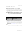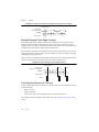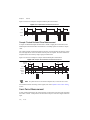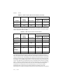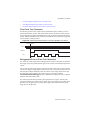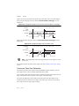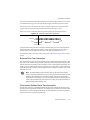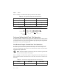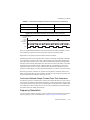
1
TM
NI cDAQ -917x
User Manual
NI CompactDAQ cDAQ-9171/9174/9178 USB Chassis
Français
Deutsch
ni.com/manuals
NI cDAQ-917x User Manual
May 2013
372838D-01
Support
Worldwide Technical Support and Product Information
ni.com
Worldwide Offices
Visit ni.com/niglobal to access the branch office Web sites, which provide up-to-date
contact information, support phone numbers, email addresses, and current events.
National Instruments Corporate Headquarters
11500 North Mopac Expressway Austin, Texas 78759-3504 USA Tel: 512 683 0100
For further support information, refer to the Technical Support and Professional Services
appendix. To comment on National Instruments documentation, refer to the National
Instruments Web site at ni.com/info and enter the Info Code feedback.
© 2009–2013 National Instruments. All rights reserved.
Important Information
Warranty
NI devices are warranted against defects in materials and workmanship for a period of one year from the invoice date, as
evidenced by receipts or other documentation. National Instruments will, at its option, repair or replace equipment that proves
to be defective during the warranty period. This warranty includes parts and labor.
The media on which you receive National Instruments software are warranted not to fail to execute programming instructions,
due to defects in materials and workmanship, for a period of 90 days from the invoice date, as evidenced by receipts or other
documentation. National Instruments will, at its option, repair or replace software media that do not execute programming
instructions if National Instruments receives notice of such defects during the warranty period. National Instruments does not
warrant that the operation of the software shall be uninterrupted or error free.
A Return Material Authorization (RMA) number must be obtained from the factory and clearly marked on the outside of
the package before any equipment will be accepted for warranty work. National Instruments will pay the shipping costs of
returning to the owner parts which are covered by warranty.
National Instruments believes that the information in this document is accurate. The document has been carefully reviewed
for technical accuracy. In the event that technical or typographical errors exist, National Instruments reserves the right to
make changes to subsequent editions of this document without prior notice to holders of this edition. The reader should
consult National Instruments if errors are suspected. In no event shall National Instruments be liable for any damages arising
out of or related to this document or the information contained in it.
EXCEPT AS SPECIFIED HEREIN, NATIONAL INSTRUMENTS MAKES NO WARRANTIES, EXPRESS OR IMPLIED, AND SPECIFICALLY DISCLAIMS ANY
WARRANTY OF MERCHANTABILITY OR FITNESS FOR A PARTICULAR PURPOSE. CUSTOMER’S RIGHT TO RECOVER DAMAGES CAUSED BY FAULT
OR NEGLIGENCE ON THE PART OF NATIONAL INSTRUMENTS SHALL BE LIMITED TO THE AMOUNT THERETOFORE PAID BY THE CUSTOMER.
NATIONAL INSTRUMENTS WILL NOT BE LIABLE FOR DAMAGES RESULTING FROM LOSS OF DATA, PROFITS, USE OF PRODUCTS, OR INCIDENTAL
OR CONSEQUENTIAL DAMAGES, EVEN IF ADVISED OF THE POSSIBILITY THEREOF. This limitation of the liability of National Instruments
will apply regardless of the form of action, whether in contract or tort, including negligence. Any action against National
Instruments must be brought within one year after the cause of action accrues. National Instruments shall not be liable for any
delay in performance due to causes beyond its reasonable control. The warranty provided herein does not cover damages,
defects, malfunctions, or service failures caused by owner’s failure to follow the National Instruments installation, operation,
or maintenance instructions; owner’s modification of the product; owner’s abuse, misuse, or negligent acts; and power failure
or surges, fire, flood, accident, actions of third parties, or other events outside reasonable control.
Copyright
Under the copyright laws, this publication may not be reproduced or transmitted in any form, electronic or mechanical,
including photocopying, recording, storing in an information retrieval system, or translating, in whole or in part, without the
prior written consent of National Instruments Corporation.
National Instruments respects the intellectual property of others, and we ask our users to do the same. NI software is protected
by copyright and other intellectual property laws. Where NI software may be used to reproduce software or other materials
belonging to others, you may use NI software only to reproduce materials that you may reproduce in accordance with the
terms of any applicable license or other legal restriction.
End-User License Agreements and Third-Party Legal Notices
You can find end-user license agreements (EULAs) and third-party legal notices in the following locations:
• Notices are located in the <National Instruments>\_Legal Information and <National Instruments>
directories.
• EULAs are located in the <National Instruments>\Shared\MDF\Legal\license directory.
• Review <National Instruments>\_Legal Information.txt for more information on including legal information
in installers built with NI products.
Trademarks
Refer to the NI Trademarks and Logo Guidelines at ni.com/trademarks for more information on National Instruments
trademarks.
ARM, Keil, and µVision are trademarks or registered of ARM Ltd or its subsidiaries.
LEGO, the LEGO logo, WEDO, and MINDSTORMS are trademarks of the LEGO Group. ©2013 The LEGO Group.
TETRIX by Pitsco is a trademark of Pitsco, Inc.©2013
FIELDBUS FOUNDATION™ and FOUNDATION™ are trademarks of the Fieldbus Foundation.
EtherCAT® is a registered trademark of and licensed by Beckhoff Automation GmbH.
CANopen® is a registered Community Trademark of CAN in Automation e.V.
DeviceNet™ and EtherNet/IP™ are trademarks of ODVA.
Go!, SensorDAQ, and Vernier are registered trademarks of Vernier Software & Technology. Vernier Software & Technology
and vernier.com are trademarks or trade dress.
Xilinx is the registered trademark of Xilinx, Inc.
Taptite and Trilobular are registered trademarks of Research Engineering & Manufacturing Inc.
FireWire® is the registered trademark of Apple Inc.
Linux® is the registered trademark of Linus Torvalds in the U.S. and other countries.
Handle Graphics®, MATLAB®, Real-Time Workshop®, Simulink®, Stateflow®, and xPC TargetBox® are registered
trademarks, and TargetBox™ and Target Language Compiler™ are trademarks of The MathWorks, Inc.
Tektronix®, Tek, and Tektronix, Enabling Technology are registered trademarks of Tektronix, Inc.
The Bluetooth® word mark is a registered trademark owned by the Bluetooth SIG, Inc.
The ExpressCard™ word mark and logos are owned by PCMCIA and any use of such marks by National Instruments is under
license.
The mark LabWindows is used under a license from Microsoft Corporation. Windows is a registered trademark of Microsoft
Corporation in the United States and other countries.
Other product and company names mentioned herein are trademarks or trade names of their respective companies.
Members of the National Instruments Alliance Partner Program are business entities independent from National Instruments
and have no agency, partnership, or joint-venture relationship with National Instruments.
Patents
For patents covering National Instruments products/technology, refer to the appropriate location: Help»Patents in your
software, the patents.txt file on your media, or the National Instruments Patent Notice at ni.com/patents.
Export Compliance Information
Refer to the Export Compliance Information at ni.com/legal/export-compliance for the National Instruments global
trade compliance policy and how to obtain relevant HTS codes, ECCNs, and other import/export data.
WARNING REGARDING USE OF NATIONAL INSTRUMENTS PRODUCTS
(1) NATIONAL INSTRUMENTS PRODUCTS ARE NOT DESIGNED WITH COMPONENTS AND TESTING FOR A
LEVEL OF RELIABILITY SUITABLE FOR USE IN OR IN CONNECTION WITH SURGICAL IMPLANTS OR AS
CRITICAL COMPONENTS IN ANY LIFE SUPPORT SYSTEMS WHOSE FAILURE TO PERFORM CAN
REASONABLY BE EXPECTED TO CAUSE SIGNIFICANT INJURY TO A HUMAN.
(2) IN ANY APPLICATION, INCLUDING THE ABOVE, RELIABILITY OF OPERATION OF THE SOFTWARE
PRODUCTS CAN BE IMPAIRED BY ADVERSE FACTORS, INCLUDING BUT NOT LIMITED TO FLUCTUATIONS
IN ELECTRICAL POWER SUPPLY, COMPUTER HARDWARE MALFUNCTIONS, COMPUTER OPERATING
SYSTEM SOFTWARE FITNESS, FITNESS OF COMPILERS AND DEVELOPMENT SOFTWARE USED TO
DEVELOP AN APPLICATION, INSTALLATION ERRORS, SOFTWARE AND HARDWARE COMPATIBILITY
PROBLEMS, MALFUNCTIONS OR FAILURES OF ELECTRONIC MONITORING OR CONTROL DEVICES,
TRANSIENT FAILURES OF ELECTRONIC SYSTEMS (HARDWARE AND/OR SOFTWARE), UNANTICIPATED
USES OR MISUSES, OR ERRORS ON THE PART OF THE USER OR APPLICATIONS DESIGNER (ADVERSE
FACTORS SUCH AS THESE ARE HEREAFTER COLLECTIVELY TERMED “SYSTEM FAILURES”). ANY
APPLICATION WHERE A SYSTEM FAILURE WOULD CREATE A RISK OF HARM TO PROPERTY OR PERSONS
(INCLUDING THE RISK OF BODILY INJURY AND DEATH) SHOULD NOT BE RELIANT SOLELY UPON ONE
FORM OF ELECTRONIC SYSTEM DUE TO THE RISK OF SYSTEM FAILURE. TO AVOID DAMAGE, INJURY, OR
DEATH, THE USER OR APPLICATION DESIGNER MUST TAKE REASONABLY PRUDENT STEPS TO PROTECT
AGAINST SYSTEM FAILURES, INCLUDING BUT NOT LIMITED TO BACK-UP OR SHUT DOWN MECHANISMS.
BECAUSE EACH END-USER SYSTEM IS CUSTOMIZED AND DIFFERS FROM NATIONAL INSTRUMENTS'
TESTING PLATFORMS AND BECAUSE A USER OR APPLICATION DESIGNER MAY USE NATIONAL
INSTRUMENTS PRODUCTS IN COMBINATION WITH OTHER PRODUCTS IN A MANNER NOT EVALUATED
OR CONTEMPLATED BY NATIONAL INSTRUMENTS, THE USER OR APPLICATION DESIGNER IS
ULTIMATELY RESPONSIBLE FOR VERIFYING AND VALIDATING THE SUITABILITY OF NATIONAL
INSTRUMENTS PRODUCTS WHENEVER NATIONAL INSTRUMENTS PRODUCTS ARE INCORPORATED IN A
SYSTEM OR APPLICATION, INCLUDING, WITHOUT LIMITATION, THE APPROPRIATE DESIGN, PROCESS
AND SAFETY LEVEL OF SUCH SYSTEM OR APPLICATION.
Contents
Chapter 1
Getting Started with the cDAQ Chassis
Safety Guidelines.............................................................................................................. 1-2
Safety Guidelines for Hazardous Voltages............................................................... 1-3
Electromagnetic Compatibility Guidelines ...................................................................... 1-3
Unpacking......................................................................................................................... 1-4
Installing the cDAQ Chassis............................................................................................. 1-5
Mounting the cDAQ Chassis............................................................................................ 1-7
Using the cDAQ Chassis on a Desktop .................................................................... 1-7
NI 9901 Desktop Kit for NI cDAQ-9174/9178 Chassis................................... 1-7
Mounting the cDAQ Chassis on a Panel .................................................................. 1-8
NI cDAQ-9171 ................................................................................................. 1-8
NI cDAQ-9174/9178 ........................................................................................ 1-8
Mounting the NI cDAQ-9174/9178 on a DIN Rail .................................................. 1-10
NI cDAQ Chassis Features............................................................................................... 1-11
Chassis Grounding Screw......................................................................................... 1-11
USB Cable Strain Relief........................................................................................... 1-12
LEDs......................................................................................................................... 1-12
Power Connector ...................................................................................................... 1-13
TRIG (PFI) BNC Connectors ................................................................................... 1-13
Cables and Accessories .................................................................................................... 1-13
Removing I/O Modules from the Chassis ........................................................................ 1-13
Using the cDAQ Chassis .................................................................................................. 1-14
C Series I/O Module ................................................................................................. 1-14
Parallel versus Serial DIO Modules ................................................................. 1-15
cDAQ Module Interface ........................................................................................... 1-15
STC3......................................................................................................................... 1-15
Chapter 2
Analog Input
Analog Input Triggering Signals ...................................................................................... 2-1
Analog Input Timing Signals ........................................................................................... 2-1
AI Sample Clock Signal ........................................................................................... 2-2
Routing the Sample Clock to an Output Terminal ........................................... 2-2
AI Sample Clock Timebase Signal........................................................................... 2-2
AI Convert Clock Signal Behavior For Analog Input Modules............................... 2-2
Scanned Modules.............................................................................................. 2-3
Simultaneous Sample-and-Hold Modules ........................................................ 2-3
Sigma-Delta Modules ....................................................................................... 2-3
Slow Sample Rate Modules.............................................................................. 2-4
© National Instruments
|
v
Contents
AI Start Trigger Signal ............................................................................................. 2-5
Using a Digital Source ...................................................................................... 2-5
Using an Analog Source ................................................................................... 2-5
Routing AI Start Trigger to an Output Terminal .............................................. 2-5
AI Reference Trigger Signal..................................................................................... 2-5
Using a Digital Source ...................................................................................... 2-6
Using an Analog Source ................................................................................... 2-6
Routing the Reference Trigger Signal to an Output Terminal.......................... 2-7
AI Pause Trigger Signal............................................................................................ 2-7
Using a Digital Source ...................................................................................... 2-7
Using an Analog Source ................................................................................... 2-7
Getting Started with AI Applications in Software............................................................ 2-7
Chapter 3
Analog Output
Analog Output Data Generation Methods ........................................................................ 3-1
Software-Timed Generations .................................................................................... 3-1
Hardware-Timed Generations................................................................................... 3-2
Buffered Analog Output ................................................................................... 3-2
Analog Output Triggering Signals.................................................................................... 3-3
Analog Output Timing Signals ......................................................................................... 3-3
AO Sample Clock Signal .......................................................................................... 3-3
Routing AO Sample Clock to an Output Terminal........................................... 3-4
AO Sample Clock Timebase Signal ......................................................................... 3-4
AO Start Trigger Signal ............................................................................................ 3-4
Using a Digital Source ...................................................................................... 3-4
Using an Analog Source ................................................................................... 3-4
Routing AO Start Trigger Signal to an Output Terminal ................................. 3-4
AO Pause Trigger Signal .......................................................................................... 3-5
Using a Digital Source ...................................................................................... 3-5
Using an Analog Source ................................................................................... 3-5
Minimizing Glitches on the Output Signal .......................................................................3-6
Getting Started with AO Applications in Software .......................................................... 3-6
Chapter 4
Digital Input/Output and PFI
Digital Input/Output.......................................................................................................... 4-1
Serial DIO versus Parallel DIO Modules ................................................................. 4-1
Static DIO ................................................................................................................. 4-1
Digital Input .............................................................................................................. 4-2
Digital Input Triggering Signals .......................................................................4-2
Digital Input Timing Signals ............................................................................ 4-2
Digital Input Filters...........................................................................................4-6
Getting Started with DI Applications in Software............................................ 4-7
vi
|
ni.com
NI cDAQ-917x User Manual
Change Detection Event ........................................................................................... 4-7
Routing Change Detection Event to an Output Terminal................................. 4-7
Change Detection Acquisition.......................................................................... 4-7
Digital Output ........................................................................................................... 4-8
Digital Output Data Generation Methods......................................................... 4-8
Digital Output Triggering Signals .................................................................... 4-9
Digital Output Timing Signals ......................................................................... 4-10
Getting Started with DO Applications in Software .......................................... 4-13
Digital Input/Output Configuration for NI 9401 ...................................................... 4-13
PFI .................................................................................................................................... 4-13
PFI Filters ................................................................................................................. 4-13
Chapter 5
Counters
Counter Timing Engine .................................................................................................... 5-1
Counter Input Applications .............................................................................................. 5-3
Counting Edges......................................................................................................... 5-3
Single Point (On-Demand) Edge Counting ...................................................... 5-3
Buffered (Sample Clock) Edge Counting......................................................... 5-4
Controlling the Direction of Counting.............................................................. 5-4
Pulse-Width Measurement ....................................................................................... 5-5
Single Pulse-Width Measurement .................................................................... 5-5
Implicit Buffered Pulse-Width Measurement................................................... 5-5
Sample Clocked Buffered Pulse-Width Measurement ..................................... 5-6
Pulse Measurement................................................................................................... 5-7
Single Pulse Measurement................................................................................ 5-7
Implicit Buffered Pulse Measurement.............................................................. 5-7
Sample Clocked Buffered Pulse Measurement ................................................ 5-8
Semi-Period Measurement ....................................................................................... 5-8
Single Semi-Period Measurement .................................................................... 5-9
Implicit Buffered Semi-Period Measurement................................................... 5-9
Pulse versus Semi-Period Measurements ......................................................... 5-10
Frequency Measurement........................................................................................... 5-10
Low Frequency with One Counter ................................................................... 5-10
High Frequency with Two Counters ................................................................ 5-11
Large Range of Frequencies with Two Counters ............................................. 5-12
Sample Clocked Buffered Frequency Measurement ........................................ 5-13
Choosing a Method for Measuring Frequency ................................................. 5-14
Which Method Is Best? .................................................................................... 5-15
Period Measurement ................................................................................................. 5-17
Position Measurement .............................................................................................. 5-18
Measurements Using Quadrature Encoders ..................................................... 5-18
Channel Z Behavior.................................................................................................. 5-19
Measurements Using Two Pulse Encoders ...................................................... 5-20
Buffered (Sample Clock) Position Measurement............................................. 5-20
© National Instruments
|
vii
Contents
Two-Signal Edge-Separation Measurement ............................................................. 5-21
Single Two-Signal Edge-Separation Measurement .......................................... 5-21
Implicit Buffered Two-Signal Edge-Separation Measurement ........................ 5-22
Sample Clocked Buffered Two-Signal Separation Measurement .................... 5-22
Counter Output Applications ............................................................................................ 5-23
Simple Pulse Generation...........................................................................................5-23
Single Pulse Generation.................................................................................... 5-23
Single Pulse Generation with Start Trigger ...................................................... 5-24
Pulse Train Generation ............................................................................................. 5-24
Finite Pulse Train Generation ........................................................................... 5-25
Retriggerable Pulse or Pulse Train Generation................................................. 5-25
Continuous Pulse Train Generation .................................................................. 5-26
Buffered Pulse Train Generation ...................................................................... 5-27
Finite Implicit Buffered Pulse Train Generation .............................................. 5-27
Continuous Buffered Implicit Pulse Train Generation ..................................... 5-28
Finite Buffered Sample Clocked Pulse Train Generation ................................ 5-28
Continuous Buffered Sample Clocked Pulse Train Generation ....................... 5-29
Frequency Generation............................................................................................... 5-29
Using the Frequency Generator ........................................................................ 5-30
Frequency Division................................................................................................... 5-31
Pulse Generation for ETS ......................................................................................... 5-31
Counter Timing Signals .................................................................................................... 5-32
Counter n Source Signal ...........................................................................................5-32
Routing a Signal to Counter n Source .............................................................. 5-33
Routing Counter n Source to an Output Terminal ............................................ 5-33
Counter n Gate Signal............................................................................................... 5-33
Routing a Signal to Counter n Gate .................................................................. 5-33
Routing Counter n Gate to an Output Terminal ............................................... 5-34
Counter n Aux Signal ............................................................................................... 5-34
Routing a Signal to Counter n Aux................................................................... 5-34
Counter n A, Counter n B, and Counter n Z Signals ................................................ 5-34
Routing Signals to A, B, and Z Counter Inputs ................................................ 5-34
Routing Counter n Z Signal to an Output Terminal ......................................... 5-34
Counter n Up_Down Signal...................................................................................... 5-35
Counter n HW Arm Signal ....................................................................................... 5-35
Routing Signals to Counter n HW Arm Input .................................................. 5-35
Counter n Sample Clock Signal................................................................................ 5-35
Using an Internal Source................................................................................... 5-36
Using an External Source ................................................................................. 5-36
Routing Counter n Sample Clock to an Output Terminal ................................ 5-36
Counter n Internal Output and Counter n TC Signals .............................................. 5-36
Routing Counter n Internal Output to an Output Terminal .............................. 5-36
Frequency Output Signal .......................................................................................... 5-36
Routing Frequency Output to a Terminal ......................................................... 5-37
viii
|
ni.com
NI cDAQ-917x User Manual
Default Counter/Timer Routing........................................................................................ 5-37
Counter Triggering ........................................................................................................... 5-37
Other Counter Features..................................................................................................... 5-38
Cascading Counters .................................................................................................. 5-38
Prescaling.................................................................................................................. 5-38
Synchronization Modes ............................................................................................ 5-38
80 MHz Source Mode....................................................................................... 5-39
External or Internal Source Less than 20 MHz ................................................ 5-39
Chapter 6
Digital Routing and Clock Generation
Digital Routing ................................................................................................................. 6-1
Clock Routing................................................................................................................... 6-1
80 MHz Timebase .................................................................................................... 6-1
20 MHz Timebase .................................................................................................... 6-2
100 kHz Timebase .................................................................................................... 6-2
Appendix A
Where to Go from Here
Appendix B
Technical Support and Professional Services
Index
© National Instruments |
ix
1
Getting Started with the
cDAQ Chassis
This chapter provides an NI CompactDAQ chassis overview and lists information about
mounting the chassis and installing C Series I/O modules.
The one-slot NI cDAQ-9171, four-slot NI cDAQ-9174, and eight-slot NI cDAQ-9178 USB
chassis are designed for use with C Series I/O modules. The cDAQ chassis are capable of
measuring a broad range of analog and digital I/O signals using a Hi-Speed USB 2.0 interface.
For module specifications, refer to the documentation included with your C Series I/O module(s)
or go to ni.com/manuals.
Figure 1-1 shows the NI cDAQ-9171 chassis.
Figure 1-1. NI cDAQ-9171 Chassis
1
4
2
3
1
2
ACTIVE and READY Status LEDs
USB Connector with Strain Relief
3
4
Chassis Grounding Screw
Module Slot
© National Instruments
|
1-1
Chapter 1
Getting Started with the cDAQ Chassis
Figure 1-2 shows the NI cDAQ-9174 chassis.
Figure 1-2. NI cDAQ-9174 Chassis
1
NI cDAQ-9174
NI CompactDAQ
5
POWER
READY
ACTIVE
1
2
2
3
4
V
C
INPUT
9-30 V
15 W MAX
4
3
1
2
3
POWER, READY, and ACTIVE Status LEDs
USB Connector with Strain Relief
9–30 VDC Power Connector
4
5
Module Slots
Chassis Grounding Screw
Figure 1-3 shows the NI cDAQ-9178 chassis.
Figure 1-3. NI cDAQ-9178 Chassis
1
NI cDAQ-9178
NI CompactDAQ
7
POWER
READY
ACTIVE
2
3
1
2
3
4
5
TRIG 0
V
C
TRIG 1
INPUT
9-30 V
15 W MAX
4
1
2
3
4
5
POWER, READY, and ACTIVE Status LEDs
USB Connector with Strain Relief
TRIG 0 (PFI 0) and TRIG 1 (PFI 1) BNC Connectors
9–30 VDC Power Connector
6
5
6
7
Module Slots
Installed C Series Modules
Chassis Grounding Screw
Safety Guidelines
Operate the NI cDAQ-917x chassis only as described in this user manual.
Refer to the Read Me First: Safety and Electromagnetic Compatibility
document for important safety and electromagnetic compatibility information. To
Caution
1-2
| ni.com
NI cDAQ-917x User Manual
obtain a copy of this document online, visit ni.com/manuals and search for the
document title.
Because some C Series I/O modules may have more stringent certification
standards than the NI cDAQ-917x chassis, the combined system may be limited by
individual component restrictions. Refer to the specifications document for your
cDAQ chassis for more details.
Note
Caution
The NI cDAQ-917x chassis is not certified for use in hazardous locations.
Hot Surface This icon denotes that the component may be hot. Touching this
component may result in bodily injury.
Safety Guidelines for Hazardous Voltages
If hazardous voltages are connected to the module, take the following precautions. A hazardous
voltage is a voltage greater than 42.4 Vpk or 60 VDC to earth ground.
Caution Ensure that hazardous voltage wiring is performed only by qualified
personnel adhering to local electrical standards.
Caution Do not mix hazardous voltage circuits and human-accessible circuits on
the same module.
Caution Make sure that chassis and circuits connected to the module are properly
insulated from human contact.
The NI cDAQ-917x chassis provides no isolation, but some modules offer
isolation. Follow the safety guidelines for each module when using hazardous
voltage.
Caution
Electromagnetic Compatibility Guidelines
This product was tested and complies with the regulatory requirements and limits for
electromagnetic compatibility (EMC) as stated in the product specifications. These requirements
and limits are designed to provide reasonable protection against harmful interference when the
product is operated in its intended operational electromagnetic environment.
This product is intended for use in industrial locations. There is no guarantee that harmful
interference will not occur in a particular installation, when the product is connected to a test
object, or if the product is used in residential areas. To minimize the potential for the product to
cause interference to radio and television reception or to experience unacceptable performance
degradation, install and use this product in strict accordance with the instructions in the product
documentation.
© National Instruments
|
1-3
Chapter 1
Getting Started with the cDAQ Chassis
Furthermore, any changes or modifications to the product not expressly approved by National
Instruments could void your authority to operate it under your local regulatory rules.
To ensure the specified EMC performance, operate this product only with
shielded cables and accessories.
Caution
This product may become more sensitive to electromagnetic disturbances
in the operational environment when test leads are attached or when connected to a
test object.
Caution
Emissions that exceed the regulatory requirements may occur when this
product is connected to a test object.
Caution
Changes or modifications not expressly approved by National
Instruments could void the user’s authority to operate the hardware under the local
regulatory rules.
Caution
Unpacking
The cDAQ chassis ships in an antistatic package to prevent electrostatic discharge (ESD). ESD
can damage several components on the device.
Caution
Never touch the exposed pins of connectors.
To avoid ESD damage in handling the device, take the following precautions:
•
Ground yourself with a grounding strap or by touching a grounded object.
•
Touch the antistatic package to a metal part of your computer chassis before removing the
device from the package.
Remove the device from the package and inspect it for loose components or any other signs of
damage. Notify NI if the device appears damaged in any way. Do not install a damaged device
in your computer or chassis.
Store the device in the antistatic package when the device is not in use.
1-4
| ni.com
NI cDAQ-917x User Manual
Installing the cDAQ Chassis
The cDAQ chassis and C Series I/O module(s) are packaged separately. For an interactive
demonstration of how to install the cDAQ chassis, go to ni.com/info and enter
cdaqinstall. Refer to Figure 1-1, 1-2, or 1-3 while completing the following assembly steps.
1.
Install the application software (if applicable), as described in the installation instructions
that accompany your software.
2.
Install NI-DAQmx. For more information, download the Read Me First: NI-DAQmx and
DAQ Device Installation Guide.
Note The NI-DAQmx software is included on the disk shipped with your kit and is
available for download at ni.com/support. The documentation for NI-DAQmx is
available after installation from Start»All Programs»National Instruments»
NI-DAQ. Other NI documentation is available from ni.com/manuals.
Table 1-1 lists the earliest NI-DAQmx support version for each cDAQ chassis.
Table 1-1. NI cDAQ Chassis NI-DAQmx Software Support
cDAQ Chassis
NI-DAQmx Version Support
NI cDAQ-9171
NI-DAQmx 9.4 and later
NI cDAQ-9174
NI-DAQmx 9.0.2 and later
NI cDAQ-9178
NI-DAQmx 9.0.2 and later
3.
(Optional) Mount the cDAQ chassis to a panel, wall, or DIN rail as described in the
Mounting the cDAQ Chassis section.
4.
Attach a ring lug to a 1.31 mm2 (16 AWG) or larger wire. Connect the ring lug to the chassis
ground terminal on the side of the cDAQ chassis using the chassis grounding screw as
shown in Figure 1-4. Attach the other end of the wire to the grounding electrode system of
your facility. Refer to the Chassis Grounding Screw section for more information about
making this connection.
If you use shielded cabling to connect to a C Series I/O module with a plastic
connector, you must attach the cable shield to the chassis grounding terminal using
1.31 mm2 (16 AWG) or larger wire. Use shorter wire for better EMC performance.
Note
© National Instruments
|
1-5
Chapter 1
Getting Started with the cDAQ Chassis
Figure 1-4. Ring Lug Attached to Ground Terminal
5.
Make sure that no signals are connected to the C Series I/O module.
6.
Align the C Series I/O module with the cDAQ chassis slot.
7.
Squeeze both C Series I/O module latches, insert the I/O module into the module slot, and
press until both latches lock the module in place.
8.
Wire the C Series I/O module as indicated in the C Series module documentation.
Note Connect I/O cable shields to the chassis grounding screw, shown in
Figure 1-4, unless otherwise specified in the C Series module documentation. Refer
to the Chassis Grounding Screw section for more information about making this
connection.
9.
Connect the cDAQ chassis with the USB cable to any available USB port on your
computer. If you are using a locking USB cable, use the jackscrew to securely attach the
cable to the chassis.
10. (NI cDAQ-9174/9178) Connect the supplied power source to the cDAQ chassis. The
NI cDAQ-9174/9178 chassis requires an external power supply that meets the
specifications listed in the specifications document for your cDAQ chassis.
11. Double-click the Measurement & Automation icon on the desktop to open MAX.
12. Expand Devices and Interfaces and verify that your chassis is listed there. If your chassis
does not appear, press <F5> to refresh the view in MAX. If your chassis is still not
recognized, refer to ni.com/support/daqmx for troubleshooting information.
13. Self-test your chassis in MAX by expanding Devices and Interfaces, right-clicking
NI cDAQ-<model number>, and selecting Self-Test. Self-test performs a brief test to
determine successful chassis installation. When the self-test finishes, a message indicates
1-6
| ni.com
NI cDAQ-917x User Manual
successful verification or if an error occurred. If an error occurs, refer to ni.com/
support/daqmx.
14. Run a Test Panel in MAX by expanding Devices and Interfaces» NI cDAQ-<model
number>, right-clicking your C Series module, and selecting Test Panels to open a test
panel for the selected module.
If the test panel displays an error message, refer to ni.com/support.
Click Close to exit the test panel.
Note When in use, the cDAQ chassis may become warm to the touch. This is
normal.
Mounting the cDAQ Chassis
You can use the cDAQ chassis on a desktop or mount it to a panel or wall. You can also mount
the NI cDAQ-9174/9178 on a DIN rail. For accessory ordering information, refer to the pricing
section of your cDAQ chassis product page at ni.com.
Caution
Your installation must meet the following requirements:
•
Allows 25.4 mm (1 in.) of clearance above and below the cDAQ chassis for air
circulation.
•
Allows at least 50.8 mm (2 in.) of clearance in front of the modules for common
connector cabling such as the 10-terminal detachable screw terminal connector
and, as needed, up to 88.9 mm (3.5 in.) of clearance in front of the modules for
other types of cabling.
For more information about cabling clearances for C Series I/O modules, refer to ni.com/
info and enter the Info Code cseriesconn.
Using the cDAQ Chassis on a Desktop
You can use the cDAQ chassis on a desktop. NI cDAQ-9174/9178 users can install an optional
desktop mounting kit.
Caution
Do not stack the cDAQ chassis.
NI 9901 Desktop Kit for NI cDAQ-9174/9178 Chassis
The NI 9901 desktop mounting kit includes two metal feet you can install on the sides of the
NI cDAQ-9174/9178 chassis for desktop use. With this kit, you can tilt the cDAQ chassis for
convenient access to the I/O module connectors. When you install the two metal feet, the two
existing screws on the back side and I/O end of the chassis must be removed, as shown in
Figure 1-5. After removing the screws, replace them with the two M3 × 14 screws included in
the NI 9901 desktop mounting kit.
© National Instruments
|
1-7
Chapter 1
Getting Started with the cDAQ Chassis
Figure 1-5. NI 9901 Desktop Mounting Kit
You must mount the chassis before installing the C Series I/O modules.
Mounting the cDAQ Chassis on a Panel
You do not need a kit to panel mount the NI cDAQ-9171 chassis. You can use a panel mount kit
to mount the NI cDAQ-9174/9178 chassis to a panel. For kit accessory ordering information,
refer to the pricing section of your cDAQ chassis product page at ni.com.
NI cDAQ-9171
Two keyholes are located on the NI cDAQ-9171 for mounting it to a panel or wall. You can
panel mount the NI cDAQ-9171 with either #6-32 panhead machine screws or M3.5 panhead
machine screws. Installed screw height for both screw types is 7.37 mm (0.29 in.). Refer to the
NI cDAQ-9171 Specifications for mounting dimensions.
NI cDAQ-9174/9178
You can panel mount the cDAQ chassis with or without a panel mount kit:
•
Panel Mounting with a Panel Mount Kit—Use the NI 9904 panel mount kit to mount the
NI cDAQ-9174 chassis on a panel. Use the NI 9905 panel mount kit to mount the
NI cDAQ-9178 chassis on a panel.
Remove the C Series I/O module(s) from the cDAQ chassis before you
mount the chassis to the panel. After the cDAQ chassis is mounted, you can reinsert
the C Series module.
Caution
Align the cDAQ chassis on the panel mount accessory and attach the chassis to the
accessory with two M4 × 17 screws (included in the kit), as shown in Figure 1-6. You must
use these screws because they are the correct depth and thread for the panel. You can then
attach the panel mount accessory to a wall or panel with the two holes or the four keyholes
1-8
| ni.com
NI cDAQ-917x User Manual
with M4, M5, No. 8, or No.10 panhead screws. Refer to the documentation included with
the panel mount kit for more detailed dimensions.
Figure 1-6. NI cDAQ-9174/9178 Panel Mount Dimensions and Installation
330.2 mm
(13.00 in.)
NI cDAQ-9178
NI CompactDAQ
POWER
READY
ACTIVE
1
2
3
4
5
6
7
88.1 mm
(3.47 in.)
8
PFI 0
V
C
PFI 1
INPUT
9-30 V
15 W MAX
48.1 mm
(1.90 in.)
28.1 mm
(1.11 in.)
234.95 mm
(9.250 in.)
NI cDAQ-9174
NI CompactDAQ
POWER
READY
ACTIVE
1
2
3
4
88.1 mm
(3.47 in.)
V
C
INPUT
9-30 V
15 W MAX
48.4 mm
(1.91 in.)
NI
NI
27.0 mm
(1.06 in.)
cD
AQ
Co
mp
-9
ac 17
tD 8
AQ
© National Instruments
|
1-9
Chapter 1
•
Getting Started with the cDAQ Chassis
Panel Mounting without a Panel Mount Kit—You can mount the cDAQ chassis directly
on a flat surface using the mounting holes. Align the chassis on the surface. Then, fasten
the chassis to the surface using two screws as shown in Figure 1-7. The NI cDAQ-9174
uses two M4 or No. 8 flathead screws. The NI cDAQ-9178 uses two M4 or No. 8 panhead
screws. National Instruments does not provide these screws with the chassis.
Figure 1-7. Mounting the cDAQ Chassis Directly on a Flat Surface
NI cDAQ-9174
NI CompactDAQ
POWER
READY
ACTIVE
1
2
3
4
V
C
INPUT
9-30 V
15 W MAX
Refer to the specifications document for your cDAQ chassis for mounting dimensions.
Make sure that no I/O modules are in the chassis before removing it from
the surface.
Caution
Mounting the NI cDAQ-9174/9178 on a DIN Rail
Use the NI 9912 DIN rail kit to mount the NI cDAQ-9174 chassis on a DIN rail. Use the NI 9915
DIN rail kit with the NI cDAQ-9178 chassis on a DIN rail.
Each DIN rail kit contains one clip for mounting the chassis on a standard 35 mm DIN rail. To
mount the chassis on a DIN rail, fasten the DIN rail clip to the chassis using a number 2 Phillips
screwdriver and two M4 × 17 screws. The screws are included in the DIN rail kit. Make sure the
DIN rail kit is installed as illustrated in Figure 1-8, with the larger lip of the DIN clip positioned
up. When the DIN rail kit is properly installed, the cDAQ chassis is centered on the DIN rail.
1-10
|
ni.com
NI cDAQ-917x User Manual
Figure 1-8. NI cDAQ-9174/9178 DIN Rail Installation
Clip the chassis onto the DIN rail with the larger lip of the DIN clip positioned up, as shown in
Figure 1-9.
Figure 1-9. DIN Rail Clip Parts Locator Diagram
1
2
3
1
DIN Rail Clip
Caution
2
DIN Rail Spring
3
DIN Rail
Remove the I/O modules before removing the chassis from the DIN rail.
NI cDAQ Chassis Features
The cDAQ chassis features a chassis grounding screw, USB cable strain relief, and LEDs.
Multislot cDAQ chassis have a power connector and the NI cDAQ-9178 chassis also features
two TRIG (PFI) BNC connectors. Refer to Figure 1-1, 1-2, or 1-3 for locations of the cDAQ
chassis features.
Chassis Grounding Screw
To ensure the specified EMC performance, the cDAQ chassis must be
connected to the grounding electrode system of your facility using the chassis ground
terminal.
Caution
© National Instruments
|
1-11
Chapter 1
Getting Started with the cDAQ Chassis
The wire should be 1.31 mm2 (16 AWG) or larger solid copper wire with a maximum length of
1.5 m (5 ft). Attach the wire to the earth ground of the facility’s power system. For more
information about earth ground connections, refer to the KnowledgeBase document, Grounding
for Test and Measurement Devices, by going to ni.com/info and entering the Info Code
emcground.
If you use shielded cabling to connect to a C Series I/O module with a plastic
connector, you must attach the cable shield to the chassis grounding terminal using
1.31 mm2 (16 AWG) or larger wire. Use shorter wire for better EMC performance.
Note
USB Cable Strain Relief
You can provide strain relief for the USB cable by using the jackscrew on a locking USB cable
to securely attach the cable to the chassis.
LEDs
The cDAQ chassis features two status LEDs: ACTIVE and READY. The ACTIVE LED
indicates cDAQ chassis USB bus communication. The READY LED lights when the cDAQ
chassis is ready for use.
NI cDAQ-9174/9178 chassis also features a POWER status LED.
Table 1-2. LED State/Chassis Status
LED Color
Status LED
Off
Green
Amber
ACTIVE
No USB traffic
present/suspend
USB traffic present
Unconfigured
READY
USB connection is not
established/suspend
Full-Speed (12 Mb/s)
Hi-Speed (480 Mb/s)
POWER*
No power supplied
Power supplied
* NI cDAQ-9174/9178 chassis only.
1-12
|
ni.com
—
NI cDAQ-917x User Manual
Power Connector
(NI cDAQ-9174/9178) Refer to the specifications document for your cDAQ chassis for
information about the power connector on the NI cDAQ-9174/9178 chassis.
TRIG (PFI) BNC Connectors
(NI cDAQ-9178) Refer to the PFI section of Chapter 4, Digital Input/Output and PFI, for
information about the BNC connectors for TRIG 0 (PFI 0) and TRIG 1 (PFI 1).
Cables and Accessories
Table 1-3 contains information about cables and accessories available for the cDAQ chassis. For
a complete list of cDAQ chassis accessories and ordering information, refer to the pricing
section of your cDAQ chassis product page at ni.com.
Table 1-3. NI cDAQ Chassis Cables and Accessories
Accessory
Part Number
cDAQ Chassis
NI 9901 desktop mounting kit
779473-01
NI cDAQ-9174/9178
NI 9904 panel mount kit
779097-01
NI cDAQ-9174
NI 9905 panel mount kit
779558-01
NI cDAQ-9178
NI 9912 DIN rail kit
779019-01
NI cDAQ-9174
NI 9915 DIN rail kit
779018-01
NI cDAQ-9178
2-pos screw terminal kit for power
supply connection, qty 4
780702-01
NI cDAQ-9174/9178
Locking USB cable, (1 m length)
198506-01
NI cDAQ-9171/9174/9178
Locking USB cable, (2 m length)
780534-01
NI cDAQ-9171/9174/9178
Removing I/O Modules from the Chassis
Complete the following steps to remove a C Series I/O module from the chassis.
1.
Make sure that no I/O-side power is connected to the I/O module. If the system is in a
nonhazardous location, the chassis power can be on when you remove I/O modules.
2.
Squeeze the latches on both sides of the module and pull the module out of the chassis.
© National Instruments
|
1-13
Chapter 1
Getting Started with the cDAQ Chassis
Using the cDAQ Chassis
The cDAQ system consists of three parts—C Series I/O module(s), the cDAQ module interface,
and the STC3—as shown in Figure 1-10. These components digitize signals, perform D/A
conversions to generate analog output signals, measure and control digital I/O signals, and
provide signal conditioning.
Figure 1-10. Block Diagram
C Series
I/O Module
cDAQ Module
Interface
STC3
Ethernet/
Wireless
Network
C Series
I/O Module
(NI cDAQ-9184/9188)
Chassis
PFI Terminals
(NI cDAQ-9188)
C Series I/O Module
National Instruments C Series I/O modules provide built-in signal conditioning and screw
terminal, spring terminal, BNC, D-SUB, or RJ-50 connectors. A wide variety of I/O types are
available, allowing you to customize the cDAQ system to meet your application needs.
C Series I/O modules are hot-swappable and automatically detected by the cDAQ chassis.
I/O channels are accessible using the NI-DAQmx driver software.
Because the modules contain built-in signal conditioning for extended voltage ranges or
industrial signal types, you can usually make your wiring connections directly from the C Series
I/O modules to your sensors/actuators. In most cases, the C Series I/O modules provide isolation
from channel-to-earth ground and channel-to-channel.
For more information about which C Series I/O modules are compatible with the cDAQ chassis,
refer to the Developer Zone document, C Series Support in NI-DAQmx. To access this
Developer Zone document, go to ni.com/info and enter the Info Code rdcdaq.
1-14
|
ni.com
NI cDAQ-917x User Manual
Parallel versus Serial DIO Modules
Digital I/O module capabilities are determined by the type of digital signals that the module is
capable of measuring or generating.
•
Serial digital I/O modules are designed for signals that change slowly and are accessed by
software-timed reads and writes.
•
Parallel digital I/O modules are for signals that change rapidly and are updated by either
software-timed or hardware-timed reads and writes.
For more information about digital I/O modules, refer to Chapter 4, Digital Input/Output
and PFI.
cDAQ Module Interface
The cDAQ module interface manages data transfers between the STC3 and the C Series
I/O modules. The interface also handles autodetection, signal routing, and synchronization.
STC3
The STC3 features independent high-speed data streams; flexible AI, AO, and DIO sample
timing; triggering; PFI signals for multi-device synchronization; flexible counter/timers with
hardware gating; digital waveform acquisition and generation; and static DIO.
•
•
AI, AO, and DIO Sample Timing—The STC3 contains advanced AI, AO, and DIO
timing engines. A wide range of timing and synchronization signals are available through
the PFI lines. Refer to the following sections for more information about the configuration
of these signals:
–
The Analog Input Timing Signals section of Chapter 2, Analog Input
–
The Analog Output Timing Signals section of Chapter 3, Analog Output
–
The Digital Input Timing Signals section of Chapter 4, Digital Input/Output and PFI
–
The Digital Output Timing Signals section of Chapter 4, Digital Input/Output and PFI
Triggering Modes—The cDAQ chassis supports different trigger modes, such as start
trigger, reference trigger, and pause trigger with analog, digital, or software sources. Refer
to the following sections for more information:
–
The Analog Input Triggering Signals section of Chapter 2, Analog Input
–
The Analog Output Triggering Signals section of Chapter 3, Analog Output
–
The Digital Input Triggering Signals section of Chapter 4, Digital Input/Output
and PFI
–
The Digital Output Triggering Signals section of Chapter 4, Digital Input/Output
and PFI
© National Instruments
|
1-15
Chapter 1
•
Getting Started with the cDAQ Chassis
Independent Data Streams—The NI cDAQ-9171 supports six independent high-speed
data streams, which allow for up to six simultaneous hardware-timed tasks, such as analog
input, analog output, buffered counter/timers, and hardware-timed digital input/output.
The NI cDAQ-9174/9178 supports seven independent high-speed data streams, which
allow for up to seven simultaneous hardware-timed tasks, such as analog input, analog
output, buffered counter/timers, and hardware-timed digital input/output.
•
PFI Signals—The PFI signals provide access to advanced features such as triggering,
synchronization, and counter/timers. You can also enable a programmable debouncing
filter on each PFI signal that, when enabled, samples the input on each rising edge of a filter
clock. PFI signals are available through parallel digital input and output modules installed
in up to two chassis slots and through the two PFI terminals provided on the NI cDAQ-9178
chassis. Refer to the PFI section of Chapter 4, Digital Input/Output and PFI, for more
information.
•
Flexible Counter/Timers—The cDAQ chassis includes four general-purpose 32-bit
counter/timers that can be used to count edges, measure pulse-widths, measure periods and
frequencies, and perform position measurements (encoding). In addition, the
counter/timers can generate pulses, pulse trains, and square waves with adjustable
frequencies. You can access the counter inputs and outputs using parallel digital I/O
modules installed in up to two slots, or by using the two chassis PFI terminals provided on
the NI cDAQ-9178 chassis. Refer to Chapter 5, Counters, for more information.
1-16
|
ni.com
2
Analog Input
To perform analog input measurements, insert a supported analog input C Series I/O module into
any slot on the cDAQ chassis. The measurement specifications, such as number of channels,
channel configuration, sample rate, and gain, are determined by the type of C Series I/O module
used. For more information and wiring diagrams, refer to the documentation included with your
C Series I/O modules.
(NI cDAQ-9174/9178) The NI cDAQ-9174/9178 has three AI timing engines, which means that
three analog input tasks can be running at a time on a chassis. An analog input task can include
channels from multiple analog input modules. However, channels from a single module cannot
be used in multiple tasks.
Multiple timing engines allow the NI cDAQ-9174/9178 to run up to three analog input tasks
simultaneously, each using independent timing and triggering configurations. The three AI
timing engines are ai, te0, and te1.
Analog Input Triggering Signals
A trigger is a signal that causes an action, such as starting or stopping the acquisition of data.
When you configure a trigger, you must decide how you want to produce the trigger and the
action you want the trigger to cause. The cDAQ chassis supports internal software, external
digital triggering, and analog triggering.
Three triggers are available: Start Trigger, Reference Trigger, and Pause Trigger. An analog or
digital trigger can initiate these three trigger actions. Up to two C Series parallel digital input
modules can be used in any chassis slot to supply a digital trigger. To find your module triggering
options, refer to the documentation included with your C Series I/O modules. For more
information about using digital modules for triggering, refer to Chapter 4, Digital Input/Output
and PFI.
Refer to the AI Start Trigger Signal, AI Reference Trigger Signal, and AI Pause Trigger Signal
sections for more information about the analog input trigger signals.
Analog Input Timing Signals
The cDAQ chassis features the following analog input timing signals:
•
AI Sample Clock Signal*
•
AI Sample Clock Timebase Signal
•
AI Start Trigger Signal*
© National Instruments
|
2-1
Chapter 2
Analog Input
•
AI Reference Trigger Signal*
•
AI Pause Trigger Signal*
Signals with an * support digital filtering. Refer to the PFI Filters section of Chapter 4, Digital
Input/Output and PFI, for more information.
Refer to the AI Convert Clock Signal Behavior For Analog Input Modules section for AI Convert
Clock signals and the cDAQ chassis.
AI Sample Clock Signal
A sample consists of one reading from each channel in the AI task. SampleClock signals the start
of a sample of all analog input channels in the task. SampleClock can be generated from external
or internal sources as shown in Figure 2-1.
Figure 2-1. AI Sample Clock Timing Options
PFI
Analog Comparison Event
Ctr n Internal Output
PFI
Analog Comparison
Event
20 MHz Timebase
80 MHz Timebase
AI Sample Clock
Sigma-Delta Module Internal Output
AI Sample Clock
Timebase
Programmable
Clock
Divider
100 kHz Timebase
Routing the Sample Clock to an Output Terminal
You can route SampleClock to any output PFI terminal. SampleClock is an active high pulse by
default.
AI Sample Clock Timebase Signal
The AI Sample Clock Timebase signal is divided down to provide a source for SampleClock.
SampleClockTimebase can be generated from external or internal sources.
SampleClockTimebase is not available as an output from the chassis.
AI Convert Clock Signal Behavior For Analog Input
Modules
Refer to the Scanned Modules, Simultaneous Sample-and-Hold Modules, Sigma-Delta Modules,
and Slow Sample Rate Modules sections for information about the AI Convert Clock signal and
C Series I/O modules.
2-2
| ni.com
NI cDAQ-917x User Manual
Scanned Modules
Scanned C Series analog input modules contain a single A/D converter and a multiplexer to
select between multiple input channels. When the cDAQ Module Interface receives a Sample
Clock pulse, it begins generating a Convert Clock for each scanned module in the current task.
Each Convert Clock signals the acquisition of a single channel from that module. The Convert
Clock rate depends on the module being used, the number of channels used on that module, and
the system Sample Clock rate.
The driver chooses the fastest conversion rate possible based on the speed of the A/D converter
for each module and adds 10 µs of padding between each channel to allow for adequate settling
time. This scheme enables the channels to approximate simultaneous sampling. If the AI Sample
Clock rate is too fast to allow for 10 µs of padding, NI-DAQmx selects a conversion rate that
spaces the AI Convert Clock pulses evenly throughout the sample. NI-DAQmx uses the same
amount of padding for all the modules in the task. To explicitly specify the conversion rate, use
the ActiveDevs and AI Convert Clock Rate properties using the DAQmx Timing property
node or functions.
Simultaneous Sample-and-Hold Modules
Simultaneous sample-and-hold (SSH) C Series analog input modules contain multiple A/D
converters or circuitry that allows all the input channels to be sampled at the same time. These
modules sample their inputs on every Sample Clock pulse.
Sigma-Delta Modules
Sigma-delta C Series analog input modules function much like SSH modules, but use A/D
converters that require a high-frequency oversample clock to produce accurate, synchronized
data. Some sigma-delta modules in the cDAQ chassis automatically share a single oversample
clock to synchronize data from all the modules that support an external oversample clock
timebase when they all share the same task. (DSA modules are an example). The cDAQ chassis
supports a maximum of two synchronization pulse signals configured for your system. This
limits the system to two tasks with different oversample clock timebases.
The oversample clock is used as the AI Sample Clock Timebase. While most modules supply a
common oversample clock frequency (12.8 MHz), some modules, such as the NI 9234, supply
a different frequency. When sigma-delta modules with different oversample clock frequencies
are used in an analog input task, the AI Sample Clock Timebase can use any of the available
frequencies; by default, the fastest available is used. The sampling rate of all modules in the
system is an integer divisor of the frequency of the AI Sample Clock Timebase.
When one or more sigma-delta modules are in an analog input task, the sigma-delta modules also
provide the signal used as the AI Sample Clock. This signal is used to cause A/D conversion for
other modules in the system, just as the AI Sample Clock does when a sigma-delta module is not
being used.
When sigma-delta modules are in an AI task, the chassis automatically issues a synchronization
pulse to each sigma-delta modules that resets their ADCs at the same time. Because of the
© National Instruments
|
2-3
Chapter 2
Analog Input
filtering used in sigma-delta A/D converters, these modules usually exhibit a fixed input delay
relative to non-sigma-delta modules in the system. This input delay is specified in the C Series
I/O module documentation.
Slow Sample Rate Modules
(NI cDAQ-9174/9178) Some C Series analog input modules are specifically designed for
measuring signals that vary slowly, such as temperature. Because of their slow rate, it is not
appropriate for these modules to constrain the AI Sample Clock to operate at or slower than their
maximum rate. When using such a module in the NI cDAQ-9174/9178 chassis, the maximum
Sample Clock rate can run faster than the maximum rate for the module. When operating at a
rate faster than these slow rate modules can support, the slow rate module returns the same point
repeatedly, until a new conversion completes. In a hardware-timed task, the first point is
acquired when the task is committed. The second point is acquired after the start trigger as shown
in Figure 2-2.
Figure 2-2. Sample Clock Timing Example
StartTrigger
1st A/D Conversion
Data from
A/D Conversion
(Slow Module)
2nd A/D Conversion
3rd A/D Conversion
B
A
C
SampleClock
Data Returned
to AI Task
A
A
A
B
B
B
C
For example, if running an AI task at 1 kHz using a module with a maximum rate of 10 Hz, the
slow module returns 100 samples of the first point, followed by 100 samples of the second point,
etc. Other modules in the task will return 1,000 new data points per second, which is normal.
When performing a single-point acquisition, no points are repeated. To avoid this behavior, use
multiple AI timing engines, and assign slow sample rate modules to a task with a rate at or slower
than their maximum rate.
Refer to the Developer Zone document, C Series Support in NI-DAQmx, for more information.
To access this Developer Zone document, go to ni.com/info and enter the Info Code
rdcdaq.
2-4
| ni.com
NI cDAQ-917x User Manual
AI Start Trigger Signal
Use the Start Trigger signal to begin a measurement acquisition. A measurement acquisition
consists of one or more samples. If you do not use triggers, begin a measurement with a software
command. Once the acquisition begins, configure the acquisition to stop in one of the following
ways:
•
When a certain number of points has been sampled (in finite mode)
•
After a hardware reference trigger (in finite mode)
•
With a software command (in continuous mode)
An acquisition that uses a start trigger (but not a reference trigger) is sometimes referred to as a
posttriggered acquisition. That is, samples are measured only after the trigger.
When you are using an internal sample clock, you can specify a default delay from the start
trigger to the first sample.
Using a Digital Source
To use the Start Trigger signal with a digital source, specify a source and a rising or falling edge.
Use the following signals as the source:
•
Any PFI terminal
•
Counter n Internal Output
The source also can be one of several other internal signals on your cDAQ chassis. Refer to the
Device Routing in MAX topic in the NI-DAQmx Help or the LabVIEW Help for more
information.
Using an Analog Source
Some C Series I/O modules can generate a trigger based on an analog signal. In NI-DAQmx, this
is called the Analog Comparison Event. When you use an analog trigger source for StartTrigger,
the acquisition begins on the first rising edge of the Analog Comparison Event signal.
Note Depending on the C Series I/O module capabilities, you may need two
modules to utilize analog triggering.
Routing AI Start Trigger to an Output Terminal
You can route the Start Trigger signal to any output PFI terminal. The output is an active high
pulse.
AI Reference Trigger Signal
Use Reference Trigger to stop a measurement acquisition. To use a reference trigger, specify a
buffer of finite size and a number of pretrigger samples (samples that occur before the reference
trigger). The number of posttrigger samples (samples that occur after the reference trigger)
desired is the buffer size minus the number of pretrigger samples.
© National Instruments
|
2-5
Chapter 2
Analog Input
Once the acquisition begins, the cDAQ chassis writes samples to the buffer. After the cDAQ
chassis captures the specified number of pretrigger samples, the cDAQ chassis begins to look
for the reference trigger condition. If the reference trigger condition occurs before the cDAQ
chassis captures the specified number of pretrigger samples, the chassis ignores the condition.
If the buffer becomes full, the cDAQ chassis continuously discards the oldest samples in the
buffer to make space for the next sample. This data can be accessed (with some limitations)
before the cDAQ chassis discards it. Refer to the KnowledgeBase document, Can a Pretriggered
Acquisition be Continuous?, for more information. To access this KnowledgeBase, go to
ni.com/info and enter the Info Code rdcanq.
When the reference trigger occurs, the cDAQ chassis continues to write samples to the buffer
until the buffer contains the number of posttrigger samples desired. Figure 2-3 shows the final
buffer.
Figure 2-3. Reference Trigger Final Buffer
Reference Trigger
Pretrigger Samples
Posttrigger Samples
Complete Buffer
Using a Digital Source
To use Reference Trigger with a digital source, specify a source and a rising or falling edge.
Either PFI or one of several internal signals on the cDAQ chassis can provide the source. Refer
to the Device Routing in MAX topic in the NI-DAQmx Help or the LabVIEW Help for more
information.
Using an Analog Source
Some C Series I/O modules can generate a trigger based on an analog signal. In NI-DAQmx, this
is called the Analog Comparison Event.
When you use an analog trigger source, the acquisition stops on the first rising or falling edge of
the Analog Comparison Event signal, depending on the trigger properties.
Note Depending on the C Series I/O module capabilities, you may need two
modules to utilize analog triggering.
2-6
| ni.com
NI cDAQ-917x User Manual
Routing the Reference Trigger Signal to an Output Terminal
You can route ReferenceTrigger to any output PFI terminal. Reference Trigger is active high by
default.
AI Pause Trigger Signal
You can use the Pause Trigger to pause and resume a measurement acquisition. The internal
sample clock pauses while the external trigger signal is active and resumes when the signal is
inactive. You can program the active level of the pause trigger to be high or low.
Using a Digital Source
To use the Pause Trigger, specify a source and a polarity. The source can be either from PFI or
one of several other internal signals on your cDAQ chassis. Refer to the Device Routing in MAX
topic in the NI-DAQmx Help or the LabVIEW Help for more information.
Using an Analog Source
Some C Series I/O modules can generate a trigger based on an analog signal. In NI-DAQmx, this
is called the Analog Comparison Event.
When you use an analog trigger source, the internal sample clock pauses when the Analog
Comparison Event signal is low and resumes when the signal goes high (or vice versa).
Note Depending on the C Series I/O module capabilities, you may need two
modules to utilize analog triggering.
Note
Pause triggers are only sensitive to the level of the source, not the edge.
Getting Started with AI Applications in Software
You can use the cDAQ chassis in the following analog input applications:
•
Single-point acquisition
•
Finite acquisition
•
Continuous acquisition
For more information about programming analog input applications and triggers in software,
refer to the NI-DAQmx Help or the LabVIEW Help for more information.
© National Instruments
|
2-7
3
Analog Output
To generate analog output, insert an analog output C Series I/O module in any slot on the cDAQ
chassis. The generation specifications, such as the number of channels, channel configuration,
update rate, and output range, are determined by the type of C Series I/O module used. For more
information, refer to the documentation included with your C Series I/O module(s).
On a single analog output C Series module, you can assign any number of channels to either a
hardware-timed task or a software-timed (single-point) task. However, you cannot assign some
channels to a hardware-timed task and other channels (on the same module) to a software-timed
task. Furthermore, you cannot run multiple tasks of any type on a single analog output module.
(NI cDAQ-9174/9178) With multiple analog output modules, you can have as many
software-timed tasks as there are modules in the chassis, but you can still have only one
hardware-timed task. Any hardware-timed task or software-timed task can have channels from
multiple modules in the same chassis.
Analog Output Data Generation Methods
When performing an analog output operation, you either can perform software-timed or
hardware-timed generations. Hardware-timed generations must be buffered.
Software-Timed Generations
With a software-timed generation, software controls the rate at which data is generated. Software
sends a separate command to the hardware to initiate each DAC conversion. In NI-DAQmx,
software-timed generations are referred to as on-demand timing. Software-timed generations are
also referred to as immediate or static operations. They are typically used for writing out a single
value, such as a constant DC voltage.
The following considerations apply to software-timed generations:
•
If any AO channel on a module is used in a hardware-timed (waveform) task, no channels
on that module can be used in a software-timed task
•
You can configure software-timed generations to simultaneously update
•
Only one simultaneous update task can run at a time
•
Software-timed generations are limited to 16 channels. Refer to the specifications
document for your cDAQ chassis for more information.
Note Simultaneous update is not limited because it uses hardware-timed generation
with onboard regeneration.
•
A hardware-timed AO task and a simultaneous update AO task cannot run at the same time
© National Instruments
|
3-1
Chapter 3
Analog Output
Hardware-Timed Generations
With a hardware-timed generation, a digital hardware signal controls the rate of the generation.
This signal can be generated internally on the chassis or provided externally.
Hardware-timed generations have several advantages over software-timed acquisitions:
•
The time between samples can be much shorter
•
The timing between samples is deterministic
•
Hardware-timed acquisitions can use hardware triggering
Hardware-timed AO operations on the cDAQ chassis must be buffered.
Buffered Analog Output
A buffer is a temporary storage in computer memory for generated samples. In a buffered
generation, data is moved from a host buffer to the cDAQ chassis onboard FIFO before it is
written to the C Series I/O modules.
One property of buffered I/O operations is sample mode. The sample mode can be either finite
or continuous:
•
Finite—Finite sample mode generation refers to the generation of a specific,
predetermined number of data samples. After the specified number of samples is written
out, the generation stops.
•
Continuous—Continuous generation refers to the generation of an unspecified number of
samples. Instead of generating a set number of data samples and stopping, a continuous
generation continues until you stop the operation. There are three different continuous
generation modes that control how the data is written. These modes are regeneration,
onboard regeneration, and non-regeneration:
3-2
–
In regeneration mode, you define a buffer in host memory. The data from the buffer is
continually downloaded to the FIFO to be written out. New data can be written to the
host buffer at any time without disrupting the output. There is no limitation on the
number of waveform channels supported by regeneration mode.
–
With onboard regeneration, the entire buffer is downloaded to the FIFO and
regenerated from there. After the data is downloaded, new data cannot be written to
the FIFO. To use onboard regeneration, the entire buffer must fit within the FIFO size.
The advantage of using onboard regeneration is that it does not require communication
with the main host memory once the operation is started, which prevents problems that
may occur due to excessive bus traffic or operating system latency. There is a limit of
16 waveform channels for onboard regeneration.
–
With non-regeneration, old data is not repeated. New data must continually be written
to the buffer. If the program does not write new data to the buffer at a fast enough rate
to keep up with the generation, the buffer underflows and causes an error. There is no
limitation on the number of waveform channels supported by non-regeneration.
| ni.com
NI cDAQ-917x User Manual
Analog Output Triggering Signals
Analog output supports two different triggering actions: AO Start Trigger and AO Pause
Trigger.
An analog or digital trigger can initiate these actions. Up to two C Series parallel digital input
modules can be used in any chassis slot to supply a digital trigger. An analog trigger can be
supplied by some C Series analog modules.
Refer to the AO Start Trigger Signal and AO Pause Trigger Signal sections for more information
about the analog output trigger signals.
Analog Output Timing Signals
The cDAQ chassis features the following AO (waveform generation) timing signals:
•
AO Sample Clock Signal*
•
AO Sample Clock Timebase Signal
•
AO Start Trigger Signal*
•
AO Pause Trigger Signal*
Signals with an * support digital filtering. Refer to the PFI Filters section of Chapter 4, Digital
Input/Output and PFI, for more information.
AO Sample Clock Signal
The AO sample clock (ao/SampleClock) signals when all the analog output channels in the task
update. AO Sample Clock can be generated from external or internal sources as shown in
Figure 3-1.
Figure 3-1. Analog Output Timing Options
PFI
Analog Comparison Event
PFI
Analog Comparison
Event
20 MHz Timebase
AO Sample Clock
Ctr n Internal Output
AO Sample Clock
Timebase
Programmable
Clock
Divider
80 MHz Timebase
100 kHz Timebase
© National Instruments
|
3-3
Chapter 3
Analog Output
Routing AO Sample Clock to an Output Terminal
You can route AO Sample Clock to any output PFI terminal. AO Sample Clock is active high
by default.
AO Sample Clock Timebase Signal
The AO Sample Clock Timebase (ao/SampleClockTimebase) signal is divided down to provide
a source for AO Sample Clock. AO Sample Clock Timebase can be generated from external or
internal sources, and is not available as an output from the chassis.
AO Start Trigger Signal
Use the AO Start Trigger (ao/StartTrigger) signal to initiate a waveform generation. If you do
not use triggers, you can begin a generation with a software command. If you are using an
internal sample clock, you can specify a delay from the start trigger to the first sample. For more
information, refer to the NI-DAQmx Help.
Using a Digital Source
To use AO Start Trigger, specify a source and a rising or falling edge. The source can be one of
the following signals:
•
A pulse initiated by host software
•
Any PFI terminal
•
AI Reference Trigger
•
AI Start Trigger
The source also can be one of several internal signals on the cDAQ chassis. Refer to the Device
Routing in MAX topic in the NI-DAQmx Help or the LabVIEW Help for more information.
You also can specify whether the waveform generation begins on the rising edge or falling edge
of AO Start Trigger.
Using an Analog Source
Some C Series I/O modules can generate a trigger based on an analog signal. In NI-DAQmx, this
is called the Analog Comparison Event, depending on the trigger properties.
When you use an analog trigger source, the waveform generation begins on the first rising or
falling edge of the Analog Comparison Event signal, depending on the trigger properties. The
analog trigger circuit must be configured by a simultaneously running analog input task.
Note Depending on the C Series I/O module capabilities, you may need two
modules to utilize analog triggering.
Routing AO Start Trigger Signal to an Output Terminal
You can route AO Start Trigger to any output PFI terminal. The output is an active high pulse.
3-4
| ni.com
NI cDAQ-917x User Manual
AO Pause Trigger Signal
Use the AO Pause Trigger signal (ao/PauseTrigger) to mask off samples in a DAQ sequence.
When AO Pause Trigger is active, no samples occur, but AO Pause Trigger does not stop a
sample that is in progress. The pause does not take effect until the beginning of the next sample.
When you generate analog output signals, the generation pauses as soon as the pause trigger is
asserted. If the source of the sample clock is the onboard clock, the generation resumes as soon
as the pause trigger is deasserted, as shown in Figure 3-2.
Figure 3-2. AO Pause Trigger with the Onboard Clock Source
Pause Trigger
Sample Clock
If you are using any signal other than the onboard clock as the source of the sample clock, the
generation resumes as soon as the pause trigger is deasserted and another edge of the sample
clock is received, as shown in Figure 3-3.
Figure 3-3. AO Pause Trigger with Other Signal Source
Pause Trigger
Sample Clock
Using a Digital Source
To use AO Pause Trigger, specify a source and a polarity. The source can be a PFI signal or one
of several other internal signals on the cDAQ chassis.
You also can specify whether the samples are paused when AO Pause Trigger is at a logic high
or low level. Refer to the Device Routing in MAX topic in the NI-DAQmx Help or the LabVIEW
Help for more information.
Using an Analog Source
Some C Series I/O modules can generate a trigger based on an analog signal. In NI-DAQmx, this
is called the Analog Comparison Event, depending on the trigger properties.
© National Instruments
|
3-5
Chapter 3
Analog Output
When you use an analog trigger source, the samples are paused when the Analog Comparison
Event signal is at a high or low level, depending on the trigger properties. The analog trigger
circuit must be configured by a simultaneously running analog input task.
Note Depending on the C Series I/O module capabilities, you may need two
modules to utilize analog triggering.
Minimizing Glitches on the Output Signal
When you use a DAC to generate a waveform, you may observe glitches on the output signal.
These glitches are normal; when a DAC switches from one voltage to another, it produces
glitches due to released charges. The largest glitches occur when the most significant bit of the
DAC code changes. You can build a lowpass deglitching filter to remove some of these glitches,
depending on the frequency and nature of the output signal. Go to ni.com/support for more
information about minimizing glitches.
Getting Started with AO Applications in Software
You can use the cDAQ chassis in the following analog output applications:
•
Single-point (on-demand) generation
•
Finite generation
•
Continuous generation
•
Waveform generation
For more information about programming analog output applications and triggers in software,
refer the LabVIEW Help or to the NI-DAQmx Help.
3-6
| ni.com
Digital Input/Output and PFI
4
This chapter describes the digital input/output (DIO) and Programmable Function Interface
(PFI) functionality available on the cDAQ chassis. Refer to the Digital Input/Output and PFI
sections.
Digital Input/Output
To use digital I/O, insert a digital I/O C Series module into any slot on the cDAQ chassis. The
I/O specifications, such as number of lines, logic levels, update rate, and line direction, are
determined by the type of C Series I/O module used. For more information, refer to the
documentation included with your C Series I/O module(s).
Serial DIO versus Parallel DIO Modules
Serial digital I/O modules have more than eight lines of digital input/output. They can be used
in any chassis slot and can perform the following tasks:
•
Software-timed and hardware-timed digital input/output tasks
Parallel digital I/O modules can be used in any chassis slot and can perform the following tasks:
•
Software-timed and hardware-timed digital input/output tasks
•
Counter/timer tasks (can be used in up to two slots)
•
Accessing PFI signal tasks (can be used in up to two slots)
•
Filter digital input signals
Software-timed and hardware-timed digital input/output tasks have the following restrictions:
•
You cannot use parallel and serial modules together on the same hardware-timed task.
•
You cannot use serial modules for triggering.
•
You cannot do both static and timed tasks at the same time on a single serial module.
•
You can only do hardware timing in one direction at a time on a serial bidirectional module.
To determine the capability of digital I/O modules supported by the cDAQ chassis, refer to the
Developer Zone document, C Series Support in NI-DAQmx. To access this Developer Zone
document, go to ni.com/info and enter the Info Code rdcdaq.
Static DIO
Each of the DIO lines can be used as a static DI or DO line. You can use static DIO lines to
monitor or control digital signals on some C Series I/O modules. Each DIO line can be
© National Instruments
|
4-1
Chapter 4
Digital Input/Output and PFI
individually configured as a digital input (DI) or digital output (DO), if the C Series I/O module
being used allows such configuration.
All samples of static DI lines and updates of static DO lines are software-timed.
Digital Input
You can acquire digital waveforms using parallel digital modules. The DI waveform acquisition
FIFO stores the digital samples. The cDAQ chassis samples the DIO lines on each rising or
falling edge of the DI Sample Clock signal.
Digital Input Triggering Signals
A trigger is a signal that causes an action, such as starting or stopping the acquisition of data.
When you configure a trigger, you must decide how you want to produce the trigger and the
action you want the trigger to cause. The cDAQ chassis supports three types of digital triggering:
internal software digital triggering, external digital triggering, and internal digital triggering.
Three triggers are available: Start Trigger, Reference Trigger, and Pause Trigger. An analog or
digital trigger can initiate these three trigger actions. Up to two C Series parallel digital input
modules can be used in any chassis slot to supply a digital trigger. To find your module triggering
options, refer to the documentation included with your C Series I/O modules. For more
information about using analog modules for triggering, refer to the Analog Input Triggering
Signals section of Chapter 2, Analog Input, and the Analog Output Triggering Signals section of
Chapter 3, Analog Output.
Refer to the DI Start Trigger Signal, DI Reference Trigger Signal, and DI Pause Trigger Signal
sections for more information about the digital input trigger signals.
Digital Input Timing Signals
The cDAQ chassis features the following digital input timing signals:
•
DI Sample Clock Signal*
•
DI Sample Clock Timebase Signal
•
DI Start Trigger Signal*
•
DI Reference Trigger Signal*
•
DI Pause Trigger Signal*
Signals with an * support digital filtering. Refer to the PFI Filters section for more information.
DI Sample Clock Signal
Use the DI Sample Clock (di/SampleClock) signal to sample digital I/O on any slot using
parallel digital modules, and store the result in the DI waveform acquisition FIFO. If the cDAQ
chassis receives a DI Sample Clock signal when the FIFO is full, it reports an overflow error to
the host software.
4-2
| ni.com
NI cDAQ-917x User Manual
A sample consists of one reading from each channel in the DI task. DI Sample Clock signals the
start of a sample of all digital input channels in the task. DI Sample Clock can be generated from
external or internal sources as shown in Figure 4-1.
Figure 4-1. DI Sample Clock Timing Options
PFI
Analog Comparison Event
Ctr n Internal Output
PFI
Analog Comparison
Event
DI Sample Clock
Sigma-Delta Module Internal Output
DI Sample Clock
Timebase
20 MHz Timebase
Programmable
Clock
Divider
80 MHz Timebase
100 kHz Timebase
Routing DI Sample Clock to an Output Terminal
You can route DI Sample Clock to any output PFI terminal.
DI Sample Clock Timebase Signal
The DI Sample Clock Timebase (di/SampleClockTimebase) signal is divided down to provide
a source for DI Sample Clock. DI Sample Clock Timebase can be generated from external or
internal sources. DI Sample Clock Timebase is not available as an output from the chassis.
Using an Internal Source
To use DI Sample Clock with an internal source, specify the signal source and the polarity of the
signal. Use the following signals as the source:
•
AI Sample Clock
•
AO Sample Clock
•
Counter n Internal Output
•
Frequency Output
•
DI Change Detection Output
Several other internal signals can be routed to DI Sample Clock. Refer to the Device Routing in
MAX topic in the NI-DAQmx Help or the LabVIEW Help for more information.
Using an External Source
You can route the following signals as DI Sample Clock:
•
Any PFI terminal
•
Analog Comparison Event (an analog trigger)
You can sample data on the rising or falling edge of DI Sample Clock.
© National Instruments
|
4-3
Chapter 4
Digital Input/Output and PFI
Routing DI Sample Clock to an Output Terminal
You can route DI Sample Clock to any output PFI terminal. The PFI circuitry inverts the polarity
of DI Sample Clock before driving the PFI terminal.
DI Start Trigger Signal
Use the DI Start Trigger (di/StartTrigger) signal to begin a measurement acquisition. A
measurement acquisition consists of one or more samples. If you do not use triggers, begin a
measurement with a software command. Once the acquisition begins, configure the acquisition
to stop in one of the following ways:
•
When a certain number of points has been sampled (in finite mode)
•
After a hardware reference trigger (in finite mode)
•
With a software command (in continuous mode)
An acquisition that uses a start trigger (but not a reference trigger) is sometimes referred to as a
posttriggered acquisition. That is, samples are measured only after the trigger.
When you are using an internal sample clock, you can specify a delay from the start trigger to
the first sample.
Using a Digital Source
To use DI Start Trigger with a digital source, specify a source and a rising or falling edge. Use
the following signals as the source:
•
Any PFI terminal
•
Counter n Internal Output
The source also can be one of several other internal signals on the cDAQ chassis. Refer to the
Device Routing in MAX topic in the NI-DAQmx Help or the LabVIEW Help for more
information.
Using an Analog Source
Some C Series I/O modules can generate a trigger based on an analog signal. In NI-DAQmx, this
is called the Analog Comparison Event. When you use an analog trigger source for DI Start
Trigger, the acquisition begins on the first rising edge of the Analog Comparison Event signal.
Note Depending on the C Series I/O module capabilities, you may need two
modules to utilize analog triggering.
Routing DI Start Trigger to an Output Terminal
You can route DI Start Trigger to any output PFI terminal. The output is an active high pulse.
DI Reference Trigger Signal
Use a reference trigger (di/ReferenceTrigger) signal to stop a measurement acquisition. To use
a reference trigger, specify a buffer of finite size and a number of pretrigger samples (samples
4-4
| ni.com
NI cDAQ-917x User Manual
that occur before the reference trigger). The number of posttrigger samples (samples that occur
after the reference trigger) desired is the buffer size minus the number of pretrigger samples.
Once the acquisition begins, the cDAQ chassis writes samples to the buffer. After the cDAQ
chassis captures the specified number of pretrigger samples, the chassis begins to look for the
reference trigger condition. If the reference trigger condition occurs before the cDAQ chassis
captures the specified number of pretrigger samples, the chassis ignores the condition.
If the buffer becomes full, the cDAQ chassis continuously discards the oldest samples in the
buffer to make space for the next sample. This data can be accessed (with some limitations)
before the cDAQ chassis discards it. Refer to the KnowledgeBase document, Can a Pretriggered
Acquisition be Continuous?, for more information. To access this KnowledgeBase, go to
ni.com/info and enter the Info Code rdcanq.
When the reference trigger occurs, the cDAQ chassis continues to write samples to the buffer
until the buffer contains the number of posttrigger samples desired. Figure 4-2 shows the final
buffer.
Figure 4-2. Reference Trigger Final Buffer
Reference Trigger
Pretrigger Samples
Posttrigger Samples
Complete Buffer
Using a Digital Source
To use DI Reference Trigger with a digital source, specify a source and a rising or falling edge.
Either PFI or one of several internal signals on the cDAQ chassis can provide the source. Refer
to the Device Routing in MAX topic in the NI-DAQmx Help or the LabVIEW Help for more
information.
Using an Analog Source
Some C Series I/O modules can generate a trigger based on an analog signal. In NI-DAQmx, this
is called the Analog Comparison Event.
When you use an analog trigger source, the acquisition stops on the first rising or falling edge of
the Analog Comparison Event signal, depending on the trigger properties.
Note Depending on the C Series I/O module capabilities, you may need two
modules to utilize analog triggering.
© National Instruments
|
4-5
Chapter 4
Digital Input/Output and PFI
Routing DI Reference Trigger Signal to an Output Terminal
You can route DI Reference Trigger to any output PFI terminal. Reference Trigger is active high
by default.
DI Pause Trigger Signal
You can use the DI PauseTrigger (di/PauseTrigger) signal to pause and resume a measurement
acquisition. The internal sample clock pauses while the external trigger signal is active and
resumes when the signal is inactive. You can program the active level of the pause trigger to be
high or low.
Using a Digital Source
To use di/PauseTrigger, specify a source and a polarity. The source can be either from PFI or
one of several other internal signals on your cDAQ chassis. Refer to the Device Routing in MAX
topic in the NI-DAQmx Help or the LabVIEW Help for more information.
Using an Analog Source
Some C Series I/O modules can generate a trigger based on an analog signal. In NI-DAQmx, this
is called the Analog Comparison Event.
When you use an analog trigger source, the internal sample clock pauses when the Analog
Comparison Event signal is low and resumes when the signal goes high (or vice versa).
Note Depending on the C Series I/O module capabilities, you may need two
modules to utilize analog triggering.
Note
Pause triggers are only sensitive to the level of the source, not the edge.
Digital Input Filters
When performing a hardware timed task, you can enable a programmable debouncing filter on
the digital input lines of a parallel DIO module. All lines on a module must share the same filter
configuration. When the filter is enabled, the chassis samples the inputs with a user-configured
Filter Clock derived from the chassis timebase. This is used to determine whether a pulse is
propagated to the rest of the system. However, the filter also introduces jitter onto the input
signal.
In NI-DAQmx, the filter is programmed by setting the minimum pulse width, Tp1, that will pass
the filter, and is selectable in 25 ns increments. The appropriate Filter Clock is selected by the
driver. Pulses of length less than 1/2 Tp will be rejected, and the filtering behavior of lengths
between 1/2 Tp and 1 Tp are not defined because they depend on the phase of the Filter Clock
relative to the input signal.
1
Tp is a nominal value; the accuracy of the chassis timebase and I/O distortion will affect this value.
4-6
| ni.com
NI cDAQ-917x User Manual
Figure 4-3 shows an example of low-to-high transitions of the input signal. High-to-low
transitions work similarly.
Assume that an input terminal has been low for a long time. The input terminal then changes
from low to high, but glitches several times. When the filter clock has sampled the signal high
on consecutive rising edges, the low-to-high transition is propagated to the rest of the circuit.
Figure 4-3. Digital Input Filter Example
Digital Input P0.x
1
1
1
1
1
2
2
Filter Clock
Filtered Input
Getting Started with DI Applications in Software
You can use the cDAQ chassis in the following digital input applications:
•
Single-point acquisition
•
Finite acquisition
•
Continuous acquisition
For more information about programming digital input applications and triggers in software,
refer to the NI-DAQmx Help or the LabVIEW Help for more information.
Change Detection Event
The Change Detection Event is the signal generated when a change on the rising or falling edge
lines is detected by the change detection task.
Routing Change Detection Event to an Output Terminal
You can route ChangeDetectionEvent to any output PFI terminal.
Change Detection Acquisition
You can configure lines on parallel digital modules to detect rising or falling edges. When one
or more of these lines sees the edge specified for that line, the cDAQ chassis samples all the lines
in the task. The rising and falling edge lines do not necessarily have to be in the task.
Change detection acquisitions can be buffered or nonbuffered:
•
Nonbuffered Change Detection Acquisition—In a nonbuffered acquisition, data is
transferred from the cDAQ chassis directly to a PC buffer.
•
Buffered Change Detection Acquisition—A buffer is a temporary storage in computer
memory for acquired samples. In a buffered acquisition, data is stored in the cDAQ chassis
onboard FIFO then transferred to a PC buffer. Buffered acquisitions typically allow for
much faster transfer rates than nonbuffered acquisitions because data accumulates and is
transferred in blocks, rather than one sample at a time.
© National Instruments
|
4-7
Chapter 4
Digital Input/Output and PFI
Digital Output
To generate digital output, insert a digital output C Series I/O module in any slot on the cDAQ
chassis. The generation specifications, such as the number of channels, channel configuration,
update rate, and output range, are determined by the type of C Series I/O module used. For more
information, refer to the documentation included with your C Series I/O module(s).
On a single digital output C Series module, you can assign any number of channels to either a
hardware-timed task or a software-timed (single-point) task. However, you cannot assign some
channels to a hardware-timed task and other channels (on the same module) to a software-timed
task. Furthermore, you cannot run multiple tasks of any type on a single digital output module.
(NI cDAQ-9174/9178) With parallel digital output modules (formerly known as hardware-timed
modules), you can do multiple software-timed tasks on a single module, as well as mix
hardware-timed and software-timed digital output tasks on a single module. On serial digital
output modules (formerly known as static digital output modules), you cannot mix
hardware-timed and software-timed tasks, but you can run multiple software-timed tasks.
Digital Output Data Generation Methods
When performing a digital output operation, you either can perform software-timed or
hardware-timed generations. Hardware-timed generations must be buffered.
Software-Timed Generations
With a software-timed generation, software controls the rate at which data is generated. Software
sends a separate command to the hardware to initiate each digital generation. In NI-DAQmx,
software-timed generations are referred to as on-demand timing. Software-timed generations are
also referred to as immediate or static operations. They are typically used for writing out a single
value.
For software-timed generations, if any DO channel on a module is used in a hardware-timed
task, no channels on that module can be used in a software-timed task.
Hardware-Timed Generations
With a hardware-timed generation, a digital hardware signal controls the rate of the generation.
This signal can be generated internally on the chassis or provided externally.
Hardware-timed generations have several advantages over software-timed acquisitions:
•
The time between samples can be much shorter.
•
The timing between samples is deterministic.
•
Hardware-timed acquisitions can use hardware triggering.
Hardware-timed DO operations on the cDAQ chassis must be buffered.
4-8
| ni.com
NI cDAQ-917x User Manual
Buffered Digital Output
A buffer is a temporary storage in computer memory for generated samples. In a buffered
generation, data is moved from a host buffer to the cDAQ chassis onboard FIFO before it is
written to the C Series I/O module(s).
One property of buffered I/O operations is sample mode. The sample mode can be either finite
or continuous:
•
Finite—Finite sample mode generation refers to the generation of a specific,
predetermined number of data samples. After the specified number of samples is written
out, the generation stops.
•
Continuous—Continuous generation refers to the generation of an unspecified number of
samples. Instead of generating a set number of data samples and stopping, a continuous
generation continues until you stop the operation. There are three different continuous
generation modes that control how the data is written. These modes are regeneration,
onboard regeneration, and non-regeneration:
–
In regeneration mode, you define a buffer in host memory. The data from the buffer is
continually downloaded to the FIFO to be written out. New data can be written to the
host buffer at any time without disrupting the output.
–
With onboard regeneration, the entire buffer is downloaded to the FIFO and
regenerated from there. After the data is downloaded, new data cannot be written to
the FIFO. To use onboard regeneration, the entire buffer must fit within the FIFO size.
The advantage of using onboard regeneration is that it does not require communication
with the main host memory once the operation is started, which prevents problems that
may occur due to excessive bus traffic or operating system latency.
(NI cDAQ-9178) Install parallel DO modules in slots 1 through 4 to
maximize accessible FIFO size because using a module in slots 5 through 8 will
reduce the accessible FIFO size.
Note
–
With non-regeneration, old data is not repeated. New data must continually be written
to the buffer. If the program does not write new data to the buffer at a fast enough rate
to keep up with the generation, the buffer underflows and causes an error.
Digital Output Triggering Signals
Digital output supports two different triggering actions: DO Start Trigger and DO Pause Trigger.
A digital or analog trigger can initiate these actions. Any PFI terminal can supply a digital
trigger, and some C Series analog modules can supply an analog trigger. For more information,
refer to the documentation included with your C Series I/O module(s).
Refer to the DO Start Trigger Signal and DO Pause Trigger Signal sections for more
information about the digital output trigger signals.
© National Instruments
|
4-9
Chapter 4
Digital Input/Output and PFI
Digital Output Timing Signals
The cDAQ chassis features the following DO timing signals:
•
DO Sample Clock Signal*
•
DO Sample Clock Timebase Signal
•
DO Start Trigger Signal*
•
DO Pause Trigger Signal*
Signals with an * support digital filtering. Refer to the PFI Filters section for more information.
DO Sample Clock Signal
The DO Sample Clock (do/SampleClock) signals when all the digital output channels in the task
update. DO Sample Clock can be generated from external or internal sources as shown in
Figure 4-4.
Figure 4-4. Digital Output Timing Options
PFI
Analog Comparison Event
PFI
Analog Comparison
Event
DO Sample Clock
Ctr n Internal Output
DO Sample Clock
Timebase
20 MHz Timebase
Programmable
Clock
Divider
80 MHz Timebase
100 kHz Timebase
Routing DO Sample Clock to an Output Terminal
You can route DO Sample Clock to any output PFI terminal. DO Sample Clock is active high
by default.
DO Sample Clock Timebase Signal
The DO Sample Clock Timebase (do/SampleClockTimebase) signal is divided down to provide
a source for DO Sample Clock. DO Sample Clock Timebase can be generated from external or
internal sources, and is not available as an output from the chassis.
DO Start Trigger Signal
Use the DO Start Trigger (do/StartTrigger) signal to initiate a waveform generation. If you do
not use triggers, you can begin a generation with a software command. If you are using an
internal sample clock, you can specify a delay from the start trigger to the first sample. For more
information, refer to the NI-DAQmx Help.
4-10
|
ni.com
NI cDAQ-917x User Manual
Using a Digital Source
To use do/StartTrigger, specify a source and a rising or falling edge. The source can be one of
the following signals:
•
A pulse initiated by host software
•
Any PFI terminal
•
AI Reference Trigger
•
AI Start Trigger
The source also can be one of several internal signals on the cDAQ chassis. Refer to the Device
Routing in MAX topic in the NI-DAQmx Help or the LabVIEW Help for more information.
You also can specify whether the waveform generation begins on the rising edge or falling edge
of do/StartTrigger.
Using an Analog Source
Some C Series I/O modules can generate a trigger based on an analog signal. In NI-DAQmx, this
is called the Analog Comparison Event, depending on the trigger properties.
When you use an analog trigger source, the waveform generation begins on the first rising or
falling edge of the Analog Comparison Event signal, depending on the trigger properties. The
analog trigger circuit must be configured by a simultaneously running analog input task.
Note Depending on the C Series I/O module capabilities, you may need two
modules to utilize analog triggering.
Routing DO Start Trigger Signal to an Output Terminal
You can route do/StartTrigger to any output PFI terminal. The output is an active high pulse.
DO Pause Trigger Signal
Use the DO Pause Trigger signal (do/PauseTrigger) to mask off samples in a DAQ sequence.
When DO Pause Trigger is active, no samples occur, but DO Pause Trigger does not stop a
sample that is in progress. The pause does not take effect until the beginning of the next sample.
When you generate digital output signals, the generation pauses as soon as the pause trigger is
asserted. If the source of the sample clock is the onboard clock, the generation resumes as soon
as the pause trigger is deasserted, as shown in Figure 4-5.
© National Instruments
|
4-11
Chapter 4
Digital Input/Output and PFI
Figure 4-5. DO Pause Trigger with the Onboard Clock Source
Pause Trigger
Sample Clock
If you are using any signal other than the onboard clock as the source of the sample clock, the
generation resumes as soon as the pause trigger is deasserted and another edge of the sample
clock is received, as shown in Figure 4-6.
Figure 4-6. DO Pause Trigger with Other Signal Source
Pause Trigger
Sample Clock
Using a Digital Source
To use DO Pause Trigger, specify a source and a polarity. The source can be a PFI signal or one
of several other internal signals on the cDAQ chassis.
You also can specify whether the samples are paused when DO Pause Trigger is at a logic high
or low level. Refer to the Device Routing in MAX topic in the NI-DAQmx Help or the LabVIEW
Help for more information.
Using an Analog Source
Some C Series I/O modules can generate a trigger based on an analog signal. In NI-DAQmx, this
is called the Analog Comparison Event, depending on the trigger properties.
When you use an analog trigger source, the samples are paused when the Analog Comparison
Event signal is at a high or low level, depending on the trigger properties. The analog trigger
circuit must be configured by a simultaneously running analog input task.
Note Depending on the C Series I/O module capabilities, you may need two
modules to utilize analog triggering.
4-12
|
ni.com
NI cDAQ-917x User Manual
Getting Started with DO Applications in Software
You can use the cDAQ chassis in the following digital output applications:
•
Single-point (on-demand) generation
•
Finite Generation
•
Continuous Generation
For more information about programming digital output applications and triggers in software,
refer the LabVIEW Help or to the NI-DAQmx Help.
Digital Input/Output Configuration for NI 9401
When you change the configuration of lines on a NI 9401 digital I/O module between input and
output, NI-DAQmx temporarily reserves all of the lines on the module for communication to
send the module a line configuration command. For this reason, you must reserve the task in
advance through the DAQmx Control Task before any task has started. If another task or route
is actively using the module, to avoid interfering with the other task, NI-DAQmx generates an
error instead of sending the line configuration command. During the line configuration
command, the output lines are maintained without glitching.
PFI
You can configure channels of a parallel digital module as Programmable Function Interface
(PFI) terminals. The NI cDAQ-9178 chassis also provides two terminals for PFI. Up to two
digital modules can be used to access PFI terminals in a single chassis.
You can configure each PFI individually as the following:
•
Timing input signal for AI, AO, DI, DO, or counter/timer functions
•
Timing output signal from AI, AO, DI, DO, or counter/timer functions
PFI Filters
You can enable a programmable debouncing filter on each PFI signal. When the filter is enabled,
the chassis samples the inputs with a user-configured Filter Clock derived from the chassis
timebase. This is used to determine whether a pulse is propagated to the rest of the circuit.
However, the filter also introduces jitter onto the PFI signal.
The following is an example of low-to-high transitions of the input signal. High-to-low
transitions work similarly.
© National Instruments
|
4-13
Chapter 4
Digital Input/Output and PFI
Assume that an input terminal has been low for a long time. The input terminal then changes
from low to high, but glitches several times. When the Filter Clock has sampled the signal high
on N consecutive edges, the low-to-high transition is propagated to the rest of the circuit. The
value of N depends on the filter setting, as shown in Table 4-1.
Table 4-1. Selectable PFI Filter Settings
Filter Setting
Filter Clock
Jitter
Min Pulse
Width* to
Pass
112.5 ns (short)
80 MHz
12.5 ns
112.5 ns
100 ns
6.4 μs
(medium)
80 MHz
12.5 ns
6.4 μs
6.3875 μs
2.56 ms (high)
100 kHz
10 μs
2.56 ms
2.55 ms
User-configura
ble
1 Filter Clock
period
Tuser
Tuser - (1 Filter Clock
period)
Custom
Max Pulse Width*
to Not Pass
* Pulse widths are nominal values; the accuracy of the chassis timebase and I/O distortion will affect
these values.
On power up, the filters are disabled. Figure 4-7 shows an example of a low-to-high transition
on an input that has a custom filter set to N = 5.
Figure 4-7. PFI Filter Example
PFI Terminal
1
Filter Clock
Filtered Input
4-14
|
ni.com
1
2
3
4
1
2
3
4
5
Filtered input goes
high when terminal
is sampled high on
five consecutive filter
clocks.
5
Counters
The cDAQ chassis has four general-purpose 32-bit counter/timers and one frequency generator.
The general-purpose counter/timers can be used for many measurement and pulse generation
applications. Figure 5-1 shows the cDAQ chassis Counter 0 and the frequency generator. All
four counters on the cDAQ chassis are identical.
Figure 5-1. Counter 0 and Frequency Generator
Input Selection Muxes
Counter 0
Counter 0 Source (Counter 0 Timebase)
Counter 0 Gate
Counter 0 Internal Output
Counter 0 Aux
Embedded Ctr0
Counter 0 HW Arm
FIFO
Counter 0 A
Counter 0 B (Counter 0 Up_Down)
Counter 0 TC
Counter 0 Z
Counter 0 Sample Clock
Input Selection Muxes
Frequency Generator
Frequency Output Timebase
Freq Out
Counters have eight input signals, although in most applications only a few inputs are used.
For information about connecting counter signals, refer to the Default Counter/Timer Routing
section.
Each counter has a FIFO that can be used for buffered acquisition and generation. Each counter
also contains an embedded counter (Embedded Ctrn) for use in what are traditionally
two-counter measurements and generations. The embedded counters cannot be programmed
independent of the main counter; signals from the embedded counters are not routable.
Counter Timing Engine
Unlike analog input, analog output, digital input, and digital output, the cDAQ chassis counters
do not have the ability to divide down a timebase to produce an internal counter sample clock.
© National Instruments
|
5-1
Chapter 5
Counters
For sample clocked operations, an external signal must be provided to supply a clock source. The
source can be any of the following signals:
•
AI Sample Clock
•
AI Start Trigger
•
AI Reference Trigger
•
AO Sample Clock
•
DI Sample Clock
•
DI Start Trigger
•
DO Sample Clock
•
CTR n Internal Output
•
Freq Out
•
PFI
•
Change Detection Event
•
Analog Comparison Event
Not all timed counter operations require a sample clock. For example, a simple buffered pulse
width measurement latches in data on each edge of a pulse. For this measurement, the measured
signal determines when data is latched in. These operations are referred to as implicit timed
operations. However, many of the same measurements can be clocked at an interval with a
sample clock. These are referred to as sample clocked operations. Table 5-1 shows the different
options for the different measurements.
Table 5-1. Counter Timing Measurements
Implicit
Timing Support
Sample Clocked
Timing Support
Buffered Edge Count
No
Yes
Buffered Pulse Width
Yes
Yes
Buffered Pulse
Yes
Yes
Buffered Semi-Period
Yes
No
Buffered Frequency
Yes
Yes
Buffered Period
Yes
Yes
Buffered Position
No
Yes
Buffered Two-Signal Edge Separation
Yes
Yes
Measurement
5-2
| ni.com
NI cDAQ-917x User Manual
Counter Input Applications
The following sections list the various counter input applications available on the cDAQ chassis:
•
Counting Edges
•
Pulse-Width Measurement
•
Pulse Measurement
•
Semi-Period Measurement
•
Frequency Measurement
•
Period Measurement
•
Position Measurement
Counting Edges
In edge counting applications, the counter counts edges on its Source after the counter is armed.
You can configure the counter to count rising or falling edges on its Source input. You also can
control the direction of counting (up or down), as described in the Controlling the Direction of
Counting section. The counter values can be read on demand or with a sample clock.
Refer to the following sections for more information about edge counting options:
•
Single Point (On-Demand) Edge Counting
•
Buffered (Sample Clock) Edge Counting
Single Point (On-Demand) Edge Counting
With single point (on-demand) edge counting, the counter counts the number of edges on the
Source input after the counter is armed. On-demand refers to the fact that software can read the
counter contents at any time without disturbing the counting process. Figure 5-2 shows an
example of single point edge counting.
Figure 5-2. Single Point (On-Demand) Edge Counting
Counter Armed
SOURCE
Counter Value
0
1
2
3
4
5
You also can use a pause trigger to pause (or gate) the counter. When the pause trigger is active,
the counter ignores edges on its Source input. When the pause trigger is inactive, the counter
counts edges normally.
You can route the pause trigger to the Gate input of the counter. You can configure the counter
to pause counting when the pause trigger is high or when it is low. Figure 5-3 shows an example
of on-demand edge counting with a pause trigger.
© National Instruments
|
5-3
Chapter 5
Counters
Figure 5-3. Single Point (On-Demand) Edge Counting with Pause Trigger
Counter Armed
Pause Trigger
(Pause When Low)
SOURCE
Counter Value
0
0
1
2
3
4
5
Buffered (Sample Clock) Edge Counting
With buffered edge counting (edge counting using a sample clock), the counter counts the
number of edges on the Source input after the counter is armed. The value of the counter is
sampled on each active edge of a sample clock and stored in the FIFO. The STC3 transfers the
sampled values to host memory using a high-speed data stream.
The count values returned are the cumulative counts since the counter armed event. That is, the
sample clock does not reset the counter. You can configure the counter to sample on the rising
or falling edge of the sample clock.
Figure 5-4 shows an example of buffered edge counting. Notice that counting begins when the
counter is armed, which occurs before the first active edge on Sample Clock.
Figure 5-4. Buffered (Sample Clock) Edge Counting
Counter Armed
Sample Clock
(Sample on Rising Edge)
SOURCE
Counter Value
0
1
2
3
4
3
Buffer
5
6
7
3
6
Controlling the Direction of Counting
In edge counting applications, the counter can count up or down. You can configure the counter
to do the following:
•
Always count up
•
Always count down
•
Count up when the Counter 0 B input is high; count down when it is low
For information about connecting counter signals, refer to the Default Counter/Timer Routing
section.
5-4
| ni.com
NI cDAQ-917x User Manual
Pulse-Width Measurement
In pulse-width measurements, the counter measures the width of a pulse on its Gate input signal.
You can configure the counter to measure the width of high pulses or low pulses on the Gate
signal.
You can route an internal or external periodic clock signal (with a known period) to the Source
input of the counter. The counter counts the number of rising (or falling) edges on the Source
signal while the pulse on the Gate signal is active.
You can calculate the pulse width by multiplying the period of the Source signal by the number
of edges returned by the counter.
A pulse-width measurement will be accurate even if the counter is armed while a pulse train is
in progress. If a counter is armed while the pulse is in the active state, it will wait for the next
transition to the active state to begin the measurement.
Refer to the following sections for more information about cDAQ chassis pulse-width
measurement options:
•
Single Pulse-Width Measurement
•
Implicit Buffered Pulse-Width Measurement
•
Sample Clocked Buffered Pulse-Width Measurement
Single Pulse-Width Measurement
With single pulse-width measurement, the counter counts the number of edges on the Source
input while the Gate input remains active. When the Gate input goes inactive, the counter stores
the count in the FIFO and ignores other edges on the Gate and Source inputs. Software then reads
the stored count.
Figure 5-5 shows an example of a single pulse-width measurement.
Figure 5-5. Single Pulse-Width Measurement
GATE
SOURCE
Counter Value
Latched Value
0
1
2
2
Implicit Buffered Pulse-Width Measurement
An implicit buffered pulse-width measurement is similar to single pulse-width measurement, but
buffered pulse-width measurement takes measurements over multiple pulses.
© National Instruments
|
5-5
Chapter 5
Counters
The counter counts the number of edges on the Source input while the Gate input remains active.
On each trailing edge of the Gate signal, the counter stores the count in the counter FIFO. The
STC3 transfers the sampled values to host memory using a high-speed data stream.
Figure 5-6 shows an example of an implicit buffered pulse-width measurement.
Figure 5-6. Implicit Buffered Pulse-Width Measurement
GATE
SOURCE
0
Counter Value
1
3
2
1
2
3
Buffer
3
2
3
2
Sample Clocked Buffered Pulse-Width Measurement
A sample clocked buffered pulse-width measurement is similar to single pulse-width
measurement, but buffered pulse-width measurement takes measurements over multiple pulses
correlated to a sample clock.
The counter counts the number of edges on the Source input while the Gate input remains active.
On each sample clock edge, the counter stores the count in the FIFO of the last pulse width to
complete. The STC3 transfers the sampled values to host memory using a high-speed data
stream.
Figure 5-7 shows an example of a sample clocked buffered pulse-width measurement.
Figure 5-7. Sample Clocked Buffered Pulse-Width Measurement
Pulse
Source
2
2
4
2
2
3
Sample Clock
Buffer
Note
4
4
3
If a pulse does not occur between sample clocks, an overrun error occurs.
For information about connecting counter signals, refer to the Default Counter/Timer Routing
section.
5-6
| ni.com
NI cDAQ-917x User Manual
Pulse Measurement
In pulse measurements, the counter measures the high and low time of a pulse on its Gate input
signal after the counter is armed. A pulse is defined in terms of its high and low time, high and
low ticks or frequency and duty cycle. This is similar to the pulse-width measurement, except
that the inactive pulse is measured as well.
You can route an internal or external periodic clock signal (with a known period) to the Source
input of the counter. The counter counts the number of rising (or falling) edges occurring on the
Source input between two edges of the Gate signal.
You can calculate the high and low time of the Gate input by multiplying the period of the Source
signal by the number of edges returned by the counter.
Refer to the following sections for more information about cDAQ chassis pulse measurement
options:
•
Single Pulse Measurement
•
Implicit Buffered Pulse Measurement
•
Sample Clocked Buffered Pulse Measurement
Single Pulse Measurement
Single (on-demand) pulse measurement is equivalent to two single pulse-width measurements
on the high (H) and low (L) ticks of a pulse, as shown in Figure 5-8.
Figure 5-8. Single (On-Demand) Pulse Measurement
Counter Armed
Gate
Source
Latched
Value
H L
1
2
3
4
5
6
7
1
2
3
4
5
6
7
8
9
10
7 10
Implicit Buffered Pulse Measurement
In an implicit buffered pulse measurement, on each edge of the Gate signal, the counter stores
the count in the FIFO. The STC3 transfers the sampled values to host memory using a
high-speed data stream.
The counter begins counting when it is armed. The arm usually occurs between edges on the
Gate input but the counting does not start until the desired edge. You can select whether to read
the high pulse or low pulse first using the StartingEdge property in NI-DAQmx.
© National Instruments
|
5-7
Chapter 5
Counters
Figure 5-9 shows an example of an implicit buffered pulse measurement.
Figure 5-9. Implicit Buffered Pulse Measurement
Counter Armed
Gate
Source
Buffer
H L
H L
H L
H L
4 2
4 2
4 4
4 2
4 4
6 2
4
4
6
2
2
4
2
2
Sample Clocked Buffered Pulse Measurement
A sample clocked buffered pulse measurement is similar to single pulse measurement, but a
buffered pulse measurement takes measurements over multiple pulses correlated to a sample
clock.
The counter performs a pulse measurement on the Gate. On each sample clock edge, the counter
stores the high and low ticks in the FIFO of the last pulse to complete. The STC3 transfers the
sampled values to host memory using a high-speed data stream.
Figure 5-10 shows an example of a sample clocked buffered pulse measurement.
Figure 5-10. Sample Clocked Buffered Pulse Measurement
Counter
Armed
S2
S1
Gate
Source
Sample
Clock
HL
Buffer
2
Note
2
2 2
H L
3
3
2 2
3 3
If a pulse does not occur between sample clocks, an overrun error occurs.
For information about connecting counter signals, refer to the Default Counter/Timer Routing
section.
Semi-Period Measurement
In semi-period measurements, the counter measures a semi-period on its Gate input signal after
the counter is armed. A semi-period is the time between any two consecutive edges on the Gate
input.
5-8
| ni.com
NI cDAQ-917x User Manual
You can route an internal or external periodic clock signal (with a known period) to the Source
input of the counter. The counter counts the number of rising (or falling) edges occurring on the
Source input between two edges of the Gate signal.
You can calculate the semi-period of the Gate input by multiplying the period of the Source
signal by the number of edges returned by the counter.
Refer to the following sections for more information about semi-period measurement options:
•
Single Semi-Period Measurement
•
Implicit Buffered Semi-Period Measurement
Refer to the Pulse versus Semi-Period Measurements section for information about the
differences between semi-period measurement and pulse measurement.
Single Semi-Period Measurement
Single semi-period measurement is equivalent to single pulse-width measurement.
Implicit Buffered Semi-Period Measurement
In implicit buffered semi-period measurements, on each edge of the Gate signal, the counter
stores the count in the FIFO. The STC3 transfers the sampled values to host memory using a
high-speed data stream.
The counter begins counting when it is armed. The arm usually occurs between edges on the
Gate input. You can select whether to read the first active low or active high semi period using
the CI.SemiPeriod.StartingEdge property in NI-DAQmx.
Figure 5-11 shows an example of an implicit buffered semi-period measurement.
Figure 5-11. Implicit Buffered Semi-Period Measurement
Counter
Armed
Starting
Edge
GATE
SOURCE
Counter Value
Buffer
0
1
2
3
33
1
1
13
1
1
2
2 3
1
2
For information about connecting counter signals, refer to the Default Counter/Timer Routing
section.
© National Instruments
|
5-9
Chapter 5
Counters
Pulse versus Semi-Period Measurements
In hardware, pulse measurement and semi-period are the same measurement. Both measure the
high and low times of a pulse. The functional difference between the two measurements is how
the data is returned. In a semi-period measurement, each high or low time is considered one point
of data and returned in units of seconds or ticks. In a pulse measurement, each pair of high and
low times is considered one point of data and returned as a paired sample in units of frequency
and duty cycle, high and low time or high and low ticks. When reading data, 10 points in a
semi-period measurement will get an array of five high times and five low times. When you read
10 points in a pulse measurement, you get an array of 10 pairs of high and low times.
Also, pulse measurements support sample clock timing while semi-period measurements do not.
Frequency Measurement
You can use the counters to measure frequency in several different ways. Refer to the following
sections for information about cDAQ chassis frequency measurement options:
•
Low Frequency with One Counter
•
High Frequency with Two Counters
•
Large Range of Frequencies with Two Counters
•
Sample Clocked Buffered Frequency Measurement
Low Frequency with One Counter
For low frequency measurements with one counter, you measure one period of your signal using
a known timebase.
You can route the signal to measure (fx) to the Gate of a counter. You can route a known timebase
(fk) to the Source of the counter. The known timebase can be an onboard timebase, such as
80 MHz Timebase, 20 MHz Timebase, or 100 kHz Timebase, or any other signal with a known
rate.
5-10
|
ni.com
NI cDAQ-917x User Manual
You can configure the counter to measure one period of the gate signal. The frequency of fx is
the inverse of the period. Figure 5-12 illustrates this method.
Figure 5-12. Low Frequency with One Counter
Interval Measured
fx
fx
Gate
fk
Source
1
2
3
…
…
N
fk
Single Period
Measurement
Period of fx =
N
fk
Frequency of fx =
fk
N
High Frequency with Two Counters
For high frequency measurements with two counters, you measure one pulse of a known width
using your signal and derive the frequency of your signal from the result.
Note Counter 0 is always paired with Counter 1. Counter 2 is always paired with
Counter 3.
In this method, you route a pulse of known duration (T) to the Gate of a counter. You can
generate the pulse using a second counter. You also can generate the pulse externally and connect
it to a PFI terminal. You only need to use one counter if you generate the pulse externally.
Route the signal to measure (fx) to the Source of the counter. Configure the counter for a single
pulse-width measurement. If you measure the width of pulse T to be N periods of fx, the
frequency of fx is N/T.
Figure 5-13 illustrates this method. Another option is to measure the width of a known period
instead of a known pulse.
Figure 5-13. High Frequency with Two Counters
Width of Pulse (T )
Pulse
Pulse
Gate
1
fx
Source
Pulse-Width
Measurement
2
…
N
fx
Width of T =
Pulse
Frequency of fx =
N
fx
N
T
© National Instruments
|
5-11
Chapter 5
Counters
Large Range of Frequencies with Two Counters
By using two counters, you can accurately measure a signal that might be high or low frequency.
This technique is called reciprocal frequency measurement. When measuring a large range of
frequencies with two counters, you generate a long pulse using the signal to measure. You then
measure the long pulse with a known timebase. The cDAQ chassis can measure this long pulse
more accurately than the faster input signal.
Counter 0 is always paired with Counter 1. Counter 2 is always paired with
Counter 3.
Note
You can route the signal to measure to the Source input of Counter 0, as shown in Figure 5-14.
Assume this signal to measure has frequency fx. NI-DAQmx automatically configures Counter
0 to generate a single pulse that is the width of N periods of the source input signal.
Figure 5-14. Large Range of Frequencies with Two Counters
Signal to
Measure (fx)
Source
Out
Counter 0
Signal of Known
Frequency (fk)
Source
Out
Counter 1
Gate
CTR_0_SOURCE
(Signal to Measure)
CTR_0_OUT
(CTR_1_GATE)
0
1
2
3 … N
Interval
to Measure
CTR_1_SOURCE
Next, route the Counter 0 Internal Output signal to the Gate input of Counter 1. You can route a
signal of known frequency (fk) to the Counter 1 Source input. Configure Counter 1 to perform a
single pulse-width measurement. Suppose the result is that the pulse width is J periods of the fk
clock.
From Counter 0, the length of the pulse is N/fx. From Counter 1, the length of the same pulse is
J/fk. Therefore, the frequency of fx is given by fx = fk * (N/J).
5-12
|
ni.com
NI cDAQ-917x User Manual
Sample Clocked Buffered Frequency Measurement
Sample clocked buffered point frequency measurements can either be a single frequency
measurement or an average between sample clocks. Use CI.Freq.EnableAveraging to set the
behavior. For buffered frequency, the default is True.
A sample clocked buffered frequency measurement with CI.Freq.EnableAveraging set to True
uses the embedded counter and a sample clock to perform a frequency measurement. For each
sample clock period, the embedded counter counts the signal to measure (fx) and the primary
counter counts the internal time-base of a known frequency (fk). Suppose T1 is the number of
ticks of the unknown signal counted between sample clocks and T2 is the number of ticks
counted of the known timebase as shown in Figure 5-15. The frequency measured is:
fx = fk * (T1/T2)
Figure 5-15. Sample Clocked Buffered Frequency Measurement (Averaging)
Counter Armed
S1
S2
S3
Gate
(fx)
1
2
1
6
10
6
Source
(fk)
Sample
Clock
T1 T2
1 6
Buffer
T1 T2
1 7
2 10
T1T2
1 7
2 10
1 6
When CI.Freq.EnableAveraging is set to false, the frequency measurement returns the
frequency of the pulse just before the sample clock. This single measurement is a single
frequency measurement and is not an average between clocks as shown in Figure 5-16.
Figure 5-16. Sample Clocked Buffered Frequency Measurement (Non-Averaging)
Counter Armed
Gate
Source
Sample
Clock
Latched
Values
6
4
6
6
4
6
6
4
6
© National Instruments
|
5-13
Chapter 5
Counters
With sample clocked frequency measurements, ensure that the frequency to measure is twice as
fast as the sample clock to prevent a measurement overflow.
Choosing a Method for Measuring Frequency
The best method to measure frequency depends on several factors including the expected
frequency of the signal to measure, the desired accuracy, how many counters are available, and
how long the measurement can take. For all frequency measurement methods, assume the
following:
fx
is the frequency to be measured if no error
fk
is the known source or gate frequency
measurement time (T)
is the time it takes to measure a single sample
Divide down (N)
is the integer to divide down measured frequency, only used in
large range two counters
fs
is the sample clock rate, only used in sample clocked frequency
measurements
Here is how these variables apply to each method, summarized in Table 5-2.
•
One counter—With one counter measurements, a known timebase is used for the source
frequency (fk). The measurement time is the period of the frequency to be measured, or 1/fx.
•
Two counter high frequency—With the two counter high frequency method, the second
counter provides a known measurement time. The gate frequency equals 1/measurement
time.
•
Two counter large range—The two counter larger range measurement is the same as a one
counter measurement, but now the user has an integer divide down of the signal. An internal
timebase is still used for the source frequency (fk), but the divide down means that the
measurement time is the period of the divided down signal, or N/fx where N is the divide
down.
•
Sample clocked—For sample clocked frequency measurements, a known timebase is
counted for the source frequency (fk). The measurement time is the period of the sample
clock (fs).
5-14
|
ni.com
NI cDAQ-917x User Manual
Table 5-2. Frequency Measurement Methods
Two Counter
Variable
fk
Measurement
time
Max.
frequency
error
Max. error %
Sample Clocked
One
Counter
Known timebase
Known
timebase
1
---fs
1
---fx
fx
fx × ------------------------------fx
fk × ---- – 1
fs
fx
fx × --------------fk – fx
fx
------------------------------fx
fk × ---- – 1
fs
fx
--------------fk – fx
High
Frequency
1
------------------------------gating period
Large Range
Known timebase
gating period
fk
N
---fx
fx
fx × ------------------------N × fk – fx
fk
---fx
fx
------------------------N × fk – fx
Note: Accuracy equations do not take clock stability into account. Refer to the specifications document
for your cDAQ chassis for information about clock stability.
Which Method Is Best?
This depends on the frequency to be measured, the rate at which you want to monitor the
frequency and the accuracy you desire. Take for example, measuring a 50 kHz signal. Assuming
that the measurement times for the sample clocked (with averaging) and two counter frequency
measurements are configured the same, Table 5-3 summarizes the results.
Table 5-3. 50 kHz Frequency Measurement Methods
Two Counter
Sample
Clocked
One Counter
High
Frequency
Large Range
fx
50,000
50,000
50,000
50,000
fk
80 M
80 M
1,000
80 M
Measurement
time (mS)
1
.02
1
1
N
—
—
—
50
Variable
© National Instruments
|
5-15
Chapter 5
Counters
Table 5-3. 50 kHz Frequency Measurement Methods (Continued)
Two Counter
Variable
Max. frequency
error (Hz)
Max. error %
Sample
Clocked
One Counter
High
Frequency
Large Range
.638
31.27
1,000
.625
.00128
.0625
2
.00125
From this, you can see that while the measurement time for one counter is shorter, the accuracy
is best in the sample clocked and two counter large range measurements. For another example,
Table 5-4 shows the results for 5 MHz.
Table 5-4. 5 MHz Frequency Measurement Methods
Two Counter
Sample
Clocked
One Counter
High
Frequency
Large Range
fx
5M
5M
5M
5M
fk
80 M
80 M
1,000
80 M
Measurement
time (mS)
1
.0002
1
1
N
—
—
—
5,000
Max.
Frequency
error (Hz)
62.51
333 k
1,000
62.50
Max. Error %
.00125
6.67
.02
.00125
Variable
Again the measurement time for the one counter measurement is lowest but the accuracy is
lower. Note that the accuracy and measurement time of the sample clocked and two counter large
range are almost the same. The advantage of the sample clocked method is that even when the
frequency to measure changes, the measurement time does not and error percentage varies little.
For example, if you configured a large range two counter measurement to use a divide down of
50 for a 50 k signal, then you would get the accuracy measurement time and accuracy listed in
Table 5-3. But if your signal ramped up to 5 M, then with a divide down of 50, your measurement
time is 0.01 ms, but your error is now 0.125%. The error with a sample clocked frequency
measurement is not as dependent on the measured frequency so at 50 k and 5 M with a
measurement time of 1 ms the error percentage is still close to 0.00125%. One of the
disadvantages of a sample clocked frequency measurement is that the frequency to be measured
5-16
|
ni.com
NI cDAQ-917x User Manual
must be at least twice the sample clock rate to ensure that a full period of the frequency to be
measured occurs between sample clocks.
•
Low frequency measurements with one counter is a good method for many applications.
However, the accuracy of the measurement decreases as the frequency increases.
•
High frequency measurements with two counters is accurate for high frequency signals.
However, the accuracy decreases as the frequency of the signal to measure decreases. At
very low frequencies, this method may be too inaccurate for your application. Another
disadvantage of this method is that it requires two counters (if you cannot provide an
external signal of known width). An advantage of high frequency measurements with two
counters is that the measurement completes in a known amount of time.
•
Measuring a large range of frequencies with two counters measures high and low frequency
signals accurately. However, it requires two counters, and it has a variable sample time and
variable error % dependent on the input signal.
Table 5-5 summarizes some of the differences in methods of measuring frequency.
Table 5-5. Frequency Measurement Method Comparison
Number of
Counters
Used
Number of
Measurements
Returned
Measures
High
Frequency
Signals
Accurately
Low frequency with
one counter
1
1
Poor
Good
High frequency with
two counters
1 or 2
1
Good
Poor
Large range of
frequencies with
two counters
2
1
Good
Good
Sample clocked
(averaged)
1
1
Good
Good
Method
Measures
Low
Frequency
Signals
Accurately
For information about connecting counter signals, refer to the Default Counter/Timer Routing
section.
Period Measurement
In period measurements, the counter measures a period on its Gate input signal after the counter
is armed. You can configure the counter to measure the period between two rising edges or two
falling edges of the Gate input signal.
© National Instruments
|
5-17
Chapter 5
Counters
You can route an internal or external periodic clock signal (with a known period) to the Source
input of the counter. The counter counts the number of rising (or falling) edges occurring on the
Source input between the two active edges of the Gate signal.
You can calculate the period of the Gate input by multiplying the period of the Source signal by
the number of edges returned by the counter.
Period measurements return the inverse results of frequency measurements. Refer to the
Frequency Measurement section for more information.
Position Measurement
You can use the counters to perform position measurements with quadrature encoders or
two-pulse encoders. You can measure angular position with X1, X2, and X4 angular encoders.
Linear position can be measured with two-pulse encoders. You can choose to do either a single
point (on-demand) position measurement or a buffered (sample clock) position measurement.
You must arm a counter to begin position measurements.
Refer to the following sections for more information about the cDAQ chassis position
measurement options:
•
Measurements Using Quadrature Encoders
•
Measurements Using Two Pulse Encoders
•
Buffered (Sample Clock) Position Measurement
Measurements Using Quadrature Encoders
The counters can perform measurements of quadrature encoders that use X1, X2, or X4
encoding. A quadrature encoder can have up to three channels—channels A, B, and Z.
•
X1 Encoding—When channel A leads channel B in a quadrature cycle, the counter
increments. When channel B leads channel A in a quadrature cycle, the counter
decrements. The amount of increments and decrements per cycle depends on the type of
encoding—X1, X2, or X4.
Figure 5-17 shows a quadrature cycle and the resulting increments and decrements for X1
encoding. When channel A leads channel B, the increment occurs on the rising edge of
channel A. When channel B leads channel A, the decrement occurs on the falling edge of
channel A.
Figure 5-17. X1 Encoding
Ch A
Ch B
Counter Value 5
5-18
|
ni.com
6
7
7
6
5
NI cDAQ-917x User Manual
•
X2 Encoding—The same behavior holds for X2 encoding except the counter increments
or decrements on each edge of channel A, depending on which channel leads the other.
Each cycle results in two increments or decrements, as shown in Figure 5-18.
Figure 5-18. X2 Encoding
Ch A
Ch B
Counter Value 5
•
6
7
8
9
9
7
8
6
5
X4 Encoding—Similarly, the counter increments or decrements on each edge of
channels A and B for X4 encoding. Whether the counter increments or decrements depends
on which channel leads the other. Each cycle results in four increments or decrements, as
shown in Figure 5-19.
Figure 5-19. X4 Encoding
Ch A
Ch B
Counter Value
5
6
7
8
9
10
11
12
13
13 12
11
10
9
8
7
6
5
Channel Z Behavior
Some quadrature encoders have a third channel, channel Z, which is also referred to as the index
channel. A high level on channel Z causes the counter to be reloaded with a specified value in a
specified phase of the quadrature cycle. You can program this reload to occur in any one of the
four phases in a quadrature cycle.
Channel Z behavior—when it goes high and how long it stays high—differs with quadrature
encoder designs. You must refer to the documentation for your quadrature encoder to obtain
timing of channel Z with respect to channels A and B. You must then ensure that channel Z is
high during at least a portion of the phase you specify for reload. For instance, in Figure 5-20,
channel Z is never high when channel A is high and channel B is low. Thus, the reload must
occur in some other phase.
In Figure 5-20, the reload phase is when both channel A and channel B are low. The reload
occurs when this phase is true and channel Z is high. Incrementing and decrementing takes
priority over reloading. Thus, when the channel B goes low to enter the reload phase, the
increment occurs first. The reload occurs within one maximum timebase period after the reload
phase becomes true. After the reload occurs, the counter continues to count as before. The figure
illustrates channel Z reload with X4 decoding.
© National Instruments
|
5-19
Chapter 5
Counters
Figure 5-20. Channel Z Reload with X4 Decoding
Ch A
Ch B
Ch Z
Max Timebase
Counter Value
5
6
7
8
9
0
1
2
3
4
A=0
B=0
Z=1
Measurements Using Two Pulse Encoders
The counter supports two pulse encoders that have two channels—channels A and B.
The counter increments on each rising edge of channel A. The counter decrements on each rising
edge of channel B, as shown in Figure 5-21.
Figure 5-21. Measurements Using Two Pulse Encoders
Ch A
Ch B
Counter Value 2
3
4
5
4
3
4
For information about connecting counter signals, refer to the Default Counter/Timer Routing
section.
Buffered (Sample Clock) Position Measurement
With buffered position measurement (position measurement using a sample clock), the counter
increments based on the encoding used after the counter is armed. The value of the counter is
sampled on each active edge of a sample clock. The STC3 transfers the sampled values to host
memory using a high-speed data stream. The count values returned are the cumulative counts
since the counter armed event; that is, the sample clock does not reset the counter. You can route
the counter sample clock to the Gate input of the counter. You can configure the counter to
sample on the rising or falling edge of the sample clock.
5-20
|
ni.com
NI cDAQ-917x User Manual
Figure 5-22 shows an example of a buffered X1 position measurement.
Figure 5-22. Buffered Position Measurement
Sample Clock
(Sample on Rising Edge)
Counter
Armed
Ch A
Ch B
Count
Buffer
0
1
2
3
4
1
3
1
Two-Signal Edge-Separation Measurement
Two-signal edge-separation measurement is similar to pulse-width measurement, except that
there are two measurement signals—Aux and Gate. An active edge on the Aux input starts the
counting and an active edge on the Gate input stops the counting. You must arm a counter to
begin a two edge separation measurement.
After the counter has been armed and an active edge occurs on the Aux input, the counter counts
the number of rising (or falling) edges on the Source. The counter ignores additional edges on
the Aux input.
The counter stops counting upon receiving an active edge on the Gate input. The counter stores
the count in the FIFO.
You can configure the rising or falling edge of the Aux input to be the active edge. You can
configure the rising or falling edge of the Gate input to be the active edge.
Use this type of measurement to count events or measure the time that occurs between edges on
two signals. This type of measurement is sometimes referred to as start/stop trigger
measurement, second gate measurement, or A-to-B measurement.
Refer to the following sections for more information about the cDAQ chassis edge-separation
measurement options:
•
Single Two-Signal Edge-Separation Measurement
•
Implicit Buffered Two-Signal Edge-Separation Measurement
•
Sample Clocked Buffered Two-Signal Separation Measurement
Single Two-Signal Edge-Separation Measurement
With single two-signal edge-separation measurement, the counter counts the number of rising
(or falling) edges on the Source input occurring between an active edge of the Gate signal and
an active edge of the Aux signal. The counter then stores the count in the FIFO and ignores other
edges on its inputs. Software then reads the stored count.
© National Instruments
|
5-21
Chapter 5
Counters
Figure 5-23 shows an example of a single two-signal edge-separation measurement.
Figure 5-23. Single Two-Signal Edge-Separation Measurement
Counter
Armed
Measured Interval
AUX
GATE
SOURCE
Counter Value
0
0
0
0
1
2
3
4
5
6
7
8
8
8
8
Latched Value
Implicit Buffered Two-Signal Edge-Separation Measurement
Implicit buffered and single two-signal edge-separation measurements are similar, but implicit
buffered measurement measures multiple intervals.
The counter counts the number of rising (or falling) edges on the Source input occurring between
an active edge of the Gate signal and an active edge of the Aux signal. The counter then stores
the count in the FIFO. On the next active edge of the Gate signal, the counter begins another
measurement. The STC3 transfers the sampled values to host memory using a high-speed data
stream.
Figure 5-24 shows an example of an implicit buffered two-signal edge-separation measurement.
Figure 5-24. Implicit Buffered Two-Signal Edge-Separation Measurement
AUX
GATE
SOURCE
Counter Value
1
2
3
1
3
Buffer
2
3
3
3
1
2
3
3
3
3
Sample Clocked Buffered Two-Signal Separation Measurement
A sample clocked buffered two-signal separation measurement is similar to single two-signal
separation measurement, but buffered two-signal separation measurement takes measurements
over multiple intervals correlated to a sample clock. The counter counts the number of rising (or
falling) edges on the Source input occurring between an active edge of the Gate signal and an
active edge of the Aux signal. The counter then stores the count in the FIFO on a sample clock
edge. On the next active edge of the Gate signal, the counter begins another measurement. The
STC3 transfers the sampled values to host memory using a high-speed data stream.
5-22
|
ni.com
NI cDAQ-917x User Manual
Figure 5-25 shows an example of a sample clocked buffered two-signal separation
measurement.
Figure 5-25. Sample Clocked Buffered Two-Signal Separation Measurement
Sample
Clock
AUX
GATE
SOURCE
Counter Value
1
2
3
1
2
3
Buffer
3
1
2
3
3
3
Note If an active edge on the Gate and an active edge on the Aux does not occur
between sample clocks, an overrun error occurs.
For information about connecting counter signals, refer to the Default Counter/Timer Routing
section.
Counter Output Applications
The following sections list the various counter output applications available on the cDAQ
chassis:
•
Simple Pulse Generation
•
Pulse Train Generation
•
Frequency Generation
•
Frequency Division
•
Pulse Generation for ETS
Simple Pulse Generation
Refer to the following sections for more information about the cDAQ chassis simple pulse
generation options:
•
Single Pulse Generation
•
Single Pulse Generation with Start Trigger
Single Pulse Generation
The counter can output a single pulse. The pulse appears on the Counter n Internal Output signal
of the counter.
You can specify a delay from when the counter is armed to the beginning of the pulse. The delay
is measured in terms of a number of active edges of the Source input.
© National Instruments
|
5-23
Chapter 5
Counters
You can specify a pulse width. The pulse width is also measured in terms of a number of active
edges of the Source input. You also can specify the active edge of the Source input (rising or
falling).
Figure 5-26 shows a generation of a pulse with a pulse delay of four and a pulse width of three
(using the rising edge of Source).
Figure 5-26. Single Pulse Generation
Counter Armed
SOURCE
OUT
Single Pulse Generation with Start Trigger
The counter can output a single pulse in response to one pulse on a hardware Start Trigger signal.
The pulse appears on the Counter n Internal Output signal of the counter.
You can specify a delay from the Start Trigger to the beginning of the pulse. You also can specify
the pulse width. The delay is measured in terms of a number of active edges of the Source input.
You can specify a pulse width. The pulse width is also measured in terms of a number of active
edges of the Source input. You can also specify the active edge of the Source input (rising and
falling).
Figure 5-27 shows a generation of a pulse with a pulse delay of four and a pulse width of three
(using the rising edge of Source).
Figure 5-27. Single Pulse Generation with Start Trigger
GATE
(Start Trigger)
SOURCE
OUT
Pulse Train Generation
Refer to the following sections for more information about the cDAQ chassis pulse train
generation options:
•
Finite Pulse Train Generation
•
Retriggerable Pulse or Pulse Train Generation
•
Continuous Pulse Train Generation
•
Buffered Pulse Train Generation
•
Finite Implicit Buffered Pulse Train Generation
5-24
|
ni.com
NI cDAQ-917x User Manual
•
Continuous Buffered Implicit Pulse Train Generation
•
Finite Buffered Sample Clocked Pulse Train Generation
•
Continuous Buffered Sample Clocked Pulse Train Generation
Finite Pulse Train Generation
This function generates a train of pulses with programmable frequency and duty cycle for a
predetermined number of pulses. With cDAQ chassis counters, the primary counter generates
the specified pulse train and the embedded counter counts the pulses generated by the primary
counter. When the embedded counter reaches the specified tick count, it generates a trigger that
stops the primary counter generation.
Figure 5-28. Finite Pulse Train Generation: Four Ticks Initial Delay, Four Pulses
Counter Armed
Source
Enablex
Ctrx
Retriggerable Pulse or Pulse Train Generation
The counter can output a single pulse or multiple pulses in response to each pulse on a hardware
Start Trigger signal. The generated pulses appear on the Counter n Internal Output signal of the
counter.
You can route the Start Trigger signal to the Gate input of the counter. You can specify a delay
from the Start Trigger to the beginning of each pulse. You also can specify the pulse width. The
delay and pulse width are measured in terms of a number of active edges of the Source input.
The initial delay can be applied to only the first trigger or to all triggers using the
CO.EnableInitalDelayOnRetrigger property. The default for a single pulse is True, while the
default for finite pulse trains is False.
The counter ignores the Gate input while a pulse generation is in progress. After the pulse
generation is finished, the counter waits for another Start Trigger signal to begin another pulse
generation. For retriggered pulse generation, pause triggers are not allowed since the pause
trigger also uses the gate input.
© National Instruments
|
5-25
Chapter 5
Counters
Figure 5-29 shows a generation of two pulses with a pulse delay of five and a pulse width of
three (using the rising edge of Source) with CO.EnableInitalDelayOnRetrigger set to the
default True.
Figure 5-29. Retriggerable Single Pulse Generation with Initial Delay on Retrigger
Counter
Load Values
4 3 2 1 0 2 1 0
4 3 2 1 0 2 1 0
GATE
(Start Trigger)
SOURCE
OUT
5
3
5
3
Figure 5-30 shows the same pulse train with CO.EnableInitalDelayOnRetrigger set to the
default False.
Figure 5-30. Retriggerable Single Pulse Generation False
Counter
Load Values
4 3 2 1 0 2 1 0
4 3 2 1 0 2 1 0
GATE
(Start Trigger)
SOURCE
OUT
5
3
2
3
Note The minimum time between the trigger and the first active edge is two ticks
of the source.
For information about connecting counter signals, refer to the Default Counter/Timer Routing
section.
Continuous Pulse Train Generation
This function generates a train of pulses with programmable frequency and duty cycle. The
pulses appear on the Counter n Internal Output signal of the counter.
You can specify a delay from when the counter is armed to the beginning of the pulse train. The
delay is measured in terms of a number of active edges of the Source input.
You specify the high and low pulse widths of the output signal. The pulse widths are also
measured in terms of a number of active edges of the Source input. You also can specify the
active edge of the Source input (rising or falling).
5-26
|
ni.com
NI cDAQ-917x User Manual
The counter can begin the pulse train generation as soon as the counter is armed, or in response
to a hardware Start Trigger. You can route the Start Trigger to the Gate input of the counter.
You also can use the Gate input of the counter as a Pause Trigger (if it is not used as a Start
Trigger). The counter pauses pulse generation when the Pause Trigger is active.
Figure 5-31 shows a continuous pulse train generation (using the rising edge of Source).
Figure 5-31. Continuous Pulse Train Generation
SOURCE
OUT
Counter Armed
Continuous pulse train generation is sometimes called frequency division. If the high and low
pulse widths of the output signal are M and N periods, then the frequency of the Counter n
Internal Output signal is equal to the frequency of the Source input divided by M + N.
For information about connecting counter signals, refer to the Default Counter/Timer Routing
section.
Buffered Pulse Train Generation
The cDAQ chassis counters can use the FIFO to perform a buffered pulse train generation. This
pulse train can use implicit timing or sample clock timing. When using implicit timing, the pulse
idle time and active time changes with each sample you write. With sample clocked timing, each
sample you write updates the idle time and active time of your generation on each sample clock
edge. Idle time and active time can also be defined in terms of frequency and duty cycle or idle
ticks and active ticks.
Note On buffered implicit pulse trains the pulse specifications in the DAQmx
Create Counter Output Channel are ignored so that you generate the number of pulses
defined in the multipoint write. On buffered sample clock pulse trains the pulse
specifications in the DAQmx Create Counter Output Channel are generated after the
counters starts and before the first sample clock so that you generate the number of
updates defined in the multipoint write.
Finite Implicit Buffered Pulse Train Generation
This function generates a predetermined number of pulses with variable idle and active times.
Each point you write generates a single pulse. The number of pairs of idle and active times (pulse
specifications) you write determines the number of pulses generated. All points are generated
back to back to create a user defined pulse train.
© National Instruments
|
5-27
Chapter 5
Counters
Table 5-6 and Figure 5-32 detail a finite implicit generation of three samples.
Table 5-6. Finite Implicit Buffered Pulse Train Generation
Sample
Idle Ticks
Active Ticks
1
2
2
2
3
4
3
2
2
Figure 5-32. Finite Implicit Buffered Pulse Train Generation
SOURCE
OUT
2
2
3
4
2
2
Counter Armed
Continuous Buffered Implicit Pulse Train Generation
This function generates a continuous train of pulses with variable idle and active times. Instead
of generating a set number of data samples and stopping, a continuous generation continues until
you stop the operation. Each point you write generates a single pulse. All points are generated
back to back to create a user defined pulse train.
Finite Buffered Sample Clocked Pulse Train Generation
This function generates a predetermined number of pulse train updates. Each point you write
defines pulse specifications that are updated with each sample clock. When a sample clock
occurs, the current pulse (idle followed by active) finishes generation and the next pulse updates
with the next sample specifications.
When the last sample is generated, the pulse train continues to generate with
these specifications until the task is stopped.
Note
Table 5-7 and Figure 5-33 detail a finite sample clocked generation of three samples where the
pulse specifications from the create channel are two ticks idle, two ticks active, and three ticks
initial delay.
Table 5-7. Finite Buffered Sample Clocked Pulse Train Generation
5-28
|
Sample
Idle Ticks
Active Ticks
1
3
3
ni.com
NI cDAQ-917x User Manual
Table 5-7. Finite Buffered Sample Clocked Pulse Train Generation (Continued)
Sample
Idle Ticks
Active Ticks
2
2
2
3
3
3
Figure 5-33. Finite Buffered Sample Clocked Pulse Train Generation
Counter Armed
Sample
Clock
Counter
Load Values
2 1 0 1 0 1 0 1 0 2 1 0 2 1 0 2 1 0 2 1 0 1 0 1 0 2 1 0 2 1 0
Source
Out
3
2
2
2
3
3
3
3
2
2
3
3
There are several different methods of continuous generation that control what data is written.
These methods are regeneration, FIFO regeneration, and non-regeneration modes.
Regeneration is the repetition of the data that is already in the buffer.
Standard regeneration is when data from the PC buffer is continually downloaded to the FIFO
to be written out. New data can be written to the PC buffer at any time without disrupting the
output. With FIFO regeneration, the entire buffer is downloaded to the FIFO and regenerated
from there. Once the data is downloaded, new data cannot be written to the FIFO. To use FIFO
regeneration, the entire buffer must fit within the FIFO size. The advantage of using FIFO
regeneration is that it does not require communication with the main host memory once the
operation is started, thereby preventing any problems that may occur due to excessive bus traffic.
With non-regeneration, old data is not repeated. New data must be continually written to the
buffer. If the program does not write new data to the buffer at a fast enough rate to keep up with
the generation, the buffer underflows and causes an error.
Continuous Buffered Sample Clocked Pulse Train Generation
This function generates a continuous train of pulses with variable idle and active times. Instead
of generating a set number of data samples and stopping, a continuous generation continues until
you stop the operation. Each point you write specifies pulse specifications that are updated with
each sample clock. When a sample clock occurs, the current pulse finishes generation and the
next pulse uses the next sample specifications.
Frequency Generation
You can generate a frequency by using a counter in pulse train generation mode or by using the
frequency generator circuit, as described in the Using the Frequency Generator section.
© National Instruments
|
5-29
Chapter 5
Counters
Using the Frequency Generator
The frequency generator can output a square wave at many different frequencies. The frequency
generator is independent of the four general-purpose 32-bit counter/timer modules on the cDAQ
chassis.
Figure 5-34 shows a block diagram of the frequency generator.
Figure 5-34. Frequency Generator Block Diagram
20 MHz Timebase
÷2
Frequency
Output
Timebase
Frequency Generator
FREQ OUT
100 kHz Timebase
Divisor
(1–16)
The frequency generator generates the Frequency Output signal. The Frequency Output signal
is the Frequency Output Timebase divided by a number you select from 1 to 16. The Frequency
Output Timebase can be either the 20 MHz Timebase, the 20 MHz Timebase divided by 2, or
the 100 kHz Timebase.
The duty cycle of Frequency Output is 50% if the divider is either 1 or an even number. For an
odd divider, suppose the divider is set to D. In this case, Frequency Output is low for (D + 1)/2
cycles and high for (D–1)/2 cycles of the Frequency Output Timebase.
Figure 5-35 shows the output waveform of the frequency generator when the divider is set to 5.
Figure 5-35. Frequency Generator Output Waveform
Frequency
Output
Timebase
FREQ OUT
(Divisor = 5)
Frequency Output can be routed out to any PFI terminal. All PFI terminals are set to
high-impedance at startup. The FREQ OUT signal also can be routed to many internal timing
signals.
In software, program the frequency generator as you would program one of the counters for
pulse train generation.
For information about connecting counter signals, refer to the Default Counter/Timer Routing
section.
5-30
|
ni.com
NI cDAQ-917x User Manual
Frequency Division
The counters can generate a signal with a frequency that is a fraction of an input signal. This
function is equivalent to continuous pulse train generation. Refer to the Continuous Pulse Train
Generation section for detailed information.
For information about connecting counter signals, refer to the Default Counter/Timer Routing
section.
Pulse Generation for ETS
In the equivalent time sampling (ETS) application, the counter produces a pulse on the output a
specified delay after an active edge on Gate. After each active edge on Gate, the counter
cumulatively increments the delay between the Gate and the pulse on the output by a specified
amount. Thus, the delay between the Gate and the pulse produced successively increases.
The increase in the delay value can be between 0 and 255. For instance, if you specify the
increment to be 10, the delay between the active Gate edge and the pulse on the output increases
by 10 every time a new pulse is generated.
Suppose you program your counter to generate pulses with a delay of 100 and pulse width of 200
each time it receives a trigger. Furthermore, suppose you specify the delay increment to be 10.
On the first trigger, your pulse delay will be 100, on the second it will be 110, on the third it will
be 120; the process will repeat in this manner until the counter is disarmed. The counter ignores
any Gate edge that is received while the pulse triggered by the previous Gate edge is in progress.
The waveform thus produced at the counter’s output can be used to provide timing for
undersampling applications where a digitizing system can sample repetitive waveforms that are
higher in frequency than the Nyquist frequency of the system. Figure 5-36 shows an example of
pulse generation for ETS; the delay from the trigger to the pulse increases after each subsequent
Gate active edge.
Figure 5-36. Pulse Generation for ETS
GATE
OUT
D1
D2 = D1 + ΔD
D3 = D1 + 2ΔD
For information about connecting counter signals, refer to the Default Counter/Timer Routing
section.
© National Instruments
|
5-31
Chapter 5
Counters
Counter Timing Signals
The cDAQ chassis features the following counter timing signals:
•
Counter n Source Signal
•
Counter n Gate Signal
•
Counter n Aux Signal
•
Counter n A Signal
•
Counter n B Signal
•
Counter n Z Signal
•
Counter n Up_Down Signal
•
Counter n HW Arm Signal
•
Counter n Sample Clock Signal
•
Counter n Internal Output Signal
•
Counter n TC Signal
•
Frequency Output Signal
In this section, n refers to the cDAQ chassis Counter 0, 1, 2, or 3. For example, Counter n Source
refers to four signals—Counter 0 Source (the source input to Counter 0), Counter 1 Source (the
source input to Counter 1), Counter 2 Source (the source input to Counter 2), or Counter 3
Source (the source input to Counter 3).
All counter timing signals can be filtered. Refer to the PFI Filters section of
Chapter 4, Digital Input/Output and PFI, for more information.
Note
Counter n Source Signal
The selected edge of the Counter n Source signal increments and decrements the counter value
depending on the application the counter is performing. Table 5-8 lists how this terminal is used
in various applications.
Table 5-8. Counter Applications and Counter n Source
Application
Purpose of Source Terminal
Pulse Generation
Counter Timebase
One Counter Time Measurements
Counter Timebase
Two Counter Time Measurements
Input Terminal
Non-Buffered Edge Counting
Input Terminal
Buffered Edge Counting
Input Terminal
Two-Edge Separation
5-32
|
ni.com
Counter Timebase
NI cDAQ-917x User Manual
Routing a Signal to Counter n Source
Each counter has independent input selectors for the Counter n Source signal. Any of the
following signals can be routed to the Counter n Source input:
•
80 MHz Timebase
•
20 MHz Timebase
•
100 kHz Timebase
•
Any PFI terminal
•
Analog Comparison Event
•
Change Detection Event
In addition, TC or Gate from a counter can be routed to a different counter source.
Some of these options may not be available in some driver software. Refer to the Device Routing
in MAX topic in the NI-DAQmx Help or the LabVIEW Help for more information about available
routing options.
Routing Counter n Source to an Output Terminal
You can route Counter n Source out to any PFI terminal.
Counter n Gate Signal
The Counter n Gate signal can perform many different operations depending on the application
including starting and stopping the counter, and saving the counter contents.
Routing a Signal to Counter n Gate
Each counter has independent input selectors for the Counter n Gate signal. Any of the following
signals can be routed to the Counter n Gate input:
•
Any PFI terminal
•
AI Reference Trigger
•
AI Start Trigger
•
AO Sample Clock
•
DI Sample Clock
•
DI Reference Trigger
•
DO Sample Clock
•
Change Detection Event
•
Analog Comparison Event
In addition, a counter’s Internal Output or Source can be routed to a different counter’s gate.
© National Instruments
|
5-33
Chapter 5
Counters
Some of these options may not be available in some driver software. Refer to the Device Routing
in MAX topic in the NI-DAQmx Help or the LabVIEW Help for more information about available
routing options.
Routing Counter n Gate to an Output Terminal
You can route Counter n Gate out to any PFI terminal.
Counter n Aux Signal
The Counter n Aux signal indicates the first edge in a two-signal edge-separation measurement.
Routing a Signal to Counter n Aux
Each counter has independent input selectors for the Counter n Aux signal. Any of the following
signals can be routed to the Counter n Aux input:
•
Any PFI terminal
•
AI Reference Trigger
•
AI Start Trigger
•
Analog Comparison Event
•
Change Detection Event
In addition, a counter’s Internal Output, Gate or Source can be routed to a different counter’s
Aux. A counter’s own gate can also be routed to its Aux input.
Some of these options may not be available in some driver software. Refer to the Device Routing
in MAX topic in the NI-DAQmx Help or the LabVIEW Help for more information about available
routing options.
Counter n A, Counter n B, and Counter n Z Signals
Counter n B can control the direction of counting in edge counting applications. Use the A, B,
and Z inputs to each counter when measuring quadrature encoders or measuring two pulse
encoders.
Routing Signals to A, B, and Z Counter Inputs
Each counter has independent input selectors for each of the A, B, and Z inputs. Any of the
following signals can be routed to each input:
•
Any PFI terminal
•
Analog Comparison Event
Routing Counter n Z Signal to an Output Terminal
You can route Counter n Z out to any PFI terminal.
5-34
|
ni.com
NI cDAQ-917x User Manual
Counter n Up_Down Signal
Counter n Up_Down is another name for the Counter n B signal.
Counter n HW Arm Signal
The Counter n HW Arm signal enables a counter to begin an input or output function.
To begin any counter input or output function, you must first enable, or arm, the counter. In some
applications, such as a buffered edge count, the counter begins counting when it is armed. In
other applications, such as single pulse-width measurement, the counter begins waiting for the
Gate signal when it is armed. Counter output operations can use the arm signal in addition to a
start trigger.
Software can arm a counter or configure counters to be armed on a hardware signal. Software
calls this hardware signal the Arm Start Trigger. Internally, software routes the Arm Start Trigger
to the Counter n HW Arm input of the counter.
Routing Signals to Counter n HW Arm Input
Any of the following signals can be routed to the Counter n HW Arm input:
•
Any PFI terminal
•
AI Reference Trigger
•
AI Start Trigger
•
Analog Comparison Event
•
Change Detection Event
A counter’s Internal Output can be routed to a different counter’s HW Arm.
Some of these options may not be available in some driver software. Refer to the Device Routing
in MAX topic in the NI-DAQmx Help or the LabVIEW Help for more information about available
routing options.
Counter n Sample Clock Signal
Use the Counter n Sample Clock (CtrnSampleClock) signal to perform sample clocked
acquisitions and generations.
You can specify an internal or external source for Counter n Sample Clock. You also can specify
whether the measurement sample begins on the rising edge or falling edge of Counter n Sample
Clock.
If the cDAQ chassis receives a Counter n Sample Clock when the FIFO is full, it reports an
overflow error to the host software.
© National Instruments
|
5-35
Chapter 5
Counters
Using an Internal Source
To use Counter n Sample Clock with an internal source, specify the signal source and the
polarity of the signal. The source can be any of the following signals:
•
DI Sample Clock
•
DO Sample Clock
•
AI Sample Clock (ai/SampleClock, te0/SampleClock, te1/SampleClock)
•
AI Convert Clock
•
AO Sample Clock
•
DI Change Detection output
Several other internal signals can be routed to Counter n Sample Clock through internal routes.
Refer to Device Routing in MAX in the NI-DAQmx Help or the LabVIEW Help for more
information.
Using an External Source
You can route any of the following signals as Counter n Sample Clock:
•
Any PFI terminal
•
Analog Comparison Event
You can sample data on the rising or falling edge of Counter n Sample Clock.
Routing Counter n Sample Clock to an Output Terminal
You can route Counter n Sample Clock out to any PFI terminal. The PFI circuitry inverts the
polarity of Counter n Sample Clock before driving the PFI terminal.
Counter n Internal Output and Counter n TC Signals
The Counter n Internal Output signal changes in response to Counter n TC.
The two software-selectable output options are pulse output on TC and toggle output on TC. The
output polarity is software-selectable for both options.
With pulse or pulse train generation tasks, the counter drives the pulse(s) on the Counter n
Internal Output signal. The Counter n Internal Output signal can be internally routed to be a
counter/timer input or an “external” source for AI, AO, DI, or DO timing signals.
Routing Counter n Internal Output to an Output Terminal
You can route Counter n Internal Output to any PFI terminal.
Frequency Output Signal
The Frequency Output (FREQ OUT) signal is the output of the frequency output generator.
5-36
|
ni.com
NI cDAQ-917x User Manual
Routing Frequency Output to a Terminal
You can route Frequency Output to any PFI terminal.
Default Counter/Timer Routing
Counter/timer signals are available to correlated digital I/O C Series modules. To determine the
signal routing options for modules installed in your system, refer to the Device Routes tab in
MAX.
You can use these defaults or select other sources and destinations for the counter/timer signals
in NI-DAQmx. Refer to Connecting Counter Signals in the NI-DAQmx Help or the LabVIEW
Help for more information about how to connect your signals for common counter
measurements and generations. The cDAQ chassis default PFI lines for counter functions are
listed in Physical Channels in the NI-DAQmx Help or the LabVIEW Help.
Counter Triggering
Counters support three different triggering actions:
•
Arm Start Trigger—To begin any counter input or output function, you must first enable,
or arm, the counter. Software can arm a counter or configure counters to be armed on a
hardware signal. Software calls this hardware signal the Arm Start Trigger. Internally,
software routes the Arm Start Trigger to the Counter n HW Arm input of the counter.
For counter output operations, you can use it in addition to the start and pause triggers. For
counter input operations, you can use the arm start trigger to have start trigger-like behavior.
The arm start trigger can be used for synchronizing multiple counter input and output tasks.
When using an arm start trigger, the arm start trigger source is routed to the Counter n HW
Arm signal.
•
Start Trigger—For counter output operations, a start trigger can be configured to begin a
finite or continuous pulse generation. Once a continuous generation has triggered, the
pulses continue to generate until you stop the operation in software. For finite generations,
the specified number of pulses is generated and the generation stops unless you use the
retriggerable attribute. When you use this attribute, subsequent start triggers cause the
generation to restart.
When using a start trigger, the start trigger source is routed to the Counter n Gate signal
input of the counter. Counter input operations can use the arm start trigger to have start
trigger-like behavior.
•
Pause Trigger—You can use pause triggers in edge counting and continuous pulse
generation applications. For edge counting acquisitions, the counter stops counting edges
while the external trigger signal is low and resumes when the signal goes high or vice versa.
For continuous pulse generations, the counter stops generating pulses while the external
trigger signal is low and resumes when the signal goes high or vice versa.
When using a pause trigger, the pause trigger source is routed to the Counter n Gate signal
input of the counter.
© National Instruments
|
5-37
Chapter 5
Counters
Other Counter Features
The following sections list the other counter features available on the cDAQ chassis.
Cascading Counters
You can internally route the Counter n Internal Output and Counter n TC signals of each counter
to the Gate inputs of the other counter. By cascading two counters together, you can effectively
create a 64-bit counter. By cascading counters, you also can enable other applications. For
example, to improve the accuracy of frequency measurements, use reciprocal frequency
measurement, as described in the Large Range of Frequencies with Two Counters section.
Prescaling
Prescaling allows the counter to count a signal that is faster than the maximum timebase of the
counter. The cDAQ chassis offers 8X and 2X prescaling on each counter (prescaling can be
disabled). Each prescaler consists of a small, simple counter that counts to eight (or two) and
rolls over. This counter can run faster than the larger counters, which simply count the rollovers
of this smaller counter. Thus, the prescaler acts as a frequency divider on the Source and puts
out a frequency that is one-eighth (or one-half) of what it is accepting as shown in Figure 5-37.
Figure 5-37. Prescaling
External Signal
Prescaler Rollover
(Used as Source
by Counter)
Counter Value
0
1
Prescaling is intended to be used for frequency measurement where the measurement is made on
a continuous, repetitive signal. The prescaling counter cannot be read; therefore, you cannot
determine how many edges have occurred since the previous rollover. Prescaling can be used for
event counting provided it is acceptable to have an error of up to seven (or one) ticks. Prescaling
can be used when the counter Source is an external signal. Prescaling is not available if the
counter Source is one of the internal timebases (80 MHz Timebase, 20 MHz Timebase, or
100 kHz Timebase).
Synchronization Modes
The 32-bit counter counts up or down synchronously with the Source signal. The Gate signal and
other counter inputs are asynchronous to the Source signal, so the cDAQ chassis synchronizes
these signals before presenting them to the internal counter.
Depending on how you configure your chassis, the cDAQ chassis uses one of two
synchronization methods:
•
80 MHz Source Mode
•
External or Internal Source Less than 20 MHz
5-38
|
ni.com
NI cDAQ-917x User Manual
80 MHz Source Mode
In 80 MHz source mode, the chassis synchronizes signals on the rising edge of the source, and
counts on the third rising edge of the source. Edges are pipelined so no counts are lost, as shown
in Figure 5-38.
Figure 5-38. 80 MHz Source Mode
80 MHz Source
Synchronize
Count
External or Internal Source Less than 20 MHz
With an external or internal source less than 20 MHz, the chassis generates a delayed Source
signal by delaying the Source signal by several nanoseconds. The chassis synchronizes signals
on the rising edge of the delayed Source signal, and counts on the following rising edge of the
source, as shown in Figure 5-39.
Figure 5-39. External or Internal Source Less than 20 MHz
Source
Synchronize
Delayed Source
Count
© National Instruments
|
5-39
Digital Routing and Clock
Generation
6
This chapter describes the digital routing and clock routing circuitry on the cDAQ chassis. Refer
to the Digital Routing and Clock Routing sections.
Digital Routing
The digital routing circuitry has the following functions:
•
Manages the flow of data between the bus interface and the acquisition/generation
sub-systems (analog input, analog output, digital I/O, and the counters). The digital routing
circuitry uses FIFOs (if present) in each sub-system to ensure efficient data movement.
•
Routes timing and control signals. The acquisition/generation sub-systems use these
signals to manage acquisitions and generations. These signals can come from the following
sources:
•
–
Your C Series I/O modules
–
User input through the PFI terminals using parallel digital C Series I/O modules or the
NI cDAQ-9178 chassis PFI terminals
Routes and generates the main clock signals for the cDAQ chassis. To determine the signal
routing options for C Series I/O module(s) installed in the cDAQ chassis, refer to the
Device Routes tab in MAX.
Clock Routing
Figure 6-1 shows the clock routing circuitry of the cDAQ chassis.
Figure 6-1. Clock Routing Circuitry
Onboard
80 MHz
Oscillator
80 MHz Timebase
÷4
20 MHz Timebase
÷ 200
100 kHz Timebase
80 MHz Timebase
You can use the 80 MHz Timebase as the Source input to the 32-bit general-purpose
counter/timers.
© National Instruments
|
6-1
Chapter 6
Digital Routing and Clock Generation
20 MHz Timebase
The 20 MHz Timebase normally generates many of the AI and AO timing signals. It can
function as the Source input to the 32-bit general-purpose counter/timers.
The 20 MHz Timebase is generated by dividing down the 80 MHz Timebase, as shown in
Figure 6-1.
100 kHz Timebase
You can use the 100 kHz Timebase to generate many of the AI and AO timing signals. It can
also function as the Source input to the 32-bit general-purpose counter/timers.
The 100 kHz Timebase is generated by dividing down the 20 MHz Timebase by 200, as shown
in Figure 6-1.
6-2
| ni.com
Where to Go from Here
A
This section lists where you can find example programs for the cDAQ chassis and C Series
modules and relevant documentation.
Example Programs
NI-DAQmx software includes example programs to help you get started programming with the
cDAQ chassis and C Series modules. Modify example code and save it in an application, or use
examples to develop a new application, or add example code to an existing application.
To locate NI software examples, go to ni.com/info and enter the Info Code daqmxexp. For
additional examples, refer to zone.ni.com.
To run examples without the device installed, use an NI-DAQmx simulated device. For more
information, in Measurement & Automation Explorer (MAX), select Help»Help
Topics»NI-DAQmx»MAX Help for NI-DAQmx and search for simulated devices.
Related Documentation
Each application software package and driver includes information about writing applications
for taking measurements and controlling measurement devices. The following references to
documents assume you have NI-DAQmx 9.7 or later.
NI cDAQ Chassis Documentation
The NI cDAQ-91xx Quick Start packaged with your cDAQ chassis, describes how to install your
NI-DAQmx for Windows software, how to install the cDAQ chassis and C Series I/O module,
and how to confirm that your device is operating properly.
The NI cDAQ-91xx Specifications lists all specifications for your cDAQ chassis. Go to
ni.com/manuals and search for your cDAQ chassis.
The NI cDAQ Chassis Calibration Procedure contains information for calibrating all National
Instruments CompactDAQ chassis. Go to ni.com/manuals and search for your cDAQ
chassis.
C Series I/O Module Documentation and Specifications
For module specifications, refer to the documentation included with your C Series I/O module
or go to ni.com/manuals.
© National Instruments
|
A-1
Appendix A
Where to Go from Here
NI-DAQmx
The NI-DAQ Readme lists which devices, ADEs, and NI application software are supported by
this version of NI-DAQ. Select Start»All Programs»National Instruments»NI-DAQ»
NI-DAQ Readme.
The NI-DAQmx Help contains API overviews, general information about measurement
concepts, key NI-DAQmx concepts, and common applications that are applicable to all
programming environments. Select Start»All Programs»National Instruments»NI-DAQ»
NI-DAQmx Help.
LabVIEW
If you are a new user, use the Getting Started with LabVIEW manual to familiarize yourself with
the LabVIEW graphical programming environment and the basic LabVIEW features you use to
build data acquisition and instrument control applications. Open the Getting Started with
LabVIEW manual by selecting Start»All Programs»National Instruments»LabVIEW»
LabVIEW Manuals or by navigating to the labview\manuals directory and opening
LV_Getting_Started.pdf.
Use the LabVIEW Help, available by selecting Help»LabVIEW Help in LabVIEW, to access
information about LabVIEW programming concepts, step-by-step instructions for using
LabVIEW, and reference information about LabVIEW VIs, functions, palettes, menus, and
tools. Refer to the following locations on the Contents tab of the LabVIEW Help for information
about NI-DAQmx:
•
Getting Started with LabVIEW»Getting Started with DAQ—Includes overview
information and a tutorial to learn how to take an NI-DAQmx measurement in LabVIEW
using the DAQ Assistant.
•
VI and Function Reference»Measurement I/O VIs and Functions» DAQmx - Data
Acquisition VIs and Functions—Describes the LabVIEW NI-DAQmx VIs and functions.
•
Property and Method Reference»NI-DAQmx Properties—Contains the property
reference.
•
Taking Measurements—Contains the conceptual and how-to information you need to
acquire and analyze measurement data in LabVIEW, including common measurements,
measurement fundamentals, NI-DAQmx key concepts, and device considerations.
LabWindows™/CVI™
The Data Acquisition book of the LabWindows/CVI Help contains Taking an NI-DAQmx
Measurement in LabWindows/CVI, which includes step-by-step instructions about creating a
measurement task using the DAQ Assistant. In LabWindows/CVI, select Help»Contents, then
select Using LabWindows/CVI»Data Acquisition. This book also contains information about
accessing detailed information through the NI-DAQmx Help.
A-2
|
ni.com
NI cDAQ-917x User Manual
The NI-DAQmx Library book of the LabWindows/CVI Help contains API overviews and
function reference for NI-DAQmx. Select Library Reference»NI-DAQmx Library in the
LabWindows/CVI Help.
Measurement Studio
If you program your NI-DAQmx-supported device in Measurement Studio using Visual C# or
Visual Basic .NET, you can interactively create channels and tasks by launching the DAQ
Assistant from MAX or from within Visual Studio. You can use Measurement Studio to generate
the configuration code based on your task or channel. Refer to the DAQ Assistant Help for
additional information about generating code.
The NI Measurement Studio Help is fully integrated with the Microsoft Visual Studio help. To
view this help file from within Visual Studio, select Measurement Studio»NI Measurement
Studio Help. For information related to developing with NI-DAQmx, refer to the following
topics within the NI Measurement Studio Help:
•
For step-by-step instructions on how to create an NI-DAQmx application using the
Measurement Studio Application Wizard and the DAQ Assistant, refer to Walkthrough:
Creating a Measurement Studio NI-DAQmx Application.
•
For help with NI-DAQmx methods and properties, refer to the
NationalInstruments.DAQmx namespace and the
NationalInstruments.DAQmx.ComponentModel namespace.
•
For conceptual help with NI-DAQmx, refer to Using the Measurement Studio NI-DAQmx
.NET Library and Creating Projects with Measurement Studio NI-DAQmx.
•
For general help with programming in Measurement Studio, refer to Getting Started with
the Measurement Studio Class Libraries.
To create an NI-DAQmx application using Visual Basic .NET or Visual C#, follow these general
steps:
1.
In Visual Studio, select File»New»Project to launch the New Project dialog box.
2.
Choose a programming language (Visual C# or Visual Basic .NET), and then select
Measurement Studio to see a list of project templates.
3.
Select NI DAQ Windows Application. You add DAQ tasks as part of this step. Choose a
project type. You add DAQ tasks as a part of this step.
ANSI C without NI Application Software
The NI-DAQmx Help contains API overviews and general information about measurement
concepts. Select Start»All Programs»National Instruments»NI-DAQ»NI-DAQmx Help.
The NI-DAQmx C Reference Help describes the NI-DAQmx Library functions, which you can
use with National Instruments data acquisition devices to develop instrumentation, acquisition,
and control applications. Select Start»All Programs»National Instruments»NI-DAQ»
Text-Based Code Support»NI-DAQmx C Reference Help.
© National Instruments
|
A-3
Appendix A
Where to Go from Here
.NET Languages without NI Application Software
With the Microsoft .NET Framework, you can use NI-DAQmx to create applications using
Visual C# and Visual Basic .NET without Measurement Studio. Refer to the NI-DAQmx
Readme for specific versions supported.
Training Courses
If you need more help getting started developing an application with NI products, NI offers
training courses. To enroll in a course or obtain a detailed course outline, refer to ni.com/
training.
Technical Support on the Web
For additional support, refer to ni.com/support or zone.ni.com.
Note
You can download these documents at ni.com/manuals.
Many DAQ specifications and user guides/manuals are available as PDFs. You must have Adobe
Reader 7.0 or later (PDF 1.6 or later) installed to view the PDFs. Refer to the Adobe Systems
Incorporated Web site at www.adobe.com to download Adobe Reader. Refer to the National
Instruments Product Manuals Library at ni.com/manuals for updated documentation
resources.
A-4
|
ni.com
Technical Support and
Professional Services
B
Log in to your National Instruments ni.com User Profile to get personalized access to your
services. Visit the following sections of ni.com for technical support and professional services:
•
Support—Technical support at ni.com/support includes the following resources:
–
Self-Help Technical Resources—For answers and solutions, visit ni.com/
support for software drivers and updates, a searchable KnowledgeBase, product
manuals, step-by-step troubleshooting wizards, thousands of example programs,
tutorials, application notes, instrument drivers, and so on. Registered users also
receive access to the NI Discussion Forums at ni.com/forums. NI Applications
Engineers make sure every question submitted online receives an answer.
–
Standard Service Program Membership—This program entitles members to direct
access to NI Applications Engineers via phone and email for one-to-one technical
support, as well as exclusive access to self-paced online training modules at ni.com/
self-paced-training. All customers automatically receive a one-year
membership in the Standard Service Program (SSP) with the purchase of most
software products and bundles including NI Developer Suite. NI also offers flexible
extended contract options that guarantee your SSP benefits are available without
interruption for as long as you need them. Visit ni.com/ssp for more information.
For information about other technical support options in your area, visit ni.com/
services, or contact your local office at ni.com/contact.
•
Training and Certification—Visit ni.com/training for training and certification
program information. You can also register for instructor-led, hands-on courses at locations
around the world.
•
System Integration—If you have time constraints, limited in-house technical resources, or
other project challenges, National Instruments Alliance Partner members can help. To learn
more, call your local NI office or visit ni.com/alliance.
•
Declaration of Conformity (DoC)—A DoC is our claim of compliance with the Council
of the European Communities using the manufacturer’s declaration of conformity. This
system affords the user protection for electromagnetic compatibility (EMC) and product
safety. You can obtain the DoC for your product by visiting ni.com/certification.
•
Calibration Certificate—If your product supports calibration, you can obtain the
calibration certificate for your product at ni.com/calibration.
© National Instruments
|
B-1
Appendix B
Technical Support and Professional Services
You also can visit the Worldwide Offices section of ni.com/niglobal to access the branch
office Web sites, which provide up-to-date contact information, support phone numbers, email
addresses, and current events.
B-2
|
ni.com
Index
Symbols
B
<20 MHz source mode, 5-39
buffered
edge counting, 5-4
hardware-timed generations
analog output, 3-2
digital output, 4-9
position measurement, 5-20
two-signal edge-separation
measurement, 5-22
Numerics
100 kHz Timebase, 6-2
20 MHz Timebase, 6-2
80 MHz source mode, 5-39
80 MHz Timebase, 6-1
A
accessories, 1-13
acquisitions, digital waveform, 4-2
analog input
getting started with applications in
software, 2-7
timing signals, 2-1
triggering, 2-1
analog input signals
AI Convert Clock behavior, 2-2
AI Pause Trigger, 2-7
AI Reference Trigger, 2-5
AI Sample Clock, 2-2
AI Sample Clock Timebase, 2-2
AI Start Trigger, 2-5
analog output
data generation methods, 3-1
getting started with applications in
software, 3-6
glitches on the output signal, 3-6
timing signals, 3-3
triggering, 3-3
analog output signals
AO Pause Trigger, 3-5
AO Sample Clock, 3-3
AO Sample Clock Timebase, 3-4
AO Start Trigger, 3-4
ANSI C documentation, A-3
applications
counter input, 5-3
counter output, 5-23
edge counting, 5-3
arm start trigger, 5-37
C
C Series I/O module, 1-14
C Series module specifications, A-1
cables, 1-13
calibration certificate (NI resources), B-1
cascading counters, 5-38
cDAQ chassis
cables and accessories, 1-13
desktop use, 1-7
documentation, A-1
features, 1-11
installation and configuration, 1-5
mounting, 1-7
NI cDAQ-9171, 1-1
NI cDAQ-9174, 1-2
NI cDAQ-9178, 1-2
unpacking, 1-4
using, 1-13, 1-14
cDAQ module interface, 1-15
channel Z behavior, 5-19
chassis grounding screw, 1-11
choosing frequency measurement, 5-14
clock routing, 6-1
configuration, 1-5
continuous pulse train generation, 5-26
controlling counting direction, 5-3
counter signals
Counter n A, 5-34
Counter n Aux, 5-34
Counter n B, 5-34
Counter n Gate, 5-33
Counter n HW Arm, 5-35
© National Instruments
|
I-1
Index
Counter n Internal Output, 5-36
Counter n Source, 5-32
Counter n TC, 5-36
Counter n Up_Down, 5-35
FREQ OUT, 5-36
Frequency Output, 5-36
counters, 5-1
cascading, 5-38
edge counting, 5-3
generation, 5-23
input applications, 5-3
other features, 5-38
output applications, 5-23
prescaling, 5-38
pulse train generation, 5-24
retriggerable single pulse
generation, 5-25
simple pulse generation, 5-23
single pulse generation, 5-23
with start trigger, 5-24
synchronization modes, 5-38
timing signals, 5-32
triggering, 5-37
counting edges, 5-3
triggering, 4-2
digital input signals
DI Pause Trigger, 4-6
DI Reference Trigger, 4-4
DI Sample Clock, 4-2
DI Sample Clock Timebase, 4-3
DI Start Trigger, 4-4
digital output
data generation methods, 4-8
getting started with applications in
software, 4-13
timing signals, 4-10
triggering, 4-9
digital output signals
DO Pause Trigger, 4-11
DO Sample Clock, 4-10
DO Sample Clock Timebase, 4-10
DO Start Trigger, 4-10
digital routing, 6-1
DIN rail mounting, 1-10
documentation
NI resources, B-1
related documentation, A-1
drivers (NI resources), B-1
D
E
data
edge counting, 5-3
buffered, 5-4
on-demand, 5-3
sample clock, 5-4
single point, 5-3
edge-separation measurement
buffered two-signal, 5-22
single two-signal, 5-21
electromagnetic compatibility guidelines, 1-3
encoders, quadrature, 5-18
encoding
X1, 5-18
X2, 5-19
X4, 5-19
equivalent time sampling, 5-31
examples (NI resources), B-1
AO generation methods, 3-1
DO generation methods, 4-8
Declaration of Conformity (NI resources),
B-1
diagnostic tools (NI resources), B-1
digital I/O
change detection event, 4-7
configuration for NI 9401, 4-13
digital input, 4-2
digital output, 4-8
parallel versus serial DIO modules, 4-1
static DIO, 4-1
waveform acquisition, 4-2
digital input
filters (parallel DIO modules only), 4-6
getting started with applications in
software, 4-7
timing signals, 4-2
I-2
|
ni.com
NI cDAQ-917x User Manual
F
H
features, 1-11
features, counter, 5-38
filters
digital input (parallel DIO modules
only), 4-6
PFI, 4-13
FREQ OUT signal, 5-36
frequency
division, 5-31
generation, 5-29
generator, 5-30
measurement, 5-10
Frequency Output signal, 5-36
hardware-timed generations
analog output, 3-2
digital output, 4-8
help, technical support, B-1
G
generations
analog output data, 3-1
buffered hardware-timed
analog output, 3-2
digital output, 4-9
continuous pulse train, 5-26
digital output data, 4-8
frequency, 5-29
hardware-timed
analog output, 3-2
digital output, 4-8
pulse for ETS, 5-31
pulse train, 5-24
retriggerable single pulse, 5-25
simple pulse, 5-23
single pulse, 5-23
single pulse with start trigger, 5-24
software-timed
analog output, 3-1
digital output, 4-8
getting started
AI applications in software, 2-7
AO applications in software, 3-6
DI applications in software, 4-7
DO applications in software, 4-13
with the cDAQ chassis, 1-1
I
implicit buffered
pulse-width measurement, 5-5
semi-period measurement, 5-9
installation, 1-5
instrument drivers (NI resources), B-1
K
KnowledgeBase, B-1
L
LabVIEW documentation, A-2
LabWindows/CVI documentation, A-2
LEDs, 1-12
M
Measurement Studio documentation, A-3
measurements
buffered two-signal edgeseparation, 5-22
choosing frequency, 5-14
frequency, 5-10
implicit buffered pulse-width, 5-5
implicit buffered semi-period, 5-9
period, 5-17
position, 5-18
pulse-width, 5-5
semi-period, 5-8
single pulse-width, 5-5
single semi-period, 5-9
single two-signal edge-separation, 5-21
two-signal edge-separation, 5-21
using quadrature encoders, 5-18
using two pulse encoders, 5-20
© National Instruments
|
I-3
Index
measuring
high frequency with two counters, 5-11
large range of frequencies using two
counters, 5-12
low frequency, 5-10
minimizing glitches on the output signal, 3-6
mounting, 1-7
desktop use, 1-7
DIN rail, 1-10
panel, 1-8
N
National Instruments support and
services, B-1
.NET languages documentation, A-4
NI support and services, B-1
NI-DAQmx
device documentation browser, A-1
documentation, A-2
O
on-demand edge counting, 5-3
output signals, minimizing glitches, 3-6
P
panel mounting, 1-8
pause trigger, 5-37
period measurement, 5-17
PFI, 4-13
BNC connectors, 1-13
filters, 4-13
position measurement, 5-18
buffered, 5-20
power connector, 1-13
prescaling, 5-38
programming examples (NI resources), B-1
pulse
encoders, 5-20
generation for ETS, 5-31
train generation, 5-24
continuous, 5-26
pulse-width measurement, 5-5
implicit buffered, 5-5
single, 5-5
I-4
|
ni.com
Q
quadrature encoders, 5-18
R
reciprocal frequency measurement, 5-12
related documentation, A-1
retriggerable single pulse generation, 5-25
routing
clock, 6-1
digital, 6-1
S
safety guidelines, 1-2
for hazardous voltages, 1-3
sample clock measurement, 5-20
sample clock, edge counting, 5-4
semi-period measurement, 5-8
implicit buffered, 5-9
single, 5-9
simple pulse generation, 5-23
single
point edge counting, 5-3
pulse generation, 5-23
retriggerable, 5-25
with start trigger, 5-24
pulse-width measurement, 5-5
semi-period measurement, 5-9
two-signal edge-separation
measurement, 5-21
software (NI resources), B-1
software-timed generations
analog output, 3-1
digital output, 4-8
start trigger, 5-37
status LEDs, 1-12
STC3, 1-15
strain relief, 1-12
support
technical, B-1
synchronization modes, 5-38
100 MHz source, 5-39
external source less than 40 MHz, 5-39
internal source less than 40 MHz, 5-39
NI cDAQ-917x User Manual
T
technical support, A-4, B-1
timebase
100 kHz, 6-2
20 MHz, 6-2
80 MHz, 6-1
training, A-4
training and certification (NI resources), B-1
TRIG (PFI) BNC connectors, 1-13
trigger
arm start, 5-37
pause, 5-37
start, 5-37
troubleshooting (NI resources), B-1
two-signal edge-separation
measurement, 5-21
buffered, 5-22
single, 5-21
U
unpacking, 1-4
USB cable strain relief, 1-12
using the cDAQ chassis, 1-14
W
Web resources, B-1
X
X1 encoding, 5-18
X2 encoding, 5-19
X4 encoding, 5-19
© National Instruments
|
I-5