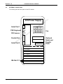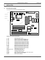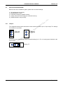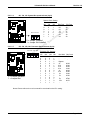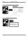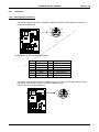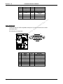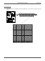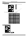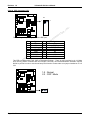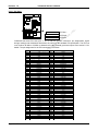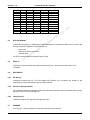
1
Yellowknife X4 User’s Manual
Revision 1.0
C
IN
.
Yellowknife
X4
User’s Manual
CH
R
A
ED
V
I
BY
EE
R
F
LE
A
SC
S
O
IC
EM
R,
O
CT
U
ND
5/13/98
Revision 1.0
Preliminary copy, subject to change without notice
Page 1 of 39
Revision 1.0
1
2
3
4
5
Yellowknife X4 User’s Manual
OVERVIEW ......................................................................................................................................................... 4
1.1
Revision History ........................................................................................................................................... 4
1.2
Introduction .................................................................................................................................................. 5
1.3
Purpose........................................................................................................................................................
5
C.
4.3
External CONTROLS & Indicators.............................................................................................................. 9
4.4
External connectors ................................................................................................................................... 10
IN
,
1.3
Reference Documents .................................................................................................................................
5
OR
1.3.1
Motorola Documents.............................................................................................................................
5
T
C
1.3.2
External Documents .............................................................................................................................
5
U
D
N
O
PRODUCT SUMMARY .......................................................................................................................................
6
IC
M
SE
E
SYSTEM CONFIGURATION ..............................................................................................................................
7
AL
C
3.1
Block Diagram..............................................................................................................................................
8
ES
E
R
F
CHASSIS.............................................................................................................................................................
9
BY
D
4.1
Chassis ........................................................................................................................................................
9
VE
I
H
C
4.2
Slots .............................................................................................................................................................
9
AR
INSTALLATION................................................................................................................................................. 11
5.1
Motherboard diagram................................................................................................................................. 11
Jumpers and connectors Description................................................................................................................ 11
5.2
Jumpers, Slots and Connectors................................................................................................................. 12
5.2.1
Jumpers .............................................................................................................................................. 12
5.2.2
Connectors ......................................................................................................................................... 12
5.2.3
Additional Connectors / Sockets......................................................................................................... 12
5.3
Installation procedure................................................................................................................................. 13
5.3.1
Jumpers .............................................................................................................................................. 13
5.3.1.1 Jumper Settings .............................................................................................................................. 14
5.3.1.1.1 J39 COP Enable Mode (3-pin).................................................................................................. 14
5.3.1.1.2 J63 Test Support Jumper (3-pin)............................................................................................... 14
5.3.1.1.3 J64 Interrupt routing Jumper (3-pin) .......................................................................................... 14
5.3.1.1.4 J61, J34, J32 System Bus speed selector (2-pin) .................................................................... 15
5.3.1.1.5 J35, J36, J38, J40 Processor Speed selector (2-pin)............................................................... 15
5.3.1.1.6 J40, J57, J59, J58 MPC106 bus speed selector (GPLL)(2-pin) ................................................ 16
5.3.1.1.7 J45, J46, J47, J55, J56 VID override Jumper (3-pin) ................................................................ 16
5.3.2
Connectors ......................................................................................................................................... 17
Page 2 of 39
Yellowknife X4 User’s Manual
Revision 1.0
5.3.2.1 PS/2 Keyboard and mouse ............................................................................................................. 17
5.3.2.2 Serial Ports...................................................................................................................................... 18
5.3.2.3 Parallel Port..................................................................................................................................... 19
5.3.2.4 Power Connector ............................................................................................................................ 20
5.3.2.5 IDE Connectors............................................................................................................................... 21
5.3.2.6 Floppy Disk Connector.................................................................................................................... 22
5.3.2.7 CMOS Battery Connector (J2).......................................................................................................... 22
5.3.2.8 Misc. Connectors (J44)................................................................................................................... 23
5.3.2.9 CPU Fan Power Connector (3-pin).................................................................................................. 23
5.3.2.10 ESP Connector (J33)..................................................................................................................... 24
5.3.2.11 VRM Connector ..............................................................................................................................
25
C.
N
5.3.3 EXPANSION SLOTS...............................................................................................................................
26
I
,
R
5.3.3.1 DRAM DIMM Slots............................................................................................................................
26
O
T
5.3.3.2 ROM ..................................................................................................................................................
26
5.3.3.2.1 Toolbox ROM (For testing purpose) ...........................................................................................
26
UC
D
5.3.3.2.2 Boot ROM ...................................................................................................................................
28
N
O
5.3.3.3 PowerPC Processor socket..............................................................................................................
29
IC
5.3.3.4 ISA slots............................................................................................................................................
30
M
SE
5.3.3.5 PCI Slots .........................................................................................................................................
32
6
LE
A
HARDWARE .....................................................................................................................................................
34
SC
E
E
FR
6.1
PROCESSOR SPEED SUPPORT.............................................................................................................
34
BY
D
6.2
System bus and PCI busEcontrol................................................................................................................
35
V
I
H
6.3
Voltage RegulatorCModule
(VRM) .............................................................................................................. 35
R
A
6.4
RTC and NVRAM....................................................................................................................................... 36
6.5
Display ....................................................................................................................................................... 36
6.6
Disk Drives ................................................................................................................................................. 36
6.6.1
IDE Drive(s) ........................................................................................................................................ 36
6.6.2
Hard Drive Activity Indicator ............................................................................................................... 36
6.6.3
Floppy Drive(s) ................................................................................................................................... 36
6.7
Speaker...................................................................................................................................................... 36
6.8
Power Supply ............................................................................................................................................. 37
6.9
Key Components........................................................................................................................................ 37
6.9.1
MPC106 .............................................................................................................................................. 37
6.9.2
Winbond 83C553 ................................................................................................................................ 37
6.9.3
National Semiconductor PC87308VUL............................................................................................... 37
7
DINK32 DEBUG MONITOR.............................................................................................................................. 38
8
SOFTWARE ...................................................................................................................................................... 39
8.1
Utilities........................................................................................................................................................ 39
Page 3 of 39
Revision 1.0
Yellowknife X4 User’s Manual
1
OVERVIEW
1.1
REVISION HISTORY
Date
Revision
Distribution
Comments
5/13/98
1.0
General Release .....................................for Motherboard version X4
Please send your comments of this user’s manual to:
RISC Hotline
Phone: 512-895-4488
Email: [email protected]
TRADEMARKS
E
LE
A
SC
S
O
IC
EM
R,
O
CT
U
ND
C
IN
.
E PowerPC 603, PowerPC740 and PowerPC750 are
The PowerPC name, the PowerPC logotype,
FR
trademarks of International Business
Machines Corporation used by Motorola under license from
International Business Machines
BYCorporation
ED
V
This document contains
I information on a new product under development. Specifications and information
herein are subject C
toH
change without notice.
AR
Page 4 of 39
Yellowknife X4 User’s Manual
1.2
Revision 1.0
INTRODUCTION
This user’s manual defines the features of a PowerPC 6xx/7xx evaluation
"Yellowknife X4".
system, code-named
Before system power on, check the system with the packing list. If any items are missing, please call your
local Motorola sales office.
The design philosophy behind Yellowknife was to create a very modular, full-featured evaluation system
that could be easily tailored by the users to meet their specific requirement. Key features are:
1.3
-
Easy processor upgrade through PGA ZIF socket
-
Selectable operating frequencies
-
Software debugs platform for embedded application.
-
Development platform for use by third-parties firmware/utility developers.
.
R,
O
CT
U
- ATX form factor motherboard allows full size PCI and ISA add-on
cards
D
N
O
IC
M
SE
LE
A
PURPOSE
SC
E
E
The Yellowknife X4 evaluation systemR has various uses including, but not limited to :
F
BY in benchmarking, compatibility testing, RTAS
- System for use by customers
D
customization andEfirmware development.
IV
H
C to showcase the 6xx and 7xx PowerPC processors, as well as the MPC106
- System suitable
AR
Chipset.
1.3
REFERENCE DOCUMENTS
1.3.1
Motorola Documents
-
1.3.2
C
IN
PowerPC Microprocessor Family: The Programming Environments manual
PowerPC 603e Users manual
PowerPC 750 User’s manual
PowerPC 106 User's manual
External Documents
-
IBM AT Technical Reference Manual
Peripheral Component Interconnect (PCI) Specification Rev 2.1
ATX Specification version 1.0
Page 5 of 39
Revision 1.0
2
Yellowknife X4 User’s Manual
PRODUCT SUMMARY
The following is a summary of the major features of Yellowknife:
Processor and Chipset support
-
Processors supported: all 6xx and 7xx processor with external
bus frequencies up to 100 MHz
One PGA (Socket 3) connector on board
MPC106 Processor to PCI bridge
Winbond 83C553 as PCI to ISA bridge
Memory support
-
2 64-bit (168-pin) DIMM sockets
8 MB minimum, 128 MB maximum SDRAM
O
IC
Support for 8 MB, 16 MB , 32 MB and 64MB DIMMs
512K pipelined L2 cache on board
EM
S
Flash EPROM for boot firmware
E
Peripheral support
-
EE
R
F
AL
C
S
Three PCI slots
Two ISA slots
BY
Two serial portsD(buffered, 16550-compatible)
E port
One DB25 parallel
IV
Two IDEHconnectors
C
PS/2Rkeyboard
port
A
PS/2 mouse port
Floppy interface
Chassis
-
ATX size chassis with ATX power supply
Software
-
Page 6 of 39
DINK32 Debug Monitor Software
R,
O
CT
U
ND
C
IN
.
Yellowknife X4 User’s Manual
3
Revision 1.0
SYSTEM CONFIGURATION
-
PowerPC 603, 740 or 750 Microprocessor
ATX chassis with ATX power supply
32 MB DIMM
On board 512 KB Pipelined L2 Cache
DINK32 debug monitor ROM
CH
R
A
ED
V
I
BY
EE
R
F
LE
A
SC
S
O
IC
EM
R,
O
CT
U
ND
C
IN
.
Page 7 of 39
Revision 1.0
3.1
Yellowknife X4 User’s Manual
BLOCK DIAGRAM
The following is the block diagram of the Yellowknife X4 configuration:
DRAM DIMMs
6xx or 7xx Processor
DRAM
DIMM
Socket
Universal Bus
Transceivers
CH
R
A
ED
V
I
IN
,
OR
T
UC
D
N
C
O
IC
PowerPC Bus
EM
16501
BY
L2 Cache. on board
F
S
E
L
Processor-to-PCI
CA
S
E Bridge
RE MPC106
(Grackle)
PCI Bus
PCI slots
PCI-ISA
Bridge
With Enhanced IDE
ISA Bus
ISA slots
NVRAM
Floppy
Page 8 of 39
Keyboard
Super I/O
Controller
PC87308VUL
Mouse
Boot ROM
Serial X 2
Parallel
Yellowknife X4 User’s Manual
4
CHASSIS
4.1
CHASSIS
Revision 1.0
Standard PC I/Os is supported in Yellowknife. The Yellowknife uses the ATX format chassis which has
drive bay to accomodate an additional hard drive.
4.2
SLOTS
,
C
IN
.
The Yellowknife chassis supports a total of five I/O slots for add-in cards. Three
R of the slots support PCI
cards and the remaining two support ISA cards.
TO
4.3
EXTERNAL CONTROLS & INDICATORS
O
IC
EM
UC
D
N
The following diagram shows the front panel of the Yellowknife
system:
S
CH
R
A
ED
V
I
BY
EE
R
F
LE
A
SC
POWER ON LED
POWER ON SWITCH
RESET SWITCH
Page 9 of 39
Revision 1.0
4.4
Yellowknife X4 User’s Manual
EXTERNAL CONNECTORS
The following show the back panel on the ATX chassis:
ATX Power Supply
Serial Port 1
PS/2 Keyboard
PS/2 mouse
Y
Parallel Port D B
VE
I
CH
R
Serial A
Port 2
EE
R
F
LE
A
SC
PCI Slot 1
PCI Slot 2
PCI Slot 3
ISA Slot X 2
Page 10 of 39
S
O
IC
EM
R,
O
CT
U
ND
C
IN
.
Fan
Optional
Serial and
Parallel
Ports
Yellowknife X4 User’s Manual
5
INSTALLATION
5.1
MOTHERBOARD DIAGRAM
Revision 1.0
The following is the Yellowknife x4 motherboard diagram:
1
1
J35J36
J38 J40
1
1 1
1
COM1
J45 J46 J47 J55J56
1
PS/2 KEYBD
POWER
CONNECTOR
J63
1
1
ZIF SOCKET 3
DIMM Slot
1
0
PS/2 MOUSE
1
PARALLEL
J57 J59 J58J60
J33
COM2
1
1
J62
1
BY
D
E
IV PCI Slot 3
PCI Slot 1
EE
R
F
LE
A
SC
S
O
IC
EM
ISA Slot 1
C
IN
R,
O
CT
U
ND
.
1
VRM
1
1
1
SCSI
IDE1
IDE2
Toolbox
ROM
Boot ROM
J64
PCI Slot 2
CH
R
A
Floppy
J50
1
1
1
J61 J34 J32
J39
1
ISA Slot 2
J2
1
1
J44
Jumpers and connectors Description
1) J39
2) J61
3) J34
4) J32
5) J35
6) J36
7) J38
8) J40
9) J57
10) J59
11) J58
12) J60
13) J2
14) J45,46,47,55,56
15) J64
16) J63
17) J44
18) J50
19) J33
COP Enable Mode (3-pin)
System bus speed selector FREQO (2-pin)
System bus speed selector FREQ1(2-pin)
System bus speed selector FREQ2 (2-pin)
Internal processor bus selector PLL0 (3-pin)
Internal processor bus selector PLL1 (3-pin)
Internal processor bus selector PLL2 (3-pin)
Internal processor bus selector PLL3 (3-pin)
MPC106 bus speed selector GPLL0 (2-pin)
MPC106 bus speed selector GPLL1 (2-pin)
MPC106 bus speed selector GPLL2 (2-pin)
MPC106 bus speed selector GPLL3 (2-pin)
CMOS Battery connector (3-pin)
VID override jumper (3-pin)
Interrupt routing jumper (3-pin)
Test Support Jumper (3-pin)
Misc. connectors for Reset,speaker, LEDs, Power switch....
CPU Fan Power Connector (3-pin)
ESP connector (2x8-pin)
Page 11 of 39
Revision 1.0
Yellowknife X4 User’s Manual
5.2
JUMPERS, SLOTS AND CONNECTORS
5.2.1
Jumpers
1) J39
2) J63
3) J64
4) J61
5) J34
6) J32
7) J35
8) J36
9) J38
10) J40
11) J57
12) J59
13) J58
14) J60
15 ) J45,46,47,55,56
5.2.2
Connectors
p.14
p.14
p.14
p.15
p.15
p.15
p.15
p.15
p.15
p.16
p.16
p.16
p.16
p.16
p.17
COP Enable Mode (3-pin)
Test Support Jumper (3-pin)
Interrupt routing jumper (3-pin)
System bus speed selector FREQO (2-pin)
System bus speed selector FREQ1(2-pin)
System bus speed selector FREQ2 (2-pin)
Internal processor bus selector PLL0 (3-pin) ,
Internal processor bus selector PLL1 (3-pin) R
Internal processor bus selector PLL2 (3-pin)
TO
C
Internal processor bus selector PLL3U
(3-pin)
D(2-pin)
MPC106 bus speed selector GPLL0
N
O (2-pin)
MPC106 bus speed selectorC
GPLL1
I GPLL2
MPC106 bus speed selector
(2-pin)
M
E
MPC106 bus speed selector
GPLL3
(2-pin)
S
E
VID override jumper
(3-pin)
L
Y
B
1) PS/2 Keyboard
p.17
D
2) PS/2 Mouse
VE p.17
I
3) Serial Port
p.18
H
4) Parallel Port RC
p.19
A
5) Power Connector
p.20
6) IDE Connector
p.21
7) Floppy
p.22
8) J2
p.22
9) J44
p.23
10) J50
p.23
11) J33
p.24
12) VRM Module
p.25
13) J62
5.2.3
E
FR
Page 12 of 39
p.26
p.26
p.29
p.30
p.32
.
CA
S
E
PS/2 keyboard connector (6 pin)
PS/2 mouse connector (6-pin)
Serial Port COM1 & COM2 (9-pin)
Parallel Port LPT1 (25-pin)
ATX power supply connector (20-pin)
IDE connectors(40-pin)
Floppy Drive connector (34-pin)
CMOS Battery connector (3-pin)
Misc. connectors for Reset,speaker, LEDs, Power switch....
CPU Fan Power Connector (3-pin)
ESP connector (2x8-pin)
VRM module connector (2x15-pin)
Test Clock connector (2-pin) (For testing only)
Additional Connectors / Sockets
1) DIMM slots
2) ROM socket
3) ZIF Socket 3
4) ISA slots
5) PCI slots
C
IN
DRAM Memory DIMM socket
ROM Socket for Boot ROM
Socket for PowerPC Processor (PGA)
16-bit ISA slots
32-bit PCI Bus Expansion slots
Yellowknife X4 User’s Manual
5.3
Revision 1.0
INSTALLATION PROCEDURE
Before Power on the Yellowknife system, please make sure the followings:
1)
2)
3)
5)
6)
All Jumpers are set correctly
DRAM Modules in place
PowerPC processor is installed correctly
Cables, wires and Power Supply are connected correctly
DINK32 software setup correctly
C
IN
5.3.1
.
R,
O
Jumpers
CT
U
The Yellowknife board jumpers discussed in these sections are either
ND 2-pin or 3 pin arrays. Two settings
O
are possible for 2-pin array:
IC
M
SE
E
AL
C
ES
E
FR
BY
D
For the 3-pin array, the following
diagram shows the setting for 1-2. Pin 1 of each jumper is labeled on the
VE
I
system board
CH
R
A
short
Open
Setting 1-2
1
Page 13 of 39
Revision 1.0
Yellowknife X4 User’s Manual
5.3.1.1 Jumper Settings
5.3.1.1.1
J39 COP Enable Mode (3-pin)
1-2 : Normal
2-3 : COP Mode
1
5.3.1.1.2
E
J63 Test Support Jumper (3-pin)
CH
R
A
5.3.1.1.3
ED
V
I
LE
A
SC
S
O
IC
EM
R,
O
CT
U
ND
C
IN
.
E
FR 1
BY
J63
For Lab Testing Only
Left Open
J64 Interrupt routing Jumper (3-pin)
J64
1-2 Do not populate
2-3 Using 8259 for interrupt controller (Default)
1
Page 14 of 39
Yellowknife X4 User’s Manual
5.3.1.1.4
Revision 1.0
J61, J34, J32 System Bus speed selector (2-pin)
System Clock Setting
J61
0
0
0
0
1
1
1
J61 J34 J32
1
0 = Jumper Installed
1 = Jumper Not Installed
5.3.1.1.5
J34
0
0
1
1
0
0
1
J32
0
1
0
1
0
1
0
N
O
IC
M
E
S
E
L
J35, J36, J38, J40 Processor Speed
selector (2-pin)
CA
S
E
E
J35 J36 J38 J40
FR Processor PLL Settings
BY
1
J35 J36
J38 J40
D
E
0
0
0
0
V
I
H
0
0
0
1
C
R
0
0
1
0
A
0
0
1
1
0 = Jumper Installed
1 = Jumper Not
0
0
0
0
1
1
1
1
1
1
1
1
1
1
1
1
0
0
0
0
1
1
1
1
0
0
1
1
0
0
1
1
0
0
1
1
0
1
0
1
0
1
0
1
0
1
0
1
Bus Freq.
50
60
66
75
,
83 OR
90
CT
U
D 99
PCI Freq.
25
30 .
C
33
IN
37
33
36
39
Bus Multi Bus Clock
7x
25-33
Bypass
2x
60-83
6.5x
25-40
2.5x
50-83
4.5x
33-60
3x
40-83
5.5x
25-40
4x
33-66
5x
25-50
6x
25-40
3.5x
40-75
-
Notes: Please refers to the user’s manual for more detail on the PLL setting.
Page 15 of 39
Revision 1.0
5.3.1.1.6
Yellowknife X4 User’s Manual
J40, J57, J59, J58 MPC106 bus speed selector (GPLL)(2-pin)
MPC106 PLL Settings
0 = Jumper Installed
1 = Jumper Not
5.3.1.1.7
J57 J59
J58 J60
Bus Clock PCI Clock
0
0
0
0
0
0
0
1
1x
33
33
J57 J59 J58 J60
.
0
0
1
0
1x 16-25 C16-25
N
0
0
1
1
Bypass I
1
0
1
0
0
2x R
66,
33
0
1
0
1
2xTO33-50 16-25
C 83
0
1
1
0
33
U2.5x
0
1
1
1 D 2.5x 41-50 16-20
N 3x 75-100 25-33
1
0
0
0
O
1
0
0 IC 1
3x
50
16
M
1
0
1
0
E
S 1
1
0
1
E
1 AL1
0
0
C
1
1
0
1
S
E
1
1
1
0
E
R
1
1
1
1
OFF
F
ED
V
I
BY
H J55, J56 VID override Jumper (3-pin)
J45, J46, J47,
C
AR
J45 J46 J47 J55 J56
3
2
1
WARNING:
These jumpers are for testing purpose
only. Please do not populate these
jumpers! Populate any of these Jumpers
may cause the system malfunctions.
Page 16 of 39
Yellowknife X4 User’s Manual
5.3.2
Revision 1.0
Connectors
5.3.2.1 PS/2 Keyboard and mouse
Yellowknife supports both the AT-compatible keyboard interfaces. PS/2 keyboard connectors are
located at the back panel .
6
4
2
EE
LE
A
SC
5
3
1
S
O
IC
EM
R,
O
CT
U
ND
C
IN
.
The following is the PS/2 keyboard pin
Rdefinition:
D
PinE
I1V
H
C 2
AR
3
4
5
6
Shell
BY
F
Signal
KBDATA
NC
GND
FVcc
KBCLK
NC
N/A
I/O
I/O
N/A
N/A
N/A
I/O
N/A
N/A
Definition
Keyboard data
No connection
Signal GND
Fused supply voltage
Keyboard clock
No connection
Chassis GND
Yellowknife supports both the PS/2 compatible mouse The PS/2 mouse is supported through the
mouse port . PS/2-mouse connector is located at the back panel .
PS/2 mouse connector pin assignment
6
4
2
5
3
1
Page 17 of 39
Revision 1.0
Yellowknife X4 User’s Manual
Pin
1
2
3
4
5
6
Shell
Signal
MFDATA
NC
GND
FVcc
I/O
I/O
N/A
N/A
N/A
KBCLK
NC
N/A
I/O
N/A
N/A
Definition
Mouse data
No connection
Signal GND
Fused supply
voltage
Mouse clock
No connection
Chassis GND
5.3.2.2 Serial Ports
O
R,
O
CT
U
ND
C
IN
Yellowknife has two 16550-compatible serial ports. PC serialIC
connectors are located
M
at the back panel.
PC serial port pin assignment
CH
R
A
ED
V
I
Pin
1
2
3
4
5
6
7
8
9
Page 18 of 39
BY
EE
R
F
LE
A
SC
SE
1
5
6
Signal
DCD
SIN
SOUT
DTR
GND
DSR
RTS
CTS
RI
I/O
I
I
O
O
N/A
I
O
I
I
9
Definition
Data carrier detect
Serial input
Serial output
Data terminal ready
Signal GND
Data Set Ready
Request To Send
Clear To Send
Ring Indicator
.
Yellowknife X4 User’s Manual
Revision 1.0
5.3.2.3 Parallel Port
Yellowknife has one AT-compatible, bi-directional parallel port. This connector is located at the back
panel.
1
13
25
Pin
1
2
3 D
4
VE
I
CH 5
R
6
A
7
8
9
10
11
12
13
14
15
16
17
18-25
Signal
EE
R
STB#
F
Y
B PD0
PD1
PD2
PD3
PD4
PD5
PD6
PD7
ACK#
BUSY
PE
SLCT
AFD#
ERR#
INIT#
SLIN#
GND
LE
A
SC
I/O
I/O
I/O
I/O
I/O
I/O
I/O
I/O
I/O
I/O
I
I
I
I
O
I
O
O
N/A
S
O
IC
EM
R,
O
CT
U
ND
C
IN
.
14
Definition
Strobe
Printer data bit o
Printer data bit 1
Printer data bit 2
Printer data bit 3
Printer data bit 4
Printer data bit 5
Printer data bit 6
Printer data bit 7
Acknowledge
Busy
Paper end
Select
Automatic Feed
Error
Initialize printer
Select in
Signal GND
Page 19 of 39
Revision 1.0
Yellowknife X4 User’s Manual
5.3.2.4 Power Connector
Yellowknife uses the standard ATX power supply which provide the 5V and 3.3V to the motherboard. The
following is the power connector pin assignment:
1
LE
A
SC
Pin
Signal
EE
R
1
+3.3V
F
Y
2
+3.3V
B
3 D
GND
E
4
VCC
V
I
H
5
GND
C 6
VCC
AR
7
GND
8
PWRGOOD
9
VSTDBY
10
+12V
Page 20 of 39
Pin
11
12
13
14
15
16
17
18
19
20
S
O
IC
EM
R,
O
CT
U
ND
Signal
+3.3V
-12V
GND
PS_ON
GND
GND
GND
-5V
VCC
VCC
C
IN
.
Yellowknife X4 User’s Manual
Revision 1.0
5.3.2.5 IDE Connectors
The Enhanced IDE controller is built in the PCI-ISA Bridge, two IDE connectors are on the motherboard
to support both the enhanced IDE hard drives and the IDE CD-ROM.
IDE1 IDE0
J37 J16
1
IDE connector pin assignment
Pin
1
3
E5D
V
HI 7
C
9
AR
11
13
15
17
19
21
23
25
27
29
31
33
35
37
39
EE
LE
A
SC
R
FSignal
BYIDERESET#
IDED7
IDED6
IDED5
IDED4
IDED3
IDED2
IDED1
IDED0
GROUND
IDEDRQ#
IDEIOW#
IDEIOR#
N/C
IDEACK#
IDEIRQ
IDESA1
IDESA0
IDECS0#
DISKLED#
S
Pin
2
4
6
8
10
12
14
16
18
20
22
24
26
28
30
32
34
36
38
40
1 O
IC
M
E
R,
O
CT
U
ND
C
IN
.
Signal
GND
IDED8
IDED9
IDED10
IDED11
IDED12
IDED13
IDED14
IDED15
N.C.
GND
GND
GND
IDEBALE
GND
IDEIOCS16#
N.C.
IDESA2
IDECS1#
GND
Page 21 of 39
Revision 1.0
Yellowknife X4 User’s Manual
5.3.2.6 Floppy Disk Connector
Yellowknife incorporates a 34-pin Floppy disk connector to support the floppy disk drive .
1
J43
O
R,
O
CT
U
ND
The pin assignment of the autoeject floppy disk drive is as follows:
IC
Pin
1
3
5
7
9
11 D
V13E
I
CH 15
R
17
A
19
21
23
25
27
29
31
33
Signal
Pin
L2E
F_EJECT#
A
KEY SC 4
GndEE
6
R
Gnd
8
F
Y
Gnd
10
B
Gnd
12
Gnd
14
Gnd
16
Gnd
18
Gnd
20
Gnd
22
Gnd
24
Gnd
26
Gnd
28
Gnd
30
Gnd
32
Gnd
34
5.3.2.7 CMOS Battery Connector (J2)
1
J2
Connect the CMOS battery connector to 1-4
Page 22 of 39
SE
M
Signal
DENSEL
MSEN0
DISK CHANGE#
INDEX#
MTR0#
DRVSEL1#
DRVSEL0#
MTR1#
DIR#
STEP#
WDATA#
WGATE#
TRK0#
WRTPRT#
RDATA#
HDSEL#
PULL UP
C
IN
.
Yellowknife X4 User’s Manual
Revision 1.0
5.3.2.8 Misc. Connectors (J44)
Disk
LED
Reset
J44
2
1
IR Port
The following are the pin assignment for J44:
Pin
1
3
5 D
7E
V
I
9
CH 11
R
A
13
15
17
19
21
23
25
27
29
31
33
Signal
EE
R
FVCC
Y
NC
B IRRX
GND
IRTX
NC
VCC
NC
GND
NC
GND
NC
NC
PCSPKR
NC
GND
VCC
R,
O
CT
U
ND
STDBY PWR
PS ON LED SWITCH
C
IN
.
O
IC
PWR LED M SPKR
SE
E
AL
C
S
Pin
2
4
6
8
10
12
14
16
18
20
22
24
26
28
30
32
34
Signal
GND
RSTHDR#
GND
NC
NC
VCC
DISKLED#
DISKLED#
VCC
PS_ON#
GND
NC
VSTDBY
GND
NC
PWR_A
PWR_B
5.3.2.9 CPU Fan Power Connector (3-pin)
1
J50
J50 CPU FAN POWER
1 - GND
2 - +12V
3 - GND
Page 23 of 39
Revision 1.0
Yellowknife X4 User’s Manual
5.3.2.10 ESP Connector (J33)
J33
1
2
R,
O
CT
U
ND
The following is the pin assignment for the ESP port:
Pin
Signal
Pin
1
TDO
2 E
3
TDI
4
AL
C
5
NC
S 6
7
TCK EE
8
R
9
TMS
10
F
Y
11
12
BSRST
13 D HRST
14
E CKSTPO
15
16
IV
S
CH
C
IN
.
O
IC
EM Signal
NC
TRST
ESPSENSE
NC
NC
NC
KEY
GND
R with JTAG, COP or Riscwatch Emulator . There is a KEY position in pin 14. Make
This ESP portA
works
sure the key position matches with the Emulator connector. HP/Corelis/RiscWatch Emulator requires
QACK to pull low in order to use the soft stop CPU function. Please make sure jumper installed on 2-3 of
J39.
1-2 : Normal
2-3 : COP Mode
1
Page 24 of 39
Yellowknife X4 User’s Manual
Revision 1.0
5.3.2.11 VRM Connector
J5
B1
R,
O
CT
U
ND
A1
Pin
Signal
Pin
A1
GND
B1
A2
GND
B2 E
A3
+3.3V
B3
AL
C
A4
+3.3V
B4
ES B5
A5
VCC E
FR
A6
VCC
B6
A7
VID4
B7
BY
A8 ED VID3
B8
V
A9
VID0
B9
I
H
A10
GND
B10
C
GND
B11
AR A11
A12
NC
B12
A13
IVDD
B13
A14
IVDD
B14
A15
IVDD
B15
S
C
IN
.
O
Signal
IC
EM GND
GND
+3.3V
+3.3V
VCC
VCC
VID2
VID1
+12V
GND
GND
NC
IVDD
IVDD
IVDD
Page 25 of 39
Revision 1.0
Yellowknife X4 User’s Manual
5.3.3 EXPANSION SLOTS
5.3.3.1 DRAM DIMM Slots
DIMM SLOTS
1 0
E
S
O
IC
EM
R,
O
CT
U
ND
C
IN
.
Yellowknife supports SDRAM DIMMs.
AL0 and 1), Yellowknife supports from 16MB to 128MB of
With two 64-bit ( 168-pin) DIMM sockets (labeled
C
S
system memory using DIMM with variousE
densities.
RE
F
Please refer to the MPC106 user's
manual and hardware specification
BYof 100MHz SDRAM module.
Yellowknife is shipped with 32MB
ED
V
HI
C
5.3.3.2 ROM
AR
for DRAM timings. Currently,
There are 2 ROMs on the Yellowknife motherboard. The first ROM is the TOOLBOX ROM that is mainly
for testing purpose . The second ROM is the boot ROM that supports DINK32 .
5.3.3.2.1 Toolbox ROM (For testing purpose)
There is a ROM DIMM socket on the motherboard. The size of the Toolbox ROM is 4 MB and this
ROM is located on the Local 60X-memory bus.
Toolbox ROM
Page 26 of 39
Yellowknife X4 User’s Manual
Revision 1.0
The Toolbox ROM socket is 160 pins and the pin assignment is as follows:
CH
R
A
Pin
81
82
83
84
85
86
87
88
89
90
91
92
93
94
95
96
97
98
99
100
101
102
103
104
105
106
107
108
109
110
111
112
113
114
115
116
117
118
119
120
ED
V
I
Pin
121
122
123
124
125
126
127
128
129
130
131
132
133
134
135
136
137
138
139
140
141
142
143
144
145
146
147
Signal
+5V
GND
+12V
MDL31
MDL30
MDL29
MDL28
NC
+5V
NC
MDL27
MDL26
MDL25
MDL24
GND
MDL23
MDL22
MDL21
MDL20
NC
+5V
NC
MDL19
MDL18
MDL17
MDL16
GND
ROMA19
ROMA18
NC
ROMA16
ROMA14
ROMA12
ROMA10
RCS1#
ROM_PRESENT
ROMWE#
FOE#
NC
NC
Pin
1
2
3
4
5
6
7
8
9
10
11
12
13
14
15
16
17
18
19
20
21
22
23
24
25
26
27
28
29
30
31
32
33
34
35
36
37
38
39
40
Signal
+5V
NC
GND
ROMA08
ROMA06
ROMA04
ROMA02
ROMA00
NC
NC
NC
NC
GND
MDL15
MDL14
MDL13
MDL12
NC
+5V
NC
MDL11
MDL10
MDL09
MDL08
GND
MDL07
MDL06
Pin
41
42
43
44
45
46
47
48
49
50
51
52
53
54
55
56
57
58
59
60
61
62
63
64
65
66
67
BY
EE
R
F
LE
A
SC
S
O
IC
EM
Signal
+5V
GND
+12V
MDH31
MDH30
MDH29
MDH28
NC
+5V
NC
MDH27
MDH26
MDH25
MDH24
GND
MDH23
MDH22
MDH21
MDH20
NC
+5V
NC
MDH19
MDH18
MDH17
MDH16
GND
NC
NC
ROMA17
ROMA15
ROMA13
ROMA11
ROMA09
NC
NC
ROMWE#
ROMOE#
NC
NC
R,
O
CT
U
ND
C
IN
.
Signal
+5V
NC
GND
ROMA07
ROMA05
ROMA03
ROMA01
NC
NC
NC
NC
NC
GND
MDH15
MDH14
MDH13
MDH12
NC
+5V
NC
MDH11
MDH10
MDH09
MDH08
GND
MDH07
MDH06
Page 27 of 39
Revision 1.0
Yellowknife X4 User’s Manual
148
149
150
151
152
153
154
155
156
157
158
159
160
MDL05
MDL04
NC
+5V
NC
MDL03
MDL02
MDL01
MDL00
GND
NC
NC
+5V
68
69
70
71
72
73
74
75
76
77
78
79
80
MDH05
MDH04
NC
+5V
NC
MDH03
MDH02
MDH01
MDH00
GND
NC
NC
+5V
5.3.3.2.2 Boot ROM
O
IC
EM
R,
O
CT
U
ND
C
IN
.
S ROM
Boot
EE
R
F
LE
A
SC
BY
D
VE a boot ROM which is implemented as a 4Mb (512Kbx8) flash EPROM.
I
Yellowknife incorporates
CH
R
A contains the DINK boot code to support basic debug function. See DINK user's manual
The bootROM
for more information.
The boot ROM is physically located on the ISA bus.
Page 28 of 39
Yellowknife X4 User’s Manual
Revision 1.0
5.3.3.3 PowerPC Processor socket
ZIF Socket
O
IC
EM
R,
O
CT
U
ND
C
IN
.
S
Yellowknife supports all 1.8V-3.3V 6xx and 7xx PowerPC
processors operating in modes that result in
EVoltage regulator
external processor bus speeds up to 100 MHz.
module is used to provide different
L
A
voltage for different processor. There is oneCsocket 3 PGA ZIF socket on board. Socket 3 is a 17 X 17
S
fully populated footprint. A BGA to PGA E
interposer
will be used to convert the BGA footprint to the PGA
E
footprint.
R
U
T
F
Y
B
Pin Assignment for the 17 x 17 array (Top View)
ED
V
17
16
15
14
13
12
11
10
9
HI
C
MPINT DL15 DH3
DH5 DL20 DL22 DH9 DH11 DH12
R
MPCLK OVDD DH2 AGND DL18 OVDD DH8
GND DH13
R
DL11
DL14 DBG2 DL16
DH4
DL19
DH16
8
7
6
5
4
3
2
1
DH17
DH19 DH23
DH27
DH29
DL31
PID1
PID0
U
GND
DH22 OVDD DH28
GND
DL28
OVDD
DL27
T
DH18
DH24 DH25
DH30
DL29
PID2
DL26
DP6
R
DL21
DH10
OVDD DH15 OVDD DH21
P
DL10
GND
DL13 OVDD
DH0
GND
DH7
DL30
OVDD
DL24
GND
DP4
P
N
DL4
DL6
DL9
DL12
NC
DH1
DL17
DH6
DH14
DH20
DH26
DL31 QREQ
GND
DL25
DL23
DP3
DP1
N
M
DL2
OVDD
DL5
GND
DL8
GND
VDD
GND
OVDD
GND
VDD
GND
DP7
GND
DP2
OVDD
A31
M
DP5
DP0
L
DBB
DL0
TS
DL3
DL7
VDD
GND
VDD
GND
VDD
GND
VDD
K
XATS
GND
DL1
OVDD
A30
GND
VDD
GND
VDD
GND
VDD
GND
J
DTRY
TA
DBDI
TEA
A28
OVDD
GND
VDD
GND
VDD
GND OVDD
BG
ABB
SHD
A29
L
AACK
GND
DBG
K
DBWO
A27
A25
A21
J
ATRY OVDD
H
A26
GND
A24
OVDD
A22
GND
VDD
GND
VDD
GND
VDD
GND
A23
OVDD
A19
GND
A17
H
G
A20
A18
A16
A14
A10
VDD
GND
VDD
GND
VDD
GND
VDD
A7
A9
A11
A13
A15
G
F
A12
OVDD
A8
GND
A0
GND
VDD
GND
OVDD
GND
VDD
GND
GBL
GND
A3
OVDD
A5
F
E
A6
A4
TT4
INT
BG2
TBST
TSZ0
L2CK CHKO
BR
CSE0
AP0
QACK TBEN
DRV0
CI
A1
E
D
A2
GND
MCP
GND
LSSD OVDD HALT OVDD NAPR
GND
RSRV OVDD
WT
D
C
TT3
TT2
TLBI
TT1
TMS
TCK
PLL3
SYSC CKST
APE
TC2
TC0
B
SMI
OVDD TSZ2
GND
TDI
OVDD
L1CL
GND
HRST
GND
DPE
A
BR2
TT0
TSZ1
TD0
PLL2
TRST AVDD
PLL1
PLL0
ARAY L2INT CLK0
17
16
15
14
13
10
9
OVDD SRST
12
11
8
7
DRV1
GND
AP1
VID4
VID1
GND
VID3
OVDD
TC1
AP3
SCLK
VID2
5
4
3
2
AP2
OVDD CSE1
6
SDATA C
VID0
B
A
1
Page 29 of 39
Revision 1.0
Yellowknife X4 User’s Manual
5.3.3.4 ISA slots
C
IN
.
R,
O
C2T
ISA Slot
U
NDSlot 1
ISA
O
IC
M
Yellowknife has two ISA slots (ISA1, and ISA2). The connectors,
pin assignments, signal timings, loadings
SEISA specification. The pin assignment for the ISA
and mechanical dimensions all conform to the standard
connectors is as follows:
LE
A
SC Pin
Pin
Description
Description
E
E
B1
GROUND
A1
IOCHK*
R
B2
A2
SD7
FRESETDRV
B3 Y
+5V
A3
SD6
B4B
IRQ9
A4
SD5
D
B5
-5V
A5
SD4
DRQ2
A6
SD3
VE B6
I
B7
-12V
A7
SD2
CH
B8
NOWS*
A8
SD1
R
B9
+12V
A9
SD0
A
Page 30 of 39
B10
B11
B12
B13
B14
B15
B16
B17
B18
B19
B20
B21
B22
B23
B24
B25
B26
B27
B28
B29
B30
B31
GROUND
SMEMW*
SMEMR*
IOW*
IOR*
DACK3*
DRQ3
DACK1*
DRQ1
REFRESH*
SYSCLK
IRQ7
IRQ6
IRQ5
IRQ4
IRQ3
DACK2*
T/C
BALE
+5V
OSC
GROUND
A10
A11
A12
A13
A14
A15
A16
A17
A18
A19
A20
A21
A22
A23
A24
A25
A26
A27
A28
A29
A30
A31
IOCHRDY
AEN
SA19
SA18
SA17
SA16
SA15
SA14
SA13
SA12
SA11
SA10
SA9
SA8
SA7
SA6
SA5
SA4
SA3
SA2
SA1
SA0
D1
D2
D3
D4
D5
D6
D7
D8
D9
D10
D11
D12
D13
D14
MEMCS16*
IOCS16*
IRQ10
IRQ11
IRQ12
IRQ15
IRQ14
DACK0*
DRQ0
DACK5*
DRQ5
DACK6*
DRQ6
DACK7*
C1
C2
C3
C4
C5
C6
C7
C8
C9
C10
C11
C12
C13
C14
SBHE*
LA23
LA22
LA21
LA20
LA19
LA18
LA17
MEMR*
MEMW*
SD8
SD9
SD10
SD11
Yellowknife X4 User’s Manual
D15
D16
D17
D18
CH
R
A
ED
V
I
BY
DRQ7
+5V
MASTER*
GROUND
EE
R
F
C15
C16
C17
C18
LE
A
SC
S
Revision 1.0
SD12
SD13
SD14
SD15
O
IC
EM
R,
O
CT
U
ND
C
IN
.
Page 31 of 39
Revision 1.0
Yellowknife X4 User’s Manual
5.3.3.5 PCI Slots
PCI Slot 1
C
IN
.
R,
O
PCI SlotC3T
DU
N
Yellowknife has three PCI slots (PCI 1, PCI 2 and PCI 3). O
The connectors, pin assignments, signal
timings, loadings and mechanical dimensions all conform toIC
the standard PCI specification. The PCI bus
runs at either 30 MHz or 33 MHz as determined by the
(external) processor speed. See section 5.3 for
EM
details. The pin assignment for the PCI connectors is S
as follows:
LE
A
Pin
Description
Pin
Description
SC A1
B1
-12V
TRST*
E
B2
TCK
A2
+12V
E
R
B3
GROUND
A3
TMS
F
B4
TD0
A4
TDI
Y
B5
A5
+5V
B +5V
B6
+5V
A6
INTA*
ED INTB*
B7
A7
INTC*
V
B8
INTD*
A8
+5V
HI
B9C
PRSNT1*
A9
RESERVED
B10
RESERVED
A10
+5V
AR
B11
PRSNT2*
A11
RESERVED
PCI Slot 2
B12
B13
B14
B15
B16
B17
B18
B19
B20
B21
B22
B23
B24
B25
B26
B27
B28
B29
B30
B31
B32
B33
B34
B35
B36
B37
B38
B39
B40
B41
B42
B43
B44
B45
B46
Page 32 of 39
GROUND
GROUND
RESERVED
GROUND
CLK
GROUND
REQ*
+5V (I/O)
AD31
AD29
GROUND
AD27
AD25
+3.3V
C/BE*3
AD23
GROUND
AD21
AD19
+3.3V
AD17
C/BE*2
GROUND
IRDY*
+3.3V
DEVSEL*
GROUND
LOCK*
PERR*
+3.3V
SERR*
+3.3V
C/BE*1
AD14
GROUND
A12
A13
A14
A15
A16
A17
A18
A19
A20
A21
A22
A23
A24
A25
A26
A27
A28
A29
A30
A31
A32
A33
A34
A35
A36
A37
A38
A39
A40
A41
A42
A43
A44
A45
A46
GROUND
GROUND
RESERVED
RST*
+5V (I/O)
GNT*
GROUND
RESERVED
AD30
+3.3V
AD28
AD26
GROUND
AD24
IDSEL
+3.3V
AD22
AD20
GROUND
AD18
AD16
+3.3V
FRAME*
GROUND
TRDY*
GROUND
STOP*
+3.3V
SDONE
SBO*
GROUND
PAR
AD15
+3.3V
AD13
Yellowknife X4 User’s Manual
B47
B48
B49
B50
B51
B52
B53
B54
B55
B56
B57
B58
B59
B60
B61
B62
CH
R
A
AD12
AD10
GROUND
(KEY)
(KEY)
AD8
AD7
+3.3V
AD5
AD3
GROUND
AD1
+5V (I/O)
ACK64*
+5V
+5V
ED
V
I
BY
EE
R
F
A47
A48
A49
A50
A51
A52
A53
A54
A55
A56
A57
A58
A59
A60
A61
A62
LE
A
SC
S
Revision 1.0
AD11
GROUND
AD9
(KEY)
(KEY)
C/BE*0
+3.3V
AD6
AD4
GROUND
AD2
AD0
+5V (I/O)
REQ64*
+5V
+5V
O
IC
EM
R,
O
CT
U
ND
C
IN
.
Page 33 of 39
Revision 1.0
Yellowknife X4 User’s Manual
6
HARDWARE
6.1
PROCESSOR SPEED SUPPORT
Six sets of jumpers will be located on board which are set to specify:
-
external CPU bus speed (50, 60, 66, 75, 83, 100 MHz)
processor clock PLL setting (2x, 2.5x, 3x, 3.5x , 4x, 4.5x ,5x, 5,5x, 6x).
C.
N
The following table lists some examples of the processor core speed Vs external processor
bus speed:
,I
R
PLL Setting
Frequency (MHz)
J35
J36
J40
TO J38
C
Core
Bus
PLL0
PLL1 U
PLL2
PLL3
2x
180
90
0
1
0
0
ND
O
200
100
IN
OUT
IN
OUT
IC
M
2.5X
188
75
0
1
1
0
SE
E
200
83
L
OUT
OUT
IN
225
90
CAIN
S
250
100
EE
R
3x
180
60 F
1
0
0
0
200
B66Y
225
OUT
IN
IN
IN
ED 75
V
250
83
I
270 CH
90
R
300
100
A
3.5x
210
233
262
290
315
350
60
66
75
83
90
100
200
240
266
300
332
50
60
66
75
83
225
270
300
50
60
66
250
300
333
50
60
66
5.5x
275
300
6x
300
4x
4.5x
5x
Page 34 of 39
1
1
1
0
OUT
OUT
OUT
IN
1
0
1
0
OUT
IN
OUT
IN
0
1
1
1
IN
OUT
OUT
OUT
1
0
1
1
OUT
IN
OUT
OUT
50
60
1
OUT
0
IN
1
OUT
0
IN
50
1
OUT
1
OUT
0
IN
1
OUT
Yellowknife X4 User’s Manual
6.2
Revision 1.0
SYSTEM BUS AND PCI BUS CONTROL
Seven jumpers used to define the speed of the system bus and the PCI bus. J61, J34
The following table lists all the system and PCI bus speed and the jumper's settings:
Bus Speed (MHz)
System
PCI
50
25
60
30
66
33
75
37
83
33
90
36
100
40
100
33
J61
J34
J32
0
0
0
0
1
1
1
1
0
0
1
1
0
0
0
0
0
1
0
1
0
1
1
1
0 = Jumper Installed
1 = Jumper Not Installed
EE
R
F
6.3
J57
GPLL0
0
0
0
0
0
0
0
1
LE
A
SC
S
J59
J58
J60
GPLL1
GPLL2
GPLL3
1
0
1
1
0
0
1
0
C. 00
1
0 IN
1
1,
0
R
O
1
1
0
T
1 UC
1
0
0D
0
0
N
O
IC
M
E
VOLTAGE REGULATOR MODULE
BY (VRM)
ED
The RCB010 from Raytheon
IV Electronics is a programmable DC-DC Voltage Regulator Module designed
H
to deliver the selectable
processor core voltage required by the PowerPC processor. The RCB010 takes
C
R
full advantage of
a Raytheon programmable DC-DC controller IC. This IC integrates a 5-bit DAC for
A
automatic output programmability without the need for external precision resistors. The RCB010 provides
an extremely well regulated selectable output voltage from 1.3V to 3.5V. Output voltage selection is
accomplished through a 5-bit interface between the processor interposer and the module connector.
The VID selections are done on the interposer. Do not populate J45,J46, J47, J55 and J56 unless you are
instructed by a Motorola field application engineer.
The following are the output voltage programming codes:
VID4
0
0
0
0
0
0
0
0
0
0
0
0
0
0
0
0
1
1
VID3
1
1
1
1
1
1
1
1
0
0
0
0
0
0
0
0
1
1
VID2
1
1
1
1
0
0
0
0
1
1
1
1
0
0
0
0
1
1
VID1
1
1
0
0
1
1
0
0
1
1
0
0
1
1
0
0
1
0
VID0
1
0
1
0
1
0
1
0
1
0
1
0
1
0
1
0
0
1
VOLTAGE
1.3V
1.35V
1.4V
1.45V
1.5V
1.55V
1.6V
1.65V
1.7V
1.75V
1.8V
1.85V
1.9V
1,95V
2V
2.05V
2.1V
2.2V
Page 35 of 39
Revision 1.0
1
1
1
1
1
1
1
1
1
1
1
1
1
6.4
Yellowknife X4 User’s Manual
1
1
1
1
1
0
0
0
0
0
0
0
0
1
0
0
0
0
1
1
1
1
0
0
0
0
0
1
1
0
0
1
1
0
0
1
1
0
0
0
1
0
1
0
1
0
1
0
1
0
1
0
RTC AND NVRAM
2.3V
2.4V
2.5V
2.6V
2.7V
2.8V
2.9V
3.0V
3.1V
3.2V
3.3V
3.4V
3.5V
S
O
IC
EM
R,
O
CT
U
ND
C
IN
.
E
Yellowknife incorporates an 8-KB battery-backedLSRAM
that is organized as 8Kbx8 and is used for the
A
storage of system configuration information such
as:
C
ES
E
- Boot record
FR
- Global environment parameters
- Language data
BY
D
E
The RTC is located inside
IV the National Super I/O chip.
6.5
DISPLAY
CH
R
A
Yellowknife communicate with the terminal through serial port 1, the terminal needs to be VT-100
compatible.
6.6
DISK DRIVES
6.6.1
IDE Drive(s)
Yellowknife includes logic for a PCI Bus Master IDE Interface. Two connectors are located on the
motherboard to support the primary and secondary interface.
6.6.2
Hard Drive Activity Indicator
The Yellowknife chassis incorporates a hard disk drive activity indicator, which is ON when data is being,
transferred to/from any internal IDE drive.
6.6.3
Floppy Drive(s)
Yellowknife supports 3.5" standard PC floppy disk drive.
6.7
SPEAKER
A PC-type 2.5"--diameter speaker is mounted on the inside of the chassis.
Page 36 of 39
Yellowknife X4 User’s Manual
6.8
Revision 1.0
POWER SUPPLY
Yellowknife incorporates a ATX format 250W PC-type power supply capable of supplying sufficient power
at all required voltages to meet the needs of the supported motherboard, drives and add-in cards.
The power supply is switchable externally between 100V/60Hz and 220V/50Hz operations.
6.9
KEY COMPONENTS
The following table summarizes the key components used in the Yellowknife system:
NC
Processor
CPU-PCI Bridge
PCI-ISA Bridge
I/O Controller
Enhanced IDE controller
NVRAM (RTC)
NVRAM (SRAM)
Cache Tag RAMs
6.9.1
MPC106
BY
EE
R
F
,I
R
603, 740 and 750 familyTO
MPC106 (Grackle) UC
Winbond 83C553
ND
O
National Semi
PC87308VUL
IC
Built in the
PCI-ISA bridge
M
EPC87308VUL
BuiltSin
E LH5168 (8k x 8)
LSharp
A
Motorola
27t416
SC
.
The MPC106 is a single-chip
bridge device providing access between the MPC6xx/MPC7xx processor
ED also integrates a secondary cache controller and a high performance
and the PCI bus. The V
MPC106
memory controller that
HIsupports EDO and SDRAM. The memory controllers also support EITHER ROM or
C
Flash ROM. In R
the Yellowknife Design, up to 128 Mbytes of onboard SDRAM will be supported. The
A
MPC106's processor
interface module handles the processor transactions and performs snoop
operations. This interface also provides the bus arbitration function between processors, one level of
address pipelining, and address and data bus parking. The secondary cache controller supports 256
Kbytes to 1Mbyte of direct-mapped cache in write-through or write-back mode; either mode can be
programmed through an internal configuration register.
6.9.2
Winbond 83C553
The Yellowknife system uses the Winbond 83C553 PCI-ISA controller as a bridge to the ISA bus. This
bridge provides the following functions:
- 100% PCI and ISA compatible
- Incorporates two 8237 DMA controllers
- High performance PCI arbiter
- Incorporates two 8259 interrupt controllers
- One 82C54 16-bit counter/timer
- Bus master IDE support for 4 IDE devices
For more information on the Winbond chip, please refer to their user manual.
6.9.3
National Semiconductor PC87308VUL
The PC87308VUL is a single chip super I/O controller. It incorporates in one fully Plug and Play
compatible chip, a Floppy Disk controller, a Keyboard and mouse controller, a Real-time clock, two full
function UARTs, infrared support, a full IEEE 1284 parallel port, three general purpose chip select signals,
and support for power management functions.
PC87308VUL also provide interface to the external SRAMs to provide the NVRAM functions.
Page 37 of 39
Revision 1.0
7
Yellowknife X4 User’s Manual
DINK32 DEBUG MONITOR
Yellowknife embedded configuration is shipped with DINK32 boot firmware. DINK32 is a flexible software
tool enabling evaluation and debugging of the PowerPC 32-bit microprocessor. DINK is designed to be
both a hardware and software-debugging tool. DINK32 was written in ANSI C and built with modular
routines around a central core. Only a few necessary functions were written in PowerPC assembly.
The DINK32 provides the following functions:
·
·
·
·
·
·
·
·
·
·
Modification and display of general purpose, floating point, and special purpose registers
Assembly and disassembly of PowerPC instructions for modification and display C
of.code
N
Single-step race and continued execution from a specified address
,I
Modification, display, and movement of system memory
R
Setting, displaying and removing breakpoints
TO
C
Automatic decompression of compressed s-record files while downloading
DU
Extensive on-line help
N
Ability to execute user-assembled and/or download software
COin a controlled environment
I
Logging function for generating a transcript of a debugging
M session
SE
Two command sets for novice and experienced users
LE
A
SC
Please visit http://www.mot.com/SPS/PowerPC/teksupport/tools/DINK32/index.html
for more information
E
on Dink32.
RE
CH
R
A
Page 38 of 39
ED
V
I
BY
F
Yellowknife X4 User’s Manual
8
SOFTWARE
8.1
UTILITIES
Revision 1.0
Yellowknife embedded configuration is shipped with the following utility supplied on a floppy diskette:
·
·
DINK32 diskette
- contains Motorola S-Record files for supporting 603,740 and 750 families
- All *.lst, *.s, *.h, *.c files
.
R,
O
The purpose of this code is to support initial bring-up or evaluationTof Yellowknife platform. A “C”
environment is established to enable driver and test routines are
UCwritten in the “C” language.
D
N
O
IC
M
SE
E
AL
C
ES
E
FR
BY
D
VE
I
CH
R
A
Initialization code
-
C
IN
Page 39 of 39