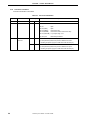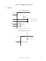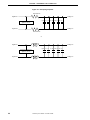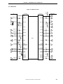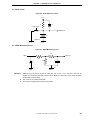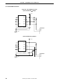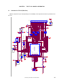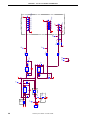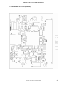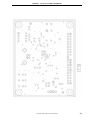
1
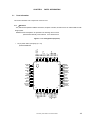
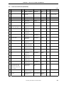
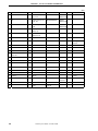
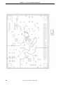
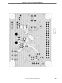
Preliminary User’s Manual
ET-0170
µPD720133 (USB2.0 to IDE Bridge) Evaluation Board
Document No. S17123EJ1V0UM00 (1st edition)
Date Published March 2004 NS CP (N)
2004
Printed in Japan
[MEMO]
2
Preliminary User's Manual S17123EJ1V0UM
NOTES FOR CMOS DEVICES
1
VOLTAGE APPLICATION WAVEFORM AT INPUT PIN
Waveform distortion due to input noise or a reflected wave may cause malfunction. If the input of the
CMOS device stays in the area between VIL (MAX) and VIH (MIN) due to noise, etc., the device may
malfunction. Take care to prevent chattering noise from entering the device when the input level is fixed,
and also in the transition period when the input level passes through the area between VIL (MAX) and
VIH (MIN).
2
HANDLING OF UNUSED INPUT PINS
Unconnected CMOS device inputs can be cause of malfunction. If an input pin is unconnected, it is
possible that an internal input level may be generated due to noise, etc., causing malfunction. CMOS
devices behave differently than Bipolar or NMOS devices. Input levels of CMOS devices must be fixed
high or low by using pull-up or pull-down circuitry. Each unused pin should be connected to VDD or GND
via a resistor if there is a possibility that it will be an output pin. All handling related to unused pins must
be judged separately for each device and according to related specifications governing the device.
3
PRECAUTION AGAINST ESD
A strong electric field, when exposed to a MOS device, can cause destruction of the gate oxide and
ultimately degrade the device operation. Steps must be taken to stop generation of static electricity as
much as possible, and quickly dissipate it when it has occurred.
Environmental control must be
adequate. When it is dry, a humidifier should be used. It is recommended to avoid using insulators that
easily build up static electricity. Semiconductor devices must be stored and transported in an anti-static
container, static shielding bag or conductive material. All test and measurement tools including work
benches and floors should be grounded.
The operator should be grounded using a wrist strap.
Semiconductor devices must not be touched with bare hands. Similar precautions need to be taken for
PW boards with mounted semiconductor devices.
4
STATUS BEFORE INITIALIZATION
Power-on does not necessarily define the initial status of a MOS device. Immediately after the power
source is turned ON, devices with reset functions have not yet been initialized. Hence, power-on does
not guarantee output pin levels, I/O settings or contents of registers. A device is not initialized until the
reset signal is received. A reset operation must be executed immediately after power-on for devices
with reset functions.
Preliminary User's Manual S17123EJ1V0UM
3
USB logo is a trademark of USB Implementers Forum, Inc.
Windows is either a registered trademark or a trademark of Microsoft Corporation in the United States
and/or other countries.
• The information contained in this document is being issued in advance of the production cycle for the
product. The parameters for the product may change before final production or NEC Electronics
Corporation, at its own discretion, may withdraw the product prior to its production.
• No part of this document may be copied or reproduced in any form or by any means without prior written consent of
NEC Electronics. NEC Electronics assumes no responsibility for any errors that may appear in this document.
• NEC Electronics does not assume any liability for infringement of patents, copyrights or other intellectual property
rights of third parties by or arising from the use of NEC Electronics products listed in this document or any other
liability arising from the use of such NEC Electronics products. No license, express, implied or otherwise, is granted
under any patents, copyrights or other intellectual property rights of NEC Electronics or others.
• Descriptions of circuits, software and other related information in this document are provided for illustrative purposes
in semiconductor product operation and application examples. The incorporation of these circuits, software and
information in the design of customer's equipment shall be done under the full responsibility of customer. NEC
Electronics assumes no responsibility for any losses incurred by customers or third parties arising from the use of
these circuits, software and information.
M5A 02. 11
4
Preliminary User's Manual S17123EJ1V0UM
INTRODUCTION
Readers
This manual is intended for engineers who will test USB2.0 to IDE bridge system by
using the ET-0170.
Purpose
This manual explains the functions of the ET-0170 in the following arrangements.
Arrangement
This manual includes the following chapters.
•
•
•
•
•
•
How to Read This Manual
Overview
Usage of the ET-0170
Parts information
Reference for connection
The ET-0170 board information
The reference schematic
It is assumed that the readers of this manual have general knowledge of electricity,
logic circuits, USB specification, USB mass storage class specification, and AT
Attachment with Packet Interface-6 (ATA/ATAPI-6) specification.
Conventions
Data significance:
Higher significant digits on the left and lower significant digits
on the right
Active low representation: xxxB (B suffixed to pin name or signal name)
Note:
Footnote for item marked with Note in the text
Caution:
Information requiring particular attention
Remark:
Supplementary information
Numeric notation:
Binary … xxxx or xxxxB
Decimal … xxxx
Hexadecimal … xxxxH
Related Documents
The related documents indicated in this document may include preliminary versions.
• µPD720133 Data Sheet: To be released soon
• µPD720133 User’s Manual: To be released soon
• µPD720133 Application Note Serial ROM Utility: To be released soon
• Universal Serial Bus Specification 2.0
• Universal Serial Bus Mass Storage Class Specification Overview
(Including documents listed in the Overview)
• AT Attachment with Packet Interface-6 (ATA/ATAPI-6) specification
Be sure to read the latest version of the above documents when using the ET-0170.
Version History
No.
1
Version
ET-0170 (FB-2471A)
Description
st
1 Version
Details in difference are described in this manual.
Preliminary User's Manual S17123EJ1V0UM
5
CONTENTS
CHAPTER 1 OVERVIEW...........................................................................................................................8
1.1 Features ........................................................................................................................................8
1.2 Board Diagram..............................................................................................................................9
1.3 Picture of the ET-0170................................................................................................................10
CHAPTER 2 USAGE OF THE ET-0170 ...............................................................................................11
2.1 Required Items to Test IDE Bridge System with the µPD720133 ..........................................11
2.2
2.3
2.1.1
Power supply ...................................................................................................................................11
2.1.2
USB cable........................................................................................................................................11
2.1.3
PC ...................................................................................................................................................11
2.1.4
IDE device .......................................................................................................................................11
How to Setup IDE Bridge System .............................................................................................12
2.2.1
Check jumper and connector setting ...............................................................................................12
2.2.2
Board checking................................................................................................................................13
2.2.3
Connects IDE device to the ET-0170 ..............................................................................................13
2.2.4
Connects power supply to IDE device and the ET-0170..................................................................13
How to Test IDE Bridge System................................................................................................14
2.3.1
Power ON ........................................................................................................................................14
2.3.2
Connect to USB port........................................................................................................................14
2.3.3
Disconnect from USB port ...............................................................................................................14
CHAPTER 3 PARTS INFORMATION.....................................................................................................15
3.1 Parts Information........................................................................................................................15
3.1.1
µPD720133......................................................................................................................................15
3.1.2
Serial ROM Socket (U2) ..................................................................................................................17
3.1.3
Power switch (U3) ...........................................................................................................................19
3.1.4
Regulator (U4, U5) ..........................................................................................................................19
3.1.5
Oscillator (Y1)..................................................................................................................................19
3.1.6
Power supply and reset information ................................................................................................19
3.1.7
Jumper information ..........................................................................................................................19
3.1.8
Connector information .....................................................................................................................20
CHAPTER 4 REFERENCE FOR CONNECTION ..................................................................................21
4.1 USB Circuit .................................................................................................................................21
4.2 IDE Circuit ...................................................................................................................................23
4.3 Oscillator.....................................................................................................................................24
4.4 Reset Circuit ...............................................................................................................................25
4.5 VBUS Monitoring Circuit ...........................................................................................................25
4.6 Serial ROM Connection .............................................................................................................26
CHAPTER 5 THE ET-0170 BOARD INFORMATION ..........................................................................27
5.1 Schematic for ET-0170 (FB-2471A)...........................................................................................27
5.2 Parts List for ET-0170 (FB-2471A) ............................................................................................29
5.3 Board Pattern for ET-0170 (FB-2471A).....................................................................................31
6
Preliminary User's Manual S17123EJ1V0UM
LIST OF FIGURES
Figure No.
Title
Page
1-1 Board Diagram........................................................................................................................................................ 9
2-1 Jumper Setting...................................................................................................................................................... 12
3-1 Pin Configuration (Top View) ................................................................................................................................ 15
4-1 USB Data Signaling .............................................................................................................................................. 21
4-2 USB Reference Resistor....................................................................................................................................... 21
4-3 Decoupling Capacitor ........................................................................................................................................... 22
4-4 IDE Connection..................................................................................................................................................... 23
4-5 Oscillator Circuit.................................................................................................................................................... 24
4-6 Reset Reference Circuit........................................................................................................................................ 25
4-7 VBUS Monitoring Circuit ....................................................................................................................................... 25
4-8 Serial ROM Connection ........................................................................................................................................ 26
LIST OF TABLES
Table No.
Title
Page
2-1 Jumper Setting...................................................................................................................................................... 12
3-1 Pin Information...................................................................................................................................................... 16
3-2 Serial ROM Data................................................................................................................................................... 17
3-3 DV1/DV0, CLC, PWR Setting ............................................................................................................................... 18
3-4 DV1/DV0, DCC Setting ......................................................................................................................................... 18
3-5 Power Supply and Reset Information ................................................................................................................... 19
3-6 Jumper Information............................................................................................................................................... 19
3-7 Connector Information .......................................................................................................................................... 20
Preliminary User's Manual S17123EJ1V0UM
7
CHAPTER 1 OVERVIEW
This document describes the functions of the µPD720133 evaluation board ET-0170.
The µPD720133 and a serial ROM are implemented on the ET-0170. This board allows quick test of different serial
ROM’s data setting against the µPD720133 during prototyping. This board has been certified by USB implementers
forum (TID: 10330107).
1.1
Features
This section explains the main features of the ET-0170.
(1) Compliant with Universal Serial Bus Specification Revision 2.0 (Data Rate 12/480 Mbps)
This board has the µPD720133 which is the bus/self-powered high-speed capable device and works at 12
Mbps data rate (FS: full speed) or 480 Mbps date rate (HS: high speed). The chip µPD720133 has been
certified by USB Implementers Forum and granted with USB 2.0 high-speed Logo (TID: 40320125).
(2) Compliant with AT Attachment with Packet Interface-6 (ATA/ATAPI-6). The IDE controller in the µPD720133
supports PIO Mode 0-4, Multi Word DMA Mode 0-2, Ultra DMA Mode 0-4, and LBA48. The evaluation kit
comes with Ultra DMA Mode 4 IDE cable. The IDE bridge system will be ready for test once IDE target device
is attached.
(3) Bus-powered USB2.0 to IDE bridge system
The device supports bus-powered operation if the power consumption for whole USB2.0 to IDE bridge system
is less than the specification for bus-powered device. The µPD720133 has some features such as power
supply control signaling for IDE device. The power supply circuitry on the board uses either VBUS or external
power supply for the power line connector connecting to the IDE target device. The power line connector has
DPC, GND and VDD line, and it is readily for bus-powered application using the power supply circuit on board.
(4) Extension for function
The function of the µPD720133 is controlled by data in serial ROM. Also, It is possible to realize firmware
extension by using the serial ROM. This board has a serial ROM socket for quick serial ROM replacement.
8
Preliminary User's Manual S17123EJ1V0UM
CHAPTER 1 OVERVIEW
1.2
Board Diagram
Figure 1-1. Board Diagram
NEC
uPD720133
Evaluation Board
JP6 JP7 JP8
ET-0170
U2
CN1
JP2
U4
JP3
U3
CN3
JP1
JP5
JP4
U5
U1
S1
Y1
PC1
LED2
JP9
LED1
CN2
PC1
: Power line connector
CN1
: USB connector
CN2
: IDE connector
CN3
: Power line selection connector
U1
: USB to IDE bridge chip (µPD720133)
U2
: Socket (Serial ROM)
U3
: Regulator
U4
: Regulator
U5
: Power switch
LED1
: Access lamp
LED2
: Power LED
Y1
: X’tal
S1
: Reset switch
JP(9:1)
: Jumper
Preliminary User's Manual S17123EJ1V0UM
9
CHAPTER 1 OVERVIEW
1.3
10
Picture of the ET-0170
Preliminary User's Manual S17123EJ1V0UM
CHAPTER 2
2.1
USAGE OF THE ET-0170
Required Items to Test IDE Bridge System with the µPD720133
This section explains the required items to test IDE bridge system with the ET-0170.
2.1.1
Power supply
The ET-0170 requires 5 V power supply. Typical ATX power supply or any other 5 V power supply is
applicable. The PC1 connector on this board uses the power connector of 3.5” floppy drive (FDD).
2.1.2
USB cable
A USB cable is required certifying by USB Implementers Forum as high-speed capable. If the uncertified
cable is used for this system, the transaction error on USB bus may be occurred. And if any transaction error
occurs on USB bus, the performance of the ET-0170 will be degraded.
2.1.3
PC
It is required that PC should have a USB 2.0 Host controller on the mother board or on the PCI card plugged
into PCI slot. If the IDE bridge system operates in high-speed transactions at 480 Mbps, EHCI driver should be
installed on Windows® 2000 or Windows XP system. USB Mass Storage Class Driver is also required for test of
the IDE bridge system. A standard USB Mass Storage Class Driver is bundled in Windows Me, Windows 2000
and Windows XP.
2.1.4
IDE device
It is required that an IDE device compliant with ATA/ATAPI-5 (Also ATA/ATAPI-6) be connected to the ET-
0170.
Preliminary User's Manual S17123EJ1V0UM
11
CHAPTER 2 USAGE OF THE ET-0170
2.2
How to Setup IDE Bridge System
This section explains how to set up the IDE bridge system with the ET-0170 before evaluation.
2.2.1
Check jumper and connector setting
Be sure to check Jumper setting as follows.
Table 2-1. Jumper Setting
Symbol
Setting
Jumper
JP1
Description
1-2
2-3
Short
-
Power supply to an serial ROM (U2)
SCL pin (µPD720133)
JP2
SCL
Open
Short
JP3
CMB_BSY
Short
-
CMB_BSY pin (µPD720133)
JP4
CMB_STATE
Short
-
CMB_STATE pin (µPD720133)
JP5
DPC
Open
Short
JP6
Short
-
Current measurement point for VDD33
JP7
Short
-
Current measurement point for VDD25
JP8
Short
-
Current measurement point for AVDD
Short
-
Power supply from the VBUS line
JP9
VBUS
Symbol
CN3
DPC pin (µPD720133)
Setting
Description
1-2
Open
Power line from a power switch (U3)
3-4
Short
Power line from PC1
Figure 2-1. Jumper Setting
NEC
uPD720133
Evaluation Board
JP6 JP7 JP8
ET-0170
U2
CN1
JP2
U4
JP3
U3
CN3
JP5
JP4
U5
U1
PC1
LED2
JP9
LED1
CN2
12
JP1
Preliminary User's Manual S17123EJ1V0UM
S1
Y1
CHAPTER 2 USAGE OF THE ET-0170
2.2.2
Board checking
Check a serial ROM has been inserted into a socket (U2) properly (The ET-0170 is shipped with one serial
ROM). Check the board is damaged from shipment.
2.2.3
Connects IDE device to the ET-0170
Connect both ends of IDE cable to IDE device and the ET-0170. An IDE cable must support Ultra DMA/66 for
test of an Ultra DMA/66 IDE device.
2.2.4
Connects power supply to IDE device and the ET-0170
This section assumes that the power supply is ATX type. Before a connector for FDD of an ATX power supply
is connected to the ET-0170, the ATX power supply must be turned OFF. Choose the appropriate power
supplying to the IDE device.
Preliminary User's Manual S17123EJ1V0UM
13
CHAPTER 2 USAGE OF THE ET-0170
2.3
How to Test IDE Bridge System
2.3.1
Power ON
When the output from an ATX power supply is activated, the LED2 (green) is turned on. At this time, if the
LED2 is not turned on, the ATX power supply should be turned off immediately. And be sure to recheck jumper
settings, board, IDE device, and connection of power supply. Next, check LED1 (red) is flashed on and off.
(Operations of LED1 depend on IDE devices)
At this point, the initialization of the µPD720133 is done and the µPD720133 is communicating to IDE device.
2.3.2
Connect to USB port
Connect the ET-0170 to a USB2.0 host with a USB cable. Once the µPD720133 detects the valid voltage
level at the VBUS pin from USB connection, the µPD720133 enables a Pull-up resistor on D+ line. And then, the
host controller detects the ET-0170.
After the enumeration has been completed, the IDE device is shown in the Device Manager and Explorer
window. And IDE device is ready for use.
2.3.3
Disconnect from USB port
When the ET-0170 is disconnected from the USB2.0 host, the application software accessing a device should
be stopped at first. And it is preferred to use the unplug tool found in Windows’ system tray to avoid instability in
OS before the removable device is disconnected from USB bus. There is no damage to the ET-0170 without
using the unplug tool.
14
Preliminary User's Manual S17123EJ1V0UM
CHAPTER 3
3.1
PARTS INFORMATION
Parts Information
This section describes main components on the ET-0170.
3.1.1
µPD720133
The µPD720133 implements USB2.0 transceiver, endpoint controller, firmware and etc to realize USB2.0 to IDE
bridge system.
Detailed function descriptions are provided in the following user’s manual.
µPD720133 Preliminary User’s Manual: To be released soon
Figure 3-1. Pin Configuration (Top View)
64-pin plastic TQFP (Fine pitch) (10 × 10)
49
8
41
16
33
IDE9
IDED5
IDED10
IDED4
IDED11
IDED3
IDED12
VDD33
VSS
VDD25
IDED2
IDED13
IDED1
IDED14
IDED0
IDED15
32
48
25
1
17
SCAN
RPU
VDD25
VSS
RSDP
DP
VDD33
DM
RSDM
VSS
AVDD25
AVSS
RREF
AVSS(R)
AVDD25
TEST
56
64
CMB_BSY
CMB_STATE
DPC
SCL
SDA
RESETB
VDD25
VSS
XOUT
XIN
VDD33
IDERSTB
IDED7
IDED8
IDED6
VSS
µPD720133GB-YEU
VBUS
IDECS1B
IDECS0B
IDEA2
IDEA0
IDEA1
IDEINT
VDD33
VSS
VDD25
IDEDAKB
IDEIORDY
IDEIORB
IDEIOWB
IDEDRQ
VSS
•
Preliminary User's Manual S17123EJ1V0UM
15
CHAPTER 3 PARTS INFORMATION
Table 3-1. Pin Information
Pin Name
I/O
Buffer Type
Active Level
Function
XIN
I
2.5 V Input
System clock input or oscillator In
XOUT
O
2.5 V Output
Oscillator out
RESETB
I
3.3 V Schmitt Input
Low
Asynchronous reset signaling
IDECS(1:0)B
O (I/O)
5 V tolerant Output
Low
IDE host chip select
IDEA(2:0)
O (I/O)
5 V tolerant Output
IDEINT
I
IDEDAKB
O (I/O)
IDEIORDY
I
IDE address bus
5 V tolerant Input
High
IDE interrupt request from device to host
5 V tolerant Output
Low
IDE DMA acknowledge
5 V tolerant Input
High
IDE IO channel ready
IDEIORB
O (I/O)
5 V tolerant Output
Low
IDE IO read strobe
IDEIOWB
O (I/O)
5 V tolerant Output
Low
IDE IO write strobe
IDEDRQ
I
5 V tolerant Input
High
IDE DMA request from device to host
IDED(15:0)
I/O
IDERSTB
O (I/O)
CMB_BSY (GPIO7)
I/O
5 V tolerant I/O
IDE data bus
5 V tolerant Output
Low
IDE reset from host to device
3.3 V I/O
Combo IDE bus busy
CMB_STATE (GPIO6)
I/O
3.3 V I/O
Combo IDE bus state
DPC (GPIO5)
I/O
3.3 V I/O
Power control signaling for IDE device
SDA (PIO0)
I/O
3.3 V I/O
Serial ROM data signaling
SCL (PIO1)
I/O
3.3 V I/O
Serial ROM clock signaling
VBUS
I
5 V Schmitt Input
Note
VBUS monitoring
DP
I/O
USB high speed D+ I/O
USB’s high speed D+ signal
DM
I/O
USB high speed D− I/O
USB’s high speed D− signal
RSDP
O
USB full speed D+ Output
USB’s full speed D+ signal
RSDM
O
USB full speed D− Output
USB’s full speed D− signal
RPU
A
USB Pull-up control
USB’s 1.5 kΩ pull-up resistor control
RREF
A
Analog
Reference resistor
SCAN
I
3.3 V Input
Scan mode control
TEST
I
3.3 V Input
Test mode setting
AVDD25
2.5 V VDD for Analog circuit
VDD25
2.5 V VDD
VDD33
3.3 V VDD
AVSS
VSS for Analog circuit
VSS
VSS
Remarks 1. “5 V tolerant“ means that the buffer is 3.3 V buffer with 5 V tolerant circuit.
2. The signal marked as “(I/O)” in the above table operates only as I/O signals during testing.
16
Preliminary User's Manual S17123EJ1V0UM
CHAPTER 3 PARTS INFORMATION
3.1.2
Serial ROM Socket (U2)
(1) Data in serial ROM
The µPD720133 loads data such as Vendor ID, Product ID and some additional USB related information from a
serial ROM when the µPD720133 is initialized. Example of data in serial ROM is as follows.
NEC Electronics releases tool to generate serial ROM data. Tool should be used to calculate the checksum
needed in the serial ROM.
Detailed function descriptions are provided in the following user’s manual and detailed information of tools is
provided in following application note.
µPD720133 Preliminary User’s Manual: To be released soon
µPD720133 Preliminary Application Note Serial ROM Utility: To be released soon
Table 3-2. Serial ROM Data
Offset (H)
+00
Data Size
1 Word
Symbol
idMark
Description
Validation Mark of 55AAH
+02
1 Word
CheckSum
Check sum of serial ROM
+04
1 Word
Flags
Control for descriptor overwrite
+06
1 Byte
ModeReset
PWR, CLC, DCC, DV[1:0], DPC Reset bit map field
+07
1 Byte
ModeSet
PWR, CLC, DCC, DV[1:0], DPC Set bit map field
+08
1 Word
idVendor
idVendor field in Device descriptor
+0A
1 Word
idProduct
idProduct field in Device descriptor
+0C
1 Word
bcdDevice
bcdDevice field in Device descriptor
+0E
1 Word
Reserved
Reserved for future use.
+10
1 Byte
MaxPower Bus
bMaxPower field in Configuration descriptor for Bus powered mode
+11
1 Byte
MaxPower Self
bMaxPower field in Configuration descriptor for Self powered mode
+12
1 Byte
bInterfaceClass
bInterfaceClass field in Interface descriptor
+13
1 Byte
bInterfaceSubClass
bInterfaceSubClass field in Interface descriptor
+14
1 Byte
bInterfaceProtocol
bInterfaceProtocol field in Interface descriptor
+15
1 Byte
Reserved
Reserved for future use.
+16
1Word
TxModeReset
IDE transmission type such as Ultra DMA 66 Reset bit map field
+18
1Word
TxModeSet
IDE transmission type such as Ultra DMA 66 Set bit map field
+1A
1Word
RompatchSW
ROM Patch information (Patch On or Off) of External Function
+1C
4 Bytes
Reserved
Reserved for future use.
+20
32 Bytes
ManufactureString
String descriptor for Manufacturer
+40
32 Bytes
ProductString
String descriptor for Product
+60
32 Bytes
SerialString
String descriptor for Device serial number
+80
128 × n Bytes
FW Patch
Firmware patch module for self-powered/bus-powered mode
Preliminary User's Manual S17123EJ1V0UM
17
CHAPTER 3 PARTS INFORMATION
(2) Control Bit in Serial ROM
The following tables show IDE status and control bit in serial ROM.
Table 3-3. DV1/DV0, CLC, PWR Setting
No.
0
Device
Internal
Power
Clock
Bus Powered
7.5 MHz
ATA/ATAPI
PWR
CLC
DV1
DV0
No device connected
1
1
1
1
1
ATA
1
1
1
0
2
ATAPI
1
1
0
1
3
Reserved
1
1
0
0
60 MHz
4
No device connected
1
0
1
1
5
ATA
1
0
1
0
6
ATAPI
1
0
0
1
Reserved
1
0
0
0
No device connected
0
1
1
1
9
Combo (ATA)
0
1
1
0
10
Combo (ATAPI)
0
1
0
1
11
Combo auto device detect
0
1
0
0
12
No device connected
0
0
1
1
13
ATA
0
0
1
0
14
ATAPI
0
0
0
1
15
Auto device detect
0
0
0
0
7
Self Powered
8
60 MHz
Remarks 1. Setting of no. 0, 3, 4, 7, 8, and 12 are not allowed.
2. For bus powered setting, some critical considerations such as power consumption for the total
system should be observed.
3. The slave device function cannot use Auto device detect.
Table 3-4. DV1/DV0, DCC Setting
Condition
DV1
DV0
Mode
1
0
ATA
0
1
ATAPI
DCC
setting in
Device
Serial ROM
ATA
Reset
Ultra, Multi Word DMA are disabled.
Set
Ultra, Multi Word DMA are enabled.
ATAPI
Reset
Set
0
0
Auto
ATA
device
detect
ATAPI
18
Ultra DMA are disabled.
Ultra, Multi Word DMA are enabled.
Reset
Ultra, Multi Word DMA are disabled.
Set
Ultra, Multi Word DMA are enabled.
Reset
Set
Remark
Description
Target
Ultra DMA are disabled.
Ultra, Multi Word DMA are enabled.
PIO mode 0-4 are always enabled.
Preliminary User's Manual S17123EJ1V0UM
CHAPTER 3 PARTS INFORMATION
3.1.3
Power switch (U3)
In bus-powered system, in order to control the power supply to an IDE device with the DPC pin of the
µPD720133, the ET-0170 has the power switch (U5).
3.1.4
Regulator (U4, U5)
The µPD720133 uses dual power rails. The ET-0170 uses two regulators. One is 2.5 V regulator (U4), another is
3.3 V regulator (U3).
3.1.5
Oscillator (Y1)
The ET-0170 uses the AT-49 30 MHz.
3.1.6
Power supply and reset information
Table 3-5. Power Supply and Reset Information
Symbol
Name
Description
PC1
Power line connector
Power line connector
S1
Reset SW
µPD720133’s hardware reset switch
During pressing this switch, a reset signal is activated.
3.1.7
Jumper information
Jumper information is as follows.
Table 3-6. Jumper Information
Symbol
Jumper
JP1
JP2
SCL
Setting
Description
1-2
2-3
Short
-
Power supply to serial ROM
Open
Short
SCL pin (µPD720133) setting
(Short)
(Open)
(If the size of Serial ROM ≤ 2 Kbytes, settings in parentheses
are available.)
JP2 (Pin 1): 3.3 V
JP2 (Pin 3): GND
JP3
CMB_BSY
Short
-
CMB_BSY pin (µPD720133) setting
If not using the CMB_BSY pin, the JP3 is needed to be short.
JP4
CMB_STATE
Short
-
CMB_STATE pin (µPD720133) setting
If not using the CMB_STATE pin, the JP4 is needed to be short.
JP5
DPC pin (µPD720133) setting
JP5 (Pin 1): connected to the power switch (U3)
JP5 (Pin 3): GND
Open
Short
JP6
Short
-
Current measurement point for VDD33
JP7
Short
-
Current measurement point for VDD25
JP8
Short
-
Current measurement point for AVDD
Open
-
Power supply from the VBUS line
JP9
DPC
VBUS
Short: Enable
Open: Disable
Preliminary User's Manual S17123EJ1V0UM
19
CHAPTER 3 PARTS INFORMATION
3.1.8
Connector information
Connector information is as follows.
Table 3-7. Connector Information
Symbol
Connector
Setting
Description
CN1
USB connector
ALL
-
USB Connector
CN2
IDE connector
ALL
-
IDE connector
Pin 20
: Open
Pin 28 (CSEL)
: Open
Pin 34 (PDIAG)
: Connected to JP1
Pin 39 (DASPB) : Connected to LED1 Disk Access Lamp
Pin 32 (IOCS16B) : 5 V pull up through 1 kΩ
Any other pins
CN3
Power line selection
connector
1-2
Open
: Refer IDE specification.
Power line from the power switch (U3)
(In bus-powered system, these pins are needed to be short if
controlling the power supply to an IDE device with the DPC pin.)
3-4
Short
Power line from the PC1 connector
(In bus-powered system, these pins are needed to be open if
controlling the power supply to an IDE device with the DPC pin.)
20
Preliminary User's Manual S17123EJ1V0UM
CHAPTER 4 REFERENCE FOR CONNECTION
4.1 USB Circuit
Figure 4-1. USB Data Signaling
Inside-package
Outside-package
RPU
1.5 kΩ ± 1%
DP
Port: D+ to USB B receptacle pin 3
DM
Port: D− to USB B receptacle pin 2
RS = 39 Ω ± 1%
RSDP
RSDM
RS = 39 Ω ± 1%
RS + Ron (Resistance for driver which is active) = 45 Ω ± 10%
Figure 4-2. USB Reference Resistor
RREF
Inside-package
Outside-package
RREF = 2.43 kΩ ± 1%
AVSS(R)
Preliminary User's Manual S17123EJ1V0UM
21
CHAPTER 4 REFERENCE FOR CONNECTION
Figure 4-3. Decoupling Capacitor
Less than 3 Ω
Analog VDD
Digital VDD
10 µF
Decoupling capacitors for
digital VDD and VSS
0.1 µF
0.1 µF 0.01 µF
0.01 µF
Digital VSS
Analog VSS
Less than 3 Ω
or
Digital VDD
Analog VDD
Decoupling capacitors for
digital VDD and VSS
10 µF
0.1 µF
0.1 µF 0.01 µF
Digital VSS
22
0.01 µF
Analog VSS
Preliminary User's Manual S17123EJ1V0UM
CHAPTER 4 REFERENCE FOR CONNECTION
4.2 IDE Circuit
Figure 4-4. IDE Connection
VCC
Connector
IC
Connector
CSEL
82 Ω
33 Ω
33 Ω
CS[1:0]#
CS[1:0]#
DD[15:0]
DD[15:0]
IDEA(2:0)
33 Ω
IDEDAKB
22 Ω
IDEDRQ
82 Ω
33 Ω
VCC
Only DD7 is
pulled down
by 10 kΩ
10 kΩ
DASP#
DASP#
DA[2:0]
DA[2:0]
DC
82 Ω
82 Ω
DMACK#
DMACK#
DMARQ
DMARQ
22 Ω
5.6 kΩ
IDEINT
IDE device
CSEL
IDECS(1:0)B
IDED(15:0)
10 kΩ
Cable
82 Ω
INTRQ
INTRQ
22 Ω
10 kΩ
IDEIORB
22 Ω
VCC
DIOR#
(HDMARDY#:
HSTROBE)
DIOR#
(HDMARDY#:
HSTROBE)
IORDY
(DDMARDY#:
DSTROBE)
IORDY
(DDMARDY#:
DSTROBE)
82 Ω
1 kΩ
IDEIORDY
IDEIOWB
82 Ω
22 Ω
VCC
DIOW#
(STOP)
DIOW#
(STOP)
IOCS16
Reserved
PDIAG#
(CBLID#)
PDIAG#
(CBLID#)
33 Ω
RESET#
RESET#
82 Ω
VCC
1 kΩ
IDERSTB
22 Ω
Preliminary User's Manual S17123EJ1V0UM
10 kΩ
82 Ω
23
CHAPTER 4 REFERENCE FOR CONNECTION
4.3 Oscillator
Figure 4-5. Oscillator Circuit
XIN
XOUT
R
X’tal
C1
C2
Digital VSS
The AT-49 30-MHz X’tal is used on the current ET-0170 board. The following table shows the external parameters
for the AT-49 30. NEC Electronics is scheduled to evaluate the oscillator circuit.
Vendor
KDS
Name
AT-49 (30.000 MHz)
R
C1
C2
47 Ω
12 pF
12 pF
If AT-49 30 MHz is used on the board, contact to Daishinku Corp. (KDS) for getting the best external parameters
depending on the board configuration.
KDS’s home page : http://www.kdsj.co.jp
AT-49 catalogue No. : 1AI300002CA
Also, NEC Electronics is scheduled to evaluate NDK’s X’tal. The following table shows the external parameters for
the AT-41.
Vendor
NDK
Name
AT-41 (30.000 MHz)
R
C1
C2
47 Ω
10 pF
10 pF
If NDK’s X’tal is used on the board, contact to NIHON DEMPA KOGYO CO.,LTD. (NDK) for getting the best
external parameters depending on the board configuration.
NDK’s home page : http://www.ndk.com
X’tal catalogue No. : 02092X
Caution
24
When an oscillator circuit is used, the following guidelines should be observed.
• Keep the signal length as short as possible.
• Do not cross the signal with the other signal lines.
• Do not route the signal near a signal line with high current flows
• Always keep the VSS point of the oscillator to the same potential as VSS of the µPD720133.
• Do not ground the capacitor to a VSS of high current flow.
Preliminary User's Manual S17123EJ1V0UM
CHAPTER 4 REFERENCE FOR CONNECTION
4.4 Reset Circuit
Figure 4-6. Reset Reference Circuit
3.3 V
R
D
Reset switch
RESETB pin
+
C
Digital VSS
4.5 VBUS Monitoring Circuit
Figure 4-7. VBUS Monitoring Circuit
R3
VBUS
VBUS pin
R1
+
R2
D
VSS
Remarks 1.
C
VSS
VBUS pin may be used to monitor for VBUS line even if VDD33, VDD25, and AVDD25 are shut off.
System must ensure that the input voltage level for VBUS pin is less than 3.0 V in avoid exceeding
the absolute maximum rating.
2.
The unit of R1, R2, and R3 is kΩ order.
3.
This circuit is not applicable in bus-powered system.
Preliminary User's Manual S17123EJ1V0UM
25
CHAPTER 4 REFERENCE FOR CONNECTION
4.6 Serial ROM Connection
Figure 4-8. Serial ROM Connection
(a) Serial ROM Size ≤ 2 Kbytes
3.3V
A0
VCC
A1
WP
A2
SCL
GND
SDA
Serial ROM
(VDD=3.3V, fSCL=100KHz)
R1
R
C
µPD720133
SDA
SCL
VSS
(b) Serial ROM Size > 2 Kbytes
3.3V
A0
VCC
A1
WP
A2
SCL
GND
SDA
Serial ROM
(VDD=3.3V, fSCL=100KHz)
R
C
R2
µPD720133
SDA
SCL
VSS
26
Preliminary User's Manual S17123EJ1V0UM
Preliminary User's Manual S17123EJ1V0UM
VBU S
D PC
4
3
2
1
CN1
Q ZF-B4LFD G 7A2K
FG
2
1
FG
FG
3
4
FG
1SS294
D2
R 19
5.6K
R 23
10K
AVD D
XJ8C -0311
DPC
JP5
R 20
10k
R 32
R 16
2.2uF/16V
C4
2.43K(1% )
39(1% )
39(1% )
R 11
R 12
1.5K(1% )
+
+
1
2.5V
2
+
1
1
2
3
4
5
6
7
8
9
10
11
12
13
14
15
16
3.3V
SC AN
R PU
VD D 25
G ND
R SD P
DP
VD D 33
DM
R SD M
G ND
PVD D
AVSS
R R EF
AVSS
AVD D
TEST
XG 8W -0231
+
JP3
CMB_BSY
XG 8W -0231
2
JP4
CMB_STATE
10k
10K
R 33
10k
R 10
R 31
AVSS
1
2
3
1K
10k
R3
JP2
XJ8C -0311
SCL
R4
R2
10k
47
R1
10k
uPD 720133
U1
G ND
3.3V
2.5V
ID ED 9
ID ED 5
ID ED 10
ID ED 4
ID ED 11
ID ED 3
ID ED 12
VD D 33
G ND
VD D 25
ID ED 2
ID ED 13
ID ED 1
ID ED 14
ID ED 0
ID ED 15
Y1
30M H z
3.3V
48
47
46
45
44
43
42
41
40
39
38
37
36
35
34
33
8
7
6
5
A0
A1
A2
G ND
U2
C 1 12pF/10pF
1
2
3
4
R 27
10K
R9
10K
N ote
K D S:12pF
N D K :10pF
M 24C 32-W BN 6
VC C
WP
SC L
SD A
JP1
XG 8W -0231
C 2 12pF/10pF
0.1uF
C P1
3.3V
1
+ +
2
R6
3.3V
P
N
3
2
1
64
63
62
61
60
59
58
57
56
55
54
53
52
51
50
49
G PIO 7/C M B_BSY
G PIO 6/C M B_STATE
G PIO 5/D PC
PIO 1/SC L
PIO 0/SD A
R ESETB
VD D 25
G ND
XO U T
XIN
VD D 33
ID ER STB
ID ED 7
ID ED 8
ID ED 6
G ND
VBU S
ID EC S1B
ID EC S0B
ID EA2
ID EA0
ID EA1
ID EIN T
VD D 33
G ND
VD D 25
ID ED AKB
ID EIO R D Y
ID EIO R B
ID EIO W B
ID ED R Q
G ND
1
2
3
4
1
2
3
4
8
7
6
5
1
2
3
4
1
N M R 14 33ohm
2
3
4
8
7
6
5
R 13
8
7
6
5
8
7
6
5
33
82
R 22
R 25
22
R 21
N M R 14 33ohm
R A5
82
22
R 26
5.6K
SLR -322-R
LED 1
DISK
D A0
D A2
C S0B
C S1B
D ASPB
IN TR Q
IO C S16B
D A1
ID ED AKB
ID ER D Y
ID EIO R B
ID EIO W B
DD7
DD8
DD6
DD9
DD5
D D 10
DD4
D D 11
DD3
D D 12
DD2
D D 13
DD1
D D 14
DD0
D D 15
ID ER STB
ID ER Q
R8
1K
22
R7
1K
5V
82
33
R 18
R 17
R 14
N M R 14 33ohm
R 15
R A4
S1
RESET
B3F-1002
R A2
N M R 14 33ohm
N M R 14 33ohm
1
8
2
7
3
6
R A3
4
5
R A1
R5
1.5k
TTP1
ID ER ESETB
C3
22uF/16V
D1
1SS294
3.3V
P
N
R 28
XG 4C -4031
1
2
3
4
5
6
7
8
9
10
11
12
13
14
15
16
17
18
19
20
21
22
23
24
25
26
27
28
29
30
31
32
33
34
35
36
37
38
39
40
CN2
ID E
1K
5V
5.1
17
18
19
20
21
22
23
24
25
26
27
28
29
30
31
32
CHAPTER 5
THE ET-0170 BOARD INFORMATION
Schematic for ET-0170 (FB-2471A)
Different components may be used depending on the availability of the component at the time of production of the
ET-0170.
27
D PC
VBU S
1
2
3
4
171825-4
PC 1
VBUS
POWER
TTP4
5V
JP9
XG 8W -0231
1 + + 2
LED 2
SLR -322-M G
R 29
1K
1uF
C5
2
4
Self
XG 8W -0431
+
+
Bus
M AX891L
IN 1
O U T1
IN 2
O U T2
O N B FAU LTB
G ND
SET
CN3
1 +
3 +
1
2
3
4
U3
8
7
6
5
2.4K
R 30
0.1uF
C P2
5V
P
N
28
10uF/16V
C 14
C 11 0.01uF
1uF
C7
1
2
3
4
U4
O UT
SEN
G ND
BPY
U5
IN
G ND
G ND
SH D
8
7
6
5
LT1761ES5-3.3
IN
O UT
G ND
SH D N BPY
LT1763C S8-2.5
1
2
3
5
4
C 12
1uF
C 8 0.01uF
P
10uF/16V
C9
TTP7 TTP8
G ND G ND
N
TTP2
5V
Preliminary User's Manual S17123EJ1V0UM
+
+
2
JP8
XG 8W -0231
1
JP7
XG 8W -0231
1 + + 2
JP6
XG 8W -0231
1 + + 2
TTP5
2.5V
TTP3
3.3V
FB2
BLM 21PG 600SN 1
1
2
FB1
BLM 21PG 600SN 1
1
2
C 15
+10uF
tantal
TTP6
AVD D 2.5
AVSS
C P13 C P14
C 16
0.1uF 0.1uF 10uF tantal
+
AVD D
C P9 C P10 C P11 C P12
0.1uF 0.1uF 0.1uF 0.1uF
C 10
10uF tantal
+
3.3V
C 13
10uF tantal
+
2.5V
C P3 C P4 C P5 C P6 C P7 C P8
0.1uF 0.1uF 0.1uF 0.1uF 0.1uF 0.1uF
Place near the uPD720133
CHAPTER 5 THE ET-0170 BOARD INFORMATION
CHAPTER 5 THE ET-0170 BOARD INFORMATION
5.2
Parts List for ET-0170 (FB-2471A)
(1/2)
No.
1
Name
U1
Type
LSI
Products
USB2.0 – IDE Bridge
Product No.
µPD720133
Vendor
NEC
Count
Comment
1
Electronics
2
U2
Socket 8-pin DIP
-
-
1
A socket for serial
ROM
3
U3
IC
3.3 V regulator
LT1761ES5-3.3
Linear
1
4
U4
IC
2.5 V regulator
LT1763CS8-2.5
Linear
1
5
U5
IC
Power switch
MAX891L
MAXIM
1
6
RA1, RA2, RA3, RA4, RA5 R
ROHM
5
MCR03EZHJ
ROHM
10
MCR03EZHJ
ROHM
5
MCR03EZHJ
ROHM
1
MCR03EZHJ
ROHM
1
MCR03EZHJ
ROHM
3
MCR03EZHJ
ROHM
3
MCR03EZHF
ROHM
1
MCR03EZHF
ROHM
2
MCR03EZHF
ROHM
1
MCR03EZHJ
ROHM
1
MCR03EZHJ
ROHM
2
MCR03EZHJ
ROHM
1
MCR10EZHJ
ROHM
1
14
Chip resistor networks MNR14E0ABJ33
(0603) 33 Ω
7
8
R1, R2, R3, R9, R20, R23, R
Chip resistor
R27, R31, R32, R33
(0603) 10 kΩ
R6, R7, R8, R28, R29
R
Chip resistor
(1608) 1 kΩ
9
R13
R
Chip resistor
(2125) 33 Ω
10
R25
R
Chip resistor
(1608) 33 Ω
11
R14, R18, R22
R
Chip resistor
(1608) 82 Ω
12
R15, R17, R21
R
Chip resistor
(1608) 22 Ω
13
R10
R
Chip resistor
(1608) 1.5 kΩ (1%)
14
R11, R12
R
Chip resistor
(2125) 39 Ω (1%)
15
R16
R
Chip resistor
(2125) 2.43 kΩ (1%)
16
R4
R
Chip resistor
(1608) 47 Ω
17
R19, R26
R
Chip resistor
(1608) 5.6 kΩ
18
R5
R
Chip resistor
(1608) 1.5 kΩ
19
R30
R
Chip resistor
(1608) 2.4 kΩ
20
CP1, CP2, CP3, CP4,
C
CP5, CP6, CP7, CP8,
Chip capacitor
GRM188F11E104 Murata
(2125) 0.1 µF
ZA01
Chip capacitor
GRM40CH120J50 Murata
CP9, CP10, CP11, CP12,
CP13, CP14
21
C1, C2
C
2
(2125) 12 or 10 pF Note
22
C9, C14
C
Tantalum Electrolytic cap. 16MCE106MATER NIPPON
10 µF 16 V
Preliminary User's Manual S17123EJ1V0UM
2
CHEMI-CON
29
CHAPTER 5 THE ET-0170 BOARD INFORMATION
(2/2)
No.
23
24
25
Name
C4
C3
C10, C13, C16
Type
C
C
C
Products
Product No.
Tantalum Electrolytic cap. 16MCE225MA2TER
NIPPON
2.2 µF 16 V
CHEMI-CON
Tantalum Electrolytic cap. 16MCE226MB2TER
NIPPON
22 µF 16 V
CHEMI-CON
Tantalum capacitor
10MCM106MA
10 µF
26
27
C5, C7, C12
C8, C11
C
C
Vendor
NIPPON
Count
Comment
1
1
3
CHEMI-CON
Chip capacitor
GRM188F11C105ZA0 Murata
(1608) 1 µF
1
Chip capacitor
GRM1882C1H100JA0 Murata
(1608) 0.01 µF
1
3
2
28
D1, D2
Di
Chip diode
1SS294
Toshiba
2
29
CN1
CN
Connector
QZF-B4LFDG7A2K
Honda
1
USB B-type
connector
30
CN2
CN
Connector
XG4C-4031
OMRON
1
31
CN3
CN
Connector
XG8W-0431
OMRON
1
32
JP2, JP5
JP
Jumper
XJ8C-0311
OMRON
2
JP1, JP3, JP4, JP6, JP7,
JP
Jumper
XG8W-0231
OMRON
7
33
JP8, JP9
34
LED1
LED
LED (Red)
SLR-322-VR3F
ROHM
1
35
LED2
LED
LED (Green)
SLR-322-MG3F
ROHM
1
36
Y1
X’tal
X’tal 30 MHz
AT-49 or AT-41 (30
KDS or NDK
1
MHz)
37
PC1
CN
Power Connector
171825-4
AMP
1
38
S1
SW
Switch
B3F-1002
OMRON
1
39
FB1, FB2
FB
Ferrite beads
BLM21PG600SN1
Murata
2
40
TTP(9:1)
TP
Test pin
-
-
41
-
-
Serial ROM
M24C32
STMicro
Not used
1
electronics
42
-
-
IDE cable
-
-
1
43
-
-
Board
FB-2471A
-
-
30
Preliminary User's Manual S17123EJ1V0UM
CHAPTER 5 THE ET-0170 BOARD INFORMATION
5.3
Board Pattern for ET-0170 (FB-2471A)
Preliminary User's Manual S17123EJ1V0UM
31
CHAPTER 5 THE ET-0170 BOARD INFORMATION
32
Preliminary User's Manual S17123EJ1V0UM
CHAPTER 5 THE ET-0170 BOARD INFORMATION
Preliminary User's Manual S17123EJ1V0UM
33
CHAPTER 5 THE ET-0170 BOARD INFORMATION
34
Preliminary User's Manual S17123EJ1V0UM
CHAPTER 5 THE ET-0170 BOARD INFORMATION
Preliminary User's Manual S17123EJ1V0UM
35
[MEMO]
36
Preliminary User's Manual S17123EJ1V0UM