1
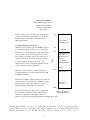
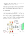
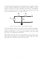
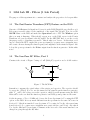
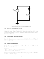
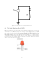
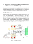
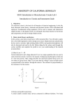
PHYSICS 3050
Electronics I
Laboratory Manual
Fall 2007
Contents
1 3050 Lab I - Introduction to Electronic Instruments and Measurements (1
Lab Period)
1
1.1
The Instruments
. . . . . . . . . . . . . . . . . . . . . . . . . . . . . . . . .
1
1.2
Using the DSO and Function Generator . . . . . . . . . . . . . . . . . . . . .
2
1.3
Using the DC Power Supply and the DMM . . . . . . . . . . . . . . . . . . .
3
2 3050 Lab II - Simple Passive Networks (1 Lab Period)
4
2.1
Voltage Division . . . . . . . . . . . . . . . . . . . . . . . . . . . . . . . . . .
4
2.2
Thévenin Equivalent Circuits . . . . . . . . . . . . . . . . . . . . . . . . . .
4
3 3050 Lab III - Filters (1 Lab Period)
6
3.1
The Fast Fourier Transform (FFT) Feature on the DSO . . . . . . . . . . . .
6
3.2
The Low-Pass RC Filter, Part I . . . . . . . . . . . . . . . . . . . . . . . . .
6
3.3
Introduction to LabVIEW . . . . . . . . . . . . . . . . . . . . . . . . . . . . .
7
3.4
The Low-Pass RC Filter, Part II . . . . . . . . . . . . . . . . . . . . . . . . .
7
4 3050 Lab IV - Introduction to Diodes (1 Lab Period)
8
4.1
Testing the Diode . . . . . . . . . . . . . . . . . . . . . . . . . . . . . . . . .
8
4.2
Reverse-biased Diode Circuit . . . . . . . . . . . . . . . . . . . . . . . . . . .
8
4.3
Forward-biased Diode Circuit . . . . . . . . . . . . . . . . . . . . . . . . . .
9
4.4
Germanium and Zener Diodes . . . . . . . . . . . . . . . . . . . . . . . . . .
9
4.5
Diode Characteristics . . . . . . . . . . . . . . . . . . . . . . . . . . . . . . .
9
4.6
The Light Emitting Diode (LED) . . . . . . . . . . . . . . . . . . . . . . . .
10
5 3050 Lab V - Introduction to Transistors (1 Lab Period)
11
5.1
Testing Transistors . . . . . . . . . . . . . . . . . . . . . . . . . . . . . . . .
12
5.2
DC Transistor Characteristics . . . . . . . . . . . . . . . . . . . . . . . . . .
12
i
6 3050 Lab VI - The Transistor as a Switch (1 Lab Period)
14
6.1
Rise and Fall Times . . . . . . . . . . . . . . . . . . . . . . . . . . . . . . . .
14
6.2
A NOT gate . . . . . . . . . . . . . . . . . . . . . . . . . . . . . . . . . . . .
15
7 3050 Lab VII - The Common Emitter Amplifier (1 Lab Period)
16
7.1
Biasing the Amplifier . . . . . . . . . . . . . . . . . . . . . . . . . . . . . . .
16
7.2
Amplifier Gain and Frequency Response . . . . . . . . . . . . . . . . . . . .
16
ii
Introduction, Lab Safety, and Circuit Building Tips
In the PHYS3050 lab we will learn how to construct circuits on breadboards with passive
elements like the resistor and capacitor as well as the basic semiconductor PN Junction
devices – the diode and transistor.
General Plan of the Lab
The experiments in this laboratory will steadily require more individual work on your part.
Many of the experiments will be outlined in detail but some will require you to “fill in the
gaps” and to use your own initiative to select the proper components.
A demonstrator will normally be available to give you advice and assistance when required,
but you are expected to make an attempt to solve the problems that arise before soliciting
such assistance.
Lab Records and Reports
Students should be aware of the importance of recording ALL the details of a
laboratory experiment. If, for some reason, you find inexplicable results upon the analysis
of your data at home, you should be able to make an educated guess as to what went wrong
from reviewing your lab records.
Every experiment carried out in the laboratory must be recorded and reported. Your record
of each experiment should be considered a full outline of the laboratory work on that experiment so that, if required, you could use it as a basis for writing a formal report when away
from the laboratory. Your report should include the following:
• title, student’s name, date.
• brief statement of the principle of the observations.
• the different exercises clearly labeled in each experiment.
• equipment specified either through a serial number or some other distinctive marking
for that instrument.
• complete circuit diagram.
• exact record of your experimental procedure.
• tables of any data plotted in a graph (with units!).
• graphs of the observations, when required.
• brief note on sources of errors.
iii
• conclusions and discussion, including comparisons with “theoretical” expectations, if
relevant.
Graphs play an important role in the record and the report since they often make certain
results and trends clear which may not be apparent in the tabulated data. A picture is worth
a thousand ... numbers. The axes of each graph should be fully labeled (with units!), and
each graph should have a title and a legend. Graphs should normally be on separate pages
from the text, should always be on the appropriate graph paper, and preferably should be
located near the corresponding description in the text of the report.
After completing your experiments, you must have all the tabulated data in your own notebook and it must be presented to your demonstrator for his/her signature.
Each experiment must be submitted to your lab demonstrator for marking at the beginning
of your next lab period (both the first and the final lab reports are due one week after
completion of the lab and should be dropped off at a place specified by your demonstrator).
Thus, you will need two bound notebooks to contain your lab reports. Neither typing of the
lab reports nor usage of a hardcover lab book is required. Reports will be graded on quality,
not quantity. Your preparation time will be reduced if you try to be concise, but complete.
Late reports will be accepted up to four days beyond the assigned due date. A penalty of
25% per work day late will be applied. After four days late the report will not be
accepted.
Lab Safety
Electrical equipment and circuits can be dangerous if you are not fully aware of the potential
hazards. Operating manuals and instruction for using the equipment in the lab are available
from the lab demonstrator. Make sure that you are familiar with the equipment before
turning it on.
The chief sources of electric power in the lab are the 110 V AC power outlets in the walls,
extension cords and consoles, and the DC power supplies. Much higher voltages occur inside
some units (e.g., > 14 kV in the oscilloscope) but these are ordinarily protected by the cover
plates. Do not stick your fingers inside an instrument when the power is on.
Even given that, remember that it is current through your body that is dangerous.
The magnitude of the current through your body depends on your body resistance but the
damage it does to you depends on the current path through your body. A current path
from one hand through your body and out the other hand is far more dangerous to you than
current that enters through one finger and exits out the next finger. Therefore, it is common
practice to keep one hand behind your back when dealing with hazardous electrical systems.
The physiological effects of current are given below.
iv
THE FATAL CURRENT
Reprinted through the courtesy of
Fluid Controls Company,
University of California,
Safer Oregon
1.0
Strange as it may seem, most fatal electric shocks happen
to people who should know better. Here are some electromedical facts that should make you think twice before
taking that last chance.
While any amount of current over 10 mA is capable of
producing painful to severe shock, currents between 100
and 200 mA are lethal.
Currents above 200 mA, while producing severe burns and
unconsciousness, do not usually cause death if the victim is
given immediate attention. Resuscitation, consisting of
artificial respiration, will usually revive the victim.
0.2
DEATH
0.1
Extreme Breathing
Difficulties
Breathing Upset
Labored
SevereShock
Muscular Paralysis
Amperes
IT'S THE CURRENT THAT KILLS
Offhand it would seem that a shock of 10,000 V would be
more deadly than 100 V. But this is not so! Individuals
have been electrocuted by appliances using ordinary house
currents of 110 V and by electrical apparatus in industry
using as little as 42 V direct current. The real measure of
shock's intensity lies in the amount of current (amperes)
forced through the body, and not the voltage. Any
electrical device used on a house wiring circuit can, under
certain conditions, transmit a fatal current.
Severe Burns
Breathing Stops
Painful
0.01
Mild Sensation
Threshold of
Sensation
0.001
From a practical viewpoint, after a person is knocked out
Physiological Effects
by an electrical shock it is impossible to tell how much
of Electrical Currents
current passed through the vital organs of their body.
Artificial respiration must be applied immediately if breathing has stopped.
The internal resistance of your body (right hand to left hand or, hand to leg) is typically
around 500 Ω. In series with this is the surface resistance of your skin which varies from
1000 Ω when moist to over 100 kΩ when dry. Thus a voltage as low as 50 V can be
v
dangerous if your hands are wet. Hence, never work with electrical equipment when your
hands or clothing are wet.
Lab Etiquette
Be careful not to damage any of the measuring equipment and try to avoid breaking the
components. We need them for other students in other lab periods in this course. You should
report equipment/component faults promptly to the demonstrator. You should never set
aside faulty equipment without reporting it. Furthermore, you should not attempt to repair
faulty equipment yourself.
Return all components and equipment to the proper location at the end of each lab period.
Equipment, components, and operation manuals may not be removed from the lab under
any circumstances.
You are not permitted to work in the laboratory outside of regular laboratory periods, unless
special authorization is obtained and a lab demonstrator is present.
Food and drink are not allowed in the lab at any time. If you are hungry or thirsty feel free
to leave the lab and take a short break.
Circuit Building Tips
Much of the lab equipment you will work with is expensive and delicate. Therefore, to save
the equipment and also to reduce the amount of time you waste using faulty equipment and
components, here are a few random tips associated with doing experiments in the lab:
• Build up the circuit in steps, checking each element before you use it.
• Never wire a circuit with the power supply on.
• Turn off the input voltage and then the power supply when changing a circuit element.
• Keep in mind the power rating of the resistors being used and the polarity (if relevant) of the capacitor. When using semiconductor devices like diodes and transistors,
remember that the maximum current they can transmit is something like 40 mA. So
care must be taken to make sure that resistors are added properly so as to ensure that
the component is not required to pass larger currents. The elements will burn – they
are not expensive but you will waste a lot of time if it turns out one of the components
in your circuit has burned out.
vi
1
3050 Lab I - Introduction to Electronic Instruments
and Measurements (1 Lab Period)
The purpose of this experiment is to familiarize you with the electronic instruments that will
be required for future experiments. The proper methods of measurements and technique are
important in all experimental work and this experiment will provide you an opportunity to
’brush-up’ on some the skills you learned in the past and introduce you to new ones.
1.1
The Instruments
Each pair of students has a suite of instruments for performing the experiments for this
course. Those instruments include: an Agilent E3630A Triple Output DC Power Supply,
an Agilent 33120A Function/Arbitrary Waveform Generator, an Agilent 34401A Digital
Multimeter (DMM), and a Tektronix TDS200 Digital Storage Oscilloscope (DSO). In the
first part of the experiment we will go through each instrument in turn and discuss how
it is used. In particular, the DSO is one of the most useful measurement devices you will
encounter in the lab. Though at first perhaps a little intimidating, the oscilloscope is an
easy to use, versatile instrument which you should be comfortable using and confident of
its application. The basic workings of an “analogue” oscilloscope are shown in the Figure 1
while the workings of the Digital Storage Scope are illustrated in Figure 2.
Figure 1: An Analogue Oscilloscope.
1
Figure 2: The Digital Storage Oscilloscope.
Concepts you should learn about the DSO are:
– fundamental oscilloscope operation including use of MENUs
– grounding considerations
– the function of the AC-GND-DC coupling
– oscilloscope triggering
1.2
Using the DSO and Function Generator
Connect the Function Generator to CH1 of the DSO using a cable with BNC connectors
at both ends. First generate a sine wave having a frequency in the 10’s of kHz range and
an amplitude that is some multiple of 100 mV (see page 19 of the Agilent 33120A Function
Generator User’s Guide). Also, add a DC offset of 100 to 200 mV. On the DSO, adjust the
“sec/div” knob to see two complete cycles of the waveform on CH1. Use the CH1 menu to
set the Coupling, BW Limit, Volts/Div, Probe, and Invert values (see page 89 of the
TDS 200-Series Digital Real-Time Oscilloscope User Manual). What values did you choose
and why did you choose them? Use the TRIGGER menu to set the Trigger mode to Edge.
Set the Slope, Source, Mode and Coupling values and adjust the Trigger Level. Again,
what values did you choose and why did you choose them?
With the DSO in DC-coupled mode, select the MEASURE menu. Check what happens to the
menu display when you select Source or Type. Measure the following values using the menu
buttons.
1. Frequency
2
2. Pk-Pk Voltage
3. Mean Voltage
4. Period
Are these values consistent with the settings on your function generator? Do they change if
you change to AC coupling on the DSO?
Repeat the steps in this section for a square wave, triangular wave, and sawtooth wave.
1.3
Using the DC Power Supply and the DMM
Grab a couple of resistors from the pile provided. Record the band structure of the resistors
and measure their resistance using the DMM. [For your report: How close are they in value
to what the bands indicate they are? Is this what you would expect?] Connect the resistors
in series on a bread-board (also called a proto-board) and measure the resistance of the pair.
Now use the Power Supply to apply around 2 V DC across the pair. Draw completely how
you set up the circuit including where is the common ground point of the Power Supply.
Measure and record the potential drop across each resistor in turn using the DMM. Measure
the current through the resistors. Show exactly how you performed the measurements. What
did you expect the results to be and did you find this to be the case? Perform the voltage
measurements again using the DSO rather than the DMM.
Now remove the DC Power Supply and connect the square-wave signal from section 1.2 across
the pair of resistors. Repeat the measurements of the previous paragraph, again making sure
to show how each measurement was made. Compare the values from the MEASURE Menu on
the DSO with the measurement from the DMM. Are they consistent?
3
2
3050 Lab II - Simple Passive Networks (1 Lab Period)
The purpose of this lab is to investigate voltage division and a Thévenin equivalent circuit.
2.1
Voltage Division
You will need four resistors: 1 kΩ, 10 kΩ, 1 MΩ and 10 MΩ. Construct the circuit of Figure
3 using R1 = 1 kΩ, R2 = 10 kΩ, and the DC power supply as the voltage source. For a VDC
A
V DC
R1
+
−
B
R2
C
Figure 3: A voltage divider circuit.
between 10 and 15 V, measure VBC ≡ VB - VC . Measure VAB directly. Compare what you
find to what you expect (i.e., calculate VAB from VDC and VBC ).
Again measure VBC but now with R1 = 1 MΩ and R2 = 10 MΩ. Again compare what you
find with what you expect. Are the VBC values different for the two cases? If so, why do you
think that might be? Can one say something about the properties of either the DC power
supply or the Digital Multimeter? (Hint: Check page 17 of the Agilent 34401A Multimeter
User’s Guide.)
2.2
Thévenin Equivalent Circuits
Choose any three (different) resistors with values between 330 Ω and 10 kΩ and construct
the circuit of Figure 4. Again VDC should be between 10 and 15 V.
Now we are going to measure the Thévenin equivalent voltage (VEQ ) and resistance (REQ )
“as seen by” AB. First we obtain VEQ by measuring the open circuit voltage across AB.
Since AB is already an open circuit, then VEQ = VAB . In general, we can’t short circuit AB
and measure IAB since this could harm the instruments. In this case we can, and will, but
4
only after following the standard method for measuring REQ . Connect a number of different
load resistors (with values ranging from, again, 330 Ω to 10 kΩ) across AB and record in a
table VL = VAB and IL = IAB . Plot VL (y axis) VS IL (x axis) and draw a straight line
through the points. The slope of this line (called the “load line”) is -REQ . Verify this value
of REQ by connecting A to ground (i.e., “shorting” AB) and measuring the current through
R2 . Show explicitly what value you get for REQ by doing this.
R1
R2
A
V DC
+
−
R3
B
Figure 4: Circuit for which to find the Thévenin equivalent.
Construct the Thévenin equivalent for your circuit. That is, use the DC power supply as
VEQ in series with REQ . As we probably will not have a resistor exactly with the value REQ ,
you may need to put a number of resistors in series and/or parallel to get your value of R EQ .
Using the same RL resistors as above, again measure VL VS IL (i.e., RL ). Do the values
agree? If not, can you think why they should differ?
Calculate what you would expect the values of VEQ and REQ to be given your choice of VDC ,
R1 ,R2 , and R3 . If they don’t agree, can you explain why? Would we expect disagreement
between theory and experiment if we had used resistors with R > 1 MΩ? If so, does it
matter which, if any, of the three resistors has such a large value?
5
3
3050 Lab III - Filters (1 Lab Period)
The purpose of this experiment is to construct and analyze the properties of a low-pass filter.
3.1
The Fast Fourier Transform (FFT) Feature on the DSO
Generate a 50 kHz sinusoidal signal and observe it on the DSO (Digital Storage Oscilloscope).
Pick some reasonable value for the amplitude of the signal, like 500 mV. Now choose the
MATH Menu on the DSO and make sure Operation is set to FFT. The Window option
that you want is Henning. What should appear now on the DSO screen is the Fourier
Transform or Power Spectrum for the AC signal. Use the SEC/DIV knob to set the x-scale
(frequency scale) to something reasonable. Sketch what you observe. Is this what you’d
expect? Sketch the FFT output (the power spectrum) for a square wave, triangular wave,
and a sawtooth wave having the same frequency and amplitude as the sinusoidal signal. Also
look at the power spectrum for the Noise output from the function generator. Is this white
noise?
3.2
The Low-Pass RC Filter, Part I
Construct the circuit of Figure 5 using a 1 nF (1000 pF) capacitor and a 20 kΩ resistor.
V in
V out
R
C
Figure 5: The RC Filter.
Remember to measure the actual values of the resistor and capacitor. The capacitor should
be non-polar. (Why?) For Vin , use the sinusoidal AC signal from the function generator,
while Vout will be the voltage across the capacitor, which you will measure using the DSO.
Make sure to take care that the function generator and DSO ground points are the same.
Set the frequency of Vin to 50 kHz and observe the Power Spectrum for Vout using the FFT
option on the DSO. Is it very much different from the spectrum for the same AC source in
Section 3.1? Sketch in turn the Power Spectrum of Vout using for Vin the other waveforms
from Section 3.1 (i.e., square wave, triangular wave, sawtooth wave, and Noise). Also sketch
Vout for the different Vin waveforms. Comment on the how each of the waveforms has been
changed in going through the RC filter.
6
3.3
Introduction to LabVIEW
LabVIEW is a very powerful software tool for data acquisition and instrument control that is
widely used in industry and research. A program in LabVIEW is called a “vi” (pronounced
vee-eye) which is the acronym for “virtual instrument.” The code in a vi is written in the
graphical programming language of LabVIEW. LabVIEW communicates with the outside world
through a specialized data acquisition (DAQ) card, which is housed inside the computer.
The DAQ card is connected by a cable to an interface box, which allows the user to input
and/or output analog and/or digital signals. In this lab you will use a specially designed vi
to control the function generator and to measure the gain of your low-pass RC filter.
Start up LabVIEW on the computer by clicking on the icon. Follow the tutorial for an
introduction to the concepts of LabVIEW.
3.4
The Low-Pass RC Filter, Part II
You will now use LabVIEW to set the frequency of the applied voltage and to measure V out
for several input frequencies. On the computer, go into Open VI and open filtersVI.
filtersVI allows the user to control the frequency of the function generator sinusoidal
signal. It will then plot the gain versus frequency measured from your circuit.
Start with the same circuit setup from Section 3.2 but you will no longer need the DSO to
view Vout , as you will now use LabVIEW. Use a BNC cable with alligator clips at the other
end. Connect the BNC connector to the AIN0 input of the interface box and connect the
alligator clips to the appropriate wires in your circuit for Vin . Similarly, use the AIN1 input
for Vout . LabVIEW controls the function generator via an RS232 cable running between the
computer and the back of the function generator.
Measure and plot the voltage gain as a function of frequency for this circuit. You may set
a specific frequency for a measurement or you may use LabVIEW to scan a large frequency
range. A frequency range of 25 Hz to 20 kHz should be sufficient to characterize the circuit
(although you may find a measurement with a DC input to be useful as well. Why would
that be?). What is the breakpoint√frequency? (Recall that the breakpoint frequency is the
frequency at which the gain is 1/ 2 of the maximum gain.) Since this is a low-pass filter,
for what frequency do you expect the gain to be a maximum? Is the observed breakpoint
frequency consistent with what you would expect knowing the values of R and C?
7
4
3050 Lab IV - Introduction to Diodes (1 Lab Period)
The purpose of this experiment is for you to become familiar with the operating characteristics of the diode. The diode is the physical realization of the PN junction. Depending on
which way the diode is biased, current either flows readily or is unable to flow. The circuit
symbol for a diode and a diagram showing at which end the band appears on a real diode
as well as the equivalent circuits for when the diode is forward- and reverse-biased are given
below. Forward and reverse bias are defined by whether VA - VB = VAB is equal to (forward)
or less than (reverse) the diode “turn-on” voltage Vd . End A is known as the anode and
end B as the cathode. So another definition of forward-biased is when the anode is Vd Volts
higher in potential than the cathode.
A
B
A
Forward biased (VAB> V d)
A
Reverse biased (VAB< V d)
B
r
B
A
Vd
B
R
The forward-bias resistance r is very small. An “ideal” diode has no forward resistance (i.e.,
is a short-circuit current path). The reversed-biased diode resistance is very large (many
MΩ) with the reverse-biased ideal diode operating as an open circuit (i.e., no current flow
allowed at all).
4.1
Testing the Diode
Get a 1N4002 silicon diode and use the DMM to test that the diode is good. To do this, put
the DMM in diode measure mode (it is a shift function) and measure across the diode. With
one orientation of the probes you should get open and the other orientation should show the
diode turn-on voltage of around 0.6 V. If you get open (overload) in both orientations or 0.0
in both then the diode is no good.
4.2
Reverse-biased Diode Circuit
Construct the circuit of Figure 6 using R = 1 MΩ. Use the DMM to measure the diode
reverse current and the voltage across the diode for a range of bias voltages from 0 V to
40 V. Note: the reverse current will be very small (less than 1 µA), so the voltage drop
across R will be small.
8
Vbb +
−
R
Figure 6: Reverse-biased diode measurement circuit.
4.3
Forward-biased Diode Circuit
Construct the circuit of Figure 7 using R=100 Ω. Measure the forward-biased diode current
and the potentail drop across the diode, changing the supply voltage so that the current is
0.1, 1, 2, 4, 8, and 10 mA.
4.4
Germanium and Zener Diodes
Repeat the above measurements using a germanium diode (either 1N34A or 1N87A) and a
Zener diode (1N4731).
4.5
Diode Characteristics
Plot the I-V curve for each of the diodes used. You will need to use a different scale
for the reverse-biased current.
Questions:
– What are the turn-on voltages for each of the diodes?
– Which diode is most like an ideal diode?
Discuss the properties of the Zener diode. What value do you get for the so-called Zener
breakdown or avalanche voltage?
9
V bb +
−
R
Figure 7: Forward-biased diode measurement circuit.
4.6
The Light Emitting Diode (LED)
LEDs are PN junction devices that radiate energy primarily as light instead of as heat. The
connections to a red LED are shown below. Set up a circuit which includes a red LED
and a resistor of such a value that the current through the LED is limited to less
than about 25 mA. Using a sawtooth signal with an amplitude of 5 V and a frequency
of 100 mHz (1/10 Hz) measure the LED “turn on” voltage. Observe the LED current as
a function of time and comment on how the intensity of the LED output varies with the
current. Do the same with a green LED.
10
5
3050 Lab V - Introduction to Transistors (1 Lab Period)
The bipolar junction transistor (BJT), like the diode, utilizes the property of the PN junction
in a semiconductor. Unlike the diode, the transistor is a three-port device – with the three
ports referred to as the Base (B), Collector (C), and Emitter (E). The collector and the
emitter regions are similarly doped (either p-type or n-type ) while the base is oppositely
doped. Hence there are two types of transistors - so called NPN and PNP transistors. The
circuit symbols for these two types are shown below:
NPN
PNP
The physical transistor looks like the following.
Sometimes the three legs are labeled on the flat side of the transistor. Transistors always
have one round side and one flat side. If the round side is facing you, the Collector leg is on
the left, the Base leg is in the middle, and the Emitter leg is on the right.
Transistors, like diodes, will only work as expected under certain biasing conditions. The
emitter-base junction is forward-biased so the resistance of that junction will be low. The
reverse-biased base-collector junction is the converse. What you then would have is a situation where current carriers entering the low resistance emitter junction would easily be
carried through the base region and out through the high-resistance base-collector junction.
You have transferred current from a low resistance input to a high resistance output. This
function enables transistors to act as amplifiers.
11
Transistors, being 3-port devices, have different ways of being integrated into circuits. One
could have the input of the circuit being across the base and emitter, and the output of
the circuit being across the collector and emitter. Such a set-up is called a common-emitter
configuration since the emitter junction of the transistor is common to both the input and
output of the circuit. Similarly, one could have a common-base transistor circuit and a
common-collector circuit.
When in the common-base configuration, the amplification factor α is defined by α = IC /IE
for fixed values of VCB . When in the common-emitter configuration, the amplification factor
β is defined by β = IC /IB for fixed values of VCE .
Being a silicon device, like diodes, transistors are susceptible to damage. There are two
ways to damage a transistor. One way is to apply too much voltage across certain pins.
You should always ensure that the collector-emitter voltage is less than 30 V, and that the
base-emitter voltage is never more than 5 V. The other way to damage a transistor is to
apply too much current. One must always calculate beforehand what the acceptable amount
of current flowing through your transistor can be. For example, our transistors can dissipate
200 mW of power, so if you have the base-emitter junction at 5 V, then you can only allow,
at most, 40 mA of current through that junction. So, you must set the current limit of your
power supply below 40 mA.
Fortunately, with all that can go wrong with a transistor and it still visually appear the
same, there are methods of determining if a transistor is ‘good’. This will be the focus of
the first part of the lab.
5.1
Testing Transistors
(a) Select an NPN transistor (2N3904)
(b) Like last week when testing a diode, put the DMM in diode measure mode (it is a shift
function).
(c) Measure across the BE and CB junctions using both orientations of the probes. Recall
that these are just PN junctions so you expect to get the same results you got last
week for the diode.
(d) Repeat steps (b) and (c) using a 2N3906 PNP transistor.
5.2
DC Transistor Characteristics
Hook up the circuit of Figure 8 using a 2N3904 NPN transistor. Use the +20 V output of
the DC power supply for Vbb2 and the +6 V for Vbb1 . Recall that IE is around β times IB
so you want RB to be a fair bit larger than RE . So RE around a kΩ and RB some 10’s of kΩ
should suffice.
NOTE: During this experiment, remember to keep IC VCE < Pmax .
12
C
V bb2
B
V bb1
RB
E
RE
Figure 8: Transistor characteristics circuit.
a) Measure IE , VB , and VE for various values of VCE by varying Vbb2 for a fixed values of
IB . This entails adjusting both Vbb2 and Vbb1 . Perform this measurement for values
of IB = 2 µA, 5 µA, 10 µA.
b) Graph IC versus VCE for the three values of IB . Remember IE = IC + IB ≈ IC . Why
is this?
c) Is the above circuit a common-base, common-emitter, or common-collector circuit?
d) What is β for your transistor?
e) Draw the circuit one would need in order to do this same experiment with a PNP
transistor. [Note that, depending on whether you have a PNP or an NPN transistor,
biasing a junction involves different placement of the higher potential.]
13
6
3050 Lab VI - The Transistor as a Switch (1 Lab
Period)
The main functions of transistors are as switches and amplifiers. In this lab we will investigate
the characteristics of the transistor switch and build a simple transistor logic gate.
6.1
Rise and Fall Times
Recall that in normal switch operation, the transistor is saturated so VCE ∼ 0.2 V and
IC 6= βIB . Because of the underlying physics of the PN junctions, the transistor cannot
instantly turn off and on. The rise time of the output signal, tr , is defined as the time it
takes the output to rise from 10% to 90% of its final “ON” value. Similarly, the fall time,
tf , is the time it takes to fall from 90% to 10%. There is also a storage time, ts , which is the
time between when the input has gone to zero and when the output falls to 90% of it’s ON
value. This is illustrated in Figure 9.
V in
t
90%
V out
10%
tr
ts tf
t
Figure 9: Definitions of the rise, delay, and fall times.
Construct the circuit shown in Figure 10. Check all components before they are used
in the circuit. Vin will be the square wave from the signal generator with VPP of about
10 V and a frequency of 1 kHz or so. The bias voltage Vbb of about +10 V is supplied by the
+20 V output of the Power Supply. Use the 2N3904 transistor and RC should be something
like 1 kΩ. Two values of RB will be used – a low value of a few kΩ and a high value of
around 50 kΩ. For which value of RB will the transistor be saturated? Observe Vin
and Vout simultaneously on the oscilloscope.
What are the rise and fall times for Vin ?. Sketch Vout and measure the rise, fall, and delay
14
times for both values of RB . Which RB gives shorter rise and fall times? Why?
V bb
RC
V out
V in
RB
Figure 10: Transistor switch circuit.
6.2
A NOT gate
Construct the circuit of Figure 11 with Vbb = 10 V and a Vin having two discrete values
- 0 V (OFF) and 10 V (ON). This is a crude traffic light control system (with no yellow
caution light!). For what input logic condition is the red LED illuminated? Explain how the
circuit works.
V bb
RED
LED
GREEN
LED
330 Ω
330 Ω
2.2 k Ω
V in
2.2 k Ω
Figure 11: Staged transistor NOT gates.
15
7
3050 Lab VII - The Common Emitter Amplifier (1
Lab Period)
In this lab we will investigate the properties of the transistor as an amplifier of a small AC
signal.
7.1
Biasing the Amplifier
First we need to construct the DC bias circuit shown in Figure 12. Choose Vbb to be
something like 12 V. Explain how you would establish that the transistor is ON and follow
your procedure. You do not want the transistor to be saturated. Why?
V CC
68 k Ω
6.8 k Ω
1kΩ
680 Ω
5.6 k Ω
Figure 12: Transistor DC bias circuit.
7.2
Amplifier Gain and Frequency Response
Now connect an AC input to the base as shown in Figure 13. Take Vout at the collector.
Note that the output coupling capacitor is polarized. The pinched end of the capacitor is
the + end. Compare Vout with and without the coupling capacitor.
16
V CC
6.8 k Ω
68 k Ω
0.22 µ F
+
22 µ F
1kΩ
V in
5.6 k Ω
V out
680 Ω
Figure 13: The Common Emitter Amplifier.
Measure the voltage gain for a 10 kHz input signal. Remember that you only want a small
amplitude input signal. Is this gain consistent with what you would expect? Vary the
frequency from 1 Hz to 1 MHz. How does the gain change as a function of frequency?
Explain. (Hint: think of whether the input stage constitutes some kind of filter). A more
stable circuit can be constructed with a 22 µF capacitor (positive end at the emitter) in
parallel with the 680 Ω emitter resistor. If you have time, you might want to try this and
see if the output signal quality at 10 kHz improves.
17