1
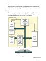
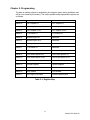
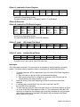
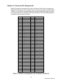
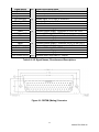
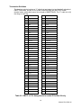
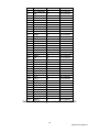
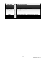
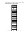
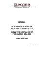
10623 Roselle Street, San Diego, CA 92121 (858) 550-9559 Fax (858) 550-7322 [email protected] www.accesio.com MODELS PCIe-IDIO-24, PCIe-IDI-24, PCIe-IDO-24, PCIe-IDIO-12 ISOLATED DIGITAL INPUT FET OUTPUT BOARDS USER MANUAL File: MPCIe-IDIO-24.A3b Notice The information in this document is provided for reference only. ACCES does not assume any liability arising out of the application or use of the information or products described herein. This document may contain or reference information and products protected by copyrights or patents and does not convey any license under the patent rights of ACCES, nor the rights of others. IBM PC, PC/XT, and PC/AT are registered trademarks of the International Business Machines Corporation. Copyright © by ACCES I/O Products, Inc. 10623 Roselle Street, San Diego, CA 92121. All rights reserved. WARNING!! ALWAYS CONNECT AND DISCONNECT YOUR FIELD CABLING WITH THE COMPUTER POWER OFF. ALWAYS TURN COMPUTER POWER OFF BEFORE INSTALLING A BOARD. CONNECTING AND DISCONNECTING CABLES, OR INSTALLING BOARDS INTO A SYSTEM WITH THE COMPUTER OR FIELD POWER ON MAY CAUSE DAMAGE TO THE I/O BOARD AND WILL VOID ALL WARRANTIES, IMPLIED OR EXPRESSED. 2 Manual PCIe-IDIO-24 Warranty Prior to shipment, ACCES equipment is thoroughly inspected and tested to applicable specifications. However, should equipment failure occur, ACCES assures its customers that prompt service and support will be available. All equipment originally manufactured by ACCES which is found to be defective will be repaired or replaced subject to the following considerations. Terms and Conditions If a unit is suspected of failure, contact ACCES' Customer Service department. Be prepared to give the unit model number, serial number, and a description of the failure symptom(s). We may suggest some simple tests to confirm the failure. We will assign a Return Material Authorization (RMA) number which must appear on the outer label of the return package. All units/components should be properly packed for handling and returned with freight prepaid to the ACCES designated Service Center, and will be returned to the customer's/user's site freight prepaid and invoiced. Coverage First Three Years: Returned unit/part will be repaired and/or replaced at ACCES option with no charge for labor or parts not excluded by warranty. Warranty commences with equipment shipment. Following Years: Throughout your equipment's lifetime, ACCES stands ready to provide on-site or in-plant service at reasonable rates similar to those of other manufacturers in the industry. Equipment Not Manufactured by ACCES Equipment provided but not manufactured by ACCES is warranted and will be repaired according to the terms and conditions of the respective equipment manufacturer's warranty. General Under this Warranty, liability of ACCES is limited to replacing, repairing or issuing credit (at ACCES discretion) for any products which are proved to be defective during the warranty period. In no case is ACCES liable for consequential or special damage arriving from use or misuse of our product. The customer is responsible for all charges caused by modifications or additions to ACCES equipment not approved in writing by ACCES or, if in ACCES opinion the equipment has been subjected to abnormal use. "Abnormal use" for purposes of this warranty is defined as any use to which the equipment is exposed other than that use specified or intended as evidenced by purchase or sales representation. Other than the above, no other warranty, expressed or implied, shall apply to any and all such equipment furnished or sold by ACCES. 3 Manual PCIe-IDIO-24 TABLE OF CONTENTS Chapter 1: Introduction ............................................................................................................................. 5 Features .................................................................................................................................................... 5 Applications ............................................................................................................................................. 5 Functional Description ............................................................................................................................ 5 Inputs ........................................................................................................................................................ 5 Interrupts .................................................................................................................................................. 6 Outputs ..................................................................................................................................................... 6 Figure 1-1: Block Diagram .................................................................................................................. 6 Figure 1-2: Example of One Input Circuit .......................................................................................... 7 Figure 1-3: Example of One Output Circuit ....................................................................................... 7 Ordering Guide ........................................................................................................................................ 7 Model Options .......................................................................................................................................... 7 Included with your board ........................................................................................................................ 7 Optional Accessories .............................................................................................................................. 7 Chapter 2: Installation ................................................................................................................................ 8 Chapter 3: Hardware Details ...................................................................................................................... 9 Option Selection ...................................................................................................................................... 9 Figure 3-1: Dimensioned Drawing...................................................................................................... 9 Chapter 4: Address Selection .................................................................................................................. 10 Chapter 5: Programming .......................................................................................................................... 11 Table 5-1: Register Map..................................................................................................................... 11 Interrupts ................................................................................................................................................ 15 Chapter 6: Connector Pin Assignments ................................................................................................. 16 Table 6-1: DB78F Pin Assignments (J2) for Model PCIe-IDxx-24 ................................................. 16 Table 6-2: I/O Signal Names, Directions and Descriptions............................................................ 17 Figure 6-1: DB78M (Mating) Connector ........................................................................................... 17 Table 6-3: DB37F x 2 Pin Assignments for model PCIe-IDxx-24 only .......................................... 18 Table 6-4: DB78F Pin Assignments for Model PCIe-IDIO-12 ......................................................... 19 Table 6-5: I/O Signal Names, Directions and Descriptions for Model PCIe-IDIO-12 ................... 20 Table 6-6: DB37F Pin Assignments for Model PCIe-IDIO-12 ......................................................... 21 Chapter 7: Specification ........................................................................................................................... 22 Customer Comments ................................................................................................................................ 23 4 Manual PCIe-IDIO-24 Chapter 1: Introduction The PCIe-IDIO-24 provides isolated digital inputs with Change of State Detection and isolated FET high-side switches. The board has twenty four optically-isolated input circuits for AC or DC control signals and twenty four isolated FET high-side switches. The board occupies sixteen consecutive addresses in I/O space. Read and write operations may be 8, 16, or 32 bits wide. Several versions of this board are available. The PCIe-IDIO-24 also has eight TTL level non-isolated I/O lines. Model PCIe-IDIO-12 provides twelve isolated inputs and outputs and four TTL/CMOS I/O lines. Features • • • • • 24 optically isolated, non-polarized digital inputs o Software configurable filters on inputs for electrically noisy environments o 2 optically isolated groups (common return per 12 channels) o Can detect input state change and assert interrupt 8 non-isolated TTL/CMOS I/O lines 24 optically isolated high-side FET switches o 4 groups, sharing external power and return per 6 output channels Opto-couplers rated for 2.5kV isolation Automatically detected under Windows Applications These boards are especially useful in applications where high common-mode external voltages are present. Isolation is required to guard electronics from transient voltage spikes and offers greater common-mode noise rejection in electronically noisy surroundings containing industrial machinery and inductive loads. These applications include factory automation, energy management, industrial ON/OFF control, security systems, manufacturing test, and process monitoring. In addition to protecting industrial applications from accidental contact with high external voltages, the isolation provided eliminates troublesome ground loops. Functional Description Inputs The isolated inputs can be driven by either AC or DC signals. Input signals are rectified by photocoupler diodes. A 1.8K-ohm resistor in series dissipates unused power. Standard 12/24 AC control transformer outputs can be accepted as well as DC voltages. The input voltage range is 3 to 31 volts (rms). External resistors connected in series may be used to extend the input voltage, however this will raise the input threshold range. Consult with the factory for available modified input ranges. Each input bank (12x2) contains a switchable filter that has a 4.7 millisecond time constant. Without filtering, rise time response is 10us fall time is 30us. The filter must be selected for AC inputs in order to eliminate the on/off response to the AC zero crossing. The filter is also valuable for use with slow DC input signals in a noisy environment. The filters may be switched out for DC inputs in order to obtain faster response. Filters are selected by the user's software. 5 Manual PCIe-IDIO-24 Interrupts When configured by the user's software, the board asserts an interrupt whenever any enabled inputs change state from HIGH (more than 3V) to LOW (less than 3V), LOW to HIGH, or both. This is called Change-of-State (COS) detection. See the programming section for a discussion of the COS interrupt management scheme. Outputs The solid state outputs are comprised of twenty four fully protected FET high-side switches. The FETs have built in current limiting and are protected against short-circuit, over-temperature, ESD and inductive load transients. The current limitation is activated until the thermal protection acts. The FETs are all off at power-on. Figure 1-1: Block Diagram 6 Manual PCIe-IDIO-24 Figure 1-2: Example of One Input Circuit (shared return pin per 12 channel group) Figure 1-3: Example of One Output Circuit (shared PWR+ and RETURN- pins per 6 channel group) Ordering Guide PCIe-IDIO-24 PCIe-IDI-24 PCIe-IDO-24 PCIe-IDIO-12 24 isolated inputs 8 non-isolated inputs, 24 high-side FET outputs Inputs only (24 isolated, 8 TTL/CMOS) 24 isolated FET outputs and 8 TTL/CMOS I/O lines 12-isolated inputs, 4 TTL I/O lines, 12-isolated outputs Model Options -T -RoHS Extended temperature (-40° to +85°C) RoHS compliant version Included with your board The following components are included with your shipment. Please take time now to ensure that no items are damaged or missing. 1. Software Master CD (PDF user manual installed with product package) 2. Printed I/O Quick-Start Guide Optional Accessories STB-37/2 Kit Complete screw termination solution, consisting of: Two (2) STB-37’s installed on a 12” SNAP-TRACK & 6’ “Y” Cable Assembly terminating in two DB37F connectors STB-37/2 Kit-CL Includes four clips for mounting the STB-37/2 Kit to a standard DINRail. 7 Manual PCIe-IDIO-24 Chapter 2: Installation Software CD Installation The software provided with this board is contained on one CD and must be installed onto your hard disk prior to use. To do this, perform the following steps as appropriate for your operating system. Substitute the appropriate drive letter for your drive where you see D: in the examples below. Windows a. b. c. Place the CD into your CD-ROM drive. The install program automatically run. If the install program does not run, click START | RUN and type , click OK or press . Follow the on-screen prompts to install the software for this board. Linux a. Please refer to linux.htm on the CD for information on installing under Linux. Hardware Installation Please install the software package before plugging the hardware into the system. Refer to the printed I/O Quick Start Guide included with your board which can also be found on the CD, for specific, quick steps, to complete the hardware and software installation. Caution! ESD A single static discharge can damage your card and cause premature failure! Please follow all reasonable precautions to prevent a static discharge such as grounding yourself by touching any grounded surface prior to touching the card. 8 Manual PCIe-IDIO-24 Chapter 3: Hardware Details Option Selection There are no jumpers or switches to set or configure prior to installing the card into the PCIe slot of the PC. Figure 3-1: Dimensioned Drawing 9 Manual PCIe-IDIO-24 Chapter 4: Address Selection The Vendor ID for this card is 0x494F. (ASCII for "IO") The Device ID for the PCIe-IDIO-24 is 0x0FD0. The Device ID for the PCIe-IDI-24 is 0x0BD0. The Device ID for the PCIe-IDO-24 is 0x07D0. The Device ID for the PCIe-IDIO-12 is 0x0FC0. This card uses I/O addresses offset from the Offset assigned by the PCIe bus. The address spaces are defined in the programming section of this manual. PCIe architecture is Plug-and-Play. This means that the BIOS or Operating System determines the resources assigned to PCIe cards rather than the user selecting those resources with switches or jumpers. As a result, you cannot set or change the card's Offset or IRQ level. You can only determine what the system has assigned. The following information is for advanced users only: The PCIe bus supports 64K of I/O address space, so your card's addresses may be located anywhere in the 0000h to FFFFh range. The card uses more resources than you usually need be concerned with. For those who require it, be aware of the following: BAR[0]: memory mapped PEX8311 BAR[1]: I/O mapped PEX8311 BAR[2]: I/O mapped card registers (←all most software needs) 10 Manual PCIe-IDIO-24 Chapter 5: Programming The base or starting address is assigned by the computer system during installation and will fall on a sixteen-byte boundary. The card’s readable and programmable registers are as follows: I/O Address Read Write Base +0 FET Outputs 0-7 FET Outputs 0-7 Base +1 FET Outputs 8-15 FET Outputs 8-15 Base +2 FET Outputs 16-23 FET Outputs 16-23 Base +3 TTL/CMOS 0-7 TTL/CMOS 0-7 Base +4 Isolated Inputs 0-7 Reserved Base +5 Isolated Inputs 8-15 Reserved Base +6 Isolated Inputs 16-23 Reserved Base +7 TTL/CMOS 0-7 Reserved Base +8 COS Status Inputs 0-7 COS Clear Inputs 0-7 Base +9 COS Status Inputs 8-15 COS Clear Inputs 8-15 Base +A COS Status Inputs 16-23 COS Clear Inputs 16-23 Base +B COS Status TTL/CMOS 0-7 COS Clear TTL/CMOS 0-7 Base +C Control Register Control Register Base +D Reserved Reserved Base +E COS Enable COS Enable Base +F IRQ Output Pin Status Software Board Reset Table 5-1: Register Map 11 Manual PCIe-IDIO-24 Offset +0 (read/write) FET Outputs 0-7 Bit 7 OUT7 Bit 6 OUT6 Bit 5 OUT5 Bit 4 OUT4 Bit 3 OUT3 Bit 2 OUT2 Bit 1 OUT1 Bit 0 OUT0 Reading from this address will return the values last written. Writing a 1 to any bit will turn on the corresponding FET output. The card initializes with all outputs off (all “0’s”). Offset +1 (read/write) FET Outputs 8-15 Bit 7 OUT15 Bit 6 OUT14 Bit 5 OUT13 Bit 4 OUT12 Bit 3 OUT11 Bit 2 OUT10 Bit 1 OUT9 Bit 0 OUT8 Reading from this address will return the values last written. Writing a 1 to any bit will turn on the corresponding FET output. The card initializes with all outputs off (all “0’s”). Offset +2 (read/write) FET Outputs 16-23 Bit 7 OUT23 Bit 6 OUT22 Bit 5 OUT21 Bit 4 OUT20 Bit 3 OUT19 Bit 2 OUT18 Bit 1 OUT17 Bit 0 OUT16 Reading from this address will return the values last written. Writing a 1 to any bit will turn on the corresponding FET output. The card initializes with all outputs off (all “0’s”). Offset +3 (read/write) TTL/CMOS 0-7 Bit 7 TTL7 Bit 6 TTL6 Bit 5 TTL5 Bit 4 TTL4 Bit 3 TTL3 Bit 2 TTL2 Bit 1 TTL1 Bit 0 TTL0 The card initializes in the Input mode, standard TTL/CMOS levels apply. When Output mode is set (see Offset +C, Control Register), data bit values written will be reflected at the corresponding connector pin, (positive logic). 12 Manual PCIe-IDIO-24 Offset +4 (read) Bit 7 IN7 Isolated Inputs 0-7 Bit 6 IN6 Bit 5 IN5 Bit 4 IN4 Bit 3 IN3 Bit 2 IN2 Bit 1 IN1 Bit 0 IN0 Reading from this address will return the Input values. Each bit returning a “1” indicates the corresponding Input is active / energized (from 3V to 31V). Offset +5 (read) Bit 7 IN15 Isolated Inputs 8-15 Bit 6 IN14 Bit 5 IN13 Bit 4 IN12 Bit 3 IN11 Bit 2 IN10 Bit 1 IN9 Bit 0 IN8 Reading from this address will return the Input values. Each bit returning a “1” Indicates the corresponding Input is active / energized (from 3V to 31V). Offset +6 (read) Bit 7 IN23 Isolated Inputs 16-23 Bit 6 IN22 Bit 5 IN21 Bit 4 IN20 Bit 3 IN19 Bit 2 IN18 Bit 1 IN17 Bit 0 IN16 Reading from this address will return the Input values. Each bit returning a “1” Indicates the corresponding Input is active / energized (from 3V to 31V). Offset +7 (read) Bit 7 TTL7 TTL/CMOS 0-7 Bit 6 TTL6 Bit 5 TTL5 Bit 4 TTL4 Bit 3 TTL3 Bit 2 TTL2 Bit 1 TTL1 Bit 0 TTL0 Reading from this address will return the Input values. Each bit returning a “0” Indicates the corresponding Input is Low (all Inputs are pulled up to 5V via 10kΩ). 13 Manual PCIe-IDIO-24 Offset +8 (read) COS Status Inputs 0-7 Bit 7 Bit 6 Bit 5 Bit 4 Bit 3 Bit 2 Bit 1 Bit 0 IN7 IN6 IN5 IN4 IN3 IN2 IN1 IN0 Reading from this address will return a “1” at each bit for the corresponding Input that has changed state (since the last “Clear” write to Base +8). Offset +8 (write) COS Clear Inputs 0-7 Bit 7 Bit 6 Bit 5 Bit 4 Bit 3 Bit 2 Bit 1 Bit 0 IN7 IN6 IN5 IN4 IN3 IN2 IN1 IN0 Writing a “1” to any bit at this address will clear the change of state detection for the corresponding Input, and will also clear the card’s Interrupt Output pin *. Offset +9 (read) COS Status Inputs 8-15 Bit 7 Bit 6 Bit 5 Bit 4 Bit 3 Bit 2 Bit 1 Bit 0 IN15 IN14 IN13 IN12 IN11 IN10 IN9 IN8 Reading from this address will return a “1” at each bit for the corresponding Input that has changed state (since the last “Clear” write to Base +9). Offset +9 (write) COS Clear Inputs 8-15 Bit 7 Bit 6 Bit 5 Bit 4 Bit 3 Bit 2 Bit 1 Bit 0 IN15 IN14 IN13 IN12 IN11 IN10 IN9 IN8 Writing a “1” to any bit at this address will clear the change of state detection for the corresponding Input, and will also clear the card’s Interrupt Output pin *. Offset +A (read) COS Status Inputs 16-23 Bit 7 Bit 6 Bit 5 Bit 4 Bit 3 Bit 2 Bit 1 Bit 0 IN23 IN22 IN21 IN20 IN19 IN18 IN17 IN16 Reading from this address will return a “1” at each bit for the corresponding Input that has changed state (since the last “Clear” write to Base +A). Offset +A (write) COS Clear Inputs 16-23 Bit 7 Bit 6 Bit 5 Bit 4 Bit 3 Bit 2 Bit 1 Bit 0 IN23 IN22 IN21 IN20 IN19 IN18 IN17 IN16 Writing a “1” to any bit at this address will clear the change of state detection for the corresponding Input, and will also clear the card’s Interrupt Output pin *. Offset +B (read) COS Status TTL/CMOS 0-7 Bit 7 Bit 6 Bit 5 Bit 4 Bit 3 Bit 2 Bit 1 Bit 0 TTL7 TTL6 TTL5 TTL4 TTL3 TTL2 TTL1 TTL0 Reading from this address will return a “1” at each bit for the corresponding Input that has changed state (since the last “Clear” write to Base +B). Offset +B (write) COS Clear TTL/CMOS 0-7 Bit 7 Bit 6 Bit 5 Bit 4 Bit 3 Bit 2 Bit 1 Bit 0 TTL7 TTL6 TTL5 TTL4 TTL3 TTL2 TTL1 TTL0 Writing a “1” to any bit at this address will clear the change of state detection for the corresponding Input, and will also clear the card’s Interrupt Output pin*. *= If all 32 COS status bits have been cleared) 14 Manual PCIe-IDIO-24 Offset +C (read/write) Control Register Bit 7 0 Bit 6 Bit 5 0 0 Bit 4 Bit 3 0 FILTER EN FILTER EN OUT MODE BUFFER EN IN12-23 IN0-11 TTL 0-7 TTL 0-7 Bit 2 Bit 1 Bit 0 Reading from this address will return the values last written. Writing a 1 to any bit will enable the corresponding function. The card initializes with Bit 0=1 (Enabled), and Bit 1-7=0 (Disabled). Offset +D Reserved Offset +E (read/write) COS Enable Register Bit 7 Bit 6 Bit 5 Bit 4 Bit 3 Bit 2 Bit 1 Bit 0 IRQ EN Falling Edge TTL0-7 IRQ EN Falling Edge IN16-23 IRQ EN Falling Edge IN8-15 IRQ EN Falling Edge IN0-7 IRQ EN Rising Edge TTL0-7 IRQ EN Rising Edge IN16-23 IRQ EN Rising Edge IN8-15 IRQ EN Rising Edge IN0-7 Reading from this address will return the values last written. Writing a 1 to any bit will enable the corresponding function. The card initializes with all bits=0 (COS IRQ disabled). Offset +F (read) IRQ Output Pin Status Bit 7 Bit 6 Bit 5 Bit 4 Bit 3 Bit 2 Bit 1 Bit 0 0 0 0 0 0 0 0 IRQ Reading from this address will return a “1” at Bit 0 when the card’s interrupt pin is active. Offset +F (write) Software Board Reset Bit 7 Bit 6 Bit 5 Bit 4 Bit 3 Bit 2 Bit 1 Bit 0 X X X X X X X X Writing any value to this address will return the Control Register to the default state, all Outputs to off, and clear all Input COS status bits. Interrupts: The card supports interrupts. The interrupt level is assigned by the plug-and-play operating system. The card’s interrupt capability makes it unnecessary to continuously poll inputs. 1. 2. 3. 4. To enable interrupts, SET the appropriate bit(s) in the 8-bit COS Enable Register at offset +E. a. Each bit maps to a group of eight inputs as described above. b. Each group of eight can be configured to generate a COS IRQ on either the rising transition, the falling transition, or both. Read the 4 byte (32 bit) block beginning at offset+8 to see what inputs have changed. If interrupts were enabled and if any of the bits in the block are SET then an IRQ will be generated. To clear interrupts, write the value read from the 32-bit COS-Status register at offset +8, to the 32-bit COS-Clear register at offset +8. This technique will clear the COS latch only for those bits your software has successfully detected as having changed, while allowing other bits to generate COS states in the time between the Status Read, and the COS Clear. 15 Manual PCIe-IDIO-24 Chapter 6: Connector Pin Assignments Digital I/O signals are connected to the card via a female 78-pin D type connector that extends through the back of the computer case. The mating connector is an AMPLIMITE 1658674-1 or equivalent. We optionally provide a breakout cable that divides the 78-pin I/O connector down to two female 37-pin D type connectors. See the following pages for information about termination solutions. Pin 1 2 3 4 5 6 7 8 9 10 11 12 13 14 15 16 17 18 19 20 21 22 23 24 25 26 27 28 29 30 31 32 33 34 35 36 37 38 39 Name IN_COMMON0 IN0 IN1 IN2 IN12 IN13 IN14 +5V TTL0 TTL2 VBB0OUT4 OUT2 OUT0 VBB1OUT10 OUT8 OUT6 VBB0+ VBB0+ IN3 IN4 IN5 IN15 IN16 IN17 IN_COMMON1 GND TTL1 TTL3 OUT5 OUT3 OUT1 No Connection OUT11 OUT9 OUT7 VBB1+ VBB1+ Pin 40 41 42 43 44 45 46 47 48 49 50 51 52 53 54 55 56 57 58 59 60 61 62 63 64 65 66 67 68 69 70 71 72 73 74 75 76 77 78 Name IN_COMMON0 IN6 IN7 IN8 IN18 IN19 IN20 +5V TTL4 TTL6 VBB2OUT16 OUT14 OUT12 VBB3OUT22 OUT20 OUT18 VBB2+ VBB2+ IN9 IN10 IN11 IN21 IN22 IN23 IN_COMMON1 GND TTL5 TTL7 OUT17 OUT15 OUT13 No Connection OUT23 OUT21 OUT19 VBB3+ VBB3+ Table 6-1: DB78F Pin Assignments (J2) for Model PCIe-IDxx-24 16 Manual PCIe-IDIO-24 Signal Name I/O Signal Description Name IN_COMMON0 IN0 thru IN11 IN_COMMON1 IN12 thru IN23 TTL0 thru TTL7 +5V GND VBB0+ VBB0OUT0 thru OUT5 VBB1+ VBB1OUT6 thru OUT11 VBB2+ VBB2OUT12 thru OUT17 VBB3+ VBB3OUT18 thru OUT23 In In In In I/O Out Out In In Out In In Out In In Out In In Out Common Return for IN0 thru IN11 Isolated Inputs, 3 to 31VDC or 22VACrms Common Return for IN12 thru IN23 Isolated Inputs, 3 to 31VDC or 22VACrms 5V Logic, Pulled up via 10kΩ Unfused +5V connection +5V and TTLx Return connection Common External Supply + connection for OUT0 thru OUT5 Common External Supply - connection for OUT0 thru OUT5 Switched VBB0+ High Side FET Outputs Common External Supply + connection for OUT6 thru OUT11 Common External Supply - connection for OUT6 thru OUT11 Switched VBB1+ High Side FET Outputs Common External Supply + connection for OUT12 thru OUT17 Common External Supply - connection for OUT12 thru OUT17 Switched VBB2+ High Side FET Outputs Common External Supply + connection for OUT18 thru OUT23 Common External Supply - connection for OUT18 thru OUT23 Switched VBB3+ High Side FET Outputs Table 6-2: I/O Signal Names, Directions and Descriptions Figure 6-1: DB78M (Mating) Connector 17 Manual PCIe-IDIO-24 Termination Solutions The breakout solution involves a “Y” cable that terminates into two identically pinned out DB37F connectors. As part of a kit, these connectors plug into the STB-37 screw terminal cards, which easily mount into a length of SNAPTRACK. The “Y” cable is six (6) feet long on each leg. PIN NAME PIN NAME 1 IN_COMMON0 IN0 IN1 IN2 IN12 IN13 IN14 1 IN_COMMON0 IN6 IN7 IN8 IN18 IN19 IN20 +5V TTL0 TTL2 VBB0OUT4 OUT2 8 OUT0 VBB1OUT10 OUT8 OUT6 VBB0+ 14 IN3 IN4 IN5 IN15 IN16 IN17 IN_COMMON1 20 GND TTL1 TTL3 OUT5 OUT3 OUT1 27 No Connection OUT11 OUT9 OUT7 VBB1+ 33 2 3 4 5 6 7 8 9 10 11 12 13 14 15 16 17 18 19 20 21 22 23 24 25 26 27 28 29 30 31 32 33 34 35 36 37 2 3 4 5 6 7 9 10 11 12 13 15 16 17 18 19 21 22 23 24 25 26 28 29 30 31 32 34 35 36 37 +5V TTL4 TTL6 VBB2OUT16 OUT14 OUT12 VBB3OUT22 OUT20 OUT18 VBB2+ IN9 IN10 IN11 IN21 IN22 IN23 IN_COMMON1 GND TTL5 TTL7 OUT17 OUT15 OUT13 No Connection OUT23 OUT21 OUT19 VBB3+ Table 6-3: DB37F x 2 Pin Assignments for model PCIe-IDxx-24 only 18 Manual PCIe-IDIO-24 Pin 1 2 3 4 5 6 7 8 9 10 11 12 13 14 15 16 17 18 19 20 21 22 23 24 25 26 27 28 29 30 31 32 33 34 35 36 37 38 39 Name IN_COMMON0 IN0 IN1 IN2 IN8 IN9 IN10 +5V TTL0 TTL2 VBB0OUT4 OUT2 OUT0 VBB1OUT10 OUT8 OUT6 VBB0+ VBB0+ IN3 IN4 IN5 IN11 IN6 IN7 IN_COMMON1 GND TTL1 TTL3 OUT5 OUT3 OUT1 No Connection OUT11 OUT9 OUT7 VBB1+ VBB1+ Pin 40 41 42 43 44 45 46 47 48 49 50 51 52 53 54 55 56 57 58 59 60 61 62 63 64 65 66 67 68 69 70 71 72 73 74 75 76 77 78 Name No Connection No Connection No Connection No Connection No Connection No Connection No Connection +5V No Connection No Connection No Connection No Connection No Connection No Connection No Connection No Connection No Connection No Connection No Connection No Connection No Connection No Connection No Connection No Connection No Connection No Connection No Connection GND No Connection No Connection No Connection No Connection No Connection No Connection No Connection No Connection No Connection No Connection No Connection Table 6-4: DB78F Pin Assignments for Model PCIe-IDIO-12 19 Manual PCIe-IDIO-24 Signal Name I/O Signal Description Name IN_COMMON0 IN0 thru IN11 IN_COMMON1 IN12 thru IN23 TTL0 thru TTL7 +5V GND VBB0+ VBB0OUT0 thru OUT5 VBB1+ VBB1- In In In In I/O Out Out In In Out In In Common Return for IN0 thru IN5 Isolated Inputs, 3 to 31VDC or 22VACrms Common Return for IN6 thru IN11 Isolated Inputs, 3 to 31VDC or 22VACrms 5V Logic, Pulled up via 10kΩ Unfused +5V connection +5V and TTLx Return connection Common External Supply + connection for OUT0 thru OUT5 Common External Supply - connection for OUT0 thru OUT5 Switched VBB0+ High Side FET Outputs Common External Supply + connection for OUT6 thru OUT11 Common External Supply - connection for OUT6 thru OUT11 Table 6-5: I/O Signal Names, Directions and Descriptions for Model PCIe-IDIO-12 20 Manual PCIe-IDIO-24 The breakout solution for the PCIe-IDIO-12 consists of a DB78M to DB37F cable. As part of a kit, the DB37F plugs into an STB-37 screw terminal card, which easily mount into a length of SNAPTRACK. The cable is six (6) feet long. PIN NAME 1 IN_COMMON0 2 IN0 3 IN1 4 IN2 5 IN8 6 IN9 7 IN10 8 +5V 9 TTL0 10 TTL2 11 VBB012 OUT4 13 OUT2 14 OUT0 15 VBB116 OUT10 17 OUT8 18 OUT6 19 VBB0+ 20 IN3 21 IN4 22 IN5 23 IN11 24 IN6 25 IN7 26 IN_COMMON1 27 GND 28 TTL1 29 TTL3 30 OUT5 31 OUT3 32 OUT1 33 No Connection 34 OUT11 35 OUT9 36 OUT7 37 VBB1+ Table 6-6: DB37F Pin Assignments for Model PCIe-IDIO-12 21 Manual PCIe-IDIO-24 Chapter 7: Specification Isolated Digital Inputs Number of inputs: Type: Voltage Range: Isolation: Input Resistance: Response Time: with filter: without filter: 24 Non-polarized, optically isolated sharing a common return per 12 channel input group. (not TTL/CMOS compatible) 3 to 31V DC or 22 VACrms (40-10kHz) Opto-couplers rated at 2.5kV See note 1 1.8k ohms in series with two diodes and a photo-coupler LED 4.7 mSec rise time = 10 uSec fall time = 30 uSec Non-Isolated Digital Input/Outputs Number of lines: 8, programmable as all inputs or all outputs Type: TTL/CMOS compatible, pulled up to 5V via 10kΩ Interrupts Change of State Detection available on all 32 input bits; software enabled byte-by-byte Solid State FET Outputs Number of outputs: 24, isolated in four, 6-channel groups Output Type: Smart High Side Power MOSFET Switch Protected against short circuit, over-temp., ESD, can drive inductive loads. Voltage Range: 5-34VDC recommended (40VDC absolute maximum) FET Ratings: On-state resistance = 60mΩ 2A continuous per FET, with a 9A cumulative total per group of 6 FETs Environmental Operating Temp.: Storage Temp.: Humidity: 0° to 70°C, optional -40° to +85°C -40 to +85°C 5 to 90 percent (non-condensing) Mechanical Size: Connector: Mating Connector: Standard height 4.2” (106.65 mm), half length 6.6" (167.6 mm) DB78 Female AMPLIMITE 1658674-1 or equivalent Note 1: Opto-couplers are rated for at least 2.5kV, but isolation voltage breakdowns will vary and is affected by factors like cabling, spacing of pins, spacing between traces on the PCB, humidity, dust and other environmental factors. This is a safety issue so a careful approach is required. For CE certification on the front end of the circuitry, isolation was specified at 40V AC and 60V DC. The design intention was to eliminate the influence of common mode. Use proper wiring techniques to minimize voltage between channels and to ground. For example, when working with AC voltages do not connect the hot side of the line to an input. Tolerance of higher isolation voltage can be obtained on request by applying a conformal coating to the board. 22 Manual PCIe-IDIO-24 Customer Comments If you experience any problems with this manual or just want to give us some feedback, please email us at: [email protected]. Please detail any errors you find and include your mailing address so that we can send you any manual updates. 10623 Roselle Street, San Diego CA 92121 Tel. (858)550-9559 FAX (858)550-7322 www.accesio.com 23 Manual PCIe-IDIO-24