1
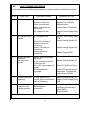
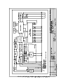
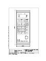
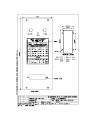
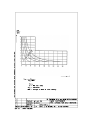
(An ISO 9001:2008Mfg. Co.) MICROCONTROLLER-BASED AUTOMATIC VOLTAGE REGULATING RELAY EE-302 INSTRUCTION MANUAL Instruction Manual for Microcontroller-Based Automatic Voltage Regulating Relay Type - EE 302 EMCO ELECTRONICS Head Office : 302, Vasan Udyog Bhavan, Senapati Bapat Marg, Lower Parel (W), Mumbai – 13. Tel.: +91-22-2492 3183 / 2490 2283 Fax : +91-22-2495 1024 E-mail : [email protected] Factory : Unit No. 13, Kedarnath, Tungareshwar Indl. Complex No. 1, Sativali, Vasai (E), Dist - Thane. 401 208. Tel. : +91-250-2481 783 / 804 Fax : +91-250-2481 087 E-mail : [email protected] South Office : 15, Wood Street, 1st floor, Richmond Road, Bangalore – 560 025. Tel.: +91-80-2557 0215 Tel.Fax : +91-80-2556 6606 E-mail : [email protected] www.emcoelectronics.org CONTENTS Sr. No. TITLE PAGE No. I General Description 1 II Specifications 2 III Indications / Controls / Inputs and Outputs 4 IV Operating Instructions 9 V Typical Inspection Procedure 11 VI Functional Description of PCBs 13 VII Options 15 VIII Fault Finding Procedure 18 IX Appendix 20 X List of drawings 21 XI Warranty 22 I. GENERAL DESCRIPTION EMCO’s Microcontroller based Automatic Voltage Regulating Relay type EE–302 is a new generation Relay used for regulating the secondary voltage of Power Transformers with a motor driven On Load Tap Changer (OLTC). A single control pulse to the motor causes a change in voltage by one step. When step by step function is inactive, the motor drive is controlled by a continuous control pulse. A “Raise” or “Lower” control signal is generated by the voltage regulator when the measured voltage deviates from preset conditions. The parameters are programmable through a membrane keyboard and are stored in Non-Volatile Memory. Time Delay Setting (for deviation from deadband to the first control pulse) can be set in Linear or Integral mode (i.e. Inversely proportional to the deviation). Where the voltage correction requires more than one control pulse, the time delay between consecutive control pulses is also programmable. Relays with potential free contacts are provided for signaling ‘Undervoltage’, ‘Overvoltage’ & ‘Control Fail’ (voltage remaining outside the deadband for more than 5 minutes) conditions. The Undervoltage and Control Fail conditions result in the blocking of the Tap Changer whereas an Overvoltage condition results in high speed return. The regulated voltage can be displayed in volts, kilovolts or %deviation from the Nominal value. LED annunciators are provided for presignal conditions and Relay operations. The regulated voltage can be lowered by means of loadshedding in 3 steps, ie. 3%, 6% and 9% of Nominal voltage via external relay contacts or switches. The Auto / Manual selection allows the Relay to operate in the Auto mode or in the Manual mode. In the Manual mode, the “Raise” and “Lower” pulses are blocked, but all other alarm signaling relays are available. Load dependent voltage drops due to line impedance can be compensated by increasing / decreasing the desired value by means of simulated Resistance & Reactive compensation. (Optional) In case of failure of Auxiliary supply to the Relay a pair of normally closed contacts is available for signaling an alarm (Optional). The modular construction makes it very convenient for easy servicing and quick replacement of cards, without withdrawing the AVR from the Control Panel. 1 I I. SPECIFICATIONS Settings Nominal Voltage Setting (NS) Lower Voltage Setting (LS) Raise Voltage Setting (RS) Time Delay (T1) between deviation and First Pulse Time Delay (T2) between consecutive Pulses Undervoltage Blocking (UV) Overvoltage Detection (OV) Primary Voltage Factor (KV) Control Fail Delay Time Loadshedding Resistive compensation for LDC (%R) Reactive compensation for LDC (%X) : : : : 85 to 140V in steps of 0.1V +0.5 to +9% of NS in steps of 0.1V -0.5 to -9% of NS in steps of 0.1V 10 to 180 secs, Linear or Inverse response : 0 to 11 secs, where 0 – continuous operation; 11 – T2 = T1 : 60 to 95% of NS in steps of 0.1% : 105 to 130% of NS in steps of 0.1% with high speed return (2 secs ON / 2 secs OFF) : 0 – 999.9 KV corresponding to NS in steps of 0.1KV : 5 minutes fixed internally : 3 steps @ 3%, 6% and 9% fixed : ± 0 – 20% of NS in steps of 1% : ± 0 – 20% of NS in steps of 1% Parameter Adjust Rotate (→) Increment ( ↑ ) Enter (EN) - Selects & rotates clockwise the digit to be modified - Increments the value of the selected digit - Saves the modified value if within limits Display 4 digits 7 segments LED Display LED indicators for parameter units (V,KV,%,S); Presignal conditions (L,R), Manual mode indication (M), and Relay operations (LR,RR,UV,OV,CF) Secondary Voltage Indication (LV) with 0.1V resolution Primary Voltage Indication (HV) with 0.1 KV resolution Percentage Deviation (%∆) with 0.1% resolution Mode Control Auto / Manual (A / M) Linear / Inverse (L / I) : Keyboard selectable. Toggles Automatic or Manual Mode of Tap-changer. Manual mode indicated with a LED and cuts off Lower and Raise Relays. Other Alarm Relays (OV, UV, CF) are not cut off. : Keyboard selectable. Toggles Linear or Inverse Time response for delay T1 2 Output Relays One pair of NO contacts for Lower, Raise, Undervoltage, Overvoltage and Control Fail conditions. Contact rating : 5A @ 240V AC or 24V DC Relay ON Time 1. Lower, Raise : 2 secs pulse 2. Overvoltage, Undervoltage, : Continuous operation Control Fail Inputs PT Supply Auxiliary Supply C.T. Current Load Shedding : : : : 110V AC, 50Hz, 1.5VA 110V / 230V AC ± 15%, 50Hz, 15VA 1 Amp, 1VA max. 3 opto isolated inputs with 1 common (pole) for connecting external switch. : : : : 268 x 125 mm. Depth 300 mm. M6 Screws @ 190 x 147 mm. centers 0 – 450 C < 5 Kg. Others Panel Cutout Mounting holes Operating Temperature Weight Options 1. Line Drop Compensation with ± 0 to 20%, %R and %X compensation 2. Auxiliary Fail Relay with a pair of NC contacts to indicate failure of Auxiliary Supply to the Relay 3. Built-in Tap Position Indicator upto maximum 35 taps with 1K step Resistance. 4. Overcurrent Blocking at 150% of load current. 3 III. INDICATIONS / CONTROLS / INPUTS AND OUTPUTS (Ref. Drg. No : 03-ED-02 for Front Panel and Drg. No : 03-ED-03 for Rear Panel). INDICATIONS 1. 4x7 Segment Display : Display lights when Auxiliary Supply is ‘ON’ 2. ‘L’ LED ON whenever the PT Voltage : `Lower Volts’ (LS) Set limit. 3. ‘R’ LED : ON whenever the PT Voltage falls below the `Raise Volts’ (RS) Set limit. 4. ‘UV’ LED : ON whenever the PT Voltage falls below the `Under Voltage’ (UV) Set limit & the UV Relay is energised. This lamp will turn off when the PT voltage becomes greater than 5% above the set `Under Voltage’ value. 5. ‘OV’ LED : ON whenever the PT Voltage exceeds the `Over Voltage’ (OV) Set limit & the OV Relay is energised. This lamp will turn off when the PT voltage becomes less than 5% below the set `Over Voltage’ value. 6. ‘LR’ LED : ON when Lower Relay is energised. 7. ‘RR’ LED : ON when Raise Relay is energised. 8. ‘A/M’ LED : ON when AVR is in manual mode. 9. ‘CF’ LED : ON when Control Fail Relay is energised, i.e. when the PT voltage remains outside the bandwidth for more than 5 minutes. 10. ‘V’ LED : ON when value displayed is in volts. 11. ‘KV’ LED : ON when value displayed is in Kilovolts. 12. ‘%’ LED : ON when value displayed is in percentage of Nominal Value. 13. ‘S’ LED : ON when value displayed is in seconds. 14. 3%, 6%, 9% LEDs : ON when 3%,6% or 9% loadshedding is activated through an external switch or Normally Open potential free contacts (Input pins LS3, LS6, LS9 & LSCom. on Rear panel Terminal Block). The Nominal voltage setting is reduced by 3%, 6% or 9% accordingly. The voltage reduction remains effective as long as the activating contact is closed. 4 exceeds the CONTROLS 1.0 Power - ON switch This is a Rocker switch which when ON, supplies Auxiliary Voltage to the instrument. 2.0 Keyboard Keyboard is used for setting parameters and selecting type of display. 2.1 ‘RS’ Key Displays value of Raise Setting. It is adjustable from 0.5% to 9.0% of the `NS’ Setting. This setting sets the lower limit of the PT voltage below which if the PT voltage reduces, Raise command is given. ‘%’ indicator becomes ON when `RS’ is selected. 2.2 ‘NS’ Key Displays value of the Nominal voltage setting for PT voltage. It is adjustable between 85V to 140V. This setting becomes the reference level with respect to which LS and RS settings are settable. `V’ indicator becomes ON when `NS’ is selected. 2.3 ‘LS’ Key Displays value of Lower setting. It is adjustable from 0.5% to 9.0% of the `NS’ setting. This setting sets upper limit of the PT voltage, above which if the PT voltage increases, Lower command is given. `%’ indicator becomes ON when `LS’ is selected. 2.4 ‘UV’ Key Displays value of the Undervoltage limit. It is adjustable from 60% to 95% of the `NS’ setting. When the PT voltage falls below the Undervoltage Setting, blocking of the Raise Relay takes place. This suppresses tap-changer operations. When PT voltage becomes greater than the restoration value (i.e. 5% greater than the set value), the blocking is released and tap-changer operations are enabled. `%’ indicator becomes ON when `UV’ is selected. 2.5 ‘KV’ Key Displays value to be set for displaying the Primary side voltage corresponding to the set Nominal value (NS). It is adjustable from 0 to 999.9 KV. `KV’ indicator becomes ON when `KV’ is selected. 2.6 ‘OV’ Key Displays value of the Overvoltage limit. It is adjustable from 105% to 130% of the `NS’ setting. When the PT voltage goes above the Overvoltage Setting, high speed return is initiated i.e. Lower commands with 2 secs ON/OFF pulse duration are given, till the voltage reaches the restoration value (i.e. 5% less than the set value). When the PT 5 voltage goes below the restoration value, the set time delay (T2) between the 2 consecutive pulses becomes applicable. `%’ indicator becomes ON when `OV’ is selected. 2.7 ‘L / I’ Key Displays the saved mode of Time Delay ie. `Lin’ for Linear Time Delay and `Int’ for Integral Time Delay. Every key press toggles the display. The displayed value is selected by pressing the `EN’ key and saved in the NOVOL. The `L / I’ time delay is applicable only to Time Delay `T1’. `S’ indicator becomes on when `L / I’ is selected. 2.8 ‘T1’ Key Displays the value of the Time Delay in secs. From the moment of deviation to the first control pulse. When the PT voltage exceeds the Lower or Raise settings, T1 is initiated. It is adjustable from 10 to180 secs. As soon as the PT voltage returns back to the deadband limits, the time delay is cancelled. Depending on the `L / I’ selection, the time delay is `Linear’ i.e. equal to the set value or `Integral’ i.e. Inversely proportional to the ratio of percentage deviation / set % bandwidth [T1 / (%∆ / %BW)]. `S’ indicator becomes ON when `T1’ is selected. 2.9 ‘T2’ Key Displays the value of the Time Delay between two consecutive tap changes in secs, when more than 1 tap-change operation is necessary to bring back the PT voltage within bandwidth limits. It is adjustable from 0 to 10 secs or can be set in `OFF’ condition ie. T2=T1. `OFF’ condition is set by setting T2=11. Setting T2=0, results in a continuous pulse of the output (RAISE & LOWER) relays. `S’ indicator becomes ON when T2 is selected. 2.10 ‘%R’ Key Displays the value of the Resistive Line-Drop Compensation setting. It is adjustable from 0% to 20%. The polarity of compensation is displayed as `P’ for positive and `n’ for negative. When LDC option is not available, ‘nA’ is displayed. ‘%’ indicator becomes ON when `%R’ is selected. 2.11 ‘+ / -’ Key This key toggles the polarity of %R and %X values. Hence it is valid only after `%R’ or `%X’ values have been displayed. `P’ stands for Positive and `n’ stands for Negative compensation. The displayed polarity is selected & saved only after pressing `EN’ key. When LDC option is not available, ‘nA’ is displayed. 6 2.12 ‘%X’ Key Displays the value of the reactive Line-Drop Compensation setting. It is adjustable from 0% to 20%. The polarity of compensation is displayed as `P’ for positive and `n’ for negative. When LDC option is not available, ‘nA’ is displayed. `%’ indicator becomes ON when `%X’ is selected. 2.13 ‘A / M’ Key This key toggles the mode of operation of the motor drive. In the Auto mode (A), the control pulses from AVR drive the motor. In the Manual mode (M) the Raise and Lower relays are isolated and the motor is driven manually. However, UV,OV, and CF Relays contacts are available for alarm indication even in the manual mode. The PT voltage is displayed on the AVR in both the modes. The `A / M’ indicator is ON when the manual mode is selected. 2.14 ‘→’ Key This key is used along with the `↑’ and `EN’ keys to modify the value of the various parameters. This key is valid, only after the setting whose value is to be changed is displayed. When `→’ key is pressed, the MSB starts blinking. Subsequent key press shifts the blinking digit to the RHS. After the LSB is reached, the blinking digit shifts back to MSB. The value of the blinking digit can be modified by the `↑’ key. 2.15 ‘↑’ Key This key allows the value of the blinking digit to be incremented from 0 to 9. The `↑’ key is pressed till the required value of the blinking digit is reached. The subsequent digits are selected by `→’ key & their values modified by `↑’ key. When the modification of all the digits is complete, the modified value is saved by pressing the `EN’ key. If `EN’ is not pressed after modifying the set value, the original value is retained. For alphabetical characters `↑’ key is invalid. 2.16 ‘EN’ Key This key allows the modified value of the parameter to be saved in the NOVOL. Before the modified value is saved, it is checked if it lies within its specified limits. If not, the display remains unchanged with the MSB blinking. If the modified value is within its specified limits, it is saved and the display returns back to display the PT voltage. 2.17 ‘HV’ Key Displays the PT voltage on the Primary side. The displayed voltage is equal to the product of the 7 Secondary PT voltage & the ratio of KV and Nominal Value settings ie. HV = LV x KV / NS. `KV’ indicator becomes ON when `HV’ is selected. 2.18 ‘LV’ Key Displays the PT voltage on the Secondary side. `V’ indicator becomes ON when `LV’ is selected. 2.19 ‘%∆’ Key Displays the PT voltage as `% deviation’ from the Nominal value. Positive deviation (PT > Nominal value) is displayed as `P’. Negative deviation (PT < Nominal value) is displayed as `n’. `%’ indicator becomes ON when `%∆’ is selected. 3.0 Rear Panel 3.1 Fuses 3.2 : PT Fuse – 100mA Aux. Fuse – 300mA Rear Panel Connections for Inputs / Outputs Inputs Auxiliary Supply PT Supply CT Current Load Shedding : : : : 110V / 230V AC, 50Hz, 15VA 110V AC, 50Hz, 1.5VA 1 Amp, 1VA max 3%, 6%, 9% opto-isolated inputs with common (pole) Outputs : 1 pair of NO contacts for Lower, Raise, Undervoltage, Overvoltage & Control Fail Relays. Auxiliary Fail Relay contacts available as option Contact Rating : 5A @ 240V AC or 24V DC resistive load Relay `ON’ time 2 secs. Pulse for Lower & Raise. Continuous operation for other Alarm Relays (UV, OV, CF) 8 IV. OPERATING INSTRUCTIONS 1. Ensure that the unit housing is properly grounded using the `EARTH’ screw on the Rear Panel. Confirm that the Relay outputs are properly wired as given in the label on the Rear Panel. 2. Connect the Auxiliary supply to pins 1 and 2 and PT supply to pins 3 and 4 of the Rear Panel Terminal Block. In case where separate Auxiliary Supply is not available, connect the PT Supply to pins 1 and 2 and short pins 5, 3 and 6, 4. Connect CT between pins 11 and 12 of the Rear Panel Terminal Block (for Line Drop Compensation option). 3. Determine the desired value to be set as the Nominal Value (depending on average load). 4. Make the settings for NS, RS, LS, UV, OV, KV, T1 and T2 as required. 5. Select Time Delay mode L / I as required and set Auto / Manual switch to Manual mode of operation. For %R, and %X settings, refer LDC option. 6. LOWER OPERATION - Switch on the Power and read the PT voltage on the display. Manually change the tap to reach the deadband condition (i.e. presignal LEDs L & R are off). Note the tap no. Increase the tap by giving `Raise’ pulses manually to get lower presignal condition. Switch to Auto mode. The tap-changer should return automatically to the deadband condition after the set time delay (T1). LR indication glows when Lower pulse is given. 7. RAISE OPERATION - Switch back to Manual mode. Decrease the tap by giving `Lower’ pulses manually to get Raise presignal condition. Switch to Auto mode. The tap changer should return automatically to the deadband condition after the set time delay (T1). RR indication glows when Raise pulse is given. 8. T2 CHECK - Repeat the above steps 5 and 6 for two tap change operations. The second tap-change pulse should come after the time delay (T2). 9. UNDER VOLTAGE BLOCKING - Select Manual mode to check for UV condition without actually having an actual UV condition. Increase the Nominal Value Setting proportionally i.e. if the UV setting is 80% increase the Nominal Value by 20%. Reduce PT voltage till the UV indication appears and check Normally Open contacts on pins (21,22) on Rear Panel Terminal Block close. Switch to Auto mode, and confirm no `Raise’ pulses are given and tap-changer does not operate. Switch back to Manual mode and change the Nominal Value to 115% of original value. Increase PT voltage till the UV indication disappears and the contacts open. Switch to Auto mode to confirm that the `Raise’ pulse is enabled to the tap-changer and tap operation is executed. Immediately change over to Manual mode and change the Nominal Value Setting to the desired value. Switch to Auto mode to bring back the PT voltage in the deadband. 9 10. OVERVOLTAGE DETECTION - Switch to Manual mode. To check for OV condition without having an actual OV condition, decrease the Nominal Value setting proportionally i.e. if the OV setting is 120% reduce the Nominal Value by 20%. Increase PT voltage till the OV indication appears and check the OV Normally Open contacts on pins (19,20) on Rear Panel Terminal Block close. LR pulse is inhibited since Manual mode is selected. Switch to Auto mode and LR pulse comes after every 2 secs. Immediately switch back to Manual mode and change the Nominal value setting to 115% of the original value. Decrease the PT voltage till OV indication disappears and contacts open. Restore the Nominal Value setting to the desired value. Switch to Auto mode to bring back the PT voltage in the deadband. 11. CONTROL FAIL BLOCKING - Switch to Manual mode. Manually increase or decrease tap so that presignal L or R comes. Let the condition remain for more than 5 minutes. After 5 minutes CF indication appears and the contacts (23, 24) on Rear Panel Terminal Block close. Switch to Auto mode and the tap-changer does not return to the original tap automatically as LR, RR pulses are blocked. Switch to Manual mode and manually bring the voltage within the deadband. CF indication goes off. 12. LOADSHEDDING OPERATION - Switch to Manual mode. Press NS key to display the Nominal value. Short pins 7 and 10 on the Rear Panel. The 3% Loadshed LED becomes ON and NS value reduces by 3%. Remove the short. Now short pins 8 and 10 on Rear panel Terminal Block. The 6% Loadshed LED becomes ON and NS value is reduced by 6%. Remove the short and lastly short pins 9 and 10 on Rear Panel. The 9% Loadshed LED becomes ON and NS value is reduced by 9%. Remove the short to display the original NS value. Switch to Auto mode and press LV key to display the PT voltage. 13. Press the HV key and check whether the displayed voltage in KV is the actual primary voltage. Adjust the `KV’ value with the `KV’ key if necessary, to get the correct `KV’ voltage display. 14. Press `%∆’ key and check whether the displayed % deviation corresponds to the actual PT voltage with respect to the Nominal Value setting. (P = +ve deviation ,n = -ve deviation). 15. For checking options, Refer `OPTIONS’ on page 15. 10 V. TYPICAL INSPECTION PROCEDURE 1. Check that there is no mechanical damage to the unit during transportation. 2. Check Auxiliary and PT fuses are properly tightened. 3. Connect 110V AC to the Auxiliary Supply pins 1 and 2 on Rear Panel Terminal Block and 110V AC through a variac to the PT supply pins 3 and 4 on Rear Panel Terminal Block. 4. Switch on Power to the unit. 5. Set the following settings : a. NS = 110V, LS = 2%, RS = 2% b. UV = 80%, OV = 120%, KV = 22KV c. T1 = 30 secs, T2 = 5 secs, L/I =Lin d. %R = 0, %X = 0, A/M = Auto mode (M LED off) 6. Press LV to display the PT voltage given through the variac. When the displayed voltage is within the deadband (i.e. 110v±2%), none of the presignal or Relay LEDs are ON. Only the `S’ LED is ON. 7. Increase the variac voltage above 112.2V to get `L’ indication. After 30secs `LR’ LED will become ON for 2 secs and then remain OFF for 5 secs. The `LR’ pulse will again come for 2 secs and then remain off for 5 secs. Check the contacts close on pins 15,16 on Rear Panel Terminal Block when the `LR’ indication is ON and open when the `LR’ indication is OFF. Reduce the PT voltage to come back to the deadband. Both the L and LR LEDs should go OFF. 8. Reduce the PT voltage below 107.8 to get the `R’ indication. After 30secs `RR’ LED will become ON for 2 secs and then remain off for 5secs. The `RR’ pulse will again come for 2 secs and remain off for 5secs. Check the contacts close on pins 17, 18 on Rear Panel Terminal Block when the `RR’ indication is ON and open when the `RR’ indication is OFF. Increase the PT voltage to come back to the deadband. Both the R and RR LEDs should go OFF. 9. Change the value of T2 to 11 and repeat steps 7 and 8. The control pulses will come after 30 secs delay. Change the value of T2 to 0 and repeat steps 7 and 8. The LR and RR LEDs should permanently remain ON respectively alongwith the contacts closed. 10. Reduce the PT voltage below 88V. The UV LED becomes ON and UV contacts on pins 21, 22 on Rear Panel Terminal Block close. Note that after 30secs RR LED will not become ON as the RR pulse is blocked. Increase the PT voltage above 93.5V but below 107.8V. `UV’ LED will go off and the contacts will open. `RR’ pulse will start coming after the T1 time delay is over. 11. Increase the PT voltage above 132V. `OV’ indication with becomes ON and contacts on pins 19,20 on Rear Panel Terminal Block will close. The LR pulse will start coming after every 2 secs. Reduce the PT voltage below 126.5V but above 11 112.2V. The OV LED will go off and the contacts will open. Now the LR pulse will come after every 5 secs (T2 delay). 12. Repeat steps 7 and 8 and let the conditions exist for more than 5 minutes. After 5 minutes, the Control Fail `CF’ LED becomes ON and the contacts on pins 23,24 on Rear Panel Terminal Block close. The LR, RR relays are blocked i.e. there is no control action. 13. Press NS key to display the Nominal Value (110V). Short pins 7,10 on Rear Panel Terminal Block. 3% Loadshed indication becomes ON and the `NS’ value reduces to 106.7V. Remove the short and now short pins 8,10 on Rear Panel Terminal Block. 6% Loadshed LED becomes on and the `NS’ value reduces to 103.4V. Remove the short and finally short pins 9,10 on Rear Panel Terminal Block. 9% Loadshed LED becomes on and `NS’ value reduces to 100.1V. Remove the short and `NS’ value should display 110V. 14. Adjust PT voltage to read 110V. Press HV key to display 22KV. Reduce PT voltage by 10% to 99V (read with LV key) and press HV key. It should display 19.8KV (10% less). Increase PT to 121V (10% more and read with LV key) and press HV key. It should display 24.2KV (10% more). Check for other values of PT voltage. 15. Adjust the PT voltage to 110V. Press `%∆’ key. It should display 0%. Increase the PT voltage to 121V (10% more) (read with LV key) and press `%∆' key. It should display P10%. Reduce the PT voltage to 99V (10% less) (read with LV key) and press %∆ key. It should display n 10%. Check for other values of PT voltage. 16. Select Manual mode by pressing `A/M’ key. `M’ LED should turn on. Repeat steps 7 and 8. The contacts between pins 15,16 and 17,18 respectively will not close. Switch back to `Auto’ mode. 17. For checking Auxiliary Fail Relay (Optionally provided) remove Auxiliary Fuse on Rear Panel and check contacts between pins 25, 26 close. When fuse is inserted, again check contacts open. 18. For checking LDC refer options page 15. When LDC option is not available, `nA’ is displayed. 19. For checking TPI refer options page 17. 12 VI. FUNCTIONAL DESCRIPTION OF VARIOUS MODULE The Automatic Voltage Regulating Relay Type EE-302 has the following various modules. 1. Mains Transformer (fitted on rear side railing). It steps down the voltage from 110V or 230V to 15V and 10V AC for generating ±12V and 5V DC outputs. 2. Sense Transformer (fitted on rear side railing). It steps down the PT voltage to 3.3V AC which is used as the signal voltage. 3. CT Transformer (fitted on rear side railing). It steps down the CT current from 1Ampere to 15mA (used for LDC). 4. Auxiliary Fail Relay (fitted on rear side railing). Provides NC contacts for detecting failure of Auxiliary Supply to the unit (OPTIONAL). 5. Analog Digital PCB (LHS) This module converts the stepped down PT voltage to DC volts. This DC voltage is fed to the Analog to Digital converter to get the digital value. This is then compared with the preset settings set through the keyboard by the microcontroller. The software is stored in an EPROM and the programmable parameters are stored in Nonvolatile Memory. The control signals are outputted by the microcontroller and the same are displayed as LEDs on Front Panel and are fed to the Control Relays located on the Power Supply/Relay PCB. The Keyboard/Display Controller senses the key press and displays the corresponding value on the display. The CT current develops a voltage drop across a resistor. This drop is converted into a DC value using another AC to DC converter. The DC value is further converted to its digital form by the Analog to Digital converter. This value is used for LDC. Opto-isolators isolate the three loadshedding inputs which are fed to the microcontroller. 6. Power Supply Relay PCB (RHS) This module generates the DC voltages (±12V, 5V) for the functioning of the unit. The mains transformer secondary voltage is rectified and given to three pin regulators. Test pins are available for monitoring the DC voltages from the front. The regulated outputs are passed on to the Analog Digital PCB and the Display PCB. Control Relays are driven by transistor drivers as per the signals received from the Analog Digital PCB. Lower and Raise Relays have pulse output whereas UV, OV, and CF relays have continuous operations. Auto / Manual Relay cuts off power to the L and R Relays in Manual mode. 7. Display PCB (Front Panel) This module displays the value of the voltage or the parameter to be displayed. It consists of 4 x 7 segment LEDs with their driver circuit. Single LEDs are used as indicators for presignal conditions, relay operation and units of display. The keyboard signals are brought out on a Connector for connecting the keyboard. 13 8. Keyboard (Front Panel) A membrane keyboard is stuck on the Front Plate and its flexible cable terminates onto the connector on the Display PCB. The keyboard has a 5x4 matrix. 9. Motherboard PCB It connects signals between the Analog Digital PCB and the Power Supply Relay PCB. It also connects signals to the Rear Panel Terminal Block for inputs and outputs. 10. Tap Position Indicator PCB (Front Panel) Tap Position Indicator (TPI) PCB is fixed behind the front panel. It senses the voltage drop across the resistor chain on OLTC and indicates the tap position (optional). 14 VII. OPTIONS The following options are available for AVR EE-302. Line Drop Compensation. Auxiliary Fail Relay. Built-in Tap Position Indicator 1. LINE DROP COMPENSATION The Line Drop compensation is optionally provided where the distance between the generating end and the load end is long. The line resistance and impedance results in a drop on the line whereby the voltage at the load end is different from the regulated value. This Line Drop Compensation is used to compensate for this line drop and the amount of compensation is calculated as a % of the Nominal Value knowing the length of the line, its resistance / unit length, reactance / unit length and the rated current. The line current is stepped down to 1 ampere and fed to the AVR on pins 11 and 12 of Rear Panel Terminal Block. The resistive and reactive drops are simulated by having 90° phase shifted voltages. Polarity is selected by the polarity switch `+/-‘displaying `P’ for positive and `n’ for negative compensation. The amount of resistive compensation is set by `%R’ key and the amount of reactive compensation is set by `%X’ key. SPECIFICATIONS Resistive Compensation Reactive Compensation CT Input Accuracy Maximum Overcurrent Polarity selection : : : : : : 0 - 20% of Nominal Value. 0 - 20% of Nominal Value 1 Ampere @ 1VA 10% 150% of rated current Positive and Negative. OPERATING INSTRUCTION Connect the stepped down 1 Ampere CT secondary to pins 11 and 12 on Rear Panel Terminal Block. Set the %R and %X settings using the `%R’ and `%X’ keys on the front panel. The amount of compensation can be calculated as follows : %R = (√3 IL x RL / VL) x 100% %X = (√3 IL x XL / VL) x 100% where, IL = Primary rated line current VL = Voltage between lines of power transformer XL = Line reactance in ohms / phase RL = Line resistance in ohms / phase Depending on the settings, the line drop compensator simulates the resistive and reactive drops across the line. The %R setting gives the resistive drop which is in phase with the PT voltage. The polarity of the setting decides whether the drop has to be added or subtracted from the PT voltage. When the polarity is positive `P’ the voltage drop is subtracted from the PT voltage so that its effect is to raise the voltage 15 equal to the resistive drop to make the voltage at the load end equal to the regulated voltage. When the polarity is negative `n’, the voltage drop is added to lower the voltage. In normal situation the positive polarity is selected. The %X setting gives the reactive drop which is in phase quadrature to the PT voltage. The positive `P’ drop gives lagging compensation and negative `n’ drop gives leading compensation. Since the reactive compensation is in quadrature, its effect on AVR is very less, but similar to %R compensation, i.e. positive compensation raises the voltage and negative compensation lowers the voltage. NOTE : 1. Switch off the CT current or short CT before removing the unit from the panel. 2. When LDC is not required set %R and %X values to zero. INSPECTION PROCEDURE 1. Connect 110V AC supply to Auxiliary Input pins 1, 2 on Rear Panel Terminal Block and 110V AC PT supply through a variac to pins 3, 4 on Rear Panel Terminal Block 2. Switch on and feed 1Ampere AC current through the pins 11, 12 on Rear Panel Terminal Block. 3. Set NVA = 110, LS and RS = 2%, %R and %X = 0. 4. Varry the variac voltage to read 110.0V on the display. 5. Set %R to P 5%. `Raise’ indication should come and PT voltage is reduced by 5% (104.5V). 6. Change the %R polarity to `n’. `Lower’ indication should come and the display reads 5% more (115.5V) 7. Set LS and RS to 1% and %R back to zero. Set %X to P20% `Raise’ indication should come. 8. Change %X polarity to `n’. `Lower’ indication should come. Note: Since the %X compensation is in quadarature, the effect is less. 2. Auxiliary Fail Relay This option consists of a relay which operates on 110V AC. The relay is energised as long as the Auxiliary Supply to the unit is present. When the auxiliary supply fails the contacts on pins 25, 26 of Rear Panel Terminal Block close to operate an alarm (external). 16 TEST PROCEDURE Give 110V AC supply to pins 1 and 2 on Rear Panel Terminal Block. Check contacts between pins 25 and 26 are open. Remove the AC supply and contacts between pins 25 and 26 should close. 3. Tap Position Indicator A built-in Tap Position Indicator is provided to indicate the tap position of the Power Transformer. Resistors are connected between each tap on the tap-changer. The connections from the minimum, maximum and wiper positions coming from the tapchanger are connected to the respective Min (28), Max (27) and Com (14) terminals marked on the Rear Panel Terminal Block. Separate AC Power is not required as the TPI operates from system power. A separate two digit 7 segment display indicates the Tap Position number. When the unit is powered on, the display indicates the current position of the Tapchanger. As the tap is increased, the display increases and decreases as the tap is decreased. Check the TPI by changing the tap from position 1 (min) to the max. position and confirm that it reads correctly. When the wiper is open, the display indicates zero. SPECIFICATIONS Max. No. of tap positions Step resistance / tap Display : 35 : 1KΩ ± 1% : 7 segment LED 4. Overcurrent Blocking Option This option allows the blocking action of the tapchanger when the load current exceeds a preset limit. The limit is internally set to the value specified by the customer (150% in your case). As soon as the load current exceeds 150% of the rated current, a pair of NO contacts on pins 27, 28 of the terminal block will close, and block the tap-changer i.e. no further Lower or Raise command will be given.A hysteresis of 5% is kept between the blocking & release actions. When the load current reduces to 145% of the rated current, the blocking is released & the Lower & Raise pulses are available for tap change after time delay. An LED marked ‘OC’ on the Front Panel indicates the overcurrent condition. It glows when the overcurrent blocking condition occurs i.e. CT current > 1.5Amps. & goes off when the overcurrent condition is released i.e. CT current < 1.45Amps. 17 VIII. FAULT FINDING PROCEDURE In the unlikely event of failure during operation proceed as follows to identify the problem. Sr No. 1 2 SYMPTOM No Display Any random fixed display POSSIBLE CAUSES REMEDIAL ACTION Auxiliary Supply not proper. Auxiliary Fuse blown. Power on switch bad. Mains Transformer not functioning. DC voltages not OK. Ensure proper supply. Replace Fuse (300mA). Replace Switch. Replace Mains Transformer. DC voltages not OK. Replace Power Supply Relay PCB. Replace Analog Digital PCB. AC to DC or Analog to Digital converter not functioning. Display Controller not functioning. Display drivers not functioning. 3 Annunciator and presignal indications not proper Replace Power Supply Relay PCB. Replace Analog Digital PCB. Replace Display PCB. Sense Transformer output not proper. A to D converter and other Circuitry not OK. AC to DC output voltage not proper. Stored parameters Corrupted. Replace Sense Transformer. Replace Analog Digital PCB. Adjust P3, from Front Panel. Switch OFF and ON and set parameters. If Problem still exists replace NVRAM. 4 Control Relays not operating Control signal not OK. Control signal OK but relays are not functioning. Replace Analog Digital PCB. Replace Power Supply Relay PCB. 5 Indefinable response of the voltage regulator Electrical disturbance or Electromagnetic interference. Replace Analog Digital PCB. 18 If problem still exists return unit to EMCO ELECTRONICS. Note : 1. DC voltages are available on Power Supply Relay PCB test points TP1 = DG TP4 = AG TP2 = +5V TP5 = +12V TP3 = -12V 2. Test points on Analog / Digital PCB are as follows : TP1 = AG TP2 = CT Volts (3.0V AC) corresponding to 1A CT I/P current TP3 = PT Volts (3.3V AC) corresponding to 110V PT I/P voltage TP4 = DC output of AC to DC converter (approx. 5V) TP5 = DC output for 1Ampere CT (approx. 5V) 3. Potentiometer P3 can be adjusted in case PT voltage displayed is not matching the actual value. Disturb P3 only if absolutely necessary. RECOMMENDED SPARES 1. 2. 3. 4. 5. 6. 7. Mains Transformer Sense Transformer Analog Digital PCB Power Supply Relay PCB Display PCB CT Transformer (for LDC option) TPI PCB (optional) 19 IX. APPENDIX PROCEDURE FOR MODIFYING THE SETTINGS. 1. Press the key whose value has to be changed. e.g. `KV’. Assume that the display shows 022.0 KV. It has to be modified to say 011.0KV. 2. Press `→’ key. The first digit (MSB) i.e. 0 starts blinking. 3. Press `→’ key once again as we do not want to change the first digit. 4. The second digit now starts blinking. Press `↑’ key and the digit increases to 3. 5. Keep on pressing `↑’ key till the digit increases from 3 to 9 to 0 and then to 1 6. Press `→’ key once again and the third digit starts blinking. 7. Press `↑’ key as in 5 above till the display shows 1. 8. Now the display reads 011.0KV. Press `EN’ key to save the changes. On pressing `EN’ key display returns back to display the PT voltage. 9. When the modified value is invalid i.e. not within the expected range, the value is not saved on pressing `EN’ key. The display remains unchanged and can be modified once again for valid values. 10. On pressing the `KV' key once again, the display should show 11.0KV. Also if the unit is switched off and again powered on, the `KV' value should remain at 11.0KV. 11. When the blinking digit is a preceding zero `↑’ key is inhibited and the value cannot be updated. 12. When the allowed range of a digit is only 0 and 1 the `↑’ key toggles the value from 0 to 1. 13. When the parameter also has a polarity e.g. %R and %X, the polarity digit is changed by `+/-’ key and the value by the `↑’ key. Note : In case of corruption of the values stored in the Nonvolatile Ram, switch off the unit and switch on again. The default parameters will be loaded at power on and they can be modified to the required values. In case the modified values cannot be overwritten due to bad NOVOL, ‘Err’ is displayed. 20 X. LIST OF DRAWINGS 1. Block Diagram (03-ED-01) 2. Front Panel (03-ED-02) 3. Rear Panel with Mounting Details (03-ED-03) 4. Integral Time Delay Response (03-ED-04) 21 WARRANTY This product from EMCO ELECTRONICS is warranted against defects in materials and workmanship for a period of 12 months from the date of dispatch to the first buyer/purchaser of this equipment, this being essentially limited by warranties given to EMCO ELECTRONICS on the component used in equipment. During the warranty period, EMCO ELECTRONICS will at its option, either repair or replace the product which proves to be defective provided the product has been used with reasonable care and in accordance with the manuals/product specification. Consequently this warranty shall also not apply to defects/damages in transit or resulting from misbehaving, misuse, unauthorized modifications or repairs operations outside the environmental, electrical and/or other specification, improper or inadequate maintenance of the product, or site conditions as required/recommended and damages arising from accidental or abnormal causes. The warranty period for items repaired/replaced shall not exceed the period for which the equipment was originally warranted and also the liability of EMCO ELECTRONICS to the purchaser shall not in any case, exceed the original purchase price of the equipment. For warranty service or repair, the equipment must be returned to EMCO ELECTRONICS securely packed on Freight paid basis and accompanied by a certificate stating that the equipment is being returned for warranty repairs along with details of the purchase (Purchaser’s Name, and address, Invoice No. and Date of purchase) and details of the equipment failure, faults conditions, other useful information to facilitate early repair/rectification of the equipment. Return of the equipment duly repaired can be arranged on payment of the packing and forwarding charges together with any other taxes, duties, other miscellaneous expense incurred. Alternatively the purchaser may arrange to collect the equipment from EMCO ELECTRONICS. In case the repairs are not covered under warranty, the charges for the same must also be paid before collection of the equipment. Our engineer’s services are available at site for instruments during warranty or out of warranty period, on chargeable basis, details of which are available on request. In the interest of development and improvement, EMCO Electronics reserves the right to amend without notice, details contained in this publication. No legal liabilities will be accepted by EMCO Electronics for any errors, omissions or amendments. 22