1
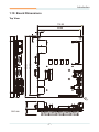
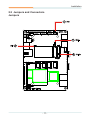
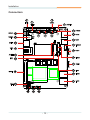
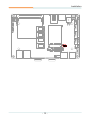
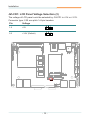
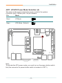
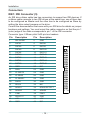
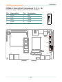
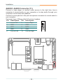
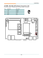
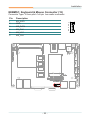
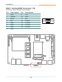
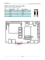
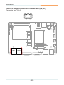
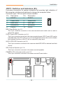
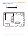
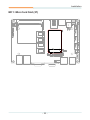
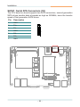
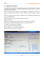
85
EPIC-745E
Wide Range Temperature
EPIC Compact Board
User’s Manual
Version 1.0
85
2011.03
This page is intentionally left blank.
Index
Contents
Chapter 1 - Introduction............................................. 1
1.1 Copyright Notice..........................................................2
1.2 About this User’s Manual............................................2
1.3 Warning........................................................................2
1.4 Replacing the Lithium Battery....................................3
1.5 Technical Support........................................................3
1.6 Warranty.......................................................................4
1.7 Packing List.................................................................5
1.8 Ordering Information...................................................5
1.9 Specifications..............................................................6
1.10 Board Dimensions.....................................................7
Chapter 2 - Installation............................................... 9
2.1 Block Diagram...........................................................10
2.2 Jumpers and Connectors.........................................11
Jumpers.............................................................................13
JRS1: COM2 RS-232/422/485 Mode Selection......13
JBAT1: Clear CMOS Setting...................................14
JVLCD1: LCD Panel Voltage Selection.................16
JAT1: AT/ATX Power Mode Selection....................17
Connectors........................................................................18
IDE1: IDE Connector...............................................18
COM2~5: Serial Port Connectors..........................21
AUDIO1: AUDIO Connector....................................22
JCOM1: RS-422/485 Output Connector................23
USB1~2: USB Connectors......................................24
EKBMS1: Keyboard & Mouse Connector.............25
VGA1: Analog RGB Connector..............................26
LVDS1: LVDS LCD Connector................................27
COM1: Serial Port Connector................................28
INV1: LCD Inverter Connector...............................29
LAN1~2: Gigabit Ethernet Connectors.................30
USB3~4: USB Connectors......................................31
-i-
Index
DIO1: Digital IO Connector.....................................32
JFRT1: Switched and Indicators...........................33
MINIPCI1: Mini PCI slot...........................................34
MC1: Mini-Card Slot................................................35
SATA1: Serial ATA Connectors..............................36
12VIN1: +12V Connector........................................37
SAPO1: Small 4P Power Connector......................38
2.3 The Installation Paths of CD Driver.........................39
Chapter 3 - BIOS....................................................... 41
3.1 BIOS Introduction......................................................42
3.2 Advanced Settings....................................................44
3.2.1 CPU Configuration.........................................45
3.2.2 IDE Configuration..........................................46
3.2.3 Super IO Configuration.................................48
3.2.4 Hardware Health Configuration...................49
3.2.5 USB Configuration.......................................50
3.3 Advanced Chipset Settings......................................51
3.3.1 North Bridge Chipset Configuration...........52
3.3.2 South Bridge Chipset Configuration...........54
3.3 Advanced PCI/PnP Settings.....................................56
3.4 Boot Settings.............................................................57
3.4.1 Boot Settings Configuration.........................58
3.5 Security......................................................................59
3.6 Exit Options...............................................................61
3.7 AMI BIOS Checkpoints..............................................63
3.7.1 Bootblock Initialization Code Checkpoints....
........................................................................63
3.7.2 Bootblock Recovery Code Checkpoints.....65
3.7.3 POST Code Checkpoints..............................67
3.7.4 DIM Code Checkpoints.................................71
3.7.5 ACPI Runtime Checkpoints..........................72
- ii -
Index
Appendix................................................................... 73
Appendix-A I/O Port Address Map..................................74
Appendix-B Interrupt Request Lines (IRQ)...................75
Appendix-C BIOS memory mapping..............................76
Appendix-D Watchdog Timer (WDT) Setting.................77
Appendix-E Digital I/O Setting........................................78
- iii -
Index
This page is intentionally left blank.
- iv -
Introduction
1
Chapter 1
Introduction
Chapter 1 - Introduction
-1-
Introduction
1.1 Copyright Notice
All Rights Reserved.
The information in this document is subject to change without prior notice in
order to improve the reliability, design and function. It does not represent a
commitment on the part of the manufacturer.
Under no circumstances will the manufacturer be liable for any direct, indirect,
special, incidental, or consequential damages arising from the use or inability
to use the product or documentation, even if advised of the possibility of such
damages.
This document contains proprietary information protected by copyright.
All rights are reserved. No part of this manual may be reproduced by any
mechanical, electronic, or other means in any form without prior written
permission of the manufacturer.
1.2 About this User’s Manual
This User’s Manual is intended for experienced users and integrators with
hardware knowledge of personal computers. If you are not sure about any
description in this User’s Manual, please consult your vendor before further
handling.
1.3 Warning
Single Board Computers and their components contain very delicate
Integrated Circuits (IC). To protect the Single Board Computer and its
components against damage from static electricity, you should always follow
the following precautions when handling it :
1.Disconnect your Single Board Computer from the power source when you
want to work on the inside.
2.Hold the board by the edges and try not to touch the IC chips, leads or
circuitry.
3.Use a grounded wrist strap when handling computer components.
4.Place components on a grounded antistatic pad or on the bag that came
with the Single Board Computer, whenever components are separated
from the system.
-2-
Introduction
1.4 Replacing the Lithium Battery
Incorrect replacement of the lithium battery may lead to a risk of explosion.
The lithium battery must be replaced with an identical battery or a battery type
recommended by the manufacturer.
Do not throw lithium batteries into the trash-can. It must be disposed of in
accordance with local regulations concerning special waste.
1.5 Technical Support
If you have any technical difficulties, please do not hesitate to call or e-mail
our customer service.
http://www.arbor.com.tw
E-mail:[email protected]
-3-
Introduction
1.6 Warranty
This product is warranted to be in good working order for a period of two years
from the date of purchase. Should this product fail to be in good working order
at any time during this period, we will, at our option, replace or repair it at no
additional charge except as set forth in the following terms. This warranty
does not apply to products damaged by misuse, modifications, accident or
disaster.
Vendor assumes no liability for any damages, lost profits, lost savings or any
other incidental or consequential damage resulting from the use, misuse of,
or inability to use this product. Vendor will not be liable for any claim made by
any other related party.
Vendors disclaim all other warranties, either expressed or implied, including
but not limited to implied warranties of merchantibility and fitness for a
particular purpose, with respect to the hardware, the accompanying product’s
manual(s) and written materials, and any accompanying hardware. This
limited warranty gives you specific legal rights.
Return authorization must be obtained from the vendor before returned
merchandise will be accepted. Authorization can be obtained by calling or
faxing the vendor and requesting a Return Merchandise Authorization (RMA)
number. Returned goods should always be accompanied by a clear problem
description.
-4-
Introduction
1.7 Packing List
Packing List
Before you begin installing your single board, please make sure that the following
materials have been shipped:
1 x EPIC-745E EPIC Compact Board with heat sink
1 x Power cable
1 x Driver CD
1 x Quick Installation Guide
If any of the above items is damaged or missing, contact your vendor immediately.
1.8 Ordering Information
EPIC-745E
Intel Atom™ N450 1.66GHz Wide range temperature
EPIC Compact Board
CBK-11-2902-00
Cable Kit
1 x Audio Cable
4 x COM Port Cables
1 x IDE Cable
1 x KB & MS Cable
2 x SATA Cables
2 x USB Cables
-5-
Introduction
1.9 Specifications
Form Factor
EPIC Compact Board
CPU
Intel® Atom™ N450 1.66GHz processor
Chipset
Intel® ICH8M
System Memory
Soldered onboard 1GB DDR2 SDRAM
VGA/ LCD
Controller
Integrated Intel® Graphics Media Accelerator 3150,
Analog RGB/ Single Channel 18-bit LVDS
Ethernet
2 x Realtek 8111C PCIe Gigabit Ethernet controllers
I/O Chips
Winbond W83627UHG
BIOS
AMI PnP Flash BIOS
Audio
Realtek ALC888 HD Audio CODEC,
MIC-in/ Line-In/ Line-Out
Storage
2 x Serial ATA ports with 300MB/s HDD transfer rate
1 x Ultra ATA, support 2 IDE devices
Soldered onboard 2GB NANDrive
Serial Port
5 x COM ports (COM1, COM3, COM4, COM5: RS-232,
COM2: RS-232/422/485 selectable)
KBMS
One 6-pin wafer connector (PS/2 interface Keyboard and
Mouse via cable)
Universal Serial Bus 8 x USB 2.0 ports
Digital I/O
8-bit programmable Digital Input/Output
Expansion Interface
1 x Mini-Card Socket
1 x Mini-PCI Socket
1 SIM Socket
Operation Temp.
-40oC ~ 85oC (-40oF ~ 185oF)
Watchdog Timer
1~255 levels Reset
Dimension (L x W)
165 x 115 mm (6.5” x 4.5” )
-6-
Introduction
1.10 Board Dimensions
Top View
114.98
109.98
5.08
5.08
159.88
164.98
Ø3
.2
18.4
16.6
Unit: mm
-7-
Introduction
This page is intentionally left blank.
-8-
Installation
2
Chapter 2
Installation
Chapter 2 - Installation
-9-
Installation
2.1 Block Diagram
Single Channel DDR2
Soldered on board
DDR2 1GB SDRAM
667MHz
Analog R.G.B.
Intel®
Atom
N450/ D510
1.6GHz
Single Channel 18-bit LVDS
DMIx4
USB
Audio
2 x SATA
Mini-PCI Socket
8 x USB ports
Audio
VGA
LVDS
DF13-30
COM1~ COM5
COM1 ~ COM5
USB I/F
HD
CODEC
ALC888
HD Link
LPC I/F
Super IO
W83627UHG
Serial ATA I/F
KB, MS
8-bit Digital I/O
Intel®
ICH8M
IDE ATA I/F
PCI Bus
KB/ MS
Digital I/O
IDE
NANDrive
Mini-Card Slot
PCIex1
PCIex
8111C GbE
controller
GbE
PCIex
8111C GbE
controller
GbE
SIM Socket
- 10 -
1 x RJ-45
1 x RJ-45
Installation
2.2 Jumpers and Connectors
Jumpers
1
IDE1
9
COM3
10
1
2
1
1
2
1
2
1
9
2
1
2
1
2
1
10
2
1
JRS1
1
JRS1
2
4
1
3
2
JBAT1
1
2
52
51
1
1
1
JAT1 4
17
15
3
1
1
2
16
18
30
29
1
1
1
124
123
AUDIO1
2
1
2
1
2
1
2
1
- 11 -
JVLCD1
Installation
Connectors
IDE1
5
10
6
IDE1
COM2
11 AUDIO1
EATX1
COM3
7
1
12VIN1 31
2
4
1
3
9
SAPO1 32
10
JRS1
1
2
1
COM4
8
1
2
1
2
1
9
COM3
2
1
2
1
2
1
10
2
1
12 JCOM1
COM5
9
13 USB2
14 USB1
1
SATA1 30
1
1
1
2
51
52
SIM1 29
15 EKBMS1
1
C3
17
C6
C2
16
29
15
18
C7
C5
16 VGA1
JBATT1 28
1
1
2
C1
1
17 LVDS1
MC1 27
1
18 COM1
19 INV1
MPCI1 26
20 LAN2
JFRT1 25
21 LAN1
124
123
AUDIO1
10
9
2
1
2
1
DIO1
24
2
1
2
1
USB3
23
USB4
22
- 12 -
Installation
Jumpers
JRS1: COM2 RS-232/422/485 Mode Selection (1)
The onboard COM2 port can be configured to operate in RS-232, RS-422
or RS-485 modes. RS-422 modes differ in the way RX/TX is being handled.
Jumper JRS1 switches between RS-232 or RS-422/485 mode.
Connector type: 2.00mm pitch 2x3-pin headers.
RS-232
(Default)
RS-422
RS-485
1-2
Short
Open
Open
3-4
Open
Short
Open
5-6
Open
Mode
Open
1
2
1
5
6
5
Short
2
1
2
6
5
6
123
1
2
1
2
1
124
2
1
1
1
2
3
4
2
1
1
2
1
1
2
1
9
10
2
1
2
1
2
1
2
16
52
18
1 2
1
1
15
51
17
30
2
1
1
2
1
1
29
1
9
10
1
1
- 13 -
Installation
JBAT1: Clear CMOS Setting (2)
If the board refuses to boot due to inappropriate CMOS settings here is how
to proceed to clear (reset) the CMOS to its default values.
Connector type: 2.00mm pitch 1x3-pin headers
Pin
Mode
1-2
Keep CMOS (Default)
2-3
Clear CMOS
3
2
1
3
2
1
You may need to clear the CMOS if your system cannot boot up because you
forgot your password, the CPU clock setup is incorrect, or the CMOS settings
need to be reset to default values after the system BIOS has been updated.
Refer to the following solutions to reset your CMOS setting:
Solution A:
1. Power off the system and disconnect the power cable.
2. Place a shunt to short pin 2 and pin 3 of JBAT1 for five seconds.
3. Place the shunt back to pin 1 and pin 2 of JBAT1.
4. Power on the system.
Solution B:
If the CPU Clock setup is incorrect, you may not be able to boot up. In this
case, follow these instructions:
1.Turn the system off, then on again. The CPU will automatically boot up
using standard parameters.
2.As the system boots, enter BIOS and set up the CPU clock.
Note:
If you are unable to enter BIOS setup, turn the system on and off a few
times.
- 14 -
Installation
123
1
2
1
2
1
124
2
1
1
1
2
3
4
2
1
1
2
1
1
2
1
9
10
2
1
2
1
2
1
2
16
52
18
1
51
17
30
2
1
15
2
1
1
1
2
1
1
29
1
9
10
1
1
- 15 -
Installation
JVLCD1: LCD Panel Voltage Selection (3)
The voltage of LCD panel could be selected by JVLCD1 in +5V or +3.3V.
Connector type: 2.00 mm pitch 1x3-pin headers
Pin
Voltage
1-2
+5V
2-3
+3.3V (Default)
3
2
1
3
2
1
123
1
2
1
2
1
124
2
1
1
1
2
3
4
2
1
1
2
1
1
2
1
9
10
2
1
2
1
2
1
2
16
52
18
2
1
1
1
51
17
30
2
1
15
1
2
1
1
29
1
9
1
- 16 -
10
1
Installation
JAT1: AT/ATX Power Mode Selection (4)
The power mode jumper selects the power mode for the system.
Connector type: 2.00mm pitch 1x2-pin headers.
Pin
Mode
Short
AT Mode
1
2
Open
ATX Mode (Default)
1
2
123
1
2
1
2
1
124
2
1
1
1
2
3
4
2
1
1
2
1
1
2
1
9
10
2
1
2
1
2
1
2
16
52
18
2
1
1
1
15
51
17
30
2
1
1
2
1
1
29
1
9
10
1
1
Note:
To activate the ATX power mode, you must turn on the power button switch
first (the connector for power button swtich is located in JFRT1).
- 17 -
Installation
Connectors
IDE1: IDE Connector (5)
An IDE drive ribbon cable has two connectors to support two IDE devices. If
a ribbon cable connects to two IDE drives at the same time, one of them has
to be configured as Master and the other has to be configured as Slave by
setting the drive select jumpers on the drive.
Consult the documentation that came with your IDE drive for details on jumper
locations and settings. You must orient the cable connector so that the pin 1
(color) edge of the cable corresponds to pin 1 of the IDE connector.
Connector type: 2.00mm pitch 2x22-pin box headers
Pin
Description
Pin
Description
1
IDE RESET
2
GND
3
DATA7
4
DATA8
5
DATA6
6
DATA9
7
DATA5
8
DATA10
9
DATA4
10
DATA11
11
DATA3
12
DATA12
13
DATA2
14
DATA13
15
DATA1
16
DATA14
17
DATA0
18
DATA15
19
GND
20
N/C
21
REQ
22
GND
23
IO WRITE
24
GND
25
IO READ
26
GND
27
IO READY
28
GND
29
DACK
30
GND
31
IRQ14
32
N/C
33
ADAD1
34
ATA66 DETECT
35
ADAD0
36
ADAD2
37
CS#1
38
CS#3
39
IDEACTP
40
GND
41
+5V
42
+5V
43
GND
44
N/C
- 18 -
1
2
43
44
Installation
123
1
2
1
2
1
1 2
124
1
1
2
3
4
2
1
1
2
1
1
2
1
10
9
2
1
43 44
2
1
2
1
2
16
52
18
2
1
1
1
15
51
17
30
2
1
1
2
1
1
29
1
9
10
1
1
- 19 -
Installation
EATX1: ATX Feature Connector (6)
Connector type: 2.54mm pitch 1x3-pin box wafer
connector
Pin
Description
1
PS-ON
2
GND
3
5V_SB
1
2
3
123
1
2
1
2
1
124
2
1
1
1
2
3
4
2
1
1
2
1
1
2
1
2
1
2
1
2
1
2
16
52
18
2
1
1
1
15
51
17
30
2
1
1
2
1
1
29
1
9
10
1
1
- 20 -
Installation
COM2~5: Serial Port Connectors (7, 8, 9, 10)
Connector type: 2.00mm pitch 2x5-pin box headers.
Pin
Description
Pin
Description
1
DCD#
2
RXD
3
TXD
4
DTR#
5
GND
6
DSR#
7
RTS#
8
CTS#
9
RI#
10
N/C
1 2
9 10
123
1
2
1
2
1
124
2
1
1
1
2
1
2
1
4
3
1 2
1
2
1
COM3
1 2
COM4
1 2
1 2
COM5
2
16
COM2
52
18
2
1
1
1
15
51
17
30
2
1
1
2
1
1
29
1
9
10
1
1
- 21 -
Installation
AUDIO1: AUDIO Connector (11)
Connect a tape player or another audio source to the light blue Line-in
connector to record audio on your computer or to play audio through your
computer’s sound chip and speakers.
Connect a micro-phone to the pink microphone connector to record audio to
your computer.
Connector type: 2.00mm pitch 2x5-pin box headers.
Pin Description
Pin Description
1
Line-in Left
2
Line-in Right
3
GND
4
GND
5
MIC1
6
MIC2
7
GND
8
GND
9
Line-out Left
10
Line-out Right
1 2
9 10
123
1
2
1
2
1
124
2
1
1
1
2
3
4
2
1
1
2
1
1
2
1
2
1
2
1
16
2
1
2
52
18
2
1
1
1
15
51
17
30
2
1
1 2
29
1
1
1
- 22 -
1
1
Installation
JCOM1: RS-422/ 485 Output Connector (12)
Connector type: 2.00mm pitch 1x4 box wafer connector
Pin
RS-422
RS-485
1
TX+
Data+
2
TX-
Data-
3
RX+
N/C
4
RX-
N/C
1
2
3
4
123
1
2
1
2
1
124
2
1
1
1
2
3
4
2
1
1
2
1
1
2
1
2
1
2
1
16
2
1
2
52
18
2
1
1
1
1
15
1
51
17
30
2
1
1 2
29
1
1
1
- 23 -
Installation
USB1~2: USB Connectors (13, 14)
The USB connector supports two USB 2.0 ports w/ 480Mb/s.
Connector type: double stack USB type A.
1 2 3 4
USB
1 2 3 4
USB
123
1
2
1
2
1
124
2
1
1
1
2
3
4
2
1
1
2
1
1
2
1
2
1
2
1
2
1
2
16
52
18
2
1
1
1
15
51
17
30
1
1
2
2
1
1
29
1
1
1
- 24 -
USB1
USB2
Installation
EKBMS1: Keyboard & Mouse Connector (15)
Connector Type: 2.0mm pitch 1x6-pin box wafer connector
Pin
Description
1
KB_DATA
2
GND
3
MS_DATA
4
KB_CLK
5
KB_VCC
6
MS_CLK
1
2
3
4
5
6
123
1
2
1
2
1
124
2
1
1
1
2
3
4
2
1
1
2
1
1
2
1
2
1
2
1
2
1
2
16
52
18
2
1
1
1
15
51
17
30
2
2
1
1
29
1
1
EKBMS1
1
- 25 -
1
1
Installation
VGA1: Analog RGB Connector (16)
Connector type: D-Sub 15-pin female.
Pin
Description
Pin
Description
1
RED
9
+5V
2
GREEN
10
GND
3
BLUE
11
N/C
4
N/C
12
D-DATA
5
GND
13
H-SYNC
6
GND
14
V-SYNC
7
GND
15
D-DCLK
8
GND
5
1
15
11
123
1
2
1
2
1
124
2
1
1
1
2
3
4
2
1
1
2
1
1
2
1
2
1
2
1
2
1
2
16
52
18
2
1
1
1
51
17
30
2
2
1
1
29
1
1
1
VGA1
- 26 -
1
15
1
Installation
LVDS1: LVDS LCD Connector (17)
The LVDS connector supports 18-bit single channel LVDS.
VDD could be selected by JVLCD1 in +5V or +3.3V.
Connector type: DF-13-30DP-1.25V
Pin
2
4
6
8
10
12
14
16
18
20
22
24
26
28
30
Description
VDD
N/C
N/C
GND
N/C
N/C
GND
N/C
N/C
GND
N/C
N/C
GND
N/C
N/C
Pin
1
3
5
7
9
11
13
15
17
19
21
23
25
27
29
Description
VDD
TX1CLK+
TX1CLKGND
TX1D0+
TX1D0GND
TX1D1+
TX1D1GND
TX1D2+
TX1D2GND
N/C
N/C
2
1
30
29
123
1
2
1
2
1
124
2
1
1
1
2
3
4
2
1
1
2
1
1
2
1
9
10
2
1
2
1
2
1
2
16
52
18
2
1
1
1
15
51
17
1
1
2
29
1
2
1
1
30
9
10
1
1
- 27 -
Installation
COM1: Serial Port Connector (18)
Connector type: D-Sub 9-pin male.
Description
Pin
Description
1
DCD#
6
DSR#
2
RXD
7
RTS#
3
TXD
8
CTS#
4
DTR#
9
RI#
5
GND
1
Pin
6
9
5
123
1
2
1
2
1
124
2
1
1
1
2
3
4
2
1
1
2
1
1
2
1
9
10
2
1
2
1
2
1
2
16
52
18
2
1
1
1
15
51
17
30
2
1
1
2
1
1
29
1
9
1
- 28 -
10
1
COM1
Installation
INV1: LCD Inverter Connector (19)
Connector type: 2.00mm pitch 1x5-pin box wafer connector.
Pin
Description
1
+12V
2
GND
3
Backlight on/off
4
Brightness control
5
GND
1
2
3
4
5
123
1
2
1
2
1
124
2
1
1
1
2
3
4
2
1
1
2
1
1
2
1
2
1
2
1
2
1
2
16
52
18
2
1
1
1
15
51
17
30
2
2
1
1
29
1
1
1
- 29 -
1
1
Installation
LAN1~2: Gigabit Ethernet Connectors (20, 21)
Connector type: RJ-45
123
1
2
1
2
1
124
2
1
1
1
2
3
4
2
1
1
2
1
1
2
1
2
1
2
1
2
1
2
16
52
18
2
1
1
1
15
51
17
30
2
2
1
1
29
1
1
LAN1
LAN2
1
- 30 -
1
1
Installation
USB3~4: USB Connectors (22, 23)
Connector type: 2.00 mm pitch 2x5-pin headers.
Pin
Description
Pin
Description
1
+5V
2
+5V
3
USBD-
4
USBD-
5
USBD+
6
USBD+
7
GND
8
GND
9
GND
10
N/C (Key)
1
2
9
10
123
1
2
1
2
1
124
2
1
1
1
4
2
1
2
1
3
USB3
1
1 2
1 2
USB4
2
1
2
1
2
1
2
16
52
18
2
1
1
1
15
51
17
30
2
2
1
1
29
1
1
1
- 31 -
1
1
Installation
DIO1: Digital I/O Connector (24)
DIO1 is a 8-bit DIO connector that supports 8-bit programmable digital input
and output.
Connector type: 2.00 mm pitch 2x5-pin headers.
Pin
Description
Pin
Description
1
DIO0
2
DIO1
3
DIO2
4
DIO3
5
DIO4
6
DIO5
7
DIO6
8
DIO7
9
+5V
10
GND
1
2
9
10
123
1
2
1
1 2
124
2
1
1
1
2
3
4
2
1
1
2
1
1
2
1
2
1
2
1
2
1
2
16
52
18
2
1
1
1
15
51
17
30
2
2
1
1
29
1
1
1
- 32 -
1
1
Installation
JFRT1: Switches and Indicators (25)
It provides connectors for system indicators that provides light indication of
the computer activities and switches to change the computer status.
Connector type: 2.00 mm pitch 2x5-pin headers
Pin
Description
Pin
Description
1
RESET+
2
RESET-
3
Power LED+
4
Power LED-
5
HDD LED+
6
HDD LED-
7
SPEAKER+
8
SPEAKER-
9
PSON+
10
PSON-
1
9
2
10
RES: Reset Button, pin 1-2.
This 2-pin connector connects to the case-mounted reset switch and is used to
reboot the system.
PLED: Power LED Connector, pin 3-4.
This 2-pin connector connects to the case-mounted power LED. Power LED can be
indicated when the CPU card is on or off. And keyboard lock can be used to disable
the keyboard function so the PC will not respond by any input.
HLED: HDD LED Connector, pin 5-6.
This 2-pin connector connects to the case-mounted HDD LED to indicate hard disk
activity.
SPK: External Speaker, pin 7-8.
This 2-pin connector connects to the case-mounted speaker.
PWRBTN: ATX soft power switch, pin 9-10.
This 2-pin connector connects to the case-mounted Power button.
123
1
2
1
1 2
124
2
1
1
1
2
3
4
2
1
1
2
1
1
2
1
2
1
2
1
2
1
2
16
52
18
2
1
1
1
1
15
51
17
30
2
1
- 33 -
2
1
1
29
1
1
Installation
MINIPCI1: Mini PCI slot (26)
123
1
2
1
2
1
124
2
1
1
1
2
3
4
2
1
1
2
1
1
2
1
2
1
2
1
2
1
2
16
52
18
2
1
1
1
15
51
17
30
2
2
1
1
29
1
1
1
- 34 -
1
1
Installation
MC1: Mini-Card Slot (27)
123
1
2
1
2
1
124
2
1
1
1
2
3
4
2
1
1
2
1
1
2
1
2
1
2
1
2
1
2
16
52
18
2
1
1
1
15
51
17
30
2
2
1
1
29
1
1
1
- 35 -
1
1
Installation
SATA1: Serial ATA Connectors (30)
The CPU board on board supports two SATA connectors, second generation
SATA drives transfer data at speeds as high as 300MB/s, twice the transfer
speed of first generation SATA drives.
Pin
Description
1
GND
2
TX+
3
TX-
4
GND
5
RX-
6
RX+
7
GND
1
7
123
1
2
1
2
1
SATA1
124
2
1
1
1
2
3
4
2
1
1
2
1
1
2
1
2
1
2
1
2
1
2
16
52
18
2
1
1
1
15
51
17
30
2
2
1
1
29
1
1
1
- 36 -
1
1
Installation
12VIN1: +12V Connector (31)
PWR1 supplies the CPU operation at +12V (Vcore).
Pin
Description
Pin
Description
2
GND
4
+12V
1
GND
3
2
4
1
3
+12V
123
1
2
1
2
1
124
2
1
1
1
2
1
1
2
3
4
2
1
1
2
1
2
1
2
1
2
1
2
16
52
18
2
1
1
1
15
51
17
30
2
2
1
1
29
1
1
1
- 37 -
1
1
Installation
SAPO1: Small 4P Power Connector (32)
Connector type: 2.54mm pitch 1x4-pin
wafer one wall 90D connector
Pin
Description
1
+5V
2
GND
3
GND
4
+12V
1
SAPO1
123
1
2
1
2
1
124
2
1
1
1
2
3
4
2
1
1
2
1
1
2
1
2
1
2
1
2
1
2
16
52
18
2
1
1
1
15
51
17
30
2
2
1
1
29
1
1
1
- 38 -
1
1
Installation
2.3 The Installation Paths of CD Driver
Windows 2000 & XP
Driver
Path
CHIPSET
\CHIPSET\INF 9.11
VGA
\GRAPHICS\INTEL_2K_XP_32\5182
AUDIO
\AUDIO\REALTEK_HD\WIN2K_XP_x86x64_R252
LAN
\ETHERNET\REALTEK\8111_WINXP_5764
Windows 7
Driver
Path
CHIPSET
\CHIPSET\INF 9.11
VGA
\GRAPHICS\INTEL_WIN7_32\2230
\GRAPHICS\INTEL_WIN7_64\2214
AUDIO
\AUDIO\REALTEK_HD\Win7_R257
LAN
\ETHERNET\REALTEK\8110SCL_Win7_7037
- 39 -
Installation
This page is intentionally left blank.
- 40 -
BIOS
3
Chapter 3
BIOS
Chapter 3 - BIOS
- 41 -
BIOS
3.1 BIOS Introduction
The AMI BIOS provides a Setup utility program for specifying the system
configurations and settings. The BIOS ROM of the system stores the Setup
utility and configurations.
When you turn on the computer, the AMI BIOS is immediately activated. To
enter the BIOS SETUP UTILILTY, press “Delete” once the power is turned
on.
When the computer is shut down, the battery on the motherboard supplies the
power for BIOS RAM.
The Main Setup screen lists the following information
System Overview
BIOS Version: displays the current version information of the BIOS
Build Date: the date that the BIOS version was made/updated
Processor (auto-detected if installed)
Speed: displays the processor speed
System Memory (auto-detected if installed)
Size: lists the memory size information
- 42 -
BIOS
Key Commands
BIOS Setup Utility is mainly a key-based navigation interface. Please refer to
the following key command instructions for navigation process.
“←”“→”
Move to highlight a particular configuration screen from
the top menu bar / Move to highlight items on the screen
“↓” “↑”
Move to highlight previous/next item
Enter
Select and access a setup item/field
Esc
On the Main Menu – Quit the setup and not save changes
into CMOS (a message screen will display and ask you to
select “OK” or “Cancel” for exiting and discarding changes.
Use “←” and “→” to select and press “Enter” to confirm)
On the Sub Menu – Exit current page and return to main
menu
Page Up / +
Increase the numeric value on a selected setup item /
make change
Page Down -
Decrease the numeric value on a selected setup item /
make change
F1
Activate “General Help” screen
F10
Save the changes that have been made in the setup and
exit. (a message screen will display and ask you to select
“OK” or “Cancel” for exiting and saving changes. Use “←”
and “→” to select and press “Enter” to confirm)
System Time
Set the system time.
The time format is:
Hour : 00 to 23
Minute : 00 to 59
Second : 00 to 59
System Date
Set the system date. Note that the ‘Day’ automatically changes when you set
the date.
The date format is:
Day : Sun to Sat
Month : 1 to 12
Date : 1 to 31
Year : 1999 to 2099
- 43 -
BIOS
3.2 Advanced Settings
The “Advanced” screen provides the setting options to configure CPU, IDE,
Super IO and other peripherals. You can use “←” and “→” keys to select
“Advanced” and use the “↓” and “↑” to select a setup item.
Note: please pay attention to the “WARNING” part at the left frame before you
decide to configure any setting of an item.
- 44 -
BIOS
3.2.1 CPU Configuration
Press “Enter” on “CPU Configuration” and you will be able to configure the
CPU on the “Configure advanced CPU settings” screen.
CPU Details
Manufacturer: shows the name of the CPU manufacturer
Frequency: indicates the processor speed
FSB Speed: the data flow speed of FSB (Front Side Bus)
Cache L1: shows the Cache L1 size for the CPU
Cache L2: shows the Cache L2 size for the CPU
Ratio Actual Value: actual value of clock ratio for the CPU
Hyper-Threading Technology
Enabled: activates the Hyper-Threading Technology for higher CPU threading
speed. (Recommended)
Disabled: Disactivates the Hyper-Threading Technology.
Intel® SpeedStep™ Tech
Enabled: Enable GV3.
Disabled: Disable GV3.
- 45 -
BIOS
3.2.2 IDE Configuration
Select the “IDE Configuration to configure the IDE settings. When an item
is selected, there is a status description appearing at the right. You can use
“Page Up/+” and “Page Down/-” keys to change the value of a selected item.
ATA/IDE Configuration
Configures the options of ATA/IDE controllers connected to the board
Disabled: disables the ATA/IDE controllers connected to the board
Compatible: sets the ATA/IDE controllers to be compatible
Enhanced: sets the ATA/IDE controllers to be in enhanced mode
Configure SATA as
Configure SATA as IDE or AHCI.
- 46 -
BIOS
Primary, Secondary/ Third IDE Master/Slave
The BIOS Setup displays all the available, connected IDE devices as well
as the IDE status. You may enter a specific IDE device to do particular
configurations. Press “Enter” to access the submenu of an IDE device on the
list.
Hard Disk Write Protect
Disable/ Enable device write protection. This will be effective only if device is
accessed through BIOS.
IDE Detect Time Out (Sec)
Select the time out value for detecting ATA/ATAPI device(s).
The choice:
0
5
10
15
20
25
30
35
ATA(PI) 80pin Cable Detection
Select the mechanism for detecting 80-pin ATA(PI) cable.
The choice:
Host & Device
Host
Device
- 47 -
BIOS
3.2.3 Super IO Configuration
Use “Super IO Configuration to specify address and modes for Serial Port.
Serial Port1 ~ Port5 Address
Select an address and corresponding interrupt for the first and second serial
ports.
Port Address choice:
3F8
2F8
3E8
2E8
3E0
2E0
Disabled
IRQ choice:
3
4
10
11
- 48 -
BIOS
3.2.4 Hardware Health Configuration
The “Hardware Health Configuration” lists out the temperature and voltage
information that is being monitored. The default for “H/W Health Function” is
“Enabled.
System/ CPU Temperature
Show you the current System / CPU fan temperature.
Vcore
Show you the voltage level of CPU (Vcore).
5V / DDR2 Vcc/ 1.05V/ +3.3Vin
Show you the voltage level of the 5V, DDR2 Vcc, 1.05V, and +3.3Vin.
- 49 -
BIOS
3.2.5 USB Configuration
Legacy USB Support
Enables support for legacy USB. AUTO option disables legacy support if no
USB devices are connected.
USB 2.0 Controller Mode
Configures the USB 2.0 controller in High Speed (480Mbps) or Full Speed
(12Mbps).
BIOS EHCI Hand-Off
Enabled: enables the EHCI Hand-Off function by BIOS
Disabled: disables the EHCI Hand-Off function by BIOS
Note: this setting potion allows you to enable EHCI Hand Off if your computer
operating system does not support it.
EHCI is the abbreviation for Enhanced Host Controller Interface which is
necessary for high speed USB operation.
- 50 -
BIOS
3.3 Advanced Chipset Settings
Select “Chipset” to access to “North Bridge Configuration” and “South Bridge
Configuration”. You can enter the sub menu of the two configuration options.
- 51 -
BIOS
3.3.1 North Bridge Chipset Configuration
Initate Graphic Adapter
Select which graphics controller to use as the primary boot device.
The Choice: IGD, PCI/IGD
Internal Graphic Mode Select
Select the amount of system memory used by the Internal graphics device.
The Choice: Enabled, 8MB
DVMT Mode
The Choice: FIXED mode, DVMT (Default).
DVMT/FIXED Memory Size
Setting: 128MB, 256MB (Default), Maximum DVMT.
Boot Display Device
Boot setting for the display device connected to the computer, such as “CRT”
monitor.
The Choice: CRT, LVDS, CRT + LVDS
- 52 -
BIOS
Flat Panel Type
Select the Flat Panel Type.
The choice:
640x480
800x600
1024x768
1280x768
1280x800
- 53 -
BIOS
3.3.2 South Bridge Chipset Configuration
Normally, the south bridge controls the basic I/O functions, such as USB and
audio. This screen allows you to access to the configurations of the I/Os.
USB Funtion
This item allows you to active USB ports.
The Choice:
Disabled
2 USB Ports
4 USB Ports
6 USB Ports
8 USB Ports
10 USB Ports
- 54 -
BIOS
USB 2.0 Controller
Select “Enabled” if your system contains a Universal Serial Bus 2.0 (USB 2.0)
controller and you have USB peripherals.
The Choice: Enabled, Disabled.
HDA Controller
This item allows you to select the chipset family to support HD Audio
Controller.
The Choice: Enabled, Disabled.
- 55 -
BIOS
3.3 Advanced PCI/PnP Settings
Allocate IRQ to PCI VGA
Yes: Assigns IRQ to PCI VGA card if card requests IRQ.
No: Does not assign IRQ to PCI VGA card even if card requests an IRQ.
DMA Channel 0 - DMA Channel 7
Available: Specified DMA is available to be used by PCI/PnP devices.
Reserved: Specified DMA is reserved for use by Legacy ISA devices.
- 56 -
BIOS
3.4 Boot Settings
Boot Setting Configuration
Press Enter the sub menu for boot setting.
Boot Device Priority
Access to the sub menu for boot device priority.
Hard Disk Drives
Configure the boot settings for the Hard Disk Drives connected to the
system.
- 57 -
BIOS
3.4.1 Boot Settings Configuration
Quiet Boot
Displays normal POST messages when it’s selected as “Disabled”.
When it is set as “Enabled”, OEM messages will be displayed instead of POST
messages. The default is “Disabled”.
Bootup Num-Lock
Modifies Number Lock setting when the system boots up. Select “On” to
automatically enable the Number Lock on keyboard when the system is
booting up.
- 58 -
BIOS
3.5 Security
Supervisor Password & User Password
You can set either supervisor or user password, or both of them.
The differences between are:
Set Supervisor Password: Can enter and change the options of the
setup menus.
ENTER PASSWORD:
Type the password, up to eight characters in length, and press <Enter>.
The password typed now will clear any previously entered password from
CMOS memory. You will be asked to confirm the password. Type the password
again and press <Enter>. You may also press <ESC> to abort the selection
and not enter a password.
- 59 -
BIOS
To disable a password, just press <Enter> when you are prompted to
enter the password. A message will confirm the password will be disabled.
Once the password is disabled, the system will boot and you can enter Setup
freely.
PASSWORD DISABLED.
When a password has been enabled, you will be prompted to enter it
every time you try to enter Setup. This prevents an unauthorized person from
changing any part of your system configuration.
Additionally, when a password is enabled, you can also require the BIOS
to request a password every time your system is rebooted. This would prevent
unauthorized use of your computer.
You determine when the password is required within the BIOS Features
Setup Menu and its Security option. If the Security option is set to “System”,
the password will be required both at boot and at entry to Setup. If set to
“Setup”, prompting only occurs when trying to enter Setup.
- 60 -
BIOS
3.6 Exit Options
Save Changes and Exit
Pressing <Enter> on this item asks for confirmation:
Save configuration changes and exit setup?
Pressing <OK> stores the selection made in the menus in CMOS - a special
section of memory that stays on after you turn your system off. The next
time you boot your computer, the BIOS configures your system according to
the Setup selections stored in CMOS. After saving the values the system is
restarted again.
- 61 -
BIOS
Discard Changes and Exit
Exit system setup without saving any changes.
You can also press <ESC> to activate this function.
Load Optimal Defaults
When you press <Enter> on this option, a message dialog box will appear
asking for your confirmation:
Load Optimal Defaults?
[OK] [Cancel]
Press [OK] to load the BIOS Optimal Default values for all the setup options.
You can also press <F9> key to enable this operation.
- 62 -
BIOS
3.7 AMI BIOS Checkpoints
3.7.1 Bootblock Initialization Code Checkpoints
The Bootblock initialization code sets up the chipset, memory and other
components before system memory is available. The following table describes
the type of checkpoints that may occur during the bootblock initialization
portion of the BIOS (Note):
Checkpoint
Description
Before D0
If boot block debugger is enabled, CPU cache-as-RAM
functionality is enabled at this point. Stack will be enabled
from this point.
D0
Early Boot Strap Processo (BSP) initialization like microcode
update, frequency and other CPU cirtical initialization. Early
chipset initialization is done.
D1
Early super I/O initialization is done including RTC and
keyboard controller. Serial port is enabled at this point if
needed for debugging. NMI is deisabled. Perfrom keyboard
controller BAT test. Save power-on CPUID value in scretch
CMOS. Go to flat mode with 4GB limit and GA20 enabled.
D2
Verify the boot block checksum. System will hang here if
checksum is bad.
D3
Disable CACHE before memory detection. Execute full
memory sizing module. If memory sizing module not
executed, start memory refresh and do memory sizing in
Boot block code. Do additional chipset initialization. Reenabled CACHE. Verify that flat mode is enabled.
D4
Test base 512KB memory. Adjust policies and cache first
8MB. Set stack.
D5
Bootblock code is copied from ROM to lower system memory
and control is given to it. BIOS now executes out of RAM.
Copies compressed boot block code to memory in right
segments. Copies BIOS from ROM to RAM for faster access.
Perfroms main BIOS checksum and updates recovery status
accordingly.
- 63 -
BIOS
D6
Both key sequence and OEM specific method is checked
to determine if BIOS recovery is forced. If BIOS recovery is
necessary, control flows tocheckpoint E0. Seed Bootblock
Recovery Code Checkpoints section of document for more
information.
D7
Restore CPUID value back into register. The BootblockRuntime interface module is moved to system memory and
control is given to it. Determine whether in memory.
D8
The Tuntime module is uncompressed into memory. CPUID
information is stored in memory.
D9
Store the Uncompressed pointer for future use in PMM.
Copying Main BIOS into memory. Leaves all RAM below
1MB Read-Write including E000 and F000 shadow areas
but closing SMRAM.
DA
Restore CPUID value back into register. Give control to BIOS
POS (ExecutePOSTKernel). See POST Code Checkpoints
section of document for more information.
DC
System is saking from ACPI S3 state.
E1 - E8
EC - EE
OEM memory detection / configuration error. This range is
reserved for chipset vendors & system manufacturers. The
error associated with this value may be different from one
platform to be next.
- 64 -
BIOS
3.7.2 Bootblock Recovery Code Checkpoints
The Bootblock recovery code gets control when the BIOS determines that
a BIOS recovery needs to occur because the user has forced the update
or the BIOS checksum is corrupt. The following table describes the type of
checkpoints that may occur during the Bootblock recovery portion of the BIOS
(Note)
:
Checkpoint
Description
E0
Initialize the floppy controller in the super I/O. Some interrupt
vectors are initialized. DMA controller is initialized. 8259
interrupt controller is initialized. L2 cache is enabled.
E9
Set up floppy controller and data. Attempt to red from floppy.
EA
Enable ATAPI hardware. Attempt to read from ARMD and ATAPI
CDROM.
EB
Disable ATAPI hardware. Jump back to checkpoint E9.
EF
Read error occurred on media. Jump back to checkpoint EB.
F0
Search for pre-defined recovery file name in root directory.
F1
Recovery file not found.
F2
Start reading FAT table and analyze FAT to find the clusters
occupied by the recovery file.
F3
Start reading the recovery file cluster by cluster.
F5
Disable L1 cache.
FA
Check the validity of the recovery file configuration to the current
configuration of the flash part.
FB
Make flash write enabled through chipset and OEM specific
method. Detect proper flash part. Verify that the found flash
part size equals the recovery file size.
F4
The recovery file size does not equal the found flash part size.
- 65 -
BIOS
FC
Erase the flash part.
FD
Program the flash part.
FF
The flash has been updated successfully. Make flash write
disabled. Disable ATAPI hardware. Restore CPUID value back
into register. Give control to F000 ROM at F000:FFF0h.
- 66 -
BIOS
3.7.3 POST Code Checkpoints
The POST code checkpoints are the largest set of checkpoints during the
BIOS pre-boot process. The following table describes the type of checkpoints
that may occur during the POST portion of the BIOS (Note):
Checkpoint
Description
03
Disable NMI, Parity, video for EGA, and DMA controllers.
Initialize BIOS, POST, Runtime data area. Also initialize BIOS
modules on POST entry and GPNV area. Initialized CMOS as
mentioned in the Kernel Variable "wCMOSFlags."
Check CMOS diagnostic byte to determine if battery power
is OK and CMOS checksum is OK. Verify CMOS checksum
manually by reading storage area.
04
If the CMOS checksum is bad, update CMOS with power-on
default values and clear passwords. Initialize status register A.
Initializes data variables that are based on CMOS setup
questions.
Initializes both the 8259 compatible PICs in the system.
05
06
Initializes the interrupt controlling hardware (generally PIC) and
interrupt vector table.
Do R/W test to CH-2 count reg. Initialize CH-0 as system timer.
Install the POSTINT1Ch handler. Enable IRQ-0 in PIC for
system timer interrupt.
Traps INT1Ch vector to "POSTINT1ChHandlerBlock."
07
Fixes CPU POST interface calling pointer.
08
Initializes the CPU. The BAT test is being done on KBC.
Program the keyboard controller command byte is being done
after Auto detection of KB/MS using AMI KB-5.
C0
Early CPU Init Start -- Disable Cache - Init Local APIC
C1
Set up boot strap processor Information
C2
Set up boot strap processor for POST
C5
Enumerate and set up application processors
C6
Re-enable cache for boot strap processor
- 67 -
BIOS
C7
Early CPU Init Exit
0A
Initializes the 8042 compatible Key Board Controller.
0B
Detects the presence of PS/2 mouse.
0C
Detects the presence of Keyboard in KBC port.
0E
Testing and initialization of different Input Devices. Also, update
the Kernel Variables.
Traps the INT09h vector, so that the POST INT09h handler
gets control for IRQ1. Uncompress all available language,
BIOS logo, and Silent logo modules.
13
Early POST initialization of chipset registers.
20
Relocate System Management Interrupt vector for all CPU in
the system.
24
Uncompress and initialize any platform specific BIOS modules.
GPNV is initialized at this checkpoint.
2A
Initializes different devices through DIM.
See DIM Code Checkpoints section of document for more
information.
2C
Initializes different devices. Detects and initializes the video
adapter installed in the system that have optional ROMs.
2E
Initializes all the output devices.
31
Allocate memory for ADM module and uncompress it. Give
control to ADM module for initialization. Initialize language and
font modules for ADM.
Activate ADM module.
33
Initializes the silent boot module. Set the window for displaying
text information.
37
Displaying sign-on message, CPU information, setup key
message, and any OEM specific information.
38
Initializes different devices through DIM. See DIM Code
Checkpoints section of document for more information. USB
controllers are initialized at this point.
- 68 -
BIOS
39
Initializes DMAC-1 & DMAC-2.
3A
Initialize RTC date/time.
3B
Test for total memory installed in the system. Also, Check for
DEL keys to limit memory test. Display total memory in the
system.
3C
Mid POST initialization of chipset registers.
40
Detect different devices (Parallel ports, serial ports, and
coprocessor in CPU, … etc.) successfully installed in the
system and update the BDA, EBDA…etc.
52
Updates CMOS memory size from memory found in memory
test. Allocates memory for Extended BIOS Data Area from
base memory. Programming the memory hole or any kind of
implementation that needs an adjustment in system RAM size
if needed.
60
Initializes NUM-LOCK status and programs the KBD typematic
rate.
75
Initialize Int-13 and prepare for IPL detection.
78
Initializes IPL devices controlled by BIOS and option ROMs.
7C
Generate and write contents of ESCD in NVRam.
84
Log errors encountered during POST.
85
Display errors to theuser and gets the user response for error.
87
Execute BIOS setup if needed / requested. Check boot
password if installed.
8C
Late POST initialization of chipset registers.
8D
Build ACPI tables (if ACPI is supported)
8E
Program the peripheral parameters. Enable/Disalbe NMI as
selected.
90
Initialization of system management interrupt by invoking all
handlers.
A1
Lian-up work needed before booting to OS.
A2
Takes care of runtime image preparation for different BIOS
modules. Fill the free area in F000h segment with 0FFh.
Initializes the Microsoft IRQ Routing Table. Prepares the
runtime language module. Disables the system configuration
display if needed.
- 69 -
BIOS
A4
Initialize runtime language module. Display boot option popup
menu.
A7
Displays the system configuration screen if enabled. Initialize
the CPU’s before boot, which includes the programming of the
MTRR’s.
A9
Wait for userinput at config display if needed.
AA
Uninstall POST INT1Ch vector and INT09h vector.
AB
Prepare BBS for Int 19 boot. Init MP tables.
AC
End of POST initialization of chipset registers. De-initializes the
ADM module.
B1
Save system context for ACPI. Prepare CPU for OS boot
including final MTRR values.
00
Passes control to OS Loader (typically INT19h).
- 70 -
BIOS
3.7.4 DIM Code Checkpoints
The Device Initialization Manager (DIM) gets control at various times during
BIOS POST to initialize different system buses. The following table describes
the main checkpoints where the DIM module is accessed (Note):
Checkpoint
Description
2A
Initialize different buses and perform the following functions:
Reset, Detect, and Disable (function 0); Static Device
Initialization (function); Boot Output Device Initialization
(function 2). Function 0 disables all device nodes, PCI devices,
and PnP ISA cards. It also assigns PCI bus numbers. Function
1 initializes all static devices that include manual configured
onboard peripherals, memory and I/O decode windows in PCIPCI bridges, and noncompliant PCI devices. Static resources
are also reserved. Function 2 searches for and initializes any
PnP, PCI, or AGP video devices.
38
Initialize different buses and perform the following functions:
Boot Input Device Initialization (function 3); IPL Device
Initialization (function 4); General Device Initialization (function
5). Function 3 searches for and configures PCI input devices
and detects if system has standard keyboard controller.
Function 4 searches for and configures all PnP and PCI boot
devices. Function 5 configures all onboard peripherals that are
set to an automatic configuration and configures all remaining
PnP and PCI devices.
While control is in the different functions, additional checkpoints are output to
port 80h as a word value to identify the routines under execution. The low byte
value indicates the main POST Code Checkpoint. The high byte is divided
into two nibbles and contains two fields. The details of the high byte of these
checkpoints are as follows:
HIGH BYTE XY
The upper nibble “X” indicates the function number that is being executed.
“X” can be from 0 to 7.
0 = func#0, disable all devices on the BUS concerned.
2 = func#2, output device initialization on the BUS concerned.
- 71 -
BIOS
3 = func#3, input device initialization on the BUS concerned.
4 = func#4, IPL device initialization on the BUS concerned.
5 = func#5, general device initialization on the BUS concerned.
6 = func#6, error reporting for the BUS concerned.
7 = func#7, add-on ROM initialization for all BUSes.
8 = func#8, BBS ROM initialization for all BUSes.
The lower nibble 'Y' indicates the BUS on which the different routines are
being executed. 'Y' can be from 0 to 5.
0 = Generic DIM (Device Initialization Manager).
1 = On-board System devices.
2 = ISA devices.
3 = EISA devices.
4 = ISA PnP devices.
5 = PCI devices.
3.7.5 ACPI Runtime Checkpoints
ACPI checkpoints are displayed when an ACPI capable operating system
either enters or leaves a sleep state. The following table describes the type of
checkpoints that may occur during ACPI sleep or wake events (Note):
Checkpoint
Description
AC
First ASL check point. Indicates the system is running in
ACPI mode.
AA
System is running in APIC mode.
01, 02, 03, 04, 05 Entering sleep state S1, S2, S3, S4, or S5.
10, 20, 30, 40, 50 Waking from sleep state S1, S2, S3, S4, or S5.
Note:
Please note that checkpoints may differ between different platforms based on
system configuration. Checkpoints may change due to vendor requirements,
system chipset or option ROMs from add-in PCI devices.
- 72 -
Appendix
Appendix
Appendix
- 73 -
Appendix
Appendix-A I/O Port Address Map
Each peripheral device in the system is assigned a set of I/O port addresses
which also becomes the identity of the device.
The following table lists the I/O port addresses used.
Address
Device Description
00000000 - 0000000F
DMA Controller
00000080 - 0000009F
DMA Controller
000000C0 - 000000DF
DMA Controller
00000020 - 00000021
Programmable Interrupt Controller
000000A0 - 000000A1
Programmable Interrupt Controller
00000040 - 00000043
System Timer
00000044 - 00000047
System Timer
00000060 - 00000064
Keyboard Controller
00000070 - 00000073
System CMOS/Real Time Clock
000000F0 - 000000FF
Math Co-processor
000001F0 - 000001F7
Primary IDE
00000274 - 00000277
ISAPNP Read Data Port
00000279, 00000A79
ISAPNP Configuration
000002F8 - 000002FF
Communications Port (COM2, If use)
00000378 - 0000037A
Parallel Port (If use)
000003B0 - 000003BF
MDA/MGA
000003C0 - 000003CF
EGA/VGA
000003D4 - 000003D9
CGA Analog RGB register
000003F0 - 000003F7
Floppy Diskette
000003F6 - 000003F6
Primary IDE
000003F8 - 000003FF
Communications Port (COM1, If use)
00000400 - 0000041F
South Bridge SMB
000004D0 - 000004D1
IRQ Edge/Level Control Ports
00000500 - 0000053F
South Btidge GPIO
00000800 - 0000087F
ACPI
00000A00 - 00000A07
PME
- 74 -
Appendix
00000A10 - 00000A17
Hardware Monitor
00000CF8
PCI Configuration Address
00000CFC
PCI Configuration Data
Appendix-B Interrupt Request Lines (IRQ)
Peripheral devices use interrupt request lines to notify CPU for the service
required. The following table shows the IRQ used by the devices on board.
Level
Function
IRQ 0
System Timer
IRQ 1
Keyboard Controller
IRQ 2
VGA and Link to Secondary PIC
IRQ 3
Communications Port (COM2)
IRQ 4
Communications Port (COM1)
IRQ 5
PCI Device
IRQ 6
Standard Floppy Disk Controller
IRQ 7
Parallel Port
IRQ 8
System CMOS/real time clock
IRQ 9
Microsoft ACPI-Compliant System
IRQ 10
PCI Device
IRQ 11
PCI Device
IRQ 12
PS/2 Compatible Mouse
IRQ 13
FPU Exception
IRQ 14
IDE Controller
IRQ 15
PCI Device
- 75 -
Appendix
Appendix-C BIOS memory mapping
Address
Device Description
00000h - 9FFFFh
DOS Kernel Area
A0000h, BFFFFh
EGA and VGA Video Buffer (128KB)
C00000h - CFFFFh
EGA/VGA ROM
D0000h - DFFFFh
Adaptor ROM
E00000h - FFFFFh
System BIOS
- 76 -
Appendix
Appendix-D Watchdog Timer (WDT) Setting
WDT is widely used for industry application to monitoring the activity
of CPU. Application software depends on its requirement to trigger WDT with
adequate timer setting. Before WDT time out, the functional normal system
will reload the WDT. The WDT never time out for a normal system. Then, WDT
will time out and reset the system automatically to avoid abnormal operation.
This board supports 255 levels watchdog timer by software
programming. Below are the source codes written in C language, please take
them for WDT application examples.
C Language Code
/*----- Include Header Area -----*/
#include "math.h"
#include "stdio.h"
#include "dos.h"
/*-----
routing, sub-routing -----*/
void main()
{
}
outportb(0x2e, 0x87);
outportb(0x2e, 0x87);
/* initial IO port twice */
outportb(0x2e, 0x2B);
outportb(0x2e+1, 0x00);
/* select CR2B */
/* update CR2B bit4 to 00h */
/* Set PIN89 as WDTO */
outportb(0x2e, 0x07);
outportb(0x2e+1, 0x08);
outportb(0x2e, 0x30);
outportb(0x2e+1, 0x01);
outportb(0x2e, 0xf0);
outportb(0x2e+1, 0x00);
outportb(0x2e, 0xf5);
outportb(0x2e+1, 0x00);
outportb(0x2e, 0xF6);
outportb(0x2e+1, 0x05);
/* point to logical device selector */
/* select logical device 8 */
/* select CR30 */
/* update CR30 to 01h */
/* select CRF0 */
/* update CRF0 to 00h */
/* select CRF5 to set timer unit */
/* update CRF5 bit2, 0:sec; 1:Min. */
/* select CRF6 */
/* update CRF6 to 05h (5 sec) */
outportb(0x2e, 0xAA);
/* stop program W83627, Exit */
- 77 -
Appendix
Appendix-E Digital I/O Setting
Below are the source codes written in C language, please take them
for Digital I/O application examples.
C Language Code
/*----- Include Header Area -----*/
#include “math.h”
#include “stdio.h”
#include “dos.h”
/*----- routing, sub-routing -----*/
void main()
{
outportb(0x2e, 0x87); outportb(0x2e, 0x87);
/* initial IO port twice */
outportb(0x2e, 0x07); outportb(0x2e+1, 0x08);
/* point to logical device */
/* select logical device 8 */
outportb(0x2e, 0x30); outportb(0x2e+1, 0x02);
/* select CR30 */
/* set bit1=1, GPIO port 5 active */
outportb(0x2e, 0xE0); outportb(0x2e+1, 0x00);
/* select CRE0, GPIO5 I/O Register */
/* bit7~bit0 0:output 1:input */
outportb(0x2e, 0xE1); outportb(0x2e+1, 0xff); /* select CRE1, GPIO5 Data Register */
/* set all GPIO pin output 1 */
outportb(0x2e, 0xE1); outportb(0x2e+1, 0x00);
/* select CRF1, Data Register */
/* set all GPIO pin output 0 */
outportb(0x2e, 0xAA); /* stop program W83627, Exit */
}
- 78 -