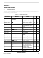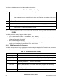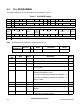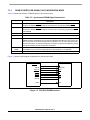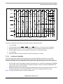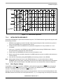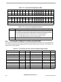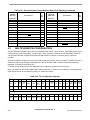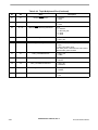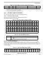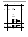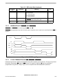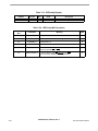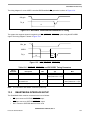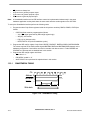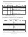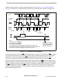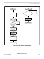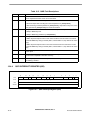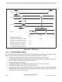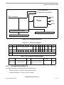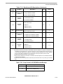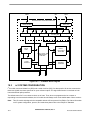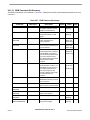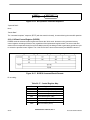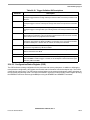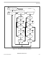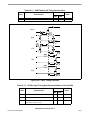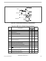
1
SCF5250 User’s Manual
Document Number: SCF5250UM
Rev. 4
03/2005
How to Reach Us:
Home Page:
www.freescale.com
E-mail:
[email protected]
USA/Europe or Locations Not Listed:
Freescale Semiconductor
Technical Information Center, CH370
1300 N. Alma School Road
Chandler, Arizona 85224
+1-800-521-6274 or +1-480-768-2130
[email protected]
Europe, Middle East, and Africa:
Freescale Halbleiter Deutschland GmbH
Technical Information Center
Schatzbogen 7
81829 Muenchen, Germany
+44 1296 380 456 (English)
+46 8 52200080 (English)
+49 89 92103 559 (German)
+33 1 69 35 48 48 (French)
[email protected]
Japan:
Freescale Semiconductor Japan Ltd.
Headquarters
ARCO Tower 15F
1-8-1, Shimo-Meguro, Meguro-ku,
Tokyo 153-0064, Japan
0120 191014 or +81 3 5437 9125
[email protected]
Asia/Pacific:
Freescale Semiconductor Hong Kong Ltd.
Technical Information Center
2 Dai King Street
Tai Po Industrial Estate
Tai Po, N.T., Hong Kong
+800 26668334
[email protected]
For Literature Requests Only:
Freescale Semiconductor Literature Distribution Center
P.O. Box 5405
Denver, Colorado 80217
1-800-441-2447 or 303-675-2140
Fax: 303-675-2150
[email protected]
Information in this document is provided solely to enable system and
software implementers to use Freescale Semiconductor products. There are
no express or implied copyright licenses granted hereunder to design or
fabricate any integrated circuits or integrated circuits based on the
information in this document.
Freescale Semiconductor reserves the right to make changes without further
notice to any products herein. Freescale Semiconductor makes no warranty,
representation or guarantee regarding the suitability of its products for any
particular purpose, nor does Freescale Semiconductor assume any liability
arising out of the application or use of any product or circuit, and specifically
disclaims any and all liability, including without limitation consequential or
incidental damages. “Typical” parameters that may be provided in Freescale
Semiconductor data sheets and/or specifications can and do vary in different
applications and actual performance may vary over time. All operating
parameters, including “Typicals”, must be validated for each customer
application by customer’s technical experts. Freescale Semiconductor does
not convey any license under its patent rights nor the rights of others.
Freescale Semiconductor products are not designed, intended, or authorized
for use as components in systems intended for surgical implant into the body,
or other applications intended to support or sustain life, or for any other
application in which the failure of the Freescale Semiconductor product could
create a situation where personal injury or death may occur. Should Buyer
purchase or use Freescale Semiconductor products for any such unintended
or unauthorized application, Buyer shall indemnify and hold Freescale
Semiconductor and its officers, employees, subsidiaries, affiliates, and
distributors harmless against all claims, costs, damages, and expenses, and
reasonable attorney fees arising out of, directly or indirectly, any claim of
personal injury or death associated with such unintended or unauthorized
use, even if such claim alleges that Freescale Semiconductor was negligent
regarding the design or manufacture of the part.
Freescale™ and the Freescale logo are trademarks of Freescale
Semiconductor, Inc. All other product or service names are the property
of their respective owners.© Freescale Semiconductor, Inc. 2005. All rights
reserved.
Document Number: SCF5250UM
Rev. 4
03/2005
TABLE OF CONTENTS
SECTION 1
SCF5250 INTRODUCTION
1.1
1.2
1.3
1.4
1.5
1.5.1
1.5.2
1.5.3
1.5.4
1.5.5
1.5.6
1.5.7
1.5.8
1.5.9
1.5.10
1.5.11
1.5.12
1.5.13
1.5.14
1.5.15
1.5.16
1.5.17
1.5.18
1.5.19
1.5.20
1.5.21
1.5.22
1.5.23
1.5.24
1.5.25
1.5.26
1.5.27
1.5.28
SCF5250 Overview ........................................................................................................ 1-1
SCF5250 Feature Introduction ....................................................................................... 1-1
SCF5250 Block Diagram ................................................................................................ 1-2
SCF5250 Feature Details ............................................................................................... 1-3
SCF5250 Functional Overview ...................................................................................... 1-5
ColdFire V2 Core ...................................................................................................... 1-5
DMA Controller ......................................................................................................... 1-5
Enhanced Multiply and Accumulate Module (EMAC) ............................................... 1-5
Instruction Cache ...................................................................................................... 1-6
Internal 128-KB SRAM .............................................................................................. 1-6
DRAM Controller ....................................................................................................... 1-6
System Interface ....................................................................................................... 1-6
External Bus Interface ............................................................................................... 1-6
Serial Audio Interfaces .............................................................................................. 1-6
IEC958 Digital Audio Interfaces ................................................................................ 1-6
Audio Bus .................................................................................................................. 1-7
CD-ROM Encoder/Decoder ...................................................................................... 1-7
Dual UART Module ................................................................................................... 1-7
Queued Serial Peripheral Interface QSPI ................................................................. 1-7
Timer Module ............................................................................................................ 1-8
IDE Interface ............................................................................................................. 1-8
Analog/Digital Converter (ADC) ................................................................................ 1-8
Flash Memory Card Interface ................................................................................... 1-8
I2C Module ................................................................................................................ 1-8
Chip-Selects .............................................................................................................. 1-8
GPIO Interface .......................................................................................................... 1-8
Interrupt Controller .................................................................................................... 1-9
JTAG ......................................................................................................................... 1-9
System Debug Interface ........................................................................................... 1-9
On-chip Crystal oscillator and On-chip PLL .............................................................. 1-9
Sleep mode / WAKE-UP ........................................................................................... 1-9
Bootloader ................................................................................................................. 1-9
Internal Voltage Regulator ......................................................................................... 1-9
SECTION 2
SIGNAL DESCRIPTION 1
2.1
2.2
2.3
2.3.1
2.3.2
2.3.3
Introduction .................................................................................................................... 2-1
GPIO .............................................................................................................................. 2-5
SCF5250 Bus Signals .................................................................................................... 2-5
Address Bus .............................................................................................................. 2-5
Read-Write Control ................................................................................................... 2-5
Output Enable ........................................................................................................... 2-5
SCF5250 User’s Manual, Rev. 4
Freescale Semiconductor
TOC-1
2.3.4
2.3.5
2.4
2.5
2.6
2.7
2.8
2.9
2.10
2.11
2.12
2.13
2.14
2.15
2.16
2.17
2.18
2.19
2.19.1
2.19.2
2.19.3
2.19.4
2.19.5
2.20
2.21
2.21.1
2.21.2
2.22
2.23
Data Bus ................................................................................................................... 2-5
Transfer Acknowledge .............................................................................................. 2-5
SDRAM Controller Signals ............................................................................................. 2-5
CHIP Selects .................................................................................................................. 2-6
ISA Bus .......................................................................................................................... 2-6
Bus Buffer Signals .......................................................................................................... 2-6
I2C Module Signals ........................................................................................................ 2-7
Serial Module Signals .................................................................................................... 2-7
Timer Module Signals .................................................................................................... 2-8
Serial Audio Interface Signals ........................................................................................ 2-8
Digital Audio Interface Signals ....................................................................................... 2-9
Subcode Interface .......................................................................................................... 2-9
Analog to Digital Converter (ADC) ................................................................................. 2-9
Secure Digital/ MemoryStick card Interface ................................................................. 2-10
Queued Serial Peripheral Interface (QSPI) .................................................................. 2-10
Crystal Trim .................................................................................................................. 2-11
Clock Out ..................................................................................................................... 2-11
Debug and Test Signals ............................................................................................... 2-11
Test Mode ............................................................................................................... 2-11
High Impedance ...................................................................................................... 2-11
Processor Clock Output .......................................................................................... 2-11
Debug Data ............................................................................................................. 2-11
Processor Status ..................................................................................................... 2-11
BDM/JTAG Signals ...................................................................................................... 2-12
Clock and Reset signals ............................................................................................... 2-12
Reset In ................................................................................................................... 2-13
System Bus input .................................................................................................... 2-13
Wake-Up Signal ........................................................................................................... 2-13
On-chip Linear Regulator ............................................................................................. 2-13
SECTION 3
COLDFIRE® CORE
3.1
3.2
3.2.1
3.2.1.1
3.2.1.2
3.2.1.3
3.2.1.4
3.2.1.5
3.2.2
3.2.2.1
3.2.3
3.2.3.1
3.2.3.2
3.3
3.4
3.5
3.5.1
3.5.2
3.5.3
Processor Pipelines ....................................................................................................... 3-1
Processor Register Description ...................................................................................... 3-2
User Programming Model ......................................................................................... 3-2
Data Registers (D0–D7) ...................................................................................... 3-2
Address Registers (A0–A6) ................................................................................. 3-2
Stack Pointer (A7,SP) .......................................................................................... 3-2
Program Counter (PC) ......................................................................................... 3-3
Condition Code Register (CCR) .......................................................................... 3-3
Enhanced Multiply Accumulate Module (EMAC) User Programming Model ............ 3-4
EMAC Instruction Set Summary .......................................................................... 3-4
Supervisor Programming Model ............................................................................... 3-5
Status Register (SR) ............................................................................................ 3-6
Vector Base Register (VBR) ................................................................................ 3-6
Exception Processing Overview ..................................................................................... 3-7
Exception Stack Frame Definition .................................................................................. 3-8
Processor Exceptions .................................................................................................... 3-9
Access Error Exception ............................................................................................. 3-9
Address Error Exception ......................................................................................... 3-10
Illegal Instruction Exception .................................................................................... 3-10
SCF5250 User’s Manual, Rev. 4
TOC-2
Freescale Semiconductor
Table of Contents
3.5.4
3.5.5
3.5.6
3.5.7
3.5.8
3.5.9
3.5.10
3.5.11
3.5.12
3.6
3.6.1
3.6.2
3.7
3.8
3.9
3.10
Divide By Zero ........................................................................................................ 3-10
Privilege Violation ................................................................................................... 3-10
Trace Exception ...................................................................................................... 3-10
Debug Interrupt ....................................................................................................... 3-11
RTE and Format Error Exceptions .......................................................................... 3-11
TRAP Instruction Exceptions .................................................................................. 3-11
Interrupt Exception .................................................................................................. 3-11
Fault-on-Fault Halt .................................................................................................. 3-11
Reset Exception ...................................................................................................... 3-12
Instruction Execution Timing ........................................................................................ 3-12
Timing Assumptions ................................................................................................ 3-12
MOVE Instruction Execution Times ........................................................................ 3-13
Standard One Operand Instruction Execution Times ................................................... 3-14
Standard Two Operand Instruction Execution Times ................................................... 3-15
Miscellaneous Instruction Execution Times ................................................................. 3-16
Branch Instruction Execution Times ............................................................................. 3-18
SECTION 4
PHASE-LOCKED LOOP AND CLOCK DIVIDERS
4.1
4.2
4.2.1
4.2.2
4.2.3
4.3
4.4
4.5
4.6
4.7
PLL Features .................................................................................................................. 4-1
PLL Programming .......................................................................................................... 4-2
PLL Operation ........................................................................................................... 4-4
PLL Lock-in Time ...................................................................................................... 4-4
PLL Electrical Limits .................................................................................................. 4-4
Audio Clock Generation ................................................................................................. 4-4
Reduced Power Mode .................................................................................................... 4-5
Sleep / wake-up mode ................................................................................................... 4-6
Selecting Audio_Clock Input .......................................................................................... 4-6
Recommended Settings ................................................................................................. 4-6
SECTION 5
INSTRUCTION CACHE
5.1
5.2
5.3
5.3.1
5.3.2
5.3.3
5.3.4
5.3.5
5.4
5.4.1
5.4.2
5.4.2.1
5.4.2.2
Instruction Cache Features ............................................................................................ 5-1
Instruction Cache Physical Organization ....................................................................... 5-1
Instruction Cache Operation .......................................................................................... 5-2
Interaction with Other Modules ................................................................................. 5-2
Memory Reference Attributes ................................................................................... 5-3
Cache Coherency and Invalidation ........................................................................... 5-3
Reset ......................................................................................................................... 5-3
Cache Miss Fetch Algorithm/Line Fills ...................................................................... 5-3
Instruction Cache Programming Model .......................................................................... 5-5
Instruction Cache Registers Memory Map ................................................................ 5-5
Instruction Cache Register ........................................................................................ 5-5
Cache Control Register ....................................................................................... 5-5
Access Control Registers .................................................................................... 5-7
SCF5250 User’s Manual, Rev. 4
Freescale Semiconductor
TOC-3
SECTION 6
STATIC RAM (SRAM)
6.1
6.2
6.1
6.3.1
6.3.2
6.3.3
6.3.4
SRAM Features .............................................................................................................. 6-1
SRAM Operation ............................................................................................................ 6-1
SRAM Programming Model ........................................................................................... 6-1
SRAM Base Address Register .................................................................................. 6-1
SRAM Initialization .................................................................................................... 6-4
SRAM Initialization Code .......................................................................................... 6-4
Power Management .................................................................................................. 6-4
SECTION 7
SYNCHRONOUS DRAM CONTROLLER MODULE
7.1
7.1.1
7.1.2
7.2
7.2.1
7.3
7.3.1
7.3.2
4.3.2.1
7.3.2.2
7.3.2.3
7.3.3
7.3.3.1
7.3.3.2
7.3.3.3
7.3.3.4
7.3.3.5
7.3.3.6
7.3.4
7.3.4.1
7.4
7.4.1
7.4.2
7.4.3
7.4.4
7.4.5
7.4.6
SDRAM Features ........................................................................................................... 7-1
Definitions ................................................................................................................. 7-1
Block Diagram and Major Components .................................................................... 7-1
DRAM Controller Operation ........................................................................................... 7-3
DRAM Controller Registers ....................................................................................... 7-3
Synchronous Operation ................................................................................................. 7-3
DRAM Controller Signals in Synchronous Mode ...................................................... 7-4
Synchronous Register Set ........................................................................................ 7-5
DRAM Control Register (DCR) (Synchronous Mode) .......................................... 7-5
DRAM Address and Control (DACR0) (Synchronous Mode) .............................. 7-6
DRAM Controller Mask Registers (DMR0) .......................................................... 7-8
General Synchronous Operation Guidelines ............................................................ 7-9
Address Multiplexing ............................................................................................ 7-9
Interfacing Example ........................................................................................... 7-11
Burst Page Mode ............................................................................................... 7-11
Continuous Page Mode ..................................................................................... 7-13
Auto-Refresh Operation ..................................................................................... 7-15
Self-Refresh Operation ...................................................................................... 7-16
Initialization Sequence ............................................................................................ 7-17
Mode Register Settings ..................................................................................... 7-17
SDRAM Example ......................................................................................................... 7-19
SDRAM Interface Configuration .............................................................................. 7-19
DCR Initialization .................................................................................................... 7-19
DACR Initialization .................................................................................................. 7-20
DMR Initialization .................................................................................................... 7-21
Mode Register Initialization ..................................................................................... 7-22
Initialization Code .................................................................................................... 7-24
SECTION 8
BUS OPERATION
8.1
8.2
8.2.1
8.2.2
8.2.3
8.2.4
8.2.5
Bus Features .................................................................................................................. 8-1
Bus and Control Signals ................................................................................................. 8-1
Address Bus .............................................................................................................. 8-1
Read/Write control .................................................................................................... 8-2
Transfer Acknowledge (TA) ...................................................................................... 8-2
Data Bus ................................................................................................................... 8-2
Chip Selects .............................................................................................................. 8-2
SCF5250 User’s Manual, Rev. 4
TOC-4
Freescale Semiconductor
Table of Contents
8.2.6
8.3
8.3.1
8.3.2
8.4
8.5
8.5.1
8.5.2
8.5.3
8.5.4
8.5.5
8.5.5.1
8.5.5.2
8.6
8.7
8.7.1
Output Enable ........................................................................................................... 8-3
Clock and Reset Signals ................................................................................................ 8-3
Reset In ..................................................................................................................... 8-3
System Bus Clock Output ......................................................................................... 8-3
Bus Characteristics ........................................................................................................ 8-3
Data Transfer Operation ................................................................................................ 8-4
Bus Cycle Execution ................................................................................................. 8-5
Read Cycle ............................................................................................................... 8-6
Write Cycle ................................................................................................................ 8-8
Back-to-Back Bus Cycles ........................................................................................ 8-10
Burst Cycles ............................................................................................................ 8-10
Line Transfers .................................................................................................... 8-11
Line Read Bus Cycles ....................................................................................... 8-11
Misaligned Operands ................................................................................................... 8-14
Reset Operation ........................................................................................................... 8-15
Software Watchdog Reset ...................................................................................... 8-16
SECTION 9
SYSTEM INTEGRATION MODULE
9.1
9.1.1
9.2
9.2.1
9.3
9.3.1
9.3.2
9.3.3
9.4
9.4.1
9.4.1.1
9.4.1.2
9.4.2
9.4.2.1
9.4.2.2
9.4.2.3
9.4.2.4
9.4.3
9.4.4
9.5
9.5.1
9.5.2
9.5.2.1
9.5.2.2
9.5.2.3
9.6
9.7
9.7.1
9.7.1.1
9.7.1.2
9.8
9.8.1
SIM Introduction ............................................................................................................. 9-1
SIM Features ............................................................................................................ 9-1
Programming Model ....................................................................................................... 9-1
SIM Register Memory Map ....................................................................................... 9-1
SIM Programming and Configuration ............................................................................. 9-3
Module Base Address Registers ............................................................................... 9-3
Device ID .................................................................................................................. 9-5
Interrupt Controller .................................................................................................... 9-6
Interrupt Interface ........................................................................................................... 9-7
Primary controller Interrupt Registers ....................................................................... 9-7
Interrupt Mask Register ....................................................................................... 9-9
Interrupt Pending Register ................................................................................... 9-9
Secondary Interrupt Controller Registers ................................................................ 9-10
Interrupt Level Selection .................................................................................... 9-11
Interrupt Vector Generation ............................................................................... 9-11
Spurious Vector Register ................................................................................... 9-12
Secondary Interrupt Sources ............................................................................. 9-12
Software interrupts .................................................................................................. 9-14
Interrupt Monitor ...................................................................................................... 9-14
System Protection And Reset Status ........................................................................... 9-15
Reset Status Register ............................................................................................. 9-15
Software Watchdog Timer ...................................................................................... 9-16
System Protection Control Register ................................................................... 9-18
Software Watchdog Interrupt Vector Register ................................................... 9-19
Software Watchdog Service Register ................................................................ 9-19
CPU HALT Instruction .................................................................................................. 9-20
SCF5250 Bus Arbitration Control ................................................................................. 9-20
Default Bus Master Park Register ........................................................................... 9-20
Internal Arbitration Operation ............................................................................. 9-20
PARK Register Bit Configuration ....................................................................... 9-21
General Purpose I/Os .................................................................................................. 9-22
General Purpose Inputs .......................................................................................... 9-23
SCF5250 User’s Manual, Rev. 4
Freescale Semiconductor
TOC-5
9.8.1.1
9.8.2
9.9
General Purpose Input Interrupts ...................................................................... 9-24
General Purpose Outputs ....................................................................................... 9-25
Multiplexed PIn Configuration ...................................................................................... 9-27
SECTIO 10
CHIP-SELECT MODULE
10.1
10.1.1
10.2
10.2.1
10.2.1.1
10.2.1.2
10.2.1.3
10.2.1.4
10.2.1.5
10.2.2
10.2.3.
10.3
10.3.1
10.3.1.1
10.3.1.1.1
10.3.1
10.4
10.4.1
10.4.2
10.4.2.1
10.4.2.2
10.4.2.3
10.4.2.4
Introduction .................................................................................................................. 10-1
Chip Select Features .............................................................................................. 10-1
Chip-Select Signals ...................................................................................................... 10-1
Chip Selects ............................................................................................................ 10-1
CS0/CS4 ............................................................................................................ 10-1
CS1/QSPI_CS3/GPIO28 ................................................................................... 10-1
CS2 - IDE-DIOR/GPIO31 and IDE-DIOW/GPIO32 ........................................... 10-2
CS3 .................................................................................................................... 10-2
Output Enable OE .............................................................................................. 10-2
Buffer Enable Signals - BUFENB1 and BUFENB2 ................................................. 10-2
IDE-IORDY - Bus Termination Signal ..................................................................... 10-2
Chip-Select Operation .................................................................................................. 10-2
Chip-Select Module ................................................................................................. 10-2
General Chip Select Operation .......................................................................... 10-3
Port Sizing .................................................................................................... 10-3
Global Chip-Select Operation ................................................................................. 10-3
Programming Model ..................................................................................................... 10-4
Chip-Select Registers Memory Map ....................................................................... 10-4
Chip Select Module Registers ................................................................................. 10-5
Chip Select Address Register ............................................................................ 10-5
Chip Select Mask Register ................................................................................ 10-5
Chip Select Control Register ............................................................................. 10-7
Code example .................................................................................................... 10-8
SECTION 11
TIMER MODULE
11.1
11.2
11.3
11.3.1
11.4
11.4.1
11.4.2
11.4.3
11.5
11.5.1
11.5.2
11.5.3
11.5.4
11.5.5
11.5.5.1
11.5.5.2
Timer Module Overview ............................................................................................... 11-1
Timer Features ............................................................................................................. 11-1
Timer Signals ............................................................................................................... 11-1
Timer Output ........................................................................................................... 11-1
General-Purpose Timer Units ...................................................................................... 11-2
Selecting the Prescaler ........................................................................................... 11-2
Configuring the Timer for Reference Compare ....................................................... 11-3
Configuring the Timer for Output Mode (TIMER0) .................................................. 11-3
General-Purpose Timer Registers ............................................................................... 11-3
Timer Mode Registers (TMR0, TMR1) .................................................................... 11-3
Timer Reference Registers (TRR0, TRR1) ............................................................. 11-4
Timer Counters (TCN0, TCN1) ............................................................................... 11-5
Timer Event Registers (TER0, TER1) ..................................................................... 11-5
Timer Initialization Example Code .......................................................................... 11-6
Timer0 (Timer Mode Register) ........................................................................... 11-6
Timer0 (Timer Reference Register0) ................................................................. 11-6
SCF5250 User’s Manual, Rev. 4
TOC-6
Freescale Semiconductor
Table of Contents
SECTION 12
ANALOG TO DIGITAL CONVERTER (ADC)
12.1
12.2
12.2.1
12.2.2
ADC Overview .............................................................................................................. 12-1
ADC Functionality ........................................................................................................ 12-2
ADC Measurement Operation ................................................................................. 12-2
Recommendations for set-up of ADC and external components. ........................... 12-4
SECTION 13
IDE AND FLASHMEDIA INTERFACE
13.1
13.1.1
13.1.2
13.1.3
13.2
13.2.1
13.3
13.3.1
13.4
13.4.1
13.4.1.1
13.4.2
13.4.2.1
13.4.2.2
13.4.2.3
13.4.3
13.4.3.1
13.4.4
13.4.5
13.4.5.1
13.4.5.2
13.4.5.3
13.4.6
13.4.6.1
13.4.6.2
13.4.7
13.4.7.1
13.4.7.2
13.4.7.3
IDE and SmartMedia Overview .................................................................................... 13-1
Buffer Enables BUFENB1, BUFENB2, and Associated Logic. ............................... 13-2
Generation of IDE-DIOR and IDE-DIOW ................................................................ 13-4
Cycle Termination on CS2 (IDE-DIOR, IDE-DIOW) ............................................... 13-5
SmartMedia Interface Setup ........................................................................................ 13-6
SmartMedia Timing ................................................................................................. 13-7
Setting Up the IDE Interface ........................................................................................ 13-8
IDE Timing Diagram ................................................................................................ 13-9
FlashMedia Interface .................................................................................................. 13-10
FlashMedia Interface Registers ............................................................................ 13-11
FlashMedia Clock Generation and Configuration ............................................ 13-11
FlashMedia Interface Operation ............................................................................ 13-12
FlashMedia Command Registers in MemoryStick Mode ................................. 13-13
FlashMedia Command Register 1 in Secure Digital Mode .............................. 13-13
FLASHMEDIA COMMAND REGISTER 2 in Secure Digital Mode .................. 13-14
FlashMedia Data Register .................................................................................... 13-14
FlashMedia Status Register ............................................................................. 13-15
FlashMedia Interrupt Interface .............................................................................. 13-15
FlashMedia Interface Operation in MemoryStick Mode ........................................ 13-16
Reading Data From the MemoryStick .............................................................. 13-16
Writing Data to the MemoryStick ..................................................................... 13-17
Interrupt From MemoryStick ............................................................................ 13-18
FlashMedia interface Operation in Secure Digital (SD) mode .............................. 13-19
Send Command To Card ................................................................................. 13-19
Write Data To Card .......................................................................................... 13-20
Commonly Used Commands in SD Mode ............................................................ 13-22
Send Command To Card (No Data) ................................................................ 13-22
Send Command To Card (Receive Multiple Data Blocks and Status) ............. 13-23
Send Command To Card (Write Multiple Data Blocks) ................................... 13-24
SECTION 14
DMA CONTROLLER MODULE
14.1
14.2
14.2.1
14.3
14.4
14.4.1
14.4.2
14.4.3
DMA Features .............................................................................................................. 14-1
DMA Signal Description ............................................................................................... 14-1
DMA Request .......................................................................................................... 14-2
DMA Module Overview ................................................................................................ 14-3
DMA Programming Model ............................................................................................ 14-4
REQUEST Source Selection .................................................................................. 14-6
Source Address Register ........................................................................................ 14-7
Destination ADDRESS Register ............................................................................. 14-8
SCF5250 User’s Manual, Rev. 4
Freescale Semiconductor
TOC-7
14.4.4
14.4.5
14.4.6
14.4.7
14.5
14.5.1
14.5.2
14.6
14.6.1
14.6.1.1
14.6.1.2
14.7
14.7.1
14.7.1.1
14.7.1.2
14.7.2
14.7.2.1
14.7.2.2
14.7.2.3
14.7.3
14.7.3.1
14.7.3.2
Byte Count Register ................................................................................................ 14-8
DMA Control Register ............................................................................................. 14-9
DMA Status Register ............................................................................................ 14-12
DMA Interrupt Vector Register .............................................................................. 14-14
Transfer Request Generation ..................................................................................... 14-14
Cycle-Steal Mode .................................................................................................. 14-14
Continuous Mode .................................................................................................. 14-14
Data Transfer Modes ................................................................................................. 14-14
Dual-Address Transaction .................................................................................... 14-14
Dual-Address Read ......................................................................................... 14-15
Dual-Address Write .......................................................................................... 14-15
DMA Transfer Functional Description ....................................................................... 14-15
Channel Initialization and Startup ......................................................................... 14-15
Channel Prioritization ....................................................................................... 14-15
Programming the DMA .................................................................................... 14-16
Data Transfer ........................................................................................................ 14-16
Periphery Request Operation .......................................................................... 14-16
Auto Alignment ................................................................................................ 14-17
Bandwidth Control ........................................................................................... 14-17
Channel Termination ............................................................................................. 14-17
Error Conditions ............................................................................................... 14-17
Interrupts .......................................................................................................... 14-17
SECTION 15
UART MODULES
15-1
15.1.1
15.1.2
15.1.3
15.2
15.2.1
15.2.2
15.2.3
15.2.4
15.3
15.3.1
15.3.2
15.3.2.1
15.3.2.2
16.3.2.3
15.3.3
15.3.3.1
15.3.3.2
15.3.3.3
15.3.4
15.3.5
15.3.5.1
15.3.5.2
15.3.5.3
15.4
15.4.1
Module Overview ......................................................................................................... 15-1
Serial Communication Channel .............................................................................. 15-2
Baud-Rate Generator/Timer ................................................................................... 15-2
Interrupt Control Logic ............................................................................................ 15-2
UART Module Signal Definitions .................................................................................. 15-3
Transmitter Serial Data Output ............................................................................... 15-3
Receiver Serial Data Input ...................................................................................... 15-3
Request-To-Send .................................................................................................... 15-4
Clear-To-Send ........................................................................................................ 15-4
Operation ..................................................................................................................... 15-4
Baud-Rate Generator/Timer ................................................................................... 15-4
Transmitter and Receiver Operating Modes ........................................................... 15-4
Transmitter ......................................................................................................... 15-5
Receiver ............................................................................................................. 15-6
Receiver FIFO ................................................................................................... 15-8
Looping Modes ....................................................................................................... 15-9
Automatic Echo Mode ........................................................................................ 15-9
Local Loopback Mode ........................................................................................ 15-9
Remote Loopback Mode .................................................................................... 15-9
Multidrop Mode ..................................................................................................... 15-10
Bus Operation ....................................................................................................... 15-12
Read Cycles .................................................................................................... 15-12
Write Cycles ..................................................................................................... 15-12
Interrupt Acknowledge Cycles ......................................................................... 15-12
Register Description and Programming ..................................................................... 15-12
Register Description .............................................................................................. 15-12
SCF5250 User’s Manual, Rev. 4
TOC-8
Freescale Semiconductor
Table of Contents
15.4.1.1
15.4.1.2
15.4.1.3
15.4.1.4
15.4.1.5
15.4.1.6
15.4.1.6.1
15.4.1.6.2
15.4.1.6.3
15.4.1.6.4
15.4.1.6.5
15.4.1.6.6
15.4.1.6.7
15.4.1.7
15.4.1.7.1
15.4.1.7.2
15.4.1.7.3
15.4.1.7.4
15.4.1.8
15.4.1.8.1
15.4.1.8.2
15.4.1.8.3
15.4.1.8.4
15.4.1.9
15.4.1.10
15.4.1.11
15.4.1.12
15.4.1.13
15.4.1.14
15.4.1.15
15.4.1.16
15.4.1.17
15.4.1.18
15.4.1.19
15.4.2
15.4.2.1
15.4.2.2
15.4.2.3
15.5
Mode Register 1 (UMR1n) ............................................................................... 15-13
Mode Register 2 (UMR2n) ............................................................................... 15-15
Status Registers (USRn) ................................................................................. 15-17
Clock-Select Registers (USCRn) ..................................................................... 15-18
Command Registers (UCRn) ........................................................................... 15-19
Miscellaneous Commands ............................................................................... 15-19
Reset Mode Register Pointer ..................................................................... 15-20
Reset Receiver ........................................................................................... 15-20
Reset Transmitter ....................................................................................... 15-20
Reset Error Status ...................................................................................... 15-20
Reset Break-Change Interrupt .................................................................... 15-20
Start Break .................................................................................................. 15-20
Stop Break .................................................................................................. 15-20
Transmitter Commands ................................................................................... 15-20
No Action Taken ......................................................................................... 15-20
Transmitter Enable ..................................................................................... 15-21
Transmitter Disable .................................................................................... 15-21
Do Not Use ................................................................................................. 15-21
Receiver Commands ....................................................................................... 15-21
No Action Taken ......................................................................................... 15-21
Receiver Enable ......................................................................................... 15-21
Receiver Disable ........................................................................................ 15-21
Do Not Use ................................................................................................. 15-21
Receiver Buffer Registers (UBRn) ................................................................... 15-21
Transmitter Buffer Registers (UTBn) ............................................................... 15-22
Input Port Change Registers UIPCRn) ............................................................ 15-22
Auxiliary Control Registers (UACRn) ............................................................... 15-23
Interrupt Status Registers (UISRn) ................................................................. 15-23
Interrupt Mask Registers (UIMRn) ................................................................... 15-24
Baud Rate Generator (MSB) Register (UBG1n) .............................................. 15-25
Baud Rate Generator (LSB) Register (UBG2n) ............................................... 15-25
Interrupt Vector Registers (UIVRn) .................................................................. 15-25
Input Port Registers (UIPn) .............................................................................. 15-26
Output Port Data Registers (UOP1n) .............................................................. 15-26
Programming ........................................................................................................ 15-27
UART Module Initialization .............................................................................. 15-27
I/O Driver Example .......................................................................................... 15-27
Interrupt Handling ............................................................................................ 15-27
UART Module Initialization Sequence ........................................................................ 15-28
SECTION 16
QUEUED SERIAL PERIPHERAL INTERFACE (QSPI) MODULE
16.1
16.2
16.2.1
16.2.2
16.3
16.3.1
16.3.1.1
16.3.1.2
16.3.1.3
Overview ...................................................................................................................... 16-1
Module Description ...................................................................................................... 16-1
Interface and Pins ................................................................................................... 16-1
Internal Bus Interface .............................................................................................. 16-2
Operation ..................................................................................................................... 16-3
QSPI RAM .............................................................................................................. 16-4
Transmit RAM .................................................................................................... 16-5
Receive RAM ..................................................................................................... 16-5
Command RAM ................................................................................................. 16-5
SCF5250 User’s Manual, Rev. 4
Freescale Semiconductor
TOC-9
16.3.2
16.3.3
16.3.4
16.3.5
16.4
16.4.1
16.4.2
16.4.3
16.4.4
16.4.5
16.4.6
16.4.7
16.4.8
Baud Rate Selection ............................................................................................... 16-5
Transfer Delays ....................................................................................................... 16-6
Transfer Length ....................................................................................................... 16-7
Data Transfer .......................................................................................................... 16-7
Programming Model ..................................................................................................... 16-7
QSPI Mode Register (QMR) ................................................................................... 16-8
QSPI Delay Register (QDLYR) ............................................................................. 16-10
QSPI Wrap Register (QWR) ................................................................................. 16-10
QSPI Interrupt Register (QIR) ............................................................................... 16-11
QSPI Address Register (QAR) .............................................................................. 16-12
QSPI Data Register (QDR) ................................................................................... 16-13
Command RAM Registers (QCR0–QCR15) ......................................................... 16-13
Programming Example ......................................................................................... 16-15
SECTION 17
AUDIO FUNCTIONS
17.1
17.1.1
17.1.1.1
17.2
17.2.1
17.2.2
17.2.3
17.3
17.3.1
17.3.1.1
17.3.1.2
17.3.1.3
17.3.1.4
17.3.1.5
17.3.1.6
17.3.1.7
17.3.1.8
17.3.1.9
17.3.1.10
17.3.2
17.3.2.1
17.3.2.2
17.3.2.3
17.3.2.4
17.3.3
17.3.3.1
17.3.3.2
17.3.4
17.4
17.4.1
17.4.2
17.4.2.1
17.4.3
17.4.4
17.4.5
Audio Interface Overview ............................................................................................. 17-1
Audio Interface Structure ........................................................................................ 17-2
Audio Interrupt Mask and Interrupt Status Registers ......................................... 17-3
Serial Audio Interface (IIS/EIAJ) .................................................................................. 17-5
IIS/EIAJ Transmitter Descriptions ........................................................................... 17-9
IIS/EIAJ Transmitter Interrupts ................................................................................ 17-9
IIS/EIAJ Receiver Descriptions ............................................................................... 17-9
Digital Audio Interface (EBU / SPDIF) ........................................................................ 17-10
IEC958 Receive Interface ..................................................................................... 17-13
Audio Data Reception ...................................................................................... 17-13
Control Channel Reception .............................................................................. 17-13
Control Channel Interrupt (IEC958 “C” Channel New Frame) ......................... 17-13
Validity Flag Reception .................................................................................... 17-13
IEC958 Exception Definition ............................................................................ 17-14
EBU Extracted Clock ....................................................................................... 17-14
Reception of User Channel and CD-subcode Over IEC958 Receiver ............. 17-14
U and Q Receive Register Interrupts ............................................................... 17-16
Behavior of User Channel Receive Interface (CD Data) ................................. 17-16
Behavior of User Channel Receive Interface (non-CD data) ........................... 17-18
IEC958 (SPDIF) Transmit Interface ...................................................................... 17-18
Transmit “C” Channel ...................................................................................... 17-18
IEC958 Transmitter Interrupt Conditions ......................................................... 17-19
IEC958-3 Ed2 and Tech 3250-E Standards Compliance ................................ 17-19
Transmission of U-Channel and CD Subcode Data ........................................ 17-19
CD Subcode Interrupts ......................................................................................... 17-20
Free Running Counter Synchronization ........................................................... 17-21
Controlling the SFSY Sync Position ................................................................ 17-21
Inserting CD User Channel Data Into IEC958 Transmit Data ............................... 17-21
Processor Interface Overview .................................................................................... 17-22
Data Exchange Register Descriptions .................................................................. 17-22
Data Exchange Register Overview ....................................................................... 17-24
Data In Selection ............................................................................................. 17-24
PDIR and PDOR Field Formatting ........................................................................ 17-26
Overrun and Underrun with PDIR and PDOR Registers ...................................... 17-26
Automatic Resynchronization of FIFOs ................................................................ 17-27
SCF5250 User’s Manual, Rev. 4
TOC-10
Freescale Semiconductor
Table of Contents
17.4.6
17.4.6.1
17.4.6.2
17.4.6.3
17.4.6.4
17.4.7
17.4.7.1
17.4.7.2
17.5
17.6
17.6.1
17.6.1.2
17.6.2
17.6.3
17.7
Audio Interrupts ..................................................................................................... 17-29
AudioTick Interrupts ......................................................................................... 17-29
PDIR1, PDIR2, and PDIR3, Interrupts ............................................................. 17-29
PDOR1, PDOR2, and PDOR3 Interrupts ........................................................ 17-29
Audio Interrupt Routines and Timing ............................................................... 17-31
CD-ROM Block Encoder and Decoder ................................................................. 17-32
CD-ROM Decoder Interrupts ........................................................................... 17-34
CD-ROM Encoder Interrupts ........................................................................... 17-35
DMA Channel Interaction ........................................................................................... 17-35
Phase/Frequency Determination and Xtrim Function ................................................ 17-36
Incoming Source Frequency Measurement .......................................................... 17-36
Filtering for the Discrete Time Oscillator .......................................................... 17-38
XTRIM Option - Locking Xtal Clock to Incoming Signal ........................................ 17-38
XTRIM Internal Logic ............................................................................................ 17-39
Audio Interface Memory Map ..................................................................................... 17-40
SECTION 18
MODULES
I 2C
18.1
18.2
18.3
18.4
18.4.1
18.4.2
18.4.3
18.4.4
18.4.5
18.4.6
18.4.7
18.4.8
18.4.9
18.5
18.5.1
18.5.2
18.5.3
18.5.4
18.5.5
18.6
18.6.1
18.6.2
18.6.3
18.6.4
18.6.5
I2C Overview ................................................................................................................ 18-1
I2C Interface Features .................................................................................................. 18-1
I2C System Configuration ............................................................................................. 18-2
I2C Protocol .................................................................................................................. 18-3
START Signal ......................................................................................................... 18-3
Slave Address Transmission .................................................................................. 18-3
Data Transfer .......................................................................................................... 18-4
Repeated START Signal ......................................................................................... 18-4
STOP Signal ........................................................................................................... 18-4
Arbitration Procedure .............................................................................................. 18-4
Clock Synchronization ............................................................................................ 18-4
Handshaking ........................................................................................................... 18-5
Clock Stretching ...................................................................................................... 18-5
Programming Model ..................................................................................................... 18-5
I2C Address Registers (MADR) .............................................................................. 18-6
I2C Frequency Divider Registers (MFDR) ............................................................... 18-6
I2C Control Registers (MBCR) ................................................................................ 18-8
I2C Status Registers (MBSR) .................................................................................. 18-9
I2C Data I/O Registers (MBDR) ............................................................................ 18-11
2
I C Programming Examples ....................................................................................... 18-11
Initialization Sequence .......................................................................................... 18-11
Generation of START ........................................................................................... 18-12
Post-Transfer Software Response ........................................................................ 18-12
Slave Mode ........................................................................................................... 18-14
Arbitration Lost ...................................................................................................... 18-14
SECTION 19
BOOT ROM
19.1
19.1.1
19.2
19.2.1
General description ...................................................................................................... 19-1
Boot modes ............................................................................................................. 19-1
Boot ROM Operation .................................................................................................... 19-2
Initialization ............................................................................................................. 19-2
SCF5250 User’s Manual, Rev. 4
Freescale Semiconductor
TOC-11
19.2.1.1
19.2.1.2
19.2.2
19.2.3
19.2.3.1
19.2.3.2
19.2.4
19.2.5
19.2.5.1
19.2.5.2
19.2.5.3
19.2.5.3.1
19.2.5.4
19.3
Boot ROM Memory map .................................................................................... 19-2
Internal SRAM usage ......................................................................................... 19-2
Boot type detection ................................................................................................. 19-3
Serial Boot Data Format ......................................................................................... 19-3
Command Encoding / Size Encoding: ............................................................... 19-4
Supported Commands: ...................................................................................... 19-4
IDE Boot DATA FORMAT ....................................................................................... 19-4
Boot modes ............................................................................................................. 19-5
Boot from I2C / SPI – master mode ................................................................... 19-5
Boot from I2C - slave mode ............................................................................... 19-6
Boot from UART ................................................................................................ 19-6
UART Protocol .............................................................................................. 19-6
Boot from IDE device ......................................................................................... 19-6
Creating appropriate Boot record files ......................................................................... 19-7
SECTION 20
DEBUG SUPPORT
20.1
20.1.1
20.1.2
20.1.3
20.1.4
20.1.5
20.1.6
20.1.7
20.2
20.2.1
20.2.1.1
20.2.1.2
20.2.1.3
20.2.1.4
20.2.1.5
20.2.1.6
20.2.1.7
20.2.1.9
20.2.1.10
20.2.1.11
20.2.1.12
20.3
20.3.1
20.3.2
20.3.2.1
20.3.2.2
20.3.3
20.3.3.1
20.3.3.2
20.3.4
20.3.4.1
20.3.4.1.1
20.3.4.1.2
20.3.4.1.3
Breakpoint (BKPT) ....................................................................................................... 20-1
Debug Support Signals ........................................................................................... 20-1
Debug Data (DDATA[3:0]) ...................................................................................... 20-2
Development Serial Clock (DSCLK) ....................................................................... 20-2
Development Serial Input (DSI) .............................................................................. 20-2
Development Serial Output (DSO) .......................................................................... 20-2
Processor Status (PST[2:0]) ................................................................................... 20-2
Processor Status Clock (PSTCLK) ......................................................................... 20-3
Real-Time Trace SUPPORT ........................................................................................ 20-4
Processor Status Signal Encoding .......................................................................... 20-4
Continue Execution (PST = $0) ......................................................................... 20-4
Begin Execution of an Instruction (PST = $1) .................................................... 20-4
Entry into User Mode (PST = $3) ....................................................................... 20-4
Begin Execution of PULSE or WDDATA Instructions (PST = $4) ..................... 20-4
Begin Execution of Taken Branch (PST = $5) ................................................... 20-5
Begin Execution of RTE Instruction (PST = $7) ................................................. 20-6
Begin Data Transfer (PST = $8–$B) .................................................................. 20-6
Exception Processing (PST = $C) ..................................................................... 20-6
Emulator Mode Exception Processing (PST = $D) ............................................ 20-6
Processor Stopped (PST = $E) ......................................................................... 20-6
Processor Halted (PST = $F) ............................................................................. 20-6
Background-Debug Mode (BDM) ................................................................................. 20-6
CPU Halt ................................................................................................................. 20-7
BDM Serial Interface ............................................................................................... 20-8
Receive Packet Format ..................................................................................... 20-8
Transmit Packet Format .................................................................................... 20-9
BDM Command Set ................................................................................................ 20-9
BDM Command Set Summary ........................................................................ 20-10
ColdFire BDM Commands ............................................................................... 20-11
Command Sequence Diagram .............................................................................. 20-12
Command Set Descriptions ............................................................................. 20-13
Read Address/Data Register (RAREG/RDREG) ........................................ 20-13
Write Address/Data Register (WAREG and WDREG) ............................... 20-14
Read Memory Location (READ) ................................................................. 20-15
SCF5250 User’s Manual, Rev. 4
TOC-12
Freescale Semiconductor
Table of Contents
20.3.4.1.4
20.3.4.1.5
20.3.4.1.6
20.3.4.1.7
20.3.4.1.8
20.3.4.1.9
20.3.4.1.10
20.3.4.1.11
20.3.4.1.12
20.3.4.1.13
20.3.4.2
20.4
20.4.1
20.4.1.1
20.4.1.2
20.4.1.2.1
20.4.2
20.4.2.1
20.4.2.1.1
20.4.2.2
20.4.2.3
20.4.2.4
20.4.2.5
20.4.2.6
20.4.3
20.4.4
Write Memory Location (WRITE) ................................................................ 20-16
Dump Memory Block (DUMP) .................................................................... 20-17
Fill Memory Block (FILL) ............................................................................. 20-19
Resume Execution (GO) ............................................................................ 20-21
No Operation (NOP) ................................................................................... 20-21
Read Control Register (RCREG) ................................................................ 20-22
Write Control Register (WCREG) ............................................................... 20-23
Read Debug Module Register (RDMREG) ................................................. 20-24
Write Debug Module Register (WDMREG) ................................................ 20-25
Unassigned Opcodes ................................................................................. 20-26
BDM Accesses of the EMAC Registers ........................................................... 20-26
Real-Time Debug Support ......................................................................................... 20-27
Theory of Operation .............................................................................................. 20-27
Emulator Mode ................................................................................................ 20-28
Debug Module Hardware ................................................................................. 20-29
Reuse of Debug Module Hardware (Rev. A) .............................................. 20-29
Programming Model .............................................................................................. 20-29
Address Breakpoint Registers ......................................................................... 20-30
Address Attribute Trigger Register ............................................................. 20-31
Program Counter Breakpoint Register (PBR, PBMR) ..................................... 20-32
Data Breakpoint Registers (DBR, DBMR) ....................................................... 20-33
Trigger Definition Register (TDR) .................................................................... 20-34
Configuration/Status Register (CSR) ............................................................... 20-36
BDM Address Attribute (BAAR) ....................................................................... 20-39
Concurrent BDM and Processor Operation .......................................................... 20-40
Freescale-Recommended BDM Pinout ................................................................ 20-40
SECTION 21
IEEE 1149.1 TEST ACCESS PORT (JTAG)
21.1
21.2
21.2.1
21.2.2
21.2.3
21.2.4
21.2.5
21.3
21.4
21.4.1
21.4.1.1
21.4.1.2
21.4.1.3
21.4.1.4
21.4.1.5
21.4.1.6
21.4.2
21.4.3
21.4.4
21.5
21.6
21.7
JTAG Overview ............................................................................................................ 21-1
JTAG Signal Descriptions ........................................................................................... 21-2
Test Clock - (TCK) .................................................................................................. 21-3
Test Reset/Development Serial Clock - (TRST/DSCLK) ........................................ 21-3
Test Mode Select/ Breakpoint (TMS/BKPT) ........................................................... 21-3
Test Data Input/Development Serial Input - (TDI/DSI) ............................................ 21-4
Test Data Output/Development Serial Output - (TDO/DSO) .................................. 21-4
TAP Controller .............................................................................................................. 21-4
JTAG Registers ............................................................................................................ 21-6
JTAG Instruction Shift Register .............................................................................. 21-6
EXTEST Instruction ........................................................................................... 21-6
IDCODE ............................................................................................................. 21-6
SAMPLE/PRELOAD Instruction ........................................................................ 21-7
CLAMP Instruction ............................................................................................. 21-7
HIGHZ Instruction .............................................................................................. 21-7
BYPASS Instruction ........................................................................................... 21-7
IDcode Register ...................................................................................................... 21-8
JTAG Boundary Scan Register ............................................................................... 21-8
JTAG Bypass Register ............................................................................................ 21-9
Restrictions .................................................................................................................. 21-9
Disabling IEEE 1149.1A Standard Operation .............................................................. 21-9
Obtaining the IEEE 1149.1A Standard ....................................................................... 21-10
SCF5250 User’s Manual, Rev. 4
Freescale Semiconductor
TOC-13
SECTION 22
ELECTRICAL SPECIFICATIONS
22.1
IIS Module AC Timing Specifications ......................................................................... 22-17
SECTION 23
MECHANICAL DATA
23.1
23.2
Package ....................................................................................................................... 23-1
Pin Assignment ............................................................................................................ 23-1
SCF5250 User’s Manual, Rev. 4
TOC-14
Freescale Semiconductor
LIST OF FIGURES
Figure 1-1
Figure 3-1
Figure 3-2
Figure 3-3
Figure 3-4
Figure 3-5
Figure 4-1
Figure 5-1
Figure 7-1
Figure 7-2
Figure 7-3
Figure 7-4
Figure 7-5
Figure 7-6
Figure 7-7
Figure 7-8
Figure 7-9
Figure 7-10
Figure 7-11
Figure 7-12
Figure 7-13
Figure 7-14
Figure 7-15
Figure 7-16
Figure 7-17
Figure 8-1
Figure 8-2
Figure 8-3
Figure 8-4
Figure 8-5
Figure 8-6
Figure 8-7
Figure 8-8
Figure 8-9
Figure 8-10
Figure 8-11
Figure 8-12
Figure 8-13
Figure 8-14
Figure 8-15
Figure 8-16
Figure 9-1
Figure 9-2
Figure 11-1
Figure 12-1
Figure 13-1
SCF5250 Block Diagram ................................................................................................ 1-2
V2 ColdFire Processor Core Pipelines ........................................................................... 3-1
User Programming Model .............................................................................................. 3-3
Supervisor Programming Model ..................................................................................... 3-5
Vector Base Register (VBR) .......................................................................................... 3-6
Exception Stack Frame Form ......................................................................................... 3-8
Phase-Locked Loop Module Block Diagram .................................................................. 4-1
Instruction Cache Block Diagram ................................................................................... 5-2
Synchronous DRAM Controller Block Diagram .............................................................. 7-2
SCF5250 SDRAM Interface ........................................................................................... 7-4
DRAM Control Register (DCR) (Synchronous Mode) .................................................... 7-5
DACR0 (Synchronous Mode) ......................................................................................... 7-6
DRAM Controller Mask Registers (DMR0) ..................................................................... 7-8
Burst Read SDRAM Access ......................................................................................... 7-12
Burst Write SDRAM Access ......................................................................................... 7-13
Synchronous, Continuous Page-Mode Access—Consecutive Reads ......................... 7-14
Synchronous, Continuous Page-Mode Access—Read after Write .............................. 7-15
Auto-Refresh Operation ............................................................................................... 7-16
Self-Refresh Operation ................................................................................................ 7-17
Mode Register Set (mrs) Command ............................................................................ 7-18
Initialization Values for DCR ........................................................................................ 7-19
SDRAM Configuration .................................................................................................. 7-20
DACR Register Configuration ...................................................................................... 7-21
DMR0 Register ............................................................................................................. 7-22
Mode Register Mapping to SCF5250 A[31:0] .............................................................. 7-23
Signal Relationship to BCLK for Non-DRAM Access ..................................................... 8-4
Connections for External Memory Port Sizes ................................................................ 8-5
Read Cycle Flowchart .................................................................................................... 8-7
Basic Read Bus Cycle .................................................................................................... 8-7
Write Cycle Flowchart .................................................................................................... 8-9
Basic Write Bus Cycle .................................................................................................... 8-9
Back-to-Back Bus Cycle ............................................................................................... 8-10
Line Read Burst (one wait cycle) ................................................................................. 8-11
Line Read Burst (no wait cycles)Line Write Bus Cycles .............................................. 8-12
Line Read Burst-Inhibited ............................................................................................. 8-12
Line Write Burst (no wait cycles ................................................................................... 8-13
Line Write Burst with One Wait State ........................................................................... 8-13
Line Write Burst-Inhibited ............................................................................................. 8-14
Misaligned Longword Transfer ..................................................................................... 8-15
Misaligned Word Transfer ............................................................................................ 8-15
Master Reset Timing .................................................................................................... 8-16
SCF5250 Unterminated Access Recovery ................................................................... 9-17
General-Purpose Pin Logic for Pin SCLK3/GPIO35 .................................................... 9-26
Timer Block Diagram Module Operation ...................................................................... 11-2
ADC Convertor Block Diagram and External Components .......................................... 12-2
Bus Setup with IDE and SmartMedia Interface ............................................................ 13-1
SCF5250 User’s Manual, Rev. 4
Freescale Semiconductor
LOF-1
Figure 13-2
Figure 13-3
Figure 13-4
Figure 13-5
Figure 13-6
Figure 13-7
Figure 13-8
Figure 13-9
Figure 13-10
Figure 13-11
Figure 13-12
Figure 13-13
Figure 13-14
Figure 13-15
Figure 13-16
Figure 13-17
Figure 13-18
Figure 13-19
Figure 14-1
Figure 14-2
Figure 15-1
Figure 15-2
Figure 15-3
Figure 15-4
Figure 15-5
Figure 15-6
Figure 15-7
Figure 15-8
Figure 15-9
Figure 15-10
Figure 15-11
Figure 15-12
Figure 15-13
Figure 16-1
Figure 16-2
Figure 16-3
Figure 16-4
Figure 16-5
Figure 16-6
Figure 16-7
Figure 16-8
Figure 16-9
Figure 16-10
Figure 16-11
Figure 17-1
Figure 17-2
Figure 17-3
Figure 17-4
Figure 17-5
Figure 17-6
Figure 17-7
Figure 17-8
Buffer Enables (BUFENB1 and BUFENB2) ................................................................. 13-2
DIOR Timing Diagram .................................................................................................. 13-5
Non-IORDY Controlled IDE/SmartMedia TA Timing .................................................... 13-6
CS2 (IDE-DIOR, IDE-DIOW) ........................................................................................ 13-6
SmartMedia Timing ...................................................................................................... 13-7
IDE Timing ................................................................................................................... 13-9
FlashMedia Block Diagram ........................................................................................ 13-10
Shift Register .............................................................................................................. 13-12
Reading Data From MemoryStick .............................................................................. 13-16
Reading Data From MemoryStick Timing .................................................................. 13-17
Writing Data To MemoryStick .................................................................................... 13-17
Writing Data to MemoryStick Timing .......................................................................... 13-18
Interrupt From MemoryStick ....................................................................................... 13-18
Interrupt From MemoryStick ....................................................................................... 13-19
Send Command To Card ........................................................................................... 13-19
Writing To Card With Busy ......................................................................................... 13-20
Writing To Card Without Busy .................................................................................... 13-21
Read Data From Card ................................................................................................ 13-22
DMA Signal Diagram. ................................................................................................... 14-2
Dual Address Transfer ................................................................................................. 14-4
UART Block Diagram ................................................................................................... 13-1
External and Internal Interface Signals ........................................................................ 13-3
Baud-Rate Timer Generator Diagram .......................................................................... 13-4
Transmitter and Receiver Functional Diagram ............................................................. 13-5
Transmitter Timing Diagram ......................................................................................... 13-6
Receiver Timing Diagram ............................................................................................. 13-7
Looping Modes Functional Diagram .......................................................................... 13-10
Multidrop Mode Timing Diagram ................................................................................ 13-11
UART Software Flowchart (1 of 5) ............................................................................. 13-29
UART Software Flowchart (2 of 5) ............................................................................. 13-30
UART Software Flowchart (3 of 5) ............................................................................. 13-31
UART Software Flowchart (4 of 5) ............................................................................. 13-32
UART Software Flowchart (5 of 5) ............................................................................. 13-33
QSPI Block Diagram .................................................................................................... 16-2
QSPI RAM Model ......................................................................................................... 16-4
QSPI Mode Register (QMR) ........................................................................................ 16-8
QSPI Clocking and Data Transfer Example ................................................................. 16-9
QSPI Delay Register (QDLYR) .................................................................................. 16-10
QSPI Wrap Register (QWR) ...................................................................................... 16-10
QSPI Interrupt Register (QIR) .................................................................................... 16-11
QSPI Address Register (QAR) ................................................................................... 16-13
QSPI Data Register (QDR) ........................................................................................ 16-13
Command RAM Registers (QCR0–QCR15) .............................................................. 16-13
QSPI Timing ............................................................................................................... 16-15
Audio Interface Block Diagram ..................................................................................... 17-2
IIS/EIAJ Timing Diagram (16 SCLK edges per word) .................................................. 17-9
IIS/EIAJ Timing Diagram (24 or 32 SCLK edges per word) ....................................... 17-10
CD-Subcode Interface ................................................................................................ 17-19
Data Format on CD-Subcode Interface Out ............................................................... 17-20
Processor/Audio Module Interface ............................................................................. 17-22
Automatic Resynchronization FSM of left-right FIFOs ............................................... 17-27
Audio Transmit / Receive FIFOs ................................................................................ 17-32
SCF5250 User’s Manual, Rev. 4
LOF-2
Freescale Semiconductor
List of Figures
Figure 17-9
Figure 17-10
Figure 17-11
Figure 17-12
Figure 17-13
Figure 18-1
Figure 18-2
Figure 18-3
Figure 18-4
Figure 19-1
Figure 19-2
Figure 20-1
Figure 20-2
Figure 20-3
Figure 20-4
Figure 20-5
Figure 20-6
Figure 20-7
Figure 20-8
Figure 20-9
Figure 20-10
Figure 20-11
Figure 20-12
Figure 20-13
Figure 20-14
Figure 20-15
Figure 20-16
Figure 20-17
Figure 20-18
Figure 20-19
Figure 20-20
Figure 20-21
Figure 20-22
Figure 20-23
Figure 20-24
Figure 20-25
Figure 20-26
Figure 21-1
Figure 21-2
Figure 21-3
Figure 21-4
Figure 22-1
Figure 22-2
Figure 22-3
Figure 22-4
Figure 22-5
Figure 22-6
Figure 22-7
Figure 22-8
Figure 22-9
Figure 22-10
Figure 22-11
Block Decoder ............................................................................................................ 17-34
Block Encoder ............................................................................................................ 17-35
Frequency Measurement Circuit ................................................................................ 17-37
XTRIM External Circuit ............................................................................................... 17-39
PDM Modulator Used on Xtrim Output ....................................................................... 17-39
I2C Module Block Diagram ........................................................................................... 18-2
I2C Standard Communication Protocol ........................................................................ 18-3
Synchronized Clock SCL ............................................................................................. 18-5
Flow-Chart of Typical I2C Interrupt Routine ............................................................... 18-15
I2C Master Boot Mode .................................................................................................. 19-5
Boot Loader IDE Interface ............................................................................................ 19-7
Processor/Debug Module Interface .............................................................................. 20-1
Example PST/DDATA Diagram ................................................................................... 20-5
1BDM Serial Transfer ................................................................................................... 20-8
Command Sequence Diagram ................................................................................... 20-12
Command/Result Formats ......................................................................................... 20-13
Read A/D Register Command Sequence .................................................................. 20-14
Write A/D Register Command Sequence ................................................................... 20-14
WAREG/WDREG Command Format ......................................................................... 20-15
READ Command/Result Format ................................................................................ 20-15
Read Memory Location Command Sequence ........................................................... 20-16
Write Memory Location Command Sequence ........................................................... 20-17
DUMP Command/Result Format ............................................................................... 20-18
DUMP Memory Block Command Sequence .............................................................. 20-19
Fill Memory Block Command Sequence .................................................................... 20-20
Resume Execution ..................................................................................................... 20-21
No Operation Command Sequence ........................................................................... 20-22
RCREG Command/Result Formats ........................................................................... 20-22
WCREG Command Sequence ................................................................................... 20-23
Write Control Register Command Sequence ............................................................. 20-23
RDMREG Command/Result Formats ........................................................................ 20-24
Read Debug Module Register Command Sequence ................................................. 20-24
WDMREG BDM Command Format ........................................................................... 20-25
Write Debug Module Register Command Sequence ................................................. 20-26
Read Control Register Command Sequence ............................................................. 20-27
Debug Programming Mode ........................................................................................ 20-30
Recommended BDM Connector ................................................................................ 20-41
JTAG Test Logic Block Diagram .................................................................................. 21-2
JTAG TAP Controller State Machine ........................................................................... 21-5
Disabling JTAG in JTAG Mode .................................................................................... 21-9
Disabling JTAG in Debug Mode ................................................................................. 21-10
Clock Timing Definition ................................................................................................ 22-4
Input/Output Timing Definition-1 .................................................................................. 22-7
Input/Output Timing Definition-II .................................................................................. 22-8
Debug Timing Definition ............................................................................................... 22-9
Timer Module Timing Definition ................................................................................. 22-10
UART Timing Definition .............................................................................................. 22-11
I2C Timing Definition .................................................................................................. 22-13
I2C and System Clock Timing Relationship ............................................................... 22-14
General-Purpose Parallel Port Timing Definition ....................................................... 22-15
JTAG Timing .............................................................................................................. 22-16
SCLK Input, SDATA Output Timing ........................................................................... 22-17
SCF5250 User’s Manual, Rev. 4
Freescale Semiconductor
LOF-3
Figure 22-12
Figure 22-13
Figure 23-1
Figure 23-2
Figure 23-3
SCLK Output, SDATAO Output Timing Diagram ....................................................... 22-17
SCLK Input/Output, SDATAI Input Timing Diagram ................................................... 22-18
144 QFP Package (1 of 3) ........................................................................................... 23-8
144 QFP Package (2 of 3) ........................................................................................... 23-9
144 QFP Package (3 of 3) ......................................................................................... 23-10
SCF5250 User’s Manual, Rev. 4
LOF-4
Freescale Semiconductor
LIST OF TABLES
Table 2-1
Table 2-2
Table 2-3
Table 2-4
Table 2-5
Table 2-6
Table 2-7
Table 2-8
Table 2-9
Table 2-10
Table 2-11
Table 3-1
Table 3-2
Table 3-3
Table 3-4
Table 3-5
Table 3-6
Table 3-7
Table 3-8
Table 3-9
Table 3-10
Table 3-11
Table 3-12
Table 3-13
Table 3-14
Table 3-15
Table 3-16
Table 4-1
Table 4-2
Table 4-3
Table 4-4
Table 4-5
Table 5-1
Table 5-2
Table 5-3
Table 5-4
Table 5-5
Table 5-6
Table 5-7
Table 5-8
Table 6-1
Table 6-2
Table 6-3
SCF5250 Signal Index ................................................................................................... 2-1
SDRAM Controller Signals ............................................................................................. 2-6
I2C Module Signals ........................................................................................................ 2-7
Serial Module Signals .................................................................................................... 2-7
Timer Module Signals .................................................................................................... 2-8
Serial Audio Interface Signals ........................................................................................ 2-8
Digital Audio Interface Signals ....................................................................................... 2-9
Subcode Interface Signal ............................................................................................... 2-9
Flash Memory Card Signals ......................................................................................... 2-10
Queued Serial Peripheral Interface (QSPI) Signals ..................................................... 2-10
Processor Status Signal Encodings ............................................................................. 2-12
Condition Code Register (Bits 0-4) ................................................................................ 3-3
CCR Functionality .......................................................................................................... 3-4
EMAC Instruction Summary ........................................................................................... 3-4
Status Register ............................................................................................................... 3-6
Status Bit Descriptions ................................................................................................... 3-6
Exception Vector Assignments ...................................................................................... 3-8
Format Field Encoding ................................................................................................... 3-9
Fault Status Encoding .................................................................................................... 3-9
Misaligned Operand References .................................................................................. 3-13
Move Byte and Word Execution times ......................................................................... 3-13
One Operand Instruction Execution Times .................................................................. 3-14
Move Long Execution Times ........................................................................................ 3-14
Two Operand Instruction Execution Times - (MACS) .................................................. 3-15
Miscellaneous Instruction Execution Times ................................................................. 3-16
General Branch Instruction Execution Times ............................................................... 3-18
BRA, Bcc Instruction Execution Times ......................................................................... 3-18
PLLCONFIG Register .................................................................................................... 4-2
PLL Electrical Limits ....................................................................................................... 4-4
PLLCR Bit Fields ............................................................................................................ 4-5
Audio_ClockSelection Fields .......................................................................................... 4-6
Recommended PLL Settings .......................................................................................... 4-7
Initial Fetch Offset vs. CLNF Bits ................................................................................... 5-4
Instruction Cache Operation as Defined by CACR[31,10] ............................................. 5-4
Memory Map of I-Cache Registers ................................................................................ 5-5
Cache Control Register (CACR) .................................................................................... 5-5
Cache Control Bit Descriptions ...................................................................................... 5-6
Access Control Registers (ACR0, ACR1) ...................................................................... 5-7
External Fetch Size Based on Miss Address and CLNF ................................................ 5-7
Access Control Bit Descriptions ..................................................................................... 5-8
SRAM Base Address Register (RAMBAR0) .................................................................. 6-2
SRAM1 Base Address Register (RAMBAR1) ................................................................ 6-2
Cache Control Bit Descriptions ...................................................................................... 6-3
SCF5250 User’s Manual, Rev. 4
Freescale Semiconductor
LOT-1
Table 6-4
Table 7-1
Table 7-2
Table 7-3
Table 7-4
Table 7-5
Table 7-6
Table 7-7
Table 7-8
Table 7-9
Table 7-10
Table 7-11
Table 7-12
Table 7-13
Table 7-14
Table 7-15
Table 7-16
Table 7-17
Table 7-18
Table 8-1
Table 8-2
Table 8-3
Table 8-4
Table 8-5
Table 8-6
Table 8-7
Table 8-8
Table 8-9
Table 9-1
Table 9-2
Table 9-3
Table 9-4
Table 9-5
Table 9-6
Table 9-7
Table 9-8
Table 9-9
Table 9-10
Table 9-11
Table 9-12
Table 9-13
Table 9-14
Table 9-15
Table 9-16
Table 9-17
Table 9-18
Table 9-19
Table 9-20
Table 9-21
Typical RAMBAR Setting Examples .............................................................................. 6-4
DRAM Controller Registers ............................................................................................ 7-3
SDRAM Commands ....................................................................................................... 7-3
Synchronous DRAM Signal Connections ....................................................................... 7-4
DCR Field Descriptions (Synchronous Mode) ............................................................... 7-5
DACR0 Field Descriptions (Synchronous Mode) ........................................................... 7-6
DMR0 Field Descriptions ............................................................................................... 7-9
SDRAM Interface (16-Bit Port, 8-Column Address Lines) ........................................... 7-10
SDRAM Interface (16-Bit Port, 9-Column Address Lines) ........................................... 7-10
SDRAM Interface (16-Bit Port, 10-Column Address Lines ........................................... 7-10
SDRAM Interface (16-Bit Port, 9-Column Address Lines) ........................................... 7-10
SDRAM Interface (16-Bit Port, 10-Column Address Lines) ......................................... 7-10
SDRAM Hardware Connections ................................................................................... 7-11
SDRAM Example Specifications .................................................................................. 7-19
SDRAM Hardware Connections ................................................................................... 7-19
DCR Initialization Values .............................................................................................. 7-20
DACR Initialization Values ........................................................................................... 7-21
DMR0 Initialization Values ........................................................................................... 7-22
Mode Register Initialization .......................................................................................... 7-23
SCF5250 Bus Signal Summary ..................................................................................... 8-1
Reset Port Settings ........................................................................................................ 8-2
Chip Select Settings ....................................................................................................... 8-3
CF-Bus Signal Summary ................................................................................................ 8-3
Accesses by Matches .................................................................................................... 8-6
Read Cycle States ......................................................................................................... 8-8
Write Cycle States .......................................................................................................... 8-9
Allowable Line Access Patterns ................................................................................... 8-11
Power-on Reset Configuration for CS0 ........................................................................ 8-16
MBAR Register Addresses ............................................................................................ 9-2
SIM Memory Map ........................................................................................................... 9-2
Module Base Address Register (MBAR) ........................................................................ 9-4
Module Base Address Bit Descriptions .......................................................................... 9-4
Second Module Base Address Register (MBAR2) ......................................................... 9-5
Second Module Base Address Bit Descriptions ............................................................. 9-5
DeviceID Register (DeviceID) ........................................................................................ 9-6
Primary Interrupt Control Register Memory Map ........................................................... 9-7
Interrupt Control Register (ICR) .......................................................................................v7
Interrupt Control Bit Descriptions ................................................................................... 9-7
Interrupt Priority Assignment .......................................................................................... 9-8
Interrupt Priority Scheme ............................................................................................... 9-8
Interrupt Mask Register (IMR) ........................................................................................ 9-9
Interrupt Mask Bit Descriptions ...................................................................................... 9-9
Interrupt Pending Register (IPR) .................................................................................. 9-10
Interrupt Pending Bit Descriptions ................................................................................ 9-10
Secondary Interrupt Controller Registers Memory Map ............................................... 9-10
Secondary Interrupt Level Programming Bit Assignment ............................................ 9-11
INTBase Register Description ...................................................................................... 9-11
INTBase Bit Descriptions ............................................................................................. 9-11
Spurvec Register Description ....................................................................................... 9-12
SCF5250 User’s Manual, Rev. 4
LOT-2
Freescale Semiconductor
List of Tables
Table 9-22
Table 9-23
Table 9-24
Table 9-25
Table 9-26
Table 9-27
Table 9-28
Table 9-29
Table 9-30
Table 9-31
Table 9-32
Table 9-33
Table 9-34
Table 9-35
Table 9-36
Table 9-37
Table 9-38
Table 9-39
Table 9-40
Table 9-41
Table 9-42
Table 9-43
Table 9-44
Table 10-1
Table 10-2
Table 10-3
Table 10-4
Table 10-5
Table 10-6
Table 10-7
Table 10-8
Table 10-9
Table 10-10
Table 11-1
Table 11-2
Table 11-3
Table 11-4
Table 11-5
Table 11-6
Table 11-7
Table 12-1
Table 12-2
Table 12-3
Table 12-4
Table 12-5
Table 13-1
Table 13-2
Table 13-3
Table 13-4
Secondary Interrupt Sources ....................................................................................... 9-12
FlashMedia Interrupt Interface ..................................................................................... 9-14
Extraint Register Descriptions ...................................................................................... 9-15
Reset Status Register (RSR) ....................................................................................... 9-16
Reset Status Bit Descriptions ....................................................................................... 9-16
System Protection Control Register (SYPCR) ............................................................. 9-18
System Protection Control Bit Descriptions .................................................................. 9-18
SWT Timeout Period .................................................................................................... 9-19
Software Watchdog Interrupt Vector Register (SWIVR) .............................................. 9-19
Software Watchdog Service Register (SWSR) ............................................................ 9-19
Default Bus Master Register (MPARK) ........................................................................ 9-20
Default Bus Master Selected with PARK[1:0] .............................................................. 9-21
Round Robin (PARK[1:0] = 00) .................................................................................... 9-21
Park on Master Core Priority (PARK[1:0] = 01) ........................................................... 9-21
Park on Master DMA Module Priority (PARK[1:0] = 10) .............................................. 9-21
Park on Current Master Priority (PARK[1:0] = 11) ....................................................... 9-21
Park Bit Descriptions .................................................................................................... 9-22
General Purpose I/O .................................................................................................... 9-22
General Purpose Input to Pin Mapping ........................................................................ 9-23
GPIO-INT-STAT, GPIO-INT-CLEAR and GPIO-INT-EN Interrupts ............................. 9-24
General-Purpose Output Register Bits to Pins Mapping .............................................. 9-26
Pin Configuration Register ........................................................................................... 9-27
Triple Multiplexed Pins ................................................................................................. 9-28
CS0 Operation ............................................................................................................. 10-1
Accesses by Matches in CS Control Registers ............................................................ 10-3
Memory Map of Chip-Select Registers ........................................................................ 10-4
Chip Select Address Register (CSARx) ....................................................................... 10-5
Chip Select Bit Descriptions ......................................................................................... 10-5
Chip Select Mask Register (CSMRx) ........................................................................... 10-5
Chip Select Mask Bit Descriptions ............................................................................... 10-6
Chip Select Control Register - CSCR0 ........................................................................ 10-7
Chip Select Control Register - CSCRx ......................................................................... 10-7
Chip Select Bit Descriptions ......................................................................................... 10-8
Programming Model for Timers .................................................................................... 11-3
Timer Mode Register (TMRn) ...................................................................................... 11-3
Timer Mode Bit Descriptions ........................................................................................ 11-3
Timer Reference Register (TRRn) ............................................................................... 11-4
Timer Counter (TCN) ................................................................................................... 11-5
Timer Event Register (TERn) ....................................................................................... 11-5
Timer Event Bit Descriptions ........................................................................................ 11-5
ADC Registers ........................................................................................................... 12- 2
ADconfig (ADconfig) Register ...................................................................................... 12-3
ADconfig Register Bit Descriptions .............................................................................. 12-3
ADvalue Register ......................................................................................................... 12-4
ADvalue Register Bit Descriptions ............................................................................... 12-4
IDEConfig1 Register .................................................................................................... 13-3
IDEConfig1 Bits ............................................................................................................ 13-3
IDEConfig Register ...................................................................................................... 13-5
IDEConfig Bit Description ............................................................................................. 13-5
SCF5250 User’s Manual, Rev. 4
Freescale Semiconductor
LOT-3
Table 13-5
Table 13-6
Table 13-7
Table 13-8
Table 13-9
Table 13-10
Table 13-11
Table 13-12
Table 13-13
Table 13-14
Table 13-15
Table 14-1
Table 14-2
Table 14-3
Table 14-4
Table 14-5
Table 14-6
Table 14-7
Table 14-8
Table 14-9
Table 14-10
Table 14-11
Table 14-12
Table 14-13
Table 14-14
Table 14-15
Table 14-16
Table 14-17
Table 14-18
Table 14-19
Table 14-20
Table 15-1
Table 15-2
Table 15-3
Table 15-4
Table 15-5
Table 15-6
Table 15-7
Table 15-8
Table 15-9
Table 15-10
Table 15-11
Table 15-12
Table 15-13
Table 15-14
Table 15-15
Table 15-16
Table 15-17
Table 15-18
IDE-DIOR, IDE-DIOW, and IDE-IORDY Timing Parameters ....................................... 13-6
SmartMedia Timing Values .......................................................................................... 13-8
IDE Timing Values ....................................................................................................... 13-9
FlashMedia Registers ................................................................................................ 13-11
FLASHMEDIACONFIG Register Configuration ......................................................... 13-11
FLASHMEDIA COMMAND REGISTERS (MemoryStick Mode) ................................ 13-13
FLASHMEDIA COMMAND REGISTER 1 (Secure Digital Mode) .............................. 13-13
FLASHMEDIA COMMAND REGISTER 2 (Secure Digital Mode) .............................. 13-14
FLASHMEDIA DATA REGISTERS ............................................................................ 13-14
FLASHMEDIA STATUS REGISTER .......................................................................... 13-15
FLASHMEDIA INTERRUPTS .................................................................................... 13-15
Memory Map DMA Channels ....................................................................................... 14-5
Memory Map (DMA Controller Registers —BCR24BIT = 1) ........................................ 14-6
DMAroute Register ....................................................................................................... 14-6
DMAroute Register Fields ............................................................................................ 14-6
DMA3REQ Field Definition ........................................................................................... 14-6
DMA2REQ Field Definition ........................................................................................... 14-7
DMA1REQ Field Definition ........................................................................................... 14-7
DMA0REQ Field Definition ........................................................................................... 14-7
Source Address Register (SAR) .................................................................................. 14-7
Destination Address Register (DAR) ............................................................................ 14-8
Byte Count Register (BCR)—BCR24BIT = 1 ............................................................... 14-8
Byte Count Register (BCR)—BCR24BIT = 0 ............................................................... 14-9
DMA Control Register (DCR)—BCR24BIT = 0 ............................................................ 14-9
DMA Control Bit Descriptions ..................................................................................... 14-10
BWC Encoding ........................................................................................................... 14-11
SSIZE Encoding ......................................................................................................... 14-11
DSIZE Encoding ......................................................................................................... 14-12
DMA Status Register (DSR) ....................................................................................... 14-12
DMA Status Bit Descriptions ...................................................................................... 14-13
DMA Interrupt Vector Register (DIVR) ....................................................................... 14-14
UART Module Programming Model ........................................................................... 15-13
Mode Register 1 ......................................................................................................... 15-13
PMx and PT Control Bits ............................................................................................ 15-14
Mode Register 1 Bit Descriptions ............................................................................... 15-14
B/Cx Control Bits ........................................................................................................ 15-15
Mode Register 2 ......................................................................................................... 15-15
Mode Register 2 Bit Descriptions ............................................................................... 15-15
Status Registers (USR0 and USR1) .......................................................................... 15-17
Status Bit Descriptions ............................................................................................... 15-17
Clock Select Register (UCSRn) ................................................................................. 15-18
Clock Select Bit Descriptions ..................................................................................... 15-19
Command Register (UCRn) ....................................................................................... 15-19
MISCx Control Bits ..................................................................................................... 15-19
TCx Control Bits ......................................................................................................... 15-20
RCx Control Bits ......................................................................................................... 15-21
Receiver Buffer (URBn) ............................................................................................. 15-22
Receiver Buffer Bit Descriptions ................................................................................ 15-22
Transmitter Buffer (UTBn) .......................................................................................... 15-22
SCF5250 User’s Manual, Rev. 4
LOT-4
Freescale Semiconductor
List of Tables
Table 15-19
Table 15-20
Table 15-21
Table 15-22
Table 15-23
Table 15-24
Table 15-25
Table 15-26
Table 15-27
Table 15-28
Table 15-29
Table 15-30
Table 15-31
Table 15-32
Table 15-33
Table 15-34
Table 16-1
Table 16-2
Table 16-3
Table 16-4
Table 16-5
Table 16-6
Table 16-7
Table 17-1
Table 17-2
Table 17-3
Table 17-4
Table 17-5
Table 17-6
Table 17-7
Table 17-8
Table 17-9
Table 17-10
Table 17-11
Table 17-12
Table 17-13
Table 17-14
Table 17-15
Table 17-16
Table 17-17
Table 17-18
Table 17-19
Table 17-20
Table 17-21
Table 17-22
Table 17-23
Table 17-24
Table 17-25
Table 17-26
Transmitter Buffer Bit Descriptions ............................................................................ 15-22
Input Port Change Register (UIPCRn) ....................................................................... 15-22
Input Port Change Bit Descriptions ............................................................................ 15-23
Auxiliary Control Register (UACRn) ........................................................................... 15-23
Auxiliary Control Bit Descriptions ............................................................................... 15-23
Interrupt Status Register (UISRn) .............................................................................. 15-24
Interrupt Status Bit Descriptions ................................................................................. 15-24
Interrupt Mask Register (UIMRn) ............................................................................... 15-24
Interrupt Mask Bit Descriptions .................................................................................. 15-25
Interrupt Vector Register (UIVRn) .............................................................................. 15-25
Interrupt Vector Bit Descriptions ................................................................................ 15-25
Input Port Register (UIPn) .......................................................................................... 15-26
Interrupt Vector Bit Descriptions ................................................................................ 15-26
Output Port Data Registers (UOP1n) ......................................................................... 15-26
Output Port Data Bit Descriptions .............................................................................. 15-26
Output Port Data Registers (UOP0n) ......................................................................... 15-27
QSPI Input and Output Signals and Functions ............................................................ 16-2
QSPI_CLK Frequency as Function of SYSCLK and Baud Rate .................................. 16-6
QSPIMR Field Descriptions ......................................................................................... 16-8
QDLYR Field Descriptions ......................................................................................... 16-10
QWR Field Descriptions ............................................................................................. 16-11
QIR Field Descriptions ............................................................................................... 16-12
QCR0–QCR15 Field Descriptions .............................................................................. 16-14
Interrupt Register Addresses ....................................................................................... 17-4
Interrupt Register Description ...................................................................................... 17-4
InterruptEn3 InterruptClear3, InterruptStat3 Register Description ............................... 17-5
IIS1 Configuration Registers (0x10) ............................................................................. 17-6
IIS2 Configuration Registers (0x14) ............................................................................. 17-6
IIS3 and IIS4 (SCLK4) Configuration Registers (0x18, 0x1C) ..................................... 17-6
IIS Configuration Bit Descriptions ................................................................................ 17-7
EBU1Config Register ................................................................................................. 17-10
EBU1Config Register Bit Descriptions ....................................................................... 17-11
EBU2Config Register ................................................................................................. 17-12
EBU2Config Register Bit Descriptions ....................................................................... 17-12
EBURcvCChannel Register ....................................................................................... 17-13
UChannel Receive and QChannel Receive Registers ............................................... 17-15
U Channel Receive and Q Channel Receive Bit Descriptions ................................... 17-15
CDTEXTCONTROL ................................................................................................... 17-15
CD-Subcode Register Bit Descriptions ...................................................................... 17-15
Correlation Between Zero Bits and Sync Symbols .................................................... 17-17
EBU1TxCChannel Registers Addresses .................................................................... 17-18
Formatting of EBUOUT1 (Consumer “C” channel) .................................................... 17-18
UChannel Transmit Register ...................................................................................... 17-20
CD-Subcode Register ................................................................................................ 17-20
Data Exchange Register Descriptions ....................................................................... 17-23
DataInControl Register ............................................................................................... 17-24
DataInControl Bit Descriptions ................................................................................... 17-25
PDIR1-L, PDIR3-L, PDOR1-L, PDOR2-L Formatting ................................................ 17-26
PDIR1-R, PDIR3-R, PDOR1-R, PDOR2-R Formatting .............................................. 17-26
SCF5250 User’s Manual, Rev. 4
Freescale Semiconductor
LOT-5
Table 17-27
Table 17-28
Table 17-29
Table 17-30
Table 17-31
Table 17-32
Table 17-33
Table 17-34
Table 17-35
Table 17-36
Table 17-37
Table 17-38
Table 17-39
Table 17-40
Table 18-1
Table 18-2
Table 18-3
Table 18-4
Table 18-5
Table 18-6
Table 18-7
Table 18-8
Table 18-9
Table 18-10
Table 18-11
Table 19-1
Table 19-2
Table 19-3
Table 19-4
Table 19-5
Table 20-1
Table 20-2
Table 20-3
Table 20-4
Table 20-5
Table 20-6
Table 20-7
Table 20-8
Table 20-9
Table 20-10
Table 20-11
Table 20-12
Table 20-13
Table 20-14
Table 20-15
Table 20-16
Table 20-17
Table 20-18
Table 20-19
PDIR2, PDOR3 Formatting ........................................................................................ 17-26
audioGlob Register .................................................................................................... 17-28
audioGlob Register Fields (0xCE) .............................................................................. 17-28
Interrupt Register Description (0x94, 0x98) ............................................................... 17-30
BlockControl Register ................................................................................................ 17-32
BlockControl Bit Descriptions ..................................................................................... 17-32
Swap Control in CD-ROM Encoder/Decoder ............................................................. 17-33
DMA Config Register Address ................................................................................... 17-36
DMA Config Bit Descriptions ...................................................................................... 17-36
PhaseConfig and Frequency Measure Register Addresses ...................................... 17-38
PhaseConfig Register ................................................................................................ 17-38
PhaseConfig Bit Descriptions ..................................................................................... 17-38
XTrim Register Address and Description ................................................................... 17-39
Audio Interface Memory Map ..................................................................................... 17-40
I2C Interfaces Programmer’s Model ............................................................................. 18-6
MADR Register ............................................................................................................ 18-6
MADR Bit Descriptions ................................................................................................. 18-6
MFDR Register ............................................................................................................ 18-7
MFDR Bit Descriptions ................................................................................................. 18-7
I2C Prescaler Values .................................................................................................... 18-7
MBCR Register ............................................................................................................ 18-8
MBCR Bit Descriptions ................................................................................................. 18-8
MBSR Register ............................................................................................................ 18-9
MBSR Bit Descriptions ............................................................................................... 18-10
MBDR Register .......................................................................................................... 18-11
Boot Detection GPIO .................................................................................................... 19-3
Boot Records ............................................................................................................... 19-3
Command Bits .............................................................................................................. 19-4
Size Bits ....................................................................................................................... 19-4
Boot Records ............................................................................................................... 19-5
Processor Status Encoding .......................................................................................... 20-3
Receive BDM Packet ................................................................................................... 20-8
CPU-Generated Command Responses ....................................................................... 20-9
Receive BDM Bit Descriptions ..................................................................................... 20-9
Transmit BDM Packet .................................................................................................. 20-9
Transmit Bit Descriptions ............................................................................................. 20-9
BDM Command Summary ......................................................................................... 20-10
BDM Command Format ............................................................................................. 20-11
BDM Bit Descriptions ................................................................................................. 20-11
BDM Size Field Encoding .......................................................................................... 20-12
WAREG/WDREG Command ..................................................................................... 20-14
Byte FILL Command .................................................................................................. 20-20
Word FILL Command ................................................................................................. 20-20
Long FILL Command ................................................................................................. 20-20
GO Command ............................................................................................................ 20-21
NOP Command .......................................................................................................... 20-21
Control Register Map .................................................................................................. 20-22
Definition of DRc Encoding--Read ............................................................................. 20-24
Definition of DRc Encoding--Write ............................................................................. 20-25
SCF5250 User’s Manual, Rev. 4
LOT-6
Freescale Semiconductor
List of Tables
Table 20-20
Table 20-21
Table 20-22
Table 20-23
Table 20-24
Table 20-25
Table 20-26
Table 20-27
Table 20-28
Table 20-29
Table 20-30
Table 20-31
Table 20-32
Table 20-33
Table 20-34
Table 20-35
Table 20-36
Table 21-1
Table 21-2
Table 21-3
Table 21-4
Table 22-1
Table 22-2
Table 22-3
Table 22-4
Table 22-5
Table 22-6
Table 22-7
Table 22-8
Table 22-9
Table 22-10
Table 22-11
Table 22-12
Table 22-13
Table 22-14
Table 22-15
Table 22-16
Table 22-17
Table 22-18
Table 22-19
Table 23-1
DDATA[3:0], CSR[31:28] Breakpoint Response ........................................................ 20-28
Shared BDM/Breakpoint Hardware ............................................................................ 20-29
Address Breakpoint Low Register (ABLR) ................................................................. 20-30
Address Breakpoint High Register (ABHR) ................................................................ 20-31
Address Attribute Trigger Register (AATR) ................................................................ 20-31
Address Attribute Trigger Bit Descriptions ................................................................. 20-31
Program Counter Breakpoint Register (PBR) ............................................................ 20-33
Program Counter Breakpoint Mask Register (PBMR) ................................................ 20-33
Data Breakpoint Register (DBR) ................................................................................ 20-34
Data Breakpoint Mask Register (DBMR) ................................................................... 20-34
Trigger Definition Register (TDR) ............................................................................... 20-35
Trigger Definition Bit Descriptions .............................................................................. 20-35
Access and Operand Data Location .......................................................................... 20-35
Configuration/Status Register (CSR) ......................................................................... 20-37
Configuration/Status Bit Descriptions ......................................................................... 20-37
BDM Address Attribute Register (BAAR) ................................................................... 20-39
BDM Address Attribute (BAAR) Bit Descriptions ....................................................... 20-40
JTAG Pin Descriptions ................................................................................................. 21-3
JTAG Instructions ......................................................................................................... 21-6
ID Code Register Command ........................................................................................ 21-8
ID Code Bit Descriptions .............................................................................................. 21-8
Maximum Ratings ........................................................................................................ 22-1
Operating Temperature ................................................................................................ 22-1
Recommended Operating Supply Voltages ................................................................ 22-2
Linear Regulator Operating Specification .................................................................... 22-2
DC Electrical Specifications (I/O Vcc = 3.3 Vdc + 0.3 Vdc) ......................................... 22-3
Clock Timing Specification ........................................................................................... 22-3
Input AC Timing Specification ...................................................................................... 22-4
Output AC Timing Specification ................................................................................... 22-6
Debug AC Timing Specification ................................................................................... 22-8
Timer Module AC Timing Specification ........................................................................ 22-9
UART Module AC Timing Specifications .................................................................... 22-10
I2C-Bus Input Timing Specifications Between SCL and SDA .................................... 22-11
I2C-Bus Output Timing Specifications Between SCL and SDA ................................. 22-12
I2C Output Bus Timings ............................................................................................. 22-13
General-Purpose I/O Port AC Timing Specifications ................................................. 22-14
IEEE 1149.1 (JTAG) AC Timing Specifications ......................................................... 22-15
SCLK INPUT, SDATAO OUTPUT Timing Specifications .......................................... 22-17
SCLK OUTPUT, SDATA0 OUTPUT Timing Specifications ....................................... 22-17
SCLK INPUT, SDATAI INPUT Timing Specifications ................................................ 22-18
144 QFP Pin Assignments ........................................................................................... 23-1
SCF5250 User’s Manual, Rev. 4
Freescale Semiconductor
LOT-7
SCF5250 User’s Manual, Rev. 4
LOT-8
Freescale Semiconductor
Section 1
SCF5250 Introduction
1.1
SCF5250 OVERVIEW
This document provides an overview of the SCF5250 ColdFire® processor and general descriptions of the
SCF5250 features and modules.
The SCF5250 was designed as a system controller/decoder for compressed Audio music players (MP3, WMA,
OggVorbis etc), addressing both portable and automotive solutions supporting CD and HDD based systems. The
32-bit ColdFire core with Enhanced Multiply and Accumulate (EMAC) unit provides optimum performance and
code density for the combination of control code and signal processing required for compressed audio decode, file
management, and system control.
Low power features include flexible PLL (with power-down mode) a hardwired CD ROM decoder, advanced
0.13um CMOS process technology, 1.2 V core power supply, and on-chip 128K-byte SRAM.
MP3 decode requires less than 20 MHz CPU bandwidth and runs in on-chip SRAM.
The SCF5250 is also an excellent general purpose system controller with over 107 Dhrystone 2.1 MIPS @
120 MHz performance at a very competitive price. The integrated peripherals and EMAC allow the SCF5250 to
replace both the microcontroller and the DSP in certain applications. Most peripheral pins can also be remapped
as General Purpose I/O pins.
1.2
SCF5250 FEATURE INTRODUCTION
The SCF5250 integrated microprocessor combines a Version 2 ColdFire® processor core operating at 120 MHz
with the following modules.
•
•
•
•
•
•
•
•
•
•
•
•
•
•
•
•
•
•
•
DMA controller with 4 DMA channels
Integrated Enhanced Multiply-accumulate Unit (EMAC)
8K-byte Direct Mapped Instruction Cache
128K-byte SRAM (Two 64K banks)
Operates from internal or external crystal oscillator
Supports 16-bit wide SDRAM memories
Serial Audio Interface which supports IIS and EIAJ audio protocols
Digital audio transmitter (SPDIF) and two receivers compliant with IEC958 audio protocol
CD-ROM and CD-ROM XA block decoding and encoding function
Two UARTS
Queued Serial Peripheral Interface (QSPI) (Master Only)
Two timers
IDE Interface or SmartMedia Interface
6-channel Analog/Digital Converter
Flash Memory Card Interface
Two I2C modules1
System debug support
General Purpose I/O pins shared with other functions
1.2 V core, 3.3 V I/O
1. I2C is a proprietary Philips bus.
SCF5250 User’s Manual, Rev. 4
Freescale Semiconductor
1-1
• Internal 1.2 V Linear regulator to power the Core (configuration is optional)
• 144 pin QFP package
SCF5250 User’s Manual, Rev. 4
1-2
Freescale Semiconductor
SCF5250 Block Diagram
1.3
SCF5250 BLOCK DIAGRAM
Standard ColdFire Peripheral Blocks
Debug
Module w/
JTAG
Timer
Pins
Timer
I2C
Pins
I2C
5x08
DMA
Instruction
Cache
64K
64K
KRAM1
UART
Pins
Twin
UART
5x08
Interrupt
5x08
Arbiter
ColdFire
V2 Core
120 Mhz
E-bus
S/DRAM
Interface
KRAM0
MUX
SDRAM
SRAM
IDE
E-bus
BUFENB1
BufEn_b1
“Backdoor” Interface
IDE
SmartMedia
Translator
BUFENB2
IDE-DIOR
IDE-DIOW
Interrupt
Controller
SPI
Interface
Audio
Interfaces
Clock
PLL
XTAL
Oscillator
IDE-IORDY
SPI Pins
Audio Interface Pins
AD
Logic
MemoryStick SD
Interface
(6) Flash Media Pins
Figure 1-1. SCF5250 Block Diagram
SCF5250 User’s Manual, Rev. 4
Freescale Semiconductor
1-3
1.4
SCF5250 FEATURE DETAILS
The primary features of the SCF5250 integrated processor include the following:
• ColdFire V2 Processor Core operating at 120 MHz
— Clock-doubled Version 2 microprocessor core
— 32-bit internal data bus, 16 bit external data bus
— 16 user-visible, 32-bit general-purpose registers
— Supervisor/user modes for system protection
— Vector base register to relocate exception-vector table
— Optimized for high-level language constructs
• DMA controller
— Four fully programmable channels: Two dedicated to the audio interface module and two dedicated to
the UART module (External requests are not supported.)
— Supports dual- and single-address transfers with 32-bit data capability
— Two address pointers that can increment or remain constant
— 16-/24-bit transfer counter
— Operand packing and unpacking support
— Auto-alignment transfers supported for efficient block movement
— Supports bursting and cycle stealing
— All channels support memory to memory transfers
— Interrupt capability
— Provides two clock cycle internal access
• Enhanced Multiply-accumulate Unit
— Single-cycle multiply-accumulate operations for 32 x 32 bit and 16 x 16 bit operands
— Support for signed, unsigned, integer, and fixed-point fractional input operands
— Four 48-bit accumulators to allow the use of a 40-bit product
— The addition of 8 extension bits to increase the dynamic number range
— Fast signed and unsigned integer multiplies
• 8-KB Direct Mapped Instruction Cache
— Clocked at core clock frequency
— Flush capability
— Non-blocking cache provides fast access to critical code and data
• 128-KB SRAM
— Provides one-cycle access to critical code and data
— Split into two banks, SRAM0 (64K), and SRAM1 (64K)
— DMA requests to/from internal SRAM1 supported
• Crystal Trim
— The XTRIM output can be used to trim an external crystal oscillator circuit which would allow lock with
an incoming IEC958 or serial audio signal
• Audio Interfaces
— SPDIF (IEC958) inputs and output
— Three serial Philips IIS/Sony EIAJ interfaces
– One with input and output, one with output only and one with input only (Two inputs, two outputs)
– Master and Slave operation
• CD Text Interface
SCF5250 User’s Manual, Rev. 4
1-4
Freescale Semiconductor
SCF5250 Feature Details
— Allows the interface of CD subcode (transmitter only)
• Dual Universal Asynchronous Receiver/Transmitter (Dual UART)
— Full duplex operation
— Baud-rate generator
— Modem control signals: clear-to-send (CTS) and request-to-send (RTS)
— DMA interrupt capability
— Processor-interrupt capability
• Queued Serial Peripheral Interface (QSPI)
— Programmable queue to support up to 16 transfers without user intervention
— Supports transfer sizes of 8 to 16 bits in 1-bit increments
— Four peripheral chip-select lines for control of up to 15 devices
— Supports Baud rates upto 15 Mbps at 120 MHz
— Programmable delays before and after transfers
— Programmable clock phase and polarity
— Supports wraparound mode for continuous transfers
— Master mode only
• Dual 16-bit General-purpose Multimode Timers
— Clock source selectable from external, CPU clock/2 and CPU clock/32.
— 8-bit programmable prescaler
— 1 output
— Processor-interrupt capability
— 16.6 nS resolution with CPU clock at 120 MHz
• IDE Interface
— Allows direct connection to an IDE hard drive or other IDE peripheral. SmartMedia interface (i.e.
Compact Flash) can also be implemented but not simultaneously with the IDE interface.
• Analog/Digital Converter
— 12-Bit Resolution
— 6 Muxed inputs
• Flash Memory Card Interface
— Allows connection to Sony MemoryStick compatible devices
— Support ScanDisk (SD) cards and other types of flash media (Multi-Media Card).
• Dual I2C Interfaces
— Interchip bus interface for EEPROMs, LCD controllers, A/D converters, keypads, CD-DSP’s
— Master and slave modes, support for multiple masters
— Automatic interrupt generation with programmable level
• System debug support
— Real-time instruction trace for determining dynamic execution path
— Background debug mode (BDM) for debug features while halted
— Debug exception processing capability
— Real-time debug support
• System Interface
— Glueless bus interface and DRAMC support for interface to 16-bit for DRAM, SRAM, ROM, FLASH, and
I/O devices
— Three programmable chip-select signals for static memories or peripherals with programmable wait
states and port sizes.
SCF5250 User’s Manual, Rev. 4
Freescale Semiconductor
1-5
— One dedicated chip select for 16-bit wide DRAM/SDRAM.
— The device can boot from external memory or from its own internal boot ROM. If selected to boot from
external memory (Flash / ROM) then CS0 is active after reset.
— Programmable interrupt controller (low interrupt latency, eight external interrupt requests, programmable
autovector generator)
— Upto 57 programmable general-purpose outputs.
— Upto 60 programmable general-purpose inputs.
— IEEE 1149.1A Test (JTAG) Module
• Clocking
— Clock-multiplied PLL, programmable frequency
• 1.2 V Core, 3.3 V I/O
• 144 pin QFP package (120 MHz)
1.5
SCF5250 FUNCTIONAL OVERVIEW
1.5.1
COLDFIRE V2 CORE
The ColdFire processor Version 2 core consists of two independent, decoupled pipeline structures to maximize
performance while minimizing core size.The instruction fetch pipeline (IFP) is a two-stage pipeline for prefetching
instructions. The prefetched instruction stream is then gated into the two-stage operand execution pipeline (OEP),
which decodes the instruction, fetches the required operands, and then executes the required function. Because
the IFP and OEP pipelines are decoupled by an instruction buffer that serves as a FIFO queue, the IFP can
prefetch instructions in advance of their actual use by the OEP, which minimizes time stalled waiting for
instructions. The OEP is implemented in a two-stage pipeline featuring a traditional RISC data path with a
dual-read-ported register feeding an arithmetic/logic unit (ALU).
1.5.2
DMA CONTROLLER
The SCF5250 provides four fully programmable DMA channels for quick data transfer. Single and dual address
mode is supported with the ability to program bursting and cycle stealing. Data transfer is selectable as 8, 16, 32,
or 128-bits. Packing and unpacking is supported.
Two internal audio channels and the dual UART can be used with the DMA channels. All channels can perform
memory to memory transfers. The DMA controller has a user-selectable, 24- or 16-bit counter and a programmable
DMA exception handler.
External requests are not supported.
1.5.3
ENHANCED MULTIPLY AND ACCUMULATE MODULE (EMAC)
The integrated EMAC unit provides a common set of DSP operations and enhances the integer multiply
instructions in the ColdFire architecture. The EMAC provides functionality in three related areas:
1. Faster signed and unsigned integer multiplies
2. Multiply-accumulate operations supporting signed and unsigned operands
3. Miscellaneous register operations
Multiplies of 16x16 and 32x32 with 48-bit accumulates are supported in addition to a full set of extensions for
signed and unsigned integers plus signed, fixed-point fractional input operands. The EMAC has a single-clock
issue for 32x32-bit multiplication instructions and implements a four-stage execution pipeline.
SCF5250 User’s Manual, Rev. 4
1-6
Freescale Semiconductor
SCF5250 Functional Overview
1.5.4
INSTRUCTION CACHE
The instruction cache improves system performance by providing cached instructions to the execution unit in a
single clock cycle. The SCF5250 processor uses an 8K-byte, direct-mapped instruction cache to achieve 107
MIPS at 120 MHz. The cache is accessed by physical addresses, where each 16-byte line consists of an address
tag and a valid bit. The instruction cache also includes a bursting interface for 16-bit and 8-bit port sizes to quickly
fill cache lines.
1.5.5
INTERNAL 128-KB SRAM
The 128-KB on-chip SRAM is split over two banks, SRAM0 (64K) and SRAM1 (64K). It provides single clock-cycle
access for the ColdFire core. This SRAM can store processor stack and critical code or data segments to maximize
performance. Memory in the second bank (SRAM1) can be accessed under DMA.
1.5.6
DRAM CONTROLLER
The SCF5250 DRAM controller provides a glueless interface for one bank of DRAM, and can address up to 32MB.
The controller supports a 16-bit data bus. The controller operates in page mode, non-page mode, and burst-page
mode and supports SDRAMs.
1.5.7
SYSTEM INTERFACE
The SCF5250 provides a glueless interface to 16-bit port size SRAM, ROM, and peripheral devices with
independent programmable control of the assertion and negation of chip-select and write-enable signals.
The SCF5250 also supports bursting ROMs.
1.5.8
EXTERNAL BUS INTERFACE
The bus interface controller transfers data between the ColdFire core or DMA and memory, peripherals, or other
devices on the external bus. The external bus interface provides 23 address lines, a 16-bit data bus, Output
Enable, and Read/Write signals. This interface implements an extended synchronous protocol that supports
bursting operations.
1.5.9
SERIAL AUDIO INTERFACES
The SCF5250 digital audio interface provides three serial Philips IIS/Sony EIAJ interfaces. One interface is a 4-pin
(1 bit clock, 1 word clock, 1 data in, 1 data out), the other two interfaces are 3-pin (1 bit clock, 1 word clock, 1 data
in or 1 data out). The serial interfaces have no limit on minimum sampling frequency. Maximum sampling
frequency is determined by the maximum frequency on the bit clock input. (1/3 the frequency of the internal system
clock.)
1.5.10
IEC958 DIGITAL AUDIO INTERFACES
The SCF5250 has two digital audio input interfaces, and one digital audio output interface. There are four digital
audio input pins and one digital audio output pin. An internal multiplexer selects one of the four inputs to one of the
two digital audio inputs.
There is one digital audio output interface which carries the consumer “c” channel.
The IEC958 output can take the output from the internal IEC958 generator, or multiplex out one of the four IEC958
inputs.
SCF5250 User’s Manual, Rev. 4
Freescale Semiconductor
1-7
1.5.11
AUDIO BUS
The audio interfaces connect to an internal bus that carries all audio data. Each receiver places its received data
on the audio bus and each transmitter takes data from the audio bus for transmission. Each transmitter has a
source select register.
In addition to the audio interfaces, there are six CPU accessible registers connected to the audio bus. Three of
these registers allow data reads from the audio bus and allow selection of the audio source. The other three
registers provide a write path to the audio bus and can be selected by transmitters as the audio source. Through
these registers, the CPU has access to the audio samples for processing.
Audio can be routed from a receiver to a transmitter without the data being processed by the core so the audio bus
can be used as a digital audio data switch. The audio bus can also be used for audio format conversion.
1.5.12
CD-ROM ENCODER/DECODER
The SCF5250 is capable of processing CD-ROM sectors in hardware. Processing is compliant with CD-ROM and
CD-ROM XA standards.
The CD-ROM decoder performs the following functions in hardware:
•
•
•
•
Sector sync recognition
Descrambling of sectors
Verification of the CRC checksum for Mode 1, Mode 2 Form 1, and Mode 2 Form 2 sectors
Third-layer error correction (ECC) is not performed.
The CD-ROM encoder performs the following functions in hardware:
•
•
•
•
Sector sync recognition
Scrambling of sectors
Insertion of the CRC checksum for Mode 1, Mode 2 Form 1, and Mode 2 Form 2 sectors.
Third-layer error encoding needs to be done in software. This can use approximately 5-10 MHz of
performance for single-speed.
1.5.13
DUAL UART MODULE
Two full-duplex UARTs with independent receive and transmit buffers are in this module. Data formats can be 5, 6,
7, or 8 bits with even, odd, or no parity, and up to 2 stop bits in 1/16 increments. Four-byte receive buffers and
two-byte transmit buffers minimize CPU service calls. The Dual UART module also provides several
error-detection and maskable-interrupt capabilities. Modem support includes request-to-send (RTS) and
clear-to-send (CTS) lines.
The system clock provides the clocking function from a programmable prescaler. Users can select full duplex,
auto-echo loopback, local loopback, and remote loopback modes. The programmable Dual UARTs can interrupt
the CPU on numerous events.
1.5.14
QUEUED SERIAL PERIPHERAL INTERFACE QSPI
The QSPI module provides a serial peripheral interface with queued transfer capability. It supports up to 16
stacked transfers at a time, making CPU intervention between transfers unnecessary. Transfers of up to 15
Mbits/second are possible at a CPU clock of 120 MHz. The QSPI supports master mode operation only.
SCF5250 User’s Manual, Rev. 4
1-8
Freescale Semiconductor
SCF5250 Functional Overview
1.5.15
TIMER MODULE
The timer module includes two general-purpose timers, each of which contains a free-running 16-bit timer.
Timer0 has an Output Compare pin (TOUT0).
The timer unit has an 8-bit prescaler that allows programming of the clock input frequency, which is derived from
the system clock. In addition to the ÷1 and ÷16 clock derived from the bus clock (CPU clock / 2), the programmable
timer-output pin (TOUT0) generates an active-pulse or toggles the output.
1.5.16
IDE INTERFACE
The SCF5250 system bus allows connection of an IDE hard disk drive with a minimum of external hardware. The
external hardware consists of bus buffers for address and data and are intended to reduce the load on the bus and
prevent SDRAM and Flash accesses from propagating to the IDE bus. The control signals for the buffers are
generated in the SCF5250.
1.5.17
ANALOG/DIGITAL CONVERTER (ADC)
The six channel ADC is based on the Sigma-Delta concept with 12-bit resolution. Both the analogue comparator
and digital sections are integrated in the MF5250. An external integrator circuit (resistor/capacitor) is required
which is driven by the ADC output. A interrupt is provided when the ADC measurement cycle is complete.
1.5.18
FLASH MEMORY CARD INTERFACE
The interface is Sony MemoryStick, SecureDigital and Multi-Media card compatible. However, there is no
hardware support for Sony MagicGate™.
1.5.19
I2C MODULE
The two-wire I2C bus interface, which is compliant with the Philips I2C bus standard, is a bidirectional serial bus
that exchanges data between devices. The I2C bus minimizes the interconnection between devices in the end
system and is best suited for applications that need occasional bursts of rapid communication over short distances
among several devices. Bus capacitance and the number of unique addresses limit the maximum communication
length and the number of devices that can be connected.
1.5.20
CHIP-SELECTS
There are three programmable chip selects on the SCF5250:
• Three programmable chip-select outputs (CS0/CS4, CS1 and CS2) provide signals that enable glueless
connection to external memory and peripheral circuits. The base address, access permissions, and automatic
wait-state insertion are programmable with configuration registers. These signals also interface to 16-bit
ports.
CS0 is intended to be used with an external boot ROM / Flash memory.
The SCF5250 can boot from its internal boot ROM, here CS0 is used internally, CS0/CS4 pin is then is
configured as CS4. CS0 and CS4 cannot be used simultaneously.
• One dedicated chip select (CS2) is used for the IDE interface
1.5.21
GPIO INTERFACE
Upto 60 General Purpose Inputs and upto 57 General Purpose Outputs are available. These are multiplexed with
various other signals. Eight of the GPIO inputs have edge sensitive interrupt capability.
SCF5250 User’s Manual, Rev. 4
Freescale Semiconductor
1-9
1.5.22
INTERRUPT CONTROLLER
The SCF5250 has a primary and a secondary interrupt controller. These interrupt controllers handle interrupts from
all internal interrupt sources. In addition, there are 8 GPIOs where external interrupts can be generated on the
rising or falling edge of the pin. All interrupts are autovectored and interrupt levels are programmable.
1.5.23
JTAG
To help with system diagnostics and manufacturing testing, the SCF5250 includes dedicated user-accessible test
logic that complies with the IEEE 1149.1A standard for boundary scan testability, often referred to as Joint Test
Action Group, or JTAG. For more information, refer to the IEEE 1149.1A standard. Freescale provides BSDL files
for JTAG testing.
1.5.24
SYSTEM DEBUG INTERFACE
The ColdFire processor core debug interface supports real-time instruction trace and debug, plus
background-debug mode. A background-debug mode (BDM) interface provides system debug.
In real-time instruction trace, four status lines provide information on processor activity in real time (PST pins). A
four-bit wide debug data bus (DDATA) displays operand data and change-of-flow addresses, which helps track the
CPU’s dynamic execution path.
1.5.25
ON-CHIP CRYSTAL OSCILLATOR AND ON-CHIP PLL
The on-chip oscillator will operate from an external crystal connected across CRIN and CROUT. The circuit can
also operate from an external clock connected to CRIN.
Typically, an external 16.92 MHz or 33.86 MHz clock input is used for CD R/W applications, while an 11.2896 MHz
clock is more practical for Portable CD player applications. However, the on-chip programmable PLL, which
generates the processor clock, allows the use of almost any low frequency external clock (5-35 MHz).
Two clock outputs (MCLK1 and MCLK2) are provided for use as Audio Master Clock. The output frequencies of
both outputs are programmable to Fxtal, Fxtal/2, Fxtal/3, and Fxtal/4. The Fxtal/3 option is only available with the
the 33.86 MHz crystal option is used.
The SCF5250 supports VCO operation of the oscillator by means of a 16-bit pulse density modulation output.
Using this mode, it is possible to lock the oscillator to the frequency of an incoming IEC958 or IIS signal. The
maximum trim depends on the type and design of the oscillator. Typically a trim of +/- 100 ppm can be achieved
with a crystal oscillator and over +/- 1000 ppm with an LC oscillator.
1.5.26
SLEEP MODE / WAKE-UP
The SCF5250 has a low power Sleep mode where all clocks are disabled and SRAM contents are maintained.
Sleep mode is exited by taking the external Wake-up pin low. Sleep mode is selected by software control of a bit in
the PLL register. When Sleep mode is exited code execution resumes from the next instruction.
1.5.27
BOOTLOADER
The SCF5250 incorporates a ROM Bootloader, which enables booting from UART, I2C, SPI or IDE devices.
1.5.28
INTERNAL VOLTAGE REGULATOR
An internal 1.2 volt regulator can be used to supply the CPU and PLL sections of the SCF5250, reducing the
number of external components required and allowing operation from a single supply rail, typically 3.3 volts.
However, it should be noted that the internal regulator has an efficiency of less than 50%, and it is not intended for
SCF5250 User’s Manual, Rev. 4
1-10
Freescale Semiconductor
SCF5250 Functional Overview
use in battery powered applications, where the use of a highly efficient external DC-DC converter would be more
appropriate.
SCF5250 User’s Manual, Rev. 4
Freescale Semiconductor
1-11
SCF5250 User’s Manual, Rev. 4
1-12
Freescale Semiconductor
Section 2
Signal Description
2.1
INTRODUCTION
This section describes the SCF5250 input and output signals. The signal descriptions as shown in Table 2-A are
grouped according to relevant functionality.
Table 2-1. SCF5250 Signal Index
Signal Name
Address
Input/
Output
Reset
State
24 address lines, address line
23 multiplexed with GPO54 and
address 24 is multiplexed with
A20 (SDRAM access only).
Out
X
Mnemonic
A[24:1]
A[23]/GPO54
Function
Read-write control
R/W
Bus write enable - indicates if
read or write cycle in progress
Out
H
Output enable
OE
Output enable for asynchronous
memories connected to chip
selects
Out
negated
Data
D[31:16]
Data bus used to transfer word
data
In/Out
Hi-Z
Synchronous row
address strobe
SDRAS/GPIO59
Row address strobe for external
SDRAM.
Out
negated
Synchronous column
address strobe
SDCAS/GPIO39
Column address strobe for
external SDRAM
Out
negated
SDRAM write enable
SDWE/GPIO38
Write enable for external
SDRAM
Out
negated
SDRAM upper byte
enable
SDUDQM/GPO53
Indicates during write cycle if
high byte is written
Out
SDRAM lower byte
enable
SDLDQM/GPO52
Indicates during write cycle if
low byte is written
Out
SDRAM chip selects
SD_CS0/GPIO60
SDRAM chip select
SDRAM clock enable
BCLKE/GPIO63
SDRAM clock enable
Out
System clock
BCLK/GPIO40
SDRAM clock output
In/Out
ISA bus read strobe
IDE-DIOR/GPIO31
(CS2)
In/Out
ISA bus write strobe
IDE-DIOW/GPIO32
(CS2)
There is 1 ISA bus read strobe
and 1 ISA bus write strobe.
They allow connection of one
independent ISA bus
peripherals, e.g. an IDE slave
device.
ISA bus wait signal
IDE-IORDY/GPIO33
ISA bus wait line - available for
both busses
In/Out
negated
In/Out
In/Out
SCF5250 User’s Manual, Rev. 4
Freescale Semiconductor
2-1
Table 2-1. SCF5250 Signal Index (Continued)
Signal Name
Chip Selects[2:0]
Mnemonic
CS0/CS4
CS1/QSPI_CS3/GPIO28
Function
Enables peripherals at
programmed addresses.
Input/
Output
Reset
State
Out
In/Out
negated
CS[0] provides boot ROM
selection
In/Out
BUFENB2/GPIO30
Two programmable buffer
enables allow seamless steering
of external buffers to split data
and address bus in sections.
Transfer acknowledge
TA/GPIO12
Transfer Acknowledge signal
In/Out
Wake Up
WAKE_UP/GPIO21
Wake-up signal input
Serial Clock Line
SCL0/SDATA1_BS1/GPIO41
Clock signal for Dual I2C module
operation
In/Out
In/Out
SDA1/RXD1/GPIO44
Serial data port for second I2C
module operation
Receive Data
SDA1/RXD1/GPIO44
RXD0/GPIO46
Signal is receive serial data
input for DUART
In
Transmit Data
SCL1/TXD1/GPIO10
TXD0/GPIO45
Signal is transmit serial data
output for DUART
Out
Request-To-Send
DDATA3/RTS0/GPIO4
DDATA1/RTS1/SDATA2_BS2/GP
IO2
DUART signals a ready to
receive data query
Out
Clear-To-Send
DDATA2/CTSO/GPIO3
DDATA0/CTS1/SDATA0_SDIO1/
GPIO1
Signals to DUART that data can
be transmitted to peripheral
In
Timer Output
SDATAO1/TOUT0/GPIO18
Capable of output waveform or
pulse generation
Out
IEC958 inputs
EBUIN1/GPIO36
EBUIN2/SCLK_OUT/GPIO13
EBUIN3/CMD_SDIO2/GPIO14
QSPI_CS0/EBUIN4/GPIO15
audio interfaces IEC958 inputs
In
IEC958 outputs
EBUOUT1/GPIO37
QSPI_CS1/EBUOUT2/GPIO16
audio interfaces IEC958 outputs
Serial data in
SDATAI1/GPIO17
SDATAI3/GPIO8
audio interfaces serial data
inputs
In
Serial data out
SDATAO1/TOUT0/GPIO18
SDATAO2/GPIO34
audio interfaces serial data
outputs
In/Out
Out
Word clock
LRCK1/GPIO19
LRCK2/GPIO23
LRCK3/GPIO43/AUDIO_CLOCK
audio interfaces serial word
clocks
In/Out
Buffer enable 1
BUFENB1/GPIO29
Buffer enable 2
SCL1/TXD1/GPIO10
Serial Data Line
SDA0/SDATA3/GPIO42
In/Out
In
Out
SCF5250 User’s Manual, Rev. 4
2-2
Freescale Semiconductor
Table 2-1. SCF5250 Signal Index (Continued)
Signal Name
Mnemonic
Function
Input/
Output
Bit clock
SCLK1/GPIO20
SCLK2/GPIO22
SCLK3/GPIO35
audio interfaces serial bit clocks
In/Out
Serial input
EF/GPIO6
error flag serial in
In/Out
Serial input
CFLG/GPIO5
C-flag serial in
In/Out
RCK/QSPI_DIN/QSPI_DOUT/
audio interfaces subcode clock
In/Out
Subcode clock
Reset
State
GPIO26
Subcode sync
QSPI_DOUT/SFSY/GPIO27
audio interfaces subcode sync
In/Out
Subcode data
QSPI_CLK/SUBR/GPIO25
audio interfaces subcode data
In/Out
Clock frequency trim
XTRIM/GPIO0
clock trim control
Out
Audio clocks out
MCLK1/GPIO11
QSPI_CS2/MCLK2/GPIO24
DAC output clocks
Out
Audio clock in
LRCK3/GPIO43/AUDIO_CLOCK
Optional Audio clock Input
MemoryStick/SecureD EBUIN3/CMD_SDIO2/GPIO14
igital interface
Secure Digital command lane
MemoryStick interface 2 data i/o
In/Out
EBUIN2/SCLK_OUT/GPIO13
Clock out for both MemoryStick
interfaces and for Secure Digital
In/Out
DDATA0/CTS1/SDATA0_SDIO1/
GPIO1
SecureDigital serial data bit 0
MemoryStick interface 1 data i/o
In/Out
SCL0/SDATA1_BS1/GPIO41
SecureDigital serial data bit 1
MemoryStick interface 1 strobe
In/Out
DDATA1/RTS1/SDATA2_BS2/GP
IO2
SecureDigital serial data bit 2
MemoryStick interface 2 strobe
Reset output signal
In/Out
SDA0/SDATA3/GPIO42
SecureDigital serial data bit 3
In/Out
ADIN0/GPI52
Analog to Digital converter input
signals
In
In/Out
ADOUT/SCLK4/GPIO58
Analog to digital convertor
output signal. Connect to
ADREF via integrator network.
QSPI clock
QSPI_CLK/SUBR/GPIO25
QSPI clock signal
In/Out
QSPI data in
RCK/QSPI_DIN/QSPI_DOUT/GP
IO26
QSPI data input
In/Out
ADC IN
ADIN1/GPI53
ADIN2/GPI54
ADIN3/GPI55
ADIN4/GPI56
ADIN5/GPI57
ADC OUT
ADREF
SCF5250 User’s Manual, Rev. 4
2-3
Freescale Semiconductor
Table 2-1. SCF5250 Signal Index (Continued)
Signal Name
QSPI data out
Mnemonic
RCK/QSPI_DIN/QSPI_DOUT/GP
IO26
Input/
Output
Function
QSPI data out
In/Out
QSPI chip selects
In/Out
Reset
State
QSPI_DOUT/SFSY/GPIO27
QSPI chip selects
QSPI_CS0/EBUIN4/GPIO15
QSPI_CS1/EBUOUT2/GPIO16
QSPI_CS2/MCLK2/GPIO24
CS1/QSPI_CS3/GPIO28
Crystal in
CRIN
Crystal input
In
Crystal out
CROUT
Crystal Out
Out
Reset In
RSTI
Processor Reset Input
In
Freescale Test Mode
TEST[2:0]
TEST pins.
In
Linear regulator output LINOUT
outputs 1.2 V to supply core
Out
Linear regulator input
LININ
Input, typically I/O supply (3.3V)
In
Linear regulator
ground
LINGND
High Impedance
HI-Z
Assertion Tri-states all output
signal pins.
In
Debug Data
DDATA0/CTS1/SDATA0_SDIO1/
GPIO1
Displays captured processor
data and break-point status.
In/Out
Hi-Z
In/Out
Hi-Z
DDATA1/RTS1/SDATA2_BS2/GP
IO2
DDATA2/CTS0/GPIO3
DDATA3/RTS0/GPIO4
Processor Status
PST0/GPIO50
PST1/GPIO49
PST2/INTMON2/GPIO48
PST3/INTMON1/GPIO47
Indicates internal processor
status.
Processor clock
PSTCLK/GPIO51
processor clock output
Test Clock
TCK
Clock signal for IEEE 1149.1A
JTAG.
In
Test
Reset/Development
Serial Clock
TRST/DSCLK
Multiplexed signal that is
asynchronous reset for JTAG
controller. Clock input for debug
module.
In
Test Mode Select/
Break Point
TMS/BKPT
Multiplexed signal that is test
mode select in JTAG mode and
a hardware break-point in debug
mode.
In
Out
SCF5250 User’s Manual, Rev. 4
2-4
Freescale Semiconductor
GPIO
Table 2-1. SCF5250 Signal Index (Continued)
Signal Name
Mnemonic
Function
Test Data Input /
Development Serial
Input
TDI/DSI
Multiplexed serial input for the
JTAG or background debug
module.
Test Data
Output/Development
Serial Output
TDO/DSO
Multiplexed serial output for the
JTAG or background debug
module.
2.2
Input/
Output
Reset
State
In
Out
GPIO
Many pins have an optional GPIO function.
• General purpose input is always active, regardless of state of pin.
• General purpose output or primary output is determined by the appropriate setting of the Pin Multiplex Control
Registers, GPIO-FUNCTION, GPIO1-FUNCTION and PIN-CONFIG.
• At Power-on reset all pins are set to their primary function.
2.3
SCF5250 BUS SIGNALS
These signals provide the external bus interface to the SCF5250.
2.3.1
ADDRESS BUS
• The address bus provides the address of the byte or most significant byte of the word or longword being
transferred.The address lines also serve as the DRAM address pins, providing multiplexed row and column
address signals.
• Bits 23 down to 1 and 24 of the address are available. A24 is intended to be used with 256 Mbit DRAM’s.
Signals are named:
— A[23:1]
— A20/24
2.3.2
READ-WRITE CONTROL
This signal indicates during any bus cycle whether a read or write is in progress. A low is write cycle and a high is
a read cycle.
2.3.3
OUTPUT ENABLE
The OE signal is intended to be connected to the output enable of asynchronous memories connected to chip
selects. During bus read cycles, the ColdFire processor will drive OE low.
2.3.4
DATA BUS
The data bus (D[31:16]) is bi-directional and non-multiplexed. Data is registered by the SCF5250 on the rising
clock edge. The data bus uses a default configuration if none of the chip-selects or DRAM bank match the address
decode. All 16 bits of the data bus are driven during writes, regardless of port width or operand size.
SCF5250 User’s Manual, Rev. 4
Freescale Semiconductor
2-5
2.3.5
TRANSFER ACKNOWLEDGE
The TA/GPIO12 pin is the transfer acknowledge signal.
2.4
SDRAM CONTROLLER SIGNALS
The following SDRAM signals provide a glueless interface to external SDRAM. An SDRAM width of 16 bits is
supported and can access as much as 32MBs of memory. ADRAMs are not supported.
SCF5250 User’s Manual, Rev. 4
2-6
Freescale Semiconductor
CHIP SELECTS
Table 2-2. SDRAM Controller Signals
SDRAM Signal
Description
Synchronous DRAM row address
strobe
The SDRAS/GPIO59 active low pin provides a seamless interface
to the RAS input on synchronous DRAM
Synchronous DRAM Column Address
Strobe
The SDCAS/GPIO39 active low pin provides a seamless interface
to CAS input on synchronous DRAM.
Synchronous DRAM Write
Synchronous DRAM Chip Enable
The SD_CS0/GPIO60 active-low output signal is used during
synchronous mode to route directly to the chip select of a SDRAM
device.
Synchronous DRAM UDQM and
LQDM signals
The DRAM byte enables UDMQ and LDQM are driven by the
SDUDQM/GPO53 and SDLDQM/GPO52 byte enable outputs.
Synchronous DRAM clock
Synchronous DRAM Clock Enable
2.5
The SDWE/GPIO38 active-low pin is asserted to signify that a
SDRAM write cycle is underway. This pin outputs logic ‘1’ during
read bus cycles.
The DRAM clock is driven by the BCLK/GPIO40 signal
The BCLKE active high output signal is used during synchronous
mode to route directly to the SCKE signal of external SDRAMs.
This signal provides the clock enable to the SDRAM.
CHIP SELECTS
There are three chip select outputs on the SCF5250 device. CS0/CS4 and CS1/QSPI_CS3/GPIO28 and CS2
which is associated with the IDE interface read and write strobes - IDE-DIOR and IDE-DIOW.
CS0 and CS4 are multiplexed. The SCF5250 has the option to boot from an internal Boot Rom.
The function of the CS0/CS4 pin is determined by the boot mode. When the device is booted from internal ROM,
the internal ROM is accessed with CS0 (required for boot) and the CS0/CS4 pin is driven by CS4. When the device
is booted from external ROM / Flash, the CS0/CS4 pin is driven by CS0 and the internal ROM is disabled.
The active low chip selects can be used to access asynchronous memories. The interface is glueless.
2.6
ISA BUS
The SCF5250 supports an ISA bus. Using the ISA bus protocol, reads and writes for one ISA bus peripheral is
possible. IDE-DIOR/GPIO31 and IDE-DIOW/GPIO32 are the read and write strobe. The peripheral can insert wait
states by pulling IDE-IORDY/GPIO33.
CS2 is associated with the IDE-DIOR and IDE-DIOW.
2.7
BUS BUFFER SIGNALS
As the SCF5250 has a quite complicated slave bus, with the possibility of having DRAM, asynchronous memories
and an ISA peripherals on the bus, it may become necessary to introduce a buffer on the bus. The SCF5250 has a
glueless interface to steer these bus buffers with 2 bus buffer output signals BUFENB1/GPIO29 and
BUFENB2/GPIO30.
SCF5250 User’s Manual, Rev. 4
Freescale Semiconductor
2-7
2.8
I2C MODULE SIGNALS
There are two I2C interfaces on this device.
The I2C module acts as a two-wire, bidirectional serial interface between the SCF5250 processor and peripherals
with an I2C interface (e.g., LED controller, A-to-D converter, D-to-A converter). When devices connected to the I2C
bus drive the bus, they will either drive logic-0 or high-impedance. This can be accomplished with an open-drain
output.
Table 2-3. I2C Module Signals
I2c Module Signal
I2C Serial Clock
Description
The SCL0/SDATA1_BS1/GPIO41 and SCL1/TXD1/GPIO10
bidirectional signals are the clock signal for first and second I2C
module operation. The I2C module controls this signal when the
bus is in master mode; all I2C devices drive this signal to
synchronize I2C timing.
Signals are multiplexed
I2C Serial Data
The SDA0/SDATA3/GPIO42 and SDA1/RXD1/GPIO44
bidirectional signals are the data input/output for the first and
second serial I2C interface.
Signals are multiplexed
2.9
SERIAL MODULE SIGNALS
The following signals transfer serial data between the two UART modules and external peripherals.
Table 2-4. Serial Module Signals
Serial Module Signal
Description
Receive Data
The RXD0/GPIO46 and SDA1/RXD1/GPIO44 are the inputs on
which serial data is received by the DUART. Data is sampled on
RxD[1:0] on the rising edge of the serial clock source, with the
least significant bit received first.
Transmit Data
The DUART transmits serial data on the TXD0/GPIO45 and
SCL1/TXD1/GPIO10 output signals. Data is transmitted on the
falling edge of the serial clock source, with the least significant bit
transmitted (LSB) first. When no data is being transmitted or the
transmitter is disabled, these two signals are held high. TxD[1:0]
are also held high in local loopback mode.
Request To Send
The DDATA3/RTS0/GPOI4 and
DDATA1/RTS1/SDATA2_BS2/GPIO2 request-to-send outputs
indicate to the peripheral device that the DUART is ready to send
data and requires a clear-to-send signal to initiate transfer.
Clear To Send
Peripherals drive the DDATA2/CTS0/GPIO3 and
DDATA0/CTS1/SDATA0_SDIO1/GPIO1 inputs to indicate to the
SCF5250 serial module that it can begin data transmission.
SCF5250 User’s Manual, Rev. 4
2-8
Freescale Semiconductor
Timer Module Signals
2.10
TIMER MODULE SIGNALS
The following signal provides an external interface to Timer0. The 2 16-bit timers can trigger external events or
internal interrupts.
Table 2-5. Timer Module Signals
Serial Module Signal
Timer Output
2.11
Description
The SDATAO1/TOUT0/GPIO18 programmable output pulse or
toggle on various timer events.
SERIAL AUDIO INTERFACE SIGNALS
The following signals provide the external audio interface.
Table 2-6. Serial Audio Interface Signals
Serial Module Signal
Description
Serial Audio Bit Clock
The SCLK1/GPIO20, SCLK2/GPIO22 and SCLK3/GPIO35,
multiplexed pins can serve as general purpose I/Os or serial audio
bit clocks. As bit clocks, these bidirectional pins can be
programmed as outputs to drive their associated serial audio (IIS)
bit clocks. Alternately, these pins can be programmed as inputs
when the serial audio bit clocks are driven internally. The
functionality is programmed within the Audio module. During reset,
these pins are configured as input serial audio bit clocks.
Serial Audio Word Clock
The LRCK1/GPIO19, LRCK2/GPIO23 and
LRCK3/GPIO43/AUDIO_CLOCK multiplexed pins can serve as
general purpose I/Os or serial audio word clocks. As word clocks,
the bidirectional pins can be programmed as inputs to drive their
associated serial audio word clock. Alternately, these pins can be
programmed as outputs when the serial audio word clocks are
derived internally. The functionality is programmed within the Audio
module. During reset, these pins are configured as input serial
audio word clocks.
LRCK3/GPIO43/AUDIO_CLOCK can be used as the external
audio clock input. If the core clock chosen to be non-audio specific.
Serial Audio Data In
The SDATAI1/GPIO17 and SDATAI3/GPIO8 multiplexed pins can
serve as general purpose I/Os or serial audio inputs. As serial
audio inputs the data is sent to interfaces 1and 3 respectively.
During reset, the pins are configured as serial data inputs.
Serial Audio Data Out
SDATO1/TOUT0/GPIO18 AND SDATAO2/GPIO34 multiplexed
pins can serve as general purpose I/Os or serial audio outputs.
During reset, the pins are configured as serial data outputs.
Serial audio error flag
The EF/GPIO6 multiplexed pin can serve as general purpose I/Os
or error flag input. As error flag input, this pin will input the error flag
delivered by the CD-DSP. EF/GPIO6 is only relevant for serial
interface SDATAI1.
SCF5250 User’s Manual, Rev. 4
Freescale Semiconductor
2-9
Table 2-6. Serial Audio Interface Signals (Continued)
2.12
Serial Module Signal
Description
Serial audio CFLG
The CFLG/GPIO5 multiplexed pin can serve as general purpose
I/O or CFLG input. As CFLG input, the pin will input the CFLG flag
delivered by the CD-DSP. CFLG/GPIO5 is only relevant for serial
interface SDATAI1.
DIGITAL AUDIO INTERFACE SIGNALS
Table 2-7. Digital Audio Interface Signals
2.13
Serial Module Signal
Description
Digital Audio In
The EBUIN1/GPIO36, EBUIN2/SCLK_OUT/GPIO13,
EBUIN3/CMD_SDIO2/GPIO14, and QSPI_CS0/EBUIN4/GPIO15
multiplexed signals can serve as general purpose input or can be
driven by various digital audio (IEC958) input sources. Both
functionalities are always active. Input chosen for IEC958 receiver
is programmed within the audio module. Input value on the 4 pins
can always be read from the appropriate gpio register.
Digital Audio Out
The EBUOUT1/GPIO37 and QSPI_CS1/EBUOUT2/GPIO16
multiplexed pins can serve as general purpose I/O or as digital
audio (IEC958) output. EBUOUT1 is digital audio out for consumer
mode, EBUOUT2 is digital audio out for professional mode. During
reset, the pin is configured as a digital audio output.
SUBCODE INTERFACE
There is a 3-line subcode interface on the SCF5250. This 3-line subcode interface allows the device to format and
transmit subcode in EIAJ format to a CD channel encoder device. The three signals are described in Table 2-8.
Table 2-8. Subcode Interface Signal
Signal name
Description
RCK/QSPI_DIN/QSPI_DOUT/GPIO26 Subcode clock input. When pin is used as subcode clock, this pin
is driven by the CD channel encoder.
QSPI_DOUT/SFSY/GPIO27
Subcode sync output
This signal is driven high if a subcode sync needs to be inserted in
the EFM stream.
QSPI_CLK/SUBR/GPIO25
Subcode data output
This signal is a subcode data out pin.
2.14
ANALOG TO DIGITAL CONVERTER (ADC)
The ADOUT signal on the ADOUT/SCLK4/GPIO58 pin provides the reference voltage in PWM format. Therefore
this output requires an external integrator circuit (resistor/capacitor) to convert it to a DC level to be input to the
ADREF pin.
SCF5250 User’s Manual, Rev. 4
2-10
Freescale Semiconductor
Secure Digital/ MemoryStick card Interface
The six AD inputs are each fed to their own comparator the reference input to each (ADREF) is then multiplexed as
only one AD comparison can be made at any one time.
Note:
2.15
To use the ADINx as General Purpose inputs (rather than there analogue function) it is necessary to
generate a fixed comparator voltage level of VDD/2. This can be accomplished by a potential divider
network connected to the ADREF pin. However in portable applications where stand-by power
consumption is important the current taken by the divider network (in stand-by mode) could be excessive.
Therefore it is possible to generate a VDD/2 voltage by selecting SCLK4 output mode and feeding this
clock signal (which is 50% duty cycle) through an external integration circuit. This would generate a
voltage level equal to VDD/2 but would be disabled when stand-by mode was selected.
SECURE DIGITAL/ MEMORYSTICK CARD INTERFACE
The device has a versatile flash card interface that supports both SecureDigital and MemoryStick cards. The
interface can either support one SecureDigital or two MemoryStick cards. No mixing of card types is possible.
Table 2-9 gives the pin descriptions.
Table 2-9. Flash Memory Card Signals
Flash Memory Signal
EBUIN2/SCLKOUT/GPIO13
EBUIN3/CMD_SDIO2/GPIO14
Description
Clock out for both MemoryStick interfaces and for SecureDigital
Secure Digital command line
MemoryStick interface 2 data i/o
DDATAO/CTS1/SDATA0_SDIO1/GPIO SecureDigital serial data bit 0
1
MemoryStick interface 1 data i/o
SCL0/SDATA1_BS1/GPIO41
SecureDigital serial data bit 1
MemoryStick interface 1 strobe
DDATA1/RTS1/SDATA2_BS2/GPIO2
SDA0/SDATA3/GPIO42
2.16
SecureDigital serial data bit 2
MemoryStick interface 2 strobe
Reset output signal
Selection between Reset function and SDATA2_BS2 is done by
programming PLLCR register.
SecureDigital serial data bit 3
QUEUED SERIAL PERIPHERAL INTERFACE (QSPI)
The QSPI interface is a high-speed serial interface allowing transmit and receive of serial data. Pin descriptions are
given in Table 2-10.
Table 2-10. Queued Serial Peripheral Interface (QSPI) Signals
Serial Module Signal
QSPICLK/SUBR/GPIO25
RCK/QSPIDIN/QSPI_DOUT/GPIO26
Description
Multiplexed signal IIC interface clock or QSPI clock output
Function select is done via PLLCR register.
Multiplexed signal IIC interface data or QSPI data input.
Function select is done via PLLCR register.
SCF5250 User’s Manual, Rev. 4
Freescale Semiconductor
2-11
Table 2-10. Queued Serial Peripheral Interface (QSPI) Signals (Continued)
Serial Module Signal
Description
RCK/QSPI_DIN/QSPI_DOUT/GPIO26 QSPI data output
QSPI_DOUT/SFSY/GPIO27
QSPICS0/EBUIN4GPIO15
4 different QSPI chip selects
QSPICS1/EBUOUT2/GPIO16
QSPICS2/MCLK2/GPIO24
CS1/QSPICS3/GPIO28
2.17
CRYSTAL TRIM
The XTRIM/GPIO0 output produces a pulse-density modulated phase/frequency difference signal to be used after
low-pass filtering to control varicap-voltage to control crystal oscillation frequency. This will lock the crystal to the
incoming digital audio signal.
2.18
CLOCK OUT
The MCLK1/GPIO11 and QSPI_CS2/MCLK2/GPIO24 can serve as DAC clock outputs. When programmed as
DAC clock outputs, these signals are directly derived from the crystal oscillator or clock Input (CRIN).
2.19
DEBUG AND TEST SIGNALS
These signals interface with external I/O to provide processor debug and status signals.
2.19.1
TEST MODE
The TEST[2:0] inputs are used for various manufacturing and debug tests. For normal mode TEST [2:1] should be
ways be tied low. TEST0 should be set high for BDM debug mode and set low for JTAG mode.
2.19.2
HIGH IMPEDANCE
The assertion of HI_Z will force all output drivers to a high-impedance state. The timing on HI_Z is independent of
the clock.
Note:
2.19.3
JTAG operation will override the HI_Z pin.
PROCESSOR CLOCK OUTPUT
The internal PLL generates this PSTCLK/GPIO51 and output signal, and is the processor clock output that is used
as the timing reference for the Debug bus timing (DDATA[3:0] and PST[3:0]). The PSTCLK/GPIO51 is at the same
frequency as the core processor.
2.19.4
DEBUG DATA
The debug data pins, DDATA0/CTS1/SDATA0_SDIO1/GPIO1, DDATA1/RTS1/SDATA2_BS2/GPIO2,
DDATA2/CTS0/GPIO3, and DDATA3/RTS0/GPIO4, are four bits wide. This nibble-wide bus displays captured
processor data and break-point status. Refer to Signal Description for additional information on this bus.
SCF5250 User’s Manual, Rev. 4
2-12
Freescale Semiconductor
BDM/JTAG Signals
2.19.5
PROCESSOR STATUS
The processor status pins, PST0/GPIO50, PST1/GPIO49, PST2/INTMON/GPIO48, and PST3/INTMON/GPIO47,
indicate the SCF5250 processor status. During debug mode, the timing is synchronous with the processor clock
(PSTCLK) and the status is not related to the current bus transfer. Table 2-11 shows the encodings of these
signals.
.
Table 2-11. Processor Status Signal Encodings
PST[3:0]
Definition
(HEX)
(BINARY)
$0
0000
Continue execution
$1
0001
Begin execution of an instruction
$2
0010
Reserved
$3
0011
Entry into user-mode
$4
0100
Begin execution of PULSE and WDDATA instructions
$5
0101
Begin execution of taken branch or Synch_PC1
$6
0110
Reserved
$7
0111
Begin execution of RTE instruction
$8
1000
Begin 1-byte data transfer on DDATA
$9
1001
Begin 2-byte data transfer on DDATA
$A
1010
Begin 3-byte data transfer on DDATA
$B
1011
Begin 4-byte data transfer on DDATA
$C
1100
Exception processing2
$D
1101
Emulator mode entry exception processing2
$E
1110
Processor is stopped, waiting for interrupt2
$F
1111
Processor is halted2
Notes:
1 Rev. B enhancement.
2 These encodings are asserted for multiple cycles.
2.20
BDM/JTAG SIGNALS
The SCF5250 complies with the IEEE 1149.1A JTAG testing standard. The JTAG test pins are multiplexed with
background debug pins. See Signal Description for details.
SCF5250 User’s Manual, Rev. 4
Freescale Semiconductor
2-13
2.21
CLOCK AND RESET SIGNALS
These signals configure the SCF5250 and provide interface signals to the external system.
2.21.1
RESET IN
Asserting RSTI causes the SCF5250 to enter reset exception processing. When RSTI is recognized, the data bus
is tri-stated.
2.21.2
SYSTEM BUS INPUT
SCF5250 includes on -chip crystal oscillator. The crystal should be connected between CRIN and CROUT.
An externally generated clock signal can also be used and should be connected directly to the CRIN pin.
2.22
WAKE-UP SIGNAL
To exit power down mode, apply a LOW level to the WAKE_UP/GPIO21 input pin.
2.23
ON-CHIP LINEAR REGULATOR
The SCF5250 includes an on-chip linear regulator. This regulator provides an 1.2 V output which is intended to be
used to power the SCF5250 core. Three pins are associated with this function.
LININ, LINOUT and LINGND. Typically LININ would be fed by the I/O (PAD) supply (3.3 V) with separate filtering
recommended to provide some isolation between the I/O and the core.
In portable solutions this linear regulator may not be efficient enough and in this case we would expect the 1.2 V
supply to be generated externally, possibly by a highly efficient DC-DC convertor.
If not used leave pins not connected.
SCF5250 User’s Manual, Rev. 4
2-14
Freescale Semiconductor
Section 3
ColdFire® Core
This section provides an overview of the microprocessor core of the SCF5250. The section describes the V2
programming model as it is implemented on the SCF5250. It also includes a full description of exception handling,
data formats, an instruction set summary, and a table of instruction timings. For detailed information on
instructions, see the ColdFire Family Programmer’s Reference Manual.
3.1
PROCESSOR PIPELINES
The following figure shows a block diagram of the processor pipelines of a V2 ColdFire core
IFP
INSTRUCTION
ADDRESS IA
GENERATION
INSTRUCTION
FETCH
PIPELINE
INSTRUCTION
FETCH
ADDRESS[31:0]
3 X 32
FIFO
INSTRUCTION
BUFFER
OEP
OPERAND
EXECUTION
PIPELINE
DATA[31:0]
DECODE & SELECT,
OPERAND FETCH
ADDRESS
GENERATION,
EXECUTE
Figure 3-1. V2 ColdFire Processor Core Pipelines
The processor core is comprised of two separate pipelines that are decoupled by an instruction buffer. The
Instruction Fetch Pipeline (IFP) is responsible for instruction address generation and instruction fetch. The
instruction buffer is a first-in-first-out (FIFO) buffer that holds prefetched instructions awaiting execution in the
Operand Execution Pipeline (OEP). The OEP includes two pipeline stages. The first stage decodes instructions
and selects operands (DSOC); the second stage (AGEX) performs instruction execution and calculates operand
effective addresses, if needed.
SCF5250 User’s Manual, Rev. 4
Freescale Semiconductor
3-1
3.2
PROCESSOR REGISTER DESCRIPTION
The following sections describe the processor registers in the user and supervisor programming models. The
appropriate programming model is selected based on the privilege level (user mode or supervisor mode) of the
processor as defined by the S bit of the status register.
3.2.1
USER PROGRAMMING MODEL
Figure 3-2 shows the user programming model. The model is the same as the M68000 family of microprocessors
and consists of the following registers:
•
•
•
3.2.1.1
16 general-purpose 32-bit registers (D0–D7, A0–A7)
32-bit program counter (PC)
8-bit condition code register (CCR)
Data Registers (D0–D7)
Registers D0–D7 are used as data registers for bit (1 bit), byte (8 bit), word (16 bit) and longword (32 bit)
operations and can also be used as index registers.
3.2.1.2
Address Registers (A0–A6)
Registers A0–A6 can be used as software stack pointers, index registers, or base address registers as well as for
word and longword operations.
3.2.1.3
Stack Pointer (A7,SP)
The ColdFire architecture supports a single hardware stack pointer (A7) for explicit references as well as for
implicit ones during stacking for subroutine calls and returns and exception handling. The initial value of A7 is
loaded from the reset exception vector, address $0. The same register is used for both user and supervisor mode
as well as word and longword operations.
SCF5250 User’s Manual, Rev. 4
3-2
Freescale Semiconductor
Processor Register Description
31
15
7
0
D0
D1
D2
D3
D4
D5
D6
D7
15
7
DATA
REGISTERS
A0
A1
A2
A3
A4
A5
A6
ADDRESS
REGISTERS
A7
STACK
POINTER
PC
PROGRAM
COUNTER
CCR
CONDITION
CODE
REGISTER
0
Figure 3-2. User Programming Model
A subroutine call saves the Program Counter (PC) on the stack and the return restores it from the stack. Both the
PC and the Status Register (SR) are saved to the stack during the processing of exceptions and interrupts. The
return from exception instruction restores the SR and PC values from the stack.
3.2.1.4
Program Counter (PC)
The PC contains the address of the next instruction to execute. During instruction execution and exception
processing, the processor automatically increments the contents of the PC or places a new value in the PC, as
appropriate. For some addressing modes, the PC can be used as a pointer for PC-relative operand addressing.
3.2.1.5
Condition Code Register (CCR)
The CCR is the least significant byte of the processor status register (SR). Refer to Status Register (SR) on
Section 3-5 for more information. Bits 4–0 represent indicator flags based on results generated by processor
operations. Bit 4, the extend bit (X bit), is also used as an input operand during multiprecision arithmetic
computations.
Table 3-1. Condition Code Register (Bits 0-4)
7
6
5
4
3
2
1
0
—
—
—
X
N
Z
V
C
SCF5250 User’s Manual, Rev. 4
Freescale Semiconductor
3-3
The following table describes the bits in the condition code register.
Table 3-2. CCR Functionality
Bit
Code
7–5
—
Reserved, should be cleared.
4
X
Extend condition code bit. Assigned the value of the carry bit for arithmetic operations; otherwise not affected or set to a specified result. Also used as an input operand for multiple-precision arithmetic.
3
N
Negative condition code bit. Set if the msb of the result is set; otherwise cleared.
2
Z
Zero condition code bit. Set if the result equals zero; otherwise cleared.
1
V
Overflow condition code bit. Set if an arithmetic overflow occurs, implying that the result cannot
be represented in the operand size; otherwise cleared.
0
C
Carry condition code bit. Set if a carry-out of the data operand msb occurs for an addition or if a
borrow occurs in a subtraction; otherwise cleared.
3.2.2
Description
ENHANCED MULTIPLY ACCUMULATE MODULE (EMAC) USER PROGRAMMING
MODEL
The EMAC provides a variety of program-visible registers:
•
•
Four 48-bit accumulators (Raccx = Racc0, Racc1, Racc2, Racc3)
Eight 8-bit accumulator extensions (2 per accumulator), packaged as two 32-bit values for load and store
operations (Raccext01, Raccext23)
One 16-bit Mask Register (Rmask)
One 32-bit Status Register (MACSR) including four indicator bits signaling product or accumulation
overflow (one for each accumulator: PAV0, PAV1, PAV2, PAV3)
•
•
3.2.2.1
EMAC Instruction Set Summary
The EMAC unit supports the integer multiply operations defined by the baseline ColdFire architecture, as well as
the multiply-accumulate instructions. The following table summarizes the EMAC unit instruction set.
Table 3-3. EMAC Instruction Summary
Command
Mnemonic
Multiply Signed
MULS <ea>y,Dx
Multiplies two signed operands yielding a signed result
Multiply Unsigned
MULU <ea>y,Dx
Multiplies two unsigned operands yielding an unsigned
result
Multiply Accumulate
MAC Ry,RxSF,Raccx
MSAC Ry,RxSF,Raccx
Multiply Accumulate
with Load
Description
Multiplies two operands, then adds/subtracts the product
to/from an accumulator
MAC Ry,RxSF,Rw,Raccx Multiplies two operands, then combines the product to an
MSAC Ry,RxSF,Rw,Raccx accumulator while loading a register with the memory
operand
Load Accumulator
MOV.L {Ry,#imm},Raccx
Store Accumulator
MOV.L Raccx,Rx
Loads an accumulator with a 32-bit operand
Writes the contents of an accumulator to a CPU register
SCF5250 User’s Manual, Rev. 4
3-4
Freescale Semiconductor
Processor Register Description
Table 3-3. EMAC Instruction Summary (Continued)
Command
Mnemonic
Description
Copy Accumulator
MOV.L Raccy,Raccx
Copies a 48-bit accumulator
Load MAC Status Reg MOV.L {Ry,#imm},MACSR Writes a value to the MAC status register
Store MAC Status Reg
MOV.L MACSR,Rx
Store MACSR to CCR
MOV.L MACSR,CCR
Load MAC Mask Reg
MOV.L {Ry,#imm},Rmask
Store MAC Mask Reg
MOV.L Rmask,Rx
Writes the contents of the MAC mask register to a CPU
register
Load
AccExtensions01
MOV.L
{Ry,#imm},Raccext01
Loads the accumulator 0,1 extension bytes with a 32-bit
operand
Load
AccExtensions23
MOV.L
{Ry,#imm},Raccext23
Loads the accumulator 2,3 extension bytes with a 32-bit
operand
Store
AccExtensions01
MOV.L Raccext01,Rx
Writes the contents of accumulator 0,1 extension bytes
into a CPU register
Store
AccExtensions23
MOV.L Raccext23,Rx
Writes the contents of accumulator 2,3 extension bytes
into a CPU register
3.2.3
Write the contents of the MAC status register to a CPU
register
Write the contents of the MAC status register to the
processor’s CCR register
Writes a value to the MAC Mask Register
SUPERVISOR PROGRAMMING MODEL
Only system programmers use the supervisor programming model to implement sensitive operating system
functions, I/O control, and memory management. All accesses that affect the control features of ColdFire
processors are in the supervisor programming model, which consists of the registers available to users as well as
the following control registers:
•
•
16-bit status register (SR)
32-bit vector base register (VBR)
31 — 20
19 — 0
MUST BE ZEROS
15 — 8
7—0
System Byte
CCR
VBR
VECTOR BASE REGISTER
SR
STATUS REGISTER
Figure 3-3. Supervisor Programming Model
Additional registers may be supported on a part-by-part basis.
The following sections describe the supervisor programming model registers.
SCF5250 User’s Manual, Rev. 4
Freescale Semiconductor
3-5
3.2.3.1
Status Register (SR)
The SR stores the processor status and includes the CCR, the interrupt priority mask, and other control bits. In the
supervisor mode, software can access the entire SR. In user mode, only the lower 8 bits are accessible (CCR).
The control bits indicate the following states for the processor: trace mode (T-bit), supervisor or user mode (S bit),
and master or interrupt state (M).
Table 3-4. Status Register
System Byte
15
14
13
12
11
T
0
S
M
0
Condition Code Register (CCR)
10
9
I[2:0]
8
7
6
5
4
3
2
1
0
0
0
0
X
N
Z
V
C
Table 3-5. Status Bit Descriptions
Bit Name
Description
T
When set, the trace enable allows the processor to perform a trace exception after every
instruction.
S
The supervisor / user state bit denotes whether the processor is in supervisor mode
(S=1) or user mode (S=0).
M
The master / interrupt state bit is cleared by an interrupt exception, and can be set by
software during execution of the RTE or move to SR instructions.
I [2:0]
The interrupt priority mask defines the current interrupt priority. Interrupt requests are
inhibited for all priority levels less than or equal to the current priority, except the
edge-sensitive level 7 request, which cannot be masked.
3.2.3.2
Vector Base Register (VBR)
The VBR contains the base address of the exception vector table in memory. The displacement of an exception
vector is added to the value in this register to access the vector table. The lower 20 bits of the VBR are not
implemented by ColdFire processors; they are zero, forcing the table to be aligned on a 1-megabyte boundary.
SCF5250 User’s Manual, Rev. 4
3-6
Freescale Semiconductor
Exception Processing Overview
Field
30 — 21
19 — 0
Exception vector table base address
—
Reset
0000_0000_0000_0000_0000_0000_0000_0000
R/W
Written from a BDM serial command or from the CPU using the MOVEC instruction.
VBR can be read from the debug module only. The upper 12 bits are returned, the
low-order 20 bits are undefined.
Rc [11-0]
0x801
Figure 3-4. Vector Base Register (VBR)
3.3
EXCEPTION PROCESSING OVERVIEW
Exception processing for ColdFire processors is streamlined for performance. The ColdFire processors provide a
simplified exception processing model. The next section details the model.Differences from previous 68000 Family
processors include:
•
•
•
•
A simplified exception vector table
Reduced relocation capabilities using the vector base register
A single exception stack frame format
Use of a single self-aligning system stack
ColdFire processors use an instruction restart exception model but do require more software support to recover
from certain access errors. Refer to Section 3.5.1, Access Error Exception for details.
Exception processing is comprised of four major steps and is defined as the time from the detection of the fault
condition to the fetch of the first handler instruction has been initiated.
1. The processor makes an internal copy of the SR and then enters supervisor mode by setting the S bit and
disabling trace mode by clearing the T bit. The occurrence of an interrupt exception also forces the M bit to
be cleared and the interrupt priority mask to be set to the level of the current interrupt request.
2. The processor determines the exception vector number. For all faults except interrupts, the processor
performs this calculation based on the exception type. For interrupts, the processor performs an
interrupt-acknowledge (IACK) bus cycle to obtain the vector number from a peripheral device. The IACK
cycle is mapped to a special acknowledge address space with the interrupt level encoded in the address.
3. The processor saves the current context by creating an exception stack frame on the system stack. The V2
Core supports a single stack pointer in the A7 address register; therefore, there is no notion of separate
supervisor or user stack pointers. As a result, the exception stack frame is created at a 0-modulo-4 address
on the top of the current system stack. Additionally, the processor uses a simplified fixed-length stack frame
for all exceptions. The exception type determines whether the program counter placed in the exception
stack frame defines the location of the faulting instruction (fault) or the address of the next instruction to be
executed (next).
4. The processor calculates the address of the first instruction of the exception handler. By definition, the
exception vector table is aligned on a 1-megabyte boundary. This instruction address is generated by
fetching an exception vector from the table located at the address defined in the vector base register. The
SCF5250 User’s Manual, Rev. 4
Freescale Semiconductor
3-7
index into the exception table is calculated as (4 x vector number). Once the exception vector has been
fetched, the contents of the vector determine the address of the first instruction of the desired handler. After
the instruction fetch for the first opcode of the handler has been initiated, exception processing terminates
and normal instruction processing continues in the handler.
ColdFire 5200 processors support a 1024-byte vector table aligned on any 1-megabyte address boundary (see
Table 3-6). The table contains 256 exception vectors where the first 64 are defined by Freescale and the remaining
192 are user-defined interrupt vectors.
The V2 Core processor inhibits sampling for interrupts during the first instruction of all exception handlers. This
allows any handler to effectively disable interrupts, if necessary, by raising the interrupt mask level contained in the
status register.
Table 3-6. Exception Vector Assignments
Vector
Numbers(s)
Vector
Offset (HEX)
Stacked
Program
Counter
0
$000
—
Initial stack pointer
1
$004
—
Initial program counter
2
$008
Fault
Access error
3
$00C
Fault
Address error
4
$010
Fault
Illegal instruction
5
$014
Fault
Divide by zero
6-7
$018-$01C
—
8
$020
Fault
Privilege violation
9
$024
Next
Trace
10
$028
Fault
Unimplemented line-a opcode
11
$02C
Fault
Unimplemented line-f opcode
12
$030
Next
Debug interrupt
13
$034
—
14
$038
Fault
Format error
15
$03C
Next
Uninitialized interrupt
16-23
$040-$05C
—
24
$060
Next
Spurious interrupt
25-31
$064-$07C
Next
Level 1-7 autovectored interrupts
32-47
$080-$0BC
Next
Trap # 0-15 instructions
48-63
$0C0-$0FC
—
64-255
$100-$3FC
Next
Assignment
Reserved
Reserved
Reserved
Reserved
User-defined interrupts
Notes:
1 “Fault” refers to the PC of the instruction that caused the exception
2 “Next” refers to the PC of the next instruction that follows the instruction that caused the fault.
SCF5250 User’s Manual, Rev. 4
3-8
Freescale Semiconductor
Exception Stack Frame Definition
3.4
EXCEPTION STACK FRAME DEFINITION
The exception stack frame is shown in Figure 3-5. The first longword of the exception stack frame contains the
16-bit format/vector word (F/V) and the 16-bit status register, and the second longword contains the 32-bit program
counter address.
31
A7
27
FORMAT
25
17
FS[3:0]
VECTOR[7:0]
+ $04
15
C
FS[1:0]
STATUSREGISTER
PROGRAM COUNTER[31:0]
Figure 3-5. Exception Stack Frame Form
The 16-bit format/vector word contains 3 unique fields:
•
A 4-bit format field at the top of the system stack is always written with a value of {4,5,6,7} by the processor
indicating a two-longword frame format. See Table 3-7.
Table 3-7. Format Field Encoding
•
Original A7 @ Time of
Exception, Bits 1:0
A7 @ 1st Instruction
of Handler
Format Field
00
Original A7 - 8
4
01
Original A7 - 9
5
10
Original A7 - 10
6
11
Original A7 - 11
7
There is a 4-bit fault status field, FS[3:0], at the top of the system stack. This field is defined for access and
address errors only and written as zeros for all other types of exceptions. See Table 3-8.
Table 3-8. Fault Status Encoding
FS[3:0]
Definition
00xx
Reserved
0100
Error on instruction fetch
0101
Reserved
011x
Reserved
1000
Error on operand write
1001
Attempted write to write-protected space
101x
Reserved
1100
Error on operand read
1101
Reserved
SCF5250 User’s Manual, Rev. 4
Freescale Semiconductor
3-9
Table 3-8. Fault Status Encoding
•
FS[3:0]
Definition
111x
Reserved
The 8-bit vector number, vector[7:0], defines the exception type and is calculated by the processor for all
internal faults and represents the value supplied by the peripheral in the case of an interrupt. Refer to
Table 3-6.
3.5
PROCESSOR EXCEPTIONS
3.5.1
ACCESS ERROR EXCEPTION
The exact processor response to an access error depends on the type of memory reference being performed. For
an instruction fetch, the processor postpones the error reporting until the faulted reference is needed by an
instruction for execution. Therefore, faults that occur during instruction prefetches that are then followed by a
change of instruction flow do not generate an exception. When the processor attempts to execute an instruction
with a faulted opword and/or extension words, the access error is signaled and the instruction aborted. For this
type of exception, the programming model has not been altered by the instruction generating the access error.
If the access error occurs on an operand read, the processor immediately aborts the current instruction’s execution
and initiates exception processing. In this situation, any address register updates attributable to the
auto-addressing modes, (e.g., (An)+,-(An)), have already been performed, so the programming model contains the
updated An value. In addition, if an access error occurs during the execution of a MOVEM instruction loading from
memory, any registers already updated before the fault occurs contains the operands from memory.
The ColdFire processor uses an imprecise reporting mechanism for access errors on operand writes. Because the
actual write cycle may be decoupled from the processor’s issuing of the operation, the signaling of an access error
appears to be decoupled from the instruction that generated the write. Accordingly, the PC contained in the
exception stack frame merely represents the location in the program when the access error was signaled. All
programming model updates associated with the write instruction are completed. The NOP instruction can collect
access errors for writes. This instruction delays its execution until all previous operations, including all pending
write operations, are complete. If any previous write terminates with an access error, it is guaranteed to be reported
on the NOP instruction.
3.5.2
ADDRESS ERROR EXCEPTION
Any attempted execution transferring control to an odd instruction address (i.e., if bit 0 of the target address is set)
results in an address error exception.
Any attempted use of a word-sized index register (Xn.w) or a scale factor of 8 on an indexed effective addressing
mode generates an address error as does an attempted execution of a full-format indexed addressing mode.
3.5.3
ILLEGAL INSTRUCTION EXCEPTION
The SCF5250 processors decode the full 16-bit opcode and generate this exception if execution of an unsupported
instruction is attempted. Additionally, attempting to execute an illegal line A or line F opcode generates unique
exception types: vectors 10 and 11, respectively.
SCF5250 User’s Manual, Rev. 4
3-10
Freescale Semiconductor
Processor Exceptions
ColdFire processors do not provide illegal instruction detection on extension words of any instruction, including
MOVEC. Attempting to execute an instruction with an illegal extension word causes undefined results.
3.5.4
DIVIDE BY ZERO
Attempted division by zero causes an exception (vector 5, offset = 0x014) except when the PC points to the faulting
instruction (DIVU, DIVS, REMU, REMS).
3.5.5
PRIVILEGE VIOLATION
The attempted execution of a supervisor mode instruction while in user mode generates a privilege violation
exception. Refer to the ColdFire Programmer’s Reference Manual for lists of supervisor- and user-mode
instructions.
3.5.6
TRACE EXCEPTION
To aid in program development, the V2 processors provide an instruction-by-instruction tracing capability. While in
trace mode, indicated by the assertion of the T bit in the status register (SR[15] = 1), the completion of an
instruction execution signals a trace exception. This functionality allows a debugger to monitor program execution.
The single exception to this definition is the STOP instruction. When the STOP opcode is executed, the processor
core waits until an unmasked interrupt request is asserted, then aborts the pipeline and initiates interrupt exception
processing.
Because ColdFire processors do not support hardware stacking of multiple exceptions, it is the responsibility of the
operating system to check for trace mode after processing other exception types. For example, consider the
execution of a TRAP instruction while in trace mode. The processor will initiate the TRAP exception and then pass
control to the corresponding handler. If the system requires that a trace exception be processed, it is the
responsibility of the TRAP exception handler to check for this condition (SR[15] in the exception stack frame
asserted) and pass control to the trace handler before returning from the original exception.
3.5.7
DEBUG INTERRUPT
This special type of program interrupt is covered in detail in Section 20, Debug Support. This exception is
generated in response to a hardware breakpoint register trigger. The processor does not generate an IACK cycle
but rather calculates the vector number internally (vector number 12).
3.5.8
RTE AND FORMAT ERROR EXCEPTIONS
When an RTE instruction is executed, the processor first examines the 4-bit format field to validate the frame type.
For a ColdFire 5200 processor, any attempted execution of an RTE where the format is not equal to {4,5,6,7}
generates a format error. The exception stack frame for the format error is created without disturbing the original
RTE frame and the stacked PC pointing to the RTE instruction.
The selection of the format value provides some limited debug support for porting code from 68000 applications.
On 680x0 family processors, the SR was located at the top of the stack. On those processors, bit[30] of the
longword addressed by the system stack pointer is typically zero. Thus, if an RTE is attempted using this “old”
format, it generates a format error on a ColdFire 5200 processor.
If the format field defines a valid type, the processor: (1) reloads the SR operand, (2) fetches the second longword
operand, (3) adjusts the stack pointer by adding the format value to the auto-incremented address after the fetch of
the first longword, and then (4) transfers control to the instruction address defined by the second longword operand
within the stack frame.
SCF5250 User’s Manual, Rev. 4
Freescale Semiconductor
3-11
3.5.9
TRAP INSTRUCTION EXCEPTIONS
Executing TRAP always forces an exception and is useful for implementing system calls. The trap instruction may
be used to change from user to supervisor mode.
3.5.10
INTERRUPT EXCEPTION
The interrupt exception processing, with interrupt recognition and vector fetching, includes uninitialized and
spurious interrupts as well as those where the requesting device supplies the 8-bit interrupt vector. Autovectoring
may optionally be supported through the System Integration module (SIM).
3.5.11
FAULT-ON-FAULT HALT
If a V2 processor encounters any type of fault during the exception processing of another fault, the processor
immediately halts execution with the catastrophic “fault-on-fault” condition. A reset is required to force the
processor to exit this halted state.
3.5.12
RESET EXCEPTION
Asserting the reset input signal to the processor causes a reset exception. The reset exception has the highest
priority of any exception; it provides for system initialization and recovery from catastrophic failure. Reset also
aborts any processing in progress when the reset input is recognized. Processing cannot be recovered.
The reset exception places the processor in the supervisor mode by setting the S bit and disables tracing by
clearing the T bit in the SR. This exception also clears the M bit and sets the processor’s interrupt priority mask in
the SR to the highest level (level 7). Next, the VBR is initialized to zero ($00000000). The control registers
specifying the operation of any memories (e.g., cache and/or RAM modules) connected directly to the processor
are disabled.
Note:
Other implementation-specific supervisor registers are also affected.
Refer to each of the modules in this manual for details on these registers.
After reset is negated, the core performs two longword read bus cycles. The first longword at address 0 is loaded
into the stack pointer and the second longword at address 4 is loaded into the program counter. After the initial
instruction is fetched from memory, program execution begins at the address in the PC. If an access error or
address error occurs before the first instruction is executed, the processor enters the fault-on-fault halted state.
3.6
INSTRUCTION EXECUTION TIMING
This section describes V2 processor instruction execution times in terms of processor core clock cycles. The
number of operand references for each instruction is enclosed in parentheses following the number of clock cycles.
Each timing entry is presented as C(r/w) where:
•
C — number of processor clock cycles, including all applicable operand fetches and writes, and all internal
core cycles required to complete the instruction execution.
• r/w — number of operand reads (r) and writes (w) required by the instruction. An operation performing a
read-modify-write function is denoted as (1/1).
This section includes the assumptions concerning the timing values and the execution time details.
3.6.1
TIMING ASSUMPTIONS
For the timing data presented in this section, the following assumptions apply:
SCF5250 User’s Manual, Rev. 4
3-12
Freescale Semiconductor
Instruction Execution Timing
1. The operand execution pipeline (OEP) is loaded with the opword and all required extension words at the
beginning of each instruction execution. This implies that the OEP does not wait for the instruction fetch
pipeline (IFP) to supply opwords and/or extension words.
2. The OEP does not experience any sequence-related pipeline stalls. For ColdFire 5200 processors, the
most common example of this type of stall involves consecutive store operations, excluding the MOVEM
instruction. For all STORE operations (except MOVEM), certain hardware resources within the processor
are marked as “busy” for two clock cycles after the final DSOC cycle of the store instruction. If a subsequent
STORE instruction is encountered within this 2-cycle window, it will be stalled until the resource again
becomes available. Thus, the maximum pipeline stall involving consecutive STORE operations is 2 cycles.
The MOVEM instruction uses a different set of resources and this stall does not apply.
3. The OEP completes all memory accesses without any stall conditions caused by the memory itself. Thus,
the timing details provided in this section assume that an infinite zero-wait state memory is attached to the
processor core.
4. All operand data accesses are aligned on the same byte boundary as the operand size, i.e., 16 bit
operands aligned on 0-modulo-2 addresses, 32 bit operands aligned on 0-modulo-4 addresses.
If the operand alignment fails these guidelines, it is misaligned. The processor core decomposes the misaligned
operand reference into a series of aligned accesses as shown in the following table.
Table 3-9. Misaligned Operand References
3.6.2
Address[1:0]
Size
KBUS Operations
Additional C(R/W)
X1
Word
Byte, Byte
2(1/0) if read
1(0/1) if write
X1
Long
Byte, Word, Byte
3(2/0) if read
2(0/2) if write
10
Long
Word, Word
2(1/0) if read
1(0/1) if write
MOVE INSTRUCTION EXECUTION TIMES
The execution times for the MOVE.{B,W} instructions are shown in Table 3-10, while Table 3-11 provides the
timing for MOVE.L.
Note:
For all tables in this section, the execution time of any instruction using the PC-relative effective
addressing modes is the same for the comparable An-relative mode.
The nomenclature “xxx.wl” refers to both forms of absolute addressing, xxx.w and xxx.l.
Table 3-10. Move Byte and Word Execution times
Destination
Source
Rx
(Ax)
(Ax)+
-(Ax)
(d16,Ax)
(d8,Ax,Xi)
(xxx).wl
Dn
1(0/0)
1(0/1)
1(0/1)
1(0/1)
1(0/1)
2(0/1)
1(0/1)
An
1(0/0)
1(0/1)
1(0/1)
1(0/1)
1(0/1)
2(0/1)
1(0/1)
SCF5250 User’s Manual, Rev. 4
Freescale Semiconductor
3-13
Table 3-10. Move Byte and Word Execution times (Continued)
Source
Destination
Rx
(Ax)
(Ax)+
-(Ax)
(d16,Ax)
(d8,Ax,Xi)
(xxx).wl
(An)
3(1/0)
3(1/1)
3(1/1)
3(1/1)
3(1/1)
4(1/1)
3(1/1)
(An)+
3(1/0)
3(1/1)
3(1/1)
3(1/1)
3(1/1)
4(1/1)
3(1/1)
-(An)
3(1/0)
3(1/1)
3(1/1)
3(1/1)
3(1/1)
4(1/1)
3(1/1)
(d16,An)
3(1/0)
3(1/1)
3(1/1)
3(1/1)
3(1/1)
—
—
(d8,An,Xi)
4(1/0)
4(1/1)
4(1/1)
4(1/1)
—
—
—
(xxx).w
3(1/0)
3(1/1)
3(1/1)
3(1/1)
—
—
—
(xxx).l
3(1/0)
3(1/1)
3(1/1)
3(1/1)
—
—
—
(d16,PC)
3(1/0)
3(1/1)
3(1/1)
3(1/1)
3(1/1)
—
—
(d8,PC,Xi)
4(1/0)
4(1/1)
4(1/1)
4(1/1)
—
—
—
#<xxx>
1(0/0)
3(0/1)
3(0/1)
3(0/1)
—
—
—
Table 3-11. Move Long Execution Times
Source
Destination
Rx
(Ax)
(Ax)+
-(Ax)
(d16,Ax)
(d8,Ax,Xi)
(xxx).wl
Dn
1(0/0)
1(0/1)
1(0/1)
1(0/1)
1(0/1)
2(0/1)
1(0/1)
An
1(0/0)
1(0/1)
1(0/1)
1(0/1)
1(0/1)
2(0/1)
1(0/1)
(An)
2(1/0)
2(1/1)
2(1/1)
2(1/1)
2(1/1)
3(1/1)
2(1/1)
(An)+
2(1/0)
2(1/1)
2(1/1)
2(1/1)
2(1/1)
3(1/1)
2(1/1)
-(An)
2(1/0)
2(1/1)
2(1/1)
2(1/1)
2(1/1)
3(1/1)
2(1/1)
(d16,An)
2(1/0)
2(1/1)
2(1/1)
2(1/1)
2(1/1)
—
—
(d8,An,Xi)
3(1/0)
3(1/1)
3(1/1)
3(1/1)
—
—
—
(xxx).w
2(1/0)
2(1/1)
2(1/1)
2(1/1)
—
—
—
(xxx).l
2(1/0)
2(1/1)
2(1/1)
2(1/1)
—
—
—
(d16,PC)
2(1/0)
2(1/1)
2(1/1)
2(1/1)
2(1/1)
—
—
(d8,PC,Xi)
3(1/0)
3(1/1)
3(1/1)
3(1/1)
—
—
—
#<xxx>
1(0/0)
2(0/1)
2(0/1)
2(0/1)
—
—
—
3.7
STANDARD ONE OPERAND INSTRUCTION EXECUTION TIMES
Table 3-12. One Operand Instruction Execution Times
Opcode
<EA>
clr.b
clr.w
Effective Address
Rn
(An)
(An)+
-(An)
(d16,An)
(d8,An,Xn*SF)
xxx.wl
#xxx
<ea>
1(0/0)
1(0/1)
1(0/1)
1(0/1)
1(0/1)
2(0/1)
1(0/1)
—
<ea>
1(0/0)
1(0/1)
1(0/1)
1(0/1)
1(0/1)
2(0/1)
1(0/1)
—
SCF5250 User’s Manual, Rev. 4
3-14
Freescale Semiconductor
Standard Two Operand Instruction Execution Times
Table 3-12. One Operand Instruction Execution Times (Continued)
Opcode
<EA>
clr.l
Effective Address
Rn
(An)
(An)+
-(An)
(d16,An)
(d8,An,Xn*SF)
xxx.wl
#xxx
<ea>
1(0/0)
1(0/1)
1(0/1)
1(0/1)
1(0/1)
2(0/1)
1(0/1)
—
ext.w
Dx
1(0/0)
—
—
—
—
—
—
—
ext.l
Dx
1(0/0)
—
—
—
—
—
—
—
extb.l
Dx
1(0/0)
—
—
—
—
—
—
—
neg.l
Dx
1(0/0)
—
—
—
—
—
—
—
negx.l
Dx
1(0/0)
—
—
—
—
—
—
—
not.l
Dx
1(0/0)
—
—
—
—
—
—
—
Scc
Dx
1(0/0)
—
—
—
—
—
—
—
swap
Dx
1(0/0)
—
—
—
—
—
—
—
tst.b
<ea>
1(0/0)
3(1/0)
3(1/0)
3(1/0)
3(1/0)
4(1/0)
3(1/0)
1(0/0)
tst.w
<ea>
1(0/0)
3(1/0)
3(1/0)
3(1/0)
3(1/0)
4(1/0)
3(1/0)
1(0/0)
tst.l
<ea>
1(0/0)
2(1/0)
2(1/0)
2(1/0)
2(1/0)
3(1/0)
2(1/0)
1(0/0)
3.8
STANDARD TWO OPERAND INSTRUCTION EXECUTION TIMES
Table 3-13. Two Operand Instruction Execution Times - (MACS)
Effective Address
Opcode
<EA>
add.l
Rn
(An)
(An)+
-(An)
(d16,An)
(d16,PC)
(d8,An,Xn*SF)
(d8,PC,Xn*SF)
xxx.wl
#xxx
<ea>,Rx
1(0/0)
3(1/0)
3(1/0)
3(1/0)
3(1/0)
4(1/0)
3(1/0)
1(0/0)
add.l
Dy,<ea>
—
3(1/1)
3(1/1)
3(1/1)
3(1/1)
4(1/1)
3(1/1)
—
addi.l
#imm,Dx
1(0/0)
—
—
—
—
—
—
—
addq.l
#imm,<ea>
1(0/0)
3(1/1)
3(1/1)
3(1/1)
3(1/1)
4(1/1)
3(1/1)
—
addx.l
Dy,Dx
1(0/0)
—
—
—
—
—
—
—
and.l
<ea>,Rx
1(0/0)
3(1/0)
3(1/0)
3(1/0)
3(1/0)
4(1/0)
3(1/0)
1(0/0)
and.l
Dy,<ea>
—
3(1/1)
3(1/1)
3(1/1)
3(1/1)
4(1/1)
3(1/1)
—
andi.l
#imm,Dx
1(0/0)
—
—
—
—
—
—
—
asl.l
<ea>,Dx
1(0/0)
—
—
—
—
—
—
1(0/0)
asr.l
<ea>,Dx
1(0/0)
—
—
—
—
—
—
1(0/0)
bchg
Dy,<ea>
2(0/0)
4(1/1)
4(1/1)
4(1/1)
4(1/1)
5(1/1)
4(1/1)
—
bchg
#imm,<ea>
2(0/0)
4(1/1)
4(1/1)
4(1/1)
4(1/1)
—
—
—
bclr
Dy,<ea>
2(0/0)
4(1/1)
4(1/1)
4(1/1)
4(1/1)
5(1/1)
4(1/1)
—
bclr
#imm,<ea>
2(0/0)
4(1/1)
4(1/1)
4(1/1)
4(1/1)
—
—
—
bset
Dy,<ea>
2(0/0)
4(1/1)
41/1)
4(1/1)
4(1/1)
5(1/1)
4(1/1)
—
bset
#imm,<ea>
2(0/0)
4(1/1)
4(1/1)
4(1/1)
4(1/1)
—
—
—
btst
Dy,<ea>
2(0/0)
3(1/1)
3(1/1)
3(1/1)
3(1/1)
4(1/1)
3(1/1)
—
SCF5250 User’s Manual, Rev. 4
Freescale Semiconductor
3-15
Table 3-13. Two Operand Instruction Execution Times - (MACS) (Continued)
Effective Address
Opcode
<EA>
btst
Rn
(An)
(An)+
-(An)
(d16,An)
(d16,PC)
(d8,An,Xn*SF)
(d8,PC,Xn*SF)
xxx.wl
#xxx
#imm,<ea>
1(0/0)
3(1/1)
3(1/1)
3(1/1)
3(1/1)
—
—
1(0/0)
cmp.l
<ea>,Rx
1(0/0)
3(1/0)
3(1/0)
3(1/0)
3(1/0)
4(1/0)
3(1/0)
1(0/0)
cmpi.l
#imm,Dx
1(0/0)
—
—
—
—
—
—
—
DIVS.W
<ea>,Dx
20(0/0)
23(1/0)
23(1/0)
23(1/0)
23(1/0)
24(1/0)
23(1/0)
20(0/0)
DIVU.W
<ea>,Dx
20(0/0)
23(1/0)
23(1/0)
23(1/0)
23(1/0)
24(1/0)
23(1/0)
20(0/0)
DIVS.L
<ea>,Dx
35(0/0)
38(1/0)
38(1/0)
38(1/0)
38(1/0)
DIVU.L
<ea>,Dx
35(0/0)
38(1/0)
38(1/0)
38(1/0)
38(1/0)
eor.l
Dy,<ea>
1(0/0)
3(1/1)
3(1/1)
3(1/1)
3(1/1)
4(1/1)
3(1/1)
—
eori.l
#imm,Dx
1(0/0)
—
—
—
—
—
—
—
lea
<ea>,Ax
—
1(0/0)
—
—
1(0/0)
2(0/0)
1(0/0)
—
lsl.l
<ea>,Dx
1(0/0)
—
—
—
—
—
—
1(0/0)
LSR.L
<ea>,Dx
1(0/0)
—
—
—
—
—
—
1(0/0)
MAC.W
Ry,Rx
1(0/0)
—
—
—
—
—
—
—
MAC.L
Ry,Rx
1(0/0)
—
—
—
—
—
—
—
MSAC.W
Ry,Rx
1(0/0)
—
—
—
—
—
—
—
MSAC.L
Ry,Rx
3(0/0)
—
—
—
—
—
—
—
MAC.W
Ry,Rx,ea,Rw
—
2(1/0)
2(1/0)
2(1/0)
2(1/0)
—
—
—
MAC.L
Ry,Rx,ea,Rw
—
2(1/0)
2(1/0)
2(1/0)
2(1/0)
—
—
—
MSAC.W
Ry,Rx,ea,Rw
—
2(1/0)
2(1/0)
2(1/0)
2(1/0)
—
—
—
MSAC.L
Ry,Rx,ea,Rw
—
2(1/0)
2(1/0)
2(1/0)
2(1/0)
—
—
—
MOVEQ
#imm,Dx
—
—
—
—
—
—
—
1(0/0)
MULS.W
<ea>,Dx
4(0/0)
6(1/0)
6(1/0)
6(1/0)
6(1/0)
12(1/0)
11(1/0)
9(0/0)
mulu.w
<ea>,Dx
4(0/0)
6(1/0)
6(1/0)
6(1/0)
6(1/0)
12(1/0)
11(1/0)
9(0/0)
muls.l1
<ea>,Dx
≤ 4(0/0)
≤ 6(1/0)
≤ 6(1/0)
≤ 6(1/0)
≤ 6(1/0)
—
—
—
mulu.l1
<ea>,Dx
≤ 4(0/0)
≤ 6(1/0)
≤ 6(1/0)
≤ 6(1/0)
≤ 6(1/0)
—
—
—
or.l
<ea>,Rx
1(0/0)
3(1/0)
3(1/0)
3(1/0)
3(1/0)
4(1/0)
3(1/0)
1(0/0)
or.l
Dy,<ea>
—
3(1/1)
3(1/1)
3(1/1)
3(1/1)
4(1/1)
3(1/1)
—
ori.l
#imm,Dx
1(0/0)
—
—
—
—
—
—
—
sub.l
<ea>,Rx
1(0/0)
3(1/0)
3(1/0)
3(1/0)
3(1/0)
4(1/0)
3(1/0)
1(0/0)
rems.l
<ea>,Dx
35(0/0)
38(1/0)
38(1/0)
38(1/0)
38(1/0)
—
—
—
remu.l
<ea>,Dx
35(0/0)
35(1/0)
38(1/0)
38(1/0)
38(1/0)
—
—
—
sub.l
Dy,<ea>
—
3(1/1)
3(1/1)
3(1/1)
3(1/1)
4(1/1)
3(1/1)
—
subi.l
#imm,Dx
1(0/0)
—
—
—
—
—
—
—
subq.l
#imm,<ea>
1(0/0)
3(1/1)
3(1/1)
3(1/1)
3(1/1)
4(1/1)
3(1/1)
—
subx.l
Dy,Dx
1(0/0)
—
—
—
—
—
—
—
SCF5250 User’s Manual, Rev. 4
3-16
Freescale Semiconductor
Miscellaneous Instruction Execution Times
3.9
MISCELLANEOUS INSTRUCTION EXECUTION TIMES
Table 3-14. Miscellaneous Instruction Execution Times
Opcode
<EA>
cpushl
Effective Address
Rn
(An)
(An)+
-(An)
(d16,An)
(d8,An,Xn*SF)
xxx.wl
#xxx
(Ax)
—
11(0/1)
—
—
—
—
—
—
link.w
Ay,#imm
2(0/1)
—
—
—
—
—
—
—
move.w
CCR,Dx
1(0/0)
—
—
—
—
—
—
—
move.w
<ea>,CCR
1(0/0)
—
—
—
—
—
—
1(0/0)
move.w
SR,Dx
1(0/0)
—
—
—
—
—
—
—
move.w
<ea>,SR
7(0/0)
—
—
—
—
—
—
7(0/0) 2
movec
Ry,Rc
9(0/1)
—
—
—
—
—
—
—
movem.l
<ea>,&list
—
1+n(n/0)
—
—
1+n(n/0)
—
—
—
movem.l
&list,<ea>
—
1+n(0/n)
—
—
1+n(0/n)
—
—
—
3(0/0)
—
—
—
—
—
—
—
—
2(0/1)
—
—
2(0/1)
—
1(0/0)
—
—
—
—
—
—
—
nop
pea
<ea>
pulse
2(0/1)
4
3(0/1)
5
stop
#imm
—
—
—
—
—
—
—
3(0/0) 3
trap
#imm
—
—
—
—
—
—
—
15(1/2)
trapf
1(0/0)
—
—
—
—
—
—
—
trapf.w
1(0/0)
—
—
—
—
—
—
—
trapf.l
1(0/0)
—
—
—
—
—
—
—
unlk
Ax
2(1/0)
—
—
—
—
—
—
—
wddata
<ea>
—
3(1/0)
3(1/0)
3(1/0)
3(1/0)
4(1/0)
3(1/0)
3(1/0)
wdebug
<ea>
—
5(2/0)
—
—
5(2/0)
—
—
—
Notes:
n is the number of registers moved by the MOVEM opcode.
1≤
indicates that long multiplies have early termination after 9 cycles; thus, actual cycle count is operand independent
2
If a MOVE.W #imm,SR instruction is executed and imm[13] = 1, the execution time is 1(0/0).
3
The execution time for STOP is the time required until the processor begins sampling continuously for interrupts.
4
PEA execution times are the same for (d16,PC)
5PEA
execution times are the same for (d8,PC,Xn*SF)
SCF5250 User’s Manual, Rev. 4
Freescale Semiconductor
3-17
3.10
BRANCH INSTRUCTION EXECUTION TIMES
Table 3-15. General Branch Instruction Execution Times
Effective Address
Opcode
<EA>
BSR
Rn
(An)
(An)+
-(An)
(d16,An)
(d16,PC)
(d8,An,Xi*SF)
(d8,PC,Xi*SF)
xxx.wl
#xxx
—
—
—
—
3(0/1)
—
—
—
JMP
<ea>
—
3(0/0)
—
—
3(0/0)
4(0/0)
3(0/0)
—
JSR
<ea>
—
3(0/1)
—
—
3(0/1)
4(0/1)
3(0/1)
—
RTE
—
—
10(2/0)
—
—
—
—
—
RTS
—
—
5(1/0)
—
—
—
—
—
Table 3-16. BRA, Bcc Instruction Execution Times
Opcode
Forward
Taken
Forward
Not Taken
Backward
Taken
Backward
Not Taken
BRA
2(0/0)
—
2(0/0)
—
Bcc
3(0/0)
1(0/0)
2(0/0)
3(0/0)
SCF5250 User’s Manual, Rev. 4
3-18
Freescale Semiconductor
Section 4
Phase-Locked Loop and Clock Dividers
4.1
PLL FEATURES
•
The PLL locks to the crystal clock at the CRIN pin and produces a processor clock (PSTCLK) and a
SYSCLK which is always 1/2 of the processor clock.
•
The audio clock (AUDIO_CLOCK) can be derived directly from CRIN or from the
LRCK3/GPIO43/AUDIO_CLOCK input pin.
•
The Audio DAC Master clocks MCLK1 and MCLK2 are derived directly from CRIN.
•
The PLL is configured by writing to a configuration register.
•
The PLL Configuration Register must always be programmed to Bypass mode before it is reprogrammed
to change any clock frequency. In bypass mode, the crystal clock is fed to the processor (PSTCLK).
•
When the clock circuit is switched from “bypass” to “normal operation”, the switch-over is delayed until the
PLL is locked.
The following figure shows the PLL module and the frequency relationships of various clock signals.
PLLBYPASS
Divide
By
VCODIV
Divide
By
PLLDIV
Divide
By 2
Phase
Frequency
Comparator
VCO
Divide
By
VCOOUT
Divide By
CPUDIV
CRSEL,CLSEL
0
1
PSTCLK
Divide
By 2
SCLK
MCLK1
Divide
By 2
Divide
By 3
Divide
By 4
CRIN
MCLK2
0
1
AUDIOSEL
0
1
AUDIO_CLOCK
A20/A24
LRCK3/GPIO43/AUDIO_CLK
Figure 4-1. Phase-Locked Loop Module Block Diagram
SCF5250 User’s Manual, Rev. 4
Freescale Semiconductor
4-1
4.2
PLL PROGRAMMING
The different settings for the PLL/clock module are summarized in Table 4-1.
Table 4-1. PLLCONFIG Register
BITS
31
FIELD
LOCK
RESET
0
R/W
R
BITS
15
FIELD
30
29
28
CLSEL
0
0
26
N/A
0
0
25
24
23
0
0
22
AUDIO
CRSEL
SEL
CPUDIV
0
0
0
20
19
N/A
18
17
16
VCODIV
0
0
0
0
0
0
0
14
13
12
0
11
10
POWERDOWN
0
0
9
8
7
PLL
POWER
DOWN
6
5
4
3
2
1
0
N/A
PLL
BYPASS
0
0
0
0
0
PLLDIV
0
0
0
R/W
R/W
ADDR
ADDRESS MBAR2BAS + 0 x 180
Note:
21
R/W
VCODIV
RESET
27
VCOOUT
0
0
0
0
Bits marked N/A are reserved bits; program these bits to 0.
Address
MBAR2BAS +
Access
Size
Bits
Name
Description
Reset
180
RW
32
PllConfig
PLL configuration register
0x02020088
PllConfig
Bits
Name
Access
31
LOCK
R
30:28
CLSEL
26:24
Description
Notes
Read-only bit, 1 if PLL is locked
2
RW
MCLK1 and MCLK2 select
7
CPUDIV
RW
CPU clock divider
23
CRSEL
RW
0: Fin = CRIN
1: Fin = CRIN/2
22
AUDIOSEL
RW
if (pull-up on address pin A20/A24): Faudio =
LRCK3/GPIO43/AUDIO_CLOCK
if (pull-down on address pin A20/A24 && AUDIOSEL = 1):
Faudio = CRIN
if (pull-down on address pin A20/A24 && AUDIOSEL = 0):
Faudio = CRIN/2
21
N/A
Don’t use - Always write 0
20
N/A
Don’t use - Always write 0
19:12
VCODIV
11
SLEEP MODE
RW
8,9
3
PLL compare frequency is VCO frequency divided by
(VcoDiv)
1: Switch device to Sleep mode, including stopping clocks
0: switch back to operational mode
4,12
5,10
11
SCF5250 User’s Manual, Rev. 4
4-2
Freescale Semiconductor
PLL Programming
PllConfig
Bits
Name
10
N/A
9
PLL POWERDOWN
RW
1: Disable PLL to power-down mode
0: PLL normal operation
8:4
PLLDIV
RW
Input frequency (Fin) is divided by (PllDiv) to determine the
PLL compare frequency.
5
3:2
VCOOUT
RW
VCO output divider
6
1
RESERVED
RW
Don’t use - Always write 0
0
PLLBYPASES
RW
0: Bypass PLL and dividers
1: switch to PLL after PLL is locked
Notes: 1.
Access
Description
Notes
Don’t use - Always write 0
1,2
If this bit is 0, the PLL is by-passed , and CRIN is sent directly to the CPU and MCLKs. Always set the PLL to
Bypass mode before changing any other bit in this register. Clock frequencies described in other notes are only
valid when this bit is set 1.
2.
PLL may require up to 10 mS to lock
3.
Fin is input frequency to PLL. Nominal setting for CRsel is ‘1’ for 33.8688 Mhz X-tal, ‘0’ for 16.9344 Mhz or
11.2896MHz X-tal.
4.
Faudio is clock for audio interfaces. Normally 11.2896 or 16.9344 or 33.8688 Mhz.
5.
Fvco = Fin * (2 * VCODIV)/ (PLLDIV)
6.
FvcoOut depends on Fvco (note 5) and vcoout setting as follows:
7.
Vcoout
setting
FvcoOut
0
don’t use
1
Fvco
2
Fvco/2
3
don’t use
Field determines frequency output on MCLK1 and MCLK2 pins
Crsel
CLsel
Frequency
MCLK1
Frequency
MCLK2
0
000
CRIN
CRIN/2
0
001
CRIN
CRIN
0
010
CRIN/2
CRIN/2
0
011
CRIN/2
CRIN
1
000
CRIN/2
CRIN/2
1
001
CRIN/2
CRIN/3
1
010
CRIN/2
CRIN/4
1
011
CRIN/3
CRIN/2
1
100
CRIN/3
CRIN/3
1
101
CRIN/3
CRIN/4
1
110
CRIN/4
CRIN/2
1
111
CRIN/4
CRIN/3
SCF5250 User’s Manual, Rev. 4
Freescale Semiconductor
4-3
When frequency is CRIN/2 or CRIN/4, duty cycle is 50%. When frequency is CRIN/3, duty cycle is 33%.
8.
Fcpu = FVCOOUT / CPUDIV; Fcpu is the frequency the processor is running at.
9.
If field is “000”, divide by 8
10. Fvco min. 200 MHz max. is 400 MHz
11. This bit controls power-down.
12. Faudio is the audio clock. It is LRCK3/GPIO43/AUDIO_CLOCK when address pin A20/A24 is connected with a
pull-up to Vdd, it is CRIN or CRIN/2 when address pin A20/A24 is connected with a pull-down to GND.
4.2.1
PLL OPERATION
The input to the PLL is either CRIN, or CRIN divided by two. Selection is done by CRSEL. The PLL divides this
input frequency by a programmable division factor (PLLDIV). In the PLL phase/frequency detector, this divided
clock is compared with the VCO output clock divided by (VCODIV). As a result, Fvco = Fin * (VCODIV) / (PLLDIV).
Note:
The PLL lock counter is designed for worst case input frequency (Fin) of 33.8688MHz. This will result in
the required 0.5 ms for the PLL to lock. Other Fin frequencies can be used, however, the resulting lock
time will be slightly longer.
In a second step, this VCO clock is divided by (VCOOUT * CPUDIV) to create the CPU clock PSTCLK.
The multiplexers that switch between PLL clock and CRIN is glitch-free, so no system reset is needed when
switchiung between bypass and PLL modes.
Note:
It is important that before reprogramming the PLL division factors, users must switch to PLL bypass
mode. After reprogramming, users may immediately switch back to PLL enabled mode. Switching back is
delayed internally until the PLL is locked.
4.2.2
PLL LOCK-IN TIME
PLL lock time is typically around 10 ms.
4.2.3
PLL ELECTRICAL LIMITS
Due to implementation of the block, some limits apply to the PLL block. These limitations are shown in Table 4-2.
Table 4-2. PLL Electrical Limits
Name
Min. Frequency Mhz Max Frequency MHz
Reason
Notes
Fvco
200
400
PLL limitations
Fcpu
0
120
Max. operating frequency of device
Fin/PLLDIV
2
8
4.3
PLL limitations
AUDIO CLOCK GENERATION
The audio clocks and output DAC clocks are derived directly from the CRIN pin. Clock settings depend on CRSEL,
CLSEL, and AUDIOSEL bits, as explained in Table 4-3. As the table shows, the AUDIO_CLOCK is completely
derived from the AUDIOSEL bit, and this clock is independent of the other select bits. For the DAC clocks (MCLK2
and MCLK1) the relationship between CRSEL and CLSEL is defined in Table 4-3.
SCF5250 User’s Manual, Rev. 4
4-4
Freescale Semiconductor
Reduced Power Mode
Table 4-3. PLLCR Bit Fields
PLLCR CLSEL
(Bits30-28)
PllCR CRsel
(Bit 23)
pllCR Config
Audiosel
(Bit 22)
AUDIO_CLOCK
MCLK2
MCLK1
000
1
1
CRIN
CRIN
CRIN/2
001
1
1
CRIN
CRIN
CRIN
010
1
1
CRIN
CRIN/2
CRIN/2
011
1
1
CRIN
CRIN/2
CRIN
100
1
1
CRIN
CRIN
CRIN/2
101
1
1
CRIN
CRIN
CRIN
110
1
1
CRIN
CRIN/2
CRIN/2
111
1
1
CRIN
CRIN/2
CRIN
000
1
0
CRIN/2
CRIN
CRIN/2
001
1
0
CRIN/2
CRIN
CRIN
010
1
0
CRIN/2
CRIN/2
CRIN/2
011
1
0
CRIN/2
CRIN/2
CRIN
100
1
0
CRIN/2
CRIN
CRIN/2
101
1
0
CRIN/2
CRIN
CRIN
110
1
0
CRIN/2
CRIN/2
CRIN/2
111
1
0
CRIN/2
CRIN/2
CRIN
Notes:
MCLK1 will output a clock signal just after reset, it can be configured as GPIO if so desired. The frequency of the clock will be the same
as CRIN prior to initialization of the PLL.
The AUDIO_CLOCK can also be derived from the LRCK3/GPIO43/AUDIO_CLOCK pin.
The multiplexer that switches AUDIO_CLOCK between CRIN and CRIN/2 is glitch free. No reset is needed after
switching audio clock. For the MCLK1 and MCLK2 clocks, the divide by 2 is 50% duty cycle, divide by 3 is 33%
duty cycle, and divide by 4 is 50% duty cycle.
4.4
REDUCED POWER MODE
To save power, it is recommended that users reduce the frequency of the CPU clocks. This is done by
reprogramming the PLLCONFIG register.
The PLL is also configured with a power down bit. This bit, when set to ‘1’, this sets the PLL to “sleep” mode. In
“sleep” mode, the VCO and charge pump are turned off.
Note:
The PLL must go through the re-locking procedure when it is re-enabled.
SCF5250 User’s Manual, Rev. 4
Freescale Semiconductor
4-5
4.5
SLEEP / WAKE-UP MODE
The device can be put in a low power Sleep mode, where all internal clocks and all on-chip functions are stopped.
In Sleep mode, the only block still functional is the on-chip voltage regulator.
All the other analog features are put in to low-power operation and all digital functions are stopped.
Enter Sleep mode
To enter Sleep mode, first put the PLL in bypass mode by clearing bit 0 of PLLCONFIG. Next, switch off all
activity by setting the SLEEPMODE bit (bit 11) in PLLCONFIG. As a result, the device will go in to a low-power
standby mode. All clocks are stopped.
Exit Sleep Mode
To exit Sleep mode, apply a LOW level to the WAKE_UP/GPIO21 input pin. This will power up all the analog
functions, and restart the on-chip clocks after a 10 mS time delay.
Program code should then clear bit.11 in PLLCONFIG before the low level on the WAKE_UP/GPIO21 pin is
removed.
If WAKE_UP/GPIO21 pin is programmed as its GPO21 function, it may be impossible to exit Sleep mode by
applying low level to the WAKE_UP pin.
In order to exit Sleep mode under this circumstance ensure the WAKE_UP/GPIO21 pin is in its non-GPIO
function prior to entering Sleep mode.
4.6
SELECTING AUDIO_CLOCK INPUT
During power-on reset, the value on pin A20/A24 is sensed. A 10 Kohm resistor should be connected between
these pins and VDD/GND. Depending whether a pull-up or pull-down is mounted, different options are selected.
Table 4-4. Audio_ClockSelection Fields
Pin
A20/A24
Description
Pull-down: Audio clock taken from CRIN
Pull-up: Audio clock taken from
LRCK3/GPIO43/AUDIO_CLOCK pin
4.7
RECOMMENDED SETTINGS
Many valid PLL settings exist. However, in many cases some limitations apply so that only a few typical settings
will be used. In a typical system, the following limitations may exist:
•
Users want to run the processor at 120, 96, or 72 Mhz clock frequency
•
MCLK1 must be 11.2896 Mhz see Table 4-3 in this section for further definition.
As a result, the user may select a 11.2896 Mhz X-TAL and use the settings shown in Table 4-5.
SCF5250 User’s Manual, Rev. 4
4-6
Freescale Semiconductor
Recommended Settings
Table 4-5. Recommended PLL Settings
X-Tal Freq
MHz
CPU
Div
CRSel
Vco
Div
Pll
Div
Vco
Out
CPU
Clock
MHz
11.2896
2
0
42
4
1
120
11.2896
3
0
51
4
1
96
11.2896
4
0
51
4
1
72
SCF5250 User’s Manual, Rev. 4
Freescale Semiconductor
4-7
SCF5250 User’s Manual, Rev. 4
4-8
Freescale Semiconductor
Section 5
Instruction Cache
5.1
INSTRUCTION CACHE FEATURES
•
8 KB Direct-Mapped Cache
•
Single-Cycle Access on Cache Hits
•
Physically Located on the ColdFire® Core High-Speed Local Bus
•
Nonblocking Design to Maximize Performance
•
16 Byte Line-Fill Buffer
•
Configurable Cache Miss-Fetch Algorithm
5.2
INSTRUCTION CACHE PHYSICAL ORGANIZATION
The instruction cache is a direct-mapped single-cycle memory, organized as 512 lines, each containing 16 Bytes.
The memory storage consists of a 512-entry tag array (containing addresses and a valid bit), and the data array
containing 8KB of instruction data, organized as 2048 x 32 bits.
The two memory arrays are accessed in parallel: bits [12:4] of the instruction fetch address provide the index into
the tag array, and bits [12:2] addressing the data array. The tag array outputs the address mapped to the given
cache location along with the valid bit for the line. This address field is compared to bits [31:12] of the instruction
fetch address from the local bus to determine if a cache hit in the memory array has occurred. If the desired
address is mapped into the cache memory, the output of the data array is driven onto the ColdFire core's local data
bus completing the access in a single cycle.
The tag array maintains a single valid bit per line entry. Accordingly, only entire 16 Byte lines are loaded into the
instruction cache.
The instruction cache also contains a 16 Byte fill buffer that provides temporary storage for the last line fetched in
response to a cache miss. With each instruction fetch, the contents of the line fill buffer are examined. Thus, each
instruction fetch address examines both the tag memory array and the line fill buffer to see if the desired address is
mapped into either hardware resource. A cache hit in either the memory array or the line-fill buffer is serviced in a
single cycle. Because the line fill buffer maintains valid bits on a longword basis, hits in the buffer can be serviced
immediately without waiting for the entire line to be fetched.
If the referenced address is not contained in the memory array or the line-fill buffer, the instruction cache initiates
the required external fetch operation. In most situations, this is a 16-byte line-sized burst reference.
The hardware implementation is a nonblocking design, meaning the ColdFire core's local bus is released after the
initial access of a miss. Thus, the cache or the SRAM module can service subsequent requests while the
remainder of the line is being fetched and loaded into the fill buffer.
SCF5250 User’s Manual, Rev. 4
Freescale Semiconductor
5-1
EXTERNAL DATA[31:0]
31
LOCAL ADDRESS BUS
12 4 3 21 0
31
4
LINE BUFFER DATA STORAGE
BUFFER
ADDRESS
LINE
MUX
=
FILL HIT
9
TAG
0
VALID
31
31
0
0
DATA
‘127
31
=
TAG HIT
MUX
LOCAL DATA BUS
Figure 5-1. Instruction Cache Block Diagram
5.3
INSTRUCTION CACHE OPERATION
The instruction cache is physically connected to the ColdFire core local bus, allowing it to service all instruction
fetches from the ColdFire core and certain memory fetches initiated by the debug module. Typically, the debug
module's memory references appear as supervisor data accesses but the unit can be programmed to generate
user-mode accesses and/or instruction fetches. The instruction cache processes any instruction fetch access in
the normal manner.
5.3.1
INTERACTION WITH OTHER MODULES
Because both the instruction cache and high-speed SRAM module are connected to the ColdFire core local data
bus, certain user-defined configurations can result in simultaneous instruction fetch processing.
If the referenced address is mapped into the SRAM module, that module will service the request in a single cycle.
In this case, data accessed from the instruction cache is simply discarded and no external memory references are
generated. If the address is not mapped into the SRAM space, the instruction cache handles the request in the
normal fashion.
SCF5250 User’s Manual, Rev. 4
5-2
Freescale Semiconductor
Instruction Cache Operation
5.3.2
MEMORY REFERENCE ATTRIBUTES
For every memory reference the ColdFire core or the debug module generates, a set of “effective attributes” is
determined based on the address and the Access Control Registers (ACR0, ACR1). This set of attributes includes
the cacheable/noncacheable definition, the precise/imprecise handling of operand write, and the write-protect
capability.
In particular, each address is compared to the values programmed in the Access Control Registers (ACR). If the
address matches one of the ACR values, the access attributes from that ACR are applied to the reference. If the
address does not match either ACR, then the default value defined in the Cache Control Register (CACR) is used.
The specific algorithm is as follows:
if (address = ACR0_address including mask)
Effective Attributes = ACR0 attributes
else if (address = ACR1_address including mask)
Effective Attributes = ACR1 attributes
else Effective Attributes = CACR default attributes
5.3.3
CACHE COHERENCY AND INVALIDATION
The instruction cache does not monitor ColdFire core data references for accesses to cached instructions.
Therefore, software must maintain cache coherency by invalidating the appropriate cache entries after modifying
code segments.
The cache invalidation can be performed in two ways. The assertion of bit 24 in the CACR forces the entire
instruction cache to be marked as invalid. The invalidation operation requires 512 cycles because the cache
sequences through the entire tag array, clearing a single location each cycle. Any subsequent instruction fetch
accesses are postponed until the invalidation sequence is complete.
The privileged CPUSHL instruction can invalidate a single cache line. When this instruction is executed, the cache
entry defined by bits[12:4] of the source address register is invalidated, provided bit 28 of the CACR is cleared.
These invalidation operations can be initiated from the ColdFire core or the debug module.
5.3.4
RESET
A hardware reset clears the CACR disabling the instruction cache. The contents of the tag array are not affected by
the reset. Accordingly, the system startup code must explicitly perform a cache invalidation by setting CACR[24]
before the cache can be enabled.
5.3.5
CACHE MISS FETCH ALGORITHM/LINE FILLS
As detailed in Section 5.1, Instruction Cache Features, the instruction cache hardware includes a 16-byte line fill
buffer for providing temporary storage for the last fetched instruction.
With the cache enabled as defined by CACR[31], a cacheable instruction fetch that misses in both the tag memory
and the line-fill buffer generates a external fetch. The size of the external fetch is determined by the value
contained in the 2-bit CLNF field of the CACR and the miss address. Table 5-1 shows the relationship between the
CLNF bits, the miss address, and the size of the external fetch.
Depending on the runtime characteristics of the application and the memory response speed, overall performance
may be increased by programming the CLNF bits to values {00, 01}.
SCF5250 User’s Manual, Rev. 4
Freescale Semiconductor
5-3
Table 5-1. Initial Fetch Offset vs. CLNF Bits
Longword address bits
CLNF[1:0]
00
01
10
11
00
Line
Line
Line
Longword
01
Line
Line
Longword
Longword
1X
Line
Line
Line
Line
For all cases of a line-sized fetch, the critical longword defined by bits [3:2] of the miss address is accessed first
followed by the remaining three longwords that are accessed by incrementing the longword address in a
modulo-16 fashion is shown in the following example code:
if miss address[3:2] = 00
fetch sequence = {$0, $4, $8, $C}
if miss address[3:2] = 01
fetch sequence = {$4, $8, $C, $0}
if miss address[3:2] = 10
fetch sequence = {$8, $C, $0, $4}
if miss address[3:2] = 11
fetch sequence = {$C, $0, $4, $8}
Once an external fetch has been initiated and the data loaded into the line-fill buffer, the instruction cache
maintains a special “most-recently-used” indicator that tracks the contents of the fill buffer versus its corresponding
cache location. At the time of the miss, the hardware indicator is set, marking the fill buffer as “most recently used.”
If a subsequent access occurs to the cache location defined by bits [8:4] of the fill buffer address, the data in the
cache memory array is now most recently used, so the hardware indicator is cleared. In all cases, the indicator
defines whether the contents of the line fill buffer or the memory data array are most recently used. At the time of
the next cache miss, the contents of the line-fill buffer are written into the memory array if the entire line is present,
and the fill buffer data is still most recently used compared to the memory array.
The fill buffer can also be used as temporary storage for line-sized bursts of non-cacheable references under
control of CACR[10]. With this bit set, a noncacheable instruction fetch is processed as defined by Table 5-2. For
this condition, the fill buffer is loaded and subsequent references can hit in the buffer, but the data is never loaded
into the memory array.
The following table shows the relationship between CACR bits 31 and 10 and the type of instruction fetch.
Table 5-2. Instruction Cache Operation as Defined by CACR[31,10]
Type of Instr.
Fetch
CACR[31]
CACR[10]
Description
0
0
N/A
Instruction cache is completely disabled; all fetches are
word, longword in size.
0
1
N/A
All fetches are word, longword in size
SCF5250 User’s Manual, Rev. 4
5-4
Freescale Semiconductor
Instruction Cache Programming Model
Table 5-2. Instruction Cache Operation as Defined by CACR[31,10]
5.4
1
X
Cacheable
Fetch size is defined by Table 4-1 and contents of the
line-fill buffer can be written into the memory array
1
0
Noncacheable
All fetches are longword in size, and not loaded into the
line-fill buffer
1
1
Noncacheable
Fetch size is defined by Table 4-1 and loaded into the
line-fill buffer, but are never written into the memory array.
INSTRUCTION CACHE PROGRAMMING MODEL
Three supervisor registers define the operation of the instruction cache and local bus controller: the Cache Control
Register (CACR) and two Access Control Registers (ACR0, ACR1).
5.4.1
INSTRUCTION CACHE REGISTERS MEMORY MAP
Table 5-3 shows the memory map of the Instruction cache and access control registers.
The following list describes several key issues regarding the programming model table:
•
The Cache Control Register and Access Control Registers can only be accessed in supervisor mode using
the MOVEC instruction with an Rc value of $002, $004 and $005, respectively.
•
Addresses not assigned to the registers and undefined register bits are reserved for future expansion.
Write accesses to these reserved address spaces and reserved register bits have no effect; read accesses
will return zeros.
•
The reset value column indicates the initial value of the register at reset. Certain registers may contain
random values after reset.
The access column indicates if the corresponding register allows both read/write functionality (R/W), read-only
functionality (R), or write-only functionality (W). If a read access to a write-only register is attempted, zeros will be
returned. If a write access to a read-only register is attempted the access will be ignored and no write will occur.
Table 5-3. Memory Map of I-Cache Registers
Reset
Value
Access
Cache Control Register
$0000
W
32
Access Control Register 0
$0000
W
32
Access Control Register 1
$0000
W
Address
Name
Width
MOVEC with $002
CACR
32
MOVEC with $004
ACR0
MOVEC with $005
ACR1
Description
5.4.2
INSTRUCTION CACHE REGISTER
5.4.2.1
Cache Control Register
The CACR controls the operation of the instruction cache. The CACR provides a set of default memory access
attributes used when a reference address does not map into the spaces defined by the ACRs.
The CACR is a 32-bit write-only supervisor control register. It is accessed in the CPU address space using the
MOVEC instruction with an Rc encoding of $002. The CACR can be read when in Background Debug mode
(BDM). At system reset, the entire register is cleared.
SCF5250 User’s Manual, Rev. 4
Freescale Semiconductor
5-5
Table 5-4. Cache Control Register (CACR)
BITS
31
FIELD
CENB
RESET
0
R/W
R/W
BITS
15
30 29
28
27
R/W
25
CPDI CFRZ
0
0
14 13
0
0
R/W
R/W
12
11
FIELD
RESET
26
24
23
22
21 20
19
18
17
16
CINV
0
0
0
0
0
0
0
0
0
0
0
10
9
8
7
6
5
4
3
2
1
0
CEIB DCM DBWE
0
0
0
0
0
0
0
0
R/W
R/W
R/W
DWP
0
0
CLNF1 CLNF2
0
0
R/W
0
0
0
0
R/W
R/W
Table 5-5. Cache Control Bit Descriptions
Bit Name
Description
CENB
The Cache Enable bit generally provides longword references used for sequential fetches. If the
processor branches to an odd word address, a word-sized fetch is generated. The memory array
of the instruction cache is enabled only if CENB is asserted.
0 = Cache disabled
1 = Cache enabled
CPDI
When the disable CPUSHL Invalidation instruction is executed, the cache entry defined by bits
[8:4] of the address is invalidated if CPDI = 0. If CPDI = 1, no operation is performed.
0 = Enable invalidation
1 = Disable invalidation
CFRZ
The Cache Freeze bit allows users to freeze the contents of the cache. When CFRZ is asserted
line fetches can be initiated and loaded into the line-fill buffer, but a valid cache entry can not be
overwritten. If a given cache location is invalid, the contents of the line-fill buffer can be written
into the memory array while CFRZ is asserted.
0 = Normal Operation
1 = Freeze valid cache lines
CINV
The Cache Invalidate bit forces the cache to invalidate each tag array entry. The invalidation process requires 32 machine cycles, with a single cache entry cleared per machine cycle. The state
of this bit is always read as a zero. After a hardware reset, the cache must be invalidated before
it is enabled.
0 = No operation
1 = Invalidate all cache locations
CEIB
The Cache Enable Noncacheable Instruction Bursting bit enables the line-fill buffer to be loaded
with burst transfers under control of CLINF[1:0] for non-cacheable accesses. Noncacheable
accesses are never written into the memory array.
0 = Disable burst fetches on noncacheable accesses
1 = Enable burst fetches on noncacheable accesses
DCM
The Default Cache Mode bit defines the default cache mode: 0 is cacheable, 1 is noncacheable.
For more information on the selection of the effective memory attributes, see 5.3.2, Memory Reference Attributes.
0 = Default cacheable
1 = Default noncacheable
SCF5250 User’s Manual, Rev. 4
5-6
Freescale Semiconductor
Instruction Cache Programming Model
Table 5-5. Cache Control Bit Descriptions
Bit Name
Description
DBWE
The Default Buffered Write Enable bit defines the default value for enabling buffered writes. If
DBWE = 0, the termination of an operand write cycle on the processor's local bus is delayed until
the external bus cycle is completed. If DBWE = 1, the write cycle on the local bus is terminated
immediately and the operation buffered in the bus controller. In this mode, operand write cycles
are effectively decoupled between the processor's local bus and the external bus.
Generally, enabled buffered writes provide higher system performance but recovery from access
errors can be more difficult. For the ColdFire CPU, reporting access errors on operand writes is
always imprecise and enabling buffered writes simply further decouples the write instruction from
the signaling of the fault
0 = Disable buffered writes
1 = Enable buffered writes
DWP
Default Write Protection
0 = Read and write accesses permitted
1 = Only read accesses permitted
CLNF[1:0]
The Cache Line Fill bits control the size of the memory request the cache issues to the bus controller for different initial line access offsets. The following table shows the fetch size.
Table 5-6. External Fetch Size Based on Miss Address and CLNF
Longword Address Bits
CLNF[1:0]
5.4.2.2
00
01
10
11
00
Line
Line
Line
Longword
01
Line
Line
Longword
Longword
10
Line
Line
Line
Line
11
Line
Line
Line
Line
Access Control Registers
The access control registers ACR0 and ACR1, provide a definition of memory reference attributes for two memory
regions (one per ACR). This set of effective attributes is defined for every memory reference using the ACRs or the
set of default attributes contained in the CACR. The ACRs are examined for every memory reference that is NOT
mapped to the SRAM module.
The ACRs are 32-bit write-only supervisor control registers. They are accessed in the CPU address space using
the MOVEC instruction with an Rc encoding of $004 and $005. The ACRs can be read when in background debug
mode (BDM). At system reset, the registers are cleared.
Table 5-7. Access Control Registers (ACR0, ACR1)
BITS
FIELD
31
BA31
30
BA30
29
BA29
28
BA28
27
BA27
26
25
BA26 BA25
24
23
BA24
BAM3
1
22
21
BAM3
BAM29
0
20
19
18
17
16
BAM
28
BAM2
7
BAM2
6
BAM2
5
BAM2
4
RESET
0
0
0
0
0
0
0
0
0
0
0
0
0
0
0
0
R/W
R/W
R/W
R/W
R/W
R/W
R/W
R/W
R/W
R/W
R/W
R/W
R/W
R/W
R/W
R/W
R/W
12
11
10
9
8
7
4
3
2
1
0
0
0
BITS
15
14
13
FIELD
EN
SM1
SM0
RESET
0
0
0
0
0
0
0
0
0
6
5
CM
BWE
0
0
WP
0
0
0
SCF5250 User’s Manual, Rev. 4
Freescale Semiconductor
5-7
Table 5-7. Access Control Registers (ACR0, ACR1)
R/W
R/W
R/W
R/W
R/W
R/W
R/W
SCF5250 User’s Manual, Rev. 4
5-8
Freescale Semiconductor
Instruction Cache Programming Model
Table 5-8. Access Control Bit Descriptions
Bit Name
Description
AB[31:24]
The Address Base [31:24] 8-bit field is compared to address bits [31:24] from the processor's
local bus under control of the ACR address mask. If the address matches, the attributes for the
memory reference are sourced from the given ACR.
AM[31:24]
The Address Mask [31:24] 8-bit field can mask any bit of the AB field comparison. If a bit in the
AM field is set, then the corresponding bit of the address field comparison is ignored.
EN
SM[1:0]
CM
The Enable bit defines the ACR enable. Hardware reset clears this bit, disabling the ACR.
0 = ACR disabled
1 = ACR enabled
The Supervisor mode two-bit field allows the given ACR to be applied to references based on
operating privilege mode of the ColdFire processor. The field uses the ACR for user references
only, supervisor references only, or all accesses.
00 = Match if user mode
01 = Match if supervisor mode
1x = Match always - ignore user/supervisor mode
The Cache Mode bit defines the cache mode: 0 is cacheable, 1 is noncacheable.
0 = Caching enabled
1 = Caching disabled
BWE
The Buffered Write Enable bit defines the value for enabling buffered writes. If BWE = 0, the termination of an operand write cycle on the processor's local bus is delayed until the external bus
cycle is completed. If BWE = 1, the write cycle on the local bus is terminated immediately and
the operation is then buffered in the bus controller. In this mode, operand write cycles are effectively decoupled between the processor's local bus and the external bus.
Generally, the enabling of buffered writes provides higher system performance but recovery from
access errors may be more difficult. For the ColdFire CPU, the reporting of access errors on
operand writes is always imprecise, and enabling buffered writes simply decouples the write
instruction from the signaling of the fault even more.
0 = Don’t buffer writes
1 = Buffer writes
WP
The Write Protect bit defines the write-protection attribute. If the effective memory attributes for a
given access select the WP bit, an access error terminates any attempted write with this bit set.
0 = Read and write accesses permitted
1 = Only read accesses permitted
SCF5250 User’s Manual, Rev. 4
Freescale Semiconductor
5-9
SCF5250 User’s Manual, Rev. 4
5-10
Freescale Semiconductor
Section 6
Static RAM (SRAM)
6.1
SRAM FEATURES
•
Two 64KB SRAMS
•
Single-cycle access
•
Physically located on processor's high-speed local bus
•
Memory location programmable on any 64KB address boundary
•
Byte, word, longword address capabilities
6.2
SRAM OPERATION
The SRAM module provides a general-purpose memory block that the ColdFire processor can access in a single
cycle. The location of the memory block can be specified to any modulo-64K address within the 4GB address
space. The memory is ideal for storing critical code or data structures or for use as the system stack. Because the
SRAM module is physically connected to the processor's high-speed local bus.
Depending on configuration information, instruction fetches may be sent to both the cache and the SRAM block
simultaneously. If the reference is mapped into the region defined by the SRAM, the SRAM provides the data back
to the processor, and the cache data discarded. Accesses from the SRAM module are not cached.
Only SRAM1 can be accessed by the DMA controller of the SCF5250.
SRAM0 and SRAM1 are made up of two memory arrays each consisting of 2048 lines, with 16 Bytes in each line.
As SRAM1 can be accessed by the DMA then the split in the array (Upper 32K bank and Lower 32K bank) allows
simultaneous access by both DMA and the CPU. In Section 1 SCF5250 Introduction, Figure 1-1., SCF5250 Block
Diagram, shows this concept.
6.3
SRAM PROGRAMMING MODEL
The SRAM programming model includes a description of the SRAM base address register (RAMBAR), SRAM
initialization, and power management.
6.3.1
SRAM BASE ADDRESS REGISTER
The configuration information in the SRAM Base Address Register (RAMBAR[0:1]) controls the operation of the
SRAM module.
•
There are 2 RAMBAR registers. One for SRAM0, the second for SRAM1.
•
The RAMBAR register holds the base address of the SRAM. The MOVEC instruction provides write-only
access to this register.
•
The RAMBAR registers can be read or written from the Debug module in a similar manner.
•
All undefined bits in the register are reserved. These bits are ignored during writes to the RAMBAR, and
return zeroes when read from the debug module.
•
The RAMBAR valid bit is cleared by reset, disabling the SRAM module. All other bits are unaffected.
The RAMBAR register contains several control fields. These fields are detailed in the following tables.
SCF5250 User’s Manual, Rev. 4
Freescale Semiconductor
6-1
Table 6-1. SRAM Base Address Register (RAMBAR0)
BITS
FIELD
31
30
29
28
27
26
25
24
23
22
21
20
19
18
17
16
BA31 BA30 BA29 BA28 BA27 BA26 BA25 BA24 BA23 BA22 BA21 BA20 BA19 BA18 BA17 BA16
RESET
—
—
—
—
—
—
—
—
—
—
—
—
—
—
—
—
R/W
R/W
R/W
R/W
R/W
R/W
R/W
R/W
R/W
R/W
R/W
R/W
R/W
R/W
R/W
R/W
R/W
BITS
15
14
13
12
11
10
9
8
7
6
5
4
3
2
1
0
C/I
SC
SD
UC
UD
V
—
—
—
—
—
0
R/W
R/W
R/W
R/W
R/W
R/W
18
17
16
FIELD
BA15 BA14
RESET
—
—
R/W
R/W
R/W
WP
—
—
—
—
—
—
—
—
R/W
CPU + $C04
Table 6-2. SRAM1 Base Address Register (RAMBAR1)
BITS
FIELD
31
30
29
28
27
26
25
24
23
22
21
20
19
BA31 BA30 BA29 BA28 BA27 BA26 BA25 BA24 BA23 BA22 BA21 BA20 BA19 BA18 BA17 BA16
RESET
—
—
—
—
—
—
—
—
—
—
—
—
—
—
—
—
R/W
R/W
R/W
R/W
R/W
R/W
R/W
R/W
R/W
R/W
R/W
R/W
R/W
R/W
R/W
R/W
R/W
15
14
13
12
11
10
7
6
BITS
FIELD
BA15 BA14
RESET
—
—
R/W
R/W
R/W
PRI1 PRI2
—
—
9
8
SPV
WP
—
—
—
—
R/W
R/W
R/W
R/W
—
—
5
4
3
2
1
0
C/I
SC
SD
UC
UD
V
—
—
—
—
—
0
R/W
R/W
R/W
R/W
R/W
R/W
CPU + $C05
SCF5250 User’s Manual, Rev. 4
6-2
Freescale Semiconductor
SRAM Programming Model
Table 6-3. Cache Control Bit Descriptions
Bit Name
Description
BA[31:14]
The Base Address field defines the modulo-64K base address of the SRAM module. The
SRAM memory occupies a 64KB space defined by the contents of the Base Address field.
By programming this field, the SRAM may be located on any 64KB boundary within the processor’s four gigabyte address space.
PRI1, PRI2
The PRI1 priority bit determines if DMA or CPU has priority in upper 32k bank of memory.
(Only applicia- PRI2 determines if DMA or CPU has priority in lower 32k bank of memory. If bit is set, DMA
ble to SRAM1) has priority. If bit is reset, CPU has priority. Priority is determined by the following table:
PRI[1:2]
UPPER BANK
PRIORITY
LOWER BANK
PRIORITY
2’b00
CPU Accesses
CPU Accesses
2’b01
CPU Accesses
DMA Accesses
2’b10
DMA Accesses
CPU Accesses
2’b11
DMA Accesses
DMA Accesses
SPV
Allow DMA access
(Only applicia- 0 = DMA access to memory is disabled.
ble to SRAM1) 1 = DMA access to memory is enabled.
WP
C/I, SC, SD,
UC, UD
The Write Protect field allows only read accesses to the SRAM. When this bit is set, any
attempted write access will generate an access error exception to the ColdFire processor
core.
0 = Allows read and write accesses to the SRAM module
1 = Allows only read accesses to the SRAM module
Address Space Masks (ASn)
These five bit fields allow certain types of accesses to be “masked,” or inhibited from accessing the SRAM module. The address space mask bits are:
C/I = CPU space/interrupt acknowledge cycle mask
SC = Supervisor code address space mask
SD = Supervisor data address space mask
UC = User code address space mask
UD = User data address space mask
For each address space bit:
0 = An access to the SRAM module can occur for this address space
1 = Disable this address space from the SRAM module. If a reference using this address
space is made, it is inhibited from accessing the SRAM module, and is processed like any
other non-SRAM reference.
These bits are useful for power management as detailed in Section 6.3.4.
V
The valid bit. A hardware reset clears this bit. When set, this bit enables the SRAM module;
otherwise, the module is disabled.
0 = Contents of RAMBAR are not valid
1 = Contents of RAMBAR are valid
SCF5250 User’s Manual, Rev. 4
Freescale Semiconductor
6-3
6.3.2
SRAM INITIALIZATION
After a hardware reset, the contents of the SRAM module are undefined. The valid bit of the RAMBAR is cleared,
disabling the module. If the SRAM requires initialization with instructions or data, the following steps should be
performed:
1. Load the RAMBAR mapping the SRAM module to the desired location within the address space and set
the Valid bit.
2. Read the source data and write it to the SRAM. There are various instructions to support this function,
including memory-to-memory move instructions, or the MOVEM opcode. The MOVEM instruction is
optimized to generate line-sized burst fetches on modulo-64 addresses, so this opcode generally provides
maximum performance.
3. After the data has been loaded into the SRAM, it may be appropriate to load a revised value into the
RAMBAR with a new set of attributes. These attributes consist of the write-protect and address space
mask fields.
The ColdFire processor or an external emulator using the debug module can perform these initialization functions.
6.3.3
SRAM INITIALIZATION CODE
The following code segment describes how to initialize the SRAM. The code sets the base address of the SRAM at
$20000000 and then initializes the RAM to zeros.
RAMBASE EQU $20000000; set this variable to $20000000
RAMVALID EQU $00000001;
move.l #RAMBASE+RAMVALID,D0;load RAMBASE + valid bit into D0.
movec.l D0, RAMBAR;load RAMBAR and enable SRAM
The following loop initializes the entire SRAM to zero
lea.l RAMBASE,A0;load pointer to SRAM
move.l #4096,D0;load loop counter into D0
SRAM_INIT_LOOP:
clr.l (A0)+); clear 4 bytes of SRAM
subq.l #1,D0;decrement loop counter
bne.b SRAM_INIT_LOOP;if done, then exit; else continue looping
6.3.4
POWER MANAGEMENT
As noted previously, depending on the configuration defined by the RAMBAR, instruction fetch and operand read
accesses may be sent to the SRAM and unified cache simultaneously. If the access is mapped to the SRAM
module, it sources the read data, and the unified cache access is discarded. If the SRAM is used only for data
operands, asserting the ASn bits associated with instruction fetches can decrease power dissipation. Additionally,
if the SRAM contains only instructions, masking data accesses can reduce power dissipation. The following table
shows some examples of typical RAMBAR settings
.
Table 6-4. Typical RAMBAR Setting Examples
Data Contained in SRAM
RAMBAR[7:0]
Code Only
$2B
Data Only
$35
Both Code And Data
$21
SCF5250 User’s Manual, Rev. 4
6-4
Freescale Semiconductor
Section 7
Synchronous DRAM Controller Module
7.1
SDRAM FEATURES
The key features of the SDRAM controller include the following:
•
Supports one block of SDRAM
•
Interface to standard synchronous dynamic random access memory (SDRAM) components
•
Programmable SDRAS, SDCAS, and refresh timing
•
Support for page mode
•
Support for 16- wide SDRAM blocks
7.1.1
DEFINITIONS
The following terminology is used in this section:
•
SDRAM block—DRAM memory selected by SD_CS0/GPIO60 signals.
The base address of the block is programmed in the DRAM address and control register (DACR0).
•
SDRAM—RAMs that operate like asynchronous DRAMs but with a synchronous clock, a pipelined,
multiple-bank architecture, and faster speed.
•
SDRAM bank—An internal partition in an SDRAM device. For example, a 64-MBIT SDRAM component
might be configured as four 512K x 32 banks. Banks are selected through the SDRAM component’s bank
select lines.
7.1.2
BLOCK DIAGRAM AND MAJOR COMPONENTS
The basic components of the DRAM controller are shown in Figure 7-1.
SCF5250 User’s Manual, Rev. 4
Freescale Semiconductor
7-1
DRAM Controller Module
A[31:0]
Internal
Bus
Page Hit
Logic
Address
Multiplexing
A24, A[23:1]
Control Logic
and
State Machine
SD_CS0
SDRAS
SDCAS
SDWE
SDUDQM
SDLDQM
BCLKE
Memory Block 0 Hit Logic
DRAM Address/Control Register 0
(DACR0)
DRAM Control
Register (DCR)
Refresh Counter
Figure 7-1. Synchronous DRAM Controller Block Diagram
The DRAM controller’s major components, shown in Figure 7-1, are described as follows:
•
DRAM address and control register (DACR0)—The DRAM controller consists of a configuration register
unit. DACR0 is accessed at MBAR + 0x0108;
The register information is passed on to the hit logic.
•
Control logic and state machine—Generates all DRAM signals, taking bus cycle characteristic data from
the block logic, along with hit information to generate DRAM accesses. Handles refresh requests from the
refresh counter.
–
–
DRAM control register (DCR)—Contains data to control refresh operation of the DRAM controller. The
memory block is refreshed concurrently as controlled by DCR[RC].
Refresh counter—Determines when refresh should occur, determined by the value of DCR[RC]. It
generates a refresh request to the control block.
•
Hit logic—Compares address and attribute signals of a current DRAM bus cycle to DACR to determine if
the DRAM block is being accessed. Hits are passed to the control logic along with characteristics of the
bus cycle to be generated.
•
Page hit logic—Determines if the next DRAM access is in the same DRAM page as the previous one. This
information is passed on to the control logic.
•
Address multiplexing—Multiplexes addresses to allow column and row addresses to share pins. This
allows glueless interface to DRAMs.
SCF5250 User’s Manual, Rev. 4
7-2
Freescale Semiconductor
DRAM Controller Registers
7.2
DRAM CONTROLLER OPERATION
7.2.1
DRAM CONTROLLER REGISTERS
The DRAM controller registers memory map is shown in Table 7-1.
.
Table 7-1. DRAM Controller Registers
MBAR
Offset
[31:24]
[23:16]
DRAM control register (DCR) [7.2.1, DRAM Controller Registers]
0x100
[15:8]
[7:0]
Reserved
0x104
Reserved
0x108
DRAM address and control register 0 (DACR0) [See 7.3.2.2, DRAM Address and Control (DACR0)
(Synchronous Mode).]
0x10C
DRAM mask register block 0 (DMR0) [See 7.3.2.3, DRAM Controller Mask Registers (DMR0).]
0x110
Reserved
0x114
Reserved
7.3
SYNCHRONOUS OPERATION
By running synchronously with the system clock, the SDRAM can (after an initial latency period) be accessed on
every clock; 5-1-1-1 is a typical SCF5250 burst rate to SDRAM.
Note:
Because the SCF5250 cannot have more than one page open at a time, it does not support interleaving.
Table 7-2 lists common SDRAM commands.
Table 7-2. SDRAM Commands
Command
Definition
ACTV
Activate. Executed before READ or WRITE executes; SDRAM registers and decodes row
address.
MRS
Mode register set.
NOP
No-op. Does not affect SDRAM state machine; DRAM controller control signals negated;
SD_CS0 asserted.
PALL
Precharge all. Precharges all internal banks of an SDRAM component; executed before new
page is opened.
READ
Read access. SDRAM registers column address and decodes that a read access is occurring.
REF
Refresh. Refreshes internal bank rows of SDRAM.
SELF
Self refresh. Refreshes internal bank rows of SDRAM when it is in low-power mode.
SELFX
Exit self refresh. This command is sent to the DRAM controller when DCR[IS] is cleared.
WRITE
Write access.
Commands are issued to memory using specific encoding on address and control pins. After system reset, a
command must be sent to the SDRAM mode register to configure SDRAM operating parameters.
Note:
Synchronous operation is selected by setting DCR[SO], DRAM controller registers reflect the synchronous
operation.
SCF5250 User’s Manual, Rev. 4
Freescale Semiconductor
7-3
7.3.1
DRAM CONTROLLER SIGNALS IN SYNCHRONOUS MODE
Table 7-3 shows the behavior of DRAM signals in synchronous mode.
Table 7-3. Synchronous DRAM Signal Connections
Signal
Description
SDRAS
Synchronous row address strobe. Indicates a valid SDRAM row address is present and can be
latched by the SDRAM. SDRAS should be connected to the corresponding SDRAM SRAS.
SDCAS
Synchronous column address strobe. Indicates a valid column address is present and can be
latched by the SDRAM. SDCAS should be connected to the corresponding signal labeled SCAS
on the SDRAM.
SDWE
DRAM read/write. Asserted for write operations and negated for read operations.
SD_CS0
Chip Select for the SDRAM memory block connected to the SCF5250.
BCLKE
Synchronous DRAM clock enable. Connected directly to the CKE (clock enable) signal of
SDRAMs. Enables and disables the clock internal to SDRAM. When BCLKE is low, memory can
enter a power-down mode where operations are suspended or they can enter self-refresh mode.
BCLKE functionality is controlled by DCR[COC]. For designs using external multiplexing, setting
COC allows BCLKE to provide command-bit functionality.
UDQM
LDQM
Column address strobe. For synchronous operation, UDQM, LDQM function as byte enables to
the SDRAMs. They connect to the DQM signals (or mask qualifiers) of the SDRAMs.
BCLK
Bus clock output. Connects to the CLK input of SDRAMs.
Figure 7-2 shows a typical signal configuration for synchronous mode.
SCF5250
SD_CS0
SDRAM
CS
ADDRESS
DATA
DQM
WE
CAS
RAS
CKE
A[31:0]
D[31:16]
U/L DQM
SDWE
SDCAS
SDRAS
BCLKE
BCLK
CLK
.
Figure 7-2. SCF5250 SDRAM Interface
SCF5250 User’s Manual, Rev. 4
7-4
Freescale Semiconductor
Synchronous Register Set
7.3.2
SYNCHRONOUS REGISTER SET
The memory map is shown in Table 7-1. Bit descriptions are shown in the following sections.
7.3.2.1
DRAM Control Register (DCR) (Synchronous Mode)
The DRAM control register (DCR), Figure 7-3, controls refresh logic.
15
Field
SO
Reset
0
14
—
13
12
NAM COC
11
10
IS
9
8
7
6
RTIM
5
4
3
2
1
0
RC
Uninitialized
R/W
R/W
Addr
MBAR + 0x100
Figure 7-3. DRAM Control Register (DCR) (Synchronous Mode)
Table 7-4. DCR Field Descriptions (Synchronous Mode)
Bits
Name
15
SO
Description
Synchronous operation. Selects synchronous or asynchronous mode. When in synchronous
mode, the DRAM controller can be switched to ADRAM mode only by resetting the SCF5250.
0 Asynchronous DRAM. Default at reset. Do not use.
1 Synchronous DRAM
Note: bit setting SO=0 is a legacy mode. Do not use. First action must always be to set this bit..
14
—
13
NAM
Reserved, should be cleared.
No address multiplexing. Some implementations require external multiplexing. For example,
when linear addressing is required, the DRAM should not multiplex addresses on DRAM
accesses.
0 The DRAM controller multiplexes the external address bus to provide column addresses.
1 The DRAM controller does not multiplex the external address bus to provide column
addresses.
12
COC
Command on SDRAM clock enable (BCLKE). Implementations that use external multiplexing
(NAM = 1) must support command information to be multiplexed onto the SDRAM address bus.
0 BCLKE functions as a clock enable; self-refresh is initiated by the DRAM controller through
DCR[IS].
1 BCLKE drives command information. Because BCLKE is not a clock enable, self-refresh
cannot be used (setting DCR[IS]). Thus, external logic must be used if this functionality is
desired. External multiplexing is also responsible for putting the command information on
the proper address bit.
11
IS
Initiate self-refresh command.
0 Take no action or issue a SELFX command to exit self refresh.
1 If DCR[COC] = 0, the DRAM controller sends a SELF command to the SDRAMv to put it in
low-power, self-refresh state where they remain until IS is cleared, at which point the
controller sends a SELFX command for the SDRAM to exit self-refresh. The refresh counter
is suspended while the SDRAM is in self-refresh; the SDRAM controls the refresh period.
SCF5250 User’s Manual, Rev. 4
Freescale Semiconductor
7-5
Table 7-4. DCR Field Descriptions (Synchronous Mode) (continued)
Bits
Name
10–9
RTIM
Description
Refresh timing. Determines the timing operation of auto-refresh in the DRAM controller.
Specifically, it determines the number of clocks inserted between a REF command and the next
possible ACTV command. This corresponds to tRC in the SDRAM specification.
00 3 clocks
01 6 clocks
1x 9 clocks
8–0
RC
Refresh count. Controls refresh frequency. The number of bus clocks between refresh cycles is
(RC + 1) * 16. Refresh can range from 16–8192 bus clocks to accommodate both standard and
low-power DRAMs with bus clock operation from less than 2 MHz to greater than 50 MHz.
The following example calculates RC for an auto-refresh period for 4096 rows to receive 64 mS of
refresh every 15.625 µs for each row (625 bus clocks at 40 MHz).
# of bus clocks = 625 = (RC field + 1) * 16
RC = (625 bus clocks/16) -1 = 38.06, which rounds to 38; therefore, RC = 0x26.
7.3.2.2
DRAM Address and Control (DACR0) (Synchronous Mode)
The DRAM address and control register (DACR0), shown in Figure 7-4, contain the base address compare value
and the control bits for the memory block of the DRAM controller. Address and timing are also controlled by bits in
DACR0.
31
Field
18
BA
Reset
17
16
—
Uninitialized
15
RE
14 13 12
11
— CASL —
0
10
9
8
CBM
Uninitialized
R/W
R/W
Addr
MBAR+0x108 (DACR0);
7
6
5
— IMR
S
4
PS
0
3
IP
2
1 0
PM —
Uninitialized
Figure 7-4. DACR0 (Synchronous Mode)
Table 7-5 describes DACR0 fields.
Table 7-5. DACR0 Field Descriptions (Synchronous Mode)
Bit
Name
Description
31–18
BA
Base address register. With DMR[BAM], determines the address range in which the associated
DRAM block is located. Each BA bit is compared with the corresponding address of the current bus
cycle. If all unmasked bits match, the address hits in the associated DRAM block.
17–16
—
Reserved, should be cleared.
SCF5250 User’s Manual, Rev. 4
7-6
Freescale Semiconductor
Synchronous Register Set
Table 7-5. DACR0 Field Descriptions (Synchronous Mode) (continued)
Bit
Name
15
RE
Description
Refresh enable. Determines when the DRAM controller generates a refresh cycle to the DRAM
block.
0 Do not refresh associated DRAM block
1 Refresh associated DRAM block
14
—
13–12
CASL
Reserved, should be cleared.
CAS latency. Affects the following SDRAM timing specifications. Timing nomenclature varies with
manufacturers. Refer to the SDRAM specification for the appropriate timing nomenclature:
Note: The SDRAM controller only supports CAS latencies of 1 or 2. However very few SDRAM
devices are available that support CASL = 1. So we recommend to only use CASL = 2. Some fast
SDRAM are now becoming available and require a CASL = 3 which is not supported by this SDRAM
controller.
Parameter
11
—
10–8
CBM
Number of Bus Clocks
CASL = 00
CASL = 01
CASL = 10
CASL = 11
tRCD—SRAS assertion to SCAS
assertion
N/A
2
3
3
tCASL—SCAS assertion to data out
N/A
1
2
2
tRAS—ACTV command to precharge
command
N/A
4
6
6
tRP—Precharge command to ACTV
command
N/A
2
3
3
tRWL,tRDL—Last data input to
precharge command
N/A
1
1
1
tEP—Last data out to precharge
command)
N/A
1
1
1
Reserved, should be cleared.
Command and bank MUX [2:0]. Because different SDRAM configurations cause the command and
bank select lines to correspond to different addresses, these resources are programmable. CBM
determines the addresses onto which these functions are multiplexed.
CBM Command Bit Bank Select Lines
000 17 18 and up
001 18 19 and up
010 19 20 and up
011 20 21 and up
100 21 22 and up
101 22 23 and up
110 23 24 and up
111 24 25 and up
This encoding and the address multiplexing scheme handle common SDRAM organizations. Bank
select lines include a base line and all address lines above for SDRAMs with multiple bank select
lines.
SCF5250 User’s Manual, Rev. 4
Freescale Semiconductor
7-7
Table 7-5. DACR0 Field Descriptions (Synchronous Mode) (continued)
Bit
Name
7
—
6
IMRS
Description
Reserved, should be cleared.
Initiate mode register set (MRS) command. Setting IMRS generates a MRS command to the
associated SDRAM. In initialization, IMRS should be set only after all DRAM controller registers are
initialized and PALL and REFRESH commands have been issued. After IMRS is set, the next access to
an SDRAM block programs the SDRAM’s mode register. Thus, the address of the access should be
programmed to place the correct mode information on the SDRAM address pins. Because the
SDRAM does not register this information, it doesn’t matter if the IMRS access is a read or a write.
The DRAM controller clears IMRS after the MRS command finishes.
0 Take no action
1 Initiate MRS command
5–4
PS
3
IP
Port size. Indicates the port size of the associated block of SDRAM, which allows for dynamic sizing
of associated SDRAM accesses.
1x
16-bit port
0x
Do not use.
Initiate precharge all (PALL) command. The DRAM controller clears IP after the PALL command is
finished. Accesses using IP should be no wider than the port size programmed in PS.
0 Take no action.
1 A PALL command is sent to the associated SDRAM block. During initialization, this command
is executed after all DRAM controller registers are programmed. After IP is set, the next write
to an appropriate SDRAM address generates the PALL command to the SDRAM block.
2
PM
Page mode. Indicates how the associated SDRAM block supports page-mode
operation.
0 Page mode on bursts only. The DRAM controller dynamically bursts the transfer if it falls
within a single page and the transfer size exceeds the port size of the SDRAM block. After the
burst, the page closes and a precharge is issued.
1 Continuous page mode. The page stays open and only SDCAS needs to be asserted for
sequential SDRAM accesses that hit in the same page, regardless of whether the access is a
burst.
1–0
7.3.2.3
—
Reserved, should be cleared.
DRAM Controller Mask Registers (DMR0)
The DMR0, Figure 7-5, includes mask bits for the base address and for address attributes.
31
Field
Reset
18 17
BAM
9
—
8
7
6
WP
—
C/I
5
AM SC
Uninitialized
R/W
R/W
Addr
MBAR + 0x10C (DMR0)
4
3
2
1
0
SD UC UD V
0
Figure 7-5. DRAM Controller Mask Registers (DMR0)
SCF5250 User’s Manual, Rev. 4
7-8
Freescale Semiconductor
General Synchronous Operation Guidelines
Table 7-6. DMR0 Field Descriptions
Bits
Name
Description
31–18
BAM
Base address mask. Masks DACR0[BA]. Lets the DRAM controller connect to various DRAM sizes.
Mask bits need not be contiguous (see Section 7.4, “SDRAM Example.”)
0 The associated address bit is used in decoding the DRAM hit to a memory block.
1 The associated address bit is not used in the DRAM hit decode.
17–9
—
8
WP
Reserved, should be cleared.
Write protect. Determines whether the associated block of DRAM is write protected.
0 Allow write accesses
1 Ignore write accesses. The DRAM controller ignores write accesses to the memory block and
an address exception occurs. Write accesses to a write-protected DRAM region are
compared in the chip select module for a hit. If no hit occurs, an external bus cycle is
generated. If this external bus cycle is not acknowledged, an access exception occurs.
7
—
6–1
AMx
Reserved, should be cleared.
Address modifier masks. Determine which accesses can occur in a given DRAM block.
0 Allow access type to hit in DRAM
1 Do not allow access type to hit in DRAM
Bit
0
V
Associated Access Type
Access Definition
C/I
CPU space/interrupt acknowledge
MOVEC instruction or interrupt acknowledge cycle
AM
Alternate master
External or DMA master
SC
Supervisor code
Any supervisor-only instruction access
SD
Supervisor data
Any data fetched during the instruction access
UC
User code
Any user instruction
UD
User data
Any user data
Valid. Cleared at reset to ensure that the DRAM block is not erroneously decoded.
0 Do not decode DRAM accesses.
1 Registers controlling the DRAM block are initialized; DRAM accesses can be decoded.
7.3.3
GENERAL SYNCHRONOUS OPERATION GUIDELINES
To reduce system logic and to support a variety of SDRAM sizes, the DRAM controller provides SDRAM control
signals as well as a multiplexed row address and column address to the SDRAM.
When SDRAM blocks are accessed, the DRAM controller can operate in either burst or continuous page mode.
The following sections describe the DRAM controller interface to SDRAM, the supported bus transfers, and
initialization.
7.3.3.1
Address Multiplexing
The following tables (Table 7-7, Table 7-8, Table 7-9, Table 7-10, and Table 7-11) provide a comprehensive,
step-by-step way to determine the correct address line connections for interfacing the SCF5250 to SDRAM. Note:
that there are seperate connection tables for 4Mb to 128 Mb devices and 256 Mb devices.
SCF5250 User’s Manual, Rev. 4
Freescale Semiconductor
7-9
To use the tables, find the one that corresponds to the number of column address lines on the SDRAM.
Most SDRAMs likely have fewer address lines than are shown in the tables, so follow only the connections shown
until all SDRAM address lines are connected.
The following SDRAM pin connection tables are for use with 4Mbit, 16Mbit, 64Mbit or 128Mbit devices only.
Table 7-7. SDRAM Interface (16-Bit Port, 8-Column Address Lines)
SCF5250
Pins
A16
A15
A14
A13
A12
A11
A10
A9
A17
A18
A19
A20
A21
A22
A23
16
15
14
13
12
11
10
9
17
18
19
20
21
22
23
A8
A9
A10
A11
A12
A13
A14
Row
Column
1
2
3
4
5
6
7
8
SDRAM
Pins
A0
A1
A2
A3
A4
A5
A6
A7
Table 7-8. SDRAM Interface (16-Bit Port, 9-Column Address Lines)
SCF5250
Pins
A16
A15
A14
A13
A12
A11
A10
A9
A18
A19
A20
A21
A22
A23
Row
16
15
14
13
12
11
10
9
18
19
20
21
22
23
Column
1
2
3
4
5
6
7
8
17
SDRAM
Pins
A0
A1
A2
A3
A4
A5
A6
A7
A8
A9
A10
A11
A12
A13
)
Table 7-9. SDRAM Interface (16-Bit Port, 10-Column Address Lines
SCF5250
Pins
A16
A15
A14
A13
A12
A11
A10
A9
A18
A20
A21
A22
A23
Row
16
15
14
13
12
11
10
9
18
20
21
22
23
Column
1
2
3
4
5
6
7
8
17
19
SDRAM
Pins
A0
A1
A2
A3
A4
A5
A6
A7
A8
A9
A10
A11
A12
The following SDRAM pin connection tables are for use with 256 Mbit devices only.
Table 7-10. SDRAM Interface (16-Bit Port, 9-Column Address Lines)
SCF5250
Pins
A16
A15
A14
A13
A12
A11
A10
A9
A21
A17
A22
A19
A18
A23
A24
Row
16
15
14
13
12
11
10
9
21
17
18
19
22
23
24
Column
1
2
3
4
5
6
7
8
20
SDRAM
Pins
A0
A1
A2
A3
A4
A5
A6
A7
A8
A9
A10
A11
A12
A13
A14
Table 7-11. SDRAM Interface (16-Bit Port, 10-Column Address Lines)
SCF5250
Row
A16
A15
A14
A13
A12
A11
A10
A9
A18
A21
A22
A19
A23
A24
16
15
14
13
12
11
10
9
18
21
19
22
23
24
A10
A11
A12
A13
Column
1
2
3
4
5
6
7
8
17
20
SDRAM
Pins
A0
A1
A2
A3
A4
A5
A6
A7
A8
A9
SCF5250 User’s Manual, Rev. 4
7-10
Freescale Semiconductor
General Synchronous Operation Guidelines
7.3.3.2
Interfacing Example
The tables in the previous section can be used to configure the interface in the following example. To interface one
1M x 16-bit x 4 bank SDRAM component (8 columns) to the SCF5250, the connections would be as shown in
Table 7-12. Pin A20/A24 is programmed to A20 mode.
Table 7-12. SDRAM Hardware Connections
7.3.3.3
SDRAM
Pins
A0
A1
A2
A3
A4
A5
A6
A7
A8
A9
A10 = CMD
A11
BA0/
A12
BA1/
A13
SCF5250
Pins
A16
A15
A14
A13
A12
A11
A10
A9
A17
A18
A19
A20/
A24
A21
A22
Burst Page Mode
The SDRAM can efficiently provide data when an SDRAM page is opened. As soon as SDCAS is issued, the
SDRAM accepts a new address and asserts SDCAS every clock for as long as accesses are in that page. In burst
page mode, there are multiple read or write operations for every ACTV command in the SDRAM if the requested
transfer size exceeds the port size of the associated SDRAM. The first cycle of the transfer generates the ACTV and
READ or WRITE commands; additional cycles generate only READ or WRITE commands. As soon as the transfer
completes, the PALL command is generated to prepare for the next access.
Note:
In synchronous operation, burst mode and address incrementing during burst cycles are controlled by the
SCF5250 DRAM controller. Thus, instead of the SDRAM enabling its internal burst incrementing capability,
the SCF5250 controls this function. This means that the burst function that is enabled in the mode register
of SDRAMs must be disabled when interfacing to the SCF5250.
Figure 7-6 shows a burst read operation. In this example, DACR[CASL] = 01, for an SRAS-to-SCAS delay (tRCD) of
1BCLKO cycles. Because tRCD is one more than the read CAS latency (SCAS assertion to data out), this value is 2
BCLK cycles. Notice that NOPs are executed until the last data is read. A PALL command is executed one cycle after
the last data transfer.
SCF5250 User’s Manual, Rev. 4
Freescale Semiconductor
7-11
BCLK
Row
A[31:0]
Column
Column Column
Column
SDRAS
tRCD = 2
SDCAS
tEP
SDWE
tCASL = 1
D[31:16]
SD_CS0
UDQM
LDQM
actv
nop
read
nop
nop
pall
Figure 7-6. Burst Read SDRAM Access
Figure 7-7 shows the burst write operation. In this example, DACR[CASL] = 01, which creates an SRAS-to-SCAS
delay (tRCD) of 2 BCLK cycles.
Note:
Data is available upon SCAS assertion and a burst write cycle completes two cycles sooner than a burst
read cycle with the same tRCD. The next bus cycle is initiated sooner, but cannot begin an SDRAM cycle
until the precharge-to-ACTV delay completes.
SCF5250 User’s Manual, Rev. 4
7-12
Freescale Semiconductor
General Synchronous Operation Guidelines
BCLK
Row
A[31:0]
Column
Column Column
Column
SDRAS
tRP
SDCAS
tCASL = 2
tRWL
SDWE
D[31:16]
SD_CS0
XDQM
ACTV
NOP
WRITE
NOP
PALL
Figure 7-7. Burst Write SDRAM Access
Accesses in synchronous burst page mode always cause the following sequence:
1. ACTV command
2. NOP commands to assure SRAS-to-SCAS delay (if CAS latency is 1, there are no NOP commands).
3. Required number of READ or WRITE commands to service the transfer size with the given port size.
4. Some transfers need more NOP commands to assure the ACTV-to-precharge delay.
5. PALL command
6. Required number of idle clocks inserted to assure precharge-to-ACTV delay.
7.3.3.4
Continuous Page Mode
Continuous page mode is identical to burst page mode, except that it allows the processor core to handle
successive bus cycles that hit the same page without having to close the page. When the current bus cycle
finishes, the SCF5250 core internal pipelined bus can predict whether the upcoming cycle will hit in the same page.
•
If the next bus cycle is not pending or misses in the page, the PALL command is generated to the SDRAM.
•
If the next bus cycle is pending and hits in the page, the page is left open, and the next SDRAM access
begins with a READ or WRITE command.
•
Because of the nature of the internal CPU pipeline this condition does not occur often; however, the use of
continuous page mode is recommended because it can provide a slight performance increase.
Figure 7-8 shows two read accesses in continuous page mode.
SCF5250 User’s Manual, Rev. 4
Freescale Semiconductor
7-13
Note:
There is no precharge between the two accesses. Also, the second cycle begins with a read operation with
no ACTV command.
BCLK
Row
A[31:0]
Column
Column
SDRAS
SDCAS
tEP
tRCD = 2
SDWE
tCASL = 1
tCASL = 1
D[31:16]
SD_CS0
XDQM
actv
nop
read
nop
read
nop
nop
pall
Figure 7-8. Synchronous, Continuous Page-Mode Access—Consecutive Reads
SCF5250 User’s Manual, Rev. 4
7-14
Freescale Semiconductor
General Synchronous Operation Guidelines
Figure 7-9 shows a write followed by a read in continuous page mode. Because the bus cycle is terminated with a
WRITE command, the second cycle begins sooner after the write than after the read. A read requires data to be
returned before the bus cycle can terminate.
Note:
In continuous page mode, secondary accesses output the column address only.
BCLK
Row
A[31:0]
Column
Column
SDRAS
SDCAS
tEP
tRCD = 3
SDWE
tCASL = 2
D[31:16]
SD_CS0]
XDQM
ACTV
NOP
WRITE
NOP
READ
NOP
NOP
NOP
PALL
Figure 7-9. Synchronous, Continuous Page-Mode Access—Read after Write
7.3.3.5
Auto-Refresh Operation
The DRAM controller is equipped with a refresh counter and control. This logic is responsible for providing timing
and control to refresh the SDRAM. Once the refresh counter is set, and refresh is enabled, the counter counts to
zero. At this time, an internal refresh request flag is set and the counter begins counting down again. The DRAM
controller completes any active burst operation and then performs a PALL operation. The DRAM controller then
initiates a refresh cycle and clears the refresh request flag. This refresh cycle includes a delay from any precharge
to the auto-refresh command, the auto-refresh command, and then a delay until any ACTV command is allowed.
Any SDRAM access initiated during the auto-refresh cycle is delayed until the cycle is completed.
SCF5250 User’s Manual, Rev. 4
Freescale Semiconductor
7-15
Figure 7-10 shows the auto-refresh timing. In this case, there is an SDRAM access when the refresh request
becomes active. The request is delayed by the precharge to ACTV delay programmed into the active SDRAM bank
by the CAS bits. The REF command is then generated and the delay required by DCR[RTIM] is inserted before the
next ACTV command is generated. In this example, the next bus cycle is initiated, but does not generate an SDRAM
access until TRC is finished.
BCLKO
A[31:0]
SDRAS
tRC = 6
tRCD = 2
SDCAS
SDWE
SD_CS
PALL
NOP
REF
NOP
ACTV
Figure 7-10. Auto-Refresh Operation
7.3.3.6
Self-Refresh Operation
Self-refresh is a method of allowing the SDRAM to enter into a low-power state, while at the same time to perform
an internal refresh operation and to maintain the integrity of the data stored in the SDRAM. The DRAM controller
supports self-refresh with DCR[IS]. When IS is set, the SELF command is sent to the SDRAM. When IS is cleared,
the SELFX command is sent to the DRAM controller. Figure 7-11 shows the self-refresh operation.
SCF5250 User’s Manual, Rev. 4
7-16
Freescale Semiconductor
Initialization Sequence
BCLK
SDRAS
tRCD = 2
SDCAS
tRC = 6
SDWE
SD_CS0
BCLKE
(DCR[COC] = 0)
PALL
NOP
SELF
SelfRefresh
Active
SELFX
NOP
First
Possible
ACTV
Figure 7-11. Self-Refresh Operation
7.3.4
INITIALIZATION SEQUENCE
Synchronous DRAMs have a prescribed initialization sequence. The DRAM controller supports this sequence with
the following procedure:
1. SDRAM control signals are reset to idle state. Wait the prescribed period after reset before any action is
taken on the SDRAMs. This is normally around 100 µs.
2. Initialize the DCR, DACR, and DMR in their operational configuration. Do not yet enable PALL or REF
commands.
3. Issue a PALL command to the SDRAMs by setting DCR[IP] and accessing a SDRAM location. Wait the
time (determined by tRP) before any other execution.
4. Enable refresh (set DACR[RE]) and wait for at least 8 refreshes to occur.
5. Before issuing the MRS command, determine if the DMR mask bits need to be modified to allow the MRS to
execute properly
6. Issue the MRS command by setting DACR[IMRS] and accessing a location in the SDRAM.
Note:
7.3.4.1
Mode register settings are driven on the SDRAM address bus, so care must be taken to change
DMR[BAM] if the mode register configuration does not fall in the address range determined by the address
mask bits. After the mode register is set, DMR mask bits can be restored to their desired configuration.
Mode Register Settings
It is possible to configure the operation of SDRAMs, namely their burst operation and CAS latency, through the
SDRAM mode register. CAS latency is a function of the speed of the SDRAM and the bus clock of the DRAM
controller. The DRAM controller operates at a CAS latency of 1 or 2.
Although the SCF5250 DRAM controller supports bursting operations, it does not use the bursting features of the
SDRAMs. Because the SCF5250 can burst operand sizes of 1, 2, 4, or 16 bytes long, the concept of a fixed burst
SCF5250 User’s Manual, Rev. 4
Freescale Semiconductor
7-17
length in the SDRAMs mode register becomes problematic. Therefore, the SCF5250 DRAM controller generates
the burst cycles rather than the SDRAM device. Because the SCF5250 generates a new address and a READ or
WRITE command for each transfer within the burst, the SDRAM mode register should be set either to a burst length
of one or to not burst. This allows bursting to be controlled by the SCF5250 instead.
The SDRAM mode register is written to by setting the associated block’s DACR[IMRS]. First, the base address and
mask registers must be set to the appropriate configuration to allow the mode register to be set.
Note:
Improperly set DMR mask bits may prevent access to the mode register address. Thus, the user should
determine the mapping of the mode register address to the SCF5250 address bits to find out if an access
is blocked. If the DMR setting prohibits mode register access, the DMR should be reconfigured to enable
the access and then set to its necessary configuration after the MRS command executes.
The associated CBM bits should also be initialized. After DACR[IMRS] is set, the next access to the SDRAM
address space generates the MRS command to that SDRAM. The address of the access should be selected to
place the correct mode information on the SDRAM address pins. The address is not multiplexed for the MRS
command. The MRS access can be a read or write. The important thing is that the address output of that access
needs the correct mode programming information on the correct address bits.
Figure 7-12 shows the MRS command, which occurs in the first clock of the bus cycle.
BCLK
A[31:0]
SDRAS, SDCAS
SDWE
D[31:16]
SD_CS0
MRS
Figure 7-12. Mode Register Set (MRS) Command
SCF5250 User’s Manual, Rev. 4
7-18
Freescale Semiconductor
SDRAM Interface Configuration
7.4
SDRAM EXAMPLE
This example interfaces a Samsung K4S641633 1M x 16-bit x 4 bank SDRAM component to a SCF5250 operating
at 80 MHz (40 MHz bus). Table 7-13 lists design specifications for this example.
Table 7-13. SDRAM Example Specifications
Parameter
Specification
12 rows, 8 columns
Two bank-select lines to access four internal banks
ACTV-to-read/write
delay (tRCD)
20 nS (min.)
Period between auto refresh and ACTV command (tRC)
ACTV
7.4.1
70 nS
command to precharge command (tRAS)
48 nS (min.)
Precharge command to ACTV command (tRP)
20 nS (min.)
Last data input to PALL command (tRWL)
1 bus clock (25 nS)
Auto refresh period for 4096 rows (tREF)
64 mS
SDRAM INTERFACE CONFIGURATION
To interface this component to the SCF5250 DRAM controller, use the connection table that corresponds to a
16-bit port size with 8 columns (Figure 7-14). Two pins select one of four banks when the part is functional. Table
7-14 shows the proper hardware hook-up.
Table 7-14. SDRAM Hardware Connections
7.4.2
SCF5250
Pins
A16
A15
A14
A13
A12
A11
A10
A9
A17
A18
A19
A20/
A24
A21
A22
SDRAM Pins
A0
A1
A2
A3
A4
A5
A6
A7
A8
A9
A10 = CMD
A11
BA0
BA1
DCR INITIALIZATION
At power-up, the DCR has the following configuration if synchronous operation and SDRAM address multiplexing
is desired.
Field
Setting
15
14
13
12
11
SO
res
NA
M
CO
C
IS
1
X
0
0
0
(hex)
8
10
9
8
0
RTIM
0
0
0
RC
0
0
0
0
1
1
0
0
1
0
2
Figure 7-13. Initialization Values for DCR
This configuration results in a value of 0x8012 for DCR, as shown in Table 7-15.
SCF5250 User’s Manual, Rev. 4
Freescale Semiconductor
7-19
Table 7-15. DCR Initialization Values
7.4.3
Bits
Name
Setting
Description
15
SO
1
Indicating synchronous operation
14
—
x
Don’t care (reserved)
13
NAM
0
Indicating SDRAM controller multiplexes address lines internally
12
COC
0
BCLKE is used as clock enable instead of command bit because user is not
multiplexing address lines externally and requires external command feed.
11
IS
0
At power-up, allowing power self-refresh state is not appropriate because registers
are being set up.
10–9
RTIM
00
Because tRC value is 70 nS, indicating a 3-clock refresh-to-ACTV timing.
8–0
RC
0x12
Specification indicates auto-refresh period for 4096 rows to be 64 mS or refresh
every 15.625 µs for each row, or 312 bus clocks at 40MHz. Because DCR[RC] is
incremented by 1 and multiplied by 16, RC = (312 bus clocks/16) -1 = 18.56 = 0x12
DACR INITIALIZATION
As shown in Figure 7-14, in this example the SDRAM is programmed to access only the second 512-KB block of
each 1-MB partition in the SDRAM (each 16 MB). The starting address of the SDRAM is 0xFF80_0000.
Continuous page mode feature is used.
Accessible
Memory
SDRAM Component
Bank 1
Bank 0
1 MB
512 KB
512 KB
1 MB
512 KB
512 KB
Bank 2
1 MB
512 KB
512 KB
Bank 3
1 MB
512 KB
512 KB
Figure 7-14. SDRAM Configuration
SCF5250 User’s Manual, Rev. 4
7-20
Freescale Semiconductor
DMR Initialization
31
18
Field
Setting
(hex)
—
1111_1111_1000_10
xx
Field
Setting
15
14
RE
—
CASL
—
0
X
01
X
(hex)
13
12
11
16
BA
15
15
17
8
10
1
8
7
6
CBM
—
IMRS
010
X
0
2
8
5
4
3
2
PS
IP
PM
—
10
0
1
xx
2
1
0
4
Figure 7-15. DACR Register Configuration
This configuration results in a value of DACR0 = 0xFF88_1224, as described in Table 7-16.
Table 7-16. DACR Initialization Values
7.4.4
Bits
Name
Setting
31–18
BA
Base address. So DACR0[31–16] = 0xFF88, which places the starting
address of the SDRAM accessible memory at 0xFF88_0000.
17–16
—
Reserved. Don’t care.
15
RE
14
—
13–12
CASL
11
—
10–8
CBM
7
—
6
IMRS
0
Indicates MRS command has not been initiated.
5–4
PS
10
16-bit port.
3
IP
0
Indicates precharge has not been initiated.
2
PM
1
Indicates continuous page mode
1–0
—
0
Description
0, which keeps auto-refresh disabled because registers are being set up at
this time.
Reserved. Don’t care.
01
Indicates a delay of data 1 cycle after CAS is asserted
Reserved. Don’t care.
010
Command bit is pin 19 and bank selects are 20 and up.
Reserved. Don’t care.
Reserved. Don’t care.
DMR INITIALIZATION
In this example, only the second 512-KB block of each 1-MB space is accessed in each bank. In addition the
SDRAM component is mapped only to readable and writable supervisor and user data. The DMRs have the
following configuration.
SCF5250 User’s Manual, Rev. 4
Freescale Semiconductor
7-21
31
18
Field
17
BAM
Setting
0
0
(hex)
0
0
0
0
0
0
—
X
X
(hex)
0
0
1
X
X
X
X
0
1
1
0
1
7
9
Field
Setting
—
0
15
X
16
X
X
4
8
7
6
5
4
3
2
1
0
WP
—
C/I
AM
SC
SD
UC
UD
V
0
X
1
1
1
0
1
0
1
0
7
5
Figure 7-16. DMR0 Register
With this configuration, the DMR0 = 0x0074_0075, as described in Table 7-17.
Table 7-17. DMR0 Initialization Values
Bits
Name
31–16
BAM
Setting
Description
With bits 17 and 16 as don’t cares, BAM = 0x0074, which leaves bank select bits
and upper 512K select bits unmasked.
Bits 22 and 21 are set because they are used as bank selects; bit 20 is set
because it controls the 1-MB boundary address.
7.4.5
15–9
—
Reserved. Don’t care.
8
WP
7
—
6
C/I
1
Disable CPU space access
5
AM
1
Disable alternate master access
4
SC
1
Disable supervisor code accesses
3
SD
0
Enable supervisor data accesses
2
UC
1
Disable user code accesses
1
UD
0
Enable user data accesses
0
V
1
Enable accesses.
0
Allow reads and writes
Reserved
MODE REGISTER INITIALIZATION
When DACR[IMRS] is set, a bus cycle initializes the mode register. If the mode register setting is read on A[9:0] of
the SDRAM on the first bus cycle, the bit settings on the corresponding SCF5250 address pins must be determined
while being aware of masking requirements.
Table 7-18 lists the desired initialization setting:
SCF5250 User’s Manual, Rev. 4
7-22
Freescale Semiconductor
Mode Register Initialization
Table 7-18. Mode Register Initialization
SCF5250 Pins
SDRAM Pins
Mode Register Initialization
A22
BA1 / A13
0
A21
BA0 / A12
0
A20
A11
Reserved
0
A19
command / A10
WB
0
A18
A9
Opmode
0
A17
A8
Opmode
0
A9
A7
A10
A6
CASL
0
A11
A5
CASL
0
A12
A4
CASL
1
A13
A3
BT
0
A14
A2
BL
0
A15
A1
BL
0
A16
A0
BL
0
Next, this information is mapped to an address to determine the hexadecimal value.
31
30
29
28
27
26
25
24
23
22
21
20
19
18
17
16
Field
Setting
X
X
(hex)
X
X
X
X
0
15
14
X
X
X
0
0
13
12
11
10
0
0
0
0
0
9
8
7
6
0
0
1
0
0
5
4
3
2
Field
Setting
V
0
0
(hex)
0
1
1
0
0
0
X
X
X
0
X
X
X
0
X
X
X
0
Figure 7-17. Mode Register Mapping to SCF5250 A[31:0]
Although A[31:20] corresponds to the address programmed in DACR0, according to how DACR0 and DMR0 are
initialized, bit 19 must be set to hit in the SDRAM. Thus, before the mode register bit is set, DMR0[19] must be set
to enable masking.
SCF5250 User’s Manual, Rev. 4
Freescale Semiconductor
7-23
7.4.6
INITIALIZATION CODE
The following assembly code initializes the SDRAM example.
Power-Up Sequence:
move.w
move.w
move.l
move.l
move.l
move.l
#0x8012, d0
d0, DCR
#0xFF881220, d0
d0, DACR0
#0x00740075, d0
d0, DMR0
//Initialize DCR
//Initialize DACR0
//Initialize DMR0
Precharge Sequence:
move.l
move.l
move.l
move.l
#0xFF881228, d0
//Set DACR0[IP]
d0, DACR0
#0xBEADDEED, d0 //Write to memory location to init. precharge
d0, 0xFF880000
Refresh Sequence:
move.l
move.l
#0xFF889220, d0
d0, DACR0
//Enable refresh bit in DACR0
Mode Register Initialization Sequence:
move.l
move.l
move.l
move.l
move.l
move.l
move.l
move.l
#0x00600075, d0
d0, DMR0
#0xFF889260, d0
d0, DACR0
#0x00000000, d0
d0, 0xFF801000
#0x00740075, d0
d0, DMR0
//Mask bit 19 of address
//Enable DACR0[IMRS]; DACR0[RE] remains set
//Access SDRAM address to initialize mode register
//Set up DMR again
SCF5250 User’s Manual, Rev. 4
7-24
Freescale Semiconductor
Section 8
Bus Operation
This section describes bus functionality, the bus control signals, and the bus cycles provided for data-transfer
operations. Bus operation is defined for transfers initiated by the SCF5250 as a bus master and for transfers
initiated by an alternate bus master. This section includes descriptions of the error conditions, bus arbitration, and
the reset operation.
8.1
BUS FEATURES
•
24 bit address bus (24-bit for SDRAM access only 23-bit otherwise)
•
16 bit data bus
•
16 bit port size
•
Generates byte, word, longword, and line size transfers
•
Burst and burst-inhibited transfer support
•
Internal termination generation (TA)
8.2
BUS AND CONTROL SIGNALS
Although the timing of all of these signals is referenced to the BCLK, it is not considered a bus signal. It is expected
that the clock will be routed as needed to meet application requirements. Table 8-1 summarizes the SCF5250 bus
signals. A brief description of the function of each signal follows.
Note:
An overbar indicates an active-low signal.
Table 8-1. SCF5250 Bus Signal Summary
Signal Name
8.2.1
Direction
Description
A[24:1]
Out
Address Bus
RW
Out
Read-write control
D[31:16]
In/Out
Data Bus
CS0/CS4
Out
Chip select 0 / Chip select 4
CS1/QSPI_CS3/GPIO28
Out
Chip select 1
OE
Out
Output enable
ADDRESS BUS
The address bus A[24:1] provides the address of the byte or most significant byte of the word or longword being
transferred.The address lines also serve as the SDRAM address pins, providing multiplexed row and column
address signals.
Note:
For SDRAM access A24 is multiplexed with A20.
A0 is not available on the address bus. As a result, the SCF5250 supports only 16-bit port size.
SCF5250 User’s Manual, Rev. 4
Freescale Semiconductor
8-1
8.2.2
READ/WRITE CONTROL
The read/write (RW) control line will indicate that a bus cycle in progress is read or write. RW timing is same as
address timing.
8.2.3
TRANSFER ACKNOWLEDGE (TA)
This active-low synchronous input signal indicates the successful completion of a requested data transfer
operation. During SCF5250 -initiated transfers, transfer acknowledge (TA) is an asynchronous input signal from
the referenced slave device indicating completion of the transfer.
The SCF5250 edge-detects and re-times the TA input. This means that an additional wait state may or may not be
inserted. For example if the active chip select is used to immediately generate the TA input, one or two wait states
may be inserted in the bus access.
The TA signal function is not available after reset. It must be enabled by configuring the appropriate pin
configuration register bit (it is multiplexed with GPIO12) along with the value of CS0Rn[WS]. If TA is not used, it
should either have a pull-up resistor or be driven through gating logic that always ensures the input is inactive. TA
should be negated on the negating edge of the active chip select.
TA must always be negated before it can be recognized as asserted again. If held asserted into the following bus
cycle, it has no effect and does not terminate the bus cycle.
TA is not used for termination during SDRAM accesses.
8.2.4
DATA BUS
The data bus D[31:16] is a bidirectional, non-multiplexed bus. Data is latched by the MF5250 on the rising BCLK
clock edge. When interfacing with external memory or peripherals, the data bus port width, wait states, and internal
termination are initially defined.
Table 8-7. Reset Port Settings
Reset Port Size
Reset cycle length
16 Bit
Internal termination, 15 wait cycles
The port width for each chip-select and DRAM bank are user programmable. If none of the chip-selects, DRAM
bank or System Bus Controller (SBC) spaces match the address decode, the memory cycle will terminate with
error. The data bus can transfer byte or word-sized data. All 16 bits of the data bus are driven during writes,
regardless of port width or operand size.
8.2.5
CHIP SELECTS
Chip select CS1 is shared with QSPI_CS3 and GPIO28.
Power-on reset function of CS1/QSPI_CS3/GPIO28 is CS1
The function can be programmed in the Pin Configuration register.
Chip select CS0 shares with CS4.
Its default mode is dependent on the state of address pin A23 at power-on reset.
This is determined as follows:
SCF5250 User’s Manual, Rev. 4
8-2
Freescale Semiconductor
Clock and Reset Signals
During power-on reset, logic level of pins A23 and A20/A24 are sensed. A pull-up / pull-down resistor should be
connected between these pins and VDD or GND. Depending whether a pull-up or pull-down is mounted, different
options are selected.
Table 8-7. Chip Select Settings
Pin
Description
A23
Pull-up: Boot from memory connected to CS0/CS4. CS0/CS4 function is CS0
Pull-down: Boot from on-chip boot ROM. CS0/CS4 function becomes CS4
When the address decode matches one of the chip select spaces, the SCF5250 processor will pull low the
appropriate chip select low indicating an external bus access.
CS2 is also available but is associated with the IDE read and write strobes IDE-DIOR and IDE-DIOW.
Configuration registers for CS3 are present but no hardware pin exists for this CS on the SCF5250. However it is
possible to program BUFENB2 via the CS3 registers.
8.2.6
OUTPUT ENABLE
The OE pin on the SCF5250 will be pulled low during any read cycle from a device selected by CS0, CS1, CS2, or
CS4.
8.3
CLOCK AND RESET SIGNALS
These signals provide the external system interface for the SCF5250 (see Table 8-7).
Table 8-7. CF-Bus Signal Summary
8.3.1
Signal Name
Direction
RSTI
In
BCLK
Out
Description
Reset In
System Bus Clock Output (SYSCLK)
RESET IN
Asserting RSTI causes the SCF5250 processor to enter reset exception processing. When RSTI is recognized, the
data bus is tri-stated, and OE, CS0, and CS1 are negated.
8.3.2
SYSTEM BUS CLOCK OUTPUT
The BCLK output signal is generated by the internal PLL, and is the system bus clock output used as the bus
timing reference by the external devices. BCLK is always half the frequency of the processor clock.
8.4
BUS CHARACTERISTICS
The external bus operates at the same speed as the bus clock rate, where all bus operations are synchronous to
the rising edge of BCLK, and the bus chip selects are synchronous to the falling edge of the BCLK, which is shown
in Figure 8-1.. The bus characteristics may be somewhat different for interfacing with external DRAM.
SCF5250 User’s Manual, Rev. 4
Freescale Semiconductor
8-3
BCLK
tvo
tho
OUTPUT
SIGNALS
tvo
tho
OUTPUT
CONTROL
tsi
thi
INPUTS
tvo = Propagation delay of signal relative to BCLK edge
tho = Output hold time relative to BCLK edge
tsi = Required input setup time relative to BCLK edge
thi = Required input hold time relative to BCLK edge
Figure 8-1. Signal Relationship to BCLK for Non-DRAM Access
8.5
DATA TRANSFER OPERATION
Data transfer between the SCF5250 processor and other devices involves the following signals:
1. Address bus (A[23:1])
2. RW control signal
3. Data bus (D[31:16])
4. Strobe signal (CSx, OE)
The bus signals transition on the rising edge of BCLK. The strobe signals CSx, OE make their transitions on the
falling edge of BCLK. Read data is latched on the rising edge of BCLK.
The bus supports byte, word, and longword operand transfers and uses a 16-bit data port. With the SCF5250, the
port size of all memory must be programmed to 16 bits, the internal transfer termination must be enabled, and the
number of wait states must be set for the external slave being accessed by programming the Chip-Select Control
Registers (CSCRs) and the DRAM Controller Control Registers (DCRs). For more information on programming
these registers, refer to Section 10, Chip-Select Module and Section 7, Bus Operation.
SCF5250 User’s Manual, Rev. 4
8-4
Freescale Semiconductor
Data Transfer Operation
Figure 8-3 shows the byte lanes that external chip-select memory and DRAM should be connected to and the
sequential transfers that would occur for each memory if a longword was transferred to it. A 16-bit memory should
be connected to[31:16] of the SCF5250 data bus. For a longword transfer, the most significant word D[31:16] will
be transferred on lane D[31:16], followed by the least significant word being transferred.
Processor External
Data Bus
D[31:24]
D[23:16]
16-Bit Port Memory
Byte 0
Byte 1
Byte 2
Byte 3
8-Bit Port Memory
Byte 0
Byte 1
Driver with
Indeterminate
Values
Byte 2
Byte 3
Figure 8-2. Connections for External Memory Port Sizes
8.5.1
BUS CYCLE EXECUTION
When a bus cycle is initiated, the processor compares the address of that bus cycle with the base address and
mask configurations programmed for various memory-mapped peripherals. These include SRAM0, SRAM1,
System Bus Controller 1 and 2, chip selects, and the DRAM. If no match is found, the cycle will terminate in an
error. If a match is found for any chip selects or DRAM, the bus cycle will be executed on the external bus. Chip
select accesses follow timing diagrams given in this section. DRAM accesses are different. They are described in
the section on the DRAM controller.
Table 8-7 shows the type of access as a function of match in various memory space programming registers.
SCF5250 User’s Manual, Rev. 4
Freescale Semiconductor
8-5
Table 8-7. Accesses by Matches
KRAM
Matches
SBC 2
Matches
SBC 1
Matches
Number of Chip
Selects Register
Matches
Number of DRAM
Controller Register
Matches
yes
any
any
any
any
on-chip SRAM
no
yes
any
any
any
SBC 2
no
no
yes
none
none
SBC 1
no
no
no
single
none
as defined by Chip-Select control register
no
no
no
none
single
as defined by DRAM control register
no
no
no
none
none
Undefined
All other combinations
Type of Access
Undefined
Basic operation of the SCF5250 bus is a three-clock bus cycle. During the first clock, the address is driven. CSx is
asserted at the falling edge of the clock to indicate that address and attributes are valid and stable. Data and TA
are sampled during the second clock of a bus-read cycle. TA is generated internally in the chip select module.
During a read, the external device provides data and is sampled at the rising edge at the end of the second bus
clock. This data is concurrent with TA, which is also sampled at the rising edge of the clock. During a write, the
SCF5250 drives data from the rising clock edge at the end of the first clock to the rising clock edge at the end of the
bus cycle.
Users can add wait states between the first and second clocks by delaying the assertion of TA. This refers to
internal transfers only and not the write cycles. This is done by programming the relevant chip select registers. If
“0000” is programmed in the WS field of the relevant chip select register, a no wait cycle results. If n is
programmed in the WS field, n wait cycles will result. The last clock of the bus cycle uses what would be an idle
clock between cycles to provide hold time for address and write data. Figure 8-4 and Figure 8-6 show the basic
read and write operations.
8.5.2
READ CYCLE
The Read cycle as shown in Figure 8-3, will occur if the wait cycle field (WS) in the Chip Select Control Register
(CSR) is programmed to value “0000”. The CS low time is increased with n clocks if n is programmed into the WS
field.
During a read cycle, the SCF5250 receives data from memory or from a peripheral device. The read cycle
flowchart is shown in Figure 8-3 while the read cycle timing diagram is shown in Figure 8-4.
SCF5250 User’s Manual, Rev. 4
8-6
Freescale Semiconductor
Data Transfer Operation
SCF5250
1. Set R/W to read
1. Decode address and select appropriate device
2. Place address on A[23:1]
2. Drive data on D[31:16]
1. Sample TA low and latch data
3. CS unit asserts TA (internal termination)
or assert TA externally for 1 BCLK cycle
(external termination).
1. Stop Driving D[31:16]
1. Start next cycle
Figure 8-3. Read Cycle Flowchart
S0
S1
S2
S3
S4
S5
BCLK
A[23:1]
R/W
CSx
OE
D[31:16]
Read
TA
Figure 8-4. Basic Read Bus Cycle
SCF5250 User’s Manual, Rev. 4
Freescale Semiconductor
8-7
A basic read bus cycle has six states (S0–S5). The signal timing relationship in the constituent states of a basic
read cycle is as follows:
Table 8-7. Read Cycle States
State Name
Description
STATE 0
The read cycle is initiated in state 0 (S0). On the rising edge of BCLK, the SCF5250 places a
valid address on the address bus and drives R/W high, if it is not already high.
STATE 1
The appropriate CS and OE are asserted on the falling edge of BCLK.
STATE 2
STATE 3
Data is made available by the external device and is sampled on the rising edge of BCLK
with TA asserted. If TA not asserted before the rising edge of BCLK at the end of the first
clock cycle, the SCF5250 inserts wait states (full clock cycles) until TA is asserted. If internal
TA is requested (auto-acknowledge enabled in the chip select control register, CSCR) then
TA is generated internally by the chip select module.
STATE 4
During state 4, TA should be negated by the external device or if auto-acknowledge is
enabled will be negated internally by the chip select module.
STATE 5
CS and OE are negated on the falling edge of state 5 (S5). The SCF5250 stops driving the
address lines and R/W on the rising edge of BCLK, terminating the read cycle. The external
device must have its drive from the bus. The external device must stop driving the bus.
The rising edge of BCLK may be the start of state 0 for the next access cycle.
8.5.3
Note:
The external device has a maximum of 1.5 BCLK cycles after the start of S4 to three-state the data
bus after data is sampled in S3 during a read cycle. This applies to basic read cycles and the last
transfer of a burst.
Note:
The SCF5250 would not drive out data for a minimum of two BCLK cycles. However, another slave
device may start driving the bus as soon as its chip select is asserted. Chip select may be asserted
at the beginning of S1, so bus drive must stop before the end of S0. Under these conditions, data
contention on the bus would not exist.
WRITE CYCLE
The Write cycle as shown in Figure 8-6., will occur if the wait cycle field (WS) in the Chip Select Control Register
(CSR) is programmed to value “0000”. The CS low time is increased with n clocks if n is programmed into the WS
field.
During a write cycle, the SCF5250 sends data to the memory or to a peripheral device.
The write cycle flowchart is Figure 8-6. Write cycle timing diagram is Figure 8-7.
SCF5250 User’s Manual, Rev. 4
8-8
Freescale Semiconductor
Data Transfer Operation
SCF5250
1. Set R/W to Write
SYSTEM
2. Place Address on A[23:1]
SYSTEM
1. Decode Address
3. Drive Data on D[31:16]
2. Store Data on D[31:16]
1. Sample TA Low
3. CS unit asserts TA (internal termination) or assert TA
externally for 1 BCLK cycle
(external termination).
2. Tri-State Data on D[31:16]
3. Start Next Cycle
Figure 8-5. Write Cycle Flowchart
The description for the six states of a basic write cycle is as follows:
S0
S1
S2
S3
S4
S5
BCLK
A[23:1]
R/W
CSx
D[31:16]
Write
TA
Figure 8-6. Basic Write Bus Cycle
Table 8-7. Write Cycle States
State Name
Description
STATE 0
The write cycle is initiated in state 0 (S0). On the rising edge of BCLK, the SCF5250 places a valid
address on the address bus and drives R/W low, if it is not already low.
STATE 1
The appropriate CS is asserted on the falling edge of BCLK.
STATE 2
The data bus is driven out of high impedance as data is placed on the bus on the rising edge of BCLK.
STATE 3
During state 3 (S3), the SCF5250 waits for a cycle termination signal (TA). If TA is not asserted before
the rising edge of BCLK at the end of the first clock cycle, the SCF5250 inserts wait states (full clock
cycles) until TA is asserted. TA is generated internally by the chip select module. If internal TA is
requested (auto-acknowledge enabled in the chip select control register, CSCR) then TA is generated
internally by the chip select module.
SCF5250 User’s Manual, Rev. 4
Freescale Semiconductor
8-9
Table 8-7. Write Cycle States (Continued)
State Name
Description
STATE 4
During state 4, TA should be negated by the external device or if auto-acknowledge is enabled, negated
internally by the chip select module.
STATE 5
CS is negated on the falling edge of BCLK in state 5 (S5). The SCF5250 stops driving the address lines
and R/W, terminating the write cycle. The data bus returns to high impedance on the rising edge of
BCLK.
The rising edge of BCLK may be the start of state 0 for the next access cycle.
8.5.4
BACK-TO-BACK BUS CYCLES
The SCF5250 can accommodate back-to-back bus cycles. The processor runs back-to-back bus cycles whenever
possible. For example, when a longword read is started on a word-size bus, and burst read enable is disabled into
the relevant chip select register, the processor will perform two word reads back to back. Figure 8-7. shows a read,
followed by a write that occurs back to back.
A basic read and a write cycle are used to illustrate the back-to-back cycle. There is no restriction as to the type of
operation to be placed back to back. The initiation of a back-to-back cycle is not user definable.
S0
S1
S2
S3
S4
S5
S0
S1
S2
S3
S4
S5
BCLK
A[31:0]
R/W
CSx
OE
D[31:16]
Read
Write
TA
Figure 8-7. Back-to-Back Bus Cycle
8.5.5
BURST CYCLES
When burst read enable or burst write enable is asserted into the relevant chip select register, the SCF5250 will
initiate burst cycles any time a transfer size is larger than the port size the SCF5250 is transferring to. A line
transfer to a 16-bit port would constitute a burst cycle of eight words of data.
The SCF5250 bus can support 3-2-2-2 burst cycles to maximize cache performance and optimize DMA transfers.
Users can add wait states if desired by delaying termination of the cycle.
SCF5250 User’s Manual, Rev. 4
8-10
Freescale Semiconductor
Data Transfer Operation
Through the chip select control registers, users can enable bursting on reads, bursting on writes or bursting on
both reads and writes if desired. In the SCF5250, any chip select can be declared “burst inhibited” by clearing the
Chip-Select Burst Read-Enable and Burst Write-Enable bits for that region. If a line access is initiated to a region
that is burst inhibited, back-to-back bus cycles will occur (See section 8.5.4).
8.5.5.1
Line Transfers
A line is defined as a 16-byte value, aligned in memory on 16-byte boundaries. Although the line itself is aligned on
16-byte boundaries, the line access does not necessarily begin on the aligned address.Therefore, the bus interface
supports line transfers on multiple address boundaries. The allowable patterns during a line access are shown in
Table 8-8.
Table 8-8. Allowable Line Access Patterns
8.5.5.2
Addr[3:2]
Longword Accesses
00
0-4-8-C
01
4-8-C-0
10
8-C-0-4
11
C-0-4-8
Line Read Bus Cycles
Figure 8-8 shows a line access read with zero wait states.
Note:
The bus cycle begins similar to a basic read bus cycle with the first data transfer being sampled on the
rising edge of S4. However, also notice that the next pipelined burst data is sampled one cycle later on the
rising edge of S6. Each subsequent pipelined data burst will be single cycle until the last cycle which can
be held for a maximum of 2 BCLK past the TA assertion. CS and OE remain asserted throughout the burst
transfer.
Figure 8-8 shows a line access read with one wait state. Wait states can be programmed in the chip select control
register (CSCRs) to give the peripheral or memory more time to return read data. This figure follows the same
execution as a zero-wait state read burst with the exception of an added wait state.
SCF5250 User’s Manual, Rev. 4
Freescale Semiconductor
8-11
Figure 8-8. Line Read Burst (one wait cycle)
SCF5250 User’s Manual, Rev. 4
8-12
Freescale Semiconductor
Data Transfer Operation
Figure 8-9. Line Read Burst (no wait cycles)Line Write Bus Cycles
Figure 8-10. Line Read Burst-Inhibited
SCF5250 User’s Manual, Rev. 4
Freescale Semiconductor
8-13
Figure 8-11. Line Write Burst (no wait cycles
Note:
The bus cycle begins similar to a basic write bus cycle with data being driven one clock after the address.
Also notice that the next pipelined burst data is driven one cycle after the write data has been registered
(on the rising edge of S6). Each subsequent pipelined write data burst will be a single cycle.
CS remains asserted throughout the burst transfer.
Figure 8-12. Line Write Burst with One Wait State
SCF5250 User’s Manual, Rev. 4
8-14
Freescale Semiconductor
Misaligned Operands
Figure 8-13. Line Write Burst-Inhibited
8.6
MISALIGNED OPERANDS
All SCF5250 data formats can be located in memory on any byte boundary. A byte operand is properly aligned at
any address; a word operand is misaligned at an odd address; and a longword is misaligned at an address that is
not evenly divisible by four. Unlike opcodes, because operands can reside at any byte boundary, they are allowed
to be misaligned. Although the SCF5250 does not enforce any alignment restrictions for data operands (including
program counter (PC) relative data addressing), some performance degradation occurs when additional bus cycles
are required for longword or word operands that are misaligned. For maximum performance, data items should be
aligned on their natural boundaries. All instruction words and extension words (opcodes) must reside on word
boundaries. An address error exception will occur with any attempt to prefetch an instruction word at an odd
address.
The SCF5250 converts misaligned operand accesses that are noncachable to a sequence of aligned accesses.
Figure 8-14 illustrates the transfer of a longword operand from a byte address to a 32-bit port, requiring more than
one bus cycle. The slave device supplies the byte and acknowledges the data transfer. The next two bytes are
transferred during the second cycle. During the third cycle, the byte offset is now $0; the port supplies the final byte
and the operation is complete. Figure 8-14 is similar to the example illustrated in Figure 8-15 except that the
operand is word-sized and the transfer requires only two bus cycles.
SCF5250 User’s Manual, Rev. 4
Freescale Semiconductor
8-15
31
24 23
16 15
87
0
TRANSFER 1
—
OP 3
—
—
TRANSFER 2
—
—
OP 2
OP 1
TRANSFER 3
OP 0
—
—
—
Figure 8-14. Misaligned Longword Transfer
31
24 23
16 15
87
0
TRANSFER 1
—
—
—
OP 1
TRANSFER 2
OP 0
—
—
—
Figure 8-15. Misaligned Word Transfer
8.7
RESET OPERATION
The SCF5250 processor supports one type of reset which resets the entire SCF5250: the external master reset
input (RSTI).
To perform a master reset, an external device asserts the reset input pin (RSTI). When power is applied to the
system, external circuitry should assert RSTI for a minimum of 16 CRIN cycles after Vcc is within tolerance. Figure
8-16 is a functional timing diagram of the master reset operation, illustrating relationships among VCC, RSTI, mode
selects, and bus signals. The crystal oscillation on CRIN, CROUT must be stable by the time VCC reaches the
minimum operating specification. The crystal should start oscillating as VCC is ramped up to clear out contention
internal to the SCF5250SCF5250 processor caused by the random states of internal flip-flops on power up. RSTI is
internally synchronized for two CRIN cycles before being used and must meet the specified setup and hold times in
relationship to CRIN to be recognized.
SCF5250 User’s Manual, Rev. 4
8-16
Freescale Semiconductor
Reset Operation
>16
CLKIN CYCLES
CRIN
VCC
RSTI
D[31:16]
A[23:1], RW
CS, OE
SDRAS, SDCAS
SDWE, BCLKE
Figure 8-16. Master Reset Timing
During the master reset period, the data bus is being tri-stated, the address bus is driven to any value, and all other
bus signals are driven to their negated state. Once RSTI negates, the bus stays in this state until the core begins
the first bus cycle for reset exception processing. A master reset causes any bus cycle (including DRAM refresh
cycle) to terminate. In addition, master reset initializes registers appropriately for a reset exception.
If at power-on reset, the SCF5250 is configured to boot from external memory connected to CS0. Then CS0 is
configured to address the external boot ROM / Flash. The configuration for CS0 at this time is hard-wired inside the
SCF5250.
Configuration is summarized in table Table 8-9.
Table 8-9. Power-on Reset Configuration for CS0
Port Size
16 Bits
Cycle type
Internal termination, 15 wait cycles
burst inhibit asserted for both read and
write cycles
8.7.1
SOFTWARE WATCHDOG RESET
The software watchdog reset is performed anytime the executing software does not provide the correct write
sequence with the enable-control bit set. This reset helps recovery from runaway software or nonterminated bus
cycles.
During the software watchdog reset period all signals are driven either to a high imepdance state or a negated
state as appropriate.
SCF5250 User’s Manual, Rev. 4
Freescale Semiconductor
8-17
SCF5250 User’s Manual, Rev. 4
8-18
Freescale Semiconductor
Section 9
System Integration Module
9.1
SIM INTRODUCTION
This section describes the operation and programming model of the System Integration Module (SIM) registers,
including the interrupt controller and system-protection functions for the SCF5250. The SIM provides overall
control of the internal and external buses and serves as the interface between the ColdFire® core and the internal
peripherals or external devices. The SIM also configures the general purpose input/output and enables the CPU
HALT instruction.
9.1.1
SIM FEATURES
• Module Base Address Registers (MBAR and MBAR2)
–
Base address location of all internal peripherals and SIM resources
–
Address space masking to internal peripherals and SIM resources
• Interrupt Controller
–
Two interrupt controllers
–
Programmable interrupt level (1-7) for peripheral interrupts
• System Protection and Reset Status
–
Reset status to indicate cause of last reset
–
Software watchdog timer with optional secondary bus monitor functionality
• Bus Arbitration Control Register (MPARK)
–
Enables display of internal accesses on the external bus for debug
• General purpose input/output registers
–
Defines general-purpose inputs and outputs
–
Edge interrupt triggers on general-purpose I/Os, 0 to 7
• Software interrupts
–
Allow programmer to make interrupt pending under software control
9.2
PROGRAMMING MODEL
9.2.1
SIM REGISTER MEMORY MAP
Table 9-2 shows the memory map of all the SIM registers. The internal registers in the SIM are memory-mapped
registers offset from the MBAR or MBAR2 address pointers. The following should be noted when programming the
MBAR registers:
• The Module Base Address Registers are accessed in supervisor mode only using the MOVEC instruction.
• The MBAR and MBAR2 are accessible using the debug module as read/write registers. See Section 20 for
more details.
SCF5250 User’s Manual, Rev. 4
Freescale Semiconductor
9-1
Table 9-1. MBAR Register Addresses
Address
Name
Size
(Bytes)
CPU + $C0F
MBAR
4
Module base address register
CPU + $C0E
MBAR2
4
Module base address register 2
Description
Table 9-2. SIM Memory Map
Address
MBAR + $000
Description
SYSTEM CONTROL REG
0
RSR
MBAR + $004
Reserved
MBAR + $008
Reserved
1
SYPCR
2
3
SWIVR
SWSR
MBAR + $00C
BUS MASTER CONTROL REG
MPARK
Reserved
MBAR + $010
—
Reserved
MBAR + $014
—
MBAR + $018
—
MBAR + $01C
—
MBAR + $020
—
MBAR + $024
—
MBAR + $028
—
MBAR + $02C
—
MBAR + $030
—
MBAR + $034
—
MBAR + $038
—
MBAR + $03C
—
MBAR + $040
Primary interrupt Pending Reg
IPR
MBAR + $044
Primary Interrupt Mask Reg
IMR
MBAR + $04C
Primary Interrupt Control Reg
ICR0
ICR1
ICR2
ICR3
MBAR + $050
Primary Interrupt Control Reg
ICR4
ICR5
ICR6
ICR7
MBAR + $054
Primary Interrupt Control Reg
ICR8
ICR9
ICR10
ICR11
MBAR2 + $000
gpio 0-31 input reg
GPIO-READ (READ ONLY)
MBAR2 + $004
gpio 0-31 output reg
GPIO-OUT
MBAR2 + $008
gpio 0-31 output enable reg
GPIO-ENABLE
MBAR2 + $00C
gpio 0-31 function select
GPIO-FUNCTION
MBAR + $0AC
Device ID Reg
MBAR2 + $0B0
gpio 32-63 input reg
GPIO1-READ (READ ONLY)
MBAR2 + $0B4
gpio 32-63 output reg
GPIO1-OUT
MBAR2 + $0B8
gpio 32-63 output enable reg
GPIO1-ENABLE
MBAR2 + $0BC
gpio 32-63 function select
GPIO1-FUNCTION
SCF5250 User’s Manual, Rev. 4
9-2
Freescale Semiconductor
SIM Programming and Configuration
Table 9-2. SIM Memory Map (Continued)
Address
Description
0
MBAR2 + $140
secondary interrupts 0-7 priority
INTPRI1
MBAR2 + $144
secondary interrupts 8-15 priority
INTPRI2
MBAR2 + $148
secondary interrupts 16-23 priority
INTPRI3
MBAR2 + $14C
secondary interrupts 24-31 priority
INTPRI4
MBAR2 + $150
secondary interrupts 32-39 priority
INTPRI5
MBAR2 + $154
secondary interrupts 40-47 priority
INTPRI6
MBAR2 + $158
secondary interrupts 48-55 priority
INTPRI7
MBAR2 + $15C
secondary interrupts 56-63 priority
INTPRI8
MBAR2 + $164
Spurious secondary interrupt vector
SPURVEC
MBAR2 + $168
secondary interrupt base vector register
INTBASE
MBAR2 + $198
software interrupts and interrupt monitor
EXTRAINT
1
9.3
SIM PROGRAMMING AND CONFIGURATION
9.3.1
MODULE BASE ADDRESS REGISTERS
2
3
The base address of all internal peripherals is determined by the MBAR and MBAR2 registers.
The MBAR and MBAR2 are 32-bit write-only supervisor control register that physically reside in the SIM. They are
accessed in the CPU address spaces $C0F and $C0E using the MOVEC instruction. Refer to the ColdFire Family
Programmer’s Reference Manual Rev. 1.0 for use of MOVEC instruction. The MBAR and MBAR2 can be read
when in debug mode using background debug commands.
At system reset, the MBAR valid bits (MBAR[0], MBAR2[0]) are cleared to prevent incorrect reference to resources
before the MBAR or MBAR2 are written. The remainder of the MBAR and MBAR2 bits are uninitialized. To access
the MBAR and MBAR2 peripherals, users should write MBAR and MBAR2 with the appropriate base address and
set the valid bit after system reset.
The MBAR2 base address defines a single relocatable memory block on any 1024-megabyte boundary. If the
MBAR2 valid bit is set, the base address field is compared to the upper two bits of the full 32-bit internal address to
determine if an MBAR2 peripheral is being accessed.
Any processor bus access is first compared for SRAM match (RAMBAR registers), then it is compared against
MBAR and MBAR2. If no match is found in any of these registers, the cycle will be mapped to the Chip Select and
SDRAM units.
Table 9-3. shows the bits in the module base address register (MBAR), and Table 9-5. shows the bits in the
MBAR2.
SCF5250 User’s Manual, Rev. 4
Freescale Semiconductor
9-3
Table 9-3. Module Base Address Register (MBAR)
BITS
31
30
29
28
27
26
25
24
23
22
21
20
19
18
17
16
FIELD
BA31
BA30
BA29
BA28
BA27
BA26
BA25
BA24
BA23
BA22
BA21
BA20
BA19
BA18
BA17
BA16
RESET
-
-
-
-
-
-
-
-
-
-
-
-
-
-
-
-
R/W
R/W
R/W
R/W
R/W
R/W
R/W
R/W
R/W
R/W
R/W
R/W
R/W
R/W
R/W
R/W
R/W
BITS
15
14
13
12
11
10
9
8
7
6
5
4
3
2
1
0
FIELD
BA15
BA14
BA13
BA12
AM
C/I
SC
SD
UC
UD
V
RESET
-
-
-
-
-
-
-
-
-
-
0
R/W
R/W
R/W
R/W
R/W
R/W
R/W
R/W
R/W
R/W
R/W
R/W
WP
-
-
-
-
-
R/W
MBAR2 + 0X180
Table 9-4. Module Base Address Bit Descriptions
Bit Name
BA[31:12]
WP
Description
The Base Address field defines the base address for a minimum 4-KB address range.
The Write Protect bit is the mask bit for write cycles in the MBAR-mapped register address range.
0 = module address range is read/write
1 = module address range is read only
AM
AM–Alternate Master Mask
When AM = 0 and an alternate master actually accesses the MBAR-mapped registers; bits SC,
SD, UC, and UD (MBAR[4:1]) are “don’t cares” in the address decoding.
0 = alternate master access allowed
1 = alternate master access masked
SC
Mask Supervisor Code space in MBAR address range
0 = supervisor code access allowed
1 = supervisor code access masked
SD
Mask Supervisor Data space in MBAR address range
0 = supervisor data access allowed
1 = supervisor data access masked
C/I
Mask CPU Space and Interrupt Acknowledge Cycle
0 = IACK cycle mapped to MBAR space
1 = IACK cycle not responded to by MBAR peripherals
UC
Mask User Code space in MBAR address range
0 = user code access allowed
1 = user code access masked
UD
Mask User Data space in MBAR address range
0 = user data space access allowed
1 = user data space access masked
V
This bit defines when the base address is valid:
0 = MBAR address space not visible by CPU
1 = MBAR address space visible by CPU
SCF5250 User’s Manual, Rev. 4
9-4
Freescale Semiconductor
SIM Programming and Configuration
The following example shows how to set the MBAR to location $10000000 using the D0 register. A “1” in the least
significant bit validates the MBAR location. This example assumes that all accesses are valid:
move.1 #$10000001,DO
movec DO,MBAR
Table 9-5. Second Module Base Address Register (MBAR2)
BITS
31
30
29
28
27
26
25
24
23
22
21
20
19
18
17
16
FIELD
BA31
BA30
-
-
-
-
-
-
-
-
-
-
-
-
-
-
RESET
0
0
-
-
-
-
-
-
-
-
-
-
-
-
-
-
R/W
R/W
R/W
BITS
15
14
13
12
11
10
9
8
7
6
5
4
3
2
1
0
LS7
LS6
LS5
LS4
LS3
LS2
LS1
V
0
0
0
0
0
0
0
0
R/W
R/W
R/W
R/W
R/W
R/W
R/W
R/W
FIELD
RESET
-
-
-
-
-
-
-
-
R/W
Table 9-6. Second Module Base Address Bit Descriptions
Bit Name
Description
BA[31:30]
The Base Address field defines the base address for a 1024-megabyte address range. If V-bit in
MBAR2 is set, address range Base Address to BaseAddress + $3FFF FFFF are mapped to
MBAR2 space, and cannot be used for MBAR, SDRAM or Chip Select.
LS[7:1]
If interrupts in both the “primary” and the “secondary” interrupt controllers have the same interrupt
level pending then bits LS[7:1] determine which interrupt controller gets priority.
If the bit is cleared, the primary interrupt controller gets priority. If the bit is set, the secondary
interrupt controller gets priority.
There are 7 LSn bits, one for each interrupt level.
V
The Valid bit defines if the CPU can access the MBAR2 mapped peripherals.
0 = MBAR2 address space not visible by CPU.
1 = MBAR2 address space visible by CPU
9.3.2
DEVICE ID
The DeviceID register is a read only register that allows the software to determine what hardware it is running on.
The register contains the part number in the upper 24 bits, the mask revision number in the lower 8 bits, and is read
as 0x005250rr, where rr is the revision number.
This register allows developers the flexibility to write code to run on more than one device. The revision number
allows developers to distinguish between different mask versions that may have minor changes or bug fixes. For
example, developers may want to distribute a single code image or library for use on different revisions of the
silicon.
SCF5250 User’s Manual, Rev. 4
Freescale Semiconductor
9-5
Table 9-7. DeviceID Register (DeviceID)
BITS
31
30
29
28
27
26
25
FIELD
RESET
-
-
-
9.3.3
22
21
20
19
18
17
16
-
-
-
-
-
-
-
-
-
-
-
-
-
6
5
4
3
2
1
0
-
-
0
READ ONLY
15
14
13
FIELD
RESET
23
PART NUMBER
R/W
BITS
24
12
11
10
9
8
7
PART NUMBER
-
-
-
-
-
MASK REVISION
-
-
-
-
R/W
READ ONLY
ADDR
MBAR2 + 0xAC
-
-
-
-
INTERRUPT CONTROLLER
For legacy reasons, there are two interrupt controllers on the SCF5250.
The primary interrupt controller is centralized, and services the following:
• Software Watchdog Timer (SWT)
• Timer modules
• I2C0 module
• UART modules
• DMA modules
• QSPI module
The secondary interrupt controller is decentralized, and services the following:
• GPIO interrupts
• Audio interface module
• MemoryStick/SD module
• AD convertor module
• I2C1 module
• Software triggered Interrupts
SCF5250 User’s Manual, Rev. 4
9-6
Freescale Semiconductor
Interrupt Interface
9.4
INTERRUPT INTERFACE
9.4.1
PRIMARY CONTROLLER INTERRUPT REGISTERS
Primary internal interrupt sources have their own interrupt control registers ICR[11:0], IPR, and IMR. Table 9-8.
gives the location and description of each ICR.
Table 9-8. Primary Interrupt Control Register Memory Map
Address
Name
Width
Description
Reset Value
Access
MBAR + $04C
ICR0
8
SWT
$00
R/W
MBAR + $04D
ICR1
8
TIMER 0
$00
R/W
MBAR + $04E
ICR2
8
TIMER 1
$00
R/W
MBAR + $04F
ICR3
8
I2C0
$00
R/W
MBAR + $050
ICR4
8
UART 0
$00
R/W
MBAR + $051
ICR5
8
UART 1
$00
R/W
MBAR + $052
ICR6
8
DMA 0
$00
R/W
MBAR + $053
ICR7
8
DMA 1
$00
R/W
MBAR + $054
ICR8
8
DMA 2
$00
R/W
MBAR + $055
ICR9
8
DMA 3
$00
R/W
MBAR + $056
ICR10
8
QSPI
$00
R/W
MBAR + $057
ICR11
8
Reserved
—
—
Primary interrupts are programmed to a level and priority. All primary interrupts have a unique Interrupt Control
Register (ICR). There are 28 possible priority levels, for the primary interrupts.
Table 9-9. Interrupt Control Register (ICR)
BITS
7
6
5
4
3
2
1
0
FIELD
AVEC
-
-
IL[2]
IL[1]
IL[0]
IP[1]
IP[0]
RESET
0
-
-
R/W
R/W
0
0
0
0
0
R/W
R/W
R/W
R/W
R/W
Table 9-10. Interrupt Control Bit Descriptions
Bit Name
Description
AVEC
The Autovector Enable bit determines whether the interrupt-acknowledge cycle requires an
autovector response (for the internal interrupt level indicated in IL[2:0] for each interrupt).
0 = Interrupting source returns vector during interrupt-acknowledge cycle
1 = SIM generates auto vector during interrupt acknowledge cycle
IL[2:0]
The Interrupt Level bits indicate the interrupt level assigned to each interrupt input.
IP[1:0]
The Interrupt Priority bits indicate the interrupt priority within the interrupt level assignment.
Table 9-11. shows the priority levels associated with the IP contents.
SCF5250 User’s Manual, Rev. 4
Freescale Semiconductor
9-7
Table 9-11. Interrupt Priority Assignment
IP[1:0]
Priority
00
Lower
01
Low
10
High
11
Higher
Table 9-12. shows all possible primary source priority schemes for the SCF5250. The interrupt source in this table
can be any internal interrupt source programmed to the given level and priority. For example, assume that two
internal interrupt sources were programmed to IL[2:0] =110, one having a priority of IP[1:0] = 01 and one having a
priority of IP[1:0] = 10. If both assert an interrupt request at the same time, the order of servicing would occur as
follows:
1. Internal module with IL[2:0] =110 and IP[1:0] = 10 would be serviced first
2. Internal module with IL[2:0] = 110 and IP[1:0] = 01 would be serviced last
Table 9-12. Interrupt Priority Scheme
Interrupt Level
Internal Module ICR Reg
Interrupt Source
IL[2:0]
IP[1]
IP[0]
7
111
1
1
Internal Module
7
111
1
0
Internal Module
7
111
0
1
Internal Module
7
111
0
0
Internal Module
6
110
1
1
Internal Module
6
110
1
0
Internal Module
6
110
0
1
Internal Module
6
110
0
0
Internal Module
5
101
1
1
Internal Module
5
101
1
0
Internal Module
5
101
0
1
Internal Module
5
101
0
0
Internal Module
4
100
1
1
Internal Module
4
100
1
0
Internal Module
4
100
0
1
Internal Module
4
100
0
0
Internal Module
3
011
1
1
Internal Module
3
011
1
0
Internal Module
3
011
0
1
Internal Module
3
011
0
0
Internal Module
2
010
1
1
Internal Module
2
010
1
0
Internal Module
SCF5250 User’s Manual, Rev. 4
9-8
Freescale Semiconductor
Interrupt Interface
Table 9-12. Interrupt Priority Scheme (Continued)
Note:
2
010
0
1
Internal Module
2
010
0
0
Internal Module
1
001
1
1
Internal Module
1
001
1
0
Internal Module
1
001
0
1
Internal Module
1
001
0
0
Internal Module
Multiple internal modules should not be assigned to the same interrupt level and same interrupt priority
when configuring the ICR registers. This can cause erratic chip behavior.
9.4.1.1
Interrupt Mask Register
The IMR register is used to mask both internal and external interrupt sources from occurring.
Table 9-13. Interrupt Mask Register (IMR)
BITS
31
30
29
28
27
26
25
24
23
22
21
20
19
FIELD
RESET
—
—
—
—
—
—
—
—
—
—
—
—
—
R/W
BITS
15
14
13
12
11
FIELD
DMA
1
DMA
0
UART
1
UART
0
I2C0
RESET
1
1
1
1
1
10
9
TIMER1 TIMER0
1
R/W
1
18
17
16
QSPI
DMA
3
DMA
2
1
1
1
R/W
R/W
R/W
8
7
6
5
4
3
2
1
0
SWT
—
—
—
—
—
—
—
—
1
1
1
1
1
1
1
1
—
R/W
MBAR + 0X44
Table 9-14. Interrupt Mask Bit Descriptions
Bit Name
Description
IMR[17:8]
Each Interrupt Mask bit corresponds to an interrupt source defined in the Interrupt Control
Register (ICR). An interrupt is masked by setting the corresponding bit in the IMR. When a
masked interrupt occurs, the corresponding bit in the IPR is still set, regardless of the setting
of the IMR bit, but no interrupt request is passed to the core processor. At system reset, all
defined bits are initialized high, thereby masking all interrupts.
The proper procedure for masking interrupt sources is to first set the core’s status register
interrupt mask level to the level of the source being masked in the IMR. Then, the IMR bit
can be masked.
An interrupt can be masked by setting the corresponding bit in the IMR and enable an
interrupt by clearing the corresponding bit in the IMR.
RES[7:1]
9.4.1.2
Reserved.
Interrupt Pending Register
The IPR makes visible the interrupt sources that have an interrupt pending.
SCF5250 User’s Manual, Rev. 4
Freescale Semiconductor
9-9
Table 9-15. Interrupt Pending Register (IPR)
BITS
31
30
29
28
27
26
25
24
23
22
21
20
19
FIELD
18
17
16
QSPI
DMA
3
DMA
2
RESET
—
—
—
—
—
—
—
—
—
—
—
—
—
—
—
—
BITS
15
14
13
12
11
10
9
8
7
6
5
4
3
2
1
0
FIELD
DMA
1
DMA
0
UART
1
UART
0
I2C
SWT
—
—
—
—
—
—
—
—
RESET
—
—
—
—
—
—
—
—
—
—
—
—
—
—
TIMER1 TIMER0
—
—
MBAR + 0X40
Table 9-16. Interrupt Pending Bit Descriptions
Bit Name
Description
IPR[18:8]
Each Interrupt Pending bit corresponds to an interrupt source defined by the Interrupt
Control Register. At every clock this register samples the signal generated by the interrupting
source. The corresponding bit in this register reflects the state of the interrupt signal even if
the corresponding mask bit were set. The IPR is a read-only longword register.
0 = The corresponding interrupt source does not have an interrupt pending
1 = The corresponding interrupt source has an interrupt pending
RES[7:1]
9.4.2
Reserved.
SECONDARY INTERRUPT CONTROLLER REGISTERS
The secondary controller serves 64 interrupt sources with programmable interrupt levels. All 64 interrupts are
auto-vectored. Interrupt pending registers and interrupt mask registers are decentralized, and available in the
modules that own the interrupts.
Table 9-17. Secondary Interrupt Controller Registers Memory Map
Address
Name
Width
MBAR2 + $140
INTPRI1
32
MBAR2 + $144
INTPRI2
MBAR2 + $148
Description
Reset Value
Access
Interrupts 0-7 priority
$00
R/W
32
Interrupts 8-15 priority
$00
R/W
INTPRI3
32
Interrupts 16-23 priority
$00
R/W
MBAR2 + $14C
INTPRI4
32
Interrupts 24-31 priority
$00
R/W
MBAR2 + $150
INTPRI5
32
Interrupts 32-39 priority
$00
R/W
MBAR2 + $154
INTPRI6
32
Interrupts 40-47 priority
$00
R/W
MBAR2 + $158
INTPRI7
32
Interrupts 48-55 priority
$00
R/W
MBAR2 + $15C
INTPRI8
32
Interrupts 56-63 priority
$00
R/W
MBAR2 + $16B
INTBASE
8
Interrupt base vector
$00
R/W
MBAR2 + $167
SPURVEC
8
spurious vector
$00
R/W
SCF5250 User’s Manual, Rev. 4
9-10
Freescale Semiconductor
Interrupt Interface
9.4.2.1
Interrupt Level Selection
The interrupt level, intpri[1:7], of the 64 interrupts serviced by the secondary interrupt controller can be
programmed for every interrupt separately. Every interrupt is given a 4-bit field in one of the interrupt priority
register. This 4-bit field controls level setting for the interrupt. Values 1-7 correspond with ColdFire interrupt
priorities. Value 0 is off.
Table 9-18. Secondary Interrupt Level Programming Bit Assignment
Address
Name
Bit
31-28
Bit
27-24
Bit
23-20
Bit
19-16
Bit
15-12
Bit
11-8
Bit
7-4
Bit
3-0
MBAR2 + $140
INTPRI1
INT7
INT6
INT5
INT4
INT3
INT2
INT1
INT0
MBAR2 + $144
INTPRI2
INT15
INT14
INT13
INT12
INT11
INT10
INT9
INT8
MBAR2 + $148
INTPRI3
INT23
INT22
INT21
INT20
INT19
INT18
INT17
INT16
MBAR2 + $14C
INTPRI4
INT31
INT30
INT29
INT28
INT27
INT26
INT25
INT24
MBAR2 + $150
INTPRI5
INT39
INT38
INT37
INT36
INT35
INT34
INT33
INT32
MBAR2 + $154
INTPRI6
INT47
INT46
INT45
INT44
INT43
INT42
INT41
INT40
MBAR2 + $158
INTPRI7
INT55
INT54
INT53
INT52
INT51
INT50
INT49
INT48
MBAR2 + $15C
INTPRI8
INT63
INT62
INT61
INT60
INT59
INT58
INT57
INT56
9.4.2.2
Interrupt Vector Generation
All secondary interrupts are autovectored. The vector number for interrupt 0 is given by register INTBASE. The
vector numbers for the other interrupts are offset from this number. Vector number for interrupt 23 is e.g. INTBASE
+ 23. The secondary interrupt controller will generate vector numbers INTBASE to INTBASE + 63 for its 64
interrupts.
Table 9-19. INTBase Register Description
BITS
7
6
5
4
3
2
1
0
FIELD
BASE[7]
BASE[6]
BASE[5]
BASE[4]
BASE[3]
BASE[2]
BASE[1]
BASE[0]
RESET
0
0
0
0
0
0
0
0
R/W
R/W
R/W
R/W
R/W
R/W
R/W
R/W
R/W
ADDR
MBAR2 + $16B
Table 9-20. INTBase Bit Descriptions
Bit Name
Description
BASE[7:0]
This is the 8-bit interrupt vector for interrupt 0. Vector numbers for other interrupts are obtained by
adding the interrupt number to BASE. E.g. INTERRUPT 23 VECTOR IS BASE + 23.
SCF5250 User’s Manual, Rev. 4
Freescale Semiconductor
9-11
9.4.2.3
Spurious Vector Register
Table 9-21. Spurvec Register Description
BITS
7
6
5
4
3
2
1
0
FIELD
SPURVEC[7]
SPURVEC[6]
SPURVEC[5]
SPURVEC[4]
SPURVEC[3]
SPURVEC[2]
SPURVEC[1]
SPURVEC[0]
RESET
—
—
—
—
—
—
—
—
R/W
R/W
R/W
R/W
R/W
R/W
R/W
R/W
R/W
ADDR
MBAR2 + $167
The SPURVEC register contains the interrupt vector number that is fed when a spurious interrupt event occurs on
the secondary interrupt controller. A spurious interrupt occurs when a pending interrupt causes the ColdFire
processor to feed an interrupt vector, but before the interrupt vector can be fed, the pending interrupt disappears.
9.4.2.4
Secondary Interrupt Sources
The 64 secondary interrupts used by modules are detailed in Table 9-22.
Table 9-22. Secondary Interrupt Sources
Interrupt
Interrupt Name
Module
Description
63
A/D
A/D
A to D convertor
62
IIC1
IIC1
iic1 interrupt
61
IPADDRESSERROR
SIM
IP address error cycle interrupt
60
see Table 9-23.
FLASHINTER
SD/MemoryStick interrupt
59
see Table 9-23.
FLASHINTER
SD/MemoryStick interrupt
58
see Table 9-23.
FLASHINTER
SD/MemoryStick interrupt
57
see Table 9-23.
FLASHINTER
SD/MemoryStick interrupt
56
CDROMNEWBLOCK
AUDIO
CD-ROM new block interrupt
55
CDROMILSYNC
AUDIO
CD-ROM ilsync interrupt
54
CDROMNOSYNC
AUDIO
CD-ROM nosync interrupt
53
CDROMCRCERR
AUDIO
CD-ROM crc error interrupt
50
SOFTINT3
AUXINT
Software interrupt 3
49
SOFTINT2
AUXINT
Software interrupt 2
48
SOFTINT1
AUXINT
Software interrupt 1
47
SOFTINT0
AUXINT
Software interrupt 0
52
51
46
45
44
43
42
41
SCF5250 User’s Manual, Rev. 4
9-12
Freescale Semiconductor
Interrupt Interface
Table 9-22. Secondary Interrupt Sources (Continued)
Interrupt
Interrupt Name
Module
Description
40
39
GPI7
SIM
gpio interrupt
38
GPI6
SIM
gpio interrupt
37
GPI5
SIM
gpio interrupt
36
GPI4
SIM
gpio interrupt
35
GPI3
SIM
gpio interrupt
34
GPI2
SIM
gpio interrupt
33
GPI1
SIM
gpio interrupt
32
GPI0
SIM
gpio interrupt
31
IIS1TXUNOV
AUDIO
iis1 transmit fifo under / over
30
IIS1TXRESYN
AUDIO
iis1 transmit fifo resync
29
IIS2TXUNOV
AUDIO
iis2 transmit fifo under / over
28
IIS2TXRESYN
AUDIO
iis2 transmit fifo resync
27
EBUTXUNOV
AUDIO
IEC958 transmit fifo under / over
26
EBUTXRESYN
AUDIO
IEC958 transmit fifo resync
25
IEC958-1 CNEW
AUDIO
IEC958-1 receives new C control channel frame
24
IEC958-1 VAL
NOGOOD
AUDIO
IEC958 validity flag no good
23
IEC958-1 PARITY OR SYMBOL
ERROR
AUDIO
IEC958 receiver 1 bit or symbol error
22
PDIR3UNOV
AUDIO
Processor data in 3 under/over
21
UCHANTXEMPTY
AUDIO
U channel transmit register is empty
20
UCHANTXUNDER
AUDIO
U channel transmit register underrun
19
UCHANTX
NEXTFIRST
AUDIO
U channel transmit register next byte will be first
18
IEC958-1 U/Q BUFFER ATTENTION
AUDIO
IEC 958 -1 U/Q channel buffer full interrupt
17
IEC958-2 CNEW
AUDIO
New C-channel received on IEC958-2
16
IEC958-2 VALNOGOOD
AUDIO
Validity flag not good on IEC958-2
15
IEC958-2 PARITY ERROR OR
SYMBOL ERROR
AUDIO
IEC958-2 receiver parity error or symbol error
14
IEC958-2 U/Q BUFFER ATTENTION
AUDIO
IEC958-2 U/Q channel buffer full interrupt
13
U1CHANRCVOVER
Q1CHANOVERRUN
UQ1CHANERR
AUDIO
IEC958 receiver 1U/Q channel error
12
PDIR1UNOV
AUDIO
processor data in 1 under / over
11
PDIR1RESYN
AUDIO
processor data in 1 resync
10
PDIR2UNOV
AUDIO
Processor data in 2 under / over
9
PDIR2RESYN
AUDIO
Processor data in 2 resync
8
AUDIOTICK
AUDIO
“tick” interrupt
SCF5250 User’s Manual, Rev. 4
Freescale Semiconductor
9-13
Table 9-22. Secondary Interrupt Sources (Continued)
Interrupt
Interrupt Name
Module
Description
7
U2CHANRCVOVER
Q2CHANOVERRUN
UQ2CHANERR
AUDIO
IEC 958 receiver 2 U/Q channel error
6
PDIR3 RESYNC
AUDIO
Processor data in 3 resync
5
PDIR3 FULL
AUDIO
Processor data in 3 full
4
IIS1TXEMPTY
AUDIO
IIS1 transmit fifo empty
3
IIS2TXEMPTY
AUDIO
IIS2 transmit fifo empty
2
EBUTXEMPTY
AUDIO
ebu transmit fifo empty
1
PDIR2 FULL
AUDIO
Processor data in 2 full
0
PDIR1 FULL
AUDIO
Processor data in 1 full
Table 9-23. FlashMedia Interrupt Interface
FlashMediaIntStat
FlashMediaIntEn
FlashMediaIntClear bits
Int Name
0
SHIFTBUSY1FALL
1
SHIFTBUSY1RISE
2
9.4.3
Reset
Interrupt
Associated
Interrupt
interrupt set on falling edge of shift_busy_1
intClear
60
interrupt set on rising edge of shift_busy_1
intClear
60
INTLEVEL1FALL
interrupt set on falling edge of int_level_1
intClear
60
3
INTLEVEL1RISE
interrupt set on rising edge of int_level_1
intClear
60
4
SHIFTBUSY2FALL
interrupt set on falling edge of shift_busy_2
intClear
59
5
SHIFTBUSY2RISE
interrupt set on rising edge of shift_busy_2
intClear
59
6
INTLEVEL2FALL
interrupt set on falling edge of int_level_2
intClear
59
7
INTLEVEL2RISE
interrupt set on rising edge of int_level_2
intClear
59
8
RCV1FULL
interrupt set if receive buffer reg 1 full
read data
58
9
TX1EMPTY
interrupt set if transmit buffer reg 1 empty
write data
58
10
RCV2FULL
interrupt set if receive buffer reg 2 full
read data
57
11
TX2EMPTY
interrupt set if transmit buffer reg 2 empty
write data
57
Meaning
SOFTWARE INTERRUPTS
The SCF5250 supports four software interrupts. These interrupts are activated by writing a “1” to an ExtraInt
register bit. When active, the interrupts can generate a normal interrupt exception to the ColdFire processor. The
interrupt exception is only generated if the corresponding level register interrupt mask is higher than the current
processor interrupt mask.
9.4.4
INTERRUPT MONITOR
To allow measuring interrupt latency during device debugging, two interrupt monitor pins INTMON1 and INTMON2
are available. These pins can be programmed in the Extraint register to output on any of the 64 interrupts available
on the secondary interrupt controller.
SCF5250 User’s Manual, Rev. 4
9-14
Freescale Semiconductor
System Protection And Reset Status
Table 9-24. Extraint Register Descriptions
ExtraInt
MBAR2 + 198
Bit Field
Name
Access
Description
Int No
Note
27:22
INTMON2
RW
INTMON2 selector
1,4
21:16
INTMON1
RW
INTMON1 selector
1,4
3,7
SOFTINT3
R
read softint3 value
50
1,2
2,6
SOFTINT2
R
read softint2 value
49
1,2
1,5
SOFTINT1
R
read softint1 value
48
1,2
0,4
SOFTINT0
R
read softint0 value
47
1,2
7
SOFTINT3_SET
W
write one to this bit to set softint3
50
2, 3, 4
6
SOFTINT2_SET
W
write one to this bit to set softint2
49
2, 3, 4
5
SOFTINT1_SET
W
write one to this bit to set softint1
48
2, 3, 4
4
SOFTINT0_SET
W
write one to this bit to set softint0
47
2, 3, 4
3
SOFTINT3_CLR
W
write one to this bit to clear softint3
50
2, 3, 4
2
SOFTINT2_CLR
W
write one to this bit to clear softint2
49
2, 3, 4
1
SOFTINT1_CLR
W
write one to this bit to clear softint1
48
2, 3, 4
0
SOFTINT0_CLR
W
write one to this bit to clear softint0
47
2, 3, 4
Notes:
1.
INTMON1, INTMON2 registers are used to route an interrupt from the secondary interrupt controller (section 9.3) such that its status
can be monitored on either the external INTMON1 or INTMON2 pin. This feature is intended to help measure the latency of an interrupt
service routine.
2.
Bits 7-4 of the register can be read to obtain the value of the software interrupts 0-3. When written zero, the value of the corresponding
software interrupt will not change. When written one, the corresponding software interrupt is set to a 1.
3.
Bits 3-0 of the register can be read to read the value of software interrupts 0-3. When written zero, the value of the corresponding
software interrupt will not change. When written one, the corresponding software interrupt is set to 0.
4.
To write SOFTINT_SET and SOFTINT_CLR registers, while avoiding writing to the INTMONx fields, use word-size or byte-size
addressing to update only bits 0-7.
9.5
SYSTEM PROTECTION AND RESET STATUS
9.5.1
RESET STATUS REGISTER
The RSR contains a bit for each reset source to the SIM. A bit set to 1 indicates the last type of reset that occurred.
The RSR is updated by the reset control logic on completion of the reset operation. Only one bit will be set at any
given time in the RSR. If a reset occurs and the user failed to clear this register, reset control logic will clear all bits
and set the appropriate bit to indicate the current cause of reset. The RSR programming model is illustrated as
follows.
The Reset Status Register (RSR) is an 8-bit supervisor read-write register.
SCF5250 User’s Manual, Rev. 4
Freescale Semiconductor
9-15
Table 9-25. Reset Status Register (RSR)
BITS
7
6
5
4
3
2
1
0
FIELD
HRST
—
SWTR
—
—
—
—
—
RESET
1
0
0
0
0
0
0
0
R/W
R/W
R/W
ADDR
MBAR + $00
Table 9-26. Reset Status Bit Descriptions
Bit Name
9.5.2
Description
HRST
For the Hardware or System Reset, a 1 = An external device driving RSTI caused the last
reset. Assertion of reset by an external device causes the core processor to take a reset
exception. All registers in internal peripherals and the SIM are reset.
SWTR
For the Software Watchdog Timer Reset, a 1 = The last reset was caused by the software
watchdog timer. If SWRI in the SYPCR is set and the software watchdog timer times out, a
hardware reset occurs.
SOFTWARE WATCHDOG TIMER
The SWT prevents system lockup should the software become trapped in loops with no controlled exit.
The SWT can be enabled or disabled using the SWE bit in the SYPCR. If enabled, the SWT requires the execution
of a software watchdog servicing sequence periodically. If this periodic servicing action does not occur, the SWT
times-out resulting in a SWT IRQ or hardware reset, as programmed by the SWRI bit in the SYPCR.
If the SWT times out and software watchdog transfer acknowledge enable (SWTA = SYPCR[2]) bit is set in the
system protection control register, the SWT IRQ will assert. If after another timeout and the SWT IACK cycle has
not occurred, the SWT TA signal will assert in an attempt to terminate the bus cycle and allow IACK cycle to
proceed. The setting of the SWTAVAL flag bit (SYPCR[1]) in the system protection control register indicates that
the SWT TA signal was asserted. The SWTA function when terminating a locked bus is shown in Figure .
SCF5250 User’s Manual, Rev. 4
9-16
Freescale Semiconductor
System Protection And Reset Status
CODE ENABLES SWT INTERRUPT AND
SWTA FUNCTIONALITY BY WRITING SYPCR
CODE IN SWT INTERRUPT HANDLER POLLS THE
SWTAVAL BIT IN THE SYPCR TO DETERMINE
WHETHER OR NOT SWT TA WAS NEEDED.
IF SO, EXECUTE CODE TO IDENTIFY BAD ADDRESS.
PROBLEM:
1. SWT TIMES-OUT DUE TO UN-TERMINATED BUS
NOTE: RECOMMEND THAT SWT IRQ
BE SET TO THE HIGHEST LEVEL IN THE SYSTEM.
SWT IRQ 1
SWT TIMEOUT
2. UNABLE TO SERVICE SWT INTERRUPT DUE TO “HUNG” BUS
CYCLE. WAIT ANOTHER SWT TIMEOUT BEFORE SETTING SWTA.
3. HELD UNTIL ANOTHER
BUS CYCLE STARTS
SWT TA 1
SWT TIMEOUT
SWTAVAL 2
(BIT 1 IN SYPCR)
1
2
SWT IRQ AND SWT TA ARE ACTIVE-LOW SIGNALS.
SWTAVAL IS SET TO ‘1’ IF SWT TA SIGNAL IS ASSERTED.
SWT IACK CYCLE
Figure 9-1. SCF5250 Unterminated Access Recovery
When the SWT times out and SWRI register bit is programmed for a software reset, an internal reset will be
asserted, and the SWTR register bit will be set in the RSR.
To prevent SWT from interrupting or resetting, users must service the SWSR register. The SWT service sequence
consists of the following steps:
1. Write $55 to SWSR
2. Write $AA to the SWSR
Both writes must occur in the order listed prior to the SWT timeout, but any number of instructions or accesses to
the SWSR can be executed between the two writes. This allows interrupts and exceptions to occur, if necessary,
between the two writes.
Caution should be exercised when changing system protection control register (SYPCR) values after the software
watchdog timer (SWT) has been enabled with the setting of the SWE register bit, because it is difficult to determine
the state of the SWT while the timer is running. The SWP and SWT[1:0] bits in SYPCR determine the SWT timeout
period. The countdown value determined by the SWP and SWT[1:0] bits is constantly compared with that specified
SCF5250 User’s Manual, Rev. 4
Freescale Semiconductor
9-17
by these bits. Therefore, altering the contents of the SWP and SWT[1:0] bits improperly will result in unpredictable
processor behavior. The following steps must be taken in order to change one of these values in the SYPCR:
1. Disable SWT by writing a 0 to the SWE bit in SYPCR.
2. Service the SWSR, write $55, then write $AA to SWSR. This action resets the counter.
3. Re-write new SWT[1:0] and SWP values to SYPCR register.
4. Re-enable SWT by writing a 1 to SWE bit in SYPCR. Users can perform this task in Step 3.
9.5.2.1
System Protection Control Register
The SYPCR controls the software watchdog timer, timeout periods, and software watchdog timer transfer
acknowledge.
The SYPCR is an 8-bit read-write register. The register can be read at any time, but can be written only if SWT IRQ
is not pending. At system reset, the software watchdog timer is disabled.
Table 9-27. System Protection Control Register (SYPCR)
BITS
7
6
5
4
3
2
1
0
FIELD
SWE1
SWRI
SWP
SWT[1]
SWT[0]
SWTA
SWTAVAL
—
RESET
0
0
0
0
0
0
0
R/W
R/W
R/W
R/W
R/W
R/W
R/W
R/W
ADDR
MBAR + $01
Table 9-28. System Protection Control Bit Descriptions
Bit Name
SWE
Description
Software Watchdog Enable
0 = SWT disabled
1 = SWT enabled
SWRI
Software Watchdog Reset/Interrupt Select
0 = If SWT timeout occurs, SWT generates an interrupt to the core processor
at the level programmed into the IL bits of ICR0.
1 = SWT causes soft reset to be asserted for all modules of the part.
SWP
Software Watchdog Prescalar
0 = SWT clock not prescaled
1 = SWT clock prescaled by a value of 8192
SWT[1:0]
SWTA
The Software Watchdog Timing Delay bits (along with the SWP bit) select the timeout period
for the SWT as shown in Table 9-29.. At system reset, the software watchdog timer is set to
the minimum timeout period.
Software Watchdog Transfer Acknowledge Enable
0 = SWTA Transfer Acknowledge disabled
1 = SWTA Assert Transfer Acknowledge enabled.
After 1 SWT timeout period of the unacknowledged assertion of the SWT interrupt, the
Software Watchdog Transfer Acknowledge will assert, which allows SWT to terminate a bus
cycle and allow the IACK to occur
SCF5250 User’s Manual, Rev. 4
9-18
Freescale Semiconductor
System Protection And Reset Status
Table 9-28. System Protection Control Bit Descriptions
Bit Name
Description
SWTA
Software Watchdog Transfer Acknowledge Enable
0 = SWTA Transfer Acknowledge disabled
1 = SWTA Assert Transfer Acknowledge enabled.
After 1 SWT timeout period of the unacknowledged assertion of the SWT interrupt, the
Software Watchdog Transfer Acknowledge will assert, which allows SWT to terminate a bus
cycle and allow the IACK to occur
Table 9-29. SWT Timeout Period
Note:
9.5.2.2
SWP
SWT[1:0]
SWT TIMEOUT PERIOD
0
00
29 / BCLK
0
01
211 / BCLK
0
10
213 / BCLK
0
11
215 / BCLK
1
00
222 / BCLK
1
01
224 / BCLK
1
10
226 / BCLK
1
11
228/ BCLK
If the SWP and SWT bits are modified to select a new software timeout, users must peform the software
service sequence ($55 followed by $AA written to the SWSR) before the new timeout period takes effect.
Software Watchdog Interrupt Vector Register
The SWIVR contains the 8-bit interrupt vector the SIM returns during an interrupt- acknowledge cycle in response
to a SWT-generated interrupt. The following register illustrates the SWIVR programming model.
The SWIVR is an 8-bit supervisor write-only register. This register is set to the uninitialized vector $0F at system
reset.
.
Table 9-30. Software Watchdog Interrupt Vector Register (SWIVR)
BITS
7
6
5
4
3
2
1
0
FIELD
SWIV7
SWIV6
SWIV5
SWIV4
SWIV3
SWIV2
SWIV1
SWIV0
RESET
0
0
0
0
1
1
1
1
R/W
R/W
R/W
R/W
R/W
R/W
R/W
R/W
R/W
ADDR
9.5.2.3
MBAR + $02
Software Watchdog Service Register
The SWSR is where the SWT servicing sequence should be written. To prevent an SWT timeout, users should
write a $55 followed by a $AA to this register. Both writes must be performed in the order listed prior to the SWT
timeout, but any number of instructions or accesses to the SWSR can be executed between the two writes. If the
SWT has already timed out, writing to this register will have no effect in negating the SWT interrupt. The following
register illustrates the SWSR programming model.
SCF5250 User’s Manual, Rev. 4
Freescale Semiconductor
9-19
The SWSR is an 8-bit write-only register. At system reset, the contents of SWSR are uninitialized.
Table 9-31. Software Watchdog Service Register (SWSR)
BITS
7
6
5
4
3
2
1
0
FIELD
SWSR7
SWSR6
SWSR5
SWSR4
SWSR3
SWSR2
SWSR1
SWSR0
RESET
-
-
-
-
-
-
-
-
R/W
R/W
R/W
R/W
R/W
R/W
R/W
R/W
R/W
ADDR
9.6
MBAR + $03
CPU HALT INSTRUCTION
Executing the CPU HALT instruction stops the core but does not disable any system clocks.
9.7
SCF5250 BUS ARBITRATION CONTROL
9.7.1
DEFAULT BUS MASTER PARK REGISTER
The MPARK register determines the default bus master arbitration applied between internal transfers. This
arbitration is needed because there are two bus masters inside the SCF5250. One is the CPU, the other is the
DMA unit. Both can access internal registers within the SCF5250 peripherals. Table 9-32. shows the MPARK
register bit encoding.
The MPARK is an 8-bit read-write register.
Table 9-32. Default Bus Master Register (MPARK)
BITS
7
6
5
4
3
2
1
0
FIELD
PARK[1]
PARK[0]
IARBCTRL
EARBCTRL
SHOWDATA
-
-
BCR24BIT
RESET
0
0
0
0
0
0
0
0
R/W
R/W
R/W
R/W
R/W
R/W
ADDR
9.7.1.1
R/W
MBAR + $0C
Internal Arbitration Operation
PARK register field bits [1:0] are programmed to indicate the priority of internal transfers.
The possible masters that can initiate internal transfers are the core and the on-chip DMAs. Since the priority
between DMAs is resolved by their relative priority amongst each other and by programming the BWC bits in their
respective DMA control registers (see DMA section), the MPARK bits need only arbitrate priority between the core
and the DMA module (which contains all four DMA channels) for internally generated transfers.
There are four arbitration schemes that the MPARK[1:0] bits can be programmed to with respect to internally
generated transfers. The following summarizes these schemes when EARBCTRL=0:
1. Round Robin Scheme (PARK[1:0]=00)-- In this scenario, depending on which master has priority in the
current transfer, the other master has priority in the next transfer once the current master has finished.
When the processor is initialized, the core has first priority.
So for example, if the core is the bus master and is finishing a bus transfer and DMA channels 0 and 1
(both set to BWC=010) are asserting an internal bus request signal, then the DMA channel 0 would gain
SCF5250 User’s Manual, Rev. 4
9-20
Freescale Semiconductor
SCF5250 Bus Arbitration Control
ownership of the bus after the core; but after channel 0 finishes its transfer, the core would have ownership
of the bus if its request was asserted.
Note:
The Internal DMA has higher priority than the ColdFire Core if the internal DMA has its bandwidth
BWC[2:0] bits set to 000 (maximum bandwidth).
2. Park on Master Core Priority (PARK[1:0]=01) -- Any time arbitration is occurring or the bus is idle, the core
has priority. The DMA module can arbitrate a transfer only when the core’s internal bus request signal is
negated.
3. Park on Master DMA Priority (PARK[1:0]=10) -- Any time arbitration is occurring or the bus is idle, the DMA
has priority. The core can arbitrate a transfer only when the DMA’s internal bus request signal is negated.
4. Park on Current Master Priority (PARK[1:0]=11)-- Whatever the current master is, they have priority. Only
when the bus is idle can the other master gain ownership and priority of the bus. For example, if out of
reset the core has priority it will continue to have priority until the bus becomes idle. Then when the DMA
asserts its internal bus request signal, it will then have priority
9.7.1.2
PARK Register Bit Configuration
The following tables show the encoding for the PARK[1:0] bit of the MPARK register along with the priority
schemes for each encoding.
Table 9-33. Default Bus Master Selected with PARK[1:0]
Park[1:0]
Default Bus Master Number
00
Round Robin between DMA and ColdFire Core
01
Park on master ColdFire Core
10
Park on master DMA Module
11
Park on current master
Table 9-34. Round Robin (PARK[1:0] = 00)
Current Highest
Priority Master
Current Lowest
Priority Master
Next Arbitration Cycle Highest
Priority Master
Next Arbitration Cycle Lowest
Priority Master
Core
DMA
DMA
Core
DMA
Core
Core
DMA
Table 9-35. shows the round robin configuration of internal module arbitration. Depending on which master has
current ownership of the bus (i.e. has highest priority), the next arbitration cycle will switch priority to master that
had lowest priority on that prior current cycle.
Table 9-35. Park on Master Core Priority (PARK[1:0] = 01)
Priority
Bus Master Name
Highest
ColdFire Core
Lowest
Internal DMA
SCF5250 User’s Manual, Rev. 4
Freescale Semiconductor
9-21
Table 9-36. Park on Master DMA Module Priority (PARK[1:0] = 10)
Priority
Bus Master Name
Highest
Internal DMA
Lowest
ColdFire Core
Table 9-37. Park on Current Master Priority (PARK[1:0] = 11)
Note:
Current Highest
Priority Master
Current Lowest
Priority Master
Next Arbitration Cycle Highest
Priority Master
Next Arbitration Cycle Lowest
Priority Master
Core
DMA
Core
DMA
DMA
Core
DMA
Core
When using the park on current master setting, the first master to arbitrate for the bus becomes the current master. The
corresponding priority scheme should be interpreted as the priority of the next master once the current master finishes.
Table 9-38. Park Bit Descriptions
Bit Name
IARBCTRL
Description
Legacy bit.
0 = Normal use
1 = do not use
EARBCTRL
Legacy bit.
0 = Normal use
1 = do not use
SHOWDATA
BCR24BIT
Not used
This bit controls the BCR and address mapping for the DMA. The bit allows the byte count
register to be used as a 24-bit register. See the DMA section for memory maps and bit
positions for the BCRs.
0 = DMA BCRs function as 16-bit counters.
1 = DMA BCRs function as 24-bit counters.
9.8
GENERAL PURPOSE I/OS
The SCF5250 has upto 57 programmable general-purpose outputs and upto 60 programmable general-purpose
inputs. Two groups of 32-bit registers control these GPIOs.
Table 9-39. General Purpose I/O
Address
Name
Width
Description
Reset Value
Access
MBAR2 + $0x000
GPIO-READ
32
gpio input value
MBAR2 + $0x004
GPIO-OUT
32
gpio output value
0
R/W
MBAR2 + $0x008
GPIO-EN
32
output enable
0
R/W
MBAR2 + $0x00C
GPIO-FUNCTION
32
function select
0
R/W
MBAR2 + $0x0B0
GPIO1-READ
32
gpio input value
MBAR2 + $0x0B4
GPIO1-OUT
32
gpio output value
R
R
0
R/W
SCF5250 User’s Manual, Rev. 4
9-22
Freescale Semiconductor
General Purpose I/Os
Table 9-39. General Purpose I/O
Address
Name
Width
Description
Reset Value
Access
MBAR2 + $0x0B8
GPIO1-EN
32
output enable
0
R/W
MBAR2 + $0x0BC
GPIO1-FUNCTION
32
function select
0
R/W
MBAR2 + $0x0C0
GPIO-INT-STAT
32
interrupt status
R
MBAR2 + $0x0C0
GPIO-INT-CLEAR
32
interrupt clear
W
MBAR2 + $0x0C4
GPIO-INT-EN
32
interrupt enable
0
R/W
SCF5250 User’s Manual, Rev. 4
Freescale Semiconductor
9-23
9.8.1
GENERAL PURPOSE INPUTS
There are 64 possible general purpose inputs. They can be read in registers GPIO-READ and GPIO-READ1.
These bits reflect the logical value of the pin they are associated with. The GPIO-READ and GPIO-READ1
registers always reflect the pin values, independent of the settings in the GPIO-FUNCTION, GPIO-EN,
GPIO1-FUNCTION and GPIO1-EN registers. It does not matter if the pin is driving data out, or is being driven. The
GPIO-READ and GPIO-READ1 bit to pin association is detailed in Table 9-40.
Table 9-40. General Purpose Input to Pin Mapping
General
Purpose Input
Read From Pin
General Purpose
Input
Read From Pin
GPIO-READ(31)
IDE-DIOR/GPIO31
GPIO1-READ(63)
BCLKE/GPIO63
GPIO-READ(30)
BUFENB2/GPIO30
GPIO1-READ(62)
none
GPIO-READ(29)
BUFENB1/GPIO29
GPIO1-READ(61)
none
GPIO-READ(28)
CS1/QSPI_CS3/GPIO28
GPIO1-READ(60)
SD_CS0/GPIO60
GPIO-READ(27)
QSPI_DOUT/SFSY/GPIO27
GPIO1-READ(59)
SDRAS/GPIO59
GPIO-READ(26)
RCK/QSPI_DIN/QSPI_DOUT/GPIO26
GPIO1-READ(58)
ADOUT/SCLK4/GPIO58
GPIO-READ(25)
QSPI_CLK/SUBR/GPIO25
GPIO1-READ(57)
ADIN5/GPI57
GPIO-READ(24)
QSPI_CS2/MCLK2/GPIO24
GPIO1-READ(56)
ADIN4/GPI56
GPIO-READ(23)
LRCK2/GPIO23
GPIO1-READ(55)
ADIN3/GPI55
GPIO-READ(22)
SCLK2/GPIO22
GPIO1-READ(54)
ADIN2/GPI54
GPIO-READ(21)
WAKE_UP/GPIO21
GPIO1-READ(53)
ADIN1/GPI53
GPIO-READ(20)
SCLK1/GPIO20
GPIO1-READ(52)
ADIN0/GPI52
GPIO-READ(19)
LRCK1/GPIO19
GPIO1-READ(51)
PSTCLK/GPIO51
GPIO-READ(18)
SDATAO1/TOUT0/GPIO18
GPIO1-READ(50)
PST0/GPIO50
GPIO-READ(17)
SDATAI1/GPIO17
GPIO1-READ(49)
PST1/GPIO49
GPIO-READ(16)
QSPI_CS1/EBUOUT2/GPIO16
GPIO1-READ(48)
PST2/INTMON2/GPIO48
GPIO-READ(15)
QSPI_CS0/EBUIN4/GPIO15
GPIO1-READ(47)
PST3/INTMON1/GPIO47
GPIO-READ(14)
EBUIN3/CMD_SDIO2/GPIO14
GPIO1-READ(46)
RXD0/GPIO46
GPIO-READ(13)
EBUIN2/SCLK_OUT/GPIO13
GPIO1-READ(45)
TXD0/GPIO45
GPIO-READ(12)
TA/GPIO12
GPIO1-READ(44)
SDA1/RXD1/GPIO44
GPIO-READ(11)
MCLK1/GPIO11
GPIO1-READ(43)
LRCK3/GPIO43/AUDIO_CLOCK
GPIO-READ(10)
SCL1/TXD1/GPIO10
GPIO1-READ(42)
SDA0/SDATA3/GPIO42
GPIO-READ(9)
none
GPIO1-READ(41)
SCL0/SDATA1_BS1/GPIO41
GPIO-READ(8)
SDATAI3/GPIO8
GPIO1-READ(40)
BCLK/GPIO40
GPIO-READ(7)
none
GPIO1-READ(39)
SDCAS/GPIO39
GPIO-READ(6)
EF/GPIO6
GPIO1-READ(38)
SDWE/GPIO38
GPIO-READ(5)
CFLG/GPIO5
GPIO1-READ(37)
EBUOUT1/GPIO37
SCF5250 User’s Manual, Rev. 4
9-24
Freescale Semiconductor
General Purpose I/Os
Table 9-40. General Purpose Input to Pin Mapping (Continued)
General
Purpose Input
Read From Pin
General Purpose
Input
Read From Pin
GPIO-READ(4)
DDATA3/RTS0/GPIO4
GPIO1-READ(36)
EBUIN1/GPIO36
GPIO-READ(3)
DDATA2/CTSO/GPIO3
GPIO1-READ(35)
SCLK3/GPIO35
GPIO-READ(2)
DDATA1/RTS1/SDATA2_BS2/GPIO2
GPIO1-READ(34)
SDATAO2/GPIO34
GPIO-READ(1)
DDATA0/CTS1/SDATA0_SDIO1/GPIO1
GPIO1-READ(33)
IDE-IORDY/GPIO33
GPIO-READ(0)
XTRIM/GPIO0
GPIO1-READ(32)
IDE-DIOW/GPIO32
Note:
MCLK1 will output a clock signal just after reset and before it can be configured as a GPIO if so desired.
The frequency of the clock will be the same as CRIN prior to initialization of the PLL.
Note:
EBUOUT1 will output a clock signal just after reset and before they can be configured as GPIO. The
frequency of the clock output will be CRIN/16.
These two pins can still be used for GPIO. The user needs to ensure that when one of these two pins is
assigned as a GPIO control within the system, that its use will not cause the application to exhibit problems
when the clock is active just after reset and before the boot code sets them to GPIO mode, e.g., do not use
these pins to switch a critical circuit on/off.
9.8.1.1
General Purpose Input Interrupts
There are seven general purpose inputs, those associated with GPIO-READ(6:0), have interrupt capability
On every low-to-high edge transistion of these inputs, one of the bits 0-6 of register GPIO-INT-STAT is set.
On every high-to-low edge of the inputs, one of the bits 8-14 is set.
Clear is done by writing a ‘1’ to the corresponding bit in GPIO-INT-CLEAR register.
If any bit in GPIO-INT-STAT is set, and the corresponding bit in GPIO-INT-EN is set, an interrupt will be made
pending on the secondary interrupt controller.
Note:
The registers GPIO-INT-STAT, GPIO-INT-CLEAR and GPIO-INT-EN also control some audio interrupts.
Set the GPIO_FUNCTION register bit to 1 or 0 for interrupts, as applicable.
Table 9-41. GPIO-INT-STAT, GPIO-INT-CLEAR and GPIO-INT-EN Interrupts
Event
GPIO-INT-STAT,
GPIO-INT-CLEAR, GPIO-INT-EN
Secondary Interrupt
Controller Number
Bit Number
GPI0 L-H
0
32
GPI1 L-H
1
33
GPI2 L-H
2
34
GPI3 L-H
3
35
GPI4 L-H
4
36
GPI5 L-H
5
37
GPI6 L-H
6
38
GPI7 L-H
N/A
39
SCF5250 User’s Manual, Rev. 4
Freescale Semiconductor
9-25
Table 9-41. GPIO-INT-STAT, GPIO-INT-CLEAR and GPIO-INT-EN Interrupts (Continued)
Event
GPIO-INT-STAT,
GPIO-INT-CLEAR, GPIO-INT-EN
Secondary Interrupt
Controller Number
Bit Number
GPI0 H-L
8
32
GPI1 H-L
9
33
GPI2 H-L
10
34
GPI3 H-L
11
35
GPI4 H-L
12
36
GPI5 H-L
13
37
GPI6 H-L
14
38
GPI7 H-L
N/A
39
CD-ROM DECODER NEWBLOCK
16
56
CD-ROM DECODER ILSYNC
17
55
CD-ROM DECODER NOSYNC
18
54
CD-ROM DECODER CRCERROR
19
53
CD-ROM ENCODER NEWBLOCK
20
56
CD-ROM ENCODER ILSYNC
21
55
CD-ROM ENCODER NOSYNC
22
54
reserved
23
-
9.8.2
GENERAL PURPOSE OUTPUTS
There are 64 possible defined general purpose output bits. They are controlled by registers GPIO-OUT, GPIO-EN,
GPIO-FUNCTION, GPIO1-OUT, GPIO1-EN and GPIO1-FUNCTION. Three bits are needed to control a single
general-purpose output. As an example, the logic that drives pin SCLK3/GPIO35 is shown in Figure 9-2.
The primary output function of the pin is the SCLK3 function it can be configured as a general-purpose output
(GPIO35) by setting its controlling bit (35) in the GPIO1-FUNCTION register.
At power-on, the function is always the primary function. When a ‘0’ is programmed in any bit of GPIO-FUNCTION
or GPIO1-FUNCTION, the corresponding pin gets its primary function. In this case, output drive strength and
output value are determined by the primary function logic. When a ‘1’ is programmed the corresponding pin is in
GPO-mode, drive direction is determined by value in GPIO-EN or GPIO1-EN. When a ‘0’ is programmed in any bit,
the corresponding pin is driven to high-impedance state. When a ‘1’ is programmed, the corresponding pin is
driven low or high.
When a pin is in GPO-mode, and being driven low-impedance, the actual drive value of the pin is determined by
what is programmed in the corresponding bit of registers GPIO-OUT or GPIO1-OUT. If ‘0’ is programmed here, the
pin is driven low. If ‘1’ is programmed, the pin is driven high.
SCF5250 User’s Manual, Rev. 4
9-26
Freescale Semiconductor
General Purpose I/Os
GPIO1-READ
SCLK3/GPIO35
SCLK3 Input Value
SCLK3 Drive Value
0
1
GPIO1-OUT
SCLK3 Drive Strength
0
1
GPIO1-EN
GPIO1-FUNCTION
Figure 9-2. General-Purpose Pin Logic for Pin SCLK3/GPIO35
Table 9-42. General-Purpose Output Register Bits to Pins Mapping
GPIO-Function
GPIO-EN
GPIO-OUT
Pin
Type
Associated Pin
GPIO1-Function
GPIO1-EN
GPIO1-OUT
Associated Pin
Pin
Type
Bit Number
Bit Number
31
IDE-DIOR/GPIO31
I/O
63
BCLKE/GPIO63
I/O
30
BUFENB2/GPIO30
I/O
62
none
I/O
29
BUFENB1/GPIO29
I/O
61
none
I/O
28
CS1/QSPI_CS3/GPIO28
I/O
60
SD_CS0/GPIO60
I/O
27
QSPI_DOUT/SFSY/GPIO27
I/O
59
SDRAS/GPIO59
I/O
26
RCK/QSPI_DIN/QSPI_DOUT/GPIO26
I/O
58
ADOUT/SCLK4/GPIO58
I/O
25
QSPI_CLK/SUBR/GPIO25
I/O
57
none
I/O
24
QSPI_CS2/MCLK2/GPIO24
I/O
56
none
I/O
23
LRCK2/GPIO23
I/O
55
none
I/O
22
SCLK2/GPIO22
I/O
54
A23/GPO54
O
21
WAKE_UP/GPIO21
I/O
53
SDUDQM/GPO53
O
20
SCLK1/GPIO20
I/O
52
SDLDQM/GPO52
O
19
LRCK1/GPIO19
I/O
51
PSTCLK/GPIO51
I/O
18
SDATAO1/TOUT0/GPIO18
I/O
50
PST0/GPIO50
I/O
17
SDATAI1/GPIO17
I/O
49
PST1/GPIO49
I/O
16
QSPI_CS1/EBUOUT2/GPIO16
I/O
48
PST2/INTMON2/GPIO48
I/O
15
QSPI_CS0/EBUIN4/GPIO15
I/O
47
PST3/INTMON1/GPIO47
I/O
14
EBUIN3/CMD_SDIO2/GPIO14
I/O
46
RXD0/GPIO46
I/O
13
EBUIN2/SCLK_OUT/GPIO13
I/O
45
TXD0/GPIO45
I/O
12
TA/GPIO12
I/O
44
SDA1/RXD1/GPIO44
I/O
11
MCLK1/GPIO11
I/O
43
LRCK3/GPIO43/AUDIO_CLOCK
I/O
SCF5250 User’s Manual, Rev. 4
Freescale Semiconductor
9-27
Table 9-42. General-Purpose Output Register Bits to Pins Mapping (Continued)
GPIO-Function
GPIO-EN
GPIO-OUT
Pin
Type
Associated Pin
GPIO1-Function
GPIO1-EN
GPIO1-OUT
Associated Pin
Pin
Type
Bit Number
Bit Number
10
SCL1/TXD1/GPIO10
I/O
42
SDA0/SDATA3/GPIO42
I/O
9
none
41
SCL0/SDATA1_BS1/GPIO41
I/O
8
SDATAI3/GPIO8
I/O
40
BCLK/GPIO40
I/O
7
none
I/O
39
SDCAS/GPIO39
I/O
6
EF/GPIO6
I/O
38
SDWE/GPIO38
I/O
5
CFLG/GPIO5
I/O
37
EBUOUT1/GPIO37
I/O
4
DDATA3/RTS0/GPIO4
I/O
36
EBUIN1/GPIO36
I/O
3
DDATA2/CTS0/GPIO3
I/O
35
SCLK3/GPIO35
I/O
2
DDATA1/RTS1/SDATA2_BS2/GPIO2
I/O
34
SDATAO2/GPIO34
I/O
1
DDATA0/CTS1/SDATA0_SDIO1/GPIO1
I/O
33
IDE-IORDY/GPIO33
I/O
0
XTRIM/GPIO0
I/O
32
IDE-DIOW/GPIO32
I/O
9.9
MULTIPLEXED PIN CONFIGURATION
The SCF5250 has a number of pins which are multiplexed with both a Primary function, a Secondary function and
a GPIO function (triple functionality). Two pins have 3 major functions (a Primary and two Secondary functions).
Two pins also have their multiplexed functions selected at power-on Reset via external pull-up / pull-down
resistors.
At Power-on RESET the primary function (the function listed first in the pin name) is enabled. The GPIO function is
selected as required by setting the appropriate bit in the GPIO-FUNCTION or GPIO1-FUNCTION registers as
described in General Purpose IO section.
To enable the secondary function the appropriate Pin Configuration register bit needs to be set.
Note: in all cases the GPIO FUNCTION register setting has priority. Therefore it is necessary to set the appropriate
GPIO FUNCTION bit to 0 to enable the primary or secondary function.
Table 9-43. Pin Configuration Register
BITS
31
30
29
28
27
26
25
24
23
22
21
FIELD
A24
EBU
IN4
EBU
OUT2
MCLK2
SUBR
QSPI_
DIN/
DOUT
QSPI_
CS3
RTS1
SDATA2
_BS2
CTS0
RTS0
RESET
0
0
0
0
0
0
0
0
0
0
0
0
7
6
5
4
R/W
20
19
18
17
16
INT
MON1
INT
MON2
SCLK
_OUT
0
0
0
0
3
2
1
0
TXD1 RXD1
R/W
BITS
15
14
13
12
11
10
9
8
FIELD
CMD
_SDIO2
CTS1
SDATA0
_SDIO1
SDATA1
_BS1
SDATA3
SFSY
SCLK4
TOUT
0
SCF5250 User’s Manual, Rev. 4
9-28
Freescale Semiconductor
Multiplexed PIn Configuration
Table 9-43. Pin Configuration Register
RESET
0
0
0
0
0
0
0
R/W
0
0
0
0
0
0
0
0
0
R/W
MBAR2 + $19C
The following table lists the pins which have a triple multiplexed function and the associated Pin Configuration bit.
(Pins configured at power-on reset by pull-up / pull-down resistors are listed for reference).
Table 9-44. Triple Multiplexed Pins
Pin
Bit
Name
Description
31
CS0/CS4
FUNCTION SELECT WITH
PULL-UP/PULL-DOWN RESISTOR CONNECTED
TO A23 PIN.
80
LRCK3/GPIO43/AUDIOCLOCK
AUDIOCLOCK INPUT SELECTED BY
PULL-UP/PULL-DOWN RESISTOR CONNECTED
TO A20/A24
64
8
SDATAO1/TOUT0/GPIO18
0 = SDATAO1
1 = TOUT0
79
9
ADOUT/SCLK4/GPIO58
58
10
QSPI_DOUT/SFSY/GPIO27
83
11
SDA0/SDATA3/GPIO42
82
12
SCL0/SDATA1_BS1/GPIO41
84
13 + 14
DDATA0/CTS1/SDATA0_SDIO1/GPIO1
50
15
EBUIN3/CMD_SDIO2/GPIO14
0 = EBUIN3
1 = CMD_SDIO2
49
16
EBUIN2/SCLK_OUT/GPIO13
0 = EBUIN2
1 = SCLK_OUT
96
17
PST2/INTMON2/GPIO48
0 = PST2
1 = INTMON2
95
18
PST3/INTMON1/GPIO47
0 = PST3
1 = INTMON1
91
19
SDA1/RXD1/GPIO44
0 = SDA1
1 = RXD1
88
20
SCL1/TXD1/GPIO10
0 = SCL1
1 = TXD1
0 = ADOUT
1 = SCLK4
0 = QSPI_DOUT
1 = SFSY
0 = SDA0
1 = SDATA3
0 = SCL0
1 = SDATA1_BS1
14: 13
0: 0 = DDATA0
0: 1 = SDATA0_SDIO1
1: 0 = CTS1
1: 1 = CTS1
SCF5250 User’s Manual, Rev. 4
Freescale Semiconductor
9-29
Table 9-44. Triple Multiplexed Pins (Continued)
Pin
Bit
Name
Description
87
21
DDATA3/RTS0/GPIO4
0 = DDATA3
1 = RTS0
86
22
DDATA2/CTS0/GPIO3
0 = DDATA2
1 = CTS0
85
23 + 24
DDATA1/RTS1/SDATA2_BS2/GPIO2
55
25
CS1/QSPI_CS3/GPIO28
56
26
RCK/QSPI_DIN/QSPI_DOUT/GPIO26
24: 23
0: 0 = DDATA1
0: 1 = SDATA2_BS2
1: 0 = RTS1
1: 1 = RTS1
0 = CS1
1 = QSPI_CS3
(((PINCONFIG(26) &~QSPI_CS3)?
0 = RCK
1 = QSPI_DIN / QSPI_DOUT
Note: QSPI_DOUT is selected when CS3 is active,
otherwise QSPI_DIN is enabled.
57
27
QSPI_CLK/SUBR/GPIO25
0 = QSPI_CLK
1 = SUBR
68
28
QSPI_CS2/MCLK2/GPIO24
0 = QSPI_CS2
1 = MCLK2
59
29
QSPI_CS1/EBUOUT2/GPIO16
0 = QSPI_CS1
1 = EBUOUT2
60
30
QSPI_CS0/EBUIN4/GPIO15
0 = QSPI_CS0
1 = EBUIN4
6
31
A20/A24
0 = A20
1 = A24
SCF5250 User’s Manual, Rev. 4
9-30
Freescale Semiconductor
Section 10
Chip-Select Module
10.1
INTRODUCTION
The Chip Select Module provides user-programmable control of the three chip select outputs, two buffer enable
outputs and one output-enable signal.
This section describes the operation and programming model of the chip-select (CS) registers, including the chip
select address, mask, and control registers.
10.1.1
•
•
•
•
•
•
10.2
CHIP SELECT FEATURES
Three programmable chip select outputs (CS0/CS4, CS1 and CS2 (IDE-DOIR and IDE-DIOW))
IORDY and TA handshake pins
Two programmable buffers enable signals for glueless interface to bus buffers
Address masking for memory block sizes from 64KBs to 4GBytes
Programmable wait states
Port size is 16 bits
CHIP-SELECT SIGNALS
The SCF5250 provides three programmable chip selects that can directly interface with SRAM, EPROM,
EEPROM, and peripherals. Chip select CS2 provides separate read and write strobes for an AT-bus peripheral
interface , and uses IORDY signalling to insert wait states.
10.2.1
CHIP SELECTS
10.2.1.1 CS0/CS4
CS0 is the first chip select and it addresses either the on-chip or external boot memory. At power-on reset, all bus
cycles are mapped to the CS0. This allows the boot memory to be defined at any address space. CS0 is the only
chip select initialized at reset.
During power-on reset, pin A23 is sensed. A pull-up resistor should be connected between this pin and VDD or
GND. Depending whether a pull-up or pull-down is mounted, different options are selected as described in .
Table 10-1. CS0 Operation
Pin
A23
Description
Pull-up: Boot from memory connected to CS0/CS4. CS0/CS4 function is CS0
Pull-down: Boot from on-chip boot ROM. CS0/CS4 function becomes CS4
10.2.1.2 CS1/QSPI_CS3/GPIO28
CS1 has a programmable address range, wait state generation, and internal/external termination. A reset clears all
chip select programming. It is multiplexed with QSPI_CS3 and GPIO28.
SCF5250 User’s Manual, Rev. 4
Freescale Semiconductor
10-1
10.2.1.3 CS2 - IDE-DIOR/GPIO31 and IDE-DIOW/GPIO32
CS2 provides two seperate control signals for read and write operations. These two signals go active during CS2
cycles. IDE-DIOR can be programmed to go active on read and write cycles, or only to go active on read cycles.
IDE-DIOW operates only on write cycles.
IDE-DIOR and IDE-DIOW can be used as enables to access an IDE drive or another AT-bus peripheral. This
added functionality allows users to insert more than 16 wait states on IDE-DIOR, IDE-DIOW, and allows dynamic
cycle termination using the IDE-IORDY signal.
10.2.1.4 CS3
There is no physical output pin. However, the registers for CS3 are available and can be used to enable the
BUFENx outputs. These BUFENx outputs could then be used as a physical CS3.
This would require programming the CS3 registers and then setting the appropriate bits in the IDECONFIG1
register. Table 13-2 bits 18 or 21.
10.2.1.5 Output Enable OE
The OE signal enables read accesses to memory and/or peripherals. It is asserted and negated on the falling edge
of the clock. This signal is asserted when there is a match with one of the chip selects.
10.2.2
BUFFER ENABLE SIGNALS - BUFENB1 AND BUFENB2
The BUFENB1/GPIO29 and BUFENB2/GPIO30 signals are intended to enable bus buffers which will provide
isolation / buffering between the SCF5250 high speed memory bus and additional external memory mapped devices.
BUFENB1 is always active on CS0.
BUFENB2 is always in-active on CS0. It is programmable to be active on CS1, CS2, CS3 (special case) and CS4
as desired.
10.2.3
IDE-IORDY - BUS TERMINATION SIGNAL
The IDE-IORDY signal controls the insertion of wait states on CS2.
10.3
CHIP-SELECT OPERATION
10.3.1
CHIP-SELECT MODULE
The chip select module provides a glueless interface to many types of external memory. The module contains the
necessary external control signals to interface to SRAM, PROM, EPROM, EEPROM, FLASH and peripherals.
Some features of the chip selects are controlled by the IDECONFIG1 and IDECONFIG2 registers. These are
described in Section10.4, Programming Model.
Each of the three chip select outputs has an associated mask register and control register.
Chip selects (CS0/CS4, CS1/QSPI_CS3/GPIO28, IDE-DIOR / IDE-DIOW (CS2):
•
•
•
Each has a 16-bit base address register.
Each has a 32-bit mask register, which provides 16-bit address masking and access control.
Each has a 16-bit control register, which provides port size, burst capability, wait state generation and
automatic acknowledge generation.
SCF5250 User’s Manual, Rev. 4
10-2
Freescale Semiconductor
Chip-Select Operation
CS0 provides special functionality. It is a “global” chip select after reset and provides relocatable boot ROM
capability.
In addition to the two external chip select outputs, the module contains one chip select (CS2) for use with AT-bus
peripherals such as IDE drives and Flash Card interfaces. Capabilities for CS2 are like CS1, but there are some
enhancements for typical AT-bus features. The enhancements are described in Section10.4, Programming Model.
10.3.1.1 General Chip Select Operation
The general-purpose chip selects are controlled by the chip select mask register (CSMR), the chip select control
register (CSCR), and by the chip select address register (CSAR). There is one CSAR, CSMR, and CSCR for each
of the chip selects (CS0, CS1, CS2 and CS4).
Chip Selects :
•
•
•
The chip select address register controls the base address space of the chip select.
The chip select mask register controls the memory block size and addressing attributes of the chip select.
The chip select control register programs the features of the chip select signals.
The SCF5250 processor compares the address and mask in the chip select control registers. If the address and
attributes do not match in a single chip select register, the cycle will terminate in an error. Table 10-2 shows the
type of access depending on what matches are made in the CS control registers.
Table 10-2. Accesses by Matches in CS Control Registers
Number of Chip Selects Register Matches
Type of Access
None
Error1
Single
As defined by chip select control register
Multiple
External2,3
Notes:
1.
The cycle will not terminate, and the bus will hang. Watchdog timer may recover from hung bus.
2.
External termination by pulling the TA pin low is required. Glueless interface with memory is not
possible. If TA pin is not pulled low, cycle will not terminate causing the bus to hang.
3.
For the case of multiple chip selects matching, all of the matching chip selects will be asserted.
10.3.1.1.1 Port Sizing
The SCF5250 only supports a 16-bit wide port size (PS). The size of the port controlled by a chip-select is
programmable. The port size is specified by the (PS) bits in the chip select control register (CSCR). It should
always be programmed as a 16-bit wide port. See Section10.4.2.3, Chip Select Control Register for details.
10.3.2
GLOBAL CHIP-SELECT OPERATION
CS0 is the global (boot) chip select and it allows address decoding for the boot ROM before system initialization
occurs. Its operation differs from the other external chip-select outputs following a system reset. Its operation is
also dependent on the pull-up or pull-down status of address line A23 at power-on reset, see Section10.2.1.1,
CS0/CS4 for details.
Note:
CS0/CS4 are multiplexed, when CS0 is enabled for on-chip boot ROM access, CS0 is used for these
access and CS4 is automatically enabled as the output for the CS0/CS4 pin.
After system reset, CS0 is asserted for every external access. Internal accesses can be made to go external by
setting the internal bus arbitration control (IARBCTRL) bit of the default bus master (MPARK) register in the system
integration module (SIM). No other chip-select can be used while CS0 is a global chip select. CS0 operates in this
SCF5250 User’s Manual, Rev. 4
Freescale Semiconductor
10-3
manner until the valid bit is set in chip select mask register CSMR0[0], at which point CS1 may be used. At reset,
the port size and automatic acknowledge functions of the global chip-select are determined.
The reset state of CS0 is always auto-acknowledge (AA) with 15 wait states and the port size is 16-bits.
Provided the required address range is first loaded into chip select address register (CSAR), CS0 can be
programmed to continue to decode for a range of addresses after the valid (V) bit is set. After the V-bit is set for
CS0, global chip-select can be restored only with another system reset.
10.4
PROGRAMMING MODEL
10.4.1
CHIP-SELECT REGISTERS MEMORY MAP
Table 10-3 shows the memory map of all the chip-select registers. Reading reserved locations returns zeros.
The CSCRs should be accessed through a MOV.L to longword address offset they belong to, while reading and
writing to the lower 16-bits of the longword data transfer (DATA[15:0]).
Note:
All of these accesses are longword in length, instead of word length, even though both the CSARs and
CSCRs use only 16 bits in the 32-bits registers.
Table 10-3. Memory Map of Chip-Select Registers
Address
Name
Width
Description
Reset
Access
MBAR + 0x80
CSAR0
16
Chip-Select Address Register–Bank 0
uninitialized
R/W
MBAR + 0x84
CSMR0
32
Chip-Select Mask Register–Bank 0
uninitialized
(except V = 0)
R/W
MBAR + 0x88
CSCR0
16
Chip-Select Control Register–Bank 0
BEM = 1; BSTR = BSTW =
0; AA = 1; PS1 = 1; PS0 =
0; WS3 = WS2 = WS1 =
WS0 = 1
R/W
MBAR + 0x8C
CSAR1
16
Chip-Select Address Register–Bank 1
uninitialized
R/W
MBAR + 0x90
CSMR1
32
Chip-Select Mask Register–Bank 1
uninitialized
(except V = 0)
R/W
MBAR + 0x94
CSCR1
16
Chip-Select Control Register–Bank 1
uninitialized
R/W
MBAR + 0x98
CSAR2
16
Chip-Select Address Register–IDE
uninitialized
R/W
MBAR + 0x9C
CSMR2
32
Chip-Select Mask Register–IDE
uninitialized
(except V = 0)
R/W
MBAR + 0xA0
CSCR2
16
Chip-Select Control Register–IDE
uninitialized
R/W
MBAR + 0xA4
CSAR3
16
Chip-Select Address Register
uninitialized
R/W
MBAR + 0xA8
CSMR3
32
Chip-Select Mask Register
uninitialized
(except V = 0)
R/W
MBAR + 0xAC
CSCR3
16
Chip-Select Control Register
uninitialized
R/W
MBAR + 0xB0
CSAR4
16
Chip-Select Address Register–Bank 4
uninitialized
R/W
MBAR + 0xB4
CSMR4
32
Chip-Select Mask Register–Bank 4
uninitialized
(except V = 0)
R/W
SCF5250 User’s Manual, Rev. 4
10-4
Freescale Semiconductor
Programming Model
Table 10-3. Memory Map of Chip-Select Registers (Continued)
Address
Name
Width
MBAR + 0xB8
CSCR4
16
Notes:
1.
2.
10.4.2
Description
Chip-Select Control Register–Bank 4
Reset
Access
uninitialized
R/W
Addresses not assigned to a register and undefined register bits are reserved for future expansion. Write accesses to these reserved
address spaces and reserved register bits are undefined.
The reset value column indicates the register initial value at reset.
CHIP SELECT MODULE REGISTERS
The various chip select registers in the module are described as follows.
10.4.2.1 Chip Select Address Register
CSARx determine the base address of the corresponding chip select pin.
These read/write registers are 32-bit in length.
Table 10-4. Chip Select Address Register (CSARx)
BITS
31
30
29
28
27
26
25
24
23
22
21
20
19
18
17
16
FIELD
BA31
BA30
BA29
BA28
BA27
BA26
BA25
BA24
BA23
BA22
BA21
BA20
BA19
BA18
BA17
BA16
RESET
—
—
—
—
—
—
—
—
—
—
—
—
—
—
—
—
R/W
R/W
R/W
R/W
R/W
R/W
R/W
R/W
R/W
R/W
R/W
R/W
R/W
R/W
R/W
R/W
R/W
BITS
15
14
13
12
11
10
9
8
7
6
5
4
3
2
1
0
FIELD
—
—
—
—
—
—
—
—
—
—
—
—
—
—
—
—
RESET
—
—
—
—
—
—
—
—
—
—
—
—
—
—
—
—
R/W
MBAR + OX80, MBAR + 0X8C, MBAR + 0X98, MBAR + 0XA4,
Table 10-5. Chip Select Bit Descriptions
Bit Name
Description
BA[31:16]
The Base Address field defines the base address location of memory dedicated to chip
select CS[3:0]. These bits are compared to bits 31–16 on the internal core address bus to
determine if the chip select memory is being accessed.
10.4.2.2 Chip Select Mask Register
The chip select mask registers CSMRx determine the address mask. In addition, they determine what type of
access is allowed for these signals. Each CSMR is a 32-bit read/write control register that physically resides in the
chip select module. With the exception of bit 0 (V-bit), which is initialized to 0 on reset, all other bits in CSMRx are
uninitialized by reset.
Table 10-6. Chip Select Mask Register (CSMRx)
BITS
31
30
29
28
27
26
25
24
23
22
21
20
19
18
17
16
FIELD
BAM3
1
BAM3
0
BAM2
9
BAM2
8
BAM2
7
BAM2
6
BAM2
5
BAM2
4
BAM2
3
BAM2
2
BAM2
1
BAM2
0
BAM1
9
BAM1
8
BAM1
7
BAM1
6
SCF5250 User’s Manual, Rev. 4
Freescale Semiconductor
10-5
Table 10-6. Chip Select Mask Register (CSMRx)
RESET
—
—
—
—
—
—
—
—
—
—
—
—
—
—
—
—
R/W
R/W
R/W
R/W
R/W
R/W
R/W
R/W
R/W
R/W
R/W
R/W
R/W
R/W
R/W
R/W
R/W
BITS
15
14
13
12
11
10
9
8
7
6
5
4
3
2
1
0
FIELD
—
—
—
—
—
—
—
WP
—
AM
C/I
SC
SD
UC
UD
V
RESET
—
—
—
—
—
—
—
—
—
—
—
—
—
—
—
0
R/W
MBAR + 0X84, MBAR + 0X90, MBAR + 0X9C, MBAR + 0XA8,
Table 10-7. Chip Select Mask Bit Descriptions
Bit Name
Description
BAM [31:16]
The Base Address Mask field defines the chip select block size through the use of address mask bits.
Any set bit masks the corresponding base address register (CSAR) bit (the base address bit becomes a
don’t care in the decode).
0 = Corresponding address bit is used in chip select decode
1 = Corresponding address bit is a don’t care in chip select decode
The block size for all CS are equal to 2n, where n = (number of bits set in the base address mask field of
the respective CSMR + 16).
For example, if CSAR0 were set at $0000 and CSMR0 were set at $0008, then chip select CS0 would
address two discontinuous memory blocks of 64KBs each: the first block would be from $00000000 to
$0000FFFF and the second block would be from $00080000 to $0008FFFF. Stated another way, if any
of the upper 16-bits in the CSMR0 were set, then the corresponding address bit is a don’t care in the
chip select decode.
Another example might be if CS0 were to access 32MBs of address space starting at location $0 and
CS1 has to begin at the next byte after CS0 for an address space of 16MB. Then:
CSAR0 = $0000, (upper 16 bits of) CSMR0 = $01FF, and
CSAR1 = $0200, (upper 16 bits of) CSMR1 = $00FF.
Address Space Mask Bits
WP, AM, C/I, SC,
SD, UC, UD
These fields mask specific address spaces.
If an address space mask bit were cleared, an access to a location in that address space can activate
the corresponding chip select. If an address space mask bit were set, an access to a location in that
address space becomes a regular external bus access, and no chip select is activated.
AM: alternate master access (DMA)
C/I: interrupt cycle access
SC: Supervisor code access
SD: supervisor data access
UC: user code access
UD: user data access
For each address space mask bit (AM, C/I, SC, SD, UC, UD):
0 = Do not mask this address space for the chip select. An access using the chip select can occur for
this address space.
1 = Mask this address space from the chip select activation. If this address space is accessed, no chip
select activation occurs on the external cycle.
SCF5250 User’s Manual, Rev. 4
10-6
Freescale Semiconductor
Programming Model
Table 10-7. Chip Select Mask Bit Descriptions (Continued)
Bit Name
Description
WP
The Write Protect bit can restrict write accesses to the address range in a CSAR. An attempt to write to
the range of addresses specified in a CSAR that has this bit set results in the appropriate chip select not
being selected. No exception occurs.
0 = Both read and write accesses are allowed.
1 = Only read access is allowed.
AM
The Alternate Master bit indicates if alternate master (DMA) access is allowed or denied
0 = Alternate master access is allowed
1 = Alternate master access is denied
V
The Valid bit indicates that the contents of its address register, mask register, and control register are
valid. The programmed chip selects do not assert until the V-bit is set (except for CS0 which acts as the
global (boot) chip select –see Section10.3.2, Global Chip-Select Operation.)
A reset clears the V-bit in each CSMR.
0 = Chip select invalid
1 = Chip select valid
10.4.2.3 Chip Select Control Register
CSCRx control the auto acknowledge, external master support, port size, burst capability, and activation of each of
the chip selects.
For CSCR0, bits BSTR, and BSTW are initialized to 0 by reset; bits WS[3:0] and BEM are initialized to 1 by reset;
while AA, PS1, and PS0 are loaded with “110”, respectively at reset. For CSCR1 to CSCR4 none of the bits are
initialized at reset. These are shown in Table 10-8. and Table 10-9.
CS0 is the global (boot) chip select which allows address decoding for boot ROM before system initialization
occurs. Its operation differs from the other external chip select outputs following a system reset.
Table 10-8. Chip Select Control Register - CSCR0
BITS
15
14
13
12
11
10
9
8
7
6
5
4
3
2
1
0
FIELD
—
—
WS3
WS2
WS1
WS0
—
AA
PS1
PS0
—
BSTR
BSTW
—
—
—
RESET
—
—
1
1
1
1
—
1
1
0
—
0
0
—
—
0
R/W
R/W
R/W
R/W
R/W
R/W
R/W
R/W
R/W
R/W
R/W
R/W
MBAR + 0X8A
Table 10-9. Chip Select Control Register - CSCRx
BITS
15
14
13
12
11
10
9
8
7
6
FIELD
—
—
WS3
WS2
WS1
WS0
—
AA
PS1
PS0
RESET
—
—
—
—
—
—
—
—
—
—
R/W
R/W
R/W
R/W
R/W
R/W
R/W
R/W
5
4
3
2
1
0
BSTR
BSTW
—
—
—
—
—
—
—
—
0
R/W
R/W
R/W
R/W
MBAR +0X96, MBAR +0XA2, MBAR +0XAE
SCF5250 User’s Manual, Rev. 4
Freescale Semiconductor
10-7
Table 10-10. Chip Select Bit Descriptions
Bit Name
WS[3:0]
BSTR
Description
The Wait States field defines the number of wait states that are inserted before an internal
transfer acknowledge is generated. If the AA bit is cleared, TA must be asserted by the
external system regardless of the number of wait states generated.
The Burst Read Enable field specifies whether burst reads are used for the memory
associated with each chip select.
0 = Breaks data larger than the specified port size into individual non-burst reads that equals
the specified port size. For example, a longword read from an 16-bit port would be broken
into two individual wordreads.
1 = Enables burst read of data larger than the specified port size.
BSTW
The Burst Write Enable field specifies whether burst writes are used for the memory
associated with each chip select.
0 = Break data larger than the specified port size into individual non-burst writes that equals
the specified port size. For example, a longword write to an 16-bit port would be broken into
two individual word writes.
1 = Enables burst write of data larger than the specified port size.
AA
The Auto-Acknowledge Enable field determines the assertion of the internal
transfer-acknowledge for accesses specified by the chip select address.
0 = No internal transfer acknowledge (TA) is asserted.
1 = Internal acknowledge (TA) is asserted as specified by WS[3:0].
PS[1:0]
The Port Size field specifies the width of the data associated with each chip select. It
determines where data is driven during write cycles and where data is sampled during read
cycles. Port size should always be programmed to 16-bits.
00 = reserved
01 = 8-bit port size
10 = 16-bit port size–Data sampled and driven on D[31:16] only
11 = 16-bit port size–Data sampled and driven on D[31:16] only
Note: A0 is not available on the external bus.
10.4.2.4 Code example
The following code provides an example of how to initialize the chip-selects.
CSAR0 EQU MBARx+$080;Chip Select 0 address register
CSMR0 EQU MBARx+$084;Chip Select 0 mask register
CSCR0 EQU MBARx+$088;Chip Select 0 control register
CSAR1 EQU MBARx+$08C;Chip Select 1 address register
CSMR1 EQU MBARx+$090;Chip Select 1 mask register
CSCR1 EQU MBARx+$094;Chip Select 1 control register
; All other chip selects should be programmed and made valid before global
; chip select is de-activated by validating CS0
; Program Chip Select 1 Registers
move.l#$00000000,D0;CSAR1 base addresses $00000000 (to $001FFFFF)
move.lD0,CSAR1;and $80000000 (to $801FFFFF)
move.l#$000009B0,D0;CSCR1 = 2 wait states, AA=1, PS=16-bit, BEM=1,
SCF5250 User’s Manual, Rev. 4
10-8
Freescale Semiconductor
Programming Model
move.lD0,CSCR1;BSTR=1, BSTW=0
move.l#801F0001,D0;Address range from $00000000 to $001FFFFF and
move.lD0,CSMR1;$80000000 to $801FFFFF
;WP,EM,C/I,SC,SD,UC,UD=0, V=1
;Program Chip Select 0 Registers
move.l#$00800000,D0;CSAR0 base address $00800000 (to $009FFFFF)
move.lD0,CSAR0
move.l#$00000D80,D0;CSCR0 = 3 wait states, AA=1, PS=16-bit, BEM=0,
move.lD0,CSCR0;BSTR=0, BSTW=0
; Program Chip Select 0 Mask Register (validate chip selects)
move.l#001F0001,D0;Address range from $00800000 to $009FFFFF
move.lD0,CSMR0;WP,EM,C/I,SC,SD,UC,UD=0; V=1
SCF5250 User’s Manual, Rev. 4
Freescale Semiconductor
10-9
SCF5250 User’s Manual, Rev. 4
10-10
Freescale Semiconductor
Section 11
Timer Module
11.1
TIMER MODULE OVERVIEW
This section describes the configuration and operation of the two general purpose timer modules (Timer0 and
Timer1).
The timer module incorporates two independent, general purpose 16-bit timers. The output of an 8-bit prescaler
clocks each 16-bit timer. The prescaler input can be the system clock or the system clock divided by 16.
Figure 11-1 is a block diagram of the timer module.
Timer0 output pin is multiplexed with SDATAO1/TOUT0/GPIO18. Upon reset, this pin is programmed as
SDATAO1. To use the TOUT0 pin function it is necessary to program the Pin Configuration register as appropriate.
Note:
11.2
The maximum system clock (SYSCLK) is 1/2 CPU clock.
TIMER FEATURES
Each of the general purpose 16-bit timers provide the following features:
•
Maximum period of 4.47 seconds at 60 MHz SYSCLK (BCLK).
•
16.6 ns minimum resolution at 60 MHz
•
Programmable sources for the clock input
•
Output-compare with programmable mode for the output pin (Timer0 only).
•
Free run and restart modes
•
Maskable interrupt on reference-compare
11.3
TIMER SIGNALS
This section describes the signals utilized in the Timer Module.
11.3.1
TIMER OUTPUT
Only Timer0 has an output pin. The timer output pin is SDATAO1/TOUT0/GPO18. At reset, the function is set to
SDATAO1.
SCF5250 User’s Manual, Rev. 4
Freescale Semiconductor
11-1
GENERAL-PURPOSE TIMER
7
0
EVENT REG
TIMER
CLOCK
GENERATOR
15
15
0
BUS
0
MODE REGISTER
PRESCALERMODE BITS
DIVIDER
CLOCK
SYSTEM CLOCK OR
SYSTEM
CLOCK/16
TIMER COUNTER
15
0
REFERENCE REGISTER
IRQ
DATA BUS (16)
TOUT
Figure 11-1. Timer Block Diagram Module Operation
11.4
GENERAL-PURPOSE TIMER UNITS
The general-purpose timer units provide the following features:
•
On the SCF5250 users can program timers to count and compare to a reference value stored in a register.
•
An 8-bit prescalar output clocks the timers
•
Users can program the prescalar clock input
•
Programmed events generate interrupts
•
Users can configure the TOUT0 pin to toggle or to pulse on an event
The minimum resolution of each timer is one system clock (SYSCLK) cycle (16.666 ns at 60 MHz). The maximum
timeout period (16*256*65536)/60MHz = 4.47seconds. ($0 - $FFFF = 65536 decimal.)
11.4.1
SELECTING THE PRESCALER
Users can select the prescalar clock from the SYSCLK(divided by 1 or by 16).
The CLK bits of the corresponding Timer Mode Register (TMR) select the clock input source. The prescaler is
programmed to divide the clock input by values from 1 to 256. The prescalar output is used as an input to the 16-bit
counter.
SCF5250 User’s Manual, Rev. 4
11-2
Freescale Semiconductor
General-Purpose Timer Registers
11.4.2
CONFIGURING THE TIMER FOR REFERENCE COMPARE
Users can configure the timer to count until it reaches a reference value at which time it either starts a new time
count immediately or continues to run. The free run/restart (FRR) bit of the TMR selects either mode. When the
timer reaches the reference value, the REF bit in the TER register is set and issues an interrupt if the output
reference interrupt (ORI) enable bit in TMR is set.
11.4.3
CONFIGURING THE TIMER FOR OUTPUT MODE (TIMER0)
Timer0 can send an output signal on the timer output (TOUT0) pin when it reaches the reference value as selected
by the output mode (OM) bit in the TMR. This signal can be an active-low pulse or a toggle of the current output
under program control.
11.5
GENERAL-PURPOSE TIMER REGISTERS
Users can modify the timer registers at any time. Table 11-1. shows the timer programming model.
Table 11-1. Programming Model for Timers
Timer 0 Address
Timer 1 Address
Timer Module Registers
MBAR+$140
MBAR+$180
Timer Mode Register (TMRn)
MBAR+$144
MBAR+$184
Timer Reference Register (TRRn)
MBAR+$148
MBAR+$188
Timer Capture Register (TCRn)
MBAR+$14C
MBAR+$18C
Timer Counter (TCNn)
MBAR+$151
MBAR+$191
11.5.1
Reserved
Timer Event Register (TERn)
TIMER MODE REGISTERS (TMR0, TMR1)
The TMR is a 16-bit memory-mapped register. This register programs the various timer modes and is cleared by reset.
Table 11-2. Timer Mode Register (TMRn)
BITS
15
14
FIELD
RESET
13
12
11
10
9
8
PRESCALER VALUE (PS7 - PS0)
0
0
0
0
0
0
7
6
CE1 - CE0
0
0
0
5
4
3
OM
ORI
FRR
0
0
0
0
R/W
READ/WRITE SUPERVISOR OR USER MODE
ADDR
MBAR+$140, MBAR+$180
2
1
CLK1 - CLK0
0
0
0
RESET
0
Table 11-3. Timer Mode Bit Descriptions
Bit Name
PS7–PS0
Description
The Prescaler Value is programmed to divide the clock input by values from 1 to 256. The value
00000000 divides the clock by 1; the value 11111111 divides the clock by 256.
Prescalar value = $[PS7 - PS0] + 1
CE1–CE0
These bits have no function and should be set to 00.
SCF5250 User’s Manual, Rev. 4
Freescale Semiconductor
11-3
Table 11-3. Timer Mode Bit Descriptions (Continued)
Bit Name
Description
OM
Output Mode
1 = Toggle output
0 = Active-low pulse for one system clock cycle (16.666 ns at 60 MHz)
ORI
Output Reference Interrupt Enable
1 = Enable interrupt upon reaching the reference value
0 = Disable interrupt for reference reached (does not affect interrupt on capture function)
If ORI is set when the REF event is asserted in the Timer Event Register (TER), an immediate
interrupt occurs. If ORI is cleared while an interrupt is asserted, the interrupt negates.
FRR
Free Run/Restart
1 = Restart: Timer count is reset immediately after reaching the reference value
0 = Free run: Timer count continues to increment after reaching the reference value
CLK1–CLK0
Input Clock Source for the Timer
11 = invalid.
10 = SYSCLK divided by 16.
The clock source is synchronized with the timer. However, the divider is not reset to 0 when the
timer is stopped, thus successive time-outs may vary slightly in length.
01 = SYSCLK
00 = Stops counter. After the counter is stopped, the value in the Timer Counter (TCN) register
remains constant.
RST
The Reset Timer bit performs a software timer reset identical to that of an external reset. All timer
registers take on their corresponding reset values. While this bit is zero, the other register values
can still be written, if necessary. A transition of this bit from one to zero is what resets the register
values. The counter/timer/prescaler is not clocked unless the timer is enabled.
1 = Enable timer
0 = Reset timer (software reset)
11.5.2
TIMER REFERENCE REGISTERS (TRR0, TRR1)
The TRR is a 16-bit register that contains the reference value that is compared with its respective, free-running
timer counter (TCN), as part of the output-compare function. TRR is a memory-mapped read/write register.
TRR is set at reset. The reference value is not matched until TCN equals TRR, and the prescaler indicates that the
TCN should be incremented again. Thus, the reference register is matched after (TRR+1) time intervals.
Table 11-4. Timer Reference Register (TRRn)
BITS
15
14
13
12
11
FIELD
RESET
10
9
8
7
6
5
4
3
2
1
0
1
1
1
1
16-BIT REFERENCE COMPARE VALUE REF15 - REF0
1
1
1
1
1
1
1
1
1
1
1
1
R/W
READ/WRITE SUPERVISOR OR USER MODE
ADDR
MBAR+$144, MBAR+$184
SCF5250 User’s Manual, Rev. 4
11-4
Freescale Semiconductor
General-Purpose Timer Registers
11.5.3
TIMER COUNTERS (TCN0, TCN1)
TCN is a memory-mapped 16-bit up counter that users can read at any time. A read cycle to TCN yields the current
timer value and does not affect the counting operation.
A write of any value to TCN causes it to reset to all zeros.
Table 11-5. Timer Counter (TCN)
BITS
15
14
13
12
11
FIELD
RESET
11.5.4
10
9
8
7
6
5
4
3
2
1
0
0
0
0
0
16-BIT TIMER COUNTER VALUE COUNT15 - COUNT0
0
0
0
0
0
0
0
0
0
0
0
0
R/W
READ/WRITE SUPERVISOR OR USER MODE
ADDR
MBAR+$14C, MBAR+$18C
TIMER EVENT REGISTERS (TER0, TER1)
The TER is an 8-bit register that reports events the timer recognizes. When the timer recognizes an event, it sets
the appropriate bit in the TER, regardless of the corresponding interrupt-enable bits (ORI and CE) in the TMR.
TER appears as a memory-mapped register and can be read at any time.
Writing a one to a bit will clear it (writing a zero does not affect the bit value); more than one bit can be cleared at a
time. The REF and CAP bits must be cleared before the timer will negate the IRQ to the interrupt controller. Reset
clears this register.
Table 11-6. Timer Event Register (TERn)
BITS
7
6
FIELD
RESET
5
4
3
2
RESERVED READ AS 0
0
0
0
0
0
0
R/W
READ/WRITE SUPERVISOR OR USER MODE
ADDR
MBAR+$151, MBAR+$191
1
0
REF
CAP
0
0
Table 11-7. Timer Event Bit Descriptions
Bit Name
Bits 7–2
Description
Reserved for future use. These bits are currently 0 when read.
CAP
Not applicable
REF
If a one is read from the Output Reference Event bit, the counter has reached the TRR value.
The ORI bit in the TMR enables the interrupt request caused by this event. Writing a one to
this bit will clear the event condition.
SCF5250 User’s Manual, Rev. 4
Freescale Semiconductor
11-5
11.5.5
TIMER INITIALIZATION EXAMPLE CODE
There are two timers on the SCF5250. With a 60 MHZ clock, the maximum period is 4.47 seconds and a resolution
of 16.66ns. The timers can be free running or count to a value and reset. The following examples set up the timers:
Timer0 will count to $AFAF, toggle its output, and reset back to $0000. This will continue infinitely until the timer is
disabled or a reset occurs. No interrupts are set. Prescale is set at 256 and the system clock is divided by 16,
therefore resolution is (16*(256))/60 MHz = 68.26us. Timeout period is (16*256*44976)/60 MHz = 3.07s ($0 $AFAF = 44976 decimal).
Note:
The timers were initialized in the SIM to have interrupt values. The following examples have the interrupts
disabled. The initialization in the SIM configuration was for reference. The Timers CANNOT provide
interrupt vectors, only autovectors.
Autovectors and ICRs have been set up as follows. The interrupt levels and priorities were chosen by random for
demonstrative purposes. Users should define the interrupt level and priorities for their specific application.
11.5.5.1 Timer0 (Timer Mode Register)
Bits 15:8
sets the prescale to 256 ($FF)
Bits 7:6 set for no interrupt (“00”)
Bits 5:4 sets output mode for “toggle”. No interrupts(“10”)
Bits 3 set for “restart” (“1”)
Bits 2:1 set the clocking source to system clock/16 (“10”)
Bit 0 enables/disables the timer
(“0”)
move.w #$FF2C,D0;Setup the Timer mode register (TMR0)
move.w D0,TMR1;;
Bit 1 is set to 0 to disable the timer
move.w #$0000,D0; writing to the timer counter with any value resets it to zero
move.w D0,TCN1;
11.5.5.2 Timer0 (Timer Reference Register0)
The TRR register is set to $AFAF. The timer will count up to this value (TCN = TRR), toggle the “TOUT” pin, and
reset the TCN to $0000.
move.w #$AFAF,D0;Setup the Timer reference register (TRR0)
move.w D0,TRR1
Other registers used for TIMER 0
TCR0;TIMER0 Capture Register, 16-bit, R
TER0;TIMER0 Event Register, 8-bit, R/W
SCF5250 User’s Manual, Rev. 4
11-6
Freescale Semiconductor
Section 12
Analog to Digital Converter (ADC)
12.1
ADC OVERVIEW
The ADC functionality is based on the Sigma-Delta concept using 12-bit resolution. The ADC has six muxed inputs
with the following pin names.
1. ADIN0/GPI52
2. ADIN1GPI53
3. ADIN2/GPI54
4. ADIN3/GPI55
5. ADIN4/GPI56
6. ADIN5/GPI57
The ADOUT signal on the ADOUT/SCLK4/GPIO58 pin provides the ADC comparators (ramping) reference voltage
in PWM format. This output requires an external integrator circuit (resistor/capacitor) to convert the PWM source to
a DC level which is then input to the ADREF pin. A circuit example - see Figure 12-1.
Only one ADC input can be converted at any one time. The input to be converted is selected via the source select
bits [10:8] of the ADConfig Register.
An interrupt can be provided when the ADC measurement cycle is complete.
SCF5250 User’s Manual, Rev. 4
Freescale Semiconductor
12-1
12.2
ADC FUNCTIONALITY
Figure 12-1. ADC Convertor Block Diagram and External Components
Table 12-1. ADC Registers
Address
Name
Width
Description
Reset
Value
Access
MBAR2 + 0x402
ADconfig
16
AD configuration
RW
MBAR2 + 0x406
ADvalue
16
AD measurement result
R
The ADC uses the sigma-delta modulation principle. The ADC external components required are an integrator
circuit comprising of a resistor and capacitor. The desired values for this integrator network are dependent on the
BUSCLK clock frequency and the associated setting of the ADconfig register bits [3:0] these determine the
maximum ADOUT PWM frequency.
12.2.1
ADC MEASUREMENT OPERATION
The device will select one of the 6 inputs using multiplexer 7. ADOUT is calculated via flip-flop 8 and buffer 9. The
feed-back loop 1-7-8-9 will keep the voltage on the external integrator capacitor close to ADIN0, and in this way,
the voltage on ADIN0 is proportional to the duty cycle of the signal on ADOUT.
The circuit will measure the duty cycle of the ADOUT signal. Every time ADOUT is high, counter 10 will increment.
Every 4096 AD_CLK clock pulses the value from counter 10 is latched into register 11, and ADinterrupt is
generated. Counter 10 is also reset.
SCF5250 User’s Manual, Rev. 4
12-2
Freescale Semiconductor
ADC Functionality
On reception of ADInterrupt, microprocessor will read Advalue(12:0) from ADvalue register. Value is in range
0-4096, and indicates duty cycle of ADOUT.
Table 12-2. ADconfig (ADconfig) Register
BITS
15
14
13
12
11
FIELD
-
-
-
-
-
RESET
-
-
-
-
-
10
9
8
7
6
SOURCE SELECT
INTCLEAR
INTERRUPT
ENABLE
ADOUT_DRIVE
ADCLK_SEL
000
-
-
-
-
R/W
5
4
3
2
1
0
R/W
Address MBAR2 + 0x402
Table 12-3. ADconfig Register Bit Descriptions
Notes:
1.
2.
Field
Field
Name
10:8
SOURCE SELECT
7
INTCLEAR
6
INTERRUPTENABLE
5:4
ADOUT_DRIVE
3:0
ADCLK_SEL
Description
000: IN0
001: IN1
010: IN2
011: IN3
100: IN4
101: IN5
Reset
000
(On read): ‘1’ indicates interrupt pending ‘0’ no interrupt
pending
(On write): ‘1’ clear interrupt ‘0’ no action
0: interrupt disabled
1: interrupt enabled
01: ADOUT tri-state
00: ADOUT drives +Vdd for Hi, GND for low
11: ADOUT drives +Vdd for Hi, Hi-Z for low
10: ADOUT drives Hi-Z for Hi, GND for low
0: ADCLK = BUSCLK
1: ADCLK = BUSCLK / 2
2: ADCLK = BUSCLK / 4
3: ADCLK = BUSCLK / 8
4: ADCLK = BUSCLK / 16
5: ADCLK = BUSCLK / 32
6: ADCLK = BUSCLK / 64
7: ADCLK = BUSCLK / 128
8: ADCLK = BUSCLK / 256
Measurement frequency is ADCLK / 4096
For the circuit shown in Figure 12-1., the ADOUT_DRIVE should be set to 00.
Other circuits can use settings 10 or 11.
3.
AD resolution is 12 bits.
4.
Only one channel can be measured at anyone time.
SCF5250 User’s Manual, Rev. 4
Freescale Semiconductor
12-3
Table 12-4. ADvalue Register
BITS
15
14
13
12
11
10
9
8
FIELD
-
-
-
-
ADVALUE
RESET
-
-
-
-
-
R/W
7
6
5
4
3
2
1
0
R
Address MBAR2 + 0x406
Table 12-5. ADvalue Register Bit Descriptions
Field
Field
Name
11:0
ADVALUE
Description
Reset
AD measurement result
Each ADC input channel has its own on-chip comparator the output of which is multiplexed with the digital
section.The reason to have seperate comparators for each channel allows for the inputs to be used as GPI’s. In
this mode the ADREF should be a fixed level (typically VDD/2) and each comparator is then being used to indicate
if its input is above or below this reference (HIGH or LOW). The state of each GPI in this case is read using the
GPIO_READ registers.
Note:
12.2.2
Note: it is possible to mix the use of each of these inputs between ADC and GPI function as the
ADOUT/SCLK4/GPIO58 pin can be switched between providing the ramping ADOUT signal (ADC mode)
to providing a fixed level (VDD/2) by switching its operation to SCLK4 mode when appropraite. SCLK4 will
output a 50% duty cycle clock. Which when integrated will produce a reference voltage close to VDD/2.
The output frequency of SCLK4 can be varied by programming the IIS4 Audio register in the Audio
periperhal section.
RECOMMENDATIONS FOR SET-UP OF ADC AND EXTERNAL COMPONENTS.
Don’t run the ADC clock any faster than 10 Mhz.
Then to calculate the external component values RC = K * t. K is a constant. If K is small, the ripple on the
comparator input will be quite large, and there will be some mismeasurement because the average value on both
comparator pins is not equal. If K is small, the comparator will have difficulty determining if the comparation result is
negative or positive. The circuit becomes sensitive to noise.
We therefore recommend to set K between 20 and 50.
t = 1/ADCCLOCK. The ADCCLOCK should be such that the comparator can take the decision whether its output
needs to be positive or negative in time t
When K is high it means that RC is high relative to the clock period of the ADC and the voltage step over C per
clock cycle becomes small. Therefore, the ADC becomes slow in responding to changes of the input voltage and
this affects the accuracy of the measurement.
For a correct measurement, the voltage over C should be equal to the input voltage during the entire measurement
cycle (1024 ADC clocks). Therefore, 2 consecutive measurements on each channel should be made and the first
one ignored. This then allows the capacitor (C) to charge to the average value of the channel. If voltages between
the channels are significantly different, the first measurement will be inaccurate because the capacitor may not
have charged to the new level in time.
SCF5250 User’s Manual, Rev. 4
12-4
Freescale Semiconductor
ADC Functionality
We therefore recommend to use R=33K, C=10nF with ADCLK = SYSCLK / 256. This should produce good results
for typical system clock frequencies between 30 MHz and 60 MHz.
SCF5250 User’s Manual, Rev. 4
Freescale Semiconductor
12-5
SCF5250 User’s Manual, Rev. 4
12-6
Freescale Semiconductor
Section 13
IDE and FlashMedia Interface
13.1
IDE AND SMARTMEDIA OVERVIEW
The SCF5250 memory bus allows connection of an IDE hard disk drive or SmartMedia flash card with a minimum
of external hardware. Figure 13-1.shows the bus set-up for the SCF5250 device. The figure shows an interface
with both an IDE device and a SmartMedia device connected although both cannot be supported simultaneously
as the IDE-DIOR and IDE-DIOW signals can only be used to interface to one or the other.
Note:
SmartMedia refers to Flash memory cards such as Compact Flash. For other Flashmedia such as Secure
Digital (SD), MultiMedia Card (MMC) or Memory Stick, refer to Section 13.4, FlashMedia Interface.
Figure 13-1. Bus Setup with IDE and SmartMedia Interface
SCF5250 User’s Manual, Rev. 4
Freescale Semiconductor
13-1
In this example there is only one buffer between the SCF5250 memory bus and the IDE / SmartMedia interface.
The SDRAM (if used) is connected directly to the memory bus along with the Flash memory (if used). The buffer
therefore provides isolation (and signal buffering) between the memory bus components and the slow, high
capcitance and low impedance IDE bus. Thus allowing access to the SDRAM at the highest memory bus speed
(60MHz) possible. The buffer also prevents the SDRAM and Flash ROM signals from going to/from the IDE /
SmartMedia interfaces
In some systems where the Flash ROM load may be excessivily high or there is the requirement for additional
devices on the memory bus such as an additional SRAM or Ethernet controller. It maybe necessary to provide
further isolation and buffering of the memory bus between the SCF5250 / SDRAM. There is provision for an
additional buffer control signal in the system. The “first” bus buffer isolates the SCF5250 / SDRAM bus from the
flash ROM and any other additional devices (SRAM, Ethernet Controller, etc). The “second” bus buffer prevents
the flash ROM signals from going to/from IDE and SmartMedia interfaces. The IDE and SmartMedia interfaces
share most signals with the ColdFire address and data bus.
To support this bus set-up, a number of signals are available.
•
BUFENB1: active-low external buffer enable. This enable is always active when the CS0/CS4 pin is active,
and should enable a buffer going to the external boot Flash / ROM and any additional memories or
controllers.
• When CS0 is being used internally as the Chip Select for the boot ROM, the CS0/CS4 pin operates with the
CS4 settings, BUFENB1 settings then apply to CS4.
•
BUFENB2: active-low external buffer enable. This enable is always inactive when the CS0/CS4 pin is
active, and should enable a buffer for the IDE / SmartMedia Interface.
•
IDE-DIOR, IDE-DIOW: active-low IDE bus read and write strobe can also be used to implement a
SmartMedia interface.
•
IDE-IORDY: active-high “ready” indication from IDE device to SCF5250.
Note:
Either of the buffer enables can be programmed to be active on CS1 or CS2
The extra bus signals, and their configuration are detailed in the following section.
13.1.1
BUFFER ENABLES BUFENB1, BUFENB2, AND ASSOCIATED LOGIC.
Buffer enables BUFENB1 and BUFENB2 allow a seamless interface to external bus buffers. The buffers are
placed on the address and the data bus.
SCF5250 User’s Manual, Rev. 4
13-2
Freescale Semiconductor
CSx_core
CS0, CS1,
DIOR, DIOW, SRE, SWE
BUFENBx
bufenx_b
CSPOST
cspost
CSPRE
cspre
Figure 13-2. Buffer Enables (BUFENB1 and BUFENB2)
As shown in Figure 13-2., the buffer enables BUFENB1 and BUFENB2 will go active at time CSPRE before the
falling edge of the Chip Select signal, and continue to be active for a time CSPOST after the rising edge of the chip
select signal. The pre-drive time CSPRE is realized by delaying the falling edge of the select signal. If pre-drive
time CSPRE is programmed non-zero, and internal ColdFire cycle termination is used, chip select length will be
CSPRE shorter than the programmed length. Times CSPRE, CSPOST are the same for both BUFENB1 AND
BUFENB2. Times CSPRE, CSPOST are independently programmable for every Chip Select.
Buffer enable configuration is programmable using the IDE_CONFIG1 register.
Table 13-1. IDEConfig1 Register
Address
Access
Size
Bits
Name
MBAR2 + 0x18c
RW
32
IDE CONFIG1
Description
Configuration of buffer enable
generation
Table 13-2. IDEConfig1 Bits
IDE Config1
Bits
Field Name
Meaning
Res
2:0
CS0/CS4PRE
pre-drive for CS0/CS4
000: no predrive
001: 1 clock
010: 2 clocks
011: 3 clocks
100: 4 clocks
101: 5 clocks
0
4:3
CS0/CS4POST
post-drive for CS0/CS4
00: no post-drive
01: 1 clock post-drive
10: 2 clock post drive
11: 3 clock post drive
0
SCF5250 User’s Manual, Rev. 4
Freescale Semiconductor
13-3
Table 13-2. IDEConfig1 Bits (Continued)
IDE Config1
Bits
Field Name
Meaning
Res
7:5
CS1PRE
pre-drive for CS0/CS4
000: no predrive
001: 1 clock
010: 2 clocks
011: 3 clocks
100: 4 clocks
101: 5 clocks
0
9:8
CS1POST
post-drive for CS1
00: no post-drive
01: 1 clock post-drive
10: 2 clock post drive
11: 3 clock post drive
0
pre-drive for IDE-DIOR, IDE-DIOW
000: no predrive
001: 1 clock
010: 2 clocks
011: 3 clocks
100: 4 clocks
101: 5 clocks
0
post-drive for CS2
00: no post-drive
01: 1 clock post-drive
10: 2 clock post drive
11: 3 clock post drive
0
12:10
CS2PRE
14:13
CS2POST
16
BUFEN1CS1EN
0: BUFENB1 inactive on CS1 cycles
1: BUFENB1 active on CS1 cycles
0
17
BUFEN1CS2EN
0: BUFENB1 inactive on IDE-DIOR, IDE-DIOW
cycles
1: BUFENB1 active on IDE-DIOR, IDE-DIOW cycles
0
18
BUFEN1CS3EN
0: BUFENB1 inactive on CS3 cycles
1: BUFENB1 active on CS3 cycles
0
19
BUFEN2CS1EN
0: BUFENB2 inactive on CS1 cycles
1: BUFENB2 active on CS1 cycles
0
20
BUFEN2CS2EN
0: BUFENB2 inactive on IDE-DIOR, DIOW cycles
1: BUFENB2 active on IDE-DIOR, IDE-DIOW cycles
0
21
BUFEN2CS3EN
0: BUFENB2 inactive on CS3 cycles
1: BUFENB2 active on CS3 cycles
0
pre-drive for CS3
000: no predrive
001: 1 clock
010: 2 clocks
011: 3 clocks
100: 4 clocks
101: 5 clocks
0
24:22
CS3PRE
SCF5250 User’s Manual, Rev. 4
13-4
Freescale Semiconductor
Table 13-2. IDEConfig1 Bits (Continued)
IDE Config1
Bits
Field Name
26:25
CS3POST
Meaning
Res
post-drive for CS3
00: no post-drive
01: 1 clock post-drive
10: 2 clock post drive
11: 3 clock post drive
0
27
DIOR on write
0: IDE-DIOR not active during write cycles
1: IDE-DIOR active during write cycles
0
28
N/A
N/A
0
13.1.2
GENERATION OF IDE-DIOR AND IDE-DIOW
IDE-DIOR and IDE-DIOW are created by gating CS2 with RW.
IDE-DIOR is programmable to go active on write cycles. It therefore can be used as an extra Chip Select (CS2), if
required.
CS2 pin
CS3 pin
RWb
DIOR
dior
(writes disabled)
DIOR
dior
(writes enabled)
DIOW
diow
SRE
sre
(writes disabled)
sre SRE
(writes enabled)
SWE
swe
Figure 13-3. DIOR Timing Diagram
13.1.3
CYCLE TERMINATION ON CS2 (IDE-DIOR, IDE-DIOW)
Dedicated logic has been added to the SCF5250 to allow IDE compliant cycles on the bus. The logic can generate
the transfer acknowledge (TA) signal for CS2 access. The manner in which the TA signal is generated is
programmable using the IDE config 2 register, and is compatible with IDE/SmartMedia requirements.
SCF5250 User’s Manual, Rev. 4
Freescale Semiconductor
13-5
Table 13-3. IDEConfig Register
Address
Access
Size
Bits
Name
MBAR2 + 0x190
RW
32
IDE CONFIG2
Description
Configuration of TA generation on CS2
Table 13-4. IDEConfig Bit Description
IDE Config2
Bits
Field Name
7:0
WAITCOUNT3
reserved set to 0
0
15:8
WAITCOUNT2
CS2 delay count. Controls TA timing for CS2
0
16
TA ENABLE 3
reserved set to 0
0
17
IORDY ENABLE 3
reserved set to 0
0
18
TA ENABLE 2
1: Generate TA for CS2 accesses
0: Do not generate TA for CS2
0
19
IORDY ENABLE 2
1: Allow IORDY to delay TA generation for CS2
0: do not look at IORDY for CS2 TA generation
0
Meaning
RES
SCF5250 User’s Manual, Rev. 4
13-6
Freescale Semiconductor
SmartMedia Interface Setup
The timing diagram for a non-IORDY controlled IDE/SmartMedia TA generation is shown in Figure 13-4.
CSx_pin
TA_b
t1
Figure 13-4. Non-IORDY Controlled IDE/SmartMedia TA Timing
The system also supports dynamic lengthening of CS2 (IDE-DIOR, IDE-DIOW) cycles using the IDE-IORDY
signal. The timing diagram is shown in Figure 13-5.
CSx_pin
IORDY
TA_b
t2
t3
Figure 13-5. CS2 (IDE-DIOR, IDE-DIOW)
Table 13-5. IDE-DIOR, IDE-DIOW, and IDE-IORDY Timing Parameters
Timing
Parameter
t1
Description
Min
IDE-DIOR, IDE-DIOW low to TA
Typ
Max
Read (waitCount2 + 2.5)T
Write (waitCount3 + 2.5)T
Note:
13.2
t2
IDE-DIOR, IDE-DIOW low to
IDE-IORDY low
0
0
Read (waitCount2 + 1.5)T
Write (waitCount3 + 1.5)T
t3
IDE-IORDY high to TA
2T
3T
t2 is relevant for IDE-IORDY controlled cycles only.
SMARTMEDIA INTERFACE SETUP
The SmartMedia block must be connected to the bus as follows:
•
RE input connect to SCF5250 IDE-DIOR output
•
WE input connect to SCF5250 IDE-DIOW output
•
D0-7 connect to SCF5250 data bus wires 31-24
SCF5250 User’s Manual, Rev. 4
Freescale Semiconductor
13-7
•
CE connect to always low
•
ALE connect to general purpose output
•
CLE connect to general purpose output
•
R/B connect to general purpose input
Note:
A SmartMedia interface and an IDE interface cannot be implemented simultaneously in the same
hardware application as they both share the same read and write strobe signals on the SCF5250.
To set up the SmartMedia interface perform the following tasks.
1. Program the three Chip Select registers inside the chip select modules (CSAR2, CSMR2, CSCR2) as
follows:
–
CSCR2 bit fields must be programmed as follows:
•
AA: 0 (TA signal generated by IDEconfig2 register logic)
•
WS[3:0]: not relevant
•
PS[1:0]: 01 (8 bit port size)
•
BSTR, BSTW: 00 (no burst read/write cycles)
2. Program the IDE config1 register. Only fields CS2PRE, CS2POST, BUFEN1CS2EN, BUFEN2CS2EN.
The values required for the buffer enable signals BUFEN1CS2EN and BUFEN2CS2EN depend on the
hardware configuration. If two buffers are used in cascade, both bits must be 1. Fields CS2PRE and
CS2POST are relevant and are detailed later in this section.
3. Program the IDE config2 register as follows:
13.2.1
–
TA enable 2= ‘1.’
–
IDE-IORDY enable 2= ‘0.’
–
WAITCOUNT2 is required and is explained later in this section.
SMARTMEDIA TIMING
Clk
Address
BUFENB
BufEnb
DIOW
SWE
t11
t12
t13
Write data
Figure 13-6. SmartMedia Timing
SCF5250 User’s Manual, Rev. 4
13-8
Freescale Semiconductor
Setting Up The IDE Interface
Table 13-6. SmartMedia Timing Values
SmartMedia
Timing
Symbol
Typical Value
nS
Controlled by
Setting
Equation (Approximately)
Comment
tCLS, tCLH,
tALS, tALH
20, 40
-
CS2PRE > t1 - tbuf
Realized in software because
CLE and ALE are driven by gpio.
tREA
45
WAITCOUNT2
(waitCount2 + 3.5)T > tREA
tDH
20
CS2POST
CS2POST > tDH
To meet this timing, typical value
for cs2post is 20 ns
Under typical circumstances, CS2PRE = 0 clocks, waitCount2 = 1 or 2.
Note:
If CS2POST is set to 2, every write cycle is lengthened with 1 clock. If CS2POST is set to 3, every write
cycle is lengthened with 2 clocks.
13.3
SETTING UP THE IDE INTERFACE
To set up the IDE interface, complete the following tasks.
Note:
A SmartMedia interface and an IDE interface cannot be implemented simultaneously in the same
hardware application as they both share the same read and write strobe signals on the SCF5250.
1. Program the Chip Select 2 registers inside the chip select modules. (CSAR2, CSMR2, CSCR2).
–
CSAR2, CSMR2 must be programmed to see the IDE interface in the correct part of the ColdFire
address map.
–
CSCR2 bit fields must be programmed as follows:
•
AA: 0 (TA signal generated by IDECONFIG2 register logic)
•
WS[3:0]: not relevant
•
PS[1:0]: 10 (16 bit port size)
•
BSTR, BSTW: 00 (no burst read/write cycles)
2. Program the IDE config1 register. Fields CS2PRE, CS2POST, BUFEN1CS2EN, BUFEN2CS2EN, and
DIOR active during write are relevant. The values required for the buffer enable signals BUFEN1CS2EN
and BUFEN2CS2EN depend on the hardware configuration. If two buffers are used in cascade, both bits
must be 1. Fields CS2PRE and CS2POST are relevant and are explained later in this section.
3. Program IDECONFIG2 register. Program this register as follows:
–
TA enable 2 = ‘1.’
–
IDE-IORDY enable 2 = ‘1’ if IDE-IORDY is connected from the IDE drive to the SCF5250 chip.
–
IDE-IORDY enable 2 = ‘0’ if IDE-IORDY wait handshake is not used.
–
WAITCOUNT2 is required and is explained later in this section.
SCF5250 User’s Manual, Rev. 4
Freescale Semiconductor
13-9
13.3.1
IDE TIMING DIAGRAM
BCLK
Address
BUFENB1
BUFENB2
bufenb1,
bufenb2
tbuf
t1
t2
t9
cs2pre
DIOR, DIOW
IORDY
tA
t5a
TA
tR
t5
Read data
Write data
(waitCount2 + 3.5)T
data in
time
Figure 13-7. IDE Timing
Table 13-7. IDE Timing Values
ATA
Timing
Symbol
ATA4
Value
Controlled by
Setting
Equation (Approximately)
t1
25
CS2PRE
CS2PRE > t1 - tbuf
t2
70
WAITCOUNT2
(WAITCOUNT2+ 4)T > t2
t2 is the DIOR, DIOW low period. To meet 70 nS
t2 period, waitCount2 must be set to 3.
t5a
50
WAITCOUNT2
(WAITCOUNT2 + 3.5)T > t5a
+ tio + tbuf
tio: Input/output delay of device. Typ. 10 nS
tbuf: External buffer delay. Typ. 15 nS
To meet this timing, waitCount2 must be set to 4-5
tA
35
WAITCOUNT2
(WAITCOUNT2 + 1.5)T >
tA + tio
To meet this timing, waitCount2 must be set 3-4.
tR
0
-
3T > tbuf + tdel - tR
tdel: time difference between path from IORDY
and from read data
Read data in device must be valid 3 clocks after
IORDY going high.
t9
10
CS2POST
CS2POST > t9
To meet this timing, typical value for cs2post is
10 nS.
Note:
Comment
tbuf is external buffer enable time.
cs2pre must be set high enough to provide
sufficient address-to-DIOR, DIOW setup time.
Typical cs2pre values will range from 3 to 5
SCLK clocks.
If CS2POST is set to 2, every write cycle is lengthened with 1 clock. If CS2POST is set to 3, every write
cycle is lengthened with 2 clocks. This marginally reduces throughput.
SCF5250 User’s Manual, Rev. 4
13-10
Freescale Semiconductor
FlashMedia Interface
Note:
13.4
A 3-clock cycle hold time to any SCF5250 external access has been added. As a result, hold time address
to TA and write data to TA is not an issue.
FLASHMEDIA INTERFACE
The SCF5250 is capable of interfacing with Sony MemoryStick and Multi-Media Card (MMC) / Secure Digital (SD)
flash cards. The interface can handle one of them at any given time, but not both at the same time.
sclk_out_pin
SCLK_OUT
BS1
bs1_pin
Clock
Generator
stopclock1
stopclock2
sdata3_pin
SDATA3
Interface shift
register 1
SDATA2
sdata2_pin
sdata1_pin
SDATA1
sdata0_sdio1_pin
SDATA0_SDIO1
Interface shift
register 2
Processor
Interface
bs2_pin
BS2
cmd_sdio2_pin
CMD_SDIO2
Flash Interface block diagram
Figure 13-8. FlashMedia Block Diagram
In the FlashMedia interface there are four blocks:
1. The clock generator generates the clock to the flash device
2. The Processor interface handles interrupts and processor I/O.
3. Interface shift register 1
4. Interface shift register 2
Each interface shift register is a serial interface to the FlashMedia device. The two interfaces share the clock
generating circuitry.
The flash media interface can operate in two modes.
1. MemoryStick mode. In this mode it is possible to connect two Sony MemoryStick cards. Each interface can
handle one MemoryStick card. The two interfaces share only the clock generating logic, all other logic is
fully independent.
2. SecureDigital mode. In this mode it is possible to connect one SD card. The SD card has a command line
and 1 or 4 serial data lines. The interface shift register 1 will handle communication on the serial data lines,
the interface shift register 2 will handle communication on the command line. From a software point of
view, the two interfaces operate independently.
SCF5250 User’s Manual, Rev. 4
Freescale Semiconductor
13-11
13.4.1
FLASHMEDIA INTERFACE REGISTERS
The FlashMedia interface contains eight 32-bit registers
.
Table 13-8. FlashMedia Registers
Address
Access
Size
Bits
Name
MBAR2+ 0x460
RW
32
FLASHMEDIACONFIG
Clock and general configuration
MBAR2+ 0x464
RW
32
FLASHMEDIACMD1
Command register for interface 1
MBAR2+ 0x468
RW
32
FLASHMEDIACMD2
Command register for interface 2
MBAR2+ 0x46C
RW
32
FLASHMEDIADATA1
Data register for interface 1
MBAR2+ 0x470
RW
32
FLASHMEDIADATA2
Data register for interface 2
MBAR2+ 0x474
RW
32
FLASHMEDIASTATUS
MBAR2+ 0x478
RW
32
FLASHMEDIAINTEN
Interrupt enable register
MBAR2+ 0x47C
R
32
FLASHMEDIAINTSTAT
Interrupt status register
MBAR2+ 0x47C
W
32
FLASHMEDIAINTCLEAR
Interrupt clear register
Description
Status register
13.4.1.1 FlashMedia Clock Generation and Configuration
Clock generation and selection of the card type is accomplished by programming the FLASHMEDIACONFIG
register as shown in the following table.
Table 13-9. FLASHMEDIACONFIG Register Configuration
Notes:
1.
FlashMedia
Config
Bits
Field Name
Meaning
RES
Notes
7:0
CLOCKCOUNT0
(CLOCKCOUNT0+1) is the sclk_out_pin low period
in number of bus clocks
15
1,2
15:8
CLOCKCOUNT1
(CLOCKCOUNT1+1) is the sclk_out_pin high period
in number of bus clocks
15
1,2
17,16
STOPCLOCK
00: normal operation
01: freeze clock low
10: freeze clock high
01
2
18
-
reserved
0
19
RECEIVEEDGE
1: receive data on falling edge of SCLK_OUT pin
0: receive data on rising edge of SCLK_OUT pin
0
21:20
CARDTYPE
00: Sony MemoryStick
01: SecureDigital, 1-bit serial data
11: SecureDigital, 4-bit serial data
0
3
The clock generator will increase the length of some SCLK_OUT clock cycles to avoid bus contention when the SDIO pin switches
from input to output, or from output to input mode. The clock generator will stop the SCLK_OUT clock if this is necessary to avoid buffer
overrun or buffer underrun.
2.
It is legal to reprogram these bits while the interface is running. No glitch will occur on sclk_out.
3.
In SD mode, this bit should be programmed 1. In MemoryStick mode, programming 1 gives more relaxed timing, however MemoryStick
specs stipulate it should be 0.
SCF5250 User’s Manual, Rev. 4
13-12
Freescale Semiconductor
FlashMedia Interface
13.4.2
FLASHMEDIA INTERFACE OPERATION
The FlashMedia interface is build around two Interface Shift Registers, each of which work independently. The
following figure shows a block diagram of one interface shift register.
stopclock
(to clock generator)
CommandBits
bitCounter
shift_busy
int_level
crc_is_0
Interface
Shift
Register
BS (MemoryStick mode only)
SERIAL
DATA
Serial
data
TxBufferEmpty
RxBufferFull
RcvBufferFull
loadTxShiftReg
storeRcvShiftReg
Figure 13-9. Shift Register
The processor interface sends commands to the interface shift register. One command instructs the interface shift
register to do one of the following:
•
Transmit a packet of N bits to the FlashMedia device. The number of bits N is programmable. It is also
programmable if bits 15:0, or bits 47:0 in SD wide bus mode, need to be replaced with a valid CRC or not.
CRC insertion is possible for MemoryStick data packet and SecureDigital data packets. CRC insertion is
not possible for SecureDigital command packets.
•
Receive a packet of N bits from the FlashMedia device. The number of bits N is programmable. After
reception of all bits, the interface shift register will display on status line CRC_IS_0 if CRC check was
successful or not. CRC check is done for MemoryStick data packets and for SecureDigital data packets.
No CRC check is available for SD command packets.
•
Wait for an interrupt event from the FlashMedia device.
After writing a command to the interface shift register, the processor needs to monitor TxBUFFEREMPTY or
RxBUFFERFULL, and read or write data to the interface as required.
•
When the transmit shift register is empty, new data is loaded from the TxBUFFERREG. If the transmit
buffer register is empty, the interface shift register will stop the SCLK_OUT clock, and wait for new data to
be written in the TxBUFFERREG.
•
When the receive shift register is full, data is transferred to the RxBUFFERREG. If the receive buffer
register is full, the interface shift register will stop the SCLK_OUT clock, and wait until the RxBUFFERREG
is read.
•
If the number of bits in the packet to send/receive from the FlashMedia is greater than 32, multiple
longword transfers to the buffer register are needed. All of these, except the first, contain 32 packet bits.
The last data word for the transfer always contains packet bits 31-0, even if CRC transmit or check is on.
If e.g. a 48-bit transfer is requested to the FlashMedia, the first data word will contain 16 bits, the second
one will contain 32 bits. The first word is LSB aligned for receive data, MSB aligned for transmit data.
This is also true if CRC insertion is involved. If a 4096 bit packet + 16 bit CRC need to be transmitted to the
FlashMedia, 129 long-word transfers are needed. The first long-word will contain packet bits 4095:4080,
SCF5250 User’s Manual, Rev. 4
Freescale Semiconductor
13-13
MSB aligned. The last longword will contain packet bits 15:0 padded with 16 zeros or ones. The padded
value will be replaced with the CRC by the transmit interface. (if the interface is programmed to do so.)
During and after transmission of a command, the processor can monitor the Interface Shift Register status by
looking at some status signals.
•
SHIFT_BUSY This signal is high while the data transmission is in progress.
•
INT_LEVEL During interrupt commands, a high on this signal indicates an interrupt event coming from the
FlashMedia.
•
CRC_IS_0 After a read transmission is completed, this signal indicates if the packet CRC was 0 or not.
•
BITCOUNTER. This counter indicates the number of bits still to be exchange with the FlashMedia card.
13.4.2.1 FlashMedia Command Registers in MemoryStick Mode
Table 13-10. FLASHMEDIA COMMAND REGISTERS (MemoryStick Mode)
FlashMediaCmd1
FlashMediaCmd2
Bits
Field Name
RW
15:0
BITCOUNTER
RW
Meaning
RES
Write to this field the number of bits to be exchanged
with the flash card.
Notes
0
Read value is the number of bits remaining.
19:16
CMDCODE
0001: read data (MemoryStick)
0010: write data (MemoryStick)
1000: wait for INT (MemoryStick)
0
20
NEXT BS
next value to output on BS pin (MemoryStick)
0
21
SENDCRC
0: No CRC inserted
1: packet bits 0-15 will be replaced with CRC
0
13.4.2.2 FlashMedia Command Register 1 in Secure Digital Mode
Table 13-11. FLASHMEDIA COMMAND REGISTER 1 (Secure Digital Mode)
FlashMediaCmd1
Bits
Field Name
RW
15:0
BITCOUNTER
RW
19:16
CMDCODE
20
NEXT BS
next value to output on BS pin (MemoryStick)
0
21
SENDCRC
0: No CRC inserted
1: packet bits 0-15 will be replaced with CRC
0
22
WIDESHIFT
0: 1-bit data bus
1: 4-bit data bus
0
Meaning
RES
Write to this field the number of bits to be
exchanged with the flash card.
Read value is the number of bits remaining.
Notes
0
0
Notes: The following codes are relevant for FlashMedia command register 1:
FLASHMEDIACMD1[22:16] = 0x44: wait for read, 4 bit wide
FLASHMEDIACMD1[22:16] = 0x04: wait for read, 1 bit wide
FLASHMEDIACMD1[22:16] = 0x66: write data, 4 bit wide
FLASHMEDIACMD1[22:16] = 0x26: write data, 1 bit wide
FLASHMEDIACMD1[22:16] = 0x00: receive handshake
FLASHMEDIACMD1[22:16] = 0x08: wait for busy signalling
SCF5250 User’s Manual, Rev. 4
13-14
Freescale Semiconductor
FlashMedia Interface
13.4.2.3 FLASHMEDIA COMMAND REGISTER 2 in Secure Digital Mode
Table 13-12. FLASHMEDIA COMMAND REGISTER 2 (Secure Digital Mode)
FlashMediaCmd2
Bits
Field Name
RW
15:0
BITCOUNTER
RW
Meaning
RES
Write to this field the number of bits to be
exchanged with the flash card.
Notes
0
Read value is the number of bits remaining.
19:16
CMDCODE
20
NEXT BS
21
0
next value to output on BS pin (MemoryStick)
0
SENDCRC
reserved, should be 0
0
22
DRIVECMD
0: do not drive command line
1: start driving command line after receiving card
status response
0
23
DRIVEDATA
0: do not drive data line
1: start driving data line after command
transmission end.
Notes: The following codes are relevant for FlashMedia command register 2:
FLASHMEDIACMD2[23:16] = 0x46: Send read data command to SD. (drive cmd line after receiving flash status, do not drive data
lines)
FLASHMEDIACMD2[23:16] = 0x40: Receive status for read data command from SD
FLASHMEDIACMD2[23:16] = 0xC6: Send write data command to SD. (Drive cmd line after receiving flash status. Drive data line
after sending command.)
FLASHMEDIACMD2[23:16] = 0xC0: Receive status for write data command from SD
FLASHMEDIACMD2[23:16] = 0x06: Send non-data command to SD
FLASHMEDIACMD2[23:16] = 0x00: Receive status for non-data command, stop driving cmd and data lines.
The commands and their meanings are described in detail later in this section.
13.4.3
FLASHMEDIA DATA REGISTER
Table 13-13. FLASHMEDIA DATA REGISTERS
FlashMediadata1
FlashMediadata2
Bits
Field Name
RW
Meaning
RES
31:0
TXBUFFERREG
W
Data written to this register will be
transmitted
0
31:0
RCVBUFFERREG
R
Read receive data from this
register
0
Notes
SCF5250 User’s Manual, Rev. 4
Freescale Semiconductor
13-15
13.4.3.1 FlashMedia Status Register
Table 13-14. FLASHMEDIA STATUS REGISTER
FlashMediaStat
Bits
Field Name
RW
0
CRC_IS_0_1
R
Interface 1 CRC status. Valid after read phase
end. ‘1’ indicates CRC OK, ‘0’ indicates CRC fail
0
1
SHIFT_BUSY1
R
Interface 1 shift status. ‘1’ indicates interface busy
shifting data, ‘0’ indicates interface idle
0
2
INT_LEVEL1
R
Interface 1 interrupt indicator. ‘1’ indicates interrupt
condition, requiring attention, ‘0’ indicates no
interrupt
0
3
CRC_IS_0_2
R
Interface 2 CRC status. Valid after read phase
end. ‘1’ indicates CRC OK, ‘0’ indicates CRC fail
0
4
SHIFT_BUSY2
R
Interface 2 shift status. ‘1’ indicates interface busy
shifting data, ‘0’ indicates interface idle
5
INT_LEVEL2
R
Interface 2 interrupt indicator. ‘1’ indicates interrupt
condition, requiring attention, ‘0’ indicates no
interrupt
13.4.4
Meaning
RES
Notes
FLASHMEDIA INTERRUPT INTERFACE
There are 12 interrupt sources associated with the FlashMedia interface. REGISTER FLASHMEDIAINTSTAT
allows the viewing of pending interrupts. Register FLASHMEDIAINTEN allows the enabling of interrupts (‘1’ =
enabled, ‘0’ = disabled). Some interrupts can be cleared by writing a ‘1’ to the corresponding bit of the
FLASHMEDIAINTCLEAR register.
Table 13-15. FLASHMEDIA INTERRUPTS
FlashMediaIntStat
FlashMediaIntEn
FlashMediaIntClear
Bits
Int Name
Meaning
Reset
Interrupt
Associated
Interrupt
0
SHIFTBUSY1FALL
interrupt set on falling edge of
shift_busy_1
intClear
60
1
SHIFTBUSY1RISE
interrupt set on rising edge of
shift_busy_1
intClear
60
2
INTLEVEL1FALL
interrupt set on falling edge of
int_level_1
intClear
60
3
INTLEVEL1RISE
interrupt set on rising edge of
int_level_1
intClear
60
4
SHIFTBUSY2FALL
interrupt set on falling edge of
shift_busy_2
intClear
59
5
SHIFTBUSY2RISE
interrupt set on rising edge of
shift_busy_2
intClear
59
6
INTLEVEL2FALL
interrupt set on falling edge of
int_level_2
intClear
59
7
INTLEVEL2RISE
interrupt set on rising edge of
int_level_2
intClear
59
SCF5250 User’s Manual, Rev. 4
13-16
Freescale Semiconductor
FlashMedia Interface
Table 13-15. FLASHMEDIA INTERRUPTS (Continued)
FlashMediaIntStat
FlashMediaIntEn
FlashMediaIntClear
Bits
Int Name
8
RCV1FULL
9
13.4.5
Reset
Interrupt
Associated
Interrupt
interrupt set if receive buffer
reg 1 full
read data
58
TX1EMPTY
interrupt set if transmit buffer
reg 1 empty
write data
58
10
RCV2FULL
interrupt set if receive buffer
reg 2 full
read data
57
11
TX2EMPTY
interrupt set if transmit buffer
reg 2 empty
write data
57
Meaning
FLASHMEDIA INTERFACE OPERATION IN MEMORYSTICK MODE
Before any data exchange is possible with the MemoryStick, the FLASHMEDIACONFIG register must be written to
set up the clock and the card type. After this, the card is accessed by issuing one of three possible command
sequences. Each new command sent to the card, must toggle the BS line going out. The “handshake” phase of the
MemoryStick can be implemented as a 16-bit read. There is no specific handshake command.
Note:
The FlashMedia interface can handle two MemoryStick cards. One is attached to the primary interface, the
other to the secondary interface. There is one potential issue. If there is a buffer full or a buffer empty on
one interface, the system will freeze the outgoing SCLK signal, which causes the second interface to go
into a wait-state as well.
SCF5250 User’s Manual, Rev. 4
Freescale Semiconductor
13-17
13.4.5.1 Reading Data From the MemoryStick
write cmd_reg(19:16) = 0001
write cmd_reg(15:0) : no. of bits to read from stick
write cmd_reg(20): new value on BS pin
write cmd_reg(21): 0
YES
cmd_reg(15:0) = 0 ? or
fall. edge on shiftBusy ?
NO
NO
rcv_data_reg full ?
NO
rcv_data_reg full ?
YES
YES
read rcv_data_reg
read rcv_data_reg
read bit crc_is_0 in status reg
end
Program flow diagram to read data from memoryStick
Figure 13-10. Reading Data From MemoryStick
SCLK_OUT
sclk_out
write to CMD register
WRITE TO CMD REGISTER
bitcounter
BITCOUNTER
0
47
48
33
32
31
1
0
BS_PIN
bs_pin
SDIO_OUT
sdio_out
47
46
45
33
32
31
30
1
0
SDIO_IN
sdio_in
shift_busy
SHIFT_BUSY
rcv_data_reg_full
RCV_DATA_REG_FULL
Memory Stick interface timing diagram for cmd_reg(19:16) = 0001
(Read data from stick)
Figure 13-11. Reading Data From MemoryStick Timing
In the timing diagram, the assumption is made that the processor reads the full receive buffer register before the
next 32 bits are received. If this is not the case, the FlashMedia interface will stop the outgoing sclk clock which
prevents data overrun.
SCF5250 User’s Manual, Rev. 4
13-18
Freescale Semiconductor
FlashMedia Interface
13.4.5.2 Writing Data to the MemoryStick
write
write
write
write
write
YES
end
cmd_reg(19:16) = 0010
cmd_reg(15:0) : no. of bits to write to stick
cmd_reg(20): new value on BS pin
cmd_reg(21): 0 : no crc will be inserted
cmd_reg(21): 1 : crc will be inserted
cmd_reg(15:0) = 0 ? or
fall. edge on shiftBusy ?
NO
tx_data_reg empty?
NO
YES
write tx_data_reg
Program flow diagram to write data to memoryStick
Figure 13-12. Writing Data To MemoryStick
In Figure 13-13. the assumption is made the processor writes the empty transmit buffer register before the next 32
bits are transmitted. If this is not the case, the FlashMedia interface will stop the outgoing sclk clock, and in this
way prevent data underrun.
SCF5250 User’s Manual, Rev. 4
Freescale Semiconductor
13-19
SCLK_OUT
sclk_out
write to CMD register
WRITE TO CMD REGISTER
bitcounter
BITCOUNTER
0
48
47
46
45
33
32
31
1
0
46
45
33
32
31
1
0
BS_PIN
bs_pin
SDIO_OUT
sdio_out
47
SDIO_IN
sdio_in
SHIFT_BUSY
shift_busy
Memory Stick interface timing diagram for cmd_reg(19:16) = 0010
(Write data to stick)
Figure 13-13. Writing Data to MemoryStick Timing
13.4.5.3 Interrupt From MemoryStick
write cmd_reg(19:0) = 80000h
write cmd_reg(20): new value on BS pin
write cmd_reg(21): 0
wait for 5 sclk clock periods
turn off sclk clock
(turning clock off is option)
int_level = 1 ? or
rising edge on int_level ?
NO
YES
INT found
end
Program flow diagram for INT transfer to MemoryStick
Figure 13-14. Interrupt From MemoryStick
SCF5250 User’s Manual, Rev. 4
13-20
Freescale Semiconductor
FlashMedia Interface
SCLK_OUT
sclk_out
write
toTO
CMD
register
WRITE
CMD
REGISTER
BITCOUNTER
bitcounter
0
BS_PIN
bs_pin
SDIO_OUT
sdio_out
SDIO_IN
sdio_in
shift_busy
SHIFT_BUSY
INT_LEVEL
int_level
Memory Stick interface timing diagram for cmd_reg(19:16) = 1000
(Wait for INT from stick)
Figure 13-15. Interrupt From MemoryStick
13.4.6
FLASHMEDIA INTERFACE OPERATION IN SECURE DIGITAL (SD) MODE
All interactions to the Secure Digital (SD) card can be broken down into a number of cascaded elementary
operations. There are three elementary operations in SD mode:
•
Send command to card
•
Read data from card (one or more packets)
•
Write data to card (one or more packets)
13.4.6.1 Send Command To Card
Card driving bus
Host command
Card Response
cmdBitCount
CMD line
Z
Z
S
rspBitCount
E
Z
Z
P P
note 1
P S
E
DATA lines
Z PZ PZ PZ PZ Z
note 2
PZ PZ PZ PZ Z
shift_busy2
bitcounter2
write
FLASHMEDIACMD2 =
0x60000 +
cmdBitCount +
driveCmdMask +
driveDataMask
write one or more
times to
FLASHMEDIADATA2
write
FLASHMEDIACMD2 =
rspBitCount +
driveCmdMask +
driveDataMask
read one or more
times from
FLASHMEDIADATA2
write
FLASHMEDIACMD2 = 0
Note 1: If driveCmdMask = 0x40000, CMD line is driven P after receiving card response
If driveCmdMask = 0, CMD line is not driven (Z) after receiving card response
Note 2: If driveDataMask = 0x80000, DATA lines are driven P after receiving CMD response.
If driveDataMask = 0, DATA lines are not driven (Z) after receiving CMD response.
Note 3:To stop host driving P on cmd or data lines, write FLASHMEDIACMD2 with driveDataMask or driveCmdMask 0
Note 4: Host interface will stop SCLK_OUT clock when needed to prevent transmit underrun or receive overrun. (not shown)
Figure 13-16. Send Command To Card
SCF5250 User’s Manual, Rev. 4
Freescale Semiconductor
13-21
The send-command sequence first sends out a command on the CMD line, then receives a card response on the
same CMD line. After receiving the card response, the host may drive the CMD and DATA lines depending on the
values of the DRIVECMDMASK and DRIVEDATAMASK.
Note:
Both lines must be driven if the next operation is sending a data packet to the card. The CMD line must be
driven, while DATA lines are kept Z when the next operation is receiving data from the card. Both CMD and
DATA lines are kept Z when no data follows the command.
While the host is sending data and receiving status from the card, it must look for events on the SHIFTBUSY2
status bit in the FLASHMEDIASTATUS register. It is also possible to capture these events using the
SHIFTBUSY2RISE and SHIFTBUSY2FALL interrupts.
To exchange data with the card, the host must write the FLASHMEDIADATA2 register when TX2EMPTY is set, or
read FLASHMEDIADATA2 when RCV2FULL is set. This can be done by using interrupts, by polling
FLASHMEDIAINTSTAT, or by using a DMA channel on FLASHMEDIADATA2.
A number of bits/bytes/longwords corresponding with CMDBITCOUNT must be written to FLASHMEDIADATA2
during the command transmission. All words, except the first word, contain 32 bits of data. The first word contains
the remainder. The data in the first word is left-justified. No CRC logic is present in hardware, so CRC must be
inserted by software.
A number of bits/bytes/longwords corresponding with RESPBITCOUNT must be read from FLASHMEDIADATA2
during the response phase. All words, except the first word, contain 32 bits of data. The first word contains the
remainder. The data in the first word is right-justified. No CRC logic is present in hardware, so CRC must be
inserted by software.
The writing of RSPBITCOUNT + DRIVECMDMASK + DRIVEDATAMASK to FLASHMEDIACMD2 must take place
after SHIFTBUSY2 has gone high.
13.4.6.2 Write Data To Card
The following two timing diagrams show writing data with and without a busy response from the card.
Host driving bus
Host driving
bus
Card driving bus
dataBitCount
DATA lines
P
P
P P
P S
Data
CRC
E
Z
Z
S crc status
E
Z
Z
P
shift_busy1
bitcounter1
write
FLASHMEDIACMD1 =
0x40000 +
wideShiftMask
write
FLASHMEDIACMD1 =
0x260000 +
dataBitCount +
wideShiftMask
write one or more
times to
FLASHMEDIADATA1
write
FLASHMEDIACMD1 =
0x000003 +
read
FLASHMEDIADATA1
(get CRC status)
Note 1: For 4-bit wide bus, wideShiftMask is 0x400000, CRC length is 64 bits
For 1-bit wide bus, wideShiftMask = 0, CRC length is 16 bits.
Note 2: If read data packet followed by another read data packet (block read), set
readDataMask = 0x40000. If only one read data packet, set readDataMask = 0.
Note 3: Host interface will stop SCLK_OUT clock when needed to prevent transmit underrun or receive overrun. (not shown)
Figure 13-17. Writing To Card With Busy
SCF5250 User’s Manual, Rev. 4
13-22
Freescale Semiconductor
FlashMedia Interface
Host driving bus
Host driving
bus
Card driving bus Card signals busy
dataBitCount
DATA lines P P P P P S
Data
CRC
E Z Z S crc status E S L .. L
E
Z Z P
shift_busy1
interrupt1
bitcounter1
write
FLASHMEDIACMD1 =
0x40000 +
wideShiftMask
write
FLASHMEDIACMD1 =
0x260000 +
dataBitCount +
wideShiftMask
write one or more
times to
FLASHMEDIADATA1
write
FLASHMEDIACMD1 =
0x000003 +
Note 1: For 4-bit wide bus, wideShiftMask is 0x400000, CRC length is 64 bits
For 1-bit wide bus, wideShiftMask = 0, CRC length is 16 bits.
read
FLASHMEDIADATA1
(get CRC status)
Note 2: If read data packet followed by another read data packet (block read), set
readDataMask = 0x40000. If only one read data packet, set readDataMask = 0.
write
FLASHMEDIACMD1=
0x80000
Check
interrupt1 in
FLASHMEDIASTATUS
write
FLASHMEDIACMD1=
0
Note 3: Host interface will stop SCLK_OUT clock when needed to prevent transmit underrun or receive overrun. (not shown)
Figure 13-18. Writing To Card Without Busy
The write sequence sends out a packet on the DATA line, receives a CRC STATUS response from the card, and
then looks for a potential busy.
The DATABITCOUNT is the number of bits in the packet. This includes the CRC bits. There are 16 CRC bits for
each data line (16 CRC bits for the 1-bit bus, 64 CRC bits for the 4-bit bus). The number of bits/bytes/longwords
that need to be written to FLASHMEDIADATA1 corresponds with DATABITCOUNT. The user needs to write
dummy data instead of the CRC bits to FLASHMEDIADATA1. The CRC value is calculated inside the
FlashMediaInterface, and the CRC bits written to FLASHMEDIADATA1 are discarded. All words, except the first
word, written to FLASHMEDIADATA1 contain 32 bits of data. The first word contains the remainder. Data in the
first word must be left-justified.
To read the CRC status, the host must read the FLASHMEDIADATA1 data register once. The CRC status is the
three LSB’s of the value read.
During this sequence, the host must look for events on SHIFT_BUSY1 and INTERRUPT1. This is accomplished by
polling FLASHMEDIASTATUS or FLASHMEDIAINTSTATUS, or by waiting for interrupts SHIFTBUSY1RISE,
SHIFTBUSY1FALL, INTERRUPT1RISE, INTERRUPT1FALL.
To read/write data to/from FLASHMEDIADATA1, the host can poll FLASHMEDIAINTSTAT, wait for interrupt, or
use a DMA channel. In Figure 13-19., the DATA lines default to a “P” state (strong ‘1’ driven by host). This is only
the case if DRIVEDATAMASK was set during last write to FLASHMEDIACMD2. Writing 0x3 to
FLASHMEDIACMD1 must take place after SHIFTBUSY1 has gone high. One or more write packets can be sent to
the card using this timing diagram.
SCF5250 User’s Manual, Rev. 4
Freescale Semiconductor
13-23
Card driving bus
dataBitCount
DATA lines
Z
Z
P P
P S
Data
CRC
E
shift_busy1
bitcounter1
write
FLASHMEDIACMD1 =
0x40000 +
wideShiftMask
write
FLASHMEDIACMD1 =
dataBitCount +
readDataMask +
wideShiftMask
read one or more
times from
FLASHMEDIADATA1
read
FLASHMEDIASTATUS
Extract bit CRCOK1
Note 1: For 4-bit wide bus, wideShiftMask is 0x400000, CRC length is 64 bits
For 1-bit wide bus, wideShiftMask = 0, CRC length is 16 bits.
Note 2: If read data packet followed by another read data packet (block read), set
readDataMask = 0x40000. If only one read data packet, set readDataMask = 0.
Note 3: Host interface will stop SCLK_OUT clock when needed to prevent transmit underrun or receive overrun. (not shown)
Figure 13-19. Read Data From Card
The DATABITCOUNT is the number of bits in the packet. This includes the CRC bits. There are 16 CRC bits for
the 1-bit bus, 64 CRC bits for the 4-bit bus (16 CRC bits for the 1-bit bus, 64 CRC bits for the 4-bit bus). The
number of bits/bytes/longwords that need to be read from FLASHMEDIADATA1 corresponds with
DATABITCOUNT.
The CRC can be read from FLASHMEDIADATA1, but the user does need to check the CRC in software. This is
done in hardware. The CRC can be checked via bit 0 in register FLASHMEDIASTATUS after packet read. All
words, except the first word read from FLASHMEDIADATA1 contain 32 bits of data. The first word contains the
remainder. Data in the first word is right-justified.
During this sequence, the host must look for events on SHIFT_BUSY1 and INTERRUPT1. This can be done by
polling FLASHMEDIASTATUS or FLASHMEDIAINTSTATUS, or by waiting for interrupts SHIFTBUSY1RISE,
SHIFTBUSY1FALL, INTERRUPT1RISE, INTERRUPT1FALL. To read/write data to/from FLASHMEDIADATA1,
the host can poll FLASHMEDIAINTSTAT, wait for interrupt, or use a DMA channel. The writing of
DATABITCOUNT + READDATAMASK + WIDESHIFTMASK to FLASHMEDIACMD1 must take place after
SHIFTBUSY1 has gone high. One or more packets can be received from the card using Figure 13-19.
13.4.7
COMMONLY USED COMMANDS IN SD MODE
Some pseudo-code descriptions are given in this section for send command, read multiple block, and write multiple
block commands.
13.4.7.1 Send Command To Card (No Data)
This sequence is intended for commands that require status response from the card, but no data transfer between
host and card. There is provision to do CRC insertion or check for command and response packets. All need to be
done in software.
/* write command to host */
CMDBITCOUNT = 46
FLASHMEDIACMD2 = 0x060000 + CMDBITCOUNT
while(CMDBITCOUNT > 0)
{
if(FLASHMEDIADATA2 empty)
SCF5250 User’s Manual, Rev. 4
13-24
Freescale Semiconductor
FlashMedia Interface
{
write data to FLASHMEDIADATA2
CMDBITCOUNT:= CMDBITCOUNT - 32;
}
}
/* one of the two waits need to be done. */
/* First one is more suitable for polling */
/* second one more suitable for interrupt driven */
wait until ((FLASHMEDIACMD2 & 0xFFFF) == 0) OR
wait until (SHIFTBUSY2FALL event)
/* receive status from host */
wait until (SHIFTBUSY2RISE event) OR
wait until ((FLASHMEDIASTATUS & 8)!= 0)
RESPBITCOUNT = 46 or 134 /* depends on command */
FLASHMEDIACMD2 = RESPBITCOUNT;
while(RESPBITCOUNT > 0)
{
if(FLASHMEDIADATA2 full)
{
read data from FLASHMEDIADATA2
RESPBITCOUNT:= RESPBITCOUNT - 32;
}
}
13.4.7.2 Send Command To Card (Receive Multiple Data Blocks and Status)
This sequence sends a read data command to the card. The card sends back a response token on the CMD line,
while at the same time sending the data on the DATA lines. The sequence is set to receive BLOCKCOUNT data
packets from the card. No STOP command is sent as part of this sequence.
CMDBITCOUNT = 46
if(wide_shift_mode)
wide_shift_mask = 0x400000;
else
wide_shift_mask = 0;
FLASHMEDIACMD2 = 0x460000 + CMDBITCOUNT
FLASHMEDIACMD1 = 0x040000 + wide_shift_mask
while(CMDBITCOUNT > 0)
{
if(FLASHMEDIADATA2 empty)
{
read FLASHMEDIADATA2
CMDBITCOUNT = CMDBITCOUNT - 32;
}
}
wait until ((FLASHMEDIACMD2 & 0xFFFF) == 0) OR
wait until (SHIFTBUSY2FALL event)
/* start receiving data and status */
RESPBITCOUNT = 46 or 134;
BLOCKCOUNT = <N>;
while(BLOCKCOUNT > 0)
SCF5250 User’s Manual, Rev. 4
Freescale Semiconductor
13-25
{
-- start reception of new block
DATABITCOUNT = <blocklen> + crclen;
while(DATABITCOUNT > 0 || RESPBITCOUNT > 0)
{
if(RESPBITCOUNT > 0 && SHIFTBUSY2RISE event)
FLASHMEDIACMD2 = 0x400000 + RESPBITCOUNT;
if(SHIFTBUSY1RISE event)
if(BLOCKCOUNT == 1) /* last block */
FLASHMEDIACMD1 =
0x000000 + dataBitCount + wide_shift_mask;
else
FLASHMEDIACMD1 =
0x040000 + dataBitCount + wide_shift_mask;
if(FLASHMEDIADATA2 full)
{
read FLASHMEDIADATA2
RESPBITCOUNT = RESPBITCOUNT - 32;
}
if(FLASHMEDIADATA1 full)
{
read FLASHMEDIADATA1
dataBitCount = dataBitCount - 32;
}
}
if((FLASHMEDIASTATUS & 1) == 1)
CRC OK!.
BLOCKCOUNT = BLOCKCOUNT - 1;
}
13.4.7.3 Send Command To Card (Write Multiple Data Blocks)
This sequence sends a write data command to the card. The card sends back a response token on the CMD line.
After receiving this response, the host starts transmitting data on the DAT lines. After every data packet, the card
sends back a CRC status response, followed by a possible busy.
The sequence is set to send BLOCKCOUNT data packets to the card. No STOP command is sent as part of this
sequence.
/* write command to host */
CMDBITCOUNT = 46
if(wide_shift_mode)
wide_shift_mask = 0x400000;
else
wide_shift_mask = 0;
FLASHMEDIACMD2 = 0xC60000 + CMDBITCOUNT
while(CMDBITCOUNT > 0)
{
if(FLASHMEDIADATA2 empty)
{
write data to FLASHMEDIADATA2
CMDBITCOUNT:= CMDBITCOUNT - 32;
}
}
SCF5250 User’s Manual, Rev. 4
13-26
Freescale Semiconductor
FlashMedia Interface
/* one of the two waits need to be done. */
/* First one is more suitable for polling */
/* second one more suitable for interrupt driven */
wait until ((FLASHMEDIACMD2 & 0xFFFF) == 0) OR
wait until (SHIFTBUSY2FALL event)
/* receive status from host */
wait until (SHIFTBUSY2RISE event) OR
wait until ((FLASHMEDIASTATUS & 8)!= 0)
RESPBITCOUNT = 46 or 134 /* depends on command */
FLASHMEDIACMD2 = 0xC00000 + RESPBITCOUNT;
while(RESPBITCOUNT > 0)
{
if(FLASHMEDIADATA2 full)
{
read data from FLASHMEDIADATA2
RESPBITCOUNT:= RESPBITCOUNT - 32;
}
}
}
/* start sending data to card */
BLOCKCOUNT:= <N>
while(BLOCKCOUNT > 0)
{
-- start transmission of new block
DATABITCOUNT = <blockLen> + crcLen;
FLASHMEDIACMD1 = 0x260000 + dataBitCount +
wide_shift_mask;
while(DATABITCOUNT > 0)
{
if(FLASHMEDIADATA1 empty)
{
write data to FLASHMEDIADATA1
DATABITCOUNT = DATABITCOUNT - 32;
}
}
wait until((FLASHMEDIACMD1 & 0xFFFF) == 0) OR
wait until (SHIFTBUSY1FALL event)
-- receive CRC status from card
wait until (SHIFTBUSY1RISE event) OR
wait until ((FLASHMEDIASTATUS & 2)!= 0)
FLASHMEDIACMD1 = 3;
wait until(FLASHMEDIADATA1 full)
CRC status = 0x7 & FLASHMEDIADATA1
FLASHMEDIACMD1 = 0x80000;
/* wait for interrupt now.
On rising edge of busy, INTLEVEL1RISE event will
occur. On falling edge of busy, INTLEVEL1FALL event
will occur. During busy, (FLASHMEDIASTATUS & 4) == 4
*/
wait until ((FLASHMEDIASTATUS & 4) == 0) /* busy end */
FLASHMEDIACMD1 = 0;
SCF5250 User’s Manual, Rev. 4
Freescale Semiconductor
13-27
BLOCKCOUNT:= BLOCKCOUNT - 1;
}
FLASHMEDIACMD2 = 0;
SCF5250 User’s Manual, Rev. 4
13-28
Freescale Semiconductor
Section 14
DMA Controller Module
The direct memory access (DMA) controller module quickly and efficiently moves blocks of data with minimal
processor overhead. The DMA module, shown in Figure 14-1, provides four channels that allow byte, word, or
longword data transfers. These transfers are dual address to on-chip devices; such as the UART, SDRAM
controller, and audio module.
Note: DMA transfers to / from the IDE interface are considered memory to memory transfers and therefore there
are no specific channel allocations mentioned in this section.
14.1
DMA FEATURES
•
Four fully independent programmable DMA controller module channels
•
Auto-alignment feature for source or destination accesses
•
Dual-address transfer capability
•
Programmable hardware request lines from the Audio and UART peripherals going to all 4 DMA channels
•
Channels 2 and 3 request signals may be connected to the interrupt lines of UART0 and UART1,
respectively
•
Channel arbitration on transfer boundaries
•
Data transfers in 8-, 16-, 32-, or 128-bit blocks using a 16-byte buffer
•
Burst and cycle steal transfers
•
Independent transfer widths for source and destination
•
Independent source and destination address registers
•
Data transfer in two clocks
14.2
DMA SIGNAL DESCRIPTION
This section contains a brief description of the DMA module signals that provide handshake control for either a
source or destination external device. Table 14-1 summarizes these handshake signals.
SCF5250 User’s Manual, Rev. 4
Freescale Semiconductor
14-1
INTERNAL
BUS
CHANNEL0 CHANNEL1 CHANNEL2 CHANNEL3
INTERNAL
REQUESTS
CHANNEL
REQUESTS
SAR
SAR
SAR
SAR
DAR
DAR
DAR
DAR
BCR
BCR
BCR
BCR
CNTRL
CNTRL
CNTRL
CNTRL
STATUS
STATUS
STATUS
STATUS
CHANNEL
ENABLES
CHANNEL
ATTRIBUTES
MUX CONTROL
INTERRUPTS
EXTERNAL
BUS ADDRESS
MUX
CURRENT
MASTER
ATTRIBUTES
EXTERNAL
BUS SIZE
ARBITRATION/
CONTROL
DATAPATH CONTROL
DATAPATH
READ BUS
DATA
INTERFACE
BUS
WRITE BUS
DATA
REGISTERED
BUS SIGNALS
Figure 14-1. DMA Signal Diagram.
14.2.1
DMA REQUEST
These internal request signals are DMA inputs. There is one input for each of the 4 DMA channels. The request
sources are selectable by programming the DMAROUTE register. Each DMA channel is programmable
individually.
The internal signals are asserted by a peripheral device to request an operand transfer between that peripheral
and memory.
SCF5250 User’s Manual, Rev. 4
14-2
Freescale Semiconductor
DMA Module Overview
14.3
DMA MODULE OVERVIEW
The DMA controller module usually transfers data at rates much faster than the ColdFire core under software
control can handle. The term DMA refers to the ability for a peripheral device to access memory in a system in the
same manner as the core. DMA operations can greatly increase overall system performance.
The DMA module consists of four independent channels. The term DMA is used throughout this section to
reference any of the four channels, as they are all functionally equivalent. It is impossible to implicitly address all
four DMA channels at the same time. The SCF5250 on-chip peripherals do not support the single-address transfer
mode.
DMA requests can be generated by the processor writing to the START bit in the DMA control register or
generated by an on-chip peripheral device asserting one of the REQUEST signals. The processor can program the
amount of bus bandwidth allocated for the DMA for each channel. The DMA channels support continuous and
cycle-steal transfer modes.
The DMA controller supports dual-address transfers. In dual-address mode, the DMA channel supports 32 bits of
address and 32 bits of data. Dual-address transfers can be initiated by either a processor request using the START
bit or by an internal peripheral device using the REQUEST signal. Two bus transfers occur in this mode, a read
from a source device and a write to a destination device (see Figure 14-2).
Any operation involving the DMA module follows the same three basic steps:
1. Channel initialization step — The DMA channel registers are loaded with control information, address
pointers, and a byte transfer count. Also, the DMAROUTE register is programmed to control the source of
the internal requests.
2. Data transfer step — The DMA accepts requests for operand transfers and provides addressing and bus
control for the transfers.
3. Channel termination step — This occurs after operation is complete. The channel indicates the status of
the operation in the channel status register.
SCF5250 User’s Manual, Rev. 4
Freescale Semiconductor
14-3
MEMORY
or
MEMORYMAPPED
PERIPHERAL
DMA
MEMORY
or
MEMORYMAPPED
PERIPHERAL
Figure 14-2. Dual Address Transfer
14.4
DMA PROGRAMMING MODEL
The registers of each channel are mapped into memory as shown in Table 14-1.
The DMA control module registers determine the operation of the DMA controller module. This section describes
each of the internal registers and its bit assignment.
Note:
There is no mechanism for preventing a write to a control register during DMA transfer. This situation
should be avoided.
SCF5250 User’s Manual, Rev. 4
14-4
Freescale Semiconductor
DMA Programming Model
Table 14-1. Memory Map DMA Channels
DMA
Channel
Channel 0
Address
Source Address Register 0
MBAR + $304
Destination Address Register 0
MBAR + $308
DMA Control Register 0
Byte Count Register 0
Reserved
MBAR + $310
Status Register 0
Reserved
MBAR + $314
Interrupt Vector
Register 0
Reserved
MBAR + $340
Source Address Register 1
MBAR + $344
Destination Address Register 1
MBAR +$ 348
DMA Control Register 1
Byte Count Register 1
Reserved
MBAR + $350
Status Register 1
Reserved
MBAR + $354
Interrupt Vector
Register 1
Reserved
MBAR + $380
Source Address Register 2
MBAR + $384
Destination Address Register 2
MBAR + $388
DMA Control Register 2
Byte Count Register 2
Reserved
MBAR + $390
Status Register 2
Reserved
MBAR + $394
Interrupt Vector
Register 2
Reserved
MBAR + $3C0
Source Address Register 3
MBAR + $3C4
Destination Address Register 3
MBAR + $3C8
DMA Control Register 3
MBAR + $3CC
Note:
[7:0]
MBAR + $300
MBAR + $38C
Channel 3
[15:8]
DMAROUTE - Request source control
MBAR + $34C
Channel 2
[23:16]
MBAR2 + $188
MBAR + $30C
Channel 1
[31:24]
Byte Count Register 3
Reserved
MBAR + $3D0
Status Register 3
Reserved
MBAR + $3D4
Interrupt Vector
Register 3
Reserved
Table 14-2 is for BCR24BIT = 0. Table 14-3 shows the difference in the memory map when BCR24BIT = 1.
SCF5250 User’s Manual, Rev. 4
Freescale Semiconductor
14-5
Table 14-2. Memory Map (DMA Controller Registers —BCR24BIT = 1)
14.4.1
DMA
Channel
Address Offset from
MBAR
[31:24]
[23:0]
Channel 0
30C
Reserved
Byte Count Register 0
Channel 1
34C
Reserved
Byte Count Register 1
Channel 2
38C
Reserved
Byte Count Register 2
Channel 3
3CC
Reserved
Byte Count Register 3
REQUEST SOURCE SELECTION
The routing control register (DMAroute) controls where the non-processor DMA request for the four DMA channels
is coming from.
Table 14-3. DMAroute Register
BITS
31
30
29
28
FIELD
27
26
25
24
23
22
21
20
DMA3REQ
19
18
17
16
DMA2REQ
RESET
0
0
0
0
0
0
0
0
0
0
0
0
0
0
0
0
R/W
R/W
R/W
R/W
R/W
R/W
R/W
R/W
R/W
R/W
R/W
R/W
R/W
R/W
R/W
R/W
R/W
BITS
15
14
13
12
11
10
9
8
7
6
5
4
3
2
1
0
FIELD
DMA1REQ
DMA0REQ
RESET
0
0
0
0
0
0
0
0
0
0
0
0
0
0
0
0
R/W
R/W
R/W
R/W
R/W
R/W
R/W
R/W
R/W
R/W
R/W
R/W
R/W
R/W
R/W
R/W
R/W
MBAR2 + $188
Table 14-4. DMAroute Register Fields
DMAroute
Bits
Field Name
DMA Channel
31:24
DMA3REQ(7:0)
DMA3
23:16
DMA2REQ(7:0)
DMA2
15:8
DMA1REQ(7:0)
DMA1
7:0
DMA0REQ(7:0)
DMA0
Table 14-5. DMA3REQ Field Definition
DMA3req(7:0)
Field Value
Request Source for DMA3
Block
0x80
DMA3: UART 1
UART1
SCF5250 User’s Manual, Rev. 4
14-6
Freescale Semiconductor
DMA Programming Model
Table 14-6. DMA2REQ Field Definition
DMA2req(7:0)
Field Value
Request Source for DMA2
Block
0x80
DMA2: UART 0
UART0
Table 14-7. DMA1REQ Field Definition
DMA1req(7:0)
Field Value
Request Source for DMA1
Block
0x80
DMA1: audio source 1
audio
0x81
DMA1: audio source 2
audio
Table 14-8. DMA0REQ Field Definition
14.4.2
DMA0req(7:0)
Field Value
Request Source for DMA0
Block
0x80
DMA0: audio source 1
audio
0x81
DMA0: audio source 2
audio
SOURCE ADDRESS REGISTER
The source address register (SAR) is a 32-bit register containing the address from which the DMA controller
module requests data during a transfer.
Table 14-9. Source Address Register (SAR)
BITS
FIELD
31
30
29
28
27
26
25
24
23
22
21
20
19
18
17
16
SAR3 SAR3 SAR2 SAR2 SAR2 SAR2 SAR2 SAR2 SAR2 SAR2 SAR2 SAR2 SAR1 SAR1 SAR1 SAR1
1
0
9
8
7
6
5
4
3
2
1
0
9
8
7
6
RESET
0
0
0
0
0
0
0
0
0
0
0
0
0
0
0
0
R/W
R/W
R/W
R/W
R/W
R/W
R/W
R/W
R/W
R/W
R/W
R/W
R/W
R/W
R/W
R/W
R/W
BITS
15
14
13
12
11
10
9
8
7
6
5
4
3
2
1
0
FIELD
SAR1 SAR1 SAR1 SAR1 SAR1 SAR1
SAR9 SAR8 SAR7 SAR6 SAR5 SAR4 SAR3 SAR2 SAR1 SAR0
5
4
3
2
1
0
RESET
0
0
0
0
0
0
0
0
0
0
0
0
0
0
0
0
R/W
R/W
R/W
R/W
R/W
R/W
R/W
R/W
R/W
R/W
R/W
R/W
R/W
R/W
R/W
R/W
R/W
MBAR + $300, MBAR+ $340, MBAR + $380, MBAR + $3C0
Note:
Only part of the on-chip SRAM can be accessed by the DMA. The memory controlled by RAMBAR0 is not
visible for DMA. The memory controlled by RAMBAR1 is visible for DMA. As a result, the SAR or DAR
address range cannot be programmed to on-chip SRAM0 memory, since the on-chip DMAs cannot access
on-chip SRAM0 as a source or destination. They can access SRAM1, however.
SCF5250 User’s Manual, Rev. 4
Freescale Semiconductor
14-7
14.4.3
DESTINATION ADDRESS REGISTER
The destination address register (DAR) is a 32-bit register containing the address to which the DMA controller
module sends data during a transfer.
Table 14-10. Destination Address Register (DAR)
BITS
FIELD
31
30
29
28
27
26
25
24
23
22
21
20
19
18
17
16
DAR3 DAR3 DAR2 DAR2 DAR2 DAR2 DAR2 DAR2 DAR2 DAR2 DAR2 DAR2 DAR1 DAR1 DAR1 DAR1
1
0
9
8
7
6
5
4
3
2
1
0
9
8
7
6
RESET
0
0
0
0
0
0
0
0
0
0
0
0
0
0
0
0
R/W
R/W
R/W
R/W
R/W
R/W
R/W
R/W
R/W
R/W
R/W
R/W
R/W
R/W
R/W
R/W
R/W
BITS
15
14
13
12
11
10
9
8
7
6
5
4
3
2
1
0
FIELD
DAR1 DAR1 DAR1 DAR1 DAR1 DAR1
DAR9 DAR8 DAR7 DAR6 DAR5 DAR4 DAR3 DAR2 DAR1 DAR0
5
4
3
2
1
0
RESET
0
0
0
0
0
0
0
0
0
0
0
0
0
0
0
0
R/W
R/W
R/W
R/W
R/W
R/W
R/W
R/W
R/W
R/W
R/W
R/W
R/W
R/W
R/W
R/W
R/W
MBAR + $304, MBAR + $344, MBAR + $384, MBAR + $3C4
Note:
14.4.4
The SCF5250 on-chip DMAs must be careful when transferring data to cacheable memory since the
on-chip DMAs do not maintain cache coherency with the SCF5250 instruction cache.
BYTE COUNT REGISTER
The byte count register (BCR) is a 24-bit register containing the number of bytes remaining to be transferred for a
given block. The offset within the memory map is based on the value of the BCR24BIT bit in the MPARK register of
the SIM module. See the following table for the bit locations.
Note:
If the BCR24BIT = 1, the upper 8 bits are loaded with zeros.
The BCR decrements on the successful completion of the address phase of a write transfer in dual-address mode.
The amount the BCR decrements is 1, 2, 4, or 16 for byte, word, longword, or line accesses, respectively.
Table 14-11. Byte Count Register (BCR)—BCR24BIT = 1
BITS
31
30
29
FIELD
28
27
26
25
24
23
22
21
20
19
18
17
16
BCR2 BCR2 BCR2 BCR2 BCR1 BCR1 BCR1 BCR1
3
2
1
0
9
8
7
6
RESERVED
RESET
0
0
0
0
0
0
0
0
R/W
R/W
R/W
R/W
R/W
R/W
R/W
R/W
R/W
7
6
5
4
3
2
1
0
BITS
FIELD
15
14
13
12
11
10
9
8
BCR1 BCR1 BCR1 BCR1 BCR1 BCR1
BCR9 BCR8 BCR7 BCR6 BCR5 BCR4 BCR3 BCR2 BCR1 BCR0
5
4
3
2
1
0
RESET
0
0
0
0
0
0
0
0
0
0
0
0
0
0
0
0
R/W
R/W
R/W
R/W
R/W
R/W
R/W
R/W
R/W
R/W
R/W
R/W
R/W
R/W
R/W
R/W
R/W
MBAR + $30C, MBAR + $34C, MBAR + $38C, MBAR + $3CC
SCF5250 User’s Manual, Rev. 4
14-8
Freescale Semiconductor
DMA Programming Model
Table 14-12. Byte Count Register (BCR)—BCR24BIT = 0
BITS
FIELD
31
30
29
28
27
26
25
24
23
22
21
20
19
18
17
16
BCR1 BCR1 BCR1 BCR1 BCR1 BCR1
BCR9 BCR8 BCR7 BCR6 BCR5 BCR4 BCR3 BCR2 BCR1 BCR0
5
4
3
2
1
0
RESET
R/W
R/W
R/W
R/W
R/W
R/W
R/W
R/W
R/W
R/W
R/W
R/W
R/W
R/W
R/W
R/W
R/W
BITS
15
14
13
12
11
10
9
8
7
6
5
4
3
2
1
0
FIELD
RESERVED
RESET
R/W
MBAR + $30C, MBAR + $34C, MBAR + $38C, MBAR + $3CC
The DONE bit in the DMA status register (Table 14-18) is set when the entire block transfer is complete.
When a transfer sequence is initiated and the BCR contains a value that is not divisible by 16, 4, or 2 when the
DMA is configured for line, longword, or word transfers, respectively, the configuration error bit (CE) in the DMA
status register (DSR) is set and the transfer does not take place. Refer to Section 14.4.6, DMA Status Register for
more details.
14.4.5
DMA CONTROL REGISTER
The DMA control register (DCR) sets the configuration of the DMA controller module. Depending on the state of the
BCR24BIT in the MPARK register in the SIM module, the DMA control register looks slightly different. Specifically,
the AT bit (DCR[15]) is included when BCR24BIT = 1, providing greater flexibility in DMA transfer acknowledge.
Table 14-13. DMA Control Register (DCR)—BCR24BIT = 0
BITS
31
30
29
28
FIELD
INT
EEXT
CS
AA
27
26
25
BWC
24
23
22
DAA
S_RW
SINC
21
20
SSIZE
19
DINC
18
17
DSIZE
16
START
RESET
R/W
BITS
R/W
15
14
FIELD
13
12
11
10
9
8
7
6
5
4
3
2
1
0
RESERVED
RESET
R/W
MBAR + $308, MBAR + $348, MBAR + $388, MBAR + $3C8
SCF5250 User’s Manual, Rev. 4
Freescale Semiconductor
14-9
Table 14-14. DMA Control Bit Descriptions
Bit Name
Description
INT
The Interrupt on completion of transfer field determines whether an interrupt is generated at the completion
of the transfer or occurrence of an error condition.
0 = No interrupt is generated.
1 = Internal interrupt signal is enabled.
EEXT
Enable peripheral request. Collision could occur between the START bit and the REQUEST signal when
EEXT = 1. Therefore, caution should be exercised when initiating a DMA transfer with the START bit while
EEXT = 1.
0 = Peripheral request is ignored.
1 = Enables peripheral request to initiate transfer. Internal request is always enabled. It is initiated by writing
a 1 to the START bit
CS
Cycle steal.
0 = DMA continuous make read/write transfers until the BCR decrements to zero.
1 = Forces a single read/write transfer per request. The request may be processor by setting the START bit,
or periphery by asserting the REQUEST signal. (Can be generated by the processor.)
AA
The auto-align bit and the SIZE bits determine whether the source or destination is auto-aligned. Auto
alignment means that the accesses are optimized based on the address value and the programmed size.
For more information, see Section 14.7.2.2, Auto Alignment.
0 = Auto-align disabled.
1 = If the SSIZE bits indicate a larger or equivalent transfer size with respect to DSIZE, then the source
accesses are auto-aligned. If the DSIZE bits indicate a larger transfer size than SSIZE, then the destination
accesses are auto-aligned. Source alignment takes precedence over destination alignment. If autoalignment is enabled, the appropriate address register increments, regardless of the state of DINC or SINC.
SCF5250 User’s Manual, Rev. 4
14-10
Freescale Semiconductor
DMA Programming Model
Table 14-14. DMA Control Bit Descriptions (Continued)
Bit Name
Description
BWC
The three bandwidth control bits are decoded for internal bandwidth control. When the byte count reaches
any multiple of the programmed BWC boundary, the request signal to the internal arbiter is negated until
data access completes. This enables the arbiter to give another device access to the bus.Table 14-15
shows the encoding for these bits. When the bits are cleared, the DMA does not negate its request. The
000 encoding asserts a priority signal when the channel is active, signaling that the transfer has been
programmed for a higher priority. When the BCR reaches a multiple of the values shown in the table, the
bus is relinquished.
For example, if BWC = 001 (512 bytes or value of 0x0200), BCR24BIT = 0, and the BCR is set to 0x1000,
the bus is relinquished after BCR values of 0x2000, 0x1E00, 0x1C00, 0x1A00, 0x1800, 0x1600, 0x1400,
0x1200, 0x1000, 0x0E00, 0x0C00, 0x0A00, 0x0800, 0x0600, 0x0400, and 0x0200. In another example,
BWC = 110, BCR24BIT = 0, and the BCR is set to 33000. The bus is relinquished after transferring 232
bytes, because the BCR is at 32768, which is a multiple of 16384.
Table 14-15. BWC Encoding
BWC
Block Size
BCR24BIT = 0
000
S_RW
DAA
BCR24BIT = 1
DMA has priority
001
512
16384
010
1024
32768
011
2048
65536
100
4096
131072
101
8192
262144
110
16384
524288
111
32768
1048576
Reserved, must be set to 0.
Dual address access.
0 = The DMA channel is in dual-address mode.
1 = Reserved
SINC
The source increment bit determines whether the source address increments after each successful transfer.
0 = No change to the SAR after a successful transfer.
1 = The SAR increments by 1, 2, 4, or 16; depending upon the size of the transfer.
SCF5250 User’s Manual, Rev. 4
Freescale Semiconductor
14-11
Table 14-14. DMA Control Bit Descriptions (Continued)
Bit Name
SSIZE
Description
The source size field determines the data size of the source bus cycle for the DMA control module. Table
14-16 shows the encoding for this field.
Table 14-16. SSIZE Encoding
DINC
SSize
Transfer Size
00
Longword
01
Byte
10
Word
11
Line
The destination increment bit determines whether the destination address increments after each successful
transfer.
0 = No change to the DAR after a successful transfer.
1 = The DAR increments by 1, 2, 4, or 16; depending upon the size of the transfer.
DSIZE
The Destination Size field determines the data size of the destination bus cycle for the DMA controller
module. Table 14-17 shows the encoding for this field.
Table 14-17. DSIZE Encoding
START
SSize
Transfer Size
00
Longword
01
Byte
10
Word
11
Line
Start transfer.
0 = DMA inactive.
1 = The DMA begins the transfer in accordance to the values in the control registers. This bit is self-clearing
after one clock and is always read as logic 0.
14.4.6
DMA STATUS REGISTER
The 8-bit DMA status register (DSR) indicates the status of the DMA controller module. The DMA controller
module, in response to an event, writes to the appropriate bit in the DSR. Only a write to the DONE bit (DSR[0])
results in action. Setting the DONE bit creates a single-cycle pulse which resets the channel, thus clearing all bits
in the register. The DONE bit is set at the completion of a transfer or during the transfer to abort the access.
Table 14-18 shows the detailed structure of the DMA status register.
Table 14-18. DMA Status Register (DSR)
BITS
7
6
5
4
3
2
1
0
FIELD
–
CE
BES
BED
–
REQ
BSY
DONE
SCF5250 User’s Manual, Rev. 4
14-12
Freescale Semiconductor
DMA Programming Model
Table 14-18. DMA Status Register (DSR)
RESET
0
0
0
1
1
1
R/W
R/W
R/W
R/W
R/W
R/W
R/W
MBAR + $310, MBAR + $350, MBAR + $390, MBAR + $3D0
SCF5250 User’s Manual, Rev. 4
Freescale Semiconductor
14-13
Table 14-19. DMA Status Bit Descriptions
Bit Name
Bit 7
CE
Description
Reserved
A configuration error results when either the number of bytes represented by the BCR is not
consistent with the requested source or destination transfer size. Configuration error can
also result from the SAR or DAR containing an address that does not match the requested
transfer size for the source or destination. The bit is cleared during a hardware reset or by
writing a one to DSR[DONE].
0 = No configuration error exists.
1 = A configuration error has occurred.
BES
Bus error on source.
0 = No bus error occurred.
1 = The DMA channel terminated with a bus error either during the read portion of a transfer.
BED
Bus error on destination.
0 = No bus error occurred.
1 = The DMA channel terminated with a bus error during the write portion of a transfer.
Bit 3
Reserved
REQ
Request
0 = There is no request pending or the channel is currently active. The bit is cleared when
the channel is selected.
1 = The DMA channel has a transfer remaining and the channel is not selected.
BSY
Busy
0 = DMA channel is inactive. This bit is cleared when the DMA has finished the last
transaction.
1 = This bit is set the first time the channel is enabled after a transfer is initiated.
DONE
The transaction done bit may be read or written and is set when all DMA controller module
transactions have completed normally, as determined by the transfer count and error
conditions. When the BCR reaches zero, DONE is set at the successful conclusion of the
final transfer.
Writing a 1 to this bit clears all DMA status bits and therefore can be used as an interrupt
handler to clear the DMA interrupt and error bits. The DONE bit can also be used to abort a
transfer in progress by resetting the status bits. The DONE bit is self clearing. Therefore,
writing a 0 to it has no effect.
0= Writing or reading a 0 has no effect whatsoever.
1= DMA transfer completed.
SCF5250 User’s Manual, Rev. 4
14-14
Freescale Semiconductor
Transfer Request Generation
14.4.7
DMA INTERRUPT VECTOR REGISTER
The DMA Interrupt Vector Register (DIVR) is an 8-bit register, which is driven out onto the bus in response to an
internal acknowledge cycle.
Table 14-20. DMA Interrupt Vector Register (DIVR)
BITS
7
6
5
FIELD
4
3
2
1
0
INTERRUPT VECTOR BITS
RESET
0
0
0
0
1
1
1
1
R/W
R/W
R/W
R/W
R/W
R/W
R/W
R/W
R/W
MBAR + $314, MBAR + $354, MBAR + $394, MBAR + $3D4
14.5
TRANSFER REQUEST GENERATION
The DMA channel supports processor and periphery requests. Bus utilization can be minimized for either
processor or periphery request by selecting between cycle-steal and continuous modes. The DCR[EEXT] field
determines the request-generation method for each channel.
14.5.1
CYCLE-STEAL MODE
The DMA is in cycle-steal mode if the CS field (DCR[29]) is set. In this mode, only one complete transfer from
source to destination takes place for each request. Depending on the state of the EEXT field (DCR[30]), the
request can be either processor or periphery. Processor request is selected by setting the START bit (DCR[16}).
Periphery request is initiated by asserting the REQUEST signal while the EEXT bit is set.
14.5.2
CONTINUOUS MODE
The DMA is in continuous mode If the CS field (DCR[29]) is cleared. After an internal or external request is
asserted, the DMA continuously transfers data until the byte count register (BCR) reaches zero or the DONE bit
(DSR[0]) is set.
The continuous mode can operate at maximum or limited rate. The maximum rate of transfer can be achieved if the
bandwidth control BWC field (DCR[27:25]) is programmed to 000. Then the active DMA channel continues until the
BCR decrements to zero or the DONE bit is set.
A limited rate can be achieved by programming the BWC field to any value other than 000. The DMA performs the
specified number of transfers, then relinquishes control of the bus. The DMA negates its internal bus request on
the last transfer before the BCR reaches a multiple of the boundary specified in the BWC field. On transfer
completion, the DMA asserts its bus request again to regain bus ownership at the earliest opportunity, as
determined by the internal bus arbiter. The minimum time that the DMA loses bus control is one bus cycle.
14.6
DATA TRANSFER MODES
Each DMA channel supports dual-address transfers. The dual-address transfer mode consists of a source operand
read and a destination operand write.
SCF5250 User’s Manual, Rev. 4
Freescale Semiconductor
14-15
14.6.1
DUAL-ADDRESS TRANSACTION
The DMA controller module begins a dual-address transfer sequence when the DAA bit (DCR[24]) is cleared
during a DMA request. If no error condition exists, the REQ bit (DSR[2]) is set.
14.6.1.1 Dual-Address Read
The DMA controller module will drive the value in the source address register (SAR) onto the internal address bus.
If the SINC bit (DCR[22]) is set, then the SAR increments by the appropriate number of bytes upon a successful
read cycle. When the appropriate number of read cycles completes successfully, the DMA initiates the write portion
of the transfer.
In the event of a termination error, the BES (DSR[5]) and DONE bit (DSR[0]) are set and no further DMA
transactions take place.
14.6.1.2 Dual-Address Write
The DMA controller module drives the value in the destination address register (DAR) onto the address bus. If the
DINC bit (DCR[19]) is set, then the DAR increments by the appropriate number of bytes at the completion of a
successful write cycle. The byte count register (BCR) decrements by the appropriate number of bytes. The DONE
bit (DSR[0]) is set when the BCR reaches zero. If the BCR is greater than zero, then another read/write transfer is
initiated. If the byte count register (BCR) is a multiple of the programmed bandwidth control (BWC), then the DMA
request signal is negated until termination of the bus cycle to allow the internal arbiter to switch masters.
In the event of a termination error, the BES (DSR[5]) and DONE bit (DSR[0]) are set and no further DMA
transactions takes place.
14.7
DMA TRANSFER FUNCTIONAL DESCRIPTION
In the following section, the term DMA request implies that the START bit (DCR[16]) is set or the EEXT bit
(DCR[30]) is set, followed by assertion of REQUEST. The START bit is cleared when the channel begins an
internal access.
Before initiating a transfer, the DMA controller module verifies that the source size (SSIZE = DSC[21:20]) and
destination size (DSIZE = DSR[18:17]) for dual-address access are consistent with the source address and
destination address. The CE bit is also set if inconsistency is found between the destination size and the source
size in the BCR for dual-address access. If a misalignment is detected, no transfer occurs and the configuration
error bit (CE = DSR[6]) is set. Depending on the configuration of the DCR, an interrupt event may be issued when
the CE bit is set.
Note:
If the auto-align bit (AA = DCR[28]) is set, error checking is performed on the appropriate registers only.
A read/write transfer refers to a dual-address access in which a number of bytes are read from the source address
and written to the destination address. The number of bytes in the transfer is determined by the larger of the sizes
specified by the source and destination size encoding. See Table 14-14 and Table 14-20.
The source and destination address registers (SAR and DAR) increment at the completion of a successful address
phase. The BCR decrements at the completion of a successful address write phase. A successful address phase
occurs when a valid address request is not held by the arbiter.
SCF5250 User’s Manual, Rev. 4
14-16
Freescale Semiconductor
DMA Transfer Functional Description
14.7.1
CHANNEL INITIALIZATION AND STARTUP
Before starting a block transfer operation, the channel registers must be initialized with information describing the
channel configuration, request-generation method, and data block. This initialization is accomplished by
programming the appropriate information into the channel registers.
14.7.1.1 Channel Prioritization
The four DMA channels are prioritized in ascending order (channel 0 having highest priority and channel 3 having
the lowest) or as determined by the BWC bits in the DCR. If the BWC bits for a DMA channel are set to 000, then
that channel has priority over the channel immediately preceding it. For example, if DMA channel 3 has the BWC
bits set to 000, it has priority over DMA channel 2 but not over DMA channel 1. This is assuming that DMA channel
2 has something other than all zeroes in the BWC bits.
Another example would be the case where the BWC bits in only DMA 2 and DMA 1 are all zeroes. In this case,
DMA 1 would have priority over DMA 0 and DMA 2. The BWC bits being zero in DMA 2 in this case have no effect
on prioritization.
In the case of simultaneous external requests, the prioritization is either ascending or as determined by each
channels BWC bits as described in the previous paragraphs.
14.7.1.2 Programming the DMA
The following are some general comments on programming the DMA:
•
No mechanism exists for preventing writes to control registers during DMA accesses
•
If the BWC of sequential channels are equivalent, channel priority is in ascending order
The SAR is loaded with the source (read) address. If the transfer is from a peripheral device to memory, the source
address is the location of the peripheral data register. If the transfer is from memory to a peripheral device or memory
to memory, the source address is the starting address of the data block. This address can be any byte address.
The DAR should contain the destination (write) address. If the transfer is from a peripheral device to memory, or
memory to memory, the DAR is loaded with the starting address of the data block to be written. If the transfer is
from memory to a peripheral device, the DAR is loaded with the address of the peripheral data register. This
address can be any byte address.
The manner in which the SAR and DAR change after each cycle depends on the values in the DCR SSIZE and
DSIZE fields and the SINC and DINC bits, and the starting address in the SAR and DAR. If programmed to
increment, the increment value is 1, 2, 4, or 16 for byte, word, longword, or line operands, respectively. If the address
register is programmed to remain unchanged (no count), the register is not incremented after the operand transfer.
The BCR must be loaded with the number of byte transfers that are to occur. This register is decremented by 1, 2,
4, or 16 at the end of each transfer. The DSR must be cleared for channel startup.
Once the channel has been initialized, it is started by writing a one to the START bit in the DCR or asserting the
REQUEST signal, depending on the status of the EEXT bit in the DCR. Programming the channel for processor
request causes the channel to request the bus and start transferring data immediately. If the channel is
programmed for periphery request, REQUEST must be asserted before the channel requests the bus.
If any fields in the DCR are modified while the channel is active, that change is effective immediately. To avoid any
problems with changing the setup for the DMA channel, a 1 should be written to the DONE bit in the DSR to stop
the DMA channel.
SCF5250 User’s Manual, Rev. 4
Freescale Semiconductor
14-17
14.7.2
DATA TRANSFER
14.7.2.1 Periphery Request Operation
All channels can initiate transfers to/from a periphery module by means of REQUEST[3:0]. Source where
REQUEST is coming from is programmed in register DMAROUTE. If the EEXT bit (DCR[30]) is set, when a
REQUEST is asserted, the DMA initiates a transfer provided the channel is idle. If the CS (cycle steal) bit is set, the
read/write transaction on the bus is limited to a single transfer. If the CS bit is clear, multiple read/write transfers
can occur on the bus as programmed. REQUEST does not need to be negated until the DONE bit (DSR[0]) is set.
14.7.2.2 Auto Alignment
This feature allows for block transfers to occur at the optimum size based on the address, byte count, and
programmed size. To use this feature, AA in the DCR must be set. The source is auto-aligned when the SSIZE bits
indicate a larger transfer size compared to DSIZE. Source alignment takes precedence over the destination when
the source and destination sizes are equal. Otherwise, the destination is auto-aligned. The address register that is
chosen for alignment increments regardless of the value of the increment bit. Configuration error checking is
performed on the registers that are not chosen for alignment.
If the BCR contains a value greater than 16, the address will determine the size of the transfer. Single byte, word or
longword transfers will occur until the address is aligned to the programmed size boundary, at which time the
programmed size accesses begin. When the BCR is less than 16 at the beginning of a read/write transfer, the
number of bytes remaining will dictate the transfer size, longword, word or byte.
For example:
AA = 1, SAR = $0001, BCR = $00f0, SSIZE = 00 (longword) and DSIZE = 01 (byte),
Because the SSIZE > DSIZE, the source is auto-aligned. Error checking is performed on the destination registers.
The sequence of accesses is as follows:
1. Read byte from $0001—write byte, increment SAR
2. Read word from $0002—write 2 bytes, increment SAR
3. Read long word from $0004—write 4 bytes, increment SAR
4. Repeat longwords until SAR = $00f0
5. Read byte from $00f0—write byte, increment SAR.
If DSIZE is set to another size, then the data writes are optimized to write the largest size allowed based on the
address, but not exceeding the configured size.
14.7.2.3 Bandwidth Control
This feature makes provision to force the DMA off the bus to allow another master access. Bus arbiter design was
simplified by making arbitration programmable. The decode of the DCR[BWC] field provides 7 levels of block
transfer sizes. If the BCR decrements to a value that is a multiple of the decode of the BWC, the DMA bus request
negates until termination of the bus cycle. Should a request be pending, the arbiter may then choose to switch the
bus to another master. If auto-alignment is enabled (DCR[AA] = 1), the BCR may skip over the programmed
boundary. In this case, the DMA bus request will not be negated. If the BWC = 000, the request signal will remain
asserted until the BCR reaches zero. In addition, an internal signal will assert to indicate that the channel has been
programmed to have priority.
Note:
In this arbitration scheme, the arbiter can always force the DMA to relinquish the bus.
SCF5250 User’s Manual, Rev. 4
14-18
Freescale Semiconductor
DMA Transfer Functional Description
14.7.3
CHANNEL TERMINATION
14.7.3.1 Error Conditions
When the bus encounters a read or write cycle that terminates with an error condition, the appropriate bit of the
DSR is set, depending on whether the bus cycle was a read (BES) or a write (BED). The DMA transfers are then
halted. If the error condition occurred during a write cycle, any data remaining in the internal holding register is lost.
14.7.3.2 Interrupts
If the INT bit of the DCR is set, the DMA will drive the appropriate slave bus interrupt signal. The processor can
then read the DSR to determine if the transfer terminated successfully or with an error. The DONE bit of the DSR is
then written with a 1 to clear the interrupt, along with clearing the DONE and error bits.
SCF5250 User’s Manual, Rev. 4
Freescale Semiconductor
14-19
SCF5250 User’s Manual, Rev. 4
14-20
Freescale Semiconductor
Section 15
UART Modules
The SCF5250 contains two asynchronous receiver/transmitters (UARTs) that act independently. Each UART is
clocked by the system clock. This section applies to both UARTs, which are functionally identical. Refer to Section
15.4, Register Description and Programming for addressing differences.
Each UART module, shown in Figure 15-1, consists of the following functional areas:
•
Serial Communication Channel
•
16-Bit Baud-Rate Timer
•
Internal Channel Control Logic
•
Interrupt Control Logic
SERIAL COMMUNICATION
CHANNEL
CTS
RTS
RXD
TXD
16-BIT TIMER
FOR BAUD RATE GENERATION
SYSTEM CLOCK
INTERNAL CHANNEL
CONTROL LOGIC
INTERRUPT CONTROL
LOGIC
Figure 15-1. UART Block Diagram
15.1
MODULE OVERVIEW
The SCF5250 contains two independent UART modules. Features of each UART module include the following:
•
UART clocked by the system clock
•
Full duplex asynchronous receiver/transmitter channel
•
Quadruple-buffered receiver
•
Double-buffered transmitter
•
Independently programmable receiver and transmitter clock sources:
•
Programmable data format
–
Five to eight data bits plus parity
–
Odd, even, no parity, or force parity
–
.563 to 2 stop bits in x16 mode (asynchronous)/1or 2 stop bits in synchronous mode
SCF5250 User’s Manual, Rev. 4
Freescale Semiconductor
15-1
•
Programmable channel modes:
–
Normal (full duplex)
–
Automatic echo
–
Local loopback
–
Remote loopback
•
Automatic wakeup mode for multidrop applications
•
Four maskable interrupt conditions
•
Parity, framing, break, and overrun error detection
•
False start bit detection
•
Line-break detection and generation
•
Detection of breaks originating in the middle of a character
•
Start/end break interrupt/status
15.1.1
SERIAL COMMUNICATION CHANNEL
The communication channel provides a full duplex asynchronous receiver and transmitter using an operating
frequency derived from the system clock.
The transmitter accepts parallel data from the CPU; converts it to a serial bit stream; inserts the appropriate start,
stop, and optional parity bits; then outputs a composite serial data stream on the channel transmitter serial data
output (TxD). Refer to Section 15.3.2.1, Transmitter for additional information.
The receiver accepts serial data on the channel receiver serial data input (RxD); converts it to parallel format;
checks for a start bit, stop bit, parity (if any), or any error condition; and transfers the assembled character onto the
bus during read operations. The receiver can be polled or interrupt driven. Refer to Section 15.3.2.2, Receiver for
additional information.
15.1.2
BAUD-RATE GENERATOR/TIMER
The 16-bit timer, clocked by the system clock, can function as an asynchronous x16 clock. The baud-rate timer is
part of each UART and not related to the ColdFire timer modules.
15.1.3
INTERRUPT CONTROL LOGIC
An internal interrupt request signal (IRQ) notifies the SCF5250 interrupt controller of an interrupt condition. The
output is the logical NOR of all (as many as four) unmasked interrupt status bits in the UART Interrupt Status
Register (UISR). The UART Interrupt Mask Register (UIMR) can be programmed to determine which interrupts will
be valid in the UISR.
The UART module interrupt level in the SCF5250 interrupt controller is programmed external to the UART module.
The UART can be configured to supply the vector from the UART Interrupt Vector Register (UIVR) or the SIM can
be programmed to provide an autovector when a UART interrupt is acknowledged.
The interrupt level, priority within the level, and autovectoring capability can also be programmed in the SIM
register ICR_U1.
SCF5250 User’s Manual, Rev. 4
15-2
Freescale Semiconductor
UART Module Signal Definitions
15.2
UART MODULE SIGNAL DEFINITIONS
The following paragraphs contain a brief description of the UART module signals. Figure 15-2 shows both the
external and internal signal groups.
Note:
The terms assertion and negation are used throughout this section to avoid confusion when dealing with a
mixture of active-low and active-high signals. The term assert or assertion indicates that a signal is active
or true, independent of the level represented by a high or low voltage. The term negate or negation
indicates that a signal is inactive or false.
15.2.1
TRANSMITTER SERIAL DATA OUTPUT
The multiplexed signals TXD0/GPIO45 and SCL1/TXD1/GPIO10 can be programmed as general purpose outputs
or transmitter serial data outputs. When used as transmitters, the output is held high ('‘mark’' condition) when the
transmitter is disabled, idle, or operating in the local loopback mode. Data is shifted out on this signal on the falling
edge of the clock source, with the least significant bit transmitted first.
15.2.2
RECEIVER SERIAL DATA INPUT
Interface To Cpu
INTERNAL
CONTROL
CONTROL
LOGIC
DATA
IRQ
UART MODULE INTERNAL BUS
ADDRESS BUS
Four-character
RECEIVE BUFFER
RxD
TWO-CHARACTER
TRANSMIT
BUFFER
TxD
INPUT PORT
OUTPUT PORT
CTS
RTS
EXTERNAL INTERFACE SIGNALS
The multiplexed signals RXD0/GPIO46 and SDA1/RXD1/GPIO10 can be programmed as general purpose inputs
or receiver serial data inputs. When used as receivers, data received on this signal is sampled on the rising edge of
the clock source, with the least significant bit received first.
16-BIT TIMER/
BAUD RATE
GENERATOR
SYSTEM CLOCK
Figure 15-2. External and Internal Interface Signals
SCF5250 User’s Manual, Rev. 4
Freescale Semiconductor
15-3
15.2.3
REQUEST-TO-SEND
The Request-To-Send (RTS) pins DDATA3/RTS0/GPIO4 and DDATA1/RTS1/SDATA2_BS2/GPIO2 are
multiplexed. When programmed for RTS, this active-low output signal can be programmed to be automatically
negated and asserted by either the receiver or transmitter. When connected to the clear-to-send (CTS) input of a
transmitter, this signal controls serial data flow.
15.2.4
CLEAR-TO-SEND
The multiplexed signals DDATA2/CTS0/GPIO3 and DDATA0/CTS1/SDATA0_SDIO1/GPIO1 can be programmed
as general purpose inputs or Clear-To-Send inputs. When programmed as (CTS), this active-low input is the
clear-to-send input and can generate an interrupt on change-of-state.
15.3
OPERATION
The following sections describe the operation of the baud-rate generator, transmitter and receiver, and other
operating modes of the UART module.
15.3.1
BAUD-RATE GENERATOR/TIMER
The timer references made here relative to clocking the UART are different than the SCF5250 timer module that is
integrated on the bus of the ColdFire core. The UART has a baud generator based on an internal baud-rate timer
that is dedicated to the UART. The Clock Select Register (UCSR) needs to be programmed to enable the
baud-rate timer. With the baud-rate timer, a prescaler supplies an asynchronous 32x clock source to the baud-rate
timer. The baud-rate timer register value is programmed with the UBG1 and UBG2 registers. See Section
15.4.1.15, Baud Rate Generator (MSB) Register (UBG1n) and Section 15.4.1.16, Baud Rate Generator (LSB)
Register (UBG2n) for more information.
SCF5250 UART
BAUD
RATE
BAUD RATE OUTPUT PROGRAMMED IN UCSR
TIMER
OUTPUT
x32
INTERNAL
PRESCALAR
TIMER
SYSTEM CLOCK
Figure 15-3. Baud-Rate Timer Generator Diagram
15.3.2
TRANSMITTER AND RECEIVER OPERATING MODES
The functional block diagram of the transmitter and receiver, including command and operating registers, is shown
in Figure 15-4. The following paragraphs describe these functions in reference to this diagram. For detailed register
information, refer to section Section 15.4, Register Description and Programming.
SCF5250 User’s Manual, Rev. 4
15-4
Freescale Semiconductor
Operation
.
EXTERNAL INTERFACE
UART SERIAL CHANNEL
W
UART COMMAND REGISTER (UCR)
UART MODE REGISTER 1 (UMR1)
R/W
UART MODE REGISTER 2 (UMR2) R/W
UART STATUS REGISTER (USR)
TRANSMIT
BUFFER (UTB)
(2 REGISTERS)
TRANSMIT HOLDING REGISTER
R
W
TXD
TRANSMIT SHIFT REGISTER
RECEIVER HOLDING REGISTER 1
R
FIFO
RECEIVER HOLDING REGISTER 2
RECEIVER HOLDING REGISTER 3
RECEIVE
BUFFER (URB)
(4 REGISTERS)
RECEIVER SHIFT REGISTER
RXD
Figure 15-4. Transmitter and Receiver Functional Diagram
15.3.2.1 Transmitter
The transmitter is enabled through the UART command register (UCR) located within the UART module. The
UART module signals the CPU when it is ready to accept a character by setting the transmitter-ready bit (TxRDY)
in the UART status register (USR). Functional timing information for the transmitter is shown in Figure 15-5.
The transmitter converts parallel data from the CPU to a serial bit stream on TxD. It automatically sends a start bit
followed by
•
The programmed number of data bits
•
An optional parity bit
•
The programmed number of stop bits
The least significant bit is sent first. Data is shifted from the transmitter output on the falling edge of the clock
source.
After the transmission of the stop bits, if a new character is not available in the transmitter holding register, the TxD
output remains in the high (mark condition) state, and the transmitter-empty bit (TxEMP) in the USR is set.
Transmission resumes and the TxEMP bit is cleared when the CPU loads a new character into the UART
transmitter buffer (UTB). If the transmitter receives a disable command, it continues operating until the character (if
one is present) in the transmit-shift register is completely shifted out of transmitter TxD. If the transmitter is reset
SCF5250 User’s Manual, Rev. 4
Freescale Semiconductor
15-5
through a software command, operation ceases immediately (refer to Section 15.4.1.5, Command Registers
(UCRn)). The transmitter is re-enabled through the UCR to resume operation after a disable or software reset.
TxD
C1
C3
C2
C4
C6
Transmitter 4
Enabled
TxRDY
Internal
Module
Select
(W=Write)
Disable 7
Trans.
W
C1
W
W
W
C3 Start5
Break
C2
W
C4
W W
Stop
Break
W
W
C5
C6
Not
Transmitted
CTS1
RTS2
Manually Asserted
by Bit-Set Command
Notes:
1. Timing shown for UMR2[4]=1
2. Timing shown for UMR2[5]=1
3. CN=Transmit 8-bit character
4. Transmitter enable by configuring TCx bits in UCR (see Table 11-9)
5. Start break/Stop break programmed by MISCx bits in UCR (see table 11-8)
6. Transmitter is enabled and disabled by using software control
Manually
Asserted
Negated since transmit
buffer and shift register
are empty (last character
has been shifted out)
Figure 15-5. Transmitter Timing Diagram
If clear-to-send operation is enabled, CTS must be asserted for the character to be transmitted. If CTS is negated
in the middle of a transmission, the character in the shift register is transmitted and following the completion of
STOP bits TxD, enters in the mark state until CTS is asserted again. If the transmitter is forced to send a
continuous low condition by issuing a Send-Break command, the transmitter ignores the state of CTS.
Users can program the transmitter to automatically negate the request-to-send (RTS) output on completion of a
message transmission. If the transmitter is programmed to operate in this mode, RTS must be manually asserted
before a message is transmitted. In applications where the transmitter is disabled after transmission is complete
and RTS is appropriately programmed, RTS is negated one bit time after the character in the shift register is
completely transmitted. Users must manually enable the transmitter by setting the enable-transmitter bit in the
UART Command Register (UCR).
SCF5250 User’s Manual, Rev. 4
15-6
Freescale Semiconductor
Operation
15.3.2.2 Receiver
The receiver is enabled through the UCR located within the UART module. Functional timing information for the
receiver is shown in Figure 15-6. The receiver looks for a high-to-low (mark-to-space) transition of the start bit on
RxD. When a transition is detected the start bit is validated 0.5 baud clock after the transistion. If RxD is sampled
high, the start bit is not valid and the search for the valid start bit repeats. If RxD is still low, a valid start bit is
assumed and the receiver continues to sample the input at one-bit time intervals at the theoretical center of the bit.
RxD
C1
C2
C3
C4
C5
C6
C7
C8
C6, C7, C8 ARE LOST DUE TO
RECEIVER DISABLED
RECEIVER
ENABLED
RxRDY2(S
RO)
FFULL2.5
(SR1)
INTERNAL
MODULE
SELECT CS
R = Read
R
R
|STATUS DATA|
R R
C5
LOST
R R
RR
|STATUS DATA| |STATUS DATA|
|STATUS DATA| |
|
| C2
C3
C4
OVERRUN
(SR4)
RTS1
(OP0)
RESET BY COMMAND
UOP1[0]=1
NOTES:
1. TIMING SHOWN FOR UMR1[7]=1
2. TIMING SHOWN FOR UMR1[6]=0
3. CN = RECEIVED 5-8 BIT CHARACTER
Figure 15-6. Receiver Timing Diagram
This process continues until the proper number of data bits and parity (if any) is assembled and one stop bit is
detected. Data on the RxD input is sampled on the rising edge of the programmed clock source. The least
significant bit is received first. The data is then transferred to a receiver holding register and the RxRDY bit in the
USR is set. If the character length is less than eight bits, the most significant unused bits in the receiver holding
register are cleared. The Rx RDY bit in the USR is set at the one-half point of the stop bit.
SCF5250 User’s Manual, Rev. 4
Freescale Semiconductor
15-7
After the stop bit is detected, the receiver immediately looks for the next start bit. However, if a nonzero character
is received without a stop bit (framing error) and RxD remains low for one-half of the bit period after the stop bit is
sampled, the receiver operates as if a new start bit is detected. The parity error (PE), framing error (FE), overrun
error (OE), and received break (RB) conditions (if any) set error and break flags in the USR at the received
character boundary and are valid only when the RxRDY bit in the USR is set.
If a break condition is detected (RxD is low for the entire character including the stop bit), a character of all zeros is
loaded into the receiver holding register and the Receive Break (RB) and RxRDY bits in the USR are set. The RxD
signal must return to a high condition for at least one-half bit time before a search for the next start bit begins.
The receiver will detect the beginning of a break in the middle of a character if the break persists through the next
character time. When the break begins in the middle of a character, the receiver places the damaged character in
the receiver first-in-first-out (FIFO) stack and sets the corresponding error conditions and RxRDY bit in the USR.
The break persists until the next character time, the receiver places an all-zero character into the receiver FIFO,
and sets the corresponding RB and RxRDY bits in the USR. Interrupts can be enabled on receive break
15.3.2.3 Receiver FIFO
The FIFO is used in the UART receiver buffer logic. The FIFO consists of three receiver holding registers. The
receive buffer consists of the FIFO and a receiver shift register connected to the RxD (refer to
Figure 15-4). Data is assembled in the receiver shift register and loaded into the top empty receiver holding register
position of the FIFO. Thus, data flowing from the receiver to the CPU is quadruple buffered.
In addition to the data byte, three status bits, parity error (PE), framing error (FE), and received break (RB) are
appended to each data character in the FIFO; overrun error (OE) is not appended. By programming the error-mode
bit (ERR) in the channel's mode register (UMR1), status can be provided in character or block modes.
The RxRDY bit in the USR is set whenever one or more characters are available to be read by the CPU. A read of
the receiver buffer produces an output of data from the top of the FIFO. After the read cycle, the data at the top of
the FIFO and its associated status bits are ‘'popped,'’ and the receiver shift register can add new data at the bottom
of the FIFO. The FIFO-full status bit (FFULL) is set if all three stack positions are filled with data. Either the RxRDY
or FFULL bit can be selected to cause an interrupt.
Character and block modes are two error modes that can be selected within the UMR.
In the character mode, status provided in the USR is given on a character-by-character basis and thus applies only
to the character at the top of the FIFO. In the block mode, the status provided in the USR is the logical OR of all
characters coming to the top of the FIFO since the last reset error command. A continuous logical OR function of
the corresponding status bits is produced in the USR as each character reaches the top of the FIFO.
The block mode is useful in applications where the software overhead of checking each character's error cannot be
tolerated. In this mode, entire messages are received and only one data integrity check is performed at the end of
the message. This mode has a data-reception speed advantage; however, each character is not individually
checked for error conditions by software. If an error occurs within the message, the error is not recognized until the
final check is performed, and no indication exists as to which message character is at fault.
In either mode, reading the USR does not affect the FIFO. The FIFO is popped only when the receive buffer is
read. The USR should be read prior to reading the receive buffer. If all three of the FIFO receiver holding registers
are full when a new character is received, the new character is held in the receiver shift register until a FIFO
position is available. If an additional character is received during this state, the contents of the FIFO are not
affected. However, the previous character in the receiver shift register is lost and the OE bit in the USR is set when
the receiver detects the start bit of the new overrunning character.
SCF5250 User’s Manual, Rev. 4
15-8
Freescale Semiconductor
Operation
To support flow control capability, the receiver can be programmed to automatically negate and assert RTS. When
in this mode, the receiver automatically negates RTS when a valid start bit is detected and the FIFO is full. When a
FIFO position becomes available, the receiver asserts RTS. Using this mode of operation prevents overrun errors
by connecting the RTS to the CTS input of the transmitting device.
To use the RTS signals on UART1, the SCF5250 Pin Configuration Register in the SIM must be set up to enable
the corresponding I/O pins for these functions. If the FIFO contains characters and the receiver is disabled, the
CPU can still read the characters in the FIFO. If the receiver is reset, the FIFO and all receiver status bits,
corresponding output ports, and interrupt request are reset. No additional characters are received until the receiver
is re-enabled.
15.3.3
LOOPING MODES
The UART can be configured to operate in various looping modes as shown in Figure 15-7. These modes are
useful for local and remote system diagnostic functions. The modes are described in the following paragraphs with
additional information available in section 15.4.
Switching between modes should only be done while the transmitter and receiver are disabled because the
selected mode is activated immediately on mode selection, even if this occurs in the middle of character
transmission or reception. In addition, if a mode is deselected, the device switches out of the mode immediately,
except for automatic echo and remote echo loopback modes. In these modes, the deselection occurs just after the
receiver has sampled the stop bit (this is also the one-half point). For automatic echo mode, the transmitter stays in
this mode until the entire stop bit has been retransmitted.
15.3.3.1 Automatic Echo Mode
In this mode, the UART automatically retransmits the received data on a bit-by-bit basis. The local CPU-to-receiver
communication continues normally but the CPU-to-transmitter link is disabled. While in this mode, received data is
clocked on the receiver clock and retransmitted on TxD. The receiver must be enabled but not the transmitter.
Instead, the transmitter is clocked by the receiver clock.
Because the transmitter is not active, the TxEMP and TxRDY bits in USR are inactive and data is transmitted as it
is received. Received parity is checked but not recalculated for transmission. Character framing is also checked
but stop bits are transmitted as received. A received break is echoed as received until the next valid start bit is
detected.
15.3.3.2 Local Loopback Mode
In this mode, TxD is internally connected to RxD. This mode is useful for testing the operation of a local UART
module channel by sending data to the transmitter and checking data assembled by the receiver. In this manner,
correct channel operations can be assured. Both transmitter and CPU-to-receiver communications continue
normally in this mode. While in this mode, the RxD input data is ignored, the TxD is held marking, and the receiver
is clocked by the transmitter clock. The transmitter must be enabled but not the receiver.
15.3.3.3 Remote Loopback Mode
In this mode, the channel automatically transmits received data on the TxD output on a bit-by-bit basis. The local
CPU-to-transmitter link is disabled. This mode is useful for testing remote channel receiver and transmitter
operation. While in this mode, the receiver clocks the transmitter.
Note:
Because the receiver is not active, the CPU cannot read received data. All status conditions are inactive.
Received parity is not checked and is not recalculated for transmission. Stop bits are transmitted as
received. A received break is echoed as received until the next valid start bit is detected.
SCF5250 User’s Manual, Rev. 4
Freescale Semiconductor
15-9
RxD
Input
Rx
CPU
Disabled
TxD
Output
Tx
(a) Automatic Echo
Disabled
Rx
RxD
Input
CPU
Disabled
Tx
TxD
Output
(b) Local Loopback
Rx
Disabled
RxD
Input
Disabled
TxD
Output
CPU
Tx
(c) Remote Loopback
Figure 15-7. Looping Modes Functional Diagram
15.3.4
MULTIDROP MODE
The UART can be programmed to operate in a wakeup mode for multidrop or multiprocessor applications.
Functional timing information for the multidrop mode is shown in Figure 15-8. The mode is selected by setting bits
3 and 4 in UART mode register 1 (UMR1). This mode of operation connects the master station to several slave
stations (maximum of 256). In this mode, the master transmits an address character followed by a block of data
characters targeted for one of the slave stations. The slave stations channel receivers are disabled; however, they
continuously monitor the data stream sent out by the master station. When the master sends an address character,
the slave receiver channel notifies its respective CPU by setting the RxRDY bit in the USR and generating an
interrupt (if programmed to do so). Each slave station CPU then compares the received address to its station
address and enables its receiver if it wants to receive the subsequent data characters or block of data from the
master station. Slave stations not addressed continue to monitor the data stream for the next address character.
Data fields in the data stream are separated by an address character. After a slave receives a block of data, the
slave station CPU disables the receiver and reinitiates the process.
SCF5250 User’s Manual, Rev. 4
15-10
Freescale Semiconductor
Operation
Figure 15-8. Multidrop Mode Timing Diagram
A transmitted character from the master station consists of a start bit, a programmed number of data bits, an
address/data (A/D) bit flag, and a programmed number of stop bits. The A/D bit identifies the type of character
being transmitted to the slave station. The character is interpreted as an address character if the A/D bit is set or as
a data character if the A/D bit is cleared. The polarity of the A/D bit is selected by programming bit 2 of UMR1.
UMR1 should also be programmed before enabling the transmitter and loading the corresponding data bits into the
transmit buffer.
In multidrop mode, the receiver continuously monitors the received data stream, regardless of whether it is enabled
or disabled. If the receiver is disabled, it sets the RxRDY bit and loads the character into the receiver holding
register FIFO, provided the received A/D bit is a one (address tag). The character is discarded if the received A/D
bit is a zero (data tag). If the receiver is enabled, all received characters are transferred to the CPU using the
receiver holding register stack during read operations.
In either case, the data bits are loaded into the data portion of the stack while the A/D bit is loaded into the status
portion of the stack normally used for a parity error (USR bit 5). Framing error, overrun error, and break detection
operate normally. The A/D bit takes the place of the parity bit; therefore, parity is neither calculated nor checked.
Messages in this mode can still contain error detection and correction information. One way to provide error
SCF5250 User’s Manual, Rev. 4
Freescale Semiconductor
15-11
detection, if 8-bit characters are not required, is to use software to calculate parity and append it to the 5-, 6-, or
7-bit character.
15.3.5
BUS OPERATION
This section describes the operation of the bus during read, write, and interrupt- acknowledge cycles to the UART
module. All UART module registers must be accessed as bytes.
15.3.5.1 Read Cycles
The CPU accesses the UART module with 1 to 2 wait states because the core system clock is divided by 2 for the
UART module. The UART module responds to reads with byte data on D[7:0]. Reserved registers return logic zero
during reads.
15.3.5.2 Write Cycles
The CPU with zero wait states accesses the UART module. The UART module accepts write data on D[7:0]. Write
cycles to read-only registers and reserved registers complete in a normal manner without exception processing;
however, the data is ignored.
15.3.5.3 Interrupt Acknowledge Cycles
The UART module can arbitrate for interrupt servicing and supply the interrupt vector when it has successfully won
arbitration. The vector number must be provided if interrupt servicing is necessary; thus, the interrupt vector
register (UIVR) must be initialized. The interrupt vector number generated by the IVR is used if the autovector is
not enabled in the SIM Interrupt Control Register (ICR). If the UIVR is not initialized and the ICR is not programmed
for autovector, a spurious interrupt exception is taken if interrupts are generated. This works in conjunction with the
SCF5250 interrupt controller, which allows a programmable Interrupt Priority Level (IPL) for the interrupt.
15.4
REGISTER DESCRIPTION AND PROGRAMMING
This section contains a detailed description of each register and its specific function as well as flowcharts of basic
UART module programming.
15.4.1
REGISTER DESCRIPTION
Writing control bytes into the appropriate registers controls the UART operation. A list of UART module registers
and their associated addresses is shown in Table 15-1.
Note:
All UART module registers are accessible only as bytes. The contents of the mode registers (UMR1 and
UMR2), clock-select register (UCSR), and the auxiliary control register (UACR) bit 7 should be changed
only after the receiver/transmitter is issued a software RESET command—i.e., channel operation must be
disabled. Be careful if the register contents are changed during receiver/transmitter operations because
unpredictable results can occur.
For the registers described in this section, the numbers above the register description represent the bit position in
the register. The register description contains the mnemonic for the bit. The values as shown in the following tables
are the values of those register bits after a hardware reset. A value of U indicates that the bit value is unaffected by
reset. The read/write status is shown in the last line.
SCF5250 User’s Manual, Rev. 4
15-12
Freescale Semiconductor
Register Description and Programming
Table 15-1. UART Module Programming Model
UART 0
UART 1
Register Read (R/W = 1)
Register Write (R/W = 0)
MBAR+$1C0
MBAR+$200
Mode Register (UMR1, UMR2)
Mode Register (UMR1, UMR2)
MBAR+$1C4
MBAR+$204
Status Register (USR)
Clock-Select Register (UCSR)
MBAR+$1C8
MBAR+$208
DO NOT ACCESS1
Command Register (UCR)
MBAR+$1CC
MBAR+$20C
Receiver Buffer (URB)
Transmitter Buffer (UTB)
MBAR+$1D0
MBAR+$210
Input Port Change Register (UIPCR)
Auxiliary Control Register (UACR)
MBAR+$1D4
MBAR+$214
Interrupt Status Register (UISR)
Interrupt Mask Register (UIMR)
MBAR+$1D8
MBAR+$218
Baud Rate Generator Prescale MSB
(UBG1)
Baud Rate Generator Prescale MSB
(UBG1)
MBAR+$1DC
MBAR+$21C
Baud Rate Generator Prescale LSB
(UBG2)
Baud Rate Generator Prescale LSB
(UBG2)
DO NOT ACCESS1
MBAR+$1F0
MBAR+$230
Interrupt Vector Register (UIVR)
Interrupt Vector Register (UIVR)
MBAR+$1F4
MBAR+$234
Input Port Register (UIP)
DO NOT ACCESS1
MBAR+$1F8
MBAR+$238
DO NOT ACCESS1
Output Port Bit Set CMD (UOP1)2
MBAR+$1FC
MBAR+$23C
DO NOT ACCESS1
Output Port Bit Reset CMD (UOP0)2
Notes:
1.
2.
This address is used for factory testing and should not be read. Reading this location results in undesired effects and possible
incorrect transmission or reception of characters. Register contents can also be changed.
Address-triggered commands.
15.4.1.1 Mode Register 1 (UMR1n)
The UMR1 controls some of the UART module configuration. This register can be read or written at any time and is
accessed when the mode register pointer points to UMR1. The pointer is set to UMR1 by RESET or by a set
pointer command using the control register. After reading or writing UMR1, the pointer points to UMR2.
Table 15-2. Mode Register 1
BITS
7
6
5
4
3
2
1
0
FIELD
RXRTS
RXIRQ
ERR
PM1
PM0
PT
B/C1
B/C0
RESET
0
0
0
0
0
0
0
0
R/W
READ/WRITE SUPERVISOR OR USER
ADDR
MBAR + $1C0 (UMR10)
MBAR + $200 (UMR11)
SCF5250 User’s Manual, Rev. 4
Freescale Semiconductor
15-13
Table 15-3. Mode Register 1 Bit Descriptions
Bit Name
RxRTS
Description
Receiver Request-to-Send Control
1 = On receipt of a valid start bit, RTS is negated if the UART FIFO is full. RTS is reasserted
when the FIFO has an empty position available.
0 = The receiver has no effect on RTS. The RTS is asserted by writing a one to the Output
Port Bit Set Register (UOP1)
This feature can be used for flow control to prevent overrun in the receiver by using the RTS
output to control the CTS input of the transmitting device. If both the receiver and transmitter
are programmed for RTS control, RTS control is disabled for both because such a
configuration is incorrect.
RxIRQ
RxIRQ — Receiver Interrupt Select
1 = FFULL is the source that generates IRQ
0 = RxRDY is the source that generates IRQ
ERR
The Error Mode bit controls the meaning of the three FIFO status bits (RB, FE, and PE) in
the USR.
1 = Block mode—The values in the channel USR are the accumulation (i.e., the logical OR)
of the status for all characters coming to the top of the FIFO since the last reset error status
command for the channel was issued. Refer to Section 15.4.2.1, UART Module
Initialization for more information on UART module commands.
0 = Character mode—The values in the channel USR reflect the status of the character at
the top of the FIFO.
ERR = 0 must be used to obtain the correct A/D flag information when in multidrop mode.
PM1–PM0
The Parity Mode bits encode the type of parity used for the channel (see Table 15-4). The
parity bit is added to the transmitted character and the receiver performs a parity check on
incoming data. These bits can alternatively select multidrop mode for the channel.
PT
The Parity Type bit selects the parity type if parity is programmed by the parity mode bits; if
multidrop mode is selected, it configures the transmitter for data character transmission or
address character transmission. Table 15-4 lists the parity mode and type or the multidrop
mode for each combination of the parity mode and the parity type bits.
Table 15-4. PMx and PT Control Bits
Note:
PM1
PM0
Parity Mode
PT
Parity Types
0
0
With Parity
0
Even Parity
0
0
With Parity
1
Odd Parity
0
1
Force Parity
0
Low Parity
0
1
Force Parity
1
High Parity
1
0
No Parity
X
No Parity
1
1
Multidrop Mode
0
Data Character
1
1
Multidrop Mode
1
Address Character
“Force parity low” means forcing a 0 parity bit.
“Force parity high” forces a 1 parity bit.
SCF5250 User’s Manual, Rev. 4
15-14
Freescale Semiconductor
Register Description and Programming
Table 15-3. Mode Register 1 Bit Descriptions (Continued)
Bit Name
B/C1–B/C0
Description
The Bits per Character bits select the number of data bits per character to be transmitted.
The character length listed in Table 15-5 does not include start, parity, or stop bits.
Table 15-5. B/Cx Control Bits
B/C1
B/C0
Bits/Character
0
0
5 Bits
0
1
6 Bits
1
0
7 Bits
1
1
8 Bits
15.4.1.2 Mode Register 2 (UMR2n)
UART mode registers 2 (UMR2n) control UART module configuration. UMR2n can be read or written when the
mode register pointer points to it, which occurs after any access to UMR1n. UMR2n accesses do not update the
pointer.
Table 15-6. Mode Register 2
BITS
7
FIELD
RESET
6
CM
0
0
5
4
3
TXRTS
TXCTS
0
0
2
1
0
0
0
SB
0
R/W
READ/WRITE SUPERVISOR OR USER
ADDR
MBAR + $1C0 (UMR20)
MBAR + $200 (UMR21)
0
Table 15-7. Mode Register 2 Bit Descriptions
Bit Name
CM
Description
Channel mode.
Selects a channel mode. Section 16.5.3, “Looping Modes,” describes individual modes.
00 Normal
01 Automatic echo
10 Local loop-back
11 Remote loop-back
TxRTS
Transmitter ready-to-send.
Controls negation of RTS to automatically terminate a message transmission when the transmitter is disabled
after completion of a transmission. Attempting to program a receiver and transmitter in the same channel for
RTS control is not permitted and disables RTS control for both.
0 The transmitter has no effect on RTS.
1 When the transmitter is disabled after transmission completes, setting this bit automatically clears
UOP[RTS] one bit time after any characters in the channel transmitter shift and holding registers are
completely sent, including the programmed number of stop bits.
SCF5250 User’s Manual, Rev. 4
Freescale Semiconductor
15-15
Table 15-7. Mode Register 2 Bit Descriptions (Continued)
Bit Name
TxCTS
Description
Transmitter clear-to-send.
If both TxCTS and TxRTS are enabled, TxCTS controls the operation of the transmitter.
0 CTS has no effect on the transmitter.
1 Enables clear-to-send operation. The transmitter checks the state of CTS each time it is ready to send a
character. If CTS is asserted, the character is sent; if it is negated, the channel TxD remains in the high state
and transmission is delayed until CTS is asserted. Changes in CTS as a character is being sent do not affect
its transmission.
SB
Stop-bit length control.
Selects the length of the stop bit appended to the transmitted character. Stop-bit lengths of 9/16th to 2 bits are
programmable for 6–8 bit characters. Lengths of 1 1/16th to 2 bits are programmable for 5-bit characters. In
all cases, the receiver checks only for a high condition at the center of the first stop-bit position, that is, one bit
time after the last data bit or after the parity bit, if parity is enabled. If an external 1x clock is used for the
transmitter, clearing bit 3 selects one stop bit and setting bit 3 selects 2 stop bits for transmission.
SB
5 Bits
6 -8 Bits
0000
0001
0010
0011
1.063
1.125
1.188
1.250
0.563
0.625
0.688
0.750
SB
5 Bits
6 -8 Bits
0100
0101
0110
0111
1.313
1.375
1.438
1.500
0.813
0.875
0.938
1.000
SB
5 Bits
6 -8 Bits
1000
1001
1010
1011
1.563
1.625
1.688
1.750
1.563
1.625
1.688
1.750
SB
5 Bits
6 -8 Bits
1100
1101
1110
1111
1.813
1.875
1.938
2.000
1.813
1.875
1.938
2.000
SCF5250 User’s Manual, Rev. 4
15-16
Freescale Semiconductor
Register Description and Programming
15.4.1.3 Status Registers (USRn)
The USR registers indicate the status of the characters in the receive FIFO and the status of the transmitter and
receiver. The RB, FE, and PE bits are cleared by the Reset Error Status command in the UCR registers if the RB
bit has not been read. Also, RB, FE, PE and OE can also be cleared by reading the Receive buffer (URB).
Table 15-8. Status Registers (USR0 and USR1)
BITS
7
6
5
4
3
2
1
0
FIELD
RB
FE
PE
OE
TXEMP
TXRDY
FFULL
RXRDY
RESET
0
0
0
0
0
0
0
0
R/W
READ/WRITE SUPERVISOR OR USER
ADDR
MBAR + $1C4 (USR0)
MBAR + $204 (USR1)
Table 15-9. Status Bit Descriptions
Bit Name
RB
Description
Received Break
1 = An all-zero character of the programmed length has been received without a stop bit.
The RB bit is valid only when the RxRDY bit is set. A single FIFO position is occupied when
a break is received. Additional entries into the FIFO are inhibited until RxD returns to the high
state for at least one-half bit time, which is equal to two successive edges of the internal or
external clock x 1 or 16 successive edges of the external clock x 16. The received break
circuit detects breaks that originate in the middle of a received character. However, if a break
begins in the middle of a character, it must persist until the end of the next detected
character time.
0 = No break has been received.
FE
Framing Error
1 = A stop bit was not detected when the corresponding data character in the FIFO was
received. The stop-bit check occurs in the middle of the first stop-bit position. The bit is valid
only when the RxRDY bit is set.
0 = No framing error has occurred.
PE
Parity Error
1 = When the with-parity or force-parity mode is programmed in the UMR1, the
corresponding character in the FIFO was received with incorrect parity. When the multidrop
mode is programmed, this bit stores the received A/D bit. This bit is valid only when the
RxRDY bit is set.
0 = No parity error has occurred.
OE
Overrun Error
1 = One or more characters in the received data stream have been lost. This bit is set on
receipt of a new character when the FIFO is full and a character is already in the shift register
waiting for an empty FIFO position. When this occurs, the character in the receiver-shift
register and its break-detect, framing-error status, and parity error, if any, are lost. The
reset-error status command in the UCR clears this bit.
0 = No overrun has occurred.
SCF5250 User’s Manual, Rev. 4
Freescale Semiconductor
15-17
Table 15-9. Status Bit Descriptions (Continued)
Bit Name
TxEMP
Description
Transmitter Empty
1 = The transmitter has underrun (both the transmitter holding register and transmitter shift
registers are empty). This bit is set after transmission of the last stop bit of a character if
there are no characters in the transmitter-holding register awaiting transmission.
0 = The transmitter buffer is not empty. Either a character is currently being shifted out or
the transmitter is disabled. Users can enable/disable the transmitter by programming the
TCx bits in the UCR.
TxRDY
Transmitter Ready
1 = The transmitter-holding register is empty and ready to be loaded with a character. This
bit is set when the character is transferred to the transmitter shift register. This bit is also set
when the transmitter is first enabled. Characters loaded into the transmitter holding register
while the transmitter is disabled are not transmitted.
0 = The CPU has loaded the transmitter-holding register or the transmitter is disabled.
FFULL
FIFO Full
1 = Three characters have been received and are waiting in the receiver buffer FIFO.
0 = The FIFO is not full but can contain as many as two unread characters.
RxRDY
Receiver Ready
1 = One or more characters have been received and are waiting in the receiver buffer FIFO.
0 = The CPU has read the receiver buffer and no characters remain in the FIFO after this
read.
15.4.1.4 Clock-Select Registers (USCRn)
To use the timer mode for either the receiver and transmitter channel, program the UCSR registers to the value
$DD.
Note:
External clock input is not available so this register should always be set to select internal timer mode.
The transmitter and receiver can be programmed to different clock sources.
Table 15-10. Clock Select Register (UCSRn)
BITS
7
6
5
4
3
2
1
0
FIELD
RCS3
RCS2
RCS1
RCS0
TCS3
TCS2
TCS1
TCS0
RESET
1
1
0
1
1
1
0
1
R/W
WRITE ONLY
ADDR
MBAR + $1C4 (USCR0
MBAR + $204 (USCR1)
SCF5250 User’s Manual, Rev. 4
15-18
Freescale Semiconductor
Register Description and Programming
Table 15-11. Clock Select Bit Descriptions
Bit Name
Description
RCS3–RCS0
The Receiver Clock Select bits select the clock source for the receiver channel. Table 15-12
details the register bits necessary for each mode.
TCS3–TCS0
RCS3
RCS2
RCS1
RCS0
Mode
1
1
0
1
TIMER
1
1
0
1
reserved
1
1
0
1
reserved
The Transmitter Clock Select bits determine the clock source of the UART transmitter channel.
TCS3
TCS2
TCS1
TCS0
SET 1
1
1
0
1
TIMER
1
1
0
1
reserved
1
1
0
1
reserved
15.4.1.5 Command Registers (UCRn)
The UCR supplies commands to the UART. Multiple commands can be specified in a single write to the UCR if the
commands are not conflicting. For example, reset-transmitter and enable-transmitter commands cannot be
specified in a single command.
Table 15-12. Command Register (UCRn)
BITS
7
6
5
4
3
2
1
0
FIELD
—
MISC2
MISC1
MISC0
TC1
TC0
RC1
RC0
RESET
0
0
0
0
0
0
0
0
R/W
WRITE ONLY
ADDR
MBAR + $1C8 (UCR0)
MBAR + $208 (UCR1)
15.4.1.6 Miscellaneous Commands
Bits MISC3 through MISC0 select a single command as listed in Table 15-13.
Table 15-13. MISCx Control Bits
MISC2
MISC1
MISC0
Command
0
0
0
No Command
0
0
1
Reset Mode Register Pointer
0
1
0
Reset Receiver
0
1
1
Reset Transmitter
1
0
0
Reset Error Status
1
0
1
Reset Break-Change Interrupt
1
1
0
Start Break
SCF5250 User’s Manual, Rev. 4
Freescale Semiconductor
15-19
Table 15-13. MISCx Control Bits
1
1
1
Stop Break
15.4.1.6.1 Reset Mode Register Pointer
The reset mode register pointer command causes the mode register pointer to point to UMR1.
15.4.1.6.2 Reset Receiver
The reset receiver command resets the receiver. The receiver is immediately disabled, the FFULL and RxRDY bits
in the USR are cleared, and the receiver FIFO pointer is reinitialized. All other registers are unaltered. Use this
command instead of the receiver-disable command whenever the receiver configuration is changed (it places the
receiver in a known state).
15.4.1.6.3 Reset Transmitter
The reset transmitter command resets the transmitter. The transmitter is immediately disabled and the TxEMP and
TxRDY bits in the USR are cleared. All other registers are unaltered. Use this command instead of the
transmitter-disable command whenever the transmitter configuration is changed (it places the transmitter in a
known state).
15.4.1.6.4 Reset Error Status
The reset error status command clears the RB, FE, PE, and OE bits in the USR. This command is also used in the
block mode to clear all error bits after a data block is received.
15.4.1.6.5 Reset Break-Change Interrupt
The reset break-change interrupt command clears the delta break (DBx) bit in the UISR.
15.4.1.6.6 Start Break
The start break command forces TxD low. If the transmitter is empty, the start of the break conditions can be
delayed by as much as two bit times. If the transmitter is active, the break begins when transmission of the
character is complete. If a character is in the transmitter shift register, the start of the break is delayed until the
character is transmitted. If the transmitter holding register has a character, that character is transmitted before the
break. The transmitter must be enabled for this command to be accepted. The state of the CTS input is ignored for
this command.
15.4.1.6.7 Stop Break
The stop break command causes TxD to go high (mark) within two bit times. Characters stored in the transmitter
buffer, if any, are transmitted.
15.4.1.7 Transmitter Commands
Bits TC1 and TC0 select a single command as listed in Table 15-14.
Table 15-14. TCx Control Bits
TC1
TC0
Command
0
0
No Action Taken
0
1
Transmitter Enable
1
0
Transmitter Disable
1
1
Do Not Use
SCF5250 User’s Manual, Rev. 4
15-20
Freescale Semiconductor
Register Description and Programming
15.4.1.7.1 No Action Taken
The “no action taken” command causes the transmitter to stay in its current mode. If the transmitter is enabled, it
remains enabled; if disabled, it remains disabled.
15.4.1.7.2 Transmitter Enable
The “transmitter enable” command enables operation of the channel's transmitter. The
TxEMP and TxRDY bits in the USR are also set. If the transmitter is already enabled, this command has no effect.
15.4.1.7.3 Transmitter Disable
The “transmitter disable” command terminates transmitter operation and clears the TxEMP and TxRDY bits in the
USR. However, if a character is being transmitted when the
transmitter is disabled, the transmission of the character is completed before the transmitter becomes inactive. If
the transmitter is already disabled, this command has no effect.
15.4.1.7.4 Do Not Use
Do not use this bit combination because the result is indeterminate.
15.4.1.8 Receiver Commands
Bits RC1 and RC0 select a single command as listed in Table 15-15.
Table 15-15. RCx Control Bits
RC1
RC0
Command
0
0
No Action Taken
0
1
Receiver Enable
1
0
Receiver Disable
1
1
Do Not Use
15.4.1.8.1 No Action Taken
The “no action taken” command causes the receiver to stay in its current mode. If the receiver is enabled, it
remains enabled; if disabled, it remains disabled.
15.4.1.8.2 Receiver Enable
The “receiver enable” command enables operation of the channel's receiver. If the UART module is not in
multidrop mode, this command also forces the receiver into the search-for-start-bit state. If the receiver is already
enabled, this command has no effect.
15.4.1.8.3 Receiver Disable
The “receiver disable” command immediately disables the receiver. Any character being received is lost. The
command has no effect on the receiver status bits or any other control register. If the UART module is programmed
to operate in the local loopback mode or multidrop mode, the receiver operates even though this command is
selected. If the receiver is already disabled, this command has no effect.
15.4.1.8.4 Do Not Use
Do not use this bit combination because the result is indeterminate.
SCF5250 User’s Manual, Rev. 4
Freescale Semiconductor
15-21
15.4.1.9 Receiver Buffer Registers (UBRn)
The receiver buffer (URB) contains three receiver-holding registers and a serial shift register. The RxD pin is
connected to the serial shift register while the holding registers act as a FIFO. The CPU reads from the top of the
stack while the receiver shifts and updates from the bottom of the stack when the shift register has been filled (see
Figure 15-4).
Table 15-16. Receiver Buffer (URBn)
BITS
7
6
5
4
3
2
1
0
FIELD
RB7
RB6
RB5
RB4
RB3
RB2
RB1
RB0
RESET
1
1
1
1
1
1
1
1
R/W
READ ONLY
ADDR
MBAR + $1CC (URB0)
MBAR + $20C (URB1)
Table 15-17. Receiver Buffer Bit Descriptions
Bit Name
RB7–RB0
Description
These bits contain the character in the receiver buffer.
15.4.1.10 Transmitter Buffer Registers (UTBn)
The transmitter buffer (UTB) consists of two registers: the transmitter-holding register and the transmitter shift
register (see Figure 15-4). The holding register accepts characters from the bus master if the TxRDY bit in the
channel's USR is set. A write to the transmitter buffer clears the TxRDY bit, inhibiting additional characters until the
shift register is ready to accept more data. When the shift register is empty, it checks the holding register for a valid
character to be sent (TxRDY bit cleared). If a valid character is present, the shift register loads the character and
reasserts the TxRDY bit in the USR. Writes to the transmitter buffer when the channel's UART Status Register
(USR) TxRDY bit is clear and when the transmitter is disabled have no effect on the transmitter buffer.
Table 15-18. Transmitter Buffer (UTBn)
BITS
7
6
5
4
3
2
1
0
FIELD
TB7
TB6
TB5
TB4
TB3
TB2
TB1
TB0
RESET
0
0
0
0
0
0
0
0
R/W
WRITE ONLY
ADDR
MBAR + $1CC (UTB0)
MBAR + $20C (UTB1)
Table 15-19. Transmitter Buffer Bit Descriptions
Bit Name
Description
TB7–TB0
These bits contain the character in the transmitter buffer.
15.4.1.11 Input Port Change Registers UIPCRn)
The UIPCR registers show the current state and the change-of-state for the CTS pin.
SCF5250 User’s Manual, Rev. 4
15-22
Freescale Semiconductor
Register Description and Programming
Table 15-20. Input Port Change Register (UIPCRn)
BITS
7
6
5
4
3
2
1
0
FIELD
RESVD
RESVD
RESVD
COS
RESVD
RESVD
RESVD
CTS
RESET
0
0
0
0
1
1
1
1
R/W
READ ONLY
ADDR
MBAR + $1D0 (UIPCR0)
MBAR + $210 (UIPCR1)
Table 15-21. Input Port Change Bit Descriptions
Bit Name
Description
Bits 7, 6, 5, 3, 2, 1
Reserved
COS
Change-of-State
1 = A change-of-state (high-to-low or low-to-high transition), lasting longer than 25–50 µs
has occurred at the CTS input. When this bit is set, the UART Auxiliary Control Register
(UACR) can be programmed to generate an interrupt to the CPU.
0 = No change-of-state has occurred since the last time the CPU read the UART Input Port
Change Register (UIPCR). A read of the UIPCR also clears the UART Interrupt Status
Register (UISR)COS bit.
Current State
CTS
Starting two serial clock periods after reset, the CTS bit reflects the state of the CTS pin. If
the CTS pin is detected as asserted at that time, the COS bit is set, which initiates an
interrupt if the Input Enable Control (IEC) bit of the UACR register is enabled.
1 = The current state of the CTS input is logic one.
0 = The current state of the CTS input is logic zero.
15.4.1.12 Auxiliary Control Registers (UACRn)
The UART auxiliary control registers control the input enable.
Table 15-22. Auxiliary Control Register (UACRn)
BITS
7
6
5
4
3
2
1
0
FIELD
-
-
-
-
-
-
-
IEC
RESET
0
0
0
0
0
0
0
0
R/W
WRITE ONLY
ADDR
MBAR + $1D0 (UACR0)
MBAR + $210 (UACR1)
SCF5250 User’s Manual, Rev. 4
Freescale Semiconductor
15-23
Table 15-23. Auxiliary Control Bit Descriptions
Bit Name
IEC
Description
Input Enable Control
1 = UISR bit 7 is set and generates an interrupt when the COS bit in the UART Input Port
Change Register (UIPCR) is set by an external transition on the CTS input (if bit 7 of the
interrupt mask register (UIMR) is set to enable interrupts).
0 = Setting the corresponding bit in the UIPCR has no effect on UISR bit 7.
15.4.1.13 Interrupt Status Registers (UISRn)
The UISR registers provides status for all potential interrupt sources. The UART Interrupt Mask Register (UIMR)
masks the contents of this register. If a flag in the UISR is set and the corresponding bit in UIMR is also set, the
internal interrupt output is asserted. If the corresponding bit in the UIMR is cleared, the state of the bit in the UISR
has no effect on the interrupt output.
Note:
The UIMR does not mask reading of the UISR. True status is provided regardless of the contents of UIMR.
A UART module reset clears the contents of UISR.
.
Table 15-24. Interrupt Status Register (UISRn)
BITS
7
6
5
4
3
2
1
0
FIELD
COS
—
—
—
—
DB
RXRDY
TXRDY
RESET
0
0
0
0
0
0
0
0
R/W
READ ONLY
ADDR
MBAR + $1D4 (UISR0)
MBAR + $214 (UISR1)
Table 15-25. Interrupt Status Bit Descriptions
Bit Name
COS
Description
Change-of-State
1 = A change-of-state has occurred at the CTS input and has been selected to cause an
interrupt by programming bit 0 of the UACR.
0 = COS bit in the UIPCR is not selected.
DB
Delta Break
1 = The receiver has detected the beginning or end of a received break.
0 = No new break-change condition to report. Refer to Section 15.4.1.5, Command
Registers (UCRn) for more information on the reset break-change interrupt command.
RxRDY
Receiver Ready or FIFO Full
UMR1 bit 6 programs the function of this bit. It is a duplicate of either the FFULL or RxRDY
bit of USR.
SCF5250 User’s Manual, Rev. 4
15-24
Freescale Semiconductor
Register Description and Programming
Table 15-25. Interrupt Status Bit Descriptions
Bit Name
TxRDY
Description
Transmitter Ready
This bit is the duplication of the TxRDY bit in USR.
1 = The transmitter holding register is empty and ready to be loaded with a character.
0 = The CPU loads the transmitter-holding register or the transmitter is disabled. Characters
loaded into the transmitter-holding register when TxRDY=0 are not transmitted.
15.4.1.14 Interrupt Mask Registers (UIMRn)
The UIMR registers select the corresponding bits in the UISR that cause an interrupt. By setting the bit, the
interrupt is enabled. If one of the bits in the UISR is set and the corresponding bit in the UIMR is also set, the
internal interrupt output is asserted. If the corresponding bit in the UIMR is zero, the state of the bit in the UISR has
no effect on the interrupt output. The UIMR does not mask the reading of the UISR.
Table 15-26. Interrupt Mask Register (UIMRn)
BITS
7
6
5
4
3
2
1
0
FIELD
COS
—
—
—
—
DB
FFULL
TXRDY
RESET
0
0
0
0
0
0
0
0
R/W
WRITE ONLY
ADDR
MBAR + $1D4 (UIMR0)
MBAR + $214 (UIMR1)
Table 15-27. Interrupt Mask Bit Descriptions
Bit Name
COS
Description
Change-of-State
1 = Enable interrupt
0 = Disable interrupt
DB
Delta Break
1 = Enable interrupt
0 = Disable interrupt
FFULL
FIFO Full
1 = Enable interrupt
0 = Disable interrupt
TxRDY
Transmitter Ready
1 = Enable interrupt
0 = Disable interrupt
15.4.1.15 Baud Rate Generator (MSB) Register (UBG1n)
The UBG1n register hold the eight most significant bits of the preload value the timer uses for providing a given
baud rate. The minimum value that can be loaded on the concatenation of UBG1 with UBG2 is $0002. This register
is write only and cannot be read by the CPU. The UBG1 address is MBAR + $1D8 for UART0 and MBAR + $218
UART1.
SCF5250 User’s Manual, Rev. 4
Freescale Semiconductor
15-25
15.4.1.16 Baud Rate Generator (LSB) Register (UBG2n)
The UBG2n register holds the eight least significant bits of the preload value the timer uses for providing a given
baud rate. The minimum value that can be loaded on the concatenation of UBG1 with UBG2 is $0002. This register
is write only and cannot be read by the CPU. The UBG2 address is MBAR + $1DC for UART0 and MBAR + $21C
UART1.
15.4.1.17 Interrupt Vector Registers (UIVRn)
The UIVR registers contain the 8-bit vector number of the internal interrupt.
Table 15-28. Interrupt Vector Register (UIVRn)
BITS
7
6
5
4
3
2
1
0
FIELD
IVR7
IVR6
IVR5
IVR4
IVR3
IVR2
IVR1
IVR0
RESET
0
0
0
0
1
1
1
1
R/W
SUPERVISOR OR USER
ADDR
MBAR + $1F0 (UIVR0)
MBAR + $230 (UIVR1)
Table 15-29. Interrupt Vector Bit Descriptions
Bit Name
Description
IVR7–IVR0
The Interrupt Vector Bits are an 8-bit number that indicates the offset from the base of the
vector table where the address of the exception handler for the specified interrupt is located.
The UIVR is reset to $0F, which indicates an uninitialized interrupt condition.
15.4.1.18 Input Port Registers (UIPn)
The UIP registers show the current state of the CTS input.
Table 15-30. Input Port Register (UIPn)
BITS
7
6
5
4
3
2
1
0
FIELD
—
—
—
—
—
—
—
CTS
RESET
1
1
1
1
1
1
1
1
R/W
READ ONLY
ADDR
MBAR + $1F4 (UIP0)
MBAR + $234 (UIP1)
SCF5250 User’s Manual, Rev. 4
15-26
Freescale Semiconductor
Register Description and Programming
Table 15-31. Interrupt Vector Bit Descriptions
Bit Name
CTS
Description
Current State
1 = The current state of the CTS input is logic one.
0 = The current state of the CTS input is logic zero.
The information contained in this bit is latched and reflects the state of the input pin at the
time that the UIP is read.
This bit has the same function and value as the UIPCR bit 0.
15.4.1.19 Output Port Data Registers (UOP1n)
The RTS output is set by a bit set command (writing to UOP1n) and is cleared by a bit reset command (writing to
UOP0n).
Table 15-32. Output Port Data Registers (UOP1n)
BITS
7
6
5
4
3
2
1
0
FIELD
RESET
RTS
—
—
—
—
—
R/W
WRITE ONLY
ADDR
MBAR + $1F8 (UOP10)
MBAR + $238 (UOP11)
—
—
0
Table 15-33. Output Port Data Bit Descriptions
Bit Name
RTS
Description
Output Port Parallel Output
1 = A write cycle to the OPset address asserts the RTS signal.
0 = This bit is not affected by writing a zero to this address.
The output port bits are inverted at the pins so the RTS set bit provides an asserted RTS pin.
Table 15-34. Output Port Data Registers (UOP0n)
BITS
7
6
5
4
3
2
1
0
FIELD
—
—
—
—
—
—
—
RTS
RESET
—
—
—
—
—
—
—
—
R/W
WRITE ONLY
ADDR
MBAR + $1FC (UOP00)
MBAR + $23C (UOP01)
SCF5250 User’s Manual, Rev. 4
Freescale Semiconductor
15-27
15.4.2
PROGRAMMING
Figure 15-9. shows the basic interface software flowchart required for operation of the UART module. The routines
are divided into these three categories:
1. UART Module Initialization
2. I/O Driver
3. Interrupt Handling
15.4.2.1 UART Module Initialization
The UART module initialization routines consist of SINIT and CHCHK. SINIT is called at system initialization time
to check UART operation. Before SINIT is called, the calling routine allocates two words on the system stack. On
return to the calling routine, SINIT passes information on the system stack to reflect the status of the UART. If
SINIT finds no errors, the receiver and transmitter are enabled. The CHCHK routine performs the actual checks as
called from the SINIT routine. When called, SINIT places the UART in the local loopback mode and checks for the
following errors:
•
Transmitter Never Ready
•
Receiver Never Ready
•
Parity Error
•
Incorrect Character Received
15.4.2.2 I/O Driver Example
The I/O driver routines consist of INCH and OUTCH. INCH is the terminal input character routine and obtains a
character from the receiver. OUTCH sends a character to the transmitter.
15.4.2.3 Interrupt Handling
The interrupt-handling routine consists of SIRQ, which is executed after the UART module generates an interrupt
caused by a change in break (beginning of a break). SIRQ then clears the interrupt source, waits for the next
change-in-break interrupt (end of break), clears the interrupt source again, then returns from exception processing
to the system monitor.
SCF5250 User’s Manual, Rev. 4
15-28
Freescale Semiconductor
UART Module Initialization Sequence
15.5
UART MODULE INITIALIZATION SEQUENCE
The following steps are required to properly initialize the UART module:
Command Register (UCR)
Reset the receiver and transmitter.
Baud Rate Generator Register (UBG1 and UBG2)
Set Baud Rate
Interrupt Vector Register (UIVR)
Program the vector number for a UART module interrupt or use auto-vector, as desired.
Interrupt Mask Register (UIMR)
Enable the desired interrupt sources.
Auxiliary Control Register (UACR)
Initialize the Input Enable Control (IEC) bit.
Clock Select Register (UCSR)
Select the receiver and transmitter internal clock.
Mode Register 1 (UMR1)
1. If required, program operation of Receiver Ready-to-Send (RxRTS Bit).
2. Select Receiver-Ready or FIFO-Full Notification (R/F Bit).
3. Select character or block-error mode (ERR Bit).
4. Select parity mode and type (PM and PT Bits).
5. Select number of bits per character (B/Cx Bits).
Mode Register 2 (UMR2)
1. Select the mode of operation (CMx bits).
2. If required, program operation of Transmitter Ready-to-Send (TxRTS Bit).
3. If required, program operation of Clear-to-Send (TxCTS Bit).
4. Select stop-bit length (SBx Bits).
Command Register (UCR)
Enable the receiver and transmitter.
SCF5250 User’s Manual, Rev. 4
Freescale Semiconductor
15-29
SERIAL MODULE
INITIATE:
CHANNEL
INTERRUPTS
CHK1
CALL CHCHK
SAVE CHANNEL
STATUS
ENABLE
ANY
ERRORS?
Y
N
ENABLE
RECEIVER
ASSERT
REQUEST TO SEND
SINTR
RETURN
Figure 15-9. UART Software Flowchart (1 of 5)
SCF5250 User’s Manual, Rev. 4
15-30
Freescale Semiconductor
UART Module Initialization Sequence
CHCHK
(NOTE: IN LOOPBACK MODE
TRANSMITTER MUST BE
ENABLED. (NOT RECEIVER)
PLACE CHANNEL
IN LOCAL
LOOPBACK
MODEL
ENABLE
TRANSMITTER
CLEAR
STATUS WORD
N
TxCHK
IS
TRANSMITTER
READY?
N
WAITED
TOO
LONG?
Y
SET
TRANSMITTERNEVER-READY
FLAG
Y
SEND CHARACTER
TO TRANXMITTER
N
HAS
CHARACTER
BEEN
RECEIVED?
N
WAITED
TOO
LONG?
Y
SET RECEIVERNEVER-READY
FLAG
Y
B
A
Figure 15-10. UART Software Flowchart (2 of 5)
SCF5250 User’s Manual, Rev. 4
Freescale Semiconductor
15-31
A
B
FRCHK
RSTCHN
DISABLE
TRANSMITTER
N
HAVE
FRAMING
ERROR?
Y
RESTORE TO
ORIGINAL MODE
SET FRAMING
ERROR FLAG
PRCHK
N
HAVE
PARITY
ERROR?
RETURN
Y
SET PARITY
ERROR FLAG
CHRCHK
GET CHARACTER
FROM RECEIVER
N
SAME AS
TRANSMITTED
CHARACTER?
Y
SET INCORRECT
CHARACTER FLAG
B
Figure 15-11. UART Software Flowchart (3 of 5)
SCF5250 User’s Manual, Rev. 4
15-32
Freescale Semiconductor
UART Module Initialization Sequence
INCH
SIRQ
DOES RECEIVER
HAVE
A CHARACTER?
IRQ CAUSED
BY BEGINNING
OF A BREAK?
Y
PLACE
CHARACTER IN D0
CLEAR CHANGE
-IN-BREAK STATUS
HAS
END-OF-BREAK
IRQ ARRIVED
YET?
N
N
RETURN
Y
CLEAR
CHANGE-IN-BREAK
STATUS BIT
REMOVE BREAK
CHARACTER FROM
RECEIVE FIFO
REPLACE RETURN
ADDRESS ON
SYSTEM STACK AND
MONITOR WARM
START ADDRESS
RTE
Figure 15-12. UART Software Flowchart (4 of 5)
SCF5250 User’s Manual, Rev. 4
Freescale Semiconductor
15-33
OUTCH
N
IS
TRANSMITTER
READY?
Y
SEND CHARACTER TO
TRANSMITTER
RETURN
Figure 15-13. UART Software Flowchart (5 of 5)
SCF5250 User’s Manual, Rev. 4
15-34
Freescale Semiconductor
Section 16
Queued Serial Peripheral Interface (QSPI) Module
16.1
OVERVIEW
The QSPI module provides a serial peripheral interface with queued transfer capability. It allows users to queue up
to 16 transfers at once, eliminating CPU intervention between transfers.
•
Programmable queue to support up to 16 transfers without user intervention
•
Supports transfer sizes of 8 to 16 bits in 1-bit increments
•
Four peripheral chip-select lines for control of up to 15 devices
•
Programmable baud rates upto 15Mbps at a CPU clock of 120 MHz
•
Programmable delays
•
Programmable clock phase and polarity
•
Supports wraparound mode for continuous transfers
16.2
MODULE DESCRIPTION
The QSPI module communicates with the core using internal memory mapped registers starting at MBAR + $400.
See Section 16.4, Programming Model.” A block diagram of the QSPI module is shown in Figure 16-1.
16.2.1
INTERFACE AND PINS
The module supports 4 external CS pins which can be decoded externally to provide control for upto 15 devices.
There are a total of seven signals: QSPI_Dout, QSPI_Din, QSPI_CLK, QSPI_CS [3:0].
Peripheral chip-select signals, QSPI_CS[3:0], are used to select an external device as the source or destination for
serial data transfer. Signals are asserted at a logic level corresponding to the value of the QSPI_CS[3:0] bits in the
command RAM whenever a command in the queue is executed. More than one chip-select signal can be asserted
simultaneously.
Although QSPI_CS[3:0] will function as simple chip selects in most applications, up to 15 devices can be selected
by decoding them with an external 4-to-16 decoder.
SCF5250 User’s Manual, Rev. 4
Freescale Semiconductor
16-1
'DWD5HJLVWHU
$GGUHVV5HJLVWHU
4XHXH&RQWURO
%ORFN
4XHXH3RLQWHU
&RPSDUDWRU
%\WH
463,5$0
(QG4XHXH
3RLQWHU
&RQWURO/RJLF
06%
&KLS6HOHFW
6WDWXV
5HJLVWHUV
/RJLF
$UUD\
&RQWURO
5HJLVWHUV
&RPPDQG
/6%
%LW6KLIW5HJLVWHU
463,B'LQ
5[7['DWD5HJLVWHU
463,B'RXW
463,B&6>@
QSPI_CS[3:0]
'DWD&RXQWHU
,QWHUQDO%XV
6<6&/.
'LYLGHE\
%DXG5DWH*HQHUDWRU
463,B&/.
Figure 16-1. QSPI Block Diagram
Table 16-1. QSPI Input and Output Signals and Functions
Signal Name
Hi-Z or Actively Driven
Function
QSPI Data Output (QSPI_Dout)
Configurable
Serial data output from QSPI
QSPI Data Input (QSPI_Din)
N/A
Serial data input to QSPI
Serial Clock (QSPI_CLK)
Actively driven
Clock output from QSPI
Peripheral Chip Selects (QSPI_CS[3:0])
Actively driven
Peripheral selects
16.2.2
INTERNAL BUS INTERFACE
Because the QSPI module only operates in master mode, the master bit in the QSPI mode register (QMR[MSTR])
must be set for the QSPI to function properly. The QSPI can initiate serial transfers but cannot respond to transfers
initiated by other QSPI masters.
SCF5250 User’s Manual, Rev. 4
16-2
Freescale Semiconductor
Operation
16.3
OPERATION
The QSPI uses a dedicated 80-byte block of static RAM accessible both to the module and the CPU to perform
queued operations. The RAM is divided into three segments as follows:
•
16 command control bytes (command RAM)
•
16 transmit data words (transfer RAM)
•
16 receive data words (transfer RAM)
RAM is organized so that 1 byte of command control data, 1 word of transmit data, and 1 word of receive data
comprise 1 queue entry.
The user initiates QSPI operation by loading a queue of commands in command RAM, writing transmit data into
transmit RAM, and then enabling the QSPI data transfer. The QSPI executes the queued commands and sets the
completion flag in the QSPI interrupt register (QIR[SPIF]) to signal their completion. Optionally, QIR[SPIFE] can be
enabled to generate an interrupt.
The QSPI uses four queue pointers. The user can access three of them through fields in QSPI Wrap Register
(QWR):
•
The new queue pointer, QWR[NEWQP], points to the first command in the queue.
•
An internal queue pointer points to the command currently being executed.
•
The completed queue pointer, QWR[CPTQP], points to the last command executed.
•
The end queue pointer, QWR[ENDQP], points to the final command in the queue.
The internal pointer is initialized to the same value as QWR[NEWQP]. During normal operation, the following
sequence repeats:
1. The command pointed to by the internal pointer is executed.
2. The value in the internal pointer is copied into QWR[CPTQP].
3. The internal pointer is incremented.
Execution continues at the internal pointer address unless the QWR[NEWQP] value is changed. After each
command is executed, QWR[ENDQP] and QWR[CPTQP] are compared. When a match occurs, QIR[SPIF] is set
and the QSPI stops unless wraparound mode is enabled. Setting QWR[WREN] enables wraparound mode.
QWR[NEWQP] is cleared at reset. When the QSPI is enabled, execution begins at address 0x0 unless another
value has been written into QWR[NEWQP]. QWR[ENDQP] is cleared at reset but is changed to show the last
queue entry before the QSPI is enabled. QWR[NEWQP] and QWR[ENDQP] can be written at any time. When the
QWR[NEWQP] value changes, the internal pointer value also changes unless a transfer is in progress, in which
case the transfer completes normally. Leaving QWR[NEWQP] and QWR[ENDQP] set to 0x0 causes a single
transfer to occur when the QSPI is enabled.
Data is transferred relative to QSPI_CLK which can be generated in any one of four combinations of phase and
polarity using QMR[CPHA, CPOL]. Data is transferred most significant bit (msb) first. The number of bits
transferred defaults to eight, but can be set to any value from 8 to 16 by writing a value into the BITSE field of the
command RAM, QCR[BITSE].
SCF5250 User’s Manual, Rev. 4
Freescale Semiconductor
16-3
16.3.1
QSPI RAM
The QSPI contains an 80-byte block of static RAM that can be accessed by both the user and the QSPI. This RAM
does not appear in the SCF5250 memory map because it can only be accessed by the user indirectly through the
QSPI address register (QAR) and the QSPI data register (QDR). The RAM is divided into three segments with 16
addresses each:
•
Receive data RAM, the initial destination for all incoming data
•
Transmit data RAM, a buffer for all out-bound data
•
Command RAM, where commands are loaded
The transmit and command RAM are write-only by the user. The receive RAM is read-only by the user. Figure 16-2
shows the RAM configuration. The RAM contents are undefined immediately after a reset.
The command and data RAM in the QSPI is indirectly accessible with QDR and QAR as 48 separate locations that
comprise 16 words of transmit data, 16 words of receive data and 16 bytes of commands.
A write to QDR causes data to be written to the RAM entry specified by QAR[ADDR] and causes the value in QAR
to increment. Correspondingly, a read at QDR returns the data in the RAM at the address specified by
QAR[ADDR]. This also causes QAR to increment. A read access requires a single wait state.
SCF5250 User’s Manual, Rev. 4
16-4
Freescale Semiconductor
Operation
RELATIVE
ADDRESS
REGISTER
0x00
QTR0
0x01
QTR1
.
Transmit RAM
.
.
.
.
.
0x0F
QTR15
0x10
QRR0
0x11
QRR1
.
.
.
.
.
.
0x1F
QRR15
0x20
QCR0
0x21
QCR1
.
.
.
.
.
.
0x2F
FUNCTION
16 bits wide
Receive RAM
16 bits wide
Command RAM
8 bits wide
QCR15
Figure 16-2. QSPI RAM Model
16.3.1.1 Transmit RAM
Data to be transmitted by the QSPI is stored in the transmit RAM segment located at addresses 0x0 to 0xF. The
user normally writes 1 word into this segment for each queue command to be executed. The user cannot read
transmit RAM.
Out-bound data must be written to transmit RAM in a right-justified format. The unused bits are ignored. The QSPI
copies the data to its data serializer (shift register) for transmission. The data is transmitted most significant bit first
and remains in transmit RAM until overwritten by the user.
16.3.1.2 Receive RAM
Data received by the QSPI is stored in the receive RAM segment located at 0x10 to 0x1F in the QSPI RAM space.
The user reads this segment to retrieve data from the QSPI. Data words with less than 16 bits are stored
right-justified in the RAM. Unused bits in a receive queue entry are set to zero upon completion of the individual
queue entry.
SCF5250 User’s Manual, Rev. 4
Freescale Semiconductor
16-5
Note:
Throughout ColdFire documentation, ‘word’ is used consistently and exclusively to designate a 16-bit data
unit. The only exceptions to this rule appear in the sections that detail serial communication modules such
as the QSPI that supports variable-length data units. To simplify this issue, the functional unit is referred to
as a ‘word’ regardless of length.
QWR[CPTQP] shows which queue entries have been executed. The user can query this field to determine which
locations in receive RAM contain valid data.
16.3.1.3 Command RAM
The CPU writes one byte of control information to this segment for each QSPI command to be executed.
Command RAM is write-only memory from a user’s perspective.
Command RAM consists of 16 bytes with each byte divided into two fields. The peripheral chip select field controls
the QSPI_CS signal levels for the transfer. The command control field provides transfer options.
A maximum of 16 commands can be in the queue. Queue execution proceeds from the address in QWR[NEWQP]
through the address in QWR[ENDQP].
The QSPI executes a queue of commands defined by the control bits in each command RAM entry which
sequence the following actions:
•
chip-select pins are activated
•
data is transmitted from transmit RAM and received into the receive RAM
•
the synchronous transfer clock QSPI_CLK is generated
Before any data transfers begin, control data must be written to the command RAM, and any out-bound data must
be written to transmit RAM. Also, the queue pointers must be initialized to the first and last entries in the command
queue.
Data transfer is synchronized with the internally generated QSPI_CLK, whose phase and polarity are controlled by
QMR[CPHA] and QMR[CPOL]. These control bits determine which QSPI_CLK edge is used to drive outgoing data
and to latch incoming data.
16.3.2
BAUD RATE SELECTION
Baud rate is selected by writing a value from 2–255 into QMR[BAUD]. The QSPI uses a prescaler to derive the
QSPI_CLK rate from the system clock, SYSCLK, divided by two.
A baud rate value of zero turns off the QSPI_CLK.
The desired QSPI_CLK baud rate is related to SYSCLK and QMR[BAUD] by the following expression:
QMR[BAUD] = SYSCLK / [2 × (desired QSPI_CLK baud rate)] (SYSCLK = CORE operating frequency / 2).
Table 16-2. QSPI_CLK Frequency as Function of SYSCLK and Baud Rate
SYSCLK
QMR [BAUD]
60MHz
48 MHz
33 MHz
20 MHz
2
15,000,000
12,000,000
8,250,000
5,000,000
4
7,500,000
6,000,000
4,125,000
2,500,000
8
3,725,000
3,000,000
2,062,500
1,250,000
16
1,862,500
1,500,000
1,031,250
625,000
SCF5250 User’s Manual, Rev. 4
16-6
Freescale Semiconductor
Operation
Table 16-2. QSPI_CLK Frequency as Function of SYSCLK and Baud Rate
SYSCLK
16.3.3
QMR [BAUD]
60MHz
48 MHz
33 MHz
20 MHz
32
931,250
750,000
515,625
312,500
255
423,295
94,118
64,706
39,216
TRANSFER DELAYS
The QSPI supports programmable delays for the QSPI_CS signals. The time between QSPI_CS assertion and the
leading QSPI_CLK edge, and the time between the end of one transfer and the beginning of the next, are both
independently programmable.
The chip select to clock delay enable (DSCK) bit in command RAM, QCR[DSCK], enables the programmable delay
period from QSPI_CS assertion until the leading edge of QSPI_CLK. QDLYR[QCD] determines the period of delay
before the leading edge of QSPI_CLK. The following expression determines the actual delay before the QSPI_CLK
leading edge:
QSPI_CS-to-QSPI_CLK delay = QCD/SYSCLK frequency
QCD has a range of 1–127.
When QCD or DSCK equals zero, the standard delay of one-half the QSPI_CLK period is used.
The delay after transmit enable (DT) bit in command RAM enables the programmable delay period from the
negation of the QSPI_CS signals until the start of the next transfer. The delay after transfer can be used to provide
a peripheral deselect interval. A delay can also be inserted between consecutive transfers to allow serial A/D
converters to complete conversion. There are two transfer delay options: the user can choose to delay a standard
period after serial transfer is complete or can specify a delay period. Writing a value to QDLYR[DTL] specifies a
delay period. The DT bit in command RAM determines whether the standard delay period (DT = 0) or the specified
delay period (DT = 1) is used. The following expression is used to calculate the delay:
Delay after transfer = 32 × QDLYR[DTL] /SYSCLK frequency (DT = 1)
where QDLYR[DTL] has a range of 2–255.
A zero value for DTL causes a delay-after-transfer value of 8192/SYSCLK frequency.
Standard delay after transfer = 17/SYSCLK frequency (DT = 0)
Adequate delay between transfers must be specified for long data streams because the QSPI module requires
time to load a transmit RAM entry for transfer. Receiving devices need at least the standard delay between
successive transfers. If SYSCLK is operating at a slower rate, the delay between transfers must be increased
proportionately.
16.3.4
TRANSFER LENGTH
There are two transfer length options. The user can choose a default value of 8 bits or a programmed value of 8 to
16 bits inclusive. The programmed value must be written into QMR[BITS]. The bits per transfer enable (BITSE)
field in the command RAM determines whether the default value (BITSE = 0) or the BITS[3–0] value (BITSE = 1) is
used. QMR[BITS] gives the required number of bits to be transferred.
SCF5250 User’s Manual, Rev. 4
Freescale Semiconductor
16-7
16.3.5
DATA TRANSFER
Operation is initiated by setting QDLYR[SPE]. Shortly after QDLYR[SPE] is set, the QSPI executes the command
at the command RAM address pointed to by QWR[NEWQP]. Data in transmit RAM is loaded into the data shift
register and transmitted. Data that is simultaneously received is stored in the receive RAM.
When the proper number of bits has been transferred, the QSPI stores the working queue pointer value in
QWR[CPTQP], increments the working queue pointer, and loads the next data for transfer from the transmit RAM.
The command pointed to by the incremented working queue pointer is executed next unless a new value has been
written to QWR[NEWQP]. If a new queue pointer value is written while a transfer is in progress, then that transfer is
completed normally.
When the CONT bit in the command RAM is set, the QSPI_CS signals are asserted between transfers. When
CONT is cleared, QSPI_CS[3:0] are negated between transfers. The QSPI_CS signals are not high impedance.
When the QSPI reaches the end of the queue, it asserts QIR[SPIF]. If QIR[SPIFE] is set, an interrupt request is
generated when QIR[SPIF] is asserted. Then the QSPI clears QDLYR[SPE] and stops, unless wraparound mode
is enabled.
Wraparound mode is enabled by setting QWR[WREN]. The queue can wrap to pointer address 0x0, or to the
address specified by QWR[NEWQP], depending on the state of QWR[WRTO].
In wraparound mode, the QSPI cycles through the queue continuously, even while requesting interrupt service.
QDLYR[SPE] is not cleared when the last command in the queue is executed. New receive data overwrites
previously received data in the receive RAM. Each time the end of the queue is reached, QIR[SPIFE] is set.
QIR[SPIF] is not automatically reset. If interrupt driven QSPI service is used, the service routine must clear
QIR[SPIF] to abort the current request. Additional interrupt requests during servicing can be prevented by clearing
QIR[SPIFE].
There are two recommended methods of exiting wraparound mode: clearing QWR[WREN] or setting QWR[HALT].
Exiting wraparound mode by clearing QDLYR[SPE] is not recommended because this may abort a serial transfer
in progress. The QSPI sets SPIF, clears QDLYR[SPE], and stops the first time it reaches the end of the queue after
QWR[WREN] is cleared. After QWR[HALT] is set, the QSPI finishes the current transfer, then stops executing
commands. After the QSPI stops, QDLYR[SPE] can be cleared.
16.4
PROGRAMMING MODEL
The programming model for the QSPI consists of six registers. They are the QSPI mode register (QMR), QSPI
delay register (QDLYR), QSPI wrap register (QWR), QSPI interrupt register (QIR), QSPI address register (QAR),
and the QSPI data register (QDR).
There are a total of 80 bytes of memory used for transmit, receive, and control data. This memory is accessed
indirectly using QAR and QDR.
Registers and RAM are written and read by the CPU.
16.4.1
QSPI MODE REGISTER (QMR)
The QMR register, shown in Figure 16-3, determines the basic operating modes of the QSPI module. Parameters
such as clock polarity and phase, baud rate, master mode operation, and transfer size are determined by this
register. The data output high impedance enable, DOHIE, controls the operation of QSPI_Dout between data
transfers. When DOHIE is cleared, QSPI_Dout is actively driven between transfers. When DOHIE is set,
QSPI_Dout assumes a high impedance state.
SCF5250 User’s Manual, Rev. 4
16-8
Freescale Semiconductor
Programming Model
Note:
Because the QSPI does not operate in slave mode, the master mode enable bit, QMR[MSTR], must be set
for the QSPI module to operate correctly.
Field
15
14
MSTR
DOHIE
13
10
BITS
9
8
CPOL
CPHA
7
Reset
0000_0001_0000_0100
R/W
R/W
Address
MBAR + 0x 400
0
BAUD
Figure 16-3. QSPI Mode Register (QMR)
Table 16-3. QSPIMR Field Descriptions
Bits
Name
15
MSTR
Description
Master mode enable.
0 Reserved, do not use.
1 The QSPI is in master mode. Must be set for the QSPI module to operate
correctly.
14
DOHIE
Data output high impedance enable. Selects QSPI_Dout mode of operation.
0 Default value after reset. QSPI_Dout is actively driven between transfers.
1 QSPI_Dout is high impedance between transfers.
13–10
BITS
Transfer size. Determines the number of bits to be transferred for each entry in the queue.
Value
Bits per transfer
0000 16
0001– 0111 Reserved
1000
8
1001
9
1010 10
1011 11
1100 12
1101 13
1110 14
1111 15
9
CPOL
Clock polarity. Defines the clock polarity of QSPI_CLK.
0 The inactive state value of QSPI_CLK is logic level 0.
1 The inactive state value of QSPI_CLK is logic level 1.
SCF5250 User’s Manual, Rev. 4
Freescale Semiconductor
16-9
Table 16-3. QSPIMR Field Descriptions (Continued)
Bits
Name
8
CPHA
Description
Clock phase. Defines the QSPI_CLK clock-phase.
0 Data is captured on the rising edge of QSPI_CLK and changed on the falling edge of
QSPI_CLK.
1 Data is changed on the falling leading edge of QSPI_CLK and captured on the rising
edge of QSPI_CLK.
7–0
BAUD
Baud rate divider. The baud rate is selected by writing a value in the range 2–255. A value
of zero disables the QSPI. The desired QSPI_CLK baud rate is related to SYSCLK and
QMR[BAUD] by the following expression:
QMR[BAUD] = SystemClock / [2 × (desired QSPI_CLK baud rate)]
QSPI_CLK
QSPI_Dout
15
14
13
12
11
10
9
8
7
6
5
4
3
2
1
0
14
13
12
11
10
9
8
7
6
5
4
3
2
1
0
msb
QSPI_Din
15
A
B
QSPI_CS
QMR[CPOL] = 0
QMR[CPHA] = 1
QCR[CONT] = 0
Chip selects are active low
A = QDLYR[QCD]
B = QDLYR[DTL]
Figure 16-4. QSPI Clocking and Data Transfer Example
16.4.2
QSPI DELAY REGISTER (QDLYR)
15
Field
SPE
14
8
7
QCD
0
DTL
Reset
0000_0100_0000_0100
R/W
R/W
Address
MBAR + 0x404
Figure 16-5. QSPI Delay Register (QDLYR)
SCF5250 User’s Manual, Rev. 4
16-10
Freescale Semiconductor
Programming Model
Table 16-4. QDLYR Field Descriptions
Bits
Name
15
SPE
QSPI enable. When set, the QSPI initiates transfers in master mode by executing
commands in the command RAM. Automatically cleared by the QSPI when a transfer
completes.The user can also clear this bit to abort transfer unless QIR[ABRTL] is set. The
recommended method for aborting transfers is to set QWR[HALT].
14–8
QCD
QSPILCK Delay. When the DSCK bit in the command RAM, is set this field determines the
length of the delay from assertion of the chip selects to valid QSPI_CLK transition.
7–0
DTL
Delay after transfer.When the DT bit in the command RAM sets this field, it determines the
length of delay after the serial transfer.
16.4.3
Description
QSPI WRAP REGISTER (QWR)
Field
15
14
13
12
HALT
WREN
WRTO
CSIV
11
8
7
4
–
ENDQP
Reset
0000_0000_0000_0000
R/W
R/W
Address
MBAR + 0x408
3
0
NEWQP
Figure 16-6. QSPI Wrap Register (QWR)
SCF5250 User’s Manual, Rev. 4
Freescale Semiconductor
16-11
Table 16-5. QWR Field Descriptions
Bits
Name
Description
15
HALT
Halt transfers. Assertion of this bit causes the QSPI to stop execution of commands once
it has completed execution of the current command.
14
WREN
Wraparound enable. Enables wraparound mode.
0 Execution stops after executing the command pointed to by QWR[ENDQP].
1 After executing command pointed to by QWR[ENDQP], wrap back to entry zero, or the
entry pointed to by QWR[NEWQP] and continue execution.
13
WRTO
Wraparound location. Determines where the QSPI wraps to in wraparound mode.
0 Wrap to RAM entry zero.
1 Wrap to RAM entry pointed to by QWR[NEWQP].
12
CSIV
QSPI_CS inactive level.
0 QSPI chip select outputs return to zero when not driven from the value in the current
command RAM entry during a transfer (that is, inactive state is 0, chip selects are active
high).
1 QSPI chip select outputs return to one when not driven from the value in the current
command RAM entry during a transfer (that is, inactive state is 1, chip selects are active
low).
16.4.4
11–8
ENDQP
End of queue pointer. Points to the RAM entry that contains the last transfer description
in the queue.
7–4
CPTQP
Completed queue entry pointer. Points to the RAM entry that contains the last command
to have been completed. This field is read only.
3–0
NEWQP
Start of queue pointer. This 4-bit field points to the first entry in the RAM to be executed
on initiating a transfer.
QSPI INTERRUPT REGISTER (QIR)
15
Field
WCEFB
14
13
ABRTB
—
12
11
10
ABRTL WCEFE ABRTE
9
8
—
SPIFE
Reset
0000_0000_0000_0000
R/W
R/W
Address
MBAR + 0x40C
7
4
—
3
2
WCEF ABRT
1
0
— SPIF
Figure 16-7. QSPI Interrupt Register (QIR)
SCF5250 User’s Manual, Rev. 4
16-12
Freescale Semiconductor
Programming Model
Table 16-6. QIR Field Descriptions
BIts
Name
Description
15
WCEFB
Write collision access error enable. A write collision occurs during a data transfer when
the RAM entry containing the command currently being executed is written to by the CPU
with the QDR. When this bit is asserted, the write access to QDR results in an access
error.
14
ABRTB
Abort access error enable. An abort occurs when QDLYR[SPE] is cleared during a
transfer. When set, an attempt to clear QDLYR[SPE] during a transfer results in an
access error.
13
—
12
ABRTL
Abort lock-out. When set, QDLYR[SPE] cannot be cleared by writing to the QDLYR.
QDLYR[SPE] is only cleared by the QSPI when a transfer completes.
11
WCEFE
Write collision interrupt enable. Interrupt enable for WCEF. Setting this bit enables the
interrupt, and clearing it disables the interrupt.
10
ABRTE
Abort interrupt enable. Interrupt enable for ABRT flag. Setting this bit enables the
interrupt, and clearing it disables the interrupt.
9
—
8
SPIFE
7–4
—
3
WCEF
Write collision error flag. Indicates that an attempt has been made to write to the RAM
entry that is currently being executed. Writing a 1 to this bit clears it and writing 0 has no
effect.
2
ABRT
Abort flag. Indicates that QDLYR[SPE] has been cleared by the user writing to the
QDLYR rather than by completion of the command queue by the QSPI. Writing a 1 to this
bit clears it and writing 0 has no effect.
1
—
0
SPIF
Reserved, should be cleared.
Reserved, should be cleared.
QSPI finished interrupt enable. Interrupt enable for SPIF. Setting this bit enables the
interrupt, and clearing it disables the interrupt.
Reserved, should be cleared.
Reserved, should be cleared.
QSPI finished flag. Asserted when the QSPI has completed all the commands in the
queue. Set on completion of the command pointed to by QWR[ENDQP], and on
completion of the current command after assertion of QWR[HALT]. In wraparound mode,
this bit is set every time the command pointed to by QWR[ENDQP] is completed. Writing
a 1 to this bit clears it and writing 0 has no effect.
The command and data RAM in the QSPI is indirectly accessible with QDR and QAR as 48 separate locations that
comprise 16 words of transmit data, 16 words of receive data and 16 bytes of commands.
A write to QDR causes data to be written to the RAM entry specified by QAR[ADDR]. This also causes the value in
QAR to increment.
Correspondingly, a read at QDR returns the data in the RAM at the address specified by QAR[ADDR]. This also
causes QAR to increment. A read access requires a single wait state.
Note:
16.4.5
The QAR does not wrap after the last queue entry within each section of the RAM.
QSPI ADDRESS REGISTER (QAR)
The QAR, shown in Figure 16-8, is used to specify the location in the QSPI RAM that read and write operations
affect.
SCF5250 User’s Manual, Rev. 4
Freescale Semiconductor
16-13
15
6
Field
5
—
0
ADDR
Reset
0000_0000_0000_0000
R/W
R/W
Address
MBAR + 0x410
Figure 16-8. QSPI Address Register (QAR)
16.4.6
QSPI DATA REGISTER (QDR)
The QDR, shown in Figure 16-9, is used to access QSPI RAM indirectly. The CPU reads and writes all data from
and to the QSPI RAM through this register.
15
0
Field
DATA
Reset
0000_0000_0000_0000
R/W
R/W
Address
MBAR + 0x414
Figure 16-9. QSPI Data Register (QDR)
16.4.7
COMMAND RAM REGISTERS (QCR0–QCR15)
The command RAM is accessed using the upper byte of QDR. The QSPI cannot modify information in command
RAM.
There are 16 bytes in the command RAM. Each byte is divided into two fields. The chip select field enables
external peripherals for transfer. The command field provides transfer operations.
Note:
The command RAM is accessed only using the most significant byte of QDR and indirect addressing
based on QAR[ADDR].
Field
15
14
13
12
11
CONT
BITSE
DT
DSCK
8
7
QSPI_CS
Reset
Undefined
R/W
Write Only
Address
QAR[ADDR]
0
–
Figure 16-10. Command RAM Registers (QCR0–QCR15)
SCF5250 User’s Manual, Rev. 4
16-14
Freescale Semiconductor
Programming Model
Table 16-7. QCR0–QCR15 Field Descriptions
Bits
Name
15
CONT
Description
Continuous.
0 Chip selects return to inactive level defined by QWR[CSIV] when transfer is
complete.
1 Chip selects remain asserted after the transfer of 16 words of data1.
14
BITSE
Bits per transfer enable.
0 Eight bits
1 Number of bits set in QMR[BITS]
13
DT
Delay after transfer enable.
0 Default reset value.
1 The QSPI provides a variable delay at the end of serial transfer to facilitate
interfacing with peripherals that have a latency requirement. The delay between
transfers is determined by QDLYR[DTL].
12
DSCK
Chip select to QSPI_CLK delay enable.
0 Chip select valid to QSPI_CLK transition is one-half QSPI_CLK period.
1 QDLYR[QCD] specifies the delay from QSPI_CS valid to QSPI_CLK.
11–8
QSPI_CS
7–0
—
Peripheral chip selects. Used to select an external device for serial data transfer.
More than one chip select may be active at once, and more than one device can
be connected to each chip select.
Reserved, should be cleared.
Notes: In order to keep the chip selects asserted for all transfers, the QWR [CSIV] bit must be set to control the level that the
chip selects return to after the first transfer.
SCF5250 User’s Manual, Rev. 4
Freescale Semiconductor
16-15
QSPICS[3:0]
QS1
QSPI_CLK
QS2
QSPI_DOUT
QS3
QS5
QS4
QSPI_DIN
Min
1T1
QS1: QSPICS to QSPI_CLK
QS2: QSPI_CLK to QSPI_DOUT VALID
20 ns
QS3: QSPI_CLK to QSPI_DOUT HOLD
0 ns
QS4: QSPI_DIN to QSPI_CLK SETUP
10 ns
QS5: QSPI_DIN to QSPI_CLK HOLD
10 ns
1
Max
T1 is defined as the clock period in ns.
Figure 16-11. QSPI Timing
16.4.8
PROGRAMMING EXAMPLE
The following steps are necessary to set up the QSPI 12-bit data transfers and a QSPI_CLK of 15MHz. The QSPI
RAM is set up for a queue of 16 transfers. All four QSPI_CS signals are used in this example.
1. Set QSPI pin functionality by the programming the PIN_CONFIG register as appropriate.
2. Write the QMR with 0xB302 to set up 12-bit data words with the data shifted on the falling clock edge, and
a clock frequency of 15MHz (assuming a 60-MHz SYSCLK).
3. Write QDLYR with the desired delays.
4. Write QIR with 0xD00F to enable write collision, abort bus errors, and clear any interrupts.
5. Write QAR with 0x0020 to select the first command RAM entry.
6. Write QDR with 0x7E00, 0x7E00, 0x7E00, 0x7E00, 0x7D00, 0x7D00, 0x7D00, 0x7D00, 0x7B00, 0x7B00,
0x7B00, 0x7B00, 0x7700, 0x7700, 0x7700, and 0x7700 to set up four transfers for each chip select. The
chip selects are active low in this example.
SCF5250 User’s Manual, Rev. 4
16-16
Freescale Semiconductor
Section 17
Audio Functions
17.1
AUDIO INTERFACE OVERVIEW
The audio interface module provides the necessary input and output features to receive and transmit digital audio
signals over serial audio interfaces (IIS/EIAJ) and over digital audio interfaces (IEC958).
The SCF5250 is equipped with three serial audio interfaces compliant with Philips IIS and Sony EIAJ format. There
are two IEC958 (SPDIF) receivers with 4 multiplexed inputs, and one IEC958 (SPDIF) transmitter output with
support for the consumer C-channel.
The audio interface block allows the direct retransmission of an audio signal received on one receiver to another
transmitter, without CPU intervention, or it allows the CPU to receive or transmit digital audio to/from any of the
audio interfaces.
The IEC958 (SPDIF) receivers and transmitter support audio and allow the handling of IEC958 C and U channels.
A frequency measurement block exists to allow precise measurement of an incoming sampling frequency. This can
be used inconjunction with the XTRIM output (and with the appropriate control s/w) to “lock” the clock being input to
CRIN (either external generated clock or crystal) to the receovered SPDIF audio clock, if so desired. Some
external hardware is required for this including a set of varicap diodes. This is covered in Section 17.6,
Phase/Frequency Determination and Xtrim Function.
SCF5250 User’s Manual, Rev. 4
Freescale Semiconductor
17-1
17.1.1
AUDIO INTERFACE STRUCTURE
SDATAO2
sdatao2
IIS2
Transmit
5
sclk2
SCLK2
IIS2
clock gen
6
IIS2 Tx
Source Select
14
15
IIS2 Tx
Fifo
sclk1
LRCK1
0
IIS1 Tx
Source Select
IIS1
Transmit
1
IIS 1
clock gen
2
6 fields
13
0
IIS1 Tx
Fifo
6 fields
0
sdatai1
SCLK3
sclk3
LRCK3
IIS1
Receive
3
IIS1
Control
4
IIS3
clock gen
6
sdatai3
sclk4
LRCK4
lrck4
sdatai4
101
Block
Encoder
PDOR1
Reg
PDOR2
PDOR3
register
(write-only)
PDOR1 register
(write only)
PDOR2 register
(write only)
Reg
lrck3
SDATI3
0
PDOR3e
iis1RcvData(39:0)
Memory-mapped
ColdFire processo
bus
17b PDIR3
register
PDIR1 (read-only)
FIFO
16b
6 fields
lrck1
SDATAI1
17a PDIR1
register
PDIR1 (read-only)
FIFO
16a
8
PDIR2
100 register
(Read-only)
Block
Decoder
6 fields
12
SCLK1
17
PDIR2
FIFO
16
0
IIS2
Control
sdatao1
PDIR2
Source
Select
6 fields
LRCK2
lrck2
SDATAO1
Internal
Audio
Data
Bus
IIS3
Receive
7
IIS3
Control
8
IIS4
clock gen
9
Ebu Tx
Source
Select
iis3RcvData(39:0)
25
24
EBU Tx
Fifo
6 fields
0
10
11
IIS4
Receive
Control
IIS4
Control
iis4RcvData(39:0)
11
32-bit EBU "C" channel
(read only)
ebuRcvUChannelStream 22
(read only)
26
32-bit EBU "c" channel
(write only)
27
EbuIn1
Source
Select
18
EbuIn2
Clock Select
19
EBU
Receive
Block
ebuTxUChannelStream
ebuRcvData1
EbuIn4
31a
EBU
Receive
Block
(write only)
30
EBU
Tx
Block
18a
EbuIn3
28
31 EBUOUT2
ebuOut2
1
ebuOut1
ebuRcvData2
29
EBU
clock gen
ebuOut1
ebuOut2
EBUOUT1
ebuOff
Bypass select
23
ebuExtractedClock
(To FreqMeas block)
SCF5250 User’s Manual, Rev. 4
17-2
Freescale Semiconductor
Figure 17-1. Audio Interface Block Diagram
There are four serial audio interface blocks labeled as follows:
1.
2.
3.
4.
IIS1: Capable of transmitting and receiving audio data.
IIS2: Transmit only.
IIS3: Receive only.
IIS4: Only SCLK4 input / output is available. This is intended to be used with the ADC circuit under certain
conditions see ADC section for details.
As shown in Figure 17-1., there two IEC958 receivers. The source selector (18) and the receiver block itself (19).
The receiver is capable of taking its input signal from four possible EBU inputs:
1.
2.
3.
4.
EBUIN1
EBUIN2
EBUIN3
EBUIN4
There is one IEC958 transmitter (30) and carries the “consumer” C-channel.
Four audio interface receivers (IIS1, IIS3, and the two EBU receivers) send their received data on an internal 40-bit
wide bus, the Internal Audio Data Bus. Every transmitter sources its data to be transmitted from this same internal
bus. Every transmitter has a multiplexer to select the data source. Possible sources are (IIS1 receiver, IIS3
receiver, two EBU receivers, processor data output1, processor data output2, processor data output 3). Every
transmitter also has a FIFO after the multiplexer. This FIFO gives the data source some freedom when data is
generated. The FIFOs compensate for phase shifts when a transmitter takes data from another receiver. In the
case that the transmitter sends out processor-generated data, the FIFO allows the processor to send several audio
words in one burst to the audio transmitter.
To allow the processor to receive and transmit audio data, an interface is present between the internal Audio Data
Bus and the ColdFire memory space. As shown in Figure 17-2, this interface is seen in the memory map as
Processor Data Interface Registers. Three of these are Processor Data Out registers, PDOR1, PDOR2 and
PDOR3. When the processor writes to one of these registers, the data is sent directly to the Internal Audio Data
Bus, and depending on the setting of the multiplexers (13, 15, and 24) it will end up in one or several of the transmit
FIFOs (12, 14, and 25). There are three Processor Data In registers, PDIR1, PDIR2, and PDIR3. When the
processor reads from one of these address locations, it actually reads data from one of the FIFOs (17, 17a or 17b).
These FIFOs receive data from the Internal Audio Data Bus using multiplexers (16, 16a and 16b). Depending on
the setting of the multiplexers, data from one of the audio data receivers will end in the FIFOs. Possible receivers
for the three PDIR channels are IIS1 receiver, IIS3 receiver and the two IEC958 receivers.
Besides the mechanism to let the processor access the audio data, there are several interrupts and control
registers to allow the processor to determine when it should read or write data to the appropriate Processor Data
Interface Register.
The IEC958 receiver and transmitter handle the main data audio stream in the same way as the IIS receivers and
transmitters. This is done using the internal Audio Data Bus. Additionally, they support the IEC958 “C” and “U”
channels. IEC958 “C” and “U” channel data is interfaced directly to memory-mapped registers (22,26,27 and 28).
17.1.1.1 Audio Interrupt Mask and Interrupt Status Registers
The interrupts of the audio interface use vectors 0-31 of the interrupt controller. There are two sets of registers
associated with interrupt operation.
SCF5250 User’s Manual, Rev. 4
Freescale Semiconductor
17-3
Table 17-1. Interrupt Register Addresses
Address
Name
Width
Description
Reset
Value
Access
MBAR2 +0x94:
MBAR2 + 0x97
InterruptEn
32
Interrupt enable register
0
RW
MBAR2 + 0x98
MBAR2 + 0x9B
InterruptStat
32
Interrupt status register
-
R
MBAR2 + 0x9
MBAR2 + 0x9B
InterruptClear
32
Interrupt clear register
-
W
MBAR2 + 0xE4
MBAR2 + 0xE7
InterruptEn3
32
Interrupt enable register
-
RW
MBAR2 + 0xE0
MBAR2 + 0xE3
InterruptStat3
32
Interrupt status register
-
R
MBAR2 + 0xE0
MBAR2 + 0xE3
InterruptClear3
32
Interrupt clear register
-
W
Every pending audio interrupt will show up as a ‘1’ in register InterruptStat or InterruptStat3. The interrupt will
cause the associated interrupt to go active if the corresponding bit in InterruptEn is set to ‘1‘. Most interrupts are
cleared by writing a ‘1’ to the corresponding bit in InterruptClear register.
Table 17-2. Interrupt Register Description
Bit
Interrupt Name
31
IIS1TXUNOV
30
Description
Vector
How to Clear
iis1 transmit fifo under / over
31
reg. IntClear
IIS1TXRESYN
iis1 transmit fifo resync
30
reg. IntClear
29
IIS2TXUNOV
iis2 transmit fifo under / over
29
reg. IntClear
28
IIS2TXRESYN
iis2 transmit fifo resync
28
reg. IntClear
27
EBUTXUNOV
IEC958 transmit fifo under / over
27
reg. IntClear
26
EBUTXRESYN
IEC958 transmit fifo resync
26
reg. IntClear
25
EBU1CNEW
IEC958-1 receiver new C channel received
25
reg. IntClear
24
EBU1VALNOGOOD
IEC958-1 receiver validity bit not set
24
reg. IntClear
23
EBU1SYMERR
IEC958-1 receiver symbol error
23
reg. IntClear
22
EBU1BITERR
IEC958-1 receiver parity bit error
23
reg. IntClear
21
UCHANTXEMPTY
U channel transmit register is empty
21
write to tx reg
20
UCHANTXUNDER
U channel transmit register underrun
20
reg. IntClear
19
UCHANTX
NEXTFIRST
U channel transmit register next byte will be first
19
write to Tx reg
18
U1CHANRCVFULL
U1ChannelReceive register full
18
read Rcv reg
17
U1CHANRCVOVER
U1ChannelReceive register overrun
23
reg. IntClear
16
Q1CHANRCVFULL
Q1ChannelReceive register full
18
read rcv reg
15
Q1CHANRCVOVER
Q1ChannelReceive register overrun
13
reg. IntClear
14
UQ1CHANSYNC
U/Q channel sync found
18
reg. IntClear
13
UQ1CHANERR
U/Q channel framing error
13
reg IntClear
SCF5250 User’s Manual, Rev. 4
17-4
Freescale Semiconductor
Serial Audio Interface (IIS/EIAJ)
Table 17-2. Interrupt Register Description (Continued)
Bit
Interrupt Name
12
PDIR1UNOV
11
Description
Vector
How to Clear
processor data in 1 under / over
12
reg IntClear
PDIR1RESYN
processor data in 1 resync
11
reg IntClear
10
PDIR2UNOV
Processor data in 2 under / over
10
reg IntClear
9
PDIR2RESYN
Processor data in 2 resync
9
reg IntClear
8
AUDIOTICK
“tick” interrupt
8
reg IntClear
7
U2CHANRCVOVER
Q2CHANOVERRUN
UQ2CHANERR
IEC 958 receiver 2 U/Q channel error
7
reg IntClear
6
PDIR3 RESYNC
Processor data in 3 resync
6
reg IntClear
5
PDIR3 FULL
Processor data in 3 full
5
read fromPDIR3
4
IIS1TXEMPTY
IIS1 transmit fifo empty
4
write to FIFO
3
IIS2TXEMPTY
IIS2 transmit fifo empty
3
write to FIFO
2
EBUTXEMPTY
ebu transmit fifo empty
2
write to FIFO
1
PDIR2 FULL
Processor data in 2 full
1
read from PDIR2
0
PDIR1 FULL
Processor data in 1 full
0
read from PDIR1
Table 17-3. InterruptEn3 InterruptClear3, InterruptStat3 Register Description
Bit
Interrupt Name
Description
Vector
How to Clear
25
EBU2CNEW
IEC958-2 receiver new C channel received
17
reg. IntClear3
24
EBU2VALNOGOOD
IEC958-2 receiver validity bit not set
16
reg. IntClear3
23
EBU2SYMERR
IEC958-2 receiver symbol error
15
reg. IntClear3
22
EBU2BITERR
IEC958-2 receiver parity bit error
15
reg. IntClear3
18
UCHANRCVFULL
U2ChannelReceive register full
14
read rcv reg
17
UCHANRCVOVER
U2ChannelReceive register overrun
7
reg. IntClear3
16
QCHANRVFULL
Q2ChannelReceive register full
14
read rcv reg
15
QCHANOVERRUN
Q2ChannelReceive register overrun
7
reg. IntClear3
14
UQCHANSYNC
U/Q2 channel sync found
14
reg. IntClear3
13
UQCHANERR
U/Q2 channel framing error
7
reg IntClear3
17.2
SERIAL AUDIO INTERFACE (IIS/EIAJ)
There are a total of three serial audio interfaces. Each interface can handle Philips IIS or Sony EIAJ protocol.
Interface 1 is a receive/transmit interface. Interface 2 is transmit only, Interfaces 3 is a receive only. See Table
17-4. Every serial audio interface block has a 32-bit configuration register associated with it.
Note:
Each of the three IIS interfaces is capable of operating in Philips IIS mode or Sony EIAJ mode with either
32, 36, or 40 bits per word clock. Timing diagrams describing each of these modes are given in the
following sections. The frequency of the clock and data signals is programmable, as is the inversion of the
bit clock (SCLK) or word clock (LRCK) for each IIS interface.
SCF5250 User’s Manual, Rev. 4
Freescale Semiconductor
17-5
Inversion of the LRCK clock only operates correctly on a slave receiver, therefore IIS3. If IIS1 is being used
for transmit and receive in master mode then LRCK will be inverted on both the input and the output.
Thereby cancelling the effect.
The SCLK and LRCK signals for each IIS interface can either be inputs to the interface or they can be generated
internally (outputs). See Table 17-7.
Table 17-4. IIS1 Configuration Registers (0x10)
BITS
31
30
29
28
27
26
25
24
23
22
21
20
19
FIELD
RESET
0
0
0
0
0
0
0
0
0
0
R/W
BITS
17
16
EF/CFLG
INSERT
CFLG
SAMPLE
POSITION
TXSOURCE
SELECT
0
0
0
0
0
4
3
2
1
0
LRCK
INVERT
SCLK
INVERT
0
0
17
16
R/W
15
FIELD
RESET
18
14
13
12
TX FIFO
CONTROL
CLOCKSEL
0
0
0
11
0
1
10
9
8
7
6
TXSOURCE
SELECT
SIZE
1
1
1
1
5
MODE
1
LRCK FREQUENCY
0
1
0
R/W
R/W
ADDR
(IIS1config) MBAR2 + 0x10 (reset 0x0fc8)
.
Table 17-5. IIS2 Configuration Registers (0x14)
BITS
31
30
29
28
27
26
25
24
23
22
21
20
19
18
TXSOURCE
SELECT
FIELD
RESET
0
0
0
0
0
0
0
0
0
0
R/W
BITS
1
0
0
0
4
3
2
1
0
LRCK
INVERT
SCLK
INVERT
0
0
R/W
15
FIELD
RESET
0
14
13
12
TX FIFO
CONTROL
CLOCKSEL
0
0
0
11
0
1
10
9
8
7
6
TXSOURCE
SELECT
SIZE
1
1
1
1
5
MODE
LRCK FREQUENCY
1
0
1
R/W
R/W
ADDR
(IIS2config) MBAR2 + 0x14 (reset 0x0fc8)
0
.
Table 17-6. IIS3 and IIS4 (SCLK4) Configuration Registers (0x18, 0x1C)
BITS
31
30
29
28
27
26
25
24
23
22
0
0
0
0
1
0
0
0
0
0
21
20
19
18
17
16
0
0
0
0
0
4
3
2
1
0
LRCK
INVERT
SCLK
INVERT
0
0
FIELD
RESET
R/W
BITS
R/W
15
FIELD
RESET
R/W
14
13
12
11
10
9
8
CLOCKSEL
0
0
0
7
6
SIZE
0
1
1
1
1
1
5
MODE
1
LRCK FREQUENCY
0
1
0
R/W
SCF5250 User’s Manual, Rev. 4
17-6
Freescale Semiconductor
Serial Audio Interface (IIS/EIAJ)
Table 17-6. IIS3 and IIS4 (SCLK4) Configuration Registers (0x18, 0x1C)
(IIS3config) MBAR2 + 0x18 (reset 0x0fc8)
(IIS4config(SCLK4)) MBAR2 + 0x1C (reset 0x0fc8)
ADDR
Table 17-7. IIS Configuration Bit Descriptions
Bit Name
Bits
EF/CFLG insert
18
CFLG sample
position
17
Description
See note 16
0: not active
1: active
See note 16
0: sample CFLG input 1 SCLK clock after incoming LRCK edge
1: sample CFLG input 6 SCLK clocks before incoming LRCK edge
See notes 1, 11, 14 and 17 following bit these descriptions.
0000: SCLK/LRCK is input
0001: SCLK: Audio Clk/ 24
0010: SCLK: Audio Clk / 16
0011: SCLK: Audio Clk / 12
0100: SCLK: Audio Clk / 8
CLOCKSEL
15,14,13,12
0101: SCLK: Audio Clk / 6
0110: SCLK: Audio Clk / 4
0111: SCLK: Audio Clk / 3
1100: SCLK: Audio Clk / 2
1000: SCLK, LRCK: follow IIS1
1001: SCLK, LRCK: follow IIS2
1010: SCLK, LRCK: follow IIS3
1011: reserved
TX FIFO
CONTROL
See notes 2, 7, 13, and 15 following these bit descriptions.
11
1: reset to 1 sample remaining
0: normal operation
See notes 2, 9, 12, and 15 following bit these descriptions.
Bits 16, 10-8
0 000: Digital zero
0 001: PDOR1
TXSOURCE
SELECT
0 010: PDOR2
16,10,9,8
0 011: PDOR3
0 100: IIS1 RcvData
0 101: IIS3 RcvData
0 110: reserved
0 111: EBU RcvData
1 000: EBU2 RcvData
SCF5250 User’s Manual, Rev. 4
Freescale Semiconductor
17-7
Table 17-7. IIS Configuration Bit Descriptions (Continued)
Bit Name
Bits
Description
See notes 3, 4, and 8 following bit these descriptions.
00: 16 bits
SIZE
7,6
01: 18 bits
10: 20 bits
11: zero
MODE
5
1 = Sony, EIAJ mode
0 = Philips IIS mode
100: 64 bit clocks / word clock
LRCK
FREQUENCY
4,.3,2
010: 48 bit clocks / word clock
000: 32 bit clocks / word clock
Other settings: reserved, undefined
See note 5 following bit these descriptions.
LRCK INVERT
1
SCLK INVERT
0
1 = Invert on word clock
0 = No invert on word clock
See note 6 following bit these descriptions.
1 = Invert on bit clock
0 = No invert on bit clock
SCF5250 User’s Manual, Rev. 4
17-8
Freescale Semiconductor
Serial Audio Interface (IIS/EIAJ)
Table 17-7. IIS Configuration Bit Descriptions (Continued)
Bit Name
Notes:
Bits
Description
1. Audio Clk is is typically 11.2896 MHz or 16.93 MHz. Actual value given Table 4-5 in Section 4.
2. When bit 11 is set, FIFO is in reset condition. The FIFO is always re-set to “1 sample remaining”. The value of the
remaining one sample will be all-zero.
3. When Philips IIS mode is selected, 16-18-20 bits will yield the same result.
4. Internal interface is 40 bits / sample (20 left + 20 right). 16, 18 bit words are padded with zeros
5. LRCK “invery” will invert the incoming LRCK signal between the pin and the serial data receiver and transmitter
6. SCLK “invert” will invert the incoming SCLK signal between the pin and the serial data receiver and transmitter.
7. Reset to one sample remaining is used to synchronize the data transfer from one input interface to another output
interface running at the same frequency.
8. “Zero” means data is transferred at the sampling frequency, with all data cleared down to digital zero.
9. PDOR1, PDOR2, PDOR3: audio data output registers.
10. Serial data transmit / receive interfaces have no limit on minimum incoming or outgoing sampling frequency. The
maximum SCLK frequency is limited to 1/3 of the internal system clock (CPUclk/2). Mark/space ratio should be
equal or better than 38/62.
11. Reprogramming bits 15-12 during functional operation is not allowed. Reprogramming is only allowed while FIFO is
in reset condition (bit 11 set ‘1’)
12. When “digital zero” is selected as the source, the FIFO outputs “zero” on its outgoing data bus, regardless of the
input side and content of the FIFO. No FIFO related exceptions are generated.
13. When the FIFO leaves the reset state, because the user writes a “normal operation” state into the control register,
the FIFO is kept in reset until the first long-word is written to it. As a result, the “start” of the normal operation is
synchronized with the writing of the first data into the fifo.
14. When IIS/Sony interface LRCK/SCLK is set in “follow IIS” mode, the bit clock and word clock become exactly
identical to bit and word clock of the “followed” interface. If e.g. LRCK/SCLK for IIS interface 2 is set in “follow IIS1”,
the DAC or ADC connected to IIS2 can use the bit clock and word clock of IIS1. Note:- Bit and word clock for IIS2
can be used then used as GPIO if desired.
15. Bit 16 extends the Tx FIFO control bit and the bit order becomes 16, 10, 9, 8.
16. These bits should be programmed to zero for normal operation. For IIS1 receiver, it is possible to use the special
EF/CFLG insertion mode, by setting bit 18 = 1. This mode is intended to interface with Philips CD decoders
(SAA7324 and successors). When this mode is used, IIS1CONFIG must be programmed to “Sony” mode, 16 bits.
The SAA7324 must also be programmed to “Sony” mode, 16 bits. The CFLG flag coming from SAA7324 must be
connected with CFLG input. The EF flag coming from SAA7324 must be connected with EF input. If all this is done
correctly, the device will receive the 16 MSB ‘s of the incoming data in bits [17:2] of the received serial data. Bit [1]
of the received data is the EF flag of the corresponding word, as output by SAA7324. Bit [1] will be set if the MSB or
the LSB or both are flagged. Bit [0] of the received data is the CFLG flag of the corresponding word, as output by
SAA7324. These flags can be used for implementing an electronic shock protection FIFO.
17. For IIS4 only the SCLK4 setting can be used. See ADC section for the purpose of this function.
SCF5250 User’s Manual, Rev. 4
Freescale Semiconductor
17-9
17.2.1
IIS/EIAJ TRANSMITTER DESCRIPTIONS
The two IIS/EIAJ transmitters operate independently. Each of the transmitters has the capability of transmitting
data from one of several sources:
•
One of the three processor data out registers.
•
One of the two IIS receivers.
•
The digital audio (EBU) receiver.
•
Digital zero.
The source of the transmit data is programmable.
17.2.2
IIS/EIAJ TRANSMITTER INTERRUPTS
There are a number of interrupts defined for use with the serial audio transmitters:
•
•
•
•
•
•
Serial audio interface1 transmit FIFO overrun or underrun
Serial audio interface1 transmit FIFO left/right resynchronization
Serial audio interface1 transmit FIFO empty
Serial audio interface 2 transmit FIFO overrun or underrun
Serial audio interface 2 transmit FIFO left/right resynchronization
Serial audio interface 2 transmit FIFO empty
The action of the IIS transmitters on FIFO underrun is to repeat the last sample.
Timing diagrams for IIS/EIAJ mode are shown in Figure 17-2 and Figure 17-3. Data and word clock output is
clocked on the falling edge of the SCLK bit clock (noninverted).
17.2.3
IIS/EIAJ RECEIVER DESCRIPTIONS
Each of the two IIS receivers operate independently. For timing diagrams, see Figure 17-2 and Figure 17-3. The
data can be clocked into each receiver using an external or using an internally-generated SCLK/LRCK. Data is
always clocked on the rising edge of the SCLK bit clock (non-inverted).
SCLK
(inverted clock)
SCLK
(noninverted)
LRCK(IIS)
LRCK(Sony-16 bit)
Left (if noninverted)
Left (if noninverted)
Data out
D4 D19 D18 D17 D16 D15 D14 D13 D12 D11 D10 D9 D8 D7 D6 D5 D4 D19 D18 D17
Data In
Figure 17-2. IIS/EIAJ Timing Diagram (16 SCLK edges per word)
SCF5250 User’s Manual, Rev. 4
17-10
Freescale Semiconductor
Digital Audio Interface (EBU / SPDIF)
SCLK
(inverted clock)
SCLK
(noninverted)
Left (if noninverted)
LRCK(IIS)
LRCK(Sony-20 bit)
LRCK(Sony-18 bit)
LRCK(Sony-16 bit)
Left (if noninverted)
Data out
D19 D18 D17 D16 D15 D14 D13 D12 D11 D10 D9 D8 D7 D6 D5 D4 D3 D2 D1
D0
Data In
Figure 17-3. IIS/EIAJ Timing Diagram (24 or 32 SCLK edges per word)
Note:
In 18-bit mode, bits D1 and D0 are set 0.
In 16-bit mode, bits D3,D2,D1 and D0 are set 0.
17.3
DIGITAL AUDIO INTERFACE (EBU / SPDIF)
Table 17-8. EBU1Config Register
BITS
FIELD
16
15
TX
SOURCE
SELECT
RESET
R/W
ADDR
14
13
12
TX
FIFO
CONTROL
CLOCKSEL
0
0
1
11
1
1
10
9
8
TX
SOURCE
SELECT
1
1
7
6
IEC958
RECEIVE
SOURCE
SELECT
1
0
0
5
4
2
IEC958
OUT
SELECT
VAL
CONTROL
0
3
0
0
1
0
U SOURCE
SELECT
0
0
0
R/W
MBAR2 + 0X20 / 0X24 (RESET 0X3F00)
SCF5250 User’s Manual, Rev. 4
Freescale Semiconductor
17-11
Table 17-9. EBU1Config Register Bit Descriptions
Field - Bits
Name
Description
Reset
Notes
15,14,13,12
CLOCKSEL
0000: IEC958 clock: audioclk / 16
0001: IEC958 clock: audioclk / 12
0010: IEC958 clock: audioclk / 8
0011: IEC958 clock: audioclk / 6
0100: IEC958 clock: audioclk / 4
0101: IEC958 clock: audioclk / 3
0110: IEC958 clock: sclk1
0111: IEC958 clock: sclk2
1000: IEC958 clock: sclk3
1001: IEC958 clock: sclk4
11
TX
FIFO
CONTROL
1: reset to one sample remaining
0: normal operation
1111
3,5,11
TXSOURCE
SELECT
0 000: digital zero
0 001: PDOR1
0 010: PDOR2
0 011: PDOR3
0 100: iis1RcvData
0 101: iis3RcvData
0 110: reserved
0 111: ebu1RcvData
1 000: ebu2RcvData
1111
3,6,9
00: EBU in 1
01: EBU in 2
10: EBU in 3
11: EBU in 4
00
VALCONTROL
0: Outgoing “V” flag always 1
1: Outgoing “V” flag always 0
0
10
IEC958 OUT
SELECT
000: Off. Output “0”
001: feed-through EBUIn1
010: feed-through EBUIn2
011: feed-through EBUIn3
100: feed-through EBUIn4
101: normal operation
000
12
U SOURCE
SELECT
00: No embedded U channel
01: U channel from IEC958 receive
block. (CD mode)
10: Reserved, undefined
11: U channel from on-chip U channel
transmitter.
00
4
16,10,9,8
7,6
5
4,3,2
1,0
IEC958
RECEIVE
SOURCE
SELECT
0011
1,2,8
SCF5250 User’s Manual, Rev. 4
17-12
Freescale Semiconductor
Digital Audio Interface (EBU / SPDIF)
Table 17-9. EBU1Config Register Bit Descriptions (Continued)
Field - Bits
Name
Description
Reset
Notes
1. The IEC958 interface needs 64 * audio sample frequency clock for good operation. This is 2.822 Mhz for
operation at a sample rate of 44.1 Khz.
2. When The IEC958 tranmitter is set to follow SCLK1, SCLK2, SCLK3 OR SCLK4, it will transmit at the same rate
as the serial audio interface only if the interface uses 64 bit clocks / word clock format.
3.When bit 11 is set, the FIFO is in its reset condition. The FIFO is always re-set to “contain 1 sample”. This sample
value is re-set at the same time to “all-zeros”.
4. U channel selection is described on section handling subcode processing.
5. Before starting IEC958 transmission to copy data from another incoming channel, first reset the FIFO to one
sample remaining, while the source selector is set to correct source. When the FIFO is switched to normal
operation, transmission will start normally.
6. Digital zero means data transmitted is digital zero, while “C” and “U” channel contain valid data. When digital zero
is transmitted, the IEC958 transmit fifo is not read any more by the IEC958 transmit hardware.
7. PDOR1, PDOR2, PDOR3: Processor Data Out Register.
8. Reprogramming bits 15-12 during functional operation is not allowed. Reprogramming is only allowed while FIFO
is in its reset condition (bit 11 set ‘1’)
9. When “digital zero” is selected as a source, the FIFO outputs “zero” on its outgoing data bus, regardless of the
input side and content of the FIFO. No FIFO related exceptions are generated.
10. This bit controls the outgoing validity flag of the EBU transmitter. When it is re-set, all outgoing data is flagged
as “valid”. If it is set, all data is flagged “invalid”.
11. When the FIFO leaves the reset state, because the user write a “normal operation” state into the control
register, the FIFO is kept into reset until first long-word is written to it. As a result, the “start” of the normal
operation is synchronized with the writing of the first data into the fifo.
12. This field selects what is output on EBUOUT1. If the field is “000,” the SPDIF output is off and outputs 0. If the
field is “001” to “100,” it muxes out one of the EBUIN’s to the EBUOUT, without any reformatting. When the field is
set to “101,” this is normal operation of the SPDIF transmitter.
Table 17-10. EBU2Config Register
BITS
16
15
14
13
12
11
10
9
8
7
6
5
4
3
2
1
0
00
0
0
0
0
0
IEC958
RECEIVE
SOURCE
SELECT
FIELD
RESET
0
0
1
1
1
1
1
1
R/W
0
0
R/W
ADDR
MBAR2 + 0XD0: 0XD3 (RESET 0X3F00)
Table 17-11. EBU2Config Register Bit Descriptions
Field - Bits
7,6
Name
Description
IEC958
RECEIVE
SOURCE
SELECT
00: EBU in 1
01: EBU in 2
10: EBU in 3
11: EBU in 4
Reset
Notes
00
SCF5250 User’s Manual, Rev. 4
Freescale Semiconductor
17-13
17.3.1
IEC958 RECEIVE INTERFACE
The IEC958 (SPDIF) receive interface consists of 2 blocks:
1. The source selector
2. The IEC958 receiver itself
The source is selected by programming the appropriate EBU Control Register bits 7:6. The receiver then extracts
the data from the stream and outputs the data on the internal audio bus. The data can then be used by the
processor (using the PDIR and other registers) or by the IIS or EBU transmit interface. In the case of the data being
used as input to one of the IIS transmitters, the data rate of the incoming EBU data must match exactly with that of
the IIS transmitter. The following functions are performed by the block.
17.3.1.1 Audio Data Reception
The IEC958 receive block (19) extracts the audio data from the stream and puts this in 20-bit format on the Internal
Audio Data bus. The format is exactly the same as the format produced by the serial data interfaces.
17.3.1.2 Control Channel Reception
For a description of the control (or “C”) channel in EBU data formatting, refer to IEC958-3 description of control
channel. There are two 32-bit registers, one for each receiver, which receive the first 32 bits of the “C” channel. No
interpretation is done. See Table 17-12.
Table 17-12. EBURcvCChannel Register
BITS
31
30
29
28
27
FIELD
RESET
26
25
-
-
-
-
-
22
21
20
19
18
17
16
-
-
-
-
-
-
-
-
-
-
-
6
5
4
3
2
1
0
-
-
-
-
-
READ ONLY
15
14
13
12
11
FIELD
RESET
23
EBURCVC CHANNEL1 AND CHANNEL2
R/W
BITS
24
10
9
8
7
EBURCVC CHANNEL1 AND CHANNEL2
-
-
-
-
-
-
-
-
-
-
-
R/W
READ ONLY
ADDR
EBU1RCVCCHANNEL MBAR2 + 0X24:
EBU2RCVCCHANNEL MBAR2 + 0XD4:
Bits are ordered first bit left. So, C-channel bit “0” is seen in bit position 31 in the EBURcvCChannel register.
C-channel bit “31” is seen as the LSB bit in the register.
17.3.1.3 Control Channel Interrupt (IEC958 “C” Channel New Frame)
When the value of a new IEC958 “C” channel frame is loaded into the EBURcvCChannel register, an interrupt is
generated. This interrupt is cleared when the processor writes the corresponding bit in the InterruptClear register.
EBURcvCChannel is double buffered. However the register can be read at any time and provide true values the
interrupt only indicates that a NEW “C” channel value has been loaded.
17.3.1.4 Validity Flag Reception
An interrupt is associated with the Validity flag. (interrupt 24 - IEC958ValNoGood). This interrupt is set every time a
frame is seen on the IEC958 interface with the validity bit set to “invalid”.
SCF5250 User’s Manual, Rev. 4
17-14
Freescale Semiconductor
Digital Audio Interface (EBU / SPDIF)
17.3.1.5 IEC958 Exception Definition
There are several IEC958 exceptions defined that will trigger an interrupt. These are:
•
Control channel change — Set when EBURcvCChannel register is updated. The register is updated for
every new C-Channel received. The exception is reset when EBURcvCChannel register is read.
•
EBU Illegal Symbol — Set on reception of illegal symbol during IEC958 receive. Reset by writing register
InterruptClear. Refer to the section on interrupts for details. The EBU input is a biphase/mark modulated
signal. The time between any two successive transitions of the EBU signal is always 1, 2 or 3 EBU symbol
periods long. The EBU receiver will parse the stream, and split it in so-called symbols. It recognizes s1, s2
and s3 symbols, depending on the length of the symbols. Not all sequences of these symbols are allowed.
To give an example, a sequence s2-s1-s1-s1-s2 cannot occur in a error-free EBU signal. If the receiver
finds such an illegal sequence, the illegal symbol interrupt is set. No corrective action is undertaken.
When the interrupt occurs, this means that
(a) The EBU signal is has been affected by noise
(b) The EBU frequency has changed.
•
IEC958 bit error — Set on reception of bit error. (Parity bit does not match). Reset on write to
InterruptClear register. Refer to the section on interrupts for details.
17.3.1.6 EBU Extracted Clock
The clock from the EBU signal is extracted for measurement purposes only. It cannot be used as a clock to drive
other audio interfaces like IIS. The average rate is 128 x the sampling frequency (ex. 128 * 44.1 KHz for 44.1 KHz
input sampling frequency). The internal signal is used by the FreqMeas circuit (and with suitable software) to
calculate the incoming sample rate. It can also be used to calculate the offset between the incoming SPDIF audio
clock and the audio clock input at CRIN. This offset value can then be used to calculate the necessary trim required
to have the CRIN clock locked to the incoming SPDIF clock. This is acheived via suitable external hardware and
the XTRIM pin. In this way we can provide a inherently stable and jitter free SPDIF locked clock for the rest of the
application. The resultant audio clock jitter produced is then solely a result of the stability of the crystal used as the
CRIN clock source.
17.3.1.7 Reception of User Channel and CD-subcode Over IEC958 Receiver
The IEC958 receiver is capable of extracting the User Channel bits out of the data stream. The extracted bits are
assembled in the 32-bit UChannelReceive register, with the first U-Channel bit in the MSB position (bit 31). The
interface can be configured to detect Sync patterns in the U-Channel in the case the U-Channel contains CD
subcode (CD-mode). The Sync Detection can be enabled by setting the USyncMode bits in the CD-Subcode
register (Table 17-15). Sync recognition is done as follows:
•
Internally, a symbol starting with a “1” is treated as a “data symbol”. Any consecutive 11 zeros are treated
as a “zero symbol”
•
The sync detector will assume User Channel sync whenever:
(a) A sequence of 4 symbols, data-sync-sync-data, is found.
(b) 98 symbols (does not matter data or zero) after the previous “sync symbols”
•
The ChannelLengthError interrupt is set when a new sync is not found at the correct distance from the
previous sync, or if UChannelReceive or QChannelReceive do not contain the correct number of
bits/bytes.
Furthermore, in CD-mode, the Q-channel receiver extracts the Q-channel CD-Subcode from the U-Channel stream
and assembles the bits in the 32-bit “QChannelReceive” with the first bit in the MSB position.
Associated registers are shown in the following table:
SCF5250 User’s Manual, Rev. 4
Freescale Semiconductor
17-15
Table 17-13. UChannel Receive and QChannel Receive Registers
BITS
31
30
29
28
27
26
25
24
23
22
FIELD
UCHANNEL RECEIVE 1 AND 2
QCHANNEL RECEIVE 1 AND 2
RESET
UNDEFINED
R/W
READ ONLY
BITS
15
14
13
12
11
10
9
8
7
6
21
20
19
18
17
16
5
4
3
2
1
0
FIELD
UCHANNEL RECEIVE 1 AND 2
QCHANNEL RECEIVE 1 AND 2
RESET
UNDEFINED
R/W
READ ONLY
ADDR
MBAR2 + 0X88: 0X8B (U CHANNEL1)
MBAR2 + 0XD8: 0XDB (U CHANNEL2)
MBAR2 + 0X8C: 0X8F (Q CHANNEL 1)
MBAR2 + 0XDC: 0XDF (Q CHANNEL 2)
Table 17-14. U Channel Receive and Q Channel Receive Bit Descriptions
Bit Name
Description
UCHANNEL RECEIVE 1 AND 2
U channel receive register. Contains next 4 U channel bytes.
QCHANNEL RECEIVE 1 AND 2
Q channel receive register. Contains next 4 Q channel bytes.
Table 17-15. CDTEXTCONTROL
BITS
15
14
FIELD
PRESETEN
RESET
0
13
12
11
10
9
8
7
6
5
4
3
PRESETCOUNT(6:0)
0
0
0
0
0
0
0
0
0
0
R/W
R/W
ADDR
MBAR2 + 0X92
0
0
2
1
0
USyncMo
de
EBU2
USyncM
ode
EBU1
UCHANT
XTIM
0
0
0
Table 17-16. CD-Subcode Register Bit Descriptions
Field
Bits
Mode
15
PRESETEN
14:8
PRESETCOUNT
(6:0)
2
USYNCMODE
EBU2
1: CD user channel reception
0: Other data.
1
USYNCMODE
EBU1
1: CD user channel reception
0: Other data.
Description
1: preset free-running sync position counter
0: no action on free-running sync position counter.
sync presetting count
Notes
2,3
1,3
SCF5250 User’s Manual, Rev. 4
17-16
Freescale Semiconductor
Digital Audio Interface (EBU / SPDIF)
Table 17-16. CD-Subcode Register Bit Descriptions (Continued)
Field
Bits
Mode
0
Notes:
UCHANTXTIM
Description
Notes
0: Timing to reg. UChannelTx from cd-text output
interface
1: Timing to reg. UChannelTx from EBU1 output
interface
1. On read back, last written value is returned
2. On read back, zero is returned
3. PRESETCOUNT(6:0) will only affect the free running counter when the register is written with PRESETEN = ‘1’.
Writing with PRESETEN = ‘0’ does not affect the counter.
17.3.1.8 U and Q Receive Register Interrupts
•
UChannelRcvFull — Receive register full
•
UChannelRcvOverrun — Overrun error
•
QChannelRcvFull — Receive register full
•
QChannelOverrun — Overrun error on Q channel
•
ChannelSyncFound — Received sync on U/Q channel.
•
ChannelLengthError — Set when ChannelSyncFound occurs when there are less than 32 bits waiting in
QchannelReceive register, or less than 4 bytes in UChannelReceive, or when a syncing error is found. To
regain correct syncing, U channel receive register and Q channel receive register must be read to
establish correct synchronization.
On the input interface, 2 data receive registers are defined:
1. UChannelReceive — 32-bit register to receive U-channel incoming subcode.
2. QChannelReceive — 32-bit register to receive Q-channel of incoming subcode.
The hardware associated with the IEC958 receiver U-channel reception is intended for reception of the following
kind of data:
•
CD or CD-compatible User channel subcode (P,Q and R-W, or Q and R-W). See the CD Red Book
specification for a detailed description.
•
Other types of subcode.
17.3.1.9 Behavior of User Channel Receive Interface (CD Data)
This section details the behavior of the user channel receive interface on incoming CD user channel subcode in the
IEC958 receiver. This mode is selected if UsyncMode (bit 1) in register CD-Subcode control, is set.
The CD subcode stream embedded into the IEC958 User channel consists of a sequence of packets. Every packet
contains 98 symbols. The first two symbols of every packet are sync symbols and the other 96 symbols are data
symbols.
Any sequence found in the IEC958 U-channel stream starting with a leading one, followed by 7 information bits, is
recognized as a data symbol. Subsequent data symbols are separated by pauses. During the pause, zero bits are
seen on the IEC958 U-channel.
Data symbols come in MSB first. The MSB is the leading one and is always received as bit 7.
When a long pause is seen between 2 subsequent data symbols, the IEC958 receiver assumes the reception of
one or more sync symbols. Table 17-17 shows this functionality.
SCF5250 User’s Manual, Rev. 4
Freescale Semiconductor
17-17
Table 17-17. Correlation Between Zero Bits and Sync Symbols
No of U Channel Zero Bits
Corresponding Number of Sync Symbols
0-1
unpredictable, not allowed
2-10
0
11-22
1
23-34
2
35-45
3
> 45
unpredictable, not allowed
The recognition of the number of sync symbols derives from the fact that the U-channel transmitter in the CD
channel decoder will transmit one symbol on average every 12 IEC958 channel bits. On this average rate, there is
a tolerance of 5% maximum.
The IEC958 receiver is tolerant on symbol error. Due to the physical nature of the transmission of the data over the
CD disc, not more than one out of any 5 consecutive user channel symbols may be in error. The error may cause a
change in data value, which is not treated by this interface, or it may cause a data symbol to be seen as a sync
symbol, or a sync symbol to be seen as a data symbol. However, not more than one out of any 5 consecutive user
channel symbols can be affected in this way.
The IEC958 User channel circuitry will recognize the 98-symbol packet structure. The 96 symbol payload is
transferred using 2 registers as follows:
•
The UChannelRcv register — In this register, data is presented 4 symbols at a time. Every time 4 new valid
symbols, received on the IEC958 U-Channel, are present, the UChannelRcvFull interrupt is asserted. For
one 98-symbol packet, 96 symbols are carried across UChannelRcv. To transfer all this data, 24
UChannelRcvFull interrupts are generated.
•
The QChannelRcv register — In this register, only the Q bit of the packet is accumulated. Operation is
similar to UChannelRcv. Because only Q-bit is transferred, only 96 Q-bits are transferred for any
98-symbol packet. To transfer this data, 3 QChannelRcvFull interrupts are generated. When
QChannelRcvFull occurs, it is coincident with UChannelRcvFull. There is only one QChannelRcvFull for
every 8 UChannelRcvFull. The convention is that the most significant data is transmitted first, and is
left-aligned in the registers.
The timing, as it applies to packet boundary, is extracted by hardware.The last UChannelRcvFull corresponding to
a given packet should be coincident with the last QChannelRcvFull. In this last U, Q channel interrupt, symbols
95-98 are received, as are Q-channel bits 67-98. The interrupts are coincident with ChannelSyncFound, flagging
the last symbols of the current frame.
When the start of a new packet is found before the current packet is complete (less than 98 symbols in the packet),
the ChannelLengthError interrupt is set. The application software should read out UChannelRcv and QchannelRcv
registers, discard the value, and assume the start of a new packet.
As previously mentioned, packet sync extraction is tolerant for single-symbol errors. Packet sync detection is
based on the recognition of the sequence data-sync-sync-data in the symbol stream, because this is the only
syncing sequence that is not affected by single errors. If the sync symbol is not found 98 symbols after the previous
occurrence, it is assumed to be destroyed by channel error, and a new sync symbol is interpolated.
SCF5250 User’s Manual, Rev. 4
17-18
Freescale Semiconductor
Digital Audio Interface (EBU / SPDIF)
Normally, only data bytes are passed to the application software. Every data byte will have its most significant bit
set. If sync symbols are passed to the application software (i.e., the processor), they are seen as all-zero symbols.
Sync symbols can only end up in the data stream due to channel error.
17.3.1.10 Behavior of User Channel Receive Interface (non-CD data)
This section details the behavior of the user channel receive interface on incoming non-CD data.
This mode is selected if UsyncMode (bit 1) in register CD Text control is set ‘0’.
In non-CD mode, the IEC958 User channel stream is recognized as a sequence of data symbols. No packet
recognition is done.
Any sequence found in the IEC958 U-channel stream starting with a leading one, followed by 7 information bits, is
recognized as a data symbol. Subsequent data symbols are separated by pauses. During the pause, zero bits are
seen on the IEC958 U-channel.
Four consecutive data symbols seen in the IEC958 U-Channel stream are grouped together into the UChannelRcv
register. First symbol is left, last symbol is right aligned. Whenever UChannelRcv contains 4 new data symbols,
UChannelRcvFull is asserted.
In this mode, the operation of QchannelRcv and associated interrupt QChannelRcvFull is reserved, undefined.
Also reserved, undefined is the operation of ChannelLengthError and ChannelSyncFound.
The U-channel is extracted and output by the IEC958 Receive block on EBURcvUChannelStream. Processing is
done by the CD-Subcode as described in Section 17.4, Processor Interface Overview.
17.3.2
IEC958 (SPDIF) TRANSMIT INTERFACE
The IEC958 interface provides the necessary features to allow transmitting of digital data according to the IEC958
specification with the exception that only 20-bit data is supported. The 4 LSB’s of the 24-bit data word are always
‘0’. In addition to data, the interface allows for transmission of the C- and U-channels and control over the Valid
flag. Note: For the U-channel, only the CD User Data format is supported.
Note:
EBUOUT1 will output a clock signal just after reset and before they can be configured as GPIO. The
frequency of the clock output will be CRIN/16.
17.3.2.1 Transmit “C” Channel
The “C” channel includes control bits such as data valid, copy protected, transmited sample rate etc.
Table 17-18. EBU1TxCChannel Registers Addresses
Address
Name
Width
MBAR2 + 0x28
EBU1TxC
Channel1
32
Description
“C” channel bit settings for IEC958
transmitter - Consumer format
Reset
Value
Access
Undefined
RW
Table 17-19. Formatting of EBUOUT1 (Consumer “C” channel)
IEC958 bits
Field
Name
Description
Taken From,
0:31
CONTROL
Relevant data
EBU1TXCCHANNEL1(31:0)
32:191
always 0
SCF5250 User’s Manual, Rev. 4
Freescale Semiconductor
17-19
Table 17-19. Formatting of EBUOUT1 (Consumer “C” channel)
IEC958 bits
Notes:
Field
Name
Description
Taken From,
1. Ordering of bits in Ebu1TxCChannel1 is MSB sent out first. So, Ebu1TxCChannel1(31) is sent out as
IEC958 bit 0.
17.3.2.2 IEC958 Transmitter Interrupt Conditions
There are three transmitter interrupt conditions:
1. Transmit FIFO underrun
2. Transmit FIFO overrun
3. Transmit FIFO empty
17.3.2.3 IEC958-3 Ed2 and Tech 3250-E Standards Compliance
The IEC958 transmitter is compliant with IEC958-3 Ed2 and Tech 3250-E documents from international IEC
standards committee and European Broadcasting Union organizations.
The IEC958 transmitter implementation allows any sample frequency. Operation is guaranteed up to a maximum
incoming transmit clock of 16MHz. The mark/space ratio of the transmit clock must be equal to or better than
38/62.
17.3.2.4 Transmission of U-Channel and CD Subcode Data
The user channel transmitter is intended to assemble the CD subcode stream, and conform to the IEC958 CD
standard specification. The generation of the data needs to be done in software and loaded into hardware
registers. The Audio peripheral has provisions to insert this CD subcode stream into the outgoing IEC958 stream,
or to transmit it over a dedicated 3-wire interface, called the CD-Subcode interface. The 3-wire CD-Subcode is
intended to connect Philips Semiconductor CD encoder devices.
This combined interface provides output formats for both CD-Subcode and IEC958 U-channel. The same data is
used for both output formats.
SCF5250 User’s Manual, Rev. 4
17-20
Freescale Semiconductor
Digital Audio Interface (EBU / SPDIF)
To EBU transmitter
U channel source selector
EBU U channel in
RCK
CD Text
Transmit
SFSY
SUBR
U channel receive register
U channel transmit register
Q channel receive register
Figure 17-4. CD-Subcode Interface
Table 17-21. CD-Subcode Register
BITS
15
FIELD
PRESET
EN
RESET
0
14
13
12
11
10
9
8
7
6
5
4
3
PRESETCOUNT(6:0)
0
0
0
0
0
0
0
0
R/W
R/W
ADDR
MBAR2 + 0x92
0
0
0
0
2
1
0
USYNC
MODE
EBU1
USYNC
MODE
EBU1
UCHAN
TXTIM
0
0
0
Table 17-20. UChannel Transmit Register
Address
Name
Width
MBAR2 + 0x84
UChannel Transmit
32
Description
Reset
Value
Access
--
RW
U channel transmit register.
17.3.3
Contains next 4 U channel
bytes.
CD SUBCODE INTERRUPTS
The following interrupts are associated with the CD Subcode data:
•
UChannelTxEmpty — Register is empty, needs re-loaded.
•
UChannelTxUnderrun — Under run error on register.
SCF5250 User’s Manual, Rev. 4
Freescale Semiconductor
17-21
•
Note:
UChannelTxNextFirstByte — Received indication from CD-Subcode output interface that next word to be
written contains first byte of the 96-byte U-channel frame.CD Subcode Interface: SFSY, RCK and SUBR
The subr, rck, and sfsy signals are only used on the 160 MAPBGA package.
RCK
(SCF5250 in)
SFSY
(SCF5250 out)
SUBR
(SCF5250 out)
Figure 17-5. Data Format on CD-Subcode Interface Out
RCK is the incoming clock from the channel encoder. SFSY is used to flag the first symbol bit, and first packet
symbol. During the first bit of every symbol, SFSY is low, During the first two bits of the first symbol of every packet,
SFSY is low.
SUBR is the data out, used to transmit outgoing data in serial form. The most significant bit is transmitted first.
RCK is an input, SFSY and SUBR are outputs.
CD User channel subcode is transmitted out of the 3-wire CD subcode interface. This user channel subcode needs
to be assembled by the ColdFire processor application software.
The CD-Subcode format has a 98-symbol packet structure. Of these 98 packets, the first 2 symbols are sync
symbols, followed by 96 8-bit data symbols.
The boundaries of the 98-symbol packets are determined by free-run counters. The first symbol of any packet is
transmitted with the special sync sequence on SFSY. The first and second symbols are all-0 symbols. The other 96
symbols need to be uploaded by the application software in register UChannelTransmit.
Upload is done by application software handshaking to interrupt UChannelTxEmpty. If this interrupt is set, the
application software uploads 4 symbols of the current user channel packets into register UChannelTx.
The interrupt UChannelTxNextFirstByte flags the start of a new U-channel packet. It is always coincident with
UChannelTxEmpty, and signal that the first 4 symbols of a new packet need to be loaded into UChannelTx.
The following pseudo-code reacts on both interrupts. One interrupt handler can take care of both
UchannelTxEmpty and UChannelTxNextFirstByte. This last interrupt is not enabled.
if(UChannelTxEmpty interrupt) then
if(UChannelTxNextFirstByt interrupt set also) then
reset this interrupt
synchronize pointer to sent out new frame
end if ;
load UChannelTransmit with data from pointer
update pointer
reset interrupt
end if ;
SCF5250 User’s Manual, Rev. 4
17-22
Freescale Semiconductor
Processor Interface Overview
17.3.3.1 Free Running Counter Synchronization
There is a synchronization issue on start-up between the SCF5250 and some channel encoders. On start-up, the
RCK clock is kept silent. At a certain point in time, the CDR601 will start clocking the RCK, and then it will require
that the first symbol transmitted from the SCF5250 to the CDR60 is a sync symbol. If this is not the case, the
CDR60 fails to synchronize.
To solve the synchronization issue, the counter that determines the sync position can be preset using the register
CdTextControl (Table 17-15).
17.3.3.2 Controlling the SFSY Sync Position
When RCK is not clocking, it is possible to control the subcode byte number that will be sent out next by the
CD-Subcode interface by writing CdTextControl with PresetEn set ‘1’.
•
When 0 is written to presetCount, the next byte sent out will be a CD-Subcode sync byte. (SFSY low).
•
When a value (97 - i) is written to presetCount, i non-sync bytes are transmitted, followed by a sync byte.
•
After writing to CdTextControl with PresetEn set to ‘1’, next bit out will always be the first bit of a new byte.
•
Writing CdTextControl with PresetEn set to ‘1’, while RCK is running, will result in unpredictable, undefined
operation.
17.3.4
INSERTING CD USER CHANNEL DATA INTO IEC958 TRANSMIT DATA
Source selection of data transmitted into the User Channel of the IEC958 transmitter is selected by bits (1,0) of
register EBUConfig.
•
When selected the source is the IEC958 receiver, every user channel data byte received into the input of
the IEC958 user channel, is inserted into the outgoing stream at approximately. the same time it was found
in the incoming stream.
•
When the selected source is CD-Subcode, every data byte transmitted over the CD-Subcode output is
also inserted into the IEC958 output stream. The most significant bit of every byte is transmitted as a “1”.
All sync symbols are transmitted as all-0.
•
In case the RCK clock is not present, it is still possible to use the CD-Subcode interface to assemble the
outgoing IEC958 User channel data. In this case, bit UChanTxTim in register CDText config must be set ‘1’
(Table 17-37). It will cause the timing to the CD-Subcode registers to be controlled by the IEC958
transmitter. One symbol (data or sync) will be transmitted into the IEC958 output every 12 User Channel
data bits.
17.4
PROCESSOR INTERFACE OVERVIEW
The interface between the processor and the Audio Modules is given in this section. Figure 17-6, shows a
simplified picture of the interface between the audio modules and the processor core.
Note:
The audio module register addresses are relative to the MBAR2 register.
1.
CDR60 is the informal name for Philips CD-R channel encoder
SCF5250 User’s Manual, Rev. 4
Freescale Semiconductor
17-23
Processor
Core
ADDRESS[7:0]
CTRL (R/W, etc.)
DATA[31:0]
Control Registers
Data Exchange
Registers
Interrupt Registers
Figure 17-6. Processor/Audio Module Interface
17.4.1
DATA EXCHANGE REGISTER DESCRIPTIONS
Table 17-22 shows the Data Exchange Registers. To read/write data to/from the audio modules use the registers
as shown in Table 17-40.
Table 17-22. Data Exchange Register Descriptions
Address
MBAR2 +
Name
Width
Reset
Value
Description
Access
0x34
0x38
0x3C
0x40
PDIR1-L
32
Processor data in Left.
Multiple address to read this register
allows MOVEM instruction to read FIFO.
-
R
0x44
0x48
0x4C
0x50
PDIR3-L
32
Processor data in Left.
Multiple address to read this register
allows MOVEM instruction to read FIFO.
-
R
0x54
0x58
0x5C
0x60
PDIR1-R
32
Processor data in Right
Multiple address to read this register
allows MOVEM instruction to read FIFO.
-
R
0x64
0x68
0x6C
0x70
PDIR3-R
32
Processor data in Right
Multiple address to read this register
allows MOVEM instruction to read FIFO.
-
R
SCF5250 User’s Manual, Rev. 4
17-24
Freescale Semiconductor
Processor Interface Overview
Table 17-22. Data Exchange Register Descriptions
Address
MBAR2 +
Name
Width
Description
Reset
Value
Access
0x34
0x38
0x3C
0x40
PDOR1-L
32
Processor data out 1 Left.
Multiple address to write this register
allows MOVEM instruction to write FIFO.
undef
W
0x44
0x48
0x4C
0x50
PDOR1-R
32
Processor data out 1 Right
Multiple address to write this register
allows MOVEM instruction to write FIFO
undef
W
0x54
0x58
0x5C
0x60
PDOR2-L
32
Processor data out 2 Left
Multiple address to write this register
allows MOVEM instruction to write FIFO
undef
W
0x64
0x68
0x6C
0x70
PDOR2-R
32
Processor data out 2 Right
Multiple address to write this register
allows MOVEM instruction to write FIFO
undef
W
0x74
0x78
0x7C
0x80
PDOR3
32
Processor data out 3 left + right
undef
W
0x74
0x78
0x7C
0x80
PDIR2
32
Processor data in 3 left + right
undef
R
Notes:
1. Multiple addresses for PDOR/PDIR fields are intended for easy use of MOVEM instruction to move data into
and out of the fifo ‘s. The data read at each address of any range is exactly the same, being the next sample
in/out of the fifo. There is no difference in FIFO operation between a read at address e.g. 0x74, 0x78, 0x7C.
2. There is memory overlaps between PDIR’s and PDOR’s. PDOR’s cannot be read, PDIR cannot be written to.
SCF5250 User’s Manual, Rev. 4
Freescale Semiconductor
17-25
17.4.2
DATA EXCHANGE REGISTER OVERVIEW
•
PDOR1-L, PDOR1-R: (Processor Data Out 1). These are 32-bit registers. Both registers have 4
consecutive longword addresses assigned (multiple decode). This allows easy transfer of multiple samples
using MOVEM instructions. Data written to these registers will end in one of the FIFO ‘s (fig. 17-1) 12, 14,
17, 17a, 17b or 25. The format of data in the registers is defined below.
•
PDOR2-L, PDOR2-R: (Processor Data Out 2). Same function as PDOR1. Both (PDOR2-L and PDOR2-R)
registers occupy 4 consecutive longword addresses (multiple decoded.) Data written to it will end in one of
the FIFO ‘s. (fig. 17-1) 12,14,17, 17a, 17b or 25.
•
PDOR3: (Processor Data Out3). Same function as PDOR1. But it is a single 32-bit register which contains
both Left + Right data in 16-bit precision occupying 4 consecutive longword addresses. Data written to it
will end in one of the FIFO ‘s. (fig 17-1) 12,14, 17a, 17b or 25.
•
PDIR1-L, PDIR1-R (Processor data in). Used to transfer data to the processor. These 32-bit registers,
each occupy 4 consecutive longword addresses are used to read data from the audio bus. Data flowing in
is selected by source multiplexer 16a. Control via register DataInControl(12,2:0). Table 17-24.
•
PDIR2 (Processor data in). Same function as PDIR1. Single 32-bit register contains both Left + Right in
16-bit precision. Data flowing in is selected by source multiplexer 16. Control via register
DataInControl(13,5:3) Table 17-24
•
PDIR3-L, PDIR3-R (Processor data in). This function is identical to PDIR1. Data flowing in is selected by
source multiplexer 16b. Control via register DataInControl(19:16). Table 17-24.
17.4.2.1 Data In Selection
The DataInControl register determines what data will be in the PDIR1 input FIFO, in PDIR2 input FIFO, and in the
PDIR3 input FIFO. All fifo’s are six-deep, and have programmable “full” indication.
Table 17-23. DataInControl Register
BITS
31
30
29
28
27
26
25
24
0
0
0
0
0
0
0
R/W
BITS
FIELD
RESET
Note:
22
PDIR3
PDIR3
ZERO
RESET
CTRL
FIELD
RESET
23
0
21
20
19
PDIR3 FULL
INTERRUPT
18
1
7
16
SELECT PDIR3
0
0
0
0
0
0
0
0
7
6
5
4
3
2
1
0
R/W
15
14
PDIR2 FULL
INTERRUPT
SELECT
0
0
13
12
11
SELECT
PDIR2
SELECT
PDIR1
PDIR2
ZERO
CTRL
0
0
0
10
9
8
PDIR1
PDIR2 PDIR1
ZERO
RESET RESET
CTRL
0
0
0
PDIR FULL
INTERRUPT
SELECT
0
R/W
R/W
ADDR
MBAR2 + 0X30 (RESET 0X00)
0
SELECT PDIR2
0
0
0
SELECT PDIR1
0
0
0
The DataInControl register bits 7:6 allow selection when FIFO full flag is set. This is necessary due to
polling. It may be necessary to service the FIFO when it is less than completely full. For PDIR2, only
interrupt-driven and DMA-driven read-out is supported.
SCF5250 User’s Manual, Rev. 4
17-26
Freescale Semiconductor
Processor Interface Overview
Table 17-24. DataInControl Bit Descriptions
Field
Field
Name
Description
Reset
23
PDIR3 ZERO
CONTROL
0: normal operation
22
PDIR3
RESET
0: normal operation
1: reset PDIR3 to one sample remaining
0
21:20
PDIR3 FULL
INTERRUPT
SELECT
00: full interrupt if at least 1 sample in fifo
01: full interrupt if at least 2 samples in fifo
10: full interrupt if at least 3 samples in fifo
11: full interrupt if at least 6 samples in fifo
00
19:16
SELECT
PDIR3
0000: off
0001: PDOR1
0010: PDOR2
0011: unused
0100: iis1RcvData
0101: iis3RcvData
0110: reserved
0111: ebu1RcvData
1000: ebu2RcvData
000
15:14
PDIR2 FULL
INTERRUPT
SELECT
00: full interrupt if at least 1 sample in fifo
01: full interrupt if at least 2 samples in fifo
10: full interrupt if at least 3 samples in fifo
11: full interrupt if at least 6 samples in fifo
00
11
PDIR2 ZERO
CONTROL
0: normal operation
1: Always read zero from PDIR2
0
10
PDIR1 ZERO
CONTROL
0: normal operation
1: always read zero from PDIR1
0
PDIR2
RESET
0: normal operation
1: reset PDIR2 to one sample remaining
0
8
PDIR1
RESET
0: normal operation
1: reset PDIR1 to one sample remaining
0
7:6
PDIR1 FULL
INTERRUPT
SELECT
00: full interrupt if at least 1 sample in fifo
01: full interrupt if at least 2 samples in fifo
10: full interrupt if at least 3 samples in fifo
11: full interrupt if at least 6 samples in fifo
00
SELECT
PDIR2
0 000: off
0 001: PDOR1
0 010: PDOR2
0 011: unused
0 100: iis1RcvData
0 101: iis3RcvData
0 110: reserved
0 111: ebu1RcvData
1 000: ebu2RcvData
000
9
13,5:3
1: Always read zero from PDIR3
0
SCF5250 User’s Manual, Rev. 4
Freescale Semiconductor
17-27
Table 17-24. DataInControl Bit Descriptions (Continued)
Field
Name
Field
Reset
0 000: off
0 001: PDOR1
0 010: PDOR2
0 011: unused
0 100: iis1RcvData
0 101: iis3RcvData
0 110: reserved
0 111: ebu1RcvData
1 000: ebu2RcvData
SELECT
PDIR1
12,2:0
17.4.3
Description
000
PDIR AND PDOR FIELD FORMATTING
Each PDIR, PDOR 32-bit register contains only 20 relevant data bits. Formatting is done as follows:
Table 17-25. PDIR1-L, PDIR3-L, PDOR1-L, PDOR2-L Formatting
BIT 31
n/a
BIT 30
n/a
BIT 15
L5
BIT 14
L4
BIT 29
L19
BIT 13
L3
BIT 28
L18
BIT 12
L2
BIT 27
L17
BIT 11
L1
BIT 26
L16
BIT 25
L15
BIT 10
L0
BIT 24
L14
BIT 9
0
BIT 23
L13
BIT 8
0
BIT 22
L12
BIT 7
0
BIT 21
L11
BIT 6
0
BIT 20
L10
BIT 5
0
BIT 19
L9
BIT 4
0
BIT 18
L8
BIT 3
0
BIT 17
L7
BIT 2
0
BIT 16
L6
BIT 1
0
BIT 0
0
Table 17-26. PDIR1-R, PDIR3-R, PDOR1-R, PDOR2-R Formatting
BIT 31
n/a
BIT 30
n/a
BIT 15
R5
BIT 14
R4
BIT 29
R19
BIT 13
R3
BIT 28
R18
BIT 12
R2
BIT 27
R17
BIT 11
R1
BIT 26
R16
BIT 25
R15
BIT 10
R0
BIT 24
R14
BIT 9
0
BIT 23
R13
BIT 8
0
BIT 22
R12
BIT 7
0
BIT 21
R11
BIT 6
0
BIT 20
R10
BIT 5
0
BIT 19
R9
BIT 4
0
BIT 18
R8
BIT 3
0
BIT 17
R7
BIT 2
0
BIT 16
R6
BIT 1
0
BIT 0
0
Table 17-27. PDIR2, PDOR3 Formatting
BIT 31
L19
BIT 15
R19
Notes:
17.4.4
BIT 30
L18
BIT 14
R18
BIT 29
L17
BIT 13
R17
BIT 28
L16
BIT 12
R16
BIT 27
L15
BIT 11
R15
BIT 26
L14
BIT 10
R14
BIT 25
L13
BIT 9
R13
BIT 24
L12
BIT 8
R12
BIT 23
L11
BIT 7
R11
BIT 22
L10
BIT 6
R10
BIT 21
L9
BIT 5
R9
BIT 20
L8
BIT 4
R8
BIT 19
L7
BIT 3
R7
BIT 18
L6
BIT 17
L5
BIT 2
R6
BIT 1
R5
BIT 16
L4
BIT 0
R4
1. L18 is bit 18 of left sample, ~L19 is inverse of bit 19 of left sample, R18 is bit 18 of right sample.
2. If incoming/outgoing interface use 16, 18 bits, data is aligned at the MSB side. LSB ‘s D1-D0 or D3-D0 will read all-zero. Written
values are disregarded.
3. PDOR3, PDIR2 use only 16 MSB of both left and right.
4. Inversion of MSB ‘s L19 and R19 translates the format from 2-complement to unsigned.
(The continuous range e.g. -0x8000 to +7FFF is translated to 0 to +0xFFFF)
OVERRUN AND UNDERRUN WITH PDIR AND PDOR REGISTERS
All PDOR and PDIR registers have different FIFOs for left and right channels. As a result, there is always the
possibility that the left and right FIFOs may go out of sync due to FIFO underruns and FIFO overruns that affect
only one part (left or right) of any FIFO. To prevent this from happening, two hardware mechanisms are available:
1. If PDIR1, PDIR2, or PDIR3 FIFO overrun occurs on, as an example, the right half of the FIFO, the sample
that caused the overrun is not written to the right half (due to overrun). Special hardware will make sure the
SCF5250 User’s Manual, Rev. 4
17-28
Freescale Semiconductor
Processor Interface Overview
next sample is not written to the left half of the FIFO. If the overrun occurs on the left half of the FIFO, the
next sample is not written to the right half of the FIFO.
2. If IIS1 or IIS2 Tx FIFO, or EBU Tx FIFO underruns on, for example, the right half of the FIFO, no sample
leaves that FIFO. (because it was already empty.) Special hardware ensures that the next sample read
from the left FIFO will not leave the FIFO. (No read strobe is generated). If the underrun occurs on the left
half of the FIFO, next read strobe to the right FIFO is blocked.
17.4.5
AUTOMATIC RESYNCHRONIZATION OF FIFOS
An automatic FIFO resynchronization feature is available on the SCF5250. It can be enabled or disabled
separately for every FIFO. If enabled, the hardware will check if the left and right FIFOs are in sync, and if not, it will
set the filling pointer of the right FIFO to be equal to the filling pointer of the left FIFO.
The operation is shown in Figure 17-7. Every FIFO auto-resync controller has a state machine with three states:
1. Off
2. Stand-By
3. On
In the On state, the filling of the left FIFO is compared with the filling of right, and if they are not equal, right is made
equal to left, and an interrupt is generated.
Standby
Read left sample from IIS1, IIS2, EBU
Write left sample to PDIR1, PDIR2
Read left sample from IIS1, IIS2, EBU
Write left sample to PDIR1, PDIR2
Read right sample from IIS1, IIS2, EBU
Write right sample to PDIR1, PDIR2
Off
On
Processor write to IIS1, IIS2, EBU fifo
Processo read from PDIR1, PDIR2
Figure 17-7. Automatic Resynchronization FSM of left-right FIFOs
The controller will stay in the Off state when the feature is disabled. When not disabled, the state machine will go to
the Off state on any processor read or write to the FIFO. It will go from On or Off to Standby on any left sample
read from IIS, IIS2, and EBU Tx FIFO’s, or on any left sample write to PDIR1, PDIR2, PDIR3 FIFO’s. The controller
will go from Standby to On on any right sample read from IIS1, IIS2 and EBU Tx FIFO’s, or on any right sample
write to PDIR1, PDIR2 and PDIR3.
SCF5250 User’s Manual, Rev. 4
Freescale Semiconductor
17-29
Table 17-28. audioGlob Register
BITS
15
14
13
FIELD
12
11
10
9
PDIR3
FIFO
AUTO
SYNC
AUDIOTICK
SOURCE
EBU2 EXT
EBU1 TX
AUTO
SYNC
8
IIS2 FIFO
AUTO SYNC
7
6
PDIR2
FIFO
AUTO
SYNC
PDIR1
FIFO
AUTO
SYNC
5
4
3
2
1
0
AUDIO_TICK
COUNT
AUDIOTICK
SOURCE
RESET
0
0
0
0
0
0
0
0
0
0
0
0
0
0
0
0
R/W
R/
W
R/
W
R/
W
R/W
R/W
R/W
R/W
R/W
R/W
R/W
R/
W
R/
W
R/
W
R/
W
R/
W
R/
W
ADDR
0XCC
Table 17-29. audioGlob Register Fields (0xCE)
Field - Bits
Name
Description
Reset
12
PDIR3 FIFO AUTO SYNC
0: auto synchronization off
1: auto synchronization on
0
10
EBU TX AUTO SYNC
0: auto synchronization off
1: auto synchronization on
0
9
IIS2 FIFO AUTO SYNC
0: auto synchronization off
1: auto synchronization on
0
8
IIS1 FIFO AUTO SYNC
0: auto synchronization off
1: auto synchronization on
0
7
PDIR2 FIFO AUTO SYNC
0: auto synchronization off
1: auto synchronization on
0
6
PDIR1 FIFO AUTO SYNC
0: auto synchronization off
1: auto synchronization on
0
AUDIO TICK COUNT
000: 1. Interrupt for every event
001: 2 Interrupt for every 2 events
010: 3
011: 4
100: 5
Other: reserved, unused
000
5:3
11, 2:0
AUDIO TICK SOURCE
0 000: off
0 001: IIS1 Tx Right fifo / Read
0 010: IIS2 Tx Right fifo / Read
0 011: EBU Tx Right fifo / Read
0 100: IIS1 Rcv Data
0 101: IIS3 Rcv Data
0 110: reserved
0 111: EBU1 Rcv Data
Notes
000
1 000: EBU2 Rcv Data
SCF5250 User’s Manual, Rev. 4
17-30
Freescale Semiconductor
Processor Interface Overview
Table 17-29. audioGlob Register Fields (0xCE) (Continued)
Field - Bits
Notes:
Name
Description
Reset
Notes
The automatic FIFO resynchronization can be switched on, and will avoid all mismatch between left and right FIFO‘s,
if the software obeys following rules:
1. When left data is read or written to the left FIFO, in the same place of the program, data must be read or written
to the right FIFO. Maximum time difference between left and right is 1/2 sample clock. (E.g. if the sample
frequency is 44 Khz, then this is approximately 10 micro-seconds. For 88 Khz, then this approximately 5
micro-seconds.)
2. Writing or reading data to the FIFO ‘s must be at least 2 samples at the time. If there is a mis-match between
Left-Right, the resync logic may go on only 1 sample clock after last data is read/written to the FIFO. Also
acceptable is polling the FIFO, if at least part of the time, 2 samples will be read/written to it.
17.4.6
AUDIO INTERRUPTS
17.4.6.1 AudioTick Interrupts
The audio tick interrupt is an interrupt to sustain an interrupt routine that is synchronous with one of the audio
interfaces, but not directly related to any FIFO being full or empty. Two fields control how this interrupt is
generated:
1. The source field controls the source event.
2. The count field controls the number of events (sample pairs) between any two audioTick interrupts.
For example, if the source is set to IIS1 Tx FIFO / Read, and count is set to three, the interrupt will occur after every
three read strobes to the IIS1 Tx FIFO. Even if the FIFO is in reset state, the interrupt will continue running.
17.4.6.2 PDIR1, PDIR2, and PDIR3, Interrupts
With FIFO’s feeding data to the PDIR registers, three interrupts are associated.
1. Full
2. Under/over
3. Resync
When the Full condition is set for processor data input registers, the processor should read data from the FIFO,
before overrun occurs (this is within a 1/2 sample period). Reading of data should be done using 32-bit operands
(ex. MOVE.L instruction). When the Full condition is set, and the FIFO contains, for example six samples, it is
acceptable for the software to read the first six samples from the LEFT address, followed by six samples from the
RIGHT address, or six samples from the RIGHT address, followed by six samples from the LEFT address, or one
sample LEFT, followed by one sample RIGHT repeated six times. The order of reading does not need to be carried
out in any specfic order.
The implementation for PDIR1 is a double FIFO, one for left and one for right. The Full condition is set when both
FIFOs are full. The Underrun/Overrun condition is set when one of the FIFO’s actually underrun’s or overrun’s. The
resync interrupt is set when the hardware took special action to resynchronize either the left or the right FIFO.
17.4.6.3 PDOR1, PDOR2, and PDOR3 Interrupts
Three interrupts are associated with FIFOs that can be written from PDOR1, PDOR2, PDOR3:
1. Empty
2. Under/over
3. Resync
SCF5250 User’s Manual, Rev. 4
Freescale Semiconductor
17-31
When the Empty condition is set for processor data output registers, the processor should write data to the FIFO,
before underrun occurs. Writing of data should be done using MOVE LONG or MOVEM instructions (with
long-word oriented instructions). When Empty is set, and, for example, six samples need to be written, it is
acceptable for the software to write first six samples from the LEFT address, followed by six samples from the
RIGHT address, or one sample LEFT, followed by one sample RIGHT repeated six times.
Note:
In any chosen writing scheme the left should be written before the right.
The implementation of all data output FIFO’s is a double FIFO, one for left and one for right. The Empty Interrupt is
set when both FIFO’s are empty. The Underrun/Overrun interrupt is set when one of the FIFO’s either underrun’s
or overrun’s. Resync is set when the hardware resynchronizes the left and right FIFOs.
On receiving an Underrun/Overrun interrupt, synchronization between Left and Right words in the FIFOs may be
lost. Synchronization will not be lost when the underrun or overrun comes from the audio side of the FIFO. If the
processor reads or writes more data from, for example, the left than from the right, synchronization will be lost. If
automatic resynchronization is enabled, and if the software obeys the rules to let this work, resynchronization will
be automatic.
Table 17-30. Interrupt Register Description (0x94, 0x98)
Bit
Interrupt Name
Description
How to Clear
31
IIS1TxUnOv
IIS1 transmit FIFO under/overrun
reg. IntClear
30
IIS1TxResyn
IIS1 transmit FIFO resync
reg. IntClear
29
IIS2TxUnOv
IIS2 transmit FIFO under/overrun
reg. IntClear
28
IIS2TxResyn
IIS2 transmit FIFO resync
reg. IntClear
27
EBUTxUnOv
EBU (IEC958) transmit FIFO under/overrun
reg. IntClear
26
EBUTxResyn
EBU (IEC958) transmit FIFO resync
reg. IntClear
25
EBUCNew
EBU (IEC958) Rx change of value of the C channel
reg. IntClear
24
IEC958ValNoGood
IEC958 Validity Flag no good
reg. IntClear
23
EBUSymErr
IEC958 receiver found illegal symbol
reg. IntClear
22
EBUBitErr
IEC958 receiver found parity bit error
reg. IntClear
21
UChanTxEm
UChannelTransmit register empty
write to tx reg
20
UChanTxUnder
UchannelTransmit register underrun
reg. IntClear
19
UChanTx-NextFirst
UchannelTransmit register next byte will be first
write to Tx reg
18
UChanRcvFull
UChannelReceive register full
read Rcv reg
17
UChanRcvOver
UChannelReceive register overrun
reg. IntClear
16
QChanRvFull
QChannelReceive register full
read rcv reg
15
QChanOverrun
QChannelReceive register overrun
reg. IntClear
14
UQChanSync
U/Q channel sync found
reg. IntClear
13
UQChanErr
U/Q channel framing error
reg IntClear
12
Pdir1UnOv
Processor data input underrun/overrun
reg IntClear
11
Pdir1Resyn
Processor data input resync
reg IntClear
10
Pdir2UnOv
Processor data input underrun/overrun
reg IntClear
9
Pdir2Resyn
Processor data input resync
reg IntClear
SCF5250 User’s Manual, Rev. 4
17-32
Freescale Semiconductor
Processor Interface Overview
Table 17-30. Interrupt Register Description (0x94, 0x98) (Continued)
Bit
8
Interrupt Name
Description
How to Clear
audioTick
audio tick interrupt
reg IntClear
4
iis1TxEmpty
IIS 1 transmit FIFO empty
write to FIFO
3
iis2TxEmpty
IIS 2 transmit FIFO empty
write to FIFO
2
ebuTxEmpty
IEC958 transmit FIFO empty
write to FIFO
1
PDIR2 full
Processor data input full
read from PDIR2
0
PDIR1 full
Processor data input full
read from PDIR1
7
6
5
17.4.6.4 Audio Interrupt Routines and Timing
Usually, the processor will run an audio interrupt routine. Every time the audio interrupt routine runs, it will process
2, 3, or 4 audio samples, and send this many samples to one or more PDOR output registers. Also, the audio
interrupt routine will read one or more PDIR registers until empty.
In the audio interrupt routine, typically at the beginning, the PDIR registers are read until empty, while the PDOR
registers are written at the end of the routine when all calculations are completed. Due to this calculation latency,
there is a delay between entering the audio interrupt routine and the filling of the transmit FIFOs.
Due to this delay, it is difficult to “fire” the audio interrupt routine on a transmit FIFO empty interrupt. Because of the
extra delay before the data is written, the transmit fifo will underrun before any data is written.
To make it easy for the programmer, the audioTick interrupt was added. To start the audio interrupt routine, use the
following sequence:
1.
2.
3.
4.
5.
Reset the transmit FIFOs
Program the transmit FIFOs to the correct source, then release the reset on transmit FIFOs
Reset the PDIR FIFOs
Load audio interrupt routine in on-chip SRAM
Release reset for the PDIR FIFOs and enable audioTick interrupt
The transmit FIFOs have a special feature. After the software releases the reset to them, they will stay in reset until
the audio Interrupt Routine writes data to them for the first time. So, during Step 2 of above mentioned start-up
procedure, all transmit FIFO’s are set in reset, with one sample remaining. They will stay in this state, until the
audio Interrupt Routine writes data to them. At this point in time, they are then filled up with an extra 2,3, or 4
samples to a total of 3,4, or 5 samples. Also, the first data write to the FIFOs releases the reset, and starts
transmission of the FIFO data on the corresponding transmit output. (IIS1, IIS2 or IEC958). The next time that data
is written to the FIFO’s in the audioTick interrupt routine, 2,3, or 4 samples have been transmitted and the FIFO is
ready to accept new data.
To work properly, the jitter from one audioTick write point to the next is important. Jitter should be lower than 1
sample period if data is written in groups of 2 or 3 samples to the transmit FIFOs, and lower than 1/2 sample period
if data is written in groups of 4 samples to the transmit FIFOs.
The receive FIFO’s (PDIR’s) don’t have an auto-reset-de-assert mechanism, and should be released out of reset
just before enabling audioTick interrupt.
SCF5250 User’s Manual, Rev. 4
Freescale Semiconductor
17-33
Figure 17-8. shows the timing (relative to the Word Clock) of the Empty, Under-run, and Audio Tick interrupts. Each
FIFO holds up to six audio samples (left and right).
The Empty Interrupt occurs when there is still one right sample left to be transmitted, thus giving the system one
audio sample length to fill the FIFO back-up. The Underrun Interrupt occurs when there are no samples left to be
transmitted. While this is a situation that should be taken seriously, it will rarely occur, if at all. However, should this
happen, the system will continue to repeat the last sample until the FIFO buffer has new data.
The Audio Tick Interrupt was introduced to aid a busy system by allowing the Interrupt to occur after a number of
(programmable) sample pairs. In this example, the Audio Tick Interrupt has been set to trigger after the 4th sample
pair. This gives the system up to two audio sample pairs to respond and fill the FIFO. This avoids the under-run
issue. The decision to use the Audio Tick interrupt as apposed to the Empty Interrupt is dependent on the system
and the reaction time of that system. Therefore, it is not expected that the Audio Tick Interrupt needs to be
employed in all systems.
1L
1R
2R
2L
3L
4L
3R
4R
5L
5R
6L
6R
Word Clock
FIFO Empty Interrupt
Programmable
Audio Tick Interrupt
FIFO Under-run Interrupt
Figure 17-8. Audio Transmit / Receive FIFOs
17.4.7
CD-ROM BLOCK ENCODER AND DECODER
The processor interface registers PDOR3 and PDIR2 are equipped with a CD-ROM block encoder/decoder. The
two interfaces are fully independent. One control register is associated with the interface.
Table 17-31. BlockControl Register
BITS
FIELD
RESET
15
14
DECODE
SWAP
0
0
13
12
DECODE
SYNC
ALLOW
0
11
DECODE
DESCRAMBLE
0
0
10
9
8
DECODE
MODE
0
0
7
6
ENCODE
SWAP
0
0
R/W
R/W
ADDR
MBAR2 BAS+ 0xC8
5
4
ENCODE
SYNC
ALLOW
0
0
3
2
ENCODE
SCRAMBLE
0
0
1
0
ENCODE
MODE
0
0
0
Table 17-32. BlockControl Bit Descriptions
Bit
Number
Bit Name
14,15
DECODE SWAP
Description
See note 1.
Block decode swap control.(
Reset
Notes
00
1
SCF5250 User’s Manual, Rev. 4
17-34
Freescale Semiconductor
Processor Interface Overview
Table 17-32. BlockControl Bit Descriptions (Continued)
Bit
Number
Bit Name
13
DECODE-SYNC
ENABLE
Description
Notes
0
2
0
3
00
4
00
1
0
2
0
3
00
4, 5
See note 2.
1 = Sync detection enabled.
0 = Sync detection disabled
See note 3.
DECODE
ENABLE
11
Reset
1 = descramble enabled.
0 = escramble disabled
See note 4.
00: No CRC check
DECODE
MODE
9, 10
01: Mode 1
10: Mode 2, form 1
11: Mode 2, form 2
6, 7
ENCODE SWAP
5
ENCODE SYNC
ENABLE
Block encode swap control
See note 2.
1 = Outgoing sync detecting enabled.
0 = Outgoing sync detecting disabled
See note 3.
ENCODE
ENABLE
3
See note 1.
1 = scramble active
0 = scrambling inactive
00: No CRC instructed
01: Mode 1
ENCODE
MODE
1, 2
10: mode 2, form 1
11: mode 2, form 2
Notes:
1. See Table 17-33 for definition of how the swap is done.
2. Decode Sync Allow and Encode Sync Allow define whether the interfaces recognize the CD-ROM syncs
embedded in the CD-ROM sectors. If this bit is switched on, then the interface will recognize the start of
a new sector after finding the sync sequence in the data. If the bit is switched off, or if no sync sequence
is found, sector start is assumed to be one sector length (2352 bytes) after the previous sector.
3. CDROM descrambling/scrambling control if required.
4. Mode selection determines how the CRC is calculated. The CRC depends on the CD-ROM mode/form,
as defined in CD standards.
5. inserted CRC will over-write processor written data. (Processor sets CRC to any value, logic overwrites
this.)
Table 17-33. Swap Control in CD-ROM Encoder/Decoder
Swap Field
Swap action
00
dataOut(31:0):= dataIn(31:0)
01
dataOut(31:16):= dataIn(15:0)
dataOut(15:0):= dataIn(31:16)
SCF5250 User’s Manual, Rev. 4
Freescale Semiconductor
17-35
Table 17-33. Swap Control in CD-ROM Encoder/Decoder
Swap Field
Notes:
Internal
Audio
Bus
1
Swap action
10
dataOut(31:24):= dataIn(23:16)
dataOut(23:16):= dataIn(31:24)
dataOut(15:8):= dataIn(7:0)
dataOut(7:0):= dataIn(15:8)
11
dataOut(31:24):= dataIn(7:0)
dataOut(23:16):= dataIn(15:8)
dataOut(15:8):= dataIn(23:16)
dataOut(7:0):= dataIn(31:24)
1. Notation used is 32-bit words. Bits31-16 are part of the
LEFT sample, bits 15-0 are part of the RIGHT sample.
Swap
Bytes
3
Descramble
2
6
FIFO
Swap select
(DATA)
newBlockInt
ilSyncInt
noSyncInt
crcErrorInt
On/Off select
Sync
Recognition
4
Sync Settings
5
CRC
Check
Mode
Form
Settings
Figure 17-9. Block Decoder
17.4.7.1 CD-ROM Decoder Interrupts
The block decoder can detect and flag sync patterns and error conditions. The following conditions are flagged in
status bits and each of these can generate an interrupt. All interrupts occur when the corresponding data word
reaches the output of the FIFO.
•
newBlock interrupt — Set when the next longword to be read is the first word of new block.
•
noSync interrupt — Set when the next longword to be read is the first word of new block, and no valid sync
pattern was found before the start of this new block in the stream.
•
ilSync interrupt — Set when the next longword to be read is the first word of a new block, and the length of
previous block was not equal to 2352 bytes (the nominal block length).
SCF5250 User’s Manual, Rev. 4
17-36
Freescale Semiconductor
DMA Channel Interaction
•
crcError interrupt — Set when the next longword to be read is the first word of a new block, and CRC check
on the previous block failed.
Processor
Data
1
CRC
calculate
and
insert
Sync
Recognition
4
Scramble
2
On/Off select
Swap
Bytes
3
To
audio
data
bus
Swap select
newBlockInt
ilSyncInt
noSyncInt
Sync Settings
Figure 17-10. Block Encoder
The block encoder works on the incoming PDOR3 stream. First, CRC insertion is done in the CRC Calculate and
Insert block (1), next the stream is scrambled in the Scramble block (2), and finally it is byte-swapped in the Swap
Bytes Block (3). All three operations can be configured by writing to the blockControl register. CRC insertion and
scrambling are done as described in CD Yellow Book.
The CRC insertion (1) and the Scrambling (2) are done on a block-by-block basis. A block is normally 2352 bytes
long. A block starts after the so-called sync Pattern, “00FFFFFF-FFFFFFFF-FFFFFF00”. To detect the start of a
new block, two mechanisms are build into the encoder.
•
First long-word of a new block is assumed after finding the sync pattern
“00FFFFFF-FFFFFFFF-FFFFFF00”
•
First long-word of a new block is assumed exactly 2352 bytes after the first longword of the previous block.
This second detection mechanism builds in immunity for corrupted syncs. Even if the sync is corrupted, the
block encoder will correctly find the start of the a new block.
17.4.7.2 CD-ROM Encoder Interrupts
•
newBlock interrupt — Active when transmission of a new block is started. No direct synchronization with
data written to the transmit fifo.
•
noSync interrupt — Set when the sync pattern was not recognized for the current newBlock interrupt.
•
ilSync interrupt — Set when the previous block did not have the correct length. (Length different from 2352
bytes).
17.5
DMA CHANNEL INTERACTION
It is possible to use the DMA to transfer data to/from the FIFO’s in the audio interface module. However, only
PDIR2 and PDOR3 registers support DMA transfer, as the others need more than 1 long-word to transfer data
to/from the FIFO and cannot be used with DMA operation.
SCF5250 User’s Manual, Rev. 4
Freescale Semiconductor
17-37
Operation is as follows:
•
If PDIR2 is full and DMAConfig(1) is set to ‘0’, DMA1REQ is activated.
•
If PDIR2 is full and DMAConfig(0) is set to ‘0’, DMA0REQ is activated.
•
If the FIFO connected to PDOR3 is empty, and DMAConfig(1) is set ‘1’, DMA1REQ is activated.
•
If the FIFO connected to PDOR3 is empty, and DMAConfig(0) is set to ‘1’, DMA0REQ is activated.
Both DMA1REQ and DMA0REQ can be routed to DMA channel 0 or DMA channel 1.
Table 17-34. DMA Config Register Address
BITS
7
6
5
1
0
FIELD
DMA1REQ
DMA0REQ
RESET
0
0
R/W
R/W
R/W
ADDR
4
3
2
MBAR2 + 0X9F
Table 17-35. DMA Config Bit Descriptions
Bit Name
DMA1REQ
DMA0REQ
17.6
Description
0 = PDIR2
1 = PDOR3
0 = PDIR2
1 = PDOR3
NOTES
1, 2, 3
1, 2, 3
PHASE/FREQUENCY DETERMINATION AND XTRIM FUNCTION
The Phase/Frequency determination function can be used to determine when a software sample rate convertor
should be enabled and provide the necessary control to steer the sample rate convertor clock (when the incoming
sample rate is other than 44.1 Khz). This applies to IIS inputs and the EBU input.
In addition, the Phase/Frequency determination function can also be used to determine when the incoming IEC958
clock does not match the phase of the CRIN clock and use the XTRIM function to trim the CRIN source to match
(within a 150ppm range). Typically, when the IEC958 input is being used, the CRIN clock requires trimming to
match but this only when the source is completely external to the application and when any audio output must be
synchronous to the input source.
When the source is internal to the application, such as from a CD player controlled by the processor, then the input
sample rate does not need to match the output sample rate, they can be asynchronous. When FIFO under-run or
over-run occurs, requests can be made to re-read the lost data by the system.
17.6.1
INCOMING SOURCE FREQUENCY MEASUREMENT
A frequency measurement block exists to allow precise measurement of an incoming sampling frequency. This can
be used inconjunction with the XTRIM output (and with the appropriate control s/w) to “lock” the clock being input to
CRIN (either external generated clock or crystal) to the recovered SPDIF audio clock - if so desired. Some external
hardware is required for this including a set of varicap diodes.
SCF5250 User’s Manual, Rev. 4
17-38
Freescale Semiconductor
Phase/Frequency Determination and Xtrim Function
Upon request Freescale can supply example s/w code that implements the Frequency measurement and controls
the XTRIM output to allow CRIN to be locked to the EBU clock input.
The PLL maintaining phase relation between the incoming source signal and internal signal is mainly digital. It is
necessary, however, to measure the phase/frequency of the incoming signal in relationship with the CRIN clock in
order to be able to steer the sample rate convertor clock. The circuit shown in Figure 17-11 is used for maintaining
this phase relationship.
SCLK1
SCLK2
SCLK3
2
D
1
3
4
xor
D
5
EBU-In
Select
6
+
7
8
sat
9
10
D
16
CRIN
+
15
12
13
sat
14
D
FreqMeas[31:0]
11
Figure 17-11. Frequency Measurement Circuit
Associated with the Frequency measurement block are two registers. (See Table 17-36). The circuit will measure
the frequency of the incoming clock by comparison with the audio CRIN clock (which is typically 16.93 MHz or
11.2896MHz). Multiplexer (1) selects the incoming clock source. Registers (2),(3), and xor (4) are an edge
detector. Multiplexer (5) is a by-pass for the IEC958 input. The rest of the circuit is a second-order filter with a
bandwidth of approximately 80 Hz. The output FreqMeas(31:0) is an unsigned number, giving the frequency of the
selected source as a function of the CRIN clock. The filter is calculated internally in 48 bit precision. The 16 LSBs
are not sent out.
The value read from the FreqMeas Register is calculated as follows:
•
For measurement of the IIS inputs: FreqMeas = (IIS SCLK Freq * 2)/Faudio * (2 ** 15) * Gain
•
For measurement of the EBU input : FreqMeas = (EBU Freq) / Faudio * (2 ** 15) * Gain
SCF5250 User’s Manual, Rev. 4
Freescale Semiconductor
17-39
Table 17-36. PhaseConfig and Frequency Measure Register Addresses
Reset
Value
Address
Name
Width
Description
Access
MBAR2 + 0xA3
PhaseConfig
8
Phase Configuration (gain and source select)
R/W
MBAR2 + 0xA8
FreqMeas
32
Frequency measurement
R
Table 17-37. PhaseConfig Register
BITS
7
6
5
3
2
GAIN SELECT
FIELD
RESET
R/W
4
R/W
R/W
1
0
SOURCE SELECT
0
0
0
0
0
0
R/W
R/W
R/W
R/W
R/W
R/W
MBAR2 + 0XA3
ADDR
Table 17-38. PhaseConfig Bit Descriptions
Bit Name
Description
000: 6 * 2 ** 15
001: 4 * 2 ** 15
010: 3 * 2 ** 15
GAIN SELECT
011: 4 * 2 ** 14
100: 3 * 2 ** 14
101: 4 * 2 ** 13
110: 3 * 2 ** 13
000: SCLK1
001: SCLK2
SOURCE
SELECT
010: SCLK3
011: reserved
100: EBUIN
others: Reserved, undefined
17.6.1.1 Filtering for the Discrete Time Oscillator
The frequency measurement circuit first detects the edges of the incoming clock. This pulse signal is then passed
through an 80 Hz band-width low-pass filter. The signal that comes after the low-pass filter is low-noise, and is
suitable for precision frequency measurement. (Expected noise level: order-of magnitude -100 dB). Before it can
be used as a frequency increment for the Discrete Time oscillator, it must undergo additional filtering to push back
the noise level on the phase.
17.6.2
XTRIM OPTION - LOCKING XTAL CLOCK TO INCOMING SIGNAL
The XTRIM output allows use of varicap-controlled crystal. (See Figure 17-12). To do this, the XTRIM must output
a PWM/PDM modulated phase-error signal. One 16-bit config register is associated with this functionality.
SCF5250 User’s Manual, Rev. 4
17-40
Freescale Semiconductor
Phase/Frequency Determination and Xtrim Function
SCF5250 Device
CRIN
CROUT
XTRIM
16.98 or 11.2896MHz
1n
1n
2x100k
100k
Figure 17-12. XTRIM External Circuit
Table 17-39. XTrim Register Address and Description
Address
Name
Width
Description
Reset
Value
Access
MBAR2 + 0xA6
XTRIM
16
XTRIM output value
0x8000
RW
The duty cycle output on XTRIM is proportional to the value written to register XTIM. 0x0000 corresponds with duty
cycle 0, 0xFFFF corresponds with 100%. 0x8000 corresponds with 50%.
17.6.3
XTRIM INTERNAL LOGIC
For XTRIM, the internal circuit of the PDM modulator is used as shown in Figure 17-13. It is a first-order pulse
density modulator, working from the system clock divided by 16.
SCF5250 User’s Manual, Rev. 4
Freescale Semiconductor
17-41
3
Xtrim
Output
D
PdmOut[15:0]
Memory-mapped
Register
16-bit
adder
1
2
Reg
E
sysclock/16
Figure 17-13. PDM Modulator Used on Xtrim Output
17.7
AUDIO INTERFACE MEMORY MAP
All of the Audio Interface registers listed in the following table have already been shown in the various parts of this
section. They are repeated here as a quick reference.
Table 17-40. Audio Interface Memory Map
Address
Access
Sze
Bits
MBAR2 + 0x12
RW
32
IIS1config
Config register for IIS interface 1
MBAR2 + 0x16
RW
32
IIS2config
Config register for IIS interface 2
MBAR2 + 0x1A
RW
32
IIS3config
Config register for IIS interface 3
MBAR2 + 0x1E
RW
32
IIS4config(SCLK4)
Config register for SCLK4
MBAR2 + 0x20
RW
32
EBU1config
Config register for EBU 1 interface
MBAR2 + 0x20
RW
32
EBU2config
Config register for EBU 2 interface
MBAR2 +
0x24:0x27
R
32
EBU1RcvCChannel
Control channel 1 as received by EBU
interface - first 32 bits
MBAR2 +
0xD0:0xD3
R
32
EBU2RcvCChannel
Control channel 2 as received by EBU
interface - first 32 bits
MBAR2 +
0x28:0x2B
RW
32
EBU1TxCChannel
“C” channel bits for EBU transmitter Consumer format
MBAR2 +
0x2C:0x2F
RW
32
EBU2TxCChannel
“C” channel bits fro EBU transmitter professional format
MBAR2 + 0x32
RW
16
DataInControl
PDIR source select
Name
Description
SCF5250 User’s Manual, Rev. 4
17-42
Freescale Semiconductor
Audio Interface Memory Map
Table 17-40. Audio Interface Memory Map
Address
Access
Sze
Bits
MBAR2 + 0x34:0x37
MBAR2 + 0x38:0x3B
MBAR2 + 0x3C:0x3F
MBAR2 + 0x40:0x43
R
32
MBAR2 + 0x44:0x47
MBAR2 + 0x48:0x4B
MBAR2 + 0x4C:0x4F
MBAR2 + 0x50:0x53
R
MBAR2 + 0x54:0x57
MBAR2 + 0x58:0x5B
MBAR2 + 0x5C:0x5F
MBAR2 + 0x60:0x63
R
Name
PDIR1-L
Description
Processor data in - Left
Multiple read addresses allow
MOVEM instruction to read FIFO
32
PDIR3-L
Processor data in - Left
Multiple read addresses allow
MOVEM instruction to read FIFO
32
MBAR2 + 0x64:0x67
MBAR2 + 0x68:0x6B
MBAR2 + 0x6C:0x6F
MBAR2 + 0x70:0x73
PDIR1-R
Processor data in - Right
PDIR3-R
Processor data in - Right
MBAR2 + 0x34:0x37
MBAR2 + 0x38:0x3B
MBAR2 + 0x3C:0x3F
MBAR2 + 0x40:0x43
W
32
PDOR1-L
Processor data out 1 - Left
MBAR2 + 0x44:0x47
MBAR2 + 0x48:0x4B
MBAR2 + 0x4C:0x4F
MBAR2 + 0x50:0x53
W
32
PDOR1-R
Processor data out 1 - Right
MBAR2 + 0x54:0x57
MBAR2 + 0x58:0x5B
MBAR2 + 0x5C:0x5F
MBAR2 + 0x60:0x63
W
32
PDOR2-L
Processor data out 2 - Left
MBAR2 + 0x64:0x67
MBAR2 + 0x68:0x6B
MBAR2 + 0x6C:0x6F
MBAR2 + 0x70:0x73
W
32
PDOR2-R
Processor data out 2 - Right
MBAR2 + 0x74:0x77
MBAR2 + 0x78:0x7B
MBAR2 + 0x7C:0x7F
MBAR2 + 0x80:0x83
W
32
PDOR3
Processor data out 3 left + right
MBAR2 + 0x74:0x77
MBAR2 + 0x78:0x7B
MBAR2 + 0x7C:0x7F
MBAR2 + 0x80:0x83
R
32
PDIR2
Processor data in 2 left + right
MBAR2 + 0x84:0x87
RW
32
UChannelTransmit
U channel transmit register
MBAR2 + 0x88
R
32
UChannelReceive
U channel receive register
MBAR2 + 0x8C
R
32
QChannelReceive
Q channel receive register
MBAR2 + 0x92:0x93
RW
16
CDTextControl
CD text configuration register
MBAR2 + 0x9F
RW
8
DmaConfig
Configure DMA
MBAR2 + 0xA2
RW
8
PhaseConfig
Configure phase measurement circuit
SCF5250 User’s Manual, Rev. 4
Freescale Semiconductor
17-43
Table 17-40. Audio Interface Memory Map
Address
Access
Sze
Bits
MBAR2 + 0xA6
RW
16
XTRIM
Value output on XTRIM pin
MBAR2 + 0xA8
R
32
FreqMeas
Phase /Frequency measurement
MBAR2 + 0xC8
RW
32
blockControl
Block decoder/encoder control
MBAR2 + 0xCE
RW
16
audioGlob
fifo sync mechanism, audioTick interrupt
Name
Description
SCF5250 User’s Manual, Rev. 4
17-44
Freescale Semiconductor
Section 18
I2C Modules
18.1
I2C OVERVIEW
The SCF5250 provides dual I2C interface capability. This bus was formerly referred to as the Motorola Bus
(MBUS). The I2C interface described in this section is fully compatible with the I2C Bus Standard.
The I2C is a two-wire, bidirectional serial bus that provides a simple and efficient method of data exchange
between devices. This two-wire bus minimizes the interconnection between devices.
The I2C bus is suitable for applications requiring occasional communications over a short distance between many
devices. The flexible I2C allows additional devices to be connected to the bus for expansion and system
development.
The interface operates up to 100 kbps with maximum bus loading and timing. Operation can be extended to
operate at the high speed I2C specification (400 kbps) but this requires careful thought and design. To adhere to
the I2C bus timing specifciation load capacitance will have to be carefully controlled, to this end the number of
devices that can be attached to a high speed I2C bus interface will be limited. Also the value of the I2C pull-up
resistors will need to be kept at a relativily low impedance, which may cause noise issues in some systems.
The I2C system is a true multimaster bus including collision detection and arbitration that prevents data corruption
if two or more masters attempt to control the bus simultaneously. This feature allows for complex applications with
multiprocessor control. It can also be used for rapid testing and alignment of end products using external
connections to an assembly line computer.
18.2
I2C INTERFACE FEATURES
• Compatibility with I2C Bus standard
• Multimaster operation
• Software-programmable for one of 64 different serial clock frequencies
• Software-selectable acknowledge bit
• Interrupt-driven byte-by-byte data transfer
• Arbitration-lost interrupt with automatic mode switching from master to slave
• Calling address identification interrupt
• Start and stop signal generation/detection
• Repeated START signal generation
• Acknowledge bit generation/detection
• Bus-busy detection
SCF5250 User’s Manual, Rev. 4
Freescale Semiconductor
18-1
ADDR
IRQ
DATA
REGISTERS AND COLDFIRE INTERFACE
ADDR_DECODE
CTRL_REG
DATA_MUX
FREQ_REG
ADDR_REG
STATUS_REG
INPUT
SYNC
DATA_REG
IN/OUT
DATA SHIFT
REGISTER
START, STOP, AND
ARBITRATION
CONTROL
CLOCK
CONTROL
ADDRESS
COMPARE
SCL
SDA
Figure 18-1. I2C Module Block Diagram
18.3
I2C SYSTEM CONFIGURATION
I2C module uses a serial data line (SDA) and a serial clock line (SCL) for data transfer. All devices connected to
these two signals must have open drain or open collector outputs. The logic AND function is exercised on both
lines with external pullup resistors.
The default state of I2C is as a slave receiver out of reset. Thus, when not programmed to be a master or
responding to a slave transmit address, the I2C module should always return to the default state of slave receiver.
Note:
This I2C module is designed to be compatible with the I2C bus protocol from Philips. For further information
on I2C system configuration, protocol, and restrictions please refer to the Philips I2C Standard
SCF5250 User’s Manual, Rev. 4
18-2
Freescale Semiconductor
I2C Protocol
I2C PROTOCOL
18.4
A standard communication is composed of four parts:
1. START signal
2. Slave address transmission
3. Data transfer
4. STOP signal
They are described briefly in the following sections and shown in Figure 18-2.
SCL
MSB
1 2
SDA
AD7 AD6 AD5 AD4AD3 AD2AD1R/W
3
4
5
6
LSB
7 8 9
CALLING ADDRESS
START
SIGNAL
1
SDA
LSB
2
3
4
5
6
7
8
AD7 AD6AD5 AD4AD3AD2 AD1R/W
START
SIGNAL
XXX
CALLING ADDRESS
3
4
5
6
7
DATA BYTE
NO STOP
ACK SIGNAL
BIT
LSB
MSB
9
1
XX
LSB
8 9
D7 D6 D5 D4 D3 D2 D1 D0
R/W ACK
BIT
MSB
SCL
MSB
1 2
2
3
4
5
6
7
8
9
AD7 AD6AD5 AD4AD3 AD2AD1R/W
R/W ACK REPEATED
BIT START
SIGNAL
NEW CALLING ADDRESS
R/W NO STOP
ACKSIGNAL
BIT
STOP
Figure 18-2. I2C Standard Communication Protocol
18.4.1
START SIGNAL
When the bus is free, i.e., no master device is engaging the bus (both SCL and SDA lines are at logic high), a
master can initiate communication by sending a START signal. As shown in Figure 18-2., a START signal is
defined as a high-to-low transition of SDA while SCL is high. This signal denotes the beginning of a new data
transfer (each data transfer can contain several bytes of data) and awakens all slaves.
18.4.2
SLAVE ADDRESS TRANSMISSION
The first byte of data transferred by the master immediately after the START signal is the slave address. This is a
seven-bit calling address followed by a R/W bit. The R/W bit tells the slave data transfer direction. No two slaves in
SCF5250 User’s Manual, Rev. 4
Freescale Semiconductor
18-3
the system can have the same address. In addition, if the I2C is master, it must not transmit an address that is
equal to its slave address. The I2C cannot be master and slave at the same time.
Only the slave with an address that matches the one transmitted by the master will respond. It returns an
acknowledge bit by pulling the SDA low at the 9th clock (see Figure 18-2.).
18.4.3
DATA TRANSFER
Once successful slave addressing is achieved, the data transfer can proceed on a byte-by-byte basis in the
direction specified by the R/W bit sent by the calling master.
Each data byte is 8 bits long. Data can be changed only while SCL is low and must be held stable while SCL is
high, as shown in Figure 18-2. There is one clock pulse on SCL for each data bit with the MSB being transferred
first. Each byte of data must be followed by an acknowledge bit, which is signalled from the receiving device by
pulling the SDA low at the ninth clock. One complete data byte transfer needs nine clock pulses.
If the slave receiver does not acknowledge the master, the SDA line must be left high by the slave. The master can
then generate a stop signal to abort the data transfer or a start signal (repeated start) to start a new calling
sequence.
If the master receiver does not acknowledge the slave transmitter after a byte transmission, it means “end of data'’
to the slave. The slave releases the SDA line for the master to generate a STOP or START signal.
18.4.4
REPEATED START SIGNAL
As shown in Figure 18-2, a repeated START signal is a START signal generated without first generating a STOP
signal to terminate the communication. The master uses this method to communicate with another slave or with the
same slave in a different mode (transmit/receive mode) without releasing the bus.
18.4.5
STOP SIGNAL
The master can terminate the communication by generating a STOP signal to free the bus. However, the master
can generate a START signal followed by a calling command without generating a STOP signal first. This is
called repeated START. A STOP signal is defined as a low-to-high transition of SDA while SCL is at logical 1 (see
Figure 18-2).
Note:
18.4.6
A master can generate a STOP even if the slave has made an acknowledgment at which point the slave
must release the bus.
ARBITRATION PROCEDURE
2
I C is a true multimaster bus that allows connection to more than one master. If two or more masters try to
simultaneously control the bus, a clock synchronization procedure determines the bus clock, for which the low
period is equal to the longest clock low period and the high is equal to the shortest one among the devices. A data
arbitration procedure determines the relative priority of the contending masters. A bus master loses arbitration if it
transmits logic 1 while another master transmits logic 0. The losing masters immediately switch over to
slave-receive mode and stop driving SDA output. In this case, the transition from master to slave mode does not
generate a STOP condition. Meanwhile, hardware sets MBSR[IAL] to indicate loss of arbitration.
18.4.7
CLOCK SYNCHRONIZATION
Because wire-AND logic is performed on SCL line, a high-to-low transition on SCL line affects all the devices
connected on the bus. The devices start counting their low period when the master drives the SCL line low. Once a
SCF5250 User’s Manual, Rev. 4
18-4
Freescale Semiconductor
Programming Model
device clock has gone low, it holds the SCL line low until the clock high state is reached. However, the change of
low to high in the SCF5250 clock may not change the state of the SCL line if another device clock is still within its
low period. Therefore, SCL is held low by the device with the longest low period. Devices with shorter low periods
enter a high wait state during this time (see Figure 18-3.). When all devices concerned have counted off their low
period, the SCL line is released and pulled high. At this point, there is no difference between the device clocks and
the state of the SCL line and all the devices start counting their high periods. The first device to complete its high
period pulls the SCL line low again.
WAIT
START COUNTING HIGH PERIOD
SCL1
SCL2
SCL
INTERNAL COUNTER RESET
Figure 18-3. Synchronized Clock SCL
18.4.8
HANDSHAKING
The clock synchronization mechanism can be used as a handshake in data transfer. Slave devices can hold the
SCL line low after completion of one byte transfer (9 clocks). In such cases, it halts the bus clock and forces the
master clock into wait states until the slave releases the SCL line.
18.4.9
CLOCK STRETCHING
Slaves can use the clock synchronization mechanism to slow down the transfer bit rate. After the master has driven
SCL low, the slave can drive SCL low for the required period and then release it. If the slave SCL low period is
greater than the master SCL low period, the resulting SCL bus signal low period is stretched.
18.5
PROGRAMMING MODEL
Internal configuration of the five registers used in the I2C interface are detailed in the following subsections. Table
18-1 shows the programmer’s model of the I2C interface.
SCF5250 User’s Manual, Rev. 4
Freescale Semiconductor
18-5
Table 18-1. I2C Interfaces Programmer’s Model
Address
I2C Module Registers
MBAR+$280
I2C Address Register (MADR)
MBAR+$284
I2C Frequency Divider Register (MFDR)
MBAR+$288
I2C Control Register (MBCR)
MBAR+$28C
I2C Status Register (MBSR)
MBAR+$290
I2C Data I/O Register (MBDR)
MBAR2 + $440
MBAR2 I2C Address Register (MADR2)
MBAR2 + $444
MBAR2 I2C Frequency Divider Register (MFDR2)
MBAR2 + $448
MBAR2 I2C Control Register (MBCR2)
MBAR2 + $44C
MBAR2 I2C Status Register (MBSR2)
MBAR2 + $450
MBAR2 I2C Data I/O Register (MBDR2)
External masters cannot access the SCF5250 on-chip memories or MBAR, but can access any I2C
module register.
Note:
18.5.1
I2C ADDRESS REGISTERS (MADR)
This register contains the address that the I2C will respond to when addressed as a slave.
Note: It is not the address sent on the bus during the address transfer.
Table 18-2. MADR Register
BITS
7
6
5
4
3
2
1
0
FIELD
ADR7
ADR6
ADR5
ADR4
ADR3
ADR2
ADR1
-
RESET
0
0
0
0
0
0
0
0
R/W
READ/WRITE SUPERVISOR OR USER MODE
ADDR
MBAR+$280 (MADR)
MBAR2+$440 (MADR2)
Table 18-3. MADR Bit Descriptions
Bit Name
ADR7–ADR1 —
Slave Address
Description
Bit 1 to bit 7 contains the specific slave address to be used by the I2C module.
SCF5250 User’s Manual, Rev. 4
18-6
Freescale Semiconductor
Programming Model
18.5.2
I2C FREQUENCY DIVIDER REGISTERS (MFDR)
The MFDR provides a programmable prescalar to configure the clock for bit rate selection.
Table 18-4. MFDR Register
BITS
7
6
5
4
3
2
1
0
FIELD
-
-
IC5
IC4
IC3
IC2
IC1
IC0
RESET
0
0
0
0
0
0
0
0
R/W
READ/WRITE SUPERVISOR OR USER MODE
ADDR
MBAR+ $284 (MFDR)
MBAR2+ $444 (MFDR2)
Table 18-5. MFDR Bit Descriptions
Bit Name
Description
IC5–IC0 —I2C This field is used to prescale the clock for bit rate selection. Due to the potential slow rise and
Clock Rate 5–0 fall times of the SCL and SDA signals, bus signals are sampled at the prescaler frequency.
The serial bit clock frequency is equal to the system clock divided by the divider shown in
Table 18-6
Note: The MFDR frequency value can be changed at any point in a program.
Table 18-6. I2C Prescaler Values
MBC5-0 (hex)
Divider (dec)
MBC5-0 (hex)
Divider (dec)
00
01
02
03
04
05
06
07
08
09
0A
0B
0C
0D
0E
0F
10
11
12
13
14
15
28
30
34
40
44
48
56
68
80
88
104
128
144
160
192
240
288
320
384
480
576
640
20
21
22
23
24
25
26
27
28
29
2A
2B
2C
2D
2E
2F
30
31
32
33
34
35
20
22
24
26
28
32
36
40
48
56
64
72
80
96
112
128
160
192
224
256
320
384
SCF5250 User’s Manual, Rev. 4
Freescale Semiconductor
18-7
Table 18-6. I2C Prescaler Values (Continued)
18.5.3
MBC5-0 (hex)
Divider (dec)
MBC5-0 (hex)
Divider (dec)
16
17
18
19
1A
1B
1C
1D
1E
1F
768
960
1152
1280
1536
1920
2304
2560
3072
3840
36
37
38
39
3A
3B
3C
3D
3E
3F
448
512
640
768
896
1024
1280
1536
1792
2048
I2C CONTROL REGISTERS (MBCR)
The MBCR enables the I2C module and the associated I2C interrupts. It also contains the bits that govern
operation as Master or Slave.
Table 18-7. MBCR Register
BITS
7
6
5
4
3
2
1
FIELD
IEN
IIEN
MSTA
MTX
TXAK
RSTA
-
RESET
0
0
0
0
0
0
0
R/W
READ/WRITE SUPERVISOR OR USER MODE
ADDR
MBAR+ $288 (MBCR)
MBAR2+ $448 (MBCR2)
0
0
Table 18-8. MBCR Bit Descriptions
Bit Name
IEN
Description
The I2C Enable bit controls the software reset of the entire I2C module.
1 = The I2C module is enabled. This bit must be set before any other MBCR bits have any
effect.
0 = The module is disabled, but registers can still be accessed.
If the I2C module is enabled in the middle of a byte transfer, the interface behaves as follows:
The slave mode ignores the current transfer on the bus and starts operating whenever a
subsequent start condition is detected. Master mode will not be aware that the bus is busy;
therefore, if a start cycle is initiated, the current bus cycle can become corrupt. This
ultimately results in either the current bus master or the I2C module losing arbitration, after
which bus operation returns to normal.
IIEN
I2C Interrupt Enable
1 = Interrupts from the I2C module are enabled. An I2C interrupt occurs provided the IIF bit
in the status register is also set.
0 = Interrupts from the I2C module are disabled. This does not clear any currently pending
interrupt condition.
SCF5250 User’s Manual, Rev. 4
18-8
Freescale Semiconductor
Programming Model
Table 18-8. MBCR Bit Descriptions
Bit Name
Description
MSTA
At reset, the Master/Slave Mode Select Bit is cleared. When this bit is changed from 0 to 1, a
START signal is generated on the bus, and the master mode is selected. When this bit is
changed from 1 to 0, a STOP signal is generated and the operation mode changes from
master to slave.
MSTA is cleared without generating a STOP signal when the master loses arbitration.
1 = Master Mode
0 = Slave Mode
MTX
The Transmit/Receive Mode Select Bit selects the direction of master and slave transfers.
When addressed as a slave this bit should be set by software according to the SRW bit in the
status register. In master mode, this bit should be set according to the type of transfer
required. Therefore, for address cycles, this bit will always be high.
1 = Transmit
0 = Receive
TXAK
The Transmit Acknowledge Enable bit specifies the value driven onto SDA during
acknowledge cycles for both master and slave receivers.
Writing this bit only applies when the I2C bus is a receiver, not a transmitter.
1 = No acknowledge signal response is sent (i.e., acknowledge bit = 1)
0 = An acknowledge signal will be sent out to the bus at the 9th clock bit after receiving one
byte data
RSTA
18.5.4
Writing a 1 to the Repeat Start bit will generate a repeated START condition on the bus,
provided it is the current bus master. This bit will always be read as a low. Attempting a
repeated start at the wrong time, if the bus is owned by another master, will result in loss of
arbitration.
1 = Generate repeat start cycle
0 = No repeat start
I2C STATUS REGISTERS (MBSR)
This status register is read-only with the exception of bit 1 (IIF) and bit 4 (IAL), which can be cleared by software.
All bits are cleared on reset except bit 7 (ICF) and bit 0 (RXAK), which are set (=1) at reset.
Table 18-9. MBSR Register
BITS
7
6
5
4
3
2
1
0
FIELD
ICF
IAAS
IBB
IAL
-
SRW
IIF
RXAK
RESET
1
0
0
0
0
0
0
1
R/W
READ/WRITE SUPERVISOR OR USER MODE
ADDR
MBAR+ $28C (MBSR)
MBAR2+ $44C (MBSR2)
SCF5250 User’s Manual, Rev. 4
Freescale Semiconductor
18-9
Table 18-10. MBSR Bit Descriptions
Bit Name
Description
ICF
While one byte of data is being transferred, the Data Transferring Bit bit is cleared. It is set by
the falling edge of the 9th clock of a byte transfer.
1 = Transfer complete
0 = Transfer in progress
IAAS
When its own specific address (I2C Address Register) is matched with the calling address,
the Addressed as a Slave Bit is set. The CPU is interrupted provided the IIEN is set. Next,
the CPU must check the SRW bit and set its TX/RX mode accordingly. Writing to the I2C
Control Register clears this bit.
1 = Addressed as a slave
0 = Not addressed
IBB
The Bus Busy Bit indicates the status of the bus. When a START signal is detected, the IBB
is set. If a STOP signal is detected, it is cleared.
1 = Bus is busy
0 = Bus is idle
IAL
Hardware sets the Arbitration Lost bit (IAL) when the arbitration procedure is lost. Arbitration
is lost in the following circumstances:
SDA sampled as low when the master drives a high during an address or data-transmit
cycle.
SDA sampled as a low when the master drives a high during the acknowledge bit of a
data-receive cycle.
A start cycle is attempted when the bus is busy.
A repeated start cycle is requested in slave mode.
A stop condition is detected when the master did not request it.
This bit must be cleared by software by writing a zero to it.
SRW
When IAAS is set, the Slave Read/Write bit indicates the value of the R/W command bit of
the calling address sent from the master. This bit is valid only when:
A complete transfer has occurred and no other transfers have been initiated.
I2C is a slave and has an address match.
Checking this bit, the CPU can select slave transmit/receive mode according to the
command of the master.
1 = Slave transmit, master reading from slave
0 = Slave receive, master writing to slave
IIF
The I2C Interrupt (IIF) bit is set when an interrupt is pending, which will cause a processor
interrupt request (provided IIEN is set). IIF is set when one of the following events occurs:
Complete one byte transfer (set at the falling edge of the 9th clock)
Receive a calling address that matches its own specific address in slave-receive mode
Arbitration lost
This bit must be cleared by software by writing a zero to it in the interrupt routine.
SCF5250 User’s Manual, Rev. 4
18-10
Freescale Semiconductor
I2C Programming Examples
Table 18-10. MBSR Bit Descriptions
Bit Name
Description
RXAK
The value of SDA during the acknowledge bit of a bus cycle. If the received acknowledge bit
(RXAK) is low, it indicates an acknowledge signal has been received after the completion of
8 bits data transmission on the bus. If RXAK is high, it means no acknowledge signal has
been detected at the 9th clock.
1 = No acknowledge received
0 = Acknowledge received
18.5.5
I2C DATA I/O REGISTERS (MBDR)
Table 18-11. MBDR Register
BITS
7
6
5
4
3
2
1
0
FIELD
D7
D6
D5
D4
D3
D2
D1
D0
RESET
0
0
0
0
0
0
0
0
R/W
READ/WRITE SUPERVISOR OR USER MODE
ADDR
MBAR+$290 (MBDR)
MBAR2+$450 (MBDR2)
When an address and R/W bit is written to the MBDR and the I2C is the master, a transmission will start. When
data is written to the MBDR, a data transfer is initiated. The most significant bit is sent first in both cases. In the
master-receive mode, reading the MBDR register allows the read to occur but also initiates next byte data
receiving. In slave mode, the same function is available after it is addressed.
18.6
I2C PROGRAMMING EXAMPLES
18.6.1
INITIALIZATION SEQUENCE
A reset places the I2C Control Register into default status. Before the interface can transfer serial data, users must
perform an initialization procedure as follows:
1. Update the Frequency Divider Register (MFDR) and select the required division ratio to obtain SCL
frequency from the system bus clock.
2. Update the I2C Address Register (MADR) to define its slave address.
3. Set the IEN bit of the I2C Control Register (MBCR) to enable the I2C bus interface system.
4. Modify the MBCR to select master/slave mode, transmit/receive mode, and interrupt-enable or not.
Note:
During the initialization of the I2C bus module, the user should check the IBB bit of the MBSR register. If
the IBB bit is set when the I2C module is enabled, then the following code sequence should be executed
before proceeding with the normal initialization code. This issues a STOP command to the slave device,
which places it into the idle state as if it were recently power cycled.
MBCR = $0
MBCR = $A0
dummy read of MBDR
MBSR = $0
SCF5250 User’s Manual, Rev. 4
Freescale Semiconductor
18-11
MBCR = $0
18.6.2
GENERATION OF START
After completion of the initialization procedure, users can transmit serial data by selecting the “master transmitter'’
mode. If the SCF5250 is connected to a multimaster bus system, users must test the state of the I2C Busy Bit (IBB)
to check whether the serial bus is free.
If the bus is free (IBB=0), the start condition and the first byte (the slave address) can be sent. The data written to
the data register comprises the address of the desired slave and the LSB is set to indicate the direction of transfer
required.
The bus free time (i.e., the time between a STOP condition and the following START condition) is built into the
hardware that generates the START cycle. Depending on the relative frequencies of the system clock and the SCL
period, users may have to wait until the I2C is busy after writing the calling address to the MBDR before proceeding
with the following instructions.
An example of a program that generates the START signal and transmits the first byte of data (slave address) is
shown as follows:
CHFLAG MOVE.B MBSR,-(A7);Check the MBB bit of the MBSR
BTST.B #5, (A7)+
BNE.S CHFLAG;If it is set, wait until it is clear
TXSTART MOVE.B MBCR,-(A7);Set transmit mode
BSET.B #4,(A7)
MOVE.B (A7)+, MBCR
MOVE.B MBCR, -(A7);Set master mode
BSET.B #5, (A7);Generate START condition
MOVE.B (A7)+, MBCR;
MOVE.B CALLING,-(A7);Transmit the calling address, D0=R/W
MOVE.B (A7)+, MBDR;
IFREE MOVE.B MBSR,-(A7);Check the IBB bit of the MBSR.
;If it is clear, wait until it is set.
BTST.B #5, (A7)+;
BEQ.S IBFREE;
18.6.3
POST-TRANSFER SOFTWARE RESPONSE
Transmission or reception of a byte will set the data transferring bit (ICF) to 1, which indicates one byte
communication is finished. The interrupt bit (IIF) is also set. An interrupt will be generated if the interrupt function is
enabled during initialization by setting the IIEN bit. Software must clear the IIF bit in the interrupt routine first. The
ICF bit will be cleared by reading from the I2C Data I/O Register (MBDR) in receive mode or writing to MBDR in
transmit mode.
Software can service the I2C I/O in the main program by monitoring the IIF bit if the interrupt function is disabled.
Polling should monitor the IIF bit rather than the ICF bit because that operation is different when arbitration is lost.
When an interrupt occurs at the end of the address cycle, the master will always be in transmit mode. For example,
the address is transmitted. If master receive mode is required, indicated by MBDR[R/W], then the MTX bit should
be toggled.
SCF5250 User’s Manual, Rev. 4
18-12
Freescale Semiconductor
I2C Programming Examples
During slave-mode address cycles (IAAS=1), the SRW bit in the status register is read to determine the direction of
the subsequent transfer and the MTX bit is programmed accordingly. For slave-mode data cycles (IAAS=0), the
SRW bit is not valid. The MTX bit in the control register should be read to determine the direction of the current
transfer.
The following is an example of a software response by a “master transmitter’' in the interrupt routine (see Figure
18-4).
MBSR LEA.L MBSR,-(A7);Load effective address
BCLR.B #1,(A7)+;Clear the IIF flag
MOVE.B MBCR,-(A7);Push the address on stack,
BTST.B #5,(A7)+;check the MSTA flag
BEQ.S SLAVE;Branch if slave mode
MOVE.B MBCR,-(A7);Push the address on stack
BTST.B #4,(A7)+;check the mode flag
BEQ.S RECEIVE;Branch if in receive mode
MOVE.B MBSR,-(A7);Push the address on stack,
BTST.B #0,(A7)+;check ACK from receiver
BNE.B
END;If no ACK, end of transmission
TRANSMIT MOVE.B DATABUF,-(A7);Stack data byte
MOVE.B (A7)+, MBDR);Transmit next byte of data
Generation of STOP
A data transfer ends with a STOP signal generated by the “master’' device. A master transmitter can generate a
STOP signal after all the data has been transmitted. The following code is an example showing how a master
transmitter generates a stop condition.
MASTX
MOVE.B MBSR, -(A7); If no ACK, branch to end
BTST.B #0,(A7)+
BNE.B END
MOVE.B TXCNT,D0;Get value from the transmitting counter
BEQ.S END;If no more data, branch to end
MOVE.B DATABUF,-(A7);Transmit next byte of data
MOVE.B (A7)+,MBDR
MOVE.B TXCNT,D0;Decrease the TXCNT
SUBQ.L #1,D0
MOVE.B D0,TXCNT
BRA.S EMASTX;Exit
END LEA.L MBCR,-(A7);Generate a STOP condition
BCLR.B #5,(A7)+
EMASTX RTE; Return from interrupt
If a master receiver wants to terminate a data transfer, it must inform the slave transmitter by not acknowledging
the last byte of data, which can be done by setting the transmit acknowledge bit (TXAK) before reading the
next-to-last byte of data. Before reading the last byte of data, a STOP signal must first be generated. The following
code is an example showing how a master receiver generates a STOP signal.
MASR MOVE.B RXCNT,D0;Decrease RXCNT
SUBQ.L #1,D0
MOVE.B D0,RXCNT
BEQ.S ENMASR;Last byte to be read
SCF5250 User’s Manual, Rev. 4
Freescale Semiconductor
18-13
MOVE.B RXCNT,D1;Check second-to-last byte to be read
EXTB.L D1
SUBI.L #1,D1;
BNE.S NXMAR; Not last one or second last
LAMAR BSET.B #3,MBCR;Disable ACK
BRA NXMAR
ENMASR BCLR.B #5,MBCR; Last one, generate 'STOP'signal
NXMAR MOVE.B MBDR,RXBUF; Read data and store RTE
Generation of Repeated START
At the end of data transfer, if the master still wants to communicate on the bus, it can generate another START signal
followed by another slave address without first generating a STOP signal. A program example follows.
RESTART MOVE.B MBCR,-(A7); Another START (RESTART)
BSET.B #2, (A7)
MOVE.B (A7)+, MBCR
MOVE.B CALLING,-(A7);Transmit the calling address, D0=R/WMOVE.B CALLING,-(A7);
MOVE.B (A7)+, MBDR
18.6.4
SLAVE MODE
In the slave interrupt service routine, the module that is addressed as slave bit (IAAS), should be tested to check if
a calling of its own address was received. If IAAS is set, software should set the transmit/receive mode select bit
(MTX bit of MBCR) according to the R/W command bit (SRW). Writing to the MBCR clears the IAAS automatically.
The only time IAAS is read as set is from the interrupt at the end of the address cycle where an address match
occurred; interrupts resulting from subsequent data transfers will have IAAS cleared. A data transfer can now be
initiated by writing information to MBDR, for slave transmits, or read from MBDR, in slave-receive mode. A dummy
read of the MBDR in slave/receive mode will release SCL, allowing the master to transmit data.
In the slave transmitter routine, the received acknowledge bit (RXAK) must be tested before transmitting the next
byte of data. Setting RXAK means an “end-of-data’' signal from the master receiver, after which it must be switched
from transmitter mode to receiver mode by software. A read from MBDR then releases the SCL line so that the
master can generate a STOP signal.
18.6.5
ARBITRATION LOST
If several devices try to engage the bus at the same time, only one becomes master and the others lose arbitration.
The devices that lost arbitration are immediately switched to slave receive mode by the hardware. Their data
output to the SDA line is stopped, but SCL is still generated until the end of the byte during which arbitration was
lost. An interrupt occurs at the falling edge of the ninth clock of this transfer with IAL=1 and MSTA=0. If one master
tries to transmit or do a START while the bus is being engaged by another master, the hardware does the
following:
1. Inhibits the transmission
2. Switches the MSTA bit from 1 to 0 without generating STOP condition
3. Generates an interrupt to CPU
4. Sets the IAL to indicate the failed attempt to engage the bus.
When considering these cases, the slave service routine should test the IAL first and the software should clear the
IAL bit if it is set.
SCF5250 User’s Manual, Rev. 4
18-14
Freescale Semiconductor
I2C Programming Examples
CLEAR
IIF
Y
TX
TX/RX
?
MASTER
MODE?
N
Y ARBITRATION
RX
LOST?
N
LAST BYTE
TRANSMITTED Y
CLEAR IAL
?
N
RXAK=0
?
LAST
BYTE TO BE
READ?
N
Y
Y
Y
2ND LAST
BYTE TO BE
READ?
(READ)Y
WRITE NEXT
BYTE TO MBDR
SET TXAK =1
IAAS=1
?
N DATA
CYCLE
SRW=1
?
N
N
Y
IAAS=1
?
ADDRESSY
CYCLE
N
END OF
ADDR CYCLE
(MASTER RX)
?
N
Y
TX/RX
?
TX
N (WRITE)
GENERATE
STOP SIGNAL
RX
Y ACK FROM
SET TX
MODE
RECEIVER
?
N
WRITE DATA
TO MBDR
GENERATE
STOP SIGNAL
READ DATA
FROM MBDR
AND STORE
READ DATA
FROM MBDR
AND STORE
SET RX
MODE
SWITCH TO
RX MODE
DUMMY READ
FROM MBDR
DUMMY READ
FROM MBDR
SWITCH TO
RX MODE
DUMMY READ
FROM MBDR
TX NEXT
BYTE
RTE
Figure 18-4. Flow-Chart of Typical I2C Interrupt Routine
SCF5250 User’s Manual, Rev. 4
Freescale Semiconductor
18-15
SCF5250 User’s Manual, Rev. 4
18-16
Freescale Semiconductor
Section 19
Boot ROM
19.1
GENERAL DESCRIPTION
The boot ROM on the SCF5250 serves to boot the CPU in designs which do not have external Flash memory or
ROM. Typically these systems use a seperate MCU for control, and/or the SCF5250 is used as a stand-alone
decoder.
The boot loader resides in 8 K byte on-chip ROM and is enabled by means of a pull-down resistor connected to
address pin A23.
With the exception of the UART modes, the boot ROM assumes that the maximum input clock frequency will be
33.8688 MHz.
Therefore, in I2C master or SPI Master modes the generated serial clock will scale with the input clock frequency.
For the UART boot modes there are three different settings available to allow operation with the following crystal or
external clock frequencies: 5, 5.6448, 8.4672, 10, 11.2896, 16.9344, 20 and 33.8688 MHz.
19.1.1
BOOT MODES
The SCF5250 can be booted in one of three modes:
• External ROM
• Internal ROM Master mode
• Internal ROM Slave mode
Boot from external ROM is selected by pulling A23 high during system Power-on Reset. In this mode, the internal
boot ROM is not available in the memory map, and the boot process is under control of the user program in
external memory connected to CS0.
By pulling A23 low during Power-on Reset, CS0 is assigned to the internal boot ROM, where code execution will
begin after RESET.
Pin CS0/CS4 is assigned the function of CS4.
The internal boot ROM code supports master and slave modes.
In Master mode operation, the SCF5250 will control the communication with the boot device. It will attempt to load
code from a slave device to RAM (either internal or external) and execute this code when it receives an execute
command. In this mode, no error recovery is performed by the boot loader.
This mode supports booting from the following:
• I2C connected slave device
• SPI connected slave device
• Hard Disk Drive (IDE)
In slave mode, the SCF5250 will wait for communication from a controlling MCU and store the code it receives in
RAM. It executes this code after receiving an execute command. The controlling MCU must control the data
transfer and handle error recovery if required.
SCF5250 User’s Manual, Rev. 4
Freescale Semiconductor
19-1
This mode supports booting from the following:
• I2C connected master device
• UART connected master
19.2
BOOT ROM OPERATION
19.2.1
INITIALIZATION
19.2.1.1 Boot ROM Memory map
bootrom:
mbar:
mbar2:
sram1:
sram0:
origin = 0x00000000, length = 0x00002000
origin = 0xb0000000, length = 0x10000000
origin = 0xc0000000, length = 0x40000000
origin = 0x10000000, length = 0x00010000
origin = 0x10010000, length = 0x00010000
19.2.1.2 Internal SRAM usage
The boot ROM data resides in the upper range of the internal SRAM.
The SRAM allocation is as follows:
0x1001FC90 – 0x1001FF13Bootloader uninitialized data (HDD) (644 bytes)
0x1001FF14 – 0x1001FF3FBootloader uninitialized data (Serial) (44 bytes)
0x1001FF40 – 0x1001FFFFBootloader Stack (192 bytes)
Note:
The HDD data space is available for use when booting from a serial device.
If the user routine exceeds the assigned stack allocation, then it would be more appropriate for the
user to define their own stack space, especially if the user routine returns to the bootloader
Initialization sequence
_Boot:
move.w
#0x2700,SR
move.l
#VECTOR_TABLE,d0
movec
d0,VBR
;
/* Invalidate the cache and disable it */
move.l
#0x01000000,d0
movec
d0,cacr
;
/* Disable ACRs */
moveq.l
#0,d0
movec
d0,ACR0
movec
d0,ACR1
;
/* Initialize SRAMBAR */
move.l
#SRAM0base+1,d0;/* locate SRAM0, validate it! */
movec
d0,SRAMBAR
move.l
#SRAM1base+1,d0;/* locate SRAM1, validate it! */
movec
d0,SRAMBAR1
move.l
movec
#___MBAR+1,d0;/* locate MBAR and validate */
d0,MBAR;
SCF5250 User’s Manual, Rev. 4
19-2
Freescale Semiconductor
Boot ROM Operation
move.l
movec
;
#___MBAR2+1,d0;/* locate MBAR2 and validate*/
d0,MBAR2;
/* Initialize CS0 */
move.l
#ROMbase,d0;
move.l
d0,CSAR0;
/* locate ROM */
move.l
#0xFFFF0001,d0;/* block size 64 KB, validate */
move.l
d0,CSMR0;
move.l
#0x0580,d0;
/* port size 16 bit, AA, 1WS */
move.l
d0,CSCR0;
move.l
move.w
jsr
bra
19.2.2
#___SP_INIT,sp
#0x2000,SR; /* enable interrupts */
_main
.;
/* loop in case main returns */
BOOT TYPE DETECTION
Three GPIO lines define the boot mode and device type. After initialization of the on-chip resources, the boot
loader reads the status of the GPIO lines and selects the requested device to boot from. Boot type encoding is
described in Table 19-1.
Table 19-1. Boot Detection GPIO
19.2.3
GPIO50
GPIO49
GPIO48
I2C master
0
0
0
SPI (master)
0
0
1
IDE (master)
0
1
0
I2C slave
1
0
0
UART (5.6448/11.2896 MHz Xtal)
1
0
1
UART (8.4672/16.9344/33.8688 MHz Xtal)
1
1
0
UART (5/10/20 MHz Xtal)
1
1
1
SERIAL BOOT DATA FORMAT
All serial boot modes use the same data structure to read data from the external device. All data is organized in
boot records. The boot loader reads one or more boot records and processes the data according to the command
which is supplied in the boot record header. A boot record has the following structure:
Table 19-2. Boot Records
Offset
# Bytes
Description
0
1
Sync Byte (0x55)
1
1
Command/Data width (byte, word, longword)
2
4
Destination address in 5250 memory space
6
4
Number of bytes in data/code section (BC)
10
BC
Data/Code section
SCF5250 User’s Manual, Rev. 4
Freescale Semiconductor
19-3
The first byte of a boot record is a sync byte with value 0x55. The boot-loader will ignore all data up to and
including this byte. The second byte contains the command to execute and the data width of the data/code section.
The command is coded in the upper nibble; the size is coded in the lower nibble. The size specification defines the
word length to be used to store the data in the SCF5250 memory space. This allows writing to registers through the
boot loader.
The following tables describe the encoding of the command and size bits:
Table 19-3. Command Bits
Command
Code
Store Immediate
0b0001
Execute
0b0011
Table 19-4. Size Bits
Size
Code
Byte
0b0001
Word
0b0010
Long Word
0b0100
19.2.3.1 Command Encoding / Size Encoding:
The destination address is the base address for the data in the boot record. Data will be stored sequentially starting
at this address.
The Byte Count (BC) is the number of data bytes in the boot record. After the loader has read the number of bytes
specified, it assumes the next byte to be the start of a new record.
The data/code section in a command block contains the actual data to be written. This section can be empty
(BC=0). Typically used to start program execution at the address specified in the address field.
19.2.3.2 Supported Commands:
• Store Immediate
— The store immediate command causes the boot loader to read from the serial device and store the data
at the destination address as soon as a complete unit (1, 2 or 4 bytes) has been read. The unit size is
defined in the lower nibble of the command word.
• Execute
— The execute command has no data associated to it. The address field contains the entry point of the
code to be executed. The byte count is 0. Upon reception of an execute command, the loader calls the
routine at the specified address by means of a JSR instruction. If the called routine returns, the loader
will continue and read the next boot record.
19.2.4
IDE BOOT DATA FORMAT
An IDE boot record has the following structure:
SCF5250 User’s Manual, Rev. 4
19-4
Freescale Semiconductor
Boot ROM Operation
Table 19-5. Boot Records
Offset
# Bytes
Description
0
4
Load address in 5250 memory space
4
4
Execution address
8
2
Boot record CRC
10
2
Length of record in sectors (max 256)
12
-
Data/Code section
The load address provides the start location where the boot record will be stored within the 5250’s memory map,
the execution address provides the entry point code execution will begin from after the boot record has been
loaded into memory. The CRC allows the boot record to be validated before attempting to begin code execution.
The length of the boot record is described in number of sectors (512 bytes) it occupies on the drive, upto a
maximum of 256, making the maximum boot file size 131,060 bytes, 12 bytes are required for the boot record.
The boot record must be stored as the first three files in the root directory of a newly formatted FAT32 device. The
files have to be in a continuous cluster (single section) and named as IDEBOOT1.IDE, IDEBOOT2.IDE and
IDEBOOT3.IDE.
19.2.5
BOOT MODES
19.2.5.1 Boot from I2C / SPI – master mode
In I2C master mode, the boot loader reads data from a serial EEPROM/FLASH connected to I2C0 (SCL0 and
SDA0). The I2C address of the device must be 0b1010000x, as this address is standard for serial memories. Only
devices which use a 16-bit memory address are supported. The I2C clock speed is set at 100KHz when the
maximum crystal / external clock input is used (33.8688 MHz). The I2C clock speed will scale in a linear fashion
with lower clock frequencies. Obviously the boot time will increase with lower frequencies, but the interface will still
operate.
The loader uses ‘sequential read mode’ to retrieve the data, and starts reading from address zero.
16-bit
addressing
mode
Figure 19-1. I2C Master Boot Mode
Boot from a serial device over the SPI interface is similar to the I2C master mode. In SPI mode the maximum bit
rate is used, which is dependent on the clock input. QSPI_CS0, QSPI_DIN, QSPI_DOUT and QSPI_CLK provide
the interface to the external device.
SCF5250 User’s Manual, Rev. 4
Freescale Semiconductor
19-5
19.2.5.2 Boot from I2C - slave mode
In I2C slave mode, an external master can transfer boot records and data to the boot loader via I2C0, using the
slave address 0b0101000x.
19.2.5.3 Boot from UART
In UART mode, the SCF5250 acts as a slave device and receives data over UART1 (TXD1 and RXD1).
UART configuration:
Baud rate:
Bits:
Parity
Stop Bits
Note:
19200 / 9600 / 4800 baud @ Xtal = 33.8688 / 16.9344 / 8.4672 MHz (see config GPIO’s)
19200 / 9600 baud @ Xtal = 11.2896 / 5.6448 MHz (see config GPIO’s)
19200 / 9600 / 4800 baud @ Xtal = 20 / 10 / 5 MHz (see config GPIO’s)
8
None
1
The baud rate generator must be configured such that the actual baud rate is within +/- 3% of the
intended baud rate.
19.2.5.3.1 UART Protocol
To allow a master device to synchronize with the SCF5250 during the boot process, the boot loader will echo all
data received from the master. Data bytes are echoed as they are received. The master can use the echo to
determine if the data has been received correctly or determine when an execute command has been completed.
19.2.5.4 Boot from IDE device
The boot loader expects a partitioned disk, with the first partition being a FAT32 partition.
It will attempt to read the file "IDEBOOT1.IDE" and then verify the checksum. If this fails it tries "IDEBOOT2.IDE"
eventually followed by "IDEBOOT3.IDE"
Typically, the data in the boot file is a second stage boot loader which performs the system initialization (SDRAM
etc) and loads the application code.
SCF5250 User’s Manual, Rev. 4
19-6
Freescale Semiconductor
Creating appropriate Boot record files
This second stage boot loader now performs the system boot, allowing the boot process to be customized,
supporting different file systems, if necessary.
SCF5250 Interface
IDE Interface
74LCX16245
A0-A2
CS0, CS1
A1-A5
R/W
BUFENB2
DIR
OE
74LCX16245
D15-D0
D31-D15
DIR
OE
IOW
IOR
IORDY
IRQ
RESET
IDEIOW
IDEIOR
IDEIORDY
GPIO04
GPIO18
Figure 19-2. Boot Loader IDE Interface
19.3
CREATING APPROPRIATE BOOT RECORD FILES
For serial boot modes typically at least two boot record headers must be added to the raw binary file generated by
the user code. The first must be at the start of the file and should be a ‘Store Immediate’ header with an appropriate
load address and byte count, the second, an ‘Execute’ header, should be at the end of the file with an approprite
execute address.
Multiple ‘Store Immediate’ headers can be used if several separate blocks of data need to be loaded before code
execution can begin.
Example utilities are available from Freescale to generate appropriate boot record files if required, contact your
local Freescale representative for further details.
SCF5250 User’s Manual, Rev. 4
Freescale Semiconductor
19-7
SCF5250 User’s Manual, Rev. 4
19-8
Freescale Semiconductor
Section 20
Debug Support
This section details the SCF5250 hardware debug support. The SCF5250 implements an enhanced debug
architecture. The original design plus these enhancements is known as Revision A (or Rev. A). The enhanced
functionality is clearly identified in this section. The Rev. A enhancements are backward compatible with the
original ColdFire debug definition.
The general topic of debug support is divided into three separate areas:
1. Real-Time Trace Support
2. Background Debug Mode (BDM)
3. Real-Time Debug Support
Note:
To enable Debug Mode, MTMOD[2:0] pins must be = 001.
The logic required to support these three areas is contained in a debug module as shown in Figure 20-1.
COLDFIRE CPU
CORE
HIGH SPEED
LOCAL BUS
DEBUG
MODULE
COMMUNICATION PORT
DSCLK, DSI, DSO
CONTROLTRACE PORT
BKPT
DDATA, PST, PSTCLK
Figure 20-1. Processor/Debug Module Interface
20.1
BREAKPOINT (BKPT)
This section describes signals associated with the debug module. All ColdFire debug signals are unidirectional and
are related to the rising-edge of the processor core’s clock signal.
20.1.1
DEBUG SUPPORT SIGNALS
The BKPT active-low input signal is used to request a manual breakpoint. Its assertion causes the processor to
enter a halted state after the completion of the current instruction. The halt status is reflected on the processor
status (PST) pins as the value $F.
SCF5250 User’s Manual, Rev. 4
Freescale Semiconductor
20-1
20.1.2
DEBUG DATA (DDATA[3:0])
These output signals display the hardware register breakpoint status as a default, or optionally, captured address
and operand values. The capturing of data values is controlled by the setting of the configuration/status register
(CSR). Additionally, execution of the WDDATA instruction by the processor captures operands which are displayed
on DDATA. These signals are updated each processor cycle.
20.1.3
DEVELOPMENT SERIAL CLOCK (DSCLK)
This input signal is synchronized internally and provides the clock for the serial communication port to the debug
module. The maximum frequency is 1/5 the speed of the processor’s clock (CLK). At the synchronized rising edge
of DSCLK, the data input on DSI is sampled, and the DSO output changes state. See Figure 20-3 for more
information,
20.1.4
DEVELOPMENT SERIAL INPUT (DSI)
The input signal is synchronized internally and provides the data input for the serial communication port to the
debug module.
20.1.5
DEVELOPMENT SERIAL OUTPUT (DSO)
This signal provides serial output communication for the debug module responses.
20.1.6
PROCESSOR STATUS (PST[2:0])
These output signals report the processor status. Table 20-1 shows the encoding of these signals. These outputs
indicate the current status of the processor pipeline and are not related to the current bus transfer. The PST value
is updated each processor cycle.
SCF5250 User’s Manual, Rev. 4
20-2
Freescale Semiconductor
Table 20-1. Processor Status Encoding
PST[3:0]
Definition
(HEX)
(BINARY)
$0
0000
Continue execution
$1
0001
Begin execution of an instruction
$2
0010
Reserved
$3
0011
Entry into user-mode
$4
0100
Begin execution of PULSE and
WDDATA instructions
$5
0101
Begin execution of taken branch
or Sync_PC
$6
0110
Reserved
$7
0111
Begin execution of RTE
instruction
$8
1000
Begin 1-byte transfer on DDATA
$9
1001
Begin 2-byte transfer on DDATA
$A
1010
Begin 3-byte transfer on DDATA
$B
1011
Begin 4-byte transfer on DDATA
$C
1100
Exception processing†
$D
1101
Emulator-mode entry exception
processing†
$E
1110
Processor is stopped, waiting for
interrupt†
$F
1111
Processor is halted †
Note: †These encodings are asserted for multiple cycles.
20.1.7
PROCESSOR STATUS CLOCK (PSTCLK)
Since the debug trace port signals transition each processor cycle and are not related to the external bus
frequency, an additional signal is output from the ColdFire microprocessor. The PSTCLK signal is a delayed
version of the processor’s high-speed clock and its rising-edge is used by the development system to sample the
values on the PST and DDATA output buses. The PSTCLK signal is intended for use in the standard 26-pin debug
connector. See Figure 20-26.
If the real-time trace functionality is not being used, the PCD bit of the CSR may be set (CSR[17] = 1) to force the
PSTCLK, PST and DDATA outputs to be disabled.
SCF5250 User’s Manual, Rev. 4
Freescale Semiconductor
20-3
20.2
REAL-TIME TRACE SUPPORT
In the area of debug functions, one fundamental requirement is support for real-time trace functionality. For
example, definition of the dynamic execution path. The ColdFire solution is to include a parallel output port
providing encoded processor status and data to an external development system. This port is partitioned into two
nibbles (4 bits): one nibble allows the processor to transmit information concerning the execution status of the core
(processor status: PST), while the other nibble allows operand data to be displayed. (debug data: DDATA). The
processor status (PST) timing is synchronous with the processor status clock (PSTCLK) and may not be related to
the current bus transfer. Table 20-1 shows the encoding of these signals.
The PST outputs can be used with an external image of the program to completely track the dynamic execution
path of the machine when used with external development systems. The tracking of this dynamic path is
complicated by any change-of-flow operation. This is especially evident when the branch target address is
calculated based on the contents of a program-visible register (variant addressing.) For this reason, the DDATA
outputs can be configured to display the target address of these types of change-of-flow instructions. Because the
DDATA bus is only 4 bits wide, the address is displayed a nibble at a time across multiple clock cycles.
The debug module includes two 32-bit storage elements for capturing the internal ColdFire bus information. These
two elements effectively form a FIFO buffer connecting the processor’s high-speed local bus to the external
development system through the DDATA signals. The FIFO buffer captures branch target addresses along with
certain operand data values for eventual display on the DDATA output port, a nibble at a time, starting with the
least-significant bit. The execution speed of the ColdFire processor is affected only when both storage elements
contain valid data waiting to be dumped onto the DDATA port. In this case, the processor core is stalled until one
FIFO entry is available. In all other cases, data output on the DDATA port does not impact execution speed.
20.2.1
PROCESSOR STATUS SIGNAL ENCODING
The PST signals are encoded to reflect the state of the Operand Execution Pipeline, and are generally not related
to the current external bus transfer.
20.2.1.1 Continue Execution (PST = $0)
Many instructions complete in a single processor cycle. If an instruction requires more clock cycles, the
subsequent clock cycles are indicated by driving the PST outputs with this encoding.
20.2.1.2 Begin Execution of an Instruction (PST = $1)
For most instructions, this encoding signals the first clock cycle of an instruction’s execution. Certain
change-of-flow opcodes, plus the PULSE and WDDATA instructions generate different encodings.
20.2.1.3 Entry into User Mode (PST = $3)
This encoding indicates the ColdFire processor has entered user mode. This encoding is signaled after the
instruction which caused the user mode entry has executed.
20.2.1.4 Begin Execution of PULSE or WDDATA instructions (PST = $4)
The ColdFire instruction set architecture includes a PULSE opcode. This opcode generates a unique PST
encoding, $4, when executed. This instruction can define logic analyzer triggers for debug and/or performance
analysis. Additionally, a WDDATA instruction is supported that allows the processor core to write any operand
(byte, word, longword) directly to the DDATA port, independent of any debug module configuration. This opcode
also generates the special PST encoding ($4) when executed, followed by the appropriate marker and then the
SCF5250 User’s Manual, Rev. 4
20-4
Freescale Semiconductor
Real-Time Trace SUPPORT
data transfer on the DDATA outputs. The length of the data transfer is dependent on the operand size of the
WDDATA instruction.
20.2.1.5 Begin Execution of Taken Branch (PST = $5)
This encoding is generated whenever a taken branch is executed. For certain opcodes, the branch target address
may be optionally displayed on DDATA depending on the control parameters contained in the configuration/status
register (CSR). The number of bytes of the address to be displayed is also controlled in the CSR and indicated by
the PST marker value immediately preceding the DDATA outputs.
The bytes are always displayed in a least-significant to most-significant order. The processor captures only those
target addresses associated with taken branches using a variant addressing mode. For example, all JMP and JSR
instructions using address register indirect or indexed addressing modes, all RTE and RTS instructions as well as
all exception vectors.
The simplest example of a branch instruction using a variant address is the compiled code for a C language “case”
statement. Typically, the evaluation of this statement uses the variable of an expression as an index into a table of
offsets, where each offset points to a unique case within the structure. For these types of change-of-flow
operations, the ColdFire processor uses the debug pins to output a sequence of information on successive
processor clock cycles:
1. Identify a taken branch has been executed using the PST pins ($5).
2. Using the PST pins, optionally signal the target address is to be displayed on the DDATA pins. The
encoding ($9, $A, $B) identifies the number of bytes that are displayed.
3. The new target address is optionally available on subsequent cycles using the nibble-wide DDATA port.
The number of bytes of the target address displayed on this port is a configurable parameter (2, 3, or 4
bytes).
Another example of a variant branch instruction would be a JMP (A0) instruction. Figure 20-2 shows the outputs of
the PST and DDATA signals when a JMP (A0) instruction executed, assuming the CSR is programmed to display
the lower two bytes of an address.
PSTCLK
PST
$5
$9
DData
$0
$0
A[3:0]
A[7:4]
A[11:8]
A[15:12]
Figure 20-2. Example PST/DDATA Diagram
PST is driven with a $5 indicating a taken branch. In the second cycle, PST is driven with a marker value of $9
indicating a two-byte address that is displayed four bits at a time on the DDATA signals over the next four clock
cycles. The remaining four clock cycles display the lower two-bytes of the address (A0), least significant nibble to
most significant nibble. The output of the PST signals after the JMP instruction completes is dependent on the
target instruction. The PST can continue with the next instruction before the address has completely displayed on
SCF5250 User’s Manual, Rev. 4
Freescale Semiconductor
20-5
the DDATA because of the DDATA FIFO. If the FIFO is full and the next instruction needs to display captured
values on DDATA, the pipeline stalls (PST = $0) until space is available in the FIFO.
20.2.1.6 Begin Execution of RTE Instruction (PST = $7)
The unique encoding is generated whenever the return-from-exception (RTE) instruction is executed.
20.2.1.7 Begin Data Transfer (PST = $8–$B)
These encodings serve as markers to indicate the number of bytes to be displayed on the DDATA port on
subsequent clock cycles. This encoding is driven onto the PST port one processor cycle before the actual data is
displayed on DDATA. When PST outputs a $8/$9/$A/$B marker value, the DDATA port outputs 1/2/3/4 bytes of
captured data respectively on consecutive processor cycles.
20.2.1.8 Exception Processing (PST = $C)
This encoding is displayed during normal exception processing. Exceptions which enter emulation mode (debug
interrupt, or optionally trace) generate a different encoding. Because this encoding defines a multicycle mode, the
PST outputs are driven with this value until exception processing is completed.
20.2.1.9 Emulator Mode Exception Processing (PST = $D)
This encoding is displayed during emulation mode (debug interrupt, or optionally trace). Because this encoding
defines a multicycle mode, the PST outputs are driven with this value until exception processing is completed.
20.2.1.10Processor Stopped (PST = $E)
This encoding is generated as a result of the STOP instruction. The ColdFire processor remains in the stopped
state until an interrupt occurs. Because this encoding defines a multicycle mode, the PST outputs are driven with
this value until the stopped mode is exited.
20.2.1.11Processor Halted (PST = $F)
This encoding is generated when the ColdFire processor is halted (Refer to Section 20.3.1 CPU Halt.) Because
this encoding defines a multicycle mode, the PST outputs are driven with this value until the processor is restarted,
or reset.
20.3
BACKGROUND-DEBUG MODE (BDM)
Background debug mode (BDM) implements a low-level system debugger in the microprocessor hardware.
Communication with the development system is handled through a dedicated, high-speed, full-duplex serial
command interface. The BDM features are as follows:
• ColdFire implements the BDM controller in a dedicated hardware module. Although some BDM operations
do require the CPU to be halted (For example, CPU register accesses), other BDM commands such as
memory accesses can be executed while the processor is running.
• The read/write control register commands, RCREG and WCREG use the register coding scheme from the
MOVEC instruction.
• The read/write debug module register commands, RDMREG and WDMREG support debug module register
accesses.
• Illegal command responses can be returned using the FILL and DUMP commands, if not immediately
preceded by certain, specific BDM commands.
SCF5250 User’s Manual, Rev. 4
20-6
Freescale Semiconductor
Background-Debug Mode (BDM)
• For any command performing a byte-sized memory read operation, the upper 8 bits of the response data are
undefined. The referenced data is returned in the lower 8 bits of the response.
• The debug module forces alignment for memory-referencing operations: long accesses are forced to a
0-modulo-4 address; word accesses are forced to a 0-modulo-2 address. An address error response is never
returned.
20.3.1
CPU HALT
Although many BDM operations can occur in parallel with CPU operation, unrestricted BDM operation requires the
CPU to be halted. A number of sources can cause the CPU to halt, including the following as shown in order of
priority:
1. The occurrence of the catastrophic fault-on-fault condition automatically halts the processor.
2. The occurrence of a hardware breakpoint can be configured to generate a pending halt condition in a
manner similar to the assertion of the BKPT signal. In all cases, the assertion of this type of halt is first
made pending in the processor. Next, the processor samples for pending halt and interrupt conditions once
per instruction. Once the pending condition is asserted, the processor halts execution at the next sample
point. See Section 20.4.1 Theory of Operation for more detail.
3. The execution of the HALT ColdFire instruction immediately suspends execution. By default this is a
supervisor instruction and attempted execution while in user mode generates a privilege violation
exception. A User Halt Enable (UHE) control bit is provided in the Configuration/Status Register (CSR) to
allow execution of HALT in user mode. The processor may be restarted after the execution of the HALT
instruction by serial shifting a “GO” command into the debug module. Execution continues at the
instruction following the HALT opcode.
4. The assertion of the BKPT input pin is treated as a pseudo-interrupt. For example, the halt condition is
made pending until the processor core samples for halts/interrupts. The processor samples for these
conditions once during the execution of each instruction. If there is a pending halt condition at the sample
time, the processor suspends execution and enters the halted state.
There are two special cases involving the assertion of the BKPT pin to be considered.
After the system reset signal is negated, the processor waits for 16 clock cycles before beginning reset exception
processing. If the BKPT input pin is asserted within the first eight cycles after RSTI is negated, the processor
enters the halt state, signaling that halt status, ($F), on the PST outputs. While in this state, all resources
accessible through the debug module can be referenced. This is the only opportunity to force the ColdFire
processor into emulation mode using the EMU bit in the configuration/status register (CSR). Once the system
initialization is complete, the processor response to a BDM GO command is dependent on the set of BDM
commands performed while breakpointed. Specifically, if the processor’s PC register was loaded, then the GO
command simply causes the processor to exit the halted state and pass control to the instruction address
contained in the PC.
Note: In this case, the normal reset exception processing is bypassed. Conversely, if the PC register was not loaded, then
the GO command causes the processor to exit the halted state and continue with reset exception processing.
ColdFire also handles a special case of the assertion of BKPT while the processor is stopped by execution of the
STOP instruction. For this case, the processor exits the stopped mode and enters the halted state. Once halted, all
BDM commands may be exercised. When the processor is restarted, it continues with the execution of the next
sequential instruction. For example, the instruction following the STOP opcode.
The halt source is indicated in CSR[27:24]. For simultaneous halt conditions, the highest priority source is
indicated.
SCF5250 User’s Manual, Rev. 4
Freescale Semiconductor
20-7
20.3.2
BDM SERIAL INTERFACE
Once the CPU is halted and the halt status reflected on the PST outputs, the development system may send
unrestricted commands to the debug module. The debug module implements a synchronous protocol using a
three-pin interface: development serial clock (DSCLK), development serial input (DSI), and development serial
output (DSO). The development system serves as the serial communication channel master and is responsible for
generation of the clock (DSCLK). The maximum operating bandwidth of the serial channel is DC to 1/5 of the
processor frequency. The channel uses a full duplex mode, where data is transmitted and received simultaneously
by both master and slave devices. The transmission consists of 17-bit packets composed of a status/control bit and
a 16-bit data word. As shown in Figure 20-3, all state transitions are enabled on a rising edge of the processor
clock when DSCLK is high. For example, DSI is sampled and DSO is driven. The DSCLK signal must also be
sampled low (on a positive edge of CPUCLK) between each bit exchange. The MSB is transferred first.
Figure 20-3. BDM Serial Transfer
1
Both DSCLK and DSI are synchronized inputs.The DSCLK signal essentially acts as a pseudo “clock enable” and
is sampled on the rising edge of CPUCLK as well as the DSI. The DSO output is delayed from the DSCLK-enabled
CPUCLK rising edge. All events in the debug module’s serial state machine are based on the rising edge of the
microprocessor clock).
20.3.2.1 Receive Packet Format
The basic receive packet of information is 17 bits long,16 data bits plus a status bit, as shown in Table 20-2.
Table 20-2. Receive BDM Packet
16
S
15
14
13
12
11
10
9
8
7
6
5
4
3
2
1
0
DATA FIELD [15:0]
Table 20-3 describes the receive BDM packets. Bit descriptions are described in Table 20-4.
SCF5250 User’s Manual, Rev. 4
20-8
Freescale Semiconductor
Background-Debug Mode (BDM)
Table 20-3. CPU-Generated Command Responses
S Bit
Data
0
xxxx
Message Type
0
$FFFF
Status OK
1
$0000
Not ready with response; try again
1
$0001
Error—terminated bus cycle; data invalid
1
$FFFF
Illegal command
Valid data transfer
Table 20-4. Receive BDM Bit Descriptions
Bit Name
Description
S- Status[16]
The status bit indicates the status of CPU-generated messages as shown in Table 20-3.
Data Field[15:0]
The data field contains the message data to be communicated from the debug module to the
development system. The response message is always a single word, with the data field
encoded as shown in Table 20-3.
20.3.2.2 Transmit Packet Format
The basic transmit packet of information is 17 bits long,16 data bits plus a control bit, as shown in Table 20-5.
Table 20-5. Transmit BDM Packet
16 15 14 13 12 11 10
C
9
8
7
6
5
4
3
2
1
0
DATA FIELD [15:0]
Table 20-6. Transmit Bit Descriptions
20.3.3
Bit Name
Description
C-Control [16]
The Control Bit (Bit 16) is reserved. Command and data
transfers initiated by the development system should clear
bit 16.
Data Field[15:0]
The data field contains the message data to be
communicated from the development system to the debug
module.
BDM COMMAND SET
ColdFire supports a subset of BDM commands to provide access to new hardware features. The BDM commands
must not be issued whenever the ColdFire processor is accessing the debug module registers using the WDEBUG
instruction, or the resulting behavior is undefined.
SCF5250 User’s Manual, Rev. 4
Freescale Semiconductor
20-9
20.3.3.1 BDM Command Set Summary
The BDM command set is summarized in Table 20-7. Subsequent sections contain detailed descriptions of each
command.
Table 20-7. BDM Command Summary
Command
Mnemonic
READ A/D REGISTER
RAREG/RDREG
WRITE A/D REGISTER
Description
Read the selected address or
data register and return results
through the serial interface.
CPU
Command
Page
Impact1
(HEX)
Halted
$218 {A/D,
Reg[2:0]}
20-13
WAREG/WDREG The data operand is written to
the specified address or data
register.
Halted
$208 {A/D,
Reg[2:0]}
20-14
READ MEMORY
LOCATION
READ
Read the data at the memory
location specified by the
longword address.
Steal
$1900–byte 20-15
$1940–wd
$1980–long
WRITE MEMORY
LOCATION
WRITE
Write the operand data to the
Steal
memory location specified by the
longword address.
$1800–byte 20-16
$1840–wd
$1880–long
DUMP MEMORY BLOCK DUMP
Used with the READ command Steal
to dump large blocks of memory.
An initial READ is executed to
set up the starting address of the
block and to retrieve the first
result. Subsequent operands are
retrieved with the DUMP
command.
$1D00–byte 20-17
$1D40–wd
$1D80–long
FILL MEMORY BLOCK
FILL
Used with the WRITE command Steal
to fill large blocks of memory. An
initial WRITE is executed to set
up the starting address of the
block and to supply the first
operand. Subsequent operands
are written with the FILL
command.
$1C00–byte 20-19
$1C40–wor
d
$1C80–long
RESUME EXECUTION
GO
The pipeline is flushed and
Halted
refilled before execution resumes
at the current PC.
$0C00
20-21
NO OPERATION
NOP
NOP performs no operation and Parallel
may be used as a null command.
$0000
20-21
READ CONTROL
REGISTER
RCREG
Read the system control register. Halted
$2980
20-22
WRITE CONTROL
REGISTER
WCREG
Write the operand data to the
system control register.
$2880
20-23
Halted
READ DEBUG MODULE RDMREG
REGISTER
Read the debug module register. Parallel
$2D {$4†
DRc[4:0]}
20-24
WRITE DEBUG
MODULE REGISTER
Write the operand data to the
debug module register.
$2C {$4†
Drc[4:0]}
20-25
WDMREG
Parallel
SCF5250 User’s Manual, Rev. 4
20-10
Freescale Semiconductor
Background-Debug Mode (BDM)
Table 20-7. BDM Command Summary
Command
Mnemonic
CPU
Command
Page
Impact1
(HEX)
Description
Note: General command effect and/or requirements on CPU operation:
Halted—The CPU must be halted to perform this command
Steal—Command generates bus cycles which can be interleaved with CPU accesses
Parallel—Command is executed in parallel with CPU activity
Refer to command summaries for detailed operation descriptions.
20.3.3.2 ColdFire BDM Commands
All ColdFire Family BDM commands include a 16-bit operation word followed by an optional set of one or more
extension words as shown in Table 20-8.
Table 20-8. BDM Command Format
15
14
13
12
OPERATION
11
10
9
8
0
R/W
7
6
5
4
3
OP SIZE
0
0
A/D
2
1
0
REGISTER
EXTENSION WORD(S)
Table 20-9 describes the BDM bit fields.
Table 20-9. BDM Bit Descriptions
Bit Name
Operation Field
Description
The operation field specifies the command.
R/W Field
The R/W field specifies the direction of operand transfer. When the
bit is set, the transfer is from the CPU to the development system.
When the bit is cleared, data is written to the CPU or to memory
from the development system.
Operand Size
For sized operations, this field specifies the operand data size. All
addresses are expressed as 32-bit absolute values. The size field
is encoded as listed in Table 20-10.
Address / Data
(A/D) Field
The A/D field is used in commands that operate on address and
data registers in the processor. It determines whether the register
field specifies a data or address register. A one indicates an
address register; zero, a data register.
Register Field
In commands that operate on processor registers, this field
specifies which register is selected. The field value contains the
register number.
Extension
Word(s) (as
required)
Certain commands require extension words for addresses and/or
immediate data. Addresses require two extension words because
only absolute long addressing is permitted. Immediate data can be
either one or two words in length—byte and word data each
require a single extension word; longword data requires two
words. Both operands and addresses are transferred most
significant word first. In the following descriptions of the BDM
command set, the optional set of extension words is defined as
“Address,” “Data,” or “Operand Data.”
SCF5250 User’s Manual, Rev. 4
Freescale Semiconductor
20-11
Table 20-10. BDM Size Field Encoding
20.3.4
Encoding
Operand Size
Bit Values
00
Byte
8 bits
01
Word
16 bits
10
Longword
32 bits
11
Reserved
COMMAND SEQUENCE DIAGRAM
A command sequence diagram (see Figure 20-4) shows the serial bus traffic for each command. Each bubble in
the diagram represents a single 17-bit transfer across the bus. The top half in each bubble corresponds to the data
transmitted by the development system to the debug module; the bottom half corresponds to the data returned by
the debug module in response to the previous development system commands. Command and result transactions
are overlapped to minimize latency.
Commands Transmitted to the Debug Module
Command Code Transmitted During This Cycle
High-Order 16 Bits of Memory Address
Low-Order 16 Bits of Memory Address
Non-Serial Related Activity
Sequence Taken If
Operation Has Not
Completed
Read (Long)
MS Addr
LS Addr
???
“Not Ready”
“Not Ready”
Read
Memory
Location
Next
Command
Mode
XXX
“Not Ready”
XXX
Next CMD
XXX
Next CMD
“Illegal”
“Not Ready”
MS Result
LS Result
Data Unused From
This Transfer
Sequence Taken if Illegal Command
is Received by Debug Module
Results From Previous Command
Responses from the Debug Module
XXX
Next CMD
BERR
“Not Ready”
Sequence Taken if Bus
Error Occurs On
Memory Access
High and Low-Order
16 Bits of Results
Figure 20-4. Command Sequence Diagram
SCF5250 User’s Manual, Rev. 4
20-12
Freescale Semiconductor
Background-Debug Mode (BDM)
The cycle in which the command is issued contains the development system command mnemonic (in this
example, “read memory location”). During the same cycle, the debug module responds with either the low-order
results of the previous command or a command complete status (if no results were required).
During the second cycle, the development system supplies the high-order 16 bits of the memory address. The
debug module returns a “not ready” response unless the received command was decoded as unimplemented, in
which case the response data is the illegal command encoding. If an illegal command response occurs, the
development system should retransmit the command.
Note: The “not ready” response can be ignored unless a memory-referencing cycle is in progress. Otherwise, the debug
module can accept a new serial transfer after 32 processor clock periods.
In the third cycle, the development system supplies the low-order 16 bits of a memory address. The debug module
always returns the “not ready” response in this cycle. At the completion of the third cycle, the debug module
initiates a memory read operation. Any serial transfers that begin while the memory access is in progress return the
“not ready” response.
Results are returned in the two serial transfer cycles following the completion of the memory access. The data
transmitted to the debug module during the final transfer is the opcode for the following command. If a memory or
register access is terminated with a bus error, the error status (S=1, DATA=$0001) is returned in place of the result
data.
20.3.4.1 Command Set Descriptions
The BDM command set is summarized in Table 20-7. Subsequent sections contain detailed descriptions of each
command.
Note: The BDM status bit (S) is zero for normally-completed commands, while illegal commands, “not ready” responses and
bus-error transfers return a logic one in the S bit. Refer to Section 20.3.2 BDM Serial Interface for information on the
serial packet receive packet format
Unassigned command opcodes are reserved by Freescale for future expansion. All unused command formats
within any revision level perform a NOP and return the ILLEGAL command response.
20.3.4.1.1 Read Address/Data Register (RAREG/RDREG)
RAREG and RDREG reads the selected address or data register and return the 32-bit result. A bus error response
is returned if the CPU core is not halted.
Figure 20-5. Command/Result Formats
Command Sequence:
SCF5250 User’s Manual, Rev. 4
Freescale Semiconductor
20-13
RAREG/RDREG
???
XXX
MS Result
Next CMD
LS Result
XXX
Next CMD
“Not Ready”
BERR
Figure 20-6. Read A/D Register Command Sequence
“Operand Data”
None
“Result Data”
The contents of the selected register are returned as a longword value. The data is returned most significant word
first.
20.3.4.1.2 Write Address/Data Register (WAREG and WDREG)
WAREG and WDREG write the operand longword data to the specified address or data register. All 32 register bits
are altered by the write. A bus error response is returned if the CPU core is not halted.
Command Format:
Table 20-11. WAREG/WDREG Command
15
14
13
12
$2
11
10
9
8
7
$0
6
5
4
$8
3
A/D
2
1
0
REGISTER
DATA [31:16]
DATA [15:0]
Command Sequence:
WDREG/WAREG
???
MS Data
“Not Ready”
XXX
BERR
LS Data
“Not Ready”
Next CMD
“Cmd Complete”
Next CMD
“Not Ready”
Figure 20-7. Write A/D Register Command Sequence
Operand Data
Longword data is written into the specified address or data register. The data is supplied most significant word first.
SCF5250 User’s Manual, Rev. 4
20-14
Freescale Semiconductor
Background-Debug Mode (BDM)
Result Data
Command complete status is indicated by returning the data $FFFF (with the status bit cleared) when the register
write is complete.
20.3.4.1.3 Read Memory Location (READ)
The READ command reads the operand data from the memory location specified by the longword address. The
address space is defined by the contents of the low-order 5 bits {TT, TM} of the BDM Address Attribute Register
(BAAR). The hardware forces the low-order bits of the address to zeros for word and longword accesses to ensure
that operands are always accessed on natural boundaries: words on 0-modulo-2 addresses, longwords on
0-modulo-4 addresses.
Figure 20-8. WAREG/WDREG Command Format
Figure 20-9. READ Command/Result Format
Command Sequence:
SCF5250 User’s Manual, Rev. 4
Freescale Semiconductor
20-15
Read (B/W)
MS Addr
LS Addr
???
“Not Ready”
“Not Ready”
Read
Memory
Location
XXX
“Not Ready”
Next Cmd
Cmd Complete
XXX
Next CMD
“Not Ready”
BERR
Read (Long)
???
MS Addr
“Not Ready”
LS Addr
“Not Ready”
Read
Memory
Location
XXX
“Not Ready”
XXX
MS Result
Next CMD
LS Result
XXX
Next CMD
“Not Ready”
BERR
Figure 20-10. Read Memory Location Command Sequence
“Operand Data”
The single operand is the longword address of the requested memory location.
“Result Data”
The requested data is returned as either a word or longword. Byte data is returned in the least significant byte of a
word result, with the upper byte undefined. Word results return 16 bits of significant data; longword results return
32 bits. A value of $0001 (with the status bit set) is returned if a bus error occurs.
20.3.4.1.4 Write Memory Location (WRITE)
The WRITE command writes the operand data to the memory location specified by the longword address. The
address space is defined by the contents of the low-order 5 bits {TT, TM} of the BDM Address Attribute Register
(BAAR). The hardware forces the low-order bits of the address to zeros for word and longword accesses to ensure
that operands are always accessed on natural boundaries: words on 0-modulo-2 addresses, longwords on
0-modulo-4 addresses.
Command Sequence:
SCF5250 User’s Manual, Rev. 4
20-16
Freescale Semiconductor
Background-Debug Mode (BDM)
Read (B/W)
MS Addr
LS Addr
Data
???
“Not Ready”
“Not Ready”
“Not Ready”
Write
Memory
Location
XXX
“Not Ready”
Next Cmd
Result
XXX
BERR
Write (Long)
???
MS Addr
LS Addr
MS Data
“Not Ready”
“Not Ready”
“Not Ready”
LS Data
“Not Ready”
Next Cmd
“Not Ready”
Write
Memory
Location
XXX
“Not Ready”
Next Cmd
“Cmd Complete”
XXX
BERR
Next Cmd
“Not Ready”
Figure 20-11. Write Memory Location Command Sequence
Operand Data:
Two operands are required for this instruction. The first operand is a longword absolute address that specifies a
location to which the operand data is to be written. The second operand is the data. Byte data is transmitted as a
16-bit word, justified in the least significant byte; 16- and 32-bit operands are transmitted as 16 and 32 bits,
respectively.
Result Data:
Command complete status is indicated by returning the data $FFFF (with the status bit cleared) when the register
write is complete. A value of $0001 (with the status bit set) is returned if a bus error occurs.
20.3.4.1.5 Dump Memory Block (DUMP)
DUMP is used in conjunction with the READ command to access large blocks of memory. An initial READ is
executed to set up the starting address of the block and to retrieve the first result. The DUMP command retrieves
SCF5250 User’s Manual, Rev. 4
Freescale Semiconductor
20-17
subsequent operands. The initial address is incremented by the operand size (1, 2, or 4) and saved in a temporary
register. Subsequent DUMP commands use this address, perform the memory read, increment it by the current
operand size, and store the updated address in the temporary register.
Note: The DUMP command does not check for a valid address. DUMP is a valid command only when preceded by another
DUMP, NOP, or by a READ command. Otherwise, an illegal command response is returned. The NOP command can
be used for intercommand padding without corrupting the address pointer.
The size field is examined each time a DUMP command is processed, allowing the operand size to be dynamically
altered.
Figure 20-12. DUMP Command/Result Format
Command Sequence
SCF5250 User’s Manual, Rev. 4
20-18
Freescale Semiconductor
Background-Debug Mode (BDM)
Read
Memory
Location
Dump (B/W)
???
XXX
“Not Ready”
Next Cmd
Result
XXX
Next Cmd
“Not Ready”
“Illegal”
Read
Memory
Location
Dump (Long)
???
XXX
BERR
XXX
“Not Ready”
Next Cmd
MS Result
XXX
“Illegal”
Next Cmd
“Not Ready”
Next Cmd
“Not Ready”
XXX
BERR
Next Cmd
LS Result
Next Cmd
“Not Ready”
Figure 20-13. DUMP Memory Block Command Sequence
“Operand Data”:
None
“Result Data:”
Requested data is returned as either a word or longword. Byte data is returned in the least significant byte of a
word result. Word results return 16 bits of significant data; longword results return 32 bits. A value of $0001 (with
the status bit set) is returned if a bus error occurs.
20.3.4.1.6 Fill Memory Block (FILL)
FILL is used in conjunction with the WRITE command to access large blocks of memory. An initial WRITE is
executed to set up the starting address of the block and to supply the first operand. The FILL command writes
subsequent operands. The initial address is incremented by the operand size (1, 2, or 4) and saved in a temporary
register after the memory write. Subsequent FILL commands use this address, perform the write, increment it by
the current operand size, and store the updated address in the temporary register.
Note: The FILL command does not check for a valid address FILL is a valid command only when preceded by another FILL,
NOP or by a WRITE command. Otherwise, an illegal command response is returned. The NOP command can be used
for intercommand padding without corrupting the address pointer.
The size field is examined each time a FILL command is processed, allowing the operand size to be altered
dynamically.
Command Formats:
SCF5250 User’s Manual, Rev. 4
Freescale Semiconductor
20-19
Table 20-12. Byte FILL Command
15
14
13
12
11
10
$1
X
X
9
8
7
6
$C
X
X
X
X
5
4
3
2
$0
X
1
0
1
0
1
0
$0
X
DATA [7:0]
Table 20-13. Word FILL Command
15
14
13
12
11
10
$1
9
8
7
6
$C
5
4
3
2
$4
$0
DATA [15:0]
Table 20-14. Long FILL Command
15
14
13
12
$1
11
10
9
8
7
$C
6
5
4
3
2
$8
$0
DATA [31:16]
DATA [15:0]
Command Sequence:
Fill (Long)
???
MS Data
“Not Ready”
XXX
“Illegal”
LS Data
“Not Ready”
Write
Memory
Location
XXX
“Not Ready”
Next Cmd
“Not Ready”
Next Cmd
“Cmd Complete”
XXX
BERR
Fill (B/W)
???
Data
“Not Ready”
XXX
“Illegal”
Write
Memory
Location
Next Cmd
“Not Ready”
Next Cmd
“Not Ready”
XXX
“Not Ready”
Next Cmd
“Cmd Complete”
XXX
BERR
Next Cmd
“Not Ready”
Figure 20-14. Fill Memory Block Command Sequence
Operand Data:
SCF5250 User’s Manual, Rev. 4
20-20
Freescale Semiconductor
Background-Debug Mode (BDM)
A single operand is data to be written to the memory location. Byte data is transmitted as a 16-bit word, justified in
the least significant byte; 16- and 32-bit operands are transmitted as 16 and 32 bits, respectively.
Result Data:
Command complete status is indicated by returning the data $FFFF (with the status bit cleared) when the register
write is complete. A value of $0001 (with the status bit set) is returned if a bus error occurs.
20.3.4.1.7 Resume Execution (GO)
The GO command flushes and refills the pipeline before resuming normal instruction execution. Prefetching begins
at the current PC and current privilege level. If any register (For example, the PC or SR) was altered by a BDM
command while halted, the updated value is used as the prefetching resumes.
Command Formats:
Table 20-15. GO Command
15
14
13
12
11
10
$0
9
8
7
$C
6
5
4
3
$0
2
1
0
$0
Command Sequence:
NEXT CMD
“CMD COMPLETE”
GO
SYNC_PC
???
Figure 20-15. Resume Execution
Operand Data:
None
Result Data:
The “command complete” response ($0FFFF) is returned during the next shift operation.
20.3.4.1.8 No Operation (NOP)
NOP performs no operation and may be used as a null command where required.
Command Formats:
Table 20-16. NOP Command
15
12
$0
11
8
$0
7
4
$0
3
0
$0
Command Sequence:
SCF5250 User’s Manual, Rev. 4
Freescale Semiconductor
20-21
NOP
SYNC_PC
???
NEXT CMD
“CMD COMPLETE”
Figure 20-16. No Operation Command Sequence
“Operand Data”:
None
“Result Data”:
The “command complete” response, $FFFF (with the status bit cleared), is returned during the next shift operation.
20.3.4.1.9 Read Control Register (RCREG)
RCREG reads the selected control register and returns the 32-bit result. Accesses to the processor/memory
control registers are always 32 bits in size, regardless of the implemented register width. The second and third
words of the command effectively form a 32-bit address used by the debug module to generate a special bus cycle
to access the specified control register. The 12-bit Rc field is the same as that used by the MOVEC instruction.
Figure 20-17. RCREG Command/Result Formats
Rc encoding:
Table 20-17. Control Register Map
Rc
Register Definition
$002
Cache Control Register (CACR)
$004
Access Control Register 0 (ACR0)
$005
Access Control Register 1 (ACR1)
$801
Vector BASE Register (VBR)
$804
MAC Status Register (MACSR)
$805
MAC Mask Register (MASK)
$806
MAC Accumulator (ACC0)
SCF5250 User’s Manual, Rev. 4
20-22
Freescale Semiconductor
Background-Debug Mode (BDM)
Table 20-17. Control Register Map
Rc
Register Definition
$807
MAC Accumulator (ACC1)
$808
MAC Accumulator (ACC2)
$80B
MAC Accumulator (ACC3)
$80E
Status Register (SR)
$80F
Program Register (PC)
$C04
RAM Base Address Register (RAMBAR0)
$C05
RAM Base Address Register (RAMBAR1)
$C0F
Module Base Address Register (MBAR)
$C0E
Module Base Address Register (MBAR2)
20.3.4.1.10Write Control Register (WCREG)
The operand (longword) data is written to the specified control register. The write alters all 32 register bits.
Figure 20-18. WCREG Command Sequence
Command Sequence
SCF5250 User’s Manual, Rev. 4
Freescale Semiconductor
20-23
WCREG
MS Addr
LS Addr
???
“Not Ready”
“Not Ready”
LS Data
“Not Ready”
MS Data
“Not Ready”
Write
Control
Register
XXX
“Not Ready”
Next Cmd
“Cmd Complete”
XXX
Next Cmd
BERR
“Not Ready”
Figure 20-19. Write Control Register Command Sequence
Operand Data:
Two operands are required for this instruction. The first long operand selects the register to which the operand data
is to be written. The second operand is the data.
Result Data:
Successful write operations return a $FFFF. Bus errors on the write cycle are indicated by the assertion of bit 16 in
the status message and by a data pattern of $0001.
20.3.4.1.11Read Debug Module Register (RDMREG)
RDMREG reads the selected debug module register and return the 32-bit result. The only valid register selection
for the RDMREG command is the CSR (DRc = $0).
Figure 20-20. RDMREG Command/Result Formats
DRc encoding:
Command Sequence
SCF5250 User’s Manual, Rev. 4
20-24
Freescale Semiconductor
Background-Debug Mode (BDM)
Table 20-18. Definition of DRc Encoding--Read
DRc[3:0]
Debug Register Definition
Mnemonic
Initial State
$0
Configuration/Status
CSR
$0
$1-$F
Reserved
-
–
:
RDMREG
XXX
Next CMD
???
MS Result
LS Result
XXX
Next CMD
“Illegal”
“Not Ready”
Figure 20-21. Read Debug Module Register Command Sequence
Operand Data:
None
Result Data:
The contents of the selected debug register are returned as a longword value. The data is returned most significant
word first.
20.3.4.1.12Write Debug Module Register (WDMREG)
The operand (longword) data is written to the specified debug module register. All 32 bits of the register are altered
by the write. The DSCLK signal must be inactive while debug module register writes from the CPU accesses are
performed using the WDEBUG instruction.
Figure 20-22. WDMREG BDM Command Format
DRc encoding
:
Table 20-19. Definition of DRc Encoding--Write
DRc[3:0]
$0
$1-$4
Debug Register Definition
Mnemonic
Initial State
CSR
$0
-
–
Configuration/Status
Reserved
SCF5250 User’s Manual, Rev. 4
Freescale Semiconductor
20-25
Table 20-19. Definition of DRc Encoding--Write
DRc[3:0]
Debug Register Definition
Mnemonic
Initial State
$5
BDM Address Attribute
BAAR
$5
$6
Bus Attributes and Mask
AATR
$5
$7
Trigger Definition
TDR
$0
$8
PC Breakpoint
PBR
–
$9
PC Breakpoint Mask
PBMR
–
–
–
$A-$B
Reserved
$C
Operand Address High Breakpoint
ABHR
–
$D
Operand Address Low Breakpoint
ABLR
–
$E
Data Breakpoint
DBR
–
$F
Data Breakpoint Mask
DBMR
–
Command Sequence:
WDMREG
MS Data
???
“Not Ready”
LS Data
“Not Ready”
XXX
Next CMD
“Illegal”
“Not Ready”
Next CMD
“Cmd Complete”
Figure 20-23. Write Debug Module Register Command Sequence
Operand Data:
Longword data is written into the specified debug register. The data is supplied most significant word first.
Result Data:
Command complete status ($0FFFF) is returned when register write is complete.
20.3.4.1.13Unassigned Opcodes
Unassigned command opcodes are reserved by Freescale. All unused command formats within any revision level
perform a NOP and return the ILLEGAL command response.
20.3.4.2 BDM Accesses of the EMAC Registers
The presence of rounding logic in the output data path of the EMAC requires special care for BDM-initiated reads
and writes of its programming model. In particular, any result rounding modes must be disabled during the
read/write process so the exact bit-wise EMAC register contents are accessed. For example, a BDM read of an
accumulator (ACCx) requires the following sequence:
Bdm Read ACCx (
rcreg macsr; // read current macsr contents & save
wcreg #0,macsr; // disable all rounding modes
SCF5250 User’s Manual, Rev. 4
20-26
Freescale Semiconductor
Real-Time Debug Support
rcreg ACCx; // read the desired accumulator
wcreg #saved_data,macsr; // restore the original macsr
)
Likewise to write an accumulator register, the following BDM sequence is needed:
Bdm Write ACCx (
rcreg macsr; // read current macsr contents & save
wcreg #0,macsr; // disable all rounding modes
wcreg #data,ACCx; // write the desired accumulator
wcreg #saved_data,macsr; // restore the original macsr
)
Additionally, writes to the accumulator extension registers must be performed after the corresponding
accumulators are updated because a write to any accumulator alters the corresponding extension register
contents.
Command Sequence:
MS ADDR
“NOT READY”
RCREG
???
MS ADDR
“NOT READY”
READ
CONTROL
REGISTER
XXX
“NOT READY”
XXX
MS RESULT
NEXT CMD
LS RESULT
XXX
BERR
NEXT CMD
“NOT READY”
Figure 20-24. Read Control Register Command Sequence
Operand Data:
The single operand is the 32-bit Rc control register select field.
Result Data:
The contents of the selected control register are returned as a longword value. The data is returned most
significant word first. For those control registers with widths less than 32 bits, only the implemented portion of the
register is guaranteed to be correct. The remaining bits of the longword are undefined.
20.4
REAL-TIME DEBUG SUPPORT
The ColdFire Family provides support for the debug of real-time applications. For these types of embedded
systems, the processor cannot be halted during debug, but must continue to operate. The foundation of this area of
debug support is that while the processor cannot be halted to allow debugging, the system can generally tolerate
small intrusions into the real-time operation.
The debug module provides a number of hardware resources to support various hardware breakpoint functions.
Specifically, three types of breakpoints are supported: PC with mask, operand address range, and data with mask.
These three basic breakpoints can be configured into one- or two-level triggers with the exact trigger response also
SCF5250 User’s Manual, Rev. 4
Freescale Semiconductor
20-27
programmable. The debug module programming model is accessible from either the external development system
using the serial interface or from the processor’s supervisor programming model using the WDEBUG instruction.
20.4.1
THEORY OF OPERATION
The breakpoint hardware can be configured to respond to triggers in several ways. The desired response is
programmed into the Trigger Definition Register (TDR). In all situations where a breakpoint triggers, an indication is
provided on the DDATA output port, when not displaying captured operands or branch addresses, as shown in
Table 20-20.
Table 20-20. DDATA[3:0], CSR[31:28] Breakpoint Response
DDATA[3:0], CSR[31:28]
Breakpoint Status
$000x
No Breakpoints Enabled
$001x
Waiting for Level 1 Breakpoint
$010x
Level 1 Breakpoint Triggered
$101x
Waiting for Level 2 Breakpoint
$110x
Level 2 Breakpoint Triggered
All other encodings are reserved for future use.
The breakpoint status is also posted in the CSR.
The BDM instructions load and configure the desired breakpoints using the appropriate registers. As the system
operates, a breakpoint trigger generates a response as defined in the TDR. If the system can tolerate the
processor being halted, a BDM-entry can be used. With the TRC bits of the TDR equal to $1, the breakpoint trigger
causes the core to halt as reflected in the PST = $F status.
Note: For PC breakpoints, the halt occurs before the targeted instruction is executed. For address and data breakpoints, the
processor may have executed several additional instructions. As a result, trigger reporting is considered imprecise.
If the processor core cannot be halted, the special debug interrupt can be used. With this configuration, TRC bits of
the TDR equal to $2, the breakpoint trigger is converted into a debug interrupt to the processor. This interrupt is
treated higher than the nonmaskable level 7 interrupt request. As with all interrupts, it is made pending until the
processor reaches a sample point, which occurs once per instruction. Again, the hardware forces the PC
breakpoint to occur immediately (before the execution of the targeted instruction). This is possible because the PC
breakpoint comparison is enabled at the same time the interrupt sampling occurs. For the address and data
breakpoints, the reporting is considered imprecise because several additional instructions may be executed after
the triggering address or data is seen.
Once the debug interrupt is recognized, the processor aborts execution and initiates exception processing. At the
initiation of the exception processing, the core enters emulator mode. After the standard 8-byte exception stack is
created, the processor fetches a unique exception vector, 12, from the vector table (Refer to the ColdFire
Programmer’s Reference Manual).
Execution continues at the instruction address contained in this exception vector. All interrupts are ignored while in
emulator mode. Users can program the debug-interrupt handler to perform the necessary context saves using the
supervisor instruction set. As an example, this handler may save the state of all the program-visible registers as
well as the current context into a reserved memory area.
SCF5250 User’s Manual, Rev. 4
20-28
Freescale Semiconductor
Real-Time Debug Support
Once the required operations are completed, the return-from-exception (RTE) instruction is executed and the
processor exits emulator mode. Once the debug interrupt handler has completed its execution, the external
development system can then access the reserved memory locations using the BDM commands to read memory.
Prior to the Rev. A implementation, if a hardware breakpoint (For example, a PC trigger) is left unmodified by the
debug interrupt service routine, another debug interrupt is generated after the RTE instruction completes
execution. In the Rev. A design, the hardware has been modified to inhibit the generation of another debug
interrupt during the first instruction after the RTE exits emulator mode. This behavior is consistent with the existing
logic involving trace mode, where the execution of the first instruction occurs before another trace exception is
generated. This Rev. A enhancement disables all hardware breakpoints until the first instruction after the RTE has
completed execution, regardless of the programmed trigger response.
20.4.1.1 Emulator Mode
Emulator mode is used to facilitate non-intrusive emulator functionality. This mode can be entered in three different
ways:
• The EMU bit in the CSR may be programmed to force the ColdFire processor to begin execution in emulator
mode. This bit is only examined when RSTI is negated and the processor begins reset exception processing.
It may be set while the processor is halted before the reset exception processing begins. Refer to Section
20.3.1 CPU Halt.
• A debug interrupt always enters emulation mode when the debug interrupt exception processing begins.
• The TCR bit in the CSR may be programmed to force the processor into emulation mode when trace
exception processing begins.
During emulation mode, the ColdFire processor exhibits the following properties:
• All interrupts are ignored, including level seven.
• If the MAP bit of the CSR is set, all memory accesses are forced into a specially mapped address space
signalled by TT = $2, TM = $5 or $6. This includes the stack frame writes and the vector fetch for the exception
which forced entry into this mode.
• If the MAP bit in the CSR is set, all caching of memory accesses is disabled. Additionally, the SRAM module
is disabled while in this mode.
The return-from-exception (RTE) instruction exits emulation mode. The processor status output port provides a
unique encoding for emulator mode entry ($D) and exit ($7).
20.4.1.2 Debug Module Hardware
20.4.1.2.1 Reuse of Debug Module Hardware (Rev. A)
The debug module implementation provides a common hardware structure for both BDM and breakpoint
functionality. Several structures are used for both BDM and breakpoint purposes. Table 20-21 identifies the shared
hardware structures.
Table 20-21. Shared BDM/Breakpoint Hardware
Register
BDM Function
Breakpoint Function
AATR
Bus Attributes for All Memory Commands
Attributes for Address Breakpoint
ABHR
Address for All Memory Commands
Address for Address Breakpoint
DBR
Data for All BDM Write Commands
Data for Data Breakpoint
SCF5250 User’s Manual, Rev. 4
Freescale Semiconductor
20-29
The shared use of these hardware structures means the loading of the register to perform any specified function is
destructive to the shared function. For example, if an operand address breakpoint is loaded into the debug module,
a BDM command to access memory overwrites the breakpoint. If a data breakpoint is configured, a BDM write
command overwrites the breakpoint contents.
20.4.2
PROGRAMMING MODEL
In addition to the existing BDM commands that provide access to the processor’s registers and the memory
subsystem, the debug module contains nine registers to support the required functionality. All of these registers are
treated as 32-bit quantities, regardless of the actual number of bits in the implementation. The registers, known as
the debug control registers, are accessed through the BDM port using two new BDM commands: WDMREG and
RDMREG. These commands contain a 4-bit field, DRc, which specifies the particular register being accessed.
These registers are also accessible from the processor’s supervisor programming model through the execution of
the WDEBUG instruction. Thus, the breakpoint hardware within the debug module may be accessed by the
external development system using the serial interface, or by the operating system running on the processor core.
It is the responsibility of the software to guarantee that all accesses to these resources are serialized and logically
consistent. The hardware provides a locking mechanism in the CSR to allow the external development system to
disable any attempted writes by the processor to the breakpoint registers (setting IPW = 1). The BDM commands
must not be issued if the ColdFire processor is accessing the debug module registers using the WDEBUG
instruction.
31
15
15
0
7
ABLR
ABHR
ADDRESS
BREAKPOINT REGISTERS
AATR
ADDRESS ATTRIBUTE
TRIGGER REGISTER
PBR
PBMR
PC BREAKPOINT
REGISTERS
DBR
DBMR
DATA BREAKPOINT
REGISTERS
0
TDR
CSR
BAAR
TRIGGER DEFINITION
REGISTER
CONFIGURATION/STATUS
REGISTER
BDM ADDRESS
ATTRIBUTE REGISTER
Figure 20-25. Debug Programming Mode
20.4.2.1 Address Breakpoint Registers
The address breakpoint registers (ABLR and ABHR) define a region in the operand address space of the
processor that can be used as part of the trigger. The full 32-bits of the ABLR and ABHR values are compared with
the address for all transfers on the processor’s high-speed local bus. The trigger definition register (TDR)
determines if the trigger is the inclusive range bound by ABLR and ABHR, all addresses outside this range, or the
address in ABLR only. The ABHR is accessible in supervisor mode as debug control register $C using the
SCF5250 User’s Manual, Rev. 4
20-30
Freescale Semiconductor
Real-Time Debug Support
WDEBUG instruction and through the BDM port using the RDMREG and WDMREG commands. The ABLR is
accessible in supervisor mode as debug control register $D using the WDEBUG instruction and through the BDM
port using the WDMREG commands. The ABHR is overwritten by the BDM hardware when accessing memory as
described in Section 20.4.1.2 Debug Module Hardware.
Table 20-22. Address Breakpoint Low Register (ABLR)
BITS
31
30
29
28
27
26
25
FIELD
24
23
22
21
20
19
18
17
16
-
-
-
-
-
-
-
6
5
4
3
2
1
0
-
-
-
-
-
-
-
ADDRESS[31:0]
RESET
-
-
-
-
-
-
-
R/W
-
-
WRITE ONLY
ADDR
BITS
15
14
13
12
11
10
9
FIELD
8
7
ADDRESS[31:0]
RESET
-
-
-
-
-
-
-
R/W
-
-
WRITE ONLY
ADDRESS[31:0]–Low Address
This field contains the 32-bit address which marks the lower bound of the address breakpoint range. Additionally, if
a breakpoint on a specific address is required, the value is programmed into the ABLR.
Table 20-23. Address Breakpoint High Register (ABHR)
BITS
31
30
29
28
27
26
25
FIELD
RESET
-
-
-
-
-
-
-
22
21
20
19
18
17
16
-
-
-
-
-
-
-
-
-
6
5
4
3
2
1
0
-
-
-
-
-
-
-
WRITE ONLY
15
14
13
12
11
10
9
FIELD
RESET
23
ADDRESS[31:0]
R/W
BITS
24
8
7
ADDRESS[31:0]
-
-
-
-
-
-
R/W
-
-
-
WRITE ONLY
ADDRESS[31:0]–High Address
This field contains the 32-bit address which marks the upper bound of the address breakpoint range.
20.4.2.1.1 Address Attribute Trigger Register
The AATR defines the address attributes and a mask to be matched in the trigger. The AATR value is compared
with the address attribute signals from the processor’s local high-speed bus, as defined by the setting of the TDR.
The AATR is accessible in supervisor mode as debug control register $6 using the WDEBUG instruction and
through the BDM port using the WDMREG command. The lower five bits of the AATR are also used for BDM
command definition to define the address space for memory references as described in Section 20.4.1.2 Debug
Module Hardware.
SCF5250 User’s Manual, Rev. 4
Freescale Semiconductor
20-31
Table 20-24. Address Attribute Trigger Register (AATR)
BITS
15
FIELD
RM
RESET
0
14
13
12
SZM
0
11
10
TTM
0
R/W
0
9
8
TMM
0
0
0
7
6
R
0
0
5
4
SZ
0
3
2
TT
0
0
1
0
TM
0
1
0
1
WRITE ONLY
ADDR
Table 20-25. Address Attribute Trigger Bit Descriptions
Bit Name
Description
RM[15]
The Read/Write Mask field corresponds to the R-field. Setting this bit causes R to be ignored
in address comparisons.
SZM[14:13]
The Size Mask field corresponds to the SZ field. Setting a bit in this field causes the
corresponding bit in SZ to be ignored in address comparisons.
TTM[12:11]
The Transfer Type Mask field corresponds to the TT field. Setting a bit in this field causes the
corresponding bit in TT to be ignored in address comparisons.
TMM[10:8]
The Transfer Modifier Mask field corresponds to the TM field. Setting a bit in this field causes
the corresponding bit in TM to be ignored in address comparisons.
R [7]
SZ [6:5]
The Read/Write field is compared with the R?W signal of the processor’s local bus.
The Size field is compared to the size signals of the processor’s local bus. These signals
indicate the data size for the bus transfer.
00 = Longword
01 = byte
10 = word
11 = reserved
TT [4:3]
The transfer type field is compared with the transfer type signals of the processor’s local bus.
These signals indicate the transfer type for the bus transfer. These signals are always
encoded as if the ColdFire is in the ColdFire IACK mode.
00 = Normal Processor Access
01 = Reserved
10 = Emulator Mode Access
11 = Acknowledge/CPU Space Access
These bits also define the TT encoding for BDM memory commands. In this case, the 01
encoding generates an alternate master access (for backward compatibility).
SCF5250 User’s Manual, Rev. 4
20-32
Freescale Semiconductor
Real-Time Debug Support
Table 20-25. Address Attribute Trigger Bit Descriptions
Bit Name
TM [2:0]
Description
The transfer modifier field is compared with the transfer modifier signals of the processor’s
local bus. The signals provide supplemental information for each transfer type.
The encoding for normal processor transfers (TT = 0) is:
000 = Explicit Cache Line Push
001 = User Data Access
010 = User Code Access
011 = Reserved
100 = Reserved
101 = Supervisor Data Access
110 = Supervisor Code Access
111 = Reserved
The encoding for emulator mode transfers (TT = 10) is:
0xx = Reserved
100 = Reserved
101 = Emulator Mode Data Access
110 = Emulator Mode Code Access
111 = Reserved
The encoding for acknowledge/CPU space transfers (TT = 11) is:
000 = CPU Space Access
001 = Interrupt Acknowledge Level 1
010 = Interrupt Acknowledge Level 2
011 = Interrupt Acknowledge Level 3
100 = Interrupt Acknowledge Level 4
101 = Interrupt Acknowledge Level 5
110 = Interrupt Acknowledge Level 6
111 = Interrupt Acknowledge Level 7
These bits also define the TM encoding for BDM memory commands (For backward
compatibility).
20.4.2.2 Program Counter Breakpoint Register (PBR, PBMR)
The PC breakpoint registers (PBR and PBMR) define a region in the code address space of the processor that can
be used as part of the trigger. The PBR value is masked by the PBMR value, allowing only those bits in PBR that
have a corresponding zero in PBMR to be compared with the processor’s program counter register, as defined in
the TDR. The PBR is accessible in supervisor mode as debug control register $8 using the WDEBUG instruction
and through the BDM port using the RDMREG and WDMREG commands. The PBMR is accessible in supervisor
mode as debug control register $9 using the WDEBUG instruction and through the BDM port using the WDMREG
command.
Table 20-26. Program Counter Breakpoint Register (PBR)
BITS
31
30
29
28
27
26
25
FIELD
RESET
23
22
21
20
19
18
17
16
-
-
-
-
-
-
-
6
5
4
3
2
1
0
ADDRESS[31:0]
-
-
-
-
-
-
-
R/W
BITS
24
-
-
WRITE ONLY
15
14
13
12
11
10
9
8
7
SCF5250 User’s Manual, Rev. 4
Freescale Semiconductor
20-33
Table 20-26. Program Counter Breakpoint Register (PBR)
FIELD
RESET
ADDRESS[31:0]
-
-
-
-
-
-
-
R/W
-
-
-
-
-
-
-
-
-
WRITE ONLY
ADDRESS[31:0]–PC Breakpoint Address
This field contains the 32-bit address to be compared with the PC as a breakpoint trigger.
Table 20-27. Program Counter Breakpoint Mask Register (PBMR)
BITS
31
30
29
28
27
26
25
FIELD
RESET
-
-
-
-
-
-
-
22
21
20
19
18
17
16
-
-
-
-
-
-
-
-
-
6
5
4
3
2
1
0
-
-
-
-
-
-
-
WRITE ONLY
15
14
13
12
11
10
9
FIELD
RESET
23
MASK [31:0]
R/W
BITS
24
8
7
MASK [31:0]
-
-
-
-
-
-
-
R/W
-
-
WRITE ONLY
ADDR
MASK[31:0]–PC Breakpoint Mask
This field contains the 32-bit mask for the PC breakpoint trigger. A zero in a bit position causes the corresponding
bit in the PBR to be compared to the appropriate bit of the PC. A one causes that bit to be ignored.
20.4.2.3 Data Breakpoint Registers (DBR, DBMR)
The data breakpoint registers (DBR and DBMR) define a specific data pattern that can be used as part of the
trigger into debug mode.The DBR value is masked by the DBMR value, allowing only those bits in DBR that have a
corresponding zero in DBMR to be compared with the data value from the processor’s local bus, as defined in the
TDR. The DBR is accessible in supervisor mode as debug control register $E using the WDEBUG instruction and
through the BDM port using the RDMREG and WDMREG commands. The DBMR is accessible in supervisor mode
as debug control register $F using the WDEBUG instruction and through the BDM port using the WDMREG
command. The DBR is overwritten by the BDM hardware when accessing memory as described in Section
20.4.1.2 Debug Module Hardware.
Table 20-28. Data Breakpoint Register (DBR)
BITS
31
30
29
28
27
26
25
FIELD
RESET
24
23
22
21
20
19
18
17
16
-
-
-
-
-
-
-
6
5
4
3
2
1
0
ADDRESS [31:0]
-
-
-
-
-
-
-
R/W
-
-
WRITE ONLY
ADDR
BITS
15
14
13
12
11
10
9
8
7
SCF5250 User’s Manual, Rev. 4
20-34
Freescale Semiconductor
Real-Time Debug Support
Table 20-28. Data Breakpoint Register (DBR)
FIELD
RESET
ADDRESS [31:0]
-
-
-
-
-
-
-
R/W
-
-
-
-
-
-
-
-
-
WRITE ONLY
DATA[31:0]–Data Breakpoint Value
This field contains the 32-bit value to be compared with the data value from the processor’s local bus as a
breakpoint trigger.
Table 20-29. Data Breakpoint Mask Register (DBMR)
BITS
31
30
29
28
27
26
25
FIELD
RESET
-
-
-
-
-
-
-
22
21
20
19
18
17
16
-
-
-
-
-
-
-
-
-
6
5
4
3
2
1
0
-
-
-
-
-
-
-
WRITE ONLY
15
14
13
12
11
10
9
FIELD
RESET
23
MASK [31:0]
R/W
BITS
24
8
7
MASK [31:0]
-
-
-
-
-
-
R/W
-
-
-
WRITE ONLY
MASK[31:0]–Data Breakpoint Mask
This field contains the 32-bit mask for the data breakpoint trigger. A zero in a bit position causes the corresponding
bit in the DBR to be compared to the appropriate bit of the internal data bus. A one causes that bit to be ignored
The data breakpoint register supports both aligned and misaligned references. The relationship between the
processor address, the access size, and the corresponding location within the 32-bit data bus is shown in Table
20-30.
.
Table 20-30. Access and Operand Data Location
Address[1:0]
Access Size
Operand Location
00
Byte
Data[31:24]
01
Byte
Data[23:16]
10
Byte
Data[15:8]
11
Byte
Data[7:0]
0x
Word
Data[31:16]
1x
Word
Data[15:0]
xx
Long
Data[31:0]
SCF5250 User’s Manual, Rev. 4
Freescale Semiconductor
20-35
20.4.2.4 Trigger Definition Register (TDR)
The TDR configures the operation of the hardware breakpoint logic within the debug module and controls the
actions taken under the defined conditions. The breakpoint logic may be configured as a one- or two-level trigger,
where bits [31:16] of the TDR define the 2nd level trigger and bits [15:0] define the first level trigger. The TDR is
accessible in supervisor mode as debug control register $7 using the WDEBUG instruction and through the BDM
port using the WDMREG command.
Table 20-31. Trigger Definition Register (TDR)
BITS
31
FIELD
RESET
30
TRC
0
29
28
27
TRC EDLW EDWL
0
0
0
0
26
25
24
23
22
21
20
EDWU
EDLL
EDLM
EDUM
EDUU
DI
EAI
0
0
0
0
0
0
0
0
0
0
0
3
2
1
0
R/W
BITS
18
17
EAR EAL EPC
16
PCI
WRITE ONLY
15
FIELD
RESET
19
14
LXT
0
13
EBL
0
0
12
11
EDLW EDWL
0
0
10
9
8
7
6
5
4
EDWU
EDLL
EDLM
EDUM
EDUU
DI
EAI
0
0
0
0
0
0
0
R/W
EAR EAL EPC
0
0
0
PCI
0
WRITE ONLY
Table 20-32. Trigger Definition Bit Descriptions
Bit Name
TRC
Description
The trigger response control determines how the processor is to respond to a completed
trigger condition. The trigger response is always displayed on the DDATA pins.
00 = display on DDATA only
01 = processor halt
10 = debug interrupt
11 = reserved
TDR[15]
0 = Level-2 trigger = PC_condition & Address_range & Data_condition
1 = Level-2 trigger = PC_condition | (Address_range & Data_condition)
TDR[14]
0 = Level-1 trigger = PC_condition & Address_range & Data_condition
1 = Level-1 trigger = PC_condition | (Address_range & Data_condition)
EBL
If set, the Enable Breakpoint Level bit serves as the global enable for the breakpoint trigger.
If cleared, all breakpoints are disabled.
EDLW
If set, the Enable Data Breakpoint for the Data Longword bit enables the data breakpoint
based on the entire processor’s local data bus. The assertion of any of the ED bits enables
the data breakpoint. If all bits are cleared, the data breakpoint is disabled.
EDWL
If set, the Enable Data Breakpoint for the Lower Data Word bit enables the data breakpoint
based on the low-order word of the processor’s local data bus.
EDWU
If set, the Enable Data Breakpoint for the Upper Data Word bit enables the data breakpoint
trigger based on the high-order word of the processor’s local data bus.
EDLL
If set, the Enable Data Breakpoint for the Lower Lower Data Byte bit enables the data
breakpoint trigger based on the low-order byte of the low-order word of the processor’s local
data bus.
SCF5250 User’s Manual, Rev. 4
20-36
Freescale Semiconductor
Real-Time Debug Support
Table 20-32. Trigger Definition Bit Descriptions
Bit Name
Description
EDLM
If set, the Enable Data Breakpoint for the Lower Middle Data Byte bit enables the data
breakpoint trigger based on the high-order byte of the low-order word of the processor’s local
data bus.
EDUM
If set, the Enable Data Breakpoint for the Upper Middle Data Byte bit enables the data
breakpoint trigger on the low-order byte of the high-order word of the processor’s local data
bus.
EDUU
If set, the Enable Data Breakpoint for the Upper Upper Data Byte bit enables the data
breakpoint trigger on the high-order byte of the high-order word of the processor’s local data
bus.
DI
The Data Breakpoint Invert bit provides a mechanism to invert the logical sense of all the
data breakpoint comparators. This can develop a trigger based on the occurrence of a data
value not equal to the one programmed into the DBR.
EAI
If set, the Enable Address Breakpoint Inverted bit enables the address breakpoint based
outside the range defined by ABLR and ABHR. The assertion of any of the EA bits enables
the address breakpoint. If all three bits are cleared, this breakpoint is disabled.
EAR
If set, the Enable Address Breakpoint Range bit enables the address breakpoint based on
the inclusive range defined by ABLR and ABHR.
EAL
If set, the Enable Address Breakpoint Low bit enables the address breakpoint based on the
address contained in the ABLR.
EPC
If set, the Enable PC Breakpoint bit enables the PC breakpoint.
PCI
If set, the PC Breakpoint Invert bit allows execution outside a given region as defined by
PBR and PBMR to enable a trigger. If cleared, the PC breakpoint is defined within the region
defined by PBR and PBMR.
20.4.2.5 Configuration/Status Register (CSR)
The CSR defines the debug configuration for the processor and memory subsystem. In addition to defining the
microprocessor configuration, this register also contains status information from the breakpoint logic. The CSR is
cleared during system reset. The CSR can be read and written by the external development system and written by
the supervisor programming model. The CSR is accessible in supervisor mode as debug control register $0 using
the WDEBUG instruction and through the BDM port using the RDMREG and WDMREG commands.
SCF5250 User’s Manual, Rev. 4
Freescale Semiconductor
20-37
Table 20-33. Configuration/Status Register (CSR)
BITS
31
30
FIELD
29
28
STATUS
RESET
0
0
R/W
0
27
26
25
24
FOF
TRG
HALT
BKPT
0
0
0
0
R
R
R
R
11
10
9
8
0
READ ONLY
23
22
21
20
HRL
19
18
17
16
-
BKD
PCD
IPW
0
READ ONLY
-
-
R/W
R/W
3
2
1
0
ADDR
BITS
15
14
13
FIELD
MAP
RESET
0
0
0
R/W
R/W
R/W
R/W
12
TRC EMU
DDC
0
UHE
0
R/W
0
R/W
BTB
0
0
R/W
7
6
5
4
-
NPL
0
0
0
0
R
R/W
R/
W
R/W
IPI SSM
-
ADDR
Note:
The CSR is a write only register from the programming model. It can be read from and written to through the BDM
port.
Table 20-34. Configuration/Status Bit Descriptions
Bit Name
STATUS[31:28]
Description
The Breakpoint Status 4-bit field provides read-only status information concerning the
hardware breakpoints. This field is defined as follows:
000x = no breakpoints enabled
001x = waiting for level 1 breakpoint
010x = level 1 breakpoint triggered
101x = waiting for level 2 breakpoint
110x = level 2 breakpoint triggered
The breakpoint status is also output on the DDATA port when it is not busy displaying other
processor data. A write to the TDR resets this field.
FOF[27]
If the read-only Fault-on-Fault status bit is set, a catastrophic halt has occurred and forced
entry into BDM. This bit is cleared on a read from the CSR.
TRG[26]
If the read-only Hardware Breakpoint Trigger status bit is set, a hardware breakpoint has
halted the processor core and forced entry into BDM. This bit is cleared by reading CSR.
HALT[25]
If the read-only Processor Halt status bit is set, the processor has executed the HALT
instruction and forced entry into BDM. This bit is cleared by reading the CSR.
BKPT[24]
If the read-only Breakpoint Assert status bit is set, the BKPT signal was asserted, forcing the
processor into BDM. This bit is cleared on a read from the CSR.
HRL[23:20]
This hardware revision level indicates the level of functionality implemented in the debug
module. This information could be used by an emulator to identify the level of functionality
supported. A zero value would indicate the initial debug functionality. For example, a value
of 1 would represent Revision A while a value of 0 would represent the earlier release of
Revision A.
SCF5250 User’s Manual, Rev. 4
20-38
Freescale Semiconductor
Real-Time Debug Support
Table 20-34. Configuration/Status Bit Descriptions
Bit Name
Description
BKD[18]
The Disable the Normal BKPT Input Signal Functionality bit is used to disable the normal
BKPT input signal functionality, and allow the assertion of this pin to generate a debug
interrupt. If set, the assertion of the BKPT pin is treated as an edge-sensitive event.
Specifically, a high-to-low edge on the BKPT pin generates a signal to the processor
indicating a debug interrupt. The processor makes this interrupt request pending until the
next sample point occurs. At that time, the debug interrupt exception is initiated. In the
ColdFire architecture, the interrupt sample point occurs once per instruction. There is no
support for any type of “nesting” of debug interrupts.
PCD[17]
If set, the PSTCLK Disable bit disables the generation of the PSTCLK output signal, and
forces this signal to remain quiescent.
IPW[16]
If set, the Inhibit Processor Writes to Debug Registers bit inhibits any processor-initiated
writes to the debug module’s programming model registers. This bit can only be modified by
commands from the external development system.
MAP[15]
If set, the Force Processor References in Emulator Mode bit forces the processor to map all
references while in emulator mode to a special address space, TT = $2, TM = $5 or $6. If
cleared, all emulator-mode references are mapped into supervisor code and data spaces.
TRC[14]
If set, the Force Emulation Mode on Trace Exception bit forces the processor to enter
emulator mode when a trace exception occurs.
EMU[13]
If set, the Force Emulation Mode bit forces the processor to begin execution in emulator
mode. Refer to Section 20.4.1.1 Emulator Mode.
DDC[12:11]
The 2-bit Debug Data Control field provides configuration control for capturing operand data
for display on the DDATA port. The encoding is:
00 = no operand data is displayed
01 = capture all M-Bus write data
10 = capture all M-Bus read data
11 = capture all M-Bus read and write data
In all cases, the DDATA port displays the number of bytes defined by the operand
reference size. For example, byte displays 8 bits, word displays 16 bits, and long displays 32
bits (one nibble at a time across multiple clock cycles.) Refer to Section 20.2.1.7 Begin Data
Transfer (PST = $8–$B).
UHE[10]
The User Halt Enable bit selects the CPU privilege level required to execute the HALT
instruction.
0 = HALT is a privileged, supervisor-only instruction
1 = HALT is a non-privileged, supervisor/user instruction
BTB[9:8]
The 2-bit Branch Target Bytes field defines the number of bytes of branch target address to
be displayed on the DDATA outputs. The encoding is:
00 = 0 bytes
01 = lower two bytes of the target address
10 = lower three bytes of the target address
11 = entire four-byte target address
Refer to Section 20.2.1.5 Begin Execution of Taken Branch (PST = $5).
SCF5250 User’s Manual, Rev. 4
Freescale Semiconductor
20-39
Table 20-34. Configuration/Status Bit Descriptions
Bit Name
Description
NPL[6]
If set, the Non-Pipelined Mode bit forces the processor core to operate in a nonpipeline
mode of operation. In this mode, the processor effectively executes a single instruction at a
time with no overlap.
When operating in non-pipelined mode, performance is severely degraded. For the V3
design, operation in this mode essentially adds 6 cycles to the execution time of each
instruction. Given that the measured Effective Cycles per Instruction for V3 is ~2
cycles/instruction, meaning performance in non-pipeline mode would be ~8
cycles/instruction, or approximately 25% compared to the pipelined performance.
Regardless of the state of CSR[6], if a PC breakpoint is triggered, it is always reported
before the instruction with the breakpoint is executed. The occurrence of an address and/or
data breakpoint trigger is imprecise in normal pipeline operation. When operating in
non-pipeline mode, these triggers are always reported before the next instruction begins
execution. In this mode, the trigger reporting can be considered to be precise.
As previously detailed, the occurrence of an address and/or data breakpoint should always
happen before the next instruction begins execution. Therefore the occurrence of the
address/data breakpoints should be guaranteed.
IPI[5]
SSM[4]
If set, the Ignore Pending Interrupts bit forces the processor core to ignore any pending
interrupt requests signalled while executing in single-instruction-step mode.
If set, the Single-Step Mode bit forces the processor core to operate in a
single-instruction-step mode. While in this mode, the processor executes a single instruction
and then halts. While halted, any of the BDM commands may be executed. On receipt of the
GO command, the processor executes the next instruction and then halts again. This
process continues until the single-instruction-step mode is disabled.
20.4.2.6 BDM Address Attribute (BAAR)
The BAAR register defines the address space for memory-referencing BDM commands. Bits [7:5] are loaded
directly from the BDM command, while the low-order 5 bits can be programmed from the external development
system. To maintain compatibility with the Rev. A implementation, this register is loaded any time the AATR is
written. The BAR is initialized to a value of $5, setting “supervisor data” as the default address space.
Table 20-35. BDM Address Attribute Register (BAAR)
BITS
7
FIELD
R
RESET
0
R/W
6
5
4
SZ
0
3
2
TT
0
0
1
0
TM
0
1
0
1
WRITE ONLY
SCF5250 User’s Manual, Rev. 4
20-40
Freescale Semiconductor
Real-Time Debug Support
Table 20-36. BDM Address Attribute (BAAR) Bit Descriptions
Bit Name
R[7]
SZ[6:5]
Description
0 = Write
1 = Read
Size
00 = Longword
01 = Byte
10 = Word
11 = Reserved
20.4.3
TT[4:3]
Transfer Type
See the TT definition in the AATR description, Section20.4.2.1.1.
TM[2:0]
Transfer Modifier
See the TM definition in the AATR description, Section20.4.2.1.1 .
CONCURRENT BDM AND PROCESSOR OPERATION
The debug module supports concurrent operation of both the processor and most BDM commands. BDM
commands may be executed while the processor is running, except for the operations that access
processor/memory registers:
• Read/Write Address and Data Registers
• Read/Write Control Registers
For BDM commands that access memory, the debug module requests the processor’s local bus. The processor
responds by stalling the instruction fetch pipeline and then waiting until all current bus activity is complete. At that
time, the processor relinquishes the local bus to allow the debug module to perform the required operation. After
the conclusion of the debug module bus cycle, the processor reclaims ownership of the bus.
The development system must use caution in configuring the breakpoint registers if the processor is executing.
The debug module does not contain any hardware interlocks, so Freescale recommends that the TDR be disabled
while the breakpoint registers are being loaded. At the conclusion of this process, the TDR can be written to define
the exact trigger. This approach guarantees that no spurious breakpoint triggers occur.
Because there are no hardware interlocks in the debug unit, no BDM operations are allowed while the CPU is
writing the debug’s registers (BKPT and DSCLK must be inactive).
20.4.4
FREESCALE-RECOMMENDED BDM PINOUT
The ColdFire BDM connector is a 26-pin Berg Connector arranged 2x13, shown in Figure 20-26.
SCF5250 User’s Manual, Rev. 4
Freescale Semiconductor
20-41
Developer Reserved
1
2
BKPT
GND
3
4
DSCLK
GND
5
6
Developer Reserved
RESET
7
8
DSI
+3.3V1
9
10
DSO
GND
11
12
PST3
PST2
13
14
PST1
PST0
15
16
DDATA3
DDATA2
17
18
DDATA1
DDATA0
19
20
GND
Freescale Reserved
21
22
Freescale Reserved
GND
23
24
PSTCLK
Vdd_CPU1
25
26
TA
NOTES: 1.
2.
Supplied by target
Pins reserved for BDM developer use. Contact developer.
Figure 20-26. Recommended BDM Connector
SCF5250 User’s Manual, Rev. 4
20-42
Freescale Semiconductor
Section 21
IEEE 1149.1 Test Access Port (JTAG)
The SCF5250 JTAG test architecture implementation currently supports circuit board test strategies that are based
on the IEEE standard. This architecture provides access to all of the data and chip control pins from the board
edge connector through the standard four-pin test access port (TAP) and the active-low JTAG reset pin, TRST.
The test logic uses static design and is wholly independent of the system logic, except where the JTAG is
subordinate to other complimentary test modes (see the DEBUG section, for more information). When in
subordinate mode, the JTAG test logic is placed in reset and the TAP pins can be used for other purposes in
accordance with the rules and restrictions set forth using a JTAG compliance-enable pin.
The SCF5250 JTAG implementation can do the following:
•
•
•
•
•
Perform boundary-scan operations to test circuit board electrical continuity
Bypass the SCF5250 by reducing the shift register path to a single cell
Sample the SCF5250 system pins during operation and transparently shift out the result
Set the SCF5250 output drive pins to fixed logic values while reducing the shift register path to a single cell
Protect the SCF5250 system output and input pins from backdriving and random toggling (such as during
in-circuit testing) by placing all system signal pins to high- impedance state
Note: The IEEE Standard 1149.1 test logic cannot be considered completely benign to those planning not to use JTAG
capability. Users must observe certain precautions to ensure that this logic does not interfere with system or debug
operation. Refer to Section 21.6.
21.1
JTAG OVERVIEW
Figure 21-1 is a block diagram of the SCF5250 implementation of the 1149.1A IEEE Standard. The test logic
includes several test data registers, an instruction register, instruction register control decode, and a 16-state
dedicated TAP controller.
SCF5250 User’s Manual, Rev. 4
Freescale Semiconductor
21-1
TEST DATA REGISTERS
V+
TDI
BOUNDARY SCAN REGISTER
IDCODE REGISTER
M
U
X
BYPASS
4-BIT INSTRUCTION DECODE
TDO
MUX
4-BIT INSTRUCTION REGISTER
V+
TMS
TAP
CONTROLLER
TCK
V+
TRST
Figure 21-1. JTAG Test Logic Block Diagram
21.2
JTAG SIGNAL DESCRIPTIONS
The JTAG operation on the SCF5250 is enabled when test[2:0]= 000, in which case the external pin descriptions in
Table 21-1 apply.Otherwise, the JTAG Test Access Port signals (TCK/TMS/TDI/TDO/TRST) are interpreted as the
debug port pins.
SCF5250 User’s Manual, Rev. 4
21-2
Freescale Semiconductor
JTAG Signal Descriptions
Table 21-1. JTAG Pin Descriptions
Pin
21.2.1
Description
TCK
A test clock input that synchronizes test logic operations
TMS
A test mode select input with a default internal pullup resistor that is sampled on the rising
edge of TCK to sequence the TAP controller
TDI
A serial test data input with a default internal pullup resistor that is sampled on the rising
edge of TCK
TDO
A tri-state test data output that is actively driven only in the Shift-IR and Shift-DR controller
states and only updates on the falling edge of TCK
TRST
An active-low asynchronous reset with a default internal pullup resistor that forces the TAP
controller into the test-logic-reset state.
TEST CLOCK - (TCK)
TCK is the dedicated JTAG test logic clock that is independent of the SCF5250 processor clock. Various JTAG
operations occur on the rising or falling edge of TCK. The internal JTAG controller logic is designed such that
holding TCK high or low for an indefinite period of time will not cause the JTAG test logic to lose state information.
If TCK is not used, it should be tied to Vdd. There is an internal pullup connected to this pin.
21.2.2
TEST RESET/DEVELOPMENT SERIAL CLOCK - (TRST/DSCLK)
The TEST[2:0] signals determine the function of this dual-purpose pin. If TEST[2:0]=001, the DSCLK function is
selected. If TEST[2:0]= 000, the TRST function is selected, the pin has an internal pullup and the JTAG reset is
executed. For all other modes the signal is forced internally to its active value. TEST[2:0] should not be changed
while RSTI is asserted.
When used as TRST, this pin asynchronously resets the internal JTAG controller to the test logic reset state,
causing the JTAG instruction register to choose the “idcode” command. When this occurs, all the JTAG logic is
benign and will not interfere with the normal functionality of the SCF5250 processor. Although this signal is
asynchronous, Freescale recommends that TRST make only a 0 to 1 (asserted to negated) transition while TMS is
held at a logic 1 value. TRST has an internal pullup so that if it is not driven low its value will default to a logic level
of 1. However, if TRST is not used, it can either be tied to ground or, if TCK is clocked, it can be tied to VDD. The
former connection will place the JTAG controller in the test logic reset state immediately, while the later connection
will cause the JTAG controller (if TMS is a logic 1) to eventually end up in the test logic reset state after 5 clocks of
TCK.
This pin is also used as the development serial clock (DSCLK) for the serial interface to the debug module.The
maximum frequency for the DSCLK signal is 1/2 the SYSCLK frequency.
21.2.3
TEST MODE SELECT/ BREAKPOINT (TMS/BKPT)
The TEST[2:0] signals determine this pin’s dual function. If TEST[2:0] =001, the BKPT function is selected. If
TEST[2:0] = 000, then the TMS function is selected. TEST[2:0] should not change while RSTI is asserted. When
used as TMS, this input signal provides the JTAG controller with information to determine which test operation
mode should be performed. The value of TMS and current state of the internal 16-state JTAG controller state
machine at the rising edge of TCK determine whether the JTAG controller holds its current state or advances to the
next state. This directly controls whether JTAG data or instruction operations occur. TMS has an internal pullup so
SCF5250 User’s Manual, Rev. 4
Freescale Semiconductor
21-3
that if it is not driven low, its value will default to a logic level of 1. However, if TMS will not be used, it should be tied
to Vdd. This pin also signals a hardware breakpoint to the processor when in the debug mode.
21.2.4
TEST DATA INPUT/DEVELOPMENT SERIAL INPUT - (TDI/DSI)
This is a dual-function pin. If TEST[2:0] = 001, then DSI is selected. If TEST[2:0] = 000, then TDI is selected. When
used as TDI, this input signal provides the serial data port for loading the various JTAG shift registers composed of
the boundary scan register, the bypass register, and the instruction register. Shifting in of data depends on the
state of the JTAG controller state machine and the instruction currently in the instruction register. This data shift
occurs on the rising edge of TCK. TDI also has an internal pullup so that if it is not driven low its value will default to
a logic level of 1. However, if TDI will not be used, it should be tied to VDD.
This pin also provides the single-bit communication for the debug module commands.
21.2.5
TEST DATA OUTPUT/DEVELOPMENT SERIAL OUTPUT - (TDO/DSO)
This is a dual-function pin. When TEST[2:0] = 001, then DSO is selected. When TEST[2:0] = 000, TDO is selected.
When used as TDO, this output signal provides the serial data port for outputting data from the JTAG logic. Shifting
out of data depends on the state of the JTAG controller state machine and the instruction currently in the
instruction register. This data shift occurs on the falling edge of TCK. When TDO is not outputting test data, it is
tri-stated. TDO can also be placed in tri-state mode to allow bussed or parallel connections to other devices having
JTAG.
21.3
TAP CONTROLLER
The state of TMS at the rising edge of TCK determines the current state of the TAP controller. There are basically
two paths that the TAP controller can follow: The first, for executing JTAG instructions; the second, for
manipulating JTAG data based on the JTAG instructions. The various states of the TAP controller are shown in
Figure 21-2. For more detail on each state, refer to the IEEE 1149.1A Standard JTAG document.
Note: From any state that the TAP controller is in, Test-Logic-Reset can be entered if TMS is held high for at least five rising
edges of TCK.
SCF5250 User’s Manual, Rev. 4
21-4
Freescale Semiconductor
TAP Controller
1
TEST - LOGIC - RESET
TLR
<-0 VALUE OF TMS AT RISING EDGE OF TCK
RUN - TEST - IDLE
0
1
1
SELECT - IR - SCAN 1
SeIR
SELECT - DR - SCAN
SeDR
RTI
0
0
1
1
CAPTURE - DR
CaDR
CAPTURE - IR
CaIR
0
0
SHIFT - DR
ShDR
SHIFT - IR
0
0
ShIR
1
1
EXIT1 - DR
EXIT1 - IR
1
1
E1IR
E1DR
0
0
PAUSE - DR
PAUSE - IR
0
PaDR
0
PaIR
1
0
1
EXIT2 - DR
0
EXIT2 - IR
E2DR
E2IR
1
1
UPDATE - DR
UPDATE - IR
UpDR
UpIR
1
1
0
1
0
Figure 21-2. JTAG TAP Controller State Machine
SCF5250 User’s Manual, Rev. 4
Freescale Semiconductor
21-5
21.4
JTAG REGISTERS
21.4.1
JTAG INSTRUCTION SHIFT REGISTER
The SCF5250 IEEE 1149.1A Standard implementation uses a 4-bit instruction-shift register without parity. This
register transfers its value to a parallel hold register and applies one of eight possible instructions on the falling
edge of TCK when the TAP state machine is in the update-IR state. To load the instructions into the shift portion of
the register, place the serial data on the TDI pin prior to each rising edge of TCK.
Table 21-2 lists the public, usable instructions that are supported along with their encoding.
Table 21-2. JTAG Instructions
Instruction
ABBR
Class
IR[3:0]
Instruction Summary
EXTEST
EXT
Required
0000
Select BS register while applying fixed values to output pins
and asserting functional reset
IDCODE
IDC
Optional
0001
Selects IDCODE register for shift
SAMPLE/
PRELOAD
SMP
Required
0010
Selects BS register for shift, sample, and preload without
disturbing functional operation
CLAMP
CMP
Optional
0011
Selects bypass while applying fixed values to output pins
and asserting functional reset
HIGHZ
HIZ
Optional
0100
Selects the bypass register while tri-stating all output pins
and asserting functional reset
RINGOSC
RING
Optional
0111
User defined function for device test
ORGATE
OR
Optional
1000
User defined function for device test
BYPASS
BYP
Required
1111
Selects the bypass register for data operations
The IEEE 1149.1A Standard requires the EXTEST, SAMPLE/PRELOAD, and BYPASS instructions. IDCODE,
CLAMP, HIGHZ are optional standard instructions that the SCF5250 implementation supports and are described in
the IEEE Standard 1149.1A. The RINGOSC and ORGATE are user defined instructions only used for device test
during manufacturing.
21.4.1.1 EXTEST Instruction
The external test instruction (EXTEST) selects the boundary-scan register. The EXTEST instruction forces all
output pins and bidirectional pins configured as outputs to the preloaded fixed values (with the
SAMPLE/PRELOAD instruction) and held in the boundary-scan update registers. The EXTEST instruction can also
configure the direction of bidirectional pins and establish high-impedance states on some pins. The EXTEST
instruction becomes active on the falling edge of TCK in the update-IR state when the data held in the
instruction-shift register is equivalent to hex 0.
21.4.1.2 IDCODE
The IDCODE instruction selects the 32-bit IDcode register for connection as a shift path between the TDI pin and
the TDO pin. This instruction lets users interrogate the SCF5250 to determine its version number and other part
SCF5250 User’s Manual, Rev. 4
21-6
Freescale Semiconductor
JTAG Registers
identification data. The IDcode register has been implemented in accordance with IEEE 1149.1A so that the least
significant bit of the shift register stage is set to logic 1 on the rising edge of TCK following entry into the
capture-DR state. Therefore, the first bit to be shifted out after selecting the IDcode register is always a logic 1. The
remaining 31-bits are also set to fixed values (see Section 21.4.2 ) on the rising edge of TCK following entry into
the capture-DR state.
The IDCODE instruction is the default value placed in the instruction register when a JTAG reset is accomplished
by either asserting TRST or holding TMS high while clocking TCK through at least five rising edges and the falling
edge after the fifth rising edge. A JTAG reset will cause the TAP state machine to enter the test-logic-reset state
(normal operation of the TAP state machine into the test-logic-reset state will also result in placing the default value
of 1 into the instruction register). The shift register portion of the instruction register is loaded with the default value
of 1 when in the Capture-IR state and a rising edge of TCK occurs.
21.4.1.3 SAMPLE/PRELOAD Instruction
The SAMPLE/PRELOAD instruction provides two separate functions. First, it obtains a sample of the system data
and control signals present at the SCF5250 input pins and just prior to the boundary scan cell at the output pins.
This sampling occurs on the rising edge of TCK in the capture-DR state when an instruction encoding of 2 is
resident in the instruction register. Users can observe this sampled data by shifting it through the boundary-scan
register to the output TDO by using the shift-DR state. Both the data capture and the shift operation are transparent
to system operation. Users are responsible for providing some form of external synchronization to achieve
meaningful results because there is no internal synchronization between TCK and the SYSCLK.
The second function of the SAMPLE/PRELOAD instruction is to initialize the boundary scan register update cells
before selecting EXTEST or CLAMP. This is achieved by ignoring the data being shifted out of the TDO pin while
shifting in initialization data. The update-DR state in conjunction with the falling edge of TCK can then transfer this
data to the update cells. This data will be applied to the external output pins when one of the instructions listed
above is applied.
21.4.1.4 CLAMP Instruction
The CLAMP instruction selects the bypass register and asserts functional reset while simultaneously forcing all
output pins and bidirectional pins configured as outputs to the fixed values that are preloaded and held in the
boundary-scan update registers. This instruction enhances test efficiency by reducing the overall shift path to a
single bit (the bypass register) while conducting an EXTEST type of instruction through the boundary-scan register.
The CLAMP instruction becomes active on the falling edge of TCK in the update-IR state when the data held in the
instruction-shift register is equivalent to 3.
21.4.1.5 HIGHZ Instruction
The HIGHZ instruction anticipates the need to backdrive the output pins and protect the input pins from random
toggling during circuit board testing. The HIGHZ instruction selects the bypass register, forcing all output and
bidirectional pins to the high-impedance state.
The HIGHZ instruction goes active on the falling edge of TCK in the update-IR state when the data held in the
instruction shift register is equivalent to 4.
21.4.1.6 BYPASS Instruction
The BYPASS instruction selects the single-bit bypass register, creating a single-bit shift register path from the TDI
pin to the bypass register to the TDO pin. This instruction enhances test efficiency by reducing the overall shift path
when a device other than the SCF5250 processor becomes the device under test on a board design with multiple
SCF5250 User’s Manual, Rev. 4
Freescale Semiconductor
21-7
chips on the overall IEEE1149.1A defined boundary-scan chain. The bypass register has been implemented in
accordance with IEEE1149.1A so that the shift register stage is set to logic zero on the rising edge of TCK following
entry into the capture-DR state. Therefore, the first bit to be shifted out after selecting the bypass register is always
a logic zero (to differentiate a part that supports an IDCODE register from a part that supports only the bypass
register). The BYPASS instruction goes active on the falling edge of TCK in the update-IR state when the data held
in the instruction shift register is equivalent to 0xF.
21.4.2
IDCODE REGISTER
An IEEE 1149.1A compliant JTAG identification register has been included on the SCF5250. The SCF5250 JTAG
instruction encoded as 1 provides for reading the JTAG IDcode register.
Table 21-3. ID Code Register Command
BITS
31
FIELD
RESET
30
29
28
27
26
VERSION NUMBER
25
24
23
22
21
20
DESIGN CENTER
19
18
17
16
DEVICE NUMBER
0
0
1
0
0
1
0
1
0
1
0
0
0
0
0
0
15
14
13
12
11
10
9
8
7
6
5
4
3
2
1
0
R/W
ADDR
BITS
FIELD
RESET
DEVICE NUMBER
0
1
1
JEDECID
0
0
0
0
0
0
0
JTAGID
0
1
1
1
0
1
R/W
ADDR
Table 21-4. ID Code Bit Descriptions
Bit Name
21.4.3
Description
Bits 31-28
The Version Number bits indicate the revision number of the SCF5250.
Bits 27-22
The Design Center bits indicate the Munich design center.
Bits 21-12
The Device Number bits indicate an SCF5250.
Bits 11-1
The JEDEC ID bits indicate the reduced JEDEC ID for Freescale (JEDEC refers to the Joint
Electron Device Engineering Council. Refer to JEDEC publication 106-A and section 11 of
the IEEE 1149.1A Standard for further information on this field).
Bit 0
Differentiates this register as the JTAG ID code register (as opposed to the bypass register)
according to the IEEE 1149.1A Standard.
JTAG BOUNDARY SCAN REGISTER
The SCF5250 model includes an IEEE 1149.1A-compliant boundary-scan register. The boundary-scan register is
connected between TDI and TDO when the EXTEST or SAMPLE/PRELOAD instructions are selected. This
register captures signal pin data on the input pins, forces fixed values on the output signal pins, and selects the
direction and drive characteristics (a logic value or high impedance) of the bidirectional and tri-state signal pins. A
detailed description of the boundary scan register bits for the SCF5250 is part of the BDSL file.
SCF5250 User’s Manual, Rev. 4
21-8
Freescale Semiconductor
Restrictions
21.4.4
JTAG BYPASS REGISTER
The SCF5250 includes an IEEE 1149.1A-compliant bypass register, which creates a single bit shift register path
from TDI to the bypass register to TDO when the BYPASS instruction is selected.
21.5
RESTRICTIONS
The test logic is implemented using static logic design, and TCK can be stopped in either a high or low state
without loss of data. The system logic, however, operates on a different system clock which is not synchronized to
TCK internally. Any mixed operation requiring the use of IEEE 1149.1A test logic in conjunction with system
functional logic that uses both clocks, must have coordination and synchronization of these clocks done externally
to the SCF5250.
21.6
DISABLING IEEE 1149.1A STANDARD OPERATION
There are two ways to use the SCF5250 without the IEEE 1149.1A test logic being active:
1. Non-use of the JTAG test logic by either non-termination (disconnection) or intentional fixing of TAP logic
values.
2. Intentional disabling of the JTAG test logic by setting test[2:0]= 001 (entering Debug mode)
There are several considerations that must be addressed if the IEEE 1149.1A logic is not going to be used once
the SCF5250 is assembled onto a board.
The prime consideration is to ensure that the IEEE 1149.1A test logic remains transparent and benign to the
system logic during functional operation. This requires the minimum of either connecting the TRST pin to logic 0, or
connecting the TCK clock pin to a clock source that will supply five rising edges and the falling edge after the fifth
rising edge, to ensure that the part enters the test-logic-reset state. The recommended solution is to connect TRST
to logic 0.
Another consideration is that the TCK pin does not have an internal pullup as is required on the TMS, TDI, and
TRST pins; therefore, it should not be left unterminated to preclude mid-level input values. Figure 21-3 shows pin
values recommended for disabling JTAG with the SCF5250 in JTAG mode.
VDD
•
TMS/BKPT
TDI/DSI
•
•
TRST/DSCLK
TCK
NOTE: TEST[2:0] SET TO ‘ 000’ ALLOWS JTAG MODE.
Figure 21-3. Disabling JTAG in JTAG Mode
SCF5250 User’s Manual, Rev. 4
Freescale Semiconductor
21-9
A second method of using the SCF5250 without the IEEE 1149.1A logic being active is to select Debug mode by
setting TEST[2:0]= 0001. The IEEE 1149.1A test controller is now placed in the test-logic-reset state by the internal
assertion of the TRST signal to the controller and the TAP pins function as debug mode pins. While in JTAG mode,
input pins TDI/DSI, TMS/BKPT, and TRST/DSCLK have internal pullups enabled. Figure 21-4 shows pin values
recommended for disabling JTAG with the SCF5250 in debug mode.
TDI /DSI
DEBUG INTERFACE
TMS/BKPT
TRST/DSCLK
TCK
NOTE: TEST[2:0] SET TO’ 001’ PROHIBITS JTAG.
Figure 21-4. Disabling JTAG in Debug Mode
21.7
OBTAINING THE IEEE 1149.1A STANDARD
The IEEE 1149 Standard JTAG specification is a copyrighted document and must be obtained directly from the
IEEE:
IEEE Standards Department
445 Hoes Lane
P.O. Box 1331
Piscataway, NJ 08855-1331
USA
http://stdsbbs.ieee.org/
Fax: 908-981-9667
Information: 908-981-0060 or 1-800-678-4333
SCF5250 User’s Manual, Rev. 4
21-10
Freescale Semiconductor
Section 22
Electrical Specifications
Table 22-1. Maximum Ratings
Rating
Symbol
Value
Units
Supply Core Voltage
Vcc
-0.5 to +2.5
V
Maximum Core Operating Voltage
Vcc
+1.32
V
Minimum Core Operating Voltage
Vcc
+1.08
V
Supply I/O Voltage
Vcc
-0.5 to +4.6
V
Maximum I/O Operating Voltage
Vcc
+3.6
V
Minimum I/O Operating Voltage
Vcc
+3.0
V
Input Voltage
Vin
-0.5 to +6.0
V
Storage Temperature Range
Tstg
-65 to150
oC
Table 22-2. Operating Temperature
Characteristic
Symbol
Value
Units
Maximum Operating Ambient Temperature
TAmax
851
οC
Minimum Operating Ambient Temperature
TAmin
-40
oC
1.
This published maximum operating ambient temperature should be used only as a system design guideline. All device
operating parameters are guaranteed only when the junction temperature does not exceed 105°C.
SCF5250 User’s Manual, Rev. 4
Freescale Semiconductor
22-1
Table 22-3. Recommended Operating Supply Voltages
PIN NAME
MIN
CORE-VDD
1.08V
CORE-VSS
PAD-VDD
3.0V
PAD-VSS
TYP
MAX
1.2V
1.32V
GND
---
3.3V
3.6V
GND
ADVDD
3.0V
3.3V
ADGND
3.6V
GND
OSCPAD-VDD
3.0V
3.3V
OSCPAD-GND
3.6V
GND
PLLCORE1VDD
1.08V
1.2V
PLLCORE1GND
1.32V
GND
PLLCORE2VDD
1.08V
1.2V
PLLCORE2GND
1.32V
GND
LIN
3.0V
3.3V
3.6V
Table 22-4. Linear Regulator Operating Specification
Characteristic
Symbol
Typ
Max
Input Voltage
Vin
3.0V
3.3V
3.6
Output Voltage (LINOUT)
Vout
1.14V
1.2V
1.26V
Output Current
Iout
100mA
150mA
Power Dissipation
Pd
Load Regulation
10% Iout -> 90% Iout
Power Supply Rejection
Note:
Min
500mW
40mV
PSRR
50mV
60mV
40dB
A pmos regulator is employed as a current source in this Linear regulator, so a 10µF capacitor (ESR 0
... 5 Ohm) is needed on the output pin (LINOUT) to integrate the current. Typically this will require the
use of a Tantalum type capacitor.
SCF5250 User’s Manual, Rev. 4
22-2
Freescale Semiconductor
Table 22-5. DC Electrical Specifications (I/O Vcc = 3.3 Vdc + 0.3 Vdc)
Characteristic
Symbol
Min
Max
Units
Operation Voltage Range for I/O
Vcc
3.0
3.6
V
Input High Voltage
VIH
2
5.5
V
Input Low Voltage
VIL
-0.3
0.8
V
Input Leakage Current @ 0.0 V /3.3 V
During Normal Operation
Iin
-
±1
µµA
Hi-Impedance (Three-State) Leakage Current
@ 0.0 V/3.3 V During Normal Operation
ITSI
-
±1
µµA
Output High Voltage IOH = 8mA1, 4mA2, 2mA3
VOH
2.4
-
V
Output Low Voltage IOL = 8mA1, 4mA2, 2mA3
VOL
-
0.4
V
Schmitt Trigger Low to High Threshold Point6
VT+
1.47
-
V
Schmitt Trigger High to Low Threshold Point6
VT-
-
.95
V
Load Capacitance (DATA[31:16], SCLK[4:1], SCLKOUT,
EBUOUT[2:1], LRCK[3:1], SDATAO[2:1], CFLG, EF,
DDATA[3:0], PST[3:0], PSTCLK, IDE-DIOR, IDE-DIOW,
IORDY)
CL
-
50
pF
Load Capacitance (ADDR[24:9], BCLK)
CL
-
40
pF
Load Capacitance (BCLKE, SDCAS, SDRAS, SDLDQM,
SD_CS0, SDUDQM, SDWE, BUFENB[2:1])
CL
-
30
pF
Load Capacitance (SDA0, SDA1, SCL0, SCL1, CMD_SDIO2,
SDATA2_BS2, SDATA1_BS1, SDATA0_SDIO1, CS0/CS4,
CS1, OE, R/W, TA, TXD[1:0], XTRIM, TDO/DSO, RCK, SFSY,
SUBR, SDATA3, TOUT0, QSPID_OUT, QSPICS[3:0], GP[6:5])
CL
-
20
pF
Capacitance5, Vin = 0 V, f = 1 MHz
CIN
-
6
pF
1.
DATA[31:16], ADDR[24:9], PSTCLK, BCLK
2.
SCL, SDA, PST[3:0], DDATA[3:0], TDSO, SDRAS, SDCAS, SDWE, SD_CS0, SDLDQM, SDUDQM, R/W
3.
TOUT0, RTS[1:0], TXD[1:0], SCLK[4:1]
4.
BKPT/TMS, DSI/TDI, DSCLK/TRST
5.
Capacitance CIN is periodically sampled rather than 100% tested.
6.
SCLK[4:1], SCL0, SCL1, SDA0, SDA1, CRIN, RSTI
Table 22-6. Clock Timing Specification
NUM
C5
Characteristic
120MHz CPU
Units
Min
Max
CRIN Frequency1
5.00
33.86
MHz
PSTCLK cycle time
8.33
—
nSec
SCF5250 User’s Manual, Rev. 4
Freescale Semiconductor
22-3
Table 22-6. Clock Timing Specification
NUM
1.
120MHz CPU
Characteristic
Units
Min
Max
40
60
%
C6
PSTCLK duty cycle
C7
BCLK cycle time
16.67
—
nSec
C8
BCLK duty cycle
45
55
%
There are only three choices for the valid Audio frequencies 11.29 MHz, 16.93 MHz, or 33.86
MHz; no other values are allowed. The System Clock is derived from one of these crystals via
an internal PLL.
CRIN
C5
PSTCLK
C6
C6
C7
BCLK
C8
C8
Figure 22-1. Clock Timing Definition
Note: Signals above are shown in relation to the SYSCLK clock. No relationship between signals is implied or intended.
Table 22-7. Input AC Timing Specification
Num
Characteristic
Min
Max
Units
B11,2
Signal Valid to BCLK Rising (setup)
3
—
nSec
B21
BCLK Rising to signal Invalid (hold)
2
—
nSec
B31
BCLK to Input High Impedance
—
5
BCLK
cycle
SCF5250 User’s Manual, Rev. 4
22-4
Freescale Semiconductor
Table 22-7. Input AC Timing Specification
Num
1.
2.
Characteristic
Min
Max
Units
Inputs (rising): DATA[31:16]
AC timing specs assume 40pF load capacitance on BCLK and 50pF load capacitance on
output pins. If this value is different, the input and output timing specifications would need to
be adjusted to match the clock load.
SCF5250 User’s Manual, Rev. 4
Freescale Semiconductor
22-5
Table 22-8. Output AC Timing Specification
Num
Characteristic5
B101
Units
Min
Max
BCLK (8mA) Rising to signal Valid
---
10
nSec
B111
BCLK (8mA) Rising to signal Invalid (hold)
3.5
—
nSec
B102
BCLK (4mA) Rising to signal Valid
---
11
nSec
B112
BCLK (4mA) Rising to signal Invalid (hold)
4
—
nSec
B123
BCLK to High Impedance
(Three-State)
---
14
nSec
H1
HIZ to High Impedance
—
tbd
nSec
H2
HIZ to Low Impedance
—
tbd
nSec
1.
Outputs (8mA): DATA[31:16], ADDR[25,23:9]
2.
Outputs (4mA): SDRAS, SDCAS, SDWE, SD_CS0, SDUDQM, SDLDQM, BCLKE, ADDR(8:1)
3.
High Impedance (tri-State): DATA[31:16]
4.
AC timing specs assume 40pF load capacitance on BCLK and a 50pF load capacitance on output
pins. If this value is different, the input and output timing specifications would need to be adjusted
to match the clock load.
SCF5250 User’s Manual, Rev. 4
22-6
Freescale Semiconductor
B12
B11
S5
S4
S3
B5
B10
S2
S1
S0
S5
B2
S4
S3
S2
DATA[31:16]
R/W
BCLK
ADDR[24:0]
B10
S1
S0
Figure 22-2. Input/Output Timing Definition-1
SCF5250 User’s Manual, Rev. 4
Freescale Semiconductor
22-7
BCLK
B3
B4
INPUTS
BCLK
B13
B14
OUTPUTS
HIZ
H1
H2
OUTPUTS
Figure 22-3. Input/Output Timing Definition-II
Table 22-9. Debug AC Timing Specification
Num
Characteristic
Min
Max
Units
D1
PSTCLK to signal Valid (Output valid)
---
6
nSec
D2
PSTCLK to signal Invalid (Output hold)
1.8
—
nSec
D31
Signal Valid to PSTCLK (Input setup)
3
—
nSec
D4
PSTCLK to signal Invalid (Input hold)
5
—
nSec
SCF5250 User’s Manual, Rev. 4
22-8
Freescale Semiconductor
Table 22-9. Debug AC Timing Specification
Num
Characteristic
Min
Max
Units
1.
DSCLK and DSI are internally synchronized. This setup time must be met only if recognition
on a particular clock is required.
2.
AC timing specs assume 50pF load capacitance on PSTCLK and output pins. If this value is
different, the input and output timing specifications would need to be adjusted to match the
clock load.
PSTCLK
D4
D3
DSCLK
D4
D3
D1
DSI
PST[3:0]
DDATA[3:0]
DSO
D2
Figure 22-4. Debug Timing Definition
Table 22-10. Timer Module AC Timing Specification
Num
Characteristic
Min
Max
Units
T1
TIN Cycle time
3T
—
bus clocks
T2
TIN Valid to BCLK (input setup)
6
—
nSec
T3
BCLK to TIN Invalid (input hold)
0
—
nSec
T4
BCLK to TOUT Valid (output valid)
—
10
nSec
T5
BCLK to TOUT Invalid (output hold)
tbd
—
nSec
T6
TIN Pulse Width
1T
—
bus clocks
SCF5250 User’s Manual, Rev. 4
Freescale Semiconductor
22-9
Table 22-10. Timer Module AC Timing Specification
Num
T7
Characteristic
TOUT Pulse Width
BCLK
TIN
Min
Max
1T
—
Units
bus clocks
T6
T2
T3
TIN
T1
T7
TOUT
T4
T5
Figure 22-5. Timer Module Timing Definition
Table 22-11. UART Module AC Timing Specifications
Num
Characteristic
Min
Max
Units
U1
RXD Valid to BCLK (input setup)
6
—
nSec
U2
BCLK to RXD Invalid (input hold)
0
—
nSec
U3
CTS Valid to BCLK (input setup)
6
—
nSec
U4
BCLK to CTS Invalid (input hold)
0
—
nSec
U5
BCLK to TXD Valid (output valid)
---
tbd
nSec
U6
BCLK to TXD Invalid (output hold)
3
—
nSec
U7
BCLK to RTS Valid (output valid)
---
tbd
nSec
SCF5250 User’s Manual, Rev. 4
22-10
Freescale Semiconductor
Table 22-11. UART Module AC Timing Specifications
Num
U8
Characteristic
Min
Max
3
—
BCLK to RTS Invalid (output hold)
Units
nSec
BCLK
U1
RXD
U2
U3
CTS
U4
U5
TXD
U6
U7
RTS
U8
Figure 22-6. UART Timing Definition
Table 22-12. I2C-Bus Input Timing Specifications Between SCL and SDA
Num
Characteristic
Min
Max
Units
M1
Start Condition Hold Time
2
—
bus clocks
M2
Clock Low Period
8
—
bus clocks
M3
SCL/SDA Rise Time
(VIL= 0.5 V to VIH = 2.4 V)
—
1
mSec
SCF5250 User’s Manual, Rev. 4
Freescale Semiconductor
22-11
Table 22-12. I2C-Bus Input Timing Specifications Between SCL and SDA
Num
Characteristic
Min
Max
Units
M4
Data Hold Time
0
—
nSec
M5
SCL/SDA Fall Time
(VIH= 2.4 V to VIL = 0.5 V)
—
1
mSec
M6
Clock High time
4
—
bus clocks
M7
Data Setup Time
0
—
nSec
M8
Start Condition Setup Time
(for repeated start condition only)
2
—
bus clocks
M9
Stop Condition Setup Time
2
—
bus clocks
Table 22-13. I2C-Bus Output Timing Specifications Between SCL and SDA
Num
Characteristic
Min
Max
Units
M11
Start Condition Hold Time
6
—
bus clocks
M21
Clock Low Period
10
—
bus clocks
M32
SCL/SDA Rise Time
(VIL= 0.5 V to VIH = 2.4 V)
note 2
note 2
mSec
M41
Data Hold Time
7
—
bus clocks
M53
SCL/SDA Fall Time
(VIH= 2.4 V to VIL = 0.5 V)
—
3
nSec
M61
Clock High time
10
—
bus clocks
M71
Data Setup Time
2
—
bus clocks
M81
Start Condition Setup Time
(for repeated start condition only)
20
—
bus clocks
M91
Stop Condition Setup Time
10
—
bus clocks
1.
Note: Output numbers are dependent on the value programmed into the MFDR; an MFDR
programmed with the maximum frequency (MFDR = 0x20) will result in minimum output
timings as shown in the above table. The MBUS interface is designed to scale the actual data
transition time to move it to the middle of the SCL low period. The actual position is affected
by the prescale and division values programmed into the MFDR; however, numbers given in
the above table are the minimum values.
2.
Since SCL and SDA are open-collector-type outputs, which the processor can only actively
drive low, the time required for SCL or SDA to reach a high level depends on external signal
capacitance and pull-up resistor values.
3.
Specified at a nominal 20 pF load.
SCF5250 User’s Manual, Rev. 4
22-12
Freescale Semiconductor
M2
SCL
M1
M6
M4
M5
M7
M3
M8
M9
SDA
Figure 22-7. I2C Timing Definition
Table 22-14. I2C Output Bus Timings
Num
Characteristic
96 MHz
Min
Max
Units
M103
SCL, SDA Valid to BCLK (input setup)
2
—
nSec
M11
BCLK to SCL, SDA Invalid (input hold)
4.5
—
nSec
M121
BCLK to SCL, SDA Low (output valid)
—
10
nSec
M132
BCLK to SCL, SDA Invalid (output hold)
3
—
nSec
1.
Since SCL and SDA are open-collector-type outputs, which the processor can only actively drive low,
this specification applies only when SCL or SDA are driven low by the processor. The time required for
SCL or SDA to reach a high level depends on external signal capacitance and pull-up resistor values.
2.
Since SCL and SDA are open-collector-type outputs, which the processor can only actively drive low,
this specification applies only when SCL or SDA are actively being driven or held low by the processor.
3.
SCL and SDA are internally synchronized.This setup time must be met only if recognition on a particular
clock is required.
SCF5250 User’s Manual, Rev. 4
Freescale Semiconductor
22-13
BCLK
M10
SCL, SDA IN
SCL, SDA OUT
M11
M12
SCL, SDA OUT
M13
Figure 22-8. I2C and System Clock Timing Relationship
Table 22-15. General-Purpose I/O Port AC Timing Specifications
Num
Characteristic
Min
Max
Units
P1
GPIO Valid to BCLK (input setup)
6
—
nSec
P2
BCLK to GPIO Invalid (input hold)
0
—
nSec
P3
BCLK to GPIO Valid (output valid)
—
tbd
nSec
P4
BCLK to GPIO Invalid (output hold)
1
—
nSec
SCF5250 User’s Manual, Rev. 4
22-14
Freescale Semiconductor
BCLK
P1
GPIO IN
P2
P3
GPIO OUT
P4
Figure 22-9. General-Purpose Parallel Port Timing Definition
Table 22-16. IEEE 1149.1 (JTAG) AC Timing Specifications
Num
-
Characteristic
TCK Frequency of Operation
Units
Min
Max
0
10
MHz
J1
TCK Cycle Time
100
-
nSec
J2a
TCK Clock Pulse High Width
25
-
nSec
J2b
TCK Clock Pulse Low Width
25
-
nSec
J3a
TCK Fall Time
(VIH=2.4 V to VIL=0.5 V)
—
5
nSec
J3b
TCK Rise Time
(VIL=0.5 v to VIH=2.4 V)
—
5
nSec
J4
TDI, TMS to TCK rising (Input Setup)
8
—
nSec
J5
TCK rising to TDI, TMS Invalid (Hold)
10
—
nSec
J6
Boundary Scan Data Valid to TCK (Setup)
tbd
—
nSec
J7
TCK to Boundary Scan Data Invalid to rising edge (Hold)
tbd
—
nSec
J8
TRST Pulse Width
(asynchronous to clock edges)
12
—
nSec
J9
TCK falling to TDO Valid
(signal from driven or three-state)
—
15
nSec
J10
TCK falling to TDO High Impedance
—
15
nSec
SCF5250 User’s Manual, Rev. 4
Freescale Semiconductor
22-15
Table 22-16. IEEE 1149.1 (JTAG) AC Timing Specifications
Num
Characteristic
Min
Max
Units
J11
TCK falling to Boundary Scan Data Valid
(signal from driven or three-state)
—
tbd
nSec
J12
TCK falling to Boundary Scan
Data High Impedance
—
tbd
nSec
J1
TCK
J3A
J2A
J2B
J3B
J4
TDI, TMS
J5
BOUNDARY
SCAN DATA
INPUT
J6
J7
TRST
J8
J9
TDO
J10
BOUNDARY
SCAN DATA
OUTPUT
J11
J12
Figure 22-10. JTAG Timing
SCF5250 User’s Manual, Rev. 4
22-16
Freescale Semiconductor
22.1
IIS MODULE AC TIMING SPECIFICATIONS
Table 22-17. SCLK INPUT, SDATAO OUTPUT Timing Specifications
Name
SCLK
Characteristic
Min
Max
Unit
TU
SCLK fall to SDATAO rise
---
25
ns
TD
SCLK fall to SDATAO fall
---
25
ns
(INPUT)
SDATAO1, 2 (OUTPUT)
TU
TD
Figure 22-11. SCLK Input, SDATA Output Timing
Table 22-18. SCLK OUTPUT, SDATA0 OUTPUT Timing Specifications
Name
Characteristic
Min
Max
Unit
TU
SCLK fall to SDATAO rise
---
3
ns
TD
SCLK fall to SDATAO fall
---
3
ns
SCLK
(OUTPUT)
SDATAO1, 2 (OUTPUT)
TU
TD
Figure 22-12. SCLK Output, SDATAO Output Timing Diagram
SCF5250 User’s Manual, Rev. 4
Freescale Semiconductor
22-17
Table 22-19. SCLK INPUT, SDATAI INPUT Timing Specifications
Name
Characteristic
Min
Max
Unit
TSU
SDATAI IN to SCLKn
-5
—
ns
TH
SCLK rise to SDATAI
3
—
ns
SCLK
(INPUT OR OUTPUT)
SDATA1, 3, 4 (INPUT)
TSU
TH
Figure 22-13. SCLK Input/Output, SDATAI Input Timing Diagram
SCF5250 User’s Manual, Rev. 4
22-18
Freescale Semiconductor
Section 23
Mechanical Data
Visit the URL [http://www.freescale.com/coldfire] and choose the documentation library to obtain information on the
mechanical characteristics of the SCF5250 integrated microprocessor.
23.1
PACKAGE
The SCF5250 is assembled in 144-pin QFP package.
23.2
PIN ASSIGNMENT
Table 23-1. 144 QFP Pin Assignments
144 QFP
Pin
Number
Name
Type
01
DATA16
I/O
Data
X
02
A23/GPO54
I/O
SDRAM address / static adr
Out (requires pull
up /down for
boot-up
selection)
03
PAD-VDD
04
A22
O
SDRAM address / static adr
Out
05
A21
O
SDRAM address / static adr
Out
06
A20/A24
O
SDRAM address / static adr
Out (requires pull
up /down for
boot-up
selection)
07
A19
O
SDRAM address / static adr
Out
08
A18
O
SDRAM address / static adr
Out
09
PAD-GND
10
A17
O
SDRAM address / static adr
Out
11
A16
O
SDRAM address / static adr
Out
12
A15
O
SDRAM address / static adr
Out
13
A14
O
SDRAM address / static adr
Out
14
A13
O
SDRAM address / static adr
Out
Pin State
After Reset
Description
SCF5250 User’s Manual, Rev. 4
Freescale Semiconductor
23-1
Table 23-1. 144 QFP Pin Assignments
144 QFP
Pin
Number
Name
15
PAD-VDD
16
A12
O
SDRAM address / static adr
Out
17
A11
O
SDRAM address / static adr
Out
18
CORE-VDD
19
CORE-GND
20
A10
O
SDRAM address / static adr
Out
21
A9
O
SDRAM address / static adr
Out
22
A8
O
SDRAM address / static adr
Out
23
A7
O
SDRAM address / static adr
Out
24
A6
O
SDRAM address / static adr
Out
25
A5
O
SDRAM address / static adr
Out
26
PAD-GND
27
A4
O
SDRAM address / static adr
Out
28
A3
O
SDRAM address / static adr
Out
29
A2
O
SDRAM address / static adr
Out
30
A1
O
SDRAM address / static adr
Out
31
CS0/CS4
O
Static chip select 0 / static chip
select 4
Out
32
RW
O
Bus write enable
Out
33
OSC PAD VDD
34
CRIN
I
Crystal / external clock input
X
35
CROUT
O
Crystal clock output
X
36
OSC PAD GND
37
PLL CORE1 VDD
38
PLL CORE2 VDD
Type
Pin State
After Reset
Description
PAD-GND
OSC_PAD_GND
SCF5250 User’s Manual, Rev. 4
23-2
Freescale Semiconductor
Pin Assignment
Table 23-1. 144 QFP Pin Assignments
144 QFP
Pin
Number
Name
39
PLL CORE2 GND
40
PLL CORE1 GND
41
OE
O
Output Enable
Out
42
IDE-DIOW/GPIO32
I/O
IDE DIOW
Out / HIGH
43
IDE-IORDY/GPIO33
I/O
IDE interface IORDY
In / LOW
44
IDE-DIOR/GPIO31
I/O
IDE interface DIOR
Out / HIGH
45
BUFENB2/GPIO30
I/O
External buffer 2 enable
Out / HIGH
46
BUFENB1/GPIO29
I/O
External buffer 1 enable
Out / HIGH
47
TA/GPIO12
I/O
Transfer acknowledge
In (requires
pull-up for
normal
operation)
48
WAKE_UP/
GPIO21
I/O
Wake-up input
In (requires
pull-up for
normal
operation)
49
EBUIN2/SCLK_OUT/
GPIO13
I/O
Audio interfaces EBUIN2 /
FlashMedia Clock
In / LOW
50
EBUIN3/CMD_SDIO2/
GPIO14
I/O
Audio interfaces EBUIN3 /
FlashMedia Command interface
In / LOW
51
PAD VDD
52
EBUIN1/GPIO36
I/O
Audio interfaces EBUIN1
In / LOW
53
EBUOUT1/GPIO37
I/O
Audio interfaces EBUOUT1
Out / LOW
54
XTRIM/GPIO0
I/O
Audio interfaces X-tal trim
Out / clock out
55
CS1/QSPI_CS3/GPIO
28
I/O
Chip select 1/ QSPI Chip Select 3
Out / HIGH
56
RCK/
QSPI_DIN/QSPI_DO
UT/
GPIO26
I/O
Subcode RCK interface /
QSPI Data In / Data Out
Out / LOW
Type
Description
Pin State
After Reset
SCF5250 User’s Manual, Rev. 4
Freescale Semiconductor
23-3
Table 23-1. 144 QFP Pin Assignments
144 QFP
Pin
Number
Pin State
After Reset
Name
Type
Description
57
QSPI_CLK/SUBR/
GPIO25
I/O
QSPI clock pin / subcode interface
Out / LOW
58
QSPI_DOUT/SFSY/
GPIO27
I/O
QSPI Data Output / subcode
interface SFSY
Out / LOW
59
QSPI_CS1/EBUOUT2
/
GPIO16
I/O
QSPI Chip select 1 output /
audio interface EBU output 2
Out / LOW
60
QSPI_CS0/EBUIN4/
GPIO15
I/O
QSPI chip select 0 /
audio interface EBUIN 4
Out / LOW
61
PAD GND
62
SCLK1/GPIO20
I/O
Audio interfaces serial clock 1
In / LOW
63
LRCK1/GPIO19
I/O
Audio interfaces word clock 1
In / LOW
64
SDATAO1/TOUT0/
GPIO18
I/O
Audio interfaces serial data
output 1 / Timer output 0
Out / LOW
65
SDATAI1/GPIO17
I
Audio interfaces serial data in 1
In / LOW
66
CFLG/GPIO5
I/O
CFLG input
In / LOW
67
EF/GPIO6
I/O
Error flag input
In / LOW
68
QSPI_CS2/MCLK2/
GPIO24
I/O
QSPI Chip Select output 2 /
audio master clock output 2
Out / LOW
69
SDATAI3/GPIO8
I/O
Audio interfaces serial data input 3
In / LOW
70
ADIN0/GPI52
A
AD input 0
In only
71
ADIN1/GPI53
A
AD input 1
In only
72
ADIN2/GPI54
A
AD input 2
In only
73
ADVDD
74
ADGND
75
ADIN3/GPI55
A
AD input 3
In only
76
ADIN4/GPI56
A
AD input 4
In only
77
ADIN5/GPI57
A
AD input 5
In only
SCF5250 User’s Manual, Rev. 4
23-4
Freescale Semiconductor
Pin Assignment
Table 23-1. 144 QFP Pin Assignments
144 QFP
Pin
Number
Name
Type
78
ADREF
A
79
ADOUT/SCLK4/
GPIO58
80
Pin State
After Reset
Description
ADC reference intput
In
I/O
AD output / SCLK4
(for GPI function in low power
applications)
Out / clock output
LRCK3/GPIO43/
AUDIO_CLOCK
I/O
Audio interface LRCK3 /
Audio master clock input
In / LOW
81
SCLK3/GPIO35
I/O
Audio interface SCLK3
In / LOW
82
SCL0/SDATA1_BS1/
GPIO41
I/O
I2C0 clock line / FlashMedia
Data interface
Out / LOW
83
SDA0/SDATA3/
GPIO42
I/O
I2C0 data / FlashMedia
data interface
Hi-Z
84
DDATA0/CTS1/
SDATA0_SDIO1/
GPIO1
I/O
Debug / UART1 CTS / FlashMedia
data interface
Out / HIGH
85
DDATA1/RTS1/
SDATA2_BS2/GPIO2
I/O
Debug / UART1 RTS / FlashMedia
data interface
Out / HIGH
86
DDATA2/CTS0/GPIO
3
I/O
Debug / UART0 CTS
Out / HIGH
87
DDATA3/RTS0/GPIO
4
I/O
Debug / UART0 RTS
Out / HIGH
88
SCL1/TXD1/GPIO10
I/O
I2C1 1clock line / second
UART transmit data output
Out / LOW
89
CORE VDD
90
CORE GND
91
SDA1/RXD1/GPIO44
I/O
I2C1 data line / second UART1
receive data input
Hi-Z
92
PAD VDD
93
TXD0/GPIO45
I/O
UART0 transmit data output
Out / HIGH
94
RXD0/GPIO46
I/O
UART0 receive data input
In / LOW
95
PST3/INTMON1/
GPIO47
I/O
Debug / interrupt monitor output 1
Out / HIGH
SCF5250 User’s Manual, Rev. 4
Freescale Semiconductor
23-5
Table 23-1. 144 QFP Pin Assignments
144 QFP
Pin
Number
Pin State
After Reset
Name
Type
Description
96
PST2/INTMON2/
GPIO48
I/O
Debug / interrupt monitor output 2
Out / HIGH
97
PAD GND
98
PST1/GPIO49
I/O
Debug
Out / HIGH
99
PST0/GPIO50
I/O
Debug
Out / HIGH
100
PSTCLK/GPIO51
I/O
Debug
Out / clock output
101
TDO/DSO
O
JTAG/debug
BDM
102
TDI/DSI
I
JTAG/debug
BDM
103
TCK
I
JTAG
BDM
104
TMS/BKPT
I
JTAG/debug
BDM
105
TRST/DSCLK
I
JTAG/Debug
BDM
106
RSTI
I
Reset
X
107
SCLK2/GPIO22
I/O
Audio interfaces serial clock 2
In / LOW
108
LRCK2/GPIO23
I/O
Audio interfaces Word Clock 2
In /LOW
109
LINOUT
A
Linear regulator output
X
110
LININ
A
Linear regulator input
X
111
LINGND
Linear regulator ground
X
112
SDATAO2/GPIO34
I/O
Audio interfaces serial data output
2
Out / LOW
113
MCLK1/GPIO11
I/O
Audio master clock output 1
Out / clock output
114
HI-Z
I
JTAG
X
115
TEST2
I
Test
X
116
TEST1
I
Test
X
117
TEST0
I
Test
X
118
SDWE/GPIO38
I/O
SDRAM write enable
Out / HIGH
119
SDCAS/GPIO39
I/O
SDRAM CAS
Out / HIGH
SCF5250 User’s Manual, Rev. 4
23-6
Freescale Semiconductor
Pin Assignment
Table 23-1. 144 QFP Pin Assignments
144 QFP
Pin
Number
Name
120
PAD VDD
121
SDRAS/GPIO59
I/O
SDRAM RAS
Out / HIGH
122
SD_CS0/GPIO60
I/O
SDRAM chip select out 0
Out / HIGH
123
SDLDQM/GPO52
O
SDRAM LDQM
Out / HIGH
124
SDUDQM/GPO53
O
SDRAM UDQM
Out / HIGH
125
BCLKE/GPIO63
I/O
SDRAM clock enable output
Out / HIGH
126
BCLK/GPIO40
I/O
SDRAM clock output
Out / HIGH
127
DATA31
I/O
Data
X
128
DATA30
I/O
Data
X
129
PAD GND
130
DATA29
I/O
Data
X
131
DATA28
I/O
Data
X
132
DATA27
I/O
Data
X
133
DATA26
I/O
Data
X
134
DATA25
I/O
Data
X
135
PAD-VDD
136
DATA24
I/O
Data
X
137
DATA23
I/O
Data
X
138
DATA22
I/O
Data
X
139
DATA21
I/O
Data
X
140
DATA20
I/O
Data
X
141
PAD GND
142
DATA19
I/O
Data
X
143
DATA18
I/O
Data
X
144
DATA17
I/O
Data
X
Type
Pin State
After Reset
Description
SCF5250 User’s Manual, Rev. 4
Freescale Semiconductor
23-7
Figure 23-1. 144 QFP Package (1 of 3)
SCF5250 User’s Manual, Rev. 4
23-8
Freescale Semiconductor
Pin Assignment
Figure 23-2. 144 QFP Package (2 of 3)
SCF5250 User’s Manual, Rev. 4
Freescale Semiconductor
23-9
Figure 23-3. 144 QFP Package (3 of 3)
SCF5250 User’s Manual, Rev. 4
23-10
Freescale Semiconductor