1
Preliminary document
DAS1614SD
DSP DATA ACQUISITION SYSTEM
User’s manual
Szeged, February 2003
Preliminary document
TABLE OF CONTENTS
Introduction ........................................................................................................................................................................2
System components............................................................................................................................................................3
DAS1614SD internal structure and the central signal processing units .........................................................................4
Analog inputs, A/D conversion ......................................................................................................................................4
Analog outputs, D/A conversion, buffered outputs ........................................................................................................6
Direct digital synthesizers ..............................................................................................................................................6
Sine wave generation..................................................................................................................................................6
Sampling clock generation .........................................................................................................................................6
Sensor interface ..............................................................................................................................................................7
TTL ports........................................................................................................................................................................8
Relays .............................................................................................................................................................................9
Clock and trigger signals ................................................................................................................................................9
Using the data acquisition system ....................................................................................................................................10
Beginning a measurement project ................................................................................................................................10
Measurements of static or slow signals ........................................................................................................................11
Static voltage or current generation..............................................................................................................................11
Time dependent measurements ....................................................................................................................................11
Sensor measurements ...................................................................................................................................................11
Specifications ...................................................................................................................................................................13
Advanced topics ...............................................................................................................................................................15
Host program downloading ..........................................................................................................................................15
System commands........................................................................................................................................................15
1
Preliminary document
Introduction
Real world signal processing can be made very flexible, if the signals are translated into the
digital domain, i.e. to integer numbers and vica versa. The real world signal is first converted to an
electronic quantity (e.g. current or voltage) using a sensor, then this signal is amplified, filtered and
converted to numbers by analog-to-digital converters (A/D converter, ADC). These numbers are
treated by digital electronics, processors or computers, and the algorithm performing the necessary
tasks is executed. Of course, the control needs the computed numbers to be converted back to the
analog domain using digital-to-analog converters (D/A converter, DAC) and this voltage or current
will control objects – this latter conversion is realized by actuators. In this way most of our
equipment is realized by software, which gives extreme flexibility.
The diagram of this kind of real world signal processing is shown below.
Another advantage of this arrangement is that one can easily compute and display quantities
that cannot be measured directly. In such way it is possible to track quantities that was not enabled
by older methods. Modern measurement and control uses this architecture. There are many kinds of
sensors, actuators that suit almost all types of problems. Addition of a general purpose data
acquisition system like the DAS1614SD performs the data conversion and allows the user to realize
incredibly large number of instruments by just replacing the software only. Since the main part of
the instrument is software, sometimes these instruments are called virtual instruments. But don’t
forget: they carry out very real measurements! Just to give an idea: using the DAS1614SD data
acquisition system you can build your multi-channel chart recorder, programmable power supply,
temperature controller, motor driver, arbitrary waveform generator, digital storage oscilloscope,
transient recorder, spectrum analyser, digital lock-in amplifier, ECG/EEG recorder and many-many
more.
The DAS1614SD is an intelligent data acquisition system built around a high performance
digital signal processor (DSP) and precision data converters. Since its heart is a DSP, the program
running on it can control its other functional parts with a very simple control from a host personal
computer (PC). The DSP runs some kind of an operating system that allows the user to control the
instrument without extensive knowledge about the hardware. You can send commands to the
DAS1614SD that will be interpreted and executed by the built-in DSP. The commands include
simple tasks such as setting a desired output voltage and more sophisticated processes like
simultaneous arbitrary time dependent signal generation and acquisition with averaging and
transient skipping when only the result is sent to the host PC. These commands are simple strings
of bytes that can be sent easily via the serial interface using almost any kind of operating system
and programming environment thanks to the RS232 serial port, which is one of the most widely
supported interfaces.
Using the DAS1614SD data acquisition system allows you to develop your special function
virtual instruments based on the powerful features and ease of use of this system – you can create a
software for your real world measurement and control application which will perform all the
necessary operations. With a PC-hosted development software (LabVIEW is recommended) it
provides a general working environment enabling the user to create and use almost any kind of
virtual, but really working instrument.
For applications and ideas please visit www.noise.physx.u-szeged.hu .
2
DIFFERENTIAL ANALOG INPUTS
1A BUFFER
1A BUFFER
LCD
DISPLAY
AMP
AMP
AMP
AMP
RELAY
RELAY
TTL BUFFER
8
8
SPDT RELAYS
ADC
ADC
DAC
MICROCONTROLLER
DSP
TTL BUFFER
RS232 PORT
TTL I/O
DDS
ADC
PGA
MUX
DDS CLOCK
ISOLATION
PC INTERFACE
DAC
ADC
PGA
MUX
2Mbyte
SRAM
Preliminary document
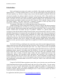
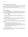
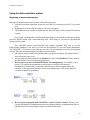
System components
The block diagram of the system
SENSOR PORTS
ANALOG OUTPUTS
3
Preliminary document
DAS1614SD internal structure and the central signal processing units
The data acquisition system has modular structure consisting of a power supply unit, a
backplane for euro-style cards and the plug-in cards. There are five cards in the unit by default:
• DSP card
• ADC card
• DAC and direct digital synthesizer (DDS) card
• SRAM memory card (1MWords)
• sensor and digital interface card.
The DAS1614SD data acquisition system uses three processors: a DSP for high speed data
acquisition and control, a microcontroller for controlling the sensor ports and another
microcontrooller for driving the LCD display.
The DSP has 80kbytes of on-chip memory for program and data storage. The acquired data
is temporarily stored here for asynchronous uploading to the host PC. It may also serve as a buffer
for arbitrary waveform generation. The current memory limit is 4kwords of data both for
acquisition and signal generation (may depend on software and external memory options).
The SRAM card serves as a buffer for long data acquisition processes by providing room
for 1Mwords of 16-bit data.
The DSP card has two independent UART ports: one for internal communications with the
plug-in cards and another for galvanically isolated communication with the host computer.
The DSP card manages a special 16-bit digital bus for intercard communications, two
independent synchronous serial buses and control signals such as address and I/O control.
The main units in the system are the following:
• 16-bit fixed point DSP
• eight channel 16-bit Σ∆ ADC (two ADCs, simultaneously sampling, two 4x1
overvoltage protected differential multiplexers)
• four independent 14-bit DACs
• two DDS signal generators (sampling clock and sine wave generation)
• isolated UART for host communication
• LCD display with a dedicated microcontroller
• Two 16-bit ADCs and a 12-bit DAC with a dedicated microcontroller for sensor
signal digitization
• Two high current voltage outputs driven by the 14-bit DACs
• Two independent SPDT relays
• 8-bit TTL input and 8-bit TTL output port
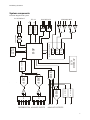
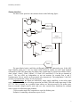
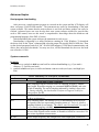
Analog inputs, A/D conversion
The eight analog input channels are organized as two four-channel blocks. Each block has a
four-channel differential multiplexer, a switch for selecting single ended operation (see figure
below). The inputs are overvoltage protected up to 20V below or above the supplies (-15V and
+15V if switched on). The input range is –10V to 10V. The multiplexer’s output is digitized by two
independent 16-bit Σ∆ ADCs, whose output is a 2’s complement 16-bit signed integer number.
4
Preliminary document
MUX
The input structure of one four-channel block. The differential amplifier’s output is connected to the input of
the A/D converter
5
Preliminary document
Analog outputs, D/A conversion, buffered outputs
The four independent analog outputs are driven by a quad 14-bit DAC. The output voltage
range is –10V to 10V. The output current for these outputs must be less than 10mA, the output
impedance is 50Ω. The two high current buffered voltage sources are driven by the first two DAC
output voltages. Absolute accuracy must be guaranteed by calibration.
Note that the DACs should be set by a left justified 16-bit 2’s complement signed integer
number.
Direct digital synthesizers
The system has two high performance direct digital synthesizers (DDS) for generation of a
sine wave and the sampling clock signal with extremely high resolution. The base clock source for
the two DDS chips is a 20MHz oscillator. The on-board PLL of the DDS circuits can multiply this
clock by 6 resulting a 120MHz reference clock. The output frequency of the DDS is given by:
n
f (n) = 6 p ⋅ 20MHz 32 ,
2
where n is the 32-bit tuning word and p=1 if the PLL is enabled (default value), 0 otherwise.
The frequency resolution is 6p·20MHz/232, approximately 4.7mHz (p=0) or 28 mHz (p=1).
Sine wave generation
The first DDS is used to generate a precise sine wave whose amplitude and offset is
controlled by the 3rd and 4th DAC outputs, respectively. The DDS output generates a sine wave
between 0V and 1V. The output signal is given by the following formula:
Vout (t ) = A ⋅ DDAC 3 ⋅ sin( 2πft ) + B ⋅ DDAC 3 + C ⋅ DDAC 4
where DDAC3 and DDAC4 are the 16-bit signed integer numbers sent to DAC3 and DAC4
respectively, and A,B and C are calibration coefficients. These coefficients can be calibrated on the
following way:
• set the desired output frequency by programming the DDS
• set DDAC3 to 0 and measure the output DC value at DDAC4=+10000 and DDAC4=-10000. C is
given as the difference between the measured DC values divided by 20000.
• set DDAC4 to 0 and measure the output AC and DC values at DDAC3=15000 and DDAC3=5000.
A is given as the difference between the measured AC values divided by 10000 while B can
be calculated similarly using the measured DC values.
Sampling clock generation
The ADC sampling clock is driven by the second DDS, however the ADC divides this clock
internally by 32 in normal and 16 in fast mode. This gives resolution for the sampling rate of about
1mHz to 2mHz independent of the set frequency.
6
Preliminary document
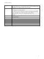
Sensor interface
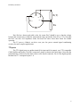
The three sensor ports have the structure shown in the following figure:
_
+5V
PGA
+
ADC0
_
+5V
PGA
+
MICRO
CONTROLLER
+5V
BUF
ADC1
BUF
DAC
The ports labeled with A and B have differential inputs and connected to two 16-bit ADC
input channels, while port C uses two single ended buffers for another two ADC input channels
referenced to GND. The input range for sensor ports A and B may be selected by software (20mV,
40mV, 80mV, 160mV, 320mV, 640mV, 1.2V and 2,56V) and fixed 2.5V for the two channels of
port C. The two ADCs are independent, so one can measure for example Port A and C
simultaneously (Port A and B can be measured only alternatively). The independent 12-bit DAC
provides a programmable voltage for all sensor ports.
Important note: the inputs are buffered by single supply amplifiers, so the safety input
range is limited to 0..5V (no overvoltage protection provided), while the usable input range is from
0V..3.5V. This is usually not a problem when sensors are driven/powered by the sensor ports,
however external voltages must be used with care. Also consider these limitations for common
mode voltages on differential input channels.
5V power and a single DAC output drives a pin for all three ports.
Example of connecting a thermistor to port A or B:
7
Preliminary document
GND
DAC
+5V
IN-
R(T)
IN+
Ro
Here Ro has a known and stable value, the sensor DAC should be set so that the voltage
between the resistors stays within the measurement range (practically from 0V to 2.5V). Note that
the DAC can drive low impedance loads, but must not source more than 10mA for reliable
operation.
The 5V power (<100mA) can drive even your low power external signal conditioning
circuitry for more complex applications.
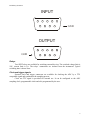
TTL ports
The TTL digital ports are unidirectional (8-bit input and 8-bit output), uses TTL compatible
CMOS buffers and latches. The DB-9 connectors’ pinout is shown in the next figure. Note, that the
pin numbering is mirrored on the male relative to the female connector. Pin 9 is the digital ground,
the data bits 0..7 correspond to pins 1..8.
8
Preliminary document
INPUT
1
2
6
3
7
4
8
5
GND
9
OUTPUT
5
GND
4
9
3
8
4
7
1
6
Relays
Two SPDT relays are available for switching external devices. The switched voltage limit is
50V, current limit is 1A. The relays’ connections are isolated from the instrument. Typical
switching time is about 10ms.
Clock and trigger signals
External clock and trigger connectors are available for clocking the ADC by a TTL
compatible signal and synchronize the sampling process.
Clock out TTL signal is provided for external use. It can be configured as the ADC
sampling clock, programmable clock and a bit programmed by the user.
9
Preliminary document
Using the data acquisition system
Beginning a measurement project
Starting of a measurement project consists of the following steps:
1. Switch on your data acquisition system. Be sure, that it is connected to your PC’s free serial
port.
2. Download the system software using the DasInit.exe program.
3. The instrument is now ready for measurements, the LCD display indicates the DSP software
version.
Note: if the communication with the instrument hangs or the instrument does not respond,
press the RESET button with a non-conducting stick. After doing so, you need to download the
system software again.
The LabVIEW drivers (das1614sd.llb) and example programs help you to use the
DAS1614SD promptly or can serve as a basis for development of your own virtual instruments.
The LabVIEW Vis included in the package are quite self documenting to aid the development
process. The most important things to remember are listed below:
1. The system software must be downloaded before using the instrument. This must be done
once after power on or reset.
2. Always open the communication with InitDAS.vi, close with CloseDAS.vi. These must be
the first and last Vis executed in any application.
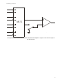
3. Do not run two or more DAS1614SD related Vis simultaneously. For example, if you
put two Vis without any guaranteed execution order, LabVIEW will run them
simultaneously and this may corrupt the communication. The next figure shows this
situation: on the upper program the Vis may run simultaneously, while in the other the
execution sequence is guaranteed.
4. Do not stop your program with LabVIEW’s „Abort execution” button. This may also
corrupt and hang the communication since it may happen during a communication process.
Implement your own stop method using for example while loops.
10
Preliminary document
5. The indexing is zero-based, so the first analog output is indexed as 0, the second analog
input is indexed as 1.
6. Do not modify the DAS1614SD.llb library, the routines are tested. If you find a bug,
please report it to us.
Measurements of static or slow signals
When slow signals are measured, the user must first set up the ADC input parameters
(channel, gain, differential mode) by adcsetup.vi. The parameters will be valid until you modify
them. This means that if you measure many times with the same parameters, you need to setup only
once. However, if you measure for example on two channels, the setup should be applied before
each conversion. Note here that the channel parameter is a zero-based index. The ADC converts
continuously at a rate defined by the latest command, you will receive always the most recent
value.
Static voltage or current generation
Output voltages and currents can be generated by SetDAC.vi. This VI can set one channel at
a time, accepts voltage or integer code (2’s complement, 16-bit) as well. The current generators are
connected to the DAC outputs so they are not independent. DAC number is a zero-based index.
Time dependent measurements
Time dependent measurements are realised as periodic sampling at a given rate. The rate
can be programmed by dividing the 20MHz master clock by a 16-bit integer number. The
LabVIEW driver has a VI dedicated to this function called SetFreq.vi. Note that since the
resolution is not infinite, one should consider the real sampling frequency returned by this VI.
You have two choices:
1. Start an untriggered sampling.
2. Start a hardware/software triggered sampling.
For the first you simply may use Sampling.vi, which starts an acquisition, waits for end of
sampling and reads data.
For triggered measurements first you should setup the sampling parameters
(SetupSampling.vi), start the sampling process (StartTriggeredSampling.vi), wait for end of
sampling (IsSampling.vi) and the read the acquired data (ReadTrigData.vi).
For more information please see the examples.
Sensor measurements
There are three sensor ports on DAS1614SD labelled A,B and C. Ports A and B have
differential inputs, a DAC output (same for all ports) and 5V supply for low power external
circuitry. Port C has two single ended, buffered inputs and the same DAC and 5V power. Sensor
ports A and B are connected to a two channel ADC with software programmable input range
(20mV..2.56V) and the two inputs of port C are connected to another two channel ADC. The
sample rate can be set up to 20Hz, the ADC’s resolution is 16 bits. The sensor DAC has 12-bit
resolution and 0..5V output range.
11
Preliminary document
Using the sensor port related VIs in DAS1614SD.llb you access all features of the sensor
ports.
12
Preliminary document
Specifications
DAS1614SD DSP data acquisition system
Host processor card
• 40 MIPS high performance 16-bit fixed point digital signal processor (ADSP-2181)
• 80kbytes of on-chip memory (code and data)
• 64kbyte program EEPROM
• simple monitor program for serial port downloading
• system software downloaded from the host PC – extreme flexibility
• easy communication with the host PC using simple serial port communications
A/D conversion and analog inputs
• 8 differential or single ended inputs (software selectable)
• overvoltage protection for -35V..35V out of operating range
• approximately 400kHz maximum bandwidth, internal anti-aliasing filter
• 1MHz maximum sample rate, 16-bit resolution
• 10us settling time to 0.01%
• simultaneous sampling of 2 selected channels
• integral non-linearity: ±1LSB typical
• total harmonic distortion (THD): 90 dB typical
• software analog triggering based on converted input voltage
• high resolution DDS clock for conversion
D/A conversion and analog outputs
• four independent channels with fixed ±10V range, with 50Ω output impedance and can
source or sink 10mA
• 14-bit resolution, 1LSB typical nonlinearity
• 100KHz update rate
• 10us settling to 0.01%
• two high current buffered outputs (1A)
Digital ports
• 8 TTL outputs
• 8 TTL inputs
• programmable TTL clock out up to 20MHz
Relays
• two independent SPDT isolated relays
• max. current: 1A
Sensor ports
• three ports for sensors, four channels
• 5V power (max 100mA), 12-bit independent DAC output (max. 10mA)
• two high resolution 16-bit sigma-delta A/D converters, one with two differential and one
with two single ended inputs
• software programmable gain on differential inputs
• 20Hz maximum sample rate
13
Preliminary document
Serial communication port
• one isolated RS232 compatible serial port, 115200 bits per second data rate
• one asynchronous serial port for internal communications
LCD display
• 4 lines, 16 characters per line
Software support
• DSP system software and system loader
• LabVIEW library and examples
14
Preliminary document
Advanced topics
Host program downloading
After power on a simple monitor program is executed on the system and the LCD display will
show a message “DAS1614SD monitor”. The instrument now waits for downloading of the main
system software. This means that the main software is not fixed and future updates can easily be
realized. Advanced users can even develop their own system software tailored for special tasks
such as PID control, however this needs a comprehensive knowledge about the hardware and
programming language of the DSP, of course.
After downloading the system software the instrument is ready to use.
Downloading is supported by a utility DasInit.exe running on 32-bit Windows. To download
the driver click on the “Open” command and select the proper file (usually DAS1614SD.dxe). Then
set the desired parameters and click “Ok”. DAS1614SD supports 115200 baud communication, and
allows fast (unverified) downloads. You may use slow, verified download also, however the baud
rate is fixed at 115200.
System commands
Remarks:
1. characters or symbols in bold are sent back for software handshaking (e.g. if you send a
character ‘$’ it will be sent back).
2. symbols in italics are bytes, in italics and SMALL CAPS are words (two bytes, send high byte
first)
Brief summary of available commands
Command
$s
$M
$S a
$f A
$F A B c
Description
Analog input related commands
Starts sampling using the selected values for sampling frequency, channel
setup, length, skip and averaging (see commands $f,$C,$c,$N,$A) and waits
for end of sampling. The end of sampling indicated by sending a byte to the
PC. During sampling, the downloaded waveform will appear on the first
analog output. See $T.
Starts the sampling using the defined configuration and returns immediately.
See $s as an alternative.
Query sampling status. The dummy byte a for handshaking can be any byte,
the response is the byte representing sampling status as 1: active, 0: inactive
(sampling finished or not started). The value a won’t be sent back! Use only if
you’ve started sampling with $M.
Sets the sampling frequency to 12000kHz/(A+1). The upper limit of A is 65536,
the lower limit depends on the number of channels selected for conversion. See
later at time dependent measurements.
Sets the output frequency and configures the clock output port. Values of c
15
Preliminary document
$C A b
$c {A b}
$N A
$A a b
$Q a b
$R
directs the following to clock out:
c=0: 12000kHz/(A+1)
c=1: sampling clock defined by $f
c=2: flag_out pin of the DSP
c=3: 12000kHz/(A+1)/(B+1)
Configures sampling for single channel or simultaneous sampling mode.
meaning of the bits of A:
0,1: block 0 channel select
2,3: block 1 channel select
4,5: block 0 gain select
6,7: block 1 gain select
8: block 0 differential (1) or single ended (0) mode
9: block 1 differential (1) or single ended (0) mode
10: enable external clock
11: invert external clock
12: select hardware trigger
13: invert hardware trigger
meaning of the bits of b:
0: block 0 channel selected for conversion
1: block 1 channel selected for conversion
2: aux 0 channel selected for conversion
3: aux 1 channel selected for conversion
typical configurations:
b=1: single channel conversion of block 0
b=2: single channel conversion of block 1
b=3: simultaneous conversion of block 0 and 1
Configures sampling for switched channel mode. {A b} is an 8 element array of
channel configuration words and bytes (A1 b1 A2 b2 …). During sampling
every conversion if followed by a new setting defined by this array in a circular
manner.
Sets the length of samples to A. The range is 1..4096.
Sets the averaging number to a, number of skipped sequences to b. The ranges
are 1..255 and 0..255, respectively.
Read last converted data. Can be used as a static measurement, the value is
updated in the instrument using the selected values for sampling frequency,
channel setup, length, skip and averaging (see commands $f,$C). a and b are
dummy bytes for handshaking, the high byte of data is sent to the host PC upon
reception of a, while the low byte is sent after receiving b.
Read sampled data stored in the DSP’s memory. This command is usually
preceded by $s or $M.
$r
$P
$p
$D a B
Analog output related commands
Sets the a-th D/A converter to value B. Byte a is a zero based index and B is a
two’s complement integer.
16
Preliminary document
$T A {B}
$J a b C D E
$h A
Fills the DSP’s waveform memory with values defined by the integer array {B}.
The length of the array is A with maximum value of 4096. Remind that during
sampling the array length selected by $N will be used.
Configures the timer based waveform generator. The parameters are:
a=0: disable the waveform generation
a=1: enable the waveform generation using the downloaded waveform ($T)
b is the timer prescaler, C is the timer period, D is the length of the waveform
array, E is the phase update value. The update frequency will be
12000kHz/(b+1)/(C+1), every E–th element of the waveform array will be used
circularly.
Sets the scaling coefficient for the waveform generator. A is a signed, two’s
complement integer.
17