1
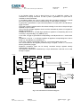
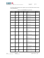
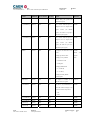
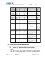
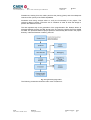
Technical
Information
Manual
Revision n. 8
12 February 2010
MOD. V1495
GENERAL PURPOSE
VME BOARD
NPO:
00117/04:V1495.MUTx/08
CAEN will repair or replace any product within the guarantee period if the Guarantor declares that the
product is defective due to workmanship or materials and has not been caused by mishandling,
negligence on behalf of the User, accident or any abnormal conditions or operations.
CAEN declines all responsibility for damages or
injuries caused by an improper use of the Modules due
to negligence on behalf of the User. It is strongly
recommended to read thoroughly the CAEN User's
Manual before any kind of operation.
CAEN reserves the right to change partially or entirely the contents of this Manual at any time
and without giving any notice.
Disposal of the Product
The product must never be dumped in the Municipal Waste. Please check your local
regulations for disposal of electronics products.
Document type:
User's Manual (MUT)
Title:
Mod. V1495 General Purpose VME Board
Revision date:
12/02/2010
Revision:
8
TABLE OF CONTENTS
1.
2.
3.
GENERAL DESCRIPTION.........................................................................................................................6
1.1.
OVERVIEW ...............................................................................................................................................6
1.2.
BLOCK DIAGRAM .....................................................................................................................................7
TECHNICAL SPECIFICATIONS ..............................................................................................................8
2.1.
PACKAGING ..............................................................................................................................................8
2.2.
POWER REQUIREMENTS ............................................................................................................................8
2.3.
FRONT PANEL DISPLAYS ...........................................................................................................................8
2.4.
FRONT PANEL...........................................................................................................................................9
2.5.
MOTHERBOARD SPECIFICATIONS ...........................................................................................................10
2.6.
MEZZANINE SPECIFICATIONS .................................................................................................................10
2.7.
MEZZANINE BOARDS INSTALLATION ......................................................................................................11
2.8.
FRONT PANEL CONNECTOR CABLING ......................................................................................................11
OPERATING MODES ...............................................................................................................................13
3.1. TIMERS ...................................................................................................................................................13
3.1.1.
Timer0, Timer1 ..............................................................................................................................13
3.1.2.
Timer2, Timer3 ..............................................................................................................................14
3.2. FPGA PROGRAMMING ...........................................................................................................................15
3.2.1.
FPGA VME....................................................................................................................................15
3.2.2.
FPGA USER ..................................................................................................................................16
4.
VME INTERFACE .....................................................................................................................................17
4.1. REGISTER ADDRESS MAP ........................................................................................................................17
4.1.1.
Configuration ROM.......................................................................................................................17
4.2.
CONTROL REGISTER ...............................................................................................................................18
4.3.
STATUS REGISTER ..................................................................................................................................18
4.4.
INTERRUPT LEVEL REGISTER .................................................................................................................18
4.5.
INTERRUPT STATUS-ID REGISTER ..........................................................................................................19
4.6.
GEO ADDRESS REGISTER ......................................................................................................................19
4.7.
MODULE RESET REGISTER .....................................................................................................................19
4.8.
FIRMWARE REVISION REGISTER .............................................................................................................19
4.9.
SCRATCH16 REGISTER ...........................................................................................................................20
4.10.
SCRATCH32 REGISTER .......................................................................................................................20
4.11.
SELECT VME FPGA FLASH REGISTER...............................................................................................20
4.12.
SELECT USER FPGA FLASH REGISTER .............................................................................................20
4.13.
VME FPGA FLASH MEMORY ............................................................................................................20
NPO:
00117/04:V1495.MUTx/08
Filename:
V1495_REV8.DOC
Number of pages:
42
Page:
3
Document type:
User's Manual (MUT)
5.
Title:
Mod. V1495 General Purpose VME Board
Revision date:
12/02/2010
Revision:
8
4.14.
USER FPGA FLASH MEMORY ...........................................................................................................20
4.15.
USER FPGA CONFIGURATION REGISTER ..........................................................................................21
V1495 USER FPGA REFERENCE DESIGN KIT...................................................................................22
5.1.
INTRODUCTION .......................................................................................................................................22
5.2. DESIGN KIT ............................................................................................................................................22
5.2.1.
V1495HAL .....................................................................................................................................22
5.2.2.
COIN_REFERENCE Design .........................................................................................................23
5.3. INTERFACE DESCRIPTION ........................................................................................................................25
5.3.1.
Global Signals ...............................................................................................................................25
5.3.2.
REGISTER INTERFACE ...............................................................................................................25
5.3.3.
V1495 Front Panel Ports (PORT A,B,C,G) INTERFACE.............................................................26
5.3.4.
V1495 Mezzanine Expansion Ports (PORT D,E,F) INTERFACE .................................................26
5.3.5.
PDL Configuration Interface.........................................................................................................26
5.3.6.
Delay Lines and Oscillators I/O ....................................................................................................27
5.3.7.
SPARE Interface ............................................................................................................................27
5.3.8.
LED Interface ................................................................................................................................27
5.4.
REFERENCE DESIGN DESCRIPTION ..........................................................................................................27
5.5. REGISTER DETAILED DESCRIPTION.............................................................................................31
5.5.1.
V1495 Front Panel Ports Registers (PORT A,B,C,G) ...................................................................31
5.5.2.
V1495 Mezzanine Expansion Ports Registers (PORT D,E,F) .......................................................32
5.5.3.
Delay Selection ..............................................................................................................................32
5.5.4.
PDL DELAY VALUE SETTING AND READBACK ......................................................................33
5.5.5.
Delay Unit using PDLs..................................................................................................................34
5.5.6.
Delay Unit using DLOs .................................................................................................................35
5.6.
QUARTUS II WEB EDITION PROJECT ......................................................................................................36
5.7.
FIRMWARE UPGRADE..............................................................................................................................42
LIST OF FIGURES
FIG. 1.1: MOD. V1495 BLOCK DIAGRAM .................................................................................................................7
FIG. 2.1: MODEL V1495 FRONT PANEL (WITH A395A/B/C PIGGY BACK BOARDS) ...................................................9
FIG. 2.2: MULTIPIN CONNECTOR PIN ASSIGNMENT .................................................................................................11
FIG. 2.3: MOD. A967 CABLE ADAPTER .................................................................................................................12
FIG. 3.1: TIMERS DIAGRAM ....................................................................................................................................14
FIG. 3.2: GATE PULSE EXAMPLE .............................................................................................................................14
FIG. 3.3: TIMER2 AND TIMER3 USED TOGETHER FOR HANDLING A GATE PULSE .....................................................15
FIG. 3.4: FPGA VME DIAGRAM .............................................................................................................................15
FIG. 3.5: FPGA USER DIAGRAM............................................................................................................................16
FIG. 4.1: INTERRUPT LEVEL REGISTER ...................................................................................................................18
FIG. 4.2: INTERRUPT VECTOR REGISTER ................................................................................................................19
FIG. 4.3: GEOGRAPHICAL ADDRESS REGISTER ........................................................................................................19
FIG. 4.4: FIRMWARE REVISION REGISTER ..............................................................................................................19
NPO:
00117/04:V1495.MUTx/08
Filename:
V1495_REV8.DOC
Number of pages:
42
Page:
4
Document type:
User's Manual (MUT)
Title:
Mod. V1495 General Purpose VME Board
Revision date:
12/02/2010
Revision:
8
FIG. 4.5: USER FPGA CONFIGURATION REGISTER................................................................................................21
FIG. 5.1: USER FPGA BLOCK DIAGRAM ................................................................................................................22
FIG. 5.2: FRONT PANEL PORTS INTERFACE DIAGRAM ............................................................................................28
FIG. 5.3: PDL_CONTROL BIT FIELDS ...................................................................................................................33
FIG. 5.4: DELAY UNIT WITH PDLS .........................................................................................................................34
FIG. 5.5: PDLS DELAY LINE TIMING .......................................................................................................................34
FIG. 5.6: DELAY UNIT WITH DLOS ........................................................................................................................36
FIG. 5.7: DLOS DELAY LINE TIMING ......................................................................................................................36
FIG. 5.8: QUARTUS II PROJECT FLOW......................................................................................................................37
FIG. 5.9: QUARTUS II MAIN MENU ..........................................................................................................................38
FIG. 5.10: QUARTUS II FILE MENU ..........................................................................................................................38
FIG. 5.11: QUARTUS II PROJECT BROWSER .............................................................................................................39
FIG. 5.12: QUARTUS II NETLIST ..............................................................................................................................40
FIG. 5.13: QUARTUS II HIERARCHICAL STRUCTURE ................................................................................................40
FIG. 5.14: QUARTUS II COMPILER LAUNCHING .......................................................................................................41
FIG. 5.15: QUARTUS II COMPILING SUMMARY ........................................................................................................41
LIST OF TABLES
TABLE 1.1: AVAILABLE ITEMS .................................................................................................................................6
TABLE 2.1: MODEL V1495 AND MEZZANINE BOARDS POWER REQUIREMENTS .........................................................8
TABLE 2.2: V1495 MOTHERBOARD I/O SECTIONS..................................................................................................10
TABLE 2.3: V1495 MEZZANINE BOARDS ................................................................................................................10
TABLE 4.1: ADDRESS MAP FOR THE MODEL V1495...............................................................................................17
TABLE 4.2: ROM ADDRESS MAP FOR THE MODEL V1495.....................................................................................17
TABLE 5.1: COIN_REFERENCE SIGNALS ............................................................................................................23
TABLE 5.2: V1495 MEZZANINE EXPANSION PORTS SIGNALS .................................................................................26
TABLE 5.3: PDL CONFIGURATION INTERFACE SIGNALS .........................................................................................26
TABLE 5.4: DELAY LINES AND OSCILLATORS SIGNALS ..........................................................................................27
TABLE 5.5: SPARE INTERFACE SIGNALS ...............................................................................................................27
TABLE 5.6: LED INTERFACE SIGNALS ....................................................................................................................27
TABLE 5.7: COIN_REFERENCE REGISTER MAP ..................................................................................................29
TABLE 5.8: SELECTION OF THE DELAY LINE ...........................................................................................................32
NPO:
00117/04:V1495.MUTx/08
Filename:
V1495_REV8.DOC
Number of pages:
42
Page:
5
Document type:
User's Manual (MUT)
Title:
Mod. V1495 General Purpose VME Board
Revision date:
12/02/2010
Revision:
8
1. General description
1.1. Overview
The Mod. V1495 is a VME 6U board, 1U wide, suitable for various digital
Gate/Trigger/Translate/Buffer/Test applications, which can be directly customised by the
User, and whose management is handled by two FPGA’s:
FPGA “Bridge”, which is used for the VME interface and for the connection between the
VME interface and the 2nd FPGA (FPGA “User”) through a proprietary local bus. FPGA
“Bridge” manages also the programming via VME of the FPGA “User”.
FPGA “User”, which manages the front panel I/O channels. FPGA “User” is provided with
a basic firmware which allows to perform coincidence matrix, I/O register and
asynchronous timers functions.
FPGA “User” can be also free reprogrammed by the user with own custom logic function
(see § 5.1). It is connected as slave to the FPGA “Bridge” via CAEN Local Bus, whose
protocol shall be used in order to communicate with the FPGA “Bridge” and thus with the
VME bus.
The I/O channel digital interface is composed by four sections (A, B, C, G) placed on the
motherboard (see § 1.2). The channel interface can be expanded in the D, E, F sections
by using up to 3 mezzanine boards (see § 2.6 and § 2.7), which can be added, choosing
between the five types developed in order to cover the I/O functions and the ECL, PECL,
LVDS, NIM, TTL signals and 16bit DAC (see § 1.2). The maximum number of channels
can be expanded up to 194.
The FPGA “User” can be programmed “on the fly” directly via VME, without external
hardware tools, without disconnecting the board from the set up, without resetting it or
turning the crate off, allowing quick debug operations by the developer with his own
firmware. A flash memory on the board can store the different programming file, which
can be loaded to the FPGA “User” at any moment.
Four independent digital programmable asynchronous timers are available for
Gate/Trigger applications. It is possible to chain them for generating complex
Gate/Trigger pulse.
Table 1.1: Available items
Code
Description
WV1495XAAAAA
V1495 - General Purpose VME Board
WA395XAAAAAA
A395A - 32 LVDS/ECL/PECL input channels
WA395XBAAAAA
A395B - 32 LVDS output channels
WA395XCAAAAA
A395C - 32 ECL output channels
WA395XDAAAAA
A395D - 8 NIM/TTL input/output channels
WA395XEAAAAA
A395E - 8 channel 16Bit ±5V DAC
WPERS0149501
V1495 - Customization - 3 A395C Mounting Option
WA967XAAAAAA
A967 - 32 Channel Cable Adapter (1x32 to 2x16)
WFW1495SCXAA
FW1495SC - 128 Channels Latching Scaler for V1495
NPO:
00117/04:V1495.MUTx/08
Filename:
V1495_REV8.DOC
Number of pages:
42
Page:
6
Document type:
User's Manual (MUT)
Title:
Mod. V1495 General Purpose VME Board
Revision date:
12/02/2010
Revision:
8
32
16 bit
32
B
32
C
32
USER
PROGRAMMABLE
FPGA
FLASH
µC
G
16/32/64 bit
8 bit
32
A
BRIDGE
FPGA
(VME interface)
LPT
F
LOCAL
BUS
(optional)
E
32
FW LOADING
D
VME BUS
1.2. Block Diagram
4
Asyn. Timers
USER
FPGA
CONFIG
4
Fig. 1.1: Mod. V1495 Block Diagram
NPO:
00117/04:V1495.MUTx/08
Filename:
V1495_REV8.DOC
Number of pages:
42
Page:
7
Document type:
User's Manual (MUT)
Title:
Mod. V1495 General Purpose VME Board
Revision date:
12/02/2010
Revision:
8
2. Technical specifications
2.1. Packaging
The module is housed in a 6U-high, 1U-wide VME unit. The board is provided the VME
P1, and P2 connectors and fits into both VME standard and V430 backplanes.
2.2. Power requirements
The power requirements of the modules are as follows:
Table 2.1: Model V1495 and mezzanine boards power requirements
Power supply
V1495
A395A
A395B
A395C
A395D
A395E
+5 V
1A
0.1 A
0.1 A
1.4 A
1.1 A
0.3 A
2.3. Front panel displays
The front panel (refer to § 2.4) hosts the following LEDs:
DTACK:
Colour: green.
Function: it lights up green whenever a VME read/write
access to the board is performed.
USER:
Colour: green / orange / red.
Function: programmable.
NPO:
00117/04:V1495.MUTx/08
Filename:
V1495_REV8.DOC
Number of pages:
42
Page:
8
Document type:
User's Manual (MUT)
Title:
Mod. V1495 General Purpose VME Board
Revision date:
12/02/2010
Revision:
8
2.4. Front Panel
Mod.
V560E
Mod. V1495
USER DTACK
-
+
+ -
31
I
N
L
V
D
S
/
E
C
L
0
A
-
D
+
+ -
31
I
N
L
V
D
S
/
E
C
L
0
B
G0
E
G1
+-
-
+
31
O
U
T
L
V
D
S
B
A
0
16
CCH F
SCALE
R
GENERAL
PURPOSE
VME BOARD
Fig. 2.1: Model V1495 front panel (with A395A/B/C piggy back boards)
NPO:
00117/04:V1495.MUTx/08
Filename:
V1495_REV8.DOC
Number of pages:
42
Page:
9
Document type:
User's Manual (MUT)
Title:
Mod. V1495 General Purpose VME Board
Revision date:
12/02/2010
Revision:
8
2.5. Motherboard Specifications
The Mod. V1495 Motherboard is composed by four I/O sections (see § 1.2), described in
the following table:
Table 2.2: V1495 Motherboard I/O sections
Board No. of Ch.
Direction
Logic
Signal
Bandwidth
Robinson Nugent P50E068-P1-SR1-TG
type,
(34+34) pins
Robinson Nugent P50E068-P1-SR1-TG
type,
(34+34) pins
A/B
32
Input
Direct
LVDS/ECL/PECL
(single
ended
TTL optional)
110ohm
Rt.
Extended
200MHz
Common Mode
input range –4V
to +5V; Fail Safe
input feature.
C
32
Output
Direct
LVDS
100ohm Rl
G
2
I/O
selectable
TTL IN=Direct
TTL OUT=Direct
NIM IN=Invert
NIM OUT=Direct
NIM/TTL
selectable
Open/50ohm Rt
selectable
250MHz
250MHz
Front panel connector
LEMO 00
2.6. Mezzanine Specifications
The five I/O Mezzanine boards developed so far are described in the following table:
Table 2.3: V1495 Mezzanine boards
Board
No. of Ch.
Direction
Logic
Signal
Bandwidth
Front panel connector
Robinson Nugent P50E068-P1-SR1-TG type,
(34+34) pins
A395A
32
Input
Direct
LVDS/ECL/
PECL
(single ended
TTL optional)
110ohm Rt.
Extended
200MHz
Common Mode
input range –4V
to +5V; Fail
Safe input
feature.
A395B
32
Output
Direct
LVDS
100ohm Rl
250MHz
Robinson Nugent P50E068-P1-SR1-TG type,
(34+34) pins
A395C
32
Output
Direct
ECL
300MHz
Robinson Nugent P50E068-P1-SR1-TG type,
(34+34) pins
A395D
8
I/O
selectable
TTL IN=Direct
TTL OUT=Direct
NIM IN=Invert
NIM OUT=Direct
NIM/TTL
selectable
250MHz
Open/50ohm Rt
selectable
LEMO 00
A395E
8
Output
Analog
16bit resolution
±5V @10kΩ RL N.A.
±4V @200Ω RL
LEMO 00
NPO:
00117/04:V1495.MUTx/08
Filename:
V1495_REV8.DOC
Number of pages:
42
Page:
10
Document type:
User's Manual (MUT)
Title:
Mod. V1495 General Purpose VME Board
Revision date:
12/02/2010
Revision:
8
2.7. Mezzanine boards installation
In order to install one A395x-series mezzanine board on the V1495 motherboard it is
necessary to follow these steps:
− Remove (unscrew) the metal cover (one at will)
− Plug the mezzanine board into the 100 pin connector on the motherboard
− Fix the mezzanine board with the screws
WARNING! A Mounting Option is necessary in order to install three A395C
mezzanine boards on the V1495 (see table 1.1)
2.8. Front panel connector cabling
Motherboard I/O sections A, B, C and A395A, A395B and A395C Mezzanine boards
feature the Robinson Nugent P50E-068-P1-SR1-TG multipin connector, whose pin set is
shown in the following figure:
N.C.
N.C.
N.C.
N.C.
CH31CH31+
CH15CH15+
CH30CH30+
CH14CH14+
CH17CH17+
CH1CH1+
CH16CH16+
CH0CH0+
Fig. 2.2: Multipin connector pin assignment
NPO:
00117/04:V1495.MUTx/08
Filename:
V1495_REV8.DOC
Number of pages:
42
Page:
11
Document type:
User's Manual (MUT)
Title:
Mod. V1495 General Purpose VME Board
Revision date:
12/02/2010
Revision:
8
The CAEN Mod. A967 Cable Adapter allows to adapt each Robinson Nugent Multipin
Connector into two 1” 17+17-pin Header-type male connectors (3M, 4634-7301) with
locks through two 25 cm long flat cables.
N.C.
CH31
CH17
CH16
N.C.
CH15
CH1
CH0
Fig. 2.3: Mod. A967 Cable Adapter
NPO:
00117/04:V1495.MUTx/08
Filename:
V1495_REV8.DOC
Number of pages:
42
Page:
12
Document type:
User's Manual (MUT)
Title:
Mod. V1495 General Purpose VME Board
Revision date:
12/02/2010
Revision:
8
3. Operating modes
3.1. Timers
Gate/Trigger applications require the production of an output signal with programmable
width (Gate), whenever an input signal (Trigger) occurs.
Gates can be produced in several ways, according to the system set up, which can be
either synchronous or asynchronous.
Synchronous systems:
Input signals are referred to a system clock: they can be sampled by the clock itself and
the output is a gate signal (obtained with a counter) whose width (and delay) is a multiple
of the clock period. If the application requires a width (and delay) of the Gate signal
synchronous but with step resolution higher than the system clock period, this can be
achieved by enabling the PLL in the USER FPGA and enter the reference clock on
channel G0.
Asynchronous systems:
Input signals are not referred to a system clock. As a consequence the gate signal will be
generated without any time reference. It is possible to use the implementation described
above, with the freedom of choosing the clock source between external or 40MHz
internal. The resulting Gate signal will have stable duration, but with maximum position
jitter equal to one clock period.
Such position jitter can be rejected by using the asynchronous timers present on the
V1495, which allow to generate references synchronous with the occurred trigger.
3.1.1.
Timer0, Timer1
Each timer is based on a programmable delay line. FPGA USER drives a STARTx pulse
and, after the programmed delay, it receives the return signal PULSEx. The time
difference between transmission and reception (logic implementation inside the FPGA
USER) can be used to drive a gate signal. The programming of the delay time can be
done manually as binary value either via 8 bit dip switches (SW4 and SW5) or via VME
register, with a 1ns step resolution (max step delay = 255ns). The software setting has
higher priority with respect to the dip switches.
The following figure shows a diagram of the timers usage:
NPO:
00117/04:V1495.MUTx/08
Filename:
V1495_REV8.DOC
Number of pages:
42
Page:
13
Document type:
User's Manual (MUT)
Title:
Mod. V1495 General Purpose VME Board
Revision date:
12/02/2010
Revision:
8
Tperiod
Twidth
START 0
Tset
T offset
PULSE 0
GATE
Tdly= Toffset + Tset
Toffset = 30 ± 2ns
Tset = SETBINARY * 1ns
STARTx-WIDTHMIN = 320ns recommended
STARTx-PERIODMIN = 640ns recommended
(22ns absolute min.)
(46ns absolute min.)
Fig. 3.1: Timers diagram
The use of STARTx signals with timing shorter than those recommended is possible,
although the linearity on the set delay scale is no longer guaranteed.
3.1.2.
Timer2, Timer3
Each timer is made up of one digital circuit which produces a typical fixed time base with
10ns period and 50% duty cycle. These timers are proposed for generating any Gate
pulse > 10ns with a 10ns step. The following figure shows an example of a Gate
generation made with Timer2 and n.3 PULSE width.
/START 2
Ten
PULSE 2
Tpd
COUNT 2
COUNT 0
COUNT 1
COUNT 2
GATE
Fig. 3.2: Gate pulse example
FPGA USER drives a /STARTx pulse and after TEN time FPGA USER will receive a
PULSEx clock signal. A counter with clock = PULSEx implemented in the FPGA USER,
allows to generate a pulse with programmable duration. It is possible to reduce to one
half (5ns) the counter step by advancing the counter on both sides of PULSEx. Since the
circuit is completely digital, no recovery time is necessary between one stop and the
following start: it is thus possible to generate multiple gate pulses with very high rate.
Timer2 and Timer3 can be used together for handling one single Gate pulse from
multiple overlapped triggers.
NPO:
00117/04:V1495.MUTx/08
Filename:
V1495_REV8.DOC
Number of pages:
42
Page:
14
Document type:
User's Manual (MUT)
Title:
Mod. V1495 General Purpose VME Board
Revision date:
12/02/2010
Revision:
8
/START 2
PULSE 2
COUNT 2
COUNT 0
COUNT 1
COUNT 2
/START 3
PULSE 3
COUNT 0
COUNT 3
COUNT 1
COUNT 2
GATE
Fig. 3.3: Timer2 and Timer3 used together for handling a Gate pulse
3.2. FPGA Programming
The programming of FPGA VME and FPGA USER are handled by two independent
microcontrollers + flash memory. The updating of the firmware contained in the flash
memories does not require the use of external tools and can be executed via VME.
The flash related to FPGA VME contains the firmware dedicated to the interface of the
board with the FPGA USER and the VME bus; such firmware is developed by CAEN.
The flash related to the FPGA USER contains the firmware developed by the User
according to his own application requirements.
3.2.1.
FPGA VME
The microcontroller provides the firmware uploading at board’s power on. The flash
memory contains two versions of the firmware, which can be selected manually via
jumper (Standard or Backup).
VME BUS
FPGA VME Program Circuit
VME
FPGA
FLASH
uC
FW SEL
STD
BKP
Fig. 3.4: FPGA VME diagram
NPO:
00117/04:V1495.MUTx/08
Filename:
V1495_REV8.DOC
Number of pages:
42
Page:
15
Document type:
User's Manual (MUT)
Title:
Mod. V1495 General Purpose VME Board
3.2.2.
Revision date:
12/02/2010
Revision:
8
FPGA USER
The microcontroller provides the firmware uploading at board’s power on. The flash
memory contains one firmware image only (Standard).
FPGA
USER
FW LOAD
FW SEL
FPGA
VME
VME BUS
FPGA USER Program Circuit
FLASH
uC
Fig. 3.5: FPGA USER diagram
FPGA VME aim is to handle the operation of FPGA USER, which can be programmed on
the fly, i.e. without turning off the system, thus allowing quick debug operations by the
Developer.
Register implemented on FPGA VME allows the following operations:
•
•
FPGA USER flash memory programming.
FPGA USER updating.
NPO:
00117/04:V1495.MUTx/08
Filename:
V1495_REV8.DOC
Number of pages:
42
Page:
16
Document type:
User's Manual (MUT)
Title:
Mod. V1495 General Purpose VME Board
Revision date:
12/02/2010
Revision:
8
4. VME Interface
4.1. Register address map
The Address map for the Model V1495 is listed in Table 4.1. All register addresses are
referred to the Base Address of the board, i.e. the addresses reported in the Tables are
the offsets to be added to the board Base Address.
Table 4.1: Address Map for the Model V1495
ADDRESS
REGISTER/CONTENT
Base + 0x0000÷0x7FFC USER FPGA Access
Base + 0x8000
Control Register
Base + 0x8002
Status Register
Base + 0x8004
Interrupt Level
Base + 0x8006
Interrupt Status-ID
Base + 0x8008
Geo Address_Register
Base + 0x800A
Module Reset
Base + 0x800C
Firmware revision
Base + 0x800E
Select VME FPGA Flash(**)
Base + 0x8010
VME FPGA Flash memory(**)
Base + 0x8012
Select USER FPGA Flash(**)
Base + 0x8014
USER FPGA Flash memory(**)
Base + 0x8016
USER FPGA Configuration(**)
Base + 0x8018
Scratch16
Base + 0x8020
Scratch32
Base + 0x8100÷0x801FE Configuration ROM(**)
(*) Read/Write capability depends on USER FPGA implementation.
ADDR
A24/A32
A24/A32
A24/A32
A24/A32
A24/A32
A24/A32
A24/A32
A24/A32
A24/A32
A24/A32
A24/A32
A24/A32
A24/A32
A24/A32
A24/A32
A24/A32
DATA
D16
D16
D16
D16
D16
D16
D16
D16
D16
D16
D16
D16
D16
D16
D32
D16
Read/Write
R/W (*)
R/W
R
R/W
R/W
R
W
R
R/W
R/W
R/W
R/W
R/W
R/W
R/W
R
(**) See § 5.7
4.1.1.
Configuration ROM
The following registers contain some module’s information according to the Table 3.2,
they are D16 accessible (read only):
•
OUI:
manufacturer identifier (IEEE OUI)
•
Version:
purchased version
•
Board ID:
Board identifier
•
Revision:
hardware revision identifier
•
Serial MSB:
serial number (MSB)
•
Serial LSB:
serial number (LSB)
Table 4.2: ROM Address Map for the Model V1495
Description
Address
checksum
0x8100
checksum_length2
0x8104
checksum_length1
0x8108
checksum_length0
0x810C
constant2
0x8110
NPO:
00117/04:V1495.MUTx/08
Filename:
V1495_REV8.DOC
Content
Number of pages:
42
Page:
17
Document type:
User's Manual (MUT)
Title:
Mod. V1495 General Purpose VME Board
Revision date:
12/02/2010
Description
Address
constant1
0x8114
constant0
0x8118
c_code
0x811C
r_code
0x8120
oui2
0x8124
0x00
oui1
0x8128
0x40
oui0
vers
0x812C
0x8130
0xE6
board2
0x8134
0x00
board1
0x8138
0x05
board0
0x813C
0xD7
revis3
0x8140
revis2
0x8144
revis1
0x8148
revis0
0x814C
sernum1
0x8180
sernum0
0x8184
Revision:
8
Content
These data are written into one Flash page; at Power ON the Flash content is loaded
into the Configuration ROM.
4.2. Control Register
(Base Address + 0x8000, read/write, D16)
This register allows performing some general settings of the module.
Not used for VME FPGA Rev 0.0. Foreseen for future development
4.3. Status Register
(Base + 0x8002, read only, D16)
This register contains information on the status of the module.
Not used for VME FPGA Rev 0.0. Foreseen for future development
4.4. Interrupt Level Register
(Base Address + 0x8004, read/write, D16)
The 3 LSB of this register contain the value of the interrupt level (Bits 3 to 15 are
meaningless). Default setting is 0x0. In this case interrupt generation is disabled.
Not implemented in VME FPGA Rev 0.0. Available in next releases
15 14 13 12 11 10
9
8
7
6
5
4
3
2
1
0
LEVEL
Fig. 4.1: Interrupt Level Register
NPO:
00117/04:V1495.MUTx/08
Filename:
V1495_REV8.DOC
Number of pages:
42
Page:
18
Document type:
User's Manual (MUT)
Title:
Mod. V1495 General Purpose VME Board
Revision date:
12/02/2010
Revision:
8
4.5. Interrupt Status-ID Register
(Base Address + 0x8006, read/write, D16)
This register contains the STATUS/ID that the V1495 places on the VME data bus during
the Interrupt Acknowledge cycle (Bits 8 to 15 are meaningless). Default setting is 0xDD.
Not implemented in VME FPGA Rev 0.0. Available in next releases
15 14 13 12 11 10
9
8
7
6
5
4
3
2
1
0
STATUS/ID
Fig. 4.2: Interrupt Vector Register
4.6. GEO Address Register
(Base Address + 0x8008, read, D16)
The register content is the following:
15 14 13 12 11 10 9 8 7 6 5 4 3 2 1 0
GEO ADDR 0
GEO ADDR 1
GEO ADDR 2
GEO ADDR 3
GEO ADDR 4
Fig. 4.3: Geographical address register
This register allows readback of the level of GEO pins for the selected board. The
register content is valid only for the VME64X board version. The register content for the
VME64 version is 0x1F.
4.7. Module Reset Register
(Base Address + 0x800A write only, D16)
A dummy access to this register allows to generate a single shot RESET of the module.
4.8. Firmware Revision Register
(Base Address + 0x800C, read only, D16)
This register contains the firmware revision number coded on 8 bit. For instance, the
REV. 1.2 register content is:
15 14 13 12 11 10
0
0
0
0
0
0x1
0
9
8
7
6
5
4
3
2
1
0
0
1
0
0
0
0
0
0
1
0
0x2
Fig. 4.4: Firmware Revision Register
NPO:
00117/04:V1495.MUTx/08
Filename:
V1495_REV8.DOC
Number of pages:
42
Page:
19
Document type:
User's Manual (MUT)
Title:
Mod. V1495 General Purpose VME Board
Revision date:
12/02/2010
Revision:
8
4.9. Scratch16 Register
(Base Address + 0x8018, D16, read/write)
This register allows to perform 16 bit test accesses for test purposes.
4.10. Scratch32 Register
(Base Address + 0x8020, D32, read/write)
This register allows to perform 32 bit test accesses for test purposes.
4.11. Select VME FPGA Flash Register
(Base Address + 0x800E, read/write, D16)
This register allows the VME FPGA configuration update (stored into on-board flash
memory) via VMEBUS.
The configuration can be updated by the user by means of the V1495Upgrade software
(developed and distributed by CAEN), see § 5.7.
4.12. Select USER FPGA Flash Register
(Base Address + 0x8012, read/write, D16)
This register allows USER FPGA configuration update (stored into on-board flash
memory) via VMEBUS.
The configuration can be updated by the user by means of the V1495Upgrade software
(developed and distributed by CAEN), see § 5.7.
4.13. VME FPGA Flash Memory
(Base Address + 0x8010, read/write, D16)
This register allows the VME FPGA configuration update (stored into on-board flash
memory) via VMEBUS.
The configuration can be updated by the user by means of the V1495Upgrade software
(developed and distributed by CAEN), see § 5.7.
4.14. USER FPGA Flash Memory
(Base Address + 0x8014, read/write, D16)
This register allows the USER FPGA configuration update (stored into on-board flash
memory) via VMEBUS.
The configuration can be updated by the user by means of the V1495Upgrade software
(developed and distributed by CAEN), see § 5.7.
NPO:
00117/04:V1495.MUTx/08
Filename:
V1495_REV8.DOC
Number of pages:
42
Page:
20
Document type:
User's Manual (MUT)
Title:
Mod. V1495 General Purpose VME Board
Revision date:
12/02/2010
Revision:
8
4.15. USER FPGA Configuration Register
(Base Address + 0x8016, read/write, D16)
This register allows the update of the USER FPGA configuration. A write access to this
register generates a configuration reload. The configuration image (Standard) will be
uploaded into the USER FPGA as the IMAGE_SELECT bit is set to 1:
IMAGE_SELECT
=1
Standard image (default).
15 14 13 12 11 10 9
8
7
6
5
4
3
2
1
0
IMAGE_SELECT
Fig. 4.5: USER FPGA Configuration Register
NPO:
00117/04:V1495.MUTx/08
Filename:
V1495_REV8.DOC
Number of pages:
42
Page:
21
Document type:
User's Manual (MUT)
Title:
Mod. V1495 General Purpose VME Board
Revision date:
12/02/2010
Revision:
8
5. V1495 USER FPGA Reference Design Kit
5.1. Introduction
The CAEN V1495 board provides a user-customizable FPGA (called USER FPGA).
The COIN_REFERENCE reference design illustrates how to use the USER FPGA to
implement a Coincidence Unit & I/O Register Unit. This design can be customised by the
user in order to adapt its functionality to his own needs.
ON-BOARD DELAY LINES
CAEN LOCAL BUS
HARDWARE ABSTRACTION LAYER
MEZZANINE
CARD
ON SLOT
D
MEZZANINE
CARD
ON SLOT
E
USER-DEFINED
LOGIC
MEZZANINE
CARD
ON SLOT
F
Port A (32 IN ECL/LVDS)
Port B (32 IN ECL/LVDS)
Port C (32 OUT LVDS)
Fig. 5.1: USER FPGA block diagram
5.2. Design Kit
5.2.1.
V1495HAL
The V1495 Hardware Abstraction Layer (V1495HAL) is a HDL module provided, in
Verilog format at netlist level, in order to help the hardware interfacing.
NPO:
00117/04:V1495.MUTx/08
Filename:
V1495_REV8.DOC
Number of pages:
42
Page:
22
Document type:
User's Manual (MUT)
5.2.2.
Title:
Mod. V1495 General Purpose VME Board
Revision date:
12/02/2010
Revision:
8
COIN_REFERENCE Design
The COIN_REFERENCE design VHDL entity is the interface to the V1495HAL. If the
User wishes to use V1495HAL to develop his own application on the V1495 platform, the
VHDL entity must not be modified: this means that signals names and function of the
COIN_REFERENCE entity must be used, as shown in the following table:
Table 5.1: COIN_REFERENCE signals
PORT NAME
DIRECTION
WIDTH
DESCRIPTION
GLOBAL SIGNALS
NLBRES
IN
1
Async Reset (active low)
LCLK
IN
1
Local Bus Clock (40 MHz)
REGISTER INTERFACE
REG_WREN
IN
1
Write pulse (active high)
REG_RDEN
IN
1
Read pulse (active high)
REG_ADDR
IN
16
Register address
REG_DIN
IN
16
Data from CAEN Local Bus
REG_DOUT
OUT
16
Data to CAEN Local Bus
USR_ACCESS
IN
1
Current
register
access
is
at user address space(Active high)
V1495 Front Panel Ports (PORT A,B,C,G) INTERFACE
A_DIN
IN
32
In A (32 x LVDS/ECL)
B_DIN
IN
32
In B (32 x LVDS/ECL)
C_DOUT
OUT
32
Out C (32 x LVDS)
G_LEV
OUT
1
Output Level Select (0=>TTL; 1=>
NIM)
G_DIR
OUT
1
Output Enable (0=>Output, 1=>Input)
G_DOUT
OUT
2
Out G - LEMO (2 x NIM/TTL)
G_DIN
IN
2
In G – LEMO (2 x NIM/TTL)
V1495 Mezzanine Expansion Ports (PORT D,E,F) INTERFACE
D_IDCODE
IN
3
D slot mezzanine Identifier
D_LEV
OUT
1
D slot Port Signal Level Select
(the level selection depends on the
mezzanine expansion board mounted
onto this port)
NPO:
00117/04:V1495.MUTx/08
Filename:
V1495_REV8.DOC
Number of pages:
42
Page:
23
Document type:
User's Manual (MUT)
Title:
Mod. V1495 General Purpose VME Board
PORT NAME
D_DIR
DIRECTION
Revision date:
12/02/2010
WIDTH
Revision:
8
DESCRIPTION
OUT
1
D slot Port Direction
IN
32
D slot Data In Bus
D_DOUT
OUT
32
D slot Data Out Bus
E_IDCODE
IN
3
E slot mezzanine Identifier
E_LEV
OUT
1
E slot Port Signal Level Select
D_DIN
1
(the level selection depends on the
mezzanine expansioon board mounted
onto this port)
E_DIR
OUT
1
E slot Port Direction
E_DIN
IN
32
E slot Data In Bus
E_DOUT
OUT
32
E slot Data Out Bus
F_IDCODE
IN
3
F slot mezzanine Identifier
F_LEV
OUT
1
F slot Port Signal Level Select
(the level selection depends on the
mezzanine expansion board mounted
onto this port)
F_DIR
OUT
1
F slot Port Direction
F_DIN
IN
32
F slot Data In Bus
F_DOUT
OUT
32
F slot Data Out Bus
PDL CONFIGURATION INTERFACE
PDL_WR
OUT
1
Write Enable
PDL_SEL
OUT
1
PDL Selection (0=>PDL0, 1=>PDL1)
PDL_READ
IN
8
Read Data
PDL_WRITE
OUT
8
Write Data
PDL_DIR
OUT
1
Direction (0=>Write, 1=>Read)
DELAY LINES AND OSCILLATORS I/O
1
PDL0_OUT
IN
1
Signal from PDL0 Output
PDL1_OUT
IN
1
Signal from PDL1 Output
DLO0_OUT
IN
1
Signal from DLO0 Output
DLO1_OUT
IN
1
Signal from DLO1 Output
The I/O channels of the A395D Mezzanine board are mapped on the 8 LSB of D_DIN, D_DOUT, E_DIN, E_DOUT, F_DIN,
F_DOUT signals
NPO:
00117/04:V1495.MUTx/08
Filename:
V1495_REV8.DOC
Number of pages:
42
Page:
24
Document type:
User's Manual (MUT)
Title:
Mod. V1495 General Purpose VME Board
PORT NAME
DIRECTION
Revision date:
12/02/2010
WIDTH
Revision:
8
DESCRIPTION
PDL0_IN
OUT
1
Signal to PDL0
PDL1_IN
OUT
1
Signal to PDL1 Input
DLO0_GATE
OUT
1
Signal to DLO0 Input
DLO1_GATE
OUT
1
Signal to DLO1 Input
SPARE INTERFACE
SPARE_OUT
OUT
12
SPARE Data Out
SPARE_IN
IN
12
SPARE Data In
SPARE_DIR
OUT
1
SPARE Direction
LED INTERFACE
RED_PULSE
OUT
1
RED Led Pulse (active high)
GREEN_PULSE
OUT
1
GREEN Led Pulse (active high)
5.3. Interface description
5.3.1.
Global Signals
The nLBRES must be used as an asynchronous reset signal by the user. An active low
pulse will be generated when a write is done at the Module Reset register address (see
§ 4.1).
The LBCLK is a 40 MHz clock. It is the FPGA main clock.
5.3.2.
REGISTER INTERFACE
The signals of the Register Interface allows to read/write into the USER FPGA registers,
which can be accessed via VMEbus. The COIN_REFERENCE module shows how to
implement a set of registers.
The following table shows the registers map as it is provided. Each register address is
coded via constants in V1495pkg.vhd file. This file allows to modify the registers map; all
registers allow D16 accesses (write only, read only or read/write). Registers default value
is the value after a reset for write only and read/write registers; read only registers return
the status of the signals read by the FPGA and have no default value.
The Register Interface allows to abstract the VME registers access. The User can access
a simple register interface: two signals (REG_WREN e REG_RDEN) are pulses with a
one clock cycle duration which enables respectively a write or a read access to a
register. REG_ADDR signal represents the register address.
Writing into a register:
In case of a write operation into a register via VME, the 16 bit datum is available through
the REG_DIN signal. The datum is guaranteed stable on the CLK leading edge where
REG_WREN is active. The register access is valid only when USR_ACCESS is at logic
level = 1.
NPO:
00117/04:V1495.MUTx/08
Filename:
V1495_REV8.DOC
Number of pages:
42
Page:
25
Document type:
User's Manual (MUT)
Title:
Mod. V1495 General Purpose VME Board
Revision date:
12/02/2010
Revision:
8
Reading from a register:
In case of a read operation from a register via VME, the datum to be returned must drive
the REG_DOUT and be stable on the CLK leading edge, where REG_RDEN is active.
The register access is valid only when USR_ACCESS is at logic level = 1.
5.3.3.
V1495 Front Panel Ports (PORT A,B,C,G) INTERFACE
These signals allows to handle the interface with the motherboard ports A, B, C, G.
A_DIN and B_DIN signals show the logic level of A and B ports (32 bit, input only).
The output logic level on port C can be set via C_DOUT signal.
The logic level on port G (LEMO connectors) can be set via G_LEV signal; the direction
via G_DIR, the datum to be written via G_DOUT or to be read via G_DIN.
5.3.4.
V1495 Mezzanine Expansion Ports (PORT D,E,F) INTERFACE
These signals allows to handle the interface with the piggy back board ports D, E, F.
The following table explains the available signals:
Table 5.2: V1495 Mezzanine Expansion Ports signals
Port:
D
E
F
Signal:
D_DIR
D_DIN
D_DOUT
D_ IDCODE
D_LEV
E_DIR
E_DIN
E_DOUT
E_ IDCODE
E_LEV
F_DIR
F_DIN
F_DOUT
F_ IDCODE
F_LEV
5.3.5.
Function:
Selects direction
Read the logic level
Set the logic level
Read IDCODE for piggy back identification
Set the logic level
Selects direction
Read the logic level
Set the logic level
Read IDCODE for piggy back identification
Set the logic level
Selects direction
Read the logic level
Set the logic level
Read IDCODE for piggy back identification
Set the logic level
Applies to:
Bidirectional port
Input/Bidirectional
Output/Bidirectional
All
Output/Bidirectional
Bidirectional port
Input/Bidirectional
Output/Bidirectional
All
Output/Bidirectional
Bidirectional port
Input/Bidirectional
Output/Bidirectional
All
Output/Bidirectional
PDL Configuration Interface
PDL Configuration Interface signals are as follows:
Table 5.3: PDL Configuration Interface signals
PDL_WR
OUT
1
Write Enable
PDL_SEL
OUT
1
PDL Selection (0=>PDL0, 1=>PDL1)
PDL_READ
IN
8
Read Data
PDL_WRITE
OUT
8
Write Data
PDL_DIR
OUT
1
Direction (0=>Write, 1=>Read)
NPO:
00117/04:V1495.MUTx/08
Filename:
V1495_REV8.DOC
Number of pages:
42
Page:
26
Document type:
User's Manual (MUT)
5.3.6.
Title:
Mod. V1495 General Purpose VME Board
Revision date:
12/02/2010
Revision:
8
Delay Lines and Oscillators I/O
Delay Lines and Oscillators signals are as follows (see also § 5.5.5 and § 5.5.6):
Table 5.4: Delay Lines and Oscillators signals
PDL0_OUT
IN
1
Signal from PDL0 Output
PDL1_OUT
IN
1
Signal from PDL1 Output
DLO0_OUT
IN
1
Signal from DLO0 Output
DLO1_OUT
IN
1
Signal from DLO1 Output
PDL0_IN
OUT
1
Signal to PDL0
PDL1_IN
OUT
1
Signal to PDL1 Input
DLO0_GATE
OUT
1
Signal to DLO0 Input
DLO1_GATE
OUT
1
Signal to DLO1 Input
5.3.7.
SPARE Interface
These signals allow to set and read the status of SPARE pin present on the board.
Table 5.5: SPARE Interface signals
SPARE_OUT
OUT
12
SPARE Data Out
SPARE_IN
IN
12
SPARE Data In
SPARE_DIR
OUT
1
SPARE Direction
5.3.8.
LED Interface
These signals, when active for one clock cycle, allow to generate a blink of the relevant
Led.
Table 5.6: LED Interface signals
RED_PULSE
OUT
1
RED Led Pulse (active high)
GREEN_PULSE
OUT
1
GREEN Led Pulse (active high)
5.4. Reference design description
The reference design preloaded into the USER FPGA is given as a design guide. It is a
full functional application of the usage of the board as a concidence and/or I/O register
unit. This reference design give access to A,B,C,G ports. So no mezzanine expansion
cards are needed in order to use this design.
The MODE register can be used to set the preferred operating mode. When the board is
switched on, the default operating mode is I/O Register mode.
NPO:
00117/04:V1495.MUTx/08
Filename:
V1495_REV8.DOC
Number of pages:
42
Page:
27
Document type:
User's Manual (MUT)
Title:
Mod. V1495 General Purpose VME Board
Revision date:
12/02/2010
Revision:
8
In I/O Register Mode, C port is directly driven by the C_CONTROL register. The
coincidence is anyway still active so that a pulse in generated on G port when a
coincidence event is detected.
In Coincidence Mode, the C port is used to report the coincidence operator on A and B
port. In this case the C port can be masked through a mask register (C_MASK).
A gate pulse is generated on G port when data patterns on input ports A and B satisfy a
trigger condition.
The trigger condition implemented in this reference design is true when a bit-per-bit logic
operation on port A and B
is true. The logic operator applied to Port A and B is selectable by means of a register bit
(MODE Register Bit 4).
If MODE bit 4 is set to '0', an AND logic operation is applied to corresponding bits in Port
A and B (i.e. A(0) AND B(0), A(1) AND B(1) etc.).
In this case, a trigger is generated if corresponding A and B port bits are '1' at the same
time.
If MODE bit 4 is set to '1', an OR logic operation is applied to corresponding bits in Port A
and B (i.e. A(0) OR B(0), A(1) OR B(1) etc.).
In this case, a trigger is generated if there is a '1' on one bit of either port A or B.
Port A and B bits can be singularly masked through a register, so that a '1' on that bit
doesn't generate any trigger.
Expansion mezzanine cards can be directly controlled through registers already
implemented in this design.
The expansion mezzanine is identified by a unique identification code that can be read
through a register.
PORT A
A_MASK
OPERATOR
C_CONTROL
C_STATUS
PORT C
M
A
S
K
A_DIN
A
AND
C
A_STATUS
M
A
S
K
B_DIN
B
M
A
S
K
C_DOUT
OR
UNIT_MODE
B_STATUS
B_MASK
COINCIDENCE
LOGIC
PORT B
STARTDELAY
COINC
G_DOUT(0)
PULSE_OUT
READ ONLY REG
DELAY_SEL
G_DOUT(1)
DELAY
UNIT
PULSE_MODE
GATEWIDTH
WRITE ONLY REG
PDL0 PDL1 DLO0 DLO1
Fig. 5.2: Front Panel Ports Interface Diagram
NPO:
00117/04:V1495.MUTx/08
Filename:
V1495_REV8.DOC
Number of pages:
42
Page:
28
Document type:
User's Manual (MUT)
Title:
Mod. V1495 General Purpose VME Board
Revision date:
12/02/2010
Revision:
8
The following table illustrates the the register map of the USER FPGA reference design
(COIN_REFERENCE).
Table 5.7: COIN_REFERENCE register map
NAME
ADDRESS
DATA SIZING
ACCESS
NOTES
DEFAULT
A_STATUS_L
0x0000
D16
RO
Port A status. This register reflects
A[15:0] bit status.
A_STATUS_H
0x0002
D16
RO
Port A status. This register reflects
A[31:16] bit status.
B_STATUS_L
0x0004
D16
RO
Port B status. This register reflects
B[15:0] bit status.
B_STATUS_H
0x0006
D16
RO
Port B status. This register reflects
B[31:16] bit status.
C_STATUS_L
0x0008
D16
RO
Port C status. This register reflects
C[15:0] bit status.
C_STATUS_H
0x000A
D16
RO
Port C status. This register reflects
C[31:16] bit status.
A_MASK_L
0x000C
D16
WO
Port A mask. This register masks X"FFFF"
A[15:0].
Mask bit is active low.
A_MASK_H
0x000E
D16
WO
Port A mask. This register masks X"FFFF"
A[31:16].
Mask bit is active low.
B_MASK_L
0x0010
D16
WO
Port B mask. This register masks X"FFFF"
B[15:0].
Mask bit is active low.
B_MASK_H
0x0012
D16
WO
Port B mask. This register masks X"FFFF"
B[31:16].
Mask bit is active low.
C_MASK_L
0x0014
D16
WO
Port C mask. This register masks X"FFFF"
C[15:0].
C_MASK_H
0x0016
D16
WO
Mask bit is active low.
Port C mask. This register
X"FFFF"
masks C[31:16].
Mask bit is active low.
GATEWIDTH
0x0018
D16
WO
Gate signal width. This number X"0004"
represents
NPO:
00117/04:V1495.MUTx/08
Filename:
V1495_REV8.DOC
a
multiple
of
the
Number of pages:
42
Page:
29
Document type:
User's Manual (MUT)
Title:
Mod. V1495 General Purpose VME Board
NAME
ADDRESS
DATA SIZING
Revision date:
12/02/2010
ACCESS
Revision:
8
NOTES
DEFAULT
selected delay line period (see
detailed description)
C_CONTROL_L
0x001A
D16
WO
Port C control. When the port C is X"0000"
configured to be an output under
register
control
(see
MODE
register), the status of C[15:0] is
controlled by this register.
C_CONTROL_H 0x001C
D16
WO
Port C control. When the port C is X"0000"
configured to be an output under
register
control
(see
MODE
register), the status of C[31:16] is
controlled by this register.
MODE
0x001E
D16
WO
It configures the behaviour of the X"0008";
system:
Default : I/O
MODE[1:0]: DELAY SEL
Register
MODE[3]: UNIT_MODE
Mode.
‘0’: Coincidcence Unit
‘1’: I/O Register
MODE[4]:OPERATOR
‘0’: C= A AND B;
‘1’: C = A OR B;
MODE[5]:PULSE_MODE
See Description
SCRATCH
0x0020
D16
RW
This register is available to test X"5A5A"
read and write to a register.
G CONTROL
0x0022
D16
W
Only Bit 0 (G_CONTROL(0)) is X"0000"
used in this reference design. It can
be used to select G output level:
‘0’: TTL
‘1’: NIM
D_CONTROL_L
0x0024
D16
RW
X"0000"
D_CONTROL_H 0x0026
D16
RW
X"0000"
D_DATA_L
0x0028
D16
RW
X"0000"
D_DATA_H
0x002A
D16
RW
X"0000"
NPO:
00117/04:V1495.MUTx/08
Filename:
V1495_REV8.DOC
--
Number of pages:
42
Page:
30
Document type:
User's Manual (MUT)
Title:
Mod. V1495 General Purpose VME Board
Revision date:
12/02/2010
Revision:
8
NAME
ADDRESS
DATA SIZING
ACCESS
NOTES
DEFAULT
E_CONTROL_L
0x002C
D16
RW
X"0000"
E_CONTROL_H
0x002E
D16
RW
X"0000"
E_DATA_L
0x0030
D16
RW
X"0000"
E_DATA_H
0x0032
D16
RW
X"0000"
F_CONTROL_L
0x0034
D16
RW
X"0000"
F_CONTROL_H
0x0036
D16
RW
X"0000"
F_DATA_L
0x0038
D16
RW
X"0000"
F_DATA_H
0x003A
D16
RW
X"0000"
REVISION
0x003C
D16
RW
Firmware revision . For example, X"XXYY"
the register conent for release 1.0 is
X”0100”.
PDL_CONTROL 0x003E
D16
RW
It allows to either set the PDL X”0001”;
delay
though
either
on-board Default : PDL
delay is set by
switches or via VMEbus.
on-board dipswitches
PDL_DATA
0x0040
D16
RW
D_IDCODE
0x0042
D16
RO
X”0000”
Read Slot D mezzazine ID Code.
ID
Code
is
X”0007”
if
no
mezzanine is plugged.
E_IDCODE
0x0044
D16
RO
Read Slot E mezzazine ID Code.
ID
Code
is
X”0007”
if
no
mezzanine is plugged
F_IDCODE
0x0046
D16
RO
Read Slot F mezzazine ID Code.
ID
Code
is
X”0007”
if
no
mezzanine is plugged
5.5. REGISTER DETAILED DESCRIPTION
5.5.1.
V1495 Front Panel Ports Registers (PORT A,B,C,G)
The Front Panel ports (A,B,C,G) can be configured and accessed using a set of
registers:
The x_MASK_y (x can be A,B,C; y can be L or H) registers can be used to selectively
mask a bit of a port. Each status register is split into two 16 bit register (MASK_L
corresponds to MASK[15:0], while MASK_H corresponds to MASK[31:16]). There is not a
NPO:
00117/04:V1495.MUTx/08
Filename:
V1495_REV8.DOC
Number of pages:
42
Page:
31
Document type:
User's Manual (MUT)
Title:
Mod. V1495 General Purpose VME Board
Revision date:
12/02/2010
Revision:
8
MASK register associated with G port. Each bit of the input ports (A,B) mask registers
are internally used in a logic AND operation with the corresponding bit of the port, so it is
an active low mask bit. For instance, when A_ MASK _L[0] is set to ‘0’, the A[0] bit is
internally masked (logic ‘0’).
Each bit of the output port (C) mask register is internally used in a logic AND operation
with the corresponding bit of the internal signal, so it is an active low mask bit. For
instance, when C_ MASK _L[0] is set to ‘0’, the C[0] bit is masked (output bit is stuck at
‘0’).
The x_STATUS_y (x can be A,B,C; y can be L or H) registers can be used to read back
eack port bit. Each status register is split into two 16 bit register (STATUS_L corresponds
to STATUS[15:0], while STATUS_H corresponds to STATUS[31:0]). There is not a
STATUS register associated with G port. The x_STATUS_y register reflects the status of
the unmasked input and output ports.
A control register (C_CONTROL) is available to set the C port when the board is
configured in I/O register mode.
5.5.2.
V1495 Mezzanine Expansion Ports Registers (PORT D,E,F)
The mezzanine expansion ports (D,E,F) can be configured and accessed using a set of
registers:
In this reference design, no mask register is implemented for the expansion ports.
The x_DATA_y (x can be D,E,F; y can be L or H) registers can be used to read back
each port bit. Each status register is split into two 16 bit register (D_DATA_L corresponds
to D[15:0], while D_DATA_H corresponds to D[31:16]). The expansion ports can be
bidirectional. In case the port is configured as an output, the register value set the port
value. In case the port is configured as an input, the register content reflects current port
value.
A x_CONTROL register (x can be D,E,F) is available to set the corresponding port
direction and logic level selection.
5.5.3.
Delay Selection
The selection of the asynchronous timer is made through the MODE register by means of
the DELAY_SEL bit (MODE[1:0]).
The selection of the delay line is made according to the following table:
Table 5.8: Selection of the delay line
MODE[1]
MODE[0]
DELAY LINE
0
0
PDL0
0
1
PDL1
1
0
DLO0
1
1
DLO1
NPO:
00117/04:V1495.MUTx/08
Filename:
V1495_REV8.DOC
Number of pages:
42
Page:
32
Document type:
User's Manual (MUT)
5.5.4.
Title:
Mod. V1495 General Purpose VME Board
Revision date:
12/02/2010
Revision:
8
PDL DELAY VALUE SETTING AND READBACK
The programmable delay lines chip available on board can be programmed with a
specific delay using :
on-board 8 bit dip-switch (SW6 for Delay 0 and SW5 for Delay1 on motherboard)
via VMEbus
Two registers are available to configure PDLs:
PDL_CONTROL
PDL_DATA
PDL_CONTROL is used to:
Select target PDL for read/write operations
Enable delay update
Select programming mode (via VME register or by on-board switches)
The PDL_CONTROL bit fields are shown in the following figure:
15 14 13 12 11 10 9
8
7
6
5
4
3
2
1
0
PDL_WR
PDL_DIR
PDL_SEL
Fig. 5.3: PDL_CONTROL bit fields
PDL_WR = ‘1’ enables the updating of the PDL delay value: in this way, the delay value
set either via dip switch or via PDL_DATA register is automatically loaded. By setting this
bit to 0, the delay value cannot be changed.
PDL_DIR allows to select the source of data for PDL programming:
0: the selected PDL has as delay value on its parallel programming bus the dip switch
value.
1: the selected PDL has as delay value on its parallel programming bus the PDL_DATA
register 8 LSB
PDL_SEL allows to select one of the PDL’s (PDL0 and PDL1) for read/write operations.
PDL_DATA register is used to:
Write the delay value for the next delay update via VMEbus
Read the on-board switch status
Examples:
updating of PDL0 delay via switch: the default value in the PDL_CONTROL allows to
update the delay directly via dip switch just after the board turning ON; each change in
the dip switch status set immediately a new delay value.
The sequence to be followed is:
Step 1: write 0x1 in the PDL_CONTROL register
Step2: update the dip switches value
B) updating of PDL1 delay via switch:
Step 1: write 0x5 in the PDL_CONTROL register
Step 2: update the dip switches value
C) updating of PDL0 delay via VMEbus:
Step 1: write 0x3 in the PDL_CONTROL register
Step2: write the delay value in the PDL_DATA register
NPO:
00117/04:V1495.MUTx/08
Filename:
V1495_REV8.DOC
Number of pages:
42
Page:
33
Document type:
User's Manual (MUT)
Title:
Mod. V1495 General Purpose VME Board
Revision date:
12/02/2010
Revision:
8
D) updating of PDL1 delay via VMEbus:
Step 1: write 0x7 in the PDL_CONTROL register
Step2: write the delay value in the PDL_DATA register
GATE WIDTH (USING Delay Line Oscillators)
The GATEWIDTH register can be used to set the gate signal width on the G port (see
Delay Unit using DLOs, see § 5.5.6).
5.5.5.
Delay Unit using PDLs
The following diagram shows the implementation of the DELAY_UNIT using the one of
the two programmable delay lines (PDL) available on the boards.
PDLx
PDLx_IN
PDLx_OUT
MONOSTABLE
'1'
D
COINC
PULSE
GEN.
(360 ns
pulse)
Q
CLK
CLR
STARTDELAY
'1'
D
Q
STOPDELAY
PDL_PULSEOUT
CLK
CLR
STOPDELAY
Fig. 5.4: Delay Unit with PDLs
Tmon
Tp
COINC
PDLx_IN
PDLx_OUT
PDL_PULSEOUT
STARTDELAY
STOPDELAY
.
Fig. 5.5: PDLs Delay line timing
The pulse width generated using PDLs (Tp) can be adjusted setting the PDL delay using
either on-board dip switches or through register.
NPO:
00117/04:V1495.MUTx/08
Filename:
V1495_REV8.DOC
Number of pages:
42
Page:
34
Document type:
User's Manual (MUT)
Title:
Mod. V1495 General Purpose VME Board
Revision date:
12/02/2010
Revision:
8
When a coincidence occurs (leading edge of COINC signal) the STARTDELAY signal
becomes active (high). STARTDELAY triggers a monostable in order to generate a pulse
with a duration large enough to ensure maximum linearity performance of the. This value
should be more than 320 ns PDL (see 3D3428 component datasheet). The selected
value in the reference design is 360 ns.
The PDL_PULSEOUT internal signal is generated as the logic OR of PDL_IN and
PDL_OUT, so generating a pulse whose width is proportional to the PDL actual delay.
The PDL_PULSEOUT signal falling edge is used to reset the flip-flop state.
The pulse width (Tp) is:
Tp=Tpd+Tpf
Where Tpd is the delay of the selected PDL. (programmable via VME or by on-board dipswitches, whichever mode is enabled).
Tpf is the delay introduced by the FPGA pad and internal logic.
The maximum pulse width is limited by the PDL maximum delay, in this case.
5.5.6.
Delay Unit using DLOs
The following diagram shows the implementation of the DELAY_UNIT
oscillators based on delay lines (DLO) present on the board.
using two
DLOx
DLOx_GATE
DLOx_OUT
'1'
D
COINC
Q
STARTDELAY
CLK
CLR
STOPDELAY
Q1
DELAY COUNTER
nCLR
Q
PULSE_OUT
PULSE
CLK
NPO:
00117/04:V1495.MUTx/08
Filename:
V1495_REV8.DOC
Number of pages:
42
Page:
35
Document type:
User's Manual (MUT)
Title:
Mod. V1495 General Purpose VME Board
Revision date:
12/02/2010
Revision:
8
Fig. 5.6: Delay Unit with DLOs
COINC
DLOx_GATE
DLOx_OUT
PULSE
STARTDELAY
DELAY_COUNTER
0
1
2
3
4
0
STOPDELAY
PULSE_OUT
Fig. 5.7: DLOs Delay line timing
When a coincidence occurs (leading edge of COINC signal) the STARTDELAY signal
becomes active (high).
STARTDELAY enables the oscillator on external delay line (DLOx) selected via MODE
register. At the same time the DELAY_COUNTER is enabled. The PULSE signal leading
edge increases the counter until the value set via GATEWIDTH register is reached. The
PULSE signal corresponds, in this reference, with the selected PDL output. On the first
PULSE leading edge after the coincidence, PULSE_OUT is activated high and is kept
high until a time = GATEWIDTH times the period of the selected DLO. The period in this
case is constant.
The maximum pulse width is limited by the GATEWIDTH counter: in the case of this
reference design the GATEWIDTH register is 16 bit wide, so a maximum width of
65536*Td (Td is the intrinsic delay of the selected DLO).
5.6. Quartus II Web Edition Project
The freely available Altera Quartus II (it can be downloaded from the Altera Web site)
software must be used in order to generate a user firmware for the USER FPGA. It
includes the source of VHDL reference design, which can be modified according to the
decription provided with the manual, in order to modify the card functionalities.
The tool provides a complete pinout of the FPGA; it is also enabled to generate the file
type of programming (RBF format) used fot the flash programming.
This software tool requires the Quartus II Web Edition rel. 5.1 (and newer) and can be
freely downloaded at:
http://www.caen.it/nuclear/software_download.php
Quartus II manual is available at: www.altera.com/literature/hb/qts
The following figure shows the typical project flow for generating the firmware for an
ALTERA FPGA, through the following steps:
Design Entry is the functional descritption of the circuit; it could be either a description of
the hardware (VHDL, Verilog, AHDL) or a scheme made with the tool provide by Quartus.
The reference design provided is developed through VHDL; a VHDL knowledge is
required in order to modify this design. A different description can be developed with a
different language among those allowed by the Quartus tool.
Syntesis translates the descritpion into a format compatible with the subsequent
place&route step.
NPO:
00117/04:V1495.MUTx/08
Filename:
V1495_REV8.DOC
Number of pages:
42
Page:
36
Document type:
User's Manual (MUT)
Title:
Mod. V1495 General Purpose VME Board
Revision date:
12/02/2010
Revision:
8
Place&route, starting from the netlist, performs the placing (place) and the subsequent
interconnection (route) of the FPGA capabilities.
Simulation and timing analysis allow to verify the functionality of the project. The
reference design includes a minimum set of contraints in order to allow the design to
perform the foreseen function.
The last important step is the generation of the programmation file. Quartus allows to
generate different formats: the RBF format is the one used to program the FPGA USER
via VME. The provided reference project produces automatically this format in the project
directory under the filename v1495usr_demo.rbf.
Fig. 5.8: Quartus II project flow
The following screenshot shows the main menu of Quartus II:
NPO:
00117/04:V1495.MUTx/08
Filename:
V1495_REV8.DOC
Number of pages:
42
Page:
37
Document type:
User's Manual (MUT)
Title:
Mod. V1495 General Purpose VME Board
Revision date:
12/02/2010
Revision:
8
Fig. 5.9: Quartus II main menu
Now select File>Open Project…
Fig. 5.10: Quartus II file menu
NPO:
00117/04:V1495.MUTx/08
Filename:
V1495_REV8.DOC
Number of pages:
42
Page:
38
Document type:
User's Manual (MUT)
Title:
Mod. V1495 General Purpose VME Board
Revision date:
12/02/2010
Revision:
8
browse the file project v1495usr_demo.qpf
Fig. 5.11: Quartus II project browser
Once the project is open, the Project Navigator shows the following information:
There are 5 VHDL files (filename.vhd) and a Verilog netlist (listname.vqm):
The reference design is included in the coin_reference.vhd file.
The other files provide support to the project and shall not be midified by the developer.
HAL (Hardware Abstraction Layer) is implemented on the netlist Verilog
v1495usr_hal.vqm.
NPO:
00117/04:V1495.MUTx/08
Filename:
V1495_REV8.DOC
Number of pages:
42
Page:
39
Document type:
User's Manual (MUT)
Title:
Mod. V1495 General Purpose VME Board
Revision date:
12/02/2010
Revision:
8
Fig. 5.12: Quartus II netlist
The first time the project is launched the hierarchy includes only the name of the head of
the project (v1495usr_demo). At the end of the project flow the whole hierarchical
structure of the project is shown.
Fig. 5.13: Quartus II hierarchical structure
NPO:
00117/04:V1495.MUTx/08
Filename:
V1495_REV8.DOC
Number of pages:
42
Page:
40
Document type:
User's Manual (MUT)
Title:
Mod. V1495 General Purpose VME Board
Revision date:
12/02/2010
Revision:
8
In order to generate a new programmation file it is necessary to launch the compiler, by
clicking on the red “play” button on the tool bar.
Fig. 5.14: Quartus II compiler launching
Quartus at this point launches in sequence the steps of the flow chart (synthesis, fitting,
place&route), then shows the correct compiling and the following screen:
Fig. 5.15: Quartus II compiling summary
At this point an updated RBF file is generated in the project directory. This file can be
used for updating the firmware as described in § 5.7.
NPO:
00117/04:V1495.MUTx/08
Filename:
V1495_REV8.DOC
Number of pages:
42
Page:
41
Document type:
User's Manual (MUT)
Title:
Mod. V1495 General Purpose VME Board
Revision date:
12/02/2010
Revision:
8
5.7. Firmware upgrade
It is possible to upgrade the board firmware via VME, by writing the Flash: for this
purpose, download the software package and the CVUpgrade tool, both available at:
http://www.caen.it/nuclear/software_download.php
The instructions are explained by the README text file included in the CVUpgrade
folder.
NPO:
00117/04:V1495.MUTx/08
Filename:
V1495_REV8.DOC
Number of pages:
42
Page:
42