1
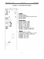
ACCES I/O PRODUCTS INC
10623 Roselle St., San Diego, CA 92121
Tel: (858) 550-9559 FAX: (858) 550-7322
ANALOG AND DIGITAL I/O CARD
AD12-16/16F
USER MANUAL
file:MAD12-16F.D2e.wpd
ANALOG/DIGITAL I/O CARD
AD12-16/16F
USER MANUAL
NOTICES
The information in this document is provided for reference only. ACCES I/O PRODUCTS
INC. does not assume any liability arising out of the application or use of the information
or products described herein. This document may contain or reference information and
products protected by copyrights or patents and does not convey any license under the
patent rights of ACCES, nor the rights of others.
IBM PC, PC/XT, and PC/AT are registered trademarks of the International Business
Machines Corporation.
Printed in USA. Copyright 1994 by ACCES I/O PRODUCTS INC, 10623 Roselle Street,
San Diego, CA 92121-1506. All rights reserved.
ANALOG/DIGITAL I/O CARD
AD12-16/16F
USER MANUAL
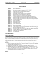
TABLE OF CONTENTS
INSTALLATION . . . . . . . . . . . . . . . . . . . . . . . . . . . . . . . . . . . . .
CD INSTALLATION . . . . . . . . . . . . . . . . . . . . . . . . . . . .
3.5-INCH DISKETTE INSTALLATION . . . . . . . . . . . . .
DIRECTORIES CREATED ON THE HARD DISK . . . .
.
.
.
.
.
.
.
.
.
.
.
.
.
.
.
.
.
.
.
.
.
.
.
.
.
.
.
.
.
.
.
.
.
.
.
.
.
.
.
.
.
.
.
.
.
.
.
.
.
.
.
.
.
.
.
.
.
.
.
.
1-1
1-1
1-1
1-2
FUNCTIONAL DESCRIPTION . . . . . . . . . . . . . . . . . . . . . . . . . . . .
ANALOG INPUTS . . . . . . . . . . . . . . . . . . . . . . . . . . . . . . .
INPUT SYSTEM EXPANSION . . . . . . . . . . . . . . . . . . . . .
DIS CR ET E D IGIT AL I/O . . . . . . . . . . . . . . . . . . . . . . . . . .
COUNTER/TIMER . . . . . . . . . . . . . . . . . . . . . . . . . . . . . .
ANALOG OUTPUT . . . . . . . . . . . . . . . . . . . . . . . . . . . . . .
INTERRUPTS AND DMA . . . . . . . . . . . . . . . . . . . . . . . . .
TRANSFERRING DATA INTO THE COMPUTER . . . . . .
REFERENCE VOLTAGE AND POWER REQUIRED . . . .
INPUT/OUTPUT CONNECTIONS . . . . . . . . . . . . . . . . . .
UTILITY SOFTWARE . . . . . . . . . . . . . . . . . . . . . . . . . . . .
AD12-16/16F BLOCK DIAGRAM . . . . . . . . . . . . . . . . . . .
.
.
.
.
.
.
.
.
.
.
.
.
.
.
.
.
.
.
.
.
.
.
.
.
..........
..........
..........
..........
..........
..........
..........
..........
..........
..........
..........
..........
.
.
.
.
.
.
.
.
.
.
.
.
.
.
.
.
.
.
.
.
.
.
.
.
..........
..........
..........
..........
..........
..........
..........
..........
..........
..........
..........
..........
.
.
.
.
.
.
.
.
.
.
.
.
.
.
.
.
.
.
.
.
.
.
.
.
...
...
...
...
...
...
...
...
...
...
...
...
2-1
2-1
2-1
2-2
2-2
2-3
2-3
2-3
2-4
2-4
2-4
2-5
HARDWARE CONFIGURATION AND INSTALLATION . . . . . . . . . . . . . . . . . . . . . . . . . . . . . . . . . . . . .
OPTION SELECTION . . . . . . . . . . . . . . . . . . . . . . . . . . . . . . . . . . . . . . . . . . . . . . . . . . . . . . . . .
MULTIPLEXER CONFIGURATION . . . . . . . . . . . . . . . . . . . . . . . . . . . . . . . . . . . . . . . .
UNIPOLAR/BIPOLAR RANGE . . . . . . . . . . . . . . . . . . . . . . . . . . . . . . . . . . . . . . . . . . .
INPUT VOLTAGE RANGE . . . . . . . . . . . . . . . . . . . . . . . . . . . . . . . . . . . . . . . . . . . . . . .
OPTION SELECTION MAP . . . . . . . . . . . . . . . . . . . . . . . . . . . . . . . . . . . . . . . . . . . . . .
COUNTER/TIMER . . . . . . . . . . . . . . . . . . . . . . . . . . . . . . . . . . . . . . . . . . . . . . . . . . . . .
CLOCK FREQUENCY SELECT . . . . . . . . . . . . . . . . . . . . . . . . . . . . . . . . . . . . . . . . . .
DIG ITAL I/O . . . . . . . . . . . . . . . . . . . . . . . . . . . . . . . . . . . . . . . . . . . . . . . . . . . . . . . . . .
SELECTING A BASE ADDRESS . . . . . . . . . . . . . . . . . . . . . . . . . . . . . . . . . . . . . . . . .
STANDARD ADDRESS ASSIGNMENTS FOR 286/386/486 COMPUTERS . . . . . . . .
SETTING THE BASE ADDRESS . . . . . . . . . . . . . . . . . . . . . . . . . . . . . . . . . . . . . . . . .
BASE A DDRE SS EXA MPLE . . . . . . . . . . . . . . . . . . . . . . . . . . . . . . . . . . . . . . . . . . . . .
USING THE SETUP PROGRAM TO SET THE BASE ADDRESS . . . . . . . . . . . . . . . .
INSTALLING THE AD12-16/16F CARD . . . . . . . . . . . . . . . . . . . . . . . . . . . . . . . . . . . . . . . . . . .
CALIBRATION AND TEST . . . . . . . . . . . . . . . . . . . . . . . . . . . . . . . . . . . . . . . . . . . . . . . . . . . . .
3-1
3-1
3-1
3-1
3-1
3-3
3-4
3-4
3-4
3-4
3-6
3-7
3-7
3-7
3-8
3-8
PROG RAM MING THE AD12-16/16F . . . . . . . . . . . . . . . . . . . . . . . . . .
AD12-16/16F REGISTER ADDRESS MAP . . . . . . . . . . . . . .
REGISTER DEFINITIONS . . . . . . . . . . . . . . . . . . . . . . . . . . .
A/D REGISTERS . . . . . . . . . . . . . . . . . . . . . . . . . . . .
DIG ITAL I/O . . . . . . . . . . . . . . . . . . . . . . . . . . . . . . . .
ANALOG O UTPUTS . . . . . . . . . . . . . . . . . . . . . . . . .
CARD STATUS AND CLEAR INTERRUPT . . . . . . . .
CARD CONTROL REGISTER . . . . . . . . . . . . . . . . . .
COUNTER/TIMER REGISTERS . . . . . . . . . . . . . . . .
.
.
.
.
.
.
.
.
.
.
.
.
.
.
.
.
.
.
.
.
.
.
.....
.....
.....
.....
.
.
.
.
.
.
.
.
.
.
.
.
.
.........
.........
.........
.........
.........
.........
.........
.........
.........
STANDARD DRIVER REFERENCE . . . . . . . . . . . . . . . . . . . . . . . . . . . . . . . . . . . . .
TASK SUMMARY . . . . . . . . . . . . . . . . . . . . . . . . . . . . . . . . . . . . . . . . . . . . .
TASK REFERENCE . . . . . . . . . . . . . . . . . . . . . . . . . . . . . . . . . . . . . . . . . . .
TASK 0: INITIALIZE . . . . . . . . . . . . . . . . . . . . . . . . . . . . . . . . . . . . .
TASK 1: SET MULTIPLEXER SCAN LIMITS . . . . . . . . . . . . . . . . .
TASK 2: FETCH MUX SCAN LIMITS AND CURRENT CHANNEL .
i
.
.
.
.
.
.
.
.
.
.
.
.
.
.
.....
.....
.....
.....
.
.
.
.
.
.
.
.
.
.
.
.
.
.
.
.
.
.
.
.
.
.
.
.
.
.
.
.
.
.
.
.
.
......
......
......
......
......
......
.
.
.
.
.........
.........
.........
.........
.........
.........
.........
.........
.........
.
.
.
.
.
.
.
.
.
.
.
.
..
..
..
..
..
..
.
.
.
.
.
.
.
.
.
.
.
.
.
.
.
.
.
.
.
.
.
.
.
.
.
.
.
.
4-1
4-1
4-2
4-2
4-3
4-4
4-5
4-5
4-6
.
.
.
.
.
.
.
.
.
.
.
.
5-1
5-3
5-3
5-4
5-5
5-6
ANALOG/DIGITAL I/O CARD
AD12-16/16F
USER MANUAL
TASK 3: PERFORM A SINGLE A/D CONVERSION . . . . . . . . . . . . . . . . . . . . . . . . . . . 5-7
TASK 4: DO N A/D CONVERSIONS USING POLLING . . . . . . . . . . . . . . . . . . . . . . . . 5-7
TASK 5: DO N A/D CONVERSIONS USING INTERRUPT . . . . . . . . . . . . . . . . . . . . . 5-9
TASK 6: DO N A/D CONVERSIONS USING DMA . . . . . . . . . . . . . . . . . . . . . . . . . . . 5-11
TASK 7: TERMINATE DMA/INTERRUPT OPERATION . . . . . . . . . . . . . . . . . . . . . . 5-13
TASK 8: FETCH DMA/INTERRUPT OPERATION STATUS . . . . . . . . . . . . . . . . . . . 5-13
TASK 9: TRANSFER DATA FROM MEMORY TO ARRAY . . . . . . . . . . . . . . . . . . . . 5-14
TASK 10: SET COUNTER 0 MODE . . . . . . . . . . . . . . . . . . . . . . . . . . . . . . . . . . . . . . 5-16
TASK 11: LOAD C OUN TER 0 . . . . . . . . . . . . . . . . . . . . . . . . . . . . . . . . . . . . . . . . . . 5-17
TASK 12: READ COUN TER 0 . . . . . . . . . . . . . . . . . . . . . . . . . . . . . . . . . . . . . . . . . . 5-17
TASK 13: WRITE DIGITAL OUTPUT BITS . . . . . . . . . . . . . . . . . . . . . . . . . . . . . . . . 5-18
TASK 14: READ DIGITAL INPUT BITS . . . . . . . . . . . . . . . . . . . . . . . . . . . . . . . . . . . . 5-19
TASK 15: WRITE VALUE TO A SINGLE D/A CONVERTER . . . . . . . . . . . . . . . . . . . 5-19
TASK 16: WRITE TO BOTH D/A CONVERTERS . . . . . . . . . . . . . . . . . . . . . . . . . . . 5-20
TASK 17: SET COUNTER 1 AND 2 RATE . . . . . . . . . . . . . . . . . . . . . . . . . . . . . . . . . 5-21
TASK 18: D/A OUTPUT ON A/D EOC . . . . . . . . . . . . . . . . . . . . . . . . . . . . . . . . . . . . 5-22
TASK 20: A/D CHANNEL SCAN ON INTERRUPT . . . . . . . . . . . . . . . . . . . . . . . . . . . 5-25
SUMMARY OF ERROR COD ES . . . . . . . . . . . . . . . . . . . . . . . . . . . . . . . . . . . . . . . . . . . . . . . 5-27
USING THE DRIVER WITH TURBO OR BORLAND C . . . . . . . . . . . . . . . . . . . . . . . . 5-28
USING THE DRIVER WITH MICROSO FT C . . . . . . . . . . . . . . . . . . . . . . . . . . . . . . . . 5-28
USING THE DRIVER WITH TURBO PASCAL . . . . . . . . . . . . . . . . . . . . . . . . . . . . . . 5-29
US ING TH E D RIV ER WITH QU ICK BA SIC . . . . . . . . . . . . . . . . . . . . . . . . . . . . . . . . . 5-30
AD12-16/16F WITH AIM-16P DRIVER REFERENCE . . . . . . . . . . . . . . . . . . . . . . . . . . . . . . . . . . . . . . . 6-1
USING THE DRIVER . . . . . . . . . . . . . . . . . . . . . . . . . . . . . . . . . . . . . . . . . . . . . . . . . . . . . . . . . 6-1
THE POINT LIST CONCEPT . . . . . . . . . . . . . . . . . . . . . . . . . . . . . . . . . . . . . . . . . . . . . 6-1
OTHER SOFTWARE FEATURES . . . . . . . . . . . . . . . . . . . . . . . . . . . . . . . . . . . . . . . . 6-2
TASK SUMMARY . . . . . . . . . . . . . . . . . . . . . . . . . . . . . . . . . . . . . . . . . . . . . . . . . . . . . . . . . . . . 6-3
TASK REFERENCE . . . . . . . . . . . . . . . . . . . . . . . . . . . . . . . . . . . . . . . . . . . . . . . . . . . . . . . . . . 6-3
TASK 0: INITIALIZE . . . . . . . . . . . . . . . . . . . . . . . . . . . . . . . . . . . . . . . . . . . . . . . . . . . . 6-3
TASK 1: SET MULTIPLEXER SCAN LIMITS . . . . . . . . . . . . . . . . . . . . . . . . . . . . . . . . 6-4
TASK 2: FETCH GAIN CODE FOR A POINT ADDRESS . . . . . . . . . . . . . . . . . . . . . . . 6-5
TASK 3: FETCH POINT ADDRESS FOR A POINT LIST INDEX . . . . . . . . . . . . . . . . . 6-6
TASK 4: ASSIGNS GAIN CODE TO RANGE OF POINT ADDRESSES . . . . . . . . . . . 6-6
TASK 5: ASSIGN POINT ADDRES SES TO THE POINT LIST . . . . . . . . . . . . . . . . . . 6-8
TASK 6: FETCH DATA FROM A POINT ADDRESS . . . . . . . . . . . . . . . . . . . . . . . . . . 6-8
TASK 7: FETCH SINGLE DATA PO INT USING POINT LIST . . . . . . . . . . . . . . . . . . . 6-9
TASK 8: FETCH MULTIPLE BUFFERED CONVERSIONS . . . . . . . . . . . . . . . . . . . . 6-10
TASK 9: INTERRUPT DRIVEN DATA ACQUISITION . . . . . . . . . . . . . . . . . . . . . . . . 6-11
TASK 10: THERMO COUPLE/FUNCTION ASSIGNMEN T . . . . . . . . . . . . . . . . . . . . . 6-13
TASK 11: RESET FUNCTIONS . . . . . . . . . . . . . . . . . . . . . . . . . . . . . . . . . . . . . . . . . 6-16
TASK 12: DIGITAL OUTPUT . . . . . . . . . . . . . . . . . . . . . . . . . . . . . . . . . . . . . . . . . . . 6-17
TASK 13: DIGITAL INPUT . . . . . . . . . . . . . . . . . . . . . . . . . . . . . . . . . . . . . . . . . . . . . 6-17
TASK 14: COUNTER/TIMER SETUP . . . . . . . . . . . . . . . . . . . . . . . . . . . . . . . . . . . . . 6-18
TASK 15: READ COUNTER/TIMER COUNT . . . . . . . . . . . . . . . . . . . . . . . . . . . . . . . 6-19
TASK 16: HIGH PERFORMANCE BUFFERED CONVERSIONS . . . . . . . . . . . . . . . 6-19
TASK 17: DO N A/D CONVERSIONS USING DMA . . . . . . . . . . . . . . . . . . . . . . . . . . 6-20
TASK 18: TRANSFER DATA FROM MEMORY TO ARRAY . . . . . . . . . . . . . . . . . . . 6-22
TASK 19: TERMINATE DMA/INTERRUPT OPERATION . . . . . . . . . . . . . . . . . . . . . 6-23
TASK 20: WRITE VALUE TO A D/A CONVERTER . . . . . . . . . . . . . . . . . . . . . . . . . . 6-24
SUMMARY OF ERROR COD ES . . . . . . . . . . . . . . . . . . . . . . . . . . . . . . . . . . . . . . . . . . . . . . . 6-25
A/D CONVERTER APPLICATIONS . . . . . . . . . . . . . . . . . . . . . . . . . . . . . . . . . . . . . . . . . . . . . . . . . . . . . 7-1
CONNE CTING ANALOG INPUTS . . . . . . . . . . . . . . . . . . . . . . . . . . . . . . . . . . . . . . . . . . . . . . . 7-1
ii
ANALOG/DIGITAL I/O CARD
AD12-16/16F
USER MANUAL
COMMENTS ON NOISE INTERFERENCE . . . . . . . . . . . . . . . . . . . . . . . . . . . . . . . . . . . . . . . .
Ground Loops . . . . . . . . . . . . . . . . . . . . . . . . . . . . . . . . . . . . . . . . . . . . . . . . . . . . . . . . .
External Noise . . . . . . . . . . . . . . . . . . . . . . . . . . . . . . . . . . . . . . . . . . . . . . . . . . . . . . . .
INPUT RANGE AND RESOLUTION SPECIFICATIONS . . . . . . . . . . . . . . . . . . . . . . . . . . . . . .
CURREN T MEASURE MENTS . . . . . . . . . . . . . . . . . . . . . . . . . . . . . . . . . . . . . . . . . . . . . . . . . .
MEASURING LARGE VOLTAGES . . . . . . . . . . . . . . . . . . . . . . . . . . . . . . . . . . . . . . . . . . . . . . .
ADDING MOR E ANALOG INPUTS . . . . . . . . . . . . . . . . . . . . . . . . . . . . . . . . . . . . . . . . . . . . . .
PRECAUTIONS - NOISE, GROUND LOOPS, AND OVERLOADS . . . . . . . . . . . . . . . . . . . . . .
7-1
7-2
7-2
7-2
7-2
7-3
7-3
7-4
COUNTER/TIMER OPERATIONS . . . . . . . . . . . . . . . . . . . . . . . . . . . . . . . . . . . . . . . . . . . . . . . . . . . . . . 8-1
OPERATIONAL MODES . . . . . . . . . . . . . . . . . . . . . . . . . . . . . . . . . . . . . . . . . . . . . . . . . . . . . . . 8-1
Mode 0: Pulse on Terminal Count . . . . . . . . . . . . . . . . . . . . . . . . . . . . . . . . . . . . . . . . . 8-1
Mode 1: Retriggerable One-Shot . . . . . . . . . . . . . . . . . . . . . . . . . . . . . . . . . . . . . . . . . . 8-2
Mode 2: Rate Generator . . . . . . . . . . . . . . . . . . . . . . . . . . . . . . . . . . . . . . . . . . . . . . . . . 8-2
Mode 3: Square Wave Generator . . . . . . . . . . . . . . . . . . . . . . . . . . . . . . . . . . . . . . . . . 8-2
Mode 4: Software Triggered Strobe . . . . . . . . . . . . . . . . . . . . . . . . . . . . . . . . . . . . . . . . 8-2
Mode 5: Hardware Triggered Strobe . . . . . . . . . . . . . . . . . . . . . . . . . . . . . . . . . . . . . . . 8-2
PROGRAMMING . . . . . . . . . . . . . . . . . . . . . . . . . . . . . . . . . . . . . . . . . . . . . . . . . . . . . . . . . . . . 8-3
READING AND LOADING THE COUNTERS . . . . . . . . . . . . . . . . . . . . . . . . . . . . . . . . 8-4
PROGRAMMING EXAMPLES . . . . . . . . . . . . . . . . . . . . . . . . . . . . . . . . . . . . . . . . . . . . 8-6
Generating a Square Wave Output . . . . . . . . . . . . . . . . . . . . . . . . . . . . . . . . . . 8-6
Determining Status of Counter #1 . . . . . . . . . . . . . . . . . . . . . . . . . . . . . . . . . . . 8-6
Using Counter #0 as a Pulse Counter . . . . . . . . . . . . . . . . . . . . . . . . . . . . . . . . 8-6
Reading Counter #0 . . . . . . . . . . . . . . . . . . . . . . . . . . . . . . . . . . . . . . . . . . . . . 8-6
PROGRAMMING EXAMPLES USING THE A16DRV DRIVER . . . . . . . . . . . . . . . . . . . 8-7
COUNTER/TIMER ENABLE REGISTER . . . . . . . . . . . . . . . . . . . . . . . . . . . . . . . . . . . . . . . . . . 8-8
TRIGGER ING THE A/D PER IODICALLY . . . . . . . . . . . . . . . . . . . . . . . . . . . . . . . . . . . 8-8
GENERATING SQUARE WAVES OF PROGRAMMED FREQUENCY . . . . . . . . . . . . 8-9
MEASURING FREQUENCY AND PERIOD . . . . . . . . . . . . . . . . . . . . . . . . . . . . . . . . 8-10
GENERATING TIME DELAYS . . . . . . . . . . . . . . . . . . . . . . . . . . . . . . . . . . . . . . . . . . . 8-10
Pulse On Terminal Count . . . . . . . . . . . . . . . . . . . . . . . . . . . . . . . . . . . . . . . . 8-10
Programmable One-Shot . . . . . . . . . . . . . . . . . . . . . . . . . . . . . . . . . . . . . . . . 8-11
Software Triggered Strobe . . . . . . . . . . . . . . . . . . . . . . . . . . . . . . . . . . . . . . . 8-11
Hardware Triggered Strobe . . . . . . . . . . . . . . . . . . . . . . . . . . . . . . . . . . . . . . . 8-11
GENERATING INTERRUPTS WITH THE COUNTER/TIMER . . . . . . . . . . . . . . . . . . 8-11
D/A CONVERTERS . . . . . . . . . . . . . . . . . . . .
PROGRAMMING . . . . . . . . . . . . . . .
USE WITH AC REFERENCE . . . . . .
ARBITRARY WAVEFORM OUTPUT
.
.
.
.
.
.
.
.
.
.
.
.
..........
..........
..........
..........
.
.
.
.
.
.
.
.
..........
..........
..........
..........
.
.
.
.
.
.
.
.
..........
..........
..........
..........
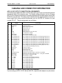
CABLING AND CONNECTOR INFORMATION . . . . . . . . . . . . . . . . . . . . . . . . . . . . . .
AD12-16/16F OUTPUT CONNE CTOR PIN ASSIGNMENTS . . . . . . . . . . . . .
AD12-16/16F TO AIM-16P CABLE ADAP TER ASS EMBLY . . . . . . . . . . . . . .
CA 37-2 - A D1 2-16/16F AD AP TO R T O S EC ON D S TR ING OF AIM -16's . . . .
.
.
.
.
.
.
.
.
.
.
.
.
.
.
.
.
.
.
.
.
.
.
.
.
.
.
.
.
......
......
......
......
.......
.......
.......
.......
.
.
.
.
9-1
9-1
9-3
9-3
10-1
10-1
10-2
10-3
SPECIFICATIONS . . . . . . . . . . . . . . . . . . . . . . . . . . . . . . . . . . . . . . . . . . . . . . . . . . . . . . . . . . . . . . . . . 11-1
WARR ANTY . . . . . . . . . . . . . . . . . . . . . . . . . . . . . . . . . . . . . . . . . . . . . . . . . . . . . . . . . . . . . . . . . . . . . . 12-1
LINEARIZATION . . . . . . . . . . . . . . . . . . . . . . . . . . . . . . . . . . . . . . . . . . . . . . . . . . . . . . . . . . . . . . . . . . A-1
BASIC INTEGER VARIABLE STORAGE . . . . . . . . . . . . . . . . . . . . . . . . . . . . . . . . . . . . . . . . . . . . . . . B-1
iii
ANALOG/DIGITAL I/O CARD
AD12-16/16F
USER MANUAL
DIRECT MEMORY ACCESS . . . . . . . . . . . . . . . . . . . . . . . . . . . . . . . . . . . . . . . . . . . . . . . . . . . . . . . . . C-1
IBM PC DMA STRUCTURE . . . . . . . . . . . . . . . . . . . . . . . . . . . . . . . . . . . . . . . . . . . . . . . . . . . C-1
PAGE REGISTER AND DMA CONTROLLER FUNCTIONS . . . . . . . . . . . . . . . . . . . . . . . . . . C-3
iv
ANALOG/DIGITAL I/O CARD
AD12-16/16F
1-1
USER MANUAL
ANALOG/DIGITAL I/O CARD
AD12-16/16F
This page purposely omittted.
1-2
USER MANUAL
ANALOG/DIGITAL I/O CARD
AD12-16/16F
USER MANUAL
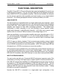
FUNCTIONAL DESCRIPTION
The AD12-16 and AD12-16F are multifunction high-speed analog/digital I/O cards for use
in IBM Personal Computers. They are full length cards that can be installed in expansion
slots of IBM PC/XT/AT and compatible computers. With this card installed, the computer
can be used as a precision data acquisition and control system or as a signal analysis
instrument. The following paragraphs describe functions provided by this card.
ANALOG INPUTS
The card accepts up to eight differential or 16 single-ended analog input channels. Inputs
are protected against overvoltages up to ±35 volts and typically survive static discharges
beyond 4000 volts. When power is off, the inputs are open-circuited providing fail-safe
operation and continue to offer ±20V overvoltage protection. The channel input
configuration is switch selectable on the card providing a choice between sixteen
single-ended channels or eight differential channels. In the latter case, common mode
rejection ratio is a minimum 6 dB and common mode voltage range is ±11V.
Inputs are amplified by an instrumentation amplifier with switch selectable gains of 10, 5,
2, 1, and 0.5 to provide voltage ranges of 1, 2, 5, and 10 volts unipolar and ±0.5, ±1, ±2.5,
±5, and ±10 volts bipolar. In addition, you can set up a special range by installing a single
gain-setting resistor.
AD12-16 uses an industry standard 12-bit successive-approximation analog-to-digital
converter (A/D) with a sample and hold amplifier input. Under ideal conditions, throughputs
of up to 50,000 conversions per second are possible. (AD12-16F uses a faster A/D and
throughputs up to 100,000 conversions per second are possible.)
A/D conversions may be initiated in any one of three ways: (a) by software command, (b)
by on-board programmable timer, or (c) by direct external trigger. In turn, data may be
transferred to the computer by any of three software selectable methods: (a) by polling for
EOC (End Of Conversion), (b) by EOC interrupt, or (c) by direct memory access (DMA).
INPUT SYSTEM EXPANSION
The card can be used with up to 16 external AIM-16P analog input expansion cards. (This
necessitates converting some digital inputs to digital outputs as will be described later.)
Each AIM-16P card provides capability for 16 differential inputs and, thus, there can be up
to a maximum of 256 inputs per combination of AIM-16P's and AD12-16/16F. The first
AIM-16P is connected to the AD12-16/16F by a special cable adapter and ribbon cable, any
additional AIM-16P cards are daisy-chained to each other by ribbon cables. Cabling
information is provided in Appendix B.
Normally the AIM-16P is connected to a single-ended input configuration of the
2-1
ANALOG/DIGITAL I/O CARD
AD12-16/16F
USER MANUAL
AD12-16/16F. However, if interconnect cable noise becomes a problem or if long cables
are necessary, then the AIM-16P cards can be connected to the differential inputs of
AD12-16/16F. A differential connection allows better monitoring of remote locations
because noise will be reduced by the common mode noise rejection capability of
AD12-16/16F. (Note: In this configuration, the maximum number of inputs accommodated
is 128.) AIM-16P card address and channel address on the selected AIM-16P are
controlled by digital outputs from the AD12-16/16F.
To use the programmable gain feature of the AIM-16P, the AD12-16/16F digital inputs bits
IP1, IP2 and IP3 must be converted to digital outputs. This conversion is done by installing
jumpers D5, D6 and D7.
DISCRETE DIGITAL I/O
Four bits of TTL/CMOS-compatible digital input capability are provided. Digital inputs IP0
and IP2 have dual uses. Input IP0 provides an external trigger for the A/D or can be used
as the gate for Counter/Timers 1 and 2. Input IP2 provides an input to enable
Counter/Timer 0.
The digital input bits can be converted to output ports for AIM-16P applications as
described in the INPUT SYSTEM EXPANSION section of this chapter. When this is done,
you give up capability for gating Counter/Timer 0. In this case discrete inputs IP1 though
IP3 are used to control the gain of the AIM-16P.
Four bits of digital output are available with LSTTL logic levels and 10 LSTTL load drive
capability. Discrete outputs OP0 through OP3 provide multiplexer addressing. capability
for input expansion card use, as described in the INPUT SYSTEM EXPANSION section,
or as separate digital outputs.
COUNTER/TIMER
The AD12-16/16F contain a type 8254 counter/timer which has three 16-bit programmable
down counters. Counter/Timer 0 is enabled by a digital input (IP2) and uses either an
internal 100 KHz clock or an external clock of up to 10 MHz as selected by user software.
This counter/timer is not committed on the card; it's clock, enable, and output lines are
available to you at the I/O connector. Counter/Timers 1 and 2 are concatenated and form
a 32-bit counter/timer for timed A/D trigger pulses and/or for external frequency generation.
The dual counter/timer can be enabled by program control and clocked by a
jumper-selected 1 MHz or 10 MHz on-board crystal oscillator source.
2-2
ANALOG/DIGITAL I/O CARD
AD12-16/16F
USER MANUAL
Counter/Timer 0 and Counter/Timers 1 and 2 can be set up for event counting, frequency
or period measurements, and pulse or wave form generation. Also, Counter/Timers 1 and
2 can be programmed to initiate A/D conversions. See the PROGRAMMABLE INTERVAL
TIMER section of this manual for a description of ways that the type 8254 counter/timer
chip can be used.
ANALOG OUTPUT
The AD12-16/16F has two multiplying 12-bit digital-to-analog converters (D/A) connected
to output drivers capable of providing 5 mA current drive. Each channel provides an output
of 0 to +5VDC if the internal -5V reference voltage is used; i.e., jumper from I/O connector
pin 8 to pin 10 (DAC 0) and from pin 8 to pin 26 (DAC 1). That on board reference voltage
can be replaced by an externally supplied reference voltage (biased AC or DC). In this
case, the D/A's will operate as multiplying D/A's with two quadrant capability. The
maximum external reference voltage that can be applied is -10 volts.
INTERRUPTS AND DMA
Interrupts can be initiated by completion of an A/D conversion or by DMA terminal count
if programmed by software. Interrupt levels 2 through 7 are selectable via software.
Software control of direct memory access for transfer of A/D conversion data to the
computer is supported at either DMA level 1 or 3 as selected by switch S1.
TRANSFERRING DATA INTO THE COMPUTER
The AD12-16/16F has been designed using state of the art components to provide high
data throughput using the DMA capabilities of the IBM PC family. Direct memory access
is the most satisfactory way to transfer data from the A/D to memory at rates over 10,000
samples/second. At this speed, program transfers through the CPU become difficult to
handle in the short time available between conversions.
Also, program transfers are subject to disruption by other interrupt processes in the
computer. Use of real time triggering of the A/D plus DMA assures synchronism in
sampling that is unaffected by other computer operations. That capability is essential in
applications such as signal analysis, fast fourier transform, and vibration and transient
analysis where high data rates must be sustained for short intervals of time.
Thus, AD12-16/16F's open I/O-mapped architecture together with three modes of data
transfer (polling via CPU, interrupt via CPU, and DMA) provides considerable application
flexibility.
2-3
ANALOG/DIGITAL I/O CARD
AD12-16/16F
USER MANUAL
REFERENCE VOLTAGE AND POWER REQUIRED
A -5.0 volt (±0.05) reference voltage is available from the A/D reference source for external
use. This reference output can source up to 5 mA of current. The AD12-16/16F requires
only +5VDC and +12VDC from the computer power supply. An on-board DC-DC converter
translates the 12VDC to low noise, isolated ±15VDC for the precision analog circuitry.
INPUT/OUTPUT CONNECTIONS
External connections can be made through a standard 37-pin male connector located at
the rear of the computer. AIM-16P's may be connected using special cabling as described
in APPENDIX B.
UTILITY SOFTWARE
Utility software is provided on CD with the AD12-16/16F card. This software includes an
illustrated setup and calibration program, software drivers for QuickBASIC, Turbo-C, and
Turbo-Pascal, and sample programs. Additionally, a utility driver for use with VisualBASIC
for Windows is provided. Section 3 of this manual contains a detailed description.
As a further convenience in application, the AD12-16 and AD12-16F are also supported by
several third-party software packages. The drivers for these cards are the same ones used
for the Keithley/MetraByte DAS-16/16F. However, these drivers do not take advantage of
the channel-by-channel gain programming capability of the AIM-16's.
Some available software packages are listed below:
a. . . STREAM-16 high speed hard disk transfer utility. Continuous A/D data
transfer rates to hard disk in excess of 50 KHz are possible on PC/AT and
somewhat slower on PC/XT depending on the hard disk controller type.
b. . . LABTECH NOTEBOOK and LT CONTROL menu-driven data acquisition,
analysis and control packages from Laboratory Technologies Corp.
c. . . ASYST programmable data acquisition and analysis software from
Keithley/ASYST.
d. . . ASYSTANT menu-driven data acquisition and analysis software from
Keithley/ASYST.
e. . . UNKELSCOPE menu-driven data acquisition and analysis from Unkel
Software Inc. (Copyright M.I.T.)
f. . . SNAPSHOT STORAGE SCOPE menu-driven data acquisition and analysis
package from H.E.M. Data Corp.
g. . . TTOOLS utilities for the Turbo-Pascal programmer from Quinn-Curtiss
Software.
h. . . CTOOLS utilities for the C programmer by the Systems Guild.
2-4
ANALOG/DIGITAL I/O CARD
AD12-16/16F
FIGURE 1-1: AD12-16/16F BLOCK DIAGRAM
2-5
USER MANUAL
ANALOG/DIGITAL I/O CARD
AD12-16/16F
(This page purposely omitted.)
2-6
USER MANUAL
ANALOG/DIGITAL I/O CARD
AD12-16/16F
USER MANUAL
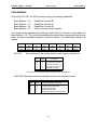
HARDWARE CONFIGURATION AND INSTALLATION
OPTION SELECTION
Many of the AD12-16/16F card features are selected by hardware jumpers or switches.
At least one of each of the option categories must be selected if the card is to operate
correctly. The setup program provided on CD with the card provides menu-driven pictorial
presentations to help you quickly set up the card.
You may also refer to FIGURE 3-1: OPTION SELECTION MAP, and the following sections
to set up the card. The card need not be plugged into the computer at this time.
MULTIPLEXER CONFIGURATION
Select the desired A/D input multiplexer configuration using switch S3 located in the upper
right hand corner of the card near the I/O connector:
8-Channel Differential Input =
16-Channel Single-Ended Input =
8CH position
16CH position
UNIPOLAR/BIPOLAR RANGE
In the unipolar mode, inputs can be positive only; i.e., ranges from zero volts to some
positive voltage. (The maximum voltage span in the unipolar mode is 10V.) In the bipolar
mode, inputs can be between positive and negative full scale limits. Select for unipolar or
bipolar range using switch S2 located just above U38:
Unipolar = UNI position (up)
Bipolar = BIP position (down)
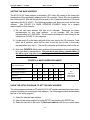
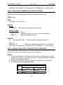
INPUT VOLTAGE RANGE
Input voltage range is selected using sections of GAIN SEL switch S5 for gains of 1, 2, 5,
and 10 and by installing the 0.5 GAIN jumper. Note that switch S5 is oriented such that,
when the card is installed in the computer, it is possible to change gain (and thus range)
at the rear of the computer without removing the card from the computer. The 0.5 GAIN
jumper is located at the top of the card.
3-1
ANALOG/DIGITAL I/O CARD
AD12-16/16F
USER MANUAL
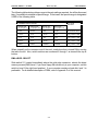
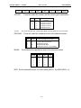
The following table relates voltage range to the gain settings required. As will be discussed
later, it's possible to establish a special range. In that case, the special range is designated
USER in the following table.
DESIRED INPUT RANGE
UNIPOLAR
x½ jum per in
UNIPOLAR
x½ jumper out
BIPOLAR
x½ jum per in
BIPOLAR
x½ jumper out
S5 GA IN
SELECT
0-5V
0-10V
±5V
±10V
All switches OFF
0-2.5V
0-5V
±2.5V
±5V
Only switch 6 ON
0-1V
0-2V
±1V
±2V
Only switch 5 ON
0-0.5V
0-1V
±0.5V
±1V
Only switch 4 ON
±USER
±USER
Only switch 3 ON
USER
USER
When viewed from the connector end of the card, a switch section is turned ON by moving
the tab to the left. Also, switch sections are numbered 6 through 1 as viewed from top to
bottom.
DMA LEVEL SELECT
Slide switch S1, located immediately above the gold edge connector, selects the direct
memory access (DMA) level. If you have floppy disk drives only in your computer, set this
switch to level 3 (the right hand position). If your computer contains a hard disk, level 1 is
preferable. For a detailed description of DMA, refer to Appendix D of this manual.
3-2
ANALOG/DIGITAL I/O CARD
AD12-16/16F
FIGURE 2-1: OPTION SELECTION MAP
3-3
USER MANUAL
ANALOG/DIGITAL I/O CARD
AD12-16/16F
USER MANUAL
COUNTER/TIMER
Three 16-bit Counter/Timers are provided on AD12-16/16F. Refer to the block diagram on
page 1-5 for an understanding of the counter/timer configuration and to CHAPTER 7:
COUNTER/TIMER OPERATIONS for a description of applications. Counter 0 is fully
accessible to you if multiple AIM-16P's are not being used with the AD12-16/16F as
described in the first section: FUNCTIONAL DESCRIPTION.
Counters 1 and 2 are intended for software-programmed, timed A/D start. Counter 0 has
its clock and output lines available on the I/O connector. The gate input for Counter 0 is
at digital input IP2.
CLOCK FREQUENCY SELECT
The clock for Counter 1 is either 1 MHz or 10 MHz derived from an on-board crystal
oscillator and selected by the CLOCK jumper located under DC/DC Converter transformer
T1. Installing the jumper between the upper two posts selects 10 MHz and installing the
jumper between the lower two posts selects 1 MHz.
DIGITAL I/O
As mentioned in CHAPTER ONE: FUNCTIONAL DESCRIPTION, digital input ports IP0
through IP3 can be converted to output ports by installation of jumpers on the card. These
are jumpers D4 through D7 located to the left of the A/D converter chip and adjacent to SIP
resistor network RN2.
SELECTING A BASE ADDRESS
You need to select an unused segment of 16 consecutive I/O addresses. The base
address will be the first address in this segment. The base address may be selected
anywhere on a 16-bit boundary within the I/O address range 200-3FF hex providing that
it does not overlap with other functions. The following procedure will show you how to
select the base I/O address.
1) Check the tables in FIGURES 2-2 and 2-3 for lists of standard address assignments
and then check what addresses are used by any other I/O peripherals that are
installed in your computer. Memory addressing is separate from I/O addressing, so
there is no possible conflict with any add-on memory that may be installed in your
computer. We urge that you carefully review the address assignment table before
selecting a card address. If the addresses of two installed functions overlap,
unpredictable computer behavior will result.
2) From this list, (or using the FINDBASE program) select an unused portion of 16
consecutive I/O addresses. Note from the tables that the sections 280-2EF and
330-36F are unused. This address space is a good area to select a base address
3-4
ANALOG/DIGITAL I/O CARD
AD12-16/16F
USER MANUAL
from. Also, if you are not using a given device listed in the tables, then you may use
that base address as well. For example, most computers do not have a prototype
card installed. If your computer does not have one, then base address 300 hex is
a good choice for a base address.
3) Finally make sure that the base address you have chosen has the last digit as 0.
This insures that your base address is on a 16-bit boundary.
3-5
ANALOG/DIGITAL I/O CARD
AD12-16/16F
FIGURE 2-3: STANDARD ADDRESS
ASSIGNMENTS FOR 286/386/486
COMPUTERS
Hex Range
Usage
000-01F
020-03F
040-05F
060-06F
070-07F
080-09F
0A0-0BF
0C0-0DF
0F0
0F1
0F8-0FF
1F0-1F8
200-207
278-27F
2F8-2FF
300-31F
360-36F
378-37F
380-38F
3A0-3AF
3B0-3BF
3C0-3CE
3D0-3DF
3F0-3F7
3F8-3FF
DMA Controller 1
INT Controller 1, Master
Timer
8042 (Keyboard)
Real Time Clock, NMI Mask
DMA Page Register
INT Controller 2
DMA Controller 2
Clear Math Coprocessor Busy
Reset Coprocessor
Arithmetic Processor
Fixed Disk
Game I/O
Parallel Printer Port 2
Asynchronous Comm'n (Secondary)
Prototype Card
Reserved
Parallel Printer Port 1
SDLC or Binary Synchronous Comm'n 2
Binary Synchronous Comm'n 1
Monochrome Display/Printer
Local Area Network
Color/Graphic Monitor
Floppy Diskette Controller
Asynchronous Comm'n (Primary)
3-6
USER MANUAL
ANALOG/DIGITAL I/O CARD
AD12-16/16F
USER MANUAL
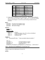
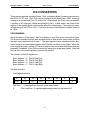
SETTING THE BASE ADDRESS
The AD12-16/16F base address is selected by DIP switch S4 located in the lower right
hand portion of the card directly adjacent to the I/O connector. Switch S4 controls address
bits A4 through A9. (Bits A0 through A3 are used for the 16 address locations in I/O space
required by the AD12-16/16F.) The following procedure will show you how to set the base
address. See FIGURE 2-4: BASE ADDRESS EXAMPLE below for a graphic
representation of this example.
1) We will use base address 300 hex as an example. Determine the binary
representation for your base address. In our example, 300, the binary
representation is 11 0000 0000. The conversion multipliers for each binary bit are
contained in FIGURE 2-4 for reference.
2) Locate switch S on the lower right side of the card, next to the I/O connector. Note
there are 6 switches, which will be used to set the first six bits in the binary
representation from step 1). The last 0 is assumed and therefore need not be set.
3) Note from FIGURE 2-4 that switch position A9 corresponds to the most significant
bit in your binary representation. For each bit in your binary representation, if
the bit is a one, turn the corresponding switch off; if the bit is zero, turn the
corresponding switch on.
FIGURE 2-4: BASE ADDRESS EXAMPLE
Hex representation
3
0
0
Binary representation
1
1
0
0
0
0
Conversion multiplier
2
1
8
4
2
1
A9
A8
A7
A6
A5
A4
OFF
OFF
ON
ON
ON
ON
Sw itch ID
Switch setting
NO
SWITCH
SETTINGS
REQUIRED
USING THE SETUP PROGRAM TO SET THE BASE ADDRESS
The setup program provided on CD with AD12-16/16F contains an interactive menu-driven
program to assist you in setting the base address. The following procedure demonstrates
the use of the setup program.
1) Select the desired base address.
2) Execute the setup program by typing SETUP and pressing the ENTER key.
3) Select the first item in the menu, 1) Set board address. with the up or down arrow
3-7
ANALOG/DIGITAL I/O CARD
AD12-16/16F
USER MANUAL
key and press ENTER.
4) Enter the desired base address in hex, the program will display a graphic
representation of how you should set the switches. You may press the space bar
to try another address.
5) Set DIP switch S4 as shown on the graphic representation.
INSTALLING THE AD12-16/16F CARD
The following procedure will show you how to install the AD12-16/16 inside the computer.
1) Ensure that all options have been set as described in the first part of this chapter.
Be sure to pay close attention to base address selection.
2) Turn off the power switch of your computer and remove the power cords from the
wall outlet.
CAUTION
FAILURE TO REMOVE POWER FROM THE COMPUTER COULD RESULT IN ELECTRICAL
SHOCK, OR DAMAGE TO YOUR COMPUTER SYSTEM.
3) Remove the computer cover.
4) Locate an unused full length slot, and remove the blank I/O back plate.
5) Insert the card in the slot, and install the I/O back plate screw. To ensure that there
is minimum susceptibility to EMI and minimum radiation, it is important that there be
a positive chassis ground. Also, proper EMI cabling techniques must be used on
I/O wiring.
6) Inspect the installation for proper fit and seating of the card.
7) Replace the computer cover.
8) Reapply power to the computer.
9) Perform the calibration procedure which follows.
CALIBRATION AND TEST
Periodic calibration of AD12-16/16F is recommended to retain full accuracy. The
calibration interval depends to a large extent on the type of service that the card is
subjected to. For environments where there are frequent large changes of temperature
and/or vibration, a three-month interval is suggested. For laboratory or office conditions,
six months to a year is acceptable.
A 4-1/2 digit digital multimeter is required as a minimum to perform satisfactory calibration.
Also, a voltage calibrator or a stable noise-free DC voltage source that can be used in
conjunction with the digital multimeter is required.
3-8
ANALOG/DIGITAL I/O CARD
AD12-16/16F
USER MANUAL
Calibration is performed using the SETUP program supplied with your card. This program
will lead you through the set up and calibration procedure with prompts and graphic
displays that show the settings and adjustment trim pots. This calibration program also
serves as a useful test of the AD12-16/16F A/D and D/A functions and can aid in
troubleshooting if problems arise.
CALIBRATION SOFTWARE
The following procedure is brief and is intended for use in conjunction with the calibration
part of the SETUP program.
1) Start the calibration program by typing SETUP and press the ENTER key at the
DOS prompt.
2) Use the relevant menu selections to set the switches and jumpers for the manner
in which the card will be used; i.e., number of channels, gain, and polarity. These
settings are used by the calibration portion of the program. Note: The card must be
in the 16-channel single-ended configuration for this calibration procedure.
3) Use the arrow key to select option 7) Calibrate, then press the ENTER key.
4) The program displays a message about the initial settings. Press any key to
continue.
5) Following the instructions on the screen, perform the Zero adjustment. Press
ENTER when complete.
6) The program will now compute the full-scale adjustment voltage. Apply this voltage
as instructed and make the full-scale adjustment. Press ENTER when complete.
7) Now, use the -5V reference voltage on the card (or your own reference voltage) as
shown on the screen. Perform DAC0 zero adjustment as instructed and press
ENTER when complete.
8) Now perform the DAC0 span adjustment.
9) Steps 7 and 8 will be repeated by the program for zero and span adjustment of
DAC1.
10) This completes the calibration procedure.
3-9
ANALOG/DIGITAL I/O CARD
AD12-16/16F
This page purposely omitted.
3-10
USER MANUAL
ANALOG/DIGITAL I/O CARD
AD12-16/16F
USER MANUAL
PROGRAMMING THE AD12-16/16F
This section provides you with information on how to program the AD12-16/16F. First,
information is provided on how to program the card using direct register access. Following
this is information on using the device drivers provided with the AD12-16/16F.
At the lowest level, the AD12-16/16F can be programmed using direct I/O input and output
instructions. In BASIC, these are the INP (X) and OUT X,Y functions. Assembly language
and most high level languages have equivalent instructions. Use of these functions usually
involves formatting data and dealing with absolute I/O addresses. Although not
demanding, this can require many lines of code and requires an understanding of the
devices, data format, and architecture of the AD12-16/16F.
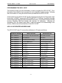
AD12-16/16F REGISTER ADDRESS MAP
The AD12-16/16F uses 16 consecutive addresses in I/O space as follows:
REGISTER ADDRESS
READ FUNCTION
WRITE FUNCTION
BASE ADDR ESS + 0
A/D Low Byte and Channel Number
Start A/D Conversion
BASE ADDR ESS + 1
A/D High Byte
Not Used
BASE ADDR ESS + 2
Start/Stop Channel Range
Start/Stop Channel Range
BASE ADDR ESS + 3
Four-Bit Digital Input
Four-Bit Digital Output
BASE ADDR ESS + 4
Not used
DA C 0 Low Byte
BASE ADDR ESS + 5
Not Used
DA C 0 High Byte
BASE ADDR ESS + 6
Not Used
DA C 1 Low Byte
BASE ADDR ESS + 7
Not Used
DA C 1 High Byte
BASE ADDR ESS + 8
Card Status
Clear Interrupt
BASE ADDR ESS + 9
Card Control
Card Control
BASE A DDRE SS + 10
Not Used
Co unter E nable
BASE A DDRE SS + 11
Not Used
Not Used
BASE A DDRE SS + 12
Counter 0 Count Value
Counter 0 Load
BASE A DDRE SS + 13
Counter 1 Count Value
Counter 1 Load
BASE A DDRE SS + 14
Counter 2 Count Value
Counter 2 Load
BASE A DDRE SS + 15
Not Used
Counter Control
4-1
ANALOG/DIGITAL I/O CARD
AD12-16/16F
USER MANUAL
REGISTER DEFINITIONS
A/D REGISTERS
A/D data are in true binary form and are latched in the A/D registers at the end of each
conversion. These are read at base address and base address +1 in low-byte/high-byte
sequence. The data are available until the end of the next A/D conversion. Channel
address, also in binary form, is supplied with the data.
Base + 0 Read: Contains the lower four bits of the A/D converter output in binary form and
the channel address in binary form.
B7
B6
B5
B4
B3
B2
B1
B0
AD3
AD2
AD1
AD0
MA3
MA2
MA1
MA0
AD0-AD3:
MA0-MA3:
The lower four bits of the A/D conversion, AD0 is the least-significant bit.
The binary representation of the channel number converted, MA0 is the
least-significant bit.
Base + 0 Write: A write to this location starts an A/D conversion. The data written is
irrelevant. This causes the EOC bit of the status register to go high until the conversion is
complete.
Base + 1 Read: Contains the upper eight bits of the A/D converter output in binary form.
B7
B6
B5
B4
B3
B2
B1
B0
AD11
AD10
AD9
AD8
AD7
AD6
AD5
AD4
AD4-AD11: The most significant eight bits of the A/D conversion, AD11 is the mostsignificant bit.
Base + 2 Read and Write: This register controls the multiplexer scan limits and contains
the channel scan starting and ending channel numbers in binary form. About 1/2
microsecond after the A/D starts a conversion, while the sample and hold amplifier is
holding the previous channel, the multiplexer address is incremented to prepare for the next
conversion. When conversion is complete at the Stop channel (High Channel Number),
the cycle repeats starting with the Start channel (Low Channel Number). When
4-2
ANALOG/DIGITAL I/O CARD
AD12-16/16F
USER MANUAL
writing to this register, the multiplexer is always automatically initialized to the Start Channel
number.
B7
B6
HMA3
HMA2
LMA0-LMA3:
HMA0-HMA3:
B5
HMA1
B4
HMA0
B3
B2
B1
B0
LMA3
LMA2
LMA1
LMA0
Binary representation of the starting channel number, LMA0 is the
least-significant bit.
Binary representation of the ending channel number, HMA0 is the
least-significant bit.
To perform conversions on a single channel, the Start channel and the Stop channel
numbers should be made equal to the desired channel number. If the AD12-16/16F is to
be operated in the 8-channel differential mode, you should ensure that the HMA3 and
LMA3 bits are zero. Also, when using the differential mode, you should not set the lower
scan limit greater than the upper scan limit. If you do this, when the upper scan limit is
reached, the multiplexer will try to cycle to channel 15, which is an undefined condition.
You can determine the multiplexer operating mode by reading bit 5 of the card status
register at base address + 8.
DIGITAL I/O
Digital I/O available consists of two 4-bit ports; a 4-bit input port, IP0-IP3, and a 4-bit output
port, OP0-OP3. These ports share the same I/O address but are essentially independent;
i.e., data written to the output port isn't readable at the input port unless the lines are
externally connected. In addition, two of the input port lines do double duty. IP0 is the
entry point for external A/D triggers and IP2 provides gate inputs for Counter 0 in the
Counter/Timer. These secondary functions may or may not be used, depending on the
application. In addition, there are jumpers on the card that permit conversion of the input
ports to outputs on a bit-by-bit basis (Jumpers D4 through D7).
Base + 3 Write: Write digital output.
B7
B6
B5
B4
OP7*
OP6*
OP5*
OP4*
OP0-OP3:
OP4-OP7
B3
B2
B1
B0
OP3
OP2
OP1
OP0
These are the four bits of digital output.
These are optional additional digital output.
*NOTE: OP4 through OP7 are only available if
jumpers D4 through D7 are installed on the card.
Base + 3 Read: Read digital input.
4-3
ANALOG/DIGITAL I/O CARD
AD12-16/16F
USER MANUAL
B7
B6
B5
B4
B3
B2
B1
B0
X
X
X
X
IP3
IP2
IP1
IP0
IP0-IP3: These are the four bits of digital input. NOTE: These are only available if the
jumpers D4 through D7 are NOT installed on the card.
X:
These bits are don't care. It is good programming practice to set these bits
to 0.
ANALOG OUTPUTS
D/A Converter (DAC) registers are write-only registers and require a low-byte/high-byte
write sequence to load the 12-bit DAC's. Note that the registers are double buffered so that
the DAC's are not updated until the second (high) byte is written. Thus, you can write the
low bytes to DAC's 0 and 1 first and then the high bytes to DAC's 0 and 1. This ensures
near-simultaneous transition of the analog outputs. Data are true binary and left justified.
Base + 4 Write: Write DAC 0 least significant byte.
B7
B6
B5
B4
B3
B2
B1
B0
DA3
DA2
DA1
DA0
X
X
X
X
DA0-DA3: Least-significant four bits of the DAC 0 output value. DA0 is the leastsignificant bit.
X:
These are "don't care" bits. It is good programming practice to set these bits
to 0.
Base + 5 Write: Write DAC 0 most significant byte.
B7
B6
B5
B4
B3
B2
B1
B0
DA11
DA10
DA9
DA8
DA7
DA6
DA5
DA4
DA4-DA11:The eight most-significant bits of the DAC 0 output. DA11 is the mostsignificant bit.
Base + 6 Write: Write DAC 1 least-significant byte. The format is the same as base +4
Base + 7 Write: Write DAC 1 most-significant byte. The format is the same as base +5.
CARD STATUS AND CLEAR INTERRUPT
The Status register provides information about the operation and configuration of the
analog input functions of the card. Writing to the Status register clears interrupt requests
4-4
ANALOG/DIGITAL I/O CARD
AD12-16/16F
USER MANUAL
and provides means of acknowledging an AD12-16/16F interrupt and re-enabling it.
Base + 8 Read: Read the card status.
B7
B6
B5
B4
B3
B2
B1
B0
EOC
U/B
MUX
INT
MA3
MA2
MA1
MA0
EOC: End of conversion. If EOC = 1, an A/D conversion is underway. If EOC is 0,
then the A/D data registers contain valid data from the previous conversion and
the A/D is ready to perform the next conversion.
U/B: Unipolar/Bipolar. If the unit is operating in unipolar mode, this bit will be a 1, or
if operating in bipolar mode, the bit will be a 0.
MUX: Single Ended/Differential. If the multiplexer is set up for 16-channel single-ended
inputs, this bit will be a 1. If setup for 8-channel differential inputs, this bit will be
0.
INT: Interrupt. This is the interrupt signal which is directed to IRQ2-IRQ7 by the
Control Register. If interrupts are disabled, INT will be a 0. After generation of
an interrupt, this bit will be 1 and will remain high until reset by a write to this
Status register. Your interrupt handler routine should include a write to the
Status register at some point to re-enable interrupts from the AD12-16/16F.
MA3-MA0: Multiplexer Address. This is the channel number of the next channel to
be converted if the EOC bit is a 0. MA0 is the least-significant bit. The
channel address changes shortly after the EOC bit goes high and when
EOC is high may be indeterminate.
Base + 8 Write: Clear interrupts. A write to this location will clear the interrupt status bit
and reset interrupts on the card. The value written is irrelevant.
CARD CONTROL REGISTER
This read/write register provides status information and software control of interrupts,
interrupt level, DMA, and the source of start pulses for the A/D.
4-5
ANALOG/DIGITAL I/O CARD
AD12-16/16F
USER MANUAL
Base + 9 Read/Write: Read or write the control register.
B7
B6
B5
B4
B3
B2
B1
B0
INTE
L2
L1
L0
X
DMA
S1
S0
INTE: This bit enables/disables AD12-16/16F generated interrupts.
1 = enabled, 0 = disabled.
L2-L0: These bits select the desired interrupt level:
L2
L1
L0
IRQ LEVEL
0
0
0
0
1
1
1
1
0
0
1
1
0
0
1
1
0
1
0
1
0
1
0
1
None - disabled
None - disabled
IRQ2
IRQ3
IRQ4
IRQ5
IRQ6
IRQ7
X: This bit is a "don't care". It is good programming practice to set this bit to 0.
DMA: Direct memory access(DMA) transfers are enabled when B2 = 1 and disabled
when B2 = 0. It is your responsibility to set up the DMA controller in the PC and
the page registers before enabling DMA on the AD12-16/16F.
S1 and S0: These bits control the source of start pulses for the A/D.
S1
S0
0
1
1
X
0
1
A/D TRIGGER SOURCE
Software start only *
Rising external A/D start(IP0)
Counter/Timer 1 & 2 output
* NOTE:Regardless of the state of S1 and S0, an A/D conversion
can alwa ys be initiated by a w rite to the Base A ddre ss.
COUNTER/TIMER REGISTERS
Base + 10 Write: This two-bit write-only register controls operation of the
Counter/Timer. The type 8254 counter/timer chip used contains three 16-bit counters.
Counters 1 and 2 are cascaded and driven by a 1 MHz or 10 MHz clock for periodic
triggering of the A/D. Periods of a few microseconds to in excess of an hour can be
programmed. Counter 0 is uncommitted and provides a gated 16-bit binary counter that
can be used for event or pulse counting, delayed triggering, or (in conjunction with other
channels) for frequency or period measurement.
4-6
ANALOG/DIGITAL I/O CARD
C0:
C1:
AD12-16/16F
USER MANUAL
B7
B6
B5
B4
B3
B2
B1
B0
X
X
X
X
X
X
C1
C0
C0 and the External A/D Start input (IP0) are ANDed so that C0 enables
external triggers and counters 1 and 2 begin counting when both are high.
This allows the set up of a timer driven DMA or interrupt process and
subsequent enabling of operations either by software or by a signal on the
external A/D start line (IP0).
C1 in conjunction with the Counter 0 Input Gate at digital input IP2, controls
clock pulses to Counter 0.
When both are high, an on-board
crystal-controlled 100 KHz clock source is connected to the counter. CLOCK
IN, GATE, and COUNTER OUT are all available at external connections. So,
if C1 is set low, the internal 100 KHz clock is disabled and an external clock
source can be applied using the CLOCK IN 0 pin. In this mode, Counter 0
can be used as an event counter. Or, if the GATE input is connected to a
time base (e.g. COUNTER 2 OUTPUT), Counter 0 can be used to determine
frequency.
Base + 12 Write/Read: Counter 0 read or write. When writing, this register is used to
load a counter value into the counter. The transfer is either a single or double byte
transfer, depending on the control byte written to the counter control register at Base
+ 15. If a double byte transfer is used, then the least-significant byte of the 16 bit value
is written first, followed by the most significant byte. When reading, the current count
of the counter is read. The type of transfer is also set by the control byte.
Additional information about the type 8254 counters is presented in CHAPTER SEVEN:
COUNTER/TIMER OPERATIONS section of this manual. However, for a full
description of features of this extremely versatile IC, refer to the Intel 8254 data sheet.
The counter read/write registers are located as follows:
Base + 13 Write/Read: Counter 1 read or write. See description for Base + 12.
Base + 14 Write/Read: Counter 2 read or write. See description for Base + 12
Base + 15 Write: The counters are programmed by writing a control byte into a counter
control register at Base Address + 15. The control byte specifies the counter to be
programmed, the counter mode, the type of read/write operation, and the modulus. The
control byte format is as follows:
B7
B6
B5
B4
B3
4-7
B2
B1
B0
ANALOG/DIGITAL I/O CARD
SC1
SC0
SC0-SC1:
* NOTE:
AD12-16/16F
RW1
RW0
USER MANUAL
M2
M1
M0
BCD
These bits select the counter that the control type is destined for.
SC1
SC0
0
0
1
1
0
1
0
1
Function
Prog ram Cou nter 0
Prog ram Cou nter 1
Prog ram Cou nter 2
Re ad/W rite Cm d.*
See CHAP TER SEV EN: COUN TER/TIMER OP ERATIONS for more information.
RW0-RW1: These bits select the read/write mode of the selected counter.
M0-M2:
RW1
RW0
Counter Read/Write Function
0
0
1
1
0
1
0
1
Counter Latch Command
Re ad/W rite LS Byte
Re ad/W rite MS B yte
Re ad/W rite LS Byte , then MS Byte
These bits set the operational mode of the selected counter.
MODE
M2
M1
M0
0
1
2
3
4
5
0
0
X
X
1
1
0
0
1
1
0
0
0
1
0
1
0
1
BCD: Set the selected counter to count in binary (BCD = 0) or BCD (BCD = 1).
4-8
ANALOG/DIGITAL I/O CARD
AD12-16/16F
USER MANUAL
AD12-16/16F STANDARD DRIVER REFERENCE
PROGRAMMING USING THE DEVICE DRIVERS
Using direct register access to program the AD12-16/16F is straightforward but the
coding can be rather tedious. To assist you in building your application quickly, ACCES
provides two device drivers. The first driver is used when there is no AIM-16P submultiplexer board attached. This driver is provided in three forms. Which form you use
will depend on the programming language you wish to develop your application with.
This section of the manual contains detailed information on the functions available in
the standard driver. The standard driver should be used when there is no submultiplexer board attached to the AD12-16/16F. The driver provides a wide range of
functions that would take weeks of development time to create. The chapter is divided
into three sections, the first is a task summary, the second is the task reference and last
is an error code summary.
The driver in DOS only are:
A16DRV.BIN
A16DRV.OBJ
A16DRVC.OBJ
A BASIC loadable driver for use with most interpreted BASIC
languages.
A Pascal and QuickBASIC linkable driver in object form.
A "C" linkable driver in object form.
The second driver is designed to be used when an AIM-16P sub-multiplexer board is
attached. This driver is significantly different from the first driver in its functionality. This
driver provides tasks that are unique to the AIM-16P, because of its thermocouple and
programmable gain capability. A task reference for this driver is provided in the
following chapter. The file names of the AIM-16P (in DOS only) driver and their
language uses are as follows:
AA16DRV.BIN
AA16DRV.OBJ
AA16DRVC.OBJ
A BASIC loadable driver for use with most interpreted BASIC
languages.
A Pascal and QuickBASIC linkable driver in object form.
A "C" linkable driver in object form.
Also, to help you in understand how to use the driver with your program, sample
programs are provided in three languages; "C", Pascal, and QuickBASIC. The first
three samples are provided for both the standard driver and the AIM-16P driver. The
last two samples are provided for the standard driver only. The programs are:
SAMPLE 1 - Demonstrates data acquisition using polling.
SAMPLE 2 - Demonstrates timer-driven data acquisition using interrupts.
SAMPLE 3 - Demonstrates timer-driven data acquisition using DMA.
5-1
ANALOG/DIGITAL I/O CARD
AD12-16/16F
USER MANUAL
SAMPLE 4 - Demonstrates D/A conversion.
SAMPLE 5 - Demonstrates digital output.
To access the functions of the driver, a call to a single procedure within the driver is
used. The name of the procedure for the standard driver is A16DRV, the name of the
procedure for the AD12-16/16F with AIM-16P is call AA16DRV. The procedure is
called with three variables, which are defined as follows:
task:
The number of the task to perform. A reference with a list of tasks for
each driver follow for the standard driver and in the next chapter for
the AIM-16P driver.
parameters: This is an array of integers which contains information required by the
driver. The reference chapter for each task defines what values need
to be passed. The array should hold seven integers.
status:
An error code is returned in this variable. A zero is returned if there
is no error.
When calling the procedure, certain important requirements must be met:
A. The variables must be declared as global. If they are not, the driver will not be
able to find their data segment. Most programming languages only use the data
segment for global variables, which is permanent storage. Variables declared
in procedures are usually allocated on the stack, which is temporary storage.
B. The driver expects parameters to be integer type variables and will write to and
read from the variables on this assumption. The driver will not function properly
if non-integer variables are used in the call.
C. The variables should be passed by reference. The driver expects offsets of the
variables so that data may be returned when required.
D. The passed variables are positional. That is, the variables must be specified in
the sequence (task, parameters, status). Their location is derived sequentially
from the variable pointers on the stack.
E. The driver will not function properly if arithmetic functions (+, -, x, etc) are
specified within the variable list bracket.
TASK SUMMARY
TASK 0: Initialize the card, set the base address, interrupt level, and the DMA
level.
5-2
ANALOG/DIGITAL I/O CARD
AD12-16/16F
USER MANUAL
TASK 1: Set the multiplexer low and high scan limit.
TASK 2: Return the next channel to be converted and the multiplexer scan limit
setting.
TASK 3: Perform a single A/D conversion. Return data and increment the
multiplexer address. Polled conversion, speed is slow and the operation
is foreground.
TASK 4: Perform an N-conversions scan. Data are transferred to an integer array.
Speed is medium and the operation is foreground.
TASK 5: Perform an N-conversions scan after trigger into a memory segment
using interrupts. Speed is medium and operation is in the background.
TASK 6: Perform an N-conversions scan after trigger into a memory segment
using DMA. Speed is fast and operation is in the background.
TASK 7: Disable DMA/Interrupt operation of Tasks 5, 6, 18, or 20.
TASK 8: Report status of DMA/Interrupt operation initiated by Tasks 5, 6, 18, or
20.
TASK 9: Transfer data from memory segment to integer array.
TASK 10: Set Counter 0 operating configuration.
TASK 11: Load Counter 0 data.
TASK 12: Read Counter 0.
TASK 13: Output to digital outputs OP0-OP3.
TASK 14: Read digital inputs IP0-IP3.
TASK 15: Output data to single D/A channel.
TASK 16: Output data to both D/A channels.
TASK 17: Set counter 1 and 2 rate.
TASK 18: D/A wave form output and A/D input, in A/D EOC interrupt.
TASK 19: Analog trigger function.
TASK 20: A/D block channel scan on Interrupt. Speed is medium and operation is
in the background.
TASK REFERENCE
The following pages will provide details on the use of each of the driver's tasks. The
code fragments are written in the "C" programming language, but the code is mostly
assignments and the call to the driver, so it should not be difficult to translate into your
development language.
Other methods of calling the driver are discussed at the end of this chapter starting on
page 28. Another detail that you should remember is how array indices are used in
your particular language. In “C”, the first element of an array is 0, as will be seen in the
reference. In Pascal, the first element of an array is whatever you made it in the type
declaration for that array. In BASIC or QuickBASIC, the first element should be a 1.
TASK 0: INITIALIZE
5-3
ANALOG/DIGITAL I/O CARD
AD12-16/16F
USER MANUAL
This task provides the driver with default information on I/O base address, interrupt level
and DMA channel. This task should be called once at the beginning of the program,
before any other tasks are called. If other tasks are called first, they will return error
code 2.
NOTES:
1) Default scan limits of 0 to 7 are set by this task if switch S3 is set in 8CH
position, otherwise the default will be 0 to 15.
2) Disables all interrupt, DMA, and external trigger functions.
3) Programmable interval timers 1 and 2 are configured for rate generator mode
and set to produce a 1 KHz pulse rate (10 KHz with a 10 MHz clock).
INPUT:
params[0]:
params[1]:
params[2]:
OUTPUT:
DATA:
Base Address
Interrupt request level (IRQ)
DMA channel
NONE
ERROR CODES:
status = 0:
status = 2:
status = 3:
status = 4:
status = 5:
status = 22:
No error.
Invalid task number, task > 20
Invalid base address, params[0] > 0x3f0 or < 0x200
Invalid interrupt level, params[1] < 2 or > 7
Invalid DMA channel, params[2] is not equal to 1 or 3
Card not present or I/O base address set improperly
EXAMPLE:
int
task,params[7],status; /* these are globally declared variables */
task = 0;
params[0] = 0x300;
/* base address = 300 hex */
params[1] = 5;
/* interrupt = IRQ5 */
params[2] = 3;
/* DMA level 3 */
a16drv(FP_OFF(&task),FP_OFF(params),FP_OFF(&status));
/* call the driver */
TASK 1: SET MULTIPLEXER SCAN LIMITS
This task sets the multiplexer scan limits for the A/D converter.
NOTES:
1) You should set the limits prior to a call to tasks 3, 4, 5, 6, 18, 20, if the default
5-4
ANALOG/DIGITAL I/O CARD
2)
3)
4)
5)
AD12-16/16F
USER MANUAL
limits set in task 0 are acceptable, then this task need not be called.
If the lower limit is greater than the higher limit, the multiplexer will scan starting
at the lower limit through the highest channel possible, then reset to 0 and scan
until the high limit is reached. For example, if params[0] = 13 and params[1] =
2 the sequence would be 13-14-15-0-1-2-13-14-15-0-1-2-13-14 etc.
If you are using the card in the 8-channel differential mode, avoid setting the
lower limit greater than the upper limit because the counter will attempt to cycle
through channels 8 through 15.
If you wish to perform continuous conversions on only one channel, set the low
and high scan limits equal to each other.
Control of the multiplexer address is performed by high speed hardware on the
AD12-16/16F card and is independent of the processor. Approximately two
microseconds after the A/D has been triggered and the Sample/Hold amplifier
is holding the previous sample, the multiplexer is advanced to the next channel.
This allows the instrumentation amplifier to settle before the Sample/Hold
amplifier returns to the Sample state at the end of the 12-microsecond A/D
conversion (8 microseconds on AD12-16F). This pipelining technique optimizes
throughput of the system.
INPUT:
params[0]:
params[1]:
Lower scan limit, 0 to 7 if differential or 0 to 15 if single ended, see
note 3.
Upper scan limit, 0 to 7 if differential or 0 to 15 if single ended, see
note 3.
OUTPUT:
DATA: NONE
ERROR CODES:
status = 0: No error.
status = 1: Driver has not been initialized with task 0.
status = 2: Invalid task number, task > 20
status = 6: Differential scan limits are out of range, limits are not in 0 to 7 range.
status = 7: Single ended scan limits are out of range, limits are not in 0 to 15
range.
5-5
ANALOG/DIGITAL I/O CARD
AD12-16/16F
USER MANUAL
EXAMPLE:
int
task,params[7],status;
/* these are globally declared variables */
task = 1
params[0] = 2;
/* lower scan limit is channel 2 */
params[1] = 15;
/* upper scan limit is channel 15 */
a16drv(FP_OFF(&task),FP_OFF(params),FP_OFF(&status)); /* call the driver */
TASK 2: FETCH MUX SCAN LIMITS AND CURRENT CHANNEL
Determine the current multiplexer channel setting and scan limits.
NOTES:
1) If Task 2 is run during the 8-12 microsecond interval when the A/D is busy
and the multiplexer address is possibly being incremented, the task will wait
until the A/D has finished converting. Thus, the multiplexer address returned
always corresponds to the next channel to be converted.
INPUT:
None.
RETURNS:
DATA:
params[0]:
params[1]:
params[2]:
Channel address for next conversion, 0 through 15.
Lower scan limit, 0 though 15.
Upper scan limit, 0 though 15
ERROR CODES:
status = 0: No error.
status = 1: Driver has not been initialized with task 0.
status = 2: Invalid task number, task > 20
EXAMPLE:
int
task,params[7],status; /* these are globally declared variables */
task = 2
a16drv(FP_OFF(&task),FP_OFF(params),FP_OFF(&status)); /* call the driver */
5-6
ANALOG/DIGITAL I/O CARD
AD12-16/16F
USER MANUAL
TASK 3: PERFORM A SINGLE A/D CONVERSION
Perform a single A/D conversion triggered by software. The multiplexer is automatically
incremented after the conversion.
NOTES:
1) The A/D will perform conversions on channels according to the scan limits set
in either Task 0 or Task 1.
2) Task 3 is the only task that allows A/D conversion to be initiated on software
command. It is slow because it is limited by program execution speed which, for
interpreted BASIC, can takes several milliseconds per line of code. A tight loop
will perform about 200 conversions per second on a 4.77 MHz PC. If compiled
BASIC is used, about 4000 samples per second can be obtained on a 4.77 MHz
computer.
INPUT:
None.
RETURNS:
DATA:
params[0]:
params[1]:
A/D data (0 to 4095 if unipolar, -2048 to 2047 if bipolar).
Channel number, (0 to 7 if differential or 0 to 15 if single ended).
ERROR CODES:
status = 0: No error.
status = 1: Driver has not been initialized with task 0.
status = 2: Invalid task number, task > 20
status = 9: No end of conversion, a timeout occurred indicating a hardware
failure.
EXAMPLE:
int
task,params[7],status; /* these are globally declared variables */
task = 3;
a16drv(FP_OFF(&task),FP_OFF(params),FP_OFF(&status));
/* call the driver */
TASK 4: DO N A/D CONVERSIONS USING POLLING
Perform N conversions and store the results in an array.
NOTES:
1) Since the CPU is performing the A/D polling and data transfers as a foreground
operation, exit from the driver will not occur until all conversions are completed.
To abandon further conversions, you may press any key at the keyboard and the
system will return to the calling program. If you do not want to wait for data to
5-7
ANALOG/DIGITAL I/O CARD
2)
3)
4)
5)
AD12-16/16F
USER MANUAL
be collected, consider Tasks 5 or 6 wherein data are gathered as a background
operation and you can collect and process data at the same time.
The A/D will perform conversions on channels according to the scan limits set
in either Task 0 or Task 1.
You must dimension a receiving array that has at least as many elements as the
number of conversions specified by params[0]. No checks are made by the
driver on whether you are requiring more conversions than the array will hold.
If you do, other areas of computer memory may be corrupted causing
unpredictable computer behavior.
If using BASIC, after assigning the pointer to the receiving array, do not
introduce any new simple variables before entering the CALL. A problem would
arise because of the way that BASIC stores array variables. They are located
in memory above the data area for simple (non-array) variables which, in turn,
is located above the program storage area. If you introduce a simple variable
that has not been used before, BASIC makes room for this variable by
re-locating all the variables upwards in memory. If you assign the pointer (using
VARPTR) to the receiving array before a new variable is introduced and then
enter the CALL, the actual location of the array will have changed and the CALL
routine will write data to the old array location causing unpredictable computer
behavior.
Conversion rates in excess of 2000 conversions per second are attainable using
this task. Since interrupts in the computer (mainly the timer interrupt) divert the
CPU away from attending to transferring data from the A/D for several hundred
microseconds, data may be lost above 3000 samples per second.
INPUT:
params[0]: Number of conversions to make.
params[1]: Offset of a data array to store counts read.
params[2]: Trigger source:
0: External trigger input. Conversions start on positive transitions of the IP0
input and continue until the conversion count is reached. NOTE: Exit
from the routine cannot take place until a number of pulses equal to the
word count have been applied.
1: Programmable interval timer. In this case, IP0 should be held low until
you want to start conversions. After IP0 goes high, this input will have no
further effect. Exit occurs when the word count is released. Conversions
start on each positive transition of the output of counter 2, therefore you
must set up counters 1 and 2 using Task 17.
RETURNS:
DATA:
The array whose offset was passed in params[1] will contain the conversions.
The upper 12 bits contain the counts, which are from 0 to 4095 regardless of
polarity. The lower 4 bits contain the channel number.
5-8
ANALOG/DIGITAL I/O CARD
ERROR CODES:
status = 0:
status = 1:
status = 2:
status = 11:
status = 19:
AD12-16/16F
USER MANUAL
No error.
Driver has not been initialized with task 0.
Invalid task number, task > 20
Number of conversions is 0 or negative.
Trigger mode is not 0 or 1.
EXAMPLE:
int
task,params[7],status,datbuf[100];/* these are globally declared variables */
task = 4;
params[0] = 100;
/* number of conversions */
params[1] = FP_OFF(datbuf);
/* passes offset to driver */
params[2] = 1;
/* use timers for conversion pulses */
a16drv(FP_OFF(&task),FP_OFF(params),FP_OFF(&status)); /* call the driver */
TASK 5: DO N A/D CONVERSIONS USING INTERRUPT
Perform N conversions and store the results in a specified segment of memory using
interrupts. This is a background task.
NOTES:
1) The A/D will perform conversions on channels according to the scan limits set
in either Task 0 or Task 1.
2) You may not re-install the interrupt handler if the interrupt is still active. (Error
20 will result.) If you use the recycle mode, which generates continuous
interrupts, then Task 7 which disables interrupts must be run before you can
successfully run Task 5 again. If you are using the non-recycle mode, then Task
5 must have reached the word count (which automatically disables interrupts),
or disable the operation with Task 7 before Task 5 can be run again.
3) The segment registers are not incremented by the handler, therefore the
maximum data area available is 64K (a page) for 32,767 conversions. Be sure
that your data area is not in use by your program or altered by subsequent
operations. Data may be retrieved by Task 9 during or after Task 5 operation
and will not alter the memory.
4) On completion of an interrupt operation, the selected level of the 8259 interrupt
mask register is disabled and the tristate interrupt drivers of the AD12-16/16F
are placed in the high impedance state. This allows multiple AD12-16/16F's to
use the same interrupt level as long as they do so sequentially. Note that any
old interrupt vectors are not restored by the driver after AD12-16/16F has
finished using the interrupt.
5) Conversion speeds up to 3000 samples per second using a 4.77 MHz PC can
be reliably achieved using Task 5. For higher speeds, use Task 6. Task 5 is
subject to disruptions from higher priority interrupts (notably from the system
timer) and this is the main limitation on throughput. In general, Task 6 is a better
5-9
ANALOG/DIGITAL I/O CARD
AD12-16/16F
USER MANUAL
choice than Task 5 at any speed because it uses much less processing time.
6) If you are using the programmable interval timer, note that you cannot exit from
Task 5 until the signal at IP0 is taken high.
INPUT:
params[0]: Number of conversions to make.
params[1]: Segment of memory to place data, must be unused.
params[2]: Trigger source:
0: External trigger input. Conversions start on positive transitions of the IP0
input and continue until the word count is reached.
1: Programmable interval timer. In this case, IP0 should be held low until
you want to start conversions. After IP0 goes high, this input will have no
further effect. Conversions start on each positive transition of the output
of counter 2, therefore you must set up counters 1 and 2 using Task 17.
params[3]: Cycle/Recycle operation:
0: One cycle. After completion of the number of conversions specified,
interrupts are disabled and operation status is set to zero.
1: Recycle. Data are continuously written to the same memory. params[0]
corresponds to the memory buffer length. Operation will continue until
stopped by Task 7.
RETURNS:
DATA:
Data are stored in the segment address passed, starting at offset 0. The data
may be converted and placed in an array by using task 9.
ERROR CODES:
status = 0: No error.
status = 1: Driver has not been initialized with task 0.
status = 2: Invalid task number, task > 20
status = 11: Number of conversions is 0 or negative.
status = 19: Trigger code not 0 or 1.
status = 20: Interrupt or DMA already active.
status = 26: Invalid memory segment.
status = 27: Recycle code not 0 or 1.
5-10
ANALOG/DIGITAL I/O CARD
EXAMPLE:
int
task,params[7],status;
AD12-16/16F
USER MANUAL
/* globally declared variables */
task = 5;
params[0] = 100;
/* number of conversions */
params[1] = 0x5000;
/* passes data segment to driver, should be unused! */
params[2] = 1;
/* use timers for conversion pulses */
params[3] = 0;
/* do one cycle only. */
a16drv(FP_OFF(&task),FP_OFF(params),FP_OFF(&status)); /* call the driver */
TASK 6: DO N A/D CONVERSIONS USING DMA
Perform N conversions using DMA and store the results in a specified segment of
memory.
NOTES:
1) DMA is performed purely by the system and the AD12-16/16F, is a background
operation, and is very fast. Throughput is limited mostly by the settle time of the
Sample/Hold amplifier and the A/D converter. The AD12-16 can provide a
maximum of about 60,000 conversions per second. The AD12-16F uses a faster
A/D converter and can sustain a throughput slightly over 100,000 conversions
per second.
2) The A/D will perform conversions on channels according to the scan limits set
in either Task 0 or Task 1.
3) You may not re-install the DMA task if the DMA task is still active. (Error 20 will
result.) If you use the recycle mode, which generates continuous DMA, then
Task 7, which disables DMA must be run before you can successfully run Task
6 again. If you are using the non-recycle mode, then it must have reached the
word count (which automatically disables DMA), or disable the operation with
Task 7 before Task 6 can be run again.
4) The segment registers are not incremented by the handler, therefore the
maximum data area available is 64K (a page) for 32,767 conversions. Be sure
that your data area is not in use by your program or altered by subsequent
operations. Data may be retrieved by Task 9 during or after Task 6 operation
and will not alter the memory.
5) On completion of an interrupt operation, the selected level of the 8259 interrupt
mask register is disabled and the tristate interrupt drivers of the AD12-16/16F
are placed in the high impedance state. This allows multiple AD12-16/16F's to
use the same interrupt level as long as they do so sequentially. Note that any
old interrupt vectors are not restored by the driver after AD12-16/16F has
finished using the interrupt.
6) Upon completion of a DMA operation, the tristate DMA request drivers of the
AD12-16/16F are placed in the high impedance state. This allows more than
one AD12-16/16F to use the same DMA level as long as they do so sequentially.
5-11
ANALOG/DIGITAL I/O CARD
AD12-16/16F
USER MANUAL
7) If you are using the programmable interval timer, note that you cannot exit from
Task 5 until the signal at IP0 is taken high.
INPUT:
params[0]: Number of conversions to make.
params[1]: Segment of memory to store data.
params[2]: Trigger source:
0: External trigger input. Conversions start on positive transitions of the IP0
input and continue until the word count is reached.
1: Programmable interval timer. In this case, IP0 should be held low until
you want to start conversions. After IP0 goes high, this input will have no
further effect. Conversions start on each positive transition of the output
of counter 2, therefore you must set up counters 1 and 2 using Task 17.
params[3]: Cycle/Recycle operation:
0: One cycle. After completion of the number of conversions specified, DMA
is disabled and operation status is set to zero.
1: Re-cycle. Data are continuously written to the same memory. params[0]
corresponds to the memory buffer length. Operation will continue until
stopped by Task 7.
RETURNS:
DATA:
The data is stored in the segment address passed, starting at offset 0. The data
may be converted and placed in an array by using task 9.
ERROR CODES:
status = 0: No error.
status = 1: Driver has not been initialized with task 0.
status = 2: Invalid task number, task > 20
status = 11: Number of conversions is 0 or negative.
status = 19: Trigger code not 0 or 1.
status = 20: Interrupt or DMA already active.
status = 21: Segment page wrap around error.
status = 26: Invalid memory segment.
status = 27: Recycle code not 0 or 1.
EXAMPLE:
int
task,params[7],status; /* these are globally declared variables */
task = 6;
params[0] = 100;
/* number of conversions */
params[1] = 0x5000;
/* use segment 5000, should not be used */
params[2] = 1;
/* use timers for conversion pulses */
params[3] = 0;
/* do one cycle only. */
a16drv(FP_OFF(&task),FP_OFF(params),FP_OFF(&status)); /* call the driver */
5-12
ANALOG/DIGITAL I/O CARD
AD12-16/16F
USER MANUAL
TASK 7: TERMINATE DMA/INTERRUPT OPERATION
Terminates any running interrupt or DMA operation initiated by tasks 5, 6, 18, or 20.
NOTES: None.
INPUT: None.
RETURNS:
DATA: None.
ERROR CODES:
status = 0: No error.
status = 1: Driver has not been initialized with task 0.
status = 2: Invalid task number, task > 20
EXAMPLE:
int
task,params[7],status; /* these are globally declared variables */
task = 7;
a16drv(FP_OFF(&task),FP_OFF(params),FP_OFF(&status));
TASK 8: FETCH DMA/INTERRUPT OPERATION STATUS
Fetches the status of background tasks 5, 6, 18, 20.
NOTES: None.
INPUT: None.
RETURNS:
DATA:
params[0]: Operation type
0 = None
1 = DMA (Task 6)
2 = Interrupt (Task 5)
3 = Interrupt (Task 18)
4 = Interrupt (Task 20)
params[1]: Status of operation
0 = Done
1 = Active (in progress)
params[2]: Number of conversions completed so far.
5-13
/* call the driver */
ANALOG/DIGITAL I/O CARD
ERROR CODES:
status = 0:
status = 1:
status = 2:
AD12-16/16F
USER MANUAL
No error.
Driver has not been initialized with task 0.
Invalid task number, task > 20
EXAMPLE:
int
task,params[7],status; /* these are globally declared variables */
task = 8;
a16drv(FP_OFF(&task),FP_OFF(params),FP_OFF(&status));
if (params[0] == 0) puts("background task complete");
/* call the driver */
TASK 9: TRANSFER DATA FROM MEMORY TO ARRAY
Takes data from a memory segment and extracts the channel and data, and places
each into its own array.
NOTES:
1) Do not transfer more words than an array will hold. The driver has no way to
detect this condition which could cause system lockups or crashes.
2) Due to data re-formatting that this Task performs, it is not a general-purpose
block-move utility.
3) If using BASIC, it is advisable to make the data array and channel array assignments just before the CALL statement because declaring a new simple variable
after making this assignment will dynamically relocate the arrays and upset
operation of this task.
4) If you don't need channel data, set params[4] = 0 and channel data will be
suppressed.
5) Once data acquisition has been set up as a background operation using the
recycle options of Tasks 5 or 6, a foreground program can be processing the
data as soon as acquired using Task 9 to retrieve the data. This is excellent for
graphic or "digital oscilloscope" applications.
6) As an alternative to Task 9, you may be tempted to retrieve data using BASIC's
PEEK function. Since PEEK retrieves data a byte at a time, if interrupt transfers
are active, it is possible that an interrupt can occur between reading the low byte
and the high byte of a data word thereby changing the halves of a word in midflight and causing your time-sequential PEEK's to return erroneous data. Use of
Task 9 avoids this problem.
INPUT:
params[0]:
params[1]:
params[2]:
Number of words to transfer.
Source memory segment to transfer from.
Starting position within source segment.
5-14
ANALOG/DIGITAL I/O CARD
params[3]:
params[4]:
AD12-16/16F
USER MANUAL
Offset of destination data buffer.
Offset of destination channel buffer.
RETURNS:
DATA:
The data array will contain the counts. The count range will be from 0 to 4095
if the card is in the unipolar mode, or from -2048 to 2047 if the card is in the
bipolar range.
The channel array will contain the channel number, 0 to 15 if the card is in the
single ended mode or 0 to 7 if in the differential mode.
ERROR CODES:
status = 0: No error.
status = 1: Driver has not been initialized with task 0.
status = 2: Invalid task number, task > 20
status = 18: Transfer count, params[2] is zero or negative.
status = 26: Invalid memory segment.
EXAMPLE:
int
task,params[7],status;
int
datbuf[100],chnbuf[100];
/* these are globally declared variables */
/* these are globally declared variables */
task = 9;
params[0] = 100;
/* number of conversions */
params[1] = 0x5000;
/* passes segment to copy from */
params[2] = 0;
/* starting position in segment is 0*/
params[3] = FP_OFF(datbuf);
/* pass offset of data buffer */
params[4] = FP_OFF(chnbuf)
/* pass offset of channel buffer */
a16drv(FP_OFF(&task),FP_OFF(params),FP_OFF(&status)); /* call the driver */
TASK 10: SET COUNTER 0 MODE
Sets the operating mode of counter 0.
NOTES:
1) Counters 1 and 2 can also operate in any of these modes but this is not
supported by the driver. Counters 1 and 2 are set by Task 0 (initialize) to
operate as divide-by-N counters as this is the best configuration for triggering the
A/D. To change their mode, use the direct outportb instructions, or your
language's equivalent .
INPUT:
5-15
ANALOG/DIGITAL I/O CARD
AD12-16/16F
USER MANUAL
params[0]: Counter operating mode.
0. Pulse on terminal count: Output low on trigger, goes high on terminal count.
1. Programmable one-shot: Output pulses low for one clock time on terminal
count.
2. Rate generator or divide-by-N counter: Output pulses low every terminal
count.
3. Square wave generator: Output high for one-half of the count and low for the
other half.
4. Software-triggered strobe: Output pulses low on terminal count after loading.
5. Hardware-triggered strobe: Output pulses low on terminal count.
RETURNS:
DATA: None.
ERROR CODES:
status = 0: No error.
status = 1: Driver has not been initialized with task 0.
status = 2: Invalid task number, task > 20
status = 12: Counter mode number out of range 0 to 5.
EXAMPLE:
int
task,params[7],status;
/* these are globally declared variables */
task = 10;
params[0] = 2;
/* set counter 0 to rate generator mode */
a16drv(FP_OFF(&task),FP_OFF(params),FP_OFF(&status)); /* call the driver */
TASK 11: LOAD COUNTER 0
Sets the operating mode of counter 0.
NOTES:
1) Since the counter is a 16-bit device, counts as high as 65,535 are possible. In
BASIC, integer variables are signed 16-bit words; i.e., can have values between
-32,767 and +32,767. To load a number larger than 32,767, set the integer
variable to X - 65,536. For example, 40,000 would be entered as -25,536.
2) If Task 10 has not been entered prior to Task 11, the mode will default to #0
which is suitable for pulse and event counting.
INPUT:
params[0]:
Counter 0 load value
5-16
ANALOG/DIGITAL I/O CARD
AD12-16/16F
USER MANUAL
RETURNS:
DATA: None.
ERROR CODES:
status = 0: No error.
status = 1: Driver has not been initialized with task 0.
status = 2: Invalid task number, task > 20
EXAMPLE:
int
task,params[7],status;
/* these are globally declared variables */
task = 10;
params[0] = 10000;
/* set counter 0 load value */
a16drv(FP_OFF(&task),FP_OFF(params),FP_OFF(&status));
/* call the driver */
TASK 12: READ COUNTER 0
Reads the current count of counter 0.
NOTES:
1) Since the counter is a 16-bit device, counts as high as 65,535 are possible. In
BASIC, integer variables are signed 16-bit words; i.e., can have values between
-32,767 and +32,767. If a negative number is returned, you may convert it to the
proper positive value by adding 65,536 to it. For example, if -8000 is returned,
add 65,536 to it to get 57,536.
2) Read type 0 does not latch the counter. Therefore, if the counter is still running,
an erroneous count may result. Use read type 1 in these situations.
3) Neither type of read will affect counter data or operation.
INPUT:
params[0]: Counter read type:
0: Read without latch while counter is running.
1: Counter is latched before reading.
RETURNS:
DATA:
params[1]: Contains the count read.
ERROR CODES:
status = 0: No error.
status = 1: Driver has not been initialized with task 0.
status = 2: Invalid task number, task > 20.
status = 16: read operation number is not 0 or 1.
5-17
ANALOG/DIGITAL I/O CARD
EXAMPLE:
int
task,params[7],status;
AD12-16/16F
USER MANUAL
/* these are globally declared variables */
task = 12;
params[0] = 1;
/* latch counter before read */
a16drv(FP_OFF(&task),FP_OFF(params),FP_OFF(&status));
/* call the driver */
TASK 13: WRITE DIGITAL OUTPUT BITS
Writes a value to digital output bit OP0 through OP3.
NOTES:
1) The value written may be 0 to 15. This represents a four bit binary value, with
each bit position corresponding to one digital output bit. A 1 output sets OP0
high, and the rest low, a 3 output sets OP0 and OP1 high and the rest low.
INPUT:
params[0]:
Value to write to digital output bits.
RETURNS:
DATA: None.
ERROR CODES:
status = 0: No error.
status = 1: Driver has not been initialized with task 0.
status = 2: Invalid task number, task > 20.
status = 13: Digital output value not in range 0 to 15.
EXAMPLE:
int
task,params[7],status;
/* these are globally declared variables */
task = 13;
params[0] = 15;
/* set all digital output bits high */
a16drv(FP_OFF(&task),FP_OFF(params),FP_OFF(&status));
/* call the driver */
TASK 14: READ DIGITAL INPUT BITS
Read the status of digital input bits IP0 through IP3.
NOTES:
1) The value read may be 0 to 15. This represents a four bit binary value, with
each bit position corresponding to one digital input bit. A 1 read means that IP0
is high, and the rest low, a 3 read means that IP0 and IP1 are high and the rest
low.
5-18
ANALOG/DIGITAL I/O CARD
AD12-16/16F
USER MANUAL
INPUT: None.
RETURNS:
DATA:
params[0]:
Value read from the digital output bits.
ERROR CODES:
status = 0: No error.
status = 1: Driver has not been initialized with task 0.
status = 2: Invalid task number, task > 20.
EXAMPLE:
int
task,params[7],status;
/* these are globally declared variables */
task = 14;
a16drv(FP_OFF(&task),FP_OFF(params),FP_OFF(&status));
printf("The digital input bits read %d.",params[0]);
TASK 15: WRITE VALUE TO A SINGLE D/A CONVERTER
Writes a value to a given D/A converter.
NOTES: None.
5-19
/* call the driver */
ANALOG/DIGITAL I/O CARD
INPUT:
params[0]:
params[1]:
AD12-16/16F
USER MANUAL
D/A channel to write to, 0 or 1.
Write value, 0 to 4095.
RETURNS:
DATA: None.
ERROR CODES:
status = 0: No error.
status = 1: Driver has not been initialized with task 0.
status = 2: Invalid task number, task > 20.
status = 14: D/A data out of range, not between 0 and 4095.
status = 15: D/A channel not 0 or 1.
EXAMPLE:
int
task,params[7],status;
/* these are globally declared variables */
task = 15;
params[0] = 1;
/* write to D/A channel 1 */
params[1] = 2047;
/* write half scale to this channel */
a16drv(FP_OFF(&task),FP_OFF(params),FP_OFF(&status)); /* call the driver */
TASK 16: WRITE TO BOTH D/A CONVERTERS
Performs a near simultaneous write to both D/A channels.
NOTES:
1) This task is an alternative to entering Task 15 twice in succession and is useful
to drive X/Y plotters, resolvers, analog controllers, etc. where the delays using
Task 15 twice in succession would not produce ideal responses.
2) If an error is detected in either channels' load value, neither channel will be
updated.
INPUT:
params[0]:
params[1]:
Channel 0 write value, 0 to 4095.
Channel 1 write value, 0 to 4095.
RETURNS:
DATA: None.
ERROR CODES:
status = 0: No error.
status = 1: Driver has not been initialized with task 0.
status = 2: Invalid task number, task > 20.
5-20
ANALOG/DIGITAL I/O CARD
AD12-16/16F
USER MANUAL
status = 14: D/A data out of range, not between 0 and 4095.
EXAMPLE:
int
task,params[7],status;
/* these are globally declared variables */
task = 16;
params[0] = 1024;
/* write 1/4 scale to channel 0 */
params[1] = 2047;
/* write 1/2 scale to channel 1 */
a16drv(FP_OFF(&task),FP_OFF(params),FP_OFF(&status)); /* call the driver */
TASK 17: SET COUNTER 1 AND 2 RATE
Sets the division ratios for Counter 2 and Counter 1 to produce a programmable output
pulse rate for triggering the A/D.
NOTES:
1) The counter input clock frequency may be 1 MHz or 10 MHz as selected by a
jumper on the card. Use the following computation to determine the counter
frequency in hertz.
a. 1,000,000 /(counter 2 load * counter 1 load) when the clock frequency
jumper is in the 1 MHz position.
b. 10,000,000 /(counter 2 load * counter 1 load) when the clock frequency
jumper is in the 10 MHz position.
2) Counters 1 and 2 are set to divide-by N (mode 2) and to output 1 KHz (10 KHz
if jumpered for 10 MHZ clock) by the initialization sequence of Task 0.
3) The minimum divisor for either counter is 2, the maximum is 65,535. Thus
possible pulse rates are 250 KHz to less than one pulse per hour with a 1 MHZ
clock and ten times those rates with a 10 MHz clock input. If you wish to perform
conversions in the 10-100 KHz range, use of the 10 MHz will give a greater
choice of selectable rates because the clock frequency is divided by the product
of two integers.
INPUT:
params[0]:
params[1]:
Counter 2 load value.
Counter 1 load value.
RETURNS:
DATA: None.
5-21
ANALOG/DIGITAL I/O CARD
AD12-16/16F
USER MANUAL
ERROR CODES:
status = 0: No error.
status = 1: Driver has not been initialized with task 0.
status = 2: Invalid task number, task > 20.
status = 10: A counter has a divisor of 1 or 0.
EXAMPLE:
int
task,params[7],status;
/* these are globally declared variables */
task = 17;
params[0] = 10;
/* Set the tow counters to */
params[1] = 1000;
/* divide by 10000 */
a16drv(FP_OFF(&task),FP_OFF(params),FP_OFF(&status));
/* call the driver */
TASK 18: D/A OUTPUT ON A/D EOC
Uses the EOC interrupt to time the outputs to the D/A converter. Optionally, if an
address to an array is passed, the values converted by the A/D are returned.
NOTES:
1) The A/D converter is triggered by the on-board interval timer. The resulting
EOC's will provide periodic interrupts delayed eight to twelve microseconds
(depending on A/D conversion time) from the timer pulse.
2) Channel scan limits and interrupt rate from the timer are set independently
preceding this task using Tasks 1 and 17.
3) Speed is dependent on the rate at which interrupts can be processed and varies
according to the type of hardware and CPU clock rate. Typically, with a 4.77
MHz clock, interrupt rates approaching 4 KHz are possible. Due to the use of
interrupts, D/A update has variable latency delays of several microseconds
which can be improved by suppressing other higher-priority interrupts such as
the computer's timer interrupt on level 0.
4) If using BASIC, it is advisable to make the data array assignments just before
the CALL statement because declaring a new simple variable after making this
assignment will dynamically relocate the arrays and upset operation of this task.
5) Digital input IP0 is polled before enabling interrupts. If IP0 is held low by external
hardware, this will hold off the start of D/A output until IP0 is taken high. Thus,
you can hardware-gate Task 18.
6) Once interrupts have been initiated by Task 18, they will run as a background
operation until the number of output cycles specified have been performed. If
you wish to terminate Task 18 before then, use Task 7. Task 8 can be used to
determine the status of a Task 18 operation.
7) This provides for stimulus/response type testing where the D/A outputs a signal
and the A/D measures the result.
8) The output and input can be set either to transfer a series of values from an
array as a single shot operation, to transfer the whole array for any number of
5-22
ANALOG/DIGITAL I/O CARD
AD12-16/16F
USER MANUAL
cycles up to 65,535, or to continuously transfer. That latter mode is useful for
wave form generation.
INPUT:
params[0]:
params[1]:
params[2]:
params[3]:
params[4]:
D/A Channel number, 0 or 1.
Number of D/A conversions to transfer, 1 to 32767.
Number of cycles to make, 0 = continuous.
D/A data array offset.
A/D data array offset, 0 is no array.
RETURNS:
DATA:
If an offset was passed in params[4], then the data array whose offset was
passed will have the packed A/D conversion. The lower four bits will contain the
channel number and the upper 12 bits will contain the counts.
ERROR CODES:
status = 0: No error.
status = 1: Driver has not been initialized with task 0.
status = 2: Invalid task number, task > 20.
status = 15: D/A channel number not 0 or 1.
status = 11 Conversion count not between 1 and 32767.
status = 20 Interrupt already active.
EXAMPLE:
int
task,params[7],status;
/* these are globally declared variables */
int DAout[10] = {0,0,0,0,0,4095,4095,4095,4095,4095}; /* also global */
task = 18;
params[0] = 1;
/* use D/A channel 1 */
params[1] = 10;
/* cycle continuously */
params[3] = FP_OFF(DAout);
/* pass this to driver */
params[4] = 0;
/* do not use AD data */
a16drv(FP_OFF(&task),FP_OFF(params),FP_OFF(&status));
5-23
/* call the driver */
ANALOG/DIGITAL I/O CARD
AD12-16/16F
USER MANUAL
TASK 19: ANALOG TRIGGER
Waits for a given A/D input to reach a certain level and then exits.
NOTES:
1) This task is useful for data compression. For instance, if you are only interested
in values above or below a certain level, this task may be used to sense this
condition. Upon return from this task, you may start your conversions.
2) It is possible to get stuck in the wait loop indefinitely if the trigger conditions are
not met. You can exit this task by pressing any key.
3) Since this task requires use of the AD12-16/16F multiplexer scan setting register
at Base Address +2 for selection of the trigger channel, the previous value of this
register is saved and restored upon exit.
4) The slope parameter controls the direction of triggering. For example, if
params[1]=1024 on the ± 5V range, the trigger level will be +2.5V and, if
params[2]=0 (positive slope), triggering will take place when the signal exceeds
+2.5V. Alternatively, if params[2]=1 (negative slope), then triggering will occur
whenever the triggering signal drops below +2.5V.
INPUT:
params[0]: A/D channel number, 0 to 7 in differential mode, 0 to 15 if single ended.
params[1]: Trigger level, 0 to 4095 if unipolar, -2048 to 2047 if bipolar.
params[2]: slope, 0 = positive, 1 = negative.
RETURNS:
DATA: None.
ERROR CODES:
status = 0: No error.
status = 1: Driver has not been initialized with task 0.
status = 2: Invalid task number, task > 20.
status = 23; Trigger channel out of range, not between 0 and 7 if differential
mode or between 0 and 15 if single ended mode.
status = 24; Trigger level out of range, not between 0 and 4095 if unipolar or
between -2048 and 2047 if bipolar.
status = 25; Slope not 0 or 1.
EXAMPLE:
int
task,params[7],status;
/* these are globally declared variables */
task = 19;
params[0] = 1;
/* use A/D channel 1 */
params[1] = 1024;
/* set trigger level to 1/4 scale unipolar */
params[2] = 0;
/* positive slope */
a16drv(FP_OFF(&task),FP_OFF(params),FP_OFF(&status)); /* call the driver */
5-24
ANALOG/DIGITAL I/O CARD
AD12-16/16F
USER MANUAL
TASK 20: A/D CHANNEL SCAN ON INTERRUPT
Scans all A/D channels set by task 1 upon interrupt trigger.
NOTES:
1) This task operates similarly to Task 5 except that instead of performing a single
A/D conversion on each trigger pulse, a complete scan of the channels specified
by the scan limits set in Task 1 is performed. Task 20 installs an interrupt
handler to perform this function.
2) Due to the execution delays of the interrupt handler, 16-channel block scan rates
are limited to about 500 16-channel scans per second on a 4.77 MHz PC. If you
only scan four channels, then 2000 scans per second would be possible. Better
performance can be expected on Turbo XT's and on AT's.
3) During the block scan, channels in a 4.77 MHz PC are sampled at about 100
microsecond intervals, but other interrupts may produce variable delays in the
scan rate. If this is a problem, you can suppress other interrupts (especially the
PC timer interrupt) while data are collected using Task 20.
4) There are two possible A/D trigger sources; external trigger inputs and the
programmable interval timer. If you start missing channels or if the foreground
program slows to a crawl, you will know that you are operating close to the
maximum interrupt rate.
INPUT:
params[0]:
Number of conversions required, 1 to 32,767. This is not number of
scans!
params[1]: Memory segment to place conversions.
params[2]: Trigger source:
0: External trigger input. Conversions start on positive transitions of the IP0
input and continue until the word count is reached.
1: Programmable interval timer. In this case, IP0 should be held low until
you want to start conversions. After IP0 goes high, this input will have no
further effect.
params[3]: Cycle/Recycle operation:
0: One cycle. After completion of the number of conversions specified,
interrupts are disabled and operation status is set to zero.
1: Re-cycle. Data are continuously written to the same memory. params[0]
corresponds to the memory buffer length. Operation will continue until
stopped by Task 7. Conversions start on each positive transition of the
output of counter 2, therefore you must set up counters 1 and 2 using
Task 17.
RETURNS:
DATA:
5-25
ANALOG/DIGITAL I/O CARD
AD12-16/16F
USER MANUAL
The memory segment specified will contain the packed data with the channel
number in the lower four bits and the count in the upper 12 bits.
ERROR CODES:
status = 0: No error.
status = 1: Driver has not been initialized with task 0.
status = 2: Invalid task number, task > 20.
status = 11: Number of conversions zero or negative.
status = 19: Trigger type not 0 or 1.
status = 20: Interrupt already active.
status = 26: Invalid memory segment.
EXAMPLE:
int
task,params[7],status; /* these are globally declared variables */
task = 20;
params[0] = 100;
/* make 100 conversions (not scans ) */
params[1] = 0x5000;
/* segment of memory to store conversions */
params[2] = 0;
/* external trigger */
params[3] = 0;
/* do one cycle only */
a16drv(FP_OFF(&task),FP_OFF(params),FP_OFF(&status)); /* call the driver */
5-26
ANALOG/DIGITAL I/O CARD
AD12-16/16F
USER MANUAL
SUMMARY OF ERROR CODES
1:
2:
3:
4:
5:
6:
Driver not initialized. Task 0 must be performed before attempting any other task.
Task number out of range. Must be Task 0 through 20.
Base address out of range. Must be between hex 200 and hex 3F0.
Interrupt level out of range. Must be between 2 and 7.
DMA level must be 1 or 3.
Multiplexer scan limits out of range for differential configuration. Must be between
0 and 7.
7: Multiplexer scan limits out of range for single-ended configuration. Must be between
0 and 15.
8: Not Used.
9: A/D timeout error (hardware error, no EOC).
10: Counter division ratios cannot be 0 or 1.
11: Number of conversions negative.
12: Counter mode out of range. Must be between 0 and 5.
13: Digital output data out of range. Must be between 0 and 15.
14: D/A data out of range. Must be between 0 and 4095.
15: D/A channel number out of range. Must be 0 or 1.
16: Counter read operation must be 0 or 1.
17: Start convert number is a negative number.
18: Word count must be a positive number greater than zero.
19: Trigger mode must be either 0 or 1.
20: DMA/Interrupt operation already active.
21: DMA page wrap around.
22: Hardware failure or installation error (Base address set wrong).
23: Trigger channel inconsistent with configuration. Must be between 0 and 7 for
differential or between 0 and 15 for single-ended.
24: Trigger source out of range.
25: Slope data must be 0 or 1.
26: Bad segment address; Segment of data buffer passed to driver was too large.
27: Bad cycle flag: Value passed to driver to indicate continuous or single pass was
invalid.
5-27
ANALOG/DIGITAL I/O CARD
AD12-16/16F
USER MANUAL
USING THE DRIVER WITH TURBO OR BORLAND C
The following list shows you how to use the driver with Borland or Turbo C. You may
refer to any of the C example programs for further illustration. Make sure that you use
the proper driver name where required depending on which of the two drivers you use.
A. Include the AA16DRVC.h or A16DRVC.h header in your program. This simple
header provides a function prototype of the procedure call.
#include "aa16drvc.h"
B. Declare the three variables for the driver globally.
int
task,params[7],status;
C. Make your assignment to these variables as desired for the function you wish to
perform. See the reference sections for details on each task.
D. Make the call to the driver, passing the offset of each parameter.
aa16drv(FP_OFF(&task),FP_OFF(params),FP_OFF(status));
E. Create a project file within the Turbo C environment, and add the name of your
program with the .C extension, and the name of the driver with a .OBJ extension.
You may use the .CPP extension if you desire to work in C++.
F. Select "LARGE" memory model under the compiler section of the options
menu.
G. Compile and link the program.
USING THE DRIVER WITH MICROSOFT C
To use the driver with Microsoft C version 6.0, add the following code to your application
code as shown below:
_asm
{
push DS
mov AX,ES
mov DS,AX
}
/* call driver as normal */
aa16drv(FP_OFF(&task),FP_OFF(params),FP_OFF(status));
5-28
ANALOG/DIGITAL I/O CARD
AD12-16/16F
USER MANUAL
_asm
{
pop DS
}
If you are using a version of Microsoft C prior to version 6.0 use the following code:
_asm _emit 0x1E
_asm _emit 0x86
_asm _emit 0xC0
_asm _emit 0x8E
_asm _emit 0xD8
/* call driver as normal */
aa16drv(FP_OFF(&task),FP_OFF(params),FP_OFF(status));
_asm _emit 0x1F
These changes work around a peculiarity of Microsoft C, enabling our drivers to locate the
variables used in the program.
USING THE DRIVER WITH TURBO PASCAL
The following procedure will show you how to use the driver with Turbo Pascal. You may
refer to any of the Pascal example programs for further illustration. Make sure that you use
the proper driver name where required depending on which of the two drivers you use.
A. Include the following compiler directive at the beginning of your program.
{$L aa16drv}
B. Declare the three variables for the driver globally.
type param_array = array[1..7] of integer;
var params : param_array;
task,status : integer;
C. Declare the driver function as external in using a prototype declaration.
procedure aa16drv(task:word; param:word; status:word);external;
D. Make your assignment to these variables as desired for the function you wish to
perform. See the reference sections for details on each task.
E. Make the call to the driver.
5-29
ANALOG/DIGITAL I/O CARD
AD12-16/16F
USER MANUAL
aa16drv(ofs(task),ofs(params),ofs(status));
F. Compile and link the program.
USING THE DRIVER WITH QUICKBASIC
The following procedure will show you how to use the driver with Microsoft QuickBASIC.
You may refer to any of the QuickBASIC sample programs for further illustration. Make
sure that you use the proper driver name where required depending on which of the two
drivers you use. The following procedure will allow you to use the driver both in the
QuickBASIC environment and from the command line compiler.
A. Declare the three variables for the driver as global.
DIM TASK%, STAT%, PARAMS%(7)
B. The array dimension statement must be followed by the COMMON statement for the
driver to be able to find the array. Note: Steps A and B are necessary for any array
that will be used by the driver. Certain tasks within the driver required the address
of a data buffer, so these two steps would need to be performed for those arrays as
well.
COMMON SHARED PARAM%()
C. Now DECLARE the driver routine.
statement before the array variable.
This declaration must include a BYVAL
DECLARE SUB A16DRV(TASK%, BYVAL PARAM%, STAT%)
D. Make your assignment to these variables as desired for the function you wish to
perform. See the reference section on each task for details.
E. Make the call to the driver. The CALL statement must explicitly pass the offset of
the array variable.
CALL A16DRV(TASK%, VARPTR(PARAM%(1)), STAT%)
F. To use the program and driver in the environment, you must link a Quick Library.
Perform the following command from the command line.
LINK /Q A16DRV.OBJ,A16DRV.QLB,,BQLB45.LIB; [ENTER]
G. Now load the Quick Library when starting the environment.
5-30
ANALOG/DIGITAL I/O CARD
AD12-16/16F
USER MANUAL
QB /L A16DRV.QLB [ENTER]
H. Use the start command from the run menu to execute the program.
I. To prepare an EXE file from the command line, use the following compile and link
commands.
BC /o YOURPROG;[ENTER]
LINK YOURPROG+A16DRV;[ENTER]
5-31
ANALOG/DIGITAL I/O CARD
AD12-16/16F
(This page purposely omitted)
.
5-32
USER MANUAL
ANALOG/DIGITAL I/O CARD
AD12-16/16F
USER MANUAL
AD12-16/16F WITH AIM-16P DRIVER REFERENCE
This chapter provides detailed information on the functions available from the AD12-16/16F
with AIM-16P driver. The chapter is divided into four sections, the first is a section detailing
the use of this driver. The second is a task summary, third is the task reference and last
is an error code summary.
USING THE DRIVER
HARDWARE INFORMATION
The following should be considered when using this driver.
1) The AIM-16P rather then the AIM-16 must be used. Because the AD12-16/16F
does not supply ±12 volts to the external connector, the AIM-16P has an on board
±15 volt power supply.
2) The cable connection between the AD12-16/16F and the AIM-16P requires a special
cable adapter, ACCES part number CA37. The connection diagram for this cable
adapter is given in APPENDIX B for those who wish to build their own.
3) Digital inputs bits IP1, IP2 and IP3 on the AD12-16/16F must be converted to digital
outputs using jumpers D5, D6 and D7 if the programmable gain feature of the AIM16P is to be used. If not, these bits may be used as desired.
THE POINT LIST CONCEPT
Most functions of this driver work with a point list. The point list is a list of point addresses
in the order that you desire to have conversions performed. A point address is a number
specifying the channel of the AD12-16/16F and the AIM-16P. The first 16 point addresses
(0-15) refer to the AIM-16P channels for the AIM-16P attached to channel 0 of the AD1216/16F. The second 16 point addresses (16-31) refer to the 16 channels of the AIM-16P
attached to channel 1 of the AD12-16/16F, and so on. Thus, with 16 single ended A/D
channels, a point address may be as large as 255.
You may install point addresses into the point list in any order, or with multiple entries for
the same point address. For example the order could be 15-12-12-11-9-255-1-1-0 etc.
The order that point addresses are installed in the point list is the order in which you call
the driver to install them. Each new entry is appended to the end of the list.
A point list index is used by the driver to keep track of which point address is the next to be
converted. After each conversion the index is incremented to the next position in the list.
When the index reaches the top of the list it is automatically set to the beginning of the list.
If you desire to set the list index to the top of the list at any time, you may use TASK 11.
The point list is dynamic. During program operation, if you desire to clear the point list and
add a different set of points, this is done quite easily using the tasks provided.
6-1
ANALOG/DIGITAL I/O CARD
AD12-16/16F
USER MANUAL
The main advantages of a point list are that conversions can be done in any order and the
driver takes care of setting the AIM-16P channel and the AD12-16/16F channel, as well as
gains, linearization and scaling.
OTHER SOFTWARE FEATURES
The driver provides the ability to use the programmable gain feature of the AIM-16P. You
may assign gains to a given point address directly. Each point address may have its own
gain code associated with it. This is useful when differing input ranges are desired using
the same AIM-16P.
The driver also provides the ability to make a function assignment to each individual point
address. You may assign a thermocouple curve or a scaling range to a point address.
Look up tables are contained in the driver to convert counts to the proper temperature.
Reference junction compensation may also be performed.
The AD12-16/16F combined with the AIM-16P and this driver provide an excellent tool to
handle most kinds of data acquisition signals.
6-2
ANALOG/DIGITAL I/O CARD
AD12-16/16F
USER MANUAL
TASK SUMMARY
TASK 0:
TASK 1:
TASK 2:
TASK 3:
TASK 4:
TASK 5:
TASK 6:
TASK 7:
TASK 8:
TASK 9:
TASK 10:
TASK 11:
TASK 12:
TASK 13:
TASK 14:
TASK 15:
TASK 16:
TASK 17:
TASK 18:
TASK 19:
TASK 20:
Driver initialization.
Set channel scan limit register of AD12-16/16F.
Fetch gain code for a given point address.
Fetch point from point list.
Assign gain code to range of point addresses.
Assign range of point addresses to point list.
Perform conversion of the given point address.
Perform conversion on next point address in the point list.
Perform multiple conversions from the point list using polling.
Perform multiple conversions from the point list using interrupts.
Function assignments.
Reset operations.
Write digital output.
Read digital input.
Load counter/timers.
Read counter/timers.
Fetch Multiple Points (High Performance), point list is used, but
function assignments are not.
Perform multiple conversions from the scan register using DMA.
Transfer data from memory segment to array.
Terminate DMA operations.
D/A operations.
TASK REFERENCE
TASK 0: INITIALIZE
This task provides the driver with default information on I/O base address and voltage
range. This task should be called once at the beginning of the program, before any
other tasks are called. If other tasks are called first, they will return error code 1.
NOTES:
1) Default channel scan limits of 0 to 7 are set if switch S3 is set in 8CH position,
otherwise the default will be 0 to 15.
2) Disables all interrupt, DMA, counter, and external trigger functions.
3) Initializes the point list to have point address for each channel of the AD1216/16F, with none for the AIM-16P (i.e. point addresses 1, 16, 32, 48 .... 240).
4) Initializes the function list for each point address to a gain code of 0 and no
functions performed on conversion counts.
INPUT:
6-3
ANALOG/DIGITAL I/O CARD
params[0]:
params[1]:
OUTPUT:
DATA:
AD12-16/16F
USER MANUAL
Base Address.
Voltage range, 5 or 10 volt.
NONE.
ERROR CODES:
status = 0:
status = 1:
status = 2:
status = 3:
status = 15:
No error.
Invalid task number, task > 20 or driver not initialized.
Invalid base address, params[0] > 0x3f0 or < 0x200.
Card does not respond.
Voltage range not 5 or 10.
EXAMPLE:
int
task,params[7],status; /* these are globally declared variables */
task = 0;
params[0] = 0x300;
/* base address = 300 hex */
params[1] = 5;
/* voltage range is 5 volts */
aa16drv(FP_OFF(&task),FP_OFF(params),FP_OFF(&status)); /* call the driver */
TASK 1: SET MULTIPLEXER SCAN LIMITS
This task sets the multiplexer scan limits for the A/D converter.
NOTES:
1) This task is included for completeness, but is not usually needed when the point
list is used.
2) If the default limits set in task 0 are acceptable, then this task need not be called.
3) If the lower limit is greater than the higher limit, the multiplexer will scan starting
at the lower limit through the highest channel possible, then reset to 0 and scan
until the high limit is reached. For example, if params[0] = 13 and params[1] = 2
the sequence would be 13-14-15-0-1-2-13-14-15-0-1-2-13-14 etc.
4) If you are using the card in the 8-channel differential mode, avoid setting the
lower limit greater than the upper limit because the counter will attempt to cycle
through channels 8 through 15.
5) If you wish to perform continuous conversions on only one channel, set the low
and high scan limits equal to each other.
6) Control of the multiplexer address is performed by high speed hardware on the
AD12-16/16F card and is independent of the processor. Approximately two
microseconds after the A/D has been triggered and the Sample/Hold amplifier is
holding the previous sample, the multiplexer is advanced to the next channel.
This allows the instrumentation amplifier to settle before the Sample/Hold
amplifier returns to the sample state at the end of the 12-microsecond A/D
conversion (8 microseconds on AD12-16F). This pipelining technique optimizes
throughput of the system.
6-4
ANALOG/DIGITAL I/O CARD
INPUT:
params[0]:
params[1]:
OUTPUT:
DATA:
AD12-16/16F
USER MANUAL
Lower scan limit.
Upper scan limit.
NONE.
ERROR CODES:
status = 0: No error.
status = 1: Invalid task number, task > 20, or driver not initialized.
status = 3: Card does not respond.
status = 17: Invalid channel number.
EXAMPLE:
int
task,params[7],status; /* these are globally declared variables */
task = 1;
params[0] = 2;
/* lower scan limit is channel 2 */
params[1] = 15;
/* upper scan limit is channel 15 */
aa16drv(FP_OFF(&task),FP_OFF(params),FP_OFF(&status)); /* call the driver */
TASK 2: FETCH GAIN CODE FOR A POINT ADDRESS
Returns a previously assigned gain code for a given point address.
NOTES: None.
INPUT:
params[0]:
Point address.
OUTPUT:
DATA:
params[1]:
Gain code for the given point address.
ERROR CODES:
status = 0:
status = 1:
status = 5:
No error.
Invalid task number, task > 20, or driver not initialized.
Invalid point address, or index.
EXAMPLE:
int
task,params[7],status; /* these are globally declared variables */
task = 2;
params[0] = 14;
/* fetch gain code for point address 14*/
6-5
ANALOG/DIGITAL I/O CARD
AD12-16/16F
USER MANUAL
aa16drv(FP_OFF(&task),FP_OFF(params),FP_OFF(&status)); /* call the driver */
TASK 3: FETCH POINT ADDRESS FOR A POINT LIST INDEX
Returns a previously assigned point address for a given point list index.
NOTES: None.
INPUT:
params[0]:
Point list index.
OUTPUT:
DATA:
params[1]:
Point address for the given point list index.
ERROR CODES:
status = 0:
status = 1:
status = 5:
No error.
Invalid task number, task > 20, or driver not initialized.
Invalid point address, or index.
EXAMPLE:
int
task,params[7],status; /* these are globally declared variables */
task = 3;
params[0] = 6;
/* fetch point address for the 6th point in the point list*/
aa16drv(FP_OFF(&task),FP_OFF(params),FP_OFF(&status)); /* call the driver */
TASK 4: ASSIGNS GAIN CODE TO RANGE OF POINT ADDRESSES
Assigns a given gain code to a given range of point addresses.
NOTES:
1) The first point address of the range must be less than or equal to the last point
address of the range. To assign a gain code to a single point address, make the
first and last point address equal.
2) These gain code settings are only meaningful if the AIM-16P is being used.
3) The following are the possible gain codes.
GA IN
CODE
AIM-16P OUTPUT RANGE SWITCH SETTINGS
G/2 OFF
G/2 ON
0
GAIN = 1
GA IN = 0.5
1
GAIN = 2
GAIN = 1
6-6
ANALOG/DIGITAL I/O CARD
AD12-16/16F
2
GAIN = 10
GAIN = 5
3
GAIN = 50
GAIN = 25
4
GAIN = 100
GAIN = 50
5
GAIN = 200
GAIN = 100
6
GAIN = 400
GAIN = 200
7
GAIN = 1000
GAIN = 500
8
USER MANUAL
AUTO RANGE
4) A gain code of 8 indicates an auto range channel. When the point address is
read, the driver will first read at a gain of 2 (gain code 1), and from this reading,
determine the best gain to use for the second reading to achieve the best
resolution.
INPUT:
params[0]:
params[1]:
params[2]:
First point in point address range.
Last point in point address range.
Gain code to assign.
OUTPUT:
DATA: None.
ERROR CODES:
status = 0:
status = 1:
status = 5:
status = 6:
No error.
Invalid task number, task > 20, or driver not initialized.
Invalid point address, or index.
Invalid gain code.
EXAMPLE:
int
task,params[7],status; /* these are globally declared variables */
task = 4;
params[0] = 1;
/* first point address in range*/
params[1] = 15;
/* last point address in range */
params[2] = 3;
/* gain code of 3 */
aa16drv(FP_OFF(&task),FP_OFF(params),FP_OFF(&status)); /* call the driver */
TASK 5: ASSIGN POINT ADDRESSES TO THE POINT LIST
Assigns a range of point addresses to the point list.
NOTES:
6-7
ANALOG/DIGITAL I/O CARD
AD12-16/16F
USER MANUAL
1) All point addresses added to the point list are appended to the end of the point
list, after any that have been previously added, including the default point
address. If you desire to start with an empty list, then use TASK 11 to clear the
point list first.
2) If the first point address is larger than the last point address, then the driver will
install them in descending order.
3) Point addresses that are not on a 16 boundary (0, 16, 32 ,48 etc) are only
meaningful if one or more AIM-16P's are attached.
INPUT:
params[0]:
params[1]:
First point address in range.
Last point address in range.
OUTPUT:
DATA: None.
ERROR CODES:
status = 0:
status = 1:
status = 4:
status = 5:
No error.
Invalid task number, task > 20, or driver not initialized.
Point list error, list full.
Invalid point address, or index.
EXAMPLE:
int
task,params[7],status; /* these are globally declared variables */
task = 5;
params[0] = 0;
/* first point address in range*/
params[1] = 31;
/* last point address in range, two AIM-16Ps */
aa16drv(FP_OFF(&task),FP_OFF(params),FP_OFF(&status)); /* call the driver */
TASK 6: FETCH DATA FROM A POINT ADDRESS
Perform a conversion on the point address indicated.
NOTES:
1) This task does not use the point list. If you wish to fetch data from the next point
in the point list then use TASK 7. This task does not use any assigned gains or
TASK 10 functions.
2) Point addresses that are not on a 16 boundary (0, 16, 32 ,48 etc) are only
meaningful if the AIM-16P is being used.
INPUT:
params[0]:
Point address to fetch data from.
6-8
ANALOG/DIGITAL I/O CARD
OUTPUT:
DATA:
params[1]:
params[2]:
AD12-16/16F
USER MANUAL
Resulting conversion.
Gain code used.
ERROR CODES:
status = 0:
status = 1:
status = 3:
status = 5:
No error.
Invalid task number, task > 20, or driver not initialized.
Card does not respond.
Invalid point address, or index.
EXAMPLE:
int
task,params[7],status; /* these are globally declared variables */
task =6;
params[0] = 16;
/* fetch data from point address */
aa16drv(FP_OFF(&task),FP_OFF(params),FP_OFF(&status)); /* call the driver */
TASK 7: FETCH SINGLE DATA POINT USING POINT LIST
Perform a conversion on the point address in the point list indicated by the point list
index.
NOTES:
1) Each time a point is fetched from the list, the list index is incremented. The list
index can be reset to the start of the point list by using TASK 11.
INPUT: None.
OUTPUT:
DATA:
params[0]:
params[1]:
params[2]:
Point address converted.
Resulting conversion data.
Gain code used.
ERROR CODES:
status = 0:
status = 1:
status = 3:
status = 5:
No error.
Invalid task number, task >20, or driver not initialized.
Card does not respond.
Invalid point address, or index.
EXAMPLE:
int
task,params[7],status; /* these are globally declared variables */
6-9
ANALOG/DIGITAL I/O CARD
AD12-16/16F
USER MANUAL
task = 7;
aa16drv(FP_OFF(&task),FP_OFF(params),FP_OFF(&status)); /* call the driver */
TASK 8: FETCH MULTIPLE BUFFERED CONVERSIONS
Fetch multiple conversions from the point list, using polling.
NOTES:
1) Each time a point is fetched from the list, the list index is incremented. The list
index can be reset to the beginning of the point list by Task 11.
2) This task uses two buffers, a data buffer and a point/gain buffer. Both buffers
should be integer buffers of the same length. The number of conversions must
not exceed the length of the shortest buffer. If you do, other areas of computer
memory may be corrupted, cause unpredictable computer behavior. The driver
has no criteria to evaluate the validity of the pointer. It is incumbent upon the
application program to supply a valid buffer pointer.
3) The point and gain for each analog input is returned in the point/gain buffer. The
point address and gain are packed into one integer with the point address in the
upper eight bits and the gain in the lower eight bits.
4) The buffers must be declared globally or the driver will not be able to find their
segment.
INPUT:
params[0]:
params[1]:
params[2]:
Offset of the data buffer address.
Offset of the point/gain buffer address.
Number of conversion to make.
OUTPUT:
DATA:
params[3]: Number of conversions completed.
The buffers will contain the conversions and the point/gain data respectively.
ERROR CODES:
status = 0:
status = 1:
status = 3:
status = 5:
No error.
Invalid task number, task > 20, or driver not initialized.
Card does not respond.
Point list error, list empty.
EXAMPLE:
int
task,params[7],status; /* these are globally declared variables */
int
datbuf[100],chnbuf[100]; /* these are globally declared variables */
task = 8;
params[0] = FP_OFF(datbuf);
/* pass offset of data buffer */
6-10
ANALOG/DIGITAL I/O CARD
AD12-16/16F
USER MANUAL
params[1] = FP_OFF(chnbuf);
/* pass offset of point/gain buffer */
params[2] = 100;
/* number of conversions */
aa16drv(FP_OFF(&task),FP_OFF(params),FP_OFF(&status)); /* call the driver */
TASK 9: INTERRUPT DRIVEN DATA ACQUISITION
Provides subtasks to perform buffered data acquisition using interrupts. Sub task
functions include initiating the interrupt conversions, checking for completion and
stopping the interrupt process.
NOTES:
1) Each time a point is fetched from the list, the list index is incremented. The list
index can be reset to the beginning of the point list by TASK 11.
2) This task uses two buffers, a data buffer and a point/gain buffer. Both buffers
should be integer buffers of the same length. The number of conversions must
not exceed the length of the shortest buffer. If you do, other areas of computer
memory may be corrupted, cause unpredictable computer behavior. The driver
has no criteria to evaluate the validity of the pointer. It is incumbent upon the
application program to supply a valid buffer pointer.
3) The point and gain for each analog input is returned in the point/gain buffer. The
point address and gain are packed into one integer with the point address in the
upper eight bits and the gain in the lower eight bits.
4) The buffers must be declared globally or the driver will not be able to find their
segment.
5) This task has several functions, each having their own required parameters.
6) If the timers are used to generate the start-conversion signals, then they should
be configured using TASK 14.
7) SUBTASK 3 is used to disable interrupts before completion of the scan. When
the scan is complete the interrupts are disabled automatically.
INPUT:
params[0]: Subtask to perform, 1, 2, or 3.
1: Initiate interrupt data acquisition.
params[1]: Interrupt level (IRQ).
params[2]: Number of conversion to make.
params[3]: Offset of the data buffer address.
params[4]: Offset of the point/gain buffer address.
params[5]: A/D trigger mode.
0: Start A/D on each positive transition of the IP0/TRG0 pin.
1: Use counters 1 and 2 to supply the A/D trigger.
2: Check for end of interrupt scan.
3: Disable the interrupt operation.
OUTPUT:
6-11
ANALOG/DIGITAL I/O CARD
AD12-16/16F
USER MANUAL
DATA:
SUBTASK 1: The buffers will contain the conversions and the point/gain
data respectively.
SUBTASK 2: Params[1] = 0 if scan complete, task number if still in progress.
ERROR CODES:
status = 0: No error.
status = 1: Invalid task number, task > 20, or driver not initialized.
status = 3: Card does not respond.
status = 5: Point error, point list is empty.
status = 7: Invalid number of conversions, not between 1 and 32767.
status = 10: Background task already active.
status = 11: Interrupt not between 2 and 7.
status = 12: Interrupt already unassigned. ( SUBTASK 3)
status = 13: Invalid subtask, not 1, 2 or 3.
status = 14: Invalid trigger mode, not 1 or 2.
EXAMPLE:
int
task,params[7],status; /* these are globally declared variables */
int
datbuf[100],chnbuf[100]; /* these are globally declared variables */
task = 9;
params[0] = 1;
/* initiate interrupt scan */
params[1] = 5;
/* use IRQ5 */
params[2] = 100;
/* do 100 conversions on this scan */
params[3] = FP_OFF(datbuf);
/* pass offset of data buffer */
params[4] = FP_OFF(chnbuf);
/* pass offset of point/gain buffer */
aa16drv(FP_OFF(&task),FP_OFF(params),FP_OFF(&status)); /* call the driver */
params[0] = 2;
/* check for end of scan process */
do {
aa16drv(FP_OFF(&task),FP_OFF(params),FP_OFF(&status)); /* call the driver */
}
while (params[1] != 0);
/* wait until end of scan
/* or if you do not want to wait until end of scan */
params[0] = 3;
/* stop interrupt process sub task */
aa16drv(FP_OFF(&task),FP_OFF(params),FP_OFF(&status)); /* call the driver */
TASK 10: THERMOCOUPLE/FUNCTION ASSIGNMENT
Provides sub tasks to assign thermocouple curves and scaling factors to a given point
address. A subtask is also provided to use the thermocouple tables to manually
linearize a given value.
NOTES:
1) The built-in NIST tables are designed to convert A/D counts to temperature
6-12
ANALOG/DIGITAL I/O CARD
2)
3)
4)
5)
AD12-16/16F
USER MANUAL
directly. When using SUBTASK 1, the driver expects the passed counts to be
multiplied by 16 if using the bipolar mode, and multiplied by 8 if using a unipolar
mode.
Curves are assigned to a point address by calling SUBTASK 2 with the ASCII
code of one of the curves listed in the table that follows. Also, temperature units
are assigned in the same manner.
If reference junction compensation using the AIM-16P on board sensor is
desired, then assign this sensor to the point list as the first channel of a given
AIM-16P (ie. 0, 16,32,48 etc). Make sure that the TMP jumpers are installed on
the AIM-16P. Finally, assign the curve "T" to this point address using SUBTASK
2. Any other point addresses on the AIM-16P will now be junction compensated
automatically by the driver each time a point address is converted.
The reference junction circuit on the AIM-16P card generates 24.4 mV/oC. The
counts read in at a gain of 1 are 2.44 millivolts/count. Thus, each count
represents 0.1o C.
When thermocouple curves are assigned to a point address, it is also required to
set that point address to a particular gain using TASK 4. These gains are
presented in the following table. Note that two gain codes are presented for each
thermocouple type, the one you use will depend on the setting of the G/2 switch
on the AIM-16P. If G/2 is OFF, use the lower gain code, if G/2 is ON then use
the higher gain code.
6-13
ANALOG/DIGITAL I/O CARD
AD12-16/16F
USER MANUAL
6) The 5 volt range should be used with thermocouple inputs.
T/C TYPE
GA IN
GAIN CODE
:VOLTS/COUNT
b
200
5/6
12.207
e
50
3/4
48.828
j
100
4/5
24.414
k
50
3/4
48.828
r
200
5/6
12.207
s
200
5/6
12.207
t
200
5/6
12.207
RTD TYPE
GA IN
GAIN CODE
:VOLTS/COUNT
a
100
4/5
24.414
u
100
4/5
24.414
7) For platinum RTD's, there are two curves; "a" for sensors with 392 alpha and "u"
for sensors with 385 alpha.
8) Temperature is returned in increments of 1/10th degree. For example, 100
degrees would be returned as 1000.
9) SUBTASK 3 can be used to force the driver to return values in units determined
by the user rather than counts. For example, you might desire values returned in
millivolts. In such a case, assuming the bipolar mode, scale factors of -5000 and
+5000 would be passed in the call to SUBTASK 3.
10) TASK 10 does not initiate any conversions, but sets up functions that will be
performed automatically whenever conversion are done using tasks 6, 7, 8 or 9.
INPUT:
params[0]: Subtask to perform, 1, 2, 3 or 4.
1: Perform manual linearization of the given data.
params[1]: ASCII code for lower case letter of curve, or upper case T for
reference junction.
params[2]: counts. (see note 1)
2: Assign thermocouple curve to a point address.
params[1]: point address.
params[2]: ASCII code for lower case letter of curve, or upper case T for
reference junction.
params[3]: ASCII code for upper case letter of the desired temperature
units,C or F.
3: Assign scaling factor to a point address.
params[1]: point address.
params[2]: Lower scaling term.
6-14
ANALOG/DIGITAL I/O CARD
AD12-16/16F
USER MANUAL
params[3]: Upper scaling term.
4: Replicate a point address function assignment to a range of point addresses.
params[1]: source address to replicate.
params[2]: first point address in destination range.
params[3]: last point address in destination range.
OUTPUT:
DATA:
SUBTASK 1:
params[3]:
params[4]:
ERROR CODES:
status = 0:
status = 1:
status = 5:
status = 13:
status = 16:
temperature in tenths of OF.
temperature in tenths of OC.
No error.
Invalid task number, task > 20, or driver not initialized.
Point error, point address out of range.
Invalid subtask, not between 1 and 4.
Invalid curve.
EXAMPLE:
int
task,params[7],status; /* these are globally declared variables */
task = 10;
/* manually linearize a value */
params[0] = 1;
/* manual linearization subtask */
params[1] = 116;
/* ASCII t for t type thermocouple */
params[2] = 1801;
/* counts * 16 at gain of 200 */
aa16drv(FP_OFF(&task),FP_OFF(params),FP_OFF(&status)); /* call the driver */
/* values returned in params[3] and params[4] */
/* assign curve to a point address */
params[0] = 2;
/* curve assignment subtask */
params[1] = 0;
/* first point address on first AIM-16P */
params[2] = 84;
/* ASCII T for reference junction */
params[3] = 70;
/* ASCII F for degrees F */
aa16drv(FP_OFF(&task),FP_OFF(params),FP_OFF(&status)); /*call the driver*/
/* assign a range of ±5 volts in millivolt increments to a point address.*/
params[0] = 3;
/* range assignment subtask */
params[1] = 22;
/* point address to assign */
params[2] = -5000;
/* lower range */
params[3] = 5000;
/* upper range */
aa16drv(FP_OFF(&task),FP_OFF(params),FP_OFF(&status)); /* call the driver */
/* replicate the assignment for point address 22 to point addresses 23-40 */
params[0] = 4;
/* replication subtask */
params[1] = 22;
/* source point address to replicate */
6-15
ANALOG/DIGITAL I/O CARD
AD12-16/16F
USER MANUAL
params[2] = 23;
/* lower point address in destination range */
params[3] = 40;
/* upper point address in destination range */
aa16drv(FP_OFF(&task),FP_OFF(params),FP_OFF(&status)); /* call the driver */
TASK 11: RESET FUNCTIONS
Performs various reset function on the point list and function/curve assignment tables.
Also provides a subtask to set the sample and hold settle time.
NOTES:
1) SUBTASK 5 is provided to set the sample and hold settle time. High speed
80286 and 80386 computers often will start a conversion before the sample and
hold has had time to settle after changing a channel on the AIM-16P. A value of
25-50 is usually sufficient for an 80386 machine.
INPUT:
params[0]: Subtask to perform, 1, 2, 3, 4 or 5.
1: Reset the point list index to first point address in the point list.
2: Clears all point addresses from the point list.
3: Resets the point list to the default conditions. as described in TASK 0.
4: Clears all curve and scaling assignments.
5: Set the sample and hold settle time.
params[1]: settle time count
OUTPUT:
DATA: None.
ERROR CODES:
status = 0:
status = 1:
status = 13:
No error.
Invalid task number, task > 20, or driver not initialized.
Invalid sub task, not between 1 and 5.
EXAMPLE:
int
task,params[7],status; /* these are globally declared variables */
task = 11;
params[0] = 5;
/* set settle time sub task */
params[1] = 50;
/* settle time count of 50 */
aa16drv(FP_OFF(&task),FP_OFF(params),FP_OFF(&status)); /* call the driver */
TASK 12: DIGITAL OUTPUT
Writes to the digital output bits.
6-16
ANALOG/DIGITAL I/O CARD
AD12-16/16F
USER MANUAL
NOTES:
1) If the AIM-16P is used, then the digital output bits are not available, as they are
used by the driver to set channel and gain on the AIM-16P.
2) If the AIM-16P is not used, the digital input bits may be converted to output bits
by installing jumpers D4 through D7 on the AD12-16/16F.
3) Output values are not checked for proper range.
INPUT:
params[0]:
Value to output.
OUTPUT:
DATA: None.
ERROR CODES:
status = 0:
status = 1:
No error.
Invalid task number, task > 20, or driver not initialized.
EXAMPLE:
int
task,params[7],status; /* these are globally declared variables */
task = 12;
params[0] = 15;
/* set standard 4 output bits high */
aa16drv(FP_OFF(&task),FP_OFF(params),FP_OFF(&status)); /* call the driver */
TASK 13: DIGITAL INPUT
Reads the digital input bits.
NOTES:
1) If the AIM-16P is used, then the digital input bits are not available, as they are
used by the driver to set channel and gain on the AIM-16P. The exception is the
IP0 bit.
2) If the AIM-16P is not used, the digital input bits may be converted to output bits
by installing jumpers D4 through D7 on the AD12-16/16F.
INPUT: None.
OUTPUT:
DATA: params[1]: Digital input value.
ERROR CODES:
status = 0:
No error.
6-17
ANALOG/DIGITAL I/O CARD
status = 1:
AD12-16/16F
USER MANUAL
Invalid task number, task > 20, or driver not initialized.
EXAMPLE:
int
task,params[7],status; /* these are globally declared variables */
task = 13;
aa16drv(FP_OFF(&task),FP_OFF(params),FP_OFF(&status)); /* call the driver */
TASK 14: COUNTER/TIMER SETUP
Load the given counter/timer with a count value and mode.
NOTES:
1) When the AD12-16/16F is used with an AIM-16P, counter 0 is not available for
use.
2) For a complete discussion of the counter/timers, see CHAPTER SEVEN.
INPUT:
params[0]:
params[1]:
params[2]:
counter number 0,1 or 2.
counter mode, between 0 and 5.
counter load count.
OUTPUT:
DATA: None.
ERROR CODES:
status = 0:
status = 1:
status = 8:
status = 9:
No error.
Invalid task number, task > 20, or driver not initialized.
Invalid counter, not 0, 1 or 2.
Invalid counter mode, not between 0 and 5.
EXAMPLE:
int
task,params[7],status; /* these are globally declared variables */
task = 14;
params[0] = 1;
/* counter 1 */
params[1] = 3;
/* counter mode 3, square wave generator */
params[2] = 100;
/* counter load value, acts as divide by 100 */
aa16drv(FP_OFF(&task),FP_OFF(params),FP_OFF(&status)); /* call the driver */
TASK 15: READ COUNTER/TIMER COUNT
Reads the count of the given counter/timer.
6-18
ANALOG/DIGITAL I/O CARD
AD12-16/16F
USER MANUAL
NOTES:
1) For a complete discussion of the counter/timers, see CHAPTER SEVEN.
2) Counter/timer is latched before read.
INPUT:
params[0]:
counter number 0,1 or 2.
OUTPUT:
DATA:
params[1]:
counter/timer count.
ERROR CODES:
status = 0:
status = 1:
status = 8:
No error.
Invalid task number, task > 20, or driver not initialized.
Invalid counter, not 0, 1 or 2.
EXAMPLE:
int
task,params[7],status; /* these are globally declared variables */
task = 15;
params[0] = 1;
/* counter 1 */
aa16drv(FP_OFF(&task),FP_OFF(params),FP_OFF(&status)); /* call the driver */
TASK 16: HIGH PERFORMANCE BUFFERED CONVERSIONS
Fetch multiple conversions from the point list using more efficient code.
NOTES:
1) The point list is used to determine which point addresses to convert.
2) This task will use the gain set up in TASK 4, but will not use the function
assignments set up in TASK 10.
3) This task uses two buffers, a data buffer and a point/gain buffer. Both buffers
should be integer buffers of the same length. The number of conversions must
not exceed the length of the shortest buffer. If you do, other areas of computer
memory may be corrupted, cause unpredictable computer behavior. The driver
has no criteria to evaluate the validity of the pointer. It is incumbent upon the
application program to supply a valid buffer pointer.
4) The point and gain for each analog input is returned in the point/gain buffer. The
point address and gain are packed into one integer with the point address in the
upper eight bits and the gain in the lower eight bits.
5) The buffers must be declared globally or the driver will not be able to find their
segment.
6) Using this task, a 25MHz "386" computer will achieve throughput approaching
34,000 samples per second.
6-19
ANALOG/DIGITAL I/O CARD
INPUT:
params[0]:
params[1]:
params[2]:
AD12-16/16F
USER MANUAL
Offset of the data buffer address.
Offset of the point/gain buffer address.
Number of conversion to make.
OUTPUT:
DATA:
params[3]: Number of conversions completed.
The buffers will contain the conversions and the point/gain data respectively.
ERROR CODES:
status = 0:
status = 1:
status = 3:
status = 5:
No error.
Invalid task number, task > 20, or driver not initialized.
Card does not respond.
Point list error, list empty.
EXAMPLE:
int
task,params[7],status; /* these are globally declared variables */
int
datbuf[100],chnbuf[100]; /* these are globally declared variables */
task = 16;
params[0] = FP_OFF(datbuf);
/* pass offset of data buffer */
params[1] = FP_OFF(chnbuf);
/* pass offset of point/gain buffer */
params[2] = 100;
/* number of conversions */
aa16drv(FP_OFF(&task),FP_OFF(params),FP_OFF(&status)); /* call the driver */
TASK 17: DO N A/D CONVERSIONS USING DMA
Perform N conversions using DMA and store the results in a specified segment of
memory.
NOTES:
1) DMA is performed purely by the system and the AD12-16/16F, is a background
operation and is very fast. Throughput is limited mostly by the settle time of the
Sample/Hold amplifier and the A/D converter. The AD12-16 can provide a
maximum of about 60,000 conversions per second. The AD12-16F uses a faster
A/D converter and can sustain a throughput slightly over 100,000 conversions
per second.
2) The A/D will perform conversions on channels according to the scan limits set in
either TASK 0 or TASK 1.
3) You may not re-install the DMA task if the DMA task is still active. If you use the
recycle mode, which generates continuous DMA, then TASK 19 which disables
DMA must be run before you can successfully run this task again. If you are
using the non-recycle mode, then it must have reached the conversion count
(which automatically disables interrupts and DMA) before this task can be run
6-20
ANALOG/DIGITAL I/O CARD
AD12-16/16F
USER MANUAL
again.
4) The segment registers are not incremented by the handler, therefore the
maximum data area available is 64K (a page) for 32,767 conversions. Be sure
that your data area is not in use by your program or altered by subsequent
operations. Data may be safely retrieved by TASK 18 during or after TASK 17
operation.
5) Upon completion of a DMA operation, the tristate DMA request drivers of the
AD12-16/16F are placed in the high impedance state. This allows more than one
AD12-16/16F to use the same DMA level as long as they do so sequentially.
6) If you are using the programmable interval timer, note that you cannot exit from
TASK 17 until the signal at IP0 is taken high.
INPUT:
params[0]: Number of conversions to make.
params[1]: Segment of memory to store data.
params[2]: Trigger source:
0: External trigger input. Conversions start on positive transitions of the IP0
input and continue until the word count is reached.
1: Programmable interval timer. In this case, IP0 should be held low until
you want to start conversions. After IP0 goes high, this input will have no
further effect. Exit occurs when the word count is reached.
params[3]: Cycle/Recycle operation:
0: One cycle. After completion of the number of conversions specified,
interrupts are disabled and operation status is set to zero.
1: Recycle. Data are continuously written to the same memory, params[0]
corresponds to the memory buffer length. Operation will continue until
stopped by TASK 19.
params[4]: DMA level, 1 or 3.
params[5]: IRQ level, 2 through 7.
RETURNS:
DATA:
Data are stored in the segment address passed, starting at offset 0. The data
may be converted and placed in an array by using TASK 18.
ERROR CODES:
status = 0: No error.
status = 1: Invalid task number, task > 20, or driver not initialized.
status = 7: Number of conversions is 0 or negative.
status = 10: Interrupt or DMA already active.
status = 11: Invalid interrupt number.
status = 18: Invalid DMA channel.
status = 19 Invalid recycle mode.
status = 20: DMA page error.
status = 21: Segment page wrap around error.
6-21
ANALOG/DIGITAL I/O CARD
AD12-16/16F
USER MANUAL
status = 22: Invalid trigger mode.
EXAMPLE:
int
task,params[7],status; /* these are globally declared variables */
task = 17;
params[0] = 100;
/* number of conversions */
params[1] = 0x5000;
/* use segment 5000, hope it isn't used */
params[2] = 1;
/* use timers for conversion pulses */
params[3] = 0;
/* do one cycle only. */
params[4] = 3;
/* use DMA level 3 */
params[5] = 5;
/* use IRQ 5 */
aa16drv(FP_OFF(&task),FP_OFF(params),FP_OFF(&status)); /* call the driver */
TASK 18: TRANSFER DATA FROM MEMORY TO ARRAY
Takes data from a segment, extracts the channel and data, and places each into their
own array.
NOTES:
1) Do not transfer more words than the array will hold. The driver has no way to
detect this condition. This condition may cause unpredictable computer
behavior.
2) Due to data re-formatting that this task performs, it is not a general-purpose
block-move utility.
3) If using BASIC. it is advisable to make the data array and channel array assignments just before the CALL statement because declaring a new simple variable
after making this assignment will dynamically relocate the arrays and upset
operation of this task.
4) If you don't need channel data, set params[4] = 0 and channel data will be
suppressed.
INPUT:
params[0]:
params[1]:
params[2]:
params[3]:
params[4]:
Number of words to transfer.
Source memory segment to transfer from.
Starting position within source segment.
Offset of destination data buffer.
Offset of destination channel buffer.
RETURNS:
DATA:
The data array will contain A/D counts. The count range will be from 0 to 4095 if
the card is in the unipolar mode, or from -2048 to 2047 if the card is in the bipolar
mode.
6-22
ANALOG/DIGITAL I/O CARD
AD12-16/16F
USER MANUAL
The channel array will contain the channel number, 0 to 15 if the card is in the
single ended mode or 0 to 7 if it is in the differential mode.
ERROR CODES:
status = 0: No error.
status = 1: Invalid task number, task > 20 or driver not initialized.
status = 2: Invalid task number.
status = 7: Word count too large.
status = 23: Segment offset too large
EXAMPLE:
int
task,params[7],status;
int
datbuf[100],chnbuf[100];
/* these are globally declared variables */
/* these are globally declared variables */
task = 18;
params[0] = 100;
/* number of conversions */
params[1] = 0x5000;
/* passes segment to copy from */
params[2] = 0;
/* starting position in segment is 0*/
params[3] = FP_OFF(datbuf);
/* pass offset of data buffer */
params[4] = FP_OFF(chnbuf);
/* pass offset of channel buffer */
aa16drv(FP_OFF(&task),FP_OFF(params),FP_OFF(&status)); /* call the driver */
TASK 19: TERMINATE DMA/INTERRUPT OPERATION
Terminates DMA operation.
NOTES: None.
INPUT: None.
RETURNS:
DATA: None.
ERROR CODES:
status = 0: No error.
status = 1: Invalid task number.
EXAMPLE:
int
task,params[7],status; /* these are globally declared variables */
task = 19;
aa16drv(FP_OFF(&task),FP_OFF(params),FP_OFF(&status)); /* call the driver */
6-23
ANALOG/DIGITAL I/O CARD
AD12-16/16F
USER MANUAL
TASK 20: WRITE VALUE TO A D/A CONVERTER
Writes a value to a given D/A converter.
NOTES: None.
INPUT:
params[0]:
params[1]:
D/A channel to write to, 0 or 1.
Write value, 0 to 4095.
RETURNS:
DATA: None.
ERROR CODES:
status = 0: No error.
status = 1: Invalid task number, task > 20, or driver has not ben initialized.
status = 24: D/A data out of range, not between 0 and 4095.
status = 25: D/A channel not 0 or 1.
EXAMPLE:
int
task,params[7],status;
/* these are globally declared variables */
task = 20;
params[0] = 1;
/* write to D/A channel 1 */
params[1] = 2047;
/* write half scale to this channel */
aa16drv(FP_OFF(&task),FP_OFF(params),FP_OFF(&status)); /* call the driver */
6-24
ANALOG/DIGITAL I/O CARD
AD12-16/16F
USER MANUAL
SUMMARY OF ERROR CODES
1:
2:
3:
4:
5:
6:
7:
8:
9:
10:
11:
12:
13:
14:
15:
16:
17:
18:
19:
20:
21:
22:
23:
24:
25:
Invalid task number: The task number does not fall within the range of 0 through 19.
This error code also occurs if any task is selected before a successful initialization
with TASK 0.
Invalid base address: The base I/O address does not fall within the range of 100 hex
through 3F0 hex.
A/D failed: The EOC (end-of-conversion) signal did not change state. This is usually
because the base address has not been set properly.
Point list is full: The point list can only hold 256 entries.
Invalid point address: The point address does not fall within the range of 0 through
255.
Invalid gain code: The gain code does not fall within the range of 0 through 8.
Invalid reset code: The reset code does not fall within the range of 0 through 5.
Invalid counter/timer number: The counter/timer number is not 0, 1 or 2.
Invalid mode: The counter/timer mode does not fall within the range of 0 through 5.
Interrupt mode already set: The interrupt mode can only be set up once. A
subsequent request has been made to set up the interrupt mode without previously
resetting the mode.
Invalid interrupt number: The interrupt number does not fall within the range of 2
through 7.
No interrupt mode is set: A request has been made to reset an interrupt mode that
has not previously been set.
Invalid SUBTASK number: SUBTASK specified is outside the valid range for a given
task.
Invalid data buffer: Data buffer is not valid for interrupt driven data acquisition.
Invalid voltage range: Voltage range specified should be either 5 or 10 volts.
Invalid curve specified: The curve code letter specified is not a valid code.
Invalid A/D channel number.
Invalid DMA channel, must be 1 or 3.
Invalid recycle mode, should be 0 or 1.
DMA page boundary error.
Bad segment for DMA transfer.
Invalid trigger mode, should be 0 or 1.
Number of transfer words too large.
D/A output value is out of range. The value is not between 0 and 4095.
D/A channel number is not 0 or 1.
6-25
ANALOG/DIGITAL I/O CARD
AD12-16/16F
(This page purposely omitted.)
6-26
USER MANUAL
ANALOG/DIGITAL I/O CARD
AD12-16/16F
USER MANUAL
A/D CONVERTER APPLICATIONS
CONNECTING ANALOG INPUTS
The AD12-16/16F offers optional switch-selected eight-channel differential or 16-channel
single-ended input configurations. Single-ended configuration means that you have only
one input relative to ground. A differential input provides two inputs and the signal
corresponds to the voltage difference between these two inputs. Although the single-ended
mode provides ability to accept 16 inputs rather than eight, this configuration is suitable
only for "floating" sources; i.e., a signal source that does not have any connection to ground
at the source.
Thus, if the signal source has one side connected to a local ground, the eight channel
differential configuration should be used. A differential input responds only to difference
signals between the high and low inputs. In practice, the signal source ground will not be
at exactly the same voltage as the computer ground where the AD12-16/16F is because
the two grounds are connected through ground returns of the equipment and the building
wiring. The difference between the ground voltages forms a common mode voltage (i.e.,
a voltage common to both inputs) that a differential input rejects up to a certain limit. In the
case of the AD12-16/16F, the common mode limit is ±10V.
If you have a combination of floating and ground-referred signal sources, use the
differential configuration. For the floating signals, connect a jumper between the low input
and the low level ground at pins 28 or 29. The jumper connected between the low input
and the low level ground effectively turns that differential input into a single-ended input.
It's important to understand the difference between input types, how to use them effectively,
and how to avoid ground loops. Misuse of inputs is the most common difficulty that users
experience in applying and obtaining the best performance from data acquisition systems.
COMMENTS ON NOISE INTERFERENCE
Noise is generally introduced into analog measurements from two sources: (a) ground
loops and (b) external noise. In both cases, use of good wiring practice will reduce and
sometimes eliminate the noise. A key point with regard to ground or return wiring is that
in an analog/digital "system", digital circuits should have a separate ground system from
analog circuits with only a single common point. The reason for separate ground busses
is that digital circuits, by their very nature, generate considerable high frequency noise as
they rapidly change state.
7-1
ANALOG/DIGITAL I/O CARD
AD12-16/16F
USER MANUAL
Ground Loops
AC noise and DC offset can be added in series with a grounded signal source if the source
ground is at a different potential than the A/D's analog ground. If there is an ohmic
resistance between the source ground and the A/D's ground, the resultant current flow
causes a voltage to be developed and a "ground loop" exists. If the signal is measured in
a single-ended mode, that voltage is added to the source signal thereby creating an error.
The best way to avoid ground loop errors is to use good wiring practice as described
above. If this is not possible, use of a differential measurement mode will minimize errors.
External Noise
Voltages can be introduced onto signal lines via radiation and/or capacitive coupling. If the
differential measurement mode is used, that noise appears in phase on both the high and
low lines and the common mode rejection capability of this measurement mode will
severely attenuate the noise. In extreme cases, twisted pair and/or shielding will also
reduce the noise problem.
INPUT RANGE AND RESOLUTION SPECIFICATIONS
Resolution of an A/D converter is usually specified in number of bits; i.e. 8 bits, 12 bits, etc.
Input range is specified in volts; i.e. 0-5V, ±10 V, ±20 mV, etc. To determine the voltage
resolution of an A/D converter, simply divide the full scale voltage range by the number of
parts of resolution. For example, for a unipolar range of 0-10 volts, a 12-bit A/D resolves
the input into 4096 parts. Thus, voltage resolution (the "weight" of one bit) is 2.44 mV. For
a bipolar range of ±10V, one LSB is worth 4.88mV.
If an amplifier is incorporated in the circuit providing gain, then divide the voltage resolution
by the gain of the amplifier. For example, a 12-bit A/D with ±10V full-scale input range and
an amplifier gain of 100 will provide an overall input resolution of about 49 :V.
CURRENT MEASUREMENTS
Current signals can be converted to voltage for measurement by the A/D converter by
addition of a shunt resistor installed across the input terminals. For example, to
accommodate 4-20 mA current transmitter inputs, connect a 250S shunt resistor across
the A/D input terminals. The resultant 1-5V signal can then be measured. The ACCES
STA-37 screw terminal accessory board, for example includes a breadboard area with
plated through holes that allow insertion of shunt resistors. If an AIM-16P multiplexer
expansion board is being used, pre-wired pads are provided on the AIM-16.
If all the inputs are 4-20mA range current inputs from current transmitters, then there is a
configuration of the multiplexer expansion board called AIM-16IP. That model includes the
shunt resistors and has offset and gain set such that the "live zero" is compensated for and
the full 12-bit resolution of the A/D is realized.
7-2
ANALOG/DIGITAL I/O CARD
AD12-16/16F
USER MANUAL
Note: Accuracy of measurement will be directly affected by the accuracy of these resistors.
Accordingly, precision resistors should be used. Also, if the ambient temperature will vary
significantly, these precision resistors should be low temperature coefficient wire-wound
resistors.
MEASURING LARGE VOLTAGES
Voltages larger than the input range of the A/D can be measured by using a voltage divider.
As above, it is necessary to use precision resistors. Also if the raw voltage is a direct
analog of a parameter being measured, then it will be necessary to apply a scale factor in
software in order to arrive at the correct engineering units.
ADDING MORE ANALOG INPUTS
You can add sub-multiplexers to any or all of the analog inputs of AD12-16/16F. ACCES'
AIM-16P provides capability for 16 channels per input plus a common instrumentation
amplifier. Up to 16 AIM-16P's can be added to one AD12-16/16F providing a total input
capability up to 256 channels. The first eight AIM-16P require a cable adapter, ACCES part
number CA37-1. If additional AIM-16P's are required then a modified cable adapter is
required, ACCES part number CA37-2. See APPENDIX B: CABLING AND CONNECTOR
INFORMATION for a description of these cable adapters. When a sub-multiplexer is
added, it is not possible to operate AD12-16/16F in the fast DMA mode because of need
to drive the sub-multiplexer board address through the digital output port. However, you
may use some of the AD12-16/16F channels as direct inputs for DMA purposes, while
using other channels for slower speed inputs through the AIM-16P(s). The AIM-16P is best
suited to handling high-gain, low-rate-of-change inputs from sensors such as thermocouples, pressure transducers, etc.
7-3
ANALOG/DIGITAL I/O CARD
AD12-16/16F
USER MANUAL
PRECAUTIONS - NOISE, GROUND LOOPS, AND OVERLOADS
Unavoidably, data acquisition applications involve connecting external things to the
computer. DO NOT get inputs mixed up with the AC line. An inadvertent short can
instantly cause extensive damage. ACCES cannot accept liability for this kind of accident.
As an aid to avoid this problem:
a. Avoid direct connection to the AC line.
b. Make sure that all connections are secure so that signal wires are not likely to come
loose and short to high voltages.
c. Use isolation amplifiers and transformers where necessary. There are two types of
ground connections on the rear connector of AD12-16/16F. These are called Power
Ground and Low Level Ground. Power ground is the noisy or dirty ground that is
meant to carry all digital signals and heavy (power supply) currents. Low Level
Ground is the signal ground for all analog input functions. It is only meant to carry
signal currents (less than a few milliamperes) and is the ground reference for the
A/D converter. Due to connector contact resistance and cable resistance there may
be many millivolts difference between the two grounds even though they are
connected together and to the computer and power line grounds on the
AD12-16/16F card.
7-4
ANALOG/DIGITAL I/O CARD
AD12-16/16F
USER MANUAL
COUNTER/TIMER OPERATIONS
The AD12-16/16F contains a type 8254 programmable counter/timer which allows you to
implement such functions as a Real-Time Clock, Event Counter, Digital One-Shot,
Programmable Rate Generator, Square-Wave Generator, Binary Rate Multiplier, Complex
Wave Generator, and/or a Motor Controller. The 8254 is a flexible but powerful device that
consists of three independent, 16-bit, presettable, down counters. Each counter can be
programmed to any count between 1 or 2 and 65,535 in binary format, depending on the
mode chosen.
On the AD12-16/16F these three counters are designated Counter #0, Counter #1, and
Counter #2. Counter #0 is un-dedicated, with the gate, output and clock connections fully
accessible via the I/O connector. Counter #0 is enabled by a discrete input and uses either
an internal 100KHz clock or an external clock of up to 10MHz as selected by your software.
Counters #1 and #2 are cascaded together to form a 32-bit counter. This dual counter
can be enabled (gated) by program control or by an external signal as selected by your
software and clocked by a jumper-selected 1MHZ or 10MHZ precision crystal-controlled
internal source.
When the AIM-16P is used in conjunction with the AD12-16/16F, counter #0 is not available
for use.
OPERATIONAL MODES
The 8254 modes of operation are described in the following paragraphs to familiarize you
with the versatility and power of this device. For those interested in more detailed
information, a full description of the 8254 programmable interval timer can be found in the
Intel (or equivalent manufacturers) data sheets. The following conventions apply for use
in describing operation of the 8254 :
Clock:
Trigger:
Counter Loading:
A positive pulse into the counter's clock input.
A rising edge input to the counter's gate input.
Programming of a binary count into the counter.
Mode 0: Pulse on Terminal Count
After the counter is loaded, the output is set low and will remain low until the counter
decrements to zero. The output then goes high and remains high until a new count is
loaded into the counter. A trigger enables the counter to start decrementing. This mode
is commonly used for event counting with Counter #0.
Mode 1: Retriggerable One-Shot
8-1
ANALOG/DIGITAL I/O CARD
AD12-16/16F
USER MANUAL
The output goes low on the clock pulse following a trigger to begin the one-shot pulse and
goes high when the counter reaches zero. Additional triggers result in reloading the count
and starting the cycle over. If a trigger occurs before the counter decrements to zero, a
new count is loaded. Thus, this forms a re-triggerable one-shot. In mode 1, a low output
pulse is provided with a period equal to the counter count-down time.
Mode 2: Rate Generator
This mode provides a divide-by-N capability where N is the count loaded into the counter.
When triggered, the counter output goes low for one clock period after N counts, reloads
the initial count, and the cycle starts over. This mode is periodic, the same sequence is
repeated indefinitely until the gate input is brought low. This mode is used on the
AD12-16/16F card in counters 1 and 2 to generate periodic A/D start commands. This
mode also works well as an alternative to mode 0 for event counting.
Mode 3: Square Wave Generator
This mode operates periodically like mode 2. The output is high for half of the count and
low for the other half. If the count is even, then the output is a symmetrical square wave.
If the count is odd, then the output is high for (N+1)/2 counts and low for (N-1)/2 counts.
Periodic triggering or frequency synthesis are two possible applications for this mode. Note
that in this mode, to achieve the square wave, the counter decrements by two for the total
loaded count, then reloads and decrements by two for the second part of the wave form.
Mode 4: Software Triggered Strobe
This mode sets the output high and, when the count is loaded, the counter begins to count
down. When the counter reaches zero, the output will go low for one input period. The
counter must be reloaded to repeat the cycle. A low gate input will inhibit the counter. This
mode can be used to provide a delayed software trigger for initiating A/D conversions.
Mode 5: Hardware Triggered Strobe
In this mode, the counter will start counting after the rising edge of the trigger input and will
go low for one clock period when the terminal count is reached. The counter is
retriggerable. The output will not go low until the full count after the rising edge of the
trigger.
8-2
ANALOG/DIGITAL I/O CARD
AD12-16/16F
USER MANUAL
PROGRAMMING
On the AD12-16/16F, the 8254 counters occupy the following addresses:
Base Address + 12:
Base Address + 13:
Base Address + 14:
Base Address + 15:
Read/Write Counter #0
Read/Write Counter #1
Read/Write Counter #2
Write to Counter Control register
The counters are programmed by writing a control byte into a counter control register at
Base Address + 15. The control byte specifies the counter to be programmed, the counter
mode, the type of read/write operation, and the modulus. The control byte format is as
follows:
B7
B6
B5
B4
B3
B2
B1
B0
SC1
SC0
RW1
RW0
M2
M1
M0
BCD
SC0-SC1:
These bits select the counter that the control byte is destined for.
SC1
SC0
Function
0
0
1
1
0
1
0
1
Program Counter #0
Program Counter #1
Program Counter #2
Re ad/W rite Cm d.*
* See section on READING AND LOADING THE COUNTERS.
RW0-RW1:These bits select the read/write mode of the selected counter.
RW1
0
0
1
1
RW0
0
1
0
1
Counter Read/Write Function
Counter Latch Command
Re ad/W rite LS Byte
Re ad/W rite MS B yte
Re ad/W rite LS Byte , then MS Byte
8-3
ANALOG/DIGITAL I/O CARD
M0-M2:
AD12-16/16F
USER MANUAL
These bits set the operational mode of the selected counter.
MODE
0
1
2
3
4
5
M2
M1
M0
0
0
X
X
1
1
0
0
1
1
0
0
0
1
0
1
0
1
BCD: Set the selected counter to count in binary (BCD = 0) or BCD (BCD = 1).
READING AND LOADING THE COUNTERS
If you attempt to read the counters on the fly when there is a high input frequency, you will
most likely get erroneous data. This is partly caused by carries rippling through the
counter during the read operation. Also, the low and high bytes are read sequentially rather
than simultaneously and, thus, it is possible that carries will be propagated from the low to
the high byte during the read cycle.
To circumvent these problems, you can perform a counter-latch operation in advance of
the read cycle. To do this, load the RW1 and RW2 bits with zeroes. This instantly latches
the count of the selected counter (selected via the SC1 and SC0 bits) in a 16-bit hold
register. (An alternative method of latching counter(s) which has an additional advantage
of operating simultaneously on several counters is by use of a readback command to be
discussed later.) A subsequent read operation on the selected counter returns the held
value. Latching is the best way to read a counter on the fly without disturbing the counting
process. You can only rely on directly read counter data if the counting process is
suspended while reading, by bringing the gate low, or by halting the input pulses.
For each counter you must specify in advance the type of read or write operation that you
intend to perform. You have a choice of loading/reading (a) the high byte of the count, or
(b) the low byte of the count, or (c) the low byte followed by the high byte. This last is of
the most general use and is selected for each counter by setting the RW1 and RW0 bits
to ones. Of course, subsequent read/load operations must be performed in pairs in this
sequence or the sequencing flip-flop in the 8254 chip will get out of step.
8-4
ANALOG/DIGITAL I/O CARD
AD12-16/16F
USER MANUAL
The readback command byte format is:
B7
B6
B5
B4
B3
B2
B1
B0
1
1
CNT
STA
C2
C1
C0
0
CNT:
When is 0, latches the counters selected by bits C0-C2.
STA:
When is 0, returns the status byte of counters selected by C0-C2.
C0, C1, C2: When high, select a particular counter for readback. C0 selects Counter
0, C1 selects Counter 1, and C2 selects Counter 2.
You can perform two types of operations with the readback command. When CNT=0, the
counters selected by C0 through C2 are latched simultaneously. When STA=0, the
counter status byte is read when the counter I/O location is accessed. The counter status
byte provides information about the current output state of the selected counter and its configuration. The status byte returned if STA=0 is:
B7
B6
B5
B4
B3
B2
B1
B0
OUT
NC
RW1
RW2
M2
M1
M0
BCD
OUT:
NC:
Current state of counter output pin.
Null count. This indicates when the last count loaded into the counter
register has actually been loaded into the counter itself. The exact time
of load depends on the configuration selected. Until the count is loaded
into the counter itself, it cannot be read.
RW1, RW0: Read/Write command.
M2, M1, M0: Counter mode.
BCD:
BCD = 0 is binary mode, otherwise counter is in BCD mode.
If both STA and CNT bits in the readback command byte are set low and the RW1 and
RW0 bits have both been previously set high in the counter control register (thus selecting
two-byte reads), then reading a selected counter address location will yield:
1st Read:
2nd Read:
3rd Read:
Status byte
Low byte of latched data
High byte of latched data
After any latching operation of a counter, the contents of its hold register must be read
before any subsequent latches of that counter will have any effect. If a status latch
command is issued before the hold register is read, then the first read will read the status,
not the latched value.
8-5
ANALOG/DIGITAL I/O CARD
AD12-16/16F
USER MANUAL
PROGRAMMING EXAMPLES
Generating a Square Wave Output
To program Counters #1 and #2 for either a 1 KHz or 10 KHz output (depending on setting
of the CLOCK jumper) you need to divide the 1 or 10MHz crystal oscillator input by 1,000.
To obtain a symmetrical waveform, the divisor loaded into the counter should be an even
number. If it is an odd number, then one half of the waveform would be one input clock
pulse period longer than the other. A convenient divisor to use in counter #1 is 10 and
counter #2 is 100 (because 10 x 100 = 1,000).
outportb(BASEADDRESS + 15, 0x76);
outportb(BASEADDRESS + 15, 0xb6);
outportb(BASEADDRESS + 13,10);
outportb(BASEADDRESS + 13,0);
outportb(BASEADDRESS + 14,100);
outportb(BASEADDRESS + 14,0);
/* counter #1 to square wave mode */
/* counter #2 to square wave mode */
/* write lower byte, counter #1 */
/* write upper byte, counter #1 */
/* write lower byte, counter #2 */
/* write upper byte, counter #2 */
Determining Status of Counter #1
outportb(BASEADDRESS + 15, 0xe4); /* read back command, counter #1 status */
printf("%d",inportb(BASEADDRESS + 13); /* read the status byte for counter #1*/
Using Counter #0 as a Pulse Counter
Note that the counters are "down" counters so, when resetting them, it's better to load them
with a full count value of 65,535 rather than zero.
outportb(BASEADDRESS + 15,0x30);
outportb(BASEADDRESS + 12,0xff);
outportb(BASEADDRESS + 12,0xff);
/* counter #0, mode 0 */
/* counter #0 low load byte */
/* counter #0 high load byte */
Reading Counter #0
outportb(BASEADDRESS + 15,0x30);
/* counter #0, latch command */
/* read in both bytes of the latched value and combine into an integer */
value = inportb(BASEADDRESS + 12) + (inportb(BASEADDRESS + 12) * 256;
8-6
ANALOG/DIGITAL I/O CARD
AD12-16/16F
USER MANUAL
PROGRAMMING EXAMPLES USING THE A16DRV DRIVER
In practice, Tasks 10 through 12 of the A16DRV driver can be used to perform equivalent
operations to the above examples with fewer programming steps.
For counting pulses, the counter configuration is not of great importance because you will
only be using the countdown capabilities of the counter. Mode 2 is as good as any other
choice for pulse counting:
task = 10;
/* set counter #0 mode task */
params[0] = 2;
/* set counter #0 mode to 2 */
a16drv(FP_OFF(task),FP_OFF(params),FP_OFF(status));
/* call the driver */
As in the previous example, load Counter #0 with a full scale count of 65,535 (hex FFFF)
using Task 11 of the driver. While loading the counter, counting can be inhibited by
holding the gate input, IP2, low.
task = 11;
/* set counter #0 count task */
params[0] = 0xffff;
/* set counter #0 count to ffff hex (65535) */
a16drv(FP_OFF(task),FP_OFF(params),FP_OFF(status));
/* call the driver */
Next, apply the number of pulses to be counted. The gate input, IP2, must now be high or
can be taken high for some fixed time interval to control the number of pulses counted.
You can read the new count using TASK 12 of the driver:
task = 12;
/* read counter #0 count task */
params[0] = 1;
/* indicates a latch before read */
task = 11;
/* set counter #0 count task */
params[0] = 0xffff;
/* set counter #0 count to ffff hex (65535) */
a16drv(FP_OFF(task),FP_OFF(params),FP_OFF(status));
/* call the driver */
Note that in the counter read task, TASK 12, params[0] specifies the type of read operation
to perform. If params[0] = 1, a counter latching operation is automatically performed. This
method of reading must be used if you want to read the counter while it is still counting.
(See previous section titled “READING AND LOADING THE COUNTERS”.) If
params[0]=0, then a direct read of the counter is initiated and, in this case, the counter
must be static or an erroneous reading can occur.
Upon return, params[1] contains the counter contents.
8-7
ANALOG/DIGITAL I/O CARD
AD12-16/16F
USER MANUAL
COUNTER/TIMER ENABLE REGISTER
This is a two-bit, write-only register located at Base Address+10. If the least-significant bit,
C0, is high, it allows the IP0 signal to control the gates of Counters #1 and #2. This
provides a means of disabling trigger pulses from the programmable interval timer to the
A/D until IP0 is taken high. If C0 is low, then IP0 has no control over the timer.
The second bit, C1, controls the source of clock inputs to Counter #0. If C1 is a zero, then
the external clock input is enabled. If C1 is a one, then the counter is connected to a stable
100KHz crystal controlled oscillator. This control capability is useful if Counter #0 is used
for pulse width measurements, delay generation, frequency synthesis, or as a secondary
timer.
TRIGGERING THE A/D PERIODICALLY
When you are using the A/D converter on AD12-16/16F, one of the key uses for the
programmable interval timer is to provide start pulses for periodic sampling. You can set
up an output frequency by using Task 17 to load Counters #1 and #2 with the required
divisors.
For example, assume that a trigger rate of 8.3KHz is needed. First, work out the overall
division ratio from either 1MHz or 10MHz (depending on the setting of the CLOCK jumper
on the card). Assuming it is set for 1MHZ:
1,000,000 / 8300 = 120.48
The closest frequency obtainable would be :
1,000,000 / 120 = 8.333KHz
Now, divide the 120 between the two counters( 3 * 40 = 120):
task = 17;/* load counters #1 and #2 task */
params[0] = 3;/* counter #1 divisor */
params[1] = 40;/* counter #2 divisor */
a16drv(FP_OFF(task),FP_OFF(params),FP_OFF(status));/* call the driver */
(Continued)
8-8
ANALOG/DIGITAL I/O CARD
AD12-16/16F
USER MANUAL
If the 10MHz clock source had been used, closer compliance to the desired 8.3KHZ
frequency would have been possible; i.e.,
10,000,000 / 8300 = 1204.8
10,000,000 / 1205 = 8.299 KHz
Then, the counters could have been loaded with division ratios of params[0] = 5 and
params[1] = 241 (5 * 241 = 1205).
GENERATING SQUARE WAVES OF PROGRAMMED FREQUENCY
Either the Counter #1 and #2 combination or Counter #0 can be used to generate square
waves of programmable frequency. Counter #0 is internally connected to a 100KHZ
on-board source when the C1 bit of the timer counter enable register is high and the
Counter #0 gate input is high. Counter #0 can be programmed to operate in a square wave
configuration with a maximum divisor of 65,535. Thus, the lowest output frequency
available directly from Counter #0 is about 1.5HZ. The minimum divisor can be as low as
1 yielding a maximum output frequency of 50KHZ. Note that the divide by 2 is
accomplished by loading a 1 into the counter.
Calculating the divisor is straightforward. For example, assume that you want a 1KHZ
output frequency. The input frequency to the counter is 100KHZ so you must divide by
100. Counter #0 should be set in mode 3 (square wave generator) and loaded with 100
as follows:
outportb(BASEADDRESS + 10, 2);
/* enable 100KHZ to counter #0 */
task = 10;
/* set counter #0 mode task */
params[0] = 3;
/* set counter #0 mode to 3 */
a16drv(FP_OFF(task),FP_OFF(params),FP_OFF(status));
/* call the driver */
task = 11;
/* set counter #0 count task */
params[0] = 100;
/* set counter #0 count to 100 */
a16drv(FP_OFF(task),FP_OFF(params),FP_OFF(status));
/* call the driver */
Counters #1 and #2 will always be set to the rate generator configuration by the A16DRV
driver when Task 0 is run. But you can use direct register write statements to alter their
operating configuration to the square wave configuration. The frequency range available
is identical to that obtained in the rate generator mode. There is considerable flexibility in
output frequency range. With a division ratio of 232 (65,535 x 65,535), a 1MHz clock input
results in an output of about 1 pulse/hour. At the other extreme, with a minimum division
ratio of 4 (2 * 2) and a 10MHz clock input, a 2.5MHz output can be generated.
8-9
ANALOG/DIGITAL I/O CARD
AD12-16/16F
USER MANUAL
MEASURING FREQUENCY AND PERIOD
The two previous sections show how to count pulses and generate output frequencies. It
is also possible to measure frequency by raising the gate input of Counter 0 for a known
time interval and counting the number of clock pulses accumulated for that interval. The
gating signal can be derived from Counters #1 and #2 operating in a square wave mode.
Counter #0 can also be used to measure pulse width or half period of a periodic signal.
The signal should be applied to the gate input of Counter #0 and a known frequency (such
as the100 KHz crystal controlled oscillator) applied to the Counter #0 clock input. During
the interval when the gate input is low, Counter #0 is loaded with a full count of 65,535.
When the gate input goes high, the counter begins decrementing until the gate input goes
back low at the end of the pulse. The counter is then read and the change in count is a
linear function of the duration of the gate input signal. If Counter #0 receives 10
microsecond duration clock pulses (100KHz), the maximum pulse duration that can be
measured is 65,535*10-5 = 655 milliseconds. Longer pulse durations can be measured if
Counters #1 and #2 are used as the input clock source for Counter #0.
GENERATING TIME DELAYS
There are four methods of using Counter #0 to generate programmable time delays.
Pulse On Terminal Count
After loading, the counter output goes low. Counting is enabled when the gate goes high.
The counter output will remain low until the count reaches zero, at which time the counter
output goes high. The output will remain high until the counter is reloaded by a
programmed command. If the gate goes low during countdown, counting will be disabled
as long as the gate input is low.
This mode can be used by the AD12-16/16F card to hold off external start pulses to the A/D
for up to 650 milliseconds. Counter #0 is operated in mode 0, with the desired number of
delay counts loaded. The Counter #0 clock is supplied by the on-board 100KHz oscillator
(C1 of the base address + 10 register should be a "1"). The output of counter #0 is connected to Counters #1 and #2 gate, at digital input IP0. Counters #1 and #2 are used as
a programmable trigger source for the A/D (C0 of the base address + 10 a "1"). When
Counter #0 is gated, it will count, and its output will go high after it has counted down. This
high will then gate Counters #1 and #2 to count, supplying trigger pulses to the A/D.
8-10
ANALOG/DIGITAL I/O CARD
AD12-16/16F
USER MANUAL
Programmable One-Shot
The counter need only be loaded once. The time delay is initiated when the gate input
goes high. At this point the counter output goes low. If the gate input goes low, counting
continues but a new cycle will be initiated if the gate input goes high again before the
timeout delay has expired; i.e., is re-triggerable. At the end of the timeout, the counter
reaches zero and the counter output goes high. That output will remain high until
re-triggered by the gate input.
Software Triggered Strobe
This is similar to Pulse-on-Terminal-Count except that, after loading, the output goes high
and only goes low for one clock period upon timeout. Thus, a negative strobe pulse is
generated a programmed duration after the counter is loaded.
Hardware Triggered Strobe
This is similar to Programmable-One-Shot except that when the counter is triggered by the
gate going high, the counter output immediately goes high, then goes low for one clock
period at timeout, producing a negative-going strobe pulse. The timeout is re-triggerable;
i.e., a new cycle will commence if the gate goes high before a current cycle has timed out.
GENERATING INTERRUPTS WITH THE COUNTER/TIMER
The AD12-16/16F architecture does not allow you to directly generate an interrupt from the
counter/timer. However, you can set up the A/D to be triggered by the counter/timer and,
in turn, have the A/D generate an interrupt at the end of its conversion cycle (a constant
delay equal to the A/D cycle). Indirectly this accomplishes the desired result and you can
install any desired interrupt routine to service the interrupt. This is what the A16DRV driver
does in Tasks 5, 18, and 20 and provides examples of using the interrupt for servicing the
A/D, outputting periodic wave forms on the D/A's, and block scanning channels.
Note also that it is possible to trigger the A/D externally or by a programmed write to an I/O
port and invoke an interrupt at the end of A/D conversion in the same way.
8-11
ANALOG/DIGITAL I/O CARD
AD12-16/16F
(This page purposely omitted.)
8-12
USER MANUAL
ANALOG/DIGITAL I/O CARD
AD12-16/16F
USER MANUAL
D/A CONVERTERS
There are two separate double-buffered, 12-bit, multiplying digital-to-analog converters on
the AD12-16/16F card. Each D/A may be used with an on-board fixed -5VDC reference
voltage as a conventional 0 to +5V output D/A. Alternatively, the D/A's may be used with
a variable or AC reference voltage as multiplying D/A's. In both cases, the output is the
product of the loaded digital count and the reference voltage input. The maximum output
voltage swing of the D/A's is ±10V. Twelve-bit accuracy is maintained at update rates up
to 1 KHz.
PROGRAMMING
Since the data is 12 bits wide, it has to be written to each D/A in two consecutive bytes.
The first byte contains the four least-significant bits of data and the second byte contains
the eight most-significant bits of data. The least-significant byte should be written first
and is stored in an intermediate register in the D/A with no effect on the output. When the
most- significant byte is written, it's value is added to the stored least-significant data and
presented "broadside" to the D/A converter thus assuring a single-step update. Note that
the four bits of the least-significant byte are left justified.
The location of the D/A registers is:
Base Address + 4:
Base Address + 5:
Base Address + 6:
Base Address + 7:
D/A #0 Low Byte
D/A #0 High Byte
D/A #1 Low Byte
D/A #1 High Byte
The data format is:
Least-significant byte:
B7
B6
B5
B4
B3
B2
B1
B0
DA3
DA2
DA1
DA0
X
X
X
X
DA0-DA3: Least-significant four bits of the output value.
X:
Don't care bits. It is good programming practice to set these to 0.
9-1
ANALOG/DIGITAL I/O CARD
AD12-16/16F
USER MANUAL
Most-significant byte:
B7
B6
B5
B4
B3
B2
B1
B0
DA11
DA10
DA9
DA8
DA7
DA6
DA5
DA4
DA4-DA11: The eight most-significant bits of the output.
For eight-bit operations, note that you can first write zeroes to the low bytes at base
address+4 and base address+6, and all subsequent operations may then be performed
with the high bytes only.
The following example shows how to output data in "C" and is readily translatable to other
languages. Since the D/A's have 12-bit resolution, data should be in the range 0 to 4095
decimal.
unsigned value;
/* this is our output variable */
value = 2048;
/* we will output half scale */
value *= 16;
/* multiplying by 16 will left justify data */
outportb(base_address + 4,value & 0xff); /* extract and output lower byte of count */
outportb(base_address + 5,value / 256); /* extract and output upper byte of count */
An assembly language routine is even simpler. Assume AX contains the data and DX
contains the card base I/O address. To write to D/A #0:
MOV CL,4
SAL AX,CL
OUT DX,AX
; set up for four left shifts
; left-justify data
; write to D/A #0
The lengthy routine using direct register access can be avoided by using TASKS 15 or 16
of the standard driver. TASK 15 outputs data to one D/A and TASK 16 is optimized to
update both D/A's near-simultaneously. A typical output routine using the driver is:
task = 16;
/* output to both D/A's */
params[0] = 2048;
/* half scale for DAC 0 */
params[1] = 1024;
/* quarter scale for DAC 1 */
a16drv(&task,params,&status);
/* call the driver */
if (stats != 0) printf("Error code %d returned by the driver...",status);
/* print error code if any */
9-2
ANALOG/DIGITAL I/O CARD
AD12-16/16F
USER MANUAL
USE WITH AC REFERENCE
Apart from uses as standard DC-output D/A's, these circuits can be used with a variable
bipolar AC or DC reference signal. In this mode, they perform as a digitally-programmed
gain control or attenuator. The voltage output:
Vout = -(digital input) * Vref/4096
A parameter of interest in AC operation is "feed-through", the amount of residual signal at
digital zero. Feed-through is mainly a function of stray capacitance and rises with
frequency. At 10 KHz it is typically 5 mV peak-to-peak with a ±5V reference.
The D/A's will perform well in synchro-to-digital and resolver applications which typically
occur at 400 HZ. The accuracy vs frequency characteristics of the D/A's will be less than
12 bits at frequencies above 1 KHZ due to distributed capacitance in the R-2R ladder
network of the D/A.
ARBITRARY WAVEFORM OUTPUT
A common requirement for D/A's in test applications is to output a waveform. At low
frequencies, this can be done with a timing loop in your program, but it is difficult to control
the timing with any degree of precision when operating at more than a few points per
second.
TASK 18 provides a method to output data from an array using interrupts. The maximum
rate at which data can be transferred depends mainly on execution time of the interrupt
service routine and the speed of the processor. Task 18 can output in excess of 4000 data
points per second on a standard 4.77 Mhz 8088 processor. After an interrupt is asserted,
there is a delay in starting to process the interrupt and this delay varies a little depending
on the instruction that is being processed at the time or if a higher priority interrupt is being
serviced or requesting service. In the PC, both the internal DOS timer on level 0 and the
keyboard on level 1 have higher priority than any of the expansion bus interrupts (levels
2-7). The latency or variation in the delay, causes a time jitter in the steps which is more
noticeable at higher output frequencies. The latency variation, which can amount to several
tens of microseconds, can be reduced by suppressing other interrupts while outputting data
from the D/A.
The following example gives an idea of the steps involved in using TASK 18. For example,
to generate a 60 HZ sine wave with 50 data points per cycle, first set up the counter/timer
to output a frequency of 60*50 = 3 KHZ to generate interrupts at the desired rate. Note that
there is a limitation here due to the rate at which interrupts can be processed:
Frequency * Number of steps < 4000
The lower the frequency, the more steps or points that we can put in the waveform. Using
9-3
ANALOG/DIGITAL I/O CARD
AD12-16/16F
USER MANUAL
a clock frequency of 10 MHZ, you can set a division ratio of 3333 at Counters 1 and 2 to
output a frequency of 3000.3 HZ. In turn, with 50 data points per cycle, this would yield an
output of 60.006 Hz; pretty close to the desired 60 Hz. Using TASK 17, set the timer:
task = 17;
params[0] = 3;
params[1] = 1111;
a16drv(&task,params,&status);
/* set up counters 1 and 2 */
/* counter 2 divider */
/* counter 1 divider */
/* call the driver */
Next, load an integer array with the table of output points. Since the array is to output a
12-bit word, it is also necessary to do scaling in this step. With the D/A connected to the
internal -5V reference, 0 corresponds to 0V and 4095 corresponds to 4.9988V. The
following will dimension a 50-element integer array and load it with a sine wave centered
around 2048 bits or +2.5V:
intindex, datbuf[50];
/* datbuf must be declared global */
/* compute the value for on complete cycle of a sine wave, using 50 increments */
for (index = 0;index < 50;index++) datbuf[index] = 2048 + (int)sin(2*2.14159)/50);
/* now use TASK 18 to output these values as a constant waveform */
task = 18;
params[0] = 0;
params[1] = 50;
params[2] = 0;
params[3] = FP_OFF(datbuf);
params[4] = 0;
a16drv(&task,params,&status);
/* waveform output task */
/* use D/A channel 0 */
/* number of data points */
/* continuous cycle operation */
/* pass the offset of our buffer */
/* do not collect A/D data */
/* call the driver */
9-4
ANALOG/DIGITAL I/O CARD
AD12-16/16F
USER MANUAL
CABLING AND CONNECTOR INFORMATION
AD12-16/16F OUTPUT CONNECTOR PIN ASSIGNMENTS
Connections are made to the AD12-16/16F card via a 37-pin D type connector that extends
through the back of the computer case. The female mating connector can be a Cannon
#DC-37S for soldered connections or insulation displacement flat cable types such as AMP
#745242-1 may be used. The wiring may be directly from the signal sources or may be on
ribbon cable from screw terminal accessories such as ACCES I/O Products Inc. part
number STA-37. The pin assignments are as follows:
PIN
1
2
3
4
5
6
7
8
9
10
11
12
13
14
15
16
17
18
19
20
21
22
23
24
25
26
27
28
29
30
31
32
33
34
35
36
37
NAME
+5VDC
CTR0 OUT
OP3
OP1
IP3
IP1
COM
V(ref)
DAC0 OUT
DAC0 REF
CH7 LO/CH15 HI
CH6 LO/CH14 HI
CH5 LO/CH13 HI
CH4 LO/CH12 HI
CH3 LO/CH11 HI
CH2 LO/CH10 HI
CH1 LO/CH9 HI
CH0 LO/CH8 HI
L.L. GND
CTR2 OUT
CT R0 IN
OP2
OP0
IP2/CTR0 GATE
IP0/TRIG 0
DAC1 REF
CAC1 OUT
L.L. GND
L.L. GND
CH7 HI
CH6 HI
CH5 HI
CH4 HI
CH3 HI
CH2 HI
CH1 HI
CH0 HI
FUNCTION
+5VD C Pow er from the Com puter Bus
Co unte r 0 Outpu t
Digital Ou tput #3 (M SB )
Digital Output #1
Digital Input #3
Digital Input #1
Pow er Co mm on (Logic Gro und)
-5V Reference Voltage
D/A Chann el 0 O utpu t
D/A Channel 0 Reference Input
Chl 7 A nalog L ow Input (diff'l) Chl 15 An alog H igh Input (s.e.)
Ch l 6 An alog Low Input (diff'l) Chl 14 Analog High Input (s.e.)
Ch l 5 An alog Low Input (diff'l) Chl 13 Analog High Input (s.e.)
Ch l 4 An alog Low Input (diff'l) Chl 12 Analog High Input (s.e.)
Ch l 3 An alog Low Input (diff'l) Chl 11 Analog High Input (s.e.)
Ch l 2 An alog Low Input (diff'l) Chl 10 Analog High Input (s.e.)
Ch l 1 An alog Low Input (diff'l) Chl 9 A nalog High Inp ut (s.e.)
Chl 0 A nalog L ow Input (diff'l) Chl 8 Ana log High Input (s.e.)
Low Level Ground (Analog Comm on)
Co unte r 2 Outpu t
Counter 0 Clock Input
Digital Output #2
Digital Output #0 (LSB)
Digital Input #2, Also gate for Counter 0 if enabled
Digital Input #0, Also A/D trigger or ctr 1 & 2 gate if enabled
D/A Channel 1 Reference Input
D/A Channel 1 Output
Low Level Ground (Analog Comm on)
Low Level Ground (Analog Comm on)
Chl 7 Analog High Input
Chl 6 Analog High Input
Ch l 5 An alog High Input
Chl 4 Analog High Input
Ch l 3 An alog High Input
Chl 2 Analog High Input
Chl 1 Analog High Input
Ch l 0 An alog High Input
AD12-16/16F TO AIM-16P CABLE ADAPTER ASSEMBLY
If you are using an AD12-16/16F with an AIM-16P, a special cable adapter may be ordered
10-1
ANALOG/DIGITAL I/O CARD
AD12-16/16F
USER MANUAL
directly from ACCES I/O Products Inc., the part number is CA37-1. The cable adapter will
allow the use the lower eight channels of the AD12-16/16F for up to eight AIM-16P's. This
adapter is designed to be used with our standard 37-pin ribbon cable.
If you desire to construct a cable yourself, the following chart provides the recommended
pin connections. The cable requires two 37 pin D type female connectors. Use caution
and ensure that in the positions where N/C is specified that no connection is made.
AIM-16P
AIM-16P FUNCTION
1
2
3
4
5
6
7
8
9
10
11
12
13
14
15
16
17
18
19
20
21
22
23
24
25
26
27
28
29
30
31
32
33
34
35
36
37
+12 volt power
unused
Ga in sele ction - b it 0
unused
Ga in sele ction - b it 1
Ga in sele ction - b it 2
Addres s selection - bit 0
Addres s selection - bit 1
Addres s selection - bit 2
Addres s selection - bit 3
Comm on ( logic ground)
unused
unused
unused
unused
unused
unused
LL GND - Analog Common
+10 V REF
-12 volt power
unused
unused
unused
unused
unused
unused
unused
+10 V R EF re turn
+5 volt power
Ou tput cha nnel 7
Ou tput cha nnel 6
Ou tput cha nnel 5
Ou tput cha nnel 4
Ou tput cha nnel 3
Ou tput cha nnel 2
Ou tput cha nnel 1
Ou tput cha nnel 0
AD12-16/16F FUNCTION
Channel 15 analog input
Digital input #1, set for output
-5 V REF
Digital input #2, set for output
Digital input #3, set for output
Digital output #0
Digital output #1
Digital output #2
Digital output #3
Comm on ( Logic ground)
Channel 14 analog input
Channel 13 analog input
Channel 12 analog input
Channel 11 analog input
Channel 10 analog input
Channel 9 analog input
LL GND - Analog Common
Channel 8 analog input
LL GND - Analog Common
D/A channel 0 output
D/A channel 0 reference input
Digital input #0, A/D trigger
D/A channel 1 reference input
D/A channel 1 output
+5 volt power
Channel 7 analog input
Channel 6 analog input
Channel 5 analog input
Channel 4 analog input
Channel 3 analog input
Channel 2 analog input
Channel 1 analog input
Channel 0 analog input
10-2
AD12-16
N/C
11
6
8
24
5
23
4
22
3
7
12
13
14
15
16
17
19
N/C
N/C
18
28
9
10
25
26
27
N/C
1
30
31
32
33
34
35
36
37
ANALOG/DIGITAL I/O CARD
AD12-16/16F
USER MANUAL
CA37-2 - AD12-16/16F ADAPTOR TO SECOND STRING OF AIM-16's
If you desire to construct a cable yourself, the following chart provides the recommended
pin connections. The cable requires two 37 pin D type female connectors. Use caution,
and ensure that in the positions where N/C is specified, that no connections are made.
AIM-16P
AIM-16P FUNCTION
1
2
3
4
5
6
7
8
9
10
11
12
13
14
15
16
17
18
19
20
21
22
23
24
25
26
27
28
29
30
31
32
33
34
35
36
37
+12 volt power
unused
Ga in sele ction - b it 0
unused
Ga in sele ction - b it 1
Ga in sele ction - b it 2
Addres s selection - bit 0
Addres s selection - bit 1
Addres s selection - bit 2
Addres s selection - bit 3
Comm on ( logic ground)
unused
unused
unused
unused
unused
unused
LL GND - Analog Common
+10 V REF
-12 volt power
unused
unused
unused
unused
unused
unused
unused
+10 V R EF re turn
+5 volt power
Ou tput cha nnel 7
Ou tput cha nnel 6
Ou tput cha nnel 5
Ou tput cha nnel 4
Ou tput cha nnel 3
Ou tput cha nnel 2
Ou tput cha nnel 1
Ou tput cha nnel 0
AD12-16/16F FUNCTION
Channel 7 analog input
Digital input #1, set for output
-5 V REF
Digital input #2, set for output
Digital input #3, set for output
Digital output #0
Digital output #1
Digital output #2
Digital output #3
Comm on ( Logic ground)
Channel 6 analog input
Channel 5 analog input
Channel 4 analog input
Channel 3 analog input
Channel 2 analog input
Channel 1 analog input
LL GND - Analog Common
Channel 0 analog input
LL GND - Analog Common
D/A channel 0 output
D/A channel 0 reference input
Digital input #0, A/D trigger
D/A channel 1 reference input
D/A channel 1 output
+5 volt power
Channel 15 analog input
Channel 14 analog input
Channel 13 analog input
Channel 12 analog input
Channel 11 analog input
Channel 10 analog input
Channel 9 analog input
Channel 8 analog input
10-3
AD12-16
N/C
30
6
N/C
24
5
23
4
22
3
7
31
32
33
34
35
36
19
N/C
N/C
37
28
9
10
25
26
27
N/C
1
11
12
13
14
15
16
17
18
ANALOG/DIGITAL I/O CARD
AD12-16/16F
(This page purposely omitted)
10-4
USER MANUAL
ANALOG/DIGITAL I/O CARD
AD12-16/16F
USER MANUAL
SPECIFICATIONS
ANALOG INPUTS
Channels:
Resolution:
Accuracy:
Switch selectable, 8 differential (Hi/Lo/Gnd) or 16 single-ended.
12 binary bits.
Can be calibrated to 0.01% of reading ±1 bit.
At Gain 1, 2, 5, 10: 0.002% typical,
0.04% maximum w/o recalibration.
Voltage Range:
Switch selectable, ±10V, ±5V, ±2.5V, ±1V, ±0.5V or 0-10V, 0-5V,
0-2V, 0-1V
Coding:
True binary for unipolar inputs and offset binary for bipolar inputs.
Overvoltage:
Continuous single channel, to ±15V without damage.
Input Current:
1.1 nA maximum, 125 pA typical at 25oC.
Temp. Coefficient: Gain: ±50 PPM/oC at gain 0.5, 1, and 10.
±78 PPM/oC at gain 2.
±63 PPM/oC at gain 5.
Zero:
±27 PPM/oC maximum at gain 10.
±107 PPM/oC maximum at gain 1.
A/D SPECIFICATION
Type:
Resolution:
Conversion Time:
Monotonicity:
Linearity:
Zero Drift:
Gain Drift:
Trigger Source:
Successive approximation.
12 binary bits.
AD12-16: 15 usec max., 12 usec typical.
AD12-16F: 9.5 usec max., 7.5 usec typical.
Guaranteed over operating temperature range.
±1 bit.
±10 PPM/oC maximum.
±45 PPM/oC maximum.
Software selectable, external trigger, programmable timer, or
program command.
SAMPLE AND HOLD AMPLIFIER
Acquisition Time: 1 microsecond to 0.01% typical for full scale step function input.
Aperture Uncertainty: 0.3 nanosecond typical.
REFERENCE VOLTAGE OUTPUT
Voltage:
Temp. Coefficient:
Load Drive:
-5.0VDC ±0.05VDC.
±30PPM/oC.
±5mA maximum.
11-1
ANALOG/DIGITAL I/O CARD
AD12-16/16F
USER MANUAL
D/A SPECIFICATION
Channels:
Type:
Linearity:
Monotonicity:
Output Range:
2, independent.
12-bit, double-buffered, multiplying.
±1/2bit.
±1/2bit.
0 to +5VDC when using the -5V reference. May also be used with
other DC or AC reference input. Maximum output limit +/10V.
Output Drive:
±10 mA minimum.
Output Resistance: <0.1 ohm.
Ref Input Range: ±10V.
Gain:
1.000, adjustable 1%.
Settling Time:
2 microseconds to 0.01% for full-scale step input.
DIGITAL I/O
Inputs:
Logic high:
Logic low:
2.0 to 5.0 VDC at 20 uA maximum at 2.7V.
-0.5 to +0.8 VDC at -0.4mA maximum.
Outputs:
Logic high:
Logic low:
2.4V minimum at -0.4mA source.
0.5V maximum at 8.0mA sink.
INTERRUPT CHANNEL
Levels:
Enable:
Levels 2 through 7, software selectable.
Via INTE of Control Register. Interrupts are latched in an internal
flip-flop on the card. The state of this flip-flop corresponds to the INT
bit in the Status Register. Service routines should acknowledge and
re-enable the interrupt flip-flop.
DIRECT MEMORY ACCESS CHANNEL
Levels:
Enable:
Termination:
Transfer:
Levels 1 or 3, switch selectable.
Via DMA bit of Control Register.
By interrupt on terminal count (or auto- initialize).
Capable of 150,000 transfers per second. User is responsible for
initialization of the DMA controller in the computer. With the DMA bit
set, double-byte requests are generated at the end of each A/D
conversion, Data are latched and available for transfer until the end
of the following A/D conversion. The transfer sequence is low
byte/high byte.
11-2
ANALOG/DIGITAL I/O CARD
AD12-16/16F
USER MANUAL
PROGRAMMABLE TIMER
Type:
Counters:
82C54-2 programmable interval timer.
Three 16-bit down counters, two permanently concatenated with
1/10MHz clock as programmable timer. One is uncommitted.
Output Drive:
2.2mA at 0.45V (5 LSTTL loads).
Input Gate:
TTL/DTL/CMOS compatible.
Clock Frequency: DC to 10MHz.
Active Count Edge: Negative edge.
Min Clock Pulse Width: 30nS high/50nS low.
Timer Range:
2.5 MHz to <1 pulse/hr.
ENVIRONMENTAL
Operating Temp:
Storage Temp:
Humidity:
Weight:
Power Required:
0 to 50oC.
-20 to +70oC.
0 to 90% RH, non-condensing.
10 oz.
+5VDC: 900 mA typical.
+12VDC: 250 mA typical.
11-3
ANALOG/DIGITAL I/O CARD
AD12-16/16F
(This page purposely omitted.)
11-4
USER MANUAL
ANALOG/DIGITAL I/O CARD
AD12-16/16F
USER MANUAL
WARRANTY
Prior to shipment, ACCES products are thoroughly inspected and tested to applicable
specifications. However, should equipment failure occur, ACCES assures its customers
that prompt service and support will be available. All equipment originally manufactured by
ACCES which is found to be defective will be repaired or replaced subject to the following
considerations.
TERMS AND CONDITIONS
If a unit is suspected of failure, contact ACCES' Customer Service department. Be
prepared to give the unit model number, serial number, and a description of the failure
symptom(s). We may suggest some simple tests to confirm the failure. We will assign a
Return Material Authorization (RMA) number which must appear on the outer label of the
return package. All units/components should be properly packed for handling and returned
with freight prepaid to the ACCES designated Service Center, and will be returned to the
customer's/user's site freight prepaid and invoiced.
COVERAGE
First Three Years: Returned unit/part will be repaired and/or replaced at ACCES option with
no charge for labor or parts not excluded by warranty. Warranty commences with
equipment shipment.
Following Years: Throughout your equipment's lifetime, ACCES stands ready to provide
on-site or in-plant service at reasonable rates similar to those of other manufacturers in the
industry.
EQUIPMENT NOT MANUFACTURED BY ACCES
Equipment provided but not manufactured by ACCES is warranted and will be repaired
according to the terms and conditions of the respective equipment manufacturer's warranty.
GENERAL
Under this Warranty, liability of ACCES is limited to replacing, repairing or issuing credit (at
ACCES discretion) for any products which are proved to be defective during the warranty
period. In no case is ACCES liable for consequential or special damage arising from use
or misuse of our product. The customer is responsible for all charges caused by
modifications or additions to ACCES equipment not approved in writing by ACCES or, if in
ACCES opinion the equipment has been subjected to abnormal use. "Abnormal use" for
purposes of this warranty is defined as any use to which the equipment is exposed other
than that use specified or intended as evidenced by purchase or sales representation.
Other than the above, no other warranty, expressed or implied, shall apply to any and all
such equipment furnished or sold by ACCES.
12-1
ANALOG/DIGITAL I/O CARD
AD12-16/16F
(This page purposely omitted.)
12-2
USER MANUAL
ANALOG/DIGITAL I/O CARD
AD12-16/16F
USER MANUAL
APPENDIX A
LINEARIZATION
A common requirement encountered in data acquisition is to linearize or compensate the
output of non-linear transducers such as thermocouples, flowmeters, etc. The starting
point for any linearizing algorithm is a knowledge of the calibration curve (input/output
behavior) of the transducer. This may be derived experimentally or may be available in
manufacturer's data or standard tables.
There are several approaches to linearization. The two most common are piecewise
linearization using look up tables and use of a mathematical function to approximate the
non-linearity. Amongst the mathematical methods, polynomial expansion is one of the
easiest to implement. The utility program, POLY.EXE allows you to generate up to a 10th
order polynomial approximation. For most practical applications, a fifth-order polynomial
approximation is usually adequate.
Before you start the program have the desired input/output data or calibration data handy.
This will be in the form of x and f(x) values where x is the input to your system and f(x) is
the resulting output. To run the program, type POLY and <ENTER> at the command line.
The program will then prompt you for the desired order of the polynomial, then the number
of pairs that you wish to use to generate the polynomial. You then enter the data pairs and
the polynomial is computed and displayed.
For example, given the following data points, let's generate a 5th order polynomial to
approximate this function:
x
0
1
2
3
4
5
6
7
8
9
10
f(X)
3
2
3
5
3
4
3
2
2
3
2
The order of the polynomial that you desire will be 5 and the number of data points that you
enter will be 11. After the data points are entered, the program gives the following output:
For the polynomial: f(x) = C(0) + C(1)x1 + C(2)x2 + C(3)x3 + C(4)x4 + C(5)x5, the
coefficients will be:
COEFFICIENT (5) : -0.003151
COEFFICIENT (4) : 0.081942
COEFFICIENT (3) : -0.740668
COEFFICIENT (2) : 2.635998
COEFFICIENT (1) : -2.816607
COEFFICIENT (0) : 2.956044
QUALITY OF SOLUTION (sum of the errors squared): 2.797989
The goal is to make the quality as close to 0 as possible. The program checks the resulting
polynomial with the data pairs that you entered. It computes the f(x) values for each x
value entered using the polynomial, subtracts the result from the supplied value of f(x), and
then squares the result. The squared results are then summed to compute the QUALITY.
A-1
ANALOG/DIGITAL I/O CARD
AD12-16/16F
USER MANUAL
If the computed f(x) values were exact, this value would be 0. But, since this is an
approximation, this value will usually be something greater than 0.
The QUALITY can be used to indicate how good a particular solution is. If the range of
points is very wide or if the points make transition from negative to positive values, then
QUALITY will suffer accordingly. For these cases, it may be better to use multiple
polynomials rather than just one.
As an example, the following data are taken from the NIST tables for type T thermocouples:
x
-6.258
-5.603
-4.468
-3.378
-1.182
0
2.035
f(x)
-270
-200
-150
-100
-50
0
50
4.277
6.702
9.286
12.01
14.86
17.82
20.87
100
150
200
250
300
350
400
If we take all the data and compute one 5th order polynomial, the QUALITY is 473.543732;
not very good. Now divide the data into two polynomials; one on the negative side
including 0 and one on the positive side also using 0. The results will show a QUALITY of
90.732620 for the negative side and a QUALITY of 0.005131 for the positive side. Thus,
by using two polynomials, you have made the positive side very accurate and dramatically
improved the negative side.
Accuracy of the negative side can be further improved by adding points. For example, add
the following pairs to the negative side of the polynomial for a type T thermocouple:
x
-6.181
-5.167
-4.051
-2.633
f(x)
-250
-175
-125
-75
If you run the new data, the QUALITY is improved to 69.555611, but still perhaps not as
good as you would like.
Thus, you may use the QUALITY as a means to determine how good the polynomial is.
You can experiment with both order and number of data points until you are satisfied with
the solution. Incidentally, this example also shows that the smaller the range of x values,
the better the solution.
The computational method used is a least squares solution using Gauss Elimination with
partial pivoting to improve accuracy.
APPENDIX B
BASIC INTEGER VARIABLE STORAGE
Data are stored in integer variables (% type) in 2's complement form. Each integer variable
B-1
ANALOG/DIGITAL I/O CARD
AD12-16/16F
USER MANUAL
uses 16 bits or two bytes of memory. Sixteen bits of binary data is equivalent to 0 to
65,535 decimal but the 2's complement convention interprets the most significant bit as the
sign bit so the actual range is -32,768 to +32,767. Numbers are represented as follows:
HIGH BYTE
NUMBER
LOW BYTE
B
7
B
6
B
5
B
4
B
3
B
2
B
1
B
0
B
7
B
6
B
5
B
4
B
3
B
2
B
1
B
0
+32767
0
1
1
1
1
1
1
1
1
1
1
1
1
1
1
1
+10000
0
0
1
0
0
1
1
1
0
0
0
1
0
0
0
0
+1
0
0
0
0
0
0
0
0
0
0
0
0
0
0
0
1
0
0
0
0
0
0
0
0
0
0
0
0
0
0
0
0
0
-1
1
1
1
1
1
1
1
1
1
1
1
1
1
1
1
1
-10000
1
1
0
1
1
0
0
0
1
1
1
1
0
0
0
0
-32768
1
0
0
0
0
0
0
0
0
0
0
0
0
0
0
0
Note: Bit 7 (B7) of the high byte is the sign bit. (1=negative, 0=positive)
Integer variables are the most compact form of storage for the 12-bit data from the A/D
converter and the 16-bit data from the interval timer. Therefore, to conserve memory and
disk space and to optimize execution time, all data exchange via the CALL is through
integer type variables.
This poses a programming problem when handling unsigned numbers in the range 32,768
to 65,535. If you wish to input or output an unsigned integer greater than 32,767, then it
is necessary to work out what its 2's complement signed equivalent is. For example, if
50,000 decimal is to be loaded into a 16-bit counter, an easy way to convert this to binary
is to enter BASIC and execute PRINT HEX$(50000). This returns C350 which, in binary
form is: 1100 0011 0101 0000. Since the most significant bit is a one, this would be stored
as a negative integer and, in fact, the correct integer variable value would be 50,000 65,536 = -15,536.
B-2
ANALOG/DIGITAL I/O CARD
AD12-16/16F
(This page purposely omitted.)
B-3
USER MANUAL
ANALOG/DIGITAL I/O CARD
AD12-16/16F
USER MANUAL
APPENDIX C
DIRECT MEMORY ACCESS
IBM PC DMA STRUCTURE
The DMA controller provides four prioritized direct memory access (DMA) channels. Each
channel has two control signals associated with it; a DMA request (DRQ) and a DMA
acknowledge (DACK).
DMA provides for the bi-directional transfer of data between I/O devices and memory
without passing the data through the CPU. The advantage is a significant improvement
in the speed of the data transfer. For example, a normal program transfer would entail:
LOOP:
EXIT:
Clk Periods
IN
AX,DX
;read data from I/O port
MOV [DI],AX
;transfer to memory @ DS:DI
CMP DI,LIMIT
;end of transfer?
JZ
EXIT ;yes, exit
INC DI
;no, continue
INC DI
;increment memory pointer
JMP LOOP
;repeat
;continue
8
10
4
4
2
2
15
The total clock periods are 43, which on a 4.77 MHz IBM compatible PC is 9 :S execution
time.
In practice, an A/D service routine would be more involved because it would require
checking the status of the A/D to see if the data was ready, etc. and execution time makes
it difficult to handle data conversion rates in excess of 10 KHz even in 4.77 MHz computers.
Still another serious shortcoming to programmed transfers through the CPU is that they are
liable to disruptions from interrupts!
DMA avoids these problems. The A/D on the AD12-16/16F is triggered by the
programmable interval timer (or an external Start pulse), performs a conversion, and issues
two sequential DRQ's at the end of conversion. Upon receipt of each DACK, the two bytes
of data corresponding to the conversion are transferred to the memory location put on the
memory address bus by the DMA controller. This transfer usually takes place in a few
microseconds and is undisturbed by interrupts. Since A/D data are latched and held until
the end of the next conversion, there is a maximum of 10 microseconds available (A/D
conversion at maximum sample rate) for the transfer to take place. This is more than
enough time, even allowing for activity on higher priority DMA levels.
When the DMA controller receives a DRQ, it issues a hold request to the CPU asking it to
release the address and data bus to the DMA controller. As soon as the CPU is able to do
this (one machine cycle) it responds by returning a hold acknowledge (HLDA) to the DMA
controller to tell it that it has the bus. The DMA controller then supplies the memory
C-1
ANALOG/DIGITAL I/O CARD
AD12-16/16F
USER MANUAL
address on the address bus, issues a DACK to the I/O device to tell it to place data on the
data bus, and, also, provides simultaneous I/O read (IOR) and memory write pulses
(MEMW) to effect the data transfer. Control is then returned to the CPU for at least one
machine cycle before another DMA cycle is possible.
The DMA controller handles a total of four DMA channels; three of which are available on
the expansion bus:
DMA
LEVEL
FUNCTION
SIGNALS
PRIORITY
0
Mem ory Refresh
Not on Bus
Highest
1
Not Used
DRQ1/DACK1
¾
2
Floppy Disk(s)
DRQ2/DACK2
¾
3
Hard Disk(XT)
DRQ3/DACK3
Lowest
DMA level 0 performs a dummy read of each memory location every 15 microseconds
thereby refreshing the dynamic memory. It is important to not interfere with setup or
operation of level 0 as this may lead to loss of memory and a computer crash.
DMA level 1 is not committed to any internal device and is generally available on all PC's
although, if you have them installed, some local area network interfaces may use this level.
DMA level 2 is always used by the floppy disk to read/write data and cannot be shared with
other devices.
On floppy-disk-only machines, DMA level 3 is free. If the PC does have a hard disk,
depending on the type of hard disk controller used, level 3 may be free. The hard disk
controller contains the fixed disk BIOS. Some manufacturers make use of block moves
(MOVs), others use hardware DMA to transfer data between the disk controller and DOS
disk buffers in memory. This is transparent to the user as the BIOS calls are functionally
identical. However, when you install another peripheral that uses DMA, it's useful to know
whether or not your controller uses level 3.
The AD12-16/16F can be operated on either levels 1 or 3. Since the AD12-16/16F is a
relatively slow device in terms of DMA service, the higher priority level 1 offers little real
performance advantage over level 3. Note also that until a DMA operation is enabled on
the AD12-16/16F, the DMA request line (DREQ) from the card is tri-stated. Therefore, you
can share it with other devices on the same level as long as they won't be enabled at the
same time.
PAGE REGISTER AND DMA CONTROLLER FUNCTIONS
The 8237 DMA controller was designed in the days of eight bit CPU's and 64K memories
and it can only handle a 16-bit address (A0 through A15). Since the 8088 CPU uses a
C-2
ANALOG/DIGITAL I/O CARD
AD12-16/16F
USER MANUAL
20-bit address bus, the higher order bits (A16 through A19) are provided by a set of supplemental registers for each DMA level. These are known as the DMA page registers and,
although there are four DMA levels, there are only three page registers. Level 0 does not
have a dedicated page register because it is used internally for memory refresh and does
not require a page register because it refreshes all pages regardless of the A16-A19
address bits. To economize, it shares the same page register as level 1. Page register I/O
locations are:
DMA LEVEL
PAGE REGISTER
I/O LOCATION
0&1
1
83 HEX
2
2
81 HEX
3
3
82 HEX
The DMA controller contains other registers that also must be initialized before DMA
transfer. Which registers you will use will depend on the DMA channel that you are using.
DMA channel specific registers are:
REGISTER ADDRESS
REGISTER FUNCTION
02 HEX
Channel 1 mem ory start address
03 HEX
Cha nnel 1 n um ber of byte tran sfers
06 HEX
Channel 3 mem ory start address
07 HEX
Cha nnel 3 n um ber of byte tran sfers
0A HEX
DMA channel enable/disable
0B HEX
Mode register
0C HEX
A write clears high/low byte flip-flop
In addition, a fifth register, the command register, is set by the BIOS at boot-up and should
not be altered.
Before a DMA operation can be started, all those registers must be initialized. This is taken
care of by TASK 6 of the standard driver. Note that, in addition to setting up the DMA
controller, the AD12-16/16F control register must also be loaded to enable the
AD12-16/16F hardware.
There are two types of DMA operation provided for in the A16DRV driver. The first is a
straight one-time data transfer. From 1 to 32,767 conversions can be transferred to any
64K page of memory. At the end of the transfer, an interrupt is generated that shuts down
the DMA hardware and signals completion of the operation. This is the non-recycle mode.
The second type of operation is an auto-initialize or recycle mode where, upon reaching
the final word count, the DMA controller automatically resets to the first memory location.
In this case, the DMA is continuous, and the word count specifies the length of the "circular
C-3
ANALOG/DIGITAL I/O CARD
AD12-16/16F
USER MANUAL
buffer" that is created.
Information on the progress of a DMA transfer can be obtained using TASK 8 and data can
be transferred from a memory buffer area to an array using TASK 9.
C-4