1
GPIB-1014P
User Manual
June 1994 Edition
Part Number 370944A-01
© Copyright 1984, 1994 National Instruments Corporation.
All Rights Reserved.
National Instruments Corporate Headquarters
6504 Bridge Point Parkway
Austin, TX 78730-5039
(512) 794-0100
Technical support fax: (800) 328-2203
(512) 794-5678
Branch Offices:
Australia (03) 879 9422, Austria (0662) 435986, Belgium 02/757.00.20, Canada (Ontario) (519) 622-9310,
Canada (Québec) (514) 694-8521, Denmark 45 76 26 00, Finland (90) 527 2321, France (1) 48 14 24 24,
Germany 089/741 31 30, Italy 02/48301892, Japan (03) 3788-1921, Mexico 95 800 010 0793,
Netherlands 03480-33466, Norway 32-84 84 00, Singapore 2265886, Spain (91) 640 0085, Sweden 08-730 49 70,
Switzerland 056/20 51 51, Taiwan 02 377 1200, U.K. 0635 523545
Limited Warranty
The GPIB-1014P is warranted against defects in materials and workmanship for a period of two years from the date
of shipment, as evidenced by receipts or other documentation. National Instruments will, at its option, repair or
replace equipment that proves to be defective during the warranty period. This warranty includes parts and labor.
A Return Material Authorization (RMA) number must be obtained from the factory and clearly marked on the
outside of the package before any equipment will be accepted for warranty work. National Instruments will pay the
shipping costs of returning to the owner parts which are covered by warranty.
National Instruments believes that the information in this manual is accurate. The document has been carefully
reviewed for technical accuracy. In the event that technical or typographical errors exist, National Instruments
reserves the right to make changes to subsequent editions of this document without prior notice to holders of this
edition. The reader should consult National Instruments if errors are suspected. In no event shall National
Instruments be liable for any damages arising out of or related to this document or the information contained in it.
EXCEPT AS SPECIFIED HEREIN, NATIONAL INSTRUMENTS MAKES NO WARRANTIES, EXPRESS OR IMPLIED,
AND SPECIFICALLY DISCLAIMS ANY WARRANTY OF MERCHANTABILITY OR FITNESS FOR A PARTICULAR
PURPOSE. CUSTOMER’S RIGHT TO RECOVER DAMAGES CAUSED BY FAULT OR NEGLIGENCE ON THE PART
OF NATIONAL INSTRUMENTS SHALL BE LIMITED TO THE AMOUNT THERETOFORE PAID BY THE CUSTOMER.
NATIONAL INSTRUMENTS WILL NOT BE LIABLE FOR DAMAGES RESULTING FROM LOSS OF DATA, PROFITS,
USE OF PRODUCTS, OR INCIDENTAL OR CONSEQUENTIAL DAMAGES , EVEN IF ADVISED OF THE POSSIBILITY
THEREOF. This limitation of the liability of National Instruments will apply regardless of the form of action,
whether in contract or tort, including negligence. Any action against National Instruments must be brought within
one year after the cause of action accrues. National Instruments shall not be liable for any delay in performance due
to causes beyond its reasonable control. The warranty provided herein does not cover damages, defects,
malfunctions, or service failures caused by owner’s failure to follow the National Instruments installation, operation,
or maintenance instructions; owner’s modification of the product; owner’s abuse, misuse, or negligent acts; and
power failure or surges, fire, flood, accident, actions of third parties, or other events outside reasonable control.
Copyright
Under the copyright laws, this publication may not be reproduced or transmitted in any form, electronic or
mechanical, including photocopying, recording, storing in an information retrieval system, or translating, in whole
or in part, without the prior written consent of National Instruments Corporation.
Trademarks
Product and company names listed are trademarks or trade names of their respective companies.
WARNING REGARDING MEDICAL AND CLINICAL USE
OF NATIONAL INSTRUMENTS PRODUCTS
National Instruments products are not designed with components and testing intended to ensure a level of reliability
suitable for use in treatment and diagnosis of humans. Applications of National Instruments products involving
medical or clinical treatment can create a potential for accidental injury caused by product failure, or by errors on
the part of the user or application designer. Any use or application of National Instruments products for or involving
medical or clinical treatment must be performed by properly trained and qualified medical personnel, and all
traditional medical safeguards, equipment, and procedures that are appropriate in the particular situation to prevent
serious injury or death should always continue to be used when National Instruments products are being used.
National Instruments products are NOT intended to be a substitute for any form of established process, procedure, or
equipment used to monitor or safeguard human health and safety in medical or clinical treatment.
FCC/DOC Radio Frequency Interference Compliance
This equipment generates and uses radio frequency energy and, if not installed and used in strict accordance with the
instructions in this manual, may cause interference to radio and television reception. This equipment has been tested
and found to comply with the following two regulatory agencies:
Federal Communications Commission
This device complies with Part 15 of the Federal Communications Commission (FCC) Rules for a Class A digital
device. Operation is subject to the following two conditions:
1.
This device may not cause harmful interference in commercial environments.
2.
This device must accept any interference received, including interference that may cause undesired operation.
Canadian Department of Communications
This device complies with the limits for radio noise emissions from digital apparatus set out in the Radio
Interference Regulations of the Canadian Department of Communications (DOC).
Le présent appareil numérique n’émet pas de bruits radioélectriques dépassant les limites applicables aux appareils
numériques de classe A prescrites dans le règlement sur le brouillage radioélectrique édicté par le ministère des
communications du Canada.
Instructions to Users
These regulations are designed to provide reasonable protection against harmful interference from the equipment to
radio reception in commercial areas. Operation of this equipment in a residential area is likely to cause harmful
interference, in which case the user will be required to correct the interference at his own expense.
There is no guarantee that interference will not occur in a particular installation. However, the chances of
interference are much less if the equipment is installed and used according to this instruction manual.
If the equipment does cause interference to radio or television reception, which can be determined by turning the
equipment on and off, one or more of the following suggestions may reduce or eliminate the problem.
•
Operate the equipment and the receiver on different branches of your AC electrical system.
•
Move the equipment away from the receiver with which it is interfering.
•
Reorient or relocate the receiver’s antenna.
•
Be sure that the equipment is plugged into a grounded outlet and that the grounding has not been defeated with
a cheater plug.
Notice to user: Changes or modifications not expressly approved by National Instruments could void the user’s
authority to operate the equipment under the FCC Rules.
If necessary, consult National Instruments or an experienced radio/television technician for additional suggestions.
The following booklet prepared by the FCC may also be helpful: How to Identify and Resolve Radio-TV
Interference Problems. This booklet is available from the U.S. Government Printing Office, Washington, DC
20402, Stock Number 004-000-00345-4.
Preface
The GPIB-1014P is a single-height circuit board which interfaces the VMEbus to the IEEE-488
General Purpose Interface Bus (GPIB). The GPIB-1014P provides a means to implement
VMEbus test and measurement systems with standard interconnecting cables.
Organization of the Manual
This manual describes the mechanical and electrical aspects of the GPIB-1014P and contains
information concerning its operation and programming. The manual is divided into the following
sections:
•
Section One, General Information, describes the GPIB-1014P, lists the contents of your
GPIB-1014P kit, and explains how to unpack the GPIB-1014P kit.
•
Section Two, General Description, contains the physical and electrical specifications for the
GPIB-1014P and describes the characteristics of key interface board components.
•
Section Three, Configuration and Installation, describes the steps needed to configure the
GPIB-1014P hardware and to verify that it is functioning properly.
•
Section Four, Register Bit Descriptions, contains detailed descriptions of the GPIB Interface
registers of the NEC µPD7210 LSI GPIB Talker/Listener/Controller as well as summary
tables for easy reference.
•
Section Five, Programming Considerations, explains important considerations for
programming the GPIB-1014P.
•
Section Six, Theory of Operation, contains a functional overview of the GPIB-1014P board
and explains the operation of each functional block making up the GPIB-1014P.
•
Section Seven, GPIB-1014P Diagnostic and Troubleshooting Test Procedures, contains test
procedures for determining if the GPIB-1014P is installed and operating correctly.
•
Appendix A, Specifications, lists the specifications of the GPIB-1014P.
•
Appendix B, Parts List and Schematic Diagrams, contains a parts list and detailed schematic
diagrams.
•
Appendix C, Sample Programs, provides sample programs in 68000 Assembly Language
code for implementing the most commonly used GPIB functions. Line-by-line comments
provide an explanation of each function.
•
Appendix D, Multiline Interface Command Messages, contains a listing of the multiline GPIB
interface messages.
© National Instruments Corporation
v
GPIB-1014P User Manual
Preface
•
Appendix E, Operation of the GPIB, describes the operation of the GPIB.
•
Appendix F, Mnemonics Key, contains an alphabetical listing of all mnemonics used in this
manual and indicates whether the mnemonic represents a bit, register, function, remote
message, local message, state, VMEbus operation, or VMEbus signal.
•
Appendix G, Customer Communication, contains forms you can use to request help from
National Instruments or to comment on our products and manuals.
•
The Index contains an alphabetical list of key terms and topics in this manual, including the
page where you can find each one.
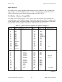
Abbreviations Used in This Manual
The following abbreviations are used in the text of this manual.
A
C
°
hex
in.
kbytes
m
Mbytes
mm
MHz
µsec
nsec
sec
V
VDC
GPIB-1014P User Manual
ampere
Celsius
degree
hexadecimal
inch
1000 bytes
meter
million bytes
millimeter
megahertz
microsecond
nanosecond
second
volt
volts direct current
vi
© National Instruments Corporation
Preface
Related Documents
The following manuals provide information that may be helpful as you read this manual:
•
ANSI/IEEE Std. 488-1978, IEEE Standard Digital Interface for Programmable
Instrumentation
•
ANSI/IEEE Std. 1014-1987, IEEE Standard for a Versatile Backplane Bus: VMEbus
•
µPD7210 GPIB-IFC User Manual
•
µPD7210 Intelligent GPIB Interface Controller Engineering Data Sheet
•
How to Interface a Microcomputer System to a GPIB (& The NEC µPD7210 TLC)
Customer Communication
National Instruments wants to receive your comments on our products and manuals. We are
interested in the applications you develop with our products, and we want to help if you have
problems with them. To make it easy for you to contact us, this manual contains comment and
configuration forms for you to complete. These forms are in Appendix G, Customer
Communication, at the end of this manual.
© National Instruments Corporation
vii
GPIB-1014P User Manual
Contents
Section One
General Information ........................................................................................................ 1-1
What Your Kit Should Contain ..................................................................................... 1-3
Optional Equipment ...................................................................................................... 1-3
Unpacking ..................................................................................................................... 1-3
Section Two
General Description .......................................................................................................... 2-1
Physical Characteristics ................................................................................................ 2-1
Electrical Characteristics ............................................................................................... 2-1
VMEbus Characteristics ............................................................................................... 2-2
VMEbus Slave-Addressing ............................................................................... 2-2
VMEbus Slave-Data ......................................................................................... 2-3
Interrupter .......................................................................................................... 2-4
VMEbus Modules Not Provided ....................................................................... 2-5
Diagnostic Aids ................................................................................................. 2-5
Data Transfer Features .................................................................................................. 2-5
GPIB-1014P Functional Description ............................................................................ 2-5
Section Three
Configuration and Installation .................................................................................... 3-1
Configuration ................................................................................................................ 3-1
Access Mode ..................................................................................................... 3-3
VMEbus Base Address ..................................................................................... 3-3
VMEbus Interrupt Configuration ...................................................................... 3-5
Interrupt Request Line Selection ........................................................... 3-5
Interrupt Priority Code .......................................................................... 3-5
Interrupt Status/ID Vector Selection ................................................................. 3-7
GPIB Cable Shield Grounding .......................................................................... 3-8
Installation ..................................................................................................................... 3-9
Verification of System Compatibility ............................................................... 3-9
Verification Testing .......................................................................................... 3-10
Cabling .............................................................................................................. 3-10
Section Four
Register Bit Descriptions ................................................................................................ 4-1
Register Map ................................................................................................................. 4-1
Register Sizes .................................................................................................... 4-2
Register Description Format ................................................................. 4-2
Terminology .......................................................................................... 4-2
Interface Registers ......................................................................................................... 4-3
Data In Register (DIR) ...................................................................................... 4-6
Command/Data Out Register (CDOR) ............................................................. 4-7
Interrupt Status Register 1 (ISR1) ..................................................................... 4-8
Interrupt Mask Register 1 (IMR1) .................................................................... 4-8
© National Instruments Corporation
xi
GPIB-1014P User Manual
Contents
Interrupt Status Register 2 (ISR2) ..................................................................... 4-14
Interrupt Mask Register 2 (IMR2) .................................................................... 4-14
Serial Poll Status Register (SPSR) .................................................................... 4-19
Serial Poll Mode Register (SPMR) ................................................................... 4-19
Address Status Register (ADSR) ...................................................................... 4-20
Address Mode Register (ADMR) ..................................................................... 4-22
Command Pass Through Register (CPTR) ....................................................... 4-25
Auxiliary Mode Register (AUXMR) ................................................................ 4-27
Hidden Registers ............................................................................................... 4-34
Internal Counter Register (ICR) ............................................................ 4-35
Parallel Poll Register (PPR) .................................................................. 4-36
Auxiliary Register A (AUXRA) ........................................................... 4-38
Auxiliary Register B (AUXRB) ............................................................ 4-40
Auxiliary Register E (AUXRE) ............................................................ 4-42
Address Register 0 (ADR0) .............................................................................. 4-43
Address Register (ADR) ................................................................................... 4-44
Address Register 1 (ADR1) .............................................................................. 4-45
End Of String Register (EOSR) ........................................................................ 4-46
Section Five
Programming Considerations ....................................................................................... 5-1
Initialization .................................................................................................................. 5-1
The GPIB-1014P as GPIB Controller ........................................................................... 5-2
Becoming Controller-In-Charge (CIC) and Active Controller ......................... 5-2
Sending Remote Multiline Messages (Commands) .......................................... 5-3
Going from Active to Standby Controller ......................................................... 5-3
Going from Standby to Active Controller ......................................................... 5-4
Going from Active to Idle Controller ............................................................... 5-4
The GPIB-1014P as GPIB Talker and Listener ............................................................ 5-5
Programmed Implementation of Talker and Listener ....................................... 5-5
Addressed Implementation of the Talker and Listener ..................................... 5-5
Address Mode 1 .................................................................................... 5-5
Address Mode 2 .................................................................................... 5-5
Address Mode 3 .................................................................................... 5-6
Sending/Receiving Messages ........................................................................................ 5-7
Sending/Receiving END or EOS ...................................................................... 5-7
Interrupts ....................................................................................................................... 5-7
Serial Polls .................................................................................................................... 5-8
Conducting Serial Polls ..................................................................................... 5-8
Responding to a Serial Poll ............................................................................... 5-8
Parallel Polls ................................................................................................................. 5-9
Conducting a Parallel Poll ................................................................................. 5-9
Responding To a Parallel Poll ........................................................................... 5-10
Section Six
Theory of Operation ........................................................................................................ 6-1
VMEbus Interface ......................................................................................................... 6-1
Data Lines ......................................................................................................... 6-1
Control Signals .................................................................................................. 6-1
Address Lines .................................................................................................... 6-2
GPIB-1014P User Manual
xii
© National Instruments Corporation
Contents
Address Decoding ......................................................................................................... 6-2
Clock and Reset Circuitry ............................................................................................. 6-2
Timing Control Logic ................................................................................................... 6-3
Interrupter Logic ........................................................................................................... 6-3
GPIB Interface .............................................................................................................. 6-4
Test and Troubleshooting .............................................................................................. 6-5
Section Seven
GPIB-1014P Diagnostic and Troubleshooting Test Procedures ..................... 7-1
Interpreting Test Procedures ......................................................................................... 7-1
GPIB-1014P Hardware Installation Tests ..................................................................... 7-2
Appendix A
Specifications ....................................................................................................................... A-1
Appendix B
Parts List and Schematic Diagrams ........................................................................... B-1
Appendix C
Sample Programs ............................................................................................................... C-1
Appendix D
Multiline Interface Command Messages .................................................................. D-1
Appendix E
Operation of the GPIB .................................................................................................... E-1
Types of Messages ........................................................................................................ E-1
Talkers, Listeners, and Controllers ............................................................................... E-1
The Controller-In-Charge and System Controller ........................................................ E-2
GPIB Signals and Lines ................................................................................................ E-2
Data Lines ......................................................................................................... E-2
Handshake Lines ............................................................................................... E-2
NRFD (not ready for data) .................................................................... E-2
NDAC (not data accepted) .................................................................... E-2
DAV (data valid) ................................................................................... E-3
Interface Management Lines ............................................................................. E-3
ATN (attention) ..................................................................................... E-3
IFC (interface clear) .............................................................................. E-3
REN (remote enable) ............................................................................ E-3
SRQ (service request) ........................................................................... E-3
EOI (end or identify) ............................................................................. E-3
Physical and Electrical Characteristics ......................................................................... E-3
Configuration Requirements ......................................................................................... E-6
Related Document ......................................................................................................... E-7
Appendix F
Mnemonics Key .................................................................................................................. F-1
© National Instruments Corporation
xiii
GPIB-1014P User Manual
Contents
Appendix G
Customer Communication............................................................................................... G-1
Index ..................................................................................................................................Index-1
Figures
Figure 1-1. GPIB-1014P Interface Board ............................................................................... 1-2
Figure 2-1. GPIB-1014P with a VMEbus Computer .............................................................. 2-6
Figure 2-2. GPIB-1014P in a Multiprocessor Application ..................................................... 2-7
Figure 2-3. GPIB-1014P Block Diagram ............................................................................... 2-8
Figure
Figure
Figure
Figure
Figure
Figure
Figure
Figure
3-1.
3-2.
3-3.
3-4.
3-5.
3-6.
3-7.
3-8.
GPIB-1014P Parts Locator Diagram .................................................................... 3-2
Access Selection .................................................................................................. 3-3
Configuration for VMEbus Base Address 1000 hex (default setting) ................. 3-4
VMEbus Interrupt Line Selection ........................................................................ 3-5
VMEbus Interrupt Priority Code Selection .......................................................... 3-6
Status/ID Byte 1A hex ......................................................................................... 3-7
GPIB Cable Shield Grounding ............................................................................. 3-8
GPIB Cable Connector ......................................................................................... 3-11
Figure 4-1. µPD7210 Interface Registers ............................................................................... 4-4
Figure 4-2. Writing to the Hidden Registers ........................................................................... 4-5
Figure E-1. GPIB Connector and the Signal Assignment ....................................................... E-4
Figure E-2. Linear Configuration ............................................................................................ E-5
Figure E-3. Star Configuration ................................................................................................ E-6
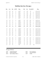
Tables
Table
Table
Table
Table
2-1.
2-2.
2-3.
2-4.
GPIB-1014P Signals ............................................................................................ 2-1
µPD7210 Internal GPIB Interface Registers ........................................................ 2-3
GPIB-1014P IEEE-488 Interface Capabilities ..................................................... 2-10
GPIB-1014P IEEE-1014 Interrupter Compliance Levels .................................... 2-12
Table 3-1. GPIB-1014P Pin Assignment on VMEbus Connector P1 ................................... 3-9
Table
Table
Table
Table
Table
4-1.
4-2.
4-3.
4-4.
4-5.
GPIB-1014P Register Map .................................................................................. 4-1
Clues to Understanding Mnemonics .................................................................... 4-3
Multiline GPIB Commands Recognized by the µPD7210 ................................... 4-25
Auxiliary Command Summary ............................................................................ 4-28
Auxiliary Commands Detail Description ............................................................. 4-30
GPIB-1014P User Manual
xiv
© National Instruments Corporation
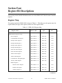
Section One
General Information
The GPIB-1014P is an IEEE-488 interface for the VMEbus. This interface permits IEEE-488
compatible engineering, scientific, or medical instruments to be controlled from a VMEbus-based
computer. The GPIB-1014P has the following features:
•
Complete IEEE-488 Talker/Listener/Controller (TLC) capability using the NEC µPD7210
GPIB TLC chip
•
Polled or interrupt driven transfers
•
Transfer rates up to 80 kbytes/sec
•
User configurable parameters
-
Base Address
-
Interrupt Request Line
-
Interrupt Status/ID byte
-
Supervisor or User Access
•
IEEE-1014 (VMEbus) standard compliance
•
Comprehensive software support
The GPIB-1014P conforms to all requirements and conventions specified in the ANSI/IEEE Std.
1014-1987. Hereafter, the General Purpose Interface Bus is referred to as the GPIB, the GPIB
standard is referred to as the IEEE-488 standard, and the ANSI/IEEE Std. 1014-1987 is referred
to as the IEEE-1014 standard.
© National Instruments Corporation
1-1
GPIB-1014P User Manual
Section One
General Information
What Your Kit Should Contain
Your GPIB-1014P kit contains one of the following boards:
•
GPIB-1014P-1
•
GPIB-1014P-2
•
GPIB-1014P-1S
Optional Equipment
You can contact National Instruments to order the following optional equipment:
•
Single-shielded Type X1 GPIB cables* (1 m, 2 m, 4 m, or 8 m)
•
Double-shielded Type X2 GPIB cables* (1 m, 2 m, or 4 m)
*
•
To meet FCC emission limits for this Class A device, you must use a shielded
(Type X1 or X2) GPIB cable. Operating this equipment with a non-shielded cable
may cause interference to radio and television reception in commercial areas.
GPIB Monitor/Analyzer
–
GPIB-400
–
GPIB-410
Unpacking
Follow these steps when unpacking your GPIB-1014P:
1. Your GPIB-1014P board is shipped packaged in an antistatic plastic bag to prevent electrostatic
damage to the board. Several components on the board can be damaged by electrostatic
discharge. To avoid such damage in handling the board, touch the plastic bag to a metal part of
your VMEbus computer chassis before removing the board from the bag.
2. Remove the board from the bag and inspect the board for loose components or any other sign
of damage. Notify National Instruments if the board appears damaged in any way. DO NOT
install a damaged board into your computer.
© National Instruments Corporation
1-3
GPIB-1014P User Manual
Section Two
General Description
This section contains the physical and electrical specifications for the GPIB-1014P and describes
the characteristics of key interface board components, including a functional block diagram as well
as illustrations of applications in test and measurement configurations.
Physical Characteristics
The GPIB-1014P measures 160 by 100 mm and is supplied with a standard 24-pin GPIB
connector mounted on the front panel. The card is available with both single- and double-height
metal front panels (.8 in. width). A DIN 41612 96-pin connector connects the GPIB-1014P to the
VMEbus backplane.
Electrical Characteristics
All integrated circuit drivers and receivers used on the GPIB-1014P meet the requirements of the
VMEbus Specification and the IEEE-1014 standard. Table 2-1 contains a list of the VMEbus
signals used by the GPIB-1014P and the device used to interface to each signal.
Note: The asterisk (*) after the bus signal indicates the signal is active low.
Table 2-1. GPIB-1014P Signals
Bus Signals
D00-D07
Driver Device
Part Number
Receiver Device
Part Number
F245
F245
A15-A04
LS2521
AM4-AM3,AM0,AM1
LS2521
DS0*,WRITE*,IACK*,IACKIN*,
SYSRESET*, SYSCLK*
LS240
LWORD*,AM5,AM2
F20
(continues)
© National Instruments Corporation
2-1
GPIB-1014P User Manual
General Description
Section Two
Table 2-1. GPIB-1014P Signals (continued)
Driver Device
Part Number
Receiver Device
Part Number
DTACK*
F38
LS240
IACKOUT*
F20
–
IRQ1*through IRQ7*
F38
–
AS*,DS1*,WRITE*
–
ALS244
A03 through A01
–
ALS244
Bus Signals
The GPIB transceivers meet the requirements of the IEEE-488 standard. The components used
are as follows:
Transceivers
Component Designation
Data Transceivers
75160
Control Transceivers
75162
Note: Current load is typically 0.5 A (1 A maximum).
VMEbus Characteristics
The following paragraphs describe both modules on the GPIB-1014P: slave and interrupter.
Table 2-3 later in this section summarizes the capabilities of these modules.
VMEbus Slave-Addressing
The GPIB-1014P occupies 16 bytes of consecutive memory addresses located in the A16 (short)
Input/Output (I/O) space. These addresses are used to access the GPIB Talker/Listener/Controller
(TLC). As a VMEbus slave, it only responds when the address modifier (AM) lines specify a
short supervisory access (AM code = 2D) or short non-privileged access (AM code = 29). An
onboard jumper allows selection of privileged or non-privileged access to the board.
The board responds to 16-bit addresses. It compares address lines A04 through A15 with its
hardware-programmable base address (see Base Address in Section Three) to generate its board
select signal. The Talker/Listener/Controller (TLC) decodes the remaining address lines, A01
through A03, and the data strobe DSO* into eight memory-mapped interface register addresses.
The GPIB TLC (µPD7210) interface registers are addressed relative to the base address of the
board as shown in Table 2-2.
GPIB-1014P User Manual
2-2
© National Instruments Corporation
Section Two
General Description
Table 2-2. µPD7210 Internal GPIB Interface Registers
Address (Base
+ Hex Offset)
Mode
Register
Size
1
R
Data In
(DIR)
8 bits
1
W
Control/Data Out
(CDOR)
8 bits
3
R
Interrupt Status 1
(ISR1)
8 bits
3
W
Interrupt Mask 1
(IMR1)
8 bits
5
R
Interrupt Status 2
(ISR2)
8 bits
5
W
Interrupt Mask 2
(IMR2)
8 bits
7
R
Serial Poll Status
(SPSR)
8 bits
7
W
Serial Poll Mode
(SPMR)
8 bits
9
R
Address Status
(ADSR)
8 bits
9
W
Address Mode
(ADMR)
8 bits
B
R
Command Pass Through
(CPTR)
8 bits
B
W
Auxiliary Mode
(AUXMR)
8 bits
D
R
Address 0
(ADR0)
8 bits
D
W
Address
(ADR)
8 bits
F
R
Address 1
(ADR1)
8 bits
F
W
End of String
(EOSR)
8 bits
VMEbus Slave-Data
As discussed previously, the GPIB-1014P can function as a VMEbus slave, decoding memory
addresses and commands from a VMEbus master. It is designed to accommodate address
pipelining as well as Address Only (ADO) cycles. All data is transferred to and from the
VMEbus with lines D00 through D07. In VMEbus terminology, the slave module of the board is
designated as A16/D08(0). The board does not implement Unaligned Transfer (UAT), Block
Transfer (BLT), and Read-Modify-Write (RMW) cycles.
© National Instruments Corporation
2-3
GPIB-1014P User Manual
General Description
Section Two
Interrupter
Interrupt events that originate from the TLC are as follows:
•
GPIB Data In (DI)
•
GPIB Data Out (DO)
•
END message received (END RX)
•
GPIB Command Out (CO)
•
Remote mode change (REMC)
•
GPIB handshake error (ERR)
•
Lockout change (LOKC)
•
Address Status Change (ADSC)
•
Secondary Address received (APT)
•
Service Request received (SRQI)
•
Trigger command received (DET)
•
Device Clear received (DEC RX)
•
Unrecognized Command received (CPT)
All 13 interrupt events are wire-ORed in the TLC to a single signal designated INT on the interface
board. When one of these events occurs, INT goes high and one of the interrupt request lines
(IRQ1* through IRQ7*) is driven low. You select the interrupt request line by means of an
onboard jumper. You set the interrupt priority via three hardware switches (U28). The encoded
value of the priority must match the level of the interrupt request line. See Interrupt Request Line
Selection in Section Three for more information on setting the interrupt level.
The onboard hardware implements the VMEbus interrupt acknowledge protocol. The interrupter
drives the VMEbus with an 8-bit Status/ID byte (vector) during an interrupt acknowledge cycle.
This Status/ID byte is set by an onboard 8-position Dual In-line Package (DIP) switch (U7). After
the interrupt handler reads the Status/ID byte from the data bus, it releases the data strobe DS0* to
high. Upon seeing DS0* high, the interrupter releases the data bus and the interrupt request line.
This implies that the GPIB-1014P interrupter is a Release On Acknowledge (ROAK) interrupter.
Note: Even though the interrupt request line is no longer driven, the TLC Interrupt (INT) line
remains asserted until it is cleared in the interrupt service routine by reading the appropriate
status register (ISR1 or ISR2). Clearing the TLC INT line in the interrupt routine enables
further interrupts from the GPIB-1014P.
GPIB-1014P User Manual
2-4
© National Instruments Corporation
Section Two
General Description
VMEbus Modules Not Provided
Because the GPIB-1014P is not designed to be VMEbus System Controller, it does not have the
following modules:
•
Master
•
Bus Timer
•
Arbiter
•
Interrupt Handler
•
IACK Daisy Chain Driver
•
System Clock Driver
•
Serial Clock Driver
•
Power Monitor
Diagnostic Aids
The GPIB-1014P is designed to allow stand-alone verification of I/O functions. See Section
Seven, GPIB-1014P Diagnostic and Troubleshooting Test Procedures, for details.
Data Transfer Features
The GPIB-1014P can be used to transfer data to and from the GPIB using programmed I/O.
Typical transfer rates range from 10 to 80 kbytes/sec. Data transfer rates approaching 1 Mbyte/sec
can be obtained with very high performance microprocessors and driver software. The actual
transfer rate for any particular GPIB system is a function of several factors including the
following:
•
Response time of the GPIB devices involved
•
Microprocessor speed and operating system and application program overhead
•
Interrupt service response time
GPIB-1014P Functional Description
In the simplest terms, the GPIB-1014P can be thought of as a bus translator, converting messages
and signals present on the VMEbus into appropriate GPIB messages and signals. Expressed in
GPIB terminology, the GPIB-1014P implements GPIB interface functions for communicating
with other GPIB devices and device functions for communicating with the central processor and
memory. Expressed in VMEbus terminology, the GPIB-1014P is an interface to the outside
world.
© National Instruments Corporation
2-5
GPIB-1014P User Manual
General Description
Section Two
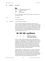
Figure 2-1 and Figure 2-2 show typical applications for the GPIB-1014P. In Figure 2-2, the
GPIB-1014P is used to interface an assortment of test instruments to a VMEbus computer
system, which then functions as an intelligent System Controller. This is the traditional role of the
GPIB.
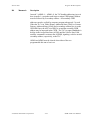
In Figure 2-2, the GPIB-1014P is used along with other National Instruments interface boards to
connect a VMEbus computer to other processors in order to transfer information or to perform
other communication functions.
Device A
VMEbus Computer with GPIB-1014P
Able to Talk, Listen, and Control
Frequency
Counter
Able to Talk
Device B
Printer
Able to Listen
Device C
Digital
Voltmeter
Able to Talk
and Listen
8 Lines
Data Lines
DIO1-DIO8
3 Lines
Handshake Lines
DAV (Data Valid)
NRFD (Not Ready for Data)
NDAC (Not Data Accepted)
Management Lines
5 Lines
IFC (Interface Clear)
ATN (Attention)
SRQ (Service Request)
REN (Remote Enable)
EOI (End or Identify)
Figure 2-1. GPIB-1014P with a VMEbus Computer
GPIB-1014P User Manual
2-6
© National Instruments Corporation
Section Two
General Description
R&D Lab
Microprocessor
Work Station
IBM PC with GPIB-PC
IEEE-488 Interface
VMEbus Computer with
GPIB-1014P IEEE-488 Interface
GPIB-100
Bus Extender
Up to
300 Meters
(RS-422)
Computer
Center
GPIB-100
Bus Extender
Production
& Testing
PDP 11/44 with GPIB11-2
IEEE-488 Interface
S-100 Computer
GPIB-696P IEEE-488 Interface
Figure 2-2. GPIB-1014P in a Multiprocessor Application
© National Instruments Corporation
2-7
GPIB-1014P User Manual
GPIB-1014P User Manual
2-8
DO7-DO0
IRQ1*IRQ7*
IACKOUT*
IACKIN*
DS1*
DTACK*
Data Bus
Transceivers
Interrupt
Logic
Timing and
Data
Direction
Control
WRITE*
DSO*
AS*,
IACK*
Bus Address
Decoding
LWORD*
AM5-AM0
A15-A01
D7-D0
INT
CS*
RD*
WR*
A03-A01
System
Controller
Select
µPD7210
TLC
SAC
DI08*DI01*
SRQ*, ATN*
EOI*, DAV*
NRFD*, NDAC*
IFC*, REN*
75162A
Transceiver
75160A
Transceiver
General Description
Section Two
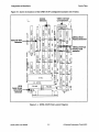
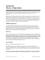
Figure 2-3 is a block diagram of the GPIB-1014P.
GPIB
LOCAL BUS
VMEbus
Figure 2-3. GPIB-1014P Block Diagram
© National Instruments Corporation
Section Two
General Description
The interface consists of these major components which are discussed in greater detail in Section
Six.
•
VMEbus Interface
Consists of the buffers, drivers, and transceivers for
the address, data, status, and control lines used on the
VMEbus, plus other logic circuitry that converts
internal signals to bus-compatible signals.
•
Address Decoder
Recognizes when the VMEbus master addresses one
of the GPIB-1014P registers and generates the
appropriate strobe to effect the data transfer.
•
Clock and Reset Circuitry
Monitors the VMEbus utility signals to generate the 8
MHz clock used by the TLC and to detect System
Reset.
•
Timing State Machine
Controls the timing of accesses to the GPIB-1014P
from the VMEbus.
•
Interrupter
Implements the correct VMEbus priority interrupt
protocol, allowing the GPIB-1014P to request and
respond to an interrupt acknowledge cycle. All
interrupt conditions are also detectable by polling.
•
GPIB TLC (NEC µPD7210)
Implements many of the GPIB interface functions,
either independently or with assistance of or
interpretation by the controlling program. Together
with special transceivers, the TLC forms the GPIB
interface side of the GPIB-1014P.
© National Instruments Corporation
2-9
GPIB-1014P User Manual
General Description
Section Two
Table 2-3 lists the capabilities of the GPIB-1014P in terms of the IEEE-488 standard codes.
Table 2-3. GPIB-1014P IEEE-488 Interface Capabilities
Capability Code
Description
SH1
Complete Source Handshake capability
AH1
Complete Acceptor Handshake capability DAC and RFD
Holdoff on certain events
T5
Complete Talker capability
Basic Talker
Serial Poll
Talk Only mode
Unaddressed on MLA
Send END or EOS
Dual primary addressing
TE5
Complete Extended Talker capability
Basic Extended Talker
Serial Poll
Talk Only mode
Unaddressed on MSA*LPAS
Send END or EOS
Dual primary addressing
L3
Complete Listener capability
Basic Listener
Listen Only mode
Unaddressed on MTA
Detect END or EOS
Dual extended addressing with software assist
LE3
Complete Extended Listener capability
Basic Listener
Listen Only mode
Unaddressed on MSA*TPAS
Detect END or EOS
Dual extended addressing with software assist
(continues)
GPIB-1014P User Manual
2-10
© National Instruments Corporation
Section Two
General Description
Table 2-3. GPIB-1014P IEEE-488 Interface Capabilities (continued)
Capability Code
Description
SR1
Complete Service Request capability
RL1
Complete Remote/Local capability with software
interpretation
PP1
Remote Parallel Poll configuration
PP2
Local Parallel Poll configuration with software assist
DC1
Complete Device Clear capability with software
interpretation
DT1
Complete Device Trigger capability with software
interpretation
C1, 2, 3 ,4, 5
E1, E2
Complete Controller capability
System Controller
Send IFC and take charge
Send REN
Respond to SRQ
Send interface messages
Receive control
Pass control
Pass Control to Self
Parallel Poll
Take control synchronously
Tri-state bus drivers with automatic switch to open
Collector drivers during Parallel Poll
The GPIB-1014P has complete Source and Acceptor Handshake capability. The GPIB-1014P can
operate as a basic Talker or Extended Talker and can respond to a Serial Poll. It can be placed in a
Talk Only mode, and it is unaddressed to talk when it receives its listen address. The interface can
operate as a basic Listener or Extended Listener. It can be placed in a Listen Only mode, and it is
unaddressed to listen when it receives its talk address. The GPIB-1014P has full capabilities for
requesting service from another Controller. It can be placed in local mode, but the interpretation of
remote versus local mode is software-dependent. The interface has full Parallel Poll capability,
although local configuration requires software assistance. It also has Device Clear and Trigger
© National Instruments Corporation
2-11
GPIB-1014P User Manual
General Description
Section Two
capability, but the interpretation is software dependent. All Controller functions as specified by the
IEEE-488 standard are included in the GPIB-1014P. These include the capability to:
•
Be System Controller
•
Initialize the interface
•
Send Remote Enable
•
Respond to Service Request
•
Send multiline command messages
•
Receive control
•
Pass control
•
Conduct a Parallel Poll
•
Take control synchronously or asynchronously
Table 2-4 indicates the GPIB-1014P IEEE-1014 compliance levels.
Table 2-4. GPIB-1014P IEEE-1014 Compliance Levels
Compliance Notation
Description
Bus Slave Compliance Levels
D08(O)
8-bit data path to TLC
A16
Responds to 16-bit short I/O addresses when specified
on the address modifier lines
ADO
Accommodates Address Only cycles
Interrupter Compliance Levels
D08(O)
Provides an 8-bit status/ID byte on D00 through D07
ROAK
Releases its interrupt request line when the interrupt
handler acknowledges the interrupt
I1 through I7
Full support of all seven interrupt priority levels and
interrupt acknowledge daisy chain
GPIB-1014P User Manual
2-12
© National Instruments Corporation
Section Three
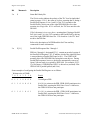
Configuration and Installation
This section describes the configuration and installation of the GPIB-1014P.
Configuration
Before installing the GPIB-1014P in the VMEbus backplane, the following options must be
configured with hardware jumpers or switches that are located on the GPIB-1014P interface board:
•
Access Mode (W2)
•
VMEbus Base Address (U28, U29)
•
VMEbus Interrupt Configuration (W3)
•
Interrupt Status/ID Vector (U7)
•
GPIB Cable Shield Grounding (W1)
© National Instruments Corporation
3-1
GPIB-1014P User Manual
Section Three
Configuration and Installation
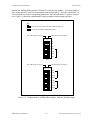
Access Mode
The GPIB-1014P can be configured to allow Supervisor (privileged) or Supervisor-and-User (nonprivileged) access using hardware jumper W2 as shown in Figure 3-2. To configure the board for
privileged access only, place the jumper on the side labeled S as shown in Figure
3-2a. To configure the board for non-privileged access, place the jumper on the side labeled NP as
shown in Figure 3-2b. The default setting for the GPIB-1014P is for non-privileged access. In the
Supervisor (privileged) mode, the GPIB-1014P only responds to Address Modifier (AM) code 2D.
In the Supervisor-and-User (non-privileged) mode, the board responds to AM codes 2D or 29.
(Refer to the ANSI/IEEE Std. 1014-1987, IEEE Standard for a Versatile Backplane Bus:
VMEbus for more information on Supervisor and Non-privileged modes.)
NP
NP
•
I/O
W2
I/O
S
•
W2
S
a. Supervisor only
(Privileged)
b. Supervisor-and-User
(Non-privileged)
Figure 3-2. Access Selection
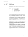
VMEbus Base Address
The address space required by the GPIB-1014P consists of one block of 16 consecutive byte
addresses. The GPIB-1014P responds only to AM codes that indicate short (16-bit) addressing
(See Access Mode previously in this section). The GPIB-1014P decodes the 12 most significant
address bits (A04 through A15) as the base address. The Talker/Listener/Controller (TLC)
internally decodes the Register Select signals, which are address bits A01 through A03.
© National Instruments Corporation
3-3
GPIB-1014P User Manual
Configuration and Installation
Section Three
Dual In-line Package (DIP) switches U28 and U29 select the base address. U29 selects address
lines A8 through A15, and U28 selects address lines A4 through A7. Press the side labeled 0 to
select a logical zero for the corresponding address bit. Press the side labeled 1 to select a logical
one. Figure 3-3 shows the configuration for the base address default setting 1000 hex.
Key
= the side you press down for Base Address 1000 hex
= not involved in Base Address selection
This side down for logic 1
This side down for logic 0
O
N
O
F
F
1
I1
2
I2
3
I3
4
A4
5
6
A5
A6
7
A7
0
U28
This side down for logic 1
This side down for logic 0
O
N
O
F
F
1
A8
2
A9
3
A10
4
A11
5
A12
6
A13
7
A14
8
A15
0
1
U29
Figure 3-3. Configuration for VMEbus Base Address 1000 hex (default setting)
GPIB-1014P User Manual
3-4
© National Instruments Corporation
Section Three
Configuration and Installation
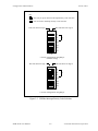
VMEbus Interrupt Configuration
The GPIB-1014P contains circuitry that permits it to request service by driving one of the VMEbus
interrupt request lines. The GPIB-1014P responds to an interrupt acknowledge cycle of correct
priority by providing an 8-bit vector (status byte) that is used to locate the appropriate interrupt
service routine. The following paragraphs explain the actions that must be performed to configure
the interrupt request line, the interrupt priority, and the status/ID byte or interrupt vector.
Interrupt Request Line Selection
The VMEbus provides seven interrupt request lines IRQ1* to IRQ7*. The GPIB-1014P can be
configured to drive any one of these seven lines. The jumper shown in Figure 3-4 is used to
connect the interrupt request from the GPIB-1014P to one of the VMEbus interrupt request lines.
The jumper is placed on the pins that correspond to the desired interrupt request line.
Note: The interrupt priority code must be set to correspond to the interrupt request line.
Figure 3-4a shows the jumper configured to select interrupt request line IRQ2*, while Figure 3-4b
shows the configuration for selecting IRQ4*. The default setting for the GPIB-1014P is IRQ2*.
•
•
•
•
•
•
•
•
•
•
•
•
•
•
•
•
•
•
•
•
7
IRQ
W3
W3
•
•
1
•
7
IRQ
•
1
a. Select Interrupt Request Line Configured
to IRQ2*
(Default setting)
b. Select Interrupt Request Line Configured
to IRQ4*
Figure 3-4. VMEbus Interrupt Line Selection
Note: An asterisk implies that the signal is active low.
Interrupt Priority Code
The interrupt priority code is used to identify an interrupt acknowledge cycle intended for the GPIB1014P. Three bits, I1 through I3, represent the interrupt priority code of the GPIB-1014P. The
encoded value of these three bits must correspond to the interrupt request line used (1 through 7) by
the board, I1 is the least significant bit. Three switches located at U28 set these bits. Press the side
labeled 0 to select a logical zero for the corresponding address bit. Press the side labeled 1 to select
a logical one. Figure 3-5a shows the switch configuration for using IRQ2* while Figure 3-5b
shows the switch configuration for using IRQ4*. The default setting for the GPIB-1014P is
IRQ2*.
© National Instruments Corporation
3-5
GPIB-1014P User Manual
Configuration and Installation
Section Three
Key
= the side you press down for Interrupt Priority Code selection
= not involved in Interrupt Priority Code selection
This side down for logic 1
This side down for logic 0
O
N
O
F
F
1
I1
2
I2
3
I3
4
A4
5
6
A5
A6
7
A7
2
U28
a. Switch configuration using IRQ2*
(Default setting)
This side down for logic 1
This side down for logic 0
O
N
O
F
F
1
I1
2
I2
3
I3
4
A4
5
6
A5
A6
7
A7
4
U28
b. Switch configuration using IRQ4*
Figure 3-5. VMEbus Interrupt Priority Code Selection
GPIB-1014P User Manual
3-6
© National Instruments Corporation
Section Three
Configuration and Installation
Interrupt Status/ID Vector Selection
Switches located at U7 configure the interrupt status/ID vector, which is provided by the GPIB1014P during an interrupt acknowledge cycle. This interrupt vector consists of eight bits, labeled
V0 through V7, as shown in Figure 3-6. Bit V7 corresponds to the most significant bit while V0
corresponds to the least significant. Press the side labeled 0 to select a logical zero for the
corresponding address bit. Press the side labeled 1 to select a logical one. Figure 3-6 shows the
configuration for a status/ID byte value 1A hex.
Key
= the side you press down for Status/ID Byte 1A hex
This side down for logic 1
This side down for logic 0
O
N
O
F
F
1
V7
2
V6
3
V5
4
V4
5
V3
6
V2
7
V1
8
V0
1
A
U7
Figure 3-6. Status/ID Byte 1A hex
© National Instruments Corporation
3-7
GPIB-1014P User Manual
Configuration and Installation
Section Three
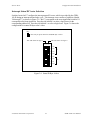
GPIB Cable Shield Grounding
The GPIB cable shield connects to the chassis ground through the metal front panel on the GPIB1014P. The cable shield can also be connected to the system logic ground if desired. Usually, the
GPIB cable shield is grounded only at the GPIB System Controller. Set hardware jumper W1 to
the side labeled CON to short or connect the GPIB cable shield to VMEbus digital logic ground.
Place the jumper on the side labeled ISO to leave the GPIB cable shield isolated. Select one
configuration depending on whether or not the GPIB-1014P is the GPIB System Controller and
whether or not the GPIB cable shield is grounded elsewhere. Figure 3-7 shows the two possible
configurations. The GPIB-1014P is shipped in the isolated or unconnected configuration.
W1
W1
ISO
SHLD
ISO
•
•
SHLD
CON
CON
a. Shield Isolated or Unconnected
(Default setting)
b. Shield Grounded or Connected
Figure 3-7. GPIB Cable Shield Grounding
GPIB-1014P User Manual
3-8
© National Instruments Corporation
Section Three
Configuration and Installation
Installation
The GPIB-1014P is a single-height board that interfaces to the VMEbus P1 and is available with
either a single- or double-height metal front cover plate. The following paragraphs describe the
GPIB-1014P interface to the VMEbus backplane and to the IEEE-488 bus.
Verification of System Compatibility
The GPIB-1014P monitors and drives those signals required by the IEEE-1014 Standard and is
compatible with certified VMEbus systems. Compare the signals listed in Table 3-1 to those used
by the VMEbus system in which the GPIB-1014P will be installed to ensure that the GPIB-1014P
provides all the necessary signals needed by the VMEbus system and vice versa.
Table 3-1. GPIB-1014P Pin Assignment on VMEbus Connector P1
Pin No.
Signal Used
A1
A2
A3
A4
A5
A6
A7
A8
A9
A10
A11
A12
A13
A14
A15
A16
D00
D01
D02
D03
D04
D05
D06
D07
GND
SYSCLK
GND
DS1*
DS0*
WRITE*
GND
DTACK*
B1
B2
B3
B4
B5
B6
B7
B8
B9
B10
B11
B12
B13
B14
B15
B16
Signal Not Used
Pin No.
A17
A18
A19
A20
A21
A22
A23
A24
A25
A26
A27
A28
A29
A30
A31
A32
BBSY*
BCLR*
ACFAIL*
BG0IN*
BG0OUT*
BG1IN*
BG1OUT*
BG2IN*
BG2OUT*
BG3IN*
BG3OUT*
BR0*
BR1*
BR2*
BR3*
B17
B18
B19
B20
B21
B22
B23
B24
B25
B26
B27
B28
B29
B30
B31
B32
AM0
Signal Used
Signal Not Used
GND
AS*
GND
IACK*
IACKIN*
IACKOUT*
AM4
A07
A06
A05
A04
A03
A02
A01
-12V
+5V
AM1
AM2
AM3
GND
SERCLK
SERDAT
GND
IRQ7*
IRQ6*
IRQ5*
IRQ4*
IRQ3*
IRQ2*
IRQ1*
+5V STDBY
+5V
(continues)
© National Instruments Corporation
3-9
GPIB-1014P User Manual
Configuration and Installation
Section Three
Table 3-1. GPIB-1014P Pin Assignment on VMEbus Connector P1 (continued)
Pin No.
C1
C2
C3
C4
C5
C6
C7
C8
C9
C10
C11
C12
C13
C14
C15
C16
Signal Used
Signal Not Used
Pin No.
D08
D09
D10
D11
D12
D13
D14
D15
C17
C18
C19
C20
C21
C22
C23
C24
C25
C26
C27
C28
C29
C30
C31
C32
GND
SYSFAIL*
BERR*
SYSRESET*
LWORD*
AM5
A23
A22
Signal Used
Signal Not Used
A21
A20
A19
A18
A17
A16
A15
A14
A13
A12
A11
A10
A09
A08
+12V
+5V
Verification Testing
A verification test can be run to ensure that the board has not been damaged during shipment and
also to ensure that the board has been configured correctly. This requires an interactive control
program or an equivalent mechanism, such as front panel control switches or front panel emulator,
that provides a way to load and read memory and I/O addresses.
The tests presented in Section Seven of this manual consist of a series of steps written in a pseudo
(processor-independent) language with instructions. The steps generally involve writing data to
specific GPIB-1014P device registers followed by reading other GPIB-1014P registers to verify
that the programming is correct. These tests exercise virtually all of the major functions of the
GPIB-1014P, including I/O communications and GPIB communications. All functions except
GPIB communications can be performed as stand-alone operations (that is, without another GPIB
device). To completely check the GPIB functions, you must use a bus tester or analyzer (such as
National Instruments GPIB-400 or GPIB-410) that can monitor and control GPIB signal lines;
emulate GPIB Talker, Listener, and Controller devices; and single-step through the Source and
Acceptor Handshakes.
Cabling
Optional cables are available to connect the GPIB-1014P to other GPIB devices. Connect the cable
to the GPIB-1014P at the standard GPIB connector labeled J1 at the top of the interface board.
(The GPIB connector protrudes through the metal front cover plate.)
GPIB-1014P User Manual
3-10
© National Instruments Corporation
Section Three
Configuration and Installation
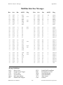
Figure 3-8 shows the signals present on the GPIB cable connector.
DIO1*
DIO2*
DIO3*
DIO4*
EOI*
DAV*
NRFD*
NDAC*
IFC*
SRQ*
ATN*
SHIELD
1
2
3
4
5
6
7
8
9
10
11
12
13
14
15
16
17
18
19
20
21
22
23
24
DIO5*
DIO6*
DIO7*
DIO8*
REN*
GND (TW PAIR W/DAV*)
GND (TW PAIR W/NRFD*)
GND (TW PAIR W/NDAC*)
GND (TW PAIR W/IFC*)
GND (TW PAIR W/SRQ*)
GND (TW PAIR W/ATN*)
SIGNAL GROUND
Figure 3-8. GPIB Cable Connector
© National Instruments Corporation
3-11
GPIB-1014P User Manual
Section Four
Register Bit Descriptions
This section presents detailed information on the use of the GPIB-1014P Talker/Listener/Controller
registers.
Register Map
The register map for the GPIB-1014P is shown in Table 4-1. This table gives the register name, the
register address, the type of the register, and the size of the register in bits.
Table 4-1. GPIB-1014P Register Map
Register Name
Address (Hex)
Type
Size
GPIB Interface Register Group:
Data In Register
Base address + 1
Read only
8-bit
Command/Data Out Register
Base address + 1
Write only
8-bit
Interrupt Status Register 1
Base address + 3
Read only
8-bit
Interrupt Mask Register 1
Base address + 3
Write only
8-bit
Interrupt Status Register 2
Base address + 5
Read only
8-bit
Interrupt Mask Register 2
Base address + 5
Write only
8-bit
Serial Poll Status Register
Base address + 7
Read only
8-bit
Serial Poll Mode Register
Base address + 7
Write only
8-bit
Address Status Register
Base address + 9
Read only
8-bit
Address Mode Register
Base address + 9
Write only
8-bit
Command Pass Through Register
Base address + B
Read only
8-bit
Auxiliary Mode Register
Base address + B
Write only
8-bit
Internal Counter Register
Base address + B
Write only
8-bit
Parallel Poll Register
Base address + B
Write only
8-bit
Auxiliary Register A
Base address + B
Write only
8-bit
Hidden Registers
(continues)
© National Instruments Corporation
4-1
GPIB-1014P User Manual
Register Bit Descriptions
Section Four
Table 4-1. GPIB-1014P Register Map (continued)
Register Name
Address (Hex)
Type
Size
Auxiliary Register B
Base address + B
Write only
8-bit
Auxiliary Register E
Base address + B
Write only
8-bit
Address Register 0
Base address + D
Read only
8-bit
Address Register
Base address + D
Write only
8-bit
Address Register 1
Base address + F
Read only
8-bit
End Of String Register
Base address + F
Write only
8-bit
Register Sizes
All program registers on the GPIB-1014P are 8-bit registers.
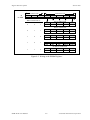
Register Description Format
The remainder of this section discusses each of the GPIB-1014P registers in the order shown in
Table 4-1. Each register group is introduced, followed by a detailed bit description of each register.
The individual register description gives the address, type, word size, and bit map of the register,
followed by a description of each bit.
The register bit map shows a diagram of the register with the most significant bit (bit 7 for an 8-bit
register) shown on the left, and the least significant bit (bit 0) shown on the right. A rectangle is
used to represent each bit. Each bit is labeled with a name inside its rectangle. An asterisk (*) after
the bit name indicates that the signal is active low. An asterisk is equivalent to an overbar.
In many of the registers, several bits are labeled with an X, indicating don't care bits. When a
register is read, these bits may appear set or cleared but should be ignored because they have no
significance. When a register is written to, these bit locations should be cleared.
Terminology
The terms set, set true, and set to one are synonymous. The terms clear, set false, set to zero, and
clear to zero are synonymous. The meanings of preset and reset are determined by the context in
which they are used. Bit signatures are written in uppercase letters.
The term addressed means the interface has been configured to perform a function from the GPIB
side, while the term programmed means that it has been configured from the VMEbus side. This
distinction is important to make because many functions, such as making the interface a Talker or
Listener, can be activated from either side.
GPIB-1014P User Manual
4-2
© National Instruments Corporation
Section Four
Register Bit Descriptions
Where it is necessary to specify a particular bit of a register, the bit position appears as a decimal
number in square brackets after the mnemonic (for example, ISR1[1] indicates the DI bit of
Interrupt Status Register 1).
A minus sign (-) is used to indicate logical negation. An ampersand (&) represents AND, and a
plus sign (+) represents OR in logical expressions.
All numbers, except register offsets, are decimal unless specified otherwise. Register offsets are
given in hexadecimal.
Uppercase mnemonics are used for control, status, data registers, register contents, and interface
functions, as well as GPIB remote messages, commands, and logic states as defined in the IEEE488 standard.
After a mnemonic of a name has been defined, the mnemonic is used thereafter. Appendix F
contains a list of all mnemonics used in this manual along with their type and name. Mnemonics
are assigned to messages, states, registers, bits, functions, and integrated circuits. Most mnemonics
contain a clue to their meaning. Table 4-2 contains a list of clues to look for.
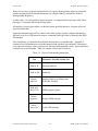
Table 4-2. Clues to Understanding Mnemonics
Clue
Mnemonic Probably Stands For:
Ends in IE
Interrupt enable bit
Ends in EN
Enable bit
4 letters,
ends in S
Interface function as defined in the
IEEE-488 standard
Ends in R,
R0, R1, R2
GPIB program register
3 letters,
uppercase
Remote GPIB message
3 letters,
lowercase
Local GPIB message
© National Instruments Corporation
4-3
GPIB-1014P User Manual
Register Bit Descriptions
Section Four
Interface Registers
All program registers are GPIB interface registers; eight are read only, eight are write only, and five
are hidden or indirectly accessible. All are located within the NEC µPD7210
Talker/Listener/Controller (TLC) integrated circuit. Each of the 16 interface registers is addressed
relative to the GPIB-1014P VMEbus base address which is set with DIP switches (refer to Base
Address in Section Three).
Figure 4-1 shows the µPD7210 Interface registers, the bit mnemonics of each, its read/write
accessibility, and its relative address. Figure 4-2 shows the hidden GPIB interface registers and
illustrates the method of writing to those registers via the Auxiliary Mode Register. A detailed
function description of all 16 interface registers is provided in the paragraphs following the figures.
GPIB-1014P User Manual
4-4
© National Instruments Corporation
Section Four
Register Bit Descriptions
Bit
7
Bit
6
Legend
(Contents of Read Register)
Bit
Bit
Bit
Bit
5
4
3
2
Bit
1
Bit
0
(Contents of Write Register)
Address
Offset
(hex)
DIR
+1
CDOR
ISR1
+3
IMR1
ISR2
SPMR
+9
ADMR
+B
AUXMR
+D
ADR
ADR1
EOSR
DI5
DI4
DI3
DI2
DI1
DI0
R
CDO7
CDO6
CDO5
CDO4
CDO3
CDO2
CDO1
CDO0
W
CPT
APT
DET END RX DEC
ERR
DO
DI
R
DI IE
W
ADSC
R
CPT IE APT IE DET IE END IE DEC IE ERR IE DO IE
0
+7
ADR0
DI6
INT SRQI
SPSR
CPTR
DI7
LOK
+5
IMR2
ADSR
Read/
Write
+F
REM
CO
LOKC
REMC
SRQI IE DMAO DMAI CO IE LOKC IE REMC IEADSC IE
W
S8
PEND
S6
S5
S4
S3
S2
S1
R
S8
rsv
S6
S5
S4
S3
S2
S1
W
CIC
ATN*
SPMS LPAS
TPAS
LA
TA
MJMN
R
ton
lon
TRM1 TRM0
0
0
ADM1 ADM0
W
CPT7
CPT6
CPT5
CPT3
CPT2
CPT1
CPT0
R
CNT2
CNT1
CNT0 COM4 COM3 COM2 COM1 COM0
W
X
DT0
DL0
ARS
DT
DL
EOI
DT1
DL1
AD5-1 AD4-1 AD3-1 AD2-1 AD1-1
R
EOS7
EOS6
EOS5
EOS4
W
Note:
CPT4
AD5-0 AD4-0 AD3-0 AD2-0 AD1-0
R
AD3
W
AD5
AD4
EOS3
EOS2
AD2
EOS1
AD1
EOS0
X indicates a don't care bit.
Figure 4-1. µPD7210 Interface Registers
© National Instruments Corporation
4-5
GPIB-1014P User Manual
Register Bit Descriptions
Section Four
Control Code
+B
AUXMR
CNT2
CNT1
Command Code
CNT0
COM4
COM3
COM2
COM1
COM0
W
When CNT2-CNT0 is:
ICR is loaded with:
0
0
1
0
0
1
1
U
CLK3
CLK2
CLK1
PPR is loaded with:
S
P3
P2
CLK0
P1
AUXRA is loaded with:
1
0
0
1
0
1
1
1
0
BIN
XEOS
REOS
HLDE
AUXRB is loaded with:
HLDA
ISS
INV
TRI
SPEOI
AUXRE is loaded with:
CPT
ENABLE
0
0
0
DHDT
DHDC
Figure 4-2. Writing to the Hidden Registers
GPIB-1014P User Manual
4-6
© National Instruments Corporation
Section Four
Register Bit Descriptions
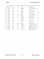
Data In Register (DIR)
VMEbus Address:
Base Address + 1 (hex)
Attributes:
Read Only
7
6
5
DI7
DI6
DI5
4
DI4
3
2
1
0
DI3
DI2
DI1
DI0
R
The Data In Register (DIR) is used to move data from the GPIB to the VMEbus when the interface
is a Listener. Incoming information is separately latched by this register and is not destroyed by a
write to the Command/Data Out Register (CDOR) which locates at the same address. The GPIB
Ready For Data (RFD) message is held false until the byte is removed from the DIR by an I/O read
from a VMEbus master. The Acceptor Handshake (AH) completes automatically after the byte has
been read. In RFD Holdoff mode (refer to Auxiliary Register A, later in this section) the GPIB
Handshake is not finished until the Finish Handshake (FH) auxiliary command is issued telling the
TLC to release the Holdoff. By using the RFD Holdoff mode, the same byte can be read several
times, or a GPIB Talker that is ready to provide more data can be held off until the program is
ready to proceed.
DI0 is the least significant bit of the data byte and corresponds to GPIB DIO1. DI7 is the most
significant bit of the data byte and corresponds to GPIB DIO8.
Bit
Mnemonic
Description
7-0r
DIR[7-0]
Data In Bits 7 through 0
© National Instruments Corporation
4-7
GPIB-1014P User Manual
Register Bit Descriptions
Section Four
Command/Data Out Register (CDOR)
VMEbus Address:
Base Address + 1 (hex)
Attributes:
Write Only
7
6
5
4
3
2
1
0
CDO7
CDO6
CDO5
CDO4
CDO3
CDO2
CDO1
CDO0
W
The Command/Data Out Register (CDOR) is used to move data from the VMEbus to the GPIB
when the TLC is the GPIB Talker or the Active Controller. Outgoing data is separately latched by
this register and is not destroyed by a read of the DIR which is located at the same address. When a
byte is written to the CDOR, the TLC GPIB Source Handshake (SH) function is initiated and the
byte is transferred to the GPIB.
Bit
Mnemonic
Description
7-0w
CDO[7-0]
Command/Data Out Bits 7 through 0
GPIB-1014P User Manual
4-8
© National Instruments Corporation
Section Four
Register Bit Descriptions
Interrupt Status Register 1 (ISR1)
VMEbus Address:
Base Address + 3 (hex)
Attributes:
Read Only,
Bits are cleared when read
Interrupt Mask Register 1 (IMR1)
VMEbus Address:
Base Address + 3 (hex)
Attributes:
Write Only
7
6
5
4
3
2
CPT
CPT IE
APT
APT IE
DET
DET IE
END RX
END IE
DEC
DEC IE
ERR
ERR IE
1
DO
DO IE
0
R
DI
DI IE
W
ISR1 is composed of eight interrupt status bits. IMR1 is composed of eight interrupt enable bits
which directly correspond to the interrupt status bits in ISR1. As a result, ISR1 and IMR1 service
eight possible interrupt conditions, where each condition has an interrupt status bit and an interrupt
enable bit associated with it. If the Interrupt Enable bit is true when the corresponding status
condition or event occurs, a hardware interrupt request is generated. Bits in ISR1 are set and cleared
by the TLC regardless of the status of the interrupt enable bits in IMR1. If an interrupt condition
occurs at the same time ISR1 is being read, the TLC holds off setting the corresponding status bit
until the read has finished.
Bit
Mnemonic
Description
7r
7w
CPT
CPT IE
Command Pass-Through Bit
Command Pass-Through Interrupt Enable Bit
CPT is set on:
[UCG + ACG & (TADS + LADS)]
& undefined & ACDS & (CPTENAB)
+ UDPCF & SCG & ACDS & CPT ENAB
CPT is cleared by:
pon + (Read ISR1)
Notes:
UCG:
ACG:
TADS:
LADS:
defined:
© National Instruments Corporation
GPIB Universal Command Group message
GPIB Addressed Command Group message
GPIB Talker Addressed State
GPIB Listener Addressed State
GPIB command automatically recognized and executed
by TLC
4-9
GPIB-1014P User Manual
Register Bit Descriptions
Bit
Mnemonic
Section Four
Description
undefined:
GPIB command not automatically recognized and
executed by TLC
ACDS:
GPIB Accept Data State
CPT ENAB: AUXRB[0]w
UDPCF:
Undefined primary command function (see below)
SCG:
GPIB Secondary Command Group message
pon:
power on reset
TAG:
GPIB Talk Address Group message
LAG:
GPIB Listen Address Group message
Read ISR1: Bit is cleared immediately after it is read
UDPCF is set on:
[UCG + ACG & (TADS + LADS)] & undefined
& ACDS & CPT ENAB
UDPCF is cleared on:
[(UCG + ACG) & defined + TAG + LAG]
& ACDS + (-CPT ENAB) + pon
The CPT bit flags the occurrence of a GPIB command not recognized by
the TLC, and all following GPIB secondary commands when the
Command pass-through feature is enabled by the CPT ENAB bit,
AUXRB[0]w. Any GPIB command message not decoded by the TLC
is treated as an undefined command (for example, the Go To Local
command, GTL). However, any addressed command is automatically
ignored when the TLC is not addressed.
Undefined commands are read using the CPTR. The TLC holds off the
GPIB Acceptor Handshake in the Accept Data State (ACDS) until the
Valid auxiliary command function code, octal 017, is written to the
AUXMR. If the CPT feature is not enabled, undefined commands are
simply ignored.
6r
6w
APT
APT IE
Address Pass-Through Bit
Address Pass-Through Interrupt Enable Bit
APT is set by:
ADM1 & ADM0 & (TPAS + LPAS) &
SCG & ACDS
APT is cleared by:
pon + (Read ISR1)
Notes:
ADM1:
ADM0:
GPIB-1014P User Manual
Address Mode Register bit 1, ADMR[1]w
Address Mode Register bit 0, ADMR[0]w
4-10
© National Instruments Corporation
Section Four
Bit
Mnemonic
Register Bit Descriptions
Description
TPAS:
LPAS:
SCG:
ACDS:
pon:
Read ISR1:
GPIB Talker Primary Addressed State
GPIB Listener Primary Addressed State
GPIB Secondary Command Group
GPIB Accept Data State
power on reset
Bit is cleared immediately after it is read.
The APT bit indicates that a secondary GPIB address has been received
and is available in the CPTR for inspection.
Note:
The application program must check this bit when using TLC
address mode 3).
When APT is set, the DAC message is held and the GPIB handshake
stops until either the Valid or Non-Valid auxiliary command is issued.
The secondary address can be read from the CPTR.
5r
5w
DET
DET IE
Device Execute Trigger Bit
Device Execute Trigger Interrupt Enable Bit
DET is set by:
DTAS
DET is cleared by:
pon + (Read ISR1)
Notes:
DTAS:
pon:
Read ISR1:
GPIB Device Trigger Active State
power on reset
Bit is cleared immediately after it is read.
The DET bit indicates that the GPIB Device Execute Trigger (DET)
command has been received while the TLC was a GPIB Listener (the
TLC has been in DTAS).
4r
4w
END RX
END IE
End Received Bit
End Received Interrupt Enable Bit
END RX is set by:
LACS & (EOI + EOS & REOS) & ACDS
END RX is cleared by:
pon + (Read ISR1)
© National Instruments Corporation
4-11
GPIB-1014P User Manual
Register Bit Descriptions
Bit
Mnemonic
Section Four
Description
Notes:
LACS:
EOI:
EOS:
REOS:
GPIB Listener Active State
GPIB End Or Identify Signal
GPIB End Of String message
Reception Of GPIB EOS allowed, AUXRA[2]w
ACDS:
pon:
Read ISR1:
GPIB Accept Data State
power on reset
Bit is cleared immediately after it is read.
The END RX bit is set when the TLC is a Listener and the GPIB uniline
message, END, is received with a data byte from the GPIB Talker, or the
data byte in the DIR matches the contents of the End Of String Register
(EOSR).
3r
3w
DEC
DEC IE
Device Clear Bit
Device Clear Interrupt Enable Bit
DEC is set by:
DCAS
DEC is cleared by:
pon + (Read ISR1)
Notes:
DCAS:
pon:
Read ISR1:
GPIB Device Clear Active State
power on reset
Bit is cleared immediately after it is read.
The DEC bit indicates that the GPIB Device Clear (DCL) command has
been received or that the GPIB Selected Device Clear (SDC) command
has been received while the TLC was a GPIB Listener (the TLC is in
DCAS).
2r
2w
ERR
ERR IE
Error Bit
Error Interrupt Enable Bit
ERR is set by:
TACS & SDYS & DAC & RFD + SIDS &
(Write CDOR) + (SDYS - SIDS)
ERR is cleared by:
pon + (Read ISR1)
GPIB-1014P User Manual
4-12
© National Instruments Corporation
Section Four
Bit
Mnemonic
Register Bit Descriptions
Description
Notes:
TACS:
GPIB Talker Active State
SDYS:
GPIB Source Delay State
DAC:
GPIB Data Accepted message
RFD:
GPIB Ready For Data message
SIDS:
GPIB Source Idle State
(Write CDOR): Bit is set immediately after writing to the
Command/Data Out Register
SDYS->SIDS: Transition from GPIB Source Delay State to Source
Idle State
pon:
power on reset
Read ISR1:
Bit is cleared immediately after it is read.
The ERR bit indicates that the contents of the CDOR have been lost.
ERR is set when data is sent over the GPIB without a specified Listener
or when a byte is written to the CDOR during SIDS or during the SDYS
to SIDS transition.
1r
1w
DO
DO IE
Data Out Bit
Data Out Interrupt Enable Bit
DO is set as:
(TACS & SGNS) becomes true
DO is cleared by:
(Read ISR1) + -(TACS) + -(SGNS)
Notes:
TACS: GPIB Talker Active State
SGNS:GPIB Source Generate State
Read ISR1: Bit is cleared immediately after it is read.
The DO bit indicates that the TLC is ready to accept another data byte
from the VMEbus for transmission onto the GPIB when the TLC is the
GPIB Talker. The DO bit is cleared when a byte is written to the CDOR
and also when the TLC ceases to be the Active Talker.
0r
0w
DI
DI IE
Data In Bit
Data In Interrupt Enable Bit
DI is set by:
LACS & ACDS & -(Continuous Mode)
© National Instruments Corporation
4-13
GPIB-1014P User Manual
Register Bit Descriptions
Bit
Mnemonic
Section Four
Description
DI is cleared by:
pon + (Read ISR1) + (Finish Handshake)
& (Holdoff Mode) + (Read DIR)
Notes:
LACS:
ACDS:
GPIB Listener Active State
GPIB Accept Data State Continuous Mode: Listen
In Continuous Mode auxiliary command in effect
pon:
power on reset
Read ISR1:
Bit is cleared immediately after it is read
Finish Handshake: Finish Handshake auxiliary command issued
Holdoff Mode:
RFD holdoff state
Read DIR:
Read Data In Register
The DI bit indicates that the TLC, as a GPIB Listener, has accepted a data
byte from the GPIB Talker.
GPIB-1014P User Manual
4-14
© National Instruments Corporation
Section Four
Register Bit Descriptions
Interrupt Status Register 2 (ISR2)
VMEbus Address:
Base Address + 5 (hex)
Attributes:
Read Only,
Bits are cleared when read
Interrupt Mask Register 2 (IMR2)
VMEbus Address:
Base Address + 5 (hex)
Attributes:
Write Only
7
6
5
4
3
2
INT
0
SRQI
SRQI IE
LOK
DMAO
REM
DMAI
CO
CO IE
LOKC
LOKC IE
1
REMC
REMC IE
0
R
ADSC
ADSC IE
W
ISR2 consists of six interrupt status bits and two TLC internal status bits. IMR2 consists of five
interrupt enable bits and two TLC internal control bits. If the Interrupt Enable bit is true when the
corresponding status condition or event occurs, a hardware interrupt request is generated. Bits in
ISR2 are set and cleared regardless of the status of the bits in IMR2. If a condition occurs which
requires the TLC to set or clear a bit or bits in ISR2 at the same time ISR2 is being read, the TLC
holds off setting or clearing the bit or bits until the read is finished.
Bit
Mnemonic
Description
7r
INT
Interrupt Bit
This bit is the logical OR of all the enabled interrupt status bits in both
ISR1 and ISR2, each one ANDed with its interrupt enable bit (refer
below). There is no corresponding mask bit for INT. If the INT=1, the
INT output pin of the TLC, signal GPIB IR, is asserted.
Note: Program the INT output pin of the TLC to be active high; see
description of AUXRB.
INT is set by:
(CPT & CPT IE) + (APT & APT IE) +
(DET & DET IE) + (ERR & ERR IE) +
(END RX & END IE) + (DEC & DEC IE) +
(DO & DO IE) + (DI & DI IE) +
(SRQI & SRQI IE) + (REMC & REMC IE) +
(CO & CO IE) + (LOKC & LOKC IE) +
(ADSC & ADSC IE)
© National Instruments Corporation
4-15
GPIB-1014P User Manual
Register Bit Descriptions
Bit
Mnemonic
Section Four
Description
Notes
CPT:
CPT IE:
APT:
APT IE:
DET:
DET IE:
ERR:
ERR IE:
END RX:
END IE:
DEC:
DEC IE:
DO:
DO IE:
DI:
DI IE:
SRQI:
SRQI IE:
REMC:
REMC IE:
CO:
CO IE:
LOKC:
LOKC IE:
ADSC:
ADSC IE:
7w
0
Command Pass Through Bit
Enable Interrupt on Command Pass Through Bit
Address Pass Through Bit
Enable Interrupt on Address Pass Through Bit
Device Execute Trigger Bit
Enable Interrupt on Device Execute Trigger Bit
Error Bit
Enable Interrupt on Error Bit
End Received Bit
Enable Interrupt on End Received Bit
Device Clear Bit
Enable Interrupt on Device Clear Bit
Data Out Bit
Enable Interrupt on Data Out Bit
Data In Bit
Enable Interrupt on Data In Bit
Service Request Input Bit
Enable Interrupt on Service Request Input Bit
Remote Change Bit
Enable Interrupt on Remote Change Bit
Command Output Bit
Enable Interrupt on Command Output Bit
Lockout Change Bit
Enable Interrupt on Lockout Change Bit
Address Status Change Bit
Enable Interrupt on Address Status Change Bit
Reserved Bit
Write zero to this bit.
6r
6w
SRQI
SRQI IE
Service Request Input Bit
Service Request Input Interrupt Enable Bit
SRQI is set when:
(CIC & SRQ & -(RQS & DAV)) becomes true
SRQI is cleared by:
pon + (Read ISR2)
Notes:
CIC:
SRQ:
RQS:
DAV:
GPIB-1014P User Manual
GPIB Controller In Charge
GPIB Service Request message
GPIB Request Service message
GPIB Data Valid message
4-16
© National Instruments Corporation
Section Four
Bit
Mnemonic
Register Bit Descriptions
Description
pon:
Read ISR2:
power on reset
Bit is cleared immediately after it is read.
The SRQI bit indicates that a GPIB Service Request (SRQ) message has
been received while the TLC Controller function is active (CIC=1).
5r
LOK
Lockout Bit
LOK is used, along with the REM bit, to indicate the status of the TLC
GPIB Remote/Local (RL) function. If set, the LOK bit indicates that the
TLC is in Local With Lockout State (LWLS) or Remote With Lockout
State (RWLS). LOK is a non-interrupt bit.
5w
DMAO
DMA Out Enable Bit
The DMA feature is not implemented. Do not set this bit.
4r
REM
Remote Bit
This bit is true whenever the TLC GPIB RL function is in one of two
states: Remote State (REMS) or Remote With Lockout State (RWLS).
The TLC RL function enters one of these states when the System
Controller has asserted the Remote Enable line (REN), and the
Controller-In-Charge addresses the TLC as a Listener.
4w
DMAI
DMA Input Enable Bit
The DMA feature is not implemented. Do not set this bit.
3r
3w
CO
CO IE
Command Out Bit
Command Out Interrupt Enable Bit
CO is set when:
(CACS & SGNS) becomes true
CO is cleared by:
(Read ISR2) + -(CACS) + -(SGNS)
Notes:
CACS:GPIB Controller Active State
SGNS:GPIB Source Generate State
Read ISR2: Bit is cleared immediately after it is read.
CO = 1 indicates CDOR is empty and that another command can be
written to it for transmission to the GPIB without overwriting a previous
command.
© National Instruments Corporation
4-17
GPIB-1014P User Manual
Register Bit Descriptions
Section Four
Bit
Mnemonic
Description
2w
2r
LOKC
LOKC IE
Lockout Change Bit
Lockout Change Interrupt Enable Bit
LOKC is set by:
any change in LOK
LOKC is cleared by:
pon + (Read ISR2)
Notes:
LOK:
ISR2[5]r
pon:
power on reset
Read ISR2: Bit is cleared immediately after it is read.
LOKC is set whenever there is a change in the LOK bit, ISR2[5]r,
(REMS + RELS).
1w
1r
REMC
REMC IE
Remote Change Bit
Remote Change Interrupt Enable Bit
REMC is set by:
any change in REM
REMC is cleared by:
pon + (Read ISR2)
Notes:
REM:
ISR2[4]r
pon:
power on reset
Read ISR2: Bit is cleared immediately after it is read.
REMC is set whenever there is a change in the REM bit, ISR2[4]r,
(REMS + RELS).
0r
0w
ADSC
ADSC IE
Addressed Status Change Bit
Addressed Status Change Interrupt Enable Bit
ADSC is set by:
[(any change in TA) + (any change in LA)
+ (any change in CIC) + (any change in MJMN)] & -(lon + ton)
ADSC is cleared by:
pon + (Read ISR2)
GPIB-1014P User Manual
4-18
© National Instruments Corporation
Section Four
Bit
Mnemonic
Register Bit Descriptions
Description
Notes:
TA:
LA:
CIC:
MJMN:
lon:
ton:
pon:
Read ISR2:
Talker Active bit, ADSR[1]r
Listener Active bit, ADSR[2]r
Controller In Charge bit,ADSR[7]r
Major/Minor bit, ADSR[0]r
Listen Only bit, ADMR[6]w
Talk Only bit, ADMR[7]w
power on reset
Bit is cleared immediately after it is read.
ADSC is set whenever there is a change in one of the four bits: TA, LA,
CIC, MJMN of the Address Status Register (ADSR).
© National Instruments Corporation
4-19
GPIB-1014P User Manual
Register Bit Descriptions
Section Four
Serial Poll Status Register (SPSR)
VMEbus Address:
Base Address + 7 (hex)
Attributes:
Read Only
Serial Poll Mode Register (SPMR)
VMEbus Address:
Base Address + 7 (hex)
Attributes:
Write Only
7
S8
S8
6
PEND
rsv
5
S6
S6
4
S5
S5
3
S4
S4
2
S3
S3
1
S2
S2
0
S1
S1
R
W
Bit
Mnemonic
Description
7r,7w
S8
Serial Poll Status Byte
5-0r
5-0w
S6-S1
6r
PEND
Cleared by Power On Reset (pon) and by issuing the Chip Reset
auxiliary command. These bits are used for sending device- or systemdependent status information over the GPIB when the TLC is serial
polled. When the TLC is addressed as the GPIB Talker and receives the
GPIB multiline Serial Poll Enable (SPE) command message, it transmits
a byte of status information, SPMR[7-0], to the Controller-In-Charge
after the Controller goes to Standby and becomes an active Listener.
Pending Bit
PEND is set when rsv=1 and cleared when Negative Poll Response
States (NPRS) & Request Service (rsv) = 1. Reading the PEND status
bit can confirm that a request was accepted and that the Status Byte
(STB) was transmitted (PEND=0).
6w
rsv
Request Service Bit
The rsv bit is used for generating the GPIB local request service
message. When rsv is set and the GPIB Active Controller is not serially
polling the TLC, the TLC enters the Service Request State (SRQS) and
asserts the GPIB SRQ signal. When the Active Controller reads the STB
during the poll, the TLC clears rsv at the Affirmative Poll Response State
(APRS). The rsv bit is also cleared by power on reset, LMR
(CFG2[1]w), and by issuing the Chip Reset auxiliary command.
GPIB-1014P User Manual
4-20
© National Instruments Corporation
Section Four
Register Bit Descriptions
Address Status Register (ADSR)
VMEbus Address:
Base Address + 9 (hex)
Attributes:
Read Only
7
6
5
4
3
2
1
0
CIC
ATN*
SPMS
LPAS
TPAS
LA
TA
MJMN
R
The ADSR contains information that can be used to monitor the TLC GPIB address status.
Bit
Mnemonic
Description
7r
CIC
Controller-In-Charge Bit
CIC = -(CIDS + CADS)
CIC indicates that the TLC GPIB Controller function is in an active or
standby state, with ATN* on or off, respectively. The Controller
function is in an idle state, with ATN* off, if CIC=0.
6r
ATN*
Attention* Bit
ATN* is a status bit which indicates the current level of the GPIB ATN*
signal. If ATN* is 0, the GPIB ATN* signal is asserted.
5r
SPMS
Serial Poll Mode State Bit
If SPMS=1, the TLC GPIB Talker (T) or Talker Extended (TE) function
is enabled to participate in a serial poll. SPMS is set when the TLC has
been addressed as a GPIB Talker and the GPIB Active Controller has
issued the GPIB Serial Poll Enable (SPE) command message. SPMS is
cleared when the GPIB Serial Poll Disable (SPD) command is received,
by power on reset, or by issuing the Chip Reset auxiliary command.
4r
LPAS
Listener Primary Addressed State Bit
The LPAS bit is used when the TLC is configured for extended GPIB
addressing and, when set, indicates that the TLC has received its primary
listen address. In Mode 3, addressing (see Address Mode Register
Description), LPAS=1 indicates that the secondary address being
received on the next GPIB command may represent the TLC Extended
(Secondary) GPIB Listen address. LPAS is cleared by pon or by issuing
the Chip Reset auxiliary command.
© National Instruments Corporation
4-21
GPIB-1014P User Manual
Register Bit Descriptions
Section Four
Bit
Mnemonic
Description
3r
TPAS
Talker Primary Addressed State Bit
TPAS is used when the TLC is configured for extended GPIB
addressing, and, when set, indicates that the TLC has received its primary
GPIB Talk address. In Mode 3 addressing extended mode, TPAS=1
indicates that the secondary address being received as the next GPIB
command message may represent the TLC extended (secondary) GPIB
Talk address.
2r
LA
Listener Active Bit
LA is set whenever the TLC has been addressed or programmed as a
GPIB Listener; that is, the TLC is in the Listener Active State (LACS) or
the Listener Addressed State (LADS). The TLC can be addressed to
listen either by sending its own listen or extended listen address while it
is Controller-In-Charge (CIC) or by receiving its listen address from an
external CIC. It can also be programmed to listen using the lon bit in the
Address Mode Register (ADMR).
If the TLC is addressed to Listen, it is automatically unaddressed to Talk.
LA is cleared by pon or by issuing the Chip Reset auxiliary command.
1r
TA
Talker Active Bit
TA is set whenever the TLC has been addressed or programmed as the
GPIB Talker; that is, the TLC is in the Talker Active State (TACS) the
Talker Addressed State (TADS) or the Serial Poll Active State (SPAS).
The TLC can be addressed to talk either by sending its own talk or
extended talk address while it is CIC or by receiving its talk address from
an external CIC. It can also be programmed to talk using the ton bit in
the Address Mode Register (ADMR).
If the TLC is addressed to talk, it is automatically unaddressed to listen.
TA is cleared by pon or by issuing the Chip Reset auxiliary command.
0r
MJMN
Major-Minor Bit
The MJMN bit is used to determine whether the information in the other
ADSR bits applies to the TLC major or minor Talker/Listener function.
MJMN is set to 1 when the TLC GPIB minor Talk address or minor
Listen address is received. MJMN is cleared on receipt of the TLC major
Talk or major Listen address.
Note: Only one Talker/Listener can be active at any one time. Thus, the
MJMN bit indicates which, if either, of the TLC Talker/Listener
functions is addressed or active. MJMN is always zero unless a
dual primary addressing mode (Mode 1 or Mode 3) is enabled
(see Address Mode Register later in this section).
GPIB-1014P User Manual
4-22
© National Instruments Corporation
Section Four
Register Bit Descriptions
Address Mode Register (ADMR)
VMEbus Address:
Base Address + 9 (hex)
Attributes:
Write Only
7
6
5
4
3
2
1
0
ton
1on
TRM1
TRM0
0
0
ADM1
ADM0
W
Bit
Mnemonic
Description
7w
ton
Talk Only Bit
Setting ton programs the TLC to be a GPIB Talker. If ton is set, the lon,
ADM1, and ADM0 bits must be cleared. This method must be used in
place of the addressing method when the TLC will be only a Talker.
Note: Clearing ton does not by itself take the TLC out of GPIB Talker
Active state (TACS). It is also necessary to execute the Chip
Reset or Immediate Execute pon auxiliary command.
6w
lon
Listen Only Bit
Setting lon programs the TLC to be a GPIB Listener. If lon is set, ton,
ADM1, and ADM0 should be cleared.
Note: Clearing lon does not by itself take the TLC out of Listener Active
state (LACS). It is also necessary to execute the Chip Reset or
Immediate Execute pon auxiliary command.
5-4w
TRM[1-0]
Transmit/Receive Mode Bits 1 through 0
TRM1 and TRM0 control the function of the TLC T/R2 and T/R3 output
pins in the following manner:
TRM1
TRM0
T/R2
T/R3
0
0
EOI OE
TRIG
0
1
CIC
TRIG
1
0
CIC
EOI OE
1
1
CIC
PE
© National Instruments Corporation
4-23
GPIB-1014P User Manual
Register Bit Descriptions
Bit
Mnemonic
Section Four
Description
Key
EOI OE
CIC
TRIG
PE
= GPIB EOI signal output enable
= Controller-In-Charge
= Trigger
= Pull-up Enable
For proper operation, set both TRM1 and TRM0 (which selects T/R2 =
CIC and T/R3 = PE).
3-2w
0
Reserved Bits
Write zeros to these bits.
1-0w
ADM[1-0]
Address Mode Bits 1 through 0
These bits state the addressing mode currently in effect–that is, the
manner in which the information in ADR0 and ADR1 is interpreted (see
Address Register 0 and Address Register 1 later in this section). If both
bits are zero then the TLC does not respond to GPIB address commands.
Instead, the ton and lon bits are used to program the Talker and Listener
functions, respectively. The ton and lon bits must be cleared if mode 1,
2, or 3 addressing is selected, and the AMD[1-0] bits must be cleared if
either of the bits ton or lon are set.
Mode
0
1
2
3
ADM1 ADM0
0
0
1
1
0
1
0
1
Title
ton/lon
Normal dual addressing
Extended single addressing
Extended dual addressing
In mode 1 ADR0 and ADR1 contain the major and minor addresses,
respectively, for dual primary GPIB address applications; that is, the TLC
responds to two GPIB addresses: a major address and a minor address.
The MJMN bit in the ADSR indicates which address was received. In
applications where the TLC needs to respond to only one address, the
major Talker and Listener function is used and the minor Talker and
Listener function should be disabled. The minor Talker and Listener
function can be disabled by setting the Disable Talker (DT) and Disable
Listener (DL) bits in ADR1 (set ADR and ADR1).
In mode 2 (ADM1=1, ADM0=0), the TLC recognizes two sequential
GPIB address bytes, a primary followed by a secondary. Both GPIB
address bytes must be received in order to enable the TLC to talk or
listen. In this manner, mode 2 addressing uses the Extended Talker and
Extended Listener functions as defined in IEEE- 488, without requiring
computer program intervention. In mode 2, ADR0 and ADR1 contain
the TLC primary and secondary GPIB addresses, respectively.
GPIB-1014P User Manual
4-24
© National Instruments Corporation
Section Four
Bit
Mnemonic
Register Bit Descriptions
Description
In mode 3 (ADM1=1, ADM0=1), the TLC handles addressing just as it
does in mode 1, except that each major or minor GPIB primary address
must be followed by a secondary address. All secondary GPIB
addresses must be verified by computer program when mode 3 is used.
When the TLC is in Talker Primary Addressed State (TPAS) or Listener
Primary Addressed State (LPAS) and a secondary address byte is on the
GPIB DIO lines, the APT bit of ISR2 is set and the secondary GPIB
address may be inspected in the CPTR. The TLC Acceptor Handshake is
held up in the Accept Data State (ACDS) until the Valid or Non-Valid
auxiliary command is written to the AUXMR, signaling a valid or invalid
secondary address, respectively, to the TLC.
ADM0 and ADM1 must be cleared when either of the two
programmable bits ton or lon is set.
© National Instruments Corporation
4-25
GPIB-1014P User Manual
Register Bit Descriptions
Section Four
Command Pass Through Register (CPTR)
VMEbus Address:
Base Address + B (hex)
Attributes:
Read Only
7
6
5
4
3
2
1
CPT7
CPT6
CPT5
CPT4
CPT3
CPT2
CPT1
Bit
Mnemonic
Description
7-0r
CPT[7-0]
Command Pass Through Bits 7 through 0
0
R
CPT0
These bits are used to transfer undefined multiline GPIB command
messages from the GPIB DIO lines to the computer. When the CPT
feature is enabled (CPT ENAB=1, AUXRB[0]w), any GPIB Primary
Command Group (PCG) message not decoded by the TLC is treated as
an undefined command. The multiline GPIB commands recognized by
the µPD7210 are listed in Table 4-3. All GPIB Secondary Command
Group (SCG) messages following an undefined GPIB PCG message are
also treated as undefined. In such a case, when an undefined GPIB
message is encountered, it is held in the CPTR and the TLC Acceptor
Handshake function is held off (in ACDS) until the Valid auxiliary
command is written to the AUXMR. The CPTR is also used to inspect
secondary addresses when mode 3 addressing is used. The TLC
Acceptor Handshake function is held off (in ACDS) until the Valid or
Non-Valid auxiliary command is written to the AUXMR.
Table 4-3. Multiline GPIB Commands Recognized by the µPD7210
Hex Number
Message
Description
01
GTL
Go To Local
04
SDC
Selected Device Clear
05
PPC
Parallel Poll Configure
08
GET
Group Execute Trigger
(continues)
GPIB-1014P User Manual
4-26
© National Instruments Corporation
Section Four
Register Bit Descriptions
Table 4-3. Multiline GPIB Commands Recognized by the µPD7210
(continued)
Hex Number
Message
Description
09
TCT
Take Control
11
LLO
Local Lockout
14
DCL
Device Clear
15
PPU
Parallel Poll Unconfigure
18
SPE
Serial Poll Enable
19
SPD
Serial Poll Disable
20-3E
MLA
My Listen Address
3F
UNL
Unlisten
40-5E
MTA
My Talk Address
5F
UNT
Untalk
60-6F
MSA,PPE My Secondary Address or Parallel
Poll Enable
70-7E
MSA,PPD My Secondary Address or Parallel
Poll Disable
The CPTR is read during a TLC-initiated Parallel Poll operation to fetch
the Parallel Poll response. The PPR message is latched into the CPTR
when CPPS is set, until CIDS is set, or until a command byte is sent
over the GPIB.
© National Instruments Corporation
4-27
GPIB-1014P User Manual
Register Bit Descriptions
Section Four
Auxiliary Mode Register (AUXMR)
VMEbus Address:
Base Address + B (hex)
Attributes:
Write Only,
Permits Access to Hidden Registers
7
6
5
4
3
2
1
0
CNT2
CNT1
CNT0
COM4
COM3
COM2
COM1
COM0
W
The AUXMR is used to issue auxiliary commands. It is also used to program the five hidden
registers:
•
Auxiliary Register A (AUXRA)
•
Auxiliary Register B (AUXRB)
•
Parallel Poll Register (PPR)
•
Auxiliary Register E (AUXRE)
•
Internal Counter Register (ICR)
Table 4-2 shows the control and command codes used.
Bit
Mnemonic
Description
7-5w
CNT[2-0]
Control Code Bits 2 through 0
These bits specify the control code (that is, the manner in which the
information in bits COM[4-0] is to be used). If CNT[2-0] are all zero,
then the special command selected by COM[4-0] is executed; otherwise,
the hidden register selected by CNT[2-0] is loaded with the data from
COM[4-0].
GPIB-1014P User Manual
4-28
© National Instruments Corporation
Section Four
Register Bit Descriptions
Bit
Mnemonic
Description
4-0w
COM[4-0]
Command Code bits 4 through 0
These bits specify the command code of the special function if the control
code is 000. Table 4-4 is a summary of the implemented special
functions. Table 4-5 explains the details of each special function. If the
control code is not 000, then these bits are written to one of the hidden
registers (indicated by the control code in CNT[2-0]).
Table 4-4. Auxiliary Command Summary
Function Code*
(COM4-COM0)
4 3 2 1 0
Hex
Code**
Auxiliary Command
0 0 0 0 0
00
Immediate Execute pon
0 0 0 1 0
02
Chip Reset
0 0 0 1 1
03
Finish Handshake
0 0 1 0 0
04
Trigger
0 0 1 0 1
05
Retur n to Local
0 0 1 1 0
06
Send EOI
0 0 1 1 1
07
Non-Valid Secondary Command or Address
0 1 1 1 1
0F
Valid Secondary Command or Address
0 0 0 0 1
0 1 0 0 1
01
09
Clear Paralle l Poll Flag
Set Paralle l Poll Flag
1 0 0 0 1
1 0 0 1 0
1 1 0 1 0
11
12
1A
Take Control Asynchronously (Pulsed)
Take Control Synchronously
Take Control Synchronously on End
(continues)
© National Instruments Corporation
4-29
GPIB-1014P User Manual
Register Descriptions
Section Four
Table 4-4. Auxiliary Command Summary (continued)
Function Code*
(COM4-COM0)
4 3 2 1 0
Hex
Code**
Auxiliary Command
1 0 0 0 0
10
Go To Standby
1 0 0 1 1
1 1 0 1 1
1 1 1 0 0
13
1B
1C
Listen
Listen in Continuous Mode
Local Unlisten
1 1 1 0 1
1D
Execute Parallel Poll
1 1 1 1 0
1 0 1 1 0
1E
16
Set IFC
Clear IFC
1 1 1 1 1
1 0 1 1 1
1F
17
Set REN
Clear REN
1 0 1 0 0
14
Disable System Control
* CNT[2-0] set to 000 binary
** Represents all eight bits of the Auxiliary Mode Register
GPIB-1014P User Manual
4-30
© National Instruments Corporation
Section Four
Register Descriptions
Table 4-5 shows the functions that are executed when the AUXMR Control Code (CNT[2-0]) is
loaded with 000 (binary) and the Command Code (COM[4-0]) is loaded.
Table 4-5. Auxiliary Commands Detailed Description
Command Code
(COM4-COM0)
4 3 2 1 0
0 0 0 0 0
Description
Immediate Execute Pon
This command generates a local pon message that places the
following GPIB interface functions into these idle states:
AIDS
CIDS
LIDS
LOCS
LPIS
NPRS
PPIS
PUCS
SIDS
SIIS
SPIS
SRIS
TIDS
TPIS
Acceptor Idle State
Controller Idle State
Listener Idle State
Local State
Listener Primary Idle State
Negative Poll Response State
Parallel Poll Idle State
Parallel Poll to Unaddressed to Configure State
Source Idle State
System Control Interface Clear Idle State
Serial Poll Idle State
System Control Remote Enable Idle State
Talker Idle State
Talker Primary Idle State
If the command is sent while a pon message is already active (by
either an external reset pulse or the Chip Reset auxiliary command)
the local pon message becomes false.
0 0 0 1 0
Chip Reset
The Chip Reset command resets the TLC in the same way as an
external reset pulse. The System Controller bit is also cleared.
The TLC is reset to the following conditions:
•
•
•
•
•
•
•
The local pon message is set and the interface functions are
placed in their idle states.
All bits of the SPMR are cleared.
The EOI bit is cleared.
All bits of the AUXRA, AUXRB, and AUXRE are cleared.
The Parallel Poll Flag and RSC local message are cleared.
The contents of the ICR is set to eight (F3 set to 1; F2, F1, and
F0 set to 0).
The TRM0 bit and the TRM1 bit are cleared.
(continues)
© National Instruments Corporation
4-31
GPIB-1014P User Manual
Register Descriptions
Section Four
Table 4-5. Auxiliary Commands: Detailed Description (continues)
Command Code
(COM4-COM0)
4 3 2 1 0
Description
The interface functions are held in their idle states until released by
an Immediate Execute pon command. Between these commands,
the TLC writable bits may be programmed to their desired states.
0 0 0 1 1
Finish Handshake (FH)
The Finish Handshake command finishes a GPIB Handshake that
was stopped because of a Holdoff on RFD or DAC.
0 0 1 0 0
Trigger
Note: Trigger cannot be used with the GPIB-1014P.
The Trigger command generates a high pulse on the TRIG pin
(T/R3 pin when TRM1=0) of the TLC. The Trigger command
performs the same function as if the DET (Device Trigger) bit
(ISR1[5]r) were set. (The DET bit is not set by issuing the
Trigger command.)
0 0 1 0 1
0 1 1 0 1
Return to Local (rtl)
Return to Local (rtl)
The two Return to Local commands implement the rtl message as
defined by IEEE-488. When COM3 is zero, the message is
generated in the form of a pulse. When COM3 is one, the rtl
command is set in the standard manner.
0 0 1 1 0
Send EOI (SEOI)
The Send EOI command causes the GPIB End Or Identify (EOI)
line to go true with the next byte transmitted. The EOI line is then
cleared upon completion of the Handshake for that byte. The TLC
recognizes the Send EOI command only if TA=1 (that is, the TLC is
addressed as the GPIB Talker).
(continues)
GPIB-1014P User Manual
4-32
© National Instruments Corporation
Section Four
Register Descriptions
Table 4-5. Auxiliary Commands: Detailed Description (continues)
Command Code
(COM4-COM0)
4 3 2 1 0
0 0 1 1 1
Description
Non-Valid Secondary Command or Address
The Non-Valid command releases the GPIB DAC message held off
by the Address Pass Through (APT). The TLC is permitted to
operate as if an Other Secondary Address (OSA) message has been
received.
0 1 1 1 1
Valid Secondary Command or Address
The Valid command releases the GPIB DAC message held off by
APT and allows the TLC to function as if a My Secondary Address
(MSA) message had been received. The DAC message is released
at the time of Command Pass Through (CPT). DAC is also released
if DCAS or DTAS is in Holdoff state.
0 0 0 0 1
0 1 0 0 1
Clear Parallel Poll Flag
Set Parallel Poll Flag
These commands set the Parallel Poll Flag to the value of COM3.
The value of the Parallel Poll Flag is used as the local message
ist when bit four of Auxiliary Register B is zero. The value of
SRQS is used as the ist when ISS=1.
1 0 0 0 0
Go To Standby
The Go To Standby command sets the local message gts if the TLC
is in Controller Active State (CACS) or when it enters CACS.
When the TLC leaves CACS, gts is cleared.
1 0 0 0 1
Take Control Asynchronously
The Take Control Asynchronously command pulses the local
message tca.
(continues)
© National Instruments Corporation
4-33
GPIB-1014P User Manual
Register Descriptions
Section Four
Table 4-5 Auxiliary Commands: Detailed Description (continues)
Command Code
(COM4-COM0)
4 3 2 1 0
1 0 0 1 0
Description
Take Control Synchronously
The Take Control Synchronously command sets the local message
tcs. The local message tcs is effective only when the TLC is in
Controller Standby State (CSBS) or Controller Synchronous Wait
State (CSWS). The local message tcs is cleared when the TLC
enters Controller Active State (CACS).
1 1 0 1 0
Take Control Synchronously on END
The Take Control Synchronously on END command sets the local
message tcs when the data block transfer End message (END bit
equal to one) is generated at CSBS. The tcs message is cleared
when the TLC enters CACS.
1 0 0 1 1
Listen
The listen command generates the local message ltn in the form of a
pulse.
1 1 0 1 1
Listen in Continuous Mode
The Listen in Continuous Mode command generates the local
message ltn in the form of a pulse and places the TLC in continuous
mode.
In continuous mode, the local message rdy is issued when the
Acceptor Not Ready State (ANRS) is initiated unless data block
transfer end is detected (END RX bit equals one). When END
is detected, the TLC is placed in the RFD Holdoff state, preventing
generation of the rdy message. In continuous mode, the DI bit is
not set when a data byte is received. The continuous mode caused
by the Listen in Continuous Mode command is released when the
Listen auxiliary command is issued or the TLC enters the Listener
Idle State (LIDS).
1 1 1 0 0
Local Unlisten
The Local Unlisten command generates the local message lun in the
form of a pulse.
(continues)
GPIB-1014P User Manual
4-34
© National Instruments Corporation
Section Four
Register Descriptions
Table 4-5 Auxiliary Commands: Detailed Description (continued)
Command Code
(COM4-COM0)
4 3 2 1 0
1 1 1 0 1
Description
Execute Parallel Poll
The Execute Parallel Poll command sets the local message Request
Parallel Poll (rpp). The rpp message is cleared when the TLC
enters either Controller Parallel Poll State (CPPS) or Controller Idle
State (CIDS). The transition of the TLC interface function is not
guaranteed if the local messages rpp and Go To Standby (gts) are
issued simultaneously when the TLC is in Controller Active State
(CACS) and Source Transfer State (STRS) or Source Delay State
(SDYS).
1 1 1 1 0
1 0 1 1 0
Set IFC
Clear IFC
These commands generate the local message request system control
(rsc) and set Interface Clear (IFC) to the value of COM3. These
commands should only be issued if the GPIB-1014P is the System
Controller (SC). In order to meet the IEEE-488 requirements, you
must not issue
the Clear IFC command until IFC has been held true
for at least 100 µsec.
1 1 1 1 1
1 0 1 1 1
Set REN
Clear REN
These commands generate the local message rsc and set REN to the
value in COM3. These commands should only be issued if the
GPIB-1014P is the System Controller (SC). In order to meet
IEEE-488 requirements, you must not issue the Set REN command
until REN has been held false for at least 100 µsec.
1 0 1 0 0
Disable System Control
The Disable System Control command clears the local message rsc.
© National Instruments Corporation
4-35
GPIB-1014P User Manual
Register Descriptions
Section Four
Hidden Registers
The hidden registers are loaded through the Auxiliary Mode Register (AUXMR). AUXMR[7-5] is
loaded with the hidden register number, and AUXMR[4-0] is loaded with the data to be transferred
to the hidden register. The hidden registers cannot be read, and in some cases the contents can only
be set; that is, they can be cleared or reset to initialized conditions only by issuing the Chip Reset
auxiliary command, or by a pon. Figure 4-2, earlier in this section, shows the five hidden registers
and illustrates how they are loaded with data from the AUXMR.
Internal Counter Register (ICR)
VMEbus Address:
Base Address + B (hex)
AUXMR Control Code: 001 (Binary, Bits 7 - 5)
Attributes:
Write Only,
Accessed through AUXMR
4
3
2
1
0
0
CLK3
CLK2
CLK1
CLK0
W
Bit
Mnemonic
Description
4w
0
Reserved Bit
Write zero to this bit.
3-0w
CLK[3-0]
Clock Bits 3 though 0
The contents of the ICR are used to divide internal counters that generate
TLC state change delay times used by the IEEE-488 specification. The
most familiar of these times, T1, is the minimum delay between placing
the data or command bytes on the GPIB DIO lines and asserting DAV.
These delay times vary depending on the type of transfer in progress and
the value of the AUXRB bit TRI.
For proper operation, ICR should be set to eight because the TLC is
clocked at 8 MHz.
GPIB-1014P User Manual
4-36
© National Instruments Corporation
Section Four
Register Descriptions
Parallel Poll Register (PPR)
VMEbus Address:
Base Address + B (hex)
AUXMR Control Code: 011 (Binary, Bits 7 - 5)
Attributes:
Write Only,
Accessed through AUXMR
4
3
2
1
0
U
S
P3
P2
P1
W
Writing to the Parallel Poll Register is done via the AUXMR. Writing the binary value 011 into the
Control Code (CNT[2-0]) and a bit pattern into the command code portion (COM[4-0]) of the
AUXMR causes the command code to be written to the Parallel Poll Register (PPR). When
COM[4-0] is written to the PPR, the bits are named as shown above. This 5-bit command code
determines the manner in which the TLC responds to a Parallel Poll.
When using the remote Parallel Poll Configure (IEEE-488 capability code PP1), do not write to the
PPR. The TLC implements remote configuration fully and automatically without software
assistance. The hardware recognizes, interprets, and responds to Parallel Poll Configure (PPC),
Parallel Poll Enable (PPE), Parallel Poll Disable (PPD), and Identify (IDY) messages. The user
need only set or clear the individual status (ist) message (using Set/Clear Parallel Poll Flag auxiliary
commands) according to pre-established system protocol convention. Writing to the PPR after it is
remotely configured will corrupt the configuration.
When using the local PPC (capability code PP2), a valid PPE or PPD message should be written to
the PPR in advance of the poll.
Bit
Mnemonic
Description
4w
U
Parallel Poll Unconfigure Bit
The U bit determines whether or not the TLC participates in a Parallel
Poll. If U=0, the TLC participates in Parallel Polls and responds in the
manner defined by PPR[3] through PPR[0] and by ist. If U=1, the TLC
does not participate in a Parallel Poll.
The U bit is equivalent to the local message lpe* (local poll enable, active
low). When U=0, S and P3-1 mean the same as the bit of the same
name in the PPE message, and the I/O write operation (to the PPR) is the
same as the receipt of the PPE message from the GPIB Controller.
When U=1, S and P3-1 do not carry any meaning, but they must be
cleared.
© National Instruments Corporation
4-37
GPIB-1014P User Manual
Register Descriptions
Bit
Section Four
Mnemonic
3w
Description
S
Status Bit Polarity Bit
The S bit is used to indicate the polarity of the TLC local ist (individual
status) message. If S=1, the status is in phase, meaning that if, during a
Parallel Poll response, S=ist=1 and U=0, the TLC responds to the
Parallel Poll by driving one of the eight GPIB DIO lines low, thus
asserting it to a logic one. If S=1 and ist=0, the TLC does not drive the
DIO line.
If S=0, the status is in reverse phase, meaning that if, during a Parallel
Poll, ist=0, and U is 0, the TLC responds to the Parallel Poll by driving
one of the eight GPIB DIO lines low. If S=0 and ist=1, the TLC does
not drive the DIO line.
Refer to the description of AUXRB and the Set/Clear auxiliary
commands for more information.
3w
P[3-1]
Parallel Poll Response Bits 3 through 1
PPR bits 3 through 1, designated P[3-1], contain an encoded version of
the Parallel Poll Response. P[3-1] indicate which of the eight DIO lines
is asserted during a Parallel Poll (equal to N-1). The GPIB-1014P
normally drives the GPIB DIO lines using three-state drivers. During
Parallel Poll responses, however, the drivers automatically convert to
Open Collector mode, as required by IEEE-488. For example, if P[31]=010 (binary), GPIB DIO line DIO3* is driven low (asserted) if the
GPIB-1014P is parallel polled (and S=ist).
Some examples of configuring the Parallel Poll Register are as follows:
Written to the AUXMR
7 6 5 4 3 2 1 0
Result
0
1
1
1
0
0
0
0
Unconfigures PPR
0
1
1
0
0
0
0
0
0 0 0 0 0 is written to the PPR. GPIB-1014P participates in a
Parallel Poll, asserting the DIO1 line if ist is 0. Otherwise,
the GPIB-1014P does not participate.
0
1
1
0
1
0
0
1
0 1 0 0 1 is written to the PPR. GPIB-1014P participates in a
Parallel Poll, asserting the DIO2 line if ist is 1. Otherwise,
the GPIB-1014P does not participate.
GPIB-1014P User Manual
4-38
© National Instruments Corporation
Section Four
Register Descriptions
Auxiliary Register A (AUXRA)
VMEbus Address:
Base Address + B (hex)
AUXMR Control Code: 100 (Binary, Bits 7 - 5)
Attributes:
Write Only,
Accessed through AUXMR
4
3
2
1
0
BIN
XEOS
REOS
HLDE
HLDA
W
Writing to Auxiliary Register A (AUXRA) is done via the AUXMR. Writing the binary value 100
into the Control Code (CNT[2-0]) and a bit pattern into the Command Code portion (COM[4-0]) of
the AUXMR causes the Command Code to be written to AUXRA. When the data is written to
AUXRA, the bits are denoted by the mnemonics shown above. This 5-bit code controls the data
transfer messages Holdoff and EOS/END.
Bit
Mnemonic
Description
4w
BIN
Binary Bit
The BIN bit selects the length of the EOS message. Setting BIN causes
the End of String Register (EOSR) to be treated as a full 8-bit byte.
When BIN=0, the EOSR is treated as a 7-bit register (for ASCII
characters) and only a 7-bit comparison is done with the data on the
GPIB.
3w
XEOS
Transmit END with EOS Bit
The XEOS bit permits or prohibits automatic transmission of the GPIB
END message at the same time as the EOS message when the TLC is in
Talker Active State (TACS). If XEOS is set and the byte in the CDOR
matches the contents of the EOSR, the EOI line is sent true along with
the data.
2w
REOS
END on EOS Received Bit
The REOS bit permits or prohibits setting the END bit (ISR1[4]r) at
reception of the EOS message when the TLC is in Listener Active State
(LACS). If REOS is set and the byte in the DIR matches the byte in the
EOSR, the END bit (ISR1[4]r) is set.
© National Instruments Corporation
4-39
GPIB-1014P User Manual
Register Descriptions
Section Four
Bit
Mnemonic
Description
1-0w
HLDE
HLDA
Holdoff on END Bit
Holdoff on All Bit
HLDE and HLDA together determine the GPIB data receiving mode.
The four possible modes are as follows:
HLDE
HLDA
Data Receiving Mode
0
0
Normal handshake
0
1
RFD holdoff on All Data
1
0
RFD holdoff on END
1
1
Continuous
In Normal Handshake mode, the local message rdy is generated when
data is received from the GPIB. When the received data is read from the
DIR, rdy is generated in Acceptor Not Ready State (ANRS), the RFD
message is transmitted, and the GPIB handshake continues.
In RFD Holdoff on All Data (HLDA) mode, RFD is not sent true after
data is received until the Finish Handshake (FH) auxiliary command is
issued. Unlike Normal Handshake mode, the RFD HLDA mode does
not generate the rdy message even if the received data is read through the
DIR; that is, the GPIB RFD message is not generated.
In RFD Holdoff on End mode, operation is the same as the RFD
HLDA, but only when the end of the data block (EOS or END message)
is detected; that is, the END message is received or, if REOS is set, the
EOS character received. Handshake holdoff is released by the FH
auxiliary command.
In continuous mode, the rdy message is generated when in ANRS until
the end of the data block is detected. A Holdoff is generated at the end of
a data block. The FH auxiliary command must be issued to release the
Holdoff. The continuous mode is useful for monitoring the data block
transfer without actually participating in the transfer (no data reception).
In continuous mode, the DI bit (ISR1[0]r) is not set by the reception of a
data byte.
GPIB-1014P User Manual
4-40
© National Instruments Corporation
Section Four
Register Descriptions
Auxiliary Register B (AUXRB)
VMEbus Address:
Base Address + B (hex)
AUXMR Control Code: 101 (Binary, Bits 7 - 5)
Attributes:
Write Only,
Accessed through AUXMR
4
3
2
1
ISS
INV
TRI
SPEOI
0
CPT
ENABLE
W
Writing to Auxiliary Register B (AUXRB) is done via the AUXMR. Writing the value 101 into the
Control Code (CNT[2-0]) and a bit pattern into the Command Code portion (COM[4-0]) of the
AUXMR causes the Command Code to be written to AUXRB. When the data is written to
AUXRB, the bits are denoted as shown in the register bit map above. This 5-bit code affects
several interface functions, as described in the following paragraphs.
Bit
Mnemonic
Description
4w
ISS
Individual Status Select Bit
The ISS bit determines the value of the TLC ist message. When ISS=1,
ist becomes the same value as the TLC Service Request State (SRQS).
(The TLC is asserting the GPIB SRQ message when it is in SRQS.)
When ISS=0, ist takes on the value of the TLC Parallel Poll Flag. The
Parallel Poll Flag is set and cleared using the Set Parallel Poll Flag and
Clear Parallel Poll Flag auxiliary commands.
3w
INV
Invert Bit
The INV bit affects the polarity of the TLC INT pin. Setting INV causes
the polarity of the Interrupt (INT) pin on the TLC to be active low. As
implemented on the GPIB-1014P, configuring the INT pin to active low
results in interrupt request errors. Consequently, INV should always be
clear and should never be set.
INV = 0 : INT pin is active high
INV = 1 : INT pin is active low
2w
TRI
Three-State Timing Bit
The TRI bit determines the TLC GPIB Source Handshake Timing, T1, as
defined in the IEEE-488 specifications. TRI can be set to enable highspeed data transfers when three-state GPIB drivers are used. (The GPIB1014P uses three-state GPIB drivers except during Parallel Poll
responses, in which case the GPIB drivers automatically switch to Open
© National Instruments Corporation
4-41
GPIB-1014P User Manual
Register Descriptions
Bit
Mnemonic
Section Four
Description
Collector.) Setting TRI enables timing during the GPIB Source
Handshake function after transmission of the first byte. Clearing TRI
sets the T1 timing to low speed in all cases.
1w
SPEOI
Send Serial Poll EOI Bit
The SPEOI bit permits or prohibits the transmission of the END
message in Serial Poll Active State (SPAS). If SPEOI is set, EOI is sent
true when the TLC is in SPAS; otherwise, EOI is sent false in SPAS.
0w
CPT ENABLE Command Pass Through Enable Bit
The CPT ENABLE bit permits or prohibits the detection of undefined
GPIB commands and permits or prohibits the setting of the CPT bit
(ISR1[7]r) on receipt of an undefined command. When CPT ENAB is
set and an undefined command has been received, the DAC message is
held and the Handshake stops until the Valid auxiliary command is
issued. The undefined command can be read from the CPTR and
processed by the software.
GPIB-1014P User Manual
4-42
© National Instruments Corporation
Section Four
Register Descriptions
Auxiliary Register E (AUXRE)
VMEbus Address:
Base Address + B (hex)
AUXMR Control Code: 110 (Binary, Bits 7 - 5)
Attributes:
Write Only,
Accessed through AUXMR
4
3
2
1
0
0
0
0
DHDC
DHDT
W
Writing to Auxiliary Register E (AUXRE) is done via the AUXMR. Writing the binary value 110
into the Control Code (CNT[2-0]) and a bit pattern into the lower five bits (COM[4-0]) of the
AUXMR causes the two lowest order bits to be written to AUXRE. The 2-bit code, DHDC and
DHDT, determines how the TLC uses DAC Holdoff.
Bit
Mnemonic
Description
4-2w
0
Reserved Bits
Write zeros to these bits.
1w
DHDC
DAC Holdoff on DCAS Bit
Setting DHDC enables DAC holdoff when the TLC enters Device Clear
Active State (DCAS). Clearing DHDC disables DAC Holdoff on
DCAS. Issuing the Finish Handshake auxiliary command releases the
Holdoff.
0w
DHDT
DAC Holdoff on DTAS Bit
Setting DHDT enables DAC holdoff when the TLC enters Device
Trigger Active State (DTAS). Clearing DHDT disables DAC Holdoff
on DTAS. Issuing the Finish Handshake auxiliary command releases
the Holdoff.
© National Instruments Corporation
4-43
GPIB-1014P User Manual
Register Descriptions
Section Four
Address Register 0 (ADR0)
VMEbus Address:
Base Address + D (hex)
Attributes:
Read Only
7
6
5
4
3
2
1
0
X
DT0
DL0
AD5-0
AD4-0
AD3-0
AD2-0
AD1-0
R
ADR0 reflects the internal GPIB address status of the TLC as configured using the ADMR. In
addressing Mode 2, ADR0 indicates the address and enable bits for the primary GPIB address of
the TLC. In dual primary addressing (Modes 1 and 3) ADR0 indicates the TLC major primary
GPIB address. (Refer to description of ADMR for information on addressing modes).
Bit
Mnemonic
Description
7r
X
Don't Care Bit
Reads as a zero or one.
6r
DT0
Disable Talker 0
If DT0 is set it indicates that the mode 2 primary (or mode 1 and 3
major) Talker is not enabled; that is, the TLC does not respond to a GPIB
talk address matching AD[5-0–1-0]. If DT0=0, the TLC responds to a
GPIB talk address matching bits AD[5-0–1-0].
5r
DL0
Disable Listener 0 Bit
If DL0 is set, it indicates that the mode 2 primary (or mode 1 and 3
major) Listener is not enabled; that is, the TLC does not respond to a
GPIB Listen address matching bits AD[5-0–1-0]. If DL0=0, the TLC
responds to a GPIB listen address matching bits AD[5-0–1-0].
4-0r
AD5-0
through
AD1-0
GPIB-1014P User Manual
Mode 2 Primary GPIB Address Bits 5-0 through 1-0
These are the lower five bits of the TLC GPIB primary (or major)
address. (The primary talk address is formed by adding octal 100 to
AD5-0 through AD1-0, while the listen address is formed by adding
octal 40.)
4-44
© National Instruments Corporation
Section Four
Register Descriptions
Address Register (ADR)
VMEbus I/O Address:
Base Address + D (hex)
Attributes:
Write Only, Internal to TLC
7
6
5
4
3
2
1
0
ARS
DT
DL
AD5
AD4
AD3
AD2
AD1
W
The Address Register (ADR) is used to load the internal registers ADR0 and ADR1. Both ADR0
and ADR1 must be loaded for all addressing modes.
Bit
Mnemonic
Description
7w
ARS
Address Register Select Bit
ARS is 0 or 1 to select whether the seven lower-order bits of ADR must
be loaded into internal registers ADR0 or ADR1, respectively.
6w
DT
Disable Talker Bit
DT must be set if recognition of the GPIB talk address formed from
AD5 through AD1 (ADR[4-0]w) is not to be enabled.
5w
DL
Disable Listener Bit
DL must be set if recognition of the GPIB Listen address formed from
AD[5-1] is not to be enabled.
4-0w
AD5-1
Address Bit
These bits specify the five low-order bits of the GPIB address that is to
be recognized by the TLC. (The corresponding GPIB Talk address is
formed by adding octal 100 to AD[5-1], while the corresponding GPIB
listen address is formed by adding octal 40.) The value written to AD[51] must not be all ones; otherwise, the corresponding talk and listen
addresses would conflict with the GPIB Untalk (UNT) and Unlisten
(UNL) commands.
© National Instruments Corporation
4-45
GPIB-1014P User Manual
Register Descriptions
Section Four
Address Register 1 (ADR1)
VMEbus Address:
Base Address + F (hex)
Attributes:
Read Only
7
6
5
4
3
2
1
0
EOI
DT1
DL1
AD5-1
AD4-1
AD3-1
AD2-1
AD1-1
R
Address Register 1 (ADR1) indicates the status of the GPIB address and enable bits for the
secondary address of the TLC if mode 2 addressing is used, or the minor primary address of the
TLC if dual-primary addressing is used (modes 1 and 3). If mode 1 addressing is used and only a
single-primary address is needed, both the talk and listen addresses disable in this register. If mode
2 addressing is used, the talk and listen disable bits in this register must match those in ADR0.
Bit
Mnemonic
Description
7r
EOI
End or Identify Bit
EOI indicates the value of the GPIB EOI line latched when a data byte is
received by the TLC GPIB Acceptor Handshake (AH) function. If
EOI=1, the EOI line was asserted with the received byte. EOI is cleared
by pon or by using the Chip Reset auxiliary command.
6r
DT1
Disable Talker 1 Bit
If DT1 is set, the mode 2 secondary (or mode 1 and 3 minor.) Talker is
not enabled; that is, the TLC does not respond to a secondary address (or
minor primary talk address) formed from bits AD5-1 to AD1-1. If DT1
is cleared (DT1 = 0) and the TLC received its primary talk address (that
is, is in TPAS), the secondary address is checked.
5r
DL1
Disable Listener 1 Bit
If DL1=1, the mode 2 secondary (or mode 1 and 3 minor) listen function
is not enabled; that is, the TLC cannot be addressed to listen at the
address specified by AD5-1 through AD1-1. If DL1 is cleared
(DL1 = 0) and the TLC received its primary listen address (that is, is in
LPAS), the secondary address is checked.
4-0r
AD[5-1 – 1-1] Mode 2 Secondary TLC GPIB Address Bits 5-1 through 1-1
These are the lower five bits of the TLC secondary or minor address.
The secondary address is formed by adding hex A0 to bits AD[5-1 –
1-1]. The minor talk address is formed by adding hex 40 to AD[5-1 – 11], while the listen address is formed by adding a hex 20.
GPIB-1014P User Manual
4-46
© National Instruments Corporation
Section Four
Register Descriptions
End Of String Register (EOSR)
VMEbus Address:
Base Address + F (hex)
Attributes:
Write Only
7
6
5
4
3
2
EOS7
EOS6
EOS5
EOS4
EOS3
EOS2
1
EOS1
0
EOS0
W
The End of String Register (EOSR) holds the byte used by the TLC to detect the end of a GPIB
data block transfer. A 7- or 8-bit byte (ASCII or binary) can be placed in the EOSR to be used in
detecting the end of a block of data. The length of the EOS byte to be used in the comparison is
selected by the BIN bit in AUXRA (AUXRA[4]w).
If the TLC is a Listener and bit REOS of AUXRA is set, the END bit is set in ISR1 whenever the
byte in the DIR matches the EOSR. If the TLC is a Talker and the data is being transmitted, and
XEOS bit of AUXRA is set, the END message (GPIB EOI* line asserted low) is sent along with
the data byte whenever the contents of the CDOR matches the EOSR.
Bit
Mnemonic
Description
7-0w
EOS7EOS0
End of String Bits 7 through 0
© National Instruments Corporation
4-47
GPIB-1014P User Manual
Section Five
Programming Considerations
This section explains important considerations for programming the GPIB-1014P.
Initialization
On power-up (pon), the VMEbus system typically issues a system reset (SYSRESET*) that drives
the GPIB-1014P RESET* signal active and initializes the following circuitry:
•
Timing State Machine
•
Interrupter
•
µPD7210 TLC
The NEC µPD7210 Talker/Listener/Controller (TLC) integrated circuit is initialized as follows:
•
The local message pon is set and the interface functions are placed in their idle states (SIDS,
AIDS, TIDS, SPIS, TPIS, LIDS, LPIS, NPRS, LOCS, PPIS, PUCS, CIDS, SRIS, SIIS).
•
All bits of the Serial Poll Mode Register (SPMR) are cleared.
•
End Or Identify (EOI) bit is cleared.
•
All bits of the Auxiliary Registers A, B, and E (AUXRA, AUXRB, and AUXRE) are cleared.
•
The Parallel Poll Flag and Request System Control (RSC) local message are cleared.
•
The Internal Clock Register (ICR) is set to a count of eight.
•
The Transmit Receive Mode 0 (TRM0) and Transmit Receive Mode 1 (TRM1) bits in the
Address Mode Register (ADMR) are cleared.
All other TLC register contents should be considered as undefined while the RESET* is asserted
and after RESET* has been cleared. All Auxiliary Mode Register (AUXMR) commands are
cleared and cannot be executed. All other TLC registers can be programmed while the TLC internal
signal pon is set. When pon is released or cleared (by issuing an Immediate Execute pon auxiliary
command to the TLC), the interface functions are released from the pon state and the auxiliary
commands can be executed.
© National Instruments Corporation
5-1
GPIB-1014P User Manual
Programming Considerations
Section Five
A typical programmed initialization sequence for the GPIB-1014P might include the following
steps:
1.Set pon by issuing the Chip Reset auxiliary command to place the GPIB-1014P in a known,
quiescent state.
2.Set or clear the desired interrupt enable bits in Interrupt Mask Register 1 (IMR1) and Interrupt
Mask Register 2 (IMR2) of the TLC.
3.Load the TLC primary GPIB address in Address Register 0 (ADR0) and Address Register 1
(ADR1).
4.Enable or disable the GPIB Talker and Listener functions and addressing mode using the ADMR.
5.Load the Serial Poll response in the SPMR.
6.Load the Parallel Poll response in the Parallel Poll Register (PPR) if local configuration is used. If
using remote configuration, clear the PPR.
7.Clear power on (pon) by issuing the Immediate Execute pon auxiliary command to the TLC to
bring TLC on-line.
8.Execute the desired TLC auxiliary commands.
The GPIB-1014P as GPIB Controller
The GPIB-1014P Controller function is generally in one of two modes: idle or in charge. When in
charge, the Controller function is either active (asserting ATN) or standby (not asserting ATN). The
following paragraphs discuss the various transitions between these two modes.
Becoming Controller-In-Charge (CIC) and Active Controller
The TLC can become CIC either by being the System Controller and taking control (by issuing the
Set IFC auxiliary command) or by being passed control of the GPIB from the current Active
Controller.
To take control, issue the Set IFC auxiliary command, wait for a minimum of 100 µsec, and then
issue the Clear IFC auxiliary command. The ensuing GPIB IFC message initializes the GPIB
interface functions of all devices on the bus. As soon as any existing CIC goes to idle (dropping
ATN if it was active) the TLC becomes CIC and Active Controller and asserts the GPIB ATN line.
In addition to asserting IFC, the Set IFC auxiliary command also causes the GPIB transceivers for
IFC* and REN* to be configured as GPIB line drivers, thus allowing the IFC and REN lines from
the GPIB-1014P to be driven to the GPIB. The transceivers remain configured as drivers until a
system reset is received or the Disable System control auxiliary command is issued, which causes
the transceivers to be reconfigured as receivers. If the GPIB-1014P is not the System Controller,
the initialization sequence should include issuing the Disable System Control auxiliary command to
ensure that the transceivers are configured as receivers.
GPIB-1014P User Manual
5-2
© National Instruments Corporation
Section Five
Programming Considerations
Another Active Controller passes control to the GPIB-1014P by sending the TLC GPIB talk
address (MTA) followed by the GPIB Take Control (TCT) message. The TLC, upon receiving
these two messages (MTA and TCT), automatically becomes CIC when ATN is dropped. The
exact sequence of events is as follows:
1. The TLC receives the My Talk Address (MTA). The TLC then enters into Talker Addressed
State (TADS). This operation can be transparent to a program. The Talker Active (TA) bit in
the Address Status Register (ADSR) is set when the TLC receives its GPIB talk address.
2. The TLC receives the GPIB TCT message.
Note:
Normally, a program does not have to read or respond to the TCT command message,
but it can read the TCT message in the Command Pass Through Register (CPTR) in
response to the assertion of the CPT status bit in Interrupt Status Register 1 (ISR1),
assuming that the CPT ENABLE bit of AUXRB has been previously set.
3. The current Active Controller sees the completed handshake, goes to idle, and unasserts ATN.
4. As soon as the ATN line on the GPIB is unasserted, the TLC automatically becomes CIC and
asserts ATN.
As soon as the TLC becomes CIC, the CIC bit in the ADSR, and the Command Output (CO) bit in
Interrupt Status Register 2 (ISR2) are set. Using these two bits, the program can unambiguously
determine that the TLC is the GPIB Active Controller and can send remote messages.
Sending Remote Multiline Messages (Commands)
The GPIB-1014P sends commands as Active Controller simply by writing to the Command/Data
Out Register (CDOR) in response to the CO status bit in ISR2.
The TLC recognizes any commands applicable to itself, such as its own talk or listen address. To
make the TLC a Listener, write its listen address to the CDOR.
Going from Active to Standby Controller
If the TLC is GPIB Active Controller, the Controller Standby State (CSBS) is entered upon
reception of the Go To Standby auxiliary command. The ATN line is unasserted as soon as the
TLC enters CSBS. Even though the TLC GPIB Controller state machine is in standby, the CIC bit
in the ADSR is still set. Do not issue the Go To Standby auxiliary command unless the CO bit in
ISR2 is set.
There are three cases to consider when going to standby:
Case 1: The TLC becomes the GPIB Talker when ATN is unasserted. To do this, wait for CO to
be set, send the TLC GPIB Talk Address (MTA), wait for CO to be set again, and then
issue the Go To Standby auxiliary command.
© National Instruments Corporation
5-3
GPIB-1014P User Manual
Programming Considerations
Section Five
Case 2: The TLC becomes a GPIB Listener when ATN is unasserted. To do this, wait for CO to
be set, issue the TLC GPIB Listen Address (MLA), wait for CO to be set again, and then
issue the Go To Standby auxiliary command.
Case 3.
The TLC is neither GPIB Talker nor Listener. In this case, issue the listen in continuous
mode auxiliary command or set the Holdoff on End (HLDE) and Holdoff on All
(HLDA) bits in AUXRA before going to standby. This puts the TLC in the continuous
mode. Once this mode is enabled, the TLC participates in the GPIB handshake without
setting the Data In (DI) bit. Then issue gts. When Holdoff occurs, the TLC can take
control synchronously. This means that the Talker must finish its transmission with the
END or EOS message. It can then take control synchronously when necessary.
Note: The Take Control Synchronously on End (tcse) auxiliary command can be
issued after gts, thereby causing the TLC to automatically take control
synchronously on holdoff.
Going from Standby to Active Controller
The manner in which the TLC resumes GPIB Active Control depends on how it went to standby.
Consider the three cases:
Case 1: The TLC, as a Talker, takes control upon receipt of the Take Control Asynchronously
auxiliary command. Do not issue the Take Control Asynchronously auxiliary command
until there are no more bytes to send and the DO bit is set).
Case 2: The TLC, as a Listener, takes control upon receipt of the Take Control Synchronously
auxiliary command. If programmed I/O is used, the Take Control Synchronously
auxiliary command should be issued between seeing a DI status bit and reading the last
byte from the DIR.
Case 3: The TLC, as neither Talker nor Listener, takes control synchronously with the Take
Control Synchronously auxiliary command after detecting the END RX bit set in ISR1.
This indicates that a holdoff is in progress
When the Take Control Synchronously auxiliary command is used, the TLC takes control of the
GPIB only at the end of a data transfer. This implies that one transfer must follow or be in progress
when the Take Control Synchronously auxiliary command is issued. If this is not the case, the Take
Control Asynchronously auxiliary command must be used. Of course, the Take Control
Asynchronously auxiliary command may be used in place of the Take Control Synchronously
auxiliary command when the possibility of disrupting an in-progress GPIB handshake (before all
GPIB Listeners have accepted the data byte) is acceptable.
In Cases 2 and 3, the END IE bit in IMR1 can also be set to indicate to the program that the TLC
(functioning as a GPIB Listener) has received its last byte.
In all cases, a CO status indicates that the GPIB-1014P is now Active Controller.
GPIB-1014P User Manual
5-4
© National Instruments Corporation
Section Five
Programming Considerations
Going from Active to Idle Controller
Going from Active to Idle GPIB Controller, also known as passing control, requires that the TLC
be the Active Controller initially (in order to send the necessary GPIB command messages). After
the TLC has become the GPIB Active Controller, it must complete the following procedures to pass
control:
1. Write the GPIB Talk address of the device being passed control to the CDOR.
2. In response to the next CO status, write the GPIB TCT message to the CDOR.
3. As soon as the TCT command message is accepted by all devices on the GPIB, the TLC
automatically unasserts ATN and the new Controller asserts ATN.
The GPIB-1014P as GPIB Talker and Listener
The TLC can be either GPIB Talker or Listener, but not both simultaneously. Either function is
deactivated automatically if the other is activated. The TA, LA, and ATN* bits in the ADSR
together indicate the specific state of the TLC:
ATN*
0 1
TA
0
1
0
1
LA
Addressed Talker–cannot send data
1
0
Active Talker–can send data
0
1
Addressed Listener–cannot receive data
0
1
Active Listener–can receive data
The status bits Address Status Change (ADSC), Command Output (CO), Address Pass Through
(APT), Data Out (DO), and Data In (DI) are used to prompt the program (possibly with an
interrupt request) when a change of state occurs.
The following paragraphs discuss several aspects of data transfers.
Programmed Implementation of Talker and Listener
When there is no Controller in the GPIB system, the ton and lon address modes (refer to the
description of the ADMR) are used to activate the TLC GPIB Talker and Listener functions. If
used, ton or lon should be set during TLC initialization.
When the TLC is GPIB Active Controller, the Listen and Local Unlisten programmed auxiliary
commands are used to activate and de-activate the TLC GPIB Listener function.
Addressed Implementation of the Talker and Listener
The TLC, when GPIB Active Controller, can address itself by sending its own GPIB Talk or Listen
address using the CO bit and the CDOR. When another device on the GPIB is acting as Controller,
the TLC is addressed with GPIB command messages to become a Talker or Listener.
© National Instruments Corporation
5-5
GPIB-1014P User Manual
Programming Considerations
Section Five
Address Mode 1
If the TLC ADMR has been configured for Address Mode 1, the TLC responds to the reception of
two primary GPIB addresses: major and minor. Upon receipt of its major or minor MTA or its
major or minor MLA from the GPIB Active Controller, the TLC is addressed as Talker or Listener.
If the TLC has received its GPIB Talk Address, the TA bit in the ADSR is set, the ADSC bit in
ISR2 is set, and the DO bit in ISR1 is set. If the TLC has received its GPIB Listen address, the LA
bit in the ADSR is set, the ADSC bit in ISR2 is set, and the DI bit in ISR1 is set when the first
GPIB data byte is received.
Address Mode 2
Address Mode 2 is used when Talker Extended (TE) or Listener Extended (LE) functions are to be
used. TE and LE functions require receipt of two addresses (primary and secondary) before setting
TA or LA. The TLC GPIB primary address is specified by the byte written to ADR0. The
secondary address is specified by the byte written to ADR1. Upon receipt of both the primary and
secondary GPIB addresses the TLC becomes an addressed Talker or Listener. If the TLC has
received its primary GPIB talk address, the Talker Primary Addressed State (TPAS) bit in the
ADSR is set. If the TLC receives its secondary GPIB talk address before receiving another GPIB
Primary Command Group (PCG) message that is not its MTA, the TA bit in the ADSR, the ADSC
bit in the ISR2, and the DO bit in the ISR1 are set. If the MC-GPIB has received its primary GPIB
listen address, the Listener Primary Addressed State (LPAS) bit in the ADSR is set. If the TLC
receives its secondary GPIB listen address before receiving another GPIB Primary Command
Group (PCG) message that is not its MLA, the LA bit in the ADSR is set, the ADSC bit in ISR2 is
set, and the DI bit in ISR1 is set when the first GPIB data byte is received. The Major-Minor
(MJMN) bit in the ADSR indicates whether the address status refers to the major or minor address.
Address Mode 3
Address Mode 3, like Address Mode 2, is used to implement Extended GPIB Talk and Listen
address recognition. However, unlike Address Mode 2, Address Mode 3 provides for both major
and minor primary addresses, and your program must identify the secondary address by reading the
CPTR. Proper operation using Address Mode 3 is listed as follows:
1. During initialization of the TLC, enable Address Mode 3 (and optionally set the APT IE bit in
IMR1 to enable an interrupt request on receipt of a secondary GPIB address). Write the TLC
major GPIB primary address to ADR0 and the TLC minor GPIB primary address to ADR1.
2. Receipt of the TLC major or minor primary GPIB Talk Address (MTA) or major or minor
primary GPIB Listen Address (MLA) sets TPAS or LPAS, indicating that the primary address
has been received.
3. If the next GPIB command following the primary address is a secondary address, the APT bit
is set and a DAC handshake holdoff is activated (the GPIB DAC message is held false).
4. In response to APT, the program must:
•
Determine whether the command just received is a listen, talk, major, or minor address by
reading the LPAS, TPAS, and MJMN bits of the ADSR.
•
Read the secondary address in the CPTR and determine whether or not it is the address of
the TLC.
GPIB-1014P User Manual
5-6
© National Instruments Corporation
Section Five
Programming Considerations
5. If it is not the TLC address, issue the Non-Valid auxiliary command. If it is the TLC address,
issue the Valid auxiliary command.
6. When the Valid auxiliary command is issued, the TLC assumes that the My Secondary Address
(MSA) message has been received, which causes:
•
The LA bit to be set and the TA bit to be cleared (LADS=TIDS=1) if LPAS was set, or the
TA bit to be set and the LA bit to be cleared (TADS=LIDS=1) if TPAS was set.
•
The GPIB DAC message to be sent true, and the GPIB handshake to be finished.
7. When the Non-Valid auxiliary command is issued, the TLC assumes that the Other Secondary
Address (OSA) message has been received, which causes:
•
The TLC Talker or Listener function to go to its idle state (TIDS=1 or LIDS=1) if the either
the TPAS or LPAS bit was set.
•
The GPIB DAC message to be sent true, and the handshake to be finished.
Until a GPIB Primary Command Group (PCG) message is received (that is, as long as the
subsequent messages are secondary addresses), the APT bit is set and a DAC holdoff is in effect
each time a GPIB secondary address is received. In this way, the GPIB CIC can address several
devices having the same primary address without repeating the primary address each time. If a
PCG message is received before a secondary address is received, the TPAS and LPAS bits are
cleared.
Sending/Receiving Messages
When the GPIB-1014P is a GPIB Talker or Listener, data (device-dependent messages) can be sent
or received.
To send data, wait until the GPIB-1014P has been programmed or addressed to talk and the CDOR
is empty. When this occurs, the DO bit in the ISR1 is set, indicating that it is safe to write a byte to
the CDOR. The DO bit is set again once the byte has been received by all GPIB Listeners.
To receive data, wait until the GPIB-1014P has been programmed or addressed to listen and the
DIR is full. When this occurs, the DI bit in the ISR1 is set indicating that the GPIB Talker has
written a byte to the DIR. Once that byte has been read, the DI bit will be set again when a new byte
is received from the GPIB Talker.
Determining when the CDOR is empty or the DIR is full can be done by polling the ISR1 until the
DO or DI status first appears or by allowing a program interrupt to occur on the respective event.
Remember, however, that the status bits and interrupt signals are cleared when the ISR1 is read, so
the absence of a true DO or DI status does not indicate that the CDOR is still full or that the DIR is
still empty.
© National Instruments Corporation
5-7
GPIB-1014P User Manual
Programming Considerations
Section Five
Sending/Receiving END or EOS
The GPIB END message is sent by issuing the Send EOI auxiliary command just before writing
the last data byte to the CDOR. The GPIB EOS message is sent simply by making the last byte
written to the CDOR the End Of String (EOS) code.
The END status bit or interrupt is used to inform the program of the receipt of an END or EOS
message.
Interrupts
The interrupt circuitry of the GPIB-1014P allows the board to interrupt the CPU to request service.
Prior to use, the following three characteristics of the interrupter must be set (see Interrupt Request
Line Selection in Section Three for details):
•
The interrupt request (IRQ) line is selected via a hardware jumper.
•
The interrupt priority is determined by three switches.
•
The encoded value of the switches must match the interrupt request line.
•
A Status/ID byte is set by an 8-switch DIP. This byte is used by the operating system to
determine the appropriate interrupt handler.
The µPD7210 TLC is the only source of interrupts on the GPIB-1014P. The TLC generates
interrupts on any of the 13 conditions specified by the ISR1 and ISR2 bits. For one of these
conditions to drive the selected IRQ line, the following criteria must be satisfied:
•
The interrupt condition must be true.
•
The interrupt condition must be enabled (bits in IMR1 and IMR2).
•
The µPD7210 interrupt signal must be programmed to be active high (see Auxiliary Register B
in Section Four).
After an interrupt is generated, the operating system will ask the interrupting source for a Status/ID
byte so that it can branch to the appropriate interrupt handler. The status of the TLC interrupt is then
found by reading the appropriate TLC status registers.
The status bits in ISR1 or ISR2 are all automatically cleared when the register is read, even if the
conditions are still true. If two conditions are true at the same time (that is, more than one bit in
ISR1 or ISR2 is set), software copy of the register must be maintained if the program is going to
analyze the conditions one at a time.
Serial Polls
Conducting Serial Polls
The TLC, as CIC, serially polls other devices as described in the IEEE-488 specification. From the
programming point of view, the TLC must first become Active Controller to send the addressing
and enabling commands to the device being polled, make itself a GPIB Listener by issuing the
Listen auxiliary command, and then go to standby with the Go To Standby auxiliary command in
order to read the status byte.
GPIB-1014P User Manual
5-8
© National Instruments Corporation
Section Five
Programming Considerations
Responding to a Serial Poll
The CIC can conduct Serial Polls to determine which device is asserting the GPIB SRQ signal to
request service.
Before requesting the service, the recommended practice is to wait until the PEND bit in the SPSR
is zero, indicating that the TLC is not presently in the middle of a Serial Poll (SPAS=0). If
PEND=0, write the desired Status Byte (STB) into the SPMR with the rsv bit set. At that time,
PEND sets and remains set until the Serial Poll completes.
Once rsv is set, the TLC waits until any current Serial Poll is complete and then asserts the GPIB
SRQ signal. In response to that signal, the CIC starts the poll addressing the TLC to talk. When the
CIC unasserts ATN, the TLC unasserts SRQ and transfers the STB message onto the GPIB data
bus with DIO7 (the RQS signal) asserted.
While the Serial Poll is in progress (SPAS=1), the CIC normally reads the STB only once;
however, it can read it any number of times provided that it asserts ATN between each one byte
read. RQS is set only during the first read. After the first read, rsv also is cleared. PEND is
cleared when the CIC asserts ATN to terminate the poll.
The GPIB EOI line is asserted along with the status byte (that is, the END message is sent) during
the serial poll if bit B1 of the AUXRB is set.
© National Instruments Corporation
5-9
GPIB-1014P User Manual
Programming Considerations
Section Five
Parallel Polls
Parallel Polls are used by the GPIB Active Controller to check the status of several devices
simultaneously. The meaning of the status returned by the devices being polled is devicedependent. There are two general ways in which Parallel Polls are useful:
•
When the GPIB Controller sees SRQ asserted in a system with several devices, it can quickly
determine which one needs to be serially polled usually using only one Parallel Poll.
•
In systems in which the Controller response time requirement to service a device is low and the
number of devices is small, Parallel Polls can replace Serial Polls entirely, provided that the
Controller polls frequently.
Although the Controller can obtain a Parallel Poll response quickly and at any time, there can be
considerable front-end overhead during initialization to configure the devices to respond
appropriately. This is contrasted with Serial Polls, where the overhead, in the form of addressing
and enabling command messages, occurs with each poll.
Conducting a Parallel Poll
The TLC as Active Controller has the capability to conduct a Parallel Poll. When the Execute
Parallel Poll auxiliary command is issued and the TLC internal local message rpp is set, the Parallel
Poll is executed (that is, the GPIB message IDY is sent true) as soon as the TLC Controller
interface function is placed in the proper state (CAWS or CACS). The Parallel Poll Response
(PPR) is automatically read from the GPIB DIO lines into the CPTR and the rpp local message is
cleared. A program can determine that the Parallel Poll operation is complete based on the condition
of CO (CO=1 when the poll is complete). The response can be obtained by reading the contents of
the CPTR. The response is held in the CPTR until a GPIB command is transmitted or the TLC
Controller function becomes inactive.
In response to IDY, each device participating in the Parallel Poll drives one and only one GPIB DIO
line (its Parallel Poll response or PPRn) active true or passive false, while it drives the other lines
passive false.
Since there are eight data lines, and for each line there can be one response (true or false) for each
device (2 lines/device), there are 16 possible responses. The line that a device uses and how that
device drives the line depends on how it was configured and whether its local individual status
message (ist) is one or zero. Thus, each device on the GPIB can be configured to drive its assigned
DIO line true if ist=1 and to drive the DIO line false if ist=0; or it can be configured to do exactly
the opposite; that is, to drive the DIO line true if ist=0 and false if ist=1. (The meaning of the value
of ist, whether one or zero, is system-dependent or device-dependent.)
Because the data lines are driven Open Collector during Parallel Polls, more than one device can
respond on each line. The device or devices asserting the line true overrides any device asserting the
line false. The Controller must know in advance whether a true response means the local ist
message of the device is one or zero. To do this, the device must be configured to respond in the
desired way. Two methods can be used to accomplish this:
•
Local configuration (Parallel Poll function subset PP2) involves assigning a response line
and sense from the device side in a manner similar to assigning the device GPIB address. Thus,
one device might be assigned to respond with remote message PPR1 (driving DIO1), while a
GPIB-1014P User Manual
5-10
© National Instruments Corporation
Section Five
Programming Considerations
second device might be assigned to respond with the remote message PPR3 (driving DIO3),
both positive (that is, true response if ist=1). Local configuration is static in that it does not
change after the system is integrated (that is, hardware configured and installed).
•
Remote configuration (Parallel Poll function subset PP1) involves the dynamic assigning of the
response line and sense to devices on the GPIB. This is accomplished using Parallel Poll
Enable (PPE) and Parallel Poll Disable (PPD) commands, which are issued by the Active
Controller. The sequence for remotely configuring devices on the GPIB is as follows:
1. Become Active Controller.
2. Send the GPIB UNL message to unaddress all GPIB Listeners.
3. Send the listen address of the first device to be configured.
4. Send the GPIB PPC message to all devices followed by the PPE message for that device.
5. Repeat from the second step (UNL) for each additional device.
The same procedure should be followed to disable polling with PPD (for example, when changing
responses during reconfiguration).
Responding To a Parallel Poll
Before the GPIB-1014P can be polled by the CIC, the TLC must be configured either locally by
your program at initialization time or remotely by the CIC. Configuration involves the following:
•
Enabling the TLC to participate in polls
•
Selecting the sense or polarity of the response
•
Selecting the GPIB data line on which the response will be asserted when the CIC issues the
IDY message
With remote configuration (PP1), the TLC interprets the configuration commands received from the
CIC, without any software assistance or interpretation from your program. With local configuration
(PP2), the three actions listed must be explicitly handled in the software by writing the appropriate
values to the U, S, and P3 to P1 bits of the PPR. Refer to the PPR description in Section Four for
more information.
Once the PPR is configured, all that remains for your program is determining the source and value
of the local individual status (ist) message. If the ISS bit in the AUXRB is zero, ist is set and
cleared via the Set and Clear Parallel Poll auxiliary commands. If ISS is one, ist is set if the TLC's
Service Request function is in the Service Request State (SRQS) and the TLC is asserting the GPIB
SRQ signal line and cleared otherwise. Consequently, setting ISS ties the Parallel Poll function to
the Service Request function and also to the Serial Poll process.
The particular response sent by the GPIB-1014P during a Parallel Poll is determined by the value of
ist and the configuration of the GPIB-1014P. The value of ist and the actual configuration must be
decided by the GPIB system integrator. The response can be changed dynamically during program
execution by changing the value of ist and, when remote configuration is used, by reconfiguration.
© National Instruments Corporation
5-11
GPIB-1014P User Manual
Section Six
Theory of Operation
This section discusses the major elements of the GPIB-1014P in detail with references to signals
and circuits shown in the schematic diagrams in Appendix B. However, a brief description of the
GPIB-1014P interface with a functional block diagram is provided in Section Two (see
Figure 2-4).
Signal names in the following discussion are referenced in terms of logic value (true or false, and
asserted or not asserted), and also in terms of logic level (TTL high or low). Both positive and
negative logic symbols are used in the schematic diagram. The terms clear, negate, unassert, reset,
and set false are synonymous as are set, assert, and set true. Since in the circuit implementation
some positive true signals are derived from the inverted output of flip-flops, these terms are not
synonymous with the device signals CLR (clear) and PR (preset).
VMEbus Interface
Low-power Schottky Transistor Transistor Logic (LSTTL), Advance Low-power Schottky
Transistor Transistor Logic (ALSTTL), or Fast Transistor Transistor Logic (FTTL) logic devices
buffer address, data, control, and status signals to or from the VMEbus. All drivers drive the
proper amount of current as required by the VMEbus specification, and all receivers meet the bus
loading limits as called out by the VMEbus specification.
Data Lines
An F245 octal bus transceiver connects VMEbus data lines D00 through D07 to the GPIB-1014P.
During interrupter Status/ID cycles or read cycles to the GPIB-1014P, the F245 is directed to allow
the GPIB-1014P to drive the data bus. During write cycles, the direction of the F245 is reversed to
allow the Talker, Listener, Controller (TLC) registers to receive data from the VME data bus. The
F245 transceiver is enabled when either the EV or the STB signal is high. The EV signal is
asserted to allow the interrupter to drive the data bus with a Status/ID byte while the STB signal is
asserted to enable the F245 during a data transfer cycle.
Control Signals
Note: An asterisk implies that the signal is active low.
The GPIB-1014P receives the VMEbus control signals DTACK*, DSO*, IACKIN*, and
WRITE* with LS240 buffers, while an ALS244 buffer receives DS1*, WRITE*, and AS*. The
slave monitors DTACK* to make certain the VME data bus has been released before beginning a
data transfer.
FTTL gates drive IRQ1* through IRQ7*, DTACK*, and IACKOUT*. The DTACK* and IRQ*
drivers have open-collector outputs. The GPIB-1014P does not drive the other control signals.
© National Instruments Corporation
6-1
GPIB-1014P User Manual
Theory of Operation
Section Six
Two onboard signals, LDTACK* and IDTACK*, determine the control of DTACK*. The
Read/Write State Machine drives LDTACK* which is used during read and write cycles, while the
interrupter circuitry controls IDTACK* which is used during Status/ID cycles. DTACK* is
asserted when either of these signals is true; DTACK* is released when both LDTACK* and
IDTACK* are false and DSO* and DS1* are both high.
Since the GPIB-1014P does not request control of the bus, the VMEbus daisy chain bus grant
signals BG0IN* through BG3IN* are connected directly to the corresponding BG0OUT* through
BG3OUT* lines.
Address Lines
Two LS2521 comparators receive VMEbus address lines A04 through A15, and the address
modifier lines AM4, AM3, AM1, and AM0 for decoding. An FTTL gate receives AM5, AM2 ,
and LWORD* which are also used in decoding.
An ALS244 buffer receives address lines A01 through A03. These addresses are latched when AS
goes high, provided the GPIB-1014P is not active in a data transfer cycle by holding MDTACK*
low. The GPIB-1014P holds MDTACK* true while it is driving the VMEbus signal DTACK*.
Latching these addresses assures that the proper address will be present at the TLC for internal
decoding when addresses are pipelined.
Address Decoding
The GPIB-1014P occupies a 16-byte space; you determine the base address by setting the switches
on U28 and U29 (see Section Three, Configuration and Installation). The GPIB-1014P only
responds if the address modifier codes indicate 16-bit addressing. This code is either 29 or 2D
depending on whether you choose supervisory or non-privileged access. An onboard jumper
selects the access mode (see Access Mode.in Section Three).
An F20 NAND gate, an S02 NOR gate, and two LS2521 8-bit comparators decode the GPIB1014P base address and address modifier codes. When the base address is matched, the address
modifier codes indicate 16-bit addressing (AM0 through AM5 = 29 or 2D), and LWORD* and
IACK* are both high; then both LS2521 outputs become true, and the D input of flip-flop U24
becomes high. If one of these conditions is not met, then the D input is low.
The signal AS-25 clocks the result of the decoding circuitry. AS-25 is the address strobe signal
delayed 25 nsec. The delay assures that the decoding has been completed and the result is valid.
The clocked output signal is labeled MCYC. If MCYC is false, the GPIB-1014P is prevented from
taking any action until a new address cycle begins. If MCYC is true, the GPIB-1014P is able to
respond if DS0* goes low. DS1* is not monitored for the purpose of distinguishing 16-bit
transfers from 8-bit transfers, so the GPIB-1014P responds to BYTE (0-1) or BYTE (2-3)
accesses. The upper byte is not used during a write cycle and returns a hex value of FF during a
read cycle. When the master releases AS*, MCYC is cleared and the GPIB-1014P is ready for a
new data transfer cycle.
GPIB-1014P User Manual
6-2
© National Instruments Corporation
Section Six
Theory of Operation
Clock and Reset Circuitry
An LS240 receives the 16 MHz utility SYSCLK provided on the VMEbus. The Read/Write State
Machine uses the 16 MHz clock to control the timing of the signal DTACK* and the TLC inputs
RD* and WR* (see Timing Control Logic). This clock is divided to 8 MHz for the CLOCK signal
used by the TLC. The VMEbus signal SYSRESET* initializes the TLC, the interrupter, and the
timing control circuitry.
Timing Control Logic
When the GPIB-1014P is addressed (see Address Decoding in this section), AS-25 clocks the local
signal MCYC true. If another module is asserting DTACK* when MCYC becomes true (that is,
the address is pipelined to the GPIB-1014P), the GPIB-1014P waits for DTACK* to be released
and for DS0* to be asserted. The GPIB-1014P then asserts STRT after delaying a minimum of 85
nsec in order to meet the TLC address set-up time.
If DS0* is never asserted, the cycle is an Address-Only (ADO) cycle. In this case, MCYC is
cleared when AS* goes high, and the GPIB-1014P takes no further action. For more information
on ADO cycles, see IEEE Standard for a Versatile Backplane Bus: VMEbus.
An LS74A D-type flip-flop and an LS393 dual 4-bit counter implement a state machine to control
the timing during Read/Write cycles. The timing control begins when STRT becomes true. If the
VMEbus signal WRITE* is false, indicating a read cycle, the TLC RD* signal is driven true and the
data bus drivers are enabled immediately. The state machine then uses the VMEbus utility
SYSCLK to count a minimum delay of 250 nsec, which corresponds to the read access time of the
TLC. At this time, the local signal LDTACK* becomes true, signaling the DTACK* assert/release
circuitry to drive the VMEbus signal DTACK* low. This indicates that valid data is present on the
data bus. The data remains valid until DS0* is released, at which time the signals DEN* and
LDTACK* go high. The DTACK* assert/release circuitry releases DTACK* once it sees that the
bus driver has been released (DEN* is high) and that DS1 is high. The state machine then delays
for a recovery time of 250 nsec.
The timing control for a write operation is similar to a read operation. When STRT and the
VMEbus signal WRITE* are true, the TLC WR* is driven true, and the data bus receivers are
enabled immediately. The state machine counts a data setup time of 250 nsec before driving the
WR* signal false and asserting LDTACK* (thus asserting DTACK*). Data is latched into the TLC
on the trailing edge of the WR* signal. The DTACK* signal remains asserted until the bus master
releases DS0* and DS1* and the F245 releases the VME data bus. After a recovery time of 250
nsec, the state machine is ready to begin the next operation. Accesses to the GPIB-1014P during
this recovery time are recognized, but are delayed until the recovery time has elapsed.
Interrupter Logic
The interrupter circuitry permits the GPIB-1014P to request service. The circuitry consists of four
flip-flops, an F85 4-bit magnitude comparator, three 25 nsec digital delay gates, and some
miscellaneous gates.
© National Instruments Corporation
6-3
GPIB-1014P User Manual
Theory of Operation
Section Six
When the TLC drives its INT line, the interrupter immediately pulls one of the interrupt request
lines low (see VMEbus Interrupt Request Line in Section Three). The F85 comparator compares
the address lines A01 through A03 with the priority you select on U28 and sets the A=B output
high if there is a match during an interrupt acknowledge cycle.
Note:
The priority you select must match the interrupt request line (see Interrupt Request Priority
in Section Three).
The VME signal AS is delayed 25 nsec to allow the comparator output to stabilize. This delayed
signal then clocks the result of the comparison. AS is delayed an additional 25 nsec before asserting
IACKOUT* or responding with a STATUS/ID byte. This additional delay assures that the output
of the flip-flop will be stable before the logic selects to either pass the interrupt of the comparison or
respond with a status byte.
If the output of the flip-flop is latched true, the interrupter is set to respond with a STATUS/ID byte.
The interrupter waits for IACKIN and DS0 to become true, as well as for the signal AS that has
been delayed 50 nsec, and makes certain that the VME signal DTACK* has been released. At this
time, an enable vector signal, EV, is latched in order to enable the data bus transceiver for the entire
transfer cycle. The complement, EV*, enables an F244 to drive the VME data bus with a
STATUS/ID byte (which you determine by setting onboard switches as described in Interrupt
Status/ID Byte in Section Three). Two inverters delay EV* to allow for data set-up on the
VMEbus; EV* then signals the DTACK* Asset/Release circuitry, via IDTACK*, to drive
DTACK* true.
EV and EV* are held true until the interrupt handler releases DS0*. The rise of EV* releases the
IRQ* line. Therefore, the GPIB-1014P is a Release On AcKnowledge (ROAK) interrupter.
Note: Even though the VMEbus interrupt request line is no longer driven, the TLC INT line
remains asserted until it is cleared in the interrupt service routine by reading the appropriate
interrupt status register (ISR1 or ISR2). The appropriate interrupt status register must be
read to enable further interrupts from the GPIB-1014P.
The DTACK* assert/release circuitry releases DTACK* after the F245 ceases driving the data bus
(DEN*=1), IDTACK* is high, and DS1* is released.
If the address lines A01 through A03 do not match the indicated priority of the GPIB-1014P, the
Q* output of the flip-flop is latched high, indicating that IACKOUT* is to be asserted. After
IACKIN and the delayed AS are received high, the VMEbus signal IACKOUT* is driven low.
IACKOUT* is released within 30 nsec of AS* being released.
GPIB Interface
The GPIB-1014P is interfaced to the GPIB using an NEC µPD7210 Talker/Listener/Controller
(TLC) large scale integrated circuit. The TLC contains most of the logic circuitry needed to
program, control, and monitor the GPIB interface functions that are implemented by the GPIB1014P. Access to these functions is through eight read-only registers and 13 write-only registers,
five of which are indirectly addressed. These registers occupy a block of 16 memory addresses
(eight consecutive odd addresses).
GPIB-1014P User Manual
6-4
© National Instruments Corporation
Section Six
Theory of Operation
The TLC is enabled during the TLC CS* pulse, and the IEEE-1014 bus address signals A1 through
A3 are decoded internally to access the appropriate register. Data on the IEEE-1014 bus are strobed
into write-only registers at the trailing edge of WR*. Data in the read-only registers are placed on
the IEEE-1014 bus in a minimum access time after TLC CS* and RD* are both true.
Most of the TLC GPIB interface functions can be implemented or activated from either side; that is,
the TLC can be programmed to do these functions by the VMEbus master or it can be addressed to
do them by the GPIB Controller. In terms of the IEEE-488 standard, the distinction between these
two modes of operation is generally the same as that between local and remote interface messages,
respectively.
The ADSR is the primary register for monitoring the current status of the TLC; that is, to determine
if it is a GPIB Talker, GPIB Listener, GPIB Active Controller, or in GPIB remote or local mode.
The CPTR provides a means to read the GPIB data bus directly and is used to recognize interface
messages that are not automatically decoded and implemented by the TLC.
The Address Register (ADR) is used to program two address registers, ADR0 and ADR1, which
contain the GPIB addresses (recognized by the TLC) and Talker and Listener disabling bits. The
manner in which the TLC uses these registers depends on the address mode established in the
ADMR. A bit in ADR1 indicates if END was set on the last byte received.
IMR1 and IMR2 are interrupt mask registers for enabling and disabling the interrupt from the TLC
on the occurrence of 13 specific GPIB conditions or events. The status of these conditions can be
read from the ISR1 and ISR2 registers. The status bits in these registers function independently of
the corresponding mask bits; that is, they are set and cleared regardless of whether an interrupt
request is enabled for the condition. An important fact to remember is that ISR1 and ISR2 are
always cleared when read, even if the condition which caused the bit to be initially set remains true.
Data to and from the GPIB is pipelined through the CDOR and DIR respectively. An 8 MHz clock
is used as the CLOCK input to the TLC. For proper GPIB timing, the internal counter register must
be programmed to eight. The TLC RESET pin is driven by the GPIB-1014 RESET signal.
The AUXMR is used to issue special commands to the TLC and write to the five hidden registers.
The Parallel Poll Register (PPR) locally configures the TLC for polling. Auxiliary Registers A, B,
and E (AUXRA/B/E) provide a means to control a variety of diverse functions, such as enabling
handshake holdoffs, transmitting END when the EOS byte is sent, setting the END RX bit when
EOS is received, and enabling high speed transfers.
Two special purpose transceivers, a 75160 for the data signals and a 75162 for the handshake and
interface management signals, interface the TLC to the GPIB. Three signals from the TLC (T/R1
through T/R3) and the SC signal from the System Controller Select logic control signal direction of
these two transceivers. Controlling the direction of the data, handshake, and EOI signals, T/R1 is
high when the TLC is a Talker or Active Controller, and low when it is a Listener. Controlling the
direction of the ATN and SRQ signals, T/R2 is high when the TLC is Controller-In-Charge (CIC)
and low otherwise. T/R3 is high when the three-state driver mode is active and low when the open
collector mode is active. When the GPIB-1014P is parallel polled, the transceiver switches to open
collector mode. SC is set whenever the System Controller Select logic senses that the TLC has
received the Set IFC auxiliary command; SC is cleared when the TLC receives the Release System
Control auxiliary command. SC controls the direction of the IFC and REN signals, driving the
GPIB when SC is high and receiving from the GPIB when it is low.
© National Instruments Corporation
6-5
GPIB-1014P User Manual
Theory of Operation
Section Six
Test and Troubleshooting
The GPIB-1014P is designed to aid acceptance testing and troubleshooting of either hardware
failures or software bugs. The hardware provides several features that enable stand-alone testing.
The NDAC* and DIO1* bits can be used to determine if the output signals of the TLC, the
75160A, and the 75162A are functioning properly. Since most failures (including problems with
short or open circuits on the PWB) prevent the TLC from working at all, this test gives limited
assurance that the TLC and its associated circuitry are working and that the output signals can be
manipulated properly.
NDAC* is the GPIB Not Data Accepted signal. By programming the TLC to Listen or not Listen
via the ADMR, NDAC* can be asserted or not asserted, respectively.
DIO1* is the GPIB Data Input/Output bit 1 (LSB). By programming the TLC as active GPIB
Controller and sending command bytes using the CO bit, the CDOR, DIO1* can be asserted and
unasserted for testing.
GPIB-1014P User Manual
6-6
© National Instruments Corporation
Section Seven
GPIB-1014P Diagnostic and Troubleshooting
Test Procedures
This section contains test procedures for determining if the GPIB-1014P is installed and operating
correctly. The tests are similar to those used by National Instruments to verify correct hardware
functioning. This method programs specific internal functions by writing to one or more registers,
then reading other registers to confirm that the functions were implemented. A user must have
available an appropriate mechanism for writing to and reading from I/O and memory locations. A
program such as an interactive control program, console emulator, monitor, or program debugger is
ideal for this purpose.
Interpreting Test Procedures
The following test procedures are written in the form of simple equations. The left side of the
equation contains the hexadecimal address offset (from the GPIB-1014P base address) and
mnemonic for the register. The right side of the equation contains a hex value. Converting the hex
value to binary results in a representation of the bit pattern in the register. For example, a hex value
of FF corresponds to a bit pattern of 11111111, 40 (hex) corresponds to a bit pattern of 01000000.
Equations not followed by a question mark are instructions to the user to load the value shown into
the designated register. Equations followed by a question mark are instructions to the user to read
the register and verify that the value in the register is the one indicated.
The column to the left of each test step contains the relative register address. Comments written to
the right of each test step briefly describe the action taken, and sometimes suggest the purpose.
The test procedures are designed to check the most elemental levels of functioning first, and then
progress to tests of higher complexity. For this reason, users are advised to perform the tests in the
order given. The tests should be performed without connecting the GPIB-1014P to another GPIB
device. All GPIB cables should be removed.
If the GPIB-1014P does not perform as described in the test procedures, users are advised to
carefully perform the following steps.
1. Verify that the test instructions have been followed correctly and all cables are disconnected.
2. Examine any read and write routines being used in connection with the checkout procedure for
errors.
3. Recheck the jumper settings described in Section Three.
After these items have been carefully checked, if the interface is still not functioning properly, gather
together the information concerning what the GPIB-1014P is and is not doing with regard to the
expected results and contact National Instruments.
© National Instruments Corporation
7-1
GPIB-1014P User Manual
Diagnostics and Troubleshooting
Section Seven
GPIB-1014P Hardware Installation Tests
1. Initialize TLC.
B
B
AUXMR = 2
AUXMR = 0
Chip Reset
Immediate execute pon
2. Send Chip Reset, then read registers and compare to reset values.
B
3
5
7
9
B
AUXMR = 2
ISR1 = 0?
ISR2 = 0?
SPSR = 0?
ADSR = 40?
CPTR = 0?
Chip Reset
3. Test ton, DO, ERR, CPTR, TA.
B
9
B
9
3
1
B
3
3
B
9
B
9
AUXMR = 2
ADMR = 80
AUXMR = 0
ADSR = 42?
ISR1 = 2?
CDOR = 51
CPTR = 51?
ISR1 = 6?
ISR1 = 0?
AUXMR = 2
ADMR = 0
AUXMR = 0
ADSR = 40?
Chip Reset
ton
Immediate execute pon
TA
DO
write data byte
verify
DO + ERR
bits cleared when read
Chip Reset
disable ton
Immediate execute pon
not TA
4. Check lon, LA.
B
3
5
9
B
9
B
9
AUXMR = 2
IMR1 = 0
IMR2 = 0
ADMR = 40
AUXMR = 0
ADSR = 44?
AUXMR = 2
ADSR = 40?
GPIB-1014P User Manual
Chip Reset
no interrupts
no interrupts
lon
Immediate execute pon
LA
Chip Reset
not LA
7-2
© National Instruments Corporation
Section Seven
Diagnostics and Troubleshooting
5. Test ATN, CIC, CO.
B
9
B
B
B
9
5
B
9
AUXMR = 2
ADMR = 31
AUXMR = 0
AUXMR = 1E
AUXMR = 16
ADSR = 80?
ISR2 = 9?
AUXMR = 10
ADSR = C0?
© National Instruments Corporation
Chip Reset
Address Mode 1
Immediate execute pon
set IFC
clear IFC
CIC
CO + ADSC
go to standby
CIC + ATN*
7-3
GPIB-1014P User Manual
Appendix A
Specifications
IEEE-488 Bus Transfer Rate
Up to 80 kbytes/sec
Power Requirement
+5 VDC
0.5 A typical
1.0 A maximum
Physical
Board dimensions
6.3 x 3.9 in.
Input/output connector
IEEE-488 standard 24-pin
Operating Environment
Component temperature
0° to 70° C
Relative humidity
10% to 90% noncondensing
Storage Environment
Temperature
-62° to 71° C
Relative humidity
0% to 100% noncondensing
© National Instruments Corporation
A-1
GPIB-1014P User Manual
Appendix B
Parts List and Schematic Diagrams
This appendix contains the parts list and schematic diagrams for the GPIB-1014P.
© National Instruments Corporation
B-1
GPIB-1014P User Manual
Appendix C
Sample Programs
This appendix contains listings of routines in 68000 assembly language code that implement the
essential elements of these major utility functions:
•
Initialize the GPIB-1014P interface (INIT).
•
Initialize the interface functions of the GPIB devices (IFC).
•
Set or clear the GPIB REN line (REN).
•
Accept data bytes from a Talker (RCV).
•
Address Talker and read device-dependent messages (READ).
•
Send data bytes to Listeners (DSEND).
•
Address Listener and write device-dependent messages (WRITE).
•
Send command bytes to Listeners (CSEND).
•
Write interface messages (CMD).
•
Pass GPIB control to another device (PASSC).
Assumptions regarding the state of the GPIB-1014P appear at the beginning of each routine and
must be adhered to for proper, error-free operation.
The following characteristics of the code must be considered:
•
The GPIB-1014P base address is FF1000 hex.
•
Normal (non-extended) GPIB addressing is used.
•
Time-out on subroutine calls is not implemented.
•
Register values are not saved on subroutine calls.
•
Program interrupt is not used; status checking is by register polling.
•
Constants and variables listed in the User-Specified Constants section of the listings must be
initialized to correct values.
•
In operands containing expressions, + is used in place of logical OR for convenience. An
arithmetic addition yields the same result for the instances here.
© National Instruments Corporation
C-1
GPIB-1014P User Manual
Sample Programs
Appendix C
;;;;;;;;;;;;;;;;;;;;;;;;;;;;;;;;;;;;;;;;;;;;;;;;;;;;;;;;;;;;;;;;;;;;;;;;;;;;;;
68000 Code
BASE
DIR
CDOR
ISR1
IMR1
ISR2
IMR2
SPSR
SPMR
ADSR
ADMR
CPTR
AUXMR
ADR0
ADR
ADR1
EOSR
=
=
=
=
=
=
=
=
=
=
=
=
=
=
=
=
=
0xFF1000
BASE + 0x1
BASE + 0x1
BASE + 0x3
BASE + 0x3
BASE + 0x5
BASE + 0x5
BASE + 0x7
BASE + 0x7
BASE + 0x9
BASE + 0x9
BASE + 0xB
BASE + 0xB
BASE + 0xD
BASE + 0xD
BASE + 0xF
BASE + 0xF
GPIB-1014P User Manual
|
;
|
GPIB-1014P Sample Functions for Driver:
;
|
;
|
INIT
(Initialize the GPIB-1014P) ;
|
IFC
(Send Interface Clear)
;
|
REN
(Set/Clear Remote Enable) ;
|
RCV
(Receive)
;
|
READ
(Read Data)
;
|
DSEND (Data Send)
;
|
WRITE (Write Data)
;
|
CSEND (Command Send)
;
|
CMD
(Write Commands)
;
|
PASSC (Pass Control)
;
|
;
;;;;;;;;;;;;;;;;;;;;;;;;;;;;;;;;;;;;;;;;;;;;;;;;;;;;;;;;;;;;;;;;;;;;;;;;;;;;;;
|
|
| Base address of GPIB-1014P interface
| Data In Register (read)
| Control/Data Out Register (write)
| Interrupt Status Register 1 (read)
| Interrupt Mask Register 1 (write)
| Interrupt Status Register 2 (read)
| Interrupt Mask Register 2 (write)
| Serial Poll Status Register (read)
| Serial Poll Mask Register (write)
| Address Status Register (read)
| Address Mode Register (write)
| Command Pass Thru Register (read)
| Auxiliary Mode Register (write)
| Address Register 0 (read)
| Address Register (write)
| Address Register 1 (read)
| End Of String Register (write)
C-2
© National Instruments Corporation
Appendix C
Sample Programs
DI
=
DO
=
ERR
=
ENDRX =
001 (octal)
002
004
020
| ISR1 Bits
| Data in
| Data out
| Error
| END received
CO
=
010
| ISR2 Bits
| Command out
DT1
DL1
=
=
0100
0-40
| ADR Bits
| Disable Talker
| Disable Listener
NATN
=
0100
| ADSR Bits
| Not ATN
MODE1 =
TRM
=
001
060
| ADMR Bits
| Address Mode 1
| GPIB-1014P functions for T/R2 and T/R3
ICR
PPR
AUXRA
AUXRB
AUXRE
=
=
=
=
=
040
0140
0200
0240
0300
| AUXMR Hidden Registers
| Internal Counter Register
| Parallel Poll Register
| Auxiliary Register A
| Auxiliary Register B
| Auxiliary Register E
IEPON
FH
SEOI
GTS
TCA
TCS
TCSE
LTN
LTNC
LUN
SIFC
CIFC
SREN
CREN
=
=
=
=
=
=
=
=
=
=
=
=
=
=
000
003
006
020
021
022
032
023
033
034
036
026
037
027
| AUXMR Commands
| Immediate execute power on
| Finish (release) handshake
| Send END
| Go to standby
| Take control asynchronously
| Take control synchronously
| Take control synchronously on END
| Listen
| Listen continuously
| Unlisten
| Set IFC
| Clear IFC
| Set REN
| Clear REN
TCT
UNL
UNT
=
=
=
SEL0
SEL1
MA
SC
=
=
=
=
011
077
0137
0
0200
0
011
GPIB Commands
| Take control
| Universal unlisten
| Universal untalk
| User Specified Constants
| Select ADR0
| Select ADR1
| GPIB address of GPIB-1014P
| System Controller (set to 0 if not System Controller)
© National Instruments Corporation
C-3
GPIB-1014P User Manual
Sample Programs
Appendix C
| Program Variables/Buffers
.even
cmdbuf: .=
.+100
| Command buffer for interface messages
cmdct: .word
0
| Number of commands to be sent
datbuf: . = .+100
| Data buffer for device-dependent messages
count:
.word
0
| Current number of commands transferred
datct:
.word
0
| Number of data bytes to be sent
cic:
.byte 0
| Controller-In-Charge flag (non-zero if CIC)
ola:
.byte
0
| Listen address passed to WRITE
sre:
.byte
0
| REN flag (zero to not set REN, non-zero to set REN)
tctadr:
.byte
0
| TCT address of new Active Controller
vseoi:
.byte
0
| SEOI flag (zero to not send, non-zero to send
| END message with last DSEND byte)
GPIB-1014P User Manual
C-4
© National Instruments Corporation
Appendix C
Sample Programs
|
|
|
|
|
|
|
|
|
|
|
|
|
|
|
|
|
|
|
|
|
|
|
|
|
|
|
|
© National Instruments Corporation
***************
* INITIALIZE - INIT*
***************
*
*
Summary:
- Initialize the GPIB-1014P hardware
Assumptions on entry:
- User specified constants MA and SC have
been initialized
- Mode 1 primary addressing is used
- Low speed timing is used
- Interrupts are not used
- Status byte will be set elsewhere
- Remote Parallel Poll configuration will be used
Actions:
- Pulse IEPON to put hardware in known reset state
- Disable interrupts and clear status
- Set hardware registers to desired values
Status on return:
- The following registers are cleared: ISR1/2, IMR1/2,
SPMR, SPSR, PPR, AUXRA, AUXRE
- Other registers are configured as described
- The GPIB-1014P interface functions are reset to idle
and are enabled
C-5
GPIB-1014P User Manual
Sample Programs
Appendix C
|
|
Comments
|
--------------------------------------------------------------------------------------------------------------------------------------------INIT: movb #IEPON,AUXMR
|Initialize and Enable TLC Functions
|
movb #0,IMR1.L
| Disable TLC interrupts
movb #0,IMR2.L
|
|
tstb
ISR1.L
| Clear status bits by reading registers
tstb
ISR2.L
|
|
movb #MODE1+TRM,ADMR.L | Set address mode, Talker/Listener inactive, and proper
| T/R signal mode
|
movb #MA+SEL0,ADR.L
| Set GPIB address (mode 1 primary only), with
| Talker/Listener enabled
|
movb #DT1+DL1+SEL1,ADR.L | Disable secondary address recognition
|
movb #ICR+8,AUXMR.L
| Set clock divider for 8MHz, low speed
|
rts
|
68000
GPIB-1014P User Manual
Code
C-6
© National Instruments Corporation
Appendix C
Sample Programs
|
| **********************
*
| * INTERFACE CLEAR - IFC*
| **********************
*
|
| Summary:
| - Initialize the interface function of other GPIB
|
devices
|
| Assumptions on entry:
| - GPIB-1014P has been initialized
|
| Actions:
| - Assert GPIB IFC
| - Wait at least 100 microseconds
| - Unassert IFC
|
| Status on return:
| - GPIB-1014P is Active Controller
| - Interface functions of other GPIB devices are reset
|
to their idle states
|
68000
Code
|
Comments
---------------------------------------------------------------------------------------------------------------------------------------------IFC: link
a6,-4
|Link
movl d1,a6@(-4)
|Save d1
movb#SIFC,AUXMR
| Set the IFC signal
movb#50,d1
| Wait at least 100 microseconds (18 clock cycles)
IFC1: subb #1,d1
|
bne
IFC1
|
movb #CIFC,AUXMR
| Clear IFC
movl a6@(-4),d1
|Restore d1
unlk
a6
|
rts
|
© National Instruments Corporation
C-7
GPIB-1014P User Manual
Sample Programs
Appendix C
|
| ********************
*
| * REMOTE ENABLE - REN*
| ********************
*
|
| Summary:
| - Set or clear GPIB Remote Enable signal
|
| Assumptions on entry:
| - User specified sre is non-zero if REN is to be
|
asserted and is zero if REN is to be unasserted
| - GPIB-1014P is System Controller and Active
|
Controller
|
| Actions:
| - Check sre flag.
|
if non-zero (true) send REN else send clear REN
|
| Status on return:
| - REN is asserted or unasserted
|
68000
Code
|
Comments
----------------------------------------------------------------------------------------------------------------------------------------------|
REN: tstb
sre.L
| Turn on the REN signal if sre is non-zero
beq REN1
|
movb #SREN,AUXMR.L
|
bra
REN2
|
|
REN1: movb #CREN,AUXMR.L
| Else, turn off REN if sre is zero
|
REN2: rts
|
|
GPIB-1014P User Manual
C-8
© National Instruments Corporation
Appendix C
Sample Programs
|
| ***************
| * RECEIVE - RCV*
| ***************
|
| Summary:
| - Called by READ to receive data if GPIB-1014P is
|
Controller-In-Charge
| - Called directly from main program to receive data if
|
GPIB-1014P is Idle Controller
|
| Assumptions on entry:
| - GPIB-1014P is Standby or Idle Controller
| - GPIB-1014P is or will be addressed to listen
| - The GPIB Talker has been or will be addressed
| - The Talker will send END with last byte if the number
|
of bytes sent is less than the byte count
| - The d0 register contains the byte count
| - The a0 register contains the address of the data
|
buffer
| - The user-specified variable cic is set properly
|
| Actions:
| - Release any holdoff in progress
| - Set up handshake holdoffs as r = ired
|
by Controller status (cic)
| - Wait for GPIB END message or byte count
| - If END set d0 register to number of bytes received
| - Holdoff handshake
|
| Status on return:
| - a NRFD handshake holdoff is in effect
| - The number of bytes transferred is in bx(bc)
© National Instruments Corporation
C-9
GPIB-1014P User Manual
Sample Programs
Appendix C
|
68000
Code
|
Comments
-----------------------------------------------------------------------------------------------------------------------------------------------|
RCV: link
a6,-4
|
movl d1,a6@(-4)
| Save d1
movl d2,a6@(-8)
| Save d2
movb #FH,AUXMR.L
| Release any handshake holdoff in progress
tst
b cic.L
| Is GPIB-1014P Controller-In-Charge?
beq
RCV1
|
movb #AUXRA+0202,AUXMR.L | Yes--Set HLDE and BIN in AUXRA
bra
RCV2
|
RCV1: movb #AUXRA,AUXMR.L
| No--Clear any HLDE or HLDA in effect
|
RCV2: clr
d1
| Clear byte counter
|
RCV3: movb ISR1.L,d2
| Read status
btst # END+DI,d2
| Wait for GPIB END or DI
beq
RCV3
|
btst
#END,d2
| Look for END
bne
RCV5
|
movb DIR,a0@+
| Read byte
addw #1,d1
|
cmpw d0,d1
| More bytes to read?
bne
RCV3
| Yes--continue
bra
RCV6
| No--exit
RCV5: movb DIR,a0@
| END--read last byte
movw d1,d0
| Record bytes read
RCV6: movb #AUXRA+1,AUXMR.L | Send HLDA
movl a6@(-8),d2
| Restore d2
movl a6@(-4),d1
| Restore d1
unlk
a6
| Unlink
rts
| Return
GPIB-1014P User Manual
C-10
© National Instruments Corporation
Appendix C
Sample Programs
|
|
|
|
|
|
|
|
|
|
|
|
|
|
|
|
|
|
|
|
|
|
|
|
|
|
|
|
|
|
|
|
|
© National Instruments Corporation
*******
*
* READ *
*******
*
Summary:
- Called to read device-dependent (data) messages
when the GPIB-1014P is Controller-In-Charge (RCV
is called when the GPIB-1014P is Idle Controller)
Assumptions on entry:
- GPIB-1014P is Controller-In-Charge
- The Talker address is placed in first location of
cmdbuf
- The variable cmdct is set to 1
- The buffer datbuf is free to place incoming data
- The number of bytes to read is placed in datct
Actions:
- Set up cmdbuf and cmdct and call CMD to address
the Talker and unaddress all other devices
- Program the GPIB-1014P to listen
- Go to standby and unassert ATN
- Transfer the contents of datct to the d0 register
- Load the a0 register with the address of datbuf
- Call RCV to receive the data
- Call CMD to unaddress all devices
- Program the GPIB-1014P to unlisten
Status on return:
- GPIB-1014P is Active Controller
- Acceptor handshake is held off at NRFD
- All GPIB devices are unaddressed
C-11
GPIB-1014P User Manual
Sample Programs
Appendix C
|
68000
Code
|
Comments
-----------------------------------------------------------------------------------------------------------------------------------------------|
READ: movb
cmdbuf.L,cmdbuf.L+2 | Put Untalk and Unlisten commands before
movb
#UNT,cmdbuf.L
| Talker address in the buffer
movb
#UNL,cmdbuf.L+1
|
addw
#2,cmdct.L
|
bsr
CMD
| Command routine will address the Talker
movb
#LTN,AUXMR.L
| Program GPIB-1014P to be a Listener
movb
#GTS,AUXMR.L
| so it can take control synchronously
| later; then go to standby and drop ATN
movw
#datct,d0
| Take control
| Preset d0 register with byte count
movl
#datbuf,a0
| Preset a0 register with buffer address
bsr
RCV
| Receive routine will read data
movb
TCS,AUXMR.L
|
|
READ1:
btst#NATN,ADSR
| Wait for ATN, indefinitely
bne
READ1
|
|
subw
#1,cmdct
| Prepare to unaddress all Talkers and Listeners
bsr
CMD
| using CMD
|
movb
#LUN,AUXMR.L
| Send Local Unlisten command
|
rts
|
GPIB-1014P User Manual
C-12
© National Instruments Corporation
Appendix C
Sample Programs
|
|****************** *
| * DATA SEND - DSEND*
|****************** *
|
| Summary:
| - Called by WRITE to transmit data messages if the
| GPIB-1014P is Controller-In-Charge
| - Called directly from the main program if the
|
GPIB-1014P is not CIC
|
| Assumptions on entry:
| - The GPIB-1014P is Standby or Idle Controller
| - GPIB-1014P is or will be addressed to talk
| - If the GPIB-1014P is Idle Controller, the current CIC
| will go to standby
| - The d0 register contains the byte count
| - The a0 register contains the address of the data
| buffer
| - The user specified variable veoi has been set
| properly
|
| Actions:
| - Copy byte count to d1
| - Wait until the CDOR is empty
| - Decrement d1
| - If last byte, assert EOI if in use
| - Write a byte
| - Check for a GPIB error
| - Loop until all bytes are transferred
| - On an error, set d0 to -1
|
| Status on return:
| - The d0 register contains the number of bytes
| transferred or a -1 to indicate an error
© National Instruments Corporation
C-13
GPIB-1014P User Manual
Sample Programs
Appendix C
|
68000
Code
|
Comments
-----------------------------------------------------------------------------------------------------------------------------------------------|
DSEND:
link
a6,-8
| Link
movl d1,a6@(-4)
| Save d1
movl d2,a6@(-8)
| Save d12
movl d0,d1
| Copy byte count
DSEND1: movb ISR1.L,d2
|
btst
#DO=ERR,d2
| Wait for CDOR or ERR
beq
DSEND1
|
btst
#ERR,d2
| Look for error
bne
DSEND3
|
subl
#1,d1
| dec byte counter
bmi
DSEND4
| Have all bytes been sent?
bne
DSEND2
| No–Is this last byte?
cmpb #0,vseoi.L
| Yes–EOI in use?
beq
DSEND2
| No
movb #SEOI,AUXMR.L
| Send EOI with last byte
DSEND2: movb a0@,CDOR.L
| Next byte
bra
DSEND1
|
movb #DMAO,IMR2
| Enable DMA to the CDOR
DSEND3: movl #-1,d0
| Return (-1) indicating error
DSEND4: movl a6@(-8),d2
| Restore d2
movl a6@(-4),d1
| Restore d1
unlk
a6
| Unlink
rts
| Return
GPIB-1014P User Manual
C-14
© National Instruments Corporation
Appendix C
Sample Programs
|
|
|
|
|
|
|
|
|
|
|
|
|
|
|
|
|
|
|
|
|
|
|
|
|
|
|
|
|
|
|
|
|
|
© National Instruments Corporation
* * * * * * * **
* WRITE *
* * * * * * * **
Summary:
- Called to send device-dependent (data) messages
when the GPIB-1014P is Controller-In-Charge
(DSEND is called when the interface is Idle
Controller)
Assumptions on entry:
- GPIB-1014P is CIC
- One Listener is addressed and its address is placed
in the variable ola
- The data to be sent is placed in datbuf
- The variable datct contains the number of bytes to
send
Actions:
- Set up cmdbuf and cmdct and call CMD to address
the GPIB-1014P as Talker, to address the Listener,
and to unaddress all other devices
- Go to standby and unassert ATN
- Transfer the contents of datct to the d0 register
- Load a0 register with the address of datbuf
- Call DSEND to write the data
- When the last byte has been sent, take control
- Call CMD to unaddress all devices
Status on return:
- The GPIB-1014P is Active Controller
- All GPIB devices are unaddressed
C-15
GPIB-1014P User Manual
Sample Programs
Appendix C
|
68000 Code
|
Comments
-----------------------------------------------------------------------------------------------------------------------------------------------|
WRITE: movw #4,cmdct.L
| Put Untalk, Unlisten, MTA, and OLA
movb #UNT,cmdbuf.L
| commands in the buffer
movb #UNL,cmdbuf.L+1
|
movb #MA+100,cmdbuf.L+2 |
movb #ola,cmdbuf.L+3
|
bsr
CMD
| Call CMD to address GPIB devices
movb #GTS,AUXMR.L
| Go to standby and drop ATN
movw #datct,d0
| Preset d0 register with byte count
movl #datbuf,a0
| Preset a0 register with address of buffer
bsr
DSEND
| Source Handshake-Data will write data
WRITE1: btst
#DO,ISR1.L
| Wait until last byte has been sent
beq
WRITE1
|
movb #TCA,AUXMR.L
| Then take control
subw #2,cmdct.L
| Prepare to unaddress all Talkers and Listeners
bsr
CMD
|
rts
|
GPIB-1014P User Manual
C-16
© National Instruments Corporation
Appendix C
Sample Programs
|
| ************************ *
| * COMMAND SEND - CSEND *
| ************************ *
|
| Summary:
|
- Called by CMD to send interface command messages
|
| Assumptions on entry:
| - The GPIB-1014P is Active Controller
| - The d0 register contains the number of bytes to
|
send
| - The a0 register contains the address oc cmdbuf
|
| Actions:
| - Initialize a count variable
| - Wait until the CDOR is empty
| - Write a byte and increment the counter
| - Check for a GPIB error
| - Loop until all bytes are transferred
| - On an error, set d0 to -1
|
| Status on return:
| - d0 register contains number of bytes sent or -1 if an
|
error occurred
|
|
68000
Code
|
Comments
-----------------------------------------------------------------------------------------------------------------------------------------------|
CSEND: clrw count.L
| Initialize count variable
|
CSEND1: btst #CO,ISR2.L
| Wait till CDOR is empty
beq CSEND1
|
cmpw #count,d0
| Have all commands been sent?
beq CSEND3
| Yes
addw #1,count.L
| No--Increment counter and write
movb (a0)+,CDOR.L
| the next command
btst #ERR,ISR1
| If there are no Listeners, return -1
bne CSEND2
| in d0 register
add1 #1,a0
|
bra
CSEND1
|
CSEND2: movw #-1,d0
|
CSEND3: rts
|
© National Instruments Corporation
C-17
GPIB-1014P User Manual
Sample Programs
Appendix C
|
* * * * * * * * * * * * * * **
| * COMMAND - CMD*
| ***************
*
|
| Summary:
| - Send GPIB interface or command messages
|
| Assumptions on entry:
| - The GPIB-1014P is Controller-In-Charge
| - The commands to be sent are in cmdbuf
| - The variable cmdct contains the number of
|
commands to be sent, which must be less than 256
| - Interruption of any data transfer in progress is
|
acceptable
|
| Actions:
| - Issue TCA command to assert ATN in case the
|
GPIB-1014P is at standby
| - Load the d0 register with the address of cmdbuf
| - Load a0 with the number of commands
| - Call CSEND to transmit the bytes
|
| Status on return:
| - GPIB-1014P is Active Controller
| - GPIB devices are programmed as implied by
|
command bytes
|
|
68000
Code
|
Comments
-----------------------------------------------------------------------------------------------------------------------------------------------|
CMD: movb #TCA,AUXMR.L
| Take control in case at standby
movl
#cmdbuf,a0
| Set up registers for CSEND call
movw
#cmdct,d0
|
bsr
CSEND
|
rts
|
|
GPIB-1014P User Manual
C-18
© National Instruments Corporation
Appendix C
Sample Programs
|
| **********************
*
| * PASS CONTROL - PASSC*
| **********************
*
|
| Summary:
|
- Passes GPIB Controller-In-Charge status to another
|
device
|
| Assumptions on entry:
| - The GPIB-1014P is Controller-In-Charge
| - The primary GPIB address of the new controller is placed
|
in tctadr
|
| Actions:
| - Send TCA command to take control in case the GPIB-1014P
|
is at standby
| - Set up the command buffer and command count
| - Call CMD to send the command bytes
|
| Status on return:
| - The GPIB-1014P is Idle Controller
|
|
68000
Code
|
Comments
-----------------------------------------------------------------------------------------------------------------------------------------------|
PASSC: movb #TCA,AUXMR.L
| Take control in case at standby
movb #UNT,cmdbuf.L
| Set up the command buffer
movb #UNL,cmdbuf.L+1
|
movb #tctadr,cmdbuf.L+2 |
movb #TCT,cmdbuf.L+3
| The GPIB-1014P automatically releases
|
movw #4,cmdct
| control when TCT is sent
bsr
CMD
|
rts
|
© National Instruments Corporation
C-19
GPIB-1014P User Manual
Appendix D
Multiline Interface Messages
The following tables are multiline interface messages (sent and received with ATN TRUE).
© National Instruments Corporation
D-1
GPIB-1014P User Manual
Multiline Interface Messages
Appendix D
Multiline Interface Messages
Hex
Oct
Dec
ASCII
00
01
02
03
04
05
06
07
000
001
002
003
004
005
006
007
0
1
2
3
4
5
6
7
NUL
SOH
STX
ETX
EOT
ENQ
ACK
BEL
08
09
0A
0B
0C
0D
0E
0F
010
011
012
013
014
015
016
017
8
9
10
11
12
13
14
15
BS
HT
LF
VT
FF
CR
SO
SI
10
11
12
13
14
15
16
17
020
021
022
023
024
025
026
027
16
17
18
19
20
21
22
23
DLE
DC1
DC2
DC3
DC4
NAK
SYN
ETB
18
19
1A
1B
1C
1D
1E
1F
030
031
032
033
034
035
036
037
24
25
26
27
28
29
30
31
CAN
EM
SUB
ESC
FS
GS
RS
US
Msg
GTL
SDC
PPC
GET
TCT
LLO
DCL
PPU
SPE
SPD
Hex
Oct
Dec
ASCII
Msg
20
21
22
23
24
25
26
27
040
041
042
043
044
045
046
047
32
33
34
35
36
37
38
39
SP
!
"
#
$
%
&
'
MLA0
MLA1
MLA2
MLA3
MLA4
MLA5
MLA6
MLA7
28
29
2A
2B
2C
2D
2E
2F
050
051
052
053
054
055
056
057
40
41
42
43
44
45
46
47
(
)
*
+
,
.
/
MLA8
MLA9
MLA10
MLA11
MLA12
MLA13
MLA14
MLA15
30
31
32
33
34
35
36
37
060
061
062
063
064
065
066
067
48
49
50
51
52
53
54
55
0
1
2
3
4
5
6
7
MLA16
MLA17
MLA18
MLA19
MLA20
MLA21
MLA22
MLA23
38
39
3A
3B
3C
3D
3E
3F
070
071
072
073
074
075
076
077
56
57
58
59
60
61
62
63
8
9
:
;
<
=
>
?
MLA24
MLA25
MLA26
MLA27
MLA28
MLA29
MLA30
UNL
Message Definitions
DCL
GET
GTL
LLO
MLA
PPC
Device Clear
Group Execute Trigger
Go To Local
Local Lockout
My Listen Address
Parallel Poll Configure
GPIB-1014P User Manual
PPU
SDC
SPD
SPE
TCT
UNL
D-2
Parallel Poll Unconfigure
Selected Device Clear
Serial Poll Disable
Serial Poll Enable
Take Control
Unlisten
© National Instruments Corporation
Appendix D
Multiline Interface Messages
Multiline Interface Messages
Hex
Oct
Dec
40
41
42
43
44
45
46
47
100
101
102
103
104
105
106
107
64
65
66
67
68
69
70
71
48
49
4A
4B
4C
4D
4E
4F
110
111
112
113
114
115
116
117
50
51
52
53
54
55
56
57
58
59
5A
5B
5C
5D
5E
5F
ASCII
Msg
Hex
Oct
DecASCII
Msg
@
A
B
C
D
E
F
G
MTA0
MTA1
MTA2
MTA3
MTA4
MTA5
MTA6
MTA7
60
61
62
63
64
65
66
67
140
141
142
143
144
145
146
147
96
97
98
99
100
101
102
103
`
a
b
c
d
e
f
g
MSA0,PPE
MSA1,PPE
MSA2,PPE
MSA3,PPE
MSA4,PPE
MSA5,PPE
MSA6,PPE
MSA7,PPE
72
73
74
75
76
77
78
79
H
I
J
K
L
M
N
O
MTA8
MTA9
MTA10
MTA11
MTA12
MTA13
MTA14
MTA15
68
69
6A
6B
6C
6D
6E
6F
150
151
152
153
154
155
156
157
104
105
106
107
108
109
110
111
h
i
j
k
l
m
n
o
MSA8,PPE
MSA9,PPE
MSA10,PPE
MSA11,PPE
MSA12,PPE
MSA13,PPE
MSA14,PPE
MSA15,PPE
120
121
122
123
124
125
126
127
80
81
82
83
84
85
86
87
P
Q
R
S
T
U
V
W
MTA16
MTA17
MTA18
MTA19
MTA20
MTA21
MTA22
MTA23
70
71
72
73
74
75
76
77
160
161
162
163
164
165
166
167
112
113
114
115
116
117
118
119
p
q
r
s
t
u
v
w
MSA16,PPD
MSA17,PPD
MSA18,PPD
MSA19,PPD
MSA20,PPD
MSA21,PPD
MSA22,PPD
MSA23,PPD
130
131
132
133
134
135
136
137
88
89
90
91
92
93
94
95
X
Y
Z
[
\
]
^
_
MTA24
MTA25
MTA26
MTA27
MTA28
MTA29
MTA30
UNT
78
79
7A
7B
7C
7D
7E
7F
170
171
172
173
174
175
176
177
120
121
122
123
124
125
126
127
x
y
z
{
|
}
~
DEL
MSA24,PPD
MSA25,PPD
MSA26,PPD
MSA27,PPD
MSA28,PPD
MSA29,PPD
MSA30,PPD
Message Definitions
PPD
PPE
MSA
Parallel Poll Disable
Parllel Poll Enable
My Secondary Address
© National Instruments Corporation
MTA
SPE
UNT
D-3
My Talk Address
Serial Poll Enable
Untalk
GPIB-1014P User Manual
Appendix E
Operation of the GPIB
Communication among interconnected GPIB devices is achieved by passing messages through the
interface system.
Types of Messages
The GPIB carries device-dependent messages and interface messages.
•
Device-dependent messages, often called data or data messages, contain device-specific
information such as programming instructions, measurement results, machine status, and data
files.
•
Interface messages manage the bus itself. They are usually called commands or command
messages. Interface messages perform such tasks as initializing the bus, addressing and
unaddressing devices, and setting device modes for remote or local programming.
The term command as used here should not be confused with some device instructions which can
also be called commands. Such device-specific instructions are actually data messages.
Talkers, Listeners, and Controllers
A Talker sends data messages to one or more Listeners. The Controller manages the flow of
information on the GPIB by sending commands to all devices.
Devices can be Listeners, Talkers, and/or Controllers. A digital voltmeter, for example, is a Talker
and may be a Listener as well.
The GPIB is a bus like an ordinary computer bus, except that the computer has its circuit cards
interconnected via a backplane bus, whereas the GPIB has standalone devices interconnected via a
cable bus.
The role of the GPIB Controller can also be compared to the role of the CPU of a computer, but a
better analogy is to the switching center of a city telephone system.
The switching center (Controller) monitors the communications network (GPIB). When the center
(Controller) notices that a party (device) wants to make a call (send a data message), it connects the
caller (Talker) to the receiver (Listener).
The Controller addresses a Talker and a Listener before the Talker can send its message to the
Listener. After the message is transmitted, the Controller may unaddress both devices.
© National Instruments Corporation
E-1
GPIB-1014P User Manual
Multiline Interface Messages
Appendix E
Some bus configurations do not require a Controller. For example, one device may always be a
Talker (called a Talk-only device) and there may be one or more Listen-only devices.
A Controller is necessary when the active or addressed Talker or Listener must be changed. The
Controller function is usually handled by a computer.
With the GPIB interface board and its software your personal computer plays all three roles.
•
Controller - to manage the GPIB
•
Talker - to send data
•
Listener - to receive data
The Controller-In-Charge and System Controller
Although there can be multiple Controllers on the GPIB, only one Controller at a time is active or
Controller-In-Charge (CIC). Active control can be passed from the current CIC to an idle
Controller. Only one device on the bus, the System Controller, can make itself the CIC. The GPIB
interface board is usually the System Controller.
GPIB Signals and Lines
The interface system consists of 16 signal lines and eight ground return or shield drain lines.
The 16 signal lines are divided into the following three groups.
•
Eight data lines
•
Three handshake lines
•
Five interface management lines
Data Lines
The eight data lines, DI01 through DI08, carry both data and command messages. All commands
and most data use the 7-bit ASCII or ISO code set, in which case the eighth bit, DI08, is unused or
used for parity.
Handshake Lines
Three lines asynchronously control the transfer of message bytes among devices. The process is
called a three-wire interlocked handshake, and it guarantees that message bytes on the data lines are
sent and received without transmission error.
NRFD (not ready for data)
NRFD indicates when a device is ready or not ready to receive a message byte. The line is driven by
all devices when receiving commands and by Listeners when receiving data messages.
GPIB-1014P User Manual
E-2
© National Instruments Corporation
Appendix E
Multiline Interface Messages
NDAC (not data accepted)
NDAC indicates when a device has or has not accepted a message byte. The line is driven by all
devices when receiving commands and by Listeners when receiving data messages.
DAV (data valid)
DAV tells when the signals on the data lines are stable (valid) and can be accepted safely by devices.
The Controller drives DAV when sending commands and the Talker drives it when sending data
messages.
Interface Management Lines
Five lines are used to manage the flow of information across the interface.
ATN (attention)
The Controller drives ATN true when it uses the data lines to send commands and false when it
allows a Talker to send data messages.
IFC (interface clear)
The System Controller drives the IFC line to initialize the bus and become CIC.
REN (remote enable)
The System Controller drives the REN line, which is used to place devices in remote or local
program mode.
SRQ (service request)
Any device can drive the SRQ line to asynchronously request service from the Controller.
EOI (end or identify)
The EOI line has two purposes. The Talker uses the EOI line to mark the end of a message string.
The Controller uses the EOI line to tell devices to identify their response in a parallel poll.
Physical and Electrical Characteristics
Devices are usually connected with a cable assembly consisting of a shielded 24 conductor cable
with both a plug and receptacle connector at each end. This design allows devices to be linked in
either a linear or a star configuration, or a combination of the two. See Figures E-1, E-2, and E-3.
The standard connector is the Amphenol or Cinch Series 57 Microribbon or Amp Champ type. An
adapter cable using a non-standard cable and/or connector is used for special interconnection
applications.
© National Instruments Corporation
E-3
GPIB-1014P User Manual
Multiline Interface Messages
Appendix E
The GPIB uses negative logic with standard TTL logic level. When DAV is true, for example, it is a
TTL low level ( ≤ 0.8V), and when DAV is false, it is a TTL high level ( ≥ 2.0V).
DIO1
DIO2
DIO3
DIO4
EOI
DAV
NRFD
NDAC
IFC
SRQ
ATN
SHIELD
1
2
3
4
5
6
7
8
9
10
11
12
13
14
15
16
17
18
19
20
21
22
23
24
DIO5
DIO6
DIO7
DIO8
REN
GND (TW PAIR W/DAV)
GND (TW PAIR W/NRFD)
GND (TW PAIR W/NDAC)
GND (TW PAIR W/IFC)
GND (TW PAIR W/SRQ)
GND (TW PAIR W/ATN)
SIGNAL GROUND
Figure E-1. GPIB Connector and the Signal Assignment
GPIB-1014P User Manual
E-4
© National Instruments Corporation
Appendix E
Multiline Interface Messages
Figure E-2. Linear Configuration
© National Instruments Corporation
E-5
GPIB-1014P User Manual
Multiline Interface Messages
Appendix E
Figure E-3. Star Configuration
Configuration Requirements
To achieve the high data transfer rate that the GPIB was designed for, the physical distance between
devices and the number of devices on the bus are limited.
The following restrictions are typical.
•
A maximum separation of four meters between any two devices and an average separation of
two meters over the entire bus.
•
A maximum total cable length of 20 m.
•
No more than 15 devices connected to each bus, with at least two-thirds powered on.
GPIB-1014P User Manual
E-6
© National Instruments Corporation
Appendix E
Multiline Interface Messages
Bus extenders are available from National Instruments and other manufacturers for use when these
limits must be exceeded.
Related Document
For more information on topics covered in this section, consult IEEE Standard Digital Interface for
Programmable Instrumentation, IEEE-488 Std. 488-1978, IEEE-488.1 Std. 488-1987, and IEEE488.2 Std. 488-1987.
© National Instruments Corporation
E-7
GPIB-1014P User Manual
Appendix F
Mnemonics Key
This appendix contains a mnemonics key that defines the mnemonics (abbreviations) used
throughout this manual for functions, remote messages, local messages, states, bits, registers,
integrated circuits, system functions, and VMEbus operations and signals.
The mnemonic types in the key that follows are abbreviated to mean the following:
B
F
IC
LM
LS
R
RM
SF
ST
VBO
VBS
Bit
Function
Integrated Circuit
Local Message
Local Signal
Register
Remote Message
System Function
State
VMEbus Operation
VMEbus Signal
© National Instruments Corporation
F-1
GPIB-1014P User Manual
Mnemonics Key
Mnemonic
Appendix F
Type
Definition
ST
RM
ST
B
B
B
B
B
B
B
R
VBO
R
R
R
B
R
ST
ST
VBS
ST
ST
B
B
B
VBS
ST
B
R
R
R
R
ST
Acceptor Data State (AH function)
Addressed Command Group
Acceptor Ready State
Channel Active Bit
Talker/Listener/Controller (TLC) GPIB Address Bits 5 through 1
Mode 2 Primary TLC GPIB Address Bits 5 through 1
Mode 2 Secondary TLC GPIB Address Bits 5 through 1
Addressed Status Change Bit
Enable Interrupt on Addressed Status Change Bit
Address Mode Bits 1 through 0
Address Mode Register
Address Only Cycle
Address Register
Address Register 0
Address Register 1
Address Status Change
Address Status Register
Acceptor Handshake
Acceptor Idle State
Address Modifier
Acceptor Not Ready State
Affirmative Poll Response State
Address Pass Through Bit
Enable Interrupt on Address Pass Through Bit
Address Register Select Bit
Address Strobe
Attention
Attention Bit
Auxiliary Mode Register
Auxiliary Register A
Auxiliary Register B
Auxiliary Register E
Acceptor Wait for New Cycle State
VBS
B
VBO
Bus Error
Binary Bit
Block Transfer
F
ST
ST
Controller
Controller Active State (C function)
Controller Addressed State
A
ACDS
ACG
ACRS
ACT
AD[5-1]
AD[5-0 – 1-0]
AD[5-1 – 1-1]
ADCS
ADCS IE
ADM[1-0]
ADMR
AD0
ADR
ADR0
ADR1
ADSC
ADSR
AH
AIDS
AM
ANRS
APRS
APT
APT IE
ARS
AS*
ATN
ATN*
AUXMR
AUXRA
AUXRB
AUXRE
AWNS
B
BERR*
BIN
BLT
C
C
CACS
CADS
GPIB-1014P User Manual
F-2
© National Instruments Corporation
Appendix F
Mnemonics Key
Mnemonic
Type
Definition
CAWS
CDOR
CDO[7-0]
CIC
CIDS
CLK[3-0]
CNT
CNT[2-0]
CO
CO IE
COM[4-0]
CPPS
CPT
CPT ENAB
CPT IE
CPTR
CPT[7-0]
CPWS
CSBS
CSHS
CSNS
CSRS
CSWS
CTRS
ST
R
B
B
ST
B
B
B
B
B
B
ST
B
B
B
R
B
ST
ST
ST
ST
ST
ST
ST
Controller Active Wait State
Control/Data Out Register
Control/Data Out Bits 7 through 0
Controller-In-Charge Bit
Controller Idle State
Clock Bits 3 through 0
Continue Bit
Control Code Bits 2 through 0
Command Out
Enable Interrupt on Command Output Bit
Command Code Bits 4 through 0
Controller Parallel Poll State
Command Pass Through Bit
Command Pass Through Enable Bit
Enable Interrupt on Command Pass Through Bit
Command Pass Through Register
Command Pass Through Bits 7 through 0
Controller Parallel Poll Wait State
Controller Standby State
Controller Standby Hold State
Controller Service Not Requested State
Controller Service Requested State
Controller Synchronous Wait State
Controller Transfer State (C function)
RM
RM
Data Byte
Data Accepted
DAC holdoff release
Data Valid
Device Clear
Device Clear Active State
Device Clear Idle State
Device Clear
Device Clear Bit
Enable Interrupt on Device Clear Bit
Device Clear Received
Data Enable
Device Execute Trigger Bit
Enable Interrupt on Device Execute Trigger Bit
DAC Holdoff on DCAS
Data Accepted Holdoff on Device Trigger Active State Bit
Data In Bit
Data In Bits 7 through 0
Enable Interrupt on Data In Bit
Data In Register
Data In Bits 7 through 0
D
DAB
DAC
dacr
DAV
DC
DCAS
DCIS
DCL
DEC
DEC IE
DEC RX
DEN*
DET
DET IE
DHDC
DHDT
DI
DI [7-0]
DI IE
DIR
DIR[7-0]
RM
F
ST
ST
RM
B
B
B
LS
B
B
B
B
B
B
B
R
B
© National Instruments Corporation
F-3
GPIB-1014P User Manual
Mnemonics Key
Appendix F
Mnemonic
Type
Definition
DL
DL0
DL1
DMA
DO
DS0*
DT
DT
DT0
DT1
DTACK*
DTAS
DTIS
B
B
B
SF
B
VBS
F
B
B
B
VBS
ST
ST
Disable Listener Bit
Disable Listener 0 Bit
Disable Listener 1 Bit
Direct Memory Access
Data Out Bit
Data Strobe Zero
Device Trigger
Disable Talker Bit
Disable Talker 0 Bit
Disable Talker 1 Bit
Data Transfer Acknowledge
Device Trigger Active State
Device Trigger Idle State
RM
B
B
B
RM
RM
B
R
B
RM
B
LS
End
Enable Interrupt on End Received Bit
End Received Bit
End or Identify Bit
End or Identify
End of String
End of String Bits 7 through 0
End of String Register
Error Bit
Error
Enable Interrupt on Error Bit
Enable Vector
RM
VBS
RM
LM
Group Execute Trigger
Ground
Go To Local
Go to Standby
B
B
Holdoff on All Bit
Holdoff on End Bit
VBS
VBS
VBS
LS
Interrupt Acknowledge Signal
Interrupt Acknowledge In
Interrupt Acknowledge Out
Interrupt DTACK
E
END
END IE
END RX
EOI
EOI
EOS
EOS [7-0]
EOSR
ERR
ERR
ERR IE
EV*
G
GET
GND
GTL
gts
H
HLDA
HLDE
I
IACK*
IACKIN*
IACKOUT*
IDTACK*
GPIB-1014P User Manual
F-4
© National Instruments Corporation
Appendix F
Mnemonics Key
Mnemonic
Type
Definition
IDY
IFC
IMR1
IMR2
INT
INV
IRQ*
ISR1
ISR2
ISS
ist
RM
RM
R
R
B
B
VBS
R
R
B
LM
Identify
Interface Clear
Interrupt Mask Register 1
Interrupt Mask Register 2
Interrupt Bit
Invert Bit
Interrupt Request
Interrupt Status Register 1
Interrupt Status Register 2
Individual Status Select Bit
Individual Status
F
B
ST
ST
RM
LS
F
ST
RM
B
ST
B
B
B
B
LM
B
ST
LM
ST
LM
LM
ST
VBS
Listener
Listener Active Bit
Listener Active State (L function)
Listener Addressed State (L function)
Listener Address Group
Local DTACK
Listener Extended
Listener Idle State
Local Lockout
Local Master Reset Bit
Local State
Lockout Bit
Lockout Change Bit
Enable Interrupt on Lockout Change Bit
Listen Only Bit
Listen Only
Listener Primary Addressed State Bit
Listener Primary Addressed State
Local Poll Enabled
Listener Primary Idle State
Listen
Local Unlisten
Local With Lockout State
Low Word
LS
LS
B
RM
RM
RM
My Cycle
DMA Acknowledge
Major-Minor Bit
My Listen Address
My Secondary Address
My Talk Address
L
L
LA
LACS
LADS
LAG
LDTACK
LE
LIDS
LLO
LMR
LOCS
LOK
LOKC
LOKC IE
lon
lon
LPAS
LPAS
lpe
LPIS
ltn
lun
LWLS
LWORD*
M
MCYC
MDTACK*
MJMN
MLA
MSA
MTA
© National Instruments Corporation
F-5
GPIB-1014P User Manual
Mnemonics Key
Mnemonic
Appendix F
Type
Definition
LM
RM
ST
RM
RM
New Byte Available
Not Data Accepted
Negative Poll Response State
Not Ready for Data
Null byte
RM
RM
Other Secondary Address
Other Talk Address
B
ST
B
LM
LM
F
ST
RM
RM
RM
ST
RM
ST
RM
ST
Parallel Poll Response Bits 3 through 1
Parallel Poll Addressed to Configure State
Pending Bit
Power Off
Power On
Parallel Poll (scan all status flags)
Parallel Poll Active State
Parallel Poll Configure
Parallel Poll Disable
Parallel Poll Enable
Parallel Poll Idle State
Parallel Poll Response
Parallel Poll Standby Active
Parallel Poll Unconfigure
Parallel Poll Unaddressed to Configure State
LM
B
B
B
ST
RM
B
RM
F
VBO
B
LM
RM
Ready for next message
Remote Bit
Remote Change Bit
Enable Interrupt on Remote Change Bit
Remote State
Remote Enable
End on End Of String Received Bit
Ready For Data
Remote/Local
Read-Modify-Write
Release on Register Access
Request Parallel Poll
Request Service
N
nba
NDAC
NPRS
NRFD
NUL
O
OSA
OTA
P
P[3-1]
PACS
PEND
pof
pon
PP
PPAS
PPC
PPD
PPE
PPIS
PPR
PPSS
PPU
PUCS
R
rdy
REM
REMC
REMC IE
REMS
REN
REOS
RFD
RL
RMW
ROAK
rpp
RQS
GPIB-1014P User Manual
F-6
© National Instruments Corporation
Appendix F
Mnemonics Key
Mnemonic
Type
Definition
rsc
rsv
rsv
rtl
RWD
RWLS
LM
B
LM
LM
B
ST
Request System Control
Request Service Bit
Request Service
Return To Local
Release When Done Bit
Remote With Lockout State
B
ST
RM
RM
ST
ST
F
ST
LM
ST
ST
ST
ST
ST
F
ST
RM
RM
B
ST
R
B
ST
R
F
ST
LM
ST
ST
RM
B
B
ST
RM
ST
ST
VBS
VBS
VBS
Status Bit Polarity (Sense) Bit
System Control Active State
Secondary Command Group
Selected Device Clear
Source Delay State
Source Generate State
Source Handshake
System Control Interface Clear Active State
Send Interface Clear
Source Idle State
System Control Interface Clear Idle State
System Control Interface Clear Not Active State
Source Idle Wait State
System Control Not Active State
Serial Poll (scanning flags)
Serial Poll Active State (T function)
Serial Poll Disable
Serial Poll Enable
Send Serial Poll End Or Indentify Bit
Serial Poll Idle State
Serial Poll Mode Register
Serial Poll Mode State Bit
Serial Poll Mode State
Serial Poll Status Register
Service Request
System Control Remote Enable Active State
Send Remote Enable
System Control Remote Enable Idle State
System Control Remote Enable Not Active State
Service Request
Service Request Input Bit
Enable Interrupt on Service Request Input Bit
Service Request State
Status Byte
Source Transfer State
Source Wait for New Cycle State
System Clock
System Fail
System Reset
S
S
SACS
SCG
SDC
SDYS
SGNS
SH
SIAS
sic
SIDS
SIIS
SINS
SIWS
SNAS
SP
SPAS
SPD
SPE
SPEOI
SPIS
SPMR
SPMS
SPMS
SPSR
SR
SRAS
sre
SRIS
SRNS
SRQ
SRQI
SRQI IE
SRQS
STB
STRS
SWNS
SYSCLK*
SYSFAIL*
SYSRESET*
© National Instruments Corporation
F-7
GPIB-1014P User Manual
Mnemonics Key
Mnemonic
Appendix F
Type
Definition
F
B
ST
ST
RM
LM
LM
TM
SX
F
ST
IC
LS
LS
B
LM
B
ST
ST
B
B
Talker
Talker Active Bit
Talker Active State (T function)
Talker Addressed State
Talk Address Group
Talk Control Asynchronously
Take Control Synchronously
Take Control
Terminate DMA
Extended Talk
Talker Idle State
Talker/Listener/Controller (GPIB Adapter)
TLC Chip Reset
TLC Write
Talker Only Bit
Talker Only
Talker Primary Addressed State Bit
Talker Primary Addressed State
Talker Primary Idle State
Three-State Timing Bit
Transmit/Receive Mode Bits 1 through 0
B
VBO
RM
RM
RM
Unconfigure Bit
Unaligned Transfer
Universal Command Group
Unlisten command
Untalk command
LS
Write
B
Transmit End with End Of String Bit
T
T
TA
TACS
TADS
TAG
tca
tcs
TCT
TDMA
TE
TIDS
TLC
TLC CS*
TLC WR*
ton
ton
TPAS
TPAS
TPIS
TRI
TRM[1-0]
U
U
UAT
UCG
UNL
UNT
W
WR*
X
XEOS
GPIB-1014P User Manual
F-8
© National Instruments Corporation
Appendix G
Customer Communication
For your convenience, this appendix contains forms to help you gather the information necessary
to help us solve technical problems you might have as well as a form you can use to comment on
the product documentation. Filling out a copy of the Technical Support Form before contacting
National Instruments helps us help you better and faster.
National Instruments provides comprehensive technical assistance around the world. In the U.S.
and Canada, applications engineers are available Monday through Friday from 8:00 a.m. to
6:00 p.m. (central time). In other countries, contact the nearest branch office. You may fax
questions to us at any time.
Corporate Headquarters
(512) 795-8248
Technical support fax: (800) 328-2203
(512) 794-5678
Branch Offices
Australia
Austria
Belgium
Denmark
Finland
France
Germany
Italy
Japan
Mexico
Netherlands
Norway
Singapore
Spain
Sweden
Switzerland
Taiwan
U.K.
Phone Number
(03) 879 9422
(0662) 435986
02/757.00.20
45 76 26 00
(90) 527 2321
(1) 48 14 24 00
089/741 31 30
02/48301892
(03) 3788-1921
95 800 010 0793
03480-33466
32-848400
2265886
(91) 640 0085
08-730 49 70
056/20 51 51
02 377 1200
0635 523545
© National Instruments Corporation
Fax Number
(03) 879 9179
(0662) 437010-19
02/757.03.11
45 76 71 11
(90) 502 2930
(1) 48 14 24 14
089/714 60 35
02/48301915
(03) 3788-1923
95 800 010 0793
03480-30673
32-848600
2265887
(91) 640 0533
08-730 43 70
056/20 51 55
02 737 4644
0635 523154
G-1
GPIB-1014P User Manual
Technical Support Form
___________________________________________________
Photocopy this form and update it each time you make changes to your software or hardware, and use the completed
copy of this form as a reference for your current configuration. Completing this form accurately before contacting
National Instruments for technical support helps our applications engineers answer your questions more efficiently.
If you are using any National Instruments hardware or software products related to this problem, include the
configuration forms from their user manuals. Include additional pages if necessary.
Name
Company
Address
Fax (
)
Phone (
Computer brand
)
Model
Processor
Operating system
Speed
Mouse
MHz
yes
Hard disk capacity
RAM
no
MB
MB
Display adapter
Other adapters installed
Brand
Instruments used
National Instruments hardware product model
Revision
Configuration
National Instruments software product
Configuration
The problem is
List any error messages
The following steps will reproduce the problem
Version
GPIB-1014P Hardware and Software
Configuration Form
Record the settings and revisions of your hardware and software on the line to the right of each item. Update
this form each time you revise your software or hardware configuration, and use this form as a reference for
your current configuration.
National Instruments Products
•
NI-488M Software Version Number on Distribution
Medium:
•
National Instruments board installed (GPIB-1014, GPIB-1014D,
GPIB-1014P, or GPIB-1014DP): _________________________________________________________
•
GPIB-1014 Revision:
•
Hardware Settings:
Base I/O
Address
Interrupt Request
Line
DMA
Channel
Base I/O
Address
Interrupt Vector
Number
DMA
Channel
1st GPIB-1014
2nd GPIB-1014
•
Software Settings:
gpib0
gpib1
Other Products
•
Application Programming Language/Version:
•
Computer Make and Model:
•
Microprocessor:
•
Clock Frequency:
•
Type of Video Board Installed:
•
Type of other boards installed and their respective hardware settings:
Board Type
Base I/O
Address
Interrupt
Level
DMA
Channel
Documentation Comment Form
National Instruments encourages you to comment on the documentation supplied with our products. This
information helps us provide quality products to meet your needs.
Title:
GPIB-1014P User Manual
Edition Date:
June 1994
Part Number:
370944A-01
Please comment on the completeness, clarity, and organization of the manual.
If you find errors in the manual, please record the page numbers and describe the errors.
Thank you for your help.
Name
Title
Company
Address
Phone
Mail to:
(
)
Technical Publications
National Instruments Corporation
6504 Bridge Point Parkway, MS 53-02
Austin, TX 78730-5039
Fax to:
Technical Publications
National Instruments Corporation
MS 53-02
(512) 794-5678
Index
Index
A
abbreviations used in the manual, vi
access mode, configuration, 3-3
AD5-0 through AD1-0 (Mode 2 Primary GPIB Address Bits 5-0 through 1-0), 4-43
AD5-1 (Address Bit), 4-44
AD[5-1 -- 1-1] (Mode 2 Secondary TLC GPIB Address Bits 5-1 through 1-1), 4-45
address
decoding, 6-2
definition, 2-9
VMEbus address lines, 6-2
VMEbus base address configuration, 3-3 to 3-4
VMEbus slave-addressing, 2-2 to 2-3
Address Mode Register (ADMR), 4-22 to 4-24
Address Register 0 (ADR), 4-44
Address Register 1 (ADR1), 4-45
Address Status Register (ADSR), 4-20 to 4-21
addressed implementation of Talker and Listener, 5-5 to 5-7
ADM[1-0] (Address Mode Bits 1 through 0), 4-23 to 4-24
ADMR. See Address Mode Register (ADMR).
ADR. See Address Register 0 (ADR).
ADR0. See Auxiliary Register 0 (ADR0).
ADR1. See Address Register 1 (ADR1).
ADSC (Addressed Status Change Bit), 4-17 to 4-18
ADSC IE (Addressed Status Change Interrupt Enable Bit), 4-17 to 4-18
ADSR. See Address Status Register (ADSR).
AH (Acceptor Handshake), 4-6
APT (Address Pass-Through Bit), 4-9 to 4-10
APT IE (Address Pass-Through Interrupt Enable Bit), 4-9 to 4-10
ARS (Address Register Select Bit), 4-44
ATN* (Attention* Bit), 4-20
ATN (attention) line, E-3
auxiliary command summary
detailed description, 4-30 to 4-34
table of, 4-28 to 4-29
Auxiliary Mode Register (AUXMR)
command summary (table), 4-28 to 4-34
overview, 4-27 to 4-28
Auxiliary Register 0 (ADR0), 4-43
Auxiliary Register A (AUXRA), 4-38 to 4-39
Auxiliary Register B (AUXRB), 4-40 to 4-41
Auxiliary Register E (AUXRE), 4-42
© National Instruments Corporation
Index-1
GPIB-1014P User Manual
Index
B
base address, VMEbus, configuring, 3-3 to 3-4
BIN (Binary Bit), 4-38
bus signals. See VMEbus.
C
cable shield grounding, GPIB, 3-8
cabling, 3-10 to 3-11
capability codes for GPIB-1014P, 2-10 to 2-12
CDO[7-0] (Command/Data Out Bits 7 through 0), 4-7
CDOR. See Command/Data Out Register (CDOR).
Chip Reset command
codes for, 4-28
description, 4-30 to 4-31
CIC (Controller-In-Charge Bit), 4-20
Clear IFC command
codes for, 4-29
description, 4-34
Clear Parallel Poll Flag command
codes for, 4-28
description, 4-32
Clear REN command
codes for, 4-29
description, 4-34
CLK[3-0] (Clock Bits 3 through 0), 4-35
clock and reset circuitry
definition, 2-9
operation, 6-2
CNT[2-0] (Control Code Bits 2 through 0), 4-27 to 4-34
CO (Command Out Bit), 4-16
CO IE (Command Out Interrupt Enable Bit), 4-16
Command/Data Out Register (CDOR), 4-7
Command Pass Through Register (CPTR), 4-25 to 4-26
COMMAND SEND-CSEND sample program, C-17
commands
auxiliary command summary
detailed description, 4-30 to 4-34
table of, 4-28 to 4-29
commands or command messages, E-1
multiline GPIB commands (table), D-2 to D-3, 4-25 to 4-26
configuration
GPIB cable shield grounding, 3-8
interrupt status/ID vector selection, 3-7
jumpers and switches, 3-2
requirements, E-6
Supervisor or Non-privileged access, 3-3
VMEbus base address, 3-3 to 3-4
VMEbus interrupt, 3-5 to 3-6
GPIB-1014P User Manual
Index-2
© National Instruments Corporation
Index
Controller function
becoming controller-in-charge (CIC) and active controller, 5-2 to 5-3
Controller-In-Charge (CIC) and System Controller, E-2
going from active to idle, 5-4
going from active to standby, 5-3
going from standby to active, 5-4
operation of, E-1 to E-2
sending remote multiline messages (commands), 5-3
CPT[7-0] (Command Pass Through Bits 7 through 0), 4-25 to 4-26
CPT (Command Pass-Through Bit), 4-8 to 4-9
CPT ENABLE (Command Pass Through Enable Bit), 4-41
CPT IE (Command Pass-Through Interrupt Enable Bit), 4-8 to 4-9
CPTR. See Command Pass Through Register (CPTR).
D
Data In Register (DIR), 4-6
data lines, E-2
data or data messages, E-1
DATA SEND-DSEND sample program, C-13 to C-14
data transfer features, 2-5
DAV (data valid) signal, E-3
DCL (Device Clear) command, 4-26
DEC (Device Clear Bit), 4-11
DEC IE (Device Clear Interrupt Enable Bit), 4-11
DET (Device Execute Trigger Bit), 4-10
DET IE (Device Execute Trigger Interrupt Enable Bit), 4-10
DHDC (DAC Holdoff on DCAS Bit), 4-42
DHDT (DAC Holdoff on DTAS Bit), 4-42
DI (Data In Bit), 4-12 to 4-13
DI IE (Data In Interrupt Enable Bit), 4-12 to 4-13
DIR. See Data In Register (DIR).
DIR[7-0] (Data In Bits 7 through 0), 4-6
Disable System Control command
codes for, 4-29
description, 4-34
DL (Disable Listener Bit), 4-44
DL0 (Disable Listener 0 Bit), 4-43
DL1 (Disable Listener 1 Bit), 4-45
DMAI (DMA Input Enable Bit), 4-16
DMAO (DMA Out Enable Bit), 4-16
DO (Data Out Bit), 4-12
DO IE (Data Out Interrupt Enable Bit), 4-12
documentation for GPIB-1014P, E-7, vi
don't care bits, definition, 4-2
DT (Disable Talker Bit), 4-44
DT0 (Disable Talker 0 Bit), 4-43
DT1 (Disable Talker 1 Bit), 4-45
© National Instruments Corporation
Index-3
GPIB-1014P User Manual
Index
E
electrical characteristics. See physical and electrical characteristics.
END IE (End Received Interrupt Enable Bit), 4-10 to 4-11
End of String Register (EOSR), 4-46
END or EOS, sending/receiving, 5-7
END RX (End Received Bit), 4-10 to 4-11
EOI (End or Identify Bit), 4-45
EOI (end or identify) line, E-3
EOS7-EOS0 (End of String Bits 7 through 0), 4-46
EOSR. See End of String Register (EOSR).
ERR (Error Bit), 4-11 to 4-12
ERR IE (Error Interrupt Enable Bit), 4-11 to 4-12
Execute Parallel Poll command
codes for, 4-29
description, 4-34
F
features of GPIB-1014P, 1-1
Finish Handshake (FH) command
codes for, 4-28
description, 4-31
G
GET (Group Execute Trigger) command, 4-25
Go To Standby command
codes for, 4-29
description, 4-32
GPIB cable shield grounding, 3-8
GPIB Controller. See Controller function.
GPIB-1014P
block diagram, 2-8
capabilities, 2-10 to 2-12
contents of kit, 1-3
definition, v, 1-1
features of, 1-1
functional description, 2-5 to 2-12
IEEE-1014 compliance levels, 2-12
illustration, 1-2
major components of, 2-9
optional equipment, 1-3
parts list and schematic diagrams, B-1 to B-8
theory of operation, 6-1 to 6-5
versions of, 1-2
GPIB TLC. See Talker/Listener/Controller (TLC).
GTL (Go To Local) command, 4-25
GPIB-1014P User Manual
Index-4
© National Instruments Corporation
Index
H
handshake lines, E-2
hidden registers
Address Register 0 (ADR), 4-44
Address Register 1 (ADR1), 4-45
Auxiliary Register 0 (ADR0), 4-43
Auxiliary Register A (AUXRA), 4-38 to 4-39
Auxiliary Register B (AUXRB), 4-40 to 4-41
Auxiliary Register E (AUXRE), 4-42
End of String Register (EOSR), 4-46
Internal Counter Register (ICR), 4-35
Parallel Poll Register (PPR), 4-36 to 4-37
HLDA (Holdoff on All Bit), 4-39
HLDE (Holdoff on END Bit), 4-39
I
ICR. See Internal Counter Register (ICR).
IEEE-488 standard, 1-1
GPIB-1014P capabilities, 2-10 to 2-12
IEEE-1014 standard, 1-1
GPIB-1014P compliance levels, 2-12
IFC (interface clear) line, E-3
Immediate Execute Pon command
codes for, 4-28
description, 4-30
IMR1. See Interrupt Mask Register 1 (IMR1).
initialization of GPIB-1014P, 5-1 to 5-2
INITIALIZE-INIT sample program, C-5 to C-6
installation
cabling, 3-10 to 3-11
hardware installation tests, 7-2 to 7-3
prerequisites for, 3-1
unpacking the GPIB-1014P, 1-3 to 1-4
verification of system compatibility, 3-9
verification testing, 3-10
INT (Interrupt Bit), 4-14 to 4-15
INTERFACE CLEAR-IFC sample program, C-7
interface registers
Address Mode Register (ADMR), 4-22 to 4-24
Address Status Register (ADSR), 4-20 to 4-21
Auxiliary Mode Register (AUXMR), 4-27 to 4-34
Command/Data Out Register (CDOR), 4-7
Command Pass Through Register (CPTR), 4-25 to 4-26
Data In Register (DIR), 4-6
hidden registers
Address Register 0 (ADR), 4-44
Address Register 1 (ADR1), 4-45
Auxiliary Register 0 (ADR0), 4-43
© National Instruments Corporation
Index-5
GPIB-1014P User Manual
Index
Auxiliary Register A (AUXRA), 4-38 to 4-39
Auxiliary Register B (AUXRB), 4-40 to 4-41
Auxiliary Register E (AUXRE), 4-42
End of String Register (EOSR), 4-46
Internal Counter Register (ICR), 4-35
overview, 4-34
Parallel Poll Register (PPR), 4-36 to 4-37
Interrupt Mask Register 1 (IMR1), 4-8 to 4-13
Interrupt Status Register 1 (ISR1), 4-8 to 4-13
Interrupt Status Register 2 (ISR2), 4-14 to 4-18
µPD7210 interface registers (chart), 4-4
overview, 4-3 to 4-4
Serial Poll Mode Register (SPMR), 4-19
Serial Poll Status Register (SPSR), 4-19
writing to hidden registers, 4-5
Internal Counter Register (ICR), 4-35
interrupt configuration, VMEbus
interrupt priority code, 3-5 to 3-6
interrupt request line selection, 3-5
overview, 3-5
Interrupt Mask Register 1 (IMR1), 4-8 to 4-13
interrupt status/ID vector selection, configuring, 3-7
Interrupt Status Register 1 (ISR1), 4-8 to 4-13
Interrupt Status Register 2 (ISR2), 4-14 to 4-18
interrupter
definition, 2-9
description of, 2-4
interrupter logic, 6-3 to 6-4
programming considerations, 5-7 to 5-8
INV (Invert Bit), 4-40
ISR1. See Interrupt Status Register 1 (ISR1).
ISR2. See Interrupt Status Register 2 (ISR2).
ISS (Individual Status Select Bit), 4-40
J
jumpers and switches
GPIB cable shield grounding, 3-8
interrupt status/ID vector selection, 3-7
parts locator diagram, 3-2
for Supervisor or Non-privileged access, 3-3
VMEbus base address, 3-4
VMEbus interrupt configuration, 3-5 to 3-6
VMEbus interrupt line selection, 3-5
VMEbus interrupt priority code selection, 3-6
GPIB-1014P User Manual
Index-6
© National Instruments Corporation
Index
L
LA (Listener Active Bit), 4-21
lines. See signals and lines.
Listen command
codes for, 4-29
description, 4-33
Listen in Continuous Mode command
codes for, 4-29
description, 4-33
LLO (Local Lockout) command, 4-26
Local Unlisten command
codes for, 4-29
description, 4-33
LOK (Lockout Bit), 4-16
LOKC (Lockout Change Bit), 4-17
LOKC IE (Lockout Change Interrupt Enable Bit), 4-17
lon (Liston Only Bit), 4-22
LPAS (Listener Primary Addressed State Bit), 4-20
M
messages, types of, E-1
µPD7210 interface registers (chart), 4-4
MJMN (Major-Minor Bit), 4-21
MLA (My Listen Address) command, 4-26
mnemonics for registers
alphabetical list with definitions, F-1 to F-8
clues to understanding, 4-3
MSA,PPD (My Secondary Address or Parallel Poll Disable) command,
4-26
MSA,PPE (My Secondary Address or Parallel Poll Enable) command,
4-26
MTA (My Talk Address) command, 4-26
multiline GPIB commands (table), D-2 to D-3, 4-25 to 4-26
N
NDAC (not data accepted) signal, E-2
Non-Valid Secondary Command or Address command
codes for, 4-28
description, 4-32
NRFD (not ready for data) signal, E-2
O
operating environment, A-1
optional equipment for GPIB-1014P, 1-3
© National Instruments Corporation
Index-7
GPIB-1014P User Manual
Index
P
P[3-1] (Parallel Poll Response Bits 3 through 1), 4-37
Parallel Poll Register (PPR), 4-36 to 4-37
parallel polls
conducting, 5-9 to 5-10
overview, 5-9
responding to, 5-10
parts list and schematic diagrams, B-1 to B-8
PASS CONTROL-PASSC sample program, C-19
PEND (Pending Bit), 4-19
physical and electrical characteristics, A-1, 2-1
description of, E-3
GPIB connector and signal assignment (illustration), E-4
linear configuration (illustration), E-5
star configuration (illustration), E-5
pin assignments. See signals.
power requirement, A-1
PPC (Parallel Poll Configure) command, 4-25
PPR. See Parallel Poll Register (PPR).
PPU (Parallel Poll Unconfigure) command, 4-26
programming
Controller function
becoming controller-in-charge (CIC) and active controller, 5-2 to 5-3
going from active to idle, 5-4
going from active to standby, 5-3
going from standby to active, 5-4
sending remote multiline messages (commands), 5-3
initialization, 5-1 to 5-2
interrupts, 5-7 to 5-8
parallel polls, 5-9 to 5-10
sample programs
68000 code, C-2 to C-4
COMMAND SEND-CSEND, C-17
DATA SEND-DSEND, C-13 to C-14
INITIALIZE-INIT, C-5 to C-6
INTERFACE CLEAR-IFC, C-7
overview, C-1
PASS CONTROL-PASSC, C-19
READ, C-11 to C-12
RECEIVE-RCV, C-9 to C-10
REMOTE ENABLE-REN, C-8
WRITE, C-15 to C-16
sending/receiving messages, 5-7
serial polls, 5-8
Talker and Listener
addressed implementation, 5-5 to 5-7
overview, 5-5
programmed implementation, 5-5
GPIB-1014P User Manual
Index-8
© National Instruments Corporation
Index
R
READ sample program, C-11 to C-12
RECEIVE-RCV sample program, C-9 to C-10
registers
format for description of, 4-2
GPIB TLC interface registers (chart), 2-3
interface registers
Address Mode Register (ADMR), 4-22 to 4-24
Address Status Register (ADSR), 4-20 to 4-21
Auxiliary Mode Register (AUXMR), 4-27 to 4-34
Command/Data Out Register (CDOR), 4-7
Command Pass Through Register (CPTR), 4-25 to 4-26
Data In Register (DIR), 4-6
hidden registers, 4-34 to 4-46
Interrupt Mask Register 1 (IMR1), 4-8 to 4-13
Interrupt Status Register 1 (ISR1), 4-8 to 4-13
Interrupt Status Register 2 (ISR2), 4-14
µPD7210 interface registers (chart), 4-4
overview, 4-3 to 4-4
Serial Poll Mode Register (SPMR), 4-19
Serial Poll Status Register (SPSR), 4-19
writing to hidden registers, 4-5
mnemonics for, 4-3
register map, 4-1 to 4-2
size of, 4-2
terminology related to, 4-2 to 4-3
REM (Remote Bit), 4-16
REMC (Remote Change Bit), 4-17
REMC IE (Remote Change Interrupt Enable Bit), 4-17
REMOTE ENABLE-REN sample program, C-8
REN (remote enable) line, E-3
REOS (END on EOS Received Bit), 4-38
reset. See system reset.
Return to Local (rtl) command
codes for, 4-28
description, 4-31
RFD Holdoff mode, 4-6, 4-39
RFD (Ready for Data) message, 4-6
rsv (Request Service Bit), 4-19
S
S8 (Serial Poll Status Byte), 4-19
S (Status Bit Polarity Bit), 4-37
sample programs
68000 code, C-2 to C-4
COMMAND SEND-CSEND, C-17
DATA SEND-DSEND, C-13 to C-14
INITIALIZE-INIT, C-5 to C-6
© National Instruments Corporation
Index-9
GPIB-1014P User Manual
Index
INTERFACE CLEAR-IFC, C-7
overview, C-1
PASS CONTROL-PASSC, C-19
READ, C-11 to C-12
RECEIVE-RCV, C-9 to C-10
REMOTE ENABLE-REN, C-8
WRITE, C-15 to C-16
schematic diagrams, B-1 to B-8
SDC (Selected Device Clear) command, 4-25
Send EOI (SEOI) command
codes for, 4-28
description, 4-31
sending/receiving messages, 5-7
Serial Poll Mode Register (SPMR), 4-19
Serial Poll Status Register (SPSR), 4-19
serial polls
conducting, 5-8
responding to, 5-8
Set IFC command
codes for, 4-29
description, 4-34
Set Parallel Poll Flag command
codes for, 4-28
description, 4-32
Set REN command
codes for, 4-29
description, 4-34
SH (Source Handshake), 4-7
signals and lines
data lines, E-2
GPIB connector and signal assignment (illustration), E-4
GPIB-1014P pin assignment on VMEbus connector P1, 3-9 to 3-10
handshake lines, E-2
DAV (data valid), E-3
NDAC (not data accepted), E-2
NRFD (not ready for data), E-2
interface management lines, E-3
ATN (attention), E-3
EOI (end or identify), E-3
IFC (interface clear), E-3
REN (remote enable), E-3
SRQ (service request), E-3
VMEbus signals
chart of, 2-1 to 2-2
operation, 6-1 to 6-2
slave-addressing, VMEbus, 2-2 to 2-3
slave-data, VMEbus, 2-3
SPD (Serial Poll Disable) command, 4-26
SPE (Serial Poll Enable) command, 4-26
GPIB-1014P User Manual
Index-10
© National Instruments Corporation
Index
specifications
electrical characteristics, 2-1 to 2-2
IEEE-488 bus transfer rate, A-1
operating environment, A-1
physical characteristics, A-1, 2-1
power requirement, A-1
storage environment, A-1
SPEOI (Send Serial Poll EOI Bit), 4-41
SPMR. See Serial Poll Mode Register (SPMR).
SPMS (Serial Poll Mode State Bit), 4-20
SPSR. See Serial Poll Status Register (SPSR).
SRQ (service request) line, E-3
SRQI (Service Request Input Bit), 4-15 to 4-16
SRQI IE (Service Request Input Interrupt Enable Bit), 4-15 to 4-16
storage environment, A-1
Supervisor or Non-privileged access, configuration, 3-3
switches. See jumpers and switches.
system reset
clock and reset circuitry, 6-2
during initialization, 5-1 to 5-2
T
TA (Talker Active Bit), 4-21
Take Control Asynchronously (Pulsed) command
codes for, 4-28
description, 4-32
Take Control Synchronously command
codes for, 4-28
description, 4-33
Take Control Synchronously on End command
codes for, 4-28
description, 4-33
Talker/Listener/Controller (TLC). See also Controller function.
addressed implementation
Address Mode 1, 5-5
Address Mode 2, 5-5 to 5-6
Address Mode 3, 5-6 to 5-7
definition, 2-9
GPIB interface, 6-4 to 6-5
initiliazation of, 5-1
interrupt events originating from, 2-4
operation of, E-1 to E-2
overview, 5-5
programmed implementation, 5-5
sending/receiving messages, 5-7
VMEbus slave-addressing, 2-2
TCT (Take Control) command, 4-26
test and troubleshooting. See troubleshooting test procedures.
© National Instruments Corporation
Index-11
GPIB-1014P User Manual
Index
theory of operation
address decoding, 6-2
clock and reset circuitry, 6-2
GPIB interface, 6-4 to 6-5
interrupter logic, 6-3 to 6-4
test and troubleshooting, 6-5
timing control logic, 6-3
VMEbus interface, 6-1 to 6-2
timing control logic, 6-3
timing state machine, definition, 2-9
TLC. See Talker/Listener/Controller (TLC).
ton (Talk Only Bit), 4-22
TPAS (Talker Primary Addressed State Bit), 4-21
transceivers for GPIB-1014P, 2-2
TRI (Three-State Timing Bit), 4-40 to 4-41
Trigger command
codes for, 4-28
description, 4-31
TRM[1-0] (Transmit/Receive Mode Bits 1 through 0), 4-22 to 4-23
troubleshooting test procedures
hardware installation tests, 7-2 to 7-3
interpreting test procedures, 7-1
overview, 6-5, 7-1
verification of GPIB-1014P before installation, 3-10
U
U (Parallel Poll Unconfigure Bit), 4-36
UNL (Unlisten) command, 4-26
unpacking the GPIB-1014P, 1-3 to 1-4
UNT (Untalk) command, 4-26
V
Valid Secondary Command or Address command
codes for, 4-28
description, 4-32
verification
of system compatibility, 3-9
testing, 3-10
VMEbus
base address configuration, 3-3 to 3-4
control signals, 6-1 to 6-2
data lines, 6-1
definition, 2-9
interrupt configuration, 3-5 to 3-6
modules not provided, 2-5
GPIB-1014P User Manual
Index-12
© National Instruments Corporation
Index
signals (chart), 2-1 to 2-2
slave-addressing, 2-2 to 2-3
slave-data, 2-3
W
WRITE sample program, C-15 to C-16
X
X (Don't Care Bit), 4-43
XEOS (Transmit END with EOS Bit), 4-38
© National Instruments Corporation
Index-13
GPIB-1014P User Manual