1
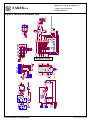
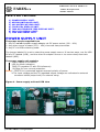
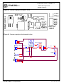
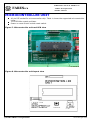
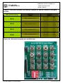
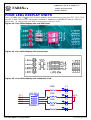
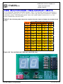
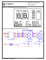
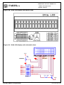
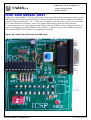
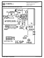
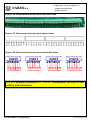
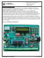
FARES EDUCATIONAL PRODUCTS FARESPCB ATMEL Development Kits MODEL: FEPST3 GENERAL DESCRIPTION FEPST3 is a simple kit designed particularly for students , beginners and recent graduated engineers to allow them to esily work with many ATMEL microcontroller chips, in addition to test and debug firmwares. FEPST3 supports many ATMEL microcontroller chips, such as ATMEL89S51, ATMEL89S52, ATMEL89S8252 and more. It offers all microcontroller I/O pins to external connectors for direct port accessing , while provides the most common primary devices and circuits , such as 2 X 16 LCD, Multiplexed 7SEG, Matrix KEYPAD, and RS232 serial interface. Thus, it saves most of the wasted time and efforts in hardware design and test, hence , the user can concentrate his efforts in software development. the most important development in this kit is the ICSP circuit included. This circuit make the programming of chip is so easy. Because you don't need to plug the chip out during programming. only press one switch to change between program and run mode. Figure 1. FEPST3 kit real PCB view ©2008 FARESPCB Corporation 1 www.fares-pcb.com FARES EDUCATIONAL PRODUCTS FARESPCB ATMEL Development Kits MODEL: FEPST3 Figure 2. FEPST3 kit layout view ©2008 FARESPCB Corporation 2 www.fares-pcb.com FARES EDUCATIONAL PRODUCTS FARESPCB ATMEL Development Kits MODEL: FEPST3 Figure 3. FEPST3 kit schematic view 3 1 1 3 DI P S W-4 P2. 0 P2. 1 P2. 2 P2. 3 KEYPAD ENABLE RX D IP SW-2 TX SERI AL ENABLE 18 19 1 2 3 4 5 6 7 8 9 10 11 12 13 14 15 16 X2 X1 3 2 1 OU T GN D VIN COM COM 12-18 VDC ©2008 FARESPCB Corporation 3 12-18 VDC www.fares-pcb.com FARES EDUCATIONAL PRODUCTS FARESPCB ATMEL Development Kits MODEL: FEPST3 FEPST3 KEY FEATURES 1) 2) 3) 4) 5) 6) 7) POWER SUPPLY UNIT. MICROCONTROLLER UNIT. 4X4 MATRIX KEYPAD UNIT. FOUR LEDs DISPLAY UNIT. TWO MULTIPLEXED 7SEG DISPLAY UNIT. 2X16 LCD DISPLAY UNIT. ICSP AND SERIAL UNIT. POWER SUPPLY UNIT The power may be supplied from 1- Any DC walwart power supply adaptor via DC power socket (12V - 18V). 2- Any other source of power (12V 18V) via screw clamp terminals. 3- Any PC via USB connecting cable. The jumper labeled J1 is set to select the power supply source. It has two ways, one for USB Of any PC labeled (USB) , and the other for adaptor source or via screw clamp terminals labeled (ADP). The power supply unit contains Power supply on-off switch. LED for power indication. 7805 (5V regulator IC with 5% tollerance). .5A Fuse for over current protection. Note 1: FEPST3 kit is protected against reversed polarity of power. 2:The input voltage and the 5V regulated output voltage are redirected to external connector labled (output volt) for external using. Figure 4. Power supply unit real PCB view ©2008 FARESPCB Corporation 4 www.fares-pcb.com FARES EDUCATIONAL PRODUCTS FARESPCB ATMEL Development Kits MODEL: FEPST3 Figure 5. Power supply unit layout view Figure 6. Power supply unit schematic view 1 2 3 4 7805 ON-OFF POWER SW USB CONNECTOR SCREW CLAMP TERMINALS 1N4004 1 2 J1 VCC 3 2 1 Header .5A FUSE 330R 220uF GREEN LED 5V 1 2 DC SOCKET VSP VCC GND 1 2 3 OUTPUT VOLT ©2008 FARESPCB Corporation 5 www.fares-pcb.com FARES EDUCATIONAL PRODUCTS FARESPCB ATMEL Development Kits MODEL: FEPST3 MICROCONTROLLER UNIT 40 pin DIP socket for microcontroller chip. Table 1 shows the supported microcontroller chips. 11.0592 MHz crystal oscillator. Power on reset circuit include reset switch. Figure 7. Microcontroller unit real PCB view Figure 8. Microcontroller unit layout view ©2008 FARESPCB Corporation 6 www.fares-pcb.com FARES EDUCATIONAL PRODUCTS FARESPCB ATMEL Development Kits MODEL: FEPST3 Figure 9. Microcontroller unit schematic view 40 PIN ZIF SOCKET P1.0 P1.1 P1.2 P1.3 P1.4 P1.5 P1.6 P1.7 1 2 3 4 5 6 7 8 P3.0 P3.1 P3.2 P3.3 P3.4 P3.5 P3.6 P3.7 10 11 12 13 14 15 16 17 VCC P1.0 P1.1 P1.2 P1.3 P1.4 P1.5 P1.6 P1.7 P0.0/AD0 P0.1/AD1 P0.2/AD2 P0.3/AD3 P0.4/AD4 P0.5/AD5 P0.6/AD6 P0.7/AD7 P3.0/RXD P3.1/TXD P3.2/INT0 P3.3/INT1 P3.4/T0 P3.5/T1 P3.6/WR P3.7/RD P2.7/A15 P2.6/A14 P2.5/A13 P2.4/A12 P2.3/A11 P2.2/A10 P2.1/A9 P2.0/A8 39 38 37 36 35 34 33 32 P0.0 P0.1 P0.2 P0.3 P0.4 P0.5 P0.6 P0.7 28 27 26 25 24 23 22 21 P2.7 P2.6 P2.5 P2.4 P2.3 P2.2 P2.1 P2.0 VCC RESET 9 RST EA/VPP ALE/PROG PSEN 31 30 29 11.0592 27pF 27pF Table 1. List of chips supported by FEPST3 Chip number AT89S51 AT89S52 AT89S53 AT89S8252 AT89S8253 ©2008 FARESPCB Corporation 7 www.fares-pcb.com FARES EDUCATIONAL PRODUCTS FARESPCB ATMEL Development Kits MODEL: FEPST3 4X4 MATRIX KEYPAD UNIT FEPST3 KIT includes 16 input switches attached to port D configured as 4 rows intersected by four columns. each intersection creates switch position. The four row lines are connected to high nipple of port D as shown. Port P2.7 ------ ROW1 Port P2.6------ ROW2 Port P2.5------ ROW3 Port P2.4------ ROW4 The four column lines are connected to low nipple of port D as shown. Port P2.3------ COL1 Port P2.2------ COL2 Port P2.1------ COL3 Port P2.0------ COL4 COLUMN COL1 COL2 COL3 COL4 P2.3 P2.2 P2.1 P2.0 ROW1 P2.7 SW1 SW2 SW3 SW4 ROW2 P2.6 SW5 SW6 SW7 SW8 ROW3 P2.5 SW9 SW10 SW11 SW12 ROW4 P2.4 SW13 SW14 SW15 SW16 Each column can be enabled/disabled individually via "KEYPAD ENABLE" DIP switch. If you don't intend to use the keypad absolutely, you must disable all columns. You may use the first row i.e. (SW1,SW2,SW3,SW4) as a direct input switches (not in matrix mode) by setting jumper J2 to (1-2). Otherwise set it to (2-3). Note: Port D is pulled up by a 10K resistor. i.e. (microcontroller read high if no switch is pressed). ©2008 FARESPCB Corporation 8 www.fares-pcb.com FARES EDUCATIONAL PRODUCTS FARESPCB ATMEL Development Kits MODEL: FEPST3 Table 2. This table indicates the setting of jumper J2 and DIP switch to configure keypad. DIP switch setting J2(1-2) Direct P2.3 SW1 enabled (P2.3) P2.2 SW2 enabled (P2.2) P2.1 SW3 enabled (P2.1) P2.0 SW4 enabled (P2.0) J2(2-3) Matrix P2.7,P2.3 ----> P2.6,P2.3 ----> P2.5,P2.3 ----> P2.4,P2.3 ----> P2.7,P2.2 ----> P2.6,P2.2 ----> P2.5,P2.2 ----> P2.4,P2.2 ----> P2.7,P2.1 ----> P2.6,P2.1 ----> P2.5,P2.1 ----> P2.4,P2.1 ----> P2.7,P2.0 ----> P2.6,P2.0 ----> P2.5,P2.0 ----> P2.4,P2.0 ----> SW1 SW5 SW9 SW13 SW2 SW6 SW10 SW14 SW3 SW7 SW11 SW15 SW4 SW8 SW12 SW16 Figure 10. 4X4 matrix keypad unit real PCB view ©2008 FARESPCB Corporation 9 www.fares-pcb.com FARES EDUCATIONAL PRODUCTS FARESPCB ATMEL Development Kits MODEL: FEPST3 Figure 11. 4X4 matrix keypad unit layout view Figure 12. 4X4 matrix keypad unit schematic view J2 3 2 1 P2.7 COL1 COL2 COL3 COL4 SW1 SW2 SW3 SW4 SW5 SW6 SW7 SW8 SW9 SW10 SW11 SW12 SW13 SW14 SW15 SW16 ROW1 Header ROW2 P2.6 ROW3 P2.5 ROW4 P2.4 ©2008 FARESPCB Corporation 10 www.fares-pcb.com FARES EDUCATIONAL PRODUCTS FARESPCB ATMEL Development Kits MODEL: FEPST3 FOUR LEDs DISPLAY UNITS Four r ed LEDs wit h 330 curr ent lim it ing r esist or s ar e connect ed t o por t pins P3.7, P3.6, P3.5 and P3.4. Each LED can be individually enabled or disabled via LEDEN DI P sw it ch. LEDs ar e act ive low. i.e. out put low t urn LED on and out put high t urn it off. Figure 13. Four LEDs display unit real PCB view. Figure 14. Four LEDs display unit layout view. Figure 15. Four LEDs display unit schematic view. DIP SW-4 P3.7 P3.6 P3.5 P3.4 330R L1 330R L2 VCC LEDEN ©2008 FARESPCB Corporation 11 330R L3 330R L4 www.fares-pcb.com FARES EDUCATIONAL PRODUCTS FARESPCB ATMEL Development Kits MODEL: FEPST3 TWO MULTIPLEXED 7SEG DISPLAY UNITS Tw o m ult iplex ed 7seg digit wit h BCD decoder ( 7447) . The decoder input s ar e connect ed t o m icr ocont r oller pins P1.0, P1.1, P1.2, and P1.3. Each 7seg digit can be enabled or disabled indiv idually using 7- SEG ENA DI P sw it ch. Not e t hat enable signal is act ive low i.e. a low out put enables t he r equir ed 7SEG. Table 2. The following table shows the required decoder input to display the numbers from 0 to 9. Digit Decoder inputs P1.3 P1.2 P1.1 P1.0 0 1 2 3 4 5 6 7 8 9 0 0 0 0 0 0 0 1 0 0 1 0 0 0 1 1 0 1 0 0 0 1 0 1 0 1 1 0 0 1 1 1 1 0 0 0 1 0 0 1 Figure 16. Two multiplexed 7SEG unit real PCB view. ©2008 FARESPCB Corporation 12 www.fares-pcb.com FARES EDUCATIONAL PRODUCTS FARESPCB ATMEL Development Kits MODEL: FEPST3 Figure 17. Two multiplexed 7SEG unit layout view. Figure 18. Two multiplexed 7SEG unit schematic view. 7447 P1.0 P1.1 P1.2 P1.3 7 1 2 6 3 5 220R D0 D1 D2 D3 A B C D E F G LT RBI BI/RBO 13 12 11 10 9 15 14 S2 A B C D E F G A B C D E F G 7 -SEG S1 A B C D E F G A B C D E F G 7 -SEG A B C D E F G 4 10K P3.3 P3.2 10K 8550 8550 7SEG EN VCC ©2008 FARESPCB Corporation 13 VCC www.fares-pcb.com FARES EDUCATIONAL PRODUCTS FARESPCB ATMEL Development Kits MODEL: FEPST3 2X16 LCD DISPLAY UNIT 2X16 alphabet ic LCD w it h t o por t P0 as follows, PORTP0.7 is connect ed t o PORTP0.6 is connect ed t o PORTP0.5 is connect ed t o PORTP0.4 is connect ed t o PORTP0.3 is connect ed t o PORTP0.2 is connect ed t o PORTP0.1 is connect ed t o PORTP0.0 is connect ed t o backlight and cont r ast cont rol configured in 4bit m ode is connect ed D7 of LCD D6 of LCD D5 of LCD D4 of LCD backlight cont rol. out put low on t his pin t urn backlight on. EN of LCD R/ W of LCD RS of LCD A 10K var iable r esist or labeled " CONT" is added t o cont r ol t he LCD cont r ast . Set "LCDEN" DI P sw it ch t o enable or disable LCD m odule. Figure 19. 2X16 LCD display unit real PCB view. ©2008 FARESPCB Corporation 14 www.fares-pcb.com FARES EDUCATIONAL PRODUCTS FARESPCB ATMEL Development Kits MODEL: FEPST3 Figure 20. 2X16 LCD display unit layout view. Figure 21. 2X16 LCD display unit schematic view. VCC R3 10K CONTRAST VCC DIP SW-8 P0.0 P0.1 P0.2 P0.4 P0.5 P0.6 P0.7 P0.3 RS RW EN D4 D5 D6 D7 BACKLIGHT R2 10K 8550 LCDEN VCC ©2008 FARESPCB Corporation 15 www.fares-pcb.com FARES EDUCATIONAL PRODUCTS FARESPCB ATMEL Development Kits MODEL: FEPST3 ICSP AND SERIAL UNIT Ser ial unit include RS232- TTL logic conver t er using t wo sm all signal t r ansist ors. And pr ovides DB9F socket for PC serial com m unicat ion. Ser ial int erface circuit can be enabled or disabled using DI P sw it ch labeled Rx , Tx . I f t his unit is enabled, you can't use t he t wo por t pins P3.0, P3.1 from ext ernal connect or s. Cr oss or st raight cable can be used by swit ch set t ing . To swit ch bet ween r un m ode and pr ogr am m ing m ode use PROG swit ch. Press t he swit ch t o ent er in pr ogr am m ing m ode ( PROG) and r elease it t o sw it ch t o r un m ode ( RUN) .t he green LED labeled PROG is an indicat or for pr ogr am m ing m ode. Figure 22. ICSP and serial unit real PCB view ©2008 FARESPCB Corporation 16 www.fares-pcb.com FARES EDUCATIONAL PRODUCTS FARESPCB ATMEL Development Kits MODEL: FEPST3 Figure 23. ICSP and serial unit layout view ©2008 FARESPCB Corporation 17 www.fares-pcb.com FARES EDUCATIONAL PRODUCTS FARESPCB ATMEL Development Kits MODEL: FEPST3 Figure 24. RS232 serial interface unit schematic view VCC 10K PROG SWITCH 16 17 18 TX_PROG RX_PROG 10K TX 2 8550 VCC CROSS/STRAIGHT CABLE 13 14 RX 15 10K MOSI 10 10K 11 12 2 MISO 7 8050 8 9 SCLK 10K 1 6 2 7 3 8 4 9 5 4 DB9 FEMALE 5 6 VCC RESET 1 2 3 330R P1.5 TO ATMEL MICROCONTROLLER CHIP P1.6 PROG LED GREEN P1.7 TO EXTERNAL CONNECTORS P3.0 P3.1 RESET Figure 25. Straight/Cross cable connection 1 6 2 7 3 8 4 9 5 1 6 2 7 3 8 4 9 5 DB9 MALE 1 6 2 7 3 8 4 9 5 DB9 FEMALE 1 6 2 7 3 8 4 9 5 DB9 MALE Straight serial cable DB9 FEMALE Cross serial cable (b) (a) PORT CONNECTORS Alt hough FEPST3 Kit has a very popular built in cir cuit s and dev ices ( swit ches , LEDs , 7seg , LCD and ot her ) , but any cir cuit can be enabled or disabled via DI P swit ch set t ing. And so t he associat ed port pins are allowed t o any ot her applicat ions t hr ough scr ew clam p t erm inals . Note Please insure t o disconnect t he built in circuit s which is connect ed t o t he por t pins you decide t o use. The ext er nal connect or s ar e grouped int o 4 unit s each repr esent one m icr ocont roller por t ( 8 I / O) . ©2008 FARESPCB Corporation 18 www.fares-pcb.com FARES EDUCATIONAL PRODUCTS FARESPCB ATMEL Development Kits MODEL: FEPST3 Figure 26. Microcontroller port pins real PCB view Figure 27. Microcontroller port pins layout view Figure 28. Microcontroller port pins schematic view Screw clamp terminals Screw clamp terminals Screw clamp terminals Screw clamp terminals PORT0 PORT1 PORT3 PORT2 FEPST3 includes standard 2.5" X 6.75" breadboard for easy circuit making and extensions. ©2008 FARESPCB Corporation 19 www.fares-pcb.com FARES EDUCATIONAL PRODUCTS FARESPCB ATMEL Development Kits MODEL: FEPST3 HOW TO START? We recommend few tests before begin to use FEPST3 KIT. 1- Det erm ine t he supply sour ce and set j um per 1 as illust r at ed pr eviously in t he POWER SUPPLY UNI T sect ion. 2- Deselect all unused built in cir cuit s in t he kit . This is accom plished by set t ing DI P swit ches LCDEN for LCD enable/ disable. KEYPAD ENABLE for KEYPAD enable/ disable. LEDEN for LEDs enable/ disable. DI P SW- 2 for select ed digit s. SERI ALEN for ser ial enable/ disable. 2- Befor e plugging t he chip in ZI F sock et , insur e t he power delivery by connect ing t he supply and swit ching t he power. I f t he power LED is init iat ed t hen t her e is a power connect ed t o t he KI T. Using a volt m et er, m easur e t he volt age differ ence bet ween GND and VCC at t he OUT connect or . I t should be 5V±0.5V. 3- Now t ur n off t he power sw it ch and inser t your pr ogr am m ed m icr ocont roller chip in t he ZI F sock et , and enj oy your t im e w it h FEPST3 KI T. I f you w ant t o t est t he built in cir cuit funct ionalit y, use a m icrocont roller program m ed wit h t he t est code FEPST3t est .hex w hich included in t he CD. The t est operat ion is: Enable all DI P sw it ches in k it ( LEDEN,7SEGEN,LCDEN,KEYPADENABLE,SERI ALENABLE) . Set J1 according t o t he supply sour ce. Set J2 To ( 2- 3) posit ion. Set RUN/ PROG sw it ch t o PROG m ode ( PROG LED w ill be t ur ned on) . Connect serial cable ( m ale t o fem ale) and set dir ect ion sw it ch according t o t he ser ial cable t ype ( release t he swit ch if st raight cable is used or pr ess it if cr oss one) . Tur n power sw it ch on. Open t he burner pr ogr am m icropr o.exe . Set t he com port from ( opt ions - set t ings) Chose t he AT89S51 chip from ( opt ions – device) Load t he t est code included in CD ( FEPST3.hex) from ( file - load flash file) . Select CHI P ERASE t hen click RUN but t on. Right click t he pr ogram but t on. Aft er pr ogr am m ing is com plet ed set RUN/ PROG sw it ch t o RUN m ode. And follow t he next st eps t o t est all circuit s in FEPST3 kit . LCD test **** FEPST3 **** FARES EDU PROD When you pow er on FEPST3 kit LCD displays seconds t hen t ur noff. and flickers for 4 7SEG test Each 7seg digit s count s fr om 0 t o 9 cont inuously. LED test LEDs ar e t urned on in a per iodic sequence cont inuously. KEYPAD test The pressed sw it ch is det ect ed and it s num ber is displayed on LCD in t he first line as SW(12) IS PREESSED ©2008 FARESPCB Corporation 20 www.fares-pcb.com FARES EDUCATIONAL PRODUCTS FARESPCB ATMEL Development Kits MODEL: FEPST3 SERIAL test RECEIVING test Any t ext r eceived from t he serial m odule will be displayed at t he second line of LCD. TRANSMITTING test I f SW16 is pressed Serial m odule Tr ansm it s " FARES EDUCATI ONAL PRODUCTS FEPST3 KI T" Com pact Disc ( CD) cont ains, User’s Manual. Dat asheet of support ed m icrocont roller chips. Test code FEPST3t est .hex ©2008 FARESPCB Corporation 21 www.fares-pcb.com