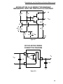
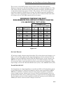
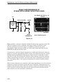
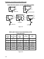
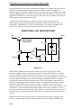
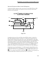
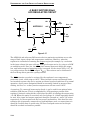
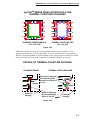
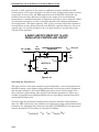
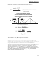
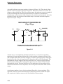
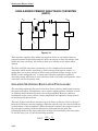
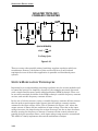
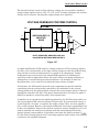
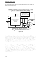
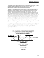
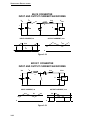
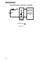
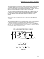
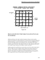
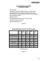
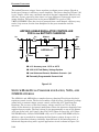
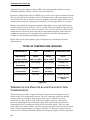
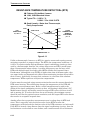
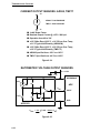
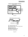
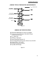
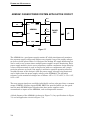
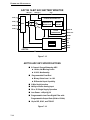
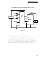
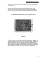
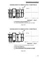
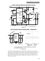
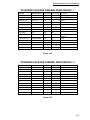
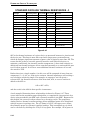
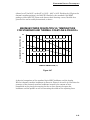
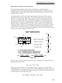
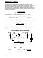
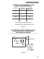
1
PRACTICAL DESIGN TECHNIQUES FOR POWER AND THERMAL MANAGEMENT INTRODUCTION - 1 REFERENCES AND LOW DROPOUT LINEAR REGULATORS - 2 SWITCHING REGULATORS - 3 SWITCHED CAPACITOR VOLTAGE CONVERTERS - 4 BATTERY CHARGERS - 5 TEMPERATURE SENSORS - 6 HARDWARE MONITORING - 7 HARDWARE DESIGN TECHNIQUES - 8 INDEX - I ANALOG DEVICES TECHNICAL REFERENCE BOOKS PUBLISHED BY PRENTICE HALL Analog-Digital Conversion Handbook Digital Signal Processing Applications Using the ADSP-2100 Family (Volume 1:1992, Volume 2:1994) Digital Signal Processing in VLSI DSP Laboratory Experiments Using the ADSP-2101 ADSP-2100 Family User's Manual PUBLISHED BY ANALOG DEVICES High Speed Design Techniques Practical Analog Design Techniques Linear Design Seminar ADSP-21000 Family Applications Handbook System Applications Guide Applications Reference Manual Amplifier Applications Guide Mixed Signal Design Seminar Notes High-Speed Design Seminar Notes Nonlinear Circuits Handbook Transducer Interfacing Handbook Synchro & Resolver Conversion THE BEST OF Analog Dialogue, 1967-1991 HOW TO GET INFORMATION FROM ANALOG DEVICES Analog Devices publishes data sheets and a host of other technical literature supporting our products and technologies. Follow the instructions below for worldwide access to this information. FOR DATA SHEETS U.S.A. and Canada n Fax Retrieval. Telephone number 800-446-6212. Call this number and use a faxcode corresponding to the data sheet of your choice for a fax-on-demand through our automated AnalogFax™ system. Data sheets are available 7 days a week, 24 hours a day. Product/faxcode cross reference listings are available by calling the above number and following the prompts. There is a short index with just part numbers, faxcodes, page count and revision for each data sheet. There is also a longer index sorted by product type with short descriptions. n World Wide Web and Internet. Our address is http://www.analog.com. Use the browser of your choice and follow the prompts. We also provide extensive DSP literature support on an Internet FTP site. Type ftp ftp.analog.com or ftp 137.71.23.11. Log in as anonymous using your e-mail address for your password. n Analog Devices Literature Distribution Center. Call 800-262-5643 and select option two from the voice prompts, or call 781-461-4700 for direct access, or fax your request to 781-821-4273. n DSP Bulletin Board Service. For the latest updates, call 781-461-4258, 8 data bits, 1 stop bit, no parity, 300bps to 14.4kbps. Europe and Israel n Fax Retrieval. Telephone number 49-8765-9300-xxxx, where xxxx is the faxcode. For a list of faxcodes dial 49-8765-9300-1000. (1000 is the code for the faxcode cross-reference listing.) n World Wide Web. Our address is http://www.analog.com. use the browser of your choice and follow the prompts. n Analog Devices Sales Offices. Call your local sales office and request a data sheet. A Worldwide Sales Directory including telephone listings is on the outside back cover of the 1997 Short Form Designers' Guide. n DSP Support Center. Fax requests to **49-89-57005-200 or e-mail [email protected]. The Bulletin Board Service is at **43-1-8887656. Australia and New Zealand n Fax Retrieval. Telephone number 61-59-864377. Follow the voice prompts. n Call 91-80-526-3606 or fax 91-80-526-3713 and request the data sheet of interest. India Other Locations n World Wide Web. Our address is http://www.analog.com. Use the browser of your choice and follow the prompts. n Analog Devices Sales Offices. Call your local sales office and request a data sheet. A Worldwide Sales Directory including telephone numbers is listed on the back cover of the 1997 Short Form Designers' Guide. TECHNICAL SUPPORT AND CUSTOMER SERVICE n In the U.S.A. and Canada, call 800-ANALOGD, (800-262-5643). For technical support on all products, select option one, then select the product area of interest. For price and delivery, select option three. For literature and samples, select option two. Non-800 Number: 781-937-1428 PRACTICAL DESIGN TECHNIQUES FOR POWER AND THERMAL MANAGEMENT a ACKNOWLEDGMENTS Thanks are due the many technical staff members of Analog Devices in Engineering and Marketing who provided invaluable inputs during this project. Particular credit is due the individual authors whose names appear at the beginning of their material. Special thanks go to Wes Freeman, Walter G. Jung, and Ed Grokulsky for thoroughly reviewing the material for content and accuracy. Judith Douville compiled the index, and printing was done by R. R. Donnelley and Sons, Inc. Walt Kester 1998 Copyright 1998 by Analog Devices, Inc. Printed in the United States of America All rights reserved. This book, or parts thereof, must not be reproduced in any form without permission of the copyright owner. Information furnished by Analog Devices, Inc., is believed to be accurate and reliable. However, no responsibility is assumed by Analog Devices, Inc., for its use. Analog Devices, Inc., makes no representation that the interconnections of its circuits as described herein will not infringe on existing or future patent rights, nor do the descriptions contained herein imply the granting of licenses to make, use, or sell equipment constructed in accordance therewith. Specifications are subject to change without notice. ISBN-0-916550-19-2 PRACTICAL DESIGN TECHNIQUES FOR POWER AND THERMAL MANAGEMENT SECTION 1 INTRODUCTION SECTION 2 REFERENCES AND LOW DROPOUT LINEAR REGULATORS n Precision Voltage References n Low Dropout Regulators SECTION 3 SWITCHING REGULATORS n Applications of Switching Regulators n Inductor and Capacitor Fundamentals n Ideal Step-Down (Buck) Converter n Ideal Step-Up (Boost) Converter n Buck-Boost Topologies n Other Non-Isolated Switcher Topologies n Isolated Switching Regulator Topologies n Switch Modulation Techniques n Control Techniques n Diode and Switch Considerations n Inductor Considerations n Capacitor Considerations n Input and Output Filtering SECTION 4 SWITCHED CAPACITOR VOLTAGE CONVERTERS n Charge Transfer Using Capacitors n Unregulated Switched Capacitor Inverter and Doubler Implementations n Voltage Inverter and Doubler Dynamic Operation n Switched Capacitor Voltage Converter Power Losses n Unregulated Inverter/Doubler Design Example n Regulated Output Switched Capacitor Voltage Converters SECTION 5 BATTERY CHARGERS n Battery Fundamentals n Battery Charging n Linear Battery Charger n Switch Mode Dual Charger for Li-Ion, NiCd, and NiMH Batteries n Universal Charger for Li-Ion, NiCd, and NiMH SECTION 6 TEMPERATURE SENSORS n Thermocouple Principles and Cold-Junction Compensation n Resistance Temperature Detectors (RTDs) n Thermistors n Semiconductor Temperature Sensors SECTION 7 HARDWARE MONITORING SECTION 8 HARDWARE DESIGN TECHNIQUES n Analog Circuit Simulation n Prototyping Techniques n Evaluation Boards n Grounding Techniques for Regulator Circuits n Power Supply Noise Reduction and Filtering n Thermal Management n EMI/RFI Considerations n Shielding Concepts INDEX PRACTICAL DESIGN TECHNIQUES FOR POWER AND THERMAL MANAGEMENT INTRODUCTION - 1 REFERENCES AND LOW DROPOUT LINEAR REGULATORS - 2 SWITCHING REGULATORS - 3 SWITCHED CAPACITOR VOLTAGE CONVERTERS - 4 BATTERY CHARGERS - 5 TEMPERATURE SENSORS - 6 HARDWARE MONITORING - 7 HARDWARE DESIGN TECHNIQUES - 8 INDEX - I INTRODUCTION SECTION 1 INTRODUCTION Walt Kester This book focuses on three rather broad and inter-related topics: power management, thermal management, and hardware monitoring. We will discuss them in terms of the various design and application issues associated with each and show how modern ICs allow cost effective and efficient solutions. Power management broadly refers to the generation and control of regulated voltages required to operate an electronic system. It encompasses much more than just power supply design. Today's systems require that power supply design be integrated with the system design in order to maintain high efficiency. In addition, distributed power supply systems require localized regulators at the PC board level, thereby requiring the design engineer to master at least the basics of switching and linear regulators. Integrated circuit components such as switching regulators, linear regulators, switched capacitor voltage converters, and voltage references are typical elements of power management. Battery charging is also an important portion of power management. Closely related to power management is thermal management. In addition to traditional applications of temperature sensors in industrial process control, today's systems require accurate control of monitoring and control of temperature, airflow, etc. Today's computers require that hardware as well as software operate properly, in spite of the many things that can cause a complex high performance system to crash or lock up. The purpose of hardware monitoring is to monitor the critical items in a computing system and take corrective action should problems occur. Microprocessor supply voltage and temperature are two critical parameters. If the supply voltage drops below a specified minimum level, further operations should be halted until the voltage returns to acceptable levels. In some cases, it is desirable to reset the microprocessor under "brownout" conditions. It is also common practice to reset the microprocessor on power-up or power-down. Switching to a battery backup may be required if the supply voltage is low. Under low voltage conditions it may also be desirable to inhibit the microprocessor from writing to external CMOS memory by inhibiting the Chip Enable signal to the memory. A summary of the concepts of power management, thermal management, and hardware monitoring is shown in Figure 1.1. 1.1 INTRODUCTION POWER MANAGEMENT, THERMAL MANAGEMENT AND HARDWARE MONITORING OVERVIEW n Power Management u Switching Supplies u Switched Capacitor Voltage Converters u Battery Chargers u Linear Low Dropout Regulators u Voltage References n Thermal Management u Temperature Sensing u Temperature Control n Hardware Monitoring u µP Supervision u Supply Voltages u Temperature Figure 1.1 In order to understand power management better, we will consider a few typical applications. Consider the traditional desktop PC power supply shown in Figure 1.2. This approach suffers from a number of disadvantages including inefficiency (all the voltages are on all the time - which is probably not necessary), multiple high-current distribution busses, etc. CLASSICAL POWER SUPPLY SYSTEM e.g. TRADITIONAL DESKTOP PCs +12/+15V 110 - 220 VAC 50 - 60 Hz STANDARD AC-DC POWER SUPPLY -12/-15V +5V –5V Major Disadvantages of the Traditional PS System Include: u Inefficiency : Output Voltages Are Always Turned On u Cable Lengths u Inductance Figure 1.2 1.2 INTRODUCTION The trend in today's systems is to make use of the distributed power approach as shown in Figure 1.3. The AC input is rectified, filtered, and converted into an unregulated intermediate voltage which is distributed throughout the system. Each subsystem uses localized voltage regulators (usually switching-types for high efficiency) for generating required voltages. This simplifies the power distribution problem and also allows individual voltages to be shutdown if they are not in use. DISTRIBUTED POWER SUPPLY SYSTEM Regulator Intermediate Voltage e.g., 5V, 12V or 48V 110 - 220 VAC 50 - 60 Hz 24V SHUTDOWN Regulator AC-DC POWER SUPPLY 12V SHUTDOWN Regulator Distributed Supply Advantages: u Regulation of Intermediate Voltage not Critical u Lower Current in Intermediate Voltage Distribution Bus u Flexibility u Selective Shutdown 5V SHUTDOWN Regulator 3.3V SHUTDOWN Figure 1.3 To see how this concept is extended to the PC board level design, Figure 1.4 shows a simplified block diagram of a data acquisition board. The unregulated intermediate voltage enters the board and drives the switching regulators. In the example shown, one switching regulator is dedicated to the processor, and the other drives a low dropout linear regulator. The critical analog circuits on the board, including the signal conditioning and A/D converter, are supplied from the output of the linear regulator. This ensures that the analog circuits operate with a well-regulated and low noise supply voltage. A separate low noise voltage reference is used in conjunction with the 16 bit A/D converter for even lower noise and higher accuracy. The hardware monitoring circuits monitor the processor power supply voltages to ensure the processor functions properly. Airflow and heat sinking is often required with modern high-speed DSPs or microprocessors because of their high power dissipation. Therefore a temperature sensor monitors the processor temperature and works in conjunction with the temperature monitoring and control circuit to regulate the airflow. Figure 1.5 summarizes some of the trends in digital and analog signal processing. 1.3 INTRODUCTION SIMPLIFIED DATA ACQUISITION BOARD UNREGULATED DC VOLTAGE SWITCHING REGULATORS ANALOG INPUTS LOW DROPOUT LINEAR REGULATOR VOLTAGE REFERENCE SIGNAL CONDITIONING 16 BIT A/D CONVERTER DATA AND CONTROL DSP, µP, or µC FAN HARDWARE MONITORING TEMPERATURE MONITORING/ CONTROL TEMPERATURE SENSOR Figure 1.4 TRENDS IN DIGITAL AND ANALOG SIGNAL PROCESSING n Faster Digital and Analog Signal Processing n Higher Power - Requires Thermal Management n Distributed Power Systems vs. Single Power SupplyImplies On-Board Regulation n Energy Efficient - Requires Switching Regulators and Low Dropout Linear Regulators n 16+ Bit ADCs Require Precision Voltage References Figure 1.5 Portable electronic equipment such as laptop computers and cell phones require other types of hardware monitoring as well as power and thermal management circuits. Today's laptop computers are replacing the traditional desktop systems in many companies (see Figure 1.6). Laptops, however, present a large number of design challenges because of the emphasis on performance, light weight, low power, and long battery life. Battery charging circuits are quite complex, and battery voltage and temperature must be monitored and controlled during the charging 1.4 INTRODUCTION cycle. Redundancy must be built into these circuits in order to prevent damage to the battery or dangerous outgassing. Thermal and power management is therefore critical to laptop computers, not only relating to the high-power microprocessor, but also with respect to the battery charging function (see Figure 1.7). Most laptops have internal fans to cool the microprocessor when the internal temperature exceeds safe levels, but the fan should only operate when necessary to conserve battery life. LAPTOPS ARE GREAT, BUT PRESENT SIGNIFICANT DESIGN CHALLENGES! n n n n n High Levels of Functionality and Performance Light Weight Longer Battery Life Fast Battery Charging Li-ion Batteries Emerging as the Battery of Choice n Lower Cost Figure 1.6 Cell phones and other types of hand-held electronic equipment make wide use of power management techniques (see Figure 1.8). Certain critical parts of a cell phone such as the oscillator and frequency synthesis circuits are generally powered by low dropout linear regulators for low noise and accuracy, while high efficiency switching regulators are most often used in the high-power transmitter circuits. Shutdown features are also vital to preserve battery life while the phone is idle. 1.5 INTRODUCTION LAPTOP COMPUTERS REQUIRE n Battery Charger Circuits n Switching Regulators n Low Dropout Linear Regulators n Temperature Sensors and Control n µP Supervisory Circuits n Airflow (Fan) Control AC-DC, MAY INCLUDE CHARGER BRICK Figure 1.7 CELL PHONES TRANSMITTER: Switching Regulator DISPLAY: Regulated Charge Pump Converter POWER UNIT: Battery Charger POWER MANAGEMENT: Voltage Reference Low dropout Regulators n n n n High Performance and Functionality Small Size, Light Weight Long Battery Life, Fast Charging Low Cost Figure 1.8 1.6 INTRODUCTION Temperature sensors and temperature control circuits are widespread in industrial applications such as process control. In many cases, the output signal levels are low level ones (as in a thermocouple), and low noise high gain conditioning is required before further processing. Semiconductor temperature sensors are useful in many applications and offer high-level output signals which reduces the burden on the signal conditioning circuitry (see Figure 1.9). In addition, semiconductor sensors are ideally suited to applications such as PCs, because their operating temperature range, power supply requirements, and packaging closely match the other types of ICs in the system. APPLICATIONS OF THERMAL MANAGEMENT n Instrumentation n Process Control n IC Temperature Monitoring n Airflow Control n Battery Charging n Heat Sink Design Figure 1.9 Finally, proper hardware design techniques are critical to all modern systems. Layout, grounding, and decoupling are extremely critical to successful system design as well as controlling EMI and RFI. Also an understanding of thermal techniques for maintaining safe junction temperatures is critical due to the high power dissipated in many digital ICs. Discussions regarding these practical issues conclude the book (see Figure 1.10). 1.7 INTRODUCTION HARDWARE DESIGN TECHNIQUES n Verifying the Design u Simulation u Prototyping n Minimizing Noise u Layout u Grounding u Decoupling and Filtering u Shielding n Thermal Management u Temperature Sensing u Airflow Control u Heat Sinks n EMI / RFI Qualification Figure 1.10 1.8 REFERENCES AND LOW DROPOUT LINEAR REGULATORS SECTION 2 REFERENCES AND LOW DROPOUT LINEAR REGULATORS Walt Jung Reference circuits and linear regulators actually have much in common. In fact, the latter could be functionally described as a reference circuit, but with greater current (or power) output. Accordingly, almost all of the specifications of the two circuit types have great commonality (even though the performance of references is usually tighter with regard to drift, accuracy, etc.). This chapter is broadly divided into an initial discussion on voltage references, followed by a concluding discussion on linear regulators, with emphasis on their low dropout operation for highest power efficiency. PRECISION VOLTAGE REFERENCES Walt Jung, Walt Kester, James Bryant Voltage references have a major impact on the performance and accuracy of analog systems. A ±5mV tolerance on a 5V reference corresponds to ±0.1% absolute accuracy–only 10-bits. For a 12-bit system, choosing a reference that has a ±1mV tolerance may be far more cost effective than performing manual calibration, while both high initial accuracy and calibration will be necessary in a system making absolute 16-bit measurements. Note that many systems make relative measurements rather than absolute ones, and in such cases the absolute accuracy of the reference is not important, although noise and short-term stability may be. Figure 2.1 summarizes some key points of the reference selection process. Temperature drift or drift due to aging may be an even greater problem than absolute accuracy. The initial error can always be trimmed, but compensating for drift is difficult. Where possible, references should be chosen for temperature coefficient and aging characteristics which preserve adequate accuracy over the operating temperature range and expected lifetime of the system. Noise in voltage references is often overlooked, but it can be very important in system design. It is generally specified on data sheets, but system designers frequently ignore the specification and assume that voltage references do not contribute to system noise. There are two dynamic issues that must be considered with voltage references: their behavior at start-up, and their behavior with transient loads. With regard to the first, always bear in mind that voltage references do not power up instantly (this is true of references inside ADCs and DACs as well as discrete designs). Thus it is rarely possible to turn on an ADC and reference, whether internal or external, make 2.1 REFERENCES AND LOW DROPOUT LINEAR REGULATORS a reading, and turn off again within a few microseconds, however attractive such a procedure might be in terms of energy saving. Regarding the second point, a given reference IC may or may not be well suited for pulse-loading conditions, dependent upon the specific architecture. Many references use low power, and therefore low bandwidth, output buffer amplifiers. This makes for poor behavior under fast transient loads, which may degrade the performance of fast ADCs (especially successive approximation and flash ADCs). Suitable decoupling can ease the problem (but some references oscillate with capacitive loads), or an additional external broadband buffer amplifier may be used to drive the node where the transients occur. References, like almost all other ICs today, are fast migrating to such smaller packages such as SO-8, and the even more tiny SOT-23, enabling much higher circuit densities within a given area of real estate. In addition to the system size reductions these steps bring, there are also tangible reductions in standby power and cost with the smaller and less expense ICs. CHOOSING VOLTAGE REFERENCES FOR HIGH PERFORMANCE SYSTEMS n Tight Tolerance Improves Accuracy, Reduces System Costs n Temperature Drift Affects Accuracy n Long-Term Stability, Low Hysteresis Assures Repeatability n Noise Limits System Resolution n Dynamic Loading Can Cause Errors n Power Consumption is Critical to Battery Systems n Tiny Low Cost Packages Increase Circuit Density Figure 2.1 TYPES OF VOLTAGE REFERENCES In terms of the functionality of their circuit connection, standard reference ICs are often only available in series, or three-terminal form (VIN, Common, VOUT), and also in positive polarity only. The series types have the potential advantages of lower and more stable quiescent current, standard pre-trimmed output voltages, and relatively high output current without accuracy loss. Shunt, or two-terminal (i.e., diode-like) references are more flexible regarding operating polarity, but they are also more restrictive as to loading. They can in fact eat up excessive power with widely varying resistor-fed voltage inputs. Also, they sometimes come in nonstandard voltages. All of these various factors tend to govern when one functional type is preferred over the other. 2.2 REFERENCES AND LOW DROPOUT LINEAR REGULATORS Some simple diode-based references are shown in Figure 2.2. In the first of these, a current driven forward biased diode (or diode-connected transistor) produces a voltage, Vf = VREF. While the junction drop is somewhat decoupled from the raw supply, it has numerous deficiencies as a reference. Among them are a strong TC of about –0.3%/°C, some sensitivity to loading, and a rather inflexible output voltage: it is only available in 600mV jumps. By contrast, these most simple references (as well as all other shunt-type regulators) have a basic advantage, which is the fact that the polarity is readily reversible by flipping connections and reversing the drive current. However, a basic limitation of all shunt regulators is that load current must always be less (usually appreciably less) than the driving current, ID. SIMPLE DIODE REFERENCE CIRCUITS +VS RS +VS ID RZ IZ D1 D1 VREF VREF D2 FORWARD-BIASED DIODE ZENER (AVALANCHE) DIODE Figure 2.2 In the second circuit of Figure 2.2, a zener or avalanche diode is used, and an appreciably higher output voltage realized. While true zener breakdown occurs below 5V, avalanche breakdown occurs at higher voltages and has a positive temperature coefficient. Note that diode reverse breakdown is referred to almost universally today as zener, even though it is usually avalanche breakdown. With a D1 breakdown voltage in the 5 to 8V range, the net positive TC is such that it equals the negative TC of forward-biased diode D2, yielding a net TC of 100ppm/°C or less with proper bias current. Combinations of such carefully chosen diodes formed the basis of the early single package "temperature-compensated zener" references, such as the 1N821-1N829 series. The temperature-compensated zener reference is limited in terms of initial accuracy, since the best TC combinations fall at odd voltages, such as the 1N829's 6.2V. And, 2.3 REFERENCES AND LOW DROPOUT LINEAR REGULATORS the scheme is also limited for loading, since for best TC the diode current must be carefully controlled. Unlike a fundamentally lower voltage (<2V) reference, zener diode based references must of necessity be driven from voltage sources appreciably higher than 6V levels, so this precludes operation of zener references from 5V system supplies. References based on low TC zener (avalanche) diodes also tend to be noisy, due to the basic noise of the breakdown mechanism. This has been improved greatly with monolithic zener types, as is described further below. At this point, we know that a reference circuit can be functionally arranged into either a series or shunt operated form, and the technology within may use either bandgap based or zener diode based circuitry. In practice there are all permutations of these available, as well as a third major technology category. The three major reference technologies are now described in more detail. BANDGAP REFERENCES The development of low voltage (<5V) references based on the bandgap voltage of silicon led to the introductions of various ICs which could be operated on low voltage supplies with good TC performance. The first of these was the LM109 (Reference 1), and a basic bandgap reference cell is shown in Figure 2.3. BASIC BANDGAP REFERENCE +VS IZ R2 ∆V BE R3 R2 6kΩ Ω R1 600Ω Ω Q2 VR = VBE + Q3 Q1 R3 600Ω Ω ∆VBE VBE Figure 2.3 2.4 R2 ∆V BE R3 REFERENCES AND LOW DROPOUT LINEAR REGULATORS This circuit is also called a "∆VBE" reference because the differing current densities between matched transistors Q1-Q2 produces a ∆VBE across R3. It works by summing the VBE of Q3 with the amplified ∆VBE of Q1-Q2, developed across R2. The ∆VBE and VBE components have opposite polarity TCs; ∆VBE is proportionalto-absolute-temperature (PTAT), while VBE is complementary-to-absolutetemperature (CTAT). The summed output is VR, and when it is equal to 1.205V (silicon bandgap voltage), the TC is a minimum. The bandgap reference technique is attractive in IC designs because of several reasons; among these are the relative simplicity, and the avoidance of zeners and their noise. However, very important in these days of ever decreasing system supplies is the fundamental fact that bandgap devices operate at low voltages, i.e., <5V. Not only are they used for stand-alone IC references, but they are also used within the designs of many other linear ICs such as ADCs, DACs, and op-amps. Buffered forms of 1.2V two terminal bandgap references, such as the AD589 IC, remain stable under varying load currents. The H-02A metal can AD589, a 1.235V reference, handles 50µA to 5mA with an output impedance of 0.6Ω, and TCs ranging between 10 and 100ppm/°C. The more recent and functionally similar AD1580, a 1.225V reference, is in the tiny SOT-23 package and handles the same nominal currents as the AD589, with TCs of 50 and 100ppm/°C. However, the basic designs of Figure 2.3 suffer from load and current drive sensitivity, plus the fact that the output needs accurate scaling to more useful levels, i.e., 2.5V, 5V, etc. The load drive issue is best addressed with the use of a buffer amplifier, which also provides convenient voltage scaling to standard levels. An improved three-terminal bandgap reference, the AD580, is shown in Figure 2.4. Popularly called the "Brokaw Cell" (see References 2 and 3), this circuit provides onchip output buffering, which allows good drive capability and standard output voltage scaling. The AD580 was the first precision bandgap based IC reference, and variants of the topology have influenced further generations of both industry standard references such as the REF01 and REF02 series, as well as more recent ADI parts such as the REF195 series, the AD680, AD780, and the AD1582-85 series. The AD580 has two 8:1 emitter-scaled transistors Q1-Q2 operating at identical collector currents (and thus 1/8 current densities), by virtue of equal load resistors and a closed loop around the buffer op-amp. Due to the resultant smaller VBE of the 8× area Q2, R2 in series with Q2 drops the ∆VBE voltage, while R1 (due to the current relationships) drops a PTAT voltage V1: V1 = 2 × R1 × ∆VBE . R2 2.5 REFERENCES AND LOW DROPOUT LINEAR REGULATORS AD580 PRECISION BANDGAP REFERENCE USES BROKAW CELL +VIN R8 R7 + I2 ≅ I1 VOUT = 2.5V R4 Q2 8A ∆VBE Q1 A VZ = 1.205V VBE (Q1) R2 R5 A = TRANSISTOR AREA R1 V1 = 2 R1 ∆V BE R2 COM Figure 2.4 The bandgap cell reference voltage VZ appears at the base of Q1, and is the sum of VBE(Q1) and V1, or 1.205V, the bandgap voltage: VZ = VBE(Q1) + V1 R1 = VBE(Q1) + 2 × × ∆VBE R2 R1 kT J1 = VBE(Q1) + 2 × × × ln R2 q J2 R1 kT = VBE(Q1) + 2 × × × ln8 R2 q = 1.205V . Note that J1 = current density in Q1, J2 = current density in Q2, and J1/J2 = 8. However, because of the presence of the R4/R5 (laser trimmed) thin film divider and the op-amp, the actual voltage appearing at VOUT can be scaled higher, in the AD580 case 2.5V. Following this general principle, VOUT can be raised to other practical levels, such as for example in the AD584, with taps for precise 2.5, 5, 7.5, and 10V operation. The AD580 provides up to 10mA output current while operating from supplies between 4.5 and 30V. It is available in tolerances as low as 10mV, with TCs as low as 10ppm/°C. 2.6 REFERENCES AND LOW DROPOUT LINEAR REGULATORS Many of the recent developments in bandgap references have focused on smaller package size and cost reduction, to address system needs for smaller, more power efficient and less costly reference ICs. Among these are several recent bandgap based IC references. The AD1580 is a shunt mode IC reference which is functionally quite similar to the classic shunt IC reference, the AD589 mentioned above. A key difference is the fact that the AD1580 uses a newer, small geometry process, enabling its availability within the tiny SOT-23 package. The very small size of this package allows use in a wide variety of space limited applications, and the low operating current lends itself to portable battery powered uses. The AD1580 circuit is shown in simplified form in Figure 2.5. AD1580 1.2V SHUNT TYPE BANDGAP REFERENCE HAS TINY SIZE IN SOT-23 FOOTPRINT V+ + R5 R6 R1 Q5 V1 Q8 R7 R2 – Q9 Q3 + Q4 R3 ∆VBE Q2 – Q1 + R4 V– VBE – Figure 2.5 In this circuit, like transistors Q1 and Q2 form the bandgap core, and are operated at a current ratio of 5 times, determined by the ratio of R7 to R2. An op amp is formed by the differential pair Q3-Q4, current mirror Q5, and driver/output stage Q8-Q9. In closed loop equilibrium, this amplifier maintains the bottom ends of R2R7 at the same potential. As a result of the closed loop control described, a basic ∆VBE voltage is dropped across R3, and a scaled PTAT voltage also appears as V1, which is effectively in series with VBE. The nominal bandgap reference voltage of 1.225V is then the sum of Q1’s VBE and V1. The AD1580 is designed to operate at currents as low as 50 µA, also handling maximum currents as high as 10 mA. It is available in grades with voltage tolerances of ±1 or ±10 mV, and with corresponding TC’s of 50 or 100 ppm/°C. 2.7 REFERENCES AND LOW DROPOUT LINEAR REGULATORS The AD1582-AD1585 series comprises a family of series mode IC references, which produce voltage outputs of 2.5, 3.0, 4.096 and 5.0V. Like the AD1580, the series uses a small geometry process to allow packaging within an SOT-23. The AD1582 series specifications are summarized in Figure 2.6. AD1582-AD1585 2.5-5V SERIES TYPE BANDGAP SERIES SPECIFICATIONS n VOUT : 2.500, 3.000, 4.096, & 5.000V n 2.7V to 12V Supply Range n Supply Current : 65µA max n Initial Accuracy: ±0.1% max n Temperature Coefficient: 50 ppm/°C max n Noise: 50µV rms (10Hz - 10kHz) n Long-Term Drift: 100ppm/1khrs n High Output Current: ±5mA min n Temperature Range –40°C to +85°C n Low Cost SOT-23 Package Figure 2.6 The circuit diagram for the series, shown in Figure 2.7, may be recognized as a variant of the basic Brokaw bandgap cell, as described under Figure 2.4. In this case Q1-Q2 form the core, and the overall loop operates to produce the stable reference voltage VBG at the base of Q1. A notable difference here is that the op amp’s output stage is designed with push-pull common-emitter stages. This has the effect of requiring an output capacitor for stability, but it also provides the IC with relatively low dropout operation. The low dropout feature means essentially that VIN can be lowered to as close as several hundred mV above the VOUT level without disturbing operation. The push-pull operation also means that this device series can actually both sink and source currents at the output, as opposed to the classic reference operation of sourcing current (only). For the various output voltage ratings, the divider R5-R6 is adjusted for the respective levels. The AD1582 series is designed to operate with quiescent currents of only 65µA (maximum), which allows good power efficiency when used in low power systems with varying voltage inputs. The rated output current for the series is 5 mA, and they are available in grades with voltage tolerances of ±0.1 or ±1% of VOUT, with corresponding TC’s of 50 or 100ppm/°C. Because of stability requirements, devices of the AD1582 series must be used with both an output and input bypass capacitor. Recommended worst case values for these are shown in the hookup diagram of Figure 2.8. For the electrical values noted, it is likely that tantalum chip capacitors will be the smallest in size. 2.8 REFERENCES AND LOW DROPOUT LINEAR REGULATORS AD1582-AD1585 2.5-5V SERIES TYPE BANDGAP REFERENCES HAVE TINY SIZE IN SOT-23 FOOTPRINT VIN R3 R4 VOUT + R5 Q1 Q2 VBG ∆VBE R6 R2 R1 V1 = 2 R1 ∆V BE R2 GND Figure 2.7 AD1582-AD1585 SERIES CONNECTION DIAGRAM 1 VOUT VIN + + 1µF 3 + 4.7µF 2 Figure 2.8 2.9 REFERENCES AND LOW DROPOUT LINEAR REGULATORS BURIED ZENER REFERENCES In terms of the design approaches used within the reference core, the two most popular basic types of IC references consist of the bandgap and buried zener units. Bandgaps have been discussed, but zener based references warrant some further discussion. In an IC chip, surface operated diode junction breakdown is prone to crystal imperfections and other contamination, thus zener diodes formed at the surface are more noisy and less stable than are buried (or sub-surface) ones. ADI zener based IC references employ the much preferred buried zener. This improves substantially upon the noise and drift of surface-mode operated zeners (see Reference 4). Buried zener references offer very low temperature drift, down to the 1-2ppm/°C (AD588 and AD586), and the lowest noise as a percent of full-scale, i.e., 100nV/√Hz or less. On the downside, the operating current of zener type references is usually relatively high, typically on the order of several mA. An important general point arises when comparing noise performance of different references. The best way to do this is to compare the ratio of the noise (within a given bandwidth) to the DC output voltage. For example, a 10V reference with a 100nV/√Hz noise density is 6dB more quiet in relative terms than is a 5V reference with the same noise level. XFETTM REFERENCES A third and brand new category of IC reference core design is based on the properties of junction field effect (JFET) transistors. Somewhat analogous to the bandgap reference for bipolar transistors, the JFET based reference operates a pair of junction field effect transistors with different pinchoff voltages, and amplifies the differential output to produce a stable reference voltage. One of the two JFETs uses an extra ion implantation, giving rise to the name XFET (eXtra implantation junction Field Effect Transistor) for the reference core design. The basic topology for the XFET reference circuit is shown in Figure 2.9. J1 and J2 are the two JFET transistors, which form the core of the reference. J1 and J2 are driven at the same current level from matched current sources, I1 and I2. To the right, J1 is the JFET with the extra implantation, which causes the difference in the J1-J2 pinchoff voltages to differ by 500mV. With the pinchoff voltage of two such FETs purposely skewed, a differential voltage will appear between the gates for identical current drive conditions and equal source voltages. This voltage, ∆VP, is: ∆VP = VP1 - VP2 , where VP1 and VP2 are the pinchoff voltages of FETs J1 and J2, respectively. 2.10 REFERENCES AND LOW DROPOUT LINEAR REGULATORS ADR290-ADR293 2.048-5V XFETTM REFERENCE TOPOLOGY FEATURES HIGH STABILITY AND LOW POWER VIN I2 I1 R 2 + R 3 VOUT = ∆VP 1 + + IPTAT • R 3 R1 + VOUT V=0 J2 R1 J1 ∆VP IPTAT R2 R3 Figure 2.9 Note that, within this circuit, the voltage ∆VP exists between the gates of the two FETs. We also know that, with the overall feedback loop closed, the op amp axiom of zero input differential voltage will hold the sources of the two JFET at same potential. These source voltages are applied as inputs to the op amp, the output of which drives feedback divider R1-R3. As this loop is configured, it stabilizes at an output voltage from the R1-R2 tap which does in fact produce the required ∆VP between the J1-J2 gates. In essence, the op amp amplifies ∆VP to produce VOUT,where R2 + R3 VOUT = ∆VP 1 + + (I PTAT )( R3) . R1 As can be noted, this expression includes the basic output scaling (leftmost portion of the right terms), plus a rightmost temperature dependent term including IPTAT. The IPTAT portion of the expression compensates for a basic negative temperature coefficient of the XFET core, such that the overall net temperature drift of the reference is typically in a range of 3 to 8ppm/°C. During manufacture, the R1-R3 scaling resistance values are adjusted to produce the different voltage output options of 2.048, 2.5, 4.096 and 5.0V for the ADR290, ADR291, ADR292 and ADR293 family (ADR29X). This ADR29X family of series mode references is available in 8 pin packages with a standard footprint, as well as a TO-92 3 lead format. They operate from supplies of VOUT plus 200mV to 15V, with a typical quiescent current of 12 µA, and output currents of up to 5 mA. A summary of specifications for the family appears in Figure 2.10. 2.11 REFERENCES AND LOW DROPOUT LINEAR REGULATORS ADR290-ADR293 XFET™ SERIES SPECIFICATIONS n VOUT : 2.048, 2.500, 4.096, & 5.000V n 2.7V to 15V Supply Range n Supply Current : 12µA max n Initial Accuracy: ±2 mV max n Temperature Coefficient: 8 ppm/°C max n Low-Noise: 6µVp-p (0.1 - 10Hz) √Hz @ 1kHz n Wideband Noise: 420nV/√ n Long-Term Drift: 0.2ppm/1khrs n High Output Current: 5mA min n Temperature Range –40°C to +125°C n Standard REF02 Pinout n 8-Lead Narrow Body SOIC, 8-Lead TSSOP, and 3-Lead TO-92 Figure 2.10 The XFET architecture offers performance improvements over bandgap and buried zener references, particularly for systems where operating current is critical, yet drift and noise performance must still be excellent. XFET noise levels are lower than bandgap based bipolar references operating at an equivalent current, the temperature drift is low and linear at 3-8 ppm/°C (allowing easier compensation when required), and the series has lower hysteresis than bandgaps. Thermal hysteresis is a low 50ppm over a –40 to +125°C range, less that half that of a typical bandgap device. Finally, the long-term stability is excellent, typically only 0.2ppm/1000 hours. Figure 2.11 summarizes the pro and con characteristics of the three reference architectures; bandgap, buried zener, and XFET. Modern IC references come in a variety of styles, but series operating, fixed output positive types do tend to dominate. These devices can use bandgap based bipolars, JFETs, or buried zeners at the device core, all of which has an impact on the part’s ultimate performance and application suitability. They may or may not also be low power, low noise, and/or low dropout, and be available within a certain package. Of course, in a given application, any single one of these differentiating factors can drive a choice, thus it behooves the designer to be aware of all the different devices available. 2.12 REFERENCES AND LOW DROPOUT LINEAR REGULATORS CHARACTERISTICS OF REFERENCE ARCHITECTURES BANDGAP BURIED ZENER XFETTM < 5V Supplies > 5V Supplies < 5V Supplies High Noise @ High Power Low Noise @ High Power Low Noise @ Low Power Fair Drift and Long Term Stability Good Drift and Long Term Stability Excellent Drift and Long Term Stability Fair Hysteresis Fair Hysteresis Low Hysteresis Figure 2.11 STANDARD POSITIVE OUTPUT THREE TERMINAL REFERENCE HOOKUP (8-PIN DIP PINOUT) +VS 2 OUTPUT (+) LEAD SHORT, HEAVY TRACE VIN C1 VOUT + C2 6 0.1µF 3 TEMP TRIM RTRIM 5 10µF RPAD VTEMP VREF GND + VOUT RL COUT 4 Iq POWER COMMON Figure 2.12 2.13 REFERENCES AND LOW DROPOUT LINEAR REGULATORS Figure 2.12 shows the standard footprint for such a series type IC positive reference in an 8 pin package (Note that “(x)” numbers refer to the standard pin for that function). There are several details which are important. Many references allow optional trimming by connecting an external trim circuit to drive the references' trim input pin (5). Some bandgap references also have a high impedance PTAT output (VTEMP) for temperature sensing (3). The intent here is that no appreciable current be drawn from this pin, but it can be useful for such non-loading types of connections as comparator inputs, to sense temperature thresholds, etc. All references should use decoupling capacitors on the input pin (2), but the amount of decoupling (if any) placed on the output (6) depends upon the stability of the reference's output op-amp with capacitive load. Simply put, there is no hard and fast rule for capacitive loads here. For example, some three terminal types require the output capacitor (i.e., REF19X and AD1582-85 series), while with others it is optional for performance improvement (AD780, REF43). The safest rule then is that you should verify what are the specific capacitive loading ground rules for the reference you intend to use, for the load conditions your circuit presents. VOLTAGE REFERENCE SPECIFICATIONS TOLERANCE It is usually better to select a reference with the required value and accuracy and to avoid external trimming and scaling if possible. This allows the best TCs to be realized, as tight tolerances and low TCs usually go hand-in-hand. Tolerances as low as 0.04% can be achieved with the AD586, AD780, REF195, while the AD588 is 0.01%. If and when trimming must be used, be sure to use the recommended trim network with no more range than is absolutely necessary. When/if additional external scaling is required, a precision op-amp should be used, along with ratioaccurate, low TC tracking thin film resistors. DRIFT The XFET and buried zener reference families have the best long term drift and TC performance. TCs as low as 1-2ppm/°C are available with the AD586 and AD588, and the AD780 bandgap reference is almost as good at 3ppm/°C. The XFET series achieve long terms drifts of 0.2 ppm/1000 hours, while the buried zener types come in at 25ppm/1000 hours. Note that where a figure is given for long term drift, it is usually drift expressed in ppm/1000 hours. There are 8766 hours in a year, and many engineers multiply the 1000 hour figure by 8.77 to find the annual drift - this is not correct, and can in fact be quite pessimistic. Long term drift in precision analog circuits is a "random walk" phenomenon and increases with the square root of the elapsed time (this supposes that drift is due to random microeffects in the chip and not some over-riding cause such as contamination). The 1 year figure will therefore be about √8.766 ≈ 3 times the 1000 hour figure, and the ten year value will be roughly 9 times the 1000 hour value. In practice, things are a little better even than this, as devices tend to stabilize with age. 2.14 REFERENCES AND LOW DROPOUT LINEAR REGULATORS The accuracy of an ADC or DAC can be no better than that of its reference. Reference temperature drift affects fullscale accuracy as shown in Figure 2.13. This table shows system resolution and the TC required to maintain 1/2 LSB error over an operating temperature range of 100°C. For example, a TC of about 1ppm/°C is required to maintain 1/2LSB error at 12-bits. For smaller operating temperature ranges, the drift requirement will be less. The last three columns of the table show the voltage value of 1/2 LSB for popular full scale ranges. REFERENCE TEMPERATURE DRIFT REQUIREMENTS FOR VARIOUS SYSTEM ACCURACIES (1/2 LSB CRITERIA, 100°C SPAN) ½ LSB WEIGHT (mV) 10, 5, AND 2.5V FULLSCALE RANGES REQUIRED DRIFT (ppm/ºC) 19.53 10V 19.53 5V 9.77 2.5V 4.88 9 9.77 9.77 4.88 2.44 10 4.88 4.88 2.44 1.22 11 2.44 2.44 1.22 0.61 12 1.22 1.22 0.61 0.31 13 0.61 0.61 0.31 0.15 14 0.31 0.31 0.15 0.08 15 0.15 0.15 0.08 0.04 16 0.08 0.08 0.04 0.02 BITS 8 Figure 2.13 SUPPLY RANGE IC reference supply voltages range from about 3V (or less) above rated output, to as high as 30V (or more) above rated output. Exceptions are devices designed for low dropout, such as the REF195 and the AD1582-AD1585 series. At low currents, the REF195 can deliver 5V with an input as low as 5.1V (100mV dropout). Note that due to process limits, some references may have more restrictive maximum voltage input ranges, such as the AD1582-AD1585 series (12V), or the ADR29X series (18V). LOAD SENSITIVITY Load sensitivity (or output impedance) is usually specified in µV/mA of load current, or mΩ. While figures of 100µV/mA (100mΩ) or less are quite good (AD780, REF43, REF195), it should be noted that external wiring drops can produce comparable errors at high currents, without care in layout. Load current dependent errors are minimized with short, heavy conductors on the (+) output and on the ground return. For the highest precision, buffer amplifiers and Kelvin sensing circuits (AD588 and AD688) are used to ensure accurate voltages at the load. 2.15 REFERENCES AND LOW DROPOUT LINEAR REGULATORS The output of a buffered reference is the output of an op amp, and therefore the source impedance is a function of frequency. Typical reference output impedance rises at 6dB/octave from the DC value, and is nominally about 10Ω at a few hundred kHz. This impedance can be lowered with an external capacitor, provided the opamp within the reference remains stable for such loading. LINE SENSITIVITY Line sensitivity (or regulation) is usually specified in µV/V of input change, and is lower than 50µV/V (–86dB) in the REF43, REF195, AD680, and AD780. For DC and very low frequencies, such errors are easily masked by noise. As with op-amps, the line sensitivity (or power supply rejection) of references degrades with increasing frequency, typically 30 to 50dB at a few hundred kHz. For this reason, the reference input should be highly decoupled (LF and HF). Line rejection can also be increased with a low dropout pre-regulator, such as one of the ADP3300 series parts. Figure 2.14 summarizes the major reference specifications. VOLTAGE REFERENCE DC SPECIFICATIONS (TYPICAL VALUES AVAILABLE) n Tolerance: u AD588: u AD586, AD780, REF195: 0.01% 0.04% n Drift (TC): u AD586, AD588: u AD780, ADR29X 1-2ppm/°C 3 ppm/°C n Drift (long term): u ADR29X: u AD588: 0.2 ppm/1000 hours 25 ppm/1000 hours n Supply Range: u REF19X, AD1582-AD1585: VOUT plus ~0.5 V n Load Sensitivity: 100µV/mA (100mohm) n Line Sensitivity: 50µV/V (-86 dB) Figure 2.14 NOISE Reference noise is not always specified, and when it is, there is not total uniformity on how. For example, some devices are characterized for peak-to-peak noise in a 0.1 to 10Hz bandwidth, while others are specified in terms of wideband rms or peak-topeak noise over a specified bandwidth. The most useful way to specify noise (as with op-amps) is a plot of noise voltage spectral density (nV/√Hz) versus frequency. 2.16 REFERENCES AND LOW DROPOUT LINEAR REGULATORS Low noise references are important in high resolution systems to prevent loss of accuracy. Since white noise is statistical, a given noise density must be related to an equivalent peak-to-peak noise in the relevant bandwidth. Strictly speaking, the peak-to-peak noise in a gaussian system is infinite (but its probability is infinitesimal). Conventionally, the figure of 6.6 × rms is used to define a practical peak value - statistically, this occurs less than 0.1% of the time. This peak-to-peak value should be less than 1/2LSB in order to maintain required accuracy. If peak-topeak noise is assumed to be 6 times the rms value, then for an N-bit system, reference voltage fullscale VREF, reference noise bandwidth (BW), the required noise voltage spectral density En (V/√Hz) is given by: En ≤ VREF . 12 ⋅ 2 N ⋅ BW For a 10V, 12-bit, 100kHz system, the noise requirement is a modest 643nV/√Hz. Figure 2.15 shows that increasing resolution and/or lower fullscale references make noise requirements more stringent. The 100kHz bandwidth assumption is somewhat arbitrary, but the user may reduce it with external filtering, thereby reducing the noise. Most good IC references have noise spectral densities around 100nV/√Hz, so additional filtering is obviously required in most high resolution systems, especially those with low values of VREF. REFERENCE NOISE REQUIREMENTS FOR VARIOUS SYSTEM ACCURACIES (1/2 LSB / 100kHZ CRITERIA) NOISE DENSITY (nV/√Hz) FOR 10, 5, AND 2.5V FULLSCALE RANGES BITS 10V 5V 2.5V 12 643 322 161 13 322 161 80 14 161 80 40 15 80 40 20 16 40 20 10 Figure 2.15 2.17 REFERENCES AND LOW DROPOUT LINEAR REGULATORS Some references, for example the AD587 buried zener type have a pin designated as the noise reduction pin (see data sheet). This pin is connected to a high impedance node preceding the on-chip buffer amplifier. Thus an externally connected capacitor CN will form a low pass filter with an internal resistor, to limits the effective noise bandwidth seen at the output. A 1µF capacitor gives a 3 dB bandwidth of 40 Hz. Note that this method of noise reduction is by no means universal, and other devices may implement noise reduction differently, if at all. There are also general purpose methods of noise reduction, which can be used to reduce the noise of any reference IC, at any standard voltage level. The reference circuit of Figure 2.16 (References 5 and 6) is one such example. This circuit uses external filtering and a precision low-noise op-amp to provide both very low noise and high DC accuracy. Reference U1 is a 2.5, 3.0, 5, or 10V reference with a low noise buffered output. The output of U1 is applied to the R1-C1/C2 noise filter to produce a corner frequency of about 1.7 Hz. Electrolytic capacitors usually imply DC leakage errors, but the bootstrap connection of C1 causes its applied bias voltage to be only the relatively small drop across R2. This lowers the leakage current through R1 to acceptable levels. Since the filter attenuation is modest below a few Hertz, the reference noise still affects overall performance at low frequencies (i.e., <10 Hz). COMBINING LOW-NOISE AMPLIFIER WITH EXTENSIVE FILTERING YIELDS EXCEPTIONAL REFERENCE NOISE PERFORMANCE (1.5 TO 5nV/√ √Hz @ 1kHZ) +15V +15V 100Ω Ω 3 2 VIN VO 6 1kΩ Ω 0.1µF U1 + R1 + R2 10kΩ Ω GND 4 + 6 U2 C1 100µF 25V 7 100Ω Ω 2 DIODES: 1N4148 4 1.1kΩ Ω C2 100µF 25V + 3.3Ω Ω 100µF,25V + U1: AD586, AD587, REF01 REF02, REF05, REF10 U2: OP113, OP27 OP176, AD797 10µF 25V Figure 2.16 The output of the filter is then buffered by a precision low noise unity-gain follower, such as the OP113EP. With less than ±150µV of offset error and under 1µV/°C drift, the buffer amplifier’s DC performance will not seriously affect the accuracy/drift of most references. For example, an ADR292E for U1 will have a typical drift of 3ppm/°C, equivalent to 7.5µV/°C, higher than the buffer amplifier. Almost any op amp will have a current limit higher than a typical IC reference. Further, even lower noise op-amps are available for 5-10V use. The AD797 offers 1kHz noise performance less than 2nV/√Hz in this circuit, compared to about 5nV/√Hz for the 2.18 REFERENCES AND LOW DROPOUT LINEAR REGULATORS OP113. With any amplifier, Kelvin sensing can be used at the load point, a technique which can eliminate I×R related output voltage errors. SCALED REFERENCES A useful approach when a non-standard reference voltage is required is to simply buffer and scale a basic low voltage reference diode. With this approach, a potential difficulty is getting an amplifier to work well at such low voltages as 3V. A workhorse solution is the low power reference and scaling buffer shown in Figure 2.17. Here a low current 1.2V two terminal reference diode is used for D1, which can be either a 1.235V AD589, or the 1.225V AD1580. Resistor R1 sets the diode current in either case, and is chosen for 50µA at a minimum supply of 2.7V (a current suitable for either diode). Obviously, loading on the unbuffered diode must be minimized at the VREF node. RAIL-TO-RAIL OUTPUT OP AMPS ALLOW GREATEST FLEXIBILITY IN LOW DROPOUT REFERENCES +3V OR MORE C1 R1 27.4kΩ Ω 0.1µF VOUT = VREF OR VOUT = VREF × (1 + R2/R3) + U1 D1: AD589 (+1.235V) AD1580 (+1.225V) R3 R2 U1: SEE TEXT VREF (UNBUFFERED) Figure 2.17 The amplifier U1 both buffers and optionally scales up the nominal 1.2V reference, allowing much higher source/sink output currents. Of course, a higher op amp quiescent current is expended in doing this, but this is a basic tradeoff of the approach. Quiescent current is amplifier dependent, ranging from 45µA/channel with the OP196/296/496 series to 1000-2000µA/channel with the OP284 and OP279. The former series is most useful for very light loads (<2mA), while the latter series provide device dependent outputs up to 50mA. Various devices can be used in the circuit as shown, and their key specs are summarized in Figure 2.18. 2.19 REFERENCES AND LOW DROPOUT LINEAR REGULATORS OP AMPS USEFUL IN LOW VOLTAGE RAIL-RAIL REFERENCES AND REGULATORS DEVICE* Iq, mA Vsat (+) Vsat (–) Isc, mA per channel V (min @ mA) V (max @ mA) min OP181/281/481 0.003 4.93 @ 0.05 0.075 @ 0.05 ± 3.5 OP193/293/493 0.017 4.20 @ 1 0.280 @ 1 (typ) ±8 OP196/296/496 0.045 4.30 @ 1 0.400 @ 1 ± 4 (typ) OP295/495 0.150** 4.50 @ 1 0.110 @ 1 ± 11 OP191/291/491 0.300 4.80 @ 2.5 0.075 @ 2.5 ± 8.75 AD820/822 0.620 4.89 @ 2 0.055 @ 2 ± 15 OP184/284/484 1.250** 4.85 @ 2.5 0.125 @ 2.5 ± 7.5 AD8531/32/34 1.400 4.90 @ 10 0.100 @ 10 ± 250 OP279 2.000 4.80 @ 10 0.075 @ 10 ± 45 * Typical device specifications @ Vs = +5V, TA = 25°C, unless otherwise noted ** Maximum Figure 2.18 In Figure 2.17, without gain scaling resistors R2-R3, VOUT is simply equal to VREF. With the use of the scaling resistors, VOUT can be set anywhere between a lower limit of VREF, and an upper limit of the positive rail, due to the op amp’s railrail output swing. Also, note that this buffered reference is inherently low dropout, allowing a +4.5V (or more) reference output on a +5V supply, for example. The general expression for VOUT is shown in the figure, where VREF is the reference voltage. Amplifier standby current can be further reduced below 20µA, if an amplifier from the OP181/281/481 or the OP193/293/493 series is used. This choice will be at some expense of current drive, but can provide very low quiescent current if necessary. All devices shown operate from voltages down to 3V (except the OP279, which operates at 5V). REFERENCE PULSE CURRENT RESPONSE The response of references to dynamic loads is often a concern, especially in applications such as driving ADCs and DACs. Fast changes in load current invariably perturb the output, often outside the rated error band. For example, the reference input to a sigma-delta ADC may be the switched capacitor circuit shown in Figure 2.19. The dynamic load causes current spikes in the reference as the capacitor CIN is charged and discharged. As a result, noise may be induced on the ADC reference circuitry. 2.20 REFERENCES AND LOW DROPOUT LINEAR REGULATORS SWITCHED CAPACITOR INPUT OF SIGMA-DELTA ADC PRESENTS A DYNAMIC LOAD TO THE VOLTAGE REFERENCE RIN SIGMA-DELTA ADC VREF IN + CEXT CIN ~ 10pF AGND Figure 2.19 Although sigma-delta ADCs have an internal digital filter, transients on the reference input can still cause appreciable conversion errors. Thus it is important to maintain a low noise, transient free potential at the ADC’s reference input. Be aware that if the reference source impedance is too high, dynamic loading can cause the reference input to shift by more than 5mV. A bypass capacitor on the output of a reference may help it to cope with load transients, but many references are unstable with large capacitive loads. Therefore it is quite important to verify that the device chosen will satisfactorily drive the output capacitance required. In any case, the input to references should always be decoupled - with at least 0.1µF, and with an additional 5-50µF if there is any LF ripple on its supply. See Figure 2.12 (again). Since some references misbehave with transient loads, either by oscillating or by losing accuracy for comparatively long periods, it is advisable to test the pulse response of voltage references which may encounter transient loads. A suitable circuit is shown in Figure 2.20. In a typical voltage reference, a step change of 1mA produces the transients shown. Both the duration of the transient, and the amplitude of the ringing increase when a 0.01µF capacitor is connected to the reference output. 2.21 REFERENCES AND LOW DROPOUT LINEAR REGULATORS MAKE SURE REFERENCE IS STABLE WITH LARGE CAPACITIVE LOADS TOP TRACE: NO LOAD (CL = 0) 50mV/div. VIN 1mA to 2mA STEP SCOPE REFERENCE UNDER TEST CL RL BOTTOM TRACE: CL = 0.01µF 200mV/div. PULSE GENERATOR BOTH TRACES: 5µs/div. Figure 2.20 Where possible, a reference should be designed to drive large capacitive loads. The AD780 is designed to drive unlimited capacitance without oscillation, it has excellent drift and an accurate output, in addition to relatively low power consumption. Other references which are useful with output capacitors are the REF19X and AD1582-AD1585 series. As noted above, reference bypass capacitors are useful when driving the reference inputs of successive-approximation ADCs. Figure 2.21 illustrates reference voltage settling behavior immediately following the "Start Convert” command. A small capacitor (0.01µF) does not provide sufficient charge storage to keep the reference voltage stable during conversion, and errors may result. As shown by the bottom trace, decoupling with a ≥1µF capacitor maintains the reference stability during conversion. Where voltage references are required to drive large capacitances, it is also critically important to realize that their turn-on time will be prolonged. Experiment may be needed to determine the delay before the reference output reaches full accuracy, but it will certainly be much longer than the time specified on the data sheet for the same reference in a low capacitance loaded state. 2.22 REFERENCES AND LOW DROPOUT LINEAR REGULATORS SUCCESSIVE APPROXIMATION ADCs CAN PRESENT A DYNAMIC TRANSIENT LOAD TO THE REFERENCE VIN SCOPE START CONVERT VREF AD780 CB SAR ADC CB = 0.01µF CB = 0.22µF CB = 1µF START CONVERT SCOPE TOP TRACE VERTICAL SCALE: 5V/div. ALL OTHER VERTICAL SCALES: 5mV/div. HORIZONTAL SCALE: 1µs/div. Figure 2.21 LOW NOISE REFERENCES FOR HIGH RESOLUTION CONVERTERS High resolution converters (both sigma-delta and high speed ones) can benefit from recent improvements in IC references, such as lower noise and the ability to drive capacitive loads. Even though many data converters have internal references, the performance of these references is often compromised because of the limitations of the converter process. In such cases, using an external reference rather than the internal one often yields better overall performance. For example, the AD7710-series of 22-bit ADCs has a 2.5V internal reference with a 0.1 to 10Hz noise of 8.3µV rms (2600nV/√Hz), while the AD780 reference noise is only 0.67µV rms (200nV/√Hz). The internal noise of the AD7710-series in this bandwidth is about 1.7µV rms. The use of the AD780 increases the effective resolution of the AD7710 from about 20.5bits to 21.5 bits. Figure 2.22 shows the AD780 used as the reference for the AD7710-series ADCs. The use of the AD780’s optional 3V scaling enhances the dynamic range of the ADC, while lowering overall system noise as described above. In addition, the AD780 allows a large decoupling capacitor on its output thereby minimizing conversion errors due to transients. There is one possible but yet quite real problem when replacing the internal reference of a converter with a higher precision external one. The converter in question may have been trimmed during manufacture to deliver its specified performance with a relatively inaccurate internal reference. In such a case, using a more accurate external reference with the converter may actually introduce additional gain error! For example, the early AD574 had a guaranteed uncalibrated gain accuracy of 0.125% when using an internal 10V reference (which itself had a specified accuracy of only ±1%). It is obvious that if such a device, having an internal 2.23 REFERENCES AND LOW DROPOUT LINEAR REGULATORS reference which is at one end of the specified range, is used with an external reference of exactly 10V, then its gain will be about 1% in error. THE AD780 IS IDEAL FOR DRIVING PRECISION SIGMA-DELTA ADCs +5V (ANALOG) + VIN 1µF AVDD REF IN(+) VO AD780 + 100µF AD77XX Σ∆ ADC 100nF REF IN (–) AGND NOTE: ONLY REFERENCE CONNECTIONS SHOWN Figure 2.22 REFERENCES (Voltage References) 1. Bob Widlar, New Developments in IC Voltage Regulators, IEEE Journal of Solid State Circuits, Vol. SC-6, February, 1971. 2. Paul Brokaw, A Simple Three-Terminal IC Bandgap Voltage Reference, IEEE Journal of Solid State Circuits, Vol. SC-9, December, 1974. 3. Paul Brokaw, More About the AD580 Monolithic IC Voltage Regulator, Analog Dialogue, 9-1, 1975. 4. Dan Sheingold, Section 20.2 within Analog-Digital Conversion Handbook, 3d. Edition, Prentice-Hall, 1986. 5. Walt Jung, Build an Ultra-Low-Noise Voltage Reference, Electronic Design Analog Applications Issue, June 24, 1993. 6. Walt Jung, Getting the Most from IC Voltage References, Analog Dialogue, 28-1, 1994, pp. 13-21. 2.24 REFERENCES AND LOW DROPOUT LINEAR REGULATORS LOW DROPOUT REGULATORS Walt Jung INTRODUCTION Linear IC voltage regulators have long been standard power system building blocks. After an initial introduction in 5 V logic voltage regulator form, they have since expanded into other standard voltage levels spanning from 3 to 24 V, handling output currents from as low as 100 mA (or less) to as high as 5 A (or more). For several good reasons, linear style IC voltage regulators have been valuable system components since the early days. One reason is the relatively low noise characteristic vis-à-vis the switching type of regulator. Others are a low parts count and overall simplicity compared to discrete solutions. But, because of their power losses, these linear regulators have also been known for being relatively inefficient. Early generation devices (of which many are still available) required 2V or more of unregulated input above the regulated output voltage, making them lossy in power terms. More recently however, linear IC regulators have been developed with more liberal (i.e., lower) limits on minimum input-output voltage. This voltage, known more commonly as dropout voltage, has led to what is termed the Low DropOut regulator, or more popularly, the LDO. Dropout voltage (VMIN) is defined simply as that minimum input-output differential where the regulator undergoes a 2% reduction in output voltage. For example, if a nominal 5.0V LDO output drops to 4.9V (-2%) under conditions of an input-output differential of 0.5V, by this definition the LDO’s VMIN is 0.5V. As will be shown in this section, dropout voltage is extremely critical to a linear regulator stage’s power efficiency. The lower the voltage allowable across a regulator while still maintaining a regulated output, the less power the regulator dissipates as a result. A low regulator dropout voltage is the key to this, as it takes this lower dropout to maintain regulation as the input voltage lowers. In performance terms, the bottom line for LDOs is simply that more useful power is delivered to the load and less heat is generated in the regulator. LDOs are key elements of power systems that must provide stable voltages from batteries, such as portable computers, cellular phones, etc. This is simply because they maintain their regulated output down to lower points on the battery’s discharge curve. Or, within classic mainspowered raw DC supplies, LDOs allow lower transformer secondary voltages, reducing system susceptibility to shutdown under brownout conditions as well as allowing cooler operation. LINEAR VOLTAGE REGULATOR BASICS A brief review of three terminal linear IC regulator fundamentals is necessary to understanding the LDO variety. As it turns out, almost all LDOs available today, as well as many of the more general three terminal regulator types, are positive leg, series style regulators. This simply means that they control the regulated voltage 2.25 REFERENCES AND LOW DROPOUT LINEAR REGULATORS output by means of a pass element which is in series with the positive side of unregulated input. This is shown more clearly in Figure 2.23, which is a hookup diagram for a hypothetical three terminal style regulator. To re-iterate what was said earlier in the chapter about reference ICs, in terms of their basic functionality, many standard voltage regulator ICs are available in the series three-terminal form as is shown here (VIN, GND or Common, VOUT). A BASIC THREE TERMINAL VOLTAGE REGULATOR VIN (6V) VMIN = VIN – VOUT = 1V IN OUT VOUT (5V) THREE TERMINAL REGULATOR IL (1A) GND RL (5Ω Ω) IGROUND (1mA) COMMON Figure 2.23 This diagram also allows some statements to be made about power losses in the regulator. There are two components to power which are dissipated in the regulator, one a function of VIN – VOUT and IL, plus a second which is a function of VIN and Iground. If we call the total power PD, this then becomes: PD = ( VIN − VOUT )( I L ) + ( VIN )(Iground ) . Obviously, the magnitude of the load current and the regulator dropout voltage both greatly influence the power dissipated. However, it is also easy to see that for a given IL, as the dropout voltage is lowered, the first term of PD is reduced. With an intermediate dropout voltage rating of 1V, a 1A load current will produce 1W of heat in this regulator, which may require a heat sink for continuous operation. It is this first term of the regulator power which usually predominates, at least for loaded regulator conditions. 2.26 REFERENCES AND LOW DROPOUT LINEAR REGULATORS The second term, being proportional to Iground (typically only 1-2 mA, sometimes even less) usually only becomes significant when the regulator is unloaded, and the regulator’s quiescent or standby power then produces a constant drain on the source VIN. However, it should be noted that in some types of regulators (notably those which have very low β pass devices such as lateral PNP transistors) the Iground current under load can actually run quite high. This effect is worst at the onset of regulation, or when the pass device is in saturation, and can be noted by a sudden Iground current “spike”, where the current jumps upward abruptly from a lower low level. All LDO regulators using bipolar transistor pass devices which can be saturated (such as PNPs) can show this effect. It is much less severe in PNP regulators using vertical PNPs (since these have a higher intrinsic β) and doesn’t exist to any major extent in PMOS LDOs (since PMOS transistors are controlled by voltage level, not current). In the example shown, the regulator delivers 5V × 1A, or 5W to the load. With a dropout voltage of 1V, the input power is 6V times the same 1A, or 6W. In terms of power efficiency, this can be calculated as: P PEFF(%) = 100 × OUT , PIN where POUT and PIN are the total output and input powers, respectively. In these sample calculations, the relatively small portion of power related to Iground will be ignored for simplicity, since this power is relatively small. In an actual design, this simplifying step may not be justified. In the case shown, the efficiency would be 100 × 5/6, or about 83%. But by contrast, if an LDO were to be used with a dropout voltage of 0.1V instead of 1V, the input voltage can then be allowed to go as low as 5.1V. The new efficiency for this condition then becomes 100 × 5/5.1, or 98%. It is obvious that an LDO can potentially greatly enhance the power efficiency of linear voltage regulator systems. A more detailed look within a typical regulator block diagram reveals a variety of elements, as is shown in Figure 2.24. In this diagram virtually all of the elements shown can be considered to be fundamentally necessary, the exceptions being the shutdown control and saturation sensor functions (shown dotted). While these are present on many current regulators, the shutdown feature is relatively new as a standard function, and certainly isn’t part of standard three-terminal regulators. When present, shutdown control is a logic level controllable input, whereby a digital HIGH (or LO) is defined as regulation active (or vice-versa). The error output, ERR , is useful within a system to detect regulator overload, such as saturation of the pass device, thermal overload, etc. The remaining functions shown are always part of an IC power regulator. 2.27 REFERENCES AND LOW DROPOUT LINEAR REGULATORS BLOCK DIAGRAM OF A VOLTAGE REGULATOR VIN VDROPOUT = VMIN = VIN – VOUT CURRENT LIMIT ERR VOUT OVERLOAD SATURATION SENSOR OVERTEMP SENSOR SD PASS DEVICE SHUTDOWN CONTROL IREF R1 R1 VOUT = VREF 1 + R2 ERROR AMP R2 VREF COMMON Figure 2.24 In operation, a voltage reference block produces a stable voltage VREF, which is almost always a bandgap based voltage, typically ~1.2V, which allows output voltages of 3V or more from supplies as low as 5V. This voltage is presented to one input of an error amplifier, with the other input connected to the VOUT sensing divider, R1-R2. The error amplifier drives the pass device, which in turn controls the output. The resulting regulated voltage is then simply: R1 VOUT = VREF 1 + . R2 With a typical bandgap reference voltage of 1.2V, the R1/R2 ratio will be approximately 3/1 for a 5V output. When standby power is critical, several design steps will be taken. The resistor values of the divider will be high, the error amplifier and pass device driver will be low power, and the reference current IREF will also be low. By these means the regulator’s unloaded standby current can be reduced to a mA or less using bipolar technology, and to only a few µA in CMOS parts. In regulators which offer a shutdown mode, the shutdown state standby current will be reduced to a µA or less. Nearly all regulators will have some means of current limiting and over temperature sensing, to protect the pass device against failure. Current limiting is usually by a series sensing resistor for high current parts, or alternately by a more simple drive current limit to a controlled β pass device (which achieves the same end). For higher voltage circuits, this current limiting may also be combined with voltage limiting, to 2.28 REFERENCES AND LOW DROPOUT LINEAR REGULATORS provide complete load line control for the pass device. All power regulator devices will also have some means of sensing over-temperature, usually by means of a fixed reference voltage and a VBE-based sensor monitoring chip temperature. When the die temperature exceeds a dangerous level (above ~150°C), this can be used to shutdown the chip, by removing the drive to the pass device. In some cases an error flag output may be provided to warn of this shutdown (and also loss of regulation from other sources). PASS DEVICES AND THEIR ASSOCIATED TRADEOFFS The discussion thus far has not treated the pass device in any detail. In practice, this major part of the regulator can actually take on quite a number of alternate forms. Precisely which type of pass device is chosen has a major influence on almost all major regulator performance issues. Most notable among these is the dropout voltage, VMIN. Figure 2.25a through 2.25e illustrates a number of pass devices which are useful within voltage regulator circuits, shown in simple schematic form. On the figure is also listed the salient VMIN for the device as it would typically be used, which directly indicates its utility for use in an LDO. Not shown in these various minifigures are the remaining circuits of a regulator. It is difficult to fully compare all of the devices from their schematic representations, since they differ in so many ways beyond their applicable dropout voltages. For this reason, the chart of Figure 2.26 is useful. This chart compares the various pass elements in greater detail, allowing easy comparison between the device types, dependent upon which criteria is most important. Note that columns A-E correspond to the schematics of Figure 2.25a2.25e. Note also that the pro/con comparison items are in relative terms, as opposed to a hard specification limit for any particular pass device type. For example, it can be seen that the all NPN pass devices of columns A and B have the attributes of a follower circuit, which allows high bandwidth and provides relative immunity to cap loading because of the characteristic low ZOUT. However, neither the single NPN nor the Darlington NPN can achieve low dropout, for any load current. This is because the VBE(s) of the pass device appears in series with the input, preventing its saturation, and thus setting a VMIN of about 1 or 2V. By contrast, the inverting mode device connections of both columns C and E do allow the pass device to be effectively saturated, which lowers the associated voltage losses to a minimum. This single factor makes these two pass device types optimum for LDO use, at least in terms of power efficiency. 2.29 REFERENCES AND LOW DROPOUT LINEAR REGULATORS PASS DEVICES USEFUL IN VOLTAGE REGULATORS VIN VIN VMIN ≅ 2V VMIN ≅ 1V VOUT VOUT (a) SINGLE NPN (b) DARLINGTON NPN VIN VIN VMIN ≅ VCE(SAT) Q1 VOUT VMIN ≅ RDS(ON) × IL VMIN ≅ 1.5V Q1 Q2 Q2 VIN VOUT P1 VOUT Q1 (d) PNP/NPN (c) SINGLE PNP (e) PMOS Figure 2.25 PROS AND CONS OF VOLTAGE REGULATOR PASS DEVICES A B C D E SINGLE NPN DARLINGTON NPN SINGLE PNP/NPN PMOS V MIN ~ 1V V MIN ~ 2V V MIN ~ 0.1V V MIN ~ 1.5V V MIN ~ R DS(ON)× IL IL < 1A IL > 1A IL < 1A IL > 1A IL > 1A Follower Follower Inverter Inverter Inverter Low ZOUT Low Z OUT High Z OUT High Z OUT High Z OUT Wide BW Wide BW Narrow BW Narrow BW Narrow BW C L Immune C L Immune CL Sensitive C L Sensitive C L Sensitive PNP Figure 2.26 2.30 REFERENCES AND LOW DROPOUT LINEAR REGULATORS For currents below 1A, either a single PNP or a PMOS pass device is most useful for low dropout, and they both can achieve a VMIN of 0.1V or less at currents of 100mA. The dropout voltage of a PNP will be highly dependent upon the actual device used and the operating current, with vertical PNP devices being superior for saturation losses, as well as minimizing the Iground spike when in saturation. PMOS pass devices offer the potential for the lowest possible VMIN, since the actual dropout voltage will be the product of the device RDS(ON) and IL. Thus a low RDS(ON) PMOS device can always be chosen to minimize VMIN for a given IL. PMOS pass devices are typically external to the LDO IC, making the IC actually a controller (as opposed to a complete and integral LDO). PMOS pass devices can allow currents up to several amps or more with very low dropout voltages. The PNP/NPN connection of column D is actually a hybrid hookup, intended to boost the current of a single PNP pass device. This it does, but it also adds the VBE of the NPN in series (which cannot be saturated), making the net VMIN of the connection about 1.5V. All of the three connections C/D/E have the characteristic of high output impedance, and require an output capacitor for stability. The fact that the output cap is part of the regulator frequency compensation is a most basic application point, and one which needs to be clearly understood by the regulator user. This factor, denoted by “CL sensitive”, makes regulators using them generally critical as to the exact CL value, as well as its ESR (equivalent series resistance). Typically this type of regulator must be used only with a specific size as well as type of output capacitor, where the ESR is controlled with respect to both time and temperature to fully guarantee regulator stability. Fortunately, some recent Analog Devices LDO IC circuit developments have eased this burden on the part of the regulator user a great deal, and will be discussed below in further detail. Some examples of standard IC regulator architectures illustrate the points above regarding pass devices, and allow an appreciation of regulator developments leading up to more recent LDO technologies. The classic LM309 5V/1A three-terminal regulator (see Reference 1) was the originator in a long procession of regulators. This circuit is shown in much simplified form in Figure 2.27, with current limiting and over temperature details omitted. This IC type is still in standard production today, not just in original form, but in family derivatives such as the 7805, 7815 etc., and their various low and medium current alternates. Using a Darlington pass connection for Q18-Q19, the design has never been known for low dropout characteristics (~1.5V typical), or for low quiescent current (~5mA). It is however relatively immune to instability issues, due to the internal compensation of C1, and the buffering of the emitter follower output. This helps make it easy to apply. The LM109/309 bandgap voltage reference actually used in this circuit consists of a more involved scheme, as opposed to the basic form which was described with Figure 2.3. Resistor R8 drops a PTAT voltage, which drives the Darlington connected error amplifier, Q9-Q10. The negative TC VBEs of Q9-Q10 and Q12-Q13 are summed with this PTAT voltage, and this sum produces a temperature-stable 5V output voltage. Current buffering of the error amplifier Q10 is provided by PNP Q11, which drives the NPN pass devices. 2.31 REFERENCES AND LOW DROPOUT LINEAR REGULATORS SIMPLIFIED SCHEMATIC OF LM309 FIXED 5V/1A THREE-TERMINAL REGULATOR Q17 VIN Q18 Q19 Q2 VOUT Q13 R9 Q3 R1 Q11 Q12 R2 Q4 C1 R3 R8 Q9 Q6 Q7 Q10 Q5 R7 R4 R5 R6 Q8 COMMON Figure 2.27 Later developments in references and three-terminal regulation techniques led to the development of the voltage adjustable regulator. The original IC to employ this concept was the LM317 (see Reference 2), which is shown in simplified schematic form in Figure 2.28. Note that this design does not use the same ∆VBE form of reference as in the LM309. Instead, Q17-Q19, etc. are employed as a form of a Brokaw bandgap reference cell (see Figure 2.4 again, and Reference 3). This adjustable regulator bootstraps the reference cell transistors Q17-Q19 and the error amplifier transistors Q16-Q18. The output of the error amplifier drives Darlington pass transistors Q25-Q26, through buffer Q12. The basic reference cell produces a fixed voltage of 1.25V, which appears between the VOUT and ADJ pins of the IC as shown. External scaling resistors R1 and R2 set up the desired output voltage, which is: R2 VOUT = VREF 1 + + 50µA × R2 . R1 2.32 REFERENCES AND LOW DROPOUT LINEAR REGULATORS SIMPLIFIED SCHEMATIC OF LM317 ADJUSTABLE THREE-TERMINAL REGULATOR VIN Q18 Q16 Q25 Q26 Q12 VOUT Q19 Q17 R15 VREF = 1.25V R14 R1 50µA ADJ R 2 VOUT = VREF 1 + + 50 µA × R 2 R 1 R2 Figure 2.28 As can be noted, the voltage output is a scaling of VREF by R2-R1, plus a small voltage component which is a function of the 50µA reference cell current. Typically, the R1-R2 values are chosen to draw >5mA, making the rightmost term relatively small by comparison. The design is internally compensated, and in many applications will not necessarily need an output bypass capacitor. Like the LM309 fixed voltage regulator, the LM317 series has relatively high dropout voltage, due to the use of Darlington pass transistors. It is also not a low power IC (quiescent current typically 3.5mA). The strength of this regulator lies in the wide range of user voltage adaptability it allows. Subsequent variations on the LM317 pass device topology modified the method of output drive, substituting a PNP/NPN cascade for the LM317’s Darlington NPN pass devices. This development achieves a lower VMIN, 1.5V or less (see Reference 4). The modification also allows all of the general voltage programmability of the basic LM317, but at some potential increase in application sensitivity to output capacitance. This sensitivity is brought about by the fundamental requirement for an output capacitor for the IC’s frequency compensation, which is a differentiation from the original LM317. LOW DROPOUT REGULATOR ARCHITECTURES As has been shown thus far, all LDO pass devices have the fundamental characteristics of operating in an inverting mode. This allows the regulator circuit to 2.33 REFERENCES AND LOW DROPOUT LINEAR REGULATORS achieve pass device saturation, and thus low dropout. A by-product of this mode of operation is that this type of topology will necessarily be more susceptible to stability issues. These basic points give rise to some of the more difficult issues with regard to LDO performance. In fact, these points influence both the design and the application of LDOs to a very large degree, and in the end, determine how they are differentiated in the performance arena. A traditional LDO architecture is shown in Figure 2.29, and is generally representative of actual parts employing either a PNP pass device as shown, or alternately, a PMOS device. There are both DC and AC design and application issues to be resolved with this architecture, which are now discussed. TRADITIONAL LDO ARCHITECTURE VIN VOUT Q1 PNP (OR PMOS) PASS DEVICE R1 CL RL – Q2 ESR gm + IGROUND CCOMP + R2 VREF Figure 2.29 In DC terms, perhaps the major issue is the type of pass device used, which influences dropout voltage and ground current. If a lateral PNP device is used for Q1, the β will be low, sometimes only on the order or 10 or so. Since Q1 is driven from the collector of Q2, the relatively high base current demanded by a lateral PNP results in relatively high emitter current in Q2, or a high Iground. For a typical lateral PNP based regulator operating with a 5V/150mA output, Iground will be typically ~18mA, and can be as high as 40mA. To compound the problem of high Iground in PNP LDOs, there is also the “spike” in Iground, as the regulator is operating within its dropout region. Under such conditions, the output voltage is out of tolerance, and the regulation loop forces higher drive to the pass device, in an attempt to maintain loop regulation. This results in a substantial spike upward in Iground, which is typically internally limited by the regulator’s saturation control circuits. PMOS pass devices do not demonstrate a similar current spike in Iground, since they are voltage controlled. But, while devoid of the Iground spike, PMOS pass 2.34 REFERENCES AND LOW DROPOUT LINEAR REGULATORS devices do have some problems of their own. Problem number one is that high quality, low RON, low threshold PMOS devices generally aren’t compatible with many IC processes. This makes the best technical choice for a PMOS pass device an external part, driven from the collector of Q2 in the figure. This introduces the term “LDO controller”, where the LDO architecture is completed by an external pass device. While in theory NMOS pass devices would offer lower RON choice options, they also demand a boosted voltage supply to turn on, making them impractical for a simple LDO. PMOS pass devices are widely available in low both RON and low threshold forms, with current levels up to several amperes. They offer the potential of the lowest dropout of any device, since dropout can always be lowered by picking a lower RON part. The dropout voltage of lateral PNP pass devices is reasonably good, typically around 300mV at 150mA, with a maximum of 600mV. These levels are however considerably bettered in regulators using vertical PNPs, which have a typical β of ~150 at currents of 200mA. This leads directly to an Iground of 1.5mA at the 200mA output current. The dropout voltage of vertical PNPs is also an improvement vis-àvis that of the lateral PNP regulator, and is typically 180mV at 200mA, with a maximum of 400mV. There are also major AC performance issues to be dealt with in the LDO architecture of Fig. 2.29. This topology has an inherently high output impedance, due to the operation of the PNP pass device in a common-emitter (or common-source with a PMOS device) mode. In either case, this factor causes the regulator to appear as a high source impedance to the load. The internal compensation capacitor of the regulator, CCOMP, forms a fixed frequency pole, in conjunction with the gm of the error amplifier. In addition, load capacitance CL forms an output pole, in conjunction with RL. This particular pole, because it is a second (and sometimes variable) pole of a two-pole system, is the source of a major LDO application problem. The CL pole can strongly influence the overall frequency response of the regulator, in ways that are both useful as well as detrimental. Depending upon the relative positioning of the two poles in the frequency domain, along with the relative value of the ESR of capacitor CL, it is quite possible that the stability of the system can be compromised for certain combinations of CL and ESR. Note that CL is shown here as a real capacitor, which is actually composed of a pure capacitance plus the series parasitic resistance ESR. Without a heavy duty exercise into closed-loop stability analysis, it can safely be said that LDOs, like other feedback systems, need to satisfy certain basic stability criteria. One of these is the gain-versus-frequency rate-of-change characteristic in the region approaching the system’s unity loop gain crossover point. For the system to be closed loop stable, the phase shift must be less than 180° at the point of unity gain. In practice, a good feedback design needs to have some phase margin, generally 45° or more to allow for various parasitic effects. While a single pole system is intrinsically stable, two pole systems are not necessarily so—they may in fact be stable, or they may also be unstable. Whether or not they are stable for a given instance is highly dependent upon the specifics of their gain-phase characteristics. 2.35 REFERENCES AND LOW DROPOUT LINEAR REGULATORS If the two poles of such a system are widely separated in terms of frequency, stability may not be a serious problem. The emitter-follower output of a classic regulator like the LM309 is an example with widely separated pole frequencies, as the very low ZOUT of the NPN follower pushes the output pole due to load capacitance far out in frequency, where it does little harm. The internal compensation capacitance (C1 of Fig. 2.27, again) then forms part of a dominant pole, which reduces loop gain to below unity at the much higher frequencies where the output pole does occur. Thus stability is not necessarily compromised by load capacitance in this type of regulator. Figure 2.30 summarizes the various DC and AC design issues of LDOs. DC AND AC DESIGN ISSUES IN LOW DROPOUT REGULATORS DC AC n Lateral PNP Pass Device: n Two Pole Compensation System High IGROUND n Vertical PNP Pass Device: n CL ESR Critical to Stability Low IGROUND Low VMIN n Requires Large CL n PMOS Pass Device: Lowest IGROUND Variation Low VMIN Ampere Level Output Currents n Requires"Zoned" CL ESR (Max/Min ESR Limits Over Time and Temperature) Figure 2.30 By their nature however, LDOs simply can’t afford the luxury of emitter follower outputs, they must instead operate with pass devices capable of saturation. Thus, given the existence of two or more poles (one or more internal and a second formed by external loading) there is the potential for the cumulative gain-phase to add in a less than satisfactory manner. The potential for instability under certain output loading conditions is, for better or worse, a fact-of-life for most LDO topologies. However, the output capacitor which gives rise to the instability can, for certain circumstances, also be the solution to the same instability. This seemingly paradoxical situation can be appreciated by realizing that almost all practical capacitors are actually as shown in Fig. 2.29, a series combination of the capacitance CL and a parasitic resistance, ESR. While load resistance RL and CL do form a pole, CL and its ESR also form a zero. The effect of the zero is to mitigate the destabilizing effect of CL for certain conditions. For example, if the pole and zero in 2.36 REFERENCES AND LOW DROPOUT LINEAR REGULATORS question are appropriately placed in frequency relative to the internal regulator poles, some of the deleterious effects can be made to essentially cancel, leaving little or no problematic instability (see Reference 5). The basic problem with this setup is simply that the capacitor’s ESR, being a parasitic term, is not at all well controlled. As a result, LDOs which depend upon output pole-zero compensation schemes must very carefully limit the capacitor ESR to certain zones, such as shown by Figure 2.31. ZONED LOAD CAPACITOR ESR CAN MAKE AN LDO APPLICATIONS NIGHTMARE 100 UNSTABLE 10 CAPACITOR ESR (Ω Ω) STABLE 1 UNSTABLE 0.1 0 IOUT (mA) 1000 Figure 2.31 A zoned ESR chart such as this is meant to guide the user of an LDO in picking an output capacitor which confines ESR to the stable region, i.e., the central zone, for all operating conditions. Note that this generic chart is not intended to portray any specific device, just the general pattern. Unfortunately, capacitor facts of life make such data somewhat limited in terms of the real help it provides. Bearing in mind the requirements of such a zoned chart, it effectively means that general purpose aluminum electrolytic are prohibited from use, since they deteriorate in terms of ESR at cold temperatures. Very low ESR types such as OS-CON or multi-layer ceramic units have ESRs which are too low for use. While they could in theory be padded up into the stable zone with external resistance, this would hardly be a practical solution. This leaves tantalum types as the best all around choice for LDO output use. Finally, since a large capacitor value is likely to be used to maximize stability, this effectively means that the solution for an LDO such as Fig. 2.29 must use a more expensive and physically large tantalum capacitor. This is not desirable if small size is a major design criteria. 2.37 REFERENCES AND LOW DROPOUT LINEAR REGULATORS THE anyCAPTM LOW DROPOUT REGULATOR FAMILY Some novel modifications to the basic LDO architecture of Fig. 2.29 allow major improvements in terms of both DC and AC performance. These developments are shown schematically in Figure 2.32, which is a simplified diagram of the Analog Devices ADP330X series LDO regulator family. These regulators are also known as the anyCAPTM family, so named for their relative insensitivity to the output capacitor in terms of both size and ESR. They are available in power efficient packages such as the Thermal Coastline (discussed below), in both stand-alone LDO and LDO controller forms, and also in a wide span of output voltage options. ADP330X anyCAPTM TOPOLOGY FEATURES IMPROVED DC & AC PERFORMANCE OVER TRADITIONAL LDOs VIN VOUT Q1 R1 CCOMP NONINVERTING WIDEBAND DRIVER + gm – R3 D1 PTAT VOS CL R1||R2 ×1 RL R4 IPTAT R2 GND Figure 2.32 Design Features Related to DC Performance One of the key differences in the ADP330X series is the use of a high gain vertical PNP pass device, with all of the advantages described above with Figs. 2.29 and 2.30 (also, see Reference 6). This allows the typical dropout voltages for the series to be on the order of 1mV/mA for currents of 200mA or less. It is important to note that the topology of this LDO is distinctly different from that of the generic form in Fig. 2.29, as there is no obvious VREF block. The reason for this is the fact that the ADP330X series uses what is termed a “merged” amplifierreference design. The operation of the integral amplifier and reference scheme illustrated in Fig. 2.32 can be described as follows. 2.38 REFERENCES AND LOW DROPOUT LINEAR REGULATORS In this circuit, VREF is defined as a reference voltage existing at the output of a zero impedance divider of ratio R1/R2. In the figure, this is depicted symbolically by the (dotted) unity gain buffer amplifier fed by R1/R2, which has an output of VREF. This reference voltage feeds into a series connection of (dotted) R1||R2, then actual components D1, R3, R4, etc. The error amplifier, shown here as a gm stage, is actually a PNP input differential stage with the two transistors of the pair operated at different current densities, so as to produce a predictable PTAT offset voltage. Although shown here as a separate block VOS, this offset voltage is inherent to a bipolar pair for such operating conditions. The PTAT VOS causes a current IPTAT to flow in R4, which is simply: I PTAT = VOS . R4 Note that this current also flows in series connected R4, R3, and the Thevenin resistance of the divider, R1||R2, so: VPTAT = I PTAT (R3 + R4 + R1||R2) . The total voltage defined as VREF is the sum of two component voltages: VREF = VPTAT + VD1 , where the IPTAT scaled voltages across R3, R4, and R1||R2 produce a net PTAT voltage VPTAT, and the diode voltage VD1 is a CTAT voltage. As in a standard bandgap reference, the PTAT and CTAT components add up to a temperature stable reference voltage of 1.25V. In this case however, the reference voltage is not directly accessible, but instead it exists in the virtual form described above. It acts as it would be seen at the output of a zero impedance divider of a numeric ratio of R1/R2, which is then fed into the R3-D1 series string through a Thevenin resistance of R1||R2 in series with D1. With the closed loop regulator at equilibrium, the voltage at the virtual reference node will be: R2 VREF = VOUT . R1 + R2 2.39 REFERENCES AND LOW DROPOUT LINEAR REGULATORS With minor re-arrangement, this can be put into the standard form to describe the regulator output voltage, as: R1 VOUT = VREF 1 + . R2 In the various devices of the ADP330X series, the R1-R2 divider is adjusted to produce standard output voltages of 2.7, 3.0, 3.2, 3.3, and 5.0V. As can be noted from this discussion, unlike a conventional reference setup, there is no power wasting reference current such as used in a conventional regulator topology (IREF of Fig. 2.24). In fact, the Fig. 2.32 regulator behaves as if the entire error amplifier has simply an offset voltage of VREF volts, as seen at the output of a conventional R1-R2 divider. Design Features Related to AC Performance While the above described DC performance enhancements of the ADP330X series are worthwhile, the most dramatic improvements come in areas of AC related performance. These improvements are in fact the genesis of the anyCAPTM series name. Capacitive loading and the potential instability it brings is a major deterrent to easily applying LDOs. While low dropout goals prevent the use of emitter follower type outputs, and so preclude their desirable buffering effect against cap loading, there is an alternative technique of providing load immunity. One method of providing a measure of insusceptibility against variation in a particular amplifier response pole is called pole splitting (see Reference 8). It refers to an amplifier compensation method whereby two response poles are shifted in such a way so as to make one a dominant, lower frequency pole. In this manner the secondary pole (which in this case is the CL related output pole) becomes much less of a major contributor to the net AC response. This has the desirable effect of greatly desensitizing the amplifier to variations in the output pole. A Basic Pole-Splitting Topology A basic LDO topology with frequency compensation as modified for pole splitting is shown in Figure 2.33. Here the internal compensation capacitor CCOMP is connected as an integrating capacitor, around pass device Q1 (C1 is the pass device input capacitance). While it is true that this step will help immunize the regulator to the CL related pole, it also has a built in fatal flaw. With CCOMP connected directly to the Q1 base as shown, the line rejection characteristics of this setup will be quite poor. In effect, when doing it this way one problem (CL sensitivity) will be exchanged for another (poor line rejection). 2.40 REFERENCES AND LOW DROPOUT LINEAR REGULATORS THE SOLUTION TO CL SENSITIVITY: POLE SPLIT COMPENSATION (WRONG WAY EXAMPLE!) VIN C1 VOUT Q1 CCOMP R1 CL + gm – ESR RL + R2 VREF Figure 2.33 The anyCAPTM Pole-Splitting Topology Returning to the anyCAPTM series topology, (Fig. 2.32, again) it can be noted that in this case CCOMP is isolated from the pass device’s base (and thus input ripple variations), by the wideband non-inverting driver. But insofar as frequency compensation is concerned, because of this buffer’s isolation, CCOMP still functions as a modified pole splitting capacitor (see Reference 9), and it does provide the benefits of a buffered, CL independent single-pole response. The regulator’s frequency response is dominated by the internal compensation, and becomes relatively immune to the value and ESR of load capacitor CL. Thus the name anyCAPTM for the series is apt, as the design is tolerant of virtually any output capacitor type. The benefits of the anyCAPTM topology are summarized by Figure 2.34. As can be noted, CL can be as low as 0.47µF, and it can also be a multi-layer ceramic capacitor (MLCC) type. This allows a very small physical size for the entire regulation function, such as when a SOT-23 packaged anyCAPTM LDO is used, for example the ADP3300 device. Because of the in-sensitivity to CL, the designer needn’t worry about such things as ESR zones, and can better concentrate on the system aspects of the regulator application. 2.41 REFERENCES AND LOW DROPOUT LINEAR REGULATORS BENEFITS OF anyCAPTM LDO TOPOLOGY n Internal CCOMP Dominates Response Rolloff n CL Can Range from 0.47µF(min) to Infinity n Low and Ultra-Low CL ESR is OK n MLCC Types for CL Work, is Physically Smallest Solution n No ESR Exclusion Zones n Fast Load Transient Response and Good Line Rejection Figure 2.34 The anyCAPTM LDO series devices The major specifications of the anyCAPTM series of LDO regulators are summarized in Figure. 2.35. The devices include both single and dual output parts, with current capabilities ranging from 50 to 200mA. Rather than separate individual specifications for output tolerance, line and load regulation, plus temperature, the anyCAPTM series devices are rated simply for a combined total accuracy figure. This accuracy is either 0.8% at 25°C, or 1.4% over the temperature range with the device operating over an input range of VOUT +0.3 (or 0.5V), up to 12V. With total accuracy being covered by one clear specification, the designer can then achieve a higher degree of confidence. It is important to note that this method of specification also includes operation within the regulator dropout range (unlike some LDO parts specified for higher input-output voltage difference conditions). anyCAPTM SERIES LDO REGULATOR DEVICES Part Number Accuracy Package Comment VMIN @ IL IL (V, typ/max) (mA) ADP3300 0.08 / 0.17 50 0.8 / 1.4 SOT-23-6 Single ADP3301 0.10 / 0.2 100 0.8 / 1.4 SO-8 Single ADP3302 0.10 / 0.2 100 0.8 / 1.4 SO-8 Dual ADP3303 0.18 / 0.4 200 0.8 / 1.4 SO-8 Single ADP3307 0.13 / 0.22 100 0.8 / 1.4 SOT-23-6 Single (±% @ 25°C / (All SO-8 are Thermal ±% Full) coastline) Figure 2.35 2.42 (Singles have NR, SD, ERR; Dual no NR) REFERENCES AND LOW DROPOUT LINEAR REGULATORS Functional Diagram and Basic 50 mA LDO Regulator A functional diagram common to the various devices of the ADP330X series LDO regulators is shown by Figure 2.36. Operation of the various pins and internal functions is discussed below. anyCAPTM SERIES LDO REGULATORS FUNCTIONAL DIAGRAM IN Q1 THERMAL PROTECTION ERR Q2 OUT CC DRIVER R1 + gm – + SD R2 BANDGAP REF GND Figure 2.36 In application, the use of the anyCAPTM series of LDOs is simple, as shown by a basic 50mA ADP3300 regulator, in Figure 2.37. This circuit is a general one, to illustrate points common to the entire device series. The ADP3300 is a basic LDO regulator device, designed for fixed output voltage applications while operating from sources over a range of 3 to 12V and a temperature range of –40 to +85°C. The actual ADP3300 device ordered would be specified as ADP3300ART-YY, where the “YY” is a voltage designator suffix such as 2.7, 3, 3.2, 3.3, or 5, for those respective voltages. The “ART” portion of the part number designates the SOT23 6-lead package. The example circuit shown produces 5.0V with the use of the ADP3300-5. In operation, the circuit will produce its rated 5V output for loads of 50mA or less, and for input voltages above 5.3V (VOUT + 0.3V), when the shutdown input is in a HIGH state. This can be accomplished either by a logic HIGH control input to the SD pin, or by simply tying this pin to VIN. When SD is LOW (or tied to ground), the regulator shuts down, and draws a quiescent current of 1µA or less. 2.43 REFERENCES AND LOW DROPOUT LINEAR REGULATORS A BASIC ADP3300 50mA LDO REGULATOR CIRCUIT VIN 5 IN NR 2 C3 0.01µF OUT 4 ADP3300-5 C1 0.47µF VOUT = 5V R1 Ω 330kΩ SD 3 GND ERR 1 6 C2 0.47µF ON OFF Figure 2.37 The ADP3300 and other anyCAPTM series devices maintain regulation over a wide range of load, input voltage and temperature conditions. However, when the regulator is overloaded or entering the dropout region (for example, by a reduction in the input voltage) the open collector ERR pin becomes active, by going to a LOW or conducting state. Once set, the ERR pin’s internal hysteresis keeps the output low, until some margin of operating range is restored. In the circuit of Fig. 2.37, R1 is a pullup resistor for the ERR output, EOUT. This resistor can be eliminated if the load being driven provides a pullup current. The ERR function can also be activated by the regulator’s over temperature protection circuit, which trips at 165°C. These internal current and thermal limits are intended to protect the device against accidental overload conditions. For normal operation, device power dissipation should be externally limited by means of heat sinking, air flow, etc. so that junction temperatures will not exceed 125°C. A capacitor, C3, connected between pins 2 and 4, can be used for an optional noise reduction (NR) feature. This is accomplished by AC-bypassing a portion of the regulator’s internal scaling divider, which has the effect of reducing the output noise ~10 dB. When this option is exercised, only low leakage 10 -100nF capacitors should be used. Also, input and output capacitors should be changed to 1 and 4.7µF values respectively, for lowest noise and the best overall performance. Note that the noise reduction pin is internally connected to a high impedance node, so connections to it should be carefully done to avoid noise. PC traces and pads connected to this pin should be as short and small as possible. 2.44 REFERENCES AND LOW DROPOUT LINEAR REGULATORS LDO Regulator Thermal Considerations To determine a regulator’s power dissipation, calculate it as follows: PD = ( VIN − VOUT )( I L ) + ( VIN )(Iground ) , where IL and Iground are load and ground current, and VIN and VOUT are the input and output voltages respectively. Assuming IL= 50mA, Iground = 0.5mA, VIN = 8V, and VOUT = 5V, the device power dissipation is: PD = (8 – 5)(0.05) + (8)(0.0005)= 0.150 + .004 = 0.154 W. To determine the regulator’s temperature rise, ∆T, calculate it as follows: ∆T = TJ – TA = PD × θJA = 0.154W × 165°C/W = 25.4°C. With a maximum junction temperature of 125°C, this yields a calculated maximum safe ambient operating temperature of 125 – 25.4°C, or just under 100°C. Since this temperature is in excess of the device’s rated temperature range of 85°C, the device will then be operated conservatively at an 85°C (or less) maximum ambient temperature. These general procedures can be used for other devices in the series, substituting the appropriate θJA for the applicable package, and applying the remaining operating conditions. For reference, a complete tutorial section on thermal management is contained in Chapter 8. In addition, layout and PCB design can have a significant influence on the power dissipation capabilities of power management ICs. This is due to the fact that the surface mount packages used with these devices rely heavily on thermally conductive traces or pads, to transfer heat away from the package. Appropriate PC layout techniques should then be used to remove the heat due to device power dissipation. The following general guidelines will be helpful in designing a board layout for lowest thermal resistance in SOT-23 and SO-8 packages: 1. PC board traces with large cross sectional areas remove more heat. For optimum results, use large area PCB patterns with wide and heavy (2 oz.) copper traces, placed on the uppermost side of the PCB. 2. Electrically connect dual VIN and VOUT pins in parallel, as well as to the corresponding VIN and VOUT large area PCB lands. 3. In cases where maximum heat dissipation is required, use double-sided copper planes connected with multiple vias. 4. Where possible, increase the thermally conducting surface area(s) openly exposed to moving air, so that heat can be removed by convection (or forced air flow, if available). 5. Do not use solder mask or silkscreen on the heat dissipating traces, as they increase the net thermal resistance of the mounted IC package. 2.45 REFERENCES AND LOW DROPOUT LINEAR REGULATORS A real life example visually illustrates a number of the above points far better than words can do, and is shown in Figure 2.38, a photo of the ADP3300 1.5" square evaluation PCB. The boxed area on the board represents the actual active circuit area. ADP3300 EVALUATION BOARD: CAPACITOR SIZE CAN MAKE A DIFFERENCE! TOTAL BOARD SIZE: 1.5" X 1.5" 10µF / 16V TANTALUM CAPACITOR (KEMET T491C SERIES) Figure 2.38 In this figure, a large cross section conductor area can be seen associated with pin 4 and VOUT, the large “U” shaped trace at the lower part within the boxed outline. Also, the effect of the anyCAPTM design on capacitor size can be noted from the tiny size of the C1 and C2 0.47µF input and output capacitors, near the upper left of the boxed area. For comparison purposes, a 10µF/16V tantalum capacitor (Kemet T491C-series) is also shown outside the box, as it might be used on a more conventional LDO circuit. It is several times the size of output capacitor C2. Recent developments in packaging have led to much improved thermal performance for power management ICs. The anyCAPTM LDO regulator family capitalizes on this most effectively, using a thermally improved leadframe as the basis for all 8 pin devices. This package is called a “Thermal Coastline” design, and is shown in Figure. 2.39. The foundation of the improvement in heat transfer is related to two key parameters of the leadframe design, distance and width. The payoff comes in the reduced thermal resistance of the leadframe based on the Thermal Coastline, only 90°C/W versus 160°C/W for a standard SO-8 package. The increased dissipation of the Thermal Coastline allows the anyCAPTM series of SO-8 regulators to support more than one watt of dissipation at 25°C. 2.46 REFERENCES AND LOW DROPOUT LINEAR REGULATORS anyCAPTM SERIES REGULATORS IN SO-8 USE THERMAL COASTLINE PACKAGES 1 8 1 8 2 7 2 7 3 6 3 6 4 5 4 5 STANDARD LEADFRAME SOIC θJA = 160 ºC/W THERMAL COASTLINE SOIC θJA = 90 ºC/W Figure 2.39 Additional insight into how the new leadframe increases heat transfer can be appreciated by Figure. 2.40. In this figure, it can be noted how the spacing of the Thermal Coastline paddle and leads shown on the right is reduced, while the width of the lead ends are increased, versus the standard leadframe, on the left. DETAILS OF THERMAL COASTLINE PACKAGE STANDARD FRAME Lead 1 Paddle THERMAL COASTLINE FRAME Face-to-face distance, Lead 1 from lead to paddle reduced by a factor of 1.5 to 2 Lead 2 Lead 2 Center of Package Width of adjoining faces increased by factor of 2 to 2.5 Paddle Center of Package Figure 2.40 2.47 REFERENCES AND LOW DROPOUT LINEAR REGULATORS LDO REGULATOR CONTROLLERS To complement the anyCAPTM series of standalone LDO regulators, there is also the LDO regulator controller. The regulator controller IC picks up where the standalone regulator IC is no longer useful in either load current or power dissipation terms, and uses an external PMOS FET for the pass device. The ADP3310 is a basic LDO regulator controller device, designed for fixed output voltage applications while operating from sources over a range of 3.8 to 15V and a temperature range of –40 to +85°C. The actual ADP3310 device ordered would be specified as ADP3310AR-YY, where the “YY” is a voltage designator suffix such as 2.8, 3, 3.3, or 5, for those respective voltages. The “AR” portion of the part number designates the SO-8 Thermal Coastline 8-lead package. A summary of the main features of the ADP3310 device is listed in Figure 2.41. anyCAPTM ADP3310 LDO REGULATOR CONTROLLER FEATURES n Controller drives external PMOS power FETs u User FET choice determines IL and VMIN performance u Small, 2 chip regulator solution handles up to 10A n Advantages compared to integrated solutions u u u u u High accuracy (1.5%) fixed voltages; 2.8, 3, 3.3, or 5V User flexibility (selection of FET for performance) Small footprint with anyCAPTM controller and SMD FET Kelvin output sensing possible Integral, low-loss current limit sensing for protection Figure 2.41 Regulator Controller Differences An obvious basic difference of the regulator controller versus a stand alone regulator is the removal of the pass device from the regulator chip. This design step has both advantages and disadvantages. A positive is that the external PMOS pass device can be chosen for the exact size, package, current rating and power handling which is most useful to the application. This approach allows the same basic controller IC to be useful for currents of several hundred mA to more than 10A, simply by choice of the FET. Also, since the regulator controller IC’s Iground of 800µA results is very little power dissipation, its thermal drift will be enhanced. On the downside, there are two packages now used to make up the regulator function. And, current limiting (which can be made completely integral to a standalone IC LDO regulator) is now a function which must be split between the regulator controller IC and an external sense resistor. This step also increases the dropout voltage of the LDO regulator controller somewhat, by about 50mV. 2.48 REFERENCES AND LOW DROPOUT LINEAR REGULATORS A functional diagram of the ADP3310 regulator controller is shown in Figure 2.42. The basic error amplifier, reference and scaling divider of this circuit are similar to the standalone anyCAPTM regulator, and will not be described in detail. The regulator controller version does share the same cap load immunity of the standalone versions, and also has a shutdown function, similarly controlled by the EN (enable) pin. The main differences in the regulator controller IC architecture is the buffered output of the amplifier, which is brought out on the GATE pin, to drive the external PMOS FET. In addition, the current limit sense amplifier has a built in 50mV threshold voltage, and is designed to compare the voltage between the VIN and IS pins. When this voltage exceeds 50mV, the current limit sense amplifier takes over control of the loop, by shutting down the error amplifier and limiting output current to the preset level. FUNCTIONAL BLOCK DIAGRAM OF anyCAPTM SERIES LDO REGULATOR CONTROLLER VIN + 50mV EN BIAS VREF – SOURCE (IS) – GATE + VOUT GND Figure 2.42 A Basic 5V/1A LDO Regulator Controller An LDO regulator controller is easy to use, since a PMOS FET, a resistor and two relatively small capacitors (one at the input, one at the output) is all that is needed to form an LDO regulator. The general configuration is shown by Figure 2.43, an LDO suitable as a 5V/1A regulator operating from a VIN of 6V, using the ADP33105 controller IC. This regulator is stable with virtually any good quality output capacitor used for CL (as is true with the other anyCAPTM devices). The actual CL value required and its associated ESR depends on the gm and capacitance of the external PMOS device. In 2.49 REFERENCES AND LOW DROPOUT LINEAR REGULATORS general, a 10µF capacitor at the output is sufficient to ensure stability for load currents up to 10A. Larger capacitors can also be used, if high output surge currents are present. In such cases, low ESR capacitors such as OS-CON electrolytics are preferred, because they offer lowest ripple on the output. For less demanding requirements, a standard tantalum or aluminum electrolytic can be adequate. When an aluminum electrolytic is used, it should be qualified for adequate performance over temperature. The input capacitor, CIN, is only necessary when the regulator is several inches or more distant from the raw DC filter capacitor. However, since it is a small type, it is usually prudent to use it in most instances, located close to the VIN pin of the regulator. A BASIC ADP3310 PMOS FET 1A LDO REGULATOR CONTROLLER CIRCUIT VIN = 6V MIN RS 50mΩ Ω NDP6020P OR NDB6020P (FAIRCHILD) VOUT = 5V @ 1A + IS GATE VIN + CL 10µF VOUT ADP3310-5 CIN 1µF EN GND Figure 2.43 Selecting the Pass Device The type and size of the pass transistor are determined by a set of requirements for threshold voltage, input-output voltage differential, load current, power dissipation, and thermal resistance. An actual PMOS pass device selected must satisfy all of these electrical requirements, plus physical and thermal parameters. There are a number of manufacturers offering suitable devices in packages ranging from SO-8 up through TO-220 in size. To ensure that the maximum available drive from the controller will adequately drive the FET under worst case conditions of temperature range and manufacturing tolerances, the maximum drive from the controller (VGS(DRIVE)) to the pass device must be determined. This voltage is calculated as follows: ( ) VGS(DRIVE) = VIN − VBE − I L(MAX) (R S ) , 2.50 REFERENCES AND LOW DROPOUT LINEAR REGULATORS where VIN is the minimum input voltage, IL(MAX) is the maximum load current, RS the sense resistor, and VBE is a voltage internal to the ADP3310 (~ 0.5 @ high temp, 0.9 cold, and 0.7V at room temp). Note that since IL(MAX) × RS will be no more than 75mV, and VBE at cold temperature ≅0.9V, this equation can be further simplified to: VGS(DRIVE) ≅ VIN − 1V . In the Figure 2.43 example, VIN = 6V and VOUT = 5V, so VGS(DRIVE) is 6 – 1 = 5V. It should be noted that the above two equations apply to FET drive voltages which are less than the typical gate-to-source clamp voltage of 8V (built into the ADP3310, for the purposes of FET protection). An overall goal of the design is to then select an FET which will have an RDS(ON) sufficiently low so that the resulting dropout voltage will be less than VIN – VOUT, which in this case is 1V. For the NDP6020P used in Fig. 2.43 (see Reference 10), this device achieves an RDS(ON) of 70 milliohms (max) with a VGS of 2.7V, a voltage drive appreciably less than the ADP3310’s VGS(DRIVE) of 5V. The dropout voltage VMIN of this regulator configuration is the sum of two series voltage drops, the FET’s drop plus the drop across RS, or: ( ) VMIN = I L(MAX) R DS(ON) + R S . In the design here, the two resistances are roughly comparable to one another, so the net VMIN will be 1A × (50+70 milliohms) = 120mV. For a design safety margin, use a FET with a rated VGS at the required RDS, with a substantial headroom between the applicable ADP3310 VGS(DRIVE) and the applicable VGS rating for the FET. In the case here, there is ample margin, with 5V of drive and a VGS of 2.7V. It should be borne in mind that the FET’s VGS and RDS(ON) will change over temperature, but for the NDP6020P device even these variations and a VGS of 4.5V are still possible with the circuit as shown. With a rated minimum DC input of 6V, this means that the design is conservative with 5V output. In practice, the circuit will typically operate with input voltage minimums on the order of VOUT plus the dropout of 120mV, or ~ 5.12V. Since the NDP6020P is also a fairly low threshold device, it will typically operate at lower output voltages, down to about 3V. In the event the output is shorted to ground, the pass device chosen must be able to conduct the maximum short circuit current, both instantaneously and longer term. Thermal Design The maximum allowable thermal resistance between the FET junction and the highest expected ambient temperature must be taken into account, to determine the type of FET package and heat sink used (if any). 2.51 REFERENCES AND LOW DROPOUT LINEAR REGULATORS Whenever possible to do so reliably, the FET pass device can be directly mounted to the PCB, and the available PCB copper lands used as an effective heat sink. This heat sink philosophy will likely be adequate when the power to be dissipated in the FET is on the order of 1-2W or less. Note that the very nature of an LDO helps this type of design immensely, as the lower voltage drop across the pass device reduces the power to be dissipated. Under normal conditions for example, Q1 of Figure 2.43 dissipates less than 1W at a current of 1A, since the drop across the FET is less than 1V. To use PCB lands as effective heat sinks with SO-8 and other SMD packages, the pass device manufacturer’s recommendations for the lowest θJA mounting should be followed (see References 11 and 12). In general these suggestions will likely parallel the 5 rules noted above, under “LDO regulator thermal considerations” for SO-8 and SOT-23 packaged anyCAPTM LDOs. For lowest possible thermal resistance, also connect multiple FET pins together, as follows: Electrically connect multiple FET source and drain pins in parallel, as well as to the corresponding RS and VOUT large area PCB lands. Using 2 oz. copper PCB material and one square inch of copper PCB land area as a heatsink, it is possible to achieve a net thermal resistance, θJA, for mounted SO-8 devices on the order of 60°C/W or less. Such data is available for SO-8 power FETs (see Reference 11). There are also a variety of larger packages with lower thermal resistance than the SO-8, but still useful with surface mount techniques. Examples are the DPAK and D2PAK, etc. For higher power dissipation applications, corresponding to thermal resistance of 50°C/W or less, a bolt-on external heat sink is required to satisfy the θJA requirement. Compatible package examples would be the TO-220 family, which is used with the NDP6020P example of Fig. 2.43. Calculating thermal resistance for VIN = 6.7V, VOUT = 5V, and IL = 1A: θ JA = TJ − TA(MAX) , VDS(MAX) ⋅ I L where TJ is the pass device junction temperature limit, TA(MAX ) is the maximum ambient temperature, VDS(MAX ) is the maximum pass device drain-source voltage, and IL(MAX ) is the maximum load current. Inserting some example numbers of 125°C as a max. junction temp for the NDP6020P, a 75°C expected ambient, and the VDS(MAX ) and IL(MAX) figures of 1.7V and 1A, the required θJA works out to be 125 – 75/1.7 = 29.4°C/W. This can be met with a very simple heat sink, which is derived as follows. The NDP6020P in the TO-220 package has a junction-case thermal resistance, θJC, of 2°C/W. The required external heatsink’s thermal resistance, θCA, is determined as follows: θCA =θJA – θJC , 2.52 REFERENCES AND LOW DROPOUT LINEAR REGULATORS where θCA is the required heat sink case-to-ambient thermal resistance, θJA is the calculated overall junction-to-ambient thermal resistance, and θJC is the pass device junction-to-case thermal resistance, which in this case is 2°C/W typical for TO-220 devices, and NDP6020P. θCA = 29.4°C/W – 2°C/W = 27.4°C/W. For a safety margin, select a heatsink with a θCA less than the results of this calculation. For example, the Aavid TO-220 style clip on heat sink # 576802 has a θCA of 18.8°C/W, and in fact many others have performance of 25°C/W or less. As an alternative, the NDB6020P D2PAK FET pass device could be used in this same design, with an SMD style heat sink such as the Aavid 573300 series used in conjunction with an internal PCB heat spreader. Note that many LDO applications like the above will calculate out with very modest heat sink requirements. This is fine, as long as the output never gets shorted! With a shorted output, the current goes to the limit level (as much as 1.5A in this case), while the voltage across the pass device goes to VIN (which could also be at a maximum). In this case, the new pass device dissipation for short circuit conditions becomes 1.5A × 6.7V, or 10W. Supporting this level of power continuously will require the entire heat sink situation to be re-evaluated, as what was adequate for 1.7W will simply not be adequate for 10W. In fact, the required heat sink θCA is about 3°C/W to support the 10W safely on a continuous basis, which requires a much larger heat sink. Note that a general overview of thermal design and heat sink selection is included in section 8. Sensing Resistors for LDO Controllers Current limiting in the ADP3310 controller is achieved by choosing an appropriate external current sense resistor, RS, which is connected between the controller’s VIN and IS (source) pins. An internally derived 50 mV current limit threshold voltage appears between these pins, to establish a comparison threshold for current limiting. This 50mV determines the threshold where current limiting begins. For a continuous current limiting, a foldback mode is established, with dissipation controlled by reducing the gate drive. The net effect is that the ultimate current limit level is a factor of 2/3 of maximum. The foldback limiting reduces the power dissipated in the pass transistor substantially. To choose a sense resistor for a maximum output current IL, RS is calculated as follows: RS = 0.05 . K F ⋅ IL In this expression, the nominal 50mV current limit threshold voltage appears in the numerator. In the denominator appears a scaling factor KF, which can be either 1.0 or 1.5, plus the maximum load current, IL. For example, if a scaling factor of 1.0 is to be used for a 1A IL, the RS calculation is straightforward, and 50 milliohms is the correct RS value. 2.53 REFERENCES AND LOW DROPOUT LINEAR REGULATORS However, to account for uncertainties in the threshold voltage and to provide a more conservative output current margin, a scaling factor of KF = 1.5 can alternately be used. When this approach is used, the same 1A IL load conditions will result in a 33 milliohm RS value. In essence, the use of the 1.5 scaling factor takes into account the foldback scheme’s reduction in output current, allowing higher current in the limit mode. The simplest and least expensive sense resistor for high current applications such as Figure 2.43 is a copper PCB trace controlled in both thickness and width. Both the temperature dependence of copper and the relative size of the trace must be taken into account in the resistor design. The temperature coefficient of resistivity for copper has a positive temperature coefficient of +0.39%/°C. This natural copper TC, in conjunction with the controller’s PTAT based current limit threshold voltage, can provide for a current limit characteristic which is simple and effective over temperature. The table of Figure 2.44 provides resistance data for designing PCB copper traces with various PCB copper thickness (or weight), in ounces of copper per square foot area. To use this information, note that the center column contains a resistance coefficient, which is the conductor resistance in milliohms/inch, divided by the trace width, W. For example, the first entry, for 1/2 ounce copper is 0.983 milliohms/inch/W. So, for a reference trace width of 0.1", the resistance would be 9.83 milliohms/inch. Since these are all linear relationships, everything scales for wider/skinnier traces, or for differing copper weights. As an example, to design a 50 milliohm RS for the circuit of Fig. 2.43 using 1/2 ounce copper, a 2.54" length of a 0.05” wide PCB trace could be used. PRINTED CIRCUIT COPPER RESISTANCE DESIGN FOR LDO CONTROLLERS Copper Thickness Resistance Coefficient, Milliohms / inch/ W Reference 0.1 Inch wide trace, (trace width W in inches) Milliohms / inch 0.983 / W 9.83 2 0.491 / W 4.91 2 0.246 / W 2.46 2 0.163 / W 1.63 1/2 oz / ft 1 oz / ft 2 oz / ft 3 oz / ft 2 Figure 2.44 To minimize current limit sense voltage errors, the two connections to RS should be made four-terminal style, as is noted in Figure 2.43 (again). It is not absolutely 2.54 REFERENCES AND LOW DROPOUT LINEAR REGULATORS necessary to actually use four-terminal style resistors, except for the highest current levels. However, as a minimum, the heavy currents flowing in the source circuit of the pass device should not be allowed to flow in the ADP3310 sense pin traces. To minimize such errors, the VIN connection trace to the ADP3310 should connect close to the body of RS (or the resistor’s input sense terminal), and the IS connection trace should also connect close to the resistor body (or the resistor’s output sense terminal). Four-terminal wiring is increasingly important for output currents of 1A or more. Alternately, an appropriate selected sense resistor such as surface mount sense devices available from resistor vendors can be used (see Reference 13). Sense resistor RS may not be needed in all applications, if a current limiting function is provided by the circuit feeding the regulator. For circuits that don’t require current limiting, the IS and VIN pins of the ADP3310 must be tied together. PCB-Layout Issues For best voltage regulation, place the load as close as possible to the controller device’s VOUT and GND pins. Where the best regulation is required, the VOUT trace from the ADP3310 and the pass device’s drain connection should connect to the positive load terminal via separate traces. This step (Kelvin sensing) will keep the heavy load currents in the pass device’s drain out of the feedback sensing path, and thus maximize output accuracy. Similarly, the unregulated input common should connect to the common side of the load via a separate trace from the ADP3310 GND pin. These points are summarized in the “Techniques” discussion of section 8, around Figures. 8.10 and 8.11 specifically. A 2.8V/8A LDO Regulator Controller With seemingly minor changes to the basic 1A LDO circuit used in Fig. 2.43, an 8A LDO regulator controller can be configured, as shown in Figure 2.45. This circuit uses an ADP3310- 2.8, to produce a 2.8V output. The sense resistor is dropped to 5 milliohms, which supports currents of up to 10A (or about 6.7A, with current limiting active). Four-terminal wiring should be used with the sense resistor to minimize errors. The most significant change over the more generic schematic of Fig. 2.43 is the use of multiple, low ESR input and output bypass capacitors. At the output, C2 is a bank of 4 × 220µF OS-CON type capacitors, in parallel with 2 × 10µF MLCC chip type capacitors. These are located right at the load point with minimum inductance wiring, plus separate wiring back to the VOUT pin of the ADP3310 and the drain of the pass device. This wiring will maximize the DC output accuracy, while the multiple capacitors will minimize the transient errors at the point-of-load. In addition, multiple bypasses on the regulator input in the form of C1 minimizes the transient errors at the regulator’s VIN pin. 2.55 REFERENCES AND LOW DROPOUT LINEAR REGULATORS A 2.8V/8A LDO REGULATOR CONTROLLER RS 5mΩ Ω VIN C1 2 × 220µF OS-CON + 2×10µF MLC NDP6020P OR NDB6020P (FAIRCHILD) 2.8V @ 8A + + IS GATE VIN VOUT C2 4 × 220µF OS-CON + 2×10µF MLC ADP3310-2.8 EN GND Figure 2.45 Heat sink requirements for the pass device in this application will be governed by the loading and input voltage, and should be calculated by the procedures discussed above. 2.56 REFERENCES AND LOW DROPOUT LINEAR REGULATORS REFERENCES (Low Dropout Regulators) 1. Bob Widlar, New Developments in IC Voltage Regulators, IEEE Journal of Solid State Circuits, Vol. SC-6, February, 1971. 2. Robert C. Dobkin, 3-Terminal Regulator is Adjustable, National Semiconductor AN-181, March, 1977. 3. Paul Brokaw, A Simple Three-Terminal IC Bandgap Voltage Reference, IEEE Journal of Solid State Circuits, Vol. SC-9, December, 1974. 4. Frank Goodenough, Linear Regulator Cuts Dropout Voltage, Electronic Design, April 16, 1987. 5. Chester Simpson, LDO Regulators Require Proper Compensation, Electronic Design, November 4, 1996. 6. Frank Goodenough, Vertical-PNP-Based Monolithic LDO Regulator Sports Advanced Features, Electronic Design, May 13, 1996. 7. Frank Goodenough, Low Dropout Regulators Get Application Specific, Electronic Design, May 13, 1996. 8. Jim Solomon, "The Monolithic Op Amp: A Tutorial Study." IEEE Journal of Solid State Circuits, Vol. SC-9, No.6, December 1974. 9. Richard J. Reay, Gregory T.A. Kovacs, "An Unconditionally Stable Two-Stage CMOS Amplifier." IEEE Journal of Solid State Circuits, Vol. SC-30, No.5, May 1995. 10. NDP6020P / NDB6020P P-Channel Logic Level Enhancement Mode Field Effect Transistor, Fairchild Semiconductor data sheet, September 1997, http://www.fairchildsemi.com. 11. Alan Li, et all, Maximum Power Enhancement Techniques for SO-8 Power MOSFETs, Fairchild Semiconductor application note AN1029, April 1996, http://www.fairchildsemi.com. 12. Rob Blattner, Wharton McDaniel, Thermal Management in On-Board DC-to-DC Power Conversion, Temic application note, http://www.temic.com. 13. “S” series surface mount current sensing resistors, KRL/Bantry Components, 160 Bouchard Street, Manchester, NH, 03103-3399, (603) 668-3210. 2.57 SWITCHING REGULATORS SECTION 3 SWITCHING REGULATORS Walt Kester, Brian Erisman INTRODUCTION Virtually all of today's electronic systems require some form of power conversion. The trend toward lower power, portable equipment has driven the technology and the requirement for converting power efficiently. Switchmode power converters, often referred to simply as "switchers", offer a versatile way of achieving this goal. Modern IC switching regulators are small, flexible, and allow either step-up (boost) or step-down (buck) operation. When switcher functions are integrated and include a switch which is part of the basic power converter topology, these ICs are called “switching regulators”. When no switches are included in the IC, but the signal for driving an external switch is provided, it is called a “switching regulator controller”. Sometimes - usually for higher power levels - the control is not entirely integrated, but other functions to enhance the flexibility of the IC are included instead. In this case the device might be called a “controller” of sorts - perhaps a “feedback controller” if it just generates the feedback signal to the switch modulator. It is important to know what you are getting in your controller, and to know if your switching regulator is really a regulator or is it just the controller function. Also, like switchmode power conversion, linear power conversion and charge pump technology offer both regulators and controllers. So within the field of power conversion, the terms “regulator” and “controller” can have wide meaning. The most basic switcher topologies require only one transistor which is essentially used as a switch, one diode, one inductor, a capacitor across the output, and for practical but not fundamental reasons, another one across the input. A practical converter, however, requires several additional elements, such as a voltage reference, error amplifier, comparator, oscillator, and switch driver, and may also include optional features like current limiting and shutdown capability. Depending on the power level, modern IC switching regulators may integrate the entire converter except for the main magnetic element(s) (usually a single inductor) and the input/output capacitors. Often, a diode, the one which is an essential element of basic switcher topologies, cannot be integrated either. In any case, the complete power conversion for a switcher cannot be as integrated as a linear regulator, for example. The requirement of a magnetic element means that system designers are not inclined to think of switching regulators as simply “drop in” solutions. This presents the challenge to switching regulator manufacturers to provide careful design guidelines, commonly-used application circuits, and plenty of design assistance and product support. As the power levels increase, ICs tend to grow in complexity because it becomes more critical to optimize the control flexibility and precision. Also, since the switches begin to dominate the size of the die, it becomes more cost effective to remove them and integrate only the controller. 3.1 SWITCHING REGULATORS The primary limitations of switching regulators as compared to linear regulators are their output noise, EMI/RFI emissions, and the proper selection of external support components. Although switching regulators do not necessarily require transformers, they do use inductors, and magnetic theory is not generally well understood. However, manufacturers of switching regulators generally offer applications support in this area by offering complete data sheets with recommended parts lists for the external inductor as well as capacitors and switching elements. One unique advantage of switching regulators lies in their ability to convert a given supply voltage with a known voltage range to virtually any given desired output voltage, with no “first order” limitations on efficiency. This is true regardless of whether the output voltage is higher or lower than the input voltage - the same or the opposite polarity. Consider the basic components of a switcher, as stated above. The inductor and capacitor are, ideally, reactive elements which dissipate no power. The transistor is effectively, ideally, a switch in that it is either “on”, thus having no voltage dropped across it while current flows through it, or “off”, thus having no current flowing through it while there is voltage across it. Since either voltage or current are always zero, the power dissipation is zero, thus, ideally, the switch dissipates no power. Finally, there is the diode, which has a finite voltage drop while current flows through it, and thus dissipates some power. But even that can be substituted with a synchronized switch, called a “synchronous rectifier”, so that it ideally dissipates no power either. Switchers also offer the advantage that, since they inherently require a magnetic element, it is often a simple matter to “tap” an extra winding onto that element and, often with just a diode and capacitor, generate a reasonably well regulated additional output. If more outputs are needed, more such taps can be used. Since the tap winding requires no electrical connection, it can be isolated from other circuitry, or made to “float” atop other voltages. Of course, nothing is ideal, and everything has a price. Inductors have resistance, and their magnetic cores are not ideal either, so they dissipate power. Capacitors have resistance, and as current flows in and out of them, they dissipate power, too. Transistors, bipolar or field-effect, are not ideal switches, and have a voltage drop when they are turned on, plus they cannot be switched instantly, and thus dissipate power while they are turning on or off. As we shall soon see, switchers create ripple currents in their input and output capacitors. Those ripple currents create voltage ripple and noise on the converter’s input and output due to the resistance, inductance, and finite capacitance of the capacitors used. That is the conducted part of the noise. Then there are often ringing voltages in the converter, parasitic inductances in components and PCB traces, and an inductor which creates a magnetic field which it cannot perfectly contain within its core - all contributors to radiated noise. Noise is an inherent by-product of a switcher and must be controlled by proper component selection, PCB layout, and, if that is not sufficient, additional input or output filtering or shielding. 3.2 SWITCHING REGULATORS INTEGRATED CIRCUIT SWITCHING REGULATORS n Advantages: u High Efficiency u Small u Flexible - Step-Up (Boost), Step-Down (Buck), etc. n Disadvantages u Noisy (EMI, RFI, Peak-to-Peak Ripple) u Require External Components (L’s, C’s) u Designs Can Be Tricky u Higher Total Cost Than Linear Regulators n "Regulators" vs. "Controllers" Figure 3.1 Though switchers can be designed to accommodate a range of input/output conditions, it is generally more costly in non-isolated systems to accommodate a requirement for both voltage step-up and step-down. So generally it is preferable to limit the input/output ranges such that one or the other case can exist, but not both, and then a simpler converter design can be chosen. The concerns of minimizing power dissipation and noise as well as the design complexity and power converter versatility set forth the limitations and challenges for designing switchers, whether with regulators or controllers. The ideal switching regulator shown in Figure 3.2 performs a voltage conversion and input/output energy transfer without loss of power by the use of purely reactive components. Although an actual switching regulator does have internal losses, efficiencies can be quite high, generally greater than 80 to 90%. Conservation of energy applies, so the input power equals the output power. This says that in stepdown (buck) designs, the input current is lower than the output current. On the other hand, in step-up (boost) designs, the input current is greater than the output current. Input currents can therefore be quite high in boost applications, and this should be kept in mind, especially when generating high output voltages from batteries. 3.3 SWITCHING REGULATORS THE IDEAL SWITCHING REGULATOR vin + iin iout LOSSLESS SWITCHING REGULATOR Pin Pout vout LOAD n Pin = Pout n Efficiency = Pout / Pin = 100% n vin • iin n = vout • iout v out i = in vin iout n Energy Must be Conserved! Figure 3.2 Design engineers unfamiliar with IC switching regulators are sometimes confused by what exactly these devices can do for them. Figure 3.3 summarizes what to expect from a typical IC switching regulator. It should be emphasized that these are typical specifications, and can vary widely, but serve to illustrate some general characteristics. Input voltages may range from 0.8 to beyond 30V, depending on the breakdown voltage of the IC process. Most regulators are available in several output voltage options, 12V, 5V, 3.3V, and 3V are the most common, and some regulators allow the output voltage to be set using external resistors. Output current varies widely, but regulators with internal switches have inherent current handling limitations that controllers (with external switches) do not. Output line and load regulation is typically about 50mV. The output ripple voltage is highly dependent upon the external output capacitor, but with care, can be limited to between 20mV and 100mV peak-to-peak. This ripple is at the switching frequency, which can range from 20kHz to 1MHz. There are also high frequency components in the output current of a switching regulator, but these can be minimized with proper external filtering, layout, and grounding. Efficiency can also vary widely, with up to 95% sometimes being achievable. 3.4 SWITCHING REGULATORS WHAT TO EXPECT FROM A SWITCHING REGULATOR IC n Input Voltage Range: 0.8V to 30V n Output Voltage: u “Standard”: 12V, 5V, 3.3V, 3V u “Specialized”: VID Programmable for Microprocessors u (Some are Adjustable) n Output Current u Up to 1.5A, Using Internal Switches of a Regulator u No Inherent Limitations Using External Switches with a Controller n Output Line / Load Regulation: 50mV, typical n Output Voltage Ripple (peak-peak) : 20mV - 100mV @ Switching Frequency n Switching Frequency: 20kHz - 1MHz n Efficiency: Up to 95% Figure 3.3 POPULAR APPLICATIONS OF SWITCHING REGULATORS For equipment which is powered by an AC source, the conversion from AC to DC is generally accomplished with a switcher, except for low-power applications where size and efficiency concerns are outweighed by cost. Then the power conversion may be done with just an AC transformer, some diodes, a capacitor, and a linear regulator. The size issue quickly brings switchers back into the picture as the preferable conversion method as power levels rise up to 10 watts and beyond. Off-line power conversion is heavily dominated by switchers in most modern electronic equipment. Many modern high-power off-line power supply systems use the distributed approach by employing a switcher to generate an intermediate DC voltage which is then distributed to any number of DC/DC converters which can be located near to their respective loads (see Figure 3.4). Although there is the obvious redundancy of converting the power twice, distribution offers some advantages. Since such systems require isolation from the line voltage, only the first converter requires the isolation; all cascaded converters need not be isolated, or at least not to the degree of isolation that the first converter requires. The intermediate DC voltage is usually regulated to less than 60 volts in order to minimize the isolation requirement for the cascaded converters. Its regulation is not critical since it is not a direct output. Since it is typically higher than any of the switching regulator output voltages, the distribution current is substantially less than the sum of the output currents, thereby reducing I2R losses in the system power distribution wiring. This also allows the use of a smaller energy storage capacitor on the intermediate DC supply output. (Recall that the energy stored in a capacitor is ½CV2). 3.5 SWITCHING REGULATORS Power management can be realized by selectively turning on or off the individual DC/DC converters as needed. POWER DISTRIBUTION USING LINEAR AND SWITCHING REGULATORS TRADITIONAL USING LINEAR REGULATORS RECTIFIER AND FILTER LINEAR REG DISTRIBUTED USING SWITCHING REGULATORS V1 V1 SW REG AC AC RECTIFIER AND FILTER LINEAR REG OFF LINE SW REG VDC < 60V VN VN SW REG Figure 3.4 ADVANTAGES OF DISTRIBUTED POWER SYSTEMS USING SWITCHING REGULATORS n Higher Efficiency with Switching Regulators than Linear Regulators n Use of High Intermediate DC Voltage Minimizes Power Loss due to Wiring Resistance n Flexible (Multiple Output Voltages Easily Obtained) n AC Power Transformer Design Easier (Only One Winding Required, Regulation Not Critical) n Selective Shutdown Techniques Can Be Used for Higher Efficiency n Eliminates Safety Isolation Requirements for DC/DC Converters Figure 3.5 Batteries are the primary power source in much of today's consumer and communications equipment. Such systems may require one or several voltages, and they may be less or greater than the battery voltage. Since a battery is a selfcontained power source, power converters seldom require isolation. Often, then, the basic switcher topologies are used, and a wide variety of switching regulators are 3.6 SWITCHING REGULATORS available to fill many of the applications. Maximum power levels for these regulators typically can range up from as low as tens of milliwatts to several watts. Efficiency is often of great importance, as it is a factor in determining battery life which, in turn, affects practicality and cost of ownership. Often of even greater importance, though often confused with efficiency, is quiescent power dissipation when operating at a small fraction of the maximum rated load (e.g., standby mode). For electronic equipment which must remain under power in order to retain data storage or minimal monitoring functions, but is otherwise shut down most of the time, the quiescent dissipation is the largest determinant of battery life. Although efficiency may indicate power consumption for a specific light load condition, it is not the most useful way to address the concern. For example, if there is no load on the converter output, the efficiency will be zero no matter how optimal the converter, and one could not distinguish a well power-managed converter from a poorly managed one by such a specification. The concern of managing power effectively from no load to full load has driven much of the technology which has been and still is emerging from today’s switching regulators and controllers. Effective power management, as well as reliable power conversion, is often a substantial factor of quality or noteworthy distinction in a wide variety of equipment. The limitations and cost of batteries are such that consumers place a value on not having to replace them more often than necessary, and that is certainly a goal for effective power conversion solutions. TYPICAL APPLICATION OF A BOOST REGULATOR IN BATTERY OPERATED EQUIPMENT STEP-UP (BOOST) SWITCHING REGULATOR VOUT > VBATTERY + LOAD VBATTERY Figure 3.6 3.7 SWITCHING REGULATORS INDUCTOR AND CAPACITOR FUNDAMENTALS In order to understand switching regulators, the fundamental energy storage capabilities of inductors and capacitors must be fully understood. When a voltage is applied to an ideal inductor (see Figure 3.7), the current builds up linearly over time at a rate equal to V/L, where V is the applied voltage, and L is the value of the inductance. This energy is stored in the inductor's magnetic field, and if the switch is opened, the magnetic field collapses, and the inductor voltage goes to a large instantaneous value until the field has fully collapsed. INDUCTOR AND CAPACITOR FUNDAMENTALS i + L V V=L di dt di V = dt L I= C I + v - dv dt dv I = dt C C v i 0 0 t Current Does Not Change Instantaneously t Voltage Does Not Change Instantaneously Figure 3.7 When a current is applied to an ideal capacitor, the capacitor is gradually charged, and the voltage builds up linearly over time at a rate equal to I/C, where I is the applied current, and C is the value of the capacitance. Note that the voltage across an ideal capacitor cannot change instantaneously. Of course, there is no such thing as an ideal inductor or capacitor. Real inductors have stray winding capacitance, series resistance, and can saturate for large currents. Real capacitors have series resistance and inductance and may break down under large voltages. Nevertheless, the fundamentals of the ideal inductor and capacitor are critical in understanding the operation of switching regulators. An inductor can be used to transfer energy between two voltage sources as shown in Figure 3.8. While energy transfer could occur between two voltage sources with a resistor connected between them, the energy transfer would be inefficient due to the power loss in the resistor, and the energy could only be transferred from the higher to the lower value source. In contrast, an inductor ideally returns all the energy that 3.8 SWITCHING REGULATORS is stored in it, and with the use of properly configured switches, the energy can flow from any one source to another, regardless of their respective values and polarities. ENERGY TRANSFER USING AN INDUCTOR iL i1 i2 + + V1 V2 L V1 L iL 0 IPEAK V − 2 L t1 t2 IPEAK E= i1 (SLOPE) t 1 L • I PEAK 2 2 0 t IPEAK i2 0 t Figure 3.8 When the switches are initially placed in the position shown, the voltage V1 is applied to the inductor, and the inductor current builds up at a rate equal to V1/L. The peak value of the inductor current at the end of the interval t1 is V IPEAK = 1 • t1 . L The average power transferred to the inductor during the interval t1 is PAVG = 1 I PEAK • V1 . 2 The energy transferred during the interval t1 is E = PAVG • t1 = 1 I PEAK • V1 • t1 . 2 Solving the first equation for t1 and substituting into the last equation yields E= 1 L • I PEAK 2 . 2 3.9 SWITCHING REGULATORS When the switch positions are reversed, the inductor current continues to flow into the load voltage V2, and the inductor current decreases at a rate –V2/L. At the end of the interval t2, the inductor current has decreased to zero, and the energy has been transferred into the load. The figure shows the current waveforms for the inductor, the input current i1, and the output current i2. The ideal inductor dissipates no power, so there is no power loss in this transfer, assuming ideal circuit elements. This fundamental method of energy transfer forms the basis for all switching regulators. IDEAL STEP-DOWN (BUCK) CONVERTER The fundamental circuit for an ideal step-down (buck) converter is shown in Figure 3.9. The actual integrated circuit switching regulator contains the switch control circuit and may or may not include the switch (depending upon the output current requirement). The inductor, diode, and load bypass capacitor are external. BASIC STEP-DOWN (BUCK) CONVERTER ERROR AMPLIFIER AND SWITCH CONTROL CIRCUIT SENSE SW L + C LOAD D f= 1 t on + t off SW ON SW OFF ton toff Figure 3.9 The output voltage is sensed and then regulated by the switch control circuit. There are several methods for controlling the switch, but for now assume that the switch is controlled by a pulse width modulator (PWM) operating at a fixed frequency, f. The actual waveforms associated with the buck converter are shown in Figure 3.10. When the switch is on, the voltage VIN–VOUT appears across the inductor, and the inductor current increases with a slope equal to (VIN–VOUT)/L (see Figure 3.10B). When the switch turns off, current continues to flow through the inductor and into the load (remember that the current cannot change instantaneously in an inductor), with the ideal diode providing the return current path. The voltage across the inductor is now VOUT, but the polarity has reversed. Therefore, the inductor 3.10 SWITCHING REGULATORS current decreases with a slope equal to – VOUT/L. Note that the inductor current is equal to the output current in a buck converter. The diode and switch currents are shown in Figures 3.10C and 3.10D, respectively, and the inductor current is the sum of these waveforms. Also note by inspection that the instantaneous input current equals the switch current. Note, however, that the average input current is less than the average output current. In a practical regulator, both the switch and the diode have voltage drops across them during their conduction which creates internal power dissipation and a loss of efficiency, but these voltages will be neglected for now. It is also assumed that the output capacitor, C, is large enough so that the output voltage does not change significantly during the switch on or off times. BASIC STEP-DOWN (BUCK) CONVERTER WAVEFORMS iIN = iSW iL = iOUT IIN IOUT vD VIN vD ton A ton IOUT B L iL = iOUT + C D toff 0 VOUT SW iD VIN 0 VIN − VOUT L − VOUT L (SLOPES) LOAD IOUT C iD 0 Lower Case = Instantaneous Value Upper Case = Average Value IOUT iIN = iSW IIN D 0 Figure 3.10 There are several important things to note about these waveforms. The most important is that ideal components have been assumed, i.e., the input voltage source has zero impedance, the switch has zero on-resistance and zero turn-on and turn-off times. It is also assumed that the inductor does not saturate and that the diode is ideal with no forward drop. Also note that the output current is continuous, while the input current is pulsating. Obviously, this has implications regarding input and output filtering. If one is concerned about the voltage ripple created on the power source which supplies a buck converter, the input filter capacitor (not shown) is generally more critical that the output capacitor with respect to ESR/ESL. 3.11 SWITCHING REGULATORS If a steady-state condition exists (see Figure 3.11), the basic relationship between the input and output voltage may be derived by inspecting the inductor current waveform and writing: VIN − VOUT V • t on = OUT • t off . L L Solving for VOUT: VOUT = VIN • t on = VIN • D , t on + t off where D is the switch duty ratio (more commonly called duty cycle), defined as the ratio of the switch on-time (ton) to the total switch cycle time (ton + toff). This is the classic equation relating input and output voltage in a buck converter which is operating with continuous inductor current, defined by the fact that the inductor current never goes to zero. INPUT/OUTPUT RELATIONSHIP FOR BUCK CONVERTER ton toff ton IOUT iL = iOUT VIN − VOUT L − VOUT L 0 n Write by Inspection from Inductor/Output Current Waveforms: n VIN − VOUT V • t on = OUT • t off L L n Rearrange and Solve for VOUT: n VOUT = VIN • t t on = VIN • D on + t off Figure 3.11 Notice that this relationship is independent of the inductor value L as well as the switching frequency 1/(ton + toff) and the load current. Decreasing the inductor value, however, will result in a larger peak-to-peak output ripple current, while increasing the value results in smaller ripple. There are many other tradeoffs involved in selecting the inductor, and these will be discussed in a later section. 3.12 SWITCHING REGULATORS In this simple model, line and load regulation (of the output voltage) is achieved by varying the duty cycle using a pulse width modulator (PWM) operating at a fixed frequency, f. The PWM is in turn controlled by an error amplifier - an amplifier which amplifies the "error" between the measured output voltage and a reference voltage. As the input voltage increases, the duty cycle decreases; and as the input voltage decreases, the duty cycle increases. Note that while the average inductor current changes proportionally to the output current, the duty cycle does not change. Only dynamic changes in the duty cycle are required to modulate the inductor current to the desired level; then the duty cycle returns to its steady state value. In a practical converter, the duty cycle might increase slightly with load current to counter the increase in voltage drops in the circuit, but would otherwise follow the ideal model. This discussion so far has assumed the regulator is in the continuous-mode of operation, defined by the fact that the inductor current never goes to zero. If, however, the output load current is decreased, there comes a point where the inductor current will go to zero between cycles, and the inductor current is said to be discontinuous. It is necessary to understand this operating mode as well, since many switchers must supply a wide dynamic range of output current, where this phenomenon is unavoidable. Waveforms for discontinuous operation are shown in Figure 3.12. BUCK CONVERTER WAVEFORMS DISCONTINUOUS MODE iIN = iSW iL = iOUT IIN IOUT VIN vD SW vD VOUT 0 VOUT L C D ton A toff iL = iOUT + iD VIN ton IOUT B 0 LOAD C iD 0 Lower Case = Instantaneous Value Upper Case = Average Value iIN = iSW IIN D 0 Figure 3.12 Behavior during the switch on-time is identical to that of the continuous mode of operation. However, during the switch off-time, there are two regions of unique behavior. First, the inductor current ramps down at the same rate as it does during continuous mode, but then the inductor current goes to zero. When it reaches zero, the current tries to reverse but cannot find a path through the diode any longer. So the voltage on the input side of the inductor (same as the diode and switch junction) 3.13 SWITCHING REGULATORS jumps up to VOUT such that the inductor has no voltage across it, and the current can remain at zero. Because the impedance at diode node (vD) is high, ringing occurs due to the inductor, L, resonating with the stray capacitance which is the sum of the diode capacitance, CD, and the switch capacitance, CSW. The oscillation is damped by stray resistances in the circuit, and occurs at a frequency given by fo = 1 2π L (C D + CSW ) . A circuit devoted simply to dampening resonances via power dissipation is called a snubber. If the ringing generates EMI/RFI problems, it may be damped with a suitable RC snubber. However, this will cause additional power dissipation and reduced efficiency. If the load current of a standard buck converter is low enough, the inductor current becomes discontinuous. The current at which this occurs can be calculated by observing the waveform shown in Figure 3.13. This waveform is drawn showing the inductor current going to exactly zero at the end of the switch off-time. Under these conditions, the average output current is IOUT = IPEAK/2. We have already shown that the peak inductor current is I PEAK = VIN − VOUT • t on . L Thus, discontinuous operation will occur if IOUT < VIN − VOUT • t on . 2L However, VOUT and VIN are related by: VOUT = VIN • D = VIN • t on . t on + t off Solving for ton: t on = 3.14 V VOUT 1 • ( t on + t off ) = OUT • . VIN VIN f SWITCHING REGULATORS Substituting this value for ton into the previous equation for IOUT: V VOUT 1 − OUT V IN IOUT < . 2Lf (Criteria for discontinuous operation buck converter) BUCK CONVERTER POINT OF DISCONTINUOUS OPERATION INDUCTOR CURRENT AND OUTPUT CURRENT IPEAK VIN − VOUT L − VOUT L IOUT 0 ton toff DISCONTINUOUS MODE IF: IOUT < V − VOUT 1 I PEAK = IN • t on 2 2L V VOUT 1 − OUT VIN IOUT < , 2Lf f= 1 t on + t off Figure 3.13 IDEAL STEP-UP (BOOST) CONVERTER The basic step-up (boost) converter circuit is shown in Figure 3.14. During the switch on-time, the current builds up in the inductor. When the switch is opened, the energy stored in the inductor is transferred to the load through the diode. The actual waveforms associated with the boost converter are shown in Figure 3.15. When the switch is on, the voltage VIN appears across the inductor, and the inductor current increases at a rate equal to VIN/L. When the switch is opened, a voltage equal to VOUT – VIN appears across the inductor, current is supplied to the load, and the current decays at a rate equal to (VOUT – VIN)/L. The inductor current waveform is shown in Figure 3.15B. 3.15 SWITCHING REGULATORS BASIC STEP-UP (BOOST) CONVERTER SENSE ERROR AMPLIFIER AND SWITCH CONTROL CIRCUIT L D + LOAD C SW f= 1 t on + t off SW ON ton SW OFF toff Figure 3.14 BASIC STEP-UP (BOOST) CONVERTER WAVEFORMS iIN = iL IOUT vD VOUT L iIN= iL C iSW toff ton IIN D + ton A 0 IIN VIN VOUT vSW iD = iOUT VIN L VIN − VOUT L B (SLOPES) 0 SW LOAD IIN C iSW 0 Lower Case = Instantaneous Value Upper Case = Average Value IIN IOUT iD = iOUT 0 Figure 3.15 3.16 D SWITCHING REGULATORS Note that in the boost converter, the input current is continuous, while the output current (Figure 3.15D) is pulsating. This implies that filtering the output of a boost converter is more difficult than that of a buck converter. (Refer back to the previous discussion of buck converters). Also note that the input current is the sum of the switch and diode current. If a steady-state condition exists (see Figure 3.16), the basic relationship between the input and output voltage may be derived by inspecting the inductor current waveform and writing: VIN V − VIN • t on = OUT • t off . L L Solving for VOUT: 1 t + t off = VIN • . VOUT = VIN • on t off 1−D INPUT/OUTPUT RELATIONSHIP FOR BOOST CONVERTER ton iL = iIN 0 VIN L toff ton VIN − VOUT L IOUT n Write by Inspection from Inductor/Input Current Waveforms: n VIN V − VIN • t on = OUT • t off L L n Rearrange and Solve for VOUT: n t + t off 1 VOUT = VIN • on = VIN • t off 1− D Figure 3.16 3.17 SWITCHING REGULATORS This discussion so far has assumed the boost converter is in the continuous-mode of operation, defined by the fact that the inductor current never goes to zero. If, however, the output load current is decreased, there comes a point where the inductor current will go to zero between cycles, and the inductor current is said to be discontinuous. It is necessary to understand this operating mode as well, since many switchers must supply a wide dynamic range of output current, where this phenomenon is unavoidable. Discontinuous operation for the boost converter is similar to that of the buck converter. Figure 3.17 shows the waveforms. Note that when the inductor current goes to zero, ringing occurs at the switch node at a frequency fo given by: fo = 1 2π L ( CD + CSW ) . BOOST CONVERTER WAVEFORMS DISCONTINUOUS MODE iIN = iL iD = iOUT IIN VIN IOUT vSW VOUT vSW VIN 0 + D L iIN = iL C iSW A VOUT SW ton ton toff IIN B 0 LOAD C iSW 0 Lower Case = Instantaneous Value Upper Case = Average Value iD = iOUT IOUT D 0 Figure 3.17 The inductor, L, resonates with the stray switch capacitance and diode capacitance, CSW + CD as in the case of the buck converter. The ringing is dampened by circuit resistances, and, if needed, a snubber. The current at which a boost converter becomes discontinuous can be derived by observing the inductor current (same as input current) waveform of Figure 3.18. 3.18 SWITCHING REGULATORS BOOST CONVERTER POINT OF DISCONTINUOUS OPERATION INDUCTOR CURRENT AND INPUT CURRENT IPEAK VIN L VIN − VOUT L IIN 0 ton toff DISCONTINUOUS MODE IF: IIN < 1 V − VIN • t off I PEAK = OUT 2 2L V 2 ( VOUT − VIN) IOUT < IN , VOUT 2 • 2Lf f= 1 t on + t off Figure 3.18 The average input current at the point of discontinuous operation is IIN = IPEAK/2. Discontinuous operation will occur if IIN < IPEAK/2. However, I V − VIN I IN = PEAK = OUT • t off . 2 2L Also, VIN • I IN = VOUT • I OUT , and therefore IOUT = ( VOUT − VIN ) VIN VIN • I IN = • • t off . VOUT VOUT 2L However, VOUT 1 = = VIN 1−D 1 t + t off = on . t on t off 1− t on + t off 3.19 SWITCHING REGULATORS Solving for toff: t off = VIN VIN t on + t off ) = . ( VOUT f • VOUT Substituting this value for toff into the previous expression for IOUT, the criteria for discontinuous operation of a boost converter is established: IOUT < VIN 2 ( VOUT − VIN ) . VOUT 2 • 2Lf (Criteria for discontinuous operation boost converter). The basic buck and boost converter circuits can work equally well for negative inputs and outputs as shown in Figure 3.19. Note that the only difference is that the polarities of the input voltage and the diode have been reversed. In practice, however, not many IC buck and boost regulators or controllers will work with negative inputs. In some cases, external circuitry can be added in order to handle negative inputs and outputs. Rarely are regulators or controllers designed specifically for negative inputs or outputs. In any case, data sheets for the specific ICs will indicate the degree of flexibility allowed. NEGATIVE IN, NEGATIVE OUT BUCK AND BOOST CONVERTERS VIN VOUT SW VIN L VOUT L D C + LOAD + D C + BUCK BOOST Figure 3.19 3.20 SW + LOAD SWITCHING REGULATORS BUCK-BOOST TOPOLOGIES The simple buck converter can only produce an output voltage which is less than the input voltage, while the simple boost converter can only produce an output voltage greater than the input voltage. There are many applications where more flexibility is required. This is especially true in battery powered applications, where the fully charged battery voltage starts out greater than the desired output (the converter must operate in the buck mode), but as the battery discharges, its voltage becomes less than the desired output (the converter must then operate in the boost mode). A buck-boost converter is capable of producing an output voltage which is either greater than or less than the absolute value of the input voltage. A simple buckboost converter topology is shown in Figure 3.20. The input voltage is positive, and the output voltage is negative. When the switch is on, the inductor current builds up. When the switch is opened, the inductor supplies current to the load through the diode. Obviously, this circuit can be modified for a negative input and a positive output by reversing the polarity of the diode. BUCK-BOOST CONVERTER #1, +VIN, -VOUT VIN VOUT (NEGATIVE) SW D + L LOAD C + The Absolute Value of the Output Can Be Less Than Or Greater Than the Absolute Value of the Input Figure 3.20 3.21 SWITCHING REGULATORS A second buck-boost converter topology is shown in Figure 3.21. This circuit allows both the input and output voltage to be positive. When the switches are closed, the inductor current builds up. When the switches open, the inductor current is supplied to the load through the current path provided by D1 and D2. A fundamental disadvantage to this circuit is that it requires two switches and two diodes. As in the previous circuits, the polarities of the diodes may be reversed to handle negative input and output voltages. BUCK-BOOST CONVERTER #2 +VIN, +VOUT VIN VOUT (POSITIVE) SW1 D2 L + D1 + LOAD SW2 C The Absolute Value of the Output Can Be Less Than Or Greater Than the Absolute Value of the Input Figure 3.21 Another way to accomplish the buck-boost function is to cascade two switching regulators; a boost regulator followed by a buck regulator as shown in Figure 3.22. The example shows some practical voltages in a battery-operated system. The input from the four AA cells can range from 6V (charged) to about 3.5V (discharged). The intermediate voltage output of the boost converter is 8V, which is always greater than the input voltage. The buck regulator generates the desired 5V from the 8V intermediate voltage. The total efficiency of the combination is the product of the individual efficiencies of each regulator, and can be greater than 85% with careful design. An alternate topology is use a buck regulator followed by a boost regulator. This approach, however, has the disadvantage of pulsating currents on both the input and output and a higher current at the intermediate voltage output. 3.22 SWITCHING REGULATORS CASCADED BUCK-BOOST REGULATORS (EXAMPLE VOLTAGES) INTERMEDIATE VOLTAGE VIN, 4 AA CELLS 3.5 - 6V VOUT 8V BOOST REGULATOR BUCK REGULATOR 5V + Figure 3.22 OTHER NON-ISOLATED SWITCHER TOPOLOGIES The coupled-inductor single-ended primary inductance converter (SEPIC) topology is shown in Figure 3.23. This converter uses a transformer with the addition of capacitor CC which couples additional energy to the load. If the turns ratio (N = the ratio of the number of primary turns to the number of secondary turns) of the transformer in the SEPIC converter is 1:1, the capacitor serves only to recover the energy in the leakage inductance (i.e., that energy which is not perfectly coupled between the windings) and delivering it to the load. In that case, the relationship between input and output voltage is given by VOUT = VIN • D . 1− D For non-unity turns ratios the input/output relationship is highly nonlinear due to transfer of energy occurring via both the coupling between the windings and the capacitor CC. For that reason, it is not analyzed here. 3.23 SWITCHING REGULATORS SINGLE-ENDED PRIMARY INDUCTANCE CONVERTER (SEPIC) VIN N:1 VOUT + CC LOAD C Figure 3.23 This converter topology often makes an excellent choice in non-isolated batterypowered systems for providing both the ability to step up or down the voltage, and, unlike the boost converter, the ability to have zero voltage at the output when desired. The Zeta and Cük converters, not shown, are two examples of non-isolated converters which require capacitors to deliver energy from input to output, i.e., rather than just to store energy or deliver only recovered leakage energy, as the SEPIC can be configured via a 1:1 turns ratio. Because capacitors capable of delivering energy efficiently in such converters tend to be bulky and expensive, these converters are not frequently used. ISOLATED SWITCHING REGULATOR TOPOLOGIES The switching regulators discussed so far have direct galvanic connections between the input and output. Transformers can be used to supply galvanic isolation as well as allowing the buck-boost function to be easily performed. However, adding a transformer to the circuit creates a more complicated and expensive design as well as increasing the physical size. The basic flyback buck-boost converter circuit is shown in Figure 3.24. It is derived from the buck-boost converter topology. When the switch is on, the current builds up in the primary of the transformer. When the switch is opened, the current reverts to the secondary winding and flows through the diode and into the load. The relationship between the input and output voltage is determined by the turns ratio, N, and the duty cycle, D, per the following equation: VOUT = 3.24 VIN D • . N 1− D SWITCHING REGULATORS A disadvantage of the flyback converter is the high energy which must be stored in the transformer in the form of DC current in the windings. This requires larger cores than would be necessary with pure AC in the windings. ISOLATED TOPOLOGY: FLYBACK CONVERTER N:1 D + C VIN LOAD VOUT SW (BUCK-BOOST DERIVED) V D VOUT = IN • N 1− D D = Duty Cycle Figure 3.24 The basic forward converter topology is shown in Figure 3.25. It is derived from the buck converter. This topology avoids the problem of large stored energy in the transformer core. However, the circuit is more complex and requires an additional magnetic element (a transformer), an inductor, an additional transformer winding, plus three diodes. When the switch is on, current builds up in the primary winding and also in the secondary winding, where it is transferred to the load through diode D1. When the switch is on, the current in the inductor flows out of D1 from the transformer and is reflected back to the primary winding according to the turns ratio. Additionally, the current due to the input voltage applied across the primary inductance, called the magnetizing current, flows in the primary winding. When the switch is opened, the current in the inductor continues to flow through the load via the return path provided by diode D2. The load current is no longer reflected into the transformer, but the magnetizing current induced in the primary still requires a return path so that the transformer can be reset. Hence the extra reset winding and diode are needed. The relationship between the input and output voltage is given by: VOUT = VIN • D. N 3.25 SWITCHING REGULATORS ISOLATED TOPOLOGY: FORWARD CONVERTER N:1 L D1 + VIN LOAD D2 VOUT C D3 SW (BUCK DERIVED) VOUT = VIN •D N D = Duty Cycle Figure 3.25 There are many other possible isolated switching regulator topologies which use transformers, however, the balance of this section will focus on non-isolated topologies because of their wider application in portable and distributed power systems. SWITCH MODULATION TECHNIQUES Important keys to understanding switching regulators are the various methods used to control the switch. For simplicity of analysis, the examples previously discussed used a simple fixed-frequency pulse width modulation (PWM) technique. There can be two other standard variations of the PWM technique: variable frequency constant on-time, and variable frequency constant off-time. In the case of a buck converter, using a variable frequency constant off-time ensures that the peak-to-peak output ripple current (also the inductor current) remains constant as the input voltage varies. This is illustrated in Figure 3.26, where the output current is shown for two conditions of input voltage. Note that as the input voltage increases, the slope during the on-time increases, but the on-time decreases, thereby causing the frequency to increase. Constant off-time control schemes are popular for buck converters where a wide input voltage range must be accomodated. The ADP1147 family implements this switch modulation technique. 3.26 SWITCHING REGULATORS CONTROL OF BUCK CONVERTER USING CONSTANT OFF-TIME, VARIABLE FREQUENCY PWM iL = iOUT VIN SW VOUT L + C D LOAD iL = iOUT WAVEFORMS − VOUT L VIN − VOUT L LARGER VIN CONSTANT PEAK-TO-PEAK RIPPLE − VOUT L Figure 3.26 In the case of a boost converter, however, neither input ramp slopes nor output ramp slopes are solely a function of the output voltage (see Figure 3.15), so there is no inherent advantage in the variable frequency constant off-time modulation method with respect to maintaining constant output ripple current. Still, that modulation method tends to allow for less ripple current variation than does fixed frequency, so it is often used. In the case where very low duty cycles are needed, e.g., under short circuit conditions, sometimes the limitation of a minimum achievable duty cycle is encountered. In such cases, in order to maintain a steady-state condition and prevent runaway of the switch current, a pulse skipping function must be implemented. This might take the form of a current monitoring circuit which detects that the switch current is too high to turn the switch on and ramp the current up any higher. So either a fixed frequency cycle is skipped without turning on the switch, or the off-time is extended in some way to delay the turn-on. The pulse skipping technique for a fixed frequency controller can be applied even to operation at normal duty cycles. Such a switch modulation technique is then referred to as pulse burst modulation (PBM). At its simplest, this technique simply gates a fixed frequency, fixed duty cycle oscillator to be applied to the switch or not. The duty cycle of the oscillator sets the maximum achievable duty cycle for the converter, and smaller duty cycles are achieved over an average of a multiplicity of pulses by skipping oscillator cycles. This switch modulation method accompanies a simple control method of using a hysteretic comparator to monitor the output voltage versus a reference and decide whether to use the oscillator to turn on the switch for that cycle or not. The hysteresis of the comparator tends to give rise to several cycles of switching followed by several cycles of not switching. Hence, the 3.27 SWITCHING REGULATORS resulting switching signal is characterized by pulses which tend to come in bursts hence the name for the modulation technique. There are at least two inherent fundamental drawbacks of the PBM switch modulation technique. First, the constant variation of the duty cycle between zero and maximum produces high ripple currents and accompanying losses. Second, there is an inherent generation of subharmonic frequencies with respect to the oscillator frequency. This means that the noise spectrum is not well controlled, and often audible frequencies can be produced. This is often apparent in higher power converters which use pulse skipping to maintain short-circuit current control. An audible noise can often be heard under such a condition, due to the large magnetics acting like speaker coils. For these reasons, PBM is seldom used at power levels above ~10 Watts. But for its simplicity, it is often preferred below that power level, but above a power level or with a power conversion requirement where charge pumps are not well suited. CONTROL TECHNIQUES Though often confused with or used in conjunction with discussing the switch modulation technique, the control technique refers to what parameters of operation are used and how they are used to control the modulation of the switch. The specific way in which the switch is modulated can be thought of separately, and was just presented in the previous section. In circuits using PBM for switch modulation, the control technique typically used is a voltage-mode hysteretic control. In this implementation the switch is controlled by monitoring the output voltage and modulating the switch such that the output voltage oscillates between two hysteretic limits. The ADP3000 switching regulator is an example of a regulator which combines these modulation and control techniques. The most basic control technique for use with PWM is voltage-mode (VM) control (see Figure 3.27). Here, the output voltage is the only parameter used to determine how the switch will be modulated. An error amplifier (first mentioned in the Buck Converter section) monitors the output voltage, its error is amplified with the required frequency compensation for maintaining stability of the control loop, and the switch is modulated directly in accordance with that amplifier output. The output voltage is divided down by a ratio-matched resistor divider and drives one input of an amplifier, G. A precision reference voltage (VREF) is applied to the other input of the amplifier. The output of the amplifier in turn controls the duty cycle of the PWM. It is important to note that the resistor divider, amplifier, and reference are actually part of the switching regulator IC, but are shown externally in the diagram for clarity. The output voltage is set by the resistor divider ratio and the reference voltage: R2 VOUT = VREF 1 + . R1 3.28 SWITCHING REGULATORS The internal resistor ratios and the reference voltage are set to produce standard output voltage options such as 12V, 5V, 3.3V, or 3V. In some regulators, the resistor divider can be external, allowing the output voltage to be adjusted. VOLTAGE FEEDBACK FOR PWM CONTROL VIN + TO PWM VOUT SWITCHING REG. IC, INDUCTOR, DIODE R2 LOAD R1 G VREF NOTE: RESISTORS, AMPLIFIER, AND VREF INCLUDED IN SWITCHING REGULATOR IC Figure 3.27 A simple modification of VM control is voltage feedforward. This technique adjusts the duty cycle automatically as the input voltage changes so that the feedback loop does not have to make an adjustment (or as much of an adjustment). Voltage feedforward can even be used in the simple PBM regulators. Feedforward is especially useful in applications where the input voltage can change suddenly or, perhaps due to current limit protection limitations, it is desirable to limit the maximum duty cycle to lower levels when the input voltage is higher. In switchers, the VM control loop needs to be compensated to provide stability, considering that the voltage being controlled by the modulator is the average voltage produced at the switched node, whereas the actual output voltage is filtered through the switcher's LC filter. The phase shift produced by the filter can make it difficult to produce a control loop with a fast response time. A popular way to circumvent the problem produced by the LC filter phase shift is to use current-mode (CM) control as shown in Figure 3.28. In current-mode control, it is still desirable, of course, to regulate the output voltage. Thus, an error amplifier (G1) is still required. However, the switch modulation is no longer controlled directly by the error amplifier. Instead, the inductor current is sensed, amplified by G2, and used to modulate the switch in accordance with the command signal from the [output voltage] error amplifier. It should be noted that the divider network, VREF, G1 and G2 are usually part of the IC switching regulator itself, rather than external as shown in the simplified diagram. 3.29 SWITCHING REGULATORS CURRENT FEEDBACK FOR PWM CONTROL TO PWM iOUT VIN + G2 SWITCHING REG. IC, INDUCTOR, DIODE VOUT RSENSE R2 LOAD R1 G1 VREF NOTE: RESISTORS, AMPLIFIERS, AND VREF INCLUDED IN SWITCHING REGULATOR IC Figure 3.28 The CM control system uses feedback from both the output voltage and output current. Recall that at the beginning of each PWM cycle, the switch turns on, and the inductor current begins to rise. The inductor current develops a voltage across the small sense resistor, RSENSE, which is amplified by G2 and fed back to the PWM controller to turn off the switch. The output voltage, sensed by amplifier G1 and also fed back to the PWM controller, sets the level at which the peak inductor current will terminate the switch on-time. Since it is inductor current that turns off the switch (and thereby sets the duty cycle) this method is commonly referred to as current-mode control, even though there are actually two feedback control loops: the fast responding current loop, and the slower responding output voltage loop. Note that inductor current is being controlled on a pulse-by-pulse basis, which simplifies protection against switch over-current and inductor saturation conditions. In essence, then, in CM control, rather than controlling the average voltage which is applied to the LC filter as in VM control, the inductor current is controlled directly on a cycle-by-cycle basis. The only phase shift remaining between the inductor current and the output voltage is that produced by the impedance of the output capacitor(s). The correspondingly lower phase shift in the output filter allows the loop response to be faster while still remaining stable. Also, instantaneous changes in input voltage are immediately reflected in the inductor current, which provides excellent line transient response. The obvious disadvantage of CM control is the requirement of sensing current and, if needed, an additional amplifier. With increasingly higher performance requirements in modern electronic equipment, the performance advantage of CM control typically outweighs the cost of 3.30 SWITCHING REGULATORS implementation. Also, some sort of current limit protection is often required, whatever the control technique. Thus it tends to be necessary to implement some sort of current sensing even in VM-controlled systems. Now even though we speak of a CM controller as essentially controlling the inductor current, more often than not the switch current is controlled instead, since it is more easily sensed (especially in a switching regulator) and it is a representation of the inductor current for at least the on-time portion of the switching cycle. Rather than actually controlling the average switch current, which is not the same as the average inductor current anyway, it is often simpler to control the peak current which is the same for both the switch and the inductor in all the basic topologies. The error between the average inductor current and the peak inductor current produces a non-linearity within the control loop. In most systems, that is not a problem. In other systems, a more precise current control is needed, and in such a case, the inductor current is sensed directly and amplified and frequencycompensated for the best response. Other control variations are possible, including valley rather than peak control, hysteretic current control, and even charge control - a technique whereby the integral of the inductor current (i.e., charge) is controlled. That eliminates even the phase shift of the output capacitance from the loop, but presents the problem that instantaneous current is not controlled, and therefore short-circuit protection is not inherent in the system. All techniques offer various advantages and disadvantages. Usually the best tradeoff between performance and cost/simplicity is peak-current control - as used by the ADP1147 family. This family also uses the current-sense output to control a sleep, or power saving mode of operation to maintain high efficiency for low output currents. GATED OSCILLATOR (PULSE BURST MODULATION) CONTROL EXAMPLE All of the PWM techniques discussed thus far require some degree of feedback loop compensation. This can be especially tricky for boost converters, where there is more phase shift between the switch and the output voltage. As previously mentioned, a technique which requires no feedback compensation uses a fixed frequency gated oscillator as the switch control (see Figure 3.29). This method is often (incorrectly) referred to as the Pulse Frequency Modulation (PFM) mode, but is more correctly called pulse burst modulation (PBM) or gated-oscillator control. The output voltage (VOUT) is divided by the resistive divider (R1 and R2) and compared against a reference voltage, VREF. The comparator hysteresis is required for stability and also affects the output voltage ripple. When the resistor divider output voltage drops below the comparator threshold (VREF minus the hysteresis voltage), the comparator starts the gated oscillator. The switcher begins switching again which then causes the output voltage to increase until the comparator threshold is reached (VREF plus the hysteresis voltage), at which time the oscillator is turned off. When the oscillator is off, quiescent current drops to a very low value 3.31 SWITCHING REGULATORS (for example, 95µA in the ADP1073) making PBM controllers very suitable for battery-powered applications. SWITCH CONTROL USING GATED OSCILLATOR (PULSE BURST MODULATION, PBM) SWITCH CONTROL VIN + ON/OFF FIXED FREQUENCY GATED OSCILLATOR VOUT SWITCHING REG. IC, INDUCTOR, DIODE R2 LOAD COMPARATOR WITH HYSTERESIS R1 VREF NOTE: RESISTORS, AMPLIFIER, OSCILLATOR AND VREF INCLUDED IN SWITCHING REGULATOR IC Figure 3.29 A simplified output voltage waveform is shown in Figure 3.30 for a PBM buck converter. Note that the comparator hysteresis voltage multiplied by the reciprocal of the attenuation factor primarily determines the peak-to-peak output voltage ripple (typically between 50 and 100mV). It should be noted that the actual output voltage ripple waveform can look quite different from that shown in Figure 3.30 depending on the design and whether the converter is a buck or boost. A practical switching regulator IC using the PBM approach is the ADP3000, which has a fixed switching frequency of 400kHz and a fixed duty cycle of 80%. This device is a versatile step-up/step-down converter. It can deliver an output current of 100mA in a 5V to 3V step-down configuration and 180mA in a 2V to 3.3V step-up configuration. Input supply voltage can range between 2V and 12V in the boost mode, and up to 30V in the buck mode. It should be noted that when the oscillator is turned off, the internal switch is opened so that the inductor current does not continue to increase. 3.32 SWITCHING REGULATORS REPRESENTATIVE OUTPUT VOLTAGE WAVEFORM FOR GATED OSCILLATOR CONTROLLED (PBM) BUCK REGULATORS VOUT OSC. ON OSC. OFF R 2 VOUT = VREF 1 + R1 R 2 Ripple ≥ V hysteresis 1 + R1 0 Figure 3.30 In the gated-oscillator method, the comparator hysteresis serves to stabilize the feedback loop making the designs relatively simple. The disadvantage, of course, is that the peak-to-peak output voltage ripple can never be less than the comparator hysteresis multiplied by the reciprocal of the attenuation factor: R2 Output Ripple ≥ Vhysteresis . R1 Because the gated-oscillator (PBM) controlled switching regulator operates with a fixed duty cycle, output regulation is achieved by changing the number of “skipped pulses” as a function of load current and voltage. From this perspective, PBM controlled switchers tend to operate in the “discontinuous” mode under light load conditions. Also, the maximum average duty cycle is limited by the built-in duty cycle of the oscillator. Once the required duty cycle exceeds that limit, no pulse skipping occurs, and the device will lose regulation. One disadvantage of the PBM switching regulator is that the frequency spectrum of the output ripple is “fuzzy” because of the burst-mode of operation. Frequency components may fall into the audio band, so proper filtering of the output of such a regulator is mandatory. Selection of the inductor value is also more critical in PBM regulators. Because the regulation is accomplished with a burst of fixed duty cycle pulses (i.e., higher than needed on average) followed by an extended off time, the energy stored in the inductor during the burst of pulses must be sufficient to supply the required energy to the load. If the inductor value is too large, the regulator may never start up, or may have poor transient response and inadequate line and load regulation. On the other hand, if the inductor value is too small, the inductor may saturate during the charging time, or the peak inductor current may exceed the maximum rated switch 3.33 SWITCHING REGULATORS current. However, devices such as the ADP3000 incorporate on-chip overcurrent protection for the switch. An additional feature allows the maximum peak switch current to be set with an external resistor, thereby preventing inductor saturation. Techniques for selecting the proper inductor value will be discussed in a following section. DIODE AND SWITCH CONSIDERATIONS So far, we have based our discussions around an ideal lossless switching regulator having ideal circuit elements. In practice, the diode, switch, and inductor all dissipate power which leads to less than 100% efficiency. Figure 3.31 shows typical buck and boost converters, where the switch is part of the IC. The process is bipolar, and this type of transistor is used as the switching element. The ADP3000 and its relatives (ADP1108, ADP1109, ADP1110, ADP1111, ADP1073, ADP1173) use this type of internal switch. NPN SWITCHES IN IC REGULATORS ADP1108/1109/1110/1111/1073/1173 VIN iSW VOUT BUCK L + C BASE DRIVE L LOAD ON-VOLTAGE ≈ 1.5V @ 650mA iD iD VOUT VIN + BOOST BASE DRIVE iSW C LOAD ON-VOLTAGE ≈ 1V @ 1A Figure 3.31 The diode is external to the IC and must be chosen carefully. Current flows through the diode during the off-time of the switching cycle. This translates into an average current which causes power dissipation because of the diode forward voltage drop. The power dissipation can be minimized by selecting a Schottky diode with a low forward drop (0.5V),such as the 1N5818-type. It is also important that the diode capacitance and recovery time be low to prevent additional power loss due to charging current, and this is also afforded by the Schottky diode. Power dissipation can be approximated by multiplying the average diode current by the forward voltage drop. 3.34 SWITCHING REGULATORS The drop across the NPN switch also contributes to internal power dissipation. The power (neglecting switching losses) is equal to the average switch current multiplied by the collector-emitter on-state voltage. In the case of the ADP3000 series, it is 1.5V at the maximum rated switch current of 650mA (when operating in the buck mode). In the boost mode, the NPN switch can be driven into saturation, so the on-state voltage is reduced, and thus, so is the power dissipation. Note that in the case of the ADP3000, the saturation voltage is about 1V at the maximum rated switch current of 1A. In examining the two configurations, it would be logical to use a PNP switching transistor in the buck converter and an NPN transistor in the boost converter in order to minimize switch voltage drop. However, the PNP transistors available on processes which are suitable for IC switching regulators generally have poor performance, so the NPN transistor must be used for both topologies. In addition to lowering efficiency by their power dissipation, the switching transistors and the diode also affect the relationship between the input and output voltage. The equations previously developed assumed zero switch and diode voltage drops. Rather than re-deriving all the equations to account for these drops, we will examine their effects on the inductor current for a simple buck and boost converter operating in the continuous mode as shown in Figure 3.32. EFFECTS OF SWITCH AND DIODE VOLTAGE ON INDUCTOR CURRENT EQUATIONS VIN VOUT VSW + L C VD VIN − VOUT − VSW L LOAD INDUCTOR CURRENT BUCK ton VIN + VOUT + VD t on = t off L toff VOUT L VD VSW C BOOST LOAD − VIN + VD V VIN − VSW t off t on = OUT L L Figure 3.32 In the buck converter, the voltage applied to the inductor when the switch is on is equal to VIN – VOUT – VSW, where VSW is the approximate average voltage drop across the switch. When the switch is off, the inductor current is discharged into a 3.35 SWITCHING REGULATORS voltage equal to VOUT + VD, where VD is the approximate average forward drop across the diode. The basic inductor equation used to derive the relationship between the input and output voltage becomes: VIN − VOUT − VSW VOUT + VD t on = t off . L L In the actual regulator circuit, negative feedback will force the duty cycle to maintain the correct output voltage, but the duty cycle will also be affected by the switch and the diode drops to a lesser degree. When the switch is on in a boost converter, the voltage applied to the inductor is equal to VIN – VSW. When the switch is off, the inductor current discharges into a voltage equal to VOUT – VIN + VD. The basic inductor current equation becomes: VIN − VSW VOUT − VIN + VD t on = t off . L L From the above equations, the basic relationships between input voltage, output voltage, duty cycle, switch, and diode drops can be derived for the buck and boost converters. The ADP3000 is a switching regulator that uses the NPN-type switch just discussed. A block diagram is shown in Figure 3.33 and key specifications are given in Figure 3.34. ADP3000 SWITCHING REGULATOR BLOCK DIAGRAM SET VIN A1 A0 GAIN BLOCK/ ERROR AMP ILIM 1.245V REFERENCE COMPARATOR SW1 400kHz OSCILLATOR R1 GND R2 DRIVER SENSE Figure 3.33 3.36 SW2 SWITCHING REGULATORS ADP3000 SWITCHING REGULATOR KEY SPECIFICATIONS n Input Voltages from 2V to 12V (Step-Up), 2V to 30V (Step-Down) n Fixed 3.3V, 5V, 12V and Adjustable Output Voltage n Step-Up or Step-Down Mode n PBM (Gated Oscillator) Control Simplifies Design n 50mV Typical Output Ripple Voltage (5V Output) n 400kHz Switching Frequency Allows Low Value Inductors n 80% Duty Cycle n 500µA Quiescent Current n Output Drive Capability: 100mA @ 3V from 5V Input in Step-Down Mode 180mA @ 3.3V from 2V Input in Step-Up Mode n 8-Pin DIP or SOIC Package Figure 3.34 The device uses the gated oscillator, or pulse burst modulation (PBM) feedback control scheme. The internal oscillator operates at a frequency of 400kHz allowing the use of small value inductors and capacitors. The internal resistors, R1 and R2, set the output voltage to 3.3V, 5V, or 12V, depending upon the option selected. A completely adjustable version is also available where the comparator input is brought out directly to the “SENSE” pin, and the user provides the external divider resistors. Total quiescent current is only 500µA. The uncommitted gain block, A1, can be used as a low-battery detector or to reduce output hysteretic ripple limits by adding gain in the feedback loop. A current-limit pin, ILIM, allows switch current to be limited with an external resistor. Limiting the switch current on a cycle by cycle basis allows the use of small inductors with low saturation current. It also allows physically small tantalum capacitors with a typical ESR of 0.1Ω to achieve an output ripple voltage as low as 40 to 80mV, as well as low input ripple current. A typical ADP3000 boost application circuit is shown in Figure 3.35. The input voltage can range from +2V to +3.2V. The output is +5V and supplies a load current of 100mA. Typical efficiency for the circuit is 80%. All components are available in surface mount. The ADP3000 can also be used in the buck configuration as shown in Figure 3.36. The input voltage to the regulator is between 5V and 6V, and the output is 3V at 100mA. Note that in this case, the adjustable version of the ADP3000 is used. The external divider resistors, R1 and R2, are chosen to set the nominal output voltage to 3V. All components are available in surface mount, and the efficiency of the circuit is approximately 75%. 3.37 SWITCHING REGULATORS ADP3000 2V TO 5V BOOST APPLICATION VIN 2V TO 3.2V L1, 6.8µH 1N5817 VOUT 5V 100mA 120Ω Ω + C1 100µF 10V 1 2 ILIM VIN SW1 3 ADP3000-5 SENSE GND 8 C2 100µF 10V + SW2 4 5 L1 = SUMIDA CD43-6R8 C1, C2 = AVX TPS D107 M010R0100 TYPICAL EFFICIENCY = 80% Figure 3.35 ADP3000 5V TO 3V BUCK APPLICATION VIN 5V TO 6V 120Ω Ω + C1 100µF 10V 1 2 3 ILIM VIN SW1 8 FB ADP3000-ADJ VOUT 3V 100mA L1, 10µH SW2 4 GND 5 1N5817 L1 = SUMIDA CD43-100 C1, C2 = AVX TPS D107 M010R0100 TYPICAL EFFICIENCY = 75% Figure 3.36 3.38 R2 150kΩ Ω + R1 110kΩ Ω C2 100µF 10V SWITCHING REGULATORS The ADP3050 is a 1.5A buck converter with an internal saturable NPN switch. It utilizes PWM current-mode control and operates at a fixed 250kHz switching frequency. An application circuit for the device is shown in Figure 3.37 and key specifications are summarized in Figure 3.38. A special boosted drive stage is used to saturate an NPN power switch, providing a system efficiency higher than conventional bipolar buck switchers. An external diode and capacitor provide the boosted voltage to the drive stage that is higher than the input supply voltage. A shutdown signal places the device in a low power mode, reducing the supply current to under 15µA. The ADP3050 provides excellent line and load regulation, maintaining ±2.5% output voltage accuracy over an ambient operating range of –40ºC to +85ºC. The ADP3050 package (8-pin SOIC footprint) is thermally enhanced and has a junction-to-ambient thermal resistance of approximately 90ºC/W. ADP3050 250kHz, 1.5A BUCK REGULATOR 1N914 0.1µF BOOST VIN VIN 7 TO 24V 5V / 1A SWITCH 33µH ADP3050-5 BIAS ON GND FB COMP + 22µF + 4kΩ Ω 1N5818 100µF 1nF Figure 3.37 For high current output switchers, external power MOSFETs are often used as switches. The basic buck and boost converter circuits using MOSFETs are shown in Figure 3.39. On-resistances are typically 0.006Ω - 0.1Ω, depending upon power and efficiency requirements. The MOSFETs are generally discrete devices and are rarely integrated onto the IC regulator. The regulator generates the appropriate gate drive signal to the MOSFET. 3.39 SWITCHING REGULATORS ADP3050 BUCK REGULATOR KEY SPECIFICATIONS n Input Voltage Range: 3.6V to 24V n 3.3V, 5V, and Adjustable Output Versions n 0.5Ω Ω Saturating NPN Switch n 250kHz Switching Frequency n Current-Mode Control n Cycle-by-Cycle Current Limit n Shutdown Feature Reduces Current to 15µA n 8-Pin SOIC Thermally Enhanced Package, θJA ≈ 90°C/W Figure 3.38 The main selection criteria for the power MOSFET is the peak current rating, threshold voltage, and the on-resistance. The minimum regulator input voltage determines whether a standard threshold or logic-level threshold MOSFET must be used. For input voltages greater than 8V, a standard threshold MOSFET with a threshold voltage of less than 4V can be used. If the input voltage is expected to drop below 8V, a logic-level MOSFET is recommended. In applications involving high current outputs and input voltages less than 8V, it may be necessary to drive the MOSFET gates with circuits which operate on a higher voltage, such as 12V. If this voltage is not available in the system, it can be derived from the input voltage using charge pump techniques (described in a later section) since the current requirements of the drive circuits are typically fairly low. The I2R loss in this type of regulator can be quite low because of the low MOSFET on-resistance, however one source of internal power dissipation which must not be overlooked is the gate charge required to turn the MOSFET on and off. The gate drive signal must overcome the gate capacitance (typically 1000 to 3000pF, and is directly proportional to physical size and the current-handling capability of the MOSFET). This current must be supplied by the input power supply and adds to the overall regulator power dissipation. It can be a significant contributor to efficiency reduction, up to 2 or 3% for output currents of 100 to 200mA. Note that gate charge loss increases directly with both input voltage and operating frequency. This is the principal reason why highest efficiency circuits which utilize this topology operate at moderate frequencies of 200kHz or less. Furthermore, it argues against using a larger MOSFET than necessary to control on-resistance I2R loss at the maximum expected output current. 3.40 SWITCHING REGULATORS POWER MOSFET SWITCHES iSW VOUT VIN BUCK P-CH + GATE DRIVE LOAD iD VIN VOUT BOOST + GATE DRIVE N-CH iD LOAD iSW Figure 3.39 Power MOSFET switches allow current levels greater than 1A at high efficiencies (greater than 90%) using ICs such as the ADP1147 buck converter controller. The input voltage for the ADP1147 can range from 3.5V to 14V. Two output voltage versions are available : 3.3V (ADP1147-3.3) and 5V (ADP1147-5). The ADP1147 regulator controller operates in a constant off-time, variable frequency control mode with current-mode control. Operating in the constant off-time mode maintains constant inductor ripple current, thereby easing the output filter design. High efficiency is maintained at low output currents by switching automatically into a power-saving (PBM) mode. A typical step-down application of the ADP1147 is shown in Figure 3.40. Input voltage in the circuit can range from 5.2V to 14V, and the output is 5V at 2A. The external resistor (Rc) and capacitor (Cc) connected to the ITH pin serves to control the frequency response of the voltage feedback loop. The off-time of the regulator is determined by the external CT capacitor. Current feedback is obtained from the voltage developed across the external RSENSE resistor. Typical efficiency is shown in the composite Figure 3.41, where the contributions of each source of efficiency loss are given (switch I2R loss, gate charge loss, quiescent power loss, and Schottky diode loss). The lower curve represents the total efficiency. Note that for output currents between about 100mA and 1A, the power required to drive the MOSFET gate (gate charge) is the largest contributor to efficiency loss. At the higher current levels, the I2R loss due to MOSFET on resistance dominates. Key specifications for the ADP1147 are summarized in Figure 3.42. 3.41 SWITCHING REGULATORS HIGH EFFICIENCY STEP DOWN REGULATOR USING THE ADP1147 CONTROLLER VIN, 5.2V TO 14V + + VIN 1µF 100µF P-CH IFR7204 P-DRIVE 0V=NORMAL >1.5V=SHUTDOWN RC, 1kΩ Ω 1000pF CT SENSE (–) CT GND 30BQ040 470pF L = COILTRONICS CTX50-2MP RSENSE = KRL SL-1-C1-0R050J Figure 3.40 ADP1147 TYPICAL EFFICIENCY LOSSES 100 I2R GATE CHARGE 95 EFFICIENCY % IQ 90 SCHOTTKY DIODE 85 80 0.01 0.03 0.1 0.3 1 OUTPUT CURRENT - A Figure 3.41 3.42 + 390µF CC 3300pF SHUTDOWN SENSE (+) ITH VOUT 5V/2A RSENSE 0.05Ω Ω L, 50µH ADP1147-5 3 SWITCHING REGULATORS ADP1147 STEP-DOWN REGULATOR CONTROLLER KEY SPECIFICATIONS n Input Voltage Range: 3.5V to 14V (16V Max.) n Output Voltage Options: 3.3V, 5V n Current-Mode Control Circuit n Constant Off-Time (5µs), Variable Frequency n P-Channel MOSFET Gate Drive Output n Power Saving Mode: 160µA Typical n Up to 95% Efficiency n 8-Pin SOIC and DIP Packages Figure 3.42 In order to achieve even higher efficiency, the Schottky diode can be replaced with an N-channel MOSFET switch as shown in Figure 3.43. This configuration is referred to as a synchronous rectifier, or synchronous switch, because the switching of the N-channel MOSFET switch must be synchronized to the switching of the Pchannel MOSFET switch so that it essentially passes the current in one direction and blocks it in the other direction, just like a rectifier or diode. This terminology does not imply that the switching frequency of the regulator is synchronized to an external clock. The gate drive signals from the controller must be non-overlapping to prevent crossconduction current spikes in the switches. This means that there is a period of time when both switches are off. The external Schottky diode prevents the body diode of the N-channel MOSFET from conducting during this time. It is not always necessary to add the Schottky diode, but it will increase overall efficiency slightly even if not required. 3.43 SWITCHING REGULATORS BUCK CONVERTER WITH SYNCHRONOUS SWITCH USING P AND N-CHANNEL MOSFETS P-CH VIN P-DRIVE iP + N-DRIVE VOUT N-CH D LOAD iN SCHOTTKY DIODE PREVENTS BODY DIODE OF N-CHANNEL MOSFET FROM CONDUCTING DURING “DEADTIME” Figure 3.43 The ADP1148 is a high efficiency synchronous step-down switching regulator controller with an input voltage range of 3.5V to 18V. It utilizes a constant off-time, variable frequency current-mode control topology and is available in three versions: the ADP1148-3.3 (3.3V output), the ADP1148-5 (5V output), and the ADP1148 (adjustable output). At low output currents, the device switches into a power-saving mode to maintain high efficiency. An application circuit for the ADP1148 synchronous step-down regulator controller is shown in Figure 3.44. Operation of the ADP1148 is similar to the ADP1147 with the addition of the drive circuitry for the synchronous N-channel MOSFET. The input voltage can range from 5.2V to 18V, and the output is 5V at 2A. A breakdown of the ADP1148 efficiency losses is shown in Figure 3.45, where the lower curve represents the total efficiency. Key specifications for the device are given in Figure 3.46. 3.44 SWITCHING REGULATORS HIGH EFFICIENCY STEP-DOWN REGULATOR USING THE ADP1148 CONTROLLER VIN, 5.2V TO 18V + + 1µF VIN 10nF IRF7204 100µF INT VCC P-DRIVE P-CH ADP1148-5 0V=NORMAL >1.5V=SHUTDOWN L, 62µH RSENSE 0.05Ω Ω SHUTDOWN ITH SENSE (+) CT SENSE (–) RC, 1kΩ Ω + 1000pF CC 3300pF VOUT 5V/2A CT 390µF N-CH N-DRIVE 470pF SGND 10BQ040 PGND IRF7403 RSENSE=KRL SL-1-C1-ORO50L L=COILTRONICS CTX-68-4 Figure 3.44 ADP1148 TYPICAL EFFICIENCY LOSSES 100 I2R GATE CHARGE 95 EFFICIENCY % IQ 90 85 80 0.01 0.03 0.1 0.3 1 3 OUTPUT CURRENT - A Figure 3.45 3.45 SWITCHING REGULATORS ADP1148 HIGH EFFICIENCY SYNCHRONOUS SWITCH REGULATOR CONTROLLER KEY SPECIFICATIONS n Input Voltage Range: 3.5V to 18V (20V Max.) n Output Voltage Options: 3.3V, 5V, and Adjustable n Current-Mode Control Circuit n Non-Overlapping P and N-Channel MOSFET Gate Drive Outputs n Constant Off-Time (5µs), Variable Frequency n Power Saving Mode: 160µA Typical n Up to 95% Efficiency Possible n 14-Pin SOIC and DIP Packages Figure 3.46 The ADP3153 is a 5-bit programmable synchronous switching regulator controller suitable for the Pentium II processor. An application circuit is shown in Figure 3.47, and key specifications are given in Figure 3.48. The ADP3153 is optimized for applications where 5V is stepped down to a digitally controlled output voltage between 1.8V and 3.5V. Using a 5-bit DAC to read a voltage identification (VID) code directly from the processor, the ADP3153 generates the precise output voltage by using a current mode constant off-time topology to drive two N-channel MOSFETs at a nominal switching frequency of 250kHz. The constant off-time topology maintains constant inductor ripple current, and current mode operation together with an optimal compensation design provide excellent line and load transient response. The current limit level is user programmable with an external current sense resistor. 3.46 SWITCHING REGULATORS ADP3153 POWER SUPPLY CONTROLLER FOR PENTIUM II (SIMPLIFIED SCHEMATIC) VCC +12V 22µF + VIN +5V + 1µF 1500µF x 3 VCC VIN +5V SD PWRGD DRIVE1 VLDO IRL3103 3.3V/1A RSENSE 9mΩ Ω 14A 1nF SENSE– 1500µF x 4 + IRL3103 CT + VO 1.8 - 3.5V SENSE+ CMP 20kΩ Ω 3.3µH ADP3153 FB 35kΩ Ω IRL3103 DRIVE2 1N5818 180pF 1000µF 1nF AGND PGND VID0-VID4 5-BIT VID CODE Figure 3.47 ADP3153 VID-PROGRAMMABLE MICROPROCESSOR CONTROLLER KEY SPECIFICATIONS n 5-Bit Digitally Programmable 1.8V to 3.5V Output Voltage n Dual N-Channel Driver Outputs n Output Accuracy: ±1% (0°C to +70°C) n Constant Off-Time, Variable Frequency Current-Mode Control n On-Chip Adjustable Linear Regulator Controller n 20-Lead TSSOP Package n Suitable for Pentium II, Pentium Pro, AMD-K6 Processors Figure 3.48 3.47 SWITCHING REGULATORS INDUCTOR CONSIDERATIONS The selection of the inductor used in a switching regulator is probably the most difficult part of the design. Fortunately, manufacturers of switching regulators supply a wealth of applications information, and standard off-the-shelf inductors from well-known and reliable manufacturers are quite often recommended on the switching regulator data sheet. However, it is important for the design engineer to understand at least some of the fundamental issues relating to inductors. This discussion, while by no means complete, will give some insight into the relevant magnetics issues. Selecting the actual value for the inductor in a switching regulator is a function of many parameters. Fortunately, in a given application the exact value is generally not all that critical, and equations supplied on the data sheets allow the designer to calculate a minimum and maximum acceptable value. That’s the easy part. Unfortunately, there is more to a simple inductor than its inductance! Figure 3.49 shows an equivalent circuit of a real inductor and also some of the many considerations that go into the selection process. To further complicate the issue, most of these parameters interact, thereby making the design of an inductor truly more of an art than a science. INDUCTOR CONSIDERATIONS IDEAL ACTUAL MODEL (APPROXIMATE) R C CORE L n Inductance Value, L n Saturation Current n Inductor Losses: u Hysteresis Loss u Eddy Current Loss u Winding Loss n Heating n EMI/RFI n Self-Resonant Frequency L n n n n n n n Core Material Form Factor, Core Volume Number of Turns Wire Size, Spacing Temperature Operating Current Operating Frequency Figure 3.49 3.48 SWITCHING REGULATORS Probably the easiest inductor problem to solve is selecting the proper value. In most switching regulator applications, the exact value is not very critical, so approximations can be used with a high degree of confidence. The heart of a switching regulator analysis involves a thorough understanding of the inductor current waveform. Figure 3.50 shows an assumed inductor current waveform (which is also the output current) for a buck converter, such as the ADP3000, which uses the gated-oscillator PBM switch modulation technique. Note that this waveform represents a worst case condition from the standpoint of storing energy in the inductor, where the inductor current starts from zero on each cycle. In high output current applications, the inductor current does not return to zero, but ramps up until the output voltage comparator senses that the oscillator should be turned off, at which time the current ramps down until the comparator turns the oscillator on again. This assumption about the worst case waveform is necessary because in a simple PBM regulator, the oscillator duty cycle remains constant regardless of input voltage or output load current. Selecting the inductor value using this assumption will always ensure that there is enough energy stored in the inductor to maintain regulation. It should be emphasized that the following inductance calculations for the PBM buck and boost regulators should be used only as a starting point, and larger or smaller values may actually be required depending on the specific regulator and the input/output conditions. CALCULATING L FOR BUCK CONVERTER: GATED OSCILLATOR (PBM) TYPE OUTPUT AND INDUCTOR CURRENT: VOUT + VD L VIN − VOUT − VSW L IPEAK IOUT = IPEAK/2 ton toff 0 V − VOUT − VSW IPEAK = IN t on L V − VOUT − VSW L = IN t on 2 IOUT USE MINIMUM VIN Figure 3.50 3.49 SWITCHING REGULATORS The peak current is easily calculated from the slope of the positive-going portion of the ramp: − VOUT − VSW V I PEAK = IN t on . L This equation can then be solved for L: V − VOUT − VSW L = IN t on . I PEAK However, the average output current, IOUT is equal to IPEAK/2, and therefore IPEAK=2IOUT. Substituting this value for IPEAK into the previous equation yields: V − VOUT − VSW L = IN t on . 2I OUT [L for buck PBM Converter] The minimum expected value of VIN should be used in order to minimize the inductor value and maximize its stored energy. If VIN is expected to vary widely, an external resistor can be added to the ADP3000 to limit peak current and prevent inductor saturation at maximum VIN. A similar analysis can be carried out for a boost PBM regulator as shown in Figure 3.51. CALCULATING L FOR BOOST CONVERTER: GATED OSCILLATOR (PBM) TYPE OUTPUT CURRENT: VIN − VSW L VOUT − VIN + VD L ton IPEAK IOUT toff DC = 0 1 t on + t off I IOUT = PEAK (1 − D ) 2 IPEAK = 2 IOUT 1− D V − VSW IPEAK = IN t on L V − VSW V − VSW L = IN t on = IN (1 − D ) t on IPEAK 2 IOUT USE MINIMUM VIN Figure 3.51 3.50 SWITCHING REGULATORS We make the same assumptions about the inductor current, but note that the output current shown on the diagram is pulsating and not continuous. The output current, IOUT, can be expressed in terms of the peak current, IPEAK, and the duty cycle, D, as: I IOUT = PEAK (1 − D) . 2 Solving for IPEAK yields: I PEAK = 2I OUT . 1− D However, IPEAK can also be expressed in terms of VIN, VSW, L, and ton: − VSW V I PEAK = IN t on , which can be solved for L: L V − VSW L = IN t on . I PEAK Substituting the previous expression for IPEAK yields: V − VSW L = IN (1 − D)t on . 2IOUT [L for boost PBM Converter] The minimum expected value of VIN should be used in order to ensure sufficient inductor energy storage under all conditions. If VIN is expected to vary widely, an external resistor can be added to the ADP3000 to limit peak current and prevent inductor saturation at maximum VIN. The above equations will only yield approximations to the proper inductor value for the PBM-type regulators and should be used only as a starting point. An exact analysis is difficult and highly dependent on the regulator and input/output conditions. However, there is considerable latitude with this type of regulator, and other analyses may yield different results but still fall within the allowable range for proper regulator operation. Calculating the proper inductor value for PWM regulators is more straightforward. Figure 3.52 shows the output and inductor current waveform for a buck PWM regulator operating in the continuous mode. It is accepted design practice to design for a peak-to-peak ripple current, Ipp, which is between 10% and 30% of the output current, IOUT. We will assume that Ipp=0.2IOUT. 3.51 SWITCHING REGULATORS CALCULATING L FOR BUCK CONVERTER: CONSTANT FREQUENCY PWM TYPE OUTPUT AND INDUCTOR CURRENT, CONTINUOUS MODE: VOUT + VD L VIN − VOUT − VSW L IOUT ton IPP toff 1 f= t on + t off 1 V − VOUT − VSW VOUT + VD L = IN f VIN − VSW + VD IPP NOMINALLY, MAKE I PP = 0.2 IOUT Figure 3.52 By inspection, we can write: VIN − VOUT − VSW VOUT + VD t on = t off , or L L V − VOUT − VSW t off = IN t on . VOUT + VD However, the switching frequency, f, is given by f = 1 , or t on + t off t off = 1 − t on . f Substituting this expression for toff in the previous equation for toff and solving for ton yields: t on = 1 VOUT + VD . f VIN − VSW + VD However, − VOUT − VSW V I pp = IN t on . L 3.52 SWITCHING REGULATORS Combining the last two equations and solving for L yields: − VOUT − VSW VOUT + VD 1 V . L = IN f VIN − VSW + VD I pp [L for buck PWM converter, constant frequency] As indicated earlier, choose Ipp to be nominally 0.2IOUT and solve the equation for L. Calculate L for the minimum and maximum expected value of VIN and choose a value halfway between. System requirements may dictate a larger or smaller value of Ipp, which will inversely affect the inductor value. A variation of the buck PWM constant frequency regulator is the buck PWM regulator with variable frequency and constant off-time (e.g., ADP1147, ADP1148). A diagram of the output and inductor current waveform is shown in Figure 3.53 for the continuous mode. CALCULATING L FOR BUCK CONVERTER: CONSTANT OFF-TIME, VARIABLE FREQUENCY PWM TYPE OUTPUT AND INDUCTOR CURRENT, CONTINUOUS MODE: VOUT + VD L VIN − VOUT − VSW L IOUT ton IPP toff VOUT + VD t off = IPP L V + VD L = OUT t off IPP NOMINALLY, MAKE I PP = 0.2 IOUT Figure 3.53 The calculations are very straightforward, since the peak-to-peak amplitude of the ripple current is constant: + VD V I pp = OUT t off . L 3.53 SWITCHING REGULATORS Solving for L: V + VD t off . L = OUT I pp [L for buck PWM constant off-time, variable frequency converter] Again, choose Ipp = 0.2IOUT, or whatever the system requires. The final example showing the inductance calculation is for the boost PWM constant frequency regulator. The inductor (and input) current waveform is shown in Figure 3.54. CALCULATING L FOR BOOST CONVERTER: CONSTANT FREQUENCY PWM TYPE INPUT AND INDUCTOR CURRENT, CONTINUOUS MODE: VOUT − VIN + VD L VIN − VSW L IIN ton IPP toff f= 1 t on + t off − VIN + VD VIN − VSW 1 V L = OUT f VOUT − VSW + VD IPP V IIN = OUT IOUT VIN NOMINALLY, MAKE I PP = 0.2 IIN Figure 3.54 The analysis is similar to that of the constant frequency buck PWM regulator. By inspection of the inductor current, we can write: VIN − VSW VOUT − VIN + VD t on = t off , or L L VIN − VSW t off = t on . VOUT − VIN + VD 3.54 SWITCHING REGULATORS However, the switching frequency, f, is given by f = 1 , or t on + t off t off = 1 − t on . f Substituting this expression for toff in the previous equation for toff and solving for ton yields: t on = 1 VOUT − VIN + VD . f VOUT − VSW + VD However, − VSW V I pp = IN t on . L Combining the last two equations and solving for L yields: − VIN + VD VIN − VSW 1 V . L = OUT f VOUT − VSW + VD I pp [L for boost PWM, constant frequency converter] For the boost converter, the inductor (input) current, IIN, can be related to the output current, IOUT, by: V I IN = OUT IOUT . VIN Nominally, make Ipp = 0.2IIN. Note that for the boost PWM, even though the input current is continuous, while the output current pulsates, we still base the inductance calculation on the peak-to-peak inductor ripple current. As was previously suggested, the actual selection of the inductor value in a switching regulator is probably the easiest part of the design process. Choosing the proper type of inductor is much more complicated as the following discussions will indicate. Fundamental magnetic theory says that if a current passes through a wire, a magnetic field will be generated around the wire (right-hand rule). The strength of this field is measured in ampere-turns per meter, or oersteds and is proportional to the current flowing in the wire. The magnetic field strength produces a magnetic flux density (B, measured in webers per square meter, or gauss). 3.55 SWITCHING REGULATORS Using a number of turns of wire to form a coil increases the magnetic flux density for a given current. The effective inductance of the coil is proportional to the ratio of the magnetic flux density to the field strength. This simple air core inductor is not very practical for the values of inductance required in switching regulators because of wiring resistance, interwinding capacitance, sheer physical size, and other factors. Therefore, in order to make a reasonable inductor, the wire is wound around some type of ferromagnetic core having a high permeability. Core permeability is often specified as a relative permeability which is basically the increase in inductance which is obtained when the inductor is wound on a core instead of just air. A relative permeability of 1000, for instance, will increase inductance by 1000:1 above that of an equivalent air core. Figure 3.55 shows magnetic flux density (B) versus inductor current for the air core and also ferromagnetic cores. Note that B is linear with respect to H for the air core inductor, i.e., the inductance remains constant regardless of current. MAGNETIC FLUX DENSITY VERSUS INDUCTOR CURRENT MAGNETIC FLUX DENSITY (B) L∝ ∆B ∆H NO AIRGAP SMALL AIRGAP LARGE AIRGAP AIR CORE INDUCTOR CURRENT, MAGNETIC FIELD STRENGTH (H) Figure 3.55 The addition of a ferromagnetic core increases the slope of the curve and increases the effective inductance, but at some current level, the inductor core will saturate (i.e., the inductance is drastically reduced). It is obvious that inductor saturation can wreck havoc in a switching regulator, and can even burn out the switch if it is not current-limited. This effect can be reduced somewhat while still maintaining higher inductance than an air core by the addition of an air gap in the ferromagnetic core. The air gap reduces the slope of the curve, but provides a wider linear operating range of inductor current. Air gaps do have their problems, however, and one of them is the tendency of the air-gapped inductor to radiate high frequency energy more than a 3.56 SWITCHING REGULATORS non-gapped inductor. Proper design and manufacturing techniques, however, can be used to minimize this EMI problem, so air-gapped cores are popular in many applications. The effects of inductor core saturation in a switcher can be disastrous to the switching elements as well as lowering efficiency and increasing noise. Figure 3.56 shows a normal inductor current waveform in a switching regulator as well as a superimposed waveform showing the effects of core saturation. Under normal conditions the slope is linear for both the charge and discharge cycle. If saturation occurs, however, the inductor current increases exponentially, corresponding to the drop in effective inductance. It is therefore important in all switching regulator designs to determine the peak inductor current expected under the worst case conditions of input voltage, load current, duty cycle, etc. This worst case peak current must be less than the peak-current rating of the inductor. Notice that when inductor literature does not have a “DC-current” rating, or shows only an “AC amps” rating, such inductors are often prone to saturation. EFFECTS OF SATURATION ON INDUCTOR CURRENT SATURATION IPEAK Figure 3.56 From a simplified design standpoint, the effects or presence of inductor saturation can best be observed with a scope and a current probe. If a current probe is not available, a less direct but still effective method is to measure the voltage across a small sense resistor in series with the inductor. The resistor value should be 1Ω or less (depending on the inductor current), and the resistor must be sized to dissipate the power. In most cases, a 1Ω, 1W resistor will work for currents up to a few hundred mA, and a 0.1Ω, 10W resistor is good for currents up to 10A. Another inductor consideration is its loss. Ideally, an inductor should dissipate no power. However, in a practical inductor, power is dissipated in the form of hysteresis loss, eddy-current loss, and winding loss. Figure 3.57 shows a typical B/H curve for an inductor. The enclosed area swept out by the B/H curve during one complete operating cycle is the hysteresis loss exhibited by the core during that cycle. Hysteresis loss is a function of core material, core volume, operating frequency, and the maximum flux density during each cycle. The second major loss within the core is eddy-current loss. This loss is caused by the flow of circulating magnetic currents 3.57 SWITCHING REGULATORS within the core material caused by rapid transitions in the magnetic flux density. It is also dependent on the core material, core volume, operating frequency, and flux density. In addition to core loss, there is winding loss, the power dissipated in the DC resistance of the winding. This loss is a function of the wire size, core volume, and the number of turns. In a switching regulator application, excessive loss will result in a loss of efficiency and high inductor operating temperatures. INDUCTOR POWER LOSSES B H LOSS FUNCTION OF n Magnetic Hysteresis u Core Material u Core Volume u Flux Density u Frequency n Eddy Currents u Core Material u Core Volume u Flux Density u Frequency n Winding Resistance u Wire Size u Number of Turns u Core Volume n Figure of Merit: " Q" = 2π πfL R Figure 3.57 Fortunately, inductor manufacturers have simplified the design process by specifying maximum peak current, maximum continuous current, and operating frequency range and temperature for their inductors. If the designer derates the maximum peak and continuous current levels by a factor of 20% or so, the inductor should be satisfactory for the application. If these simple guidelines are observed, then the designer can be reasonable confident that the major sources of efficiency losses will be due to other parts of the regulator, i.e., the switch (I2R, gate charge, on-voltage), the diode (on-voltage), and the quiescent power dissipation of the regulator itself. One method to ensure that the inductor losses do not significantly degrade the regulator performance is to measure the Q of the inductor at the switching frequency. If the Q is greater than about 25, then the losses should be insignificant. 3.58 SWITCHING REGULATORS There are many possible choices in inductor core materials: ferrite, molypermalloy (MPP) ferrite, powdered iron, etc. High efficiency converters generally cannot accommodate the core loss found in the low-cost powdered iron cores, forcing the use of more expensive ferrite, molypermalloy (MPP), or “Kool Mµ”® cores. Ferrite core material saturates “hard”, which causes the inductance to collapse abruptly when the peak current is exceeded. This results in a sharp increase in inductor ripple current. Molypermalloy from Magnetics, Inc., is a very good, low loss core material for toroids, but is more expensive than ferrite. A reasonable compromise from the same manufacturer is “Kool Mµ”. The final consideration is the inductor self-resonant frequency. A practical example would be an inductor of 10µH which has an equivalent distributed capacitance of 5pF. The self-resonant frequency can be calculated as follows: f resonance = 1 2π 1 = 22MHz. LC The switching frequency of the regulator should be at least ten times less than the resonant frequency. In most practical designs with switching frequencies less than 1MHz this will always be the case, but a quick calculation is a good idea. CAPACITOR CONSIDERATIONS Capacitors play a critical role in switching regulators by acting as storage elements for the pulsating currents produced by the switching action. Although not shown on the diagrams previously, all switching regulators need capacitors on their inputs as well as their outputs for proper operation. The capacitors must have very low impedance at the switching frequency as well as the high frequencies produced by the pulsating current waveforms. Recall the input and output current waveforms for the simple buck converter shown in Figure 3.58. Note that the input current to the buck converter is pulsating, while the output is continuous. Obviously, the input capacitor CIN is critical for proper operation of the regulator. It must maintain the input at a constant voltage during the switching spikes. This says that the impedance of the capacitor must be very low at high frequencies, much above the regulator switching frequency. The load capacitor is also critical in that its impedance will determine the peak-to-peak output voltage ripple, but its impedance at high frequencies is not as critical due to the continuous nature of the output current waveform. The situation is reversed in the case of the boost converter shown in Figure 3.59. Here the input waveform is continuous, while the output waveform is pulsating. The output capacitor must have good low and high frequency characteristics in order to minimize the output voltage ripple. Boost converters are often followed by a post filter to remove the high frequency switching noise. 3.59 SWITCHING REGULATORS BUCK CONVERTER INPUT AND OUTPUT CURRENT WAVEFORMS iIN VIN iOUT VOUT C LOAD L + CIN INPUT CURRENT, iIN OUTPUT CURRENT, iOUT IOUT IOUT IIN 0 0 Figure 3.58 BOOST CONVERTER INPUT AND OUTPUT CURRENT WAVEFORMS VIN iIN iOUT VOUT L + C CIN INPUT CURRENT, iIN LOAD OUTPUT CURRENT, iOUT IIN IIN IOUT 0 0 Figure 3.59 3.60 SWITCHING REGULATORS Switching regulator capacitors are generally of the electrolytic type because of the relatively large values required. An equivalent circuit for an electrolytic capacitor is shown in Figure 3.60. In addition to the capacitance value itself, the capacitor has some equivalent series resistance (ESR) and equivalent series inductance (ESL). It is useful to make a few assumptions and examine the approximate response of the capacitor to a fast current step input. For the sake of the discussion, assume the input current switches from 0 to 1A in 100ns. Also, assume that the ESR is 0.2Ω and that the ESL is 20nH. ESR and ESL vary widely between manufacturers and are also dependent upon body style (through-hole vs. surface mount), but these values will serve to illustrate the point. RESPONSE OF CAPACITOR TO CURRENT STEP IPEAK = 1A i INPUT CURRENT v ESR = 0.2Ω Ω 1A di = dt 100ns Equivalent f = 3.5MHz 0 ESL = 20nH di dt + ESR • IPEAK = 400mV VPEAK = ESL • C = 100µF OUTPUT VOLTAGE XC = 0.0005Ω Ω @ 3.5MHz ESR • IPEAK = 200mV 0 Figure 3.60 Assume that the actual value of the capacitor is large enough so that its reactance is essentially a short circuit with respect to the step function input. For example, 100µF at 3.5MHz (the equivalent frequency of a 100ns risetime pulse) has a reactance of 1/2πfC = 0.0005Ω. In this case, the output voltage ripple is determined exclusively by the ESR and ESL of the capacitor, not the actual capacitor value itself. These waveforms show the inherent limitations of electrolytic capacitors used to absorb high frequency switching pulses. In a practical system, the high frequency components must be attenuated by low-inductance ceramic capacitors with low ESL or by the addition of an LC filter. Figure 3.61 shows the impedance versus frequency for a typical 100µF electrolytic capacitor having an ESR of 0.2Ω and an ESL of 20nH. At frequencies below about 10kHz, the capacitor is nearly ideal. Between 10kHz and 1MHz (the range of switching frequencies for most IC switching regulators!) the impedance is limited by the ESR to 0.2Ω. Above about 1MHz the capacitor behaves like an inductor due to the ESL of 20nH. These values, although they may vary somewhat depending upon the actual type of electrolytic capacitor (aluminum general purpose, aluminum 3.61 SWITCHING REGULATORS switching type, tantalum, or organic semiconductor), are representative and illustrate the importance of understanding the limitations of capacitors in switching regulators. TYPICAL ELECTROLYTIC CAPACITOR IMPEDANCE VERSUS FREQUENCY C (100µF) REGION LOG |Z| ESL (20nH) REGION ESR (0.2Ω) Ω) REGION ESR = 0.2Ω Ω 10kHz 1MHz LOG FREQUENCY Figure 3.61 From the electrolytic capacitor impedance characteristic, it is clear that the ESR and ESL of the output capacitor will determine the peak-to-peak output voltage ripple caused by the switching regulator output ripple current. In most electrolytic capacitors, ESR degrades noticeably at low temperature, by as much as a factor of 4-6 times at –55°C vs. the room temperature value. For circuits where ESR is critical to performance, this can lead to problems. Some specific electrolytic types do address this problem, for example within the HFQ switching types, the –10°C ESR at 100kHz is no more than 2× that at room temperature. The OS-CON electrolytics have a ESR vs. temperature characteristic which is relatively flat. There are generally three classes of capacitors useful in 10kHz-100MHz frequency range, broadly distinguished as the generic dielectric types; electrolytic, film, and ceramic. These can in turn can be further sub-divided. A thumbnail sketch of capacitor characteristics is shown in the chart of Figure 3.62. 3.62 SWITCHING REGULATORS CAPACITOR SELECTION Aluminum Electrolytic (General Purpose) Aluminum Electrolytic (Switching Type) Tantalum Electrolytic OS-CON Electrolytic Polyester (Stacked Film) Ceramic (Multilayer) Size 100 µF 120 µF 120 µF 100 µF 1 µF 0.1 µF Rated Voltage 25 V 25 V 20 V 20 V 400 V 50 V 0.6 Ω @ 100 kHz 0.18 Ω @ 100 kHz 0.12 Ω @ 100 kHz 0.02 Ω @ 100 kHz 0.11 Ω @ 1 MHz 0.12 Ω @ 1 MHz ≅ 100 kHz ≅ 500 kHz ≅ 1 MHz ≅ 1 MHz ≅ 10 MHz ≅ 1 GHz ESR Operating Frequency (*) (*) Upper frequency strongly size and package dependent Figure 3.62 The electrolytic family provides an excellent, cost-effective low-frequency component, because of the wide range of values, a high capacitance-to-volume ratio, and a broad range of working voltages. It includes general purpose aluminum electrolytic types, available in working voltages from below 10V up to about 500V, and in size from 1 to several thousand µF (with proportional case sizes). All electrolytic capacitors are polarized, and thus cannot withstand more than a volt or so of reverse bias without damage. They also have relatively high leakage currents (up to tens of µA, and strongly dependent upon design specifics). A subset of the general electrolytic family includes tantalum types, generally limited to voltages of 100V or less, with capacitance of 500µF or less[Reference 8]. In a given size, tantalums exhibit a higher capacitance-to-volume ratio than do general purpose electrolytics, and have both a higher frequency range and lower ESR. They are generally more expensive than standard electrolytics, and must be carefully applied with respect to surge and ripple currents. A subset of aluminum electrolytic capacitors is the switching type, designed for handling high pulse currents at frequencies up to several hundred kHz with low losses [Reference 9]. This capacitor type competes directly with tantalums in high frequency filtering applications, with the advantage of a broader range of values. A more specialized high performance aluminum electrolytic capacitor type uses an organic semiconductor electrolyte [Reference 10]. The OS-CON capacitors feature appreciably lower ESR and higher frequency range than do other electrolytic types, with an additional feature of low low-temperature ESR degradation. 3.63 SWITCHING REGULATORS Film capacitors are available in very broad value ranges and different dielectrics, including polyester, polycarbonate, polypropylene, and polystyrene. Because of the low dielectric constant of these films, their volumetric efficiency is quite low, and a 10µF/50V polyester capacitor (for example) is actually a handful. Metalized (as opposed to foil) electrodes does help to reduce size, but even the highest dielectric constant units among film types (polyester, polycarbonate) are still larger than any electrolytic, even using the thinnest films with the lowest voltage ratings (50V). Where film types excel is in their low dielectric losses, a factor which may not necessarily be a practical advantage for filtering switchers. For example, ESR in film capacitors can be as low as 10mΩ or less, and the behavior of films generally is very high in terms of Q. In fact, this can cause problems of spurious resonance in filters, requiring damping components. Typically using a wound layer-type construction, film capacitors can be inductive, which can limit their effectiveness for high frequency filtering. Obviously, only noninductively made film caps are useful for switching regulator filters. One specific style which is non-inductive is the stacked-film type, where the capacitor plates are cut as small overlapping linear sheet sections from a much larger wound drum of dielectric/plate material. This technique offers the low inductance attractiveness of a plate sheet style capacitor with conventional leads [see References 9, 10, 11]. Obviously, minimal lead length should be used for best high frequency effectiveness. Very high current polycarbonate film types are also available, specifically designed for switching power supplies, with a variety of low inductance terminations to minimize ESL [Reference 12]. Dependent upon their electrical and physical size, film capacitors can be useful at frequencies to well above 10MHz. At the highest frequencies, only stacked film types should be considered. Some manufacturers are now supplying film types in leadless surface mount packages, which eliminates the lead length inductance. Ceramic is often the capacitor material of choice above a few MHz, due to its compact size, low loss, and availability up to several µF in the high-K dielectric formulations (X7R and Z5U), at voltage ratings up to 200V [see ceramic families of Reference 8]. NP0 (also called COG) types use a lower dielectric constant formulation, and have nominally zero TC, plus a low voltage coefficient (unlike the less stable high-K types). NP0 types are limited to values of 0.1µF or less, with 0.01µF representing a more practical upper limit. Multilayer ceramic “chip caps” are very popular for bypassing/ filtering at 10MHz or more, simply because their very low inductance design allows near optimum RF bypassing. For smaller values, ceramic chip caps have an operating frequency range to 1GHz. For high frequency applications, a useful selection can be ensured by selecting a value which has a self-resonant frequency above the highest frequency of interest. The ripple-current rating of electrolytic capacitors must not be ignored in switching regulator applications because, unlike linear regulators, switching regulators subject capacitors to large AC currents. AC currents can cause heating in the dielectric material and change the temperature-dependent characteristics of the capacitor. Also, the capacitor is more likely to fail at the higher temperatures produced by the 3.64 SWITCHING REGULATORS ripple current. Fortunately, most manufacturers provide ripple-current ratings, and this problem can be averted if understood. Calculating the exact ripple current can be tedious, especially with complex switching regulator waveforms. Simple approximations can be made, however, which are sufficiently accurate. Consider first the buck converter input and output currents (refer to Figure 3.63). The rms input capacitor ripple current can be approximated by a square wave having a peak-to-peak amplitude equal to IOUT. The rms value of this square wave is therefore IOUT/2. The output capacitor current waveform can be approximated by a sawtooth waveform having a peak-to-peak amplitude of 0.2IOUT. The rms value of this sawtooth is therefore approximately 0.2IOUT/√12, or 0.06IOUT. BUCK CONVERTER INPUT AND OUTPUT CAPACITOR RMS RIPPLE CURRENT APPROXIMATIONS INPUT CURRENT, iIN OUTPUT CURRENT, iOUT IOUT IOUT IP-P ≈ 0.2IOUT IIN 0 0 OUTPUT CAPACITOR RMS √12 RIPPLE CURRENT ≈ IP-P /√ ≈ 0.06 IOUT INPUT CAPACITOR RMS RIPPLE CURRENT ≈ 0.5 IOUT Figure 3.63 Similarly for a boost converter (see waveforms shown in Figure 3.64), the input capacitor rms ripple current is 0.06IIN, and the rms output current ripple is 0.5IIN. These boost converter expressions can also be expressed in terms of the output current, IOUT, using the relationship, IIN = IOUT(VOUT/VIN). In any case, the minimum expected value of input voltage should be used which will result in the largest value of input current. In practice, a safety factor of 25% should be added to the above approximations for further derating. In practical applications, especially those using surface mount components, it may be impossible to meet the capacitance value, ESR, and ripple current requirement using a single capacitor. Paralleling a number of equal value capacitors is a viable option which will increase the effective capacitance and reduce ESR, ESL. In addition, the ripple current is divided between the individual capacitors. 3.65 SWITCHING REGULATORS BOOST CONVERTER INPUT AND OUTPUT CAPACITOR RMS RIPPLE CURRENT APPROXIMATIONS INPUT CURRENT, iIN OUTPUT CURRENT, iOUT IIN IIN IOUT IP-P ≈ 0.2IIN 0 0 INPUT CAPACITOR RMS √12 RIPPLE CURRENT ≈ IP-P /√ ≈ 0.06 IIN OUTPUT CAPACITOR RMS RIPPLE CURRENT ≈ 0.5 IIN ≈ 0.5 IOUT(VOUT/VIN) Figure 3.64 Several electrolytic capacitor manufacturers offer low ESR surface mount devices including the AVX TPS-series [Reference 14], and the Sprague 595D-series [Reference 15]. Low ESR through-hole electrolytic capacitors are the HFQ-series from Panasonic [Reference 16] and the OS-CON-series from Sanyo [Reference 17]. SWITCHING REGULATOR OUTPUT FILTERING In order to minimize switching regulator output voltage ripple it is often necessary to add additional filtering. In many cases, this is more efficient than simply adding parallel capacitors to the main output capacitor to reduce ESR. Output ripple current in a boost converter is pulsating, while that of a buck converter is a sawtooth. In any event, the high frequency components in the output ripple current can be removed with a small inductor (2 to 10µH or so followed by a low ESR capacitor). Figure 3.65 shows a simple LC filter on the output of a switching regulator whose switching frequency is f. Generally the actual value of the filter capacitor is not as important as its ESR when filtering the switching frequency ripple. For instance, the reactance of a 100µF capacitor at 100kHz is approximately 0.016Ω, which is much less than available ESRs. 3.66 SWITCHING REGULATORS The capacitor ESR and the inductor reactance attenuate the ripple voltage by a factor of approximately 2πfL/ESR. The example shown in Figure 3.65 uses a 10µH inductor and a capacitor with an ESR of 0.2Ω. This combination attenuates the output ripple by a factor of about 32. The inductor core material is not critical, but it should be rated to handle the load current. Also, its DC resistance should be low enough so that the load current does not cause a significant voltage drop across it. SWITCHING REGULATOR OUTPUT FILTERING Vp-p, out L SWITCHING REGULATOR SWITCHING FREQUENCY f Vp-p, filtered ESR LOAD C MAIN C OUTPUT FILTER ATTENUATION ≈ Example: 2π πfL ESR ESR = 0.2Ω Ω , L = 10µH , f = 100kHz ATTENUATION = 32 Figure 3.65 SWITCHING REGULATOR INPUT FILTERING The input ripple current in a buck converter is pulsating, while that of a boost converter is a sawtooth. Additional filtering may be required to prevent the switching frequency and the other higher frequency components from affecting the main supply ripple current. This is easily accomplished by the addition of a small inductor in series with the main input capacitor of the regulator as shown in Figure 3.66. The reactance of the inductor at the switching frequency forms a divider with the ESR of the input capacitor. The inductor will block both low and high frequency components from the main input voltage source. The attenuation of the ripple current at the switching frequency, f, is approximately 2πfL/ESR. 3.67 SWITCHING REGULATORS SWITCHING REGULATOR INPUT FILTERING I p-p,line L Ip-p,in SWITCHING REGULATOR + VIN ESR SWITCHING FREQUENCY f CIN MAIN INPUT CAPACITOR ATTENUATION ≈ Figure 3.66 3.68 2π πfL ESR SWITCHING REGULATORS REFERENCES 1. Irving M. Gottlieb, Power Supplies, Switching Regulators, Inverters, and Converters, Second Edition, McGraw Hill (TAB Books), 1994. 2. Marty Brown, Practical Switching Power Supply Design, Academic Press, 1990. 3. Marty Brown, Power Supply Cookbook, Butterworth-Heinemann, 1994. 4. John D. Lenk, Simplified Design of Switching Power Supplies, Butterworth-Heinemann, 1995. 5. Keith Billings, Switchmode Power Supply Handbook, McGraw-Hill, 1989. 6. George Chryssis, High-Frequency Switching Power Supplies: Theory and Design, Second Edition, McGraw-Hill, 1989. 7. Abraham I. Pressman, Switching Power Supply Design, McGraw-Hill, 1991. 8. Tantalum Electrolytic and Ceramic Families, Kemet Electronics, Box 5828, Greenville, SC, 29606, 803-963-6300. 9. Type HFQ Aluminum Electrolytic Capacitor and Type V Stacked Polyester Film Capacitor, Panasonic, 2 Panasonic Way, Secaucus, NJ, 07094, 201-348-7000. 10. OS-CON Aluminum Electrolytic Capacitor 93/94 Technical Book, Sanyo, 3333 Sanyo Road, Forest City, AK, 72335, 501-633-6634. 11. Ian Clelland, Metalized Polyester Film Capacitor Fills High Frequency Switcher Needs, PCIM, June, 1992. 12. Type 5MC Metallized Polycarbonate Capacitor, Electronic Concepts, Inc., Box 1278, Eatontown, NJ, 07724, 908-542-7880. 13. Walt Jung, Dick Marsh, Picking Capacitors, Parts 1 and 2, Audio, February, March, 1980. 3.69 SWITCHING REGULATORS Capacitor Manufacturers: 14. AVX Corporation, 801 17th Ave. S., Myrtle Beach, SC 29577, 803-448-9411. 15. Sprague, 70 Pembroke Road, Concord, NH 03301, 603-224-1961. 16. Panasonic, 2 Panasonic Way, Secaucus, NJ 07094, 201-392-7000. 17. Sanyo Corporation, 2001 Sanyo Ave., San Diego, CA 92173, 619-661-6835 18. Kemet Electronics, Box 5828, Greenville, SC 29606, 803-963-6300 Inductor Manufacturers: 19. Coiltronics, 6000 Park of Commerce Blvd., Boca Raton, FL 33487, 407-241-7876. 20. Sumida, 5999 New Wilke Rd. Suite 110, Rolling Meadow, IL. 60008, 847-956-0666. 21. Pulse Engineering, 12220 World Trade Drive, San Diego, CA 92128, 619-674-8100. 22. Gowanda Electronics, 1 Industrial Place, Gowanda, NY 14070, 716-532-2234. 23. Coilcraft, 1102 Silver Lake Rd., Cary, IL 60013, 847-639-2361. 24. Dale Electronics, Inc., E. Highway 50, P.O. Box 180, Yankton, SD 57078, 605-665-9301. 25. Hurricane Electronics Lab, 331 N. 2260 West, P.O. Box 1280, Hurricane, UT 84737, 801-635-2003. Core Manufacturers: 26. Magnetics, P.O. Box 391, Butler, PA 16003, 412-282-8282. MOSFET Manufacturers: 27. International Rectifier, 233 Kansas Street, El Segundo, CA 90245, 310-322-3331. 28. Motorola Semiconductor, 3102 North 56th Street, MS56-126, Phoenix, AZ 85018, 800-521-6274. 29. Siliconix Inc., 2201 Laurelwood Road, P.O. Box 54951, Santa Clara, CA 95056, 408-988-8000. 3.70 SWITCHING REGULATORS Schottky Diode Manufacturers: 30. General Instrument, Power Semiconductor Division, 10 Melville Park Road, Melville, NY 11747, 516-847-3000. 31. International Rectifier, 233 Kansas Street, El Segundo, CA 90245, 310-322-3331. 32. Motorola Semiconductor, 3102 North 56th Street, MS56-126, Phoenix, AZ 85018, 800-521-6274. 3.71 SWITCHED CAPACITOR VOLTAGE CONVERTERS SECTION 4 SWITCHED CAPACITOR VOLTAGE CONVERTERS Walt Kester, Brian Erisman, Gurjit Thandi INTRODUCTION In the previous section, we saw how inductors can be used to transfer energy and perform voltage conversions. This section examines switched capacitor voltage converters which accomplish energy transfer and voltage conversion using capacitors. The two most common switched capacitor voltage converters are the voltage inverter and the voltage doubler circuit shown in Figure 4.1. In the voltage inverter, the charge pump capacitor, C1, is charged to the input voltage during the first half of the switching cycle. During the second half of the switching cycle, its voltage is inverted and applied to capacitor C2 and the load. The output voltage is the negative of the input voltage, and the average input current is approximately equal to the output current. The switching frequency impacts the size of the external capacitors required, and higher switching frequencies allow the use of smaller capacitors. The duty cycle - defined as the ratio of charging time for C1 to the entire switching cycle time - is usually 50%, because that generally yields the optimal charge transfer efficiency. After initial start-up transient conditions and when a steady-state condition is reached, the charge pump capacitor only has to supply a small amount of charge to the output capacitor on each switching cycle. The amount of charge transferred depends upon the load current and the switching frequency. During the time the pump capacitor is charged by the input voltage, the output capacitor C2 must supply the load current. The load current flowing out of C2 causes a droop in the output voltage which corresponds to a component of output voltage ripple. Higher switching frequencies allow smaller capacitors for the same amount of droop. There are, however, practical limitations on the switching speeds and switching losses, and switching frequencies are generally limited to a few hundred kHz. The voltage doubler works similarly to the inverter; however, the pump capacitor is placed in series with the input voltage during its discharge cycle, thereby accomplishing the voltage doubling function. In the voltage doubler, the average input current is approximately twice the average output current. The basic inverter and doubler circuits provide no output voltage regulation, however, techniques exist to add regulated capability and have been implemented in the ADP3603/3604/3605/3607. 4.1 SWITCHED CAPACITOR VOLTAGE CONVERTERS BASIC SWITCHED CAPACITOR VOLTAGE INVERTER AND VOLTAGE DOUBLER INVERTER VIN + C1 C2 LOAD VOUT ≈ –VIN IOUT DOUBLER VOUT ≈ 2VIN IOUT VIN + C1 C2 LOAD Figure 4.1 There are certain advantages and disadvantages of using switched capacitor techniques rather than inductor-based switching regulators. An obvious key advantage is the elimination of the inductor and the related magnetic design issues. In addition, these converters typically have relatively low noise and minimal radiated EMI. Application circuits are simple, and usually only two or three external capacitors are required. Because there is no need for an inductor, the final PCB component height can generally be made smaller than a comparable switching regulator. This is important in many applications such as display panels. Switched capacitor inverters are low cost and compact and are capable of achieving efficiencies greater than 90%. Obviously, the current output is limited by the size of the capacitors and the current carrying capacity of the switches. Typical IC switched capacitor inverters have maximum output currents of about 150mA maximum. Switched capacitor voltage converters do not maintain high efficiency for a wide range of ratios of input to output voltages, unlike their switching regulator counterparts. Because the input to output current ratio is scaled according to the basic voltage conversion (i.e., doubled for a doubler, inverted for an inverter) regardless of whether or not regulation is used to reduce the doubled or inverted voltage, any output voltage magnitude less than 2VIN for a doubler or less than |VIN| for an inverter will result in additional power dissipation within the converter, and efficiency will be degraded proportionally. 4.2 SWITCHED CAPACITOR VOLTAGE CONVERTERS SWITCHED CAPACITOR VOLTAGE CONVERTERS n No Inductors! n Minimal Radiated EMI n Simple Implementation: Only 2 External Capacitors (Plus an Input Capacitor if Required) n Efficiency > 90% Achievable n Optimized for Doubling or Inverting Supply Voltage Efficiency Degrades for Other Output Voltages n Low Cost, Compact, Low Profile (Height) n Parts with Voltage Regulation are Available: ADP3603/ADP3604/ADP3605/ADP3607 Figure 4.2 The voltage inverter is useful where a relatively low current negative voltage is required in addition to the primary positive voltage. This may occur in a single supply system where only a few high performance parts require the negative voltage. Similarly, voltage doublers are useful in low current applications where a voltage greater than the primary supply voltage is required. CHARGE TRANSFER USING CAPACITORS A fundamental understanding of capacitors (theoretical and real) is required in order to master the subtleties of switched capacitor voltage converters. Figure 4.3 shows the theoretical capacitor and its real-world counterpart. If the capacitor is charged to a voltage V, then the total charge stored in the capacitor, q, is given by q = CV. Real capacitors have equivalent series resistance (ESR) and inductance (ESL) as shown in the diagram, but these parasitics do not affect the ability of the capacitor to store charge. They can, however, have a large effect on the overall efficiency of the switched capacitor voltage converter. 4.3 SWITCHED CAPACITOR VOLTAGE CONVERTERS STORED CHARGE IN A CAPACITOR STORED CHARGE ESR q = CV + + C V C V - ESL IDEAL ACTUAL Figure 4.3 If an ideal capacitor is charged with an ideal voltage source as shown in Figure 4.4(A), the capacitor charge buildup occurs instantaneously, corresponding to a unit impulse of current. A practical circuit (Figure 4.4 (B)) will have resistance in the switch (RSW) as well as the equivalent series resistance (ESR) of the capacitor. In addition, the capacitor has an equivalent series inductance (ESL). The charging current path also has an effective series inductance which can be minimized with proper component layout techniques. These parasitics serve to limit the peak current, and also increase the charge transfer time as shown in the diagram. Typical switch resistances can range from 1Ω to 50Ω, and ESRs between 50mΩ and 200mΩ. Typical capacitor values may range from about 0.1µF to 10µF, and typical ESL values 1 to 5nH. Although the equivalent RLC circuit of the capacitor can be underdamped or overdamped, the relatively large switch resistance generally makes the final output voltage response overdamped. 4.4 SWITCHED CAPACITOR VOLTAGE CONVERTERS CHARGING A CAPACITOR FROM A VOLTAGE SOURCE IDEAL (A) ACTUAL (B) vOUT VIN + i VIN + C vOUT RSW C i ESR ESL VIN VIN vOUT vOUT 0 0 IPEAK Õ ∞ i i tÕ Õ0 0 0 Figure 4.4 The law of conservation of charge states that if two capacitors are connected together, the total charge on the parallel combination is equal to the sum of the original charges on the capacitors. Figure 4.5 shows two capacitors, C1 and C2, each charged to voltages V1 and V2, respectively. When the switch is closed, an impulse of current flows, and the charge is redistributed. The total charge on the parallel combination of the two capacitors is qT = C1·V1 + C2·V2. This charge is distributed between the two capacitors, so the new voltage, VT, across the parallel combination is equal to qT/(C1 + C2), or VT = qT C1 ⋅ V1 + C2 ⋅ V2 C1 C2 = = V2 . V1 + C1 + C2 C1 + C2 C1 + C2 C1 + C2 This principle may be used in the simple charge pump circuit shown in Figure 4.6. Note that this circuit is neither a doubler nor inverter, but only a voltage replicator. The pump capacitor is C1, and the initial charge on C2 is zero. The pump capacitor is initially charged to VIN. When it is connected to C2, the charge is redistributed, and the output voltage is VIN/2 (assuming C1 = C2). On the second transfer cycle, the output voltage is pumped to VIN/2 + VIN/4. On the third transfer cycle, the output voltage is pumped to VIN/2 + VIN/4 + VIN/8. The waveform shows how the output voltage exponentially approaches VIN. 4.5 SWITCHED CAPACITOR VOLTAGE CONVERTERS CHARGE REDISTRIBUTION BETWEEN CAPACITORS q1 = C1·V1 + V1 - q2 = C2·V2 C1 + V2 - C2 CONSERVATION OF CHARGE: qT = C1⋅ V1 + C2 ⋅ V 2 + VT C1 - VT = qT C1 + C2 VT = C2 C1 ⋅ V1 + ⋅ V2 C1 + C2 C1 + C2 C2 Figure 4.5 CONTINUOUS SWITCHING VIN vOUT + C2 C1 vOUT ASSUME: ZERO INITIAL CHARGE ON C2, AND C1 = C2 VIN VIN 2 t 0 Figure 4.6 4.6 SWITCHED CAPACITOR VOLTAGE CONVERTERS Figure 4.7 shows a pump capacitor, C1, switched continuously between the source, V1, and C2 in parallel with the load. The conditions shown are after a steady state condition has been reached. The charge transferred each cycle is ∆q = C1(V1 – V2). This charge is transferred at the switching frequency, f. This corresponds to an average current (current = charge transferred per unit time) of I = f ∆q = f·C1(V1 – V2), or I= V1 − V2 . 1 f ⋅ C1 CONTINUOUS SWITCHING, STEADY STATE V1 I + V2 f C2 LOAD C1 CHARGE TRANSFERRED / CYCLE = C1(V1- V2) I= CHARGE TRANSFERRED V1 − V 2 V1 − V 2 = f ⋅ C 1( V 1 − V 2 ) = = 1 TIME "R" f ⋅ C1 V1 + I V2 1 " R" = f ⋅ C1 C2 LOAD Figure 4.7 Notice that the quantity, 1/f·C1, can be considered an equivalent resistance, "R", connected between the source and the load. The power dissipation associated with this virtual resistance, "R", is essentially forced to be dissipated in the switch on resistance and the capacitor ESR, regardless of how low those values are reduced. (It should be noted that capacitor ESR and the switch on-resistance cause additional power losses as will be discussed shortly.) In a typical switched capacitor voltage inverter, a capacitance of 10µF switched at 100kHz corresponds to "R" = 1Ω. Obviously, minimizing "R" by increasing the frequency minimizes power loss in the circuit. However, increasing switching frequency tends to increase switching losses. The optimum switched capacitor operating frequency is therefore highly process and device dependent. Therefore, specific recommendations are given in the data sheet for each device. 4.7 SWITCHED CAPACITOR VOLTAGE CONVERTERS UNREGULATED SWITCHED CAPACITOR INVERTER AND DOUBLER IMPLEMENTATIONS An unregulated switched capacitor inverter implementation is shown in Figure 4.8. Notice that the SPDT switches (shown in previous diagrams) actually comprise two SPST switches. The control circuit consists of an oscillator and the switch drive signal generators. Most IC switched capacitor inverters and doublers contain all the control circuits as well as the switches and the oscillator. The pump capacitor, C1, and the load capacitor, C2, are external. Not shown in the diagram is a capacitor on the input which is generally required to ensure low source impedance at the frequencies contained in the switching transients. The switches used in IC switched capacitor voltage converters may be CMOS or bipolar as shown in Figure 4.9. Standard CMOS processes allow low on-resistance MOSFET switches to be fabricated along with the oscillator and other necessary control circuits. Bipolar processes can also be used, but add cost and increase power dissipation. SWITCHED CAPACITOR VOLTAGE INVERTER IMPLEMENTATION S1 S3 VIN + C1 S2 OSCILLATOR AND SWITCH DRIVE CIRCUITS Figure 4.8 4.8 -VIN S4 C2 LOAD SWITCHED CAPACITOR VOLTAGE CONVERTERS SWITCHES USED IN VOLTAGE CONVERTERS MOSFET SWITCHES P-CH BIPOLAR SWITCHES N-CH PNP NPN Figure 4.9 VOLTAGE INVERTER AND DOUBLER DYNAMIC OPERATION The steady-state current and voltage waveforms for a switched capacitor voltage inverter are shown in Figure 4.10. The average value of the input current waveform (A) must be equal to IOUT. When the pump capacitor is connected to the input, a charging current flows. The initial value of this charging current depends on the initial voltage across C1, the ESR of C1, and the resistance of the switches. The switching frequency, switch resistance, and the capacitor ESRs generally limit the peak amplitude of the charging current to less than 2.5IOUT. The charging current then decays exponentially as C1 is charged. The waveforms in Figure 4.10 assume that the time constant due to capacitor C1, the switch resistance, and the ESR of C1 is several times greater than the switching period (1/f). Smaller time constants will cause the peak currents to increase as well as increase the slopes of the charge/discharge waveforms. Long time constants cause longer start-up times and require larger and more costly capacitors. For the conditions shown in Figure 4.10 (A), the peak value of the input current is only slightly greater than 2IOUT. The output current waveform of C1 is shown in Figure 4.10 (B). When C1 is connected to the output capacitor, the step change in the output capacitor current is approximately 2IOUT. This current step therefore creates an output voltage step equal to 2IOUT × ESRC2 as shown in Figure 4.10(C). After the step change, C2 charges linearly by an amount equal to IOUT/2f•C2. When C1 is connected back to the input, the ripple waveform reverses direction as shown in the diagram. The total peak-to-peak output ripple voltage is therefore: I VRIPPLE ≈ 2IOUT ⋅ ESRC2 + OUT . 2f ⋅ C2 4.9 SWITCHED CAPACITOR VOLTAGE CONVERTERS VOLTAGE INVERTER WAVEFORMS iIN VIN + C1 ESRC1 LOAD C2 ESRC2 iOUT VOUT ≈ –VIN IOUT 2IOUT (A) iIN VRIPPLE = 2IOUT ⋅ ESRC 2 0 I + OUT 2f ⋅ C 2 0 (B) iOUT - 2IOUT (C) VRIPPLE Figure 4.10 VOLTAGE DOUBLER WAVEFORMS iIN iOUT VIN VOUT ≈ 2VIN IOUT + C1 ESRC1 C2 ESRC2 LOAD (A) 2I OUT iIN VRIPPLE = 2IOUT ⋅ ESRC 2 2IOUT (B) iOUT I + OUT 2f ⋅ C 2 0 (C) VRIPPLE Figure 4.11 4.10 SWITCHED CAPACITOR VOLTAGE CONVERTERS The current and voltage waveforms for a simple voltage doubler are shown in Figure 4.11 and are similar to those of the inverter. Typical voltage ripple for practical switched capacitor voltage inverter/doublers range from 25mV to 100mV, but can be reduced by filtering techniques as described in Section 8 of this book. Note that the input current waveform has an average value of 2IOUT because VIN is connected to C1 during C1's charge cycle and to the load during C1's discharge cycle. The expression for the ripple voltage is identical to that of the voltage inverter. SWITCHED CAPACITOR VOLTAGE CONVERTER POWER LOSSES The various sources of power loss in a switched capacitor voltage inverter are shown in Figure 4.12. In addition to the inherent switched capacitor resistance, "R" = 1/f·C1, there are resistances associated with each switch, as well as the ESRs of the capacitors. The quiescent power dissipation, Iq·VIN, must also be included, where Iq is the quiescent current drawn by the IC itself. VOLTAGE INVERTER POWER LOSSES RSW VIN + C2 C1 Iq LOAD ESRC1 ESRC2 RSW IOUT VOUT PLOSS = IOUT ( VIN − VOUT ) + IqVIN = IOUT2 ⋅ ROUT + IqVIN ROUT ≈ 8R SW + 4ESRC1 + 1 + ESRC2 f ⋅ C1 Figure 4.12 4.11 SWITCHED CAPACITOR VOLTAGE CONVERTERS The power dissipated in the switching arm is first calculated. When C1 is connected to VIN, a current of 2IOUT flows through the switch resistances (2RSW) and the ESR of C1, ESRC1. When C1 is connected to the output, a current of 2IOUT continues to flow through C1, 2RSW, and ESRC1. Therefore, there is always an rms current of 2IOUT flowing through these resistances, resulting in a power dissipation in the switching arm of: PSW = (2IOUT)2 × (2RSW + ESRC1) = IOUT2 × (8RSW + 4ESRC1). In addition to these purely resistive losses, an rms current of IOUT flows through the "resistance" of the switched capacitor, C1, yielding an additional loss of: " PC1 " = IOUT 2 × " RC1 " = IOUT 2 × 1 . f ⋅ C1 The rms current flowing through ESRC2 is IOUT, yielding a power dissipation of: PESR = IOUT2 × ESRC2. C2 Adding all the resistive power dissipations to the quiescent power dissipation yields: 1 PLOSS = IOUT 2 × 8R SW + 4 ESRC1 + ESRC2 + + IqVIN . f ⋅ C1 All of the resistive losses can be grouped into an equivalent ROUT as shown in the diagram. ROUT ≈ 8RSW + 4ESRC1 + 1/f⋅C1 + ESRC2. Typical values for switch resistances are between 1 - 20Ω, and ESRs between 50 and 200mΩ. The values of C1 and f are generally chosen such that the term, 1/f·C1, is less than 1Ω. For instance, 10µF @ 100kHz yields "R" = 1Ω. The dominant sources of power loss in most inverters are therefore the switch resistances and the ESRs of the pump capacitor and output capacitor. The ADP3603/3604/3605/3607 series regulators have a shutdown control pin which can be asserted when load current is not required. When activated, the shutdown feature reduces quiescent current to a few tens of microamperes. Power losses in a voltage doubler circuit are shown in Figure 4.13, and the analysis is similar to that of the inverter. 4.12 SWITCHED CAPACITOR VOLTAGE CONVERTERS VOLTAGE DOUBLER POWER LOSSES VOUT RSW IOUT VIN + C1 Iq C2 ESRC1 LOAD ESRC2 RSW PLOSS = IOUT ( 2VIN − VOUT ) + IqVIN = IOUT2 ⋅ ROUT + IqVIN ROUT ≈ 8R SW + 4ESRC1 + 1 + ESRC2 f ⋅ C1 Figure 4.13 UNREGULATED INVERTER/DOUBLER DESIGN EXAMPLE The ADM660 is a popular switched capacitor voltage inverter/doubler IC (see Figure 4.14). Switching frequency is selectable (25kHz/120kHz) using the FC input. When the FC input is open, the switching frequency is 25kHz. When it is connected to V+, the frequency increases to 120kHz. Only two external electrolytic capacitors (ESR should be less than 200mΩ) are required for operation (see Figure 4.14). The choice of the value of these capacitors is somewhat flexible. For a 25kHz switching frequency 10µF is recommended, and for 120kHz operation 2.2µF provides comparable performance. If frequencies less than the selected output frequency are desired, an external capacitor can be placed between the OSC input and ground. The internal oscillator can also be overridden by driving the OSC input with an external logic signal, in which case the internal charge pump frequency is one-half the external clock frequency. The ADM8660 is similar to the ADM660, however it is optimized for inverter operation and includes a "shutdown" feature which reduces the quiescent current to 5µA. Shutdown recovery time is 500µs. Key specifications for the ADM660/ADM8660 series are given in Figure 4.15. Efficiency for the ADM660/ADM8660 is greater than 90% for output currents up to 50mA and greater than 80% for output currents to 100mA (see Figure 4.16). 4.13 SWITCHED CAPACITOR VOLTAGE CONVERTERS ADM660 SWITCHED CAPACITOR VOLTAGE CONVERTER INVERTER DOUBLER VOUT≈ 2VIN VIN +1.5 TO +7V FC V+ CAP+ C1 + 10µF OSC GND OSC CAP+ C1 + ADM660 LV CAP- V+ FC VOUT≈ -VIN OUT ADM660 LV 10µF CAP- GND OUT C2 + 10µF VIN +2.5 TO +7V Figure 4.14 ADM660 / ADM8660 KEY SPECIFICATIONS n ADM660: Inverts or Doubles Input Supply Voltage n ADM8660: Inverts Input Supply Voltage n Input Range Inverting: +1.5V to +7V n Input Range Doubling: +2.5 to +7V (ADM660) n 100mA Output Current n Selectable Switching Frequency: 120kHz or 25kHz n 2.2µF or 10µF External Capacitors (120kHz / 25kHz) n 600µA Quiescent Current n Shutdown Function (ADM8660), 5µA Shutdown Current n 500µs Shutdown Recovery Time n 8-Pin SOIC Figure 4.15 4.14 C2 + 10µF SWITCHED CAPACITOR VOLTAGE CONVERTERS ADM660 / ADM8660 TYPICAL EFFICIENCY C1= C2 (2.2µF / 120kHz, 10µF / 25kHz) 100 VIN = +5V EFFICIENCY EFFICIENCY80 % 60 –3.8 40 OUTPUT VOLTAGE–4.2 Volts VOUT 20 –4.6 0 0 20 40 60 80 –5 100 LOAD CURRENT - mA Figure 4.16 REGULATED OUTPUT SWITCHED CAPACITOR VOLTAGE CONVERTERS Adding regulation to the simple switched capacitor voltage converter greatly enhances its usefulness in many applications. There are three general techniques for adding regulation to a switched capacitor converter. The most straightforward is to follow the switched capacitor inverter/doubler with a low dropout (LDO) linear regulator. The LDO provides the regulated output and also reduces the ripple of the switched capacitor converter. This approach, however, adds complexity and reduces the available output voltage by the dropout voltage of the LDO. Another approach to regulation is to vary the duty cycle of the switch control signal with the output of an error amplifier which compares the output voltage with a reference. This technique is similar to that used in inductor-based switching regulators and requires the addition of a PWM and appropriate control circuitry. However, this approach is highly nonlinear and requires long time constants (i.e., lossy components) in order to maintain good regulation control. 4.15 SWITCHED CAPACITOR VOLTAGE CONVERTERS By far the simplest and most effective method for achieving regulation in a switched capacitor voltage converter is to use an error amplifier to control the on-resistance of one of the switches as shown in Figure 4.17, a block diagram of the ADP3603/3604/3605 voltage inverters. These devices offer a regulated –3V output for an input voltage of +4.5V to +6V. The output is sensed and fed back into the device via the VSENSE pin. Output regulation is accomplished by varying the onresistance of one of the MOSFET switches as shown by control signal labeled "RON CONTROL" in the diagram. This signal accomplishes the switching of the MOSFET as well as controlling the on-resistance. Key features of the ADP3603/3604/3605 series are shown in Figure 4.18. Note that the output regulation of the ADP3605 is ±2%, and the switching frequency is 250kHz. All three devices have a shutdown feature and a turn-on, turn-off time of about 5ms. A typical application circuit for the ADP3603/3604/3605 series is shown in Figure 4.19. In the normal mode of operation, the SHUTDOWN pin should be connected to ground. The 10µF capacitors should have ESRs of less than 150mΩ, and values of 4.7µF can be used at the expense of slightly higher output ripple voltage. The equations for ripple voltage shown in Figure 4.10 also apply to the ADP3603/3604/3605. Using the values shown, typical ripple voltage ranges from 25mV to 60mV as the output current varies over its allowable range. ADP3603 / 3604 / 3605 REGULATED –3V OUTPUT VOLTAGE INVERTERS VIN Cp+ 1 8 + CPUMP RON CONTROL Cp- 7 VOUT 3 2 GND SD 4 OSC CLOCK GEN FEEDBACK CONTROL LOOP Figure 4.17 4.16 5 VSENSE SWITCHED CAPACITOR VOLTAGE CONVERTERS ADP3603 / ADP3604 / ADP3605 REGULATED INVERTERS - KEY SPECIFICATIONS ADP3603 / 3604 ADP3605 Output Accuracy ±3% ±2% Switching Frequency 120kHz 250kHz Turn-On, Turn-Off Time 5ms 5ms Shutdown Current 1.4mA 10µA Output Current 50mA / 120mA 120mA Quiescent Current 2.4mA 2mA Input Voltage 4.5V to 6V 4.5V to 6V Nominal Output –3V –3V Package SO-8 SO-8 Figure 4.18 ADP3603 / 3604 / 3605 APPLICATION CIRCUIT FOR –3V OUTPUT VIN +4.5V TO +6V VOUT = –3V VOUT VIN + C3 10µF + C2 Cp+ C1 ADP3603 / 3604 / 3605 R* + 10µF 10µF CpSHUTDOWN GND VSENSE * *SEE TEXT Figure 4.19 4.17 SWITCHED CAPACITOR VOLTAGE CONVERTERS The regulated output voltage of the ADP3603/3604/3605 series can varied between –3V and –VIN by connecting a resistor between the output and the VSENSE pin as shown in the diagram. Regulation will be maintained for output currents up to about 30mA. The value of the resistor is calculated from the following equation: R VOUT = − + 3 V . 5 kΩ The devices can be made to operate as standard inverters providing an unregulated output voltage if the VSENSE pin is simply connected to ground. The ADP3607/ADP3607-5 are boost switched capacitor voltage regulators based on a regulated voltage doubling topology. The ADP3607-5 is optimized for an output voltage of +5V for inputs between +3V and +5V. The ADP3607 output is adjustable with an external resistor. A block diagram is shown in Figure 4.20 and key specifications in Figure 4.21. The device uses a feedback control scheme similar to the ADP3603/3604/3605 to maintain output voltage regulation for VOUT < 2VIN. ADP3607 SWITCHED CAPACITOR BOOST REGULATOR VIN Cp+ 1 8 + Cp3 CPUMP 8 VOUT SD 4 OSC CLOCK GEN RON CONTROL 1.5V REF FEEDBACK CONTROL LOOP Figure 4.20 4.18 5 VSENSE 7 GND SWITCHED CAPACITOR VOLTAGE CONVERTERS ADP3607/ADP3607-5 BOOST REGULATOR KEY SPECIFICATIONS n Input Voltage Range: +3V to +5V n Output Voltage: +5V (ADP3607-5) n Adjustable Output Voltage (ADP3607), VOUT < 2VIN n Output Current: 50mA n Accuracy: ± 2% n Switching Frequency: 250kHz n Quiescent Current: 2mA n Shutdown Current: 10µA n Turn-On, Turn-Off Time: 50µs n Package: 8-Pin SOIC Figure 4.21 A typical application circuit is shown in Figure 4.22. The Schottky diode connecting the input to the output is required for proper operation during start-up and shutdown. If VSENSE is connected to ground, the devices operate as unregulated voltage doublers. The output voltage of each device can be adjusted with an external resistor. The equation which relates output voltage to the resistor value for the ADP3607 is given by: VOUT = R + 1V , for VOUT < 2VIN. 9.5 kΩ The ADP3607 should be operated with an output voltage of at least 3V in order to maintain regulation. Although the ADP3607-5 is optimized for an output voltage of 5V, its output voltage can be adjusted between 5V and 2VIN with an external resistor using the equation: VOUT = 2R + 5V , for VOUT < 2VIN. 9.5 kΩ 4.19 SWITCHED CAPACITOR VOLTAGE CONVERTERS ADP3607/ADP3607-5 APPLICATION CIRCUIT 1N5817 VOUT = +5V for ADP3607-5 VIN +3V TO +5V VOUT VIN + C3 4.7µF + C2 Cp+ C1 + R* ADP3607-5 ADP3607 4.7µF 4.7µF CpSD GND VSENSE * *SEE TEXT Figure 4.22 When using either the ADP3607 or the ADP3607-5 in the adjustable mode, the output current should be no greater than 30mA in order to maintain good regulation. The circuit shown in Figure 4.23 generates a regulated 12V output from a 5V input using the ADP3607-5 in a voltage tripler application. Operation is as follows. First assume that the VSENSE pin of the ADP3607-5 is grounded and that the resistor R is not connected. The output of the ADP3607-5 is an unregulated voltage equal to 2VIN. The voltage at the Cp+ pin of the ADP3607-5 is a square wave with a minimum value of VIN and a maximum value of 2VIN. When the voltage at Cp+ is VIN, capacitor C2 is charged to VIN (less the D1 diode drop) from VOUT1 via diode D1. When the voltage at Cp+ is 2VIN, the output capacitor C4 is charged to a voltage 3VIN (less the diode drops of D1 and D2). The final unregulated output voltage of the circuit, VOUT2, is therefore approximately 3VIN – 2VD, where VD is the Schottky diode voltage drop. The addition of the feedback resistor, R, ensures that the output is regulated for values of VOUT2 between 2VIN – 2VD and 3VIN – 2VD. Choosing R = 33.2kΩ yields an output voltage VOUT2 of +12V for a nominal input voltage of +5V. Regulation is maintained for output currents up to approximately 20mA. 4.20 SWITCHED CAPACITOR VOLTAGE CONVERTERS REGULATED +12V FROM A +5V INPUT USING THE ADP3607-5 VOUT2 C2 + 4.7µF D2, 1N5817 1N5817 C1 VOUT ADP3607-5 4.7µF +5V VIN + C4 4.7µF +12V D1 VOUT1 + C3 4.7µF CpVIN C4 4.7µF 1N5817 Cp+ + + R 33.2kΩ Ω VSENSE SD GND Figure 4.23 4.21 BATTERY CHARGERS SECTION 5 BATTERY CHARGERS Walt Kester, Joe Buxton INTRODUCTION Rechargeable batteries are vital to portable electronic equipment such as laptop computers and cell phones. Fast charging circuits must be carefully designed and are highly dependent on the particular battery's chemistry. The most popular types of rechargeable batteries in use today are the Sealed-Lead-Acid (SLA), NickelCadmium (NiCd), Nickel-Metal-Hydride (NiMH), and Lithium-Ion (Li-Ion). Li-Ion is fast becoming the chemistry of choice for many portable applications because it offers a high capacity-to-size (weight) ratio and a low self-discharge characteristic. RECHARGEABLE BATTERY CONSIDERATIONS IN PORTABLE EQUIPMENT n Amp-Hour Capacity (C) and Cell Voltage n Multiple Cell Configurations: Series/Parallel Combinations, Matching Requirements n Weight and Volume n Cost of Battery Pack n Battery Chemistry u Sealed Lead Acid (SLA) u Nickel-Cadmium (NiCd) u Nickel-Metal Hydride (NiMH) u Lithium-Ion (Li-Ion) u Lithium-Metal (Relatively New) n Discharge Characteristics n Charge Characteristics n Cost and Complexity of "Fast Charging" Circuits Figure 5.1 There are an enormous number of tradeoffs to be made in selecting the battery and designing the appropriate charging circuits. Weight, capacity, and cost are the primary considerations in most portable electronic equipment. Unfortunately, these considerations are not only interacting but often conflicting. While slow-charging (charging time greater than 12 hours) circuits are relatively simple, fast-charging circuits must be tailored to the battery chemistry and provide both reliable charging and charge termination. Overcharging batteries can cause reduced battery life, overheating, the emission of dangerous corrosive gasses, and sometimes total destruction. For this reason, fast-charging circuits generally have built-in backup means to terminate the charge should the primary termination method fail. 5.1 BATTERY CHARGERS Understanding battery charger electronics requires a knowledge of the battery charge and discharge characteristics as well as charge termination techniques. BATTERY FUNDAMENTALS Battery capacity, C, is expressed in Amp hours, or mA hours and is a figure of merit of battery life between charges. Battery current is described in units of C-Rate. For instance, a 1000mA-h battery has a C-Rate of 1000mA. The current corresponding to 1C is 1000mA, and for 0.1C, 100mA. For a given cell type, the behavior of cells with varying capacity is similar at the same C-Rate. "C-RATE" DEFINITION n Battery Charge and Discharge Currents are Expressed (Normalized) in Terms of "C-Rate" n C-Rate = C / 1 hour, Where C is the Battery Capacity Expressed in A-hour, or mA-hour n Example: u A 1000 mA-h Battery has a "C-Rate" of 1000mA u The Current Corresponding to 1C is 1000mA u The Current Corresponding to 0.1C is 100mA u The Current Corresponding to 2C is 2000mA n For a Given Cell Type, the Behavior of Cells with Varying Capacity is Similar at the same C-rate Figure 5.2 There are a number of other figures of merit used to characterize batteries which are summarized in Figure 5.3. These figures of merit are used to characterize various battery chemistries as shown in Figure 5.4. Note that in Figure 5.4, the approximate chronology of battery technology is from left to right. A few terms relating to batteries deserve further clarification. Self-discharge is the rate at which a battery discharges with no load. Li-Ion batteries are a factor of two better than NiCd or NiMH in this regard. The discharge rate is the maximum allowable load or discharge current, expressed in units of C-Rate. Note that all chemistries can be discharged at currents higher than the battery C-Rate. The number of charge and discharge cycles is the average number of times a battery can be discharged and then recharged and is a measure of the battery's service life. 5.2 BATTERY CHARGERS RECHARGEABLE BATTERY FIGURES OF MERIT n Cell Voltage n Capacity: C, Measured in Amp-hours (A-h) or mA-hours (mA-h) n Energy Density (Volume): Measured in Watt-hours/liter (Wh/l) n Energy Density (Weight): Measured in Watt-hours/kilogram (Wh/kg) n Cost: Measured in $/Wh n Memory Effect? n Self-Discharge Rate: Measured in %/month, or %/day n Operating Temperature Range n Environmental Concerns Figure 5.3 RECHARGEABLE BATTERY TECHNOLOGIES Sealed Nickel Nickel Lead- Cadmium* Metal Acid Lithium Ion* Lithium Metal* Hydride* Average Cell Voltage (V) 2 1.20 1.25 3.6 3.0 Energy Density (Wh/kg) 35 45 55 100 140 Energy Density (Wh/l) 85 150 180 225 300 Cost ($/Wh) 0.25 - 0.50 0.75 - 1.5 1.5 - 3.0 2.5 - 3.5 1.4 - 3.0 Memory Effect? No Yes No No No Self-Discharge (%/month) 5 - 10 25 20 - 25 8 1-2 Discharge Rate <5C >10C <3C <2C <2C Charge/Discharge Cycles 500 1000 800 1000 1000 Temperature Range ( ºC) 0 to +50 –10 to +50 –30 to +55 Environmental Concerns Yes No No –10 to +50 –10 to +50 Yes No * Based on AA-Size Cell Figure 5.4 5.3 BATTERY CHARGERS Memory occurs only in NiCd batteries and is relatively rare. It can occur during cyclic discharging to a definite fixed level and subsequent recharging. Upon discharging, the cell potential drops several tenths of a volt below normal and remains there for the rest of the discharge. The total ampere-hour capacity of the cell is not significantly affected. Memory usually disappears if the cell is almost fully discharged and then recharged a time or two. In practical applications, memory is not often a problem because NiCd battery packs are rarely discharged to the same level before recharging. Environmental concerns exist regarding the proper disposal of sealed-lead-acid and NiCd batteries because of hazardous metal content. NiMH and Li-Ion batteries do not contain significant amounts of pollutant, but nevertheless, some caution should be used in their disposal. The discharge profiles of these four popular type of batteries are shown in Figure 5.5. A discharge current of 0.2C was used in each case. Note that NiCd, NiMH, and SLA batteries have a relatively flat profile, while Li-Ion batteries have a nearly linear discharge profile. BATTERY DISCHARGE PROFILES AT 0.2C RATE 5 TERMINAL VOLTAGEV 4 Li-Ion 3 2 SLA 1 NiCd and NiMH 0 0 1 2 3 4 DISCHARGE TIME - HOURS Figure 5.5 5.4 5 BATTERY CHARGERS BATTERY CHARGING A generalized battery charging circuit is shown in Figure 5.6. The battery is charged with a constant current until fully charged. The voltage developed across the RSENSE resistor is used to maintain the constant current. The voltage is continuously monitored, and the entire operation is under the control of a microcontroller which may even have an on-chip A/D converter. Temperature sensors are used to monitor battery temperature and sometimes ambient temperature. GENERALIZED BATTERY CHARGING CIRCUIT CHARGING CURRENT CONTROL RSENSE TEMP SENSOR + CURRENT SENSE BATTERY VOLTAGE SENSOR CONTROL CIRCUITS AND µC TEMP SENSOR AMBIENT TEMP BATTERY TEMP Figure 5.6 This type of circuit represents a high level of sophistication and is primarily used in fast-charging applications, where the charge time is less than 3 hours. Voltage and sometimes temperature monitoring is required to accurately determine the state of the battery and the end-of-charge. Slow charging (charge time greater than 12 hours) requires much less sophistication and can be accomplished using a simple current source. Typical characteristics for slow charging are shown in Figure 5.7. Charge termination is not critical, but a timer is sometimes used to end the slow charging of NiMH batteries. If no charge termination is indicated in the table, then it is safe to trickle charge the battery at the slow-charging current for indefinite periods of time. Trickle charge is the charging current a cell can accept continually without affecting its service life. A safe trickle charge current for NiMH batteries is typically 0.03C. For example, for an NiMH battery with C = 1A-hr, 30mA would be safe. Battery manufacturers can recommend safe trickle charge current limits for specific battery types and sizes. 5.5 BATTERY CHARGERS BATTERY CHARGING CHARACTERISTICS FOR SLOW CHARGING SLA NiCd NiMH Li-Ion Current 0.25C 0.1C 0.1C 0.1C Voltage (V/cell) 2.27 1.50 1.50 4.1 or 4.2 Time (hr) 24 16 16 16 Temp. Range 0º/45ºC 5º/45ºC 5º/40ºC 5º/40ºC Termination None None Timer Voltage Limit Figure 5.7 Fast-charging batteries (charge time less than 3 hours) requires much more sophisticated techniques. Figure 5.8 summarizes fast-charging characteristics for the four popular battery types. The most difficult part of the process is to correctly determine when to terminate the charging. Undercharged batteries have reduced capacity, while overcharging can damage the battery, cause catastrophic outgassing of the electrolyte, and even explode the battery. BATTERY CHARACTERISTICS FOR FAST CHARGING (<3HOURS) SLA NiCd NiMH Li-Ion Current ≥1.5C ≥1C ≥1C 1C Voltage (V/cell) 2.45 1.50 1.50 4.1 or Time (hours) ≤1.5 ≤3 ≤3 4.2 ± 50mV 2.5 Temp. Range (ºC) 0 to 30 15 to 40 15 to 40 10 to 40 Primary Imin, –∆V, dT/dt, Imin @ Termination dT/dt dV/dt = 0 Voltage Limit Secondary ∆TCO Timer, TCO, TCO, TCO, Termination ∆TCO Timer Timer Timer C = Normal Capacity, Imin = Minimum Current-Threshold Termination TCO = Absolute Temperature Cutoff, ∆TCO = Temperature Rise Above Ambient Figure 5.8 5.6 BATTERY CHARGERS Because of the importance of proper charge termination, a primary and secondary method is generally used. Depending on the battery type, the charge may be terminated based on monitoring battery voltage, voltage change vs. time, temperature change, temperature change vs. time, minimum current at full voltage, charge time, or various combinations of the above. Battery voltage and temperature are the most popular methods of terminating the charge of NiCd and NiMH batteries. Figure 5.9 shows the cell voltage and temperature as a function of charge time for these two types of batteries (charging at the 1C-rate). Note that NiCd has a distinct peak in the cell voltage immediately preceding full charge. NiMH has a much less pronounced peak, as shown in the dotted portion of the curve. A popular method of charge termination for NiCd is the –∆V method, where the charge is terminated after the cell voltage falls 10 to 20mV after reaching its peak. Note that for both types the temperature increases rather suddenly near full charge. Because of the much less pronounced voltage peak in the NiMH characteristic, the change in temperature with respect to time (dT/dt) is most often used as a primary charge termination method. NiCd/NiMH BATTERY TEMPERATURE AND VOLTAGE CHARGING CHARACTERISTICS dV/dt = 0 NiMH Fail Safe TCO CELL V –∆ ∆V (NiCd) CELL VOLTAGE dT/dt Threshold CELL T CELL TEMP Approx. Time to full charge Fail Safe Charge Time TIME Figure 5.9 In addition to the primary termination, secondary terminations are used as backups for added protection. The primary and secondary termination methods for NiCd and NiMH cells are summarized in Figure 5.10. All these termination methods are generally controlled by a microcontroller. After proper signal conditioning, the cell 5.7 BATTERY CHARGERS voltage and temperature are converted into digital format using 8 or 10-bit A/D converters which may be located inside the microcontroller itself. NiCd AND NiMH FAST CHARGE TERMINATION METHODS SUMMARY NiMH NiCd n Primary: u –∆ ∆V u dT/dt Threshold n Primary: u dT/dt Threshold u Zero dV/dt n Secondary: u TCO (Absolute Temperature Cutoff) u Timer n Secondary: u TCO (Absolute Temperature Cutoff) u Timer Figure 5.10 Li-Ion cells behave quite differently from the other chemistries in that there is a gradual rise to the final cell voltage when charged from a constant current source (see Figure 5.11). The ideal charging source for Li-Ion is a current-limited constant voltage source (sometimes called constant-current, constant-voltage, or CC-CV). A constant current is applied to the cell until the cell voltage reaches the final battery voltage (4.2V ±50mV for most Li-Ion cells, but a few manufacturers' cells reach full charge at 4.1V). At this point, the charger switches from constant-current to constant-voltage, and the charge current gradually drops. The gradual drop in charge current is due to the internal cell resistance. Charge is terminated when the current falls below a specified minimum value, IMIN. It should be noted that approximately 65% of the total charge is delivered to the battery during the constant current mode, and the final 35% during the constant voltage mode. Secondary charge termination is usually handled with a timer or if the cell temperature exceeds a maximum value, TCO (absolute temperature cutoff). It should be emphasized that Li-Ion batteries are extremely sensitive to overcharge! Even slight overcharging can result in a dangerous explosion or severely decrease battery life. For this reason, it is critical that the final charge voltage be controlled to within about ±50mV of the nominal 4.2V value. 5.8 BATTERY CHARGERS Li-Ion FAST CHARGING CHARACTERISTICS 4.3 1C 4.2 CELL VOLTAGE 4.1 (V) 4.0 CELL CURRENT CELL VOLTAGE 3.9 CELL CURRENT (C) 3.8 3.7 IMIN 3.6 0 0 1.0 2.0 3.0 CHARGE TIME (HOURS) Figure 5.11 Battery packs which contain multiple Li-Ion cells are generally manufactured with matched cells and voltage equalizers. The external charging circuitry controls the charging current and monitors the voltage across the entire battery pack. However, the voltage across each cell is also monitored within the pack, and cells which have higher voltage than others are discharged through shunt FETs. If the voltage across any cell exceeds 4.2V, charging must be terminated. Li-Ion CHARGE TERMINATION TECHNIQUES n Primary: u Detection of Minimum Threshold Charging Current with Cell Voltage Limited to 4.2V n Secondary: u TCO (Absolute Temperature Cutoff) u Timer n Accurate Control (± 50mV) of Final Battery Voltage Required for Safety! n Multiple-Cell Li-Ion Battery Packs Require Accurate Cell Matching and/or Individual Cell Monitors and Charge Current Shunts for Safety Figure 5.12 5.9 BATTERY CHARGERS Under no circumstances should a multiple-cell Li-Ion battery pack be constructed from individual cells without providing this voltage equalization function! While the dangers of overcharging cannot be overstated, undercharging a Li-Ion cell can greatly reduce capacity as shown in Figure 5.13. Notice that if the battery is undercharged by only 100mV, 10% of the battery capacity is lost. For this reason, accurate control of the final charging voltage is mandatory in Li-Ion chargers. EFFECT OF UNDERCHARGE ON Li-Ion BATTERY CAPACITY 100 98 CAPACITY (%) 96 94 92 90 4.100 4.125 4.150 4.175 4.200 FINAL BATTERY VOLTAGE (V) Figure 5.13 From the above discussion, it is clear that accurate control of battery voltage and current is key to proper charging, regardless of cell chemistry. The ADP3810/3811series of ICs makes this job much easier to implement. A block diagram of the IC is shown in Figure 5.14. Because the final voltage is critical in charging Li-Ion cells, the ADP3810 has precision resistors (R1 and R2) which are accurately trimmed for the standard Li-Ion cell/multiple cell voltages of 4.2V (1 cell), 8.4V (2 cells), 12.6V (3 cells), and 16.8V (4 cells). The value of the charging current is controlled by the voltage applied to the VCTRL input pin. The charging current is constantly monitored by the voltage at the VCS input pin. The voltage is derived from a lowside sense resistor placed in series with the battery. The output of the ADP3810 (OUT pin) is applied to external circuitry, such as a PWM, which controls the actual charging current to the battery. The output is a current ranging from 0 to 5mA which is suitable for driving an opto-isolator in an isolated system. 5.10 BATTERY CHARGERS ADP3810/3811 BLOCK DIAGRAM GND 1.5MΩ Ω VREF VCTRL VCS VCC 80kΩ Ω VREF VSENSE UVLO UVLO + R1* R2* VREF - *ADP3810 ONLY + - + 2V - - UVLO OUT + GM1 - + - + GM2 COMP GM OVERVOLTAGE LOCKOUT ADP3810 / ADP3811 Figure 5.14 ADP3810/3811 BATTERY CHARGER CONTROLLER KEY FEATURES n Programmable Charge Current n Battery Voltage Limits u (4.2V, 8.4V, 12.6V, 16.8V) ± 1%, ADP3810 u Adjustable, ADP3811 n Overvoltage Comparator (6% Over Final Voltage) n Input Supply Voltage Range 2.7V to 16V n Undervoltage Shutdown for VCC less than 2.7V n Sharp Current to Voltage Control Transition Due to High Gain GM Stages n SO-8 Package with Single Pin Compensation Figure 5.15 5.11 BATTERY CHARGERS The charging current is held constant until the battery voltage (measured at the VSENSE input) reaches the specified value (i.e. 4.2V per cell). The voltage control loop has an accuracy of ±1%, required by Li-Ion batteries. At this point, the control switches from the current control loop (VCS) to the voltage control loop (VSENSE), and the battery is charged with a constant voltage until charging is complete. In addition, the ADP3810 has an overvoltage comparator which stops the charging process if the battery voltage exceeds 6% of its programmed value. This function protects the circuitry should the battery be removed during charging. In addition, if the supply voltage drops below 2.7V, the charging is stopped by the undervoltage lockout (UVLO) circuit. The ADP3811 is identical to the ADP3810 except that the VSENSE input ties directly to the GM2 stage input, and R1/R2 are external, allowing other voltages to be programmed by the user for battery chemistries other than Li-Ion. A simplified functional diagram of a battery charger based on the ADP3810/3811 battery charger controller is shown in Figure 5.16. The ADP3810/3811 controls the DC-DC converter which can be one of many different types such as a buck, flyback, or linear regulator. The ADP3810/3811 maintains accurate control of the current and voltage loops. ADP3810/3811 SIMPLIFIED BATTERY CHARGER IN VIN OUT DC/DC CONVERTER CTRL VOLTAGE LOOP + VBAT CURRENT LOOP GND RCS VIN RETURN CC RC COMP IOUT OUT R3 VCC VCS ADP3810/3811 GND Figure 5.16 5.12 ICHARGE R1* R2* VSENSE VCTRL *INTERNAL FOR ADP3810 CHARGE CURRENT CONTROL CIRCUITS BATTERY CHARGERS The value of the charge current is controlled by the feedback loop comprised of RCS, R3, GM1, the external DC-DC converter, and the DC voltage at the VCTRL input. The actual charge current is set by the voltage, VCTRL, and is dependent upon the choice for the values of RCS and R3 according to: ICHARGE = 1 R3 ⋅ VCTRL . RCS 80 kΩ ⋅ Typical values are RCS = 0.25Ω and R3 = 20kΩ, which result in a charge current of 1.0A for a control voltage of 1.0V. The 80kΩ resistor is internal to the IC, and it is trimmed to its absolute value. The positive input of GM1 is referenced to ground, forcing the VCS point to a virtual ground. The low-side sense resistor, RCS, converts the charging current into a voltage which is applied to the VCS pin. If the charge current increases above its programmed value, the GM1 stage forces the current, IOUT, to increase. The higher IOUT decreases the duty cycle of the DC-DC converter, reducing the charging current and balancing the feedback loop. As the battery approaches its final charge voltage, the voltage control loop takes over. The system becomes a voltage source, floating the battery at constant voltage, thereby preventing overcharging. The voltage control loop is comprised of R1, R2, GM2, and the DC-DC converter. The final battery voltage is simply set by the ratio of R1 to R2 according to: R1 VBAT = 2.000 V ⋅ + 1 . R2 If the battery voltage rises above its programmed voltage, VSENSE is pulled high causing GM2 to source more current, thereby increasing IOUT. As with the current loop, the higher IOUT reduces the duty cycle of the DC-DC converter and causes the battery voltage to fall, balancing the feedback loop. Notice that because of the low-side sensing scheme, the ground of the circuits in the system must be isolated from the ground of the DC-DC converter. Further design details for specific applications are given in the ADP3810/3811 data sheet (Reference 7), including detailed analysis and computations for compensating the feedback loops with resistor RC and capacitor CC. The ADP3810/3811 does not include circuitry to detect charge termination criteria such as –∆V or dT/dt, which are common for NiCd and NiMH batteries. If such charge termination schemes are required, a low cost microcontroller can be added to the system to monitor the battery voltage and temperature. A PWM output from the microcontroller can subsequently program the VCTRL input to set the charge current. The high impedance of VCTRL enables the addition of an RC filter to integrate the PWM output into a DC control voltage. 5.13 BATTERY CHARGERS OFF-LINE, ISOLATED, FLYBACK BATTERY CHARGER The ADP3810/3811 are ideal for use in isolated off-line chargers. Because the output stage can directly drive an optocoupler, feedback of the control signal across an isolation barrier is a simple task. Figure 5.17 shows a simplified schematic of a flyback battery charger with isolation provided by the flyback transformer and the optocoupler. For details of the schematic, refer to the ADP3810/3811 data sheet (Reference 7). Caution: This circuit contains lethal AC and DC voltages, and appropriate precautions must be observed!! Please refer to the data sheet text and schematic if building this circuit!! The operation of the circuit is similar to that of Figure 5.16. The DC-DC converter block is comprised of a primary-side PWM circuit and flyback transformer, and the control signal passes through the optocoupler to the PWM. 120 220V AC ** ADP3810 OFF-LINE FLYBACK BATTERY CHARGER FOR TWO Li-Ion CELLS (SIMPLIFIED SCHEMATIC!!) ** RECTIFIER AND FILTER 170 - 340V DC ** 3.3V VBAT = 8.4V 100kΩ Ω + ICHARGE 13V RCS VCC COMP 20kΩ Ω PWM 3845 VFB 0.25Ω Ω OUT ISENSE RLIM VREF OPTO ISOLATOR VCS OUT VCC VSENSE ADP3810-8.4 COMP VCTRL CHARGE CURRENT VOLTAGE CONTROL GND ** WARNING: LETHAL VOLTAGES PRESENT, USE EXTREME CAUTION! Figure 5.17 A typical current-mode flyback PWM controller (3845-series) was chosen for the primary control for several reasons. First and most importantly, it is capable of operating from very small duty cycles to near the maximum desired duty cycle. This makes it a good choice for a wide input AC supply voltage variation requirement, which is usually between 70V and 270V for world-wide applications. Add to that the additional requirement of 0% to 100% current control, and the PWM duty cycle must 5.14 BATTERY CHARGERS have a wide range. This charger achieves these ranges while maintaining stable feedback loops. The detailed operation and design of the primary side PWM is widely described in the technical literature and is not detailed here. However, the following explanation should make clear the reasons for the primary-side component choices. The PWM frequency is set to around 100kHz as a reasonable compromise between inductive and capacitive component sizes, switching losses, and cost. The primary-side PWM-IC derives its starting VCC through a 100kΩ resistor directly from the rectified AC input. After start-up, a simple rectifier circuit driven from a third winding on the transformer charges a 13V zener diode which supplies the VCC to the 3845 PWM. While the signal from the ADP3810/3811 controls the average charge current, the primary side should have cycle by cycle limit of the switching current. This current limit has to be designed so that, with a failed or malfunctioning secondary circuit or optocoupler, the primary power circuit components (the MOSFET and the transformer) won't be overstressed. In addition, during start-up or for a shorted battery, VCC to the ADP3810/3811 will not be present. Thus, the primary side current limit is the only control of the charge current. As the secondary side VCC rises above 2.7V, the ADP3810/3811 takes over and controls the average current. The primary side current limit is set by the RLIM resistor. The current drive of the ADP3810/3811's output stage directly connects to the photodiode of an optocoupler with no additional circuitry. With 5mA of output current, the output stage can drive a variety of optocouplers. A current-mode flyback converter topology is used on the secondary side. Only a single diode is needed for rectification, and no filter inductor is required. The diode also prevents the battery from back driving the charger when input power is disconnected. The RCS resistor senses the average current which is controlled via the VCS input. The VCC source to the ADP3810/3811 can come from a direct connection to the battery as long as the battery voltage remains below the specified 16V operating range. If the battery voltage is less than 2.7V (e.g., with a shorted battery, or a battery discharged below its minimum voltage), the ADP3810/3811 will be in Undervoltage Lock Out (UVLO) and will not drive the optocoupler. In this condition, the primary PWM circuit will run at its designed current limit. The VCC of the ADP3810/3811 is boosted using the additional rectifier and 3.3V zener diode. This circuit keeps VCC above 2.7V as long as the battery voltage is at least 1.5V with a programmed charge current of 0.1A. For higher programmed charge current, the battery voltage can drop below 1.5V, and VCC is still maintained above 2.7V. The charge current versus charge voltage characteristics for three different charge current settings are shown in Figure 5.18. The high gain of the internal amplifiers ensures the sharp transition between current-mode and voltage-mode regardless of the charge current setting. The fact that the current remains at full charging until the battery is very close to its final voltage ensures fast charging times. It should be noted, however, that the curves shown in Figure 5.18 reflect the performance of only 5.15 BATTERY CHARGERS the charging circuitry and not the I/V characteristics when charging an actual battery. The internal battery resistance will cause a more gradual decrease in charge current when the final cell voltage is reached (see Figure 5.11, for example). A detailed description of this off-line charging circuit is contained in the ADP3810/3811 data sheet (Reference 7) along with design examples for those interested. CHARGE CURRENT VS. VOLTAGE FOR FLYBACK CHARGER (2 IDEAL Li-Ion CELLS, ZERO CELL RESISTANCE) VCTRL = 1.0V 1.0 0.9 0.8 ILIMIT (A) 0.7 0.6 VCTRL = 0.5V 0.5 0.4 0.3 0.2 VCTRL = 0.1V 0.1 0.0 4.5 5 5.5 6 6.5 7 7.5 8 8.5 VOUT Figure 5.18 Off-line chargers are often used in laptop computers as shown in Figure 5.19. Here, there are many options. The "brick" may consist of a simple AC/DC converter, and the charger circuit put inside the laptop. In some laptops, the charger circuit is part of the brick. Ultimately, the entire AC/DC converter as well as the charger circuit can be put inside the laptop, thereby eliminating the need for the brick entirely. There are pros and cons to all the approaches, and laptop computer designers wrestle with these tradeoffs for each new design. 5.16 BATTERY CHARGERS APPLICATION OF OFF-LINE CHARGER IN LAPTOP COMPUTERS AC/DC, MAY INCLUDE CHARGER BRICK OUTSIDE BRICK INSIDE Figure 5.19 LINEAR BATTERY CHARGER In some applications where efficiency and heat generation is not a prime concern, a low cost linear battery charger can be an ideal solution. The ADP3820 linear regulator controller is designed to accurately charge single cell Li-Ion batteries as shown in Figure 5.20. Its output directly controls the gate of an external p-channel MOSFET. As the circuit shows, a linear implementation of a battery charger is a simple approach. In addition to the IC and the MOSFET, only an external sense resistor and input and output capacitors are required. The charge current is set by choosing the appropriate value of sense resistor, RS. The ADP3820 includes all the components needed to guarantee a system level specification of ±1% final battery voltage, and it is available with either a 4.2V or 4.1V final battery voltage. The ADP3820 has an internal precision reference, low offset amplifier, and trimmed thin film resistor divider to guarantee Li-Ion accuracy. In addition, an enable (EN) pin is available to place the part in low current shutdown. If a linear charger is needed for higher Li-Ion battery voltages such as 8.4V, 12.6V, or 16.8V, the ADP3810 with an external MOSFET can also be used. Refer to the ADP3810 data sheet for more details. 5.17 BATTERY CHARGERS The tradeoff between using a linear regulator as shown versus using a flyback or buck-type of charger is efficiency versus simplicity. The linear charger of Figure 5.20 is very simple, and it uses a minimal amount of external components. However, the efficiency is poor, especially when there is a large difference between the input and output voltages. The power loss in the power MOSFET is equal to (VIN– VBAT)•ICHARGE. Since the circuit is powered from a wall adapter, efficiency may not be a big concern, but the heat dissipated in the pass transistor could be excessive. ADP3820 LINEAR REGULATOR CONTROLLER FOR Li-Ion BATTERY CHARGING VIN RS VBAT IFR9014 40mΩ Ω + IN IS G + OUT ADP3820-4.2 1µF Li-Ion Battery 10µF EN 100kΩ Ω GND n ± 1% Accuracy over –20°C to +85°C n 4.2V/4.1V Final Battery Voltage Options n Low Quiescent Current, Shutdown Current < 1µA n Externally Programmable Current Limit Figure 5.20 SWITCH MODE DUAL CHARGER FOR LI-ION, NICD, AND NIMH BATTERIES The ADP3801 and ADP3802 are complete battery charging ICs with on-chip buck regulator control circuits. The devices combine a high accuracy, final battery voltage control with a constant charge current control, and on-chip 3.3V Low Drop-Out Regulator. The accuracy of the final battery voltage control is ±0.75% to safely charge Li-Ion batteries. An internal multiplexer allows the alternate charging of two separate battery stacks. The final voltage is pin programmable to one of six options: 4.2V (one Li-Ion cell), 8.4V (two Li-Ion cells), 12.6V (three Li-Ion cells), 4.5V (three NiCd/NiMH cells), 9.0V(six NiCd/NiMH cells), or 13.5V (nine NiCd/NiMH cells). In addition, a pin is provided for changing the final battery voltage by up to ±10% to adjust for variations in battery chemistry from different Li-Ion manufacturers. A functional diagram along with a typical application circuit is shown in Figure 5.21. 5.18 BATTERY CHARGERS The ADP3801 and ADP3802 directly drive an external PMOS transistor. Switching frequencies of the family are 200kHz (ADP3801), and 500kHz (ADP3802). An onchip end of charge comparator indicates when the charging current drops to below 80mA (50mA of hysteresis prevents comparator oscillation). ADP3801/ADP3802 BUCK BATTERY CHARGER VIN VCC VL 3.3V SD RESET 0.1Ω Ω RCS 100µH DRV LDO + REFERENCE CS+ + CS- GATE DRIVE + BATB + BATSEL BATSEL MUX CURRENT LOOP AMP SHUTDOWN UVLO + RESET BATA ISET PWM SD/ UVLO VOLTAGE LOOP AMP + EOC COMPARATOR ADP3801/3802 GND COMP BATPRG MUX BATPRG BATTERY VOLTAGE ADJUST BATADJ EOC Figure 5.21 ADP3801/ADP3802 SWITCH MODE BATTERY CHARGER KEY SPECIFICATIONS n Programmable Charge Current with High-Side Sensing n ± 0.75% End-of-Charge Voltage n Pin Programmable Battery Chemistry and Cell Number Select n On Chip LDO Regulator (3.3V) n Drives External PMOS Transistor n PWM Oscillator Frequency: u ADP3801: 200kHz u ADP3802: 500kHz n End-of-Charge Output Signal n SO-16 Package Figure 5.22 5.19 BATTERY CHARGERS Both devices offer a 3.3V LDO. The LDO can deliver up to 20mA of current to power external circuitry such as a microcontroller. An Under Voltage Lock-Out (UVLO) circuit is included to safely shut down the charging circuitry when the input voltage drops below its minimum rating. A shutdown pin is also provided to turn off the charger when, for example, the battery has been fully charged. The LDO remains active during shutdown, and the UVLO circuit consumes only 100µA of quiescent current. During charging, the ADP3801/3802 maintains a constant, programmable charge current. The high-side, differential to single-ended current sense amplifier has low offset allowing the use of a low voltage drop sense resistor of 100mΩ. The input common mode range extends from ground to VCC – 2V ensuring current control over the full charging voltage of the battery, including a short circuit condition. The output of the current sense amp is compared to a high impedance, DC voltage input, ISET. VISET sets the charge current is as follows: V I CHARGE = ISET 10 ⋅ R CS For RCS = 100mΩ, an input voltage of VISET = 1.0V gives a charge current of 1.0 Amp. When the battery voltage approaches its final limit, the device naturally transfers to voltage control mode. The charge current then decreases gradually as was shown in Figure 5.11. The BATPRG pin is used to program one of the six available battery voltages. This pin controls a six channel multiplexer that selects the proper tap on a resistor divider as shown in Figure 5.23. The output of the MUX is connected to an error amplifier that compares the divided down battery voltage to a 1.65V reference. The accuracy of the final battery voltage is dependent upon the major functions shown in Figure 5.23. The accuracy of the reference, the resistor divider, and the amplifier must all be well controlled to give an overall accuracy of ±0.75%. The ADP3801 and 3802 are designed to charge two separate battery packs. These batteries can be of different chemistries and have a different number of cells. At any given time, only one of the two batteries is being charged. To select which battery is being monitored, and therefore, which battery is being charged, the devices include a battery selector multiplexer as is shown in Figure 5.23. This two channel mux is designed to "break before make" to ensure that the two batteries are not shorted together momentarily when switching from one to the other. An important feature for Li-Ion battery chargers is an end-of-charge detect (EOC). The EOC signal operation is shown in Figure 5.24. When the charge current drops below 80mA (for RCS = 0.1Ω), the EOC output pulls low. The EOC threshold current, IMIN, is given by the equation: I MIN = 5.20 8mV . RCS BATTERY CHARGERS INTERNAL MUX SELECTS FINAL BATTERY VOLTAGE BAT SEL BAT A BAT B PART OF ADP3801/ADP3802 R1 R2 R3 + R4 + VREF R5 1.65V R6 MUX R7 BAT PRG Figure 5.23 END-OF-CHARGE (EOC) DETECTION IN THE ADP3801/ADP3802 VBAT ICHARGE IMIN = 8mV RCS t EOC t SD* CHARGING SHUTDOWN t *SD FROM SYSTEM LOGIC ≈ 30min Figure 5.24 5.21 BATTERY CHARGERS The internal EOC comparator actually monitors the voltage across CS+ and CS– (VCS). When VCS drops to 8mV, the EOC comparator trips. Thus, the actual current level for detecting the end of charge can be adjusted by changing the value of RCS. This may be useful when more than one cell is charged in parallel. For example, two parallel cells may use an end of charge current of 160mA, so RCS should be 0.05Ω. This results in a total charging current of 2A (1A/cell) for VISET = 1V. It should be noted, however, that changing the value of RCS in order to change IMIN also requires a change in VISET in order to maintain the same charging current. To prevent false triggering of EOC during start-up, the internal comparator is gated by a second comparator that monitors the battery voltage. The EOC comparator is only enabled when VBAT is at least 95% of its final value. Because of the soft start, the charge current is initially zero when the power is applied. If the EOC comparator was not gated by the battery voltage, it would initially signal the EOC until the charge current rose above 80mA, which could cause incorrect battery charging. Typically system operation is to continue charging for 30 minutes after the EOC signal and then shutdown the charger using the SD pin. Li-Ion manufacturers recommend that the battery should not be left in trickle charge mode indefinitely. Thus, the ADP3801/3802 EOC signal makes the charger design simpler. Periodically, the system can remove the SD signal, wait until the switching regulator output settles, check the status of the EOC signal, and then decide to resume charging if necessary. This operation maintains a fully charged battery without having to resort to trickle charging. The output stage of the ADP3801/3802 is designed to directly drive an external PMOS transistor. Some discrete logic level PMOS transistors have a low VGS breakdown voltage specification. To prevent damage, the output swing is limited to approximately 8V below VCC. For further details on specific design issues, consult the ADP3801/3802 product data sheet (Reference 9). UNIVERSAL CHARGER FOR LI-ION, NICD, AND NIMH Many applications only require the charger to charge one specific battery. The form factor (physical dimensions) of the battery pack is usually unique to prevent other battery types from being plugged in. However, some applications require the charger to handle multiple battery types and chemistries. The design for these universal chargers is fairly complicated because the charger must first identify the type of battery, program the charge current and voltage, and choose the proper charge termination scheme. Clearly, such a charger requires some sort of microcontroller intelligence. Figure 5.25 shows a simplified block diagram for a universal charger using a microcontroller with the ADP3801. 5.22 BATTERY CHARGERS UNIVERSAL BATTERY CHARGER - SIMPLIFIED VIN R1 AN0 VDD AN1 R4 PA0 MICRO CONTROLLER VCC ISET C1 R2 VBATA VL ADP3801/3802 CHARGER CIRCUIT* C3 BATPRG PA3 PA2 PA1 SD R5 EOC + R3 T GND C2 T: BATTERY THERMISTOR *SEE DATA SHEET FOR DETAILS NOTE: PWM COMPONENTS AND CONNECTIONS NOT SHOWN Figure 5.25 The microcontroller is used to monitor the battery voltage and temperature via its internal 8-bit ADC and multiplexer input. It also keeps track of the overall charge time. It may also monitor the ambient temperature via a thermistor or an analog temp sensor. The ADP3801’s LDO makes an ideal supply for the microcontroller and the RESET pin generates the necessary power on reset signal. The LDO can also be used as a ±1% reference for the ADC. The first step when a battery is inserted into the charger is to identify the type of battery placed in the charger. The most common method of doing this is reading the value of the in-pack thermistor. Different values of thermistors are used to identify if the battery is Li-Ion or if it is NiCd/NiMH. This thermistor is also used to monitor the temperature of the battery. A resistor from the ADP3801’s LDO to the battery’s thermistor terminal forms a resistor divider and generates a voltage across the thermistor for the microcontroller to read. During this time, the ADP3801 should be in shutdown, which the µC controls via the SD pin. When the battery has been identified, the microcontroller can do a pre-qualification of the battery to make sure its voltage and temperature are within the charging range. Assuming that the battery passes, the SD pin is taken high, and the charging process begins. To program the charge voltage and charge current, two digital outputs from the µC can be used in PWM mode with an RC filter on the BATPRG and ISET pins. A connection should also be made between the EOC pin of the ADP3801 and a digital input on the µC. If the battery has been identified as NiCd/NiMH, then the µC must monitor the voltage and temperature to look for –∆V or dT/dt criteria to terminate charging. 5.23 BATTERY CHARGERS After this point has been reached the charge current can be set to trickle charge. A timer function is needed to terminate charge if the charge time exceeds an upper limit, which is usually a sign that the battery is damaged and the normal termination methods will not work. The ADP3801’s final battery voltage should be programmed to a higher voltage than the maximum expected charging voltage. Doing so prevents interference with the NiCd/NiMH charging, yet still provides a limited output voltage in case the battery is removed. Meanwhile, the ADP3801 maintains a tightly regulated charge current. If the battery has been identified as a Li-Ion battery, then the ADP3801 is used to terminate charge. The µC should monitor the EOC pin for the charge completion signal. In some cases, the charge is continued for 30-60 minutes after EOC to top off the battery. If this is desired, the timer function should be started upon receiving the EOC . After the allotted time, the ADP3801 should be placed in shutdown to prevent constant trickle charging. By using the high accuracy final battery voltage limit of the ADP3801, the circuit can guarantee safe Li-Ion charging without requiring an expensive reference and amplifier. 5.24 BATTERY CHARGERS REFERENCES 1. Bill Schweber, Supervisory ICs Empower Batteries to Take Charge, EDN, Sept. 1, 1997, p.61. 2. Doug Vargha, A Designer's Guide to Battery Charging, Switchover, and Monitoring, ED - PIPS Supplement, May 27, 1993, p. 89. 3. Brian Kerridge, Battery Management ICs, EDN, May 13, 1993, p. 100. 4. Joe Buxton, Li-Ion Battery Charging Requires Accurate Voltage Sensing, Analog Dialogue, Vol. 31-2, 1997, p. 3. 5. Anne Watson Swager, Smart Battery Technology: Power Management's Missing Link, EDN, March 2, 1995, p. 47. 6. ADP3810/ADP3811 Product Data Sheet, Analog Devices, Norwood, MA. (http://www.analog.com). 7. Frank Goodenough, Battery-Based Systems Demand Unique ICs, ED, July 8, 1993, p. 47. 8. Pnina Dan, Make the Right Battery Choice for Portables, EDPIPS Supplement, December, 1996, p. 39. 9. ADP3801/ADP3802 Product Data Sheet, Analog Devices, Norwood, MA (http://www.analog.com). 10. David Linden (Editor), Handbook of Batteries, 2nd Edition, McGraw Hill, 1995. 11. Chester Simpson, Rechargeable Lithium Cells: Power to Burn for Portables, ED-Analog Applications Issue, June 27, 1994, p.39. 5.25 TEMPERATURE SENSORS SECTION 6 TEMPERATURE SENSORS Walt Kester INTRODUCTION Measurement of temperature is critical in modern electronic devices, especially expensive laptop computers and other portable devices with densely packed circuits which dissipate considerable power in the form of heat. Knowledge of system temperature can also be used to control battery charging as well as prevent damage to expensive microprocessors. Compact high power portable equipment often has fan cooling to maintain junction temperatures at proper levels. In order to conserve battery life, the fan should only operate when necessary. Accurate control of the fan requires a knowledge of critical temperatures from the appropriate temperature sensor. APPLICATIONS OF TEMPERATURE SENSORS n Monitoring u Portable Equipment u CPU Temperature u Battery Temperature u Ambient Temperature n Compensation u Oscillator Drift in Cellular Phones u Thermocouple Cold-Junction Compensation n Control u Battery Charging u Process Control Figure 6.1 Accurate temperature measurements are required in many other measurement systems such as process control and instrumentation applications. In most cases, because of low-level nonlinear outputs, the sensor output must be properly conditioned and amplified before further processing can occur. Except for IC sensors, all temperature sensors have nonlinear transfer functions. In the past, complex analog conditioning circuits were designed to correct for the sensor nonlinearity. These circuits often required manual calibration and precision resistors to achieve the desired accuracy. Today, however, sensor outputs may be 6.1 TEMPERATURE SENSORS digitized directly by high resolution ADCs. Linearization and calibration is then performed digitally, thereby reducing cost and complexity. Resistance Temperature Devices (RTDs) are accurate, but require excitation current and are generally used in bridge circuits. Thermistors have the most sensitivity but are the most non-linear. However, they are popular in portable applications such as measurement of battery temperature and other critical temperatures in a system. Modern semiconductor temperature sensors offer high accuracy and high linearity over an operating range of about –55ºC to +150ºC. Internal amplifiers can scale the output to convenient values, such as 10mV/ºC. They are also useful in cold-junctioncompensation circuits for wide temperature range thermocouples. Semiconductor temperature sensors can be integrated into multi-function ICs which perform a number of other hardware monitoring functions. Figure 6.2 lists the most popular types of temperature transducers and their characteristics. TYPES OF TEMPERATURE SENSORS THERMOCOUPLE RTD THERMISTOR SEMICONDUCTOR Widest Range: Range: Range: Range: –184ºC to +2300ºC –200ºC to +850ºC 0ºC to +100ºC –55ºC to +150ºC High Accuracy and Fair Linearity Poor Linearity Linearity: 1ºC Repeatability Accuracy: 1ºC Needs Cold Junction Requires Requires Compensation Excitation Excitation Low-Voltage Output Low Cost High Sensitivity Requires Excitation 10mV/K, 20mV/K, or 1µA/K Typical Output Figure 6.2 THERMOCOUPLE PRINCIPLES AND COLD-JUNCTION COMPENSATION Thermocouples are small, rugged, relatively inexpensive, and operate over the widest range of all temperature sensors. They are especially useful for making measurements at extremely high temperatures (up to +2300°C) in hostile environments. They produce only millivolts of output, however, and require precision amplification for further processing. They also require cold-junctioncompensation (CJC) techniques which will be discussed shortly. They are more linear than many other sensors, and their non-linearity has been well characterized. Some common thermocouples are shown in Figure 6.3. The most common metals used are Iron, Platinum, Rhodium, Rhenium, Tungsten, Copper, Alumel (composed 6.2 TEMPERATURE SENSORS of Nickel and Aluminum), Chromel (composed of Nickel and Chromium) and Constantan (composed of Copper and Nickel). COMMON THERMOCOUPLES JUNCTION MATERIALS TYPICAL NOMINAL ANSI DESIGNATION USEFUL SENSITIVITY RANGE (ºC) (µV/ºC) 38 to 1800 7.7 B 0 to 2300 16 C Chromel - Constantan 0 to 982 76 E Iron - Constantan 0 to 760 55 J Chromel - Alumel –184 to 1260 39 K Platinum (13%)/Rhodium- 0 to 1593 11.7 R 0 to 1538 10.4 S –184 to 400 45 T Platinum (6%)/ RhodiumPlatinum (30%)/Rhodium Tungsten (5%)/Rhenium Tungsten (26%)/Rhenium Platinum Platinum (10%)/RhodiumPlatinum Copper-Constantan Figure 6.3 Figure 6.4 shows the voltage-temperature curves of three commonly used thermocouples, referred to a 0°C fixed-temperature reference junction. Of the thermocouples shown, Type J thermocouples are the most sensitive, producing the largest output voltage for a given temperature change. On the other hand, Type S thermocouples are the least sensitive. These characteristics are very important to consider when designing signal conditioning circuitry in that the thermocouples' relatively low output signals require low-noise, low-drift, high-gain amplifiers. To understand thermocouple behavior, it is necessary to consider the non-linearities in their response to temperature differences. Figure 6.4 shows the relationships between sensing junction temperature and voltage output for a number of thermocouple types (in all cases, the reference cold junction is maintained at 0°C). It is evident that the responses are not quite linear, but the nature of the non-linearity is not so obvious. Figure 6.5 shows how the Seebeck coefficient (the change of output voltage with change of sensor junction temperature - i.e., the first derivative of output with respect to temperature) varies with sensor junction temperature (we are still considering the case where the reference junction is maintained at 0°C). When selecting a thermocouple for making measurements over a particular range of temperature, we should choose a thermocouple whose Seebeck coefficient varies as little as possible over that range. 6.3 TEMPERATURE SENSORS THERMOCOUPLE OUTPUT VOLTAGES FOR TYPE J, K, AND S THERMOCOUPLES THERMOCOUPLE OUTPUT VOLTAGE (mV) 60 50 TYPE K 40 TYPE J 30 20 TYPE S 10 0 -10 -250 0 250 500 750 1000 1250 1500 1750 TEMPERATURE (°C) Figure 6.4 THERMOCOUPLE SEEBECK COEFFICIENT VERSUS TEMPERATURE 70 SEEBECK COEFFICIENT - µV/ °C 60 TYPE J 50 TYPE K 40 30 20 TYPE S 10 0 -250 0 250 500 750 1000 TEMPERATURE (°C) Figure 6.5 6.4 1250 1500 1750 TEMPERATURE SENSORS For example, a Type J thermocouple has a Seebeck coefficient which varies by less than 1µV/°C between 200 and 500°C, which makes it ideal for measurements in this range. Presenting these data on thermocouples serves two purposes: First, Figure 6.4 illustrates the range and sensitivity of the three thermocouple types so that the system designer can, at a glance, determine that a Type S thermocouple has the widest useful temperature range, but a Type J thermocouple is more sensitive. Second, the Seebeck coefficients provide a quick guide to a thermocouple's linearity. Using Figure 6.5, the system designer can choose a Type K thermocouple for its linear Seebeck coefficient over the range of 400°C to 800°C or a Type S over the range of 900°C to 1700°C. The behavior of a thermocouple's Seebeck coefficient is important in applications where variations of temperature rather than absolute magnitude are important. These data also indicate what performance is required of the associated signal conditioning circuitry. To use thermocouples successfully we must understand their basic principles. Consider the diagrams in Figure 6.6. THERMOCOUPLE BASICS A. THERMOELECTRIC VOLTAGE C. THERMOCOUPLE MEASUREMENT Metal A Metal A V1 – V2 Metal A V1 Thermoelectric EMF Metal B T1 V1 T1 T2 Metal B D. THERMOCOUPLE MEASUREMENT B. THERMOCOUPLE Copper Metal A R Metal A T1 V Metal A T3 T2 Copper Metal A I V1 V2 V2 V1 Metal B T4 T1 T2 V2 Metal B R = Total Circuit Resistance I = (V1 – V2) / R V = V1 – V2, If T3 = T4 Figure 6.6 If we join two dissimilar metals at any temperature above absolute zero, there will be a potential difference between them (their "thermoelectric e.m.f." or "contact potential") which is a function of the temperature of the junction (Figure 6.6A). If we join the two wires at two places, two junctions are formed (Figure 6.6B). If the two junctions are at different temperatures, there will be a net e.m.f. in the circuit, and a current will flow determined by the e.m.f. and the total resistance in the circuit (Figure 6.6B). If we break one of the wires, the voltage across the break will be 6.5 TEMPERATURE SENSORS equal to the net thermoelectric e.m.f. of the circuit, and if we measure this voltage, we can use it to calculate the temperature difference between the two junctions (Figure 6.6C). We must always remember that a thermocouple measures the temperature difference between two junctions, not the absolute temperature at one junction. We can only measure the temperature at the measuring junction if we know the temperature of the other junction (often called the "reference" junction or the "cold" junction). But it is not so easy to measure the voltage generated by a thermocouple. Suppose that we attach a voltmeter to the circuit in Figure 6.6C (Figure 6.6D). The wires attached to the voltmeter will form further thermojunctions where they are attached. If both these additional junctions are at the same temperature (it does not matter what temperature), then the "Law of Intermediate Metals" states that they will make no net contribution to the total e.m.f. of the system. If they are at different temperatures, they will introduce errors. Since every pair of dissimilar metals in contact generates a thermoelectric e.m.f. (including copper/solder, kovar/copper [kovar is the alloy used for IC leadframes] and aluminum/kovar [at the bond inside the IC]), it is obvious that in practical circuits the problem is even more complex, and it is necessary to take extreme care to ensure that all the junction pairs in the circuitry around a thermocouple, except the measurement and reference junctions themselves, are at the same temperature. Thermocouples generate a voltage, albeit a very small one, and do not require excitation. As shown in Figure 6.6D, however, two junctions (T1, the measurement junction and T2, the reference junction) are involved. If T2 = T1, then V2 = V1, and the output voltage V = 0. Thermocouple output voltages are often defined with a reference junction temperature of 0ºC (hence the term cold or ice point junction), so the thermocouple provides an output voltage of 0V at 0ºC. To maintain system accuracy, the reference junction must therefore be at a well-defined temperature (but not necessarily 0ºC). A conceptually simple approach to this need is shown in Figure 6.7. Although an ice/water bath is relatively easy to define, it is quite inconvenient to maintain. Today an ice-point reference, and its inconvenient ice/water bath, is generally replaced by electronics. A temperature sensor of another sort (often a semiconductor sensor, sometimes a thermistor) measures the temperature of the cold junction and is used to inject a voltage into the thermocouple circuit which compensates for the difference between the actual cold junction temperature and its ideal value (usually 0°C) as shown in Figure 6.8. Ideally, the compensation voltage should be an exact match for the difference voltage required, which is why the diagram gives the voltage as f(T2) (a function of T2) rather than KT2, where K is a simple constant. In practice, since the cold junction is rarely more than a few tens of degrees from 0°C, and generally varies by little more than ±10°C, a linear approximation (V=KT2) to the more complex reality is sufficiently accurate and is what is often used. (The expression for the output voltage of a thermocouple with its measuring junction at T°C and its reference at 0°C is a polynomial of the form V = K1T + K2T2 + K3T3 + ..., but the values of the coefficients K2, K3, etc. are very small for most common types of thermocouple. References 8 and 9 give the values of these coefficients for a wide range of thermocouples.) 6.6 TEMPERATURE SENSORS CLASSICAL COLD-JUNCTION COMPENSATION USING AN ICE-POINT (0°C) REFERENCE JUNCTION METAL A METAL A V1 – V(0°C) T1 V1 METAL B V(0°C) ICE BATH 0°C Figure 6.7 USING A TEMPERATURE SENSOR FOR COLD-JUNCTION COMPENSATION V(OUT) V(COMP) COPPER METAL A T1 TEMPERATURE COMPENSATION CIRCUIT COPPER SAME TEMP METAL A V(T1) TEMP SENSOR V(T2) T2 METAL B V(COMP) = f(T2) V(OUT) ISOTHERMAL BLOCK = V(T1) – V(T2) + V(COMP) IF V(COMP) = V(T2) – V(0°C), THEN V(OUT) = V(T1) – V(0°C) Figure 6.8 6.7 TEMPERATURE SENSORS When electronic cold-junction compensation is used, it is common practice to eliminate the additional thermocouple wire and terminate the thermocouple leads in the isothermal block in the arrangement shown in Figure 6.9. The Metal A-Copper and the Metal B-Copper junctions, if at the same temperature, are equivalent to the Metal A-Metal B thermocouple junction in Figure 6.8. TERMINATING THERMOCOUPLE LEADS DIRECTLY TO AN ISOTHERMAL BLOCK COPPER V(OUT) = V1 – V(0°C) T2 METAL A COPPER T1 V1 METAL B TEMPERATURE COMPENSATION CIRCUIT TEMP SENSOR COPPER T2 ISOTHERMAL BLOCK Figure 6.9 The circuit in Figure 6.10 conditions the output of a Type K thermocouple, while providing cold-junction compensation, for temperatures between 0ºC and 250ºC. The circuit operates from single +3.3V to +12V supplies and has been designed to produce an output voltage transfer characteristic of 10mV/ºC. A Type K thermocouple exhibits a Seebeck coefficient of approximately 41µV/ºC; therefore, at the cold junction, the TMP35 voltage output sensor with a temperature coefficient of 10mV/ºC is used with R1 and R2 to introduce an opposing cold-junction temperature coefficient of –41µV/ºC. This prevents the isothermal, cold-junction connection between the circuit's printed circuit board traces and the thermocouple's wires from introducing an error in the measured temperature. This compensation works extremely well for circuit ambient temperatures in the range of 20ºC to 50ºC. Over a 250ºC measurement temperature range, the thermocouple produces an output voltage change of 10.151mV. Since the required circuit's output full-scale voltage change is 2.5V, the gain of the circuit is set to 246.3. Choosing R4 equal to 4.99kΩ sets R5 equal to 1.22MΩ. Since the closest 1% value for R5 is 1.21MΩ, a 50kΩ potentiometer is used with R5 for fine trim of the full-scale output voltage. Although the OP193 is a single-supply op amp, its output stage is not rail-to-rail, and will only go down to about 0.1V above ground. For this reason, R3 is added to the circuit to supply an output offset voltage of about 0.1V for a nominal supply voltage of 5V. This offset (10°C) must be subtracted when making measurements 6.8 TEMPERATURE SENSORS referenced to the OP193 output. R3 also provides an open thermocouple detection, forcing the output voltage to greater than 3V should the thermocouple open. Resistor R7 balances the DC input impedance of the OP193, and the 0.1µF film capacitor reduces noise coupling into its non-inverting input. USING A TEMPERATURE SENSOR FOR COLD-JUNCTION COMPENSATION (TMP35) 3.3V TO 5.5V 0.1µF TMP35 TYPE K THERMO COUPLE R5* 1.21MΩ Ω R4* 4.99kΩ Ω R1* 24.9kΩ Ω P1 50kΩ Ω 0 °C < T < 250 °C – R3* 1.24MΩ Ω CHROMEL – OP193 Cu + COLD JUNCTION + R7* 4.99kΩ Ω Cu R2* 102Ω Ω ALUMEL VOUT 0.1 - 2.6V 10mV/°C R6 100kΩ Ω 0.1µF FILM * USE 1% RESISTORS ISOTHERMAL BLOCK Figure 6.10 The AD594/AD595 is a complete instrumentation amplifier and thermocouple cold junction compensator on a monolithic chip (see Figure 6.11). It combines an ice point reference with a precalibrated amplifier to provide a high level (10mV/°C) output directly from the thermocouple signal. Pin-strapping options allow it to be used as a linear amplifier-compensator or as a switched output set-point controller using either fixed or remote set-point control. It can be used to amplify its compensation voltage directly, thereby becoming a stand-alone Celsius transducer with 10mV/°C output. In such applications it is very important that the IC chip is at the same temperature as the cold junction of the thermocouple, which is usually achieved by keeping the two in close proximity and isolated from any heat sources. The AD594/AD595 includes a thermocouple failure alarm that indicates if one or both thermocouple leads open. The alarm output has a flexible format which includes TTL drive capability. The device can be powered from a single-ended supply (which may be as low as +5V), but by including a negative supply, temperatures below 0°C can be measured. To minimize self-heating, an unloaded AD594/AD595 will operate with a supply current of 160µA, but is also capable of delivering ±5mA to a load. The AD594 is precalibrated by laser wafer trimming to match the characteristics of type J (iron/constantan) thermocouples, and the AD595 is laser trimmed for type K 6.9 TEMPERATURE SENSORS (chromel/alumel). The temperature transducer voltages and gain control resistors are available at the package pins so that the circuit can be recalibrated for other thermocouple types by the addition of resistors. These terminals also allow more precise calibration for both thermocouple and thermometer applications. The AD594/AD595 is available in two performance grades. The C and the A versions have calibration accuracies of ±1°C and ±3°C, respectively. Both are designed to be used with cold junctions between 0 to +50°C. The circuit shown in Figure 6.11 will provide a direct output from a type J thermocouple (AD594) or a type K thermocouple (AD595) capable of measuring 0 to +300°C. AD594/AD595 MONOLITHIC THERMOCOUPLE AMPLIFIERS WITH COLD-JUNCTION COMPENSATION +5V 0.1µF BROKEN THERMOCOUPLE ALARM 4.7kΩ Ω OVERLOAD DETECT TYPE J: AD594 TYPE K: AD595 THERMOCOUPLE VOUT 10mV/°C AD594/AD595 +A – – G + G + + ICE POINT COMP –TC +TC Figure 6.11 The AD596/AD597 are monolithic set-point controllers which have been optimized for use at elevated temperatures as are found in oven control applications. The device cold-junction compensates and amplifies a type J/K thermocouple to derive an internal signal proportional to temperature. They can be configured to provide a voltage output (10mV/°C) directly from type J/K thermocouple signals. The device is packaged in a 10-pin metal can and is trimmed to operate over an ambient range from +25°C to +100°C. The AD596 will amplify thermocouple signals covering the entire –200°C to +760°C temperature range recommended for type J thermocouples while the AD597 can accommodate –200°C to +1250°C type K inputs. They have a calibration accuracy of ±4°C at an ambient temperature of 60°C and an ambient temperature stability specification of 0.05°C/°C from +25°C to +100°C. None of the thermocouple amplifiers previously described compensate for thermocouple non-linearity, they only provide conditioning and voltage gain. High resolution ADCs such as the AD77XX family can be used to digitize the 6.10 TEMPERATURE SENSORS thermocouple output directly, allowing a microcontroller to perform the transfer function linearization as shown in Figure 6.12. The two multiplexed inputs to the ADC are used to digitize the thermocouple voltage and the cold-junction temperature sensor outputs directly. The input PGA gain is programmable from 1 to 128, and the ADC resolution is between 16 and 22 bits (depending upon the particular ADC selected). The microcontroller performs both the cold-junction compensation and the linearization arithmetic. AD77XX ADC USED WITH TMP35 TEMPERATURE SENSOR FOR CJC 3V OR 5V (DEPENDING ON ADC) 0.1µF AIN1+ CONTROL REGISTER TMP35 AIN1– THERMO COUPLE MUX AIN2+ AIN2– PGA Σ∆ ADC OUTPUT REGISTER G=1 TO 128 AD77XX SERIES (16-22 BITS) SERIAL INTERFACE TO MICROCONTROLLER Figure 6.12 RESISTANCE TEMPERATURE DETECTORS (RTDS) The Resistance Temperature Detector, or the RTD, is a sensor whose resistance changes with temperature. Typically built of a platinum (Pt) wire wrapped around a ceramic bobbin, the RTD exhibits behavior which is more accurate and more linear over wide temperature ranges than a thermocouple. Figure 6.13 illustrates the temperature coefficient of a 100Ω RTD and the Seebeck coefficient of a Type S thermocouple. Over the entire range (approximately –200°C to +850°C), the RTD is a more linear device. Hence, linearizing an RTD is less complex. 6.11 TEMPERATURE SENSORS RESISTANCE TEMPERATURE DETECTORs (RTD) n Platinum (Pt) the Most Common n 100Ω, Ω, 1000Ω Ω Standard Values n Typical TC = 0.385% / °C, 0.385Ω Ω / °C for 100Ω Ω Pt RTD n Good Linearity - Better than Thermocouple, Easily Compensated 11.5 0.400 RTD RESISTANCE TC, ∆Ω / °C 100Ω Ω Pt RTD 10.5 TYPE S THERMOCOUPLE 0.375 9.50 0.350 TYPE S THERMOCOUPLE SEEBECK COEFFICIENT, µV / °C 8.50 0.325 7.50 0.300 0.275 6.50 0 400 800 5.50 TEMPERATURE - °C Figure 6.13 Unlike a thermocouple, however, an RTD is a passive sensor and requires current excitation to produce an output voltage. The RTD's low temperature coefficient of 0.385%/°C requires similar high-performance signal conditioning circuitry to that used by a thermocouple; however, the voltage drop across an RTD is much larger than a thermocouple output voltage. A system designer may opt for large value RTDs with higher output, but large-valued RTDs exhibit slow response times. Furthermore, although the cost of RTDs is higher than that of thermocouples, they use copper leads, and thermoelectric effects from terminating junctions do not affect their accuracy. And finally, because their resistance is a function of the absolute temperature, RTDs require no cold-junction compensation. Caution must be exercised using current excitation because the current through the RTD causes heating. This self-heating changes the temperature of the RTD and appears as a measurement error. Hence, careful attention must be paid to the design of the signal conditioning circuitry so that self-heating is kept below 0.5°C. Manufacturers specify self-heating errors for various RTD values and sizes in still and in moving air. To reduce the error due to self-heating, the minimum current should be used for the required system resolution, and the largest RTD value chosen that results in acceptable response time. Another effect that can produce measurement error is voltage drop in RTD lead wires. This is especially critical with low-value 2-wire RTDs because the temperature coefficient and the absolute value of the RTD resistance are both small. If the RTD is located a long distance from the signal conditioning circuitry, then the lead resistance can be ohms or tens of ohms, and a small amount of lead resistance 6.12 TEMPERATURE SENSORS can contribute a significant error to the temperature measurement. To illustrate this point, let us assume that a 100Ω platinum RTD with 30-gauge copper leads is located about 100 feet from a controller's display console. The resistance of 30-gauge copper wire is 0.105Ω/ft, and the two leads of the RTD will contribute a total 21Ω to the network which is shown in Figure 6.14. This additional resistance will produce a 55°C error in the measurement! The leads' temperature coefficient can contribute an additional, and possibly significant, error to the measurement. To eliminate the effect of the lead resistance, a 4-wire technique is used. A 100Ω Ω Pt RTD WITH 100 FEET OF 30-GAUGE LEAD WIRES R = 10.5Ω Ω COPPER 100Ω Ω Pt RTD R = 10.5Ω Ω COPPER RESISTANCE TC OF COPPER = 0.40%/°C @ 20°C RESISTANCE TC OF Pt RTD = 0.385%/ °C @ 20°C Figure 6.14 In Figure 6.15, a 4-wire, or Kelvin, connection is made to the RTD. A constant current is applied though the FORCE leads of the RTD, and the voltage across the RTD itself is measured remotely via the SENSE leads. The measuring device can be a DVM or an instrumentation amplifier, and high accuracy can be achieved provided that the measuring device exhibits high input impedance and/or low input bias current. Since the SENSE leads do not carry appreciable current, this technique is insensitive to lead wire length. Sources of errors are the stability of the constant current source and the input impedance and/or bias currents in the amplifier or DVM. RTDs are generally configured in a four-resistor bridge circuit. The bridge output is amplified by an instrumentation amplifier for further processing. However, high resolution measurement ADCs such as the AD77XX series allow the RTD output to be digitized directly. In this manner, linearization can be performed digitally, thereby easing the analog circuit requirements. 6.13 TEMPERATURE SENSORS FOUR-WIRE OR KELVIN CONNECTION TO Pt RTD FOR ACCURATE MEASUREMENTS FORCE LEAD RLEAD 100Ω Ω Pt RTD I FORCE LEAD SENSE LEAD RLEAD TO HIGH - Z IN-AMP OR ADC SENSE LEAD Figure 6.15 Figure 6.16 shows a 100Ω Pt RTD driven with a 400µA excitation current source. The output is digitized by one of the AD77XX series ADCs. Note that the RTD excitation current source also generates the 2.5V reference voltage for the ADC via the 6.25kΩ resistor. Variations in the excitation current do not affect the circuit accuracy, since both the input voltage and the reference voltage vary ratiometrically with the excitation current. However, the 6.25kΩ resistor must have a low temperature coefficient to avoid errors in the measurement. The high resolution of the ADC and the input PGA (gain of 1 to 128) eliminates the need for additional conditioning circuits. The ADT70 is a complete Pt RTD signal conditioner which provides an output voltage of 5mV/°C when using a 1kΩ RTD (see Figure 6.17). The Pt RTD and the 1kΩ reference resistor are both excited with 1mA matched current sources. This allows temperature measurements to be made over a range of approximately –50°C to +800°C. The ADT70 contains the two matched current sources, a precision rail-to-rail output instrumentation amplifier, a 2.5V reference, and an uncommitted rail-to-rail output op amp. A shutdown function is included for battery powered equipment that reduces the quiescent current from 3mA to 10µA. The gain or full-scale range for the Pt RTD and ADT70 system is set by a precision external resistor connected to the instrumentation amplifier. The uncommitted op amp may be used for scaling the internal voltage reference, providing a "Pt RTD open" signal or "over temperature" warning, providing a heater switching signal, or other external conditioning determined by the user. The ADT70 is specified for operation from –40°C to +125°C and is available in 20-pin DIP and SOIC packages. 6.14 TEMPERATURE SENSORS INTERFACING A Pt RTD TO A HIGH RESOLUTION ADC 3V OR 5V (DEPENDING ON ADC) +VREF RREF 6.25kΩ Ω –VREF + 400µA 100Ω Ω Pt RTD CONTROL REGISTER AIN1+ MUX PGA – Σ∆ ADC OUTPUT REGISTER AIN1– G=1 TO 128 AD77XX SERIES (16-22 BITS) SERIAL INTERFACE TO MICROCONTROLLER Figure 6.16 CONDITIONING THE PLATINUM RTD USING THE ADT70 +5V 0.1µF 1kΩ Ω Pt RTD ADT70 + 2.5V REFERENCE 1kΩ Ω REF RES – MATCHED 1mA SOURCES SHUT DOWN + INST AMP – GND REF OUT = 5mV/ °C RG = 50kΩ Ω -1V TO -5V Note: Some Pins Omitted for Clarity Figure 6.17 6.15 TEMPERATURE SENSORS THERMISTORS Similar in function to the RTD, thermistors are low-cost temperature-sensitive resistors and are constructed of solid semiconductor materials which exhibit a positive or negative temperature coefficient. Although positive temperature coefficient devices are available, the most commonly used thermistors are those with a negative temperature coefficient. Figure 6.18 shows the resistance-temperature characteristic of a commonly used NTC (Negative Temperature Coefficient) thermistor. The thermistor is highly non-linear and, of the three temperature sensors discussed, is the most sensitive. RESISTANCE CHARACTERISTICS OF A 10kΩ Ω NTC THERMISTOR 40 ALPHA THERMISTOR, INCORPORATED RESISTANCE/TEMPERATURE CURVE 'A' 10 kΩ Ω THERMISTOR, #13A1002-C3 30 THERMISTOR RESISTANCE kΩ Ω 20 10 Nominal Value @ 25 °C 0 0 20 40 60 80 100 TEMPERATURE - °C Figure 6.18 The thermistor's high sensitivity (typically, – 44,000ppm/°C at 25°C, as shown in Figure 6.19), allows it to detect minute variations in temperature which could not be observed with an RTD or thermocouple. This high sensitivity is a distinct advantage over the RTD in that 4-wire Kelvin connections to the thermistor are not needed to compensate for lead wire errors. To illustrate this point, suppose a 10kΩ NTC thermistor, with a typical 25°C temperature coefficient of –44,000ppm/°C, were substituted for the 100Ω Pt RTD in the example given earlier, then a total lead wire resistance of 21Ω would generate less than 0.05°C error in the measurement. This is roughly a factor of 500 improvement in error over an RTD. 6.16 TEMPERATURE SENSORS TEMPERATURE COEFFICIENT OF 10kΩ Ω NTC THERMISTOR -60000 ALPHA THERMISTOR, INCORPORATED RESISTANCE/TEMPERATURE CURVE 'A' 10 kΩ Ω THERMISTOR, #13A1002-C3 -50000 THERMISTOR TEMPERATURE COEFFICIENT ppm/ °C -40000 -30000 -20000 0 20 40 60 80 100 TEMPERATURE - °C Figure 6.19 However, the thermistor's high sensitivity to temperature does not come without a price. As was shown in Figure 6.18, the temperature coefficient of thermistors does not decrease linearly with increasing temperature as it does with RTDs; therefore, linearization is required for all but the narrowest of temperature ranges. Thermistor applications are limited to a few hundred degrees at best because they are more susceptible to damage at high temperatures. Compared to thermocouples and RTDs, thermistors are fragile in construction and require careful mounting procedures to prevent crushing or bond separation. Although a thermistor's response time is short due to its small size, its small thermal mass makes it very sensitive to self-heating errors. Thermistors are very inexpensive, highly sensitive temperature sensors. However, we have shown that a thermistor's temperature coefficient varies from –44,000 ppm/°C at 25°C to –29,000ppm/°C at 100°C. Not only is this non-linearity the largest source of error in a temperature measurement, it also limits useful applications to very narrow temperature ranges if linearization techniques are not used. It is possible to use a thermistor over a wide temperature range only if the system designer can tolerate a lower sensitivity to achieve improved linearity. One approach to linearizing a thermistor is simply shunting it with a fixed resistor. Paralleling the thermistor with a fixed resistor increases the linearity significantly. As shown in Figure 6.20, the parallel combination exhibits a more linear variation with temperature compared to the thermistor itself. Also, the sensitivity of the combination still is high compared to a thermocouple or RTD. The primary 6.17 TEMPERATURE SENSORS disadvantage to this technique is that linearization can only be achieved within a narrow range. LINEARIZATION OF NTC THERMISTOR USING A 5.17kΩ Ω SHUNT RESISTOR 40 30 RESISTANCE kΩ Ω 20 THERMISTOR PARALLEL COMBINATION 10 0 0 20 40 60 80 100 TEMPERATURE - °C Figure 6.20 The value of the fixed resistor can be calculated from the following equation: R= RT2 ⋅ ( RT1 + RT3 ) − 2 ⋅ RT1 ⋅ RT3 , RT1 + RT3 − 2 ⋅ RT2 where RT1 is the thermistor resistance at T1, the lowest temperature in the measurement range, RT3 is the thermistor resistance at T3, the highest temperature in the range, and RT2 is the thermistor resistance at T2, the midpoint, T2 = (T1 +T3)/2. For a typical 10kΩ NTC thermistor, RT1 = 32,650Ω at 0°C, RT2 = 6,532Ω at 35°C, and RT3 = 1,752Ω at 70°C. This results in a value of 5.17kΩ for R. The accuracy needed in the signal conditioning circuitry depends on the linearity of the network. For the example given above, the network shows a non-linearity of – 2.3°C/ + 2.0 °C. The output of the network can be applied to an ADC to perform further linearization as shown in Figure 6.21. Note that the output of the thermistor network has a slope of approximately –10mV/°C, which implies a 12-bit ADC has more than sufficient resolution. 6.18 TEMPERATURE SENSORS LINEARIZED THERMISTOR AMPLIFIER 226µA VOUT ≈ 0.994V @ T = 0°C VOUT ≈ 0.294V @ T =70°C ∆VOUT/∆ ∆T ≈ −10mV/°C − 10kΩ Ω NTC THERMISTOR AMPLIFIER OR ADC 5.17kΩ Ω LINEARIZATION RESISTOR LINEARITY ≈ ± 2°C, 0°C TO +70°C Figure 6.21 SEMICONDUCTOR TEMPERATURE SENSORS Modern semiconductor temperature sensors offer high accuracy and high linearity over an operating range of about –55°C to +150°C. Internal amplifiers can scale the output to convenient values, such as 10mV/°C. They are also useful in cold-junctioncompensation circuits for wide temperature range thermocouples. All semiconductor temperature sensors make use of the relationship between a bipolar junction transistor's (BJT) base-emitter voltage to its collector current: VBE = kT I c ln q Is where k is Boltzmann's constant, T is the absolute temperature, q is the charge of an electron, and Is is a current related to the geometry and the temperature of the transistors. (The equation assumes a voltage of at least a few hundred mV on the collector, and ignores Early effects.) If we take N transistors identical to the first (see Figure 6.22) and allow the total current Ic to be shared equally among them, we find that the new base-emitter voltage is given by the equation VN = kT I c ln q N ⋅ Is 6.19 TEMPERATURE SENSORS BASIC RELATIONSHIPS FOR SEMICONDUCTOR TEMPERATURE SENSORS IC IC ONE TRANSISTOR VBE VBE = N TRANSISTORS VN kT IC ln q IS VN = VBE − VN = kT IC ln q N ⋅ IS kT ln(N) q INDEPENDENT OF IC, IS Figure 6.22 Neither of these circuits is of much use by itself because of the strongly temperature dependent current Is, but if we have equal currents in one BJT and N similar BJTs then the expression for the difference between the two base-emitter voltages is proportional to absolute temperature and does not contain Is. VBE − VN = kT I c kT I c ln − ln q q Is N ⋅ Is VBE − VN = Ic kT I c ln − ln q Is N ⋅ Is I c kT Is = kT ln( N ) VBE − VN = ln I q q c N ⋅ I s The circuit shown in Figure 6.23 implements the above equation and is known as the "Brokaw Cell" (see Reference 10). The voltage VBE – VN appears across resistor R2. The emitter current in Q2 is therefore (VBE – VN)/R2. The op amp's servo loop and the resistors, R, force the same current to flow through Q1. The Q1 and Q2 currents are equal and are summed and flow into resistor R1. The corresponding voltage developed across R1 is proportional to absolute temperature (PTAT) and given by: 6.20 TEMPERATURE SENSORS VPTAT = 2R1( VBE − VN ) R1 kT =2 ln( N ) . R2 R2 q CLASSIC BANDGAP TEMPERATURE SENSOR +VIN R "BROKAW CELL" R + I2 ≅ I1 VBANDGAP = 1.205V Q2 NA Q1 A VN kT VBE − VN = ln(N) q VBE (Q1) R2 VPTAT = 2 R1 kT ln(N) R2 q R1 Figure 6.23 The bandgap cell reference voltage, VBANDGAP, appears at the base of Q1 and is the sum of VBE(Q1) and VPTAT. VBE(Q1) is complementary to absolute temperature (CTAT), and summing it with VPTAT causes the bandgap voltage to be constant with respect to temperature (assuming proper choice of R1/R2 ratio and N to make the bandgap voltage equal to1.205V). This circuit is the basic band-gap temperature sensor, and is widely used in semiconductor temperature sensors. Current and Voltage Output Temperature Sensors The concepts used in the bandgap temperature sensor discussion above can be used as the basis for a variety of IC temperature sensors to generate either current or voltage outputs. The AD592 and TMP17 (see Figure 6.24) are current output sensors which have scale factors of 1µA/K. The sensors do not require external calibration and are available in several accuracy grades. The AD592 is available in three accuracy grades. The highest grade version (AD592CN) has a maximum error @ 25ºC of ±0.5ºC and ±1.0ºC error from –25ºC to +105ºC. Linearity error is ±0.35ºC. The TMP17 is available in two accuracy grades. The highest grade version (TMP17F) has a maximum error @ 25ºC of ±2.5ºC and ±3.5ºC error from –40ºC to +105ºC. Typical linearity error is ±0.5ºC. The AD592 is available in a TO-92 package and the TMP17 in an SO-8 package. 6.21 TEMPERATURE SENSORS CURRENT OUTPUT SENSORS: AD592, TMP17 V+ AD592: TO-92 PACKAGE TMP17: SO-8 PACKAGE V– n 1µA/K Scale Factor n Nominal Output Current @ +25°C: 298.2µA n Operation from 4V to 30V n ±0.5°C Max Error @ 25°C, ±1.0°C Error Over Temp, ±0.1°C Typical Nonlinearity (AD592CN) n ±2.5°C Max Error @ 25°C, ±3.5°C Error Over Temp, ±0.5°C Typical Nonlinearity (TMP17F) n AD592 Specified from –25°C to +105°C n TMP17 Specified from –40°C to +105°C Figure 6.24 RATIOMETRIC VOLTAGE OUTPUT SENSORS VS = +3.3V 0.1µF REFERENCE I(VS) ADC + VOUT INPUT – R(T) GND AD22103 VOUT = VS 28mV × 0.25 V + × TA 3.3 V °C Figure 6.25 6.22 TEMPERATURE SENSORS In some cases, it is desirable for the output of a temperature sensor to be ratiometric with its supply voltage. The AD22103 (see Figure 6.25) has an output that is ratiometric with its supply voltage (nominally 3.3V) according to the equation: VOUT = VS 28mV × 0.25V + × TA . 3.3V °C The circuit shown in Figure 6.25 uses the AD22103 power supply as the reference to the ADC, thereby eliminating the need for a precision voltage reference. The AD22103 is specified over a range of 0°C to +100°C and has an accuracy better than ±2.5°C and a linearity better than ±0.5°C. The TMP35/TMP36/TMP37 are low voltage (2.7V to 5.5V) SOT-23 (5-pin), SO-8, or TO-92 packaged voltage output temperature sensors with a 10mV/°C (TMP35/36) or 20mV/°C (TMP37) scale factor (see Figure 6.26). Supply current is below 50µA, providing very low self-heating (less than 0.1°C in still air). A shutdown feature is provided which reduces the current to 0.5µA. The TMP35 provides a 250mV output at +25°C and reads temperature from +10°C to +125°C. The TMP36 is specified from –40°C to +125°C. and provides a 750mV output at 25°C. Both the TMP35 and TMP36 have an output scale factor of +10mV/°C. The TMP37 is intended for applications over the range +5°C to +100°C, and provides an output scale factor of 20mV/°C. The TMP37 provides a 500mV output at +25°C. ABSOLUTE VOLTAGE OUTPUT SENSORS WITH SHUTDOWN +VS = 2.7V TO 5.5V SHUTDOWN 0.1µF TMP35 TMP36 TMP37 ALSO SO-8 OR TO-92 VOUT SOT-23-5 n VOUT: u TMP35, 250mV @ 25°C, 10mV/°C (+10°C to +125°C) u TMP36, 750mV @ 25°C, 10mV/°C (–40°C to +125°C) u TMP37, 500mV @ 25°C, 20mV/°C ( +5°C to +100°C) n ±2°C Error Over Temp (Typical), ±0.5°C Non-Linearity (Typical) n Specified –40°C to +125°C n 50µA Quiescent Current, 0.5µA in Shutdown Mode Figure 6.26 6.23 TEMPERATURE SENSORS The ADT45/ADT50 are voltage output temperature sensors packaged in a SOT-23-3 package designed for an operating voltage of 2.7V to 12V (see Figure 6.27). The devices are specified over the range of –40ºC to +125ºC. The output scale factor for both devices is 10mV/ºC. Typical accuracies are ±1ºC at +25ºC and ±2ºC over the – 40ºC to +125ºC range. The ADT45 provides a 250mV output at +25ºC and is specified for temperature from 0ºC to +100ºC. The ADT50 provides a 750mV output at +25ºC and is specified for temperature from –40ºC to +125ºC. ADT45/ADT50 ABSOLUTE VOLTAGE OUTPUT SENSORS +VS = 2.7V TO 12V VOUT ADT45 ADT50 0.1µF SOT-23 n VOUT: u ADT45, 250mV @ 25°C, 10mV/°C Scale Factor u ADT50, 750mV @ 25°C, 10mV/°C Scale Factor n ±2°C Error Over Temp (Typical), ±0.5°C Non-Linearity (Typical) n Specified –40°C to +125°C n 60µA Quiescent Current Figure 6.27 If the ADT45/ADT50 sensors are thermally attached and protected, they can be used in any temperature measurement application where the maximum temperature range of the medium is between –40°C to +125°C. Properly cemented or glued to the surface of the medium, these sensors will be within 0.01°C of the surface temperature. Caution should be exercised, as any wiring to the device can act as heat pipes, introducing errors if the surrounding air-surface interface is not isothermal. Avoiding this condition is easily achieved by dabbing the leads of the sensor and the hookup wires with a bead of thermally conductive epoxy. This will ensure that the ADT45/ADT50 die temperature is not affected by the surrounding air temperature. 6.24 TEMPERATURE SENSORS In the SOT-23-3 package, the thermal resistance junction-to-case, θJC, is 180°C/W. The thermal resistance case-to-ambient, θCA, is the difference between θJA and θJC, and is determined by the characteristics of the thermal connection. With no air flow and the device soldered on a PC board, θJA is 300°C/W. The temperature sensor's power dissipation, PD, is the product of the total voltage across the device and its total supply current (including any current delivered to the load). The rise in die temperature above the medium's ambient temperature is given by: TJ = PD × (θJC + θCA) + TA. Thus, the die temperature rise of an unloaded ADT45/ADT50 (SOT-23-3 package) soldered on a board in still air at 25°C and driven from a +5V supply (quiescent current = 60µA, PD = 300µW) is less than 0.09°C. In order to prevent further temperature rise, it is important to minimize the load current, always keeping it less than 100µA. The transient response of the ADT45/ADT50 sensors to a step change in temperature is determined by the thermal resistances and the thermal mass of the die and the case. The thermal mass of the case varies with the measurement medium since it includes anything that is in direct contact with the package. In all practical cases, the thermal mass of the case is the limiting factor in the thermal response time of the sensor and can be represented by a single-pole RC time constant. Thermal mass is often considered the thermal equivalent of electrical capacitance. The thermal time constant of a temperature sensor is defined to be the time required for the sensor to reach 63.2% of the final value for a step change in the temperature. Figure 6.28 shows the thermal time constant of the ADT45/ADT50 series of sensors with the SOT-23-3 package soldered to 0.338" x 0.307" copper PC board as a function of air flow velocity. Note the rapid drop from 32 seconds to 12 seconds as the air velocity increases from 0 (still air) to 100 LFPM. As a point of reference, the thermal time constant of the ADT45/ADT50 series in a stirred oil bath is less than 1 second, which verifies that the major part of the thermal time constant is determined by the case. The power supply pin of these sensors should be bypassed to ground with a 0.1µF ceramic capacitor having very short leads (preferably surface mount) and located as close to the power supply pin as possible. Since these temperature sensors operate on very little supply current and could be exposed to very hostile electrical environments, it is important to minimize the effects of EMI/RFI on these devices. The effect of RFI on these temperature sensors is manifested as abnormal DC shifts in the output voltage due to rectification of the high frequency noise by the internal IC junctions. In those cases where the devices are operated in the presence of high frequency radiated or conducted noise, a large value tantalum electrolytic capacitor (>2.2µF) placed across the 0.1µF ceramic may offer additional noise immunity. 6.25 TEMPERATURE SENSORS THERMAL RESPONSE IN FORCED AIR FOR SOT-23-3 35 SOT-23-3 SOLDERED TO 0.338" x 0.307" Cu PCB V+ = 2.7V TO 5V NO LOAD 30 25 TIME CONSTANTSECONDS 20 15 10 5 0 0 100 200 300 400 500 600 700 AIR VELOCITY - LFPM Figure 6.28 Digital Output Temperature Sensors Temperature sensors which have digital outputs have a number of advantages over those with analog outputs, especially in remote applications. Opto-isolators can also be used to provide galvanic isolation between the remote sensor and the measurement system. A voltage-to-frequency converter driven by a voltage output temperature sensor accomplishes this function, however, more sophisticated ICs are now available which are more efficient and offer several performance advantages. The TMP03/TMP04 digital output sensor family includes a voltage reference, VPTAT generator, sigma-delta ADC, and a clock source (see Figure 6.29). The sensor output is digitized by a first-order sigma-delta modulator, also known as the "charge balance" type analog-to-digital converter. This converter utilizes timedomain oversampling and a high accuracy comparator to deliver 12 bits of effective accuracy in an extremely compact circuit. The output of the sigma-delta modulator is encoded using a proprietary technique which results in a serial digital output signal with a mark-space ratio format (see Figure 6.30) that is easily decoded by any microprocessor into either degrees centigrade or degrees Fahrenheit, and readily transmitted over a single wire. Most importantly, this encoding method avoids major error sources common to other modulation techniques, as it is clock-independent. The nominal output frequency is 35Hz at + 25ºC, and the device operates with a fixed high-level pulse width (T1) of 10ms. 6.26 TEMPERATURE SENSORS DIGITAL OUTPUT SENSORS: TMP03/04 +VS = 4.5 TO 7V REFERENCE VOLTAGE TEMP SENSOR VPTAT CLOCK (1MHz) SIGMA-DELTA ADC OUTPUT (TMP04) OUTPUT (TMP03) TMP03/TMP04 GND Figure 6.29 TMP03/TMP04 OUTPUT FORMAT T1 T2 400 × T1 TEMPERATURE (° C) = 235 − T2 720 × T1 TEMPERATURE (° F) = 455 − T2 n n n n n n n T1 Nominal Pulse Width = 10ms ±1.5°C Error Over Temp, ±0.5°C Non-Linearity (Typical) Specified –40°C to +100°C Nominal T1/T2 @ 0°C = 60% Nominal Frequency @ +25°C = 35Hz 6.5mW Power Consumption @ 5V TO-92, SO-8, or TSSOP Packages Figure 6.30 6.27 TEMPERATURE SENSORS The TMP03/TMP04 output is a stream of digital pulses, and the temperature information is contained in the mark-space ratio per the equations: 400 × T1 Temperature ( ° C) = 235 − T2 720 × T1 Temperature ( ° F) = 455 − . T2 Popular microcontrollers, such as the 80C51 and 68HC11, have on-chip timers which can easily decode the mark-space ratio of the TMP03/TMP04. A typical interface to the 80C51 is shown in Figure 6.31. Two timers, labeled Timer 0 and Timer 1 are 16 bits in length. The 80C51's system clock, divided by twelve, provides the source for the timers. The system clock is normally derived from a crystal oscillator, so timing measurements are quite accurate. Since the sensor's output is ratiometric, the actual clock frequency is not important. This feature is important because the microcontroller's clock frequency is often defined by some external timing constraint, such as the serial baud rate. INTERFACING TMP04 TO A MICROCONTROLLER +5V XTAL 0.1µF V+ OSCILLATOR ÷12 TIMER 0 TMP04 OUT CPU P1.0 GND TIMER CONTROL TIMER 1 80C51 MICROCONTROLLER NOTE: ADDITIONAL PINS OMITTED FOR CLARITY Figure 6.31 Software for the sensor interface is straightforward. The microcontroller simply monitors I/O port P1.0, and starts Timer 0 on the rising edge of the sensor output. The microcontroller continues to monitor P1.0, stopping Timer 0 and starting Timer 1 when the sensor output goes low. When the output returns high, the sensor's T1 and T2 times are contained in registers Timer 0 and Timer 1, respectively. Further software routines can then apply the conversion factor shown in the equations above and calculate the temperature. 6.28 TEMPERATURE SENSORS The TMP03/TMP04 are ideal for monitoring the thermal environment within electronic equipment. For example, the surface mounted package will accurately reflect the thermal conditions which affect nearby integrated circuits. The TO-92 package, on the other hand, can be mounted above the surface of the board to measure the temperature of the air flowing over the board. The TMP03 and TMP04 measure and convert the temperature at the surface of their own semiconductor chip. When they are used to measure the temperature of a nearby heat source, the thermal impedance between the heat source and the sensor must be considered. Often, a thermocouple or other temperature sensor is used to measure the temperature of the source, while the TMP03/TMP04 temperature is monitored by measuring T1 and T2. Once the thermal impedance is determined, the temperature of the heat source can be inferred from the TMP03/TMP04 output. One example of using the TMP04 to monitor a high power dissipation microprocessor or other IC is shown in Figure 6.32. The TMP04, in a surface mount package, is mounted directly beneath the microprocessor's pin grid array (PGA) package. In a typical application, the TMP04's output would be connected to an ASIC where the mark-space ratio would be measured. The TMP04 pulse output provides a significant advantage in this application because it produces a linear temperature output, while needing only one I/O pin and without requiring an ADC. MONITORING HIGH POWER MICROPROCESSOR OR DSP WITH TMP04 FAST MICROPROCESSOR, DSP, ETC., IN PGA PACKAGE PGA SOCKET PC BOARD TMP04 IN SURFACE MOUNT PACKAGE Figure 6.32 Thermostatic Switches and Setpoint Controllers Temperature sensors used in conjunction with comparators can act as thermostatic switches. ICs such as the ADT05 accomplish this function at low cost and allow a single external resistor to program the setpoint to 2ºC accuracy over a range of – 40ºC to +150ºC (see Figure 6.33). The device asserts an open collector output when the ambient temperature exceeds the user-programmed setpoint temperature. The ADT05 has approximately 4ºC of hysteresis which prevents rapid thermal on/off cycling. The ADT05 is designed to operate on a single supply voltage from +2.7V to 6.29 TEMPERATURE SENSORS +7.0V facilitating operation in battery powered applications as well as industrial control systems. Because of low power dissipation (200µW @ 3.3V), self-heating errors are minimized, and battery life is maximized. An optional internal 200kΩ pull-up resistor is included to facilitate driving light loads such as CMOS inputs. The setpoint resistor is determined by the equation: R SET = 39 MΩ° C − 90.3 kΩ . TSET ( ° C) + 281.6° C The setpoint resistor should be connected directly between the RSET pin (Pin 4) and the GND pin (Pin 5). If a ground plane is used, the resistor may be connected directly to this plane at the closest available point. The setpoint resistor can be of nearly any resistor type, but its initial tolerance and thermal drift will affect the accuracy of the programmed switching temperature. For most applications, a 1% metal-film resistor will provide the best tradeoff between cost and accuracy. Once RSET has been calculated, it may be found that the calculated value does not agree with readily available standard resistors of the chosen tolerance. In order to achieve a value as close as possible to the calculated value, a compound resistor can be constructed by connecting two resistors in series or parallel. ADT05 THERMOSTATIC SWITCH +VS = 2.7V TO 7V ADT05 200kΩ Ω RPULL-UP TEMP SENSOR OUT 0.1µF SETPOINT SOT-23-5 RSET n n n n ±2°C Setpoint Accuracy 4°C Preset Hysteresis Specified Operating Range: –40°C to + 150°C Power Dissipation: 200µW @ 3.3V Figure 6.33 6.30 TEMPERATURE SENSORS The TMP01 is a dual setpoint temperature controller which also generates a PTAT output voltage (see Figure 6.34 and 6.35). It also generates a control signal from one of two outputs when the device is either above or below a specific temperature range. Both the high/low temperature trip points and hysteresis band are determined by user-selected external resistors. TMP01 PROGRAMMABLE SETPOINT CONTROLLER TMP01 VREF TEMPERATURE SENSOR AND VOLTAGE REFERENCE 2.5V R1 – SET HIGH V+ OVER + R2 SET LOW WINDOW COMPARATOR + R3 UNDER – GND HYSTERESIS GENERATOR VPTAT Figure 6.34 The TMP01 consists of a bandgap voltage reference combined with a pair of matched comparators. The reference provides both a constant 2.5V output and a PTAT output voltage which has a precise temperature coefficient of 5mV/K and is 1.49V (nominal) at +25ºC. The comparators compare VPTAT with the externally set temperature trip points and generate an open-collector output signal when one of their respective thresholds has been exceeded. Hysteresis is also programmed by the external resistor chain and is determined by the total current drawn out of the 2.5V reference. This current is mirrored and used to generate a hysteresis offset voltage of the appropriate polarity after a comparator has been tripped. The comparators are connected in parallel, which guarantees that there is no hysteresis overlap and eliminates erratic transitions between adjacent trip zones. The TMP01 utilizes laser trimmed thin-film resistors to maintain a typical temperature accuracy of ±1ºC over the rated temperature range. The open-collector outputs are capable of sinking 20mA, enabling the TMP01 to drive control relays directly. Operating from a +5V supply, quiescent current is only 500µA maximum. 6.31 TEMPERATURE SENSORS TMP01 SETPOINT CONTROLLER KEY FEATURES n VC: 4.5 to 13.2V n Temperature Output: VPTAT, +5mV/K n Nominal 1.49V Output @ 25°C n ±1°C Typical Accuracy Over Temperature n Specified Operating Range: –55°C to + 125°C n Resistor-Programmable Hysteresis n Resistor-Programmable Setpoints n Precision 2.5V ±8mV Reference n 400µA Quiescent Current, 1µA in Shutdown n Packages: 8-Pin Dip, 8-Pin SOIC, 8-Pin TO-99 n Other Setpoint Controllers: u Dual Setpoint Controllers: ADT20/21/22 (3V Versions of TMP01 with Internal Hysteresis) u Quad Setpoint Controller: ADT14 Figure 6.35 The ADT20/21/22-series are similar to the TMP01 but have internal hysteresis and are designed to operate on a 3V supply. A quad (ADT14) setpoint controller is also available. An Airflow Monitor Based on the TMP12 For large power dissipation and/or to maintain low TJ’s, forced air movement can be used to increase air flow and aid in heat removal. In its most simple form this can consist of a continuously or thermostatically operated fan, directed across high temperature, high wattage dissipation devices such as CPUs, DSP chips, etc. Quite often however, more sophisticated temperature control is necessary. Recent temperature monitoring and control ICs such as the TMP12, an airflow temperature sensor IC, lend themselves to such applications. The TMP12 includes on chip two comparators, a voltage reference, a temperature sensor and a heater. The heater is used to force a predictable internal temperature rise, to match a power IC such as a microprocessor. The temperature sensing and control portions of the IC can then be programmed to respond to the temperature changes and control an external fan, so as to maintain some range of temperature. Compared to a simple thermostat, this allows infinite resolution of user control for control points and ON/OFF hysteresis. The device is placed in an air stream near the power IC, such that both see the same stream of air, and will thus have like temperature profiles, assuming proper control of the stream. This is shown in basic form by the layout diagram of Figure 6.36. 6.32 TEMPERATURE SENSORS SYSTEM USE OF TMP12 AIRFLOW SENSOR PGA PACKAGE AIR FLOW PGA SOCKET POWER IC PC BOARD TMP12 n TMP12 HAS INTERNAL 250mW HEATER n TMP12 INTERNAL TEMPERATURE PROPORTIONAL TO AIR FLOW n TMP12 INTERNAL TEMPERATURE PROPORTIONAL TO POWER IC TEMPERATURE Figure 6.36 TMP12 TEMPERATURE RELATIONSHIPS 65 A 60 B 55 DIE TEMP (°C) C 50 D 45 A. TM P12 DIE TEMP NO AIR FLOW B. HIGH SET POINT C. LOW SET POINT D. TM P12 DIE TEMP MAX AIR FLOW E. SYSTEM AMBIENT TEMPERATURE 40 E 35 0 50 10 0 15 0 200 250 TMP12 P D (mW) Figure 6.37 6.33 TEMPERATURE SENSORS With the TMP12’s internal 250mW heater ON and no airflow, the TMP12 thermal profile will look like the curve “A” of Figure 6.37, and will show a 20°C rise above TA. When airflow is provided, this same dissipation results in a lower temperature, “D”. In programming the device for airspeed control, the designer can set up to two switch points, shown here symbolically by “B” and “C”, which are HIGH and LOW setpoints, respectively. The basic idea is that when the IC substrate reaches point B in temperature, the external fan will be turned on to create the air stream, and lower the temperature. If the overall system setup is reasonable in terms of thermal profiling, this small IC can thus be used to indirectly control another larger and independent power source with regard to its temperature. Note that the dual mode control need not necessarily be used, in all applications. An unused comparator is simply wired high or low. Figure 6.38 shows a circuit diagram using the TMP12 as a general purpose controller. The device is connected to a 5V supply, which is also used to power a control relay and the TMP12’s internal heater at pin 5. Setpoint programming of the TMP12 is accomplished by the resistor string at pins 4 through 1, R1 - R3. These resistors establish a current drain from the internal reference source at pin 4, which sets up a reference current, IREF, which is set as: IREF = (5µA/°C × THYS)+ 7µA In this expression, THYS is the hysteresis temperature swing desired about the setpoint, in °C, and the 7µA is recommended minimum loading of the reference. For a 2°C hysteresis for example, IREF is 17µA; for 5°C, it would be 32µA. Given a desired setpoint temperature in °C, the setpoint can be converted to a corresponding voltage. Although not available externally, the internal temperature dependent voltage of the TMP12 is scaled at 5mV/°C, and is equal to 1.49V at 25°C. To convert a setpoint temperature to a voltage VSETPOINT, VSETPOINT = 1.49V + [ 5mV/°C × (TSETPOINT – T25) ] where TSETPOINT is the desired setpoint temperature, and T25 is 25°C. For a 50°C high setpoint, this works out to be VSETPOINT(HI) = 1.615V. For a lower setpoint of 35°C, the voltage VSETPOINT(LO) would be 1.59V. The divider resistors are then chosen to draw the required current IREF while setting the two tap voltages corresponding to VSETPOINT(HI) and VSETPOINT(LO). RTOTAL = VREF / IREF = 2.5V / IREF R1 = [ VREF – VSETPOINT(HI) ] / IREF = [ 2.5V – VSETPOINT(HI) ] / IREF R2= [ VSETPOINT(HI) – VSETPOINT(LO) ] / IREF R3 = VSETPOINT(LO) / IREF 6.34 TEMPERATURE SENSORS In the example of the figure, the resulting standard values for R1 - R3 correspond to the temperature/voltage setpoint examples noted above. Ideal 1% values shown give resistor related errors of only 0.1°C from ideal. Note that this is error is independent of the TMP12 temperature errors, which are ±2°C. As noted above, both comparators of the device need not always be used, and in this case the lower comparator output is not used. For a single point 50°C controller, the 35°C setpoint is superfluous. One resistor can be eliminated by making R2 + R3 a single value of 95.3kΩ and connecting pin 3 to GND. Pin 6 should be left as a noconnect. If a greater hysteresis is desired, the resistor values will be proportionally lowered. It is also important to minimize potential parasitic temperature errors associated with the TMP12. Although the open-collector outputs can sink up to 20mA, it is advised that currents be kept low at this node, to limit any additional temperature rise. The Q1 - Q2 transistor buffer shown in the figure raises the current drive to 100mA, allowing a 50Ω/5V coil to be driven. The relay type shown is general purpose, and many other power interfaces are possible with the TMP12. If used as shown, the relay contacts would be used to turn on a fan for airflow when the active low output at pin 7 changes, indicating the upper setpoint threshold. A basic assumption of the TMP12’s operation is that it will “mimic” another device in temperature rise. Therefore, a practical working system must be arranged and tested for proper airflow channeling, minimal disturbances from adjacent devices, etc. Some experimentation should be expected before a final setup will result. TMP12 50ºC SETPOINT CONTROLLER +5V TMP12 1 TEMPERATURE SENSOR AND VOLTAGE REFERENCE VREF R1 2 0.1µ µF - VPTAT D1 IN4002 R5 390Ω Ω 8 R4 10kΩ Ω Q2 7 Q1 TO FAN OR COOLING DEVICE SPDT RELAY 5V COIL, 50Ω Ω MIN OMRON G2R-14-DC5 Q1, Q2 = 2N2222 + R2 3 R3 6 + - 4 5 HYSTERESIS GENERATOR 100Ω Ω NC µA FOR THYS = 2ºC, IREF = 17µ SETPOINT (HI) = 50ºC SETPOINT (LO) = 35ºC (IF USED) Ω R1 = 52.3kΩ Ω R2 = 4.42kΩ OR 95.3kΩ Ω R3 = 90.9kΩ Ω VREF IREF = R1 + R2 + R3 Figure 6.38 6.35 TEMPERATURE SENSORS ADCs With On-Chip Temperature Sensors The AD7416/7417/7418-series digital temperature sensors have on-board temperature sensors whose outputs are digitized by a 10-bit ADC. The output interface is I2C compatible for convenience. The device family offers a variety of input options for further flexibility. The AD7816/7817/7818 are similar but have standard serial interfaces. AD7416 DIGITAL TEMPERATURE SENSOR WITH I2C-COMPATIBLE INTERFACE +VC = 2.7V TO 5.5V 2.5V REF OVER TEMP REGISTER OTI A>B CLOCK 10-BIT CHARGE REDISTRIBUTION SAR ADC TEMP SENSOR GND SDA A0 Figure 6.39 6.36 SDL DATA OUTPUT AND I2C INTERFACE A1 A2 TEMPERATURE SENSORS AD7416/7417/7418 - SERIES TEMP SENSOR 10-BIT ADCs WITH I2C-COMPATIBLE INTERFACE n 10-Bit ADC with 20µs Conversion Time n I2C-Compatible Interface n On-Chip Temperature Sensor: –55°C to + 125°C n On-Chip Voltage Reference: 2.5V ±0.1% n +2.7V to +5.5V Power Supply n 4µW Power Dissipation at 10Hz Sampling Rate n Auto Power Down after Conversion n Over-Temp Interrupt Output n Four Single-Ended Analog Input Channels: AD7417 n One Single-Ended Analog Input Channel: AD7418 n AD7816/7817/7818: Similar, but have Serial Interface Figure 6.40 6.37 TEMPERATURE SENSORS REFERENCES 1. Ramon Pallas-Areny and John G. Webster, Sensors and Signal Conditioning, John Wiley, New York, 1991. 2. Dan Sheingold, Editor, Transducer Interfacing Handbook, Analog Devices, Inc., 1980. 3. Walt Kester, Editor, 1992 Amplifier Applications Guide, Section 2, 3, Analog Devices, Inc., 1992. 4. Walt Kester, Editor, System Applications Guide, Section 1, 6, Analog Devices, Inc., 1993. 5. Jim Williams, Thermocouple Measurement, Linear Technology Application Note 28, Linear Technology Corporation. 6. Dan Sheingold, Nonlinear Circuits Handbook, Analog Devices, Inc. 7. James Wong, Temperature Measurements Gain from Advances in Highprecision Op Amps, Electronic Design, 15 May 1986. 8. OMEGA Temperature Measurement Handbook, Omega Instruments, Inc. 9. Handbook of Chemistry and Physics, Chemical Rubber Co. 10. Paul Brokaw, A Simple Three-Terminal IC Bandgap Voltage Reference, IEEE Journal of Solid State Circuits, Vol. SC-9, December, 1974. 6.38 HARDWARE MONITORING SECTION 7 HARDWARE MONITORING Walt Kester INTRODUCTION Today's computers require that hardware as well as software operate properly, in spite of the many things that can cause a system crash or lockup. The purpose of hardware monitoring is to monitor the critical items in a computing system and take corrective action should problems occur. Microprocessor supply voltage and temperature are two critical parameters. If the supply voltage drops below a specified minimum level, further operations should be halted until the voltage returns to acceptable levels. In some cases, it is desirable to reset the microprocessor under "brownout" conditions. It is also common practice to reset the microprocessor on power-up or power-down. Switching to a battery backup may be required if the supply voltage is low. Under low voltage conditions it is mandatory to inhibit the microprocessor from writing to external CMOS memory by inhibiting the Chip Enable signal to the external memory. Many microprocessors can be programmed to periodically output a "watchdog" signal. Monitoring this signal gives an indication that the processor and its software are functioning properly and that the processor is not stuck in an endless loop. The need for hardware monitoring has resulted in a number of ICs, traditionally called "microprocessor supervisory products," which perform some or all of the above functions. These devices range from simple manual reset generators (with debouncing) to complete microcontroller-based monitoring sub-systems with on-chip temperature sensors and ADCs. The ADM8691-series (see Figures 7.1 and 7.2) are examples of traditional microprocessor supervisory circuits. Comparator accuracy and glitch immunity is key to the circuit's operation. The ADM8691-series provides the following functionality: (1) Power-on reset output during power-up, power-down, and brownout conditions. Circuitry remains operational with VCC as low as 1V. (2) Battery backup switching for CMOS RAM, CMOS microprocessor, or other low power logic. (3) A reset pulse is generated by the optional watchdog timer if the watchdog input has not been toggled within a specified time. (4) A 1.25V threshold detector for power fail warning, low battery detection, or to monitor a supply other than +5V. An application of the ADM8691 is shown in Figure 7.3. Resistors R1 and R2 divide the regulator input voltage down and provide a Power Fail Indication when the voltage at the POWER FAIL INPUT falls below 1.25V. 7.1 HARDWARE MONITORING The nominal low supply voltage threshold is set internally to 4.65V (ADM8691 and ADM800L) or 4.4V (ADM8693 and ADM800M). If VCC falls below these values, RESET will be asserted. MICROPROCESSOR SUPERVISORY FUNCTIONS - ADM8691 - SERIES n Low Microprocessor Supply Voltage (4.65V or 4.4V) n Battery Backup Steering Switch n Power Failure Monitor (Low Line Voltage at Regulator Input) n Power-On/Power-Down/Brownout Reset n Watchdog Timer n Inhibit Chip Enable to CMOS Memory (Prevents out-of-tolerance Microprocessor Addressing Memory) Figure 7.1 ADM8691-SERIES BLOCK DIAGRAM LOW LINE BATT ON + - 4.65V VCC + - VOUT CHIP ENABLE OUTPUT CONTROL VBATT CEIN OSC IN OSC SEL CEOUT RESET & WATCHDOG TIMEBASE RESET & GENERATOR RESET RESET WATCHDOG INPUT (WDI) POWER FAIL INPUT (PFI) WATCHDOG TRANSITION DETECTOR 1.25V WATCHDOG TIMER + - POWER FAIL OUT (PFO) GND Figure 7.2 7.2 WATCHDOG OUT (WDO) HARDWARE MONITORING APPLICATION OF ADM8691 SERIES LINE INPUT VOLTAGE +5V REG 0.1µF VCC VCC VBATT + BAT ON VOUT CMOS RAM CEOUT R1 PFI GND R2 ADM8691 ADM8693 ADM800L ADM800M CEIN OSC IN NC OSC SEL LOW LINE WDO ADDRESS DECODE WDI A0-A15 µP POWER I/O LINE PFO NMI RESET µP RESET SYSTEM STATUS INDICATORS Figure 7.3 Several other actions occur when VCC falls below its threshold value. The battery backup (VBATT) is connected to the CMOS RAM power supply input via the VOUT pin. Under normal operation, VCC is connected to VOUT, and the CMOS RAM receives its power from the VCC input of the chip. The switch resistance from VCC to VOUT is 0.8Ω, and 12Ω from VBATT to VOUT. BATT ON goes high when VOUT is internally switched to the VBATT input. It goes low when VOUT is internally switched to VCC. The BAT ON output may also be used to drive the base (via a resistor) of an external PNP transistor to increase the output current above the 250mA rating of VOUT. The Chip Enable output ( CEOUT ) goes low only when CEIN is low and VCC is above the reset threshold. If CEIN is low when reset is asserted, CEOUT will remain low for 15µs or until CEIN goes high, whichever occurs first. The watchdog input, WDI , is a three level input. If WDI remains either high or low for longer than the watchdog timeout period, RESET pulses low, and WDO goes low. The internal timer resets with each transition on the WDI line. The Watchdog Timer is disabled when WDI is left floating or driven to midsupply. With OSC SEL high or floating, the internal oscillator is enabled and sets the reset delay and the watchdog timeout period. Connecting OSC IN low selects 100ms while leaving it floating selects 1.6sec. With OSC SEL low, OSC IN can be driven by an external clock signal or an external capacitor can be connected between OSC IN and 7.3 HARDWARE MONITORING GND. This capacitor then sets both the reset active pulse timing and the watchdog timeout period. The ADM8691-series supervisory circuit contains a high degree of functionality. There are many applications, however, where all these features are not required. Figure 7.4 lists some popular supervisory products and the various functions available in each. TYPICAL SUPERVISORY PRODUCTS ADM869x Batt Switch CE Gate X X Power Low Fail Line Monitor Monitor X X ADM1232 ADM707 X WatchVcc dog Monitor, Timer Reset Gen. Manual Reset X X X X X X X X ADM809/810 X ADM811/812 X X Figure 7.4 The ADM9261 is a triple power supply monitor IC which allows simultaneous monitoring of a 9V and two 3.3V supplies and is designed primarily for pager systems. An error signal is generated if any of the supply voltages falls below an acceptable minimum value. Limits are set at 4V for the 9V supply (SU1 input), 3.0V for the SU2 3.3V input, and 2.8V for the SU3 3.3V input. Power supplies greater than VCC can be monitored because the ADM9261 has on-chip thin film resistor input attenuators. Key features of the design are the comparator hysteresis (3%) and glitch immunity (100mV, 20µs). Glitch immunity minimizes the possibility of spurious triggering by noise spikes on the supplies being monitored. A block diagram of the device is shown in Figure 7.5, key features in Figure 7.6, and a pager application circuit in Figure 7.7. 7.4 HARDWARE MONITORING ADM9261 TRIPLE COMPARATOR AND REFERENCE VCC = +2.5V TO +3.6V SU1, 9V BAT 4V THRESHOLD + ERR1 - + SU2, 3.3V #1 3.0V THRESHOLD ERR2 SU3, 3.3V #2 2.8V THRESHOLD + ERR3 - GND REFERENCE Figure 7.5 ADM9261 KEY SPECIFICATIONS n Simultaneous Monitoring of 9V, and two 3.3V Supplies n Limits set at 4V for SU1 9V Input, 3.0V for SU2 3.3V Input, and 2.8V for SU3 3.3V Input n VCC: 2.5V to 3.6V n Low Power: 10µA Typical n Internal Comparator Hysteresis: 3% n Power Supply Glitch Immunity: 20µs, 100mV on VCC or SU1-SU3 n Guaranteed from –10°C to +60°C n No External Components Required n 8-pin Micro SOIC Package Figure 7.6 7.5 HARDWARE MONITORING ADM9261 PAGER POWER SYSTEM APPLICATION CIRCUIT VCC 10kΩ Ω PSU #1 9V SU1 VCC ERR1 VCC ADM9261 PSU #2 3.3V 10kΩ Ω SU2 ERR2 PAGER ASIC µP VCC PSU #3 3.3V 10kΩ Ω SU3 GND ERR3 Figure 7.7 The ADM9264 is a quad power supply monitor IC which simultaneously monitors four separate supply voltage and outputs error signals if any of the supply voltages go above or below preset limits. It is designed for desktop PC supply monitoring but can be used in any system where multiple power supplies require monitoring. Each power supply monitor circuit uses a proprietary window comparator design whereby a three resistor network is used in conjunction with two comparators and a single precision reference to check if the supply is within its required operating tolerance. An added feature of this design is that the power supply voltages being monitored can be higher than the power supply voltage to the ADM9264. The allowable tolerance on the monitored voltages are as follows: 12V ± 1V, 5V ±0.5V, 3.3V ± 0.3V, 2.8V ± 0.2V. The error output signals are available individually and are also gated into a common output, PWROK. Auxiliary inputs ERRX, ERRY are provided which are also gated into the main PWROK signal. Signals other than power supplies can be accomodated as inputs to the ADM9264, such as temperature sensors. A block diagram of the ADM9264 is shown in Figure 7.8, key specifications in Figure 7.9, and an application circuit in Figure 7.10. 7.6 HARDWARE MONITORING ADM9264 QUAD SUPPLY VOLTAGE MONITOR + - SU1 VCC ERR1 + - ERRX + - SU2 ERRY ERR2 + - POWER MONITOR LOGIC + - SU3 ERR3 + - SU4 PWROK + - DIS + - ERR4 SU4DET VREF GND Figure 7.8 ADM9264 KEY SPECIFICATIONS n Simultaneous Monitoring of 12V, 5V, 3.3V, and 2.8V for Desktop PCs n Limits Set at 12V ± 1V, 5V ± 0.5V, 3.3V ± 0.3V, and 2.8V ± 0.2V n Auxiliary Sensor Inputs n Low Power: 25µA Typical n Internal Comparator Hysteresis: u 320mV for 12V, 130mV for 5V, 90mV for 3.3V, and 80mV for 2.8V n Power Supply Glitch Immunity: 100mV, 10µs on VCC or SU1- SU4 n VCC: 2.5V to 6V n Guaranteed: –40°C to +85°C n No External Components Required n 16-pin Narrow SOIC Package (150mil wide) Figure 7.9 7.7 HARDWARE MONITORING ADM9264 APPLICATION CIRCUIT Vcc PSU #1 12V SU1 PSU #2 5V SU2 PSU #3 3.3V SU3 PSU #4 2.8V SU4 10kΩ Ω ERR1 Vcc 10kΩ Ω ERR2 Vcc 10kΩ Ω ERR3 Vcc I/O ADAPTER CHIP µP 10kΩ Ω ERR4 Vcc Ω 10kΩ FAN ALARM ERRX Vcc ADT05 TEMP SENSOR VCC PWROK ADM9264 ERRY DIS SU4DET Figure 7.10 The ADM9268 (block diagram not shown) is similar to the ADM9264 but monitors six power supplies in a desktop PC and outputs the status information on an industry standard two-wire I2C-compatible serial interface. One input of the ADM9268 is designed to monitor the CPU core voltage of a Pentium II processor. The range of CPU voltage options is from 1.3V to 3.5V and is set by a 5-bit VID code which is inputted via the serial I2C-compatible interface. This makes the ADM9268 compatible with all the CPUs currently available in the marketplace. Key specifications for the ADM9268 are summarized in Figure 7.11. ADM9268 HEX VOLTAGE MONITOR n Monitors All Six Desktop PC Power Supplies Simultaneously with Hex Window Comparators n Monitors 12V (±6%), 5V (±7%), 3.3V (±7%), 2.5V or 3.3V (±7%), 1.5V (±7%), and CPU Core Voltage (±5%) n 5-bit VID Code Sets Core Monitor Voltage: 1.3V to 3.5V n Standard two-wire I2C-Compatible Serial Interface n Operates on VCC from 2.5V to 6V n 16-pin Narrow (150mil) SOIC Package Figure 7.11 7.8 HARDWARE MONITORING The ADM9240 (see Figure 7.12) is a complete high-level system hardware monitor for microprocessor based systems, providing measurement and limit comparison of up to four power supplies and two processor core voltages, plus temperature, fan speed, and chassis intrusion. Measured values can be read out via an I2Ccompatible serial interface, and values for limit comparisons can be programmed over the same serial bus. The high-speed 10-bit ADC allows frequent sampling of all analog channels to ensure a fast interrupt response to any out-of-limit measurement. Key specifications for the ADM9240 are summarized in Figure 7.13. ADM9240 ADC-BASED HARDWARE MONITOR NTEST_OUT/A0 A1 SDA VD0 VD1 SERIAL BUS INTERFACE VID REGISTER SCL VD3 FAN SPEED COUNTER FAN1 FAN2 VD4 LIMIT REGISTERS ANDCOMPARATORS +VCCP1 CI GNDD VCC INT VD2 INTERRUPT STATUS REGISTERS 10-BIT ADC INT AND MASK REGISTERS +2.5V +3.3V VALUE RAM CONFIGURATION REGISTER INPUT ATTEN AND MUX +5V +12V NTEST_IN/AOUT RESET 8-BIT DAC CHASSIS INT CLEAR REGISTER +VCCP2 BANDGAP TEMP SENSOR GNDA Figure 7.12 7.9 HARDWARE MONITORING ADM9240 KEY SPECIFICATIONS n 6 Direct Voltage Measurement Inputs (Including 2 Processor Core Voltages) with On-Chip Attenuators n On-Chip 10-bit ADC and 8-bit DAC n 5 Digital Voltage Identification (VID) Inputs n 2 Fan Speed Monitoring Inputs n I2C-Compatible System Management Bus n Chassis Intrusion Detect n On-Chip Temperature Sensor n VCC: 2.85V to 5.75V n 1.2mA Typical Supply Current, 10µA in Shutdown n 24-pin SOIC Package Figure 7.13 Figure 7.14 shows a generic application circuit using the AD9240. The analog inputs are connected to the power supplies and processor core voltage. VID inputs are connected to the processor Voltage ID pins. There are two inputs from fans, and the analog output is controlling the speed of a third fan. A chassis intrusion latch with a phototransistor as the sensor is connected to the CI input. In an actual application, every input and output may not be used, in which case unused analog and digital inputs should be tied to analog or digital ground as appropriate. The chassis intrusion circuit could use a microswitch that opens or closes when the cover is removed, a reed switch operated by a magnet fixed to the cover, a Hall-effect switch operated by a magnet fixed to the cover, or a phototransistor that detects light when the cover is removed. In the circuit shown in Figure 7.14, light falling on the phototransistor when the PC cover is removed will cause it to turn on and pull up the input of N1, thus setting the latch N2/N3. After the cover is replaced, a low reset on the ADM9240 CI output will pull down the input of N3, thus resetting the latch. 7.10 HARDWARE MONITORING ADM9240 APPLICATION CIRCUIT +5V +12V NTESTOUT/ A0 +12V +5V A1 VID0 VID1 SDA SERIAL BUS VID2 FROM VID PINS OF µP SCL VID3 FAN1 VID4 FAN2 +5V + 10kΩ Ω N3 CMOS BACKUP BATTERY ADM9240 MRD 901 +5V CI VCCP1 VCCP1 VCC VCCP2 VCCP2 +12VIN +12V +5VIN +5V +3.3VIN +3.3V +2.5VIN +2.5V N2 N1 INT TO 74HC132 470kΩ Ω +12V OP295 2N2219A INT PROCESSOR NTESTIN/ AOUT + - RESET 82kΩ Ω 10kΩ Ω GNDA GNDD Figure 7.14 In hardware monitoring circuits it is often desirable to use a high-resolution low-cost measurement ADC, for tasks such as monitoring battery voltages during charging. The AD7705 is a 16-bit sigma-delta ADC with a two-channel multiplexed input as shown in Figure 7.15. Key specifications are given in Figure 7.16. The AD7705 has a programmable gain amplifier which can be set for a gain of 1 to 128. The inputs and outputs are handled with a three-wire serial interface. The device has an on-chip digital filter and a programmable output rate from 20Hz to 500Hz. An application of the AD7705 as a cell monitor in a battery charging circuit is shown in Figure 7.17. 7.11 HARDWARE MONITORING AD7705 16-BIT ADC BATTERY MONITOR REF IN(–) REF IN(+) AIN1(+) VDD CHARGE BALANCING ADC AIN1(–) MUX X1 AIN2(+) SIGMA-DELTA MODULATOR PGA DIGITAL FILTER A= 1 - 128 AIN2(–) CLOCK GENERATION MCLK IN MCLK OUT RESET REGISTER BANK SCLK CS DIN DOUT DRDY AD7705 GND Figure 7.15 AD7705 ADC KEY SPECIFICATIONS n 2 Channel Charge-Balancing ADC u 16-bits, No Missing Codes u 0.012% Nonlinearity n Programmable Front End u Binary Gains from 1 to 128 u Differential Input Capability n 3 Wire Serial Interface n Ability to Buffer Analog Input n 3V or 5V Single Supply Operation n Low Power: <450µA @ 3V n Programmable Low-Pass Digital Filter with Programmable Output Rate (20Hz to 500Hz) n 16-pin DIP, SOIC, and TSSOP Figure 7.16 7.12 HARDWARE MONITORING AD7705 BATTERY MONITORING APPLICATION TO LOAD + +3V OR +5V CELL 1 + CHARGING CIRCUITS ATTEN AND MUX CELL 2 + AIN1(+) AIN1(–) CELL 3 AD7705 + AIN2(+) CELL 4 1.225V REF AIN2(–) RSENSE Figure 7.17 Complex hardware monitoring circuits often interface with a microcontroller (such as the 8051) which performs various operations based on the sensor and monitor outputs. The ADu810PC is a MicroConverter™ (combination ADC and microcontroller) based on the standard 8051 core. In addition to the microcontroller core, the device has a 10-bit, 2µs ADC with SHA and a 16-channel analog input multiplexer. The chip also contains a temperature sensor and bandgap voltage reference as well as two 8-bit DACs with voltage output buffers. MicroConverters such as these allow sophisticated monitoring and control functions such as power supply monitoring and watchdog timeout to be performed in a single chip. 7.13 HARDWARE MONITORING ADuC810PC (MicroConverter™) n Complete Hardware Monitor System with on-chip microcontroller (Standard 8051-based Core) n Calibrated 10-bit, 2 microsecond ADC with SHA and DMA Mode n 16 Channel Analog Multiplexer n On-Chip Temperature Sensor and Bandgap Voltage Reference n 2 DACs (8-bits) with Voltage Output Buffers n 3V or 5V Single Supply Operation n 64 Digital I/O for Address, Data, Interrupts, LEDs, LCDs n UART and I2C-Compatible / SPI Serial Interfaces n 3 x 16-bit Timers / Counters, 2 Muxed for 4-Channel Fans n Independent Watchdog / Clock and Supply Monitor n Power Management of Peripherals and I/O Figure 7.18 ADuC810PC PROCESSOR n DC TO 16MHz Static Industry-Standard (8051) MCU for up to 1MIP Operation n 48k Bytes Flash Program Memory n 2k Bytes Flash/EEPROM Lockable User Data Memory n 1k Bytes Data RAM n 64k Bytes External Program and Data Memory Space n Enhanced Hooks ™ Emulation and Debugging Tools n Resident Loader and Debugger n Simplified I/O through Special Function Registers n Multi-Level, Maskable Interrupts n 100-pin PQFP 14x14mm Package Figure 7.19 7.14 HARDWARE MONITORING REFERENCE Bill Schweber, Supervisory ICs Establish System Boundaries, EDN, Sept. 28, 1995, p. 71. 7.15 HARDWARE DESIGN TECHNIQUES SECTION 8 HARDWARE DESIGN TECHNIQUES Walt Kester, Walt Jung, James Bryant, Bill Chestnut ANALOG CIRCUIT SIMULATION In recent years there has been much pressure placed on system designers to verify their designs with computer simulations before committing to actual printed circuit board layouts and hardware. Simulating complex digital designs is extremely beneficial, and very often, the prototype phase can be eliminated entirely. However, bypassing the prototype phase in high-speed/high-performance analog or mixedsignal circuit designs can be risky for a number of reasons. For the purposes of this discussion, an analog circuit is any circuit which uses ICs such as op amps, instrumentation amps, programmable gain amps (PGAs), voltage controlled amps (VCAs), log amps, mixers, analog multipliers, voltage references, etc. A mixed-signal circuit is an A/D converter (ADC), D/A converter (DAC), or combinations of these in conjunction with some amount of digital signal processing which may or may not be on the same IC as the converters. Switching regulators must be classified as high-speed analog circuits because of the frequencies generated by the internal or external switching action. Consider a typical IC operational amplifier. It may contain some 20-40 transistors, almost as many resistors, and a few capacitors. A complete SPICE (Simulation Program with Integrated Circuit Emphasis, see Reference 1) model will contain all these components, and probably a few of the more important parasitic capacitances and spurious diodes formed by the various junctions in the op-amp chip. For highspeed ICs, the package and wirebond parasitics may also be included. This is the type of model that the IC designer uses to optimize the device during the design phase and is typically run on a CAD workstation. Because it is a detailed model, it will be referred to as a micromodel. In simulations, such a model will behave very much like the actual op-amp, but not exactly. The IC designer uses transistor and other device models based on the actual process upon which the component is fabricated. Semiconductor manufacturers invest considerable time and money developing and refining these device models so that the IC designers can have a high degree of confidence that the first silicon will work and that mask changes (costing additional time and money) required for the final manufactured product are minimized. However, these device models are not published, neither are the IC micromodels, as they contain proprietary information which would be of use to other semiconductor companies who might wish to copy or improve on the design. It would also take far too long for a simulation of a system containing several ICs (each represented by its own micromodel) to reach a useful result. SPICE micromodels of analog ICs often fail to converge (especially under transient conditions), and multiple IC circuits make this a greater possibility. 8.1 HARDWARE DESIGN TECHNIQUES For these reasons, the SPICE models of analog circuits published by manufacturers or software companies are macromodels (as opposed to micromodels), which simulate the major features of the component, but lack fine detail. Most manufacturers of linear ICs (including Analog Devices) provide these macromodels for components such as operational amplifiers, analog multipliers, references, etc. (Reference 2 and 3). These models represent approximations to the actual circuit, and parasitic effects such as package capacitance and inductance and PC board layout are rarely included. The models are designed to work with various versions of SPICE simulation programs such as PSpice® (Reference 4) and run on workstations or personal computers. The models are simple enough so that circuits using multiple ICs can be simulated in a reasonable amount of computation time and with good certainty of convergence. Consequently, SPICE modeling does not always reproduce the exact performance of a circuit and should always be verified experimentally using a carefully built prototype. Finally, there are mixed-signal ICs such as A/D and D/A converters which have no SPICE models, or if they exist, the models do not simulate dynamic performance (Signal-to-noise, effective bits, etc.), and prototypes of circuits using them should always be built. In addition to mixed-signal ICs, switching regulators do not lend themselves to SPICE modelling. The dynamics of either magnetic-based or switched capacitor-based regulators are far too complex for simple macromodels. ANALOG CIRCUIT SIMULATION CONSIDERATIONS n ADSpice Macromodels (Over 500) Exist for the Following: u Amplifiers u Analog Multipliers u Multiplexers and Switches u Voltage References n No Practical SPICE Macromodels for: u ADCs, DACs u Switching Regulators n There is No Substitute for a Good Prototype!! Figure 8.1 PROTOTYPING TECHNIQUES James Bryant, Walt Kester The basic principle of a breadboard or prototype is that it is a temporary structure, designed to test the performance of a circuit or system, and must therefore be easy to modify. 8.2 HARDWARE DESIGN TECHNIQUES There are many commercial prototyping systems, but almost all of them are designed to facilitate the prototyping of digital systems, where noise immunities are hundreds of millivolts or more. Non copper-clad Matrix board, Vectorboard, wire-wrap, and plug-in breadboard systems are, without exception, unsuitable for high performance or high frequency analog prototyping because their resistance, inductance, and capacitance are too high. Even the use of standard IC sockets is inadvisable in many prototyping applications. An important consideration in selecting a prototyping method is the requirement for a large-area ground plane. This is required for high frequency circuits (including switching power supplies) as well as low speed precision circuits (including references and low dropout linear regulators), especially when prototyping circuits involving ADCs or DACs. The differentiation between high-speed and high-precision mixed-signal circuits is difficult to make. For example, 16+ bit ADCs (and DACs) may operate on high speed clocks (>10MHz) with rise and fall times of less than a few nanoseconds, while the effective throughput rate of the converters may be less than 100kSPS. Successful prototyping of these circuits requires that equal attention be given to good high-speed and high-precision circuit techniques. Switching regulators also fall into the high-speed catagory. Even though their desired output is a DC voltage, low output ripple voltage is highly dependent upon the use of proper high-speed grounding, layout, and decoupling techniques. The simplest technique for analog prototyping uses a solid copper-clad board as a ground plane (Reference 5 and 6). The ground pins of the ICs are soldered directly to the plane, and the other components are wired together above it. This allows HF decoupling paths to be very short. All lead lengths should be as short as possible, and signal routing should separate high-level and low-level signals. Connection wires should be located close to the surface of the board to minimize the possibility of stray inductive coupling. In most cases, 18-gauge or larger insulated wire should be used. Parallel runs should not be "bundled" because of possible coupling. Ideally the layout (at least the relative placement of the components on the board) should be similar to the layout to be used on the final PCB. This approach is often referred to as deadbug prototyping because the ICs are often mounted upside down with their leads up in the air (with the exception of the ground pins, which are bent over and soldered directly to the ground plane). The upside-down ICs look like deceased insects, hence the name. Figure 8.2 shows a hand-wired breadboard using two high speed op amps which gives excellent performance in spite of its lack of esthetic appeal. The IC op amps are mounted upside down on the copper board with the leads bent over. The signals are connected with short point-to-point wiring. The characteristic impedance of a wire over a ground plane is about 120Ω, although this may vary as much as ±40% depending on the distance from the plane. The decoupling capacitors are connected directly from the op amp power pins to the copper-clad ground plane. When working at frequencies of several hundred MHz, it is a good idea to use only one side of the board for ground. Many people drill holes in the board and connect both sides together with short pieces of wire soldered to both sides of the board. If care is not taken, however, this may result in unexpected ground loops between the two sides of the board, especially at RF frequencies. 8.3 HARDWARE DESIGN TECHNIQUES HANDWIRED "DEADBUG" PROTOTYPE Figure 8.2 Pieces of copper-clad board may be soldered at right angles to the main ground plane to provide screening, or circuitry may be constructed on both sides of the board (with connections through holes) with the board itself providing screening. In this case, the board will need standoffs at the corners to protect the components on the underside from being crushed. When the components of a breadboard of this type are wired point-to-point in the air (a type of construction strongly advocated by Robert A. Pease of National Semiconductor (Reference 6) and sometimes known as "bird's nest" construction) there is always the risk of the circuitry being crushed and resulting short-circuits. Also, if the circuitry rises high above the ground plane, the screening effect of the ground plane is diminished, and interaction between different parts of the circuit is more likely. Nevertheless, the technique is very practical and widely used because the circuit may easily be modified (assuming the person doing the modifications is adept at using a soldering iron, solder-wick, and a solder-sucker). Copper-clad boards are available with pre-drilled holes on 0.1" centers (Reference 7). Because of the loss of copper area due to the pre-drilled holes, this technique does not provide as low a ground impedance as a completely covered copper-clad board. However, this type of board is convenient if the ICs in the prototype have the proper pin spacing. In a variation of this technique, the ICs and other components are mounted on the non-copper-clad side of the board. The holes are used as vias, and the point-to-point wiring is done on the copper-clad side of the board. The copper surrounding each 8.4 HARDWARE DESIGN TECHNIQUES hole used for a via must be drilled out to prevent shorting. This approach requires that all IC pins be on 0.1" centers. Low profile sockets can be used for low frequency circuits, and the socket pins allow easy point-to-point wiring. There is a commercial breadboarding system which has most of the advantages of the above techniques (robust ground, screening, ease of circuit alteration, low capacitance and low inductance) and several additional advantages: it is rigid, components are close to the ground plane, and where necessary, node capacitances and line impedances can be calculated easily. This system is made by Wainwright Instruments and is available in Europe as "Mini-Mount" and in the USA (where the trademark "Mini-Mount" is the property of another company) as "Solder-Mount" (Reference 8). Solder-Mount consists of small pieces of PCB with etched patterns on one side and contact adhesive on the other. These pieces are stuck to the ground plane, and components are soldered to them. They are available in a wide variety of patterns, including ready-made pads for IC packages of all sizes from 3-pin SOT-23 packages to 64-pin DILs, strips with solder pads at intervals (which intervals range from 0.040" to 0.25", the range includes strips with 0.1" pad spacing which may be used to mount DIL devices), strips with conductors of the correct width to form microstrip transmission lines (50Ω, 60Ω, 75Ω or 100Ω) when mounted on the ground plane, and a variety of pads for mounting various other components. Self-adhesive tinned copper strips and rectangles (LO-PADS) are also available as tie-points for connections. They have a relatively high capacitance to ground and therefore serve as low-inductance decoupling capacitors. They come in sheet form and may be cut with a knife or scissors. A few of the many types of Solder-Mount building-block components are shown in Figure 8.3. SAMPLES OF "SOLDER-MOUNT" COMPONENTS Figure 8.3 8.5 HARDWARE DESIGN TECHNIQUES The main advantage of Solder-Mount construction over "bird's nest" or "deadbug" is that the resulting circuit is far more rigid, and, if desired, may be made far smaller (the latest Solder-Mounts are for surface-mount devices and allow the construction of breadboards scarcely larger than the final PC board, although it is generally more convenient if the prototype is somewhat larger). Solder-Mount is sufficiently durable that it may be used for small quantity production as well as prototyping. Both the "deadbug" and the "Solder-Mount" prototyping techniques become somewhat tedious for complex analog or mixed-signal circuits. Larger circuits are often better prototyped using more formal layout techniques. Another approach to prototyping analog circuits is to actually lay out a single or double-sided board using CAD techniques. PC-based software layout packages offer ease of layout as well as schematic capture to verify connections (Reference 9). Although most layout software has some amount of auto-routing capability, this feature is best left to digital designs. After the components are placed in their desired positions, the interconnections should be routed manually following good analog layout guidelines. After the layout is complete, the software verifies the connections per the schematic diagram net list. Many design engineers find that they can use CAD techniques to lay out simple boards themselves, or work closely with a layout person who has experience in analog circuit boards. The result is a pattern-generation tape (or Gerber file) which would normally be sent to a PCB manufacturing facility where the final board is made. Rather than use a PC board manufacturer, however, automatic drilling and milling machines are available which accept the PG tape directly (Reference 10). These systems produce single and double-sided circuit boards directly by drilling all holes and use a milling technique to remove copper, and to create insulation paths for the finished board. The result is a board very similar to the final manufactured double-sided PC board, the chief exception being that there is no "plated-through" hole capability, and any "vias" between the two layers of the board must be wired and soldered on both sides. Minimum trace widths of 25 mils (1 mil = 0.001") and 12 mil spacing between traces are standard, although smaller trace widths can be achieved with care. The minimum spacing between lines is dictated by the size of the milling bit, typically 10 to 12 mils. Figures 8.4 and 8.5 show the top and bottom side of a switching regulator prototype based on the ADP3000. A CAD system was used in the layout, and the board was fabricated using a PC board milling machine (board cutter). The size of the board is approximately 2.5" by 3.5". The input to the regulator is on the left-hand side of the board (top view), and it is decoupled directly to the ground plane with three 33µF/16V tantalum surface mount capacitors. Note that the connections are directly from the input pad to the ground plane for minimum parasitic series resistance and inductance. The ADP3000 IC is mounted in a low-profile socket on the bottom side of the board near the center. The external energy transfer inductor is located in the upper part of the board slightly to the right of the center of the board. It is mounted in an encapsulated plastic package suitable for surface mounting. The output of the ADP3000 is decoupled with a 8.6 HARDWARE DESIGN TECHNIQUES 33µF/16V surface mount capacitor and is followed by an LC filter before connecting to the output load. Notice that all connections are short, especially those to the surface mount capacitors. This isolates the high-speed switching currents to a small area and prevents interference with other circuits which the regulator may be supplying. HANDWIRED PROTOTYPE (ADP3000) TOP VIEW Figure 8.4 In Figure 8.5 (bottom view) note that the ADP3000 is mounted in a low profile IC socket for convenience. The "catch diode" is located directly beneath the ADP3000. The two resistors to the right of the ADP3000 set the output voltage, and the resistor above and to the left of the ADP3000 is the current-limiting resistor. The loop of wire allows the inductor current to be monitored with a current probe. Note that the resistors are in individual pin sockets to allow easy modifications. 8.7 HARDWARE DESIGN TECHNIQUES HANDWIRED PROTOTYPE (ADP3000) BOTTOM VIEW Figure 8.5 IC sockets, however, can degrade the performance of high speed or high precision analog ICs. Although they make prototyping easier, even low-profile sockets often introduce enough parasitic capacitance and inductance to degrade the performance of the circuit. If sockets must be used in high speed circuits, an IC socket made of individual pin sockets (sometimes called cage jacks) mounted in the ground plane board may be acceptable (clear the copper, on both sides of the board, for about 0.5mm around each ungrounded pin socket and solder the grounded ones to ground on both sides of the board). Both capped and uncapped versions of these pin sockets are available (AMP part numbers 5-330808-3, and 5-330808-6, respectively). The pin sockets protrude through the board far enough to allow point-to-point wiring interconnections between them (see Figure 8.6). The spring-loaded gold-plated contacts within the pin socket makes good electrical and mechanical connection to the IC pins. Multiple insertions, however, may degrade the performance of the pin socket, and pin sockets should never be used in the high-current paths associated with linear or switching regulators. The uncapped versions allow the IC pins to extend out the bottom of the socket. After the prototype is functional and no further changes are to be made, the IC pins can be soldered directly to the bottom of the socket, thereby making a permanent and rugged connection. 8.8 HARDWARE DESIGN TECHNIQUES PIN SOCKETS (CAGE JACKS) HAVE MINIMUM PARASITIC RESISTANCE, INDUCTANCE, AND CAPACITANCE COPPER SOLDER SPRING CONTACTS SOLDER PCB DIELECTRIC PCB DIELECTRIC SOLDER SOLDER CAPPED OR UNCAPPED VERSIONS AVAILABLE Figure 8.6 The prototyping techniques discussed so far have been limited to single or doublesided PC boards. Multilayer PC boards do not easily lend themselves to standard prototyping techniques. If multilayer board prototyping is required, one side of a double-sided board can be used for ground and the other side for power and signals. Point-to-point wiring can be used for additional runs which would normally be placed on the additional layers provided by a multi-layer board. However, it is difficult to control the impedance of the point-to-point wiring runs, and the high frequency performance of a circuit prototyped in this manner may differ significantly from the final multilayer board. Other difficulties in prototyping may occur with op amps or other linear devices having bandwidths greater than a few hundred megahertz. Small variations in parasitic capacitance (<1pF) between the prototype and the final board may cause subtle differences in bandwidth and settling time. Oftentimes prototyping is done with DIP packages, when the final production package is an SOIC. This can account for differences between prototype and final PC board performance. However this option may not be available, as many new ICs are only being introduced in surface mount packages. EVALUATION BOARDS Walt Kester Most manufacturers of analog ICs provide evaluation boards (usually at a nominal cost) which allow customers to evaluate products without constructing their own prototypes. Regardless of the product, the manufacturer has taken proper precautions regarding grounding, layout, and decoupling to ensure optimum device performance. The artwork or CAD file is usually made available free of charge, 8.9 HARDWARE DESIGN TECHNIQUES should the customer wish to copy the layout directly or make modifications to suit the application. Figure 8.7 shows the very compact evaluation board for the ADP3300 50mA low dropout linear regulator. The ADP3300 is located in the center of the board and is in a SOT-23 6-lead package. The input capacitor (C1) and output capacitor (C2) are both 0.47µF low inductance surface mount devices. The Noise Reduction capacitor (C3) is 10nF. Resistor R1 is a pullup resistor for the open-collector error output pin. The entire active circuit (located within the small square) is approximately 0.6" by 0.6" (15.2mm by 15.2mm). EVALUATION BOARD FOR ADP3300 LOW DROPOUT REGULATOR Figure 8.7 Switching regulators, such as the ADP1148, place more exacting demands on layout and decoupling. The evaluation board for the ADP1148 is shown in Figures 8.8 (top view) and 8.9 (bottom view - ground plane). The board size is approximately 2" by 2" (5.1cm by 5.1cm). The input decoupling capacitors (C1 and C1A) are each 220µF/25V general purpose aluminum electrolytic capacitors. Also there is a 1µF tantalum in parallel with C1 and C1A (labeled C2). The output capacitors (C6 and C6A) are each low ESR OS-CON 220µF/10V. The ADP1148 is located to the right of the center of the board and is in a 14-pin SOIC surface mount package. The energy transfer inductor (L1) is a 68µH surface mount part from Coiltronics. Other readily visible components making up the regulator are two power MOSFETs (Q1 and Q2) and a 0.05Ω current sense resistor (R2). 8.10 HARDWARE DESIGN TECHNIQUES EVALUATION BOARD FOR ADP1148 SWITCHING REGULATOR - TOP VIEW Figure 8.8 EVALUATION BOARD FOR ADP1148 SWITCHING REGULATOR - BOTTOM VIEW (GROUND PLANE) Figure 8.9 8.11 HARDWARE DESIGN TECHNIQUES The bottom side of the board (ground plane, or "solder side") is shown in Figure 8.9. Note that with the exception of a single crossover and a few vias, the entire layer is ground plane. This in conjunction with the compact layout ensures that high frequency ground currents generated by the switching action of the regulator are localized to prevent EMI/RFI. Evaluation boards can range from relatively simple ones (linear regulators, for example) to rather complex ones for mixed-signal ICs such as A/D converters. ADC evaluation boards often have on-board memory and DSPs for analyzing the ADC performance. Software is often provided with these more complex evaluation boards so that they can interface with a personal computer to perform complex signal analysis such as histogram and FFT testing. In summary, good analog designers utilize as many tools as possible to ensure that the final system design performs correctly. The first step is the intelligent use of IC macromodels, where available, to simulate the circuit. The second step is the construction of a prototype board to further verify the design and the simulation. The final PCB layout should be then be based on the prototype layout as much as possible. Finally, evaluation boards can be extremely useful in evaluating new analog ICs, and allow designers to verify the IC performance with a minimum amount of effort. The layout of the components on the evaluation board can serve as a guide to both the prototype and the final PC board layout. Gerber files are generally available for all evaluation board layouts and may be obtained at no charge. 8.12 HARDWARE DESIGN TECHNIQUES REFERENCES: SIMULATION, PROTOTYPING, AND EVALUATION BOARDS 1. Paolo Antognetti and Guiseppe Massobrio, Ed, Semiconductor Device Modeling with SPICE, McGraw Hill, 1988. 2. Amplifier Applications Guide, Section 13, Analog Devices, Inc., Norwood, MA, 1992. 3. Boyle, et al, Macromodelling of Integrated Circuit Operational Amplifiers, IEEE Journal of Solid State Circuits, Vol. SC-9, no.6, December 1974. 4. PSpice® Simulation software. MicroSim Corporation, 20 Fairbanks, Irvine, CA 92718, 714-770-3022 5. Jim Williams, High Speed Amplifier Techniques, Linear Technology Application Note 47, August, 1991. 6. Robert A. Pease, Troubleshooting Analog Circuits, ButterworthHeinemann, 1991. 7. Vector Electronic Company, 12460 Gladstone Ave., Sylmar, CA 91342, Tel. 818-365-9661, Fax. 818-365-5718. 8. RDI Wainwright, 69 Madison Ave., Telford, PA, 18969-1829, Tel. 215-723-4333, Fax. 215-723-4620. Wainwright Instruments GmbH, Widdersberger Strasse 14, DW-8138 Andechs-Frieding, Germany. Tel: +49-8152-3162, Fax: +49-8152-40525. 9. Schematic Capture and Layout Software: PADS Software, INC, 165 Forest St., Marlboro, MA, 01752 and ACCEL Technologies, Inc., 6825 Flanders Dr., San Diego, CA, 92121 10. Prototype Board Cutters: LPKF CAD/CAM Systems, Inc., 1800 NW 169th Place, Beaverton, OR, 97006 and T-Tech, Inc., 5591-B New Peachtree Road, Atlanta, GA, 34341 11. Howard W. Johnson and Martin Graham, High-Speed Digital Design, PTR Prentice Hall, 1993. 12. Practical Analog Design Techniques, Analog Devices, 1995. 13. High Speed Design Techniques, Analog Devices, 1996. 8.13 HARDWARE DESIGN TECHNIQUES GROUNDING TECHNIQUES FOR REGULATOR CIRCUITS Walt Kester, Walt Jung The importance of maintaining a low impedance large area ground plane is critical to practically all analog circuits today, especially high current low dropout linear regulators or switching regulators. The ground plane not only acts as a low impedance return path for high frequency switching currents but also minimizes EMI/RFI emissions. In addition, it serves to minimize unwanted voltage drops due to high load currents. Because of the shielding action of the ground plane, the circuit's susceptibility to external EMI/RFI is also reduced. When using multilayer PC boards, it is wise to add a power plane. In this way, low impedances can be maintained on both critical layers. Figure 8.10 shows a grounding arrangement for a low dropout linear regulator such as the ADP3310. It is important to minimize the total voltage drop between the input voltage and the load, as this drop will subtract from the voltage dropped across the pass transistor and reduce its headroom. For this reason, these runs should be wide, heavy traces and are indicated by the wide interconnection lines on the diagram. The low-current ground (GND) and VOUT (sense) pins of the ADP3310 are connected directly to the load so that the regulator regulates the voltage at the load rather than at its own output. The IS and VIN connections to the RS current sense resistor should be made directly to the resistor terminals to minimize parasitic resistance, since the current limit resistor is typically a very low value (milliohms). In fact, for very low values it may actually consist of a PC board trace of the proper width, length, and thickness to yield the desired resistance. GROUNDING AND SIGNAL ROUTING TECHNIQUES FOR LOW DROPOUT REGULATORS METHOD 1 VIN RS IS GATE VOUT VIN C1 ADP3310 LDO LINEAR REG. LOAD C2 GND POWER COMMON è SHORT CONNECTION TO GROUND PLANE Figure 8.10 8.14 è SHORT HEAVY TRACES HARDWARE DESIGN TECHNIQUES The input decoupling capacitor (C1) should be connected with short leads at the regulator input in order to absorb any transients which may couple onto the input voltage line. Similarly, the load capacitor (C2) should have minimum lead length in order to absorb transients at that point and prevent them from coupling back into the regulator. The single-point connection to the low impedance ground plane is made directly at the load. Figure 8.11 shows a grounding arrangement which is similar to that of Figure 8.10 with the exception that all ground connections are made with direct connections to the ground plane. This method works extremely well when the regulator and the load are on the same PC board, and the load is distributed around the board rather than located at one specific point. If the load is not distributed, the connection from VOUT (sense) should be connected directly to the load as shown by the dotted line in the diagram. This ensures the regulator provides the proper voltage at the load regardless of the drop in the trace connecting the pass transistor output to the load. GROUNDING AND SIGNAL ROUTING FOR LOW DROPOUT REGULATOR METHOD 2 ALTERNATE CONNECTION (SEE TEXT) RS VIN IS VIN C1 C2B GATE LOAD ADP3310 VOUT LDO LINEAR REG. C2A GND POWER COMMON è è SHORT CONNECTION TO GROUND PLANE SHORT HEAVY TRACES Figure 8.11 Switching regulators present major challenges with respect to layout, grounding, and filtering. The discussion above on linear regulators applies equally to switchers, although the importance of DC voltage drops may not be as great. There is no way to eliminate high frequency switching currents in a switching regulator, since they are necessary for the proper operation of the regulator. What one must do, however, is to recognize the high switching current paths and take proper measures to ensure that they do not corrupt circuits on other parts of the 8.15 HARDWARE DESIGN TECHNIQUES board or system. Figure 8.12 shows a generic synchronous switching regulator controller IC and the associated external MOSFET switching transistors. The heavy bold lines indicate the paths where there are large switching currents and/or high DC currents. Notice that all these paths are connected together at a single-point ground which in turn connects to a large area ground plane. GROUNDING AND SIGNAL ROUTING TECHNIQUES FOR SWITCHING REGULATORS METHOD 1 VIN VCC SWITCHING REGULATOR CONTROLLER SGND C1 LOAD C2B C2A è PGND HIGH TRANSIENT CURRENTS: USE SHORT, HEAVY TRACES POWER COMMON Figure 8.12 In order to minimize stray inductance and resistance, each of the high current paths should be as short as possible. Capacitors C1 and C2A must absorb the bulk or the input and output switching current and shunt it to the single-point ground. Any additional resistance or inductance in series with these capacitors will degrade their effectiveness. Minimizing the area of all the loops containing the switching currents prevents them from significantly affecting other parts of the circuit. In actual practice, however, the single-point concept in Figure 8.12 is difficult to implement without adding additional lead length in series with the various components. The added lead length required to implement the single-point grounding scheme tends to degrade the effects of using the single-point ground in the first place. A more practical solution is to make multiple connections to the ground plane and make each of them as short as possible. This leads to the arrangement shown in Figure 8.13, where each critical ground connection is made directly to the ground plane with the shortest connection length possible. By physically locating all critical components associated with the regulator close together and making the ground connections short, stray series inductance and resistance are minimized. It is true that several small ground loops may occur using this approach, but they should not cause significant system problems because they are confined to a very small area of the overall ground plane. Refer back to Figure 8.9 (ADP1148 switching regulator 8.16 HARDWARE DESIGN TECHNIQUES evaluation board - ground plane side) and note that this approach to grounding was used. GROUNDING AND SIGNAL ROUTING TECHNIQUES FOR SWITCHING REGULATORS METHOD 2 VIN VCC C1 SWITCHING REGULATOR CONTROLLER C2A SGND C2B PGND è POWER COMMON LOAD è SHORT CONNECTION TO GROUND PLANE SHORT HEAVY TRACES Figure 8.13 8.17 HARDWARE DESIGN TECHNIQUES REFERENCES ON GROUNDING 1. High Speed Design Techniques, Analog Devices, 1996, Chapter 7. 2. Walt Kester, A Grounding Philosophy for Mixed-Signal Systems, Electronic Design, Special Analog Issue, June 23, 1997, p. 29. 8.18 HARDWARE DESIGN TECHNIQUES POWER SUPPLY NOISE REDUCTION AND FILTERING Walt Jung, Walt Kester, Bill Chestnut Precision analog circuitry has traditionally been powered from well regulated, low noise linear power supplies. During the last decade however, switching power supplies have become much more common in electronic systems. As a consequence, they also are being used for analog supplies. Good reasons for the general popularity include their high efficiency, low temperature rise, small size, and light weight. In spite of these benefits, switchers do have drawbacks, most notably high output noise. This noise generally extends over a broad band of frequencies, resulting in both conducted and radiated noise, as well as unwanted electric and magnetic fields. Voltage output noise of switching supplies are short-duration voltage transients, or spikes. Although the fundamental switching frequency can range from 20kHz to 1MHz, the spikes can contain frequency components extending to 100MHz or more. While specifying switching supplies in terms of RMS noise is common vendor practice, as a user you should also specify the peak (or p-p) amplitudes of the switching spikes, with the output loading of your system. The following section discusses filter techniques for rendering a switching regulator output analog ready, that is sufficiently quiet to power precision analog circuitry with relatively small loss of DC terminal voltage. The filter solutions presented are generally applicable to all power supply types incorporating switching element(s) in their energy path. This includes various DC-DC converters as well as popular 5V (PC type) supplies. An understanding of the EMI process is necessary to understand the effects of supply noise on analog circuits and systems. Every interference problem has a source, a path, and a receptor [Reference 1]. In general, there are three methods for dealing with interference. First, source emissions can be minimized by proper layout, pulse-edge rise time control/reduction, filtering, and proper grounding. Second, radiation and conduction paths should be reduced through shielding and physical separation. Third, receptor immunity to interference can be improved, via supply and signal line filtering, impedance level control, impedance balancing, and utilizing differential techniques to reject undesired common-mode signals. This section focuses on reducing switching power supply noise with external post filters. Tools useful for combating high frequency switcher noise are shown by Figure 8.14. They differ in electrical characteristics as well as practicality towards noise reduction, and are listed roughly in an order of priorities. Of these tools, L and C are the most powerful filter elements, and are the most cost-effective, as well as small sized. 8.19 HARDWARE DESIGN TECHNIQUES SWITCHING REGULATOR NOISE REDUCTION TOOLS n Capacitors n Inductors n Ferrites n Resistors n Linear Post Regulation n Proper Layout and Grounding Techniques n PHYSICAL SEPARATION FROM SENSITIVE ANALOG CIRCUITS!! Figure 8.14 Capacitors are probably the single most important filter component for switchers. There are many different types of capacitors, and an understanding of their individual characteristics is absolutely mandatory to the design of effective practical supply filters. There are generally three classes of capacitors useful in 10kHz100MHz filters, broadly distinguished as the generic dielectric types; electrolytic, film, and ceramic. These can in turn can be further sub-divided. A thumbnail sketch of capacitor characteristics is shown in the chart of Figure 8.15. TYPES OF CAPACITORS Aluminum Electrolytic (General Purpose) Aluminum Electrolytic (Switching Type) Tantalum Electrolytic OS-CON Electrolytic Polyester (Stacked Film) Ceramic (Multilayer) Size 100 µF 120 µF 120 µF 100 µF 1 µF 0.1 µF Rated Voltage 25 V 25 V 20 V 20 V 400 V 50 V 0.6 Ω @ 100 kHz 0.18 Ω @ 100 kHz 0.12 Ω @ 100 kHz 0.02 Ω @ 100 kHz 0.11 Ω @ 1 MHz 0.12 Ω @ 1 MHz ≅ 100 kHz ≅ 500 kHz ≅ 1 MHz ≅ 1 MHz ≅ 10 MHz ≅ 1 GHz ESR Operating Frequency (*) (*) Upper frequency strongly size and package dependent Figure 8.15 8.20 HARDWARE DESIGN TECHNIQUES With any dielectric, a major potential filter loss element is ESR (equivalent series resistance), the net parasitic resistance of the capacitor. ESR provides an ultimate limit to filter performance, and requires more than casual consideration, because it can vary both with frequency and temperature in some types. Another capacitor loss element is ESL (equivalent series inductance). ESL determines the frequency where the net impedance characteristic switches from capacitive to inductive. This varies from as low as 10kHz in some electrolytics to as high as 100MHz or more in chip ceramic types. Both ESR and ESL are minimized when a leadless package is used. All capacitor types mentioned are available in surface mount packages, preferable for high speed uses. The electrolytic family provides an excellent, cost-effective low-frequency filter component, because of the wide range of values, a high capacitance-to-volume ratio, and a broad range of working voltages. It includes general purpose aluminum electrolytic types, available in working voltages from below 10V up to about 500V, and in size from 1 to several thousand µF (with proportional case sizes). All electrolytic capacitors are polarized, and thus cannot withstand more than a volt or so of reverse bias without damage. They also have relatively high leakage currents (up to tens of µA, and strongly dependent upon design specifics). A subset of the general electrolytic family includes tantalum types, generally limited to voltages of 100V or less, with capacitance of 500µF or less[Reference 3]. In a given size, tantalums exhibit a higher capacitance-to-volume ratios than do general purpose electrolytics, and have both a higher frequency range and lower ESR. They are generally more expensive than standard electrolytics, and must be carefully applied with respect to surge and ripple currents. A subset of aluminum electrolytic capacitors is the switching type, designed for handling high pulse currents at frequencies up to several hundred kHz with low losses [Reference 4]. This capacitor type competes directly with tantalums in high frequency filtering applications, with the advantage of a broader range of values. A more specialized high performance aluminum electrolytic capacitor type uses an organic semiconductor electrolyte [Reference 5]. The OS-CON capacitors feature appreciably lower ESR and higher frequency range than do other electrolytic types, with an additional feature of low low-temperature ESR degradation. Film capacitors are available in very broad value ranges and an array of dielectrics, including polyester, polycarbonate, polypropylene, and polystyrene. Because of the low dielectric constant of these films, their volumetric efficiency is quite low, and a 10µF/50V polyester capacitor (for example) is actually a handful. Metalized (as opposed to foil) electrodes does help to reduce size, but even the highest dielectric constant units among film types (polyester, polycarbonate) are still larger than any electrolytic, even using the thinnest films with the lowest voltage ratings (50V). Where film types excel is in their low dielectric losses, a factor which may not necessarily be a practical advantage for filtering switchers. For example, ESR in film capacitors can be as low as 10mΩ or less, and the behavior of films generally is very high in terms of Q. In fact, this can cause problems of spurious resonance in filters, requiring damping components. 8.21 HARDWARE DESIGN TECHNIQUES Typically using a wound layer-type construction, film capacitors can be inductive, which can limit their effectiveness for high frequency filtering. Obviously, only noninductively made film caps are useful for switching regulator filters. One specific style which is non-inductive is the stacked-film type, where the capacitor plates are cut as small overlapping linear sheet sections from a much larger wound drum of dielectric/plate material. This technique offers the low inductance attractiveness of a plate sheet style capacitor with conventional leads [see References 4, 5, 6]. Obviously, minimal lead length should be used for best high frequency effectiveness. Very high current polycarbonate film types are also available, specifically designed for switching power supplies, with a variety of low inductance terminations to minimize ESL [Reference 7]. Dependent upon their electrical and physical size, film capacitors can be useful at frequencies to well above 10MHz. At the highest frequencies, only stacked film types should be considered. Some manufacturers are now supplying film types in leadless surface mount packages, which eliminates the lead length inductance. Ceramic is often the capacitor material of choice above a few MHz, due to its compact size, low loss, and availability up to several µF in the high-K dielectric formulations (X7R and Z5U), at voltage ratings up to 200V [see ceramic families of Reference 3]. NP0 (also called COG) types use a lower dielectric constant formulation, and have nominally zero TC, plus a low voltage coefficient (unlike the less stable high-K types). NP0 types are limited to values of 0.1µF or less, with 0.01µF representing a more practical upper limit. Multilayer ceramic “chip caps” are very popular for bypassing/ filtering at 10MHz or more, simply because their very low inductance design allows near optimum RF bypassing. For smaller values, ceramic chip caps have an operating frequency range to 1GHz. For high frequency applications, a useful selection can be ensured by selecting a value which has a self-resonant frequency above the highest frequency of interest. All capacitors have some finite ESR. In some cases, the ESR may actually be helpful in reducing resonance peaks in filters, by supplying “free” damping. For example, in most electrolytic types, a nominally flat broad series resonance region can be noted in an impedance vs. frequency plot. This occurs where |Z| falls to a minimum level, nominally equal to the capacitor’s ESR at that frequency. This low Q resonance can generally be noted to cover a relatively wide frequency range of several octaves. Contrasted to the very high Q sharp resonances of film and ceramic caps, the low Q behavior of electrolytics can be useful in controlling resonant peaks. In most electrolytic capacitors, ESR degrades noticeably at low temperature, by as much as a factor of 4-6 times at –55°C vs. the room temperature value. For circuits where ESR is critical to performance, this can lead to problems. Some specific electrolytic types do address this problem, for example within the HFQ switching types, the –10°C ESR at 100kHz is no more than 2× that at room temperature. The OSCON electrolytics have a ESR vs. temperature characteristic which is relatively flat. As noted, all real capacitors have parasitic elements which limit their performance. The equivalent electrical network representing a real capacitor models both ESR 8.22 HARDWARE DESIGN TECHNIQUES and ESL as well as the basic capacitance, plus some shunt resistance (see Figure 8.16). In such a practical capacitor, at low frequencies the net impedance is almost purely capacitive. At intermediate frequencies, the net impedance is determined by ESR, for example about 0.12Ω to 0.4Ω at 125kHz, for several types. Above about 1MHz these capacitor types become inductive, with impedance dominated by the effect of ESL. All electrolytics will display impedance curves similar in general shape to that of Figure 8.17. The minimum impedance will vary with the ESR, and the inductive region will vary with ESL (which in turn is strongly effected by package style). CAPACITOR EQUIVALENT CIRCUIT AND PULSE RESPONSE IPEAK = 1A i INPUT CURRENT v ESR = 0.2Ω Ω di 1A = dt 100ns Equivalent f = 3.5MHz 0 ESL = 20nH di VPEAK = ESL • dt + ESR • IPEAK = 400mV C = 100µF OUTPUT VOLTAGE XC = 0.0005Ω Ω @ 3.5MHz ESR • IPEAK = 200mV 0 Figure 8.16 Regarding inductors, Ferrites (non-conductive ceramics manufactured from the oxides of nickel, zinc, manganese, or other compounds) are extremely useful in power supply filters [Reference 9]. At low frequencies (<100kHz), ferrites are inductive; thus they are useful in low-pass LC filters. Above 100kHz, ferrites become resistive, an important characteristic in high-frequency filter designs. Ferrite impedance is a function of material, operating frequency range, DC bias current, number of turns, size, shape, and temperature. Figure 8.18 summarize a number of ferrite characteristics. 8.23 HARDWARE DESIGN TECHNIQUES ELECTROLYTIC CAPACITOR IMPEDANCE VERSUS FREQUENCY C (100µF) REGION LOG |Z| ESL (20nH) REGION ESR (0.2Ω) Ω) REGION ESR = 0.2Ω Ω 10kHz 1MHz LOG FREQUENCY Figure 8.17 FERRITES SUITABLE FOR HIGH FREQUENCY FILTERS n Ferrites Good for Frequencies Above 25kHz n Many Sizes and Shapes Available Including Leaded "Resistor Style" n Ferrite Impedance at High Frequencies Primarily Resistive -Ideal for HF Filtering n Low DC Loss: Resistance of Wire Passing Through Ferrite is Very Low n High Saturation Current Versions Available n Choice Depends Upon: u Source and Frequency of Interference u Impedance Required at Interference Frequency u Environmental: Temperature, AC and DC Field Strength, Size / Space Available n Always Test the Design! Figure 8.18 8.24 HARDWARE DESIGN TECHNIQUES Several ferrite manufacturers offer a wide selection of ferrite materials from which to choose, as well as a variety of packaging styles for the finished network (see References 10 and 11). A simple form is the bead of ferrite material, a cylinder of the ferrite which is simply slipped over the power supply lead to the decoupled stage. Alternately, the leaded ferrite bead is the same bead, pre-mounted on a length of wire and used as a component (see Reference 11). More complex beads offer multiple holes through the cylinder for increased decoupling, plus other variations. Surface mount beads are also available. PSpice ferrite models for Fair-Rite materials are available, and allow ferrite impedance to be estimated [see Reference 12]. These models have been designed to match measured impedances rather than theoretical impedances. A ferrite’s impedance is dependent upon a number of inter-dependent variables, and is difficult to quantify analytically, thus selecting the proper ferrite is not straightforward. However, knowing the following system characteristics will make selection easier. First, determine the frequency range of the noise to be filtered. Second, the expected temperature range of the filter should be known, as ferrite impedance varies with temperature. Third, the DC current flowing through the ferrite must be known, to ensure that the ferrite does not saturate. Although models and other analytical tools may prove useful, the general guidelines given above, coupled with some experimentation with the actual filter connected to the supply output under system load conditions, should lead to a proper ferrite selection. Using proper component selection, low and high frequency band filters can be designed to smooth a noisy switcher’s DC output so as to produce an analog ready 5V supply. It is most practical to do this over two (and sometimes more) stages, each stage optimized for a range of frequencies. A basic stage can be used to carry all of the DC load current, and filter noise by 60dB or more up to a 1-10MHz range. This larger filter is used as a card entry filter providing broadband filtering for all power entering a PC card. Smaller, more simple local filter stages are also used to provide higher frequency decoupling right at the power pins of individual stages. 8.25 HARDWARE DESIGN TECHNIQUES SWITCHING REGULATOR EXPERIMENTS In order to better understand the challenge of filtering switching regulators, a series of experiments were conducted with representative devices (see Figure 8.19). The first series of experiments were conducted on a low power switching regulator, the ADP3000. The regulator was tested in the boost configuration with a 2V input and a 5V/100mA output. The prototype board shown previously in Figures 8.4 and 8.5 was used for the tests. The second series of experiments were conducted on the ADP3000 configured in the buck mode with a 9V input and a 5V/100mA output. Again, the prototype board shown previously in Figures 8.4 and 8.5 was used for the tests. The third series of experiments involved the ADP1148 synchronous buck regulator with a 9V input and a 3.3V/1A output. An evaluation board similar to that shown in Figures 8.8 and 8.9 was used. The fourth series of experiments were conducted on the ADP1148 synchronous buck regulator driving an ADP3310 low dropout linear regulator. The ADP1148 was configured for a 9V input and a 3.75V/1A output, and the ADP3310 for a 3.3V/1A output. The fifth series of experiments were made on the ADP3605 +5V to –3V switched capacitor voltage converter. The ADP3605 output load was set for 100mA. FILTERING SWITCHING REGULATOR OUTPUTS SUMMARY OF EXPERIMENTS n ADP3000, 2V to 5V/100mA Boost Regulator n ADP3000, 9V to 5V/100mA Buck Regulator n ADP1148, 9V to 3.3V/1A Buck Regulator n ADP1148, 9V to 3.75V/1A Buck Regulator with ADP3310, 3.3V/1A Linear LDO Post Regulator n ADP3605, 5V to –3V/100mA Switched Capacitor Voltage Converter Figure 8.19 In addition to observing typical input and output waveforms, the objective of these experiments was to reduce the output ripple to less than 10mV peak-to-peak, a value suitable for driving most analog circuits. Measurements were made using a Tektronix wideband digitizing oscilloscope with the input bandwidth limited to 20MHz so that the ripple generated by the switching 8.26 HARDWARE DESIGN TECHNIQUES regulators could be more readily observed. In a system, power supply ripple frequencies above 20MHz are best filtered locally at each IC power pin with a low inductance ceramic capacitor and perhaps a series-connected ferrite bead. Probing techniques are critical for accurate ripple measurements. A standard passive 10X probe was used with a "bayonet" probe tip adapter for making the ground connection as short as possible (see Figure 8.20). Use of the "ground clip lead" is not recommended in making this type of measurement because the lead length in the ground connection forms an unwanted inductive loop which picks up high frequency switching noise, thereby corrupting the signal being measured. PROPER PROBING TECHNIQUES PROBE "GROUND CLIP" CONNECTOR SLIP-ON "BAYONET" GROUND ADAPTER "GROUND CLIP" LEAD (DO NOT USE!!) SIGNAL CONTACT GROUND PLANE CONTACT IC Figure 8.20 Note: Schematic representation of proper physical grounding is almost impossible. In all the following circuit schematics, the connections to ground are made to the ground plane using the shortest possible connecting path, regardless of how they are indicated in the actual circuit schematic diagram. ADP3000 2V TO 5V/100MA BOOST REGULATOR Figure 8.21 shows the connection diagram for the ADP3000 used as a 2V to 5V/100mA boost regulator. The actual switch is internal to the device. Multiple capacitors are used on both the input and output in order to lower the ESR and ESL. 8.27 HARDWARE DESIGN TECHNIQUES ADP3000 2V TO 5V BOOST REGULATOR VIN 2V L1, 12.5µH + + 33µF 16V 33µF 16V + 33µF 16V C1 100µF (33µF/16V × 3) 1N5817 120Ω Ω 1 2 ILIM VIN SW1 ADP3000-ADJ SENSE GND 5 VOUT C2 5V 100µF 100mA 16V (33µF × 3) 3 301kΩ Ω 8 SW2 100kΩ Ω + + + 4 33µF 33µF 33µF L1 = COILTRONICS CTX25-4 C1, C2 = SPRAGUE 293D-SERIES SURFACE MOUNT TANTALUM Figure 8.21 The input waveform of the boost regulator is shown in Figure 8.22 and is typical of the gated-oscillator type of regulation used in the ADP3000. It consists of series of gradually decreasing ramp waveforms during the time the inductor is being switched at the 400kHz internal oscillator rate. When the output voltage reaches the proper value, the internal oscillator is turned off, and the input capacitors recharge, as indicated by the positive-going ramp voltage. During this interval, the output voltage gradually decays until the point at which the internal oscillator is gated on again, and the cycle repeats itself. The output waveform for the circuit is shown in Figure 8.23. This waveform is also characteristic of gated-oscillator boost regulators as indicated by the pulsating waveforms followed by the decaying ramp voltage. It should be noted that the ripple in this waveform is almost entirely determined by the equivalent ESR of the parallel combination of the output capacitors. Adding more capacitors would reduce the ripple, but a more effective method is to add an LC filter on the output as shown in Figure 8.24. 8.28 HARDWARE DESIGN TECHNIQUES ADP3000 - BOOST INPUT WAVEFORM VOUT 5V 100mA VIN 2V + + + 33 µF 33 33 µF µF ADP3000 BOOST REGULATOR CIRCUIT C1 = 100µF (33µF/16V × 3) + + 37mV p-p + 33 33 33 µF µF µF C2 = 100µF (33µF/16V × 3) VERTICAL SCALE: HORIZ. SCALE: 10mV / DIV 5µs / DIV C1 = C2 = 33uF/16V x 3 , SPRAGUE 293D SURFACE MOUNT TANTALUM Figure 8.22 ADP3000 BOOST - OUTPUT WAVEFORM VOUT 5V 100mA VIN 2V + + ADP3000 BOOST REG CIRCUIT + 33 33 33 µF µF µF C1 = 100µF (33µF/16V × 3) + + 32mV p-p + 33 33 33 µF µF µF C2 = 100µF (33µF/16V × 3) VERTICAL SCALE: HORIZ. SCALE: 10mV / DIV 5µs / DIV C1 = C2 = 33µF/16V x 3 , SPRAGUE 293D SURFACE MOUNT TANTALUM Figure 8.23 8.29 HARDWARE DESIGN TECHNIQUES ADP3000 BOOST FILTERED OUTPUT, CONDITION #1 VOUT LF 5V 12.5µH 100mA VIN 2V ADP3000 BOOST REG CIRCUIT 33 33 33 µF µF µF + + + C1 = 100µF (33µF/16V × 3) + + + 33 33 33 µF µF µF 14mV p-p + CF 47 µF C2 = 100µF (33µF/16V × 3) VERTICAL SCALE: HORIZ. SCALE: 10mV / DIV 5µs / DIV OUTPUT FILTER: LF = 12.5µH, COILTRONICS CTX25-4 CF = 47µF/10V SURFACE MOUNT TANTALUM Figure 8.24 The inductor selected (LF = 12.5µH) was the same value and type used as the energy transfer inductor in the regulator circuit, thereby ensuring the inductor has adequate current-carrying capability. The capacitor (CF = 47µF) was a surface mount tantalum. Peak-to-peak ripple was reduced from 32mV to 14 mV, consisting mostly of high frequency spikes. In order to reduce the high frequency spikes, a second capacitor (CF2 = 10µF) was added in parallel with the 47µF. This output filter combination reduced the ripple to approximately 3mV as shown in Figure 8.25. The ESL of the 10µF capacitor was approximately 2.2nH (Kemet T491C-series). From this experiment, we concluded that the 47µF surface mount tantalum filter capacitor had an ESL/ESR combination which was not sufficiently low to remove the high frequency ripple components. The capacitor was removed and replaced with a 33µF tantalum (Sprague 293D-series). In addition, the regulator output capacitor (C2) was reduced to a single 33µF tantalum (also Sprague 293D-series). The resulting output waveform is shown in Figure 8.26. Note that the high frequency components have been removed, but a small amount of ripple remains at the frequency of the gated oscillator bursts (approximately 40kHz). 8.30 HARDWARE DESIGN TECHNIQUES ADP3000 BOOST FILTERED OUTPUT, CONDITION #2 ADP3000 BOOST REG 33 33 33 CIRCUIT µF µF µF + VOUT 5V 100mA LF 12.5µH VIN 2V + + C1 = 100µF (33µF/16V × 3) + + + 33 33 33 µF µF µF + 3mV p-p + CF1 47 µF CF2 10 µF C2 = 100µF (33µF/16V × 3) VERTICAL SCALE: 10mV / DIV HORIZ. SCALE: 5µs / DIV OUTPUT FILTER: LF = 12.5µH, COILTRONICS CTX25-4 CF1 = 47µF/10V SURFACE MOUNT TANTALUM CF2 = 10µF/16V SURFACE MOUNT TANTALUM, KEMET T491C SERIES Figure 8.25 ADP3000 BOOST FILTERED OUTPUT, CONDITION #3 VIN 2V ADP3000 BOOST REG CIRCUIT 33 33 33 µF µF µF + VOUT 5V 100mA LF 12.5µH + + C1 = 100µF (33µF/16V × 3) + + 33 µF CF1 33 µF 6mV p-p + CF2 10 µF C2 = 33µF/16V VERTICAL SCALE: HORIZ. SCALE: 10mV / DIV 5µs / DIV CHANGED C2 TO SINGLE 33µF/16V SURFACE MOUNT TANTALUM OUTPUT FILTER: (CHANGED CF1) LF = 12.5µH, COILTRONICS CTX25-4 CF1 = 33µF/16V SURFACE MOUNT TANTALUM, SPRAGUE 293D SERIES CF2 = 10µF/16V SURFACE MOUNT TANTALUM, KEMET T491C SERIES Figure 8.26 8.31 HARDWARE DESIGN TECHNIQUES ADP3000 9V TO 5V/100MA BUCK REGULATOR The circuit for the ADP3000 9V to 5V/100mA buck regulator is shown in Figure 8.27. The input waveform is shown in Figure 8.28. Note that the pulsating waveform followed by an increasing ramp voltage is characteristic of the gatedoscillator buck input. The corresponding output waveform is shown in Figure 8.29. The output filter chosen (see Figure 8.30) consisted of a 12.5µH inductor followed by a 33µF capacitor in parallel with a 10µF capacitor (identical to the filter used in the circuit shown in Figure 8.26). The ripple was reduced from 30mV to approximately 6mV peak-to-peak. ADP3000 9V TO 5V BUCK APPLICATION VIN 9V + + 33 µF 120Ω Ω + 33 µF 33 µF 1 2 3 ILIM VIN SW1 FB C1 100µF/16V (33µF × 3) 8 ADP3000-ADJ SW2 4 GND 5 1N5817 L1 = COILTRONICS CTX25-4 C1, C2 = SPRAGUE 293D-SERIES SURFACE MOUNT TANTALUM Figure 8.27 8.32 VOUT 5V 100mA L1, 12.5µH R2 301kΩ Ω + R1 100kΩ Ω C2 33µF 16V HARDWARE DESIGN TECHNIQUES ADP3000 BUCK INPUT WAVEFORM VOUT 5V 100mA VIN 9V + + 33 µF 33 33 µF µF ADP3000 BUCK REG CIRCUIT + C1 = 100µF (33µF/16V × 3) 60mV p-p + 33 µF C2 = 33µF/ 16V VERTICAL SCALE: HORIZ. SCALE: 20mV / DIV 5µs / DIV C1 = 33uF/16V x 3 , SPRAGUE 293D SURFACE MOUNT TANTALUM C2 = 33µF/16V , SPRAGUE 293D SURFACE MOUNT TANTALUM Figure 8.28 ADP3000 BUCK OUTPUT WAVEFORM VOUT 5V 100mA VIN 9V + + 33 µF 33 33 µF µF ADP3000 BUCK REG CIRCUIT + C1 = 100µF (33µF/16V × 3) 30mV p-p + 33 µF C2 = 33µF/ 16V VERTICAL SCALE: HORIZ. SCALE: 20mV / DIV 5µs / DIV C1 = 33uF/16V x 3 , SPRAGUE 293D SURFACE MOUNT TANTALUM C2 = 33µF/16V , SPRAGUE 293D SURFACE MOUNT TANTALUM Figure 8.29 8.33 HARDWARE DESIGN TECHNIQUES ADP3000 BUCK FILTERED OUTPUT VOUT 5V 100mA LF 12.5µH VIN 9V + + + 33 µF 33 33 µF µF ADP3000 BUCK REG CIRCUIT C1 = 100µF (33µF/16V × 3) + + 33 µF CF1 33 µF 6mV p-p + CF2 10 µF C2 = 33µF/ 16V VERTICAL SCALE: HORIZ. SCALE: C1 = 33uF/16V x 3 , SPRAGUE 293D SURFACE MOUNT TANTALUM C2 = 33µF/16V , SPRAGUE 293D SURFACE MOUNT TANTALUM 10mV / DIV 5µs / DIV OUTPUT FILTER: LF = 12.5µH, COILTRONICS CTX25-4 CF1 = 33µF/16V SPRAGUE 293D SURFACE MOUNT TANTALUM CF2 = 10µF/16V SURFACE MOUNT TANTALUM, KEMET T491C SERIES Figure 8.30 ADP1148 9V TO 3.3V/1A BUCK REGULATOR The circuit for the ADP1148 9V to 3.3V/1A buck regulator is shown in Figure 8.31, and the input waveform in Figure 8.32. The input waveform is characteristic of the PWM buck regulator. The decaying portion of the waveform occurs when the inductor is connected to the input. The flat portion is when the input is disconnected from the inductor. The fundamental switching frequency is approximately 150kHz. The output waveform of the ADP1148 buck regulator is shown in Figure 8.33. Note that the output filter capacitors consist of two leaded OS-CON types with very low ESR (approximately 0.02Ω each). This results in a low ripple of 6mV peak-to-peak, which is acceptable without further filtering. 8.34 HARDWARE DESIGN TECHNIQUES ADP1148 BUCK REGULATOR APPLICATION VIN, 9V + 1µF VIN 10nF 220µF/25V IRF7204 C1 INT VCC P-DRIVE P-CH ADP1148-3.3 L, 50µH RSENSE 0.1Ω Ω SHUTDOWN ITH SENSE (+) CT SENSE (–) C2 RC, 1kΩ Ω + 1000pF CC CT 3300pF N-CH N-DRIVE 470pF VOUT 3.3V/1A SGND 10BQ040 220µF 10V + 220µF 10V PGND IRF7403 C1 = 220µF/25V GEN PURPOSE AL ELECTROLYTIC + 1µF CERAMIC L=COILTRONICS CTX-50-4 C2 = 220µF/10V OSCON × 2 Figure 8.31 ADP1148 BUCK INPUT WAVEFORM - CONDITION 1 VOUT 3.3V 1A VIN 9V + 1µF 220µF 25V C1 = 220 µF +1 µF ADP1148 BUCK REG CIRCUIT 200mV p-p + + 220 µF 10V 220 µF 10V C2 = 440µF (220µF/10V × 2) VERTICAL SCALE: HORIZ SCALE: 100mV / DIV 5µs / DIV C1 = 1µF CERAMIC + 220µF/25V GENERAL PURPOSE AL ELECTROLYTIC C2 = 220 µF/10V OSCON × 2 Figure 8.32 In order to evaluate the effects of an output filter, the ripple was increased by replacing the two OS-CON output capacitors with a single 100µF leaded tantalum. The resulting output ripple was increased to 40mV and is shown in Figure 3.34. Now, the effects of a filter could be evaluated. It consisted of a 50µH inductor followed by a 100µF leaded tantalum. Ripple was reduced from 40mV to 3mV as shown in Figure 3.35. 8.35 HARDWARE DESIGN TECHNIQUES ADP1148 BUCK OUTPUT WAVEFORM - CONDITION 1 VOUT 3.3V 1A VIN 9V + 1µF 220µF 25V ADP1148 BUCK REG CIRCUIT C1 = 220 µF +1 µF 6mV p-p + + 220 µF 10V 220 µF 10V C2 = 440µF (220µF/10V × 2) VERTICAL SCALE: HORIZ. SCALE: 10mV / DIV 5µs / DIV C1 = 1µF CERAMIC + 220µF/25V GENERAL PURPOSE AL ELECTROLYTIC C2 = 220 µF/10V OSCON × 2 Figure 8.33 ADP1148 BUCK OUTPUT - CONDITION 2 VOUT 3.3V 1A VIN 9V + 1µF 220µF 25V C1 = 220 µF +1 µF ADP1148 BUCK REG CIRCUIT 40mV p-p + 100µF 20V C2 = 100µF/20V VERTICAL SCALE: HORIZ. SCALE: 10mV / DIV 5µs / DIV C1 = 1µF CERAMIC + 220µF/25V GENERAL PURPOSE AL ELECTROLYTIC C2 = 100µF/20V LEADED TANTALUM, KEMET T356-SERIES (ESR = 0.6Ω Ω) Figure 8.34 8.36 HARDWARE DESIGN TECHNIQUES ADP1148 BUCK FILTERED OUTPUT LF 50µH VIN 9V ADP1148 BUCK REG CIRCUIT + 1µF 220µF 25V C1 = 220 µF +1 µF VOUT 3.3V 1A + + 100µF 20V CF 100µF 20V 3mV p-p C2 = 100µF/20V VERTICAL SCALE: HORIZ. SCALE: 10mV / DIV 5µs / DIV C1 = 1µF CERAMIC + 220µF/25V GENERAL PURPOSE AL ELECTROLYTIC C2 = 100µF/20V LEADED TANTALUM, KEMET T356-SERIES (ESR = 0.6Ω Ω) OUTPUT FILTER LF=COILTRONICS CTX-50-4 CF = 100µF/20V LEADED TANTALUM, KEMET T356-SERIES Figure 8.35 ADP1148 9V TO 3.75V BUCK REGULATOR FOLLOWED BY ADP3310 3.3V LINEAR LOW DROPOUT POST REGULATOR Linear regulators are often used following switching regulators for better regulation and lower noise. Low dropout (LDO) regulators such as the ADP3310 are desirable in these applications because they require only a small input-to-output series voltage to maintain regulation. This minimizes power dissipation in the pass device and may eliminate the need for a heat sink. Figure 8.36 shows the ADP1148 buck regulator configured for a 9V input and a 3.75V/1A output. The output drives an ADP3310 linear LDO regulator configured for 3.75V input and 3.3V/1A output. The input and output of the ADP3310 is shown in Figure 8.37. Notice that the regulator reduces the ripple from 25mV to approximately 5mV. 8.37 HARDWARE DESIGN TECHNIQUES ADP1148 BUCK REGULATOR DRIVING ADP3310 LOW DROPOUT REGULATOR VIN, 9V WAVEFORMS 1µF VIN 10nF IRF7204 + 220µF 35V IFR7404 C1 INT VCC P-DRIVE P-CH ADP1148 L, 68µH RSENSE 0.1Ω Ω 3.75V SD ITH IN ADP3310-3.3 1000pF 2200pF CT CT SGND C2 SENSE (–) N-CH N-DRIVE 470pF 10BQ040 + 100µF 20V FB PGND GND R1 20kΩ Ω R2 10kΩ Ω IRF7403 Figure 8.36 WAVEFORMS FOR ADP1148 BUCK REGULATOR DRIVING ADP3310 LOW DROPOUT REGULATOR ADP1148 OUTPUT (ADP3310 INPUT) ADP3310 OUTPUT 25mV p-p 5mV p-p VERTICAL SCALE: 10mV/DIV HORIZ. SCALE: 5µs/DIV VERTICAL SCALE: 10mV/DIV HORIZ. SCALE: 5µs/DIV Figure 8.37 8.38 3.3V 1A SENSE (+) RC, 1kΩ Ω CC GATE OUT C3 10µF 35V HARDWARE DESIGN TECHNIQUES ADP3605 +5V to –3V/100mA Switched Capacitor Voltage Converter Figure 8.38 shows the application circuit for the ADP3605 switched capacitor voltage converter. All three capacitors (input, output, and pump) are 10µF surface mount tantalum (Kemet T491C-series). Input and output waveforms are shown in Figure 8.39, where the output ripple is approximately 120mV peak-to-peak. The addition of a 10µH/10µF output filter reduced the ripple to approximately 5mV as shown in Figure 8.40. ADP3605 SWITCHED CAPACITOR VOLTAGE CONVERTER APPLICATION CIRCUIT WAVEFORMS VIN +4.5V TO +6V + VOUT = –3V/100mA C3 10µF 16V + 10µF 16V VIN VOUT Cp+ VSENSE C1 ADP3605 C2 10µF 16V + CpSD GND C1 = C2 = C3 = 10µF/16V SURFACE MOUNT TANTALUM, KEMET T491C SERIES Figure 8.38 8.39 HARDWARE DESIGN TECHNIQUES ADP3605 INPUT AND OUTPUT WAVEFORMS INPUT OUTPUT 100mV p-p 120mV p-p VERTICAL SCALE: 100mV/DIV HORIZ. SCALE: 5µs/DIV VERTICAL SCALE: 100mV/DIV HORIZ. SCALE: 5µs/DIV Figure 8.39 ADP3605 FILTERED OUTPUT LF –3V 10µH 100mA VIN +4.5V TO +6V VIN Cp+ + C1 10µF + 16V C3 10µF 16V VOUT VSENSE 5mV p-p ADP3605 CpSD GND + C2 10µF 16V + CF 10µF 16V LF = 10µH, COILTRONICS CTX10-3 C1 = C2 = C3 = CF = 10µF/16V, KEMET T491C SERIES VERTICAL SCALE: 10mV/DIV HORIZ. SCALE: 5µs/DIV Figure 8.40 SUMMARY OF RESULTS OF EXPERIMENTS The preceding experiments serve to illustrate the large number of tradeoffs which can be made when filtering switching regulator outputs. The success of any combination is highly dependent upon a compact layout and the use of a large area 8.40 HARDWARE DESIGN TECHNIQUES ground plane. As has been stated earlier, all connections to the ground plane should be made as short as possible to minimize parasitic resistance and inductance. Output ripple can be reduced by the addition of low ESL/ESR capacitors to the output. However, it may be more efficient to use an LC filter to accomplish the ripple reduction. In any case, proper component selection is critical. The inductor should not saturate under the maximum load current, and its DC resistance should be low enough as not to induce significant voltage drop. The capacitors should have low ESL and ESR and be rated to handle the required ripple current. Low dropout linear post regulators provide both ripple reduction as well as better regulation and can be effective, provided the sacrifice in efficiency is not excessive. Finally, it is difficult to predict the output ripple current analytically, and there is no substitute for a prototype using the real-world components. Once the filter is proven to provide the desired ripple attenuation (with some added safety margin), care must be taken that parts substitutions or vendor changes are not made in the final production units without first testing them in the circuit for equivalent performance. SUMMARY OF RESULTS n Proper Layout and Grounding (using Ground Plane) Mandatory n Low ESL/ESR Capacitors Give Best Results n External LC Filters Very Effective in Reducing Ripple n Linear Post Regulation Effective for Noise Reduction and Best Regulation n Completely Analytical Approach Difficult, Prototyping is Required for Optimum Results n Once Design is Finalized, Do Not Switch Vendors or Use Parts Substitutions Without First Verifying Their Performance in Circuit n High Frequency Localized Decoupling at IC Power Pins is Still Required Figure 8.41 LOCALIZED HIGH FREQUENCY POWER SUPPLY FILTERING The LC filters described in the previous section are useful in filtering switching regulator outputs. However, it may be desirable to place similar filters on the individual PC boards where the power first enters the board. Of course, if the switching regulator is placed on the PC board, then the LC filter should be an integral part of the regulator design. Localized high frequency filters may also be required at each IC power pin (see Figure 8.42). This simple filter can be considered an option, one which is exercised 8.41 HARDWARE DESIGN TECHNIQUES dependent upon the high frequency characteristics of the associated IC and the relative attenuation desired. It uses Z1, a leaded ferrite bead such as the Panasonic EXCELSA39, providing a resistance of more than 80Ω at 10MHz, increasing to over 100Ω at 100MHz. The ferrite bead is best used with a local high frequency decoupling cap right at the IC power pins, such as a 0.1µF ceramic unit shown. HIGH FREQUENCY LOCALIZED DECOUPLING +5V FROM CARD-ENTRY FILTER ANALOG IC TO ADDITIONAL STAGES Z1 LEADED FERRITE BEAD PANASONIC EXCELSA39 (OPTIONAL) U1 0.1µ µF CERAMIC Figure 8.42 The following list summarizes the switching power supply filter layout/construction guidelines which will help ensure that the filter does the best possible job: (1) Pick the highest electrical value and voltage rating for filter capacitors which is consistent with budget and space limits. This minimizes ESR, and maximizes filter performance. Pick chokes for low ∆L at the rated DC current, as well as low DCR. (2) Use short and wide PCB tracks to decrease voltage drops and minimize inductance. Make track widths at least 200 mils for every inch of track length for lowest DCR, and use 1 oz or 2 oz copper PCB traces to further reduce IR drops and inductance. (3) Use short leads or better yet, leadless components, to minimize lead inductance. This minimizes the tendency to add excessive ESL and/or ESR. Surface mount packages are preferred. Make all connections to the ground plane as short as possible. (4) Use a large-area ground plane for minimum impedance. 8.42 HARDWARE DESIGN TECHNIQUES (5) Know what your components do over frequency, current and temperature variations! Make use of vendor component models for the simulation of prototype designs, and make sure that lab measurements correspond reasonably with the simulation. While simulation is not absolutely necessary, it does instill confidence in a design when correlation is achieved(see Reference 15). The discussion above assumes that the incoming AC power is relatively clean, an assumption not always valid. The AC power line can also be an EMI entry/exit path! To remove this noise path and reduce emissions caused by the switching power supply or other circuits, a power line filter is required. It is important to remember that AC line power can potentially be lethal! Do not experiment without proper equipment and training! All components used in power line filters should be UL approved, and the best way to provide this is to specify a packaged UL approved filter. It should be installed in such a manner that it is the first thing the AC line sees upon entering the equipment. Standard three wire IEC style line cords are designed to mate with three terminal male connectors integral to many line filters. This is the best way to achieve this function, as it automatically grounds the third wire to the shell of the filter and equipment chassis via a low inductance path. Commercial power line filters can be quite effective in reducing AC power-line noise. This noise generally has both common-mode and differential-mode components. Common-mode noise is noise that is found on any two of the three power connections (black, white, or green) with the same amplitude and polarity. In contrast, differential-mode noise is noise found only between two lines. By design, most commercially available filters address both noise modes (see Reference 16). 8.43 HARDWARE DESIGN TECHNIQUES REFERENCES: NOISE REDUCTION AND FILTERING 1. EMC Design Workshop Notes, Kimmel-Gerke Associates, Ltd., St. Paul, MN. 55108, (612) 330-3728. 2. Walt Jung, Dick Marsh, Picking Capacitors, Parts 1 & 2, Audio, February, March, 1980. 3. Tantalum Electrolytic and Ceramic Capacitor Families, Kemet Electronics, Box 5928, Greenville, SC, 29606, (803) 963-6300. 4. Type HFQ Aluminum Electrolytic Capacitor and type V Stacked Polyester Film Capacitor, Panasonic, 2 Panasonic Way, Secaucus, NJ, 07094, (201) 348-7000. 5. OS-CON Aluminum Electrolytic Capacitor 93/94 Technical Book, Sanyo, 3333 Sanyo Road, Forrest City, AK, 72335, (501) 633-6634. 6. Ian Clelland, Metalized Polyester Film Capacitor Fills High Frequency Switcher Needs, PCIM, June 1992. 7. Type 5MC Metallized Polycarbonate Capacitor, Electronic Concepts, Inc., Box 1278, Eatontown, NJ, 07724, (908) 542-7880. 8. Walt Jung, Regulators for High-Performance Audio, Parts 1 and 2, The Audio Amateur, issues 1 and 2, 1995. 9. Henry Ott, Noise Reduction Techniques in Electronic Systems, 2d Ed., 1988, Wiley. 10. Fair-Rite Linear Ferrites Catalog, Fair-Rite Products, Box J, Wallkill, NY, 12886, (914) 895-2055. 11. Type EXCEL leaded ferrite bead EMI filter, and type EXC L leadless ferrite bead, Panasonic, 2 Panasonic Way, Secaucus, NJ, 07094, (201) 348-7000. 12. Steve Hageman, Use Ferrite Bead Models to Analyze EMI Suppression, The Design Center Source, MicroSim Newsletter, January, 1995. 13. Type 5250 and 6000-101K chokes, J. W. Miller, 306 E. Alondra Blvd., Gardena, CA, 90247, (310) 515-1720. 14. DIGI-KEY, PO Box 677, Thief River Falls, MN, 56701-0677, (800) 344-4539. 15. Tantalum Electrolytic Capacitor SPICE Models, Kemet Electronics, Box 5928, Greenville, SC, 29606, (803) 963-6300. 16. Eichhoff Electronics, Inc., 205 Hallene Road, Warwick, RI., 02886, (401) 738-1440. 8.44 HARDWARE DESIGN TECHNIQUES THERMAL MANAGEMENT Walt Jung, Walt Kester For reliability reasons, modern semiconductor-based systems are increasingly called upon to observe some form of thermal management. All semiconductors have some specified safe upper limit for junction temperature (TJ), usually on the order of 150°C (but sometimes 175°). Like maximum power supply potentials, maximum junction temperature is a worst case limitation which shouldn’t be exceeded. In conservative designs, it won’t be approached by less than an ample safety margin. This is a critical point, since the lifetime of all semiconductors is inversely related to their operating junction temperature. The cooler semiconductors can be kept during operation, the more closely they will approach maximum useful life. Thermal basics The general symbol θ is used for thermal resistance, that is: θ = thermal resistance, in units of °C/watt (or, °C/W). θJA and θJC are two more specific terms used in dealing with semiconductor thermal issues, which are explained below. In general, a device with a thermal resistance θ equal to 100°C/W will exhibit a temperature differential of 100°C for a power dissipation of 1W, as measured between two reference points. Note that this is a linear relation, so a 500mW dissipation in the same part will produce a 50°C differential, and so forth. For any power P (in watts), calculate the effective temperature differential (∆T) in °C as: ∆T = P × θ, where θ is the total applicable thermal resistance. Figure 8.43 summarizes these thermal relationships. As the relationships signify, to maintain a low TJ, either θ or the power dissipated (or both) must be kept low. A low ∆T is the key to extending semiconductor lifetimes, as it leads to low maximum junction temperatures. In semiconductors, one temperature reference point is always the device junction, taken to mean the hottest spot inside the chip operating within a given package. The other relevant reference point will be either the case of the device, or the ambient temperature, TA, that of the surrounding air. This then leads in turn to the above mentioned individual thermal resistances, θJA and θJC. 8.45 HARDWARE DESIGN TECHNIQUES THERMAL DESIGN BASICS n θ = Thermal Resistance (°C/W) n ∆T = P × θ TA n θJA = Junction - to - Ambient Thermal Resistance n θJC = Junction - to - Case Thermal Resistance n θCA = Case - to - Ambient Thermal Resistance n θJA = θJC + θCA θCA TC n TJ = TA + (P × θJA), P = Total Device Power Dissipation n TJ(Max) = 150°C (Sometimes 175°C) θJC TJ Figure 8.43 Taking the more simple case first, θJA is the thermal resistance of a given device measured between its junction and the ambient air. This thermal resistance is most often used with small, relatively low power ICs which do not dissipate serious amounts of power, that is 1W or less. θJA figures typical of op amps and other small devices are on the order of 90-100°C/W for a plastic 8 pin DIP package. It must be understood that thermal resistances are highly package dependent, as different materials have differing degrees of thermal conductivity. As a general rule of thumb, thermal resistance for the conductors within packaging materials is closely analogous to electrical resistances, that is copper is the best, followed by aluminum, steel, and so on. Thus copper lead frame packages offer the highest performance (lowest θ). A summary of the thermal resistances of various IC packages is shown in Figures 8.44, 8.45, and 8.46. In general, most of these packages do not lend themselves to easy heat sink attachment (with notable exceptions, such as the older round metal can types or the TO-220 package). Devices which are amenable to heat sink attachment will often be noted by a θJC dramatically lower than the θJA. See for example the 15 pin SIP package (used by the AD815), the TO-220 package, and the TO-263 package. 8.46 HARDWARE DESIGN TECHNIQUES STANDARD PACKAGE THERMAL RESISTANCES - 1 Package ADI Designation θJA (ºC/W) θJC (ºC/W) Comment 3 pin SOT-23 SOT-23-3 300 5 pin SOT-23 SOT-23-5 190 6 pin SOT-23 SOT-23-6 165 8 pin plastic DIP N-8 90 8 pin ceramic DIP D-8 110 22 8 pin SOIC R-8 160 60 8 pin SOIC R-8 90 60 8 pin metal can H-08A (TO-99) 150 45 ADP3367 Thermal Coastline OP07 10 pin metal can H-10A (TO-100) 150 25 AD582 12 pin metal can H-12A (TO-8) 100 30 AD841 180 ADT45/ADT50 ADT05 92 ADP3300 AD823 AD712 Figure 8.44 STANDARD PACKAGE THERMAL RESISTANCES - 2 Package ADI Designation θJA (ºC/W) θJC (ºC/W) Comment 14 pin plastic DIP N-14 150 14 pin ceramic DIP D-14 110 14 pin SOIC R-14 120 15 pin SIP Y-15 41 2 16 pin plastic DIP N-16 120 40 16 pin ceramic DIP D-16 95 22 16 pin SOIC 85 R-16 18 pin ceramic DIP D-18 120 AD713 30 AD585 AD813 AD815 Through-Hole AD524 AD811 35 AD7575 Figure 8.45 8.47 HARDWARE DESIGN TECHNIQUES STANDARD PACKAGE THERMAL RESISTANCES - 3 Package ADI Designation θJA (ºC/W) θJC (ºC/W) Comment 20 pin plastic DIP N-20 102 31 20 pin ceramic DIP D-20 70 10 20 pin SOIC R-20 74 24 24 pin plastic DIP N-24 105 35 24 pin ceramic DIP D-24 120 35 28 pin plastic DIP AD7547 N-28 74 24 28 pin ceramic DIP D-28 51 8 28 pin SOIC 71 23 TO-220 53 3 Through-Hole TO-263 (D2PAK) 73 3 Surface Mount R-28 Figure 8.46 θJC is the thermal resistance of a given device as measured between its junction and the device case. This form is most often used with larger power semiconductors which do dissipate significant amounts of power, that is typically more than 1W. The reason for this is that a heat sink generally must be used with such devices, to maintain a sufficiently low internal junction temperature. A heat sink is simply an additional low thermal resistance device attached externally to a semiconductor part to aid in heat removal. It will have some additional thermal resistance of its own, also rated in °C/W. Rather than just a single number, θ in this case will be composed of more than one component, i.e., θ1, θ2, etc. Like series resistors, thermal impedances add, making a net calculation relatively simple. For example, to compute a net θJA given a relevant θJC, the thermal resistance of the heat sink, θCA, or case to ambient is added to the θJC as: θJA = θJC + θCA, and the result is the θJA for that specific circumstance. A real example illustrating these relationships is shown by Figure 8.47. These curves indicate the maximum power dissipation vs. temperature characteristic for a device using standard 8-pin SOIC and a thermal coastline 8-pin SOIC. Expressed in this fashion, the curves are often referred to as derating curves. The proprietary Analog Devices' thermal coastline package allows additional power to be dissipated with no increase in package size. For a TJ(max) of 150°C, the upper curve shows the allowable power in a thermal coastline package. This corresponds to a θ which can be calculated by dividing the ∆T by P at any point. For example, 1W of power is 8.48 HARDWARE DESIGN TECHNIQUES allowed at a TA of 60°C, so the ∆T is 150°C – 60°C = 90°C. Dividing by 1W gives the thermal coastline package’s θ of 90°C/W. Similarly, the standard 8-pin SOIC package yields 160°C/W. Given such data as these derating curves, the θJA for a given device can be readily determined, as above. MAXIMUM POWER DISSIPATION VS. TEMPERATURE FOR STANDARD AND THERMAL COASTLINE 8-PIN SOICs MAXIMUM POWER DISSIPATION (W) 2.0 8-PIN THERMAL COASTLINE SOIC 1.5 1.0 8-PIN STANDARD SOIC 0.5 0 -50 -40 -30 -20 -10 0 +10 +20 +30 +40 +50 +60 +70 +80 +90 AMBIENT TEMPERATURE (°C) Figure 8.47 A physical comparison of the standard 8-pin SOIC leadframe and the Analog Devices' thermal coastline leadframe is shown in Figure 8.48 and 8.49. Note that the geometry of the thermal coastline leadframe increases the amount of heat transferred to the pins by decreasing the face-to-face distance between the leadframe and the paddle as well as increasing the width of the adjoining faces. 8.49 HARDWARE DESIGN TECHNIQUES THERMAL COASTLINE PACKAGE 1 8 1 8 2 7 2 7 3 6 3 6 4 5 4 5 STANDARD LEADFRAME SOIC THERMAL COASTLINE SOIC Figure 8.48 DETAILS OF THERMAL COASTLINE PACKAGE STANDARD FRAME Lead 1 Paddle THERMAL COASTLINE FRAME Face-to-face distance, Lead 1 from lead to paddle reduced by a factor of 1.5 to 2 Lead 2 Center of Package Lead 2 Width of adjoining faces increased by factor of 2 to 2.5 Figure 8.49 8.50 Paddle Center of Package HARDWARE DESIGN TECHNIQUES Heat Sink and Airflow Considerations The fundamental purpose of heat sinks and airflow is to allow high power dissipation levels while maintaining safe junction temperatures. There are many tradeoffs which can be made between airflow and heat sink area, and this section examines some of them. A thermal model of an IC and a heat sink is shown in Figure 8.50. The critical parameter is the junction temperature, TJ, which must be kept below 150ºC for most ICs. The model shows the various thermal resistances and temperatures at various parts of the system. TA is the ambient temperature, TS is the heat sink temperature, TC is the IC case temperature, and TJ is the junction temperature. The heat sink is usually attached to the IC in such a manner as to minimize the difference between the IC case temperature and the heat sink temperature. This is accomplished by a variety of means, including thermal grease, machined surface contact area, etc. In any case, the thermal resistance between the heat sink and the IC case can usually be made less than 1ºC/W. HEAT SINK BASICS TA TA θSA TS θJA = θJC + θCS + θSA HEAT SINK TS ≈ TC, θCS ≈ 0 IC TS θCS θJA ≈ θJC + θSA TC TJ θSA ≈ θJA – θJC PD = DEVICE POWER DISSIPATION TJ(MAX) = MAXIMUM JUNCTION TEMPERATURE TA(MAX) = MAXIMUM AMBIENT TEMPERATURE θ JA = TJ(MAX ) − TA (MAX ) PD θ SA ≈ TC θJC TJ TJ(MAX ) − TA(MAX ) − θ JC PD Figure 8.50 The junction-to-ambient thermal resistance, θJA, is therefore the sum of the three thermal resistance terms: θJA = θJC + θCS + θSA , where θJC is the junction-to-case thermal resistance, θCS the case-to-heat sink thermal resistance, and θSA the heat sink-to-ambient thermal resistance. Each term is multiplied by the device power dissipation, PD, to determine the temperature rise associated with each thermal resistance: TJ = PD(θJA) = PD (θJC + θCS + θSA). 8.51 HARDWARE DESIGN TECHNIQUES In most situations the maximum junction temperature, TJ(MAX), maximum ambient temperature, TA(MAX), and PD are known quantities, and it is desired to calculate the required heat sink thermal resistance, θSA, which will limit the junction temperature to TJ(MAX) under the specified conditions. We know that the junction-to-ambient thermal resistance, θJA, can be expressed in terms of TJ(MAX), TA(MAX), and PD as follows: θ JA = TJ(MAX ) − TA( MAX ) . PD We also know that θSA can be expressed in terms of θJA, θCS, and θJC: θSA = θJA – θJC – θCS = TJ(MAX ) − TA( MAX ) − θ JC − θCS . PD In most cases, θCS can be less than 1ºC/W with the use of thermal grease, and the expression for the maximum allowable heat sink-to-ambient resistance reduces to: θ SA ≈ TJ(MAX ) − TA( MAX ) − θ JC . PD A design example will help clarify the process and identify the various tradeoffs. Consider the low dropout linear regulator circuit shown in Figure 8.51 based on the ADP3310. LDO THERMAL DESIGN EXAMPLE 11mΩ Ω VIN = 5V VOUT = 3.3V / 3A + + IS GATE VIN VOUT ADP3310-3.3 1kΩ Ω LOAD EN GND FET: NDP6020P OR NDB6020P (FAIRCHILD) θJC = 3°C / W PD = (5V – 3.3V)(3A) = 5.1W TJ(MAX) = 125°C , TA(MAX) = 50°C θ SA ≈ TJ(MAX ) − TA (MAX ) 125 − 50 − θ JC = − 3 = 14.7 − 3 = 11.7° C / W PD 5.1 Figure 8.51 8.52 HARDWARE DESIGN TECHNIQUES The power dissipated in the FET pass transistor (Fairchild NDP6020P or NDB6020P) due to the 1.7V drain-to-source voltage drop and the 3A output current is 5.1W. Now assume that we want to hold the maximum transistor junction temperature to TJ(MAX) = 125ºC at an ambient temperature of TA(MAX) = 50ºC. The junction-to-case thermal resistance of the FET is specified by the manufacturer to be 3ºC/W. We can now calculate the maximum allowable heat sink case-toambient thermal resistance (neglecting θCS, the case-to-heat sink thermal resistance): θ SA < TJ(MAX ) − TA( MAX ) 125 − 50 − θ JC = − 3 = 14.7 − 3 = 117 . °C / W . PD 51 . The 6020P Fairchild FET is available in two packages as shown in Figure 8.52. The TO-220 style has a junction-to-ambient thermal resistance of 53ºC/W (no airflow) and has a metal tab which is designed to be bolted to a heat sink. The TO-263 style has a junction-to-ambient thermal resistance of 73ºC/W (no airflow) and is designed for surface mounting. The metal drain tab of the surface mount package is designed to be soldered directly to the PC board pad which acts as a heat sink. TO-220 AND TO-263 (D2PAK) PACKAGES FOR FAIRCHILD NDP6020P/NDB6020P FETs TO-263 (NDB SERIES) G D S θJA = 73°C/W TO-220 (NDP SERIES) θJC = 3°C/W G D S 0.4" 10.16mm θJA = 53°C/W θJC = 3°C/W Figure 8.52 We will first select a suitable heat sink for the TO-220 package. Heat sink manufacturers such as AAVID Thermal Technologies have a variety of heat sinks suitable for a wide range of power dissipation levels. Selection tables provide nominal power dissipation, thermal resistance, and physical size for each heat sink available for a given package style. 8.53 HARDWARE DESIGN TECHNIQUES A heat sink suitable for the TO-220 package is shown in Figure 8.53. It is a finned heat sink manufactured by AAVID Thermal Technologies (AAVID part number 582002B12500). The width of the heat sink is approximately 1.9". The entire assembly is bolted to the PC board, and the through-hole pins of the FET are then soldered to pads on the PC board. The sink-to-ambient thermal resistance of this heat sink as a function of airflow is shown in Figure 8.54. Notice that even with no airflow, the thermal resistance is approximately 5ºC/W, which is much less than the calculated maximum allowable value of 11.7ºC/W. This heat sink will therefore provide more than adequate design margin under the specified operating conditions. AAVID 582002B12500 HEAT SINK FOR TO-220 (Courtesy AAVID Thermal Technologies, Inc.) 1.9" Figure 8.53 8.54 HARDWARE DESIGN TECHNIQUES THERMAL RESISTANCE VS. AIRFLOW FOR AAVID 582002B12500 HEAT SINK 5 Courtesy AAVID Thermal Technologies, Inc. 4 θSA (°C/W) 3 2 1 0 0 100 200 300 AIRFLOW (LFPM) 400 500 Figure 8.54 Now consider the alternate package, the surface mount TO-263 package. Because the drain pad connection acts as a heat sink, the thermal resistance is a function of the drain pad area on the PC board. Figure 8.55 shows the thermal resistance of the package as a function of PC board drain pad area which is acting as the heat sink. Note that even with 2 square inches of pad area, the thermal resistance is still 30ºC/W, which is well above the calculated maximum allowable value of 11.7ºC/W. 8.55 HARDWARE DESIGN TECHNIQUES THERMAL RESISTANCE OF TO-263 (D2PAK) VS. DRAIN PAD AREA - NO AIRFLOW 70 Courtesy AAVID Thermal Technologies, Inc. 60 θSA (°C/W) 50 40 30 0 (0) 0.5 (323) 1.0 (645) 1.5 (967) 2.0 (1290) DRAIN PAD PCB AREA, in2 (mm2) Figure 8.55 The situation can be improved by the addition of a surface-mount heat sink as shown in Figure 8.56 (AAVID part number 573300). This heat sink solders to two pads on the PC board which are extensions of the drain pad connecting area. The thermal resistance of this combination as a function of airflow is shown in Figure 8.57. Note that with the addition of the surface mount heat sink, the thermal resistance of the combination is reduced to approximately 10ºC /W with a reasonable amount of airflow (200 linear feet per minute). The curve also shows the thermal resistance with no heat sink as a function of airflow, clearly indicating that a heat sink is required in order to meet the design requirements in a surface mount package. 8.56 HARDWARE DESIGN TECHNIQUES AAVID 573300 HEAT SINK FOR TO-263 D2PAK (Courtesy AAVID Thermal Technologies, Inc.) 1" Figure 8.56 THERMAL RESISTANCE OF AAVID 573300 SURFACE MOUNT HEAT SINK VS. AIRFLOW 25 TO-263, PAD AREA > 1.6in2 20 θSA (°C/W) 15 Courtesy AAVID Thermal Technologies, Inc. 10 AAVID 573300 HEAT SINK 5 0 0 100 200 300 AIRFLOW (LFPM) 400 500 Figure 8.57 8.57 HARDWARE DESIGN TECHNIQUES These examples illustrate the basic process of thermal design and heat sink selection. Larger heat sinks may lessen or even eliminate the need for airflow. However, when operating heat sinks with no air flow, the heatsink must be oriented such that thermal convection currents can carry the heat away from the heat sink. If additional airflow is required, the air must be allowed to pass freely around the heat sink with no obstruction. Note that small SOIC packages are also useful in conjunction with PCB copper heatsink areas (see References 6 and 7). Further information on thermal management using heat sinks can be obtained from References 1-7. REFERENCES: THERMAL MANAGEMENT 1. Power Consideration Discussions, AD815 Data Sheet, Analog Devices. 2. Heat Sinks for Multiwatt Packages, AAVID Thermal Technologies, Inc., One Kool Path, Laconia, NH, 03246, (603) 528-3400. 3. General Catalog, AAVID Thermal Technologies, Inc., One Kool Path, Laconia, NH, 03246, (603) 528-3400. 4. Seri Lee, How to Select a Heat Sink, AAVID Thermal Technologies, Available on internet site: http://www.aavid.com. 5. Seri Lee, Optimum Design and Selection of Heat Sinks, 11th IEEE SEMI-THERM™ Symposium, 1995. Also available on internet site: http://www.aavid.com. 6. Alan Li, et all, Maximum Power Enhancement Techniques for SO-8 Power MOSFETs, Fairchild Semiconductor application note AN1029, April 1996, http://www.fairchildsemi.com. 7. Rob Blattner, Wharton McDaniel, Thermal Management in On-Board DC-toDC Power Conversion, Temic application note, http://www.temic.com. 8.58 HARDWARE DESIGN TECHNIQUES EMI/RFI CONSIDERATIONS Electromagnetic interference (EMI) has become a hot topic in the last few years among circuit designers and systems engineers. Although the subject matter and prior art have been in existence for over the last 50 years or so, the advent of portable and high-frequency industrial and consumer electronics has provided a comfortable standard of living for many EMI testing engineers, consultants, and publishers. With the help of EDN Magazine and Kimmel Gerke Associates, this section will highlight general issues of EMC (electromagnetic compatibility) to familiarize the system/circuit designer with this subject and to illustrate proven techniques for protection against EMI. A PRIMER ON EMI REGULATIONS The intent of this section is to summarize the different types of electromagnetic compatibility (EMC) regulations imposed on equipment manufacturers, both voluntary and mandatory. Published EMC regulations apply at this time only to equipment and systems, and not to components. Thus, EMI hardened equipment does not necessarily imply that each of the components used (integrated circuits, especially) in the equipment must also be EMI hardened. Commercial Equipment The two driving forces behind commercial EMI regulations are the FCC (Federal Communications Commission) in the U. S. and the VDE (Verband Deutscher Electrotechniker) in Germany. VDE regulations are more restrictive than the FCC’s with regard to emissions and radiation, but the European Community will be adding immunity to RF, electrostatic discharge, and power-line disturbances to the VDE regulations, and now requires mandatory compliance. In Japan, commercial EMC regulations are covered under the VCCI (Voluntary Control Council for Interference) standards and, implied by the name, are much looser than their FCC and VDE counterparts. All commercial EMI regulations primarily focus on radiated emissions, specifically to protect nearby radio and television receivers, although both FCC and VDE standards are less stringent with respect to conducted interference (by a factor of 10 over radiated levels). The FCC Part 15 and VDE 0871 regulations group commercial equipment into two classes: Class A, for all products intended for business environments; and Class B, for all products used in residential applications. For example, Figure 8.58 illustrates the electric-field emission limits of commercial computer equipment for both FCC Part 15 and VDE 0871 compliance. 8.59 HARDWARE DESIGN TECHNIQUES RADIATED EMISSION LIMITS FOR COMMERCIAL COMPUTER EQUIPMENT Reprinted from EDN Magazine (January 20, 1994), © CAHNERS PUBLISHING COMPANY 1995, A Division of Reed Publishing USA Frequency (MHz) Class A (at 3m) Class B (at 3m) 30 - 88 300 µV/m 100 µV/m 88 - 216 500 µV/m 150 µV/m 216 - 1000 700 µV/m 200 µV/m Figure 8.58 In addition to the already stringent VDE emission limits, the European Community EMC standards (IEC and IEEE) now requires mandatory compliance to these additional EMI threats: Immunity to RF fields, electrostatic discharge, and powerline disturbances. All equipment/systems marketed in Europe must exhibit an immunity to RF field strengths of 1-10V/m (IEC standard 801-3), electrostatic discharge (generated by human contact or through material movement) in the range of 10-15kV (IEC standard 801-2), and power-line disturbances of 4kV EFTs (extremely fast transients, IEC standard 801-4) and 6kV lightning surges (IEEE standard C62.41). Military Equipment The defining EMC specification for military equipment is MIL-STD-461 which applies to radiated equipment emissions and equipment susceptibility to interference. Radiated emission limits are very typically 10 to 100 times more stringent than the levels shown in Figure 8.58. Required limits on immunity to RF fields are typically 200 times more stringent (RF field strengths of 5-50mV/m) than the limits for commercial equipment. Medical Equipment Although not yet mandatory (as of December, 1997), EMC regulations for medical equipment are presently being defined by the FDA (Food and Drug Administration) in the USA and the European Community. The primary focus of these EMC regulations will be on immunity to RF fields, electrostatic discharge, and power-line disturbances, and may very well be more stringent than the limits spelled out in MIL-STD-461. The primary objective of the medical EMC regulations is to guarantee safety to humans. Industrial- and Process-Control Equipment Presently, equipment designed and marketed for industrial- and process-control applications are not required to meet pre-existing mandatory EMC regulations. In fact, manufacturers are exempt from complying to any standard in the USA. However, since industrial environments are very much electrically hostile, all equipment manufacturers are required to comply with all European Community EMC regulations as of 1996. 8.60 HARDWARE DESIGN TECHNIQUES Automotive Equipment Perhaps the most difficult and hostile environment in which electrical circuits and systems must operate is that found in the automobile. All of the key EMI threats to electrical systems exist here. In addition, operating temperature extremes, moisture, dirt, and toxic chemicals further exacerbate the problem. To complicate matters further, standard techniques (ferrite beads, feed-through capacitors, inductors, resistors, shielded cables, wires, and connectors) used in other systems are not generally used in automotive applications because of the cost of the additional components. Presently, automotive EMC regulations, defined by the very comprehensive SAE Standards J551 and J1113, are not yet mandatory. They are, however, very rigorous. SAE standard J551 applies to vehicle-level EMC specifications, and standard J1113 (functionally similar to MIL-STD-461) applies to all automotive electronic modules. For example, the J1113 specification requires that electronic modules cannot radiate electric fields greater than 300nV/m at a distance of 3 meters. This is roughly 1000 times more stringent than the FCC Part 15 Class A specification. In many applications, automotive manufacturers are imposing J1113 RF field immunity limits on each of the active components used in these modules. Thus, in the very near future, automotive manufacturers will require that IC products comply with existing EMC standards and regulations. EMC Regulations’ Impact on Design In all these applications and many more, complying with mandatory EMC regulations will require careful design of individual circuits, modules, and systems using established techniques for cable shielding, signal and power-line filtering against both small- and large-scale disturbances, and sound multi-layer PCB layouts. The key to success is to incorporate sound EMC principles early in the design phase to avoid time-consuming and expensive redesign efforts. A DIAGNOSTIC FRAMEWORK FOR EMI/RFI PROBLEM SOLVING With any problem, a strategy should be developed before any effort is expended trying to solve it. This approach is similar to the scientific method: initial circuit misbehavior is noted, theories are postulated, experiments designed to test the theories are conducted, and results are again noted. This process continues until all theories have been tested and expected results achieved and recorded. With respect to EMI, a problem solving framework has been developed. As shown in Figure 8.59, the model suggested by Kimmel-Gerke in [Reference 1] illustrates that all three elements (a source, a receptor or victim, and a path between the two) must exist in order to be considered an EMI problem. The sources of electromagnetic interference can take on many forms, and the ever-increasing number of portable instrumentation and personal communications/computation equipment only adds the number of possible sources and receptors. 8.61 HARDWARE DESIGN TECHNIQUES A DIAGNOSTIC FRAMEWORK FOR EMI Reprinted from EDN Magazine (January 20, 1994), © CAHNERS PUBLISHING COMPANY 1995, A Division of Reed Publishing USA ANY INTERFERENCE PROBLEM CAN BE BROKEN DOWN INTO: n The SOURCE of interference n The RECEPTOR of interference n The PATH coupling the source to the receptor SOURCES PATHS RECEPTORS Microcontroller u Analog u Digital Radiated Microcontroller u EM Fields u Analog u Crosstalk u Digital Capacitive Inductive Communications u Receivers ESD Conducted u Signal Communications Other Electronic u Transmitters Power Systems u Ground Power Disturbances Lightning Figure 8.59 Interfering signals reach the receptor by conduction (the circuit or system interconnections) or radiation (parasitic mutual inductance and/or parasitic capacitance). In general, if the frequencies of the interference are less than 30MHz, the primary means by which interference is coupled is through the interconnects. Between 30MHz and 300MHz, the primary coupling mechanism is cable radiation and connector leakage. At frequencies greater than 300MHz, the primary mechanism is slot and board radiation. There are many cases where the interference is broadband, and the coupling mechanisms are combinations of the above. When all three elements exist together, a framework for solving any EMI problem can be drawn from Figure 8.60. There are three types of interference with which the circuit or system designer must contend. The first type of interference is that generated by and emitted from an instrument; this is known as circuit/system emission and can be either conducted or radiated. An example of this would be the personal computer. Portable and desktop computers must pass the stringent FCC Part 15 specifications prior to general use. 8.62 HARDWARE DESIGN TECHNIQUES THREE TYPES OF INTERFERENCE EMISSIONS - IMMUNITY - INTERNAL Reprinted from EDN Magazine (January 20, 1994), © CAHNERS PUBLISHING COMPANY 1995, A Division of Reed Publishing USA HANDHELD TRANSMITTER RADIO TRANSMITTER LIGHTNING RADIATED EMISSIONS INTERNAL ELECTRONICS CONDUCTED EMISSIONS HUMAN ESD POWER DISTURBANCE Figure 8.60 The second type of interference is circuit or system immunity. This describes the behavior of an instrument when it is exposed to large electromagnetic fields, primarily electric fields with an intensity in the range of 1 to 10V/m at a distance of 3 meters. Another term for immunity is susceptibility, and it describes circuit/system behavior against radiated or conducted interference. The third type of interference is internal. Although not directly shown on the figure, internal interference can be high-speed digital circuitry within the equipment which affects sensitive analog (or other digital circuitry), or noisy power supplies which can contaminate both analog and digital circuits. Internal interference often occurs between digital and analog circuits, or between motors or relays and digital circuits. In mixed signal environments, the digital portion of the system often interferes with analog circuitry. In some systems, the internal interference reaches such high levels that even very high-speed digital circuitry can affect other low-speed digital circuitry as well as analog circuits. In addition to the source-path-receptor model for analyzing EMI-related problems, Kimmel Gerke Associates have also introduced the FAT-ID concept [Reference 1]. FAT-ID is an acronym that describes the five key elements inherent in any EMI problem. These five key parameters are: frequency, amplitude, time, impedance, and distance. 8.63 HARDWARE DESIGN TECHNIQUES The frequency of the offending signal suggests its path. For example, the path of lowfrequency interference is often the circuit conductors. As the interference frequency increases, it will take the path of least impedance, usually stray capacitance. In this case, the coupling mechanism is radiation. Time and frequency in EMI problems are interchangeable. In fact, the physics of EMI shows that the time response of signals contains all the necessary information to construct the spectral response of the interference. In digital systems, both the signal rise time and pulse repetition rate produce spectral components according to the following relationship: f EMI = 1 π ⋅ t rise Eq. 8.1 For example, a pulse having a 1ns rise time is equivalent to an EMI frequency of over 300MHz. This time-frequency relationship can also be applied to high-speed analog circuits, where slew rates in excess of 1000V/µs and gain-bandwidth products greater than 500MHz are not uncommon. When this concept is applied to instruments and systems, EMI emissions are again functions of signal rise time and pulse repetition rates. Spectrum analyzers and high speed oscilloscopes used with voltage and current probes are very useful tools in quantifying the effects of EMI on circuits and systems. Another important parameter in the analysis of EMI problems is the physical dimensions of cables, wires, and enclosures. Cables can behave as either passive antennas (receptors) or very efficient transmitters (sources) of interference. Their physical length and their shield must be carefully examined where EMI is a concern. As previously mentioned, the behavior of simple conductors is a function of length, cross-sectional area, and frequency. Openings in equipment enclosures can behave as slot antennas, thereby allowing EMI energy to affect the internal electronics. PASSIVE COMPONENTS: YOUR ARSENAL AGAINST EMI Minimizing the effects of EMI requires that the circuit/system designer be completely aware of the primary arsenal in the battle against interference: passive components. To use successfully these components, the designer must understand their non-ideal behavior. For example, Figure 8.61 illustrates the real behavior of the passive components used in circuit design. At very high frequencies, wires become transmission lines, capacitors become inductors, inductors become capacitors, and resistors behave as resonant circuits. 8.64 HARDWARE DESIGN TECHNIQUES ALL PASSIVE COMPONENTS EXHIBIT "NON-IDEAL" BEHAVIOR Reprinted from EDN Magazine (January 20, 1994), © CAHNERS PUBLISHING COMPANY 1995, A Division of Reed Publishing USA COMPONENT LF BEHAVIOR HF BEHAVIOR RESPONSE Z WIRE f Z f CAPACITOR Z INDUCTOR f Z RESISTOR f Figure 8.61 A specific case in point is the frequency response of a simple wire compared to that of a ground plane. In many circuits, wires are used as either power or signal returns, and there is no ground plane. A wire will behave as a very low resistance (less than 0.02Ω/ft for 22-gauge wire) at low frequencies, but because of its parasitic inductance of approximately 20nH/inch, it becomes inductive at frequencies above 13kHz. Furthermore, depending on size and routing of the wire and the frequencies involved, it ultimately becomes a transmission line with an uncontrolled impedance. From our knowledge of RF, unterminated transmission lines become antennas with gain. On the other hand, large area ground planes are much more well-behaved, and maintain a low impedance over a wide range of frequencies. With a good understanding of the behavior of real components, a strategy can now be developed to find solutions to most EMI problems. RADIO FREQUENCY INTERFERENCE The world is rich in radio transmitters: radio and TV stations, mobile radios, computers, electric motors, garage door openers, electric jackhammers, and countless others. All this electrical activity can affect circuit/system performance and, in extreme cases, may render it inoperable. Regardless of the location and magnitude of the interference, circuits/systems must have a minimum level of immunity to radio frequency interference (RFI). The next section will cover two general means by which RFI can disrupt normal instrument operation: the direct effects of RFI sensitive analog circuits, and the effects of RFI on shielded cables. 8.65 HARDWARE DESIGN TECHNIQUES Two terms are typically used in describing the sensitivity of an electronic system to RF fields. In communications, radio engineers define immunity to be an instrument’s susceptibility to the applied RFI power density at the unit. In more general EMI analysis, the electric-field intensity is used to describe RFI stimulus. For comparative purposes, Equation 8.2 can be used to convert electric-field intensity to power density and vice-versa: r V mW E = 61.4 PT m cm 2 Eq. 8.2 where E = Electric Field Strength, in volts per meter, and PT = Transmitted power, in milliwatts per cm2. From the standpoint of the source-path-receptor model, the strength of the electric field, E, surrounding the receptor is a function of transmitted power, antenna gain, and distance from the source of the disturbance. An approximation for the electricfield intensity (for both near- and far-field sources) in these terms is given by Equation 8.3: PT ⋅ G A r V E = 5.5 m d Eq. 8.3 where E = Electric field intensity, in V/m; PT = Transmitted power, in mW/cm2; GA = Antenna gain (numerical); and d = distance from source, in meters For example, a 1W hand-held radio at a distance of 1 meter can generate an electricfield of 5.5V/m, whereas a 10kW radio transmission station located 1km away generates a field smaller than 0.6V/m. Analog circuits are generally more sensitive to RF fields than digital circuits because analog circuits, operating at high gains, must be able to resolve signals in the microvolt/millivolt region. Digital circuits, on the other hand, are more immune to RF fields because of their larger signal swings and noise margins. As shown in Figure 8.62, RF fields can use inductive and/or capacitive coupling paths to generate noise currents and voltages which are amplified by high-impedance analog instrumentation. In many cases, out-of-band noise signals are detected and rectified by these circuits. The result of the RFI rectification is usually unexplained offset voltage shifts in the circuit or in the system. 8.66 HARDWARE DESIGN TECHNIQUES RFI CAN CAUSE RECTIFICATION IN SENSITIVE ANALOG CIRCUITS Reprinted from EDN Magazine (January 20, 1994), © CAHNERS PUBLISHING COMPANY 1995, A Division of Reed Publishing USA INPUTS PICK UP HIGH FREQUENCY ENERGY ON SIGNAL LINE, WHICH IS DETECTED BY THE AMPLIFIER VCC OUTPUT DRIVERS CAN BE JAMMED, TOO: ENERGY COUPLES BACK TO INPUT VIA VCC OR SIGNAL LINE AND THEN IS DETECTED OR AMPLIFIED Figure 8.62 There are techniques that can be used to protect analog circuits against interference from RF fields (see Figure 8.63). The three general points of RFI coupling are signal inputs, signal outputs, and power supplies. At a minimum, all power supply pin connections on analog and digital ICs should be decoupled with 0.1µF ceramic capacitors. As was shown in Reference 3, low-pass filters, whose cutoff frequencies are set no higher than 10 to 100 times the signal bandwidth, can be used at the inputs and the outputs of signal conditioning circuitry to filter noise. Care must be taken to ensure that the low pass filters (LPFs) are effective at the highest RF interference frequency expected. As illustrated in Figure 8.64, real lowpass filters may exhibit leakage at high frequencies. Their inductors can lose their effectiveness due to parasitic capacitance, and capacitors can lose their effectiveness due to parasitic inductance. A rule of thumb is that a conventional low-pass filter (made up of a single capacitor and inductor) can begin to leak when the applied signal frequency is 100 to 1000 higher than the filter’s cutoff frequency. For example, a 10kHz LPF would not be considered very efficient at filtering frequencies above 1MHz. 8.67 HARDWARE DESIGN TECHNIQUES KEEPING RFI AWAY FROM ANALOG CIRCUITS Reprinted from EDN Magazine (January 20, 1994), © CAHNERS PUBLISHING COMPANY 1995, A Division of Reed Publishing USA LOCAL REMOTE VPOS VNEG Decouple all voltage supplies to analog chip with high-frequency capacitors Use high-frequency filters on all lines that leave the board Use high-frequency filters on the voltage reference if it is not grounded Figure 8.63 A SINGLE LOW PASS FILTER LOSES EFFECTIVENESS AT 100 - 1000 f3dB Reprinted from EDN Magazine (January 20, 1994), © CAHNERS PUBLISHING COMPANY 1995, A Division of Reed Publishing USA TYPICALLY 100 - 1000 f3dB FILTER ATTENUATION f3dB FREQUENCY Figure 8.64 8.68 HARDWARE DESIGN TECHNIQUES Rather than use one LPF stage, it is recommended that the interference frequency bands be separated into low-band, mid-band, and high-band, and then use individual filters for each band. Kimmel Gerke Associates use the stereo speaker analogy of woofer-midrange-tweeter for RFI low-pass filter design illustrated in Figure 8.65. In this approach, low frequencies are grouped from 10kHz to 1MHz, mid-band frequencies are grouped from 1MHz to 100MHz, and high frequencies grouped from 100MHz to 1GHz. In the case of a shielded cable input/output, the high frequency section should be located close to the shield to prevent highfrequency leakage at the shield boundary. This is commonly referred to as feedthrough protection. For applications where shields are not required at the inputs/outputs, then the preferred method is to locate the high frequency filter section as close the analog circuit as possible. This is to prevent the possibility of pickup from other parts of the circuit. MULTISTAGE FILTERS ARE MORE EFFECTIVE Reprinted from EDN Magazine (January 20, 1994), © CAHNERS PUBLISHING COMPANY 1995, A Division of Reed Publishing USA FEEDTHROUGH CAPACITOR .01µ µF TWEETER FERRITE BEAD .01µ µF MIDRANGE IRON CORE 1µ µF WOOFER STEREO SPEAKER ANALOGY Figure 8.65 Another cause of filter failure is illustrated in Figure 8.66. If there is any impedance in the ground connection (for example, a long wire or narrow trace connected to the ground plane), then the high-frequency noise uses this impedance path to bypass the filter completely. Filter grounds must be broadband and tied to low-impedance points or planes for optimum performance. High frequency capacitor leads should be kept as short as possible, and low-inductance surface-mounted ceramic chip capacitors are preferable. 8.69 HARDWARE DESIGN TECHNIQUES NON-ZERO (INDUCTIVE AND/OR RESISTIVE) FILTER GROUND REDUCES EFFECTIVENESS Reprinted from EDN Magazine (January 20, 1994), © CAHNERS PUBLISHING COMPANY 1995, A Division of Reed Publishing USA FILTER HF ENERGY HF ENERGY BOND IMPEDANCE Figure 8.66 SOLUTIONS FOR POWER-LINE DISTURBANCES The goal of this next section is not to describe in detail all the circuit/system failure mechanisms which can result from power-line disturbances or faults. Nor is it the intent of this section to describe methods by which power-line disturbances can be prevented. Instead, this section will describe techniques that allow circuits and systems to accommodate transient power-line disturbances. Figure 8.67 is an example of a hybrid power transient protection network commonly used in many applications where lightning transients or other power-line disturbances are prevalent. These networks can be designed to provide protection against transients as high as 10kV and as fast as 10ns. Gas discharge tubes (crowbars) and large geometry zener diodes (clamps) are used to provide both differential and common-mode protection. Metal-oxide varistors (MOVs) can be substituted for the zener diodes in less critical, or in more compact designs. Chokes are used to limit the surge current until the gas discharge tubes fire. Commercial EMI filters, as illustrated in Figure 8.68, can be used to filter less catastrophic transients or high-frequency interference. These EMI filters provide both common-mode and differential mode filtering. An optional choke in the safety ground can provide additional protection against common-mode noise. The value of this choke cannot be too large, however, because its resistance may affect power-line fault clearing. These filters work in both directions: they are not only protect the equipment from surges on the power line but also prevent transients from the internal switching power supplies from corrupting the power line. 8.70 HARDWARE DESIGN TECHNIQUES POWER LINE DISTURBANCES CAN GENERATE EMI Reprinted from EDN Magazine (January 20, 1994), © CAHNERS PUBLISHING COMPANY 1995, A Division of Reed Publishing USA GAS DISCHARGE TUBES "CROWBARS" CHOKES TRANSIENT SUPPRESSORS BIG ZENERS OR MOVs V LINE LOAD N G COMMON-MODE AND DIFFERENTIAL MODE PROTECTION Figure 8.67 SCHEMATIC FOR A COMMERCIAL POWER LINE FILTER Reprinted from EDN Magazine (January 20, 1994), © CAHNERS PUBLISHING COMPANY 1995, A Division of Reed Publishing USA HOT HOT LINE LOAD NEU NEU GND OPTIONAL NOTE: OPTIONAL CHOKE ADDED FOR COMMON-MODE PROTECTION Figure 8.68 Transformers provide the best common-mode power line isolation. They provide good protection at low frequencies (<1MHz), or for transients with rise and fall times greater than 300ns. Most motor noise and lightning transients are in this range, so isolation transformers work well for these types of disturbances. Although the isolation between input and output is galvanic, isolation transformers do not provide sufficient protection against extremely fast transients (<10ns) or those caused by high-amplitude electrostatic discharge (1 to 3ns). As illustrated in Figure 8.69, isolation transformers can be designed for various levels of differential- or common- 8.71 HARDWARE DESIGN TECHNIQUES mode protection. For differential-mode noise rejection, the Faraday shield is connected to the neutral, and for common-mode noise rejection, the shield is connected to the safety ground. FARADAY SHIELDS IN ISOLATION TRANSFORMERS PROVIDE INCREASING LEVELS OF PROTECTION Reprinted from EDN Magazine (January 20, 1994), © CAHNERS PUBLISHING COMPANY 1995, A Division of Reed Publishing USA STANDARD TRANSFORMER - NO SHIELD NOTE CONNECTION FROM SECONDARY TO SAFETY GROUND TO ELIMINATE GROUND-TO-NEUTRAL VOLTAGE SINGLE FARADAY SHIELD CONNECT TO SAFETY GROUND FOR COMMON-MODE PROTECTION SINGLE FARADAY SHIELD CONNECT TO NOISY-SIDE NEUTRAL WIRE FOR DIFFERENTIAL-MODE PROTECTION TRIPLE FARADAY SHIELD CONNECT TO SAFETY GROUND FOR COMMON MODE CONNECT TO NEUTRALS FOR DIFFERENTIAL MODE Figure 8.69 PRINTED CIRCUIT BOARD DESIGN FOR EMI PROTECTION This section will summarize general points regarding the most critical portion of the design phase: the printed circuit board layout. It is at this stage where the performance of the system is most often compromised. This is not only true for signal-path performance, but also for the system’s susceptibility to electromagnetic interference and the amount of electromagnetic energy radiated by the system. Failure to implement sound PCB layout techniques will very likely lead to system/instrument EMC failures. Figure 8.70 is a real-world printed circuit board layout which shows all the paths through which high-frequency noise can couple/radiate into/out of the circuit. Although the diagram shows digital circuitry, the same points are applicable to precision analog, high-speed analog, or mixed analog/digital circuits. Identifying critical circuits and paths helps in designing the PCB layout for both low emissions and susceptibility to radiated and conducted external and internal noise sources. 8.72 HARDWARE DESIGN TECHNIQUES METHODS BY WHICH HIGH FREQUENCY ENERGY COUPLE AND RADIATE INTO CIRCUITRY VIA PLACEMENT Reprinted from EDN Magazine (January 20, 1994), © CAHNERS PUBLISHING COMPANY 1995, A Division of Reed Publishing USA COUPLING TO I/O VIA CROSSTALK OR RADIATION RADIATION FROM POWER WIRING COUPLING VIA COMMON POWER IMPEDANCE COUPLING VIA COMMON GROUND IMPEDANCE RADIATION FROM I/O WIRING Figure 8.70 A key point in minimizing noise problems in a design is to choose devices no faster than actually required by the application. Many designers assume that faster is better: fast logic is better than slow, high bandwidth amplifiers are clearly better than low bandwidth ones, and fast DACs and ADCs are better, even if the speed is not required by the system. Unfortunately, faster is not better, but worse where EMI is concerned. Many fast DACs and ADCs have digital inputs and outputs with rise and fall times in the nanosecond region. Because of their wide bandwidth, the sampling clock and the digital inputs can respond to any form of high frequency noise, even glitches as narrow as 1 to 3ns. These high speed data converters and amplifiers are easy prey for the high frequency noise of microprocessors, digital signal processors, motors, switching regulators, hand-held radios, electric jackhammers, etc. With some of these high-speed devices, a small amount of input/output filtering may be required to desensitize the circuit from its EMI/RFI environment. Adding a small ferrite bead just before the decoupling capacitor as shown in Figure 8.71 is very effective in filtering high frequency noise on the supply lines. For those circuits that require bipolar supplies, this technique should be applied to both positive and negative supply lines. To help reduce the emissions generated by extremely fast moving digital signals at DAC inputs or ADC outputs, a small resistor or ferrite bead may be required at each digital input/output. 8.73 HARDWARE DESIGN TECHNIQUES POWER SUPPLY FILTERING AND SIGNAL LINE SNUBBING GREATLY REDUCES EMI EMISSIONS Reprinted from EDN Magazine (January 20, 1994), © CAHNERS PUBLISHING COMPANY 1995, A Division of Reed Publishing USA FERRITE BEAD VCC FERRITE BEAD OR 10 - 33Ω Ω RESISTOR GND MICROPROCESSOR OR OTHER HIGH-SPEED CLOCKED CIRCUIT Figure 8.71 Once the system’s critical paths and circuits have been identified, the next step in implementing sound PCB layout is to partition the printed circuit board according to circuit function. This involves the appropriate use of power, ground, and signal planes. Good PCB layouts also isolate critical analog paths from sources of high interference (I/O lines and connectors, for example). High frequency circuits (analog and digital) should be separated from low frequency ones. Furthermore, automatic signal routing CAD layout software should be used with extreme caution, and critical paths routed by hand. Properly designed multilayer printed circuit boards can reduce EMI emissions and increase immunity to RF fields by a factor of 10 or more compared to double-sided boards. A multilayer board allows a complete layer to be used for the ground plane, whereas the ground plane side of a double-sided board is often disrupted with signal crossovers, etc. If the system has separate analog and digital ground and power planes, the analog ground plane should be underneath the analog power plane, and similarly, the digital ground plane should be underneath the digital power plane. There should be no overlap between analog and digital ground planes nor analog and digital power planes. The preferred multi-layer board arrangement is to embed the signal traces between the power and ground planes, as shown in Figure 8.72. These low-impedance planes form very high-frequency stripline transmission lines with the signal traces. The return current path for a high frequency signal on a trace is located directly above and below the trace on the ground/power planes. The high frequency signal is thus contained inside the PCB, thereby minimizing emissions. The embedded signal trace approach has an obvious disadvantage: debugging circuit traces that are hidden from plain view is difficult. 8.74 HARDWARE DESIGN TECHNIQUES "TO EMBED OR NOT TO EMBED" THAT IS THE QUESTION Reprinted from EDN Magazine (January 20, 1994), © CAHNERS PUBLISHING COMPANY 1995, A Division of Reed Publishing USA BEFORE AFTER Route Power Power Route Ground Route Route Ground Advantages of Embedding Lower impedances, therefore lower emissions and crosstalk Reduction in emissions and crosstalk is significant above 50MHz Traces are protected Disadvantages of Embedding Lower interboard capacitance, harder to decouple Impedances may be too low for matching Hard to prototype and troubleshoot buried traces Figure 8.72 Much has been written about terminating printed circuit board traces in their characteristic impedance to avoid reflections. A good rule-of-thumb to determine when this is necessary is as follows: Terminate the line in its characteristic impedance when the one-way propagation delay of the PCB track is equal to or greater than one-half the applied signal rise/fall time (whichever edge is faster). A conservative approach is to use a 2 inch (PCB track length)/nanosecond (rise-, falltime) criterion. For example, PCB tracks for high-speed logic with rise/fall time of 5ns should be terminated in their characteristic impedance if the track length is equal to or greater than 10 inches (including any meanders). The 2 inch/nanosecond track length criterion is summarized in Figure 8.73 for a number of logic families. This same 2 inch/nanosecond rule of thumb should be used with analog circuits in determining the need for transmission line techniques. For instance, if an amplifier must output a maximum frequency of fmax, then the equivalent risetime, tr, can be calculated using the equation tr = 0.35/fmax. The maximum PCB track length is then calculated by multiplying the risetime by 2 inch/nanosecond. For example, a maximum output frequency of 100MHz corresponds to a risetime of 3.5ns, and a track carrying this signal greater than 7 inches should be treated as a transmission line. 8.75 HARDWARE DESIGN TECHNIQUES LINE TERMINATION SHOULD BE USED WHEN LENGTH OF PCB TRACK EXCEEDS 2 inches/ns Reprinted from EDN Magazine (January 20, 1994), © CAHNERS PUBLISHING COMPANY 1995, A Division of Reed Publishing USA DIGITAL IC FAMILY GaAs tr , t s (ns) 0.1 PCB TRACK LENGTH (inches) 0.2 PCB TRACK LENGTH (cm) 0.5 ECL 0.75 1.5 3.8 Schottky 3 6 15 FAST 3 6 15 AS 3 6 15 AC 4 8 20 ALS 6 12 30 LS 8 16 40 TTL 10 20 50 HC 18 36 90 tr = rise time of signal in ns tf = fall time of signal in ns For analog signals @ fmax, calculate tr = tf = 0.35 / fmax Figure 8.73 Equation 8.4 can be used to determine the characteristic impedance of a PCB track separated from a power/ground plane by the board’s dielectric (microstrip transmission line): Z o (Ω) = 87 5.98d ln Eq. 8.4 ε r + 1.41 0.89w + t where εr = dielectric constant of printed circuit board material; d = thickness of the board between metal layers, in mils; w = width of metal trace, in mils; and t = thickness of metal trace, in mils. The one-way transit time for a single metal trace over a power/ground plane can be determined from Eq. 8.5: t pd ( ns / ft) = 1.017 0.475ε r + 0.67 Eq. 8.5 For example, a standard 4-layer PCB board might use 8-mil wide, 1 ounce (1.4 mils) copper traces separated by 0.021" FR-4 (εr=4.7) dielectric material. The characteristic impedance and one-way transit time of such a signal trace would be 88Ω and 1.7ns/ft (7"/ns), respectively. 8.76 HARDWARE DESIGN TECHNIQUES REFERENCES ON EMI/RFI 1. EDN’s Designer’s Guide to Electromagnetic Compatibility, EDN, January, 20, 1994, material reprinted by permission of Cahners Publishing Company, 1995. 2. Designing for EMC (Workshop Notes), Kimmel Gerke Associates, Ltd., 1994. 3. Systems Application Guide, Chapter 1, pg. 21-55, Analog Devices, Incorporated, Norwood, MA, 1994. 4. Henry Ott, Noise Reduction Techniques In Electronic Systems, Second Edition, New York, John Wiley & Sons, 1988. 5. Ralph Morrison, Grounding And Shielding Techniques In Instrumentation, Third Edition, New York, John Wiley & Sons, 1986. 6. Amplifier Applications Guide, Chapter XI, pg. 61, Analog Devices, Incorporated, Norwood, MA, 1992. 7. B.Slattery and J.Wynne, Design and Layout of a Video Graphics System for Reduced EMI, Analog Devices Application Note AN-333. 8. Paul Brokaw, An IC Amplifier User Guide To Decoupling, Grounding, And Making Things Go Right For A Change, Analog Devices Application Note, Order Number E1393-5-590. 9. A. Rich, Understanding Interference-Type Noise, Analog Dialogue, 16-3, 1982, pp. 16-19. 10. A. Rich, Shielding and Guarding, Analog Dialogue, 17-1, 1983, pp. 8-13. 11. EMC Test & Design, Cardiff Publishing Company, Englewood, CO. An excellent, general purpose trade journal on issues of EMI and EMC. 8.77 HARDWARE DESIGN TECHNIQUES SHIELDING CONCEPTS The concepts of shielding effectiveness presented next are background material. Interested readers should consult References 1,2, and 6 cited at the end of the section for more detailed information. Applying the concepts of shielding requires an understanding of the source of the interference, the environment surrounding the source, and the distance between the source and point of observation (the receptor or victim). If the circuit is operating close to the source (in the near-, or induction-field), then the field characteristics are determined by the source. If the circuit is remotely located (in the far-, or radiationfield), then the field characteristics are determined by the transmission medium. A circuit operates in a near-field if its distance from the source of the interference is less than the wavelength (λ) of the interference divided by 2π, or λ/2π. If the distance between the circuit and the source of the interference is larger than this quantity, then the circuit operates in the far field. For instance, the interference caused by a 1ns pulse edge has an upper bandwidth of approximately 350MHz. The wavelength of a 350MHz signal is approximately 32 inches (the speed of light is approximately 12"/ns). Dividing the wavelength by 2π yields a distance of approximately 5 inches, the boundary between near- and far-field. If a circuit is within 5 inches of a 350MHz interference source, then the circuit operates in the near-field of the interference. If the distance is greater than 5 inches, the circuit operates in the far-field of the interference. Regardless of the type of interference, there is a characteristic impedance associated with it. The characteristic, or wave impedance of a field is determined by the ratio of its electric (or E-) field to its magnetic (or H-) field. In the far field, the ratio of the electric field to the magnetic field is the characteristic (wave impedance) of free space, given by Zo = 377Ω. In the near field, the wave-impedance is determined by the nature of the interference and its distance from the source. If the interference source is high-current and low-voltage (for example, a loop antenna or a power-line transformer), the field is predominately magnetic and exhibits a wave impedance which is less than 377Ω. If the source is low-current and high-voltage (for example, a rod antenna or a high-speed digital switching circuit), then the field is predominately electric and exhibits a wave impedance which is greater than 377Ω. Conductive enclosures can be used to shield sensitive circuits from the effects of these external fields. These materials present an impedance mismatch to the incident interference because the impedance of the shield is lower than the wave impedance of the incident field. The effectiveness of the conductive shield depends on two things: First is the loss due to the reflection of the incident wave off the shielding material. Second is the loss due to the absorption of the transmitted wave within the shielding material. Both concepts are illustrated in Figure 8.74. The amount of reflection loss depends upon the type of interference and its wave impedance. The amount of absorption loss, however, is independent of the type of interference. It is the same for near- and far-field radiation, as well as for electric or magnetic fields. 8.78 HARDWARE DESIGN TECHNIQUES REFLECTION AND ABSORPTION ARE THE TWO PRINCIPAL SHIELDING MECHANISMS Reprinted from EDN Magazine (January 20, 1994), © CAHNERS PUBLISHING COMPANY 1995, A Division of Reed Publishing USA INCIDENT RAY REFLECTED RAY TRANSMITTED RAY SHIELD MATERIAL ABSORPTIVE REGION Figure 8.74 Reflection loss at the interface between two media depends on the difference in the characteristic impedances of the two media. For electric fields, reflection loss depends on the frequency of the interference and the shielding material. This loss can be expressed in dB, and is given by: σ r Eq. 8.6 R e (dB) = 322 + 10log10 µ f 3 r2 r where σr = relative conductivity of the shielding material, in Siemens per meter; µr = relative permeability of the shielding material, in Henries per meter; f = frequency of the interference, and r = distance from source of the interference, in meters For magnetic fields, the loss depends also on the shielding material and the frequency of the interference. Reflection loss for magnetic fields is given by: f r2 σ r Eq. 8.7 R m (dB) = 14.6 + 10log10 µr 8.79 HARDWARE DESIGN TECHNIQUES and, for plane waves ( r > λ/2π), the reflection loss is given by: σ R pw (dB) = 168 + 10log10 r µr f Eq. 8.8 Absorption is the second loss mechanism in shielding materials. Wave attenuation due to absorption is given by: A (dB) = 3.34 t σ r µ r f Eq. 8.9 where t = thickness of the shield material, in inches. This expression is valid for plane waves, electric and magnetic fields. Since the intensity of a transmitted field decreases exponentially relative to the thickness of the shielding material, the absorption loss in a shield one skin-depth (δ) thick is 9dB. Since absorption loss is proportional to thickness and inversely proportional to skin depth, increasing the thickness of the shielding material improves shielding effectiveness at high frequencies. Reflection loss for plane waves in the far field decreases with increasing frequency because the shield impedance, Zs, increases with frequency. Absorption loss, on the other hand, increases with frequency because skin depth decreases. For electric fields and plane waves, the primary shielding mechanism is reflection loss, and at high frequencies, the mechanism is absorption loss. For these types of interference, high conductivity materials, such as copper or aluminum, provide adequate shielding. At low frequencies, both reflection and absorption loss to magnetic fields is low; thus, it is very difficult to shield circuits from low-frequency magnetic fields. In these applications, high-permeability materials that exhibit low-reluctance provide the best protection. These low-reluctance materials provide a magnetic shunt path that diverts the magnetic field away from the protected circuit. Some characteristics of metallic materials commonly used for shielded enclosures are shown in Figure 8.75. A properly shielded enclosure is very effective at preventing external interference from disrupting its contents as well as confining any internally-generated interference. However, in the real world, openings in the shield are often required to accommodate adjustment knobs, switches, connectors, or to provide ventilation (see Figure 8.76). Unfortunately, these openings may compromise shielding effectiveness by providing paths for high-frequency interference to enter the instrument. 8.80 HARDWARE DESIGN TECHNIQUES CONDUCTIVITY AND PERMEABILITY FOR VARIOUS SHIELDING MATERIALS MATERIAL RELATIVE CONDUCTIVITY RELATIVE PERMEABILITY Copper 1 1 Aluminum 1 0.61 Steel 0.1 1,000 Mu-Metal 0.03 20,000 Conductivity: Ability to Conduct Electricity Permeability: Ability to Absorb Magnetic Energy Figure 8.75 ANY OPENING IN AN ENCLOSURE CAN ACT AS AN EMI WAVEGUIDE BY COMPROMISING SHIELDING EFFECTIVENESS Reprinted from EDN Magazine (January 20, 1994), © CAHNERS PUBLISHING COMPANY 1995, A Division of Reed Publishing USA VENTILATORS SEAMS SWITCHES DISPLAY PANEL DATA CABLES POWER CABLES Figure 8.76 8.81 HARDWARE DESIGN TECHNIQUES The longest dimension (not the total area) of an opening is used to evaluate the ability of external fields to enter the enclosure, because the openings behave as slot antennas. Equation 8.10 can be used to calculate the shielding effectiveness, or the susceptibility to EMI leakage or penetration, of an opening in an enclosure: λ Shielding Effectiveness (dB) = 20 log10 2 ⋅ L Eq. 8.10 where λ = wavelength of the interference and L = maximum dimension of the opening Maximum radiation of EMI through an opening occurs when the longest dimension of the opening is equal to one half-wavelength of the interference frequency (0dB shielding effectiveness). A rule-of-thumb is to keep the longest dimension less than 1/20 wavelength of the interference signal, as this provides 20dB shielding effectiveness. Furthermore, a few small openings on each side of an enclosure is preferred over many openings on one side. This is because the openings on different sides radiate energy in different directions, and as a result, shielding effectiveness is not compromised. If openings and seams cannot be avoided, then conductive gaskets, screens, and paints alone or in combination should be used judiciously to limit the longest dimension of any opening to less than 1/20 wavelength. Any cables, wires, connectors, indicators, or control shafts penetrating the enclosure should have circumferential metallic shields physically bonded to the enclosure at the point of entry. In those applications where unshielded cables/wires are used, then filters are recommended at the point of shield entry. Sensors and Cable Shielding The improper use of cables and their shields is a significant contributor to both radiated and conducted interference. As illustrated in Figure 8.77, effective cable and enclosure shielding confines sensitive circuitry and signals within the entire shield without compromising shielding effectiveness. Depending on the type of interference (pickup/radiated, low/high frequency), proper cable shielding is implemented differently and is very dependent on the length of the cable. The first step is to determine whether the length of the cable is electrically short or electrically long at the frequency of concern. A cable is considered electrically short if the length of the cable is less than 1/20 wavelength of the highest frequency of the interference, otherwise it is electrically long. For example, at 50/60Hz, an electrically short cable is any cable length less than 150 miles, where the primary coupling mechanism for these low frequency electric fields is capacitive. As such, for any cable length less than 150 miles, the amplitude of the interference will be the same over the entire length of the cable. To protect circuits against lowfrequency electric-field pickup, only one end of the shield should be returned to a low-impedance point. A generalized example of this mechanism is illustrated in Figure 8.78. 8.82 HARDWARE DESIGN TECHNIQUES LENGTH OF SHIELDED CABLES DETERMINES AN "ELECTRICALLY LONG" OR "ELECTRICALLY SHORT" APPLICATION Reprinted from EDN Magazine (January 20, 1994), © CAHNERS PUBLISHING COMPANY 1995, A Division of Reed Publishing USA SHIELDED ENCLOSURE B SHIELDED ENCLOSURE A LENGTH SHIELDED CABLE FULLY SHIELDED ENCLOSURES CONNECTED BY FULLY SHIELDED CABLE KEEP ALL INTERNAL CIRCUITS AND SIGNAL LINES INSIDE THE SHIELD. TRANSITION REGION: 1/20 WAVELENGTH Figure 8.77 CONNECT THE SHIELD AT ONE POINT AT THE LOAD TO PROTECT AGAINST LOW FREQUENCY (50/60Hz) Reprinted from EDN Magazine (January 20, 1994), © CAHNERS PUBLISHING COMPANY 1995, A Division of Reed Publishing USA CAPACITIVE COUPLING TO CABLE RECEIVER CABLE SHIELD GROUNDED AT LOAD RECEIVER en en en EQUIVALENT CIRCUITS en Figure 8.78 8.83 HARDWARE DESIGN TECHNIQUES In this example, the shield is grounded at the receiver. An exception to this approach (which will be highlighted again later) is the case where line-level (>1Vrms) audio signals are transmitted over long distances using twisted pair, shielded cables. In these applications, the shield again offers protection against lowfrequency interference, and an accepted approach is to ground the shield at the driver end (LF and HF ground) and ground it at the receiver with a capacitor (HF ground only). In those applications where the length of the cable is electrically long, or protection against high-frequency interference is required, then the preferred method is to connect the cable shield to low-impedance points at both ends (direct connection at the driving end, and capacitive connection at the receiver). Otherwise, unterminated transmission lines effects can cause reflections and standing waves along the cable. At frequencies of 10MHz and above, circumferential (360°) shield bonds and metal connectors are required to main low-impedance connections to ground. In summary, for protection against low-frequency (<1MHz), electric-field interference, grounding the shield at one end is acceptable. For high-frequency interference (>1MHz), the preferred method is grounding the shield at both ends, using 360° circumferential bonds between the shield and the connector, and maintaining metal-to-metal continuity between the connectors and the enclosure. Low-frequency ground loops can be eliminated by replacing one of the DC shield connections to ground with a low inductance 0.01µF capacitor. This capacitor prevents low frequency ground loops and shunts high frequency interference to ground. The best shield can be compromised by poor connection techniques. Shields often use “pig-tail” connections to make the connection to ground. A “pig-tail” connection is a single wire connection from shield to either chassis or circuit ground. This type of connection is inexpensive, but at high frequency, it does not provide low impedance. Quality shields do not leave large gaps in the cable/instrument shielding system. Shield gaps provide paths for high frequency EMI to enter the system. The cable shielding system should include the cable end connectors. Ideally, cable shield connectors should make 360° contact with the chassis ground. As shown in Figure 8.79, pigtail terminations on cables very often cause systems to fail radiated emissions tests because high-frequency noise has coupled into the cable shield, generally through stray capacitance. If the length of the cable is considered electrically long at the interference frequency, then it can behave as a very efficient quarter-wave antenna. The cable pigtail forms a matching network, as shown in the s, to radiate the noise which coupled into the shield. In general, pigtails are only recommended for applications below 10kHz, such as 50/60Hz interference protection. For applications where the interference is greater than 10kHz, shielded connectors, electrically and physically connected to the chassis, should be used. 8.84 HARDWARE DESIGN TECHNIQUES "SHIELDED" CABLE CAN CARRY HIGH FREQUENCY CURRENT AND BEHAVES AS AN ANTENNA Reprinted from EDN Magazine (January 20, 1994), © CAHNERS PUBLISHING COMPANY 1995, A Division of Reed Publishing USA SHIELD EQUIVALENT CIRCUIT ICM ICM ICM = COMMON-MODE CURRENT Figure 8.79 8.85 HARDWARE DESIGN TECHNIQUES REFERENCES: CABLE SHIELDING 1. H.W. Ott, Noise Reduction Techniques in Electronic Systems, Second Edition, John Wiley & Sons, Inc., New York, 1988. 2. Ralph Morrison, Grounding and Shielding Techniques in Instrumentation, Third Edition, John Wiley & Sons, Inc., New York, 1988. 3. Systems Application Guide, Section 1, Analog Devices, Inc., Norwood, MA, 1993. 4. AD620 Instrumentation Amplifier, Data Sheet, Analog Devices, Inc. 5. A. Rich, Understanding Interference-Type Noise, Analog Dialogue, 16-3, 1982, pp. 16-19. 6. A. Rich, Shielding and Guarding, Analog Dialogue, 17-1, 1983, pp. 8-13. 7. EDN’s Designer’s Guide to Electromagnetic Compatibility, EDN, January, 20, 1994, material reprinted by permission of Cahners Publishing Company, 1995. 8. Designing for EMC (Workshop Notes), Kimmel Gerke Associates, Ltd., 1994. 9. James Bryant and Herman Gelbach, High Frequency Signal Contamination, Analog Dialogue, Vol. 27-2, 1993. 10. Walt Jung, System RF Interference Prevention, Analog Dialogue, Vol. 28-2, 1994. 11. Neil Muncy, Noise Susceptibility in Analog and Digital Signal Processing Systems, presented at 97th Audio Engineering Society Convention, Nov. 1994. 8.86 HARDWARE DESIGN TECHNIQUES GENERAL REFERENCES: HARDWARE DESIGN TECHNIQUES 1. Linear Design Seminar, Section 11, Analog Devices, Inc., 1995. 2. E.S.D. Prevention Manual Available free from Analog Devices, Inc. 3. B.I. & B. Bleaney, Electricity & Magnetism, OUP 1957, pp 23,24, & 52. 4. Paul Brokaw, An I.C. Amplifier User's Guide to Decoupling, Grounding and Making Things Go Right for a Change, Analog Devices Application Note, Available free of charge from Analog Devices, Inc. 5. Jeff Barrow, Avoiding Ground Problems in High Speed Circuits, R.F. Design, July 1989. AND Paul Brokaw & Jeff Barrow, Grounding for Low- and High-Frequency Circuits, Analog Dialogue, 23-3 1989. Free from Analog Devices. 6. International EMI Emission Regulations Canada CSA C108.8-M1983 FDR Japan CISPR (VCCI)/PUB 22 USA VDE 0871/VDE 0875 FCC-15 Part J 7. Bill Slattery & John Wynne, Design & Layout of a Video Graphics System for Reduced EMI, Analog Devices Application Note (E1309-15-10/89) Free from Analog Devices. 8. William R. Blood, Jr., MECL System Design Handbook (HB205, Rev. 1), Motorola Semiconductor Products, Inc., 1988. 9. RDI Wainwright, 69 Madison Ave., Telford, PA, 18969-1829, Tel. 215-723-4333, Fax. 215-723-4620. Wainwright Instruments GmbH, Widdersberger Strasse 14, DW-8138 Andechs-Frieding, Germany. Tel: +49-8152-3162, Fax: +49-8152-40525. 10. Ralph Morrison, Grounding and Shielding Techniques in Instrumentation, Third Edition, John Wiley, Inc., 1986. 11. Henry W. Ott, Noise Reduction Techniques in Electronic Systems, Second Edition, John Wiley, Inc., 1988. 12. Robert A. Pease, Troubleshooting Analog Circuits, ButterworthHeinemann, 1991. 8.87 HARDWARE DESIGN TECHNIQUES 13. Jim Williams, Editor, Analog Circuit Design: Art, Science, and Personalities, Butterworth-Heinemann, 1991. 14. Doug Grant and Scott Wurcer, Avoiding Passive Component Pitfalls, The Best of Analog Dialogue, pp. 143-148, Analog Devices, Inc., 1991. 15. Walt Jung and Richard Marsh, Picking Capacitors, Part I., Audio, February, 1980. 16. Walt Jung and Richard Marsh, Picking Capacitors, Part II., Audio, March, 1980. 17. Daryl Gerke and Bill Kimmel, The Designer's Guide to Electromagnetic Compatibility, EDN Supplement, January 20, 1994. 18. Walt Kester, Basic Characteristics Distinguish Sampling A/D Converters, EDN, September 3, 1992, pp.135-144. 19. Walt Kester, Peripheral Circuits Can Make or Break Sampling ADC System, EDN, October 1, 1992, pp. 97-105. 20. Walt Kester, Layout, Grounding, and Filtering Complete Sampling ADC System, EDN, October 15, 1992, pp. 127-134. 21. Howard W. Johnson and Martin Graham, High-Speed Digital Design, PTR Prentice Hall, 1993. 22. High Speed Design Techniques, Analog Devices, 1996. 23. Walt Kester, A Grounding Philosophy for Mixed-Signal Systems, Electronic Design Special Analog Issue, June 23, 1997, p. 29. 8.88 INDEX Subject Index A AAVID 573300: heat sink: thermal resistance vs. airflow, 8.57 for TO-263, 8.57 AAVID 582002B12500: heat sink: thermal resistance vs. airflow, 8.55 for TO-220, 8.54 AAVID Thermal Technologies, Inc., 8.58 Absolute voltage output sensor, 6.24-25 EMI/RFI effects, 6.25 with shutdown, 6.23 thermal time constant, 6.25-26 AD580: three-terminal bandgap reference, 2.5-6 Brokaw cell, 2.6 AD586: buried zener reference, 2.10 long-term drift performance, 2.14 low tolerance, 2.14 AD587, buried zener, noise reduction pin, 2.18 AD588: buffer amplifier, 2.16 buried zener reference, 2.10 long-term drift performance, 2.14 low tolerance, 2.14 AD592, current output sensors, 6.21-22 AD594, Type J thermocouple, 6.10 AD594/595: circuit, 6.10 instrumentation amplifier/thermocouple cold junction compensator, 6.9 AD595, Type K thermocouple, 6.10 AD596/597, monolithic set-point controllers, 6.10 AD620 Instrumentation Amplifier, 8.86 AD688, Kelvin sensing circuit, 2.16 AD780: long-term drift performance, 2.14 precision sigma-delta ADC driver, 2.23 AD815 Data Sheet (Analog Devices), 8.58 AD1580, shunt bandgap reference, circuit, 2.7 AD1582-1585 series: bandgap reference: circuit, 2.9 connection diagram, 2.9 specifications, 2.8 Brokaw cell, 2.9 AD3300, evaluation board, 2.46 AD7416, circuit, 6.36 AD7416/7417/7418: digital temperature sensors, 6.36-37 temperature sensor 10-bit ADC, characteristics, 6.37 AD77XX: high resolution ADC, 6.13-15 high resolution ADCs, 6.11 AD7705: 16-bit sigma delta ADC, 7.11 applications, 7.13 battery monitor circuit, 7.13 cell monitor, battery charger, 7.13 programmable gain amplifier, 7.13 specifications, 7.13 AD7817/7818/7819: digital temperature sensors, 6.36-37 temperature sensor 10-bit ADC, serial interface, characteristics, 6.37 AD22103, ratiometric output sensor, 6.22-23 ADC: 10-bit, series temperature sensor, 6.36-37 16-bit, sigma delta, 7.11 22-bit, 2.23 high resolution, 6.13-15 resistance temperature detector interfacing, 6.15 high speed, EMI/RFI noise, 8.73 on-chip temperature sensors, 6.36-37 sigma-delta: AD780-driven, 2.23-24 internal digital filter, 2.21 noise, 2.20 reference input, 2.20-21 switched capacitor input, 2.20-21 successive-approximation, reference bypass capacitors, 2.22-23 ADM660: efficiency, 4.15 specifications, 4.14 switched capacitor voltage converter, 4.14 switched capacitor voltage inverter/doubler, 4.13-15 ADM8660: efficiency, 4.15 specifications, 4.14 switched capacitor voltage inverter/doubler, 4.13-15 ADM8691: application, 7.1-3 block diagram, 7.2 Chip Enable output, 7.3 functionality, 7.1 supervisory products, 7.4 watchdog input, 7.3 ADM9240: Index-1 INDEX block diagram, 7.9 generic application circuit, 7.11 microprocessor monitoring, 7.9 specifications, 7.10 ADM9261: key features, 7.4 pager power system application circuit, 7.6 specifications, 7.5 triple comparator and reference, 7.5 triple power supply monitor IC, 7.4 ADM9264: application circuit, 7.8 block diagram, 7.7 error output signals, 7.6 quad power supply monitor IC, 7.6 specifications, 7.7 ADM9268: hex voltage monitor, 7.8 monitor voltage in Pentium II processor, 7.8 similar to ADM9264, 7.8 specifications, 7.8 ADP1147: buck converter controller, 3.41-44 efficiency losses, 3.41-42 specifications, 3.43 step-down application, 3.41-42 buck pulse wave modulation regulator, 3.53 sleep/power saving mode, 3.31 switch modulator, 3.26 ADP1148: buck pulse wave modulation regulator, 3.53 evaluation board, 8.10-12 switching regulator, 8.10-11, 8.16 buck application circuit, 8.34-35 driving ADP3310 linear low dropout post regulator, 8.37-38 waveforms, 8.38 filtered output, 8.37 input/output waveforms, 8.35-36 synchronous step-down regulator controller, 3.44-46 application circuit, 3.44-45 efficiency losses, 3.45 specifications, 3.46 ADP3000: low dropout linear regulator, 8.9 switching regulator, 3.28, 8.6-8 block diagram, 3.36 boost application circuit, 3.38, 8.28 experiment, 8.27-31 filtered output, 8.30-31 waveforms, 8.29 buck application circuit, 3.38, 8.32 Index-2 experiment, 8.32-34 filtered output, 8.34 input/output waveforms, 8.33 NPN switching, 3.34 pulse burst modulation, 3.32, 3.34-38 pulse burst modulation/gated oscillator, 3.37 specifications, 3.37 ADP3050: switching regulator: buck converter: application circuit, 3.39 NPN switch, 3.39-40 specifications, 3.40 ADP3153: 5-bit programmable synchronous switching regulator controller: for Pentium II, 3.46-47 schematic diagram, 3.47 specifications, 3.47 ADP330X: anyCAP low dropout regulators, 2.38-47 design: AC performance, 2.40 DC performance, 2.39-40 error amplifier, 2.39 high gain vertical PNP pass device, 2.38 merged amplifier-reference design, 2.38 voltage calculation, 2.39-40 ADP3300, LDO regulator, basic circuit, 2.44 ADP3310: LDO regulator, 8.14-15 controller, 2.48-51 circuit, 2.50 features, 2.48 driven by ADP1148 buck regulator: circuit, 8.38 waveforms, 8.38 sensing resistors, 2.53 simplest, 2.54 thermal design example, 8.52 ADP3603/3604/3605: application circuit, 4.17 features, 4.17 ripple voltage equations, 4.10, 4.16 voltage inverter, regulated output, 4.16-18 voltage regulator, boost switched capacitor, 4.18 ADP3603/3604/3605/3607, regulator, shutdown feature, 4.12 ADP3605: switched capacitor voltage converter, 8.39-41 application circuit, 8.39 filtered output, 8.40 input/output waveforms, 8.40 ADP3607: INDEX application circuit, 4.20 regulated voltage, circuit diagram, 4.21 switched capacitor boost regulator: diagram, 4.18 specifications, 4.19 voltage regulator, switched capacitor, 4.18-21 ADP3801/3802: battery charging ICs, 4.22, 5.18 buck battery charger, diagram, 5.19 constant programmable charge current, 5.20 internal multiplexer, 5.18, 5.20 output, 5.20-21 output stage, external PMOS transistor, 5.22 separate battery pack charger, 5.20 switch mode battery charger, specifications, 5.19 ADP3801/3802 Product Data Sheet, 5.25 ADP3810: linear battery charger, lithium-ion cells, external MOSFET, 5.17 off-line flyback battery charger: diagram, 5.14 lithium-ion cells, 5.14 overvoltage comparator, 5.12 ADP3810/3811: battery charger controller IC, 5.10-11, 5.14-16 block diagram, 5.11 circuitry performance details, 5.13 current control details, 5.15 current-mode flyback converter topology, 5.15 key features, 5.11 off-line charging circuit, 5.16 simplified battery charger, 5.12 ADP3810/3811 Product Data Sheet, 5.25 ADP3820: charger, lithium-ion battery, 5.17 linear regulator controller, 5.17-18 ADR290-ADR293 series: XFET reference: specifications, 2.12 topology characteristics, 2.11 ADT05, temperature sensor, thermostatic switch, 6.29-30 ADT14, setpoint controller, quad, 6.32 ADT20/21/22, programmable setpoint controllers, internal hysteresis, 6.32 ADT45/ADT50: absolute voltage output sensors, 6.24-25 thermal time constant, 6.25-26 ADT70, platinum resistance temperature detector conditioning, 6.14-15 ADuC810PC: as MicroConverter, 7.13-14 as processor, 7.14 Airflow monitor, using TMP12, 6.32-35 Aluminum electrolytic capacitor: general purpose, 3.63, 8.20-22 switching, 3.63, 8.20-22 Ambient temperature, 8.45 Amplifier, linearized thermistor, 6.19 Amplifier Applications Guide (Analog Devices), 8.13, 8.77 Analog circuit: definition, 8.1 prototyping, 8.2-9 bird's nest, 8.4 deadbug, 8.3 Mini-Mount, 8.5 Solder-Mount, 8.5 advantages, 8.5 components, 8.5 RFI minimization, 8.68 RFI sensitivity, 8.66 simulation, considerations, 8.2 Antenna effect, 8.85 Antenna gain, electric field strength, 8.66 Antognetti, Paolo, 8.13 anyCAP: capacitor size, 2.46 LDO regulator series, 2.38-47 comparison, 2.42 controller, block diagram, 2.49 diagram, 2.43 Thermal Coastline packaging, 2.47 thermal performance, 2.46 LDO topology, benefits, 2.42 pole-splitting topology, 2.41-42 voltage regulation, wide range, 2.44 Avalanche diode, breakdown, 2.3 AVX TPS-series capacitors, 3.66 B Bandgap temperature sensor, 6.21 Bandgap voltage reference, 2.4-9 basic circuit, 2.4 characteristics, 2.13 shunt, circuit, 2.7 two-terminal, 2.5 Barrow, Jeff, 8.87 Battery: boost regulator, 3.7 capacity, 5.2 charge/discharge cycles, 5.2 charger, 5.1-25 linear, 5.17-18 offline isolated flyback, 5.14-17 switch mode dual, 5.18-22 universal, 5.22-24 Index-3 INDEX diagram, 5.23 charging, 5.5-13 fast, 5.5-6 generalized circuit, 5.5 termination methods, 5.7-8 trickle, 5.5-6 current, 5.2 discharge profiles, 5.4 discharge rate, 5.2 disposal, 5.4 environmental concerns, 5.4 fundamentals, 5.2-4 internal multiplexer, final voltage selector, 5.21 lithium metal, 5.3, 5.6 lithium-ion, 5.3-4, 5.6, 5.8-10 charge termination, 5.24 charger: end-of-charge detect, 5.20-22 linear, 5.17-18 switch mode dual, 5.18-22 universal, 5.22-24 memory, 5.4 NiCd, 5.3-4, 5.6 charger: switch mode dual, 5.18-22 universal, 5.22-24 nickel metal hydride, 5.3-4, 5.6 charger: switch mode dual, 5.18-22 universal, 5.22-24 overcharging, 5.1 rechargeable, 5.1 figures of merit, 5.2-3 technologies, 5.3 sealed lead-acid, 5.3-4, 5.6 self-discharge, 5.2 switching regulator, 3.6 temperature, charge termination method, 5.7 voltage, charge termination method, 5.7 Billings, Keith, 3.69 Bird's nest prototyping, 8.4 Blattner, Rob, 2.57, 8.58 Bleaney, B., 8.87 Bleaney, B.I., 8.87 Blood, William R. Jr., 8.87 Boltzmann's constant, 6.19 Boost converter: basic circuit, 3.16 discontinuous operation point, 3.19-20 gated oscillator, inductance calculation, 3.50-51 ideal, 3.15-20 input/output current: ripple current rating, 3.65-66 waveforms, 3.59-60 Index-4 input/output relationship, 3.17 negative in/negative out, 3.20 power MOSFET switches, 3.39, 3.41 pulse burst modulation, inductance calculation, 3.50-51 pulse wave modulation, constant frequency, inductance calculation, 3.54-55 waveforms, 3.16 discontinuous mode, 3.18 Boost switched capacitor voltage regulator, 4.18 Boyle, 8.13 Brokaw cell, 2.6, 2.9, 6.20-21 bandgap reference, 2.32 Brokaw, Paul, 2.24, 2.57, 6.38, 8.77, 8.87 Brown, Marty, 3.69 Brownout, 7.1 Bryant, James, 2.1, 8.1, 8.2, 8.86 Buck converter: basic scheme, 3.10 currents, 3.11 discontinuous operation point, 3.15 gated oscillator, inductance calculation, 3.49 gated oscillator control, output voltage waveform, 3.33 ideal, 3.10-15 input/output current: ripple current rating, 3.65 waveforms, 3.59-60 input/output relationship, 3.12 negative in/negative out, 3.20 power MOSFET switches, 3.39, 3.41 pulse burst modulation: inductance calculation, 3.49 output voltage waveform, 3.33 pulse wave modulation: constant frequency, inductance calculation, 3.52-53 variable frequency, inductance calculation, 3.53-54 pulse width modulation, variable frequency constant off-time, 3.26-27 switch and diode voltage effects, 3.36 switch duty cycle, 3.12 switch duty ratio, 3.12 synchronous switch, P- and N-channel MOSFETs, 3.44 waveforms, 3.10-11 discontinuous mode, 3.13-14 Buck-boost converter: schemes, 3.21-22 topologies, 3.21-23 Buffer amplifier, 2.16 Buried zener reference: characteristics, 2.13 INDEX stability, 2.10 Buxton, Joe, 5.1, 5.25 Bypass capacitor, 2.21 C Cable: shielding: electrically long/short, 8.82-84 grounding, 8.83-84 low frequency interference, 8.83-84 pigtail connections, 8.84-85 Cage jack, 8.8-9 advantages, 8.9 Capacitor: charge redistribution, 4.6 charging, 3.8 charging from voltage source, 4.5 classes, 3.62-63, 8.20-23 aluminum electrolytic, 3.63, 8.20-22 ceramic, 3.63, 8.20-22 polyester, 3.63, 8.20-22 tantalum electrolytic, 3.63, 8.20-22 considerations, 3.59-66 continuous switching, 4.6 steady state, 4.7 electrolytic: impedance versus frequency, 8.23-24 ripple-current rating, 3.64-65 equivalent circuit, pulse response, 8.23 fundamentals, 3.8-10 and law of conservation of charge, 4.5 manufacturer listing, 3.70 parasitics, 4.3-4, 8.23 pump, diagram, 4.7 stored charge, diagram, 4.4 theoretical, 4.3-4 types, 8.20-22 Cell phones: low dropout linear regulators, 1.5-6 shutdown features, 1.5 Ceramic capacitor, multilayer, 3.63-64, 8.20-22 Charge control, 3.31 Charge transfer, capacitors, 4.3-7 Chestnut, Bill, 8.1, 8.19 Chryssis, George, 3.69 Circuit: high precision, 8.3 high speed, 8.3 mixed-signal, 8.3 reference: bandgap based, 2.4 series, 2.4 shunt, 2.4 zener diode based, 2.4 see also Voltage reference Clelland, Ian, 3.69, 8.44 Cold junction, 6.6 compensation: electronic, 6.8 ice-point reference, 6.7 temperature sensor, 6.7 Contact potential, 6.5 Core, manufacturer listing, 3.70 Current output sensor, 6.21-22 Current-mode control, 3.29-30 disadvantages, 3.30-31 D DAC, high speed, EMI/RFI noise, 8.73 Dan, Pnina, 5.25 Data acquisition board, block diagram, 1.3-4 Deadbug prototyping, 8.3-4 Decoupling, 1.7, 2.14 Designing for EMC (Workshop Notes), 8.77, 8.86 Device junction, temperature reference point, 8.45 Digital output sensor: nominal output frequency, 6.26 sigma-delta ADC modulator, 6.26-29 Diode-reverse breakdown, zener, 2.3 Distance from source, electric field strength, 8.66 Dobkin, Robert C., 2.57 Drift, voltage references, 2.14-15 Dropout voltage, 2.25 E Early effect, 6.19 Eddy currents, 3.58 EDN's Designer’s Guide to Electromagnetic Compatibility, 8.77, 8.86 Effective temperature differential, 8.45 Electromagnetic compatibility, 8.59-77 Electromagnetic interference, see: EMI Embedding, 8.75 EMC Design Workshop Notes, 8.44 EMC EMI regulations, design impact, 8.61 EMC Test & Design, 8.77 EMI: frequency, 8.64 model: FAT-ID, 8.63 frequency/amplitude/time/impedance/ distance, 8.63 source/receptor/path, 8.61-62 passive components, 8.64-65 path: cable radiation, 8.62 conduction, 8.62 connector leakage, 8.62 Index-5 INDEX interconnects, 8.62 radiation, 8.62 slot and board radiation, 8.62 regulations, 8.59-61 automotive equipment, 8.61 commercial equipment: conducted interference, 8.59 FCC/VDE/VCCI, 8.59 radiated emissions, 8.59 computers, 8.60 industrial- and process-control equipment, 8.60-61 medical equipment, 8.60 military equipment, 8.60 signal/rise time, 8.64 source, physical aspects of equipment, 8.64 source/path/receptor, 8.19 type: circuit/system emission, conduction/radiation, 8.62-63 circuit/system immunity/susceptibility, 8.63 internal, 8.63 EMI/RFI: considerations, 8.59-77 diagnosis, 8.61-64 Energy transfer, using inductor, 3.8-9 Erisman, Brian, 3.1, 4.1 E.S.D. Prevention Manual, 8.87 European Community (EMC) standards, 8.60 European Community standards, see: EMC Evaluation board, 8.9-13 uses, 8.12 Extra implantation junction field effect transistor, 2.10 F FDA EMI standards, 8.60 Federal Communications Commission, see: FCC Ferrites: characteristics, 8.23-24 impedance, 8.24 in inductor power supply filters, 8.23, 8.73 materials: bead, 8.24 leaded ferrite bead, 8.24 PSpice models, 8.24 Ferromagnetic core, 3.56 Film capacitor, 3.63-64 Filter: broadband, 8.69-70 Index-6 failure, 8.69-70 high-pass, 8.69 low-pass, 8.67 effectiveness, 8.68 leakage, 8.67 multistage, 8.69 non-zero ground, effectiveness, 8.70 Filtering, reference noise performance, 2.18 Flyback charger, charge current vs. voltage, scheme, 5.16 Flyback converter, circuit, 3.25 Forward converter, circuit, 3.26 Forward-biased diode, 2.3 G Gated oscillator control, 3.31-34 Gauss, 3.55 Gelbach, Herman, 8.86 Gerber files, 8.12 Gerke, Daryl, 8.88 German EMI regulations, by Verband Deutscher Electrotechniker (VDE), 8.59 Goodenough, Frank, 2.57, 5.25 Gottlieb, Irving M., 3.69 Graham, Martin, 8.13, 8.88 Grant, Doug, 8.88 Grounding, 1.7 H Hageman, Steve, 8.44 Handbook of Chemistry and Physics, 6.38 Hardware: design techniques, 1.8, 8.1-85 analog circuit simulation, 8.1-2 layout, 1.7 Hardware monitoring, 7.1-15 brownout, 1.1 design techniques, 1.7 microprocessor supply voltage, 1.1 overview, 1.2 parameters, 1.1, 7.1 processor power supply voltage, 1.3-4, 7.1 purpose, 1.1, 7.1 scope, 1.1 temperature, 1.1, 7.1 Heat sink, 8.48 basics, 8.51 FET pass transistor, 8.53 thermal resistance: case/ambient measurement, 8.48 junction/ambient measurement, 8.51 HFQ-series capacitors, 3.66 High efficiency switching regulators, in cell phones, 1.5-6 High Speed Design Techniques (Analog Devices), 8.13, 8.17, 8.88 INDEX High-precision circuit, 8.3 High-speed circuit, 8.3 Hysteretic current control, 3.31 I IC regulator, see: Switching regulator Ice point junction, 6.6 Immunity, 8.66 Inductor: considerations, 3.48 core materials, 3.59 current, versus magnetic flux density, 3.56 energy transfer, 3.8-9 ferromagnetic core, 3.56 saturation, 3.57 fundamentals, 3.8-10 magnetic considerations, 3.55-59 magnetic core, permeability, 3.56 magnetic field strength, oersteds, 3.55 magnetic flux density, gauss, 3.55 manufacturer listing, 3.70 power loss, 3.57-58 eddy currents, 3.58 magnetic hysteresis, 3.58 winding resistance, 3.58 power supply filters, ferrites, 8.23 self-resonant frequency, 3.59 Inductor current equations, switch and diode voltage effects, 3.35-36 Integrated circuit components: linear regulators, 1.1 switched capacitor voltage regulators, 1.1 switching regulators, 1.1 voltage references, 1.1 Integrated circuit switching regulator, see: Switching regulator International EMI Emission Regulations (list), 8.87 J JFET transistor, voltage reference, 2.10-14 Johnson, Howard W., 8.13, 8.88 Jung, Walt, 2.1, 2.24-25, 3.69, 8.1, 8.14, 8.19, 8.44, 8.45, 8.86, 8.88 K Kelvin sensing, 2.55 circuit, 2.16 Kerridge, Brian, 5.25 Kester, Walt, 1.1, 2.1, 3.1, 4.1, 5.1, 6.1, 6.38, 7.1, 8.1, 8.2, 8.9, 8.14, 8.17, 8.19, 8.45, 8.88 Kimmel, Bill, 8.88 Kovacs, Gregory T.A., 2.57 KRL/Bantry Components, 2.57 L Laptop computers: circuit redundancy, 1.5-6 design challenges, 1.4 off-line flyback battery charger, 5.17 replacing desktop systems, 1.4 thermal and power management, critical, 1.5 Law of conservation of charge, 4.5 Law of Intermediate Metals, 6.6 LDO regulator: ADP330X series, diagram, 2.43 advantages, 2.25 board layout, general guidelines, 2.45-46 capacitor ESR zones, 2.37 controller, 2.48-56 basic design, 2.49-50 circuit, 2.56 current limit sense voltage errors, 2.55 differences, 2.48-49 multiple low ESR capacitors, 2.55 printed circuit copper resistance design, 2.54 DC and AC design issues, 2.36 frequency compensation, pole splitting, fatal flaw, 2.40-41 linear voltage, power efficiency enhancement, 2.27 pass device: application problem, 2.35 high output impedance, 2.35 inverting mode, 2.33-34 saturation capability, 2.36 stability criteria, 2.35 PCB-layout issues, 2.55 Kelvin sensing, 2.55 routing techniques, 8.14-15 sensing resistors, 2.53-55 thermal considerations, 2.45-47 traditional architecture, 2.34 performance, 2.35 Lee, Seri, 8.58 Lenk, John D., 3.69 Li, Alan, 2.57, 8.58 Linden, David, 5.25 Line sensitivity, voltage references, 2.16 Linear Design Seminar (Analog Devices), 8.87 Linear regulator, low dropout, routing techniques, 8.14-15 Linear voltage regulator, 2.25 basic considerations, 2.25-29 block diagram, 2.28 Index-7 INDEX controller, charging lithium-ion battery, 5.17-18 current limiting, 2.28 dropout voltage, 2.25 low noise, 2.25 pass devices: advantages/disadvantages, 2.30 Darlington NPN, 2.29-30 dropout voltage, 2.29 PMOS, 2.30 PNP/NPN, 2.30 single NPN, 2.29-30 single PNP, 2.30 tradeoffs, 2.29-33 temperature sensing, 2.28-29 three-terminal: diagram, 2.26 positive leg series style, 2.25 power dissipation, 2.26-27 types, 2.25-26 Lithium-ion battery, 5.3-4, 5.6 charge termination techniques, 5.9 charger, linear regulator controller, 5.17-18 charging caveats, 5.10 charging chemistry, 5.8 end-of-charge detect, 5.20-22 fast charging characteristics, 5.6, 5.9 multiple cell packs, 5.9 overcharging sensitivity, 5.8 slow charging characteristics, 5.6 undercharging effects, 5.10 LM109/309, bandgap voltage reference, 2.31 LM309: fixed voltage regulator, 2.32-33 dominant pole, 2.36 emitter-follower, 2.36 LM317: high dropout voltage, from Darlington pass transistors, 2.33 pass device topology, modifications, 2.33 simplified schematic form, 2.32-33 LO-PADS, 8.5 Load sensitivity, voltage references, 2.15-16 Long-term drift, in precision analog circuits, 2.14 Low dropout linear regulator, 2.25-57 in cell phones, 1.5-6 Low dropout regulator, see LDO M McDaniel, Wharton, 2.57, 8.58 Magnetic flux density, versus inductor current, 3.56 Index-8 Magnetic hysteresis, 3.58 Magnetizing current, 3.25 Marsh, Dick, 3.69, 8.44 Marsh, Richard, 8.88 Massobrio, Guiseppi, 8.13 Memory, battery, 5.4 Metals, dissimilar, thermoelectric e.m.f., 6.6 Microconverters, 7.13 Micromodel, 8.1 Microprocessor: Chip Enable inhibiting, 7.1 supervisory products, 7.1-2 supply voltage, 7.1 Mixed-signal circuit, definition, 8.1 Morrison, Ralph, 8.77, 8.86, 8.87 MOSFET, manufacturer listing, 3.70 Muncy, Neil, 8.86 N NDP6020P/NDB6020P P-Channel Logic Level Enhancement Mode Field Effect Transistor, 2.57 Nickel-cadmium battery, 5.3-4, 5.6 fast charge termination methods, 5.7-8 fast charging characteristics, 5.6 slow charging characteristics, 5.6 temperature and voltage charging characteristics, 5.7 Nickel-metal hydride battery, 5.3-4, 5.6 fast charge termination methods, 5.7-8 fast charging characteristics, 5.6 slow charging characteristics, 5.6 temperature and voltage charging characteristics, 5.7 Noise: conducted, 3.2 radiated, 3.2 voltage references, 2.16-19 Noise reduction and filtering, manufacturer listing, 8.44 NTC, see: negative temperature coefficient O Oersted, 3.55 Off-line charger, laptop computers, 5.16-17 OMEGA Temperature Measurement Handbook, 6.38 OP113EP, precision low noise unity-gain follower, 2.18 OP193, single-supply op amp, 6.8 OP196/296/496, scaled references, 2.19 OP279, scaled reference, 2.19 OP284, scaled reference, 2.19 Op amp: low voltage rail-rail references, specifications, 2.20 INDEX output as buffered reference, 2.16 rail-to-rail output, low dropout references, 2.19 Opto-isolator, 5.10 Optocoupler, 5.15 OS-CON: capacitor, 3.63, 3.66, 8.10 electrolytic, 8.20-22 low ESR, 2.37 Ott, Henry, 8.44, 8.77 Ott, Henry W., 8.87 Ott, H.W., 8.86 Output impedance, voltage references, 2.15 P Pallas-Areny, Ramon, 6.38 Parasitics, capacitors, 4.3-4, 8.23 Pass device: tradeoffs, 2.29-33 in voltage regulators: advantages/disadvantages, 2.30 Darlington NPN, 2.30 design safety margin, 2.51 dropout voltage and ground current, 2.34 FET drive voltages, 2.51 lateral PNP, dropout voltage, 2.35 PMOS, 2.30 disadvantages, 2.34-35 PNP/NPN, 2.30 selection, 2.50-51 single NPN, 2.30 single PNP, 2.30 thermal design, 2.51-53 vertical PNP, dropout voltage, 2.35 Passive component, non-ideal EMI behavior, 8.65 PCB: design: EMI protection, 8.72-76 circuit function partition, 8.74 embedding, 8.75 line termination, 8.76 multilayer, 8.74 striplines, 8.74 track impedance, 8.76 high-frequency noise, 8.72-73 multilayer, EMI protection, 8.74 Pease, Robert A., 8.13, 8.87 Permeability, 3.56 Personal computers, semiconductor sensors, 1.7 Pin socket, 8.8-9 advantages, 8.9 Polyester capacitor, stacked film, 3.63-64 Portable equipment, rechargeable Battery, considerations, 5.1 Power line: transient disturbances, 8.70-72 EMI filters, 8.70-71 Faraday shields, 8.72 transformers, 8.71 Power management: cell phones, 1.5-6 distributed power supply systems, 1.1 integrated circuit components, 1.1 localized regulators, 1.1 overview, 1.2 scope, 1.1 Power MOSFET switches: buck/boost converters, 3.39, 3.41 selection criteria, 3.40-41 Power supply: analog ready, 8.24 card entry filter, 8.24 classical, disadvantages, 1.2-3 distributed: advantages, 1.3 analog circuits, 1.3-4 EMI filtering, 8.74 high frequency: filtering, 8.41-43 filtering layout summary, 8.42-43 localized decoupling, 8.42 noise reduction and filtering, 8.19-44 Practical Analog Design Techniques (Analog Devices), 8.13 Precision voltage references, 2.1-2 Pressman, Abraham I., 3.69 Printed circuit board, see: PCB Process control, thermal management, 1.7 Prototyping techniques, 8.2-9 commercial, digital systems, 8.3 Pulse burst modulation, 3.27, 3.27-28, 3.31-34 disadvantages, 3.33 Pulse width modulation, voltage feedback, scheme, 3.29-30 PWM3845, current-mode flyback controller, 5.14-15 R Radiofrequency interference, see: RFI Ratiometric voltage output sensor, 6.22 RDI Wainwright (firm), 8.87 Reay, Richard J., 2.57 Rechargeable Battery: considerations, 5.1 figures of merit, 5.2-3 technologies, 5.3 REF195, low tolerance, 2.14 Index-9 INDEX References: packaging, 2.2 precision voltage, 2.1-2 Regulator circuit, grounding techniques, 8.14-18 Regulators, low dropout linear, 2.1-57 Resistance temperature detector, 6.11-15, 6.11-19 characteristics, 6.12 configuration, 6.13 four-wire/Kelvin connection, 6.14 interfacing high resolution ADC, 6.15 passive sensor, 6.12 Seebeck coefficient, 6.11-12 voltage drop, 6.12-13 Resistance temperature devices, 6.2 RFI: analog circuits: instrument disruption, 8.65-68 minimizing, 8.68 rectification, 8.67 electric field strength, 8.66 equipment sensitivity: electric-field intensity, 8.66 immunity, 8.66 frequency bands, separation, 8.69 instrument disruption, 8.65-70 shielded cables, 8.65 noise currents, inductive/capacitive coupling, 8.66-67 Rich, A., 8.77, 8.86 RTD, see: Resistance temperature detector S SAE EMI standards, 8.61 Scaled reference, voltage reference, 2.19-20 Schottky diode: external, 3.43 loss, 3.41 manufacturer listing, 3.71 replaced by N-channel MOSFET, 3.43-44 Schweber, Bill, 5.25, 7.15 Sealed lead-acid battery, 5.3-4, 5.6 fast charging characteristics, 5.6 slow charging characteristics, 5.6 Seebeck coefficient: resistance temperature detector, 6.11-12 thermocouples, 6.3-5 Type J thermocouple, 6.5 Type K thermocouple, 6.8 Type S thermocouple, 6.11-12 Semiconductor temperature sensor, 6.2, 6.19-38 Index-10 basic relationships, 6.20 current/voltage output type, 6.21-26 digital output type, 6.26-29 on-chip, 6.36-38 in process control, 1.7 theory, 6.19 thermostatic switches and setpoint controller, 6.29-32 TMP12-based airflow monitor, 32-35 Sensitivity: line, voltage references, 2.16 load, voltage references, 2.15-16 Sensor, temperature change, 6.11-15 Sheingold, Dan, 2.24, 6.38 Shielded cable, RFI, feed-through protection, 8.69 Shielding, 8.78-86 cables, 8.82-85 effectiveness: calculation, 8.82 wave absorption/reflection, 8.78 gaps, high frequency current, antenna effect, 8.85 grounding, 8.83-84 interference: conductive enclosures, 8.78 impedance, 8.78 source, 8.78 magnetic fields, 8.79-80 materials, conductivity/permeability, 8.81 mechanisms: absorption, 8.79-80 reflection, 8.79-80 openings: EMI waveguide, 8.81 maximum radiation, 8.82 sensors, 8.82 Signal processing, analog and digital, trends, 1.4 Simpson, Chester, 5.25 Simulation, prototyping, and evaluation boards, manufacturer list, 8.13 Slattery, B., 8.77 Slattery, Bill, 8.87 Snubber, 3.14 Socket, low-profile, 8.8 Solder-Mount: advantages, 8.5 components, 8.5 Solomon, Jim, 2.57 SPICE micromodels, 8.1-2 Sprague 595D-series capacitors, 3.66 Step-down converter: basic scheme, 3.10 currents, 3.11 discontinuous operation point, 3.15 gated oscillator, inductance calculation, INDEX 3.49 gated oscillator control, output voltage waveform, 3.33 ideal, 3.10-15 input/output current: ripple current rating, 3.65 waveforms, 3.59-60 input/output relationship, 3.12 negative in/negative out, 3.20 power MOSFET switches, 3.39, 3.41 pulse burst modulation: inductance calculation, 3.49 output voltage waveform, 3.33 pulse wave modulation: constant frequency, inductance calculation, 3.52-53 variable frequency, inductance calculation, 3.53-54 switch and diode voltage effects, 3.36 switch duty cycle, 3.12 switch duty ratio, 3.12 synchronous switch, P- and N-channel MOSFETs, 3.44 waveforms, 3.10-11 discontinuous mode, 3.13-14 Step-up converter: basic circuit, 3.16 discontinuous operation point, 3.19-20 gated oscillator, inductance calculation, 3.50-51 ideal, 3.15-20 input/output current: ripple current rating, 3.65-66 waveforms, 3.59-60 input/output relationship, 3.17 negative in/negative out, 3.20 power MOSFET switches, 3.39, 3.41 pulse burst modulation, inductance calculation, 3.50-51 pulse wave modulation, constant frequency, inductance calculation, 3.54-55 waveforms, 3.16 discontinuous mode, 3.18 Supply range, voltage references, 2.15 Swager, Anne Watson, 5.25 Switch modulation techniques, 3.26-28 Switched capacitor voltage converter, 4.1-21 advantages, 4.2-3 CMOS or bipolar switches, 4.8-9 diagram, 4.2 efficiency, 4.2 power losses, 4.11-13 regulated output, 4.15-21 steady state, 4.7 voltage doubler, 4.1-3 voltage inverter, 4.1-3 Switched capacitor voltage inverter, unregulated, 4.8-9 Switched capacitor voltage regulator, boost, 4.18 Switches, voltage converters, MOSFET or bipolar, 4.9 Switching regulator, 3.1-71 advantages, 3.2-3 applications, 3.5-7 AC/DC conversion, 3.5 power distribution, 3.6 advantages, 3.6 buck-boost, cascaded, 3.23 capacitor: electrolytic: equivalent circuit, 3.61 impedance vs. frequency, 3.61-62 function, 3.59 capacitors, ripple currents, 3.2 charge control, 3.31 components, 3.1-2 control techniques, 3.28-31 controller, 3.1 coupled-inductor single-ended primary inductance topology, 3.23-24 Cük converter, 3.24 current-mode control, 3.29-30 diodes and switches, 3.34-47 disadvantages, 3.3 filtering: output: experiments, 8.25-41 results summary, 8.40-41 probing techniques, 8.27 flyback buck-boost, circuit, 3.25 forward converter, circuit, 3.26 gated oscillator control, 3.31-34 scheme, 3.32 grounding techniques, 8.15-17 high frequency noise, reduction, 8.19-20 hysteretic current control, 3.31 ideal: efficiency, 3.5 input voltage range, 3.4-5 output current, 3.5 output line/load regulation, 3.5 output ripple voltage, 3.4-5 scheme, 3.3-4 switching frequency, 3.5 ideal lossless, 3.34 inductor, considerations, 3.48-59 input filtering, 3.67-68 circuit, 3.68 isolated topologies, 3.24-26 limitations, 3.2 modulation, 3.26-28 Index-11 INDEX noise, 3.2 non-isolated topologies, 3.23-24 NPN switches, 3.34 output, analog ready, 8.19 output filtering, 3.66-67 circuit, 3.67 pulse burst modulation, 3.27, 3.27-28, 3.31-34 disadvantages, 3.28 voltage-mode control, 3.28-29 pulse skipping, normal duty cycles, 3.27 pulse width modulation: fixed-frequency, 3.26 variable frequency constant off-time, 3.26 variable frequency constant on-time, 3.26 SEPIC topology, 3.23-24 topology, 3.1 valley control, 3.31 versus controller, 3.3 voltage-mode control, 3.28-29 Zeta converter, 3.24 Synchronous rectifier, 3.2, 3.43 Synchronous switch, 3.43 Systems Application Guide (Analog Devices), 8.77, 8.86 T Tantalum electrolytic capacitor, 3.63, 8.20-22 Temperature, 7.1 Temperature sensors, 6.1-38 applications, 6.1 resistance devices, 6.2, 6.11-15 semiconductor, 6.2, 6.19-38 bandgap, 6.21 thermistor, 6.2, 6.16-19 thermocouple, 6.2-11 types, 6.2 Thandi, Gurjit, 4.1 Thermal Coastline, 2.46-47 anyCAP applications, 2.47 leadframe device, 8.49 package details, 2.47, 8.49 Thermal design, basics, 8.46 Thermal management, 8.45-58 airflow control, 1.1 basics, 8.45-50 design basics, 8.46 heat sinks and airflow, 8.51-58 overview, 1.2 scope, 1.1 temperature control, 1.1 temperature sensors and control circuits, 1.7 Index-12 Thermal mass, 6.25 Thermal resistance, 8.45 derating curves, 8.48-49 heat sink, 8.48 IC packages, summary, 8.46-48 junction/ambient air measurement, 8.46 junction/device case measurement, 8.48 Thermistor, 6.16-19 advantages, 6.16-17 high sensitivity, 6.16 linearization, 6.17-18 using shunt resistor, 6.18 negative temperature coefficient, 6.16 temperature coefficient, 6.17 temperature sensors, 6.2 Thermocouple: basic principles, 6.5 cold-junction compensation, 6.2-3 common types, 6.3 description, 6.2 output voltage, 6.4-5 principles, 6.2-11 in process control, 1.7 Seebeck coefficient vs. temperature, 6.4 temperature difference measurement, 6.6 temperature sensors, 6.2-11 Type J, Seebeck coefficient, 6.5 Type J/K/S, 6.3-4 Type K: output conditioning, 6.8-9 Seebeck coefficient, 6.8 Type S, Seebeck coefficient, 6.11-12 voltage generation, 6.6 voltage-temperature curves, 6.3-4 Thermoelectric e.m.f., 6.5 dissimilar metals, 6.6 Thermoelectric voltage, 6.5 TMP01: programmable setpoint controller, 6.31-32 circuit, 6.31 control relay driver, 6.31 key features, 6.32 TMP03/TMP04: digital output sensors, 6.26-29 circuit, 6.27 output format, 6.27 TMP03/TMP/04, electronic equipment, thermal monitoring, 6.29 TMP04: high power dissipation monitoring, 6.29 microcontroller interfacing, 6.28 TMP12: in airflow monitor, 6.32-35 airflow temperature sensor IC, 6.32-35 circuit diagram, 6.34-35 parasitic temperature errors, 6.35 programming for airspeed control, 6.34 INDEX setpoint controller, circuit, 6.35 temperature errors, 6.35 temperature relationships, 6.33 TMP12. setpoint temperature programming, 6.34 TMP17, current output sensors, 6.21-22 TMP35: cold junction compensation, 6.9, 6.11 voltage output sensor, 6.8 TMP35/TMP36/TMP37, voltage output sensors, 6.23 TO-263, thermal resistance, 8.56 Tolerance, voltage references, 2.14 Transmitted power, electric field strength, 8.66 Trickle charge, 5.5-6 V Valley control, 3.31 Vargha, Doug, 5.25 Voltage converter: high resolution, low noise references, 2.23-24 switched capacitor, 4.1-21 advantages, 4.2-3 diagram, 4.2 efficiency, 4.2 regulated output, 4.15-21 steady state, 4.7 voltage doubler, 4.1-3 voltage inverter, 4.1-3 Voltage doubler: power losses, 4.12-13 waveforms, 4.9-11 Voltage inverter: power losses, diagram, 4.11 switched capacitor, unregulated, 4.8-9 waveforms, 4.9-11 Voltage inverter/doubler: bandgap, characteristics, 2.13 unregulated, 4.13-15 Voltage reference: architectures, characteristics, 2.13 bandgap, 2.4-9 characteristics, 2.13 buried zener: characteristics, 2.13 stability, 2.10 decoupling, 2.14 dynamic load response, 2.20 noise, 2.1, 2.16-19 system requirements, 17 trimming, 2.23 precision, 2.1-2 pulse response, circuit, 2.21-22 pulse-loading conditions, 2.2 selection criteria, 2.2 simple diode circuit: forward-biased, 2.3 zener (avalanche) diode, 2.3 specifications, 2.14-24 drift, 2.14-15 line sensitivity, 2.16 load sensitivity, 2.15-16 low noise references for high resolution converters, 2.23-24 noise, 2.16-19 reference pulse current response, 2.20-23 scaled references, 2.19-20 supply range, 2.15 tolerance, 2.14 standard positive output, three-terminal hookup, 2.13-14 startup behavior, 2.1 temperature drift, 2.1 various systems compared, 2.15 types, 2.2-4 series, 2.2 shunt, 2.2 three-terminal, 2.2, 2.14 output capacitor, 2.14 two-terminal, 2.2 XFET, 2.10-14 characteristics, 2.13 Voltage-mode control, 3.28-29 voltage feedforward, 3.29 W Wainwright Instruments GmbH (firm), 8.87 Webster, John G., 6.38 Widlar, Bob, 2.24, 2.57 Williams, Jim, 6.38, 8.13, 8.88 Winding resistance, 3.58 Wong, James, 6.38 Wurcer, Scott, 8.88 Wynne, J., 8.77 Wynne, John, 8.87 X XFET: voltage reference: basic topology, 2.10-11 characteristics, 2.13 performance improvements, 2.12 Z Zener, buried, 2.10 Zener diode: breakdown, 2.3 monolithic, 2.4 temperature compensated, 2.4 Index-13 INDEX Index-14 INDEX Analog Devices Parts Index A AD29X, 2.16 AD524, 8.47 AD574, 2.23 AD580, 2.5-6 AD582, 8.47 AD584, 2.6 AD585, 8.47 AD586, 2.10, 2.14, 2.16, 2.18 AD587, 2.18 AD588, 2.10, 2.14, 2.16 AD589, 2.5, 2.7, 2.19 AD592, 6.21-22 AD594/595, 6.9-10 AD596/597, 6.10 AD680, 2.5, 2.16 AD688, 2.16 AD712, 8.47 AD713, 8.47 AD780, 2.5, 2.14-16, 2.22-24 AD797, 2.18 AD811, 8.47 AD813, 8.47 AD815, 8.47 AD820/822, 2.20 AD823, 8.47 AD841, 8.47 AD77XX, 2.23-24, 6.11, 6.13-15 AD815, 8.46 AD1580, 2.5, 2.7, 2.19 AD1582-1585 series, 2.5, 2.8-9, 2.14-16, 2.22 AD7416/7417/7418, 6.36-37 AD7547, 8.48 AD7575, 8.47 AD7705, 7.11 AD7710 series, 2.23 AD7817/7818/7819, 6.36-37 AD8531/32/34, 2.20 AD22103, 6.22-23 ADM660, 4.13-15 ADM707, 7.4 ADM800L, 7.2-3 ADM800M, 7.2-3 ADM809/810, 7.4 ADM811/812, 7.4 ADM869X, 7.4 ADM1232, 7.4 ADM8660, 4.13-15 ADM8691, 7.11, 7.13 ADM8693, 7.2-3 ADM9240, 7.9-11 ADM9261, 7.4-6 ADM9264, 7.6-8 ADM9268, 7.8 ADP330X, 2.38 ADP1073, 3.34 ADP1108, 3.34 ADP1109, 3.34 ADP1110, 3.34 ADP1111, 3.34 ADP1147, 3.26, 3.31, 3.41-44, 3.53 ADP1148, 3.44-46, 3.53, 8.10-11, 8.16, 8.26, 8.34-38 ADP1173, 3.34 ADP3000, 3.28, 3.32, 3.34-38, 3.49, 8.6-7, 8.10, 8.26-34 ADP3050, 3.39-40 ADP3153, 3.46-47 ADP3300, 2.41-44, 2.46, 8.10, 8.47 ADP3301, 2.42 ADP3302, 2.42 ADP3303, 2.42 ADP3307, 2.42 ADP3310, 2.48-51, 2.53, 2.55-56, 8.14-15, 8.26, 8.37-38, 8.52 ADP3367, 8.47 ADP3603, 4.2, 4.12, 4.16-18 ADP3604, 4.2, 4.12, 4.16-18 ADP3605, 4.2, 4.12, 4.16-18, 8.26, 8.39-40 ADP3607, 4.2, 4.12, 4.18-21 ADP3801, 5.18-24 ADP3801/3802, 5.18-24 ADP3810, 5.12 ADP3810/3811, 5.10-16 ADP3811, 5.12 ADP3820, 5.17-18 ADR29X, 2.15 ADR290, 2.11-12 ADR291, 2.11 ADR292, 2.11, 2.18 ADR293, 2.11-12 ADT05, 6.29-30, 8.47 ADT14, 6.32 ADT20/21/22, 6.32 ADT41, 8.47 ADT45, 6.24-25 ADT50, 6.24-25 ADT70, 6.14-15 O OP07, 8.47 OP27, 2.18 OP113, 2.18-19 OP176, 2.18 OP181/281/481, 2.20 OP184/284/484, 2.20 OP191/291/491, 2.20 Index-15 INDEX OP192/293/493, 2.20 OP193, 6.8-9 OP196/296/496, 2.19-20 OP279, 2.19-20 OP284, 2.19 OP295/495, 2.20 R REF01, 2.5, 2.18 REF02, 2.5, 2.18 REF05, 2.18 REF10, 2.18 REF43, 2.14-16 REF19X, 2.14, 2.16, 2.22 REF195, 2.5, 2.14-16 T TMP01, 6.30-31 TMP03, 6.26-29 TMP04, 6.26-29 TMP12, 6.32-35 TMP17, 6.21-22 TMP35, 6.8-9, 6.11, 6.23 TMP36, 6.23 TMP37, 6.23 Index-16