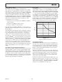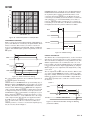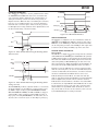
1
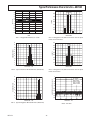
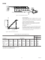
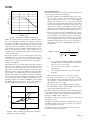
a FEATURES Throughput: 250 kSPS INL: 3 LSB Max (0.0046% of Full Scale) 16-Bit Resolution with No Missing Codes S/(N+D): 90 dB Typ @ 100 kHz THD: –100 dB Typ @ 100 kHz Analog Input Voltage Ranges Bipolar: 10 V, 5 V, 2.5 V Unipolar: 0 V to 10 V, 0 V to 5 V, 0 V to 2.5 V Both AC and DC Specifications No Pipeline Delay Parallel (8/16 Bits) and Serial 5 V/3 V Interface SPI®/QSPI™/MICROWIRE™/DSP Compatible Single 5 V Supply Operation Power Dissipation 35 mW Typical 15 W @ 100 SPS Power-Down Mode: 7 W Max Package: 48-Lead Quad Flatpack (LQFP) Package: 48-Lead Chip Scale (LFCSP) Pin-to-Pin Compatible with the AD7660/AD7664/AD7665 APPLICATIONS Data Acquisition Motor Control Communication Instrumentation Spectrum Analysis Medical Instruments Process Control 16-Bit, 250 kSPS CMOS ADC AD7663* FUNCTIONAL BLOCK DIAGRAM AVDD AGND REF REFGND IND(4R) INC(4R) INB(2R) INA(R) 4R DVDD DGND AD7663 4R 2R OVDD SERIAL PORT R SWITCHED CAP DAC INGND SER/PAR BUSY PARALLEL 16 INTERFACE D[15:0] CS CLOCK PD RESET OGND RD CONTROL LOGIC AND CALIBRATION CIRCUITRY OB/2C BYTESWAP CNVST PulSAR Selection Type/kSPS 100–250 500–570 Pseudo Differential AD7660 AD7650 AD7664 True Bipolar AD7663 AD7665 AD7671 True Differential AD7675 AD7676 AD7677 18-Bit AD7678 AD7679 AD7674 AD7654 AD7655 Simultaneous/ Multichannel 800–1000 GENERAL DESCRIPTION The AD7663 is a 16-bit, 250 kSPS, charge redistribution SAR, analog-to-digital converter that operates from a single 5 V power supply. It contains a high speed 16-bit sampling ADC, a resistor input scaler that allows various input ranges, an internal conversion clock, error correction circuits, and both serial and parallel system interface ports. The AD7663 is hardware factory-calibrated and is comprehensively tested to ensure such ac parameters as signal-to-noise ratio (SNR) and total harmonic distortion (THD), in addition to the more traditional dc parameters of gain, offset, and linearity. It is fabricated using Analog Devices’ high performance, 0.6 micron CMOS process and is available in a 48-lead LQFP and a tiny 48-lead LFCSP with operation specified from –40°C to +85°C. *Patent pending PRODUCT HIGHLIGHTS 1. Fast Throughput The AD7663 is a 250 kSPS charge redistribution, 16-bit SAR ADC with various bipolar and unipolar input ranges. 2. Single-Supply Operation The AD7663 operates from a single 5 V supply and dissipates only 35 mW typical. Its power dissipation decreases with the throughput to, for instance, only 15 µW at a 100 SPS throughput. It consumes 7 µW maximum when in power-down. 3. Superior INL The AD7663 has a maximum integral nonlinearity of 3 LSB with no missing 16-bit code. 4. Serial or Parallel Interface Versatile parallel (8 bits or 16 bits) or 2-wire serial interface arrangement compatible with both 3 V or 5 V logic. REV. B Information furnished by Analog Devices is believed to be accurate and reliable. However, no responsibility is assumed by Analog Devices for its use, nor for any infringements of patents or other rights of third parties that may result from its use. No license is granted by implication or otherwise under any patent or patent rights of Analog Devices. Trademarks and registered trademarks are the property of their respective companies. One Technology Way, P.O. Box 9106, Norwood, MA 02062-9106, U.S.A. Tel: 781/329-4700 www.analog.com Fax: 781/326-8703 © 2003 Analog Devices, Inc. All rights reserved. AD7663–SPECIFICATIONS (–40C to +85C, AVDD = DVDD = 5 V, OVDD = 2.7 V to 5.25 V, unless otherwise noted.) Parameter Conditions Min RESOLUTION ANALOG INPUT Voltage Range Common-Mode Input Voltage Analog Input CMRR Input Impedance VIND – VINGND VINGND fIN = 45 kHz THROUGHPUT SPEED Complete Cycle Throughput Rate DC ACCURACY Integral Linearity Error No Missing Codes Transition Noise Bipolar Zero Error2, TMIN to TMAX Bipolar Full-Scale Error2, TMIN to TMAX Unipolar Zero Error2, TMIN to TMAX Unipolar Full-Scale Error 2, TMIN to TMAX Power Supply Sensitivity AC ACCURACY Signal-to-Noise Spurious-Free Dynamic Range Total Harmonic Distortion Signal-to-(Noise+Distortion) ±4 REF, 0 V to 4 REF, ±2 REF (See Table I) –0.1 +0.5 62 See Table I V dB 4 250 µs kSPS +3 ±0.1 LSB1 Bits LSB LSB % of FSR % of FSR % of FSR % of FSR LSB 90 90 100 –100 90 30 800 dB3 dB dB dB dB dB kHz 2 5 ns ps rms µs –3 16 0.7 ±5 V Range Other Range –25 –0.06 –0.25 –0.18 –0.38 AVDD = 5 V ±5% fIN = 10 kHz fIN = 100 kHz fIN = 100 kHz fIN = 100 kHz fIN = 10 kHz fIN = 100 kHz, –60 dB Input Full-Scale Step REFERENCE External Reference Voltage Range External Reference Current Drain 250 kSPS Throughput 89 88.5 +25 +0.06 +0.25 +0.18 +0.38 2.75 2.3 DIGITAL INPUTS Logic Levels VIL VIH IIL IIH 2.5 50 –0.3 +2.0 –1 –1 DIGITAL OUTPUTS Data Format Pipeline Delay ISINK = 1.6 mA ISOURCE = –500 µA Unit Bits 0 SAMPLING DYNAMICS Aperture Delay Aperture Jitter Transient Response POWER SUPPLIES Specified Performance AVDD DVDD OVDD Operating Current AVDD DVDD5 OVDD5 Power Dissipation6 Max 16 –3 dB Input Bandwidth VOL VOH Typ AVDD – 1.85 V µA +0.8 DVDD + 0.3 +1 +1 V V µA µA Parallel or Serial 16-Bit Conversion Results Available Immediately after Completed Conversion 0.4 OVDD – 0.6 V V 4.75 4.75 2.7 V V V 5 5 5.25 5.25 5.254 250 kSPS Throughput 250 kSPS Throughput5 100 SPS Throughput5 In Power-Down Mode7 –2– 5 1.8 10 35 15 41 7 mA mA µA mW µW µW REV. B AD7663 Parameter Conditions Min TEMPERATURE RANGE 8 Specified Performance TMIN to TMAX –40 Typ Max Unit +85 °C NOTES 1 LSB means least significant bit. With the ±5 V input range, one LSB is 152.588 µV. 2 See Definition of Specifications section. These specifications do not include the error contribution from the external reference. 3 All specifications in dB are referred to a full-scale input FS. Tested with an input signal at 0.5 dB below full scale, unless otherwise specified. 4 The max should be the minimum of 5.25 V and DVDD + 0.3 V. 5 Tested in Parallel Reading Mode. 6 Tested with the 0 V to 5 V range and V IN – VINGND = 0 V. See Power Dissipation section. 7 With OVDD below DVDD + 0.3 V and all digital inputs forced to DVDD or DGND, respectively. 8 Contact factory for extended temperature range. Specifications subject to change without notice. Table I. Analog Input Configuration Input Voltage Range IND(4R) INC(4R) INB(2R) INA(R) Input Impedance1 ±4 REF2 ±2 REF ±REF 0 V to 4 REF 0 V to 2 REF 0 V to REF VIN VIN VIN VIN VIN VIN INGND VIN VIN VIN VIN VIN INGND INGND VIN INGND VIN VIN REF REF REF INGND INGND VIN 5.85 kW 3.41 kW 2.56 kW 3.41 kW 2.56 kW Note 3 NOTES 1 Typical analog input impedance. 2 With REF = 3 V, in this range, the input should be limited to –11 V to +12 V. 3 For this range the input is high impedance. TIMING SPECIFICATIONS (–40C to +85C, AVDD = DVDD = 5 V, OVDD = 2.7 V to 5.25 V, unless otherwise noted.) Parameter Refer to Figures 11 and 12 Convert Pulsewidth Time between Conversions CNVST LOW to BUSY HIGH Delay BUSY HIGH All Modes Except in Master Serial Read after Convert Mode Aperture Delay End of Conversion to BUSY LOW Delay Conversion Time Acquisition Time RESET Pulsewidth Symbol Min t1 t2 t3 t4 5 4 t5 t6 t7 t8 t9 Refer to Figures 13, 14, 15, and 16 (Parallel Interface Modes) CNVST LOW to DATA Valid Delay DATA Valid to BUSY LOW Delay Bus Access Request to DATA Valid Bus Relinquish Time t10 t11 t12 t13 Refer to Figures 17 and 18 (Master Serial Interface Modes)1 CS LOW to SYNC Valid Delay CS LOW to Internal SCLK Valid Delay CS LOW to SDOUT Delay CNVST LOW to SYNC Delay (Read during Convert) SYNC Asserted to SCLK First Edge Delay2 Internal SCLK Period2 Internal SCLK HIGH2 Internal SCLK LOW2 SDOUT Valid Setup Time2 SDOUT Valid Hold Time2 SCLK Last Edge to SYNC Delay2 t14 t15 t16 t17 t18 t19 t20 t21 t22 t23 t24 REV. B –3– Typ Max Unit 30 1.25 ns µs ns µs 2 10 1.25 2.75 10 1.25 20 40 15 5 10 10 10 0.5 4 25 15 9.5 4.5 2 3 40 ns ns µs µs ns µs ns ns ns ns ns ns µs ns ns ns ns ns ns ns AD7663 TIMING SPECIFICATIONS (continued) Symbol Parameter Min Typ Max Unit 10 10 10 1 Refer to Figures 17 and 18 (Master Serial Interface Modes) CS HIGH to SYNC HI-Z CS HIGH to Internal SCLK HI-Z CS HIGH to SDOUT HI-Z BUSY HIGH in Master Serial Read after Convert CNVST LOW to SYNC Asserted Delay (Master Serial Read after Convert) SYNC Deasserted to BUSY LOW Delay Refer to Figures 19 and 21 (Slave Serial Interface Modes) External SCLK Setup Time External SCLK Active Edge to SDOUT Delay SDIN Setup Time SDIN Hold Time External SCLK Period External SCLK HIGH External SCLK LOW t25 t26 t27 t28 t29 See Table II 1.25 ns ns ns µs µs t30 25 ns t31 t32 t33 t34 t35 t36 t37 5 3 5 5 25 10 10 ns ns ns ns ns ns ns 16 NOTES 1 In serial interface modes, the SYNC, SCLK, and SDOUT timings are defined with a maximum load C L of 10 pF; otherwise, the load is 60 pF maximum. 2 In Serial Master Read during Convert Mode. See Table II for Master Read after Convert Mode. Specifications subject to change without notice. Table II. Serial Clock Timings in Master Read after Convert DIVSCLK[1] DIVSCLK[0] SYNC to SCLK First Edge Delay Minimum Internal SCLK Period Minimum Internal SCLK Period Maximum Internal SCLK HIGH Minimum Internal SCLK LOW Minimum SDOUT Valid Setup Time Minimum SDOUT Valid Hold Time Minimum SCLK Last Edge to SYNC Delay Minimum BUSY HIGH Width Maximum 1.6mA TO OUTPUT PIN t18 t19 t19 t20 t21 t22 t23 t24 t28 0 0 0 1 1 0 1 1 Unit 4 25 40 15 9.5 4.5 2 3 2 20 50 70 25 24 22 4 60 2.5 20 100 140 50 49 22 30 140 3.5 20 200 280 100 99 22 90 300 5.75 ns ns ns ns ns ns ns ns µs IOL 1.4V CL 60pF* 500A 2V IOH 0.8V tDELAY *IN SERIAL INTERFACE MODES, THE SYNC, SCLK, AND SDOUT TIMINGS ARE DEFINED WITH A MAXIMUM LOAD CL OF 10pF; OTHERWISE, THE LOAD IS 60pF MAXIMUM. tDELAY 2V 0.8V Figure 1. Load Circuit for Digital Interface Timing 2V 0.8V Figure 2. Voltage Reference Levels for Timing –4– REV. B AD7663 ABSOLUTE MAXIMUM RATINGS 1 REFGND REF INGND NC NC NC NC NC IND(4R) INC(4R) INB(2R) INA(R) PIN CONFIGURATION ST-48 and CP-48 Analog Inputs IND2, INC2, INB2 . . . . . . . . . . . . . . . . . . . . –11 V to +30 V INA, REF, INGND, REFGND . . . . . . . . . . . . . . . . . . . . AGND – 0.3 V to AVDD + 0.3 V Ground Voltage Differences AGND, DGND, OGND . . . . . . . . . . . . . . . . . . . . . ±0.3 V Supply Voltages AVDD, DVDD, OVDD . . . . . . . . . . . . . . . . –0.3 V to +7 V AVDD to DVDD, AVDD to OVDD . . . . . . . . . . . . . . ±7 V DVDD to OVDD . . . . . . . . . . . . . . . . . . . . . –0.3 V to +7 V Digital Inputs . . . . . . . . . . . . . . . . –0.3 V to DVDD + 0.3 V Internal Power Dissipation3 . . . . . . . . . . . . . . . . . . . 700 mW Internal Power Dissipation4 . . . . . . . . . . . . . . . . . . . . . 2.5 W Junction Temperature . . . . . . . . . . . . . . . . . . . . . . . . . . 150°C Storage Temperature Range . . . . . . . . . . . . –65°C to +150°C Lead Temperature Range (Soldering 10 sec) . . . . . . . . . . . . . . . . . . . . . . . . . . . 300°C 48 47 46 45 44 43 42 41 40 39 38 37 AGND 1 AVDD 2 NC 3 BYTESWAP 4 OB/2C 5 NC 6 RESET CS RD DGND 29 BUSY 28 27 26 25 D15 D14 D13 D12 D11/RDERROR D9/SCLK D10/SYNC DVDD DGND D8/SDOUT OVDD D7/RDC/SDIN OGND 13 14 15 16 17 18 19 20 21 22 23 24 D4/EXT/INT D5/INVSYNC D6/INVSCLK NC = NO CONNECT Stresses above those listed under Absolute Maximum Ratings may cause permanent damage to the device. This is a stress rating only; functional operation of the device at these or any other conditions above those indicated in the operational section of this specification is not implied. Exposure to absolute maximum rating conditions for extended periods may affect device reliability. 2 See Analog Inputs section. 3 Specification is for device in free air: 48-Lead LQFP: qJA = 91°C/W, qJC = 30°C/W. 4 Specification is for device in free air: 48-Lead LFCSP: qJC = 26⬚C/W. PD 33 30 D2/DIVSCLK[0] 11 D3/DIVSCLK[1] 12 1 34 31 TOP VIEW (Not to Scale) SER/PAR 8 D0 9 D1 10 AGND CNVST 32 AD7663 NC 7 35 36 PIN 1 IDENTIFIER ORDERING GUIDE Model Temperature Range Package Description Package Option AD7663AST AD7663ASTRL AD7663ACP AD7663ACPRL EVAL-AD7663CB1 EVAL-CONTROL BRD22 –40°C to +85°C –40°C to +85°C –40⬚C to +85⬚C –40⬚C to +85⬚C Quad Flatpack (LQFP) Quad Flatpack (LQFP) Chip Scale (LFCSP) Chip Scale (LFCSP) Evaluation Board Controller Board ST-48 ST-48 CP-48 CP-48 NOTES 1 This board can be used as a standalone evaluation board or in conjunction with the EVAL-CONTROL BRD2 for evaluation/demonstration purposes. 2 This board allows a PC to control and communicate with all Analog Devices evaluation boards ending in the CB designators. CAUTION ESD (electrostatic discharge) sensitive device. Electrostatic charges as high as 4000 V readily accumulate on the human body and test equipment and can discharge without detection. Although the AD7663 features proprietary ESD protection circuitry, permanent damage may occur on devices subjected to high energy electrostatic discharges. Therefore, proper ESD precautions are recommended to avoid performance degradation or loss of functionality. REV. B –5– AD7663 PIN FUNCTION DESCRIPTION Pin No. Mnemonic Type Description 1 2 3, 6, 7, 44–48 4 AGND AVDD NC P P Analog Power Ground Pin. Input Analog Power Pin. Nominally 5 V. No Connect. BYTESWAP DI 5 OB/2C DI 8 SER/PAR DI 9, 10 D[0:1] DO 11, 12 D[2:3] or DI/O Parallel Mode Selection (8/16 Bit). When LOW, the LSB is output on D[7:0] and the MSB is output on D[15:8]. When HIGH, the LSB is output on D[15:8] and the MSB is output on D[7:0]. Straight Binary/Binary Twos Complement. When OB/2C is HIGH, the digital output is straight binary; when LOW, the MSB is inverted, resulting in a twos complement output from its internal shift register. Serial/Parallel Selection Input. When LOW, the Parallel Port is selected; when HIGH, the Serial Interface Mode is selected and some bits of the Data bus are used as a Serial Port. Bit 0 and Bit 1 of the Parallel Port Data Output Bus. When SER/PAR is HIGH, these outputs are in high impedance. When SER/PAR is LOW, these outputs are used as Bit 2 and Bit 3 of the Parallel Port Data Output Bus. When SER/PAR is HIGH, EXT/INT is LOW and RDC/SDIN is LOW, which is the Serial Master Read after Convert Mode. These inputs, part of the Serial Port, are used to slow down, if desired, the internal serial clock that clocks the data output. In the other serial modes, these pins are high impedance outputs. When SER/PAR is LOW, this output is used as Bit 4 of the Parallel Port Data Output Bus. When SER/PAR is HIGH, this input, part of the Serial Port, is used as a digital select input for choosing the internal or an external data clock, called respectively, Master and Slave Modes. With EXT/INT tied LOW, the internal clock is selected on SCLK output. With EXT/INT set to a logic HIGH, output data is synchronized to an external clock signal connected to the SCLK input, and external clock is gated by CS. When SER/PAR is LOW, this output is used as Bit 5 of the Parallel Port Data Output Bus. When SER/PAR is HIGH, this input, part of the Serial Port, is used to select the active state of the SYNC signal. When LOW, SYNC is active HIGH. When HIGH, SYNC is active LOW. When SER/PAR is LOW, this output is used as Bit 6 of the Parallel Port Data Output Bus. When SER/PAR is HIGH, this input, part of the Serial Port, is used to invert the SCLK signal. It is active in both master and slave mode. When SER/PAR is LOW, this output is used as Bit 7 of the Parallel Port Data Output Bus. When SER/PAR is HIGH, this input, part of the Serial Port, is used as either an external data input or a read mode selection input, depending on the state of EXT/INT. When EXT/INT is HIGH, RDC/SDIN could be used as a data input to daisy-chain the conversion results from two or more ADCs onto a single SDOUT line. The digital data level on SDIN is output on DATA with a delay of 16 SCLK periods after the initiation of the read sequence. When EXT/INT is LOW, RDC/SDIN is used to select the read mode. When RDC/SDIN is HIGH, the previous data is output on SDOUT during conversion. When RDC/SDIN is LOW, the data can be output on SDOUT only when the conversion is complete. Input/Output Interface Digital Power Ground. Input/Output Interface Digital Power. Nominally at the same supply as the supply of the host interface (5 V or 3 V). Digital Power. Nominally at 5 V. Digital Power Ground. DIVSCLK[0:1] 13 D[4] or EXT/INT DI/O 14 D[5] or INVSYNC DI/O 15 D[6] or INVSCLK DI/O 16 D[7] or RDC/SDIN DI/O 17 18 OGND OVDD P P 19 20 DVDD DGND P P –6– REV. B AD7663 PIN FUNCTION DESCRIPTION (continued) Pin No. Mnemonic Type Description 21 D[8] or SDOUT DO 22 D[9] or SCLK 23 D[10] or SYNC 24 D[11] or RDERROR 25–28 D[12:15] 29 BUSY 30 31 32 DGND RD CS 33 RESET 34 PD 35 CNVST 36 37 38 39 40, 41, 42, 43 AGND REF REFGND INGND INA, INB, INC, IND When SER/PAR is LOW, this output is used as Bit 8 of the Parallel Port Data Output Bus. When SER/PAR is HIGH, this output, part of the Serial Port, is used as a serial data output synchronized to SCLK. Conversion results are stored in an on-chip register. The AD7663 provides the conversion result, MSB first, from its internal shift register. The Data format is determined by the logic level of OB/2C. In Serial Mode, when EXT/INT is LOW, SDOUT is valid on both edges of SCLK. In serial mode, when EXT/INT is HIGH: If INVSCLK is LOW, SDOUT is updated on the SCLK rising edge and valid on the next falling edge. If INVSCLK is HIGH, SDOUT is updated on the SCLK falling edge and valid on the next rising edge. DI/O When SER/PAR is LOW, this output is used as Bit 9 of the Parallel Port Data Output Bus. When SER/PAR is HIGH, this pin, part of the Serial Port, is used as a serial data clock input or output, dependent upon the logic state of the EXT/INT pin. The active edge where the data SDOUT is updated depends upon the logic state of the INVSCLK pin. DO When SER/PAR is LOW, this output is used as Bit 10 of the Parallel Port Data Output Bus. When SER/PAR is HIGH, this output, part of the Serial Port, is used as a digital output frame synchronization for use with the internal data clock (EXT/INT = Logic LOW). When a read sequence is initiated and INVSYNC is LOW, SYNC is driven HIGH and remains HIGH while SDOUT output is valid. When a read sequence is initiated and INVSYNC is HIGH, SYNC is driven LOW and remains LOW while SDOUT output is valid. DO When SER/PAR is LOW, this output is used as Bit 11 of the Parallel Port Data Output Bus. When SER/PAR is HIGH and EXT/INT is HIGH, this output, part of the Serial Port, is used as an incomplete read error flag. In Slave Mode, when a data read is started and not complete when the following conversion is complete, the current data is lost and RDERROR is pulsed HIGH. DO Bit 12 to Bit 15 of the Parallel Port Data Output Bus. When SER/PAR is HIGH, these outputs are in high impedance. DO Busy Output. Transitions HIGH when a conversion is started and remains HIGH until the conversion is complete and the data is latched into the on-chip shift register. The falling edge of BUSY could be used as a data-ready clock signal. P Must Be Tied to Digital Ground. DI Read Data. When CS and RD are both LOW, the Interface Parallel or Serial Output Bus is enabled. DI Chip Select. When CS and RD are both LOW, the Interface Parallel or Serial Output Bus is enabled. CS is also used to gate the external clock. DI Reset Input. When set to a logic HIGH, reset the AD7663. Current conversion, if any, is aborted. If not used, this pin could be tied to DGND. DI Power-Down Input. When set to a logic HIGH, power consumption is reduced and conversions are inhibited after the current one is completed. DI Start Conversion. If CNVST is HIGH when the acquisition phase (t8) is complete, the next falling edge on CNVST puts the internal sample-and-hold into the hold state and initiates a conversion. This mode is the most appropriate if low sampling jitter is desired. If CNVST is LOW when the acquisition phase (t8) is complete, the internal sample-and-hold is put into the hold state and a conversion is immediately started. P Must Be Tied to Analog Ground. AI Reference Input Voltage . AI Reference Input Analog Ground. AI Analog Input Ground. AI Analog Inputs. Refer to Table I for input range configuration. NOTES AI = Analog Input DI = Digital Input DI/O = Bidirectional Digital DO = Digital Output P = Power REV. B –7– AD7663 DEFINITION OF SPECIFICATIONS Integral Nonlinearity Error (INL) Effective Number of Bits (ENOB) A measurement of the resolution with a sine wave input. It is related to S/(N+D) by the following formula: Linearity error refers to the deviation of each individual code from a line drawn from “negative full scale” through “positive full scale.” The point used as negative full scale occurs 1/2 LSB before the first code transition. Positive full scale is defined as a level 1 1/2 LSB beyond the last code transition. The deviation is measured from the middle of each code to the true straight line. ( ) ENOB = S [ N + D ]dB - 1.76) 6.02 and is expressed in bits. Total Harmonic Distortion (THD) The ratio of the rms sum of the first five harmonic components to the rms value of a full-scale input signal, expressed in decibels. Differential Nonlinearity Error (DNL) In an ideal ADC, code transitions are 1 LSB apart. Differential nonlinearity is the maximum deviation from this ideal value. It is often specified in terms of resolution for which no missing codes are guaranteed. Full-Scale Error Signal-to-Noise Ratio (SNR) The ratio of the rms value of the actual input signal to the rms sum of all other spectral components below the Nyquist frequency, excluding harmonics and dc. The value for SNR is expressed in decibels. The last transition (from 011 . . . 10 to 011 . . . 11 in twos complement coding) should occur for an analog voltage 1 1/2 LSB below the nominal full scale (2.499886 V for the ±2.5 V range). The full-scale error is the deviation of the actual level of the last transition from the ideal level. Signal-to-(Noise + Distortion) Ratio (S/[N+D]) Bipolar Zero Error Aperture Delay The ratio of the rms value of the actual input signal to the rms sum of all other spectral components below the Nyquist frequency, including harmonics but excluding dc. The value for S/(N+D) is expressed in decibels. The difference between the ideal midscale input voltage (0 V) and the actual voltage producing the midscale output code. Unipolar Zero Error In Unipolar Mode, the first transition should occur at a level 1/2 LSB above analog ground. The unipolar zero error is the deviation of the actual transition from that point. A measure of the acquisition performance measured from the falling edge of the CNVST input to when the input signal is held for a conversion. Transient Response The time required for the AD7663 to achieve its rated accuracy after a full-scale step function is applied to its input. Spurious-Free Dynamic Range (SFDR) The difference, in decibels (dB), between the rms amplitude of the input signal and the peak spurious signal. –8– REV. B Typical Performance Characteristics– AD7663 8000 3.0 2.5 6802 6745 7000 2.0 1.5 6000 5000 0.5 COUNTS INL – LSB 1.0 0 –0.5 4000 3000 –1.0 –1.5 1800 2000 –2.0 1000 1000 –2.5 0 –3.0 0 16384 32768 49152 0 33 4 CODE IN HEXA TPC 4. Histogram of 16,384 Conversions of a DC Input at the Code Transition 50 9000 45 8000 40 7000 8032 35 6000 30 COUNTS NUMBER OF UNITS TPC 1. Integral Nonlinearity vs. Code 25 5000 3944 4000 3902 20 3000 15 2000 10 5 1000 0 0 0 0 0.3 0.6 0.9 1.2 1.5 1.8 2.1 POSITIVE INL – LSB 2.1 2.7 2 233 271 0 0 0 TPC 5. Histogram of 16,384 Conversions of a DC Input at the Code Center –0 70 –20 AMPLITUDE – dB OF FULL SCALE 80 60 50 40 30 20 10 0 –3 0 7FFC 7FFD 7FFE 7FFF 8000 8001 8002 8003 8004 8005 8006 CODE IN HEXA TPC 2. Typical Positive INL Distribution (446 Units) NUMBER OF UNITS 0 7FFD 7FFE 7FFF 8000 8001 8002 8003 8004 8004 8005 CODE 4096 POINT FFT FS = 250kHz fIN = 45kHz, –0.5dB SNR = 90.1dB SINAD = 89.8dB THD = –100.5dB SFDR = 102.7dB –40 –60 –80 –100 –120 –140 –160 –180 –2.7 –2.4 –2.1 –1.8 –1.5 –1.2 –0.9 0 –0.6 –0.3 NEGATIVE INL – LSB TPC 3. Typical Negative INL Distribution (446 Units) REV. B 0 0 65536 25 50 75 FREQUENCY – kHz TPC 6. FFT Plot –9– 100 125 AD7663 16.0 –60 110 –65 95 15.5 105 SFDR –70 100 THD, HARMONICS – dB 15.0 90 SINAD 14.5 85 ENOB – Bits SNR AND S/[N+D] – dB SNR 14.0 80 –75 95 –80 90 –85 85 –90 80 –95 SECOND HARMONIC THD 75 –100 ENOB 70 –105 13.5 75 65 –110 13.0 1000 70 1 10 100 FREQUENCY – kHz 1 60 1000 10 100 FREQUENCY – kHz TPC 10. THD, Harmonics, and SFDR vs. Frequency –60 92 –70 –80 THD, HARMONICS – dB SNR – (REFERRED TO FULL SCALE) – dB THIRD HARMONIC –115 TPC 7. SNR, S/(N+D), and ENOB vs. Frequency SFDR – dB 100 90 88 –90 –100 THD –110 –120 –130 THIRD HARMONIC SECOND HARMONIC –140 –150 86 –80 –70 –60 –50 –40 –30 INPUT LEVEL – dB –20 –10 –160 –60 0 TPC 8. SNR vs. Input Level –50 –40 –30 –20 INPUT LEVEL – dB –10 0 TPC 11. THD, Harmonics vs. Input Level 50 –98 96 THD 40 93 t12 DELAY – ns THD – dB SNR – dB –100 90 SNR 30 20 –102 87 10 84 –55 –35 –15 5 25 45 65 85 105 –104 125 0 0 TEMPERATURE – C TPC 9. SNR and THD vs. Temperature 50 100 CL – pF 150 200 TPC 12. Typical Delay vs. Load Capacitance, CL –10– REV. B AD7663 CIRCUIT INFORMATION 100000 The AD7663 is a fast, low power, single-supply, precise 16-bit analog-to-digital converter (ADC). The AD7663 is capable of converting 250,000 samples per second (250 kSPS) and allows power saving between conversions. When operating at 100 SPS, for example, it consumes typically only 15 µW. This feature makes the AD7663 ideal for battery-powered applications. OPERATING CURRENTS – A 10000 AVDD 1000 100 DVDD 10 1 The AD7663 provides the user with an on-chip track-and-hold, successive approximation ADC that does not exhibit any pipeline or latency, making it ideal for multiple multiplexed channel applications. OVDD 0.1 0.01 It is specified to operate with both bipolar and unipolar input ranges by changing the connection of its input resistive scaler. 0.001 1 10 100 1000 10000 100000 1000000 SAMPLING RATE – SPS TPC 13. Operating Currents vs. Sample Rate The AD7663 can be operated from a single 5 V supply and can be interfaced to either 5 V or 3 V digital logic. It is housed in a 48-lead LQFP package or a 48-lead LFCSP package that combines space savings and flexible configurations as either serial or parallel interface. The AD7663 is pin-to-pin compatible with the AD7660. POWER-DOWN OPERATING CURRENTS – nA 500 CONVERTER OPERATION 450 400 350 DVDD 300 250 200 150 OVDD 100 AVDD 50 0 –55 –35 –15 5 25 45 TEMPERATURE – C 65 85 105 TPC 14. Power-Down Operating Currents vs. Temperature 10 6 –FS OFFSET LSB 2 0 +FS –2 –4 –6 –8 –10 –55 –35 –15 5 25 During the acquisition phase, the common terminal of the array tied to the comparator’s positive input is connected to AGND via SWA. All independent switches are connected to the output of the resistive scaler. Thus, the capacitor array is used as a sampling capacitor and acquires the analog signal. Similarly, the dummy capacitor acquires the analog signal on INGND input. When the acquisition phase is complete and the CNVST input goes or is LOW, a conversion phase is initiated. When the conversion phase begins, SWA and SWB are opened first. The capacitor array and the dummy capacitor are then disconnected from the inputs and connected to the REFGND input. Therefore, the differential voltage between the output of the resistive scaler and INGND captured at the end of the acquisition phase is applied to the comparator inputs, causing the comparator to become unbalanced. 8 4 The AD7663 is a successive approximation analog-to-digital converter based on a charge redistribution DAC. Figure 3 shows the simplified schematic of the ADC. The input analog signal is first scaled down and level shifted by the internal input resistive scaler, which allows both unipolar ranges (0 V to 2.5 V, 0 V to 5 V, and 0 V to 10 V) and bipolar ranges (±2.5 V, ±5 V, and ±10 V). The output voltage range of the resistive scaler is always 0 V to 2.5 V. The capacitive DAC consists of an array of 16 binary weighted capacitors and an additional “LSB” capacitor. The comparator’s negative input is connected to a “dummy” capacitor of the same value as the capacitive DAC array. 45 65 85 105 125 TEMPERATURE – C By switching each element of the capacitor array between REFGND or REF, the comparator input varies by binary weighted voltage steps (VREF /2, VREF /4 . . . VREF /65,536). The control logic toggles these switches, starting with the MSB first, in order to bring the comparator back into a balanced condition. After the completion of this process, the control logic generates the ADC output code and brings the BUSY output LOW. TPC 15. +FS, Offset, and –FS vs. Temperature REV. B –11– AD7663 4R IND REF REFGND 4R INC 2R MSB INB 32,768C 16,384C LSB 4C 2C C SWA SWITCHES CONTROL C R INA BUSY COMP INGND CONTROL LOGIC OUTPUT CODE 65,536C SWB CNVST Figure 3. ADC Simplified Schematic ADC CODE – Straight Binary Transfer Functions Using the OB/2C digital input, the AD7663 offers two output codings: straight binary and twos complement. The ideal transfer characteristic for the AD7663 is shown in Figure 4 and Table III. 111...111 111...110 111...101 TYPICAL CONNECTION DIAGRAM Figure 5 shows a typical connection diagram for the AD7663. Different circuitry shown on this diagram is optional and is discussed in the figure’s notes. Analog Inputs The AD7663 is specified to operate with six full-scale analog input ranges. Connections required for each of the four analog inputs, IND, INC, INB, and INA, and the resulting full-scale ranges are shown in Table I. The typical input impedance for each analog input range is also shown. 000...010 000...001 000...000 –FS –FS + 1 LSB +FS – 1 LSB –FS + 0.5 LSB +FS – 1.5 LSB ANALOG INPUT Figure 4. ADC Ideal Transfer Function Table III. Output Codes and Ideal Input Voltages Description Digital Output Code (Hexa) Straight Twos Binary Complement Analog Input 1 Full-Scale Range Least Significant Bit FSR – 1 LSB Midscale + 1 LSB Midscale Midscale – 1 LSB –FSR + 1 LSB –FSR ±10 V 305.2 µV 9.999695 V 305.2 µV 0V –305.2 µV –9.999695 V –10 V ±5 V 152.6 µV 4.999847 V 152.6 µV 0V –152.6 µV –4.999847 V –5 V ±2.5 V 76.3 µV 2.499924 V 76.3 µV 0V –76.3 µV –2.499924 V –2.5 V 0 V to 10 V 152.6 µV 9.999847 V 5.000153 V 5V 4.999847 V 152.6 µV 0V 0 V to 5 V 76.3 µV 4.999924 V 2.570076 V 2.5 V 2.499924 V 76.3 µV 0V 0 V to 2.5 V 38.15 µV 2.499962 V 1.257038 V 1.25 V 1.249962 V 38.15 µV 0V FFFF2 8001 8000 7FFF 0001 00003 7FFF2 0001 0000 FFFF 8001 80003 NOTES 1 Values with REF = 2.5 V, with REF = 3 V, all values will scale linearly. 2 This is also the code for an overrange analog input. 3 This is also the code for an underrange analog input. –12– REV. B AD7663 DVDD 100 ANALOG SUPPLY (5V) + 10F ADR421 NOTE 7 100nF AVDD + 10F AGND 100nF 100nF DGND DVDD OVDD DIGITAL SUPPLY (3.3V OR 5V) + 10F OGND SERIAL PORT REF 2.5V REF NOTE 1 1M + 50k 100nF SCLK CREF NOTE 2 SDOUT REFGND BUSY NOTE 3 50 AD7663 U2 + CNVST C/P/DSP D INA + 10F NOTE 8 100nF AD8031 OB/2C NOTE 4 DVDD 50 SER/PAR CLOCK 15 ANALOG INPUT (10V) NOTE 5 U1 + IND AD8021 CC 2.7nF CS NOTE 6 RD BYTESWAP INGND RESET INB PD INC NOTES 1. SEE VOLTAGE REFERENCE INPUT SECTION. 2. WITH THE RECOMMENDED VOLTAGE REFERENCES, CREF IS 47F. SEE VOLTAGE REFERENCE INPUT SECTION. 3. OPTIONAL CIRCUITRY FOR HARDWARE GAIN CALIBRATION. 4. FOR BIPOLAR RANGE ONLY. SEE SCALER REFERENCE INPUT SECTION. 5. THE AD8021 IS RECOMMENDED. SEE DRIVER AMPLIFIER CHOICE SECTION. 6. WITH 0V TO 2.5V RANGE ONLY. SEE ANALOG INPUTS SECTION. 7. OPTION. SEE POWER SUPPLY SECTION. 8. OPTIONAL LOW JITTER CNVST. SEE CONVERSION CONTROL SECTION. Figure 5. Typical Connection Diagram (±10 V Range Shown) Figure 6 shows a simplified analog input section of the AD7663. AVDD 4R IND 4R INC 2R INB R INA R1 CS R = 1.28k AGND Figure 6. Simplified Analog Input The four resistors connected to the four analog inputs form a resistive scaler that scales down and shifts the analog input range to a common input range of 0 V to 2.5 V at the input of the switched capacitive ADC. By connecting the four inputs INA, INB, INC, and IND to the input signal itself, the ground, or a 2.5 V reference, other analog input ranges can be obtained. REV. B The diodes shown in Figure 6 provide ESD protection for the four analog inputs. The inputs INB, INC, and IND have a high voltage protection (–11 V to +30 V) to allow wide input voltage range. Care must be taken to ensure that the analog input signal never exceeds the absolute ratings on these inputs, including INA (0 V to 5 V). This will cause these diodes to become forwardbiased and start conducting current. These diodes can handle a forward-biased current of 120 mA maximum. For instance, when using the 0 V to 2.5 V input range, these conditions could eventually occur on the input INA when the input buffer’s (U1) supplies are different from AVDD. In such cases, an input buffer with a short-circuit current limitation can be used to protect the part. This analog input structure allows the sampling of the differential signal between the output of the resistive scaler and INGND. Unlike other converters, the INGND input is sampled at the same time as the inputs. By using this differential input, small signals common to both inputs are rejected as shown in Figure 7, which represents the typical CMRR over frequency. For instance, by using INGND to sense a remote signal ground, the difference of ground potentials between the sensor and the local ADC ground is eliminated. –13– AD7663 75 Driver Amplifier Choice 70 Although the AD7663 is easy to drive, the driver amplifier needs to meet at least the following requirements: • The driver amplifier and the AD7663 analog input circuit 65 have to be able, together, to settle for a full-scale step of the capacitor array at a 16-bit level (0.0015%). In the amplifier’s data sheet, the settling at 0.1% to 0.01% is more commonly specified. It could significantly differ from the settling time at 16-bit level and, therefore, it should be verified prior to the driver selection. The tiny op amp AD8021, which combines ultralow noise and a high gain bandwidth, meets this settling time requirement even when used with a high gain up to 13. CMRR – dB 60 55 50 45 40 • The noise generated by the driver amplifier needs to be kept 35 0 10 100 as low as possible in order to preserve the SNR and transition noise performance of the AD7663. The noise coming from the driver is first scaled down by the resistive scaler according to the analog input voltage range used, and is then filtered by the AD7663 analog input circuit one-pole, low-pass filter made by (R/2 + R1) and CS. The SNR degradation due to the amplifier is 1000 FREQUENCY – kHz Figure 7. Analog Input CMRR vs. Frequency During the acquisition phase for ac signals, the AD7663 behaves like a one-pole RC filter consisting of the equivalent resistance of the resistive scaler R/2 in series with R1 and CS. The resistor R1 is typically 2700 W and is a lumped component made up of some serial resistors and the on-resistance of the switches. The capacitor CS is typically 60 pF and is mainly the ADC sampling capacitor. This one-pole filter with a typical –3 dB cutoff frequency of 800 kHz reduces undesirable aliasing effects and limits the noise coming from the inputs. SNRLOSS Except when using the 0 V to 2.5 V analog input voltage range, the AD7663 has to be driven by a very low impedance source to avoid gain errors. That can be done by using a driver amplifier whose choice is eased by the primarily resistive analog input circuitry of the AD7663. Ê ˆ Á ˜ Á ˜ 28 = 20 log Á 2 ˜ Ê 2.5 N eN ˆ ˜ Á 784 + p f ˜ –3 dB Á Á 2 Ë FSR ¯ ˜¯ Ë where: f–3 dB is the –3 dB input bandwidth in MHz of the AD7663 (0.8 MHz) or the cut-off frequency of the input filter if any used (0 V to 2.5 V range). When using the 0 V to 2.5 V analog input voltage range, the input impedance of the AD7663 is very high so the AD7663 can be driven directly by a low impedance source without gain error. That allows, as shown in Figure 5, putting an external one-pole RC filter between the output of the amplifier output and the ADC analog inputs to even further improve the noise filtering by the AD7663 analog input circuit. However, the source impedance has to be kept low because it affects the ac performances, especially the total harmonic distortion (THD). The maximum source impedance depends on the amount of THD that can be tolerated. The THD degradation is a function of the source impedance and the maximum input frequency as shown in Figure 8. N is the noise factor of the amplifier (1 if in buffer configuration). eN is the equivalent input noise voltage of the op amp in nV/Hz1/2. FSR is the full-scale span (i.e., 5 V for ±2.5 V range). For instance, when using the 0 V to 2.5 V range, a driver like the AD8610 with an equivalent input noise of 6 nV/÷Hz and configured as a buffer, thus with a noise gain of 1, the SNR degrades by only 0.24 dB. • The driver needs to have a THD performance suitable to –70 that of the AD7663. TPC 10 gives the THD versus frequency that the driver should preferably exceed. The AD8021 meets these requirements and is usually appropriate for almost all applications. The AD8021 needs an external compensation capacitor of 10 pF. This capacitor should have good linearity as an NPO ceramic or mica type. –80 THD R = 100 –90 The AD8022 could also be used where a dual version is needed and gain of 1 is used. R = 50 R = 11 The AD829 is another alternative where high frequency (above 100 kHz) performance is not required. In a gain of 1, it requires an 82 pF compensation capacitor. –100 –110 10 100 FREQUENCY – kHz 1000 The AD8610 is also another option where low bias current is needed in low frequency applications. Figure 8. THD vs. Analog Input Frequency and Input Resistance (0 V to 2.5 V Only) –14– REV. B AD7663 Voltage Reference Input Power Supply The AD7663 uses an external 2.5 V voltage reference. The AD7663 uses three sets of power supply pins: an analog 5 V supply AVDD, a digital 5 V core supply DVDD, and a digital input/output interface supply OVDD. The OVDD supply allows direct interface with any logic working between 2.7 V and DVDD + 0.3 V. To reduce the number of supplies needed, the digital core (DVDD) can be supplied through a simple RC filter from the analog supply as shown in Figure 5. The AD7663 is independent of power supply sequencing, once OVDD does not exceed DVDD by more than 0.3 V, and thus free from supply voltage induced latch-up. Additionally, it is very insensitive to power supply variations over a wide frequency range as shown in Figure 9. The voltage reference input REF of the AD7663 has a dynamic input impedance; it should therefore be driven by a low impedance source with an efficient decoupling between REF and REFGND inputs. This decoupling depends on the choice of the voltage reference but usually consists of a 1 µF ceramic capacitor and a low ESR tantalum capacitor connected to the REF and REFGND inputs with minimum parasitic inductance. 47 µF is an appropriate value for the tantalum capacitor when used with one of the recommended reference voltages: • The low noise, low temperature drift ADR421 and AD780 110 voltage reference 105 • The low power ADR291 voltage reference • The low cost AD1582 voltage reference 100 95 90 PSRR – dB For applications using multiple AD7663s, it is more effective to buffer the reference voltage with a low noise, very stable op amp like the AD8031. Care should also be taken with the reference temperature coefficient of the voltage reference that directly affects the full-scale accuracy if this parameter matters. For instance, a ±15 ppm/°C tempco of the reference changes the full scale by ±1 LSB/°C. Note that VREF , as mentioned in the Specification tables, could be increased to AVDD – 1.85 V. The benefit here is the increased SNR obtained as a result of this increase. Since the input range is defined in terms of VREF, this would essentially increase the ±REF range from ±2.5 V to ±3 V and so on with an AVDD above 4.85 V. The theoretical improvement as a result of this increase in reference is 1.58 dB (20 log [3/2.5]). Due to the theoretical quantization noise, however, the observed improvement is approximately 1 dB. The AD780 can be selected with a 3 V reference voltage. Scaler Reference Input (Bipolar Input Ranges) When using the AD7663 with bipolar input ranges, the connection diagram in Figure 5 shows a reference buffer amplifier. This buffer amplifier is required to isolate the REF pin from the signal dependent current in the INx pin. A high speed op amp, such as the AD8031, can be used with a single 5 V power supply without degrading the performance of the AD7663. The buffer must have good settling characteristics and provide low total noise within the input bandwidth of the AD7663. 85 80 75 70 65 60 55 50 1 10 100 1000 FREQUENCY – kHz Figure 9. PSRR vs. Frequency POWER DISSIPATION The AD7663 automatically reduces its power consumption at the end of each conversion phase. During the acquisition phase, the operating currents are very low, which allows a significant power savings when the conversion rate is reduced as shown in Figure 10. This feature makes the AD7663 ideal for very low power battery applications. This does not take into account the power, if any, dissipated by the input resistive scaler that depends on the input voltage range used and the analog input voltage even in power-down mode. There is no power dissipated when the 0 V to 2.5 V is used or when both the analog input voltage is 0 V and a unipolar range, 0 V to 5 V or 0 V to 10 V, is used. It should be noted that the digital interface remains active even during the acquisition phase. To reduce the operating digital supply currents even further, the digital inputs need to be driven close to the power rails (i.e., DVDD and DGND) and OVDD should not exceed DVDD by more than 0.3 V. REV. B –15– AD7663 For other applications, conversions can be automatically initiated. If CNVST is held low when BUSY is low, the AD7663 controls the acquisition phase and then automatically initiates a new conversion. By keeping CNVST low, the AD7663 keeps the conversion process running by itself. It should be noted that the analog input has to be settled when BUSY goes low. Also, at power-up, CNVST should be brought low once to initiate the conversion process. In this mode, the AD7663 could sometimes run slightly faster than the guaranteed limit of 250 kSPS. 100k POWER DISSIPATION – W 10k 1k 100 10 t9 1 RESET 0.1 1 10 100 1k 10k SAMPLING RATE – SPS 100k 1M BUSY Figure 10. Power Dissipation vs. Sample Rate CONVERSION CONTROL Figure 11 shows the detailed timing diagrams of the conversion process. The AD7663 is controlled by the signal CNVST, which initiates conversion. Once initiated, it cannot be restarted or aborted, even by the power-down input PD, until the conversion is complete. The CNVST signal operates independently of CS and RD signals. DATA BUS t8 CNVST Figure 12. RESET Timing t2 DIGITAL INTERFACE t1 The AD7663 has a versatile digital interface; it can be interfaced with the host system by using either a serial or parallel interface. The serial interface is multiplexed on the parallel data bus. The AD7663 digital interface also accommodates both 3 V or 5 V logic by simply connecting the OVDD supply pin of the AD7663 to the host system interface digital supply. Finally, by using the OB/2C input pin, twos complement and straight binary coding can be used. CNVST BUSY t4 t3 t6 t5 MODE ACQUIRE CONVERT t7 ACQUIRE CONVERT t8 Figure 11. Basic Conversion Timing For a true sampling application, the recommended operation of the CNVST signal is the following. The two signals CS and RD control the interface. When at least one of these signals is HIGH, the interface outputs are in high impedance. Usually, CS allows the selection of each AD7663 in multicircuit applications and is held LOW in a single AD7663 design. RD is generally used to enable the conversion result on the data bus. CNVST must be held HIGH from the previous falling edge of BUSY and during a minimum delay corresponding to the acquisition time t8. Then, when CNVST is brought LOW, a conversion is initiated and the BUSY signal goes HIGH until the completion of the conversion. Although CNVST is a digital signal, it should be designed with special care with fast, clean edges, and levels with minimum overshoot and undershoot or ringing. It is a good thing to shield the CNVST trace with ground and also to add a low value serial resistor (i.e., 50 W) termination close to the output of the component that drives this line. For applications where the SNR is critical, the CNVST signal should have a very low jitter. To achieve this, some use a dedicated oscillator for CNVST generation, or at least to clock it with a high frequency, low jitter clock as shown in Figure 5. –16– CS = RD = 0 t1 CNVST t 10 BUSY t3 DATA BUS t4 t 11 PREVIOUS CONVERSION DATA NEW DATA Figure 13. Master Parallel Data Timing for Reading (Continuous Read) REV. B AD7663 PARALLEL INTERFACE CS The AD7663 is configured to use the parallel interface when the SER/PAR is held LOW. The data can be read either after each conversion, which is during the next acquisition phase, or during the following conversion as shown, respectively, in Figures 14 and 15. When the data is read during the conversion, however, it is recommended that it be read-only during the first half of the conversion phase. That avoids any potential feedthrough between voltage transients on the digital interface and the most critical analog conversion circuitry. RD BYTE PINS D[15:8] HI-Z HIGH BYTE HI-Z LOW BYTE HI-Z t13 t12 t12 PINS D[7:0] LOW BYTE HIGH BYTE HI-Z CS Figure 16. 8-Bit Parallel Interface RD SERIAL INTERFACE The AD7663 is configured to use the serial interface when the SER/PAR is held HIGH. The AD7663 outputs 16 bits of data, MSB first, on the SDOUT pin. This data is synchronized with the 16 clock pulses provided on the SCLK pin. The output data is valid on both the rising and falling edge of the data clock. BUSY CURRENT CONVERSION DATA BUS t 12 t 13 Figure 14. Slave Parallel Data Timing for Reading (Read after Convert) CS = 0 t1 CNVST, RD BUSY t4 t3 PREVIOUS CONVERSION DATA BUS t 12 t 13 Figure 15. Slave Parallel Data Timing for Reading (Read during Convert) The BYTESWAP pin allows a glueless interface to an 8-bit bus. As shown in Figure 16, the LSB byte is output on D[7:0] and the MSB is output on D[15:8] when BYTESWAP is LOW. When BYTESWAP is HIGH, the LSB and MSB are swapped and the LSB is output on D[15:8] and the MSB is output on D[7:0]. By connecting BYTESWAP to an address line, the 16 data bits can be read in two bytes on either D[15:8] or D[7:0]. REV. B MASTER SERIAL INTERFACE Internal Clock The AD7663 is configured to generate and provide the serial data clock SCLK when the EXT/INT pin is held LOW. It also generates a SYNC signal to indicate to the host when the serial data is valid. The serial clock SCLK and the SYNC signal can be inverted if desired. Depending on RDC/SDIN input, the data can be read after each conversion or during the following conversion. Figures 17 and 18 show the detailed timing diagrams of these two modes. Usually, because the AD7663 has a longer acquisition phase than the conversion phase, the data is read immediately after conversion. That makes the mode master, read after conversion, the most recommended Serial Mode when it can be used. In Read-during-Conversion Mode, the serial clock and data toggle at appropriate instants that minimize potential feedthrough between digital activity and the critical conversion decisions. In Read-after-Conversion Mode, it should be noted that unlike in other modes, the signal BUSY returns LOW after the 16 data bits are pulsed out and not at the end of the conversion phase, which results in a longer BUSY width. In this mode, if necessary, the internal clock can be slowed down by a ratio selected by the DIVSCLK inputs according to Table II. –17– AD7663 EXT/INT = 0 CS, RD RDC/SDIN = 0 INVSCLK = INVSYNC = 0 t3 CNVST t 28 BUSY t 30 t 29 t 25 SYNC t 14 t 18 t 19 t 20 t 24 t 21 t 26 1 2 D15 D14 SCLK 3 14 15 16 t 15 t 27 SDOUT X t 16 D2 D1 D0 t 23 t 22 Figure 17. Master Serial Data Timing for Reading (Read after Convert) RDC/SDIN = 1 EXT/INT = 0 CS, RD INVSCLK = INVSYNC = 0 t1 CNVST t3 BUSY t 17 t 25 SYNC t 14 t 19 t 20 t 21 t 15 SCLK 1 t 24 2 3 14 15 t 18 SDOUT X t 16 t 22 t 26 16 t 27 D15 D14 D2 D1 D0 t 23 Figure 18. Master Serial Data Timing for Reading (Read Previous Conversion during Convert) –18– REV. B AD7663 EXT/INT = 1 RD = 0 INVSCLK = 0 CS BUSY t36 SCLK t35 t37 1 2 t31 3 14 15 16 17 18 t32 X SDOUT t16 D15 D14 D13 D1 D0 X15 X14 X14 X13 X1 X0 Y15 Y14 t34 SDIN X15 t33 Figure 19. Slave Serial Data Timing for Reading (Read after Convert) SLAVE SERIAL INTERFACE External Clock The AD7663 is configured to accept an externally supplied serial data clock on the SCLK pin when the EXT/INT pin is held HIGH. In this mode, several methods can be used to read the data. The external serial clock is gated by CS and the data are output when both CS and RD are LOW. Thus, depending on CS, the data can be read after each conversion or during the following conversion. The external clock can be either a continuous or discontinuous clock. A discontinuous clock can be either normally high or normally low when inactive. Figures 19 and 21 show the detailed timing diagrams of these methods. While the AD7663 is performing a bit decision, it is important that voltage transients not occur on digital input/output pins or degradation of the conversion result could occur. This is particularly important during the second half of the conversion phase because the AD7663 provides error correction circuitry that can correct for an improper bit decision made during the first half of the conversion phase. For this reason, it is recommended that when an external clock is being provided, it is a discontinuous clock that is toggling only when BUSY is LOW or, more importantly, that does not transition during the latter half of BUSY HIGH. Another advantage is to be able to read the data at any speed up to 40 MHz, which accommodates both slow digital host interface and the fastest serial reading. Finally, in this mode only, the AD7663 provides a “daisy-chain” feature using the RDC/SDIN input pin for cascading multiple converters together. This feature is useful for reducing component count and wiring connections when desired as, for instance, in isolated multiconverter applications. An example of the concatenation of two devices is shown in Figure 20. Simultaneous sampling is possible by using a common CNVST signal. It should be noted that the RDC/SDIN input is latched on the opposite edge of SCLK of the one used to shift out the data on SDOUT. Therefore, the MSB of the “upstream” converter just follows the LSB of the “downstream” converter on the next SCLK cycle. BUSY OUT BUSY BUSY AD7663 AD7663 #2 (UPSTREAM) #1 (DOWNSTREAM) RDC/SDIN External Discontinuous Clock Data Read after Conversion This mode is the most recommended of the serial slave modes. Figure 19 shows the detailed timing diagrams of this method. After a conversion is complete, indicated by BUSY returning LOW, the result of this conversion can be read while both CS and RD are LOW. The data is shifted out, MSB first, with 16 clock pulses and is valid on both the rising and falling edge of the clock. RDC/SDIN SDOUT CNVST CNVST CS CS SCLK SCLK DATA OUT SCLK IN CS IN CNVST IN Among the advantages of this method, the conversion performance is not degraded because there are no voltage transients on the digital interface during the conversion process. REV. B SDOUT Figure 20. Two AD7663s in a Daisy-Chain Configuration –19– AD7663 RD = 0 INVSCLK = 0 EXT/INT = 1 CS CNVST BUSY t3 t 35 t 36 t 37 SCLK 1 2 t 31 14 15 16 t 32 X SDOUT 3 D15 D14 D13 D1 D0 t 16 Figure 21. Slave Serial Data Timing for Reading (Read Previous Conversion during Convert) External Clock Data Read during Conversion Figure 21 shows the detailed timing diagrams of this method. During a conversion, while both CS and RD are LOW, the result of the previous conversion can be read. The data is shifted out MSB first with 16 clock pulses, and is valid on both the rising and the falling edge of the clock. The 16 bits have to be read before the current conversion is complete. If that is not done, RDERROR is pulsed HIGH and can be used to interrupt the host interface to prevent an incomplete data reading. There is no daisy-chain feature in this mode, and RDC/SDIN input should always be tied either HIGH or LOW. peripheral interface (SPI) on the MC68HC11 is configured for Master Mode (MSTR) = 1, Clock Polarity Bit (CPOL) = 0, Clock Phase Bit (CPHA) = 1, and SPI interrupt enable (SPIE) = 1 by writing to the SPI Control Register (SPCR). The IRQ is configured for edge-sensitive-only operation (IRQE = 1 in OPTION register). DVDD AD7663* MC68HC11* SER/PAR EXT/INT CS To reduce performance degradation due to digital activity, a fast discontinuous clock of at least 25 MHz is recommended to ensure that all the bits are read during the first half of the conversion phase. RD BUSY SDOUT SCLK INVSCLK MICROPROCESSOR INTERFACING CNVST IRQ MISO/SDI SCK I/O PORT *ADDITIONAL PINS OMITTED FOR CLARITY The AD7663 is ideally suited for traditional dc measurement applications supporting a microprocessor and ac signal processing applications interfacing to a digital signal processor. The AD7663 is designed to interface with either a parallel 8-bit or 16-bit wide interface or with a general-purpose Serial Port or I/O Ports on a microcontroller. A variety of external buffers can be used with the AD7663 to prevent digital noise from coupling into the ADC. The following sections illustrate the use of the AD7663 with an SPI equipped microcontroller, the ADSP-21065L and ADSP-218x signal processors. SPI Interface (MC68HC11) Figure 22 shows an interface diagram between the AD7663 and an SPI-equipped microcontroller, such as the MC68HC11. To accommodate the slower speed of the microcontroller, the AD7663 acts as a slave device and data must be read after conversion. This mode also allows the daisy-chain feature. The convert command could be initiated in response to an internal timer interrupt. The reading of output data, one byte at a time if necessary, could be initiated in response to the end-of-conversion signal (BUSY going LOW) using an interrupt line of the microcontroller. The serial Figure 22. Interfacing the AD7663 to SPI Interface ADSP-21065L in Master Serial Interface As shown in Figure 23, the AD7663 can be interfaced to the ADSP-21065L using the serial interface in Master Mode without any glue logic required. This mode combines the advantages of reducing the wire connections and being able to read the data during or after conversion at maximum speed transfer (DIVSCLK[0:1] both low. The AD7663 is configured for the Internal Clock Mode (EXT/INT low) and acts therefore as the master device. The convert command can be generated by an external low jitter oscillator or, as shown, by a FLAG output of the ADSP-21065L, or by a frame output TFS of one Serial Port of the ADSP-21065L that can be used like a timer. The Serial Port on the ADSP-21065L is configured for external clock (IRFS = 0), rising edge active (CKRE = 1), external late framed sync signals (IRFS = 0, LAFS = 1, RFSR = 1), and active HIGH (LRFS = 0). The Serial Port of the ADSP-21065L is configured by writing to its receive control register (SRCTL)—see ADSP-2106x SHARC User’s Manual. –20– REV. B AD7663 Because the Serial Port within the ADSP-21065L will be seeing a discontinuous clock, an initial word reading has to be done after the ADSP-21065L has been reset to ensure that the Serial Port is properly synchronized to this clock during each following data read operation. DVDD AD7663* ADSP-21065L* SHARC SER/PAR RDC/SDIN RD EXT/INT CS SYNC SDOUT INVSYNC SCLK INVSCLK CNVST RFS DR RCLK FLAG OR TFS *ADDITIONAL PINS OMITTED FOR CLARITY Figure 23. Interfacing to the ADSP-21065L Using the Serial Master Mode APPLICATION HINTS Layout The AD7663 has very good immunity to noise on the power supplies as can be seen in Figure 9. However, care should still be taken with regard to grounding layout. The printed circuit board that houses the AD7663 should be designed so the analog and digital sections are separated and confined to certain areas of the board. This facilitates the use of ground planes that can be easily separated. Digital and analog ground planes should be joined in only one place, preferably underneath the AD7663 or at least as close as possible to the AD7663. If the AD7663 is in a system where multiple devices require analog-to-digital ground connections, the connection should still be made at one point only, a star ground point that should be established as close as possible to the AD7663. It is recommended to avoid running digital lines under the device as these will couple noise onto the die. The analog ground plane should be allowed to run under the AD7663 to avoid noise coupling. Fast switching signals like CNVST or clocks should be shielded with digital ground to avoid radiating noise to other sections of the board and should never run near analog signal paths. Crossover of digital and analog signals should be avoided. Traces REV. B on different but close layers of the board should run at right angles to each other. This will reduce the effect of feedthrough through the board. The power supply lines to the AD7663 should use as large a trace as possible to provide low impedance paths and reduce the effect of glitches on the power supply lines. Good decoupling is also important to lower the supplies’ impedance presented to the AD7663 and to reduce the magnitude of the supply spikes. Decoupling ceramic capacitors, typically 100 nF, should be placed on all of the power supply pins AVDD, DVDD, and OVDD close to, and ideally right up against these pins and their corresponding ground pins. Additionally, low ESR 10 µF capacitors should be located in the vicinity of the ADC to further reduce low frequency ripple. The DVDD supply of the AD7663 can be either a separate supply or come from the analog supply, AVDD, or from the digital interface supply, OVDD. When the system digital supply is noisy or fast switching digital signals are present, it is recommended, if no separate supply is available, to connect the DVDD digital supply to the analog supply, AVDD, through an RC filter as shown in Figure 5, and to connect the system supply to the interface digital supply OVDD and the remaining digital circuitry. When DVDD is powered from the system supply, it is useful to insert a bead to further reduce high frequency spikes. The AD7663 has five different ground pins: INGND, REFGND, AGND, DGND, and OGND. INGND is used to sense the analog input signal. REFGND senses the reference voltage and should be a low impedance return to the reference because it carries pulsed currents. AGND is the ground to which most internal ADC analog signals are referenced. This ground must be connected with the least resistance to the analog ground plane. DGND must be tied to the analog or digital ground plane depending on the configuration. OGND is connected to the digital system ground. The layout of the decoupling of the reference voltage is important. The decoupling capacitor should be close to the ADC and connected with short and large traces to minimize parasitic inductances. Evaluating the AD7663 Performance A recommended layout for the AD7663 is outlined in the evaluation board for the AD7663. The evaluation board package includes a fully assembled and tested evaluation board, documentation, and software for controlling the board from a PC via the EvalControl Board. –21– AD7663 OUTLINE DIMENSIONS 48-Lead Low Profile Quad Flat Package [LQFP] (ST-48) Dimensions shown in millimeters 0.75 0.60 0.45 9.00 BSC SQ 1.60 MAX 37 48 36 1 10 6 2 1.45 1.40 1.35 0.15 0.05 SEATING PLANE PIN 1 SEATING PLANE 7.00 BSC SQ TOP VIEW 0.20 0.09 (PINS DOWN) VIEW A 7 3.5 0 0.10 MAX COPLANARITY 25 12 13 24 0.27 0.22 0.17 0.50 BSC VIEW A ROTATED 90 CCW COMPLIANT TO JEDEC STANDARDS MS-026BBC 48-Lead Lead Frame Chip Scale Package [LFCSP] (CP-48) Dimensions shown in millimeters 7.00 BSC SQ 0.60 MAX 0.60 MAX 37 6.75 BSC SQ TOP VIEW 0.20 REF 12 MAX 1 25 24 12 13 5.50 REF 0.80 MAX 0.65 NOM 0.05 MAX 0.02 NOM 0.50 BSC SEATING PLANE 5.25 5.10 SQ 4.95 BOTTOM VIEW 0.50 0.40 0.30 1.00 0.90 0.80 PIN 1 INDICATOR 48 36 PIN 1 INDICATOR 0.30 0.23 0.18 PADDLE CONNECTED TO AGND. THIS CONNECTION IS NOT REQUIRED TO MEET THE ELECTRICAL PERFORMANCES COPLANARITY 0.08 COMPLIANT TO JEDEC STANDARDS MO-220-VKKD-2 –22– REV. B AD7663 Revision History Location Page 4/03—Data Sheet changed from REV. A to REV. B. Changes to PulSAR Selection table . . . . . . . . . . . . . . . . . . . . . . . . . . . . . . . . . . . . . . . . . . . . . . . . . . . . . . . . . . . . . . . . . . . . . . . . . . . . . . . . 1 Changes to ORDERING GUIDE . . . . . . . . . . . . . . . . . . . . . . . . . . . . . . . . . . . . . . . . . . . . . . . . . . . . . . . . . . . . . . . . . . . . . . . . . . . . . . . . . 5 Updated OUTLINE DIMENSIONS . . . . . . . . . . . . . . . . . . . . . . . . . . . . . . . . . . . . . . . . . . . . . . . . . . . . . . . . . . . . . . . . . . . . . . . . . . . . . 22 5/02—Data Sheet changed from REV. 0 to REV. A. Edits to FEATURES . . . . . . . . . . . . . . . . . . . . . . . . . . . . . . . . . . . . . . . . . . . . . . . . . . . . . . . . . . . . . . . . . . . . . . . . . . . . . . . . . . . . . 1 Edits to GENERAL DESCRIPTION . . . . . . . . . . . . . . . . . . . . . . . . . . . . . . . . . . . . . . . . . . . . . . . . . . . . . . . . . . . . . . . . . . . . . . . . 1 Chart added to PRODUCT HIGHLIGHTS . . . . . . . . . . . . . . . . . . . . . . . . . . . . . . . . . . . . . . . . . . . . . . . . . . . . . . . . . . . . . . . . . . . 1 Edits to SPECIFICATIONS . . . . . . . . . . . . . . . . . . . . . . . . . . . . . . . . . . . . . . . . . . . . . . . . . . . . . . . . . . . . . . . . . . . . . . . . . . . . . 2–3 Edits to Table I . . . . . . . . . . . . . . . . . . . . . . . . . . . . . . . . . . . . . . . . . . . . . . . . . . . . . . . . . . . . . . . . . . . . . . . . . . . . . . . . . . . . . . . . . 3 Edits to ABSOLUTE MAXIMUM RATINGS . . . . . . . . . . . . . . . . . . . . . . . . . . . . . . . . . . . . . . . . . . . . . . . . . . . . . . . . . . . . . . . . . 5 Edits to ORDERING GUIDE . . . . . . . . . . . . . . . . . . . . . . . . . . . . . . . . . . . . . . . . . . . . . . . . . . . . . . . . . . . . . . . . . . . . . . . . . . . . . . 5 Edits to PIN FUNCTION DESCRIPTION . . . . . . . . . . . . . . . . . . . . . . . . . . . . . . . . . . . . . . . . . . . . . . . . . . . . . . . . . . . . . . . . . . . 6 Addition of TPC 15 . . . . . . . . . . . . . . . . . . . . . . . . . . . . . . . . . . . . . . . . . . . . . . . . . . . . . . . . . . . . . . . . . . . . . . . . . . . . . . . . . . . . . 11 Edits to CIRCUIT INFORMATION section . . . . . . . . . . . . . . . . . . . . . . . . . . . . . . . . . . . . . . . . . . . . . . . . . . . . . . . . . . . . . . . . . 11 Edits to Table III . . . . . . . . . . . . . . . . . . . . . . . . . . . . . . . . . . . . . . . . . . . . . . . . . . . . . . . . . . . . . . . . . . . . . . . . . . . . . . . . . . . . . . . 12 Edits to Voltage Reference Input and Power Supply sections . . . . . . . . . . . . . . . . . . . . . . . . . . . . . . . . . . . . . . . . . . . . . . . . . . . . . 15 Edits to ADSP-21065L in Master Serial Interface section . . . . . . . . . . . . . . . . . . . . . . . . . . . . . . . . . . . . . . . . . . . . . . . . . . . . . . . . 20 New Package Outline Added . . . . . . . . . . . . . . . . . . . . . . . . . . . . . . . . . . . . . . . . . . . . . . . . . . . . . . . . . . . . . . . . . . . . . . . . . . . . . . 22 REV. B –23– –24– C01845–0–5/03(B)