1
User’s Guide
Publication number E2457-97005
June 2000
For Safety information, Warranties, and Regulatory
information, see the pages behind Appendix A
© Copyright Agilent Technologies 1993-2000
All Rights Reserved
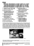
Agilent Technologies E2457A
Preprocessor Interface for the
Intel Pentium® Processor with
MMX Technology
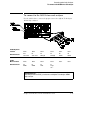
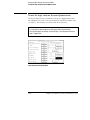
The Agilent Technologies E2457A
Preprocessor Interface—At a Glance
The Agilent Technologies E2457A Preprocessor Interface provides a
complete interface for state or timing analysis between any Intel Pentium®
processor target system and the following Agilent Technologies logic
analyzers:
•
•
•
•
•
•
1660A/C
1660AS/CS (with oscilloscope)
1670A/D
16550A (two-card, in a 16500B/C mainframe)
16554A/55A/56A (two- or three-card, in a 16500B/C mainframe)
16555D/56D (two- or three-card, in a 16500B/C mainframe)
The preprocessor interface connects the target microprocessor to the logic
analyzer, and performs any functions unique to the target microprocessor.
The configuration software on the flexible disk sets up the format
specification of the logic analyzer for compatibility with the Pentium
processor, and also loads the logic analyzer inverse assembler. The logic
analyzer inverse assembler provides Pentium processor assembly language
mnemonics. Instruction disassembly supports Intel’s MMX technology.
The optional Agilent Technologies 16505A Prototype Analyzer is strongly
recommended. The Agilent Technologies 16505A inverse assembler provides
accurate instruction execution tracking of up to two processors, along with
other enhanced features such as colorized filters. For instruction disassembly
with the Agilent Technologies 16505A, Branch Trace Messages must be
enabled and caches must be disabled. This requires a Pentium processor
run-control tool (such as the Agilent Technologies E3491B) connected to the
20-pin debug port on the preprocessor interface.
For more information on the logic analyzers or microprocessor, refer to the
appropriate reference manuals for those products.
Pentium® is a U.S. registered trademark of Intel Corporation.
MMX is a U.S. trademark of Intel Corporation.
ii
Preprocessor Interface for the Pentium Processor
Introduction
The Agilent Technologies E2457A Preprocessor Interface—At a Glance
Agilent Technologies E2457A Preprocessor Interface
Preprocessor Interface for the Pentium Processor
iii
In This Book
This book is the user’s guide for the Agilent Technologies E2457A
Preprocessor Interface. It assumes that you have a working knowledge of the
logic analyzer used and the microprocessor being analyzed.
This user’s guide is organized into three chapters and one appendix:
Chapter 1 explains how to install and configure the preprocessor
interface for state or timing analysis with the supported logic
analyzers.
Chapter 2 provides reference information on the format specification
and symbols configured by the preprocessor interface software, and
information about the inverse assemblers.
Chapter 3 contains reference information on the preprocessor
interface hardware, including the characteristics and signal mapping
for the preprocessor interface.
Appendix A contains information on troubleshooting problems or
difficulties which may occur with the preprocessor interface.
For more information on the logic analyzers or microprocessor, refer to the
appropriate reference manual for those products.
iv
Preprocessor Interface for the Pentium Processor
Contents
1 Setting Up the Preprocessor Interface
Before You Begin 1–3
Setting Up the Preprocessor Interface Hardware 1–5
To select analysis mode and clocking requirements 1–6
Selecting the Mode of Operation 1–6
Selecting the Clock Qualifier Inputs 1–7
Selecting the Clock Version (Timing Only) 1–8
To connect to the target system 1–10
To power up or power down 1–12
To protect the preprocessor interface when not in use 1–12
Connecting to the Logic Analyzer 1–13
To connect to the 1660A/AS/C/CS logic analyzers 1–13
To connect to the 1670A/D logic analyzer 1–14
To connect to the 16550A two-card analyzer 1–15
To connect to the two-card 16554/55/56 analyzers 1–16
To connect to the three-card 16554/55/56 analyzers 1–17
Setting Up the Preprocessor Interface Software 1–18
To copy and load the logic analyzer configuration files 1–19
To load the 16505A Prototype Analyzer files 1–20
To set up the preprocessor interface for timing 1–21
Using the Debug Port Connector 1–22
2 Analyzing the Intel Pentium Processor
Modes of Operation and Clocking 2–3
Timing mode 2–3
State-Per-Clock mode 2–3
Preprocessor Interface for the Pentium Processor
v
Contents
State-Per-Transfer mode 2–3
Displaying Information 2–4
To set up the 16505A workspace 2–4
To display the format specification 2–4
To display the configuration symbols 2–6
Description 2–6
Additional Symbols 2–12
To display captured state data 2–13
Description 2–13
To display the timing format specification 2–15
To display captured timing data 2–16
Using the Logic Analyzer Inverse Assembler 2–17
General output format 2–18
Overview 2–18
Burst and Cacheable Data 2–18
Address Labels 2–19
Prefetched Instructions 2–19
Operand Size 2–19
Byte Enable Validity 2–20
Incomplete Decoding 2–20
Opcode Data Numeric Bases 2–20
Branch Trace Messages 2–20
vi
Preprocessor Interface for the Pentium Processor
Contents
Illegal Instructions 2–20
To synchronize the logic analyzer inverse assembler 2–21
To use the logic analyzer Invasm Options menu 2–22
Show/Suppress 2–23
IDT Description 2–23
Code Synchronization 2–23
Using the 16505A Inverse Assembler 2–24
To use the 16505A Pentium Filter Dialog 2–25
To use the 16505A Pentium Preferences Dialog 2–26
16505A analysis techniques 2–27
Suggested Settings 2–27
Disassembler Behavior 2–28
Physical vs. Linear Addresses 2–28
3 Preprocessor Interface Hardware Reference
Operating Characteristics 3–3
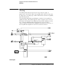
Theory of operation 3–5
Clocking 3–6
Signal-to-connector mapping 3–7
Physical dimensions 3–14
Repair strategy 3–15
A If You Have a Problem
Analyzer Problems A–3
Intermittent data errors A–3
Unwanted triggers A–3
No activity on activity indicators A–4
No trace list display A–4
Preprocessor Interface for the Pentium Processor
vii
Contents
Preprocessor Problems A–5
Target system will not boot up A–5
Erratic trace measurements A–6
Capacitive loading A–6
Inverse Assembler Problems A–8
No inverse assembly or incorrect inverse assembly A–8
Inverse assembler will not load or run A–9
Intermodule Measurement Problems A–10
An event wasn’t captured by one of the modules A–10
Messages A–11
“. . . Inverse Assembler Not Found” A–11
“Measurement Initialization Error” A–12
“No Configuration File Loaded” A–13
“Selected File is Incompatible” A–13
“Slow or Missing Clock” A–13
“Time from Arm Greater Than 41.93 ms” A–14
“Waiting for Trigger” A–14
Cleaning the Instrument A–15
viii
Preprocessor Interface for the Pentium Processor
1
Setting Up the Preprocessor
Interface
Setting Up the Preprocessor Interface
This chapter explains how to set up the Agilent Technologies E2457A
Preprocessor Interface hardware, connect the preprocessor to
supported logic analyzers, configure the logic analyzer, and configure
the Agilent Technologies 16505A Prototype Analyzer, if used.
1-2
Preprocessor Interface for the Pentium Processor
Before You Begin
This section lists the logic analyzers supported by the Agilent
Technologies E2457A, and provides other information about the
analyzers and the preprocessor.
Equipment Supplied
• The preprocessor interface hardware, which includes the
preprocessor interface circuit card and cables.
• The configuration and inverse assembly software for the logic
analyzer and Agilent Technologies 16500B/C mainframe on a
3.5-inch disk.
• Inverse assembler software for the optional Agilent Technologies
16505A Prototype Analyzer on a 3.5-inch disk.
• Two additional jumpers (Agilent part number 1252-3743).
• This User’s Guide.
Minimum Equipment Required
• The E2457A Preprocessor Interface, configuration files, and inverse
assembler.
• One of the logic analyzers listed in the table on the following page.
Additional Capabilities/Equipment Required
The 16505A Prototype Analyzer works together with the 16500B/C
mainframe logic analyzers. It provides enhanced inverse assembly,
and accurate execution tracking of up to two processors. This greatly
increases the analysis capability and performance. The E2457A
Preprocessor Interface comes with software for the 16505A.
For instruction disassembly with the 16505A, Branch Trace Messages
must be enabled and instruction caches must be disabled. This
requires a Pentium run-control tool (such as the E3491B) connected
to the 20-pin debug port on the preprocessor interface.
Preprocessor Interface for the Pentium Processor
1-3
Before You Begin
The Agilent Technologies B4620A Software Analyzer (SWA) works
together with the 16505A to correlate actual execution flow with your
C source code. The accuracy of the C source tracing is greatly
enhanced, since the 16505A inverse assembler uses branch trace
messages to track the execution of code by each CPU. With the
instruction cache disabled, Intel assembly language instructions can
be correlated to the C source code from which the instructions were
generated. With the cache enabled, branch trace messages provide
code flow visibility through the C source code.
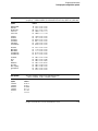
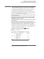
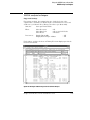
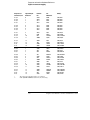
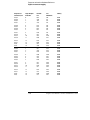
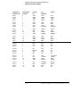
Logic Analyzers Supported
Stand-alone Logic
Analyzers
Channel
Count
State
Speed
Timing
Speed
Memory
Depth
1660A/AS/C/CS
136
100 MHz
250 MHz
4 k states
1670A
136
70 MHz
125 MHz
64 k or .5 M
states
1670D
136
70 MHz
125 MHz
64 k or 1 M
states
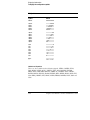
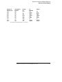
Channel
Count
State
Speed
Timing
Speed
Memory
Depth
Mainframe
Logic Analyzers
16500B
Software
Version
16500C
Software
Version
16500B/C Mainframe
v3.13
v1.03
16550A (two-card)
v3.09
v1.03
204
100 MHz
250 MHz
4 k states
16554A (two- or three-card)
v3.13
v1.03
68/card
70 MHz
125 MHz
500 k states
16555A (two- or three-card)
v3.13
v1.03
68/card
110 MHz
250 MHz
1 M states
16555D (two- or three-card)
v3.13
v1.03
68/card
110 MHz
250 MHz
2 M states
16556A (two- or three-card)
v3.13
v1.03
68/card
100 MHz
200 MHz
1 M states
16556D (two- or three-card)
v3.13
v1.03
68/card
100 MHz
200 MHz
2 M states
16505A Prototype Analyzer
A.01.30
A.01.30
Agilent Technologies
E3491B Processor Probe
v2.15
v2.15
Additional Equipment
Provides Run Control connection to the target system.
Refer to the Agilent Technologies E3491B Processor
Probe User’s Guide for operating instructions.
Agilent Technologies B4620A Software
Analyzer
1-4
Preprocessor Interface for the Pentium Processor
Setting Up the Preprocessor Interface
Hardware
Setting up for the preprocessor interface hardware consists of the
following major steps:
• Turn off the logic analyzer and the target system.
• Set the switches and jumpers (analysis mode and clocking)
according to the type of analysis you wish to perform.
• Install the preprocessor interface in the target system.
• Connect the logic analyzer pods to the cable connectors of the
preprocessor interface.
The remainder of this section covers these topics in detail, including
separate subsections for each logic analyzer this preprocessor
interface supports showing the analyzer pod cable connections.
Preprocessor Interface for the Pentium Processor
1-5
Setting Up the Preprocessor Interface Hardware
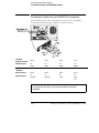
To select analysis mode and clocking requirements
To select analysis mode and clocking requirements
The Agilent Technologies E2457A can capture Pentium data in three modes:
Timing, State-Per-Clock, and State-Per-Transfer. Switches 1 and 2 allow you
to select the mode of operation (see figure on page 1-9).
For State-Per-Clock mode, you can also have qualified or non-qualified
clocking (selected through the Format menu). State-Per-Transfer mode only
works in qualified clocking. Switches 3 to 8 select the clock qualifier inputs
for qualified clocking.
In the Timing mode, you can select a buffered version of the microprocessor
clock or a phase-locked loop version. The clock version is determined by the
location of the jumper on the 1 x 3 header.
Selecting the Mode of Operation
In Timing mode, the signals are buffered, but otherwise passed straight
through to the logic analyzer. In State-Per-Clock mode, all signals are latched
by CLK, and clocked into the logic analyzer on each CLK cycle (see chapter 2
for additional information on State-Per-Clock). In State-Per-Transfer mode,
address pipelining is realigned, and only valid transfers are clocked into the
logic analyzer.
Switches 1 and 2 determine the mode of operation. The LED indicates the
selected mode of operation.
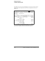
Switch 1 and 2 Settings (Mode of Operation)
Switch 1
Switch 2
Mode of Operation
LED Color
Open
Open
State-Per-Transfer
Green
Closed
Open
State-Per-Clock
Amber
Open
Closed
Timing
Red
Closed
Closed
State-Per-Transfer
Off
1-6
Preprocessor Interface for the Pentium Processor
Setting Up the Preprocessor Interface Hardware
To select analysis mode and clocking requirements
Selecting the Clock Qualifier Inputs
In qualified clocking, the level of a clock qualifier (ClkQual) is ANDed with
the edge of the clock (Clk1 on Agilent Technologies E2457A connector P1),
and the resultant rising edge clocks information into the logic analyzer.
The logic analyzer must be clocked as qualified for State-Per-Transfer mode;
it can be clocked as qualified or non-qualified for State-Per-Clock mode.
Note that for State-Per-Clock mode, qualified clocking decreases the number
of invalid data/code states which are clocked into the logic analyzer, since
only Clk1 edges that occur when ClkQual is asserted will be clocked into
the logic analyzer. The configuration files set up the logic analyzers for
qualified clocking. Use the Format menu to configure the logic analyzer for
non-qualified clocking (see Chapter 2).
Switches 3 - 8 select the inputs to the clock qualifier. These switches allow
you to select particular cycles or operations to be clocked into the logic
analyzer. The inputs to the clock qualifier are selected by closing the
appropriate switches. For all switches which are closed, the signals are ORed
together to create ClkQual; therefore, closing additional switches increases
the variety of states which are clocked into the logic analyzer.
The different clock qualifier inputs are relevant only for certain modes of
operation (see table on next page). For the modes marked "no", the switch
position has no effect.
Note that for State-Per-Transfer mode, when HLDA or BOFF# is asserted,
the preprocessor interface automatically switches to State-Per-Clock mode,
regardless of the switch 7 and 8 settings. The State-Per-Clock ClkQual signal
becomes relevant. If none of the clock qualifier inputs are selected, then no
information will be clocked into the logic analyzer. When HLDA or BOFF# is
deasserted, the preprocessor interface automatically switches back to
State-Per-Transfer mode.
Preprocessor Interface for the Pentium Processor
1-7
Setting Up the Preprocessor Interface Hardware
To select analysis mode and clocking requirements
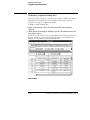
Switch 3 - 8 Settings (Clock Qualifier Inputs)
Relevant for Mode of
Operation
Switch 3
BRDY#
Switch 4
BRDYC#
Switch 5
ADS#
Switch 6
EADS#
Switch 7
HLDA
Switch 8
BOFF#
Timing
yes
yes
yes
yes
yes
yes
State-Per-Clock
yes
yes
yes
yes
yes
yes
* State-Per-Transfer
no
no
no
yes ***
**
**
* In State-Per-Transfer mode, the preprocessor-generated signal "Valid" is also ORed into ClkQual; therefore, valid data-transfer states are
always captured.. Valid = ![!(BRDY# & BRDYC#) & (Pentium in T2, T12, T2P states)]
** During State-Per-Transfer mode, when HLDA or BOFF# is asserted, the preprocessor interface automatically switches to State-Per-Clock
mode, regardless of the switch 7 and 8 settings. The State-Per-Clock clock qualifier inputs become relevant. The HLDA or BOFF# data is not
disassembled. When HLDA or BOFF# is deasserted, the preprocessor interface switches back to State-Per-Transfer: therefore, all other data
is still aligned and disassembled.
*** For State-Per-Transfer mode, pipelined addresses are realigned. The address captured with EADS# is the address of the current bus
cycle; it is not the inquire address. However, cache writebacks which are triggered by a snoop will be captured and displayed. To fully
capture inquire cycle activity, use State-Per-Clock mode.
Selecting the Clock Version (Timing Only)
The 1 x 3 header serves as a single-pole double-throw switch. It allows you
to select the version of the clock which is sent to the logic analyzer in Timing
mode. One version of the clock (PLL) is routed through a phase-locked loop,
while the other version (CLK) is only buffered. The rising edges of CLK and
PLL line up within –0.6 ±.1 ns, with PLL leading CLK. The factory setting for
the jumper is with PLL selected. For more precise timing analysis of the
clock signal, the jumper can be moved to the CLK position, so that the
buffered version of the clock is captured. The position of this jumper is only
relevant for Timing mode.
The load on the clock signal is increased by one 74FCT646A input when the
jumper is in the CLK position.
1-8
Preprocessor Interface for the Pentium Processor
Setting Up the Preprocessor Interface Hardware
To select analysis mode and clocking requirements
Pin A1 Corner
Operating
Mode
{
Agilent Technologies E2457A Switches and Jumpers
Preprocessor Interface for the Pentium Processor
1-9
Setting Up the Preprocessor Interface Hardware
To connect to the target system
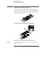
To connect to the target system
The microprocessor connector on the preprocessor will connect directly to a
PGA socket on the target system. Plastic pin protector sockets can be added
for increased clearance.
1 To prevent equipment damage, remove power from both the logic
analyzer and the target system.
CAUTION
To protect your equipment, remove the power from both the logic analyzer
and the target system before you make or break connections. Because the
logic analyzer supplies power to the preprocessor interface, the logic
analyzer should always be powered up before the target system; when
powering down, power down the target system first and then power down
the logic analyzer.
2 Remove the Pentium processor from the socket on the target system
and store it in a protected environment.
3 Install the preprocessor interface into the microprocessor socket on
the target system. Ensure that pin A1 is properly aligned.
If the preprocessor interface connector interferes with components of the
target system or if a higher profile is required, additional plastic pin protector
sockets can be added. Plastic pin protector sockets can be ordered from
Agilent Technologies using the part number 1200-1854. However, any
296-pin PGA IC socket with a Pentium processor footprint and gold-plated
pins can be used.
CAUTION
Serious damage to the target system or preprocessor interface can result
from incorrect connection. Note the position of pin A1 on the preprocessor
interface and target system socket prior to making any connection. Also,
take care to align the preprocessor interface connector with the pins on the
target system socket so that all pins are making contact.
4 Plug the microprocessor into the socket on the preprocessor
interface. The socket is designed with low-insertion-force pins to
allow easy installation and removal.
CAUTION
Care must be used when removing a microprocessor or socket from the
preprocessor interface board to prevent damaging the traces on the board.
1-10
Preprocessor Interface for the Pentium Processor
Setting Up the Preprocessor Interface Hardware
To connect to the target system
5 If you are not using the Agilent Technologies 16505A and want to
fully capture the execution trace, disable the instruction cache.
If you leave the cache enabled, all data will still be captured and decoded but
you may lose unexecuted-prefetch flagging or synchronization with the
execution trace. To capture four-cycle burst transfers you must leave the
cache enabled. This will allow you to view all data coming across the bus,
although some of the execution trace information will be lost.
The cache can be disabled with software by setting CR0.CD, TR12.CI, or the
PCD bits in the page table entries to "1". It can be disabled in hardware by
deasserting KEN#.
If the execution tracing enable bit (bit 1) in TR12.C1 is set to 1, the branch trace
message cycles will be captured and decoded by the logic analyzer. This will
allow the trace to indicate that branches have occurred, even with the cache
enabled.
If possible, you may also want to disable page translation so that the physical
addresses that the preprocessor interface monitors are effectively the logical
addresses. Page translation can be disabled by setting CR0.PG to zero.
6 If you are using the 16505A, two-cycle Branch Trace Messages must
be enabled and instruction caches must be disabled.
This requires a Pentium run-control tool (such as the Agilent Technologies
E3491B) connected to the 20-pin debug port on the preprocessor interface.
Preprocessor Interface for the Pentium Processor
1-11
Setting Up the Preprocessor Interface Hardware
To power up or power down
To power up or power down
When powering up, the logic analyzer must be powered up first, and then the
target system. The logic analyzer provides the power to the active circuits on
the preprocessor interface; unpowered circuits may cause improper
operation of the target system.
When powering down, the target system should be powered down first, and
then the logic analyzer.
To protect your equipment, remove the power from both the logic analyzer
and the target system before you make or break connections.
CAUTION
To protect the preprocessor interface when not in use
1 Cover the socket assembly pins of the preprocessor interface with a
conductive foam wafer or conductive plastic pin protector.
The socket assembly pins of the preprocessor interface were covered at the
time of shipment with either a conductive foam wafer or conductive pin
protector. If this device is not damaged, it may be reused repeatedly.
2 Store the preprocessor interface in an antistatic bag or container.
Properly storing the preprocessor interface protects the active circuitry on
the preprocessor interface from electrostatic discharge.
Electrostatic Discharge
1-12
Preprocessor Interface for the Pentium Processor
Connecting to the Logic Analyzer
Use the tables and figures in the following sections to connect the
logic analyzer pod cables to the flexible cable assemblies on the
preprocessor interface. Refer to the pod diagram for the analyzer you
are using. The configuration file for the logic analyzer is listed below
the corresponding connection table.
To connect to the 1660A/AS/C/CS logic analyzers
Use the table below to connect the preprocessor to the Agilent Technologies
1660A/C logic analyzers.
1660A/C Pod
Pod 1
Pod 2
Pod 3
Pod 4
Pod 5
Pod 6
Pod 7
Pod 8
E2457A
Connector
P1
STAT
clk ↑
P2
STAT
P3
ADDR
P4
ADDR
P5
DATA
P6
DATA
P7
DATA_B
P8
DATA_B
Configuration File
Use configuration file CP55C_3 for the Agilent Technologies 1660A/AS/C/CS
logic analyzers.
Preprocessor Interface for the Pentium Processor
1-13
Connecting to the Logic Analyzer
To connect to the 1670A/D logic analyzer
To connect to the 1670A/D logic analyzer
Use the table below to connect the preprocessor to the Agilent Technologies
1670A/D logic analyzer.
1670A Pod
Pod 8
Pod 7
Pod 6
Pod 5
Pod 4
Pod 3
Pod 2
Pod 1
E2457A
Connector
P8
DATA_B
P7
DATA_B
P6
DATA
P5
DATA
P4
ADDR
P3
ADDR
P2
STAT
P1
STAT
clk ↑
Configuration File
Use configuration file CP55C_3 for the Agilent Technologies 1670A/D logic
analyzer.
1-14
Preprocessor Interface for the Pentium Processor
Connecting to the Logic Analyzer
To connect to the 16550A two-card analyzer
To connect to the 16550A two-card analyzer
Use the table below to connect the preprocessor to the Agilent Technologies
16550A logic analyzer.
16550A Expansion
Card Pod
Pod 6
Pod 5
Pod 4
Pod 3
Pod 2
Pod 1
E2457A Connector
P10
add. status
P9
add. status
P8
DATA_B
P7
DATA_B
P6
DATA
P5
DATA
16550A
Master Card Pod
Pod 6
Pod 5
Pod 4
Pod 3
Pod 2
Pod 1
E2457A Connector
P4
ADDR
P3
ADDR
P2
STAT
P1
STAT
clk ↑
Configuration File
Use configuration file CP55C_2 for the two-card Agilent Technologies 16550A
logic analyzer.
Preprocessor Interface for the Pentium Processor
1-15
Connecting to the Logic Analyzer
To connect to the two-card 16554/55/56 analyzers
To connect to the two-card 16554/55/56 analyzers
Use the table below to connect the preprocessor to the two-card Agilent
Technologies 16554/55/56 logic analyzers (A and D versions).
16554/55/56
Expansion Card Pod
Pod 4
Pod 3
Pod 2
Pod 1
E2457A Connector
P6
DATA
P5
DATA
P4
ADDR
P3
ADDR
16554/55/56
Master Card Pod
Pod 4
Pod 3
Pod 2
Pod 1
E2457A Connector
P8
DATA_B
P7
DATA_B
P2
STAT
P1
STAT
clk ↑
Configuration File
Use configuration file CP55C_2 for the two-card Agilent Technologies
16554/55/56.
1-16
Preprocessor Interface for the Pentium Processor
Connecting to the Logic Analyzer
To connect to the three-card 16554/55/56 analyzers
To connect to the three-card 16554/55/56 analyzers
Use the table below to connect the preprocessor to the three-card
Agilent Technologies 16554/55/56 logic analyzers (A and D versions).
Exp. Card 1 Pod
Pod 4
Pod 3
Pod 2
Pod 1
E2457A Connector
P10
add. status
P9
add. status
P8
DATA_B
P7
DATA_B
Master Card Pod
Pod 4
Pod 3
Pod 2
Pod 1
E2457A Connector
P2
STAT
P1
STAT
clk ↑
Exp. Card 2 Pod
Pod 4
Pod 3
Pod 2
Pod 1
E2457A Connector
P6
DATA
P5
DATA
P4
ADDR
P3
ADDR
Configuration File
Use configuration file CP55C_1 for the three-card Agilent Technologies
16554/55/56.
Preprocessor Interface for the Pentium Processor
1-17
Setting Up the Preprocessor Interface Software
Setting up the preprocessor interface software consists of the
following major steps:
• The first time you set up the preprocessor interface, make a
duplicate copy of the master disks.
For information on duplicating disks, refer to the reference manual for
your logic analyzer.
• Insert the "16500" disk in the front disk drive of the logic analyzer,
and copy the files to the logic analyzer hard drive.
• If you are not using the Agilent Technologies 16505A, load the
appropriate configuration file into the logic analyzer.
• If you are using the Agilent Technologies 16505A Prototype
Analyzer, insert the "16505" disk into the disk drive of the
prototype analyzer and update using the Session Manager. You then
use the 16505A to configure the logic analyzer, using the files
loaded on the logic analyzer hard disk drive.
Once you have the hardware and software set up, you are ready to
make measurements with the logic analyzer and preprocessor
interface. The rest of this section provides more detailed information
on setting up the preprocessor software.
1-18
Preprocessor Interface for the Pentium Processor
Setting Up the Preprocessor Interface Software
To copy and load the logic analyzer configuration files
To copy and load the logic analyzer configuration files
1 The first time you set up the preprocessor interface, make a duplicate
copy of the master disk.
For information on duplicating disks, refer to the reference manual for your
logic analyzer.
2 For the Agilent Technologies 165xx logic analyzer modules, ensure
that the 16500B/C mainframe and the logic analyzer module have the
required software version of the operating system.
The version requirements are listed on page 1-4.
3 Insert the "16500" flexible disk in the disk drive of the 16500B/C or
1660/70.
4 Depending on your logic analyzer, select one of the following menus:
• For the 1660-series and 1670-series logic analyzers, select the "System
Disk" menu.
• For the 16500B/C mainframe, select the "System Flexible Disk" menu.
5 Create a directory on the logic analyzer using the command sequence
"Make Directory, new directory name: <name>, Execute".
6 Select the "System, Flexible Disk" menu. Copy all files to the
directory on the hard disk using the command sequence "Copy, file: *,
to:\<name> on: Hard Disk, Execute".
7 If you are using the Agilent Technologies 16505A, the logic analyzer is
configured through the 16505A, using the files you have just copied
onto the logic analyzer hard drive. Skip to the next page and use the
instructions in "To load the 16505A Prototype Analyzer files." If you
are not using the 16505A, continue with step 8.
8 Configure the menu to "Load" the analyzer configuration from disk.
For 16500-series and 1660-series logic analyzers, select the appropriate
module (such as "100/500 MHz LA" or "Analyzer") for the load.
5 Use the knob to select the appropriate configuration file.
Your configuration file choice depends on which analyzer you are using. The
configuration files are listed under the logic analyzer connection tables.
6 Execute the load operation to load the file into the logic analyzer.
The logic analyzer is configured for Pentium processor analysis by loading the
appropriate configuration file. Loading this file also automatically loads the
logic analyzer inverse assembler (IAP55CE).
Preprocessor Interface for the Pentium Processor
1-19
Setting Up the Preprocessor Interface Software
To load the 16505A Prototype Analyzer files
To load the 16505A Prototype Analyzer files
The Agilent Technologies 16505A Prototype Analyzer works together
with the Agilent Technologies 16500B/C mainframe logic analyzers. It
provides enhanced inverse assembly. To set up the prototype
analyzer:
1 If you have not already done so, copy the logic analyzer files as
described in the previous section.
The 16500B/C files must be copied to the logic analyzer hard drive first for
the 16505A to access them.
2 Connect the 16505A to the 16500B/C. Power up the 16500B/C first,
then power up the 16505A.
For information on connecting the 16505A, refer to the Agilent Technologies
16505A Installation Guide.
3 Ensure that the 16505A has software version A.01.30 or greater.
You may check the 16505A system version from a running session. In the
Main window, click Help, then click "On Version...".
4 Install the 16505A software for the Pentium processor.
Place the "16505" flexible disk in the disk drive of the 16505A. In the Session
Manager window, select the Update button. The window should display
Filegroup: pp_pent_mmx
Version: A.01.30.
Click on Update/Install and respond to the question by clicking on OK. Wait
for the Information dialog to confirm a successful installation. Click on OK to
acknowledge, and Close the Update/Install window.
5 Load the logic analyzer configuration file.
Start a session from the Session Manager window. When the main 16505A
window opens, click on File in the top menu bar to get a pull-down menu,
then click on "Load 16500 Files...". Change to the appropriate directory and
load the appropriate file. Your configuration file choice depends on which
analyzer you are using. The configuration files are listed under the logic
analyzer connection tables.
Drag and drop the "Pentium" Instrument icon into the workspace area. Next,
drag and drop a Listing Display on the "Pentium" Instrument icon in the
workspace. Double click on the Listing icon to open the Listing window and
verify that the label "Pentium Inverse Assembly with MMX" appears.
1-20
Preprocessor Interface for the Pentium Processor
Setting Up the Preprocessor Interface Software
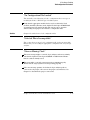
To set up the preprocessor interface for timing
To set up the preprocessor interface for timing
The configuration loaded for state analysis may also be used for timing
analysis. In Timing mode, the signals are buffered by a 74FCT646AT, with a
maximum buffer delay of 6.3 ns (minimum 2.0 ns), and a typical 1.0 ns skew.
To configure the logic analyzer for timing analysis:
1 Set the preprocessor interface switches for timing. The LED color
should be red.
2 Load the appropriate configuration file from the disk.
3 If you are not using the Agilent Technologies 16505A, select the
Configuration menu of the logic analyzer. If you are using the 16505A,
select the "Pentium" icon on the 16505A, and open the Config window
of the logic analyzer.
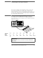
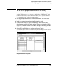
4 Select the Type field for the analyzer and select Timing.
The following figure shows the 16505A Config Window display for the 16550A
logic analyzer.
Configuration Menu for Timing Mode
Preprocessor Interface for the Pentium Processor
1-21
Using the Debug Port Connector
The Agilent Technologies E2457A Preprocessor Interface provides a
connector (J2) for debugger access. J2 complies with the 20-pin
minimal debug port implementation as specified in the "Intel Pentium
Processor User’s Manual Volume 1: Pentium Processor Data Book."
The only signal from the debug connector which does not pass
through the CPU socket to the target system is DBRESET. If you
want to give the debugger reset control over the target, then you
should connect a wire jumper from either J3 (DBRESET) or J6
(DBRESET#) on the preprocessor to your system board. Both of
these connectors have two pins: GND is toward the inside of the board
and DBRESET or DBRESET# is closest to the outside board edge.
1-22
Preprocessor Interface for the Pentium Processor
2
Analyzing the Intel Pentium
Processor
Analyzing the Intel Pentium Processor
This chapter describes the modes of operation, shows how to display
configuration information and preprocessor interface data, gives
status information label and symbol encodings, and provides
information about the inverse assemblers.
There are two inverse assemblers - one for use with logic analyzers
only, and one for use with the Agilent Technologies 16505A. The
inverse assembly information is divided into two sections, to show
only the information relevant to the particular platform.
2-2
Preprocessor Interface for the Pentium Processor
Modes of Operation and Clocking
The E2457A can capture Pentium data in three modes: Timing,
State-Per-Clock, and State-Per-Transfer. Chapter 1 shows the switch
settings for selecting the different modes of operation.
Timing mode
In Timing mode, the signals are buffered, but otherwise passed straight
through to the logic analyzer. Timing mode also allows a choice of buffered or
phase-locked loop clocks (see chapter 1). To configure the logic analyzer
and preprocessor interface for timing:
• Set the preprocessor interface switches for timing. The LED color should
be red.
• Load the appropriate configuration file from the disk.
• If you are using a logic analyzer only, select the Configuration menu of the
logic analyzer. If you are using the 16505A, select the "Pentium" icon on
the 16505A, and open the Config window of the logic analyzer.
• Select the Type field for the analyzer and select Timing.
State-Per-Clock mode
In State-Per-Clock mode, all signals are latched by CLK, and clocked into the
logic analyzer on each CLK cycle. This allows the logic analyzer to capture
wait states and idle states, in addition to valid data states. To configure the
preprocessor interface for State-Per-Clock mode, set the switches for
State-Per-Clock. The LED color should be amber.
State-Per-Transfer mode
In State-Per-Transfer mode, address pipelining is realigned, and only valid
data transfers are clocked into the logic analyzer. To configure the
preprocessor interface for State-Per-Transfer mode, set the switches for
State-Per-Transfer. The LED color should be green.
Preprocessor Interface for the Pentium Processor
2-3
Displaying Information
This section describes how to display analyzer configuration
information, state and timing data captured by the preprocessor
interface, and symbol information that has been set up by the
preprocessor interface configuration software.
To set up the 16505A workspace
To set up the Agilent Technologies 16505A workspace, drag and drop
the "Pentium" Instrument icon into the workspace area. Next, drag
and drop a Listing Display on the "Pentium" Instrument icon in the
workspace. Double click on the Listing icon to open the Listing
window and verify that the label "Pentium Inverse Assembly with
MMX" appears.
To display the format specification
• (Logic analyzer only) Select the format specification menu for your
logic analyzer.
• (With Agilent Technologies 16505A) Using the mouse, right-click and
hold on the "Pentium" instrument icon. In the pop-up menu, slide
down to "Format..." then release the mouse button.
The Agilent Technologies E2457A configuration files contain predefined
format specifications. These format specifications include all labels for
monitoring the microprocessor bus. The figures on the following pages show
the Format display with and without the Agilent Technologies 16505A.
Chapter 3 of this guide contains a table that lists the signals for the
Pentium processor and on which pod and probe line the signal comes to the
logic analyzer. Refer to this table and to the logic analyzer connection
information for your analyzer in chapter 1 to determine where the processor
signals should be on the format specification screen.
2-4
Preprocessor Interface for the Pentium Processor
Displaying Information
To display the format specification
The format specification display shown in the following figures is from the
Agilent Technologies 16550A logic analyzer. Additional labels and pod
assignments are listed off the screen. Select the "Labels" field and rotate the
knob on the analyzer front panel to view additional signals. Select the "Pods"
field and rotate the knob to view other pod-bit assignments. There may be
some slight differences in the display shown by your particular analyzer.
Format Specification with Logic Analyzer Display
Format Specification with Agilent Technologies 16505 Display
Preprocessor Interface for the Pentium Processor
2-5
Displaying Information
To display the configuration symbols
To display the configuration symbols
• (Logic analyzer only) Select the "Symbols" field on the format
specification menu and then choose a label name from the "Label"
pop-up. The logic analyzer will display the symbols associated with
the label.
• (With Agilent Technologies 16505A) Using the mouse, right-click and
hold on the instrument icon for the logic analyzer. In the pop-up
menu, slide down to "Symbol..." then release the mouse button.
Choose a label name from the "Label" list, then select "User Defined
Symbols...." The logic analyzer will display the symbols associated
with the label.
Description
The Agilent Technologies E2457A configuration software sets up symbol
tables and logic analyzer labels. The tables contain alphanumeric symbols
which identify data patterns or ranges. Labels simplify triggering on specific
Pentium processor cycles. The label base in the symbols menu is set to
hexadecimal to conserve display space.
All Pentium processor signals are routed to the preprocessor interface
connectors. Labels that begin with an uppercase letter and have lower case
letters within them are signals that are created by the preprocessor interface
hardware.
The following tables describe these symbol items:
•
•
•
•
•
•
•
the bits in the STAT label
the additional status bits
the signals which are available on the 2 x 5 header
the symbols for the Excptn label
the symbols for the Cycle label
the symbols for the Xfer label
the symbols for BE#, and symbols for many of the status signals (listed
below the BE# table).
2-6
Preprocessor Interface for the Pentium Processor
Displaying Information
To display the configuration symbols
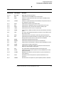
STAT Label Bits
Connector / Bit
Status Signals
Description
P1 / 7 - 0
BE7 - BE0
Byte Enable signals for the data bus.
P1 / 8
D/P#
A low indicates that the OEM Pentium is driving the bus.
P1 / 9
KEN#
A low on this signal indicates that the current cycle is cacheable, and will
therefore be a burst.
P1 / 10
CACHE#
A low on this signal indicates internal cacheability of the cycle (for reads) or a
burst writeback cycle (for writes).
P1 / 11
W/R#
A low indicates read and a high indicates write.
P1 / 12
D/C#
A low indicates a code/special cycle and a high indicates a data cycle.
P1 / 13
M/IO#
A low indicates an I/O cycle and a high indicates a memory cycle.
P1 / 14
LOCK#
A low indicates that the current bus cycle is locked.
P1 / 15
A20M#
A low indicates an Address-bit 20 mask for internal cache lookups or memory
cycles.
P2 / 0
Valid
This signal is generated by the preprocessor interface. A high indicates that a
data transfer is valid.
P2 / 1
ADS#
A low indicates that a new valid bus cycle is being driven by the Pentium.
P2 / 2
NA#
A low indicates that the external memory is ready to accept a new bus cycle,
although all data transfers for the current cycle are not completed.
P2 / 3
BRDY#
A low indicates valid data on the data pins.
P2 / 4
BRDYC#
A low indicates valid data on the data pins for cacheable data.
P2 / 5
PRDY
A high indicates that the Pentium is ready to accept a Probe Mode instruction.
P2 / 6
AHOLD
A high indicates an address hold request.
P2 / 7
EADS#
A low indicates a valid external address has been driven onto the Pentium
address pins to be used for an inquiry cycle.
P2 / 8
HIT#
This signal indicates the outcome of the most recent inquire cycle.
P2 / 9
HITM#
A low indicates (during inquire cycles) that a hit to a modified line in the data
cache has occurred.
P2 / 10
PHITM#
Modified line hit indication used in dual-processor system to maintain local
cache coherency.
P2 / 11
PHIT#
Hit indication used in a dual processor system to maintain local cache
coherency.
P2 / 12
PBGNT#
Grant line used in a dual-processor system to perform private bus arbitration.
Preprocessor Interface for the Pentium Processor
2-7
Displaying Information
To display the configuration symbols
STAT Label Bits (continued)
Connector / Bit
Status Signals
Description
P2 / 13
PBREQ#
Request line used to perform private bus arbitration for dual processing.
P2 / 14
BOFF#
A low indicates that the Pentium should abort all outstanding bus cycles and
float its bus on the next cycle.
P2 / 15
HLDA
A high indicates that the Pentium has acknowledged a hold request, and given
up the bus.
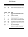
Additional Status Bits *
Connector / Bit
Status Signals
Description
P9 / 0
R/S#
A low indicates that the normal execution of the CPU has been stopped and
placed into an idle state, possibly for execution of Boundary Scan/Probe Mode
instructions.
P9 / 1
ADSC#
Address strobe used in chip-set mode.
P9 / 2
HOLD
A high indicates a system bus hold request.
P9 / 3
BREQ
A high indicates that the Pentium has internally generated a bus request.
P9 / 4
INTR
A high indicates an external interrupt.
P9 / 5
NMI
A high indicates a non-maskable external interrupt.
P9 / 6
SCYC
A high indicates a split cycle (more than two cycles will be locked together).
P9 / 7
BUSCHK#
A low indicates that the system has unsuccessfully completed a bus cycle.
P9 / 8
FLUSH#
A low indicates that the Pentium will writeback all modified lines and invalidate
its cache.
P9 / 9
INV
Indicates the final cache line state for an inquire cycle hit.
P9 / 10
EWBE#
A high (inactive) indicates that a write through cycle is pending in the external
system.
P9 / 11
WB/WT#
A low indicates that the current cache line is write-through, and a high indicates
write-back.
P9 / 12
PWT
Indicates cache writeback on a page-by-page basis.
P9 / 13
PCD
Indicates cacheability on a page-by-page basis.
P9 / 14
RESET
A high indicates that the Pentium will begin execution from a known reset state.
P9 / 15
INIT
A high indicates that the Pentium will begin execution from a known reset state,
except the internal caches and some register values are left unchanged.
2-8
Preprocessor Interface for the Pentium Processor
Displaying Information
To display the configuration symbols
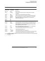
Additional Status Bits (continued) *
Connector / Bit
Status Signals
Description
P10 / 7 - 0
DP7 - 0
Data parity pins.
P10 / 9
STPCLK#
A low indicates that the internal clock is stopped to reduce core power
consumption.
P10 / 10
SMI#
A low indicates a System Power Management interrupt.
P10 / 11
SMIACT#
A low indicates that the Pentium is operating in System Management mode.
P10 / 12
PM0/BP0
P10 / 13
PM1/BP1
BP are the breakpoint pins that indicate a breakpoint match with the debug
registers DR3 - 0 when they are programmed as such; the PM are the
performance monitoring pins.
P10 / 14
BP2
P10 / 15
BP3
P3 / Clk1
FERR#
A low indicates that an unmasked floating point error has occurred.
P4 / Clk1
IERR#
A low indicates either an internal parity error or a functional redundancy error.
P5 / Clk1
IGNNE#
A low partially indicates that the Pentium will ignore any pending unmasked
numeric exception and continue executing floating point instructions for the
entire duration that the signal is asserted.
P6 / Clk1
PEN#
This signal partially determines whether a machine check exception will be
taken as a result of a parity error on a read cycle.
P7 / Clk1
PCHK#
This signal indicates the result of a parity check on a read cycle.
P8 / Clk1
AP
Address Parity for the address bus.
P9 / Clk1
* APCHK#
A low indicates a parity error on the address bus.
P10 / Clk1
* FRCMC#
A low indicates that the Pentium has been configured in checker mode, while a
high indicates that the Pentium has been configured in master mode.
*
The Agilent Technologies 1660/70 Logic Analyzers do not have enough pods to monitor the signals on the Agilent
Technologies E2457A connectors
P9 and P10.
Preprocessor Interface for the Pentium Processor
2-9
Displaying Information
To display the configuration symbols
2 x 5 Header Pins (JTAG)
Signals *
Description
TCK
Test logic clock signal.
TDI
Test logic serial input.
TDO
Test logic serial output.
TMS
Test logic control signal.
TRST
Test logic reset signal.
PD0
Programmable interrupt controller serial data.
PD1
Programmable interrupt controller serial data.
PCLK
Programmable interrupt controller bus clock.
* These signals are located on the 2 x 5 header.
Excptn Symbols
The Excptn symbols consist of the following signals, in the designated
groupings:
(HLDA BOFF#) (D7-0) (M/IO# D/C# W/R#) (BE7-0#)
Symbol
Pattern
Int Ack 1st Cycl
01 xxxxxxxx 000 11101111
0:Divide Error
1:Debug Excptn
2:NMI Interrupt
3:Breakpoint
01
01
01
01
00000000
00000001
00000010
00000011
000
000
000
000
11111110
11111110
11111110
11111110
4:INTO Overflow
5:BOUND Rng Exc
6:Invalid Opcode
7:Dev Not Avail
01
01
01
01
00000100
00000101
00000110
00000111
000
000
000
000
11111110
11111110
11111110
11111110
8:Double Fault
10:Inv Task SSeg
11:Seg N/Present
12:Stack Fault
01
01
01
01
00001000
00001010
00001011
00001100
000
000
000
000
11111110
11111110
11111110
11111110
13:Gen Protectn
14:Page Fault
16:Flt Point Err
17:Alignment Chk
---
01
01
01
01
xx
00001101
00001110
00010000
00010001
xxxxxxxx
000
000
000
000
xxx
11111110
11111110
11111110
11111110
xxxxxxxx
2-10
Preprocessor Interface for the Pentium Processor
Displaying Information
To display the configuration symbols
Cycle Symbols
The Cycle symbols consist of the following signals, in the designated
groupings: (HLDA BOFF#) (LOCK# M/IO# D/C# W/R#) (BE7-4#) (BE3-0#)
Symbol
Pattern
HLDA & BOFF
Hold Ack
Bus Backoff
Int Ack 1st
Int Ack 2nd
10
11
00
01
01
xxxx
xxxx
xxxx
x000
x000
xxxx
xxxx
xxxx
1110
1111
xxxx
xxxx
xxxx
1111
1110
I/O Read
I/O Write
Lckd Read
Lckd Write
Code Read
Lckd Code Rd
01
01
01
01
01
01
1010
1011
0010
0011
1100
0100
xxxx
xxxx
xxxx
xxxx
xxxx
xxxx
xxxx
xxxx
xxxx
xxxx
xxxx
xxxx
Reserved
Mem Read
Mem Write
Lckd Mem Rd
Lckd Mem Wr
01
01
01
01
01
x101
1110
1111
0110
0111
xxxx
xxxx
xxxx
xxxx
xxxx
xxxx
xxxx
xxxx
xxxx
xxxx
Shutdown
Flush
Halt
Writeback
Flush Ack
Brch Trg Msg
Undf Special
---
01
01
01
01
01
01
01
xx
x001
x001
x001
x001
x001
x001
x001
xxxx
xxxx
xxxx
xxxx
xxxx
xxx0
xx0x
xxxx
xxxx
xxx0
xx0x
x0xx
0xxx
xxxx
xxxx
xxxx
xxxx
Xfer Symbols
The Xfer symbols consist of the following signals:
HLDA BOFF# W/R# CACHE# KEN#
Symbol
Pattern
1 Xfer Rd
1 Xfer Rd
4 Xfer Rd
1 Xfer Wr
4 Xfer Wr
---
0101x
010x1
01000
0111x
0110x
xxxxx
Preprocessor Interface for the Pentium Processor
2-11
Displaying Information
To display the configuration symbols
BE# Symbols
Symbol
Pattern
64/b7:0
0000 0000
32/b3:0
32/b4:1
32/b5:2
32/b6:3
32/b7:4
1111
1110
1100
1000
0000
0000
0001
0011
0111
1111
16/b1:0
16/b2:1
16/b3:2
16/b4:3
16/b5:4
16/b6:5
16/b7:6
1111
1111
1111
1110
1100
1001
0011
1100
1001
0011
0111
1111
1111
1111
8/b0
8/b1
8/b2
8/b3
8/b4
8/b5
8/b6
8/b7
1111
1111
1111
1111
1110
1101
1011
0111
1110
1101
1011
0111
1111
1111
1111
1111
None
---
1111 1111
xxxx xxxx
Additional Symbols
There are also symbols for the following signals: KEN#, CACHE#, W/R#,
D/C#, M/IO#, LOCK#, SCYC, WB/WT#, PWT, PCD, BUSCK#, FLUSH#,
IERR#, INTR, NMI, SMI#, SMIAC#, A20M#, AP, APCHK#, ADS#, AHOLD,
BOFF#, BRDY#, BRDYC#, EADS#, EWBE#, HIT#, HITM#, HLDA, HOLD, INV,
NA#, BREQ, RESET, INIT, PEN#, PCHK#, FERR#, IGNNE#, PRDY, R/S# and
U/O#.
2-12
Preprocessor Interface for the Pentium Processor
Displaying Information
To display captured state data
To display captured state data
• (Logic analyzer only) Select the Listing Menu for your logic analyzer.
• (With Agilent Technologies 16505A) Double click on the Listing icon
in the workspace to open the Listing window display.
Description
Captured data is displayed in the Listing Menu (see figure below). The
inverse assemblers disassemble the captured data in a format that closely
resembles the assembly source code for your processor.
The logic analyzers always probe the full 64-bit data bus of the CPU. When
fewer than the full 64 bits of the data bus are used by a memory cycle, the
inverse assembler marks the bytes not used by the microprocessor with "xx."
Logic Analyzer State Listing
Preprocessor Interface for the Pentium Processor
2-13
Displaying Information
To display captured state data
The Listing menu reflects the Show/Suppress selections made in the Invasm
Options menu. In the figure below, the unexecuted prefetches have been
suppressed.
Logic Analyzer Listing Menu with Unexecuted Prefetches Suppressed
2-14
Preprocessor Interface for the Pentium Processor
Displaying Information
To display the timing format specification
To display the timing format specification
The logic analyzer and preprocessor interface must be configured for timing
analysis before the timing format specification can be displayed. Use the
procedure in chapter 1 to set up the equipment for timing.
To display the timing format specification:
• (Logic analyzer only) Select the Format specification menu for your
logic analyzer and choose "Timing" from the State/Timing pop-up.
• (With Agilent Technologies 16505A) Open the Format display for
your logic analyzer.
The figure below shows the Timing menu.
Timing Format Specification
Preprocessor Interface for the Pentium Processor
2-15
Displaying Information
To display captured timing data
To display captured timing data
The logic analyzer and preprocessor interface must be configured for timing
analysis before the timing data can be displayed. Use the procedure in
chapter 1 to set up the equipment for timing.
To display captured timing data:
• (Logic analyzer only) Select the Waveform Menu for your logic
analyzer.
• (With Agilent Technologies 16505A) Open the Waveform display for
your logic analyzer.
The State-Per-Clock mode can be used with the State Waveforms function of
the logic analyzer to produce state timing diagrams. The horizontal axis
displays state transitions rather than absolute time.
Waveform Menu
2-16
Preprocessor Interface for the Pentium Processor
Using the Logic Analyzer Inverse Assembler
The Agilent Technologies E2457A contains two inverse assemblers one for use with logic analyzers only, and one for use with the Agilent
Technologies 16505A. The appropriate inverse assembler is loaded by
the configuration file for your platform.
The information in this section covers the logic analyzer inverse
assembler. If you are using an Agilent Technologies 16505A, refer to
"Using the Agilent Technologies 16505A Inverse Assembler" found
later in this chapter.
The logic analyzer inverse assembler analyzes code read cycles and
disassembles them into Pentium instruction mnemonics, which are
displayed on the logic analyzer screen. Instruction disassembly
supports Intel’s MMX technology.
The inverse assembler requires the preprocessor switches to be set to
State-Per-Transfer mode. It does not work properly in
State-Per-Clock or Timing modes.
Preprocessor Interface for the Pentium Processor
2-17
Using the Logic Analyzer Inverse Assembler
General output format
General output format
The next few paragraphs describe the general output format of the logic
analyzer inverse assembler.
Overview
The logic analyzer inverse assembler operates on memory code read cycles. If
you want to fully capture the execution trace, disable the cache. If possible,
you may also want to disable page translation, so the physical addresses the
preprocessor interface monitors are effectively the logical addresses.
Do not disable the cache memory if burst transfers are to be monitored.
Enabling the cache memory will allow you to view the data coming across the
bus, but the code may not be properly disassembled. Also, when the cache is
enabled, unexecuted prefetches are not inferred, and the unexecuted
prefetch markers are not displayed.
Burst and Cacheable Data
The logic analyzer can track burst (4-transfer) and non-burst (1-transfer)
cycles. During burst transfers the microprocessor holds the address constant
during the entire burst. The inverse assembler listing displays the two least
significant hexadecimal digits of the actual address (derived by the inverse
assembler) at the left side of the column.
Up to eight instructions may be displayed for a single analyzer state, because
the CPU fetches eight instruction bytes from program memory. If the first
byte of these eight bytes contains a single-byte instruction, the next
sequential instruction begins in the next higher byte. This process continues
from the least significant byte to the most significant byte until all of the
fetched bytes are used. When a single state contains more than one
instruction, each instruction is displayed on a separate line.
2-18
Preprocessor Interface for the Pentium Processor
Using the Logic Analyzer Inverse Assembler
General output format
Address Labels
Two different address labels are provided, ADDR and ADDR_. ADDR
provides the full 32 address bits (A31:0), while ADDR_ provides the upper 24
address bits (A31:8).
When using the inverse assembler, use ADDR_ in the listing. ADDR_ gives
you the upper 24 bits of the address, while the inverse assembler display
gives you the lower eight address bits (A7:0) in its first two columns. Using
these two fields together gives you the entire 32 address bits.
The ADDR label displays the actual (acquired) 32-bit address, with
A2:0 = 000 binary. When the inverse assembler is turned off, the ADDR field
can be used to display the full address in hexadecimal format.
Prefetched Instructions
The Pentium is a prefetching microprocessor. It may prefetch up to 64 bytes
(eight 64-bit code fetches) before the current opcode. When a program
executes an instruction that causes a branch, the prefetched code is not used
and will be discarded by the microprocessor. The inverse assembler marks
unused prefetches with a hyphen "–" in the third column of the display.
The logic analyzer captures prefetches, even if they are not executed.
Therefore, care must be taken when you are specifying a trigger condition or
a storage qualification and the instruction of interest follows an instruction
that may cause branching. An unused prefetch may generate an unwanted
trigger.
The Pentium has a prefetch queue of essentially 64 bytes. This means that
by the time a branching instruction is fully decoded, up to 64 other
instruction bytes may have already been prefetched across the data bus, and
stored in the logic analyzer. Both exceptions and instructions can cause the
prefetch queue to be flushed and subsequently refilled. Branches, jumps,
calls, returns, and system control instructions are the most common causes
of prefetch queue flushes, but there are many others. Refer to the Pentium
Processor Family Developer’s Manual for more information.
Operand Size
The "=" symbol is displayed in the fourth column of the inverse assembly
display for 32-bit operands. The "=" symbol will appear for default 32-bit
operand operations, as well as for operations when the operand size prefix is
encountered and decoded.
Preprocessor Interface for the Pentium Processor
2-19
Using the Logic Analyzer Inverse Assembler
General output format
Byte Enable Validity
The Byte Enables are not valid during cache accesses (bursts). Since all
cache reads and writes must be 64 bits, all data lines are valid during these
cycles.
Incomplete Decoding
If a complete opcode is not present, the inverse assembler will not be able to
decode it. A pair of asterisks "**" will be listed on the display.
Opcode Data Numeric Bases
Most data is displayed in hexadecimal format. An exception is the operand
for the INT value, which is displayed in decimal. Decimal numbers are
indicated by a "d" suffix.
Branch Trace Messages
The logic analyzer inverse assembler displays branch trace messages, which
gives you branch target and source addresses. This is especially useful for
tracing execution while operating out of cache.
Illegal Instructions
When the inverse assembler decodes an illegal instruction, the message
"Illegal Opcode" is displayed, along with the byte(s) which caused the
decoded illegal opcode. This message is often an indication that the inverse
assembler has lost synchronization (see next section).
Do not modify the ADDR, DATA, DATA_B, or STAT labels in the format
specification if you want inverse assembly. Changes may cause incorrect
results. Also note that if the trace specification is modified to store only
selected bus cycles, incorrect or incomplete inverse assembly may result.
2-20
Preprocessor Interface for the Pentium Processor
Using the Logic Analyzer Inverse Assembler
To synchronize the logic analyzer inverse assembler
To synchronize the logic analyzer inverse assembler
Occasionally the prefetch marking algorithm in the inverse assembler loses
synchronization, and unused prefetches or executed instructions are
incorrectly marked. If you suspect that the inverse assembler has lost
synchronization, re-synchronize the inverse assembler. Once synchronized,
the inverse assembler will disassemble from this state through the end of the
screen. To re-synchronize the inverse assembler:
1 Select a line on the display that you know contains the first byte of an
executed instruction.
2 Roll this line to the top of the listing. Note that the cursor location is
not the top of the listing. In the figure below, the instruction JMP
F000:E05B is the top of the listing.
3 Select "Invasm Options", and use the "Code Synchronization" portion
of the submenu.
4 Select the choice that identifies which byte of the captured state
contains the first byte of the code fetch and what the default operand
size is for this code (16 or 32 bits). When finished, select "Align".
Rolling the screen up will inverse assemble the lines as they appear on the
bottom of the screen. If you jump to another area of the acquisition buffer by
entering a new line number, you may have to re-synchronize the inverse
assembler by repeating steps 1 through 4.
Preprocessor Interface for the Pentium Processor
2-21
Using the Logic Analyzer Inverse Assembler
To use the logic analyzer Invasm Options menu
To use the logic analyzer Invasm Options menu
The Invasm Options menu contains three functions: display filtering with
Show/Suppress selections, Code Synchronization, and IDT description entry
(see figure). The following sections describe these functions.
If the X or O pattern markers are turned on, and the designated pattern is found
in a state that has been Suppressed with display filtering, the following
message will appear on the logic analyzer display: "X (or O) pattern found, but
state is suppressed."
Logic Analyzer Invasm Options Menu
2-22
Preprocessor Interface for the Pentium Processor
Using the Logic Analyzer Inverse Assembler
To use the logic analyzer Invasm Options menu
Show/Suppress
The Show/Suppress settings determine whether the various microprocessor
operations are shown or suppressed on the logic analyzer display. The figure
on the previous page shows the microprocessor operations which have this
option. The settings for the various operations do not affect the data which is
stored by the logic analyzer, they only affect whether that data is displayed or
not. The same data can be examined with different settings, for different
analysis requirements.
This function allows faster analysis in two ways. First, unneeded information
can be filtered out of the display. For example, when unexecuted prefetches
are suppressed only executed instructions are displayed.
Second, particular operations can be isolated by suppressing all other
operations. For example, I/O accesses can be shown, with all other
operations suppressed, allowing quick analysis of I/O accesses.
IDT Description
The IDT Description settings include Mode, IDT Start, and IDT Size. Mode
can be Protected, Real, or Virtual. IDT Start refers to the starting address of
the Interrupt Descriptor Table, and IDT Size refers to the size of the table.
Set these functions to match the target system settings.
In most cases, the inverse assembler can automatically determine the target
system settings, and will operate properly regardless of the settings entered.
The inverse assembler uses the information from these settings only in cases
of uncertainty. If you suspect that the inverse assembler is disassembling
improperly, check that these settings match your target system.
Code Synchronization
Code synchronization is covered in "To synchronize the logic analyzer inverse
assembler."
Preprocessor Interface for the Pentium Processor
2-23
Using the 16505A Inverse Assembler
The information in this section covers the Agilent Technologies
16505A inverse assembler. If you are not using an Agilent
Technologies 16505A, refer to "Using the Logic Analyzer Inverse
Assembler" found earlier in this chapter.
The Agilent Technologies 16505A inverse assembler requires the
preprocessor switches to be set to State-Per-Transfer mode. It does
not work properly in State-Per-Clock or Timing modes.
Display modes are determined by the options selected in the Agilent
Technologies 16505A Listing window under the "Invasm - Filter..." and
"Invasm - Preferences..." menu pull-downs. The Filter dialog allows
you to show, suppress, or change the color of an entire acquisition
state, whereas the Preferences dialog controls the display format for a
state which is shown.
The Agilent Technologies 16505A performs inverse assembly from
two-cycle Branch Trace Messages. Disassembly is only possible when
"Display Disassembly" is selected in the Preferences dialog and
"Branch Trace Messages" are selected in the Filter dialog. In addition,
Branch Trace Messages must be enabled and instruction caches must
be disabled. This requires a Pentium processor run-control tool, such
as the
Agilent Technologies E3491B, connected to the 20-pin debug port on
the preprocessor interface. The Agilent Technologies E3491B
run-control tool requires firmware version v2.15 or higher for the
Pentium processor.
The Agilent Technologies 16505A can display an accurate instruction
execution trace of Pentium processor target systems containing up to
two processors. Instruction disassembly supports Intel’s MMX
technology.
2-24
Preprocessor Interface for the Pentium Processor
Using the 16505A Inverse Assembler
To use the 16505A Pentium Filter Dialog
To use the 16505A Pentium Filter Dialog
Filter options are accessed from the Listing menu bar by clicking on Invasm
and selecting Filter. The Filter dialog provides the ability to display only
information for particular bus agents and/or cycle types. Colorization can be
used to identify either cycles or processors. The figure below shows a sample
Filter dialog.
Preprocessor Interface for the Pentium Processor
2-25
Using the 16505A Inverse Assembler
To use the 16505A Pentium Preferences Dialog
To use the 16505A Pentium Preferences Dialog
Preferences options are accessed from the Listing window bar by clicking on
Invasm and selecting Preferences. The Preferences dialog controls the level
of detail for states shown. The following figure shows the Preferences dialog.
When "Display Disassembly" is selected, a block of instructions appears in the
Listing window under each two-cycle Branch Trace Message (the instruction
cache(s) must be disabled). "Display Instruction Data" turns on/off the
display of data bytes corresponding to each instruction. "Display Branch
Trace Details" shows the causing and target linear addresses contained in
each two-cycle Branch Trace Message.
Agilent Technologies 16505A Pentium Preferences Dialog
2-26
Preprocessor Interface for the Pentium Processor
Using the 16505A Inverse Assembler
16505A analysis techniques
16505A analysis techniques
Suggested Settings
For software analysis, the settings below give a high-level view of the
captured data. Remember to disable the processor instruction caches and
enable two-cycle Branch Trace Messages in order to get disassembly.
Switches:
State-per-Transfer Mode
Filter:
Show Processors
-- All
Show Bus Cycles
-- All except Code Reads
Show States
-- All States
Preferences:
Display Disassembly
-- ON
Display Branch Target Address
-- ON
For hardware analysis, the State and Timing Waveform displays provide the
most relevant details.
Agilent Technologies 16505A Listing window for Software Analysis
Preprocessor Interface for the Pentium Processor
2-27
Using the 16505A Inverse Assembler
16505A analysis techniques
Disassembler Behavior
To display instruction disassembly, use a Pentium processor run-control tool
such as the Agilent Technologies E3491B to enable two-cycle Branch Trace
Messages and disable the processor instruction caches. Show "Branch Trace
Messages" in the Filter dialog, and select "Display Disassembly" in the
Preferences dialog.
When a processor executes a branching instruction, a Branch Trace Message
(BTM) appears on the bus. The processor usually begins fetching code at the
branch target address before the BTM is emitted. The disassembly software
finds matching code reads before the next matching BTM, then disassembles
the code read data.
Physical vs. Linear Addresses
Branch Trace Messages give linear causing and target addresses. The
addresses displayed for Memory Code Read transactions are physical. For
real-mode programs, this is not an issue since linear and physical addresses
are equivalent. For protected-mode programs with paging enabled, the
address bits higher than A[11] will usually be different. Linear addresses for
disassembled instructions are shown in the "IP Addr" column of the Listing
window.
2-28
Preprocessor Interface for the Pentium Processor
3
Preprocessor Interface
Hardware Reference
Preprocessor Interface
Hardware Reference
This chapter contains reference information on the Agilent
Technologies E2457A hardware including the characteristics and
signal mapping for the preprocessor interface. This chapter also
includes a brief theory of operation, circuit board dimensions, and
information on repairing the preprocessor interface.
3-2
Preprocessor Interface for the Pentium Processor
Preprocessor Interface Hardware Reference
Operating Characteristics
Operating Characteristics
The following operating characteristics are not specifications, but are typical
operating characteristics for the preprocessor interface.
Operating Characteristics
Microprocessor
Compatibility
Intel Pentium Processor with MMX technology
Microprocessor
Package
296-pin SPGA
Microprocessor
Clock Speed
66 MHz external system bus clock
Accessories
Required
None
Power Requirements
1.5 A at +5 Vdc maximum, supplied by the logic analyzer.
Logic Analyzer
Required
Agilent Technologies 1660A/AS/C/CS, 1670A/D, 16550 (two cards), or
16554/55/56 (two or three cards).
Probes Required
Ten 17-channel pods are available. Eight pods are required for
inverse assembly.
Signal Line Loading
7 pf in series with 85 ohms on CLK.
14 pf in series with 35 ohms on the following signals: ADS#, BOFF#,
BRDY#, BRDYC#, HLDA, KEN#, and W/R#.
14 pf on the following signals: INIT, TDO, SMIACT#, R/S#, RESET,
BF0, STPCLK#, and U/O#.
10 pf on all other signals.
Target System
Timing
A minimum 3.5 ns setup/1.5 ns hold is required on the data bus.
A minimum 4.5 ns setup/1.5 ns hold is required on all other signals.
Microprocessor
Operations
Displayed
Interrupt Acknowledge
All Special Cycles (including Branch Trace Messages)
I/O Reads, Writes
Code Reads
Data Reads, Writes
Preprocessor Interface for the Pentium Processor
3-3
Preprocessor Interface Hardware Reference
Operating Characteristics
Additional
Capabilities
The logic analyzer captures all bus cycles, including prefetches.
The State-Per-Clock mode offers filtering for valid data (BRDY#), valid
address (ADS#), inquire address (EADS#), DMA (HLDA), and bus
arbitration (BOFF#).
Environmental
Temperature
Operating
Nonoperating
0 to 55 degrees C (+32 to +131 degrees F)
-40 to +75 degrees C (-40 to +167 degrees F)
Altitude
Operating
Nonoperating
4,600 m (15,000 ft)
15,300 m (50,000 ft)
Humidity
Up to 90% noncondensing. Avoid sudden, extreme temperature
changes which could cause condensation within the instrument.
3-4
Preprocessor Interface for the Pentium Processor
Preprocessor Interface Hardware Reference
Theory of operation
Theory of operation
The primary function of a preprocessor interface is to connect the target
microprocessor to the logic analyzer, and to perform any functions unique to
that particular microprocessor. The Agilent Technologies E2457A
Preprocessor Interface performs this primary function in the following ways:
• By latching and buffering the addresses, data, and status of the
microprocessor so that address, status, and data can be sent to the logic
analyzer at the same time.
• By generating the logic analyzer clocks and clock qualifiers from the
appropriate microprocessor signals and bus conditions.
All CPU signals are buffered/latched by the Registered Transceivers (see
figure next page). One method of capture is used for State-Per-Transfer
mode, while a different method is used for State-Per-Clock mode. The
Pipeline Register Mux controls the method of capture.
In State-Per-Transfer mode, KEN#, WB/WT#, and all signals which follow
address timing are also routed through the Stage 2 flip flops. The Pipeline
Register Mux selects either Stage 1 (Registered Transceivers) or Stage 2
data, depending on the current depth of the pipeline. The parent address is
stored by the preprocessor interface until all of its associated data has
crossed the bus. When the Control/Clocking PALs determine that the data is
valid, they assert ClkQual and the properly-aligned data and address are
captured by the logic analyzer. The preprocessor interface will align all
possible permutations of pipeline depth and burst transfers.
In State-Per-Clock mode, the Registered Transceivers are configured as flip
flops; in Timing mode, they serve as buffers. For both modes, the Pipeline
Register Mux routes the output from the Registered Transceivers directly to
the logic analyzer.
Preprocessor Interface for the Pentium Processor
3-5
Preprocessor Interface Hardware Reference
Clocking
Clocking
The CLK signal is buffered and sent to the logic analyzer on pin 3 of
preprocessor connector P1. If there is no qualification to this clock edge, data
is captured on every rising edge of CLK. This method is used in non-qualified
State-Per-Clock mode.
The Control/Clocking PALs assert ClkQual to enable the clock qualifier for
qualified clocking. This qualifier appears on pin 3 of preprocessor connector
P2. In State-Per-Transfer mode, ClkQual is asserted when valid data is on the
bus, or when the EADS# qualification signal has been selected and is
asserted. In State-Per-Clock mode, ClkQual is asserted when one or more of
the six qualification signals have been selected and are asserted.
Block Diagram
3-6
Preprocessor Interface for the Pentium Processor
Preprocessor Interface Hardware Reference
Signal-to-connector mapping
Signal-to-connector mapping
The following table shows the signal-to-connector mapping. The signal list
table column descriptions are as follows:
Connector / Pin
LA Probe Pin
Pentium Pin
Pin Mnemonic
Label(s)
The preprocessor connector and pin that carries the signal.
The pin within the pod that carries the signal.
The microprocessor pin number.
The microprocessor mnemonic for the pin.
The analyzer label(s) assigned to the signal.
Preprocessor Interface for the Pentium Processor
3-7
Preprocessor Interface Hardware Reference
Signal-to-connector mapping
Preprocessor
Connector / Pin
Logic Analyzer
Probe Pin
Pentium
Pin
Pin
Mnemonic
Label(s)
P1 / 37
P1 / 35
P1 / 33
P1 / 31
0
1
2
3
AL09
AK10
AL11
AK12
BE0#
BE1#
BE2#
BE3#
STAT, BE#
STAT, BE#
STAT, BE#
STAT, BE#
P1 / 29
P1 / 27
P1 / 25
P1 / 23
4
5
6
7
AL13
AK14
AL15
AK16
BE4#
BE5#
BE6#
BE7#
STAT, BE#
STAT, BE#
STAT, BE#
STAT, BE#
P1 / 21
P1 / 19
P1 / 17
P1 / 15
8
9
10
11
AE35
W05
U03
AM06
D/P#
KEN#
CACHE#
W/R#
STAT, D/P#
STAT, KEN#
STAT, CACHE#
STAT, W/R#
P1 / 13
P1 / 11
P1 / 9
P1 / 7
12
13
14
15
AK04
T04
AH04
AK08
D/C#
M/IO#
LOCK#
A20M#
STAT, D/C#
STAT, M/IO#
STAT, LOCK#
STAT, A20M#
P2 / 37
P2 / 35
P2 / 33
P2 / 31
0
1
2
3
*
AJ05
Y05
X04
Valid **
ADS#
NA#
BRDY#
STAT, Valid
STAT, ADS#
STAT, NA#
STAT, BRDY#
P2 / 29
P2 / 27
P2 / 25
P2 / 23
4
5
6
7
Y03
AC05
V04
AM04
BRDYC#
PRDY
AHOLD
EADS#
STAT, BRDYC#
STAT, PRDY
STAT, AHOLD
STAT, EADS#
P2 / 21
P2 / 19
P2 / 17
P2 / 15
8
9
10
11
AK06
AL05
AC03
AA03
HIT#
HITM#
PHITM#
PHIT#
STAT, HIT#
STAT, HITM#
STAT, PHITM#
STAT, PHIT#
P2 / 13
P2 / 11
P2 / 9
P2 / 7
12
13
14
15
AD04
AE03
Z04
AJ03
PBGNT#
PBREQ#
BOFF#
HLDA
STAT, PBGNT#
STAT, PBREQ#
STAT, BOFF#
STAT, HLDA
*
**
This signal is generated by the preprocessor interface.
Valid = ![!(BRDY# & BRDYC#) & (CPU in T2, T12, T2P states)]
3-8
Preprocessor Interface for the Pentium Processor
Preprocessor Interface Hardware Reference
Signal-to-connector mapping
Preprocessor
Connector / Pin
Logic Analyzer
Probe Pin
Pentium
Pin
Pin
Mnemonic
Label(s)
P3 / 37
P3 / 35
P3 / 33
P3 / 31
0
1
2
3
*
*
*
AL35
GND
GND
GND
A3
ADDR
ADDR
ADDR
ADDR
P3 / 29
P3 / 27
P3 / 25
P3 / 23
4
5
6
7
AM34
AK32
AN33
AL33
A4
A5
A6
A7
ADDR
ADDR
ADDR
ADDR
P3 / 21
P3 / 19
P3 / 17
P3 / 15
8
9
10
11
AM32
AK30
AN31
AL31
A8
A9
A10
A11
ADDR, ADDR_
ADDR, ADDR_
ADDR, ADDR_
ADDR, ADDR_
P3 / 13
P3 / 11
P3 / 9
P3 / 7
12
13
14
15
AL29
AK28
AL27
AK26
A12
A13
A14
A15
ADDR, ADDR_
ADDR, ADDR_
ADDR, ADDR_
ADDR, ADDR_
P4 / 37
P4 / 35
P4 / 33
P4 / 31
0
1
2
3
AL25
AK24
AL23
AK22
A16
A17
A18
A19
ADDR, ADDR_
ADDR, ADDR_
ADDR, ADDR_
ADDR, ADDR_
P4 / 29
P4 / 27
P4 / 25
P4 / 23
4
5
6
7
AL21
AF34
AH36
AE33
A20
A21
A22
A23
ADDR, ADDR_
ADDR, ADDR_
ADDR, ADDR_
ADDR, ADDR_
P4 / 21
P4 / 19
P4 / 17
P4 / 15
8
9
10
11
AG35
AJ35
AH34
AG33
A24
A25
A26
A27
ADDR, ADDR_
ADDR, ADDR_
ADDR, ADDR_
ADDR, ADDR_
P4 / 13
P4 / 11
P4 / 9
P4 / 7
12
13
14
15
AK36
AK34
AM36
AJ33
A28
A29
A30
A31
ADDR, ADDR_
ADDR, ADDR_
ADDR, ADDR_
ADDR, ADDR_
*
These signals are generated by the preprocessor interface.
Preprocessor Interface for the Pentium Processor
3-9
Preprocessor Interface Hardware Reference
Signal-to-connector mapping
Preprocessor
Connector / Pin
Logic Analyzer
Probe Pin
Pentium
Pin
Pin
Mnemonic
Label(s)
P5 / 37
P5 / 35
P5 / 33
P5 / 31
0
1
2
3
K34
G35
J35
G33
D0
D1
D2
D3
DATA
DATA
DATA
DATA
P5 / 29
P5 / 27
P5 / 25
P5 / 23
4
5
6
7
F36
F34
E35
E33
D4
D5
D6
D7
DATA
DATA
DATA
DATA
P5 / 21
P5 / 19
P5 / 17
P5 / 15
8
9
10
11
D34
C37
C35
B36
D8
D9
D10
D11
DATA
DATA
DATA
DATA
P5 / 13
P5 / 11
P5 / 9
P5 / 7
12
13
14
15
D32
B34
C33
A35
D12
D13
D14
D15
DATA
DATA
DATA
DATA
P6 / 37
P6 / 35
P6 / 33
P6 / 31
0
1
2
3
B32
C31
A33
D28
D16
D17
D18
D19
DATA
DATA
DATA
DATA
P6 / 29
P6 / 27
P6 / 25
P6 / 23
4
5
6
7
B30
C29
A31
D26
D20
D21
D22
D23
DATA
DATA
DATA
DATA
P6 / 21
P6 / 19
P6 / 17
P6 / 15
8
9
10
11
C27
C23
D24
C21
D24
D25
D26
D27
DATA
DATA
DATA
DATA
P6 / 13
P6 / 11
P6 / 9
P6 / 7
12
13
14
15
D22
C19
D20
C17
D28
D29
D30
D31
DATA
DATA
DATA
DATA
3-10
Preprocessor Interface for the Pentium Processor
Preprocessor Interface Hardware Reference
Signal-to-connector mapping
Preprocessor
Connector / Pin
Logic Analyzer
Probe Pin
Pentium
Pin
Pin
Mnemonic
Label(s)
P7 / 37
P7 / 35
P7 / 33
P7 / 31
0
1
2
3
C15
D16
C13
D14
D32
D33
D34
D35
DATA_B
DATA_B
DATA_B
DATA_B
P7 / 29
P7 / 27
P7 / 25
P7 / 23
4
5
6
7
C11
D12
C09
D10
D36
D37
D38
D39
DATA_B
DATA_B
DATA_B
DATA_B
P7 / 21
P7 / 19
P7 / 17
P7 / 15
8
9
10
11
D08
A05
E09
B04
D40
D41
D42
D43
DATA_B
DATA_B
DATA_B
DATA_B
P7 / 13
P7 / 11
P7 / 9
P7 / 7
12
13
14
15
D06
C05
E07
C03
D44
D45
D46
D47
DATA_B
DATA_B
DATA_B
DATA_B
P8 / 37
P8 / 35
P8 / 33
P8 / 31
0
1
2
3
D04
E05
D02
F04
D48
D49
D50
D51
DATA_B
DATA_B
DATA_B
DATA_B
P8 / 29
P8 / 27
P8 / 25
P8 / 23
4
5
6
7
E03
G05
E01
G03
D52
D53
D54
D55
DATA_B
DATA_B
DATA_B
DATA_B
P8 / 21
P8 / 19
P8 / 17
P8 / 15
8
9
10
11
H04
J03
J05
K04
D56
D57
D58
D59
DATA_B
DATA_B
DATA_B
DATA_B
P8 / 13
P8 / 11
P8 / 9
P8 / 7
12
13
14
15
L05
L03
M04
N03
D60
D61
D62
D63
DATA_B
DATA_B
DATA_B
DATA_B
Preprocessor Interface for the Pentium Processor
3-11
Preprocessor Interface Hardware Reference
Signal-to-connector mapping
Preprocessor
Connector / Pin
Logic Analyzer
Probe Pin
Pentium
Pin
Pin
Mnemonic
Label(s)
P9 / 37
P9 / 35
P9 / 33
P9 / 31
0
1
2
3
AC35
AM02
AB04
AJ01
R/S#
ADSC#
HOLD
BREQ
R/S#
ADSC#
HOLD
BREQ
P9 / 29
P9 / 27
P9 / 25
P9 / 23
4
5
6
7
AD34
AC33
AL17
AL07
INTR
NMI
SCYC
BUSCHK#
INTR
NMI
SCYC
BUSCHK#
P9 / 21
P9 / 19
P9 / 17
P9 / 15
8
9
10
11
AN07
U05
W03
AA05
FLUSH#
INV
EWBE#
WB/WT#
FLUSH#
INV
EWBE#
WB/WT#
P9 / 13
P9 / 11
P9 / 9
P9 / 7
12
13
14
15
AL03
AG05
AK20
AA33
PWT
PCD
RESET
INIT
PWT
PCD
RESET
INIT
P10 / 37
P10 / 35
P10 / 33
P10 / 31
0
1
2
3
D36
D30
C25
D18
DP0
DP1
DP2
DP3
DP
DP
DP
DP
P10 / 29
P10 / 27
P10 / 25
P10 / 23
4
5
6
7
C07
F06, H06
F02
N05
DP4
DP5
DP6
DP7
DP
DP
DP
DP
P10 / 21
P10 / 19
P10 / 17
P10 / 15
8
9
10
11
Y33
V34
AB34
AG03
BF0
STPCLK#
SMI#
SMIACT#
not assigned
STPCK#
SMI#
SMIAC#
P10 / 13
P10 / 11
P10 / 9
P10 / 7
12
13
14
15
Q03
R04
S03
S05
PM0/BP0
PM1/BP1
BP2
BP3
PM, BP
PM, BP
BP
BP
3-12
Preprocessor Interface for the Pentium Processor
Preprocessor Interface Hardware Reference
Signal-to-connector mapping
Preprocessor
Connector / Pin
P1 / 3
P2 / 3
P3 / 3
P4 / 3
P5 / 3
P6 / 3
P7 / 3
P8 / 3
P9 / 3
P10 / 3
*
Logic Analyzer
Probe Pin
Clk1
Clk1
Clk1
Clk1
Clk1
Clk1
Clk1
Clk1
Clk1
Clk1
Pentium
Pin
AK18
*
Q05
P04
AA35
Z34
AF04
AK02
AE05
Y35
Pin
Mnemonic
CLK
ClkQual
FERR#
IERR#
IGNNE#
PEN#
PCHK#
AP
APCHK#
FRCMC#
Label(s)
CLK
Qual#
FERR#
IERR#
IGNNE#
PEN#
PCHK#
AP
APCHK#
FRCMC#
This signal is generated by the preprocessor interface.
Preprocessor Interface for the Pentium Processor
3-13
Preprocessor Interface Hardware Reference
Physical dimensions
Physical dimensions
The figure below gives the dimensions for the preprocessor interface
assembly. The dimensions are listed in inches and millimeters.
Dimensions
3-14
Preprocessor Interface for the Pentium Processor
Preprocessor Interface Hardware Reference
Repair strategy
Repair strategy
The repair strategy for this preprocessor interface is board replacement.
However, the following table lists some mechanical parts that may be
replaced if they are damaged or lost. Contact your nearest Agilent
Technologies Sales Office for further information on servicing the board.
Exchange assemblies are available when a repairable assembly is returned to
Agilent Technologies. These assemblies have been set up on the "Exchange
Assembly" program. This allows you to exchange a faulty assembly with one
that has been repaired, calibrated, and performance verified by the factory.
The cost is significantly less than that of a new assembly.
Replaceable Parts
Agilent Part Number
Description
E2457-69502
E2457-68703
1200-1854
1252-3743
Exchange Board/Cable Assembly
Software Disk Pouch
Pin Protector
Jumper
Preprocessor Interface for the Pentium Processor
3-15
3-16
Preprocessor Interface for the Pentium Processor
A
If You Have a Problem
If You Have a Problem
Occasionally, a measurement may not give the expected results. If you
encounter difficulties while making measurements, use this chapter to
guide you through some possible solutions. Each heading lists a
problem you may encounter, along with some possible solutions.
If you still have difficulty using the analyzer after trying the
suggestions in this chapter, please contact your local Agilent
Technologies service center.
CAUTION
When you are working with the analyzer, be sure to power down both the
analyzer and the target system before disconnecting or connecting cables,
probes, and preprocessors. Otherwise, you may damage circuitry in the
analyzer, preprocessor, or target system.
A–2
Preprocessor Interface for the Pentium Processor
Analyzer Problems
This section lists general problems that you might encounter while
using the analyzer.
Intermittent data errors
This problem is usually caused by poor connections, incorrect signal levels, or
marginal timing.
Remove and reseat all cables and probes, ensuring that there are no
bent pins on the preprocessor interface or poor probe connections.
Adjust the threshold level of the data pod to match the logic levels in the
system under test.
Use an oscilloscope to check the signal integrity of the data lines.
Clock signals for the state analyzer must meet particular pulse shape and
timing requirements. Data inputs for the analyzer must meet pulse shape and
setup and hold time requirements.
See Also
See “Capacitive Loading” in this chapter for information on other sources of
intermittent data errors.
Unwanted triggers
Unwanted triggers can be caused by instructions that were fetched but not
executed.
Add the prefetch queue or pipeline depth to the trigger address to avoid
this problem.
The logic analyzer captures prefetches, even if they are not executed. When
you are specifying a trigger condition or a storage qualification that follows an
instruction that may cause branching, an unused prefetch may generate an
unwanted trigger.
Since the microprocessor only prefetches at most four words, one technique
to avoid unwanted triggering from unused prefetches is to add "10H" to the
Preprocessor Interface for the Pentium Processor
A–3
If You Have a Problem
No activity on activity indicators
trigger address. The trigger condition will only be satisfied if the branch is not
taken.
No activity on activity indicators
Check for loose cables, board connections, and preprocessor interface
connections.
Check for bent or damaged pins on the preprocessor probe.
No trace list display
If there is no trace list display, it may be that your analysis specification is not
correct for the data you want to capture, or that the trace memory is only
partially filled.
Check your analysis sequencer specification to ensure that it will
capture the events of interest.
Try stopping the analyzer; if the trace list is partially filled, this should
display the contents of trace memory.
A–4
Preprocessor Interface for the Pentium Processor
Preprocessor Problems
This section lists problems that you might encounter when using a
preprocessor. If the solutions suggested here do not correct the
problem, you may have a damaged preprocessor. Contact your local
Agilent Technologies Sales Office if you need further assistance.
Target system will not boot up
If the target system will not boot up after connecting the preprocessor
interface, the microprocessor (if socketed) or the preprocessor interface may
not be installed properly, or they may not be making electrical contact.
Ensure that you are following the correct power-on sequence for the
preprocessor and target system.
1 Power up the analyzer and preprocessor.
2 Power up the target system.
If you power up the target system before you power up the preprocessor,
interface circuitry in the preprocessor may latch up and prevent proper
target system operation.
Verify that the microprocessor and the preprocessor interface are
properly rotated and aligned, so that the index pin on the
microprocessor (such as pin 1 or A1) matches the index pin on the
preprocessor interface.
Verify that the microprocessor and the preprocessor interface are
securely inserted into their respective sockets.
Verify that the logic analyzer cables are in the proper sockets of the
preprocessor interface and are firmly inserted.
Reduce the number of extender sockets.
See Also
“Capacitive Loading” in this appendix.
Preprocessor Interface for the Pentium Processor
A–5
If You Have a Problem
Erratic trace measurements
Erratic trace measurements
There are several general problems that can cause erratic variations in trace
lists and inverse assembly failures.
Ensure that the preprocessor configuration switches are correctly set
for the measurement you are trying to make.
Some preprocessors include configuration switches for various features (for
example, to allow dequeueing of the trace list). See Chapter 1 for information
about setting configuration switches.
Do a full reset of the target system before beginning the measurement.
Some preprocessor designs require a full reset to ensure correct
configuration.
Ensure that your target system meets the timing requirements of the
processor with the preprocessor probe installed.
See “Capacitive Loading” in this chapter. While preprocessor loading is slight,
pin protectors, extenders, and adapters may increase it to unacceptable
levels. If the target system design has close timing margins, such loading may
cause incorrect processor functioning and give erratic trace results.
Ensure that you have sufficient cooling for the microprocessor.
Microprocessors such as the i486, Pentium, and MC68040 generate
substantial heat. This is exacerbated by the active circuitry on the
preprocessor board. You should ensure that you have ambient temperature
conditions and airflow that meet or exceed the requirements of the
microprocessor manufacturer.
Capacitive loading
Excessive capacitive loading can degrade signals, resulting in incorrect
capture by the preprocessor interface, or system lockup in the
microprocessor. All preprocessor interfaces add additional capacitive loading,
as can custom probe fixtures you design for your application.
Careful layout of your target system can minimize loading problems and
result in better margins for your design. This is especially important for
systems that are running at frequencies greater than 50 MHz.
A–6
Preprocessor Interface for the Pentium Processor
If You Have a Problem
Capacitive loading
Remove as many pin protectors, extenders, and adapters as possible.
If multiple preprocessor interface solutions are available, use one with
lower capacitive loading.
Preprocessor Interface for the Pentium Processor
A–7
Inverse Assembler Problems
This section lists problems that you might encounter while using the
inverse assembler.
When you obtain incorrect inverse assembly results, it may be unclear
whether the problem is in the preprocessor or in your target system. If
you follow the suggestions in this section to ensure that you are using
the preprocessor and inverse assembler correctly, you can proceed
with confidence in debugging your target system.
No inverse assembly or incorrect inverse assembly
This problem may be due to incorrect synchronization, modified
configuration, incorrect connections, or a hardware problem in the target
system. A locked status line can cause incorrect or incomplete inverse
assembly.
Verify that the inverse assembler has been synchronized by placing an
opcode at the top of the display (not at the cursor position) and pressing
the Invasm key.
The inverse assembler works from the first line of the trace display. If you
jump to the middle of a trace and select Invasm, prior trace states may not be
disassembled correctly. If you move to several random places in the trace list
and synchronize the disassembly each time, the trace disassembly is only
guaranteed to be correct for the portion of the trace list disassembled. See
"To synchronize the inverse assembler" in Chapter 2 for more information.
Ensure that each logic analyzer pod is connected to the correct
preprocessor connector.
There is not always a one-to-one correspondence between analyzer pod
numbers and preprocessor cable numbers. Preprocessors must supply
address (ADDR), data (DATA and DATA_B), and status (STAT) information
to the analyzer in a predefined order. The cable connections for each
preprocessor are often altered to support that need. Thus, one preprocessor
might require that you connect cable 2 to analyzer pod 2, while another will
require you to connect cable 5 to analyzer pod 2. See Chapter 1 for
connection information.
A–8
Preprocessor Interface for the Pentium Processor
If You Have a Problem
Inverse assembler will not load or run
Check the activity indicators for status lines locked in a high or low
state.
Verify that the STAT, DATA, DATA_B, and ADDR format labels have not
been modified from their default values.
These labels must remain as they are configured by the configuration file. Do
not change the names of these labels or the bit assignments within the labels.
Some preprocessors also require other data labels. See Chapter 2 for more
information.
Verify that all microprocessor caches and memory managers have been
disabled.
In most cases, if the microprocessor caches and memory managers remain
enabled you should still get inverse assembly. It may be incorrect because a
portion of the execution trace was not visible to the logic analyzer.
Verify that storage qualification has not excluded storage of all the
needed opcodes and operands.
Check that the IDT Description settings match your target system if you
suspect that the inverse assembler is disassembling improperly.
In most cases, the inverse assembler can automatically determine the target
system settings, and will operate properly regardless of the settings entered.
The inverse assembler uses the information from these settings only in cases
of uncertainty.
Inverse assembler will not load or run
Ensure that you have the correct system software loaded on your
analyzer.
Ensure that the inverse assembler is on the same disk as the
configuration files you are loading.
Configuration files for the state analyzer contain a pointer to the name of the
corresponding inverse assembler. If you delete the inverse assembler or
rename it, the configuration process will fail to load the disassembler. See
Chapter 1 for details.
Preprocessor Interface for the Pentium Processor
A–9
Intermodule Measurement Problems
Some problems occur only when you are trying to make a
measurement involving multiple modules.
An event wasn’t captured by one of the modules
If you are trying to capture an event that occurs very shortly after the event
that arms one of the measurement modules, it may be missed due to internal
analyzer delays. For example, suppose you set the oscilloscope to trigger
upon receiving a trigger signal from the logic analyzer because you are trying
to capture a pulse that occurs right after the analyzer’s trigger state. If the
pulse occurs too soon after the analyzer’s trigger state, the oscilloscope will
miss the pulse.
Adjust the skew in the Intermodule menu.
You may be able to specify a skew value that enables the event to be
captured.
Change the trigger specification for modules upstream of the one with
the problem.
If you are using a logic analyzer to trigger the scope, try specifying a trigger
state one state before the one you are using. This may be more difficult than
working with the skew because the prior state may occur more often and not
always be related to the event you are trying to capture with the oscilloscope.
A–10
Preprocessor Interface for the Pentium Processor
Messages
This section lists some of the messages that the analyzer displays
when it encounters a problem.
“. . . Inverse Assembler Not Found”
This error occurs if you rename or delete the inverse assembler file that is
attached to the configuration file. Ensure that the inverse assembler file is
not renamed or deleted.
Preprocessor Interface for the Pentium Processor
A–11
If You Have a Problem
“Measurement Initialization Error”
“Measurement Initialization Error”
This error occurs when you have installed the cables incorrectly for one or
two Agilent Technologies 16550A logic analysis cards. The following diagrams
show the correct cable connections for one-card and two-card installations.
Ensure that your cable connections match the silk screening on the card.
Then, repeat the measurement.
Cable Connections for One-Card Agilent Technologies 16550A Installations
Cable Connections for Two-Card Agilent Technologies 16550A Installations
See Also
The Agilent Technologies 16550A 100-MHz State/500-MHz Timing Logic
Analyzer Service Guide.
A–12
Preprocessor Interface for the Pentium Processor
If You Have a Problem
“No Configuration File Loaded”
“No Configuration File Loaded”
This is usually caused by trying to load a configuration file for one type of
module/system into a different type of module/system.
Verify that the appropriate module has been selected from the Load
{module} from File {filename} in the Agilent Technologies 16500A/B disk
operation menu. Selecting Load {All} will cause incorrect operation
when loading most preprocessor interface configuration files.
See Also
Chapter 1 describes how to load configuration files.
“Selected File is Incompatible”
This occurs when you try to load a configuration file for the wrong module.
Ensure that you are loading the appropriate configuration file for your logic
analyzer.
“Slow or Missing Clock”
This error message might occur if the logic analyzer cards are not firmly
seated in the Agilent Technologies 16500A/B or 16501A frame. Ensure
that the cards are firmly seated.
This error might occur if the target system is not running properly.
Ensure that the target system is on and operating properly.
If the error message persists, check that the logic analyzer pods are
connected to the proper connectors on the preprocessor interface. See
Chapter 1 to determine the proper connections.
Preprocessor Interface for the Pentium Processor
A–13
If You Have a Problem
“Time from Arm Greater Than 41.93 ms”
“Time from Arm Greater Than 41.93 ms”
The state/timing analyzers have a counter to keep track of the time from
when an analyzer is armed to when it triggers. The width and clock rate of
this counter allow it to count for up to 41.93 ms before it overflows. Once the
counter has overflowed, the system does not have the data it needs to
calculate the time between module triggers. The system must know this time
to be able to display data from multiple modules on a single screen.
“Waiting for Trigger”
If a trigger pattern is specified, this message indicates that the specified
trigger pattern has not occurred. Verify that the triggering pattern is
correctly set.
When analyzing microprocessors that fetch only from word-aligned
addresses, if the trigger condition is set to look for an opcode fetch at an
address not corresponding to a word boundary, the trigger will never be
found.
A–14
Preprocessor Interface for the Pentium Processor
Cleaning the Instrument
If this instrument requires cleaning, disconnect it from all power sources and
clean it with a mild detergent and water. Make sure the instrument is
completely dry before reconnecting it to a power source.
Preprocessor Interface for the Pentium Processor
A–15
A–16
Preprocessor Interface for the Pentium Processor
© Copyright Agilent
Technologies 1993-2000
All Rights Reserved.
Reproduction, adaptation, or
translation without prior
written permission is
prohibited, except as allowed
under the copyright laws.
Restricted Rights Legend.
Use, duplication or disclosure
by the U.S. Government is
subject to restrictions as set
forth in subparagraph (c) (1)
(ii) of the Rights in Technical
Data and Computer Software
clause at DFARS
252.227-7013 for DOD
agencies, and subparagraphs
(c) (1) and (c) (2) of the
Commercial Computer
Software Restricted Rights
clause at FAR 52.227-19 for
other agencies.
Agilent Technologies
3000 Hanover Street
Palo Alto, California 94304
U.S.A.
Document Warranty
The information contained in
this document is subject to
change without notice.
Agilent Technologies
makes no warranty of any
kind with regard to this
material, including, but
not limited to, the implied
warranties of
merchantability or fitness
for a particular purpose.
Agilent Technologies shall
not be liable for errors
contained herein or for
damages in connection with
the furnishing, performance,
or use of this material.
Agilent Technologies
P.O. Box 2197
1900 Garden of the Gods Road
Colorado Springs, CO 80901
Safety
This apparatus has been
designed and tested in
accordance with IEC
Publication 1010, Safety
Requirements for Measuring
Apparatus, and has been
supplied in a safe condition.
This is a Safety Class I
instrument (provided with
terminal for protective
earthing). Before applying
power, verify that the correct
safety precautions are taken
(see the following warnings).
In addition, note the external
markings on the instrument
that are described under
"Safety Symbols."
Warning
• Before turning on the
instrument, you must connect
the protective earth terminal
of the instrument to the
protective conductor of the
(mains) power cord. The
mains plug shall only be
inserted in a socket outlet
provided with a protective
earth contact. You must not
negate the protective action
by using an extension cord
(power cable) without a
protective conductor
(grounding). Grounding one
conductor of a two-conductor
outlet is not sufficient
protection.
• Only fuses with the
required rated current,
voltage, and specified type
(normal blow, time delay,
etc.) should be used. Do not
use repaired fuses or
short-circuited fuseholders.
To do so could cause a shock
or fire hazard.
• Service instructions are for
trained service personnel. To
avoid dangerous electric
shock, do not perform any
service unless qualified to do
so. Do not attempt internal
service or adjustment unless
another person, capable of
rendering first aid and
resuscitation, is present.
• If you energize this
instrument by an auto
transformer (for voltage
reduction), make sure the
common terminal is
connected to the earth
terminal of the power source.
• Whenever it is likely that
the ground protection is
impaired, you must make the
instrument inoperative and
secure it against any
unintended operation.
• Do not operate the
instrument in the presence of
flammable gasses or fumes.
Operation of any electrical
instrument in such an
environment constitutes a
definite safety hazard.
• Do not install substitute
parts or perform any
unauthorized modification to
the instrument.
• Capacitors inside the
instrument may retain a
charge even if the instrument
is disconnected from its
source of supply.
• Use caution when exposing
or handling the CRT.
Handling or replacing the
CRT shall be done only by
qualified maintenance
personnel.
Safety Symbols
Instruction manual symbol:
the product is marked with
this symbol when it is
necessary for you to refer to
the instruction manual in
order to protect against
damage to the product.
Hazardous voltage symbol.
Earth terminal symbol: Used
to indicate a circuit common
connected to grounded
chassis.
WARNING
The Warning sign denotes a
hazard. It calls attention to a
procedure, practice, or the
like, which, if not correctly
performed or adhered to,
could result in personal
injury. Do not proceed
beyond a Warning sign until
the indicated conditions are
fully understood and met.
CA UTIO N
The Caution sign denotes a
hazard. It calls attention to
an operating procedure,
practice, or the like, which, if
not correctly performed or
adhered to, could result in
damage to or destruction of
part or all of the product. Do
not proceed beyond a
Caution symbol until the
indicated conditions are fully
understood or met.
Product Warranty
This Agilent Technologies
product has a warranty
against defects in material
and workmanship for a period
of one year from date of
shipment. During the
warranty period, Agilent
Technologies will, at its
option, either repair or
replace products that prove
to be defective.
For warranty service or
repair, this product must be
returned to a service facility
designated by Agilent
Technologies.
For products returned to
Agilent Technologies for
warranty service, the Buyer
shall prepay shipping charges
to Agilent Technologies and
Agilent Technologies shall
pay shipping charges to
return the product to the
Buyer. However, the Buyer
shall pay all shipping charges,
duties, and taxes for products
returned to Agilent
Technologies from another
country.
Agilent Technologies
warrants that its software and
firmware designated by
Agilent Technologies for use
with an instrument will
execute its programming
instructions when properly
installed on that instrument.
Agilent Technologies does
not warrant that the
operation of the instrument
software, or firmware will be
uninterrupted or error free.
Limitation of Warranty
The foregoing warranty shall
not apply to defects resulting
from improper or inadequate
maintenance by the Buyer,
Buyer-supplied software or
interfacing, unauthorized
modification or misuse,
operation outside of the
environmental specifications
for the product, or improper
site preparation or
maintenance.
No other warranty is
expressed or implied.
Agilent Technologies
specifically disclaims the
implied warranties of
merchantability or fitness
for a particular purpose.
Exclusive Remedies
The remedies provided herein
are the buyer’s sole and
exclusive remedies. Agilent
Technologies shall not be
liable for any direct, indirect,
special, incidental, or
consequential damages,
whether based on contract,
tort, or any other legal theory.
Assistance
Product maintenance
agreements and other
customer assistance
agreements are available for
Agilent Technologies
products.
For any assistance, contact
your nearest Agilent
Technologies Sales Office.
Certification
Agilent Technologies certifies
that this product met its
published specifications at
the time of shipment from the
factory. Agilent Technologies
further certifies that its
calibration measurements are
traceable to the United States
National Institute of
Standards and Technology, to
the extent allowed by the
Institute’s calibration facility,
and to the calibration
facilities of other
International Standards
Organization members.
About this edition
This is the Agilent
Technologies E2457A
Preprocessor Interface for
the Intel Pentium®
Processor with MMX
Technology User’s Guide.
Publication number
E2457-97005, June 2000
Printed in USA.
Print history is as follows:
E2457-97000, Nov. 1993
E2457-97001, March 1994
E2457-97003, January 1997
E2457-97004, Sept. 1997
E2457-97005, June 2000
New editions are complete
revisions of the manual. Many
product updates do not
require manual changes; and,
conversely, manual
corrections may be done
without accompanying
product changes. Therefore,
do not expect a one-to-one
correspondence between
product updates and manual
updates.
DECLARATION OF CONFORMITY
according to ISO/IEC Guide 22 and EN 45014
Manufacturer’s Name:
Agilent Technologies
Manufacturer’s Address:
1900 Garden of the Gods Road
Colorado Springs , CO 80907
U.S.A.
Declares, that the product
Product Name:
Preprocessor Interface for the Intel Pentium
Processor with MMX Technology
Model Number(s):
Agilent Technologies E2457A
Product Options:
All
Conforms to the following Product Specifications:
Safety:
IEC 348:1978 / HD 401 S1:1981
UL 1244
CSA - C22.2 No. 231 (Series M-89)
EMC:
CISPR 11:1990 /EN 55011 (1991): Group 1, Class A
IEC 555-2:1982 + A1:1985 / EN 60555-2:1987
IEC 555-3:1982 + A1:1990 / EN 60555-3:1987 + A1:1991
IEC 801-2:1991 /EN 50082-1 (1992): 4 kV CD, 8 kV AD
IEC 801-3:1984 /EN 50082-1 (1992): 3 V/m, {1kHz 80% AM, 27-1000 MHz}
IEC 801-4:1988 /EN 50082-1 (1992): 0.5 kV Sig. Lines, 1 kV Power Lines
Supplementary Information:
The product herewith complies with the requirements of the Low Voltage
Directive 73/23/EEC and the EMC Directive 89/336/EEC, and carries the CE-marking
accordingly.
This product was tested in a typical configuration with Agilent Technologies test
systems.
John Strathman, Quality Manager
Colorado Springs, December 15, 1993
European Contact: Your local Agilent Technologies Sales and Service Office or Agilent Technologies GmbH,
Department ZQ / Standards Europe, Herrenberger Strasse 130, 71034 Böblingen Germany (FAX: +49-7031-143143)
Product Regulations
Safety
IEC 348:1978 / HD 401 S1:1981
UL 1244
CSA - C22.2 No. 231 (Series M-89)
EMC
This Product meets the requirements of the European Communities (EC)
EMC Directive 89/336/EEC.
Emissions
EN55011/CISPR 11 (ISM, Group 1, Class A equipment)
Immunity
EN50082-1
IEC 801-2 (ESD) 8kV AD
IEC 801-3 (Rad.) 3V/m
IEC 801-4 (EFT) 1kV
Performance
Code
Notes
3
2
3
Performance Codes:
1 Pass - Normal operation, no effect.
2 Pass - Temporary degradation, self recoverable.
3 Pass - Temporary degradation, operator intervention required.
4 Fail - Not recoverable, component damage.
Notes: (none)
Sound Pressure
Level
N/A