1
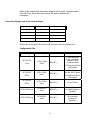
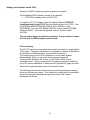
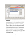
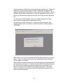
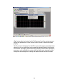
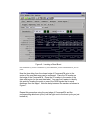
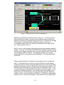
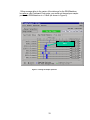
FuturePlus Systems Corporation
FS1107 Embedded DDR Analysis Software
Users Manual
For use with Agilent Technologies Logic Analyzers
Revision 2.1
FuturePlus is a registered trademark of FuturePlus Systems Corporation
Copyright 2003 FuturePlus Systems Corporation
How to reach us .......................................................................................................................... 3
Software License Agreement .................................................................................................... 4
Use of the Software ..................................................................................................... 4
Ownership ................................................................................................................... 4
Sublicensing and Distribution ...................................................................................... 4
Termination.................................................................................................................. 5
Export Clause .............................................................................................................. 5
Limitation of warranty................................................................................................... 5
Exclusive Remedies .................................................................................................... 5
Introduction................................................................................................................................. 6
Theory of Operation..................................................................................................... 6
IC Probe Types............................................................................................................ 6
Unique DDR Probing Considerations .......................................................................... 7
Getting Started............................................................................................................................ 8
FS1107 Product Components ..................................................................................... 8
Logic Analyzer Card Definitions and Requirements..................................................... 8
FS1107 Logic Analyzer Card Configuration Options ................................................. 10
Signal Naming Conventions ...................................................................................... 10
Connecting the Flying Leads to the IC Probe ............................................................ 10
Connecting Flying Leads to the Logic Analyzer......................................................... 11
Configuration Files..................................................................................................... 11
Setting up the Software on the 167xx ........................................................................ 12
167xx Licensing ......................................................................................................... 12
Setting up the 167xx Inverse Assembler ................................................................... 13
Setting up the 169xx Analyzer ................................................................................... 13
169xx Licensing ......................................................................................................... 14
Loading 169xx configuration files and define probes feature..................................... 14
Offline Analysis .......................................................................................................... 15
Threshold Considerations for Tristate........................................................................ 20
Cross Bus Analysis.................................................................................................... 21
EyeScan Operation.................................................................................................... 21
Symbols..................................................................................................................... 23
Timing Analysis ........................................................................................................................ 24
Pod Attachment for Timing Analysis .......................................................................... 24
Acquiring Data ........................................................................................................... 24
Sample Waveform Display ........................................................................................ 25
State Analysis ........................................................................................................................... 26
Pod Attachment for State Analysis ............................................................................ 26
Missing or slow clock ................................................................................................. 27
Calibration ................................................................................................................. 28
Acquiring Data in State Mode .................................................................................... 35
General Information.................................................................................................................. 36
Signal Connections.................................................................................................... 36
TSOP-66 IC Probe Drawing ...................................................................................... 40
TQFP-100 IC Probe Drawing..................................................................................... 41
2
How to reach us
For Technical Support:
FuturePlus Systems Corporation
36 Olde English Road
Bedford NH 03110
TEL: 603-471-2734
FAX: 603-471-2738
On the web http://www.futureplus.com
For Sales and Marketing Support:
FuturePlus Systems Corporation
TEL: 719-278-3540
FAX: 719-278-9586
On the web http://www.futureplus.com
FuturePlus Systems has technical sales representatives in several major countries. For
an up to date listing please see http://www.futureplus.com/contact.html.
Agilent Technologies is also an authorized reseller of many FuturePlus products. Contact
any Agilent Technologies sales office for details.
3
Software License Agreement
IMPORTANT Please read this license agreement before opening the
media envelope. Rights in the software are offered only on the condition
that the customer agrees to all terms and conditions of the license
agreement. Opening the media envelope indicates your acceptance of
these terms and conditions. If you do not agree to the licensing agreement,
you may return the unopened package for a full refund.
In return for payment for this product, FuturePlus Systems grants the
Customer a SINGLE user LICENSE in the software subject to the following:
Use of the Software
Customer may use the software on any one Agilent 1670x mainframe logic
analysis system.
•
Customer may not reverse assemble or decompile the software.
Customer may make copies or adaptations of the software:
•
For archival purpose only
•
When copying for adaptation is an essential step in the use of the
software with the logic analyzer and/or logic analysis mainframe so
long as the copies and adaptations are used in no other manner.
Customer has no right to copy software unless it acquires an
appropriate license to reproduce from FuturePlus Systems.
•
Customer agrees that it does not have any title or ownership of the
software, other than the physical media.
•
Customer acknowledges and agrees that the software is copyrighted
and protected under the copyright laws.
•
Transfer of the right of ownership shall only be done with the consent
of FuturePlus Systems.
Ownership
Sublicensing and Distribution
Customer may not sublicense the software or distribute copies of the
software to the public in physical media, or by electronic means, or any
other means without the prior written consent of FuturePlus Systems.
4
Termination
FuturePlus Systems may terminate this software license for failure to
comply with any of these terms provided FuturePlus Systems has requested
the Customer to cure the failure and Customer has failed within 30 days of
such notice.
Export Clause
Customer agrees not to export or re-export the software or any copy or
adaptation in violation of the U.S. Export Administration regulations or other
applicable regulation.
Limitation of warranty
FuturePlus Systems warrants that its software designated by FuturePlus
Systems for use with an instrument will execute its programming
instructions when properly installed on that instrument. FuturePlus Systems
does not warrant that the operation of the software will be uninterrupted or
error-free.
The foregoing warranty shall not apply to defects resulting from improper or
inadequate use by the Buyer, Buyer-supplied software or interfacing,
unauthorized modification or misuse, operation outside of the environmental
specifications for the product, or improper site preparation or maintenance.
NO OTHER WARRANTY IS EXPRESSED OR IMPLIED. FUTUREPLUS
SYSTEMS SPECIFICALLY DISCLAIMS THE IMPLIED WARRANTIES OF
MERCHANTABILITY AND FITNESS FOR A PARTICULAR PURPOSE.
Exclusive Remedies
THE REMEDIES PROVIDED HEREIN ARE BUYER’S SOLE AND
EXCLUSIVE REMEDIES. FUTUREPLUS SYSTEMS SHALL NOT BE
LIABLE FOR ANY DIRECT, INDIRECT, SPECIAL, INCIDENTAL, OR
CONSEQUENTIAL DAMAGES, WHETHER BASED ON CONTRACT,
TORT, OR ANY OTHER LEGAL THEORY.
Assistance
Product maintenance agreements and other customer assistance
agreements are available for FuturePlus Systems products. For assistance,
contact FuturePlus Systems.
5
Introduction
Thank you for purchasing the FuturePlus Systems FS1107 Embedded
DDR DRAM solution. This is a software product that can be used with
either a Mictor, Samtec or soft touch connector designed into a target DDR
bus or with an IC probe. The embedded DDR solution in conjunction with
the Agilent Technologies Logic Analyzer is a valuable tool to debug a
system. This user manual will provide the information you need to install,
configure, and use the solution. The solution can accommodate DDR
DRAMs up to 1Gb X 32.
Theory of Operation
FuturePlus Systems FS1107 Embedded DDR SDRAM software license
provides logic analyzer configuration and transaction level decode of the
DDR SDRAM memory bus traffic. The transaction decode software includes
all data commands and ECC signals.
The Embedded DDR solution, FS1107, can work with an embedded Mictor ,
Samtec or soft touch connector. The design of the connectors onto a target
board is covered in the FuturePlus Systems Application Note “Embedded
Probing of DDR SDRAM Applications”.
The analyzer is clocked on both edges of the DDR clock. Chip select is
used to qualify real commands on the bus. The software decodes
transactions and determines from the user provided cas latency and burst
size values and copies the valid data under the correct read or write
command.
Users must use timing zoom in order to adjust the setup/hold values for
capturing simultaneous reads and writes. The calibration procedure is
outlined later in the manual.
IC Probe Types
We offer two different probes to attach directly to DDR DRAM IC devices.
Both a 100 pin .65mm TQFP package (FS1008), or a 66 pin .65mm TSOP-II
package (FS1109) are available. In order to properly connect to the DDR
DRAM chip, it is recommended that you have the IC manufacturer’s data
sheet for device pinout information. Closely review the IC probe user
manual, and refer to the Signal Connections matrix and IC probe drawings
in the General Information section of this manual.
The probe directly attaches to the DDR DRAM device allowing state or
timing analysis. The design allows operation up to a 266Mhz data rate.
6
Unique DDR Probing Considerations
DDR has a differential clock CK0/CK0#. For the purpose of discussion in
this document, the crossing of CK0 and CK0# will be considered to be the
mid-point of CK0 rising.
DDR can be thought of as consisting of two buses; the command bus and
the data bus. The DDR command bus is clocked on the rising edge of CK0.
State or timing analysis of the command bus does not take any special
considerations for logic analyzer operation.
The data bus is clocked from strobes derived from both the rising and falling
edges of CK0. Strobe edges straddle the Data on READ and are centered
about Data on WRITE. State mode analysis of the data bus demands
special considerations, covered in the State Analysis section.
Timing analysis of the data bus does not require special clocking
considerations for proper logic analyzer operation.
DDR Timing Differences for
Read or Write
Read
• Strobe edges
straddle
data for
READ
Write
• Strobe edges
centered
on data for
WRITE
7
Getting Started
This section introduces you to the Embedded DDR solution and lists the
equipment required for DDR analysis.
FS1107 Product Components
• Installation diskette - contains protocol decoder and configuration files
• CD-ROM containing offline viewing analysis capability
• SW License Entitlement Certificates
Must be ordered separately if required. IC Probe for embedded DDR
DRAM devices.
• FS1108 is for 100 pin .65mm TQFP devices.
• FS1109 is for 66 pin .65mm TSOP-II devices.
• Termination adapters for Samtec, Mictor or Soft Touch connectors
For customers who put their own connectors down please refer to our
application note “Embedded Probing of DDR SDRAM Applications” for
routing information.
Logic Analyzer Card Definitions and Requirements
Logic Analyzer Modules – “Module” – A set of logic analyzer card(s) that
have been configured (via cables connecting multiple cards) to operate as a
single logic analyzer whose total available channels is the sum of the
channels on each card. A trigger within a module can be specified using all
of the channels of that module. Each module may be further broken up into
“Machines.” A single module may not extend beyond a single 5 card 16700
frame.
Logic Analyzer Machines – “Machine” – A set of logic analyzer pods from
a logic analyzer module grouped together to operate as a single state or
timing analyzer. Each logic analyzer module may be partitioned into two
independent “Machines” (either two state machines, or state and a timing
machine), and the pods of a module may be assigned freely to either
machine. Each state analyzer machine has its own state clock. Cross
triggering between modules or machines is done via the Intermodule Bus or
via the Flag bits, which will communicate across a 16700 frame and its
expander, or across multiple fames if the Multiframe product is used. Turbo
8
mode (333Mhz for 1671x or 400Mhz for 1675x cards) operation restricts a
module to having only one machine.
Logic Analyzer Requirements –16717A through 16756A modules will
work for the solutions described in this manual, we recommend using
16753A modules or better. The analyzer must be running A.02.80.00 or
better operating system.
Probing DDR generally requires two to four logic analyzer cards depending
on the bus speed, whether state or timing measurements are being used,
and the type of logic analyzer card being used. For full channel timing
measurements, only two cards (configured as a single logic analysis module
using one analyzer “machine”) are necessary.
When running at 266Mhz (state) or higher data rates the analyzer must be
configured to run in its high-speed (Turbo) mode. When the analyzer is
running in turbo mode you must leave 2 pod pairs unused.
9
FS1107 Logic Analyzer Card Configuration Options
DDR Bus
Speed
16700 Analyzer
Type
Timing Analysis
200Mhz
(PC1600)
16717/8/9
2 cards configured
as one module with
one timing
machine
266Mhz
(PC2100)
State Analysis (with
2Ghz TimingZoom™)
•
4 Cards configured as
1 module
1675X
2 cards configured
as one module with
one timing machine
•
4 cards configured
as 1 module
16717/8/9,
16750/1/2
2 cards configured
as one module, one
machine
•
4 cards configured
as 1 module
16753/4/5/6
2 cards configured
as one module, one
machine
•
4 cards configured
as 1 module
•
4 cards configured
as 1 module
and above
Up to 400
16753/4/5/6
Mb/s
(embedded)
2 cards configured
as one module
Signal Naming Conventions
This operation manual uses the same signal notation as the DDR Bus
specification. Reference the General Information section.
Connecting the Flying Leads to the IC Probe
You may find it more convenient to connect the Agilent logic analyzer’s
flying leads to the IC probe before mounting the probe to the target device.
Cross reference the signal name from the IC’s datasheet to the IC’s probe
pin and then to the appropriate logic analyzer probe pod and pin as detailed
in the General Information section. Take care in marking each pod.
10
When all the connections have been made to the IC probe, install the probe
onto the IC per the probe’s instructions. Be sure to maintain pin 1
orientation.
Connecting Flying Leads to the Logic Analyzer
Logic Analyzer
Flying Lead Set
Signals
Master Pod 1
Header 1
Command
Master Pod 2
Header 2
Address
Master Pod 3
Header 3
Data
Expander Pod 1
Header 4
Data
Please refer to the back of the manual and the format menu for exact pin out.
Configuration Files
167xx Analyzer
16715/6/7/9
1675x
169xx Analyzer
1675x, 1695x,
1691x*
File-name
DR1107_1
Comments
4 Card config files
for use with Mictor,
Samtec or Soft
Touch connector
*3 Cards required for
1691x cards
16715/6/7/9
3 Card config files
for use with IC probe
1675x, 1695x,
1691x*
DR1107_2
1675x, 1695x,
1691x
DR1107_3
2 Card Timing
16753-16756 only
16753/4/5/6,
1691x
DR1107_4
2 Card config. used
for Data Eyescan or
Eyefinder
16753-16756 only
16753/4/5/6,
1695x
DR1107_5
2 Card config. used
for Command
Eyescan or
Eyefinder
1675x
16715/6/7/9
1675x
11
*2 Cards required for
1691x cards
Setting up the Software on the 167xx
Revision A.02.80.00 operating system or greater is required.
The Embedded DDR software consists of one diskette:
• 16700/702 Installation disk for the FS1107
To install the FS1107 software, insert the diskette labeled 16700/702
Installation disk for the FS1107 into the diskette drive of the 16700. From
the SYSTEM ADMINISTRATION TOOLS, select INSTALL under
SOFTWARE. From the SOFTWARE INSTALL screen, select FLEXIBLE
DISK and APPLY. Once the title appears, select it and then select
INSTALL.
This procedure does not need to be repeated. It only needs to be done
the first time the DDR analysis probe is used.
167xx Licensing
The FS1107 product is a licensed product which is locked to a single Agilent
1670x frame. Complete instructions for licensing this software is detailed on
the Entitlement Certificate that is enclosed with this product.
The licensing area for the 1670x mainframe is found under System
Administration. Once you are at the licensing area choose the
Processor/Bus Solutions tab, in here you will find the DDR inverse
assembler listed. Type your password in the space provided to enable the
use of the inverse assembler. A demo period is provided by typing the word
demo into the password space next to the product name.
The following picture shows the licensing area after pressing the licensing
button on the previous screen. This is where you would enter the password
you will receive after following the instructions on the SW License
Entitlement Certificate.
12
Setting up the 167xx Inverse Assembler
Once the software has been installed correctly, the configurations are
located under logic/configs/futureplus/FS1107. Use the chart to determine
which configuration should be loaded. Choose the file that corresponds to
the setup you have. If you do not have the cards in the same slots that the
configurations were originally developed in, the analyzer will tell you which
slot it is trying to load the configuration into. You must click OK for it to
continue to load. When the configuration file is loaded the inverse
assembler (IA) will automatically load. If the inverse assembler fails to load
you can load it manually from the listing window. Press the INVASM button
on the top of the screen, then choose IFS1107E from the list and select the
analyzer. After selecting analyzer, press LOAD and the inverse assembler
should load.
Setting up the 169xx Analyzer
A CD containing the 16900 software is included in the FS1107 package.
The CD contains a setup file that will automatically install the configuration
files and protocol decoder onto a PC containing the 16900 operating system
or onto a 16900 analyzer itself.
13
To install the software simply double click the .exe file on the CD containing
the 16900 software. After accepting the license agreement the software
should install within a couple of minutes.
169xx Licensing
Once the software has been successfully installed you must license the
software. Please refer to the entitlement certificate for instructions on
licensing the software. The software can only be installed on one machine.
If you need to install the software on more than one machine you must
contact the FuturePlus sales department to purchase additional licenses.
Loading 169xx configuration files and define probes feature
When the software has been licensed you should be ready to load a
configuration file. You can access the configuration files by clicking on the
folder that was placed on the desktop during software installation. When
you click on the folder it should open up to display all the configuration files
to choose from. If you put your mouse cursor on the name of the file a
description will appear telling you what the setup consists of, once you
choose the configuration file that is appropriate for your configuration the
16900 operating system should execute. The protocol decoder
automatically loads when the configuration file is loaded. If the decoder
does not load, you may load it by selecting tools from the menu bar at the
top of the screen and select the decoder from the list.
After loading the configuration file of choice, go into the format specification
of the configuration by choosing Setup from the menu bar and then
selecting Bus/Signal in the drop down menu. When the format specification
appears press Define Probes at the bottom of the screen. The Define
Probes feature will describe how to hook the analyzer cards to the
connections on the target. The following figure shows what the Define
Probes screen looks like. The figure below may differ from your display; this
is an example of how the display looks in general.
14
Offline Analysis
Data that is saved on a 167xx analyzer in fast binary format, or 16900
analyzer data saved as a *.ala file, can be imported into the 1680/90/900
environment for analysis. You can do offline analysis on a PC if you have
the 1680/90/900 operating system installed on the PC, if you need this
software please contact Agilent.
Offline analysis allows a user to be able to analyze a trace offline at a PC so
it frees up the analyzer for another person to use the analyzer to capture
data.
If you have already used the license that was included with your package on
a 1680/90/900 analyzer and would like to have the offline analysis feature
on a PC you may buy additional licenses, please contact FuturePlus sales
department.
In order to view decoded data offline, after installing the 1680/90/900
operating system on a PC, you must install the FuturePlus software. Please
follow the installation instructions for “Setting up the 16900 analyzer”. Once
the FuturePlus software has been installed and licensed follow these steps
to import the data and view it.
15
From the desktop, double click on the Agilent logic analyzer icon. When the
application comes up there will be a series of questions, answer the first
question asking which startup option to use, select Continue Offline. On the
analyzer type question, select cancel. When the application comes all the
way up you should have a blank screen with a menu bar and tool bar at the
top.
For data from a 16900 analyzer, open the .ala file using the File, Open
menu selections and browse to the desired .ala file.
For data from a 16700, choose File -> Import from the menu bar, after
selecting import select “yes” when it asks if the system is ready to import
16700 data.
After clicking “next” you must browse for the fast binary data file you want to
import. Once you have located the file and clicked start import, the data
should appear in the listing.
After the data has been imported you must load the protocol decoder before
you will see any decoding. To load the decoder select Tools from the menu
bar, when the drop down menu appears select Inverse Assembler, then
choose the name of the decoder for your particular product. The figure
below is a general picture; please choose the appropriate decoder for the
trace you are working with.
16
After the decoder has loaded, select Preferences from the overview screen
and set the preferences to their correct value in order to decode the trace
properly.
The file content is displayed on the PC screen and may be manipulated and
altered to suit your particular needs using the standard Agilent controls and
conventions. We highly recommend NOT changing colors unless absolutely
necessary, as it is possible to end up with the same color selected for both
foreground and background, making that particular label column invisible.
17
The figure below shows a typical DDR screen display.
18
Once the configuration file is loaded you may make changes to the
configuration if your pinout is different from the specified format. Labels that
are used by the Protocol Decoder must be preserved, these labels must not
be removed or renamed. You may reorder, add or remove some of the bits
assigned to these labels, the exception to this is the Command label.
The following labels are used by the protocol decoder:
ADDRESS
DATALow
DATAHi
READdataLow
READdataHi
Bank Address
Command
CommandClk
CB
CBRead
#S0
#S1
#S2
#S3
The above labels must appear exactly as shown in the format menu. In
some applications you may only use 1 chip select line ( #S0 ), in those
cases assign #S1-#S3 to the same pod and channel you assigned #S0 to
satisfy the protocol decoder.
19
Threshold Considerations for Tristate
Each DDR bus implementation will have different timing due to trace length
variation on the motherboard, variations in bus loading, and sensitivity to
dynamic factors such as crosstalk or simultaneous switching noise. Many of
these timing characteristics are fixed. These differences are difficult or
impossible to predict in advance for a variety of implementations and
configurations of devices.
Eye Finder is used to measure the fixed component of these implementation
dependent timing characteristics so that the analyzer can sample all DQS
strobed signals using the single strobe DQS0 (or any DQS chosen) and
achieve reliable state capture.
Stimulus dependent timing is taken into account by running the Eye Finder
while worst case bus traffic occurs. The worst case data valid window
boundaries are found and the analyzer is set to sample data at the center of
the actual data valid window of each signal for each specific DDR
implementation and configuration.
Because the strobes are tri-stated between bursts their logic value is
undefined. Some systems will terminate the DDR bus to a voltage close to
the Vref voltage, causing the strobes to sit right at the switching threshold.
During read bursts, because read data (and strobes) are actually not valid
until the reflected wave reaches the probe, DQS0 may also spend a
significant amount of time at Voh/2 (close to Vref) between arrival of the
incident wave and the reflected wave. Therefore, simply comparing the
DQS0 signal to Vref will result in spurious analysis clocks being generated
between bursts and during read bursts.
You can vary the logic analyzer threshold to avoid false clocking. Each time
you vary the threshold, run Eye Finder. This will help you to determine the
optimal threshold setting for data capture and correct clocking.
20
Cross Bus Analysis
Real time acquisition of DDR traffic along with concurrent transactions on
other system busses such as PCI-X, USB, SCSI and many others is
supported. Use of an Agilent logic analyzer enables events on one bus to
trigger measurements on other types of busses providing time-correlated
views of all bus events. This capability is commonly referred to as cross-bus
analysis. In addition to cross-triggering, global markers enable quick
correlation between different buses.
FuturePlus Systems offers support for a wide variety of industry standard
buses. To learn more please visit our web site at www.futureplus.com
EyeScan Operation
EyeScan is a feature of the 16753/4/5/6 cards that is used to view
information about the integrity of each channel. Two configuration files are
provided which allows the user to use Eyescan for the command bus and
the data bus. You must reconfigure the pods for each configuration.
Eyescan gives a visual representation of the data valid window on each
channel, it also measures the voltage of the eye.
Command and Address
The EyeScan feature of the 16753/4/5 can be used to generate eye patterns
of signals brought to the analyzer that are related to the CK0 clock signal on
the DDR DIMM bus. Load the configuration file for Command/Address,
attach pods as stated in the table below.
Chip Select Qualification
In order to capture the Address or commands at the proper time a chip
select must be used as a qualification. The configuration file uses #S0 to
qualify the clock, if you need to use a different chip select then you will
physically need to move a chip select to a clock pin.
Embedded Connector
Analyzer Pod
J1 Odd
D1 ( Master Pod 1 )
J1 Even
D2 ( Master Pod 2 )
21
Data
Data (DQxx) and Data Strobes (DQSx) can be evaluated with EyeScan by
using the DQS0 signal as a clock input to the logic analyzer card.
Load the configuration file for Data eyescan and attach cables as listed
below. The configuration file automatically sets up DQS0 as the clock to
clock the analyzer.
Embedded Connector
Analyzer Pod
J2 Odd
D1 ( Master Pod 1 )
J2 Even
D2 ( Master Pod 2 )
J3 Odd
D3 ( Master Pod 3 )
J3 Even
D4 ( Master Pod 4 )
J4 Odd
E1 ( Expander Pod 1 )
J4 Even
E2 ( Expander Pod 2 )
Note: The table above refers to customers who have placed connectors
onto their target, the “J” numbers correspond to the “J” numbers in the DDR
application note.
The target must generate either exclusively Read or Write activity. This is
because the edges of the Data Strobes change their position relative to the
edges of the Data signals on a Read burst or a Write burst. There are some
specialized software programs that can generate this sort of activity.
22
There are symbols that are associated with the Command label found in
the format specification. These symbols can be used in the trigger
sequence and also for store qualification.
Symbols
SYMBOL
VALUE
NOP
111
ACTIVATE
011
READ
101
WRITE
100
BST
110
PRECHARGE
010
REFRESH
001
LOADMODE
000
To use these symbols simply choose the label Command label and change HEX to
SYMBOLS and choose the symbol you want. The example below shows the READ
symbol being used for a trigger.
When using these symbols for triggering or store qualification you must qualify the
command with a chip select(s) and the rising edge of the DDR clock because
commands are only valid on a rising edge of the clock and chip select(s) is valid.
23
Timing Analysis
Pod Attachment for Timing Analysis
Please refer to the table below for pod attachment for timing analysis. The
configuration assumes 64 bit analysis, 2 cards connected together as 1 machine,
master in D expander in E.
Embedded
Connector
J1 odd
J1 even
J2 odd
J2 even
J3 odd
J3 even
J4 odd
J4 even
Analyzer Pod
Master Pod D1
Master Pod D2
Master Pod D3
Master Pod D4
Expander Pod E1
Expander Pod E2
Expander Pod E3
Expander Pod E4
Acquiring Data
Timing analysis is performed by loading the configuration file specified for
timing analysis and set up the trigger specification.
Touch RUN and the logic analyzer will begin to acquire data. The analyzer
will continue to acquire data and will display the data when the analyzer
memory is full, the trigger specification is TRUE, or when you touch STOP.
The logic analyzer will flash “Waiting for Trigger” or “occurrences remaining
in level x” where x is the number of the unsatisfied trigger level if the trigger
condition is not satisfied.
24
Sample Waveform Display
25
State Analysis
This chapter explains how to use the FS1107 to perform state analysis on
an embedded DDR bus. The FS1107 embedded DDR software will load
the appropriate configuration files assigning all channels, predefine the
clocks, and load symbols. The inverse assembler, which is automatically
loaded as part of the configuration file, will decode the data and display it as
transactions
State capture of the Address and Command lines of the DDR bus requires
one clock edge for reliable results. CK0 can be used as the clock for the
analyzer. It must be properly terminated to CK0# per normal DDR
requirements. The proper termination is a 120-ohm resistor between CK0
and CK0#. This is required for proper operation of the differential clock. No
extra termination is required for probing. Probe as close the termination
resistor as possible.
State mode analysis of DDR is performed with one machine and is clocked
on both the rising and falling edges of the CK0/ #CK0 clock. Because the
analyzer is clocked on both edges there will be states captured that are
invalid, there is a preference in the preference menu of the decoder that will
strip out invalid states.
A calibration procedure is required before you can accurately capture and
analyze state data that has mixed reads and writes, the calibration
procedure is outlined later in this section.
Before proceeding you must attach 4 logic analyzer cards together as 1
machine and load the configuration file per the table on page 13. If you are
analyzing a bus with less than 32 bits you can use less than 4 cards and
adjust the pod attachment accordingly. Do not load the configs. for
Eyescan.
Pod Attachment for State Analysis
The table below shows how the pods need to be attached for state analysis
of an embedded 64 bit DDR bus. For flying lead attachment please refer to
the flying lead section of the manual. The connection assumes master card
in slot C, expanders in slots B, D, E; 4 cards connected together as one
analyzer and the pinout is the same as the Embedded DDR application
26
note. If the pinout is not exactly as the application note outlines then you
will be required to reorder bits to match your pinout.
Embedded
Connector
J1 odd
J1 even
J2 odd
J2 even
J3 odd
J3 even
J4 odd
J4 even
Analyzer Pod
Master Pod C1
Master Pod C2
Master Pod C3
Expander Pod E1
Expander Pod E3
Expander Pod D1
Expander Pod D3
Expander Pod B1
The remaining pods will be left disconnected and cannot be used.
Missing or slow clock
If the analyzer is complaining of a missing or slow clock be sure to check
the threshold settings for the J clock. If the clock was brought in
differentially and you are using soft touch or Samtec connectors along with
16753-16756 cards be sure the threshold is set for “differential”. If the clock
was brought in as a single ended signal then the threshold for the clock
should be set to SSTL2. The threshold for the clock inputs for 16717-16752
cannot be changed independent of the pod thresholds so if you are using
those type cards then the clock signal must be treated as a single ended
signal.
Also be sure the pods are attached to the connectors properly and the
correct termination adapter is being used.
27
Calibration
The calibration procedure uses TimingZoom to identify the time difference
between the CommandClk (rising and falling edges) and the center of the
read and/or write eyes. If dual sampling is used there is one set of labels for
reads and another for writes, and the sample position can be set
independently for each. The sample position for each label is set to the
middle of the data valid region for the burst type the label supports.
State analysis calibration procedure
Before calibration you must load the 4 card configuration file for state
analysis. Please refer to page 13 in the “Getting Started” section for the
table showing which configuration file to load.
The protocol decoder (IA) requires 4 parameters to be entered by the user
in order to decode valid states. These inputs can be seen by selecting
Invasm and then choosing Preferences in the state listing window. The
information required is generally available from the spec. sheet of the
memory device being used or by querying the BIOS of the target system.
Number of Chip Selects – This is based on which Chip Select is being
probed and incorporated into the IA, usually S0 and/or S1. If 4 is selected
any chip select S0:S3 would be used to determine if command is valid.
CAS Latency – Also defined as “CL”, or the delay from a valid Read
command to when the Read data is strobed on the bus. Usually either 3, 2.5
or 2.
Burst Length – Usually fixed at 2, 4, or 8.
Write Latency- defaulted to 1, this should not have to be changed.
Data Label Width – Defaulted to 2. If you require up to 64 data bits leave it
set to 2, if you require up to 32 bits or less type in a 1 for this preference.
The input screen for this information is shown below in Figure 4. Shown are
the default values.
28
Figure 4
Start a memory test program that creates a good mixture of reads and
writes, ideally with bursts of both types close enough together to fit several
cycles of each type of burst in a single TimingZoom trace.
Trigger the analyzer on a burst. This can be done by using the logic
analyzer trigger macro “Find pattern n times” as shown in Figure 5 below:
29
- Trigger on a read
Note that in addition to looking for the DDR commands the #S0 signal is
used to determine if the command is actually addressing a memory chip and
the CommandClk signal is used to make sure the command sampled on the
rising edge of the CommandClk is used (since that is when the DDR
command bus is valid). This example uses #S0 to identify valid commands.
Any chip select that addresses an actual rank of memory may be used. If
more than one chip select signal is needed (such as when there are several
DIMMs on the bus) each of those chip select signals may be ‘OR’ed
together in the trigger event.
Bring up a waveform display and add the TimingZoom labels for the
command clock, chip selects, and DQS0 (CommandClk_TZ, #S0_TZ,
DQS8-0_TZ[0]) and the data bus labels for reads (READdataHi_TZ,
READdataLow_TZ, and CB7-0) in the waveform view. Scroll the waveforms
to find the start of a read burst. You will see this by finding where the DQS0
strobe becomes active.
Figure 6 below shows an example waveform display being used to locate
the start of a read burst.
30
Figure 6 - Locating a Read Burst
Note: READDataLow_TZ refers to READdata31-0_TZ and READDataHi_TZ refers to READData63-32_TZ in the
picture.
Now the time delay from the closest edge of CommandClk prior to the
center of the read data eyes can be measured. Place the G2 marker on
that edge of the CommandClk. Place the G1 marker in the center of the
data valid region for the read data label. You may find it easier to identify
this point by locating the point on one of the DQS signals that is equal
distances from the edges. Note the delay between the markers as shown in
Figure 7.
Repeat this procedure using the next edge of CommandClk and the
corresponding data burst cycle (it will be right next to the burst cycle you just
looked at).
31
CommandClk
Rising Edge
Center of
data eye
Figure 7 - Command Clk rise to center of read data eye
Repeat this procedure for several cycles of the burst. You may do this for
other read bursts as well if you wish to cover different types of data burst
patterns and account for possible edge jitter sources. Compute the average
of the times for all the burst cycles (combining those for the rise of
CommandClk and the fall). This will be your sample position delay value,
e.g. 1.85ns as shown in Fig. 7.
Now it is time to use this delay information to set the logic analyzer sample
position. From the “format” tab of the “DDR Data” analyzer window bring up
the Eye Finder display, and then select the “Eye Finder Results” tab to bring
up the display shown in Figure 8. This display will allow you to set the
sample positions for the read and write data labels. (The write data labels
are shown)
Set the sample position to be equal to the average time you computed in
step 6. The easiest way to do this is to point to the blue vertical sample
position bar with the mouse and press and hold the left mouse button while
dragging the blue bars as far to the left side of the display as possible. This
will cause all the blue bars for that label to be set to the same value. Then
you can drag the blue sample position bar back to the right to place it in the
position you measured in step 6. The sample position is indicated on the
scale at the top of the display as well as on the side under the “Sampling
Position” column. Figure 9 shows the DATA31_0 (DATALow) label sample
position set to +1.86ns as an example. This means that if you measured a
32
1.86ns average delay to the center of the data eye for the READdataLow
bus after a valid Command Clock edge, you would set the analyzer sample
position for READdataLow to +1.86ns (as shown in Figure 9).
Sample Position
Bars
Figure 8 – Setting the Sample positions
33
Figure 9 – DATALOW set to +1.86ns
Repeat this procedure as well for the ECC bits and the data strobes.
For the DDR command/address bus you can repeat this procedure also,
except that time is measured only from the rising edge of CommandClk
since those signals are only valid at that time.
This completes the procedure for the sampling position for Reads. Use the
same procedure using Write bursts and set the sampling position for the
Write data labels ( DATALow, DATAHi, CB). (Write data eyes are centered
on the edge of the strobes whereas reads straddle the DQS strobes.)
Once you have set the sampling positions for both sets of labels ( Read and
Writes ) you should be ready to take state traces and be confident you will
capture bus traffic correctly. For more information on EyeFinder and state
mode sampling positions you can consult the on-line help system of the
16700.
34
Acquiring Data in State Mode
Once calibration is complete set the trigger specification to the desired
setting, set preferences ( see the beginning of the calibration section for info
on preferences ) and Touch RUN and the logic analyzer will begin to
acquire data once the trigger condition has been met. The analyzer will
continue to acquire data and will display the data when the analyzer
memory is full or when you touch STOP.
The logic analyzer will flash “Waiting for Trigger” or “occurrences remaining
in level x” where x is the number of the unsatisfied trigger level if the trigger
condition is not satisfied.
There may be many states that are not valid states because the analyzer is
clocked on both edges of the DDR clock, these can be filtered after the data
has been captured. To locate the filter go to the listing window and press
the INVASM button, choose filter and you should see a window like the one
below.
By default nothing is filtered, if you want states that are not valid simply
press the box next to “Not Selected State” and press apply and the non
valid states will be filtered.
35
General Information
Signal Connections
DDR revision 1.1.
example flying lead connections
Logic
Analyzer Pod
CLK/16
DDR Signal
Name
TQFP-100
x32 bit
pin #
TSOP-66
x16 bit
pin #
DQS0
94
16
15
DQ15
72
65
14
DQ14
71
63
13
DQ13
69
62
12
DQ12
68
60
11
DQ11
64
59
10
DQ10
63
57
9
DQ9
61
56
8
DQ8
60
54
7
DQ7
7
13
6
DQ6
6
11
5
DQ5
4
10
4
DQ4
3
8
3
DQ3
1
7
2
DQ2
100
5
1
DQ1
98
4
0
DQ0
97
2
no connect
36
example flying lead connections
Logic
Analyzer Pod
DDR Signal
Name
TQFP-100
x32 bit
pin #
CLK/16
no connect
15
DQ31
84
14
DQ30
83
13
DQ29
81
12
DQ28
80
11
DQ27
78
10
DQ26
77
9
DQ25
75
8
DQ24
74
7
DQ23
21
6
DQ22
20
5
DQ21
18
4
DQ20
17
3
DQ19
13
2
DQ18
12
1
DQ17
10
0
DQ16
9
37
TSOP-66
x16 bit
pin #
example flying lead connections
Logic
Analyzer Pod
DDR Signal
Name
TQFP-100
x32
pin #
TSOP-66
x16
pin #
CLK/16
no connect
15
A15
14
A14
13
A13
12
A12
11
A11
41
10
A10
28
9
A9
45
40
8
A8
51
39
7
A7
50
38
6
A6
49
37
5
A5
48
36
4
A4
47
35
3
A3
34
32
2
A2
33
31
1
A1
32
30
0
A0
31
29
38
example flying lead connections
Logic
Analyzer Pod
DDR Signal
Name
TQFP-100
x32
pin #
TSOP-66
x16
pin #
CK0
55
45
14
CS#
28
24
13
DQS3
12
DQS2
11
DQS1
10
DQS0
94
9
DM3
57
8
DM2
24
7
DM1
56
47
6
DM0
23
20
5
BA1
30
27
4
BA0
29
26
3
RAS#
27
23
2
CAS#
26
22
1
WE#
25
21
0
CKE
53
44
CLK/16
no connect
15
51
16
39
TSOP-66 IC Probe Drawing
40
TQFP-100 IC Probe Drawing
41