1
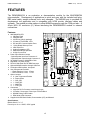
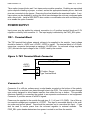
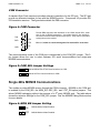
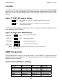
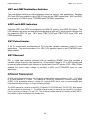
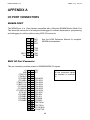
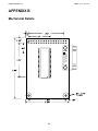
DEMO908AP64
Demonstration Module for Freescale 68HC908AP64
! Axiom Manufacturing • 2813 Industrial Lane • Garland, TX 75041
Email: [email protected] Web: http://www.axman.com !
D E M O 9 0 8 A P 6 4
J U N E
2 8 ,
2 0 0 4
CONTENTS
CAUTIONARY NOTES.............................................................................................................................3
TERMINOLOGY ...................................................................................................................................3
FEATURES...............................................................................................................................................4
REFERENCE DOCUMENTATION.......................................................................................................5
GETTING STARTED ................................................................................................................................5
RUN MODE ..........................................................................................................................................5
MON08 DEBUG MODE........................................................................................................................6
SOFTWARE DEVELOPMENT .............................................................................................................7
MEMORY MAP.........................................................................................................................................7
OPERATION.............................................................................................................................................7
POWER SUPPLY.................................................................................................................................8
TB1 – Terminal Block.......................................................................................................................8
Figure 1: TB1 Terminal Block Connector.........................................................................................8
Connector J1....................................................................................................................................8
PWR_SEL Jumper...........................................................................................................................9
Figure 2: PWR_SEL Jumper Settings..............................................................................................9
RESET SWITCH ..................................................................................................................................9
TIMING ...............................................................................................................................................10
Figure 3: OSC_SEL Jumper Settings ............................................................................................10
RS-232 COMMUNICATIONS.............................................................................................................10
Table 2: COM Connections............................................................................................................10
COM Connector .............................................................................................................................11
Figure 4: COM Connector..............................................................................................................11
Figure 5: COM_SEL Jumper Settings............................................................................................11
SINGLE-WIRE MON08 COMMUNICATIONS ....................................................................................11
Figure 6: MON_EN Jumper Setting ...............................................................................................11
VTST_EN.......................................................................................................................................12
Figure 7: VTST_EN Jumper Setting ..............................................................................................12
Figure 8: Single-Wire MON08 Setup .............................................................................................12
USER COMPONENTS.......................................................................................................................12
Table 3: User EN Option Settings..................................................................................................12
SW1 and SW2 Pushbutton Switches.............................................................................................13
LED1 and LED2 Indicators ............................................................................................................13
RV1 Potentiometer.........................................................................................................................13
RZ1 Photocell ................................................................................................................................13
INFRARED TRANSCEIVER...............................................................................................................13
APPENDIX A ..........................................................................................................................................14
I/O PORT CONNECTORS .................................................................................................................14
MON08 PORT................................................................................................................................14
MCU I/O Port Connector................................................................................................................14
APPENDIX B ..........................................................................................................................................15
MECHANICAL DETAILS ....................................................................................................................15
APPENDIX C ..........................................................................................................................................16
BILL OF MATERIALS.........................................................................................................................16
2
D E M O 9 0 8 A P 6 4
J U N E
2 8 ,
2 0 0 4
CAUTIONARY NOTES
1) Electrostatic Discharge (ESD) prevention measures should be used when handling this
product. ESD damage is not a warranty repair item.
2) Axiom Manufacturing does not assume any liability arising out of the application or use of
any product or circuit described herein; neither does it convey any license under patent
rights or the rights of others.
3) EMC Information on the DEMO908AP64 module:
a) This product as shipped from the factory with associated power supplies and cables, has
been verified to meet with requirements the FCC as a CLASS A product.
b) This product is designed and intended for use as a development platform for hardware
or software in an educational or professional laboratory.
c) In a domestic environment, this product may cause radio interference in which case the
user may be required to take adequate prevention measures.
d) Attaching additional wiring to this product or modifying the products operation from the
factory default as shipped may effect its performance and cause interference with other
apparatus in the immediate vicinity. If such interference is detected, suitable mitigating
measures should be taken.
TERMINOLOGY
This development module uses option selection jumpers. A jumper is a plastic shunt that connects 2 terminals electrically. Terminology for application of the option jumpers is as follows:
Jumper on, in, or installed - jumper is installed such that 2 pins are connected together.
Jumper off, out, or idle - jumper is installed on 1 pin only. It is recommended that jumpers be idled by installing on 1 pin so they will not be lost.
Cut-Trace – a circuit trace connection between component pads. The circuit trace may
be cut using a knife to break the default connection. To reconnect the circuit, simply install a suitably sized 0-ohm resistor or attach a wire across the pads.
3
D E M O 9 0 8 A P 6 4
J U N E
2 8 ,
2 0 0 4
FEATURES
The DEMO908AP64 is an evaluation or demonstration module for the 68HC908AP64
microcontroller. Development of applications is quick and easy with the included wall plug,
DB9 serial cable, sample software tools, and examples. The MON08 port is provided for
development tool application and is compatible with HC08 monitor interface cables and
software. The module provides options to allow MON08 access through the COM port also. A
40-pin MCU I/O connector (J1) allows interfacing the DEMO908AP64 module to external
connections.
Features:
♦
♦
♦
♦
♦
♦
♦
♦
♦
♦
♦
68HC908AP64 CPU
♦ 60K Byte Flash
♦ 2K Bytes Ram
♦ 40 I/O lines (44-pin package)
♦ 2 Channel Timer/PWM, 16 bit
♦ SCI and SPI Communications Ports
♦ 12 Key Board Wake-up Ports
♦ IrDA Serial Port
♦ Analog Comparator, R/R
♦ 8Mhz Internal Bus Operation
♦ 8 High Current Pins
Power Input Selection Jumper
- Optional power input from Connector J1
- Optional power output through Connector J1
32.768KHz Crystal or 9.8304MHz Clock
Regulated +5V power supply
RS-232 COM Serial Port w/ DB9 Connector
Optional MON08 Interface through COM Port
Full-duplex IrDA Interface, low speed
User Components Provided
- 3 Push Switches; 2 User, 1 Reset
- 3 LED Indicators; 2 User, 1 +3.3V
Option Jumpers
♦ 6 - User Component Enables
♦ 2 - Power Select
♦ 1 - OSC_SEL
♦ 1 - COM_SEL
♦ 1 - MON_EN
♦ 1 - VTST_EN
Connectors
♦ 40-pin MCU I/O Connector, stack through type
♦ 2-Position, Screw-type, Power Input Terminal Block
♦ MON08 Debug Cable Header
♦ DB9 Serial COM Connector
Supplied with DB9 Serial Cable, Documentation (CD), and Manual.
Specifications:
Module Size 2.2” x 3.1”
Power Input: +6 to +16VDC, 9VDC typical
4
D E M O 9 0 8 A P 6 4
J U N E
2 8 ,
2 0 0 4
Reference Documentation
Reference documents are provided on the support CD in Acrobat Reader format.
DEMO908AP64_SCH_C.pdf
DEMO908AP64_UG.pdf
MC68HC908AP64/D.pdf
DEMO908AP64 Module Schematic Rev. C
DEMO908AP64 User Guide (this document)
68HC908AP64 Device User Guide
See the HC08 Support CD provided with this board for all the documentation and support files
provided.
GETTING STARTED
The DEMO908AP64 Module operates in two basic Modes, Run Mode or MON08 Debug Mode.
Run Mode supports user application operation from Power On or Reset condition. MON08
Debug Mode supports the development and debug of applications via the MON08 embedded
debug monitor. See the related sections below for quickly starting the module in the desired
operation mode.
The Module may be operating a Demonstration (DEMO) program when shipped from the
factory. If so the Module kit contents will include a Quick Start document explaining the
operation of the Demonstration program. The demo program operates in RUN Mode.
No matter the operating mode, the module must be powered to operate. The +5V power
indicator will only light with the module regulator powered by the input Term Block (TB1) and
the PWR_SEL option being properly configured to power the module circuits from the on-board
regulator or from the VX supply and ground connections on the J1 MCU I/O connector. Refer
to the PWR_SEL option and J1 connector chapter for more detail on these selections.
RUN MODE
RUN Mode operates the HC08 application contained in the internal flash memory from Reset
or Power On condition. Use the following settings to configure the DEMO908AP64 module for
RUN Mode to get started quickly.
1. Configure PWR_SEL option for input supply to power the module. If supply is via J1 connection, install module on J1 external connection in powered down condition.
2. Connect COM port serial communication cable between module and host if needed for the
application. Launch supporting host software to for the module communication.
5
D E M O 9 0 8 A P 6 4
J U N E
2 8 ,
2 0 0 4
3. Set module options for RUN Mode:
VTST_EN
MON_EN
COM_EN
OSC_SEL
USER_EN
Off / open / idle
Off/ open / idle
2-3 (COM position)
As needed for application operation, 32Khz Crystal
or 9.8304Mhz Clock
Enabled as needed for application operation
4. Power On the Module. Application will begin to execute.
MON08 DEBUG MODE
MON08 Debug Mode operates the HC08 internal MON08 debug monitor from Power On. This
mode is possible by setting Module options or by applying a supporting development cable on
the Debug Port. For Debug cable application the MON_EN option must be Off / open / idle
and the OSC_EN option should be set according to the debug cable requirements (open or
clock selected). Use the following settings to configure the DEMO908AP64 module for MON08
Debug Mode via the COM port:
1. Configure PWR_SEL option for input supply to power the module. If supply is via J1 connection, install module on J1 external connection in powered down condition. Note that the
VTST_EN option requires 9VDC minimum applied at TB1 to function correctly.
2. Connect one end of the supplied 9-pin serial cable to a free COM port on the PC. Connect
the other end of the cable to the COM port connector on the DEMO908AP64 module.
3. Install and launch the PC Hosting software for the MON08 communication interface. This
may be a C compiler with IDE and MON08 communication or another MON08 debug hosting type software.
4. Set the Module options for MON08 Debug Mode:
VTST_EN
MON_EN
COM_EN
OSC_SEL
USER_EN
ON / Installed on both pins (required if the Reset
vector is not erased in the flash memory)
ON / Installed on both pins
1-2 (DEBUG position)
1-2 (9.8304Mhz Clock position)
Enabled as needed for application operation
5. Apply power to the module. This may be applied by TB1, J1, or Debug cable operation.
6. Hosting development software will establish MON08 communication now.
6
D E M O 9 0 8 A P 6 4
J U N E
2 8 ,
2 0 0 4
Software Development
Software development will require the use of an HC08 assembler or compiler and a host PC
operating a MON08 debug interface. Supplied with this board is the Motorola MCUez HC08
assembler tools along with the Axiom MON08 IDE for Windows for Debugging and Flash programming. A demonstration or evaluation copy of a C compiler may also be provided.
A powerful source code generation tool called DriveWay™ is also provided on the support CD.
This can generate C source code for the HC08 microcontroller peripherals, based on setup.
See the DriveWayTM readme.txt file for more information.
MEMORY MAP
0x0000 0x005F
Direct Page Register Space.
See the 908AP64 User Manual for details
96
bytes
0x0060 0x085F
SRAM Memory space
Stack and Data Memory
2K
bytes
0x 0860 0xFBFF
Flash Memory
User application memory
61K
bytes
0xFC00 –
0xFFCF
Utility Memory
Status, Control, MON08 ROM
975
bytes
0xFFD0 0xFFFF
Vectors and Security Memory
47
bytes
NOTE: The memory map above generally describes the MCU Memory Map. Refer to the
MC68HC908AP64 documentation for a detailed memory map.
OPERATION
The DEMO908AP64 module provides input and output features to assist in microcontroller application development. The user has access to MCU ports through connector J1. Connector
J1 is a 40-position pass-through socket type connector mounted on the bottom of the module.
Insertion of pin headers is possible from the top or bottom of the module. This allows stacking
or connecting the module as needed. Connector J1 may be used to apply power to the module as well as RS-232 communications signals. Care must be exercised when using the
MCU_PORT to power the module, as only regulated +5V DC should be applied to this connection. The PWR_SEL option also configures the module to provide regulated +5V to an external
device attached to connector J1.
7
D E M O 9 0 8 A P 6 4
J U N E
2 8 ,
2 0 0 4
Three option jumper blocks and 3 cut-traces setup module operation. Enabling an associated
option requires installing a jumper, or shunt, across the appropriate header pins so that both
pins are connected via the jumper. Removing the shunt disables the associated option. A cuttrace option can be disabled by cutting the circuit trace between the cut-trace component pads
with a razor knife. Install a 0805 SMT 0-ohm resistor or modification wire with a soldering iron
to re-enable the option if needed.
POWER SUPPLY
Input power may be applied by external connection to a 2 position terminal block and 3.3V
regulator or directly from connector J1. The input supply is selected by the PWR_SEL option.
TB1 – Terminal Block
The TB1 terminal block allows external voltage to be supplied to the module. Input voltage
should be limited to +5VDC and +16VDC; +9VDC is typical. The terminal block is a 3.55mm,
screw-type, connector that accepts a maximum 18 AWG wire. An on-board voltage regulator
(VR1) converts the input voltage to the +3.3VDC used by the module.
Figure 1: TB1 Terminal Block Connector
+5VDC +16VDC
GND
MCU_PORT
J1
+
2 Position, ScrewType Terminal Block
Connector J1
Connector J1 is a 40-pin, surface-mount, socket header mounted on the bottom of the module.
The connector is mounted over plated-through holes in the PCB. The socket is a pass-through
type socket designed to allow header insertion from either the top or bottom. This provides
maximum flexibility in connecting the module to an expansion environment or test equipment.
Connector J1 provides access to all MCU signals.
Power may be supplied to the module through pins J1-1 (+V) and J1-3 (GND). Use of this option requires voltage input regulated at +3.3VDC. This input is connected directly to the module power and ground planes. Care should be exercised not to over-drive this input. J1 can
also be used to source power from the on-board regulator to external modules. The
PWR_SEL option header determines how power is routed to and from the module.
8
D E M O 9 0 8 A P 6 4
J U N E
2 8 ,
2 0 0 4
NOTE: Power output from the module is limited by the 250 mA maximum output
of the on-board voltage regulator.
PWR_SEL Jumper
The PWR_SEL jumper selects the source of power input to the module, or allows regulated
+3.3VDC to be provided to J1 for use by external circuits. The module takes voltage input
from the 2-position on-board voltage regulator or from the 40-pin MCU connector (J1). Power
input at the terminal block must be DC voltage between +5VDC and +16VDC. Power input on
the MCU connector must be regulated voltage between +3.0VDC and +3.3VDC. The
MCU_PORT connector power input allows use of batteries, or other alternate sources, to
power the module.
CAUTION: Module damage may occur if the MCU_PORT power input pin (J1-1)
is over-driven.
The PWR_SEL option jumper provides 3 possible configurations; source power from the PWR
connector, source power from J1, or source power from PWR and supply power to J1. The
figures below show the settings for each configuration.
Figure 2: PWR_SEL Jumper Settings
1
2
• •
• •
Module powered from external +3.0VDC - +3.3VDC input connected to J1-1 (+) and J1-3 (-)
1
2
• •
• •
Module powered from external +5VDC - +16VDC connected to
TB1 Terminal Block. J1-1 is open or not connected.
1
2
• •
• •
Module powered from external +5VDC - +16VDC connected to
TB1 Terminal Block. Module provides +3.3VDC output (up to 50
mA) at pin J1 for use by external circuits.
NOTE: Power output from the module is limited by the 250 mA maximum output of the on-board voltage regulator.
Reset Switch
The RESET switch provides a method to apply an asynchronous reset to the module. Pressing the RESET switch applies a low voltage level to the RST* input. A resistor tied to the high
voltage rail prevents spurious RESET input to the MCU. A capacitor tied to ground holds the
signal line low for a sufficient amount of time.
9
D E M O 9 0 8 A P 6 4
J U N E
2 8 ,
2 0 0 4
Timing
The DEMO908AP64 provides two timing sources. A 9.8304 MHz clock oscillator, at X1, supports debug monitor operation. A 32.768 kHz crystal oscillator at Y1 provides the base operating frequency to the MCU for normal operation. The user should refer to the HC08 device
user manual for information on frequency selection. The OSC_SEL jumper selects the timing
input source.
Figure 3: OSC_SEL Jumper Settings
3 Selects X1 Timing Input – 9.8304 MHz
1
Selects Y1 Timing Input – 32.768 kHz
RS-232 Communications
The DEMO908AP64 module provides a single SCI communications port. This port is connected to the MCU_PORT connector and to the COM connector. An RS-232 translator (U3)
provides RS-232 signal level to TTL/CMOS logic level translation on the COM port. Signals
TXD and RXD are routed between the transceiver and the MCU. These signals are also
routed to connector J1. RS-232 communication signals input on J1 must be TTL/CMOS logic
levels; no translation support is provided through this path. The transceiver output may also
be driven off-module if a suitably interface is used. As added development support, hardware
flow control signals RTS and CTS are available on the logic side of U3. These signals are
routed to vias located near the transceiver (U3). RTS has been biased properly to support 2wire RS-232 communications.
Use of the J1 connector to input RS-232 signals requires disabling the on-board RS-232 transceiver to prevent signal corruption. Disabling the on-board transceiver is accomplished by removing the COM_SEL jumper. Details on the COM_SEL jumper are shown in the table below.
Table 2: COM Connections
HC08 Port
COM Signal
PTB2/TXD
PTB3/RXD
TXD OUT
RXD IN
I/O
PORT
Connector
J1-5
J1-7
10
D E M O 9 0 8 A P 6 4
J U N E
2 8 ,
2 0 0 4
COM Connector
A standard 9-pin Dsub connector provides external connections for the SCI port. The SCI port
provide an alternate interface for use with the MON08 monitor. Component U3 provides RS232 translation services. The figure below details the DB9 connector.
Figure 4: COM Connector
7
RTS
Female DB9 connector that interfaces to the HC08 internal SCI1 serial
port via the U2 RS232 transceiver. It provides simple 2 wire asynchronous serial communications without flow control. Flow control is provided
at test points on the module.
8
CTS
Pins 1, 4, and 6 are connected together for status NULL to the host.
9
NC
1
6
TXD
2
RXD
3
4
GND
5
The communications mode of the COM port is determined by the COM_SEL jumper. This 3pin jumper allows the user to select between SCI serial communications and single-wire
MON08 communications.
Figure 5: COM_SEL Jumper Settings
3 Selects MON08 Port PTA0 Communications on COM
Selects SCI Port Communications on COM
1
Single-Wire MON08 Communications
The module provides MON08 access through the COM connector. MON08 on the COM port
is enabled by the COM_SEL, the MON_EN, OSC_SEL, and VTST_EN option jumpers. This
allows MON08 debugging without the expense of a 3rd-party MON08 pod. The table above
shows the selection settings for the COM_SEL jumper. See the MON08 Debug Mode section
for more details.
Figure 6: MON_EN Jumper Setting
ON
1 2 OFF
MON08 Monitor Mode Enabled
MON08 Monitor Mode Disabled
11
D E M O 9 0 8 A P 6 4
J U N E
2 8 ,
2 0 0 4
VTST_EN
The VTST _EN jumper enables the voltage level necessary to place the MCU in MON08
monitor mode. An 8.2V zener diode at D1 sets the appropriate voltage level on the MCU IRQ*
signal line. When using the MON08 monitor mode, the input voltage on TB1 must be 9VDC
minimum.
Figure 7: VTST_EN Jumper Setting
IRQ* signal line set to 8.2V. MON08 monitor mode force entry
enabled.
ON
1 2 OFF
IRQ* signal line pulled up to VDD. MON08 monitor mode available
if Reset vector is erased.
The following table details the settings necessary to configure the MCU for MON08 monitor
mode operation via the COM port.
Figure 8: Single-Wire MON08 Setup
MON_EN
ON
Single-Wire MON08 Enabled
VTST_EN
ON
MCU in Monitor Mode
COM_SEL
3
MON08 Signaling Enabled
OSC_SEL
3
9.8304 MHz Oscillator selected
NOTE: To utilize the single-wire MON08 monitor mode, the input voltage must
exceed 9.0VDC.
USER Components
The DEMO908AP64 provides 2 user push switches, 2 LED indicators, a potentiometer, and
photocell circuit for user application. To isolate assigned I/O ports from these features, the
USER EN option is provided.
Table 3: User EN Option Settings
Jumper
User 1
User 2
User 3
User 4
User 5
User 6
On
Enable SW1
Enable SW2
Enable LED1
Enable LED2
Enable RV1
Enable RZ1
Off
Disable SW1
Disable SW2
Disable LED1
Disable LED2
Disable RV1
Disable RZ1
12
MCU PORT
PTD0 (U1-3)
PTD1 (U1-2)
PTB4 (U1-13)
PTB5 (U1-8)
PTA4 (U1-29)
PTA5 (U1-28)
D E M O 9 0 8 A P 6 4
J U N E
2 8 ,
2 0 0 4
SW1 and SW2 Pushbutton Switches
Two push button switches provide momentary active low input for user applications. Switches
SW1 and SW2 are enabled to the HC08 I/O ports by the USER option bank. SW1 and SW2
provide input to HC08 I/O ports PTD0/KBI0 and PTD1/KBI1 respectively.
LED1 and LED2 Indicators
Indicators LED1 and LED2 are enabled from HC08 I/O ports by the USER EN option. The
LED indicators are active low and will illuminate when a logic low (0 value) signal is driven from
the respective MCU I/O port. MCU ports PTB4/T1CH0 and PTB5/T1CH1 drive LED1 and
LED2 respectively.
RV1 Potentiometer
A 5k Ω, thumb-wheel potentiometer at RV1 provides variable resistance output for user
applications. The device provides a 0 to VDD (+5V typically) output to the PTA4/ADC4 input
when enabled.
RZ1 Photocell
RZ1 is visible light sensitive photocell with an amplifying OPAMP circuit that provides a
variable voltage output for user applications. Circuit output voltage of .5V to VDD typically and
is inversely proportional to light intensity on the surface of the RZ1 device (VDD = Dark). When
enabled the circuit output voltage is provided to MCU port PTA5/ADC5 input for user
application.
Infrared Transceiver
A IRDA serial infrared transceiver at U4 supports infrared serial communications of 2.4K – 115.2 Kbps
to a typical distance of 1 meter. The transceiver (ZHX1010) combines an infrared emitting diode
(IRED), a PIN photodiode detector, a digital AC coupled IRLED driver, and a receiver/decoder with
noise discrimination circuitry in a single, miniature package.
The IRDA transceiver connects to the MCU I/O signals PTC7/SCRXD and PTC6/SCTXD. Both signals
are also available at connector J1. The IRDA transceiver may be removed from the MCU I/O connections by opening cut-traces CT2 and CT3. The cut-traces maybe restored by installing a 0805 SMT 0ohm resistor or wire modification with a solder iron.
13
D E M O 9 0 8 A P 6 4
J U N E
2 8 ,
2 0 0 4
APPENDIX A
I/O PORT CONNECTORS
MON08 PORT
The MON08 port is a 16-pin header compatible with a Motorola MON08 Monitor Mode Pod.
This allows the connection of a background debugger for software development, programming,
and debugging in real-time without using HC08 I/O resources.
1
3
5
7
9
11
OSC1 13
VDD 15
2
4
6
8
10
12
14
16
GND
RST*
IRQ1*
See the HC08 Reference Manual for complete
MON08 documentation
PTA0
PTA2
PTA1
PTB0
MCU I/O Port Connector
This port connector provides access to DEMO908AP64 I/O signals.
VX
GND
PTB2/TXD
PTB3/RXD
PTD0/KBI0
PTD1/KBI1
PTB4/T1CH0
PTB5/T1CH1
PTC3/MOSI
PTC2/MISO
PTC5/SPSCK
PTC6/SS*
PTD1/KBI2
PTD3/KBI3
PTD4/KBI4
PTD5/KBI5
1
3
5
7
9
11
13
15
17
19
21
23
25
27
29
31
33
35
37
39
2
4
6
8
10
12
14
16
18
20
22
24
26
28
30
32
34
36
38
40
IRQ1*
RST*
Note:
All user component signals
are available at connector
J1
PTA0/ADC0
PTA1/ADC1
PTA2/ADC2
PTA3/ADC3
PTA4/ADC4
PTA5/ADC5
PTA6/ADC6
PTA7/ADC7
PTB0/SDA
PTB1/SCL
PTD6/KBI6
PTD7/KBI7
PTB6/T2CH0
PTB7/T2CH1
PTC7/SCRXD
PTC6/SCTXD
14
D E M O 9 0 8 A P 6 4
J U N E
APPENDIX B
Mechanical Details
15
2 8 ,
2 0 0 4
D E M O 9 0 8 A P 6 4
J U N E
2 8 ,
2 0 0 4
APPENDIX C
BILL OF MATERIALS
Item
1
2
3
4
5
6
7
8
9
Qty
3
5
4
3
1
2
1
1
1
10
11
12
13
14
15
16
17
3
1
1
1
3
6
2
2
19
1
20
1
Title
Reference
Cap, Elec, 10uF, 10V, Tant, SMA
C2, C9, C12
Cap, Mon, .1uF, 50V, 0805
C1, C5, C8, C10, C11
Cap, Mon, 1uF, 16V, 0805
C3, C4, C6, C7
Res, Carbon, 330 ohm, 1/16W, 5%, 0805
R4, R5, R7
Res, Carbon, 4.7K ohm, 5%, 0805
R2
Res, Carbon, 10K ohm, 5%, 0805
R3, R6
Res, Carbon, 1M ohm, 5%, 1/16w, 0805
R1
Resonator, Cer, 16.00MHz, w/Caps, 3Pos, SMT
Y1
Diode, Schottky, 30V, 200mA, BAT54C, Com. D1
Cathode, SOT23
LED, Green, w/reflector, 1206, SMT
LED1, LED2, +3.3V
IC, Dual RS232 XCVR, 3.3V, 16SOIC
U2
IC, MCU, 68HC908AP64, 44LQFP
U1
VReg, LDO, 3.3V, 250mA, 8 SOIC
VR1
Sw, PB, 5mm Sq, Thru
SW1, SW2, RESET
Hdw, Shunt, 2 Pos, .1"
Hdw, Hex Standoff, 4-40 Thd, .375", Al
Hdw, Screw, 4-40, 1/4", Pan Head, SS, Captive
Washer
Conn, 2x20 Socket Hdr, Pass Thru, .1", Bottom En- J1
try, SMT
Conn, Term Blk, 2Pos, 3.55mm, thru
TB1
21
22
23
24
25
1
1
1
1
1
Conn, Dsub, 9P, F, RA, PCB Mount
Conn, 1x3 Pin Header, .1" Ctr, Thru
Conn, 2x3 Pin Header, .1" Ctr, Thru
Conn, 2x4 Pin Header, .1" Ctr, Thru
PCB, 68HC908AP64DEMO Module
SCI1
PWR_SEL
BDM_PORT
USER
16
Mfr Name
Kemet
Meritek
Mfr P/N
T491A106K010
MA080525U104M500
Panasonic
EFO-BM1605E5
General Semiconductor
Rohm
SML-010MTT86
Intersil
ICL3232ECBN
Motorola
MC9S08G60
STM
L4931CD33
E-Switch
EG1827
Generic
Keystone
2202
Samtec
SSM-120-L-DV-K-BE-A
On Shore Tech- ED555/2DS
nology


![[DRAFT] DEMO908JL16 User`s Manual](http://vs1.manualzilla.com/store/data/005639706_1-2a84cd2ce2f0b318fdb7aae7896f2a79-150x150.png)