1
MELSEC iQ-R High-Speed Counter Module
User's Manual (Application)
-RD62P2
-RD62P2E
-RD62D2
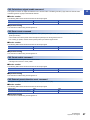
SAFETY PRECAUTIONS
(Read these precautions before using this product.)
Before using this product, please read this manual and the relevant manuals carefully and pay full attention to safety to handle
the product correctly.
The precautions given in this manual are concerned with this product only. For the safety precautions of the programmable
controller system, refer to the MELSEC iQ-R Module Configuration Manual.
In this manual, the safety precautions are classified into two levels: "
WARNING" and "
CAUTION".
WARNING
Indicates that incorrect handling may cause hazardous conditions, resulting in
death or severe injury.
CAUTION
Indicates that incorrect handling may cause hazardous conditions, resulting in
minor or moderate injury or property damage.
Under some circumstances, failure to observe the precautions given under "
CAUTION" may lead to serious
consequences.
Observe the precautions of both levels because they are important for personal and system safety.
Make sure that the end users read this manual and then keep the manual in a safe place for future reference.
1
[Design Precautions]
WARNING
● Configure safety circuits external to the programmable controller to ensure that the entire system
operates safely even when a fault occurs in the external power supply or the programmable controller.
Failure to do so may result in an accident due to an incorrect output or malfunction.
(1) Emergency stop circuits, protection circuits, and protective interlock circuits for conflicting
operations (such as forward/reverse rotations or upper/lower limit positioning) must be configured
external to the programmable controller.
(2) When the programmable controller detects an abnormal condition, it stops the operation and all
outputs are:
• Turned off if the overcurrent or overvoltage protection of the power supply module is activated.
• Held or turned off according to the parameter setting if the self-diagnostic function of the CPU
module detects an error such as a watchdog timer error.
(3) All outputs may be turned on if an error occurs in a part, such as an I/O control part, where the
CPU module cannot detect any error. To ensure safety operation in such a case, provide a safety
mechanism or a fail-safe circuit external to the programmable controller. For a fail-safe circuit
example, refer to "General Safety Requirements" in the MELSEC iQ-R Module Configuration
Manual.
(4) Outputs may remain on or off due to a failure of a component such as a relay and transistor in an
output circuit. Configure an external circuit for monitoring output signals that could cause a
serious accident.
● In an output circuit, when a load current exceeding the rated current or an overcurrent caused by a
load short-circuit flows for a long time, it may cause smoke and fire. To prevent this, configure an
external safety circuit, such as a fuse.
● Configure a circuit so that the programmable controller is turned on first and then the external power
supply. If the external power supply is turned on first, an accident may occur due to an incorrect output
or malfunction.
● For the operating status of each station after a communication failure, refer to manuals relevant to the
network. Incorrect output or malfunction due to a communication failure may result in an accident.
● When connecting an external device with a CPU module or intelligent function module to modify data
of a running programmable controller, configure an interlock circuit in the program to ensure that the
entire system will always operate safely. For other forms of control (such as program modification,
parameter change, forced output, or operating status change) of a running programmable controller,
read the relevant manuals carefully and ensure that the operation is safe before proceeding. Improper
operation may damage machines or cause accidents.
2
[Design Precautions]
WARNING
● Especially, when a remote programmable controller is controlled by an external device, immediate
action cannot be taken if a problem occurs in the programmable controller due to a communication
failure. To prevent this, configure an interlock circuit in the program, and determine corrective actions
to be taken between the external device and CPU module in case of a communication failure.
● Do not write any data to the "system area" and "write-protect area" of the buffer memory in the
module. Also, do not use any "use prohibited" signals as an output signal from the CPU module to
each module. Doing so may cause malfunction of the programmable controller system. For the
"system area", "write-protect area", and the "use prohibited" signals, refer to the user's manual for the
module used.
● If a communication cable is disconnected, the network may be unstable, resulting in a communication
failure of multiple stations. Configure an interlock circuit in the program to ensure that the entire
system will always operate safely even if communications fail. Failure to do so may result in an
accident due to an incorrect output or malfunction.
● To maintain the safety of the programmable controller system against unauthorized access from
external devices via the network, take appropriate measures. To maintain the safety against
unauthorized access via the Internet, take measures such as installing a firewall.
● Outputs may remain on or off due to a failure of a transistor for external output. Configure an external
circuit for monitoring output signals that could cause a serious accident.
[Design Precautions]
CAUTION
● During control of an inductive load such as a lamp, heater, or solenoid valve, a large current
(approximately ten times greater than normal) may flow when the output is turned from off to on.
Therefore, use a module that has a sufficient current rating.
● After the CPU module is powered on or is reset, the time taken to enter the RUN status varies
depending on the system configuration, parameter settings, and/or program size. Design circuits so
that the entire system will always operate safely, regardless of the time.
● Do not power off the programmable controller or reset the CPU module while the setting values in the
buffer memory are being written. Doing so will make the data in the flash ROM undefined. The values
need to be set in the buffer memory and written to the flash ROM again. Doing so also can cause
malfunction or failure of the module.
● When changing the operating status of the CPU module from external devices (such as the remote
RUN/STOP functions), select "Do Not OPEN in Program" for "Open Method Setting" in the module
parameters. If "OPEN in Program" is selected, an execution of the remote STOP function causes the
communication line to close. Consequently, the CPU module cannot reopen the line, and external
devices cannot execute the remote RUN function.
● Do not install the control lines or communication cables together with the main circuit lines or power
cables. Keep a distance of 150mm or more between them. Failure to do so may result in malfunction
due to noise.
3
[Installation Precautions]
WARNING
● Shut off the external power supply (all phases) used in the system before mounting or removing the
module. Failure to do so may result in electric shock or cause the module to fail or malfunction.
[Installation Precautions]
CAUTION
● Use the programmable controller in an environment that meets the general specifications in the Safety
Guidelines included with the base unit. Failure to do so may result in electric shock, fire, malfunction,
or damage to or deterioration of the product.
● To mount a module, place the concave part(s) located at the bottom onto the guide(s) of the base unit,
and push in the module until the hook(s) located at the top snaps into place. Incorrect interconnection
may cause malfunction, failure, or drop of the module.
● When using the programmable controller in an environment of frequent vibrations, fix the module with
a screw.
● Tighten the screws within the specified torque range. Undertightening can cause drop of the screw,
short circuit, or malfunction. Overtightening can damage the screw and/or module, resulting in drop,
short circuit, or malfunction.
● When using an extension cable, connect it to the extension cable connector of the base unit securely.
Check the connection for looseness. Poor contact may cause malfunction.
● When using an SD memory card, fully insert it into the SD memory card slot. Check that it is inserted
completely. Poor contact may cause malfunction.
● Securely insert an extended SRAM cassette into the cassette connector of the CPU module. After
insertion, close the cassette cover and check that the cassette is inserted completely. Poor contact
may cause malfunction.
● Do not directly touch any conductive parts and electronic components of the module, SD memory
card, extended SRAM cassette, or connector. Doing so can cause malfunction or failure of the
module.
[Wiring Precautions]
WARNING
● Shut off the external power supply (all phases) used in the system before installation and wiring.
Failure to do so may result in electric shock or cause the module to fail or malfunction.
● After installation and wiring, attach the included terminal cover to the module before turning it on for
operation. Failure to do so may result in electric shock.
4
[Wiring Precautions]
CAUTION
● Individually ground the FG and LG terminals of the programmable controller with a ground resistance
of 100 ohms or less. Failure to do so may result in electric shock or malfunction.
● Use applicable solderless terminals and tighten them within the specified torque range. If any spade
solderless terminal is used, it may be disconnected when the terminal screw comes loose, resulting in
failure.
● Check the rated voltage and signal layout before wiring to the module, and connect the cables
correctly. Connecting a power supply with a different voltage rating or incorrect wiring may cause fire
or failure.
● Connectors for external devices must be crimped or pressed with the tool specified by the
manufacturer, or must be correctly soldered. Incomplete connections may cause short circuit, fire, or
malfunction.
● Securely connect the connector to the module. Poor contact may cause malfunction.
● Do not install the control lines or communication cables together with the main circuit lines or power
cables. Keep a distance of 100mm or more between them. Failure to do so may result in malfunction
due to noise.
● Place the cables in a duct or clamp them. If not, dangling cable may swing or inadvertently be pulled,
resulting in damage to the module or cables or malfunction due to poor contact. Do not clamp the
extension cables with the jacket stripped.
● Check the interface type and correctly connect the cable. Incorrect wiring (connecting the cable to an
incorrect interface) may cause failure of the module and external device.
● Tighten the terminal screws or connector screws within the specified torque range. Undertightening
can cause drop of the screw, short circuit, fire, or malfunction. Overtightening can damage the screw
and/or module, resulting in drop, short circuit, fire, or malfunction.
● When disconnecting the cable from the module, do not pull the cable by the cable part. For the cable
with connector, hold the connector part of the cable. For the cable connected to the terminal block,
loosen the terminal screw. Pulling the cable connected to the module may result in malfunction or
damage to the module or cable.
● Prevent foreign matter such as dust or wire chips from entering the module. Such foreign matter can
cause a fire, failure, or malfunction.
● A protective film is attached to the top of the module to prevent foreign matter, such as wire chips,
from entering the module during wiring. Do not remove the film during wiring. Remove it for heat
dissipation before system operation.
● Programmable controllers must be installed in control panels. Connect the main power supply to the
power supply module in the control panel through a relay terminal block. Wiring and replacement of a
power supply module must be performed by qualified maintenance personnel with knowledge of
protection against electric shock. For wiring, refer to the MELSEC iQ-R Module Configuration Manual.
● For Ethernet cables to be used in the system, select the ones that meet the specifications in the user's
manual for the module used. If not, normal data transmission is not guaranteed.
● Do not install the control lines or communication cables together with the main circuit lines or power
cables. Keep a distance of 150mm or more between them. Failure to do so may result in malfunction
due to noise.
● Ground the shield cable on the encoder side (relay box) with a ground resistance of 100 ohm or less.
Failure to do so may cause malfunction.
5
[Startup and Maintenance Precautions]
WARNING
● Do not touch any terminal while power is on. Doing so will cause electric shock or malfunction.
● Correctly connect the battery connector. Do not charge, disassemble, heat, short-circuit, solder, or
throw the battery into the fire. Also, do not expose it to liquid or strong shock. Doing so will cause the
battery to produce heat, explode, ignite, or leak, resulting in injury and fire.
● Shut off the external power supply (all phases) used in the system before cleaning the module or
retightening the terminal screws, connector screws, or module fixing screws. Failure to do so may
result in electric shock.
[Startup and Maintenance Precautions]
CAUTION
● When connecting an external device with a CPU module or intelligent function module to modify data
of a running programmable controller, configure an interlock circuit in the program to ensure that the
entire system will always operate safely. For other forms of control (such as program modification,
parameter change, forced output, or operating status change) of a running programmable controller,
read the relevant manuals carefully and ensure that the operation is safe before proceeding. Improper
operation may damage machines or cause accidents.
● Especially, when a remote programmable controller is controlled by an external device, immediate
action cannot be taken if a problem occurs in the programmable controller due to a communication
failure. To prevent this, configure an interlock circuit in the program, and determine corrective actions
to be taken between the external device and CPU module in case of a communication failure.
● Do not disassemble or modify the modules. Doing so may cause failure, malfunction, injury, or a fire.
● Use any radio communication device such as a cellular phone or PHS (Personal Handy-phone
System) more than 25cm away in all directions from the programmable controller. Failure to do so
may cause malfunction.
● Shut off the external power supply (all phases) used in the system before mounting or removing the
module. Failure to do so may cause the module to fail or malfunction.
● Tighten the screws within the specified torque range. Undertightening can cause drop of the
component or wire, short circuit, or malfunction. Overtightening can damage the screw and/or module,
resulting in drop, short circuit, or malfunction.
● After the first use of the product, do not mount/remove the module to/from the base unit, and the
terminal block to/from the module, and do not insert/remove the extended SRAM cassette to/from the
CPU module more than 50 times (IEC 61131-2 compliant) respectively. Exceeding the limit may cause
malfunction.
● After the first use of the product, do not insert/remove the SD memory card to/from the CPU module
more than 500 times. Exceeding the limit may cause malfunction.
● Do not touch the metal terminals on the back side of the SD memory card. Doing so may cause
malfunction or failure of the module.
● Do not touch the integrated circuits on the circuit board of an extended SRAM cassette. Doing so may
cause malfunction or failure of the module.
● Do not drop or apply shock to the battery to be installed in the module. Doing so may damage the
battery, causing the battery fluid to leak inside the battery. If the battery is dropped or any shock is
applied to it, dispose of it without using.
6
[Startup and Maintenance Precautions]
CAUTION
● Startup and maintenance of a control panel must be performed by qualified maintenance personnel
with knowledge of protection against electric shock. Lock the control panel so that only qualified
maintenance personnel can operate it.
● Before handling the module, touch a conducting object such as a grounded metal to discharge the
static electricity from the human body. Failure to do so may cause the module to fail or malfunction.
[Operating Precautions]
CAUTION
● When changing data and operating status, and modifying program of the running programmable
controller from an external device such as a personal computer connected to an intelligent function
module, read relevant manuals carefully and ensure the safety before operation. Incorrect change or
modification may cause system malfunction, damage to the machines, or accidents.
● Do not power off the programmable controller or reset the CPU module while the setting values in the
buffer memory are being written to the flash ROM in the module. Doing so will make the data in the
flash ROM undefined. The values need to be set in the buffer memory and written to the flash ROM
again. Doing so can cause malfunction or failure of the module.
[Disposal Precautions]
CAUTION
● When disposing of this product, treat it as industrial waste.
● When disposing of batteries, separate them from other wastes according to the local regulations. For
details on battery regulations in EU member states, refer to the MELSEC iQ-R Module Configuration
Manual.
[Transportation Precautions]
CAUTION
● When transporting lithium batteries, follow the transportation regulations. For details on the regulated
models, refer to the MELSEC iQ-R Module Configuration Manual.
● The halogens (such as fluorine, chlorine, bromine, and iodine), which are contained in a fumigant
used for disinfection and pest control of wood packaging materials, may cause failure of the product.
Prevent the entry of fumigant residues into the product or consider other methods (such as heat
treatment) instead of fumigation. The disinfection and pest control measures must be applied to
unprocessed raw wood.
7
CONDITIONS OF USE FOR THE PRODUCT
(1) Mitsubishi programmable controller ("the PRODUCT") shall be used in conditions;
i) where any problem, fault or failure occurring in the PRODUCT, if any, shall not lead to any major or serious accident;
and
ii) where the backup and fail-safe function are systematically or automatically provided outside of the PRODUCT for the
case of any problem, fault or failure occurring in the PRODUCT.
(2) The PRODUCT has been designed and manufactured for the purpose of being used in general industries.
MITSUBISHI SHALL HAVE NO RESPONSIBILITY OR LIABILITY (INCLUDING, BUT NOT LIMITED TO ANY AND ALL
RESPONSIBILITY OR LIABILITY BASED ON CONTRACT, WARRANTY, TORT, PRODUCT LIABILITY) FOR ANY
INJURY OR DEATH TO PERSONS OR LOSS OR DAMAGE TO PROPERTY CAUSED BY the PRODUCT THAT ARE
OPERATED OR USED IN APPLICATION NOT INTENDED OR EXCLUDED BY INSTRUCTIONS, PRECAUTIONS, OR
WARNING CONTAINED IN MITSUBISHI'S USER, INSTRUCTION AND/OR SAFETY MANUALS, TECHNICAL
BULLETINS AND GUIDELINES FOR the PRODUCT.
("Prohibited Application")
Prohibited Applications include, but not limited to, the use of the PRODUCT in;
• Nuclear Power Plants and any other power plants operated by Power companies, and/or any other cases in which the
public could be affected if any problem or fault occurs in the PRODUCT.
• Railway companies or Public service purposes, and/or any other cases in which establishment of a special quality
assurance system is required by the Purchaser or End User.
• Aircraft or Aerospace, Medical applications, Train equipment, transport equipment such as Elevator and Escalator,
Incineration and Fuel devices, Vehicles, Manned transportation, Equipment for Recreation and Amusement, and
Safety devices, handling of Nuclear or Hazardous Materials or Chemicals, Mining and Drilling, and/or other
applications where there is a significant risk of injury to the public or property.
Notwithstanding the above, restrictions Mitsubishi may in its sole discretion, authorize use of the PRODUCT in one or
more of the Prohibited Applications, provided that the usage of the PRODUCT is limited only for the specific
applications agreed to by Mitsubishi and provided further that no special quality assurance or fail-safe, redundant or
other safety features which exceed the general specifications of the PRODUCTs are required. For details, please
contact the Mitsubishi representative in your region.
INTRODUCTION
Thank you for purchasing the Mitsubishi MELSEC iQ-R series programmable controllers.
This manual describes the functions, parameter settings, and troubleshooting of the relevant products listed below.
Before using this product, please read this manual and the relevant manuals carefully and develop familiarity with the
functions and performance of the MELSEC iQ-R series programmable controller to handle the product correctly.
When applying the program examples provided in this manual to an actual system, ensure the applicability and confirm that it
will not cause system control problems.
Please make sure that the end users read this manual.
Relevant products
RD62P2, RD62P2E, RD62D2
8
MEMO
9
CONTENTS
SAFETY PRECAUTIONS . . . . . . . . . . . . . . . . . . . . . . . . . . . . . . . . . . . . . . . . . . . . . . . . . . . . . . . . . . . . . . . . . . . .1
CONDITIONS OF USE FOR THE PRODUCT . . . . . . . . . . . . . . . . . . . . . . . . . . . . . . . . . . . . . . . . . . . . . . . . . . . .8
INTRODUCTION . . . . . . . . . . . . . . . . . . . . . . . . . . . . . . . . . . . . . . . . . . . . . . . . . . . . . . . . . . . . . . . . . . . . . . . . . . .8
RELEVANT MANUALS . . . . . . . . . . . . . . . . . . . . . . . . . . . . . . . . . . . . . . . . . . . . . . . . . . . . . . . . . . . . . . . . . . . . .12
TERMS . . . . . . . . . . . . . . . . . . . . . . . . . . . . . . . . . . . . . . . . . . . . . . . . . . . . . . . . . . . . . . . . . . . . . . . . . . . . . . . . .12
CHAPTER 1
1.1
FUNCTIONS
13
Pulse Input Modes and Counting Methods. . . . . . . . . . . . . . . . . . . . . . . . . . . . . . . . . . . . . . . . . . . . . . . . . . . 13
Types of pulse input modes. . . . . . . . . . . . . . . . . . . . . . . . . . . . . . . . . . . . . . . . . . . . . . . . . . . . . . . . . . . . . . . . . 13
Setting a counting method. . . . . . . . . . . . . . . . . . . . . . . . . . . . . . . . . . . . . . . . . . . . . . . . . . . . . . . . . . . . . . . . . . 16
Reading the present value. . . . . . . . . . . . . . . . . . . . . . . . . . . . . . . . . . . . . . . . . . . . . . . . . . . . . . . . . . . . . . . . . . 16
1.2
Selecting a Counter Type . . . . . . . . . . . . . . . . . . . . . . . . . . . . . . . . . . . . . . . . . . . . . . . . . . . . . . . . . . . . . . . . . 17
Linear counter function . . . . . . . . . . . . . . . . . . . . . . . . . . . . . . . . . . . . . . . . . . . . . . . . . . . . . . . . . . . . . . . . . . . . 17
Ring counter function. . . . . . . . . . . . . . . . . . . . . . . . . . . . . . . . . . . . . . . . . . . . . . . . . . . . . . . . . . . . . . . . . . . . . . 18
1.3
Coincidence Output Function . . . . . . . . . . . . . . . . . . . . . . . . . . . . . . . . . . . . . . . . . . . . . . . . . . . . . . . . . . . . . 20
Coincidence detection interrupt function . . . . . . . . . . . . . . . . . . . . . . . . . . . . . . . . . . . . . . . . . . . . . . . . . . . . . . . 22
1.4
1.5
Preset Function . . . . . . . . . . . . . . . . . . . . . . . . . . . . . . . . . . . . . . . . . . . . . . . . . . . . . . . . . . . . . . . . . . . . . . . . . 23
Counter Function Selection . . . . . . . . . . . . . . . . . . . . . . . . . . . . . . . . . . . . . . . . . . . . . . . . . . . . . . . . . . . . . . . 25
Count error . . . . . . . . . . . . . . . . . . . . . . . . . . . . . . . . . . . . . . . . . . . . . . . . . . . . . . . . . . . . . . . . . . . . . . . . . . . . . 26
Count disable function . . . . . . . . . . . . . . . . . . . . . . . . . . . . . . . . . . . . . . . . . . . . . . . . . . . . . . . . . . . . . . . . . . . . . 27
Latch counter function . . . . . . . . . . . . . . . . . . . . . . . . . . . . . . . . . . . . . . . . . . . . . . . . . . . . . . . . . . . . . . . . . . . . . 28
Sampling counter function . . . . . . . . . . . . . . . . . . . . . . . . . . . . . . . . . . . . . . . . . . . . . . . . . . . . . . . . . . . . . . . . . . 29
Cycle pulse counter function . . . . . . . . . . . . . . . . . . . . . . . . . . . . . . . . . . . . . . . . . . . . . . . . . . . . . . . . . . . . . . . . 30
1.6
Pulse Measurement Function. . . . . . . . . . . . . . . . . . . . . . . . . . . . . . . . . . . . . . . . . . . . . . . . . . . . . . . . . . . . . . 33
1.7
PWM Output Function. . . . . . . . . . . . . . . . . . . . . . . . . . . . . . . . . . . . . . . . . . . . . . . . . . . . . . . . . . . . . . . . . . . . 35
CHAPTER 2
PARAMETER SETTINGS
38
2.1
Parameter Setting Procedure . . . . . . . . . . . . . . . . . . . . . . . . . . . . . . . . . . . . . . . . . . . . . . . . . . . . . . . . . . . . . . 38
2.2
Basic Setting . . . . . . . . . . . . . . . . . . . . . . . . . . . . . . . . . . . . . . . . . . . . . . . . . . . . . . . . . . . . . . . . . . . . . . . . . . . 38
2.3
Application Setting . . . . . . . . . . . . . . . . . . . . . . . . . . . . . . . . . . . . . . . . . . . . . . . . . . . . . . . . . . . . . . . . . . . . . . 40
2.4
Interrupt Setting. . . . . . . . . . . . . . . . . . . . . . . . . . . . . . . . . . . . . . . . . . . . . . . . . . . . . . . . . . . . . . . . . . . . . . . . . 41
2.5
Refresh Setting . . . . . . . . . . . . . . . . . . . . . . . . . . . . . . . . . . . . . . . . . . . . . . . . . . . . . . . . . . . . . . . . . . . . . . . . . 42
2.6
Preset Setting . . . . . . . . . . . . . . . . . . . . . . . . . . . . . . . . . . . . . . . . . . . . . . . . . . . . . . . . . . . . . . . . . . . . . . . . . . 45
Refresh processing time . . . . . . . . . . . . . . . . . . . . . . . . . . . . . . . . . . . . . . . . . . . . . . . . . . . . . . . . . . . . . . . . . . . 44
CHAPTER 3
TROUBLESHOOTING
46
3.1
Procedure for Troubleshooting . . . . . . . . . . . . . . . . . . . . . . . . . . . . . . . . . . . . . . . . . . . . . . . . . . . . . . . . . . . . 46
3.2
Checking Module Status . . . . . . . . . . . . . . . . . . . . . . . . . . . . . . . . . . . . . . . . . . . . . . . . . . . . . . . . . . . . . . . . . . 46
3.3
Troubleshooting by Symptom . . . . . . . . . . . . . . . . . . . . . . . . . . . . . . . . . . . . . . . . . . . . . . . . . . . . . . . . . . . . . 47
When the count operation does not start. . . . . . . . . . . . . . . . . . . . . . . . . . . . . . . . . . . . . . . . . . . . . . . . . . . . . . . 47
When the count operation is not normal . . . . . . . . . . . . . . . . . . . . . . . . . . . . . . . . . . . . . . . . . . . . . . . . . . . . . . . 47
When the coincidence output function does not operate normally . . . . . . . . . . . . . . . . . . . . . . . . . . . . . . . . . . . 48
When a coincidence detection interrupt does not occur . . . . . . . . . . . . . . . . . . . . . . . . . . . . . . . . . . . . . . . . . . . 48
When the preset cannot be executed . . . . . . . . . . . . . . . . . . . . . . . . . . . . . . . . . . . . . . . . . . . . . . . . . . . . . . . . . 48
When the pulse measurement does not start . . . . . . . . . . . . . . . . . . . . . . . . . . . . . . . . . . . . . . . . . . . . . . . . . . . 48
When the pulses are not measured correctly . . . . . . . . . . . . . . . . . . . . . . . . . . . . . . . . . . . . . . . . . . . . . . . . . . . 49
When the PWM output is not correct. . . . . . . . . . . . . . . . . . . . . . . . . . . . . . . . . . . . . . . . . . . . . . . . . . . . . . . . . . 49
When the inter-module synchronization function does not operate correctly . . . . . . . . . . . . . . . . . . . . . . . . . . . 49
10
Pulse waveform shaping method . . . . . . . . . . . . . . . . . . . . . . . . . . . . . . . . . . . . . . . . . . . . . . . . . . . . . . . . . . . . 50
APPENDICES
51
Appendix 1 Module Label . . . . . . . . . . . . . . . . . . . . . . . . . . . . . . . . . . . . . . . . . . . . . . . . . . . . . . . . . . . . . . . . . . . . . . 51
Appendix 2 I/O Signals . . . . . . . . . . . . . . . . . . . . . . . . . . . . . . . . . . . . . . . . . . . . . . . . . . . . . . . . . . . . . . . . . . . . . . . . 53
List of I/O signals . . . . . . . . . . . . . . . . . . . . . . . . . . . . . . . . . . . . . . . . . . . . . . . . . . . . . . . . . . . . . . . . . . . . . . . . . 53
Input signals . . . . . . . . . . . . . . . . . . . . . . . . . . . . . . . . . . . . . . . . . . . . . . . . . . . . . . . . . . . . . . . . . . . . . . . . . . . . 54
Output signals . . . . . . . . . . . . . . . . . . . . . . . . . . . . . . . . . . . . . . . . . . . . . . . . . . . . . . . . . . . . . . . . . . . . . . . . . . . 56
List of buffer memory addresses . . . . . . . . . . . . . . . . . . . . . . . . . . . . . . . . . . . . . . . . . . . . . . . . . . . . . . . . . . . . . 59
Details of buffer memory addresses . . . . . . . . . . . . . . . . . . . . . . . . . . . . . . . . . . . . . . . . . . . . . . . . . . . . . . . . . . 61
Appendix 4 Added or Changed Functions. . . . . . . . . . . . . . . . . . . . . . . . . . . . . . . . . . . . . . . . . . . . . . . . . . . . . . . . . 68
INDEX
70
REVISIONS . . . . . . . . . . . . . . . . . . . . . . . . . . . . . . . . . . . . . . . . . . . . . . . . . . . . . . . . . . . . . . . . . . . . . . . . . . . . . .72
CONTENTS
Appendix 3 Buffer Memory Areas. . . . . . . . . . . . . . . . . . . . . . . . . . . . . . . . . . . . . . . . . . . . . . . . . . . . . . . . . . . . . . . . 59
WARRANTY . . . . . . . . . . . . . . . . . . . . . . . . . . . . . . . . . . . . . . . . . . . . . . . . . . . . . . . . . . . . . . . . . . . . . . . . . . . . .73
TRADEMARKS . . . . . . . . . . . . . . . . . . . . . . . . . . . . . . . . . . . . . . . . . . . . . . . . . . . . . . . . . . . . . . . . . . . . . . . . . . .74
11
RELEVANT MANUALS
Manual name [manual number]
Description
Available form
MELSEC iQ-R High-Speed Counter Module User's Manual
(Application)
[SH-081241ENG] (this manual)
Functions, parameter settings, troubleshooting, I/O
signals, and buffer memory of the high-speed counter
module
Print book
MELSEC iQ-R High-Speed Counter Module User's Manual
(Startup)
[SH-081239ENG]
Performance specifications, procedures before
operation, wiring, and operation examples of the highspeed counter module
Print book
e-Manual
EPUB
PDF
e-Manual
EPUB
PDF
e-Manual refers to the Mitsubishi FA electronic book manuals that can be browsed using a dedicated tool.
e-Manual has the following features:
• Required information can be cross-searched in multiple manuals.
• Other manuals can be accessed from the links in the manual.
• The hardware specifications of each part can be found from the product figures.
• Pages that users often browse can be bookmarked.
TERMS
Unless otherwise specified, this manual uses the following terms.
12
Term
Description
GX Works3
The product name of the software package for the MELSEC programmable controllers
Engineering tool
Another term for GX Works3
Global label
A label that is valid for all the program data when multiple program data are created in the project.
The global label has two types: a module specific label (module label), which is generated
automatically by GX Works3, and an optional label, which can be created for any specified
device.
High-speed counter module
The abbreviation for the MELSEC iQ-R series high-speed counter module
Buffer memory
A memory in an intelligent module for storing data (such as setting values and monitored values)
to be transferred to the CPU module
Module label
A label that represents one of memory areas (I/O signals and buffer memory areas) specific to
each module in a given character string. For the module used, GX Works3 automatically
generates this label, which can be used as a global label.
1
FUNCTIONS
1
This chapter describes the functions for the high-speed counter module and the setting methods. For details on I/O signals
and buffer memory areas, refer to the following.
• Page 54 Input signals
• Page 56 Output signals
• Page 61 Details of buffer memory addresses
This chapter describes the I/O numbers (X/Y), buffer memory addresses, and external I/O terminals for CH1.
To check the I/O numbers (X/Y) for CH2, refer to the following.
Page 53 List of I/O signals
To check the buffer memory addresses for CH2, refer to the following.
Page 59 List of buffer memory addresses
1.1
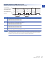
Pulse Input Modes and Counting Methods
This section describes the pulse input modes and the counting methods.
Types of pulse input modes
The following six pulse input modes are prepared: 1-phase pulse input (1 multiple/2 multiples), CW/CCW pulse input, and 2phase pulse input (1 multiple/2 multiples/4 multiples).
Pulse input modes and count timing
Pulse input mode
Count timing
1-phase multiple of 1
For counting up
φA
Counts on the rising edge () of A.
B and CH1 Down count command (Y3) are off.
φB and
CH1 Down
count command
(Y3)
For counting down
φA
Counts on the falling edge () of A.
B or CH1 Down count command (Y3) is on.
φB or
CH1 Down
count command
(Y3)
1-phase multiple of 2
For counting up
φA
φB and
CH1 Down
count command
(Y3)
For counting down
φA
φB or
CH1 Down
count command
(Y3)
CW/CCW
For counting up
φA
Counts on the rising edge () and the falling edge
() of A.
B and CH1 Down count command (Y3) are off.
Counts on the rising edge () and the falling edge
() of A.
B or CH1 Down count command (Y3) is on.
Counts on the rising edge () of A.
B is off.
φB
For counting down
φA
A is off.
Counts on the rising edge () of B.
φB
1 FUNCTIONS
1.1 Pulse Input Modes and Counting Methods
13
Pulse input mode
Count timing
2-phase multiple of 1
For counting up
Counts on the rising edge () of A while B is off.
φA
φB
Counts on the falling edge () of A while B is off.
For counting down
φA
φB
2-phase multiple of 2
For counting up
φA
Counts on the rising edge () of A while B is off.
Counts on the falling edge () of A while B is on.
φB
For counting down
φA
Counts on the rising edge () of A while B is on.
Counts on the falling edge () of A while B is off.
φB
2-phase multiple of 4
For counting up
φA
φB
For counting down
φA
φB
Counts on the rising edge () of A while B is off.
Counts on the falling edge () of A while B is on.
Counts on the rising edge () of B while A is on.
Counts on the falling edge () of B while A is off.
Counts on the rising edge () of A while B is on.
Counts on the falling edge () of A while B is off.
Counts on the rising edge () of B while A is off.
Counts on the falling edge () of B while A is on.
For the 1-phase pulse input and counting up pulses, check that the B phase pulse input and CH1 Down count
command (Y3) are off before performing the A phase pulse input. If at least one of the B phase pulse input
and CH1 Down count command (Y3) is on, pulses are counted down in the A phase pulse input.
14
1 FUNCTIONS
1.1 Pulse Input Modes and Counting Methods
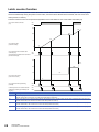
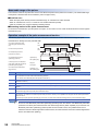
■1-phase pulse input
The count method can be selected from 1 multiple and 2 multiples. The following figure shows the relationship between the A
1
phase pulse input and B phase pulse input or CH1 Down count command (Y3).
High-speed counter module
Encoder
Pulse input
φA
φB
φB or CH1 Down count command
(Y3)
■CW/CCW pulse input
Pulses can be counted up with the A phase pulse input and counted down with the B phase pulse input. The following figure
shows the relationship between the A phase pulse input and B phase pulse input.
High-speed counter module
Count-up pulse input
Encoder
Count-down pulse input
Encoder
φA
φB
■2-phase pulse input
The count method can be selected from 1 multiple, 2 multiples, and 4 multiples. The phase difference between the A phase
pulse and B phase pulse determines whether the pulses are counted up or down. The following figure shows the relationship
between the A phase pulse input and B phase pulse input.
High-speed counter module
Phase A pulse input
φA
Encoder
Phase B pulse input
φB
1 FUNCTIONS
1.1 Pulse Input Modes and Counting Methods
15
Setting a counting method
Set a counting method in "Basic setting" For details on the setting method, refer to the following.
Page 38 Basic Setting
Reading the present value
This section describes the details on the present value stored in the buffer memory and the count values selected from the
counter function selection, and their reading method.
When the refresh setting is used
By configuring the refresh setting, writing and reading data can be performed without creating a communication program for
the high-speed counter module. For details on the setting method, refer to the following.
Page 42 Refresh Setting
When the refresh setting is not used
■Storage location of the count value
The present value is always stored in CH1 Present value (Un\G2 to Un\G3) regardless of the counter function used.
When the latch counter function, sampling counter function, or cycle pulse counter function is performed, the counter function
selection count value is stored in the corresponding buffer memory addresses listed in the following table besides CH1
Present value (Un\G2 to Un\G3).
Description
Buffer memory
address
Present value
Un\G2 to Un\G3
Counter function selection count value
Latch count
value
Sampling count
value
Cycle pulse
count previous
value
Cycle pulse
count current
value
Cycle pulse
count difference
value
Un\G12 to Un\G13
Un\G14 to Un\G15
Un\G16 to Un\G17
Un\G18 to Un\G19
Un\G24 to Un\G27
■Stored data
The present value and the counter function selection count values are stored in the buffer memory in 32-bit signed binary.
However, only the cycle pulse count difference value is stored in the buffer memory in 64-bit signed binary. The values in the
buffer memory are automatically updated depending on the count operation.
16
1 FUNCTIONS
1.1 Pulse Input Modes and Counting Methods
1.2
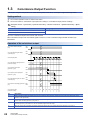
Selecting a Counter Type
1
Select a counter type in "Counter type" of "Basic setting".
Setting method
1.
2.
Set "Counter operation mode" to "Pulse count mode".
Set "Counter type" to "Linear counter" or "Ring counter".
Navigation window [Parameter] [Module Information] Module model name [Module Parameter] [Basic
setting]
Item
Description
Reference
Linear counter
This function counts pulses between -2147483648 (lower limit value) and 2147483647
(upper limit value). If a count exceeds the range, the overflow is detected.
Page 17 Linear counter function
Ring counter
This function counts pulses repeatedly between the values stored in CH1 Ring counter
lower limit value setting (Un\G20 to Un\G21) and CH1 Ring counter upper limit value
setting (Un\G22 to Un\G23).
Page 18 Ring counter function
Linear counter function
Operation of the linear counter
• This function counts pulses between -2147483648 (lower limit value) and 2147483647 (upper limit value).
• The preset function and coincidence output function can be used with this function.
Present counter value
Overflow
+2147483647
0
Counting down
Counting up
-2147483648
Overflow
Overflow error
• When the counter type is the linear counter, an overflow error occurs if the value in CH1 Present value (Un\G2 to Un\G3)
falls below -2147483648 (lower limit value) at the subtraction or exceeds 2147483647 (upper limit value) at the addition.
• If an overflow error occurs, 1 is stored in CH1 Overflow detection (Un\G8) and the counting operation stops. The present
value does not change from -2147483648 or 2147483647 even if pulses are input.
• The overflow error can be cleared by performing the preset function.
• When the preset function is performed, 0 is stored in CH1 Overflow detection (Un\G8) and the counting operation restarts.
1 FUNCTIONS
1.2 Selecting a Counter Type
17
Ring counter function
Operation of the ring counter
This function repeatedly counts pulses between the values stored in CH1 Ring counter lower limit value setting (Un\G20 to
Un\G21) and CH1 Ring counter upper limit value setting (Un\G22 to Un\G23). When the ring counter function is selected, an
overflow error does not occur. The preset function and coincidence output function can be used with this function.
Present counter value
+2147483647
CH1 Ring counter upper limit (Un\G22 to Un\G23)
0
Counting up
Counting down
CH1 Ring counter lower limit (Un\G20 to Un\G21)
-2147483648
Count range of the ring counter
The count range is determined by the relationship between the ring counter lower limit value or ring counter upper limit value
and the value in CH1 Present value (Un\G2 to Un\G3) when CH1 Count enable command (Y4) is turned on or when the
preset function is performed. Normally, the count range is Ring counter lower limit value Present value Ring counter upper
limit value.
■When the count range is Ring counter lower limit value Present value Ring counter upper
limit value (normally used)
• When pulses are counted up, the ring counter lower limit value is automatically stored in CH1 Present value (Un\G2 to
Un\G3) when the present value reaches the ring counter upper limit value.
• When pulses are counted down, even when the present value reaches the ring counter lower limit value, the ring counter
lower limit value is held as the lower limit, and the value of Ring counter upper limit value - 1 is stored in CH1 Present value
(Un\G2 to Un\G3) at the next count-down pulse input.
Both when pulses are counted up and when pulses are counted down, the ring counter upper limit value is not stored in CH1
Present value (Un\G2 to Un\G3). For example, when the count enable command is valid while the ring counter lower limit
value is 0, the ring counter upper limit value is 2000, and the present value is 500, the count range and the present value will
change as follows.
Ring counter
Ring counter
lower limit value
upper limit value
0
2000
Present value
500
-2147483648
2147483647
Counting range
Present value
500
501
to
Ring counter upper
limit value
(2000)
1998 1999
0
Ring counter
lower limit value
1
2
to
498
The ring counter upper limit value,
2000, is not stored in CH1 Present
value (Un\G2 to Un\G3).
18
1 FUNCTIONS
1.2 Selecting a Counter Type
499
■When the count range is Present value < Ring counter lower limit value or Ring counter upper
limit value < Present value
1
• When pulses are counted up, even when the present value reaches the ring counter lower limit value, the ring counter
lower limit value is held as the lower limit, and the value of Ring counter upper limit value + 1 is stored in CH1 Present value
(Un\G2 to Un\G3) at the next count-up pulse input.
• When pulses are counted down, the ring counter lower limit value is automatically stored in CH1 Present value (Un\G2 to
Un\G3) when the present value reaches the ring counter upper limit value.
Both when pulses are counted up and when pulses are counted down, the ring counter upper limit value is not stored in CH1
Present value (Un\G2 to Un\G3). For example, when the count enable command is valid while the ring counter lower limit
value is 0, the ring counter upper limit value is 2000, and the present value is 3000, the count range and the present value will
change as follows.
Ring counter
lower limit value
Ring counter
upper limit value
0
2000
Present value
3000
-2147483648
2147483647
Counting range
Counting range
Ring counter
upper limit value
Present value
Ring counter
lower limit value
(2000)
3000
3001 to 2147483647 -2147483648 to -2
-1
0
2001
2002
to
2998
2999
The ring counter upper limit
value, 2000, is not stored in CH1
Present value (Un\G2 to Un\G3).
■When the count range is Ring counter lower limit value = Ring counter upper limit value
When this condition is established, a value that can be expressed in 32-bit signed binary (-2147483648 to 2147483647) will
be the count range, regardless or the present value.
• While CH1 Count enable command (Y4) is on, even if CH1 Ring counter lower limit value setting (Un\G20 to
Un\G21) and CH1 Ring counter upper limit value setting (Un\G22 to Un\G23) are changed, the high-speed
counter module does not operate with the changed value. Turn off CH1 Count enable command (Y4) before
changing the ring counter upper limit value or ring counter lower limit value.
• Turn off CH1 Count enable command (Y4) before changing the count range using the preset function.
1 FUNCTIONS
1.2 Selecting a Counter Type
19
1.3
Coincidence Output Function
This function compares the present count value with the preset count value, and outputs a signal when they match.
Setting method
1.
2.
Set "Counter operation mode" to "Pulse count mode".
Set a count value for "Coincidence output point No.1 setting" or "Coincidence output point No.2 setting".
Navigation window [Parameter] [Module Information] Module model name [Module Parameter] [Basic
setting]
Item
Setting range
Coincidence output point No.1
-2147483648 to 2147483647
Coincidence output point No.2
Up to two coincidence outputs can be set for each channel.
When the external output of the coincidence signal is used, turn on CH1 Coincidence signal enable command (Y2)
beforehand.
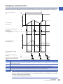
Operation of the coincidence output
CH1 Count enable command
(Y4)
CH1 Coincidence signal enable
command (Y2)
ON
OFF
ON
OFF
Counter input pulse
CH1 Coincidence output point No.1
(Un\G4 to Un\G5)
(1) 100
CH1 Counter value small
(point No.1) (X3)
ON
CH1 Counter value coincidence
(point No.1) (X2)
ON
CH1 Coincidence signal No.1 reset
command (Y0)
OFF
(2)
OFF
(3)
ON
OFF
(4)
ON
CH1 Counter value large (point No.1)
OFF
(X1)
CH1 Present value
(Un\G2 to Un\G3)
20
0
1
2
to
98
99
100 101 102 103
No.
Description
(1)
Write a coincidence output point setting value into CH1 Coincidence output point No.1 setting (Un\G4 to Un\G5) of the high-speed counter
module in 32-bit signed binary.
(2)
When the count value matches with the coincidence output point setting value, CH1 Counter value smaller (point No.1) (X3) turns off and CH1
Counter value coincident (point No.1) (X2) turns on.
(3)
Turn on CH1 Coincidence signal No.1 reset command (Y0) to reset CH1 Counter value coincident (point No.1) (X2). If CH1 Counter value
coincident (point No.1) (X2) remains on, the next coincidence signal cannot be output.
(4)
When the counter value exceeds the coincidence output point setting value, CH1 Counter value larger (point No.1) (X1) turns on.
1 FUNCTIONS
1.3 Coincidence Output Function
Precautions for using the coincidence output function
1
When CH1 Coincidence signal enable command (Y2) is turned on before the count is started or while the coincidence output
point setting value and the current value match, the coincidence output is performed. To avoid this status, perform one of the
following operations before turning on CH1 Coincidence signal enable command (Y2).
■Setting different values to the coincidence output point setting value and the current value
Set different values to the coincidence output point setting value and the current value by one of the following methods.
• Changing the coincidence output point setting value
• Changing the current value using the preset function
• Changing the current value by inputting a pulse
■Turning off the counter value coincidence signal
Turn on and off CH1 Coincidence signal No.1 reset command (Y0).
• Since CH1 Present value (Un\G2 to Un\G3) and CH1 Coincidence output point No.1 (Un\G4 to Un\G5) are
0 after the CPU module is powered on or is reset, CH1 Counter value coincident (point No.1) (X2) turns on.
• When CH1 Coincidence signal enable command (Y2) is turned on while CH1 Counter value coincident
(point No.1) (X2) is on, the coincidence output is performed to outside the module. To avoid an incorrect
coincidence output, turn on and off CH1 Coincidence signal No.1 reset command (Y0) before turning on
CH1 Coincidence signal enable command (Y2), and turn off CH1 Counter value coincident (point No.1)
(X2).
1 FUNCTIONS
1.3 Coincidence Output Function
21
Coincidence detection interrupt function
This function outputs an interrupt request to the CPU module and starts an interrupt program when the present counter value
matches with the preset coincidence output point setting value.
For details on the interrupt program, refer to the following.
MELSEC iQ-R CPU Module User's Manual (Application)
Interrupt factor
The high-speed counter module has interrupt factors of 4 points for each coincidence output point.
Interrupt factor
Turning on CH1 Counter value coincident (point No.1) (X2)
Turning on CH1 Counter value coincident (point No.2) (X6)
Turning on CH2 Counter value coincident (point No.1) (X9)
Turning on CH2 Counter value coincident (point No.2) (XD)
Interrupt program execution timing
CH1 Counter value coincident (point No.1) (X2)
CH1 Counter value coincident (point No.2) (X6)
I/O signals
CH1 Coincidence signal No.1 reset command (Y0)
CH1 Coincidence signal No.2 reset command (Y7)
Internal
processing of
CPU module
Interrupt request
Interrupt request clear
Program in CPU module
Interrupt program
Setting interrupt pointers
Set interrupt pointers in the parameter settings. For details on the setting method, refer to the following.
Page 41 Interrupt Setting
• A coincidence detection interrupt occurs on the rising edge of the counter value coincidence signal (When
the signal is turned off and on). Therefore, the next interrupt will not be requested unless the coincidence
signal is reset and the counter value coincidence signal is turned off.
22
1 FUNCTIONS
1.3 Coincidence Output Function
1.4
Preset Function
1
This function overwrites the present counter value with the set numerical value. The set value is referred to as a preset value.
This function can be used to start counting pulses from the preset value. The function can be performed using a program or
an external control signal.
Setting method
1.
2.
Set "Counter operation mode" to "Pulse count mode".
Set a preset value to "Preset value setting".
Navigation window [Parameter] [Module Information] Module model name [Module Parameter] [Basic
setting]
Item
Setting range
Preset value setting
-2147483648 to 2147483647
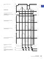
Performing the preset function using a program
Perform the preset function by turning on CH1 Preset command (Y1) using a program.
CH1 Count enable command ON
OFF
(Y4)
Counter input pulse
CH1 Preset value
(Un\G0 to Un\G1)
CH1 Preset command
(Y1)
CH1 Present value
(Un\G2 to Un\G3)
(1)
100
0
(2)
ON
OFF
0
1
2
to
65
66
67
100 101 102 103 104 105
No.
Description
(1)
Write a value into CH1 Preset value setting (Un\G0 to Un\G1) in 32-bit signed binary.
(2)
On the rising edge (off and on) of CH1 Preset command (Y1), the value in CH1 Present value (Un\G2 to Un\G3) is replaced with the value in CH1
Preset value setting (Un\G0 to Un\G1).
The preset function can be performed regardless of the on/off status of CH1 Count enable command (Y4).
1 FUNCTIONS
1.4 Preset Function
23
Performing the preset function using an external control signal
Perform the preset function by applying an ON voltage to the preset input terminal for external input.
CH1 Count enable command ON
(Y4)
OFF
Counter input pulse
(1)
CH1 Preset value
(Un\G0 to Un\G1)
0
100
(2)
Preset command
(preset input terminal)
ON
OFF
CH1 External preset
request detection
(X4)
ON
OFF
CH1 External preset
detection reset command
(Y5)
ON
OFF
CH1 Present value
(Un\G2 to Un\G3)
24
(3)
(2)
(4)
0
1
2
to
65
66
67
100
101 to 130 131 100 101
No.
Description
(1)
Write a value into CH1 Preset value setting (Un\G0 to Un\G1) in 32-bit signed binary.
(2)
On the rising edge (off and on) of the preset command (A voltage is applied to the preset input terminal), the value in CH1 Present value (Un\G2
to Un\G3) is replaced with the value in CH1 Preset value setting (Un\G0 to Un\G1). The preset function can be performed regardless of the on/off
status of CH1 Count enable command (Y4).
(3)
Even though a voltage is applied to the preset input terminal while CH1 External preset request detection (X4) is on, the value in CH1 Present
value (Un\G2 to Un\G3) is not replaced with the preset value.
(4)
CH1 External preset request detection (X4) is turned off by turning on CH1 External preset detection reset command (Y5).
1 FUNCTIONS
1.4 Preset Function
1.5
Counter Function Selection
1
The count disable function, latch counter function, sampling counter function, or cycle pulse counter function can be used by
selecting each item in the counter function selection setting of the "Counter function selection setting". The selected counter
function is performed by the counter function selection start command (when CH1 Counter function selection start command
(Y6) is turned on using a program or a voltage is applied to the function start input terminal).
Only one of the four counter functions can be selected from the counter function selection.
Setting method
1.
2.
Set "Counter operation mode" to "Pulse count mode".
Set the function to be used in "Counter function selection setting".
Navigation window [Parameter] [Module Information] Module model name [Module Parameter] [Application
setting]
Item
Description
Reference
Count disable function
This function stops counting pulses while CH1 Count enable command
(Y4) is on.
Page 27 Count disable function
Latch counter function
This function latches the present counter value when Counter function
selection start command is input.
Page 28 Latch counter function
Sampling counter function
This function counts pulses input during the specified sampling time (T)
and stores the count value in the buffer memory.
Page 29 Sampling counter function
Cycle pulse counter function
This function stores the current value, previous value, and difference
value of the counter in the buffer memory at every specified cycle time
(T).
Page 30 Cycle pulse counter function
• Change the counter function while CH1 Counter function selection start command (Y6) is off.
• The selected counter function can be performed by turning on CH1 Counter function selection start
command (Y6) or applying a voltage to the function start input terminal. A signal that is input first takes
priority.
1 FUNCTIONS
1.5 Counter Function Selection
25
Count error
A count error may occur when the selected counter function is performed using an external input (A voltage is applied to the
function start input terminal) or using a program (CH1 Counter function selection start command (Y6) is turned on). The
following describes how to calculate the count error.
Count error (max.) when an external input is used
Due to a delay in the input response time of the function start input terminal, the following error occurs.
Count error
=
(maximum)
A
[s] × B
1000
A
Function input response time setting [ms] (1ms maximum)
B
Pulse input speed [pps] (= Pulse input frequency [Hz] Multiplication [count])
Count error (max.) when a program is used
Due to a delay in the scan time of the program (Delay of turning on CH1 Counter function selection start command (Y6)), the
following error occurs.
Count error
=
(maximum)
A
[s] × B
1000
A
1 scan time [ms]
B
Pulse input speed [pps] (= Pulse input frequency [Hz] Multiplication [count])
Count error (max.) on the sampling counter function or cycle pulse counter function
A sampling/cycle time error occurs due to an error in design (100ppm) when the sampling counter function or cycle pulse
counter function is performed. The count error is calculated as follows:
Count error
=
(maximum)
26
A
[s] ×
1000
B
×C
1000000
A
Sampling/cycle time [ms]
B
100 [ppm]
C
Pulse input speed [pps] (= Pulse input frequency [Hz] Multiplication [count])
1 FUNCTIONS
1.5 Counter Function Selection
Count disable function
1
This function stops counting pulses while CH1 Count enable command (Y4) is on. The following figure shows the relationship
among CH1 Count enable command (Y4), Counter function selection start command, and the present counter value.
(1)
CH1 Count enable command
(Y4)
ON
CH1 Counter function selection
start command (Y6)
ON
Counter function selection start
command (function start input)
ON
(6)
(8)
OFF
(2)
(3)
(7)
(9)
OFF
(4)
(5)
OFF
Pulses actually input
CH1 Present value
(Un\G2 to Un\G3)
Count value stored in
CH1 Present value
(Un\G2 to Un\G3)
0
Count
stop
Count
stop
Count
stop
Count stop
No.
Description
(1)
The count operation starts when CH1 Count enable command (Y4) is turned on.
(2)
The count operation stops when CH1 Counter function selection start command (Y6) is turned on.
(3)
The count operation restarts when CH1 Counter function selection start command (Y6) is turned off.
(4)
The count operation stops when Counter function selection start command (function start input) is turned on.
(5)
The count operation restarts when Counter function selection start command (function start input) is turned off.
(6)
The count operation stops when CH1 Count enable command (Y4) is turned off.
(7)
The count operation stops regardless of the on/off status of CH1 Counter function selection start command (Y6) because CH1 Count enable
command (Y4) is off.
(8)
Even though CH1 Count enable command (Y4) is turned on, the count operation remains stopped because CH1 Counter function selection start
command (Y6) is on.
(9)
The count operation restarts when CH1 Counter function selection start command (Y6) is turned off.
1 FUNCTIONS
1.5 Counter Function Selection
27
Latch counter function
This function latches the present counter value when Counter function selection start command is input. The following figure
shows the relationship among the present counter value, Counter function selection start command, and CH1 Latch count
value (Un\G12 to Un\G13).
The latch counter function can be performed regardless of the on/off status of CH1 Count enable command (Y4).
CH1 Count enable command
(Y4)
ON
OFF
150
130
100
100
50
50
CH1 Present value
(Un\G2 to Un\G3)
0
0
(1)
CH1 Counter function selection start
command (Y6)
Counter function selection start command
(function start input)
(2)
(3)
(4)
ON
OFF
150
130
100
100
50
50
CH1 Latch count value
(Un\G12 to Un\G13)
0
28
CH1 Counter function update flag
(Un\G28)
ON
0 write request to CH1 Counter function
update flag (Un\G28) (controlled by the
program)
ON
0
OFF
OFF
No.
Description
(1)
On the rising edge of CH1 Counter function selection start command (Y6) or Counter function selection start command (function start input), the
present counter value, 0 is stored in CH1 Latch count value (Un\G12 to Un\G13).
(2)
On the rising edge of CH1 Counter function selection start command (Y6) or Counter function selection start command (function start input), the
present counter value, 50 is stored in CH1 Latch count value (Un\G12 to Un\G13).
(3)
On the rising edge of CH1 Counter function selection start command (Y6) or Counter function selection start command (function start input), the
present counter value, 100 is stored in CH1 Latch count value (Un\G12 to Un\G13).
(4)
On the rising edge of CH1 Counter function selection start command (Y6) or Counter function selection start command (function start input), the
present counter value, 130 is stored in CH1 Latch count value (Un\G12 to Un\G13).
1 FUNCTIONS
1.5 Counter Function Selection
Sampling counter function
1
This function counts pulses input during the specified sampling time (T) and stores the count value in the buffer memory. The
following figure shows the relationship among the signals and buffer memory areas used by the sampling counter function.
(5)
CH1 Count enable command
(Y4)
ON
OFF
200
100
CH1 Present value
(Un\G2 to Un\G3)
0
CH1 Counter function selection start
command (Y6)
Counter function selection start command
(function start input)
(1)
ON
OFF
T
T
T
200
100
(2)
(4)
CH1 Sampling count value
(Un\G14 to Un\G15)
0
-100
(3)
1
CH1 Sampling/cycle counter flag
(Un\G11)
CH1 Counter function update flag
(Un\G28)
0 write request to CH1 Counter function
update flag (Un\G28) (controlled by the
program)
0
ON
OFF
ON
OFF
No.
Description
(1)
Input pulses are counted from 0 on the rising edge of CH1 Counter function selection start command (Y6) or Counter function selection start
command (function start input).
(2)
The count operation stops when the specified sampling time has elapsed.
(3)
While the sampling counter function is performed, 1 is stored in CH1 Sampling/cycle counter flag (Un\G11).
(4)
Even after the sampling counter function is performed, the value stored in CH1 Sampling count value (Un\G14 to Un\G15) is held.
(5)
The sampling counter function can be performed regardless of the on/off status of CH1 Count enable command (Y4).
Set the sampling time by writing the data within the range of 1 to 65535 to CH1 Sampling/cycle time setting
(Un\G10). The unit of time differs depending on the counting speed setting in CH1 Sampling/cycle time setting
(Un\G10). For details, refer to the following.
Page 62 CH1 Sampling/cycle time setting
1 FUNCTIONS
1.5 Counter Function Selection
29
Cycle pulse counter function
This function stores the current value, previous value, and difference value of the counter in the buffer memory at every
specified cycle time (T). The following figure shows the relationship among the signals and buffer memory areas used by the
cycle pulse counter function.
30
1 FUNCTIONS
1.5 Counter Function Selection
CH1 Count enable command
(Y4)
ON
(6)
OFF
1
(2)
200
200
(4)
100
100
CH1 Present value
(Un\G2 to Un\G3)
0
CH1 Counter function selection start
command (Y6)
Counter function selection start command
(function start input)
(5)
80
(3)
20
(1)
0
ON
OFF
T
T
T
T
T
(2)
200
200
CH1 Cycle pulse count current value
(Un\G18 to Un\G19)
(4)
100
100
(5)
80
(3)
20
(1)
0
0
(3)
200
200
(5)
100
CH1 Cycle pulse count previous value
(Un\G16 to Un\G17)
100
(4)
20
(2)
0
0
(2)
200
200
(4)
80
100
CH1 Cycle pulse count difference value
(Un\G24 to Un\G27)
(1)
0
0
(5)
-20
-100
(3)
-180
-200
(7)
CH1 Sampling/cycle counter flag
(Un\G11)
1
0
CH1 Counter function update flag
(Un\G28)
ON
0 write request to CH1 Counter function
update flag (Un\G28) (controlled by the
program)
ON
OFF
OFF
1 FUNCTIONS
1.5 Counter Function Selection
31
No.
Description
(1)
The present counter value, 0 is stored in CH1 Cycle pulse count current value (Un\G18 to Un\G19).
The difference value with the previous value, 0 is stored in CH1 Cycle pulse count difference value (Un\G24 to Un\G27).
(2)
The present counter value, 200 is stored in CH1 Cycle pulse count current value (Un\G18 to Un\G19). The value 0, which has been stored in CH1
Cycle pulse count current value (Un\G18 to Un\G19), is stored in CH1 Cycle pulse count previous value (Un\G16 to Un\G17).
The difference value with the previous value, 200 is stored in CH1 Cycle pulse count difference value (Un\G24 to Un\G27).
(3)
The present counter value, 20 is stored in CH1 Cycle pulse count current value (Un\G18 to Un\G19). The value 200, which has been stored in
CH1 Cycle pulse count current value (Un\G18 to Un\G19), is stored in CH1 Cycle pulse count previous value (Un\G16 to Un\G17).
The difference value with the previous value, -180 is stored in CH1 Cycle pulse count difference value (Un\G24 to Un\G27).
(4)
The present counter value, 100 is stored in CH1 Cycle pulse count current value (Un\G18 to Un\G19). The value 20, which has been stored in
CH1 Cycle pulse count current value (Un\G18 to Un\G19), is stored in CH1 Cycle pulse count previous value (Un\G16 to Un\G17).
The difference value with the previous value, 80 is stored in CH1 Cycle pulse count difference value (Un\G24 to Un\G27).
(5)
The present counter value, 80 is stored in CH1 Cycle pulse count current value (Un\G18 to Un\G19). The value 100, which has been stored in
CH1 Cycle pulse count current value (Un\G18 to Un\G19), is stored in CH1 Cycle pulse count previous value (Un\G16 to Un\G17).
The difference value with the previous value, -20 is stored in CH1 Cycle pulse count difference value (Un\G24 to Un\G27).
(6)
The cycle pulse counter function is performed regardless of the on/off status of CH1 Count enable command (Y4).
(7)
While the cycle pulse counter function is performed, 1 is stored in CH1 Sampling/cycle counter flag (Un\G11).
Set the cycle time by writing the data within the range of 1 to 65535 to CH1 Sampling/cycle time setting
(Un\G10). The unit of time differs depending on the counting speed setting in CH1 Sampling/cycle time setting
(Un\G10). For details, refer to the following.
Page 62 CH1 Sampling/cycle time setting
Precautions for reading the previous value, current value, and difference value
Depending on the relation between the update timing of the previous value or current value in the module and the read timing
of the value using a program, the previous value and current value may match. When the previous value and current value
match, read the values again.
32
1 FUNCTIONS
1.5 Counter Function Selection
1.6
Pulse Measurement Function
1
This mode measures the following times of the pulse input in the function start input terminal.
• ON width
• OFF width
• From the rising edge of the pulse to the rising edge of the next pulse
• From the falling edge of the pulse to the falling edge of the next pulse
When the next pulse is measured, the measured value is written over the previous value.
High-speed counter
module
Buffer memory
Function start input terminal
Analysis
Pulses
CH1 Measured pulse value
(Un\G516 to Un\G517)
Setting method of the pulse measurement function
To use the pulse measurement function, select "Pulse measurement mode" for "Counter operation mode" in the parameter
settings.
Navigation window [Parameter] [Module Information] Module model name [Module Parameter] [Basic
setting]
Terminals for the pulse measurement function
This function measures the pulse input in the function start input terminal.
Measurement target
Set the measurement target by storing a value in CH1 Pulse measurement section setting (Un\G512).
On width
Rising edge to rising edge
Off width
Falling edge to falling edge
Measurement target
Setting value in CH1 Pulse measurement section setting
(Un\G512)
ON width
0
OFF width
1
From the rising edge of the pulse to the rising edge of the next pulse
2
From the falling edge of the pulse to the falling edge of the next pulse
3
Starting and stopping methods of the pulse measurement
The start or stop of the pulse measurement is determined by CH1 Pulse measurement start command (pulse measurement)
(Y6). The pulse measurement starts at the rising edge of the signal and stops at the falling edge of the signal.
1 FUNCTIONS
1.6 Pulse Measurement Function
33
Measurable range of the pulses
The measured values of the pulses are stored in CH1 Measured pulse value (Un\G516 to Un\G517). The measurable range
of the pulses is between 2000 and 2147483647 (0.2ms to approx.214s).
■Overflow error
• When the input pulses are beyond the measurable range, an overflow error will be detected.
• When an overflow error occurs, 1 is stored in CH1 Overflow detection (Un\G8).
• Clear the overflow error using the following restarting method.
■Restarting method of the pulse measurement
To resume the measurement, input the pulses once again, or turn off and on CH1 Pulse measurement start command (pulse
measurement) (Y6).
Operation example of the pulse measurement function
The following figure shows an operation example of the pulse measurement function. Assume that a target for pulse
measurement is already set to the pulse ON width.
CH1 Pulse measurement start
command (pulse measurement)
(Y6)
ON
OFF
Function start input terminal
ON
OFF
CH1 Measured pulse value
(Un\G516 to Un\G517)
(5)
(2)
0
CH1 Measured pulse value
update flag (Un\G515)
Updated (1H)
0 write request to CH1 Measured
pulse value update flag (Un\G515)
(controlled by the program)
Request
No request
CH1 Pulse under-measurement
flag (Un\G514)
(1)
(4)
XXX
YYY
(6)
ZZZ
0
Not updated (0H)
(3)
Operating (1H)
Not operating (0H)
No.
Description
(1)
The following operations are performed when CH1 Pulse measurement start command (pulse measurement) (Y6) is turned off and on. Operating
(1H) is stored in CH1 Pulse under-measurement flag (Un\G514).
• 0 is stored in CH1 Measured pulse value (Un\G516 to Un\G517).
(2)
Updated (1H) is stored in CH1 Measured pulse value update flag (Un\G515) when a measured value is stored in CH1 Measured pulse value
(Un\G516 to Un\G517).
(3)
Not updated (0H) is written in CH1 Measured pulse value update flag (Un\G515).
(4)
Even though Updated (1H) is stored in CH1 Measured pulse value update flag (Un\G515), CH1 Measured pulse value (Un\G516 to Un\G517) is
updated.
(5)
When CH1 Pulse measurement start command (pulse measurement) (Y6) is turned on and off, operation stop (0H) is stored in CH1 Pulse undermeasurement flag (Un\G514) and the pulse measurement stops.
(6)
If the measurement target (Pulse ON width in this example) has been input before Operating (1H) is stored in CH1 Pulse under-measurement
flag (Un\G514), the values in CH1 Measured pulse value (Un\G516 to Un\G517) are not updated even though the function start input terminal is
turned on and off.
Note that only the pulse input after Operating (1H) is stored in CH1 Pulse under-measurement flag (Un\G514) is the measurement target.
Do not use CH1 Measured pulse value update flag (Un\G515) when the values in CH1 Measured pulse value
(Un\G516 to Un\G517) are retrieved via the auto refresh target device. (When Updated (1H) is stored in CH1
Measured pulse value update flag (Un\G515) after the auto refresh is done, the updated values are not
reflected to the auto refresh target device and therefore, the values retrieved via the auto refresh target device
are the ones before the updating.)
34
1 FUNCTIONS
1.6 Pulse Measurement Function
1.7
PWM Output Function
1
This function outputs the PWM waveform of up to 200kHz, 100ns as the minimum ON width (0.1s) from the PWM output
point No.1 terminal (EQU1) and PWM output point No.2 terminal (EQU2).
Buffer memory
CH1 PWM output cycle time setting
(Un\G256 to Un\G257)
High-speed
counter module
Pulse output
PWM output
function
CH1 PWM output ON time setting 1
(Un\G258 to Un\G259)
Coincidence output point No.1 terminal (EQU1)
Pulse output
Coincidence output point No.2 terminal (EQU2)
CH1 PWM output ON time setting 2
(Un\G260 to Un\G261)
Output signal
CH1 PWM output start command
(PWM output) (Y6)
Setting method of the PWM output function
To use the pulse measurement function, select "PWM output mode" for "Counter operation mode" in the parameter settings.
Navigation window [Parameter] [Module Information] Module model name [Module Parameter] [Basic
setting]
PWM output terminal
The PWM output waveform is output from the following terminals.
• PWM output point No.1 terminal (EQU1)
• PWM output point No.2 terminal (EQU2)
1 FUNCTIONS
1.7 PWM Output Function
35
Setting method of the output waveform
Set the output waveform as follows. The setting values shown below can be changed during the output.
CH1 PWM output ON time setting 1
(Un\G258 to Un\G259)
Coincidence output point
No.1
CH1 PWM output cycle time setting
(Un\G256 to Un\G257)
CH1 PWM output ON time setting 2
(Un\G260 to Un\G261)
Coincidence output point
No.2
CH1 PWM output cycle time setting
(Un\G256 to Un\G257)
Setting item
Setting details
CH1 PWM output cycle time setting (Un\G256 to Un\G257)
Set the time of one cycle of the output pulse in the range of 0 to 2147483647.
Set the value in increments of 0.1s.
CH1 PWM output ON time setting 1 (Un\G258 to Un\G259)
• Set the ON time of the output pulse from the PWM output point No.1
terminal (EQU1) in the range of 0 to 2147483647. Set the value in
increments of 0.1s.
• When no pulse is output from the PWM output point No.1 terminal (EQU1),
set 0.
CH1 PWM output ON time setting 2 (Un\G260 to Un\G261)
• Set the ON time of the output pulse from the PWM output point No.2
terminal (EQU2) in the range of 0 to 2147483647. Set the value in
increments of 0.1s.
• When no pulse is output from the PWM output point No.2 terminal (EQU2),
set 0.
The PWM output starts in the OFF status. When PWM output cycle time - PWM output ON time passes, the PWM output is
turned on. The subtraction of PWM output cycle time - PWM output ON time is performed in the high-speed counter module.
When the result of the subtraction is 0, the PWM output is always on, and when the result of the subtraction is a negative
value, the PWM output is always off.
• When a value other than the setting range described above is set in each of CH1 PWM output cycle time
setting (Un\G256 to Un\G257), CH1 PWM output ON time setting 1 (Un\G258 to Un\G259), and CH1 PWM
output ON time setting 2 (Un\G260 to Un\G261), a normal pulse may not be output.
• By using the calculation formula of PWM output ON time = PWM output cycle time Duty ratio (%) 100,
the PWM output ON time can be calculated based on the duty ratio specified by users.
■Setting condition
Set a value that satisfies all the following conditions. Otherwise, the PWM output is always off.
• PWM output cycle time setting > 0
• PWM output ON time setting > 0
• PWM output cycle time setting PWM output ON time setting (When this relation is =, the PWM output is always on.)
36
1 FUNCTIONS
1.7 PWM Output Function
Operation example of the PWM output function
1
The following figure shows an operation example of the PWM output function.
(1)
CH1 PWM output start
command (PWM output) (Y6)
(5)
ON
OFF
(3)
CH1 PWM output cycle time
setting (Un\G256 to Un\G257)
CH1 PWM output ON time
setting 1 (Un\G258 to Un\G259)
ON
OFF
PWM output
1200
1000
600
600
(2)
(4)
PWM output OFF
PWM output ON time setting: 400
PWM output cycle time setting: 1200
PWM output ON time setting: 600
PWM output cycle time setting: 1000
No.
Description
(1)
When CH1 PWM output start command (PWM output) (Y6) is turned off and on, the PWM output starts according to the following setting values.
• CH1 PWM output cycle time setting (Un\G256 to Un\G257)
• CH1 PWM output ON time setting 1 (Un\G258 to Un\G259)
• CH1 PWM output ON time setting 2 (Un\G260 to Un\G261)
(2)
The PWM output is on while CH1 PWM output start command (PWM output) (Y6) is on.
(3)
The following setting values can be changed while the PWM output is on.
• CH1 PWM output cycle time setting (Un\G256 to Un\G257)
• CH1 PWM output ON time setting 1 (Un\G258 to Un\G259)
• CH1 PWM output ON time setting 2 (Un\G260 to Un\G261)
(4)
When the following setting values are changed, the changes are applied from the next output.
• CH1 PWM output cycle time setting (Un\G256 to Un\G257)
• CH1 PWM output ON time setting 1 (Un\G258 to Un\G259)
• CH1 PWM output ON time setting 2 (Un\G260 to Un\G261)
(5)
When CH1 PWM output start command (PWM output) (Y6) is turned on and off while the PWM output is on, the PWM output stops. The PWM
output is off while CH1 PWM output start command (PWM output) (Y6) is off.
The waveform output from the PWM output point No.1 terminal (EQU1) or PWM output point No.2 terminal
(EQU2) is affected by the output circuit or connected device of the high-speed counter module. Check the
waveform by using a device such as a synchroscope, and set the output waveform.
1 FUNCTIONS
1.7 PWM Output Function
37
2
PARAMETER SETTINGS
This chapter describes the parameter settings of the high-speed counter module. Setting parameters here eliminates the
need to program them.
2.1
1.
Parameter Setting Procedure
Add the high-speed counter module to an engineering tool.
Navigation window [Parameter] [Module Information] Right-click [Add New Module]
2.
The basic setting, application setting, interrupt setting, and refresh settings are included in the parameter setting. Select
one of the settings from the tree on the window shown below.
Navigation window [Parameter] [Module Information] Select the high-speed counter module [Module
Parameter]
3.
Write the setting to the CPU module with an engineering tool.
[Online] [Write to PLC]
4.
When the CPU module is reset or is powered off and on, the setting is reflected.
2.2
Basic Setting
Set the parameters for the basic functions of the high-speed counter module.
Item
38
Setting range
Reference
Pulse input mode*1
•
•
•
•
•
•
0: 1-phase multiple of 1 (default value)
1: 1-phase multiple of 2
2: CW/CCW
3: 2-phase multiple of 1
4: 2-phase multiple of 2
5: 2-phase multiple of 4
Counting speed setting*1
•
•
•
•
•
•
•
•
0: 10kpps (default value)
1: 100kpps
2: 200kpps
3: 500kpps (RD62D2 only)
4: 1Mpps (RD62D2 only)
5: 2Mpps (RD62D2 only)
6: 4Mpps (RD62D2 only)
7: 8Mpps (RD62D2 only)
Counter type*1
• 0: Linear counter (default value)
• 1: Ring counter
2 PARAMETER SETTINGS
2.1 Parameter Setting Procedure
Item
Counter operation mode*1
Setting range
• 0: Pulse count mode (default value)
• 1: Pulse measurement mode
• 2: PWM output mode
Reference
Preset value setting
-2147483648 to 2147483647 (default value: 0)
Page 61 CH1 Preset value setting
Coincidence output point No.1
-2147483648 to 2147483647 (default value: 0)
Page 61 CH1 Coincidence output point No.1
setting
Coincidence output point No.2
-2147483648 to 2147483647 (default value: 0)
Page 61 CH1 Coincidence output point No.2
setting
Ring counter upper limit value setting
-2147483648 to 2147483647 (default value: 0)
Page 64 CH1 Ring counter upper limit value setting
Ring counter lower limit value setting
-2147483648 to 2147483647 (default value: 0)
Page 64 CH1 Ring counter lower limit value setting
*1
2
The item can be set only in the parameter setting. It cannot be changed from the program.
2 PARAMETER SETTINGS
2.2 Basic Setting
39
2.3
Application Setting
Set the parameters for the various functions of the high-speed counter module.
Item
Setting range
Counter function selection setting
•
•
•
•
1 to 65535 (default value: 0) 10ms*3
Sampling/cycle time setting
*1
Page 62 CH1 Counter function selection setting
Page 62 CH1 Sampling/cycle time setting
•
•
•
•
0: Response time 0ms
4: Response time 0.1ms (default value)
8: Response time 1ms
10: Response time 10ms
Preset input response time setting*1
•
•
•
•
0: Response time 0ms
4: Response time 0.1ms (default value)
8: Response time 1ms
10: Response time 10ms
Pulse measurement section setting
•
•
•
•
0: ON width (default value)
1: OFF width
2: RiseRise
3: FallFall
Page 66 CH1 Pulse measurement section setting
Function input response time setting
PWM output cycle time setting
0 to 2147483647 (default value: 2147483647)
0.1s
Page 66 CH1 PWM output cycle time setting
PWM output ON time setting 1
0 to 2147483647 (default value: 0) 0.1s
Page 66 CH1 PWM output ON time setting 1
PWM output ON time setting 2
0 to 2147483647 (default value: 0) 0.1s
Output mode upon error*1*2
*1
*2
*3
40
0: Count disable function (default value)
1: Latch counter function
2: Sampling counter function
3: Cycle pulse counter function
Reference
• 0: Clear (default value)
• 1: Hold
Page 66 CH1 PWM output ON time setting 2
The item can be set only in the parameter setting. It cannot be changed from the program.
The external output status (clear/hold) of the high-speed counter module for when a CPU stop error occurs can be set.
If a value larger than 1Mpps is set in "Counting speed setting" when the RD62D2 is used, the unit is changed from 10ms to 1ms.
2 PARAMETER SETTINGS
2.3 Application Setting
2.4
Interrupt Setting
Set the interrupt function of the high-speed counter module.
2
Item
Setting range
Reference
Interrupt pointer
I0 to I15, I50 to I1023*1
Page 22 Coincidence detection interrupt function
*1
For details on the interrupt pointers that can be used, refer to the following.
MELSEC iQ-R CPU Module User's Manual (Application)
2 PARAMETER SETTINGS
2.4 Interrupt Setting
41
2.5
Refresh Setting
Set the transfer destination of the settings in the buffer memory of the high-speed counter module such as module labels and
devices of the CPU module. By configuring the refresh setting, the reading from the program is not required.
Select one of the following transfer destinations in "Target".
• Module Label (Page 42 Module Label)
• Refresh Data Register (Page 42 Refresh data register (RD))
• Device (Page 42 Specified device)
Module Label
The settings of the buffer memory are transferred to the module label corresponding to each buffer memory area. When
"Present value" of the channel transferred to the module label is set to "Enable", all the items of the set channel are set to
"Enable".
Refresh data register (RD)
The settings of the buffer memory are transferred to the refresh data register (RD) of the CPU module. The transfer
destinations of all items are automatically set by setting the start device to "Top Device Name".
Specified device
The settings of the buffer memory are transferred to the specified device of the CPU module. The device X, Y, M, L, B, D, W,
R, ZR, and RD can be specified. When the bit device X, Y, M, L, or B is used, set a number that can be divided by 16 points
(example: X10, Y120, and M16). Also, the buffer memory data is stored in the devices for 16 points starting from the set
device number.
Ex.
When X10 is set, the data is stored in X10 to X1F.
42
2 PARAMETER SETTINGS
2.5 Refresh Setting
Setting item
The following items are provided in the refresh settings.
2
Item
Refresh at the set timing
Reference
Transfer to the CPU
Present value
Page 61 CH1 Present value
Sampling/cycle counter flag
Page 63 CH1 Sampling/cycle counter flag
Counter function update flag
Page 65 CH1 Counter function update flag
Latch count value
Page 63 CH1 Latch count value
Sampling count value
Page 63 CH1 Sampling count value
Cycle pulse count previous value
Page 63 CH1 Cycle pulse count previous
value
Cycle pulse count current value
Page 64 CH1 Cycle pulse count current
value
Cycle pulse count difference value (L)
Page 64 CH1 Cycle pulse count difference
value
Cycle pulse count difference value (H)
Refresh Group
Overflow detection
Page 62 CH1 Overflow detection
Pulse under-measurement flag
Page 67 CH1 Pulse under-measurement
flag
Measured pulse value update flag
Page 67 CH1 Measured pulse value
update flag
Measured pulse value
Page 67 CH1 Measured pulse value
Signal monitor
Page 65 CH1 Signal monitor
Refresh Group
Page 43 Refresh Group
Group [n] (n: 1-64)
Refresh Timing (I/O)*1
Inter-module synchronous
interrupt function
Transfer to the CPU
Refresh Timing (Synchronous Interrupt)*1
*1
Refresh Timing
Synchronization latch count value
Synchronization measured pulse value
Refresh Group
Page 43 Refresh Group
For the high-speed counter module, the default setting cannot be changed.
■Refresh Group
Set the refresh timing of the specified refresh destination.
Setting value
Description
At the Execution Time of END Instruction
The refresh is performed when the END instruction of the CPU module is
executed.
At the Execution Time of Specified Program
The refresh is performed when the program specified in "Group [n]" is executed.
At the Execution Time of Synchronous Interrupt Program between Unit
The refresh is performed when the interrupt program by the interrupt pointer is
executed.
2 PARAMETER SETTINGS
2.5 Refresh Setting
43
Refresh processing time
A refresh processing time [s] is a constituent of the scan time of the CPU module. For details on the scan time, refer to the
following.
MELSEC iQ-R CPU Module User's Manual (Application)
The refresh processing time [s], which is taken for refresh, is given by:
• Refresh processing time [s] = Refresh read time (time for transferring refresh data to the CPU module)
The refresh read time varies depending on the settings of "Target".
With the inter-module synchronization function used, the refresh read time is also added to the execution time of an intermodule synchronous interrupt program.
When "Target" is a module label or a refresh data register (RD)
The following table shows the refresh read time with an RCPU used.
Classification
Refresh read time
When using the refresh settings
When using the inter-module synchronization
function
Set to CH1
only
Set to CH2
only
Set to CH1 and
CH2
Set to CH1
only
Set to CH2
only
Set to CH1 and
CH2
15.07s
15.07s
18.63s
15.63s
15.63s
15.83s
When "Target" is a specified device
Calculate the refresh read time according to the number of items and the number of their transfer data (word) that are set to
be refreshed. For the calculation method, refer to the following.
MELSEC iQ-R CPU Module User's Manual (Application)
In addition, substitute the following values in the calculation formula to calculate the refresh read time.
Item
Description
Number of refresh settings
The number of items that are set to be refreshed
Refresh time (A) of each of the first to nth set items
0.05s per one word of each of the first to nth set items*1
*1
This value is the time with an RCPU used.
Ex.
If all the 28 items (44 words in total) are set in the refresh read settings
28 0.98 + 0.05 44 + 11.6 = 41.24s
The refresh read time, therefore, is 41.24s.
44
2 PARAMETER SETTINGS
2.5 Refresh Setting
2.6
Preset Setting
Execute the preset from "Module Tool List" of the engineering tool.
Setting method
1.
2.
3.
2
Select "iQ-R Series" from "Module Series Selection", and set "Preset".
Select the high-speed counter module to execute the preset in the "Module Selection (Preset)" window.
Execute the preset.
[Tool] [Module Tool List]
Item
Description
Change Preset Value
The preset value of the selected channel is changed. The changed preset value is reflected to the "Preset Value"
column.
Reflect the Preset Value to Current Value
The value of "Preset Value" is reflected to "Current Value".
Accept External Preset Request
When CH1 External preset request detection (X4) is on, the "External Preset Request" column becomes "Detected
(Unacceptable)", and the preset function cannot be executed. When this button is clicked, CH1 External preset
request detection (X4) turns off, and the preset function can be executed.
The preset value changed with "Change Preset Value" returns to the preset value set in the parameter setting
or the one set using a program when the CPU module is reset or is powered off and on. When the preset
value change needs to be held, set the preset value in the parameter setting or using a program.
2 PARAMETER SETTINGS
2.6 Preset Setting
45
3
TROUBLESHOOTING
This chapter describes errors that may occur while using the high-speed counter module, and those troubleshooting.
Throughout the chapter, the I/O numbers (X/Y) and buffer memory addresses are described on the basis of
the case of CH1.
To check them of CH2, refer to the following:
Page 53 List of I/O signals
Page 59 List of buffer memory addresses
3.1
Procedure for Troubleshooting
If a trouble occurs, try the following troubleshooting steps:
1.
Check whether each module is mounted and wired correctly.
( MELSEC iQ-R Module Configuration Manual)
2.
3.
Check the LEDs of the power supply module and CPU module. ( User's Manual of each module)
Check the error cause and corrective action by the symptom to correct the error. ( Page 47 Troubleshooting by
Symptom)
3.2
Checking Module Status
An overflow error can be checked in CH1 Overflow detection (Un\G8).
Error information to be detected by the high-speed counter module
46
Description and cause
Where to check the error information
Action
Overflow error
• In linear counter, an up pulse has been counted
from the present value 2147483647.
• In linear counter, a down pulse has been counted
from the present value -2147483648.
Overflow detection flag
CH1 Overflow detection (Un\G8) stores one of the following
values:
• 0: No overflow
• 1: Overflow occurred
Execute a preset to clear the overflow
error.
3 TROUBLESHOOTING
3.1 Procedure for Troubleshooting
3.3
Troubleshooting by Symptom
When the count operation does not start
Check item
Action
Check whether the CPU module indicates any error.
If the CPU module indicates an error, refer to the troubleshooting in the
following manual.
MELSEC iQ-R CPU Module User's Manual (Application)
Apply a voltage directly to the pulse input terminals of A and B, and check
that each LED of A and B turns on.
If the LEDs turn on, check the external wiring and wiring on the encoder side
to correct the errors. If the LEDs do not turn on, a hardware failure is a likely
cause. Please consult your local Mitsubishi representative.
Check whether the external wiring of A and B is normal.
Check the external wiring to correct the errors.
Check whether CH1 Count enable command (Y4) is on.
Turn on CH1 Count enable command (Y4) using a program.
Check whether the pulse input method is the same as the pulse input mode of
Basic setting.
Match the pulse input method to the pulse input mode of Basic setting.
Check whether the counter operation mode is set to pulse count mode.
Set the counter operation mode to pulse count mode in Basic setting.
Check whether CH1 Counter function selection start command (Y6) is on, and
a voltage is applied to the function start input terminals.
If the count disable function is set by the counter function selection, turn off
CH1 Counter function selection start command (Y6) and the function start
input terminals.
Check whether an overflow error occurs.
Execute a preset to clear the overflow error.
For details, refer to the following.
Page 46 Checking Module Status
3
When the count operation is not normal
Check item
Action
Check whether the external wiring of A and B is normal.
Check the external wiring to correct the errors.
Even in 1-phase input, connecting an ABCOM terminal to a pulse signal can
result in an incorrect count. Reconnect the ABCOM terminal again to an
external power supply (5V/12V/24V) or a GND terminal. ( MELSEC iQ-R
High-Speed Counter Module User's Manual (Startup))
Check whether the maximum counting speed for input pulses falls within the
range of the counting speed of Basic setting.
Correct the counting speed setting of Basic setting to accommodate the
maximum counting speed for input pulses.
Check whether the waveform of pulses being inputted meets the performance
specifications.
Observe and check the pulse waveform with a synchroscope. If the input
pulse does not meet the performance specifications, input pulses which meet
the performance specifications.
Check whether the count value data is processed as 32-bit signed binary data
in the program.
Correct the program to process the count value data in 32-bit signed binary.
Check whether the shielded twisted pair cables are used for pulse input
wiring.
Use the shielded twisted pair cables for pulse input wiring.
Check whether any noise comes from the grounded part of the high-speed
counter module.
Separate the grounding cable of the high-speed counter module from the
grounded part. If the high-speed counter module touches the grounded part,
separate it.
Check whether measures against noise are taken for the adjacent devices
and inside the control panel.
Take noise reduction measures such as attaching a CR surge suppressor to
the magnet switch.
Check whether the distance between the high voltage device and pulse input
line is kept enough.
Bundle the pulse input lines separately from other lines in piping and tubing,
and keep a distance of 150mm or more between the pulse input lines and the
power line even inside the control panel.
Check whether both CH1 and CH2 return the same count value after the
same count is inputted.
If these count values are different each other, a hardware failure is a likely
cause. Please consult your local Mitsubishi representative.
Check whether the preset value is set so that the value is out of the count
range of the ring counter (ring counter function only).
Set the preset value so that the value falls within the count range of the ring
counter.
3 TROUBLESHOOTING
3.3 Troubleshooting by Symptom
47
When the coincidence output function does not operate normally
Check item
Action
Check whether CH1 Coincidence signal No.1 reset command (Y0) and CH1
Coincidence signal No.2 reset command (Y7) turn on.
Turn off CH1 Coincidence signal No.1 reset command (Y0) and CH1
Coincidence signal No.2 reset command (Y7).
Check whether CH1 Coincidence output point No.1 setting (Un\G4, Un\G5)
and CH1 Coincidence output point No.2 setting (Un\G6, Un\G7) are set so
that the values are out of the count range of the ring counter (ring counter
function only).
Set CH1 Coincidence output point No.1 setting (Un\G4, Un\G5) and CH1
Coincidence output point No.2 setting (Un\G6, Un\G7) so that the values fall
within the count range of the ring counter.
Check whether CH1 Coincidence signal enable command (Y2) is on.
Turn on CH1 Coincidence signal enable command (Y2).
Check whether a voltage is applied to the power supply terminal for external
coincidence output.
Apply a voltage to the power supply terminal for external coincidence output.
Check whether the external wiring of the coincidence output point No.1
terminal (EQU1) and coincidence output point No.2 terminal (EQU2) is
normal.
Check the external wiring to correct the errors.
When a coincidence detection interrupt does not occur
Check item
Action
Check whether the intelligent function module interrupt pointer setting of the
PC parameter is incorrect.
Review and correct the intelligent function module interrupt pointer setting.
Check whether the program execution control instruction such as IMASK has
been used incorrectly.
Review and correct the program.
Check whether CH1 Counter value coincident (point No.1) (X2) and CH1
Counter value coincident (point No.2) (X6) still remain on.
Reset (off) CH1 Counter value coincident (point No.1) (X2) and CH1 Counter
value coincident (point No.2) (X6) by using CH1 Coincidence signal No.1
reset command (Y0) and CH1 Coincidence signal No.2 reset command (Y7)
with the point number matched.
When the preset cannot be executed
Check item
Action
Check whether the CPU module indicates any error.
If the CPU module indicates an error, refer to the troubleshooting in the
following manual.
MELSEC iQ-R CPU Module User's Manual (Application)
Check whether CH1 External preset request detection (X4) is on.
Reset (off) CH1 External preset request detection (X4) by using CH1 External
preset detection reset command (Y5).
Check whether the external wiring of the preset input terminal is normal.
Check the external wiring to correct the errors.
When the pulse measurement does not start
48
Check item
Action
Check whether the CPU module indicates any error.
If the CPU module indicates an error, refer to the troubleshooting in the
following manual.
MELSEC iQ-R CPU Module User's Manual (Application)
Check whether the counter operation mode is set to pulse measurement
mode.
Set the counter operation mode to pulse measurement mode in Basic setting.
Check whether CH1 Count enable command (Y4) is on.
Turn on CH1 Count enable command (Y4) using a program.
Check whether the external wiring of the pulse measurement terminal is
normal.
Check the external wiring to correct the errors.
3 TROUBLESHOOTING
3.3 Troubleshooting by Symptom
When the pulses are not measured correctly
Check item
Action
Check whether the shielded twisted pair cables are used for pulse input
wiring.
Use the shielded twisted pair cables for pulse input wiring.
Check whether any noise comes from the grounded part of the high-speed
counter module.
Separate the grounding cable of the high-speed counter module from the
grounded part. If the high-speed counter module touches the grounded part,
separate it.
Check whether measures against noise are taken for the adjacent devices
and inside the control panel.
Take noise reduction measures such as attaching a CR surge suppressor to
the magnet switch.
Check whether the distance between the high voltage device and pulse input
line is kept enough.
Bundle the pulse input lines separately from other lines in piping and tubing,
and keep a distance of 150mm or more between the pulse input lines and the
power line even inside the control panel.
Check whether the section of the pulse to be measured is corresponding to
the pulse measurement section setting
Correct the pulse measurement section setting to suit the section of the pulse
to be measured.
Check whether the program, if used for reading out the measured pulse value,
reads out the value in unit of 2 words (32 bits).
Read out it in unit of 2 words (32 bits).
Check whether the external wiring of the pulse measurement terminal is
normal.
Check the external wiring to correct the errors.
3
When the PWM output is not correct
Check item
Action
Check whether the CPU module indicates any error.
If the CPU module indicates an error, refer to the troubleshooting in the
following manual.
MELSEC iQ-R CPU Module User's Manual (Application)
Check whether the counter operation mode is set to PWM output mode.
Set the counter operation mode to PWM output mode in Basic setting.
Check whether a voltage is applied to the power supply terminal for external
output.
Apply a voltage to the power supply terminal for external output.
Check whether the external wiring of the PWM output point No.1 terminal
(EQU1) and PWM output point No.2 terminal (EQU2) is normal.
Check the external wiring to correct the errors.
Check whether anything other than a resistive load is connected to the PWM
output point No.1 terminal (EQU1) and PWM output point No.2 terminal
(EQU2).
Connect a resistive load because the output waveform is highly distorted by
connecting a load other than a resistive load.
Check whether the shielded twisted pair cables are used for PWM output
wiring.
Use the shielded twisted pair cables for PWM output wiring.
Check whether any noise comes from the grounded part of the high-speed
counter module.
Separate the grounding cable of the high-speed counter module from the
grounded part. If the high-speed counter module touches the grounded part,
separate it.
Check whether measures against noise are taken for the adjacent devices
and inside the control panel.
Take noise reduction measures such as attaching a CR surge suppressor to
the magnet switch.
Check whether the distance between the high voltage device and PWM output
line is kept enough.
Bundle the PWM output lines separately from other lines in piping and tubing,
and keep a distance of 150mm or more between the PWM output lines and
the power line even inside the control panel.
When the inter-module synchronization function does not
operate correctly
Check item
Action
Check whether the high-speed counter module is set as the synchronization
target module in the system parameter setting of GX Works3.
Check "Module Synchronous Status" on the system monitor of GX Works3.
When "Module Synchronous Status" is displayed as "-", the high-speed
counter module is not set as the synchronization target module.
Set the high-speed counter module as the synchronization target module in
the system parameter setting of GX Works3.
Check that the CPU module is in the RUN status.
If the CPU module is not in the RUN status, switch the status to RUN.
Check whether the inter-module synchronous interrupt program exists.
If the inter-module synchronous interrupt program does not exist, add the
program.
Check whether the EI instruction is executed.
Execute the EI instruction.
3 TROUBLESHOOTING
3.3 Troubleshooting by Symptom
49
Pulse waveform shaping method
To shape pulse waveform effectively, increase the load current in cables by inserting a dummy resister of several hundreds
(/several W) between the pulse input terminals connected to a pulse generator. The greater the load current, the more
effective this method is.
The following figure shows an example of the connection of a dummy resistor at signal level 24VDC:
• Connecting a dummy resister at 24VDC
RD62P2, RD62P2E
6.8kΩ
1/3W
Shielded twisted pair cable
24V
A20(A13)
Phase
A
Shield
ABCOM
B19(B12)
6.8kΩ
1/3W
Shielded twisted pair cable
24V
A18(A11)
Phase
B
Shield
Apply a dummy resistance of several hundred ohms
(/several watts) across the pulse input terminals
(between 24V and ABCOM).
Shaping a pulse waveform is effective as a countermeasure against the following two cases.
Distance between the pulse generator and the high-speed counter module is long.
The waveform distortion is corrected and the pulse waveform becomes stable.
Waveform is distorted under a noise environment.
The pulse waveform becomes stable by shaping the waveform, which has an effect on external noise reduction.
The following example describes how to evaluate the resistance constant and rated-power of a dummy
resister. For example, if a load current of approximately 30mA is set, the resistance constant of a dummy
resistor is given by:
R = V I = 24V 30mA = 800
and the voltage applied to a dummy resistor is given by:
P = V I = 24V 30mA = 0.72W
Select a dummy resistor with the rated power of 2W, considering the design margin.
50
3 TROUBLESHOOTING
3.3 Troubleshooting by Symptom
APPENDICES
Appendix 1
A
Module Label
The functions of the high-speed counter module can be set by using module labels.
Module labels of I/O signals
The module label name of an I/O signal is defined with the following structure:
"Module name"_"Module number"."I/O signal"["(Channel)"].b"Label name" or
"Module name"_"Module number"."I/O signal"["(Channel)"].b"Label name"_D
Ex.
RD62_1.stnInputSignal[0].bCoincidenceOutputPoint1CounterValueLarge_D
■Module name
The character string of a module model name is given.
■Module number
A number starting from 1 is added to identify modules that have the same module name.
■I/O signal
The character string that represents an input or output signal is given (Input signal: stnInputSignal, Output signal:
stnOutputSignal). Note that RD62_(x).bReady does not include this string.
■Channel
The channel number corresponding to a module label is given. If the object belongs to CH1, 0 is given. If the object belongs to
CH2, 1 is given.
■Label name
The label identifier unique to a module is given.
■_D
This string indicates that the module label is for the direct access input (DX) or direct access output (DY). A module label
without the string is for the input (X) or output (Y) of the refresh processing.
APPENDICES
Appendix 1 Module Label
51
Module labels of buffer memory areas
The module label name of a buffer memory area is defined with the following structure:
"Module name"_"Module number"."Data type"["(Channel)"]."Data format""Label name" or
"Module name"_"Module number"."Data type"_D["(Channel)"]."Data format""Label name"_D
Ex.
RD62_1.stnBufferBlock0_D[0].dPresetValueSetting_D
■Module name
The character string of a module model name is given.
■Module number
A number starting from 1 is added to identify modules that have the same module name.
■Data type
The data type to sort a buffer memory area is given. Each data type is as follows:
Data type
Description
stnBufferBlock0
Used for pulse count mode.
stnPulseMeasuring
Used for pulse measurement mode.
stnPWM
Used for PWM output mode.
stnSynchronousRefreshArea0
Used for the inter-module synchronization function.
■Channel
The channel number corresponding to a module label is given. If the object belongs to CH1, 0 is given. If the object belongs to
CH2, 1 is given.
■Data format
The string that represents the data size of a buffer memory area is given. Each data format is as follows:
Data format
Description
u
16-bit unsigned binary value
d
32-bit signed binary value
udn
32-bit unsigned binary value
■Label name
The label identifier unique to a module is given.
■_D
This string indicates that the module label is for the direct access. A module label without the string is for the auto refresh. The
following shows the differences between the auto refresh and the direct access.
52
Type
Description
Access timing
Example
Auto refresh
Writing to and reading from the module label is reflected in the
high-speed counter module collectively at the auto refresh. The
execution time of the program can be shortened. To use the auto
refresh, select the module label for "Target" in "Refresh settings" of
"Module Parameter".
At the auto refresh
RD62_1.stnBufferBlock0[0].dPr
esentValue
Direct access
Writing to and reading from the module label is reflected in the
high-speed counter module instantly. Although the execution time
of the program is longer than the one at the auto refresh, the
responsiveness is improved.
At writing to or reading
from the module label
RD62_1.stnBufferBlock0_D[0].d
PresentValue_D
APPENDICES
Appendix 1 Module Label
Appendix 2
I/O Signals
A
List of I/O signals
The following table lists the I/O signals of the high-speed counter module.
For details on the I/O signals, refer to the following.
Page 54 Input signals
Page 56 Output signals
• The I/O numbers (X/Y) in this section apply when the start I/O number of the high-speed counter module is
set to 0.
• The use prohibited signals are used by the system and is not available for users. If any of those signals is
used (turned off and on) by users, the performance of the high-speed counter module is not guaranteed.
Input signal
Device No.
Signal name
X0
Module ready
X1
CH1 Counter value larger (point No.1)
X2
CH1 Counter value coincident (point No.1)
X3
CH1 Counter value smaller (point No.1)
X4
CH1 External preset request detection
X5
CH1 Counter value larger (point No.2)
X6
CH1 Counter value coincident (point No.2)
X7
CH1 Counter value smaller (point No.2)
X8
CH2 Counter value larger (point No.1)
X9
CH2 Counter value coincident (point No.1)
XA
CH2 Counter value smaller (point No.1)
XB
CH2 External preset request detection
XC
CH2 Counter value larger (point No.2)
XD
CH2 Counter value coincident (point No.2)
XE
CH2 Counter value smaller (point No.2)
XF
Use prohibited
Output signal
Device No.
Signal name
Y0
CH1 Coincidence signal No.1 reset command
Y1
CH1 Preset command
Y2
CH1 Coincidence signal enable command
Y3
CH1 Down count command
Y4
CH1 Count enable command
Y5
CH1 External preset detection reset command
Y6
CH1 Counter function selection start command/PWM output start command/Pulse measurement start command
Y7
CH1 Coincidence signal No.2 reset command
Y8
CH2 Coincidence signal No.1 reset command
Y9
CH2 Preset command
YA
CH2 Coincidence signal enable command
YB
CH2 Down count command
YC
CH2 Count enable command
YD
CH2 External preset detection reset command
YE
CH2 Counter function selection start command/PWM output start command/Pulse measurement start command
YF
CH2 Coincidence signal No.2 reset command
APPENDICES
Appendix 2 I/O Signals
53
Input signals
This section describes the details on the input signals from the high-speed counter module to the CPU module.
The I/O numbers (X/Y) in this section apply when the start I/O number of the high-speed counter module is set to 0.
This section describes the I/O numbers (X/Y), buffer memory addresses, and external I/O terminals for CH1.
To check the I/O numbers (X/Y) for CH2, refer to the following.
Page 53 List of I/O signals
To check the buffer memory addresses for CH2, refer to the following.
Page 59 List of buffer memory addresses
Module ready
• This signal turns on when the high-speed counter module is ready for counting operations after the CPU module is
powered on or is reset.
• Pulses are not counted while this signal is off.
■Device number
The following table shows the device number of this input signal.
Signal name
CH1
Module ready
X0
CH2
CH1 Counter value larger (point No.1)
• This signal turns on when the value in CH1 Present value (Un\G2 to Un\G3) is larger than the one in CH1 Coincidence
output point No.1 setting (Un\G4 to Un\G5).
• This signal turns off when the value in CH1 Present value (Un\G2 to Un\G3) is equal to or smaller than the one in CH1
Coincidence output point No.1 setting (Un\G4 to Un\G5).
■Device number
The following table shows the device number of this input signal.
Signal name
CH1
CH2
CH Counter value larger (point No.1)
X1
X8
CH1 Counter value coincident (point No.1)
• This signal turns on when the value in CH1 Present value (Un\G2 to Un\G3) is equal to the one in CH1 Coincidence output
point No.1 setting (Un\G4 to Un\G5) and the on state will be latched.
• This signal turns off when CH1 Coincidence signal No.1 reset command (Y0) is turned on. Even if the value in CH1 Present
value (Un\G2 to Un\G3) is kept to be equal to the one in CH1 Coincidence output point No.1 setting (Un\G4 to Un\G5), this
signal does not turn on. After once the value in CH1 Present value (Un\G2 to Un\G3) becomes not equal to the one in CH1
Coincidence output point No.1 setting (Un\G4 to Un\G5), this signal turns on when the value in CH1 Present value (Un\G2
to Un\G3) becomes equal to the one in CH1 Coincidence output point No.1 setting (Un\G4 to Un\G5) again.
■Device number
The following table shows the device number of this input signal.
54
Signal name
CH1
CH2
CH Counter value coincident (point No.1)
X2
X9
APPENDICES
Appendix 2 I/O Signals
CH1 Counter value smaller (point No.1)
A
• This signal turns on when the value in CH1 Present value (Un\G2 to Un\G3) is smaller than the one in CH1 Coincidence
output point No.1 setting (Un\G4 to Un\G5).
• This signal turns off when the value in CH1 Present value (Un\G2 to Un\G3) is equal to or larger than the one in CH1
Coincidence output point No.1 setting (Un\G4 to Un\G5).
■Device number
The following table shows the device number of this input signal.
Signal name
CH1
CH2
CH Counter value smaller (point No.1)
X3
XA
CH1 External preset request detection
• This signal turns on by a preset command from an external input terminal and the on state will be latched.
• This signal turns off by CH1 External preset detection reset command (Y5).
■Device number
The following table shows the device number of this input signal.
Signal name
CH1
CH2
CH External preset request detection
X4
XB
CH1 Counter value larger (point No.2)
• This signal turns on when the value in CH1 Present value (Un\G2 to Un\G3) is larger than the one in CH1 Coincidence
output point No.2 setting (Un\G6 to Un\G7).
• This signal turns off when the value in CH1 Present value (Un\G2 to Un\G3) is equal to or smaller than the one in CH1
Coincidence output point No.2 setting (Un\G6 to Un\G7).
■Device number
The following table shows the device number of this input signal.
Signal name
CH1
CH2
CH Counter value larger (point No.2)
X5
XC
CH1 Counter value coincident (point No.2)
• This signal turns on when the value in CH1 Present value (Un\G2 to Un\G3) is equal to the one in CH1 Coincidence output
point No.2 setting (Un\G6 to Un\G7) and the on state will be latched.
• This signal turns off when CH1 Coincidence signal No.2 reset command (Y7) is turned on. Even if the value in CH1 Present
value (Un\G2 to Un\G3) is kept to be equal to the one in CH1 Coincidence output point No.2 setting (Un\G6 to Un\G7), this
signal does not turn on. After once the value in CH1 Present value (Un\G2 to Un\G3) becomes not equal to the one in CH1
Coincidence output point No.2 setting (Un\G6 to Un\G7), this signal turns on when the value in CH1 Present value (Un\G2
to Un\G3) becomes equal to the one in CH1 Coincidence output point No.2 setting (Un\G6 to Un\G7) again.
■Device number
The following table shows the device number of this input signal.
Signal name
CH1
CH2
CH Counter value coincident (point No.2)
X6
XD
APPENDICES
Appendix 2 I/O Signals
55
CH1 Counter value smaller (point No.2)
• This signal turns on when the value in CH1 Present value (Un\G2 to Un\G3) is smaller than the one in CH1 Coincidence
output point No.2 setting (Un\G6 to Un\G7).
• This signal turns off when the value in CH1 Present value (Un\G2 to Un\G3) is equal to or larger than the one in CH1
Coincidence output point No.2 setting (Un\G6 to Un\G7).
■Device number
The following table shows the device number of this input signal.
Signal name
CH1
CH2
CH Counter value smaller (point No.2)
X7
XE
Output signals
This section describes the details on the output signals from the high-speed counter module to the CPU module.
The I/O numbers (X/Y) in this section apply when the start I/O number of the high-speed counter module is set to 0.
This section describes the I/O numbers (X/Y), buffer memory addresses, and external input terminals for CH1.
To check the I/O numbers (X/Y) for CH2, refer to the following.
Page 53 List of I/O signals
To check the buffer memory addresses for CH2, refer to the following.
Page 59 List of buffer memory addresses
CH1 Coincidence signal No.1 reset command
This signal is turned on to reset CH1 Counter value coincident (point No.1) (X2).
■Device number
The following table shows the device number of this output signal.
Signal name
CH1
CH2
CH Coincidence signal No.1 reset command
Y0
Y8
■Operation timing
The command is valid as long as this signal is on.
CH1 Preset command
This signal is turned on to execute the preset function.
■Device number
The following table shows the device number of this output signal.
Signal name
CH1
CH2
CH Preset command
Y1
Y9
■Operation timing
The command is valid at the rising edge of this signal (turned off and on).
56
APPENDICES
Appendix 2 I/O Signals
CH1 Coincidence signal enable command
A
This signal is turned on to output the statuses of CH1 Counter value coincident (point No.1) (X2) and CH1 Counter value
coincident (point No.2) (X6) to the external terminal.
■Device number
The following table shows the device number of this output signal.
Signal name
CH1
CH2
CH Coincidence signal enable command
Y2
YA
■Operation timing
The command is valid as long as this signal is on.
CH1 Down count command
• This signal is turned on to count down pulses in the 1-phase pulse input mode. (The command is invalid in the 2-phase
pulse input mode.)
• The module counts down pulses when the B phase pulse input or this signal is turned on.
• For counting up pulses, check that the B phase pulse input and this signal are off.
■Device number
The following table shows the device number of this output signal.
Signal name
CH1
CH2
CH Down count command
Y3
YB
■Operation timing
The command is valid as long as this signal is on.
CH1 Count enable command
• The status of Y4 in the pulse count mode is shown.
• This signal is turned on to count pulses.
■Device number
The following table shows the device number of this output signal.
Signal name
CH1
CH2
CH Count enable command
Y4
YC
■Operation timing
The command is valid as long as this signal is on.
CH1 External preset detection reset command
This signal is turned on to reset CH1 External preset request detection (X4).
■Device number
The following table shows the device number of this output signal.
Signal name
CH1
CH2
CH External preset detection reset command
Y5
YD
■Operation timing
The command is valid as long as this signal is on.
APPENDICES
Appendix 2 I/O Signals
57
CH1 Counter function selection start command
• The status of Y6 in the pulse count mode is shown.
• This signal is turned on to execute the counter function selection.
■Device number
The following table shows the device number of this output signal.
Signal name
CH1
CH2
CH Counter function selection start command
Y6
YE
■Operation timing
The operation timing differs depending on the function used.
Function
Timing to become valid
Latch counter function
At the rising edge of the signal (turned off and on)
Sampling counter function
Count disable function
While the signal is on
Cycle pulse counter function
CH1 PWM output start command (PWM output)
• The status of Y6 in the PWM output mode is shown.
• This signal is turned on to execute the PWM output.
■Device number
The following table shows the device number of this output signal.
Signal name
CH1
CH2
CH PWM output start command (PWM output)
Y6
YE
■Operation timing
The command is valid as long as this signal is on.
CH1 Pulse measurement start command (pulse measurement)
• The status of Y6 in pulse measurement mode is shown.
• This signal is turned on to execute the pulse measurement.
■Device number
The following table shows the device number of this output signal.
Signal name
CH1
CH2
CH Pulse measurement start command (pulse
measurement)
Y6
YE
■Operation timing
The command is valid as long as this signal is on.
CH1 Coincidence signal No.2 reset command
This signal is turned on to reset CH1 Counter value coincident (point No.2) (X6).
■Device number
The following table shows the device number of this output signal.
Signal name
CH1
CH2
CH Coincidence signal No.2 reset command
Y7
YF
■Operation timing
The command is valid as long as this signal is on.
58
APPENDICES
Appendix 2 I/O Signals
Appendix 3
Buffer Memory Areas
A
List of buffer memory addresses
The following table lists the buffer memory addresses of the high-speed counter module. For details on the buffer memory
addresses, refer to the following.
Page 61 Details of buffer memory addresses
Do not write any data to the system area or the area whose data type is monitor in the buffer memory. Writing
any data in those areas may cause a malfunction.
Address
Decimal (hexadecimal)
CH1
CH2
0 (0H)
32 (20H)
Name
Default value
Data type
Auto refresh
CH Preset value setting (L)
0
Setting
1 (1H)
33 (21H)
CH Preset value setting (H)
0
Setting
2 (2H)
34 (22H)
CH Present value (L)
0
Monitor
3 (3H)
35 (23H)
CH Present value (H)
0
Monitor
4 (4H)
36 (24H)
CH Coincidence output point No.1 setting (L)
0
Setting
5 (5H)
37 (25H)
CH Coincidence output point No.1 setting (H)
0
Setting
6 (6H)
38 (26H)
CH Coincidence output point No.2 setting (L)
0
Setting
7 (7H)
39 (27H)
CH Coincidence output point No.2 setting (H)
0
Setting
8 (8H)
40 (28H)
CH Overflow detection
0
Monitor
9 (9H)
41 (29H)
CH Counter function selection setting
0
Setting
10 (0AH)
42 (2AH)
CH Sampling/cycle time setting
0
Setting
11 (0BH)
43 (2BH)
CH Sampling/cycle counter flag
0
Monitor
12 (0CH)
44 (2CH)
CH Latch count value (L)
0
Monitor
13 (0DH)
45 (2DH)
CH Latch count value (H)
0
Monitor
14 (0EH)
46 (2EH)
CH Sampling count value (L)
0
Monitor
15 (0FH)
47 (2FH)
CH Sampling count value (H)
0
Monitor
16 (10H)
48 (30H)
CH Cycle pulse count previous value (L)
0
Monitor
17 (11H)
49 (31H)
CH Cycle pulse count previous value (H)
0
Monitor
18 (12H)
50 (32H)
CH Cycle pulse count current value (L)
0
Monitor
19 (13H)
51 (33H)
CH Cycle pulse count current value (H)
0
Monitor
20 (14H)
52 (34H)
CH Ring counter lower limit value setting (L)
0
Setting
21 (15H)
53 (35H)
CH Ring counter lower limit value setting (H)
0
Setting
22 (16H)
54 (36H)
CH Ring counter upper limit value setting (L)
0
Setting
23 (17H)
55 (37H)
CH Ring counter upper limit value setting (H)
0
Setting
24 (18H)
56 (38H)
CH Cycle pulse count difference value (LL)
0
Monitor
25 (19H)
57 (39H)
CH Cycle pulse count difference value (LH)
0
Monitor
26 (1AH)
58 (3AH)
CH Cycle pulse count difference value (HL)
0
Monitor
27 (1BH)
59 (3BH)
CH Cycle pulse count difference value (HH)
0
Monitor
28 (1CH)
60 (3CH)
CH Counter function update flag
0
Monitor
29 (1DH)
61 (3DH)
CH Signal monitor
Depends on external
signal status
Monitor
30 (1EH)
62 (3EH)
CH Synchronization latch count value (L)
0
Monitor
31 (1FH)
63 (3FH)
CH Synchronization latch count value (H)
0
Monitor
64 to 255 (40H to FFH)
System area
256 (100H)
CH PWM output cycle time setting (L)
FFFFH
Control
272 (110H)
257 (101H)
273 (111H)
CH PWM output cycle time setting (H)
7FFFH
Control
258 (102H)
274 (112H)
CH PWM output ON time setting 1 (L)
0
Control
259 (103H)
275 (113H)
CH PWM output ON time setting 1 (H)
0
Control
260 (104H)
276 (114H)
CH PWM output ON time setting 2 (L)
0
Control
APPENDICES
Appendix 3 Buffer Memory Areas
59
Address
Decimal (hexadecimal)
60
Name
Default value
Data type
Auto refresh
CH1
CH2
261 (105H)
277 (115H)
CH PWM output ON time setting 2 (H)
0
Control
262 to 271
(106H to 10FH)
278 to 287
(116H to 11FH)
System area
288 to 511 (120H to 1FFH)
System area
512 (200H)
528 (210H)
CH Pulse measurement section setting
0
Setting
513 (201H)
529 (211H)
System area
514 (202H)
530 (212H)
CH Pulse under-measurement flag
0
Monitor
515 (203H)
531 (213H)
CH Measured pulse value update flag
0
Monitor
516 (204H)
532 (214H)
CH Measured pulse value (L)
0
Monitor
517 (205H)
533 (215H)
CH Measured pulse value (H)
0
Monitor
518 (206H)
534 (216H)
CH Synchronization measured pulse value (L)
0
Monitor
519 (207H)
535 (217H)
CH Synchronization measured pulse value (H)
0
Monitor
520 to 527
(208H to 20FH)
536 to 544
(218H to 21FH)
System area
APPENDICES
Appendix 3 Buffer Memory Areas
Details of buffer memory addresses
A
This section describes the I/O numbers (X/Y), buffer memory addresses, and external I/O terminals for CH1.
To check the I/O numbers (X/Y) for CH2, refer to the following.
Page 53 List of I/O signals
To check the buffer memory addresses for CH2, refer to the following.
Page 59 List of buffer memory addresses
CH1 Preset value setting
• A preset value is stored in this area.
• The setting range is between -2147483648 and 2147483647 (32-bit signed binary value).
■Buffer memory address
The following shows the buffer memory address of this area.
Buffer memory address name
CH1
CH2
CH Preset value setting
0 to 1
32 to 33
CH1 Present value
• The present counter value is stored in this area.
• The range of the stored value is between -2147483648 and 2147483647 (32-bit signed binary value).
■Buffer memory address
The following shows the buffer memory address of this area.
Buffer memory address name
CH1
CH2
CH Present value
2 to 3
34 to 35
CH1 Coincidence output point No.1 setting
• The setting value of the coincidence output point No.1 for comparison with the present counter value is stored in this area.
• The setting range is between -2147483648 and 2147483647 (32-bit signed binary value).
■Buffer memory address
The following shows the buffer memory address of this area.
Buffer memory address name
CH1
CH2
CH Coincidence output point No.1 setting
4 to 5
36 to 37
CH1 Coincidence output point No.2 setting
• The setting value of the coincidence output point No.2 for comparison with the present counter value is stored in this area.
• The setting range is between -2147483648 and 2147483647 (32-bit signed binary value).
■Buffer memory address
The following shows the buffer memory address of this area.
Buffer memory address name
CH1
CH2
CH Coincidence output point No.2 setting
6 to 7
38 to 39
APPENDICES
Appendix 3 Buffer Memory Areas
61
CH1 Overflow detection
• When the counter type is set to linear counter in the pulse count mode, or when the pulse measurement mode is set, the
overflow status of the counter is stored in this area.
• Either of the following values is stored based on the overflow status.
Status
Stored value
No overflow detected
0
Overflow detected
1
■Buffer memory address
The following shows the buffer memory address of this area.
Buffer memory address name
CH1
CH2
CH Overflow detection
8
40
CH1 Counter function selection setting
• A value to select the counter function is stored in this area.
• The following table shows the setting value for each function.
Counter function selection
Setting value
Count disable function
0
Latch counter function
1
Sampling counter function
2
Cycle pulse counter function
3
■Buffer memory address
The following shows the buffer memory address of this area.
Buffer memory address name
CH1
CH2
CH Counter function selection setting
9
41
CH1 Sampling/cycle time setting
A time value for the sampling counter function or cycle pulse counter function is stored in this area.
■Setting range
• The setting range is between 1 and 65535 (16-bit unsigned binary value).
• The unit of time differs depending on the counting speed setting.
Counting speed setting
Time unit
500kpps or less
10 ms
1Mpps or more
1 ms
Ex.
When 500kpps is set in the counting speed setting and 420 is set in CH1 Sampling/cycle time setting (Un\G10), the function
operates at 4200ms (420 10ms).
■Buffer memory address
The following shows the buffer memory address of this area.
62
Buffer memory address name
CH1
CH2
CH Sampling/cycle time setting
10
42
APPENDICES
Appendix 3 Buffer Memory Areas
CH1 Sampling/cycle counter flag
A
• When the sampling counter function or cycle pulse counter function is selected, the operating status of the selected
function is stored in this area.
• Either of the following values is stored based on the operating status of the function.
Operating status
Stored value
Function stopped
0
Function being executed
1
■Buffer memory address
The following shows the buffer memory address of this area.
Buffer memory address name
CH1
CH2
CH Sampling/cycle counter flag
11
43
CH1 Latch count value
• The latch count value is stored in this area during the execution of the latch counter function.
• The range of the stored value is between -2147483648 and 2147483647 (32-bit signed binary value).
■Buffer memory address
The following shows the buffer memory address of this area.
Buffer memory address name
CH1
CH2
CH Latch count value
12 to 13
44 to 45
Although the storage addresses differ between the latch count value and cycle pulse count current value, the
stored values are always the same (updated simultaneously). Therefore, when the latch counter function or
cycle pulse counter function is executed, the latch count value and cycle pulse count current value do not hold
their previous values.
CH1 Sampling count value
• The sampling count value is stored in this area during the execution of the sampling counter function.
• The range of the stored value is between -2147483648 and 2147483647 (32-bit signed binary value).
■Buffer memory address
The following shows the buffer memory address of this area.
Buffer memory address name
CH1
CH2
CH Sampling count value
14 to 15
46 to 47
CH1 Cycle pulse count previous value
• The cycle pulse count previous value is stored in this area during the execution of the cycle pulse counter function.
• The range of the stored value is between -2147483648 and 2147483647 (32-bit signed binary value).
■Buffer memory address
The following shows the buffer memory address of this area.
Buffer memory address name
CH1
CH2
CH Cycle pulse count previous value
16 to 17
48 to 49
APPENDICES
Appendix 3 Buffer Memory Areas
63
CH1 Cycle pulse count current value
• The cycle pulse count current value is stored in this area during the execution of the cycle pulse counter function.
• The range of the stored value is between -2147483648 and 2147483647 (32-bit signed binary value).
■Buffer memory address
The following shows the buffer memory address of this area.
Buffer memory address name
CH1
CH2
CH Cycle pulse count current value
18 to 19
50 to 51
Although the storage addresses differ between the latch count value and cycle pulse count current value, the
stored values are always the same (updated simultaneously). Therefore, when the latch counter function or
cycle pulse counter function is executed, the latch count value and cycle pulse count current value do not hold
their previous values.
CH1 Ring counter lower limit value setting
• When the counter type is set to ring counter, the lower limit value of the count range is stored in this area.
• The setting range is between -2147483648 and 2147483647 (32-bit signed binary value).
■Buffer memory address
The following shows the buffer memory address of this area.
Buffer memory address name
CH1
CH2
CH Ring counter lower limit value setting
20 to 21
52 to 53
CH1 Ring counter upper limit value setting
• When the counter type is set to ring counter, the upper limit value of the count range is stored in this area.
• The setting range is between -2147483648 and 2147483647 (32-bit signed binary value).
■Buffer memory address
The following shows the buffer memory address of this area.
Buffer memory address name
CH1
CH2
CH Ring counter upper limit value setting
22 to 23
54 to 55
CH1 Cycle pulse count difference value
• The difference value between the cycle pulse count previous value and cycle pulse count current value is stored in this area
during the execution of the cycle pulse counter function.
• The range of the stored value is between -8589934592 and 8589934591 (64-bit signed binary value).
■Buffer memory address
The following shows the buffer memory address of this area.
64
Buffer memory address name
CH1
CH2
CH Cycle pulse count difference value
24 to 27
56 to 59
APPENDICES
Appendix 3 Buffer Memory Areas
CH1 Counter function update flag
A
The value indicating whether the buffer memory areas for the selected counter function are updated or not is stored in this
area. When the buffer memory areas are updated, 1H is stored. When the buffer memory areas are not updated, 0H is stored.
Counter function selection
Buffer memory area
Latch counter function
CH1 Latch count value (Un\G12 to Un\G13)
Sampling counter function
CH1 Sampling count value (Un\G14 to Un\G15)
Cycle pulse counter function
CH1 Cycle pulse count previous value (Un\G16 to Un\G17)
CH1 Cycle pulse count current value (Un\G18 to Un\G19)
CH1 Cycle pulse count difference value (Un\G24 to Un\G27)
The buffer memory areas shown above are updated without resetting this area. To check the update status once again, reset
this area by the following resetting method.
■Resetting method
Write 0H in this area using a program and reset this area.
When this area is used as an interlock, consider the scan time. Depending on the program used, immediately
after 0H is written by a program, either of the buffer memory areas shown above may be updated, and 1H
may be stored in this area.
■Buffer memory address
The following shows the buffer memory address of this area.
Buffer memory address name
CH1
CH2
CH Counter function update flag
28
60
CH1 Signal monitor
The input statuses of the preset input terminal for the external input, function start input terminal, A phase input terminal, and
B phase input terminal, as well as the output statuses of the coincidence output point No.1 terminal and coincidence output
point No.2 terminal for the external output are stored.
to
b15
0
0
0
0
0
b6
0
0
0
0
b5
b4
b3
b2
b1
b0
0
Bit data from b15 to b6 are fixed to 0.
Bit
Stored status
b5
The output status of the coincidence output point
No.1 terminal is stored.
b4
The output status of the coincidence output point
No.2 terminal is stored.
b3
The pulse input status to the phase A pulse input
terminal is stored.
b2
The pulse input status to the phase B pulse input
terminal is stored.
b1
The input status to the preset input terminal is
stored.
b0
The input status to the function start input terminal
is stored.
Stored value
• ON (1)
• OFF (0)
■Buffer memory address
The following shows the buffer memory address of this area.
Buffer memory address name
CH1
CH2
CH Signal monitor
29
61
APPENDICES
Appendix 3 Buffer Memory Areas
65
CH1 Synchronization latch count value
• The present counter value is latched by synchronizing with the fall of the synchronization signal during the execution of the
synchronization control function (during the inter-module synchronization control).
• In this area, the present counter value is latched only in the pulse count mode.
• The range of the stored value is between -2147483648 and 2147483647 (32-bit signed binary value).
■Buffer memory address
The following shows the buffer memory address of this area.
Buffer memory address name
CH1
CH2
CH Synchronization latch count value
30 to 31
62 to 63
CH1 PWM output cycle time setting
• Set the time of one cycle for the PWM output.
• The setting range is between 0 and 2147483647 (in increments of 0.1s).
■Buffer memory address
The following shows the buffer memory address of this area.
Buffer memory address name
CH1
CH2
CH PWM output cycle time setting
256 to 257
272 to 273
CH1 PWM output ON time setting 1
• Set the ON time of the PWM output of the PWM output point No.1 terminal (EQU1).
• The setting range is between 0 and 2147483647 (in increments of 0.1s). In addition, set a value that is equal to or smaller
than the setting value in CH PWM output cycle time setting (Un\G256 to Un\G257, Un\G272 to Un\G273) in this area.
■Buffer memory address
The following shows the buffer memory address of this area.
Buffer memory address name
CH1
CH2
CH PWM output cycle time setting
258 to 259
274 to 275
CH1 PWM output ON time setting 2
• Set the ON time of the PWM output of the PWM output point No.2 terminal (EQU2).
• The setting range is between 0 and 2147483647 (in increments of 0.1s). In addition, set a value that is equal to or smaller
than the setting value in CH PWM output cycle time setting (Un\G256 to Un\G257, Un\G272 to Un\G273) in this area.
■Buffer memory address
The following shows the buffer memory address of this area.
Buffer memory address name
CH1
CH2
CH PWM output cycle time setting
260 to 261
276 to 277
CH1 Pulse measurement section setting
Set the pulse measurement section of the pulse measurement function.
Pulse measurement section setting
66
Setting value
ON width
0
OFF width
1
From the rising edge of the pulse to the rising edge of the next pulse
2
From the falling edge of the pulse to the falling edge of the next pulse
3
APPENDICES
Appendix 3 Buffer Memory Areas
■Buffer memory address
The following shows the buffer memory address of this area.
Buffer memory address name
CH1
CH2
CH Pulse measurement section setting
512
528
A
CH1 Pulse under-measurement flag
• The value indicating whether the pulse is being measured in the pulse measurement function is stored in this area.
• When the pulse is being measured, 1H is stored. When the pulse is not being measured, 0H is stored.
■Buffer memory address
The following shows the buffer memory address of this area.
Buffer memory address name
CH1
CH2
CH Pulse under-measurement flag
514
530
CH1 Measured pulse value update flag
• The update status of CH1 Measured pulse value (Un\G516 to Un\G517) is stored. When the buffer memory areas are
updated, 1H is stored. When the buffer memory areas are not updated, 0H is stored.
• The buffer memory areas shown above are updated without resetting this area. To check the update status once again,
reset this area by the following resetting method.
■Resetting method
Write 0H in this area using a program and reset this area.
When this area is used as an interlock, consider the scan time. Depending on the program used, immediately
after 0H is written by a program, either of the buffer memory areas shown above may be updated, and 1H
may be stored in this area.
■Buffer memory address
The following shows the buffer memory address of this area.
Buffer memory address name
CH1
CH2
CH Measured pulse value update flag
515
531
CH1 Measured pulse value
• The measured value of the ON width or OFF width of the pulse input to the function start input terminal is stored.
• The measurement range is between 2000 and 2147483647 (in increments of 0.1s).
■Buffer memory address
The following shows the buffer memory address of this area.
Buffer memory address name
CH1
CH2
CH Measured pulse value
516 to 517
532 to 533
CH1 Synchronization measured pulse value
• The measured pulse value is latched by synchronizing with the rise of the synchronization signal during the execution of the
synchronization control function (during the inter-module synchronization control).
• In this area, the measured pulse value is latched only in the pulse measurement mode.
• The range of the stored value is between 2000 and 2147483647 (in increments of 0.1s).
■Buffer memory address
The following shows the buffer memory address of this area.
Buffer memory address name
CH1
CH2
CH Synchronization measured pulse value
518 to 519
534 to 535
APPENDICES
Appendix 3 Buffer Memory Areas
67
Appendix 4
Added or Changed Functions
This section describes the functions added to or changed for the high-speed counter module.
68
Added or changed contents
Reference
Online module change
MELSEC iQ-R Online Module Change Manual
APPENDICES
Appendix 4 Added or Changed Functions
MEMO
A
APPENDICES
Appendix 4 Added or Changed Functions
69
INDEX
Coincidence detection interrupt function . . . . . . . . 22
Coincidence output function . . . . . . . . . . . . . . . . .20
Count disable function . . . . . . . . . . . . . . . . . . . . .27
Count error . . . . . . . . . . . . . . . . . . . . . . . . . . . .26
Counter function selection . . . . . . . . . . . . . . . . . . 25
Counter type . . . . . . . . . . . . . . . . . . . . . . . . . . . 17
CW/CCW . . . . . . . . . . . . . . . . . . . . . . . . . . . . . .13
Cycle pulse counter function . . . . . . . . . . . . . . . .30
0 to 9
1-phase multiple of 1 .
1-phase multiple of 2 .
2-phase multiple of 1 .
2-phase multiple of 2 .
2-phase multiple of 4 .
....................
....................
....................
....................
....................
13
13
14
14
14
A
Application setting . . . . . . . . . . . . . . . . . . . . . . . 40
I
Interrupt setting . . . . . . . . . . . . . . . . . . . . . . . . .41
B
Basic setting . . . . . . . . . . . . . . . . . . . . . . . . . . . 38
L
Latch counter function . . . . . . . . . . . . . . . . . . . . .28
Linear counter function . . . . . . . . . . . . . . . . . . . .17
C
CH1 Coincidence output point No.1 setting . . . . .
CH1 Coincidence output point No.2 setting . . . . .
CH1 Coincidence signal enable command . . . . . .
CH1 Coincidence signal No.1 reset command . . .
CH1 Coincidence signal No.2 reset command . . .
CH1 Count enable command . . . . . . . . . . . . . . .
CH1 Counter function selection setting . . . . . . . .
CH1 Counter function selection start command . .
CH1 Counter function update flag . . . . . . . . . . . .
CH1 Counter value coincident (point No.1) . . . . .
CH1 Counter value coincident (point No.2) . . . . .
CH1 Counter value larger (point No.1) . . . . . . . . .
CH1 Counter value larger (point No.2) . . . . . . . . .
CH1 Counter value smaller (point No.1) . . . . . . .
CH1 Counter value smaller (point No.2) . . . . . . .
CH1 Cycle pulse count current value. . . . . . . . . .
CH1 Cycle pulse count difference value . . . . . . .
CH1 Cycle pulse count previous value . . . . . . . .
CH1 Down count command . . . . . . . . . . . . . . . .
CH1 External preset detection reset command . . .
CH1 External preset request detection . . . . . . . .
CH1 Latch count value . . . . . . . . . . . . . . . . . . .
CH1 Measured pulse value . . . . . . . . . . . . . . . .
CH1 Measured pulse value update flag . . . . . . . .
CH1 Overflow detection . . . . . . . . . . . . . . . . . . .
CH1 Present value . . . . . . . . . . . . . . . . . . . . . .
CH1 Preset command . . . . . . . . . . . . . . . . . . . .
CH1 Preset value setting . . . . . . . . . . . . . . . . . .
CH1 Pulse measurement section setting . . . . . . .
CH1 Pulse measurement start command
(pulse measurement). . . . . . . . . . . . . . . . . . . . .
CH1 Pulse under-measurement flag . . . . . . . . . .
CH1 PWM output cycle time setting . . . . . . . . . .
CH1 PWM output ON time setting 1 . . . . . . . . . .
CH1 PWM output ON time setting 2 . . . . . . . . . .
CH1 PWM output start command (PWM output) . .
CH1 Ring counter lower limit value setting . . . . . .
CH1 Ring counter upper limit value setting . . . . .
CH1 Sampling count value . . . . . . . . . . . . . . . . .
CH1 Sampling/cycle counter flag . . . . . . . . . . . .
CH1 Sampling/cycle time setting. . . . . . . . . . . . .
CH1 Signal monitor . . . . . . . . . . . . . . . . . . . . . .
CH1 Synchronization latch count value . . . . . . . .
CH1 Synchronization measured pulse value . . . .
70
61
61
57
56
58
57
62
58
65
54
55
54
55
55
56
64
64
63
57
57
55
63
67
67
62
61
56
61
66
58
67
66
66
66
58
64
64
63
63
62
65
66
67
M
Module label . . . . . . . . . . . . . . . . . . . . . . . . . . . 51
Module ready . . . . . . . . . . . . . . . . . . . . . . . . . . .54
O
Overflow error . . . . . . . . . . . . . . . . . . . . . . . . . .17
P
Parameter settings . . . . . . . . . . . . . . . . . . . . . . .38
Performing the preset function using a program . . .23
Performing the preset function using an external
control signal . . . . . . . . . . . . . . . . . . . . . . . . . . . 24
Preset function . . . . . . . . . . . . . . . . . . . . . . . 23,45
Pulse measurement function . . . . . . . . . . . . . . . .33
PWM output function . . . . . . . . . . . . . . . . . . . . . .35
R
Reading the present value . . .
Refresh processing time . . . .
Refresh setting . . . . . . . . . . .
Ring counter function . . . . . .
. . . . . . . . . . . . . . . 16
. . . . . . . . . . . . . . .44
. . . . . . . . . . . . . . .42
. . . . . . . . . . . . . . . 18
S
Sampling counter function . . . . . . . . . . . . . . . . . . 29
MEMO
I
71
REVISIONS
*The manual number is given on the bottom left of the back cover.
Revision date
*Manual number
Description
June 2014
SH(NA)-081241ENG-A
First edition
January 2015
SH(NA)-081241ENG-B
■Added function
Online module change
■Added or modified parts
RELEVANT MANUALS, Appendix 4
Japanese manual number: SH-081240-B
This manual confers no industrial property rights of any other kind, nor does it confer any patent licenses. Mitsubishi Electric Corporation cannot be held
responsible for any problems involving industrial property rights which may occur as a result of using the contents noted in this manual.
2014 MITSUBISHI ELECTRIC CORPORATION
72
WARRANTY
Please confirm the following product warranty details before using this product.
1. Gratis Warranty Term and Gratis Warranty Range
If any faults or defects (hereinafter "Failure") found to be the responsibility of Mitsubishi occurs during use of the product
within the gratis warranty term, the product shall be repaired at no cost via the sales representative or Mitsubishi Service
Company.
However, if repairs are required onsite at domestic or overseas location, expenses to send an engineer will be solely at
the customer's discretion. Mitsubishi shall not be held responsible for any re-commissioning, maintenance, or testing
on-site that involves replacement of the failed module.
[Gratis Warranty Term]
The gratis warranty term of the product shall be for one year after the date of purchase or delivery to a designated place.
Note that after manufacture and shipment from Mitsubishi, the maximum distribution period shall be six (6) months, and
the longest gratis warranty term after manufacturing shall be eighteen (18) months. The gratis warranty term of repair
parts shall not exceed the gratis warranty term before repairs.
[Gratis Warranty Range]
(1) The range shall be limited to normal use within the usage state, usage methods and usage environment, etc., which
follow the conditions and precautions, etc., given in the instruction manual, user's manual and caution labels on the
product.
(2) Even within the gratis warranty term, repairs shall be charged for in the following cases.
1. Failure occurring from inappropriate storage or handling, carelessness or negligence by the user. Failure caused
by the user's hardware or software design.
2. Failure caused by unapproved modifications, etc., to the product by the user.
3. When the Mitsubishi product is assembled into a user's device, Failure that could have been avoided if functions
or structures, judged as necessary in the legal safety measures the user's device is subject to or as necessary by
industry standards, had been provided.
4. Failure that could have been avoided if consumable parts (battery, backlight, fuse, etc.) designated in the
instruction manual had been correctly serviced or replaced.
5. Failure caused by external irresistible forces such as fires or abnormal voltages, and Failure caused by force
majeure such as earthquakes, lightning, wind and water damage.
6. Failure caused by reasons unpredictable by scientific technology standards at time of shipment from Mitsubishi.
7. Any other failure found not to be the responsibility of Mitsubishi or that admitted not to be so by the user.
2. Onerous repair term after discontinuation of production
(1) Mitsubishi shall accept onerous product repairs for seven (7) years after production of the product is discontinued.
Discontinuation of production shall be notified with Mitsubishi Technical Bulletins, etc.
(2) Product supply (including repair parts) is not available after production is discontinued.
3. Overseas service
Overseas, repairs shall be accepted by Mitsubishi's local overseas FA Center. Note that the repair conditions at each FA
Center may differ.
4. Exclusion of loss in opportunity and secondary loss from warranty liability
Regardless of the gratis warranty term, Mitsubishi shall not be liable for compensation of damages caused by any cause
found not to be the responsibility of Mitsubishi, loss in opportunity, lost profits incurred to the user by Failures of
Mitsubishi products, special damages and secondary damages whether foreseeable or not, compensation for accidents,
and compensation for damages to products other than Mitsubishi products, replacement by the user, maintenance of
on-site equipment, start-up test run and other tasks.
5. Changes in product specifications
The specifications given in the catalogs, manuals or technical documents are subject to change without prior notice.
73
TRADEMARKS
Microsoft, Windows, Windows Vista, Windows NT, Windows XP, Windows Server, Visio, Excel, PowerPoint, Visual Basic,
Visual C++, and Access are either registered trademarks or trademarks of Microsoft Corporation in the United States, Japan,
and other countries.
Intel, Pentium, and Celeron are either registered trademarks or trademarks of Intel Corporation in the United States and other
countries.
Ethernet is a trademark of Xerox Corp.
The SD and SDHC logos are either registered trademarks or trademarks of SD-3C, LLC.
All other company names and product names used in this manual are either trademarks or registered trademarks of their
respective companies.
74
SH(NA)-081241ENG-B
SH(NA)-081241ENG-B(1501)MEE
MODEL:
RD62-U-OU-E
MODEL CODE: 13JX14
HEAD OFFICE : TOKYO BUILDING, 2-7-3 MARUNOUCHI, CHIYODA-KU, TOKYO 100-8310, JAPAN
NAGOYA WORKS : 1-14 , YADA-MINAMI 5-CHOME , HIGASHI-KU, NAGOYA , JAPAN
When exported from Japan, this manual does not require application to the
Ministry of Economy, Trade and Industry for service transaction permission.
Specifications subject to change without notice.