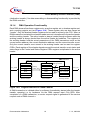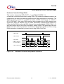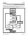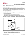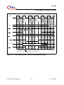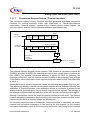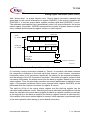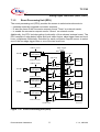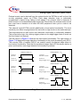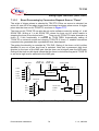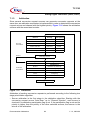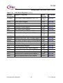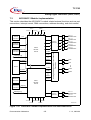
1
Do cu me n ta tio n A dd en du m , V 1.4 , Ju n e 20 04
T C 1 76 5
3 2 - B i t S i n g l e - C h i p M i cr o c o n t r o l l e r
M i c ro c o n t ro l l e rs
N e v e r
s t o p
t h i n k i n g .
Edition 2004-06
Published by Infineon Technologies AG,
St.-Martin-Strasse 53,
81669 München, Germany
© Infineon Technologies AG 2004.
All Rights Reserved.
Attention please!
The information herein is given to describe certain components and shall not be considered as warranted
characteristics.
Terms of delivery and rights to technical change reserved.
We hereby disclaim any and all warranties, including but not limited to warranties of non-infringement, regarding
circuits, descriptions and charts stated herein.
Infineon Technologies is an approved CECC manufacturer.
Information
For further information on technology, delivery terms and conditions and prices please contact your nearest
Infineon Technologies Office in Germany or our Infineon Technologies Representatives worldwide
(www.infineon.com).
Warnings
Due to technical requirements components may contain dangerous substances. For information on the types in
question please contact your nearest Infineon Technologies Office.
Infineon Technologies Components may only be used in life-support devices or systems with the express written
approval of Infineon Technologies, if a failure of such components can reasonably be expected to cause the failure
of that life-support device or system, or to affect the safety or effectiveness of that device or system. Life support
devices or systems are intended to be implanted in the human body, or to support and/or maintain and sustain
and/or protect human life. If they fail, it is reasonable to assume that the health of the user or other persons may
be endangered.
Do cu me n ta tio n A dd en du m , V 1.4 , Ju n e 20 04
T C 1 76 5
3 2 - B i t S i n g l e - C h i p M i cr o c o n t r o l l e r
M i c ro c o n t ro l l e rs
N e v e r
s t o p
t h i n k i n g .
TC1765 Documentation Addendum
Revision History:
2004-06
Previous Version:
V1.3 2003-02, V1.2 2002-07, V1.1 2002-06, V1.0 2002-06
Page
V 1.4
Subjects (major changes since last revision)
Changes for V1.3 to V1.4
Page 3
Correction of a paragraph; correction of special cache instructions;
Page 45
Page 46
Descriptions of WDT corrected;
Page 47
Descriptions of SSC error flags corrected;
Page 51
Correction of Figure 6-40; correction of GTCCTRm.OCM bit description;
Page 91
Power-up calibration section reworked;
Page 164
Ordering codes for AC Step updated; paragraph must be deleted;
identification of AB Step and AC Step by CAN_ID register added;
Changes for V1.2 to V1.3
Page 41
Figure 11-2 corrected
Page 42 Page 44
ADV timing corrected;
Page 91
Power-up calibration description improved;
Page 164, Reference to Data Sheet V1.2: three notes added;
Page 166
several
correction of typos; see locations marked with change bars
Changes for V1.1 to V1.2
Page 5 to
Page 40
A completely reworked DMA chapter description is available has been
added.
Page 53 to A complete AD converter chapter description with corrections especially in
Page 163 the timing section is provided.
Page 3,
Page 47
SSC receive FIFOs and transmit FIFOs have four stages (and not eight
stages).
several
Bit field TOS in the service request control registers is implemented as a
single bit and not as a 2-bit bit field.
Changes for V1.0 to V1.1
9
Figure 7-22 corrected
10
Formula for fANA corrected
We Listen to Your Comments
Any information within this document that you feel is wrong, unclear or missing at all?
Your feedback will help us to continuously improve the quality of this document.
Please send your proposal (including a reference to this document) to:
[email protected]
TC1765
Table of Contents
Page
1
Introduction . . . . . . . . . . . . . . . . . . . . . . . . . . . . . . . . . . . . . . . . . . . . . . . . 3
2
User’s Manual - System Units Part . . . . . . . . . . . . . . . . . . . . . . . . . . . . . 3
Page 1-7 . . . . . . . . . . . . . . . . . . . . . . . . . . . . . . . . . . . . . . . . . . . . . . . 3
Page 1-15 . . . . . . . . . . . . . . . . . . . . . . . . . . . . . . . . . . . . . . . . . . . . . . 3
Page 4-8 . . . . . . . . . . . . . . . . . . . . . . . . . . . . . . . . . . . . . . . . . . . . . . . 3
Page 5-9 . . . . . . . . . . . . . . . . . . . . . . . . . . . . . . . . . . . . . . . . . . . . . . . 3
Page 8-8 . . . . . . . . . . . . . . . . . . . . . . . . . . . . . . . . . . . . . . . . . . . . . . . 3
Page 9-4 . . . . . . . . . . . . . . . . . . . . . . . . . . . . . . . . . . . . . . . . . . . . . . . 3
Pages 10-1 to 10-34 (reworked DMA chapter) . . . . . . . . . . . . . . . . . . 4
Page 11-17 . . . . . . . . . . . . . . . . . . . . . . . . . . . . . . . . . . . . . . . . . . . . 41
Page 13-19, 13-20 . . . . . . . . . . . . . . . . . . . . . . . . . . . . . . . . . . . . . . . 41
Page 13-22 and 13-24 . . . . . . . . . . . . . . . . . . . . . . . . . . . . . . . . . . . . 42
Page 14-4 . . . . . . . . . . . . . . . . . . . . . . . . . . . . . . . . . . . . . . . . . . . . . 45
Page 14-22 . . . . . . . . . . . . . . . . . . . . . . . . . . . . . . . . . . . . . . . . . . . . 45
Page 15-6 . . . . . . . . . . . . . . . . . . . . . . . . . . . . . . . . . . . . . . . . . . . . . 45
Page 16-15 . . . . . . . . . . . . . . . . . . . . . . . . . . . . . . . . . . . . . . . . . . . . 45
Page 18-2 . . . . . . . . . . . . . . . . . . . . . . . . . . . . . . . . . . . . . . . . . . . . . 45
Page 18-17 . . . . . . . . . . . . . . . . . . . . . . . . . . . . . . . . . . . . . . . . . . . . 45
Page 19-6 . . . . . . . . . . . . . . . . . . . . . . . . . . . . . . . . . . . . . . . . . . . . . 46
Page 19-15 . . . . . . . . . . . . . . . . . . . . . . . . . . . . . . . . . . . . . . . . . . . . 46
Page 19-24 . . . . . . . . . . . . . . . . . . . . . . . . . . . . . . . . . . . . . . . . . . . . 46
3
User’s Manual - Peripheral Units Part . . . . . . . . . . . . . . . . . . . . . . . . . .
Page 1-10 and 3-3 . . . . . . . . . . . . . . . . . . . . . . . . . . . . . . . . . . . . . . .
Page 2-33 . . . . . . . . . . . . . . . . . . . . . . . . . . . . . . . . . . . . . . . . . . . . .
Pages 3-19, 3-20 . . . . . . . . . . . . . . . . . . . . . . . . . . . . . . . . . . . . . . . .
Page 3-21 . . . . . . . . . . . . . . . . . . . . . . . . . . . . . . . . . . . . . . . . . . . . .
Page 3-25 . . . . . . . . . . . . . . . . . . . . . . . . . . . . . . . . . . . . . . . . . . . . .
Page 3-30 . . . . . . . . . . . . . . . . . . . . . . . . . . . . . . . . . . . . . . . . . . . . .
Page 3-38 . . . . . . . . . . . . . . . . . . . . . . . . . . . . . . . . . . . . . . . . . . . . .
Page 4-86 . . . . . . . . . . . . . . . . . . . . . . . . . . . . . . . . . . . . . . . . . . . . .
Page 5-60 . . . . . . . . . . . . . . . . . . . . . . . . . . . . . . . . . . . . . . . . . . . . .
Page 6-49 . . . . . . . . . . . . . . . . . . . . . . . . . . . . . . . . . . . . . . . . . . . . .
Page 6-53 . . . . . . . . . . . . . . . . . . . . . . . . . . . . . . . . . . . . . . . . . . . . .
Page 6-58 . . . . . . . . . . . . . . . . . . . . . . . . . . . . . . . . . . . . . . . . . . . . .
Page 6-113 . . . . . . . . . . . . . . . . . . . . . . . . . . . . . . . . . . . . . . . . . . . .
Page 6-119 . . . . . . . . . . . . . . . . . . . . . . . . . . . . . . . . . . . . . . . . . . . .
Page 6-125 . . . . . . . . . . . . . . . . . . . . . . . . . . . . . . . . . . . . . . . . . . . .
Page 6-129 . . . . . . . . . . . . . . . . . . . . . . . . . . . . . . . . . . . . . . . . . . . .
Page 6-129 . . . . . . . . . . . . . . . . . . . . . . . . . . . . . . . . . . . . . . . . . . . .
Page 6-150 . . . . . . . . . . . . . . . . . . . . . . . . . . . . . . . . . . . . . . . . . . . .
Pages 7-1 to 7-108 (reworked AD converter chapter) . . . . . . . . . . . .
(latest changes see “Power-Up Calibration Time” on Page 91
Documentation Addendum
1
47
47
47
47
48
48
50
50
50
50
50
50
51
51
51
51
51
51
52
52
V 1.4, 2004-06
TC1765
Table of Contents
4
Page
Data Sheet . . . . . . . . . . . . . . . . . . . . . . . . . . . . . . . . . . . . . . . . . . . . . . .
Page 2 . . . . . . . . . . . . . . . . . . . . . . . . . . . . . . . . . . . . . . . . . . . . . . .
Page 52 . . . . . . . . . . . . . . . . . . . . . . . . . . . . . . . . . . . . . . . . . . . . . .
Page 55 . . . . . . . . . . . . . . . . . . . . . . . . . . . . . . . . . . . . . . . . . . . . . .
Page 60 . . . . . . . . . . . . . . . . . . . . . . . . . . . . . . . . . . . . . . . . . . . . . .
Page 61 . . . . . . . . . . . . . . . . . . . . . . . . . . . . . . . . . . . . . . . . . . . . . .
Page 68 . . . . . . . . . . . . . . . . . . . . . . . . . . . . . . . . . . . . . . . . . . . . . .
Page 72 . . . . . . . . . . . . . . . . . . . . . . . . . . . . . . . . . . . . . . . . . . . . . .
Documentation Addendum
2
164
164
164
164
164
165
165
166
V 1.4, 2004-06
TC1765
Introduction
1
Introduction
This document describes corrections, changes, and improvements for the two parts of
the TC1775 User’s Manual V1.0 2001-01, the System Units book and the Peripheral
Units book. These corrections will be considered with the next update of these User’s
Manual documents.
The referenced documents to this addendum are:
– TC1765 System Units User’s Manual, V1.0, Jan. 2002 (Link to the PDF)
Ordering No.: B158-H7793-X-X-7600
– TC1765 Peripheral Units User’s Manual, V1.0, Jan. 2002 (Link to the PDF)
Ordering No.: B158-H7794-X-X-7600
– TC1765 Data Sheet, V1.2, December 2002 (Link to the PDF)
Ordering No.: B158-H8144-X-X-7600
2
User’s Manual - System Units Part
Page 1-7
First bullet paragraph under “Interrupt System”: the “TBD” must be replaced by “102”.
Page 1-15
Last bullet paragraph in feature list: receive FIFO and transmit FIFO of the SSCs have
four stages (and not eight stages).
Page 4-8
The short name of the SCU Trace Status Register should be corrected into “TRSTAT”.
Page 5-9
Last paragraph: the wording “... until a power-on reset or hardware reset occurs ...” must
be corrected into “... until a power-on reset occurs ...”.
Page 8-8
Description of bit TERF: for TERF = 0 and TERF = 1 the words “... on a cache miss ...”
must be replaced twice by “... on a RFB miss ...”.
Page 9-4
The three special cache instructions in section 9.1.4 are wrong. “DFLASH, DINV and
DFLINV” must be replaced by “CACHEA.W, CACHEA.I and CACHEA.WI”.
Documentation Addendum
3
V 1.4, 2004-06
TC1765
User’s Manual - System Units Part
Pages 10-1 to 10-34 (reworked DMA chapter)
A completely reworked DMA chapter description is provided (see Page 5 to Page 40 of
this Documentation Addendum). Changes to the DMA chapter from the System Units
User’s Manual V1.0 are marked with change bars.
Documentation Addendum
4
V 1.4, 2004-06
TC1765
Direct Memory Access Controller (DMA)
10
Direct Memory Access Controller (DMA)
This chapter describes the Direct Memory Access (DMA) Controller of the TC1765. This
chapter contains the following sections:
– Functional description of the DMA Kernel (see Section 10.1).
– Register descriptions for all DMA Kernel specific registers (see Section 10.2).
– TC1765 implementation specific details and registers of the DMA Controller,
including control, interrupt control, address decoding, and clock control (see
Section 10.3).
Note: The DMA Kernel register names described in Section 10.2 will be referenced in
the TC1765 Documentation Addendum with the module name prefix “DMA_” for
the DMA interface.
Documentation Addendum
5
V 1.4, 2004-06
TC1765
Direct Memory Access Controller (DMA)
10.1
DMA Controller Kernel Description
The Direct Memory Access (DMA) Controller executes DMA transactions from a source
address location to a destination address location, without intervention of the CPU. One
DMA transaction is controlled by one DMA channel. Each DMA channel has assigned
its own two channel register sets: a shadow register set and an active register set. This
feature eases programming and releases the CPU from control tasks.
Features:
• 8 independent DMA channels (4 per DMA block)
– 4 DMA selectable request inputs per DMA channel
– Fixed priority of DMA channels within a DMA block
– Software and hardware DMA request generation
• Support of FPI Bus to FPI Bus DMA transactions
• Individually programmable operation modes for each DMA channel
– Single mode: stops and disables DMA channel after a predefined number of DMA
transfers
– Continuous mode: DMA channel remains enabled after a predefined number of
DMA transfers; DMA transaction can be repeated;
• Full 32-bit addressing capability of each DMA channel
– 4 GByte address range
– Source and destination transfer individually programmable in steps from 0 to
255 bytes
– Support of circular buffer addressing mode
• Programmable data width of a DMA transaction: 8-bit, 16-bit, or 32-bit
• Register sets for each DMA channel with
– Source and destination start address register
– Source and destination end address register
– Channel control and status register
– Offset and transfer count register
• Bus bandwidth allocation
• Interrupt generation at the end of a DMA transaction
Documentation Addendum
6
V 1.4, 2004-06
TC1765
Direct Memory Access Controller (DMA)
10.1.1
Definition of Terms
DMA Transfer
A DMA transfer is an operation which consists always of two parts:
– A source transfer which loads data from a data source into the DMA controller
– A destination transfer which puts data from the DMA controller to a data destination
Within a DMA transfer data is always transferred from the data source via the DMA
controller to the data destination. The data width of source transfer and destination
transfer are always identical (8-bit, 16-bit, or 32-bit).
DM A C ontroller
D ata
Source
S o u rc e
T ra n sfer
DM A
C hannel
D M A Tra ns fe r
Figure 10-1
D e s t.
Tran s fe r
Data
Destination
M C B 04 9 7 2
DMA Terms Definitions
DMA Transaction
A DMA transaction is composed of several (at least by one) DMA transfers. The Transfer
Count defines the number of DMA transfers within one DMA transaction.
Documentation Addendum
7
V 1.4, 2004-06
TC1765
Direct Memory Access Controller (DMA)
10.1.2
DMA Principle
The DMA controller supports DMA transfers from FPI Bus to FPI Bus. DMA Transfers
can be requested either by hardware or by software. DMA hardware requests are
triggered by specific request lines from the peripheral modules (see Figure 10-2). The
number of available DMA request lines from a peripheral module varies depending on
the module functionality. Typically, the occurrence of a receive or transmit data interrupts
in a peripheral module can generate in parallel to the interrupt request a DMA request.
Therefore, the interrupt control unit and the DMA controller in the TC1765 can react
independently on interrupt and DMA requests that have been generated by one source.
The DMA controller consists of a control unit and two DMA blocks. The control unit
includes a FPI Bus slave interface for programming of the DMA controller registers.
Once configured, each block of the DMA controller is able to act as a master on the FPI
Bus using its FPI Bus master interface.
FPI Bus
D M A Controller
R e q ue s t
Peripheral 1
(e .g . A S C )
Block 0
R e q ue s t
Peripheral 2
(e .g . S S C )
R e q ue s t
Control Unit
Peripheral 3
(e.g. A D C )
R e q u es t
Block 1
.
.
.
.
.
Peripheral x
M C B 0 49 6 8
Figure 10-2
DMA Principle
To ease the architecture of the DMA controller, one data buffer per each DMA channel
is implemented. Neither block nor split modes are supported on the FPI Bus.
Documentation Addendum
8
V 1.4, 2004-06
TC1765
Direct Memory Access Controller (DMA)
10.1.3
DMA Block Diagram
Each of the two blocks in the DMA controller, block 0 and block 1, provides four DMA
channels with sixteen DMA request inputs. The request assignment unit in each block
assign one DMA request input to each DMA channel. The control unit includes a third
request unit dedicated especially for request control through I/O pins. This unit is
connects two of eight request inputs with two request outputs which can be then wired
externally of the DMA controller module to the request inputs of the two DMA controller
blocks. Request assignment unit 2 evaluates pulses or levels by its edge detect and level
select logic.
Clock control, address decoding, and interrupt service request control for the eight
interrupt service request outputs are managed outside the DMA controller module
kernel.
D M A Controller
B lo c k 0
C lo c k
C on tro l
fD M A
DMA
C h a n ne ls
0 0 -0 3
R eq u e st
A s s ig n .
U n it 0
16
D M A R E Q [1 5 :0 ]
4
A d d re s s
D e c o de r
R e qu e s t
A ss ig n .
U nit 2
C o n tro l
U n it
REQO 0
4
SR0
SR1
Inte rru p t
C on tro l
SR6
SR7
R E Q I[3 :0 ]
R E Q I[7 :4 ]
REQO 1
B lo c k 1
DMA
C h a n ne ls
1 0 -1 3
R e q u es t
A s sig n.
U n it 1
16
D M A R E Q [3 1:1 6]
M C B 0 49 6 4
Figure 10-3
Block Diagram of DMA Controller Module
Each DMA transaction consists of a programmable number of DMA transfers that can
be either 8-bit, 16-bit or 32-bit wide. Data is read from the source (source transfer) and
stored intermediately in the corresponding DMA channel data buffer. In the second part
of the DMA transfer, data is written from the DMA channel data buffer to the destination
Documentation Addendum
9
V 1.4, 2004-06
TC1765
Direct Memory Access Controller (DMA)
(destination transfer). No data assembling or disassembling functionality is provided by
the DMA controller.
10.1.4
DMA Operation Functionality
Each DMA channel has three register sets: an active register set, a shadow register set,
and a working register set (see Figure 10-4). These register sets are also named as
“header”. Only the shadow header registers can be read or written by the CPU. When a
DMA transaction is started the shadow header content is transferred to the active header
and the working header. The active header is always loaded through software while the
working header is always loaded from the active header by hardware. The registers of
the working header hold the actual parameters of the DMA transactions such as the
current source address, the current destination address, and the current transfer count.
Only the current transfer count stored in the working header can be read via register
CSRn. Each register of the shadow header except the actual transfer count status and
status flags in the Control and Status Register CSRn register is duplicated in the active
header.
D M A C hannel n
TR C O U N T & S tatus
C SR n
C H n_ R E Q
O TC n
C o ntrol Flag s
S ettin g
C S R n.TS H
S tart/R e pe at/A b ort
D M A tra ns ac tion
O TCn
T ran sfer C o un t
SSAn
S o urc e A d dre s s
SEAn
SEAn
D es t. A d dre ss
D SAn
D SAn
D EAn
D EAn
S ha do w H e ad er
A c tiv e H e ad er
SSAn
C H n _S R
Tra ns fer D a ta
W ork in g H ea de r
M C A 04969
Figure 10-4
Register Interface of a DMA Channel
A DMA transaction is initiated either by software (immediately started after the header
transfer operation) or by hardware via the DMA request input CHn_REQ. After
completion of a DMA transaction, a service request signal is generated to the service
request node of DMA channel n.
Documentation Addendum
10
V 1.4, 2004-06
TC1765
Direct Memory Access Controller (DMA)
10.1.5
DMA Channel Configuration
For the setup of a DMA channel, the following steps must be performed:
1. The registers of the shadow register set OTCn, SSAn, SEAn, DSAn, DEAn of the
DMA channel must be configured.
2. The transfer shadow header bit CSRn.TSH is set to transfer the shadow header with
all DMA transaction parameters to the active header and to enable the DMA channel
for DMA transaction. Of course, when writing to the CSRn with TSH set, also the
channel transfer control bit CHTC, the channel operation mode bit CHMODE, the
channel data width bit CHDW, and the peripheral request select bit field PRSEL (in
hardware controlled modes only) are transferred to the active register set.
If the actual DMA channel is currently running (CRSn.CHAC set) and should be
updated with new data from the shadow header by setting CSRn.TSH, the shadow
header transfer is delayed until the end of the running DMA transaction (bit CSRn.TSH
remains set). CSRn.TSH is automatically cleared by hardware when the shadow
header transfer to the active header and working header occurred.
10.1.5.1 DMA Transfer Triggering
There are two ways of triggering a DMA transfer within a DMA transaction of a DMA
channel. The two trigger modes are controlled by the channel transfer control bit
CSRn.CHTC.
1. CSRn.CHTC = 0: a DMA transfer of DMA channel n starts automatically as soon as
the active and working header has been loaded by the content of the shadow header.
This is mode is called software controlled/triggered.
2. CSRn.CHTC = 1: a DMA transfer of DMA channel n waits for an active DMA request
input as selected by CSRn.PRSEL. This mode is called hardware controlled/triggered.
10.1.5.2 DMA Channel Operation Mode
The operation mode is individually programmable for each DMA channel n via control bit
CSRn.CHMODE. A channel can operate either in one of two modes:
– Single mode or
– Continuous mode
In single mode, the DMA channel n active status bit CSRn.CHAC is cleared after the last
DMA transfer of a DMA transaction in order to disable this DMA channel n. For the start
of the next DMA transaction, DMA channel n transfer shadow header bit CSRn.TSH
must be set again.
In continuous mode, the DMA channel n active status bit CSRn.CHAC remains set,
which allows DMA requesting units in hardware controlled mode to initiate repeating
DMA transactions without any CPU intervention.
Documentation Addendum
11
V 1.4, 2004-06
TC1765
Direct Memory Access Controller (DMA)
Software Controlled Single Mode
This mode in selected by CSRn.CHTC = 0 and CSRn.CHMODE = 0.
In software controlled single mode, setting of CSRn.TSH causes the shadow header to
be transferred to active and working header and the DMA transaction to be started. The
DMA transaction consists of a predefined number of DMA transfers (tc), as defined in
OTCn.TRCOUNT. After each DMA transfer the transfer count tc (CSRn.TRCOUNT) is
decremented. When tc is 0 after the last DMA transfer, the DMA channel n becomes
disabled (CSRn.CHAC = 0) and its interrupt service line SRn is activated. Setting
CSRn.TSH again starts the next DMA transaction with the parameters as currently
stored in the shadow register set. The running DMA transaction is indicated by channel
active flag CSRn.CHAC set.
C S R n .T S H
C S R n .C H A C
D M A T ra n sfe r n
o n the FP I B u s
C R S n .T R C O U N T
TR0
TR1
tc
tc -1
TRn
0
tc = in itia l tra n sfe r co u n t
Figure 10-5
TR 0
TR 1
tc
tc-1
M C T 04 9 6 2
Software Controlled Single Mode Operation
Documentation Addendum
12
V 1.4, 2004-06
TC1765
Direct Memory Access Controller (DMA)
Software Controlled Continuous Mode
This mode is selected by CSRn.CHTC = 0 and CSRn.CHMODE = 1.
In software controlled continuous mode, setting of CSRn.TSH causes the shadow
header to be transferred to active and working header and the DMA transaction to be
started. The DMA transaction consists of a predefined number of DMA transfers (tc), as
defined in OTCn.TRCOUNT. After each DMA transfer the transfer count tc
(CSRn.TRCOUNT) is decremented. When tc is 0 after the last DMA transfer, the
interrupt service line SRn of DMA channel n is activated, CSRn.CHSCM is checked and
when not set the working header is reloaded with the content of the active header and a
new DMA transaction is started. In case of CSRn.CHSCM = 1 after the last DMA
transfer, the DMA transaction is stopped and CSRn.CHAC and CSRn.CHSCM are reset.
During continuous mode the active flag CSRn.CHAC is always set.
C S R n .T S H
C S R n .C H A C
D M A T ra ns fer n
o n the FP I B u s
C S R n .T R C O U N T
TR0
TR1
tc
tc -1
TRn
0
TR0
TR1
TR 2
tc
tc -1
tc-2
tc = in itia l tra n sfer co un t
Figure 10-6
M C T 0 49 6 1
Software Controlled Continuous Mode Operation
Documentation Addendum
13
V 1.4, 2004-06
TC1765
Direct Memory Access Controller (DMA)
Hardware Controlled Single Mode
This mode is selected by CSRn.CHTC = 1 and CSRn.CHMODE = 0.
In hardware controlled single mode, setting CSRn.TSH causes the shadow header to be
transferred to the active and working header and the DMA transaction to be started. The
DMA transaction consists of a predefined number of DMA transfers (tc), as defined in
OTCn.TRCOUNT. After each DMA transfer, that is triggered by a DMA request input
signal CHn_REQ, the transfer count tc (CSRn.TRCOUNT) is decremented. When tc is
0 after the last DMA transfer, the DMA channel n becomes disabled (CSRn.CHAC = 0),
and the interrupt service line SRn is activated. Setting CSRn.TSH again starts the next
DMA transaction with the parameters as defined in the shadow register set. The running
DMA transaction is indicated by channel active flag CSRn.CHAC set.
C S R n .T S H
C S R n .C H A C
C Hn_REQ
D M A T ra n sfer n
o n the FP I B u s
TR0
C S R n .T R C O U N T
tc
TR1
tc-1
TRn
TR0
0
tc = in itia l tra n sfer co un t
Figure 10-7
tc
tc-1
M C T 04 9 60
Hardware Controlled Single Mode Operation
Documentation Addendum
14
V 1.4, 2004-06
TC1765
Direct Memory Access Controller (DMA)
Hardware Controlled Continuous Mode
This mode is selected by CSRn.CHTC = 1 and CSRn.CHMODE = 1.
In hardware controlled continuous mode, setting of CSRn.TSH causes the shadow
header to be transferred to the active and working header and the DMA transaction to
be started. The DMA transaction consists of a predefined number of DMA transfers (tc),
as defined in OTCn.TRCOUNT. After each DMA transfer, that is triggered by a DMA
request input signal CHn_REQ, the transfer count tc (CSRn.TRCOUNT) is
decremented. When tc is 0 after the last DMA transfer, the interrupt service line SRn of
DMA channel n is activated, CSRn.CHSCM is checked and when not set the working
header is reloaded with the content of the active header and a new DMA transaction is
started. In case of CSRn.CHSCM = 1 after the last DMA transfer, the DMA transaction
is stopped and CSRn.CHAC and CSRn.CHSCM are reset. Setting CSRn.TSH again
starts the next DMA transaction with the parameters as defined in the shadow register
set. The running DMA transaction is indicated by channel active flag CSRn.CHAC set.
C S R n .T S H
C S R n .C H A C
C Hn_REQ
D M A T ra n sfer n
o n the FP I B u s
TR0
C S R n .T R C O U N T
tc
TR1
TR2
tc -2
tc-1
TRn
0
TR0
tc
tc = in itia l tra n sfer co un t
Figure 10-8
TR1
tc-1
M C T 0 4 95 9
Hardware Controlled Continuous Mode Operation
Documentation Addendum
15
V 1.4, 2004-06
TC1765
Direct Memory Access Controller (DMA)
Figure 10-9 shows the flow diagram of a DMA transaction in single and continuous
mode including the reset handling. Figure 10-10 shows the flow diagram of the
execution of one DMA transfer which is one block in Figure 10-9.
Lo a ding S h a do w H e ad e r an d
startin g D M A tra nsa ctio n
b y se ttin g C S R n .T SH
(ex ec uted by s oftw are)
Tra nsfe r o f S h a do w H e ad e r
to Active H e ad e r
C S R n .C H AC := 1
T ra nsfe r o f A ctive H ea d er
to W o rkin g H ea d er
no
C S R n .C H T C = 1 ?
ye s
no
D M A re q u est
in p ut a ctive ?
ye s
tc := tc - 1
E xe cu tion of o ne
D M A T ra n sfe r
yes
C a lcula tion of n ext so u rce
an d d e stin atio n ad d re ss
in w orking he a de r
no
tc = 0 ?
C o ntin uo u s m o de ?
no
C on tinu o u s m od e ?
no
ye s
no
yes
C SR n .C H SC M = 1 ?
ye s
C SR n .C H R ST = 1 ?
no
ye s
tc: T ra n sfe r co u nt
in w o rkin g h e a de r
C S R n .C H S C M := 0
C S R n .C H AC := 0
D M A tra n sa ctio n finish e d
Figure 10-9
D M A T rans ac tio n
DMA Transaction Flow Diagram
Documentation Addendum
16
V 1.4, 2004-06
TC1765
Direct Memory Access Controller (DMA)
R e q ue st for D M A T ran sfe r
Prio rity A rb itra tio n
no
H ig he st prio rity ?
ye s
P erfo rm S ou rce (R e a d )
T ra n sfe r
Prio rity A rb itra tio n
no
H ig he st prio rity ?
ye s
P erfo rm D e stina tio n (W rite )
T ra n sfe r
D M A T ran sfe r fin ishe d
D M A T rans fer
Figure 10-10 DMA Transfer Execution Flow Diagram
Documentation Addendum
17
V 1.4, 2004-06
TC1765
Direct Memory Access Controller (DMA)
10.1.5.3 DMA Transfer Parameters
Transfer Count
One parameter of a DMA transaction is the 16-bit transfer count. This 16-bit transfer
count defines the number of DMA transfers to be executed within one DMA transaction.
Its value is defined by the number of requested DMA transfers decremented by 1. This
means for example, that a 0000H must be programmed for the transfer count when one
DMA transfer should be executed.
Address Calculation Principles
Besides the transfer count, each part of a DMA transfer, source and destination transfer,
is controlled by three parameters:
– 32-bit Start Address (SA), stored in registers SSAn and DSAn
– 32-bit End Address (EA), stored in registers SEAn and DEAn
– 8-bit Offset (OFF), stored in bit fields SRCOFS and DESTOFS of register OTCn
The address for the next source/destination transfer is calculated according
Section 10-11.
S ta rt o f D M A T ra n s fe r
C A := S A
P e rfo rm R ea d /W rite
T ra n sfe r
yes
CA > EA ?
no
CA:
SA:
EA:
O FF:
C A := C A + O F F
C u rre n t A dd ress
S ta rt A d d re ss
E n d A dd ress
O ffse t
M C B 0 4 9 63
Figure 10-11 Source/Destination Transfer Address Update
In continuous mode, the end address for source or destination transfers is calculated by
– End address = Address of the last transfer - offset field in OTCn
Documentation Addendum
18
V 1.4, 2004-06
TC1765
Direct Memory Access Controller (DMA)
Example for a DMA Transaction Parameter Calculation
For a DMA transaction with 4 word transfers, source and destination increment, the
following parameters must be programmed:
OTCn.SRCOFS
OTCn.DESTOFS
OTCn.TRCOUNT
CSRn.CHDW
= 04H
= 04H
= 0003H
= 10B
(= 4 byte source address increment)
(= 4 byte destination address increment)
(= requested number of transfers - 1)
(= 32-bit transfers)
10.1.5.4 DMA Channel Priorities and Request Arbitration
The DMA channels of a DMA block have a fixed priority: the DMA channel with the lowest
number has the highest priority. The priority of the two DMA blocks among each other is
defined by the priority assignment of its FPI Bus master interfaces as FPI Bus master
agent.
Table 10-1
DMA Channel Priorities
DMA Channel
DMA Channel Priority
DMA Block Priority
(FPI Bus Master Priority)
00
high
low
01
medium high
02
medium low
03
low
10
high
11
medium high
12
medium low
13
low
high
DMA channel arbitration is done after every source (read) and destination (write)
transfer. Therefore, a DMA transfer can be interrupted by another high priority DMA
channel also after a source transfer.
10.1.5.5 DMA Bus Bandwidth Limitation
After each source transfer or destination transfer the related DMA block will release the
FPI Bus for at least 3 FPI Bus clock cycles. This gives other FPI Bus masters the chance
to arbitrate for the FPI Bus ownership.
10.1.5.6 DMA Channel Interrupts
Each DMA channel has one interrupt (service request) output line. This interrupt output
line becomes active at the end of a DMA transaction.
Documentation Addendum
19
V 1.4, 2004-06
TC1765
Direct Memory Access Controller (DMA)
10.1.5.7 Error Conditions
The DMA controller allows to detect error conditions individually for each DMA channel.
The source transfer error flag CSRn.SRCERR flag indicates an FPI Bus error that
occurred during a source transfer (read) of a DMA transaction. The destination transfer
error flag CSRn.DESTERR flag indicates an FPI Bus error that occurred during a
destination transfer (write) of a DMA transaction.
The request overrun error flag CSRn.REQOVR indicates if DMA requests for a DMA
channel have been lost. Each DMA channel has a DMA request counter, which counts
up to 15 DMA requests in hardware controlled modes. The DMA request counter is
incremented with each incoming DMA request and decremented after each destination
(write) transfer. With the overflow condition of the DMA request counter (counter
value = 15 and DMA request occurs) bit CSRn.REQOVR is set while the counter value
remains set to 15.
10.1.5.8 Channel Reset/Stop Operation
In single and continuous mode a DMA transfer of a DMA channel n can be reset by
setting bit CSRn.CHRST. If bit CSRn.CHRST becomes set, a running DMA transfer of
DMA channel n is terminated after the next destination (write) transfer. The user can poll
the CSRn.CHAC bit to detect when the DMA channel becomes inactive.
CSRn.TRCOUNT is not reset and indicates the actual number of remaining DMA
transfers of the aborted DMA transaction plus 1.
A user program should execute the following steps for resetting and restarting a DMA
channel:
1. Writing a 1 to CSRn.CHRST.
2. Polling bit CSRn.CHAC until bit is set to 0.
3. Restarting the DMA channel n again by writing a 1 to CSRn.TSH.
In continuous mode a DMA transfer of a DMA channel n can be also stopped (instead of
reset) at the end of its DMA transaction. When CSRn.TRCOUNT is 0000H after the last
DMA transfer, bit CSRn.CHSCM is checked and when set the DMA transaction is
stopped and CSRn.CHAC and CSRn.CHSCM are reset.
A user program should execute the following steps for stopping and restarting a DMA
channel that operates in continuous mode:
1. Writing a 1 to CSRn.CHSCM.
2. Polling bit CSRn.CHAC until bit is set to 0.
3. Restarting the DMA channel n again by writing a 1 to CSRn.TSH.
Documentation Addendum
20
V 1.4, 2004-06
TC1765
Direct Memory Access Controller (DMA)
10.1.6
Request Assignment Units 0 and 1
Each DMA block, block 0 and 1, contains one request assignment unit, that multiplexes
the sixteen request inputs of a DMA block to one request input for each DMA channel.
A pulse on the DMAREQn lines takes at least two clock cycles. Each request input
multiplexer of DMA channel n is controlled by the peripheral request select bit field
CSRn.PRSEL.
DM A B lock 0
D M A Block 1
C S R 10 .P R S E L
C S R 00 .P R S E L
DM AREQ0
00
DM AREQ1
01
DM AREQ2
10
DM AREQ3
11
00
C H00_REQ
DM A
Channel 10
DMA
Channel 00
00
DM AREQ5
01
DM AREQ6
10
DM AREQ7
11
00
DM AREQ9
01
D M AR EQ 10
10
D M AR EQ 11
11
C H 0 1 _R E Q
DMA
Channel 01
DM A
Channel 11
00
D M AR EQ 13
01
D M AR EQ 14
10
D M AR EQ 15
11
D M AR EQ 18
D M AR EQ 19
C H02_REQ
C H 0 3 _R E Q
C H 1 1 _R E Q
00
D M AR EQ 20
01
D M AR EQ 21
10
D M AR EQ 22
11
D M AR EQ 23
C S R 12 .P R S E L
DMA
Channel 02
DM A
Channel 12
C H 1 2 _R E Q
00
D M AR EQ 24
01
D M AR EQ 25
10
D M AR EQ 26
11
D M AR EQ 27
C S R 13 .P R S E L
C S R 0 3 .P R S E L
D M AR EQ 12
10
C S R 11 .P R S E L
C S R 02 .P R S E L
DM AREQ8
01
11
C S R 01 .P R S E L
DM AREQ4
C H 1 0 _R E Q
D M AR EQ 16
D M AR EQ 17
DM A
Channel 13
DM A
Channel 03
C H 1 3 _R E Q
00
D M AR EQ 28
01
D M AR EQ 29
10
D M AR EQ 30
11
D M AR EQ 31
M C B 0 4 9 70
Figure 10-12 Request Assignment Unit in DMA Block 0 and 1
Documentation Addendum
21
V 1.4, 2004-06
TC1765
Direct Memory Access Controller (DMA)
10.1.7
Request Assignment Unit 2
Besides the two DMA request assignment units in each DMA block, the DMA controller
has a request assignment unit 2 which is located in the control unit of the DMA controller
(see Figure 10-3). Request assignment unit 2 allows to control external DMA requests
coming from an I/O pin by providing edge detection and gating functionality. The two
outputs REQO0 and REQO1 can be wired back as a DMA request input line to request
assignment unit 0 or 1. Details on the request assignment unit 2 interconnections as
implemented in the TC1765 are given in Section 10.3.1.
G C TR .E D R S 0
2
R E Q I0
00
R E Q I1
01
R E Q I2
10
R E Q I3
11
G C T R .E D L S 0
3
00
R E Q I5
01
R E Q I6
10
R E Q I7
11
1
EXREQ0
REQO0
R equest
Assignm ent
U nit 2
R E Q I4
G C T R .O M 0
E d g e D ete ct/
Le v e l S e le c t
C o nto l U n it
EXREQ1
2
G C TR .E D R S 1
REQO1
3
G C T R .E D L S 1
1
G C T R .O M 1
M C B 0 49 7 1
Figure 10-13 Request Assignment Unit 2 Block Diagram
In general, the functionality of the request assignment unit 2 is controlled by the global
control register GCTR. Bit field GCTR.EDRSx (x = 0,1) controls the request input
multiplexers and selects one of four possible request input for the EXREQx lines.
The edge detection and level select control unit provides in general two operating
modes:
– Edge sensitive mode
– Gating mode
The functionality of the operating modes is shown in Figure 10-14.
Documentation Addendum
22
V 1.4, 2004-06
TC1765
Direct Memory Access Controller (DMA)
Edge Sensitive M ode:
O M 1 = OM 0 = 0
G C T R .E D L S 0
3
EXREQ 0
E d ge
D e te c tio n
REQO 0
EXREQ 1
E d ge
D e te c tio n
REQO 1
3
G C T R .E D L S 1
G ating M ode 0:
O M 1 = 0, O M 0 = 1
G C T R .E D L S 0
3
EXREQ0
10 1
REQO 0
n o t av a ilab le
10 0
&
EXREQ1
E d ge
D e te c tion
REQO 1
3
G C TR .E D L S 1
G ating M ode 1:
O M 1 = 1, O M 0 = 0
EXREQ0
G C TR .E D L S 0
3
E d ge
D e te c tion
&
10 0
EXREQ1
10 1
3
G C T R .E D L S 1
REQO 0
REQO1
no t a va ila b le
M C B 0 4 9 71 a
Figure 10-14 Request Assignment Unit 2 Operating Modes
Documentation Addendum
23
V 1.4, 2004-06
TC1765
Direct Memory Access Controller (DMA)
In edge sensitive mode, two independent edge detections can be used for the two
request inputs EXREQx. Whenever a rising and/or falling signal transition occurs at input
signal EXREQx, a pulse of two clock cycles width is generated at output REQOx. Edge
sensitive mode is selected by setting OM1 = OM0 = 0.
In gating mode, two types of gating modes can be selected:
– Gating mode 0:
Input EXREQ0 operates as gating input with programmable gating level for the
edge sensitive request input EXREQ1 with request output REQO1. Output REQO0
is not available. Gating mode 0 is selected by GCTR.OM1 = 0 and GCTR.OM0 = 1.
– Gating mode 1:
Input EXREQ1 operates as gating input with programmable gating level for the
edge sensitive request input EXREQ0 with request output REQO0. Output REQO1
is not available. Gating mode 1 is selected by GCTR.OM1 = 1 and GCTR.OM0 = 0.
In both gating modes, the edge detection can e selected for rising and/or falling signal
transitions of the corresponding request input. Gating for a request input is enabled with
low level at EXREQx when GCTR.EDLSx = 100B. Gating for a request input is enabled
with high level at EXREQx when GCTR.EDLSx = 101B. Please note that the
combination of GCTR.OM0 = 0 and GCTR.OM1 = 0 should not be used, because in this
case, both request outputs, REQO0 and REQO1, are inoperable.
Documentation Addendum
24
V 1.4, 2004-06
TC1765
Direct Memory Access Controller (DMA)
10.2
DMA Module Kernel Registers
Figure 10-15 and Table 10-2 show all registers associated with the DMA Kernel.
Control
Registe r
Channel Control
and
Status R egisters
C hannel Source
A ddress Registers
Chann el Destina tion
A ddress R egisters
C S R 00
S S A 00
D S A 00
O T C 00
S E A 00
D E A 00
C S R 01
S S A 01
D S A 01
O T C 01
S E A 01
D E A 01
C S R 02
S S A 02
D S A 02
O T C 02
S E A 02
D E A 02
C S R 03
S S A 03
D S A 03
O T C 03
S E A 03
D E A 03
C S R 10
S S A 10
D S A 10
O T C 10
S E A 10
D E A 10
C S R 11
S S A 11
D S A 11
O T C 11
S E A 11
D E A 11
C S R 12
S S A 12
D S A 12
O T C 12
S E A 12
D E A 12
C S R 13
S S A 13
D S A 13
O T C 13
S E A 13
D E A 13
G C TR
DMA
Channel 00
DMA
Channel 01
DMA
Channel 02
DMA
Channel 03
DMA
Channel 10
DMA
Channel 11
DMA
Channel 12
DMA
Channel 13
M C A0 4967
Figure 10-15 DMA Kernel Registers
Documentation Addendum
25
V 1.4, 2004-06
TC1765
Direct Memory Access Controller (DMA)
Table 10-2
DMA Kernel Registers
Register
Register Long Name
Short Name
Offset Address Description
see
GCTR
DMA Global Control Register
0010H
Page 27
CSRn
DMA Channel n Control and Status
Register
m × 20H + 00H
Page 29
OTCn
DMA Channel n Offset and Transfer
Count Register
m × 20H + 04H
Page 32
SSAn
DMA Channel n Source Start Address m × 20H + 08H
Register
Page 33
SEAn
DMA Channel n Source End Address
Register
m × 20H + 0CH
Page 33
DSAn
DMA Channel n Destination Start
Address Register
m × 20H + 10H
Page 34
DEAn
DMA Channel n Destination End
Address Register
m × 20H + 14H
Page 34
Table 10-3
Offset Address Factor Assignment DMA Channel n to m
n
m
n
m
00
1
10
5
01
2
11
6
02
3
12
7
03
4
13
8
Note: All DMA kernel register names described in this section will be referenced in other
parts of the TC1765 Documentation Addendum with the module name prefix
“DMA_” for the DMA interface.
Documentation Addendum
26
V 1.4, 2004-06
TC1765
Direct Memory Access Controller (DMA)
The global control register contains the control bits for the request control unit 2 of the
DMA module. See also Section 10.1.7 for more details of the external request control
unit.
GCTR
Global Control Register
31
30
29
28
Reset Value: 0000 0000H
27
26
25
24
23
22
21
20
19
18
17
16
7
6
5
4
3
2
1
0
0
r
15
14
13
12
11
10
9
8
0
EDRS1
0
EDRS0
OM1
EDLS1
OM0
EDLS0
r
rw
r
rw
rw
rw
rw
rw
Field
Bits
Type
Description
EDLS0
[2:0]
rw
Edge Detect Level Select 0 Control
This bit field controls the functionality (edge selection or
gating level selection) of request input EXREQ0.
Edge sensitive mode (OM1 = OM0 = 0):
000B No action
001B Detect falling edges at EXREQ0
010B Detect rising edges at EXREQ0
011B Detect rising and falling edges at EXREQ0
1XXB Reserved
Gating mode 0 (OM1 = 0, OM0 = 1):
0XXB Reserved
100B EXREQ0 = 0: requests at EXREQ1 are enabled
to REQO1. EXREQ0 = 1: requests are disabled.
101B EXREQ0 = 1: requests at EXREQ1 are enabled
to REQO1. EXREQ0 = 0: requests are disabled.
11XB Reserved
OM0
3
rw
Operation Mode for EXREQ0
This bit defines the operating mode for input EXREQ0.
0
Edge sensitive mode selected.
1
Gating mode selected; REQO0 is not operable.
Documentation Addendum
27
V 1.4, 2004-06
TC1765
Direct Memory Access Controller (DMA)
Field
Bits
Type
Description
EDLS1
[6:4]
rw
Edge Detect Level Select 1 Control
This bit field controls the functionality (edge selection or
gating level selection) of request input EXREQ1.
Edge sensitive mode (OM0 = OM1 = 0):
000B No action
001B Detect falling edges at EXREQ1
010B Detect rising edges at EXREQ1
011B Detect rising and falling edges at EXREQ1
1XXB Reserved
Gating mode 1 (OM1 = 1, OM0 = 0):
0XXB Reserved
100B EXREQ1 = 0: requests at EXREQ0 are enabled
to REQO0. EXREQ1 = 1: requests are disabled.
101B EXREQ1 = 1: requests at EXREQ0 are enabled
to REQO0. EXREQ1 = 0: requests are disabled.
11XB Reserved
OM1
7
rw
Operation Mode for EXREQ1
This bit defines the operating mode for input EXREQ1.
0
Edge sensitive mode selected.
1
Gating mode selected; REQO1 is not operable.
EDRS0
[9:8]
rw
External DMA Request Select Control 0
This bit field controls the input multiplexer for request
input signal EXREQ0.
REQI0 is selected
00B
01B
REQI1 is selected
10B
REQI2 is selected
11B
REQI3 is selected
EDRS1
[13:12] rw
External DMA Request Select Control 1
This bit field controls the input multiplexer for request
input signal EXREQ1.
00B
REQI4 is selected
01B
REQI5 is selected
10B
REQI6 is selected
11B
REQI7 is selected
0
[31:14] r
[11:10]
Reserved; returns 0 if read; should be written with 0.
Documentation Addendum
28
V 1.4, 2004-06
TC1765
Direct Memory Access Controller (DMA)
The control and status register assigned to each DMA channel contains its control and
status flags.
CSRn (n = 00-03 and n = 10-13)
Control and Status Register
31
30
29
28
27
26
Reset Value: 0000 0000H
25
24
23
22
21
20
19
18
17
16
6
5
4
3
2
1
0
CH
MO
DE
rw
CH
TC
CH
AC
0
TSH
rw
rh
r
rwh
TRCOUNT
rh
15
14
13
12
REQ DES
T SRC
OVR ERR
ERR
r
rwh rwh
11
10
9
0
PRSEL
r
rw
8
7
CH CH
RST SCM
w
rwh
CHDW
rw
Field
Bits
Type Description
TSH
0
rwh
Transfer Shadow Header and Enable Channel n
This bit controls the transfer of the shadow header for
DMA channel n and starts the DMA channel n for
DMA transfer.
0
No action
1
Transfer the shadow header of DMA channel n
to the active and working header of DMA
channel n, as soon as the corresponding
channel is inactive, and enable the DMA
channel n for DMA transfer afterwards.
TSH remains set until the shadow header has been
transferred. After this transfer TSH is reset by
hardware. TSH is also reset after a channel reset
operation (setting CHRST). TSH cannot be reset by
software directly.
CHAC
2
rh
Channel Active Flag
This bit is set by hardware at least two DMA clock
cycles after TSH has been set by a CSRn write
operation. CHAC remains set as long as DMA
channel n is performing a DMA transfer.
0
DMA channel n is inactive
1
DMA channel n is active
Any write to this bit has no effect.
Documentation Addendum
29
V 1.4, 2004-06
TC1765
Direct Memory Access Controller (DMA)
Field
Bits
Type Description
CHTC
3
rw
Channel Transfer Control
This bit specifies whether the transfer rate in a DMA
Transfer is controlled by hardware (a DMA
requesting source) or by software.
0
The transfer rate in a DMA transfer is controlled
by software, assuming that the source and
destination locations are ready.
1
The transfer rate in a DMA transfer is controlled
by the corresponding channel request line of
the DMA requesting source.
CHMODE
4
rw
Channel Operation Mode
This bit field defines the operating mode of DMA
channel n.
0
Single mode operation selected for DMA
channel n
1
Continuous mode operation selected for DMA
channel n
CHDW
[6:5]
rw
Channel Data Width
CHDW specifies the data width for source and
destination transactions of DMA channel n.
00B 8-bit (byte) transfers selected
01B 16-bit (half-word) transfers selected
10B 32-Bit (word) transfers selected
11B Reserved; don’t use this combination.
CHSCM
7
rwh
Channel Stop Continuous Mode
Setting CHSCM for a DMA channel n operating in
continuous mode causes the DMA channel to be
stopped at the end of the current DMA transaction.
0
No action
1
Stop continuous mode at the end of the DMA
transaction.
CHSCM is cleared by hardware each time when a
shadow header transfer occurs.
CHRST
8
w
Channel Reset
This bit forces DMA channel n to stop its current DMA
transfer and resets all bits in CSRn (except bit field
TRCOUNT).
0
No action
1
Stop DMA channel n and reset CSRn bits.
Bit is always read as 0.
Documentation Addendum
30
V 1.4, 2004-06
TC1765
Direct Memory Access Controller (DMA)
Field
Bits
Type Description
PRSEL
[10:9]
rw
Peripheral Request Select
This bit field controls the input multiplexer of DMA
channel n in the request assignment unit.
00
Multiplexer input 0 selected
01
Multiplexer input 1 selected
10
Multiplexer input 2 selected
11
Multiplexer input 3 selected
SRCERR
13
rwh
Source Transfer Error Flag
This bit is set whenever an FPI Bus error occurred
during a source (read) transfer of a DMA transaction
executed at DMA channel n. Bit is reset by writing a
0 to this bit location.
DESTERR
14
rwh
Destination Write Operation Error Flag
This bit is set whenever an FPI Bus error occurred
during the destination (write) transfer of a DMA
transaction executed at DMA channel n. Bit is reset
by writing a 0 to this bit location.
REQOVR
15
rwh
Request Overrun Error Flag
This bit is set whenever an overrun of DMA requests
occurs on DMA channel n. Bit is reset by writing a 0
to this bit location.
TRCOUNT
[31:16]
rh
Transfer Count Status
This bit field contains the actual value of the DMA
transfer count of an active DMA transaction at DMA
channel n.
0
1,
[12:11]
r
Reserved; returns 0 if read; should be written with 0.
Documentation Addendum
31
V 1.4, 2004-06
TC1765
Direct Memory Access Controller (DMA)
The offset and transfer count register contains the source and destination offset as well
as the transfer count value.
OTCn (n = 00-03 and n = 10-13)
Offset and Transfer Count Register n
31
30
29
28
27
26
25
Reset Value: 0000 0000H
24
23
22
21
20
19
18
17
16
6
5
4
3
2
1
0
TRCOUNT
rw
15
14
13
12
11
10
9
8
7
DESTOFS
SRCOFS
rw
rw
Field
Bits
Type Description
SRCOFS
[7:0]
rw
Source Offset
This bit field specifies the address offset in bytes to be
added to the source address pointer, after a read
transfer from the source buffer.
DESTOFS
[15:8]
rw
Destination Offset
This bit field specifies the address offset in bytes to be
added to the destination address pointer, after a write
transfer to the destination buffer.
TRCOUNT
[31:16] rw
Documentation Addendum
Transaction Counter
This bit field contains the number of DMA transfers to be
performed within one DMA transaction decremented
by 1.
32
V 1.4, 2004-06
TC1765
Direct Memory Access Controller (DMA)
The source start address register contains the 32-bit start address of the source buffer.
SSAn (n = 00-03 and n = 10-13)
Source Start Address Register
31
30
29
28
27
26
Reset Value: 0000 0000H
25
24
23
22
21
20
19
18
17
16
6
5
4
3
2
1
0
ADR
rw
15
14
13
12
11
10
9
8
7
ADR
rw
Field
Bits
Type Description
ADR
[31:0]
rw
Source Start Address
This bit field specifies the 32-bit start address of the
source buffer.
The source end address register contains the end address of the source buffer, used to
support circular buffer address mode.
SEAn (n = 00-03 and n = 10-13)
Source End Address Register
31
30
29
28
27
26
Reset Value: 0000 0000H
25
24
23
22
21
20
19
18
17
16
6
5
4
3
2
1
0
ADR
rw
15
14
13
12
11
10
9
8
7
ADR
rw
Field
Bits
Type Description
ADR
[31:0]
rw
Documentation Addendum
Source End Address
This bit field specifies the 32-bit end address of the
source buffer. The value of the source buffer end
address is the last address of the source buffer
decremented by the source offset.
33
V 1.4, 2004-06
TC1765
Direct Memory Access Controller (DMA)
The destination start address register contains the start address of the destination buffer.
DSAn (n = 00-03 and n = 10-13)
Destination Start Address Register
31
30
29
28
27
26
25
Reset Value: 0000 0000H
24
23
22
21
20
19
18
17
16
6
5
4
3
2
1
0
ADR
rw
15
14
13
12
11
10
9
8
7
ADR
rw
Field
Bits
Type Description
ADR
[31:0]
rw
Destination Start Address
This bit field specifies the 32-bit start address of the
destination buffer.
The destination end address register contains the end address of the destination buffer,
used to support circular buffer address mode.
DEAn (n = 00-03 and n = 10-13)
Destination End Address Register
31
30
29
28
27
26
25
Reset Value: 0000 0000H
24
23
22
21
20
19
18
17
16
6
5
4
3
2
1
0
ADR
rw
15
14
13
12
11
10
9
8
7
ADR
rw
Field
Bits
Type Description
ADR
[31:0]
rw
Documentation Addendum
Destination End Address
This bit field specifies the 32-bit end address of the
destination buffer. The value of the end address is the
last address of the destination buffer decremented by
the destination offset
34
V 1.4, 2004-06
TC1765
Direct Memory Access Controller (DMA)
10.3
DMA Module Implementation
This section describes DMA module interfaces with the clock control, interrupt control,
and address decoding.
10.3.1
Interfaces of the DMA Module
Figure 10-16 shows the TC1765 specific implementation details and interconnections of
the DMA module. The DMA module is further supplied by a separate clock control,
address decoding, interrupt control, port control logic.
P 0 .1 /
DM R EQ 0A
P 4 .1 /
DM R EQ 0B
P 5 .0 /
DM R EQ 0C
DM A C ontroller
G PTA
(G TC 3 0)
S u b -B lo ck 0
C lo c k
C on tro l
fDM A
DMA
C h an n e ls
00 -03
ASC0
16
R e q ue s t
A ss ign .
U n it 0
ASC1
SSC0
4
A d d re s s
D e c o de r
C o ntro l
U n it
REQO0
R e q u es t
A s s ig n.
U n it 2
REQO1
4
SR0
SR1
Interru p t
C on tro l
SR6
SR7
SSC1
DMA
R e q ue s t
W iring
M atrix
ADC0
S u b -B lo ck 1
DMA
C h an n e ls
10 -13
16
R e q ue s t
A ss ign .
U n it 1
ADC1
G PTA
(L TC 5 4)
P 0 .2 /
DM R EQ 1A
P 4 .2 /
DM R EQ 1B
P 5 .1 /
DM R EQ 1C
M C B 0 49 6 5
Figure 10-16 DMA Module Implementation and Interconnections
Documentation Addendum
35
V 1.4, 2004-06
TC1765
Direct Memory Access Controller (DMA)
10.3.1.1 Request Assignment Unit 0/1 Input Connections
The DMA request input lines DMAREQ[31:0] are connected with the TC1765 to the DMA
request output request lines of the peripheral modules according Table 10-4.
Table 10-4
Request Assignment Units 0/1Input Connections
DMA Request DMA Request
Input
Source
DMA
Channel
DMA Channel DMA Block
Priority
(FPI Bus) Priority
DMA Block 0
DMAREQ0
SSC0_RDR
DMAREQ1
SSC0_TDR
DMAREQ2
ADC0_CH3DR
DMAREQ3
ADC1_CH14DR
DMAREQ4
SSC1_RDR
DMAREQ5
SSC1_TDR
DMAREQ6
ADC0_CH5DR
DMAREQ7
ADC1_CH12DR
DMAREQ8
SSC1_TDR
DMAREQ9
ADC1_CH14
DMAREQ10
ADC0_CH15DR
DMAREQ11
ADC1_CH9DR
DMAREQ12
REQO0
DMAREQ13
REQO1
DMAREQ14
ASC1_RDR
DMAREQ15
ASC1_TDR
Documentation Addendum
DMA
Channel 00
high
DMA
Channel 01
medium high
low
DMA
Channel 02
medium low
DMA
Channel 03
low
36
V 1.4, 2004-06
TC1765
Direct Memory Access Controller (DMA)
Table 10-4
Request Assignment Units 0/1Input Connections (cont’d)
DMA Request DMA Request
Input
Source
DMA
Channel
DMA Channel DMA Block
Priority
(FPI Bus) Priority
DMA Block 0
DMAREQ16
SSC1_RDR
DMAREQ17
EXT_R0
DMAREQ18
ADC0_CH4DR
DMAREQ19
ADC1_CH13DR
DMAREQ20
SSC0_TDR
DMAREQ21
EXT_R1
DMAREQ22
ADC0_CH6DR
DMAREQ23
ADC1_CH11DR
DMAREQ24
SSC0_TDR
DMAREQ25
ADC1_CH13DR
DMAREQ26
ADC0_CH14
DMAREQ27
ADC1_CH8
DMAREQ28
ASC0_RDR
DMAREQ29
ASC0_TDR
DMAREQ30
REQO0
DMAREQ31
REQO1
DMA
Channel 10
high
DMA
Channel 11
medium high
high
DMA
Channel 12
medium low
DMA
Channel 13
low
10.3.1.2 Request Assignment Unit 2 Input Connections
The inputs of the DMA Request Unit 2 are connected to I/O lines according Table 10-5
Table 10-5
Request Assignment Unit 2 Input Connections
Input
Port Line
Input
Port Line
REQI0
P0.1 / DMAREQ0A
REQI4
P0.2 / DMAREQ1A
REQI1
P4.1 / DMAREQ0B
REQI5
P4.2 / DMAREQ1B
REQI2
P5.0 / DMAREQ0C
REQI6
P5.1 / DMAREQ1C
REQI3
GTC30
REQI7
LTC54
Documentation Addendum
37
V 1.4, 2004-06
TC1765
Direct Memory Access Controller (DMA)
10.3.2
DMA Module Related External Registers
C ontrol R egisters
Interrupt Registers
DM A_CLC
D M A_SR Cn
n = 0-7
M C A 04 9 6 6
Figure 10-17 DMA Implementation Specific Special Function Registers
10.3.2.1 Clock Control Register
The clock control register allows the programmer to adapt the functionality and power
consumption of the DMA module to the requirements of the application. The table below
shows the clock control register functionality which is implemented for the DMA module.
DMA_CLC is controlling the fDMA clock signal.
DMA_CLC
DMA Clock Control Register
31
30
29
28
27
26
Reset Value: 0000 0003H
25
24
23
22
21
20
19
18
17
16
7
6
5
4
3
2
1
0
0
FS
OE
SB
WE
E
DIS
SP
EN
DIS
S
DIS
R
r
rw
w
rw
rw
r
rw
0
r
15
14
13
12
11
10
9
8
Field
Bits
Type Description
DISR
0
rw
Module Disable Request Bit
Used for enable/disable control of the module.
DISS
1
r
Module Disable Status Bit
Bit indicates the current status of the module.
SPEN
2
rw
Module Suspend Enable for OCDS
Used for enabling the suspend mode.
EDIS
3
rw
External Request Disable
Used for controlling the external clock disable request.
Documentation Addendum
38
V 1.4, 2004-06
TC1765
Direct Memory Access Controller (DMA)
Field
Bits
Type Description
SBWE
4
w
Module Suspend Bit Write Enable for OCDS
Defines whether SPEN and FSOE are write protected.
FSOE
5
rw
Fast Switch Off Enable
Used for fast clock switch off in OCDS suspend mode.
0
[31:6]
r
Reserved; returns 0 if read; should be written with 0.
Note: After a hardware reset operation, the DMA module is disabled.
10.3.2.2 Interrupt Registers
The interrupts of the DMA module (one interrupt register for each DMA channel) are
controlled by the DMA service request control registers.
DMA_SRCn (n = 0-7)
DMA Service Request Control Register n
31
30
29
28
27
26
25
24
Reset Values: 0000 0000H
23
22
21
20
19
18
17
16
7
6
5
4
3
2
1
0
0
r
15
14
13
12
11
10
0
TOS
0
SRPN
r
rw
r
rw
SET CLR SRR SRE
R
R
w
w
rh
rw
9
8
Field
Bits
Type Description
SRPN
[7:0]
rw
Service Request Priority Number
TOS
10
rw
Type of Service Control; must be written with 0.
SRE
12
rw
Service Request Enable
SRR
13
rh
Service Request Flag
CLRR
14
w
Request Clear Bit
SETR
15
w
Request Set Bit
0
[9:8],
r
11,
[31:16]
Reserved; returns 0 if read; should be written with 0.
Note: Further details on interrupt handling and processing are described in Chapter 14
of the TC1765 System Units Documentation Addendum.
Documentation Addendum
39
V 1.4, 2004-06
TC1765
Direct Memory Access Controller (DMA)
10.3.3
DMA Register Address Ranges
In the TC1765, the registers of the DMA controller is located in the following address
range:
– DMA controller:
Module Base Address = F000 3C00H
Module End Address = F000 3DFFH
Absolute Register Address = Module Base Address + Offset Address
(offset addresses see Table 10-2)
Documentation Addendum
40
V 1.4, 2004-06
TC1765
User’s Manual - System Units Part
2
User’s Manual - System Units Part
Page 11-17
The Data Range numbering in Figure 11-2 is not correct. The figure must be updated in
the following way:
M e m o ry
D P R n_ 3U
U p pe r B ou nd
D P R n_ 3L
Lo w e r B ou nd
D P M n D P M n _3
D P M n_ 2
D P M n_ 1
D P R n_ 2U
U p pe r B ou nd
D P R n_ 2L
Lo w e r B ou nd
D P M n D P M n _3
D P M n_ 2
D P M n_ 1
D P R n_ 1U
U p pe r B ou nd
D P R n_ 1L
Lo w e r B ou nd
D P M n D P M n _3
D P M n_ 2
D P M n_ 1
D P R n_ 0U
U p pe r B ou nd
D P R n_ 0L
Lo w e r B ou nd
D P M n D P M n _3
D P M n_ 2
D P M n_ 1
D P M n_0
D ata R an ge 2
D a ta
R ange 3
D P M n_0
D ata R an ge 1
D P M n_0
D ata R an ge 0
D P M n_0
M C A 047 32_m od
Figure 11-2
Example Configuration of a Data Protection Register Set
Page 13-19, 13-20
In Table 13-9 several parts are not correct. The following table shows only the corrected
rows of Table 13-9.
Table 13-9
Data Assembly/Disassembly
FPI Bus Data Width FBU operation for
Access of External demultiplexed access
Width
Device
BC3
BC2
BC1
BC0
16-bit
high
high
high
low
8-bit
first Byte access with A[0] = 0
second Byte access with A[0] = 11)
Documentation Addendum
41
V 1.4, 2004-06
TC1765
User’s Manual - System Units Part
Table 13-9
Data Assembly/Disassembly (cont’d)
BC3
BC2
BC1
BC0
first Byte access with A[1:0] = 00B high
high
high
low
high
low
low
FPI Bus Data Width FBU operation for
Access of External demultiplexed access
Width
Device
32-bit
8-bit
second Byte access with
A[1:0] = 01B
1)
third Byte access with 1)
A[1:0] = 10B
fourth Byte access with 1)
A[1:0] = 11B
16-bit
first Halfword access on byte
lanes 0 and 1 with A[1:0] = 00B
high
second Halfword access on byte
lanes 2 and 3 with A[1:0] = 10B 2)
1) This byte access is performed automatically in consecutive to the previous byte access.
2) This half-word access is performed automatically in consecutive to the pervious halfword access.
Page 13-22 and 13-24
The timing of signal ADV in Figure 13-6 and Figure 13-7 must be extended. The ADV
timing also depends on the setting of bit EBU_BUSCONx.SETUP.
Documentation Addendum
42
V 1.4, 2004-06
TC1765
User’s Manual - System Units Part
ECOUT
Phase 0:
A d dres s
S e tu p;
O p tio na l
Phase 1a:
R ea d
A c tiv ation
Phase 1b: Phase 2:
Phase 3:
O p tio na l;
R ea d
R e co ve ry
R ep ea ta ble D ea ctiva tio n C y cle ;
O ption al /
R e pe atab le
E C IN
A [2 3:0]
ADV
A d dres s
A dd re ss
A d dres s
1)
CSx
RD
R D /W R
D ata In
D [31 :0]
E arly
S am p le
S a m ple
BCn
1 ) T he so lid w avefo rm o f AD V is valid for E BU _B U S C O N x.S ET U P = 0 .
T he da sh ed w a ve form of A D V is va lid fo r EB U _ BU SC O N x.SE T U P = 1.
Figure 13-6
M C T 0 500 1_ m o d
Basic Read Access Timing in Demultiplexed Mode
Documentation Addendum
43
V 1.4, 2004-06
TC1765
User’s Manual - System Units Part
ECOUT
Phase 0:
A d dres s
S e tu p;
O p tio na l
A [23 :0 ]
ADV
A d dres s
Phase 1a:
W rite
A c tiv ation
Phase 1b: Phase 2:
Phase 3:
O p tio na l;
W rite
D ata H o ld;
R ep ea ta ble D e ac tiv ation O p tio na l /
R ep ea ta ble
A ddres s
A dd re ss
Phase 4:
R e co ve ry
C y cle ;
O ption al /
R e pe atab le
A d dres s
1)
CSx
RD
R D /W R
D ata O u t
D [31:0]
BCn
1) T h e solid w a ve form of A D V is va lid fo r EB U _ BU S C O N x.S ET U P = 0 .
T h e d ashe d w avefo rm o f AD V is valid for E BU _BU SC O N x.SE T U P = 1.
Figure 13-7
M C T 05 00 2_ m od
Basic Write Access Timing in Demultiplexed Mode
Documentation Addendum
44
V 1.4, 2004-06
TC1765
User’s Manual - System Units Part
Page 14-4
Bit field TOS in the service request control registers is implemented as a single bit and
not as a 2-bit bit field. This affects all SRC registers of the TC1765!
12
11
wrong:
10
TOS
9
12
----> correct::
rw
11
10
0
TOS
r
rw
9
TOS
10
rw
Type of Service Control
0
CPU service is initiated.
1
Reserved; must be written with 0.
0
11
r
Reserved; read as 0; should be written with 0.
Section 14.3.1.5 must be corrected in the following way:
14.3.1.5 Type-of-Service Control (TOS)
The Service Provider for service requests in the TC1765 is the CPU. With TOS = 0 a
service request is directed to the CPU. In the TC1765, other TOS = 1 is reserved for
extensions of the interrupt system and must not be used.
Page 14-22
CPU_SRC.TOS must be corrected according the description on Page 45.
Page 15-6
In the last line of the paragraph below “MPW Trap” the words “.. with read permissions ..”
must be replaced by “.. with write permissions ..”.
Page 16-15
BCU_SRC.TOS must be corrected according the description on Page 45.
Page 18-2
Bullet paragraph “Double Reset Detection”: the wording “... until a power-on reset or
hardware reset occurs.” must be corrected into “... until a power-on reset occurs.”
Page 18-17
If a power saving mode is awakened by the WDT, no NMI trap occurs. Therefore, the
section 18.4.6.5 must be replaced by the following description:
Documentation Addendum
45
V 1.4, 2004-06
TC1765
User’s Manual - System Units Part
18.4.6.5 WDT Operation During Power-Saving Modes
If the CPU is in Idle Mode or Sleep Mode it cannot service the Watchdog Timer because
no software is running. Excluding the case where the system is running normally, a
strategy for managing the WDT is needed while the CPU is in Idle Mode or Sleep Mode.
There are two ways to manage the WDT in these cases. First, the Watchdog can be
disabled before idling the CPU. This has the disadvantage that the system will no longer
be monitored during the idle period.
A better approach to this problem relies upon a wake-up features of the WDT. Whenever
the CPU is put in Idle or Sleep Mode and the WDT is not disabled, it causes the CPU to
be awakened at regular intervals. When the Watchdog Timer changes its count value
(WDT_SR.WDTTIM) from 7FFFH to 8000H (when the most significant bit of the WDT
counter changes its state from 0 to 1), the CPU becomes awakened and continues to
execute the instruction that follows the instruction which has been executed as the last
instruction before entering the Idle or Sleep Mode.
Note: Before switching into a non-running power-management mode, software should
perform a Watchdog service sequence. With the Modify Access, the Watchdog
reload value, WDT_CON0.WDTREL, should be programmed such that the wakeup occurs after a period which best meets application requirements. The
maximum period between two CPU wake-ups is one-half of the maximum
Watchdog Timer period.
Page 19-6
Section 19.1.4.3, bottom of the page: the first two actions that are performed on a
breakpoint trap are incorrect. The correct order of actions is:
– Write PCXI to BE80 0000H
– Write PSW to BE80 0004H
– .........
Page 19-15
SBSRC0.TOS must be corrected according the description on Page 45.
Page 19-24
The paragraph above Table 19-6 should be replaced by:
“A zero at a trace output line indicates that the corresponding address counter has been
updated. A one indicates that is has not been updated.”
Documentation Addendum
46
V 1.4, 2004-06
TC1765
User’s Manual - Peripheral Units Part
3
User’s Manual - Peripheral Units Part
Page 1-10 and 3-3
Last bullet paragraph in feature list: receive FIFO and transmit FIFO of the SSCs have
four stages (and not eight stages).
Page 2-33
Bit field TOS of all ASC0 and ASC1 SRC registers must be corrected according the
description on Page 45.
Pages 3-19, 3-20
In case of an error, the corresponding error flag is always set independently of the error
enable bit. The error interrupt line EIR becomes only activated if the corresponding error
enable bit is set (as shown Figure 3-10). The description does not describe this behavior
correctly.Therefore, the following sentences must be corrected:
Page 3-19, 1. paragraph: “When an error is detected, the respective error flag is always
set and the error interrupt request will be generated by activating the EIR line if the
corresponding error enable bit is set (see Figure 3-10).”
Page 3-19, last paragraph below Figure 3-10: “This condition sets the error flag
STAT.RE and, if enabled via CON.REN, sets the error interrupt request line EIR.”
Page 3-20, 1. paragraph: “This condition sets the error status flag STAT.PE and, if
enabled via CON.PEN, the error interrupt request line EIR.”
Page 3-20, 2. paragraph: “This condition sets the error status flag STAT.BE and, if
enabled via CON.BEN, the error interrupt request line EIR.”
Page 3-20, paragraph below 1. “Note”: “This condition sets the error status flag STAT.TE
and, if enabled via CON.TEN, the error interrupt request line EIR.”
Documentation Addendum
47
V 1.4, 2004-06
TC1765
User’s Manual - Peripheral Units Part
Page 3-21
Register WHBCON is missing in Figure 3-11 and Table 3-2. Therefore, the following
corrections are applicable:
C ontrol R egisters
D ata Registers
CON
TB
BR
RB
RXCON
TXCON
FSTAT
W HBCON
Figure 3-11
SSC Kernel Registers
Table 3-2
SSC Kernel Registers
M C A 0 5 02 5
Register
Register Long Name
Short Name
WHBCON
Offset
Address
Write Hardware Modified Control Register Bits 0040H
Description
see
Page 49
Page 3-25
In the middle of the page (after the “Note” paragraph) the paragraphs below and the
description of register WHBCON (next two pages) must be added.
Critical “rwh” Bits
Register CON contains four error flags: TE, RE, PE, BE. If the software wants to modify
only one of these error flags, it uses typically a Read-Modify-Write (RMW) instruction.
When one of the other error flags, which is not intended to be modified the RMW
instruction, is changed by hardware after the read access but before the write back
access of the RMW instruction, it is overwritten with the old bit value, and the hardware
change of the bit gets lost. This problem does not affect the bits which are intended to
be modified by the RMW instruction. It only affects bits which were not intended to be
changed with the RMW instruction.
The four error flags in register CON can be additionally set or reset by software via
register WHBCON. This capability avoids the problem with the CON register RMW
instruction access to the error flags.
Documentation Addendum
48
V 1.4, 2004-06
TC1765
User’s Manual - Peripheral Units Part
WHBCON
Write Hardware Modified Control Register Bits
31
30
29
28
27
26
25
24
Reset Value: 0000 0000H
23
22
21
20
19
18
17
16
7
6
5
4
3
2
1
0
0
r
15
14
13
12
11
10
9
8
SET SET SET SET CLR CLR CLR CLR
BE PE RE TE BE PE RE TE
w
w
w
w
w
w
w
0
w
Field
Bits
Type Description
CLRTE
8
w
Clear Transmit Error Flag Bit
0
No effect.
1
Bit CON.TE is cleared.
Bit is always read as 0.
CLRRE
9
w
Clear Receive Error Flag Bit
0
No effect.
1
Bit CON.RE is cleared.
Bit is always read as 0.
CLRPE
10
w
Clear Phase Error Flag Bit
0
No effect.
1
Bit CON.PE is cleared.
Bit is always read as 0.
CLRBE
11
w
Clear Baud Rate Error Flag Bit
0
No effect.
1
Bit CON.BE is cleared.
Bit is always read as 0.
SETTE
12
w
Set Transmit Error Flag Bit
0
No effect.
1
Bit CON.TE is set.
Bit is always read as 0.
SETRE
13
w
Set Receive Error Flag Bit
0
No effect.
1
Bit CON.RE is set.
Bit is always read as 0.
Documentation Addendum
49
V 1.4, 2004-06
TC1765
User’s Manual - Peripheral Units Part
Field
Bits
Type Description
SETPE
14
w
Set Phase Error Flag Bit
0
No effect.
1
Bit CON.PE is set.
Bit is always read as 0.
SETBE
15
w
Set Baud Rate Error Flag Bit
0
No effect.
1
Bit CON.BE is set.
Bit is always read as 0.
0
[7:0],
[31:16]
r
Reserved; returns 0 if read; should be written with 0.
Note: When the set and clear bit for an error flag is set at the same time during a
WHBCON write operation (e.g SETPE = CLRPE = 1), the error flag in CON is not
affected.
Page 3-30
Bit field TXFITL: in column “Description” the 2nd sentence of the 1st paragraph should
be corrected into “... when the filling level of the tranmsit FIFO is equal to or less than
TXFITL.”
Page 3-38
Bit field TOS of all SSC0 and SSC1 SRC registers must be corrected according the
description on Page 45.
Page 4-86
CAN_SRC[7:0].TOS must be corrected according the description on Page 45.
Page 5-60
GPTU_SRC[7:0].TOS must be corrected according the description on Page 45.
Page 6-49
Text in brackets will be added at the end of the first bullet paragraph under “Architecture”:
“(YI of LTC00 is always 0000H)”
Page 6-53
Table 6-3 “LTC Data Input Line Operation”, right-most cell on top row,: sentence “In case
of full speed GPTA selection ....” must be replaced by the following text:
“In case of full speed GPTA module clock selection, level sensitive mode must be
Documentation Addendum
50
V 1.4, 2004-06
TC1765
User’s Manual - Peripheral Units Part
selected as input line mode. Edge sensitive mode will not produce any event in this
special case“.
Page 6-58
In Figure 6-40, the “0” at the cutting point of the two axes should be replaced by “FFFFH“
or “-1”.
Page 6-113
The short name of the Duty Cycle Measurement Control Register k should be corrected
into “DCMCTRk”.
Page 6-119
The width of bit field PLLDTR.DTR must be corrected into [24:0]. Bits [31:25] are 0,r.
Page 6-125
The bit description for OCM = 1XXB should be corrected into:
“GTCkOUT output line state is affected by an internal GTCk event and/or by an operation
occurred in an adjacent GTCn (n = less or equal k) and reported by the M1I, M0I interface
lines.”
Page 6-129
In row “Description” for bit ILM the following text should be added:
“In case of full speed GPTA module clock selection, level sensitive mode must be
selected as input line mode. Edge sensitive mode will not produce any event in this
special case“.
Page 6-129
The description of bit CUD must be corrected in the following way:
CUD
9
Documentation Addendum
rwh
Timer Reset Mode: Coherent Update Enable
0
Select line output SO is not toggled on timer
reset overflow.
1
Select line output SO is toggled on next timer
reset overflow.
When CUD is set by software it remains set until the
next timer reset overflow (LTCk reset event) occurs
and is cleared by hardware afterwards. When CUD is
set, it cannot be reset by software by writing a 0 to it.
51
V 1.4, 2004-06
TC1765
User’s Manual - Peripheral Units Part
Page 6-150
GPTA_SRC[53:00].TOS must be corrected according the description on Page 45.
Pages 7-1 to 7-108 (reworked AD converter chapter)
A complete AD converter chapter description with corrections especially in the timing
section (Section 7.1.4) is provided in this Documentation Addendum (see Page 53 to
Page 163). Changes to the AD converter chapter from the TC1765 Peripheral Unit
User’s Manual V1.0 are marked with change bars.
Documentation Addendum
52
V 1.4, 2004-06
TC1765
Analog Digital Converters (ADC0, ADC1)
7
Analog Digital Converters (ADC0, ADC1)
This chapter describes the two ADC Analog-to-Digital converters (ADC0 and ADC1) of
the TC1765. This chapter contains the following sections:
– Functional description of the ADC Kernel for ADC0 and ADC1 (see Section 7.1)
– Register descriptions for all ADC Kernel specific registers (see Section 7.2)
– TC1765 implementation specific details and registers of the ADC0/ADC1 modules,
including port connections and control, interrupt control, address decoding, and
clock control (see Section 7.3).
Note: The ADC Kernel register names described in Section 7.2 will be referenced in the
TC1765 Documentation Addendum with the module name prefix “ADC0_” for the
ADC0 interface and “ADC1_” for the ADC1 interface.
7.1
ADC Kernel Description
The two on-chip ADC modules of the TC1765 are analog to digital converters with 8-bit,
10-bit or 12-bit resolution including sample & hold functionality. The A/D converters
operate by the method of the successive approximation. A multiplexer selects between
up to 16 analog input channels for each ADC module. The 24 analog inputs are switched
to the analog input channels of the ADC modules by a fixed scheme. Conversion
requests are generated either under software control or by hardware (GPTA). An
automatic self-calibration adjusts the ADC modules to changing temperatures or
process variations.
Features
•
•
•
•
•
•
•
•
•
•
•
•
•
•
•
•
•
•
•
8-bit, 10-bit, 12-bit A/D Conversion
Successive approximation conversion method
Fast conversion times: e.g. 10-bit conversion (without sample time): 2.05 µs
Total Unadjusted Error (TUE) of ±2 LSB @ 10-bit resolution
Integrated sample and hold functionality
24 analog input pins / 16 analog input channels of each ADC module
Fix assignment of 24 analog input pins to the 32 ADC0/ADC1 input channels
Dedicated control and status registers for each analog channel
Flexible conversion request mechanisms
Selectable reference voltages for each channel
Programmable sample and conversion timing schemes
Limit checking
Flexible ADC module service request control unit
Synchronization of the two on-chip A/D Converters
Automatic control of an external analog input multiplexer for ADC0
Equidistant samples initiated by timer
Two trigger inputs, connected with the General Purpose Timer Array (GPTA)
Two external trigger input pins of each ADC for generating conversion requests
Power reduction and clock control feature
Documentation Addendum
53
V 1.4, 2004-06
TC1765
Analog Digital Converters (ADC0, ADC1)
Figure 7-1 shows a global view of the ADC module kernel with the module specific
interface connections.
Each of the ADC modules has 16 analog input channels. Clock control, address
decoding, and interrupt service request control is managed outside the ADC module
kernel. A synchronization bridge is used for internal control purposes.
V S SA
V D DM
V AGN D V DD A V SSM V AREF
C lo ck
C ontrol
fADC
E X T IN 0
E X T IN 1
A ddress
D ecode r
P ort
C ontrol
EM UX0
EM UX1
Interrupt
C ontrol
SR0
SR1
SR2
SR3
ADC
M odule
K ernel
EM UX2
A IN 0
A IN 1
SRCH0
S R C H 15
A IN 14
P T IN 0
P T IN 1
A IN 15
S ynchronization B ridge
M CB 05057
Figure 7-1
General Block Diagram of the ADC Interface
The ADC modules communicate with the external world via five (ADC0) or two (ADC1)
digital I/O lines and sixteen analog inputs. Clock control, address decoding, digital I/O
port control, and service request generation is managed outside the ADC module kernel.
The end of a conversion is indicated for each channel n (n = 15-0) by a pulse on the
output signals SRCHn. These signals can be used to trigger a DMA transfer to read the
conversion result automatically. Two trigger inputs and a synchronization bridge are
used for internal control purposes.
Documentation Addendum
54
V 1.4, 2004-06
TC1765
Analog Digital Converters (ADC0, ADC1)
Figure 7-2 shows a more detailed block diagram of the ADC kernel with its main
functional units.
EMUX0
E xterna l
M ultiplexer
C ontrol
EMUX1
S ynchronization
C ontrol
S ynch ronization
B ridge
EMUX2
V AGND
V AREF
MUX
A rbiter
R e quest
G eneration
C ontrol
A IN 0
A IN 1
A IN 2
A IN 3
MUX
A /D
C onverte r
8, 10, 12-B it
C ontrol U n it
A IN 15
S tatus U nit
E X T IN 0
E X T IN 1
E vent
P ro cessing U nit
P T IN 0
In terrupt
C ontrol
S R C H [15:0]
S R [3:0]
P T IN 1
M C B 05058
Figure 7-2
Block Diagram of the ADC Kernel
Documentation Addendum
55
V 1.4, 2004-06
TC1765
Analog Digital Converters (ADC0, ADC1)
7.1.1
Conversion Request Sources
The ADC module control logic provides extraordinarily effective methods to request and
arbitrate conversions. Conversion requests for one or more analog channels can be
triggered by hardware as well as by software to provide maximum flexibility in requesting
analog to digital conversions. Up to six individual configurable conversion request
sources are implemented to issue analog to digital conversion requests.
In principle, the conversion request sources can be assigned either to the group of
parallel conversion request sources or the group of sequential conversion request
sources. A global overview of parallel and sequential conversion request sources and
detailed descriptions of each source are provided in the following sections.
7.1.1.1
Parallel Conversion Request Sources
Parallel conversion request sources generate one or more conversion request at a time
for the analog channels. Table 7-1 shows the available parallel conversion request
sources including the associated control and status signals.
Table 7-1
Parallel Conversion Request Sources
Source
Conversion
Req. Control
Register
Conversion
Req. Pending
Register
Arbitration
Participation
Flag
Source
Arbitration
Level
Timer
TTC
TCRP
AP.TP
SAL.SALT
External Event EXTC0
EXTC1
EXCRP
AP.EXP
SAL.SALEX
Software
REQ0
SW0CRP
AP.SW0P
SAL.SALSW0
Auto-Scan
SCN
ASCRP
AP.ASP
SAL.SALAS
A parallel conversion request source consists of a conversion request register, a
conversion request pending register, an arbitration participation flag, and the source
arbitration level.
Each conversion request register is 16 bits wide and each bit within this register
represents an analog channel for which a conversion request can be generated. The
content of the conversion request register is loaded into the conversion request pending
register on source specific trigger events. If at least one bit is set in the conversion
request pending register, the arbitration participation flag is set for this source. This
informs the arbiter to include this parallel conversion request source into arbitration.
If this source is the arbitration winner, a conversion is started for the conversion request
within the conversion request register with the highest channel number. Starting a
conversion causes the conversion request bit to be reset in the conversion request
pending register by the arbiter. If a currently running conversion initiated by the parallel
Documentation Addendum
56
V 1.4, 2004-06
TC1765
Analog Digital Converters (ADC0, ADC1)
source is cancelled, the arbiter restores the corresponding conversion request bit in the
conversion request pending registers for this channel. If all pending conversion requests
are processed, the arbiter resets the arbitration participation flag of this parallel source.
The content of the conversion request pending register can be reset globally under
software control by resetting the arbitration participation flag for this source.
7.1.1.2
Sequential Conversion Request Sources
Sequential conversion request sources generate only one conversion request at a time
for an analog channel. The settings of the ADC’s resolution and the external multiplexer
are derived from the request register of the sequential source. Table 7-2 shows the
available sequential conversion request sources including the associated control and
status blocks.
Table 7-2
Sequential Conversion Request Sources
Source
Conversion
Request
Control
Register
Back-Up
Register
Arbitration
Participation
Flag
Source
Arbitration
Level
Channel
Injection
CHIN
not accessible
via Bus
AP.CHP
SAL.SALCHIN
Queue
QR
not accessible
via Bus
AP.QP
SAL.SALQ
A sequential conversion request source consists of a conversion request control register,
a back-up register, an arbitration participation flag and the source arbitration level.
The request register contains a conversion request bit, the channel number to be
converted, control information for external multiplexer settings and control information to
select the resolution of the ADC. Setting the conversion request bit causes the arbitration
participation flag to be set. This informs the arbiter to include the sequential conversion
request source into arbitration. If this sequential source is the arbitration winner, a
conversion is started for the analog channel specified within the request register. The
settings of the external multiplexer and the resolution of the ADC are also derived from
this conversion request control register.
Starting a conversion causes the conversion request bit to be reset by the arbiter. The
arbitration participation flag is automatically reset if the conversion request register and
the back-up register contains no valid request.
If a currently running conversion initiated by a sequential source is cancelled, the arbiter
restores the conversion information in the back-up for this channel. Conversion
information means to the conversion request bit, the setting for the external multiplexer,
and the settings of the TC1765’s resolution. If the back-up register contains valid
Documentation Addendum
57
V 1.4, 2004-06
TC1765
Analog Digital Converters (ADC0, ADC1)
conversion information, the arbiter reads from the back-up register instead from the
conversion request control register. Thus, the previously cancelled conversion
participates in arbitration again. A new conversion request generated in the meantime
via the conversion request register will be performed after the request in the back-up
register is served.
The request bit of the request register and the back-up register can be cancelled under
software control. Resetting the arbitration participation bit clears either the request bit in
the request register (the back-up register contains no request) or the request bit in the
back-up register (the back-up register contains a valid request).
Documentation Addendum
58
V 1.4, 2004-06
TC1765
Analog Digital Converters (ADC0, ADC1)
7.1.1.3
Conversion Request Source “Timer”
Periodic samples can be achieved by timer generated conversion requests. An individual
programmable timer is integrated in the ADC module to serve as a trigger source. It
provides interrupt generation logic as well as the arbitration lock mechanism to ensure
periodical sampling without jitter. A block diagram of the timer and its control and status
blocks is shown in Figure 7-3.
T C O N .TR L D
Set
C le a r
T im e r = 0 o r
s et T C O N .T R
T C O N .T R
In terru p t
G e ne ra tio n
14
C lo c k
fro m A rb ite r
-1
T S T A T .TIM E R
f T IM E R
14
COM PARE
M a tc h
14
R eq u e st
G e ne ra tio n
and
A rbitra tio n
L oc k
T C O N .A L B
M C A 0 5 0 35
Figure 7-3
Block Diagram of Conversion Request Source “Timer”
While the timer run bit is set the timer is clocked with fTIMER, which is derived from the
arbiter. This synchronizes the timer on the arbiter for jitter-free sampling. If the timer run
bit becomes set, the timer register bit field STAT.TIMER is loaded with the timer reload
value TCON.TRLD. With each clock cycle of fTIMER, the timer register is decremented
and compared to the arbitration-lock-boundary value TCON.ALB. If the value of the timer
register is equal to the value of the arbitration-lock-boundary, the arbitration lock bit
STAT.AL is set and the arbitration is locked. This arbitration-lock mechanism can be
used to generate samples without being delayed by a currently running conversion.
When the timer = 0, the arbitration is unlocked, the timer register is reloaded, the
arbitration lock bit is cleared, the timer related service request status flag (MSS1.MSRT)
is set, and a trigger pulse is sent to the conversion request source “Timer”.
The timer period fTPERIOD can be specified within the range from microseconds up to
milliseconds according to the following equation.
tTPERIOD = TRLD ×
Documentation Addendum
1
with tTIMER = tADC / 20
fTIMER
59
V 1.4, 2004-06
TC1765
Analog Digital Converters (ADC0, ADC1)
Figure 7-4 shows the control and status blocks of the conversion request source
“Timer”.
TT C
16
T im er U nd e rflo w
T C O N .TR = 1
16
S TA T .A L
S et/R es e t by A rb iter
TC R P
1
16
>1
Set
R es e t by S o ftw a re
A P .T P
C le a r all
on re se t b y
so ftw a re
M C A 0 5 03 6
Figure 7-4
Conversion Request Source “Timer”
Up to sixteen individual selectable analog input channels can be allocated to the
conversion request source “Timer”. Setting request bit(s) in the timer trigger control
register enables the generation of a conversion request for this analog input channel(s)
by the timer. If timer = 0, the content of the timer trigger control register TTC is loaded
into the timer conversion request pending register TCRP. This triggers conversion
requests for the selected channel(s).
The content of the timer conversion request pending register and the arbitration lock bit
are logically or’ed. If bit STAT.AL or at least one bit is set in the timer conversion request
pending register, the arbitration participation flag AP.TP is set. This informs the arbiter
to include the conversion request source “Timer” in the arbitration.
If “Timer” is the arbitration winner, a conversion is started for the conversion request
within register TCRP with the highest channel number. Starting a conversion causes the
conversion request bit to be reset in register TCRP by the arbiter. If a currently running
timer initiated conversion is cancelled, the arbiter sets the corresponding conversion
request bit in registers TCRP for this channel. If all pending conversion requests are
processed, the arbiter resets the arbitration participation flag AP.TP.
The content of register TCRP can be cleared globally under software control by resetting
the timer arbitration participation flag.
The arbitration-lock mechanism provides the means to start timer triggered conversion
requests without being delayed by a currently running conversion. Figure 7-5 shows this
method in detail.
Documentation Addendum
60
V 1.4, 2004-06
TC1765
Analog Digital Converters (ADC0, ADC1)
T im er P eriod
R eload V alue
A rbitration Lock
B oun dary
t TIM E R
f T IM E R
A rbitration
U nlock
Lock
S c an S can
C onversion
R equests
S ca n S c an
C onversion
S c an
U nlock
S c an S ca n
S ca n Tim e r Tim er Tim e r T im e r Tim er S ca n S c an
C hannel 'n' by S ource 'y'
Idle
C h 'x' by T im er
M C T050 60
Figure 7-5
Arbitration Lock Mechanism
The arbitration must be locked before the timer is 0, in order to insure that the running
conversion has been finished and no new conversion will be started in the meantime.
While the arbitration is locked, lower prioritized conversion request source than the
“Timer” are blocked from performing requested conversions.
See Figure 7-5, in which the conversion request source “Auto Scan” has triggered
conversion request(s) that are not served according to a currently running conversion
and the locked arbitration. On timer = 0, the conversion requested by the timer is started
(it is assumed that the “Timer” is programmed to a higher priority than the “Auto Scan”).
Arbitration Lock Mode is enabled by setting bit field TCON.ALB to any value greater than
zero. The value of the arbitration lock boundary is also used to specify the time tlock for
which the arbitration is locked. Running in Arbitration Lock Mode, the current value of the
timer register is compared to the arbitration lock boundary. Note that the arbitration will
always be locked if the reload value is selected to be equal to or less than the arbitration
lock boundary.On a compare match, the arbitration logic is locked (STAT.AL = 1, while
an timer underflow removes the arbitration lock. Bit STAT.AL is either reset on timer
underflow or after resetting bit TCON.TR.
Documentation Addendum
61
V 1.4, 2004-06
TC1765
Analog Digital Converters (ADC0, ADC1)
7.1.1.4
Conversion Request Source “External Event”
Externally triggered conversion requests are mandatory for a multitude of microcontroller
based control applications. The conversion request source “External Event” receives
trigger pulses from the Event Processing Unit. Figure 7-6 shows the conversion request
source “External Event”. Register EXTC0 is assigned to External Event Group 0, while
register EXTC1 is assigned to External Event Group1.
EXTC0
T rig g er P ulse s
E x te rn a l E v e nt G rou p 0
EXTC1
T rig g er P ulse s
E x te rn a l E v e nt G rou p 1
16
16
16
B itw ise O R
16
EXCRP
S et/R es e t by A rb ite r
16
>1
Set
R e s et b y S oftw are
C le a r all
o n res e t by
s o ftw a re
A P .E X P
M C A 0 5 03 7
Figure 7-6
Conversion Request Source “External Event”
Up to sixteen individually selectable analog input channels per external trigger control
register EXTCn can be assigned to the conversion request source “External Event”.
Setting request bit(s) in the external trigger control register enables the generation of a
conversion request for the analog input channel(s) on trigger pulses coming from the
Event Processing Unit. A trigger pulse initiates a load operation of the content of the
corresponding external trigger control register into the external conversion request
pending register EXCRP. This triggers conversion requests for the selected channel(s).
If an external event is detected by an external trigger selection block, the content of the
corresponding external trigger control register is loaded into the external conversion
request pending register. “Load” means that the outputs of the external trigger control
Documentation Addendum
62
V 1.4, 2004-06
TC1765
Analog Digital Converters (ADC0, ADC1)
registers and the external conversion request pending register are bitwise or’ed, as
shown in Figure 7-6.
If at least one bit is set in the conversion request pending register, the arbitration
participation flag AP.EXP is set. This informs the arbiter to include the conversion
request source “External Event” into arbitration. If “External Event” is the arbitration
winner, a conversion is started for the conversion request within register EXCRP with the
highest channel number. Starting a conversion causes the conversion request bit to be
reset in register EXCRP by the arbiter. If a currently running “External Event” initiated
conversion is cancelled, the arbiter sets the corresponding conversion request bit in
registers EXCRP for this channel. If all pending conversion requests are processed, the
arbitration participation flag AP.EXP becomes 0.
The content of register EXCRP can be reset globally under software control by resetting
the “External Event” arbitration participation flag. Note that conversion requests caused
by trigger pulses are lost if the flag for this channel is already set in the external
conversion request pending register.
Documentation Addendum
63
V 1.4, 2004-06
TC1765
Analog Digital Converters (ADC0, ADC1)
7.1.1.5
Conversion Request Source “Software”
The conversion request source “Software” provides the means to generate conversion
request under software control, as shown in Figure 7-7.
REQ0
16
W rite to R eg ister R E Q 0
16
S W 0C R P
S et/R es e t by A rb ite r
16
>1
C lea r a ll
on re s et b y
so ftw are
Set
A P .S W 0 P
R es e t by S o ftw a re
M C A 05 0 38
Figure 7-7
Conversion Request Source “Software”
One or more request bits can be set at a time by software, resulting in a conversion
request for the designated analog channel(s). Writing to the software conversion request
register REQ0 automatically loads its content to the software conversion request
pending register SW0CRP. The content of the software conversion request register
remains unchanged after a load operation.
If at least one bit is set in the software conversion request pending register, the
arbitration participation flag AP.SW0P is set. This informs the arbiter to include the
conversion request source “Software” into the arbitration. If “Software” is the arbitration
winner, a conversion is started for the conversion request within register SW0CRP with
the highest channel number. Starting a conversion causes the conversion request bit to
be reset in register SW0CRP by the arbiter. If a currently running “Software” initiated
conversion is cancelled, the arbiter sets the corresponding conversion request bit in
registers SW0CRP for this channel. If all pending conversion requests are processed,
the arbitration participation flag AP.SW0P becomes 0.
The content of register SW0CRP can be reset under software control either bitwise by
writing a 0 to the corresponding bit position in register REQ0 or globally by resetting the
“Software” arbitration participation flag.
Documentation Addendum
64
V 1.4, 2004-06
TC1765
Analog Digital Converters (ADC0, ADC1)
7.1.1.6
Conversion Request Source “Auto-Scan”
The conversion request source “Auto-scan” allows continuous conversions of a
selectable group of analog channels with almost zero software effort in generating and
controlling these conversion requests. Auto-scan provides a single conversion sequence
mode as well as continuous conversion sequence mode. Each analog channel can
individually be configured to participate in an auto-scan sequence.
SCN
A u to -S ca n
C o n tro l
U n it a n d
S e rv ice
R e q u es t
G e n e ra tio n
16
16
ASCRP
S e t/R e se t b y A rbite r
16
>1
S et
R e se t b y S o ftw a re
A P .A S P
C le a r a ll
o n re s e t b y
s o ftw a re
M C A 0 50 3 9
Figure 7-8
Conversion Request Source “Auto-Scan”
The group of analog channels to be auto-scanned is specified in the auto-scan control
register SCN by setting the corresponding channel request flags SCN.SRQn. The autoscan sequence is started by selecting an auto-scan mode via bit field CON.SCNM.
Selecting an auto-scan mode loads the content of the auto-scan control register into the
auto-scan conversion request pending register ASCRP.
If at least one bit is set in the auto-scan conversion request pending register, the
arbitration participation flag AP.ASP is set. This informs the arbiter to include the
conversion request source “Auto-scan” into the arbitration. If “Auto-scan” is the
arbitration winner, a conversion is started for the conversion request within register
ASCRP with the highest channel number. Pending conversion requests for the autoscan channels are processed in the sequence from the highest to the lowest channel
number. Starting a conversion causes the conversion request bit to be reset in register
ASCRP.
The auto-scan sequence is complete if the channel with the lowest number selected to
be auto-scanned has been converted (all bits of ASCRP are reset). In single
conversion sequence mode, the bit field CON.SCNM is automatically reset and the
conversion request source “Auto-scan” enters the idle state. In continuous conversion
Documentation Addendum
65
V 1.4, 2004-06
TC1765
Analog Digital Converters (ADC0, ADC1)
sequence mode, the conversion request source “Auto-scan” automatically requests a
new auto-scan sequence. Results previously stored in the specific channel status
register(s) will be overwritten. Continuous auto-scan sequence is performed until autoscan is stopped under software control.
If a currently running “Auto-scan” initiated conversion is cancelled, the arbiter sets the
corresponding conversion request bit in registers ASCRP for this channel.
The source service request flag MSS1.MSRAS is set after the conversion of the last
channel within an auto-scan sequence was finished. Service requests can be generated
only if the service request node pointer destination (SRNP.PAS) is configured and
enabled (SRNP.ENPAS).
The auto-scan control functionality is described in the following tables. This includes the
actions to be performed on changes in the auto-scan mode or the channels to be autoscanned as well as resetting the auto-scan arbitration participation flag.
Table 7-3 describes the action to be performed on a change of bit field CON.SCNM.
Table 7-3
Change of Auto-Scan Mode
Value of CON.SCNM
Action
Current Value
of CON.SCNM
Value after
Write Action
to CON.SCNM
00
00
No action
00
01
Load SCN content to register ASCRP, set bit
AP.ASP, and start single auto-scan sequence if at
least one channel is specified in register SCN to
participate in auto-scan mode; otherwise, reset bit
field CON.SCNM.
00
10
Load SCN content to register ASCRP, set bit
AP.ASP, and start continuous auto-scan sequence if
at least one channel is specified in register SCN to
participate in auto-scan mode; otherwise, reset bit
field CON.SCNM.
00
11
Reset bit field CON.SCNM
01
00
Finish currently performed auto-scan sequence and
generate a service request (if enabled) at the end of
the sequence.
01
01
Continue to perform auto-scan sequence and
generate a service request (if enabled) at the end of
the sequence.
Documentation Addendum
66
V 1.4, 2004-06
TC1765
Analog Digital Converters (ADC0, ADC1)
Table 7-3
Change of Auto-Scan Mode (cont’d)
Value of CON.SCNM
Action
Current Value
of CON.SCNM
Value after
Write Action
to CON.SCNM
01
10
Finish currently performed auto-scan conversion,
generate a service request (if enabled) if this is the
last channel of the auto-scan sequence.
Load SCN content in register ASCRP and start a
continuous auto-scan sequence.
01
11
Reset bit field CON.SCNM, finish auto-scan
sequence, and generate service request (if enabled)
at the end of the sequence.
10
00
Finish auto-scan sequence and generate service
request (if enabled) at the end of the sequence.
10
01
Finish currently performed auto-scan conversion
and generate a service request (if enabled) at the
end of the conversion if this was the last channel of
the sequence.
Load SCN content to register ASCRP and start
single auto-scan sequence.
10
10
Continue to perform continuous auto-scan sequence
and generate a service request (if enabled) at the
end of the sequence.
Load SCN content to register ASCRP and start
continuous auto-scan sequence.
10
11
Reset bit field CON.SCNM and finish auto-scan
sequence. Generate a service request (if enabled) at
the end of the sequence.
Documentation Addendum
67
V 1.4, 2004-06
TC1765
Analog Digital Converters (ADC0, ADC1)
Table 7-4 shows the actions to be taken on a change of the auto-scan control register
SCN.
Table 7-4
Change of the Auto-Scan Control Register
Value of SCN
Action
Current Value Value after
of SCN
Write Action
to SCN
<>0
0000H
Bit field CON.SCNM is reset independently from the
auto-scan mode.
Finish currently performed auto-scan sequence and
generate a service request (if enabled) if this was the
last channel of the sequence.
No new auto-scan sequence is started.
<>0
<>0
In case of CON.SCNM = 00B, 01B, or 11B:
Reset bit field CON.SCNM.
Finish currently performed auto-scan sequence and
generate a service request (if enabled) if this was the
last channel of the sequence.
No new auto-scan sequence is started.
<>0
<>0
In case of CON.SCNM = 10B:
Finish the currently performed auto-scan conversion
and generate a service request is (if enabled) if this
was the last channel of the sequence.
Start a new continuous auto-scan sequence.
Documentation Addendum
68
V 1.4, 2004-06
TC1765
Analog Digital Converters (ADC0, ADC1)
Table 7-5 shows the actions to be taken on a change of the auto-scan arbitration
participation flag.
Table 7-5
Change of the Auto-Scan Arbitration Participation Flag
Current Value Write to ASP
of ASP
Action
0
0
No action
0
1
No action
1
0
In case of bit field CON.SCNM = 00B, 01B, or 11B:
Bit field SCNM is reset.
Finish currently performed auto-scan conversion.
Generate a service request (if enabled) if this was the
last channel of auto-scan sequence.
1
0
In case of bit field CON.SCNM = 10B:
Finish currently performed auto-scan conversion and
generate a service request (if enabled) if this was the
last channel of auto-scan sequence.
Start new continuous auto-scan sequence
1
1
Don’t care
Documentation Addendum
69
V 1.4, 2004-06
TC1765
Analog Digital Converters (ADC0, ADC1)
7.1.1.7
Conversion Request Source “Channel Injection”
The conversion request source “Channel Injection” generates sequential conversion
requests for analog channels either with Wait-Inject or Cancel-Inject-Repeat
functionality. “Channel Injection” consists of the channel injection control register, the
back-up register, and the channel injection arbitration participation flag.
R e se t
b y A rb iter
S e t/R e se t
b y A rb iter
C H IN
C IN
REQ
C IR E N
EMUX
RES
CHNR
IN
B a ck -up R e g is te r
C IN
REQ
C IR E N
EMUX
RES
CHNR
IN
>1
C le a r R E Q
on re se t
by s o ftw a re
Set
A P .C H P
R es e t by S o ftw a re
M C A 0 50 4 0
Figure 7-9
Conversion Request Source Channel Injection
The channel injection request control register CHIN contains a conversion request bit
CINREQ, a control bit CIREN for selecting the cancel inject repeat feature, a control bit
field (EMUX) for external multiplexer settings, a control bit RES for selecting the
resolution of the ADC, and the channel number CHNRIN to be converted. Note that the
CHIN.EMUX value is only taken for an injected conversion when bit CHCONn.EMUXEN
is set to 1.
Setting the channel injection request bit causes the arbitration participation flag to be set.
This informs the arbiter to include the conversion request source “Channel Injection” into
arbitration. If “Channel Injection” is the arbitration winner, a conversion is started for the
analog channel specified within the conversion request control register. The settings of
the external multiplexer and the resolution of the ADC are also derived from this register.
Starting a conversion causes the channel injection request bit to be reset. The channel
injection arbitration participation flag is automatically reset if the channel injection control
register and the back-up register contain no valid request.
If a currently running conversion initiated by “Channel Injection” is cancelled, the arbiter
restores the conversion information in the back-up for this channel. In this context,
conversion information refers to the conversion request bit, the setting for the external
Documentation Addendum
70
V 1.4, 2004-06
TC1765
Analog Digital Converters (ADC0, ADC1)
multiplexer, and the settings of the ADC’s resolution. If the back-up register contains
valid conversion information, the arbiter reads from the back-up register instead from the
channel injection control register. Thus, the previously cancelled conversion participates
in arbitration once again. A new conversion requested via the conversion request control
register will be performed after the request in the back-up register is served.
The request bit of the channel injection control register and the back-up register can be
cancelled under software control. Resetting the arbitration participation bit clears either
the request bit in the request register (the back-up register contains no request) or the
request bit in the back-up register (the back-up register contains a valid request).
As mentioned previously, “Channel Injection” generates sequential conversion requests
for analog channels either with the Inject-Wait or the Cancel-Inject-Repeat functionality.
• Channel Injection with Inject-Wait provides the means to wait until the current
conversion with higher priority is finished before the requested conversion is injected.
The Inject-Wait feature is selected by default after initialization.
• Channel Injection with Cancel-Inject-Repeat “Cancels” a currently performed
conversion, “Injects” the requested conversion, and finally “Repeats” the previously
cancelled conversion. The Cancel-Inject-Repeat feature is enabled if bit CHIN.CIREN
is set. When using this feature, the currently performed conversion is cancelled if its
source arbitration level is lower than the source arbitration level of channel injection.
If a currently performed conversion is cancelled, a new request is generated for this
conversion. Thus, the previously cancelled conversion participates in the arbitration
again.
The following examples give an overview on the behavior of the conversion request
source “Channel Injection”.
Figure 7-10 shows the functionality of conversion requests generated by “Channel
Injection” with Inject-Wait feature. The conversion requested with a source-arbitrationlevel of ‘L3’ waits until the currently performed conversion with a source-arbitration-level
of ‘L1’ is finished. The second channel injection request is delayed until both conversions
requested with a source-arbitration-level of ‘L2’ are finished.
Documentation Addendum
71
V 1.4, 2004-06
TC1765
Analog Digital Converters (ADC0, ADC1)
.
Arbitration
Cycle
Pending
Conversion
Requests
CHIN L3 CHIN L3
Conversion
Src ‘n’ Level L1
CHIN L3 CHIN L3 CHIN L3
Src. L2
CHIN Level L3
Src ‘m’ Level L2
Delay
Figure 7-10
CHIN L3
Delay
MCT04651
Channel Injection with Inject-Wait
Figure 7-11 shows the behavior of conversion requests generated by “Channel
Injection” using the Cancel-Inject-Repeat feature. In the first case, the currently
performed conversion is cancelled, since its source arbitration level of ‘L2’ is below the
source arbitration level of ‘L1’ of “Channel Injection” A new conversion request is
generated for the cancelled conversion in order to restart this cancelled conversion later.
This new request participates in arbitration and will be selected for repetition due to its
priority level. The second injection request with a source arbitration level of ‘L4’ is
delayed, even if the Cancel-Inject-Repeat feature is enabled.
Arbitration
Cycle
Pending
Conversion
Requests
CHIN L4
CHIN L1
Src. L2
Src. L3
CHIN L4 CHIN L4
Repeat
Conversion
Src L2
CHIN Level L1
Src ‘m’ Level L2
Src ‘m’ Level L3
CHIN
Delay
Cancel
Figure 7-11
MCT04652
Channel Injection with Cancel-Inject-Repeat Feature
Documentation Addendum
72
V 1.4, 2004-06
TC1765
Analog Digital Converters (ADC0, ADC1)
Figure 7-12 shows the teamwork of conversions requested by “Channel Injection” and
conversions triggered by “Timer” running in Arbitration Lock Mode. First, a conversion is
requested by “Channel Injection” with a source arbitration level of ‘L3' using the CancelInject-Repeat feature, during which the arbitration is locked by the timer. This request is
delayed until the timer triggered conversion is finished or until “Channel Injection” is
programmed to a higher priority than the timer. Second, a conversion is requested by
“Channel Injection” with a source arbitration level of ‘L1’ with the Cancel-Inject-Repeat
feature selected, during which the arbitration is locked by the timer. In this case the
arbitration lock is not taken into account because the timer was programmed on source
arbitration level ‘L2’. Even a currently running timer triggered conversion would have
been cancelled and participates in arbitration anew.
.
A rb itra tio n
C y c le
P e nd ing
C o nv e rs ion
R e qu e s ts
C H IN L 3 C H IN L 3 C H IN L 3
T im e r L 2
C H IN L 1 C H IN L 1 C H IN L 1
T im er L 2 Tim e r L 2
O n T im e r
U n d erflow
A rb itra tio n
Lock
Lock
Set by
T im e r
U n lo c k
T im e r Le v e l L 2
C o nv e rs ion
Lock
C H IN L e ve l L 3
Ig no re
A rb itra tio n L oc k
U n lo c k
C H IN Le v e l L 1
T im e r
M C T 0 4 65 3
Figure 7-12
Channel Injection and Timer Triggered Conversion
Documentation Addendum
73
V 1.4, 2004-06
TC1765
Analog Digital Converters (ADC0, ADC1)
7.1.1.8
Conversion Request Source “Queue”
The conversion request source “Queue” with its queue storage block is designed to
handle and store burst transfers of conversion request. Dedicated queue filling-state
control logic can be used to request the next burst transfer of data while the queue’s
filling level is below a predefined level.
Q ue u e R e g is te r
QR
Q u e ue Lo a d
16
Q u eu e
S ervic e
R eq u e st
C o n trol
16
Q u e ue E le m e n t 1 5
Q u e u e E lem en t 6
Q u e u e E lem en t 5
Q u e ue Fu ll
S TA T .Q F
Q u e u e E n a b le
C O N .Q E N
Q u e u e E lem en t 2
Q u e u e E lem en t 1
Q u e ue R e se t
C O N .Q R S
Q u e u e E lem en t 0
Q ueue
W a rn in g
L e ve l
P ointe r
C O N .Q W LP
Figure 7-13
Q ueue
L e ve l
P ointe r
S TA T .Q L P
16
Q u eu e S ta tu s R eg ister
QUEUE0
M C A 0 5 04 1
Queue Storage Block Diagram
The queue consists of a queue register QR, sixteen queue elements, queue status
register QUEUE0, and the queue control logic, as shown in Figure 7-13.
The queue control logic includes the queue load logic, a queue level pointer, a queue
warning limit pointer, the queue based service request control block, as well as control
and status flags to monitor and control the queue state.
The queue register, the queue status register, and each of the sixteen queue elements
contain a valid bit (V-bit), external multiplexer control bits (EMUX), A/D Converter’s
resolution control bits (RES), and the channel number for which an conversion should
be started (CHNR).
Documentation Addendum
74
V 1.4, 2004-06
TC1765
Analog Digital Converters (ADC0, ADC1)
The queue is automatically filled by writing valid data to the queue register QR. Valid data
means that at least the V-bit is set, while “zero” is a valid option for the external
multiplexer setting, the resolution control bit field and the channel number. Valid data in
the queue register (QR.V, QR.EMUX, QR.RES and QR.CHNR data) is then copied to
the next empty queue element determined by the queue level pointer STAT.QLP. The
queue load operation causes the valid bit in the queue register to be reset automatically.
Any software access to the queue register is denied during this copy operation. No
queue load is performed if the queue state is full (STAT.QF is set) and the queue register
contains valid data. Note that the QR.EMUX value is only taken for a conversion when
bit CHCONn.EMUXEN is set to 1.
As shown in Figure 7-13, queue elements zero to five contain valid data; therefore, the
queue register’s content is copied to queue element six.
The queue level pointer indicates the number of valid queue elements. It is incremented
after a queue load operation. It is decremented after a queue based conversion is
started, or after the queue participation flag is reset. The queue level pointer is cleared
after a queue reset operation by setting the queue reset bit. Note that there are sixteen
valid queue elements in the queue if the queue level pointer is 0FH and the queue full bit
is set.
The queue warning limit pointer CON.QWLP can be used to generate service requests,
based on a queue element state change. The value of the queue warning limit pointer
must be programmed with a value “n” in order to focus on a state change from valid to
invalid of queue element “n”. A queue based service request can be triggered in this
case, thus requesting the next transfer of data to the queue. If the queue element
specified by (CON.QWLP) + 1 becomes invalid after a conversion, the module service
request flag MSS1.MSRQR is automatically set. The service request destination node
pointer (PQR) must be configured and enabled (ENPQR) in order to trigger a service
request node assigned to the queue.
The conversion request source “Queue” consists of the queue status register QUEUE0,
a back-up register, and a queue arbitration participation flag AP.QP, as shown in
Figure 7-14. The content of queue element number zero is represented in the queue
status register QUEUE0. Therefore, set/reset actions of the valid-bit of the queue status
register QUEUE0 are also performed on queue element zero.
If at least one queue element contains valid data, this (these) valid bit(s) cause(s) the
queue arbitration participation flag to be set. This informs the arbiter to include the
conversion request source “Queue” into arbitration. If “Queue” is the arbitration winner,
a conversion is started for the analog channel specified within the queue status register.
The settings of the external multiplexer and the resolution of the A/D Converter are also
derived from this register.
Starting a queue based conversion causes the valid bit of the queue status register
QUEUE0 to be reset by the arbiter. The content of all queue elements containing valid
data slides one step down. For example, queue element one contains valid data, this
Documentation Addendum
75
V 1.4, 2004-06
TC1765
Analog Digital Converters (ADC0, ADC1)
data “slides down” to queue element zero. Queue based conversion requests are
generated for the control information of register QUEUE0, if the queue is enabled (bit
CON.QEN = 1) and the queue status register contains valid data (QUEUE0.V is set).
The arbitration participation flag is automatically reset if all queue elements, the queue
status register (remember: QUEUE0 represents the content of queue element number
zero) contains and the back-up register contain no valid request.
R e se t
b y A rb ite r
S e t/R e se t
b y A rb ite r
QUEUE0
V a lid
EM UX
RES
CHNR
B a c k -u p R eg ister
V a lid
EM UX
RES
CHNR
>1
C lea r R E Q
on re s et
by so ftw a re
Set
A P .Q P
R e s et b y S oftw are
M C A 0 5 04 2
Figure 7-14
Conversion Request Source “Queue”
If a currently running conversion initiated by “Queue” is cancelled, the arbiter restores
the conversion information in the back-up for this channel. In this context, conversion
information refers to the conversion request bit, the setting for the external multiplexer
and the settings of the A/D Converter’s resolution. If the back-up register contains valid
conversion information, the arbiter reads from the back-up register instead of the queue
status register. Thus, the previously cancelled conversion participates in arbitration once
again. A conversion requested via the queue storage block (register QUEUE0) will be
performed after the request in the back-up register is served.
The valid bit (V-bit) of the queue status register and the back-up register can be
cancelled under software control. Resetting the queue arbitration participation bit clears
either the valid bit in the queue status register (the back-up register contains no request)
or the request bit in the back-up register (the back-up register contains a valid request).
If the valid bit of the queue status register is cleared, a slide operation is performed equal
to the slide operation after starting a queue based conversion.
Documentation Addendum
76
V 1.4, 2004-06
TC1765
Analog Digital Converters (ADC0, ADC1)
7.1.2
Event Processing Unit (EPU)
The event processing unit (EPU) provides the means to select external events to:
• generate externally triggered conversion requests,
• to start the timer of the conversion request source “Timer” on external events,
• to enable the conversion request source “Queue” on external events.
Additionally, the EPU includes gating functionality of the selected external event. The
EPU consists of edge detect logics and level select logics, edge trigger lines and level
lines, multiplexers individually controlled for each conversion request source to select
one of the four edge trigger lines or one of the two level lines.
E dge T rigger
Lines
E T L3
Q E V .E T S
E X E V C .LV S 1
E X T IN 1
E d ge D etect
Level S elect
G LL1
Q E V .G LS
2
E X E V C .E V S 3
Q ueu e
E X E V C .LV S 0
T E V .E T S
E X T IN 0
E T L2
E d ge D etect
Level S elect
T E V .G LS
G LL0
T im er
2
E X E V C .E V S 2
P T IN 1
E X E V .E T S 1
E d ge D etect
E T L1
Level S elect
E X E V .G LS 1
E xtern al
E ven t
G roup 1
2
E X E V C .E V S 1
P T IN 0
E X E V .E T S 0
E d ge D etect
E T L0
Level S elect
Q E V .G LS 0
E xtern al
E ven t
G roup 0
2
E X E V C .E V S 0
Level Lines
Figure 7-15
M C A 0 5068
Event Processing Unit (EPU)
Documentation Addendum
77
V 1.4, 2004-06
TC1765
Analog Digital Converters (ADC0, ADC1)
External events can be derived from the external world via EXTINn as well as from the
on-chip peripheral inputs via PTINn. Each edge detection logic is individually
programmed to detect rising, falling or both edges. If an external event is detected, a
pulse is driven on the associated edge trigger line. Events from the external world via the
port must have a duration of at least one ADC peripheral clock cycle in order to be
detected.
The external inputs EXTINn provide additionally a level select functionality. The level
sensitivity can either be programmed for low levels or high levels on the associated pin.
The edge detection as well as the level selection functionality is individually disabled.
This prevents the logic from driving trigger pulses on the edge trigger lines or levels on
the level lines if not desired.
The left column of Figure 7-16 shows the level select functionality. The right column of
Figure 7-16 depicts the edge detection functionality of the event processing unit (EPU).
The controls EVSx of register EXEVC are used to specify the desired edge detect or
level select functionality. Note that the peripheral trigger inputs PTINn always deliver a
pulse and therefore only edge detection functionality is provided.
E X E V C .E V S x = 0 1 B
E X E V C .L V S x = 0
L evel at
E X T IN n
Level at
E X T IN n / P T IN n
L evel on
L evel Line
P ulse on
E dge T rigger L ine
E X E V C .E V S x = 1 0 B
E X E V C .L V S x = 1
L evel at
E X T IN n
Level at
E X T IN n / P T IN n
L evel on
L evel Line
P ulse on
E dge T rigger L ine
E X E V C .E V S x = 1 1 B
Level at
E X T IN n / P T IN n
P ulse on
E dge T rigger L ine
M C T0 5071
Figure 7-16
Level Select and Edge Detect Functionality
Documentation Addendum
78
V 1.4, 2004-06
TC1765
Analog Digital Converters (ADC0, ADC1)
7.1.2.1
Event Processing by Conversion Request Source “Timer”
The origin of trigger pulses is selected by TEV.ETS. Either no source is selected (no
action) or one out of four edge trigger lines is selected as trigger pulse source. A trigger
pulse sets the timer run bit TCON.TR, as shown in Figure 7-17.
The timer run bit TCON.TR can also be set under software control by writing a 1 to bit
SCON.TRS. Writing a 1 to bit SCON.TRC clears the timer run bit, which results in
stopping the timer to be clocked with fTimer. Timer run bit TCON.TR is also cleared on a
timer = 0, if this functionality is enabled by TCON.TSEN. Automatically setting of
TCON.TR on external events and clearing TCON.TR if timer = 0, enables conversion
requests to be generated after a predefined timer has elapsed.
The gating functionality is controlled by TEV.GLS. Gating of the timer run bit is either
disabled or one out of two level lines is selected. Note that a permanent high level
directed to the input of the AND gate lets the timer run bit signal pass the AND gate.
Gating of the timer run bit signal means that the timer is clocked as long as bit TCON.TR
is set and a high level is asserted to the AND gate.
W rite 1 to
S C O N .T R S
E T L3
100
E T L2
011
E T L1
010
E T L0
001
n o act.
000
W rite 1 to
S C O N .T R C
Reset
T E V .E T S
3
T C O N .T S E N
R ese t
T im er = 0
Set
Set
E dge T rigger Line
T E V .G LS
T R C O N .T R
&
L evel Lin e
2
res.
11
G LL1
10
G LL0
01
1
00
C loc k fro m
A rbite r
f T IM E R
T im er
U nit
M CA 05073
Figure 7-17
Event Processing by Conversion Request Source “Timer“
Documentation Addendum
79
V 1.4, 2004-06
TC1765
Analog Digital Converters (ADC0, ADC1)
7.1.2.2
Event Processing by Conversion Request Source “Ext. Event”
The source of trigger pulses is selected by EXEV.ETSn. Either no source is selected (no
action) or one out of four edge trigger lines is selected as trigger pulse source. Trigger
pulses are forwarded to the AND gate, as shown in Figure 7-18. The gating functionality
is controlled by EXEV.GLSn. Gating of trigger pulses is either disabled or one out of two
level lines is selected for gating functionality. Note that a permanent high level directed
to the input of the AND gate lets all trigger pulses pass the AND gate.
E X E V .E T S n
3
E T L3
100
E T L2
011
E T L1
010
E T L0
001
n o act.
000
E dge T rig ger Line
E X E V .G LS n
Level L ine
2
res.
11
G L L1
10
G L L0
01
1
00
&
T rigger P ulses to
E xternal E vent
G roup n
M C A 0506 9
Figure 7-18
Event Processing by Conversion Request Source “External Event”
Figure 7-19 shows the gating functionality of trigger pulses. If one of the two level lines
is selected (gating functionality is enabled), then the level on the selected level lines is
used to gate the trigger pulses derived from the selected edge trigger line. Trigger pulses
passed the AND gate, are forwarded to the associated Group of the conversion request
source “External Event”. Each of these trigger pulses request a load operation of EXTCn
to EXCRP.
P ulse on
E dge T rigger Line
L evel on
L evel Lin e
T rigger P ulse s to
E xternal E ven t
G roup 0/1
M CT 05070
Figure 7-19
Gating Functionality for Trigger Pulses
Documentation Addendum
80
V 1.4, 2004-06
TC1765
Analog Digital Converters (ADC0, ADC1)
7.1.2.3
Event Processing by Conversion Request Source “Queue”
The origin of trigger pulses is selected by QEV.ETS. Either no source is selected (no
action) or one out of four edge trigger lines is selected as trigger pulse source. A trigger
pulse sets the queue enable bit CON.QEN, as shown in Figure 7-20.
The queue enable control bit CON.QEN can also be set under software control by writing
a 1 to bit SCON.QENS. Writing a 1 to bit SCON.QENC clears the queue enable bit,
which results in disabling the queue from generating conversion requests.
The gating functionality is controlled by QEV.GLS. Gating of the queue enable signal is
either disabled or one out of two level lines is selected. Note that a permanent high level
directed to the input of the AND gate lets all trigger pulses pass the AND gate. Gating of
the queue enable signal means that the queue is enabled to generate conversion
requests as long as bit CON.QEN is set and a high level is asserted to the AND gate.
W rite 1 to
S C O N .Q E N S
W rite 1 to
S C O N .Q E N C
Reset
Q E V .E T S
3
E T L3
100
E T L2
011
E T L1
010
E T L0
001
n o act.
000
S et
C O N .Q E N
S et
E dge T rigger Line
Q E V .G LS
Le vel L ine
&
Q ueue
Log ic
2
res.
11
G LL1
10
G LL0
01
1
00
M C A 05 072
Figure 7-20
Event Processing by Conversion Request Source “Queue”
Documentation Addendum
81
V 1.4, 2004-06
TC1765
Analog Digital Converters (ADC0, ADC1)
7.1.3
Arbitration
Since several conversion request sources can generate conversion requests at the
same time, an arbitration mechanism is implemented in order to detected the conversion
request source and channel with the highest priority. Figure 7-21 shows the arbitration
scheme with the associated controls.
Source
Priority
Participation
A u to-S c a n
SALAS
ASP
Q ueue
SALQ
QP
S o ftw a re
S A LS W 0
SW 0P
E x te rna l E v e n t
SALEXT
E X TP
T im e r
S A LT
TP
C h a n n el In jec tio n
S A L C H IN
CHP
S ou rce
A rb itra tion
S ele ct
W inn ing S o urc e
W inning Source
Analog Channel
A u to-S c a n
A S C R P [1 5 :0 ]
Q ueue
Q U E U E 0 o r B a c k -U p
S o ftw a re
S W C R P [1 5 :0 ]
E x te rna l E v e n t
E X C R P [1 5 :0 ]
T im e r
T TC [1 5 :0 ]
C h a n n el In jec tio n
C H IN o r B a c k -U p
C ha n n e l
A rb itra tion
W in n in g C ha n n el
M C A 0 4 6 56
Figure 7-21
Arbitration
Arbitration of pending conversion requests is performed according to the following two
stage prioritization algorithm:
• Source arbitration is the first stage in the arbitration algorithm. Starting with the
conversion request source “Auto-Scan” up to “Channel Injection”, each source is
checked if its arbitration participation flag is set. If the participation flag is set and its
priority is higher than the priority of the other selected sources, that source is the
winner of the arbitration.
Documentation Addendum
82
V 1.4, 2004-06
TC1765
Analog Digital Converters (ADC0, ADC1)
• Channel arbitration follows after source arbitration. For the winning source, channel
arbitration is performed. Within the second stage of the arbitration algorithm, the
pending conversion request with the highest priority is detected. If a parallel source is
the winning source, the flag representing the highest channel number within the
conversion request pending register is determined. If a sequential source is the
winning source, the channel in the request register or in the back-up register is
determined. Note that a pending request in the back-up register is preferred.
The arbitration result consists of the winning source and channel number. A start of
conversion can occur, if the A/D Converter is idle or if the arbitration winner has
permission to cancel a currently running conversion. After the conversion has started,
the corresponding pending conversion request is automatically reset. Attempt to start a
conversion for this arbitration result will be repeated until either the start is successful
(other conversion is currently running) or a new result (source and channel number with
a higher priority) was arbitrated.
7.1.3.1
Source Arbitration Level
The priority of each conversion request source can be programmed individually in the
corresponding bit fields of the source arbitration level register SAL. The priority of a
source is named as source-arbitration-level and it determines the order in which pending
conversion requests from different sources are performed. A low number of the sourcearbitration-level represents a high priority and vice versa.
After initialization, an individual source-arbitration-level is assigned to each source.
“Channel Injection” has the highest priority, while “Auto-Scan” has the lowest priority.
These predefined priority levels can be reprogrammed to adapt the ADC’s functionality
to the requirements of the application.
It is recommended that source-arbitration-levels are reprogrammed while no conversion
request is pending, as any modification of the source arbitration level register
immediately affects the arbitration scheme. Each source should have an individual
priority level. Nevertheless, if several conversion request sources have been
programmed to the same priority level, the first detected source within this group of
identical levels is taken into account.
7.1.3.2
Arbitration Participation Flags
Each source has an arbitration participation flag located in the arbitration participation
register AP. An arbitration participation flag set to 1 indicates, that at least one
conversion request has been generated by this source and that this source participates
in the arbitration.
The arbitration participation flag is automatically reset if no conversion request is
pending for this source (all requested conversions have been started).
Documentation Addendum
83
V 1.4, 2004-06
TC1765
Analog Digital Converters (ADC0, ADC1)
The arbitration participation flag can also be reset under software control. Writing a 0 to
the corresponding flag resets the arbitration participation flag. All bits in the
corresponding conversion request pending register are reset if a participation flag of a
parallel source is reset under software control. If a participation flag of a sequential
source is reset, the following action is performed:
• ONLY the request bit of the back-up register is reset, if the back-up register
contains valid data. The request bit of the corresponding conversion request register
(CHIN or QUEUE0) is not reset in this case.
• OR the request bit of the corresponding conversion request register (CHIN or
QUEUE0) is reset, if the back-up register does not contain valid data.
Note: Writing a 1 to a participation bit is not taken into account.
7.1.3.3
Cancel Functionality
Channel Injection and Synchronized Injection have the ability to cancel a currently
running conversion. If a conversion is cancelled, the following actions are performed:
• If a conversion initiated by a parallel source is cancelled, the conversion request flag
is automatically set again in the corresponding conversion request pending register.
• If a conversion initiated by a sequential source is cancelled, the control information
(such as resolution, external multiplexer information, etc.) of the cancelled conversion
is rescued into the back-up register (for example: queue based conversion is
cancelled, so the queue back-up register receives the control information of the
cancelled conversion).
Thus, the request participates in the arbitration anew and will be served according to its
source-arbitration level.
7.1.3.4
Clear of Pending Conversion Requests
This feature can be used to save conversion time by handling more than one conversion
request at the same time.
Clear of pending conversion requests in parallel sources: If several conversion requests
are pending for the same analog channel and a conversion for this analog channel has
been started, all pending conversion requests of parallel sources can be cancelled for
this analog channel by the arbiter (for example: timer, software and auto-scan triggered
each a conversion request for the same analog channel. Thus, only one conversion is
started for this analog channel. The other two pending conversion requests will be
automatically cancelled by the arbiter. Note that the conversion will be started for the
arbitration winner, the source with the highest priority). The conversion result is valid for
all parallel sources which requested this channel. A service request is generated only for
the source that caused the processed conversion. This feature can be enabled by
software.
Documentation Addendum
84
V 1.4, 2004-06
TC1765
Analog Digital Converters (ADC0, ADC1)
Individual clear of pending conversion requests: If several conversion requests are
pending for the same analog channel, this channel will be converted several times until
all pending conversion requests are performed. This is the default setting after reset.
7.1.3.5
Arbitration and Synchronized Injection
The master of a Synchronized Injection provides no separated source for this feature.
The behavior of a Synchronized Injection is specified by the original requesting source.
In the slave module, a request for a Synchronized Injection always has the highest
priority. A request for a synchronized request in a slave module does not participate in
the arbitration cycle. This synchronized request is immediately set as the arbitration
winner. This request remains until it is served or it is cancelled by the master.
7.1.3.6
Arbitration Lock
If the timer runs in Arbitration Lock Mode and the current timer value TSTAT.TIMER is
equal to or below the arbitration lock boundary the arbitration lock bit STAT.AL is set.
Setting the arbitration lock bit also sets the timer participation flag. In this way the timer
source can participate in the arbitration cycle without any pending request. Such an
arbitration participation by the timer without a pending request denies all currently
pending sources that have a source-arbitration-level below the timer source as
arbitration winner. All sources with a source-arbitration-level greater than the timer
source keep their possibility to win the arbitration. If the timer wins the arbitration without
a pending request, no conversion will be started for this arbitration winner. This case can
occur if bit AP.TP is set while no bit is set in register TCRP. This feature can be used to
guarantee that no conversions can be started for lower prioritized sources.
Note: The timer participation flag is also set by any pending timer conversion request in
register TCRP.
Note: If any source has the same source-arbitration-level as the timer source, the result
of the arbitration cycle depends on the position of this source compared to the
timer source. If this source is checked before the timer source, this can be the
arbitration winner. If this source is checked after the timer source, this source can’t
be the arbitration winner.
Documentation Addendum
85
V 1.4, 2004-06
TC1765
Analog Digital Converters (ADC0, ADC1)
7.1.4
Clock Circuit
The clock divider blocks shown in Figure 7-22 determine the clock frequencies in the
ADC module and the conversion and sample timing.
A/D C onverter M odule
P e rip he ral
C loc k D ivide r
(1:1 ) to (1 :8)
f A DC
f DIV
C O N .P C D
A rb ite r
(1:20 )
P ro gra m m ab le
C loc k D ivide r
(1:1 ) to (1 :12 8)
C O N .C TC
f T IM E R
fBC
fAN A
1 :4
1:3
C O N .C P S
C o ntrol U n it
(Tim e r)
P rog ram m ab le
C o unter
S a m p le
T im e t S
C H C O N n .S TC
C o ntrol/S tatu s Lo gic
In terrup t Lo gic
E x terna l Trigg er Lo gic
E xtern al M ultip lex e r Lo gic
R e qu es t G e ne ration Lo gic
M C A 04657_ m od
Figure 7-22
Clock Control Structure
The following definitions for the A/D Converter clocks are used in this chapter:
–
–
–
–
–
fADC:
fDIV:
fBC:
fANA:
fTIMER:
Peripheral clock
Divided peripheral clock
Basic operating clock
Internal A/D Converter clock
Arbiter clock
The conversion time is composed of the sample time, the time for the successive
approximation and the calibration time. Table 7-6 shows the conversion time tC based
on the sample time tS, basic operating clock frequency fBC and the divided module clock
fDIV (tBC = 1 / fBC, tDIV = 1 / fDIV).
Table 7-6
Conversion Time tC
A/D Converter Resolution
8 - bit
10 - bit
12 - bit
Documentation Addendum
Clock Divider (CON.CPS)
Conversion Time tC
0
tS + 30 tBC + 2 tDIV
tS + 34 tBC + 2 tDIV
tS + 36 tBC + 2 tDIV
tS + 40 tBC + 2 tDIV
tS + 42 tBC + 2 tDIV
tS + 46 tBC + 2 tDIV
1
0
1
0
1
86
V 1.4, 2004-06
TC1765
Analog Digital Converters (ADC0, ADC1)
Note: The TC1765 basic operating clock frequency fBC influences the maximum
allowable internal resistance of the used reference voltage supply.
7.1.4.1
Conversion Principles
After reset, a power-up calibration is automatically performed in order to correct gain and
offset errors of the A/D Converter. The ongoing power-up calibration is indicated in the
A/D Converter status register by an activated calibrate bit STAT.CAL. To achieve best
calibration results, the reference voltages as well as the supply voltages must be stable
during the power-up calibration.
When a conversion is started, first the capacitances of the converter are loaded via the
respective analog input channel to the analog input voltage. The time to load the
capacitances is referred to as sample time tS. The sample phase is indicated by an
activated status bit STAT.SMPL in the A/D Converter status register. Next, the sampled
voltage is converted to a digital value. Finally an internal self calibration adapts the
analog converter module to changing temperatures and device tolerances. The
conversion and calibration phase is indicated by the busy signal STAT.BUSY, which
goes inactive at the end of the calibration phase.
Note: During the power-up calibration, no conversion should be started.
7.1.4.2
Peripheral Clock Divider
The peripheral clock divider is automatically activated with a divide factor of 4 after reset
and can be configured under software by setting bit field CON.PCD.
The following equation shows the dependency of the divided peripheral clock fDIV from
fADC.
fDIV =
Documentation Addendum
87
fADC
2PCD
V 1.4, 2004-06
TC1765
Analog Digital Converters (ADC0, ADC1)
7.1.4.3
Conversion Timing Control (CTC and CPS)
The A/D Converter basic operating clock frequency fBC is derived from fDIV via the
programmable clock divider, which provides dividing factors from 1:1 to 1:128. The basic
operating clock is related to fDIV according to the following equation:
fDIV
fBC =
CTC + 1
The A/D Converter basic operating clock frequency fBC must not exceed 15 MHz when
using a dividing factor of 3 (CON.CPS = 0), or must not exceed 20 MHz when using a
dividing factor of 4 (CON.CPS = 1). The basic operating clock must also not drop below
0.5 MHz.
The internal A/D Converter clock frequency fANA is either a third or a quarter of the
TC1765 basic operating clock frequency fBC, based on the state of the control bit
CON.CPS. The internal A/D Converter clock is related to fDIV according to the following
equation:
fANA =
fBC
CPS + 3
=
1
CPS + 3
×
fDIV
CTC + 1
With the clock control bit field CON.CTC and CON.CPS, the internal A/D Converter clock
fANA can be adjusted to different peripheral clock frequencies fADC in order to optimize
the performance of the TC1765 A/D converter. Note that CON.CTC and CON.CPS may
be changed during a conversion, but will be evaluated after the currently performed
conversion is finished.
Table 7-7
CON.CTC
0000000B
0000001B
0000010B
0000011B
:
Conversion Timing Control
CON.CPS
0
1
0
1
0
1
0
1
:
Documentation Addendum
fBC
tBC
fDIV / 1
1 / fDIV
fDIV / 2
2 / fDIV
fDIV / 3
3 / fDIV
fDIV / 4
4 / fDIV
fANA
fDIV / 3
fDIV / 4
fDIV / 6
fDIV / 8
fDIV / 9
fDIV / 12
fDIV / 12
fDIV / 16
tANA
3 / fDIV
4 / fDIV
6 / fDIV
8 / fDIV
9 / fDIV
12 / fDIV
12 / fDIV
16 / fDIV
:
88
V 1.4, 2004-06
TC1765
Analog Digital Converters (ADC0, ADC1)
Table 7-7
CON.CTC
1111111B
Conversion Timing Control (cont’d)
CON.CPS
0
1
Documentation Addendum
fBC
tBC
fANA
fDIV / 128
128 / fDIV
fDIV / 388
fDIV / 512
89
tANA
388 / fDIV
512 / fDIV
V 1.4, 2004-06
TC1765
Analog Digital Converters (ADC0, ADC1)
7.1.4.4
Sample Timing Control
The sample time control defines the duration of the sample phase of a conversion, that
is, the period during which the channel input capacitance is charged/discharged by the
selected analog signal source. The duration of the sample phase is programmed
individually for each channel via sample time control bit field CHCONn.STC. Any
modification of CHCONn.STC will be evaluated after the currently performed conversion
is terminated.
The sample time tS depends on the ADC basic operating clock fBC and the
programmable value of bit field CHCONn.STC. The sample time tS is selected in periods
of tBC = 1 / fBC within the range from 8 × tBC up to 1028 × tBC.
The sample time tS is calculated according to the following equation:
tS = (3 + CPS) × (STC + 2) × tBC
Table 7-8 shows the selectable values of CON.CPS and CON.STC and the resulting
ADC basic operating clock fBC and sample time tS.
Table 7-8
Sample Time Control
CHCONn.STC
00000000B
00000001B
00000010B
00000011B
:
11111111B
1
tS
6 × tBC
8 × tBC
9 × tBC
12 × tBC
12 × tBC
16 × tBC
15 × tBC
20 × tBC
:
:
0
771 × tBC
1
1028 × tBC
CON.CPS
0
1
0
1
0
1
0
Note: The duration of the sample phase influences the maximum allowable internal
resistance of the respective analog input signal source.
Documentation Addendum
90
V 1.4, 2004-06
TC1765
Analog Digital Converters (ADC0, ADC1)
7.1.4.5
Power-Up Calibration Time
The power-up calibration takes 3328 × tANA. After a reset operation, the A/D Converter
is disabled and must be enabled by software by writing an appropriate value to register
ADC0_CLC (see Page 159). When writing bit field ADC0_CLC.RMC with 01H, the
fastest possible peripheral clock fADC is selected. This results, together with the
ADCx_CON reset value, in the selection of the fastest possible power-up calibration
time.
Example 1 shows the fastest power-up calibration time, that is achieved with the
ADCx_CON reset value at fSYS = 40 MHz. Example 2 shows the power-up calibration
time, that is achieved when the module clock fADC is reduced by factor two.
Example 1 (fADC = 40 MHz):
•
•
•
•
•
fSYS = 40 MHz
fADC = fSYS = 40 MHz
fDIV = fADC / 1 = 40 MHz
fBC = fDIV = 40 MHz
fANA = fBC / 4 = 10 MHz
(ADC0_CLC.RMC = 00000001B)
(CON.PDC = 00B)
(CON.CTC = 0000000B)
(CON.CPS = 1)
These values result in the fastest possible power-up calibration:
fANA = 10 MHz or tANA = 0.1 µs
Power-up calibration time (max.) = 3328 × tANA = 332.8 µs
Example 2 (fADC = 20 MHz):
•
•
•
•
•
fSYS = 40 MHz
fADC = fSYS / 2 = 20 MHz
fDIV = fADC / 1 = 20 MHz
fBC = fDIV = 20 MHz
fANA = fBC / 4 = 5 MHz
(ADC0_CLC.RMC = 00000010B)
(CON.PDC = 00B)
(CON.CTC = 0000000B)
(CON.CPS = 1)
These values result in the fastest possible power-up calibration:
fANA = 5 MHz or tANA = 0.2 µs
Power-up calibration time (max.) = 3328 × tANA = 665.6 µs
Documentation Addendum
91
V 1.4, 2004-06
TC1765
Analog Digital Converters (ADC0, ADC1)
7.1.5
Reference Voltages (VAREF and VAGND)
The digital result of a conversion represents the analog input as a fraction of the
reference (VAREF - VAGND) in steps of 2-n by n-bit resolution:
Result = 2n × (VAIN - VAGND) / (VAREF - VAGND)
The ADC module offers the choice of four selectable reference voltages VAREF[0] to
VAREF[3]. The reference voltage can independently be selected for each analog channel
via the respective bit field CHCONn.REF. VAREF[0] corresponds to the positive reference
voltage VAREF and is used for self calibration of the A/D Converter. Therefore, it must be
stable during all conversions, even for those which use another reference voltage.
The reference voltages must fulfill the following specifications:
VAREF[0] ≤ VDDM + 0.05 V; VDDM ≤ 5 V
VAREF[1] to VAREF[3] ≤ VAREF[0]
A conversion with low reference voltage affects the accuracy of the A/D Converter. The
TUE of an A/D Converter that is operated at a reduced positive reference voltage can be
evaluated according to the following equations:
TUE |A → TUE |B = K × TUE |A, (K ≥ 1)
with factor K as:
VAREF |A → VAREF |B =
1
× VAREF |A
K
where VAREF |A:minimum positive reference voltage range is specified
for 0 V ≤ VAREF ≤ VDDM + 0.05 V;
VAREF |B:positive reference voltage, which is below the specified range;
TUE |A: total unadjusted error for reference voltages within the specified range;
TUE |B: total unadjusted error for reference voltages below the specified range.
Note: All unused analog input pins must be connected to a fixed potential either VAGND
or VAREF[0] to avoid disturbance of active analog inputs.
Note: Is is not recommended in general to set VAREF below 50% of VDDM.
Note: The analog input voltages VAIN must be in the range between VAGND and the
selected VAREF.
Documentation Addendum
92
V 1.4, 2004-06
TC1765
Analog Digital Converters (ADC0, ADC1)
7.1.6
Error through Overload Conditions
An additional error can occur when overloading an analog input (such as channel D). In
this case, an additional leakage current exist between the analog input D and the
adjacent analog inputs D ± 1, affecting the conversion result of an analog input channel
D by an additional error AEL based on the additional sampled voltage VAEL (Analog Error
Leakage).
V AEL
D±1
= R AIN
D
× I OV
D
× kA
The coupling factor kA defines the physical relation of two adjacent analog inputs. The
resulting error AEL out of this behavior is given by:
× I OV × k A
D
AEL D ± 1 = ------------------------------------------------------
R AIN
D
VAREF
where VAREF:
reference voltage for conversion;
RAIN |D: resistance of the analog input channel D;
IOV |D: overload current of the analog input D;
AEL:
additional error caused by a leakage current, related to VAREF;
kA :
coupling factor for the analog input D;
Note: If AEL should be calculated in bit units, AEL must be multiplied by 2n-1.
Documentation Addendum
93
V 1.4, 2004-06
TC1765
Analog Digital Converters (ADC0, ADC1)
7.1.7
Limit Checking
Limit checking provides the means to check conversion results on exceeding or
becoming lower than a defined limit. The checking parameters can be configured
individually for each analog channel. Service requests can be generated for each analog
channel on limit checking results such as on a limit violation or on successful limit
checks.
CHCONn
LCC
BSELA BSELB
L im it C he c k C o n trol U nit
S e lec t
11
10
01
00
S ta rt
L C C O N 3 .B o u nd a ry
L C C O N 2.B o u n da ry
LC C O N 1 .B o u n da ry
L C C O N 0 .B o un d a ry
C o m p are
C H S T A Tn
L im it
C he c k in g
S e rv ice
R e q ue s t
G e n e ra tio n
R ES ULTn
M C A 04 6 5 8
Figure 7-23
Limit Check Unit
A limit check is performed for the conversion result stored in a specific channel status
register. For limit checking, the A/D Converter’s measuring range is divided into three
areas in order to check whether the conversion result meets the specified range. Two
boundaries out of four can be selected and programmed per limit check. The boundaries
are selected for each analog channel via the bit fields CHCONn.BSELA and
CHCONn.BSELB, n = 15-0. Four boundaries can individually be set in the limit check
control register LCCON0/1/2/3.
The limit check control bit field specifies if a limit check is performed for the current
conversion result and which area must be met or avoided by the current conversion
result (see Figure 7-24).
Depending on the selected limit check control parameter CHCONn.LCC, n = 15-0 the
service request flag is not set, is set if the selected area is hit, or is set if the selected
area is missed for the related conversion result A service request is only generated if the
service request destination node pointer is enabled.
Documentation Addendum
94
V 1.4, 2004-06
TC1765
Analog Digital Converters (ADC0, ADC1)
Figure 7-24 shows the selectable parameters for limit check.
top
A re a III
A re a II
L C C O N 1 .B o un d a ry
LC C
000
001
010
011
N e ith e r
In A rea
In A rea
In A rea
1
1
1
1
In te rru p t on
N o t in A rea
N o t in A rea
N o t in A rea
0
0
1
1
0
1
0
1
D es c riptio n
Lim it C h e c k n or In terru p t
I
II
III
W rite C o n v. R es u lt
I
II
III
L C C O N 2 .B o un d a ry
A rea I
0 x0 0 0
Figure 7-24
M C A 0 4 65 9
Limit Checking
The A/D Converter’s measuring range is divided into the following three areas:
– Area I: From 000H to (including) the lower boundary
– Area II: excluding the lower boundary to (including) the upper boundary
– Area III: excluding the upper boundary to top (top due to the selected resolution)
The value stored in LCCONn.Boundary represents a boundary, that is selected by the
channel-specific bit fields CHCONn.BSELA/B. Neither boundary A (selected by
CHCONn.BSELA) nor boundary B (selected by CHCONn.BSELB) is fixed in its
assignment as a lower or upper one. The boundary’s value specifies, whether it is
assumed to be the upper or lower one.
In this example, channel number 5 is configured for limit checking. CHCON5.BSELA is
set to 10B and selects the boundary stored in LCCON2.Boundary. CHCON5.BSELB is
configured to 01B and selects the boundary stored in LCCON1.Boundary. Since the
value of LCCON1.Boundary is above than the value of LCCON2.Boundary, it is
assumed to be the upper one while the boundary stored in LCCON2.Boundary is the
lower one.
Documentation Addendum
95
V 1.4, 2004-06
TC1765
Analog Digital Converters (ADC0, ADC1)
7.1.8
Expansion of Analog Channels
The number of analog inputs can be expanded in a very flexible and powerful way to
satisfy the increased needs for analog inputs. In principle, an external analog multiplexer
might be connected to each analog channel if the following items are considered:
–
–
–
–
Inverse current injection (overload) behavior
ON resistance of the external multiplexer and load capacitance
Timing of the external multiplexer
Noise due to adjacent digital input pins
Note: The characteristics of the external multiplexers influence the accuracy of the A/D
Converters. An accuracy of ±2 LSB @ 10-bit resolution is no longer guaranteed.
Three control lines are provided to drive external multiplexer, as shown in Figure 7-25.
The external channel expansion feature is individually enabled for each channel by bit
CHCONn.EMUXEN.
Note: In the TC1765 external channel expansion is only possible with ADC0.
A N 0 -0
A N 0 -1
E xte rn a l
MUX
A N 0 -7
A IN 0
A IN 1
A IN 2
A /D
C o n v erte r
In terna l
MUX
A N 1 -0
A N 1 -1
E xte rn a l
MUX
A N 1 -7
C o n tro l
A IN 1 5
CHNR EM UXEN EM UX
4
3
3
E M U X [2:0]
M C A 0 5 0 44
Figure 7-25
External Expansion of Analog Channels
Parallel sources receive the information to drive the external multiplexer (bit field
CHCONn.EMUX) from the channel-specific control register individually for each analog
channel. Sequential sources derive the external multiplexer control information from the
conversion request control register (bit field CHIN.EMUX and QUEUE0.EMUX). The
Documentation Addendum
96
V 1.4, 2004-06
TC1765
Analog Digital Converters (ADC0, ADC1)
external multiplexer controls (bit field CHCONn.EMUX) from the channel-specific control
registers are not taken into account for sequential sources.
7.1.8.1
Inverse Current Injection (Overload) Behavior
An overload condition occurs when the analog input voltage is above or below the supply
range. An overload condition at a channel connected to an external multiplexer (such as
AN0-0 in Figure 7-25) can affect the conversion of another channel connected to the
same external multiplexer (such as AN0-1 to AN0-3). This depends on the overload
capability of the external multiplexer. In case of an overload condition at one channel
while another channel of the same external multiplexer is sampled by the A/D Converter,
an even higher conversion error must be expected.
Note: The overload behavior of every channel that is directly connected to the internal
multiplexer or through another external multiplexer does not change.
7.1.8.2
On Resistance of the External Multiplexer
If an external multiplexer is connected to an analog input channel, a typical application
might add RC filter before the external multiplexer to each additional external analog
inputs (for example, each of the external analog inputs AN0-0 to AN0-3 in Figure 7-25
is adapted by a RC filter). In this case the resistance of the external multiplexer reduces
the efficiency of the external capacitors of the RC filter. An additional blocking capacitor
between the external multiplexer and the analog input line could improve the noise
suppression capability. However, in this case, the capacitance, that must be charged,
would be increased by the size of the blocking capacitor.
7.1.8.3
Timing of the External Multiplexer
An analog input channel of an external analog multiplexer is selected after the arbitration
round is finished. Therefore, the information to drive an external multiplexer is available
at least two fADC cycles before the sample time begins.
7.1.8.4
Load Capacitance
Because each analog input of the external multiplexer might be applied by different
analog voltages (e.g. AN0-0 = 4V, AN0-1 = 1V), the total input capacitance of the A/D
Converter must be recharged within the sample time, each time that an analog input
channel of an external multiplexer is measured.
For analog input channels, that are directly applied to the analog input pin of the A/D
Converter (such as AN2 to AN15 of Figure 7-25) the input capacitance does not change.
The analog voltage source of such channels must solely recharge the switched input
capacitance of the A/D Converter.
Documentation Addendum
97
V 1.4, 2004-06
TC1765
Analog Digital Converters (ADC0, ADC1)
7.1.9
Service Request Processing
A fully configurable and very flexible service request control structure is implemented in
the A/D converter module. The main part of the service request structure are the service
request sources, the module service request status flags (MSS-Flag), the Service
Request Node Pointer (containing an enable bit and a destination bit field), and the four
A/D Converter Service Request Nodes. Table 7-9 lists the service request sources of the
A/D Converter module and its related control and status flags/bits.
Table 7-9
Service Request Control Structure
Service Request Source
Service Request
Status Flag
Service Request Node Pointer
Destination
Bit Field
Enable Bits
Write result into CHSTATn1) MSS0.MSRCHn
1)
or
Limit checking of channel n1)
CHCONn.PCH
CHCONn.LCC
1)
1)
Timer
MSS1.MSRT
SRNP.PT
SRNP.ENPT
Queue
MSS1.MSRQR
SRNP.PQR
SRNP.ENPQR
Auto-scan
MSS1.MSRAS
SRNP.PAS
SRNP.ENPAS
Synchronization Injection
MSS1.MSRSY
SRNP.PSY
SRNP.ENPSY
1) Valid for n = 15-0.
Documentation Addendum
98
V 1.4, 2004-06
TC1765
Analog Digital Converters (ADC0, ADC1)
7.1.9.1
Module Service Request Status Flags
Figure 7-26 shows the analog control logic of each analog channel, which is responsible
to select the trigger cause to set the associated module service request flag
MSS0.MSRCHn (n = 15-0).
Bit field CHCONn.LCC selects whether the associated module service request flag
• is never set on any action to CHSTATn.RESULT,
• is set on a limit violation,
• is set on a write action to CHSTATn.RESULT (no limit checking performed).
The module service request flag can be used for polling on channel-specific actions. If
polling functionality is required, the Service Request Node Pointer must be disabled by
setting bit CHCONn.ENPCH to 0.
C H C O N n .L C C
3
N o A c tio n o n W rite
to R E S U L T
0 00
S e t M S S 0 .M S R C H n
if re su lt in a re a I
0 01
S e t M S S 0 .M S R C H n
if re su lt in a re a II
0 10
S e t M S S 0 .M S R C H n
if re su lt in a re a III
S e t M S S 0 .M S R C H n
o n W rite to R E S U L T
0 11
MUX
1 00
S e t M S S 0 .M S R C H n
if re su lt n o t in a re a I
1 01
S e t M S S 0 .M S R C H n
if re su lt n o t in a re a II
1 10
S e t M S S 0 .M S R C H n
if re su lt n o t in a re a III
1 11
C h a nn e l
In te rrup t E v e n t
M C A 0 5 04 6
Figure 7-26
Module Service Request Status Flag Generation
Documentation Addendum
99
V 1.4, 2004-06
TC1765
Analog Digital Converters (ADC0, ADC1)
7.1.9.2
Service Request Compressor
The A/D Converter module is equipped with 20 service request sources (see Table 7-9)
and four Service Request Nodes. Each service request source can be allocated
independently to one of the four A/D Converter Service Request Nodes. A request
compressor condenses these 20 sources to the four Service Request Nodes reporting
the service requests of the A/D Converter module to the interrupt controller.
A Service Request Node Pointer is assigned to each request source. Its destination bit
field determines which A/D Converter Service Request Node is triggered by the
associated service request source, while its enable bit is used to enable/disable the
service request. Figure 7-27 illustrates the request compressors logic for one service
request source. The open inputs of the OR gates are connected to the remaining 19
service request sources in the A/D Converter module.
S erv ic e R e q u es t S o u rc e
S e rv ic e R e q u e st N o d e P ointe r
in R e g is te r C H C O N n
E n a ble
PCH
D es tin atio n
ENPCH
2
C h a nn e l
Inte rru p t
E v e nt
SRCHn
D eMUX
S e rvice
R e q u es t
N od e s
SRN0
.. > 1
.
SR0
S et
M S S 0 .M S R C H n
..
.
..
.
..
.
SRN1
>1
SRN2
>1
SRN0
>1
SR1
SR2
SR3
M C A 0 50 4 5
Figure 7-27
Service Request Node and Compressor Logic
For DMA purposes the module service request status flag set signal of each DMA
channel is available as an output SRCHn (n = 15-0) outside of the A/D Converter module
(see also Figure 7-1).
Documentation Addendum
100
V 1.4, 2004-06
TC1765
Analog Digital Converters (ADC0, ADC1)
7.1.9.3
Service Request Source and Service Request Test Mode
Each event generated by a service request source sets the corresponding module
service request status flag (MSS-Flag) and also sends a trigger to the service request
compressor. The module service request status flags are located in registers
MSS0/MSS1. Figure 7-28 shows the scheme of a service request source.
Trig g er fro m S e rv ic e
R e q ue s t S o u rc e
= In terru p t E v en t
C O N .S R T E S T
>1
T o S e rv ic e
R e qu e s t
C o m p re s so r
Set
&
MSS
F la g
W ritin g 1 to M S S F la g
R e s e t M S S F la g b y
w ritin g 1 to M S S F la g
M C A 0 5 04 7
Figure 7-28
Concept of Service Request Sources
A MSS-Flag is reset under software control by writing a 1 to the bit position in the
corresponding MSS0/MSS1 register. This write action is taken into account only if the
MSS-Flag is set. If a MSS-Flag is set and a reset condition occurs in the same clock
cycle as an new set condition, a new service request is generated and the MSS-Flag
remains set.
In Service Request Test Mode, service requests can be triggered under software control
additionally to the hardware trigger input. In Test Mode, MSS-Flags can additionally be
set if bit CON.SRTEST is set and 1 is written to a MSS-Flag. After a write action is
performed to register MSS0/MSS1 (writing to a MSS-Flag), bit CON.SRTEST is
automatically reset.
Documentation Addendum
101
V 1.4, 2004-06
TC1765
Analog Digital Converters (ADC0, ADC1)
Table 7-10 summarizes the actions to be performed after a write action on a MSS Flag
depending on the service request test mode.
Table 7-10
Module Service Request Status Flags
SR Test Mode
CON.SRTEST
0
1
MSS Flag
current
value
Write
Action to
MSS Flag
Result of
Write Action
MSS Flag
Comment
0
0
0
No action
0
1
0
No action
1
0
1
No action
1
1
0
Reset MSS-Flag by
software, no service
request is generated.
0
0
0
No action
0
1
1
Set MSS-Flag by
software, service
request generated.
1
0
1
No action
1
1
1
Set MSS-Flag by
software, service
request generated.
Documentation Addendum
102
V 1.4, 2004-06
TC1765
Analog Digital Converters (ADC0, ADC1)
7.1.10
Synchronization of Two ADC Modules
To synchronize conversions in two ADC modules, a synchronization logic is
implemented in each module. A handshake mechanism guarantees the synchronization
between both ADCs without additional CPU load. As shown in Figure 7-29, both
modules have an identical structure. Neither module 0 nor module 1 has a fixed
assignment as master or slave. Because each module can request to be master, a
synchronization and handshake mechanism guarantees a proper master-slave
coordination.
A/D C onverter
M odule 0
A /D C onverter
M odule 1
S yn c h ro n iz a tio n
L o g ic
S y n ch ron iza tio n
B rid ge
R e qu e s t
A c kn o w le dg e
S y n ch ron iza tio n
L og ic
R e q ue s t
A c kn o w le dg e
A rb ite r
A rb iter
A /D
C o n ve rte r
A /D
C o n ve rte r
16
A n a lo g Inp u ts
16
A n alo g In p uts
M C A 0 46 6 5
Figure 7-29
Synchronization of Two A/D-Converter
Each ADC module provides a synchronized injection status register SYSTAT. The
conversion request and the control information for a synchronized conversion is always
driven by the initiating ADC module, which is referred to as master. Because the master
transfers all control information necessary for the synchronized conversion in the slave,
the channel number, the A/D Converter resolution, the external multiplexer information
and the cancel-synchronize-repeat information are identical in both modules. The timing
information as well as the service request generation can be different in both modules
(for instance, a synchronized conversion is started in both ADC modules for channel
number CH5, 12-bit resolution, the identical external multiplexer information). Note that
the cancel-synchronize-repeat information is needed only in the slave module in order to
determine whether a currently running conversion will be cancelled.
The control bits of register SYSTAT retain their values if the synchronized conversion is
started except that the request bit is automatically reset on a start of the synchronized
Documentation Addendum
103
V 1.4, 2004-06
TC1765
Analog Digital Converters (ADC0, ADC1)
conversion. The content of register SYSTAT will be overwritten if a new synchronized
conversion is requested. Status flags indicate the state (master and/or slave) of the ADC
module during the synchronized conversion.
7.1.10.1 Synchronized Injection Mode
The Synchronized Injection Mode is controlled by bit field CHCONn.SYM in the ADC
module channel-specific control register. A synchronized conversion is always initiated
by an analog channel operating in Synchronized Injection Mode instead of a normal
request. The initiating ADC module is named as master, while the participating ADC
module is named as slave.
To initiate a synchronized conversion in both ADC modules, the analog channel
configured for Synchronized Injection Mode must be triggered by any source. If it wins
the arbitration, a synchronized conversion is initiated in both ADC modules. This means
that the control information needed for a synchronized conversion is transferred from the
master to the slave (for instance, channel number CH2 of ADC module 0 is configured
for Synchronized Injection Mode with sync-wait feature selected; then, each time this
channel is triggered and wins the arbitration, a synchronized conversion is requested.
Thus, ADC module 0 is assumed to be the master and the control information needed
for a synchronized conversion is transferred to ADC module 1 the slave).
Note: A Channel Injection request with an active cancel-inject-repeat feature that is
requesting a Synchronized Injection doesn’t cancel a running conversion in the
master. A Channel Injection request with an active cancel-inject-repeat feature
doesn’t automatically set the cancel-sync-repeat mode in the Synchronized
Injection.
The Synchronized Injection Mode provides two features:
• Sync-wait (CHCONn.SYM = 01B), the synchronized start of the conversion is delayed
until the currently performed conversions in the partner (slave) and the initiating ADC
module (master) are terminated.
• Cancel-sync-repeat (CHCONn.SYM = 10B), this feature provides the ability to cancel
a conversion that is currently performed in the partner ADC module (slave). Thus, the
synchronized conversion is immediately started after a currently performed
conversion in the initiating ADC module is terminated. Because a conversion is
cancelled in the partner ADC module (slave), the control information is restored and
will participate in arbitration again.
If synchronized conversion and sync-wait or cancel-sync-repeat functionality is selected
for channel n within the master, it should be noted that the corresponding
CHCONn.EMUX settings of the master will be always taken for the same channel
number within the slave. When using a synchronized master-slave conversion, the slave
will always output the multiplexer settings SYSTAT.EMUX of the master, independent of
its (the slave’s) multiplexer settings SYSTAT.EMUX.
Documentation Addendum
104
V 1.4, 2004-06
TC1765
Analog Digital Converters (ADC0, ADC1)
7.1.10.2 Status Information During Synchronized Conversion
Each ADC module provides three specific status bits in register STAT that display the
status of the ADC module during a Synchronized Injection.
Master Status: Bit STAT.REQSY is set in the initiating ADC (master) module during a
synchronized conversion. It is set at the start of the synchronized conversion and is reset
after this synchronized conversion is finished.
Slave Status: Bit STAT.PARSY is set in the partner ADC module (slave) during a
synchronized conversion. It is set at the start of the synchronized conversion and is reset
after this synchronized conversion is finished.
Master/Slave Status: Bit STAT.SYMS is set in both ADC modules, to indicate that both
ADC modules requested a synchronized conversion at the same time with identical
channel number. Bit STAT.SYMS is automatically reset at the generation of the
synchronized service request.
7.1.10.3 Master-Slave Functionality for Synchronized Injection
Each ADC module can operate either as master or slave or both. The ADC module
operating functionality for Synchronized Injection (master, slave or master/slave
functionality) is automatically detected. All associated controls for synchronized
conversion are shown in Table 7-11:
Table 7-11
Functionality
during Sync.
Conversion
Master
Master-Slave Functionality and Control
Controls
Description
CHCONn.SYM
Selects either sync-wait or cancel-sync-repeat
feature
STAT.REQSY
Status bit indicating master functionality
STAT.IENREQ
Status bit is driven by master to indicate that the
master finished its synchronized conversion
STAT.IENPAR
Status bit is driven by slave to indicate that the
slave finished its synchronized conversion
Documentation Addendum
105
V 1.4, 2004-06
TC1765
Analog Digital Converters (ADC0, ADC1)
Table 7-11
Functionality
during Sync.
Conversion
Master-Slave Functionality and Control (cont’d)
Controls
Description
SYSTAT.SYREQ
Status bit is driven by master to request the slave
for a synchronized conversion
SYSTAT.CHNRSY
Status bit field is driven by master to indicate the
channel to be converted for a synchronized
conversion
SYSTAT.RES
Status bit field is driven by master to indicate the
resolution for a synchronized conversion
SYSTAT.EMUX
Status bit field is driven by master to indicate the
external multiplexer control info for a
synchronized conversion
SYSTAT.CSREN
Status bit is driven by master to indicate whether
sync-wait or cancel-sync-repeat feature was
selected in the master
STAT.SYMS
Status bit to indicate that both modules
requested a synchronized conversion at the
same time for the same channel
Slave
Master/Slave
Master Functionality
After an arbitration winner is detected, the Synchronized Injection Mode bit field
CHCONn.SYM in the corresponding channel-specific control register is evaluated. If this
bit field is configured either for sync-wait (CHCONn_SYM = 01B) or cancel-sync-repeat
(CHCONn.SYM = 10B) functionality, a synchronized-request is generated for the partner
(slave) ADC module. A synchronized request means setting bit SYSTAT.SYREQ in the
slave’s register.
In addition to this synchronized-request, the channel number (SYSTAT.CHNRSY), the
resolution (SYSTAT.RES), the external multiplexer information (SYSTAT.EMUX), and
the cancel-sync-repeat information (SYSTAT.CSREN) is transferred to the slave.
Then the master ADC module waits for the acknowledge of the slave. This indicates that
both ADC modules are ready to start their synchronized conversion. At reception of this
acknowledge, the synchronized conversion is started and bit STAT.REQSY is set. Bit
STAT.REQSY indicates that a synchronized conversion is currently performed and this
ADC module provides master functionality. After the currently performed synchronized
conversion is completely finished, bit STAT.REQSY is reset and bit STAT.IENREQ is
set.
Documentation Addendum
106
V 1.4, 2004-06
TC1765
Analog Digital Converters (ADC0, ADC1)
Bits STAT.IENREQ and STAT.IENPAR are used for service request generation in the
master ADC module. In order to generate a service request after both ADC modules
have finished their synchronized conversion, the master checks bit STAT.IENPAR,
which is driven by the slave. In case both ADC modules have finished their conversion,
bit STAT.IENREQ and STAT.IENPAR are set. This generates a service request (bit
MSS1.MSRSY is set). As well as setting bit MSS1.MSRSY, both bits STAT.IENREQ and
STAT.IENPAR are automatically reset.
Slave Functionality
On reception of the synchronized request (bit SYSTAT.SYREQ is set), the channel
number (SYSTAT.CHNRSY), the resolution (SYSTAT.RES), the external multiplexer
information (SYSTAT.EMUX), as well as the cancel-sync-repeat information
(SYSTAT.CSREN) are driven by the master. Beside this synchronized request derived
from the master, the evaluation of an arbitration result of the slave is disabled.
Thus, the slave itself cannot generate a request.
Then, the cancel-sync-repeat enable bit is evaluated. This bit specifies whether a
conversion is cancelled (SYSTAT.CSREN = 1) or not (SYSTAT.CSREN = 0) that is
currently performed in the slave. Note that a synchronized conversion cannot be
cancelled by another synchronized conversion. Bit STAT.REQSY is set to indicate that
this module is the partner (slave) in a synchronized conversion.
The handshake guarantees that the master and the slave are ready to start a
synchronized conversion if the synchronized request is still active (bit SYSTAT.SYREQ
is set in the slave). In the case that bit SYSTAT.SYREQ is reset in the meantime by the
master, the ADC module continues with normal behavior.
Beside the start of conversion, the synchronized request (bit SYSTAT.SYREQ) is reset,
bit STAT.PARSY is set, and the write to the arbitration result is enabled anew. At the end
of the synchronized conversion, master’s status bit STAT.IENPAR is driven by the slave
and the slave’s status bit STAT.PARSY is reset.
Master/Slave Functionality
The special master/slave mode is entered, if both ADC modules requested to be master
at the same time and both ADC modules requested a synchronized conversion for the
same channel. In this case, each ADC module compares the received channel number
from the synchronization bridge with the channel number stored in their arbitration result.
Three cases must be treated:
1. SYSTAT.CHNRSY < channel number in arbitration result register
ADC module behaves as master.
Reset the synchronized conversion request (bit SYSTAT.SYREQ) because this is the
master (see description on master functionality).
2. SYSTAT.CHNRSY = channel number in arbitration result
ADC module provide master/slave functionality.
Documentation Addendum
107
V 1.4, 2004-06
TC1765
Analog Digital Converters (ADC0, ADC1)
3. SYSTAT.CHNRSY > channel number in arbitration result
ADC module behaves as slave and bit SYSTAT.SYREQ remains set.
(see description on slave functionality)
In case that this ADC module provides master/slave functionality, bit STAT.SYMS is set
and any write action to the arbitration result is disabled. This means that the
synchronized conversion is started next in the slave.
From this point, the behavior is similar to the one of a master until the synchronized
conversion is finished. At the end of the synchronized conversion, bit STAT.SYMS is
reset and bit MSS1.MSRSY is set for each ADC module.
7.1.10.4 Conversion Timing during Synchronized Conversion
The settings for the conversion and sample timing can be selected individually for each
ADC module. Thus, the conversions are started synchronous but the master can finish
its synchronized conversion at a different time than the slave.
7.1.10.5 Service Request Generation in Synchronized Injection
The Synchronized Injection based service request is automatically generated either in
the master ADC module or in each ADC module while each provides master/slave
functionality.
In the case that both ADC modules have finished their conversion, bit STAT.IENREQ
and STAT.IENPAR are set in the master ADC module. This sets bit MSS1.MSRSY and
generates a service request if enabled and configured. Beside setting bit MSS1.MSRSY,
bits STAT.IENREQ and STAT.IENPAR are automatically reset.
A service request can be generated in both ADC modules for the converted channel if
the channel-specific service request node pointer is configured and enabled.
Documentation Addendum
108
V 1.4, 2004-06
TC1765
Analog Digital Converters (ADC0, ADC1)
7.1.10.6 Example for Synchronized Injection
Figure 7-30 shows the Synchronized Injection Mode with sync-wait functionality. The
start of the synchronized conversion is always delayed until the currently performed
conversion in the slave ADC module is finished.
In this example, channel 5 is the arbitration winner. Its CHCON5.SYM bit field is
configured
for
Synchronized
Injection
with
sync-wait
functionality
(CHCON5.SYM = 01B). Thus, a synchronized request is transferred to the slave,
causing the slave’s bit SYSTAT.SYREQ to be set. This immediately locks the slaves’s
arbiter until the synchronized conversion is started. Any pending conversion requests in
the slave (in this case the request by source “i”) are served after the synchronized
conversion is finished.
S y nc h ro n iz e d In je c tion
C H C O N 5 .S Y M = 01 B
A rb ite r
M as te r A D C
S y nc h ro n iz e d In je c tion
C H C O N 3 .S Y M = 0 1 B
D e la y
D e lay
A /D C on v e rte r
M as te r A D C
CH NR =5
CH NR =3
A /D C on v e rte r
S la v e A D C
CH NR =5
CH NR =3
L oc k
Lo c k
A rb ite r
S la v e A D C
S ou rc e n
S o u rc e m
S o u rc e i
M C T0 4 6 66
Figure 7-30
Synchronized Injection with Sync-Wait Functionality
Documentation Addendum
109
V 1.4, 2004-06
TC1765
Analog Digital Converters (ADC0, ADC1)
Figure 7-31 shows the Synchronized Injection Mode with cancel-sync-repeat
functionality. Currently performed conversions in the slave will always be cancelled,
independent to their source arbitration levels. Note that a currently running synchronized
conversion cannot be cancelled by any other source, not even by a new request for
synchronized conversion. Thus, a request for a synchronized conversion will be delayed
until the currently running synchronized conversion is finished.
In this example, channel 5 is the arbitration winner. Its CHCON5.SYM bit field is
configured for Synchronized Injection with cancel-sync-repeat functionality
(CHCON5.SYM = 10B). Thus, a synchronized request is transferred to the slave and the
currently performed conversion is immediately cancelled.
S y n ch ron iz e d In jec tio n
C H C O N 5.S Y M = 10 B
S y n c hro nize d Inje ctio n
C H C O N 3 .S Y M = 1 0 B
S y n c hron ize d Inje ctio n
C H C O N 8 .S Y M = 1 0 B
A rb ite r
M as te r A D C
D e la y
A /D C on v e rte r
M as te r A D C
CHN R=5
CH NR =3 CH NR =8
C a n c el
A /D C on v e rte r
S la v e A D C
C an c e l
CHN R=5
CH NR =3 CH NR =8
R ep e a t
R ep e a t
A rb ite r
S la v e A D C
S o u rc e n
Figure 7-31
S ou rce n
(re pe a t)
S o u rc e m
S o urc e m
(re p e at)
M C T0 4 66 7
Synchronized Conversions with Cancel-Sync-Repeat Functionality
Documentation Addendum
110
V 1.4, 2004-06
TC1765
Analog Digital Converters (ADC0, ADC1)
7.2
ADC Kernel Registers
The ADC kernel registers can be divided into two types of register (see Figure 7-32).
C ontrol Registers
Data Registers
CHCONn
C H IN
CHSTATn
LCC O N m
QR
TS T A T
EXTC0
CON
TC R P
EXTC1
SCN
SW 0CR P
EXEVC
REQ0
ASCRP
EXEV
TTC
EXCRP
TEV
SAL
STAT
QEV
M SS0
AP
SCON
M SS1
QUEUE0
TCO N
SRNP
SYSTAT
M C A 05 0 4 8
Figure 7-32
SFRs associated with the ADC
Table 7-12
ADC Kernel Registers
Register
Register Long Name
Short Name
Offset
Address
Description
see
CHCONn
Channel Control Register n (n = 15-0)
0010H +
n × 4H
Page 113
EXEV
Source External Event Control Register
0074H
Page 126
TEV
Source Timer Event Control Register
0078H
Page 118
QEV
Source Queue Event Control Register
007CH
Page 123
EXEVC
External Event Control Register
0080H
Page 131
AP
Arbitration Participation Register
0084H
Page 133
SAL
Source Arbitration Level Register
0088H
Page 134
TTC
Timer Trigger Control Register
008CH
Page 119
EXTC0
External Trigger Control Register 0
0090H
Page 127
EXTC1
External Trigger Control Register 1
0094H
Page 127
SCON
Source Control Register
0098H
Page 136
Documentation Addendum
111
V 1.4, 2004-06
TC1765
Analog Digital Converters (ADC0, ADC1)
Table 7-12
ADC Kernel Registers (cont’d)
Register
Register Long Name
Short Name
Offset
Address
Description
see
LCCONm
Limit Check Control Register m (m = 3-0)
0100H +
m × 4H
Page 135
TCON
Timer Control Register
0114H
Page 120
CHIN
Channel Injection Register
0118H
Page 145
QR
Queue Register
011CH
Page 125
CON
Converter Control Register
0120H
Page 137
SCN
Auto Scan Control Register
0124H
Page 129
REQ0
Conversion Request Register SW0
0128H
Page 147
CHSTATn
Channel Status Register n (n = 15-0)
0130H +
n × 4H
Page 116
QUEUE0
Queue Status Register
0170H
Page 124
SW0CRP
Software SW0 Conv. Req. Pending Register
0180H
Page 148
ASCRP
Auto Scan Conversion Req. Pending Register 0188H
Page 130
SYSTAT
Synchronization Status Register
0190H
Page 140
TSTAT
Timer Status Register
01B0H
Page 121
STAT
Converter Status Register
01B4H
Page 142
TCRP
Timer Conversion Req. Pending Register
01B8H
Page 122
EXCRP
External Conversion Req. Pending Register
01BCH
Page 128
MSS0
Module Service Request Status Register 0
01D0H
Page 149
MSS1
Module Service Request Status Register 1
01D4H
Page 150
SRNP
Service Request Node Pointer Register
01DCH
Page 152
Documentation Addendum
112
V 1.4, 2004-06
TC1765
Analog Digital Converters (ADC0, ADC1)
7.2.1
Channel Registers
CHCONn, n = 15-0
Channel Control Register
31
30
29
28
27
Reset Value: 0000 0000H
26
25
24
23
22
21
20
19
18
17
16
PCH
SYM
0
EN
PCH
LCC
BSELA
BSELB
rw
rw
r
rw
rw
rw
rw
15
E
MUX
EN
rw
14
13
12
11
10
9
8
7
6
5
4
3
EMUX
RES
REF
STC
rw
rw
rw
rw
2
1
0
Field
Bits
Type Description
STC
[7:0]
rw
Sample Time Control
Defines the duration of the sample phase for channel n.
Any modification of this bit field is taken into account
after the currently running conversion is finished.
REF
[9:8]
rw
Analog Reference Voltage Control
Defines the reference voltage for channel n.
00
Voltage at VAREF is taken as reference voltage
01
Voltage at analog input AIN0 is taken as reference
voltage
10
Voltage at analog input AIN1 is taken as reference
voltage
11
Voltage at analog input AIN2 is taken as reference
voltage
RES
[11:10] rw
Conversion Resolution Control
Defines the resolution of the A/D Converter for the
conversion of channel n. Any modification of this bit field
is taken into account after the currently running
conversion is finished.
00
10-bit resolution
01
12-bit resolution
10
8-bit resolution
11
Reserved
Documentation Addendum
113
V 1.4, 2004-06
TC1765
Analog Digital Converters (ADC0, ADC1)
Field
Bits
Type Description
EMUX
[14:12] rw
External Multiplexer Control1)
Drives an external multiplexer connected to analog input
channel n.
Note: See also the external multiplexer enable bit
CHCONn.EMUXEN.
rw
External Multiplexer Enable Control1)
Enables or disables the external channel expansion
feature for channel n.
0
External channel expansion feature is disabled.
1
External channel expansion feature is enabled.
EMUXEN
15
BSELA
BSELB
[17:16] rw
[19:18]
Boundary Select Control
Selects two limit check control registers for limit
checking.
00
LCCON0 (BOUNDARY0) is selected.
01
LCCON1 (BOUNDARY1) is selected.
10
LCCON2 (BOUNDARY2) is selected.
11
LCCON3 (BOUNDARY3) is selected.
LCC
[22:20] rw
Limit Check Control
000B Neither limit check is performed nor a service
request is generated on write of the conversion
result to bit field STAT.RESULT.
001B Generate service request if conversion result is in
area I.
010B Generate service request if conversion result is in
area II.
011B Generate service request if conversion result is in
area III.
100B Generate s service request on write of
conversion result to bit field STAT.RESULT.
101B Generate a service request result if conversion
result is not in area I.
110B Generate a service request result if conversion
result is not in area II.
111B Generate a service request result if conversion
result is not in area III.
ENPCH
23
Service Request Node Pointer Enable
0
Service Request is disabled.
1
Service Request is enabled.
rw
Documentation Addendum
114
V 1.4, 2004-06
TC1765
Analog Digital Converters (ADC0, ADC1)
Field
Bits
Type Description
SYM
[29:28] rw
Synchronized Injection Mode
This bit field defines whether channel n can trigger a
synchronized conversion as master. If enabled, a
synchronized conversion will be requested automatically
when channel n is selected for a conversion.
00
Synchronized conversions are disabled for analog
channel n.
01
Synchronized conversions and sync-wait
functionality is selected for channel n.
10
Synchronized conversion and cancel-sync-repeat
functionality is selected for channel n.
11
Reserved
PCH
[31:30] rw
Service Request Node Pointer Destination
Directs the service request of channel n to one of the
four service request nodes.
00
Service request source of channel n is directed to
service request node 0.
01
Service request source of channel n is directed to
service request node 1.
10
Service request source of channel n is directed to
service request node 2.
11
Service request source of channel n is directed to
service request node 3.
0
[27:24] r
Reserved; read as 0; should be written with 0.
1) In the TC1765 external channel expansion is only possible with ADC0. Therefore, for ADC1 these bits are don’t
care.
Documentation Addendum
115
V 1.4, 2004-06
TC1765
Analog Digital Converters (ADC0, ADC1)
CHSTATn (n = 15-0)
Channel Status Register
31
15
30
14
29
28
Reset Value: 0000 0000H
27
26
25
24
23
22
21
0
CHNR
0
CRS
r
rh
r
rh
13
12
11
10
9
8
7
6
5
0
LCD
RESULT
r
rh
rh
Field
Bits
Type Description
RESULT
[11:0]
rh
LCD
[14:12] rh
Documentation Addendum
20
19
18
E
MUX
EN
rh
4
3
17
16
EMUX
rh
2
1
0
Result of the Last Conversion
This bit field contains the result of the latest
conversion of channel n.
Alignment of 8-bit, 10-bit, 12-bit conversion result:
8-bit:
CHSTATn[11:4]
10-bit: CHSTATn[11:2]
12-bit: CHSTATn[11:0]
Last Conversion Data
Indicates the origin of the conversion result, stored in
bit field RESULT.
Channel Injection
000B
001B
Timer
010B
Synchronized Injection
011B
External event
100B
Software SW0
Reserved
101B
110B
Queue
111B
Auto-Scan
In case that the external multiplexer functionality is
enabled, each odd numbered channel-specific status
register (CHSTATn, n = 15, 13, 11, … 1) contains in
odd numbered bit fields CHSTATn.LCD (n = 15, 13,
11, … 1) the external multiplexer information of the
last conversion result.
116
V 1.4, 2004-06
TC1765
Analog Digital Converters (ADC0, ADC1)
Field
Bits
Type Description
EMUX
[18:16] rh
Setting of External Multiplexer1)
Indicates the setting of the external multiplexer
control. This information is either derived from
CHCONn.EMUX (parallel conversion request
sources) or from CHIN.EMUX and QUEUE.EMUX
(sequential conversion request sources).
EMUXEN
19
rh
Setting of External Multiplexer Enable1)
Indicates the setting of the external multiplexer
enable bit for channel n. This information is derived
from the associated channel control register
CHCONn.
0
EMUX control disabled for channel n. The value
of CHSTATn.EMUX is invalid.
1
EMUX control enabled for channel n. The value
of CHSTATn.EMUX is valid.
CRS
[22:20] rh
Conversion Request Source
Indicates the origin of the conversion result, stored in
bit field RESULT.
Channel Injection
000B
001B
Timer
010B
Synchronized Injection
011B
External event
100B
Software SW0
Reserved
101B
110B
Queue
111B
Auto-Scan
CHNR
[27:24] rh
Channel Number
Indicates the channel number (= n).
0
[31:15] r
Reserved; read as 0.
1) In the TC1765 external channel expansion is only possible with ADC0. Therefore, for ADC1 these bits are don’t
care.
Note: The former content of a CHSTATn register is overwritten with the new result for
the same channel.
Documentation Addendum
117
V 1.4, 2004-06
TC1765
Analog Digital Converters (ADC0, ADC1)
7.2.2
Timer Registers
TEV
Source Timer Event Control Register
31
30
29
28
27
26
25
Reset Value: 0000 0000H
24
23
22
21
20
19
18
17
16
7
6
5
4
3
2
1
0
0
r
15
14
13
12
11
10
9
8
0
GLS
0
ETS
r
rw
r
rw
Field
Bits
Type Description
ETS
[2:0]
rw
Edge Trigger Select for Timer Unit
000B No action.
001B Edge trigger line ETL0 selected.
010B Edge trigger line ETL1 selected.
011B Edge trigger line ETL2 selected.
100B Edge trigger line ETL3 selected.
others Reserved; no trigger action.
GLS
[5:4]
rw
Gating Level Select for Timer Unit
00
No gating; all selected events are taken into
account.
01
Gating level line GLL0 selected.
10
Gating level line GLL1 selected.
11
Reserved; no trigger possible.
0
3,
[31:6]
r
Reserved; read as 0; should be written with 0.
Note: The functions of the register TEV control bits are shown in Figure 7-15 and
Figure 7-17.
Documentation Addendum
118
V 1.4, 2004-06
TC1765
Analog Digital Converters (ADC0, ADC1)
TTC
Time Trigger Control Register
31
30
29
28
27
26
Reset Value: 0000 0000H
25
24
23
22
21
20
19
18
17
16
7
6
5
4
3
2
1
0
0
r
15
14
13
12
11
10
9
8
TTC TTC TTC TTC TTC TTC TTC TTC TTC TTC TTC TTC TTC TTC TTC TTC
CH CH CH CH CH CH CH CH CH CH CH CH CH CH CH CH
15
14
13
12
11
10
9
8
7
6
5
4
3
2
1
0
rw
rw
rw
rw
rw
rw
rw
rw
rw
rw
rw
rw
rw
rw
rw
rw
Field
Bits
Type Description
TTCCHn
n = 15-0
[15:0]
rw
0
[31:16] r
Documentation Addendum
Timer Trigger Control for Channel n
Specifies whether or not a conversion request is
triggered for channel n on timer underflow.
0
No conversion request is triggered for
channel n.
1
A conversion request is triggered for channel
n.
Reserved; read as 0; should be written with 0.
119
V 1.4, 2004-06
TC1765
Analog Digital Converters (ADC0, ADC1)
TCON
Timer Control Register
29
31
30
TR
TS
EN
TRLD
rh
rw
rw
15
14
13
28
Reset Value: 0000 0000H
12
27
26
11
10
25
9
24
23
8
22
7
6
0
ALB
r
rw
Field
Bits
Type Description
ALB
[13:0]
rw
21
20
19
18
17
16
5
4
3
2
1
0
Arbitration Lock Boundary
The arbitration lock boundary is used to specify the
arbitration lock time tLOCK. Arbitration Lock Mode is
automatically enabled if any value greater than zero is
written to ALB.
Note: The arbitration is locked if the value of ALB
is above TRLD.
TRLD
[29:16]
rw
Timer Reload Value
The timer reload value is reloaded into the timer
register when timer = 0 or each time when
SCON.TRS is set.
Note: If the timer reload value is zero, timer lock is
always active and a service request can be
generated for each timer clock.
TSEN
30
rw
Timer Stop Enable
0
Timer = 0 has no effect on the timer run bit
TCON.TR.
1
Timer run bit TCON.TR is cleared on timer = 0.
TR
31
rh
Timer Run Control
0
Timer is stopped.
1
Timer register is decremented with fTIMER.
Note: Resetting bit TR causes the arbitration lock to
be removed, if it is set.
0
[15:14]
Documentation Addendum
r
Reserved; read as 0; should be written with 0.
120
V 1.4, 2004-06
TC1765
Analog Digital Converters (ADC0, ADC1)
TSTAT
Timer Status Register
31
30
29
28
Reset Value: 0000 0000H
27
26
25
24
23
22
21
20
19
18
17
16
7
6
5
4
3
2
1
0
0
r
15
14
13
12
11
10
9
8
0
TIMER
r
rh
Field
Bits
Type Description
TIMER
[13:0]
rh
0
[31:14] r
Documentation Addendum
Timer Register
Contains the current value of the timer.
Reserved; read as 0.
121
V 1.4, 2004-06
TC1765
Analog Digital Converters (ADC0, ADC1)
TCRP
Timer Conversion Request Pending Register
31
30
29
28
27
26
25
24
Reset Value: 0000 0000H
23
22
21
20
19
18
17
16
7
6
5
4
3
2
1
0
0
r
15
14
13
12
11
10
9
8
TRP TRP TRP TRP TRP TRP TRP TRP TRP TRP TRP TRP TRP TRP TRP TRP
15
14
13
12
11
10
9
8
7
6
5
4
3
2
1
0
rh
rh
rh
rh
rh
rh
rh
rh
rh
Field
Bits
Type Description
TRPn,
(n = 15-0)
[15:0]
rh
0
[31:16] r
Documentation Addendum
rh
rh
rh
rh
rh
rh
rh
Timer Conversion Request Pending Flag for
Channel n
The pending flag is set each time a conversion
request is generated for channel n on timer underflow
that could not be serviced immediately. A start of
conversion of the pending request leads
automatically to a reset of the pending flag. All
pending request flags can also be reset under
software control, if bit AP.TP is reset.
0
No timer based conversion request is pending
for channel n.
1
A timer based conversion request is pending for
channel n.
Reserved; read as 0; should be written with 0.
122
V 1.4, 2004-06
TC1765
Analog Digital Converters (ADC0, ADC1)
7.2.3
Queue Registers
QEV
Source Queue Event Control Register
31
30
29
28
27
26
25
Reset Value: 0000 0000H
24
23
22
21
20
19
18
17
16
7
6
5
4
3
2
1
0
0
r
15
14
13
12
11
10
9
8
0
GLS
0
ETS
r
rw
r
rw
Field
Bits
Type Description
ETS
[2:0]
rw
Edge Trigger Select for Queue
000B No action.
001B Edge trigger line ETL0 selected.
010B Edge trigger line ETL1 selected.
011B Edge trigger line ETL2 selected.
100B Edge trigger line ETL3 selected.
others Reserved; no trigger action.
GLS
[5:4]
rw
Gating Level Select for Queue
00
No gating; all selected events are taken into
account.
01
Gating level line GLL0 selected.
10
Gating level line GLL1 selected.
11
Reserved; no trigger possible.
0
3,
[31:6]
r
Reserved; read as 0; should be written with 0.
Note: The functions of the register QEV control bits are shown in Figure 7-15 and
Figure 7-20.
Documentation Addendum
123
V 1.4, 2004-06
TC1765
Analog Digital Converters (ADC0, ADC1)
QUEUE0
Queue Status Register
31
30
29
28
Reset Value: 0000 0000H
27
26
25
24
23
22
21
20
19
18
17
16
7
6
5
4
3
2
1
0
0
r
15
14
13
12
11
10
9
8
V
0
EMUX
RES
0
CHNR
rh
r
rh
rh
r
rh
Field
Bits
Type Description
CHNR
[3:0]
rh
Channel to be converted
RES
[7:6]
rh
Conversion Resolution Status
Indicates the resolution of the A/D Converter for the
conversion of the analog channel defined by CHNR.
Any modification of this bit field is taken into account
after the currently running conversion is finished.
00
10-bit resolution
01
12-bit resolution
10
8-bit resolution
11
Reserved
EMUX
[10:8]
rh
External Multiplexer Control Status
Indicates the external multiplexer control line status of
of the analog channel defined by CHNR. The EMUX
value is only taken for a conversion when bit
CHCONn.EMUXEN is set to 1.
V
15
rh
Valid Status
Indicates whether the information of register QR is
valid or invalid.
0
QR.CHNR, QR.RES, and QR.EMUX are invalid.
1
QR.CHNR, QR.RES, and QR.EMUX are valid; a
queue conversion request is pending.
0
[5:4],
[14:11],
[31:16]
r
Reserved; read as 0; should be written with 0.
Documentation Addendum
124
V 1.4, 2004-06
TC1765
Analog Digital Converters (ADC0, ADC1)
QR
Queue Register
31
30
29
Reset Value: 0000 0000H
28
27
26
25
24
23
22
21
20
19
18
17
16
7
6
5
4
3
2
1
0
0
r
15
14
13
12
11
10
9
8
V
0
EMUX
RES
0
CHNR
rwh
r
rw
rw
r
rw
Field
Bits
Type Description
CHNR
[3:0]
rw
Channel to be converted
RES
[7:6]
rw
Conversion Resolution Control
Controls the resolution of the A/D Converter for the
conversion of the analog channel as programmed for
CHNR. Any modification of this bit field is taken into
account after the currently running conversion is
finished.
00
10-bit resolution
01
12-bit resolution
10
8-bit resolution
11
Reserved
EMUX
[10:8]
rw
External Multiplexer Control
Drives an external multiplexer for the conversion of
the analog channel as programmed for CHNR.
V
15
rwh
Valid Control
Indicates whether the information of register QR is
valid or invalid. Bit V is reset by hardware when the
QR content is transferred to the queue.
0
CHNR, RES, and EMUX are invalid.
1
CHNR, RES, and EMUX are valid.
0
[5:4],
[14:11],
[31:16]
r
Reserved; read as 0; should be written with 0.
Documentation Addendum
125
V 1.4, 2004-06
TC1765
Analog Digital Converters (ADC0, ADC1)
7.2.4
External Count Registers
EXEV
Source External Event Control Register
31
15
30
14
29
13
28
12
27
26
25
24
Reset Value: 0000 0000H
23
22
21
20
19
18
17
0
GLS1
0
ETS1
r
rw
r
rw
11
10
9
8
7
6
5
4
3
2
1
0
GLS0
0
ETS0
r
rw
r
rw
16
0
Field
Bits
Type Description
ETS0
[2:0]
rw
Edge Trigger Select for External Event Group 0
000B No action.
001B Edge trigger line ETL0 selected.
010B Edge trigger line ETL1 selected.
011B Edge trigger line ETL2 selected.
100B Edge trigger line ETL3 selected.
others Reserved; no trigger action.
GLS0
[5:4]
rw
Gating Level Select for External Event Group 0
00
No gating; all selected events are taken into
account.
01
Gating level line GLL0 selected.
10
Gating level line GLL1 selected.
11
Reserved; no trigger possible.
ETS1
[18:16] rw
Documentation Addendum
Edge Trigger Select for External Event Group 1
000B No action.
001B Edge trigger line ETL0 selected.
010B Edge trigger line ETL1 selected.
011B Edge trigger line ETL2 selected.
100B Edge trigger line ETL3 selected.
others Reserved; no trigger action.
126
V 1.4, 2004-06
TC1765
Analog Digital Converters (ADC0, ADC1)
Field
Bits
Type Description
GLS1
[21:20] rw
Gating Level Select for External Event Group 1
00
No gating; all selected events are taken into
account.
01
Gating level line GLL0 selected.
10
Gating level line GLL1 selected.
11
Reserved; no trigger possible.
0
3, 19, r
[15:6]
[31:22]
Reserved; read as 0; should be written with 0.
Note: The functions of the register EXEV control bits are shown in Figure 7-15 and
Figure 7-18.
EXTCk (k = 1, 0)
External Trigger Control Register
31
30
29
28
27
26
Reset Value: 0000 0000H
25
24
23
22
21
20
19
18
17
16
7
6
5
4
3
2
1
0
0
r
15
14
13
12
11
10
9
8
ETC ETC ETC ETC ETC ETC ETC ETC ETC ETC ETC ETC ETC ETC ETC ETC
CH CH CH CH CH CH CH CH CH CH CH CH CH CH CH CH
15
14
13
12
11
10
9
8
7
6
5
4
3
2
1
0
rw
rw
rw
rw
rw
rw
rw
rw
rw
rw
rw
rw
rw
rw
rw
rw
Field
Bits
Type Description
ETCHn
(n = 15-0)
[15:0]
rw
External Trigger Control for Channel n
Specifies if a conversion request is triggered on an
event on the selected input line (including gating)
for channel n.
0
No conversion request is triggered for
channel n.
1
A conversion request is triggered for channel
n.
Note: see also bit external event trigger control.
0
[31:16] r
Documentation Addendum
Reserved; read as 0; should be written with 0.
127
V 1.4, 2004-06
TC1765
Analog Digital Converters (ADC0, ADC1)
EXCRP
External Conversion Request Pending Register
31
30
29
28
27
26
25
24
Reset Value: 0000 0000H
23
22
21
20
19
18
17
16
7
6
5
4
3
2
1
0
0
r
15
14
13
12
11
10
9
8
EX EX EX EX EX EX EX EX EX EX EX EX EX EX EX EX
CRP CRP CRP CRP CRP CRP CRP CRP CRP CRP CRP CRP CRP CRP CRP CRP
15
14
13
12
11
10
9
8
7
6
5
4
3
2
1
0
rh
rh
rh
rh
rh
rh
rh
rh
rh
rh
rh
rh
rh
rh
rh
rh
Field
Bits
Type Description
EXCRPn,
(n = 15-0)
[15:0]
rh
0
[31:16] r
Documentation Addendum
External Event Conversion Request Pending Flag
for Channel n
The pending flag is set each time a conversion
request is generated for channel n by an external
event that could not be serviced immediately. A start
of conversion of the pending request leads
automatically to a reset of the pending flag. All
pending request flags can also be reset under
software control, if bit AP.EXP is reset.
0
No external event based conversion request is
pending for channel n.
1
An external event based conversion request is
pending for channel n.
Reserved; read as 0; should be written with 0.
128
V 1.4, 2004-06
TC1765
Analog Digital Converters (ADC0, ADC1)
7.2.5
Auto-Scan Registers
SCN
Auto-Scan Conversion Request Register
31
30
29
28
27
26
25
24
Reset Value: 0000 0000H
23
22
21
20
19
18
17
16
7
6
5
4
3
2
1
0
0
r
15
14
13
12
11
10
9
8
SRQ SRQ SRQ SRQ SRQ SRQ SRQ SRQ SRQ SRQ SRQ SRQ SRQ SRQ SRQ SRQ
15
14
13
12
11
10
9
8
7
6
5
4
3
2
1
0
rw
rw
rw
rw
rw
rw
rw
rw
rw
Field
Bits
Type Description
SRQn
(n = 15-0)
[15:0]
rw
rw
rw
rw
rw
rw
rw
rw
Auto-Scan Request for Channel n
0
Channel n does not participate in an autoscan sequence.
1
Channel n participates in an auto-scan
sequence.
Note: Bits SRQn maintain their values after autoscan control bit field CON.SCNM is cleared.
0
[31:16] r
Documentation Addendum
Reserved; read as 0; should be written with 0.
129
V 1.4, 2004-06
TC1765
Analog Digital Converters (ADC0, ADC1)
ASCRP
Auto-Scan Conversion Request Pending Register
31
30
29
28
27
26
25
24
Reset Value: 0000 0000H
23
22
21
20
19
18
17
16
7
6
5
4
3
2
1
0
0
r
15
14
13
12
11
10
9
8
AS AS AS AS AS AS AS AS AS AS AS AS AS AS AS AS
CRP CRP CRP CRP CRP CRP CRP CRP CRP CRP CRP CRP CRP CRP CRP CRP
15
14
13
12
11
10
9
8
7
6
5
4
3
2
1
0
rh
rh
rh
rh
rh
rh
rh
rh
rh
rh
rh
rh
rh
rh
rh
rh
Field
Bits
Type Description
ASCRPn,
(n = 15-0)
[15:0]
rh
0
[31:16] r
Documentation Addendum
Auto-Scan Conversion Request Pending Flag for
Channel n
The pending flag is set each time a conversion
request is generated for this specific channel n by
auto-scan that could not be serviced immediately. A
start of conversion of the pending request leads
automatically to a reset of the pending flag. All
pending request flags can also be reset under
software control, if bit AP.ASP is reset.
0
No auto-scan based conversion request is
pending for channel n.
1
A auto-scan based conversion request is
pending for channel n.
Reserved; read as 0; should be written with 0.
130
V 1.4, 2004-06
TC1765
Analog Digital Converters (ADC0, ADC1)
7.2.6
Other Control/Status Registers
EXEVC
External Event Control Register
31
30
29
28
27
26
Reset Value: 0000 0000H
25
24
23
22
21
20
19
18
17
16
7
6
5
4
3
2
1
0
0
r
15
14
13
12
11
10
9
8
0
LVS
1
EVS3
0
LVS
0
EVS2
EVS1
EVS0
r
rw
rw
r
rw
rw
rw
rw
Field
Bits
Type Description
EVS0
[1:0]
rw
Edge Trigger Event Selection for ETL0
This bit field defines the event to activate the ETL0
line depending on the input signal PTIN0.
00
Edge detection disabled.
01
Detection of falling edges enabled.
10
Detection of rising edges enabled.
11
Detection of falling and rising edges enabled.
EVS1
[3:2]
rw
Edge Trigger Event Selection for ETL1
This bit field defines the event to activate the ETL1
line depending on the input signal PTIN1.
00
Edge detection disabled.
01
Detection of falling edges enabled.
10
Detection of rising edges enabled.
11
Detection of falling and rising edges enabled.
EVS2
[5:4]
rw
Edge Trigger Event Selection for ETL2
This bit field defines the event to activate the ETL2
line depending on the input signal EXTIN0.
00
Edge detection disabled.
01
Detection of falling edges enabled.
10
Detection of rising edges enabled.
11
Detection of falling and rising edges enabled.
Documentation Addendum
131
V 1.4, 2004-06
TC1765
Analog Digital Converters (ADC0, ADC1)
Field
Bits
Type Description
LVS0
6
rw
Level Event Selection for GLL0
This bit defines the level of the gating level line GLL0
depending on the input signal EXTIN0.
0
Level line output is not inverted compared to
EXTIN0.
1
Level line output is inverted compared to
EXTIN0.
EVS3
[9:8]
rw
Edge Trigger Event Selection for ETL3
This bit field defines the event to activate the ETL3
line depending on the input signal EXTIN1.
00
Edge detection disabled.
01
Detection of falling edges enabled.
10
Detection of rising edges enabled.
11
Detection of falling and rising edges enabled.
LVS1
10
rw
Level Event Selection for GLL1
This bit defines the level of the gating level line GLL1
depending on the input signal EXTIN1.
0
Level line output is not inverted compared to
EXTIN1.
1
Level line output is inverted compared to
EXTIN1.
0
7,
r
[31:11]
Reserved; read as 0; should be written with 0.
Note: The functions of the register EXEVC control bits are demonstrated in Figure 7-15
and Figure 7-16.
Documentation Addendum
132
V 1.4, 2004-06
TC1765
Analog Digital Converters (ADC0, ADC1)
AP
Arbitration Participation Register
31
30
29
28
27
26
25
Reset Value: 0000 0000H
24
23
22
21
20
19
18
17
16
7
6
5
4
3
2
1
0
0
CHP
TP
0
EXP SW
0P
0
QP ASP
r
rwh
rwh
r
rwh
r
rwh
0
r
15
14
13
12
11
10
9
8
rwh
Field
Bits
Type Description
ASP
0
rwh
Auto-Scan Arbitration Participation
0
Source does not participate in arbitration.
1
Source participates in arbitration.
QP
1
rwh
Queue Arbitration Participation
0
Source does not participate in arbitration.
1
Source participates in arbitration.
SW0P
3
rwh
Software SW0 Arbitration Participation Flag
0
Source does not participate in arbitration.
1
Source participates in arbitration.
EXP
4
rwh
External Event Arbitration Participation Flag
0
Source does not participate in arbitration.
1
Source participates in arbitration.
TP
6
rwh
Timer Arbitration Participation Flag
0
Source does not participate in arbitration.
1
Source participates in arbitration.
CHP
7
rwh
Channel Injection Arbitration Participation Flag
0
Source does not participate in arbitration.
1
Source participates in arbitration.
0
2, 5,
[31:8]
r
Reserved; read as 0; should be written with 0.
Documentation Addendum
133
rwh
V 1.4, 2004-06
TC1765
Analog Digital Converters (ADC0, ADC1)
SAL
Source Arbitration Level Register
31
30
29
28
27
26
25
Reset Value: 0103 4067H
24
23
22
21
20
19
18
17
0
SALCHIN
0
SALT
0
SALEXT
r
rw
r
rw
r
rw
15
14
13
12
11
10
9
8
7
6
5
4
3
2
1
0
SALSW0
0
SALQ
0
SALAS
r
rw
r
rw
r
rw
Field
Bits
Type Description
SALAS
[2:0]
rw
Auto-Scan Source Arbitration Level
000B Highest priority for arbitration.
111B Lowest priority for arbitration.
SALQ
[6:4]
rw
Queue Source Arbitration Level
000B Highest priority for arbitration.
111B Lowest priority for arbitration.
SALSW0
[14:12]
rw
Software Source Arbitration Level
000B Highest priority for arbitration.
111B Lowest priority for arbitration.
SALEXT
[18:16]
rw
External Event Source Arbitration Level
000B Highest priority for arbitration.
111B Lowest priority for arbitration.
SALT
[26:24]
rw
Timer Source Arbitration Level
000B Highest priority for arbitration.
111B Lowest priority for arbitration.
SALCHIN
[30:28]
rw
Channel Injection Source Arbitration Level
000B Highest priority for arbitration.
111B Lowest priority for arbitration.
0
3, 15,
27, 31,
[11:7],
[23:19]
r
Reserved; read as 0; should be written with 0.
16
0
Note: See also Section 7.1.3.1
Documentation Addendum
134
V 1.4, 2004-06
TC1765
Analog Digital Converters (ADC0, ADC1)
LCCONm (m = 3-0)
Limit Check Control Register
31
30
29
28
27
26
Reset Value: 0000 0000H
25
24
23
22
21
20
19
18
17
16
7
6
5
4
3
2
1
0
0
r
15
14
13
12
11
10
9
8
0
BOUNDARY
r
rw
Field
Bits
Type
Description
BOUNDARY
[11:0]
rw
Boundary for Limit Checks
This bit field contains the boundary value used for
limit checking. The relevant bits of this bit field for
the different resolutions are:
8-bit:
LCCONm[11:4]
10-bit: LCCONm[11:2]
12-bit: LCCONm[11:0]
0
[31:12] r
Documentation Addendum
Reserved; read as 0; should be written with 0.
135
V 1.4, 2004-06
TC1765
Analog Digital Converters (ADC0, ADC1)
SCON
Source Control Register
31
30
29
28
Reset Value: 0000 0000H
27
26
25
24
23
22
21
20
19
18
17
16
7
6
5
4
3
2
1
0
0
r
15
14
13
12
11
10
9
8
QEN
TRS TRC QEN
S
C
0
r
w
w
w
w
Field
Bits
Type Description
QENC
0
w
Queue Enable Clear
Writing a 1 to this bit clears bit CON.QEN (also if
QENS has been set simultaneously). This is a write
only bit and a read action delivers always zero.
QENS
1
w
Queue Enable Set
Writing a 1 to this bit and a 0 to QENC sets bit
CON.QEN. This is a write only bit and a read action
delivers always zero.
TRC
2
w
Timer Run Bit Clear
Writing a 1 to this bit, clears bit TCON.TR (also if TRS
has been set simultaneously). This is a write only bit
and a read action delivers always zero.
TRS
3
w
Timer Run Bit Set
Writing a 1 to this bit and a 0 to TRC sets bit
TCON.TR. This is a write only bit and a read action
delivers always zero.
0
[31:4]
r
Reserved; read as 0; should be written with 0.
Documentation Addendum
136
V 1.4, 2004-06
TC1765
Analog Digital Converters (ADC0, ADC1)
CON
AD Converter Control Register
31
SR
TE
ST
rw
15
30
29
28
26
25
24
23
22
21
20
19
18
17
PCD
CPR
0
QWLP
rwh
rw
r
rw
14
13
12
QEN QRS
rh
27
Reset Value: 0000 0001H
rw
11
10
9
8
7
6
5
4
3
2
1
16
0
0
SCNM
CTC
CPS
r
rw
rw
rw
Field
Bits
Type Description
CPS
0
rw
Clock Prescaler Select
Defines whether the ADC basic operating clock fBC is
divided by 3 or 4. Any modification of this bit is taken
into account after the currently performed conversion
is finished.
0
ADC basic operating clock fBC is divided by 3.
1
ADC basic operating clock fBC is divided by 4.
CTC
[7:1]
rw
Conversion Time Control
Defines the period of the ADC basic operating clock
fBC. Any modification of this bit field is taken into
account after the currently performed conversion is
finished.
SCNM
[9:8]
rw
Auto-Scan Mode
00
Auto-scan mode disabled.
01
Auto-scan single sequence mode enabled.
10
Auto-scan continuous sequence mode enabled.
11
Reserved.
QRS
14
rw
Queue Reset
Setting bit QRS tags all queue elements invalid (resets
V-bit of each queue element), clears bit STAT.QF and
STAT.QLP.
QRS is automatically reset after all queue elements
have been tagged invalid. A read action on QRS
shows always zero.
Documentation Addendum
137
V 1.4, 2004-06
TC1765
Analog Digital Converters (ADC0, ADC1)
Field
Bits
Type Description
QEN
15
rh
Queue Enable
Specifies if queue controlled conversions are
enabled/disabled and queue based conversion
requests are generated.
0
Queue is disabled.
1
Queue is enabled.
Note: The queue load is not affected by a queue
disable condition.
QWLP
[19:16] rw
Queue Warning Limit Pointer
The value of the queue warning limit pointer specifies
the queue element to be watched.
CPR
28
Clear of Pending Conversion Requests in Parallel
Sources by Arbiter
Bit CPR defines, whether all pending conversion
requests for an AD channel, indicated by
STAT.CHNRCC, are cancelled by the arbiter or not,
when the conversion for this channel has been started.
0
The individual clear by arbiter is enabled. Only
the conversion request of channel n of the
winning source is reset when a conversion of
channel n is started.
1
The global clear by arbiter is enabled. All
conversion requests for channel n are reset in
parallel sources if a conversion of channel n is
started.
PCD
[30:29] rwh
Documentation Addendum
rw
Peripheral Clock Divider
The peripheral clock divider is used to divide the input
clock fADC of the ADC module. With PCD = 00 the
maximum frequency of the internal A/D Converter
clock fANA can be selected more precise.
00
1:1 clock divider selected (default after reset).
01
2:1 clock divider selected.
10
4:1 clock divider selected.
11
8:1 clock divider selected.
138
V 1.4, 2004-06
TC1765
Analog Digital Converters (ADC0, ADC1)
Field
Bits
Type Description
SRTEST
31
rw
Service Request Test Mode
Used to set a source service request flag under
software control.
Note: See also the chapter on the service request
scheme, registers MSS0, MSS1.
0
[13:10] r
[27:20]
Documentation Addendum
Reserved; read as 0; should be written with 0.
139
V 1.4, 2004-06
TC1765
Analog Digital Converters (ADC0, ADC1)
SYSTAT
Synchronization Status Register
31
30
29
28
27
26
Reset Value: 0000 0000H
25
24
23
SY
REQ
0
rh
r
15
14
13
12
11
10
9
8
22
21
20
19
18
17
16
6
5
4
3
2
1
0
7
CSR
EN
0
EMUX
RES
0
CHNRSY
rh
r
rh
rh
r
rh
Field
Bits
Type Description
CHNRSY
[3:0]
rh
Channel to be Converted in Synchronized
Conversion
This bit field indicates the channel number of the
analog channel which is converted in synchronized
mode.
RES
[7:6]
rh
Conversion Resolution Status
Indicates the resolution of the A/D Converter for the
conversion of the analog channel defined by
CHNRSY.
00
10-bit resolution
01
12-bit resolution
10
8-bit resolution
11
Reserved
EMUX
[10:8]
rh
External Multiplexer Status
Indicates the external multiplexer selection that is
used during an AD conversion for the analog channel
defined by CHNRSY.
CSREN
15
rh
Cancel, Synchronize and Repeat State
Indicates whether the Cancel, Synchronize and
Repeat feature is enabled or disabled for the analog
channel defined by CHNRSY.
0
Cancel, Synchronize and Repeat is disabled.
1
Cancel, Synchronize and Repeat is enabled.
Documentation Addendum
140
V 1.4, 2004-06
TC1765
Analog Digital Converters (ADC0, ADC1)
Field
Bits
Type Description
SYREQ
31
rh
0
[5:4],
r
[14:11]
[30:16]
Documentation Addendum
Synchronized Injection Request State
Indicates whether a synchronized conversion is
requested for the analog channel defined by
CHNRSY.
0
No synchronized conversion is requested.
1
A synchronized conversion is requested.
Reserved; read as 0.
141
V 1.4, 2004-06
TC1765
Analog Digital Converters (ADC0, ADC1)
STAT
Converter Status Register
31
30
29
27
26
25
24
23
22
21
20
19
18
17
0
SY IEN IEN PAR REQ
MS PAR REQ SY SY
0
QF
QLP
r
rh
rh
rh
rh
rh
r
rh
rh
12
11
10
9
8
15
14
BU
SY
SM CAL
PL
rh
28
Reset Value: 0000 0000H
rh
13
rh
AL
rh
DA
TA
VAL
rh
7
6
5
4
3
2
1
CHTSCC
0
CHNRCC
rh
r
rh
16
0
Field
Bits
Type Description
CHNRCC
[3:0]
rh
Number of Channel Currently Converted
0000B Channel 0 is currently converted.
…
…
1111B Channel 15 is currently converted.
CHTSCC
[10:8]
rh
Trigger Source of Channel Currently Converted
Indicates the origin of a conversion request that
triggered the channel currently converted.
000B Channel Injection
001B Timer
010B Synchronization injection mode
011B External events
100B Software SW0
101B Reserved
110B Queue
111B Auto-scan
DATAVAL
11
rh
Data Valid
This bit is set, if the conversion is finished and is
cleared one clock cycle (fADC) after the next
conversion has been started.
AL
12
rh
Arbitration Lock
This bit is set, if the timer running in Arbitration Lock
Mode meets the value specified in TCON.ALB, while
it is reset on timer underflow.
0
Arbitration Lock Mode is inactive.
1
Arbitration Lock Mode is active.
Documentation Addendum
142
V 1.4, 2004-06
TC1765
Analog Digital Converters (ADC0, ADC1)
Field
Bits
Type Description
CAL
13
rh
Power-Up Calibration Status
0
Power-up calibration is finished.
1
The ADC is in power-up calibration phase.
SMPL
14
rh
Sample Phase Status
0
The ADC is currently not in the sample phase.
1
The ADC currently samples the analog input
voltage (sample phase).
BUSY
15
rh
Busy Status
0
The ADC is currently idle.
1
The ADC currently performs a conversion.
QLP
[19:16]
rh
Queue Level Pointer
This bit field points to the empty queue element with
the lowest queue element number. It is incremented
on a queue load operation; it is decremented after a
queue based conversion is started.
QF
20
rh
Queue Full Status
This bit is set on a write action to the last empty queue
element. It is reset if at least one queue element is
empty.
0
At least on queue element is empty.
1
Queue is full.
REQSY
24
rh
Requestor of Synchronized Conversion
This bit is set during a synchronized conversion in the
case that this ADC module is the master in the
synchronized conversion.
0
No synchronized conversion is performed or
this ADC module provides no master
functionality in the synchronized conversion.
1
A synchronized conversion is performed and
this ADC module provides master functionality.
PARSY
25
rh
Partner in Synchronized Conversion
This bit is set during a synchronized conversion in the
case that this ADC module is the slave in the
synchronized conversion.
0
No synchronized conversion is performed or
this ADC module provides no slave
functionality in the synchronized conversion.
1
A synchronized conversion is performed and
this ADC module provides slave functionality.
Documentation Addendum
143
V 1.4, 2004-06
TC1765
Analog Digital Converters (ADC0, ADC1)
Field
Bits
Type Description
IENREQ
26
rh
Interrupt Enable by Requestor
This bit is set in the master ADC module after the
master finished its synchronized conversion.
0
The master does not finish the synchronized
conversion, if any was requested.
1
The master finished its synchronized
conversion.
IENPAR
27
rh
Interrupt Enable by Requestor
This bit is set in the master ADC module after the
slave finished its synchronized conversion. In
master/slave mode, bit IENPAR is driven by the
opposite ADC module after the synchronized
conversion is finished.
0
The slave doesn’t finish the synchronized
conversion, if any was requested.
1
The slave finished its synchronized conversion.
SYMS
28
rh
Synchronized Master/Slave Functionality
Is set if this ADC module enters the master/slave
mode. It is reset after the service request of
synchronization mode is generated.
0
This synchronized conversion has not been
triggered by both modules.
1
This synchronized conversion has been
triggered by both modules at the same time.
0
[7:4],
r
[23:21],
[31:29]
Documentation Addendum
Reserved; read as 0.
144
V 1.4, 2004-06
TC1765
Analog Digital Converters (ADC0, ADC1)
7.2.7
Channel Inject Register
CHIN
Channel Injection Control Register
31
30
29
28
27
26
25
Reset Value: 0000 0000H
24
23
CIN
REQ
0
rw
r
15
14
13
12
11
10
9
8
22
21
20
19
18
17
16
6
5
4
3
2
1
0
7
CIR
EN
0
EMUX
RES
0
CHNRIN
rw
r
rw
rw
r
rw
Field
Bits
Type
Description
CHNRIN
[3:0]
rw
Channel Number to be Injected
RES
[7:6]
rw
Conversion Resolution Control
Controls the resolution of the A/D Converter for the
conversion of the analog channel defined by CHNRIN.
Any modification of this bit field is taken into account
after the currently running conversion is finished.
00
10-bit resolution
01
12-bit resolution
10
8-bit resolution
11
Reserved
EMUX
[10:8]
rw
External Multiplexer Control
Drives an external multiplexer connected to the
analog channel defined by CHNRIN. The EMUX value
is only taken for a conversion when bit
CHCONn.EMUXEN is set to 1.
CIREN
15
rw
Cancel, Inject and Repeat Enable
0
Cancel, Inject and Repeat feature is disabled.
1
Cancel, Inject and Repeat feature is enabled.
Documentation Addendum
145
V 1.4, 2004-06
TC1765
Analog Digital Converters (ADC0, ADC1)
Field
Bits
Type
Description
CINREQ
31
rw
Channel Injection Request
Request bit for Channel Injection. Bit is automatically
reset after the requested conversion is injected.
0
No Channel Injection request
1
Channel Injection request
0
[5:4],
[14:11],
[30:16]
r
Reserved; read as 0; should be written with 0.
Documentation Addendum
146
V 1.4, 2004-06
TC1765
Analog Digital Converters (ADC0, ADC1)
7.2.8
Software Request Registers
REQ0
SW0 Conversion Request Register
31
30
29
28
27
26
25
Reset Value: 0000 0000H
24
23
22
21
20
19
18
17
16
7
6
5
4
3
2
1
0
0
r
15
14
13
12
11
10
9
8
REQ REQ REQ REQ REQ REQ REQ REQ REQ REQ REQ REQ REQ REQ REQ REQ
0
0
0
0
0
0
0
0
0
0
0
0
0
0
0
0
15
14
13
12
11
10
9
8
7
6
5
4
3
2
1
0
rw
rw
rw
rw
rw
rw
rw
rw
rw
rw
rw
rw
rw
rw
rw
rw
Field
Bits
Type Description
REQ0n
(n = 15-0)
[15:0]
rw
0
[31:16] r
Documentation Addendum
Software SW0 Conversion Request for
Channel n
0
No conversion is requested for channel n.
1
A conversion is requested for channel n.
Reserved; read as 0; should be written with 0.
147
V 1.4, 2004-06
TC1765
Analog Digital Converters (ADC0, ADC1)
SW0CRP
Software SW0 Conversion Request Pending Register
31
30
29
28
27
26
25
24
Reset Value: 0000 0000H
23
22
21
20
19
18
17
16
7
6
5
4
3
2
1
0
0
r
15
14
13
12
11
10
9
8
SW0 SW0 SW0 SW0 SW0 SW0 SW0 SW0 SW0 SW0 SW0 SW0 SW0 SW0 SW0 SW0
CRP CRP CRP CRP CRP CRP CRP CRP CRP CRP CRP CRP CRP CRP CRP CRP
15
14
13
12
11
10
9
8
7
6
5
4
3
2
1
0
rh
rh
rh
rh
rh
rh
rh
rh
rh
rh
rh
rh
rh
rh
rh
rh
Field
Bits
Type Description
SW0CRPn,
(n = 15-0)
[15:0]
rh
0
[31:16] r
Documentation Addendum
Software SW0 Conversion Request Pending Flag
for Channel n
The pending flag is set each time a conversion
request is generated for this specific channel n by
SW0, which could not be serviced immediately. A
start of conversion of the pending request leads
automatically to a reset of the pending flag. All
pending request flags can also be reset under
software control, if bit AP.SW0P is reset.
0
No SW0 based conversion request is pending
for channel n.
1
A SW0 based conversion request is pending for
channel n.
Reserved; read as 0; should be written with 0.
148
V 1.4, 2004-06
TC1765
Analog Digital Converters (ADC0, ADC1)
7.2.9
Interrupt Registers
MSS0
Module Service Request Status Register 0
31
30
29
28
27
26
25
24
Reset Value: 0000 0000H
23
22
21
20
19
18
17
16
7
6
5
4
3
2
1
0
0
r
15
14
13
12
11
10
9
8
MSR MSR MSR MSR MSR MSR MSR MSR MSR MSR MSR MSR MSR MSR MSR MSR
CH CH CH CH CH CH CH CH CH CH CH CH CH CH CH CH
15
14
13
12
11
10
9
8
7
6
5
4
3
2
1
0
rwh rwh rwh rwh rwh rwh rwh rwh rwh rwh rwh rwh rwh rwh rwh rwh
Field
Bits
Type Description
MSRCHn,
(n = 15-0)
[15:0]
rwh
0
[31:16] r
Documentation Addendum
Module Service Request Status for Channel n
Specifies if a source service request has been
generated by A/D Converter channel n.
0
No source service request has been generated
by channel n.
1
A source service request has been generated
by channel n.
These bits are reset by writing a 1 to the
corresponding bit position.
Reserved; read as 0; should be written with 0.
149
V 1.4, 2004-06
TC1765
Analog Digital Converters (ADC0, ADC1)
MSS1
Module Service Request Status Register 1
31
30
29
28
27
26
25
24
Reset Value: 0000 0000H
23
22
21
20
19
18
17
16
7
6
5
4
3
2
1
0
0
r
15
14
13
12
11
10
9
8
MSR MSR MSR MSR
AS QR SY
T
0
r
rwh
rwh
rwh
rwh
Field
Bits
Type Description
MSRT
0
rwh
Module Service Request Status for Source Timer
Specifies if a timer source service request has been
generated.
0
No timer source service request has been
generated.
1
A timer source service request has been
generated.
This bit is reset by writing a 1 to this bit position.
MSRSY
1
rwh
Module Service Request Status for Source
Synchronized Injection
0
No Synchronized Injection source service
request has been generated.
1
A Synchronized Injection source service request
has been generated.
This bit is reset by writing a 1 to this bit position.
MSRQR
2
rwh
Module Service Request Status for Source Queue
0
No queue source service request has been
generated.
1
A queue source service request has been
generated.
This bit is reset by writing a 1 to this bit position.
Documentation Addendum
150
V 1.4, 2004-06
TC1765
Analog Digital Converters (ADC0, ADC1)
Field
Bits
Type Description
MSRAS
3
rwh
Module Service Request Status for Source AutoScan
0
No auto-scan source service request has been
generated.
1
A auto-scan source service request has been
generated.
This bit is reset by writing a 1 to this bit position.
0
[31:4]
r
Reserved; read as 0; should be written with 0.
Documentation Addendum
151
V 1.4, 2004-06
TC1765
Analog Digital Converters (ADC0, ADC1)
SRNP
Service Request Node Pointer Register
31
30
29
28
27
26
25
Reset Value: 0000 0000H
24
23
22
21
20
19
18
17
16
8
7
6
5
4
3
2
1
0
0
r
15
14
13
12
11
10
9
0
PAS
EN
PAS
0
PQR
EN
PQR
0
PSY
EN
PSY
0
PT
EN
PT
r
rw
rw
r
rw
rw
r
rw
rw
r
rw
rw
Field
Bits
Type Description
ENPT
0
rw
Timer Service Request Node Pointer Enable
0
Timer Service Request Node Pointer is
disabled.
1
Timer Service Request Node Pointer is
enabled.
PT
[2:1]
rw
Timer Service Request Node Pointer Destination
Directs a Timer Service Request Source trigger to
one out of four Service Request Nodes.
00
Timer Service Request Source trigger is
directed to Service Request Node Pointer 0.
01
Timer Service Request Source trigger is
directed to Service Request Node Pointer 1.
10
Timer Service Request Source trigger is
directed to Service Request Node Pointer 2.
11
Timer Service Request Source trigger is
directed to Service Request Node Pointer 3.
ENPSY
4
rw
Synchronized Conversion Service Request Node
Pointer Enable
0
Synchronized Conversion Service Request
Node Pointer is disabled.
1
Synchronized Conversion Service Request
Node Pointer is enabled.
Documentation Addendum
152
V 1.4, 2004-06
TC1765
Analog Digital Converters (ADC0, ADC1)
Field
Bits
Type Description
PSY
[6:5]
rw
Timer Service Request Node Pointer Destination
Directs a Synchronized Conversion Service Request
Source trigger to one out of four Service Request
Nodes.
00
Synchronized Conversion Service Request
Source trigger is directed to Service Request
Node Pointer 0.
01
Synchronized Conversion Service Request
Source trigger is directed to Service Request
Node Pointer 1.
10
Synchronized Conversion Service Request
Source trigger is directed to Service Request
Node Pointer 2.
11
Synchronized Conversion Service Request
Source trigger is directed to Service Request
Node Pointer 3.
ENPQR
8
rw
Queue Service Request Node Pointer Enable
0
Queue Service Request Node Pointer is
disabled.
1
Queue Service Request Node Pointer is
enabled.
PQR
[10:9]
rw
Queue Service Request Node Pointer Destination
Directs a Queue Service Request Source trigger to
one out of four Service Request Nodes.
00
Queue Service Request Source trigger is
directed to Service Request Node Pointer 0.
01
Queue Service Request Source trigger is
directed to Service Request Node Pointer 1.
10
Queue Service Request Source trigger is
directed to Service Request Node Pointer 2.
11
Queue Service Request Source trigger is
directed to Service Request Node Pointer 3.
ENPAS
12
rw
Auto-Scan Service Request Node Pointer Enable
0
Auto-Scan Service Request Node Pointer is
disabled.
1
Auto-Scan Service Request Node Pointer is
enabled.
Documentation Addendum
153
V 1.4, 2004-06
TC1765
Analog Digital Converters (ADC0, ADC1)
Field
Bits
PAS
[14:13] rw
Auto-Scan Service Request Node Pointer
Destination
Directs a Auto-Scan Service Request Source trigger
to one out of four Service Request Nodes.
00
Auto-Scan Service Request Source trigger is
directed to Service Request Node Pointer 0.
01
Auto-Scan Service Request Source trigger is
directed to Service Request Node Pointer 1.
10
Auto-Scan Service Request Source trigger is
directed to Service Request Node Pointer 2.
11
Auto-Scan Service Request Source trigger is
directed to Service Request Node Pointer 3.
0
r
3, 7,
11,
[31:15]
Reserved; read as 0; should be written with 0.
Documentation Addendum
Type Description
154
V 1.4, 2004-06
TC1765
Analog Digital Converters (ADC0, ADC1)
7.3
ADC0/ADC1 Module Implementation
This section describes the ADC0/ADC1 module related external functions such as port
connections, interrupt control, DMA connections, address decoding, and clock control.
V SSA1
V DD M 1
V AG ND 1 V DD A1 V SSM 1 V AREF1
fADC
P ort 0
C ontrol
A ddre ss
D ecod er
Interrupt
C ontro l
ADC0
M odule
K ernel
S R [3:0]
A IN 1
S R C H [1 5:0]
To D M A
A IN 14
P T IN 00
P T IN 01
A IN 15
S ynchron ization B rid ge
G PTA
A IN 0
P T IN 10
P T IN 11
A IN 1
A IN 13
A IN 15
A ddre ss
D ecod er
Interrupt
C ontro l
AN0
AN1
A N 22
A N 23
ADC1
M odule
K ernel
S R [3:0 ]
S R C H [15:0]
To D MA
P ort 0
C ontrol
V A GND 1 V D DA1 V SSM 1 V AR EF1
V SSA1
V D DM 1
Figure 7-33
P 0.0 /
A D 0E X T IN 0
P 0.1 /
A D 0E X T IN 1
P 0.4 /
A D 0E M U X 0
P 0.5 /
A D 0E M U X 1
P 0.6 /
A D 0E M U X 2
A IN 0
Analog Pad to ADC0/ADC1 Input Channel
Connection
C lock
C ontro l
P 0.2 /
A D 1E X T IN 0
P 0.3 /
A D 1E X T IN 1
M C B 05054
ADC0/ADC1 Module Implementation and Interconnections
Documentation Addendum
155
V 1.4, 2004-06
TC1765
Analog Digital Converters (ADC0, ADC1)
7.3.1
Analog Input Lines to Analog Input Channel Connection
Table 7-13 defines the analog input lines AN[23:0] and internal sources to the
ADC0/ADC1 module analog input channel AIN[15:0] connection.
Table 7-13
Analog Pin AN[23:0] to Analog Input Channel AIN[15:0] Connection
Analog Inputs AN[23:0] and Analog Input Channel
Internal Analog Source
AIN[15:0] of ADC0
Analog Input Channel
AIN[15:0] of ADC1
AN0
AIN0
–
AN1
AIN1
–
AN2
AIN2
–
AN3
AIN3
–
AN4
AIN4
–
AN5
AIN5
–
AN6
AIN6
–
AN7
AIN7
–
AN8
AIN8
AIN15
AN9
AIN9
AIN14
AN10
AIN10
AIN13
AN11
AIN11
AIN12
AN12
AIN12
AIN11
AN13
AIN13
AIN10
AN14
AIN14
AIN9
AN15
AIN15
AIN8
AN16
–
AIN7
AN17
–
AIN6
AN18
–
AIN5
AN19
–
AIN4
AN20
–
AIN3
AN21
–
AIN2
AN22
–
AIN1
AN23
–
AIN0
Documentation Addendum
156
V 1.4, 2004-06
TC1765
Analog Digital Converters (ADC0, ADC1)
7.3.2
DMA Requests
The DMA request lines SRCHn of the ADC0/ADC1 modules become active (pulse is
generated) whenever a conversion is finished for the related channel. Each ADC module
has one DMA request line for each A/D Converter channel. In the TC1765, the DMA
request lines of six A/D Converter channels of each ADC module are connected to the
DMA controller according Table 7-14.
Table 7-14
DMA Request Line to DMA Connections of ADC0/ADC1
Module
ADC Service
DMA Request
Request Output Input
Description
ADC0
SRCH0
not connected
–
SRCH1
not connected
–
SRCH2
not connected
–
SRCH3
ADC0_CH3DR
ADC0 Channel 3 DMA Request
SRCH4
ADC0_CH4DR
ADC0 Channel 4 DMA Request
SRCH5
ADC0_CH5DR
ADC0 Channel 5 DMA Request
SRCH6
ADC0_CH6DR
ADC0 Channel 6 DMA Request
SRCH7
not connected
–
SRCH8
not connected
–
SRCH9
not connected
–
SRCH10
not connected
–
SRCH12
not connected
–
SRCH13
not connected
–
SRCH14
ADC0_CH14DR
ADC0 Channel 14 DMA Request
SRCH15
ADC0_CH15DR
ADC0 Channel 15 DMA Request
SRCH0
not connected
–
SRCH1
not connected
–
SRCH2
not connected
–
SRCH3
not connected
–
SRCH4
not connected
–
SRCH5
not connected
–
SRCH6
not connected
–
SRCH7
not connected
–
ADC1
Documentation Addendum
157
V 1.4, 2004-06
TC1765
Analog Digital Converters (ADC0, ADC1)
Table 7-14
DMA Request Line to DMA Connections of ADC0/ADC1 (cont’d)
Module
ADC Service
DMA Request
Request Output Input
Description
ADC1
SRCH8
ADC1_CH8DR
ADC1 Channel 8 DMA Request
SRCH9
ADC1_CH9DR
ADC1 Channel 9 DMA Request
SRCH10
not connected
–
SRCH11
ADC1_CH11DR
ADC1 Channel 11 DMA Request
SRCH12
ADC1_CH12DR
ADC1 Channel 12 DMA Request
SRCH13
ADC1_CH13DR
ADC1 Channel 13 DMA Request
SRCH14
ADC1_CH14DR
ADC1 Channel 14 DMA Request
SRCH15
not connected
–
7.3.3
ADC0/ADC1 Module Related External Registers
System R egisters
Port Register
Interrupt Registers
A D C 0_ C LC
P 0 _ A L T S E L0
A D C 0 _S R C 0
P 0 _ D IR
A D C 0 _S R C 1
A D C 0 _S R C 2
A D C 0 _S R C 3
A D C 1 _S R C 0
A D C 1 _S R C 1
A D C 1 _S R C 2
A D C 1 _S R C 3
M C A 05 0 4 9
Figure 7-34
ADC0/ADC1 Implementation Specific Special Function Registers
Documentation Addendum
158
V 1.4, 2004-06
TC1765
Analog Digital Converters (ADC0, ADC1)
7.3.3.1
Clock Control Registers
The clock control register allows the programmer to adapt the functionality and power
consumption of an ADC module to the requirements of the application. The diagram
below shows the clock control register functionality as is implemented for the ADC
modules. In the TC1765 only one clock control register ADC0_CLC is available for both
A/D converter modules.
ADC0_CLC
ADC0 Clock Control Register
31
30
29
28
27
26
Reset Value: 0000 0002H
25
24
23
22
21
20
19
18
17
16
7
6
5
4
3
2
1
0
0
r
15
14
13
12
11
10
9
8
RMC
0
SB
WE
E
DIS
SP
EN
DIS
S
DIS
R
rw
r
w
rw
rw
r
rw
Field
Bits
Type Description
DISR
0
rw
Module Disable Request Bit
Used for enable/disable control of the module.
DISS
1
r
Module Disable Status Bit
Bit indicates the current status of the module.
SPEN
2
rw
Module Suspend Enable for OCDS
Used for enabling the suspend mode.
EDIS
3
rw
External Request Disable
Used for controlling the external clock disable request.
SBWE
4
w
Module Suspend Bit Write Enable for OCDS
Defines whether SPEN and FSOE are write protected.
RMC
[15:8]
rw
8-Bit Clock Divider Value in RUN Mode
0
[7:5],
r
[31:16]
Reserved; returns 0 if read; should be written with 0.
Note: After a hardware reset operation, the ADC modules are disabled.
Documentation Addendum
159
V 1.4, 2004-06
TC1765
Analog Digital Converters (ADC0, ADC1)
7.3.3.2
Port Registers
The external digital I/O lines of the ADC modules are connected with Port 0 and can be
enabled as alternate function of Port 0. This alternate function is controlled by register
P0_ALTSEL0. The direction of the I/O lines is controlled by the port direction register
P0_DIR.
Note: Bits marked with ‘X’ are not relevant for ADC operation.
P0_ALTSEL0
Port 0 Alternate Select Register 0
31
30
29
28
27
26
25
Reset Value: 0000 0000H
24
23
22
21
20
19
18
17
16
7
6
5
4
3
2
1
0
X
P6
P5
P4
X
rw
rw
rw
rw
rw
0
r
15
14
13
12
11
10
9
8
P0_ALTSEL1
Port 0 Alternate Select Register 1
31
30
29
28
27
26
25
Reset Value: 0000 0000H
24
23
22
21
20
19
18
17
16
7
6
5
4
3
2
1
0
X
P6
P5
P4
X
rw
rw
rw
rw
r
0
r
15
14
13
12
11
Documentation Addendum
10
9
8
160
V 1.4, 2004-06
TC1765
Analog Digital Converters (ADC0, ADC1)
P0_DIR
Port 0 Direction Register
31
30
29
28
27
Reset Value: 0000 0000H
26
25
24
23
22
21
20
19
18
17
16
7
6
5
4
3
2
1
0
X
P3
P2
P1
P0
rw
rw
rw
rw
rw
0
r
15
14
13
12
11
10
9
8
Table 7-15 shows the bits of P0_ALTSEL0, P0_ALTSEL1, and P0_DIR that must be set
to enable the required I/O functionality of the ADC I/O lines.
Table 7-15
ADC0/ADC1 I/O Line Selection and Setup
Module
Port Lines
ADC0
P0.0 / AD0EXTIN0 P0_ALTSEL0.P0 = 0
P0_DIR.P0 = 0 Input
P0.1 / AD0EXTIN1 P0_ALTSEL0.P1 = 0
P0_DIR.P1 = 0 Input
P0.4 / AD0EMUX0
P0_ALTSEL0.P4 = 1
P0_ALTSEL1.P4 = 0
–
Output
P0.5 / AD0EMUX1
P0_ALTSEL0.P5 = 1
P0_ALTSEL1.P5 = 0
–
Output
P0.6 / AD0EMUX2
P0_ALTSEL0.P6 = 1
P0_ALTSEL1.P6 = 0
–
Output
ADC1
P0_ALTSEL Bits
P0_DIR Bits
I/O for ADC
P0.2 / AD1EXTIN0 P0_ALTSEL0.P2 = 0
P0_DIR.P2 = 0 Input
P0.3 / AD1EXTIN1 P0_ALTSEL0.P3 = 0
P0_DIR.P3 = 0 Input
Documentation Addendum
161
V 1.4, 2004-06
TC1765
Analog Digital Converters (ADC0, ADC1)
7.3.3.3
Interrupt Registers
The eight interrupts of ADC0 and ADC1 are controlled by the following service request
control registers:
ADC0_SRC0
ADC0 Service Request Control Register 0
ADC0_SRC1
ADC0 Service Request Control Register 1
ADC0_SRC2
ADC0 Service Request Control Register 2
ADC0_SRC3
ADC0 Service Request Control Register 3
ADC1_SRC0
ADC1 Service Request Control Register 0
ADC1_SRC1
ADC1 Service Request Control Register 1
ADC1_SRC2
ADC1 Service Request Control Register 2
ADC1_SRC3
ADC1 Service Request Control Register 3
Reset Values: 0000 0000H
31
30
29
28
27
26
25
24
23
22
21
20
19
18
17
16
7
6
5
4
3
2
1
0
0
r
15
14
13
12
11
10
0
TOS
0
SRPN
r
rw
r
rw
SET CLR SRR SRE
R
R
w
w
rh
rw
9
8
Field
Bits
Type Description
SRPN
[7:0]
rw
Service Request Priority Number
TOS
10
rw
Type of Service Control; must be written with 0.
SRE
12
rw
Service Request Enable
SRR
13
rh
Service Request Flag
CLRR
14
w
Request Clear Bit
SETR
15
w
Request Set Bit
Documentation Addendum
162
V 1.4, 2004-06
TC1765
Analog Digital Converters (ADC0, ADC1)
Field
Bits
Type Description
0
[9:8],
r
11,
[31:16]
Reserved; returns 0 if read; should be written with 0.
Note: Further details on interrupt handling and processing are described in the chapter
“Interrupt System” of the TC1765 System Unit Documentation Addendum
7.3.4
ADC0/ADC1 Register Address Ranges
In the TC1765, the registers of the two ADC modules are located in the following address
ranges:
– ADC0 module:
Module Base Address = F000 2200H
Module End Address = F000 23FFH
– ADC1 module:
Module Base Address = F000 2400H
Module End Address = F000 25FFH
– Absolute Register Address = Module Base Address + Offset Address
(offset addresses see Table 7-12)
Documentation Addendum
163
V 1.4, 2004-06
TC1765
Data Sheet
4
Data Sheet
Page 2
The ordering information table on page 2 must be extended for the AC Step. in the
following way:
Type
Ordering Code
Package
Description
SAK-TC1765N-L40EB
(AB Step)
Q67121-C2326-A200
SAK-TC1765N-L40EB
(AC Step)
Q67121-C2326-A300
P-LBGA-260 32-Bit Single-Chip
Microcontroller
40 MHz,
-40 °C to +125 °C
SAK-TC1765T-L40EB
(AB Step)
Q67121-C2348-A200
SAK-TC1765T-L40EB
(AC Step)
Q67121-C2348-A300
32-Bit Single-Chip
Microcontroller
40 MHz,
-40 °C to +125 °C
(with OCDS2 trace
port)
Page 52
The paragraph “– C1B, C2: 12 pF” on the bottom of page 52 (above the “Note” paragraph)
must be deleted.
Page 55
The TC1765 AB Step and AC Step can be identified by different values of the CAN
Module Identification Register CAN_ID as defined in Table 7. All other module
identification registers have identical values for TC1765 AB Step and AC Step.
Table 7
TC1765 Identification Register CAN_ID
Short Name
CAN_ID
AB Step
Address
Value
F010 0008H
0000 4110H
AC Step
0000 4111H
Page 60
The VIL/VIH TTL test condition is not applicable for HDRST and BYPASS. These pins are
only tested with CMOS levels. An additional note is added in the corresponding row.
Pins P4.4 (CFG[0]), P4.5 (CFG[1]), and P4.6 (CFG[2]) can only be tested with TTL test
conditions. Its CMOS input functionality is guaranteed by device characterization.
Documentation Addendum
164
V 1.4, 2004-06
TC1765
Data Sheet
The table extract below shows the additional two notes in the red marked table cells
(note 1) and note 2)).
Class A Pins (VDDP = 3.0 to 5.25 V)
Input low voltage5)
VIL
SR
-0.5
0.8
V
(TTL)1)
0.45 ×
V
VIL
SR
2.0
0.2 ×
V
VDDP
VDDP
V
VDDP = 3.0 to 4.49 V
(CMOS)2)
VDDP = 4.5 to 5.25 V
(TTL)1)
+ 0.5
0.73 ×
VDDP = 4.5 to 5.25 V
(CMOS)2)
VDDP
Input high voltage5)
VDDP = 4.5 to 5.25 V
V
VDDP = 3.0 to 5.25 V
(CMOS)2)
VDDP
1) This test condition is not applicable for pins HDRST and BYPASS.
2) This test condition is not applicable for pins P4.4 (CFG[0]), P4.5 (CFG[1]), and P4.6 (CFG[2]). These pins can
only be tested with TTL input voltage levels. Its operation with CMOS test conditions is guaranteed by device
characterization.
Page 61
The pull-up currents for the dedicated (class B) EBU address pins A[23:0] are not
measured because these pins cannot put into tri-state mode with pull-ups connected.
Therefore, a note will be added to the corresponding specification value.
Pull-up current1)
|IPUH| CC –
10
µA
|IPUL| CC 50
250
µA
VOUT = VDD - 0.02 V
VOUT = 0.5 × VDD
1) This parameter is not applicable for EBU address pins A[23:0] (pins cannot be tri-stated with pull-ups
connected).
Page 68
Typo for VIHX in table column “Symbol”: VIHX is a “SR” (system requirement) and not a
“RR”.
Documentation Addendum
165
V 1.4, 2004-06
TC1765
Data Sheet
Page 72
A note (note 1)) is added to the four input clock timing parameters t1 to t4:
Input clock high time1)
Input clock low time
1)
Input clock rise time
1)
Input clock fall time1)
t1
t2
t3
t4
SR 7
–
ns
SR 7
–
ns
SR –
4
ns
SR –
4
ns
1) The clock input signal at XTAL1 must reach the defined levels VILX and VIHX.
Documentation Addendum
166
V 1.4, 2004-06
http://www.infineon.com
Published by Infineon Technologies AG