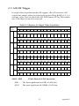
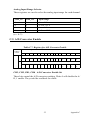
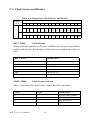
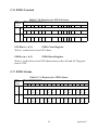
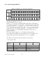
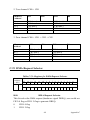
1
MIC-3714
Simultaneous 4-CH
Analog Input Card for the
CompactPCI
User Manual
Copyright
The documentation and the software included with this product are copyrighted by Advantech Co., Ltd. All rights are reserved. Advantech Co.,
Ltd. reserves the right to make improvements in the products described in
this manual at any time without notice. No part of this manual may be
reproduced, copied, translated or transmitted in any form or by any means
without the prior written permission of Advantech Co., Ltd. Information
provided in this manual is intended to be accurate and reliable. However,
Advantech Co., Ltd. assumes no responsibility for its use, nor for any
infringements of the rights of third parties, which may result from its use.
Acknowledgments
PC-LabCard is a trademark of Advantech Co., Ltd. IBM and PC are
trademarks of International Business Machines Corporation. MS-DOS,
Windows, Microsoft Visual C++ and Visual BASIC are trademarks of
Microsoft Corporation. Intel and Pentium are trademarks of Intel Corporation. Delphi and C++ Builder are trademarks of Borland Corporation.
CE notification
The MIC-3714, developed by ADVANTECH CO., LTD., has passed the
CE test for environmental specifications when shielded cables are used
for external wiring. We recommend the use of shielded cables. This kind
of cable is available from Advantech. Please contact your local supplier
for ordering information.
On-line Technical Support
For technical support and service, please visit our support website at:
http://www.advantech.com/support
MIC-3714 User Manual
Part No. 2003371400
1st Edition
Printed in Taiwan
December 2005
ii
Product Warranty (2 years)
Advantech warrants to you, the original purchaser, that each of its products will be free from defects in materials and workmanship for two years
from the date of purchase.
This warranty does not apply to any products which have been repaired or
altered by persons other than repair personnel authorized by Advantech,
or which have been subject to misuse, abuse, accident or improper installation. Advantech assumes no liability under the terms of this warranty as
a consequence of such events.
Because of Advantech’s high quality-control standards and rigorous testing, most of our customers never need to use our repair service. If an
Advantech product is defective, it will be repaired or replaced at no
charge during the warranty period. For out-of-warranty repairs, you will
be billed according to the cost of replacement materials, service time and
freight. Please consult your dealer for more details.
If you think you have a defective product, follow these steps:
1.
Collect all the information about the problem encountered. (For
example, CPU speed, Advantech products used, other hardware
and software used, etc.) Note anything abnormal and list any
onscreen messages you get when the problem occurs.
2.
Call your dealer and describe the problem. Please have your manual, product, and any helpful information readily available.
3.
If your product is diagnosed as defective, obtain an RMA (return
merchandize authorization) number from your dealer. This allows
us to process your return more quickly.
4.
Carefully pack the defective product, a fully-completed Repair and
Replacement Order Card and a photocopy proof of purchase date
(such as your sales receipt) in a shippable container. A product
returned without proof of the purchase date is not eligible for warranty service.
5.
Write the RMA number visibly on the outside of the package and
ship it prepaid to your dealer.
iii
Declaration of Conformity
CE
This product has passed the CE test for environmental specifications
when shielded cables are used for external wiring. We recommend the
use of shielded cables. This kind of cable is available from Advantech.
Please contact your local supplier for ordering information.
FCC Class A
Note: This equipment has been tested and found to comply with the limits
for a Class A digital device, pursuant to part 15 of the FCC Rules. These
limits are designed to provide reasonable protection against harmful
interference when the equipment is operated in a commercial environment. This equipment generates, uses, and can radiate radio frequency
energy and, if not installed and used in accordance with the instruction
manual, may cause harmful interference to radio communications. Operation of this equipment in a residential area is likely to cause harmful interference in which case the user will be required to correct the interference
at his own expense.
FCC Class B
Note: This equipment has been tested and found to comply with the limits
for a Class B digital device, pursuant to part 15 of the FCC Rules. These
limits are designed to provide reasonable protection against harmful
interference in a residential installation. This equipment generates, uses
and can radiate radio frequency energy and, if not installed and used in
accordance with the instructions, may cause harmful interference to radio
communications. However, there is no guarantee that interference will
not occur in a particular installation. If this equipment does cause harmful
interference to radio or television reception, which can be determined by
turning the equipment off and on, the user is encouraged to try to correct
the interference by one or more of the following measures:
• Reorient or relocate the receiving antenna.
• Increase the separation between the equipment and receiver.
• Connect the equipment into an outlet on a circuit different from that to
which the receiver is connected.
MIC-3714 User Manual
iv
• Consult the dealer or an experienced radio/TV technician for help.
FM
The MIC-3714 has passed the FM certification. According to the
National Fire Protection Association, work sites are classified into different classes, divisions and groups, based on hazard considerations.
MIC-3714 is compliant with the specifications of Class I, Division 2,
Groups A, B, C and D indoor hazards.
Technical Support and Assistance
Step 1. Visit the Advantech web site at www.advantech.com/support
where you can find the latest information about the product.
Step 2. Contact your distributor, sales representative, or Advantech's customer service center for technical support if you need additional
assistance. Please have the following information ready before
you call:
- Product name and serial number
- Description of your peripheral attachments
- Description of your software (operating system, version, application software, etc.)
- A complete description of the problem
- The exact wording of any error messages
Document Feedback
To assist us in making improvements to this manual, we would welcome
comments and constructive criticism. Please send all such - in writing to:
[email protected]
Safety Instructions
1.
Read these safety instructions carefully.
2.
Keep this User's Manual for later reference.
3.
Disconnect this equipment from any AC outlet before cleaning.
Use a damp cloth. Do not use liquid or spray detergents for cleaning.
4.
For plug-in equipment, the power outlet socket must be located
near the equipment and must be easily accessible.
5.
Keep this equipment away from humidity.
v
6.
Put this equipment on a reliable surface during installation. Dropping it or letting it fall may cause damage.
7.
The openings on the enclosure are for air convection. Protect the
equipment from overheating. DO NOT COVER THE OPENINGS.
8.
Make sure the voltage of the power source is correct before connecting the equipment to the power outlet.
9.
Position the power cord so that people cannot step on it. Do not
place anything over the power cord.
10.
All cautions and warnings on the equipment should be noted.
11.
If the equipment is not used for a long time, disconnect it from the
power source to avoid damage by transient overvoltage.
12.
Never pour any liquid into an opening. This may cause fire or electrical shock.
13.
Never open the equipment. For safety reasons, the equipment
should be opened only by qualified service personnel.
14.
If one of the following situations arises, get the equipment checked
by service personnel:
a. The power cord or plug is damaged.
b. Liquid has penetrated into the equipment.
c. The equipment has been exposed to moisture.
d. The equipment does not work well, or you cannot get it to work
according to the user's manual.
e. The equipment has been dropped and damaged.
f. The equipment has obvious signs of breakage.
15.
DO NOT LEAVE THIS EQUIPMENT IN AN ENVIRONMENT
WHERE THE STORAGE TEMPERATURE MAY GO BELOW 20° C (-4° F) OR ABOVE 60° C (140° F). THIS COULD DAMAGE THE EQUIPMENT. THE EQUIPMENT SHOULD BE IN A
CONTROLLED ENVIRONMENT.
16.
CAUTION: DANGER OF EXPLOSION IF BATTERY IS
INCORRECTLY REPLACED. REPLACE ONLY WITH THE
SAME OR EQUIVALENT TYPE RECOMMENDED BY THE
MANUFACTURER, DISCARD USED BATTERIES ACCORDING TO THE MANUFACTURER'S INSTRUCTIONS.
The sound pressure level at the operator's position according to IEC 7041:1982 is no more than 70 dB (A).
MIC-3714 User Manual
vi
DISCLAIMER: This set of instructions is given according to IEC 704-1.
Advantech disclaims all responsibility for the accuracy of any statements
contained herein.
Wichtige Sicherheishinweise
1.
1. Bitte lesen sie Sich diese Hinweise sorgfältig durch.
2.
Heben Sie diese Anleitung für den späteren Gebrauch auf.
3.
Vor jedem Reinigen ist das Gerät vom Stromnetz zu trennen. Verwenden Sie Keine Flüssig-oder Aerosolreiniger. Am besten dient
ein angefeuchtetes Tuch zur Reinigung.
4.
Die NetzanschluBsteckdose soll nahe dem Gerät angebracht und
leicht zugänglich sein.
5.
Das Gerät ist vor Feuchtigkeit zu schützen.
6.
Bei der Aufstellung des Gerätes ist auf sicheren Stand zu achten.
Ein Kippen oder Fallen könnte Verletzungen hervorrufen.
7.
Die Belüftungsöffnungen dienen zur Luftzirkulation die das Gerät
vor überhitzung schützt. Sorgen Sie dafür, daB diese Öffnungen
nicht abgedeckt werden.
8.
Beachten Sie beim. AnschluB an das Stromnetz die AnschluBwerte.
9.
Verlegen Sie die NetzanschluBleitung so, daB niemand darüber
fallen kann. Es sollte auch nichts auf der Leitung abgestellt werden.
10.
Alle Hinweise und Warnungen die sich am Geräten befinden sind
zu beachten.
11.
Wird das Gerät über einen längeren Zeitraum nicht benutzt, sollten
Sie es vom Stromnetz trennen. Somit wird im Falle einer Überspannung eine Beschädigung vermieden.
12.
Durch die Lüftungsöffnungen dürfen niemals Gegenstände oder
Flüssigkeiten in das Gerät gelangen. Dies könnte einen Brand bzw.
elektrischen Schlag auslösen.
13.
Öffnen Sie niemals das Gerät. Das Gerät darf aus Gründen der elektrischen Sicherheit nur von authorisiertem Servicepersonal geöffnet werden.
14.
Wenn folgende Situationen auftreten ist das Gerät vom Stromnetz
zu trennen und von einer qualifizierten Servicestelle zu überprüfen:
a - Netzkabel oder Netzstecker sind beschädigt.
vii
b - Flüssigkeit ist in das Gerät eingedrungen.
c - Das Gerät war Feuchtigkeit ausgesetzt.
d - Wenn das Gerät nicht der Bedienungsanleitung entsprechend funktioniert oder Sie mit Hilfe dieser Anleitung keine Verbesserung
erzielen.
e - Das Gerät ist gefallen und/oder das Gehäuse ist beschädigt.
f - Wenn das Gerät deutliche Anzeichen eines Defektes aufweist.
15.
VOSICHT: Explisionsgefahr bei unsachgemaben Austausch der
Batterie.Ersatz nur durch densellben order einem vom Hersteller
empfohlene-mahnlichen Typ. Entsorgung gebrauchter Batterien
navh Angaben des Herstellers.
16.
ACHTUNG: Es besteht die Explosionsgefahr, falls die Batterie auf
nicht fach-männische Weise gewechselt wird. Verfangen Sie die
Batterie nur gleicher oder entsprechender Type, wie vom Hersteller
empfohlen. Entsorgen Sie Batterien nach Anweisung des Herstellers.
Der arbeitsplatzbezogene Schalldruckpegel nach DIN 45 635 Teil 1000
beträgt 70dB(A) oder weiger.
Haftungsausschluss: Die Bedienungsanleitungen wurden entsprechend
der IEC-704-1 erstellt. Advantech lehnt jegliche Verantwortung für die
Richtigkeit der in diesem Zusammenhang getätigten Aussagen ab.
Safety Precaution - Static Electricity
Follow these simple precautions to protect yourself from harm and the
products from damage.
1.
To avoid electrical shock, always disconnect the power from your
PC chassis before you work on it. Don't touch any components on
the CPU card or other cards while the PC is on.
2.
Disconnect power before making any configuration changes. The
sudden rush of power as you connect a jumper or install a card may
damage sensitive electronic components.
MIC-3714 User Manual
viii
Contents
Chapter
Chapter
1 Introduction ..................................................... 2
1.1
1.2
1.3
Features ............................................................................. 2
Applications ...................................................................... 3
Installation Guide .............................................................. 4
1.4
1.5
1.6
Software Overview............................................................ 6
Device Drivers Roadmap .................................................. 7
Accessories........................................................................ 9
2 Installation ..................................................... 12
2.1
2.2
2.3
Chapter
Chapter
Chapter
Figure 1.1:Installation Flow Chart ................................. 5
Unpacking ....................................................................... 12
Driver Installation ........................................................... 13
Figure 2.1:Automation Software Setup Screen ........... 14
Figure 2.2:Options for Driver Setup ............................ 14
Hardware Installation ...................................................... 15
2.3.1
Installing a CompactPCI Card: .................................... 15
2.4
Device Setup & Configuration........................................ 16
2.5
Device Testing................................................................. 18
Figure 2.3:The Device Manager Dialog Box ............... 17
Figure 2.4:Device Names in the Device Box .............. 18
Figure 2.5:Device Test Dialog Box ............................. 19
Figure 2.6:Analog Input Tab ....................................... 20
3 Signal Connections ........................................ 22
3.1
3.2
Overview ......................................................................... 22
Switch and Jumper Settings ............................................ 22
3.3
Signal Connections.......................................................... 24
Figure 3.1:Connector, Jumper, and Switch Locations . 22
Figure 3.2:Power on Config. After Hot Reset (JP1) .... 23
Figure 3.3:I/O Connector Pin Assignment .................. 24
4 Principles of Operation................................. 26
4.1
4.2
Analog Input Range and Gains ....................................... 26
Analog Input Acquisition Modes .................................... 26
4.3
A/D Sample Clock Sources............................................. 30
4.4
4.5
Trigger Sources ............................................................... 31
Analog Input Data Format............................................... 32
Figure 4.1:Post-Trigger Acquisition Mode .................. 27
Figure 4.2:Delay-Trigger Acquisition Mode ............... 28
Figure 4.3:About-Trigger Acquisition Mode ............... 29
Figure 4.4:Pre-Trigger Acquisition Mode ................... 29
Figure 4.5: MIC-3714 Sample Clock Sources ............. 31
5 Calibration ..................................................... 34
Figure 5.1: Setup Button launches the Device Setting 34
Figure 5.2:Calibration Button launches Calibration .... 35
ix
Table of Contents
Figure 5.3:Start-up Window for Offset Calibration ..... 36
Figure 5.4:Adjustment of Offset Calibration .............. 36
Figure 5.5:Offset Calibration Success ......................... 37
Figure 5.6:Offset Calibration Failed ............................ 38
Figure 5.7:Start-up Window for Gain Calibration ....... 38
Figure 5.8: Adjustment Process for Gain Calibration .. 39
Figure 5.9:Gain Calibration Success ........................... 39
Figure 5.10:Gain Calibration Failed ............................ 40
Figure 5.11:Calibration Procedure Completed ............ 40
Appendix A Specifications ................................................. 42
Appendix B Block Diagram ............................................... 46
Appendix C Register Structure & Format ....................... 48
C.1
C.2
C.3
C.4
C.5
C.6
C.7
C.8
C.9
C.10
C.11
C.12
C.13
C.14
C.15
C.16
C.17
C.18
C.19
Overview ......................................................................... 48
Register Format ............................................................... 48
A/D SW Trigger .............................................................. 53
AI Range Control ............................................................ 54
A/D Converter Enable..................................................... 55
Clock Source and Divider ............................................... 56
Trigger Mode and Source................................................ 57
FIFO Control ................................................................... 59
FIFO Status ..................................................................... 59
FIFO for Programmable Flag.......................................... 61
DMA Counter.................................................................. 62
Interrupt Control/Flag ..................................................... 63
Clear Interrupt ................................................................. 64
Analog Trigger Threshold Voltage ................................. 65
Calibration Command ..................................................... 66
Board ID.......................................................................... 67
Reset DMA Start Channel to CH0 .................................. 67
AD Channel nDATA....................................................... 68
DMA Request Selector.................................................... 69
MIC-3714 User Manual
x
CHAPTER
1
2
Introduction
Sections include:
• Features
• Applications
• Installation Guide
• Software Overview
• Device Drivers Roadmap
• Accesories
Chapter 1 Introduction
Thank you for buying the Advantech MIC-3714. MIC-3714 is a 30MHz
Simultaneous 4-CH Analog Input Card for the PCI bus. It is an advancedperformance data acquisition card based on 32-bit CompactPCI architecture. The maximum sampling rate of MIC-3714 is up to 30MHz samples
per second, with an emphasis on continuous, non-stop, high-speed,
streaming data of A/D samples to host memory.
The following sections of this chapter will provide further information
about features of the multifunction cards, a Quick Start for installation,
together with some brief information on software and accessories for the
MIC-3714 card.
1.1 Features
The Advantech MIC-3714 offers the following main features:
• 32-bit PCI-Bus Mastering DMA data transfer
• 4 A/D converters simultaneously sampling
• 12-bit A/D converter up to 30M samples per second
• 4 single-ended analog input channels
• Programmable gain for each input channel
• On board FIFO memory
• Multiple A/D triggering modes
• Programmable pacer/counter
• Auto calibration
Some of them are highlighted and more detailed, such as the following:
PCI-Bus Mastering Data Transfer
MIC-3714 supports PCI-Bus mastering DMA for high-speed data transfer. By setting aside a block of memory in the PC, MIC-3714 performs
bus-mastering data transfers without CPU intervention, freeing the CPU
to perform other more urgent tasks such as data analysis and graphic
manipulation. The function allows users to run all I/O functions simultaneously at full speed without losing data.
MIC-3714 User Manual
2
Simultaneous Sampling
MIC-3714 is capable of simultaneous sampling, and uses 4 identical circuitries and ADC for each analog input channel. Where the time relationship between inputs is important, this feature allows you to sample
simultaneously.
S/W, Internal and External Pacer Triggering Supported
MIC-3714 supports three kinds of trigger modes for A/D conversion:
software triggering, internal pacer triggering and external pacer triggering. The software trigger allows users to acquire a sample when needed;
the internal pacer triggers continuous high-speed data acquisitions. MIC3714 also accepts external trigger sources, allowing synchronous sampling with external devices.
On-board FIFO Memory
There are 32K samples of FIFO memory on MIC-3714. This is an important feature for fast data transfer and stable performance using Windows
OS.
Auto Calibration
MIC-3714 features software auto calibration. There is no variable resister
trimming required. This is convenient for user to calibrate.
Note: For detailed specifications of the MIC-3714, please refer to Appendix
A, Specifications.
1.2 Applications
The following are some of the possible applications of MIC-3714:
• Testing Instrument
• Ultrasound Imaging
• Gamma Camera Imaging
• CCD Camera Imaging
• Video Digitizing
3
Chapter 1
1.3 Installation Guide
Before you install your MIC-3714 card, please make sure if you have the
following necessary components:
MIC-3714 DA&C card
MIC-3714 User’s Manual
This manual
Driver software
Advantech DLL drivers (included in the companion CD-ROM)
Wiring cable
PCL-10901-1, PCL-1010B-1 (optional)
Wiring board
ADAM-3909 (optional)
Computer
Personal computer or workstation with a PCIbus slot (running Windows 98/2000/XP)
Some other optional components are also available for enhanced
operation:
Application software: ActiveDAQ or other 3rd party software packages
After you get the necessary components and maybe some of the accessories for enhanced operation of your Multifunction card, you can then
begin the Installation procedures. Fig. 1-1 on the next page provides a
concise flow chart to give users a broad picture of the software and hardware installation procedures:
MIC-3714 User Manual
4
Install Driver from CD-ROM, then power-off PC
Install Hardware and power-on PC
Use driver utility to configure hardware
Use test utility to test hardware
Read examples & driver manual
Start to write your own application
Figure 1.1: Installation Flow Chart
5
Chapter 1
1.4 Software Overview
Advantech offers a rich set of DLL drivers, third-party driver supports
and application software to help fully utilize the functions of your MIC3714 card:
• Device Drivers (on the companion CD-ROM)
• LabVIEW driver
Programming choices for DA&C cards
You may use Advantech application software such as Advantech Device
Drivers. On the other hand, advanced users can use another option for
register-level programming, although it is not recommended due to its
laborious and time-consuming nature.
Device Drivers
The Advantech Device Drivers software is included on the companion
CD-ROM at no extra charge. It also comes with all Advantech DA&C
cards. Advantech’s device drivers feature a complete I/O function library
to help boost your application performance. The Advantech Device Drivers for Windows 98/2000/XP work seamlessly with development tools
such as Visual C++, Visual Basic, Borland C++ Builder and Borland
Delphi.
Register-level Programming
Register-level programming is reserved for experienced programmers
who find it necessary to write code directly at the level of device registers. Since register-level programming requires much effort and time, we
recommend that you use the Advantech Device Drivers instead. However, if register-level programming is necessary, you should refer to the
relevant information in Appendix C, Register Structure and Format, or to
the example codes included on the companion CD-ROM.
MIC-3714 User Manual
6
1.5 Device Drivers Roadmap
This section will provide you a roadmap to demonstrate how to build an
application from scratch using Advantech Device Drivers with your
favorite development tools such as Visual C++, Visual Basic, Delphi and
C++ Builder. The step-by-step instructions on how to build your own
applications using each development tool will be given in the Device
Drivers Manual. Moreover, a rich set of example source code is also
given for your reference.
Programming Tools
Programmers can develop application programs with their favorite development tools:
• Visual C++
• Visual Basic
• Delphi
• C++ Builder
For instructions on how to begin programming work with each development tool, Advantech offers a Tutorial Chapter in the Device Drivers
Manual for your reference.
Please refer to the corresponding sections in this chapter of the Device
Drivers Manual to begin your programming efforts. You can also look at
the example source code provided for each programming tool, since they
can get you very well oriented.
The Device Drivers Manual can be found on the companion CD-ROM.
Or if you have already installed the Device Drivers on your system, The
Device Drivers Manual can be readily accessed through the Start button:
Start/Programs/Advantech eAutomation/Device Manager/Device
Driver's Manual
The example source codes could be found under the corresponding installation folder such as the default installation path:
\Program Files\Advantech\ADSAPI\Examples
For information about using other function groups or other development
tools, please refer to Device Driver Programming Guide chapter and the
Function Reference chapter on the Device Drivers Manual.
7
Chapter 1
Programming with Device Drivers Function Library
Advantech Device Drivers offers a rich function library to be utilized in
various application programs. This function
library consists of numerous APIs that support many development tools,
such as Visual C++, Visual Basic, Delphi and C++ Builder.
According to their specific functions or services, those APIs can be categorized into several function groups:
Device Function
Analog Input/Output Function
Digital Input/Output Function
Port I/O Function
Counter Function
Temperature Measurement Function
Alarm Function
Communication port Function
High speed Function
Hardware Function
For the usage and parameters of each function, please refer to the Function Description chapter in the Device Drivers Manual.
Troubleshooting Device Drivers Error
Driver functions will return a status code when they are called to perform
a certain task for the application. When a function returns a code that is
not zero, it means the function has failed to perform its designated function. To troubleshoot the Device Drivers error, you can pass the error
code to DRV_GetErrorMessage function to return the error message.
Or you can refer to the Device Drivers Error Codes Appendix in the
Device Drivers Manual for a detailed listing of the Error Code, Error ID
and the Error Message.
MIC-3714 User Manual
8
1.6 Accessories
Advantech offers a complete set of accessory products to support the
MIC-3714 card. These accessories include:
Wiring Cable
PCL-10901-1
The PCL-10901-1 cable is specially designed for MIC3714 cards to connect to the wiring board, ADAM-3909,
for external synchronization signal source, such like an
external trigger and/or clock signal.
PCL-1010B-1
The PCL-1010B-1 cable is designed for connecting to the
signal source. The cable links the MIC-3714 cards with
the signal source via the BNC connectors. There are all
four BNC ports on board available for simultaneous signal input.
Wiring Board
ADAM-3909
The ADAM-3909 is a DB-9 Wiring Terminal for DIN-rail
Mounting. This terminal module can be readily connected
to the Advantech PC-Lab cards and allows easy yet reliable access to individual pin connections for the MIC3714 card.
9
Chapter 1
MIC-3714 User Manual
10
CHAPTER
2
2
Installation
Sections include:
• Installation
• Unpacking
• Driver Installation
• Hardware Installation
• Device Setup and Configuration
• Device Testing
Chapter 2 Installation
This chapter gives users a package item checklist, proper instructions
about unpacking and step-by-step procedures for both driver and card
installation.
2.1 Unpacking
After receiving your MIC-3714 package, please inspect its contents first.
The package should contain the following items:
• MIC-3714 card
• Companion CD-ROM (DLL driver included)
• User’s Manual
The MIC-3714 card harbors certain electronic components vulnerable to
electrostatic discharge (ESD). ESD could easily damage the integrated
circuits and certain components if preventive measures are not carefully
paid attention to.
Before removing the card from the antistatic plastic bag, you should
take following precautions to ward off possible ESD damage:
• Touch the metal part of your computer chassis with your hand to discharge static electricity accumulated on your body. Or use a grounding
strap.
• Touch the anti-static bag to a metal part of your computer chassis
before opening the bag.
• Take hold of the card only by the metal bracket when removing it from
the bag.
After taking out the card, first you should:
Inspect the card for any possible signs of external damage (loose or damaged components, etc.). If the card is visibly damaged, please notify our
service department or the local sales representative immediately. Avoid
installing a damaged card into your system.
MIC-3714 User Manual
12
Also, be careful of the following aspects to ensure proper installation:
• Avoid physical contact with materials that could hold static electricity
such as plastic, vinyl and Styrofoam.
• Whenever you handle the card, grasp it only by its edges. DO NOT
TOUCH the exposed metal pins of the connector or the electronic components.
Note: Keep the anti-static bag for future use. You might need the original bag
to store the card if you have to remove the card from the PC or transport it
elsewhere.
2.2 Driver Installation
We recommend you to install the driver before you install the MIC3714 card into your system, since this will guarantee a smooth installation process.
The Advantech Device Drivers setup program for the MIC-3714 card is
included on the companion CD-ROM that is shipped with your DA&C
card package. Please follow the steps below to install the driver software:
Step 1: Insert the companion CD-ROM into your CD-ROM drive.
Step 2: The Setup program will be launched automatically if you have
the AUTORUN function enabled on your system. When the Setup program is launched, you’ll see the following setup screen.
Note: If the AUTORUN function is not enabled on your computer, use Windows Explorer or the Windows Run command to execute SETUP.EXE on the
companion CD-ROM.
13
Chapter 2
Figure 2.1: Automation Software Setup Screen
Step 3: Select the Individual Drivers option.
Step 4: Select the specific device then just follow the installation instructions step by step to complete your device driver setup.
Figure 2.2: Options for Driver Setup
For further information on driver-related issues, an online version of
Device Drivers Manual is available by accessing:
Start/Programs/Advantech eAutomation/Device Driver's Manual
MIC-3714 User Manual
14
2.3 Hardware Installation
Note: Make sure you first install the driver before installing the card. We
strongly recommend that you install the software driver before installing the
hardware into your system, since this will guarantee a smooth and troublefree installation process. For more information about the driver installation,
configuration and removal procedures for Windows 9X, Windows NT, Windows 2000 and Windows XP, please see the Device Driver Manual.
When installing the MIC-3714 card, please make sure the DLL driver of
MIC-3714 installation is completed. You can then go on to install the
MIC-3714 card in your CompactPCI system. If you have any doubts,
please consult the user manual or related documentation. Please follow
the below steps to install the card in your system.
2.3.1 Installing a CompactPCI Card:
Step 1: Remove one cover on the unused slot of your CompactPCI computer slot.
Step 2: Hold the card vertically. Be sure that the card is pointing in the
correct direction. The components of the card should be pointing to the
right-hand side and the black handle of the card should be pointing to the
lower edge of the backplane.
Step 3: Hold the lower handle and pull the handle down to unlock it.
Step 4: Insert the MIC-3714 card into the CompactPCI chassis carefully
by sliding the lower edges of the card into the card guides.
Step 5: Push the card into the slot gently by sliding the card along the
card guide until J1 meets the long needle on the backplane, then the Blue
LED on the front panel of the card will be lit.
Note: If your card is correctly positioned and has been slid all the way into
the chassis, the handle should match the rectangular holes. If not, remove the
card from the card guide and repeat step 3 again. Do not try to install a card
by forcing it into the chassis
Step 6: Now push the card into the right place, and the Blue LED will
turn off.
Step 7: After the Blue LED is off, push the handle to secure the card and
lock it into place.
15
Chapter 2
Note: In case you installed the card without installing the DLL driver first,
Windows 98/200/XP will recognize your card as an “unknown device” after
rebooting, and will prompt you to provide the necessary driver. You should
ignore the prompting messages (just click the Cancel button) and set up the
driver according to the steps described in 2.2 Driver Installation.
After the MIC-3714 card is installed, you can verify whether it is properly
installed on your system in the Device Manager:
1. Access the Device Manager through:
Start /Control Panel /System /Device Manager.
2. The device name of the MIC-3714 should be listed on the Device Manager tab on the System Property Page.
Note: If your card is properly installed, you should see the device name of
your card listed on the Device Manager tab. If you do see your device name
listed on it but marked with an exclamation sign “!”, it means your card has
not been correctly installed. In this case, remove the card device from the
Device Manager by selecting its device name and press the Remove button.
Then go through the driver installation process again.
After your card is properly installed on your system, you can now configure your device using the Device Manager program that has itself already
been installed on your system during driver setup. A complete device
installation procedure should include board selection and device setup.
After that, you can operate this card through the operation. The following
sections will guide you through the board selection, device setup and
operation of your device.
2.4 Device Setup & Configuration
The Device Manager program is a utility that allows you to setup, configure and test your device, and later store your settings on the system registry. These settings will be used when you call the APIs of Advantech
Device Drivers.
Setting Up and Configuring the Device
MIC-3714 User Manual
16
Step 1: To install the I/O device for your card, you must first run the
Advantech Device Manager program by accessing:
Start/Programs/Advantech eAutomation/Device Manager/Advantech
Device Manager
Step 2: You can then view the device(s) already installed on your system
(if any) in the Installed Devices list box. Since you haven’t installed any
device yet, you might see a blank list such as the one below (Fig. 2-3).
Figure 2.3: The Device Manager Dialog Box
Step 3: After you have finished configuring the device, click OK and the
device name will appear in the Installed Devices box as the following:
17
Chapter 2
Figure 2.4: Device Names in the Device Box
Note: The device name “001:<MIC-3714 BoardID=9 I/O=e000H>” begins
with a device number “001”, which is specifically assigned to each card. The
device number is passed to the driver to specify which device you wish to control.
If you want to test the card device further, go right to the next section on
the Device Testing. You can also find the rich examples on the CD-ROM
to speed up your Programming.
2.5 Device Testing
Following through the Setup and Configuration procedures to the last
step described in the previous section, you can now proceed to test the
device by clicking the Test button on the Device Manager dialog box. A
Device Test dialog box will appear accordingly (Fig. 2-5):
MIC-3714 User Manual
18
Figure 2.5: Device Test Dialog Box
On the Device Test dialog box, users are free to test various functions of
MIC-3714 on the Analog input tabs, functions on the other tabs are not
supported for this model.
Testing Analog Input Function
Make sure the Analog Input tab is selected, otherwise, click on the Analog Input tab to bring it up to front of the screen. Select the input range for
each channel in the Input range drop-down boxes. Configure the Sampling period on the scroll bar to adjust the sampling rate, the Analog input
reading windows will show the readings of all the four channels accordingly. Scroll the Sampling period scroll bar freely to test any sampling
rate you want. When the device is fully tested, click Exit button to end the
testing procedure.
19
Chapter 2
Figure 2.6: Analog Input Tab
MIC-3714 User Manual
20
CHAPTER
3
2
Signal Connections
Sections include:
• Signal Connections
• Overview
• Switch and Jumper Settings
• Software Overview
• Device Drivers Roadmap
• Accesories
Chapter 3 Signal Connections
Maintaining proper signal connections is one of the most important factors to ensure that your application system is sending and receiving data
correctly. A good signal connection can avoid unnecessary and costly
damage to your PC and other hardware devices. This chapter provides
useful information about how to connect input and output signals to the
MIC-3714 via the I/O connector.
3.1 Overview
Maintaining signal connections is one of the most important factors in
ensuring that your application system is sending and receiving data correctly. A good signal connection can avoid unnecessary and costly damage to your PC and other hardware devices. This chapter provides useful
information about how to connect input and output signals to the MIC3714 via the I/O connector.
3.2 Switch and Jumper Settings
The MIC-3714 card has one function switch and five jumper settings.
Figure 3.1: Connector, Jumper, and Switch Locations
MIC-3714 User Manual
22
Board ID setting (SW1)
ID3
ID2
1
1
1
1
1
1
1
1
1
0
1
0
1
0
1
0
0
1
0
1
0
1
0
1
0
0
0
0
0
0
0
0
Note: On: 1, Off: 0
ID1
1
1
0
0
1
1
0
0
1
1
0
0
1
1
0
0
ID0
1
0
1
0
1
0
1
0
1
0
1
0
1
0
1
0
Board ID
0
1
2
3
4
5
6
7
8
9
10
11
12
13
14
15
Figure 3.2: Power on Config. After Hot Reset (JP1)
User can use the JP1 to set the hot reset type of MIC-3714.
JP1
Power-on configuration after hot reset
Keep the I/O configuration while hot reset.
Clear the I/O configuration to default while hot reset.
Input terminator select (JP2 to JP5)
User can use the JP2 to JP5 to set input terminator value for each AI
channel CH0 to CH3, respectively.
23
Chapter 3
JP2, JP3, JP4, JP5
Input terminator select
50Ω
1MΩ
High Impedance
3.3 Signal Connections
CN1 Pin Assignment
Fig. 3-2 shows the pin assignments for the PS-2 connector and the DB-9
connector on the cable.
GND
4
EXT TRIG0
NC
6
1
EXT CLK1
EXT TRIG0
1
NC
2
EXT CLK0+
2
5
3
EXT CLK0-
GND
EXT CLK0-
3
4
5
9
GND
8
GND
7
GND
6
EXT CLK1
EXT CLK0+
On board PS-2 connector
PS2 To DB-9 Cable Connector
Figure 3.3: I/O Connector Pin Assignment
J1 to J4 BNC are the AI input connectors.
J1 is for AI0, J2 is for AI1, J3 is for AI2 and J4 is for AI3.
MIC-3714 User Manual
24
CHAPTER
4
2
Principles of Operation
Sections include:
• Analog Input Range and Gains
• Analog Input Acquisition Mode
• A/D Sample Clock Sources
• Trigger Sources
• Analog Input Data Format
Chapter 4 Principles of Operation
This chapter describes the following features of the MIC-3714 card:
• Analog input ranges and gains
• Analog input acquisition modes
• A/D sample clock sources
• Trigger sources
• Analog Input Data Format
4.1 Analog Input Range and Gains
Each channel on the MIC-3714 can measure bipolar analog input signals
ranging within ± 5 V FSR, and can be set up with different input ranges
respectively. The sampling rate can be up to 30 MS/s.
MIC-3714 also provides various gain levels that are programmable per
channel. Table 4-1 lists the effective ranges supported by the MIC-3714
using these gains.
Table 4.1: Gains and Analog Input Range
Gain
1
2
5
10
Analog Input Range
±5 V
±2.5 V
±1 V
±0.5 V
For each channel, choose the gain level that provides most optimal range
that can accommodate the signal range you have to measure. For detailed
information, please refer to Appendix C.4 AI Range Control.
4.2 Analog Input Acquisition Modes
The MIC-3714 can acquire data in single value, pacer, post-trigger,
delay-trigger, about-trigger and pre-trigger acquisition modes. These analog input acquisition modes are described in more details in the following:
Single Value Acquisition Mode
The single value acquisition mode is the simplest way to acquire data.
Once the software issues a trigger command, the A/D converter will conMIC-3714 User Manual
26
vert one data, and return it immediately. User can check the A/D FIFO
status (Read BASE+10, 12) to make sure if the data is ready to be
received. For detailed information, please refer to Appendix C.8 FIFO
Control, Appendix C.9 FIFO Status, Appendix C.10 FIFO for Progarmmable Flag.
Pacer Acquisition Mode
Use pacer acquisition mode to acquire data if you want to accurately control the time interval between conversions of individual channels in a
scan. A/D conversion clock comes from A/D counter or external clock
source on connector. A/D conversion starts when the first clock signal
comes in, and will not stop if the clock is still continuously sending into
it. Conversion data is put into the A/D FIFO. For high-speed data acquisition, you have to use the DMA data transfer for analog input to prevent
data loss.
Post-Trigger Acquisition Mode
Post-trigger allows you to acquire data based on a trigger event. Posttrigger acquisition starts when the MIC-3714 detects the trigger event and
stops when the preset number of post-trigger samples has been acquired
or when you stop the operation. This trigger mode must work with the
DMA data transfer mode enabled. Use post-trigger acquisition mode
when you want to acquire data when a post-trigger event occurs. Please
specify the following parameters when using software in post-trigger
acquisition mode:
• Set to Post-Trigger Acquisition Mode
• The A/D sample clock source and sampling rate
• The trigger source
• The acquired sample number N
Figure 4.1: Post-Trigger Acquisition Mode
27
Chapter 4
Delay Trigger Acquisition Mode
In delay trigger mode, data acquisition will be activated after a preset
delay number of sample has been taken after the trigger event. The delay
number of sample ranges from 2 to 65535 as defined in DMA counter.
Delay-trigger acquisition starts when the MIC-3714 detects the trigger
event and stops when the specified number of A/D samples has been
acquired or when you stop the operation. This triggering mode must work
with the DMA data transfer mode enabled Please specify the following
parameters when using software in delay trigger mode:
• Set to Delay-Trigger Acquisition Mode
• The sample clock source and sampling rate
• The trigger source
• The acquired sample number N
• The sample number M delays after the delay-trigger event happened
Figure 4.2: Delay-Trigger Acquisition Mode
About Trigger Acquisition Mode
Use about-trigger acquisition mode when you want to acquire data both
before and after a specific trigger event occurs. This operation is equivalent to doing both a pre-trigger and a post-trigger acquisition. When using
software, please specify the following parameters, when using software
in About-Trigger acquisition mode:
• Set to About-Trigger Acquisition Mode
• The sample clock source and sample rate
• The trigger source
• The total acquired sample number N
• The specific sample number M after the trigger event. The range of preset sample number is from 2 to 65536 samples.
MIC-3714 User Manual
28
In about-trigger mode, users must first designate the size of the allocated
memory and the amount of samples to be snatched after the trigger event
happens. The about-trigger acquisition starts when the first clock signal
comes in. Once a trigger event happens, the on-going data acquisition
will continue until the designated amount of samples have been reached.
When the MIC-3714 detects the selected about trigger event, the card
keeps acquiring the preset number of samples, and kept the total number
of samples on the FIFO.
Figure 4.3: About-Trigger Acquisition Mode
Pre-Trigger Acquisition Mode
Pre-Trigger mode is a particular application of about-trigger mode. Use
pre-trigger acquisition mode when you want to acquire data before a specific trigger event occurs. Pre-trigger acquisition starts when you start the
operation and stops when the trigger event happens. Then the specific
number of samples will be reversed in the FIFO before the pre-trigger
event occurred. Please specify the following parameters, when using software in Pre-trigger acquisition mode:
• Set to Pre-Trigger Acquisition Mode
• The sample clock source and sample rate
• The trigger source
• Assume the total acquired sample number is N, then set the total sample
number to be N+2.
Figure 4.4: Pre-Trigger Acquisition Mode
29
Chapter 4
4.3 A/D Sample Clock Sources
The MIC-3714 can adopt both internal and external clock sources for
pacer, post-trigger, delay-trigger, about-trigger acquisition modes:
• Internal A/D sample clock with 8-bit Counter
• External A/D sample clock that is connected to either the EXT-CLK0
(the differential clock source) or the EXT_CLK1 (the single ended
clock source) on the ADAM-3909 screw terminal board.
The internal and both external A/D sample clocks are described in more
details as the following.
Internal A/D Sample Clock
The internal A/D sample clock uses a 60 MHz time base. Conversions
start on the rising edge of the counter output. You can use software to
specify the clock source as internal and the sampling frequency to pace
the operation. The minimum frequency is 234375 S/s, the maximum frequency is 30 MS/s. According to the sampling theory (Nyquist Theorem),
you must specify a frequency that is at least twice as fast as the input’s
highest frequency component to achieve a valid sampling. For example,
to accurately sample a 300 kHz signal, you have to specify sampling frequency of at least 600 kHz. This consideration can avoid an error condition often know as aliasing, in which high frequency input components
appear erroneously as lower frequencies when sampling.
External A/D Sample Clock 0
The external sample clock 0 is a sine wave signal source which is converted to a TTL signal inside the MIC-3714. This signal is AC coupled.
The input impedance of external clock 0 is 50 ohms and the input level is
2 volts peak-to-peak.
Please note that the frequency of the external clock is the system clock.
The maximum A/D clock frequency is half of the system clock.
External A/D Sample Clock 1
The external sample clock 1 is a digital clock. The input impedance is 50
ohms and the input level should be 2.4V~5V into the 50-ohm load. This
signal is DC coupled.
MIC-3714 User Manual
30
60 Mhz
Trigger
and
Control
Logic
8-bit
Counter
A/D
Converter
Internal
EXT_CLK0
Trigger
Source
EXT_CLK1
Figure 4.5: MIC-3714 Sample Clock Sources
4.4 Trigger Sources
The MIC-3714 supports the following trigger sources for post-, delay-,
about- and pre-trigger acquisition modes:
• Software trigger,
• External digital (TTL) trigger, and
• Analog threshold trigger.
With MIC-3714, user can define the type of trigger source as rising-edge
or falling-edge. These following sections describe these trigger sources in
more detail.
Software Trigger
A software trigger event occurs when you start the analog input operation
(the computer issues a write to the board to begin acquisitions). When
you write the value to analog input trigger flag TRGF on Write
BASE+Eh to produce either a rising-edge or falling-edge trigger, depending upon the trigger source type you choose. This edge will then act as an
A/D trigger event.
For detailed information, please refer to Appendix C.7 Trigger Mode and
Source.
31
Chapter 4
External Digital (TTL) Trigger
For analog input operations, an external digital trigger event occurs when
the MIC-3714 detects either a rising or falling edge on the External A/D
TTL trigger input signal from screw terminal EXT_TRIG on the ADAM3909 screw terminal board. The trigger signal is TTL-compatible.
Analog Threshold Trigger
For analog input operations, an analog trigger event occurs when the
MIC-3714 detects a transition from above a threshold level to below a
threshold level (falling edge), or a transition from below a threshold level
to above a threshold level (rising edge). User should connect the analog
signals from the external device to one of the four BNC source connectors. Which one of the four sources is selected as the trigger source can be
defined or identified by writing to or reading from the flags from TS0 to
TS2 of Write/Read BASE+Eh. On the MIC-3714, the analog trigger
threshold voltage level is set using a dedicated 8-bit DAC; you can write
or read the flags from AT0 to AT7 on Write/Read BASE+24h to define or
identify the analog trigger threshold voltage level. Please also refer to the
Appendix C.14 Analog Trigger Threshold Voltage for more details.
4.5 Analog Input Data Format
Table 4.2: Analog Input Data Format
A/D Code
Mapping Voltage
Hex.
Dec.
000h
0d
-FS
7FFh
2047d
-1 LSB
800h
2048d
0
FFFh
4095d
1LSB
FS-1 LSB
FS/2048
Table 4.3: Various Input Voltage Ranges
Gain
Range
FS
1
±5
5
2
±2.5
2.5
5
±1
1
10
±0.5
0.5
MIC-3714 User Manual
32
CHAPTER
5
2
Calibration
Chapter 5 Calibration
This chapter offers you a brief guide to the calibration procedure. The
MIC-3714 has been well calibrated at the factory for initial use. Users are
not necessary to calibrate the MIC-3714 in normal conditions. However,
if some other conditions that the users have to calibrate the MIC-3714,
then they can follow the procedure listed below to perform the necessary
calibration.
To perform an effective calibration, the user has to prepare a standard 41/2 digits resolution, stable and low-noise DC voltage source. It is important that the accuracy of the device will depend on the accuracy of the DC
source.
Calibration Procedure
Step 1: Click the Setup button on the Advantech Device Manager window (Fig.5-1) to launch the MIC-3714 Device Setting window (Fig.5-2).
Figure 5.1: Setup Button launches the Device Setting
MIC-3714 User Manual
34
Step 2: Select the input range of the channel which you want to calibrate.
Step 3: Click the Calibration button to start the calibration process. The
Calibration Wizard window will pop up.
Note: Each calibration process can calibrate only one channel and one input
range at a time.
Figure 5.2: Calibration Button launches Calibration
Step 4: Follow the instruction of Calibration Wizard to input a correct
DC voltage as a reference and click the Next button to proceed to the next
step.
35
Chapter 5
Figure 5.3: Start-up Window for Offset Calibration
Step 5: Click the Start button to start the Offset Calibration. Note that the
Status will indicate Unknown as default at the beginning.
Figure 5.4: Adjustment of Offset Calibration
MIC-3714 User Manual
36
Step 6: If the reference DC voltage source and the wiring are both correct, the calibration will proceed automatically after the Start button is
clicked. When the offset calibration is completed, the Status will indicate
Succeeded, then click the Next button to proceed to the next step.
Figure 5.5: Offset Calibration Success
Step 7: Once the Status indicates Failed, please check if both the wiring
and the input voltage are correct. When finished checking, click the Start
button again to restart the procedure, or click the Cancel button to stop the
calibration.
37
Chapter 5
Figure 5.6: Offset Calibration Failed
Step 7: If the offset calibration is completed, then it is going to proceed to
the Gain Calibration. The steps of gain calibration are quite similar to
those of the offset calibration. Follow the instructions of the Calibration
Wizard to input a correct DC voltage and click the Next button to proceed.
Figure 5.7: Start-up Window for Gain Calibration
MIC-3714 User Manual
38
Step 8: Click the Start button to start gain calibration. Note that the Status
will indicate Unknown as default at the beginning.
Figure 5.8: Adjustment Process for Gain Calibration
Step 9: When the gain calibration is completed then click the Next button
to proceed.
Figure 5.9: Gain Calibration Success
39
Chapter 5
Step 9: Once the Status indicates Failed, please check if both the wiring
and the input voltage are correct. When finished checking, click the Start
button again to restart the procedure, or click the Cancel button to stop the
calibration.
Figure 5.10: Gain Calibration Failed
Step 10: When the current channel is calibrated, click the Finish button to
end the procedure. You can proceed to Step 3 to select another channel
for calibration, and repeat from Step 4 to Step 9, until the rest of the channels are all calibrated one after one.
Figure 5.11: Calibration Procedure Completed
MIC-3714 User Manual
40
APPENDIX
A
2
Specifications
Appendix A Specifications
Table A.1: Analog Input
Channels
4 single-ended analog input channels
Resolution
12-bit
Max. Sampling Rate1
Up to 30MHz1
FIFO Size 32K locations
Common Mode Voltage ±11 V max. (operational)
Input Range and
Gain List
Gain
1
2
5
10
Range
±5V
±2.5V
±1V
±0.5V
Drift
Gain
1
2
5
10
Zero (µV/°C)
200
100
40
20
Gain (ppm/°C)
±30
±30
±30
±30
Small Signal
Bandwidth for PGA
Gain
1
2
5
10
Bandwidth
(-3dB)
7MHz
7MHz
7MH 7MHz
z
Max. Input Voltage
±15 V
Input Impedance
50Ω /1MΩ /∞ jumper selectable 100pF
Trigger Mode
Software, pacer, post-trigger, pre-trigger, delay-trigger,
about-trigger
Accuracy
DC
Input Surge
Protect
30 Vp-p
DNLE: ±1LSB (No Missing Codes:12 Bits Guaranteed)
INLE: ±2LSB
External Clock 1
Offset
error
Adjustable to ±1LSB
Gain
error
Adjustable to ±1LSB
AC
SINAD: S/(N+D): 64 dB
ENOB: 10.33bits
THD: -71 dB
Logic level
TTL (Low: 0.8V max. High: 2.0V min.)
Input
impedance
50 ohms
Input coupled DC
External Clock 0
Frequency
Up to 10 MHz
Logic level
5.0V peak to peak sin wave
Input
impedance
Hi Z
Input coupled AC
Frequency
MIC-3714 User Manual
Up to 10 MHz
42
External Trigger 0
Logic level
TTL (Low: 0.8V max. High: 2.0V min.)
Input
impedance
Hi Z
Input coupled AC
External Analog
Trigger Input
Frequency
Up to 10 MHz
Range
By analog input range
Resolution
8-bit
Frequency
Up to 1 MHz
Table A.2: General
I/O Connector Type
4 BNC connector for AI
1 PS2 connector for ext. clock and trigger
Dimensions
160mm x 100mm (6.3" x 3.9")
Power Consumption
Typical
Temperature
+5 V @ 850 mA ; +12 V @ 600
mA
Max.
+5 V @ 1 A ; +12 V @ 700m A
Operation
0~+70°C(32~158°F)
Storage
-20~+85°C(-4~185°F)
Relative Humidity
5~95%RH non-condensing (refer to IEC 68-2-3)
Certification
CE certified
Note1: 30 MHz is only for FIFO depth (32K). Continuous acquisition
depends on platform performance.
43
Appendix A
MIC-3714 User Manual
44
APPENDIX
B
2
Block Diagram
Appendix B Block Diagram
MIC-3714 User Manual
46
C
APPENDIX
2
Register Structure &
Format
Appendix C Register Structure & Format
C.1 Overview
The MIC-3714 is delivered with an easy-to-use 32-bit DLL driver for
user programming under the Windows 98/2000/XP operating systems.
We advise users to program the MIC-3714 using the 32-bit DLL driver
provided by Advantech to avoid the complexity of low-level programming by register.
The most important consideration in programming the MIC-3714 at register level is to understand the function of the card's registers. The information in the following sections is provided only for users who would
like to do their own low-level programming.
C.2 Register Format
The register format is the basis to control the MIC-3714.
There are some rules for programmer’s reference:
1.
All registers are 32-bit format. Please use the DWORD command
in your own software.
2.
Some registers are used only for write or read.
3.
Some registers can support write and read back, they usually use
the same name.
4.
Some registers could write any value to complete a command.
5.
In general, read only register is called status register, write only
register is called control register.
6.
Some registers are very similar, usually denote as a group. For
example, A4, A3, A2, A1, A0 usually denote as A4: A0.
7.
In this document, 1Fh means hexadecimal number 1F.
Table C-1 shows the function of each register of the MIC-3714 or driver
and its address relative to the card's base address.
MIC-3714 User Manual
48
Table C.1: MIC-3714 Register Format (Part 1)
AD0
0
AD1
AD0
1
AD2
AD1
AD0
2
AD3
AD2
AD1
3
AD4
AD3
AD2
AD0
4
AD5
AD4
AD3
AD1
5
AD6
AD5
AD4
AD2
6
AD8 AD7
AD6
AD5
AD3
7
R AI Channel 0 Data
TRGF OV
G1 G0 AD11 AD10 AD9
W AI Channel 1 Single Value Acquisition
AD8 AD7
AD6
AD4
8
2h
R AI Channel 1 Data
TRGF OV
G1 G0 AD11 AD10 AD9
W AI Channel 2 Single Value Acquisition
AD8 AD7
AD5
9
4h
R AI Channel 2 Data
TRGF OV
G1 G0 AD11 AD10 AD9
W AI Channel 3 Single Value Acquisition
AD6
Base
MIC-3714 Register Format
Address 15
14
13 12 11
10
0h W AI Channel 0 Single Value Acquisition
6h
AD8 AD7
TSE
TSE
CKS1 CKS0 DIV7
CKS1 CKS0 DIV7
TS2
TS2
DIV6
DIV6
TS1
TS1
DIV5
DIV5
TS0
TS0
DIV4
DIV4
DIV3
DIV3
CH3
CH3
TM2
TM2
DIV2
DIV2
CH2
CH2
TM1
TM1
DIV1
DIV1
CH1
CH1
TM0
TM0
DIV0
DIV0
CH0
CH0
CH3_G1 CH3_G0 CH2_G1 CH2_G0 CH1_G1 CH1_G0 CH0_G1 CH0_G0
CH3_G1 CH3_G0 CH2_G1 CH2_G0 CH1_G1 CH1_G0 CH0_G1 CH0_G0
R AI Channel 3 Data
TRGF OV
G1 G0 AD11 AD10 AD9
W AI Range Control Register
8h
R
Ah W A/D Converter Enable Register
R
Ch W Clock Source and Divider Register
R
TRGF DMA_TCF
Eh W Trigger Mode and Source Register
TRGF DMA_TCF
R
Appendix C
49
Table C.2: MIC-3714 Register Format (Part 2)
Base
MIC-3714 Register Format
Address 15
14
13
12
10h W FIFO Control Register
R FIFO Status Register
FIFO1_AF FIFO1_AE
12h W FIFO Control Register
R FIFO Status Register
FIFO3_AF FIFO3_AE
14h W FIFO 0 Programmable Flag Register
PF14 PF13
FP12
R FIFO 0 Programmable Flag Register
PF14 PF13
FP12
16h W FIFO 1 Programmable Flag Register
PF14 PF13
FP12
R FIFO 1 Programmable Flag Register
PF14 PF13
FP12
18h W FIFO 2 Programmable Flag Register
PF14 PF13 FP12
R FIFO 2 Programmable Flag Register
PF14 PF13 FP12
1Ah W FIFO 3 Programmable Flag Register
PF14 PF13
FP12
R FIFO 3 Programmable Flag Register
PF14 PF13
FP12
1Ch W DMA Counter Register
CN15 CN14 CN13
CN12
R
CN15 CN14 CN13
CN12
1Eh W Rest DMA Counter
R
10
9
FCLR1
8
5
4
2
1
0
PF11 PF10
PF11 PF10
PF11 PF10
PF9
PF9
PF9
PF9
PF8
PF8
PF8
PF8
PF8
PF7 PF6 PF5
PF7 PF6 PF5
PF7 PF6 PF5
PF7 PF6 PF5
PF7 PF6 PF5
PF7 PF6 PF5
PF4
PF4
PF4
PF4
PF4
PF4
PF4
PF3 PF2
PF3 PF2
PF3 PF2
PF3 PF2
PF3 PF2
PF3 PF2
PF3 PF2
PF3 PF2
CN1
PF1
PF1
PF1
PF1
PF1
PF1
PF1
PF1
CN0
CN0
PF0
PF0
PF0
PF0
PF0
PF0
PF0
PF0
3
FCLR0
PF11 PF10
PF9
PF8
PF7 PF6 PF5
PF4
CN3 CN2
CN1
6
FRST0
FIFO0_FF FIFO0_HF FIFO0_EF
FCLR2
PF11 PF10
PF9
PF8
PF7 PF6 PF5
CN4
CN3 CN2
7
FIFO0_AF FIFO0_AE
FRST2
PF11 PF10
PF9
PF8
CN7 CN6 CN5
CN4
11
FRST1
FCLR3
FIFO1_FF FIFO1_HF FIFO1_EF
FRST3
PF11 PF10
PF9
CN8
CN7 CN6 CN5
FIFO2_FF FIFO2_HF FIFO2_EF
PF11 PF10
CN9
CN8
FIFO2_AF FIFO2_AE
CN11 CN10
CN9
FIFO3_FF FIFO3_HF FIFO3_EF
CN11 CN10
50
MIC-3714 User Manual
Table C.3: MIC-3714 Register Format (Part 3)
Base
Address
+ HEX
20h W
MIC-3714 Register Format
15 14
13
12 11 10
Interrupt Control Register
INT
E
9
8
7
6
5
4
3
2
1
0
DM FIF FIF FIF FIF FIF FIF FIF FIF
A_T O3_ O3_ O2_ O2_ O1_ O1_ O0_ O0_
C
AF HF AF HF AF HF AF HF
R
22h W
R
INT
F
Clear Interrupt
INT INT INT INT INT INT INT INT INT
F8 F7 F6 F5 F4 F3 F2 F1 F0
N/A
24h W
Analog Trigger Threshold voltage Register
R
Analog Trigger Threshold voltage Register
AT7 AT6 AT5 AT4 AT3 AT2 AT1 AT0
AT7 AT6 AT5 AT4 AT3 AT2 AT1 AT0
26h W
N/A
R
N/A
28h W
Calibration Command Register
CG1 CG0 X CM CM CM CD
2
1
0
7
CD
6
CD
5
CD
4
CD
3
CD
2
CD
1
CD
0
CM CM CM CD
2
1
0
7
CD
6
CD
5
CD
4
CD
3
CD
2
CD
1
CD
0
R
CG
1
CG0 C
B
U
S
Y
2Ah W
R
2Ch W
Board ID
R
BID BID BID BID
3
2
1
0
2Eh W
R
51
Appendix C
Table C.4: MIC-3714 Register Format (Part 4)
Base
Address
+ HEX
30h W
R
32h W
R
34h W
MIC-3714 Register Format
15 14 13 12 11 10
Reset start read channel to CH0
9
8
7
6
5
4
3
2
1
0
AD Channel n DATA
TR OV G1
GF
N/A
G0
AD AD AD AD AD AD AD AD AD AD AD AD
11 10 9
8
7
6
5
4
3
2
1
0
AD Channel n+1 DATA
TR OV G1 G0 AD AD AD AD AD AD AD AD AD AD AD AD
GF
11 10 9
8
7
6
5
4
3
2
1
0
DMA Request selector
DS0
R
MIC-3714 User Manual
52
C.3 A/D SW Trigger
In single value acquisition mode (SW trigger), the A/D converter will
convert one sample when you write to the register Write BASE+0, 2, 4, 6
with any value. User can check the A/D FIFO status (FIFOn_FE) to make
sure if the data is ready to be received.
Table C.5: Register for Single Value Acquisition
Base
Address
+ HEX
0h
2h
4h
6h
W
MIC-3714 Register Format
15 14 13 12 11 10 9
AI Channel 0 Single Value Acquisition
8
R
AI Channel 0 Data
W
TR OV G1 G0 AD AD AD
GF
11 10 9
AI Channel 1 Single Value Acquisition
R
AI Channel 1 Data
W
TR OV G1 G0 AD AD AD
GF
11 10 9
AI Channel 2 Single Value Acquisition
R
AI Channel 2 Data
W
TR OV G1 G0 AD AD AD
GF
11 10 9
AI Channel 3 Single Value Acquisition
R
AI Channel 3 Data
TR
GF
OV G1
AD11: AD0
G0
AD
11
AD AD
10 9
7
6
5
4
3
2
1
0
AD AD
8
7
AD AD AD AD AD
6
5
4
3
2
AD AD
1
0
AD AD
8
7
AD AD AD AD AD
6
5
4
3
2
AD AD
1
0
AD AD
8
7
AD AD AD AD AD
6
5
4
3
2
AD AD
1
0
AD AD
7
8
AD AD AD AD AD
6
5
4
3
2
AD AD
1
0
12 bits Data of A/D Conversion
AD0
The least significant bit (LSB) of A/D data.
AD11
The most significant bit (MSB) of A/D data.
53
Appendix C
G1: G0
Range Code
These 2 bits indicate the input range of the data.
G1
G0
Input range
0
0
1
1
0
1
0
1
-5 to +5V
-2.5 to +2.5V
-1 to +1V
-0.5 to +0.5V
OV
Over Range Flag
This bit indicates whether the input voltage is over range or not. Read 1
means over range.
TRGF
Trigger Flag
The trigger flag indicates whether a trigger event has happened during A/
D conversion process.
C.4 AI Range Control
Table C.6: Register for Analog Input Range Control
Base
MIC-3714 Register Format
Address
+ HEX 15 14 13 12 11 10
8h W AI Range Control Register
9
8
7
6
5
4
3
2
1
0
CH CH CH CH CH CH CH CH
3_ 3_ 2_ 2_ 1_ 1_ 0_ 0_
G1 G0 G1 G0 G1 G0 G1 G0
R
CH CH CH CH CH CH CH CH
3_ 3_ 2_ 2_ 1_ 1_ 0_ 0_
G1 G0 G1 G0 G1 G0 G1 G0
MIC-3714 User Manual
54
Analog Input Range Selector
These registers are used to select the analog input range for each channel.
CHn_G1
CHn_G0
Input range
0
0
1
1
0
1
0
1
-5 to +5 V
-2.5 to +2.5 V
-1 to +1 V
-0.5 to +0.5 V
(n = 0~3)
C.5 A/D Converter Enable
Table C.7: Register for A/D Converter Enable
Base
Address
+ HEX
Ah
W
MIC-3714 Register Format
15 14 13 12 11 10
A/D Converter Enable Register
9
8
7
6
5
4
3
2
1
0
CH
3
CH
2
CH
1
CH
0
CH
3
CH
2
CH
1
CH
0
R
CH3, CH2, CH1, CH0 A/D Converter Enable bit
These bits control the A/D converter working. Write 0 will disable the A/
D, 1 enable. They could be read back for check.
55
Appendix C
C.6 Clock Source and Divider
Table C.8: Register for Clock Source and Divider
Base
Address
+ HEX
Ch W
MIC-3714 Register Format
15 14 13 12 11 10 9
8
Clock Source and Divider Register
7
6
5
4
3
2
1
0
CK CK DI DI DI DI DI DI DI DI
S1 S0 V7 V6 V5 V4 V3 V2 V1 V0
R
CK CK DI DI DI DI DI DI DI DI
S1 S0 V7 V6 V5 V4 V3 V2 V1 V0
DIV7: DIV0
Clock Divider
When select the internal clock source (60MHz) the clock will pre-divide
by the clock divider. The divider is 8-bit wide, so it could divide from 2 to
256.
DIV7: DIV0
Divide value
00h
01h
02h
.
FEh
FFh
N/A
divide by 2
divide by 3
.
divide by 255
divide by 256
CKS1: CKS0
Clock Source Selector
These 2 bits select the clock source feed to the A/D converters.
CKS1
CKS0
Clock source
0
0
1
1
0
1
0
1
Internal clock 60MHz
External clock 0
External clock 1
Off
MIC-3714 User Manual
56
C.7 Trigger Mode and Source
Table C.9: Register for Trigger Mode and Source
Base
Address
+ HEX
Eh
W
MIC-3714 Register Format
15
14
13 12 11
Trigger Mode and Source Register
10
9 8 7
6
5
4
3 2
1
0
TRG
F
DMA_TCF
TSE
TS2
TS1
TS0
TM2 TM1 TM0
TRG
F
DMA_TCF
TSE
TS2
TS1
TS0
TM2 TM1 TM0
R
TM2: TM0
Trigger Mode Selector
There are 5 trigger modes for MIC-3714. Please refer to the operation
theorem for more information.
TM2
TM1
TM0
Meaning
0
0
0
Single value acquisition mode (SW trigger)
0
0
1
Pacer acquisition mode
0
1
0
Post-trigger acquisition mode
0
1
1
Delay-trigger acquisition mode
1
0
0
About-trigger acquisition mode
1
0
1
N/A
1
1
0
N/A
1
1
1
N/A
57
Appendix C
TS2: TS0
Trigger Source Selector
TS2
TS1
TS0
Meaning
0
0
0
0
1
1
1
1
0
0
1
1
0
0
1
1
0
1
0
1
0
1
0
1
Analog input CH0
Analog input CH1
Analog input CH2
Analog input CH3
Digital trigger input
N/A
N/A
N/A
TSE
Trigger Edge Selector:
Rising edge trigger
Falling edge trigger
DMA_TCF
DMA Counter Terminal Count Flag
DMA counter is not terminal count
DMA counter is terminal count
TRGF
Trigger Flag
Trigger not occurred
Trigger occurred
MIC-3714 User Manual
58
C.8 FIFO Control
Table C.10: Register for FIFO Control
Base
Address
+ HEX
10h W
12h
W
MIC-3714 Register Format
15 14 13 12 11
FIFO Control Register
10
9
8
7
6
5
4
3
2
1
0
FRST1 FCLR
1
FRST0 FCLR
0
FRST3 FCLR
3
FRST2 FCLR
2
FIFO Control Register
FCLRn (n = 0~3)
FIFO Clear Register
Write 1 to this bit to clear FIFO data.
FRSTn (n = 0~3)
FIFO Reset Register
Write 1 to this bit to clear FIFO data and reset the AE and AF flag position to 7FH.
C.9 FIFO Status
Table C.11: Register for FIFO Status
Base
Address
+ HEX
10h R
12h R
MIC-3714 Register Format
15 14 13 12 11
FIFO Status Register
10
9
FIF FIF
O1_ O1_
AF AE
FIFO Status Register
FIF FIF FIF
O1_ O1_ O1_
FF HF EF
FIF FIF
O0_ O0_
AF AE
FIF FIF FIF
O0_ O0_ O0_
FF HF EF
FIF FIF
O3_ O3_
AF AE
FIF FIF FIF
O3_ O3_ O3_
FF HF EF
FIF FIF
O2_ O2_
AF AE
FIF FIF FIF
O2_ O2_ O2_
FF HF EF
59
8
7
6
5
4
3
2
1
0
Appendix C
FIFOn_EF (n = 0~3)
1
FIFO is empty
0
FIFO is not empty
FIFOn_HF (n = 0~3)
1
FIFO is half full
0
FIFO is not half full
FIFOn_FF (n = 0~3)
1
FIFO is full
0
FIFO is not full
FIFOn_AE (n = 0~3)
FIFO Empty Flag
FIFO Half Full Flag
FIFO Full Flag
FIFO Almost Empty Flag
1
FIFO is almost empty
0
FIFO is not almost empty
FIFOn_AF (n = 0~3)
FIFO Almost Full Flag
1
FIFO is almost full
0
FIFO is not almost full
MIC-3714 User Manual
60
C.10 FIFO for Programmable Flag
Table C.12: Register for FIFO Programmable Flag
Base
MIC-3714 Register Format
Address
+ HEX 15 14
13
12
11
10
14h W FIFO 0 Programmable Flag Register
PF 14
PF13
9
8
7
6
5
4
3
2
1
0
FP12 PF11 PF10 PF9 PF8 PF7 PF6 PF5 PF4 PF3 PF2 PF1 PF0
R FIFO 0 Programmable Flag Register
PF 14
16h
PF13
FP12 PF11 PF10 PF9 PF8 PF7 PF6 PF5 PF4 PF3 PF2 PF1 PF0
W FIFO 1 Programmable Flag Register
PF 14
PF13
FP12 PF11 PF10 PF9 PF8 PF7 PF6 PF5 PF4 PF3 PF2 PF1 PF0
R FIFO 1 Programmable Flag Register
PF 14
18h
PF13
FP12 PF11 PF10 PF9 PF8 PF7 PF6 PF5 PF4 PF3 PF2 PF1 PF0
W FIFO 2 Programmable Flag Register
PF14
PF13
FP12 PF11 PF10 PF9 PF8 PF7 PF6 PF5 PF4 PF3 PF2 PF1 PF0
R FIFO 2 Programmable Flag Register
PF 14
PF13
FP12 PF11 PF10 PF9 PF8 PF7 PF6 PF5 PF4 PF3 PF2 PF1 PF0
1Ah W FIFO 3 Programmable Flag Register
PF 14
PF13
FP12 PF11 PF10 PF9 PF8 PF7 PF6 PF5 PF4 PF3 PF2 PF1 PF0
R FIFO 3 Programmable Flag Register
PF 14
PF14: PF0
PF13
FP12 PF11 PF10 PF9 PF8 PF7 PF6 PF5 PF4 PF3 PF2 PF1 PF0
FIFO n Programmable Flag Register (n = 0 ~3)
The FIFO on MIC-3714 is very powerful. It allow user to define the indicate flag in any depth. There are two flags could be defined: FIFO Almost
Empty flag and FIFO Almost Full flag. To define these flags must follow
the procedure:
First write is the Almost Empty flag offset count from the empty.
Second write is the Almost Full flag offset count from the full.
Read procedure is the same as write. Once set the offset, the value will
keep until FIFO reset.
61
Appendix C
C.11 DMA Counter
Table C.13: Register for DMA Counter
Base
Address
+ HEX
1Ch W
MIC-3714 Register Format
15 14 13 12 11 10
DMA Counter Register
9
8
7
6
5
4
3
2
1
0
CN CN CN CN CN CN CN CN CN CN CN CN CN CN CN CN
15 14 13 12 11 10 9
8
7
6
5
4
3
2
1
0
R
1Eh W
CN CN CN CN CN CN CN CN CN CN CN CN CN CN CN CN
15 14 13 12 11 10 9
8
7
6
5
4
3
2
1
0
Reset DMA Counter
CN15: CN0
DMA counter register:
DMA counter is a16-bit counter designed for ABOUT and DELAY trigger mode only. Set the counter value for about trigger data counts after
the trigger event. Also the value for delay trigger data counts after the
trigger event.
Reset DMA Counter
Before start the DMA counter, write the BASE + 1Eh to reset the DMA
counter.
MIC-3714 User Manual
62
C.12 Interrupt Control/Flag
Table C.14: Register for Interrupt Control/Flag
Base
Address
+ HEX
20h W
MIC-3714 Register Format
15 14 13 12 11
Interrupt Control Register
10
9
INT
E
R
8
7
6
5
4
3
2
1
0
DM FIF FIF FIF FIF FIF FIF FIF FIF
A_ O3_ O3_ O2_ O2_ O1_ O1_ O0_ O0_
TC AF HF AF HF AF HF AF HF
Interrupt Flag
INT
F
INT INT INT INT INT INT INT INT INT
F8 F7 F6 F5 F4 F3 F2 F1 F0
Interrupt Control Register
MIC-3714 provides 9 sources to generate the interrupt. Write 1 to enable
the interrupt, write 0 to disable. The INTE is control the total interrupt.
FIFO0_HF
FIFO 0 Half Full
FIFO0_AF
FIFO 0 Almost Full
FIFO1_HF
FIFO 1 Half Full
FIFO1_AF
FIFO 1 Almost Full
FIFO2_HF
FIFO 2 Half Full
FIFO2_AF
FIFO 2 Almost Full
FIFO3_HF
FIFO 3 Half Full
FIFO3_AF
FIFO 3 Almost Full
DMA_TC
DMA counter Terminal Count
INTE
Total Interrupt Enable
Interrupt Flag
63
Appendix C
These bits correspond to the same bit number of the interrupt control register to indicate which interrupt occurred. Read 1 means interrupt
occurred.
INTF0
FIFO 0 Half Full interrupt flag
INTF1
FIFO 0 Almost Full interrupt flag
INTF2
FIFO 1 Half Full interrupt flag
INTF3
FIFO 1 Almost Full interrupt flag
INTF4
FIFO 2 Half Full interrupt flag
INTF5
FIFO 2 Almost Full interrupt flag
INTF6
FIFO 3 Half Full interrupt flag
INTF7
FIFO 3 Almost Full interrupt flag
INTF8
DMA counter Terminal Count interrupt flag
INTF
Total Interrupt flag
C.13 Clear Interrupt
Table C.15: Register for Clear Interrupt
Base
MIC-3714 Register Format
Address
+ HEX 15 14 13 12 11 10
22h W Clear Interrupt
9
8
7
6
5
4
3
2
1
0
Clear Interrupt
Write any value to this address will clear interrupt. It will clear all flags to
0 if there is no any interrupt in coming.
MIC-3714 User Manual
64
C.14 Analog Trigger Threshold Voltage
Table C.16: Register for Analog Trigger Threshold Voltage
Base
Address
+ HEX
24h W
MIC-3714 Register Format
15 14 13 12 11 10 9
8
Analog Trigger Threshold voltage Register
7
6
5
4
3
2
1
0
AT7 AT6 AT5 AT4 AT3 AT2 AT1 AT0
R
Analog Trigger Threshold voltage Register
AT7 AT6 AT5 AT4 AT3 AT2 AT1 AT0
AT7: AT0
Analog Trigger Threshold Voltage Register
These registers set the analog trigger threshold voltage level.
AT7: AT0
FFh
FEh
.
81h
80h
79h
.
01h
00h
±0.5V
0.496
0.492
.
0.004
0
-0.004
.
-0.496
-0.5
±1V
0.992
0.984
.
0.008
0
-0.008
.
-0.992
-1
65
±2.5V
2.48
2.46
.
0.02
0
-0.02
.
-2.48
-2.5
±5V
4.96
4.92
.
0.04
0
-0.04
.
-4.96
-5
Appendix C
C.15 Calibration Command
Table C.17: Register for Calibration Command
Base
Address
+ HEX
28h W
MIC-3714 Register Format
15 14 13 12 11 10 9
Calibration Command Register
CG CG X
1
0
8
7
6
5
4
3
2
1
0
C C C CD CD CD CD CD CD CD CD
M2 M1 M0 7
6
5
4
3
2
1
0
R
CG CG CB C C C CD CD CD CD CD CD CD CD
1
0
US M2 M1 M0 7
6
5
4
3
2
1
0
Y
CD7: CD0
Calibration Data
The value is form 00h to FFh.
CM2: CM0
Calibration Command Register
CM2
CM1
CM0
0
0
0
0
1
1
1
1
0
0
1
1
0
0
1
1
0
1
0
1
0
1
0
1
G1: G0
Meaning
Analog input CH0 offset adjustment
Analog input CH0 gain adjustment
Analog input CH1 offset adjustment
Analog input CH1 gain adjustment
Analog input CH2 offset adjustment
Analog input CH2 gain adjustment
Analog input CH3 offset adjustment
Analog input CH4 gain adjustment
Calibration Range Code
G1
G0
Input Range
0
0
1
1
0
1
0
1
-5 to +5 V
-2.5 to +2.5 V
-1 to +1 V
-0.5 to +0.5 V
CBUSY
Calibration command busy flag
This bit indicates the calibration command is complete and ready for next
command input.
MIC-3714 User Manual
66
C.16 Board ID
Table C.18: Register for Board ID
Base
Address
+ HEX
2Ch R
MIC-3714 Register Format
15
14
13
12
11
10
9
8
7
6
5
4
3
2
1
0
Board ID
BI BI BI BI
D3 D2 D1 D0
BID3: BID0
Board ID
Board ID selector value is from 0 to 15. Please refer to board ID switch
setting.
C.17 Reset DMA Start Channel to CH0
Table C.19: Register for Reset DMA Start Channel to CH0
Base
Address
+ HEX
30h W
MIC-3714 Register Format
15
14
13
12
11
10
9
8
7
6
5
4
3
2
1
0
Reset DMA start channel to CH0
Reset DMA Start Channel to CH0
Write any value to BASE+30h to reset DMA transfer data from CH0.
Before start DMA transfer, user has to reset the start channel to CH0.
This only for four channels DMA data transfer.
67
Appendix C
C.18 AD Channel nDATA
Table C.20: Register for AD Channel nDATA
Base
Address
+ HEX
30h R
32h R
MIC-3714 Register Format
15
14
13
12
11
10
9
8
7
6
5
4
3
2
1
0
AD Channel n DATA
TR OV G1 G0 AD AD AD AD AD AD AD AD AD AD AD AD
GF
11 10 9
8
7
6
5
4
3
2
1
0
AD Channel n+1 DATA
TR OV G1 G0 AD AD AD AD AD AD AD AD AD AD AD AD
GF
11 10 9
8
7
6
5
4
3
2
1
0
AD Channel nDATA (n = 0 or 2)
BASE + 30, 32 are for four channels DMA data transfer. Data transfer
will alternate from CH0 + CH1 to CH2 + CH3 automatically. The format
is the same as BASE + 0, 2 or BASE + 4, 6. CH0 + CH1 is first 32-bit,
CH2 + CH3 is the second and CH0 + CH1, …and so on. User only want
to transfer CH0 + CH1, please use BASE + 0, 2, transfer CH2 + CH3,
please use BASE + 4, 6. About DMA data transfer, please refer to
PCI9056 datasheet.
DMA data transfer support 1, 2 or 4 channels data acquisition.
For 1 channel data acquisition, only channel 0 or 2 is acceptable. For 2
channels data acquisition, only channel 0,1 or 2,3 is acceptable.
The DMA data transfer to memory format are list as below:
1. One channel CH0
Memory
Address
D31
N
N+1
N+2
N+3
:
CH0 data 1
CH0 data 3
CH0 data 5
CH0 data 7
:
MIC-3714 User Manual
D16
D15
CH0 data 0
CH0 data 2
CH0 data 4
CH0 data 6
:
68
D0
2. Two channel CH0 + CH1
Memory
Address
D31
D16
N
N+1
N+2
N+3
:
CH1 data 0
CH1 data 1
CH1 data 2
CH1 data 3
:
D15
D0
CH0 data 0
CH0 data 1
CH0 data 2
CH0 data 3
:
3. Four channel CH0 + CH1 + CH2 + CH3
Memory
Address
D31
N
N+1
N+2
N+3
:
CH1 data 0
CH3 data 0
CH1 data 1
CH3 data 1
:
D16
D15
D0
CH0 data 0
CH2 data 0
CH0 data 1
CH2 data 1
:
C.19 DMA Request Selector
Table C.21: Register for DMA Request Selector
Base
Address
+ HEX
34h W
MIC-3714 Register Format
15
14
13
12
11
10
9
8
7
6
5
4
3
2
1
0
DMA Request selector
DS0
DS0
DMA Request Selector
This bit select the DMA request (hardware signal DREQ), user could use
FIFO 0 flag or FIFO 2 flag to generate DREQ.
0
FIFO 0 flag
1
FIFO 2 flag
69
Appendix C
Note: When the user applies the single AI channel (channel 0), this bit should
be set to 0. If user applied AI to channel 0 and channel 1, this bit should be set
to 1. In the other words, if the user sets AI to channel 2 and channel 3, this bit
will be set as 1. When the user applies the total 4 AI channels, this bit can be
either 0 or 1.
MIC-3714 User Manual
70