1
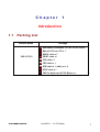
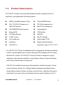
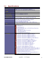
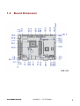
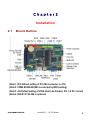
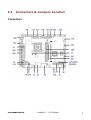
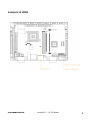
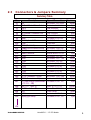
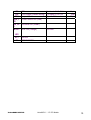
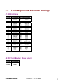
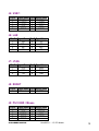
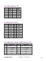
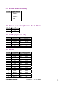
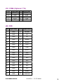
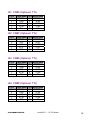
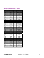
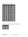
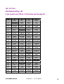
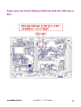
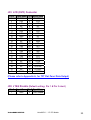
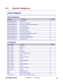
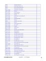
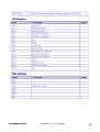
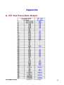
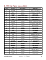
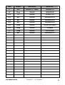
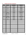
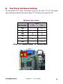
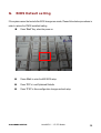
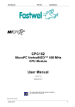
VSX-6127-V2 DM&P Vortex86SX 300MHz 3.5” CPU Module with 8S/3USB/VGA/LCD/LVDS/LAN/GPIO/CF/FDD 128MB DDR2 Onboard User’s Manual (Revision 1.0A) http://www.microcomputersystems.com Copyright The information in this manual is subject to change without notice for continuous improvement in the product. All rights are reserved. The manufacturer assumes no responsibility for any inaccuracies that may be contained in this document. And makes no commitment to update or to keep current the information contained in this manual. No part of this manual may be reproduced, copied, translated or transmitted, in whole or in part, in any form or by any means without the prior written permission of the ICOP Technology Inc.. ©Copyright 2007 ICOP Technology Inc. Manual No. IUM6127-V2000-01 Ver.1.0A April, 2010 Trademarks Acknowledgment Vortex86SX™ is the registered trademark of ICOP Technology Inc. Other brand names or product names appearing in this document are the properties and registered trademarks of their respective owners. All names mentioned herewith are served for identification purpose only. Table of Contents T a b l e o f C o n t e n t s .............................................................iii C h a p t e r 1 Introduction……………………………………………1 1.1 Packing List............................................................ 1 1.2 Product Description ................................................ 1 1.3 Specifications ......................................................... 3 1.4 Board Dimension.................................................... 5 Chapter 2 2.1 2.2 2.3 2.4 2.5 2.6 2.7 2.8 Installation……………………………………………..6 Board Outline ......................................................... 6 Connectors & Jumpers Location .................... ........7 Connectors & Jumpers Summary........................... 9 Pin Assignments & Jumper Settings......................11 System Mapping................................................... 24 Watchdog Timer ................................................... 27 GPIO .................................................................... 28 SPI flash............................................................... 29 Chapter Driver Installation……………………………………30 Appendix 3 ………………………………………………………………..31 A. TFT Flat Panel Data Output ...................................... 31 B. TFT Flat Panel Support List....................................... 32 C. LVDS Flat Panel Support List.................................... 34 D. Flat Panel Hardware Setting ..................................... 35 E. Flat Panel Wiring and Lighting .................................. 36 F. TCP/IP library for DOS real mode.............................. 37 G. BIOS Default Setting................................................. 38 Warranty............................................................................................ 39 Chapter 1 Introduction 1.1 Packing List Product Name Package Embedded Vortex86SX CPU All-in-One Board Manual & Drivers CD x 1 RS232 cable x 7 VSX-6127-V2 PRINT cable x1 IDE cable x 1 FDD cable x 1 USB cable x 1 (USB port x 2 ) GPIO cable x 1 YKB for Keyboard & PS/2 Mouse x 1 Vortex86SX-6127-V2 Vortex86SX™ 3.5” CPU Module 1 1.2 Product Description The VSX-6127-V2 family of low-power x86 embedded controller is designed to meet 3.5” specification, and integrated with the following features. 300MHz Vortex86SX System-On-Chip Onboard 2MB SPI Flash VGA, TFT/LVDS LCD support up to PC/104-Plus expansion bus 1280x1024 resolution Meet PC/104 stacking spec. 128/ 256MB DDR2 system memory 2 watchdog timer Enhanced IDE JTAG interface 10/100Mbps Ethernet AMI BIOS 3 USB 2.0 (Host) Mini-PCI (TypeⅢ) Up to 8 serial ports Single voltage +5V DC Parallel port Support extended operating 16-bit GPIO x1 temperature range of -20°C to +70°C The VSX-6127-V2 3.5” family of embedded controller is designed with backward compatibility in mind, to provide migration path for projects facing end-of-life challenges with their existing x86 based 3.5” controller. The VSX-6127-V2 family of controller is designed as a plug in replacement, with backward compatibility to support legacy software to help extend existing product life cycle without heavy re-engineering. VSX-6127-V2 is suitable for broad range of data-acquisition, Industrial automation, Process control, Automotive controller, AVL, Intelligent Vehicle management devic,Medical device, Human machine interface, Robotics, machinery control And more…application that required small footprint, low-power and low-cost hardware with open industry standard such as 3.5 ”. Vortex86SX-6127-V2 Vortex86SX™ 3.5” CPU Module 2 1.3 Specifications Features CPU VSX-6127-V2 DM&P SoC CPU Vortex86SX- 300MHz Real Time Clock with Lithium Battery Backup L1:16K I-Cache, 16K D-Cache Cache BIOS Bus Interface AMI BIOS System Memory 128/ 256MB DDR2 Onboard Watchdog Timer Software programmable from 30.5 us to 512 seconds x2 sets(Watchdog 1 fully compatible with M6117D) XGI Volari Z9s Chipset VGA and TFT Flat Panel Interface Support LVDS Flat Panel Interface Support Onboard 32MB VGA Memory Support resolution up to 1280 x 1024,16MB colors Integrated 10/100M Ethernet VGA LAN I /O Interface Connectors Vortex86SX-6127-V2 PC/104+ Standard Compliant Enhanced IDE port x1 FDD port x1 RS-232 port x7 RS-232/422/485 port x1 (RS-485:Auto Direction) Parallel port x1 USB port x3 (USB 2.0 version) 16-bit GPIO port x1 10/100Mbps Ethernet port x1 2.00 mm ∅ 44-pin box header for IDE x1 2.00 mm ∅ 44-pin box header for LCD x 1 2.00 mm ∅ 34-pin box header for FDD x1 2.00 mm ∅ 26-pin box header for Print x1 2.00 mm ∅ 20-pin box header for 16-bit GPIO x1 2.00 mm ∅ 16-pin header for LVDS x 1 2.00 mm ∅ 10-pin box header for RS-232 x7 2.00 mm ∅ 10-pin box header for USB x1 2.54 mm ∅ 4-pin header for DC-in x1 2.54 mm ∅ 3-pin header for RS-485 x1 2.54 mm ∅ 2-pin header for Reset x1 1.25 mm ∅ 6-pin wafer for JTAG x1 0.8mm ∅ 124-pin MiNi PCI connector x1 External 15-pin D-Sub female connector for VGA x1 External 9-pin D-Sub male connector for RS-232 x1 External RJ-45 connector for Ethernet x1 External USB connector for x1 External Mini DIN socket for Keyboard/Mouse x1 Type I/II Compact Flash slot x1 Vortex86SX™ 3.5” CPU Module 3 Flash Disk Support SRAM support Power Requirement Dimension Weight Operating Temperature Vortex86SX-6127-V2 Onboard 2MB SPI Flash Disk (Driver: A) 44-pin IDE Flash Disk( EmbedDisk 16MB or above) Type I/II CF Card 512KB (Optional) Single Voltage +5V @ 800mA 102 X 144mm (4.01 x 5.67 inches) 148g -20 o C ~ +70 o C -40°C ~ +85°C (Optional) Vortex86SX™ 3.5” CPU Module 4 1.4 Board Dimension Vortex86SX-6127-V2 Vortex86SX™ 3.5” CPU Module 5 Chapter2 Installation 2.1 Board Outline (Note1: VI/O Default setting of PCI-104 connector is +5V) (Note2: COM2 RS232/422/485 is selected by BIOS setting) (Note3: J39 Default setting of JTAG Has to be Disable: Pin 1 & Pin 2 short) (Note4: VSX-6127-V2-256 is optional) Vortex86SX-6127-V2 Vortex86SX™ 3.5” CPU Module 6 2.2 Connectors & Jumpers Location Connectors Vortex86SX-6127-V2 Vortex86SX™ 3.5” CPU Module 7 Jumpers & LEDs Vortex86SX-6127-V2 Vortex86SX™ 3.5” CPU Module 8 2.3 Connectors & Jumpers Summary Summary Table Nbr J1 J2 J3 J4 J6 J7 J8 J9 J10 J11 J12 J15 J16 J17 J18 J19 J20 J21 J22 J23 J24 J25 J26 J27 J28 J29 J30 J31 J32 Description Type of Connections Pin nbrs. IDE Box Header, 2.0∅ ,22x2 44-pin CF Card Master/Slave Select Pin Header, 2.54∅, 2x1 2-pin USB 2 USB connector 4-pin USB 1 Box Header,2.0∅ , 5x2 10-pin 10/100Base-T Ethernet LAN RJ45 Connector 8-pin JTAG Wafer, 1.25∅ , 6x1 6-pin Reset Pin Header, 2,54∅,1x2 2-pin PS/2 Keyboard / Mouse Mini-DIN Female 6-pin COM1 D-Sub Male 9-pin GPIO ( Port 0 / 1) Box Header, 2.0∅ ,10x2 20-pin 10-pin COM2(RS232/RS485/RS422) Box Header, 2.54∅ 5x2 RS-485 Molex Header,2.54∅, 3x1 3-pin Power Connector Terminal Block 5.0∅,2x1 2-pin COM3 Box Header, 2.0∅ 5x2 10-pin PRINT Box Header, 2.0∅ , 13x2 26-pin COM4 Box Header, 2.0∅ 5x2 10-pin FDD Pin Header, 2.0∅ ,17x2 24-pin COM5 Pin Header, 2.0∅ 5x2 10-pin COM7 Pin Header, 2.0∅ 5x2 10-pin COM6 Pin Header, 2.0∅ 5x2 10-pin COM8 Pin Header, 2.0∅ 5x2 10-pin PC104 Connector – 64 pin Box Header, 2.54∅ 32x2 64-pin PC104 Connector – 40 pin Box Header, 2.54∅ 20x2 40-pin 4-pin 4P Power Source (Interconnect Pin Header, 2.54∅ , 4x1 to PC/104 – J25) MINI_PCI _Type- Ⅲ Type- Ⅲ connector 124-pin PC/104 + Box Header, 2.0∅ , 30x4 120-pin VGA D-Sub Female 15-pin LVDS Pin Header, 2.0∅ 8x2 16-pin Pin Header, 2.54∅ , 3x1 3-pin Display type Setup J38 Vortex86SX-6127-V2 Vortex86SX™ 3.5” CPU Module 9 J33 J39 CF1 PWR_L ED IDE_LE D MTBFLED SP1 S1 Box Header,2.0∅ ,22x2 LCD JTAG Disable (Default setting) Pin Header, 2,54∅,1x2 Compact Flash Type I/II CF Connector POWER Active LED (Red) 44-pin 2-pin 50-pin IDE Active LED (Green ) MTBF-Out (Orange) LED-SMD BUZZER RESET SWITCH Vortex86SX-6127-V2 Vortex86SX™ 3.5” CPU Module 10 2.4 Pin Assignments & Jumper Settings J1: IDE (44 Pins) Pin # 1 3 5 7 9 11 13 15 17 19 21 23 25 27 29 31 33 35 37 39 41 43 Signal Name IDERST IDED7 IDED6 IDED5 IDED4 IDED3 IDED2 IDED1 IDED0 GND IDEREQ IDEIOW IDEIOR ICHRDY IDEACK IDEINT IDESA1 IDESA0 IDECS-0 IDELED VCC GND Pin # Signal Name 2 GND 4 IDED8 6 IDED9 8 IDED10 10 IDED11 12 IDED12 14 IDED13 16 IDED14 18 IDED15 20 NC 22 GND 24 GND 26 GND 28 GND 30 GND 32 NC 34 IDECBLID 36 IDESA2 38 IDECS1 40 GND 42 VCC 44 NC J2: CF Card Master / Slave Select Pin # Signal Name CLOSE Master OPEN Slave Vortex86SX-6127-V2 Vortex86SX™ 3.5” CPU Module 11 J4: USB 1 Pin # 1 3 5 7 9 Signal Name Pin # Signal Name VCC 2 VCC LUSBD04 LUSBD1LUSBD0+ 6 LUSBD1+ GND 8 GND GGND 10 GGND J6: LAN Pin # 1 3 5 7 Signal Name Pin # Signal Name TD+ 2 TDRO+ 4 NC NC 6 RONC 8 NC J7: JTAG Pin # 1 3 5 Signal Name Pin # Signal Name VCC 2 GND TCK 4 TDO TDI 6 TMS J8: RESET Pin # 1 Signal Name Pin # Signal Name Reset 2 GND J9: PS/2 KBD / Mouse Pin # 1 3 5 7 9 Signal Name Pin # Signal Name KBCLK 2 MSCLK GND 4 KBDAT MSDAT 6 VCC GGND 8 GGND GGND Vortex86SX-6127-V2 Vortex86SX™ 3.5” CPU Module 12 J10: COM 1 (Optional: TTL) Pin # 1 3 5 7 9 11 Signal Name DCD1 TXD1 GND RTS1 RI1 GND Pin # 2 4 6 8 10 Signal Name RXD1 DTR1 DSR1 CTS1 GND J11: GPIO (Port 0 / Port 1) Pin # 1 3 5 7 9 11 13 15 17 19 Signal Name GND GP00 GP01 GP02 GP03 GP04 GP05 GP06 GP07 VCC Pin # Signal Name 2 VCC 4 GP10 6 GP11 8 GP12 10 GP13 12 GP14 14 GP15 16 GP16 18 GP17 20 GND J12: COM2 RS232 / RS422 / RS485 (Optional: TTL) Pin # Signal Name Pin # Signal Name 1 DCD2/ 422TX- / RS485- 2 RXD2 / 422TX+ / RS485+ 3 TXD2 / 422RX+ 4 DTR2 / 422RX- 5 GND 6 DSR2 7 RTS2 8 CTS2 9 RI2 10 NC Vortex86SX-6127-V2 Vortex86SX™ 3.5” CPU Module 13 J15: RS485 (Auto direction) Pin # Signal Name 1 RS485+ 2 RS485- 3 GND J16: Power Connector (Terminal Block 5.0mm) Pin # 1 2 Signal Name +5V GND J17: COM3 (Optional: TTL) Pin # 1 3 5 7 9 Signal Name Pin # Signal Name DCD3 2 RXD3 TXD3 4 DTR3 GND 6 DSR3 RTS3 8 CTS3 RI3 10 NC J18: PRINT Pin # 1 2 3 4 5 6 7 8 9 10 11 12 13 Signal Name STBPD0 PD1 PD2 PD3 PD4 PD5 PD6 PD7 ACKBUSY PE SLCT Vortex86SX-6127-V2 Pin # Signal Name 14 AFD15 ERR16 INIT17 SLIN18 GND 19 GND 20 GND 21 GND 22 GND 23 GND 24 GND 25 GND 26 NC Vortex86SX™ 3.5” CPU Module 14 J19: COM4 (Optional: TTL) Pin # 1 3 5 7 9 Signal Name Pin # Signal Name DCD4 2 RXD4 TXD4 4 DTR4 GND 6 DSR4 RTS4 8 CTS4 RI4 10 NC J20: FDD Pin # Signal Name Pin # Signal Name 1 GND 2 DENSEL 3 GND 4 NC 5 GND 6 NC 7 GND 8 INDEX\ 9 GND MTRO\ 11 GND 10 12 13 GND 14 DS0\ 15 GND 16 MTR1\ 17 GND 18 DIR\ 19 GND 20 STEP\ 21 GND 22 WD\ 23 GND 24 WG\ 25 GND 26 TR0\ 27 GND 28 WP\ 29 GND 30 RD\ 31 GND 32 HDSEL\ 33 GND 34 DSKCHG\ Vortex86SX-6127-V2 DS1\ Vortex86SX™ 3.5” CPU Module 15 J21: COM5 (Optional: TTL) Pin # 1 3 5 7 9 Signal Name Pin # Signal Name DCD5 2 RXD5 TXD5 4 DTR5 GND 6 DSR5 RTS5 8 CTS5 RI5 10 NC J22: COM7 (Optional: TTL) Pin # 1 3 5 7 9 Signal Name Pin # Signal Name DCD7 2 RXD7 TXD7 4 DTR7 GND 6 DSR7 RTS7 8 CTS7 RI7 10 NC J23: COM6 (Optional: TTL) Pin # 1 3 5 7 9 Signal Name Pin # Signal Name DCD6 2 RXD6 TXD6 4 DTR6 GND 6 DSR6 RTS6 8 CTS6 RI6 10 NC J24: COM8 (Optional: TTL) Pin # 1 3 5 7 9 Signal Name Pin # Signal Name DCD8 2 RXD8 TXD8 4 DTR8 GND 6 DSR8 RTS8 8 CTS8 RI8 10 NC Vortex86SX-6127-V2 Vortex86SX™ 3.5” CPU Module 16 J25: PC104 Connector – 64pin Pin # 1 3 5 7 9 11 13 15 17 19 21 23 25 27 29 31 33 35 37 39 41 43 45 47 49 51 53 55 57 59 61 63 Signal Name Pin # Signal Name IOCHCHK * 2 GND SD7 4 RESETDRV SD6 6 VCC SD5 8 IRQ9 SD4 10 -5V SD3 12 DRQ2 SD2 14 -12V SD1 16 OWS SD0 18 +12V IOCHRDY 20 GND AEN 22 SMEMW * SA19 24 SMEMR * SA18 26 IOW * SA17 28 IOR * SA16 30 DACK3 * SA15 32 DRQ3 SA14 34 DACK1 * SA13 36 DRQ1 SA12 38 REFRESH * SA11 40 SYSCLK SA10 42 IRQ7 SA9 44 IRQ6 SA8 46 IRQ5 SA7 48 IRQ4 SA6 50 IRQ3 SA5 52 DACK2 * SA4 54 TC SA3 56 BALE SA2 58 VCC SA1 60 OSC SA0 62 GND GND 64 GND Vortex86SX-6127-V2 Vortex86SX™ 3.5” CPU Module 17 J26: PC104 Connector – 40pin Pin # 1 3 5 7 9 11 13 15 17 19 21 23 25 27 29 31 33 35 37 39 Signal Name GND MEMCS16 * IOCS16 * IRQ10 IRQ11 IRQ12 IRQ15 IRQ14 DACK0 * DRQ0 DACK5 * DRQ5 DACK6 * DRQ6 DACK7 * DRQ7 VCC MASTER * GND GND Pin # 2 4 6 8 10 12 14 16 18 20 22 24 26 28 30 32 34 36 38 40 Signal Name GND SBHE * SA23 SA22 SA21 SA20 SA19 SA18 SA17 MEMR * MEMW * SD8 SD9 SD10 SD11 SD12 SD13 SD14 SD15 NC J27: 4P Power Source (Interconnect to PC/104 – J25) Pin # 1 2 3 4 Signal Name -5V -12V +12V GND Vortex86SX-6127-V2 Vortex86SX™ 3.5” CPU Module 18 J29: PC/104 + VI/O Default setting: +5V If you need to use VI/O as +3.3V, please see the page 20. Pin # 1 2 3 4 5 6 7 8 9 10 11 12 13 14 15 16 17 18 19 20 21 22 23 24 25 26 27 28 29 30 A B C D GND NC +5V AD00 VI/O(+5V) AD02 AD01 +5V AD05 GND AD04 AD03 C/BE0# AD07 GND AD06 GND AD09 AD08 GND AD11 VI/O(+5V) AD10 GND AD14 AD13 GND AD12 +3.3V C/BE1# AD15 +3.3V SERR# GND NC PAR GND PERR# +3.3V NC STOP# +3.3V LOCK# GND +3.3V TRDY# GND DEVSEL# FRAME# GND IRDY# +3.3V GND AD16 +3.3V C/BE2# AD18 +3.3V AD17 GND AD21 AD20 GND AD19 +3.3V AD23 AD22 +3.3V IDSEL0 GND IDSEL1 IDSEL2 AD24 C/BE3# VI/O(+5V) IDSEL3 GND AD26 AD25 GND AD29 +5V AD28 AD27 +5V AD30 GND AD31 REQ0# GND REQ1# VI/O(+5V) GND REQ2# +5V GNT0# GNT1# VI/O(+5V) GNT2# GND +5V CLK0 GND CLK1 CLK2 +5V CLK3 GND GND INTD# +5V RST# +12V INTA# INTB# INTC# -12V NC NC GND Vortex86SX-6127-V2 Vortex86SX™ 3.5” CPU Module 19 Please remove the 0 ohm (1206 type) of R260 and add 0 ohm (1206 type) on R261 Vortex86SX-6127-V2 Vortex86SX™ 3.5” CPU Module 20 J30: VGA Pin # 1 3 5 7 9 11 13 15 Signal Name R OUT B OUT GND GND VCC NC HSYNC DDCCLK Pin # Signal Name 2 G OUT 4 NC 6 GND 8 GND 10 GND 12 DDCDAT 14 VSYNC J31: LVDS Pin # 1 3 5 7 9 11 13 15 Signal Name Pin # Signal Name VCC3 (3.3V) GND RxIN0+ RxIN1GND RxIN2+ CKINGND Vortex86SX-6127-V2 2 4 6 8 10 12 14 16 VCC3 (3.3V) GND RxIN0GND RxIN1+ RxIN2GND CKIN+ Vortex86SX™ 3.5” CPU Module 21 J32~J38: Display type setup (CRT /LCD) Connector Pin # Signal Name 1 VCC 2 GPIOA 3 GND 1 VCC 2 GPIOB 3 GND 1 VCC 2 GPIOC 3 GND 1 VCC 2 GPIOD 3 GND 1 VCC 2 GPIOE 3 GND 1 VCC 2 GPIOF 3 GND J32 J34 J35 J36 J37 J38 (Please refer to Appendix D, for Display type setup) Vortex86SX-6127-V2 Vortex86SX™ 3.5” CPU Module 22 J33: LCD (DVO) Connector Pin # 1 3 5 7 9 11 13 15 17 19 21 23 25 27 29 31 33 35 37 39 41 43 Signal Name +3.3V LG2 LG4 NC LR0 LR2 LR4 GND NC NC NC LB0 LB2 LB4 NC LG0 GND NC NC NC NC LBACKL Pin # Signal Name 2 +3.3V 4 LG3 6 LG5 8 NC 10 LR1 12 LR3 14 LR5 16 NC 18 NC 20 GND 22 NC 24 LB1 26 LB3 28 LB5 30 NC 32 LG1 34 GND 36 LCLK 38 LDE 40 LHSYNC 42 LVSYNC 44 LVDDEN (Please refer to Appendix A, for TFT Flat Panel Data Output) J39: JTAG Disable (Default setting: Pin 1 & Pin 2 short) Pin # 1 Signal Name Pin # Signal Name GND 2 JTAG Disable Vortex86SX-6127-V2 Vortex86SX™ 3.5” CPU Module 23 2.5 System Mapping Vortex86SX-6127-V2 Vortex86SX™ 3.5” CPU Module 24 Vortex86SX-6127-V2 Vortex86SX™ 3.5” CPU Module 25 Vortex86SX-6127-V2 Vortex86SX™ 3.5” CPU Module 26 2.6 Watchdog Timer There are two watchdog timers in Vortex86SX/DX CPU. One is compatible with M6117D watchdog timer and the other is new. The M6117D compatible watchdog timer is called WDT0 and new one is called WDT1. We also provide DOS, Linux and WinCE example for your reference. For more technical support, please visit: http://www.dmp.com.tw/tech or download the PDF file: http://www.dmp.com.tw/tech/vortex86dx/ Vortex86SX-6127-V2 Vortex86SX™ 3.5” CPU Module 27 2.7 GPIO (General Purpose Input / Output) 40 GPIO pins are provided by the Vortex86SX/DX for general usage in the system. All GPIO pins are independent and can be configured as inputs or outputs, with or without pull-up/pull-down resistors. We also offer DOS, Linux and WinCE example for your reference. For more technical support, please visit: http://www.dmp.com.tw/tech or download the PDF file: http://www.dmp.com.tw/tech/vortex86dx/ Vortex86SX-6127-V2 Vortex86SX™ 3.5” CPU Module 28 2.8 SPI flash (Serial Peripheral Interface) As SPI Flash (Serial Peripheral Interface) offers many benefits including: reduced controller pin count, smaller and simpler PCBs, reduced switching noise, less power consumption, and lower system cost Many of users may consider using a formatted SPI flash to boot for the system or emulate SPI flash as Floppy (A: Driver or B: Driver). Then you must know how to set for this condition in CMOS Setup and boot up under DOS 6.22, X-DOS, DR-DOS and Free DOS. For more technical support, please visit: http://www.dmp.com.tw/tech or download the PDF file: http://www.dmp.com.tw/tech/vortex86dx/ Vortex86SX-6127-V2 Vortex86SX™ 3.5” CPU Module 29 Chapter 3 Driver Installation VGA The Vortex86SX processor also use external Display chip ““Volari™ Z9s” which is an ultra low powered graphics chipset with total power consumption at around 1-1.5 W. It is capable in providing VGA display output upto 1600x1200. With DVO interface, developers could easily connect flat Panel to support TFT and LVDS output. LAN The Vortex86SX processor also integrated 10/100Mbps Ethernet controller that supports both 10/100BASE-T and allows direct connection to your 10/100Mbps Ethernet based Local Area Network for full interaction with local servers, wide area networks such as the Internet. The controller supports: Half / Full-Duplex Ethernet function to double channel bandwidth, auto media detection. Operating system support The Vortex86SX-6127-V2 3.5” CPU board supports Embedded software: Free DOS, DOS 6.22, PCDOS 7.1, DR-DOS, x-DOS, OS/2, Windows CE 5.0 / 6.0 Please get the drivers from the Driver CD which attached with the standard packing of Vortex86SX-6127-V2 board or please get it from DMP official website: http://www.dmp.com.tw/tech/vortex86sx/ Vortex86SX-6127-V2 also supports most of the popular Linux distributions, for more detail information, please visit DMP official website: http://www.dmp.com.tw/tech/vortex86sx/ . Vortex86SX-6127-V2 Vortex86SX™ 3.5” CPU Module 30 Appendix A. TFT Flat Panel Data Output Vortex86SX-6127-V2 Vortex86SX™ 3.5” CPU Module 31 B. TFT Flat Panel Support List Size Brand Resolution Model No. 5.7” Data image 320x240 FG050701DSSWBG01 5.7” Optrex 320x240 55264GD057J-FW-ABN 5.7” TOSHIBA 320x240 LTA057A343F 5.7” Sharp 320x240 (QVGA / VGA) LQ057Q3DC02 5.7” Kyocera 320x240 (QVGA / VGA) TCG057QV1AC-G10 5.7” PVI 320x240 (QVGA / VGA) PD057VU4 /U5 5.7” Data image 640x480 FG050710DSSWJG01/DG01 5.7” Ampire 640x480 AM-640480GTMQW-T00H 5.7” URT 640x480 UMSH-8004MD-T 5.7” Sharp 640x480 LQ057V3DG01 5.7” CPT 640x480 CLAA057VA01 6.4” PVI 640x480 V16C6448AC 6.4” LG-PHILIPS 640x480 LB064V02 6.4” PVI 640x480 PD064VT2 /VT4 /VT5 6.4” Sharp 640x480 LQ064V3DG01 7” AUO 800x480 C070VW02V0 7” Data image 800x480 FG0700A0DSSWBG01 7” LG-PHILIPS 800x480 (TFT 24 bits) LB070WV1 7” HITACHI 800x480 TX18D57VM2BAA 7” Samsung 800x480 LMS700KF05 7” PVI 800x480 PM070WL4 7” URT 800x480 UMSH-8173MD-1T 7” CHI HSIN 800x480 LW700AT9309 8” Sharp 640x480 LQ080V3DG01 Vortex86SX-6127-V2 Vortex86SX™ 3.5” CPU Module 32 Size Brand Resolution Model No. 8” AUO 800x600 (TFT 24bits) A080SN01 V0 8.4” Sharp 800x600 LQ084S3DG01 10.4” PVI 640x480 PD104VT1/VT2 10.4” NEC 640x480 NL6448AC33-18 10.4” NEC 640x480 NL6448AC33-29 10.4” NEC 640x480 NL6448BC33-59 10.4” Sharp 640x480 LQ104V1DG51/DG61 10.4” Sharp 640x480 LQ10d368 11” Sharp 800x480 LQ110Y3DG01 12.1” NEC 800x600 NL8060BC31-01 Vortex86SX-6127-V2 Vortex86SX™ 3.5” CPU Module 33 C. LVDS Flat Panel Support Size Brand Resolution Model No. 3.5” PVI 640x480 PD035VL1 5” PVI 640x480 PD050VL1 6.5” AUO 640x480 G065VN01 8.4” AUO 800x600 G084SN03 8.9” AUO 1024x600 A089SW01 8.9” CPT 1024x600 CLAA089NA0ACW 8.9” HannStar 1024x600 HSD089IFW1 10.4” MITSUBISHI 800x600 AA104SG01 10.4” AUO 800x600 G104SN02 10.4” Sharp 800x600 LQ104S1LG61 12.1” MITSUBISHI 800x600 AA121SL03 12.1” AUO 800x600 G121SN01 15” AUO 1024x768 G150XG01 Vortex86SX-6127-V2 Vortex86SX™ 3.5” CPU Module 34 D. Flat Panel Hardware Setting: The Vortex86SX-6127-V2 offers the Hardware setting for the various TFT LCD Flat Panels support and please make sure the jumper setting (J32~J38) before you connect the LCD. Display type setup LCD Connector 1-2 2-3 J32 C J34 C J35 X X J36 X X J37 C J38 C Note: "C" means close; "X" means open Vortex86SX-6127-V2 Vortex86SX™ 3.5” CPU Module 35 E. Flat Panel Wiring and Lighting Hardware Before you connect the TFT LCD Flat Panel with Vortex86SX-6127-V2, please make sure that the input Voltage of LCD is 3.3V or Not BIOS Please contact or e-mail our regional sales to get the special BIOS for the any TFT LCD Flat Panels. Wiring LCD Cable Please refer to Page 23 (J33: LCD connector) and Page 31~36. Or for more LCD lighting and integration service, please contact our regional sales or mail to [email protected] ,if you have any questions. Vortex86SX-6127-V2 Vortex86SX™ 3.5” CPU Module 36 F. TCP/IP library for DOS real mode DSock is a TCP/IP library for DOS real mode, which is used by RSIP. It provides simple C functions for programmer to write Internet applications. ICOP also provide Internet examples using DSock: BOOTP/DHCP, FTP server, SMTP client/server, HTTP server, TELNET server, Talk client/server, etc. DSock provides a lot of example source code. Programmer can add Internet functions to their project easily and save development time. With a utility "MakeROM”, programmer also can make a ROM image to fit their application, those examples can be seen in the following Application systems: Mity-Mite Serial Server, Web Camera Tiny Server and RSIP Serial Server. DSock is free for All ICOP products using M6117D/Vortex86/Vortex86SX/Vortex86DX CPU and ICOP also provide the business version of DSock for those customers who are using other x86 CPUs. If you would like to use DSock or business version of DSock, Please mail to [email protected] or contact your regional sales. Please download the trial DSock software and Utilities from our website: http://www.dmp.com.tw/tech/dmp-lib/dsock/ Vortex86SX-6127-V2 Vortex86SX™ 3.5” CPU Module 37 G. BIOS Default setting If the system cannot be booted after BIOS changes are made, Please follow below procedures in order to restore the CMOS as default setting. Press “End” Key, when the power on Press <Del> to enter the AMI BIOS setup Press “F9” to Load Optimized Defaults Press “F10” to Save configuration changes and exit setup Vortex86SX-6127-V2 Vortex86SX™ 3.5” CPU Module 38 Warranty This product is warranted to be in good working order for a period of one year from the date of purchase. Should this product fail to be in good working order at any time during this period, we will, at our option, replace or repair it at no additional charge except as set forth in the following terms. This warranty does not apply to products damaged by misuse, modifications, accident or disaster. Vendor assumes no liability for any damages, lost profits, lost savings or any other incidental or consequential damage resulting from the use, misuse of, originality to use this product. Vendor will not be liable for any claim made by any other related party. Return authorization must be obtained from the vendor before returned merchandise will be accepted. Authorization can be obtained by calling or faxing the vendor and requesting a Return Merchandise Authorization (RMA) number. Returned goods should always be accompanied by a clear problem description. Vortex86SX-6127-V2 Vortex86SX™ 3.5” CPU Module 39