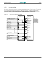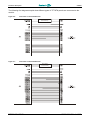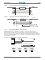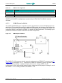
1
CPB902
3.5" Highly Integrated
Low Power SBC
User Manual
Rev. 1.4a E
November 2005
Product Title:
CPB902
Document name: CPB902 User Manual
Manual version: 1.4a E
Copyright © 2005 Fastwel Co. Ltd. All rights reserved.
Revision History
Rev. Index
Brief Description of Changes
Board Index
Date of Issue
1.4 beta
Initial version
CPB902
November 2005
1.4a
Errors corrections, design and styling changes, figures and tables
modification
CPB902
November 2005
Contact Information
Fastwel Co. Ltd.
Address:
Tel.:
Fax:
E-mail:
108 Profsoyuznaya st., Moscow 117437, Russian Federation
+7 (095) 234-0639
+7 (095) 232-1654
[email protected]
For more details, please visit our Web-site:
http://www.fastwel.com/
CPB902
Table of Contents
Table of Contents.................................................................................................................................................. 0-1
List of Tables......................................................................................................................................................... 0-3
List of Figures ....................................................................................................................................................... 0-4
Notation Conventions............................................................................................................................................ 0-5
General Safety Precautions .................................................................................................................................. 0-6
Unpacking, Inspection and Handling..................................................................................................................... 0-7
Three Year Warranty ............................................................................................................................................ 0-9
1
Introduction......................................................................................................................................... 1-1
1.1
1.2
1.3
1.4
1.5
2
Technical Specifications ................................................................................................................... 2-1
2.1
2.2
2.3
2.4
2.5
2.6
3
General...................................................................................................................................................... 2-1
Power Requirements ................................................................................................................................. 2-2
Environmental............................................................................................................................................ 2-2
Mechanical ................................................................................................................................................ 2-2
Dimensions and Weight............................................................................................................................. 2-3
MTBF......................................................................................................................................................... 2-3
External Connections ........................................................................................................................ 3-1
3.1
3.2
3.3
4
Module Introduction ................................................................................................................................... 1-1
CPB902 Versions ...................................................................................................................................... 1-2
Delivery Checklist ...................................................................................................................................... 1-2
Additional Accessories............................................................................................................................... 1-2
Supplementary Information........................................................................................................................ 1-3
1.5.1
Related Publications ................................................................................................................. 1-3
Safety Regulations..................................................................................................................................... 3-1
Connection of Peripheral Devices.............................................................................................................. 3-2
3.2.1
CompactFlash Cards Installation .............................................................................................. 3-4
3.2.2
USB Devices Connection.......................................................................................................... 3-4
3.2.3
Battery Replacement ................................................................................................................ 3-5
Software Installation .................................................................................................................................. 3-5
Functional Description ...................................................................................................................... 4-1
4.1
4.2
4.3
C P B 9 0 2
Structure and Layout ................................................................................................................................. 4-1
Address Mapping....................................................................................................................................... 4-4
4.2.1
Memory Addressing .................................................................................................................. 4-4
4.2.2
I/O Addressing .......................................................................................................................... 4-4
4.2.3
Interrupt settings ..................................................................................................................... 4-12
4.2.4
DMA channels ........................................................................................................................ 4-14
Functional Description ............................................................................................................................. 4-15
4.3.1
Microprocessor ....................................................................................................................... 4-15
4.3.2
SDRAM Memory..................................................................................................................... 4-15
4.3.3
Reserved Flash BIOS ............................................................................................................. 4-15
4.3.4
UIDE/Compact Flash Interface ............................................................................................... 4-15
4.3.5
CompactFlash Socket............................................................................................................. 4-16
4.3.6
NAND Flash............................................................................................................................ 4-17
4.3.7
Video Controller and VGA/TFT Adapter Module..................................................................... 4-17
4.3.7.1
Video Controller Operation Modes and Connection of Monitors ............................ 4-17
U s e r
M a n u a l
0-1
© 2 0 0 5
F a s t w e l
v . 1 . 4 a E
CPB902
4.3.7.2
Sharp LQ104V1DG51 TFT Panel Connection ....................................................... 4-21
4.3.7.3
CVM01 Expansion Module .................................................................................... 4-22
4.3.8
Keyboard and Mouse Interface............................................................................................... 4-23
4.3.9
USB Interface ......................................................................................................................... 4-23
4.3.10
Fast Ethernet Interface ........................................................................................................... 4-24
4.3.11
Serial Ports ............................................................................................................................. 4-24
4.3.12
FDD/LPT Port ......................................................................................................................... 4-27
4.3.13
LCD and Matrix Keyboard Port ............................................................................................... 4-29
4.3.13.1 LCD Connection..................................................................................................... 4-29
4.3.13.2 Matrix Keypad Connection ..................................................................................... 4-31
4.3.13.3 Using Keyboard Interface by the Discrete I/O Unit................................................. 4-32
4.3.14
Optoisolated Reset/Interrupt ................................................................................................... 4-34
4.3.15
FBUS Connector..................................................................................................................... 4-35
4.3.16
RTC and Serial FRAM ............................................................................................................ 4-35
4.3.17
J19 Configuration Jumpers ..................................................................................................... 4-36
4.3.18
PC/104 Header ....................................................................................................................... 4-36
4.3.19
Diagnostic LEDs ..................................................................................................................... 4-39
4.3.20
Power Supply Connector ........................................................................................................ 4-39
Overall and Mounting Dimensions ........................................................................................................... 4-40
4.4.1
Mounting on a Panel ............................................................................................................... 4-41
4.4
5
General Software® BIOS ................................................................................................................... 5-1
5.1
5.2
5.3
5.4
5.5
5.6
5.7
5.8
5.9
5.10
BIOS Setup Program. Introduction ............................................................................................................ 5-1
Main Menu................................................................................................................................................. 5-1
Basic CMOS configuration......................................................................................................................... 5-3
Custom Configuration ................................................................................................................................ 5-5
PnP Configuration...................................................................................................................................... 5-7
Shadow Configuration ............................................................................................................................... 5-8
Manufacturing Link Mode .......................................................................................................................... 5-9
The Rest Main Menu Commands ............................................................................................................ 5-10
5.8.1
Reset CMOS to last known values ......................................................................................... 5-10
5.8.2
Reset CMOS to Factory Defaults............................................................................................ 5-10
5.8.3
Write to CMOS and Exit.......................................................................................................... 5-10
5.8.4
Exit without changing CMOS .................................................................................................. 5-10
Reset CMOS to Factory Defaults from a Remote PC .............................................................................. 5-11
Extended BIOS Functions ....................................................................................................................... 5-11
5.10.1
User Programs Interface with FRAM memory units................................................................ 5-11
5.10.2
User LEDs Control.................................................................................................................. 5-12
5.10.3
SuperIO FDC37B787 Watchdog Timer Operation.................................................................. 5-13
5.10.4
ADM8697 Supervisor's Watchdog Timer Operation ............................................................... 5-14
5.10.5
Using INT 17H BIOS Extension to Control the Watchdog Timers........................................... 5-15
A
Jumper Settings by Function............................................................................................................A-1
B
Jumper Settings by Assignment ......................................................................................................B-1
C P B 9 0 2
U s e r
M a n u a l
0-2
© 2 0 0 5
F a s t w e l
v . 1 . 4 a E
CPB902
List of Tables
Table 1.1:
Table 1.2:
Table 1.3:
Table 1.4:
Table 4.1:
Table 4.2:
Table 4.3:
Table 4.4:
Table 4.5:
Table 4.6:
Table 4.7:
Table 4.8:
Table 4.9:
Table 4.10:
Table 4.11:
Table 4.12:
Table 4.13:
Table 4.14:
Table 4.15:
Table 4.16:
Table 4.17:
Table 4.18:
Table 4.19:
Table 4.20:
Table 4.21:
Table 4.22:
Table 4.23:
Table 4.24:
Table 4.25:
Table 5.1:
Table 5.2:
Table 5.3:
Table A.1:
Table B.1:
C P B 9 0 2
U s e r
CPB902 Versions................................................................................................................................. 1-2
CPB902 Supplied Set .......................................................................................................................... 1-2
CPB902 Additional Accessories........................................................................................................... 1-2
Related Publications ............................................................................................................................ 1-3
Memory Address Mapping ................................................................................................................... 4-4
I/O Address Space ...............................................................................................................................4-4
System I/O ports (FPGA) ..................................................................................................................... 4-6
Interrupt Settings................................................................................................................................ 4-13
DMA Request Map............................................................................................................................. 4-14
J1 HDD Connector Pinout.................................................................................................................. 4-15
J2 Compact Flash Socket Pinout ....................................................................................................... 4-16
S1 Settings: Display Type and Video Mode Selection ....................................................................... 4-17
Different Types of TFT/STN Panels Connection ................................................................................ 4-18
TFT/STN Panels Connector J16 Pinout ............................................................................................. 4-19
P7 D-Sub VGA Connector Pinout ...................................................................................................... 4-19
CVM02 J2 Pin Assignments............................................................................................................... 4-22
CVM01 J5 Connector Pinout.............................................................................................................. 4-23
PS/2 Keyboard/Mouse Connector P5 Pinout ..................................................................................... 4-23
Serial Ports Pin Assignments............................................................................................................. 4-25
LPT/FDD J15 Connector Pinout......................................................................................................... 4-28
J18 DIP-Switch Pinout ....................................................................................................................... 4-31
J17 Connector Pinout......................................................................................................................... 4-34
J13 Settings: Switching Reset/IRQ Source ........................................................................................ 4-35
RJ45 FBUS Connector P6 Pinout ...................................................................................................... 4-35
J19 Pins Designation ......................................................................................................................... 4-36
PC/104 P4 (Rows A and B) Contacts Designation............................................................................. 4-37
PC/104 P4 (Rows C and D) Contacts Designation ............................................................................ 4-38
CPB902 Diagnostic LEDs Function ................................................................................................... 4-39
J20 Power Connector Pinout ............................................................................................................. 4-39
Main Menu Items ................................................................................................................................. 5-2
Basic CMOS Configuration Menu Items............................................................................................... 5-3
Custom Configuration Menu Items....................................................................................................... 5-5
Jumper Settings by Function............................................................................................................... A-1
Jumper Settings by Assignment.......................................................................................................... B-1
M a n u a l
0-3
© 2 0 0 5
F a s t w e l
v . 1 . 4 a E
CPB902
List of Figures
Figure 1.1:
Figure 3.1:
Figure 3.2:
Figure 4.1:
Figure 4.2:
Figure 4.3:
Figure 4.4:
Figure 4.5:
Figure 4.6:
Figure 4.7:
Figure 4.8:
Figure 4.9:
Figure 4.10:
Figure 4.11:
Figure 4.12:
Figure 4.13:
Figure 4.14:
Figure 4.15:
Figure 4.16:
Figure 4.17:
Figure 4.18:
Figure 4.19:
Figure 4.20:
Figure 4.21:
Figure 4.22:
Figure 4.23:
Figure 4.24:
Figure 4.25:
Figure 4.26:
Figure 5.1:
Figure 5.2:
Figure 5.3:
Figure 5.4:
Figure 5.5:
CPB902 Module Appearance............................................................................................................... 1-1
External Devices Connection ............................................................................................................... 3-2
Cables 3 and 4 (Fig. 3.1) Connection for Console Operation............................................................... 3-4
CPB902 Functional Block Diagram ...................................................................................................... 4-1
Top Side: Connectors and Main Components Layout.......................................................................... 4-3
Bottom Side: Connectors and Main Components Layout..................................................................... 4-3
Interrupt Source Multiplexing Diagram ............................................................................................... 4-12
DMA Request Channels Multiplexing Diagram .................................................................................. 4-14
Connection of 16-bit DSTN Panel ...................................................................................................... 4-20
Connection of 24-bit DSTN Panel ...................................................................................................... 4-20
Connection of a TFT Panel with 1 Pixel per FPSCLK Period............................................................. 4-21
Connection of a TFT Panel with 2 Pixels per FPSCLK Period ........................................................... 4-21
SHARP LQ104V1DG51 TFT Panel Connection and Setup ............................................................... 4-21
CVM01 Expansion Module................................................................................................................. 4-22
IDC10 Pins Numbering ...................................................................................................................... 4-24
COM3 – COM6 Ports Jumpers .......................................................................................................... 4-25
Point-to-Point Connection of Two Modules in RS-422 Mode ............................................................. 4-26
Connection of Several Devices in RS-485 Mode ............................................................................... 4-26
COM3-COM6 Ports: Simplified Interface Circuit Diagram.................................................................. 4-27
POWERTIP PC1604-A Alphanumeric LCD Connection Diagram ...................................................... 4-30
POWERTIP PG12864-A Graphics LCD Connection Diagram ........................................................... 4-30
J18 Pinpad Connection Circuit Diagram ............................................................................................ 4-31
Discrete I/O Channel Block Diagram.................................................................................................. 4-33
Discrete I/O Unit: Ports Binding Diagram ........................................................................................... 4-33
Reset Source Selection and Optoisolated Input Circuit Diagram ....................................................... 4-34
J19 Circuit Diagram............................................................................................................................ 4-36
PC/104 P4 Contacts Layout............................................................................................................... 4-36
CPB902 Top Side: Overall and Mounting Dimensions....................................................................... 4-40
CPB902 Bottom Side: Overall and Mounting Dimensions.................................................................. 4-40
Main Menu Screen Image .................................................................................................................... 5-2
Basic CMOS Configuration Screen Image ........................................................................................... 5-3
Custom Configuration Menu Screen .................................................................................................... 5-5
Plug-n-Play Configuration Menu Screen Image ................................................................................... 5-7
Shadow Configuration Menu Screen Image......................................................................................... 5-8
All information in this document is provided for reference only, with no warranty of its suitability for any particular purpose. This information has
been thoroughly checked and is believed to be entirely reliable and consistent with the product that it describes. However, Fastwel accepts no
responsibility for inaccuracies, omissions or the their consequences, as well as liability arising from the use or application of any product or
example described in this document.
Fastwel Co. Ltd. reserves the right to change, modify, and improve this document or the products described in it, at Fastwel's discretion without
further notice. Software described in this document is provided on an “as is” basis without warranty. Fastwel assumes no liability for consequential
or incidental damages originated by the use of this software.
This document contains information, which is property of Fastwel Co. Ltd. It may not be copied, reproduced, or transmitted by any means, stored
in any information retrieval system, translated or converted to any electronic or machine-readable form in full or in parts without antecedent written
approval of Fastwel Co. Ltd. or one of its officially authorized agents.
Fastwel and Fastwel logo are trademarks owned by Fastwel Co. Ltd., Moscow, Russian Federation. CompactPCI is a trademark of the PCI
industrial Computers Manufacturers Group. Ethernet is a registered trademark of Xerox Corporation. IEEE is a registered trademark of the
Institute of Electrical and Electronics Engineers Inc. Intel is a trademark of Intel Corporation. Pentium M and Celeron M are trademarks of Intel
Corporation. Microsoft is a trademark of the Microsoft corporation. In addition, this document may include names, company logos and trademarks,
which are registered trademarks and, therefore, are property of their respective owners.
Fastwel welcomes suggestions, remarks and proposals regarding the form and the content of this Manual.
C P B 9 0 2
U s e r
M a n u a l
0-4
© 2 0 0 5
F a s t w e l
v . 1 . 4 a E
CPB902
Notation Conventions
Caution: Electric Shock!
This symbol and title warn of hazards due to electrical shocks (> 60 V) when touching
products or parts of them. Failure to observe the precautions indicated and/or prescribed
by the law may endanger your life/health and/or result in damage to your product.
Warning, ESD Sensitive Device!
This symbol and title inform that electronic modules and their components are sensitive to
static electricity. Therefore, care must be taken during all handling operations and
inspections of this product, in order to ensure product safety.
Warning!
The surface of the heatsink and some components can get very hot during operation.
Take due care when handling, avoid touching hot surfaces!
Warning!
This symbol and title emphasize points, which, if not fully understood and taken into
consideration by the reader, may endanger your health and/or result in damage to your
product.
Note...
This symbol and title emphasize aspects the reader should read through carefully
for his or her own advantage.
C P B 9 0 2
U s e r
M a n u a l
0-5
© 2 0 0 5
F a s t w e l
v . 1 . 4 a E
CPB902
General Safety Precautions
Fastwel has developed and carefully tested this product to provide all features necessary to ensure
its conformance to electrical safety requirements. It was also designed for a long fault-free life.
However, the expected life time of your product can be considerably reduced by improper handling
during unpacking, installation and operation. Therefore, for the sake of your own safety and of the
correct operation of this product, you are requested to conform to the following rules.
Warning!
All operations on this device must be carried out by sufficiently
skilled personnel only.
Warning!
When handling this product, special care must be taken not to hit
the heatsink (if installed) against another rigid object. Also, be
careful not to drop the product, since this may cause damage
to the heatsink, CPU or other sensitive components as well.
Please, keep in mind that any physical damage to this product
is not covered under warranty.
Note:
This product is guaranteed to operate within the published
temperature ranges and relevant conditions. However, prolonged
operation near the maximum temperature is not recommended by
Fastwel or by electronic chip manufacturers due to thermal stress
related failure mechanisms. These mechanisms are common to all
silicon devices, they can reduce the MTBF of the product by
increasing the failure probability. Prolonged operation at the lower
limits of the temperature ranges has no limitations.
Caution, Electric Shock!
Before installing your Fastwel product into a system always ensure
that your mains power is switched off. This applies also to the
installation of other devices on the module.
Serious electrical shock hazards can exist during all installation,
repair and maintenance operations with this product. Therefore,
always unplug the power cable and any other cables, which provide
external voltages before handling the product.
C P B 9 0 2
U s e r
M a n u a l
0-6
© 2 0 0 5
F a s t w e l
v . 1 . 4 a E
CPB902
Unpacking, Inspection and Handling
Please read the manual carefully before unpacking the module or mounting the device into your
system. Keep in mind the following:
ESD Sensitive Device!
Electronic modules and their components are sensitive to static
electricity. Even a non-perceptible by human being static discharge
can be sufficient to destroy or degrade a component's operation!
Therefore, all handling operations and inspections of this product
must be performed with due care, in order to keep product integrity
and operability:
Preferably, unpack or pack this product only at EOS/ESD safe workbenches. Otherwise, it is
important to be electrically discharged before touching the product.
This can be done by touching a metal part of your system case. It is particularly important to
observe anti-static precautions when setting jumpers or replacing components.
If the product contains batteries for RTC or memory back-up, ensure that the board is not
placed on conductive surfaces, including anti-static mats or sponges. They can cause short
circuits and damage the batteries or conductive circuits of the product.
Store this product in its protective packaging while it is not used for operational purposes.
Unpacking
The product is carefully packed in an antistatic bag and in a carton box to protect it against
possible damage and harmful influence during shipping. Unpack the product indoors only at a
temperature not less than +15°C and relative humidity not more than 70%. Please note, that if the
product was exposed to the temperatures below 0°С for a long time, it is necessary to keep it at
normal conditions for at least 24 hours before unpacking. Do not keep the product close to a heat
source.
Following ESD precautions, carefully take the product out of the shipping carton box. Proper
handling of the product is critical to ensure correct operation and long-term reliability. When
unpacking the product, and whenever handling it thereafter, be sure to hold the board preferably by
the front panel, card edges or the ejector handles. Avoid touching the components and connectors.
Keep all original packaging material for future storage or warranty shipments of the product.
Initial Inspection
Although the product is carefully packaged, it is still possible that shipping damages may occur.
Careful inspection of the shipping carton can reveal evidence of damage or rough handling. Should
you notice that the package is damaged, please notify the shipping service and the manufacturer
as soon as possible.
After unpacking the product, you should inspect it for visible damage that could have occurred
during shipping or unpacking. If damage is observed (usually in the form of bent component leads
or loose socketed components), contact Fastwel's official distributor from which you have
purchased the product for additional instructions. Depending on the severity of the damage, the
product may need to be returned to the factory for repair. DO NOT apply power to the product if it
has visible damage. Doing so may cause further, possibly irreparable damage, as well as result in
a fire or electric shock hazard.
If the product contains socketed components, they should be inspected to make sure they are
seated fully in their sockets.
C P B 9 0 2
U s e r
M a n u a l
0-7
© 2 0 0 5
F a s t w e l
v . 1 . 4 a E
CPB902
Handling
In performing all necessary installation and application operations, please follow only the
instructions supplied by the present manual.
In order to maintain Fastwel’s product warranty, this product must not be altered or modified in any
way. Changes or modifications to the device, which are not explicitly approved by Fastwel Co. Ltd.
and described in this manual or received from Fastwel’s Technical Support Service as a special
handling instruction, will void your warranty.
This device should only be installed in or connected to systems that fulfill all necessary technical
and specific environmental requirements. This applies also to the operational temperature range of
the specific module version, which must not be exceeded. If batteries and storage devices are
present, their temperature restrictions must be taken into account.
Keep all the original packaging material for future storage or warranty shipments. If it is necessary
to store or ship the board, please re-pack it as nearly as possible in the manner in which it was
delivered.
When handling the product, please, remember that the board, its components and connectors
require delicate care.
C P B 9 0 2
U s e r
M a n u a l
0-8
© 2 0 0 5
F a s t w e l
v . 1 . 4 a E
CPB902
Three Year Warranty
Fastwel Co. Ltd. (Fastwel), warrants that its standard hardware products will be free from defects
in materials and workmanship under normal use and service for the currently established warranty
period. Fastwel’s only responsibility under this warranty is, at its option, to replace or repair any
defective component part of such products free of charge.
Fastwel neither assumes nor authorizes any other liability in connection with the sale, installation
or use of its products. Fastwel shall have no liability for direct or consequential damages of any
kind arising out of sale, delay in delivery, installation, or use of its products.
If a product should fail through Fastwel's fault during the warranty period, it will be repaired free of
charge. For out of warranty repairs, the customer will be invoiced for repair charges at current
standard labor and materials rates.
Warranty period for Fastwel products is 36 months since the date of purchase.
The warranty set forth above does not extend to and shall not apply to:
1.
Products, including software, which have been repaired or altered by other than
Fastwel personnel, unless Buyer has properly altered or repaired the products in
accordance with procedures previously approved in writing by Fastwel.
2.
Products, which have been subject to power, supply reversal, misuse, neglect,
accident, or improper installation.
Returning a product for repair
1.
Apply to Fastwel company or to any of the Fastwel's official representatives for the
Product Return Authorization.
2.
Attach a failure inspection report with a product to be returned in the form, accepted by
customer, with a description of the failure circumstances and symptoms.
3.
Carefully package the product in the antistatic bag, in which the product had been
supplied. Failure to package in antistatic material will VOID all warranties. Then
package the product in a safe container for shipping.
4.
The customer pays for shipping the product to Fastwel or to an official Fastwel
representative or dealer.
C P B 9 0 2
U s e r
M a n u a l
0-9
© 2 0 0 5
F a s t w e l
v . 1 . 4 a E
Introduction
1
CPB902
Introduction
This document presents general information on CPB902 processor module, the details of its proper
and safe installation, configuration and operation. The issues of PC/104 modules and external
devices connection are also considered.
1.1
Module Introduction
CPB902 processor module is a 3.5" highly integrated single board computer with full PC
functionality. It is designed for applications where high-performance and low power consumption
are required. CPB902 incorporates numerous I/O ports and interfaces: serial ports; IDE interface;
CompactFlash socket; printer/FDD connector; digital I/O port combined with LCD monitor/matrix
keypad interface; two USB ports; PS/2 mouse/keyboard connector; video port; two Fast Ethernet
ports and PC/104 interface.
The module is supplied with installed FDOS 6.22 operating system and is compatible with
Windows 2000, Windows CE5, Linux, QNX6.x, RTOS32 и MSDOS operating systems.
Figure 1.1:
CPB902 Module Appearance
The appearance may vary for different versions of the module.
C P B 9 0 2
U s e r
M a n u a l
1-1
© 2 0 0 5
F a s t w e l
v . 1 . 4 a E
Introduction
1.2
CPB902
CPB902 Versions
Table 1.1:
CPB902 Versions
Version
Decimal ID
SDRAM Size
SVGA
CPB90201
467444.001
128 MB
+
CPB90202
467444.002
32 MB
–
1.3
Delivery Checklist
Table 1.2:
CPB902 Supplied Set
Code
Description
Note
CPB90201 or
CPB90202
Processor module (467444.001 or 467444.002)
–
ACS0006
FCD-9F (685611.012-02)
adapter cable DB9-IDC10 for connection to COM1
–
ACS00010
FC44 (685611.051)
cable for connection of a 2.5" HDD to 44-pin onboard header
–
CDM02
Adapter module for connection of 3.5" HDD or CD-ROM drive
(469535.023).
–
–
Y-cable for simultaneous connection of PS/2 keyboard and mouse
(1700060202)
Is not supplied with
CPB90202 version
–
CD ROM with documentation and service software
Antistatic bag and consumer carton box
Note:
Keep the antistatic bag and the original package at least until the warranty period
is over. It can be used for future storage or warranty shipments.
1.4
Additional Accessories
Peripheral devices are attached to the module directly or via additional accessories and cables
listed in the following table.
Table 1.3:
CPB902 Additional Accessories
Code
Description
ACS00011
FCD25F
LPT connection cable, IDC26 – DB25
ACS0002
FC26-60
FDD connection cable, IDC26 – IDC26
CDM01
FDD connection adapter (469535.030)
CVM01
VGA monitor or TFT/STN panel adapter module (469535.024)
CVM02
Sharp LQ104V1DG51 LCD panel connection module (469535.031)
ACS00022
Cable for connection of CVM02 to CPB90201 (685611.050)
CC902
CPB902 mounting cage (301152.011)
Additional accessories are not supplied with the processor module, ordered separately.
C P B 9 0 2
U s e r
M a n u a l
1-2
© 2 0 0 5
F a s t w e l
v . 1 . 4 a E
Introduction
CPB902
1.5
Supplementary Information
1.5.1
Related Publications
The following publications contain information relating to this product.
Table 1.4:
Related Publications
Product
Publication
CompactFlash Cards
CF+ and CompactFlash Specification Revision 1.4
Processor
STPC Vega Programming manual
Graphics controller
LynxEM+ DataBook
Super I/O
SuperIO FDC37B787 Data sheet
C P B 9 0 2
U s e r
M a n u a l
1-3
© 2 0 0 5
F a s t w e l
v . 1 . 4 a E
Technical Specifications
CPB902
2
Technical Specifications
2.1
General
CPU: STPC Vega 200 MHz
32-bit x86 PII core
64-bit coprocessor
64-bit memory bus
System memory
SDRAM 32/128 MB
Flash BIOS
256 KB, reserved
In-system modification
Solid State Disk
16/32 MB with Fastwel file system
Storage:
Compact Flash Type I/II socket on board (bottom side)
Support for two UltraATA/66 IDE devices
Serial ports
Six serial ports
High speed NS16C550 compatible
COM1: RS232, 3 wires (null-modem), up to 115 Kb/s
COM2: RS232, complete, up to 115 Kb/s
COM3-COM6: RS232/422/485, up to 921.6 Kb/s,
FIFO buffer for each channel – 64 bytes
USB
Two USB 1.1 channels
Ethernet
Two Fast Ethernet ports 10/100 Mb/s
VGA controller
Video memory 4 MB
LCD (TFT or DSTN) panels support, resolution up to 1024×768
Analog display support
DualApp and DualView modes support
Watchdog timers
Two Watchdog timers with LED indication
Safety
System configuration settings stored in CMOS+SFRAM
Saving essential user data in SFRAM in case of power failure
C P B 9 0 2
U s e r
M a n u a l
2-1
© 2 0 0 5
F a s t w e l
v . 1 . 4 a E
Technical Specifications
CPB902
RTC
On-board real time clock with Li battery
PS/2
PS/2 keyboard and mouse interface
FDD
Floppy disk interface
Parallel port
SPP/ECP/EPP compatible. Header, shared with FDD controller
LCD Display and Matrix keyboard ports
Connector for devices with FBUS interface
Optoisolated Reset/IRQ input
PC/104 Expansion Header
Software Support:
General Software® BIOS
DOS, QNX® 6.3x, RTOS32, Windows CE4, Windows XPe, Linux®,
Windows 2000
2.2
Power Requirements
The module is powered by an external DC power source providing the following characteristics:
Voltage: +5 V (from +4.75 V to +5.25 V)
Consumption current (without external devices):
CPB90201 – 1.3 A
CPB90202 – 1.2 A
Important:
+12 V voltage is not used by the module.
+12 V line from power supply connector is routed
to the PC/104 header contact.
2.3
Environmental
Operating temperature range from: -40°C to +85°C
Storage temperature: -55°C to +90°C
Relative humidity: 5% to 95% at 25°С, noncondensing
2.4
Mechanical
Vibration – 5g;
Single shock, peak acceleration – 100 g;
Multiple shock, peak acceleration – 50 g.
C P B 9 0 2
U s e r
M a n u a l
2-2
© 2 0 0 5
F a s t w e l
v . 1 . 4 a E
Technical Specifications
2.5
CPB902
Dimensions and Weight
Dimensions, not more: 107 × 147 × 26 mm (4.21” × 5.79” × 1.02”)
(see also section 4.4)
Weight, not more:
0.22 kg
2.6
MTBF
MTBF for CPB902 is 120000 hours.
The value is calculated according to: Telcordia Issue 1, Method I Case 3,
for continuous operation at ambient temperature 30°С.
C P B 9 0 2
U s e r
M a n u a l
2-3
© 2 0 0 5
F a s t w e l
v . 1 . 4 a E
External Connections
3
CPB902
External Connections
The following precautions must be observed to ensure proper installation and to avoid damage to
the module, other system components, or harm to personnel.
3.1
Safety Regulations
The following safety regulations must be observed when installing or operating the module.
Fastwel assumes no responsibility for any damage resulting from infringement of these rules.
Warning!
When handling or operating the module, special attention should be
paid to the heatsink, because it can get very hot. Do not touch the
heatsink when installing or removing the module.
In addition, the module should not be placed on any surface or in
any kind of storage container until the module and its heatsink have
cooled down to room temperature.
ESD Sensitive Equipment!
This product contains electrostatically sensitive components. Please
observe the necessary precautions to avoid damage to the module:
Discharge your clothing before touching the assembly.
Tools must also be discharged before use.
Do not touch components, contacts or traces.
If working at an anti-static workbench with professional
discharging equipment, please do not omit to use it.
Extra caution should be taken in cold and dry weather.
C P B 9 0 2
U s e r
M a n u a l
3-1
© 2 0 0 5
F a s t w e l
v . 1 . 4 a E
External Connections
3.2
CPB902
Connection of Peripheral Devices
Figure 3.1:
External Devices Connection
CD-ROM
1
2.5"HDD
J14
2
P4
J15
PC/104Connector
J17
J1
2xUSB
Ethernet 2
PS/2Key board
P5
P2
Ethernet 1
5
Compact Flash
P3
Kbd /
Mouse
PS/2 Mouse
J2
Flat Panel
Console
(RemotePC)
HDD/CD-ROM
4
COM1
Monitor
3
J4
COM2
J3
KEY/LCD
SVGA Monitor
J16
SVGA
FDD/LPT
P7
OptoReset
P1
P6
J20 Power
J7
COM4
J11
COM6
J5
COM3
J9
COM5
On/Of f
Switch
Pow er Supply
+5V
1.0-1.5 А
~220 V
Please, find notes on callouts on the next page.
C P B 9 0 2
U s e r
M a n u a l
3-2
© 2 0 0 5
F a s t w e l
v . 1 . 4 a E
External Connections
CPB902
Callouts of the Figure 3.1:
1. CDM02 adapter for CD-ROM connection
2. ASC00010 FCC44 cable
3. Null-modem cable with DB9 connectors
4. IDC10-DB9 adapter cable
5. PS/2 Y-cable
The following standard equipment can be connected to the module (Figure 3.1):
CD-ROM drive
HDD
SVGA monitor
Personal computer
Power supply
The following devices are necessary to put the module into operation:
Power supply unit with +5 V and 1 to 1.5 A output is connected to J20 power
connector. If the module is intended for operation with PC/104 modules requiring +12 V
power supply, then this supply should be connected to the appropriate J20 contact.
For checkout and adjustment purposes the AT or ATX power supply units are
recommended;
Y-cable allowing to connect a mouse and a keyboard to the module's J5 connector.
It is enough to connect only a keyboard directly to J5 connector for CPB90202 version
of the module;
The following devices may be connected to the module to serve as a display unit:
Monitor of a remote PC (console operation) connected via a null-modem cable
and FCD9F adapter to J4 connector;
SVGA monitor directly attached to P7 connector.
The operating system is loaded from the on-board NAND Flash memory. The operating system on
this flash-disk is FDOS supplemented with utilities.
Before starting to work with CPB902 it is necessary to close the 1-2 jumper of J19 switch to enable
the battery of the RTC for both versions of the module. See subsection 4.3.17 for details.
For CPB90201 version (with graphics controller) a console (remote PC) connected via a nullmodem cable to J4 and/or VGA monitor connected to P7 can be used as a display unit. A
keyboard and a mouse are connected via a Y-cable to J5.
For CPB90202 version (without graphics controller) a remote PC (console operation) connected
via a null-modem cable and FCD9F adapter to J4 connector can be used as a display unit. Figure
3.2 illustrates the cables connection. PS/2 keyboard is connected directly to J5 connector, Y-cable
is not supplied with this version of the module.
C P B 9 0 2
U s e r
M a n u a l
3-3
© 2 0 0 5
F a s t w e l
v . 1 . 4 a E
External Connections
Figure 3.2:
CPB902
Cables 3 and 4 (Fig. 3.1) Connection for Console Operation
PC COM-port
CPB902 Connector J 4
DB9
6
7
8
9
DB9
DB9
1
2
3
4
5
TXD
RXD
6
GND
7
8
9
1
2
3
4
5
IDC10
IDC10-DB9AdapterCable
Null-ModemCable
The Hyperterminal program running on the PC to support console operation should have the
following settings:
Transfer rate –
Data bits –
Stop bits –
Parity check –
3.2.1
115200 bit/s
8
1
Off
CompactFlash Cards Installation
CompactFlash socket of CPB902 supports any 3.3 V or 5 V CompactFlash ATA type I/II cards.
Carefully slide in the correctly oriented card and gently press to engage the contacts completely.
To disengage the card, use the ejector button.
Note:
Connection of the CompactFlash cards while the power is on may
damage your system.
3.2.2
USB Devices Connection
The CPB902 supports all USB 1.1 Plug&Play computer peripherals (e.g. keyboard, mouse, printer,
etc.)
Note
All USB devices may be connected or disconnected while the host
or other peripherals are powered up.
C P B 9 0 2
U s e r
M a n u a l
3-4
© 2 0 0 5
F a s t w e l
v . 1 . 4 a E
External Connections
3.2.3
CPB902
Battery Replacement
The lithium battery must be replaced with an identical battery or a battery with similar
characteristics. Suitable batteries include the Panasonic BR2032 and compatible models.
The typical life expectancy of a 190 mAh battery (Panasonic BR2032) is about 5 - 6 years with an
average on time of 8 hours per working day at an operating temperature of 30°C. However, this
typical value may vary because battery lifetime depends on the operating temperature and the
standby time (shutdown time) of the system in which the battery is installed.
Note...
It is recommended to exchange the battery after 4 - 5 years to
guarantee its operability.
Note:
The polarity must be observed when the battery is replaced.
The battery should be replaced only with an identical or equivalent
type recommended by the manufacturer.
Dispose of used batteries according to the manufacturer’s
instructions and local regulations.
3.3
Software Installation
The installation of the on-board peripheral drivers is described in detail in the relevant Driver Kit
files.
Installation of an operating system is a function of the OS software and is not addressed in this
manual. Refer to appropriate OS software documentation for installation instructions.
C P B 9 0 2
U s e r
M a n u a l
3-5
© 2 0 0 5
F a s t w e l
v . 1 . 4 a E
Functional Description
CPB902
4
Functional Description
4.1
Structure and Layout
Functional block diagram of the CPB902 module is shown in Figure 4.1.
Figure 4.1:
MDIN-6
Kbd/Mouse
CPB902 Functional Block Diagram
DB9
FDC/Parellelport
J3
P5
OptoRST
J15
IDC44 (2 мм)
IDC40(1,27мм)
DB15
UIDE
LCD
RGB
J14
WDT1
BIOS
SIO
FDC37B787
J4
Mux IRQ
Mux DMA
IRQ
DMA
J1
J16
P7
P3
Compact Flash
PFO
I2C
SDRAM
128Mb
STPC
Vega
ISA
P4
2 x USB 1.1
RST
ADM8697 WDT2
SerialFRAM
PC/104
IDC10
COM1
RS232
IDC26
COM2
RS232
Ly nxEM+
PCI P C I
IRQ
IRQ
DMA
FPGA
On-board f lash
16 Mb
TL16C754
4xUART
DP83815
Ethernet
10/100
Mbit
DP83815
Ethernet
10/100
Mbit
J11
COM6
COM5
J7
COM4
COM3
RS232/422/485
J9
P6
J17
FBUS
LCD +KBD
RJ45
vertical
IDC30
J5
P1
P2
RJ45
4xIDC10
RJ45
CPB902 includes the following main functional units:
STPC Vega 180 (200) MHz microprocessor, including 32-bit x86 PII core, 64-bit
coprocessor, 64-bit SDRAM memory bus;
SDRAM system memory – 128 or 32 MB for versions CPB90201 and CPB90202
respectively;
Flash memory based reserved BIOS, in-system modification;
Onboard flash-disk, 16/32 MB;
IDE port with support for two Ultra DMA/66 devices;
CompactFlash port;
C P B 9 0 2
U s e r
M a n u a l
4-1
© 2 0 0 5
F a s t w e l
v . 1 . 4 a E
Functional Description
CPB902
Serial ports:
COM2: RS232, 9 wires (complete), maximum exchange rate – 115.2 Kbit/s;
COM1: RS232, 3 wires (null-modem), for console I/O and file exchange,
maximum exchange rate – 115.2 Kbit/s;
COM3 – СОМ6: RS232/RS422/RS485, maximum exchange rate 921.6 Kbit/s;
Two Fast Ethernet channels 10/100 Mbit/s;
Two USB 1.1 channels;
Two watchdog timers;
CMOS+SFRAM for BIOS configuration storage;
Real time clock with Li battery;
PS/2 keyboard/mouse port;
FDD/LPT shared header. Universal parallel port supports EPP and ECP modes;
LCD/matrix keypad ports;
FBUS port;
Graphics controller:
Video memory 4 MB;
LCD (TFT or DSTN) panels support, resolution up to 1024×768;
Analog RGB display support;
DualApp and DualView modes support (under Windows 95/98/NT only)
Optoisolated Reset/IRQ input
The layout of main CPB902 components and connectors on top and bottom sides is presented in
Figures 4.2 and 4.3 respectively.
C P B 9 0 2
U s e r
M a n u a l
4-2
© 2 0 0 5
F a s t w e l
v . 1 . 4 a E
Functional Description
Figure 4.2:
CPB902
Top Side: Connectors and Main Components Layout
PS/2 Mouse, KBD
COM1
COM2
VGA
J3
P7
Ethernet
USB
P5
P1
P3
P2
1
J4
D20
D11
D10
D9
1
FDD/LPT J15
RESET
J20
J1
UIDE
2
1
U7
GND
CPU
Y2
C220
1
+
1
J7
U18
U53
COM3
COM4
P4
U31
C212
J5
U52
U54 Y3
J19
+
1
1
L16
L15
2
1
2
BT1
J9
U25
J11
U26
J18
1
COM5
COM6
U4
R154
1
1
J6
2 1
2 1
J10
J8
C0 D0
U6
BZ1
Speaker
2
2
P6
J16
J12
COM3-COM6
Terminators
in RS422/485
Modes
Figure 4.3:
RESET SEL
1
U1
PC/104
VIDEO
GND
+5V
2
J13
U9
SDRAM
+12V
S1
SW1
1
FBUS
TFT
LCD
Power
J14
1
J17
2
B1 A1
LCD and
Matrix Keypad
Optoisolated
Reset/IRQ
Bottom Side: Connectors and Main Components Layout
U27
U49
U30
Y4
C7
+
+
C5
+
U14
+
C21
+
U8
U2
D19
+
+
L22
U17
Compact Flash
U36
U32
U44
U40
L21
+
U19
J2
U20
U5
+
U3
U51
F1
U48
U21
SDRAM
C P B 9 0 2
U s e r
M a n u a l
4-3
© 2 0 0 5
F a s t w e l
v . 1 . 4 a E
Functional Description
CPB902
4.2
Address Mapping
4.2.1
Memory Addressing
Table 4.1:
Memory Address Mapping
Address Range
Size
Description
00000H – 09FFFH
640 КБ
System memory
A0000H – BFFFFH
128 КБ
Video memory
C0000H – С7FFFH
32 КБ
Display BIOS memory
C8000H – EFFFH
160 КБ
BIOS extensions
16K blocks can be copied into system memory.
See section 5.6 for details.
F0000H – FFFFFH
64 КБ
System BIOS area
10000H – 4FFFFFFH
127 МБ
Extended system memory
FE0000 – FFFFFF
128 KБ
System BIOS area
4.2.2
I/O Addressing
Table 4.2:
I/O Address Space
Address Range
Function
000h – 0A7h
System I/O ports
0A8h – 0AFh
System I/O ports
0B0h – 0FFh
System I/O ports
100h – 107h
COM3 (default)
108h – 10Fh
COM4 (default)
110h – 117h
COM5 (default)
118h – 11Fh
COM6 (default)
120h – 141h
Reserved
142h
COM3-COM6 ID register (default)
143h – 2F7h
Reserved (alternative address space for COM3-COM6 and LPT1)
2F8h – 2FFh
COM2
300h – 31Fh
System and user I/O ports (FPGA)
370h – 377h
System I/O ports (SIO)
378h – 37Bh
LPT1 (default range; 278h address is allowed, unless allocated for COM3-COM6)
3F0h – 3F7h
FDD controller
3F8h – 3FFh
COM1
CF8h – CFFh
Host PCI controller configuration registers
C P B 9 0 2
U s e r
M a n u a l
4-4
© 2 0 0 5
F a s t w e l
v . 1 . 4 a E
Functional Description
CPB902
Base addresses of COM3-COM6 ports can be changed by bits 5, 6 of COM_ID identification
register, the ID register address itself changes along with it.
By default, the LPT port is set to ECP mode and has base address 378h.
System I/O ports allocated in 000h–0FFh range have standard IBM PC addressing. Non-standard
ports within 300h–31Fh range are used for module resource management. FPGA ports description
is presented in the table below.
Attention!
These ports description is intended for use by system
programmers.
Application programs should not address these ports!
C P B 9 0 2
U s e r
M a n u a l
4-5
© 2 0 0 5
F a s t w e l
v . 1 . 4 a E
Functional Description
Table 4.3:
Port
(hex)
CPB902
System I/O ports (FPGA)
Bit
Read
Write
0
yes
yes
1
yes
yes
2
yes
yes
3
yes
yes
4
yes
yes
5
yes
yes
6
yes
yes
7
yes
yes
0
1
yes
yes
no
no
2
yes
no
3
yes
yes
4
yes
yes
5
yes
no
6
yes
yes
7
yes
yes
0
yes
yes
1
yes
no
2
yes
yes
3
yes
no
4
yes
yes
5
yes
yes
6
yes
yes
300
301
310*
Value
0
1
0
1
0
1
0
1
0
1
0
1
0
1
0
1
0
0
0
1
0
1
0
1
/CE NAND FLASH line set to 0
/CE NAND FLASH line set to 1
/WP NAND FLASH line set to 0
/WP NAND FLASH line set to 1
0
Reserved. Permanent logic “0”
0
1
0
1
0
1
0
1
0
1
0
1
0
1
0
1
ALE NAND FLASH line set to 0
ALE NAND FLASH line set to 1
CLE NAND FLASH line set to 0
CLE NAND FLASH line set to 1
0
1
7
C P B 9 0 2
U s e r
yes
M a n u a l
no
Comment
NAND flash: read/write data, write address, write commands
–
FL_RB line status reading (NAND FLASH not available)
/PDOWN_VIDEO line status set/read
WDT_READ line status: read
WDT_RES line status: set/read
/SV_PFO line status: read
/PC104_MEMW line mask bit status: set/read
(1 – Set mask, 0 – Clear mask)
/SV_PFO line mask bit status: set/read
(1 – Set mask, 0 – Clear mask)
KEY_R[5…0] and KEY_C[5...0] lines switching between matrix
keypad and discrete I/O units.
0 – Matrix keypad unit connected to
KEY_R[5…0] and KEY_C[5...0] lines
1 – Discrete I/O unit connected to
KEY_R[5…0] and KEY_C[5...0] lines
0
–
4-6
© 2 0 0 5
F a s t w e l
v . 1 . 4 a E
Functional Description
Port
(hex)
CPB902
Bit
Read
Write
Value
0
yes
yes
0
1
0
1
yes
yes
1
0
2
yes
yes
1
311*
312*
(read)
312*
(write)
313*
(write)
C P B 9 0 2
3
yes
yes
4
yes
yes
5
yes
yes
6
no
no
7
no
no
0
yes
1
yes
2
yes
3
yes
4
yes
5
yes
6
yes
7
yes
–
0
1
0
1
0
1
–
–
–
–
0
1
0
1
0
1
0
1
0
1
0
1
0
1
0
1
0
1
0
yes
1
no
–
no
–
0
1
–
–
–
–
2
3
4
5
6
7
0
1
2
3
4
5
6
7
U s e r
–
–
M a n u a l
yes
no
no
no
no
yes
yes
yes
yes
yes
yes
yes
yes
–
Comment
Switching DMA acknowledgement (DACENC=2)
to /FDC_DACK2 line
Switching DMA acknowledgement (DACENC=2)
to /PC104_DACK2 line
Switching DMA acknowledgement (DACENC=3)
to /FBUS_DACK1 line
Switching DMA acknowledgement (DACENC=3)
to /PC104_DACK3 line
Switching DMA acknowledgement (DACENC=5)
to /FBUS_DACK2 line
Switching DMA acknowledgement (DACENC=5)
to /PC104_DACK5 line
DMA request (DRQ2) received via FDC_DRQ2 line
DMA request (DRQ2) received via PC104_DRQ2 line
DMA request (DRQ3) received via FBUS_DRQ1 line
DMA request (DRQ3) received via PC104_DRQ3 line
DMA request (DRQ5) received via FBUS_DRQ2 line
DMA request (DRQ5) received via PC104_DRQ5 line
–
–
FBUS unit: FAULT line status (1 – "Data Unreliable" error)
FBUS unit: FERR line status (1 – "Frame Error")
FBUS unit: T_ERR line status (1 – "Timeout" error)
FBUS unit: TXMODE line status
(1 – FBUS unit in data transmission mode)
FBUS unit: RXMODE line status
(1 – FBUS unit in data reception mode)
FBUS unit: CHECKMODE line status
(1 – FBUS unit in data validity check mode)
FBUS unit: OVR line status
(1 – FBUS "Input Buffer Overflow" error)
FBUS unit: HISPEED line status
FBUS unit: Set DAISY line status to 0
FBUS unit: Set DAISY line status to 1
–
–
FBUS unit: Clear Reset
FBUS unit: Set Reset
–
–
–
–
FBUS unit: Received/Transmitted bytes counters loading.
Loading order:
1) Transmit counter lower byte;
2) Transmit counter upper byte;
3) Receive counter lower byte;
4) Receive counter upper byte
4-7
© 2 0 0 5
F a s t w e l
v . 1 . 4 a E
Functional Description
Port
(hex)
314*
(write)
314*
(read)
Bit
Read
CPB902
Write
0
yes
1
yes
2
yes
3
4
no
–
yes
5
yes
6
yes
7
yes
0
yes
1
yes
2
3
4
5
6
7
no
no
no
no
no
no
0
yes
–
310.6=0
1
2
3
315
4
5
6
Value
no
310.6=1
yes
310.6=0
no
310.6=1
yes
310.6=0
no
310.6=1
yes
310.6=0
no
310.6=1
yes
310.6=0
no
310.6=1
yes
310.6=0
no
310.6=1
yes
310.6=0
no
310.6=1
yes
310.6=0
yes
yes
yes
yes
yes
yes
yes
0
1
0
1
0
1
–
0
1
0
1
0
1
0
1
0
1
0
1
–
–
–
–
–
–
0
1
0
1
0
1
0
1
0
1
0
1
0
1
0
1
0
1
0
1
0
1
0
1
0
1
0
1
0
7
yes
1
0
310.6=1
C P B 9 0 2
U s e r
M a n u a l
yes
1
Comment
FBUS unit: Disable interrupt on completion of transmission cycle
FBUS unit: Enable interrupt on completion of transmission cycle
FBUS unit: Disable interrupt on error
FBUS unit: Enable interrupt on error
–
Start transmission cycle via FBUS
–
FBUS unit: Set transmission rate coefficient (TRC).
The FBUS unit transmission rate (BR) is calculated using
the following equation:
BR = 2 / (1 + TRC) (Mbit/s)
FBUS unit: DAISY line status
FBUS unit: Interrupt line status
–
1 – Matrix keypad column "0" scanning in progress
Write: Set status of the KEY_R0 discrete I/O channel trigger
(gray indicates trigger status after reset)
Read: KEY_R0 discrete I/O channel status
1 – Matrix keypad column "1" scanning in progress
Write: Set status of the KEY_R1 discrete I/O channel trigger
(gray indicates trigger status after reset)
Read: KEY_R1 discrete I/O channel status
1 – Matrix keypad column "2" scanning in progress
Write: Set status of the KEY_R2 discrete I/O channel trigger
(gray indicates trigger status after reset)
Read: KEY_R2 discrete I/O channel status
1 – Matrix keypad column "3" scanning in progress
Write: Set status of the KEY_R3 discrete I/O channel trigger
(gray indicates trigger status after reset)
Read: KEY_R3 discrete I/O channel status
1 – Matrix keypad column "4" scanning in progress
Write: Set status of the KEY_R4 discrete I/O channel trigger
(gray indicates trigger status after reset)
Read: KEY_R4 discrete I/O channel status
1 – Matrix keypad column "5" scanning in progress
Write: Set status of the KEY_R5 discrete I/O channel trigger
(gray indicates trigger status after reset)
Read: KEY_R5 discrete I/O channel status
–
Write: Set status of the KEY_C0 discrete I/O channel trigger
(gray indicates trigger status after reset)
Read: KEY_C0 discrete I/O channel status
Read: Matrix keypad interrupt indicator
1 – Unprocessed interrupt exists (cleared after read)
0 – No interrupts
Write: Controls matrix keypad interrupt generation (KBD_IRQ)
1 – Interrupts enabled;
0 – Interrupts disabled
Write: Set status of the KEY_C1 discrete I/O channel trigger
(gray indicates trigger status after reset)
Read: KEY_C1 discrete I/O channel status
4-8
© 2 0 0 5
F a s t w e l
v . 1 . 4 a E
Functional Description
Port
(hex)
Bit
0
1
2
316
3
4
5
6
7
Read
CPB902
Write
318*
C P B 9 0 2
no
310.6=1
yes
310.6=0
no
310.6=1
yes
310.6=0
no
310.6=1
yes
310.6=0
no
310.6=1
yes
310.6=0
no
310.6=1
no
310.6=0
no
310.6=1
no
310.6=0
no
0
310.6=1
no
0
1
310.6=0
no
0
yes
yes
yes
yes
yes
yes
yes
yes
no
0
yes
yes
1
yes
yes
2
yes
yes
3
yes
yes
4
yes
yes
5
yes
yes
6
yes
no
7
yes
yes
0
yes
yes
1
yes
yes
2
yes
yes
3
4
5
6
7
yes
yes
yes
yes
yes
no
no
no
no
no
U s e r
M a n u a l
0
1
0
310.6=0
310.6=1
317*
Value
1
0
1
0
1
0
1
0
1
0
1
0
1
0
1
0
1
0
1
0
1
0
1
0
1
0
1
0
1
0
1
0
1
0
1
0
0
1
0
1
0
1
0
1
0
0
0
0
0
Comment
Matrix keypad row 0:
0 – No key pressed
1 – Key pressed
Write: Set status of the KEY_C2 discrete I/O channel trigger
(gray indicates trigger status after reset)
Read: KEY_C2 discrete I/O channel status
Matrix keypad row 1:
0 – No key pressed
1 – Key pressed
Write: Set status of the KEY_C3 discrete I/O channel trigger
(gray indicates trigger status after reset)
Read: KEY_C3 discrete I/O channel status
Matrix keypad row 2:
0 – No key pressed
1 – Key pressed
Write: Set status of the KEY_C4 discrete I/O channel trigger
(gray indicates trigger status after reset)
Read: KEY_C4 discrete I/O channel status
Matrix keypad row 3:
0 – No key pressed
1 – Key pressed
Write: Set status of the KEY_C5 discrete I/O channel trigger
(gray indicates trigger status after reset)
Read: KEY_C5 discrete I/O channel status
Matrix keypad row 4:
0 – No key pressed
1 – Key pressed
KEY_R0 discrete I/O channel trigger status
Matrix keypad row 5:
0 – No key pressed
1 – Key pressed
KEY_R1 discrete I/O channel trigger status
–
KEY_R2 discrete I/O channel trigger status
–
KEY_R3 discrete I/O channel trigger status
IRQ1 source selection: SIO_IRQ1
IRQ1 source selection: KBD_IRQ (matrix keypad)
IRQ5 source selection: FBUS_IRQ (FBUS unit)
IRQ5 source selection: PC104_IRQ5
IRQ6 source selection: SIO_IRQ6
IRQ6 source selection: PC104_IRQ6
IRQ7 source selection: SIO_IRQ7
IRQ7 source selection: PC104_IRQ7
IRQ8 source selection: SIO_IRQ8
IRQ8 source selection: PC104_IRQ4
IRQ9 source selection: UART_IRQ (internal)
IRQ9 source selection: PC104_IRQ9
–
IRQ11 source selection: UART_IRQ (internal)
IRQ11 source selection: PC104_IRQ11
IRQ12 source selection: SIO_IRQ12
IRQ12 source selection: PC104_IRQ12
IRQ14 source selection: OPTO_IRQ
IRQ14 source selection: PC104_IRQ14
IRQ15 source selection: FL_RB (NAND FLASH available)
IRQ15 source selection: PC104_IRQ15
–
–
–
–
–
4-9
© 2 0 0 5
F a s t w e l
v . 1 . 4 a E
Functional Description
Port
(hex)
CPB902
Bit
Read
Write
0
yes
yes
1
yes
yes
2
yes
yes
3
yes
yes
4
yes
yes
5
yes
yes
6
yes
yes
7
yes
yes
0
1
2
yes
yes
yes
no
no
no
3
yes
yes
4
yes
yes
5
yes
yes
6
yes
yes
7
yes
yes
0
yes
no
1
yes
no
2
yes
no
3
yes
no
4
yes
no
5
yes
no
6
yes
no
7
yes
no
0
yes
no
1
yes
no
2
yes
no
3
yes
no
4
yes
yes
5
yes
yes
6
yes
yes
7
yes
yes
319
31A
31B
31C*
31C*
C P B 9 0 2
U s e r
M a n u a l
Value
0
1
0
1
0
1
0
1
0
1
0
1
0
1
0
1
Always 1
0
0
0
1
0
1
0
1
0
1
0
1
0
1
0
1
0
1
0
1
0
1
0
1
0
1
0
1
0
1
0
1
0
1
0
1
0
1
0
1
0
1
0
1
Comment
LCD: read/write data, write commands, read status
LCD read available
–
–
/lcd_cs2 line status
lcd_e line status
lcd_rs line status
lcd_rw line status
/lcd_cs1 line status
KEY_R4 discrete I/O channel trigger status
(bit 6 of port 310 is set to 1)
KEY_R5 discrete I/O channel trigger status
(bit 6 of port 310 is set to 1)
KEY_C0 discrete I/O channel trigger status
(bit 6 of port 310 is set to 1)
KEY_C1 discrete I/O channel trigger status
(bit 6 of port 310 is set to 1)
KEY_C2 discrete I/O channel trigger status
(bit 6 of port 310 is set to 1)
KEY_C3 discrete I/O channel trigger status
(bit 6 of port 310 is set to 1)
KEY_C4 discrete I/O channel trigger status
(bit 6 of port 310 is set to 1)
KEY_C5 discrete I/O channel trigger status
(bit 6 of port 310 is set to 1)
TXEN_485_COM3 line status
TXEN_485_COM4 line status
TXEN_485_COM5 line status
TXEN_485_COM6 line status
HF_485_COM3 line status
HF_485_COM4 line status
HF_485_COM5 line status
HF_485_COM6 line status
4-10
© 2 0 0 5
F a s t w e l
v . 1 . 4 a E
Functional Description
Port
(hex)
CPB902
Bit
Read
Write
0
yes
yes
1
yes
yes
2
yes
yes
3
yes
yes
4
5
6
7
yes
yes
yes
yes
no
no
no
no
0
yes
yes
1
yes
yes
2
yes
yes
3
yes
yes
4
yes
yes
5
yes
yes
6
yes
yes
7
yes
yes
0
yes
no
1
yes
no
2
yes
no
3
yes
no
4
yes
yes
yes
yes
yes
yes
31D*
31E
142,
1C2,
242,
2C2
(ID
register)
6,5
7
Notes:
Value
0
1
0
1
0
1
0
1
0
0
0
0
0
1
0
1
0
1
0
1
0
1
0
1
0
1
0
1
0
1
0
1
0
1
0
1
0
1
00
01
10
11
0
1
Comment
EN_232_COM3 line status
EN_232_COM4 line status
EN_232_COM5 line status
EN_232_COM6 line status
–
–
–
–
FPGA registers (marked with *) access control.
To allow access to FPGA registers it is necessary
to write 55h to the port.
After reset contains FFh
COM3 port interrupt request line status
COM4 port interrupt request line status
COM5 port interrupt request line status
COM6 port interrupt request line status
UART reference frequency is 1.8432 MHz
UART reference frequency is 14.7456 MHz
UART base address – 100h, ID register address – 142h
UART base address – 180h, ID register address – 1С2h
UART base address – 200h, ID register address – 242h
UART base address – 280h, ID register address – 2С2h
Direct interrupt lines status output
Inverted interrupt lines status output
Gray color marks the values after reset
The ports marked with "*" are not available for read/write after hardware reset
(see port 31E, Table 4.3)
C P B 9 0 2
U s e r
M a n u a l
4-11
© 2 0 0 5
F a s t w e l
v . 1 . 4 a E
Functional Description
4.2.3
CPB902
Interrupt settings
By default, interrupts are generated by the devices belonging to the CPB902 module. The interrupt
source multiplexing diagram is presented in Figure 4.4. Table 4.4 contains interrupt settings.
Among the alternative interrupt generating devices are: expansion modules on ISA system bus
(PC/104 connector), optoisolated Reset input, NAND flash memory, and keyboard.
Figure 4.4:
Interrupt Source Multiplexing Diagram
IRQ Selector
SIO_IRQ1(SIOKey board)
Kbd_IRQ
SIO_IRQ4(SIOCom1)
IRQ MUX
IRQ0(Timer)
IRQ_MUX0
IRQ1
IRQ2(Cascade)
IRQ3(Int. Com2)
IRQ4(COM1)
IRQ5(LPT2)
FBUS_IRQ
PC104_IRQ5
SIO_IRQ6
PC104_IRQ6
SIO_IRQ5
PC104_IRQ7
IRQ_MUX1
IRQ_MUX2
IRQ_MUX3
IRQ6(Floppy )
IRQ7(LPT1)
SIO_IRQ8
PC104_IRQ4
IRQ8(RTC)
UART_IRQ
PC104_IRQ9
IRQ9
IRQ10
PC104_IRQ11
IRQ11
SIO_IRQ12(SIOMouse)
PC104_IRQ12
OptoIRQ
PC104_IRQ14
IRQ12(Mouse)
IRQ13(MCo)
IRQ14(HDD1
Primary )
FL_RB
PC104_IRQ15
C P B 9 0 2
U s e r
M a n u a l
IRQ15(HDD2 Secondary
)
4-12
© 2 0 0 5
F a s t w e l
v . 1 . 4 a E
Functional Description
CPB902
Interrupt request configuration is performed in BIOS Setup, see description in sections 5.4 and 5.5.
Table 4.4:
Interrupt Settings
IRQ
Default Source
Alternative Source
IRQ0
System timer
–
IRQ1
Keyboard (main port)
Matrix keypad
IRQ2
Cascading to IRQ9
–
IRQ3
COM2
–
IRQ4
COM1
–
IRQ5
PC/104
FBUS controller
IRQ6
FDD
PC/104
IRQ7
PC/104
LPT1
IRQ8
RTC
–
IRQ9
Serial interfaces COM3 – COM6
PC/104
IRQ10
–
PCI bus devices
IRQ11
PC/104
Serial interfaces COM3 – COM6
IRQ12
Mouse
PC/104
IRQ13
Reserved for math. coprocessor
–
IRQ14
Primary IDE controller
External optoisolated input or PC/104
IRQ15
Secondary IDE controller
Flash-disk or PC/104
C P B 9 0 2
U s e r
M a n u a l
4-13
© 2 0 0 5
F a s t w e l
v . 1 . 4 a E
Functional Description
4.2.4
CPB902
DMA channels
Figure 4.5:
DMA Request Channels Multiplexing Diagram
DRQ Selector
DRQ MUX
DRQ0
PC104_DRQ1
FDC_DRQ2(SIO)
PC104_DRQ2
FBUS_DRQ1
PC104_DRQ3
FBUS_DRQ2
PC104_DRQ5
PC104_DRQ6
PC104_DRQ7
DACKENC0
DRQ_MUX0
DRQ1
DRQ_MUX1
DRQ2
DRQ3
DRQ4
DRQ5
DRQ6
DRQ7
DACK Selector
DACK Demux
(seeDREQSelector)
DACKENC1
/PC104_DACK1
/FDC_DACK2(SIO)
/PC104_DACK2
/FBUS_DACK1
/PC104_DACK3
/FBUS_DACK2
/PC104_DACK5
/PC104_DACK6
/PC104_DACK7
DACKENC2
Table 4.5:
DMA Request Map
DMA Channel
Main Function
Alternative Source
0
Reserved for memory regeneration
–
1
PC/104 (DRQ1)
–
2
FDD (SIO)
PC/104 (DRQ2)
3
FBUS
PC/104 (DRQ3)
4
Slave controller
–
5
FBUS
PC/104 (DRQ5)
6
PC/104 (DRQ6)
–
7
PC/104 (DRQ7)
–
C P B 9 0 2
U s e r
M a n u a l
4-14
© 2 0 0 5
F a s t w e l
v . 1 . 4 a E
Functional Description
CPB902
4.3
Functional Description
4.3.1
Microprocessor
The module is based on STPC Vega 180 (200) MHz microprocessor, which includes 32-bit x86 PII
core, 64-bit coprocessor and 64-bit memory bus (SDRAM). The processor also includes MAC
connected to PCI bus, the MAC is not used in the current version. Programmable I/O port
JPIO[0...7] of the processor is used for system and application purposes. The detailed description
of the microprocessor can be found in STPC Vega Programming Manual.
4.3.2
SDRAM Memory
Four SDRAM memory chips are soldered on board, two – on the top side, two – on the bottom side
of the PCB. Total memory size is 128 MB (CPB90201) or 32 MB (CPB90202).
4.3.3
Reserved Flash BIOS
The CPB902 takes advantage of flash-memory based BIOS. Flash BIOS storage capacity is 512
KB. The main (working) copy of BIOS occupies 256 KB, the rest 256 KB is used for reserve BIOS
copy. The reserve BIOS is enabled by setting jumper into position 5-6 at the J19 pinpad.
It is possible to upgrade BIOS in system. It is done with the help of fwflash.exe program.
For example:
fwflash.exe b902v1_3.bin
where b902v1_3.bin – BIOS image binary file name.
4.3.4
UIDE/Compact Flash Interface
J1 connector of CPB902 (Figure 4.2) allows connection of two UDMA-66 compatible devices
(master and slave) to the primary IDE channel. J1 connector is a 44-pin 2 mm pitch header.
Its pinout is shown in the following table.
Table 4.6:
J1 HDD Connector Pinout
Pin#
Signal
Pin#
Signal
Pin#
Signal
Pin#
Signal
1
/RESET
12
DD12
23
/IOW
34
–
2
GND
13
DD2
24
GND
35
DA0
3
DD7
14
DD13
25
/IOR
36
DA2
4
DD8
15
DD1
26
GND
37
/CS1
5
DD6
16
DD14
27
/IOCHRDY
38
/CS3
6
DD9
17
DD0
28
GND
39
DASP
7
DD5
18
DD15
29
/DACK
40
GND
8
DD10
19
GND
30
GND
41
+5V
9
DD4
20
–
31
IRQ
42
+5V
10
DD11
21
DRQ
32
/CS16
43
GND
11
DD3
22
GND
33
DA1
44
–
C P B 9 0 2
U s e r
M a n u a l
4-15
© 2 0 0 5
F a s t w e l
v . 1 . 4 a E
Functional Description
CPB902
The ACS00010 FC44 cable allows direct connection of a 2.5" HDD to the J1 connector. Other IDE
devices (3.5" HDD, CD-ROM) having 40-contact 2.5 mm pitch connector can be connected to
CPB902 via the CDM02 adapter. This adapter is connected to the 40-pin contact connector of the
IDE device, and with the ACS00010 FC44 cable to CPB902 J1 connector.
4.3.5
CompactFlash Socket
CompactFlash Type I/II cards can be connected to J2 socket on the bottom side of CPB902. The
device in this socket will be detected by the system as Secondary Master disk drive. This device
can be assigned as a bootable disk in BIOS Setup program. The pinout of the J2 socket is
presented in the following table.
Table 4.7:
J2 Compact Flash Socket Pinout
Pin #
Function
Pin #
Function
1
GND
26
/CD1
2
D03
27
D11
3
D04
28
D12
4
D05
29
D13
5
D06
30
D14
6
D07
31
D15
7
/CS0
32
/CS1
8
A10 (NC)
33
/VS1 (NC)
9
/ATA SEL
34
/IORD
10
A09 (NC)
35
/IOWR
11
A08 (NC)
36
/WE
12
A07 (NC)
37
INTRQ
13
VCC (+5V)
38
VCC (+5V)
14
A06 (NC)
39
/CSEL
15
A05 (NC)
40
/VS2 (NC)
16
A04 (NC)
41
/RESET
17
A03 (NC)
42
IORDY
18
A02
43
/INPACK
19
A01
44
/REG
20
A00
45
/DASP (NC)
21
D00
46
/PDIAG (NC)
22
D01
47
D08
23
D02
48
D09
24
/IOCS16
49
D10
25
/CD2
50
GND
Note:
C P B 9 0 2
U s e r
M a n u a l
(NC) indicates that this contact is not connected to the module's circuits
4-16
© 2 0 0 5
F a s t w e l
v . 1 . 4 a E
Functional Description
4.3.6
CPB902
NAND Flash
The capacity of the on-board NAND flash memory chip is 16 MB. It can be used as a bootable disk
or can be disabled in BIOS Setup (see section 5.3 for details).
4.3.7
Video Controller and VGA/TFT Adapter Module
4.3.7.1
Video Controller Operation Modes and Connection of Monitors
The module utilizes Silicon Motion SM712GE graphics controller with the following main features:
Video memory size 4 MB;
Connection of TFT or DSTN LCD-panels with resolution up to 1024×768;
Connection of VGA RGB monitors;
Dual display capability. Possibility to direct video output from two applications to two
monitors simultaneously (in Windows 95/98/NT only).
The details on architecture and programming of the video controller can be found in "LynxEM+
DataBook".
The S1 DIP-switch allows to choose the video mode for the display. The table below presents the
available display types and video controller operation modes.
Table 4.8:
S1 Settings: Display Type and Video Mode Selection
S1 Setting
8 7 6 5 4 3 2 1
Display Type and Video Mode
0 0 0 0 0 0 0 0
VGA monitor in RGB mode
x x x x x x x 0
LCD type – Color TFT
x x x x x x x 1
LCD type – Color STN
x x x x x x 0 1
TFT FPCLK : normal
x x x x x x 1 1
TFT FPCLK : inverted
x x x x 0 0 x x
LCD resolution set to 640×480
x x x x 0 1 x x
LCD resolution set to 800×600
x x x x 1 0 x x
LCD resolution set to 1024×768
x x x x 1 1 x x
LCD resolution set to 1280×1024
x 0 0 0 x x x x
Color resolution 9 bpp (3 bits per color channel)
x 0 0 1 x x x x
Color resolution 12 bpp (4 bits per color channel)
x 0 1 0 x x x x
Color resolution 18 bpp (6 bits per color channel)
x 0 1 1 x x x x
Color resolution 24 bpp (8 bits per color channel)
x 1 0 0 x x x x
24 bit per pixel (12+12 bit, 2 pixels + clock)
x 1 0 1 x x x x
Analog TFT display (RGB)
x 1 1 0 x x x x
36 bit per pixel (18+18 bit, 2 pixels + clock)
0 x x x x x x x
16-bit DSTN interface
1 x x x x x x x
24-bit DSTN interface
C P B 9 0 2
U s e r
M a n u a l
4-17
© 2 0 0 5
F a s t w e l
v . 1 . 4 a E
Functional Description
CPB902
The module's video controller supports color STN and TFT panels with digital interface. These
panels are connected to J16 connector (AMP P/N: 147377-4, counterpart АМР P/N:111196-9).
The correspondence between the video controller interface lines (FDATA[23…0]) and TFT/STN
panels' interfaces is given in the table below. The pin destinations of J16 connector is presented in
the next table.
Table 4.9:
Different Types of TFT/STN Panels Connection
Color DSTN
Color TFT
Pin Name
16-bit
24-bit
9-bit
12-bit
18-bit
24-bit
12-bit x2
FHSYNC
LP
LP
HSYNC
HSYNC
HSYNC
HSYNC
HSYNC
FVSYNC
FP
FP
VSYNC
VSYNC
VSYNC
VSYNC
VSYNC
FPSCLK
XCK
XCK
CK
CK
CK
CK
CK
ENAB
ENAB
ENAB
ENAB
ENAB
FPEN
FPEN
FPEN
FPEN
FPEN
DE
FPEN
FPEN
FPEN
FDATA23
UD11
R7
RB3
FDATA22
UD10
R6
RB2
FDATA21
UD9
R5
R5
RB1
FDATA20
UD8
R4
R4
RB0
R3
R3
R3
RA3
FDATA19
UD7
UD7
FDATA18
UD6
UD6
R2
R2
R2
R2
RA2
FDATA17
UD5
UD5
R1
R1
R1
R1
RA1
FDATA16
UD4
UD4
R0
R0
R0
R0
RA01
FDATA15
UD3
UD3
G7
GB3
FDATA14
UD2
UD2
G6
GB2
FDATA13
UD1
UD1
G5
G5
GB1
FDATA12
UD0
UD0
G4
G4
GB01
G3
G3
G3
GA3
FDATA11
LD11
FDATA10
LD10
G2
G2
G2
G2
GA2
FDATA9
LD9
G1
G1
G1
G1
GA1
FDATA8
LD8
G0
G0
G0
G0
GA0
FDATA7
LD7
LD7
B7
BB3
FDATA6
LD6
LD6
B6
BB2
FDATA5
LD5
LD5
B5
B5
BB1
FDATA4
LD4
LD4
B4
B4
BB0
FDATA3
LD3
LD3
B3
B3
B3
BA3
FDATA2
LD2
LD2
B2
B2
B2
B2
BA2
FDATA1
LD1
LD1
B1
B1
B1
B1
BA1
FDATA0
LD0
LD0
B0
B0
B0
B0
BA0
FPVDDEN
VDD
VDD
VDD
VDD
VDD
VDD
VDD
VBIASEN
VEE
VEE
VEE
VEE
VEE
VEE
VEE
C P B 9 0 2
U s e r
M a n u a l
4-18
© 2 0 0 5
F a s t w e l
v . 1 . 4 a E
Functional Description
Table 4.10:
CPB902
TFT/STN Panels Connector J16 Pinout
Pin #
Signal
Pin #
Signal
1
GND
21
FDATA16
2
LVDS_MCKIN
22
FDATA17
3
VBIASEN
23
FDATA18
4
FPVDDEN
24
FDATA19
5
FDATA0
25
FDATA20
6
FDATA1
26
FDATA21
7
FDATA2
27
FDATA22
8
FDATA3
28
FDATA23
9
FDATA4
29
FPEN
10
FDATA5
30
DE
11
FDATA6
31
FPSCLK
12
FDATA7
32
FVSYNC
13
FDATA8
33
GND
14
FDATA9
34
FHSYNC
15
FDATA10
35
+5V
16
FDATA11
36
+5V
17
FDATA12
37
–
18
FDATA13
38
–
19
FDATA14
39
–
20
FDATA15
40
–
Color DSTN panels with 16-bit or 24-bit interface and resolution up to 1024×768 are supported.
For color TFT panels the color resolutions of 9, 12, 18, and 24 bits per pixel or 24 bits per two
pixels at screen resolution 1280×1024 are supported. The video controller also supports 36-bit
interface, but J16 connector provides only 24 data lines, thus the two-pixel mode for TFT panels
with 18-bit interface is not supported.
A VGA analog monitor can be connected to the 15-contact D-Sub connector P7. Its pinout is
presented in the table below.
Table 4.11:
P7 D-Sub VGA Connector Pinout
Pin #
Signal
Pin #
Signal
1
OUTR
9
–
2
OUTG
10
GND
3
OUTB
11
–
4
–
12
SDA
5
GND
13
HSYNC
6
GND
14
VSYNC
7
GND
15
SCL
8
GND
–
–
C P B 9 0 2
U s e r
M a n u a l
4-19
© 2 0 0 5
F a s t w e l
v . 1 . 4 a E
Functional Description
CPB902
The following four diagrams explain how different types of TFT/STN panels are connected to the
module.
Figure 4.6:
Connection of 16-bit DSTN Panel
panel power
control circuitry
Figure 4.7:
Connection of 24-bit DSTN Panel
panel power
control circuitry
C P B 9 0 2
U s e r
M a n u a l
4-20
© 2 0 0 5
F a s t w e l
v . 1 . 4 a E
Functional Description
Figure 4.8:
CPB902
Connection of a TFT Panel with 1 Pixel per FPSCLK Period
1 pixel/clock
TFT
panel power
control circuitry
Figure 4.9:
Connection of a TFT Panel with 2 Pixels per FPSCLK Period
TFT Panel
2 pixels/clock
panel power
control circuitry
12/18
12/18
4.3.7.2
Sharp LQ104V1DG51 TFT Panel Connection
SHARP LQ104V1DG51 TFT panel can be connected to J16 header of the module using
ACS00022 40-thread ribbon cable and CVM02 adapter card, which is installed directly on the
panel's connector. The CVM02 adapter card has a DIP-switch J2 used to set display orientation on
the panel screen and for backlight control. The diagram on the figure below shows how this panel
type is connected to CPB902.
Figure 4.10:
SHARP LQ104V1DG51 TFT Panel Connection and Setup
CVM02
CPB902
7
1
2
8
J16
685611.050Cable
J2
C P B 9 0 2
U s e r
M a n u a l
J2
J1
1
2
J2
SHARP LQ104V1DG51 Panel
1
2
J2
4-21
1
2
J2
1
2
© 2 0 0 5
F a s t w e l
v . 1 . 4 a E
Functional Description
Table 4.12:
CPB902
CVM02 J2 Pin Assignments
J2 Pins
Assignment
1-6
Panel screen display orientation (see figure above)
7
FPVDDEN signal is used for backlight control
8
GND
SHARP LQ104V1DG51 backlight lamp is powered by the TDK CXA-P1212B-WJL external
converter.
4.3.7.3
CVM01 Expansion Module
The CVM01 (469535.004) is an expansion module, which allows to connect TFT/STN panels via
the 40-pin 2.54 mm pitch J5 connector or additional RGB monitor with standard VGA interface via
P1 D-Sub connector. CVM01 has a DAC which converts digital input into analog VGA signal. This
expansion module is connected to CPB902 J16 header with 40-thread cable. The following figure
presents the location of CVM01 connectors and other components.
Figure 4.11:
CVM01 Expansion Module
VGA
TFT-Panels Connection
Discrete Input
The CVM01 P1 VGA connector has the same pin assignments as CPB902 P7 connector (see P7
Pinout Table in subsection 4.3.7.1). The pinout of CVM01 J5 connector is given in the table below.
CVM01 provides possibility to adjust the display driver power voltage (VEEP) with R5
potentiometer, and to set the digital interface power voltage with J2-J4 jumpers. Closing J3 and J4
sets VDDP = +3.3 V, closing J2 and J3 sets VDDP = +5 V.
C P B 9 0 2
U s e r
M a n u a l
4-22
© 2 0 0 5
F a s t w e l
v . 1 . 4 a E
Functional Description
Table 4.13:
CPB902
CVM01 J5 Connector Pinout
Pin #
Signal
Pin #
Signal
1
VEEP
21
FDATA14
2
VDDP
22
GND
3
GND
23
GND
4
FDATA1
24
FDATA17
5
FDATA0
25
FDATA16
6
FDATA3
26
FDATA19
7
FDATA2
27
FDATA18
8
FDATA5
28
FDATA21
9
FDATA4
29
FDATA20
10
FDATA7
30
FDATA23
11
FDATA6
31
FDATA22
12
GND
32
GND
13
GND
33
GND
14
FDATA9
34
NP_FPVS
15
FDATA8
35
NP_FPSCLK
16
FDATA11
36
NP_FPHS
17
FDATA10
37
GND
18
FDATA13
38
GND
19
FDATA12
39
NP_FPEN
20
FDATA15
40
NP_FPDE
4.3.8
Keyboard and Mouse Interface
CPB902 is provided with a 6-contact PS/2 mini-DIN connector for mouse and/or keyboard.
Simultaneous connection of mouse and keyboard is possible via Y-cable.
Table 4.14:
PS/2 Keyboard/Mouse Connector P5 Pinout
Pin Number
Name
Function
In/Out
1
KDATA
Keyboard data
In/Out
2
MDATA
Mouse data
In/Out
3
GND
GND signal
–
4
VCC
VCC signal +5 V
–
5
KCLK
Keyboard clock
Out
6
MCLK
Mouse clock
Out
4.3.9
USB Interface
The module is equipped with two USB 1.1 ports. Each channel has separate power control circuit.
These ports are available via P3 USB-A duplex connector at the edge of the board.
C P B 9 0 2
U s e r
M a n u a l
4-23
© 2 0 0 5
F a s t w e l
v . 1 . 4 a E
Functional Description
4.3.10
CPB902
Fast Ethernet Interface
The CPB902 has two 10Base-TX/100Base-TX Ethernet channels provided by two National
Semiconductor DP83815 controllers. They are available via two RJ45 (P1 and P2) connectors at
the edge of the board (see Figure 4.2). Their pinout conforms to IEEE 802.3 Ethernet specification.
4.3.11
Serial Ports
The CPB902 is finished with six serial ports. COM1 and COM2 ports have standard PC AT base
addresses. The base address of COM3 – COM6 group of ports can be changed.
COM1 is routed to J4 IDC10 connector (pitch 2.54 mm). It has only three lines (RXD, TXD and
GND) and is intended for console operation and file exchange. To connect this port to a remote PC
a null-modem cable is needed. COM2 is a full function RS232 port and is routed to DB9 J3
connector. Maximum transfer rate for COM1 and COM2 ports is 115.2 Kb/s. They are fully
compatible with UART16550.
COM3 – COM6 ports allow data transmission rates up to 921,6 Kb/s and support RS-232/RS422/RS-485 interfaces. The transmission clock frequency and operation modes for these ports are
set in BIOS Setup, see section 5.4. These four ports are routed to IDC10 on-board connectors (J5,
J7, J9 and J11 correspond to COM3, COM4, COM5 and COM6 respectively). IDC10 connector
pins numbering is shown on figure below.
Figure 4.12:
IDC10 Pins Numbering
The following table gives information on COM ports pin assignments for all serial ports and
different interfaces. Empty cells (dashes in cells) mean that in the current mode the pins are not
used, but it is not allowed to connect any signals to them.
C P B 9 0 2
U s e r
M a n u a l
4-24
© 2 0 0 5
F a s t w e l
v . 1 . 4 a E
Functional Description
Table 4.15:
CPB902
Serial Ports Pin Assignments
COM2
COM1
COM3/COM4/COM5/COM6
Pin #
RS-232
RS-232
RS-232
RS-422
RS-485
1
DCD
–
DCD
RX+
–
2
DSR
–
DSR
RX-
–
3
RXD
RXD
RXD
–
–
4
RTS
–
RTS
–
–
5
TXD
TXD
TXD
–
–
6
CTS
–
CTS
–
–
7
DTR
–
DTR
TX+
D+
8
RI
–
RI
TX-
D-
9
GND
GND
GND
GND
GND
10
–
–
+5V
+5V
+5V
COM2, COM3 – COM6 ports have ESD and overload protection. COM1 port has no protection.
The jumpers of the DIP-switches J6 (COM3), J8 (COM4), J10 (COM5) and J12 (COM6) connect
terminators to RS-485/RS-422 signal lines. In RS-232 mode the terminators should not be
connected. The pins of all DIP-switches have identical designation shown in the following figure.
Figure 4.13:
COM3 – COM6 Ports Jumpers
2
1
4
3
T X-/T X+T erminatorEnabled
RX-/RX+T erminatorEnabled
To use any of the COM3 – COM6 ports in RS-422 or RS-485 mode, do the following:
Set jumpers on the DIP-switch, corresponding to the port;
Initialize the port by software
The figures 4.14 and 4.15 show the RS-422 and RS-485 interfaces structure respectively.
Figure 4.14 shows two modules connected in RS-422 mode. The jumper connecting terminator is
set on receive lines only (lines RX+ and RX-). In RS-485 mode the terminators are connected only
on devices at the ends of the line (see Figure 4.15). The terminators' resistance is 120 Ohm. The
complete description of jumpers can be found in Appendix A and Appendix B.
C P B 9 0 2
U s e r
M a n u a l
4-25
© 2 0 0 5
F a s t w e l
v . 1 . 4 a E
Functional Description
Figure 4.14:
CPB902
Point-to-Point Connection of Two Modules in RS-422 Mode
IDC10Connector
(J5/J7/J9/J11)
on
on
1
RS422/RS485
Converter
2
120
3
DI
DE
Y
Z
RX+
4
RX-
5
RO
H/F
A
B
TX+
7
TX-
8
6
9
120
10
DCD
DSR
RXD
RTS
TXD
CTS
DT R
RI
GND
+5V
DCD
DSR
RXD
RTS
TXD
CTS
DTR
RI
GND
+5V
1
120
3
RX+
4
RX-
5
Y
Z
DI
DE
A
B
RO
H/F
6
7
TX+
8
TX-
9
120
10
off
off
Figure 4.15:
RS422/RS485
Converter
2
Connection of Several Devices in RS-485 Mode
Terminating
Module
IDC10Connector
(J5/J7/J9/J11)
off
1
RS422/RS485
Converter
DI
DE
2
120
3
Y
Z
4
5
6
RO
H/F
A
B
7
D+
8
D-
9
120
10
DCD
DSR
RXD
RTS
TXD
CTS
DT R
RI
GND
+5V
Peripheral Module
RS485Converter
RO
on
D+
DDI
DE
Terminating
Module
IDC10Connector
(J5/J7/J9/J11)
off
1
RS422/RS485
Converter
DI
DE
Y
Z
RO
H/F
A
B
2
120
3
4
5
6
D+
7
D-
8
9
120
10
DCD
DSR
RXD
RTS
TXD
CTS
DT R
RI
GND
+5V
Peripheral Module
RS485Converter
RO
DI
DE
on
Figure 4.16 presents a diagram explaining functioning and mode selection for one of
COM3 – COM6 ports.
TXD_COM and RXD_COM are TTL level signals and are routed to UART16550 compatible serial
interface controller. RS-232 converter is activated on setting EN_COM=”1” and RS-422/RS-485
converter is activated when EN_COM=”0”. RXD_COM signal is multiplexed from the appropriate
converter. In RS-485 mode the TXEN_485 signal determines the data transfer direction, it switches
the channel between "receive" and "transmit" modes. This signal status can only be read. When
EN_COM=”0”, HF_485 allows to select RS-485 or RS-422 mode: HF_485=”1” corresponds to RS485 mode, HF_485=”0” – to RS-422.
C P B 9 0 2
U s e r
M a n u a l
4-26
© 2 0 0 5
F a s t w e l
v . 1 . 4 a E
Functional Description
Figure 4.16:
CPB902
COM3-COM6 Ports: Simplified Interface Circuit Diagram
IDC10 Connectors
J5/J7/J9/J11
RT X RS-232
Other RS-232 Signals (TTL)
1
2
3
4
5
6
7
8
9
10
TXD_COM (TTL)
TXD
RXD
DCD (RX+)
DSR (RX-)
RXD
RTS
TXD
CTS
DTR (TX+/D+)
RI (TX-/D-)
GND
VCC
+5V
MUX 2 to 1
RXD_COM (TTL)
EN_COM
120
(Port0x 31D, bitN-3)*
DI
TXEN_485
DE
(Port0x 31C, bitN-3)*
RO
1
2
3
4
120
Y
Terminators
Z
HF_485
H/F
(Port 0x 31C,bit N+1)*
A
B
RT X RS-422/485
*) N - COM-port number (3, 4, 5, 6)
In RS-232 mode the terminators should not be enabled. In RS-485 or RS-422 modes the jumpers
should be set on appropriate DIP-switches: J6 (COM3), J8 (COM4), J10 (COM5) and J12 (COM6).
Switching to RS-422/RS-485 modes is done in BIOS Setup. For COM1 – COM6 ports base
addresses, please, refer to Tables 4.2 and 4.3.
4.3.12
FDD/LPT Port
The LPT1 port of CPB902 supports EPP and ECP operation modes. ECP is the default mode. LPT
is routed to J15 connector shared with FDD port. Switching between LPT and FDD ports is
performed in BIOS Setup.
LPT1 uses IRQ7 interrupt line, IRQ6 is assigned to FDD port. Interrupts from these ports can be
disabled and switched for use by ISA bus devices in BIOS Setup program (see sections 5.4 and
5.5).
A printer is connected to J15 header via ACS00011 FCD25F cable with DB25F connector.
A floppy disk drive is connected to J15 header via the ACS0002FC26-60 26-thread ribbon cable
and CDM01 (469535.030) transition module, which is installed directly on 34-pin FDD connector.
The table below describes pin assignments of the J15 connector.
C P B 9 0 2
U s e r
M a n u a l
4-27
© 2 0 0 5
F a s t w e l
v . 1 . 4 a E
Functional Description
Table 4.16:
CPB902
LPT/FDD J15 Connector Pinout
Pin #
LPT1 Signals
FDD Signals
1
/STROBE
/DS0
2
/ALF
/DRVDEN0
3
PD0
/INDEX
4
/ERROR
/HDSEL
5
PD1
/TRK0
6
/INIT
/DIR
7
PD2
/WP
8
/SLCTIN
/STEP
9
PD3
/RDATA
10
GND
GND
11
PD4
/DSKCHG
12
GND
GND
13
PD5
–
14
GND
GND
15
PD6
/MTR0
16
GND
GND
17
PD7
–
18
GND
GND
19
/ACK
/DS1
20
GND
GND
21
BUSY
/MTR1
22
GND
GND
23
PE
WDATA
24
GND
GND
25
SLCT
WGATE
26
+5V
+5V
C P B 9 0 2
U s e r
M a n u a l
4-28
© 2 0 0 5
F a s t w e l
v . 1 . 4 a E
Functional Description
4.3.13
CPB902
LCD and Matrix Keyboard Port
LCD monitors and matrix keypads share J17 header on the top side of CPB902 processor module.
4.3.13.1
LCD Connection
The CPB902 connector J17 is used for connection of LCD monitors based on HD44780, S6A0069,
S6B0108 or compatible controllers. Sample LCD connection diagrams are shown in the figures
below (4.17, 4.18). The driver power voltage is controlled by R154 adjustable potentiometer and
J18 DIP-switch jumper (see description and a diagram below in this section).
Two ports in I/O address space are dedicated for data transmission and control purposes when
working with LCDs. They are Command/Data port (319h) and Control port (31Ah).
Commands/Data port:
Port address – 319h
The port is available for read/write
Assignment: read/write data to/from LCD, write commands to LCD, read LCD status.
Control Port:
Port Address: 31Аh
The control bits of this port are used to set the required timing chart for data exchange between the
processor and LCD.
Control Port Bits Designation:
Bit
Read/Write
Function
0
Read
Always 1. LCD available for read.
1
Read
Always 0
2
Read
Always 0
3
Read/Write
/LCD_CS2 line control
4
Read/Write
LCD_E line control
5
Read/Write
LCD_RS line control
6
Read/Write
LCD_R/W line control
7
Read/Write
/LCD_CS1 line control
C P B 9 0 2
U s e r
M a n u a l
4-29
© 2 0 0 5
F a s t w e l
v . 1 . 4 a E
Functional Description
Figure 4.17:
CPB902
POWERTIP PC1604-A Alphanumeric LCD Connection Diagram
Signal
Contact
LCD Contact
Signal
GND
J17.14
1
Vss
+5V
J17.15
2
Vdd
LCD_TRIM*
J17.16
3
Vo
LCD_RS
J17.17
4
RS
LCD_R/W
J17.18
5
R/#W
LCD_E
J17.19
6
E
LCD_D0
J17.20
7
DB0
LCD_D1
J17.21
8
DB1
LCD_D2
J17.22
9
DB2
LCD_D3
J17.23
10
DB3
LCD_D4
J17.24
11
DB4
LCD_D5
J17.25
12
DB5
LCD_D6
J17.26
13
DB6
LCD_D7
J17.27
14
DB7
Note:
LCD_TRIM voltage should be set to the range from –1 V to –3 V
using R154 potentiometer and J18.3–J18.4 jumper.
Figure 4.18:
C P B 9 0 2
POWERTIP PG12864-A Graphics LCD Connection Diagram
Signal
Contact
LCD Contact
Signal
GND
J17.14
1
Vss
+5V
J17.15
2
Vdd
LCD_TRIM*
J17.16
3
Vo
LCD_RS
J17.17
4
D/#I
LCD_R/W
J17.18
5
R/#W
LCD_E
J17.19
6
E
LCD_D0
J17.20
7
DB0
LCD_D1
J17.21
8
DB1
LCD_D2
J17.22
9
DB2
LCD_D3
J17.23
10
DB3
LCD_D4
J17.24
11
DB4
LCD_D5
J17.25
12
DB5
LCD_D6
J17.26
13
DB6
LCD_D7
J17.27
14
DB7
/LCD_CS1
J17.28
15
CS1
/LCD_CS2
J17.29
16
CS2
/LCD_RST
J17.30
17
#RST
U s e r
M a n u a l
4-30
© 2 0 0 5
F a s t w e l
v . 1 . 4 a E
Functional Description
CPB902
Note:
LCD_TRIM voltage should be set to –7 V using R154 potentiometer
and J18.3–J18.4 jumper.
Table 4.17 presents designation of contacts of the J18 pinpad, which is used to set the LCD driver
power voltage. J17 connector pinout is given in Table 4.18.
Table 4.17:
J18 DIP-Switch Pinout
Pin #
Name
Function
1
VEE
Driver power input
2
GND
Common ground
3
VEE
Driver power input
4
“-7 V”
-7 V supply from module
The figure below (4.19) shows circuit diagram explaining the function of the J18 pinpad.
If a commercial temperature range LCD module is used, the LCD TRIM line voltage should be
0 to +5 V (J18 jumper in position 1-2, voltage adjusted by R154). If an extended temperature range
LCD module is used, it is possible that the LCD TRIM voltage should have negative value
(J18 jumper in position 3-4, voltage adjusted by R154).
Figure 4.19:
J18 Pinpad Connection Circuit Diagram
+5V
ToLCDTRIMContact
J18
R154
1
2
3
4
-7V
0V
4.3.13.2
Matrix Keypad Connection
A matrix keypad can be connected to the J17 header. It is possible to use a matrix keypad having
16 (4х4), 20 (4х5 or 5х4), 25 (5х5), 30 (6х5 or 5х6) or 36 (6х6) keys. To interface with a keypad
CPB902 has two ports in I/O address area – one is column scanning and interrupt control port,
another one is row scanning port.
The keyboard interface can also be used as a discrete input/output.
C P B 9 0 2
U s e r
M a n u a l
4-31
© 2 0 0 5
F a s t w e l
v . 1 . 4 a E
Functional Description
CPB902
Column scanning and interrupt control port:
Port address – 315h
Bits 5...0 – available for read only. "1" in one of the bits indicates the number of the currently
scanned column;
Bit 6 – not used;
Bit 7 – available for read/write. When read, this bit indicates the presence of keypad interrupt.
"1" – keypad interrupt is present, cleared after read;
"0" – no interrupt.
In "write" mode controls the matrix keypad generation.
"0" – interrupt disabled;
"1" – interrupt enabled.
Row scanning port:
Port address – 316h
Bits 5...0 available for read only. "0" in one of the bits indicates the column, where the key is
pressed. If no key is pressed, all these bits are set to "1".
There are two ways to access a keypad in a user program – by reading bit 7 of 315h port or using
IRQ1 interrupt. By default, this interrupt is used by a PS/2 keyboard at P5 connector. To use it for
matrix keypad, it is necessary to switch it in BIOS Setup program (see section 5.4).
Upon receipt of the "key pressed" attribute or enabling the IRQ1 interrupt handler, the user
program should read the 315h and 316h ports and generate the code of the pressed key. The way
the keys are coded depend on the type of the keypad, on the KEY_R[5…0] and KEY_C[5…0] lines
connection diagram and therefore is not described in this Manual.
4.3.13.3
Using Keyboard Interface by the Discrete I/O Unit
The discrete I/O unit consists of 12 I/O channels (KEY_R[5…0] and KEY_C[5…0]), routed to J17
header. The unit is enabled by writing 1 to the bit 6 of 310h port, and at the same time the matrix
keyboard unit is disconnected from KEY_R[5…0] and KEY_C[5…0] lines.
All the 12 channels are identical. Each channel allows to read the line status and, if pull-up
resistors are connected, to set the required logical state.
The line status is read from the ports 315h (bits 7...0 correspond to the channels KEY_C[1…0] and
KEY_R[5…0]) and 316h (bits 3...0 correspond to the channels KEY_C[5…2]).
For each channel logical zero is set by writing "0" to the corresponding bit of 315h and 316h ports.
Logical one is set by writing "1" to the corresponding bit of 315h and 316h ports, if pull-up resistors
are connected.
For each channel the trigger status is retrieved via the ports 316h (bits 7...4 correspond to
KEY_R[3…0] lines) and 31Bh (bits 7...0 correspond to KEY_C[5...0] and KEY_R[5...4] lines).
I/O channel block diagram is shown in Figure 4.20.
The I/O unit structure is presented in Figure 4.21.
C P B 9 0 2
U s e r
M a n u a l
4-32
© 2 0 0 5
F a s t w e l
v . 1 . 4 a E
Functional Description
Figure 4.20:
CPB902
Discrete I/O Channel Block Diagram
Outputport(T rigger)
FPGA
315h,316h(W)
316h,31Bh(R)
+5 V (max)
1
SD
Load
C1
Inputport
315h,316h(R)
I max =20 mА
SD
OE
Figure 4.21:
Discrete I/O Unit: Ports Binding Diagram
Read/Writeport316h
D3
D2
D1
D0
KEY_C5
KEY_C4
KEY_C3
KEY_C2
C5
C4
C3
C2
Read/Writeport315h
D7
D6
D5
D4
D3
D2
D1
D0
KEY_C1
KEY_C0
KEY_R5
KEY_R4
KEY_R3
KEY_R2
KEY_R1
KEY_R0
C1
C0
R5
R4
R3
R2
R1
R0
T riggers StateReadPort316h
D7
D6
D5
D4
R3
R2
R1
R0
T riggers StateReadPort31Bh
D7
D6
D5
D4
D3
D2
D1
D0
C P B 9 0 2
U s e r
M a n u a l
C5
C4
C3
C2
C1
C0
R5
R4
4-33
© 2 0 0 5
F a s t w e l
v . 1 . 4 a E
Functional Description
Table 4.18:
CPB902
J17 Connector Pinout
Pin #
Function
Pin #
Function
1
KEY R0
16
LCD TRIM
2
KEY C2
17
LCD_RS
3
KEY C1
18
LCD_R/W
4
KEY R1
19
LCD_E
5
KEY R2
20
LCD_D0
6
KEY C0
21
LCD_D1
7
KEY C3
22
LCD_D2
8
KEY R3
23
LCD_D3
9
KEY R4
24
LCD_D4
10
KEY C4
25
LCD_D5
11
KEY C5
26
LCD_D6
12
KEY R5
27
LCD_D7
13
GND
28
/LCD_CS1
14
GND
29
/LCD_CS2
15
+5V
30
/LCD_RST
4.3.14
Optoisolated Reset/Interrupt
The module has one optoisolated discrete input J14, which can be used for remote reset or for
interrupt generation. This interrupt is served by IRQ14 line of the interrupt controller. Use J13
jumpers to select the microprocessor reset source and to enable the interrupt generation by the
signal from the optoisolated input. Remote reset source voltage is 3 – 5 V. Figure 4.22 presents a
simplified diagram of the circuits. J13 jumper settings are described in the Table 4.19.
Figure 4.22:
Reset Source Selection and Optoisolated Input Circuit Diagram
+3.3V
J13
/SV_WDT
WDT
SIO
/SIO_WDT
1
3
5
7
2
4
6
8
&
/MPR_RESET
CPURESET
+3.3V
1
OptoisolatedReset/IRQInput
OPT O_IRQ
IRQ
1
S1
E
470
J14
3-5V
2
C P B 9 0 2
U s e r
M a n u a l
4-34
© 2 0 0 5
F a s t w e l
v . 1 . 4 a E
Functional Description
Table 4.19:
CPB902
J13 Settings: Switching Reset/IRQ Source
Closed contacts
Function
1-2
Enable Reset from supervisor's WDT
3-4
Enable Reset from SIO WDT
5-6
Enable the optoisolated input as a Reset source
Enable Reset from the optoisolated input
7-8
Enable the optoisolated input as an IRQ14 interrupt source.
IRQ14 interrupt can be used only if Primary IDE channel is disabled
in BIOS Setup (see section 5.4)
It is not allowed to close the contacts 5-6 and 7-8 simultaneously, the optoisolated input can have
only one assignment. The jumpers 1-2, 3-4, and 5-6 can be set closed together. In this case, the
resulting active low Reset signal for the microprocessor is formed as logic OR function based on
incoming signals. The supervisor issues Reset signal when the power voltage drops below the
specified value or when the connected to the supervisor SW1 button is pressed (see Components
Layout Diagram, Figure 4.2).
4.3.15
FBUS Connector
FBUS is an interface bus, which enables CPB902 to be a part of FBUS networks. FBUS interface
controller is routed to P6 vertical RJ45 on-board connector. FBUS physical level is identical to the
one of RS485 interface. The addresses 0x312–0x314 are used to manipulate the FBUS controller.
The power voltage (+5 V) is supplied to FBUS by closing pins 3-4 at the J18 DIP-switch. The P6
contacts assignment is given in Table 4.20.
Table 4.20:
RJ45 FBUS Connector P6 Pinout
Pin #
Signal
Pin #
Signal
1
D+
5
GND
2
D-
6
GND
3
DAISY OUT
7
VCC_FBUS
4
HISPEED
8
VCC_FBUS
4.3.16
RTC and Serial FRAM
The module is equipped with a standard Real Time Clock. FRAM is non-volatile memory with I2C
serial interface. It serves as a back-up storage for BIOS Setup parameters and for restoration of
the RTC memory if an error is detected. Free FRAM memory units (7 KB) are available to the user
via INT17H BIOS function. See also subsection 5.8.1 in BIOS Setup description.
For long-term storage of the CPB902 module the on-board battery can be disconnected by
removing the jumper from the J19 contacts 1-2 (see next subsection).
C P B 9 0 2
U s e r
M a n u a l
4-35
© 2 0 0 5
F a s t w e l
v . 1 . 4 a E
Functional Description
4.3.17
CPB902
J19 Configuration Jumpers
Some of the system configuration jumpers are integrated at the J19 DIP-switch. They allow
switching between main and reserve BIOS copies, switching of the RTC battery, and switching of
+5 V power voltage on VCC_FBUS line of FBUS interface. The J19 circuit diagram is shown in
Figure 4.23 and the jumpers' function is given in Table 4.21 below.
Figure 4.23:
J19 Circuit Diagram
+5V
+5V
1
3
5
2
4
6
To RTC
VCC_FBUS
To ROMBIOS (SA18)
J19
Battery1
Table 4.21:
J19 Pins Designation
Jumper Position
Function
1-2
Closed: RTC battery is connected; open: the battery is disconnected
3-4
Closed: +5 V power voltage is supplied to VCC_FBUS line of FBUS interface.
If modules providing other power supply voltages to VCC_FBUS lines are connected
to FBUS, this jumper must be removed!
5-6
When closed, the reserve BIOS copy is enabled (EEPROM lower addresses area).
When open, the main BIOS copy is enabled (EEPROM high addresses area)
4.3.18
PC/104 Header
P4 header mounted on CPB902 allows connection of PC/104 expansion modules. The processor
module can accommodate 3 PC/104 expansion modules maximum. The contact configuration of
P4 header is shown in Figure 4.24. Tables 4.22 and 4.23 give the designation of P4 contacts.
Figure 4.24:
C P B 9 0 2
U s e r
PC/104 P4 Contacts Layout
M a n u a l
4-36
© 2 0 0 5
F a s t w e l
v . 1 . 4 a E
Functional Description
Table 4.22:
CPB902
PC/104 P4 (Rows A and B) Contacts Designation
Pin #
Signal
In/Out
Pin #
Signal
In/Out
A1
/IOCHK
–
B1
GND
Power
A2
SD7
In/Out
B2
RESET
Out
A3
SD6
In/Out
B3
+5V
Power
A4
SD5
In/Out
B4
IRQ9
In
A5
SD4
In/Out
B5
-5V
–
A6
SD3
In/Out
B6
DRQ2
In
A7
SD2
In/Out
B7
-12V
Power
A8
SD1
In/Out
B8
0WS
In
A9
SD0
In/Out
B9
+12V
Power
A10
IOCHRDY
In
B10
GND
Power
A11
AEN
Out
B11
/SMEMW
Out
A12
SA19
Out
B12
/SMEMR
Out
A13
SA18
Out
B13
/IOW
Out
A14
SA17
Out
B14
/IOR
Out
A15
SA16
Out
B15
/DACK3
Out
A16
SA15
Out
B16
DRQ3
In
A17
SA14
Out
B17
/DACK1
Out
A18
SA13
Out
B18
DRQ1
In
A19
SA12
Out
B19
/REFRESH
Out
A20
SA11
Out
B20
BCLK
Out
A21
SA10
Out
B21
IRQ7
In
A22
SA9
Out
B22
IRQ6
In
A23
SA8
Out
B23
IRQ5
In
A24
SA7
Out
B24
IRQ4
In
A25
SA6
Out
B25
IRQ3
In
A26
SA5
Out
B26
/DACK2
Out
A27
SA4
Out
B27
TC
Out
A28
SA3
Out
B28
BALE
Out
A29
SA2
Out
B29
+5V
Power
A30
SA1
Out
B30
OSC
Out
A31
SA0
Out
B31
GND
Power
C P B 9 0 2
U s e r
M a n u a l
4-37
© 2 0 0 5
F a s t w e l
v . 1 . 4 a E
Functional Description
Table 4.23:
CPB902
PC/104 P4 (Rows C and D) Contacts Designation
Pin #
Signal
In/Out
Pin #
Signal
In/Out
C0
GND
In
D0
GND
In
C1
/SBHE
Out
D1
/MEMCS16
In
C2
LA23
Out
D2
/IOCS16
In
C3
LA22
Out
D3
IRQ10
In
C4
LA21
Out
D4
IRQ11
In
C5
LA20
Out
D5
IRQ12
In
C6
LA19
Out
D6
IRQ13
In
C7
LA18
Out
D7
IRQ14
In
C8
LA17
Out
D8
/DACK0
Out
C9
/MEMR
Out
D9
DRQ0
In
C10
/MEMW
Out
D10
/DACK5
Out
C11
SD8
In/Out
D11
DRQ5
In
C12
SD9
In/Out
D12
/DACK6
Out
C13
SD10
In/Out
D13
DRQ6
In
C14
SD11
In/Out
D14
/DACK7
Out
C15
SD12
In/Out
D15
DRQ7
In
C16
SD13
In/Out
D16
+5V
In
C17
SD14
In/Out
D17
/MASTER
In
C18
SD15
In/Out
D18
GND
In
C19
KEY
–
D19
GND
In
Note:
In tables 4.22 and 4.23:
"–" - Not used;
"Power" - The power is supplied to the module installed
into a crate
In/Out column shows the data transfer direction for a processor
module being the bus master.
C P B 9 0 2
U s e r
M a n u a l
4-38
© 2 0 0 5
F a s t w e l
v . 1 . 4 a E
Functional Description
4.3.19
CPB902
Diagnostic LEDs
CPB902 has four diagnostic LEDs (D9, D10, D11, D20 - upper-right corner in Figure 4.2). If the
processor module is installed into the mounting cage, additional light pipes can be installed to
conduct the light to the front panel. The following table describes the function of these LEDs.
Table 4.24:
CPB902 Diagnostic LEDs Function
LED
Function
D9
IDE HDD activity
D10
User LED1
D11
User LED2
D20
Processor reset by WDT.
This LED lights up when the processor was reset on WDT timeout expiry.
It should not lit during normal operation.
LED1 and LED2 user LEDs are linked directly with GPIO5 and GPIO6 microprocessor ports. They
are switched on and off by a BIOS procedure, which can be invoked from user application
programs. The description of the procedure can be found in subsection 5.10.2.
4.3.20
Power Supply Connector
The power is supplied to CPB902 via the J20 connector. The main power voltage of the processor
module is +5V. +12 V is supplied via J20 connector, but is not used in CPB902. It is routed to P4
PC/104 connector. The PC/104 connector contacts corresponding to -5 V and -12 V voltages are
not connected to the board circuitry. The following table gives J20 contacts' assignments.
Table 4.25:
J20 Power Connector Pinout
Pin
Assignment
1
+12 В
2
GND
3
GND
4
+5 В
C P B 9 0 2
U s e r
M a n u a l
4-39
© 2 0 0 5
F a s t w e l
v . 1 . 4 a E
Functional Description
4.4
CPB902
Overall and Mounting Dimensions
Figure 4.25:
CPB902 Top Side: Overall and Mounting Dimensions
27 max
148 max
1,5*
134
85,9
Ф3 7 openings
J3
9
1
P7
1
95,5
P4
80
73,7
101,5
А
CPB90201
U1
108 max
17
Ф1,9
C0 D0
B1 A1
10,9
40
Figure 4.26:
25
CPB902 Bottom Side: Overall and Mounting Dimensions
A (Heat-conducting Plate View)
40
М3* Two openings
18*
28*
J2
3
51.4
U20
10,9
C P B 9 0 2
U s e r
M a n u a l
20,3
4-40
© 2 0 0 5
F a s t w e l
v . 1 . 4 a E
Functional Description
4.4.1
CPB902
Mounting on a Panel
It is possible to provide additional heat removal, when CPB902 is installed on a metallic mounting
panel using 9 mm high stud spacers. For better heat transfer results use thermal paste or heatconducting pad.
In case the additional heat dissipation is not needed, the stud spacers' height should be not less
than 10 mm.
To install CPB902 on a panel, it is recommended to use the CC902 mounting card cage. It
provides mechanical protection for CPB902 and its components, as well as easy accommodation
of a 2.5" HDD and PS902 power converter.
C P B 9 0 2
U s e r
M a n u a l
4-41
© 2 0 0 5
F a s t w e l
v . 1 . 4 a E
General Software® BIOS
5
CPB902
General Software® BIOS
CPB902 uses an adapted version of a standard General Software® BIOS for IBM PC
AT-compatible personal computers. It supports the Intel®x86 and compatible processors.
The BIOS provides critical low-level support for the system central processing, memory,
and I/O subsystems.
With the help of BIOS Setup program, you can modify BIOS parameters and control the special
features of your module.
The last section of this chapter gives instructions on usage of extended BIOS functions.
5.1
BIOS Setup Program. Introduction
With the BIOS Setup program, you can modify BIOS settings and control the special features of
the module. The Setup program uses a number of menus for making changes and turning the
special features on or off. These settings are stored in a dedicated battery-backed memory, CMOS
RAM, that retains the information when the power is switched off.
5.2
Main Menu
To start the BIOS Setup program switch on the power or restart the system. By default the startup
screen looks like this:
General Software Embedded BIOS 2000 (tm) Revision 5.2
Copyright (C) 2003 General Software, Inc.
Fastwel adaptation for CPB902/CPC106 boards Revision 1.0
Copyright (C) 2005 Fastwel Co., Ltd.
Hit <Del> if you want to run SETUP.
Fastwel Flash Disk (FFD) Version 3.0
Copyright (C) 1999-2004 Fastwel, Inc.
Starting MS-DOS...
To start BIOS Setup, press "Del" key on a keyboard while the message "Hit <Del> if you
want to run SETUP" is seen on the screen. This will lead you to the Main Menu screen, shown
in Figure below.
C P B 9 0 2
U s e r
M a n u a l
5-1
© 2 0 0 5
F a s t w e l
v . 1 . 4 a E
General Software® BIOS
Figure 5.1:
CPB902
Main Menu Screen Image
╔══════════════════════════════════════════════════════════════════════════════╗
║
System BIOS Setup - Utility v5.2
║
║
(C) 2003 General Software, Inc. All rights reserved
║
╠══════════════════════════════════════════════════════════════════════════════╣
║
║
║
║
║
║
║
║
║
>Basic CMOS Configuration
║
║
Custom Configuration
║
║
PnP Configuration
║
║
Shadow Configuration
║
║
Reset CMOS to last known values
║
║
Reset CMOS to factory defaults
║
║
Write to CMOS and Exit
║
║
Exit without changing CMOS
║
║
║
║
║
║
║
║
║
╠══════════════════════════════════════════════════════════════════════════════╣
║
↑/↓/<Tab> to select. <Esc> to continue (no save)
║
║
www.gensw.com
www.fastwel.ru
║
╚══════════════════════════════════════════════════════════════════════════════╝
The Main Menu items and their functions are described in the table below.
Table 5.1:
Main Menu Items
Menu Item
Purpose
Basic CMOS Configuration
This item lead you to the menu which allows you to setup the main system
parameters, such as System date and time; Disk drives types definition and letter
assignments, Boot sequence and others.
Custom Configuration
This item opens a menu screen, where you can setup DMA and interrupt levels,
I/O ports base addresses and select console I/O devices.
PnP Configuration
This menu item gives you access to Plug-and-Play related IRQ and DMA settings.
Shadow Configuration
Shadow memory configuration item allows you to select BIOS extensions memory
blocks to copy into RAM on module initialization.
Start RS232 Manufacturing Link
This menu item starts the service mode, which allows to explore the disk drives of
the CPB902 from a remote PC using a RS232 link between the module and a
remote PC (see section 5.7).
Reset CMOS to last known
values
This menu command allows you to reset the BIOS configuration parameters to the
values, with which the system has switched on last time, and continue with BIOS
Setup.
Reset CMOS to factory defaults
This command allows you to reset the BIOS configuration parameters to the
values set by the manufacturer.
Write to CMOS and Exit
This command lets you write the configuration parameters into CMOS memory
and exit BIOS Setup.
Exit without changing CMOS
This command allows you to exit the Setup program without writing any possible
changes into the CMOS memory, thus keeping intact the previously saved
configuration.
Use "Up" and "Down" cursor keys or <Tab> key to move between menu items. <Enter> selects the
item and allows to proceed with the command or opens the submenu screen.
C P B 9 0 2
U s e r
M a n u a l
5-2
© 2 0 0 5
F a s t w e l
v . 1 . 4 a E
General Software® BIOS
5.3
CPB902
Basic CMOS configuration
On selection of this Main menu item the following screen is shown:
Figure 5.2:
Basic CMOS Configuration Screen Image
╔══════════════════════════════════════════════════════════════════════════════╗
║
System BIOS Setup - Basic CMOS Configuration
║
║
(C) 2003 General Software, Inc. All rights reserved
║
╠══════════════════════════════════════════════════════════════════════════════╣
║
IDE DRIVE GEOMETRY:
Sect Hds Cyls
║
║ Date:>Jan 01, 1980
Master:
AUTOCONFIG, LBA
║
║ Time: 04 : 47 : 27
Slave:
Not installed
║
║
CompactFlash: Not installed
║
║
║
║
║
║
Onboard Flash Disk: Enabled
║
║ First Boot From : C:
║
║ F1 Error Wait
: Enabled
1st Disk (Disk C:) IDE Master
║
║ NumLock
: Disabled
║
║ Typematic Delay : 250 ms
Floppy Disk Drive: 1.44 MB, 3.5"
║
║ Typematic Rate :
30 cps
║
║
║
║ Boot Method
: Boot Sector
║
║
Memory
║
║
Base : 601KB
║
║
Ext. : 127MB
║
╠══════════════════════════════════════════════════════════════════════════════╣
║
↑/↓/→/←/<CR>/<Tab> to select or <PgUp>/<PgDn>/+/- to modify
║
║
w<Esc> to return to main menu
║
╚══════════════════════════════════════════════════════════════════════════════╝
Use arrow keys, <Tab> key and <Enter> to move between items and for selection.
<PgUp>, <PgDn>, <+> or <-> are used to change the selected parameter,
<Esc> – to return to the Main Menu.
The following table presents explanations on "Basic CMOS Configuration" menu screen
Table 5.2:
Basic CMOS Configuration Menu Items
Menu Item
Function
Date
Time
These items allow you to set system date and time.
First Boot From
Selection of disk name to boot from first.
Choice set: A:, C:, CDROM:
F1 Error Wait
Enables or disables waiting for pressing of <F1> key on error
NumLock
Allows to control the state of a numeric keypad after boot
Enabled – NumLock On;
Disabled – NumLock Off
Typematic Delay
Sets typematic delay of the keyboard in milliseconds
Typematic Rate
Keyboard: autorepeat rate setting in characters per second
Boot Method
Operating system boot mode.
Options:
Boot Sector – for operating systems using boot sector to load;
Windows CE – to load Windows CE image using the internal loader
Onboard ROM Disk
–
Onboard Flash Disk
Enables or disables the on-board flash-disk
C P B 9 0 2
U s e r
M a n u a l
5-3
© 2 0 0 5
F a s t w e l
v . 1 . 4 a E
General Software® BIOS
CPB902
Menu Item
Function
IDE DRIVE GEOMETRY:
Master
Slave
Compact Flash
IDE disk drive geometry selection for Primary Master (Master), Primary Slave
(Slave) and Secondary Master (Compact Flash).
Options:
Not installed – disk drive not connected;
Autoconfig, Normal – automatic geometry detection without disk parameters
translation;
Autoconfig LBA – automatic geometry detection with translation of disk parameters
into linear address;
Large – disk parameters translation using Phoenix algorithm;
CDROM – CDROM drive installed
1st Disk (Disk C:)
Selection of a disk drive to assign "C:"
Choice set:
IDE Master;
IDE Slave;
Compact Flash;
On Board Flash Disk
Floppy Disk Drive
FDD (Floppy 0) type selection.
Options:
Not Installed – FDD is not connected
360 KB, 5.25”;
1.2 MB, 5.25”;
720 KB, 3.5”;
1.44 MB, 3.5”;
2.88 MB, 3.5”
Memory:
Base:
Ext:
Base and Extended memory size indication
C P B 9 0 2
U s e r
M a n u a l
5-4
© 2 0 0 5
F a s t w e l
v . 1 . 4 a E
General Software® BIOS
5.4
CPB902
Custom Configuration
Custom Configuration menu screen is shown on the following figure:
Figure 5.3:
Custom Configuration Menu Screen
╔══════════════════════════════════════════════════════════════════════════════╗
║
System BIOS Setup - Custom Configuration
║
║
(C) 2003 General Software, Inc. All rights reserved
║
╠═══════════════════════════════════════╤══════════════════════════════════════╣
║ Console Input
:
KBD │ IRQ1
:
PS/2 Kbd ║
║ Console Output
:
VGA │ IRQ6
:
FDC ║
║ PS/2 Mouse
: Disabled │ IRQ7
:
LPT ║
║ COM3..COM6 Base Address
:
100h │ IRQ9
: COM3..COM6 ║
║ COM3..COM6 Clock, MHz
:
1.8432 │ IRQ11
: COM3..COM6 ║
║ COM3..COM6 IRQ Inversion :
OFF │ IRQ12
: PS/2 Mouse ║
║ COM3 Mode
:
RS232 │ IRQ14
:
OPTO_IRQ ║
║ COM4 Mode
:
RS232 │ IRQ15
: NAND_FLASH ║
║ COM5 Mode
:
RS232 │ DRQ2
:
FDC ║
║ COM6 Mode
:
RS232 │ FDC/LPT Pins
:
FDC ║
║ PFO -> NMI
:>Disabled │
║
║
│
║
║
│
║
║
│
║
║
│
║
║
│
║
║
│
║
╠═══════════════════════════════════════╧══════════════════════════════════════╣
║
<CR>/<Tab> to select or <PgUp>/<PgDn>/+/- to modify
║
║
<Esc> to return to main menu
║
╚══════════════════════════════════════════════════════════════════════════════╝
Custom Configuration menu items are described in the table below.
Table 5.3:
Custom Configuration Menu Items
Menu Item
Options
Description
Console Input
COM1
Input via COM1(default).
Terminal setting should be: 115200, n, 8, 1;
Input via PS/2 keyboard port and COM1;
Input via PS/2 keyboard port
COM1+KBD
KBD
Console Output
COM1
COM1+VGA
VGA
Output to COM1 (default).
Transmission parameters: 115200, n, 8, 1;
Output to COM1 and video-controller;
Output to video-controller
COM3…COM6
Base Address
100H
180H
200H
280H
СОМ3...СОМ6 ports base address selection
COM3…COM6
Clock, MHz
1.8432 MHz
14.7456 MHz
СОМ3...СОМ6 ports frequency selection.
When frequency of 14.7456 is selected, the exchange rate
is eight times as much compared to standard one.
COM3…COM6
IRQ Inversion
Disabled
Enabled
IRQ request lines bits inversion in interrupts ID register.
The inversion may be needed to provide compatibility with multi-port
card drivers.
C P B 9 0 2
U s e r
M a n u a l
5-5
© 2 0 0 5
F a s t w e l
v . 1 . 4 a E
General Software® BIOS
CPB902
Menu Item
Options
Description
COM3 Mode
COM4 Mode
COM5 Mode
COM6 Mode
RS232
RS422
RS485
СОМ3...СОМ6 ports operation mode selection
FDC/LPT Pins
FDC
LPT
Disabled
J15 connector device selection.
When "Disabled" is selected, the LPT and FDD address ranges can
be used by other interface devices.
IRQ1
PS/2 Kbd
Matrix Kbd
Interrupt source:
PS/2 keyboard
Matrix keypad, connected to J17 connector
IRQ6
FDC
PC/104
IRQ6 from floppy disk controller
IRQ6 from PC/104 interface
IRQ7
LPT
PC/104
IRQ7 from printer controller
IRQ7 from PC/104 interface
IRQ9
COM3…COM6
PC/104
IRQ9 from СОМ3...СОМ6 ports
IRQ9 from PC/104 interface
IRQ11
COM3…COM6
PC/104
IRQ11 from СОМ3...СОМ6 ports
IRQ11 from PC/104 interface
IRQ12
PS/2 mouse
PC/104
IRQ12 from PS/2 mouse
IRQ12 from PC/104 interface
IRQ14
OPTO_IRQ
PC/104
IRQ14 from optoisolated input
IRQ14 from PC/104 interface
This interrupt is available only if IDE Primary channel is disabled:
Master – Not Installed, Slave – Not Installed
IRQ15
NAND_FLASH
PC/104
IRQ15 from NAND Flash
IRQ15 from PC/104 interface
This interrupt is available only if IDE Secondary channel is disabled:
Compact Flash – Not Installed
DRQ2
FDC
PC/104
DMA channel is used by floppy disk controller
DMA channel is available for external devices via PC/104 interface
PFO->NMI
Disabled
Enabled
If enabled, connects the PFO signal to NMI.
PFO (Power Fail Output) signal is issued by a supervisor
if power voltage becomes lower than nominal value.
Remember! Wrong or incorrect settings may lead to abnormal system performance.
To correct possible errors, restart the BIOS Setup program and restore manufacturer's settings
by selection of “Reset CMOS to factory defaults” command in Main menu.
C P B 9 0 2
U s e r
M a n u a l
5-6
© 2 0 0 5
F a s t w e l
v . 1 . 4 a E
General Software® BIOS
5.5
CPB902
PnP Configuration
This BIOS Setup section provides access to Plug-and-Play related IRQ and DMA assignments.
The menu screen is shown in the figure below.
Figure 5.4:
Plug-n-Play Configuration Menu Screen Image
╔══════════════════════════════════════════════════════════════════════════════╗
║
System BIOS Setup - Plug-n-Play Configuration
║
║
(C) 2003 General Software, Inc. All rights reserved
║
╠═══════════════════════════════════════╤══════════════════════════════════════╣
║ Enable PnP Support
:>Enabled
│ Enable PnP O/S
: Enabled
║
║
│
║
║ Assign IRQ0 to PnP
: Disabled
│ Assign IRQ8 to PnP
: Disabled ║
║ Assign IRQ1 to PnP
: Disabled
│ Assign IRQ9 to PnP
: Enabled
║
║ Assign IRQ2 to PnP
: Disabled
│ Assign IRQ10 to PnP
: Enabled
║
║ Assign IRQ3 to PnP
: Enabled
│ Assign IRQ11 to PnP
: Enabled
║
║ Assign IRQ4 to PnP
: Enabled
│ Assign IRQ12 to PnP
: Disabled ║
║ Assign IRQ5 to PnP
: Enabled
│ Assign IRQ13 to PnP
: Enabled
║
║ Assign IRQ6 to PnP
: Disabled
│ Assign IRQ14 to PnP
: Disabled ║
║ Assign IRQ7 to PnP
: Enabled
│ Assign IRQ15 to PnP
: Disabled ║
║
│
║
║ Assign DMA0 to PnP
: Disabled
│ Assign DMA4 to PnP
: Enabled
║
║ Assign DMA1 to PnP
: Disabled
│ Assign DMA5 to PnP
: Enabled
║
║ Assign DMA2 to PnP
: Disabled
│ Assign DMA6 to PnP
: Enabled
║
║ Assign DMA3 to PnP
: Enabled
│ Assign DMA7 to PnP
: Enabled
║
║
│
║
║
│
║
╠═══════════════════════════════════════╧══════════════════════════════════════╣
║
↑/↓/→/←/<CR>/<Tab> to select or <PgUp>/<PgDn>/+/- to modify
║
║
<Esc> to return to main menu
║
╚══════════════════════════════════════════════════════════════════════════════╝
All items allow to choose between the two options – “Enabled” or “Disabled”. Use arrow keys,
<Tab> key and <Enter> to move between items and for selection. <PgUp>, <PgDn>, <+> or <->
are used to change the selected parameter, <Esc> – to return to the Main Menu.
C P B 9 0 2
U s e r
M a n u a l
5-7
© 2 0 0 5
F a s t w e l
v . 1 . 4 a E
General Software® BIOS
5.6
CPB902
Shadow Configuration
The figure below presents the Shadow Configuration menu screen.
Figure 5.5:
Shadow Configuration Menu Screen Image
╔══════════════════════════════════════════════════════════════════════════════╗
║
System BIOS Setup - Shadow/Cache Configuration
║
║
(C) 2003 General Software, Inc. All rights reserved
║
╠══════════════════════════════════════════════════════════════════════════════╣
║ Shadow 16KB ROM at CC00 :>Disabled
║
║ Shadow 16KB ROM at D000 : Disabled
║
║ Shadow 16KB ROM at D400 : Disabled
║
║ Shadow 16KB ROM at D800 : Disabled
║
║ Shadow 16KB ROM at DC00 : Disabled
║
║
║
║
║
║
║
║
║
║
║
║
║
║
║
║
║
║
║
║
║
║
║
║
║
╠══════════════════════════════════════════════════════════════════════════════╣
║
↑/↓/→/←/<CR>/<Tab> to select or <PgUp>/<PgDn>/+/- to modify
║
║
<Esc> to return to main menu
║
╚══════════════════════════════════════════════════════════════════════════════╝
All items allow to choose between the two options – “Enabled” or “Disabled”. Use arrow keys,
<Tab> key and <Enter> to move between items and for selection. <PgUp>, <PgDn>, <+> or <->
are used to change the selected parameter, <Esc> – to return to the Main Menu.
If "Enabled" is selected, Shadow Configuration menu items allow to copy extension modules' BIOS
into operating memory by 16 KB blocks on initialization of the processor module.
C P B 9 0 2
U s e r
M a n u a l
5-8
© 2 0 0 5
F a s t w e l
v . 1 . 4 a E
General Software® BIOS
5.7
CPB902
Manufacturing Link Mode
Manufacturing Link mode allows to exchange files between the module and a remote PC via
RS232 link. To do so the driver mfgdrv.sys should be loaded into PC memory. In this case the disk
drives of the CPB902 become available at the PC as logical units. The config.sys initialization
string for loading mfgdrv.sys into PC memory should look like this:
DEVICE=MFGDRV.SYS /BAUD=115K /PORT=COMn /UNIT=u
where:
PORT – PC COM port number (COM1, COM2)
UNIT – Module's disk drive, which will be available at the PC via COM port
(u=0 – disk A; u=1 – disk B; u=80 – disk C; u=81 – disk D etc.)
For example, if C: is the last PC disk drive, then in Manufacturing Link mode after mfgdrv.sys is
loaded with the following parameters:
DEVICE=MFGDRV.SYS /BAUD=115K /PORT=COM2 /UNIT=0
DEVICE=MFGDRV.SYS /BAUD=115K /PORT=COM2 /UNIT=80
the drives D: and E: corresponding to the devices A: and C: of the module will appear on the PC.
The Manufacturing Link mode can also be used for formatting of the CPB902 disks and
transferring of MS DOS or FDOS 6.22 operating systems.
To format a CPB902 disk and transfer MS DOS operating system:
1)
2)
Boot a PC with the operating system, which is to be transferred onto a CPB902
disk, and start the Manufacturing link mode;
On the PC enter the command
FORMAT Z: /S
where Z is a CPB902 drive name
3)
Wait until the message "System transferred" appears.
To format a CPB902 disk and transfer FDOS 6.22 operating system:
1)
Establish a connection between CPB902 and a PC in Manufacturing Link mode;
2)
If Windows is running on the PC, enter the following command
LOCK Z:
where Z stands for a CPB902 disk name
3)
From FDOS system directory on the PC enter the next command
SYS Z: /F:. /C
4)
C P B 9 0 2
U s e r
Wait until the messages "System transferred" and "COMMAND.COM transferred"
appear.
M a n u a l
5-9
© 2 0 0 5
F a s t w e l
v . 1 . 4 a E
General Software® BIOS
CPB902
5.8
The Rest Main Menu Commands
5.8.1
Reset CMOS to last known values
If you changed your mind and decided not to write the changes you have made in BIOS Setup
program and have not yet saved the values in CMOS memory, you may select this command to
return to the last saved parameters (i.e. to those with which the system was successfully booted
last time) and continue with BIOS Setup.
On selection of this command the following message appears:
Reset CMOS to last known values? (Y/N):
Pressing “Y” resets the parameters in CMOS memory, “N” – returns you to the Main menu.
5.8.2
Reset CMOS to Factory Defaults
To reset the BIOS parameters to the values defined by the manufacturer, select this Main menu
command. The program responds with this message:
Reset CMOS to Factory Defaults? (Y/N):
Pressing “Y” resets the values stored in CMOS to the Factory defaults and returns you to the Main
menu, “N” returns you to the Main menu without changing anything.
5.8.3
Write to CMOS and Exit
After making your changes on the BIOS Setup menus, always select "Write to CMOS and Exit" to
store the selections displayed in the menus in CMOS (short for "battery-backed CMOS RAM") a
special section of nonvolatile memory that stays on after you power down your system. The next
time you boot your computer, the BIOS configures your system according to the Setup parameters
stored in CMOS memory.
On selection of this Main menu command, the program displays this message:
Save changes and exit? (Y/N):
If you choose “Y”, the program saves the BIOS Setup parameters to CMOS, exits BIOS Setup and
reboots the system. “N” returns you to the Main menu.
During boot up, General Software® BIOS attempts to load and use the values stored in CMOS. If
system does not boot with those values, reboot and press <Del> to enter BIOS Setup. In Setup,
you can try to change the parameters that caused the boot failure or get the Factory Default
Values.
5.8.4
Exit without changing CMOS
Use this option to exit Setup without storing in CMOS any changes you may have made. The
previous parameters remain in effect.
The program displays this message:
Exit without changing CMOS? (Y/N):
“Y” confirms exiting without saving any changes, “N” – returns you to the Main menu.
C P B 9 0 2
U s e r
M a n u a l
5-10
© 2 0 0 5
F a s t w e l
v . 1 . 4 a E
General Software® BIOS
5.9
CPB902
Reset CMOS to Factory Defaults from a Remote PC
CMOS_RST.COM is a software utility, which allows to reset the BIOS setup parameters stored in
CMOS memory to factory defaults from a remote PC. To do so, follow the procedure below.
1.
Connect COM1 port of CPB902 to a PC COM port with a null-modem cable;
2.
Start CMOS_RST.COM on a remote PC with the parameter:
CMOS_RST.COM COM2
where COM2 is a name of a PC COM port, to which the module is connected;
3.
Switch on the module power. The PC monitor should display the following
message:
“reset” acknowledged
5.10
Extended BIOS Functions
5.10.1
User Programs Interface with FRAM memory units
INT17H BIOS function is used to address FRAM memory. FRAM size, available to the user
is 7 KB.
For read mode the following parameters are set:
ah = 0;
bx = address (offset) in the FRAM user area (0...1BFFh);
cx = number of bytes to read;
dx = 4657h ('FW');
es:[di] = <read data buffer>
For write mode the following parameters are set:
ah = 1;
bx = address (offset) in the FRAM user area (0...1BFFh);
cx = number of bytes to write;
dx = 4657h ('FW');
ds:[si] = write data buffer
On completion the functions return the result in C (CF) tag: NC = OK; CY = Error.
C P B 9 0 2
U s e r
M a n u a l
5-11
© 2 0 0 5
F a s t w e l
v . 1 . 4 a E
General Software® BIOS
5.10.2
CPB902
User LEDs Control
USER_LED1 and USER_LED2 user LEDs are switched on and off by writing logical 1 or 0
respectively to GPIO4 and GPIO5 lines of the GPIO processor unit. Sample LED control program
code fragments are given below.
Attention! GPIO3 … GPIO0 lines are used by the system.
Incorrect handling of these lines may lead to system failure.
//Enable GPIO processor unit
//32-bit output of the value 0x80006040 to 0xCF8 port
outpd(0xCF8,0x80006040);
//32-bit input from 0xCFC port
SB_MISC_REG_cont = inpd(0xCFC);
if(!(SB_MISC_REG_cont & 0x2))
{
outpd(0xCF8,0x80006040);
//Enable GPIO unit
outp(0xCFC,SB_MISC_REG_cont|0x02);
}
//Obtaining GPIO base address and saving it to gpio_base variable
outpd(0xCF8,0x80006044);
gpio_base = inpw(0xCFC)&0xFFFE;
//Check the lines direction
direction_reg_cont = inp(gpio_base);
if(direction_reg_cont&0x30)
{
//Set GPIO4 and GPIO5 lines to output
outp(gpio_base,direction_reg_cont&0xCF);
}
//Get GPIO lines state from data source
read_control_reg_cont = inp(gpio_base+1);
if(read_control_reg_cont)
//GPIO state read directly from GPIO lines
outp(gpio_base+1,0x00);
//Switch USER_LED1 on/off
if(inp(gpio_base+6)&0x10)
//Switch USER_LED1 off
outp(gpio_base+6,inp(gpio_base+6)&0xEF);
else
//Switch USER_LED1 on
outp(gpio_base+6,inp(gpio_base+6)|0x10);
//Switch USER_LED2 on/off
if(inp(gpio_base+6)&0x20)
//Switch USER_LED2 off
outp(gpio_base+6,inp(gpio_base+6)&0xDF);
else
// Switch USER_LED2 on
outp(gpio_base+6,inp(gpio_base+6)|0x20);
More details on GPIO unit operation can be found in STPC Vega Programming manual.
C P B 9 0 2
U s e r
M a n u a l
5-12
© 2 0 0 5
F a s t w e l
v . 1 . 4 a E
General Software® BIOS
5.10.3
CPB902
SuperIO FDC37B787 Watchdog Timer Operation
The SuperIO FDC37B787 internal WDT has software adjustable (programmable) timeout period
from 1 second up to 255 minutes. Upon expiry of the timeout the RESET signal is issued by the
WDT, unless it is reset by the user program. Sample program code fragments setting and clearing
the WDT are given below.
//SuperIO configuration register setting function
void write_cfg_reg(BYTE log_dev,BYTE reg_ind,BYTE value)
{
asm{
mov dx,0x370
mov al,0x55
cli
out dx,al
sti
mov dx,0x370
mov al,0x07
out dx,al
mov dx,0x371
mov al,log_dev
out dx,al
mov dx,0x370
mov al,reg_ind
out dx,al
mov dx,0x371
mov al,value
out dx,al
mov dx,0x370
mov ax,0xAA
out dx,al
}
}
//Watchdog timer setup
//WDT timeout variable
wdt_timeout=10;
//WDT timeout in seconds (write to configuration register WDT_UNITS)
write_cfg_reg(0x08,WDT_UNITS,0x80);
//Set GP12 line to work with the WDT (GP12 configuration register)
write_cfg_reg(0x08,GP12,0x0A).
//Reset the WDT in a user program
do
{
//Any actions …
//Write the timeout value to WDT_VAL configuration register
write_cfg_reg(0x08,WDT_VAL,wdt_timeout);
// Any actions …
}while(!Exit);
More details on SuperIO FDC37B787 operation can be found in SuperIO FDC37B787 Data sheet.
C P B 9 0 2
U s e r
M a n u a l
5-13
© 2 0 0 5
F a s t w e l
v . 1 . 4 a E
General Software® BIOS
5.10.4
CPB902
ADM8697 Supervisor's Watchdog Timer Operation
This watchdog timer has fixed timeout period from 4.5 to 10.5 seconds depending on supervisor
chip parameters. Upon expiry of the timeout the WDT resets the system, unless it is reset by the
user program. Sample program code fragments for setting and recurring resetting the ADM8697
WDT are given below. To reset the WDT the GPIO6 line of the GPIO processor unit is used.
Attention! GPIO3 … GPIO0 lines are used by the system.
Incorrect handling of these lines may lead to system failure.
//Enable GPIO unit
//32-bit output of the value 0x80006040 to 0xCF8 port
outpd(0xCF8,0x80006040);
//32-bit input from 0xCFC port
SB_MISC_REG_cont = inpd(0xCFC);
if(!(SB_MISC_REG_cont & 0x2))
{
outpd(0xCF8,0x80006040);
//Enable GPIO unit
outp(0xCFC,SB_MISC_REG_cont|0x02);
}
//Obtaining GPIO base address and saving it to gpio_base variable
outpd(0xCF8,0x80006044);
gpio_base = inpw(0xCFC)&0xFFFE;
//Check the GPIO line direction
direction_reg_cont = inp(gpio_base);
if(direction_reg_cont&0x40)
{
//Set GPIO6 line to output
outp(gpio_base,direction_reg_cont&0xBF);
}
//Get GPIO lines state from data source
read_control_reg_cont = inp(gpio_base+1);
if(read_control_reg_cont)
//GPIO state read directly from GPIO lines
outp(gpio_base+1,0x00);
//Reset the WDT in a user program
do
{
//Any actions …
//WDT reset
outp(gpio_base+6, inp(gpio_base+6)|0x40);
outp(gpio_base+6, inp(gpio_base+6)&0xBF);
//Any actions …
}while(!Exit);
More details on GPIO unit operation can be found in STPC Vega Programming manual.
C P B 9 0 2
U s e r
M a n u a l
5-14
© 2 0 0 5
F a s t w e l
v . 1 . 4 a E
General Software® BIOS
5.10.5
CPB902
Using INT 17H BIOS Extension to Control the Watchdog Timers
INT 17H extensions which allow to access the watchdog timers and to support their operation are
described below.
SIO WDT1 control
▪ WDT1 enable;
Input parameters:
AH=11h;
CX=TIMEOUT in seconds. If CX > 255, the value is rounded down to a number,
devisable by 60;
DX=4657h.
Returned value:
CF=NC (on successful completion);
CF=CY (if incorrect value is specified in CX).
▪ WDT1 strobing
Input parameters:
AH=12h;
DX=4657h.
▪ Disable WDT1
Input parameters:
AH=13h;
DX=4657h.
Supervisor's WDT control (WDT2)
▪ Enable WDT2
Input parameters:
AH=21h;
DX=4657h.
▪ WDT2 strobing
Input parameters:
AH=22h;
DX=4657h.
▪ Disable WDT2
Input parameters:
AH=23h;
DX=4657h.
C P B 9 0 2
U s e r
M a n u a l
5-15
© 2 0 0 5
F a s t w e l
v . 1 . 4 a E
General Software® BIOS
CPB902
To control the WDT2 the OCTAGON interface can be used as well:
▪ Enable WDT2
Input parameters:
AX=0FD01h;
DX=0FFFFh.
▪ WDT2 strobing
Input parameters:
AX=0FD02h4
DX=0FFFFh.
▪ Disable WDT2
Input parameters:
AX=0FD03h;
DX=FFFFh.
INT17H call
Input parameters:
AH=0Fh;
DX=4657H.
Returned value:
AL=310h register state after FPGA is loaded.
Bit 1 set to "1" indicates that the module has rebooted at the command of WDT.
C P B 9 0 2
U s e r
M a n u a l
5-16
© 2 0 0 5
F a s t w e l
v . 1 . 4 a E
Jumper Settings by Function
CPB902
Appendix A
A
Jumper Settings by Function
Table A.1:
Jumper Settings by Function
Function
Terminators on COM3
in RS-422/RS-485 modes
Terminators on COM4
in RS-422/RS-485 modes
Terminators on COM5
in RS-422/RS-485 modes
Terminators on COM6
in RS-422/RS-485 modes
Microprocessor RESET
signal source selection
Connection of the battery
to RTC
Jumper
Short Description (*)
J6: 1-2
Enable terminator between RX+ and RX- lines of COM3 port in RS422
mode
J6: 3-4
Enable terminator between TX+ and TX- lines of COM3 port in RS422
mode or between D+ and D- lines of COM3 port in RS485 mode
J8: 1-2
Enable terminator between RX+ and RX- lines of COM4 port in RS422
mode
J8: 3-4
Enable terminator between TX+ and TX- lines of COM4 port in RS422
mode or between D+ and D- lines of COM4 port in RS485 mode
J10: 1-2
Enable terminator between RX+ and RX- lines of COM5 port in RS422
mode
J10: 3-4
Enable terminator between TX+ and TX- lines of COM5 port in RS422
mode or between D+ and D- lines of COM5 port in RS485 mode
J12: 1-2
Enable terminator between RX+ and RX- lines of COM6 port in RS422
mode
J12: 3-4
Enable terminator between TX+ and TX- lines of COM6 port in RS422
mode or between D+ and D- lines of COM6 port in RS485 mode
J13: 1-2
Enable module reset by supervisor's WDT
J13: 3-4
Enable module reset by SIO internal WDT
J13: 5-6
Enable module reset by optoisolated input signal
J13: 7-8
Enable the optoisolated input as IRQ14 source
J19: 1-2
If closed the battery is connected to RTC
ROM1 addressing.
Switching between main
and reserve BIOS copies
J19: 5-6
Enable lower ROM BIOS part addressing.
If the jumper is not set, the upper part of ROM BIOS is addressed
(with main BIOS copy). Closing the jumper enables the reserve copy
of BIOS.
Connection of +5 V
to FBUS connector
J19: 3-4
If the jumper is closed +5 V is supplied to FBUS connector power
contacts (VCC_FBUS)
(*)
C P B 9 0 2
U s e r
M a n u a l
The action described in this column corresponds
to the closed jumper contacts
A-1
© 2 0 0 5
F a s t w e l
v . 1 . 4 a E
Jumper Settings by Assignment
CPB902
Appendix B
B
Jumper Settings by Assignment
Table B.1:
Jumper Settings by Assignment
Jumper
Assignment
J13: 1-2
Enable module reset by supervisor's WDT
J13: 3-4
Enable module reset by SIO WDT
J13: 5-6
Enable module reset by optoisolated input signal
J13: 7-8
Enable the optoisolated input as IRQ14 source
J6: 1-2
Enable terminator between RX+ and RX- lines of COM3 port in RS422 mode
J6: 3-4
Enable terminator between TX+ and TX- lines of COM3 port in RS422 mode
or between D+ and D- lines of COM3 port in RS485 mode
J8: 1-2
Enable terminator between RX+ and RX- lines of COM4 port in RS422 mode
J8: 3-4
Enable terminator between TX+ and TX- lines of COM4 port in RS422 mode
or between D+ and D- lines of COM4 port in RS485 mode
J10: 1-2
Enable terminator between RX+ and RX- lines of COM5 port in RS422 mode
J10: 3-4
Enable terminator between TX+ and TX- lines of COM5 port in RS422 mode
or between D+ and D- lines of COM5 port in RS485 mode
J12: 1-2
Enable terminator between RX+ and RX- lines of COM6 port in RS422 mode
J12: 3-4
Enable terminator between TX+ and TX- lines of COM6 port in RS422 mode
or between D+ and D- lines of COM6 port in RS485 mode
J19: 1-2
Enable connection of battery to the RTC
J19: 3-4
Enable +5 V on FBUS connector power contacts (VCC_FBUS)
J19: 5-6
Switch addressing to lower part of ROM BIOS
Note:
C P B 9 0 2
The Assignment column describes the action corresponding to the closed jumper position
U s e r
M a n u a l
B-1
© 2 0 0 5
F a s t w e l
v . 1 . 4 a E