1
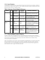
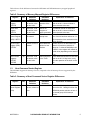
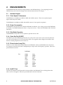
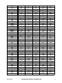
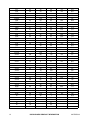
Order this document
by EB420/D Rev.1
MOTOROLA
SEMICONDUCTOR
ENGINEERING BULLETIN
EB420
Converting DSP56001-Based Designs to
the DSP56002
This document details the differences between the DSP56001 and DSP56002 that need to be taken into
consideration when redesigning a system based on the DSP56001 to use the DSP56002. The differences fall
into two major categories: changes which must be addressed by the user and enhancements which the
designer may elect to implement.
Please refer to the DSP56001 and DSP56002 Technical Data Sheets and their associated documentation for
complete information. A list of all associated documents is contained in Appendix A.
1.
REQUIRED CHANGES
1.1
Hardware/Layout
1.1.1. Pinout
The physical pinout of the DSP56001 is different from the DSP56002. This means that it is not possible to
directly replace a DSP56001 with a DSP56002 without changing the board layout. Please refer to the
DSP56002 Technical Data Sheet for details of the device pinout. For comparison purposes, Appendix B of
this document contains a table comparing the pin assignments of the DSP56001 packages to the DSP56002
packages.
1.1.2. Packaging
The DSP56001 is available in 3 package types:
The DSP56002 is also available in 3 package types:
PGA, 88 pin
PQFP, 132 pin
CQFP, 132 pin
PGA, 132 pin
PQFP, 132 pin
TQFP, 144 pin
Note that the PQFP has plastic “tabs” located at each corner. The layout must accommodate these “tabs”
and avoid placing components in areas occupied by these “tabs”.
1.1.3. Phase Locked Loop (PLL)
The 56002 has a Phase Locked Loop on-chip which permits operating the device from low frequency
external clock sources, precluding the need for additional high frequency clocks exclusively for the high
speed DSP. Tying the PINIT to GND disables the PLL upon power up. Although not necessary, the PCAP
pin should be tied to Vcc or GND.
This document contains information on a product under development.
Motorola reserves the right to change or discontinue this product without notice.
© MOTOROLA, INC., 1995
1.1.4. OnCE™ Port
The OnCE™ Port has been added to permit unobtrusive access to the core for debugging and testing. Tying
the Debug Request (DR#) 1 pin to Vcc will disable the OnCE port. It is recommended that DSCK be tied to
GND through a 56k ohm resistor.
1.1.5. Bus Control
There have been several changes made to the bus control pins. The BR#/WT# and BG#/BS# pins on the
DSP56001 have been demultiplexed on the DSP56002, and an additional control signal Bus Needed (BN#)
has been added.
DSP56001
DSP56002
input
input
input
output
output
output
BR#/WT#
output BG#/BS#
BR#
WT#
BG#
BS#
BN#
DSP56001-based designs should be simplified due to the presence of individual signal pins for all bus
arbitration functions. Both BR# and WT# require pull-up resistors to Vcc or they must be connected to
external logic which assures that their quiescent state is a logic “high”.
1.1.6. Bootstrap
The DSP56002 has an extra Mode Select pin (MODC/NMI#) which also serves as the Non-Maskable
Interrupt. The Mode Select pins are read as the processor comes out of reset and are used to define the
chip’s operating mode. Refer to the DSP56002 documentation for specific details on the various bootstrap
selections available via the MODA/MODB/MODC pins.
The reset circuitry will need to be modified for the DSP56002 so that the device will enter the correct
operating mode after exiting reset. For the DSP56002, bit 23 of the data bus no longer serves to select
between EPROM and Host Interface Boot modes.
1.1.7. Non-Maskable Interrupt (NMI)
A Non-Maskable Interrupt (NMI) function was previously accessible on the DSP56001 by applying 10 Volts
to the MODB/IRQB# pin. The DSP56002 supports a non-maskable interrupt (NMI) through the
MODC/NMI# pin which is TTL/CMOS compatible. DO NOT APPLY 10 VOLTS TO ANY PIN OF THE
DSP56002 (including MODB)! Subjecting any pin of the DSP56002 to voltages in excess of the specified
TTL/CMOS levels will permanently damage the device.
1.1.8. DC Electrical Characteristics
The supply voltage and logic level specifications of the DSP56001 and DSP56002 are the same. Most
DSP56002 buffers are capable of sinking 3.2 mA compared to the 1.6 mA buffers of the DSP56001. Please
refer to the DSP56001 and DSP56002 Technical Data Sheets for specific details.
1 Note that throughout this document, # is used to indicate that the signal is asserted when the voltage =
ground (active low).
2
DSP560PCMDK PRODUCT INFORMATION
MOTOROLA
1.1.9. AC Electrical Characteristics
The timing specifications of the DSP56002 differ from those of the DSP56001. This is due, in part, to the
superior performance inherent in the design of the DSP56002. The user should evaluate the impact of these
differences on a case-by-case basis.
The DSP56002 has been designed to operate at higher frequencies than the DSP56001. As a result, many
DSP56002 signals exhibit faster rise- and fall-times than the same signals on the DSP56001. These faster
edges may generate more radiated noise and EMI, and may require more attention to these issues (e.g., the
DSP56002 based circuit may require better decoupling). Use of the PLL, however, may reduce the actual
radiated noise and EMI. Please refer to the DSP56002 documentation.
1.2
Software/Application
The DSP56002 instruction set is upwardly compatible with the DSP56001. This means that software written
for the DSP56001 will generally run unmodified on the DSP56002. There are, however, certain differences
which result from the DSP56002’s enhanced functionality and increased level of performance. Users should
consider the impact these differences may have on each application.
1.2.1. MOVEP to Rn/Nn/Mn Registers
On the DSP56001 there is a pipeline delay when using the MOVEP instruction to change the contents of an
address register (Mn, Nn, or Rn). The new contents of the destination address register will not be available
for use during the following instruction (i.e, there is a single instruction cycle delay).
On the DSP56002 this pipeline delay has been removed. If an address register (Mn, Nn, or Rn) is directly
changed with a MOVEP instruction, the updated contents will be available for use during the following
instruction. DSP56001 software which depends on this pipeline delay must be modified when moved onto
the DSP56002.
1.2.2. MOVEP to/from Data ALU Registers
MOVEP Instructions to/from Data ALU Registers take 2 instruction cycles on the DSP56001. On the
DSP56002, these instructions take only 1 instruction cycle. DSP56001 software which is dependent on the
timing of this form of the MOVEP instruction must be modified when ported to the DSP56002.
1.2.3. MOVEP Immediate
MOVEP Immediate instructions take 3 instruction cycles on the DSP56001. On the DSP56002, these
instructions take only 2 instruction cycles. DSP56001 software which is dependent on the timing of this
form of the MOVEP instruction must be modified when ported to the DSP56002.
1.2.4. Stop/Wait Timing
Wake-up from the Stop and Wait operating modes with IRQn# is longer on the DSP56002 by one Tc period.
1.2.5. SCI/SSI Initialization Timing
On the DSP56002, the SCI and SSI clocks are stopped when the peripherals are not enabled in order to save
power. As a result, the initialization time of the SCI and SSI is longer on the DSP56002.
MOTOROLA
DSP560PCMDK PRODUCT INFORMATION
3
1.2.6. Control Registers
The DSP56002 has been improved to support Block Floating Point, Double Precision Arithmetic, additional
bootstrap modes, NMI and other features. In order to support these improvements, the OMR and the Status
Register have been altered, as outlined in Table 1.
Table 1: Summary of Control Register Differences
Register
Bit
Status Register
7
13
DSP56001
Definition
Reserved Read/Written as
zero.
T - Trace mode
14
Reserved Read/Written as
zero.
Operating Mode 0,1,4 0 - MA
Register
1 - MB
4 - Reserved
3
7
Reserved Read/Written as
zero.
EA - External
memory access
DSP56002
Definition
S - Scaling bit
T - Trace mode
DM - Double
precision multiply
0 - MA
1 - MB
4 - MC
YD - internal Y
memory disable
Reserved Read/Written as
zero.
Explanation of Difference
On the 002 this bit can be read as ‘1’
depending on the contents of S1,S0,
and the accumulators. It is a sticky bit.
The 002 manual states that the OnCE
trace mode should be used.
In the 002, if the DM bit is set, the
operations performed by the MPY and
MAC instructions change.
These three bits control the operating
mode of the device. The MODA, B & C
pins are latched in on reset. Completely
different for 001 and 002.
If this bit is set, all Y memory data
addresses are considered to be
external.
Controls the definition of the Port A
control pins. Not required on the 002 as
the bus control pins have been demultiplexed.
1.2.7. X:Memory Mapped Peripheral Registers
In order to support the new peripherals present on the DSP56002, some of the reserved X:I/O addresses
which were reserved on the DSP56001 have been redefined as peripheral control registers. It is important to
ensure that the new definitions of these previously unused X:I/O addresses do not conflict with any
software developed for the DSP56001.
Many of the peripheral control registers within the DSP56001 and DSP56002 have reserved bits. Reads from
these reserved bits will return zero. In order to guarantee compatibility with future products, these bits
should be written as zero. On the DSP56002, some of the previously reserved bits in these registers have
been redefined in order to support enhanced funtionality.
4
DSP560PCMDK PRODUCT INFORMATION
MOTOROLA
Table 2 shows all the differences between the DSP56001 and DSP56002 memory mapped peripheral
registers.
Table 2: Summary of Memory Mapped Register Differences
Register
Bit
DSP56001
Definition
DSP56002
Definition
PLL Control
Register
X:$FFFD
OnCE GDB
Register
X:$FFFC
SCI Interface
Control Register
(SCR) X:$FFF0
All
Reserved - read
as random, write
as don’t care.
Reserved - read
as random, write
as don’t care.
Written as zero in
the manual
Control the
operation of the
PLL
Used in the
execution of
OnCE commands
STIR - Timer
interrupt rate
Port B Control
Register (PBC)
X:$FFE0
1
Timer Control
Registers
X:$FFDF
X:$FFDE
All
1.3
All
14
Explanation of Difference
This address should not have been
used on the 001. Users will have to
ensure that this is the case.
This address should not have been
used on the 001. Users will have to
ensure that this is the case.
On the 001 this bit should be written as
zero. If this bit has been written as ‘1’ it
will increase the timer resolution on the
002 by 32 times.
Written as zero in Offers additional If written as zero, as described in the
manual
options for host
manual, will cause no problems. If
interface
written as ‘1’ either the HACK# pin will
be GPIO, or the register will contain an
invalid value (depending on the state of
bit 0)
Reserved - read Control Registers These addresses should not have been
as random, write for the Timer
used on the 001. If they have, it may
as don’t care.
effect the operation of the timer on the
002.
Host Command Vector Register
The DSP56002 supports 64 Interrupt Vectors, compared to the 32 Interrupt Vectors supported by the
DSP56001.
Table 3: Summary of Host Command Vector Register Differences
Register
Bit
Host Command
Vector Register
(CVR)
5
MOTOROLA
DSP56001
Definition
DSP56002
Definition
Reserved - read Host Vector MSB
as zero, written as
zero.
Explanation of Difference
This bit should always be written as
zero on the 001. Setting this bit on the
DSP56002 permits selection of one of
the second group of 32 Interrupt
Vectors.
DSP560PCMDK PRODUCT INFORMATION
5
2.
ENHANCEMENTS
The DSP56002 embodies numerous improvements to the DSP56001 design. Users migrating from the
DSP56001 may wish to take advantage of these enhancements in their new designs.
2.1
Hardware/Layout
2.1.1. Clock Speed / Performance
The DSP56001 is available in 20.5 MHz, 27 MHz and 33 MHz versions. There are no planned speed
improvements beyond 33 MHz.
The DSP56002 is available in 40 MHz and 66 MHz versions. Faster speeds are planned.
2.1.2. Power Consumption
The DSP56002 consumes less power than the DSP56001. In addition, a low voltage version of the DSP56002
is available; the DSP56L002 operates from 3.3 volt power sources. Refer to the DSP56002/L002 Technical
Data Sheet.
2.1.3. Fully Static Operation
The DSP56002 is a fully static device, capable of operation down to DC.
2.1.4. Clock Out Pin (CKOUT)
The CKOUT pin of the DSP56002 provides the user with a clock source which can be driven by either the
core clock or the output of a Low Power Divider (LPD). This signal has been designed to minimize skew
between external peripheral clocks and the core.
2.1.5. Phase Locked Loop (PLL)
The PLL is a new feature that has been added to the DSP56002. It allows the DSP56002 to be driven by a
low frequency external clock which is multiplied up on chip to allow full frequency operation. There are 9
pins dedicated to the PLL.
DSP56002
PLL
supply
supply
input
input
output
supply
supply
input
output
Vccp
GNDP
PCAP
CKP
PLOCK
Vcccl
GNDCL
PINIT
CKOUT
2.1.6. OnCE™ Port
The On-Chip Emulator (OnCE) interface has been added to the DSP56002. This is a debug feature that
allows access to all registers. There are 4 pins dedicated to the OnCE interface.
6
DSP560PCMDK PRODUCT INFORMATION
MOTOROLA
DSP56002
OnCE
in/out
in/out
input
output
DSCK/OS1
DSI/OS0
DR#
DSO
2.1.7. Host Acknowledge (HACK#)
The HACK# pin may now be used as a general purpose I/O pin (GPIO) independent of the other Host
Interface pins. Bits 0 and 1 of the Port B Control Register (PBC) now work in concert to define the function
of HACK# and the remaining Host Interface Pins.
2.1.8. Timer/TIO Pin
A 24-bit timer/event counter has been added to the DSP56002. Refer to the DSP56002 User’s Manual,
Section 7, Timer and Event Counter.
2.1.9. I/O Buffer Drive
Most DSP56002 buffers are capable of sinking 3.2 mA compared to the 1.6 mA buffers of the DSP56001.
Refer to the DSP56002 Technical Data Sheet.
2.1.10.
SCI Timer Interrupt Rate
Bit 14 in the SCI Control Register now controls a divide by 32 in the SCI Timer interrupt generator. This bit
was reserved on the DSP56001.
2.1.11.
SCI Bootstrap
The 56002 supports bootstrapping from the SCI.
2.1.12.
Demultiplexed Bus Control Signals
As mentioned above, BR#, BG#, BS# and WT# no longer share pins. On the DSP56002, the bus arbitration
function and the external wait state generation function are no longer mutually exclusive. In addition, a
new pin, Bus Needed (BN#) has been added.
2.2
Software/Application
2.2.1. MOVEP Timing
Refer to the discussion above regarding enhanced performance of the MOVEP instructions.
2.2.2. Double Precision Multiply
Refer to the DSP56000 Family Manual, Section 3, Data Arithmetic Logic Unit.
2.2.3. Wrap Around Addressing Mode
Refer to the DSP56000 Family Manual, Section 4, Address Generation Unit and Addressing Modes.
2.2.4. Block Floating Point
Refer to the DSP56000 Family Manual, Section 5, Program Control Unit, Section 5.4.2, Status Register.
2.2.5. Increased Vector Table Size
The DSP56001 supports 32 interrupt vectors (P:$00-P:$3F) while the DSP56002 supports 64 vectors
(P:$00-P:$7F).
MOTOROLA
DSP560PCMDK PRODUCT INFORMATION
7
2.2.6. Host Command Register
The Host Vector portion of the Host Command Register (HCR) has been extended to 6 bits in order to
support the increased vector table size.
2.2.7. Instruction Set Enhancements
The following Instructions have been added:
INC
DEC
DEBUG
DEBUGcc
Immediate versions of MPY/MPYR/MAC/MACR
Refer to the DSP56000 Family Manual, Appendix A, Instruction Set Details.
APPENDIX A - Related Documents
Complete technical information on the DSP56001 and DSP56002 is contained in the following documents,
which can be ordered from your Motorola Literature Distribution Center using the reference numbers
shown:
DSP56001 Technical Data Sheet - DSP56001/D
DSP56000/1 Users Manual - DSP56000UM/AD
DSP56002 Technical Data Sheet - DSP56002/D
DSP56000 Family Manual - DSP56KFAM/D
DSP56002 Users Manual - DSP56002UM/AD
8
DSP560PCMDK PRODUCT INFORMATION
MOTOROLA
APPENDIX B - Comparison of DSP56001 to DSP56002
Pin Assignments
Table 4: Signal Name to DSP56001 and DSP56002 Pinout Cross Reference
Signal Name
A0
A1
A2
A3
A4
A5
A6
A7
A8
A9
A10
A11
A12
A13
A14
A15
BG#
BN#
BR#
BS#
CKOUT
CKP
D0
D1
D2
D3
D4
D5
D6
D7
D8
D9
D10
MOTOROLA
DSP56001
DSP56002 FC DSP56002 PV DSP56001 RC DSP56002 RC
FC or FE
132 pin PQFP 144 pin TQFP 88 pin PGA
132 pin PGA
132 pin PQFP
Pin
Pin
Pin
Pin
or CQFP Pin
53
54
57
58
60
61
65
67
68
70
71
75
76
77
79
80
43
45
43
81
82
85
86
87
88
92
93
94
96
97
60
61
63
64
65
68
71
72
73
74
76
77
78
80
82
83
43
41
44
54
123
126
84
85
87
88
90
91
93
94
95
96
100
83
84
86
87
88
92
95
96
97
98
100
101
102
104
106
107
64
62
65
77
8
11
110
111
113
114
116
117
119
120
121
122
126
DSP560PCMDK PRODUCT INFORMATION
M11
N11
N10
M9
N9
M8
N8
N7
N6
M6
N5
M5
N4
N3
N2
M3
K12
L13
K12
N1
M2
L2
M1
L1
K2
K1
J2
J1
H1
G1
K9
L9
M9
L8
M8
M7
L7
M6
L6
M5
L5
K5
M4
L4
K4
J4
K12
H13
L12
N11
C5
B4
N2
M3
M2
L3
L2
K3
K2
J3
J2
H3
H2
9
D11
D12
D13
D14
D15
D16
D17
D18
D19
D20
D21
D22
D23
DR#
DS#
DSCK
DSI
DSO
EXTAL
GNDC
GNDCK
GNDD
GNDD
GNDD
GNDD
GNDD
GNDD
GNDH
GNDH
GNDH
GNDH
GNDN
GNDN
GNDN
GNDN
GNDN
GNDP
GNDQ
GNDQ
GNDQ
GNDQ
GNDS
GNDS
H0
10
99
102
104
105
106
108
109
113
114
115
118
119
120
49
127
90
91
111
112
23
24
55
56
73
74
33
34
130
131
25
101
103
104
106
107
108
109
111
112
114
115
117
118
51
57
50
53
52
1
48
122
86
92
99
105
110
116
5
11
16
22
56
62
70
75
81
129
3
36
67
98
27
34
24
128
130
131
133
134
135
136
138
139
141
142
2
3
74
80
71
76
75
19
69
7
112
118
125
132
137
143
23
29
34
42
79
85
94
99
105
14
21
57
90
124
47
54
44
DSP560PCMDK PRODUCT INFORMATION
F1
F2
E1
D1
C1
D2
B1
C2
A1
B2
A2
A3
B4
M12
B6
D3
J3
E11
L6
L9
B7
G11
D12
H1
G3
G2
G1
F1
F2
F3
E2
E3
D2
D3
E4
D4
K11
L10
N12
M11
L11
C8
N13
C4
B1
D1
E1
K1
L1
N1
A12
A13
C13
E13
N10
N3
N5
N6
N8
C6
A1
A3
A5
A7
J13
L13
E11
MOTOROLA
H1
H2
H3
H4
H5
H6
H7
HA0
HA1
HA2
HACK#
HEN#
HR/W#
HREQ#
IRQA#
IRQB#
MODA
MODB
MODC
NMI#*
OS0
OS1
PB0
PB1
PB2
PB3
PB4
PB5
PB6
PB7
PB8
PB9
PB10
PB11
PB12
PB13
PB14
PC0
PC1
PC2
PC3
PC4
PC5
PC6
MOTOROLA
22
20
19
16
15
14
11
5
2
1
6
8
9
10
123
121
123
121
121
25
22
20
19
16
15
14
11
5
2
1
9
8
10
6
27
28
29
31
40
37
32
23
21
19
18
17
15
14
7
6
4
8
10
12
13
121
120
121
120
119
119
53
50
24
23
21
19
18
17
15
14
7
6
4
12
10
13
8
25
26
28
29
35
32
31
43
41
39
38
35
33
32
25
24
22
26
28
30
31
6
5
6
5
4
4
76
71
44
43
41
39
38
35
33
32
25
24
22
30
28
31
26
45
46
48
49
56
52
51
DSP560PCMDK PRODUCT INFORMATION
C13
C12
B13
B12
A13
A12
B11
B8
A8
A7
A9
A10
A11
B10
B5
A4
B5
A4
A4
D12
C13
C12
B13
B12
A13
A12
B11
B8
A8
A7
A11
A10
B10
A9
D13
E13
F13
F12
K13
H13
G13
D11
C11
E10
D10
B12
A11
B11
C9
B9
A9
A10
B10
D9
C10
C3
C2
C3
C2
D5
D5
M11
N12
E11
D11
C11
E10
D10
B12
A11
B11
C9
B9
A9
D9
B10
C10
A10
C12
D12
E12
F11
G12
F13
F12
11
PC7
PC8
PCAP
PINIT
PLOCK
PS#
RD#
RESET#
RXD
SC0
SC1
SC2
SCK
SCLK
SRD
STD
TIO
TXD
V CCC
V CCCK
V CCD
V CCD
V CCD
V CCH
V CCH
V CCN
V CCN
V CCN
V CCP
V CCQ
V CCQ
V CCQ
V CCQ
V CCS
WR#
WT#
X/Y#
XTAL
nc
nc
nc
nc
nc
nc
12
42
39
52
47
124
27
31
40
37
32
29
42
39
28
100
101
12
13
63
64
35
36
128
129
46
45
48
126
3
4
7
17
18
21
38
33
128
131
130
59
47
125
25
29
35
32
31
28
38
33
39
26
45
124
89
102
113
9
20
58
69
79
127
2
37
66
97
30
46
42
55
132
40
49
59
53
13
16
15
82
68
10
45
49
56
52
51
48
59
53
60
46
66
9
115
129
140
27
40
81
93
103
12
20
58
89
123
50
67
63
78
17
1
18
36
37
55
61
DSP560PCMDK PRODUCT INFORMATION
J12
J13
N12
L12
A5
D13
F12
K13
H13
G13
F13
J12
J13
E13
G3
C9
L8
C6
G12
M13
L13
N13
A6
G13
G11
B6
C7
B7
M10
J10
B3
C12
F11
G12
F13
F12
E12
G13
G11
H11
D12
M13
B2
C1
J1
M1
B13
D13
N4
N7
N9
B5
A2
A4
A6
A8
K13
J11
J12
K10
B8
H12
M12
MOTOROLA
nc
nc
nc
nc
nc
nc
nc
nc
nc
nc
nc
nc
nc
nc
nc
nc
nc
nc
nc
nc
nc
nc
nc
nc
nc
nc
26
30
38
41
44
50
51
59
62
66
69
72
78
83
84
89
95
98
103
107
110
116
117
122
125
132
70
72
73
91
108
109
127
144
Notes:
# indicates the signal is asserted when the voltage = ground (active low).
* On the 56001 (only): NMI is a 10 V high signal, BR# also acts as WT#, and BG# also acts as BS# .
nc = no connection.
MOTOROLA
DSP560PCMDK PRODUCT INFORMATION
13
Table 5: Pinout to DSP56001 and DSP56002 Signal Name Cross Reference
DSP56001
FC or FE
132 pin PQFP
or CQFP Pin
DSP56002 FC
132 pin PQFP
Pin
DSP56002 PV
144 pin TQFP
Pin
Signal Name
1
2
3
4
5
6
7
8
9
10
11
12
13
14
15
16
17
18
19
20
21
22
23
24
25
26
27
28
29
30
31
32
33
34
35
36
37
38
4
6
40
49
7
8
22
24
61
70
25
26
91
28
30
31
32
40
27
33
35
38
108
109
39
41
127
43
34
42
44
73
45
46
48
18
49
51
21
57
58
20
52
55
HA2/PB10
HA1/PB9
nc
nc
HA0/PB8
HACK#/PB14
nc
HEN#/PB12
HR/W#/PB11
HREQ#/PB13
H7/PB7
V CCH
V CCH
H6/PB6
H5/PB5
H4/PB4
nc
nc
H3/PB3
H2/PB2
nc
H1/PB1
GNDH
GNDH
H0/PB0
nc
RXD/PC0
TXD/PC1
SCLK/PC2
nc
SC0/PC3
SCK/PC6
GNDQ
GNDQ
V CCQ
V CCQ
SC2/PC5
nc
14
10
12
13
14
20
9
15
17
18
19
21
23
16
22
24
25
26
28
29
31
3
36
37
2
32
DSP560PCMDK PRODUCT INFORMATION
MOTOROLA
39
40
41
42
43
44
45
46
47
48
49
50
51
52
53
54
55
56
57
58
59
60
61
62
63
64
65
66
67
68
69
70
71
72
73
74
75
76
77
78
79
80
81
82
MOTOROLA
33
35
38
43
44
46
47
55
57
53
56
72
59
64
59
60
61
70
62
63
64
65
67
68
78
80
144
1
82
83
84
94
85
86
87
65
68
88
92
79
69
71
103
93
95
72
73
96
97
74
76
98
100
75
81
77
78
80
99
105
101
102
104
82
83
84
85
106
107
110
111
STD/PC8
SC1/PC4
nc
SRD/PC7
BG#(/BS#)*
nc
BR#(/WT#)*
WR#
RD#
X/Y#
DS#
nc
nc
PS#
A0
A1
GNDN
GNDN
A2
A3
nc
A4
A5
nc
V CCN
V CCN
A6
nc
A7
A8
nc
A9
A10
nc
GNDN
GNDN
A11
A12
A13
nc
A14
A15
D0
D1
DSP560PCMDK PRODUCT INFORMATION
15
83
84
85
86
87
88
89
90
91
92
93
94
95
96
97
98
99
100
101
102
103
104
105
106
107
108
109
110
111
112
113
114
115
116
117
118
119
120
121
122
123
124
125
126
16
87
88
90
91
36
37
113
114
116
117
99
92
93
94
95
125
118
119
120
121
96
100
122
126
101
113
102
103
128
140
129
130
104
106
107
131
133
134
108
109
135
136
105
110
111
112
114
132
137
138
139
141
115
117
118
120
142
2
3
5
121
125
6
10
132
17
nc
nc
D2
D3
D4
D5
nc
GNDD
GNDD
D6
D7
D8
nc
D9
D10
nc
D11
V CCD
V CCD
D12
nc
D13
D14
D15
nc
D16
D17
nc
GNDD
GNDD
D18
D19
D20
nc
nc
D21
D22
D23
MODB/IRQB#(NMI/)*
nc
MODA/IRQA#
RESET#
nc
XTAL
DSP560PCMDK PRODUCT INFORMATION
MOTOROLA
127
128
129
130
131
132
1
97
66
67
98
19
123
89
90
124
5
11
27
30
34
39
41
42
45
48
50
51
52
53
54
56
58
86
89
116
119
122
123
124
126
127
128
129
130
131
23
29
47
50
54
60
62
63
66
69
71
74
75
76
77
79
81
112
115
143
4
7
8
9
11
12
13
14
15
16
EXTAL
V CCQ
V CCQ
GNDQ
GNDQ
nc
GNDH
GNDH
GNDS
V CCS
GNDS
TIO
BN#
WT#
V CCC
GNDC
DSCK/OS1
DR#
DSO
DSI/OS0
BS#
GNDN
V CCN
GNDD
V CCD
GNDD
MODC/NMI#*
GNDCK
CKOUT
V CCCK
CKP
V CCP
PCAP
GNDP
PLOCK
PINIT
Notes:
# indicates the signal is asserted when the voltage = ground (active low).
* NMI is a 10 V high signal on the 56001 (only).
nc = no connection.
'001 '002
FC/FE
FC
132
132
MOTOROLA
'002
PV
144
Signal
'001 '002
FC/FE
FC
132
132
'002
PV
144
Signal
DSP560PCMDK PRODUCT INFORMATION
17
PQFP/ PQFP
CQFP
Pin
Pin
---- ---1
4
2
6
3
40
4
49
5
7
6
8
7
8
10
9
12
10
13
11
14
12
20
13
9
14
15
15
17
16
18
17
18
19
19
20
21
21
22
23
23
16
24
22
25
24
26
27
25
28
26
29
28
30
31
29
32
31
33
3
34
36
35
37
36
2
37
32
38
39
33
40
35
41
42
38
43
43
18
TQFP
Pin
---22
24
61
70
25
26
91
28
30
31
32
40
27
33
35
38
108
109
39
41
127
43
34
42
44
73
45
46
48
18
49
51
21
57
58
20
52
55
53
56
72
59
64
Name
PQFP/ PQFP
CQFP
Pin
Pin
----------- ---- ---HA2/PB10
: 84
HA1/PB9
: 85
87
nc
: 86
88
nc
: 87
90
HA0/PB8
: 88
91
HACK#/PB14 : 89
nc
: 90
99
HEN#/PB12
: 91
92
HR/W#/PB11 : 92
93
HREQ#/PB13 : 93
94
H7/PB7
: 94
95
VccH
: 95
VccH
: 96
96
H6/PB6
: 97
100
H5/PB5
: 98
H4/PB4
: 99
101
nc
: 100
113
nc
: 101
102
H3/PB3
: 102
103
H2/PB2
: 103
nc
: 104
104
H1/PB1
: 105
106
GNDH
: 106
107
GNDH
: 107
H0/PB0
: 108
108
nc
: 109
109
RXD/PC0
: 110
TXD/PC1
: 111
105
SCLK/PC2
: 112
110
nc
: 113
111
SC0/PC3
: 114
112
SCK/PC6
: 115
114
GNDQ
: 116
GNDQ
: 117
VccQ
: 118
115
VccQ
: 119
117
SC2/PC5
: 120
118
nc
: 121
120
STD/PC8
: 122
SC1/PC4
: 123
121
nc
: 124
125
SRD/PC7
: 125
BG#(/BS#)* : 126
132
TQFP
Pin
---37
113
114
116
117
125
118
119
120
121
122
126
128
140
129
130
131
133
134
135
136
132
137
138
139
141
142
2
3
5
6
10
17
Name
------nc
D2
D3
D4
D5
nc
GNDD
GNDD
D6
D7
D8
nc
D9
D10
nc
D11
VccD
VccD
D12
nc
D13
D14
D15
nc
D16
D17
nc
GNDD
GNDD
D18
D19
D20
nc
nc
D21
D22
D23
MODB/IRQB#(NMI/)*
nc
MODA/IRQA#
RESET#
nc
XTAL
DSP560PCMDK PRODUCT INFORMATION
MOTOROLA
44
45
46
47
48
49
50
51
52
53
54
55
56
57
58
59
60
61
62
63
64
65
66
67
68
69
70
71
72
73
74
75
76
77
78
79
80
81
82
83
44
46
47
55
57
59
60
61
70
62
63
64
65
67
68
78
80
144
1
82
83
84
94
85
86
87
65
68
88
92
79
69
71
103
93
95
72
73
96
97
74
76
98
100
75
81
77
78
80
99
105
101
102
104
82
83
84
85
106
107
110
111
36
nc
BR#(/WT#)*
WR#
RD#
X/Y#
DS#
nc
nc
PS#
A0
A1
GNDN
GNDN
A2
A3
nc
A4
A5
nc
VccN
VccN
A6
nc
A7
A8
nc
A9
A10
nc
GNDN
GNDN
A11
A12
A13
nc
A14
A15
D0
D1
nc
:
:
:
:
:
:
:
:
:
:
:
:
:
:
:
:
:
:
:
:
:
:
:
:
:
:
:
:
:
:
:
:
:
:
:
:
127
128
129
130
131
132
1
97
66
67
98
19
123
89
90
124
5
11
27
30
34
39
41
42
45
48
50
51
52
53
54
56
58
86
89
116
119
122
123
124
126
127
128
129
130
131
23
29
47
50
54
60
62
63
66
69
71
74
75
76
77
79
81
112
115
143
4
7
8
9
11
12
13
14
15
16
EXTAL
VccQ
VccQ
GNDQ
GNDQ
nc
GNDH
GNDH
GNDS
VccS
GNDS
TIO
BN#
WT#
VccC
GNDC
DSCK/OS1
DR#
DSO
DSI/OS0
BS#
GNDN
VccN
GNDD
VccD
GNDD
MODC/NMI# *
GNDCK
CKOUT
VccCK
CKP
VccP
PCAP
GNDP
PLOCK
PINIT
Notes:
# indicates the signal is asserted when the voltage = ground (active low).
* On the 56001 (only): NMI is a 10 V high signal, BR# also acts as WT#, and
BG# also acts as BS#.
nc = no connection.
MOTOROLA
DSP560PCMDK PRODUCT INFORMATION
19
'001
FC/FE
Signal
132
pin
Name
PQFP/
CQFP
Pin
------ ---A0
A1
A2
A3
A4
A5
A6
A7
A8
A9
A10
A11
A12
A13
A14
A15
BG#
BN#
BR#
BS#
CKOUT
CKP
D0
D1
D2
D3
D4
D5
D6
D7
D8
D9
D10
D11
D12
D13
D14
20
53
54
57
58
60
61
65
67
68
70
71
75
76
77
79
80
43
45
43
81
82
85
86
87
88
92
93
94
96
97
99
102
104
105
'002
FC
132
pin
PQFP
'002
PV
144
pin
TQFP
'001
RC
88
pin
PGA
'002
RC
132
pin
PGA
Pin
----
Pin
----
Pin
----
Pin
---
60
61
63
64
65
68
71
72
73
74
76
77
78
80
82
83
43
41
44
54
123
126
84
85
87
88
90
91
93
94
95
96
100
101
103
104
106
83
84
86
87
88
92
95
96
97
98
100
101
102
104
106
107
64
62
65
77
8
11
110
111
113
114
116
117
119
120
121
122
126
128
130
131
133
M11
N11
N10
M9
N9
M8
N8
N7
N6
M6
N5
M5
N4
N3
N2
M3
K12
L13
K12
N1
M2
L2
M1
L1
K2
K1
J2
J1
H1
G1
F1
F2
E1
D1
K9
L9
M9
L8
M8
M7
L7
M6
L6
M5
L5
K5
M4
L4
K4
J4
K12
H13
L12
N11
C5
B4
N2
M3
M2
L3
L2
K3
K2
J3
J2
H3
H2
H1
G3
G2
G1
DSP560PCMDK PRODUCT INFORMATION
MOTOROLA
D15
D16
D17
D18
D19
D20
D21
D22
D23
DR#
DS#
DSCK
DSI
DSO
EXTAL
GNDC
GNDCK
GNDD
GNDD
GNDD
GNDD
GNDD
GNDD
GNDH
GNDH
GNDH
GNDH
GNDN
GNDN
GNDN
GNDN
GNDN
GNDP
GNDQ
GNDQ
GNDQ
GNDQ
GNDS
GNDS
H0
H1
H2
H3
H4
H5
H6
H7
106
108
109
113
114
115
118
119
120
49
127
90
91
111
112
23
24
55
56
73
74
33
34
130
131
MOTOROLA
25
22
20
19
16
15
14
11
107
108
109
111
112
114
115
117
118
51
57
50
53
52
1
48
122
86
92
99
105
110
116
5
11
16
22
56
62
70
75
81
129
3
36
67
98
27
34
24
23
21
19
18
17
15
14
134
135
136
138
139
141
142
2
3
74
80
71
76
75
19
69
7
112
118
125
132
137
143
23
29
34
42
79
85
94
99
105
14
21
57
90
124
47
54
44
43
41
39
38
35
33
32
C1
D2
B1
C2
A1
B2
A2
A3
B4
M12
B6
D3
J3
E11
L6
L9
B7
G11
D12
C13
C12
B13
B12
A13
A12
B11
F1
F2
F3
E2
E3
D2
D3
E4
D4
K11
L10
N12
M11
L11
C8
N13
C4
B1
D1
E1
K1
L1
N1
A12
A13
C13
E13
N10
N3
N5
N6
N8
C6
A1
A3
A5
A7
J13
L13
E11
D11
C11
E10
D10
B12
A11
B11
DSP560PCMDK PRODUCT INFORMATION
21
HA0
HA1
HA2
HACK#
HEN#
HR/W#
HREQ#
IRQA#
IRQB#
MODA
MODB
MODC
NMI#*
OS0
OS1
PB0
PB1
PB2
PB3
PB4
PB5
PB6
PB7
PB8
PB9
PB10
PB11
PB12
PB13
PB14
PC0
PC1
PC2
PC3
PC4
PC5
PC6
PC7
PC8
PCAP
PINIT
PLOCK
PS#
RD#
RESET#
RXD
SC0
22
5
2
1
6
8
9
10
123
121
123
121
121
25
22
20
19
16
15
14
11
5
2
1
9
8
10
6
27
28
29
31
40
37
32
42
39
52
47
124
27
31
7
6
4
8
10
12
13
121
120
121
120
119
119
53
50
24
23
21
19
18
17
15
14
7
6
4
12
10
13
8
25
26
28
29
35
32
31
38
33
128
131
130
59
47
125
25
29
25
24
22
26
28
30
31
6
5
6
5
4
4
76
71
44
43
41
39
38
35
33
32
25
24
22
30
28
31
26
45
46
48
49
56
52
51
59
53
13
16
15
82
68
10
45
49
B8
A8
A7
A9
A10
A11
B10
B5
A4
B5
A4
A4
D12
C13
C12
B13
B12
A13
A12
B11
B8
A8
A7
A11
A10
B10
A9
D13
E13
F13
F12
K13
H13
G13
J12
J13
N12
L12
A5
D13
F12
C9
B9
A9
A10
B10
D9
C10
C3
C2
C3
C2
D5
D5
M11
N12
E11
D11
C11
E10
D10
B12
A11
B11
C9
B9
A9
D9
B10
C10
A10
C12
D12
E12
F11
G12
F13
F12
G13
G11
B6
C7
B7
M10
J10
B3
C12
F11
DSP560PCMDK PRODUCT INFORMATION
MOTOROLA
SC1
SC2
SCK
SCLK
SRD
STD
TIO
TXD
VccC
VccCK
VccD
VccD
VccD
VccH
VccH
VccN
VccN
VccN
VccP
VccQ
VccQ
VccQ
VccQ
VccS
WR#
WT#
X/Y#
XTAL
nc
nc
nc
nc
nc
nc
nc
nc
nc
nc
nc
nc
nc
nc
nc
nc
nc
nc
nc
40
37
32
29
42
39
28
100
101
12
13
63
64
35
36
128
129
46
45
48
126
3
4
7
17
18
21
26
30
38
41
44
50
51
59
62
66
69
72
78
MOTOROLA
35
32
31
28
38
33
39
26
45
124
89
102
113
9
20
58
69
79
127
2
37
66
97
30
46
42
55
132
40
49
56
52
51
48
59
53
60
46
66
9
115
129
140
27
40
81
93
103
12
20
58
89
123
50
67
63
78
17
1
18
36
37
55
61
70
72
73
91
108
109
127
144
K13
H13
G13
F13
J12
J13
E13
G3
C9
L8
C6
G12
M13
L13
N13
A6
G12
F13
F12
E12
G13
G11
H11
D12
M13
B2
C1
J1
M1
B13
D13
N4
N7
N9
B5
A2
A4
A6
A8
K13
J11
J12
K10
B8
H12
M12
DSP560PCMDK PRODUCT INFORMATION
23
nc
nc
nc
nc
nc
nc
nc
nc
nc
nc
nc
nc
nc
83
84
89
95
98
103
107
110
116
117
122
125
132
Notes:
# indicates the signal is asserted when the voltage = ground (active low).
* NMI is a 10 V high signal on the 56001 (only).
nc = no connection.
24
DSP560PCMDK PRODUCT INFORMATION
MOTOROLA
OnCE is a trademark of Motorola, Inc.
All product and brand names appearing herein are trademarks or registered trademarks of their respective holders.
Motorola reserves the right to make changes without further notice to any products herein. Motorola makes no warranty, representation or
guarantee regarding the suitability of its products for any particular purpose, nor does Motorola assume any liability arising out of the
application or use of any product or circuit, and specifically disclaims any and all liability, including without limitation consequential or
incidental damages. “Typical” parameters can and do vary in different applications. All operating parameters, including “Typical”, must
be validated for each customer application by customer's technical experts. Motorola does not convey any license under its patent rights
nor the rights of others. Motorola products are not designed, intended, or authorized for use as components in systems intended for surgical implant into the body, or other applications intended to support or sustain life, or for any other application in which the failure of the
Motorola product could create a situation where personal injury or death may occur. Should Buyer purchase or use Motorola products for
any such unintended or unauthorized application, Buyer shall indemnify and hold Motorola and its officers, employees, subsidiaries,
affiliates, and distributors harmless against all claims, costs, damages, and expenses, and reasonable attorney fees arising out of, directly or
indirectly, any claim of personal injury or death associated with such unintended or unauthorized use, even if such claim alleges that
Motorola was negligent regarding the design or manufacture of the part.
Motorola and
are registered trademarks of Motorola, Inc.
Motorola, Inc. is an Equal Opportunity/Affirmative Action Employer.
Literature Distribution Centers:
USA: Motorola Literature Distribution; P.O. Box 20912; Phoenix, AZ 85036.
EUROPE: Motorola Ltd.; European Literature Centre; 88 Tanners Drive; Blakelands, Milton Keynes,
MK14 5BP; Great Britain.
JAPAN: Nippon Motorola Ltd.; 4-32-1, Nishi-Gotanda; Shinagawa-ku; Tokyo 141 Japan.
ASIA-PACIFIC: Motorola Semiconductors H.K. Ltd.; Silicon Harbour Center; No. 2 Dai King Street; Tai Po
Industrial Estate; Tai Po, N.T.; Hong Kong.