1
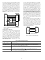
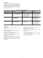
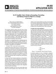
a
ONE TECHNOLOGY WAY
AN-400
APPLICATION NOTE
• P.O. BOX 9106 • NORWOOD, MASSACHUSETTS 02062-9106 • 617/329-4700
Considerations for Selecting a DSP Processor—Why Buy the ADSP-2181?
(The Analog Devices ADSP-2181 vs. Texas Instruments & Motorola Fixed-Point DSPs)
INTRODUCTION
You should use the ADSP-2181 Digital Signal Processor
for your high performance, fixed-point DSP applications
because this processor provides all the memory, I/O,
and interface support you need in a single chip. Table I
shows a comparison of the ADSP-2181, TMS320C5x,
and DSP56000 processors. The ADSP-2181 beats the
other DSPs with the following features:
• 32K words of on-chip RAM (nearest competitor has
9.5K words)
• Glue-less (no decode required) interface for off-chip
RAM and I/O peripherals
• Integrated 8 and 16-bit DMA support
COMPARING THE DSP PROCESSORS—ADSP-2181,
TMS320C5X, AND DSP56000
The point of comparing DSP processors is to determine
which provides the features you need to develop your
DSP system and run your DSP applications. This section
first examines typical system and algorithm requirements then reviews how each of the DSPs meet these
needs.
DSP applications require high speed RAM. Data and
instructions for the DSP are stored in RAM and accessed
at run time. As shown in Table II, many common RAMintensive applications require 9.5K words of RAM or
more; this information was gathered from Analog
Devices applications engineers using ADSP-2100 Family
DSPs.
This application note explains how the ADSP-2181’s onchip RAM, off-chip RAM & I/O interface, and integrated
DMA support provide increased performance and decreased system costs compared to Texas Instruments
and Motorola fixed-point DSPs.
To support these types of applications, DSP systems
must either use a DSP with sufficient on-chip RAM or
include sufficient off-chip DSP RAM. And, the RAM used
must have a fast enough access speed to not impair the
DSP’s operation. From the data in Tables I and II, you
can see that the ADSP-2181 is the only fixed-point DSP
that provides sufficient on-chip RAM to support all these
typical DSP algorithms.
Table I. Comparison of Fixed-Point DSP Costs and Features
DSP Processor
ADSP-2181
DSP56002
TMS320C50
TMS320C53
On-Chip RAM
32K words
1K word
9.5K words
3.5K words
“Glue-Less” Off-Chip RAM
and I/O Interface?
Yes
No
No
No
DSP Instruction Rate
33 MIPS
20 MIPS
40 MIPS
40 MIPS
Table II. Typical DSP Algorithms with Approximate MIPS and Memory Requirements
Algorithm
Approximate MIPS Required
Approximate RAM Required
V.32bis or V.32terbo FAX/Modem
16
16K words PM, 16K words DM
20 Voice Music Synthesis
20
6K words PM, 4K words DM
Full Duplex Speaker Phone
13
2K words PM, 2K words DM
Digital Answering Machine
8
5K words PM, 1K word DM
GSM, 13 kbps Compression/Decompression
4
2K words PM, 1K word DM
CELP, 4.3 or 7.5 kbps Compression/Decompression
12.5
1.5K words PM, 1.5K words DM
MPEG Layer2, 64 kbps Compression
16
5K words PM, 4K words DM
MPEG Layer2, 64 kbps Decompression
10
1K words PM, 8.5K words DM
Dolby AC-2, 117 kbps Compression/Decompression
13
4K words PM, 8.5K words DM
All DSP systems have some type of peripherals (DACs,
ADCs, CODECs, etc.) connected to the DSP. Many DSPs
include specialized interface ports (serial, parallel, or
both) for these peripherals. For connecting parallel
I/O DSP peripherals, a DSP with a separate I/O memory
space, I/O control lines, and I/O specific instructions
provides some advantages. Having a separate I/O
space for peripherals implies that you do not have to
use DSP memory addresses to memory map the external I/O devices. By supporting control lines to external
I/O peripherals, the DSP reduces the amount of decode
and control logic needed in your system. I/O specific
instructions for controlling the I/O interface ease I/O
programming.
There are two factors that influence the access time
(speed) of RAM needed in DSP systems—DSP instruction rate and decode logic. At DSP instruction rates of
25 MIPS and higher, SRAM with access times of 15 ns or
less are required for full-speed DSP operation (zero wait
state). Systems using address decoding logic require
SRAM with faster access times to compensate for the
delay incurred by the decoding.
Another important issue tied to using off-chip RAM in a
DSP system is the time involved in designing, debugging, and using an interface for off-chip RAM. From the
number of application notes, articles, and user’s manual
pages devoted to developing interfaces for off-chip RAM
by all DSP vendors, it is easy to conclude that building
an off-chip RAM interface requires a considerable design time investment.
The sections that follow describe the features of each
processor, and the conclusion section of this note presents a table of the comparison results. Each comparison feature contributes or detracts from the ease of
DSP system and software development. The comparison topics covered are the following:
DSP systems that use off-chip RAM face a performance
bottleneck. Many DSP operations require two reads
from data memory and one read from program
memory. The ADSP-2181, with its large on-chip RAM
and triple internal memory bus, can complete these accesses and execute the instruction in one instruction
cycle. Using an off-chip memory interface on other DSPs
to complete this same operation requires three instruction cycles for the memory reads alone.
• Internal DSP RAM Size
• External Memory and I/O Interface
• System Design Simplicity
The Texas Instruments TMS320C5x
The TMS320C5x DSPs are general purpose 16-bit,
fixed-point DSPs. Depending on the device version,
TMS320C5x parts include up to 9.5K words of on-chip
program/data RAM, up to 16K words of ROM, a standard serial port, a time-division-multiplexed (TDM) serial port, and a 16-bit timer. The four variations of the
TMS320C5x are TMS320C50 (9.5K words on-chip
RAM), TMS320C51 (1.5K words on-chip RAM),
TMS320C52 (1K word on-chip RAM), and TMS320C53
(3.5K words on-chip RAM). Table III lists the comparison features for the TMS320C52 processor.
One technique for reducing DSP overhead (the number
of DSP cycles/access) related to RAM access is Direct
Memory Accessing (DMA). Using DMA, an external device can access internal DSP memory without any intervention by the DSP. This easy access to DSP internal
RAM lets you interface the DSP and host devices without incurring a lot of DSP overhead with each DMA data
transfer.
–2–
Table III. TMS320C52 Comparison Features
Comparison Features
TMS320C52 Supports . . .
On-Chip Memory
1K × 16-bit on-chip total RAM.
This memory is available as data and program memory. (Some instructions require multiple
locations for storage, reducing the amount of on-chip RAM availability.)
Off-Chip Memory Access
Access to off-chip memory requires a minimum of two cycles on all external memory writes.
Nominal memory access time is 12 ns using a TMS320C52 at 80 MHz. (To access RAM or
peripherals requires asserting the RAM’s OE signal continuously and using the DSP’s R/W
and STRB signals for memory selection. This technique continuously drives the bus leading
to contention and power usage issues.)
I/O Peripheral Interface
64K × 16-bit I/O Space for peripheral interfacing.
Has dedicated control lines and DSP instructions for accessing I/O space directly.
Direct Memory Accessing
An external DMA controller interface, but DSP operation is suspended during DMA transfers.
Block DMA transfers require DSP intervention.
If you need to support any of the typical DSP algorithms
mentioned with a TMS320C53 based system, your system might look something like the system shown in Figure 1 (peripherals may vary). The DSP requires
additional external memory with decode logic to access
the memory and peripherals. These additional components add time and expense to the development/debugging process. While the TMS320C53 does support a
separate I/O space and DMA, accessing external
memory does saddle the DSP with additional overhead
(wait states).
FOUR 16K x 4-BIT
EXTERNAL SRAMs
TMS320C53
WE
R/W
RD
OE
DATA
DATA
ADDRESS
ADDRESS
RAM ENABLE
STRB0
DS
A13
ADDRESS
DECODE
LOGIC
A14
DAC ENABLE
WE
RD
ADDRESS
The Motorola DSP56000
The DSP56000/100 DSPs are general purpose 24- and
16-bit, fixed-point DSPs. Depending on the device version, DSP56000/100 parts include up to 1K word of onchip program/data RAM, a parallel host interface, two
serial ports, a codec, a timer, and some ROM coded
variations. The variations of the DSP56000/100 DSPs include DSP56001 (24-bit with on-chip ROM companding
& sine tables), DSP56002 (24-bit), DSP56156 (16-bit), and
DSP56166 (16-bit with on-chip boot ROM). Table IV lists
the comparison features for the DSP56002 processor.
CS
DATA
(40 MIPS DSP WITH 3.5K WORDS INTERNAL RAM)
CS
WR
RD
ADDRESS
DATA
DAC
Figure 1. TMS320C53 with Added Memory, Decode
Logic, and DAC
Table IV. DSP56002 Comparison Features
Comparison Features
DSP56002 Supports . . .
On-Chip Memory
256 Words X memory, 256 Words Y memory, and 512 Words program memory.
Off-Chip Memory Access
Access to off-chip memory in one DSP instruction cycle is possible. Nominal
memory access time is 15 ns for zero wait state using a 56002 at 66 MHz.
I/O Peripheral Interface
No distinct I/O Space. External peripherals must be memory mapped, requiring
address decoding in external memory space. A DSP system with this configuration requires address decode logic, implying the need for faster S RAM to maintain
zero wait state performance.
Direct Memory Accessing
No support for DMA to external memory or peripherals.
–3–
Four ports, with integrated DMA control on the ADSP2181, let external devices transfer data and instructions
to the DSP’s RAM without interrupting the processor. A
16-bit parallel Internal DMA (IDMA) port lets an external
processor upload or download data and instructions to
the ADSP-2181s on-chip RAM. The IDMA port can also
perform a power-up boot of the ADSP-2181. An 8-bit
parallel Byte Memory DMA (BDMA) port lets the DSP
access data stored in 8-bit wide memories through the
external data bus. As with the IDMA port, the ADSP-2181
can use the BDMA port for run time memory access or
booting. Two serial ports with built-in DMA circuitry let
the DSP transfer data directly to and from the on-chip
RAM from CODECs or other I/O devices. All DMA transfers occur in the background while the DSP is executing
code. Table V lists the comparison features for the
ADSP-2181 processor.
If you need to support any of the typical DSP algorithms
mentioned with a DSP56002 based system, your system
might look something like the system shown in Figure 2
(peripherals may vary). The DSP requires additional external memory with decode logic to access the memory
and peripherals. These additional components add time
and expense to the development/debugging process.
Because the DSP56002 does not support a separate I/O
space or DMA, accessing external memory or peripherals saddles the DSP with additional overhead (wait
states).
THREE 32K x 8-BIT
EXTERNAL SRAMS
DSP56002
WR
R/W
RD
OE
DATA
DATA
ADDRESS
ADDRESS
RAM ENABLE
CE
Because the ADSP-2181 has all the internal RAM you
need to support any of the typical DSP algorithms mentioned, an ADSP-2181 system is simpler to design as
shown in Figure 3. The DSP does not require any additional external memory with decode logic to access the
memory and peripherals. The ADSP-2181’s support for a
separate I/O space and DMA eases host interface design
and peripheral I/O programming.
CS
PS
DS
X/Y
A13
ADDRESS
DECODE
LOGIC
A14
DAC ENABLE
CS
WR
WR
RD
ADDRESS
RD
ADDRESS
DATA
DATA
(20 MIPS DSP WITH 1.5K WORDS INTERNAL RAM)
DAC
ADSP-2181
Figure 2. DSP56002 with Added Memory, Decode
Logic, and DAC
CMS
The Analog Devices ADSP-2181
The ADSP-2181 is a general purpose, 16-bit, fixed-point
DSP. It is based on, and is code compatible with,
the Analog Devices ADSP-2100 Family. The on-chip
memory includes 16K × 24-bit Program Memory (PM)
and 16K × 16-bit Data Memory (DM), providing 32K
words of on-chip RAM. The DSP can access PM and DM
RAM twice every DSP cycle through an internal three
bus architecture. This architecture lets the DSP fetch the
next instruction and two operands from on-chip
memory in a single cycle.
AD7769
CS
WE
WR
RD
RD
ADDRESS
DATA
ADDRESS
DATA
(DAC)
(33 MIPS DSP WITH 32K WORDS INTERNAL RAM)
Figure 3. ADSP-2181 with Added DAC
Table V. ADSP-2181 Comparison Features
Comparison Features
ADSP-2181 Supports
On-Chip Memory
32K words on-chip total RAM.
Off-Chip Memory Access
Access to off-chip memory is possible in one DSP instruction cycle. Nominal memory
access time is 12 ns using an ADSP-2181 at 33 MHz.
I/O Peripheral Interface
2K × 16-bit I/O Space for peripheral interfacing.
Has dedicated control lines and DSP instructions for accessing I/O space directly.
Direct Memory Accessing
An internal DMA controller interface. The “cycle stealing” DMA technique lets the DSP
continue operation unimpeded by DMA transfers.
–4–
CONCLUSION
The ADSP-2181 is the clear leader among the DSPs compared in this note. With its large internal RAM, integrated DMA control and I/O interfaces, the ADSP-2181
provides more system support than any other 16-bit,
fixed-point DSP. Table VI provides a summary of the
comparison information.
Table VI. DSP Comparison Summary
Comparison Features
ADSP-2181
DSP56002
TMS320C53
On-Chip Memory
32K words
1.5K words
3.5K words
Off-Chip Memory Access
2 Accesses per DSP instruction
cycle, no decode hardware
needed
1 Access per DSP instruction
cycle possible, external
decode hardware needed
(for memory and I/O)
1 Access takes two DSP
instruction cycles, external
decode hardware needed
(for memory and I/O)
I/O Peripheral Interface
Integrated I/O space
support, no decode
hardware needed
No I/O space support
Integrated I/O space
support, external decode
hardware needed (for
memory and I/O)
Direct Memory Accessing
Integrated DMA support,
“cycle stealing” DMA
No DMA support
Support for an external
DMA controller, but DSP
operation is suspended
during DMA transfers
REFERENCES
The following sources contributed information to this
applications note:
ADSP-2100 Family User’s Manual, Analog Devices, Inc.,
(82-000780-02, Prentice-Hall, 1994)
Buyer’s Guide to DSP Processors, Berkeley Design Technology, Inc., February, 1994.
ADSP-2171/81 User’s Manual, Analog Devices, Inc., (82000763-01, 1994)
DSP56000/DSP56001 Digital Signal Processor User’s
Manual, Motorola, (DSP56000UM/AD, Rev 1)
Child, J., Higher Levels Of Integration Come To DSPs,
(Computer Design, May 1994)
TMS320C5x User’s Guide, Texas Instruments, (25473019721 revision D, January 1993)
Leonard, J., EDN’s 1994 DSP-Chip Directory, (Electronic
Design News, June 9, 1994)
TMS320 DSP Designer’s Notebook Number 41—Supporting External DMA Activity to Internal RAM for
TMS320C5x Devices With the PZ Package, Texas Instruments, (5/94)
–5–
–6–
PRINTED IN U.S.A.
E2020–4–5/95