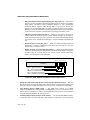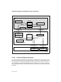
1
IA-32 Intel® Architecture
Software Developer’s Manual
Volume 3B:
System Programming Guide, Part 2
NOTE: The IA-32 Intel Architecture Software Developer's Manual
consists of five volumes: Basic Architecture, Order Number
253665; Instruction Set Reference A-M, Order Number 253666;
Instruction Set Reference N-Z, Order Number 253667; System
Programming Guide, Part 1, Order Number 253668; System
Programming Guide, Part 2, Order Number 253669. Refer to all
five volumes when evaluating your design needs.
Order Number: 253669-019
March 2006
INFORMATION IN THIS DOCUMENT IS PROVIDED IN CONNECTION WITH INTEL PRODUCTS. NO LICENSE, EXPRESS OR IMPLIED, BY ESTOPPEL OR OTHERWISE, TO ANY INTELLECTUAL PROPERTY RIGHTS IS GRANTED BY
THIS DOCUMENT. EXCEPT AS PROVIDED IN INTEL’S TERMS AND CONDITIONS OF SALE FOR SUCH PRODUCTS,
INTEL ASSUMES NO LIABILITY WHATSOEVER, AND INTEL DISCLAIMS ANY EXPRESS OR IMPLIED WARRANTY, RELATING TO SALE AND/OR USE OF INTEL PRODUCTS INCLUDING LIABILITY OR WARRANTIES RELATING TO FITNESS FOR A PARTICULAR PURPOSE, MERCHANTABILITY, OR INFRINGEMENT OF ANY PATENT, COPYRIGHT OR
OTHER INTELLECTUAL PROPERTY RIGHT. INTEL PRODUCTS ARE NOT INTENDED FOR USE IN MEDICAL, LIFE
SAVING, OR LIFE SUSTAINING APPLICATIONS.
Intel may make changes to specifications and product descriptions at any time, without notice.
Developers must not rely on the absence or characteristics of any features or instructions marked “reserved” or “undefined.”
Improper use of reserved or undefined features or instructions may cause unpredictable behavior or failure in developer's
software code when running on an Intel processor. Intel reserves these features or instructions for future definition and shall
have no responsibility whatsoever for conflicts or incompatibilities arising from their unauthorized use.
The Intel® IA-32 architecture processors (e.g., Pentium® 4 and Pentium III processors) may contain design defects or errors
known as errata. Current characterized errata are available on request.
Hyper-Threading Technology requires a computer system with an Intel® Pentium® 4 processor supporting Hyper-Threading
Technology and an HT Technology enabled chipset, BIOS and operating system. Performance will vary depending on the
specific hardware and software you use. See http://www.intel.com/techtrends/technologies/hyperthreading.htm for more information including details on which processors support HT Technology.
Intel® Virtualization Technology requires a computer system with an enabled Intel® processor, BIOS, virtual machine monitor
(VMM) and for some uses, certain platform software enabled for it. Functionality, performance or other benefits will vary depending on hardware and software configurations. Intel® Virtualization Technology-enabled BIOS and VMM applications are
currently in development.
Intel® Extended Memory 64 Technology (Intel® EM64T) requires a computer system with a processor, chipset, BIOS, OS,
device drivers and applications enabled for Intel EM64T. Processor will not operate (including 32-bit operation) without an Intel EM64T-enabled BIOS. Performance will vary depending on your hardware and software configurations. Intel
EM64T-enabled OS, BIOS, device drivers and applications may not be available. Check with your vendor for more
information.
Intel, Intel386, Intel486, Pentium, Intel Xeon, Intel NetBurst, Intel SpeedStep, OverDrive, MMX, Celeron, and Itanium are
trademarks or registered trademarks of Intel Corporation and its subsidiaries in the United States and other countries.
*Other names and brands may be claimed as the property of others.
Contact your local Intel sales office or your distributor to obtain the latest specifications and before placing your product order.
Copies of documents which have an ordering number and are referenced in this document, or other Intel literature, may be
obtained from:
Intel Corporation
P.O. Box 5937
Denver, CO 80217-9808
or call 1-800-548-4725
or visit Intel’s website at http://www.intel.com
Copyright © 1997-2006 Intel Corporation
18
Debugging and
Performance
Monitoring
CHAPTER 18
DEBUGGING AND PERFORMANCE MONITORING
The IA-32 architecture provides debug facilities for use in debugging code and monitoring
performance. These facilities are valuable for debugging application software, system software,
and multitasking operating systems. Debug support is accessed using debug registers (DB0
through DB7) and model-specific registers (MSRs):
•
Debug registers hold the addresses of memory and I/O locations called breakpoints.
Breakpoints are user-selected locations in a program, a data-storage area in memory, or
specific I/O ports. They are set where a programmer or system designer wishes to halt
execution of a program and examine the state of the processor by invoking debugger
software. A debug exception (#DB) is generated when a memory or I/O access is made to a
breakpoint address.
•
MSRs (which were introduced into the IA-32 architecture in the P6 family processors)
monitor branches, interrupts, and exceptions and record the addresses of the last branch,
interrupt or exception taken and the last branch taken before an interrupt or exception.
18.1
OVERVIEW OF THE DEBUGGING SUPPORT FACILITIES
The following processor facilities support debugging and performance monitoring:
•
Debug exception (#DB) — Transfers program control to a debug procedure or task when a
debug event occurs.
•
Breakpoint exception (#BP) — Transfers program control to a debug procedure or task
when an INT 3 instruction is executed.
•
Breakpoint-address registers (DR0 through DR3) — Specifies the addresses of up to 4
breakpoints.
•
Debug status register (DR6) — Reports the conditions that were in effect when a debug
or breakpoint exception was generated.
•
Debug control register (DR7) — Specifies the forms of memory or I/O access that cause
breakpoints to be generated.
•
T (trap) flag, TSS — Generates a debug exception (#DB) when an attempt is made to
switch to a task with the T flag set in its TSS.
•
RF (resume) flag, EFLAGS register — Suppresses multiple exceptions to the same
instruction.
•
TF (trap) flag, EFLAGS register — Generates a debug exception (#DB) after every
execution of an instruction.
Vol. 3B 18-1
DEBUGGING AND PERFORMANCE MONITORING
•
Breakpoint instruction (INT 3) — Generates a breakpoint exception (#BP) that transfers
program control to the debugger procedure or task. This instruction is an alternative way to
set code breakpoints. It is especially useful when more than four breakpoints are desired,
or when breakpoints are being placed in the source code.
•
Last branch recording facilities — See Section 18.5, “Last Branch, Interrupt, and
Exception Recording (Pentium 4 and Intel Xeon Processors),” and Section 18.8, “Last
Branch, Interrupt, and Exception Recording (P6 Family Processors).”
These facilities allow a debugger to be called as a separate task or as a procedure in the context
of the current program or task. The following conditions can be used to invoke the debugger:
•
•
•
•
•
•
•
•
•
Task switch to a specific task.
Execution of the breakpoint instruction.
Execution of any instruction.
Execution of an instruction at a specified address.
Read or write of a byte, word, or doubleword at a specified memory address.
Write to a byte, word, or doubleword at a specified memory address.
Input of a byte, word, or doubleword at a specified I/O address.
Output of a byte, word, or doubleword at a specified I/O address.
Attempt to change the contents of a debug register.
18.2
DEBUG REGISTERS
The eight debug registers (see Figure 18-1) control the debug operation of the processor. These
registers can be written to and read using the move to or from debug register form of the MOV
instruction. A debug register may be the source or destination operand for one of these instructions. The debug registers are privileged resources; a MOV instruction that accesses these registers can only be executed in real-address mode, in SMM, or in protected mode at a CPL of 0. An
attempt to read or write the debug registers from any other privilege level generates a generalprotection exception (#GP).
The primary function of the debug registers is to set up and monitor from 1 to 4 breakpoints,
numbered 0 though 3. For each breakpoint, the following information can be specified and
detected with the debug registers:
•
•
•
•
•
The linear address where the breakpoint is to occur.
The length of the breakpoint location (1, 2, or 4 bytes).
The operation that must be performed at the address for a debug exception to be generated.
Whether the breakpoint is enabled.
Whether the breakpoint condition was present when the debug exception was generated.
18-2 Vol. 3B
DEBUGGING AND PERFORMANCE MONITORING
31 30 29 28 27 26 25 24 23 22 21 20 19 18 17 16 15 14 13 12 11 10 9 8 7 6 5 4 3 2 1 0
LEN R/W LEN R/W LEN R/W LEN R/W 0 0 G 0 0 1 G L G L G L G L G L
DR7
3
3
2
2
1
1
0
0
D
E E 3 3 2 2 1 1 0 0
31
16 15 14 13 12 11 10 9 8 7 6 5 4 3 2 1 0
Reserved (set to 1)
B B B 0 1 1 1 1 1 1 1 1 1 B B B B
DR6
T S D
3 2 1 0
31
0
DR5
31
0
DR4
31
0
DR3
Breakpoint 3 Linear Address
31
0
DR2
Breakpoint 2 Linear Address
31
0
DR1
Breakpoint 1 Linear Address
31
0
Breakpoint 0 Linear Address
DR0
Reserved
Figure 18-1. Debug Registers
The following paragraphs describe the functions of flags and fields in the debug registers.
18.2.1
Debug Address Registers (DR0-DR3)
Each of the debug-address registers (DR0 through DR3) holds the 32-bit linear address of a
breakpoint (see Figure 18-1). Breakpoint comparisons are made before physical address translation occurs. The contents of debug register DR7 further specifies each breakpoint condition.
Vol. 3B 18-3
DEBUGGING AND PERFORMANCE MONITORING
18.2.2
Debug Registers DR4 and DR5
Debug registers DR4 and DR5 are reserved when debug extensions are enabled (when the DE
flag in control register CR4 is set), and attempts to reference the DR4 and DR5 registers cause
an invalid-opcode exception (#UD) to be generated. When debug extensions are not enabled
(when the DE flag is clear), these registers are aliased to debug registers DR6 and DR7.
18.2.3
Debug Status Register (DR6)
The debug status register (DR6) reports the debug conditions that were sampled at the time the
last debug exception was generated (see Figure 18-1). Updates to this register only occur when
an exception is generated. The flags in this register show the following information:
•
B0 through B3 (breakpoint condition detected) flags (bits 0 through 3) — Indicates
(when set) that its associated breakpoint condition was met when a debug exception was
generated. These flags are set if the condition described for each breakpoint by the LENn,
and R/Wn flags in debug control register DR7 is true. They are set even if the breakpoint is
not enabled by the Ln and Gn flags in register DR7.
•
BD (debug register access detected) flag (bit 13) — Indicates that the next instruction in
the instruction stream will access one of the debug registers (DR0 through DR7). This flag
is enabled when the GD (general detect) flag in debug control register DR7 is set. See
Section 18.2.4, “Debug Control Register (DR7),” for further explanation of the purpose of
this flag.
•
BS (single step) flag (bit 14) — Indicates (when set) that the debug exception was
triggered by the single-step execution mode (enabled with the TF flag in the EFLAGS
register). The single-step mode is the highest-priority debug exception. When the BS flag
is set, any of the other debug status bits also may be set.
•
BT (task switch) flag (bit 15) — Indicates (when set) that the debug exception resulted
from a task switch where the T flag (debug trap flag) in the TSS of the target task was set.
See Section 6.2.1, “Task-State Segment (TSS),” for the format of a TSS. There is no flag in
debug control register DR7 to enable or disable this exception; the T flag of the TSS is the
only enabling flag.
Certain debug exceptions may clear bits 0-3. The remaining contents of the DR6 register are
never cleared by the processor. To avoid confusion in identifying debug exceptions, debug
handlers should clear the register before returning to the interrupted task.
18-4 Vol. 3B
DEBUGGING AND PERFORMANCE MONITORING
18.2.4
Debug Control Register (DR7)
The debug control register (DR7) enables or disables breakpoints and sets breakpoint conditions
(see Figure 18-1). The flags and fields in this register control the following things:
•
L0 through L3 (local breakpoint enable) flags (bits 0, 2, 4, and 6) — Enable (when set)
the breakpoint condition for the associated breakpoint for the current task. When a
breakpoint condition is detected and its associated Ln flag is set, a debug exception is
generated. The processor automatically clears these flags on every task switch to avoid
unwanted breakpoint conditions in the new task.
•
G0 through G3 (global breakpoint enable) flags (bits 1, 3, 5, and 7) — Enable (when
set) the breakpoint condition for the associated breakpoint for all tasks. When a breakpoint
condition is detected and its associated Gn flag is set, a debug exception is generated. The
processor does not clear these flags on a task switch, allowing a breakpoint to be enabled
for all tasks.
•
LE and GE (local and global exact breakpoint enable) flags (bits 8 and 9) — (Not
supported in the P6 family processors and later IA-32 processors.) When set, these flags
cause the processor to detect the exact instruction that caused a data breakpoint condition.
For backward and forward compatibility with other IA-32 processors, Intel recommends
that the LE and GE flags be set to 1 if exact breakpoints are required.
•
GD (general detect enable) flag (bit 13) — Enables (when set) debug-register protection,
which causes a debug exception to be generated prior to any MOV instruction that
accesses a debug register. When such a condition is detected, the BD flag in debug status
register DR6 is set prior to generating the exception. This condition is provided to support
in-circuit emulators. (When the emulator needs to access the debug registers, emulator
software can set the GD flag to prevent interference from the program currently executing
on the processor.) The processor clears the GD flag upon entering to the debug exception
handler, to allow the handler access to the debug registers.
•
R/W0 through R/W3 (read/write) fields (bits 16, 17, 20, 21, 24, 25, 28, and 29) —
Specifies the breakpoint condition for the corresponding breakpoint. The DE (debug
extensions) flag in control register CR4 determines how the bits in the R/Wn fields are
interpreted. When the DE flag is set, the processor interprets these bits as follows:
00 — Break on instruction execution only.
01 — Break on data writes only.
10 — Break on I/O reads or writes.
11 — Break on data reads or writes but not instruction fetches.
When the DE flag is clear, the processor interprets the R/Wn bits the same as for the
Intel386™ and Intel486™ processors, which is as follows:
00 — Break on instruction execution only.
01 — Break on data writes only.
10 — Undefined.
11 — Break on data reads or writes but not instruction fetches.
Vol. 3B 18-5
DEBUGGING AND PERFORMANCE MONITORING
•
LEN0 through LEN3 (Length) fields (bits 18, 19, 22, 23, 26, 27, 30, and 31) — Specify
the size of the memory location at the address specified in the corresponding breakpoint
address register (DR0 through DR3). These fields are interpreted as follows:
00 — 1-byte length.
01 — 2-byte length.
10 — Undefined (or 8 byte length, see note below).
11 — 4-byte length.
If the corresponding RWn field in register DR7 is 00 (instruction execution), then the LENn
field should also be 00. The effect of using any other length is undefined. See Section 18.2.5,
“Breakpoint Field Recognition,” for more information on the use of these fields.
For Pentium 4 and Intel Xeon processor with CPUID signature corresponding to family 15
(model 3 or 4) the break point condition permit specifying 8 byte length on data read/write with
the encoding 10B in the LENx field. Otherwise, the encoding 10B is undefined for other IA-32
processors.
18.2.5
Breakpoint Field Recognition
The breakpoint address registers (debug registers DR0 through DR3) and the LENn fields for
each breakpoint define a range of sequential byte addresses for a data or I/O breakpoint. The
LENn fields permit specification of a 1-, 2-, 4-, or 8-byte range beginning at the linear address
specified in the corresponding debug register (DRn). Two-byte ranges must be aligned on word
boundaries and 4-byte ranges must be aligned on doubleword boundaries. I/O breakpoint
addresses are zero extended from 16 to 32 bits for purposes of comparison with the breakpoint
address in the selected debug register. These requirements are enforced by the processor; it uses
the LENn field bits to mask the lower address bits in the debug registers. Unaligned data or I/O
breakpoint addresses do not yield the expected results.
A data breakpoint for reading or writing data is triggered if any of the bytes participating in an
access is within the range defined by a breakpoint address register and its LENn field. Table 18-1
gives an example setup of the debug registers and the data accesses that would subsequently trap
or not trap on the breakpoints.
A data breakpoint for an unaligned operand can be constructed using two breakpoints, where
each breakpoint is byte-aligned, and the two breakpoints together cover the operand. These
breakpoints generate exceptions only for the operand, not for any neighboring bytes.
Instruction breakpoint addresses must have a length specification of 1 byte (the LENn field is
set to 00). The behavior of code breakpoints for other operand sizes is undefined. The processor
recognizes an instruction breakpoint address only when it points to the first byte of an instruction. If the instruction has any prefixes, the breakpoint address must point to the first prefix.
18-6 Vol. 3B
DEBUGGING AND PERFORMANCE MONITORING
18.2.6
Debug Registers and Intel EM64T
For IA-32 processors that support Intel EM64T, debug registers DR0–DR7 are 64 bits. In 16-bit
modes or 32-bit modes (including protected mode and compatibility mode), writes to a debug
register fill the upper 32 bits with zeros. Reads from a debug register return the lower 32 bits. In
64-bit mode, MOV DRn instructions read or write all 64 register bits. Operand-size prefixes are
ignored.
In 64-bit mode, the upper 32 bits of DR6 and DR7 are reserved and must be written with zeros.
Writing 1 to any of the upper 32 bits results in a #GP(0) exception.
All 64 bits of DR0–DR3 are writable by software. However, MOV DRn instructions do not
check that addresses written to DR0–DR3 are in the linear-address limits of a processor implementation (address matching is supported only on valid addresses generated by the processor
implementation). Break point conditions for 8-byte memory read/writes are supported in all
modes (see Section 15.2.4 for applicability of the encoded value for 8-byte length for fields
LEN0 through LEN3).
63
32
DR7
31 30 29 28 27 26 25 24 23 22 21 20 19 18 17 16 15 14 13 12 11 10 9 8 7 6 5 4 3 2 1 0
LEN R/W LEN R/W LEN R/W LEN R/W 0 0 G 0 0 1 G L G L G L G L G L
DR7
3
3
2
2
1
1
0
0
D
E E 3 3 2 2 1 1 0 0
63
32
DR6
31
16 15 14 13 12 11 10 9 8 7 6 5 4 3 2 1 0
Reserved (set to 1)
B B B 0 1 1 1 1 1 1 1 1 1 B B B B
DR6
T S D
3 2 1 0
Reserved
Figure 18-2. DR6 and DR7 Layout on IA-32 Processors Supporting Intel EM64T
18.3
DEBUG EXCEPTIONS
The IA-32 processors dedicate two interrupt vectors to handling debug exceptions: vector 1
(debug exception, #DB) and vector 3 (breakpoint exception, #BP). The following sections
describe how these exceptions are generated and typical exception handler operations for
handling these exceptions.
Vol. 3B 18-7
DEBUGGING AND PERFORMANCE MONITORING
Table 18-1. Breakpointing Examples
Debug Register Setup
Debug Register
R/Wn
Breakpoint Address
LENn
DR0
DR1
DR2
DR3
R/W0 = 11 (Read/Write)
R/W1 = 01 (Write)
R/W2 = 11 (Read/Write)
R/W3 = 01 (Write)
A0001H
A0002H
B0002H
C0000H
LEN0 = 00 (1 byte)
LEN1 = 00 (1 byte)
LEN2 = 01) (2 bytes)
LEN3 = 11 (4 bytes)
Data Accesses
Operation
Address
Access Length
(In Bytes)
Data operations that trap
- Read or write
- Read or write
- Write
- Write
- Read or write
- Read or write
- Read or write
- Write
- Write
- Write
A0001H
A0001H
A0002H
A0002H
B0001H
B0002H
B0002H
C0000H
C0001H
C0003H
1
2
1
2
4
1
2
4
2
1
Data operations that do not trap
- Read or write
- Read
- Read or write
- Read or write
- Read
- Read or write
A0000H
A0002H
A0003H
B0000H
C0000H
C0004H
1
1
4
2
2
4
18.3.1
Debug Exception (#DB)—Interrupt Vector 1
The debug-exception handler is usually a debugger program or is part of a larger software
system. The processor generates a debug exception for any of several conditions. The debugger
can check flags in the DR6 and DR7 registers to determine which condition caused the exception
and which other conditions might also apply. Table 18-2 shows the states of these flags
following the generation of each kind of breakpoint condition.
Instruction-breakpoint and general-detect condition (see Section 18.3.1.3, “General-Detect
Exception Condition”) result in faults; other debug-exception conditions result in traps. The
debug exception may report either or both at one time. The following sections describe each
class of debug exception. See Chapter 5, “Interrupt 1—Debug Exception (#DB),” in the IA-32
Intel® Architecture Software Developer’s Manual, Volume 3A for additional information about
this exception.
18-8 Vol. 3B
DEBUGGING AND PERFORMANCE MONITORING
18.3.1.1
Instruction-Breakpoint Exception Condition
The processor reports an instruction breakpoint when it attempts to execute an instruction at an
address specified in a breakpoint-address register (DB0 through DR3) that has been set up to
detect instruction execution (R/W flag is set to 0). Upon reporting the instruction breakpoint, the
processor generates a fault-class, debug exception (#DB) before it executes the target instruction
for the breakpoint.
Instruction breakpoints are the highest priority debug exceptions. They are serviced before any
other exceptions detected during the decoding or execution of an instruction. Note, however,
that if a code instruction breakpoint is placed on an instruction located immediately after a
POP SS/MOV SS instruction, it may not be triggered. In most situations, POP SS/MOV SS
will inhibit such interrupts (see “MOV—Move” and “POP—Pop a Value from the Stack” in
Chapters 3 and 4 of the IA-32 Intel® Architecture Software Developer’s Manual, Volumes
2A & 2B).
Table 18-2. Debug Exception Conditions
Debug or Breakpoint Condition
DR6 Flags Tested
Single-step trap
BS = 1
DR7 Flags Tested
Exception Class
Instruction breakpoint, at addresses
defined by DRn and LENn
Bn = 1 and
(Gn or Ln = 1)
R/Wn = 0
Fault
Data write breakpoint, at addresses
defined by DRn and LENn
Bn = 1 and
(Gn or Ln = 1)
R/Wn = 1
Trap
I/O read or write breakpoint, at addresses
defined by DRn and LENn
Bn = 1 and
(Gn or Ln = 1)
R/Wn = 2
Trap
Data read or write (but not instruction
fetches), at addresses defined by DRn
and LENn
Bn = 1 and
(Gn or Ln = 1)
R/Wn = 3
Trap
General detect fault, resulting from an
attempt to modify debug registers
(usually in conjunction with in-circuit
emulation)
BD = 1
Fault
Task switch
BT = 1
Trap
Trap
Because the debug exception for an instruction breakpoint is generated before the instruction is
executed, if the instruction breakpoint is not removed by the exception handler, the processor
will detect the instruction breakpoint again when the instruction is restarted and generate another
debug exception. To prevent looping on an instruction breakpoint, the IA-32 architecture
provides the RF flag (resume flag) in the EFLAGS register (see Section 2.3, “System Flags and
Fields in the EFLAGS Register,” in the IA-32 Intel® Architecture Software Developer’s Manual,
Volume 3A). When the RF flag is set, the processor ignores instruction breakpoints.
All IA-32 processors manage the RF flag as follows. The processor sets the RF flag automatically prior to calling an exception handler for any fault-class exception except a debug exception that was generated in response to an instruction breakpoint. For debug exceptions resulting
from instruction breakpoints, the processor does not set the RF flag prior to calling the debug
Vol. 3B 18-9
DEBUGGING AND PERFORMANCE MONITORING
exception handler. The debug exception handler then has the option of disabling the instruction
breakpoint or setting the RF flag in the EFLAGS image on the stack. If the RF flag in the
EFLAGS image is set when the processor returns from the exception handler, it is copied into
the RF flag in the EFLAGS register by the IRETD or task switch instruction that causes the
return. The processor then ignores instruction breakpoints for the duration of the next instruction. (Note that the POPF, POPFD, and IRET instructions do not transfer the RF image into the
EFLAGS register.) Setting the RF flag does not prevent other types of debug-exception conditions (such as, I/O or data breakpoints) from being detected, nor does it prevent non-debug
exceptions from being generated. After the instruction is successfully executed, the processor
clears the RF flag in the EFLAGS register, except after an IRETD instruction or after a JMP,
CALL, or INT n instruction that causes a task switch.
Note that the processor also does not set the RF flag when calling exception or interrupt handlers
for trap-class exceptions, for hardware interrupts, or for software-generated interrupts.
For the Pentium processor, when an instruction breakpoint coincides with another fault-type
exception (such as a page fault), the processor may generate one spurious debug exception after
the second exception has been handled, even though the debug exception handler set the RF flag
in the EFLAGS image. To prevent this spurious exception with Pentium processors, all faultclass exception handlers should set the RF flag in the EFLAGS image.
18.3.1.2
Data Memory and I/O Breakpoint Exception Conditions
Data memory and I/O breakpoints are reported when the processor attempts to access a memory
or I/O address specified in a breakpoint-address register (DB0 through DR3) that has been set
up to detect data or I/O accesses (R/W flag is set to 1, 2, or 3). The processor generates the exception after it executes the instruction that made the access, so these breakpoint condition causes
a trap-class exception to be generated.
Because data breakpoints are traps, the original data is overwritten before the trap exception is
generated. If a debugger needs to save the contents of a write breakpoint location, it should save
the original contents before setting the breakpoint. The handler can report the saved value after
the breakpoint is triggered. The address in the debug registers can be used to locate the new
value stored by the instruction that triggered the breakpoint.
The Intel486 and later IA-32 processors ignore the GE and LE flags in DR7. In the Intel386
processor, exact data breakpoint matching does not occur unless it is enabled by setting the LE
and/or the GE flags.
The P6 family processors, however, are unable to report data breakpoints exactly for the REP
MOVS and REP STOS instructions until the completion of the iteration after the iteration in
which the breakpoint occurred.
For repeated INS and OUTS instructions that generate an I/O-breakpoint debug exception, the
processor generates the exception after the completion of the first iteration. Repeated INS and
OUTS instructions generate an I/O-breakpoint debug exception after the iteration in which the
memory address breakpoint location is accessed.
18-10 Vol. 3B
DEBUGGING AND PERFORMANCE MONITORING
18.3.1.3
General-Detect Exception Condition
When the GD flag in DR7 is set, the general-detect debug exception occurs when a program
attempts to access any of the debug registers (DR0 through DR7) at the same time they are being
used by another application, such as an emulator or debugger. This additional protection feature
guarantees full control over the debug registers when required. The debug exception handler can
detect this condition by checking the state of the BD flag of the DR6 register. The processor
generates the exception before it executes the MOV instruction that accesses a debug register,
which causes a fault-class exception to be generated.
18.3.1.4
Single-Step Exception Condition
The processor generates a single-step debug exception if (while an instruction is being executed)
it detects that the TF flag in the EFLAGS register is set. The exception is a trap-class exception,
because the exception is generated after the instruction is executed. (Note that the processor does
not generate this exception after an instruction that sets the TF flag. For example, if the POPF
instruction is used to set the TF flag, a single-step trap does not occur until after the instruction
that follows the POPF instruction.)
The processor clears the TF flag before calling the exception handler. If the TF flag was set in a
TSS at the time of a task switch, the exception occurs after the first instruction is executed in the
new task.
The TF flag normally is not cleared by privilege changes inside a task. The INT n and INTO
instructions, however, do clear this flag. Therefore, software debuggers that single-step code
must recognize and emulate INT n or INTO instructions rather than executing them directly. To
maintain protection, the operating system should check the CPL after any single-step trap to see
if single stepping should continue at the current privilege level.
The interrupt priorities guarantee that, if an external interrupt occurs, single stepping stops.
When both an external interrupt and a single-step interrupt occur together, the single-step interrupt is processed first. This operation clears the TF flag. After saving the return address or
switching tasks, the external interrupt input is examined before the first instruction of the singlestep handler executes. If the external interrupt is still pending, then it is serviced. The external
interrupt handler does not run in single-step mode. To single step an interrupt handler, single step
an INT n instruction that calls the interrupt handler.
18.3.1.5
Task-Switch Exception Condition
The processor generates a debug exception after a task switch if the T flag of the new task's TSS
is set. This exception is generated after program control has passed to the new task, and prior to
the execution of the first instruction of that task. The exception handler can detect this condition
by examining the BT flag of the DR6 register.
Note that, if the debug exception handler is a task, the T bit of its TSS should not be set. Failure
to observe this rule will put the processor in a loop.
Vol. 3B 18-11
DEBUGGING AND PERFORMANCE MONITORING
18.3.2
Breakpoint Exception (#BP)—Interrupt Vector 3
The breakpoint exception (interrupt 3) is caused by execution of an INT 3 instruction. See
Chapter 5, “Interrupt 3—Breakpoint Exception (#BP).” Debuggers use break exceptions in the
same way that they use the breakpoint registers; that is, as a mechanism for suspending program
execution to examine registers and memory locations. With earlier IA-32 processors, breakpoint
exceptions are used extensively for setting instruction breakpoints.
With the Intel386 and later IA-32 processors, it is more convenient to set breakpoints with the
breakpoint-address registers (DR0 through DR3). However, the breakpoint exception still is
useful for breakpointing debuggers, because the breakpoint exception can call a separate exception handler. The breakpoint exception is also useful when it is necessary to set more breakpoints
than there are debug registers or when breakpoints are being placed in the source code of a
program under development.
18.4
LAST BRANCH RECORDING OVERVIEW
P6 family processors introduced the ability to set breakpoints on taken branches, interrupts, and
exceptions, and to single-step from one branch to the next. This capability has been modified
and extended in the Pentium 4, Intel Xeon, Pentium M, Intel® Core™ Solo and Intel® Core™
Duo processors to allow logging of branch trace messages in a branch trace store (BTS) buffer
in memory.
See the following sections for descriptions of the mechanism for last branch recording:
— Section 18.5, “Last Branch, Interrupt, and Exception Recording (Pentium 4 and Intel
Xeon Processors)”
— Section 18.6, “Last Branch, Interrupt, and Exception Recording (Intel® Core™ Solo
and Intel® Core™ Duo Processors)”
— Section 18.7, “Last Branch, Interrupt, and Exception Recording (Pentium M
Processors)”
— Section 18.8, “Last Branch, Interrupt, and Exception Recording (P6 Family
Processors)”
The IA-32 branch instructions that are tracked with the last branch recording mechanism are the
JMP, Jcc, LOOP, and CALL instructions.
18.5
LAST BRANCH, INTERRUPT, AND EXCEPTION RECORDING
(PENTIUM 4 AND INTEL XEON PROCESSORS)
The Pentium 4 and Intel Xeon processors provide the following methods of recording taken
branches, interrupts and exceptions:
•
Store branch records in the last branch record (LBR) stack MSRs for the most recent taken
branches, interrupts, and/or exceptions in MSRs. A branch record consist of a branch-from
and a branch-to instruction address.
18-12 Vol. 3B
DEBUGGING AND PERFORMANCE MONITORING
•
•
Send the branch records out on the system bus as branch trace messages (BTMs).
Log BTMs in a memory-resident branch trace store (BTS) buffer.
To support these functions, the processor provides the following MSRs:
•
MSR_DEBUGCTLA MSR — Enables last branch, interrupt, and exception recording;
single-stepping on taken branches; branch trace messages (BTMs); and branch trace store
(BTS). This register is named DebugCtlMSR in the P6 family processors.
•
Debug store (DS) feature flag (CPUID.1:EDX.DS[bit 21]) — Indicates that the
processor provides the debug store (DS) mechanism, which allows BTMs to be stored in a
memory-resident BTS buffer.
•
CPL-qualified debug store (DS) feature flag (CPUID.1:ECX.DS-CPL[bit 4]) —
Indicates that the processor provides a CPL-qualified debug store (DS) mechanism, which
allows software to selectively skip storing BTMs, according to specified current privilege
level settings, into a memory-resident BTS buffer.
•
•
IA32_MISC_ENABLE MSR — Indicates that the processor provides the BTS facilities.
•
Last branch record top-of-stack (TOS) pointer — The TOS Pointer MSR contains a
2-bit pointer (0-3) to the MSR in the LBR stack that contains the most recent branch,
interrupt, or exception recorded for the Pentium 4 and Intel Xeon processor family
[CPUID family 0FH, models 0H-02H]. This pointer becomes a 4-bit pointer (0-15) for the
Pentium 4 and Intel Xeon processor family [CPUID family 0FH, model 03H]. See also:
Table 18-3, Figure 18-3, and Section 18.5.3, “LBR Stack (Pentium 4 and Intel Xeon
Processors).”
•
Last exception record — See Section 18.5.7, “Last Exception Records (Pentium 4 and
Intel Xeon Processors).”
Last branch record (LBR) stack — The LBR stack is a circular stack that consists of
four MSRs (MSR_LASTBRANCH_0 through MSR_LASTBRANCH_3) for the
Pentium 4 and Intel Xeon processor family [CPUID family 0FH, models 0H-02H]. The
LBR stack consists of 16 MSR pairs (MSR_LASTBRANCH_0_FROM_LIP through
MSR_LASTBRANCH_15_FROM_LIP and MSR_LASTBRANCH_0_TO_LIP through
MSR_LASTBRANCH_15_TO_LIP) for the Pentium 4 and Intel Xeon processor family
[CPUID family 0FH, model 03H].
18.5.1
CPL-Qualified Last Branch Recording Mechanism
CPL-qualified last branch recording mechanism is available to a subset of IA-32 processors that
support last branch recording mechanism. Software can detect support for CPL-qualified last
branch recording mechanism by executing CPUID with EAX = 1, and examine the returned
value of bit 4 of ECX.
CPL-qualified last branch recording mechanism is similar to that described in Sections 18.5,
18.5.2, and 18.5.8. It also sends the branch records out on the system bus as branch trace
messages (BTMs). But system software can selectively specify CPL qualification to not store
BTMs associated with the specified privilege level. Two bit fields, BTS_OFF_USR and
Vol. 3B 18-13
DEBUGGING AND PERFORMANCE MONITORING
BTS_OFF_OS, are provided in the debug control register to specify the CPL of those BTMs that
will not logged in the BTS buffer.
Table 18-3. LBR MSR Stack Structure for the Pentium 4 and Intel Xeon Processor Family
LBR MSRs for Family 0FH, Models 0H-02H;
MSRs at locations 1DBH-1DEH.
Decimal Value of TOS Pointer in
MSR_LASTBRANCH_TOS (bits 0-1)
MSR_LASTBRANCH_0
MSR_LASTBRANCH_1
MSR_LASTBRANCH_2
MSR_LASTBRANCH_3
0
1
2
3
LBR MSRs for Family 0FH, Models; MSRs at
locations 680H-68FH.
Decimal Value of TOS Pointer in
MSR_LASTBRANCH_TOS (bits 0-3)
MSR_LASTBRANCH_0_FROM_LIP
MSR_LASTBRANCH_1_FROM_LIP
MSR_LASTBRANCH_2_FROM_LIP
MSR_LASTBRANCH_3_FROM_LIP
MSR_LASTBRANCH_4_FROM_LIP
MSR_LASTBRANCH_5_FROM_LIP
MSR_LASTBRANCH_6_FROM_LIP
MSR_LASTBRANCH_7_FROM_LIP
MSR_LASTBRANCH_8_FROM_LIP
MSR_LASTBRANCH_9_FROM_LIP
MSR_LASTBRANCH_10_FROM_LIP
MSR_LASTBRANCH_11_FROM_LIP
MSR_LASTBRANCH_12_FROM_LIP
MSR_LASTBRANCH_13_FROM_LIP
MSR_LASTBRANCH_14_FROM_LIP
MSR_LASTBRANCH_15_FROM_LIP
0
1
2
3
4
5
6
7
8
9
10
11
12
13
14
15
LBR MSRs for Family 0FH, Model 03H; MSRs
at locations 6C0H-6CFH.
MSR_LASTBRANCH_0_TO_LIP
MSR_LASTBRANCH_1_TO_LIP
MSR_LASTBRANCH_2_TO_LIP
MSR_LASTBRANCH_3_TO_LIP
MSR_LASTBRANCH_4_TO_LIP
MSR_LASTBRANCH_5_TO_LIP
MSR_LASTBRANCH_6_TO_LIP
MSR_LASTBRANCH_7_TO_LIP
MSR_LASTBRANCH_8_TO_LIP
MSR_LASTBRANCH_9_TO_LIP
MSR_LASTBRANCH_10_TO_LIP
MSR_LASTBRANCH_11_TO_LIP
MSR_LASTBRANCH_12_TO_LIP
MSR_LASTBRANCH_13_TO_LIP
MSR_LASTBRANCH_14_TO_LIP
MSR_LASTBRANCH_15_TO_LIP
18-14 Vol. 3B
0
1
2
3
4
5
6
7
8
9
10
11
12
13
14
15
DEBUGGING AND PERFORMANCE MONITORING
1 0
31
Reserved
Family 0FH, Models 01-02H
Top-of-stack pointer (TOS)
3
31
0
Reserved
Family 0FH, Model 03H+
Top-of-stack pointer (TOS)
Figure 18-3. MSR_LASTBRANCH_TOS MSR Layout for the Pentium 4
and Intel Xeon Processor Family
NOTE
The initial implementation of BTS_OFF_USR and BTS_OFF_OS in
MSR_DEBUGCTLA is shown in Figure 18-4. The BTS_OFF_USR and
BTS_OFF_OS fields may be implemented on other model-specific debug
control register at different locations.
The following sections describe the MSR_DEBUGCTLA MSR and the various last branch
recording mechanisms. See Appendix B, “Model-Specific Registers (MSRs),” for a detailed
description of each of the last branch recording MSRs.
18.5.2
MSR_DEBUGCTLA MSR (Pentium 4 and Intel Xeon
Processors)
The MSR_DEBUGCTLA MSR enables and disables the various last branch recording mechanisms described in the previous section. This register can be written to using the WRMSR
instruction, when operating at privilege level 0 or when in real-address mode. A protected-mode
operating system procedure is required to provide user access to this register. Figure 18-4 shows
the flags in the MSR_DEBUGCTLA MSR. The functions of these flags are as follows:
•
LBR (last branch/interrupt/exception) flag (bit 0) — When set, the processor records a
running trace of the most recent branches, interrupts, and/or exceptions taken by the
processor (prior to a debug exception being generated) in the last branch record (LBR)
stack. Each branch, interrupt, or exception is recorded as a 64-bit branch record. The
processor clears this flag whenever a debug exception is generated (for example, when an
instruction or data breakpoint or a single-step trap occurs). See Section 18.5.3, “LBR Stack
(Pentium 4 and Intel Xeon Processors).”
Vol. 3B 18-15
DEBUGGING AND PERFORMANCE MONITORING
•
BTF (single-step on branches) flag (bit 1) — When set, the processor treats the TF flag
in the EFLAGS register as a “single-step on branches” flag rather than a “single-step on
instructions” flag. This mechanism allows single-stepping the processor on taken
branches, interrupts, and exceptions. See Section 18.5.5, “Single-Stepping on Branches,
Exceptions, and Interrupts.”
•
TR (trace message enable) flag (bit 2) — When set, branch trace messages are enabled.
Thereafter, when the processor detects a taken branch, interrupt, or exception, it sends the
branch record out on the system bus as a branch trace message (BTM). See Section 18.5.6,
“Branch Trace Messages.”
31
7 6 5 4 3 2 1 0
Reserved
BTS_OFF_USR — Disable storing non-CPL_0 BTS
BTS_OFF_OS — Disable storing CPL_0 BTS
BTINT — Branch trace interrupt
BTS — Branch trace store
TR — Trace messages enable
BTF — Single-step on branches
LBR — Last branch/interrupt/exception
Figure 18-4. MSR_DEBUGCTLA MSR for Pentium 4 and Intel Xeon Processors
•
BTS (branch trace store) flag (bit 3) — When set, enables the BTS facilities to log BTMs
to a memory-resident BTS buffer that is part of the DS save area. See Section 18.13.5, “DS
Save Area.”
•
BTINT (branch trace interrupt) flag (bits 4) — When set, the BTS facilities generate an
interrupt when the BTS buffer is full. When clear, BTMs are logged to the BTS buffer in a
circular fashion. See Section 18.5.8, “Branch Trace Store (BTS).”
•
BTS_OFF_OS (disable ring 0 branch trace store) flag (bit 5) — When set, enables the
BTS facilities to skip logging CPL_0 BTMs to the memory-resident BTS buffer. See
Section 18.5.1, “CPL-Qualified Last Branch Recording Mechanism.”
•
BTS_OFF_USR (disable ring 0 branch trace store) flag (bit 6) — When set, enables the
BTS facilities to skip logging non-CPL_0 BTMs to the memory-resident BTS buffer. See
Section 18.5.1, “CPL-Qualified Last Branch Recording Mechanism.”
18.5.3
LBR Stack (Pentium 4 and Intel Xeon Processors)
The LBR stack is made up of LBR MSRs that are treated by the processor as a circular stack.
The TOS pointer (MSR_LASTBRANCH_TOS MSR) points to the LBR MSR (or LBR MSR
pair) that contains the most recent (last) branch record placed on the stack. Prior to placing a new
18-16 Vol. 3B
DEBUGGING AND PERFORMANCE MONITORING
branch record on the stack, the TOS is incremented by 1. When the TOS pointer reaches it
maximum value, it wraps around to 0. See Table 18-3 and Figure 18-3.
The registers in the LBR MSR stack and the MSR_LASTBRANCH_TOS MSR are read-only
and can be read using the RDMSR instruction.
Figure 18-5 shows the layout of a branch record in an LBR MSR (or MSR pair). Each branch
record consists of two linear addresses, which represent the “from” and “to” instruction pointers
for a branch, interrupt, or exception. The contents of the from and to addresses differ, depending
on the source of the branch:
•
Taken branch — If the record is for a taken branch, the “from” address is the address of
the branch instruction and the “to” address is the target instruction of the branch.
•
Interrupt — If the record is for an interrupt, the “from” address the return instruction
pointer (RIP) saved for the interrupt and the “to” address is the address of the first
instruction in the interrupt handler routine. The RIP is the linear address of the next
instruction to be executed upon returning from the interrupt handler.
•
Exception — If the record is for an exception, the “from” address is the linear address of
the instruction that caused the exception to be generated and the “to” address is the address
of the first instruction in the exception handler routine.
CPUID Family 0FH, Models 0H-02H
MSR_LASTBRANCH_0 through MSR_LASTBRANCH_3
63
0
32 - 31
From Linear Address
To Linear Address
CPUID Family 0FH, Model 03H-04H
MSR_LASTBRANCH_0_FROM_LIP through MSR_LASTBRANCH_15_FROM_LIP
0
32 - 31
63
Reserved
From Linear Address
MSR_LASTBRANCH_0_TO_LIP through MSR_LASTBRANCH_15_TO_LIP
63
0
32 - 31
Reserved
To Linear Address
Figure 18-5. LBR MSR Branch Record Layout for the Pentium 4
and Intel Xeon Processor Family
Additional information is saved if an exception or interrupt occurs in conjunction with a branch
instruction. If a branch instruction generates a trap type exception, two branch records are stored
in the LBR stack: a branch record for the branch instruction followed by a branch record for the
exception.
Vol. 3B 18-17
DEBUGGING AND PERFORMANCE MONITORING
If a branch instruction generates a fault type exception, a branch record is stored in the LBR
stack for the exception, but not for the branch instruction itself. Here, the location of the branch
instruction can be determined from the CS and EIP registers in the exception stack frame that is
written by the processor onto the stack.
If a branch instruction is immediately followed by an interrupt, a branch record is stored in the
LBR stack for the branch instruction followed by a record for the interrupt.
18.5.3.1
LBR Stack and Intel EM64T
For IA-32 processors that support Intel EM64T, the LBR MSRs are 64-bits. If IA-32e mode is
disabled, only the lower 32-bits are accessible. If IA-32e mode is enabled, the processor writes
64-bit values into the MSR. In 64-bit mode, last branch records stores 64-bit addresses; in
compatibility mode, the upper 32-bits of last branch records are cleared.
18.5.4
Monitoring Branches, Exceptions, and Interrupts
(Pentium 4 and Intel Xeon Processors)
When the LBR flag in the MSR_DEBUGCTLA MSR is set, the processor automatically begins
recording branch records for taken branches, interrupts, and exceptions (except for debug exceptions) in the LBR stack MSRs.
When the processor generates a a debug exception (#DB), it automatically clears the LBR flag
before executing the exception handler. This action does not clear previously stored LBR stack
MSRs. The branch record for the last four taken branches, interrupts and/or exceptions are
retained for analysis.
A debugger can use the linear addresses in the LBR stack to reset breakpoints in the break-point
address registers (DR0 through DR3). This allows a backward trace from the manifestation of a
articular bug toward its source.
If the LBR flag is cleared and TR flag in the MSR_DEBUGCTLA MSR remains set, the
processor will continue to update LBR stack MSRs. This is because BTM information must be
generated from entries in the LBR stack (see 14.5.5). A #DB does not automatically clear the
TR flag.
18.5.5
Single-Stepping on Branches, Exceptions, and Interrupts
When software sets both the BTF flag in the MSR_DEBUGCTLA MSR and the TF flag in the
EFLAGS register, the processor generates a single-step debug exception the next time it takes a
branch, services an interrupt, or generates an exception. This mechanism allows the debugger to
single-step on control transfers caused by branches, interrupts, and exceptions. This “controlflow single stepping” helps isolate a bug to a particular block of code before instruction singlestepping further narrows the search. If the BTF flag is set when the processor generates a debug
exception, the processor clears the BTF flag along with the TF flag. The debugger must reset the
BTF and TF flags before resuming program execution to continue control-flow single stepping.
18-18 Vol. 3B
DEBUGGING AND PERFORMANCE MONITORING
18.5.6
Branch Trace Messages
Setting The TR flag in the MSR_DEBUGCTLA (see Figure 18-4), IA32_DEBUG (see
Figure 18-6), or MSR_DEBUGB (see Figure 18-8) MSR enables branch trace messages
(BTMs). Thereafter, when the processor detects a branch, exception, or interrupt, it sends a
branch record out on the system bus as a BTM. A debugging device that is monitoring the
system bus can read these messages and synchronize operations with taken branch, interrupt,
and exception events.
When interrupts or exceptions occur in conjunction with a taken branch, additional BTMs are
sent out on the bus, as described in Section 18.5.4, “Monitoring Branches, Exceptions, and Interrupts (Pentium 4 and Intel Xeon Processors).”
Setting this flag (BTS) alone will greatly reduces the performance of the processor. CPL-qualified
last branch recording mechanism can help mitigate the performance impact of logging branch
trace messages. See Section 18.5.1, “CPL-Qualified Last Branch Recording Mechanism.”
Unlike the P6 family processors, the Pentium 4 and Intel Xeon processors can collect branch
records in the LBR stack MSRs while at the same time sending BTMs out on the system bus
when both the TR and LBR flags are set in the MSR_DEBUGCTLA MSR.
18.5.7
Last Exception Records (Pentium 4 and Intel Xeon
Processors)
The Pentium 4 and Intel Xeon processors provide two 32 bit MSRs (the MSR_LER_TO_LIP
and the MSR_LER_FROM_LIP MSRs) that duplicate the functions of the LastExceptionToIP
and LastExceptionFromIP MSRs found in the P6 family processors. The MSR_LER_TO_LIP
and MSR_LER_FROM_LIP MSRs contain a branch record for the last branch that the processor
took prior to an exception or interrupt being generated.
18.5.7.1
Last Exception Records and Intel EM64T
For IA-32 processors that support Intel EM64T, the MSRs that store last exception records are
64-bits. If IA-32e mode is disabled, only the lower 32-bits are accessible. If IA-32e mode is
enabled, the processor writes 64-bit values into the MSR. In 64-bit mode, last exception records
stores 64-bit addresses; in compatibility mode, the upper 32-bits of last exception records are
cleared.
18.5.8
Branch Trace Store (BTS)
A trace of taken branches, interrupts, and exceptions is useful for debugging code by providing
a method of determining the decision path taken to reach a particular code location. The
Pentium 4 and Intel Xeon processors provide a mechanism for capturing records of taken
branches, interrupts, and exceptions and saving them in the last branch record (LBR) stack
MSRs and/or sending them out onto the system bus as BTMs. The branch trace store (BTS)
mechanism provides the additional capability of saving the branch records in a memory-resident
Vol. 3B 18-19
DEBUGGING AND PERFORMANCE MONITORING
BTS buffer, which is part of the DS save area. The BTS buffer can be configured to be circular
so that the most recent branch records are always available or it can be configured to generate
an interrupt when the buffer is nearly full so that all the branch records can be saved. See
Section 18.13.5, “DS Save Area.”
18.5.8.1
Detection of the BTS Facilities
The DS feature flag (bit 21) returned by the CPUID instruction indicates (when set) the availability of the DS mechanism in the processor, which supports the BTS (and PEBS) facilities.
When this bit is set, the following BTS facilities are available:
•
The BTS_UNAVAILABLE flag in the IA32_MISC_ENABLE MSR indicates (when
clear) the availability of the BTS facilities, including the ability to set the BTS and BTINT
bits in the MSR_DEBUGCTLA MSR.
•
The IA32_DS_AREA MSR can be programmed to point to the DS save area.
18.5.8.2
Setting Up the DS Save Area
To save branch records with the BTS buffer, the DS save area must first be set up in memory as
described in the following procedure. See Section 18.5.8.3, “Setting Up the BTS Buffer,” and
Section 18.13.8.3, “Setting Up the PEBS Buffer,” for instructions for setting up a BTS buffer
and/or a PEBS buffer, respectively, in the DS save area:
1. Create the DS buffer management information area in memory (see Section 18.13.5, “DS
Save Area,” and Section 18.13.5.1, “DS Save Area and IA-32e Mode Operation”). Also
see the additional notes in this section.
2. Write the base linear address of the DS buffer management area into the IA32_DS_AREA
MSR.
3. Set up the performance counter entry in the xAPIC LVT for fixed delivery and edge
sensitive. See Section 8.5.1, “Local Vector Table.”
4. Establish an interrupt handler in the IDT for the vector associated with the performance
counter entry in the xAPIC LVT.
5. Write an interrupt service routine to handle the interrupt. See Section 18.5.8.5, “Writing
the DS Interrupt Service Routine.”
The following restrictions should be applied to the DS save area.
•
The three DS save area sections should be allocated from a non-paged pool, and marked
accessed and dirty. It is the responsibility of the operating system to keep the pages that
contain the buffer present and to mark them accessed and dirty. The implication is that the
operating system cannot do “lazy” page-table entry propagation for these pages.
•
The DS save area can be larger than a page, but the pages must be mapped to contiguous
linear addresses. The buffer may share a page, so it need not be aligned on a 4-KByte
boundary. For performance reasons, the base of the buffer must be aligned on a
doubleword boundary and should be aligned on a cache line boundary.
18-20 Vol. 3B
DEBUGGING AND PERFORMANCE MONITORING
•
It is recommended that the buffer size for the BTS buffer and the PEBS buffer be an
integer multiple of the corresponding record sizes.
•
The precise event records buffer should be large enough to hold the number of precise
event records that can occur while waiting for the interrupt to be serviced.
•
The DS save area should be in kernel space. It must not be on the same page as code, to
avoid triggering self-modifying code actions.
•
There are no memory type restrictions on the buffers, although it is recommended that the
buffers be designated as WB memory type for performance considerations.
•
Either the system must be prevented from entering A20M mode while DS save area is
active, or bit 20 of all addresses within buffer bounds must be 0.
•
Pages that contain buffers must be mapped to the same physical addresses for all
processes, such that any change to control register CR3 will not change the DS addresses.
•
The DS save area is expected to used only on systems with an enabled APIC. The LVT
Performance Counter entry in the APCI must be initialized to use an interrupt gate instead
of the trap gate.
18.5.8.3
Setting Up the BTS Buffer
Three flags in the MSR_DEBUGCTLA MSR (see Table 18-4), IA32_DEBUGCTL (see
Figure 18-6), or MSR_DEBUGCTLB (see Figure 18-8) control the generation of branch
records and storing of them in the BTS buffer; these are TR, BTS, and BTINT. The TR flag
enables the generation of BTMs. The BTS flag determines whether the BTMs are sent out on
the system bus (clear) or stored in the BTS buffer (set). BTMs cannot be simultaneously sent to
the system bus and logged in the BTS buffer. The BTINT flag enables the generation of an interrupt when the BTS buffer is full. When this flag is clear, the BTS buffer is a circular buffer.
Table 18-4. MSR_DEBUGCTLA, IA32_DEBUGCTL, MSR_DEBUGCLTB Flag Encodings
TR
BTS
BTINT
Description
0
X
X
1
0
X
Generate BTMs
1
1
0
Store BTMs in the BTS buffer, used here as a circular buffer
1
1
1
Store BTMs in the BTS buffer, and generate an interrupt when the
buffer is nearly full
Branch trace messages (BTMs) off
The following procedure describes how to set up a Pentium 4 or Intel Xeon processor to collect
branch records in the BTS buffer in the DS save area:
1. Place values in the BTS buffer base, BTS index, BTS absolute maximum, and BTS
interrupt threshold fields of the DS buffer management area to set up the BTS buffer in
memory.
Vol. 3B 18-21
DEBUGGING AND PERFORMANCE MONITORING
2. Set the TR and BTS flags in the MSR_DEBUGCTLA MSR (or IA32_DEBUGCTL for
Intel Core Solo and Intel Core Duo processors; or MSR_DEBUGCTLB for Pentium M
processors).
3. Either clear the BTINT flag in the MSR_DEBUGCTLA MSR (to set up a circular BTS
buffer) or set the BTINT flag (to generate an interrupt when the BTS buffer is nearly full).
For Intel Core Solo and Intel Core Duo processors, do the same in IA32_DEBUGCTL; or
in MSR_DEBUGCTLB for Pentium M processors.
18.5.8.4
Setting Up CPL-Qualified BTS
If the processor supports CPL-qualified last branch recording mechanism, the generation of
branch records and storing of them in the BTS buffer are determined by: TR, BTS,
BTS_OFF_OS, BTS_OFF_USR, and BTINT. The encoding of these five bits are shown in
Table 18-5.
Table 18-5. CPL-Qualified Branch Trace Store Encodings
TR
BTS
BTS_OFF_
OS
0
X
X
X
X
Branch trace messages (BTMs) off
1
0
X
X
X
Generate BTM but does not store BTMs
1
1
0
0
0
Store all BTMs in the BTS buffer, used here as a
circular buffer
1
1
1
0
0
Store BTMs with CPL > 0 in the BTS buffer
1
1
0
1
0
Store BTMs with CPL =0 in the BTS buffer
1
1
1
1
X
Generate BTM but does not store BTMs
1
1
0
0
1
Store all BTMs in the BTS buffer; generate an
interrupt when the buffer is nearly full
1
1
1
0
1
Store BTMs with CPL > 0 in the BTS buffer;
generate an interrupt when the buffer is nearly full
1
1
0
1
1
Store BTMs with CPL = 0 in the BTS buffer;
generate an interrupt when the buffer is nearly full
18.5.8.5
BTS_OFF_
USR
BTINT
Description
Writing the DS Interrupt Service Routine
The BTS, non-precise event-based sampling, and PEBS facilities share the same interrupt vector
and interrupt service routine (called the debug store interrupt service routine or DS ISR). To
handle BTS, non-precise event-based sampling, and PEBS interrupts: separate handler routines
must be included in the DS ISR. Use the following guidelines when writing a DS ISR to handle
BTS, non-precise event-based sampling, and/or PEBS interrupts.
•
The DS interrupt service routine (ISR) must be part of a kernel driver and operate at a
current privilege level of 0 to secure the buffer storage area.
18-22 Vol. 3B
DEBUGGING AND PERFORMANCE MONITORING
•
Because the BTS, non-precise event-based sampling, and PEBS facilities share the same
interrupt vector, the DS ISR must check for all the possible causes of interrupts from these
facilities and pass control on to the appropriate handler.
BTS and PEBS buffer overflow would be the sources of the interrupt if the buffer index
matches/exceeds the interrupt threshold specified. Detection of non-precise event-based
sampling as the source of the interrupt is accomplished by checking for counter overflow.
•
•
There must be separate save areas, buffers, and state for each processor in an MP system.
•
The processor will not disable the DS save area when the buffer is full and the circular
mode has not been selected. The current DS setting must be retained and restored by the
ISR on exit.
•
After reading the data in the appropriate buffer, up to but not including the current index
into the buffer, the ISR must reset the buffer index to the beginning of the buffer.
Otherwise, everything up to the index will look like new entries upon the next invocation
of the ISR.
•
•
The ISR must clear the mask bit in the performance counter LVT entry.
•
The Pentium 4 Processor and Intel Xeon Processor mask PMIs upon receiving an interrupt.
Clear this condition before leaving the interrupt handler.
Upon entering the ISR, branch trace messages and PEBS should be disabled to prevent
race conditions during access to the DS save area. This is done by clearing TR flag in the
MSR_DEBUGCTLA MSR and by clearing the precise event enable flag in the
IA32_PEBS_ENABLE MSR. These settings should be restored to their original values
when exiting the ISR.
The ISR must re-enable the CCCR's ENABLE bit if it is servicing an overflow PMI due to
PEBS.
18.6
LAST BRANCH, INTERRUPT, AND EXCEPTION RECORDING
(INTEL® CORE™ SOLO AND INTEL® CORE™ DUO
PROCESSORS)
Intel Core Solo and Intel Core Duo processors provide last branch interrupt and exception
recording. The capability is almost identical to that found in Pentium 4 and Intel Xeon processors. There are differences in the stack and in some MSR names and locations. Note the
following:
•
IA32_DEBUGCTL MSR — Enables debug trace interrupt, debug trace store, trace
messages enable, performance monitoring breakpoint flags, single stepping on branches,
and last branch. IA32_DEBUGCTL MSR is located at register address 01D9H. See
Figure 18-6 the layout and the entries below for a description of the flags.
— LBR (last branch/interrupt/exception) flag (bit 0) — When set, the processor
records a running trace of the most recent branches, interrupts, and/or exceptions
taken by the processor (prior to a debug exception being generated) in the last
Vol. 3B 18-23
DEBUGGING AND PERFORMANCE MONITORING
branch record (LBR) stack. For more information, see the “Last Branch Record
(LBR) Stack” bullet below.
— BTF (single-step on branches) flag (bit 1) — When set, the processor treats the
TF flag in the EFLAGS register as a “single-step on branches” flag rather than a
“single-step on instructions” flag. This mechanism allows single-stepping the
processor on taken branches, interrupts, and exceptions. See Section 18.5.5,
“Single-Stepping on Branches, Exceptions, and Interrupts,” for more information
about the BTF flag.
— TR (trace message enable) flag (bit 6) — When set, branch trace messages are
enabled. When the processor detects a taken branch, interrupt, or exception; it
sends the branch record out on the system bus as a branch trace message (BTM).
See Section 18.5.6, “Branch Trace Messages,” for more information about the TR
flag.
— BTS (branch trace store) flag (bit 7) — When set, the flag enables BTS facilities
to log BTMs to a memory-resident BTS buffer that is part of the DS save area. See
Section 18.13.5, “DS Save Area.”
— BTINT (branch trace interrupt) flag (bits 8) — When set, the BTS facilities
generate an interrupt when the BTS buffer is full. When clear, BTMs are logged to
the BTS buffer in a circular fashion. See Section 18.5.8, “Branch Trace Store
(BTS),” for a description of this mechanism.
31
8 7 6 5 4 3 2 1 0
Reserved
BTINT — Branch trace interrupt
BTS — Branch trace store
TR — Trace messages enable
Reserved
BTF — Single-step on branches
LBR — Last branch/interrupt/exception
Figure 18-6. IA32_DEBUGCTL MSR for Intel® Core™ Solo and Intel® Core™ Duo
Processors
•
Debug store (DS) feature flag (bit 21), returned by the CPUID instruction — Indicates
that the processor provides the debug store (DS) mechanism, which allows BTMs to be
stored in a memory-resident BTS buffer. See Section 18.5.8, “Branch Trace Store (BTS).”
•
Last Branch Record (LBR) Stack — The LBR stack consists of 8 MSRs
(MSR_LASTBRANCH_0 through MSR_LASTBRANCH_7); bits 31-0 hold the ‘from’
address, bits 63-32 hold the ‘to’ address. For Pentium M Processors, these pairs are located
at register addresses 040H-047H. See Figure 18-9.
18-24 Vol. 3B
DEBUGGING AND PERFORMANCE MONITORING
•
Last Branch Record Top-of-Stack (TOS) Pointer — The TOS Pointer MSR contains a
3-bit pointer (bits 2-0) to the MSR in the LBR stack that contains the most recent branch,
interrupt, or exception recorded. For Intel Core Solo and Intel Core Duo processors, this
MSR is located at register address 01C9H.
For compatibility, the Intel Core Solo and Intel Core Duo processors provide two 32-bit MSRs
(the MSR_LER_TO_LIP and the MSR_LER_FROM_LIP MSRs) that duplicate functions of
the LastExceptionToIP and LastExceptionFromIP MSRs found in P6 family processors.
For details, see Section 18.5, “Last Branch, Interrupt, and Exception Recording (Pentium 4 and
Intel Xeon Processors),” and Appendix B.2, “MSRs In Intel® Core™ Solo and Intel® Core™
Duo Processors.”
MSR_LASTBRANCH_0 through MSR_LASTBRANCH_7
63
0
32 - 31
To Linear Address
From Linear Address
Figure 18-7. LBR Branch Record Layout for the Intel Core Solo and Intel Core Duo
Processor
18.7
LAST BRANCH, INTERRUPT, AND EXCEPTION
RECORDING (PENTIUM M PROCESSORS)
Like the Pentium 4 and Intel Xeon processor family, Pentium M processors provide last branch
interrupt and exception recording. The capability operates almost identically to that found in
Pentium 4 and Intel Xeon processors. There are differences in the shape of the stack and in some
MSR names and locations. Note the following:
•
MSR_DEBUGCTLB MSR — Enables debug trace interrupt, debug trace store, trace
messages enable, performance monitoring breakpoint flags, single stepping on branches,
and last branch. For Pentium M processors, this MSR is located at register address 01D9H.
See Figure 18-8 and the entries below for a description of the flags.
— LBR (last branch/interrupt/exception) flag (bit 0) — When set, the processor
records a running trace of the most recent branches, interrupts, and/or exceptions
taken by the processor (prior to a debug exception being generated) in the last
branch record (LBR) stack. For more information, see the “Last Branch Record
(LBR) Stack” bullet below.
— BTF (single-step on branches) flag (bit 1) — When set, the processor treats the
TF flag in the EFLAGS register as a “single-step on branches” flag rather than a
“single-step on instructions” flag. This mechanism allows single-stepping the
processor on taken branches, interrupts, and exceptions. See Section 18.5.5,
“Single-Stepping on Branches, Exceptions, and Interrupts,” for more information
about the BTF flag.
Vol. 3B 18-25
DEBUGGING AND PERFORMANCE MONITORING
— PBi (performance monitoring/breakpoint pins) flags (bits 5-2) — When these
flags are set, the performance monitoring/breakpoint pins on the processor (BP0#,
BP1#, BP2#, and BP3#) report breakpoint matches in the corresponding
breakpoint-address registers (DR0 through DR3). The processor asserts then
deasserts the corresponding BPi# pin when a breakpoint match occurs. When a
PBi flag is clear, the performance monitoring/breakpoint pins report performance
events. Processor execution is not affected by reporting performance events.
— TR (trace message enable) flag (bit 6) — When set, branch trace messages are
enabled. When the processor detects a taken branch, interrupt, or exception, it
sends the branch record out on the system bus as a branch trace message (BTM).
See Section 18.5.6, “Branch Trace Messages,” for more information about the TR
flag.
— BTS (branch trace store) flag (bit 7) — When set, enables the BTS facilities to
log BTMs to a memory-resident BTS buffer that is part of the DS save area. See
Section 18.13.5, “DS Save Area.”
— BTINT (branch trace interrupt) flag (bits 8) — When set, the BTS facilities
generate an interrupt when the BTS buffer is full. When clear, BTMs are logged to
the BTS buffer in a circular fashion. See Section 18.5.8, “Branch Trace Store
(BTS),” for a description of this mechanism.
31
8 7 6 5 4 3 2 1 0
Reserved
BTINT — Branch trace interrupt
BTS — Branch trace store
TR — Trace messages enable
PB3/2/1/0 — Performance monitoring breakpoint flags
BTF — Single-step on branches
LBR — Last branch/interrupt/exception
Figure 18-8. MSR_DEBUGCTLB MSR for Pentium M Processors
•
Debug store (DS) feature flag (bit 21), returned by the CPUID instruction — Indicates
that the processor provides the debug store (DS) mechanism, which allows BTMs to be
stored in a memory-resident BTS buffer. See Section 18.5.8, “Branch Trace Store (BTS).”
•
Last Branch Record (LBR) Stack — The LBR stack consists of 8 MSRs
(MSR_LASTBRANCH_0 through MSR_LASTBRANCH_7); bits 31-0 hold the ‘from’
address, bits 63-32 hold the ‘to’ address. For Pentium M Processors, these pairs are located
at register addresses 040H-047H. See Figure 18-9.
•
Last Branch Record Top-of-Stack (TOS) Pointer — The TOS Pointer MSR contains a
3-bit pointer (bits 2-0) to the MSR in the LBR stack that contains the most recent branch,
18-26 Vol. 3B
DEBUGGING AND PERFORMANCE MONITORING
interrupt, or exception recorded. For Pentium M Processors, this MSR is located at register
address 01C9H.
For compatibility, the Pentium M processor provides two 32-bit MSRs (the
MSR_LER_TO_LIP and the MSR_LER_FROM_LIP MSRs) that duplicate the functions of the
LastExceptionToIP and LastExceptionFromIP MSRs found in P6 family processors.
MSR_LASTBRANCH_0
63
through MSR_LASTBRANCH_7
0
32 - 31
To Linear Address
From Linear Address
Figure 18-9. LBR Branch Record Layout for the Pentium M Processor
For more detail on these capabilities, see Section 18.5, “Last Branch, Interrupt, and Exception
Recording (Pentium 4 and Intel Xeon Processors),” and Appendix B.3, “MSRs In the Pentium M
Processor.”
18.8
LAST BRANCH, INTERRUPT, AND EXCEPTION
RECORDING (P6 FAMILY PROCESSORS)
The P6 family processors provide five MSRs for recording the last branch, interrupt, or exception taken by the processor: DEBUGCTLMSR, LastBranchToIP, LastBranchFromIP, LastExceptionToIP, and LastExceptionFromIP. These registers can be used to collect last branch
records, to set breakpoints on branches, interrupts, and exceptions, and to single-step from one
branch to the next.
See Appendix B, “Model-Specific Registers (MSRs),” for a detailed description of each of the
last branch recording MSRs.
18.8.1
DEBUGCTLMSR Register (P6 Family Processors)
The version of the DEBUGCTLMSR register found in the P6 family processors enables last
branch, interrupt, and exception recording; taken branch breakpoints; the breakpoint reporting
pins; and trace messages. This register can be written to using the WRMSR instruction, when
operating at privilege level 0 or when in real-address mode. A protected-mode operating system
procedure is required to provide user access to this register. Figure 18-10 shows the flags in the
DEBUGCTLMSR register for the P6 family processors. The functions of these flags are as
follows:
•
LBR (last branch/interrupt/exception) flag (bit 0) — When set, the processor records
the source and target addresses (in the LastBranchToIP, LastBranchFromIP, LastExceptionToIP, and LastExceptionFromIP MSRs) for the last branch and the last exception or
Vol. 3B 18-27
DEBUGGING AND PERFORMANCE MONITORING
interrupt taken by the processor prior to a debug exception being generated. The processor
clears this flag whenever a debug exception, such as an instruction or data breakpoint or
single-step trap occurs.
31
7 6 5 4 3 2 1 0
Reserved
P P P P B L
T B B B B T B
R 3 2 1 0 F R
TR — Trace messages enable
PBi — Performance monitoring/breakpoint pins
BTF — Single-step on branches
LBR — Last branch/interrupt/exception
Figure 18-10. DEBUGCTLMSR Register (P6 Family Processors)
•
BTF (single-step on branches) flag (bit 1) — When set, the processor treats the TF flag
in the EFLAGS register as a “single-step on branches” flag. See Section 18.5.5, “SingleStepping on Branches, Exceptions, and Interrupts.”
•
PBi (performance monitoring/breakpoint pins) flags (bits 2 through 5) — When these
flags are set, the performance monitoring/breakpoint pins on the processor (BP0#, BP1#,
BP2#, and BP3#) report breakpoint matches in the corresponding breakpoint-address
registers (DR0 through DR3). The processor asserts then deasserts the corresponding BPi#
pin when a breakpoint match occurs. When a PBi flag is clear, the performance
monitoring/breakpoint pins report performance events. Processor execution is not affected
by reporting performance events.
•
TR (trace message enable) flag (bit 6) — When set, trace messages are enabled as
described in Section 18.5.6, “Branch Trace Messages.” Setting this flag greatly reduces the
performance of the processor. When trace messages are enabled, the values stored in the
LastBranchToIP, LastBranchFromIP, LastExceptionToIP, and LastExceptionFromIP MSRs
are undefined.
18.8.2
Last Branch and Last Exception MSRs (P6 Family
Processors)
The LastBranchToIP and LastBranchFromIP MSRs are 32-bit registers for recording the
instruction pointers for the last branch, interrupt, or exception that the processor took prior to a
debug exception being generated. When a branch occurs, the processor loads the address of the
branch instruction into the LastBranchFromIP MSR and loads the target address for the branch
into the LastBranchToIP MSR.
When an interrupt or exception occurs (other than a debug exception), the address of the instruction that was interrupted by the exception or interrupt is loaded into the LastBranchFromIP MSR
18-28 Vol. 3B
DEBUGGING AND PERFORMANCE MONITORING
and the address of the exception or interrupt handler that is called is loaded into the LastBranchToIP MSR.
The LastExceptionToIP and LastExceptionFromIP MSRs (also 32-bit registers) record the
instruction pointers for the last branch that the processor took prior to an exception or interrupt
being generated. When an exception or interrupt occurs, the contents of the LastBranchToIP and
LastBranchFromIP MSRs are copied into these registers before the to and from addresses of the
exception or interrupt are recorded in the LastBranchToIP and LastBranchFromIP MSRs.
These registers can be read using the RDMSR instruction.
Note that the values stored in the LastBranchToIP, LastBranchFromIP, LastExceptionToIP, and
LastExceptionFromIP MSRs are offsets into the current code segment, as opposed to linear
addresses, which are saved in last branch records for the Pentium 4 and Intel Xeon processors.
18.8.3
Monitoring Branches, Exceptions, and Interrupts (P6
Family Processors)
When the LBR flag in the DEBUGCTLMSR register is set, the processor automatically begins
recording branches that it takes, exceptions that are generated (except for debug exceptions), and
interrupts that are serviced. Each time a branch, exception, or interrupt occurs, the processor
records the to and from instruction pointers in the LastBranchToIP and LastBranchFromIP
MSRs. In addition, for interrupts and exceptions, the processor copies the contents of the LastBranchToIP and LastBranchFromIP MSRs into the LastExceptionToIP and LastExceptionFromIP MSRs prior to recording the to and from addresses of the interrupt or exception.
When the processor generates a debug exception (#DB), it automatically clears the LBR flag
before executing the exception handler, but does not touch the last branch and last exception
MSRs. The addresses for the last branch, interrupt, or exception taken are thus retained in the
LastBranchToIP and LastBranchFromIP MSRs and the addresses of the last branch prior to an
interrupt or exception are retained in the LastExceptionToIP, and LastExceptionFromIP MSRs.
The debugger can use the last branch, interrupt, and/or exception addresses in combination with
code-segment selectors retrieved from the stack to reset breakpoints in the breakpoint-address
registers (DR0 through DR3), allowing a backward trace from the manifestation of a particular
bug toward its source. Because the instruction pointers recorded in the LastBranchToIP, LastBranchFromIP, LastExceptionToIP, and LastExceptionFromIP MSRs are offsets into a code
segment, software must determine the segment base address of the code segment associated with
the control transfer to calculate the linear address to be placed in the breakpoint-address registers. The segment base address can be determined by reading the segment selector for the code
segment from the stack and using it to locate the segment descriptor for the segment in the GDT
or LDT. The segment base address can then be read from the segment descriptor.
Before resuming program execution from a debug-exception handler, the handler must set the
LBR flag again to re-enable last branch and last exception/interrupt recording.
Vol. 3B 18-29
DEBUGGING AND PERFORMANCE MONITORING
18.9
TIME-STAMP COUNTER
The IA-32 architecture (beginning with the Pentium processor) defines a time-stamp counter
mechanism that can be used to monitor and identify the relative time occurrence of processor
events. The counter’s architecture includes the following components:
•
TSC flag — A feature bit that indicates the availability of the time-stamp counter. The
counter is available in an IA-32 processor implementation if the function
CPUID.1:EDX.TSC[bit 4] = 1.
•
IA32_TIME_STAMP_COUNTER MSR (called TSC MSR in P6 family and Pentium
processors) — The MSR used as the counter.
•
•
RDTSC instruction — An instruction used to read the time-stamp counter.
TSD flag — A control register flag is used to enable or disable the time-stamp counter
(enabled if CR4.TSD[bit 2] = 1).
The time-stamp counter (as implemented in the P6 family, Pentium, Pentium M, Pentium 4, Intel
Xeon, Intel Core Solo and Intel Core Duo processors) is a 64-bit counter that is set to 0 following
a RESET of the processor. Following a RESET, the counter will increment even when the
processor is halted by the HLT instruction or the external STPCLK# pin. Note that the assertion
of the external DPSLP# pin may cause the time-stamp counter to stop.
Members of the processor families increment the time-stamp counter differently:
•
For Pentium M processors (family [06H], models [09H, 0DH]); for Pentium 4 processors,
Intel Xeon processors (family [0FH], models [00H, 01H, or 02H]); and for P6 family
processors: the time-stamp counter increments with every internal processor clock cycle.
The internal processor clock cycle is determined by the current core-clock to bus-clock
ratio. Intel® SpeedStep® technology transitions may also impact the processor clock.
•
For Pentium 4 processors, Intel Xeon processors (family [0FH], models [03H and higher]),
Intel Core Solo and Intel Core Duo processors (family [06H], model [0EH]): the timestamp counter increments at a constant rate. That rate may be set by the maximum coreclock to bus-clock ratio of the processor or may be set by the frequency at which the
processor is booted. The specific processor configuration determines the behavior.
Constant TSC behavior ensures that the duration of each clock tick is uniform and supports
the use of the TSC as a wall clock timer even if the processor core changes frequency. This
is the architectural behavior moving forward.
NOTE
To determine average processor clock frequency, Intel recommends the use of
EMON logic to count processor core clocks over the period of time for which
the average is required. See Section 18.13.9, “Counting Clocks,” and
Appendix A, “Performance-Monitoring Events,” for more information.
18-30 Vol. 3B
DEBUGGING AND PERFORMANCE MONITORING
The RDTSC instruction reads the time-stamp counter and is guaranteed to return a monotonically increasing unique value whenever executed, except for a 64-bit counter wraparound. Intel
guarantees that the time-stamp counter will not wraparound within 10 years after being reset. The
period for counter wrap is longer for Pentium 4, Intel Xeon, P6 family, and Pentium processors.
Normally, the RDTSC instruction can be executed by programs and procedures running at any
privilege level and in virtual-8086 mode. The TSD flag allows use of this instruction to be
restricted to programs and procedures running at privilege level 0. A secure operating system
would set the TSD flag during system initialization to disable user access to the time-stamp
counter. An operating system that disables user access to the time-stamp counter should emulate
the instruction through a user-accessible programming interface.
The RDTSC instruction is not serializing or ordered with other instructions. It does not necessarily wait until all previous instructions have been executed before reading the counter. Similarly, subsequent instructions may begin execution before the RDTSC instruction operation is
performed.
The RDMSR and WRMSR instructions read and write the time-stamp counter, treating the
time-stamp counter as an ordinary MSR (address 10H). In the Pentium 4, Intel Xeon, and P6
family processors, all 64-bits of the time-stamp counter are read using RDMSR (just as with
RDTSC). When WRMSR is used to write the time-stamp counter on processors before family
[0FH], models [03H, 04H]: only the low-order 32-bits of the time-stamp counter can be written
(the high-order 32 bits are cleared to 0). For family [0FH], models [03H, 04H, 06H] and family
[06H]], model [0EH]: all 64 bits are writable.
18.10 PERFORMANCE MONITORING OVERVIEW
Performance monitoring was introduced to the IA-32 architecture in the Pentium processor with
a set of model-specific performance-monitoring counter MSRs. These counters permit a selection of processor performance parameters to be monitored and measured. The information
obtained from these counters can then be used for tuning system and compiler performance.
In the Intel P6 family of processors, the performance monitoring mechanism was modified and
enhanced to permit a wider selection of events to be monitored and to allow greater control over
the choice of the events to be monitored.
The Pentium 4 and Intel Xeon processors introduced a new performance monitoring mechanism
and new set of performance events that can be counted.
The performance monitoring mechanisms and performance events defined for the Pentium, P6
family, Pentium 4, and Intel Xeon processors are not architectural. They are all model specific
and are not compatible among the three IA-32 processor families. For Intel Core Solo and Intel
Core Duo processors, it supports a set of architectural performance events and a non-architectural performance events.
See also:
Section 18.11, “Architectural Performance Monitoring”
Section 18.12, “Performance Monitoring (Intel® Core™ Solo and Intel® Core™ Duo
Processors)”
Vol. 3B 18-31
DEBUGGING AND PERFORMANCE MONITORING
Section 18.13, “Performance Monitoring (Pentium 4 and Intel Xeon Processors)”
Section 18.14, “Performance Monitoring and Hyper-Threading Technology”
Section 18.15, “Performance Monitoring and Dual-Core Technology”
Section 18.16, “Performance Monitoring on 64-bit Intel Xeon Processor MP with Up
to 8-MByte L3 Cache”
Section 18.17, “Performance Monitoring (P6 Family Processor)”
Section 18.18, “Performance Monitoring (Pentium Processors)”
Starting with Intel Core Solo and Intel Core Duo processors, there are two classes of performance monitoring capabilities. One class supports a number of events for monitoring performance using counting or sampling usage. These events are not architectural and vary from one
processor model to another. They are similar to those available in Pentium M processors.
The programming interface for non-architectural performance monitoring events on Intel Core
Solo and Intel Core Duo processors are specific to the microarchitecture and may change with
enhancements. They are discussed in Section 18.12, “Performance Monitoring (Intel® Core™
Solo and Intel® Core™ Duo Processors).” Non-architectural events for a given microarchitecture can not be enumerated using CPUID but are listed in Appendix A, “PerformanceMonitoring Events.”
The second class of performance monitoring capabilities is referred to as architectural performance monitoring. This class supports the same counting and sampling usages, with a smaller
set of available events. The visible behavior of architectural performance events is consistent
across processor implementations. Availability of architectural performance monitoring capabilities are enumerated using the CPUID.0AH leaf. They are discussed in Section 18.11.
18.11 ARCHITECTURAL PERFORMANCE MONITORING
Architectural performance monitoring was introduced first in Intel Core Solo and Intel Core
Duo processors. The feature provides a mechanism for software to enumerate performance
events and the configuration and counting facilities for the events. Performance monitoring
events are defined to be architectural when they behave consistently across microarchitectures.
Configuring an architectural performance monitoring event involves programming performance
event select registers. There are a finite number of performance event select MSRs
(IA32_PERFEVTSELx MSRs). The result of a performance monitoring event is reported in a
performance monitoring counter (IA32_PMCx MSR). Performance monitoring counters are
paired with performance monitoring select registers.
Performance monitoring select registers and counters are architectural in the following respects:
•
•
•
•
The bit field layout of IA32_PERFEVTSELx is consistent across microarchitectures.
The addresses of IA32_PERFEVTSELx MSRs remain the same across microarchitectures.
The addresses of IA32_PMC MSRs remain the same across microarchitectures.
Each logical processor has its own set of IA32_PERFEVTSELx and IA32_PMCx MSRs.
Configuration facilities and counters are not shared between logical processors sharing a
processor core.
18-32 Vol. 3B
DEBUGGING AND PERFORMANCE MONITORING
Architectural performance monitoring provides a CPUID mechanism for enumerating the
following information:
•
The number of performance monitoring counters available in a logical processor (each
IA32_PERFEVTSELx MSR is paired to the corresponding IA32_PMCx MSR)
•
•
The number of bits supported in each IA32_PMCx
The number of architectural performance monitoring events supported in a logical
processor
CPUID provides a leaf function that software can query by specifying 0AH in EAX on input.
This architectural performance monitoring leaf provides an identifier corresponding to the
version number of architectural performance monitoring available in the processor. The version
number provides a means for software to identify enhancements or changes of architectural
performance monitoring capabilities.
The version identifier is retrieved by querying CPUID.0AH:EAX[bits 7:0] (see Chapter 3,
“Instruction Set Reference, A-M,” in the IA-32 Intel® Architecture Software Developer’s
Manual, Volume 2A). If the version identifier is greater than zero, architectural performance
monitoring capability is supported. Software queries the CPUID.0AH for the version identifier
first; it can then analyze the value returned in CPUID.0AH:EAX to determine the architectural
performance monitoring facilities available.
In the initial implementation of architectural performance monitoring, software can determine
how many IA32_PERFEVTSELx/ IA32_PMCx MSR pairs are supported per logical processor,
the bit-width of PMC, and the number of architectural performance monitoring events available.
18.11.1 Architectural Performance Monitoring Facilities
Architectural performance monitoring facilities include a set of performance monitoring
counters and performance event select registers. The performance monitoring counters are
architectural MSRs that have the following properties:
•
IA32_PMCx MSRs start at address 0C1H and occupy a contiguous block of MSR address
space; the number of MSRs per logical processor is reported using CPUID.0AH.
•
IA32_PERFEVTSELx MSRs start at address 186H and occupy a contiguous block of
MSR address space. Each performance event select register is paired with a corresponding
performance counter in the 0C1H address block.
•
The bit width of an IA32_PMCx MSR is reported using the CPUID.0AH leaf. In the initial
implementation, the bit width for read operations is reported using CPUID; write
operations are limited to the lower 32 bits of the registers.
•
The bit field layout of IA32_PERFEVTSELx MSRs is defined architecturally.
See Figures 18-11 for the bit field layout of IA32_PERFEVTSELx MSRs. The definitions of the
bit fields are:
•
Event select field (bits 0 through 7) — Selects the event logic unit to detect certain
microarchitectural conditions (see Table 18-6, for a list of architectural events and their 8-
Vol. 3B 18-33
DEBUGGING AND PERFORMANCE MONITORING
bit codes). The set of values for this field is defined architecturally; each pre-defined value
corresponds to an event logic unit for use with an architectural performance event. The
number of architectural events must be queried using CPUID.0AH:EAX. A processor may
support only a subset of pre-defined architectural event select values.
63
31
24 23 22 21 20 19 18 17 16 15
Counter Mask I E
N
(CMASK)
V N
0
8 7
I
U
N P E O S Unit Mask (UMASK)
S R
T C
Event Select
INV—Invert counter mask
EN—Enable counters
INT—APIC interrupt enable
PC—Pin control
E—Edge detect
OS—Operating system mode
USR—User Mode
Reserved
Figure 18-11. Layout of IA32_PERFEVTSELx MSRs
•
Unit mask (UMASK) field (bits 8 through 15) — These bits qualify the condition that the
selected event logic unit detects. Valid UMASK values for each event logic unit are
specific to the unit. For each architectural performance event, its corresponding UMASK
value defines a specific microarchitectural condition. A pre-defined microarchitectural
condition associated with an architectural event may not be applicable to a given
processor, the processor then reports only a subset of pre-defined architectural events. Predefined architectural events are listed in Table 18-6; support for pre-defined architectural
events is enumerated using CPUID.0AH:EBX. Architectural performance events available
in the initial implementation are listed in Table A-8.
•
USR (user mode) flag (bit 16) — Specifies that the selected microarchitectural condition
is counted only when the logical processor is operating at privilege levels 1, 2 or 3. This
flag can be used with the OS flag.
•
OS (operating system mode) flag (bit 17) — Specifies that the selected microarchitectural condition is counted only when the logical processor is operating at privilege level 0.
This flag can be used with the USR flag.
•
E (edge detect) flag (bit 18) — Enables (when set) edge detection of the selected microarchitectural condition. The logical processor counts the number of deasserted to asserted
transitions of any condition that can be expressed by the other fields. The mechanism does
not permit back-to-back assertions to be distinguished. This mechanism allows software to
measure not only the fraction of time spent in a particular state, but also the average length
18-34 Vol. 3B
DEBUGGING AND PERFORMANCE MONITORING
of time spent in such a state (for example, the time spent waiting for an interrupt to be
serviced).
•
PC (pin control) flag (bit 19) — When set, the logical processor toggles the PMi pins and
increments the counter when performance-monitoring events occur; when clear, the
processor toggles the PMi pins when the counter overflows. The toggling of a pin is
defined as assertion of the pin for a single bus clock followed by deassertion.
•
INT (APIC interrupt enable) flag (bit 20) — When set, the logical processor generates
an exception through its local APIC on counter overflow.
•
EN (Enable Counters) Flag (bit 22) — When set, performance counting is enabled in the
corresponding performance-monitoring counter; when clear, the corresponding counter is
disabled. The event logic unit for a UMASK must be disabled by setting
IA32_PERFEVTSELx[bit 22] = 0, before writing to IA32_PMCx.
•
INV (invert) flag (bit 23) — Inverts the result of the counter-mask comparison when set,
so that both greater than and less than comparisons can be made.
•
Counter mask (CMASK) field (bits 24 through 31) — When this field is not zero, the
logical processor compares this mask to the events count of the detected microarchitectural
condition during a single cycle. If the event count is greater than or equal to this mask, the
counter is incremented by one. Otherwise the counter is not incremented. This mask is
intended for software to characterize microarchitectural conditions that can count multiple
occurrences per cycle (for example, two or more instructions retired per clock; or bus
queue occupations). If the counter-mask field is 0, then the counter is incremented each
cycle by the event count associated with multiple occurrences.
18.11.2 Pre-define Architectural Performance Events
See Table 18-6 for a listing of architecturally defined events.
Table 18-6. UMask and Event Select Encodings of Pre-Defined Architectural
Performance Events
Bit Position
CPUID.AH.EBX
Event Name
UMask
Event Select
0
UnHalted Core Cycles
00H
3CH
1
Instruction Retired
00H
C0H
2
UnHalted Core Cycles
01H
3CH
3
LLC Reference
4FH
2EH
4
LLC Misses
41H
2EH
5
Branch Instruction Retired
00H
C4H
6
Branch Misses Retired
00H
C5H
Vol. 3B 18-35
DEBUGGING AND PERFORMANCE MONITORING
A processor that supports architectural performance monitoring may not support all the
predefined architectural performance events listed in Table 18-6. Software must query
CPUID.0AH:EAX[31:24] to determine the length of a bit vector, then examine the specified
length of the bit vector to determine which pre-defined architectural performance monitoring
events are not supported. The bit vector indicating which event in Table 18-6 is not available is
the content of EBX register after executing CPUID.0AH.
The behavior of each architectural performance event is expected to be consistent on all processors that support that event. Minor variations between microarchitectures are noted below:
•
UnHalted Core Cycles — Event select 3CH, Umask 00H
This event counts core clock cycles whenever the clock signal on the specific core is
running (not halted). The counter does not advance while the logical processor is under the
following conditions:
— the logical processor is in an ACPI C-state other than C0 for normal operation
— the logical processor is in HLT
— STPCLK# pin is asserted
— being throttled by TM1
— during the frequency switching phase of a performance state transition (see Chapter
13, “Power and Thermal Management”)
The performance counter for this event counts across performance state transitions using
different core clock frequencies
•
Instructions Retired — Event select C0H, Umask 00H
This event counts the number of instructions at retirement. For instructions that consist of
multiple micro-ops, this event counts the retirement of the last micro-op of the instruction.
An instruction with REP prefix counts as one instruction (not once per iteration). Faults
occurring before the retirement of the last micro-op of a multi-ops instruction will not be
counted.
This event does not increment under VM Exit conditions. The counters continue counting
during hardware interrupts, traps, and inside interrupt handler.
•
UnHalted Reference Cycles — Event select 3CH, Umask 01H
This event counts reference clock cycles while the clock signal on the specific core is
running. The reference clock operates at a fixed frequency, irrespective of core frequency
changes due to performance state transitions.
•
Last Level Cache References — Event select 2EH, Umask 4FH
This event counts each request originating from the core to reference a cache line in the
last level cache. The event count may include speculation, but excludes cache line fills due
to a hardware-prefetch.
Because cache hierarchy, cache sizes and other implementation-specific characteristics,
direct value comparison to estimate performance differences is not recommended.
18-36 Vol. 3B
DEBUGGING AND PERFORMANCE MONITORING
•
Last Level Cache Misses — Event select 2EH, Umask 41H
This event counts each cache miss condition for references to the last level cache. The
event count may include speculation, but excludes cache line fills due to hardwareprefetch.
Because cache hierarchy, cache sizes and other implementation-specific characteristics,
direct value comparison to estimate performance differences is not recommended.
•
Branch Instructions Retired — Event select C4H, Umask 00H
This event counts branch instructions at retirement. Specifically, this event counts the
retirement of the last micro-op of a branch instruction.
•
All Branch Mispredict Retired — Event select C5H, Umask 00H
This event counts mispredicted branch instructions at retirement. Specifically, this event
counts the retirement of the last micro-op of a branch instruction in the architectural path
of execution and experienced misprediction in the branch prediction hardware.
Branch prediction hardware is implementation-specific across microarchitectures, direct
value comparison to estimate performance differences is not recommended.
18.12 PERFORMANCE MONITORING (INTEL® CORE™ SOLO AND
INTEL® CORE™ DUO PROCESSORS)
In Intel Core Solo and Intel Core Duo processors, non-architectural performance monitoring
events are programmed using the same facilities (see Figure 18-11) as are used for architectural
performance events.
Non-architectural performance events use event select values that are model-specific. Event
mask (Umask) values are also specific to event logic units. Some microarchitectural conditions
detectable by a Umask value may have specificity related to processor topology (see Section 7.7,
“Detecting Hardware Multi-Threading Support and Topology,” in the IA-32 Intel® Architecture
Software Developer’s Manual, Volume 3A). As a result, the unit mask field (for example,
IA32_PERFEVTSELx[bits 15:8] ) may contain sub-fields that specify topology information of
processor cores.
The sub-field layout within the Umask field may support two-bit encoding that qualifies the
relationship between the microarchitectural condition and the originating core. This data is
shown in Table 18-7. The two-bit encoding for core-specificity is only supported for a subset of
Umask values (see Appendix A, “Performance Monitoring Events”) and for Intel Core Duo
processors. Such events are referred to as core-specific events.
Vol. 3B 18-37
DEBUGGING AND PERFORMANCE MONITORING
Table 18-7. Core Specificity Encoding within a Non-Architectural Umask
IA32_PERFEVTSELx MSRs
Bit 15:14 Encoding
Description
11B
All cores
10B
Reserved
01B
This core
00B
Reserved
Some microarchitectural conditions allow detection specificity only at the boundary of physical
processors. Some bus events belong to this category, providing specificity between the originating physical processor (a bus agent) versus other agents on the bus. Sub-field encoding for
agent specificity is in Table 18-8.
Table 18-8. Agent Specificity Encoding within a Non-Architectural Umask
IA32_PERFEVTSELx MSRs
Bit 13 Encoding
Description
0
This agent
1
Include all agents
Some microarchitectural conditions are detectable only from the originating core. In such cases,
the unit mask does not support core-specificity or agent-specificity encodings. These are
referred to as core-only conditions.
Some microarchitectural conditions allow detection specificity that includes or excludes the
action of hardware prefetches. A two-bit encoding may be supported to qualify hardware
prefetch actions. Typically, this applies only to some L2 or bus events. The sub-field encoding
for hardware prefetch qualification is shown in Table 18-9.
Table 18-9. HW Prefetch Qualification Encoding within a Non-Architectural Umask
IA32_PERFEVTSELx MSRs
Bit 13:12 Encoding
Description
11B
All inclusive
10B
Reserved
01B
Hardware prefetch only
00B
Exclude hardware prefetch
18-38 Vol. 3B
DEBUGGING AND PERFORMANCE MONITORING
Some performance events may (a) support none of the three event-specific qualification encodings (b) may support core-specificity and agent specificity simultaneously (c) or may support
core-specificity and hardware prefetch qualification simultaneously. Agent-specificity and
hardware prefetch qualification, however, are mutually exclusive.
In addition, some L2 events permit qualifications that distinguish cache coherent states. The
sub-field encoding for cache coherency state qualification is in Table 18-10.
Table 18-10. MESI Qualification Definitions within a Non-Architectural Umask
IA32_PERFEVTSELx MSRs
Bit Position
Description
11
Counts modified state
10
Counts exclusive state
01B
Counts shared state
00B
Counts Invalid state
18.13 PERFORMANCE MONITORING (PENTIUM 4
AND INTEL XEON PROCESSORS)
The performance monitoring mechanism provided in the Pentium 4 and Intel Xeon processors
is considerably different from that provided in the P6 family and Pentium processors. While the
general concept of selecting, filtering, counting, and reading performance events through the
WRMSR, RDMSR, and RDPMC instructions is unchanged, the setup mechanism and MSR
layouts are different and incompatible with the P6 family and Pentium processor mechanisms.
Also, the RDPMC instruction has been enhanced to read the additional performance counters
provided in the Pentium 4 and Intel Xeon processors and to allow faster reading of the counters.
The event monitoring mechanism provided with the Pentium 4 and Intel Xeon processors
consists of the following facilities:
•
The IA32_MISC_ENABLE MSR, which indicates the availability in an IA-32 processor
of the performance monitoring and precise event-based sampling (PEBS) facilities.
•
Event selection control (ESCR) MSRs for selecting events to be monitored with specific
performance counters. The number available of these differs by family and model (43
to 45).
•
•
18 performance counter MSRs for counting events.
•
•
A debug store (DS) save area in memory for storing PEBS records.
18 counter configuration control (CCCR) MSRs, with one CCCR associated with each
performance counter. Each CCCR sets up its associated performance counter for a specific
method or style of counting.
The IA32_DS_AREA MSR, which establishes the location of the DS save area.
Vol. 3B 18-39
DEBUGGING AND PERFORMANCE MONITORING
•
The debug store (DS) feature flag (bit 21) returned by the CPUID instruction, which
indicates the availability in an IA-32 processor of the DS mechanism.
•
The IA32_PEBS_ENABLE MSR, which enables the PEBS facilities and replay tagging
used in at-retirement event counting.
•
A set of predefined events and event metrics that simplify the setting up of the
performance counters to count specific events.
Table 18-11 lists the performance counters and their associated CCCRs, along with the ESCRs
that select events to be counted for each performance counter. Predefined event metrics and
events are listed in Table in Appendix A, “Performance-Monitoring Events.”
Table 18-11. Performance Counter MSRs and Associated CCCR and
ESCR MSRs (Pentium 4 and Intel Xeon Processors)
Counter
Name
CCCR
ESCR
No.
Addr
Name
MSR_BPU_COUNTER0
0
300H
MSR_BPU_CCCR0
360H
MSR_BSU_ESCR0
MSR_FSB_ESCR0
MSR_MOB_ESCR0
MSR_PMH_ESCR0
MSR_BPU_ESCR0
MSR_IS_ESCR0
MSR_ITLB_ESCR0
MSR_IX_ESCR0
7
6
2
4
0
1
3
5
3A0H
3A2H
3AAH
3ACH
3B2H
3B4H
3B6H
3C8H
MSR_BPU_COUNTER1
1
301H
MSR_BPU_CCCR1
361H
MSR_BSU_ESCR0
MSR_FSB_ESCR0
MSR_MOB_ESCR0
MSR_PMH_ESCR0
MSR_BPU_ESCR0
MSR_IS_ESCR0
MSR_ITLB_ESCR0
MSR_IX_ESCR0
7
6
2
4
0
1
3
5
3A0H
3A2H
3AAH
3ACH
3B2H
3B4H
3B6H
3C8H
MSR_BPU_COUNTER2
2
302H
MSR_BPU_CCCR2
362H
MSR_BSU_ESCR1
MSR_FSB_ESCR1
MSR_MOB_ESCR1
MSR_PMH_ESCR1
MSR_BPU_ESCR1
MSR_IS_ESCR1
MSR_ITLB_ESCR1
MSR_IX_ESCR1
7
6
2
4
0
1
3
5
3A1H
3A3H
3ABH
3ADH
3B3H
3B5H
3B7H
3C9H
MSR_BPU_COUNTER3
3
303H
MSR_BPU_CCCR3
363H
MSR_BSU_ESCR1
MSR_FSB_ESCR1
MSR_MOB_ESCR1
MSR_PMH_ESCR1
MSR_BPU_ESCR1
MSR_IS_ESCR1
MSR_ITLB_ESCR1
MSR_IX_ESCR1
7
6
2
4
0
1
3
5
3A1H
3A3H
3ABH
3ADH
3B3H
3B5H
3B7H
3C9H
MSR_MS_COUNTER0
4
304H
MSR_MS_CCCR0
364H
MSR_MS_ESCR0
MSR_TBPU_ESCR0
MSR_TC_ESCR0
0
2
1
3C0H
3C2H
3C4H
MSR_MS_COUNTER1
5
305H
MSR_MS_CCCR1
365H
MSR_MS_ESCR0
MSR_TBPU_ESCR0
MSR_TC_ESCR0
0
2
1
3C0H
3C2H
3C4H
18-40 Vol. 3B
Addr
Name
No.
Addr
DEBUGGING AND PERFORMANCE MONITORING
Table 18-11. Performance Counter MSRs and Associated CCCR and
ESCR MSRs (Pentium 4 and Intel Xeon Processors) (Contd.)
Counter
Name
CCCR
ESCR
No.
Addr
Name
Addr
Name
No.
Addr
MSR_MS_COUNTER2
6
306H
MSR_MS_CCCR2
366H
MSR_MS_ESCR1
MSR_TBPU_ESCR1
MSR_TC_ESCR1
0
2
1
3C1H
3C3H
3C5H
MSR_MS_COUNTER3
7
307H
MSR_MS_CCCR3
367H
MSR_MS_ESCR1
MSR_TBPU_ESCR1
MSR_TC_ESCR1
0
2
1
3C1H
3C3H
3C5H
MSR_FLAME_
COUNTER0
8
308H
MSR_FLAME_CCCR0
368H
MSR_FIRM_ESCR0
MSR_FLAME_ESCR0
MSR_DAC_ESCR0
MSR_SAAT_ESCR0
MSR_U2L_ESCR0
1
0
5
2
3
3A4H
3A6H
3A8H
3AEH
3B0H
MSR_FLAME_
COUNTER1
9
309H
MSR_FLAME_CCCR1
369H
MSR_FIRM_ESCR0
MSR_FLAME_ESCR0
MSR_DAC_ESCR0
MSR_SAAT_ESCR0
MSR_U2L_ESCR0
1
0
5
2
3
3A4H
3A6H
3A8H
3AEH
3B0H
MSR_FLAME_
COUNTER2
10
30AH
MSR_FLAME_CCCR2
36AH
MSR_FIRM_ESCR1
MSR_FLAME_ESCR1
MSR_DAC_ESCR1
MSR_SAAT_ESCR1
MSR_U2L_ESCR1
1
0
5
2
3
3A5H
3A7H
3A9H
3AFH
3B1H
MSR_FLAME_
COUNTER3
11
30BH
MSR_FLAME_CCCR3
36BH
MSR_FIRM_ESCR1
MSR_FLAME_ESCR1
MSR_DAC_ESCR1
MSR_SAAT_ESCR1
MSR_U2L_ESCR1
1
0
5
2
3
3A5H
3A7H
3A9H
3AFH
3B1H
MSR_IQ_COUNTER0
12
30CH
MSR_IQ_CCCR0
36CH
MSR_CRU_ESCR0
MSR_CRU_ESCR2
MSR_CRU_ESCR4
MSR_IQ_ESCR01
MSR_RAT_ESCR0
MSR_SSU_ESCR0
MSR_ALF_ESCR0
4
5
6
0
2
3
1
3B8H
3CCH
3E0H
3BAH
3BCH
3BEH
3CAH
MSR_IQ_COUNTER1
13
30DH
MSR_IQ_CCCR1
36DH
MSR_CRU_ESCR0
MSR_CRU_ESCR2
MSR_CRU_ESCR4
MSR_IQ_ESCR01
MSR_RAT_ESCR0
MSR_SSU_ESCR0
MSR_ALF_ESCR0
4
5
6
0
2
3
1
3B8H
3CCH
3E0H
3BAH
3BCH
3BEH
3CAH
MSR_IQ_COUNTER2
14
30EH
MSR_IQ_CCCR2
36EH
MSR_CRU_ESCR1
MSR_CRU_ESCR3
MSR_CRU_ESCR5
MSR_IQ_ESCR11
MSR_RAT_ESCR1
MSR_ALF_ESCR1
4
5
6
0
2
1
3B9H
3CDH
3E1H
3BBH
3BDH
3CBH
MSR_IQ_COUNTER3
15
30FH
MSR_IQ_CCCR3
36FH
MSR_CRU_ESCR1
MSR_CRU_ESCR3
MSR_CRU_ESCR5
MSR_IQ_ESCR11
MSR_RAT_ESCR1
MSR_ALF_ESCR1
4
5
6
0
2
1
3B9H
3CDH
3E1H
3BBH
3BDH
3CBH
Vol. 3B 18-41
DEBUGGING AND PERFORMANCE MONITORING
Table 18-11. Performance Counter MSRs and Associated CCCR and
ESCR MSRs (Pentium 4 and Intel Xeon Processors) (Contd.)
Counter
Name
CCCR
ESCR
No.
Addr
Name
Addr
Name
No.
Addr
MSR_IQ_COUNTER4
16
310H
MSR_IQ_CCCR4
370H
MSR_CRU_ESCR0
MSR_CRU_ESCR2
MSR_CRU_ESCR4
MSR_IQ_ESCR01
MSR_RAT_ESCR0
MSR_SSU_ESCR0
MSR_ALF_ESCR0
4
5
6
0
2
3
1
3B8H
3CCH
3E0H
3BAH
3BCH
3BEH
3CAH
MSR_IQ_COUNTER5
17
311H
MSR_IQ_CCCR5
371H
MSR_CRU_ESCR1
MSR_CRU_ESCR3
MSR_CRU_ESCR5
MSR_IQ_ESCR11
MSR_RAT_ESCR1
MSR_ALF_ESCR1
4
5
6
0
2
1
3B9H
3CDH
3E1H
3BBH
3BDH
3CBH
NOTES:
1. MSR_IQ_ESCR0 and MSR_IQ_ESCR1 are available only on early processor builds (family 0FH, models
01H-02H). These MSRs are not available on later versions.
The types of events that can be counted with these performance monitoring facilities are divided
into two classes: non-retirement events and at-retirement events.
•
Non-retirement events (see Table A-1) are events that occur any time during instruction
execution (such as bus transactions or cache transactions).
•
At-retirement events (see Table A-2) are events that are counted at the retirement stage of
instruction execution, which allows finer granularity in counting events and capturing
machine state. The at-retirement counting mechanism includes facilities for tagging μops
that have encountered a particular performance event during instruction execution.
Tagging allows events to be sorted between those that occurred on an execution path that
resulted in architectural state being committed at retirement as well as events that occurred
on an execution path where the results were eventually cancelled and never committed to
architectural state (such as, the execution of a mispredicted branch).
The Pentium 4 and Intel Xeon processors’ performance monitoring facilities support the three
usage models described below. The first two models can be used to count both non-retirement
and at-retirement events, the third model can be used only to count a subset of at-retirement
events:
•
Event counting — A performance counter is configured to count one or more types of
events. While the counter is counting, software reads the counter at selected intervals to
determine the number of events that have been counted between the intervals.
•
Non-precise event-based sampling — A performance counter is configured to count one
or more types of events and to generate an interrupt when it overflows. To trigger an
overflow, the counter is preset to a modulus value that will cause the counter to overflow
after a specific number of events have been counted. When the counter overflows, the
processor generates a performance monitoring interrupt (PMI). The interrupt service
routine for the PMI then records the return instruction pointer (RIP), resets the modulus,
18-42 Vol. 3B
DEBUGGING AND PERFORMANCE MONITORING
and restarts the counter. Code performance can be analyzed by examining the distribution
of RIPs with a tool like the VTune™ Performance Analyzer.
•
Precise event-based sampling (PEBS) — This type of performance monitoring is similar
to non-precise event-based sampling, except that a memory buffer is used to save a record
of the architectural state of the processor whenever the counter overflows. The records of
architectural state provide additional information for use in performance tuning. Precise
event-based sampling can be used to count only a subset of at-retirement events.
The following sections describe the MSRs and data structures used for performance monitoring
in the Pentium 4 and Intel Xeon processors, then describes how these facilities are used with the
three usage models described above.
18.13.1 ESCR MSRs
The 45 ESCR MSRs (see Table 18-11) allow software to select specific events to be countered.
Each ESCR is usually associated with a pair of performance counters (see Table 18-11), and
each performance counter has several ESCRs associated with it (allowing the events to be
counted to be selected from a variety of events).
Figure 18-12 shows the layout of an ESCR MSR. The functions of the flags and fields are as
follows:
•
USR flag, bit 2 — When set, events are counted when the processor is operating at a
current privilege level (CPL) of 1, 2, or 3. These privilege levels are generally used by
application code and unprotected operating system code.
•
OS flag, bit 3 — When set, events are counted when the processor is operating at CPL of
0. This privilege level is generally reserved for protected operating system code. (When
both the OS and USR flags are set, events are counted at all privilege levels.)
31 30
25 24
Event
Select
5 4 3 2 1 0
9 8
Tag
Value
Event Mask
Tag Enable
OS
USR
Reserved
63
32
Reserved
Figure 18-12. Event Selection Control Register (ESCR) for Pentium 4 and Intel Xeon
Processors without HT Technology Support
Vol. 3B 18-43
DEBUGGING AND PERFORMANCE MONITORING
•
Tag enable, bit 4 — When set, enables tagging of μops to assist in at-retirement event
counting; when clear, disables tagging. See Section 18.13.7, “At-Retirement Counting.”
•
Tag value field, bits 5 through 8 — Selects a tag value to associate with a μop to assist in
at-retirement event counting.
•
Event mask field, bits 9 through 24 — Selects events to be counted from the event class
selected with the event select field.
•
Event select field, bits 25 through 30) — Selects a class of events to be counted. The
events within this class that are counted are selected with the event mask field.
When setting up an ESCR, the event select field is used to select a specific class of events to
count, such as retired branches. The event mask field is then used to select one or more of the
specific events within the class to be counted. For example, when counting retired branches, four
different events can be counted: branch not taken predicted, branch not taken mispredicted,
branch taken predicted, and branch taken mispredicted. The OS and USR flags allow counts to
be enabled for events that occur when operating system code and/or application code are being
executed. If neither the OS nor USR flag is set, no events will be counted.
The ESCRs are initialized to all 0s on reset. The flags and fields of an ESCR are configured by
writing to the ESCR using the WRMSR instruction. Table 18-11 gives the addresses of the
ESCR MSRs.
Writing to an ESCR MSR does not enable counting with its associated performance counter; it
only selects the event or events to be counted. The CCCR for the selected performance counter
must also be configured. Configuration of the CCCR includes selecting the ESCR and enabling
the counter.
18.13.2 Performance Counters
The performance counters in conjunction with the counter configuration control registers
(CCCRs) are used for filtering and counting the events selected by the ESCRs. The Pentium 4
and Intel Xeon processors provide 18 performance counters organized into 9 pairs. A pair of
performance counters is associated with a particular subset of events and ESCR’s (see Table
18-11). The counter pairs are partitioned into four groups:
•
The BPU group, includes two performance counter pairs:
— MSR_BPU_COUNTER0 and MSR_BPU_COUNTER1.
— MSR_BPU_COUNTER2 and MSR_BPU_COUNTER3.
•
The MS group, includes two performance counter pairs:
— MSR_MS_COUNTER0 and MSR_MS_COUNTER1.
— MSR_MS_COUNTER2 and MSR_MS_COUNTER3.
•
The FLAME group, includes two performance counter pairs:
— MSR_FLAME_COUNTER0 and MSR_FLAME_COUNTER1.
18-44 Vol. 3B
DEBUGGING AND PERFORMANCE MONITORING
— MSR_FLAME_COUNTER2 and MSR_FLAME_COUNTER3.
•
The IQ group, includes three performance counter pairs:
— MSR_IQ_COUNTER0 and MSR_IQ_COUNTER1.
— MSR_IQ_COUNTER2 and MSR_IQ_COUNTER3.
— MSR_IQ_COUNTER4 and MSR_IQ_COUNTER5.
The MSR_IQ_COUNTER4 counter in the IQ group provides support for the PEBS.
Alternate counters in each group can be cascaded: the first counter in one pair can start the first
counter in the second pair and vice versa. A similar cascading is possible for the second counters
in each pair. For example, within the BPU group of counters, MSR_BPU_COUNTER0 can start
MSR_BPU_COUNTER2 and vice versa, and MSR_BPU_COUNTER1 can start
MSR_BPU_COUNTER3 and vice versa (see Section 18.13.6.6, “Cascading Counters”). The
cascade flag in the CCCR register for the performance counter enables the cascading of
counters.
Each performance counter is 40-bits wide (see Figure 18-13). The RDPMC instruction has been
enhanced in the Pentium 4 and Intel Xeon processors to allow reading of either the full counterwidth (40-bits) or the low 32-bits of the counter. Reading the low 32-bits is faster than reading
the full counter width and is appropriate in situations where the count is small enough to be
contained in 32 bits.
The RDPMC instruction can be used by programs or procedures running at any privilege level
and in virtual-8086 mode to read these counters. The PCE flag in control register CR4 (bit 8)
allows the use of this instruction to be restricted to only programs and procedures running at
privilege level 0.
31
0
Counter
63
32
39
Reserved
Counter
Figure 18-13. Performance Counter (Pentium 4 and Intel Xeon Processors)
The RDPMC instruction is not serializing or ordered with other instructions. Thus, it does not
necessarily wait until all previous instructions have been executed before reading the counter.
Similarly, subsequent instructions may begin execution before the RDPMC instruction operation is performed.
Only the operating system, executing at privilege level 0, can directly manipulate the performance counters, using the RDMSR and WRMSR instructions. A secure operating system would
clear the PCE flag during system initialization to disable direct user access to the performancemonitoring counters, but provide a user-accessible programming interface that emulates the
RDPMC instruction.
Vol. 3B 18-45
DEBUGGING AND PERFORMANCE MONITORING
Some uses of the performance counters require the counters to be preset before counting begins
(that is, before the counter is enabled). This can be accomplished by writing to the counter using
the WRMSR instruction. To set a counter to a specified number of counts before overflow, enter
a 2s complement negative integer in the counter. The counter will then count from the preset
value up to -1 and overflow. Writing to a performance counter in a Pentium 4 or Intel Xeon
processor with the WRMSR instruction causes all 40 bits of the counter to be written.
18.13.3 CCCR MSRs
Each of the 18 performance counters in a Pentium 4 or Intel Xeon processor has one CCCR
MSR associated with it (see Table 18-11). The CCCRs control the filtering and counting of
events as well as interrupt generation. Figure 18-14 shows the layout of an CCCR MSR. The
functions of the flags and fields are as follows:
•
Enable flag, bit 12 — When set, enables counting; when clear, the counter is disabled.
This flag is cleared on reset.
•
ESCR select field, bits 13 through 15 — Identifies the ESCR to be used to select events
to be counted with the counter associated with the CCCR.
•
Compare flag, bit 18 — When set, enables filtering of the event count; when clear,
disables filtering. The filtering method is selected with the threshold, complement, and
edge flags.
•
Complement flag, bit 19 — Selects how the incoming event count is compared with the
threshold value. When set, event counts that are less than or equal to the threshold value
result in a single count being delivered to the performance counter; when clear, counts
greater than the threshold value result in a count being delivered to the performance
counter (see Section 18.13.6.2, “Filtering Events”). The complement flag is not active
unless the compare flag is set.
•
Threshold field, bits 20 through 23 — Selects the threshold value to be used for comparisons. The processor examines this field only when the compare flag is set, and uses the
complement flag setting to determine the type of threshold comparison to be made. The
useful range of values that can be entered in this field depend on the type of event being
counted (see Section 18.13.6.2, “Filtering Events”).
•
Edge flag, bit 24 — When set, enables rising edge (false-to-true) edge detection of the
threshold comparison output for filtering event counts; when clear, rising edge detection is
disabled. This flag is active only when the compare flag is set.
18-46 Vol. 3B
DEBUGGING AND PERFORMANCE MONITORING
Reserved
31 30 29
27 26 25 24 23
20 19 18 17 16 15
Threshold
13 12 11
ESCR
Select
0
Reserved
Reserved
Enable
Reserved: Must be set to 11B
Compare
Complement
Edge
FORCE_OVF
OVF_PMI
Cascade
OVF
63
32
Reserved
Figure 18-14. Counter Configuration Control Register (CCCR)
•
FORCE_OVF flag, bit 25 — When set, forces a counter overflow on every counter
increment; when clear, overflow only occurs when the counter actually overflows.
•
OVF_PMI flag, bit 26 — When set, causes a performance monitor interrupt (PMI) to be
generated when the counter overflows occurs; when clear, disables PMI generation. Note
that the PMI is generated on the next event count after the counter has overflowed.
•
Cascade flag, bit 30 — When set, enables counting on one counter of a counter pair when
its alternate counter in the other the counter pair in the same counter group overflows (see
Section 18.13.2, “Performance Counters,” for further details); when clear, disables
cascading of counters.
•
OVF flag, bit 31 — Indicates that the counter has overflowed when set. This flag is a
sticky flag that must be explicitly cleared by software.
The CCCRs are initialized to all 0s on reset.
The events that an enabled performance counter actually counts are selected and filtered by the
following flags and fields in the ESCR and CCCR registers and in the qualification order given:
1. The event select and event mask fields in the ESCR select a class of events to be counted
and one or more event types within the class, respectively.
2. The OS and USR flags in the ESCR selected the privilege levels at which events will be
counted.
Vol. 3B 18-47
DEBUGGING AND PERFORMANCE MONITORING
3. The ESCR select field of the CCCR selects the ESCR. Since each counter has several
ESCRs associated with it, one ESCR must be chosen to select the classes of events that
may be counted.
4. The compare and complement flags and the threshold field of the CCCR select an optional
threshold to be used in qualifying an event count.
5. The edge flag in the CCCR allows events to be counted only on rising-edge transitions.
The qualification order in the above list implies that the filtered output of one “stage” forms the
input for the next. For instance, events filtered using the privilege level flags can be further qualified by the compare and complement flags and the threshold field, and an event that matched
the threshold criteria, can be further qualified by edge detection.
The uses of the flags and fields in the CCCRs are discussed in greater detail in Section 18.13.6,
“Programming the Performance Counters for Non-Retirement Events.”
18.13.4 Debug Store (DS) Mechanism
The debug store (DS) mechanism was introduced in the Pentium 4 and Intel Xeon processors to
allow various types of information to be collected in memory-resident buffers for use in debugging and tuning programs. For the Pentium 4 and Intel Xeon processors, the DS mechanism is
used to collect two types of information: branch records and precise event-based sampling
(PEBS) records. The availability of the DS mechanism in a processor is indicated with the DS
feature flag (bit 21) returned by the CPUID instruction.
See Section 18.5.8, “Branch Trace Store (BTS),” and Section 18.13.8, “Precise Event-Based
Sampling (PEBS),” for a description of these facilities. Records collected with the DS mechanism are saved in the DS save area. See Section 18.13.5, “DS Save Area.”
18.13.5 DS Save Area
The debug store (DS) save area is a software-designated area of memory that is used to collect
the following two types of information:
•
Branch records — When the BTS flag in the MSR_DEBUGCTLA MSR is set, a branch
record is stored in the BTS buffer in the DS save area whenever a taken branch, interrupt,
or exception is detected.
•
PEBS records — When a performance counter is configured for PEBS, a PEBS record is
stored in the PEBS buffer in the DS save area whenever a counter overflow occurs. This
record contains the architectural state of the processor (state of the 8 general purpose
registers, EIP register, and EFLAGS register) at the time of the event that caused the
counter to overflow. When the state information has been logged, the counter is automatically reset to a preselected value, and event counting begins again. This feature is available
only for a subset of the Pentium 4 and Intel Xeon processors’ performance events.
18-48 Vol. 3B
DEBUGGING AND PERFORMANCE MONITORING
NOTES
DS save area and recording mechanism is not available in the SMM. The
feature is disabled on transition to the SMM mode. Similarly DS recording is
disabled on the generation of a machine check exception and is cleared on
processor RESET and INIT. DS recording is available in real address mode.
The BTS and PEBS facilities may not be available on all IA-32 processors.
The availability of these facilities is indicated with the BTS_UNAVAILABLE
and PEBS_UNAVAILABLE flags, respectively, in the IA32_MISC_ENABLE
MSR (see Table B-1 in Appendix A, “Performance-Monitoring Events”).
The DS save area is divided into three parts (see Figure 18-15): buffer management area, branch
trace store (BTS) buffer, and PEBS buffer. The buffer management area is used to define the
location and size of the BTS and PEBS buffers. The processor then uses the buffer management
area to keep track of the branch and/or PEBS records in their respective buffers and to record
the performance counter reset value. The linear address of the first byte of the DS buffer
management area is specified with the IA32_DS_AREA MSR.
The fields in the buffer management area are as follows:
•
BTS buffer base — Linear address of the first byte of the BTS buffer. This address should
point to a natural doubleword boundary.
•
BTS index — Linear address of the first byte of the next BTS record to be written to.
Initially, this address should be the same as the address in the BTS buffer base field.
•
BTS absolute maximum — Linear address of the next byte past the end of the BTS
buffer. This address should be a multiple of the BTS record size (12 bytes) plus 1.
•
BTS interrupt threshold — Linear address of the BTS record on which an interrupt is to
be generated. This address must point to an offset from the BTS buffer base that is a
multiple of the BTS record size. Also, it must be several records short of the BTS absolute
maximum address to allow a pending interrupt to be handled prior to processor writing the
BTS absolute maximum record.
•
PEBS buffer base — Linear address of the first byte of the PEBS buffer. This address
should point to a natural doubleword boundary.
•
PEBS index — Linear address of the first byte of the next PEBS record to be written to.
Initially, this address should be the same as the address in the PEBS buffer base field.
Vol. 3B 18-49
DEBUGGING AND PERFORMANCE MONITORING
IA32_DS_AREA MSR
DS Buffer Management Area
BTS Buffer Base
0H
BTS Index
4H
BTS Buffer
Branch Record 0
BTS Absolute
Maximum
BTS Interrupt
Threshold
8H
Branch Record 1
CH
PEBS Buffer Base 10H
PEBS Index
PEBS Absolute
Maximum
PEBS Interrupt
Threshold
PEBS
Counter Reset
Reserved
14H
18H
Branch Record n
1CH
20H
24H
PEBS Buffer
30H
PEBS Record 0
PEBS Record 1
PEBS Record n
Figure 18-15. DS Save Area
•
PEBS absolute maximum — Linear address of the next byte past the end of the PEBS
buffer. This address should be a multiple of the PEBS record size (40 bytes) plus 1.
•
PEBS interrupt threshold — Linear address of the PEBS record on which an interrupt is
to be generated. This address must point to an offset from the PEBS buffer base that is a
multiple of the PEBS record size. Also, it must be several records short of the PEBS
absolute maximum address to allow a pending interrupt to be handled prior to processor
writing the PEBS absolute maximum record.
18-50 Vol. 3B
DEBUGGING AND PERFORMANCE MONITORING
•
PEBS counter reset value — A 40-bit value that the counter is to be reset to after state
information has collected following counter overflow. This value allows state information
to be collected after a preset number of events have been counted.
Figures 18-16 shows the structure of a 12-byte branch record in the BTS buffer. The fields in
each record are as follows:
•
Last branch from — Linear address of the instruction from which the branch, interrupt, or
exception was taken.
•
Last branch to — Linear address of the branch target or the first instruction in the
interrupt or exception service routine.
•
Branch predicted — Bit 4 of field indicates whether the branch that was taken was
predicted (set) or not predicted (clear).
31
4
0
Last Branch From
0H
Last Branch To
4H
8H
Branch Predicted
Figure 18-16. Branch Trace Record Format
Figures 18-18 shows the structure of the 40-byte PEBS records. Nominally the register values
are those at the beginning of the instruction that caused the event. However, there are cases
where the registers may be logged in a partially modified state. The linear IP field shows the
value in the EIP register translated from an offset into the current code segment to a linear
address.
18.13.5.1
DS Save Area and IA-32e Mode Operation
When IA-32e mode is active (IA32_EFER.LMA is set), the structure of the DS save area is
shown in Figure 18-17. The organization of each field in IA-32e mode operation is similar to
that of non-IA-32e mode operation. However, each field now stores a 64-bit address. The
IA32_DS_AREA MSR holds the 64-bit linear address of the first byte of the DS buffer management area.
When IA-32e mode is active, the structure of a branch record is similar to that shown in
Figure 18-16, but each field is 8 bytes in length. The structure of a PEBS record is similar to that
shown in Figure 18-18, but each field is 8 bytes in length. The size of a PEBS record is 80 bytes.
Vol. 3B 18-51
DEBUGGING AND PERFORMANCE MONITORING
IA32_DS_AREA MSR
DS Buffer Management Area
BTS Buffer Base
0H
BTS Index
8H
BTS Buffer
Branch Record 0
BTS Absolute
Maximum
BTS Interrupt
Threshold
10H
Branch Record 1
18H
PEBS Buffer Base 20H
PEBS Index
PEBS Absolute
Maximum
PEBS Interrupt
Threshold
PEBS
Counter Reset
Reserved
28H
30H
Branch Record n
38H
40H
48H
PEBS Buffer
50H
PEBS Record 0
PEBS Record 1
PEBS Record n
Figure 18-17. IA-32e Mode DS Save Area
18.13.6 Programming the Performance Counters for NonRetirement Events
To program a performance counter and begin counting events, software must perform the
following operations.
1. Select the event or events to be counted.
2. For each event, select an ESCR that supports the event using the values in the ESCR
Restrictions row in Table A-1.
18-52 Vol. 3B
DEBUGGING AND PERFORMANCE MONITORING
3. Match the CCCR Select value and ESCR name in Table A-1 to the values listed ESCR
Name and ESCR No. columns in Table 15-4, to select a CCCR and performance counter.
4. Set up an ESCR for the specific event or events to be counted and the privilege levels they
are to be counted at.
5. Set up the CCCR for the performance counter to be used to count the events, by selecting
the chosen the ESCR and selecting the desired event filters.
6. Set up the CCCR for optional cascading of event counts, so that when the selected counter
overflows its alternate counter starts counting.
7. Set up the CCCR to generate an optional performance monitor interrupt (PMI) when the
counter overflows. (If PMI generation is enabled, the local APIC must be set up to deliver
the interrupt to the processor and a handler for the interrupt must be in place.)
8. Enable the counter to begin counting.
31
0
EFLAGS
0H
Linear IP
4H
EAX
8H
EBX
CH
ECX
10H
EDX
14H
ESI
18H
EDI
1CH
EBP
20H
ESP
24H
Figure 18-18. PEBS Record Format
18.13.6.1
Selecting Events to Count
Table A-1 lists a set of non-retirement events for the Pentium 4 and Intel Xeon processors. For
each event listed in Table A-1, specific setup information is provided. Figure 18-12 gives an
example of one of the non-retirement events from Table A-1.
In Tables A-1 and A-2, the name of the event is listed in the Event Name column and various
parameters that define the event and other information are listed in the Event Parameters
column. The Parameter Value and Description columns give specific parameters for the event
and additional description information. The entries in the Event Parameters column are
described below.
Vol. 3B 18-53
DEBUGGING AND PERFORMANCE MONITORING
•
ESCR restrictions — Lists the ESCRs that can be used to program the event. Typically
only one ESCR is needed to count an event.
Table 18-12. Event Example
Event Name
Event Parameters
Parameter Value
Branch_retired
Description
Counts the retirement of a branch.
Specify one or more mask bits to
select any combination of branch
taken, not-taken, predicted and
mispredicted.
ESCR restrictions
MSR_CRU_ESCR2
MSR_CRU_ESCR3
See Table 15-3 for the addresses of
the ESCR MSRs
Counter numbers per
ESCR
ESCR2: 12, 13, 16
ESCR3: 14, 15, 17
The counter numbers associated
with each ESCR are provided. The
performance counters and
corresponding CCCRs can be
obtained from Table 15-3.
ESCR Event Select
06H
ESCR[31:25]
Bit 0: MMNP
1: MMNM
2: MMTP
3: MMTM
ESCR[24:9],
Branch Not-taken Predicted,
Branch Not-taken Mispredicted,
Branch Taken Predicted,
Branch Taken Mispredicted.
05H
CCCR[15:13]
ESCR Event Mask
CCCR Select
Event Specific Notes
P6: EMON_BR_INST_RETIRED
Can Support PEBS
No
Requires Additional
MSRs for Tagging
No
•
Counter numbers per ESCR — Lists which performance counters are associated with
each ESCR. Table 18-11 gives the name of the counter and CCCR for each counter
number. Typically only one counter is needed to count the event.
•
ESCR event select — Gives the value to be placed in the event select field of the ESCR to
select the event.
•
ESCR event mask — Gives the value to be placed in the Event Mask field of the ESCR to
select sub-events to be counted. The parameter value column defines the documented bits
with relative bit position offset starting from 0 (where the absolute bit position of relative
offset 0 is bit 9 of the ESCR. All undocumented bits are reserved and should be set to 0.
•
CCCR select — Gives the value to be placed in the ESCR select field of the CCCR
associated with the counter to select the ESCR to be used to define the event. (Note that
this value is not the address of the ESCR; instead, it is the number of the ESCR from the
Number column in Table 18-11.)
18-54 Vol. 3B
DEBUGGING AND PERFORMANCE MONITORING
•
Event specific notes — Gives additional information about the event, such as the name of
the same or a similar event defined for the P6 family processors.
•
Can support PEBS — Indicates if PEBS is supported for the event. (This information is
only supplied for at-retirement events listed in Table A-2.)
•
Requires additional MSR for tagging — Indicates which if any additional MSRs must
be programmed to count the events. (This information is only supplied for the at-retirement
events listed in Table A-2.)
NOTE
The performance-monitoring events listed in Appendix A, “PerformanceMonitoring Events” are intended to be used as guides for performance tuning.
The counter values reported are not guaranteed to be absolutely accurate and
should be used as a relative guide for tuning. Known discrepancies are
documented where applicable.
The following procedure shows how to set up a performance counter for basic counting; that is,
the counter is set up to count a specified event indefinitely, wrapping around whenever it reaches
its maximum count. This procedure is continued through the following four sections.
Using the information given in Table A-1, an event to be counted can be selected as follows:
1. Select the event to be counted.
2. Select the ESCR to be used to select events to be counted from the ESCRs field.
3. Select the number of the counter to be used to count the event from the Counter Numbers
Per ESCR field.
4. Determine the name of the counter and the CCCR associated with the counter, and
determine the MSR addresses of the counter, CCCR, and ESCR from Table 18-11.
5. Use the WRMSR instruction to write the ESCR Event Select and ESCR Event Mask
values from Table A-1 into the appropriate fields in the ESCR. At the same time set or
clear the USR and OS flags in the ESCR as desired.
6. Use the WRMSR instruction to write the CCCR Select value from Table A-1 into the
appropriate field in the CCCR.
NOTE
Typically all the fields and flags of the CCCR will be written with one
WRMSR instruction; however, in this procedure, several WRMSR writes are
used to more clearly demonstrate the uses of the various CCCR fields and
flags.
This setup procedure is continued in the next section, Section 18.13.6.2, “Filtering Events.”
Vol. 3B 18-55
DEBUGGING AND PERFORMANCE MONITORING
18.13.6.2
Filtering Events
Each counter receives up to 4 input lines from the processor hardware from which it is counting
events. The counter treats these inputs as binary inputs (input 0 has a value of 1, input 1 has a
value of 2, input 3 has a value of 4, and input 3 has a value of 8). When a counter is enabled, it
adds this binary input value to the counter value on each clock cycle. For each clock cycle, the
value added to the counter can then range from 0 (no event) to 15.
For many events, only the 0 input line is active, so the counter is merely counting the clock
cycles during which the 0 input is asserted. However, for some events two or more input lines
are used. Here, the counters threshold setting can be used to filter events. The compare, complement, threshold, and edge fields control the filtering of counter increments by input value.
If the compare flag is set, then a “greater than” or a “less than or equal to” comparison of the
input value vs. a threshold value can be made. The complement flag selects “less than or equal
to” (flag set) or “greater than” (flag clear). The threshold field selects a threshold value of from
0 to 15. For example, if the complement flag is cleared and the threshold field is set to 6, than
any input value of 7 or greater on the 4 inputs to the counter will cause the counter to be incremented by 1, and any value less than 7 will cause an increment of 0 (or no increment) of the
counter. Conversely, if the complement flag is set, any value from 0 to 6 will increment the
counter and any value from 7 to 15 will not increment the counter. Note that when a threshold
condition has been satisfied, the input to the counter is always 1, not the input value that is
presented to the threshold filter.
The edge flag provides further filtering of the counter inputs when a threshold comparison is
being made. The edge flag is only active when the compare flag is set. When the edge flag is set,
the resulting output from the threshold filter (a value of 0 or 1) is used as an input to the edge
filter. Each clock cycle, the edge filter examines the last and current input values and sends a
count to the counter only when it detects a “rising edge” event; that is, a false-to-true transition.
Figure 18-19 illustrates rising edge filtering.
The following procedure shows how to configure a CCCR to filter events using the threshold
filter and the edge filter. This procedure is a continuation of the setup procedure introduced in
Section 18.13.6.1, “Selecting Events to Count.”
7. (Optional) To set up the counter for threshold filtering, use the WRMSR instruction to
write values in the CCCR compare and complement flags and the threshold field:
— Set the compare flag.
— Set or clear the complement flag for less than or equal to or greater than comparisons,
respectively.
— Enter a value from 0 to 15 in the threshold field.
8. (Optional) Select rising edge filtering by setting the CCCR edge flag.
This setup procedure is continued in the next section, Section 18.13.6.3, “Starting Event
Counting.”
18-56 Vol. 3B
DEBUGGING AND PERFORMANCE MONITORING
Processor Clock
Output from
Threshold Filter
Counter Increments
On Rising Edge
(False-to-True)
Figure 18-19. Effects of Edge Filtering
18.13.6.3
Starting Event Counting
Event counting by a performance counter can be initiated in either of two ways. The typical way
is to set the enable flag in the counter’s CCCR. Following the instruction to set the enable flag,
event counting begins and continues until it is stopped (see Section 18.13.6.5, “Halting Event
Counting”).
The following procedural step shows how to start event counting. This step is a continuation of
the setup procedure introduced in Section 18.13.6.2, “Filtering Events.”
9. To start event counting, use the WRMSR instruction to set the CCCR enable flag for the
performance counter.
This setup procedure is continued in the next section, Section 18.13.6.4, “Reading a Performance Counter’s Count.”
The second way that a counter can be started by using the cascade feature. Here, the overflow
of one counter automatically starts its alternate counter (see Section 18.13.6.6, “Cascading
Counters”).
18.13.6.4
Reading a Performance Counter’s Count
The Pentium 4 and Intel Xeon processors’ performance counters can be read using either the
RDPMC or RDMSR instructions. The enhanced functions of the RDPMC instruction (including
fast read) are described in Section 18.13.2, “Performance Counters.” These instructions can be
used to read a performance counter while it is counting or when it is stopped.
The following procedural step shows how to read the event counter. This step is a continuation
of the setup procedure introduced in Section 18.13.6.3, “Starting Event Counting.”
10. To read a performance counters current event count, execute the RDPMC instruction with
the counter number obtained from Table 18-11 used as an operand.
This setup procedure is continued in the next section, Section 18.13.6.5, “Halting Event
Counting.”
Vol. 3B 18-57
DEBUGGING AND PERFORMANCE MONITORING
18.13.6.5
Halting Event Counting
After a performance counter has been started (enabled), it continues counting indefinitely. If the
counter overflows (goes one count past its maximum count), it wraps around and continues
counting. When the counter wraps around, it sets its OVF flag to indicate that the counter has
overflowed. The OVF flag is a sticky flag that indicates that the counter has overflowed at least
once since the OVF bit was last cleared.
To halt counting, the CCCR enable flag for the counter must be cleared.
The following procedural step shows how to stop event counting. This step is a continuation of
the setup procedure introduced in Section 18.13.6.4, “Reading a Performance Counter’s Count.”
11. To stop event counting, execute a WRMSR instruction to clear the CCCR enable flag for
the performance counter.
To halt a cascaded counter (a counter that was started when its alternate counter overflowed),
either clear the Cascade flag in the cascaded counter’s CCCR MSR or clear the OVF flag in the
alternate counter’s CCCR MSR.
18.13.6.6
Cascading Counters
As described in Section 18.13.2, “Performance Counters,” eighteen performance counters are
implemented in pairs. Nine pairs of counters and associated CCCRs are further organized as four
blocks: BPU, MS, FLAME, and IQ (see Table 18-11). The first three blocks contain two pairs
each. The IQ block contains three pairs of counters (12 through 17) with associated CCCRs
(MSR_IQ_CCCR0 through MSR_IQ_CCCR5).
The first 8 counter pairs (0 through 15) can be programmed using ESCRs to detect performance
monitoring events. Pairs of ESCRs in each of the four blocks allow many different types of
events to be counted. The cascade flag in the CCCR MSR allows nested monitoring of events
to be performed by cascading one counter to a second counter located in another pair in the same
block (see Figure 18-14 for the location of the flag).
Counters 0 and 1 form the first pair in the BPU block. Either counter 0 or 1 can be programmed
to detect an event via MSR_MO B_ESCR0. Counters 0 and 2 can be cascaded in any order, as
can counters 1 and 3. It’s possible to set up 4 counters in the same block to cascade on two pairs
of independent events. The pairing described also applies to subsequent blocks. Since the IQ
PUB has two extra counters, cascading operates somewhat differently if 16 and 17 are involved.
In the IQ block, counter 16 can only be cascaded from counter 14 (not from 12); counter 14
cannot be cascaded from counter 16 using the CCCR cascade bit mechanism. Similar restrictions apply to counter 17.
Example 18-22. Counting Events
Assume a scenario where counter X is set up to count 200 occurrences of event A; then counter
Y is set up to count 400 occurrences of event B. Each counter is set up to count a specific event
and overflow to the next counter. In the above example, counter X is preset for a count of -200
and counter Y for a count of -400; this setup causes the counters to overflow on the 200th and
400th counts respectively.
18-58 Vol. 3B
DEBUGGING AND PERFORMANCE MONITORING
Continuing this scenario, counter X is set up to count indefinitely and wraparound on overflow.
This is described in the basic performance counter setup procedure that begins in Section
18.13.6.1, “Selecting Events to Count.” Counter Y is set up with the cascade flag in its associated CCCR MSR set to 1 and its enable flag set to 0.
To begin the nested counting, the enable bit for the counter X is set. Once enabled, counter X
counts until it overflows. At this point, counter Y is automatically enabled and begins counting.
Thus counter X overflows after 200 occurrences of event A. Counter Y then starts, counting
400 occurrences of event B before overflowing. When performance counters are cascaded, the
counter Y would typically be set up to generate an interrupt on overflow. This is described in
Section 18.13.6.9, “Generating an Interrupt on Overflow.”
The cascading counters mechanism can be used to count a single event. The counting begins on
one counter then continues on the second counter after the first counter overflows. This technique doubles the number of event counts that can be recorded, since the contents of the two
counters can be added together.
18.13.6.7
EXTENDED CASCADING
Extended cascading is a model-specific feature in the Intel NetBurst microarchitecture. The
feature is available to Pentium 4 and Xeon processor family with family encoding of 15 and
model encoding greater than or equal to 2. This feature uses bit 11 in CCCRs associated with
the IQ block. See the table below.
Table 18-13. CCR Names and Bit Positions
CCCR Name:Bit Position
Bit Name
Description
MSR_IQ_CCCR1|2:11
Reserved
MSR_IQ_CCCR0:11
CASCNT4INTO0
Allow counter 4 to cascade into
counter 0
MSR_IQ_CCCR3:11
CASCNT5INTO3
Allow counter 5 to cascade into
counter 3
MSR_IQ_CCCR4:11
CASCNT5INTO4
Allow counter 5 to cascade into
counter 4
MSR_IQ_CCCR5:11
CASCNT4INTO5
Allow counter 4 to cascade into
counter 5
The extended cascading feature can be adapted to the sampling usage model for performance
monitoring. However, it is known that performance counters do not generate PMI in cascade
mode or extended cascade mode due to an erratum. This erratum applies to Pentium 4 and Intel
Xeon processors with model encoding of 2. For Pentium 4 and Intel Xeon processors with model
encoding of 0 and 1, the erratum applies to processors with stepping encoding greater than 09H.
Vol. 3B 18-59
DEBUGGING AND PERFORMANCE MONITORING
18.13.6.8
EXTENDED CASCADING
Counters 16 and 17 in the IQ block are frequently used in precise event-based sampling or atretirement counting of events indicating a stalled condition in the pipeline. Neither counter 16
or 17 can initiate the cascading of counter pairs using the cascade bit in a CCCR.
Extended cascading permits performance monitoring tools to use counters 16 and 17 to initiate
cascading of two counters in the IQ block. Extended cascading from counter 16 and 17 is
conceptually similar to cascading other counters, but instead of using CASCADE bit of a
CCCR, one of the four CASCNTxINTOy bits is used.
Example 18-23. Scenario for Extended Cascading
A usage scenario for extended cascading is to sample instructions retired on logical processor 1
after the first 4096 instructions retired on logical processor 0. A procedure to program extended
cascading in this scenario is outlined below:
1. Write the value 0 to counter 12.
2. Write the value 04000603H to MSR_CRU_ESCR0 (corresponding to selecting the
NBOGNTAG and NBOGTAG event masks with qualification restricted to logical
processor 1).
3. Write the value 04038800H to MSR_IQ_CCCR0. This enables CASCNT4INTO0 and
OVF_PMI. An ISR can sample on instruction addresses in this case (do not set ENABLE,
or CASCADE).
4. Write the value FFFFF000H into counter 16.
5. Write the value 0400060CH to MSR_CRU_ESCR2 (corresponding to selecting the
NBOGNTAG and NBOGTAG event masks with qualification restricted to logical
processor 0).
6. Write the value 00039000H to MSR_IQ_CCCR4 (set ENABLE bit, but not OVF_PMI).
Another use for cascading is to locate stalled execution in a multithreaded application. Assume
MOB replays in thread B cause thread A to stall. Getting a sample of the stalled execution in
this scenario could be accomplished by:
1. Set up counter B to count MOB replays on thread B.
2. Set up counter A to count resource stalls on thread A; set its force overflow bit and the
appropriate CASCNTxINTOy bit.
3. Use the performance monitoring interrupt to capture the program execution data of the
stalled thread.
18.13.6.9
Generating an Interrupt on Overflow
Any performance counter can be configured to generate a performance monitor interrupt (PMI)
if the counter overflows. The PMI interrupt service routine can then collect information about
the state of the processor or program when overflow occurred. This information can then be used
18-60 Vol. 3B
DEBUGGING AND PERFORMANCE MONITORING
with a tool like the Intel® VTune™ Performance Analyzer to analyze and tune program performance.
To enable an interrupt on counter overflow, the OVR_PMI flag in the counter’s associated
CCCR MSR must be set. When overflow occurs, a PMI is generated through the local APIC.
(Here, the performance counter entry in the local vector table [LVT] is set up to deliver the interrupt generated by the PMI to the processor.)
The PMI service routine can use the OVF flag to determine which counter overflowed when
multiple counters have been configured to generate PMIs. Also, note that these processors mask
PMIs upon receiving an interrupt. Clear this condition before leaving the interrupt handler.
When generating interrupts on overflow, the performance counter being used should be preset
to value that will cause an overflow after a specified number of events are counted plus 1. The
simplest way to select the preset value is to write a negative number into the counter, as
described in Section 18.13.6.6, “Cascading Counters.” Here, however, if an interrupt is to be
generated after 100 event counts, the counter should be preset to minus 100 plus 1 (-100 + 1),
or -99. The counter will then overflow after it counts 99 events and generate an interrupt on the
next (100th) event counted. The difference of 1 for this count enables the interrupt to be generated immediately after the selected event count has been reached, instead of waiting for the overflow to be propagation through the counter.
Because of latency in the microarchitecture between the generation of events and the generation
of interrupts on overflow, it is sometimes difficult to generate an interrupt close to an event that
caused it. In these situations, the FORCE_OVF flag in the CCCR can be used to improve
reporting. Setting this flag causes the counter to overflow on every counter increment, which in
turn triggers an interrupt after every counter increment.
18.13.6.10 Counter Usage Guideline
There are some instances where the user must take care to configure counting logic properly, so
that it is not powered down. To use any ESCR, even when it is being used just for tagging, (any)
one of the counters that the particular ESCR (or its paired ESCR) can be connected to should be
enabled. If this is not done, 0 counts may result. Likewise, to use any counter, there must be
some event selected in a corresponding ESCR (other than no_event, which generally has a select
value of 0).
18.13.7 At-Retirement Counting
At-retirement counting provides a means counting only events that represent work committed
to architectural state and ignoring work that was performed speculatively and later discarded.
The Intel NetBurst microarchitecture used in the Pentium 4 and Intel Xeon processors performs
many speculative activities in an attempt to increase effective processing speeds. One example
of this speculative activity is branch prediction. The Pentium 4 and Intel Xeon processors typically predict the direction of branches and then decode and execute instructions down the
predicted path in anticipation of the actual branch decision. When a branch misprediction
occurs, the results of instructions that were decoded and executed down the mispredicted path
Vol. 3B 18-61
DEBUGGING AND PERFORMANCE MONITORING
are canceled. If a performance counter was set up to count all executed instructions, the count
would include instructions whose results were canceled as well as those whose results
committed to architectural state.
To provide finer granularity in event counting in these situations, the performance monitoring
facilities provided in the Pentium 4 and Intel Xeon processors provide a mechanism for tagging
events and then counting only those tagged events that represent committed results. This mechanism is called “at-retirement counting.”
Tables A-2 through A-6 list predefined at-retirement events and event metrics that can be used
to for tagging events when using at retirement counting. The following terminology is used in
describing at-retirement counting:
•
Bogus, non-bogus, retire — In at-retirement event descriptions, the term “bogus” refers
to instructions or μops that must be canceled because they are on a path taken from a
mispredicted branch. The terms “retired” and “non-bogus” refer to instructions or μops
along the path that results in committed architectural state changes as required by the
program being executed. Thus instructions and μops are either bogus or non-bogus, but not
both. Several of the Pentium 4 and Intel Xeon processors’ performance monitoring events
(such as, Instruction_Retired and Uops_Retired in Table A-2) can count instructions or
μops that are retired based on the characterization of bogus” versus non-bogus.
•
Tagging — Tagging is a means of marking μops that have encountered a particular
performance event so they can be counted at retirement. During the course of execution,
the same event can happen more than once per μop and a direct count of the event would
not provide an indication of how many μops encountered that event.
The tagging mechanisms allow a μop to be tagged once during its lifetime and thus
counted once at retirement. The retired suffix is used for performance metrics that
increment a count once per μop, rather than once per event. For example, a μop may
encounter a cache miss more than once during its life time, but a “Miss Retired” metric
(that counts the number of retired μops that encountered a cache miss) will increment only
once for that μop. A “Miss Retired” metric would be useful for characterizing the
performance of the cache hierarchy for a particular instruction sequence. Details of various
performance metrics and how these can be constructed using the Pentium 4 and Intel Xeon
processors performance events are provided in the Intel Pentium 4 Processor Optimization
Reference Manual (see Section 1.4, “Related Literature”).
•
Replay — To maximize performance for the common case, the Intel NetBurst microarchitecture aggressively schedules μops for execution before all the conditions for correct
execution are guaranteed to be satisfied. In the event that all of these conditions are not
satisfied, μops must be reissued. The mechanism that the Pentium 4 and Intel Xeon
processors use for this reissuing of μops is called replay. Some examples of replay causes
are cache misses, dependence violations, and unforeseen resource constraints. In normal
operation, some number of replays is common and unavoidable. An excessive number of
replays is an indication of a performance problem.
•
Assist — When the hardware needs the assistance of microcode to deal with some event,
the machine takes an assist. One example of this is an underflow condition in the input
operands of a floating-point operation. The hardware must internally modify the format of
18-62 Vol. 3B
DEBUGGING AND PERFORMANCE MONITORING
the operands in order to perform the computation. Assists clear the entire machine of μops
before they begin and are costly.
18.13.7.1
Using At-Retirement Counting
The Pentium 4 and Intel Xeon processors allow counting both events and μops that encountered
a specified event. For a subset of the at-retirement events listed in Table A-2, a μop may be
tagged when it encounters that event. The tagging mechanisms can be used in non-precise eventbased sampling, and a subset of these mechanisms can be used in PEBS. There are four independent tagging mechanisms, and each mechanism uses a different event to count μops tagged
with that mechanism:
•
Front-end tagging — This mechanism pertains to the tagging of μops that encountered
front-end events (for example, trace cache and instruction counts) and are counted with the
Front_end_event event
•
Execution tagging — This mechanism pertains to the tagging of μops that encountered
execution events (for example, instruction types) and are counted with the
Execution_Event event.
•
Replay tagging — This mechanism pertains to tagging of μops whose retirement is
replayed (for example, a cache miss) and are counted with the Replay_event event. Branch
mispredictions are also tagged with this mechanism.
•
No tags — This mechanism does not use tags. It uses the Instr_retired and the Uops_
retired events.
Each tagging mechanism is independent from all others; that is, a μop that has been tagged using
one mechanism will not be detected with another mechanism’s tagged-μop detector. For
example, if μops are tagged using the front-end tagging mechanisms, the Replay_event will not
count those as tagged μops unless they are also tagged using the replay tagging mechanism.
However, execution tags allow up to four different types of μops to be counted at retirement
through execution tagging.
The independence of tagging mechanisms does not hold when using PEBS. When using PEBS,
only one tagging mechanism should be used at a time.
Certain kinds of μops that cannot be tagged, including I/O, uncacheable and locked accesses,
returns, and far transfers.
Table A-2 lists the performance monitoring events that support at-retirement counting: specifically the Front_end_event, Execution_event, Replay_event, Inst_retired and Uops_retired
events. The following sections describe the tagging mechanisms for using these events to tag
μop and count tagged μops.
Vol. 3B 18-63
DEBUGGING AND PERFORMANCE MONITORING
18.13.7.2
Tagging Mechanism for Front_end_event
The Front_end_event counts μops that have been tagged as encountering any of the following
events:
•
μop decode events — Tagging μops for μop decode events requires specifying bits in the
ESCR associated with the performance-monitoring event, Uop_type.
•
Trace cache events — Tagging μops for trace cache events may require specifying certain
bits in the MSR_TC_PRECISE_EVENT MSR (see Table A-4).
Table A-2 describes the Front_end_event and Table A-4 describes metrics that are used to set up
a Front_end_event count.
The MSRs specified in the Table A-2 that are supported by the front-end tagging mechanism
must be set and one or both of the NBOGUS and BOGUS bits in the Front_end_event event
mask must be set to count events. None of the events currently supported requires the use of the
MSR_TC_PRECISE_EVENT MSR.
18.13.7.3
Tagging Mechanism For Execution_event
Table A-2 describes the Execution_event and Table A-5 describes metrics that are used to set up
an Execution_event count.
The execution tagging mechanism differs from other tagging mechanisms in how it causes
tagging. One upstream ESCR is used to specify an event to detect and to specify a tag value (bits
5 through 8) to identify that event. A second downstream ESCR is used to detect μops that have
been tagged with that tag value identifier using Execution_event for the event selection.
The upstream ESCR that counts the event must have its tag enable flag (bit 4) set and must have
an appropriate tag value mask entered in its tag value field. The 4-bit tag value mask specifies
which of tag bits should be set for a particular μop. The value selected for the tag value should
coincide with the event mask selected in the downstream ESCR. For example, if a tag value of
1 is set, then the event mask of NBOGUS0 should be enabled, correspondingly in the downstream ESCR. The downstream ESCR detects and counts tagged μops. The normal (not tag
value) mask bits in the downstream ESCR specify which tag bits to count. If any one of the tag
bits selected by the mask is set, the related counter is incremented by one. This mechanism is
summarized in the Table A-5 metrics that are supported by the execution tagging mechanism.
The tag enable and tag value bits are irrelevant for the downstream ESCR used to select the
Execution_event.
The four separate tag bits allow the user to simultaneously but distinctly count up to four execution events at retirement. (This applies for non-precise event-based sampling. There are additional restrictions for PEBS as noted in Section 18.13.8.3, “Setting Up the PEBS Buffer.”) It is
also possible to detect or count combinations of events by setting multiple tag value bits in the
upstream ESCR or multiple mask bits in the downstream ESCR. For example, use a tag value
of 3H in the upstream ESCR and use NBOGUS0/NBOGUS1 in the downstream ESCR event
mask.
18-64 Vol. 3B
DEBUGGING AND PERFORMANCE MONITORING
18.13.7.4
Tagging Mechanism for Replay_event
Table A-2 describes the Replay_event and Table A-6 describes metrics that are used to set up an
Replay_event count.
The replay mechanism enables tagging of μops for a subset of all replays before retirement. Use
of the replay mechanism requires selecting the type of μop that may experience the replay in the
MSR_PEBS_MATRIX_VERT MSR and selecting the type of event in the
IA32_PEBS_ENABLE MSR. Replay tagging must also be enabled with the UOP_Tag flag (bit
24) in the IA32_PEBS_ENABLE MSR.
The Table A-6 lists the metrics that are support the replay tagging mechanism and the at-retirement events that use the replay tagging mechanism, and specifies how the appropriate MSRs
need to be configured. The replay tags defined in Table A-5 also enable Precise Event-Based
Sampling (PEBS, see Section 15.9.8). Each of these replay tags can also be used in normal
sampling by not setting Bit 24 nor Bit 25 in IA_32_PEBS_ENABLE_MSR. Each of these
metrics requires that the Replay_Event (see Table A-2) be used to count the tagged μops.
18.13.8 Precise Event-Based Sampling (PEBS)
The debug store (DS) mechanism in the Pentium 4 and Intel Xeon processors allow two types
of information to be collected for use in debugging and tuning programs: PEBS records and BTS
records. See Section 18.5.8, “Branch Trace Store (BTS),” for a description of the BTS mechanism.
PEBS permits the saving of precise architectural information associated with one or more
performance events in the precise event records buffer, which is part of the DS save area (see
Section 18.13.5, “DS Save Area”). To use this mechanism, a counter is configured to overflow
after it has counted a preset number of events. When the counter overflows, the processor copies
the current state of the general-purpose and EFLAGS registers and instruction pointer into a
record in the precise event records buffer. The processor then resets the count in the performance
counter and restarts the counter. When the precise event records buffer is nearly full, an interrupt
is generated, allowing the precise event records to be saved. A circular buffer is not supported
for precise event records.
PEBS is supported only for a subset of the at-retirement events: Execution_event,
Front_end_event, and Replay_event. Also, PEBS can only carried out using the one performance counter, the MSR_IQ_COUNTER4 MSR.
18.13.8.1
Detection of the Availability of the PEBS Facilities
The DS feature flag (bit 21) returned by the CPUID instruction indicates (when set) the availability of the DS mechanism in the processor, which supports the PEBS (and BTS) facilities.
When this bit is set, the following PEBS facilities are available:
•
The PEBS_UNAVAILABLE flag in the IA32_MISC_ENABLE MSR indicates (when
clear) the availability of the PEBS facilities, including the IA32_PEBS_ENABLE MSR.
Vol. 3B 18-65
DEBUGGING AND PERFORMANCE MONITORING
•
The enable PEBS flag (bit 24) in the IA32_PEBS_ENABLE MSR allows PEBS to be
enabled (set) or disabled (clear).
•
The IA32_DS_AREA MSR can be programmed to point to the DS save area.
18.13.8.2
Setting Up the DS Save Area
Section 18.5.8.2, “Setting Up the DS Save Area,” describes how to set up and enable the DS
save area. This procedure is common for PEBS and BTS.
18.13.8.3
Setting Up the PEBS Buffer
Only the MSR_IQ_COUNTER4 performance counter can be used for PEBS. Use the following
procedure to set up the processor and this counter for PEBS:
1. Set up the precise event buffering facilities. Place values in the precise event buffer base,
precise event index, precise event absolute maximum, and precise event interrupt
threshold, and precise event counter reset fields of the DS buffer management area (see
Figure 18-15) to set up the precise event records buffer in memory.
2. Enable PEBS. Set the Enable PEBS flag (bit 24) in IA32_PEBS_ENABLE MSR.
3. Set up the MSR_IQ_COUNTER4 performance counter and its associated CCCR and one
or more ESCRs for PEBS as described in Tables A-2 through A-6.
18.13.8.4
Writing a PEBS Interrupt Service Routine
The PEBS facilities share the same interrupt vector and interrupt service routine (called the DS
ISR) with the non-precise event-based sampling and BTS facilities. To handle PEBS interrupts,
PEBS handler code must be included in the DS ISR. See Section 18.5.8.5, “Writing the DS Interrupt Service Routine,” for guidelines for writing the DS ISR.
18.13.8.5
Other DS Mechanism Implications
The DS mechanism is not available in the SMM. It is disabled on transition to the SMM mode.
Similarly the DS mechanism is disabled on the generation of a machine check exception and is
cleared on processor RESET and INIT. The DS mechanism is available in real address mode.
18.13.9 Counting Clocks
The count of cycles, also known as clockticks, forms a the basis for measuring how long a
program takes to execute. Clockticks are also used as part of efficiency ratios like cycles per
instruction (CPI). Processor clocks may stop ticking under circumstances like the following:
•
The processor is halted when there is nothing for the CPU to do. For example, the
processor may halt to save power while the computer is servicing an I/O request. When
18-66 Vol. 3B
DEBUGGING AND PERFORMANCE MONITORING
Hyper-Threading Technology is enabled, both logical processors must be halted for
performance-monitoring counters to be powered down.
•
The processor is asleep as a result of being halted or because of a power-management
scheme. There are different levels of sleep. In the some deep sleep levels, the time-stamp
counter stops counting.
There are three ways to count processor clock cycles to monitor performance. These are:
•
Non-halted clockticks — Measures clock cycles in which the specified logical processor
is not halted and is not in any power-saving state. When Hyper-Threading Technology is
enabled, ticks can be measured on a per-logical-processor basis.
•
Non-sleep clockticks — Measures clock cycles in which the specified physical processor
is not in a sleep mode or in a power-saving state. These ticks cannot be measured on a
logical-processor basis.
•
Time-stamp counter — Measures clock cycles in which the physical processor is not in
deep sleep. These ticks cannot be measured on a logical-processor basis.
Some processor models permit clock cycles to be measured when the physical processor is not
in deep sleep (by using the time-stamp counter and the RDTSC instruction). Note that such
sticks cannot be measured on a per-logical-processor basis. See Section 18.9, “Time-Stamp
Counter,” for detail on processor capabilities.
The first two methods use performance counters and can be set up to cause an interrupt upon
overflow (for sampling). They may also be useful where it is easier for a tool to read a performance counter than to use a time stamp counter (the timestamp counter is accessed using the
RDTSC instruction).
For applications with a significant amount of I/O, there are two ratios of interest:
•
Non-halted CPI — Non-halted clockticks/instructions retired measures the CPI for phases
where the CPU was being used. This ratio can be measured on a logical-processor basis
when Hyper-Threading Technology is enabled.
•
Nominal CPI — Time-stamp counter ticks/instructions retired measures the CPI over the
duration of a program, including those periods when the machine halts while waiting for
I/O.
18.13.9.1
Non-Halted Clockticks
Use the following procedure to program ESCRs and CCCRs to obtain non-halted clock ticks:
1. Select an ESCR for the global_power_events and specify the RUNNING sub-event mask
and the desired T0_OS/T0_USR/T1_OS/T1_USR bits for the targeted processor.
2. Select an appropriate counter.
3. Enable counting in the CCCR for that counter by setting the enable bit.
Vol. 3B 18-67
DEBUGGING AND PERFORMANCE MONITORING
18.13.9.2
Non-Sleep Clockticks
Performance monitoring counters can be configured to count clockticks whenever the performance monitoring hardware is not powered-down. To count Non-sleep Clockticks with a performance-monitoring counter, do the following:
1. Select one of the 18 counters.
2. Select any of the ESCRs whose events the selected counter can count. Set its event select
to anything other than no_event. This may not seem necessary, but the counter may be
disabled if this is not done.
3. Turn threshold comparison on in the CCCR by setting the compare bit to 1.
4. Set the threshold to 15 and the complement to 1 in the CCCR. Since no event can exceed
this threshold, the threshold condition is met every cycle and the counter counts every
cycle. Note that this overrides any qualification (e.g. by CPL) specified in the ESCR.
5. Enable counting in the CCCR for the counter by setting the enable bit.
In most cases, the counts produced by the non-halted and non-sleep metrics are equivalent if the
physical package supports one logical processor and is not placed in a power-saving state. Operating systems may execute an HLT instruction and place a physical processor in a power-saving
state.
On processors that support Hyper-Threading Technology (HT), each physical package can
support two or more logical processors. Current implementation of HT provides two logical
processors for each physical processor. While both logical processors can execute two threads
simultaneously, one logical processor may halt to allow the other logical processor to execute
without sharing execution resources between two logical processors.
Non-halted Clockticks can be set up to count the number of processor clock cycles for each
logical processor whenever the logical processor is not halted (the count may include some
portion of the clock cycles for that logical processor to complete a transition to a halted state).
Physical processors that support HT enter into a power-saving state if all logical processors halt.
The Non-sleep Clockticks mechanism uses a filtering mechanism in CCCRs. The mechanism
will continue to increment as long as one logical processor is not halted or in a power-saving
state. Applications may cause a processor to enter into a power-saving state by using an OS
service that transfers control to an OS’s idle loop. The idle loop then may place the processor
into a power-saving state after an implementation-dependent period if there is no work for the
processor.
18.13.9.3
Incrementing the Time-Stamp Counter
The time-stamp counter increments when the clock signal on the system bus is active and when
the sleep pin is not asserted. The counter value can be read with the RDTSC instruction.
The time-stamp counter and the non-sleep clockticks count may not agree in all cases and for all
processors. See Section 18.9, “Time-Stamp Counter,” for more information on counter operation.
18-68 Vol. 3B
DEBUGGING AND PERFORMANCE MONITORING
18.13.10 Operating System Implications
The DS mechanism can be used by the operating system as a debugging extension to facilitate
failure analysis. When using this facility, a 25 to 30 times slowdown can be expected due to the
effects of the trace store occurring on every taken branch.
Depending upon intended usage, the instruction pointers that are part of the branch records or
the PEBS records need to have an association with the corresponding process. One solution
requires the ability for the DS specific operating system module to be chained to the context
switch. A separate buffer can then be maintained for each process of interest and the MSR
pointing to the configuration area saved and setup appropriately on each context switch.
If the BTS facility has been enabled, then it must be disabled and state stored on transition of
the system to a sleep state in which processor context is lost. The state must be restored on return
from the sleep state.
It is required that an interrupt gate be used for the DS interrupt as opposed to a trap gate to
prevent the generation of an endless interrupt loop.
Pages that contain buffers must have mappings to the same physical address for all
processes/logical processors, such that any change to CR3 will not change DS addresses. If this
requirement cannot be satisfied (that is, the feature is enabled on a per thread/process basis), then
the operating system must ensure that the feature is enabled/disabled appropriately in the context
switch code.
18.14 PERFORMANCE MONITORING AND HYPER-THREADING
TECHNOLOGY
The performance monitoring capability of IA-32 processors supporting Hyper-Threading Technology is similar to that on the Pentium 4 and Intel Xeon processors. However, the performance
monitoring capability is extended so that:
•
The performance counters can be programmed to select events that are qualified by logical
processor IDs.
•
Performance monitoring interrupts can be directed to a specific logical processor within
the physical processor.
This section describes the programming interfaces with respect to using performance counters,
qualifying events by logical processor IDs, additional programmable bits in ESCRs, and
CCCRs, as well as the special purpose IA32_PEBS_ENABLE, MSR_PEBS_MATRIX_VERT,
and MSR_TC_PRECISE_EVENT MSRs.
In Intel IA-32 processors supporting Hyper-Threading Technology, these registers are shared
between the two logical processors in the physical processor. To allow these shared registers to
be used to monitor performance events on either logical processor or both, additional flags have
been added to the ESCR and CCCR MSRs and to the IA32_PEBS_ENABLE MSR. These additional flags and the effect of these flags on event monitoring while Hyper-Threading Technology
is active are described in the following sections.
Vol. 3B 18-69
DEBUGGING AND PERFORMANCE MONITORING
18.14.1 ESCR MSRs
Figure 18-20 shows the layout of an ESCR MSR in the Intel IA-32 processors supporting Hyper
Threading Technology.
The functions of the flags and fields are as follows:
•
T1_USR flag, bit 0 — When set, events are counted when thread 1 (logical processor 1) is
executing at a current privilege level (CPL) of 1, 2, or 3. These privilege levels are
generally used by application code and unprotected operating system code.
Reserved
31 30
25 24
Event
Select
5 4 3 2 1 0
9 8
Tag
Value
Event Mask
Tag Enable
T0_OS
T0_USR
T1_OS
T1_USR
63
32
Reserved
Figure 18-20. Event Selection Control Register (ESCR) for the Pentium 4 Processor, Intel
Xeon Processor and Intel Xeon Processor MP Supporting Hyper-Threading Technology
•
T1_OS flag, bit 1 — When set, events are counted when thread 1 (logical processor 1) is
executing at CPL of 0. This privilege level is generally reserved for protected operating
system code. (When both the T1_OS and T1_USR flags are set, thread 1 events are
counted at all privilege levels.)
•
T0_USR flag, bit 2 — When set, events are counted when thread 0 (logical processor 0) is
executing at a CPL of 1, 2, or 3.
•
T0_OS flag, bit 3 — When set, events are counted when thread 0 (logical processor 0) is
executing at CPL of 0. (When both the T0_OS and T0_USR flags are set, thread 0 events
are counted at all privilege levels.)
•
Tag enable, bit 4 — When set, enables tagging of μops to assist in at-retirement event
counting; when clear, disables tagging. See Section 18.13.7, “At-Retirement Counting.”
•
Tag value field, bits 5 through 8 — Selects a tag value to associate with a μop to assist in
at-retirement event counting.
18-70 Vol. 3B
DEBUGGING AND PERFORMANCE MONITORING
•
Event mask field, bits 9 through 24 — Selects events to be counted from the event class
selected with the event select field.
•
Event select field, bits 25 through 30) — Selects a class of events to be counted. The
events within this class that are counted are selected with the event mask field.
The T0_OS and T0_USR flags and the T1_OS and T1_USR flags allow event counting and
sampling to be specified for a specific logical processor (0 or 1) within an Intel Xeon processor
MP (See also: Section 7.5.5, “Identifying Logical Processors in an MP System,” in the IA-32
Intel® Architecture Software Developer’s Manual, Volume 3A).
Not all performance monitoring events can be detected within an Intel Xeon processor MP on a
per logical processor basis (see Section 18.14.4, “Performance Monitoring Events”). Some subevents (specified by an event mask bits) are counted or sampled without regard to which logical
processor is associated with the detected event.
18.14.2 CCCR MSRs
Figure 18-21 shows the layout of a CCCR MSR in Intel IA-32 processors supporting HyperThreading Technology. The functions of the flags and fields are as follows:
•
Enable flag, bit 12 — When set, enables counting; when clear, the counter is disabled.
This flag is cleared on reset
•
ESCR select field, bits 13 through 15 — Identifies the ESCR to be used to select events
to be counted with the counter associated with the CCCR.
•
Active thread field, bits 16 and 17 — Enables counting depending on which logical
processors are active (executing a thread). This field enables filtering of events based on
the state (active or inactive) of the logical processors. The encodings of this field are as
follows:
00 — None. Count only when neither logical processor is active.
01 — Single. Count only when one logical processor is active (either 0 or 1).
10 — Both. Count only when both logical processors are active.
11 — Any. Count when either logical processor is active.
A halted logical processor or a logical processor in the “wait for SIPI” state is considered inactive.
•
Compare flag, bit 18 — When set, enables filtering of the event count; when clear,
disables filtering. The filtering method is selected with the threshold, complement, and
edge flags.
Vol. 3B 18-71
DEBUGGING AND PERFORMANCE MONITORING
Reserved
31 30 29
27 26 25 24 23
20 19 18 17 16 15
Threshold
13 12 11
ESCR
Select
0
Reserved
Reserved
Enable
Active Thread
Compare
Complement
Edge
FORCE_OVF
OVF_PMI_T0
OVF_PMI_T1
Cascade
OVF
63
32
Reserved
Figure 18-21. Counter Configuration Control Register (CCCR)
•
Complement flag, bit 19 — Selects how the incoming event count is compared with the
threshold value. When set, event counts that are less than or equal to the threshold value
result in a single count being delivered to the performance counter; when clear, counts
greater than the threshold value result in a count being delivered to the performance
counter (see Section 18.13.6.2, “Filtering Events”). The compare flag is not active unless
the compare flag is set.
•
Threshold field, bits 20 through 23 — Selects the threshold value to be used for comparisons. The processor examines this field only when the compare flag is set, and uses the
complement flag setting to determine the type of threshold comparison to be made. The
useful range of values that can be entered in this field depend on the type of event being
counted (see Section 18.13.6.2, “Filtering Events”).
•
Edge flag, bit 24 — When set, enables rising edge (false-to-true) edge detection of the
threshold comparison output for filtering event counts; when clear, rising edge detection is
disabled. This flag is active only when the compare flag is set.
•
FORCE_OVF flag, bit 25 — When set, forces a counter overflow on every counter
increment; when clear, overflow only occurs when the counter actually overflows.
•
OVF_PMI_T0 flag, bit 26 — When set, causes a performance monitor interrupt (PMI) to
be sent to logical processor 0 when the counter overflows occurs; when clear, disables PMI
generation for logical processor 0. Note that the PMI is generate on the next event count
after the counter has overflowed.
18-72 Vol. 3B
DEBUGGING AND PERFORMANCE MONITORING
•
OVF_PMI_T1 flag, bit 27 — When set, causes a performance monitor interrupt (PMI) to
be sent to logical processor 1 when the counter overflows occurs; when clear, disables PMI
generation for logical processor 1. Note that the PMI is generate on the next event count
after the counter has overflowed.
•
Cascade flag, bit 30 — When set, enables counting on one counter of a counter pair when
its alternate counter in the other the counter pair in the same counter group overflows (see
Section 18.13.2, “Performance Counters,” for further details); when clear, disables
cascading of counters.
•
OVF flag, bit 31 — Indicates that the counter has overflowed when set. This flag is a
sticky flag that must be explicitly cleared by software.
18.14.3 IA32_PEBS_ENABLE MSR
In an IA-32 processor supporting Hyper-Threading Technology, PEBS is enabled and qualified
with two bits in the IA32_PEBS_ENABLE MSR: bit 25 (ENABLE_PEBS_MY_THR) and 26
(ENABLE_PEBS_OTH_THR) respectively. These bits do not explicitly identify a specific
logical processor by logic processor ID(T0 or T1); instead, they allow a software agent to enable
PEBS for subsequent threads of execution on the same logical processor on which the agent is
running (“my thread”) or for the other logical processor in the physical package on which the
agent is not running (“other thread”).
PEBS is supported for only a subset of the at-retirement events: Execution_event,
Front_end_event, and Replay_event. Also, PEBS can be carried out only with two performance
counters: MSR_IQ_CCCR4 (MSR address 370H) for logical processor 0 and MSR_IQ_CCCR5
(MSR address 371H) for logical processor 1.
Performance monitoring tools should use a processor affinity mask to bind the kernel mode
components
that
need
to
modify
the
ENABLE_PEBS_MY_THR
and
ENABLE_PEBS_OTH_THR bits in the IA32_PEBS_ENABLE MSR to a specific logical
processor. This is to prevent these kernel mode components from migrating between different
logical processors due to OS scheduling.
18.14.4 Performance Monitoring Events
All of the events listed in Table A-1 and A-2 are available in an Intel Xeon processor MP. When
Hyper-Threading Technology is active, many performance monitoring events can be can be
qualified by the logical processor ID, which corresponds to bit 0 of the initial APIC ID. This
allows for counting an event in any or all of the logical processors. However, not all the events
have this logic processor specificity, or thread specificity.
Here, each event falls into one of two categories:
•
Thread specific (TS) — The event can be qualified as occurring on a specific logical
processor.
Vol. 3B 18-73
DEBUGGING AND PERFORMANCE MONITORING
•
Thread independent (TI) — The event cannot be qualified as being associated with a
specific logical processor.
Table A-7 gives logical processor specific information (TS or TI) for each of the events
described in Tables A-1 and A-2.
If for example, a TS event occurred in logical processor T0, the counting of the event (as shown
in Table 18-14) depends only on the setting of the T0_USR and T0_OS flags in the ESCR being
used to set up the event counter. The T1_USR and T1_OS flags have no effect on the count.
Table 18-14. Effect of Logical Processor and CPL Qualification for Logical-ProcessorSpecific (TS) Events
T1_OS/T1_USR = 00
T1_OS/T1_USR = 01
T1_OS/T1_USR = 11
T1_OS/T1_USR = 10
T0_OS/T0_USR = 00
Zero count
Counts while T1 in
USR
Counts while T1 in
OS or USR
Counts while T1 in
OS
T0_OS/T0_USR = 01
Counts while T0 in
USR
Counts while T0 in
USR or T1 in USR
Counts while (a) T0 in
USR or (b) T1 in OS
or (c) T1 in USR
Counts while (a) T0 in
OS or (b) T1 in OS
T0_OS/T0_USR = 11
Counts while T0 in
OS or USR
Counts while (a) T0 in
OS or (b) T0 in USR
or (c) T1 in USR
Counts irrespective of
CPL, T0, T1
Counts while (a) T0 in
OS or (b) or T0 in
USR or (c) T1 in OS
T0_OS/T0_USR = 10
Counts T0 in OS
Counts T0 in OS or
T1 in USR
Counts while (a)T0 in
Os or (b) T1 in OS or
(c) T1 in USR
Counts while (a) T0 in
OS or (b) T1 in OS
When a bit in the event mask field is TI, the effect of specifying bit-0-3 of the associated ESCR
are described in Table 15-6. For events that are marked as TI in Appendix A, the effect of selectively specifying T0_USR, T0_OS, T1_USR, T1_OS bits is shown in Table 15-6.
Table 18-15. Effect of Logical Processor and CPL Qualification for Non-logicalprocessor-specific (TI) Events
T1_OS/T1_USR = 00
T1_OS/T1_USR = 01
T1_OS/T1_USR = 11
T1_OS/T1_USR = 10
T0_OS/T0_USR = 00
Zero count
Counts while (a) T0 in
USR or (b) T1 in USR
Counts irrespective of
CPL, T0, T1
Counts while (a) T0 in
OS or (b) T1 in OS
T0_OS/T0_USR = 01
Counts while (a) T0 in
USR or (b) T1 in USR
Counts while (a) T0 in
USR or (b) T1 in USR
Counts irrespective of
CPL, T0, T1
Counts irrespective of
CPL, T0, T1
T0_OS/T0_USR = 11
Counts irrespective of
CPL, T0, T1
Counts irrespective of
CPL, T0, T1
Counts irrespective of
CPL, T0, T1
Counts irrespective of
CPL, T0, T1
T0_OS/T0_USR = 0
Counts while (a) T0 in
OS or (b) T1 in OS
Counts irrespective of
CPL, T0, T1
Counts irrespective of
CPL, T0, T1
Counts while (a) T0 in
OS or (b) T1 in OS
18-74 Vol. 3B
DEBUGGING AND PERFORMANCE MONITORING
18.15 PERFORMANCE MONITORING AND DUAL-CORE
TECHNOLOGY
The performance monitoring capability of dual-core processors duplicates the microarchitectural resources of a single-core processor implementation. Each processor core has dedicated
performance monitoring resources.
In the case of Pentium D processor, each logical processor is associated with dedicated resources
for performance monitoring. In the case of Pentium processor Extreme edition, each processor
core has dedicated resources, but two logical processors in the same core share performance
monitoring resources (see Section 18.14, “Performance Monitoring and Hyper-Threading Technology”).
18.16 PERFORMANCE MONITORING ON 64-BIT INTEL XEON
PROCESSOR MP WITH UP TO 8-MBYTE L3 CACHE
For 64-bit Intel Xeon processor MP with up to 8-MByte L3 cache has a CPUID signature of
family [0FH], model [03H or 04H]. The performance monitoring capabilities and facilities
available to Pentium 4 and Intel Xeon processors with the same encoding values (see Section
18.10 through Section 18.14) also apply to a 64-bit Intel Xeon processor MP with an L3 cache.
The level 3 cache is connected between the system bus and IOQ through additional control
logic. See Figure 18-22.
6\VWHP%XV
L%864DQGL6134
UG/HYHO&DFKH
RUZD\
L)6%
,24
3URFHVVRU&RUH
)URQWHQG([HFXWLRQ
5HWLUHPHQW//
Figure 18-22. Block Diagram of 64-bit Intel Xeon Processor MP with 8-MByte L3
Vol. 3B 18-75
DEBUGGING AND PERFORMANCE MONITORING
Additional performance monitoring capabilities and facilities unique to the 64-bit Intel Xeon
processor MP with an L3 cache are described in this section. The facility for monitoring events
consists of a set of dedicated model-specific registers (MSRs), each dedicated to a specific
event. Programming of these MSRs requires using RDMSR/WRMSR instructions with 64-bit
values.
The lower 32-bits of the MSRs at addresses 107CC through 107D3 are treated as 32 bit performance counter registers. These performance counters can be accessed using RDPMC instruction
with the index starting from 18 through 25. The EDX register returns zero when reading these
8 PMCs.
The performance monitoring capabilities consist of four events. These are:
•
IBUSQ event — This event detects the occurrence of micro-architectural conditions
related to the iBUSQ unit. It provides two MSRs: MSR_IFSB_IBUSQ0 and
MSR_IFSB_IBUSQ1. Configure sub-event qualification and enable/disable functions
using the high 32 bits of these MSRs. The low 32 bits act as a 32-bit event counter.
Counting starts after software writes a non-zero value to one or more of the upper 32 bits.
It freezes after software writes 00000000H to the upper 32 bits. See Figure 18-23.
Reserved
MSR_IFSB_IBUSQx, Addresses: 107CCH and 107CDH
63
60 59 58 57 56 55
49 48
46 45
38 37 36 35 34 33 32
1 1
Saturate
Fill_match
Eviction_match
L3_state_match
Snoop_match
Type_match
T1_match
T0_match
31
0
32 bit event count
Figure 18-23. MSR_IFSB_IBUSQx, Addresses: 107CCH and 107CDH
18-76 Vol. 3B
DEBUGGING AND PERFORMANCE MONITORING
•
ISNPQ event — This event detects the occurrence of micro-architectural conditions
related to the iSNPQ unit. It provides two MSRs: MSR_IFSB_ISNPQ0 and
MSR_IFSB_ISNPQ1. Configure sub-event qualifications and enable/disable functions
using the high 32 bits of the MSRs. The low 32-bits act as a 32-bit event counter. Counting
starts after software writes a non-zero value to one or more of the upper 32-bits. It freezes
after software writes 00000000H to the upper 32 bits. See Figure 18-24.
MSR_IFSB_ISNPQx, Addresses: 107CEH and 107CFH
63
60 59 58 57 56 55
48
46 45
Reserved
39 38 37 36 35 34 33 32
Saturate
L3_state_match
Snoop_match
Type_match
Agent_match
T1_match
T0_match
31
0
32 bit event count
Figure 18-24. MSR_IFSB_ISNPQx, Addresses: 107CEH and 107CFH
Vol. 3B 18-77
DEBUGGING AND PERFORMANCE MONITORING
•
IFSB event — This event detects the occurrence of micro-architectural conditions related
to the iFSB unit. It provides two MSRs: MSR_IFSB_DRDY0 and MSR_IFSB_DRDY1.
Configure sub-event qualifications and enable/disable functions using the high 32 bits of
the 64-bit MSR. The low 32-bit act as a 32-bit event counter. Counting starts after software
writes a non-zero value to one or more of the qualification bits in the upper 32-bits of the
MSR. It freezes after software writes 00000000H to the upper 32 bits. See Figure 18-25.
MSR_IFSB_DRDYx, Addresses: 107D0H and 107D1H
63
60 59 58 57 56 55
50 49 48
Reserved
39 38 37 36 35 34 33 32
Saturate
Other
Own
31
0
32 bit event count
Figure 18-25. MSR_IFSB_DRDYx, Addresses: 107D0H and 107D1H
18-78 Vol. 3B
DEBUGGING AND PERFORMANCE MONITORING
•
IBUSQ Latency event — This event accumulates weighted cycle counts for latency
measurement of transactions in the iBUSQ unit. The count is enabled by setting
MSR_IFSB_CTRL6[bit 26] to 1; the count freezes after software sets
MSR_IFSB_CTRL6[bit 26] to 0. MSR_IFSB_CNTR7 acts as a 64-bit event counter for
this event. See Figure 18-26.
MSR_IFSB_CTL6 Address: 107D2H
63
59
0
57
Enable
Reserved
MSR_IFSB_CNTR7 Address: 107D3H
0
63
64 bit event count
Figure 18-26. MSR_IFSB_CTL6, Address: 107D2H;
MSR_IFSB_CNTR7, Address: 107D3H
18.17 PERFORMANCE MONITORING (P6 FAMILY
PROCESSOR)
The P6 family processors provide two 40-bit performance counters, allowing two types of
events to be monitored simultaneously. These counters can either count events or measure duration. When counting events, a counter is incremented each time a specified event takes place or
a specified number of events takes place. When measuring duration, a counter counts the
number of processor clocks that occur while a specified condition is true. The counters can count
events or measure durations that occur at any privilege level. Table A-12 in Appendix A,
“Performance-Monitoring Events,” lists the events that can be counted with the P6 family
performance monitoring counters.
NOTE
The performance-monitoring event listed in Appendix A are intended to be
used as guides for performance tuning. The counter values reported are not
guaranteed to be absolutely accurate and should be used as a relative guide
for tuning. Known discrepancies are documented where applicable.
Vol. 3B 18-79
DEBUGGING AND PERFORMANCE MONITORING
The performance-monitoring counters are supported by four MSRs: the performance event
select MSRs (PerfEvtSel0 and PerfEvtSel1) and the performance counter MSRs (PerfCtr0 and
PerfCtr1). These registers can be read from and written to using the RDMSR and WRMSR
instructions, respectively. They can be accessed using these instructions only when operating at
privilege level 0. The PerfCtr0 and PerfCtr1 MSRs can be read from any privilege level using
the RDPMC (read performance-monitoring counters) instruction.
NOTE
The PerfEvtSel0, PerfEvtSel1, PerfCtr0, and PerfCtr1 MSRs and the events
listed in Table A-12 are model-specific for P6 family processors. They are not
guaranteed to be available in future IA-32 processors.
18.17.1 PerfEvtSel0 and PerfEvtSel1 MSRs
The PerfEvtSel0 and PerfEvtSel1 MSRs control the operation of the performance-monitoring
counters, with one register used to set up each counter. They specify the events to be counted,
how they should be counted, and the privilege levels at which counting should take place.
Figure 18-27 shows the flags and fields in these MSRs.
The functions of the flags and fields in the PerfEvtSel0 and PerfEvtSel1 MSRs are as follows:
•
Event select field (bits 0 through 7) — Selects the event logic unit to detect certain
microarchitectural conditions (see Table A-12, for a list of events and their 8-bit codes).
•
Unit mask (UMASK) field (bits 8 through 15) — Further qualifies the event logic unit
selected in the event select field to detect a specific microarchitectural condition. For
example, for some cache events, the mask is used as a MESI-protocol qualifier of cache
states (see Table A-12).
31
24 23 22 21 20 19 18 17 16 15
Counter Mask
(CMASK)
I
N E
V N
0
8 7
I
U
N P E O S Unit Mask (UMASK)
C
S
T
R
Event Select
INV—Invert counter mask
EN—Enable counters*
INT—APIC interrupt enable
PC—Pin control
E—Edge detect
OS—Operating system mode
USR—User Mode
* Only available in PerfEvtSel0.
Reserved
Figure 18-27. PerfEvtSel0 and PerfEvtSel1 MSRs
18-80 Vol. 3B
DEBUGGING AND PERFORMANCE MONITORING
•
USR (user mode) flag (bit 16) — Specifies that events are counted only when the
processor is operating at privilege levels 1, 2 or 3. This flag can be used in conjunction
with the OS flag.
•
OS (operating system mode) flag (bit 17) — Specifies that events are counted only when
the processor is operating at privilege level 0. This flag can be used in conjunction with the
USR flag.
•
E (edge detect) flag (bit 18) — Enables (when set) edge detection of events. The
processor counts the number of deasserted to asserted transitions of any condition that can
be expressed by the other fields. The mechanism is limited in that it does not permit backto-back assertions to be distinguished. This mechanism allows software to measure not
only the fraction of time spent in a particular state, but also the average length of time spent
in such a state (for example, the time spent waiting for an interrupt to be serviced).
•
PC (pin control) flag (bit 19) — When set, the processor toggles the PMi pins and
increments the counter when performance-monitoring events occur; when clear, the
processor toggles the PMi pins when the counter overflows. The toggling of a pin is
defined as assertion of the pin for a single bus clock followed by deassertion.
•
INT (APIC interrupt enable) flag (bit 20) — When set, the processor generates an
exception through its local APIC on counter overflow.
•
EN (Enable Counters) Flag (bit 22) — This flag is only present in the PerfEvtSel0 MSR.
When set, performance counting is enabled in both performance-monitoring counters;
when clear, both counters are disabled.
•
INV (invert) flag (bit 23) — Inverts the result of the counter-mask comparison when set,
so that both greater than and less than comparisons can be made.
•
Counter mask (CMASK) field (bits 24 through 31) — When nonzero, the processor
compares this mask to the number of events counted during a single cycle. If the event
count is greater than or equal to this mask, the counter is incremented by one. Otherwise
the counter is not incremented. This mask can be used to count events only if multiple
occurrences happen per clock (for example, two or more instructions retired per clock). If
the counter-mask field is 0, then the counter is incremented each cycle by the number of
events that occurred that cycle.
18.17.2 PerfCtr0 and PerfCtr1 MSRs
The performance-counter MSRs (PerfCtr0 and PerfCtr1) contain the event or duration counts
for the selected events being counted. The RDPMC instruction can be used by programs or
procedures running at any privilege level and in virtual-8086 mode to read these counters. The
PCE flag in control register CR4 (bit 8) allows the use of this instruction to be restricted to only
programs and procedures running at privilege level 0.
The RDPMC instruction is not serializing or ordered with other instructions. Thus, it does not
necessarily wait until all previous instructions have been executed before reading the counter.
Similarly, subsequent instructions may begin execution before the RDPMC instruction operation is performed.
Vol. 3B 18-81
DEBUGGING AND PERFORMANCE MONITORING
Only the operating system, executing at privilege level 0, can directly manipulate the performance counters, using the RDMSR and WRMSR instructions. A secure operating system would
clear the PCE flag during system initialization to disable direct user access to the performancemonitoring counters, but provide a user-accessible programming interface that emulates the
RDPMC instruction.
The WRMSR instruction cannot arbitrarily write to the performance-monitoring counter MSRs
(PerfCtr0 and PerfCtr1). Instead, the lower-order 32 bits of each MSR may be written with any
value, and the high-order 8 bits are sign-extended according to the value of bit 31. This operation
allows writing both positive and negative values to the performance counters.
18.17.3 Starting and Stopping the Performance-Monitoring
Counters
The performance-monitoring counters are started by writing valid setup information in the
PerfEvtSel0 and/or PerfEvtSel1 MSRs and setting the enable counters flag in the PerfEvtSel0
MSR. If the setup is valid, the counters begin counting following the execution of a WRMSR
instruction that sets the enable counter flag. The counters can be stopped by clearing the enable
counters flag or by clearing all the bits in the PerfEvtSel0 and PerfEvtSel1 MSRs. Counter 1
alone can be stopped by clearing the PerfEvtSel1 MSR.
18.17.4 Event and Time-Stamp Monitoring Software
To use the performance-monitoring counters and time-stamp counter, the operating system
needs to provide an event-monitoring device driver. This driver should include procedures for
handling the following operations:
•
•
•
•
•
Feature checking.
Initialize and start counters.
Stop counters.
Read the event counters.
Read the time-stamp counter.
The event monitor feature determination procedure must check whether the current processor
supports the performance-monitoring counters and time-stamp counter. This procedure
compares the family and model of the processor returned by the CPUID instruction with those
of processors known to support performance monitoring. (The Pentium and P6 family processors support performance counters.) The procedure also checks the MSR and TSC flags returned
to register EDX by the CPUID instruction to determine if the MSRs and the RDTSC instruction
are supported.
The initialize and start counters procedure sets the PerfEvtSel0 and/or PerfEvtSel1 MSRs for
the events to be counted and the method used to count them and initializes the counter MSRs
(PerfCtr0 and PerfCtr1) to starting counts. The stop counters procedure stops the performance
counters (see Section 18.17.3, “Starting and Stopping the Performance-Monitoring Counters”).
18-82 Vol. 3B
DEBUGGING AND PERFORMANCE MONITORING
The read counters procedure reads the values in the PerfCtr0 and PerfCtr1 MSRs, and a read
time-stamp counter procedure reads the time-stamp counter. These procedures would be
provided in lieu of enabling the RDTSC and RDPMC instructions that allow application code
to read the counters.
18.17.5 Monitoring Counter Overflow
The P6 family processors provide the option of generating a local APIC interrupt when a performance-monitoring counter overflows. This mechanism is enabled by setting the interrupt enable
flag in either the PerfEvtSel0 or the PerfEvtSel1 MSR. The primary use of this option is for
statistical performance sampling.
To use this option, the operating system should do the following things on the processor for
which performance events are required to be monitored:
•
•
Provide an interrupt vector for handling the counter-overflow interrupt.
•
Provide an entry in the IDT that points to a stub exception handler that returns without
executing any instructions.
•
Provide an event monitor driver that provides the actual interrupt handler and modifies the
reserved IDT entry to point to its interrupt routine.
Initialize the APIC PERF local vector entry to enable handling of performance-monitor
counter overflow events.
When interrupted by a counter overflow, the interrupt handler needs to perform the following
actions:
•
Save the instruction pointer (EIP register), code-segment selector, TSS segment selector,
counter values and other relevant information at the time of the interrupt.
•
Reset the counter to its initial setting and return from the interrupt.
An event monitor application utility or another application program can read the information
collected for analysis of the performance of the profiled application.
18.18 PERFORMANCE MONITORING (PENTIUM PROCESSORS)
The Pentium processor provides two 40-bit performance counters, which can be used either to
count events or measure duration. The performance-monitoring counters are supported by three
MSRs: the control and event select MSR (CESR) and the performance counter MSRs (CTR0
and CTR1). These registers can be read from and written to using the RDMSR and WRMSR
instructions, respectively.
They can be accessed using these instructions only when operating at privilege level 0. Each
counter has an associated external pin (PM0/BP0 and PM1/BP1), which can be used to indicate
the state of the counter to external hardware.
Vol. 3B 18-83
DEBUGGING AND PERFORMANCE MONITORING
NOTES
The CESR, CTR0, and CTR1 MSRs and the events listed in Table A-12 are
model-specific for the Pentium processor.
The performance-monitoring event listed in Appendix B, “Model-Specific
Registers (MSRs),” are intended to be used as guides for performance tuning.
The counter values reported are not guaranteed to be absolutely accurate and
should be used as a relative guide for tuning. Known discrepancies are
documented where applicable.
18.18.1 Control and Event Select Register (CESR)
The 32-bit control and event select MSR (CESR) is used to control the operation of performance-monitoring counters CTR0 and CTR1 and their associated pins (see Figure 18-28). To
control each counter, the CESR register contains a 6-bit event select field (ES0 and ES1), a pin
control flag (PC0 and PC1), and a 3-bit counter control field (CC0 and CC1). The functions of
these fields are as follows:
•
ES0 and ES1 (event select) fields (bits 0 through 5, bits 16 through 21) — Selects (by
entering an event code in the field) up to two events to be monitored. See Table A-12 for a
list of available event codes.
31
26 25 24
P
C
1
CC1
22 21
16 15
10 9 8
ES1
P
C
0
6 5
CC0
0
ESO
PC1—Pin control 1
CC1—Counter control 1
ES1—Event select 1
PC0—Pin control 0
CC0—Counter control 0
ES0—Event select 0
Reserved
Figure 18-28. CESR MSR (Pentium Processor Only)
•
CC0 and CC1 (counter control) fields (bits 6 through 8, bits 22 through 24) —
Controls the operation of the counter. The possible control codes are as follows:
000 — Count nothing (counter disabled)
001 — Count the selected event while CPL is 0, 1, or 2
010 — Count the selected event while CPL is 3
011 — Count the selected event regardless of CPL
100 — Count nothing (counter disabled)
101 — Count clocks (duration) while CPL is 0, 1, or 2
18-84 Vol. 3B
DEBUGGING AND PERFORMANCE MONITORING
110 — Count clocks (duration) while CPL is 3
111 — Count clocks (duration) regardless of CPL
The highest order bit selects between counting events and counting clocks (duration); the
middle bit enables counting when the CPL is 3; and the low-order bit enables counting
when the CPL is 0, 1, or 2.
•
PC0 and PC1 (pin control) flags (bit 9, bits 25) — Selects the function of the external
performance-monitoring counter pin (PM0/BP0 and PM1/BP1). Setting one of these flags
to 1 causes the processor to assert its associated pin when the counter has overflowed;
setting the flag to 0 causes the pin to be asserted when the counter has been incremented.
These flags permit the pins to be individually programmed to indicate the overflow or
incremented condition. Note that the external signalling of the event on the pins will lag
the internal event by a few clocks as the signals are latched and buffered.
While a counter need not be stopped to sample its contents, it must be stopped and cleared or
preset before switching to a new event. It is not possible to set one counter separately. If only
one event needs to be changed, the CESR register must be read, the appropriate bits modified,
and all bits must then be written back to CESR. At reset, all bits in the CESR register are cleared.
18.18.2 Use of the Performance-Monitoring Pins
When the performance-monitor pins PM0/BP0 and/or PM1/BP1 are configured to indicate
when the performance-monitor counter has incremented and an “occurrence event” is being
counted, the associated pin is asserted (high) each time the event occurs. When a “duration
event” is being counted the associated PM pin is asserted for the entire duration of the event.
When the performance-monitor pins are configured to indicate when the counter has overflowed, the associated PM pin is not asserted until the counter has overflowed.
When the PM0/BP0 and/or PM1/BP1 pins are configured to signal that a counter has incremented, it should be noted that although the counters may increment by 1 or 2 in a single clock,
the pins can only indicate that the event occurred. Moreover, since the internal clock frequency
may be higher than the external clock frequency, a single external clock may correspond to
multiple internal clocks.
A “count up to” function may be provided when the event pin is programmed to signal an overflow of the counter. Because the counters are 40 bits, a carry out of bit 39 indicates an overflow.
A counter may be preset to a specific value less then 240 − 1. After the counter has been enabled
and the prescribed number of events has transpired, the counter will overflow.
Approximately 5 clocks later, the overflow is indicated externally and appropriate action, such
as signaling an interrupt, may then be taken.
The PM0/BP0 and PM1/BP1 pins also serve to indicate breakpoint matches during in-circuit
emulation, during which time the counter increment or overflow function of these pins is not
available. After RESET, the PM0/BP0 and PM1/BP1 pins are configured for performance monitoring, however a hardware debugger may reconfigure these pins to indicate breakpoint
matches.
Vol. 3B 18-85
DEBUGGING AND PERFORMANCE MONITORING
18.18.3 Events Counted
The events that the performance-monitoring counters can set to count and record in the CTR0
and CTR1 MSRs are divided into two categories: occurrences and duration. Occurrences events
are counted each time the event takes place. If the PM0/BP0 or PM1/BP1 pins are configured to
indicate when a counter increments, they ar asserted each clock the counter increments. Note
that if an event can happen twice in one clock, the counter increments by 2, however, the pins
are asserted only once.
For duration events, the counter counts the total number of clocks that the condition is true.
When configured to indicate when a counter increments, the PM0/BP0 and/or PM1/BP1 pins
are asserted for the duration of the event.
Table A-12 lists the events that can be counted with the Pentium processor performance-monitoring counters.
18-86 Vol. 3B
19
Introduction to
Virtual-Machine
Extensions
CHAPTER 19
INTRODUCTION TO VIRTUAL-MACHINE
EXTENSIONS
19.1
OVERVIEW
This chapter describes the basics of virtual machine architecture and an overview of the virtualmachine extensions (VMX) that support virtualization of processor hardware for multiple software environments.
Information about VMX instructions is provided in IA-32 Intel® Architecture Software Developer’s Manual, Volume 2B. Other aspects of VMX and system programming considerations are
described in chapters of IA-32 Intel® Architecture Software Developer’s Manual, Volume 3B.
19.2 VIRTUAL MACHINE ARCHITECTURE
Virtual-machine extensions define processor-level support for virtual machines on IA-32
processors. Two principal classes of software are supported:
•
Virtual-machine monitors (VMM) — A VMM acts as a host and has full control of the
processor(s) and other platform hardware. A VMM presents guest software (see next
paragraph) with an abstraction of a virtual processor and allows it to execute directly on a
logical processor. A VMM is able to retain selective control of processor resources,
physical memory, interrupt management, and I/O.
•
Guest software — Each virtual machine (VM) is a guest software environment that
supports a stack consisting of operating system (OS) and application software. Each
operates independently of other virtual machines and uses on the same interface to
processor(s), memory, storage, graphics, and I/O provided by a physical platform. The
software stack acts as if it were running on a platform with no VMM. Software executing
in a virtual machine must operate with reduced privilege so that the VMM can retain
control of platform resources.
19.3 INTRODUCTION TO VMX OPERATION
Processor support for virtualization is provided by a form of processor operation called VMX
operation. There are two kinds of VMX operation: VMX root operation and VMX non-root
operation. In general, a VMM will run in VMX root operation and guest software will run in
VMX non-root operation. Transitions between VMX root operation and VMX non-root operation are called VMX transitions. There are two kinds of VMX transitions. Transitions into VMX
non-root operation are called VM entries. Transitions from VMX non-root operation to VMX
root operation are called VM exits.
Vol. 3B 19-1
INTRODUCTION TO VIRTUAL-MACHINE EXTENSIONS
Processor behavior in VMX root operation is very much as it is outside VMX operation. The
principal differences are that a set of new instructions (the VMX instructions) is available and
that the values that can be loaded into certain control registers are limited (see Section 19.8).
Processor behavior in VMX non-root operation is restricted and modified to facilitate virtualization. Instead of their ordinary operation, certain instructions (including the new VMCALL
instruction) and events cause VM exits to the VMM. Because these VM exits replace ordinary
behavior, the functionality of software in VMX non-root operation is limited. It is this limitation
that allows the VMM to retain control of processor resources.
There is no software-visible bit whose setting indicates whether a logical processor is in VMX
non-root operation. This fact may allow a VMM to prevent guest software from determining that
it is running in a virtual machine.
Because VMX operation places restrictions even on software running with current privilege
level (CPL) 0, guest software can run at the privilege level for which it was originally designed.
This capability may simplify the development of a VMM.
19.4 LIFE CYCLE OF VMM SOFTWARE
Figure 19-1 illustrates the life cycle of a VMM and its guest software as well as the interactions
between them. The following items summarize that life cycle:
•
•
Software enters VMX operation by executing a VMXON instruction.
•
VM exits transfer control to an entry point specified by the VMM. The VMM can take
action appropriate to the cause of the VM exit and can then return to the virtual machine
using a VM entry.
•
Eventually, the VMM may decide to shut itself down and leave VMX operation. It does so
by executing the VMXOFF instruction.
Using VM entries, a VMM can then enter guests into virtual machines (one at a time). The
VMM effects a VM entry using instructions VMLAUNCH and VMRESUME; it regains
control using VM exits.
19-2 Vol. 3B
INTRODUCTION TO VIRTUAL-MACHINE EXTENSIONS
Guest 0
VM Exit
VMXON
Guest 1
VM Entry
VM Monitor
VM Exit
VMXOFF
Figure 19-1. Interaction of a Virtual-Machine Monitor and Guests
19.5 VIRTUAL-MACHINE CONTROL STRUCTURE
VMX non-root operation and VMX transitions are controlled by a data structure called a virtualmachine control structure (VMCS).
Access to the VMCS is managed through a component of processor state called the VMCS
pointer (one per logical processor). The value of the VMCS pointer is the 64-bit address of the
VMCS. The VMCS pointer is read and written using the instructions VMPTRST and
VMPTRLD. The VMM configures a VMCS using the VMREAD, VMWRITE, and VMCLEAR
instructions.
A VMM could use a different VMCS for each virtual machine that it supports. For a virtual
machine with multiple logical processors (virtual processors), the VMM could use a different
VMCS for each virtual processor.
19.6
DISCOVERING SUPPORT FOR VMX
Before system software enters into VMX operation, it must discover the presence of VMX
support in the processor. System software can determine whether a processor supports VMX
operation using CPUID. If CPUID.1:ECX.VMX[bit 5] = 1, then VMX operation is supported.
See Figure 19-1.
Vol. 3B 19-3
INTRODUCTION TO VIRTUAL-MACHINE EXTENSIONS
31 30 29 28 27 26 25 24 23 22 21 20 19 18 17 16 15 14 13 12 11 10 9 8 7
6 5 4 3 2
1 0
ECX
CNXT-ID—L1 Context ID
TM2—Thermal Monitor 2
EST—Enhanced Intel SpeedStep® Technology
VMX—Virtual Machine Extensions
DS-CPL—CPL Qual. Debug Store
MONITOR—Monitor/Mwait
SSE3—Streaming SIMD Extensions 3
Reserved
Figure 19-1. CPUID Extended Feature Information ECX
The VMX architecture is designed to be extensible so that future processors in VMX operation
can support additional features not present in first-generation implementations of the VMX
architecture. The availability of extensible VMX features is reported to software using a set of
VMX capability MSRs (see Appendix G, “VMX Capability Reporting Facility”).
19.7
ENABLING AND ENTERING VMX OPERATION
Before system software can enter VMX operation, it enables VMX by setting
CR4.VMXE[bit 13] = 1. VMX operation is then entered by executing the VMXON instruction.
VMXON causes an invalid-opcode exception (#UD) if executed with CR4.VMXE = 0. Once in
VMX operation, it is not possible to clear CR4.VMXE (see Section 19.8). System software
leaves VMX operation by executing the VMXOFF instruction. CR4.VMXE can be cleared
outside of VMX operation after executing of VMXOFF.
VMXON is also controlled by the IA32_FEATURE_CONTROL MSR (MSR address 3AH).
This MSR is cleared to zero when a logical processor is reset. The relevant bits of the MSR are:
•
Bit 0 is the lock bit. If this bit is clear, VMXON causes a general-protection exception. If
the lock bit is set, WRMSR to this MSR causes a general-protection exception. Once the
lock bit is set, the MSR cannot be modified until a power-up reset condition. System BIOS
can use this bit to provide a setup option for BIOS to disable support for VMX. To enable
VMX support in a platform, BIOS must set bit 2 (see below) as well as the lock bit.
•
Bit 2 enables VMXON. If this bit is clear, VMXON causes a general-protection
exception.
19-4 Vol. 3B
INTRODUCTION TO VIRTUAL-MACHINE EXTENSIONS
Before executing VMXON, software should allocate a naturally aligned 4-KByte region of
memory that a logical processor may use to support VMX operation.1 This region is called the
VMXON region. The address of the VMXON region (the VMXON pointer) is provided in an
operand to VMXON. Section 20.10.4, “The VMXON Region,” details how software should
initialize and access the VMXON region.
19.8
RESTRICTIONS ON VMX OPERATION
VMX operation places restrictions on processor operation. These are detailed below:
•
In VMX operation, processors may fix certain bits in CR0 and CR4 to specific values and
not support other values. VMXON fails if any of these bits contains an unsupported value
(see “VMXON—Enter VMX Operation” in Chapter 5 of the IA-32 Intel® Architecture
Software Developer’s Manual, Volume 2B). Any attempt to set one of these bits to an
unsupported value while in VMX operation (including VMX root operation) using any of
the CLTS, LMSW, or MOV CR instructions causes a general-protection exception. VM
entry or VM exit cannot set any of these bits to an unsupported value.2
NOTE
The first processors to support VMX operation require that the following bits
be 1 in VMX operation: CR0.PE, CR0.NE, CR0.PG, and CR4.VMXE. The
restrictions on CR0.PE and CR0.PG imply that VMX operation is supported
only in paged protected mode (including IA-32e mode). Therefore, guest
software cannot be run in unpaged protected mode or in real-address mode.
See Section 25.2, “Supporting Processor Operating Modes in Guest Environments,” for a discussion of how a VMM might support guest software that
expects to run in unpaged protected mode or in real-address mode.
•
VMXON fails if a logical processor is in A20M mode (see “VMXON—Enter VMX
Operation” in Chapter 5 of the IA-32 Intel® Architecture Software Developer’s Manual,
Volume 2B). Once the processor is in VMX operation, A20M interrupts are blocked. Thus,
it is impossible to be in A20M mode in VMX operation.
•
The INIT signal is blocked whenever a logical processor is in VMX root operation. It is not
blocked in VMX non-root operation. Instead, INITs cause VM exits (see Section 21.2,
“Other Causes of VM Exits”).
1. Future processors may require that a different amount of memory be reserved. If so, this fact is reported
to software using the VMX capability-reporting mechanism.
2. Software should consult the VMX capability MSRs IA32_VMX_CR0_FIXED0 and
IA32_VMX_CR0_FIXED1 to determine how bits in CR0 are set. (see Appendix G.6). For CR4, software
should consult the VMX capability MSRs IA32_VMX_CR4_FIXED0 and IA32_VMX_CR4_FIXED1 (see
Appendix G.7).
Vol. 3B 19-5
INTRODUCTION TO VIRTUAL-MACHINE EXTENSIONS
19-6 Vol. 3B
20
Virtual-Machine
Control Structures
CHAPTER 20
VIRTUAL-MACHINE CONTROL STRUCTURES
20.1 OVERVIEW
The virtual-machine control data structure (VMCS) is defined for VMX operation. A VMCS
manages transitions in and out of VMX non-root operation (VM entries and VM exits) as well
as processor behavior in VMX non-root operation. This structure is manipulated by the new
instructions VMCLEAR, VMPTRLD, VMREAD, and VMWRITE.
A VMM can use a different VMCS for each virtual machine that it supports. For a virtual
machine with multiple logical processors (virtual processors), the VMM can use a different
VMCS for each virtual processor.
Each logical processor associates a region in memory with each VMCS. This region is called
the VMCS region.1 Software references a specific VMCS by using the 64-bit physical address
of the region; such an address is called a VMCS pointer. VMCS pointers must be aligned on a
4-KByte boundary (bits 11:0 must be zero). On processors that support Intel EM64T, these
pointers must not set bits beyond the processor’s physical-address width.2 On processors that do
not support Intel EM64T, they must not set any bits in the range 63:32.
A logical processor may maintain any number of active VMCSs. At any given time, one is the
current VMCS:
•
Software makes a VMCS active by executing VMPTRLD with the address of the VMCS.
The processor may optimize VMX operation by maintaining the state of an active VMCS
in memory, on the processor, or both. Software should not make a VMCS active on more
than one logical processor (see Section 20.10.1 for how to migrate a VMCS from one
logical processor to another). Software makes a VMCS inactive by executing VMCLEAR
with the address of the VMCS. A logical processor does not use an inactive VMCS or
maintain its state on the processor.
If VMXOFF is executed while a VMCS is active, the VMCS data in the corresponding
VMCS region are undefined after execution of VMXOFF. Software can avoid this problem
by avoiding execution of VMXOFF while a VMCS is active.
•
Software makes a VMCS current by executing VMPTRLD with the address of the
VMCS; that address is loaded into the current-VMCS pointer. VMX instructions
VMLAUNCH, VMPTRST, VMREAD, VMRESUME, and VMWRITE operate on the
current VMCS. In particular, the VMPTRST instruction stores the current-VMCS pointer
into a specified memory location (it stores the value FFFFFFFF_FFFFFFFFH if there is no
1. The amount of memory required for a VMCS region is at most 4 KBytes. The exact size is implementation specific and can be determined by consulting the VMX capability MSR IA32_VMX_BASIC to determine the size of the VMCS region (see Appendix G.1).
2. Software can determine a processor’s physical-address width by executing CPUID with 80000008H in
EAX. The physical-address width is returned in bits 7:0 of EAX.
Vol. 3B 20-1
VIRTUAL-MACHINE CONTROL STRUCTURES
current VMCS). A VMCS remains current until either software executes VMPTRLD with
the address of a different VMCS (which then becomes the current VMCS) or software
executes VMCLEAR with the address of the current VMCS (after which there is no
current VMCS).
This document frequently uses the term “the VMCS” to refer to the current VMCS.
20.2 FORMAT OF THE VMCS REGION
A VMCS region comprises up to 4-KBytes.3 The format of a VMCS region is given in
Table 20-1.
Table 20-1. Format of the VMCS Region
Byte Offset
Contents
0
VMCS revision identifier
4
VMX-abort indicator
8
VMCS data (implementation-specific format)
The first 32 bits of the VMCS region contain the VMCS revision identifier. Processors that
maintain VMCS data in different formats (see below) use different VMCS revision identifiers.
These identifiers enable software to avoid using a VMCS region formatted for one processor on
a processor that uses a different format.
Software should write the VMCS revision identifier to the VMCS region before using that
region for a VMCS. The VMCS revision identifier is never written by the processor; VMPTRLD
may fail if its operand references a VMCS region whose VMCS revision identifier differs from
that used by the processor. Software can discover the VMCS revision identifier that a processor
uses by reading the VMX capability MSR IA32_VMX_BASIC (see Appendix G, “VMX Capability Reporting Facility”).
The next 32 bits of the VMCS region are used for the VMX-abort indicator. The contents of
these bits do not control processor operation in any way. A logical processor writes a non-zero
value into these bits if a VMX abort occurs (see Section 23.7). Software may also write into this
field.
The remainder of the VMCS region is used for VMCS data (those parts of the VMCS that
control VMX non-root operation and the VMX transitions). The format of these data is implementation-specific. VMCS data are discussed in Section 20.3 through Section 20.9. To ensure
proper behavior in VMX operation, software should maintain the VMCS region and related
3. The exact size is implementation specific and can be determined by consulting the VMX capability MSR
IA32_VMX_BASIC to determine the size of the VMCS region (see Appendix G.1).
20-2 Vol. 3B
VIRTUAL-MACHINE CONTROL STRUCTURES
structures (enumerated in Section 20.10.3) in writeback cacheable memory. Future implementations may allow or require a different memory type4. Software should consult the VMX capability MSR IA32_VMX_BASIC (see Appendix G.1).
20.3 ORGANIZATION OF VMCS DATA
The VMCS data are organized into six logical groups:
•
Guest-state area. Processor state is saved into the guest-state area on VM exits and loaded
from there on VM entries.
•
•
Host-state area. Processor state is loaded from the host-state area on VM exits.
•
•
•
VM-exit control fields. These fields control VM exits.
VM-execution control fields. These fields control processor behavior in VMX non-root
operation. They determine in part the causes of VM exits.
VM-entry control fields. These fields control VM entries.
VM-exit information fields. These fields receive information on VM exits and describe
the cause and the nature of VM exits. They are read-only.
The VM-execution control fields, the VM-exit control fields, and the VM-entry control fields
are sometimes referred to collectively as VMX controls.
20.4 GUEST-STATE AREA
This section describes fields contained in the guest-state area of the VMCS. As noted earlier,
processor state is loaded from these fields on every VM entry (see Section 22.3.2) and stored
into these fields on every VM exit (see Section 23.3).
20.4.1
Guest Register State
The following fields in the guest-state area correspond to processor registers:
•
Control registers CR0, CR3, and CR4 (64 bits each; 32 bits on processors that do not
support Intel EM64T).
•
Debug register DR7 (64 bits; 32 bits on processors that do not support Intel EM64T).
4. Alternatively, software may map any of these regions or structures with the UC memory type. Doing so is
strongly discouraged unless necessary as it will cause the performance of transitions using those structures to suffer significantly. In addition, the processor will continue to use the memory type reported in
the VMX capability MSR IA32_VMX_BASIC with exceptions noted in Appendix G.1.
Vol. 3B 20-3
VIRTUAL-MACHINE CONTROL STRUCTURES
•
RSP, RIP, and RFLAGS (64 bits each; 32 bits on processors that do not support Intel
EM64T).5
•
The following fields for each of the registers CS, SS, DS, ES, FS, GS, LDTR, and TR:
— Selector (16 bits).
— Base address (64 bits; 32 bits on processors that do not support Intel EM64T). The
base-address fields for CS, SS, DS, and ES have only 32 architecturally-defined bits;
nevertheless, the corresponding VMCS fields have 64 bits on processors that support
Intel EM64T.
— Segment limit (32 bits). The limit field is always a measure in bytes.
— Access rights (32 bits). The format of this field is given in Table 20-2 and detailed as
follows:
•
The low 16 bits correspond to bits 23:8 of the upper 32 bits of a 64-bit segment
descriptor. While bits 19:16 of code-segment and data-segment descriptors
correspond to the upper 4 bits of the segment limit, the corresponding bits
(bits 11:8) are reserved in this VMCS field.
•
Bit 16 indicates an unusable segment. Attempts to use such a segment fault
except in 64-bit mode. In general, a segment register is unusable if it has been
loaded with a null selector.6
•
Bits 31:17 are reserved.
Table 20-2. Format of Access Rights
Bit Position(s)
Field
3:0
Segment type
4
S — Descriptor type (0 = system; 1 = code or data)
6:5
DPL — Descriptor privilege level
7
P — Segment present
11:8
Reserved
12
AVL — Available for use by system software
5. This chapter uses the notation RAX, RIP, RSP, RFLAGS, etc. for processor registers because most processors that support VMX operation also support Intel EM64T. For processors that do not support Intel
EM64T, this notation refers to the 32-bit forms of those registers (EAX, EIP, ESP, EFLAGS, etc.). In a few
places, notation such as EAX is used to refer specifically to lower 32 bits of the indicated register.
6. There are a few exceptions to this statement. For example, a segment with a non-null selector may be
unusable following a task switch that fails after its commit point; see “Interrupt 10—Invalid TSS Exception (#TS)” in Section 5.14, “Exception and Interrupt Handling in 64-bit Mode,” of the IA-32 Intel® Architecture Software Developer’s Manual, Volume 3A. In contrast, the TR register is usable after processor
reset despite having a null selector; see Table 9-1 in the IA-32 Intel® Architecture Software Developer’s
Manual, Volume 3A.
20-4 Vol. 3B
VIRTUAL-MACHINE CONTROL STRUCTURES
Table 20-2. Format of Access Rights (Contd.)
Bit Position(s)
Field
13
Reserved (except for CS)
L — 64-bit mode active (for CS only)
14
D/B — Default operation size (0 = 16-bit segment; 1 = 32-bit segment)
15
G — Granularity
16
Segment unusable (0 = usable; 1 = unusable)
31:17
Reserved
The base address, segment limit, and access rights compose the “hidden” part (or
“descriptor cache”) of each segment register. These data are included in the VMCS
because it is possible for a segment register’s descriptor cache to be inconsistent with the
segment descriptor in memory (in the GDT or the LDT) referenced by the segment
register’s selector.
Note that the value of the DPL field for SS is always equal to the logical processor’s
current privilege level (CPL).7
•
The following fields for each of the registers GDTR and IDTR:
— Base address (64 bits; 32 bits on processors that do not support Intel EM64T).
— Limit (32 bits). The limit fields contain 32 bits even though these fields are specified
as only 16 bits in the architecture.
•
The following MSRs:
— IA32_DEBUGCTL (64 bits)
— IA32_SYSENTER_CS (32 bits)
— IA32_SYSENTER_ESP and IA32_SYSENTER_EIP (64 bits; 32 bits on processors
that do not support Intel EM64T)
•
The register SMBASE (32 bits). This register contains the base address of the logical
processor’s SMRAM image.
7. In protected mode, CPL is also associated with the RPL field in the CS selector. However, the RPL fields
are not meaningful in real-address mode or in virtual-8086 mode.
Vol. 3B 20-5
VIRTUAL-MACHINE CONTROL STRUCTURES
20.4.2
Guest Non-Register State
In addition to the register state described in Section 20.4.1, the guest-state area includes the
following fields that characterize guest state but which do not correspond to processor registers:
•
Activity state (32 bits). This field identifies the logical processor’s activity state. When a
logical processor is executing instructions normally, it is in the active state. Execution of
certain instructions and the occurrence of certain events may cause a logical processor to
transition to an inactive state in which it ceases to execute instructions.
The following activity states are defined:8
— 0: Active. The logical processor is executing instructions normally.
— 1: HLT. The logical processor is inactive because it executed the HLT instruction.
— 2: Shutdown. The logical processor is inactive because it incurred a triple fault9 or
some other serious error.
— 3: Wait-for-SIPI. The logical processor is inactive because it is waiting for a startupIPI (SIPI).
Future processors may include support for other activity states. Software should read the
VMX capability MSR IA32_VMX_MISC (see Appendix G.5) to determine what activity
states are supported.
•
Interruptibility state (32 bits). The IA-32 architecture includes features that permit
certain events to be blocked for a period of time. This field contains information about
such blocking. Details and the format of this field are given in Table 20-3.
Table 20-3. Format of Interruptibility State
Bit Position(s)
Bit Name
Notes
0
Blocking by STI
See the “STI—Set Interrupt Flag” section in Chapter 4 of the IA-32
Intel® Architecture Software Developer’s Manual, Volume 2B.
Execution of STI with RFLAGS.IF = 0 blocks interrupts (and,
optionally, other events) for one instruction after its execution.
Setting this bit indicates that this blocking is in effect.
8. Execution of the MWAIT instruction may put a logical processor into an inactive state. However, this
VMCS field never reflects this state. See Section 23.1.
9. A triple fault occurs when a logical processor encounters an exception while attempting to deliver a double fault.
20-6 Vol. 3B
VIRTUAL-MACHINE CONTROL STRUCTURES
Table 20-3. Format of Interruptibility State (Contd.)
Bit Position(s)
Bit Name
Notes
1
Blocking by
MOV SS
See the “MOV—Move a Value from the Stack” and “POP—Pop a
Value from the Stack” sections in Chapter 3 and Chapter 4 of the
IA-32 Intel® Architecture Software Developer’s Manual, Volumes
2A & 2B, and Section 5.8.3 in the IA-32 Intel® Architecture
Software Developer’s Manual, Volume 3A.
Execution of a MOV to SS or a POP to SS blocks interrupts for
one instruction after its execution. In addition, certain debug
exceptions are inhibited between a MOV to SS or a POP to SS
and a subsequent instruction. Setting this bit indicates that the
blocking of all these events is in effect. This document uses the
term “blocking by MOV SS,” but it applies equally to POP SS.
2
Blocking by SMI
See Section 24.2 in the IA-32 Intel® Architecture Software
Developer’s Manual, Volume 3A.
System-management interrupts (SMIs) are disabled while the
processor is in system-management mode (SMM). Setting this bit
indicates that blocking of SMIs is in effect.
3
Blocking by NMI
See Section 5.7.1 in the IA-32 Intel® Architecture Software
Developer’s Manual, Volume 3A and Section 24.8 in the IA-32
Intel® Architecture Software Developer’s Manual, Volume 3B.
Delivery of a non-maskable interrupt (NMI) or a systemmanagement interrupt (SMI) blocks subsequent NMIs until the
next execution of IRET. See Section 21.3 for how this behavior of
IRET may change in VMX non-root operation. Setting this bit
indicates that blocking of NMIs is in effect. Clearing this bit does
not imply that NMIs are not (temporarily) blocked for other
reasons.
31:4
Reserved
VM entry will fail if these bits are not 0. See Section 22.3.1.5.
•
Pending debug exceptions (64 bits; 32 bits on processors that do not support Intel
EM64T). IA-32 processors may recognize one or more debug exceptions without
immediately delivering them.10 This field contains information about such exceptions.
This field is described in Table 20-4.
•
VMCS link pointer (64 bits). This field is included for future expansion. Software should
set this field to FFFFFFFF_FFFFFFFFH to avoid VM-entry failures (see Section 22.3.1.5).
10. For example, execution of a MOV to SS or a POP to SS may inhibit some debug exceptions for one
instruction. See Section 5.8.3 of IA-32 Intel® Architecture Software Developer’s Manual, Volume 3A.
In addition, certain events incident to an instruction (for example, an INIT signal) may take priority over
debug traps generated by that instruction. See Table 5-2 in the IA-32 Intel® Architecture Software Developer’s Manual, Volume 3A.
Vol. 3B 20-7
VIRTUAL-MACHINE CONTROL STRUCTURES
Table 20-4. Format of Pending-Debug-Exceptions
Bit Position(s)
Bit Name
Notes
3:0
B3 – B0
When set, each of these bits indicates that the corresponding
breakpoint condition was met. Any of these bits may be set even if
the corresponding enabling bit in DR7 is not set.
11:4
Reserved
VM entry fails if these bits are not 0. See Section 22.3.1.5.
12
Enabled
breakpoint
When set, this bit indicates that at least one data or I/O breakpoint
was met and was enabled in DR7.
13
Reserved
VM entry fails if this bit is not 0. See Section 22.3.1.5.
14
BS
When set, this bit indicates that a debug exception would have
been triggered by single-step execution mode.
63:15
Reserved
VM entry fails if these bits are not 0. See Section 22.3.1.5.
Bits 63:32 exist only on processors that support Intel EM64T.
20.5 HOST-STATE AREA
This section describes fields contained in the host-state area of the VMCS. As noted earlier,
processor state is loaded from these fields on every VM exit (see Section 23.5).
All fields in the host-state area correspond to processor registers:
•
•
•
CR0, CR3, and CR4 (64 bits each; 32 bits on processors that do not support Intel EM64T).
RSP and RIP (64 bits each; 32 bits on processors that do not support Intel EM64T).
Selector fields (16 bits each) for the segment registers CS, SS, DS, ES, FS, GS, and TR.
There is no field in the host-state area for the LDTR selector.
•
Base-address fields for FS, GS, TR, GDTR, and IDTR (64 bits each; 32 bits on processors
that do not support Intel EM64T).
•
The following MSRs:
— IA32_SYSENTER_CS (32 bits)
— IA32_SYSENTER_ESP and IA32_SYSENTER_EIP (64 bits; 32 bits on processors
that do not support Intel EM64T).
In addition to the state identified here, some processor state components are loaded with fixed
values on every VM exit; there are no fields corresponding to these components in the host-state
area. See Section 23.5 for details of how state is loaded on VM exits.
20-8 Vol. 3B
VIRTUAL-MACHINE CONTROL STRUCTURES
20.6 VM-EXECUTION CONTROL FIELDS
The VM-execution control fields govern VMX non-root operation. These are described in
Section 20.6.1 through Section 20.6.8.
20.6.1
Pin-Based VM-Execution Controls
The pin-based VM-execution controls constitute a 32-bit vector that governs the handling of
asynchronous events (for example: interrupts).11 Table 20-5 lists the controls supported. See
Chapter 21 for how these controls affect processor behavior in VMX non-root operation.
Table 20-5. Definitions of Pin-Based VM-Execution Controls
Bit Position(s)
Name
Description
0
External-interrupt
exiting
If this control is 1, external interrupts cause VM exits. Otherwise,
they are delivered normally through the guest interrupt-descriptor
table (IDT). If this control is 1, the value of RFLAGS.IF does not
affect interrupt blocking.
3
NMI exiting
If this control is 1, non-maskable interrupts (NMIs) cause VM
exits. Otherwise, they are delivered normally using descriptor 2 of
the IDT. This control also determines interactions between IRET
and blocking by NMI (see Section 21.3).
All other bits in this field are reserved, some to 0 and some to 1. Software should consult the
VMX capability MSR IA32_VMX_PROCBASED_CTLS (see Appendix G.2) to determine
how it should set the reserved bits. Failure to set reserved bits properly causes subsequent
VM entries to fail (see Section 22.2).
20.6.2
Processor-Based VM-Execution Controls
The processor-based VM-execution controls constitute a 32-bit vector that governs the handling
of synchronous events, mainly those caused by the execution of specific instructions.12 Table
20-6 lists the controls supported. See Chapter 21 for more details of how these controls affect
processor behavior in VMX non-root operation.
11. Some asynchronous events cause VM exits regardless of the settings of the pin-based VM-execution
controls (see Section 21.2).
12. Some instructions cause VM exits regardless of the settings of the processor-based VM-execution controls (see Section 21.1.2), as do task switches (see Section 21.2).
Vol. 3B 20-9
VIRTUAL-MACHINE CONTROL STRUCTURES
Table 20-6. Definitions of Processor-Based VM-Execution Controls
Bit Position(s)
Name
Description
2
Interrupt-window
exiting
If this control is 1, a VM exit occurs at the beginning of any
instruction if RFLAGS.IF = 1 and there are no other blocking of
interrupts (see Section 20.4.2).
3
Use TSC offsetting
This control determines whether executions of RDTSC and
executions of RDMSR that read from the
IA32_TIME_STAMP_COUNTER MSR return a value modified by
the TSC offset field (see Section 20.6.5 and Section 21.3).
7
HLT exiting
This control determines whether executions of HLT cause
VM exits.
9
INVLPG exiting
This determines whether executions of INVLPG cause VM exits.
10
MWAIT exiting
This control determines whether executions of MWAIT cause
VM exits.
11
RDPMC exiting
This control determines whether executions of RDPMC cause
VM exits.
12
RDTSC exiting
This control determines whether executions of RDTSC cause
VM exits.
19
CR8-load exiting
This control determines whether executions of MOV to CR8
cause VM exits. This control must be 0 on processors that do not
support Intel EM64T.
20
CR8-store exiting
This control determines whether executions of MOV from CR8
cause VM exits. This control must be 0 on processors that do not
support Intel EM64T.
21
Use TPR shadow
Setting this control to 1 activates the TPR shadow, which is
maintained in a page of memory addressed by the virtual-APIC
address. See Section 21.3.
This control must be 0 on processors that do not support Intel
EM64T.
23
MOV-DR exiting
This control determines whether executions of MOV DR cause
VM exits.
24
Unconditional I/O
exiting
This control determines whether executions of I/O instructions
(IN, INS/INSB/INSW/INSD, OUT, and
OUTS/OUTSB/OUTSW/OUTSD) cause VM exits.
This control is ignored if the “use I/O bitmaps” control is 1.
25
Use I/O bitmaps
This control determines whether I/O bitmaps are used to restrict
executions of I/O instructions (see Section 20.6.4 and Section
21.1.3).
For this control, “0” means “do not use I/O bitmaps” and “1”
means “use I/O bitmaps.” If the I/O bitmaps are used, the setting
of the “unconditional I/O exiting” control is ignored.
20-10 Vol. 3B
VIRTUAL-MACHINE CONTROL STRUCTURES
Table 20-6. Definitions of Processor-Based VM-Execution Controls (Contd.)
Bit Position(s)
Name
Description
28
Use MSR bitmaps
This control determines whether MSR bitmaps are used to
control execution of the RDMSR and WRMSR instructions (see
Section 20.6.4 and Section 21.1.3).
For this control, “0” means “do not use MSR bitmaps” and “1”
means “use MSR bitmaps.” If the MSR bitmaps are not used, all
executions of the RDMSR and WRMSR instructions cause
VM exits.
Not all processors support the 1-setting of this control. Software
may consult the VMX capability MSR
IA32_VMX_PROCBASED_CTLS (see Appendix G.2) to
determine whether that setting is supported.
29
MONITOR exiting
This control determines whether executions of MONITOR cause
VM exits.
30
PAUSE exiting
This control determines whether executions of PAUSE cause
VM exits.
All other bits in this field are reserved, some to 0 and some to 1. Software should consult the
VMX capability MSR IA32_VMX_PINBASED_CTLS (see Appendix G.2) to determine how
it should set the reserved bits. Failure to set reserved bits properly causes subsequent VM entries
to fail (see Section 22.2).
20.6.3
Exception Bitmap
The exception bitmap is a 32-bit field that contains one bit for each IA-32 exception. When an
exception occurs, its vector is used to select a bit in this field. If the bit is 1, the exception causes
a VM exit. If the bit is 0, the exception is delivered normally through the IDT, using the
descriptor corresponding to the exception’s vector.
Whether a page fault (exception with vector 14) causes a VM exit is determined by bit 14 in the
exception bitmap as well as the error code produced by the page fault and two 32-bit fields in
the VMCS (the page-fault error-code mask and page-fault error-code match). See Section
21.2 for details.
20.6.4
I/O-Bitmap Addresses
The VM-execution control fields include the 64-bit physical addresses of I/O bitmaps A and B
(each of which are 4 KBytes in size). I/O bitmap A contains one bit for each I/O port in the range
0000H through 7FFFH; I/O bitmap B contains bits for ports in the range 8000H through FFFFH.
A logical processor uses these bitmaps if and only if the “use I/O bitmaps” control is 1. If the
bitmaps are used, execution of an I/O instruction causes a VM exit if any bit in the I/O bitmaps
corresponding to a port it accesses is 1. See Section 21.1.3 for details. If the bitmaps are used,
their addresses must be 4-KByte aligned.
Vol. 3B 20-11
VIRTUAL-MACHINE CONTROL STRUCTURES
20.6.5
Time-Stamp Counter Offset
VM-execution control fields include a 64-bit TSC-offset field. If the “RDTSC exiting” control
is 0 and the “use TSC offsetting” control is 1, this field controls executions of the RDTSC
instruction and executions of the RDMSR instruction that read from the
IA32_TIME_STAMP_COUNTER MSR. The signed value of the TSC offset is combined with
the contents of the time-stamp counter (using signed addition) and the sum is reported to guest
software in EDX:EAX. See Chapter 21 for a detailed treatment of the behavior of RDTSC and
RDMSR in VMX non-root operation.
20.6.6
Guest/Host Masks and Read Shadows for CR0 and CR4
VM-execution control fields include guest/host masks and read shadows for the CR0 and CR4
registers. These fields control executions of instructions that access those registers (including
CLTS, LMSW, MOV CR, and SMSW). They are 64 bits on processors that support Intel EM64T
and 32 bits on processors that do not.
In general, bits set to 1 in a guest/host mask correspond to bits “owned” by the host:
•
Guest attempts to set them (using CLTS, LMSW, or MOV to CR) to values differing from
the corresponding bits in the corresponding read shadow cause VM exits.
•
Guest reads (using MOV from CR or SMSW) return values for these bits from the corresponding read shadow.
Bits cleared to 0 correspond to bits “owned” by the guest; guest attempts to modify them
succeed and guest reads return values for these bits from the control register itself.
See Chapter 21 for details regarding how these fields affect VMX non-root operation.
20.6.7
CR3-Target Controls
The VM-execution control fields include a set of 4 CR3-target values and a CR3-target count.
The CR3-target values each have 64 bits on processors that support Intel EM64T and 32 bits on
processors that do not. The CR3-target count has 32 bits on all processors.
An execution of MOV to CR3 in VMX non-root operation does not cause a VM exit if its source
operand matches one of these values. If the CR3-target count is n, only the first n CR3-target
values are considered; if the CR3-target count is 0, MOV to CR3 always causes a VM exit
There are no limitations on the values that can be written for the CR3-target values. VM entry
fails (see Section 22.2) if the CR3-target count is greater than 4.
Future processors may support a different number of CR3-target values. Software should read
the VMX capability MSR IA32_VMX_MISC (see Appendix G.5) to determine the number of
values supported.
20-12 Vol. 3B
VIRTUAL-MACHINE CONTROL STRUCTURES
20.6.8
Controls for CR8 Accesses
On processors that support Intel EM64T, the CR8 register can be used in 64-bit mode to access
the task-priority register (TPR) of the logical processor’s local APIC. The VMCS contains two
fields that control MOV CR8 instructions if the “use TPR shadow” VM-execution control is 1:
•
Virtual-APIC page address (64 bits). This field is the physical address of the 4-KByte
virtual-APIC page. The virtual-APIC page contains the TPR shadow, which is read and
written by the MOV CR8 instructions. The TPR shadow comprises bits 7:4 in byte 128 of
the virtual-APIC page. If the “use TPR shadow” VM-execution control is 1, the virtualAPIC page address must be 4-KByte aligned.
•
TPR threshold (32 bits). Bits 3:0 of this field determine the threshold below which the
TPR shadow (see previous item) cannot fall. A VM exit occurs after an execution of MOV
to CR8 that reduces the TPR shadow below this value.
These fields exist only on processors that support the 1-setting of the “use TPR shadow”
VM-execution control.
Note that the TPR in the local APIC can also be accessed using memory-mapped I/O. These
controls does not affect accesses made in that way. They affect only MOV CR8 instructions (see
Section 21.1.3 and Section 21.3).
20.6.9
MSR-Bitmap Address
On processors that support the 1-setting of the “use MSR bitmaps” VM-execution control, the
VM-execution control fields include the 64-bit physical address of four contiguous MSR
bitmaps, which are each 1-KByte in size. This field does not exist on processors that do not
support the 1-setting of that control. The four bitmaps are:
•
Read bitmap for low MSRs (located at the MSR-bitmap address). This contains one bit
for each MSR address in the range 00000000H – 00001FFFH. The bit determines whether
an execution of RDMSR applied to that MSR causes a VM exit.
•
Write bitmap for low MSRs (located at the MSR-bitmap address plus 1024). This
contains one bit for each MSR address in the range 00000000H – 00001FFFH. The bit
determines whether an execution of WRMSR applied to that MSR causes a VM exit.
•
Read bitmap for high MSRs (located at the MSR-bitmap address plus 2048). This
contains one bit for each MSR address in the range C0000000H – C0001FFFH. The bit
determines whether an execution of RDMSR applied to that MSR causes a VM exit.
•
Write bitmap for high MSRs (located at the MSR-bitmap address plus 3072). This
contains one bit for each MSR address in the range C0000000H – C0001FFFH. The bit
determines whether an execution of WRMSR applied to that MSR causes a VM exit.
A logical processor uses these bitmaps if and only if the “use MSR bitmaps” control is 1. If the
bitmaps are used, execution of an I/O instruction causes a VM exit if a bit in the I/O bitmaps
corresponding to a port it accesses is 1. See Section 21.1.3 for details. If the bitmaps are used,
their address must be 4-KByte aligned.
Vol. 3B 20-13
VIRTUAL-MACHINE CONTROL STRUCTURES
20.6.10 Executive-VMCS Pointer
The executive-VMCS pointer is a 64-bit field used in the dual-monitor treatment of systemmanagement interrupts (SMIs) and system-management mode (SMM). SMM VM exits save
this field as described in Section 24.16.2. VM entries that return from SMM use this field as
described in Section 24.16.4.
20.7 VM-EXIT CONTROL FIELDS
The VM-exit control fields govern the behavior of VM exits. They are discussed in Section
20.7.1 and Section 20.7.2.
20.7.1
VM-Exit Controls
The VM-exit controls constitute a 32-bit vector that governs the basic operation of VM exits.
Table 20-7 lists the controls supported. See Chapter 23 for complete details of how these
controls affect VM exits.
Table 20-7. Definitions of VM-Exit Controls
Bit Position(s)
Name
Description
9
Host address-space
size
On processors that support Intel EM64T, this control determines
whether a logical processor is in 64-bit mode after the next VM
exit. Its value is loaded into CS.L, IA32_EFER.LME, and
IA32_EFER.LMA on every VM exit.1
This control must be 0 on processors that do not support Intel
EM64T
15
Acknowledge
interrupt on exit
This control affects VM exits due to external interrupts:
• If such a VM exit occurs and this control is 1, the logical
processor acknowledges the interrupt controller, acquiring the
interrupt’s vector. The vector is stored in the VM-exit
interruption-information field, which is marked valid.
• If such a VM exit occurs and this control is 0, the interrupt is
not acknowledged and the VM-exit interruption-information
field is marked invalid.
NOTES
1. Since Intel EM64T specifies that IA32_EFER.LMA is always set to the logical-AND of CR0.PG and
IA32_EFER.LME, and since CR0.PG is always 1 in VMX operation, IA32_EFER.LMA is always identical to
IA32_EFER.LME in VMX operation.
All other bits in this field are reserved, some to 0 and some to 1. Software should consult the
VMX capability MSR IA32_VMX_EXIT_CTLS (see Appendix G.3) to determine how it
should set the reserved bits. Failure to set reserved bits properly causes subsequent VM entries
to fail (see Section 22.2).
20-14 Vol. 3B
VIRTUAL-MACHINE CONTROL STRUCTURES
20.7.2
VM-Exit Controls for MSRs
A VMM may specify lists of MSRs to be stored and loaded on VM exits. The following
VM-exit control fields determine how MSRs are stored on VM exits:
•
VM-exit MSR-store count (32 bits). This field specifies the number of MSRs to be stored
on VM exit. It is recommended that this count not exceed 512 bytes.13 Otherwise, unpredictable processor behavior (including a machine check) may result during VM exit.
•
VM-exit MSR-store address (64 bits). This field contains the physical address of the
VM-exit MSR-store area. The area is a table of entries, 16 bytes per entry, where the
number of entries is given by the VM-exit MSR-store count. The format of each entry is
given in Table 20-8. If the VM-exit MSR-store count is not zero, the address must be
16-byte aligned.
Table 20-8. Format of an MSR Entry
Bit Position(s)
Contents
31:0
MSR index
63:32
Reserved
127:64
MSR data
See Section 23.4 for how this area is used on VM exits.
The following VM-exit control fields determine how MSRs are loaded on VM exits:
•
VM-exit MSR-load count (32 bits). This field contains the number of MSRs to be loaded
on VM exit. It is recommended that this count not exceed 512 bytes. Otherwise, unpredictable processor behavior (including a machine check) may result during VM exit.14
•
VM-exit MSR-load address (64 bits). This field contains the physical address of the
VM-exit MSR-load area. The area is a table of entries, 16 bytes per entry, where the
number of entries is given by the VM-exit MSR-load count (see Table 20-8). If the
VM-exit MSR-load count is not zero, the address must be 16-byte aligned.
See Section 23.6 for how this area is used on VM exits.
20.8 VM-ENTRY CONTROL FIELDS
The VM-entry control fields govern the behavior of VM entries. They are discussed in Sections
20.8.1 through 20.8.3.
13. Future implementations may allow more MSRs to be stored reliably. Software should consult the VMX
capability MSR IA32_VMX_MISC to determine the number supported (see Appendix G.5).
14. Future implementations may allow more MSRs to be loaded reliably. Software should consult the VMX
capability MSR IA32_VMX_MISC to determine the number supported (see Appendix G.5).
Vol. 3B 20-15
VIRTUAL-MACHINE CONTROL STRUCTURES
20.8.1
VM-Entry Controls
The VM-entry controls constitute a 32-bit vector that governs the basic operation of VM entries.
Table 20-9 lists the controls supported. See Chapter 22 for how these controls affect VM entries.
Table 20-9. Definitions of VM-Entry Controls
Bit Position(s)
Name
Description
9
IA-32e mode guest
On processors that support Intel EM64T, this control determines
whether the logical processor is in IA-32e mode after VM entry.
Its value is loaded into IA32_EFER.LMA and IA32_EFER.LME as
part of VM entry.1
This control must be 0 on processors that do not support Intel
Intel EM64T
10
Entry to SMM
This control determines whether the logical processor is in
system-management mode (SMM) after VM entry. This control
must be 0 for any VM entry from outside SMM.
11
Deactivate dualmonitor treatment
If set to 1, the default treatment of SMIs and SMM is in effect after
the VM entry (see Section 24.16.7). This control must be 0 for
any VM entry from outside SMM.
NOTES
1. Since Intel EM64T specifies that IA32_EFER.LMA is always set to the logical-AND of CR0.PG and
IA32_EFER.LME, and since CR0.PG is always 1 in VMX operation; IA32_EFER.LMA is always identical to
IA32_EFER.LME in VMX operation.
All other bits in this field are reserved, some to 0 and some to 1. Software should consult the
VMX capability MSR IA32_VMX_ENTRY_CTLS (see Appendix G.4) to determine how it
should set the reserved bits. Failure to set reserved bits properly causes subsequent VM entries
to fail (see Section 22.2).
20.8.2
VM-Entry Controls for MSRs
A VMM may specify a list of MSRs to be loaded on VM entries. The following VM-entry
control fields manage this functionality:
•
VM-entry MSR-load count (32 bits). This field contains the number of MSRs to be
loaded on VM entry. It is recommended that this count not exceed 512 bytes. Otherwise,
unpredictable processor behavior (including a machine check) may result during
VM entry.15
•
VM-entry MSR-load address (64 bits). This field contains the physical address of the
VM-entry MSR-load area. The area is a table of entries, 16 bytes per entry, where the
number of entries is given by the VM-entry MSR-load count. The format of entries is
described in Table 20-8. If the VM-entry MSR-load count is not zero, the address must be
16-byte aligned.
15. Future implementations may allow more MSRs to be loaded reliably. Software should consult the VMX
capability MSR IA32_VMX_MISC to determine the number supported (see Appendix G.5).
20-16 Vol. 3B
VIRTUAL-MACHINE CONTROL STRUCTURES
See Section 22.4 for details of how this area is used on VM entries.
20.8.3
VM-Entry Controls for Event Injection
VM entry can be configured to conclude by delivering an event through the guest IDT (after all
guest state and MSRs have been loaded). This process is called event injection and is controlled
by the following three VM-entry control fields:
•
VM-entry interruption-information field (32 bits). This field provides details about the
event to be injected. Table 20-10 describes the field.
Table 20-10. Format of the VM-Entry Interruption-Information Field
Bit Position(s)
Content
7:0
Vector of interrupt or exception
10:8
Interruption type:
0: External interrupt
1: Reserved
2: Non-maskable interrupt (NMI)
3: Hardware exception
4: Software interrupt
5: Privileged software exception
6: Software exception
7: Reserved
11
Deliver error code (0 = do not deliver; 1 = deliver)
30:12
Reserved
31
Valid
— The vector (bits 7:0) determines which entry in the IDT is used.
— The interruption type (bits 10:8) determines details of how the injection is
performed. In general, a VMM should use the type hardware exception for all
exceptions other than breakpoint exceptions (#BP; generated by INT3) and overflow
exceptions (#OF; generated by INTO); it should use the type software exception for
#BP and #OF.
— For exceptions, the deliver-error-code bit (bit 11) determines whether delivery
pushes an error code on the guest stack.
— VM entry injects an event if and only if the valid bit (bit 31) is 1.
•
VM-entry exception error code (32 bits). This field is used if and only if the valid bit
(bit 31) and the deliver-error-code bit (bit 11) are both set in the VM-entry interruptioninformation field.
•
VM-entry instruction length (32 bits). For injection of events whose type is software
interrupt, software exception, or privileged software exception, this field is used to
determine the value of RIP that is pushed on the stack.
Vol. 3B 20-17
VIRTUAL-MACHINE CONTROL STRUCTURES
See Section 22.5 for details regarding the mechanics of event injection, including the use of the
interruption type and the VM-entry instruction length.
VM exits clear the valid bit (bit 31) in the VM-entry interruption-information field.
20.9 VM-EXIT INFORMATION FIELDS
The VMCS contains a section of read-only fields that contain information about the most recent
VM exit. Attempts to write to these fields with VMWRITE fail (see “VMWRITE—Write Field
to Virtual-Machine Control Structure” in Chapter 5 of the IA-32 Intel® Architecture Software
Developer’s Manual, Volume 2B).
20.9.1
Basic VM-Exit Information
The following VM-exit information fields provide basic information about a VM exit:
•
Exit reason (32 bits). This field encodes the reason for the VM exit and has the structure
given in Table 20-11.
Table 20-11. Format of Exit Reason
Bit Position(s)
Contents
15:0
Basic exit reason
28:16
Reserved (cleared to 0)
29
VM exit from VMX root operation
30
Reserved (cleared to 0)
31
VM-entry failure (0 = true VM exit; 1 = VM-entry failure)
— Bits 15:0 provide basic information about the cause of the VM exit (if bit 31 is clear) or
of the VM-entry failure (if bit 31 is set). Appendix I enumerates the basic exit reasons.
— Bit 29 is set if and only if the processor was in VMX root operation at the time the
VM exit occurred. This can happen only for SMM VM exits. See Section 24.16.2.
— Because some VM-entry failures load processor state from the host-state area (see
Section 22.7), software must be able to distinguish such cases from true VM exits.
Bit 31 is used for that purpose.
•
Exit qualification (64 bits; 32 bits on processors that do not support Intel EM64T). This
field contains additional information about the cause of VM exits due to the following:
debug exceptions; page-fault exceptions; start-up IPIs (SIPIs); task switches; INVLPG;
VMCLEAR; VMPTRLD; VMPTRST; VMREAD; VMWRITE; VMXON; control-register
accesses; MOV DR; I/O instructions; and MWAIT. The format of the field depends on the
cause of the VM exit. See Section 23.2.1 for details.
20-18 Vol. 3B
VIRTUAL-MACHINE CONTROL STRUCTURES
20.9.2
Information for VM Exits Due to Vectored Events
Event-specific information is provided for VM exits due to the following vectored events:
exceptions (including those generated by the instructions INT3, INTO, BOUND, and UD2);
external interrupts that occur while the “acknowledge interrupt on exit” VM-exit control is 1;
and non-maskable interrupts (NMIs). This information is provided in the following fields:
•
VM-exit interruption information (32 bits). This field receives basic information
associated with the event causing the VM exit. Table 20-12 describes this field.
Table 20-12. Format of the VM-Exit Interruption-Information Field
•
Bit Position(s)
Content
7:0
Vector of interrupt or exception
10:8
Interruption type:
0: External interrupt
1: Not used
2: Non-maskable interrupt (NMI)
3: Hardware exception
4 – 5: Not used
6: Software exception
7: Not used
11
Error code valid (0 = invalid; 1 = valid)
12
NMI unblocking due to IRET
30:13
Reserved (cleared to 0)
31
Valid
VM-exit interruption error code (32 bits). For VM exits caused by hardware exceptions
that would have delivered an error code on the stack, this field receives that error code.
Section 23.2.2 provides details of how these fields are saved on VM exits.
20.9.3
Information for VM Exits That Occur During Event Delivery
Additional information is provided for VM exits that occur during event delivery in VMX nonroot operation.16 This information is provided in the following fields:
•
IDT-vectoring information (32 bits). This field receives basic information associated
with the event that was being delivered when the VM exit occurred. Table 20-13 describes
this field.
16. This includes cases in which the event delivery was caused by event injection as part of VM entry; see
Section 22.5.2.
Vol. 3B 20-19
VIRTUAL-MACHINE CONTROL STRUCTURES
Table 20-13. Format of the IDT-Vectoring Information Field
Bit Position(s)
Content
7:0
Vector of interrupt or exception
10:8
Interruption type:
0: External interrupt
1: Not used
2: Non-maskable interrupt (NMI)
3: Hardware exception
4: Software interrupt
5: Privileged software exception
6: Software exception
7: Not used
11
Error code valid (0 = invalid; 1 = valid)
12
Undefined
30:13
Reserved (cleared to 0)
31
Valid
•
IDT-vectoring error code (32 bits). For VM exits the occur during delivery of hardware
exceptions that would have delivered an error code on the stack, this field receives that
error code.
See Section 23.2.3 provides details of how these fields are saved on VM exits.
20.9.4
Information for VM Exits Due to Instruction Execution
The following fields are used for VM exits caused by attempts to execute certain instructions in
VMX non-root operation:
•
VM-exit instruction length (32 bits). For VM exits resulting from instruction execution,
this field receives the length in bytes of the instruction whose execution led to the
VM exit.17 See Section 23.2.4 for details of when and how this field is used.
•
Guest linear address (64 bits; 32 bits on processors that do not support Intel EM64T).
This field is used in the following cases:
— VM exits due to attempts to execute LMSW with a memory operand.
— VM exits due to attempts to execute INS or OUTS.
— VM exits due to system-management interrupts (SMIs) that arrive immediately after
retirement of I/O instructions.
17. This field is also used for VM exits that occur during the delivery of a software interrupt or software
exception.
20-20 Vol. 3B
VIRTUAL-MACHINE CONTROL STRUCTURES
See Section 23.2.4 for details of when and how this field is used.
•
VMX-instruction information (32 bits). For VM exits due to attempts to execute
VMCLEAR, VMPTRLD, VMPTRST, VMREAD, VMWRITE, or VMXON, this field
receives details about the instruction that caused the VM exit. Table 20-14 describes this
field.
Table 20-14. Format of the VMX-Instruction Information Field
Bit Position(s)
Content
1:0
Scaling:
0: no scaling
1: scale by 2
2: scale by 4
3: scale by 8 (used only on processors that support Intel EM64T)
Undefined for register instructions (bit 10 is set) or for memory instructions with no index
register (bit 10 is clear and bit 22 is set)
2
Reserved (cleared to 0)
6:3
Reg1:
0 = RAX
1 = RCX
2 = RDX
3 = RBX
4 = RSP
5 = RBP
6 = RSI
7 = RDI
8–15 represent R8–R15, respectively (used only on processors that support Intel
EM64T)
Undefined for memory instructions (bit 10 is clear)
9:7
Address size:
0: 16-bit
1: 32-bit
2: 64-bit (used only on processors that support Intel EM64T)
Other values not used
Undefined for register instructions (bit 10 is set)
10
Mem/Reg (0 = memory; 1 = register)
Note that VMCLEAR, VMPTRLD, VMPTRST, and VMXON are always memory
instructions and thus clear this bit.
14:11
Reserved (cleared to 0)
17:15
Segment register:
0: ES
1: CS
2: SS
3: DS
4: FS
5: GS
Other values unused
Undefined for register instructions (bit 10 is set)
21:18
IndexReg (encoded as Reg1 above)
Undefined if bit 22 is set or undefined
Vol. 3B 20-21
VIRTUAL-MACHINE CONTROL STRUCTURES
Table 20-14. Format of the VMX-Instruction Information Field (Contd.)
Bit Position(s)
Content
22
IndexReg invalid (0 = valid; 1 = invalid)
Undefined for register instructions (bit 10 is set)
26:23
BaseReg (encoded as Reg1 above)
Undefined if bit 27 is set or undefined
27
BaseReg invalid (0 = valid; 1 = invalid)
Undefined for register instructions (bit 10 is set)
31:28
Reg2 (same encoding as Reg1 above)
Undefined on VM exits due to VMCLEAR, VMPTRLD, VMPTRST, and VMXON
The following fields (64 bits each; 32 bits on processors that do not support Intel EM64T) are
used only for VM exits due to SMIs that arrive immediately after retirement of I/O instructions.
They provide information about that I/O instruction:
•
•
•
•
I/O RCX. The value of RCX before the I/O instruction started.
I/O RSI. The value of RSI before the I/O instruction started.
I/O RDI. The value of RDI before the I/O instruction started.
I/O RIP. The value of RIP before the I/O instruction started (the RIP that addressed the I/O
instruction).
20.9.5
VM-Instruction Error Field
The 32-bit VM-instruction error field does not provide information about the most recent
VM exit. In fact, it is not modified on VM exits. Instead, it provides information about errors
encountered by a non-faulting execution of one of the VMX instructions.
20.10 SOFTWARE ACCESS TO THE VMCS AND RELATED
STRUCTURES
This section details guidelines that software should observe when accessing a VMCS and related
structures. It also provides descriptions of consequences for failing to follow guidelines.
20.10.1 Software Access to the Virtual-Machine Control Structure
To ensure proper processor behavior, software should observe certain guidelines when accessing
an active VMCS.
No VMCS should ever be active on more than one logical processor. If a VMCS is to be
“migrated” from one logical processor to another, the first logical processor should execute
VMCLEAR for the VMCS (to make it inactive on that logical processor and to ensure that all
20-22 Vol. 3B
VIRTUAL-MACHINE CONTROL STRUCTURES
VMCS data are in memory) before the other logical processor executes VMPTRLD for the
VMCS (to make it active on the second logical processor).
Software should never access or modify the VMCS data of an active VMCS using ordinary
memory operations, in part because the format used to store the VMCS data is implementationspecific and not architecturally defined, and also because a logical processor may maintain some
VMCS data of an active VMCS on the processor and not in the VMCS region. The following
items detail some of the hazards of performing such accesses:
•
Any data read from a VMCS with an ordinary memory read does not reliably reflect the
state of the VMCS. Results may vary from time to time or from logical processor to logical
processor.
•
Writing to a VMCS with an ordinary memory write is not guaranteed to have a deterministic effect on the VMCS. Doing so may lead to unpredictable behavior. Any or all of the
following may occur: (1) VM entries may fail for unexplained reasons or may load
undesired processor state; (2) the processor may not correctly support VMX non-root
operation as documented in Chapter 21 and may generate unexpected VM exits; and
(3) VM exits may load undesired processor state, save incorrect state into the VMCS, or
cause the logical processor to transition to a shutdown state.
Software can avoid such problems by removing any linear-address mappings to a VMCS region
before executing a VMPTRLD for that region and by not remapping it until after executing
VMCLEAR for that region.
Software should use the VMREAD and VMWRITE instructions to access the different fields in
the current VMCS (see Section 20.10.2).
Software should initialize all fields in a VMCS (using VMWRITE) before using the VMCS for
VM entry. Failure to do so may result in unpredictable behavior; for example, a VM entry may
fail for unexplained reasons, or a successful transition (VM entry or VM exit) may load
processor state with unexpected values.
20.10.2 VMREAD, VMWRITE, and Encodings of VMCS Fields
Every field of the VMCS is associated with a 32-bit value that is its encoding. The encoding is
provided in an operand to VMREAD and VMWRITE when software wishes to read or write that
field. These instructions fail if given, in 64-bit mode, an operand that sets an encoding bit
beyond bit 32. See Chapter 5 of the IA-32 Intel® Architecture Software Developer’s Manual,
Volume 2B, for a description of these instructions.
Vol. 3B 20-23
VIRTUAL-MACHINE CONTROL STRUCTURES
The structure of the 32-bit encodings of the VMCS components is determined principally by the
width of the fields and their function in the VMCS. See Table 20-15.
Table 20-15. Structure of VMCS Component Encoding
Bit Position(s)
Contents
31:15
Reserved (must be 0)
14:13
Width:
0: 16-bit
1: 64-bit
2: 32-bit
3: natural-width
12
Reserved (must be 0)
11:10
Type:
0: control
1: read-only data
2: guest state
3: host state
9:1
Index
0
Access type (0 = full; 1 = high); must be full for 16-bit, 32-bit, and natural-width fields
The following items detail the meaning of the bits in each encoding:
•
Field width. Bits 14:13 encode the width of the field.
0. A value of 0 indicates a 16-bit field.
1. A value of 1 indicates a 64-bit field.
2. A value of 2 indicates a 32-bit field.
3. A value of 3 indicates a natural-width field. Such fields have 64 bits on processors
that support Intel EM64T and 32 bits on processors that do not.
Fields whose encodings use value 1 are specially treated to allow 32-bit software access to
all 64 bits of the field. Such access is allowed by defining, for each such field, an encoding
that allows direct access to the high 32 bits of the field. See below.
•
Field type. Bits 11:10 encode the type of VMCS field: control, guest-state, host-state, or
read-only data. The last category includes the VM-exit information fields and the
VM-instruction error field.
•
•
Index. Bits 9:1 distinguish components with the same field width and type.
Access type. Bit 0 must be 0 for all fields except for 64-bit fields (those with field-width 1;
see above). A VMREAD or VMWRITE using an encoding with this bit cleared to 0
accesses the entire field. For a 64-bit field with field-width 1, a VMREAD or VMWRITE
using an encoding with this bit set to 1 accesses only the high 32 bits of the field.
20-24 Vol. 3B
VIRTUAL-MACHINE CONTROL STRUCTURES
Appendix H gives the encodings of all fields in the VMCS.
The following describes the operation of VMREAD and VMWRITE based on processor mode,
VMCS-field width, and access type:
•
16-bit fields:
— A VMREAD returns the value of the field in bits 15:0 of the destination operand; other
bits of the destination operand are cleared to 0.
— A VMWRITE writes the value of bits 15:0 of the source operand into the VMCS field;
other bits of the source operand are not used.
•
32-bit fields:
— A VMREAD returns the value of the field in bits 31:0 of the destination operand; in
64-bit mode, bits 63:32 of the destination operand are cleared to 0.
— A VMWRITE writes the value of bits 31:0 of the source operand into the VMCS field;
in 64-bit mode, bits 63:32 of the source operand are not used.
•
64-bit fields and natural-width fields using the full access type outside IA-32e mode.
— A VMREAD returns the value of bits 31:0 of the field in its destination operand;
bits 63:32 of the field are ignored.
— A VMWRITE writes the value of its source operand to bits 31:0 of the field and clears
bits 63:32 of the field.
•
64-bit fields and natural-width fields using the full access type in 64-bit mode (only on
processors that support Intel EM64T).
— A VMREAD returns the value of the field in bits 63:0 of the destination operand
— A VMWRITE writes the value of bits 63:0 of the source operand into the VMCS field.
•
64-bit fields using the high access type.
— A VMREAD returns the value of bits 63:32 of the field in bits 31:0 of the destination
operand; in 64-bit mode, bits 63:32 of the destination operand are cleared to 0.
— A VMWRITE writes the value of bits 31:0 of the source operand to bits 63:32 of the
field; in 64-bit mode, bits 63:32 of the source operand are not used.
Software seeking to read a 64-bit field outside IA-32e mode can use VMREAD with the full
access type (reading bits 31:0 of the field) and VMREAD with the high access type (reading
bits 63:32 of the field); the order of the two VMREAD executions is not important. Software
seeking to modify a 64-bit field outside IA-32e mode should first use VMWRITE with the full
access type (establishing bits 31:0 of the field while clearing bits 63:32) and then use
VMWRITE with the high access type (establishing bits 63:32 of the field).
Vol. 3B 20-25
VIRTUAL-MACHINE CONTROL STRUCTURES
20.10.3 Software Access to Related Structures
In addition to data in the VMCS region itself, VMX non-root operation can be controlled by data
structures that are referenced by pointers in a VMCS (for example, the I/O bitmaps). Note that,
while the pointers to these data structures are parts of the VMCS, the data structures themselves
are not. They are not accessible using VMREAD and VMWRITE but by ordinary memory
writes.
Software should ensure that each such data structure is modified only when no logical processor
with a current VMCS that references it is in VMX non-root operation. Doing otherwise may lead
to unpredictable behavior (including behaviors identified in Section 20.10.1).
20.10.4 The VMXON Region
Before executing VMXON, software allocates a region of memory (called the VMXON
region)18 that the logical processor uses to support VMX operation. The physical address of this
region (the VMXON pointer) is provided in an operand to VMXON. The VMXON pointer is
subject to the limitations that apply to VMCS pointers:
•
•
The VMXON pointer must be 4-KByte aligned (bits 11:0 must be zero).
On processors that support Intel EM64T, the VMXON pointer must not set any bits beyond
the processor’s physical-address width.19 On processors that do not support Intel EM64T,
the VMXON pointer must not set any bits in the range 63:32.
Before executing VMXON, software should write the VMCS revision identifier (see Section
20.2) to the VMXON region. It need not initialize the VMXON region in any other way. Software should use a separate region for each logical processor and should not access or modify the
VMXON region of a logical processor between execution of VMXON and VMXOFF on that
logical processor. Doing otherwise may lead to unpredictable behavior (including behaviors
identified in Section 20.10.1).
20.11 USING VMCLEAR TO INITIALIZE A VMCS REGION
A processor may use the VMCS data portion of a VMCS region to maintain implementationspecific information about the VMCS. When software first allocates a region of memory for use
as a VMCS region, the data in that region may be interpreted in an implementation-specific
manner. In addition to its other functions, the VMCLEAR instruction initializes any implementation-specific information in the VMCS region referenced by its operand. To avoid the uncertainties of implementation-specific behavior, software should execute VMCLEAR on a VMCS
region before making the corresponding VMCS active with VMPTRLD.
18. The amount of memory required for the VMXON region is the same as that required for a VMCS region.
This size is implementation specific and can be determined by consulting the VMX capability MSR
IA32_VMX_BASIC (see Appendix G.1).
19. Software can determine a processor’s physical-address width by executing CPUID with 80000008H in
EAX. The physical-address width is returned in bits 7:0 of EAX.
20-26 Vol. 3B
VIRTUAL-MACHINE CONTROL STRUCTURES
A logical processor uses the VMCS region to maintain the launch state of the corresponding
VMCS. The launch state may be clear or launched. The VMCLEAR instruction puts the
VMCS referenced by its operand into the clear state. The VMLAUNCH instruction requires a
VMCS whose launch state is clear and changes its launch state to launched. The VMRESUME
instruction requires a VMCS whose launch state is launched. There are no other ways to modify
the launch state of a VMCS (it cannot be modified using VMWRITE) and there is no direct way
to read it (it cannot be read using VMREAD). Improper software usage (for example, software
writing to the VMCS data of an active VMCS) may leave the launch state undefined.
The following software usage is consistent with these limitations:
•
•
VMCLEAR should be executed for a VMCS before it is used for VM entry.
•
VMRESUME should be used for any subsequent VM entry using a VMCS (until the next
execution of VMCLEAR for the VMCS).
VMLAUNCH should be used for the first VM entry using a VMCS after VMCLEAR has
been executed for that VMCS.
It is expected that, in general, VMRESUME will have lower latency than VMLAUNCH. Since
“migrating” a VMCS from one logical processor to another requires use of VMCLEAR (see
Section 20.10.1), which sets the launch state of the VMCS to “clear,” such migration requires
the next VM entry to be performed using VMLAUNCH. Software developers can avoid the
performance cost of increased VM-entry latency by avoiding unnecessary migration of a VMCS
from one logical processor to another.
Vol. 3B 20-27
VIRTUAL-MACHINE CONTROL STRUCTURES
20-28 Vol. 3B
21
VMX Non-Root
Operation
CHAPTER 21
VMX NON-ROOT OPERATION
In a virtualized environment using VMX, the guest software stack typically runs on a logical
processor in VMX non-root operation. This mode of operation is similar to that of ordinary
processor operation outside of the virtualized environment. This chapter describes the differences between VMX non-root operation and ordinary processor operation with special attention
to causes of VM exits (which bring a logical processor from VMX non-root operation to root
operation). The differences between VMX non-root operation and ordinary processor operation
are described in the following sections:
•
•
•
•
Section 21.1, “Instructions That Cause VM Exits”
Section 21.2, “Other Causes of VM Exits”
Section 21.3, “Changes to Instruction Behavior in VMX Non-Root Operation”
Section 21.4, “Other Changes in VMX Non-Root Operation”
Chapter 20, “Virtual-Machine Control Structures,” describes the data control structure that
governs VMX operation (root and non-root). Chapter 22, “VM Entries,” describes the operation
of VM entries which allow the processor to transition from VMX root operation to non-root
operation.
21.1 INSTRUCTIONS THAT CAUSE VM EXITS
Certain instructions may cause VM exits if executed in VMX non-root operation. Unless otherwise specified, such VM exits are “fault-like,” meaning that the instruction causing the VM exit
does not execute and no processor state is updated by the instruction. Section 23.1 details architectural state in the context of a VM exit.
Section 21.1.1 defines the prioritization between IA-32 faults and VM exits for instructions
subject to both. Section 21.1.2 identifies instructions that cause VM exits whenever they are
executed in VMX non-root operation (and thus can never be executed in VMX non-root operation). Section 21.1.3 identifies instructions that cause VM exits depending on the settings of
certain VM-execution control fields (see Section 20.6).
Vol. 3B 21-1
VMX NON-ROOT OPERATION
21.1.1
Relative Priority of IA-32 Faults and VM Exits
The following principles describe the ordering between existing IA-32 faults and VM exits:
•
Certain exceptions have priority over VM exits. These include invalid-opcode exceptions,
faults based on privilege level, and general-protection exceptions that are based on
checking I/O permission bits in the task-state segment (TSS). For example, execution of
RDMSR with CPL = 3 generates a general-protection exception and not a VM exit.1
•
Faults incurred while fetching instruction operands have priority over VM exits that are
conditioned based on the contents of those operands (see LMSW in Section 21.1.3).
•
VM exits caused by execution of the INS and OUTS instructions (resulting either because
the “unconditional I/O exiting” VM-execution control is 1 or because the “use I/O bitmaps
control is 1) have priority over the following faults:
— A general-protection fault due to the relevant segment (ES for INS; DS for OUTS
unless overridden by an instruction prefix) being unusable
— A general-protection fault due to an offset beyond the limit of the relevant segment
— An alignment-check exception
•
Fault-like VM exits have priority over general-protection exceptions other than those
mentioned above. For example, RDMSR of a non-existent MSR with CPL = 0 generates a
VM exit and not a general-protection exception.
When Section 21.1.2 or Section 21.1.3 (below) identify an instruction execution that may lead
to a VM exit, it is assumed that the instruction does not incur a fault that takes priority over a
VM exit.
21.1.2
Instructions That Cause VM Exits Unconditionally
The following instructions cause VM exits when they are executed in VMX non-root operation:
CPUID, INVD, MOV from CR3. This is also true of instructions introduced with VMX, which
include: VMCALL,2 VMCLEAR, VMLAUNCH, VMPTRLD, VMPTRST, VMREAD,
VMRESUME, VMWRITE, VMXOFF, and VMXON.
1. MOV DR is an exception to this rule; see Section 21.1.3.
2. Under the dual-monitor treatment of SMIs and SMM, executions of VMCALL cause SMM VM exits in
VMX root operation outside SMM. See Section 24.16.2.
21-2 Vol. 3B
VMX NON-ROOT OPERATION
21.1.3
Instructions That Cause VM Exits Conditionally
Certain instructions cause VM exits in VMX non-root operation depending on the setting of the
VM-execution controls. The following instructions can cause “fault-like” VM exits based on the
conditions described:
•
CLTS. The CLTS instruction causes a VM exit if the bits in position 3 (corresponding to
CR0.TS) are set in both the CR0 guest/host mask and the CR0 read shadow.
•
HLT. The HLT instruction causes a VM exit if the “HLT exiting” VM-execution control
is 1.
•
IN, INS/INSB/INSW/INSD, OUT, OUTS/OUTSB/OUTSW/OUTSD. The behavior of
each of these instructions is determined by the settings of the “unconditional I/O exiting”
and “use I/O bitmaps” VM-execution controls:
— If both controls are 0, the instruction executes normally.
— If the “unconditional I/O exiting” VM-execution control is 1 and the “use I/O bitmaps”
VM-execution control is 0, the instruction causes a VM exit.
— If the “use I/O bitmaps” VM-execution control is 1, the instruction causes a VM exit if
it attempts to access an I/O port corresponding to a bit set to 1 in the appropriate I/O
bitmap (see Section 20.6.4). If an I/O operation “wraps around” the 16-bit I/O-port
space (accesses ports FFFFH and 0000H), the I/O instruction causes a VM exit (the
“unconditional I/O exiting” VM-execution control is ignored if the “use I/O bitmaps”
VM-execution control is 1).
See Section 21.1.1 for information regarding the priority of VM exits relative to faults that
may be caused by the INS and OUTS instructions.
•
INLVPG. The INLVPG instruction causes a VM exit if the “INLVPG exiting”
VM-execution control is 1.
•
LMSW. In general, the LMSW instruction causes a VM exit if it would write, for any bit
set in the low 4 bits of the CR0 guest/host mask, a value different than the corresponding
bit in the CR0 read shadow. Note that LMSW never clears bit 0 of CR0 (CR0.PE). Thus,
LMSW causes a VM exit if either of the following are true:
— The bits in position 0 (corresponding to CR0.PE) are set in both the CR0 guest/mask
and the source operand, and the bit in position 0 is clear in the CR0 read shadow.
— For any bit position in the range 3:1, the bit in that position is set in the CR0
guest/mask and the values of the corresponding bits in the source operand and the CR0
read shadow differ.
•
MONITOR. The MONITOR instruction causes a VM exit if the “MONITOR exiting”
VM-execution control is 1.
•
MOV from CR8. The MOV from CR8 instruction (which can be executed only in 64-bit
mode and thus only on processors that support Intel EM64T) causes a VM exit if the
“CR8-store exiting” VM-execution control is 1.
Vol. 3B 21-3
VMX NON-ROOT OPERATION
•
MOV to CR0. The MOV to CR0 instruction causes a VM exit unless the value of its
source operand matches, for the position of each bit set in the CR0 guest/host mask, the
corresponding bit in the CR0 read shadow. (If every bit is clear in the CR0 guest/host
mask, MOV to CR0 cannot cause a VM exit.)
•
MOV to CR3. The MOV to CR3 instruction causes a VM exit unless the value of its
source operand is equal to one of the CR3-target values specified in the VMCS. Note that,
if the CR3-target count in n, only the first n CR3-target values are considered; if the CR3target count is 0, MOV to CR3 always causes a VM exit.
•
MOV to CR4. The MOV to CR4 instruction causes a VM exit unless the value of its
source operand matches, for the position of each bit set in the CR4 guest/host mask, the
corresponding bit in the CR4 read shadow.
•
MOV to CR8. The MOV to CR8 instruction (which can be executed only in 64-bit mode
and thus only on processors that support Intel EM64T) causes a VM exit if the “CR8-load
exiting” VM-execution control is 1. Note that, if this control is 0, the behavior of the MOV
to CR8 instruction is modified if the “use TPR shadow” VM-execution control is 1 (see
Section 21.3) and it may cause a trap-like VM exit (see below).
•
MOV DR. The MOV DR instruction causes a VM exit if the “MOV-DR exiting”
VM-execution control is 1. Such VM exits represent an exception to the principles
identified in Section 21.1.1; they take priority over all faults that may occur in the
execution of MOV DR.
•
MWAIT. The MWAIT instruction causes a VM exit if the “MWAIT exiting”
VM-execution control is 1.
•
PAUSE. The PAUSE instruction causes a VM exit if the “PAUSE exiting” VM-execution
control is 1.
•
RDMSR. The RDMSR instruction causes a VM exit if any of the following are true:
— The “use MSR bitmaps” VM-execution control is 0.
— The value of RCX is not in the range 00000000H – 00001FFFH or C0000000H –
C0001FFFH.
— The value of RCX is in the range 00000000H – 00001FFFH and the nth bit in read
bitmap for low MSRs is 1, where n is the value of RCX.
— The value of RCX is in the range C0000000H – C0001FFFH and the nth bit in read
bitmap for high MSRs is 1, where n is the value of RCX & 00001FFFH.
See Section 20.6.9 for details regarding how these bitmaps are identified.
•
RDPMC. The RDPMC instruction causes a VM exit if the “RDPMC exiting”
VM-execution control is 1.
•
RDTSC. The RDTSC instruction causes a VM exit if the “RDTSC exiting” VM-execution
control is 1.
21-4 Vol. 3B
VMX NON-ROOT OPERATION
•
RSM. The RSM instruction causes a VM exit if executed in system-management mode
(SMM).3
•
WRMSR. The WRMSR instruction causes a VM exit if any of the following are true:
— The “use MSR bitmaps” VM-execution control is 0.
— The value of RCX is not in the range 00000000H – 00001FFFH or C0000000H –
C0001FFFH.
— The value of RCX is in the range 00000000H – 00001FFFH and the nth bit in write
bitmap for low MSRs is 1, where n is the value of RCX.
— The value of RCX is in the range C0000000H – C0001FFFH and the nth bit in write
bitmap for high MSRs is 1, where n is the value of RCX & 00001FFFH.
See Section 20.6.9 for details regarding how these bitmaps are identified.
The MOV to CR8 instruction (which can be executed only in 64-bit mode and thus only on
processors that support Intel EM64T) may cause a “trap-like” VM exit. This means that the
instruction completes before the VM exit occurs and that processor state is updated by the
instruction (for example, the value of RIP saved in the guest-state area of the VMCS references
the next instruction). Specifically, a VM exit occurs after execution of MOV to CR8 if the
following are true:
•
•
•
The “CR8-load exiting” VM-execution control is 0.
The “use TPR shadow” VM-execution control is 1.
The execution of MOV to CR8 reduces the value of the TPR shadow below that of the
TPR threshold (see Section 20.6.8 and Section 21.3).
21.2 OTHER CAUSES OF VM EXITS
In addition to VM exits caused by instruction execution, the following events can cause
VM exits:
•
Exceptions. Exceptions (faults, traps, and aborts) cause VM exits based on the exception
bitmap (see Section 20.6.3). If an exception occurs, its vector (in the range 0–31) is used to
select a bit in the exception bitmap. If the bit is 1, a VM exit occurs; if the bit is 0, the
exception is delivered normally through the guest IDT. This use of the exception bitmap
applies also to exceptions generated by the instructions INT3, INTO, BOUND, and UD2.
Page faults (exceptions with vector 14) are specially treated. When a page fault occurs, a
logical processor consults (1) bit 14 of the exception bitmap; (2) the error code produced
with the page fault [PFEC]; (3) the page-fault error-code mask field [PFEC_MASK]; and
(4) the page-fault error-code match field [PFEC_MATCH]. It checks if PFEC &
PFEC_MASK = PFEC_MATCH. If there is equality, the specification of bit 14 in the
3. Execution of the RSM instruction outside SMM causes an invalid-opcode exception regardless of whether
the processor is in VMX operation. It also does so in VMX root operation in SMM; see Section 24.16.3.
Vol. 3B 21-5
VMX NON-ROOT OPERATION
exception bitmap is followed (for example, a VM exit occurs if that bit is set). If there is
inequality, the meaning of that bit is reversed (for example, a VM exit occurs if that bit is
clear).
Thus, if the design requires VM exits on all page faults, software can set bit 14 in the
exception bitmap to 1 and set the page-fault error-code mask and match fields each to
00000000H. If the design does not require VM exits on page faults, software could set bit
14 in the exception bitmap to 1, set the page-fault error-code mask field to 00000000H,
and set the page-fault error-code match field to FFFFFFFFH.
•
External interrupts. An external interrupt causes a VM exit if the “external-interrupt
exiting” VM-execution control is 1. Otherwise, the interrupt is delivered normally through
the IDT. (If a logical processor is in the shutdown state or the wait-for-SIPI state, external
interrupts are blocked. The interrupt is not delivered through the IDT and no VM exit
occurs.)
•
Non-maskable interrupts (NMIs). An NMI causes a VM exit if the “NMI exiting”
VM-execution control is 1. Otherwise, it is delivered using descriptor 2 of the IDT. (If a
logical processor is in the wait-for-SIPI state, NMIs are blocked. The NMI is not delivered
through the IDT and no VM exit occurs.)
•
INIT signals. INIT signals cause VM exits. A logical processor performs none of the
operations normally associated with these events. Such exits do not modify register state or
clear pending events as they would outside of VMX operation. (If a logical processor is in
the wait-for-SIPI state, INIT signals are blocked. They do not cause VM exits in this case.)
•
Start-up IPIs (SIPIs). SIPIs cause VM exits. If a logical processor is not in the wait-forSIPI activity state when a SIPI arrives, no VM exit occurs and the SIPI is discarded.
VM exits due to SIPIs do not perform any of the normal operations associated with those
events: they do not modify register state as they would outside of VMX operation. (If a
logical processor is not in the wait-for-SIPI state, SIPIs are blocked. They do not cause
VM exits in this case.)
•
Task switches. Task switches are not allowed in VMX non-root operation. Any attempt to
effect a task switch in VMX non-root operation causes a VM exit. See Section 21.4.2.
•
System-management interrupts (SMIs). If the logical processor is using the dualmonitor treatment of SMIs and system-management mode (SMM), SMIs cause SMM VM
exits. See Section 24.16.2.4
4. Under the dual-monitor treatment of SMIs and SMM, SMIs also cause SMM VM exits if they occur in
VMX root operation outside SMM. If the processor is using the default treatment of SMIs and SMM, SMIs
are delivered as described in Section 24.15.1.
21-6 Vol. 3B
VMX NON-ROOT OPERATION
In addition, there is one control that causes VM exits based on the readiness of guest software
to receive an external interrupt:
•
If the “interrupt-window exiting” VM-execution control is 1, a VM exit occurs before
execution of any instruction if RFLAGS.IF = 15 and there is no blocking of events by STI
or by MOV SS (see Table 20-3). Such a VM exit occurs immediately after VM entry if the
above conditions are true (see Section 22.6.4).
Non-maskable interrupts (NMIs) and higher priority events take priority over VM exits
caused by this control. VM exits caused by this control take priority over external
interrupts and lower priority events.
Such VM exits wake a logical processor from the same inactive states as would an external
interrupt. Specifically, they wake a logical processor from the states entered using the HLT
and MWAIT instructions. Such VM exits do not occur if the logical processor is in the
shutdown state or the wait-for-SIPI state.
21.3 CHANGES TO INSTRUCTION BEHAVIOR IN VMX NON-ROOT
OPERATION
The behavior of some instructions is changed in VMX non-root operation. Some of these
changes are determined by the settings of certain VM-execution control fields. The following
items detail such changes:
•
CLTS. Behavior of the CLTS instruction is determined by the bits in position 3 (corresponding to CR0.TS) in the CR0 guest/host mask and the CR0 read shadow:
— If bit 3 in the CR0 guest/host mask is 0, CLTS clears CR0.TS normally (the value of
bit 3 in the CR0 read shadow is irrelevant in this case), unless CR0.TS is fixed to 1 in
VMX operation (see Section 19.8), in which case CLTS causes a general-protection
exception.
— If bit 3 in the CR0 guest/host mask is 1 and bit 3 in the CR0 read shadow is 0, CLTS
completes but does not change the contents of CR0.TS.
— If the bits in position 3 in the CR0 guest/host mask and the CR0 read shadow are both
1, CLTS causes a VM exit (see Section 21.1.3).
•
IRET. Behavior of IRET with regard to the blocking by NMI (see Table 20-3) is
determined by the setting of the “NMI exiting” VM-execution control:
— If the control is 0, IRET operates normally and unblocks NMIs.
— If the control is 1, IRET does not affect blocking by NMI.
5. This chapter uses the notation RAX, RIP, RSP, RFLAGS, etc. for processor registers because most processors that support VMX operation also support Intel EM64T. For processors that do not support Intel
EM64T, this notation refers to the 32-bit forms of those registers (EAX, EIP, ESP, EFLAGS, etc.). In a few
places, notation such as EAX is used to refer specifically to lower 32 bits of the indicated register.
Vol. 3B 21-7
VMX NON-ROOT OPERATION
•
LMSW. An execution of LMSW that does not cause a VM exit (see Section 21.1.3) leaves
unmodified any bit in CR0 corresponding to a bit set in the CR0 guest/host mask. It causes
a general-protection exception if it attempts to set any bit to a value not supported in VMX
operation (see Section 19.8)
•
MOV from CR0. The behavior of MOV from CR0 is determined by the CR0 guest/host
mask and the CR0 read shadow. For each position corresponding to a bit clear in the CR0
guest/host mask, the destination operand is loaded with the value of the corresponding bit
in CR0. For each position corresponding to a bit set in the CR0 guest/host mask, the
destination operand is loaded with the value of the corresponding bit in the CR0 read
shadow. Thus, if every bit is cleared in the CR0 guest/host mask, MOV from CR0 reads
normally from CR0; if every bit is set in the CR0 guest/host mask, MOV from CR0 returns
the value of the CR0 read shadow.
Note that, depending on the contents of the CR0 guest/host mask and the CR0 read
shadow, bits may be set in the destination that would never be set when reading directly
from CR0.
•
MOV from CR4. The behavior of MOV from CR4 is determined by the CR4 guest/host
mask and the CR4 read shadow. For each position corresponding to a bit clear in the CR4
guest/host mask, the destination operand is loaded with the value of the corresponding bit
in CR4. For each position corresponding to a bit set in the CR4 guest/host mask, the
destination operand is loaded with the value of the corresponding bit in the CR4 read
shadow. Thus, if every bit is cleared in the CR4 guest/host mask, MOV from CR4 reads
normally from CR4; if every bit is set in the CR4 guest/host mask, MOV from CR4 returns
the value of the CR4 read shadow.
Note that, depending on the contents of the CR4 guest/host mask and the CR4 read
shadow, bits may be set in the destination that would never be set when reading directly
from CR4.
•
MOV from CR8. Behavior of the MOV from CR8 instruction (which can be executed
only in 64-bit mode and thus only on processors that support Intel EM64T) is determined
by the settings of the “CR8-store exiting” and “use TPR shadow” VM-execution controls:
— If both controls are 0, MOV from CR8 operates normally.
— If the “CR8-store exiting” VM-execution control is 0 and the “use TPR shadow”
VM-execution control is 1, MOV from CR8 reads from the TPR shadow. Specifically,
it loads bits 3:0 of its destination operand with the value of bits 7:4 of byte 128 of the
page referenced by the virtual-APIC page address (see Section 20.6.8).
— If the “CR8-store exiting” VM-execution control is 1, MOV from CR8 causes a
VM exit (see Section 21.1.3); the “use TPR shadow” VM-execution control is ignored
in this case.
•
MOV to CR0. An execution of MOV to CR0 that does not cause a VM exit (see Section
21.1.3) leaves unmodified any bit in CR0 corresponding to a bit set in the CR0 guest/host
mask. It causes a general-protection exception if it attempts to set any bit to a value not
supported in VMX operation (see Section 19.8).
21-8 Vol. 3B
VMX NON-ROOT OPERATION
•
MOV to CR4. An execution of MOV to CR4 that does not cause a VM exit (see Section
21.1.3) leaves unmodified any bit in CR4 corresponding to a bit set in the CR4 guest/host
mask. Such an execution causes a general-protection exception if it attempts to set any bit
to a value not supported in VMX operation (see Section 19.8).
•
MOV to CR8. Behavior of the MOV to CR8 instruction (which can be executed only in
64-bit mode and thus only on processors that support Intel EM64T) is determined by the
settings of the “CR8-load exiting” and “use TPR shadow” VM-execution controls:
— If both controls are 0, MOV to CR8 operates normally.
— If the “CR8-load exiting” VM-execution control is 0 and the “use TPR shadow”
VM-execution control is 1, MOV to CR8 writes to the TPR shadow. Specifically, it
stores bits 3:0 of its source operand into bits 7:4 of bytes 128 of the page referenced by
the virtual-APIC page address (see Section 20.6.8). Such a store may cause a VM exit
to occur after it completes (see Section 21.1.3).
— If the “CR8-load exiting” VM-execution control is 1, MOV to CR8 causes a VM exit
(see Section 21.1.3); the “use TPR shadow” VM-execution control is ignored in this
case.
•
RDMSR. Section 21.1.3 identifies when executions of the RDMSR instruction cause
VM exits. If an execution of RDMSR does not cause a VM exit and if RCX contains 10H
(indicating the IA32_TIME_STAMP_COUNTER MSR), the value returned by the
RDMSR instruction is determined by the setting of the “use TSC offsetting”
VM-execution control as well as the TSC offset:
— If the control is 0, RDMSR operates normally, loading EAX:EDX with the value of the
IA32_TIME_STAMP_COUNTER MSR.
— If the control is 1, RDMSR loads EAX:EDX with the sum (using signed addition) of
the value of the IA32_TIME_STAMP_COUNTER MSR and the value of the TSC
offset (interpreted as a signed value).
•
RDTSC. Behavior of the RDTSC instruction is determined by the settings of the “RDTSC
exiting” and “use TSC offsetting” VM-execution controls as well as the TSC offset:
— If both controls are 0, RDTSC operates normally.
— If the “RDTSC exiting” VM-execution control is 0 and the “use TSC offsetting”
VM-execution control is 1, RDTSC loads EAX:EDX with the sum (using signed
addition) of the value of the IA32_TIME_STAMP_COUNTER MSR and the value of
the TSC offset (interpreted as a signed value).
— If the “RDTSC exiting” VM-execution control is 1, RDTSC causes a VM exit (see
Section 21.1.3).
•
SMSW. The behavior of SMSW is determined by the CR0 guest/host mask and the CR0
read shadow. For each position corresponding to a bit clear in the CR0 guest/host mask, the
destination operand is loaded with the value of the corresponding bit in CR0. For each
position corresponding to a bit set in the CR0 guest/host mask, the destination operand is
loaded with the value of the corresponding bit in the CR0 read shadow. Thus, if every bit is
cleared in the CR0 guest/host mask, MOV from CR0 reads normally from CR0; if every
Vol. 3B 21-9
VMX NON-ROOT OPERATION
bit is set in the CR0 guest/host mask, MOV from CR0 returns the value of the CR0 read
shadow.
Note the following: (1) for any memory destination or for a 16-bit register destination,
only the low 16 bits of the CR0 guest/host mask and the CR0 read shadow are used
(bits 63:16 of a register destination are left unchanged); (2) for a 32-bit register destination,
only the low 32 bits of the CR0 guest/host mask and the CR0 read shadow are used
(bits 63:32 of the destination are cleared); and (3) depending on the contents of the CR0
guest/host mask and the CR0 read shadow, bits may be set in the destination that would
never be set when reading directly from CR0.
21.4 OTHER CHANGES IN VMX NON-ROOT OPERATION
Treatments of event blocking and of task switches differ in VMX non-root operation as
described in the following sections.
21.4.1
Event Blocking
Event blocking is modified in VMX non-root operation as follows:
•
If the “external-interrupt exiting” VM-execution control is 1, RFLAGS.IF does not control
the blocking of external interrupts. In this case, an external interrupt that is not blocked for
other reasons causes a VM exit (even if RFLAGS.IF = 0).
•
If the “external-interrupt exiting” VM-execution control is 1, external interrupts may or
may not be blocked by STI or by MOV SS (behavior is implementation-specific).
•
If the “NMI exiting” VM-execution control is 1, non-maskable interrupts (NMIs) may or
may not be blocked by STI or by MOV SS (behavior is implementation-specific).
21.4.2
Treatment of Task Switches
Task switches are not allowed in VMX non-root operation. Any attempt to effect a task switch
in VMX non-root operation causes a VM exit. However, the following checks are performed (in
the order indicated), possibly resulting in a fault, before there is any possibility of a VM exit due
to task switch:
1. If a task gate is being used, appropriate checks are made on its P bit and on the proper
values of the relevant privilege fields. The following cases detail the privilege checks
performed:
a.
If CALL, INT n, or JMP accesses a task gate in IA-32e mode, a general-protection
exception occurs.
b. If CALL, INT n, INT3, INTO, or JMP accesses a task gate outside IA-32e mode,
privilege-levels checks are performed on the task gate but, if they pass, privilege levels
are not checked on the referenced task-state segment (TSS) descriptor.
21-10 Vol. 3B
VMX NON-ROOT OPERATION
c.
If CALL or JMP accesses a TSS descriptor directly in IA-32e mode, a generalprotection exception occurs.
d. If CALL or JMP accesses a TSS descriptor directly outside IA-32e mode, privilege
levels are checked on the TSS descriptor.
e.
If a non-maskable interrupt (NMI), an exception, or an external interrupt accesses a
task gate in the IDT in IA-32e mode, a general-protection exception occurs.
f.
If a non-maskable interrupt (NMI), an exception other than breakpoint exceptions
(#BP) and overflow exceptions (#OF), or an external interrupt accesses a task gate in
the IDT outside IA-32e mode, no privilege checks are performed.
g. If IRET is executed with RFLAGS.NT = 1 in IA-32e mode, a general-protection
exception occurs.
h. If IRET is executed with RFLAGS.NT = 1 outside IA-32e mode, a TSS descriptor is
accessed directly and no privilege checks are made.
2. Checks are made on the new TSS selector (for example, that is within GDT limits).
3. The new TSS descriptor is read. (A page fault results if a relevant GDT page is not
present).
4. The TSS descriptor is checked for proper values of type (depends on type of task switch),
P bit, S bit, and limit.
Only if checks 1–4 all pass (do not generate faults) might a VM exit occur. However, the
ordering between a VM exit due to a task switch and a page fault resulting from accessing the
old TSS or the new TSS is implementation-specific. Some logical processors may generate a
page fault (instead of a VM exit due to a task switch) if accessing either TSS would cause a page
fault. Other logical processors may generate a VM exit due to a task switch even if accessing
either TSS would cause a page fault.
If an attempt at a task switch through a task gate in the IDT causes an exception (before generating a VM exit due to the task switch) and that exception causes a VM exit, information about
the event whose delivery that accessed the task gate is recorded in the IDT-vectoring information
fields and information about the exception that caused the VM exit is recorded in the VM-exit
interruption-information fields. See Section 23.2. The fact that a task gate was being accessed
is not recorded in the VMCS.
If an attempt at a task switch through a task gate in the IDT causes VM exit due to the task
switch, information about the event whose delivery accessed the task gate is recorded in the IDTvectoring fields of the VMCS. Since the cause of such a VM exit is a task switch and not an
interruption, the valid bit for the VM-exit interruption information field is 0. See Section 23.2.
Vol. 3B 21-11
VMX NON-ROOT OPERATION
21-12 Vol. 3B
22
VM Entries
CHAPTER 22
VM ENTRIES
Software can enter VMX non-root operation using either of the VM-entry instructions
VMLAUNCH and VMRESUME. VMLAUNCH can be used only with a VMCS whose launch
state is clear and VMRESUME can be used only with a VMCS whose the launch state is
launched. VMLAUNCH should be used for the first VM entry after VMCLEAR; VMRESUME
should be used for subsequent VM entries with the same VMCS.
Each VM entry performs the following steps in the order indicated:
1. Basic checks are performed to ensure that VM entry can commence (Section 22.1).
2. The control and host-state areas of the VMCS are checked to ensure that they are proper
for supporting VMX non-root operation and that the VMCS is correctly configured to
support the next VM exit (Section 22.2).
3. The following may be performed in parallel or in any order (Section 22.3):
•
The guest-state area of the VMCS is checked to ensure that, after the VM entry
completes, the state of the logical processor is consistent with IA-32 (as extended by
Intel EM64T).
•
•
Processor state is loaded from the guest-state area and based on the VM-entry controls.
Address-range monitoring is cleared.
4. MSRs are loaded from the VM-entry MSR-load area (Section 22.4).
5. If VMLAUNCH is being executed, the launch state of the VMCS is set to “launched.”
6. An event may be injected in the guest context (Section 22.5).
Steps 1–4 above perform checks that may cause VM entry to fail. Such failures occur in one of
the following three ways:
•
Some of the checks in Section 22.1 may generate ordinary IA-32 faults (for example, an
invalid-opcode exception). Such faults are delivered normally.
•
Some of the checks in Section 22.1 and all the checks in Section 22.2 cause control to pass
to the instruction following the VM-entry instruction. The failure is indicated by setting
RFLAGS.ZF1 (if there is a current VMCS) or RFLAGS.CF (if there is no current VMCS).
If there is a current VMCS, an error number indicating the cause of the failure is stored in
the VM-instruction error field. See Appendix I for the error numbers.
1. This chapter uses the notation RAX, RIP, RSP, RFLAGS, etc. for processor registers because most processors that support VMX operation also support Intel EM64T. For processors that do not support Intel
EM64T, this notation refers to the 32-bit forms of those registers (EAX, EIP, ESP, EFLAGS, etc.). In a few
places, notation such as EAX is used to refer specifically to lower 32 bits of the indicated register.
Vol. 3B 22-1
VM ENTRIES
•
The checks in Section 22.3 and Section 22.4 cause processor state to be loaded from the
host-state area of the VMCS (as would be done on a VM exit). Information about the
failure is stored in the VM-exit information fields. See Section 22.7 for details.
EFLAGS.TF = 1 causes a VM-entry instruction to generate a single-step debug exception only
if failure of one of the checks in Section 22.1 and Section 22.2 causes control to pass to the
following instruction. A VM-entry does not generate a single-step debug exception in any of the
following cases: (1) the instruction generates a fault; (2) failure of one of the checks in Section
22.3 or in loading MSRs causes processor state to be loaded from the host-state area of the
VMCS; or (3) the instruction passes all checks in Section 22.1, Section 22.2, and Section 22.3
and there is no failure in loading MSRs.
Section 24.16 describes the dual-monitor treatment of system-management interrupts (SMIs)
and system-management mode (SMM). Under this treatment, code running in SMM returns
using VM entries instead of the RSM instruction. A VM entry returns from SMM if it is
executed in SMM and the “entry to SMM” VM-entry control is 0. VM entries that return from
SMM differ from ordinary VM entries in ways that are detailed in Section 24.16.4.
22.1 BASIC VM-ENTRY CHECKS
Before a VM entry commences, the current state of the logical processor is checked in the
following order:
1. If the logical processor is in virtual-8086 mode or compatibility mode, an invalid-opcode
exception is generated.
2. If the current privilege level (CPL) is not zero, a general-protection exception is generated.
3. If there is no current VMCS, RFLAGS.CF is set to 1 and control passes to the next
instruction.
4. If there is a current VMCS, the following conditions are evaluated in order; any of these
cause VM entry to fail:
a.
if there is MOV-SS blocking (see Table 20-3)
b. if the VM entry is invoked by VMLAUNCH and the VMCS launch state is not clear
c.
if the VM entry is invoked by VMRESUME and the VMCS launch state is not
launched
If any of these checks fail, RFLAGS.ZF is set to 1 and control passes to the next
instruction. An error number indicating the cause of the failure is stored in the
VM-instruction error field. See Appendix J for the error numbers.
22-2 Vol. 3B
VM ENTRIES
22.2 CHECKS ON VMX CONTROLS AND HOST-STATE AREA
If the checks in Section 22.1 do not cause VM entry to fail, the control and host-state areas of
the VMCS are checked to ensure that they are proper for supporting VMX non-root operation,
that the VMCS is correctly configured to support the next VM exit, and that, after the next
VM exit, the processor’s state is consistent with IA-32 as extended by Intel EM64T.
VM entry fails if any of these checks fail. When such failures occur, control is passed to the next
instruction, RFLAGS.ZF is set to 1 to indicate the failure, and the VM-instruction error field is
loaded with an error number that indicates whether the failure was due to the controls or the
host-state area (see Appendix I).
These checks may be performed in any order. Thus, an indication by error number of one cause
(for example, host state) does not imply that there are not also other errors. Different processors
may thus give different error numbers for the same VMCS.
The checks on the controls and the host-state area are presented in Section 22.2.1 through
Section 22.2.4. These sections reference VMCS fields that correspond to processor state. Unless
otherwise stated, these references are to fields in the host-state area.
22.2.1
Checks on VMX Controls
This section identifies VM-entry checks on the VMX control fields.
22.2.1.1
VM-Execution Control Fields
VM entries perform the following checks on the VM-execution control fields:
•
Reserved bits in the pin-based VM-execution controls must be set properly. The reserved
settings are indicated in Section 20.6.1. Software may consult the VMX capability MSR
IA32_VMX_PINBASED_CTLS to determine the proper settings.
•
Reserved bits in the processor-based VM-execution controls must be set properly. The
reserved settings are indicated in Section 20.6.2. Software may consult the VMX
capability MSR IA32_VMX_PROCBASED_CTLS to determine the proper settings (see
Appendix G.2).
•
The CR3-target count must not be greater than 4. Future processors may support a different
number of CR3-target values. Software should read the VMX capability MSR
IA32_VMX_MISC to determine the number of values supported (see Appendix G.5).
•
If the “use I/O bitmaps” VM-execution control is 1, bits 11:0 of each I/O-bitmap address
must be 0. On processors that support Intel EM64T, neither address should set any bits
beyond the processor’s physical-address width.2 On processors that do not support Intel
EM64T, neither address should set any bits in the range 63:32.
2. Software can determine a processor’s physical-address width by executing CPUID with 80000008H in
EAX. The physical-address width is returned in bits 7:0 of EAX.
Vol. 3B 22-3
VM ENTRIES
•
If the “use TPR shadow” VM-execution control is 1, bits 11:0 of each virtual-APIC page
address must be 0. On processors that support Intel EM64T, the address should not set any
bits beyond the processor’s physical-address width. On processors that do not support Intel
EM64T, the address should not set any bits in the range 63:32.
•
If the “use MSR bitmaps” VM-execution control is 1, bits 11:0 of the MSR-bitmap address
must be 0. On processors that support Intel EM64T, the address should not set any bits
beyond the processor’s physical-address width. On processors that do not support Intel
EM64T, the address should not set any bits in the range 63:32.
•
The following check is performed if the “use TPR shadow” VM-execution control is 1: the
value of bits 3:0 of the TPR threshold should not be greater than the value of bits 7:4 in
byte 128 on the page referenced by the virtual-APIC page address.
22.2.1.2
VM-Exit Control Fields
VM entries perform the following checks on the VM-exit control fields.
•
Reserved bits in the VM-exit controls must be set properly. The reserved settings are
indicated in Section 20.7.1. In addition, software may consult the VMX capability MSR
IA32_VMX_EXIT_CTLS to determine the proper settings (see Appendix G.3).
•
The following checks are performed for the VM-exit MSR-store address if the VM-exit
MSR-store count field is non-zero:
— The lower 4 bits of the VM-exit MSR-store address must be 0. On processors that
support Intel EM64T, the address should not set any bits beyond the processor’s
physical-address width.3 On processors that do not support Intel EM64T, the address
should not set any bits in the range 63:32.
— On processors that support Intel EM64T, the address of the last byte in the VM-exit
MSR-store area should not set any bits beyond the processor’s physical-address width.
On processors that do not support Intel EM64T, the address of the last byte in the
VM-exit MSR-store area should not set any bits in the range 63:32. The address of this
last byte is VM-exit MSR-store address + (MSR count * 16) – 1. (The arithmetic used
for the computation uses more bits than the processor’s physical-address width.)
•
The following checks are performed for the VM-exit MSR-load address if the VM-exit
MSR-load count field is non-zero:
— The lower 4 bits of the VM-exit MSR-load address must be 0. On processors that
support Intel EM64T, the address should not set any bits beyond the processor’s
physical-address width. On processors that do not support Intel EM64T, the address
should not set any bits in the range 63:32.
— On processors that support Intel EM64T, the address of the last byte in the VM-exit
MSR-load area should not set any bits beyond the processor’s physical-address width.
On processors that do not support Intel EM64T, the address of the last byte in the
3. Software can determine a processor’s physical-address width by executing CPUID with 80000008H in
EAX. The physical-address width is returned in bits 7:0 of EAX.
22-4 Vol. 3B
VM ENTRIES
VM-exit MSR-load area should not set any bits in the range 63:32. The address of this
last byte is VM-exit MSR-load address + (MSR count * 16) – 1. (The arithmetic used
for the computation uses more bits than the processor’s physical-address width.)
22.2.1.3
VM-Entry Control Fields
VM entries perform the following checks on the VM-entry control fields.
•
Reserved bits in the VM-entry controls must be set properly. The reserved settings are
indicated in Section 20.8.1. In addition, software may consult the VMX capability MSR
IA32_VMX_ENTRY_CTLS to determine the proper settings (see Appendix G.4).
•
Fields relevant to VM-entry event injection must be set properly. These fields are the
VM-entry interruption-information field (see Table 20-10), the VM-entry exception error
code, and the VM-entry instruction length. If the valid bit (bit 31) in the VM-entry interruption-information field is 1, the following must hold:
— The field’s interruption type (bits 10:8) is not set to a reserved value (1 or 7).
— The field’s vector (bits 7:0) is consistent with the interruption type:
•
•
If the interruption type is non-maskable interrupt (NMI), the vector is 2.
If the interruption type is hardware exception, the vector is at most 31.
— The field’s deliver-error-code bit (bit 11) is 1 if and only if the interruption type is
hardware exception and the vector indicates an exception that would normally deliver
an error code (8 = #DF; 10 = TS; 11 = #NP; 12 = #SS; 13 = #GP; 14 = PF; or
17 = #AC).
— Reserved bits in the field (30:12) are 0.
— If the deliver-error-code bit (bit 11) is 1, bits 31:15 of the VM-entry exception errorcode field are 0.
— If the interruption type is software interrupt, software exception, or privileged software
exception, the VM-entry instruction-length field is in the range 1–15.
•
The following checks are performed for the VM-entry MSR-load address if the VM-entry
MSR-load count field is non-zero:
— The lower 4 bits of the VM-entry MSR-load address must be 0. On processors that
support Intel EM64T, the address should not set any bits beyond the processor’s
physical-address width.4 On processors that do not support Intel EM64T, the address
should not set any bits in the range 63:32.
— On processors that support Intel EM64T, the address of the last byte in the VM-entry
MSR-load area should not set any bits beyond the processor’s physical-address width.
On processors that do not support Intel EM64T, the address of the last byte in the
VM-entry MSR-load area should not set any bits in the range 63:32. The address of
4. Software can determine a processor’s physical-address width by executing CPUID with 80000008H in
EAX. The physical-address width is returned in bits 7:0 of EAX.
Vol. 3B 22-5
VM ENTRIES
this last byte is VM-entry MSR-load address + (MSR count * 16) – 1. (The arithmetic
used for the computation uses more bits than the processor’s physical-address width.)
•
If the processor is not in SMM, the “entry to SMM” and “deactivate dual-monitor
treatment” VM-entry controls must be 0.
•
The “entry to SMM” and “deactivate dual-monitor treatment” VM-entry controls cannot
both be 1.
22.2.2
Checks on Host Control Registers and MSRs
The following checks are performed on fields in the host-state area that correspond to control
registers and MSRs:
•
The CR0 field must not set any bit to a value not supported in VMX operation (see Section
19.8).5
•
The CR4 field must not set any bit to a value not supported in VMX operation (see Section
19.8).
•
On processors that support Intel EM64T, the CR3 field must be such that bits 63:52 and
bits in the range 51:32 beyond the processor’s physical-address width must be 0.6
•
On processors that support Intel EM64T, the IA32_SYSENTER_ESP field and the
IA32_SYSENTER_EIP field must each contain a canonical address.
22.2.3
Checks on Host Segment and Descriptor-Table Registers
The following checks are performed on fields in the host-state area that correspond to segment
and descriptor-table registers:
•
In the selector field for each of CS, SS, DS, ES, FS, GS and TR, the RPL (bits 1:0) and the
TI flag (bit 2) must be 0.
•
•
The selector fields for CS and TR cannot be 0000H.
•
On processors that support Intel EM64T, the base-address fields for FS, GS, GDTR, IDTR,
and TR must contain canonical addresses.
The selector field for SS cannot be 0000H if the “host address-space size” VM-exit control
is 0.
5. The bits corresponding to NW (bit 29) and CD (bit 30) are never checked because the values of these
bits are not changed by VM exit; see Section 23.5.1.
6. Software can determine a processor’s physical-address width by executing CPUID with 80000008H in
EAX. The physical-address width is returned in bits 7:0 of EAX.
22-6 Vol. 3B
VM ENTRIES
22.2.4
Checks Related to Address-Space Size
On processors that support Intel EM64T, the following checks related to address-space size are
performed on VMX controls and fields in the host-state area:
•
If the logical processor is outside IA-32e mode (if IA32_EFER.LMA = 0) at the time of
VM entry, the following must hold:
— The “IA-32e mode guest” VM-entry control is 0.
— The “host address-space size” VM-exit control is 0.
•
If the logical processor is in IA-32e mode (if IA32_EFER.LMA = 1) at the time of
VM entry, the “host address-space size” VM-exit control must be 1.
•
If the “host address-space size” VM-exit control is 0, the following must hold:
— The “IA-32e mode guest” VM-entry control is 0.
— Bits 63:32 in the RIP field is 0.
•
If the “host address-space size” VM-exit control is 1, the following must hold:
— Bit 5 of the CR4 field (corresponding to CR4.PAE) is 1.
— The RIP field contains a canonical address.
On processors that do not support Intel EM64T, checks are performed to ensure that the “IA-32e
mode guest” VM-entry control and the “host address-space size” VM-exit control are both 0.
22.3 CHECKING AND LOADING GUEST STATE
If all checks on the VMX controls and the host-state area pass (see Section 22.2), the following
operations take place concurrently: (1) the guest-state area of the VMCS is checked to ensure
that, after the VM entry completes, the state of the logical processor is consistent with IA-32 as
extended by Intel EM64T; (2) processor state is loaded from the guest-state area or as specified
by the VM-entry control fields; and (3) address-range monitoring is cleared.
Because the checking and the loading occur concurrently, a failure may be discovered only after
some state has been loaded. For this reason, the logical processor responds to such failures by
loading state from the host-state area, as it would for a VM exit. See Section 22.7.
22.3.1
Checks on the Guest State Area
This section describes checks performed on fields in the guest-state area. These checks may be
performed in any order. The following subsections reference fields that correspond to processor
state. Unless otherwise stated, these references are to fields in the guest-state area.
Vol. 3B 22-7
VM ENTRIES
22.3.1.1
Checks on Guest Control Registers, Debug Registers, and MSRs
The following checks are performed on fields in the guest-state area corresponding to control
registers, debug registers, and MSRs:
•
The CR0 field must not set any bit to a value not supported in VMX operation (see
Section 19.8).7
•
The CR4 field must not set any bit to a value not supported in VMX operation (see
Section 19.8).
•
•
Bits reserved in the IA32_DEBUGCTL MSR must be 0 in the field for that register.
The following checks are performed on processors that support Intel EM64T:
— If the “IA-32e mode guest” VM-entry control is 1, bit 5 in the CR4 field (corresponding to CR4.PAE) must be 1.
— The CR3 field must be such that bits 63:52 and bits in the range 51:32 beyond the
processor’s physical-address width are 0.8
— Bits 63:32 in the DR7 field must be 0.
— The IA32_SYSENTER_ESP field and the IA32_SYSENTER_EIP field must each
contain a canonical address.
22.3.1.2
Checks on Guest Segment Registers
This section specifies the checks on the fields for CS, SS, DS, ES, FS, GS, TR, and LDTR. The
following terms are used in defining these checks:
•
The guest will be virtual-8086 if the VM flag (bit 17) is 1 in the RFLAGS field in the
guest-state area.
•
The guest will be IA-32e mode if the “IA-32e mode guest” VM-entry control is 1. (This is
possible only on processors that support Intel EM64T.)
•
Any one of these registers is said to be usable if the unusable bit (bit 16) is 0 in the accessrights field for that register.
The following are the checks on these fields:
•
Selector fields.
— TR. The TI flag (bit 2) must be 0.
— LDTR. If LDTR is usable, the TI flag (bit 2) must be 0.
— SS. If the guest will not be virtual-8086, the RPL (bits 1:0) must equal the RPL of the
selector field for CS.
7. The bits corresponding to NW (bit 29) and CD (bit 30) are never checked because the values of these
bits are not changed by VM entry; see Section 22.3.2.1.
8. Software can determine a processor’s physical-address width by executing CPUID with 80000008H in
EAX. The physical-address width is returned in bits 7:0 of EAX.
22-8 Vol. 3B
VM ENTRIES
•
Base-address fields.
— CS, SS, DS, ES, FS, GS. If the guest will be virtual-8086, the address must be the
selector field shifted right 4 bits.
— The following checks are performed on processors that support Intel EM64T:
•
•
•
•
TR, FS, GS. The address must be canonical.
LDTR. If LDTR is usable, the address must be canonical.
CS. Bits 63:32 of the address must be zero.
SS, DS, ES. If the register is usable, bits 63:32 of the address must be zero.
•
Limit fields for CS, SS, DS, ES, FS, GS. If the guest will be virtual-8086, the field must be
0000FFFFH.
•
Access-rights fields.
— CS, SS, DS, ES, FS, GS.
•
If the guest will be virtual-8086, the field must be 000000F3H. Note that this
implies the following:
— Bits 3:0 (Type) must be 3, indicating an expand-up read/write accessed data
segment.
— Bit 4 (S) must be 1.
— Bits 6:5 (DPL) must be 3.
— Bit 7 (P) must be 1.
— Bits 11:8 (reserved), bit 12 (software available), bit 13 (reserved/L), bit 14
(D/B), bit 15 (G), bit 16 (unusable), and bits 31:17 (reserved) must all be 0.
•
If the guest will not be virtual-8086, the different sub-fields are considered
separately:
— Bits 3:0 (Type).
•
CS. Bit 0 of the Type must be 1 (accessed) and bit 3 of the Type must be 1
(code segment).
•
SS. If SS is usable, the Type must be 3 or 7 (read/write, accessed data
segment).
•
DS, ES, FS, GS. The following checks apply if the register is usable:
— Bit 0 of the Type must be 1 (accessed).
— If bit 3 of the Type is 1 (code segment), then bit 1 of the Type must be
1 (readable).
— Bit 4 (S). If the register is CS or if the register is usable, S must be 1.
— Bits 6:5 (DPL).
Vol. 3B 22-9
VM ENTRIES
•
CS.
— If the Type is in the range 8–11 (non-conforming code segment), the
DPL must equal the RPL (bits 1:0) from the selector field.
— If the Type is in the range 13–15 (conforming code segment), the
DPL cannot be greater than the RPL from the selector field.
•
•
SS. The DPL must equal the RPL from the selector field
DS, ES, FS, GS. If the register is usable and the register’s Type is in the
range 0 – 11 (data segment or non-conforming code segment), then the
DPL cannot be less than the RPL from the selector field
— Bit 7 (P). If the register is CS or if the register is usable, P must be 1.
— Bits 11:8 (reserved). If the register is CS or if the register is usable, these bits
must all be 0.
— Bit 14 (D/B). For CS, D/B must be 0 if the guest will be IA-32e mode and the
L bit (bit 13) in the access-rights field is 1.
— Bit 15 (G). The following checks apply if the register is CS or if the register is
usable:
•
•
If any bit in the limit field in the range 11:0 is 0, G must be 0.
If any bit in the limit field in the range 31:20 is 1, G must be 1.
— Bits 31:17 (reserved). If the register is CS or if the register is usable, these bits
must all be 0.
— TR. The different sub-fields are considered separately:
•
Bits 3:0 (Type).
— If the guest will not be IA-32e mode, the Type must be 3 (16-bit busy TSS) or
11 (32-bit busy TSS).
— If the guest will be IA-32e mode, the Type must be 11 (64-bit busy TSS).
•
•
•
•
Bit 4 (S). S must be 0.
Bit 7 (P). P must be 1.
Bits 11:8 (reserved). These bits must all be 0.
Bit 15 (G).
— If any bit in the limit field in the range 11:0 is 0, G must be 0.
— If any bit in the limit field in the range 31:20 is 1, G must be 1.
•
•
Bit 16 (Unusable). The unusable bit must be 0.
Bits 31:17 (reserved). These bits must all be 0.
22-10 Vol. 3B
VM ENTRIES
— LDTR. The following checks on the different sub-fields apply only if LDTR is usable:
•
•
•
•
•
Bits 3:0 (Type). The Type must be 2 (LDT).
Bit 4 (S). S must be 0.
Bit 7 (P). P must be 1.
Bits 11:8 (reserved). These bits must all be 0.
Bit 15 (G).
— If any bit in the limit field in the range 11:0 is 0, G must be 0.
— If any bit in the limit field in the range 31:20 is 1, G must be 1.
•
22.3.1.3
Bits 31:17 (reserved). These bits must all be 0.
Checks on Guest Descriptor-Table Registers
The following checks are performed on the fields for GDTR and IDTR:
•
On processors that support Intel EM64T, the base-address fields must contain canonical
addresses.
•
Bits 31:16 of each limit field must be 0.
22.3.1.4
Checks on Guest RIP and RFLAGS
The following checks are performed on fields in the guest-state area corresponding to RIP and
RFLAGS:
•
RIP. The following checks are performed on processors that support Intel EM64T:
— Bits 63:32 must be 0 if the “IA-32e mode guest” VM-entry control is 0 or if the L bit
(bit 13) in the access-rights field for CS is 0.
— If the processor supports N < 64 linear-address bits, bits 63:N must be identical if the
“IA-32e mode guest” VM-entry control is 1 and the L bit in the access-rights field for
CS is 1.9 (No check applies if the processor supports 64 linear-address bits.)
•
RFLAGS.
— Reserved bits 63:22 (bits 31:22 on processors that do not support Intel EM64T),
bit 15, bit 5 and bit 3 must be 0 in the field, and reserved bit 1 must be 1.
— On processors that support Intel EM64T, the VM flag (bit 17) must be 0 if the “IA-32e
mode guest” VM-entry control is 1.
— The RF flag (bit 9) must be 1 if the valid bit (bit 31) in the VM-entry interruptioninformation field is 1 and the interruption type (bits 10:8) is external interrupt.
9. Software can determine the number N by executing CPUID with 80000008H in EAX. The number of linear-address bits supported is returned in bits 15:8 of EAX.
Vol. 3B 22-11
VM ENTRIES
22.3.1.5
Checks on Guest Non-Register State
The following checks are performed on fields in the guest-state area corresponding to nonregister state:
•
Activity state.
— The activity-state field must contain a value in the range 0 – 3, indicating an activity
state supported by the implementation (see Section 20.4.2). Future processors may
include support for other activity states. Software should read the VMX capability
MSR IA32_VMX_MISC (see Appendix G.5) to determine what activity states are
supported.
— The activity-state field must not indicate the HLT state if the DPL (bits 6:5) in the
access-rights field for SS is not 0.10
— The activity-state field must indicate the active state if the interruptibility-state field
indicates blocking by either MOV-SS or by STI (if either bit 0 or bit 1 in that field
is 1).
— If the valid bit (bit 31) in the VM-entry interruption-information field is 1, the interruption to be delivered (as defined by interruption type and vector) must not be one
that would normally be blocked while a logical processor is in the activity state corresponding to the contents of the activity-state field. The following items enumerate the
interruptions whose injection is allowed for the different activity states:
•
•
Active. Any interruption is allowed.
•
•
Shutdown. Only NMIs and machine-check exceptions are allowed.
HLT. The only events allowed are those with interruption type external interrupt or
non-maskable interrupt (NMI) and those with interruption type hardware
exception and vector 1 (debug exception) or vector 18 (machine-check exception).
Wait-for-SIPI. No interruptions are allowed.
— The activity-state field must not indicate the wait-for-SIPI state if the “entry to SMM”
VM-entry control is 1.
•
Interruptibility state.
— The reserved bits (bits 31:4) must be 0.
— The field cannot indicate blocking by both STI and MOV SS (bits 0 and 1 cannot both
be 1).
— Bit 0 (blocking by STI) must be 0 if the IF flag (bit 9) is 0 in the RFLAGS field.
— Bit 0 (blocking by STI) and bit 1 (blocking by MOV-SS) must both be 0 if the valid bit
(bit 31) in the VM-entry interruption-information field is 1 and the interruption type
(bits 10:8) in that field has value 0, indicating external interrupt.
10. As noted in Section 20.4.1, SS.DPL corresponds to the logical processor’s current privilege level (CPL).
22-12 Vol. 3B
VM ENTRIES
— Bit 1 (blocking by MOV-SS) must be 0 if the valid bit (bit 31) in the VM-entry interruption-information field is 1 and the interruption type (bits 10:8) in that field has
value 2, indicating non-maskable interrupt (NMI).
— Bit 2 (blocking by SMI) must be 0 if the processor is not in SMM.
— Bit 2 (blocking by SMI) must be 1 if the “entry to SMM” VM-entry control is 1.
— A processor may require bit 0 (blocking by STI) to be 0 if the valid bit (bit 31) in the
VM-entry interruption-information field is 1 and the interruption type (bits 10:8) in
that field has value 2, indicating NMI. Other processors may not make this
requirement.
— Note that there is no requirement that bit 3 (blocking by NMI) be 0 if the valid bit
(bit 31) in the VM-entry interruption-information field is 1 and the interruption type
(bits 10:8) in that field has value 2, indicating NMI.
•
Pending debug exceptions.
— Bits 11:4, bit 13, and bits 63:15 (bits 31:15 on processors that do not support Intel
EM64T) must be 0.
— The following checks are performed if any of the following holds: (1) the interruptibility-state field indicates blocking by STI (bit 0 in that field is 1); (2) the interruptibility-state field indicates blocking by MOV SS (bit 1 in that field is 1); or (3) the
activity-state field indicates HLT:
•
•
Bit 14 (BS) must be 1 if the TF flag (bit 8) in the RFLAGS field is 1 and the BTF
flag (bit 1) in the IA32_DEBUGCTL field is 0.
•
Bit 14 (BS) must be 0 if the TF flag (bit 8) in the RFLAGS field is 0 or the BTF
flag (bit 1) in the IA32_DEBUGCTL field is 1.
VMCS link pointer. The following checks apply if the field contains a value other than
FFFFFFFF_FFFFFFFFH:
— Bits 11:0 must be 0.
— On processors that support Intel EM64T, bits beyond the processor’s physical-address
width must be 0.11 On processors that do not support Intel EM64T, bits in the
range 63:32 must be 0.
— The 32 bits located in memory referenced by the value of the field (as a physical
address) must contain the processor’s VMCS revision identifier (see Section 20.2).
— If the processor is not in SMM or the “entry to SMM” VM-entry control is 1, the field
must not contain the current VMCS pointer.
— If the processor is in SMM and the “entry to SMM” VM-entry control is 0, the field
must not contain the VMXON pointer.
11. Software can determine a processor’s physical-address width by executing CPUID with 80000008H in
EAX. The physical-address width is returned in bits 7:0 of EAX.
Vol. 3B 22-13
VM ENTRIES
22.3.1.6
Checks on Guest Page-Directory Pointers
If bit 5 in CR4 (CR4.PAE) is 1, the logical processor uses the physical-address extension
(PAE). If IA32_EFER.LMA is 0, the logical processor also uses PAE paging (see Section 3.8
in the IA-32 Intel® Architecture Software Developer’s Manual, Volume 3A).12 When PAE
paging is in use, the physical address in CR3 references a table of page-directory pointers
(PDPTRs). A MOV to CR3 when PAE paging is in use checks the validity of these pointers.
A VM entry is to a guest that uses PAE paging if (1) bit 5 (corresponding to CR4.PAE) is set in
the CR4 field in the guest-state area; and (2) the “IA-32e mode guest” VM-entry control is 0.
Such a VM entry may check the validity of the PDPTRs referenced by the CR3 field in the gueststate area. Such a VM entry must check their validity if either (1) PAE paging was not in use
before the VM entry; or (2) the value of CR3 is changing as a result of the VM entry. A
VM entry to a guest that does not use PAE paging must not check the validity of the PDPTRs.
A VM entry that checks the validity of the PDPTRs uses the same checks that are used when
CR3 is loaded with MOV to CR3 when PAE paging is in use. If MOV to CR3 would cause a
general-protection exception due to the PDPTRs that would be loaded (for example: because a
reserved bit is set), the VM entry fails.
22.3.2
Loading Guest State
Processor state is updated on VM entries in the following ways:
•
•
•
Some state is loaded from the guest-state area.
Some state is determined by VM-entry controls.
The page-directory pointers are loaded based on the values of certain control registers.
This loading may be performed in any order and in parallel with the checking of VMCS contents
(see Section 22.3.1).
The loading of guest state is detailed in Section 22.3.2.1 to Section 22.3.2.4. These sections
reference VMCS fields that correspond to processor state. Unless otherwise stated, these references are to fields in the guest-state area.
In addition to the state loading described in this section, VM entries may load MSRs from the
VM-entry MSR-load area (see Section 22.4). This loading occurs only after the state loading
described in this section and the checking of VMCS contents described in Section 22.3.1.
12. On processors that support Intel EM64T, the physical-address extension may support more than 36
physical-address bits. Software can determine the number physical-address bits supported by executing
CPUID with 80000008H in EAX. The physical-address width is returned in bits 7:0 of EAX.
22-14 Vol. 3B
VM ENTRIES
22.3.2.1
Loading Guest Control Registers, Debug Registers, and MSRs
The following items describe how guest control registers, debug registers, and MSRs are loaded
on VM entry:
•
CR0 is loaded from the CR0 field with the exception of the following bits, which are never
modified on VM entry: ET (bit 4); reserved bits 15:6, 17, and 28:19; NW (bit 29) and CD
(bit 30).13 The values of these bits in the CR0 field are ignored.
•
•
CR3 and CR4 are loaded from the CR3 field and the CR4 field, respectively.
•
The following describes how some MSRs are loaded using fields in the guest-state area:
DR7 is loaded from the DR7 field with the exception that bit 12 and bits 15:14 are always
0 and bit 10 is always 1. The values of these bits in the DR7 field are ignored.
— IA32_DEBUGCTL MSR is loaded from the IA32_DEBUGCTL field.
— The IA32_SYSENTER_CS MSR is loaded from the IA32_SYSENTER_CS field.
Since this field has only 32 bits, bits 63:32 of the MSR are cleared to 0.
— The IA32_SYSENTER_ESP and IA32_SYSENTER_EIP MSRs are loaded from the
IA32_SYSENTER_ESP field and the IA32_SYSENTER_EIP field, respectively. On
processors that do not support Intel EM64T, these fields have only 32 bits; bits 63:32
of the MSRs are cleared to 0.
— The following are performed on processors that support Intel EM64T:
•
The MSRs FS.base and GS.base are loaded from the base-address fields for FS
and GS, respectively (see Section 22.3.2.2).
•
The LMA and LME bits in the IA32_EFER MSR are each loaded with the setting
of the “IA-32e mode guest” VM-entry control.
With the exception of FS.base and GS.base, any of these MSRs may be subsequently
overwritten if it appears in the VM-entry MSR-load area. See Section 22.4.
•
The SMBASE register is unmodified by all VM entries except those that return from
SMM.
If any of CR3[63:5] (CR3[31:5] on processors that do not support Intel EM64T), CR4.PAE,
CR4.PSE, or IA32_EFER.LMA is changing, the TLBs are updated so that, after VM entry, the
logical processor will not use any translations that were cached before the transition. This is not
necessary for changes that would not affect paging due to the settings of other bits (for example,
changes to CR4.PSE if CR4.PAE was 1 before and after the transition).
13. Bits 15:6, bit 17, and bit 28:19 of CR0 and CR0.ET are unchanged by executions of MOV to CR0.
Bits 15:6, bit 17, and bit 28:19 of CR0 are always 0 and CR0.ET is always 1.
Vol. 3B 22-15
VM ENTRIES
22.3.2.2
Loading Guest Segment Registers and Descriptor-Table Registers
For each of CS, SS, DS, ES, FS, GS, TR, and LDTR, fields are loaded from the guest-state area
as follows:
•
The unusable bit is loaded from the access-rights field. This bit can never be set for TR
(see Section 22.3.1.2). If it is set for one of the other registers, the following apply:
— For each of CS, SS, DS, ES, FS, and GS, uses of the segment cause faults (generalprotection exception or stack-fault exception) outside 64-bit mode, just as they would
had the segment been loaded using a null selector. This bit does not cause accesses to
fault in 64-bit mode.
— If this bit is set for LDTR, uses of LDTR cause general-protection exceptions in all
modes, just as they would had LDTR been loaded using a null selector.
If this bit is clear for any of CS, SS, DS, ES, FS, GS, TR, and LDTR, a null selector value
does not cause a fault (general-protection exception or stack-fault exception).
•
•
TR. The selector, base, limit, and access-rights fields are loaded.
CS.
— The following fields are always loaded: selector, base address, limit, and (from the
access-rights field) the L, D, and G bits.
— For the other fields, the unusable bit of the access-rights field is consulted:
•
•
•
If the unusable bit is 0, all of the access-rights fields are loaded.
If the unusable bit is 1, the remainder of CS access rights are undefined after
VM entry.
SS, DS, ES, FS, and GS, and LDTR.
— The selector fields are loaded.
— For the other fields, the unusable bit of the corresponding access-rights field is
consulted:
•
•
If the unusable bit is 0, the base-address, limit, and access-rights fields are loaded.
If the unusable bit is 1, the base address, the segment limit, and the remainder of the
access rights are undefined after VM entry. The only exceptions are the following:
— SS.DPL: always loaded from the SS access-rights field. This will be the
current privilege level (CPL) after the VM entry completes.
— The base addresses for FS and GS: always loaded. Note that, on processors
that support Intel EM64T, the values loaded for base addresses for FS and GS
are also manifest in the FS.base and GS.base MSRs.
— The base address for LDTR on processors that support Intel EM64T: set to an
undefined but canonical value.
— Bits 63:32 of the base addresses for SS, DS, and ES on processors that support
Intel EM64T: cleared to 0.
GDTR and IDTR are loaded using the base and limit fields.
22-16 Vol. 3B
VM ENTRIES
22.3.2.3
Loading Guest RIP, RSP, and RFLAGS
RSP, RIP, and RFLAGS are loaded from the RSP field, the RIP field, and the RFLAGS field,
respectively.
22.3.2.4
Loading Page-Directory Pointers
As noted in Section 22.3.1.6, the logical processor uses PAE paging if bit 5 in CR4 (CR4.PAE)
is 1 and IA32_EFER.LMA is 0. When PAE paging is in use, the physical address in CR3 references a table of page-directory pointers (PDPTRs). A MOV to CR3 when PAE paging is in use
loads the PDPTRs into the processor (into internal, non-architectural registers).
A VM entry to a guest that uses PAE paging loads the PDPTRs into the processor as would
MOV to CR3, using the value of CR3 being load by the VM entry.
22.3.3
Clearing Address-Range Monitoring
IA-32 processors allow software to monitor a specified address range using the MONITOR and
MWAIT instructions. See Section 7.11.4 in the IA-32 Intel® Architecture Software Developer’s
Manual, Volume 3A. VM entries clear any address-range monitoring that may be in effect.
22.4 LOADING MSRS
VM entries may load MSRs from the VM-entry MSR-load area (see Section 20.8.2). Specifically each entry in that area (up to the number specified in the VM-entry MSR-load count) is
processed in order by loading the MSR indexed by bits 31:0 with the contents of bits 127:64 as
they would be written by WRMSR.
Processing of an entry fails in any of the following cases:
•
The value of bits 31:0 is either C0000100H (the IA32_FS_BASE MSR) or C0000101 (the
IA32_GS_BASE MSR).
•
The value of bits 31:0 is 9BH (the IA32_SMM_MONITOR_CTL MSR) and the VM entry
did not commence in system-management mode (SMM).
•
The value of bits 31:0 indicates an MSR that cannot be loaded on VM entries for modelspecific reasons. A processor may prevent loading of certain MSRs even if they can
normally be written by WRMSR. Such model-specific behavior is documented in
Appendix B.
•
•
Bits 63:32 are not all 0.
An attempt to write bits 127:64 to the MSR indexed by bits 31:0 of the entry would cause a
general-protection exception if executed via WRMSR with CPL = 0.14
Vol. 3B 22-17
VM ENTRIES
The VM entry fails if processing fails for any entry. The logical processor responds to such failures by loading state from the host-state area, as it would for a VM exit. See Section 22.7.
If any MSR is being loaded in such a way that would architecturally require a TLB flush, the
TLBs are updated so that, after VM entry, the logical processor will not use any translations that
were cached before the transition.
22.5 EVENT INJECTION
If the valid bit in the VM-entry interruption-information field is 1, the logical processor delivers
an event after all components of guest state have been loaded (including MSRs). The event is
delivered using the vector in that field to select a descriptor in the IDT. Since event injection
occurs after loading IDTR from the guest-state area, this is the guest IDT.
Section 22.5.1 provides details of event injection. In general, the event is delivered exactly as it
would had it been generated normally.
If event delivery encounters a nested exception (for example, a general-protection exception
because the vector indicates a descriptor beyond the IDT limit), the exception bitmap is
consulted using the vector of that exception. If the bit is 0, the exception is delivered through the
IDT. If the bit is 1, a VM exit occurs. Section 22.5.2 details cases in which event injection causes
a VM exit.
22.5.1
Details of Event Injection
The event-injection process is controlled by the contents of the VM-entry interruption information field (format given in Table 20-10), the VM-entry exception error-code field, and the
VM-entry instruction-length field. The following items provide details of the process:
•
The value pushed on the stack for RFLAGS is generally that which was loaded from the
guest-state area. The value pushed for the RF flag is not modified based on the type of
event being delivered. However, the pushed value of RFLAGS may be modified if a
software interrupt is being injected into a guest that will be in virtual-8086 mode (see
below). After RFLAGS is pushed on the stack, the value in the RFLAGS register is
modified as is done normally when delivering an event through the IDT.
•
The instruction pointer that is pushed on the stack depends on the type of event and
whether nested exceptions occur during its delivery. The term current guest RIP refers to
14. Note the following about processors that support Intel EM64T. If CR0.PG = 1, WRMSR to the
IA32_EFER MSR causes a general-protection exception if it would modify the LME bit. Since CR0.PG is
always 1 in VMX operation, the IA32_EFER MSR should not be included in the VM-entry MSR-load area
for the purpose of modifying the LME bit.
22-18 Vol. 3B
VM ENTRIES
the value to be loaded from the guest-state area. The value pushed is determined as
follows:15
— If VM entry successfully injects (with no nested exception) an event with interruption
type external interrupt, NMI, or hardware exception, the current guest RIP is pushed
on the stack.
— If VM entry successfully injects (with no nested exception) an event with interruption
type software interrupt, privileged software exception, or software exception, the
current guest RIP is incremented by the VM-entry instruction length before being
pushed on the stack.
— If VM entry encounters an exception while injecting an event and that exception does
not cause a VM exit, the current guest RIP is pushed on the stack regardless of event
type or VM-entry instruction length. If the encountered exception does cause a
VM exit that saves RIP, the saved RIP is current guest RIP.
•
If the deliver-error-code bit (bit 11) is set in the VM-entry interruption-information field,
the contents of the VM-entry exception error-code field is pushed on the stack as an error
code would be pushed during delivery of an exception.
•
DR6, DR7, and the IA32_DEBUGCTL MSR are not modified by event injection, even if
the event has vector 1 (normal deliveries of debug exceptions, which have vector 1, do
update these registers).
•
If VM entry is injecting a software interrupt and the guest will be in virtual-8086 mode
(RFLAGS.VM = 1), no general-protection exception can occur due to RFLAGS.IOPL < 3.
A VM monitor should check RFLAGS.IOPL before injecting such an event and, if desired,
inject a general-protection exception instead of a software interrupt.
•
If VM entry is injecting a software interrupt and the guest will be in virtual-8086 mode
with virtual-8086 mode extensions (RFLAGS.VM = CR4.VME = 1), event delivery is
subject to VME-based interrupt redirection based on the software interrupt redirection
bitmap in the task-state segment (TSS) as follows:
— If bit n in the bitmap is clear (where n is the number of the software interrupt), the
interrupt is directed to an 8086 program interrupt handler: the processor uses a 16-bit
interrupt-vector table (IVT) located at linear address zero. If the value of
RFLAGS.IOPL is less than 3, the following modifications are made to the value of
RFLAGS that is pushed on the stack: IOPL is set to 3, and IF is set to the value of VIF.
— If bit n in the bitmap is set (where n is the number of the software interrupt), the
interrupt is directed to a protected-mode interrupt handler. (In other words, the
injection is treated as described in the next item.) In IA-32, a software interrupt in this
case does not invoke such a handler if RFLAGS.IOPL < 3 (a general-protection
exception occurs instead). However, as noted above, RFLAGS.IOPL cannot cause an
injected software interrupt to cause such a exception. Thus, in this case, the injection
15. While these items refer to RIP, the width of the value pushed (16 bits, 32 bits, or 64 bits) is determined
normally.
Vol. 3B 22-19
VM ENTRIES
invokes a protected-mode interrupt handler independent of the value of
RFLAGS.IOPL.
Injection of events of other types are not subject to this redirection.
•
If VM entry is injecting a software interrupt (not redirected as described above) or
software exception, privilege checking is performed on the IDT descriptor being accessed
as would be the case for executions of INT n, INT3, or INTO (the descriptor’s DPL cannot
be less than CPL). There is no checking of RFLAGS.IOPL, even if the guest will be in
virtual-8086 mode. Failure of this check may lead to a nested exception. Injection of an
event with interruption type external interrupt, NMI, hardware exception, and privileged
software exception, or with interruption type software interrupt and being redirected as
described above, do not perform these checks.
•
The transition causes a last-branch record to be logged if the LBR bit is set in the
IA32_DEBUGCTL MSR. This is true even for events such as debug exceptions, which
normally clear the LBR bit before delivery.
•
The last-exception record MSRs (LERs) may be updated based on the setting of the LBR
bit in the IA32_DEBUGCTL MSR. Events such as debug exceptions, which normally
clear the LBR bit before they are delivered, and therefore do not normally update the
LERs, may do so as part of VM-entry event injection.
•
If injection of an event encounters a nested exception that does not itself cause a VM exit,
the value of the EXT bit (bit 0) in any error code pushed on the stack is determined as
follows:
— If event being injected has interruption type external interrupt, NMI, hardware
exception, or privileged software exception and encounters a nested exception (but
does not produce a double fault), the error code for the first such exception
encountered sets the EXT bit.
— If event being injected is a software interrupt or an software exception and encounters
a nested exception (but does not produce a double fault), the error code for the first
such exception encountered clears the EXT bit.
— If event delivery encounters a nested exception and delivery of that exception
encounters another exception (but does not produce a double fault), the error code for
that exception sets the EXT bit. If a double fault is produced, the error code for the
double fault is 0000H (the EXT bit is clear).
22.5.2
VM Exits During Event Injection
An event being injected never directly causes a VM exit regardless of the settings of the
VM-execution controls. For example, setting the “NMI exiting” VM-execution control to 1 does
not cause a VM exit due to injection of an NMI.
However, the event-delivery process may lead to a VM exit. If the vector in the VM-entry interruption-information field identifies a task gate in the IDT, the attempted task switch may cause
a VM exit just as it would had the injected event occurred during normal execution in VMX non-
22-20 Vol. 3B
VM ENTRIES
root operation (see Section 21.4.2). Similarly, if event delivery encounters a nested exception, a
VM exit may occur depending on the contents of the exception bitmap.
If the event-delivery process does cause a VM exit, the processor state before the VM exit is
determined just as it would be had the injected event occurred during normal execution in VMX
non-root operation. If the injected event directly accesses a task gate that cause a VM exit or if
the first nested exception encountered causes a VM exit, information about the injected event is
saved in the IDT-vectoring information field (see Section 23.2.3).
22.6 SPECIAL FEATURES OF VM ENTRY
This section details a variety of features of VM entry. It uses the following terminology: a
VM entry is injecting if the valid bit (bit 31) of the VM-entry interruption information field is
set.
22.6.1
Interruptibility State
The interruptibility-state field in the guest-state area (see Table 20-3) contains bits that control
blocking by STI, blocking by MOV SS, and blocking by NMI. This field impacts event blocking
after VM entry as follows:
•
If the VM entry is injecting, there is no blocking by STI or by MOV SS following the
VM entry, regardless of the contents of the interruptibility-state field.
•
If the VM entry is not injecting, the following apply:
— Events are blocked by STI if and only if bit 0 in the interruptibility-state field is 1.
Such blocking is cleared after the guest executes one instruction or incurs an exception
(including a debug exception made pending by VM entry; see Section 22.6.3).
— Events are blocked by MOV SS if and only if bit 1 in the interruptibility-state field is
1. This may affect the treatment of pending debug exceptions; see Section 22.6.3. Such
blocking is cleared after the guest executes one instruction or incurs an exception
(including a debug exception made pending by VM entry).
— Non-maskable interrupts (NMIs) are blocked if bit 3 in the interruptibility-state field is
1. If the “NMI exiting” VM-execution control is 0, such blocking remains in effect
until IRET is executed (even if the instruction generates a fault). If the “NMI exiting”
control is 1, such blocking remains in effect as long as the logical processor is in VMX
non-root operation.
— Blocking of system-management interrupts (SMIs) is determined as follows:
•
If the VM entry was not executed in system-management mode (SMM), SMI
blocking is unchanged by VM entry.
•
If the VM entry was executed in SMM, SMIs are blocked after VM entry if and
only if the bit 2 in the interruptibility-state field is 1.
Vol. 3B 22-21
VM ENTRIES
22.6.2
Activity State
The activity-state field in the guest-state area controls whether, after VM entry, the logical
processor is active or in one of the inactive states identified in Section 20.4.2. The use of this
field is determined as follows:
•
If the VM entry is injecting, the logical processor is in the active state after VM entry.
While the consistency checks described in Section 22.3.1.5 on the activity-state field do
apply in this case, the contents of the activity-state field do not determine the activity state
after VM entry.
•
If the VM entry is not injecting, the logical processor ends VM entry in the activity state
specified in the guest-state area. If VM entry ends with the logical processor in an inactive
activity state, the VM entry generates any special bus cycle that is normally generated
when that activity state is entered from the active state.
•
Some activity states unconditionally block certain events. The following blocking is in
effect after any VM entry that puts the processor in the indicated state:
— The active state blocks start-up IPIs (SIPIs). SIPIs that arrive while a logical processor
is in the active state and in VMX non-root operation are discarded and do not cause
VM exits.
— The HLT state blocks start-up IPIs (SIPIs). SIPIs that arrive while a logical processor
is in the HLT state and in VMX non-root operation are discarded and do not cause
VM exits.
— The shutdown state blocks external interrupts and SIPIs. External interrupts that arrive
while a logical processor is in the shutdown state and in VMX non-root operation do
not cause VM exits even if the “external-interrupt exiting” VM-execution control is 1.
SIPIs that arrive while a logical processor is in the shutdown state and in VMX nonroot operation are discarded and do not cause VM exits.
— The wait-for-SIPI state blocks external interrupts, non-maskable interrupts (NMIs),
INIT signals, and system-management interrupts (SMIs). Such events do not cause
VM exits if they arrive while a logical processor is in the wait-for-SIPI state and in
VMX non-root operation do not cause VM exits regardless of the settings of the pinbased VM-execution controls.
22.6.3
Delivery of Pending Debug Exceptions after VM Entry
The pending debug exceptions field in the guest-state area indicates whether there are debug
exceptions that have not yet been delivered (see Section 20.4.2). This section describes how
these are treated on VM entry.
There are no pending debug exceptions after VM entry if any of the following are true:
•
The VM entry is injecting with one of the following interruption types: external interrupt,
non-maskable interrupt (NMI), hardware exception, or privileged software exception.
22-22 Vol. 3B
VM ENTRIES
•
The interruptibility-state field does not indicate blocking by MOV SS and the VM entry is
injecting with either of the following interruption type: software interrupt or software
exception.
•
The VM entry is not injecting and the activity-state field indicates either shutdown or waitfor-SIPI.
If none of the above hold, the pending debug exceptions field specifies the debug exceptions that
are pending for the guest. There are valid pending debug exceptions if either the BS bit (bit 14)
or the enable-breakpoint bit (bit 12) is 1. If there are valid pending debug exceptions, they are
handled as follows:
•
If the VM entry is not injecting, the pending debug exceptions are treated as they would
had they been encountered normally in guest execution:
— If the logical processor is not blocking such exceptions (the interruptibility-state field
indicates no blocking by MOV SS), a debug exception is delivered after VM entry
(see below).
— If the logical processor is blocking such exceptions (due to blocking by MOV SS), the
pending debug exceptions are held pending or lost as would normally be the case.
•
If the VM entry is injecting (with interruption type software interrupt or software
exception and with blocking by MOV SS), the following items apply:
— For injection of a software interrupt or of a software exception with vector 3 (#BP) or
vector 4 (#OF), the pending debug exceptions are treated as they would had they been
encountered normally in guest execution if the corresponding instruction (INT3 or
INTO) were executed after a MOV SS that encountered a debug trap.
— For injection of a software exception with a vector other than 3 and 4, the pending
debug exceptions may be lost or they may be delivered after injection (see below).
If there are no valid pending debug exceptions (as defined above), no pending debug exceptions
are delivered after VM entry.
If a pending debug exception is delivered after VM entry, it has the priority of “traps on the
previous instruction” (see Section 5.9 in the IA-32 Intel® Architecture Software Developer’s
Manual, Volume 3A). Thus, an INIT signal or a system-management interrupt (SMI) takes
priority of such an exception. The exception takes priority over any pending non-maskable interrupt (NMI) or external interrupt.
A pending debug exception delivered after VM entry causes a VM exit if the bit 1 (#DB) is 1 in
the exception bitmap. If it does not cause a VM exit, it updates DR6 normally.
22.6.4
Interrupt-Window Exiting
The “interrupt-window exiting” VM-execution control may cause a VM exit to occur immediately after VM entry (see Section 21.2 for details).
Vol. 3B 22-23
VM ENTRIES
Non-maskable interrupts (NMIs) and higher priority events take priority over VM exits caused
by this control. VM exits caused by this control take priority over external interrupts and lower
priority events.
VM exits cause by this control wake the logical processor if the logical processor just entered
the HLT state because of a VM entry (see Section 22.6.2). Such VM exits do not occur if the
logical processor just entered the shutdown state or the wait-for-SIPI state.
22.6.5
VM Entries and Advanced Debugging Features
VM entries are not logged with last-branch records, do not produce branch-trace messages, and
do not update the branch-trace store.
22.7 VM-ENTRY FAILURES DURING OR AFTER LOADING GUEST
STATE
VM-entry failures due to the checks identified in Section 22.3.1 and failures during the MSR
loading identified in Section 22.4 are treated differently from those that occur earlier in
VM entry. In these cases, the following steps take place:
1. Information about the VM-entry failure is recorded in the VM-exit information fields:
— Exit reason.
•
Bits 15:0 of this field contain the basic exit reason. It is loaded with a number
indicating the general cause of the VM-entry failure. The following numbers are
used:
33. VM-entry failure due to invalid guest state. A VM entry failed one of the
checks identified in Section 22.3.1.
34. VM-entry failure due to MSR loading. A VM entry failed in an attempt to
load MSRs (see Section 22.4).
41. VM-entry failure due to machine check. A machine check occurred during
VM entry (see Section 22.8).
•
•
Bit 31 is set to 1 to indicate a VM-entry failure.
The remainder of the field (bits 30:16) is cleared.
— Exit qualification. This field is set based on the exit reason.
•
VM-entry failure due to invalid guest state. In most cases, the exit qualification is
cleared to 0. The following non-zero values are used in the cases indicated:
1. Not used.
2. Failure was due to a problem loading the PDPTRs (see Section 22.3.1.6).
22-24 Vol. 3B
VM ENTRIES
3. Failure was due to an attempt to inject a non-maskable interrupt (NMI) into a
guest that is blocking events through the STI blocking bit in the interruptibility-state field. Such failures are implementation-specific (see Section
22.3.1.5).
4. Failure was due to an invalid VMCS link pointer (see Section 22.3.1.5).
Note that VM-entry checks on guest-state fields may be performed in any order.
Thus, an indication by exit qualification of one cause does not imply that there are
not also other errors. Different processors may give different exit qualifications
for the same VMCS.
•
VM-entry failure due to MSR loading. The exit qualification is loaded to indicate
which entry in the VM-entry MSR-load area caused the problem (1 for the first
entry, 2 for the second, etc.).
— All other VM-exit information fields are unmodified.
2. Processor state is loaded as would be done on a VM exit (see Section 23.5). If this results
in [CR4.PAE & CR0.PG & ~IA32_EFER.LMA] = 1, page-directory pointers (PDPTRS)
may be checked and loaded (see Section 23.5.4).
3. The state of blocking by NMI is what it was before VM entry.
4. MSRs are loaded as specified in the VM-exit MSR-load area (see Section 23.6).
Although this process resembles that of a VM exit, many steps taken during a VM exit do not
occur for these VM-entry failures:
•
•
•
•
Most VM-exit information fields are not updated (see step 1 above).
The valid bit in the VM-entry interruption-information field is not cleared.
The guest-state area is not modified.
No MSRs are saved into the VM-exit MSR-store area.
22.8 MACHINE CHECKS DURING VM ENTRY
If a machine check occurs during a VM entry, one of the following occurs:
•
The machine check is handled normally. If CR4.MCE = 1, a machine-check exception
(#MC) is delivered through the IDT. If CR4.MCE = 0, the processor goes to the shutdown
state.
•
A VM-entry failure occurs as described in Section 22.7. The basic exit reason is 41, for
“VM-entry failure due to machine check.”
The first option is not used if the machine check occurs after any guest state has been loaded.
Vol. 3B 22-25
VM ENTRIES
22-26 Vol. 3B
23
VM Exits
CHAPTER 23
VM EXITS
VM exits occur in response to certain instructions and events in VMX non-root operation.
Section 21.1 and Section 21.2 detail the causes of VM exits. VM exits perform the following
operation:
1. Information about the cause of the VM exit is recorded in the VM-exit information fields
and the valid bit (bit 31) is cleared in the VM-entry interruption-information field
(Section 23.2).
2. Processor state is saved in the guest-state area (Section 23.3).
3. MSRs may be saved in the VM-exit MSR-store area (Section 23.4).
4. The following may be performed in parallel and in any order (Section 23.5):
•
Processor state is loaded based in part on the host-state area and some VM-exit
controls. This step is not performed for SMM VM exits that activate the dual-monitor
treatment of SMIs and SMM. See Section 24.16.6 for information on how processor
state is loaded by such VM exits.
•
Address-range monitoring is cleared.
5. MSRs may be loaded from the VM-exit MSR-load area (Section 23.6). This step is not
performed for SMM VM exits that activate the dual-monitor treatment of SMIs and SMM.
VM exits are not logged with last-branch records, do not produce branch-trace messages, and
do not update the branch-trace store.
Section 23.1 clarifies the nature of the architectural state before a VM exit begins. The steps
described above are detailed in Section 23.2 through Section 23.6.
Section 24.16 describes the dual-monitor treatment of system-management interrupts (SMIs)
and system-management mode (SMM). Under this treatment, ordinary transitions to SMM are
replaced by VM exits to a separate SMM monitor. Called SMM VM exits, these are caused by
the arrival of an SMI or the execution of VMCALL in VMX root operation. SMM VM exits
differ from other VM exits in ways that are detailed in Section 24.16.2.
23.1 ARCHITECTURAL STATE BEFORE A VM EXIT
This section describes the architectural state that exists before a VM exit, especially for
VM exits caused by events that would normally be delivered through the IDT. Note the
following:
•
An exception causes a VM exit directly if the bit corresponding to that exception is set in
the exception bitmap. A non-maskable interrupt (NMI) causes a VM exit directly if the
“NMI exiting” VM-execution control is 1. An external interrupt causes a VM exit directly
Vol. 3B 23-1
VM EXITS
if the “external-interrupt exiting” VM-execution control is 1. A start-up IPI (SIPI) that
arrives while a logical processor is in the wait-for-SIPI activity state causes a VM exit
directly. INIT signals that arrive while the processor is not in the wait-for-SIPI activity
state cause VM exits directly.
•
An exception, NMI, or external interrupt causes a VM exit indirectly if it does not do so
directly but delivery of the event causes a nested exception, double fault, or task switch
that causes a VM exit.
•
An event results in a VM exit if it causes a VM exit (directly or indirectly).
The following bullets detail when architectural state is and is not updated in response to
VM exits:
•
If an event causes a VM exit directly, it does not update architectural state as it would have
if it had it not caused the VM exit:
— A debug exception does not update DR6, DR7.GD, or IA32_DEBUGCTL.LBR.
(Information about the nature of the debug exception is saved in the exit qualification
field.)
— A page fault does not update CR2. (The linear address causing the page fault is saved
in the exit-qualification field.)
— An NMI causes subsequent NMIs to be blocked, but only after the VM exit completes.
— An external interrupt does not acknowledge the interrupt controller and the interrupt
remains pending, unless the “acknowledge interrupt on exit” VM-exit control is 1. In
such a case, the interrupt controller is acknowledged and the interrupt is no longer
pending.
— The flags L0 – L3 in DR7 (bit 0, bit 2, bit 4, and bit 6) are not cleared when a task
switch causes a VM exit.
— If a task switch causes a VM exit, none of the following are modified by the task
switch: old task-state segment (TSS); new TSS; old TSS descriptor; new TSS
descriptor; RFLAGS.NT1; or the TR register.
— No last-exception record is made if the event that would do so directly causes a
VM exit.
— If a machine-check exception causes a VM exit directly, this does not prevent
machine-check MSRs from being updated. These are updated by the machine check
itself and not the resulting machine-check exception.
1. This chapter uses the notation RAX, RIP, RSP, RFLAGS, etc. for processor registers because most processors that support VMX operation also support Intel EM64T. For processors that do not support Intel
EM64T, this notation refers to the 32-bit forms of those registers (EAX, EIP, ESP, EFLAGS, etc.). In a few
places, notation such as EAX is used to refer specifically to lower 32 bits of the indicated register.
23-2 Vol. 3B
VM EXITS
— If the logical processor happens to be in an inactive state (see Section 20.4.2) and not
executing instructions, some events may be blocked but others may return the logical
processor to the active state. Unblocked events may cause VM exits.2 If an unblocked
event causes a VM exit directly, a return to the active state occurs only after the
VM exit completes.3 The VM exit generates any special bus cycle that is normally
generated when the active state is entered from that activity state.
•
If an event causes a VM exit indirectly, the exception does update architectural state:
— A debug exception updates DR6, DR7, and the IA32_DEBUGCTL MSR. No debug
exceptions are considered pending.
— A page fault updates CR2.
— An NMI causes subsequent NMIs to be blocked before the VM exit commences.
— An external interrupt acknowledges the interrupt controller and the interrupt is no
longer pending.
— If the logical processor had been in an inactive state, it enters the active state and,
before the VM exit commences, generates any special bus cycle that is normally
generated when the active state is entered from that activity state.
— There is no blocking by STI or by MOV SS when the VM exit commences.
— Processor state that is normally updated as part of delivery through the IDT (CS, RIP,
SS, RSP, RFLAGS) is not modified. However, the incomplete delivery of the event
may write to the stack.
— The treatment of last-exception records is implementation dependent:
•
•
Some processors make a last-exception record when beginning the delivery of an
event through the IDT (before it can encounter a nested exception). Such
processors perform this update even if the event encounters a nested exception
that causes a VM exit (including the case where nested exceptions lead to a triple
fault).
•
Other processors delay making a last-exception record until event delivery has
reached some event handler successfully (perhaps after one or more nested exceptions). Such processors do not update the last-exception record if a VM exit or
triple fault occurs before an event handler is reached.
If a VM exit results from a fault encountered during execution of IRET and the “NMI
exiting” VM-execution control is 0, any blocking by NMI is cleared before the VM exit
commences. However, the state of previous blocking by NMI may be recorded in the
VM-exit interruption-information field; see Section 23.2.2.
2. If a VM exit takes the processor from an inactive state resulting from execution of a specific instruction
(HLT or MWAIT), the value saved for RIP by that VM exit will reference the following instruction.
3. An exception is made if the logical processor had been inactive due to execution of MWAIT; in this case,
it is considered to have become active before the VM exit.
Vol. 3B 23-3
VM EXITS
•
Suppose that a VM exit is caused directly by an x87 FPU Floating-Point Error (#MF) or by
any of the following events if the event was unblocked due to (and given priority over) an
x87 FPU Floating-Point Error: an INIT signal, an external interrupt, an NMI, an SMI; or a
machine-check exception. In these cases, there is no blocking by STI or by MOV SS when
the VM exit commences.
•
Normally, a last-branch record may be made when an event is delivered through the IDT.
However, if such an event results in a VM exit before delivery is complete, no last-branch
record is made.
•
If machine-check exception results in a VM exit, processor state is suspect and may result
in suspect state being saved to the guest-state area. A VM monitor should consult the RIPV
and EIPV bits in the IA32_MCG_STATUS MSR before resuming a guest that caused a
VM exit resulting from a machine-check exception.
•
If a VM exit results from a fault encountered while executing an instruction, data
breakpoints due to that instruction may have been recognized and information about them
may be saved in the pending debug exceptions field (see Section 23.3.4).
•
The following VM exits are considered to happen after an instruction is executed:
— VM exits resulting from debug traps (single-step, I/O breakpoints, and data breakpoints).
— VM exits resulting from debug exceptions whose recognition was delayed by blocking
by MOV SS.
— VM exits resulting from some machine-check exceptions.
— Trap-like VM exits due to execution of MOV to CR8 when the “CR8-load exiting”
VM-execution control is 0 and the “use TPR shadow” VM-execution control is 1.
(Such VM exits can occur only from 64-bit mode and thus only on processors that
support Intel EM64T.)
For these VM exits, the instruction’s modifications to architectural state complete before
the VM exit occurs. Such modifications include those to the logical processor’s interruptibility state (see Table 20-3). If there had been blocking by STI before the instruction
executed, such blocking is no longer in effect (the same is true for blocking by MOV SS).
23.2 RECORDING VM-EXIT INFORMATION AND UPDATING
CONTROLS
VM exits begin by recording information about the nature of and reason for the VM exit in the
VM-exit information fields. Section 23.2.1 to Section 23.2.4 detail the use of these fields.
In addition to updating the VM-exit information fields, the valid bit (bit 31) is cleared in the
VM-entry interruption-information field.
23-4 Vol. 3B
VM EXITS
23.2.1
Basic VM-Exit Information
Section 20.9.1 defines the basic VM-exit information fields. The following items detail their
use.
•
Exit reason.
— Bits 15:0 of this field contain the basic exit reason. It is loaded with a number
indicating the general cause of the VM exit. Appendix I lists the numbers used and
their meaning.
— The remainder of the field (bits 31:16) is cleared on every VM exit.
•
Exit qualification. This field is saved for VM exits due to the following causes: debug
exceptions; page-fault exceptions; start-up IPIs (SIPIs); system-management interrupts
(SMIs) that arrive immediately after the retirement of I/O instructions; task switches;
INVLPG; VMCLEAR; VMPTRLD; VMPTRST; VMREAD; VMWRITE; VMXON;
control-register accesses; MOV DR; I/O instructions; and MWAIT. For all other VM exits,
this field is cleared. The following items provide details:
— For debug exceptions, the exit qualification contains information about the debug
exception. The information has the format given in Table 23-1.
Table 23-1. Exit Qualification for Debug Exceptions
Bit Position(s)
Contents
3:0
B3 – B0. When set, each of these bits indicates that the corresponding breakpoint
condition was met. Any of these bits may be set even if its corresponding enabling bit
in DR7 is not set.
12:4
Reserved (cleared to 0).
13
BD. When set, this bit indicates that the cause of the debug exception is “debug
register access detected.”
14
BS. When set, this bit indicates that the cause of the debug exception is either the
execution of a single instruction (if RFLAGS.TF = 1 and IA32_DEBUGCTL.BTF = 0) or
a taken branch (if RFLAGS.TF = DEBUGCTL.BTF = 1).
63:15
Reserved (cleared to 0). Bits 63:32 exist only on processors that support Intel EM64T.
— For page-fault exceptions, the exit qualification contains the linear address that caused
the page fault. On processors that support Intel EM64T, bits 63:32 are cleared if the
logical processor was not in 64-bit mode before the VM exit.
— Start-up IPI (SIPI). The SIPI vector information is stored in bits 7:0 of the exit qualification. Bits 63:8 are cleared to 0.
Vol. 3B 23-5
VM EXITS
— Task switch. Details about the reason for the VM exit are encoded as shown in
Table 23-2.
Table 23-2. Exit Qualification for Task Switch
Bit Position(s)
Contents
15:0
Selector of task-state segment (TSS) to which the guest attempted to switch
29:16
Reserved (cleared to 0)
Source of task switch initiation:
0: CALL instruction
1: IRET instruction
2: JMP instruction
3: Task gate in IDT
31:30
Reserved (cleared to 0). These bits exist only on processors that support Intel
EM64T.
63:32
— For INVLPG, the exit qualification contains the linear-address operand of the
instruction.
•
On processors that support Intel EM64T, bits 63:32 are cleared if the logical
processor was not in 64-bit mode before the VM exit.
•
If the INVLPG source operand specifies an unusable segment, the linear address
specified in the exit qualification will match the linear address that the INVLPG
would have used if no VM exit occurred. Note that this address is not architecturally defined and may be implementation-specific.
— VMCLEAR, VMPTRLD, VMPTRST, VMREAD, VMWRITE, VMXON. The exit
qualification receives the value of the instruction’s displacement field, which is signextended to 64 bits if necessary (32 bits on processors that do not support Intel
EM64T). If the instruction has no displacement (for example, has a register operand),
zero is stored into the exit qualification.
On processors that support Intel EM64T, an exception is made for RIP-relative
addressing (used only in 64-bit mode). Such addressing causes an instruction to use an
address that is the sum of the displacement field and the value of RIP that references
the following instruction. In this case, the exit qualification is loaded with the sum of
the displacement field and the appropriate RIP value.
In all cases, bits of this field beyond the instruction’s address size are undefined. For
example, suppose that the address-size field in the VMX-instruction information field
(see Section 20.9.4 and Section 23.2.4) reports an n-bit address size. Then bits 63:n
(bits 31:n on processors that do not support Intel EM64T) of the instruction
displacement are undefined.
23-6 Vol. 3B
VM EXITS
— For control-register accesses, the exit qualification contains information about the
access and has the format given in Table 23-3.
Table 23-3. Exit Qualification for Control-Register Accesses
Bit Positions
Contents
3:0
Number of control register (0 for CLTS and LMSW). Bit 3 is always 0 on processors that
do not support Intel EM64T as they do not support CR8.
Access type:
0 = MOV to CR
1 = MOV from CR
2 = CLTS
3 = LMSW
5:4
LMSW operand type:
0 = register
1 = memory
6
For CLTS and MOV CR, cleared to 0
7
Reserved (cleared to 0)
11:8
For MOV CR, the general-purpose register:
0 = RAX
1 = RCX
2 = RDX
3 = RBX
4 = RSP
5 = RBP
6 = RSI
7 = RDI
8–15 represent R8–R15, respectively (used only on processors that support Intel
EM64T)
For CLTS and LMSW, cleared to 0
15:12
Reserved (cleared to 0)
31:16
For LMSW, the LMSW source data
For CLTS and MOV CR, cleared to 0
63:32
Reserved (cleared to 0). These bits exist only on processors that support Intel EM64T.
— For MOV DR, the exit qualification contains information about the instruction and has
the format given in Table 23-4.
Table 23-4. Exit Qualification for MOV DR
Bit Position(s)
Contents
2:0
Number of debug register
3
Reserved (cleared to 0)
Vol. 3B 23-7
VM EXITS
Table 23-4. Exit Qualification for MOV DR (Contd.)
Bit Position(s)
Contents
4
Direction of access (0
7:5
Reserved (cleared to 0)
11:8
63:12
= MOV to DR; 1 = MOV from DR)
General-purpose register:
0 = RAX
1 = RCX
2 = RDX
3 = RBX
4 = RSP
5 = RBP
6 = RSI
7 = RDI
8 –15 = R8 – R15, respectively
Reserved (cleared to 0)
— For I/O instructions, the exit qualification contains information about the instruction
and has the format given in Table 23-5.
Table 23-5. Exit Qualification for I/O Instructions
Bit Position(s)
Contents
Size of access:
0 = 1-byte
1 = 2-byte
3 = 4-byte
2:0
Other values not used
= OUT, 1 = IN)
3
Direction of the attempted access (0
4
String instruction (0 = not string; 1 = string)
5
REP prefixed (0 = not REP; 1 = REP)
6
Operand encoding (0 = DX, 1 = immediate)
15:7
Reserved (cleared to 0)
31:16
Port number (as specified in the I/O instruction)
63:32
Reserved (cleared to 0). These bits exist only on processors that support Intel
EM64T.
— MWAIT. A value that indicates whether address-range monitoring hardware was
armed. The exit qualification is set to either 0 (if address-range monitoring hardware is
not armed) or 1 (if address-range monitoring hardware is armed).
23-8 Vol. 3B
VM EXITS
23.2.2
Information for VM Exits Due to Vectored Events
Section 20.9.2 defines fields containing information for VM exits due to the following events:
exceptions (including those generated by the instructions INT3, INTO, BOUND, and UD2);
external interrupts that occur while the “acknowledge interrupt on exit” VM-exit control is 1;
and non-maskable interrupts (NMIs). Such VM exits include those that occur on an attempt at a
task switch that causes an exception before generating the VM exit due to the task switch that
causes the VM exit.
The following items detail the use of these fields:
•
VM-exit interruption information (format given in Table 20-12). The following items
detail how this field is established for VM exits due to these events:
— For an exception, bits 7:0 receive the exception vector (at most 31). For an NMI,
bits 7:0 are set to 2. For an external interrupt, bits 7:0 receive the interrupt number.
— Bits 10:8 are set to 0 (external interrupt), 2 (non-maskable interrupt), 3 (hardware
exception), or 6 (software exception). Hardware exceptions comprise all exceptions
except breakpoint exceptions (#BP; generated by INT3) and overflow exceptions
(#OF; generated by INTO); these are software exceptions. Note that BOUND range
exceeded exceptions (#BR; generated by BOUND) and invalid opcode exceptions
(#UD) generated by UD2 are hardware exceptions.
— Bit 11 is set to 1 if the VM exit is caused by a hardware exception that would have
delivered an error code on the stack. If bit 11 is set to 1, the error code is placed in the
VM-exit interruption error code (see below).
— Bit 12 is undefined in any of the following cases:
•
•
If the VM exit occurs with the “NMI exiting” VM-execution control set to 1.
•
If the VM exit is due to a double fault (the interruption type is hardware exception
and the vector is 8).
If the VM exit sets the valid bit in the IDT-vectoring information field (see Section
23.2.3).
Otherwise, bit 12 is defined as follows:
•
If the VM exit is due to a fault on the IRET instruction and blocking by NMI (see
Table 20-3) was in effect before execution of IRET, bit 12 is set to 1.
•
For all other relevant VM exits, bit 12 is cleared to 0.
— Bits 30:13 are always set to 0.
— Bit 31 is always set to 1.
For other VM exits (including those due to external interrupts when the “acknowledge
interrupt on exit” VM-exit control is 0), the field is marked invalid (by clearing bit 31) and
the remainder of the field is undefined.
Vol. 3B 23-9
VM EXITS
•
VM-exit interruption error code.
— For VM exits that set both bit 31 (valid) and bit 11 (error code valid) in the VM-exit
interruption-information field, this field receives the error code that would have been
pushed on the stack had the event causing the VM exit been delivered normally
through the IDT. The EXT bit is set in this field exactly when it would be set for IA-32
exceptions. For exceptions that occur during the delivery of double fault (if the IDTvectoring information field indicates a double fault), the EXT bit is set to 1, assuming
that (1) that the exception would produce an error code normally (if not incident to
double-fault delivery) and (2) that the error code uses the EXT bit (not for page faults,
which use a different format).
— For other VM exits, the value of this field is undefined.
23.2.3
Information for VM Exits During Event Delivery
Section 20.9.3 defined fields containing information for VM exits that occur while delivering an
event through the IDT and as a result of either of the following two cases:
•
A fault occurs during event delivery and causes a VM exit (because the bit associated with
the fault is set to 1 in the exception bitmap).4
•
A task switch is invoked through a task gate in the IDT. Note that the VM exit occurs due
to the task switch only after the initial checks of the task switch pass (see Section 21.4.2).
Note that these fields are used for VM exits that occur during delivery of events injected as part
of VM entry (see Section 22.5.2).
A VM exit is not considered to occur during event delivery in any of the following circumstances:
•
The original event causes the VM exit directly (for example, because the original event is a
non-maskable interrupt (NMI) and the “NMI exiting” VM-execution control is 1).
•
•
The original event results in a double-fault exception that causes the VM exit directly.
•
The VM exit is caused by a triple fault.
The VM exit occurred as a result of fetching the first instruction of the handler invoked by
the event delivery.
The following items detail the use of these fields:
•
IDT-vectoring information (format given in Table 20-13). The following items detail how
this field is established for VM exits that occur during event delivery:
— If the VM exit occurred during delivery of an exception, bits 7:0 receive the exception
vector (at most 31). If the VM exit occurred during delivery of an NMI, bits 7:0 are set
4. This includes the case in which a VM exit occurs while delivering a software interrupt (INT n) through the
16-bit IVT (interrupt vector table) that is used in virtual-8086 mode with virtual-machine extensions (if
RFLAGS.VM = CR4.VME = 1).
23-10 Vol. 3B
VM EXITS
to 2. If the VM exit occurred during delivery of an external interrupt, bits 7:0 receive
the interrupt number.
— Bits 10:8 are set to indicate the type of event that was being delivered when the
VM exit occurred: 0 (external interrupt), 2 (non-maskable interrupt), 3 (hardware
exception), 4 (software interrupt), 5 (privileged software interrupt), or 6 (software
exception).
Hardware exceptions comprise all exceptions except breakpoint exceptions (#BP;
generated by INT3) and overflow exceptions (#OF; generated by INTO); these are
software exceptions. Note that BOUND range exceeded exceptions (#BR; generated
by BOUND) and invalid opcode exceptions (#UD) generated by UD2 are hardware
exceptions.
Bits 10:8 may indicate privileged software interrupt if such an event was injected as
part of VM entry.
— Bit 11 is set to 1 if the VM exit occurred during delivery of a hardware exception that
would have delivered an error code on the stack. If bit 11 is set to 1, the error code is
placed in the IDT-vectoring error code (see below).
— Bit 12 is undefined.
— Bits 30:13 are always set to 0.
— Bit 31 is always set to 1.
For other VM exits, the field is marked invalid (by clearing bit 31) and the remainder of
the field is undefined.
•
IDT-vectoring error code.
— For VM exits that set both bit 31 (valid) and bit 11 (error code valid) in the IDTvectoring information field, this field receives the error code that would have been
pushed on the stack by the event that was being delivered through the IDT at the time
of the VM exit. The EXT bit is set in this field exactly when it would be set for IA-32
exceptions.
— For other VM exits, the value of this field is undefined.
23.2.4
Information for VM Exits Due to Instruction Execution
Section 20.9.4 defined fields containing information for VM exits that occur due to instruction
execution. (The VM-exit instruction length is also used for VM exits that occur during the
delivery of a software interrupt or software exception.) The following items detail their use.
•
VM-exit instruction length. This field is used in the following cases:
— For fault-like VM exits due to attempts to execute one of the following instructions
that cause VM exits unconditionally (see Section 21.1.2) or based on the settings of
VM-execution controls (see Section 21.1.3): CLTS, CPUID, HLT, IN, INS INVD,
INVLPG, LMSW, MONITOR, MOV CR, MOV DR, MWAIT, OUT, OUTS, PAUSE,
Vol. 3B 23-11
VM EXITS
RDMSR, RDPMC, RDTSC, RSM, VMCALL, VMCLEAR, VMLAUNCH,
VMPTRLD, VMPTRST, VMREAD, VMRESUME, VMWRITE, VMXOFF,
VMXON, and WRMSR.5
— For VM exits due to software exceptions (those generated by executions of INT3 or
INTO).
— For VM exits due to faults encountered during delivery of a software interrupt,
privileged software exception, or software exception.6
— For VM exits due to attempts to effect a task switch via instruction execution. These
are VM exits that produce an exit reason indicating task switch and either of the
following:
•
•
An exit qualification indicating execution of CALL, IRET, or JMP instruction.
An exit qualification indicating a task gate in the IDT and an IDT-vectoring
information field indicating that the task gate was encountered during delivery of
a software interrupt, privileged software exception, or software exception.7
In all these cases, this field receives the length in bytes (1–15) of the instruction (including
any instruction prefixes) whose execution led to the VM exit.8 All other VM exits leave
this field undefined.
•
Guest linear address. For VM exits due to some instructions, this field receives the linear
address of one of the instruction operands.
— VM exits due to attempts to execute LMSW with a memory operand. In these cases,
this field receives the linear address of that operand. On processors that support Intel
EM64T, bits 63:32 are cleared if the logical processor was not in 64-bit mode before
the VM exit.
— VM exits due to attempts to execute INS or OUTS for which the relevant segment (ES
for INS; DS for OUTS unless overridden by an instruction prefix) is usable. The field
receives the value of the linear address generated by ES:(E)DI (for INS) or
segment:(E)SI (for OUTS; the default segment is DS but can be overridden by a
segment override prefix). (If the relevant segment is not usable, the value is
undefined.) On processors that support Intel EM64T, bits 63:32 are cleared if the
logical processor was not in 64-bit mode before the VM exit.
— For all other VM exits, the field is undefined.
5. This item applies only to fault-like VM exits. It does not apply to trap-like VM exits following executions of
the MOV to CR8 instruction when the “use TPR shadow” VM-execution control is 1.
6. This includes faults encountered during delivery of such events when injected as part of VM entry (see
Section 22.5.2).
7. This includes faults encountered during delivery of such events when injected as part of VM entry (see
Section 22.5.2).
8. If the VM exit occurred during delivery of an event injected as part of VM entry, the VM-exit instruction
length receives the value of the VM-entry instruction length.
23-12 Vol. 3B
VM EXITS
•
VMX-instruction information (format given in Table 20-14).
— For VM exits due to attempts to execute VMCLEAR, VMPTRLD, VMPTRST,
VMREAD, VMWRITE, or VMXON, this field receives information about the
instruction that caused the VM exit.
— For all other VM exits, the field is undefined.
•
I/O RCX, I/O RSI, I/O RDI, I/O RIP. These fields are undefined except for SMM
VM exits due to system-management interrupts (SMIs) that arrive immediately after
retirement of I/O instructions. See Section 24.16.2.3.
23.3 SAVING GUEST STATE
Each field in the guest-state area of the VMCS (see Section 20.4) is written with the corresponding component of processor state. On processors that support Intel EM64T, the full values
of each natural-width field (see Section 20.10.2) is saved regardless of the mode of the logical
processor before and after the VM exit.
In general, the state saved is that which was in the logical processor at the time the VM exit
commences. See Section 23.1 for a discussion of which architectural updates occur at that time.
Section 23.3.1 through Section 23.3.4 provide details for how certain components of processor
state are saved. These sections reference VMCS fields that correspond to processor state. Unless
otherwise stated, these references are to fields in the guest-state area.
23.3.1
Saving Control Registers, Debug Registers, and MSRs
The contents of CR0, CR3, CR4, DR7, and the IA32_DEBUGCTL, IA32_SYSENTER_CS,
IA32_SYSENTER_ESP, and IA32_SYSENTER_EIP MSRs are saved into the corresponding
fields. Bits 63:32 of the IA32_SYSENTER_CS MSR are not saved. On processors that do not
support Intel EM64T, bits 63:32 of the IA32_SYSENTER_ESP and IA32_SYSENTER_EIP
MSRs are not saved.
The value of the SMBASE field is undefined after all VM exits except SMM VM exits. See
Section 24.16.2.
23.3.2
Saving Segment Registers and Descriptor-Table Registers
For each segment register (CS, SS, DS, ES, FS, GS, LDTR, or TR), the values saved for the
base-address, segment-limit, and access rights are based on whether the register was unusable
(see Section 20.4.1) before the VM exit:
Vol. 3B 23-13
VM EXITS
•
If the register was unusable, the values saved into the following fields are undefined:
(1) base address; (2) segment limit; and (3) bits 7:0 and bits 15:12 in the access-rights
field. The following exceptions apply:
— CS.
•
•
The base-address and segment-limit fields are saved.
The L, D, and G bits are saved in the access-rights field.
— SS.
•
•
DPL is saved in the access-rights field.
On processors that support Intel EM64T, bits 63:32 of the value saved for the base
address are always zero.
— DS and ES. On processors that support Intel EM64T, bits 63:32 of the values saved for
the base addresses are always zero.
— FS and GS. The base-address field is saved.
— LDTR. The value saved for the base address is always canonical.
•
If the register was not unusable, the values saved into the following fields are those which
were in the register before the VM exit: (1) base address; (2) segment limit; and
(3) bits 7:0 and bits 15:12 in access rights.
•
Bits 31:17 and 11:8 in the access-rights field are always cleared. Bit 16 is set to 1 if and
only if the segment is unusable.
The contents of the GDTR and IDTR registers are saved into the corresponding base-address
and limit fields.
23.3.3
Saving RIP, RSP, and RFLAGS
The contents of the RIP, RSP, and RFLAGS registers are saved as follows:
•
The value saved in the RIP field is determined by the nature and cause of the VM exit:
— If the VM exit occurs due to by an attempt to execute an instruction that causes
VM exits unconditionally or that has been configured to cause a VM exit via the
VM-execution controls, the value saved references that instruction.
— If the VM exit is caused by an occurrence of an INIT signal, a start-up IPI (SIPI), or
system-management interrupt (SMI), the value saved is that which was in RIP before
the event occurred.
— If the VM exit occurs due to the 1-setting of the “interrupt-window exiting”
VM-execution control, the value saved is that which would be in the register had the
VM exit not occurred.
— If the VM exit is due to an external interrupt, non-maskable interrupt (NMI), or
hardware exception (as defined in Section 23.2.2), the value saved is the return pointer
23-14 Vol. 3B
VM EXITS
that would have been saved (either on the stack had the event been delivered through a
trap or interrupt gate,9 or into the old task-state segment had the event been delivered
through a task gate).
— If the VM exits is due to a triple fault, the value saved is the return pointer that would
have been saved (either on the stack had the event been delivered through a trap or
interrupt gate,1 or into the old task-state segment had the event been delivered through
a task gate) had delivery of the double fault not encountered the nested exception that
caused the triple fault.
— If the VM exit is due to a software exception (due to an execution of INT3 or INTO),
the value saved references the INT3 or INTO instruction that caused that exception.
— Suppose that the VM exit is due to a task switch that was caused by execution of
CALL, IRET, or JMP or by execution of a software interrupt (INT n) or software
exception (due to execution of INT3 or INTO) that encountered a task gate in the IDT.
The value saved references the instruction that caused the task switch (CALL, IRET,
JMP, INT n, INT3, or INTO).
— Suppose that the VM exit is due to a task switch that was caused by a task gate in the
IDT that was encountered for any reason except the direct access by a software
interrupt or software exception. The value saved is that which would have been saved
in the old task-state segment had the task switch completed normally.
— If the VM exit is due to a MOV to CR8 that reduced the value of the TPR shadow
below that of the TPR threshold, the value saved references the instruction following
the MOV to CR8. (Such VM exits can occur only from 64-bit mode and thus only on
processors that support Intel EM64T.)
•
•
The contents of the RSP register are saved into the RSP field.
With the exception of the RF (bit 16), the contents of the RFLAGS register is saved into
the RFLAGS field. The RF is saved as follows:
— If the VM exit is caused directly by an event that would normally be delivered through
the IDT, the value saved is that which would appear in the saved RFLAGS image
(either that which would be saved on the stack had the event been delivered through a
trap or interrupt gate10 or into the old task-state segment had the event been delivered
through a task gate) had the event been delivered through the IDT. See below for
VM exits due to task switches caused by task gates in the IDT.
— If the VM exit is caused by a triple fault, the value saved is that which the logical
processor would have in RF in the RFLAGS register had the triple fault taken the
logical processor to the shutdown state.
— If the VM exit is caused by a task switch (including one caused by a task gate in the
IDT), the value saved is that which would have been saved in the RFLAGS image in
9. The reference here is to the full value of RIP before any truncation that would occur had the stack width
been only 32 bits or 16 bits.
10.The reference here is to the full value of RFLAGS before any truncation that would occur had the stack
width been only 32 bits or 16 bits.
Vol. 3B 23-15
VM EXITS
the old task-state segment (TSS) had the task switch completed normally without
exception.
— If the VM exit is caused by an attempt to execute an instruction that unconditionally
causes VM exits or one that was configured to do with a VM-execution control, the
value saved is 0.11
— For all other VM exits, the value saved in is the value RFLAGS.RF had before the
VM exit occurred.
23.3.4
Saving Non-Register State
Information corresponding to guest non-register state is saved as follows:
•
The activity-state field is saved with the logical processor’s activity state before the
VM exit.12 See Section 23.1 for details of how events leading to a VM exit may affect the
activity state.
•
The interruptibility-state field is saved to reflect the logical processor’s interruptibility
before the VM exit. See Section 23.1 for details of how events leading to a VM exit may
affect this state. VM exits that end outside system-management mode (SMM) save bit 2
(blocking by SMI) as 0 regardless of the state of such blocking before the VM exit.
•
The pending debug exceptions field is saved as clear for all VM exits except the following:
— A VM exit caused by an INIT signal, a machine-check exception, a systemmanagement interrupt (SMI), or an execution of MOV to CR8 that reduces the value
of the TPR shadow below that of the TPR threshold.
— VM exits that are not caused by debug exceptions and that occur while there is MOVSS blocking of debug exceptions.
For VM exits that do not clear the field, the value saved is determined as follows:
— Each of bits 3:0 may be set if it corresponds to a matched breakpoint. This may be true
even if the corresponding breakpoint is not enabled in DR7.
— Suppose that a VM exit is due to an INIT signal, a machine-check exception, an SMI,
or MOV to CR8 that reduces the value of the TPR shadow below that of the TPR
threshold. In this case, the value saved sets bits corresponding to the causes of any
debug exceptions that were pending at the time of the VM exit. If an INIT signal,
machine check, or SMI occurs immediately after VM entry, the value saved may
11.This is true even if RFLAGS.RF was 1 before the instruction was executed. If, in response to such a
VM exit, a VM monitor re-enters the guest to re-execute the instruction that caused the VM exit (for
example, after clearing the VM-execution control that caused the VM exit), the instruction may encounter
a code breakpoint that has already been processed. A VM monitor can avoid this by setting the guest
value of RFLAGS.RF to 1 before resuming guest software.
12.If this activity state was an inactive state resulting from execution of a specific instruction (HLT or
MWAIT), the value saved for RIP by that VM exit will reference the following instruction.
23-16 Vol. 3B
VM EXITS
match that which was loaded on VM entry (see Section 22.6.3). Otherwise, the
following items apply:
•
Bit 12 (enabled breakpoint) is set to 1 if there was at least one matched data or I/O
breakpoint that was enabled in DR7. Bit 12 is also set if it had been set on
VM entry, causing there to be valid pending debug exceptions (see Section 22.6.3)
and the VM exit occurred before those exceptions were either delivered or lost. In
other cases, bit 12 is cleared to 0.
•
Bit 14 (BS) is set if RFLAGS.TF = 1 in either of the following cases:
— IA32_DEBUGCTL.BTF = 0 and the cause of a pending debug exception was
the execution of a single instruction.
— IA32_DEBUGCTL.BTF = 1 and the cause of a pending debug exception was
a taken branch.
— Suppose that a VM exit is due to another reason (but not a debug exception) and
occurs while there is MOV-SS blocking of debug exceptions. In this case, the value
saved sets bits corresponding to the causes of any debug exceptions that were pending
at the time of the VM exit. If the VM exit occurs immediately after VM entry (no
instructions were executed in VMX non-root operation), the value saved may match
that which was loaded on VM entry (see Section 22.6.3). Otherwise, the following
items apply:
•
Bit 12 (enabled breakpoint) is set to 1 if there was at least one matched data or I/O
breakpoint that was enabled in DR7. Bit 12 is also set if it had been set on
VM entry, causing there to be valid pending debug exceptions (see Section 22.6.3)
and the VM exit occurred before those exceptions were either delivered or lost. In
other cases, bit 12 is cleared to 0.
•
The setting of bit 14 (BS) is implementation-specific. However, it is not set if
RFLAGS.TF = 0 or IA32_DEBUGCTL.BTF = 1.
— The reserved bits in the field are cleared.
23.4 SAVING MSRS
After processor state is saved to the guest-state area, values of MSRs may be stored into the
VM-exit MSR-store area (see Section 20.7.2). Specifically each entry in that area (up to the
number specified in the VM-exit MSR-store count) is processed in order by storing the value of
the MSR indexed by bits 31:0 (as they would be read by RDMSR) into bits 127:64. Processing
of an entry fails in either of the following cases:
•
An attempt to read the MSR indexed by bits 31:0 would cause a general-protection
exception if executed via RDMSR with CPL = 0.
Vol. 3B 23-17
VM EXITS
A processor may prevent certain MSRs (based on the value of bits 31:0) from being stored on
VM exits, even if they can normally be read by RDMSR. Such model-specific behavior is documented in Appendix B.
•
Bits 63:32 of the entry are not all 0.
A VMX abort occurs if processing fails for any entry. See Section 23.7.
23.5 LOADING HOST STATE
Processor state is updated on VM exits in the following ways:
•
•
•
•
Some state is loaded from or otherwise determined by the contents of the host-state area.
Some state is determined by VM-exit controls.
Some state is established in the same way on every VM exit.
The page-directory pointers are loaded based on the values of certain control registers.
This loading may be performed in any order.
On processors that support Intel EM64T, the full values of each 64-bit field loaded (for example,
the base address for GDTR) is loaded regardless of the mode of the logical processor before and
after the VM exit.
The loading of host state is detailed in Section 23.5.1 to Section 23.5.5. These sections reference
VMCS fields that correspond to processor state. Unless otherwise stated, these references are to
fields in the host-state area.
In addition to loading host state, VM exits clear address-range monitoring (Section 23.5.6).
After the state loading described in this section, VM exits may load MSRs from the VM-exit
MSR-load area (see Section 23.6). This loading occurs only after the state loading described in
this section.
23-18 Vol. 3B
VM EXITS
23.5.1
Loading Host Control Registers, Debug Registers, MSRs
VM exits load new values for controls registers, debug registers, and some MSRs:
•
CR0, CR3, and CR4 are loaded from the CR0 field, the CR3 field, and the CR4 field,
respectively. However, the following bits are not modified:
— For CR0, ET, CD, NW; bits 63:32 (on processors that support Intel EM64T), 28:19,
17, and 15:6; and any bits that are fixed in VMX operation (see Section 19.8).13
— For CR3, bits 63:52 and bits in the range 51:32 beyond the processor’s physicaladdress width (they are cleared to 0).14 (This item applies only to processors that
support Intel EM64T.)
— For CR4, any bits that are fixed in VMX operation (see Section 19.8).
•
•
DR7 is set to 400H.
The following MSRs are established as follows:
— The IA32_DEBUGCTL MSR is cleared to 00000000_00000000H.
— The IA32_SYSENTER_CS MSR is loaded from the IA32_SYSENTER_CS field.
Since that field has only 32 bits, bits 63:32 of the MSR are cleared to 0.
— IA32_SYSENTER_ESP MSR and IA32_SYSENTER_EIP MSR are loaded from the
IA32_SYSENTER_ESP field and the IA32_SYSENTER_EIP field, respectively. On
processors that do not support Intel EM64T, these fields have only 32 bits; bits 63:32
of the MSRs are cleared to 0.
— The following are performed on processors that support Intel EM64T:
•
The MSRs FS.base and GS.base are loaded from the base-address fields for FS
and GS, respectively (see Section 23.5.2).
•
The LMA and LME bits in the IA32_EFER MSR are each loaded with the setting
of the “host address-space size” VM-exit control.
With the exception of FS.base and GS.base, any of these MSRs is subsequently
overwritten if it appears in the VM-exit MSR-load area. See Section 23.6.
If any of CR3[63:5] (CR3[31:5] on processors that do not support Intel EM64T), CR4.PAE,
CR4.PSE, or IA32_EFER.LMA is changing, the TLBs are updated so that, after VM exit, the
logical processor does not use translations that were cached before the transition. This is not
necessary for changes that would not affect paging due to the settings of other bits (for example,
changes to CR4.PSE if CR4.PAE was 1 before and after the transition).
13.Note that bits 28:19, 17, and 15:6 of CR0 and CR0.ET are unchanged by executions of MOV to CR0.
CR0.ET is always 1 and the other bits are always 0.
14.Software can determine a processor’s physical-address width by executing CPUID with 80000008H in
EAX. The physical-address width is returned in bits 7:0 of EAX.
Vol. 3B 23-19
VM EXITS
23.5.2
Loading Host Segment and Descriptor-Table Registers
Each of the registers CS, SS, DS, ES, FS, GS, and TR is loaded as follows (see below for the
treatment of LDTR):
•
The selector is loaded from the selector field. The segment is unusable if its selector is
loaded with zero. Note that the checks specified Section 22.3.1.2 limit the selector values
that may be loaded. In particular, CS and TR are never loaded with zero and are thus never
unusable. SS can be loaded with zero only on processors that support Intel EM64T and
only if the VM exit is to 64-bit mode (64-bit mode allows use of segments marked
unusable).
•
The base address is set as follows:
— CS. Cleared to zero.
— SS, DS, and ES. Undefined if the segment is unusable; otherwise, cleared to zero.
— FS and GS. Undefined (but, on processors that support Intel EM64T, canonical) if the
segment is unusable and the VM exit is not to 64-bit mode; otherwise, loaded from the
base-address field. Note that, on processors that support Intel EM64T, the values loaded
for base addresses for FS and GS are also manifest in the FS.base and GS.base MSRs.
— TR. Loaded from the host-state area.
•
The segment limit is set as follows:
— CS. Set to FFFFFFFFH (corresponding to a descriptor limit of FFFFFH and a G-bit
setting of 1).
— SS, DS, ES, FS, and GS. Undefined if the segment is unusable; otherwise, set to
FFFFFFFFH.
— TR. Set to 00000067H.
•
The type field and S bit are set as follows:
— CS. Type set to 11 and S set to 1 (execute/read, accessed, non-conforming code
segment).
— SS, DS, ES, FS, and GS. Undefined if the segment is unusable; otherwise, type set to 3
and S set to 1 (read/write, accessed, expand-up data segment).
— TR. Type set to 11 and S set to 0 (busy 32-bit task-state segment).
•
The DPL is set as follows:
— CS, SS, and TR. Set to 0. The current privilege level (CPL) will be 0 after the VM exit
completes.
— DS, ES, FS, and GS. Undefined if the segment is unusable; otherwise, set to 0.
•
The P bit is set as follows:
— CS, TR. Set to 1.
— SS, DS, ES, FS, and GS. Undefined if the segment is unusable; otherwise, set to 1.
23-20 Vol. 3B
VM EXITS
•
On processors that support Intel EM64T, CS.L is loaded with the setting of the “host
address-space size” VM-exit control. Because this control is also loaded into
IA32_EFER.LMA (see Section 23.5.1), no VM exit is ever to compatibility mode (which
requires IA32_EFER.LMA = 1 and CS.L = 0).
•
D/B.
— CS. Loaded with the inverse of the setting of the “host address-space size” VM-exit
control. For example, if that control is 0, indicating a 32-bit guest, CS.D/B is set to 1.
— SS, DS, ES, FS, and GS. Undefined if the segment is unusable; otherwise, set to 1.
— TR. Set to 0.
•
G.
— CS. Set to 1.
— SS, DS, ES, FS, and GS. Undefined if the segment is unusable; otherwise, set to 1.
— TR. Set to 0.
The host-state area does not contain a selector field for LDTR. LDTR is established as follows
on all VM exits: the selector is cleared to 0000H, the segment is marked unusable and is otherwise undefined (although the base address is always canonical).
The base addresses for GDTR and IDTR are loaded from the GDTR base-address field and the
IDTR base-address field, respectively. The GDTR and IDTR limits are each set to FFFFH.
23.5.3
Loading Host RIP, RSP, and RFLAGS
RIP and RSP are loaded from the RIP field and the RSP field, respectively. RFLAGS is cleared,
except bit 1, which is always set.
23.5.4
Checking and Loading Host Page-Directory Pointers
If bit 5 in CR4 (CR4.PAE) is 1, the logical processor uses the physical-address extension
(PAE). If, in addition, IA32_EFER.LMA is 0, the logical processor uses PAE paging. See
Section 3.8 of the IA-32 Intel® Architecture Software Developer’s Manual, Volume 3A.15 When
in PAE paging is in use, the physical address in CR3 references a table of page-directory
pointers (PDPTRs). A MOV to CR3 when PAE paging is in use checks the validity of these
pointers and, if they are valid, loads them into the processor (into internal, non-architectural
registers).
15.On processors that support Intel EM64T, the physical-address extension may support more than 36
physical-address bits. Software can determine a processor’s physical-address width by executing CPUID
with 80000008H in EAX. The physical-address width is returned in bits 7:0 of EAX.
Vol. 3B 23-21
VM EXITS
A VM exit is to a VMM that uses PAE paging if (1) bit 5 (corresponding to CR4.PAE) is set in
the CR4 field in the host-state area of the VMCS; and (2) the “host address-space size” VM-exit
control is 0. Such a VM exit may check the validity of the PDPTRs referenced by the CR3 field
in the host-state area of the VMCS. Such a VM exit must check their validity if either (1) PAE
paging was not in use before the VM exit; or (2) the value of CR3 is changing as a result of the
VM exit. A VM exit to a VMM that does not use PAE paging must not check the validity of the
PDPTRs.
A VM exit that checks the validity of the PDPTRs uses the same checks that are used when CR3
is loaded with MOV to CR3 when PAE paging is in use. If MOV to CR3 would cause a generalprotection exception due to the PDPTRs that would be loaded (e.g., because a reserved bit is set),
a VMX abort occurs. If a VM exit to a VMM that uses PAE does not cause a VMX abort, the
PDPTRs are loaded into the processor as would MOV to CR3, using the value of CR3 being load
by the VM exit.
23.5.5
Updating Non-Register State
VM exits affect the non-register state of a logical processor as follows:
•
•
A logical processor is always in the active state after a VM exit.
Event blocking is affected as follows:
— There is no blocking by STI or by MOV SS after a VM exit.
— VM exits caused directly by non-maskable interrupts (NMIs) cause blocking by NMI
(see Table 20-3). Other VM exits do not affect blocking by NMI. (See Section 23.1 for
the case in which an NMI causes a VM exit indirectly.)
•
There are no pending debug exceptions after a VM exit.
23.5.6
Clearing Address-Range Monitoring
IA-32 processors allow software to monitor a specified address range using the MONITOR and
MWAIT instructions. See Section 7.11.4 in the IA-32 Intel® Architecture Software Developer’s
Manual, Volume 3A. VM exits clear any address-range monitoring that may be in effect.
23.6 LOADING MSRS
VM exits may load MSRs from the VM-exit MSR-load area (see Section 20.7.2). Specifically
each entry in that area (up to the number specified in the VM-exit MSR-load count) is processed
in order by loading the MSR indexed by bits 31:0 with the contents of bits 127:64 as they would
be written by WRMSR.
Processing of an entry fails in any of the following cases:
•
The value of bits 31:0 is either C0000100H (the IA32_FS_BASE MSR) or C0000101H
(the IA32_GS_BASE MSR).
23-22 Vol. 3B
VM EXITS
•
The value of bits 31:0 is 9BH (the IA32_SMM_MONITOR_CTL MSR) and the VM exit
will not end in system-management mode (SMM).
•
The value of bits 31:0 indicates an MSR that cannot be loaded on VM exits for modelspecific reasons. A processor may prevent loading of certain MSRs even if they can
normally be written by WRMSR. Such model-specific behavior is documented in
Appendix B.
•
•
Bits 63:32 are not all 0.
An attempt to write bits 127:64 to the MSR indexed by bits 31:0 of the entry would cause a
general-protection exception if executed via WRMSR with CPL = 0.16
If processing fails for any entry, a VMX abort occurs. See Section 23.7.
If any MSR is being loaded in such a way that would architecturally require a TLB flush, the
TLBs are updated so that, after VM exit, the logical processor does not use any translations that
were cached before the transition.
23.7 VMX ABORTS
A problem encountered during a VM exit leads to a VMX abort. A VMX abort takes a logical
processor into a shutdown state as described below.
A VMX abort does not modify the VMCS data in the VMCS region of any active VMCS. The
contents of these data are thus suspect after the VMX abort.
On a VMX abort, a logical processor saves a nonzero 32-bit VMX-abort indicator field at byte
offset 4 in the VMCS region of the VMCS whose misconfiguration caused the failure (see
Section 20.2). The following values are used:
1. There was a failure in saving guest MSRs (see Section 23.4).
2. Host checking of the page-directory pointers (PDPTRs) failed (see Section 23.5.4).
3. The current VMCS has been corrupted (through writes to the corresponding VMCS
region) in such a way that the logical processor cannot complete the VM exit properly.
4. There was a failure on loading host MSRs (see Section 23.6).
5. There was a machine check during VM exit (see Section 23.8).
Some of these causes correspond to failures during the loading of state from the host-state area.
Because the loading of such state may be done in any order (see Section 23.5) a VM exit that
might lead to a VMX abort for multiple reasons (for example, the current VMCS may be corrupt
and the host PDPTRs might not be properly configured). In such cases, the VMX-abort indicator
could correspond to any one of those reasons.
16.Note the following about processors that support Intel EM64T. If CR0.PG = 1, WRMSR to the
IA32_EFER MSR causes a general-protection exception if it would modify the LME bit. Since CR0.PG is
always 1 in VMX operation, the IA32_EFER MSR should not be included in the VM-exit MSR-load area
for the purpose of modifying the LME bit.
Vol. 3B 23-23
VM EXITS
A logical processor never reads the VMX-abort indicator in a VMCS region and writes it only
with one of the non-zero values mentioned above. The VMX-abort indicator allows software on
one logical processor to diagnose the VMX-abort on another. For this reason, it is recommended
that software running in VMX root operation zero the VMX-abort indicator in the VMCS region
of any VMCS that it uses.
After saving the VMX-abort indicator, the logical processor experiencing a VMX abort issues a
special bus cycle (to notify the chipset) and enters the VMX-abort shutdown state. RESET is
the only event that wakes a logical processor from the VMX-abort shutdown state. The
following events do not affect a logical processor in this state: machine checks; INIT signals;
external interrupts; non-maskable interrupts (NMIs); start-up IPIs (SIPIs); and system-management interrupts (SMIs).
23.8 MACHINE CHECK DURING VM EXIT
If a machine check occurs during VM exit, one of the following occurs:
•
The machine check is handled normally. If CR4.MCE = 1, a machine-check exception
(#MC) delivered through the guest IDT. If CR4.MCE = 0, the processor goes to the
shutdown state.
•
A VMX abort is generated (see Section 23.7). The logical processor blocks events as done
normally in VMX abort. The VMX abort indicator is 5, for “machine check during
VM exit.”
The first option is not used if the machine check occurs after any host state has been loaded.
23-24 Vol. 3B
24
System Management
CHAPTER 24
SYSTEM MANAGEMENT
This chapter describes aspects of IA-32 architecture used in system management mode (SMM).
SMM provides an alternate operating environment that can be used to monitor and manage
various system resources for more efficient energy usage, to control system hardware, and/or to
run proprietary code. It was introduced into the IA-32 architecture in the Intel386 SL processor
(a mobile specialized version of the Intel386 processor). It is also available in the Pentium M,
Pentium 4, Intel Xeon, P6 family, and Pentium and Intel486 processors (beginning with the
enhanced versions of the Intel486 SL and Intel486 processors).
24.1
SYSTEM MANAGEMENT MODE OVERVIEW
SMM is a special-purpose operating mode provided for handling system-wide functions like
power management, system hardware control, or proprietary OEM-designed code. It is intended
for use only by system firmware, not by applications software or general-purpose systems software. The main benefit of SMM is that it offers a distinct and easily isolated processor environment that operates transparently to the operating system or executive and software applications.
When SMM is invoked through a system management interrupt (SMI), the processor saves the
current state of the processor (the processor’s context), then switches to a separate operating
environment contained in system management RAM (SMRAM). While in SMM, the processor
executes SMI handler code to perform operations such as powering down unused disk drives or
monitors, executing proprietary code, or placing the whole system in a suspended state. When
the SMI handler has completed its operations, it executes a resume (RSM) instruction. This
instruction causes the processor to reload the saved context of the processor, switch back to
protected or real mode, and resume executing the interrupted application or operating-system
program or task.
The following SMM mechanisms make it transparent to applications programs and operating
systems:
•
•
The only way to enter SMM is by means of an SMI.
•
•
Upon entering SMM, the processor saves the context of the interrupted program or task.
•
The RSM instruction can be executed only in SMM.
The processor executes SMM code in a separate address space (SMRAM) that can be
made inaccessible from the other operating modes.
All interrupts normally handled by the operating system are disabled upon entry into
SMM.
SMM is similar to real-address mode in that there are no privilege levels or address mapping.
An SMM program can address up to 4 GBytes of memory and can execute all I/O and appli-
Vol. 3B 24-1
SYSTEM MANAGEMENT
cable system instructions. See Section 24.5 for more information about the SMM execution
environment.
NOTES
The physical address extension (PAE) mechanism introduced in the P6 family
processors is not supported when a processor is in SMM.
The IA-32e mode address-translation mechanism is not supported in SMM.
See Section 3.10 of IA-32 Intel Architecture Software Developer’s Manual,
Volume 3A.
24.1.1
System Management Mode and VMX Operation
Traditionally, SMM services system management interrupts and then resumes program execution (back to the software stack consisting of executive and application software; see Section
24.2 through Section 24.14).
A virtual machine monitor (VMM) using VMX can act as a host to multiple virtual machines
and each virtual machine can support its own software stack of executive and application software. On IA-32 processors that support VMX, the virtual-machine extensions may use systemmanagement interrupts (SMIs) and system-management mode (SMM) in one of two ways:
•
Default treatment. System firmware handles SMIs. The processor saves architectural
states and critical states relevant to VMX operation upon entering SMM. When the
firmware completes servicing SMIs, it uses RSM to resume VMX operation.
•
Dual-monitor treatment. VMX supports the collaboration to two VM monitors while in
VMX operation to service SMIs: one VMM operates outside of SMM to support basic
virtualization in support for guests; the other VMM operates inside SMM (while in VMX
operation) to support system management functions. The former is referred to as executive
monitor, the latter SMM monitor.
The default treatment is described in Section 24.15, “Default Treatment of SMIs and SMM with
VMX”. Dual-monitor treatment of SMM is described in Section 24.16, “Dual-Monitor Treatment of SMIs and SMM”.
24.2
SYSTEM MANAGEMENT INTERRUPT (SMI)
The only way to enter SMM is by signaling an SMI through the SMI# pin on the processor or
through an SMI message received through the APIC bus. The SMI is a nonmaskable external
interrupt that operates independently from the processor’s interrupt- and exception-handling
mechanism and the local APIC. The SMI takes precedence over an NMI and a maskable interrupt. SMM is non-reentrant; that is, the SMI is disabled while the processor is in SMM.
24-2 Vol. 3B
SYSTEM MANAGEMENT
NOTE
In the Pentium 4, Intel Xeon, and P6 family processors, when a processor that
is designated as an application processor during an MP initialization
sequence is waiting for a startup IPI (SIPI), it is in a mode where SMIs are
masked. However if a SMI is received while an application processor is in the
wait for SIPI mode, the SMI will be pended. The processor then responds on
receipt of a SIPI by immediately servicing the pended SMI and going into
SMM before handling the SIPI.
24.3
SWITCHING BETWEEN SMM AND THE OTHER
PROCESSOR OPERATING MODES
Figure 2-3 shows how the processor moves between SMM and the other processor operating
modes (protected, real-address, and virtual-8086). Signaling an SMI while the processor is in
real-address, protected, or virtual-8086 modes always causes the processor to switch to SMM.
Upon execution of the RSM instruction, the processor always returns to the mode it was in when
the SMI occurred.
24.3.1
Entering SMM
The processor always handles an SMI on an architecturally defined “interruptible” point in
program execution (which is commonly at an IA-32 architecture instruction boundary). When
the processor receives an SMI, it waits for all instructions to retire and for all stores to complete.
The processor then saves its current context in SMRAM (see Section 24.4), enters SMM, and
begins to execute the SMI handler.
Upon entering SMM, the processor signals external hardware that SMM handling has begun.
The signaling mechanism used is implementation dependent. For the P6 family processors, an
SMI acknowledge transaction is generated on the system bus and the multiplexed status signal
EXF4 is asserted each time a bus transaction is generated while the processor is in SMM. For
the Pentium and Intel486 processors, the SMIACT# pin is asserted.
An SMI has a greater priority than debug exceptions and external interrupts. Thus, if an NMI,
maskable hardware interrupt, or a debug exception occurs at an instruction boundary along with
an SMI, only the SMI is handled. Subsequent SMI requests are not acknowledged while the
processor is in SMM. The first SMI interrupt request that occurs while the processor is in SMM
(that is, after SMM has been acknowledged to external hardware) is latched and serviced when
the processor exits SMM with the RSM instruction. The processor will latch only one SMI while
in SMM.
See Section 24.5 for a detailed description of the execution environment when in SMM.
Vol. 3B 24-3
SYSTEM MANAGEMENT
24.3.2
Exiting From SMM
The only way to exit SMM is to execute the RSM instruction. The RSM instruction is only available to the SMI handler; if the processor is not in SMM, attempts to execute the RSM instruction
result in an invalid-opcode exception (#UD) being generated.
The RSM instruction restores the processor’s context by loading the state save image from
SMRAM back into the processor’s registers. The processor then returns an SMIACK transaction
on the system bus and returns program control back to the interrupted program.
Upon successful completion of the RSM instruction, the processor signals external hardware
that SMM has been exited. For the P6 family processors, an SMI acknowledge transaction is
generated on the system bus and the multiplexed status signal EXF4 is no longer generated on
bus cycles. For the Pentium and Intel486 processors, the SMIACT# pin is deserted.
If the processor detects invalid state information saved in the SMRAM, it enters the shutdown
state and generates a special bus cycle to indicate it has entered shutdown state. Shutdown
happens only in the following situations:
•
A reserved bit in control register CR4 is set to 1 on a write to CR4. This error should not
happen unless SMI handler code modifies reserved areas of the SMRAM saved state map
(see Section 24.4.1). Note that CR4 is saved in the state map in a reserved location and
cannot be read or modified in its saved state.
•
An illegal combination of bits is written to control register CR0, in particular PG set to 1
and PE set to 0, or NW set to 1 and CD set to 0.
•
(For the Pentium and Intel486 processors only.) If the address stored in the SMBASE
register when an RSM instruction is executed is not aligned on a 32-KByte boundary. This
restriction does not apply to the P6 family processors.
In the shutdown state, Intel processors stop executing instructions until a RESET#, INIT# or
NMI# is asserted. While Pentium family processors recognize the SMI# signal in shutdown
state, P6 family and Intel486 processors do not. Intel does not support using SMI# to recover
from shutdown states for any processor family; the response of processors in this circumstance
is not well defined. On Pentium 4 and later processors, shutdown will inhibit INTR and A20M
but will not change any of the other inhibits. On these processors, NMIs will be inhibited if no
action is taken in the SMM handler to uninhibit them (see Section 24.8).
If the processor is in the HALT state when the SMI is received, the processor handles the return
from SMM slightly differently (see Section 24.11). Also, the SMBASE address can be changed
on a return from SMM (see Section 24.12).
24.4
SMRAM
While in SMM, the processor executes code and stores data in the SMRAM space. The SMRAM
space is mapped to the physical address space of the processor and can be up to 4 GBytes in size.
The processor uses this space to save the context of the processor and to store the SMI handler
code, data and stack. It can also be used to store system management information (such as the
24-4 Vol. 3B
SYSTEM MANAGEMENT
system configuration and specific information about powered-down devices) and OEM-specific
information.
The default SMRAM size is 64 KBytes beginning at a base physical address in physical memory
called the SMBASE (see Figure 24-1). The SMBASE default value following a hardware reset
is 30000H. The processor looks for the first instruction of the SMI handler at the address
[SMBASE + 8000H]. It stores the processor’s state in the area from [SMBASE + FE00H] to
[SMBASE + FFFFH]. See Section 24.4.1 for a description of the mapping of the state save area.
The system logic is minimally required to decode the physical address range for the SMRAM
from [SMBASE + 8000H] to [SMBASE + FFFFH]. A larger area can be decoded if needed. The
size of this SMRAM can be between 32 KBytes and 4 GBytes.
The location of the SMRAM can be changed by changing the SMBASE value (see Section
24.12). It should be noted that all processors in a multiple-processor system are initialized with
the same SMBASE value (30000H). Initialization software must sequentially place each
processor in SMM and change its SMBASE so that it does not overlap those of other processors.
The actual physical location of the SMRAM can be in system memory or in a separate RAM
memory. The processor generates an SMI acknowledge transaction (P6 family processors) or
asserts the SMIACT# pin (Pentium and Intel486 processors) when the processor receives an
SMI (see Section 24.3.1).
System logic can use the SMI acknowledge transaction or the assertion of the SMIACT# pin to
decode accesses to the SMRAM and redirect them (if desired) to specific SMRAM memory. If
a separate RAM memory is used for SMRAM, system logic should provide a programmable
method of mapping the SMRAM into system memory space when the processor is not in SMM.
This mechanism will enable start-up procedures to initialize the SMRAM space (that is, load the
SMI handler) before executing the SMI handler during SMM.
24.4.1
SMRAM State Save Map
When an IA-32 processor that does not support Intel EM64T initially enters SMM, it writes its
state to the state save area of the SMRAM. The state save area begins at [SMBASE + 8000H
+ 7FFFH] and extends down to [SMBASE + 8000H + 7E00H]. Table 24-1 shows the state save
map. The offset in column 1 is relative to the SMBASE value plus 8000H. Reserved spaces
should not be used by software.
Some of the registers in the SMRAM state save area (marked YES in column 3) may be read
and changed by the SMI handler, with the changed values restored to the processor registers by
the RSM instruction. Some register images are read-only, and must not be modified (modifying
these registers will result in unpredictable behavior). An SMI handler should not rely on any
values stored in an area that is marked as reserved.
Vol. 3B 24-5
SYSTEM MANAGEMENT
SMRAM
SMBASE + FFFFH
SMBASE + 8000H
Start of State Save Area
SMI Handler Entry Point
SMBASE
Figure 24-1. SMRAM Usage
Table 24-1. SMRAM State Save Map
Offset
(Added to SMBASE +
8000H)
Register
Writable?
7FFCH
CR0
No
7FF8H
CR3
No
7FF4H
EFLAGS
Yes
7FF0H
EIP
Yes
7FECH
EDI
Yes
7FE8H
ESI
Yes
7FE4H
EBP
Yes
7FE0H
ESP
Yes
7FDCH
EBX
Yes
7FD8H
EDX
Yes
7FD4H
ECX
Yes
7FD0H
EAX
Yes
7FCCH
DR6
No
7FC8H
DR7
1
TR
No
Reserved
1
GS
1
FS
1
DS
1
SS
No
7FC4H
7FC0H
7FBCH
7FB8H
7FB4H
7FB0H
24-6 Vol. 3B
No
No
No
No
No
SYSTEM MANAGEMENT
Table 24-1. SMRAM State Save Map (Contd.)
Offset
(Added to SMBASE +
8000H)
Writable?
7FA8H
Register
1
CS
1
ES
7FA4H
I/O State Field, see Section 24.7
No
7FACH
No
No
7FA0H
I/O Memory Address Field, see Section 24.7
No
7F9FH-7F03H
Reserved
No
7F02H
Auto HALT Restart Field (Word)
Yes
7F00H
I/O Instruction Restart Field (Word)
Yes
7EFCH
SMM Revision Identifier Field (Doubleword)
No
7EF8H
SMBASE Field (Doubleword)
Yes
7EF7H - 7E00H
Reserved
No
NOTE:
1. The two most significant bytes are reserved.
The following registers are saved (but not readable) and restored upon exiting SMM:
•
•
Control register CR4. (This register is cleared to all 0s while in SMM).
The hidden segment descriptor information stored in segment registers CS, DS, ES, FS,
GS, and SS.
If an SMI request is issued for the purpose of powering down the processor, the values of all
reserved locations in the SMM state save must be saved to nonvolatile memory.
The following state is not automatically saved and restored following an SMI and the RSM
instruction, respectively:
•
•
•
•
•
Debug registers DR0 through DR3.
•
•
•
•
The state of the trap controller.
The x87 FPU registers.
The MTRRs.
Control register CR2.
The model-specific registers (for the P6 family and Pentium processors) or test registers
TR3 through TR7 (for the Pentium and Intel486 processors).
The machine-check architecture registers.
The APIC internal interrupt state (ISR, IRR, etc.).
The microcode update state.
Vol. 3B 24-7
SYSTEM MANAGEMENT
If an SMI is used to power down the processor, a power-on reset will be required before
returning to SMM, which will reset much of this state back to its default values. So an SMI
handler that is going to trigger power down should first read these registers listed above directly,
and save them (along with the rest of RAM) to nonvolatile storage. After the power-on reset, the
continuation of the SMI handler should restore these values, along with the rest of the system's
state. Anytime the SMI handler changes these registers in the processor, it must also save and
restore them.
NOTES
A small subset of the MSRs (such as, the time-stamp counter and
performance-monitoring counters) are not arbitrarily writable and therefore
cannot be saved and restored. SMM-based power-down and restoration
should only be performed with operating systems that do not use or rely on
the values of these registers.
Operating system developers should be aware of this fact and insure that their
operating-system assisted power-down and restoration software is immune to
unexpected changes in these register values.
24.4.1.1
SMRAM State Save Map and Intel EM64T
When the processor initially enters SMM, it writes its state to the state save area of the SMRAM.
The state save area on an IA-32 processor that supports Intel EM64T begins at [SMBASE +
8000H + 7FFFH] and extends to [SMBASE + 8000H + 7C00H].
Intel EM64T is supported in an IA-32 processor if the processor reports
CPUID.80000001:EDX[29] = 1. The layout of the SMRAM state save map is shown in Table
24-2.
Table 24-2. SMRAM State Save Map for Intel EM64T
Offset
(Added to SMBASE +
8000H)
Register
Writable?
7FF8H
CR0
No
7FF0H
CR3
No
7FE8H
RFLAGS
Yes
7FE0H
IA32_EFER
Yes
7FD8H
RIP
Yes
7FD0H
DR6
No
7FC8H
DR7
No
7FC4H
1
TR SEL
7FC0H
7FBCH
24-8 Vol. 3B
LDTR SEL
1
GS SEL
No
1
No
No
SYSTEM MANAGEMENT
Table 24-2. SMRAM State Save Map for Intel EM64T (Contd.)
Offset
(Added to SMBASE +
8000H)
Writable?
7FA8H
Register
1
FS SEL
1
DS SEL
1
SS SEL
1
CS SEL
1
ES SEL
7FA4H
IO_MISC
No
7F9CH
IO_MEM_ADDR
No
7FB8H
7FB4H
7FB0H
7FACH
No
No
No
No
No
7F94H
RDI
Yes
7F8CH
RSI
Yes
7F84H
RBP
Yes
7F7CH
RSP
Yes
7F74H
RBX
Yes
7F6CH
RDX
Yes
7F64H
RCX
Yes
7F5CH
RAX
Yes
7F54H
R8
Yes
7F4CH
R9
Yes
7F44H
R10
Yes
7F3CH
R11
Yes
7F34H
R12
Yes
7F2CH
R13
Yes
7F24H
R14
Yes
7F1CH
R15
Yes
7F1BH-7F04H
Reserved
No
7F02H
Auto HALT Restart Field (Word)
Yes
7F00H
I/O Instruction Restart Field (Word)
Yes
7EFCH
SMM Revision Identifier Field (Doubleword)
No
7EF8H
SMBASE Field (Doubleword)
Yes
7EF7H - 7EA8H
Reserved
No
7EA4H
LDT Info
No
7EA0H
LDT Limit
No
7E9CH
LDT Base (lower 32 bits)
No
Vol. 3B 24-9
SYSTEM MANAGEMENT
Table 24-2. SMRAM State Save Map for Intel EM64T (Contd.)
Offset
(Added to SMBASE +
8000H)
Register
Writable?
7E98H
IDT Limit
No
7E94H
IDT Base (lower 32 bits)
No
7E90H
GDT Limit
No
7E8CH
GDT Base (lower 32 bits)
No
7E8BH - 7E44H
Reserved
No
7E40H
CR4
No
7E3FH - 7DF0H
Reserved
No
7DE8H
IO_EIP
Yes
7DE7H - 7DDCH
Reserved
No
7DD8H
IDT Base (Upper 32 bits)
No
7DD4H
LDT Base (Upper 32 bits)
No
7DD0H
GDT Base (Upper 32 bits)
No
7DCFH - 7C00H
Reserved
No
NOTE:
1. The two most significant bytes are reserved.
24.4.2
SMRAM Caching
An IA-32 processor does not automatically write back and invalidate its caches before entering
SMM or before exiting SMM. Because of this behavior, care must be taken in the placement of
the SMRAM in system memory and in the caching of the SMRAM to prevent cache incoherence when switching back and forth between SMM and protected mode operation. Either of the
following three methods of locating the SMRAM in system memory will guarantee cache
coherency:
•
Place the SRAM in a dedicated section of system memory that the operating system and
applications are prevented from accessing. Here, the SRAM can be designated as
cacheable (WB, WT, or WC) for optimum processor performance, without risking cache
incoherence when entering or exiting SMM.
•
Place the SRAM in a section of memory that overlaps an area used by the operating system
(such as the video memory), but designate the SMRAM as uncacheable (UC). This method
prevents cache access when in SMM to maintain cache coherency, but the use of
uncacheable memory reduces the performance of SMM code.
•
Place the SRAM in a section of system memory that overlaps an area used by the operating
system and/or application code, but explicitly flush (write back and invalidate) the caches
upon entering and exiting SMM mode. This method maintains cache coherency, but the
incurs the overhead of two complete cache flushes.
24-10 Vol. 3B
SYSTEM MANAGEMENT
For Pentium 4, Intel Xeon, and P6 family processors, a combination of the first two methods of
locating the SMRAM is recommended. Here the SMRAM is split between an overlapping and
a dedicated region of memory. Upon entering SMM, the SMRAM space that is accessed overlaps video memory (typically located in low memory). This SMRAM section is designated as
UC memory. The initial SMM code then jumps to a second SMRAM section that is located in a
dedicated region of system memory (typically in high memory). This SMRAM section can be
cached for optimum processor performance.
For systems that explicitly flush the caches upon entering SMM (the third method described
above), the cache flush can be accomplished by asserting the FLUSH# pin at the same time as
the request to enter SMM (generally initiated by asserting the SMI# pin). The priorities of the
FLUSH# and SMI# pins are such that the FLUSH# is serviced first. To guarantee this behavior,
the processor requires that the following constraints on the interaction of FLUSH# and SMI# be
met. In a system where the FLUSH# and SMI# pins are synchronous and the set up and hold
times are met, then the FLUSH# and SMI# pins may be asserted in the same clock. In asynchronous systems, the FLUSH# pin must be asserted at least one clock before the SMI# pin to guarantee that the FLUSH# pin is serviced first.
Upon leaving SMM (for systems that explicitly flush the caches), the WBINVD instruction
should be executed prior to leaving SMM to flush the caches.
NOTES
In systems based on the Pentium processor that use the FLUSH# pin to write
back and invalidate cache contents before entering SMM, the processor will
prefetch at least one cache line in between when the Flush Acknowledge
cycle is run and the subsequent recognition of SMI# and the assertion of
SMIACT#.
It is the obligation of the system to ensure that these lines are not cached by
returning KEN# inactive to the Pentium processor.
24.5
SMI HANDLER EXECUTION ENVIRONMENT
After saving the current context of the processor, the processor initializes its core registers to the
values shown in Table 24-3. Upon entering SMM, the PE and PG flags in control register CR0
are cleared, which places the processor is in an environment similar to real-address mode. The
differences between the SMM execution environment and the real-address mode execution
environment are as follows:
•
The addressable SMRAM address space ranges from 0 to FFFFFFFFH (4 GBytes). (The
physical address extension (enabled with the PAE flag in control register CR4) is not
supported in SMM.)
•
•
The normal 64-KByte segment limit for real-address mode is increased to 4 GBytes.
The default operand and address sizes are set to 16 bits, which restricts the addressable
SMRAM address space to the 1-MByte real-address mode limit for native real-address-
Vol. 3B 24-11
SYSTEM MANAGEMENT
mode code. However, operand-size and address-size override prefixes can be used to
access the address space beyond the 1-MByte.
Table 24-3. Processor Register Initialization in SMM
Register
Contents
General-purpose registers
Undefined
EFLAGS
00000002H
EIP
00008000H
CS selector
SMM Base shifted right 4 bits (default 3000H)
CS base
SMM Base (default 30000H)
DS, ES, FS, GS, SS Selectors
0000H
DS, ES, FS, GS, SS Bases
000000000H
DS, ES, FS, GS, SS Limits
0FFFFFFFFH
CR0
PE, EM, TS, and PG flags set to 0; others unmodified
CR4
Cleared to zero
DR6
Undefined
DR7
00000400H
•
Near jumps and calls can be made to anywhere in the 4-GByte address space if a 32-bit
operand-size override prefix is used. Due to the real-address-mode style of base-address
formation, a far call or jump cannot transfer control to a segment with a base address of
more than 20 bits (1 MByte). However, since the segment limit in SMM is 4 GBytes,
offsets into a segment that go beyond the 1-MByte limit are allowed when using 32-bit
operand-size override prefixes. Any program control transfer that does not have a 32-bit
operand-size override prefix truncates the EIP value to the 16 low-order bits.
•
Data and the stack can be located anywhere in the 4-GByte address space, but can be
accessed only with a 32-bit address-size override if they are located above 1 MByte. As
with the code segment, the base address for a data or stack segment cannot be more than
20 bits.
The value in segment register CS is automatically set to the default of 30000H for the SMBASE
shifted 4 bits to the right; that is, 3000H. The EIP register is set to 8000H. When the EIP value
is added to shifted CS value (the SMBASE), the resulting linear address points to the first
instruction of the SMI handler.
The other segment registers (DS, SS, ES, FS, and GS) are cleared to 0 and their segment limits
are set to 4 GBytes. In this state, the SMRAM address space may be treated as a single flat
4-GByte linear address space. If a segment register is loaded with a 16-bit value, that value is
then shifted left by 4 bits and loaded into the segment base (hidden part of the segment register).
The limits and attributes are not modified.
24-12 Vol. 3B
SYSTEM MANAGEMENT
Maskable hardware interrupts, exceptions, NMI interrupts, SMI interrupts, A20M interrupts,
single-step traps, breakpoint traps, and INIT operations are inhibited when the processor enters
SMM. Maskable hardware interrupts, exceptions, single-step traps, and breakpoint traps can be
enabled in SMM if the SMM execution environment provides and initializes an interrupt table
and the necessary interrupt and exception handlers (see Section 24.6).
24.6
EXCEPTIONS AND INTERRUPTS WITHIN SMM
When the processor enters SMM, all hardware interrupts are disabled in the following manner:
•
The IF flag in the EFLAGS register is cleared, which inhibits maskable hardware
interrupts from being generated.
•
•
The TF flag in the EFLAGS register is cleared, which disables single-step traps.
•
NMI, SMI, and A20M interrupts are blocked by internal SMM logic. (See Section 24.8 for
more information about how NMIs are handled in SMM.)
Debug register DR7 is cleared, which disables breakpoint traps. (This action prevents a
debugger from accidentally breaking into an SMM handler if a debug breakpoint is set in
normal address space that overlays code or data in SMRAM.)
Software-invoked interrupts and exceptions can still occur, and maskable hardware interrupts
can be enabled by setting the IF flag. Intel recommends that SMM code be written in so that it
does not invoke software interrupts (with the INT n, INTO, INT 3, or BOUND instructions) or
generate exceptions.
If the SMM handler requires interrupt and exception handling, an SMM interrupt table and the
necessary exception and interrupt handlers must be created and initialized from within SMM.
Until the interrupt table is correctly initialized (using the LIDT instruction), exceptions and software interrupts will result in unpredictable processor behavior.
The following restrictions apply when designing SMM interrupt and exception-handling
facilities:
•
The interrupt table should be located at linear address 0 and must contain real-address
mode style interrupt vectors (4 bytes containing CS and IP).
•
Due to the real-address mode style of base address formation, an interrupt or exception
cannot transfer control to a segment with a base address of more that 20 bits.
•
An interrupt or exception cannot transfer control to a segment offset of more than 16 bits
(64 KBytes).
•
When an exception or interrupt occurs, only the 16 least-significant bits of the return
address (EIP) are pushed onto the stack. If the offset of the interrupted procedure is greater
than 64 KBytes, it is not possible for the interrupt/exception handler to return control to
that procedure. (One solution to this problem is for a handler to adjust the return address on
the stack.)
•
The SMBASE relocation feature affects the way the processor will return from an interrupt
or exception generated while the SMI handler is executing. For example, if the SMBASE
Vol. 3B 24-13
SYSTEM MANAGEMENT
is relocated to above 1 MByte, but the exception handlers are below 1 MByte, a normal
return to the SMI handler is not possible. One solution is to provide the exception handler
with a mechanism for calculating a return address above 1 MByte from the 16-bit return
address on the stack, then use a 32-bit far call to return to the interrupted procedure.
•
If an SMI handler needs access to the debug trap facilities, it must insure that an SMM
accessible debug handler is available and save the current contents of debug registers DR0
through DR3 (for later restoration). Debug registers DR0 through DR3 and DR7 must then
be initialized with the appropriate values.
•
If an SMI handler needs access to the single-step mechanism, it must insure that an SMM
accessible single-step handler is available, and then set the TF flag in the EFLAGS
register.
•
If the SMI design requires the processor to respond to maskable hardware interrupts or
software-generated interrupts while in SMM, it must ensure that SMM accessible interrupt
handlers are available and then set the IF flag in the EFLAGS register (using the STI
instruction). Software interrupts are not blocked upon entry to SMM, so they do not need
to be enabled.
24.7
MANAGING SYNCHRONOUS AND ASYNCHRONOUS
SYSTEM MANAGEMENT INTERRUPTS
When coding for a multiprocessor system or a system with Intel HT Technology, it was not
always possible for an SMI handler to distinguish between a synchronous SMI (triggered during
an I/O instruction) and an asynchronous SMI. To facilitate the discrimination of these two
events, incremental state information has been added to the SMM state save map.
Processors that have an SMM revision ID of 30004H or higher have the incremental state information described below.
24.7.1
I/O State Implementation
Within the extended SMM state save map, a bit (IO_SMI) is provided that is set only when an
SMI is either taken immediately after a successful I/O instruction or is taken after a successful
iteration of a REP I/O instruction (note that the successful notion pertains to the processor point
of view; not necessarily to the corresponding platform function). When set, the IO_SMI bit
provides a strong indication that the corresponding SMI was synchronous. In this case, the SMM
State Save Map also supplies the port address of the I/O operation. The IO_SMI bit and the I/O
Port Address may be used in conjunction with the information logged by the platform to confirm
that the SMI was indeed synchronous.
Note that the IO_SMI bit by itself is a strong indication, not a guarantee, that the SMI is synchronous. This is because an asynchronous SMI might coincidentally be taken after an I/O instruction. In such a case, the IO_SMI bit would still be set in the SMM state save map.
Information characterizing the I/O instruction is saved in two locations in the SMM State Save
Map (Table 24-4). Note that the IO_SMI bit also serves as a valid bit for the rest of the I/O infor-
24-14 Vol. 3B
SYSTEM MANAGEMENT
mation fields. The contents of these I/O information fields are not defined when the IO_SMI bit
is not set.
Table 24-4. I/O Instruction Information in the SMM State Save Map
State (SMM Rev. ID: 30004H or
higher)
Format
15
7
31
I/O Memory Address Field
SMRAM offset 7FA0
4
I/O Type
Reserved
I/O Port
I/0 State Field
SMRAM offset 7FA4
8
3
1
0
IO_SMI
16
I/O Length
31
0
I/O Memory Address
When IO_SMI is set, the other fields may be interpreted as follows:
•
I/O length:
•
•
•
•
001 – Byte
010 – Word
100 – Dword
I/O instruction type (Table 24-5)
Table 24-5. I/O Instruction Type Encodings
Instruction
Encoding
IN Immediate
1001
IN DX
0001
OUT Immediate
1000
OUT DX
0000
INS
0011
OUTS
0010
REP INS
0111
REP OUTS
0110
Vol. 3B 24-15
SYSTEM MANAGEMENT
24.8
NMI HANDLING WHILE IN SMM
NMI interrupts are blocked upon entry to the SMI handler. If an NMI request occurs during the
SMI handler, it is latched and serviced after the processor exits SMM. Only one NMI request
will be latched during the SMI handler. If an NMI request is pending when the processor
executes the RSM instruction, the NMI is serviced before the next instruction of the interrupted
code sequence. This assumes that NMIs were not blocked before the SMI occurred. If NMIs
were blocked before the SMI occurred, they are blocked after execution of RSM.
Although NMI requests are blocked when the processor enters SMM, they may be enabled
through software by executing an IRET/IRETD instruction. If the SMM handler requires the use
of NMI interrupts, it should invoke a dummy interrupt service routine for the purpose of
executing an IRET/IRETD instruction. Once an IRET/IRETD instruction is executed, NMI
interrupt requests are serviced in the same “real mode” manner in which they are handled
outside of SMM.
A special case can occur if an SMI handler nests inside an NMI handler and then another NMI
occurs. During NMI interrupt handling, NMI interrupts are disabled, so normally NMI interrupts are serviced and completed with an IRET instruction one at a time. When the processor
enters SMM while executing an NMI handler, the processor saves the SMRAM state save map
but does not save the attribute to keep NMI interrupts disabled. Potentially, an NMI could be
latched (while in SMM or upon exit) and serviced upon exit of SMM even though the previous
NMI handler has still not completed. One or more NMIs could thus be nested inside the first
NMI handler. The NMI interrupt handler should take this possibility into consideration.
Also, for the Pentium processor, exceptions that invoke a trap or fault handler will enable NMI
interrupts from inside of SMM. This behavior is implementation specific for the Pentium
processor and is not part the IA-32 architecture.
24.9
SAVING THE X87 FPU STATE WHILE IN SMM
In some instances (for example prior to powering down system memory when entering a 0-volt
suspend state), it is necessary to save the state of the x87 FPU while in SMM. Care should be
taken when performing this operation to insure that relevant x87 FPU state information is not
lost. The safest way to perform this task is to place the processor in 32-bit protected mode before
saving the x87 FPU state. The reason for this is as follows.
The FSAVE instruction saves the x87 FPU context in any of four different formats, depending
on which mode the processor is in when FSAVE is executed (see Chapter 8, “Programming with
the x87 FPU”, in the IA-32 Intel Architecture Software Developer’s Manual, Volume 1). When
in SMM, by default, the 16-bit real-address mode format is used. If an SMI interrupt occurs
while the processor is in a mode other than 16-bit real-address mode, FSAVE and FRSTOR will
be unable to save and restore all the relevant x87 FPU information, and this situation may result
in a malfunction when the interrupted program is resumed. To avoid this problem, the processor
should be in 32-bit protected mode when executing the FSAVE and FRSTOR instructions.
24-16 Vol. 3B
SYSTEM MANAGEMENT
The following guidelines should be used when going into protected mode from an SMI handler
to save and restore the x87 FPU state:
•
•
Use the CPUID instruction to insure that the processor contains an x87 FPU.
•
Write a procedure or routine that can be called by the SMI handler to save and restore the
x87 FPU state. This procedure should do the following:
Create a 32-bit code segment in SMRAM space that contains procedures or routines to
save and restore the x87 FPU using the FSAVE and FRSTOR instructions, respectively. A
GDT with an appropriate code-segment descriptor (D bit is set to 1) for the 32-bit code
segment must also be placed in SMRAM.
— Place the processor in 32-bit protected mode as describe in Section 9.9.1 in IA-32
Intel® Architecture Software Developer’s Manual, Volume 3A.
— Execute a far JMP to the 32-bit code segment that contains the x87 FPU save and
restore procedures.
— Place the processor back in 16-bit real-address mode before returning to the SMI
handler (see Section 9.9.2 in IA-32 Intel® Architecture Software Developer’s Manual,
Volume 3A).
The SMI handler may continue to execute in protected mode after the x87 FPU state has been
saved and return safely to the interrupted program from protected mode. However, it is recommended that the handler execute primarily in 16- or 32-bit real-address mode.
24.10 SMM REVISION IDENTIFIER
The SMM revision identifier field is used to indicate the version of SMM and the SMM extensions that are supported by the processor (see Figure 24-2). The SMM revision identifier is
written during SMM entry and can be examined in SMRAM space at offset 7EFCH. The
lower word of the SMM revision identifier refers to the version of the base SMM architecture.
Register Offset
7EFCH
31
0
18 17 16 15
Reserved
SMM Revision Identifier
SMBASE Relocation
I/O Instruction Restart
Figure 24-2. SMM Revision Identifier
The upper word of the SMM revision identifier refers to the extensions available. If the I/O
instruction restart flag (bit 16) is set, the processor supports the I/O instruction restart (see
Vol. 3B 24-17
SYSTEM MANAGEMENT
Section 24.13); if the SMBASE relocation flag (bit 17) is set, SMRAM base address relocation
is supported (see Section 24.12).
24.11 AUTO HALT RESTART
If the processor is in a HALT state (due to the prior execution of a HLT instruction) when it
receives an SMI, the processor records the fact in the auto HALT restart flag in the saved
processor state (see Figure 24-3). (This flag is located at offset 7F02H and bit 0 in the state save
area of the SMRAM.)
If the processor sets the auto HALT restart flag upon entering SMM (indicating that the SMI
occurred when the processor was in the HALT state), the SMI handler has two options:
•
It can leave the auto HALT restart flag set, which instructs the RSM instruction to return
program control to the HLT instruction. This option in effect causes the processor to reenter the HALT state after handling the SMI. (This is the default operation.)
•
It can clear the auto HALT restart flag, with instructs the RSM instruction to return
program control to the instruction following the HLT instruction.
1 0
15
Register Offset
7F02H
Reserved
Auto HALT Restart
Figure 24-3. Auto HALT Restart Field
These options are summarized in Table 24-6. Note that if the processor was not in a HALT state
when the SMI was received (the auto HALT restart flag is cleared), setting the flag to 1 will
cause unpredictable behavior when the RSM instruction is executed.
Table 24-6. Auto HALT Restart Flag Values
Value of Flag After
Entry to SMM
Value of Flag When
Exiting SMM
Action of Processor When Exiting SMM
0
0
1
1
0
1
0
1
Returns to next instruction in interrupted program or task
Unpredictable
Returns to next instruction after HLT instruction
Returns to HALT state
If the HLT instruction is restarted, the processor will generate a memory access to fetch the HLT
instruction (if it is not in the internal cache), and execute a HLT bus transaction. This behavior
results in multiple HLT bus transactions for the same HLT instruction.
24-18 Vol. 3B
SYSTEM MANAGEMENT
24.11.1 Executing the HLT Instruction in SMM
The HLT instruction should not be executed during SMM, unless interrupts have been enabled
by setting the IF flag in the EFLAGS register. If the processor is halted in SMM, the only event
that can remove the processor from this state is a maskable hardware interrupt or a hardware reset.
24.12 SMBASE RELOCATION
The default base address for the SMRAM is 30000H. This value is contained in an internal
processor register called the SMBASE register. The operating system or executive can relocate
the SMRAM by setting the SMBASE field in the saved state map (at offset 7EF8H) to a new
value (see Figure 24-4). The RSM instruction reloads the internal SMBASE register with the
value in the SMBASE field each time it exits SMM. All subsequent SMI requests will use the
new SMBASE value to find the starting address for the SMI handler (at SMBASE + 8000H) and
the SMRAM state save area (from SMBASE + FE00H to SMBASE + FFFFH). (The processor
resets the value in its internal SMBASE register to 30000H on a RESET, but does not change it
on an INIT.)
31
0
SMM Base
Register Offset
7EF8H
Figure 24-4. SMBASE Relocation Field
In multiple-processor systems, initialization software must adjust the SMBASE value for each
processor so that the SMRAM state save areas for each processor do not overlap. (For Pentium
and Intel486 processors, the SMBASE values must be aligned on a 32-KByte boundary or the
processor will enter shutdown state during the execution of a RSM instruction.)
If the SMBASE relocation flag in the SMM revision identifier field is set, it indicates the ability
to relocate the SMBASE (see Section 24.10).
24.12.1 Relocating SMRAM to an Address Above 1 MByte
In SMM, the segment base registers can only be updated by changing the value in the segment
registers. The segment registers contain only 16 bits, which allows only 20 bits to be used for a
segment base address (the segment register is shifted left 4 bits to determine the segment base
address). If SMRAM is relocated to an address above 1 MByte, software operating in realaddress mode can no longer initialize the segment registers to point to the SMRAM base address
(SMBASE).
The SMRAM can still be accessed by using 32-bit address-size override prefixes to generate an
offset to the correct address. For example, if the SMBASE has been relocated to FFFFFFH
(immediately below the 16-MByte boundary) and the DS, ES, FS, and GS registers are still
Vol. 3B 24-19
SYSTEM MANAGEMENT
initialized to 0H, data in SMRAM can be accessed by using 32-bit displacement registers, as in
the following example:
mov
mov
esi,00FFxxxxH; 64K segment immediately below 16M
ax,ds:[esi]
A stack located above the 1-MByte boundary can be accessed in the same manner.
24.13 I/O INSTRUCTION RESTART
If the I/O instruction restart flag in the SMM revision identifier field is set (see Section 24.10),
the I/O instruction restart mechanism is present on the processor. This mechanism allows an
interrupted I/O instruction to be re-executed upon returning from SMM mode. For example, if
an I/O instruction is used to access a powered-down I/O device, a chip set supporting this device
can intercept the access and respond by asserting SMI#. This action invokes the SMI handler to
power-up the device. Upon returning from the SMI handler, the I/O instruction restart mechanism can be used to re-execute the I/O instruction that caused the SMI.
The I/O instruction restart field (at offset 7F00H in the SMM state-save area, see Figure 24-5)
controls I/O instruction restart. When an RSM instruction is executed, if this field contains the
value FFH, then the EIP register is modified to point to the I/O instruction that received the SMI
request. The processor will then automatically re-execute the I/O instruction that the SMI
trapped. (The processor saves the necessary machine state to insure that re-execution of the
instruction is handled coherently.)
15
0
I/O Instruction Restart Field
Register Offset
7F00H
Figure 24-5. I/O Instruction Restart Field
If the I/O instruction restart field contains the value 00H when the RSM instruction is executed,
then the processor begins program execution with the instruction following the I/O instruction.
(When a repeat prefix is being used, the next instruction may be the next I/O instruction in the
repeat loop.) Not re-executing the interrupted I/O instruction is the default behavior; the
processor automatically initializes the I/O instruction restart field to 00H upon entering SMM.
Table 24-7 summarizes the states of the I/O instruction restart field.
Table 24-7. I/O Instruction Restart Field Values
Value of Flag After
Entry to SMM
Value of Flag When
Exiting SMM
00H
00H
00H
FFH
24-20 Vol. 3B
Action of Processor When Exiting SMM
Does not re-execute trapped I/O instruction.
Re-executes trapped I/O instruction.
SYSTEM MANAGEMENT
Note that the I/O instruction restart mechanism does not indicate the cause of the SMI. It is the
responsibility of the SMI handler to examine the state of the processor to determine the cause of
the SMI and to determine if an I/O instruction was interrupted and should be restarted upon
exiting SMM. If an SMI interrupt is signaled on a non-I/O instruction boundary, setting the I/O
instruction restart field to FFH prior to executing the RSM instruction will likely result in a
program error.
24.13.1 Back-to-Back SMI Interrupts When I/O Instruction Restart
Is Being Used
If an SMI interrupt is signaled while the processor is servicing an SMI interrupt that occurred
on an I/O instruction boundary, the processor will service the new SMI request before restarting
the originally interrupted I/O instruction. If the I/O instruction restart field is set to FFH prior to
returning from the second SMI handler, the EIP will point to an address different from the originally interrupted I/O instruction, which will likely lead to a program error. To avoid this situation, the SMI handler must be able to recognize the occurrence of back-to-back SMI interrupts
when I/O instruction restart is being used and insure that the handler sets the I/O instruction
restart field to 00H prior to returning from the second invocation of the SMI handler.
24.14 SMM MULTIPLE-PROCESSOR CONSIDERATIONS
The following should be noted when designing multiple-processor systems:
•
•
Any processor in a multiprocessor system can respond to an SMM.
•
The SMRAMs for different processors can be overlapped in the same memory space. The
only stipulation is that each processor needs its own state save area and its own dynamic
data storage area. (Also, for the Pentium and Intel486 processors, the SMBASE address
must be located on a 32-KByte boundary.) Code and static data can be shared among
processors. Overlapping SMRAM spaces can be done more efficiently with the P6 family
processors because they do not require that the SMBASE address be on a 32-KByte
boundary.
•
•
The SMI handler will need to initialize the SMBASE for each processor.
•
•
Two or more processors can be executing in SMM at the same time.
Each processor needs its own SMRAM space. This space can be in system memory or in a
separate RAM.
Processors can respond to local SMIs through their SMI# pins or to SMIs received through
the APIC interface. The APIC interface can distribute SMIs to different processors.
When operating Pentium processors in dual processing (DP) mode, the SMIACT# pin is
driven only by the MRM processor and should be sampled with ADS#. For additional
details, see Chapter 14 of the Pentium Processor Family User’s Manual, Volume 1.
SMM is not re-entrant, because the SMRAM State Save Map is fixed relative to the SMBASE.
If there is a need to support two or more processors in SMM mode at the same time then each
Vol. 3B 24-21
SYSTEM MANAGEMENT
processor should have dedicated SMRAM spaces. This can be done by using the SMBASE
Relocation feature (see Section 24.12).
24.15 DEFAULT TREATMENT OF SMIs AND SMM WITH VMX
Under the default treatment, the interactions of VMX with SMIs and SMM are few. This section
details those interactions.
24.15.1 Default Treatment of SMI Delivery
Ordinary SMI delivery saves processor state into SMRAM and then loads state based on architectural definitions. Under the default treatment, processors that support VMX operation
perform SMI delivery as follows (the underlining details VMX-specific treatment):
Enter SMM;
save the following internal to the processor:
CR4.VMXE
an indication of whether the logical processor was in VMX operation (root or non-root)
IF the logical processor is in VMX operation
THEN
save current VMCS pointer internal to the processor;
leave VMX operation;
save VMX-critical state defined below;
FI;
CR4.VMXE ← 0;
perform ordinary SMI delivery:
save processor state in SMRAM;
set processor state to standard SMM values;1
The pseudocode above makes reference to the saving of VMX-critical state. This state consists
of the following: (1) SS.DPL (the current privilege level); (2) RFLAGS.VM2; and (3) the state
of blocking by STI and by MOV SS (see Table 20-3 in Section 20.4.2). These data may be saved
internal to the processor or in the VMCS region of the current VMCS. Note that processors that
do not support SMI recognition while there is blocking by STI or by MOV SS need not save the
state of such blocking.
Because SMI delivery causes a logical processor to leave VMX operation, all the controls associated with VMX non-root operation are disabled in SMM and thus cannot cause VM exits.
1. This causes the logical processor to block INIT signals, NMIs, and SMIs.
2. Section 24.15 and Section 24.16 use the notation RAX, RIP, RSP, RFLAGS, etc. for processor registers
because most processors that support VMX operation also support Intel EM64T. For processors that do
not support Intel EM64T, this notation refers to the 32-bit forms of these registers (EAX, EIP, ESP,
EFLAGS, etc.). In a few places, notation such as EAX is used to refer specifically to the lower 32 bits of
the register.
24-22 Vol. 3B
SYSTEM MANAGEMENT
24.15.2 Default Treatment of RSM
Ordinary execution of RSM restores processor state from SMRAM. Under the default treatment,
processors that support VMX operation perform RSM as follows (the underlining details VMXspecific treatment):
IF VMXE = 1 in CR4 image in SMRAM
THEN fail and enter shutdown state;
ELSE
restore state normally from SMRAM;
CR4.VMXE ← value stored internally;
IF internal storage indicates that the logical processor
had been in VMX operation (root or non-root)
THEN
enter VMX operation (root or non-root);
restore VMX-critical state as defined in Section 24.15.1;
set CR0.PE, CR0.NE, and CR0.PG to 1;
IF RFLAGS.VM = 0
THEN
CS.RPL ← SS.DPL;
SS.RPL ← SS.DPL;
FI;
restore current VMCS pointer;
FI;
Leave SMM;
IF logical processor will be in VMX operation after RSM
THEN block A20M and leave A20M mode;
FI;
FI;
If RSM returns a logical processor to VMX non-root operation, it re-establishes the controls
associated with the current VMCS. If the “interrupt-window exiting” VM-execution control is
1, a VM exit occurs immediately after RSM if the enabling conditions apply (see Section 21.2).
RSM unblocks SMIs and restores the state of blocking by NMI (see Table 20-3 in Section
20.4.2), as it does normally. INIT signals are blocked after RSM if and only if the logical
processor will be in VMX root operation.
Vol. 3B 24-23
SYSTEM MANAGEMENT
24.15.3 Protection of CR4.VMXE in SMM
Under the default treatment, CR4.VMXE is treated as a reserved bit while a logical processor is
in SMM. Any attempt by software running in SMM to set this bit causes a general-protection
exception. In addition, software cannot use VMX instructions or enter VMX operation while in
SMM.
24.16 DUAL-MONITOR TREATMENT OF SMIs AND SMM
Dual-monitor treatment is activated through the cooperation of executive monitor and SMM
monitor code. Control is transferred to the SMM monitor through VM exits; VM entries are
used to return from SMM.
24.16.1 Dual-Monitor Treatment Overview
The dual-monitor treatment uses an executive monitor and an SMM monitor. Transitions from
the executive monitor or its guests to the SMM monitor are called SMM VM exits and are
discussed in Section 24.16.2. SMM VM exits are caused by SMIs as well as executions of
VMCALL in VMX root operation. The latter allow the executive monitor to call the SMM
monitor for service.
The SMM monitor runs in VMX root operation and uses VMX instructions to establish a VMCS
and perform VM entries to its own guests. This is done all inside SMM (see Section 24.16.3).
The SMM monitor returns from SMM, not by using the RSM instruction, but by using a
VM entry that returns from SMM. Such VM entries are described in Section 24.16.4.
Initially, there is no SMM monitor and the default treatment (Section 24.15) is used. The dualmonitor treatment is not used until it is enabled and activated. The steps to do this are described
in Section 24.16.5 and Section 24.16.6.
It is not possible to leave VMX operation under the dual-monitor treatment; VMXOFF will fail
if executed. The dual-monitor treatment must be deactivated first. The SMM monitor deactivates dual-monitor treatment using a VM entry that returns from SMM with the “deactivate
dual-monitor treatment” VM-entry control set to 1 (see Section 24.16.7).
The executive monitor configures any VMCS that it uses for VM exits to the executive monitor.
SMM VM exits, which transfer control to the SMM monitor, use a different VMCS. Under the
dual-monitor treatment, each logical processor uses a separate VMCS called the SMM-transfer
VMCS. When the dual-monitor treatment is active, the logical processor maintains another
VMCS pointer called the SMM-transfer VMCS pointer. The SMM-transfer VMCS pointer is
established when the dual-monitor treatment is activated.
24-24 Vol. 3B
SYSTEM MANAGEMENT
24.16.2 SMM VM Exits
An SMM VM exit is a VM exit that begins outside SMM and that ends in SMM.
Unlike other VM exits, SMM VM exits can begin in VMX root operation. SMM VM exits
result from the arrival of an SMI outside SMM or from execution of VMCALL in VMX root
operation outside SMM. Execution of VMCALL in VMX root operation causes an SMM
VM exit only if the valid bit is set in the IA32_SMM_MONITOR_CTL MSR (see Section
24.16.5).
Execution of VMCALL in VMX root operation causes an SMM VM exit even under the default
treatment. This SMM VM exit activates the dual-monitor treatment (see Section 24.16.6).
Differences between SMM VM exits and other VM exits are detailed in Sections 24.16.2.1
through 24.16.2.5. Differences between SMM VM exits that activate the dual-monitor treatment
and other SMM VM exits are described in Section 24.16.6.
24.16.2.1
Architectural State Before a VM Exit
System-management interrupts (SMIs) that cause SMM VM exits always do so directly. They
do not save state to SMRAM as they do under the default treatment.
24.16.2.2
Updating the Current-VMCS and Executive-VMCS Pointers
SMM VM exits begin by performing the following steps:
1. The executive-VMCS pointer field in the SMM-transfer VMCS is loaded as follows:
— If the SMM VM exit commenced in VMX non-root operation, it receives the currentVMCS pointer.
— If the SMM VM exit commenced in VMX root operation, it receives the VMXON
pointer.
2. The current-VMCS pointer is loaded with the value of the SMM-transfer VMCS pointer.
The last step ensures that the current VMCS is the SMM-transfer VMCS. State is saved into the
guest-state area of that VMCS. The VM-exit controls and host-state area of that VMCS determine how the VM exit operates.
24.16.2.3
Recording VM-Exit Information
SMM VM exits differ from other VM exit with regard to the way they record VM-exit information. The differences follow.
•
Exit reason.
— Bits 15:0 of this field contain the basic exit reason. The field is loaded with the reason
for the SMM VM exit: I/O SMI (an SMI arrived immediately after retirement of an
I/O instruction), other SMI, or VMCALL. See Appendix I, “VMX Basic Exit
Reasons”.
Vol. 3B 24-25
SYSTEM MANAGEMENT
— SMM VM exits are the only VM exits that may occur in VMX root operation. Because
the SMM monitor may need to know whether it was invoked from VMX root or VMX
non-root operation, this information is stored in bit 29 of the exit-reason field (see
Table 20-11 in Section 20.9.1). The bit is set by SMM VM exits from VMX root
operation.
— Bits 28:16 and bits 31:30 are clear.
•
Exit qualification. For an SMM VM exit due an SMI that arrives immediately after the
retirement of an I/O instruction, the exit qualification contains information about the I/O
instruction that retired immediately before the SMI.It has the format given in Table 24-6.
Table 24-6. Exit Qualification for SMIs That Arrive Immediately
After the Retirement of an I/O Instruction
Bit Position(s)
Contents
2:0
Size of access:
0 = 1-byte
1 = 2-byte
3 = 4-byte
Other values not used.
3
Direction of the attempted access (0 = OUT, 1 = IN)
4
String instruction (0 = not string; 1 = string)
5
REP prefixed (0 = not REP; 1 = REP)
6
Operand encoding (0 = DX, 1 = immediate)
15:7
Reserved (cleared to 0)
31:16
Port number (as specified in the I/O instruction)
63:32
Reserved (cleared to 0). These bits exist only on processors
that support Intel EM64T.
•
Guest linear address. This field is used for VM exits due to SMIs that arrive immediately
after the retirement of an INS or OUTS instruction for which the relevant segment (ES for
INS; DS for OUTS unless overridden by an instruction prefix) is usable. The field receives
the value of the linear address generated by ES:(E)DI (for INS) or segment:(E)SI (for
OUTS; the default segment is DS but can be overridden by a segment override prefix) at
the time the instruction started. If the relevant segment is not usable, the value is
undefined. On processors that support Intel EM64T, bits 63:32 are clear if the logical
processor was not in 64-bit mode before the VM exit.
•
I/O RCX, I/O RSI, I/O RDI, and I/O RIP. For an SMM VM exit due an SMI that arrives
immediately after the retirement of an I/O instruction, these fields receive the values that
were in RCX, RSI, RDI, and RIP, respectively, before the I/O instruction executed. Thus,
the value saved for I/O RIP addresses the I/O instruction.
24-26 Vol. 3B
SYSTEM MANAGEMENT
24.16.2.4
Saving Guest State
SMM VM exits save the contents of the SMBASE register into the corresponding field in the
guest-state area.
24.16.2.5
Updating Non-Register State
SMM VM exits affect the non-register state of a logical processor as follows:
•
SMM VM exits cause non-maskable interrupts (NMIs) to be blocked; they may be
unblocked through execution of IRET or through a VM entry (depending on the value
loaded for the interruptibility state).
•
SMM VM exits cause SMIs to be blocked; they may be unblocked by a VM entry that
returns from SMM (see Section 24.16.4).
24.16.3 Operation of an SMM Monitor
Once invoked, an SMM monitor is in VMX root operation and can use VMX instructions to
configure VMCSs and to cause VM entries to virtual machines supported by those structures.
As noted in Section 24.16.1, the VMXOFF instruction cannot be used under the dual-monitor
treatment and thus cannot be used by an SMM monitor.
The RSM instruction also cannot be used under the dual-monitor treatment. As noted in Section
21.1.3, it causes a VM exit if executed in SMM in VMX non-root operation. If executed in VMX
root operation, it causes an invalid-opcode exception. SMM monitor uses VM entries to return
from SMM (see Section 24.16.4).
24.16.4 VM Entries that Return from SMM
The SMM monitor returns from SMM using a VM entry with the “entry to SMM” VM-entry
control clear. VM entries that return from SMM reverse the effects of an SMM VM exit (see
Section 24.16.2).
VM entries that return from SMM may differ from other VM entries in that they do not necessarily enter VMX non-root operation. If the executive-VMCS pointer field in the current VMCS
contains the VMXON pointer, the logical processor remains in VMX root operation after
VM entry.
For differences between VM entries that return from SMM and other VM entries see Sections
24.16.4.1 through 24.16.4.8.
24.16.4.1
Checks on the Executive-VMCS Pointer Field
VM entries that return from SMM perform the following checks on the executive-VMCS
pointer field in the current VMCS:
•
Bits 11:0 must be 0.
Vol. 3B 24-27
SYSTEM MANAGEMENT
•
On processors that support Intel EM64T, the pointer must not set any bits beyond the
processor’s physical-address width.3 On processors that do not support Intel EM64T, it
must not set any bits in the range 63:32.
•
The 32 bits located in memory referenced by the physical address in the pointer must
contain the processor’s VMCS revision identifier (see Section 20.2).
The checks above are performed before the checks described in Section 24.16.4.2 and before
any of the following checks:
•
If the “deactivate dual-monitor treatment” VM-entry control is 0, the launch state of the
executive VMCS (the VMCS referenced by the executive-VMCS pointer field) must be
launched (see Section 20.11).
•
If the “deactivate dual-monitor treatment” VM-entry control is 1, the executive-VMCS
pointer field must contain the VMXON pointer (see Section 24.16.7).4
24.16.4.2
Checks on VM-Execution Control Fields
VM entries that return from SMM differ from other VM entries with regard to the checks
performed on the VM-execution control fields specified in Section 22.2.1.1. They do not apply
the checks to the current VMCS. Instead, VM-entry behavior depends on whether the executiveVMCS pointer field contains the VMXON pointer: 4
•
If the executive-VMCS pointer field contains the VMXON pointer (the VM entry remains
in VMX root operation), the checks are not performed at all.
•
If the executive-VMCS pointer field does not contain the VMXON pointer (the VM entry
enters VMX non-root operation), the checks are performed on the VM-execution control
fields in the executive VMCS (the VMCS referenced by the executive-VMCS pointer field
in the current VMCS). These checks are performed after checking the executive-VMCS
pointer field itself (for proper alignment).
24.16.4.3
Checks on Guest Non-Register State
For VM entries that return from SMM, the activity-state field must not indicate the wait-for-SIPI
state if the executive-VMCS pointer field contains the VMXON pointer (the VM entry is to
VMX root operation).4
24.16.4.4
Loading Guest State
VM entries that return from SMM load the SMBASE register from the SMBASE field.
3. Software can determine a processor’s physical-address width by executing CPUID with 80000008H in
EAX. The physical-address width is returned in bits 7:0 of EAX.
4. An SMM monitor can determine the VMXON pointer by reading the executive-VMCS pointer field in the
current VMCS after the SMM VM exit that activates the dual-monitor treatment.
24-28 Vol. 3B
SYSTEM MANAGEMENT
24.16.4.5
Updating the Current-VMCS and SMM-Transfer VMCS Pointers
Successful VM entries (returning from SMM) load the SMM-transfer VMCS pointer with the
current-VMCS pointer. Following this, they load the current-VMCS pointer from a field in the
current VMCS:
•
If the executive-VMCS pointer field contains the VMXON pointer (the VM entry remains
in VMX root operation), the current-VMCS pointer is loaded from the VMCS-link pointer
field.
•
If the executive-VMCS pointer field does not contain the VMXON pointer (the VM entry
enters VMX non-root operation), the current-VMCS pointer is loaded with the value of the
executive-VMCS pointer field.
If the VM entry successfully enters VMX non-root operation, the VM-execution controls in
effect after the VM entry are those from the new current VMCS. This includes any structures
external to the VMCS referenced by VM-execution control fields.
The updating of these VMCS pointers occurs before event injection. Event injection is determined, however, by the VM-entry control fields in the VMCS that was current when the
VM entry commenced.
24.16.4.6
VM Exits Induced by VM Entry
Section 22.5.2 describes how the event-delivery process invoked by event injection may lead to
a VM exit. Section 22.6.4 describes how the “interrupt-window exiting” VM-execution control
may cause a VM exit to occur immediately after VM entry.
For VM exits that are determined by VM-execution control fields, the fields used are those from
the VMCS that is current after the VM entry (see Section 24.16.4.5). This VMCS is used to
control the delivery of VM exits resulting from event injection or due to the “interrupt-window
exiting” VM-execution control. Thus, VM exits induced by a VM entry returning from SMM
are to the executive monitor and not the SMM monitor.
24.16.4.7
SMI Blocking
VM entries that return from SMM determine the blocking of system-management interrupts
(SMIs) as follows:
•
If the “deactivate dual-monitor treatment” VM-entry control is 0, SMIs are blocked after
VM entry if and only if the bit 2 in the interruptibility-state field is 1.
•
If the “deactivate dual-monitor treatment” VM-entry control is 1, SMIs are unblocked by
VM entry.
VM entries that return from SMM and that do not deactivate the dual-monitor treatment may
leave SMIs blocked. This feature exists to allow an SMM monitor to invoke functionality
outside of SMM without unblocking SMIs.
Vol. 3B 24-29
SYSTEM MANAGEMENT
24.16.4.8
Failures of VM Entries That Return from SMM
Section 22.7 describes the treatment of VM entries that fail during or after loading guest state.
Such failures record information in the VM-exit information fields and load processor state as
would be done on a VM exit. The VMCS used is the one that was current before the VM entry
commenced. Control is thus transferred to the SMM monitor and the logical processor remains
in SMM.
24.16.5 Enabling the Dual-Monitor Treatment
Code and data for the SMM monitor reside in a region of SMRAM called the monitor segment
(MSEG). Code running in SMM determines the location of MSEG and establishes its content.
This code is also responsible for enabling the dual-monitor treatment.
SMM code enables the dual-monitor treatment and determines the location of MSEG by writing
to IA32_SMM_MONITOR_CTL MSR (index 9BH). The MSR has the following format:
•
Bit 0 is the register’s valid bit. The SMM monitor may be invoked using VMCALL only if
this bit is 1. Because VMCALL is used to activate the dual-monitor treatment (see Section
24.16.6), the dual-monitor treatment cannot be activated if the bit is 0. This bit is cleared
when the logical processor is reset.
•
•
Bits 11:1 are reserved.
•
Bits 63:32 are reserved.
Bits 31:12 contain a value that, when shifted right 12 bits, is the physical address of MSEG
(the MSEG base address).
The following items detail use of this MSR:
•
A write to the IA32_SMM_MONITOR_CTL MSR using WRMSR generates a generalprotection fault (#GP(0)) if executed outside of SMM or if an attempt is made to set any
reserved bit. An attempt to write to IA32_SMM_MONITOR_CTL MSR fails if made as
part of a VM exit that does not end in SMM or part of a VM entry that does not begin in
SMM.
•
Reads from IA32_SMM_MONITOR_CTL MSR using RDMSR are allowed any time
RDMSR is allowed. The MSR may be read as part of any VM exit.
•
The dual-monitor treatment can be activated only if the valid bit in the MSR is set to 1.
The 32 bytes located at the MSEG base address are called the MSEG header. The format of the
MSEG header is given in Table 24-7 (each field is 32 bits).
Table 24-7. Format of MSEG Header
Byte Offset
Field
0
MSEG-header revision identifier
4
SMM-monitor features
24-30 Vol. 3B
SYSTEM MANAGEMENT
Table 24-7. Format of MSEG Header (Contd.)
Byte Offset
Field
8
GDTR limit
12
GDTR base offset
16
CS selector
20
EIP offset
24
ESP offset
28
CR3 offset
To ensure proper behavior in VMX operation, software should maintain the MSEG header in
writeback cacheable memory. Future implementations may allow or require a different memory
type.5 Software should consult the VMX capability MSR IA32_VMX_BASIC (see Appendix
G.1).
SMM code should enable the dual-monitor treatment (by setting the valid bit in
IA32_SMM_MONITOR_CTL MSR) only after establishing the content of the MSEG header
as follows:
•
Bytes 3:0 contain the MSEG revision identifier. Different processors may use different
MSEG revision identifiers. These identifiers enable software to avoid using an MSEG
header formatted for one processor on a processor that uses a different format. Software
can discover the MSEG revision identifier that a processor uses by reading the VMX
capability MSR IA32_VMX_MISC (see Appendix G.5).
•
Bytes 7:4 contain the SMM-monitor features field. Bits 31:1 of this field are reserved and
must be zero. Bit 0 of the field is the IA-32e mode SMM feature bit.6 It indicates whether
the logical processor will be in IA-32e mode after the SMM monitor is activated (see
Section 24.16.6).
•
Bytes 31:8 contain fields that determine how processor state is loaded when the SMM
monitor is activated (see Section 24.16.6.4). SMM code should establish these fields so
that activating of the SMM monitor invokes the SMM monitor’s initialization code.
5. Alternatively, software may map the MSEG header with the UC memory type; this may be necessary,
depending on how memory is organized. Doing so is strongly discouraged unless necessary as it will
cause the performance of transitions using those structures to suffer significantly. In addition, the processor will continue to use the memory type reported in the VMX capability MSR IA32_VMX_BASIC with
exceptions noted in Appendix G.1.
6. Note that use of IA-32e mode address-translation mechanism is not currently supported in SMM. Thus,
setting the IA-32e mode SMM feature bit to 1 is not currently supported. See note in Section 24.1.
Vol. 3B 24-31
SYSTEM MANAGEMENT
24.16.6 Activating the Dual-Monitor Treatment
The dual-monitor treatment may be enabled by SMM code as described in Section 24.16.5. The
dual-monitor treatment is activated only if it is enabled and only by the executive monitor. The
executive monitor activates the dual-monitor treatment by executing VMCALL in VMX root
operation.
When VMCALL activates the dual-monitor treatment, it causes an SMM VM exit. Differences
between this SMM VM exit and other SMM VM exits are discussed in Sections 24.16.6.1
through 24.16.6.5. See also “VMCALL—Call to VM Monitor” in Chapter 5 of IA-32 Intel®
Architecture Software Developer’s Manual, Volume 2B.
24.16.6.1
Initial Checks
An execution of VMCALL attempts to activate the dual-monitor treatment if (1) the logical
processor is in VMX root operation; (2) the logical processor is outside SMM and the valid bit
is set in the IA32_SMM_MONITOR_CTL MSR; (3) the logical processor is not in virtual-8086
mode and, if the processor supports Intel EM64T, not in compatibility mode; (4) CPL = 0; and
(5) the dual-monitor treatment is not active.
The VMCS that manages SMM VM exit caused by this VMCALL is the current VMCS established by the executive monitor. The VMCALL performs the following checks on the current
VMCS in the order indicated:
1. There must be a current VMCS pointer.
2. The launch state of the current VMCS must be clear.
3. The VM-exit control fields must be valid:
— Reserved bits in the VM-exit controls must be set properly. The reserved settings are
indicated in Section 20.7.1. In addition, software may consult the VMX capability
MSR IA32_VMX_EXIT_CTLS to determine the proper settings (see Appendix G.3).
— The following checks are performed for the VM-exit MSR-store address if the
VM-exit MSR-store count field is non-zero:
•
The lower 4 bits of the VM-exit MSR-store address must be 0. On processors that
support Intel EM64T, the address should not set any bits beyond the processor’s
physical-address width.7 On processors that do not support Intel EM64T, the
address should not set any bits in the range 63:32.
•
On processors that support Intel EM64T, the address of the last byte in the
VM-exit MSR-store area should not set any bits beyond the processor’s physicaladdress width. On processors that do not support Intel EM64T, the address of the
last byte in the VM-exit MSR-store area should not set any bits in the range 63:32.
7. Software can determine a processor’s physical-address width by executing CPUID with 80000008H in
EAX. The physical-address width is returned in bits 7:0 of EAX.
24-32 Vol. 3B
SYSTEM MANAGEMENT
The address of this last byte is VM-exit MSR-store address + (MSR count * 16) –
1. (The arithmetic used for the computation uses more bits than the processor’s
physical-address width.)
If any of these checks fail, subsequent checks are skipped and VMCALL fails. If all these checks
succeed, the logical processor uses the IA32_SMM_MONITOR_CTL MSR to determine the
base address of MSEG. The following checks are performed in the order indicated:
1. The logical processor reads the 32 bits at the base of MSEG and compares them to the
processor’s MSEG revision identifier.
2. The logical processor reads the SMM-monitor features field:
— Bit 0 of the field is the IA-32e mode SMM feature bit, and it indicates whether the
logical processor will be in IA-32e mode after the SMM monitor is activated.
•
If the VMCALL is executed on a processor that does not support Intel EM64T, the
IA-32e mode SMM feature bit must be 0.
•
If the VMCALL is executed in 64-bit mode, the IA-32e mode SMM feature bit
must be 1.
— Bits 31:1 of this field are currently reserved and must be zero.
If any of these checks fail, subsequent checks are skipped and the VMCALL fails.
24.16.6.2
MSEG Checking
SMM VM exits that activate the dual-monitor treatment check the following before updating the
current-VMCS pointer and the executive-VMCS pointer field (see Section 24.16.2.2):
•
The 32 bits at the MSEG base address (used as a physical address) must contain the
processor’s MSEG revision identifier.
•
Bits 31:1 of the SMM-monitor features field in the MSEG header (see Table 24-7) must be
0. Bit 0 of the field (the IA-32e mode SMM feature bit) must be 0 if the processor does not
support Intel EM64T.
If either of these checks fail, execution of VMCALL fails.
24.16.6.3
Updating the Current-VMCS and Executive-VMCS Pointers
Before performing the steps in Section 24.16.2.2, SMM VM exits that activate the dual-monitor
treatment begin by loading the SMM-transfer VMCS pointer with the value of the currentVMCS pointer.
24.16.6.4
Loading Host State
The VMCS that is current during an SMM VM exit that activates the dual-monitor treatment
was established by the executive monitor. It does not contain the VM-exit controls and host state
required to initialize the SMM monitor. For this reason, such SMM VM exits do not load
Vol. 3B 24-33
SYSTEM MANAGEMENT
processor state as described in Section 23.5. Instead, state is set to fixed values or loaded based
on the content of the MSEG header (see Table 24-7):
•
CR0 is set to as follows:
— PG, NE, ET, MP, and PE are all set to 1.
— CD and NW are left unchanged.
— All other bits are cleared to 0.
•
CR3 is set as follows:
— Bits 63:32 are cleared on processors that supports IA-32e mode.
— Bits 31:12 are set to bits 31:12 of the sum of the MSEG base address and the
CR3-offset field in the MSEG header.
— Bits 11:5 and bits 2:0 are cleared (the corresponding bits in the CR3-offset field in the
MSEG header are ignored).
— Bits 4:3 are set to bits 4:3 of the CR3-offset field in the MSEG header.
•
CR4 is set as follows:
— MCE and PGE are cleared.
— PAE is set to the value of the IA-32e mode SMM feature bit.
— If the IA-32e mode SMM feature bit is clear, PSE is set to 1 if supported by the
processor; if the bit is set, PSE is cleared.
— All other bits are unchanged.
•
•
•
DR7 is set to 400H.
The IA32_DEBUGCTL MSR is cleared to 00000000_00000000H.
The registers CS, SS, DS, ES, FS, and GS are loaded as follows:
— All registers are usable.
— CS.selector is loaded from the corresponding fields in the MSEG header (the high 16
bits are ignored), with bits 2:0 cleared to 0. If the result is 0000H, CS.selector is set to
0008H.
— The selectors for SS, DS, ES, FS, and GS are set to CS.selector+0008H. If the result is
0000H (if the CS selector was 0xFFF8), these selectors are instead set to 0008H.
— The base addresses of all registers are cleared to zero.
— The segment limits for all registers are set to FFFFFFFFH.
— The AR bytes for the registers are set as follows:
•
•
CS.Type is set to 11 (execute/read, accessed, non-conforming code segment).
For SS, DS, FS, and GS, the Type is set to 3 (read/write, accessed, expand-up data
segment).
24-34 Vol. 3B
SYSTEM MANAGEMENT
•
•
•
•
The S bits for all registers are set to 1.
•
•
•
CS.D is loaded with the inverse of the value of the IA-32e mode SMM feature bit.
The DPL for each register is set to 0.
The P bits for all registers are set to 1.
On processors that support Intel EM64T, CS.L is loaded with the value of the
IA-32e mode SMM feature bit.
For each of SS, DS, FS, and GS, the D/B bit is set to 1.
The G bits for all registers are set to 1.
•
LDTR is unusable. The LDTR selector is cleared to 0000H, and the register is otherwise
undefined (although the base address is always canonical)
•
GDTR.base is set to the sum of the MSEG base address and the GDTR base-offset field in
the MSEG header (bits 63:32 are always cleared on processors that supports IA-32e
mode). GDTR.limit is set to the corresponding field in the MSEG header (the high 16 bits
are ignored).
•
•
IDTR.base is unchanged. IDTR.limit is cleared to 0000H.
•
RSP is set to the sum of the MSEG base address and the value of the RSP-offset field in the
MSEG header (bits 63:32 are always cleared on logical processor that supports IA-32e
mode).
•
•
•
RFLAGS is cleared, except bit 1, which is always set.
RIP is set to the sum of the MSEG base address and the value of the RIP-offset field in the
MSEG header (bits 63:32 are always cleared on logical processors that support IA-32e
mode).
The logical processor is left in the active state.
Event blocking after the SMM VM exit is as follows:
— There is no blocking by STI or by MOV SS.
— There is blocking by non-maskable interrupts (NMIs) and by SMIs.
•
•
There are no pending debug exceptions after the SMM VM exit.
For processors that support IA-32e mode, the IA32_EFER MSR is modified so that LME
and LMA both contain the value of the IA-32e mode SMM feature bit.
If any of CR3[63:5], CR4.PAE, CR4.PSE, or IA32_EFER.LMA is changing, the TLBs are
updated so that, after VM exit, the logical processor does not use translations that were cached
before the transition. This is not necessary for changes that would not affect paging due to the
settings of other bits (for example, changes to CR4.PSE if IA32_EFER.LMA was 1 before and
after the transition).
Vol. 3B 24-35
SYSTEM MANAGEMENT
24.16.6.5
Loading MSRs
The VM-exit MSR-load area is not used by SMM VM exits that activate the dual-monitor treatment. No MSRs are loaded from that area.
24.16.7 Deactivating the Dual-Monitor Treatment
An SMM monitor may deactivate the dual monitor treatment and return the processor to default
treatment of SMIs and SMM (see Section 24.15). It does this by executing a VM entry with the
“deactivate dual-monitor treatment” VM-entry control set to 1.
As noted in Section 22.2.1.3 and Section 24.16.4.1, an attempt to deactivate the dual-monitor
treatment fails in the following situations: (1) the processor is not in SMM; (2) the “entry to
SMM” VM-entry control is 1; or (3) the executive-VMCS pointer does not contain the VMXON
pointer (the VM entry is to VMX non-root operation).
As noted in Section 24.16.4.7, VM entries that deactivate the dual-monitor treatment ignore the
SMI bit in the interruptibility-state field of the guest-state area. Instead, such a VM entry unconditionally unmasks SMIs.
24-36 Vol. 3B
25
Virtual Machine
Monitor
Programming
Considerations
CHAPTER 25
VIRTUAL-MACHINE MONITOR PROGRAMMING
CONSIDERATIONS
25.1
VMX SYSTEM PROGRAMMING OVERVIEW
The Virtual Machine Monitor (VMM) is a software class used to manage virtual machines
(VM). This chapter describes programming considerations for VMMs.
Each VM behaves like a complete physical machine and can run operating system (OS) and
applications. The VMM software layer runs at the most privileged level and has complete
ownership of the underlying system hardware. The VMM controls creation of a VM, transfers
control to a VM, and manages situations that can cause transitions between the guest VMs and
host VMM. The VMM allows the VMs to share the underlying hardware and yet provides isolation between the VMs. The guest software executing in a VM is unaware of any transitions that
might have occurred between the VM and its host.
25.2
SUPPORTING PROCESSOR OPERATING MODES IN GUEST
ENVIRONMENTS
Typically, VMMs transfer control to a VM using VMX transitions referred to as VM entries. The
boundary conditions that define what a VM is allowed to execute in isolation are specified in a
virtual-machine control structure (VMCS).
As noted in Section 19.8, processors may fix certain bits in CR0 and CR4 to specific values and
not support other values. The first processors to support VMX operation require that CR0.PE
and CR0.PG be 1 in VMX operation. Thus, a VM entry is allowed only to guests with paging
enabled that are in protected mode or in virtual-8086 mode. Guest execution in other processor
operating modes need to be specially handled by the VMM.
One example of such a condition is guest execution in real-mode. A VMM could support guest
real-mode execution using at least two approaches:
•
•
By using a fast instruction set emulator in the VMM.
By using the similarity between real-mode and virtual-8086 mode to support real-mode
guest execution in a virtual-8086 container. The virtual-8086 container may be
implemented as a virtual-8086 container task within a monitor that emulates real-mode
guest state and instructions, or by running the guest VM as the virtual-8086 container (by
entering the guest with RFLAGS.VM1 set). Attempts by real-mode code to access
1. This chapter uses the notation RAX, RIP, RSP, RFLAGS, etc. for processor registers because most processors that support VMX operation also support Intel EM64T. For processors that do not support Intel
EM64T, this notation refers to the 32-bit forms of those registers (EAX, EIP, ESP, EFLAGS, etc.).
Vol. 3B 25-1
VIRTUAL-MACHINE MONITOR PROGRAMMING CONSIDERATIONS
privileged state outside the virtual-8086 container would trap to the VMM and would also
need to be emulated.
Another example of such a condition is guest execution in protected mode with paging disabled.
A VMM could support such guest execution by using “identity” page tables to emulate unpaged
protected mode.
25.2.1
Emulating Guest Execution
In certain conditions, VMMs may resort to using a virtual-8086 container to support guest
execution in operating modes not supported by VMX. But for other conditions, VMMs may
need to resort to emulating guest execution.
These are example conditions that require guest emulation in the VMM:
•
IA-32 programming conditions that are not allowed by the VMX consistency checks.
Examples of this include transient conditions introduced when switching between realmode and protected mode (where the segment may not be consistent with the operating
mode).
•
Conditions of guest task switching. Task switches implicitly load the CR3 register, hence a
monitor protecting CR3 accesses by the guest is required to take a VM exit on task
switches for proper memory virtualization. To correctly advance the guest state, the
monitor needs to emulate the guest task switching behavior.
•
When a SMM monitor is configured, conditions where the SMRAM is relocated to an
address above 1 MByte (HSEG).
•
When executing SMM code in a guest container by an SMM monitor. SMM processor
operation allows address space ranges from 0-4 GBytes compared to the 1 MByte address
space in real-mode operation. Also, the 64-KByte segment limit of real-mode is increased
to 4 GBytes in SMM).
25.3
MANAGING VMCS REGIONS AND POINTERS
A VMM must observe necessary procedures when working with a VMCS, the associated
VMCS pointer, and the VMCS region. It must also not assume the state of persistency for
VMCS regions in memory or cache.
For VMX operation, the host VMM has a root VMCS. A VMM can host several virtual
machines and have many VMCSs active under its management. A unique VMCS region is
required for each virtual machine; a root VMCS region is required for the VMM itself.
A VMM determines the VMCS region size by reading IA32_VMX_BASIC MSR; it creates
VMCS regions of this size using a 4-KByte-aligned area of physical memory. Each VMCS
region needs to be initialized with a VMCS revision identifier (at byte offset 0) identical to the
revision reported by the processor in the VMX capability MSR.
25-2 Vol. 3B
VIRTUAL-MACHINE MONITOR PROGRAMMING CONSIDERATIONS
NOTE
Software must not read or write directly to the VMCS data region as the
format is not architecturally defined. Consequently, we recommend that the
VMM remove linear any address mappings to VMCS regions before loading.
System software does not need to do special preparation to the root VMCS before entering into
VMX operation. The address of the root VMCS for the VMM is provided as an operand to
VMXON instruction. Once in VMX root operation, the VMM needs to prepare data fields in the
VMCS that control the execution of a VM upon a VM entry. The VMM can make a VMCS the
current VMCS by using the VMPTRLD instruction. VMCS data fields must be read or written
only through VMREAD and VMWRITE commands respectively.
Every component of the VMCS is identified by a 32-bit field that is provided as an operand to
VMREAD and VMWRITE. Appendix H provides the encodings. A VMM must properly
initialize all fields in a VMCS before using the current VMCS for VM entry.
A VMCS is referred to as a controlling VMCS if it is the current VMCS on a logical processor
in VMX non-root operation. A current VMCS for controlling a logical processor in VMX nonroot operation may be referred to as a working VMCS if the logical processor is not in VMX
non-root operation. The relationship of active, current (i.e. working) and controlling VMCS
during VMX operation is shown in Figure 25-1.
The VMX capability MSR IA32_VMX_BASIC reports the memory type used by the processor
for accessing a VMCS or any data structures referenced through pointers in the VMCS. Software must maintain the VMCS structures in cache-coherent memory. Software must always
map the regions hosting the I/O bitmaps, MSR bitmaps, VM-exit MSR store area, VM-exit MSR
load area, and VM-entry MSR-load area to the write-back (WB) memory type. Mapping these
regions to uncacheable (UC) memory type is supported, but strongly discouraged due to negative impact on performance.
Vol. 3B 25-3
VIRTUAL-MACHINE MONITOR PROGRAMMING CONSIDERATIONS
(a) VMX Operation and VMX Transitions
VM Entry
VM Entry
VM Entry
VM Entry
VMXOFF
Processor
Operation
VM Exit
VM Exit
VM Exit
VMXON
VM Exit
Legend:
Outside
VMX
Operation
VMX Root
Operation
VMX
Non-Root
Operation
(b) State of VMCS and VMX Operation
VMResume B
VMLaunch A
VMLaunch B
VMPtrLd B
VMResume A
VMClear B
VMXOFF
VMCS B
VMCS A
VMClear A
VMPtrld A
Legend:
Invalid
VMCS
VM Exit
VM Exit
VM Exit
VMPtrLd A
VM Exit
VMClear A
Current
VMCS
Active VMCS
Controlling
VMCS
OM19042
Figure 25-1. VMX Transitions and States of VMCS in a Logical Processor
25-4 Vol. 3B
VIRTUAL-MACHINE MONITOR PROGRAMMING CONSIDERATIONS
25.4
USING VMX INSTRUCTIONS
VMX instructions are allowed only in VMX root operation. An attempt to execute a VMX
instruction in VMX non-root operation causes a VM exit.
Processors perform various checks while executing any VMX instruction. They follow welldefined error handling on failures. VMX instruction execution failures detected before loading
of a guest state are handled by the processor as follows:
•
•
If the working-VMCS is not valid, the instruction fails by setting RFLAGS.CF = 1.
If the working-VMCS pointer is valid, RFLAGS.ZF is set to value 1 and the proper errorcode is saved in the VM-instruction error field of the working-VMCS.
Software is required to check RFLAGS.CF and RFLAGS.ZF to determine the success or failure
of VMX instruction executions.
When executing VMX instructions (such as VMRESUME and VMLAUNCH), once the general
checks are completed successfully, any errors encountered while loading of guest-state (due to
bad guest-state or bad MSR loading) result in processor causing a “Failed VM-Entry” VM exit
with processor-state loaded from the host-state area of the working-VMCS.
“Failed VM-Entry” exits differ from other VM exits in that no guest-state is saved to the gueststate area. Software can detect “Failed VM-Entry” VM exits by checking bit 31 (for 1) in the
exit reason field of the working-VMCS and further identify the failure by using the exit qualification field.
25.5
VMM SETUP & TEAR DOWN
VMMs need to ensure that the processor is running in protected mode with paging before
entering VMX operation. The following list describes the minimal steps required to enter VMX
root operation with a VMM running at CPL = 0.
•
•
Check VMX support in processor using CPUID.
•
Create a root-VMCS region in non-pageable memory of a size specified by
IA32_VMX_BASIC MSR and aligned to a 4-KByte boundary. Software should read the
VMX physical-address width from capability MSRs and ensure the entire VMCS region
allocated is within VMX addressable physical-space. Also, software must ensure that the
VMCS region is hosted in cache-coherent memory.
•
Initialize the version identifier in the root-VMCS (the first 32 bits) with the VMCS
revision identifier reported by capability MSRs.
•
Ensure the current processor operating mode meets the required CR0 fixed bits
(CR0.PE = 1, CR0.PG = 1). Other required CR0 fixed bits can be detected through the
IA32_VMX_CR0_FIXED0 and IA32_VMX_CR0_FIXED1 MSRs.
Determine the VMX capabilities supported by the processor through the VMX capability
MSRs. See Appendix G.
Vol. 3B 25-5
VIRTUAL-MACHINE MONITOR PROGRAMMING CONSIDERATIONS
•
Enable VMX operation by setting CR4.VMXE = 1. Ensure the resultant CR4 value
supports all the CR4 fixed bits reported in the IA32_VMX_CR4_FIXED0 and
IA32_VMX_CR4_FIXED1 MSRs.
•
Program the IA32_FEATURE_CONTROL MSR (MSR index 3AH) through WRMSR.
Ensure that the lock-bit is set (Bit 0 = 1). This is generally done by the BIOS.
•
Execute VMXON with the physical address of the root-VMCS region as the operand.
Check successful execution of VMXON by checking if RFLAGS.CF = 0.
Upon successful execution of the steps above, the processor is in VMX root operation.
A VMM executing in VMX root operation and CPL = 0 leaves VMX operation by executing
VMXOFF and verifies successful execution by checking if RFLAGS.CF = 0 and
RFLAGS.ZF = 0.
If an SMM monitor (see Section 24.16) has been configured to service SMIs while in VMX
operation, the SMM monitor needs to be torn down before the executive monitor (see Section
24.16.7) can leave VMX operation. VMXOFF fails for the executive monitor (for a VMM that
entered VMX operation by way of issuing VMXON) if SMM monitor is configured.
25.6
PREPARATION AND LAUNCHING A VIRTUAL MACHINE
The following list describes the minimal steps required by the VMM to setup and launch a guest
VM.
•
Create a VMCS region in non-pageable memory of size specified by the VMX capability
MSR IA32_VMX_BASIC and aligned to 4-KBytes. Software must ensure the entire
VMCS region allocated is within VMX addressable physical-space. The term “guestVMCS address” refers to the physical address of the new VMCS region for the following
steps.
•
Initialize the version identifier in the VMCS (first 32 bits) with the VMCS revision
identifier reported by the VMX capability MSR IA32_VMX_BASIC.
•
Execute the VMCLEAR instruction by supplying the guest-VMCS address. This will
initialize the new VMCS region in memory and set the launch state of the VMCS to
“clear”. This action also invalidates the working-VMCS pointer register to
FFFFFFFF_FFFFFFFFH. Software should verify successful execution of VMCLEAR by
checking if RFLAGS.CF = 0 and RFLAGS.ZF = 0.
•
Execute the VMPTRLD instruction by supplying the guest-VMCS address. This initializes
the working-VMCS pointer with the new VMCS region’s physical address.
•
Issue a sequence of VMWRITEs to initialize various host-state area fields in the working
VMCS. The initialization sets up the context and entry-points to the VMM upon
subsequent VM exits from the guest. Host-state fields include control registers (CR0, CR3
and CR4), selector fields for the segment registers (CS, SS, DS, ES, FS, GS and TR), and
base-address fields (for FS, GS, TR, GDTR and IDTR; RSP, RIP and the MSRs that
control fast system calls).
25-6 Vol. 3B
VIRTUAL-MACHINE MONITOR PROGRAMMING CONSIDERATIONS
Chapter 22 describes the host-state consistency checking done by the processor for VM
entries. The VMM is required to setup host-state that comply with these consistency
checks. For example, VMX requires the host-area to have a task register (TR) selector with
TI and RPL fields set to 0 and pointing to a valid TSS.
•
Use VMWRITEs to setup the various VM-exit control fields, VM-entry control fields, and
VM-execution control fields in the VMCS. Care should be taken to make sure the settings
of individual fields match the allowed 0 and 1 settings for the respective controls as
reported by the VMX capability MSRs (see Appendix G). Any settings inconsistent with
the settings reported by the capability MSRs will cause VM entries to fail.
•
Use VMWRITE to initialize various guest-state area fields in the working VMCS. This
sets up the context and entry-point for guest execution upon VM entry. Chapter 22
describes the guest-state loading and checking done by the processor for VM entries to
protected and virtual-8086 guest execution.
•
The VMM is required to setup guest-state that complies with these consistency checks:
— If the VMM design requires the initial VM launch to cause guest software (typically
the guest virtual BIOS) execution from the guest’s reset vector, it may need to
initialize the guest execution state to reflect the state of a physical processor at poweron reset as described in Chapter 9, IA-32 Intel® Architecture Software Developer’s
Manual, Volume 3A.
— The VMM may need to initialize additional guest execution state that is not captured
in the VMCS guest-state area by loading them directly on the respective processor
registers. Examples include general purpose registers, the CR2 control register, debug
registers, floating point registers and so forth. VMM may support lazy loading of FPU,
MMX, SSE, and SSE2 states with CR0.TS = 1, as described in the IA-32 Intel® Architecture Software Developer’s Manual, Volume 3A.
•
Execute VMLAUNCH to launch the guest VM. If VMLAUNCH fails due to any
consistency checks before guest-state loading, RFLAGS.CF or RFLAGS.ZF will be set
and the VM-instruction error field (see Section 20.9.5) will contain the error-code. If
guest-state consistency checks fail upon guest-state loading, a “failed VM-Entry” VM exit
results (see Section 25.6).
VMLAUNCH updates the controlling-VMCS pointer with the working-VMCS pointer and
saves the old value of controlling-VMCS as the parent pointer. In addition, the launch state of
the guest VMCS is changed to “launched” from “clear”. Any programmed exit conditions will
cause the guest to VM exit to the VMM. The VMM should execute VMRESUME instruction
for subsequent VM entries to guests in a “launched” state.
25.7
HANDLING OF VM EXITS
This section provides examples of software steps involved in a VMM’s handling of VM-exit
conditions:
•
Determine the exit reason through a VMREAD of the exit-reason field in the workingVMCS. Appendix I describes exit reasons and their encodings.
Vol. 3B 25-7
VIRTUAL-MACHINE MONITOR PROGRAMMING CONSIDERATIONS
•
VMREAD the exit-qualification from the VMCS if the exit-reason field provides a valid
qualification. The exit-qualification field provides additional details on the VM-exit
condition. For example, in case of page faults, the exit-qualification field provides the
guest linear address that caused the page fault.
•
Depending on the exit reason, fetch other relevant fields from the VMCS. Appendix I lists
the various exit reasons.
•
Handle the VM-exit condition appropriately in the VMM. This may involve the VMM
emulating one or more guest instructions, programming the underlying host hardware
resources, and then re-entering the VM to continue execution.
25.7.1
Handling VM Exits Due to Exceptions
As noted in Section 21.2, an exception causes a VM exit if the bit corresponding to the exception’s vector is set in the exception bitmap. (For page faults, the error code also determines
whether a VM exit occurs.) This section provide some guidelines of how a VMM might handle
such exceptions.
Exceptions result when a logical processor encounters an unusual condition that software may
not have expected. When guest software encounters an exception, it may be the case that the
condition was caused by the guest software. For example, a guest application may attempt to
access a page that is restricted to supervisor access. Alternatively, the condition causing the
exception may have been established by the VMM. For example, a guest OS may attempt to
access a page that the VMM has chosen to make not present.
When the condition causing an exception was established by guest software, the VMM may
choose to reflect the exception to guest software. When the condition was established by the
VMM itself, the VMM may choose to resume guest software after removing the condition.
25.7.1.1
Reflecting Exceptions to Guest Software
If the VMM determines that a VM exit was caused by an exception due to a condition established by guest software, it may reflect that exception to guest software. The VMM would cause
the exception to be delivered to guest software, where it can be handled as it would be if the
guest were running on a physical machine. This section describes how that may be done.
In general, the VMM can deliver the exception to guest software using VM-entry event injection
as described in Section 22.5. The VMM can copy (using VMREAD and VMWRITE) the
contents of the VM-exit interruption-information field (which is valid, since the VM exit was
caused by an exception) to the VM-entry interruption-information field (which, if valid, will
cause the exception to be delivered as part of the next VM entry). The VMM would also copy
the contents of the VM-exit interruption error-code field to the VM-entry exception error-code
field; this need not be done if bit 11 (error code valid) is clear in the VM-exit interruption-information field. After this, the VMM can execute VMRESUME.
25-8 Vol. 3B
VIRTUAL-MACHINE MONITOR PROGRAMMING CONSIDERATIONS
The following items provide details that may qualify the general approach:
•
Care should be taken to ensure that reserved bits 30:12 in the VM-entry interruptioninformation field are 0. In particular, some VM exits may set bit 12 in the VM-exit interruption-information field to indicate NMI unblocking due to IRET. If this bit is copied as 1
into the VM-entry interruption-information field, the next VM entry will fail because that
bit should be 0.
•
Bit 31 (valid) of the IDT-vectoring information field indicates, if set, that the exception
causing the VM exit occurred while another event was being delivered to guest software. If
this is the case, it may not be appropriate simply to reflect that exception to guest software.
To provide proper virtualization of the IA-32 exception architecture, a VMM should
handle nested events as a physical processor would. Processor handling is described under
“Interrupt 8—Double Fault Exception (#DF)” in IA-32 Intel Architecture Software
Developer’s Manual, Volume 3A.
— The VMM should reflect the exception causing the VM exit to guest software in any
of the following cases:
•
The value of bits 10:8 (interruption type) of the IDT-vectoring information field is
anything other than 3 (hardware exception).
•
The value of bits 7:0 (vector) of the IDT-vectoring information field indicates a
benign exception (1, 2, 3, 4, 5, 6, 7, 9, 16, 17, 18, or 19).
•
The value of bits 7:0 (vector) of the VM-exit interruption-information field
indicates a benign exception.
•
The value of bits 7:0 of the IDT-vectoring information field indicates a contributory exception (0, 10, 11, 12, or 13) and the value of bits 7:0 of the VM-exit
interruption-information field indicates a page fault (14).
— If the value of bits 10:8 of the IDT-vectoring information field is 3 (hardware
exception), the VMM should reflect a double-fault exception to guest software in any
of the following cases:
•
The value of bits 7:0 of the IDT-vectoring information field and the value of
bits 7:0 of the VM-exit interruption-information field each indicates a contributory exception.
•
The value of bits 7:0 of the IDT-vectoring information field indicates a page fault
and the value of bits 7:0 of the VM-exit interruption-information field indicates
either a contributory exception or a page fault.
A VMM can reflect a double-fault exception to guest software by setting the VM-entry
interruption-information and VM-entry exception error-code fields as follows:
•
•
Set bits 7:0 (vector) of the VM-entry interruption-information field to 8 (#DF).
•
Set bit 11 (deliver error code) of the VM-entry interruption-information field to 1.
Set bits 10:8 (interruption type) of the VM-entry interruption-information field to
3 (hardware exception).
Vol. 3B 25-9
VIRTUAL-MACHINE MONITOR PROGRAMMING CONSIDERATIONS
•
•
•
Clear bits 30:12 (reserved) of VM-entry interruption-information field.
Set bit 31 (valid) of VM-entry interruption-information field.
Set the VM-entry exception error-code field to zero.
— If the value of bits 10:8 of the IDT-vectoring information field is 3 (hardware
exception) and the value of bits 7:0 is 8 (#DF), guest software would have encountered
a triple fault. Event injection should not be used in this case. The VMM may choose to
terminate the guest, or it might choose to enter the guest in the shutdown activity state.
25.7.1.2
Resuming Guest Software after Handling an Exception
If the VMM determines that a VM exit was caused by an exception due to a condition established by the VMM itself, it may choose to resume guest software after removing the condition.
The approach for removing the condition may be specific to the VMM’s software architecture.
and algorithms This section describes how guest software may be resumed after removing the
condition.
In general, the VMM can resume guest software simply by executing VMRESUME. The
following items provide details of cases that may require special handling:
•
Bit 12 of the VM-exit interruption-information field indicates that the VM exit was due to
a fault encountered during an execution of the IRET instruction that unblocked nonmaskable interrupts (NMIs). In particular, it provides this indication if the following are all
true:
— The “NMI exiting” VM-execution control is 0.
— Bit 31 (valid) in the IDT-vectoring information field is 0.
— The value of bits 7:0 (vector) of the VM-exit interruption-information field is not 8
(the VM exit is not due to a double-fault exception).
If these are all true and bit 12 of the VM-exit interruption-information field is 1, NMIs
were blocked before guest software executed the IRET instruction that caused the fault that
caused the VM exit. The VMM should set bit 3 (blocking by NMI) in the interruptibilitystate field (using VMREAD and VMWRITE) before resuming guest software.
•
Bit 31 (valid) of the IDT-vectoring information field indicates, if set, that the exception
causing the VM exit occurred while another event was being delivered to guest software.
The VMM should ensure that the other event is delivered when guest software is resumed.
It can do so using VM-entry event injection, as described in and below: It can do so using
the VM-entry event injection described in Section 22.5 and detailed in the following
paragraphs:
— The VMM can copy (using VMREAD and VMWRITE) the contents of the IDTvectoring information field (which is presumed valid) to the VM-entry interruptioninformation field (which, if valid, will cause the exception to be delivered as part of
the next VM entry). Care should be taken to ensure that reserved bits 30:12 in the VMentry interruption-information field are 0. In particular, the value of bit 12 in the IDTvectoring information field is undefined after all VM exits. If this bit is copied as 1
25-10 Vol. 3B
VIRTUAL-MACHINE MONITOR PROGRAMMING CONSIDERATIONS
into the VM-entry interruption-information field, the next VM entry will fail because
the bit should be 0.
— The VMM can also copy the contents of the IDT-vectoring error-code field to the VMentry exception error-code field. This need not be done if bit 11 (error code valid) is
clear in the IDT-vectoring information field.
— The VMM can also copy the contents of the VM-exit instruction-length field to the
VM-entry instruction-length field. This need be done only if bits 10:8 (interruption
type) in the IDT-vectoring information field indicate either software interrupt,
privileged software exception, or software exception.
25.8
MULTI-PROCESSOR CONSIDERATIONS
The most common VMM design will be the symmetric VMM. This type of VMM runs the same
VMM binary on all logical processors. Like a symmetric operating system, the symmetric VMM
is written to ensure all critical data is updated by only one processor at a time, IO devices are
accessed sequentially, and so forth. Asymmetric VMM designs are possible. For example, an
asymmetric VMM may run its scheduler on one processor and run just enough of the VMM on
other processors to allow the correct execution of guest VMs. The remainder of this section
focuses on the multi-processor considerations for a symmetric VMM.
A symmetric VMM design does not preclude asymmetry in its operations. For example, a
symmetric VMM can support asymmetric allocation of logical processor resources to guests.
Multiple logical processors can be brought into a single guest environment to support an MPaware guest OS. Because an active VMCS can not control more than one logical processor
simultaneously, a symmetric VMM must make copies of its VMCS to control the VM allocated
to support an MP-aware guest OS. Care must be taken when accessing data structures shared
between these VMCSs. See Section 25.8.4.
Although it may be easier to develop a VMM that assumes a fully-symmetric view of hardware
capabilities (with all processors supporting the same processor feature sets, including the same
revision of VMX), there are advantages in developing a VMM that comprehends different levels
of VMX capability (reported by VMX capability MSRs). One possible advantage of such an
approach could be that an existing software installation (VMM and guest software stack) could
continue to run without requiring software upgrades to the VMM, when the software installation
is upgraded to run on hardware with enhancements in the processor’s VMX capabilities.
Another advantage could be that a single software installation image, consisting of a VMM and
guests, could be deployed to multiple hardware platforms with varying VMX capabilities. In
such cases, the VMM could fall back to a common subset of VMX features supported by all
VMX revisions, or choose to understand the asymmetry of the VMX capabilities and assign
VMs accordingly.
This section outlines some of the considerations to keep in mind when developing an MP-aware
VMM.
Vol. 3B 25-11
VIRTUAL-MACHINE MONITOR PROGRAMMING CONSIDERATIONS
25.8.1
Initialization
Before enabling VMX, an MP-aware VMM must check to make sure that all processors in the
system are compatible and support features required. This can be done by:
•
Checking the CPUID on each logical processor to ensure VMX is supported and that the
overall feature set of each logical processor is compatible.
•
•
Checking VMCS revision identifiers on each logical processor.
Checking each of the “allowed-1” or “allowed-0” fields of the VMX capability MSR’s on
each processor.
25.8.2
Moving a VMCS Between Processors
An MP-aware VMM is free to assign any logical processor to a VM. But for performance
considerations, moving a guest VMCS to another logical processor is slower than resuming that
guest VMCS on the same logical processor. Certain VMX performance features (such as
caching of portions of the VMCS in the processor) are optimized for a guest VMCS that runs on
the same logical processor.
The reasons are:
•
To restart a guest on the same logical processor, a VMM can use VMRESUME.
VMRESUME is expected to be faster than VMLAUNCH in general.
•
To migrate a VMCS to another logical processor, a VMM must use the sequence of
VMCLEAR, VMPTRLD and VMLAUNCH.
•
Operations involving VMCLEAR can impact performance negatively. See Section 20.11.
A VMM scheduler should make an effort to schedule a guest VMCS to run on the logical
processor where it last ran. Such a scheduler might also benefit from doing lazy VMCLEARs
(that is: performing a VMCLEAR on a VMCS only when the scheduler knows the VMCS is
being moved to a new logical processor). The remainder of this section describes the steps a
VMM must take to move a VMCS from one processor to another.
A VMM must check the VMCS revision identifier in the VMX capability MSR
IA32_VMX_BASIC to determine if the VMCS regions are identical between all logical processors. If the VMCS regions are identical (same revision ID) the following sequence can be used
to move or copy the VMCS from one logical processor to another:
•
Perform a VMCLEAR operation on the source logical processor. This ensures that all
VMCS data that may be cached by the processor are flushed to memory.
•
Copy the VMCS region from one memory location to another location. This is an optional
step assuming the VMM wishes to relocate the VMCS or move the VMCS to another
system.
•
Perform a VMPTRLD of the physical address of VMCS region on the destination
processor to establish its current VMCS pointer.
25-12 Vol. 3B
VIRTUAL-MACHINE MONITOR PROGRAMMING CONSIDERATIONS
If the revision identifiers are different (but still compatible), each field must be copied to an
intermediate structure using individual reads (VMREAD) from the source fields and writes
(VMWRITE) to destination fields. Care must be taken on fields that are hard-wired to certain
values on some processor implementations.
25.8.3
Paired Index-Data Registers
A VMM may need to virtualize hardware that is visible to software using paired index-data
registers. Paired index-data register interfaces, such as those used in PCI (CF8, CFC), require
special treatment in cases where a VM performing writes to these pairs can be moved during
execution. In this case, the index (e.g. CF8) should be part of the virtualized state. If the VM is
moved during execution, writes to the index should be redone so subsequent data reads/writes
go to the right location.
25.8.4
External Data Structures
Certain fields in the VMCS point to external data structures (for example: the MSR bitmap, the
I/O bitmaps). If a logical processor is in VMX non-root operation, none of the external structures
referenced by that logical processor's current VMCS should be modified by any logical
processor or DMA. Before updating one of these structures, the VMM must ensure that no
logical processor whose current VMCS references the structure is in VMX non-root operation.
If a VMM uses multiple VMCS with each VMCS using separate external structures, and these
structures must be kept synchronized, the VMM must apply the same care to updating these
structures.
25.8.5
CPUID Emulation
CPUID reports information that is used by OS and applications to detect hardware features. It
also provides multi-threading/multi-core configuration information. For example, MP-aware
OSs rely on data reported by CPUID to discover the topology of logical processors in a platform
(see Section 7.10, “Programming Considerations for Hardware Multi-Threading Capable
Processors,” in the IA-32 Intel® Architecture Software Developer’s Manual, Volume 3A).
If a VMM is to support asymmetric allocation of logical processor resources to guest OSs that
are MP aware, then the VMM must emulate CPUID for its guests. The emulation of CPUID by
the VMM must ensure the guest’s view of CPUID leaves are consistent with the logical
processor allocation committed by the VMM to each guest OS.
25.9
32-BIT AND 64-BIT GUEST ENVIRONMENTS
For the most part, extensions provided by VMX to support virtualization are orthogonal to the
extensions provided by Intel EM64T. There are considerations that impact VMM designs. These
are described in the following sub-sections.
Vol. 3B 25-13
VIRTUAL-MACHINE MONITOR PROGRAMMING CONSIDERATIONS
25.9.1
Operating Modes of Guest Environments
For IA-32 processors supporting Intel EM64T, VMX operation supports host and guest environments that run in IA-32e mode or without IA-32e mode. VMX operation also supports host and
guest environments on IA-32 processors on which IA-32e mode is not active or not present.
A VMM entering VMX operation while IA-32e mode is active is considered to be an IA-32e
mode host. A VMM entering VMX operation while IA-32e mode is not activated or not available is referred to as a 32-bit VMM. The type of guest operations such VMMs support are
summarized in Table 25-1.
Table 25-1. Operating Modes for Host and Guest Environments
Capability
Guest Operation
in IA-32e mode
Guest Operation
Not Requiring IA-32e Mode
IA-32e mode VMM
Yes
Yes
32-bit VMM
Not supported
Yes
A VM exit may occur to an IA-32e mode guest in either 64-bit sub-mode or compatibility submode of IA-32e mode. VMMs may resume guests in either mode. The sub-mode in which an
IA-32e mode guest resumes VMX non-root operation is determined by the attributes of the code
segment which experienced the VM exit. If CS.L = 1, the guest is executing in 64-bit mode; if
CS.L = 0, the guest is executing in compatibility mode (see Section 25.9.5).
Not all of an IA-32e mode VMM must run in 64-bit mode. While some parts of an IA-32e mode
VMM must run in 64-bit mode, there are only a few restrictions preventing a VMM from
executing in compatibility mode. The most notable restriction is that most VMX instructions
cause exceptions when executed in compatibility mode.
25.9.2
Handling Widths of VMCS Fields
Individual VMCS control fields must be accessed using VMREAD or VMWRITE instructions.
Outside of 64-Bit mode, VMREAD and VMWRITE operate on 32 bits of data. The widths of
VMCS control fields may vary depending on whether a processor supports Intel EM64T.
Many VMCS fields are architected to extend transparently on processors supporting Intel
EM64T (64 bits on processors that support Intel EM64T, 32 bits on processors that do not).
Some VMCS fields are 64-bits wide regardless of whether the processor supports Intel EM64T
or is in IA-32e mode.
25.9.2.1
Natural-Width VMCS Fields
Many VMCS fields operate using natural width. Such fields return (on reads) and set (on writes)
32-bits when operating in 32-bit mode and 64-bits when operating in 64-bit mode. For the most
part, these fields return the naturally expected data widths. The “Guest RIP” field in the VMCS
guest-state area is an example of this type of field.
25-14 Vol. 3B
VIRTUAL-MACHINE MONITOR PROGRAMMING CONSIDERATIONS
25.9.2.2
64-Bit VMCS Fields
Unlike natural width fields, these fields are fixed to 64-bit width on all processors. When in 64bit mode, reads of these fields return 64-bit wide data and writes to these fields write 64-bits.
When outside of 64-bit mode, reads of these fields return the low 32-bits and writes to these
fields write the low 32-bits and zero the upper 32-bits. Should a non-IA-32e mode host require
access to the upper 32-bits of these fields, a separate VMCS encoding is used when issuing
VMREAD/VMWRITE instructions.
The VMCS control field “MSR bitmap address” (which contains the physical address of a
region of memory which specifies which MSR accesses should generate VM-exits) is an
example of this type of field. Specifying encoding 00002004H to VMREAD returns the lower
32-bits to non-IA-32e mode hosts and returns 64-bits to 64-bit hosts. The separate encoding
00002005H returns only the upper 32-bits.
25.9.3
IA-32e Mode Hosts
An IA-32e mode host is required to support 64-bit guest environments. Because activating
IA-32e mode currently requires that paging be disabled temporarily and VMX entry requires
paging to be enabled, IA-32e mode must be enabled before entering VMX operation. For this
reason, it is not possible to toggle in and out of IA-32e mode in a VMM.
Section 25.5 describes the steps required to launch a VMM. An IA-32e mode host is also
required to set the “Host Address-Space Size” VMCS VM-exit control to 1. The value of this
control is then loaded in the IA32_EFER.LME/LMA and CS.L bits on each VM exit. This establishes a 64-bit host environment as execution transfers to the VMM entry point. At a minimum,
the entry point is required to be in a 64-bit code segment. Subsequently, the VMM can, if it
chooses, switch to 32-bit compatibility mode on a code-segment basis (see Section 25.9.1).
Note, however, that VMX instructions other than VMCALL are not supported in compatibility
mode; they generate an invalid opcode exception if used.
More than one of the VMCS controls can modify the content of IA32_EFER when a VM exit
occurs: the “VM-exit MSR-load” control (see Section 20.7.2) and the “Host Address-Space
Size” control (described above). The loading of IA32_EFER.LME/LMA and CS.L bits precede
loading of IA32_EFER MSR due to the VM-exit MSR-load area of the VMCS. If IA32_EFER
is specified in the VM-exit MSR-load area, the value of the LME bit in the load image of
IA32_EFER should be set to 1. Otherwise an attempt to modify the LME bit (while paging is
enabled) will generate a general-protection fault and lead to a VMX-abort.
On the other hand, the IA32_EFER.LMA bit is always set by the processor (determined by the
value of the LME bit, the CR0.PG bit, and the CR4.PAE bit) regardless of any value specified
in the load image of the IA32_EFER MSR. For these and performance reasons, VMM writers
may choose to not use the VM-exit/entry MSR-load/save areas for IA32_EFER.
On a VMM teardown, VMX operation should be exited first before de-activating IA-32e mode
if the latter is required.
Vol. 3B 25-15
VIRTUAL-MACHINE MONITOR PROGRAMMING CONSIDERATIONS
25.9.4
IA-32e Mode Guests
A 32-bit guest can be launched by either IA-32e-mode hosts or non-IA-32e-mode hosts. A
64-bit guests can only be launched by a IA-32e-mode host.
In addition to the steps outlined in Section 25.6, VMM writers need to:
•
Set the “IA-32e-Mode Guest” VM-entry control to 1 in the VMCS to assure VM-entry
(VMLAUNCH or VMRESUME) will establish a 64-bit (or 32-bit compatible) guest
operating environment.
•
Enable paging (CR0.PG) and PAE mode (CR4.PAE) to assure VM-entry to a 64-bit guest
will succeed.
•
Ensure that the host to be in IA-32e mode (the IA32_EFER.LMA must be set to 1) and the
setting of the VM-exit “Host Address-Space Size” control bit in the VMCS must also be
set to 1.
If each of the above conditions holds true, then VM-entry will copy the value of the VM-entry
“IA-32e-Mode Guest” control bit into the guests IA32_EFER.LME bit which will result in
subsequent activation of IA-32e mode. If any of the above conditions is false, the VM-entry will
fail resulting in a “Failed VM-entry” VM-exit.
More than one VMCS control can modify the content of IA32_EFER on a VM entry: the
“VM-entry MSR-load” control (see Section 20.8.2) and the “Host Address-Space Size” control.
The loading of IA32_EFER.LME bit (described above) precedes any loading of the IA32_EFER
MSR due to the VM-entry MSR-load area of the VMCS. If loading of IA32_EFER is specified
in the VM-entry MSR-load area, the value of the LME bit in the load image should be set to 1.
Otherwise, an attempt to modify the LME bit (while paging is enabled) generates a generalprotection fault that results in a failed VM entry.
On the other hand, the IA32_EFER.LMA bit is always set by the processor (determined by the
value of the LME bit, the CR0.PG bit, and the CR4.PAE bit) regardless of any value specified
in the load image of IA32_EFER. For these and performance reasons, VMM writers may choose
to not use the VM-exit/entry MSR-load/save areas for IA32_EFER MSR.
Note that the VMM can control the processor’s architectural state when transferring control to
a VM. VMM writers may choose to launch guests in protected mode and subsequently allow the
guest to activate IA-32e mode or they may allow guests to toggle in and out of IA-32e mode. In
this case, the VMM should require VM exit on accesses to the IA32_EFER MSR to detect
changes in the operating mode and modify the VM-entry “IA-32e-Mode Guest” control accordingly.
A VMM should save/restore the extended (full 64-bit) contents of the guest general-purpose
registers, the new general-purpose registers (R8-R15) and the SIMD registers introduced in
64-bit mode should it need to modify these upon VM exit.
25-16 Vol. 3B
VIRTUAL-MACHINE MONITOR PROGRAMMING CONSIDERATIONS
25.9.5
32-Bit Guests
To launch or resume a 32-bit guest, VMM writers can follow the steps outlined in Section 25.6,
making sure that the “IA-32e-Mode Guest” VM-entry control bit is set to 0. Then the “IA-32eMode Guest” control bit is copied into the guest IA32_EFER.LME bit, establishing
IA32_EFER.LMA as 0.
25.10 HANDLING MODEL SPECIFIC REGISTERS
Model specific registers (MSR) provide a wide range of functionality. They affect processor
features, control the programming interfaces, or are used in conjunction with specific instructions. As part of processor virtualization, a VMM may wish to protect some or all MSR
resources from direct guest access.
VMX operation provides the following features to virtualize processor MSRs.
25.10.1 Using VM-Execution Controls
Processor-based VM-execution controls provide two levels of support for handling guest access
to processor MSRs:
•
MSR bitmaps: In VMX implementations that support a 1-setting (see Appendix G) of the
user-MSR-bitmaps execution control bit, MSR bitmaps can be used to provide flexibility
in managing guest MSR accesses. The MSR-bitmap-address in the guest VMCS can be
programmed by VMM to point to a bitmap region which specifies VM-exit behavior when
reading and writing individual MSRs.
MSR bitmaps form a 4-KByte region in physical memory and are required to be aligned to
a 4-KByte boundary. The first 1-KByte region manages read control of MSRs in the range
00000000H-00001FFFH; the second 1-KByte region covers read control of MSR
addresses in the range C0000000H-C0001FFFH. The bitmaps for write control of these
MSRs are located in the 2-KByte region immediately following the read control bitmaps.
While the MSR bitmap address is part of VMCS, the MSR bitmaps themselves are not.
This implies MSR bitmaps are not accessible through VMREAD and VMWRITE instructions but rather by using ordinary memory writes. Also, they are not specially cached by
the processor and may be placed in normal cache-coherent memory by the VMM.
When MSR bitmap addresses are properly programmed and the use-MSR-bitmap control
(see Section 20.6.2) is set, the processor consults the associated bit in the appropriate
bitmap on guest MSR accesses to the corresponding MSR and causes a VM exit if the bit
in the bitmap is set. Otherwise, the access is permitted to proceed. This level of protection
may be utilized by VMMs to selectively allow guest access to some MSRs while virtualizing others.
•
Default MSR protection: If the use-MSR-bitmap control is not set, an attempt by a guest
to access any MSR causes a VM exit.
Vol. 3B 25-17
VIRTUAL-MACHINE MONITOR PROGRAMMING CONSIDERATIONS
VM exits due to guest MSR accesses may be identified by the VMM through VM-exit reason
codes. The MSR-read exit reason implies guest software attempted to read an MSR protected
either by default or through MSR bitmaps. The MSR-write exit reason implies guest software
attempting to write a MSR protected through the VM-execution controls. Upon VM exits caused
by MSR accesses, the VMM may virtualize the guest MSR access through emulation of
RDMSR/WRMSR.
25.10.2 Using VM-Exit Controls for MSRs
If a VMM allows its guest to access MSRs directly, the VMM may need to store guest MSR
values and load host MSR values for these MSRs on VM exits. This is especially true if the
VMM uses the same MSRs while in VMX root operation.
A VMM can use the VM-exit MSR-store-address and the VM-exit MSR-store-count exit
control fields (see Section 20.7.2) to manage how MSRs are stored on VM exits. The VM-exit
MSR-store-address field contains the physical address (16-byte aligned) of the VM-exit MSRstore area (a table of entries with 16 bytes per entry). Each table entry specifies an MSR whose
value needs to be stored on VM exits. The VM-exit MSR-store-count contains the number of
entries in the table.
Similarly the VM-exit MSR-load-address and VM-exit MSR-load-count fields point to the location and size of the VM-Exit MSR load area. The entries in the VM-Exit-MSR-load area contain
the host expected values of specific MSRs when a VM exit occurs.
Upon VM-exit, bits 127:64 of each entry in the VM-exit MSR-store area is updated with the
contents of the MSR indexed by bits 31:0. Also, bits 127:64 of each entry in the VM-exit MSRload area is updated by loading with values from bits 127:64 the contents of the MSR indexed
by bits 31:0.
25.10.3 Using VM-Entry Controls for MSRs
A VMM may require specific MSRs to be loaded explicitly on VM entries while launching or
resuming guest execution. The VM-entry MSR-load-address and VM-entry MSR-load-count
entry control fields determine how MSRs are loaded on VM-entries. The VM-entry MSR-loadaddress and count fields are similar in structure and function to the VM-exit MSR-load address
and count fields, except the MSR loading is done on VM-entries.
25.10.4 Handling Special-Case MSRs and Instructions
A number of instructions make use of designated MSRs in their operation. The VMM may need
to consider saving the states of those MSRs. Instructions that merit such consideration include
SYSENTER/SYSEXIT, SYSCALL/SYSRET, SWAPGS.
25-18 Vol. 3B
VIRTUAL-MACHINE MONITOR PROGRAMMING CONSIDERATIONS
25.10.4.1
Handling IA32_EFER MSR
The IA32_EFER MSR provides bit fields that allow system software to enable processor
features. For example: the SCE bit enables SYSCALL/SYSRET and the NXE bit enables
Execute-Disable-Bit functionality.
VMX provides hardware support to preserve the values of these bits upon a VM entry after a
VM exit, such that it does not require VMM to modify these bits in IA32_EFER.
25.10.4.2
Handling the SYSENTER and SYSEXIT Instructions
The SYSENTER and SYSEXIT instructions use three dedicated MSRs (i.e.
IA32_SYSENTER_CS, IA32_SYSENTER_ESP and IA32_SYSENTER_EIP) to manage fast
system calls. These MSRs may be utilized by both the VMM and the guest OS to manage system
calls in VMX root operation and VMX non-root operation respectively.
VMX provides special handling of these MSRs on VM exits and VM entries:
•
The save-SYSENTER-MSRs VM-Exit control field can be set to 1 to save these MSRs to
guest-state area in VMCS on VM-Exits.
•
The load-SYSENTER-MSRs VM-Exit control field allows the processor to load these
MSRs from values saved in the host-state area of the VMCS on VM-Exits.
The load-SYSENTER-MSRs VM-Entry control field allows loading of the SYSENTER MSRs
from guest-state area of the VMCS on VM entries.
25.10.4.3
Handling the SYSCALL and SYSRET Instructions
The SYSCALL/SYSRET instructions are similar to SYSENTER/SYSEXIT but are designed to
operate within the context of a 64-bit flat code segment. They are available only in 64-bit mode
and only when the SCE bit of the IA32_EFER MSR is set. SYSCALL/SYSRET invocations can
occur from either 32-bit compatibility mode application code or from 64-bit application code.
Three related MSR registers (IA32_STAR, IA32_LSTAR, IA32_FMASK) are used in conjunction with fast system calls/returns that use these instructions.
64-Bit hosts which make use of these instructions in the VMM environment will need to save
the guest state of the above registers on VM exit, load the host state, and restore the guest state
on VM entry. One possible approach is to use the VM-exit MSR-save and MSR-load areas and
the VM-entry MSR-load area defined by controls in the VMCS. A disadvantage to this
approach, however, is that the approach results in the unconditional saving, loading, and
restoring of MSR registers on each VM exit or VM entry.
Depending on the design of the VMM, it is likely that many VM-exits will require no fast system
call support but the VMM will be burdened with the additional overhead of saving and restoring
MSRs if the VMM chooses to support fast system call uniformly. Further, even if the host
intends to support fast system calls during a VM-exit, some of the MSR values (such as the
setting of the SCE bit in IA32_EFER) may not require modification as they may already be set
to the appropriate value in the guest.
Vol. 3B 25-19
VIRTUAL-MACHINE MONITOR PROGRAMMING CONSIDERATIONS
For performance reasons, a VMM may perform lazy save, load, and restore of these MSR values
on certain VM exits when it is determined that this is acceptable. The lazy-save-load-restore
operation can be carried out “manually” using RDMSR and WRMSR.
25.10.4.4
Handling the SWAPGS Instruction
The SWAPGS instruction is available only in 64-bit mode. It swaps the contents of two specific
MSRs (IA32_GSBASE and IA32_KERNEL_GSBASE). The IA32_GSBASE MSR shadows
the base address portion of the GS descriptor register; the IA32_KERNEL_GSBASE MSR
holds the base address of the GS segment used by the kernel (typically it houses kernel structures). SWAPGS is intended for use with fast system calls when in 64-bit mode to allow immediate access to kernel structures on transition to kernel mode.
Similar to SYSCALL/SYSRET, IA-32e mode hosts which use fast system calls may need to
save, load, and restore these MSR registers on VM exit and VM entry using the guidelines
discussed in previous paragraphs.
25.10.4.5
Implementation Specific Behavior on Writing to Certain MSRs
As noted in Sections 22.4 and 23.4, a processor may prevent writing to certain MSRs when
loading guest states on VM entries or storing guest states on VM exits. This is done to ensure
consistent operation. The subset and number of MSRs subject to restrictions are implementation
specific. For initial VMX implementations, there are two MSRs: IA32_BIOS_UPDT_TRIG and
IA32_BIOS_SIGN_ID (see Appendix B).
25.10.5 Handling Accesses to Reserved MSR Addresses
Privileged software (either a VMM or a guest OS) can access a model specific register by specifying addresses in MSR address space. VMMs, however, must prevent a guest from accessing
reserved MSR addresses in MSR address space.
Consult Appendix B for lists of supported MSRs and their usage. Use the MSR bitmap control
to cause a VM exit when a guest attempts to access a reserved MSR address. The response to
such a VM exit should be to reflect #GP(0) back to the guest.
25.11 HANDLING ACCESSES TO CONTROL REGISTERS
Bit fields in control registers (CR0, CR4) control various aspects of IA-32 processor operation.
The VMM must prevent guests from modifying bits in CR0 or CR4 that are reserved at the time
the VMM is written.
Guest/host masks should be used by the VMM to cause VM exits when a guest attempts to
modify reserved bits. Read shadows should be used to ensure that the guest always reads the
reserved value (usually 0) for such bits. The VMM response to VM exits due to attempts from
a guest to modify reserved bits should be to emulate the response which the processor would
have normally produced (usually a #GP(0)).
25-20 Vol. 3B
VIRTUAL-MACHINE MONITOR PROGRAMMING CONSIDERATIONS
25.12 PERFORMANCE CONSIDERATIONS
VMX provides hardware features that may be used for improving processor virtualization
performance. VMMs must be designed to use this support properly. The basic idea behind most
of these performance optimizations of the VMM is to reduce the number of VM exits while
executing a guest VM.
This section lists ways that VMMs can take advantage of the performance enhancing features in
VMX.
•
Read Access to Control Registers. Analysis of common client workloads with common
PC operating systems in an IA-32 virtual machine shows a large number of VM-exits are
caused by control register read accesses (particularly CR0). CR0/CR4 read-shadows can
be configured by a VMM in the guest controlling-VMCS to reduce exits due to control
register reads. The VMM may save the guest expected values in read shadows, allowing
the processor to complete guest CR reads with the shadow values without causing a VMExit.
•
Write Access to Control Registers. Most VMM designs require only certain bits of the
control registers to be protected from direct guest access. Write access to CR0/CR4
registers can be reduced by defining the host-owned and guest-owned bits in them through
the CR0/CR4 host/guest masks in the VMCS. CR0/CR4 write values by the guest are
qualified with the mask bits. If they change only guest-owned bits, they are allowed
without causing VM-exits. Any write that cause changes to host-owned bits cause VMexits and need to be handled by the VMM.
•
Access Rights based Page Table protection. For VMM that implement access-rightsbased page table protection, the VMCS provides a CR3 target value list that can be
consulted by the processor to determine if a VM exit is required. Loading of CR3 with a
value matching an entry in the CR3 target-list are allowed to proceed without VM-exits.
The VMM can utilize the CR3 target-list to save page-table hierarchies whose state is
previously verified by the VMM.
•
Page-fault handling. Another common cause for a VM-Exit is due to page-faults induced
by guest address remapping done through virtual memory virtualization. VMX provides
page-fault error-code mask and match fields in the VMCS to filter VM-exits due to pagefaults based on their cause (reflected in the error-code).
Vol. 3B 25-21
VIRTUAL-MACHINE MONITOR PROGRAMMING CONSIDERATIONS
25-22 Vol. 3B
26
Virtualization of
System Resources
CHAPTER 26
VIRTUALIZATION OF SYSTEM RESOURCES
26.1
OVERVIEW
When a VMM is hosting multiple guest environments (VMs), it must monitor potential interactions between software components using the same system resources. These interactions can
require the virtualization of resources. This chapter describes the virtualization of system
resources. These include: debugging facilities, address translation, physical memory, and microcode update facilities.
26.2
VIRTUALIZATION SUPPORT FOR IA-32 DEBUGGING
FACILITIES
IA-32 debugging facilities (see Chapter 18) provide breakpoint instructions, exception conditions, register flags, debug registers, control registers and storage buffers for functions related
to debugging system and application software. In VMX operation, a VMM can support debugging system and application software from within virtual machines if the VMM properly virtualizes debugging facilities. The following list describes features relevant to virtualizing these
facilities.
•
The VMM can program the exception-bitmap (see Section 20.6.3) to ensure it gets control
on debug functions (like breakpoint exceptions occurring while executing guest code such
as INT3 instructions). Normally, debug exceptions modify debug registers (such as DR6,
DR7, IA32_DEBUGCTL). However, if debug exceptions cause VM-exits, exiting occurs
before register modification.
•
The VMM may utilize the vector-on-entry event injection facilities described in Section
27.3.1 to inject debug or breakpoint exceptions to the guest.
•
The MOV-DR exiting control bit in the processor-based VM-execution control field (see
Section 20.6.2) can be enabled by the VMM to cause VM exits on explicit guest access of
various processor debug registers (for example, MOV to/from DR0-DR7). These exits
would always occur on guest access of DR0-DR7 registers regardless of the values in CPL,
DR4.DE or DR7.GD. The task-switch exiting control in the processor-based VMexecution control field may be enabled to control any indirect guest access or modification
of debug registers during guest task switches.
•
Guest software access to debug-related model-specific registers (such as
IA32_DEBUGCTL MSR) can be trapped by the VMM through MSR access control
features (such as the MSR-bitmaps that are part of processor-based VM-execution
controls). See Section 25.10 for details on MSR virtualization.
•
Debug registers such as DR7 MSR and IA32_DEBUGCTL MSR may be explicitly
modified by the guest (through MOV-DR or WRMSR instructions) or modified implicitly
Vol. 3B 26-1
VIRTUALIZATION OF SYSTEM RESOURCES
by the processor as part of generating debug exceptions. The current DR7 MSR and
IA32_DEBUGCTL MSR are saved to guest-state area of VMCS on every VM exit.
Pending debug exceptions are debug exceptions that are recognized by the processor but
not yet delivered. See Section 22.6.3 for details on pending debug exceptions.
•
The DR7 MSR and IA32-DEBUGCTL MSR registers are loaded from values in the gueststate area of the VMCS on every VM entry. This allows the VMM to properly virtualize
debug registers when injecting debug exceptions to guest. Similarly, the RFLAGS1 register
is loaded on every VM entry (or pushed to stack if injecting a virtual event) from gueststate area of the VMCS. Pending debug exceptions are also loaded from guest-state area of
VMCS so that they may be delivered after VM entry is completed.
26.3
MEMORY VIRTUALIZATION
VMMs must control physical memory to ensure VM isolation and to remap guest physical
addresses in host physical address space for virtualization. Memory virtualization allows the
VMM to enforce control of physical memory and yet support guest OSs’ expectation to manage
memory address translation.
26.3.1
IA-32 Processor Operating Modes & Memory Virtualization
Memory virtualization is required to support guest execution in various processor operating
modes. This includes: protected mode with paging, protected mode with no paging, real-mode
and any other transient execution modes. VMX allows guest operation in protected-mode with
paging enabled and in virtual-8086 mode (with paging enabled) to support guest real-mode
execution. Guest execution in transient operating modes (such as in real mode with one or more
segment limits greater than 64-KByte) must be emulated by the VMM.
Since VMX operation requires processor execution in protected mode with paging (through
CR0 and CR4 fixed bits), the VMM may utilize paging structures to support memory virtualization. To support guest real-mode execution, the VMM may establish a simple flat page table for
guest linear to host physical address mapping. Memory virtualization algorithms may also need
to capture other guest operating conditions (such as guest performing A20M# address masking)
to map the resulting 20-bit effective guest physical addresses.
26.3.2
Guest & Host Physical Address Spaces
Memory virtualization provides guest software with contiguous guest physical address space
starting zero and extending to the maximum address supported by the guest virtual processor’s
physical address width. The VMM utilizes guest physical to host physical address mapping to
locate all or portions of the guest physical address space in host memory. The VMM is respon1. This chapter uses the notation RAX, RIP, RSP, RFLAGS, etc. for processor registers because most processors that support VMX operation also support Intel EM64T. For processors that do not support Intel
EM64T, this notation refers to the 32-bit forms of those registers (EAX, EIP, ESP, EFLAGS, etc.).
26-2 Vol. 3B
VIRTUALIZATION OF SYSTEM RESOURCES
sible for the policies and algorithms for this mapping which may take into account the host
system physical memory map and the virtualized physical memory map exposed to a guest by
the VMM. The memory virtualization algorithm needs to accommodate various guest memory
uses (such as: accessing DRAM, accessing memory-mapped registers of virtual devices or core
logic functions and so forth). For example:
•
To support guest DRAM access, the VMM needs to map DRAM-backed guest physical
addresses to host-DRAM regions. The VMM also requires the guest to host memory
mapping to be at page granularity.
•
Virtual devices (I/O devices or platform core logic) emulated by the VMM may claim
specific regions in the guest physical address space to locate memory-mapped registers.
Guest access to these virtual registers may be configured to cause page-fault induced
VM-exits by marking these regions as always not present. The VMM may handle these
VM-exits by invoking appropriate virtual device emulation code.
26.3.3
Virtualizing Virtual Memory by Brute Force
VMX provides the hardware features required to fully virtualize guest virtual memory accesses.
VMX allows the VMM to trap guest accesses to the PAT (Page Attribute Table) MSR and the
MTRR (Memory Type Range Registers). This control allows the VMM to virtualize the specific
memory type of a guest memory. The VMM may control caching by controlling the guest
CR0.CRD and CR0.NW bits, as well as by trapping guest execution of the INVD instruction.
The VMM can trap guest CR3 loads and stores, and it may trap guest execution of INVLPG.
Because a VMM must retain control of physical memory, it must also retain control over the
processor’s address-translation mechanisms. Specifically, this means that only the VMM can
access CR3 (which contains the base of the page directory) and can execute INVLPG (the only
other instruction that directly manipulates the TLB).
At the same time that the VMM controls address translation, a guest operating system will also
expect to perform normal memory management functions. It will access CR3, execute INVLPG,
and modify (what it believes to be) page directories and page tables. Virtualization of address
translation must tolerate and support guest attempts to control address translation.
A simple-minded way to do this would be to ensure that all guest attempts to access addresstranslation hardware trap to the VMM where such operations can be properly emulated. It must
ensure that accesses to page directories and page tables also get trapped. This may be done by
protecting these in-memory structures with conventional page-based protection. The VMM can
do this because it can locate the page directory because its base address is in CR3 and the VMM
receives control on any change to CR3; it can locate the page tables because their base addresses
are in the page directory.
Such a straightforward approach is not necessarily desirable. Protection of the in-memory translation structures may be cumbersome. The VMM may maintain these structures with different
values (e.g., different page base addresses) than guest software. This means that there must be
traps on guest attempt to read these structures and that the VMM must maintain, in auxiliary data
structures, the values to return to these reads. There must also be traps on modifications to these
Vol. 3B 26-3
VIRTUALIZATION OF SYSTEM RESOURCES
structures even if the translations they effect are never used. All this implies considerable overhead that should be avoided.
26.3.4
Alternate Approach to Memory Virtualization
Guest software is allowed to freely modify the guest page-table hierarchy without causing traps
to the VMM. Because of this, the active page-table hierarchy might not always be consistent
with the guest hierarchy. Any potential problems arising from inconsistencies can be solved
using techniques analogous to those used by the processor and its TLB.
This section describes an alternative approach that allows guest software to freely access page
directories and page tables. Traps occur on CR3 accesses and executions of INVLPG. They also
occur when necessary to ensure that guest modifications to the translation structures actually
take effect. The software mechanisms to support this approach are collectively called virtual
TLB. This is because they emulate the functionality of the processor’s physical translation lookaside buffer (TLB).
The basic idea behind the virtual TLB is similar to that behind the processor TLB. While the
page-table hierarchy defines the relationship between physical to linear address, it does not
directly control the address translation of each memory access. Instead, translation is controlled
by the TLB, which is occasionally filled by the processor with translations derived from the
page-table hierarchy. With a virtual TLB, the page-table hierarchy established by guest software
(specifically, the guest operating system) does not control translation, either directly or indirectly. Instead, translation is controlled by the processor (through its TLB) and by the VMM
(through a page-table hierarchy that it maintains).
Specifically, the VMM maintains an alternative page-table hierarchy that effectively caches
translations derived from the hierarchy maintained by guest software. The remainder of this
document refers to the former as the active page-table hierarchy (because it is referenced by CR3
and may be used by the processor to load its TLB) and the latter as the guest page-table hierarchy
(because it is maintained by guest software). The entries in the active hierarchy may resemble
the corresponding entries in the guest hierarchy in some ways and may differ in others.
Guest software is allowed to freely modify the guest page-table hierarchy without causing VM
exits to the VMM. Because of this, the active page-table hierarchy might not always be consistent with the guest hierarchy. Any potential problems arising from any inconsistencies can be
solved using techniques analogous to those used by the processor and its TLB. Note the
following:
•
Suppose the guest page-table hierarchy allows more access than active hierarchy (for
example: there is a translation for a linear address in the guest hierarchy but not in the
active hierarchy); this is analogous to a situation in which the TLB allows less access than
the page-table hierarchy. If an access occurs that would be allowed by the guest hierarchy
but not the active one, a page fault occurs; this is analogous to a TLB miss. The VMM
gains control (as it handles all page faults) and can update the active page-table hierarchy
appropriately; this corresponds to a TLB fill.
•
Suppose the guest page-table hierarchy allows less access than the active hierarchy; this is
analogous to a situation in which the TLB allows more access than the page-table
26-4 Vol. 3B
VIRTUALIZATION OF SYSTEM RESOURCES
hierarchy. This situation can occur only if the guest operating system has modified a pagetable entry to reduce access (for example: by marking it not-present). Because the older,
more permissive translation may have been cached in the TLB, the processor is architecturally permitted to use the older translation and allow more access. Thus, the VMM may
(through the active page-table hierarchy) also allow greater access. For the new, less
permissive translation to take effect, guest software should flush any older translations
from the TLB either by executing INVLPG or by loading CR3. Because both these
operations will cause a trap to the VMM, the VMM will gain control and can remove from
the active page-table hierarchy the translations indicated by guest software (the translation
of a specific linear address for INVLPG or all translations for a load of CR3).
As noted previously, the processor reads the page-table hierarchy to cache translations in the
TLB. It also writes to the hierarchy to main the accessed (A) and dirty (D) bits in the PDEs and
PTEs. The virtual TLB emulates this behavior as follows:
•
When a page is accessed by guest software, the A bit in the corresponding PTE (or PDE for
a 4-MByte page) in the active page-table hierarchy will be set by the processor (the same is
true for PDEs when active page tables are accessed by the processor). For guest software to
operate properly, the VMM should update the A bit in the guest entry at this time. It can do
this reliably if it keeps the active PTE (or PDE) marked not-present until it has set the A bit
in the guest entry.
•
When a page is written by guest software, the D bit in the corresponding PTE (or PDE for
a 4-MByte page) in the active page-table hierarchy will be set by the processor. For guest
software to operate properly, the VMM should update the D bit in the guest entry at this
time. It can do this reliably if it keeps the active PTE (or PDE) marked read-only until it
has set the D bit in the guest entry. This solution is valid for guest software running at
privilege level 3; support for more privileged guest software is described in Section 26.3.5.
26.3.5
Details of Virtual TLB Operation
This section describes in more detail how a VMM could support a virtual TLB. It explains how
an active page-table hierarchy is initialized and how it is maintained in response to page faults,
uses of INVLPG, and accesses to CR3. The mechanisms described here are the minimum necessary. They may not result in the best performance.
Vol. 3B 26-5
VIRTUALIZATION OF SYSTEM RESOURCES
"Virtual TLB"
Active Page-Table Hierarchy
Guest Page-Table Hierarchy
Guest
Active
F
CR3
PT
TLB
refill on
TLB miss
set dirty
accessed
refill on
page fault
F
PD
F
F
CR3
set accessed
and dirty bits
PT
PT
INVLPG
MOV to
CR3
task switch
F
PD
F
PT
F
F
INVLPG
MOV to CR3
task switch
PD = page directory
PT = page table
F = page frame
OM19040
Figure 26-1. Virtual TLB Scheme
As noted above, the VMM maintains an active page-table hierarchy for each virtual machine
that it supports. It also maintains, for each machine, values that the machine expects for control
registers CR0, CR2, CR3, and CR4 (they control address translation). These values are called
the guest control registers.
In general, the VMM selects the physical-address space that is allocated to guest software. The
term guest address refers to an address installed by guest software in the guest CR3, in a guest
PDE (as a page table base address or a page base address), or in a guest PTE (as a page base
address). While guest software considers these to be specific physical addresses, the VMM may
map them differently.
26.3.5.1
Initialization of Virtual TLB
To enable the Virtual TLB scheme, the VMCS must be set up to trigger VM exits on:
•
•
•
Writes to CR3 or the paging bits of CR0 and CR4
Page-fault (#PF) exceptions
Execution of INVLPG
26-6 Vol. 3B
VIRTUALIZATION OF SYSTEM RESOURCES
When guest software first enables paging, the VMM creates an aligned 4-KByte active page
directory that is invalid (all entries marked not-present). This invalid directory is analogous to
an empty TLB.
26.3.5.2
Response to Page Faults
Page faults can occur for a variety of reasons. In some cases, the page fault alerts the VMM to
an inconsistency between the active and guest page-table hierarchy. In such cases, the VMM can
update the former and re-execute the faulting instruction. In other cases, the hierarchies are
already consistent and the fault should be handled by the guest operating system. The VMM can
detect this and use an established mechanism for raising a page fault to guest software.
The VMM can handle a page fault by following these steps (The steps below assume the guest
is operating in a paging mode without PAE. Analogous steps to handle address translation using
PAE or four-level paging mechanisms can be derived by VMM developers according to the
paging behavior defined in Chapter 3 of IA-32 Intel Architecture Software Developer’s Manual,
Volume 3A):
1. First consult the active PDE, which can be located using the upper 10 bits of the faulting
address and the current value of CR3. The active PDE is the source of the fault if it is
marked not present or if its R/W bit and U/S bits are inconsistent with the attempted guest
access (the guest privilege level and the value of CR0:WP should also be taken into
account).
2. If the active PDE is the source of the fault, consult the corresponding guest PDE using the
same 10 bits from the faulting address and the physical address that corresponds to the
guest address in the guest CR3. If the guest PDE would cause a page fault (for example: it
is marked not present), then raise a page fault to the guest operating system.
The following steps assume that the guest PDE would not have caused a page fault.
3. If the active PDE is the source of the fault and the guest PDE contains, as page-table base
address (if PS = 0) or page base address (PS = 1), a guest address that the VMM has
chosen not to support; then raise a machine check (or some other abort) to the guest
operating system.
The following steps assume that the guest address in the guest PDE is supported for the
virtual machine.
4. If the active PDE is marked not-present, then set the active PDE to correspond to guest
PDE as follows:
a.
If the active PDE contains a page-table base address (if PS = 0), then allocate an
aligned 4-KByte active page table marked completely invalid and set the page-table
base address in the active PDE to be the physical address of the newly allocated page
table.
b. If the active PDE contains a page base address (if PS = 1), then set the page base
address in the active PDE to be the physical page base address that corresponds to the
guest address in the guest PDE.
c.
Set the P, U/S, and PS bits in the active PDE to be identical to those in the guest PDE.
Vol. 3B 26-7
VIRTUALIZATION OF SYSTEM RESOURCES
d. Set the PWT, PCD, and G bits according to the policy of the VMM.
e.
Set A = 1 in the guest PDE.
f.
If D = 1 in the guest PDE or PS = 0 (meaning that this PDE refers to a page table), then
set the R/W bit in the active PDE as in the guest PDE.
g. If D = 0 in the guest PDE, PS = 1 (this is a 4-MByte page), and the attempted access is
a write; then set R/W in the active PDE as in the guest PDE and set D = 1 in the guest
PDE.
h. If D = 0 in the guest PDE, PS = 1, and the attempted access is not a write; then set
R/W = 0 in the active PDE.
i.
After modifying the active PDE, re-execute the faulting instruction.
The remaining steps assume that the active PDE is already marked present.
5. If the active PDE is the source of the fault, the active PDE refers to a 4-MByte page
(PS = 1), the attempted access is a write; D = 0 in the guest PDE, and the active PDE has
caused a fault solely because it has R/W = 0; then set R/W in the active PDE as in the guest
PDE; set D = 1 in the guest PDE, and re-execute the faulting instruction.
6. If the active PDE is the source of the fault and none of the above cases apply, then raise a
page fault of the guest operating system.
The remaining steps assume that the source of the original page fault is not the active
PDE.
NOTE
It is possible that the active PDE might be causing a fault even though the
guest PDE would not. However, this can happen only if the guest operating
system increased access in the guest PDE and did not take action to ensure
that older translations were flushed from the TLB. Such translations might
have caused a page fault if the guest software were running on bare hardware.
7. If the active PDE refers to a 4-MByte page (PS = 1) but is not the source of the fault, then
the fault resulted from an inconsistency between the active page-table hierarchy and the
processor’s TLB. Since the transition to the VMM caused an address-space change and
flushed the processor’s TLB, the VMM can simply re-execute the faulting instruction.
The remaining steps assume that PS = 0 in the active and guest PDEs.
8. Consult the active PTE, which can be located using the next 10 bits of the faulting address
(bits 21–12) and the physical page-table base address in the active PDE. The active PTE is
the source of the fault if it is marked not-present or if its R/W bit and U/S bits are inconsistent with the attempted guest access (the guest privilege level and the value of CR0:WP
should also be taken into account).
9. If the active PTE is not the source of the fault, then the fault has resulted from an inconsistency between the active page-table hierarchy and the processor’s TLB. Since the
transition to the VMM caused an address-space change and flushed the processor’s TLB,
the VMM simply re-executes the faulting instruction.
26-8 Vol. 3B
VIRTUALIZATION OF SYSTEM RESOURCES
The remaining steps assume that the active PTE is the source of the fault.
10. Consult the corresponding guest PTE using the same 10 bits from the faulting address and
the physical address that correspond to the guest page-table base address in the guest PDE.
If the guest PTE would cause a page fault (it is marked not-present), the raise a page fault
to the guest operating system.
The following steps assume that the guest PTE would not have caused a page fault.
11. If the guest PTE contains, as page base address, a physical address that is not valid for the
virtual machine being supported; then raise a machine check (or some other abort) to the
guest operating system.
The following steps assume that the address in the guest PTE is valid for the virtual
machine.
12. If the active PTE is marked not-present, then set the active PTE to correspond to guest
PTE:
a.
Set the page base address in the active PTE to be the physical address that corresponds
to the guest page base address in the guest PTE.
b. Set the P, U/S, and PS bits in the active PTE to be identical to those in the guest PTE.
c.
Set the PWT, PCD, and G bits according to the policy of the VMM.
d. Set A = 1 in the guest PTE.
e.
If D = 1 in the guest PTE, then set the R/W bit in the active PTE as in the guest PTE.
f.
If D = 0 in the guest PTE and the attempted access is a write, then set R/W in the active
PTE as in the guest PTE and set D = 1 in the guest PTE.
g. If D = 0 in the guest PTE and the attempted access is not a write, then set R/W = 0 in
the active PTE.
h. After modifying the active PTE, re-execute the faulting instruction.
The remaining steps assume that the active PTE is already marked present.
13. If the attempted access is a write, D = 0 (not dirty) in the guest PTE and the active PTE has
caused a fault solely because it has R/W = 0 (read-only); then set R/W in the active PTE as
in the guest PTE, set D = 1 in the guest PTE and re-execute the faulting instruction.
14. If none of the above cases apply, then raise a page fault of the guest operating system.
26.3.5.3
Response to Uses of INVLPG
Operating-systems can use INVLPG to flush entries from the TLB. This instruction takes a
linear address as an operand and software expects any cached translations for the address to be
flushed. VMM should set the processor-based VMCS execution control invplg-exiting = 1, such
that any attempts by a privileged guest to execute INVLPG will trap to the VMM (attempts to
execute INVLPG by unprivileged guest are managed by the exception bitmap control in the
Vol. 3B 26-9
VIRTUALIZATION OF SYSTEM RESOURCES
VMCS). The VMM can then modify the active page-table hierarchy to emulate the desired
effect of the INVLPG.
The following steps are performed. Note that these steps are performed only if the guest invocation of INVLPG would not fault and only if the guest software is running at privilege level 0:
1. Locate the relevant active PDE using the upper 10 bits of the operand address and the
current value of CR3. If the PDE refers to a 4-MByte page (PS = 1), then set P = 0 in the
PDE.
2. If the PDE is marked present and refers to a page table (PS = 0), locate the relevant active
PTE using the next 10 bits of the operand address (bits 21–12) and the page-table base
address in the PDE. Set P = 0 in the PTE. Examine all PTEs in the page table; if they are
now all marked not-present, de-allocate the page table and set P = 0 in the PDE (this step
may be optional).
26.3.5.4
Response to CR3 Writes
A guest operating system may attempt to write to CR3. Any write to CR3 implies a TLB flush
and a possible page table change. The following steps are performed:
1. The VMM notes the new CR3 value (used later to walk guest page tables) and emulates the
write.
2. The VMM allocates a new PD page, with all invalid entries.
3. The VMM sets actual processor CR3 register to point to the new PD page.
The VMM may, at this point, speculatively fill in VTLB mappings for performance reasons.
26.4
MICROCODE UPDATE FACILITY
The microcode code update facility may be invoked at various points during the operation of a
platform. Typically, the BIOS invokes the facility on all processors during the BIOS boot
process. This is sufficient to boot the BIOS and operating system. As a microcode update more
current than the system BIOS may be available, system software should provide another mechanism for invoking the microcode update facility. The implications of the microcode update
mechanism on the design of the VMM are described in this section.
26.4.1
Early Load of Microcode Updates
The microcode update facility may be invoked early in the VMM or guest OS boot process.
Loading the microcode update early provides the opportunity to correct errata affecting the boot
process but the technique generally requires a reboot of the software.
A microcode update may be loaded from the OS or VMM image loader. Typically, such image
loaders do not run on every logical processor, so this method effects only one logical processor.
Later in the VMM or OS boot process, after bringing all application processors on-line, the
VMM or OS needs to invoke the microcode update facility for all application processors.
26-10 Vol. 3B
VIRTUALIZATION OF SYSTEM RESOURCES
Depending on the order of the VMM and the guest OS boot, the microcode update facility may
be invoked by the VMM or the guest OS. For example, if the guest OS boots first and then loads
the VMM, the guest OS may invoke the microcode update facility on all the logical processors.
If a VMM boots before its guests, then the VMM may invoke the microcode update facility
during its boot process. In both cases, the VMM or OS should invoke the microcode update
facilities soon after performing the multiprocessor startup.
In the early load scenario, microcode updates may be contained in the VMM or OS image or,
the VMM or OS may manage a separate database or file of microcode updates. Maintaining a
separate microcode update image database has the advantage of reducing the number of required
VMM or OS releases as a result of microcode update releases.
26.4.2
Late Load of Microcode Updates
A microcode update may be loaded during normal system operation. This allows system software to activate the microcode update at anytime without requiring a system reboot. This
scenario does not allow the microcode update to correct errata which affect the processor’s boot
process but does allow high-availability systems to activate microcode updates without interrupting the availability of the system. In this late load scenario, either the VMM or a designated
guest may load the microcode update. If the guest is loading the microcode update, the VMM
must make sure that the entire guest memory buffer (which contains the microcode update
image) will not cause a page fault when accessed.
If the VMM loads the microcode update, then the VMM must have access to the current set of
microcode updates. These updates could be part of the VMM image or could be contained in a
separate microcode update image database (for example: a database file on disk or in memory).
Again, maintaining a separate microcode update image database has the advantage of reducing
the number of required VMM or OS releases as a result of microcode update releases.
The VMM may wish to prevent a guest from loading a microcode update or may wish to support
the microcode update requested by a guest using emulation (without actually loading the microcode update). To prevent microcode update loading, the VMM may return a microcode update
signature value greater than the value of IA32_BISO_SIGN_ID MSR. A well behaved guest
will not attempt to load an older microcode update. The VMM may also drop the guest attempts
to write to IA32_BIOS_UPDT_TRIG MSR, preventing the guest from loading any microcode
updates. Later, when the guest queries IA32_BIOS_SIGN_ID MSR, the VMM could emulate
the microcode update signature that the guest expects.
In general, loading a microcode update later will limit guest software’s visibility of features that
may be enhanced by a microcode update.
Vol. 3B 26-11
VIRTUALIZATION OF SYSTEM RESOURCES
26-12 Vol. 3B
27
Handling Boundary
Conditions in a
Virtual Machine
Monitor
Vol. 3B -1
-2 Vol. 3B
CHAPTER 27
HANDLING BOUNDARY CONDITIONS IN A
VIRTUAL MACHINE MONITOR
27.1
OVERVIEW
This chapter describes what a VMM must consider when handling exceptions, interrupts, error
conditions, and transitions between activity states.
27.2
INTERRUPT HANDLING IN VMX OPERATION
The following bullets summarize VMX support for handling interrupts:
•
Control of Processor Exceptions. The VMM can get control on specific guest exceptions
through the exception-bitmap in the guest controlling-VMCS. The exception bitmap is a
32-bit field that allows the VMM to specify processor behavior on specific IA-32
exceptions (including traps, faults and aborts). Setting a specific bit in the exception
bitmap implies VM exits will be generated when the corresponding exception occurs. Any
exceptions that are programmed to not cause VM exits are delivered directly to the guest
through the guest IDT. The exception bitmap also controls execution of relevant instructions such as BOUND, INTO and INT3. VM exits on page-faults are treated in such a way
the page-fault error-code is qualified through the page fault error-code mask and match
fields in the VMCS.
•
Control over Triple-faults. Faults that occur while attempting to call a double-fault
handler in the guest cause VM exits.
•
Control of External-Interrupts. VMX allows both host and guest control of externalinterrupts through the pin-based VM execution control field in the VMCS. With guest
control (external- interrupt-masking/exiting bit set to 0), external-interrupts do not cause
VM exits and the interrupt delivery is controlled through the guest programmed
RFLAGS1.IF value. With host control (external-interrupt-masking/exiting bit set to 1),
external-interrupts are controlled by the host-interrupt- flag bit (0 implies masked and 1
implies unmasked) and causes VM exits on unmasked interrupts. The VMM can identify
VM-exits due to external interrupts by checking the exit-reason for an ‘external-interrupt’
(value = 1).
•
Control of Other Events. The pin-based VM-execution settings control system behavior
(exit or no-exit) with other events such as NMI events. INIT and SIPI events always cause
VM exits. Most VMM usages will need handling of NMI external events in the VMM and
hence will specify host control of these events.
1. This chapter uses the notation RAX, RIP, RSP, RFLAGS, etc. for processor registers because most processors that support VMX operation also support Intel EM64T. For processors that do not support Intel
EM64T, this notation refers to the 32-bit forms of those registers (EAX, EIP, ESP, EFLAGS, etc.).
Vol. 3B 27-1
HANDLING BOUNDARY CONDITIONS IN A VIRTUAL MACHINE
•
Acknowledge-Interrupt-On-Exit. The acknowledge-interrupt-on-exit bit in the VM-exit
control field in the controlling-VMCS controls processor behavior for external interrupt
acknowledgement. If the control bit is set, the processor acknowledges the interrupt
controller to acquire the interrupt vector upon VM-exit, and stores the vector in the VMexit interruption-information field. If the control bit is clear, the external interrupt is not
acknowledged during VM exit. Since RFLAGS.IF is automatically cleared on VM exits
due to external interrupts, VMM re-enabling of interrupts (setting RFLAGS.IF = 1)
initiates the external interrupt acknowledgement and vectoring of the external interrupt
through the monitor/host IDT.
•
Event Masking Support. VMX captures the masking conditions of specific events while
in VMX non-root operation through the interruptibility-state field in the guest-state area of
the VMCS. This feature allows proper virtualization of various interrupt blocking states in
IA-32 architecture, such as: (a) blocking of external interrupts for the instruction following
STI; (b) blocking of interrupts for the instruction following a MOV-SS or POP-SS
instruction; (c) SMI blocking other SMIs until the subsequent RSM; and (d) NMI/SMI
blocking other NMIs until the subsequent IRET/RSM. INIT and SIPI events are treated
specially. INIT assertions are always blocked in VMX root operation and while in SMM,
and unblocked otherwise. SIPI events are always blocked in VMX root operation. The load
interruptibility information bit in the VM-entry control field of VMCS controls the interruptibility state of a guest virtual processor upon VM entry. If this control is set to 1, the
interruptibility state is loaded from the VMCS guest-state area. If the control is cleared to
0, the guest is entered with no event blocking due to SMI, MOV-SS or POP-SS and the
current blocking state of NMI and SMI is retained.
•
Vector-On-Entry. VMX operation allows injecting interruptions to a guest virtual
machine through the use of VM-entry interrupt-information field in VMCS. Injectable
interruptions include external interrupts, NMI, processor exceptions, software generated
interrupts, and software traps. If the interrupt-information field indicates a valid interrupt,
exception or trap event upon the next VM entry; the processor will use the information in
the field to vector a virtual interruption through the guest IDT after all guest state and
MSRs are loaded. The vectoring through the guest IDT emulates vectoring in non-VMX
operation by doing the normal privilege checks and pushing appropriate entries to the
guest stack (entries may include RFLAGS, EIP and exception error code). A VMM with
host control of NMI and external interrupts can use the vector-on-entry facility to forward
virtual interruptions to various guest virtual machines.
•
Interrupt-window Exiting. The interrupt-window exiting (Section 20.6.2) control bit in
VM-execution control field in VMCS controls VM-exit behavior when guest RFLAGS.IF
is set to 1 and there are no other blocking interrupts. If the control is set to 1, a VM-exit
occurs at the beginning of any instruction at which RFLAGS.IF = 1 and on which the
interruptibility state of the guest would allow delivery of an interrupt. For example: when
the guest executes an STI instruction, RFLAGS = 1, and if at the completion of next
instruction the interruptibility state masking due to STI is removed; a VM-exit will occur if
interrupt-window exiting control is set to 1. The interrupt-window exiting feature allows a
VMM to queue a virtual interrupt to the guest when the guest is not in an interruptible
state. The VMM can set the interrupt-window exiting control for the guest upon initial VM
entry, and can depend on a VM exit to inject the virtual interrupt whenever the guest state
becomes interruptible. VMM can detect VM exits due to virtual pending interrupts by
27-2 Vol. 3B
HANDLING BOUNDARY CONDITIONS IN A VIRTUAL MACHINE
checking the exit-reason for ‘interrupt-window’ (value = 7) in the VM-exit information
field. With host control of interrupts, if an external interrupt arrives exactly when guest has
enabled interrupts, then a VM exit may report either ‘external-interrupt’ or ‘pendinginterrupt’. Without interrupt-window exiting support, the VMM will need to poll and
check the interruptibility state of the guest to deliver virtual interrupts.
•
VM-Exit Information. The VM-exit information fields provide details on VM exits due
to exceptions and interrupts. This information is provided through the exit-qualification,
VM-exit-interruption-information, instruction-length and interruption-error-code fields.
Also, for VM-exits that occur in the course of vectoring through the guest-IDT,
information about the event that was being vectored through the guest-IDT is provided in
the IDT-vectoring-information and IDT-vectoring-error-code fields. These information
fields allow the VMM to identify the exception cause and to handle it properly.
27.3
VMM HANDLING OF EXCEPTIONS
This section describes the use of the exception bitmap, and how the VMM may handle various
types of exceptions.
27.3.1
Debug Exceptions
VM exits due to debug exceptions differ from those due to other exceptions in that information
about the exceptions causing these exits is stored in a field in the guest-state area (see “pending
debug exceptions field” in Section 20.4.2) that is loaded on the next VM entry. For this reason,
the debug exception (and resulting VM exit) will recur after the next VM entry unless that field
is cleared using VMWRITE.
A debug exception may occur immediately after a VM entry that loads a nonzero value from the
pending debug exceptions field. If this is not desired (for example, after handling a VM exit
caused by a debug exception), software should take care to zero this field (using VMWRITE)
before VM entry.
If a VMM emulates a guest instruction that would encounter a debug trap (single step or data or
I/O breakpoint), it should cause that trap to be delivered. The VMM should not inject the debug
exception by using vector-on-entry, but should set the appropriate bits in the pending debug
exceptions field. This method will give the trap the right priority with respect to other events. (If
the exception bitmap was programmed to cause VM exits on debug exceptions, the debug trap
will cause a VM exit. At this point, the trap can be injected with vector-on-entry with the proper
priority.)
Vol. 3B 27-3
HANDLING BOUNDARY CONDITIONS IN A VIRTUAL MACHINE
There is a valid pending debug exception if the BS bit (see Table 20-4) is set, regardless of the
values of RFLAGS.TF or IA32_DEBUGCTL.BTF. The values of these bits do not impact the
delivery of pending debug exceptions.
VMMs should exercise care when emulating a guest write (attempted using WRMSR) to
IA32_DEBUGCTL to modify BTF if this is occurring with RFLAGS.TF = 1 and after a MOV
SS or POP SS instruction (for example: while debug exceptions are blocked). Note the
following:
•
Normally, if WRMSR clears BTF while RFLAGS.TF = 1 and with debug exceptions
blocked, a single-step trap will occur after WRMSR. A VMM emulating such an
instruction should set the BS bit (see Table 20-4) in the pending debug exceptions field
before VM entry.
•
Normally, if WRMSR sets BTF while RFLAGS.TF = 1 and with debug exceptions
blocked, neither a single-step trap nor a taken-branch trap can occur after WRMSR. A
VMM emulating such an instruction should clear the BS bit (see Table 20-4) in the
pending debug exceptions field before VM entry.
27.4
EXTERNAL INTERRUPT VIRTUALIZATION
VMX operation allows both host and guest control of external interrupts. While guest control of
external interrupts might be suitable for partitioned usages (different CPU cores/threads and I/O
devices partitioned to independent virtual machines), most VMMs built upon VMX are
expected to utilize host control of external interrupts. The rest of this section describes a general
host-controlled interrupt virtualization architecture for standard PC platforms through the use of
VMX supported features.
With host control of external interrupts, the VMM (or the host OS in a hosted VMM model)
manages the physical interrupt controllers in the platform and the interrupts generated through
them. The VMM exposes software-emulated virtual interrupt controller devices (such as PIC
and APIC) to each guest virtual machine instance.
27.4.1
Virtualization of Interrupt Vector Space
IA-32 architecture utilizes 8-bit interrupts of which 244 (20H - FFH) are available for external
interrupts. Vectors are used to select the appropriate entry in the interrupt descriptor table (IDT).
VMX operation allows each guest to control its own IDT. Host vectors refer to vectors delivered
by the platform to the processor during the interrupt acknowledgement cycle. Guest vectors
refer to vectors programmed by a guest to select an entry in its guest IDT. Depending on the I/O
resource management models supported by the VMM design, the guest vector space may or may
not overlap with the underlying host vector space.
•
Interrupts from virtual devices: Guest vector numbers for virtual interrupts delivered to
guests on behalf of emulated virtual devices have no direct relation to the host vector
numbers of interrupts from physical devices on which they are emulated. A guest-vector
assigned for a virtual device by the guest operating environment is saved by the VMM and
utilized when injecting virtual interrupts on behalf of the virtual device.
27-4 Vol. 3B
HANDLING BOUNDARY CONDITIONS IN A VIRTUAL MACHINE
•
Interrupts from assigned physical devices: Hardware support for I/O device assignment
allows physical I/O devices in the host platform to be assigned (direct-mapped) to VMs.
Guest vectors for interrupts from direct-mapped physical devices take up equivalent space
from the host vector space, and require the VMM to perform host-vector to guest-vector
mapping for interrupts.
Figure 27-1 illustrates the functional relationship between host external interrupts and guest
virtual external interrupts. Device A is owned by the host and generates external interrupts with
host vector X. The host IDT is set up such that the interrupt service routine (ISR) for device
driver A is hooked to host vector X as normal. VMM emulates (over device A) virtual device C
in software which generates virtual interrupts to the VM with guest expected vector P. Device B
is assigned to a VM and generates external interrupts with host vector Y. The host IDT is
programmed to hook the VMM interrupt service routine (ISR) for assigned devices for vector
Y, and the VMM handler injects virtual interrupt with guest vector Q to the VM. The guest operating system programs the guest to hook appropriate guest driver’s ISR to vectors P and Q.
Vol. 3B 27-5
HANDLING BOUNDARY CONDITIONS IN A VIRTUAL MACHINE
VM
Device Driver C
Guest IDT
Device Driver B
Guest
Vector P
Guest
Vector Q
Guest IDTR
Virtual Interrupt
Virtual Interrupt
Virtual Device C
Emulation
Host IDT
Monitor Handler
Platform Interrupt
Vector Y
Host
Virtual Machine Monitor (VMM)
Host
Host IDTR
Vector X
Device Driver A
Platform Interrupt
Hardware
Device A
Device B
OM19041
Figure 27-1. Host External Interrupts and Guest Virtual Interrupts
27.4.2
Control of Platform Interrupts
To meet the interrupt virtualization requirements, the VMM needs to take ownership of the
physical interrupts and the various interrupt controllers in the platform. VMM control of physical interrupts may be enabled through the host-control settings of VM-execution controls. To
take ownership of the platform interrupt controllers, the VMM needs to expose the virtual interrupt controller devices to the virtual machines and restrict guest access to the platform interrupt
controllers.
27-6 Vol. 3B
HANDLING BOUNDARY CONDITIONS IN A VIRTUAL MACHINE
IA-32 compatible platforms support three types of external interrupt control mechanisms:
Programmable Interrupt Controllers (PIC), Advanced Programmable Interrupt Controllers
(APIC), and Message Signaled Interrupts (MSI). The following sections provide information on
the virtualization of each of these mechanisms.
27.4.2.1
PIC Virtualization
Typical PIC-enabled platform implementations support dual 8259 interrupt controllers cascaded
as master and slave controllers. They supporting up to 15 possible interrupt inputs. The 8259
controllers are programmed through initialization command words (ICWx) and operation
command words (OCWx) accessed through specific I/O ports. The various interrupt line states
are captured in the PIC through interrupt requests, interrupt service routines and interrupt mask
registers.
Guest access to the PIC I/O ports can be restricted by activating I/O bitmaps in the guest controlling-VMCS (activate-I/O-bitmap bit in VM-execution control field set to 1) and pointing the
I/O-bitmap physical addresses to valid bitmap regions. Bits corresponding to the PIC I/O ports
can be cleared to cause a VM exit on guest access to these ports.
If the VMM is not supporting direct access to any I/O ports from a guest, it can set the unconditional-I/O-exiting in the VM-execution control field instead of activating I/O bitmaps. The
exit-reason field in VM-exit information allows identification of VM exits due to I/O access and
can provide an exit-qualification to identify details about the guest I/O operation that caused the
VM exit.
The VMM PIC virtualization needs to emulate the platform PIC functionality including interrupt priority, mask, request and service states, and specific guest programmed modes of PIC
operation.
27.4.2.2
xAPIC Virtualization
Most modern IA-32 platforms include support for an APIC. While the standard PIC is intended
for use on uniprocessor systems, APIC can be used in either uniprocessor or multi-processor
systems.
APIC based interrupt control consists of two physical components: the interrupt acceptance unit
(Local APIC) which is integrated with the processor, and the interrupt delivery unit (I/O APIC)
which is part of the I/O subsystem. APIC virtualization involves protecting the platform’s local
and I/O APICs and emulating them for the guest.
27.4.2.3
Local APIC Virtualization
The local APIC is responsible for the local interrupt sources, interrupt acceptance, dispensing
interrupts to the logical processor, and generating inter-processor interrupts. Software interacts
with the local APIC by reading and writing its memory-mapped registers residing within a
4-KByte uncached memory region with base address stored in the IA32_APIC_BASE MSR.
Since the local APIC registers are memory-mapped, the VMM can utilize memory virtualization
Vol. 3B 27-7
HANDLING BOUNDARY CONDITIONS IN A VIRTUAL MACHINE
techniques (such as page-table virtualization) to trap guest accesses to the page frame hosting
the virtual local APIC registers.
Local APIC virtualization in the VMM needs to emulate the various local APIC operations and
registers, such as: APIC identification/format registers, the local vector table (LVT), the interrupt command register (ICR), interrupt capture registers (TMR, IRR and ISR), task and
processor priority registers (TPR), the EOI register and the APIC-timer register. Since local
APICs are designed to operate with non-specific EOI, local APIC emulation also needs to
emulate broadcast of EOI to the guest’s virtual I/O APICs for level triggered virtual interrupts.
A local APIC allows interrupt masking at two levels: (1) mask bit in the local vector table entry
for local interrupts and (2) raising processor priority through the TPR registers for masking
lower priority external interrupts. The VMM needs to comprehend these virtual local APIC
mask settings as programmed by the guest in addition to the guest virtual processor interruptibility state (when injecting APIC routed external virtual interrupts to a guest VM).
VMX provides several features which help the VMM to virtualize the local APIC. These
features allow many of guest TPR accesses (using CR8 only) to occur without VM exits to the
VMM:
•
The VMCS contains a 'Virtual-APIC page address' field. This 64-bit field is the physical
address of the 4-KByte virtual APIC page (4-KByte aligned). The virtual-APIC page
contains a TPR shadow, which is accessed by the MOV CR8 instruction. The TPR shadow
comprises bits 7:4 in byte 128 of the virtual-APIC page.
•
The TPR threshold: bits 3:0 of this 32-bit filed determine the threshold below which the
TPR shadow cannot fall. A VM exit will occur after an execution of MOV CR8 that
reduces the TPR shadow below this value.
•
The processor-based VM-execution controls field contains a 'Use TPR shadow' bit and a
'CR8-store exiting' bit. If 'Use TPR shadow' is set and 'CR8-store exiting' is cleared, then a
MOV from CR8 reads from the TPR shadow. If the 'CR8-store exiting' VM-execution
control is set, then MOV from CR8 causes a VM exit. 'Use TPR shadow' is ignored in this
case.
•
The processor-based VM-execution controls field contains a 'CR8-load exiting' bit. If 'Use
TPR shadow' is set and 'CR8-load exiting' is clear, then MOV to CR8 writes to the 'TPR
shadow'. A VM exit will occur after this write if the value written is below the TPR
threshold. If 'CR8-load exiting' is set, then MOV to CR8 causes a VM exit. 'Use TPR
shadow' is ignored in this case.
27.4.2.4
I/O APIC Virtualization
The I/O APIC registers are typically mapped to a 1 MByte region where each I/O APIC is allocated a 4K address window within this range. The VMM may utilize physical memory virtualization to trap guest accesses to the virtual I/O APIC memory-mapped registers. The I/O APIC
virtualization needs to emulate the various I/O APIC operations and registers such as identification/version registers, indirect-I/O-access registers, EOI register, and the I/O redirection table.
I/O APIC virtualization also need to emulate various redirection table entry settings such as
delivery mode, destination mode, delivery status, polarity, masking, and trigger mode
27-8 Vol. 3B
HANDLING BOUNDARY CONDITIONS IN A VIRTUAL MACHINE
programmed by the guest and track remote-IRR state on guest EOI writes to various virtual local
APICs.
27.4.2.5
Virtualization of Message Signaled Interrupts
The PCI Local Bus Specification (Rev. 2.2) introduces the concept of message signaled interrupts (MSI). MSI enable PCI devices to request service by writing a system-specified message
to a system specified address. The transaction address specifies the message destination while
the transaction data specifies the interrupt vector, trigger mode and delivery mode. System software is expected to configure the message data and address during MSI device configuration,
allocating one or more no-shared messages to MSI capable devices. IA-32 system architecture
specifies the MSI message address and data register formats to be followed on IA-32 platforms.
While MSI is optional for conventional PCI devices, it is the preferred interrupt mechanism for
PCI-Express devices.
Since the MSI address and data are configured through PCI configuration space, to control these
physical interrupts the VMM needs to assume ownership of PCI configuration space. This
allows the VMM to capture the guest configuration of message address and data for MSIcapable virtual and assigned guest devices. PCI configuration transactions on PC-compatible
systems are generated by software through two different methods:
1. The standard CONFIG_ADDRESS/CONFIG_DATA register mechanism (CFCH/CF8H
ports) as defined in the PCI Local Bus Specification.
2. The enhanced flat memory-mapped (MEMCFG) configuration mechanism as defined in
the PCI-Express Base Specification (Rev. 1.0a.).
The CFCH/CF8H configuration access from guests can be trapped by the VMM through use of
I/O-bitmap VM-execution controls. The memory-mapped PCI-Express MEMCFG guest
configuration accesses can be trapped by VMM through physical memory virtualization.
27.4.3
Examples of Handling of External Interrupts
The following sections illustrate interrupt processing in a VMM (when used to support the
external interrupt virtualization requirements).
27.4.3.1
Guest Setup
The VMM sets up the guest to cause a VM exit to the VMM on external interrupts. This is done
by setting the external-interrupt-mask and host-interrupt-flag bits in the pin-based VM-execution control field in the guest controlling-VMCS.
27.4.3.2
Processor Treatment of External Interrupt
Interrupts are automatically masked by hardware in the processor on VM exit by clearing
RFLAGS.IF. The exit-reason field in VMCS is set to 1 to indicate an external interrupt as the
exit reason.
Vol. 3B 27-9
HANDLING BOUNDARY CONDITIONS IN A VIRTUAL MACHINE
If the VMM is utilizing the acknowledge-on-exit feature (by setting the acknowledge-interrupton-exit bit in guest VM-exit control field), the processor acknowledges the interrupt, retrieves
the host vector, and saves the interrupt in the exit-interruption-information field (in the VM-exit
information region of the VMCS) before transitioning control to the VMM.
27.4.3.3
Processing of External Interrupts by VMM
Upon VM exit, the VMM can determine the exit cause of an external interrupt by checking the
exit-reason field (value = 1) in VMCS. If the acknowledge-interrupt-on-exit control (see
Section 20.7.1) is enabled, the VMM can use the saved host vector (in the exit-interruptioninformation field) to switch to the appropriate interrupt handler. If acknowledge-interrupt-onexit is not enabled, the VMM may re-enable interrupts (by setting RFLAGS.IF) to allow
vectoring of external interrupts through the monitor/host IDT.
The following steps may need to be performed by the VMM to process an external interrupt:
•
Host Owned I/O Devices: For host-owned I/O devices, the interrupting device is owned
by the VMM (or hosting OS in a hosted VMM). In this model, the interrupt service routine
in the VMM/host driver is invoked and, upon ISR completion, the appropriate write
sequences (TPR updates, EOI etc.) to respective interrupt controllers are performed as
normal. If the work completion indicated by the driver implies virtual device activity, the
VMM runs the virtual device emulation. Depending on the device class, physical device
activity could imply activity by multiple virtual devices mapped over the device. For each
affected virtual device, the VMM injects a virtual external interrupt event to respective
guest virtual machines. The guest driver interacts with the emulated virtual device to
process the virtual interrupt. The interrupt controller emulation in the VMM supports
various guest accesses to the VMM’s virtual interrupt controller.
•
Guest Assigned I/O Devices: For assigned I/O devices, either the VMM uses a software
proxy or it can directly map the physical device to the assigned VM. In both cases,
servicing of the interrupt condition on the physical device is initiated by the driver running
inside the guest VM. With host control of external interrupts, interrupts from assigned
physical devices cause VM exits to the VMM and vectoring through the host IDT to the
the registered VMM interrupt handler. To un-block delivery of other low priority platform
interrupts, the VMM interrupt handler must mask the interrupt source (for level triggered
interrupts) and issue the appropriate EOI write sequences.
Once the physical interrupt source is masked and the platform EOI generated, the VMM can
map the host vector to its corresponding guest vector to inject the virtual interrupt into the
assigned VM. The guest software does EOI write sequences to its virtual interrupt controller
after completing interrupt processing. For level triggered interrupts, these EOI writes to the
virtual interrupt controller may be trapped by the VMM which may in turn unmask the previously masked interrupt source.
27-10 Vol. 3B
HANDLING BOUNDARY CONDITIONS IN A VIRTUAL MACHINE
27.4.3.4
Generation of Virtual Interrupt Events by VMM
The following provides some of the general steps that need to be taken by VMM designs when
generating virtual interrupts:
1. Check virtual processor interruptibility state. The virtual processor interruptibility state is
reflected in the guest RFLAGS.IF flag and the processor interruptibility-state saved in the
guest state area of the controlling-VMCS. If RFLAGS.IF is set and the interruptibility state
indicates readiness to take external interrupts (STI-masking and MOV-SS/POP-SSmasking bits are clear), the guest virtual processor is ready to take external interrupts. If
the VMM design supports non-active guest sleep states, the VMM needs to make sure the
current guest sleep state allows injection of external interrupt events.
2. If the guest virtual processor state is currently not interruptible, a VMM may utilize the
virtual interrupt pending feature to be notified (through a VM exit) when the virtual
processor state changes to interruptible state. The VMM enables virtual interrupt pending
by setting the interrupt-window-exiting bit in the processor-based VM-execution control
field upon the next VM entry to the guest.
3. Check the virtual interrupt controller state. If the guest VM exposes a virtual local APIC,
the current value of its processor priority register specifies if guest software allows
dispensing an external virtual interrupt with a specific priority to the virtual processor. If
the virtual interrupt is routed through the local vector table (LVT) entry of the local APIC,
the mask bits in the corresponding LVT entry specifies if the interrupt is currently masked.
Similarly, the virtual interrupt controller’s current mask (IO-APIC or PIC) and priority
settings reflect guest state to accept specific external interrupts. The VMM needs to check
both the virtual processor and interrupt controller states to verify its guest interruptibility
state. If the guest is currently interruptible, the VMM can inject the virtual interrupt. If the
current guest state does not allow injecting a virtual interrupt, the interrupt needs to be
queued by the VMM until it can be delivered.
4. Prioritize the use of Vector-on-Entry. VMX operations allow use of vector-on-entry to
inject multiple virtual events (such as external interrupts, exceptions, traps, and so forth).
VMM designs may prioritize use of virtual interrupts injection between these event types.
Since each VM entry allows injection of one event, depending on the VMM event priority
policies, the VMM may need to queue the external virtual interrupt if a higher priority
event is to be delivered on the next VM entry. Since the VMM has masked this particular
interrupt source (if it was level triggered) and done EOI to the platform interrupt controller,
other platform interrupts can be serviced while this virtual interrupt event is queued for
later delivery to the VM.
5. Update the virtual interrupt controller state. When the above checks have passed, before
generating the virtual interrupt to the guest, the VMM updates the virtual interrupt
controller state (Local-APIC, IO-APIC and/or PIC) to reflect assertion of the virtual
interrupt. This involves updating the various interrupt capture registers, and priority
registers as done by the respective hardware interrupt controllers. Updating the virtual
interrupt controller state is required for proper interrupt event processing by guest
software.
Vol. 3B 27-11
HANDLING BOUNDARY CONDITIONS IN A VIRTUAL MACHINE
6. Inject the virtual interrupt on VM entry. To inject an external virtual interrupt using vectoron-entry to a guest VM, the VMM sets up the VM-entry interruption-information field in
the guest controlling-VMCS before entry to guest using VMRESUME. Upon VM entry,
the processor will use this vector to access the gate in guest’s IDT and the value of
RFLAGS and EIP in guest-state area of controlling-VMCS is pushed on the guest stack.
The VM entry will fail with a failed-VM-entry exit reason if the guest RFLAGS.IF is clear,
if STI-masking bit is set or if the MOV- SS/POP-SS-masking bits are set.
27.5
ERROR HANDLING BY VMM
Error conditions may occur during VM entries and VM exits and a few other situations. This
section describes how VMM should handle these error conditions, including triple faults and
machine check exceptions.
27.5.1
VM-exit Failures
All VM exits load processor state from the host-state area of the VMCS that was the controlling
VMCS before the VM exit. This state is checked for consistency while being loaded. Because
the host-state is checked on VM entry, these checks will generally succeed. Failure is possible
only if host software is incorrect or if VMCS data in the VMCS region in memory has been
written by guest software (or by I/O DMA) since the last VM entry. VM exits may fail for the
following reasons:
•
•
•
There was a failure on storing guest MSRs.
•
•
There was a failure on loading host MSRs.
There was failure in loading a PDPTR.
The controlling VMCS has been corrupted (through writes to the corresponding VMCS
region) in such a way that the implementation cannot complete the VM exit.
A machine check occurred.
If one of these problems occurs on a VM exit, a VMX abort results.
27.5.2
Machine Check Considerations
The following sequence determine how machine checks are handled during VMXON,
VMXOFF, VM entries, and VM exits:
•
VMXOFF and VMXON:
If a machine check occurs during VMXOFF or VMXON and CR4.MCE = 1, a machinecheck exception (#MC) is generated. If CR4.MCE = 0, the processor goes to shutdown
state.
27-12 Vol. 3B
HANDLING BOUNDARY CONDITIONS IN A VIRTUAL MACHINE
•
VM entry:
If a machine check occurs during VM entry, one of the following two treatments must
occur:
a.
Normal delivery. If CR4.MCE = 1, delivery of a machine-check exception (#MC)
through the host IDT occurs. If CR4.MCE = 0, the processor goes to shutdown state.
b. Cause a “failed VM-entry” VM exit. The basic exit reason will be “VM-entry failure
due to machine check”.
If the machine check occurs after any guest state has been loaded, option b above must be
used. If the machine check occurs while checking host state and VMX controls (or while
reporting a failure due to such checks), option a should be preferred; however, an implementation may use b, since software will not be able to tell whether any guest state has
been loaded.
•
VM-Exit:
If a machine check occurs during VM exit, one of the following two treatments must
occur:
•
Normal delivery. If CR4.MCE = 1, delivery of a machine-check exception (#MC)
through the guest IDT. If CR4.MCE = 0, the processor goes to shutdown state.
•
Fail the VM exit. If the VM exit is to VMX root operation, a VMX abort will
result; it will block events as done normally in VMX abort. The VMX abort
indicator will show a machine check has induced the abort operation.
If a machine check is induced by an action in VMX non-root operation before any determination is made that the inducing action may cause a VM exit, that machine check should be
considered as happening during guest execution in VMX non-root operation. This is the
case even if the part of the action that caused the machine check was VMX-specific (for
example: the processor’s consulting an I/O bitmap). A machine-check exception will
occur. If bit 12H of the exception bitmap is cleared to 0, a machine-check exception could
be delivered to the guest through gate 12H of its IDT; if the bit is set to 1, the machinecheck exception will cause a VM exit.
NOTE
The state saved in the guest-state area on VM exits due to machine-check
exceptions should be considered suspect. A VMM should consult the RIPV
and EIPV bits in the IA32_MCG_STATUS MSR before resuming a guest
that caused a VM exit due to a machine-check exception.
Vol. 3B 27-13
HANDLING BOUNDARY CONDITIONS IN A VIRTUAL MACHINE
27.6
HANDLING ACTIVITY STATES BY VMM
A VMM might place a logic processor in the wait-for-SIPI activity state if supporting certain
guest operating system using the multi-processor (MP) start-up algorithm. A guest with direct
access to the physical local APIC and using the MP start-up algorithm sends an INIT-SIPI-SIPI
IPI sequence to start the application processor. In order to trap the SIPIs, the VMM must start
the logic processor which is the target of the SIPIs in wait-for-SIPI mode.
27-14 Vol. 3B
A
PerformanceMonitoring Events
APPENDIX A
PERFORMANCE-MONITORING EVENTS
This appendix contains list of the performance-monitoring events that can be monitored with the
IA-32 processors. In the IA-32 processors, the ability to monitor performance events and the
events that can be monitored are model specific. Section A.1 lists and describes the events that
can be monitored with the Pentium 4 processors; Section A.4 lists and describes the events that
can be monitored with the P6 family processors; and Section A.5 lists and describes the events
that can be monitored with Pentium processors.
NOTE
These performance-monitoring events are intended to be used as guides for
performance tuning. The counter values reported by the performancemonitoring events are approximate and believed to be useful as relative
guides for tuning software. Known discrepancies are documented where
applicable.
A.1
PENTIUM 4 AND INTEL XEON PROCESSOR
PERFORMANCE-MONITORING EVENTS
Tables A-1, A-2 and A-3 list the Pentium 4 and Intel Xeon processor performance-monitoring
events that can be counted or sampled. Table A-1 lists the non-retirement events, and Table A-2
lists the at-retirement events. Tables A-4, A-5, and A-6 describes three sets of parameters that
are available for three of the at-retirement counting events defined in Table A-2. Table A-7
shows which of the non-retirement and at retirement events are logical processor specific (TS)
(see Section 18.14.4) and which are non-logical processor specific (TI).
Some of the Pentium 4 and Intel Xeon processor performance-monitoring events may be available only to specific models. The performance-monitoring events listed in Tables A-1 and A-2
apply to processors with CPUID signature that matches family encoding 15, model encoding 0,
1, 2 3, 4, or 6. Table A-3 applies to processors with a CPUID signature that matches family
encoding 15, model encoding 3, 4 or 6.
The functionality of performance-monitoring events in Pentium 4 and Intel Xeon processors is
also available when IA-32e mode is enabled.
Vol. 3B A-1
PERFORMANCE-MONITORING EVENTS
Table A-1. Pentium 4 and Intel Xeon Processor Performance Monitoring Events
for Non-Retirement Counting
Event Name
Event Parameters
Parameter Value
TC_deliver_mode
This event counts the duration (in
clock cycles) of the operating modes
of the trace cache and decode
engine in the processor package.
The mode is specified by one or
more of the event mask bits.
ESCR restrictions
MSR_TC_ESCR0
MSR_TC_ESCR1
Counter numbers
per ESCR
ESCR0: 4, 5
ESCR1: 6, 7
ESCR Event Select
01H
Bit
0: DD
1: DB
2: DI
3: BD
4: BB
5: BI
6: ID
7: IB
CCCR Select
ESCR[31:25]
ESCR[24:9]
ESCR Event Mask
A-2 Vol. 3B
Description
01H
Both logical processors are in deliver
mode.
Logical processor 0 is in deliver
mode and logical processor 1 is in
build mode.
Logical processor 0 is in deliver
mode and logical processor 1 is
either halted, under a machine clear
condition or transitioning to a long
microcode flow.
Logical processor 0 is in build mode
and logical processor 1 is in deliver
mode.
Both logical processors are in build
mode.
Logical processor 0 is in build mode
and logical processor 1 is either
halted, under a machine clear
condition or transitioning to a long
microcode flow.
Logical processor 0 is either halted,
under a machine clear condition or
transitioning to a long microcode
flow. Logical processor 1 is in deliver
mode.
Logical processor 0 is either halted,
under a machine clear condition or
transitioning to a long microcode
flow. Logical processor 1 is in build
mode.
CCCR[15:13]
PERFORMANCE-MONITORING EVENTS
Table A-1. Pentium 4 and Intel Xeon Processor Performance Monitoring Events
for Non-Retirement Counting (Contd.)
Event Name
Event Parameters
Parameter Value
Event Specific Notes
Description
If only one logical processor is
available from a physical processor
package, the event mask should be
interpreted as logical processor 1 is
halted. Event mask bit 2 was
previously known as “DELIVER”, bit
5 was previously known as “BUILD”.
BPU_fetch_
request
This event counts instruction fetch
requests of specified request type by
the Branch Prediction unit. Specify
one or more mask bits to qualify the
request type(s).
ESCR restrictions
MSR_BPU_ESCR0
MSR_BPU_ESCR1
Counter numbers
per ESCR
ESCR0: 0, 1
ESCR1: 2, 3
ESCR Event Select
03H
ESCR[31:25]
Bit 0: TCMISS
ESCR[24:9]
Trace cache lookup miss.
00H
CCCR[15:13]
ESCR Event Mask
CCCR Select
ITLB_reference
This event counts translations using
the Instruction Translation Lookaside Buffer (ITLB).
ESCR restrictions
MSR_ITLB_ESCR0
MSR_ITLB_ESCR1
Counter numbers
per ESCR
ESCR0: 0, 1
ESCR1: 2, 3
ESCR Event Select
18H
ESCR Event Mask
ESCR[24:9]
Bit
0: HIT
1: MISS
2: HIT_UC
CCCR Select
Event Specific Notes
ESCR[31:25]
03H
ITLB hit.
ITLB miss.
Uncacheable ITLB hit,
CCCR[15:13]
All page references regardless of the
page size are looked up as actual
4-KByte pages. Use the
page_walk_type event with the
ITMISS mask for a more
conservative count.
Vol. 3B A-3
PERFORMANCE-MONITORING EVENTS
Table A-1. Pentium 4 and Intel Xeon Processor Performance Monitoring Events
for Non-Retirement Counting (Contd.)
Event Name
Event Parameters
Parameter Value
memory_cancel
This event counts the canceling of
various type of request in the Data
cache Address Control unit (DAC).
Specify one or more mask bits to
select the type of requests that are
canceled.
ESCR restrictions
MSR_DAC_ESCR0
MSR_DAC_ESCR1
Counter numbers
per ESCR
ESCR0: 8, 9
ESCR1: 10, 11
ESCR Event Select
02H
ESCR Event Mask
CCCR Select
ESCR[31:25]
ESCR[24:9]
Bit
2: ST_RB_FULL
3: 64K_CONF
Replayed because no store request
buffer is available.
Conflicts due to 64K aliasing.
05H
CCCR[15:13]
Event Specific Notes
All_CACHE_MISS will include
uncacheable memory in its count.
memory_complete
This event counts the completion of
a load split, store split, uncacheable
(UC) split, or UC load. Specify one
or more mask bits to select the
operations to be counted.
ESCR restrictions
MSR_SAAT_ESCR0
MSR_SAAT_ESCR1
Counter numbers
per ESCR
ESCR0: 8, 9
ESCR1: 10, 11
ESCR Event Select
08H
ESCR Event Mask
CCCR Select
ESCR[31:25]
ESCR[24:9]
Bit
0: LSC
1: SSC
Load split completed, excluding
UC/WC loads.
Any split stores completed.
02H
CCCR[15:13]
load_port_replay
This event counts replayed events at
the load port. Specify one or more
mask bits to select the cause of the
replay.
ESCR restrictions
A-4 Vol. 3B
Description
MSR_SAAT_ESCR0
MSR_SAAT_ESCR1
PERFORMANCE-MONITORING EVENTS
Table A-1. Pentium 4 and Intel Xeon Processor Performance Monitoring Events
for Non-Retirement Counting (Contd.)
Event Name
Event Parameters
Parameter Value
Description
Counter numbers
per ESCR
ESCR0: 8, 9
ESCR1: 10, 11
ESCR Event Select
04H
ESCR[31:25]
Bit 1: SPLIT_LD
ESCR[24:9]
Split load.
02H
CCCR[15:13]
ESCR Event Mask
CCCR Select
Event Specific Notes
Must use ESCR1 for at-retirement
counting.
store_port_replay
This event counts replayed events at
the store port. Specify one or more
mask bits to select the cause of the
replay.
ESCR restrictions
MSR_SAAT_ESCR0
MSR_SAAT_ESCR1
Counter numbers
per ESCR
ESCR0: 8, 9
ESCR1: 10, 11
ESCR Event Select
05H
ESCR[31:25]
Bit 1: SPLIT_ST
ESCR[24:9]
Split store.
02H
CCCR[15:13]
ESCR Event Mask
CCCR Select
Event Specific Notes
Must use ESCR1 for at-retirement
counting.
MOB_load_replay
This event triggers if the memory
order buffer (MOB) caused a load
operation to be replayed. Specify
one or more mask bits to select the
cause of the replay.
ESCR restrictions
MSR_MOB_ESCR0
MSR_MOB_ESCR1
Counter numbers
per ESCR
ESCR0: 0, 1
ESCR1: 2, 3
ESCR Event Select
03H
ESCR[31:25]
Vol. 3B A-5
PERFORMANCE-MONITORING EVENTS
Table A-1. Pentium 4 and Intel Xeon Processor Performance Monitoring Events
for Non-Retirement Counting (Contd.)
Event Name
Event Parameters
Parameter Value
ESCR Event Mask
ESCR[24:9]
Bit
1: NO_STA
3: NO_STD
4: PARTIAL_DATA
5: UNALGN_ADDR
CCCR Select
02H
page_walk_type
Replayed because of unknown store
address.
Replayed because of unknown store
data.
Replayed because of partially
overlapped data access between the
load and store operations.
Replayed because the lower 4 bits of
the linear address do not match
between the load and store
operations.
CCCR[15:13]
This event counts various types of
page walks that the page miss
handler (PMH) performs.
ESCR restrictions
PMH_CR_ESCR0
PMH_CR_ESCR1
Counter numbers
per ESCR
ESCR0: 0, 1
ESCR1: 2, 3
ESCR Event Select
01H
ESCR Event Mask
1: ITMISS
CCCR Select
ESCR[31:25]
ESCR[24:9]
Bit
0: DTMISS
04H
BSQ_cache
_reference
A-6 Vol. 3B
Description
Page walk for a data TLB miss
(either load or store).
Page walk for an instruction TLB
miss.
CCCR[15:13]
This event counts cache references
(2nd level cache or 3rd level cache)
as seen by the bus unit.
Specify one or more mask bit to
select an access according to the
access type (read type includes both
load and RFO, write type includes
writebacks and evictions) and the
access result (hit, misses).
ESCR restrictions
BSU_CR_ESCR0
BSU_CR_ESCR1
Counter numbers
per ESCR
ESCR0: 0, 1
ESCR1: 2, 3
PERFORMANCE-MONITORING EVENTS
Table A-1. Pentium 4 and Intel Xeon Processor Performance Monitoring Events
for Non-Retirement Counting (Contd.)
Event Name
Event Parameters
ESCR Event Select
Parameter Value
0CH
ESCR Event Mask
1: RD_2ndL_HITE
2: RD_2ndL_HITM
3: RD_3rdL_HITS
4: RD_3rdL_HITE
5: RD_3rdL_HITM
8: RD_2ndL_MISS
9: RD_3rdL_MISS
10: WR_2ndL_MISS
Event Specific Notes
ESCR[31:25]
ESCR[24:9]
Bit
0: RD_2ndL_HITS
CCCR Select
Description
07H
Read 2nd level cache hit Shared
(includes load and RFO).
Read 2nd level cache hit Exclusive
(includes load and RFO).
Read 2nd level cache hit Modified
(includes load and RFO).
Read 3rd level cache hit Shared
(includes load and RFO).
Read 3rd level cache hit Exclusive
(includes load and RFO).
Read 3rd level cache hit Modified
(includes load and RFO).
Read 2nd level cache miss (includes
load and RFO).
Read 3rd level cache miss (includes
load and RFO).
A Writeback lookup from DAC
misses the 2nd level cache (unlikely
to happen).
CCCR[15:13]
1. The implementation of this event
in current Pentium 4 and Xeon
processors treats either a load
operation or a request for
ownership (RFO) request as a
“read” type operation.
2. Currently this event causes both
over and undercounting by as
much as a factor of two due to an
erratum.
3. It is possible for a transaction that
is started as a prefetch to change
the transaction's internal status,
making it no longer a prefetch. or
change the access result status
(hit, miss) as seen by this event.
Vol. 3B A-7
PERFORMANCE-MONITORING EVENTS
Table A-1. Pentium 4 and Intel Xeon Processor Performance Monitoring Events
for Non-Retirement Counting (Contd.)
Event Name
Event Parameters
Parameter Value
IOQ_allocation
A-8 Vol. 3B
Description
This event counts the various types
of transactions on the bus. A count is
generated each time a transaction is
allocated into the IOQ that matches
the specified mask bits. An allocated
entry can be a sector (64 bytes) or a
chunks of 8 bytes.
Requests are counted once per
retry. The event mask bits constitute
4 bit fields. A transaction type is
specified by interpreting the values
of each bit field. Specify one or more
event mask bits in a bit field to select
the value of the bit field.
Each field (bits 0-4 are one field) are
independent of and can be ORed
with the others. The request type
field is further combined with bit 5
and 6 to form a binary expression.
Bits 7 and 8 form a bit field to specify
the memory type of the target
address.
Bits 13 and 14 form a bit field to
specify the source agent of the
request. Bit 15 affects read
operation only. The event is
triggered by evaluating the logical
expression: (((Request type) OR Bit
5 OR Bit 6) OR (Memory type)) AND
(Source agent).
ESCR restrictions
MSR_FSB_ESCR0,
MSR_FSB_ESCR1
Counter numbers
per ESCR
ESCR0: 0, 1;
ESCR1: 2, 3
ESCR Event Select
03H
ESCR[31:25]
PERFORMANCE-MONITORING EVENTS
Table A-1. Pentium 4 and Intel Xeon Processor Performance Monitoring Events
for Non-Retirement Counting (Contd.)
Event Name
Event Parameters
Parameter Value
ESCR Event Mask
ESCR[24:9]
Bits
0-4 (single field)
5:
6:
7:
8:
9:
ALL_READ
ALL_WRITE
MEM_UC
MEM_WC
MEM_WT
10: MEM_WP
11: MEM_WB
13: OWN
14: OTHER
15: PREFETCH
CCCR Select
Event Specific Notes
Description
06H
Bus request type (use 00001 for
invalid or default).
Count read entries.
Count write entries.
Count UC memory access entries.
Count WC memory access entries.
Count write-through (WT) memory
access entries.
Count write-protected (WP) memory
access entries.
Count WB memory access entries.
Count all store requests driven by
processor, as opposed to other
processor or DMA.
Count all requests driven by other
processors or DMA.
Include HW and SW prefetch
requests in the count.
CCCR[15:13]
1. If PREFETCH bit is cleared,
sectors fetched using prefetch
are excluded in the counts. If
PREFETCH bit is set, all sectors
or chunks read are counted.
2. Specify the edge trigger in CCCR
to avoid double counting.
3. The mapping of interpreted bit
field values to transaction types
may differ with different processor
model implementations of the
Pentium 4 processor family.
Applications that program
performance monitoring events
should use CPUID to determine
processor models when using
this event. The logic equations
that trigger the event are modelspecific (see 4a and 4b below).
Vol. 3B A-9
PERFORMANCE-MONITORING EVENTS
Table A-1. Pentium 4 and Intel Xeon Processor Performance Monitoring Events
for Non-Retirement Counting (Contd.)
Event Name
Event Parameters
Parameter Value
Description
4a. For Pentium 4 and Xeon
Processors starting with CPUID
Model field encoding equal to 2 or
greater, this event is triggered by
evaluating the logical expression
((Request type) and (Bit 5 or Bit
6) and (Memory type) and
(Source agent)).
4b. For Pentium 4 and Xeon
Processors with CPUID Model
field encoding less than 2, this
event is triggered by evaluating
the logical expression [((Request
type) or Bit 5 or Bit 6) or (Memory
type)] and (Source agent). Note
that event mask bits for memory
type are ignored if either
ALL_READ or ALL_WRITE is
specified.
5. This event is known to ignore
CPL in early implementations of
Pentium 4 and Xeon Processors.
Both user requests and OS
requests are included in the
count. This behavior is fixed
starting with Pentium 4 and Xeon
Processors with CPUID signature
0xF27 (Family 15, Model 2,
Stepping 7).
6. For write-through (WT) and writeprotected (WP) memory types,
this event counts reads as the
number of 64-byte sectors. Writes
are counted by individual chunks.
7. For uncacheable (UC) memory
types, this events counts the
number of 8-byte chunks
allocated.
8. For Pentium 4 and Xeon
Processors with CPUID
Signature less than 0xf27, only
MSR_FSB_ESCR0 is available.
A-10 Vol. 3B
PERFORMANCE-MONITORING EVENTS
Table A-1. Pentium 4 and Intel Xeon Processor Performance Monitoring Events
for Non-Retirement Counting (Contd.)
Event Name
Event Parameters
Parameter Value
IOQ_active_entries
Description
This event counts the number of
entries (clipped at 15) in the IOQ that
are active. An allocated entry can be
a sector (64 bytes) or a chunks of 8
bytes.
This event must be programmed in
conjunction with IOQ_allocation.
Specify one or more event mask bits
to select the transactions that is
counted.
ESCR restrictions
MSR_FSB_ESCR1
Counter numbers
per ESCR
ESCR1: 2, 3
ESCR Event Select
01AH
ESCR Event Mask
ESCR[24:9]
Bits
0-4 (single field)
5:
6:
7:
8:
9:
ALL_READ
ALL_WRITE
MEM_UC
MEM_WC
MEM_WT
10: MEM_WP
11: MEM_WB
13: OWN
14: OTHER
15: PREFETCH
CCCR Select
Event Specific Notes
ESCR[30:25]
06H
Bus request type (use 00001 for
invalid or default).
Count read entries.
Count write entries.
Count UC memory access entries.
Count WC memory access entries.
Count write-through (WT) memory
access entries.
Count write-protected (WP) memory
access entries.
Count WB memory access entries.
Count all store requests driven by
processor, as opposed to other
processor or DMA.
Count all requests driven by other
processors or DMA.
Include HW and SW prefetch
requests in the count.
CCCR[15:13]
1. Specified desired mask bits in
ESCR0 and ESCR1.
2. See the ioq_allocation event for
descriptions of the mask bits.
3. Edge triggering should not be
used when counting cycles.
Vol. 3B A-11
PERFORMANCE-MONITORING EVENTS
Table A-1. Pentium 4 and Intel Xeon Processor Performance Monitoring Events
for Non-Retirement Counting (Contd.)
Event Name
Event Parameters
Parameter Value
Description
4. The mapping of interpreted bit
field values to transaction types
may differ across different
processor model
implementations of the Pentium 4
processor family. Applications
that programs performance
monitoring events should use the
CPUID instruction to detect
processor models when using
this event. The logical expression
that triggers this event as
describe below.
5a. For Pentium 4 and Xeon
Processors starting with CPUID
MODEL field encoding equal to 2
or greater, this event is triggered
by evaluating the logical
expression ((Request type) and
(Bit 5 or Bit 6) and (Memory type)
and (Source agent)).
5b. For Pentium 4 and Xeon
Processors starting with CPUID
MODEL field encoding less than
2, this event is triggered by
evaluating the logical expression
[((Request type) or Bit 5 or Bit 6)
or (Memory type)] and (Source
agent). Event mask bits for
memory type are ignored if either
ALL_READ or ALL_WRITE is
specified.
6. This event is known to ignore
CPL in the current
implementations of Pentium 4
and Xeon Processors Both user
requests and OS requests are
included in the count.
7. An allocated entry can be a full
line (64 bytes) or in individual
chunks of 8 bytes.
FSB_data_activity
A-12 Vol. 3B
This event increments once for each
DRDY or DBSY event that occurs on
the front side bus. The event allows
selection of a specific DRDY or
DBSY event.
ESCR restrictions
MSR_FSB_ESCR0
MSR_FSB_ESCR1
Counter numbers
per ESCR
ESCR0: 0, 1
ESCR1: 2, 3
PERFORMANCE-MONITORING EVENTS
Table A-1. Pentium 4 and Intel Xeon Processor Performance Monitoring Events
for Non-Retirement Counting (Contd.)
Event Name
Event Parameters
ESCR Event Select
Parameter Value
17H
ESCR Event Mask
Description
ESCR[31:25]
ESCR[24:9]
Bit 0:
DRDY_DRV
Count when this processor drives
data onto the bus - includes writes
and implicit writebacks. Asserted two
processor clock cycles for partial
writes and 4 processor clocks
(usually in consecutive bus clocks)
for full line writes.
1: DRDY_OWN
Count when this processor reads
data from the bus - includes loads
and some PIC transactions.
Asserted two processor clock cycles
for partial reads and 4 processor
clocks (usually in consecutive bus
clocks) for full line reads.
Count DRDY event that we drive
Count DRDY event sampled that we
own.
2: DRDY_OTHER
Count when data is on the bus but
not being sampled by the processor.
It may or may not be being driven by
this processor. Asserted two
processor clock cycles for partial
transactions and 4 processor clocks
(usually in consecutive bus clocks)
for full line transactions.
3: DBSY_DRV
Count when this processor reserves
the bus for use in the next bus cycle
in order to drive data. Asserted for
two processor clock cycles for full
line writes and not at all for partial
line writes. May be asserted multiple
times (in consecutive bus clocks) if
we stall the bus waiting for a cache
lock to complete.
Vol. 3B A-13
PERFORMANCE-MONITORING EVENTS
Table A-1. Pentium 4 and Intel Xeon Processor Performance Monitoring Events
for Non-Retirement Counting (Contd.)
Event Name
Event Parameters
CCCR Select
Parameter Value
4: DBSY_OWN
Count when some agent reserves
the bus for use in the next bus cycle
to drive data that this processor will
sample. Asserted for two processor
clock cycles for full line writes and
not at all for partial line writes. May
be asserted multiple times (all one
bus clock apart) if we stall the bus for
some reason.
5:DBSY_OTHER
Count when some agent reserves
the bus for use in the next bus cycle
to drive data that this processor will
NOT sample. It may or may not be
being driven by this processor.
Asserted two processor clock cycles
for partial transactions and 4
processor clocks (usually in
consecutive bus clocks) for full line
transactions.
06H
CCCR[15:13]
Event Specific Notes
Specify edge trigger in the CCCR
MSR to avoid double counting.
DRDY_OWN and DRDY_OTHER
are mutually exclusive; similarly for
DBSY_OWN and DBSY_OTHER.
BSQ_allocation
A-14 Vol. 3B
Description
This event counts allocations in the
Bus Sequence Unit (BSQ) according
to the specified mask bit encoding.
The event mask bits consist of four
sub-groups:
• Request type,
• Request length,
• Memory type,
• And a sub-group consisting
mostly of independent bits (bits 5,
6, 7, 8, 9, and 10).
Specify an encoding for each subgroup.
ESCR restrictions
MSR_BSU_ESCR0
Counter numbers
per ESCR
ESCR0: 0, 1
ESCR Event Select
05H
ESCR[31:25]
PERFORMANCE-MONITORING EVENTS
Table A-1. Pentium 4 and Intel Xeon Processor Performance Monitoring Events
for Non-Retirement Counting (Contd.)
Event Name
Event Parameters
ESCR Event Mask
Parameter Value
Bit
0: REQ_TYPE0
1: REQ_TYPE1
2: REQ_LEN0
3: REQ_LEN1
5: REQ_IO_TYPE
6: REQ_LOCK_
TYPE
7: REQ_CACHE_
TYPE
8: REQ_SPLIT_
TYPE
9: REQ_DEM_TYPE
10: REQ_ORD_
TYPE
11: MEM_TYPE0
12: MEM_TYPE1
13: MEM_TYPE2
CCCR Select
07H
Description
ESCR[24:9]
Request type encoding (bit 0 and 1)
are:
0 – Read (excludes read invalidate).
1 – Read invalidate.
2 – Write (other than writebacks).
3 – Writeback (evicted from cache).
(public)
Request length encoding (bit 2, 3)
are:
0 – 0 chunks
1 – 1 chunks
3 – 8 chunks
Request type is input or output.
Request type is bus lock.
Request type is cacheable.
Request type is a bus 8-byte chunk
split across 8-byte boundary.
Request type is a demand if set
Request type is HW.SW prefetch if
0.
Request is an ordered type.
Memory type encodings (bit 11-13)
are:
0 – UC
1 – USWC
4 – WT
5 – WP
6 – WB
CCCR[15:13]
Vol. 3B A-15
PERFORMANCE-MONITORING EVENTS
Table A-1. Pentium 4 and Intel Xeon Processor Performance Monitoring Events
for Non-Retirement Counting (Contd.)
Event Name
Event Parameters
Event Specific Notes
bsq_active_entries
A-16 Vol. 3B
Parameter Value
Description
1. Specify edge trigger in CCCR to
avoid double counting.
2. A writebacks to 3rd level cache
from 2nd level cache counts as a
separate entry, this is in
additional to the entry allocated
for a request to the bus.
3. A read request to WB memory
type results in a request to the
64-byte sector, containing the
target address, followed by a
prefetch request to an adjacent
sector.
4. For Pentium 4 and Xeon
processors with CPUID model
encoding value equals to 0 and 1,
an allocated BSQ entry includes
both the demand sector and
prefetched 2nd sector.
5. An allocated BSQ entry for a data
chunk is any request less than 64
bytes.
6a. This event may undercount for
requests of split type transactions
if the data address straddled
across modulo-64 byte boundary.
6b. This event may undercount for
requests of read request of
16-byte operands from WC or UC
address.
6c. This event may undercount WC
partial requests originated from
store operands that are
dwords.
This event represents the number
of BSQ entries (clipped at 15)
currently active (valid) which meet
the subevent mask criteria during
allocation in the BSQ. Active request
entries are allocated on the BSQ
until de-allocated.
De-allocation of an entry does not
necessarily imply the request is
filled. This event must be
programmed in conjunction with
BSQ_allocation. Specify one or
more event mask bits to select the
transactions that is counted.
PERFORMANCE-MONITORING EVENTS
Table A-1. Pentium 4 and Intel Xeon Processor Performance Monitoring Events
for Non-Retirement Counting (Contd.)
Event Name
Event Parameters
Parameter Value
ESCR restrictions
ESCR1
Counter numbers
per ESCR
ESCR1: 2, 3
ESCR Event Select
06H
ESCR Event Mask
CCCR Select
Event Specific Notes
SSE_input_assist
Description
ESCR[30:25]
ESCR[24:9]
07H
CCCR[15:13]
1. Specified desired mask bits in
ESCR0 and ESCR1.
2. See the BSQ_allocation event for
descriptions of the mask bits.
3. Edge triggering should not be
used when counting cycles.
4. This event can be used to
estimate the latency of a
transaction from allocation to deallocation in the BSQ. The latency
observed by BSQ_allocation
includes the latency of FSB, plus
additional overhead.
The additional overhead may
include the time it takes to issue
two requests (the sector by
demand and the adjacent sector
via prefetch). Since adjacent
sector prefetches have lower
priority that demand fetches, on a
heavily used system there is a
high probability that the adjacent
sector prefetch will have to wait
until the next bus arbitration.
5. For Pentium 4 and Xeon
processors with CPUID model
encoding value less than 3, this
event is updated every clock.
6. For Pentium 4 and Xeon
processors with CPUID model
encoding value equals to 3 or 4,
this event is updated every other
clock.
This event counts the number of
times an assist is requested to
handle problems with input operands
for SSE/SSE2/SSE3 operations;
most notably denormal source
operands when the DAZ bit is not
set. Set bit 15 of the event mask to
use this event.
Vol. 3B A-17
PERFORMANCE-MONITORING EVENTS
Table A-1. Pentium 4 and Intel Xeon Processor Performance Monitoring Events
for Non-Retirement Counting (Contd.)
Event Name
Event Parameters
Parameter Value
ESCR restrictions
MSR_FIRM_ESCR0
MSR_FIRM_ESCR1
Counter numbers
per ESCR
ESCR0: 8, 9
ESCR1: 10, 11
ESCR Event Select
34H
ESCR[31:25]
15: ALL
ESCR[24:9]
Count assists for SSE/SSE2/SSE3
μops.
01H
CCCR[15:13]
ESCR Event Mask
CCCR Select
Event Specific Notes
1. Not all requests for assists are
actually taken. This event is
known to overcount in that it
counts requests for assists from
instructions on the non-retired
path that do not incur a
performance penalty. An assist is
actually taken only for non-bogus
μops. Any appreciable counts for
this event are an indication that
the DAZ or FTZ bit should be set
and/or the source code should be
changed to eliminate the
condition.
2. Two common situations for an
SSE/SSE2/SSE3 operation
needing an assist are: (1) when a
denormal constant is used as an
input and the Denormals-AreZero (DAZ) mode is not set, (2)
when the input operand uses the
underflowed result of a previous
SSE/SSE2/SSE3 operation and
neither the DAZ nor Flush-ToZero (FTZ) modes are set.
Enabling the DAZ mode
prevents SSE/SSE2/SSE3
operations from needing assists
in the first situation. Enabling the
FTZ mode prevents
SSE/SSE2/SSE3 operations
from needing assists in the
second situation.
packed_SP_uop
This event increments for each
packed single-precision μop,
specified through the event mask for
detection.
ESCR restrictions
A-18 Vol. 3B
Description
MSR_FIRM_ESCR0
MSR_FIRM_ESCR1
PERFORMANCE-MONITORING EVENTS
Table A-1. Pentium 4 and Intel Xeon Processor Performance Monitoring Events
for Non-Retirement Counting (Contd.)
Event Name
Event Parameters
Parameter Value
Description
Counter numbers
per ESCR
ESCR0: 8, 9
ESCR1: 10, 11
ESCR Event Select
08H
ESCR[31:25]
Bit 15: ALL
ESCR[24:9]
Count all μops operating on packed
single-precision operands.
01H
CCCR[15:13]
ESCR Event Mask
CCCR Select
Event Specific Notes
1. If an instruction contains more
than one packed SP μops, each
packed SP μop that is specified
by the event mask will be
counted.
2. This metric counts instances of
packed memory μops in a repeat
move string.
packed_DP_uop
This event increments for each
packed double-precision μop,
specified through the event mask for
detection.
ESCR restrictions
MSR_FIRM_ESCR0
MSR_FIRM_ESCR1
Counter numbers
per ESCR
ESCR0: 8, 9
ESCR1: 10, 11
ESCR Event Select
0CH
ESCR[31:25]
Bit 15: ALL
ESCR[24:9]
Count all μops operating on packed
double-precision operands.
01H
CCCR[15:13]
ESCR Event Mask
CCCR Select
Event Specific Notes
If an instruction contains more than
one packed DP μops, each packed
DP μop that is specified by the event
mask will be counted.
scalar_SP_uop
This event increments for each
scalar single-precision μop,
specified through the event mask for
detection.
ESCR restrictions
MSR_FIRM_ESCR0
MSR_FIRM_ESCR1
Counter numbers
per ESCR
ESCR0: 8, 9
ESCR1: 10, 11
ESCR Event Select
0AH
ESCR[31:25]
Vol. 3B A-19
PERFORMANCE-MONITORING EVENTS
Table A-1. Pentium 4 and Intel Xeon Processor Performance Monitoring Events
for Non-Retirement Counting (Contd.)
Event Name
Event Parameters
Parameter Value
ESCR Event Mask
CCCR Select
Bit 15: ALL
ESCR[24:9]
Count all μops operating on scalar
single-precision operands.
01H
CCCR[15:13]
Event Specific Notes
If an instruction contains more than
one scalar SP μops, each scalar SP
μop that is specified by the event
mask will be counted.
scalar_DP_uop
This event increments for each
scalar double-precision μop,
specified through the event mask for
detection.
ESCR restrictions
MSR_FIRM_ESCR0
MSR_FIRM_ESCR1
Counter numbers
per ESCR
ESCR0: 8, 9
ESCR1: 10, 11
ESCR Event Select
0EH
ESCR[31:25]
Bit 15: ALL
ESCR[24:9]
Count all μops operating on scalar
double-precision operands.
01H
CCCR[15:13]
ESCR Event Mask
CCCR Select
Event Specific Notes
If an instruction contains more than
one scalar DP μops, each scalar DP
μop that is specified by the event
mask will be counted.
64bit_MMX_uop
This event increments for each MMX
instruction, which operate on 64 bit
SIMD operands.
ESCR restrictions
MSR_FIRM_ESCR0
MSR_FIRM_ESCR1
Counter numbers
per ESCR
ESCR0: 8, 9
ESCR1: 10, 11
ESCR Event Select
02H
ESCR Event Mask
Bit 15: ALL
CCCR Select
Event Specific Notes
A-20 Vol. 3B
Description
01H
ESCR[31:25]
ESCR[24:9]
Count all μops operating on 64 bit
SIMD integer operands in memory
or MMX registers.
CCCR[15:13]
If an instruction contains more than
one 64 bit MMX μops, each 64 bit
MMX μop that is specified by the
event mask will be counted.
PERFORMANCE-MONITORING EVENTS
Table A-1. Pentium 4 and Intel Xeon Processor Performance Monitoring Events
for Non-Retirement Counting (Contd.)
Event Name
Event Parameters
Parameter Value
128bit_MMX_uop
Description
This event increments for each
integer SIMD SSE2 instruction,
which operate on 128 bit SIMD
operands.
ESCR restrictions
MSR_FIRM_ESCR0
MSR_FIRM_ESCR1
Counter numbers
per ESCR
ESCR0: 8, 9
ESCR1: 10, 11
ESCR Event Select
1AH
ESCR Event Mask
Bit 15: ALL
CCCR Select
01H
Event Specific Notes
ESCR[31:25]
ESCR[24:9]
Count all μops operating on 128 bit
SIMD integer operands in memory
or XMM registers.
CCCR[15:13]
If an instruction contains more than
one 128 bit MMX μops, each 128 bit
MMX μop that is specified by the
event mask will be counted.
x87_FP_uop
This event increments for each x87
floating-point μop, specified through
the event mask for detection.
ESCR restrictions
MSR_FIRM_ESCR0
MSR_FIRM_ESCR1
Counter numbers
per ESCR
ESCR0: 8, 9
ESCR1: 10, 11
ESCR Event Select
04H
ESCR[31:25]
Bit 15: ALL
ESCR[24:9]
Count all x87 FP μops.
01H
CCCR[15:13]
ESCR Event Mask
CCCR Select
Event Specific Notes
1. If an instruction contains more
than one x87 FP μops, each x87
FP μop that is specified by the
event mask will be counted.
2. This event does not count x87 FP
μop for load, store, move
between registers.
TC_misc
This event counts miscellaneous
events detected by the TC. The
counter will count twice for each
occurrence.
ESCR restrictions
MSR_TC_ESCR0
MSR_TC_ESCR1
Vol. 3B A-21
PERFORMANCE-MONITORING EVENTS
Table A-1. Pentium 4 and Intel Xeon Processor Performance Monitoring Events
for Non-Retirement Counting (Contd.)
Event Name
Event Parameters
Parameter Value
Counter numbers
per ESCR
ESCR0: 4, 5
ESCR1: 6, 7
ESCR Event Select
06H
ESCR[31:25]
CCCR Select
01H
CCCR[15:13]
Bit 4: FLUSH
ESCR[24:9]
Number of flushes.
ESCR Event Mask
global_power
_events
This event accumulates the time
during which a processor is not
stopped.
ESCR restrictions
MSR_FSB_ESCR0
MSR_FSB_ESCR1
Counter numbers
per ESCR
ESCR0: 0, 1
ESCR1: 2, 3
ESCR Event Select
013H
ESCR[31:25]
ESCR Event Mask
Bit 0: Running
ESCR[24:9]
The processor is active (includes the
handling of HLT STPCLK and
throttling.
CCCR Select
06H
CCCR[15:13]
tc_ms_xfer
This event counts the number of
times that uop delivery changed
from TC to MS ROM.
ESCR restrictions
MSR_MS_ESCR0
MSR_MS_ESCR1
Counter numbers
per ESCR
ESCR0: 4, 5
ESCR1: 6, 7
ESCR Event Select
05H
ESCR[31:25]
Bit 0: CISC
ESCR[24:9]
A TC to MS transfer occurred.
0H
CCCR[15:13]
ESCR Event Mask
CCCR Select
uop_queue_writes
A-22 Vol. 3B
Description
This event counts the number of
valid uops written to the uop queue.
Specify one or more mask bits to
select the source type of writes.
ESCR restrictions
MSR_MS_ESCR0
MSR_MS_ESCR1
Counter numbers
per ESCR
ESCR0: 4, 5
ESCR1: 6, 7
PERFORMANCE-MONITORING EVENTS
Table A-1. Pentium 4 and Intel Xeon Processor Performance Monitoring Events
for Non-Retirement Counting (Contd.)
Event Name
Event Parameters
ESCR Event Select
Parameter Value
09H
ESCR Event Mask
ESCR[31:25]
ESCR[24:9]
Bit
0: FROM_TC_
BUILD
1: FROM_TC_
DELIVER
2: FROM_ROM
CCCR Select
Description
0H
retired_mispred
_branch_type
The uops being written are from TC
build mode.
The uops being written are from TC
deliver mode.
The uops being written are from
microcode ROM.
CCCR[15:13]
This event counts retiring
mispredicted branches by type.
ESCR restrictions
MSR_TBPU_ESCR0
MSR_TBPU_ESCR1
Counter numbers
per ESCR
ESCR0: 4, 5
ESCR1: 6, 7
ESCR Event Select
05H
ESCR Event Mask
Bit
1: CONDITIONAL
2: CALL
3: RETURN
4: INDIRECT
CCCR Select
ESCR[30:25]
ESCR[24:9]
02H
Event Specific Notes
Conditional jumps.
Indirect call branches.
Return branches.
Returns, indirect calls, or indirect
jumps.
CCCR[15:13]
This event may overcount
conditional branches if:
a: Mispredictions cause the trace
cache and delivery engine to
build new traces.
b: When the processor's pipeline is
being cleared.
retired_branch
_type
This event counts retiring branches
by type. Specify one or more mask
bits to qualify the branch by its type
ESCR restrictions
MSR_TBPU_ESCR0
MSR_TBPU_ESCR1
Counter numbers
per ESCR
ESCR0: 4, 5
ESCR1: 6, 7
ESCR Event Select
04H
ESCR[30:25]
Vol. 3B A-23
PERFORMANCE-MONITORING EVENTS
Table A-1. Pentium 4 and Intel Xeon Processor Performance Monitoring Events
for Non-Retirement Counting (Contd.)
Event Name
Event Parameters
Parameter Value
ESCR Event Mask
ESCR[24:9]
Bit
1: CONDITIONAL
2: CALL
3: RETURN
4: INDIRECT
CCCR Select
Description
02H
Event Specific Notes
Conditional jumps.
Direct or indirect calls.
Return branches.
Returns, indirect calls, or indirect
jumps.
CCCR[15:13]
This event may overcount
conditional branches if
a: Mispredictions cause the trace
cache and delivery engine to
build new traces.
b: When the processor's pipeline is
being cleared.
resource_stall
This event monitors the occurrence
or latency of stalls in the Allocator.
ESCR restrictions
MSR_ALF_ESCR0
MSR_ALF_ESCR1
Counter numbers
per ESCR
ESCR0: 12, 13, 16
ESCR1: 14, 15, 17
ESCR Event Select
01H
Event Masks
ESCR[30:25]
ESCR[24:9]
Bit
CCCR Select
5: SBFULL
A Stall due to lack of store buffers.
01H
CCCR[15:13]
Event Specific Notes
This event may not be supported in
all models of the processor family.
WC_Buffer
This event counts Write Combining
Buffer operations that are selected
by the event mask.
ESCR restrictions
MSR_DAC_ESCR0
MSR_DAC_ESCR1
Counter numbers
per ESCR
ESCR0: 8, 9
ESCR1: 10, 11
ESCR Event Select
05H
Event Masks
ESCR[30:25]
ESCR[24:9]
Bit
A-24 Vol. 3B
0: WCB_EVICTS
WC Buffer evictions of all causes.
1: WCB_FULL_
EVICT
WC Buffer eviction: no WC buffer is
available.
PERFORMANCE-MONITORING EVENTS
Table A-1. Pentium 4 and Intel Xeon Processor Performance Monitoring Events
for Non-Retirement Counting (Contd.)
Event Name
Event Parameters
CCCR Select
Parameter Value
05H
Event Specific Notes
Description
CCCR[15:13]
This event is useful for detecting the
subset of 64K aliasing cases that are
more costly (i.e. 64K aliasing cases
involving stores) as long as there are
no significant contributions due to
write combining buffer full or hitmodified conditions.
b2b_cycles
This event can be configured to
count the number back-to-back bus
cycles using sub-event mask bits 1
through 6.
ESCR restrictions
MSR_FSB_ESCR0
MSR_FSB_ESCR1
Counter numbers
per ESCR
ESCR0: 0, 1
ESCR1: 2, 3
ESCR Event Select
016H
ESCR[30:25]
Event Masks
Bit
ESCR[24:9]
CCCR Select
03H
Event Specific Notes
CCCR[15:13]
This event may not be supported in
all models of the processor family.
bnr
This event can be configured to
count bus not ready conditions using
sub-event mask bits 0 through 2.
ESCR restrictions
MSR_FSB_ESCR0
MSR_FSB_ESCR1
Counter numbers
per ESCR
ESCR0: 0, 1
ESCR1: 2, 3
ESCR Event Select
08H
ESCR[30:25]
Event Masks
Bit
ESCR[24:9]
CCCR Select
03H
CCCR[15:13]
Event Specific Notes
This event may not be supported in
all models of the processor family.
snoop
This event can be configured to
count snoop hit modified bus traffic
using sub-event mask bits 2, 6
and 7.
ESCR restrictions
MSR_FSB_ESCR0
MSR_FSB_ESCR1
Counter numbers
per ESCR
ESCR0: 0, 1
ESCR1: 2, 3
Vol. 3B A-25
PERFORMANCE-MONITORING EVENTS
Table A-1. Pentium 4 and Intel Xeon Processor Performance Monitoring Events
for Non-Retirement Counting (Contd.)
Event Name
Event Parameters
Parameter Value
ESCR Event Select
06H
ESCR[30:25]
Event Masks
Bit
ESCR[24:9]
CCCR Select
03H
CCCR[15:13]
Event Specific Notes
This event may not be supported in
all models of the processor family.
Response
This event can be configured to
count different types of responses
using sub-event mask bits 1,2, 8,
and 9.
ESCR restrictions
MSR_FSB_ESCR0
MSR_FSB_ESCR1
Counter numbers
per ESCR
ESCR0: 0, 1
ESCR1: 2, 3
ESCR Event Select
04H
ESCR[30:25]
Event Masks
Bit
ESCR[24:9]
CCCR Select
03H
CCCR[15:13]
Event Specific Notes
A-26 Vol. 3B
Description
This event may not be supported in
all models of the processor family.
PERFORMANCE-MONITORING EVENTS
Table A-2. Pentium 4 and Intel Xeon Processor Performance Monitoring Events For
At-Retirement Counting
Event Name
Event Parameters
Parameter Value
front_end_event
Description
This event counts the retirement of
tagged μops, which are specified
through the front-end tagging
mechanism. The event mask
specifies bogus or non-bogus μops.
ESCR restrictions
MSR_CRU_ESCR2,
MSR_CRU_ESCR3
Counter numbers
per ESCR
ESCR2: 12, 13, 16
ESCR3: 14, 15, 17
ESCR Event Select
08H
ESCR Event Mask
ESCR[31:25]
ESCR[24:9]
Bit
0: NBOGUS
1: BOGUS
The marked μops are not bogus.
The marked μops are bogus.
CCCR Select
05H
CCCR[15:13]
Can Support PEBS
Yes
Require Additional
MSRs for tagging
Selected ESCRs
and/or MSR_TC_
PRECISE_EVENT
execution_event
See list of metrics supported by
Front_end tagging in Table A-3
This event counts the retirement of
tagged μops, which are specified
through the execution tagging
mechanism. The event mask allows
from one to four types of μops to be
specified as either bogus or nonbogus μops to be tagged.
ESCR restrictions
MSR_CRU_ESCR2,
MSR_CRU_ESCR3
Counter numbers
per ESCR
ESCR2: 12, 13, 16
ESCR3: 14, 15, 17
ESCR Event Select
0CH
ESCR Event Mask
CCCR Select
ESCR[31:25]
ESCR[24:9]
Bit
0: NBOGUS0
1: NBOGUS1
2: NBOGUS2
3: NBOGUS3
4: BOGUS0
5: BOGUS1
6: BOGUS2
7: BOGUS3
The marked μops are not bogus.
The marked μops are not bogus.
The marked μops are not bogus.
The marked μops are not bogus.
The marked μops are bogus.
The marked μops are bogus.
The marked μops are bogus.
The marked μops are bogus.
05H
CCCR[15:13]
Vol. 3B A-27
PERFORMANCE-MONITORING EVENTS
Table A-2. Pentium 4 and Intel Xeon Processor Performance Monitoring Events For
At-Retirement Counting (Contd.)
Event Name
Event Parameters
Parameter Value
Event Specific Notes
Each of the 4 slots to specify the
bogus/non-bogus μops must be
coordinated with the 4 TagValue bits
in the ESCR (for example,
NBOGUS0 must accompany a ‘1’ in
the lowest bit of the TagValue field in
ESCR, NBOGUS1 must accompany
a ‘1’ in the next but lowest bit of the
TagValue field).
Can Support PEBS
Yes
Require Additional
MSRs for tagging
An ESCR for an
upstream event
replay_event
See list of metrics supported by
execution tagging in Table A-4.
This event counts the retirement of
tagged μops, which are specified
through the replay tagging
mechanism. The event mask
specifies bogus or non-bogus μops.
ESCR restrictions
MSR_CRU_ESCR2,
MSR_CRU_ESCR3
Counter numbers
per ESCR
ESCR2: 12, 13, 16
ESCR3: 14, 15, 17
ESCR Event Select
09H
ESCR Event Mask
CCCR Select
ESCR[31:25]
ESCR[24:9]
Bit
0: NBOGUS
1: BOGUS
The marked μops are not bogus.
The marked μops are bogus.
05H
CCCR[15:13]
Supports counting tagged μops with
additional MSRs.
Event Specific Notes
Can Support PEBS
Yes
Require Additional
MSRs for tagging
IA32_PEBS_
ENABLE,
MSR_PEBS_
MATRIX_VERT,
Selected ESCR
instr_retired
See list of metrics supported by
replay tagging in Table A-5.
This event counts instructions that
are retired during a clock cycle.
Mask bits specify bogus or nonbogus (and whether they are tagged
using the front-end tagging
mechanism).
ESCR restrictions
A-28 Vol. 3B
Description
MSR_CRU_ESCR0,
MSR_CRU_ESCR1
PERFORMANCE-MONITORING EVENTS
Table A-2. Pentium 4 and Intel Xeon Processor Performance Monitoring Events For
At-Retirement Counting (Contd.)
Event Name
Event Parameters
Parameter Value
Counter numbers
per ESCR
ESCR0: 12, 13, 16
ESCR1: 14, 15, 17
ESCR Event Select
02H
ESCR Event Mask
3: BOGUSTAG
Non-bogus instructions that are not
tagged.
Non-bogus instructions that are
tagged.
Bogus instructions that are not
tagged.
Bogus instructions that are tagged.
04H
CCCR[15:13]
1: NBOGUSTAG
2: BOGUSNTAG
Event Specific Notes
Can Support PEBS
ESCR[31:25]
ESCR[24:9]
Bit
0: NBOGUSNTAG
CCCR Select
Description
1. The event count may vary
depending on the
microarchitectural states of the
processor when the event
detection is enabled.
2. The event may count more than
once for some IA-32 instructions
with complex uop flows and were
interrupted before retirement.
No
This event counts μops that are
retired during a clock cycle. Mask
bits specify bogus or non-bogus.
uops_retired
ESCR restrictions
MSR_CRU_ESCR0,
MSR_CRU_ESCR1
Counter numbers
per ESCR
ESCR0: 12, 13, 16
ESCR1: 14, 15, 17
ESCR Event Select
01H
ESCR Event Mask
ESCR[24:9]
Bit
0: NBOGUS
1: BOGUS
CCCR Select
04H
Event Specific Notes
Can Support PEBS
ESCR[31:25]
The marked μops are not bogus.
The marked μops are bogus.
CCCR[15:13]
P6: EMON_UOPS_RETIRED
No
Vol. 3B A-29
PERFORMANCE-MONITORING EVENTS
Table A-2. Pentium 4 and Intel Xeon Processor Performance Monitoring Events For
At-Retirement Counting (Contd.)
Event Name
Event Parameters
Parameter Value
uop_type
This event is used in conjunction
with the front-end at-retirement
mechanism to tag load and store
μops.
ESCR restrictions
MSR_RAT_ESCR0
MSR_RAT_ESCR1
Counter numbers
per ESCR
ESCR0: 12, 13, 16
ESCR1: 14, 15, 17
ESCR Event Select
02H
ESCR Event Mask
CCCR Select
Can Support PEBS
ESCR[31:25]
ESCR[24:9]
Bit
1: TAGLOADS
2: TAGSTORES
The μop is a load operation.
The μop is a store operation.
02H
CCCR[15:13]
Event Specific Notes
Setting the TAGLOADS and
TAGSTORES mask bits does not
cause a counter to increment. They
are only used to tag uops.
No
branch_retired
This event counts the retirement of a
branch. Specify one or more mask
bits to select any combination of
taken, not-taken, predicted and
mispredicted.
ESCR restrictions
MSR_CRU_ESCR2
MSR_CRU_ESCR3
See Table 18-11 for the addresses of
the ESCR MSRs
Counter numbers
per ESCR
ESCR2: 12, 13, 16
ESCR3: 14, 15, 17
The counter numbers associated
with each ESCR are provided. The
performance counters and
corresponding CCCRs can be
obtained from Table 18-11.
ESCR Event Select
06H
ESCR[31:25]
ESCR Event Mask
ESCR[24:9]
Bit
0: MMNP
1: MMNM
2: MMTP
3: MMTM
A-30 Vol. 3B
Description
Branch Not-taken Predicted.
Branch Not-taken Mispredicted.
Branch Taken Predicted.
Branch Taken Mispredicted.
PERFORMANCE-MONITORING EVENTS
Table A-2. Pentium 4 and Intel Xeon Processor Performance Monitoring Events For
At-Retirement Counting (Contd.)
Event Name
Event Parameters
CCCR Select
Parameter Value
05H
Event Specific Notes
Can Support PEBS
Description
CCCR[15:13]
P6: EMON_BR_INST_RETIRED
No
mispred_branch_
retired
This event represents the retirement
of mispredicted IA-32 branch
instructions.
ESCR restrictions
MSR_CRU_ESCR0
MSR_CRU_ESCR1
Counter numbers
per ESCR
ESCR0: 12, 13, 16
ESCR1: 14, 15, 17
ESCR Event Select
03H
ESCR[31:25]
Bit 0: NBOGUS
ESCR[24:9]
The retired instruction is not bogus.
CCCR Select
04H
CCCR[15:13]
Can Support PEBS
No
ESCR Event Mask
x87_assist
This event counts the retirement of
x87 instructions that required special
handling. Specifies one or more
event mask bits to select the type of
assistance.
ESCR restrictions
MSR_CRU_ESCR2
MSR_CRU_ESCR3
Counter numbers
per ESCR
ESCR2: 12, 13, 16
ESCR3: 14, 15, 17
ESCR Event Select
03H
ESCR Event Mask
ESCR[31:25]
ESCR[24:9]
Bit
0: FPSU
1: FPSO
2: POAO
3: POAU
4: PREA
Handle FP stack underflow.
Handle FP stack overflow.
Handle x87 output overflow.
Handle x87 output underflow.
Handle x87 input assist.
CCCR Select
05H
CCCR[15:13]
Can Support PEBS
No
Vol. 3B A-31
PERFORMANCE-MONITORING EVENTS
Table A-2. Pentium 4 and Intel Xeon Processor Performance Monitoring Events For
At-Retirement Counting (Contd.)
Event Name
Event Parameters
Parameter Value
machine_clear
This event increments according to
the mask bit specified while the
entire pipeline of the machine is
cleared. Specify one of the mask bit
to select the cause.
ESCR restrictions
MSR_CRU_ESCR2
MSR_CRU_ESCR3
Counter numbers
per ESCR
ESCR2: 12, 13, 16
ESCR3: 14, 15, 17
ESCR Event Select
02H
ESCR Event Mask
ESCR[31:25]
ESCR[24:9]
Bit
0: CLEAR
2: MOCLEAR
6: SMCLEAR
A-32 Vol. 3B
Description
CCCR Select
05H
Can Support PEBS
No
Counts for a portion of the many
cycles while the machine is cleared
for any cause. Use Edge triggering
for this bit only to get a count of
occurrence versus a duration.
Increments each time the machine is
cleared due to memory ordering
issues.
Increments each time the machine is
cleared due to self-modifying code
issues.
CCCR[15:13]
PERFORMANCE-MONITORING EVENTS
Table A-3. Model-Specific Performance Monitoring Events (For Model Encoding 3, 4 or 6)
Event Name
Event Parameters
Parameter Value
instr_completed
Description
This event counts instructions that
have completed and retired during a
clock cycle. Mask bits specify
whether the instruction is bogus or
non-bogus and whether they are:
ESCR restrictions
MSR_CRU_ESCR0,
MSR_CRU_ESCR1
Counter numbers
per ESCR
ESCR0: 12, 13, 16
ESCR1: 14, 15, 17
ESCR Event Select
07H
ESCR Event Mask
CCCR Select
ESCR[24:9]
Bit
0: NBOGUS
1: BOGUS
Non-bogus instructions.
Bogus instructions.
04H
CCCR[15:13]
Event Specific Notes
Can Support PEBS
ESCR[31:25]
This metric differs from instr_retired,
since it counts instructions
completed, rather than the number
of times that instructions started.
No
Table A-4. List of Metrics Available for Front_end Tagging
(For Front_end Event Only)
Front-end metric1
MSR_
TC_PRECISE_EVE
NT MSR Bit field
memory_loads
None
Set TAGLOADS bit
in ESCR
corresponding to
event Uop_Type.
NBOGUS
memory_stores
None
Set TAGSTORES bit
in the ESCR
corresponding to
event Uop_Type.
NBOGUS
Additional MSR
Event mask value for
Front_end_event
NOTES:
1. There may be some undercounting of front end events when there is an overflow or underflow of the floating point stack.
Vol. 3B A-33
PERFORMANCE-MONITORING EVENTS
Table A-5. List of Metrics Available for Execution Tagging
(For Execution Event Only)
TagValue in
Upstream ESCR
Event mask value for
execution_event
Set ALL bit in event
mask, TagUop bit in
ESCR of
packed_SP_uop.
1
NBOGUS0
packed_DP_retired
Set ALL bit in event
mask, TagUop bit in
ESCR of
packed_DP_uop.
1
NBOGUS0
scalar_SP_retired
Set ALL bit in event
mask, TagUop bit in
ESCR of
scalar_SP_uop.
1
NBOGUS0
scalar_DP_retired
Set ALL bit in event
mask, TagUop bit in
ESCR of
scalar_DP_uop.
1
NBOGUS0
128_bit_MMX_retired
Set ALL bit in event
mask, TagUop bit in
ESCR of
128_bit_MMX_uop.
1
NBOGUS0
64_bit_MMX_retired
Set ALL bit in event
mask, TagUop bit in
ESCR of
64_bit_MMX_uop.
1
NBOGUS0
X87_FP_retired
Set ALL bit in event
mask, TagUop bit in
ESCR of
x87_FP_uop.
1
NBOGUS0
X87_SIMD_memory_
moves_retired
Set ALLP0, ALLP2
bits in event mask,
TagUop bit in ESCR
of X87_SIMD_
moves_uop.
1
NBOGUS0
Execution metric
Upstream ESCR
packed_SP_retired
A-34 Vol. 3B
PERFORMANCE-MONITORING EVENTS
Table A-6. List of Metrics Available for Replay Tagging
(For Replay Event Only)
Replay metric1
IA32_PEBS_
ENABLE Field
to Set
MSR_PEBS_
MATRIX_VERT
Bit Field to Set
Additional MSR/
Event
Event Mask
Value for
Replay_event
1stL_cache_load
_miss_retired
Bit 0, Bit 24,
Bit 25
Bit 0
None
NBOGUS
2ndL_cache_load
_miss_retired2
Bit 1, Bit 24,
Bit 25
Bit 0
None
NBOGUS
DTLB_load_miss
_retired
Bit 2, Bit 24,
Bit 25
Bit 0
None
NBOGUS
DTLB_store_miss
_retired
Bit 2, Bit 24,
Bit 25
Bit 1
None
NBOGUS
DTLB_all_miss
_retired
Bit 2, Bit 24,
Bit 25
Bit 0, Bit 1
None
NBOGUS
Tagged_mispred_
branch
Bit 15, Bit 16, Bit
24, Bit 25
Bit 4
None
NBOGUS
MOB_load
_replay_retired3
Bit 9, Bit 24,
Bit 25
Bit 0
Select
MOB_load_replay
event and set
PARTIAL_DATA and
UNALGN_ADDR bit.
NBOGUS
split_load_retired
Bit 10, Bit 24,
Bit 25
Bit 0
Select
load_port_replay
event with the
MSR_SAAT_ESCR1
MSR and set the
SPLIT_LD mask bit.
NBOGUS
split_store_retired
Bit 10, Bit 24,
Bit 25
Bit 1
Select
store_port_replay
event with the
MSR_SAAT_ESCR0
MSR and set the
SPLIT_ST mask bit.
NBOGUS
NOTES:
1. Certain kinds of μops cannot be tagged. These include I/O operations, UC and locked accesses, returns,
and far transfers.
2. 2nd-level misses retired does not count all 2nd-level misses. It only includes those references that are
found to be misses by the fast detection logic and not those that are later found to be misses.
3. While there are several causes for a MOB replay, the event counted with this event mask setting is the
case where the data from a load that would otherwise be forwarded is not an aligned subset of the data
from a preceding store.
Vol. 3B A-35
PERFORMANCE-MONITORING EVENTS
Table A-7. Event Mask Qualification for Logical Processors
Event Type
Event Name
Event Masks, ESCR[24:9]
Non-Retirement
BPU_fetch_request
Bit 0: TCMISS
TS
Non-Retirement
BSQ_allocation
Bit
0: REQ_TYPE0
TS
Non-Retirement
Non-Retirement
BSQ_cache_reference
memory_cancel
TS or TI
1: REQ_TYPE1
TS
2: REQ_LEN0
TS
3: REQ_LEN1
TS
5: REQ_IO_TYPE
TS
6: REQ_LOCK_TYPE
TS
7: REQ_CACHE_TYPE
TS
8: REQ_SPLIT_TYPE
TS
9: REQ_DEM_TYPE
TS
10: REQ_ORD_TYPE
TS
11: MEM_TYPE0
TS
12: MEM_TYPE1
TS
13: MEM_TYPE2
TS
Bit
0: RD_2ndL_HITS
TS
1: RD_2ndL_HITE
TS
2: RD_2ndL_HITM
TS
3: RD_3rdL_HITS
TS
4: RD_3rdL_HITE
TS
5: RD_3rdL_HITM
TS
6: WR_2ndL_HIT
TS
7: WR_3rdL_HIT
TS
8: RD_2ndL_MISS
TS
9: RD_3rdL_MISS
TS
10: WR_2ndL_MISS
TS
11: WR_3rdL_MISS
TS
Bit
2: ST_RB_FULL
TS
3: 64K_CONF
TS
Non-Retirement
SSE_input_assist
Bit 15: ALL
TI
Non-Retirement
64bit_MMX_uop
Bit 15: ALL
TI
Non-Retirement
packed_DP_uop
Bit 15: ALL
TI
A-36 Vol. 3B
PERFORMANCE-MONITORING EVENTS
Table A-7. Event Mask Qualification for Logical Processors (Contd.)
Event Type
Event Name
Event Masks, ESCR[24:9]
Non-Retirement
packed_SP_uop
Bit 15: ALL
Non-Retirement
scalar_DP_uop
Bit 15: ALL
TI
Non-Retirement
scalar_SP_uop
Bit 15: ALL
TI
Non-Retirement
128bit_MMX_uop
Bit 15: ALL
TI
Non-Retirement
x87_FP_uop
Bit 15: ALL
TI
Non-Retirement
x87_SIMD_moves_uop
Bit
3: ALLP0
TI
4: ALLP2
TI
Non-Retirement
Non-Retirement
FSB_data_activity
IOQ_allocation
TS or TI
TI
Bit
0: DRDY_DRV
TI
1: DRDY_OWN
TI
2: DRDY_OTHER
TI
3: DBSY_DRV
TI
4: DBSY_OWN
TI
5: DBSY_OTHER
TI
Bit
0: ReqA0
TS
1: ReqA1
TS
2: ReqA2
TS
3: ReqA3
TS
4: ReqA4
TS
5: ALL_READ
TS
6: ALL_WRITE
TS
7: MEM_UC
TS
8: MEM_WC
TS
9: MEM_WT
TS
10: MEM_WP
TS
11: MEM_WB
TS
13: OWN
TS
14: OTHER
TS
15: PREFETCH
TS
Vol. 3B A-37
PERFORMANCE-MONITORING EVENTS
Table A-7. Event Mask Qualification for Logical Processors (Contd.)
Event Type
Event Name
Event Masks, ESCR[24:9]
TS or TI
Non-Retirement
IOQ_active_entries
Bit
0: ReqA0
TS
1:ReqA1
TS
2: ReqA2
TS
3: ReqA3
TS
4: ReqA4
TS
5: ALL_READ
TS
6: ALL_WRITE
TS
7: MEM_UC
TS
8: MEM_WC
TS
9: MEM_WT
TS
10: MEM_WP
TS
11: MEM_WB
TS
13: OWN
TS
14: OTHER
TS
15: PREFETCH
TS
Non-Retirement
global_power_events
Bit 0: RUNNING
TS
Non-Retirement
ITLB_reference
Bit
0: HIT
TS
1: MISS
TS
2: HIT_UC
TS
Bit
1: NO_STA
TS
3: NO_STD
TS
4: PARTIAL_DATA
TS
5: UNALGN_ADDR
TS
Bit
0: DTMISS
TI
1: ITMISS
TI
Bit
1: TAGLOADS
TS
Non-Retirement
Non-Retirement
Non-Retirement
MOB_load_replay
page_walk_type
uop_type
2: TAGSTORES
TS
Non-Retirement
load_port_replay
Bit 1: SPLIT_LD
TS
Non-Retirement
store_port_replay
Bit 1: SPLIT_ST
TS
A-38 Vol. 3B
PERFORMANCE-MONITORING EVENTS
Table A-7. Event Mask Qualification for Logical Processors (Contd.)
Event Type
Event Name
Event Masks, ESCR[24:9]
Non-Retirement
memory_complete
Bit
0: LSC
TS
1: SSC
TS
2: USC
TS
3: ULC
TS
Bit
0: UNCONDITIONAL
TS
1: CONDITIONAL
TS
2: CALL
TS
3: RETURN
TS
4: INDIRECT
TS
Bit
0: UNCONDITIONAL
TS
1: CONDITIONAL
TS
2: CALL
TS
3: RETURN
TS
4: INDIRECT
TS
Bit
0: CISC
TS
Bit
4: FLUSH
TS
Bit
0: DD
TI
1: DB
TI
2: DI
TI
3: BD
TI
4: BB
TI
5: BI
TI
6: ID
TI
7: IB
TI
Non-Retirement
Non-Retirement
Non-Retirement
Non-Retirement
Non-Retirement
Non-Retirement
retired_mispred_branch
_type
retired_branch_type
tc_ms_xfer
tc_misc
TC_deliver_mode
uop_queue_writes
TS or TI
Bit
0: FROM_TC_BUILD
TS
1: FROM_TC_DELIVER
TS
2: FROM_ROM
TS
Vol. 3B A-39
PERFORMANCE-MONITORING EVENTS
Table A-7. Event Mask Qualification for Logical Processors (Contd.)
Event Type
Event Name
Event Masks, ESCR[24:9]
Non-Retirement
resource_stall
Bit 5: SBFULL
TS
Non-Retirement
WC_Buffer
Bit
TI
0: WCB_EVICTS
TI
1: WCB_FULL_EVICT
TI
2: WCB_HITM_EVICT
TI
Bit
0: NBOGUSNTAG
TS
1: NBOGUSTAG
TS
2: BOGUSNTAG
TS
3: BOGUSTAG
TS
Bit
0: CLEAR
TS
At Retirement
At Retirement
At Retirement
At Retirement
At Retirement
At Retirement
A-40 Vol. 3B
instr_retired
machine_clear
front_end_event
replay_event
execution_event
x87_assist
TS or TI
2: MOCLEAR
TS
6: SMCCLEAR
TS
Bit
0: NBOGUS
TS
1: BOGUS
TS
Bit
0: NBOGUS
TS
1: BOGUS
TS
Bit
0: NONBOGUS0
TS
1: NONBOGUS1
TS
2: NONBOGUS2
TS
3: NONBOGUS3
TS
4: BOGUS0
TS
5: BOGUS1
TS
6: BOGUS2
TS
7: BOGUS3
TS
Bit
0: FPSU
TS
1: FPSO
TS
2: POAO
TS
PERFORMANCE-MONITORING EVENTS
Table A-7. Event Mask Qualification for Logical Processors (Contd.)
Event Type
At Retirement
Event Name
Event Masks, ESCR[24:9]
branch_retired
TS or TI
3: POAU
TS
4: PREA
TS
Bit
0: MMNP
TS
1: MMNM
TS
2: MMTP
TS
3: MMTM
TS
At Retirement
mispred_branch_retired
Bit 0: NBOGUS
TS
At Retirement
uops_retired
Bit
0: NBOGUS
TS
1: BOGUS
TS
Bit
0: NBOGUS
TS
1: BOGUS
TS
At Retirement
A.2
instr_completed
PERFORMANCE MONITORING EVENTS FOR INTEL®
CORE™ SOLO AND INTEL® CORE™ DUO PROCESSORS
Intel Core Solo and Intel Core Duo processors support architectural and non-architectural
performance-monitoring events. Table A-8 lists the architectural performance-monitoring
events supported in Intel Core Solo and Intel Core Duo processors.
Table A-8. Architectural Performance Events in Intel Core Solo and Intel Core Duo
Processors
Event
Num.
Event Mask
Mnemonic
Umask
Value
Description
3CH
UnhltCore_Cycles
00H Unhalted core cycles
3CH
UnhltRef_Cycles
01H Unhalted reference cycles
C0H
Instr_Retired
00H Instruction retired
2EH
LLC_Reference
4FH LL cache references
2EH
LLC_Misses
41H LL cache misses
C4H
Br_Retired
00H Branch instruction retired
C5H
MispredBr_Retired
00H Mispredicted Branch Instruction retired
Comment
Measures bus
cycle
Table A-9 lists non-architectural performance events for Intel Core Duo processors. If a nonarchitectural event requires qualification in core specificity, it is indicated in the comment
Vol. 3B A-41
PERFORMANCE-MONITORING EVENTS
column. Table A-9 also applies to Intel Core Solo processors; bits in the unit mask corresponding to core-specificity are reserved and should be 00B.
Table A-9. Non-Architectural Performance Events in Intel Core Solo and Intel Core Duo
Processors
Event
Num.
Event Mask
Mnemonic
Umask
Value
Description
Comment
03H
LD_Blocks
00H Load operations delayed due to
store buffer blocks. (The preceding
store may be blocked due to
unknown address, unknown data, or
conflict due to partial overlap
between the load and store.)
04H
SD_Drains
00H Cycles while draining store buffers
05H
Misalign_Mem_Ref
00H Misaligned data memory references
(MOB splits of loads and stores).
06H
Seg_Reg_Loads
00H Segment register loads
07H
SSE_PrefNta_Ret
00H SSE software prefetch instruction
PREFETCHNTA retired
07H
SSE_PrefT1_Ret
01H SSE software prefetch instruction
PREFETCHT1 retired
07H
SSE_PrefT2_Ret
02H SSE software prefetch instruction
PREFETCHT2 retired
07H
SSE_NTStores_Ret
03H SSE streaming store instruction
retired
10H
FP_Comps_Op_Exe
00H FP computational Instruction
executed (FADD, FSUB, FCOM,
FMULs, MUL, IMUL, FDIVs, DIV,
IDIV, FPREMs, FSQRT are included;
but exclude FADD or FMUL used in
the middle of a transcendental
instruction),
11H
FP_Assist
00H FP exceptions experienced
microcode assists
12H
Mul
00H Multiply operations (a speculative
count, including FP and integer
multiplies).
13H
Div
00H Divide operations (a speculative
count,, including FP and integer
divisions).
14H
Cycles_Div_Busy
00H Cycles the divider is busy
21H
L2_ADS
00H L2 Address strobes
Require corespecificity
22H
Dbus_Busy
00H Core cycle during which data bus
was busy (increments by 4)
Require corespecificity
A-42 Vol. 3B
PERFORMANCE-MONITORING EVENTS
Table A-9. Non-Architectural Performance Events in Intel Core Solo and Intel Core Duo
Processors
Event
Num.
Event Mask
Mnemonic
Umask
Value
Description
Comment
23H
Dbus_Busy_Rd
00H Cycles data bus is busy transferring
data to a core (increments by 4)
Require corespecificity
24H
L2_Lines_In
00H L2 cache lines allocated
Require corespecificity and HW
prefetch
qualification.
25H
L2_M_Lines_In
00H L2 Modified-state cache lines
allocated
Require corespecificity
26H
L2_Lines_Out
00H L2 cache lines evicted
27H
L2_M_Lines_Out
00H L2 Modified-state cache lines evicted
Require corespecificity and HW
prefetch
qualification.
28H
L2_IFetch
Support L2 instruction fetches from
MESI instruction fetch unit (includes
qualification speculative fetches).
Require corespecificity.
29H
L2_LD
Support L2 cache reads
MESI
qualification
Require corespecificity.
2AH
L2_ST
Support L2 cache writes (includes
MESI speculation).
qualification
Require corespecificity.
2EH
L2_Rqsts
Support L2 cache reference requests.
MESI
qualification
30H
L2_Reject_Cycles
Support Cycles L2 is busy and rejecting new
MESI requests
qualification
Require corespecificity, HW
prefetch
qualification.
32H
L2_No_Request_
Cycles
Support Cycles there is no request to access
MESI L2
qualification
3AH
EST_Trans_All
00H Any Intel Enhanced SpeedStep(R)
Technology transitions
3AH
EST_Trans_All
10H Intel Enhanced SpeedStep
Technology frequency transitions
3BH
Thermal_Trip
C0H Duration in a thermal trip based on
the current core clock
3CH
NonHlt_Ref_Cycles
01H Non-halted bus cycles
3CH
Serial_Execution_
Cycles
02H Non-halted bus cycles of this core
executing code while the other core
is halted
Use Edge trigger
to count
occurrence
Vol. 3B A-43
PERFORMANCE-MONITORING EVENTS
Table A-9. Non-Architectural Performance Events in Intel Core Solo and Intel Core Duo
Processors
Event
Num.
Event Mask
Mnemonic
Umask
Value
Description
Comment
40H
DCache_Cache_LD
Require L1 cacheable data read operations
MESI
qualification
41H
DCache_Cache_ST
Require L1 cacheable data write operations
MESI
qualification
42H
DCache_Cache_
Lock
Require L1 cacheable lock read operations to
MESI invalid state
qualification
43H
Data_Mem_Ref
01H L1 data read and writes of cacheable
and non-cacheable types
44H
Data_Mem_Cache_
Ref
02H L1 data cacheable read and write
operations
45H
DCache_Repl
0FH L1 data cache line replacements
46H
DCache_M_Repl
00H L1 data M-state cache line allocated
47H
DCache_M_Evict
00H L1 data M-state cache line evicted
48H
DCache_Pend_Miss
00H Weighted cycles of L1 miss
oustanding
49H
Dtlb_Miss
00H Data references that missed TLB
4BH
SSE_PrefNta_Miss
00H PREFETCHNTA missed all caches
4BH
SSE_PrefT1_Miss
01H PREFETCHT1 missed all caches
4BH
SSE_PrefT2_Miss
02H PREFETCHT2 missed all caches
4BH
SSE_NTStores_
Miss
03H SSE streaming store instruction
missed all caches
4FH
L1_Pref_Req
00H L1 prefetch requests due to DCU
cache misses
60H
Bus_Req_
Outstanding
61H
Bus_BNR_Clocks
00H External bus cycles while BNR
asserted
62H
Bus_DRDY_Clocks
00H External bus cycles while DRDY
asserted
Require agent
specificity
63H
Bus_Locks_Clocks
00H External bus cycles while bus lock
signal asserted
Require core
specificity
A-44 Vol. 3B
00;Requir
e corespecificity,
and agent
specificity
Weighted cycles of cacheable bus
data read requests. This event
counts full-line read request from
DCU or HW prefetcher, but not RFO,
write, instruction fetches, or others.
Use Cmask =1 to
count duration
May overcount if a
request was resubmitted
Use Cmask =1 to
count duration;
Use Umask bit 12
to include HWP or
exclude HWP
separately
PERFORMANCE-MONITORING EVENTS
Table A-9. Non-Architectural Performance Events in Intel Core Solo and Intel Core Duo
Processors
Event
Num.
Event Mask
Mnemonic
Umask
Value
Description
Comment
64H
Bus_Data_Rcv
40H External bus cycles while bus lock
signal asserted
65H
Bus_Trans_Brd
00H Burst read bus transactions (data or
code)
Require core
specificity
66H
Bus_Trans_RFO
00H Completed read for ownership
(RFO) transactions.
68H
Bus_Trans_Ifetch
00H Completed instruction fetch
transactions.
69H
Bus_Trans_Inval
00H Completed invalidate transactions.
6AH
Bus_Trans_Pwr
00H Completed partial write transactions.
6BH
Bus_Trans_P
00H Completed partial transactions
(include partial read + partial write +
line write).
1. Require agent
specificity;
2. Require core
specificity
3. Each
transaction counts
its address strobe;
4. Retried
transaction may be
counted more than
once;
6CH
Bus_Trans_IO
00H Completed I/O transactions (read
and write).
6DH
Bus_Trans_Def
20H Completed defer transactions.
1. Require core
specificity;
2. Retried
transaction may be
counted more than
once
67H
Bus_Trans_WB
C0H Completed writeback transactions
from DCU (does not include L2
writebacks).
6EH
Bus_Trans_Burst
C0H Completed burst transactions ( full
line transactions include reads,
write, RFO, and writebacks).
6FH
Bus_Trans_Mem
C0H Completed memory transactions.
This includes Bus_Trans_Burst +
Bus_Trans_P+Bus_Trans_Inval.
1. Require agent
specificity;
2. Each
transaction counts
its address strobe;
3. Retried
transaction may be
counted more than
once;
70H
Bus_Trans_Any
C0H Any completed bus transactions.
77H
Bus_Snoops
00H External bus cycles while bus lock
signal asserted
1. Require MESI
qualification
2. Require agent
specificity;
78H
DCU_Snoop_To_
Share
01H DCU snoops to share-state L1 cache
line due to L1 misses
1. Require core
specificity
7DH
Bus_Not_In_Use
00H Number of cycles there is no
transaction from the core
1. Require core
specificity
7EH
Bus_Snoop_Stall
00H Number of bus cycles while bus
snoop is stalled
Vol. 3B A-45
PERFORMANCE-MONITORING EVENTS
Table A-9. Non-Architectural Performance Events in Intel Core Solo and Intel Core Duo
Processors
Event
Num.
Event Mask
Mnemonic
Umask
Value
Description
80H
ICache_Reads
00H Number of instruction fetches from
ICache, streaming buffers (both
cacheable and uncacheable fetches)
81H
ICache_Misses
00H Number of instruction fetch misses
from ICache, streaming buffers.
85H
ITLB_Misses
00H Number of iITLB misses .
86H
IFU_Mem_Stall
00H Cycles IFU is stalled while waiting for
data from memory .
87H
ILD_Stall
00H Number of instruction length
decoder stalls (Counts number of
LCP stalls). .
88H
Br_Inst_Exec
00H Branch instruction executed
(includes speculation) .
89H
Br_Missp_Exec
00H Branch instruction executed and
were mispredicted at execution
(includes branches that do not have
prediction or mispredicted) .
8AH
Br_BAC_Missp_
Exec
00H Branch instruction executed that
were mispredicted at front end..
8BH
Br_Cnd_Exec
00H Conditional branch instruction
executed.
8CH
Br_Cnd_Missp_
Exec
00H Conditional branch instruction
executed that were mispredicted .
8DH
Br_Ind_Exec
00H Indirect branch instruction executed.
8EH
Br_Ind_Missp_Exec
00H Indirect branch instruction executed
that were mispredicted .
8FH
Br_Ret_Exec
00H Return branch instruction executed.
90H
Br_Ret_Missp_Exec
00H Return branch instruction executed
that were mispredicted.
91H
Br_Ret_BAC_Missp
_Exec
00H Return branch instruction executed
that were mispredicted at the Front
End.
92H
Br_Call_Exec
00H Return call instruction executed.
93H
Br_Call_Missp_Exec
00H Return call instruction executed that
were mispredicted.
94H
Br_Ind_Call_Exec
00H Indirect call branch instruction
executed.
A2H
Resource_Stall
00H Cycles while there is a resource
related stall (renaming, buffer
entries) as seen by allocator. .
A-46 Vol. 3B
Comment
PERFORMANCE-MONITORING EVENTS
Table A-9. Non-Architectural Performance Events in Intel Core Solo and Intel Core Duo
Processors
Event
Num.
Event Mask
Mnemonic
Umask
Value
Description
B0H
MMX_Instr_Exec
00H Number of MMX instruction
executed (does not include MOVQ
and MOVD stores).
B1H
SIMD_Int_Sat_Exec
00H Number of SIMD Integer saturating
instruction executed.
B3H
SIMD_Int_Pmul_
Exec
01H Number of SIMD Integer packed
multiply instruction executed.
B3H
SIMD_Int_Psft_Exec
02H Number of SIMD Integer packed
shift instruction executed.
B3H
SIMD_Int_Pck_Exec
04H Number of SIMD Integer pack
operation instruction executed.
B3H
SIMD_Int_Upck_
Exec
08H Number of SIMD Integer unpack
instruction executed.
B3H
SIMD_Int_Plog_
Exec
10H Number of SIMD Integer packed
logical instruction executed. .
B3H
SIMD_Int_Pari_Exec
20H Number of SIMD Integer packed
arithmetic instruction executed. .
C0H
Instr_Ret
00H Number of instruction retired (Macro
fused instruction count as 2).
C1H
FP_Comp_Instr_Ret
00H Number of FP compute instruction
retired (X87 instruction or instruction
that contain X87 operations).
C2H
Uops_Ret
00H Number of micro-ops retired (include
fused uops).
C3H
SMC_Detected
00H Number of times self-modifying code
condition is detected.
C4H
Br_Instr_Ret
00H Number of branch instruction retired
C5H
Br_MisPred_Ret
00H Number of mispredicted branch
instruction retired
C6H
Cycles_Int_Masked
00H Cycles while interrupt is disabled.
C7H
Cycles_Int_Pedning
_Masked
00H Cycles while interrupt is disabled
and interrupts are pending.
C8H
HW_Int_Rx
00H Number of hardware interrupts
received.
C9H
Br_Taken_Ret
00H Number of taken branch instruction
retired
CAH
Br_MisPred_Taken_
Ret
00H Number of taken and mispredicted
branch instruction retired
Comment
Vol. 3B A-47
PERFORMANCE-MONITORING EVENTS
Table A-9. Non-Architectural Performance Events in Intel Core Solo and Intel Core Duo
Processors
Event
Num.
Event Mask
Mnemonic
Umask
Value
Description
CCH
MMX_FP_Trans
00H Number of transitions From MMX to
X87
CCH
FP_MMX_Trans
01H Number of transitions From X87 to
MMX
CDH
MMX_Assist
00H Number of EMMS executed.
CEH
MMX_Instr_Ret
00H Number of MMX instruction retired..
D0H
Instr_Decoded
00H Number of instruction decoded .
D7H
ESP_Uops
00H Number of ESP folding instruction
decoded .
D8H
SIMD_FP_SP_Ret
00H Number of SSE/SSE2 single
precision instructions retired (packed
and scalar).
D8H
SIMD_FP_SP_S_
Ret
01H Number of SSE/SSE2 scalar single
precision instructions retired.
D8H
SIMD_FP_DP_P_
Ret
02H Number of SSE/SSE2 packed
double precision instructions retired.
D8H
SIMD_FP_DP_S_
Ret
03H Number of SSE/SSE2 scalar double
precision instructions retired
D8H
SIMD_Int_128_Ret
04H Number of SSE2 128 bit integer
instructions retired
D9H
SIMD_FP_SP_P_
Comp_Ret
00H Number of SSE/SSE2 packed single
precision compute instructions
retired (does not include AND, OR,
XOR).
D9H
SIMD_FP_SP_S_
Comp_Ret
01H Number of SSE/SSE2 scalar single
precision compute instructions
retired (does not include AND, OR,
XOR).
D9H
SIMD_FP_DP_P_
Comp_Ret
02H Number of SSE/SSE2 packed
double precision compute
instructions retired (does not include
AND, OR, XOR).
D9H
SIMD_FP_DP_S_
Comp_Ret
03H Number of SSE/SSE2 scalar double
precision compute instructions
retired (does not include AND, OR,
XOR).
DAH
Fused_Uops_Ret
00H All fused uops retired .
DAH
Fused_Ld_Uops_
Ret
01H Fused load uops retired .
A-48 Vol. 3B
Comment
PERFORMANCE-MONITORING EVENTS
Table A-9. Non-Architectural Performance Events in Intel Core Solo and Intel Core Duo
Processors
Event
Num.
Event Mask
Mnemonic
Umask
Value
Description
DAH
Fused_St_Uops_Ret
02H Fused store uops retired .
DBH
Unfusion
00H Number of unfusion events in the
ROB (due to exception) .
E0H
Br_Instr_Decoded
00H Branch instruction decoded.
E2H
BTB_Misses
00H Number of branches the BTB did not
produce a prediction
E4H
Br_Bogus
00H Number of bogus branches
E6H
BAClears
00H Number of BAClears asserted
F0H
Pref_Rqsts_Up
00H Number of hardware prefetch
request issued in forward streams
F8H
Pref_Rqsts_Dn
00H Number of hardware prefetch
request issued in backward streams
A.3
Comment
PERFORMANCE MONITORING EVENTS FOR
INTEL® PENTIUM® M PROCESSORS
The Pentium M processor’s performance-monitoring events are based on monitoring events
for the P6 family of processors. All of these performance events are model specific for the
Pentium M processor and are not available in this form in other processors. Table A-10 lists
the Performance-Monitoring events that were added in the Pentium M processor.
Table A-10. Performance Monitoring Events on Intel® Pentium® M Processors
Name
Hex Values
Descriptions
EMON_EST_TRANS
58H
Number of Enhanced Intel SpeedStep
technology transitions:
Mask = 00H - All transitions.
Mask = 02H - Only Frequency transitions.
EMON_THERMAL_TRIP
59H
Duration/Occurrences in thermal trip; to
count number of thermal trips: bit 22 in
PerfEvtSel0/1 needs to be set to enable
edge detect.
88H
Branch instructions executed (not
necessarily retired).
Power Management
BPU
BR_INST_EXEC
Vol. 3B A-49
PERFORMANCE-MONITORING EVENTS
Table A-10. Performance Monitoring Events on Intel® Pentium® M Processors (Contd.)
Name
Hex Values
Descriptions
BR_MISSP_EXEC
89H
Branch instructions executed that were
mispredicted at execution.
BR_BAC_MISSP_EXEC
8AH
Branch instructions executed that were
mispredicted at Front End (BAC).
BR_CND_EXEC
8BH
Conditional Branch instructions executed.
BR_CND_MISSP_EXEC
8CH
Conditional Branch instructions executed
that were mispredicted.
BR_IND_EXEC
8DH
Indirect Branch instructions executed.
BR_IND_MISSP_EXEC
8EH
Indirect Branch instructions executed that
were mispredicted.
BR_RET_EXEC
8FH
Return Branch instructions executed.
BR_RET_MISSP_EXEC
90H
Return Branch instructions executed that
were mispredicted at Execution.
BR_RET_BAC_MISSP_EXEC
91H
Return Branch instructions executed that
were mispredicted at Front End (BAC).
BR_CALL_EXEC
92H
CALL instruction executed.
BR_CALL_MISSP_EXEC
93H
CALL instruction executed and miss
predicted.
BR_IND_CALL_EXEC
94H
Indirect CALL instruction executed.
Decoder
EMON_SIMD_INSTR_RETIRED
CEH
Number of retired MMX instructions.
EMON_SYNCH_UOPS
D3H
Sync micro-ops.
EMON_ESP_UOPS
D7H
Total number of micro-ops.
EMON_FUSED_UOPS_RET
DAH
Number of retired fused micro-ops:
Mask = 0 - All fused micro-ops.
Mask = 1 - Only load+Op micro-ops.
Mask = 2 - Only std+sta micro-ops.
EMON_UNFUSION
DBH
Number of unfusion events in the ROB,
happened on a FP exception to a fused
µOp.
EMON_PREF_RQSTS_UP
F0H
Number of upward prefetches issued.
EMON_PREF_RQSTS_DN
F8H
Number of downward prefetches issued.
Prefetcher
A-50 Vol. 3B
PERFORMANCE-MONITORING EVENTS
A number of P6 family processor performance monitoring events are modified for the
Pentium M processor. Table A-11 lists the performance monitoring events that were changed in
the Pentium M processor, and differ from performance monitoring events for the P6 family of
processors.
Table A-11. Performance Monitoring Events Modified on Intel® Pentium® M Processors
Name
Hex
Values
Descriptions
CPU_CLK_UNHALTED
79H
Number of cycles during which the processor is not
halted, and not in a thermal trip.
EMON_SSE_SSE2_INST_
RETIRED
D8H
Streaming SIMD Extensions Instructions Retired:
Mask = 0 – SSE Packed Single and Scalar Single.
Mask = 1 – SSE Scalar-Single.
Mask = 2 – SSE2 Packed-Double.
Mask = 3 – SSE2 Scalar-Double.
EMON_SSE_SSE2_COMP_INST
_RETIRED
D9H
Computational SSE Instructions Retired:
Mask = 0 – SSE Packed Single.
Mask = 1 – SSE Scalar-Single.
Mask = 2 – SSE2 Packed-Double.
Mask = 3 – SSE2 Scalar-Double.
L2_LD
29H
L2 data loads
L2_LINES_IN
24H
L2 lines allocated
L2_LINES_OUT
26H
L2 lines evicted
L2_M_LINES_OUT
27H
Lw M-state lines
evicted
Mask[0] = 1 – count I state lines
Mask[1] = 1 – count S state lines
Mask[2] = 1 – count E state lines
Mask[3] = 1 – count M state lines
Mask[5:4]:
00H – Excluding HardwarePrefetched lines.
01H - Hardware-Prefetched
lines only.
02H/03H – All (HW-prefetched
lines and non HW --Prefetched
lines).
Vol. 3B A-51
PERFORMANCE-MONITORING EVENTS
A.4
P6 FAMILY PROCESSOR PERFORMANCE-MONITORING
EVENTS
Table A-12 lists the events that can be counted with the performance-monitoring counters and
read with the RDPMC instruction for the P6 family processors. The unit column gives the
microarchitecture or bus unit that produces the event; the event number column gives the hexadecimal number identifying the event; the mnemonic event name column gives the name of the
event; the unit mask column gives the unit mask required (if any); the description column
describes the event; and the comments column gives additional information about the event.
All of these performance events are model specific for the P6 family processors and are not
available in this form in the Pentium 4 processors or the Pentium processors. Some events (such
as those added in later generations of the P6 family processors) are only available in specific
processors in the P6 family. All performance event encodings not listed in Table A-12 are reserved and their use will result in undefined counter results.
See the end of the table for notes related to certain entries in the table.
Table A-12. Events That Can Be Counted with the P6 Family PerformanceMonitoring Counters
Unit
Data
Cache Unit
(DCU)
Event
Num.
Mnemonic Event
Name
Unit
Mask
43H
DATA_MEM_REFS
00H
Description
All loads from any memory
type. All stores to any
memory type. Each part of
a split is counted
separately. The internal
logic counts not only
memory loads and stores,
but also internal retries.
80-bit floating-point
accesses are double
counted, since they are
decomposed into a 16-bit
exponent load and a 64-bit
mantissa load. Memory
accesses are only counted
when they are actually
performed (such as a load
that gets squashed
because a previous cache
miss is outstanding to the
same address, and which
finally gets performed, is
only counted once).
Does not include I/O
accesses, or other
nonmemory accesses.
45H
A-52 Vol. 3B
DCU_LINES_IN
00H
Total lines allocated in the
DCU.
Comments
PERFORMANCE-MONITORING EVENTS
Table A-12. Events That Can Be Counted with the P6 Family PerformanceMonitoring Counters (Contd.)
Unit
Event
Num.
Mnemonic Event
Name
Unit
Mask
46H
DCU_M_LINES_IN
00H
Number of M state lines
allocated in the DCU.
47H
DCU_M_LINES_
OUT
00H
Number of M state lines
evicted from the DCU. This
includes evictions via
snoop HITM, intervention
or replacement.
48H
DCU_MISS_
OUTSTANDING
00H
Weighted number of cycles
while a DCU miss is
outstanding, incremented
by the number of
outstanding cache misses
at any particular time.
An access that also
misses the L2 is shortchanged by 2 cycles
(i.e., if counts N
cycles, should be N+2
cycles).
Cacheable read requests
only are considered.
Subsequent loads to
the same cache line
will not result in any
additional counts.
Description
Uncacheable requests are
excluded.
Read-for-ownerships are
counted, as well as line
fills, invalidates, and
stores.
Instruction
Fetch Unit
(IFU)
80H
IFU_IFETCH
00H
Number of instruction
fetches, both cacheable
and noncacheable,
including UC fetches.
81H
IFU_IFETCH_
MISS
00H
Number of instruction fetch
misses.
Comments
Count value not
precise, but still useful.
All instruction fetches that
do not hit the IFU (i.e., that
produce memory
requests).
Includes UC accesses.
85H
ITLB_MISS
00H
Number of ITLB misses.
86H
IFU_MEM_STALL
00H
Number of cycles
instruction fetch is stalled,
for any reason.
Includes IFU cache
misses, ITLB misses, ITLB
faults, and other minor
stalls.
Vol. 3B A-53
PERFORMANCE-MONITORING EVENTS
Table A-12. Events That Can Be Counted with the P6 Family PerformanceMonitoring Counters (Contd.)
Unit
L2 Cache1
A-54 Vol. 3B
Event
Num.
Mnemonic Event
Name
Unit
Mask
87H
ILD_STALL
00H
Number of cycles that the
instruction length decoder
is stalled.
28H
L2_IFETCH
MESI
0FH
Number of L2 instruction
fetches.
This event indicates that a
normal instruction fetch
was received by the L2.
The count includes only L2
cacheable instruction
fetches; it does not include
UC instruction fetches.
It does not include ITLB
miss accesses.
29H
L2_LD
MESI
0FH
Number of L2 data loads.
This event indicates that a
normal, unlocked, load
memory access was
received by the L2.
It includes only L2
cacheable memory
accesses; it does not
include I/O accesses, other
nonmemory accesses, or
memory accesses such as
UC/WT memory accesses.
It does include L2
cacheable TLB miss
memory accesses.
Description
Comments
PERFORMANCE-MONITORING EVENTS
Table A-12. Events That Can Be Counted with the P6 Family PerformanceMonitoring Counters (Contd.)
Unit
Event
Num.
Mnemonic Event
Name
Unit
Mask
2AH
L2_ST
MESI
0FH
Number of L2 data stores.
This event indicates that a
normal, unlocked, store
memory access was
received by the L2.
Specifically, it indicates
that the DCU sent a readfor-ownership request to
the L2. It also includes
Invalid to Modified requests
sent by the DCU to the L2.
It includes only L2
cacheable memory
accesses; it does not
include I/O accesses, other
nonmemory accesses, or
memory accesses such as
UC/WT memory accesses.
It includes TLB miss
memory accesses.
24H
L2_LINES_IN
00H
Number of lines allocated
in the L2.
26H
L2_LINES_OUT
00H
Number of lines removed
from the L2 for any reason.
25H
L2_M_LINES_INM
00H
Number of modified lines
allocated in the L2.
27H
L2_M_LINES_
OUTM
00H
Number of modified lines
removed from the L2 for
any reason.
2EH
L2_RQSTS
MESI
0FH
Total number of L2
requests.
21H
L2_ADS
00H
Number of L2 address
strobes.
22H
L2_DBUS_BUSY
00H
Number of cycles during
which the L2 cache data
bus was busy.
23H
L2_DBUS_BUSY_
RD
00H
Number of cycles during
which the data bus was
busy transferring read data
from L2 to the processor.
Description
Comments
Vol. 3B A-55
PERFORMANCE-MONITORING EVENTS
Table A-12. Events That Can Be Counted with the P6 Family PerformanceMonitoring Counters (Contd.)
Unit
External
Bus Logic
(EBL)2
A-56 Vol. 3B
Event
Num.
Mnemonic Event
Name
Unit
Mask
Description
Comments
62H
BUS_DRDY_
CLOCKS
00H
(Self)
20H
(Any)
Number of clocks during
which DRDY# is asserted.
Utilization of the external
system data bus during
data transfers.
Unit Mask = 00H
counts bus clocks
when the processor is
driving DRDY#.
Unit Mask = 20H
counts in processor
clocks when any agent
is driving DRDY#.
63H
BUS_LOCK_
CLOCKS
00H
(Self)
20H
(Any)
Number of clocks during
which LOCK# is asserted
on the external system
bus.3
Always counts in
processor clocks.
60H
BUS_REQ_
OUTSTANDING
00H
(Self)
Number of bus requests
outstanding.
This counter is
incremented by the number
of cacheable read bus
requests outstanding in
any given cycle.
Counts only DCU fullline cacheable reads,
not RFOs, writes,
instruction fetches, or
anything else. Counts
“waiting for bus to
complete” (last data
chunk received).
65H
BUS_TRAN_BRD
00H
(Self)
20H
(Any)
Number of burst read
transactions.
66H
BUS_TRAN_RFO
00H
(Self)
20H
(Any)
Number of completed read
for ownership transactions.
67H
BUS_TRANS_WB
00H
(Self)
20H
(Any)
Number of completed write
back transactions.
68H
BUS_TRAN_
IFETCH
00H
(Self)
20H
(Any)
Number of completed
instruction fetch
transactions.
69H
BUS_TRAN_INVAL
00H
(Self)
20H
(Any)
Number of completed
invalidate transactions.
6AH
BUS_TRAN_PWR
00H
(Self)
20H
(Any)
Number of completed
partial write transactions.
PERFORMANCE-MONITORING EVENTS
Table A-12. Events That Can Be Counted with the P6 Family PerformanceMonitoring Counters (Contd.)
Unit
Event
Num.
Mnemonic Event
Name
Unit
Mask
6BH
BUS_TRANS_P
00H
(Self)
20H
(Any)
Number of completed
partial transactions.
6CH
BUS_TRANS_IO
00H
(Self)
20H
(Any)
Number of completed I/O
transactions.
6DH
BUS_TRAN_DEF
00H
(Self)
20H
(Any)
Number of completed
deferred transactions.
6EH
BUS_TRAN_
BURST
00H
(Self)
20H
(Any)
Number of completed burst
transactions.
70H
BUS_TRAN_ANY
00H
(Self)
20H
(Any)
Number of all completed
bus transactions.
Address bus utilization can
be calculated knowing the
minimum address bus
occupancy.
Includes special cycles,
etc.
6FH
BUS_TRAN_MEM
00H
(Self)
20H
(Any)
Number of completed
memory transactions.
64H
BUS_DATA_RCV
00H
(Self)
Number of bus clock cycles
during which this processor
is receiving data.
61H
BUS_BNR_DRV
00H
(Self)
Number of bus clock cycles
during which this processor
is driving the BNR# pin.
Description
Comments
Vol. 3B A-57
PERFORMANCE-MONITORING EVENTS
Table A-12. Events That Can Be Counted with the P6 Family PerformanceMonitoring Counters (Contd.)
Unit
Event
Num.
Mnemonic Event
Name
Unit
Mask
7AH
BUS_HIT_DRV
00H
(Self)
Description
Comments
Number of bus clock cycles
during which this processor
is driving the HIT# pin.
Includes cycles due to
snoop stalls.
The event counts
correctly, but BPMi
(breakpoint monitor)
pins function as
follows based on the
setting of the PC bits
(bit 19 in the
PerfEvtSel0 and
PerfEvtSel1 registers):
• If the core-clock-tobus-clock ratio is
2:1 or 3:1, and a
PC bit is set, the
BPMi pins will be
asserted for a
single clock when
the counters
overflow.
• If the PC bit is
clear, the
processor toggles
the BPMi pins
when the counter
overflows.
• If the clock ratio is
not 2:1 or 3:1, the
BPMi pins will not
function for these
performancemonitoring counter
events.
A-58 Vol. 3B
PERFORMANCE-MONITORING EVENTS
Table A-12. Events That Can Be Counted with the P6 Family PerformanceMonitoring Counters (Contd.)
Unit
Event
Num.
Mnemonic Event
Name
Unit
Mask
7BH
BUS_HITM_DRV
00H
(Self)
Description
Comments
Number of bus clock cycles
during which this processor
is driving the HITM# pin.
Includes cycles due to
snoop stalls.
The event counts
correctly, but BPMi
(breakpoint monitor)
pins function as
follows based on the
setting of the PC bits
(bit 19 in the
PerfEvtSel0 and
PerfEvtSel1 registers):
• If the core-clock-tobus-clock ratio is
2:1 or 3:1, and a
PC bit is set, the
BPMi pins will be
asserted for a
single clock when
the counters
overflow.
• If the PC bit is
clear, the
processor toggles
the BPMipins when
the counter
overflows.
• If the clock ratio is
not 2:1 or 3:1, the
BPMi pins will not
function for these
performancemonitoring counter
events.
7EH
BUS_SNOOP_
STALL
00H
(Self)
Number of clock cycles
during which the bus is
snoop stalled.
Vol. 3B A-59
PERFORMANCE-MONITORING EVENTS
Table A-12. Events That Can Be Counted with the P6 Family PerformanceMonitoring Counters (Contd.)
Unit
FloatingPoint Unit
A-60 Vol. 3B
Event
Num.
Mnemonic Event
Name
Unit
Mask
Description
Comments
C1H
FLOPS
00H
Number of computational
floating-point operations
retired.
Excludes floating-point
computational operations
that cause traps or assists.
Includes floating-point
computational operations
executed by the assist
handler.
Includes internal suboperations for complex
floating-point instructions
like transcendentals.
Excludes floating-point
loads and stores.
Counter 0 only.
10H
FP_COMP_OPS_
EXE
00H
Number of computational
floating-point operations
executed.
The number of FADD,
FSUB, FCOM, FMULs,
integer MULs and IMULs,
FDIVs, FPREMs,
FSQRTS, integer DIVs,
and IDIVs.
This number does not
include the number of
cycles, but the number of
operations.
This event does not
distinguish an FADD used
in the middle of a
transcendental flow from a
separate FADD instruction.
Counter 0 only.
11H
FP_ASSIST
00H
Number of floating-point
exception cases handled
by microcode.
Counter 1 only.
This event includes
counts due to
speculative execution.
12H
MUL
00H
Number of multiplies.
This count includes integer
as well as FP multiplies
and is speculative.
Counter 1 only.
13H
DIV
00H
Number of divides.
This count includes integer
as well as FP divides and
is speculative.
Counter 1 only.
PERFORMANCE-MONITORING EVENTS
Table A-12. Events That Can Be Counted with the P6 Family PerformanceMonitoring Counters (Contd.)
Unit
Memory
Ordering
Event
Num.
Mnemonic Event
Name
Unit
Mask
Description
Comments
14H
CYCLES_DIV_
BUSY
00H
Number of cycles during
which the divider is busy,
and cannot accept new
divides.
This includes integer and
FP divides, FPREM,
FPSQRT, etc. and is
speculative.
Counter 0 only.
03H
LD_BLOCKS
00H
Number of load operations
delayed due to store buffer
blocks.
Includes counts caused by
preceding stores whose
addresses are unknown,
preceding stores whose
addresses are known but
whose data is unknown,
and preceding stores that
conflicts with the load but
which incompletely overlap
the load.
04H
SB_DRAINS
00H
Number of store buffer
drain cycles.
Incremented every cycle
the store buffer is draining.
Draining is caused by
serializing operations like
CPUID, synchronizing
operations like XCHG,
interrupt acknowledgment,
as well as other conditions
(such as cache flushing).
05H
MISALIGN_
MEM_REF
00H
Number of misaligned data
memory references.
Incremented by 1 every
cycle, during which either
the processor’s load or
store pipeline dispatches a
misaligned μop.
Counting is performed if it
is the first or second half,
or if it is blocked,
squashed, or missed.
In this context, misaligned
means crossing a 64-bit
boundary.
MISALIGN_MEM_
REF is only an
approximation to the
true number of
misaligned memory
references.
The value returned is
roughly proportional to
the number of
misaligned memory
accesses (the size of
the problem).
Vol. 3B A-61
PERFORMANCE-MONITORING EVENTS
Table A-12. Events That Can Be Counted with the P6 Family PerformanceMonitoring Counters (Contd.)
Unit
Event
Num.
Mnemonic Event
Name
07H
EMON_KNI_PREF_
DISPATCHED
4BH
Instruction
Decoding
and
Retirement
Unit
Mask
Description
Comments
Counters 0 and 1.
Pentium III processor
only.
00H
01H
02H
03H
Number of Streaming
SIMD extensions
prefetch/weakly-ordered
instructions dispatched
(speculative prefetches are
included in counting):
0: prefetch NTA
1: prefetch T1
2: prefetch T2
3: weakly ordered stores
Counters 0 and 1.
Pentium III processor
only.
00H
01H
02H
03H
Number of
prefetch/weakly-ordered
instructions that miss all
caches:
0: prefetch NTA
1: prefetch T1
2: prefetch T2
3: weakly ordered stores
A hardware interrupt
received during/after
the last iteration of the
REP STOS flow
causes the counter to
undercount by 1
instruction.
An SMI received while
executing a HLT
instruction will cause
the performance
counter to not count
the RSM instruction
and undercount by 1.
EMON_KNI_PREF_
MISS
C0H
INST_RETIRED
00H
Number of instructions
retired.
C2H
UOPS_RETIRED
00H
Number of μops retired.
D0H
INST_DECODED
00H
Number of instructions
decoded.
D8H
EMON_KNI_INST_
RETIRED
00H
01H
D9H
EMON_KNI_
COMP_
INST_RET
00H
01H
Interrupts
A-62 Vol. 3B
C8H
HW_INT_RX
00H
Number of Streaming
SIMD extensions retired:
0: packed & scalar
1: scalar
Counters 0 and 1.
Pentium III processor
only.
Number of Streaming
SIMD extensions
computation instructions
retired:
0: packed and scalar
1: scalar
Counters 0 and 1.
Pentium III processor
only.
Number of hardware
interrupts received.
PERFORMANCE-MONITORING EVENTS
Table A-12. Events That Can Be Counted with the P6 Family PerformanceMonitoring Counters (Contd.)
Unit
Branches
Event
Num.
Mnemonic Event
Name
Unit
Mask
C6H
CYCLES_INT_
MASKED
00H
Number of processor
cycles for which interrupts
are disabled.
C7H
CYCLES_INT_
PENDING_
AND_MASKED
00H
Number of processor
cycles for which interrupts
are disabled and interrupts
are pending.
C4H
BR_INST_
RETIRED
00H
Number of branch
instructions retired.
C5H
BR_MISS_PRED_
RETIRED
00H
Number of mispredicted
branches retired.
C9H
BR_TAKEN_
RETIRED
00H
Number of taken branches
retired.
CAH
BR_MISS_PRED_
TAKEN_RET
00H
Number of taken
mispredictions branches
retired.
E0H
BR_INST_
DECODED
00H
Number of branch
instructions decoded.
E2H
BTB_MISSES
00H
Number of branches for
which the BTB did not
produce a prediction.
E4H
BR_BOGUS
00H
Number of bogus
branches.
E6H
BACLEARS
00H
Number of times
BACLEAR is asserted.
This is the number of times
that a static branch
prediction was made, in
which the branch decoder
decided to make a branch
prediction because the
BTB did not.
Description
Comments
Vol. 3B A-63
PERFORMANCE-MONITORING EVENTS
Table A-12. Events That Can Be Counted with the P6 Family PerformanceMonitoring Counters (Contd.)
Unit
Event
Num.
Mnemonic Event
Name
Unit
Mask
Stalls
A2H
RESOURCE_
STALLS
00H
Incremented by 1 during
every cycle for which there
is a resource related stall.
Includes register renaming
buffer entries, memory
buffer entries.
Does not include stalls due
to bus queue full, too many
cache misses, etc.
In addition to resource
related stalls, this event
counts some other events.
Includes stalls arising
during branch
misprediction recovery,
such as if retirement of the
mispredicted branch is
delayed and stalls arising
while store buffer is
draining from
synchronizing operations.
D2H
PARTIAL_RAT_
STALLS
00H
Number of cycles or events
for partial stalls. This
includes flag partial stalls.
Segment
Register
Loads
06H
SEGMENT_REG_
LOADS
00H
Number of segment
register loads.
Clocks
79H
CPU_CLK_
UNHALTED
00H
Number of cycles during
which the processor is not
halted.
MMX Unit
B0H
MMX_INSTR_
EXEC
00H
Number of MMX
Instructions Executed.
Available in Intel
Celeron, Pentium II
and Pentium II Xeon
processors only.
Does not account for
MOVQ and MOVD
stores from register to
memory.
B1H
MMX_SAT_
INSTR_EXEC
00H
Number of MMX Saturating
Instructions Executed.
Available in Pentium II
and Pentium III
processors only.
A-64 Vol. 3B
Description
Comments
PERFORMANCE-MONITORING EVENTS
Table A-12. Events That Can Be Counted with the P6 Family PerformanceMonitoring Counters (Contd.)
Unit
Event
Num.
Mnemonic Event
Name
Unit
Mask
Description
Comments
B2H
MMX_UOPS_
EXEC
0FH
Number of MMX μops
Executed.
Available in Pentium II
and Pentium III
processors only.
B3H
MMX_INSTR_
TYPE_EXEC
01H
MMX packed multiply
instructions executed.
MMX packed shift
instructions executed.
MMX pack operation
instructions executed.
MMX unpack operation
instructions executed.
MMX packed logical
instructions executed.
MMX packed arithmetic
instructions executed.
Available in Pentium II
and Pentium III
processors only.
Transitions from MMX
instruction to floating-point
instructions.
Transitions from floatingpoint instructions to MMX
instructions.
Available in Pentium II
and Pentium III
processors only.
02H
04H
08H
10H
20H
CCH
FP_MMX_TRANS
00H
01H
Segment
Register
Renaming
CDH
MMX_ASSIST
00H
Number of MMX Assists
(that is, the number of
EMMS instructions
executed).
Available in Pentium II
and Pentium III
processors only.
CEH
MMX_INSTR_RET
00H
Number of MMX
Instructions Retired.
Available in Pentium II
processors only.
D4H
SEG_RENAME_
STALLS
Number of Segment
Register Renaming Stalls:
Available in Pentium II
and Pentium III
processors only.
01H
02H
04H
08H
0FH
D5H
SEG_REG_
RENAMES
Segment register ES
Segment register DS
Segment register FS
Segment register FS
Segment registers
ES + DS + FS + GS
Number of Segment
Register Renames:
01H
02H
04H
08H
0FH
Available in Pentium II
and Pentium III
processors only.
Segment register ES
Segment register DS
Segment register FS
Segment register FS
Segment registers
ES + DS + FS + GS
Vol. 3B A-65
PERFORMANCE-MONITORING EVENTS
Table A-12. Events That Can Be Counted with the P6 Family PerformanceMonitoring Counters (Contd.)
Unit
Event
Num.
Mnemonic Event
Name
Unit
Mask
D6H
RET_SEG_
RENAMES
00H
Description
Comments
Number of segment
register rename events
retired.
Available in Pentium II
and Pentium III
processors only.
NOTES:
1. Several L2 cache events, where noted, can be further qualified using the Unit Mask (UMSK) field in the
PerfEvtSel0 and PerfEvtSel1 registers. The lower 4 bits of the Unit Mask field are used in conjunction
with L2 events to indicate the cache state or cache states involved. The P6 family processors identify
cache states using the “MESI” protocol and consequently each bit in the Unit Mask field represents one
of the four states: UMSK[3] = M (8H) state, UMSK[2] = E (4H) state, UMSK[1] = S (2H) state, and
UMSK[0] = I (1H) state. UMSK[3:0] = MESI” (FH) should be used to collect data for all states; UMSK =
0H, for the applicable events, will result in nothing being counted.
2. All of the external bus logic (EBL) events, except where noted, can be further qualified using the Unit
Mask (UMSK) field in the PerfEvtSel0 and PerfEvtSel1 registers. Bit 5 of the UMSK field is used in conjunction with the EBL events to indicate whether the processor should count transactions that are selfgenerated (UMSK[5] = 0) or transactions that result from any processor on the bus (UMSK[5] = 1).
3. L2 cache locks, so it is possible to have a zero count.
A.5
PENTIUM PROCESSOR PERFORMANCEMONITORING EVENTS
Table A-13 lists the events that can be counted with the performance-monitoring counters for
the Pentium processor. The Event Number column gives the hexadecimal code that identifies
the event and that is entered in the ES0 or ES1 (event select) fields of the CESR MSR. The
Mnemonic Event Name column gives the name of the event, and the Description and Comments
columns give detailed descriptions of the events. Most events can be counted with either counter
0 or counter 1; however, some events can only be counted with only counter 0 or only counter
1 (as noted).
NOTE
The events in the table that are shaded are implemented only in the Pentium
processor with MMX technology.
A-66 Vol. 3B
PERFORMANCE-MONITORING EVENTS
Table A-13. Events That Can Be Counted with the Pentium Processor
Performance-Monitoring Counters
Event
Num.
Mnemonic Event
Name
00H
Description
Comments
DATA_READ
Number of memory data
reads (internal data cache
hit and miss combined).
Split cycle reads are counted
individually. Data Memory Reads that
are part of TLB miss processing are not
included. These events may occur at a
maximum of two per clock. I/O is not
included.
01H
DATA_WRITE
Number of memory data
writes (internal data cache
hit and miss combined);
I/O is not included.
Split cycle writes are counted
individually. These events may occur at
a maximum of two per clock. I/O is not
included.
0H2
DATA_TLB_MISS
Number of misses to the
data cache translation
look-aside buffer.
03H
DATA_READ_MISS
Number of memory read
accesses that miss the
internal data cache
whether or not the access
is cacheable or
noncacheable.
Additional reads to the same cache line
after the first BRDY# of the burst line fill
is returned but before the final (fourth)
BRDY# has been returned, will not
cause the counter to be incremented
additional times. Data accesses that
are part of TLB miss processing are not
included. Accesses directed to I/O
space are not included.
04H
DATA WRITE MISS
Number of memory write
accesses that miss the
internal data cache
whether or not the access
is cacheable or
noncacheable.
Data accesses that are part of TLB
miss processing are not included.
Accesses directed to I/O space are not
included.
05H
WRITE_HIT_TO_
M-_OR_ESTATE_LINES
Number of write hits to
exclusive or modified lines
in the data cache.
These are the writes that may be held
up if EWBE# is inactive. These events
may occur a maximum of two per clock.
06H
DATA_CACHE_
LINES_
WRITTEN_BACK
Number of dirty lines (all)
that are written back,
regardless of the cause.
Replacements and internal and external
snoops can all cause writeback and are
counted.
07H
EXTERNAL_
SNOOPS
Number of accepted
external snoops whether
they hit in the code cache
or data cache or neither.
Assertions of EADS# outside of the
sampling interval are not counted, and
no internal snoops are counted.
08H
EXTERNAL_DATA_
CACHE_SNOOP_
HITS
Number of external
snoops to the data cache.
Snoop hits to a valid line in either the
data cache, the data line fill buffer, or
one of the write back buffers are all
counted as hits.
09H
MEMORY
ACCESSES IN
BOTH PIPES
Number of data memory
reads or writes that are
paired in both pipes of the
pipeline.
These accesses are not necessarily run
in parallel due to cache misses, bank
conflicts, etc.
Vol. 3B A-67
PERFORMANCE-MONITORING EVENTS
Table A-13. Events That Can Be Counted with the Pentium Processor
Performance-Monitoring Counters (Contd.)
Event
Num.
Mnemonic Event
Name
0AH
BANK CONFLICTS
Number of actual bank
conflicts.
0BH
MISALIGNED DATA
MEMORY OR I/O
REFERENCES
Number of memory or I/O
reads or writes that are
misaligned.
A 2- or 4-byte access is misaligned
when it crosses a 4-byte boundary; an
8-byte access is misaligned when it
crosses an 8-byte boundary. Ten byte
accesses are treated as two separate
accesses of 8 and 2 bytes each.
0CH
CODE READ
Number of instruction
reads whether the read is
cacheable or
noncacheable.
Individual 8-byte noncacheable
instruction reads are counted.
0DH
CODE TLB MISS
Number of instruction
reads that miss the code
TLB whether the read is
cacheable or
noncacheable.
Individual 8-byte noncacheable
instruction reads are counted.
0EH
CODE CACHE MISS
Number of instruction
reads that miss the
internal code cache
whether the read is
cacheable or
noncacheable.
Individual 8-byte noncacheable
instruction reads are counted.
0FH
ANY SEGMENT
Number of writes into any
REGISTER LOADED segment register in real or
protected mode including
the LDTR, GDTR, IDTR,
and TR.
10H
Reserved
11H
Reserved
12H
Branches
Number of taken and not
taken branches, including
conditional branches,
jumps, calls, returns,
software interrupts, and
interrupt returns.
Also counted as taken branches are
serializing instructions, VERR and
VERW instructions, some segment
descriptor loads, hardware interrupts
(including FLUSH#), and programmatic
exceptions that invoke a trap or fault
handler. The pipe is not necessarily
flushed. The number of branches
actually executed is measured, not the
number of predicted branches.
13H
BTB_HITS
Number of BTB hits that
occur.
Hits are counted only for those
instructions that are actually executed.
A-68 Vol. 3B
Description
Comments
Segment loads are caused by explicit
segment register load instructions, far
control transfers, and task switches. Far
control transfers and task switches
causing a privilege level change will
signal this event twice. Interrupts and
exceptions may initiate a far control
transfer.
PERFORMANCE-MONITORING EVENTS
Table A-13. Events That Can Be Counted with the Pentium Processor
Performance-Monitoring Counters (Contd.)
Event
Num.
Mnemonic Event
Name
14H
Description
Comments
TAKEN_BRANCH_
OR_BTB_HIT
Number of taken
branches or BTB hits that
occur.
This event type is a logical OR of taken
branches and BTB hits. It represents an
event that may cause a hit in the BTB.
Specifically, it is either a candidate for a
space in the BTB or it is already in the
BTB.
15H
PIPELINE FLUSHES
Number of pipeline
flushes that occur.
Pipeline flushes are
caused by BTB misses on
taken branches,
mispredictions,
exceptions, interrupts,
and some segment
descriptor loads.
The counter will not be incremented for
serializing instructions (serializing
instructions cause the prefetch queue
to be flushed but will not trigger the
Pipeline Flushed event counter) and
software interrupts (software interrupts
do not flush the pipeline).
16H
INSTRUCTIONS_
EXECUTED
Number of instructions
executed (up to two per
clock).
Invocations of a fault handler are
considered instructions. All hardware
and software interrupts and exceptions
will also cause the count to be
incremented. Repeat prefixed string
instructions will only increment this
counter once despite the fact that the
repeat loop executes the same
instruction multiple times until the loop
criteria is satisfied.
This applies to all the Repeat string
instruction prefixes (i.e., REP, REPE,
REPZ, REPNE, and REPNZ). This
counter will also only increment once
per each HLT instruction executed
regardless of how many cycles the
processor remains in the HALT state.
17H
INSTRUCTIONS_
Number of instructions
EXECUTED_ V PIPE executed in the V_pipe. It
indicates the number of
instructions that were
paired.
This event is the same as the 16H
event except it only counts the number
of instructions actually executed in the
V-pipe.
18H
BUS_CYCLE_
DURATION
Number of clocks while a
bus cycle is in progress.
This event measures bus
use.
The count includes HLDA, AHOLD, and
BOFF# clocks.
19H
WRITE_BUFFER_
FULL_STALL_
DURATION
Number of clocks while
the pipeline is stalled due
to full write buffers.
Full write buffers stall data memory
read misses, data memory write
misses, and data memory write hits to
S-state lines. Stalls on I/O accesses are
not included.
Vol. 3B A-69
PERFORMANCE-MONITORING EVENTS
Table A-13. Events That Can Be Counted with the Pentium Processor
Performance-Monitoring Counters (Contd.)
Event
Num.
Mnemonic Event
Name
Description
Comments
1AH
WAITING_FOR_
DATA_MEMORY_
READ_STALL_
DURATION
Number of clocks while
the pipeline is stalled
while waiting for data
memory reads.
Data TLB Miss processing is also
included in the count. The pipeline stalls
while a data memory read is in progress
including attempts to read that are not
bypassed while a line is being filled.
1BH
STALL ON WRITE
TO AN E- OR MSTATE LINE
Number of stalls on writes
to E- or M-state lines
1CH
LOCKED BUS
CYCLE
Number of locked bus
cycles that occur as the
result of the LOCK prefix
or LOCK instruction,
page-table updates, and
descriptor table updates.
Only the read portion of the locked
read-modify-write is counted. Split
locked cycles (SCYC active) count as
two separate accesses. Cycles
restarted due to BOFF# are not recounted.
1DH
I/O READ OR
WRITE CYCLE
Number of bus cycles
directed to I/O space.
Misaligned I/O accesses will generate
two bus cycles. Bus cycles restarted
due to BOFF# are not re-counted.
1EH
NONCACHEABLE_
MEMORY_READS
Number of noncacheable
instruction or data
memory read bus cycles.
Count includes read
cycles caused by TLB
misses, but does not
include read cycles to I/O
space.
Cycles restarted due to BOFF# are not
re-counted.
1FH
PIPELINE_AGI_
STALLS
Number of address
generation interlock (AGI)
stalls. An AGI occurring in
both the U- and Vpipelines in the same
clock signals this event
twice.
An AGI occurs when the instruction in
the execute stage of either of U- or Vpipelines is writing to either the index or
base address register of an instruction
in the D2 (address generation) stage of
either the U- or V- pipelines.
20H
Reserved
21H
Reserved
A-70 Vol. 3B
PERFORMANCE-MONITORING EVENTS
Table A-13. Events That Can Be Counted with the Pentium Processor
Performance-Monitoring Counters (Contd.)
Event
Num.
Mnemonic Event
Name
22H
Description
Comments
FLOPS
Number of floating-point
operations that occur.
Number of floating-point adds,
subtracts, multiplies, divides,
remainders, and square roots are
counted. The transcendental
instructions consist of multiple adds and
multiplies and will signal this event
multiple times. Instructions generating
the divide-by-zero, negative square
root, special operand, or stack
exceptions will not be counted.
Instructions generating all other
floating-point exceptions will be
counted. The integer multiply
instructions and other instructions
which use the x87 FPU will be counted.
23H
BREAKPOINT
MATCH ON DR0
REGISTER
Number of matches on
register DR0 breakpoint.
The counters is incremented regardless
if the breakpoints are enabled or not.
However, if breakpoints are not
enabled, code breakpoint matches will
not be checked for instructions
executed in the V-pipe and will not
cause this counter to be incremented.
(They are checked on instruction
executed in the U-pipe only when
breakpoints are not enabled.)
These events correspond to the signals
driven on the BP[3:0] pins. Refer to
Chapter 18, “Debugging and
Performance Monitoring,” for more
information.
24H
BREAKPOINT
MATCH ON DR1
REGISTER
Number of matches on
register DR1 breakpoint.
See comment for 23H event.
25H
BREAKPOINT
MATCH ON DR2
REGISTER
Number of matches on
register DR2 breakpoint.
See comment for 23H event.
26H
BREAKPOINT
MATCH ON DR3
REGISTER
Number of matches on
register DR3 breakpoint.
See comment for 23H event.
27H
HARDWARE
INTERRUPTS
Number of taken INTR
and NMI interrupts.
28H
DATA_READ_OR_
WRITE
Number of memory data
reads and/or writes
(internal data cache hit
and miss combined).
Split cycle reads and writes are counted
individually. Data Memory Reads that
are part of TLB miss processing are not
included. These events may occur at a
maximum of two per clock. I/O is not
included.
Vol. 3B A-71
PERFORMANCE-MONITORING EVENTS
Table A-13. Events That Can Be Counted with the Pentium Processor
Performance-Monitoring Counters (Contd.)
Event
Num.
Mnemonic Event
Name
29H
Description
Comments
DATA_READ_MISS
OR_WRITE MISS
Number of memory read
and/or write accesses that
miss the internal data
cache whether or not the
access is cacheable or
noncacheable.
Additional reads to the same cache line
after the first BRDY# of the burst line fill
is returned but before the final (fourth)
BRDY# has been returned, will not
cause the counter to be incremented
additional times. Data accesses that
are part of TLB miss processing are not
included. Accesses directed to I/O
space are not included.
2AH
BUS_OWNERSHIP_
LATENCY
(Counter 0)
The time from LRM bus
ownership request to bus
ownership granted (that
is, the time from the
earlier of a PBREQ (0),
PHITM# or HITM#
assertion to a PBGNT
assertion).
The ratio of the 2AH events counted on
counter 0 and counter 1 is the average
stall time due to bus ownership conflict.
2AH
BUS OWNERSHIP
TRANSFERS
(Counter 1)
The number of buss
ownership transfers (that
is, the number of PBREQ
(0) assertions.
The ratio of the 2AH events counted on
counter 0 and counter 1 is the average
stall time due to bus ownership conflict.
2BH
MMX_
INSTRUCTIONS_
EXECUTED_
U-PIPE (Counter 0)
Number of MMX
instructions executed in
the U-pipe.
2BH
MMX_
INSTRUCTIONS_
EXECUTED_
V-PIPE (Counter 1)
Number of MMX
instructions executed in
the V-pipe.
2CH
CACHE_MSTATE_LINE_
SHARING
(Counter 0)
Number of times a
processor identified a hit
to a modified line due to a
memory access in the
other processor (PHITM
(O)).
2CH
CACHE_LINE_
SHARING
(Counter 1)
Number of shared data
lines in the L1 cache
(PHIT (O)).
2DH
EMMS_
INSTRUCTIONS_
EXECUTED
(Counter 0)
Number of EMMS
instructions executed.
A-72 Vol. 3B
If the average memory latencies of the
system are known, this event enables
the user to count the Write Backs on
PHITM(O) penalty and the Latency on
Hit Modified(I) penalty.
PERFORMANCE-MONITORING EVENTS
Table A-13. Events That Can Be Counted with the Pentium Processor
Performance-Monitoring Counters (Contd.)
Event
Num.
Mnemonic Event
Name
2DH
Description
Comments
TRANSITIONS_
BETWEEN_MMX_
AND_FP_
INSTRUCTIONS
(Counter 1)
Number of transitions
between MMX and
floating-point instructions
or vice versa. An even
count indicates the
processor is in MMX
state. an odd count
indicates it is in FP state.
This event counts the first floating-point
instruction following an MMX instruction
or first MMX instruction following a
floating-point instruction. The count
may be used to estimate the penalty in
transitions between floating-point state
and MMX state.
2EH
BUS_UTILIZATION_
DUE_TO_
PROCESSOR_
ACTIVITY
(Counter 0)
Number of clocks the bus
is busy due to the
processor’s own activity,
i.e., the bus activity that is
caused by the processor.
2EH
WRITES_TO_
NONCACHEABLE_
MEMORY
(Counter 1)
Number of write accesses
to noncacheable memory.
2FH
SATURATING_
MMX_
INSTRUCTIONS_
EXECUTED
(Counter 0)
Number of saturating
MMX instructions
executed, independently
of whether they actually
saturated.
2FH
SATURATIONS_
PERFORMED
(Counter 1)
Number of MMX
instructions that used
saturating arithmetic and
that at least one of its
results actually saturated.
If an MMX instruction operating on 4
doublewords saturated in three out of
the four results, the counter will be
incremented by one only.
30H
NUMBER_OF_
CYCLES_NOT_IN_
HALT_STATE
(Counter 0)
Number of cycles the
processor is not idle due
to HLT instruction.
This event will enable the user to
calculate “net CPI”. Note that during the
time that the processor is executing the
HLT instruction, the Time-Stamp
Counter is not disabled. Since this
event is controlled by the Counter
Controls CC0, CC1 it can be used to
calculate the CPI at CPL=3, which the
TSC cannot provide.
30H
DATA_CACHE_
TLB_MISS_
STALL_DURATION
(Counter 1)
Number of clocks the
pipeline is stalled due to a
data cache translation
look-aside buffer (TLB)
miss.
31H
MMX_
INSTRUCTION_
DATA_READS
(Counter 0)
Number of MMX
instruction data reads.
The count includes write cycles caused
by TLB misses and I/O write cycles.
Cycles restarted due to BOFF# are not
re-counted.
Vol. 3B A-73
PERFORMANCE-MONITORING EVENTS
Table A-13. Events That Can Be Counted with the Pentium Processor
Performance-Monitoring Counters (Contd.)
Event
Num.
Mnemonic Event
Name
31H
MMX_
INSTRUCTION_
DATA_READ_
MISSES
(Counter 1)
Number of MMX
instruction data read
misses.
32H
FLOATING_POINT_
STALLS_DURATION
(Counter 0)
Number of clocks while
pipe is stalled due to a
floating-point freeze.
32H
TAKEN_BRANCHES
(Counter 1)
Number of taken
branches.
33H
D1_STARVATION_
AND_FIFO_IS_
EMPTY
(Counter 0)
Number of times D1 stage
cannot issue ANY
instructions since the
FIFO buffer is empty.
The D1 stage can issue 0, 1, or 2
instructions per clock if those are
available in an instructions FIFO buffer.
33H
D1_STARVATION_
AND_ONLY_ONE_
INSTRUCTION_IN_
FIFO
(Counter 1)
Number of times the D1
stage issues just a single
instruction since the FIFO
buffer had just one
instruction ready.
The D1 stage can issue 0, 1, or 2
instructions per clock if those are
available in an instructions FIFO buffer.
When combined with the previously
defined events, Instruction Executed
(16H) and Instruction Executed in the
V-pipe (17H), this event enables the
user to calculate the numbers of time
pairing rules prevented issuing of two
instructions.
34H
MMX_
INSTRUCTION_
DATA_WRITES
(Counter 0)
Number of data writes
caused by MMX
instructions.
34H
MMX_
INSTRUCTION_
DATA_WRITE_
MISSES
(Counter 1)
Number of data write
misses caused by MMX
instructions.
A-74 Vol. 3B
Description
Comments
PERFORMANCE-MONITORING EVENTS
Table A-13. Events That Can Be Counted with the Pentium Processor
Performance-Monitoring Counters (Contd.)
Event
Num.
Mnemonic Event
Name
35H
Description
Comments
PIPELINE_
FLUSHES_DUE_
TO_WRONG_
BRANCH_
PREDICTIONS
(Counter 0)
Number of pipeline
flushes due to wrong
branch predictions
resolved in either the Estage or the WB-stage.
The count includes any pipeline flush
due to a branch that the pipeline did not
follow correctly. It includes cases where
a branch was not in the BTB, cases
where a branch was in the BTB but was
mispredicted, and cases where a
branch was correctly predicted but to
the wrong address. Branches are
resolved in either the Execute stage
(E-stage) or the Writeback stage
(WB-stage). In the later case, the
misprediction penalty is larger by one
clock. The difference between the 35H
event count in counter 0 and counter 1
is the number of E-stage resolved
branches.
35H
PIPELINE_
FLUSHES_DUE_
TO_WRONG_
BRANCH_
PREDICTIONS_
RESOLVED_IN_
WB-STAGE
(Counter 1)
Number of pipeline
flushes due to wrong
branch predictions
resolved in the WB-stage.
See note for event 35H (Counter 0).
36H
MISALIGNED_
DATA_MEMORY_
REFERENCE_ON_
MMX_
INSTRUCTIONS
(Counter 0)
Number of misaligned
data memory references
when executing MMX
instructions.
36H
PIPELINE_
ISTALL_FOR_MMX_
INSTRUCTION_
DATA_MEMORY_
READS
(Counter 1)
Number clocks during
pipeline stalls caused by
waits form MMX
instruction data memory
reads.
37H
MISPREDICTED_
OR_
UNPREDICTED_
RETURNS
(Counter 1)
Number of returns
predicted incorrectly or
not predicted at all.
The count is the difference between the
total number of executed returns and
the number of returns that were
correctly predicted. Only RET
instructions are counted (for example,
IRET instructions are not counted).
37H
PREDICTED_
RETURNS
(Counter 1)
Number of predicted
returns (whether they are
predicted correctly and
incorrectly.
Only RET instructions are counted (for
example, IRET instructions are not
counted).
Vol. 3B A-75
PERFORMANCE-MONITORING EVENTS
Table A-13. Events That Can Be Counted with the Pentium Processor
Performance-Monitoring Counters (Contd.)
Event
Num.
Mnemonic Event
Name
38H
Description
Comments
MMX_MULTIPLY_
UNIT_INTERLOCK
(Counter 0)
Number of clocks the pipe
is stalled since the
destination of previous
MMX multiply instruction
is not ready yet.
The counter will not be incremented if
there is another cause for a stall. For
each occurrence of a multiply interlock
this event will be counted twice (if the
stalled instruction comes on the next
clock after the multiply) or by one (if the
stalled instruction comes two clocks
after the multiply).
38H
MOVD/MOVQ_
STORE_STALL_
DUE_TO_
PREVIOUS_MMX_
OPERATION
(Counter 1)
Number of clocks a
MOVD/MOVQ instruction
store is stalled in D2 stage
due to a previous MMX
operation with a
destination to be used in
the store instruction.
39H
RETURNS
(Counter 0)
Number or returns
executed.
Only RET instructions are counted;
IRET instructions are not counted. Any
exception taken on a RET instruction
and any interrupt recognized by the
processor on the instruction boundary
prior to the execution of the RET
instruction will also cause this counter
to be incremented.
39H
Reserved
3AH
BTB_FALSE_
ENTRIES
(Counter 0)
Number of false entries in
the Branch Target Buffer.
False entries are causes for
misprediction other than a wrong
prediction.
3AH
BTB_MISS_
PREDICTION_ON_
NOT-TAKEN_
BRANCH
(Counter 1)
Number of times the BTB
predicted a not-taken
branch as taken.
3BH
FULL_WRITE_
BUFFER_STALL_
DURATION_
WHILE_
EXECUTING_MMX_
INSTRUCTIONS
(Counter 0)
Number of clocks while
the pipeline is stalled due
to full write buffers while
executing MMX
instructions.
3BH
STALL_ON_MMX_
INSTRUCTION_
WRITE_TO E-_OR_
M-STATE_LINE
(Counter 1)
Number of clocks during
stalls on MMX instructions
writing to E- or M-state
lines.
A-76 Vol. 3B
B
Model-Specific
Registers (MSRs)
APPENDIX B
MODEL-SPECIFIC REGISTERS (MSRS)
This appendix lists MSRs provided in Pentium 4 and Intel Xeon processors, P6 family processors, and Pentium processors in Tables B-1, B-5, and B-6, respectively. All MSRs listed can be
read with the RDMSR and written with the WRMSR instructions. Register addresses are given
in both hexadecimal and decimal. The register name is the mnemonic register name and the bit
description describes individual bits in registers.
Table B-7 lists the architectural MSRs.
B.1
MSRS IN THE PENTIUM 4 AND INTEL XEON PROCESSORS
The following MSRs are defined for the Pentium 4 and Intel Xeon processors:
•
MSRs with an “IA32_” prefix are designated as “architectural.” This means that the
functions of these MSRs and their addresses remain the same for succeeding families of
IA-32 processors.
•
MSRs with an “MSR_” prefix are model specific with respect to address functionalities.
The column “Model Availability” lists the model encoding value(s) within the Pentium 4
and Intel Xeon processor family at the specified register address. The model encoding value
of a processor can be queried using CPUID. See “CPUID—CPU Identification” in
Chapter 3 of the IA-32 Intel® Architecture Software Developer’s Manual, Volume 2A.
Table B-1. MSRs in the Pentium 4 and Intel Xeon Processors
Register
Address
Register Name
Fields and Flags
Model
Availability
Shared/
Unique1
Bit Description
Hex
Dec
0H
0
IA32_P5_MC_ADDR
0, 1, 2,
3, 4, 6
Shared
See Appendix B.5, “MSRs in
Pentium Processors.”
1H
1
IA32_P5_MC_TYPE
0, 1, 2,
3, 4, 6
Shared
See Appendix B.5, “MSRs in
Pentium Processors.”
6H
6
IA32_MONITOR_
FILTER_LINE_SIZE
3, 4, 6
Shared
See Section 7.11.5, “Monitor/Mwait
Address Range Determination.”
Vol. 3B B-1
MODEL-SPECIFIC REGISTERS (MSRS)
Table B-1. MSRs in the Pentium 4 and Intel Xeon Processors (Contd.)
Register
Address
Hex
Dec
Register Name
Fields and Flags
Model
Availability
Shared/
Unique1
15:0
Monitor filter line size. (R/W)
Specifies the number of bytes in a
cache line or chipset line buffer. A
value of 40H (default) specifies a
size of 64 bytes.
This register field is used to specify
the size of the semaphore spacing
and alignment for the MONITOR and
MWAIT instructions.
BIOS reads this field and the chipset
line buffer register. BIOS then
programs this register field with the
larger of the two values.
63:16
10H
16
IA32_TIME_STAMP_
COUNTER
Bit Description
Reserved.
0, 1, 2,
3, 4, 6
Unique
Time Stamp Counter.
See Section 18.9, “Time-Stamp
Counter.”
63:0
Timestamp Count Value.
A 64-bit register accessed when
referenced as a qword through a
RDMSR, WRMSR or RDTSC
instruction. Returns the current time
stamp count value. All 64 bits are
readable.
On earlier processors, only the lower
32 bits are writable. On any write to
the lower 32 bits, the upper 32 bits
are cleared. For processor family
0FH, models 3 and 4: all 64 bits are
writable.
17H
23
IA32_PLATFORM_ID
49:0
B-2 Vol. 3B
0, 1, 2,
3, 4, 6
Shared
Platform ID. (R)
The operating system can use this
MSR to determine “slot” information
for the processor and the proper
microcode update to load.
Reserved.
MODEL-SPECIFIC REGISTERS (MSRS)
Table B-1. MSRs in the Pentium 4 and Intel Xeon Processors (Contd.)
Register
Address
Hex
Dec
Register Name
Fields and Flags
Model
Availability
Shared/
Unique1
52:50
Bit Description
Platform Id. (R)
Contains information concerning the
intended platform for the processor.
52
0
0
0
0
1
1
1
1
63:53
1BH
2AH
27
42
IA32_APIC_BASE
51
0
0
1
1
0
0
1
1
50
0
1
0
1
0
1
0
1
Processor Flag 0
Processor Flag 1
Processor Flag 2
Processor Flag 3
Processor Flag 4
Processor Flag 5
Processor Flag 6
Processor Flag 7
Reserved.
0, 1, 2,
3, 4, 6
Unique
APIC Location and Status. (R/W)
Contains location and status
information about the APIC. See
Section 8.4.4, “Local APIC Status
and Location.”
7:0
Reserved.
8
Bootstrap Processor (BSP). Set if
the processor is the BSP.
10:9
Reserved.
11
APIC Global Enable. Set if enabled;
cleared if disabled.
31:12
APIC Base Address. The base
address of the xAPIC memory map.
63:32
Reserved.
MSR_EBC_HARD_
POWERON
0
0, 1, 2,
3, 4, 6
Shared
Processor Hard Power-On
Configuration. (R/W) Enables and
disables processor features; (R)
indicates current processor
configuration.
Output Tri-state Enabled. (R)
Indicates whether tri-state output is
enabled (1) or disabled (0) as set by
the strapping of SMI#. The value in
this bit is written on the deassertion
of RESET#; the bit is set to 1 when
the address bus signal is asserted.
Vol. 3B B-3
MODEL-SPECIFIC REGISTERS (MSRS)
Table B-1. MSRs in the Pentium 4 and Intel Xeon Processors (Contd.)
Register
Address
Hex
Dec
B-4 Vol. 3B
Register Name
Fields and Flags
Model
Availability
Shared/
Unique1
Bit Description
1
Execute BIST. (R)
Indicates whether the execution of
the BIST is enabled (1) or disabled
(0) as set by the strapping of INIT#.
The value in this bit is written on the
deassertion of RESET#; the bit is set
to 1 when the address bus signal is
asserted.
2
In Order Queue Depth. (R)
Indicates whether the in order queue
depth for the system bus is 1 (1) or
up to 12 (0) as set by the strapping of
A7#. The value in this bit is written on
the deassertion of RESET#; the bit is
set to 1 when the address bus signal
is asserted.
3
MCERR# Observation Disabled.
(R) Indicates whether MCERR#
observation is enabled (0) or
disabled (1) as determined by the
strapping of A9#. The value in this bit
is written on the deassertion of
RESET#; the bit is set to 1 when the
address bus signal is asserted.
4
BINIT# Observation Enabled. (R)
Indicates whether BINIT#
observation is enabled (0) or
disabled (1) as determined by the
strapping of A10#. The value in this
bit is written on the deassertion of
RESET#; the bit is set to 1 when the
address bus signal is asserted.
6:5
APIC Cluster ID. (R)
Contains the logical APIC cluster ID
value as set by the strapping of A12#
and A11#. The logical cluster ID
value is written into the field on the
deassertion of RESET#; the field is
set to 1 when the address bus signal
is asserted.
7
Bus Park Disable. (R)
Indicates whether bus park is
enabled (0) or disabled (1) as set by
the strapping of A15#. The value in
this bit is written on the deassertion
of RESET#; the bit is set to 1 when
the address bus signal is asserted.
11:8
Reserved.
MODEL-SPECIFIC REGISTERS (MSRS)
Table B-1. MSRs in the Pentium 4 and Intel Xeon Processors (Contd.)
Register
Address
Hex
Dec
Register Name
Fields and Flags
Model
Availability
Shared/
Unique1
13:12
Agent ID. (R)
Contains the logical agent ID value
as set by the strapping of BR[3:0].
The logical ID value is written into the
field on the deassertion of RESET#;
the field is set to 1 when the address
bus signal is asserted.
63:14
2BH
43
MSR_EBC_SOFT_
POWERON
Bit Description
Reserved.
0, 1, 2,
3, 4, 6
Shared
Processor Soft Power-On
Configuration. (R/W)
Enables and disables processor
features.
0
RCNT/SCNT On Request Encoding
Enable. (R/W)
Controls the driving of RCNT/SCNT
on the request encoding. Set to
enable (1); clear to disabled (0,
default).
1
Data Error Checking
Disable. (R/W)
Set to disable system data bus parity
checking; clear to enable parity
checking.
2
Response Error Checking
Disable. (R/W)
Set to disable (default); clear to
enable.
3
Address/Request Error Checking
Disable. (R/W)
Set to disable (default); clear to
enable.
4
Initiator MCERR# Disable. (R/W)
Set to disable MCERR# driving for
initiator bus requests (default); clear
to enable.
5
Internal MCERR# Disable. (R/W)
Set to disable MCERR# driving for
initiator internal errors (default); clear
to enable.
6
BINIT# Driver Disable. (R/W)
Set to disable BINIT# driver (default);
clear to enable driver.
63:7
Reserved.
Vol. 3B B-5
MODEL-SPECIFIC REGISTERS (MSRS)
Table B-1. MSRs in the Pentium 4 and Intel Xeon Processors (Contd.)
Register
Address
Hex
Dec
2CH
44
Register Name
Fields and Flags
Model
Availability
MSR_EBC_
FREQUENCY_ID
2,3, 4,
6
Shared/
Unique1
Shared
Bit Description
Processor Frequency
Configuration.
The bit field layout of this MSR varies
according to the MODEL value in the
CPUID version information. The
following bit field layout applies to
Pentium 4 and Xeon Processors with
MODEL encoding equal or greater
than 2.
(R) The field Indicates the current
processor frequency configuration.
15:0
Reserved.
18:16
Scalable Bus Speed. (R/W)
Indicates the intended scalable bus
speed:
Encoding
Scalable Bus Speed
000B
100 MHz (Model 2)
000B
266 MHz (Model 3 or 4)
001B
133 MHz
010B
200 MHz
011B
166 MHz
133.33 MHz should be utilized if
performing calculation with System
Bus Speed when encoding is 001B.
166.67 MHz should be utilized if
performing calculation with System
Bus Speed when encoding is 011B
266.67 MHz should be utilized if
performing calculation with System
Bus Speed when encoding is 000B
and model encoding = 3 or 4
All Others Reserved
B-6 Vol. 3B
23:19
Reserved
31:24
Core Clock Frequency to System
Bus Frequency Ratio. (R)
The processor core clock frequency
to system bus frequency ratio
observed at the de-assertion of the
reset pin.
63:25
Reserved.
MODEL-SPECIFIC REGISTERS (MSRS)
Table B-1. MSRs in the Pentium 4 and Intel Xeon Processors (Contd.)
Register
Address
Hex
Dec
2CH
44
Register Name
Fields and Flags
MSR_EBC_
FREQUENCY_ID
Model
Availability
Shared/
Unique1
0, 1
Shared
Bit Description
Processor Frequency
Configuration. (R)
The bit field layout of this MSR varies
according to the MODEL value of the
CPUID version information. This bit
field layout applies to Pentium 4 and
Xeon Processors with MODEL
encoding less than 2.
Indicates current processor
frequency configuration.
20:0
Reserved.
23:21
Scalable Bus Speed. (R/W)
Indicates the intended scalable bus
speed:
Encoding
000B
Scalable Bus Speed
100 MHz
All Others Reserved
63:24
3AH
79H
58
121
Reserved.
IA32_FEATURE_
CONTROL
3, 4, 6
Unique
Control Features in IA-32
Processor (R/W).
(If CPUID.1.ECX.[bit 9])
IA32_BIOS_UPDT_
TRIG
0, 1, 2,
3, 4, 6
Shared
BIOS Update Trigger
Register. (R/W)
Executing a WRMSR instruction to
this MSR causes a microcode update
to be loaded into the processor. See
Section 9.11.6, “Microcode Update
Loader.”
A processor may prevent writing to
this MSR when loading guest states
on VM entries or saving guest states
on VM exits.
8BH
139
IA32_BIOS_SIGN_ID
0, 1, 2,
3, 4, 6
Unique
BIOS Update Signature ID. (R/W)
Returns the microcode update
signature following the execution of
CPUID.01H.
A processor may prevent writing to
this MSR when loading guest states
on VM entries or saving guest states
on VM exits.
31:0
Reserved.
Vol. 3B B-7
MODEL-SPECIFIC REGISTERS (MSRS)
Table B-1. MSRs in the Pentium 4 and Intel Xeon Processors (Contd.)
Register
Address
Hex
Dec
Register Name
Fields and Flags
Model
Availability
Shared/
Unique1
63:32
9BH
155
Bit Description
Microcode Update
Signature. (R/W)
It is recommended that this field be
pre-loaded with 0 prior to executing
CPUID. If the field remains 0
following the execution of CPUID;
this indicates that no microcode
update is loaded. Any non-zero value
is the microcode update signature.
IA32_SMM_MONITOR_
CTL
3, 4, 6
Unique
SMM Monitor Configuration (R/W).
(If CPUID.1.ECX.[bit 9] and in SMM)
FEH
254
IA32_MTRRCAP
0, 1, 2,
3, 4, 6
Unique
MTRR Information.
See Section 10.11.1, “MTRR Feature
Identification.”.
174H
372
IA32_SYSENTER_CS
0, 1, 2,
3, 4, 6
Unique
CS register target for
CPL 0 code. (R/W)
Used by SYSENTER and SYSEXIT
instructions. See Section 4.8.7,
“Performing Fast Calls to System
Procedures with the SYSENTER and
SYSEXIT Instructions.”
175H
373
IA32_SYSENTER_ESP
0, 1, 2,
3, 4, 6
Unique
Stack pointer for CPL 0
stack. (R/W)
Used by SYSENTER and SYSEXIT
instructions. See Section 4.8.7,
“Performing Fast Calls to System
Procedures with the SYSENTER and
SYSEXIT Instructions.”
176H
374
IA32_SYSENTER_EIP
0, 1, 2,
3, 4, 6
Unique
CPL 0 code entry point. (R/W)
Used by SYSENTER and SYSEXIT
instructions. See Section 4.8.7,
“Performing Fast Calls to System
Procedures with the SYSENTER and
SYSEXIT Instructions.”
179H
377
IA32_MCG_CAP
0, 1, 2,
3, 4, 6
Unique
Machine Check Capabilities. (R)
Returns the capabilities of the
machine check architecture for the
processor. See Section 14.3.1.1,
“IA32_MCG_CAP MSR (Pentium 4
and Intel Xeon Processors).”
17AH
378
IA32_MCG_STATUS
0, 1, 2,
3, 4, 6
Unique
Machine Check Status. (R)
Returns machine check state
following the generation of a machine
check exception. See Section
14.3.1.3, “IA32_MCG_STATUS
MSR.”
B-8 Vol. 3B
MODEL-SPECIFIC REGISTERS (MSRS)
Table B-1. MSRs in the Pentium 4 and Intel Xeon Processors (Contd.)
Register
Address
Hex
Dec
Register Name
Fields and Flags
17BH
379
IA32_MCG_CTL
180H
384
IA32_MCG_RAX
Model
Availability
Shared/
Unique1
Machine Check Feature
Enable. (R/W)
Enables machine check capability.
See Section 14.3.1.4,
“IA32_MCG_CTL MSR.”
0, 1, 2,
3, 4, 6
Unique
63:0
181H
385
IA32_MCG_RBX
386
IA32_MCG_RCX
0, 1, 2,
3, 4, 6
Unique
387
IA32_MCG_RDX
0, 1, 2,
3, 4, 6
Unique
388
IA32_MCG_RSI
63:0
Machine Check ECX/RCX Save
State. See Section 14.3.2.5,
“IA32_MCG Extended Machine
Check State MSRs.”
Contains register state at time of
machine check error. When in non64-bit modes at the time of the error,
bits 63-32 do not contain valid data.
0, 1, 2,
3, 4, 6
Unique
63:0
184H
Machine Check EBX/RBX Save
State. See Section 14.3.2.5,
“IA32_MCG Extended Machine
Check State MSRs.”
Contains register state at time of
machine check error. When in non64-bit modes at the time of the error,
bits 63-32 do not contain valid data.
63:0
183H
Machine Check EAX/RAX Save
State. See Section 14.3.2.5,
“IA32_MCG Extended Machine
Check State MSRs.”
Contains register state at time of
machine check error. When in non64-bit modes at the time of the error,
bits 63-32 do not contain valid data.
63:0
182H
Bit Description
Machine Check EDX/RDX Save
State. See Section 14.3.2.5,
“IA32_MCG Extended Machine
Check State MSRs.”
Contains register state at time of
machine check error. When in non64-bit modes at the time of the error,
bits 63-32 do not contain valid data.
0, 1, 2,
3, 4, 6
Unique
Machine Check ESI/RSI Save
State. See Section 14.3.2.5,
“IA32_MCG Extended Machine
Check State MSRs.”
Contains register state at time of
machine check error. When in non64-bit modes at the time of the error,
bits 63-32 do not contain valid data.
Vol. 3B B-9
MODEL-SPECIFIC REGISTERS (MSRS)
Table B-1. MSRs in the Pentium 4 and Intel Xeon Processors (Contd.)
Register
Address
Hex
Dec
Register Name
Fields and Flags
185H
389
IA32_MCG_RDI
Model
Availability
0, 1, 2,
3, 4, 6
Shared/
Unique1
Unique
63:0
186H
390
IA32_MCG_RBP
391
IA32_MCG_RSP
0, 1, 2,
3, 4, 6
Unique
392
IA32_MCG_RFLAGS
0, 1, 2,
3, 4, 6
Unique
393
IA32_MCG_RIP
63:0
B-10 Vol. 3B
Machine Check ESP/RSP Save
State. See Section 14.3.2.5,
“IA32_MCG Extended Machine
Check State MSRs.”
Contains register state at time of
machine check error. When in non64-bit modes at the time of the error,
bits 63-32 do not contain valid data.
0, 1, 2,
3, 4, 6
Unique
63:0
189H
Machine Check EBP/RBP Save
State. See Section 14.3.2.5,
“IA32_MCG Extended Machine
Check State MSRs.”
Contains register state at time of
machine check error. When in non64-bit modes at the time of the error,
bits 63-32 do not contain valid data.
63:0
188H
Machine Check EDI/RDI Save
State. See Section 14.3.2.5,
“IA32_MCG Extended Machine
Check State MSRs.”
Contains register state at time of
machine check error. When in non64-bit modes at the time of the error,
bits 63-32 do not contain valid data.
63:0
187H
Bit Description
Machine Check EFLAGS/RFLAG
Save State.
See Section 14.3.2.5, “IA32_MCG
Extended Machine Check State
MSRs.”
Contains register state at time of
machine check error. When in non64-bit modes at the time of the error,
bits 63-32 do not contain valid data.
0, 1, 2,
3, 4, 6
Unique
Machine Check EIP/RIP Save
State. See Section 14.3.2.5,
“IA32_MCG Extended Machine
Check State MSRs.”
Contains register state at time of
machine check error. When in non64-bit modes at the time of the error,
bits 63-32 do not contain valid data.
MODEL-SPECIFIC REGISTERS (MSRS)
Table B-1. MSRs in the Pentium 4 and Intel Xeon Processors (Contd.)
Register
Address
Hex
Dec
Register Name
Fields and Flags
18AH
394
IA32_MCG_MISC
Model
Availability
0, 1, 2,
3, 4, 6
Shared/
Unique1
Unique
Bit Description
Machine Check Miscellaneous.
See Section 14.3.2.5, “IA32_MCG
Extended Machine Check State
MSRs.”
0
DS.
When set, the bit indicates that a
page assist or page fault occurred
during DS normal operation. The
processors response is to shut down.
The bit is used as an aid for
debugging DS handling code. It is
the responsibility of the user (BIOS
or operating system) to clear this bit
for normal operation.
63:1
Reserved.
18BH
395
IA32_MCG_
RESERVED1
Reserved.
18CH
396
IA32_MCG_
RESERVED2
Reserved.
18DH
397
IA32_MCG_
RESERVED3
Reserved.
18EH
398
IA32_MCG_
RESERVED4
Reserved.
18FH
399
IA32_MCG_
RESERVED5
Reserved.
190H
400
IA32_MCG_R8
63-0
0, 1, 2,
3, 4, 6
Unique
Machine Check R8.
See Section 14.3.2.5, “IA32_MCG
Extended Machine Check State
MSRs.”
Registers R8-15 (and the associated
state-save MSRs) exist only in
processors supporting Intel EM64T.
These registers contain valid
information only when the processor
is operating in 64-bit mode at the
time of the error.
Vol. 3B B-11
MODEL-SPECIFIC REGISTERS (MSRS)
Table B-1. MSRs in the Pentium 4 and Intel Xeon Processors (Contd.)
Register
Address
Hex
Dec
Register Name
Fields and Flags
191H
401
IA32_MCG_R9
Model
Availability
0, 1, 2,
3, 4, 6
Shared/
Unique1
Unique
63-0
192H
402
IA32_MCG_R10
403
IA32_MCG_R11
0, 1, 2,
3, 4, 6
Unique
404
IA32_MCG_R12
63-0
B-12 Vol. 3B
Machine Check R10.
See Section 14.3.2.5, “IA32_MCG
Extended Machine Check State
MSRs.”
Registers R8-15 (and the associated
state-save MSRs) exist only in
processors supporting Intel EM64T.
These registers contain valid
information only when the processor
is operating in 64-bit mode at the
time of the error.
0, 1, 2,
3, 4, 6
Unique
63-0
194H
Machine Check R9D/R9.
See Section 14.3.2.5, “IA32_MCG
Extended Machine Check State
MSRs.”
Registers R8-15 (and the associated
state-save MSRs) exist only in
processors supporting Intel EM64T.
These registers contain valid
information only when the processor
is operating in 64-bit mode at the
time of the error.
63-0
193H
Bit Description
Machine Check R11.
See Section 14.3.2.5, “IA32_MCG
Extended Machine Check State
MSRs.”
Registers R8-15 (and the associated
state-save MSRs) exist only in
processors supporting Intel EM64T.
These registers contain valid
information only when the processor
is operating in 64-bit mode at the
time of the error.
0, 1, 2,
3, 4, 6
Unique
Machine Check R12.
See Section 14.3.2.5, “IA32_MCG
Extended Machine Check State
MSRs.”
Registers R8-15 (and the associated
state-save MSRs) exist only in
processors supporting Intel EM64T.
These registers contain valid
information only when the processor
is operating in 64-bit mode at the
time of the error.
MODEL-SPECIFIC REGISTERS (MSRS)
Table B-1. MSRs in the Pentium 4 and Intel Xeon Processors (Contd.)
Register
Address
Hex
Dec
Register Name
Fields and Flags
195H
405
IA32_MCG_R13
Model
Availability
0, 1, 2,
3, 4, 6
Shared/
Unique1
Unique
63-0
196H
406
IA32_MCG_R14
407
IA32_MCG_R15
0, 1, 2,
3, 4, 6
Unique
408
IA32_PERF_
STATUS
0, 1, 2,
3, 4, 6
Unique
3, 4, 6
Unique
IA32_PERF_
CTL
See Section 13.1, “Enhanced Intel
Speedstep® Technology.”
Current Performance State Value.
(RO)
63:16
409
Machine Check R15.
See Section 14.3.2.5, “IA32_MCG
Extended Machine Check State
MSRs.”
Registers R8-15 (and the associated
state-save MSRs) exist only in
processors supporting Intel EM64T.
These registers contain valid
information only when the processor
is operating in 64-bit mode at the
time of the error.
15:0
199H
Machine Check R14.
See Section 14.3.2.5, “IA32_MCG
Extended Machine Check State
MSRs.”
Registers R8-15 (and the associated
state-save MSRs) exist only in
processors supporting Intel EM64T.
These registers contain valid
information only when the processor
is operating in 64-bit mode at the
time of the error.
63-0
198H
Machine Check R13.
See Section 14.3.2.5, “IA32_MCG
Extended Machine Check State
MSRs.”
Registers R8-15 (and the associated
state-save MSRs) exist only in
processors supporting Intel EM64T.
These registers contain valid
information only when the processor
is operating in 64-bit mode at the
time of the error.
63-0
197H
Bit Description
Reserved
3, 4, 6
Unique
See Section 13.1, “Enhanced Intel
Speedstep® Technology.”
15:0
Target Performance State Value.
(R/W)
63:16
Reserved
Vol. 3B B-13
MODEL-SPECIFIC REGISTERS (MSRS)
Table B-1. MSRs in the Pentium 4 and Intel Xeon Processors (Contd.)
Register
Address
Register Name
Fields and Flags
Model
Availability
Shared/
Unique1
Bit Description
Hex
Dec
19AH
410
IA32_CLOCK_
MODULATION
0, 1, 2,
3, 4, 6
Unique
Thermal Monitor Control. (R/W)
Enables and disables on-demand
clock modulation and allows
selection of the on-demand clock
modulation duty cycle.
See Section 13.4.3, “Software
Controlled Clock Modulation.”
19BH
411
IA32_THERM_
INTERRUPT
0, 1, 2,
3, 4, 6
Unique
Thermal Interrupt Control. (R/W)
Enables and disables the generation
of an interrupt on temperature
transitions detected with the
processor’s thermal sensor and
thermal monitor.
See Section 13.4.2, “Thermal
Monitor.”
19CH
412
IA32_THERM_STATUS
0, 1, 2,
3, 4, 6
Shared
Thermal Monitor Status. (R/W)
Contains status information about
the processor’s thermal sensor and
automatic thermal monitoring
facilities.
See Section 13.4.2, “Thermal
Monitor.”
19DH
413
B-14 Vol. 3B
IMSR_THERM2_CTL
3, 4, 6
Shared
Thermal Monitor 2 Control. (R)
When read, specifies the value of the
target TM2 transition last written.
When set, it sets the next target
value for TM2 transition.
MODEL-SPECIFIC REGISTERS (MSRS)
Table B-1. MSRs in the Pentium 4 and Intel Xeon Processors (Contd.)
Register
Address
Hex
Dec
Register Name
Fields and Flags
1A0H
416
IA32_MISC_ENABLE
Model
Availability
0, 1, 2,
3, 4, 6
Shared/
Unique1
Shared
Bit Description
Enable Miscellaneous Processor
Features. (R/W)
Allows a variety of processor
functions to be enabled and disabled.
0
Fast-Strings Enable.
When set, the fast-strings feature on
the Pentium 4 processor is enabled
(default); when clear, fast-strings are
disabled.
1
Reserved.
2
x87 FPU Fopcode Compatibility
Mode Enable.
When set, fopcode compatibility
mode is enabled; when clear
(default), mode is disabled.
See “Fopcode Compatibility Mode“ in
Chapter 8 of the IA-32 Intel®
Architecture Software Developer’s
Manual, Volume 1.
3
Thermal Monitor 1 Enable.
When set, clock modulation
controlled by the processor’s internal
thermal sensor is enabled; when
clear (default), automatic clock
modulation is disabled.
See Section 13.4.2, “Thermal
Monitor.”
4
Split-Lock Disable.
This debug feature is specific to the
Pentium 4 processor.
When set, the bit causes an #AC
exception to be issued instead of a
split-lock cycle. Operating systems
that set this bit must align system
structures to avoid split-lock
scenarios.
When the bit is clear (default),
normal split-locks are issued to the
bus.
5
Reserved.
Vol. 3B B-15
MODEL-SPECIFIC REGISTERS (MSRS)
Table B-1. MSRs in the Pentium 4 and Intel Xeon Processors (Contd.)
Register
Address
Hex
Dec
Register Name
Fields and Flags
Model
Availability
Shared/
Unique1
Bit Description
6
Third-Level Cache Disable. (R/W)
When set, the third-level cache is
disabled; when clear (default) the
third-level cache is enabled. This flag
is reserved for processors that do not
have a third-level cache.
Note that the bit controls only the
third-level cache; and only if overall
caching is enabled through the CD
flag of control register CR0, the
page-level cache controls, and/or the
MTRRs.
See Section 10.5.4, “Disabling and
Enabling the L3 Cache.”
7
Performance Monitoring
Available. (R)
When set, performance monitoring is
enabled; when clear, performance
monitoring is disabled.
8
Suppress Lock Enable.
When set, assertion of LOCK on the
bus is suppressed during a Split Lock
access. When clear (default), LOCK
is not suppressed.
9
Prefetch Queue Disable.
When set, disables the prefetch
queue. When clear (default), enables
the prefetch queue.
10
FERR# Interrupt Reporting
Enable. (R/W)
When set, interrupt reporting through
the FERR# pin is enabled; when
clear, this interrupt reporting function
is disabled.
When this flag is set and the
processor is in the stop-clock state
(STPCLK# is asserted), asserting the
FERR# pin signals to the processor
that an interrupt (such as, INIT#,
BINIT#, INTR, NMI, SMI#, or
RESET#) is pending and that the
processor should return to normal
operation to handle the interrupt.
This flag does not affect the normal
operation of the FERR# pin (to
indicate an unmasked floating-point
error) when the STPCLK# pin is not
asserted.
B-16 Vol. 3B
MODEL-SPECIFIC REGISTERS (MSRS)
Table B-1. MSRs in the Pentium 4 and Intel Xeon Processors (Contd.)
Register
Address
Hex
Dec
Register Name
Fields and Flags
Model
Availability
Shared/
Unique1
Bit Description
11
Branch Trace Storage Unavailable
(BTS_UNAVILABLE). (R)
When set, the processor does not
support branch trace storage (BTS);
when clear, BTS is supported.
12
Precise Event Based
Sampling Unavailable
(PEBS_UNAVILABLE). (R)
When set, the processor does not
support precise event-based
sampling (PEBS); when clear, PEBS
is supported.
13
3
TM2 Enable. (R/W)
When this bit is set (1) and the
thermal sensor indicates that the die
temperature is at the pre-determined
threshold, the Thermal Monitor 2
mechanism is engaged. TM2 will
reduce the bus to core ratio and
voltage according to the value last
written to MSR_THERM2_CTL bits
15:0.
When this bit is clear (0, default), the
processor does not change the VID
signals or the bus to core ratio when
the processor enters a thermal
managed state.
If the TM2 feature flag (ECX[8]) is not
set to 1 after executing CPUID with
EAX = 1, then this feature is not
supported and BIOS must not alter
the contents of this bit location. The
processor is operating out of spec if
both this bit and the TM1 bit are set
to disabled states.
17:14
Reserved.
Vol. 3B B-17
MODEL-SPECIFIC REGISTERS (MSRS)
Table B-1. MSRs in the Pentium 4 and Intel Xeon Processors (Contd.)
Register
Address
Hex
Dec
Register Name
Fields and Flags
18
Model
Availability
3, 4, 6
Shared/
Unique1
Bit Description
ENABLE MONITOR FSM. (R/W)
When set (default), the MONITOR
and MWAIT instructions are enabled.
When clear, these instructions are
disabled and attempting to execute
them results in an invalid opcode
exception.
CPUID.1:EAX.MONITOR[bit 3]
indicates the setting of the Enable
Monitor FSM bit. If
CPUID.1:ECX.SSE3[bit 0] is not set,
then the operating system must not
attempt to alter the setting of the
Enable Monitor FSM bit. BIOS
should leave this bit in the default
state.
19
Adjacent Cache Line Prefetch
Disable. (R/W)
When set to 1, the processor fetches
the cache line of the 128-byte sector
containing currently required data.
When set to 0, the processor fetches
both cache lines in the sector.
Single processor platforms should
not set this bit. Server platforms
should set or clear this bit based on
platform performance observed in
validation and testing.
BIOS may contain a setup option that
controls the setting of this bit.
21:20
B-18 Vol. 3B
Reserved.
MODEL-SPECIFIC REGISTERS (MSRS)
Table B-1. MSRs in the Pentium 4 and Intel Xeon Processors (Contd.)
Register
Address
Hex
Dec
Register Name
Fields and Flags
22
Model
Availability
3, 4, 6
Shared/
Unique1
Bit Description
Limit CPUID MAXVAL. (R/W)
When set to 1, CPUID with EAX = 0
returns a maximum value in EAX[7:0]
of 3. When set to a 0 (default),
CPUID with EAX = 0 returns the
number corresponding to the
maximum standard function
supported.
Some older OS's cannot handle a
MAXVAL greater than 3. BIOS
should contain a setup question that
allows the user to specify such an
OS is installed. Before setting this bit,
BIOS must execute the CPUID
instruction with EAX = 0 and
examine the maximum value
returned in EAX[7:0].
If the maximum value is greater than
3, then this bit is supported.
Otherwise, this bit is not supported
and BIOS must not alter the contents
of this bit location.
Setting this can cause unexpected
behavior to software that depends on
the availability of CPUID leaves
greater than 3.
23
Reserved.
24
L1 Data Cache Context
Mode. (R/W)
When set, the L1 data cache is
placed in shared mode; when clear
(default), the cache is placed in
adaptive mode. This bit is only
enabled for IA-32 processors that
support Intel Hyper-Threading
Technology. See Section 10.5.6, “L1
Data Cache Context Mode.”
When L1 is running in adaptive mode
and CR3s are identical, data in L1 is
shared across logical processors.
Otherwise, L1 is not shared and
cache use is competitive.
If the Context ID feature flag
(ECX[10]) is set to 0 after executing
CPUID with EAX = 1, the ability to
switch modes is not supported. BIOS
must not alter the contents of
IA32_MISC_ENABLE[24].
63:25
Reserved.
Vol. 3B B-19
MODEL-SPECIFIC REGISTERS (MSRS)
Table B-1. MSRs in the Pentium 4 and Intel Xeon Processors (Contd.)
Register
Address
Hex
Dec
Register Name
Fields and Flags
1A1H
417
MSR_PLATFORM_BRV
1D7H
471
Model
Availability
Shared/
Unique1
3, 4, 6
Shared
Bit Description
Platform Feature Requirements.
(R)
17:0
Reserved.
18
PLATFORM Requirements.
When set to 1, indicates the
processor has specific platform
requirements. The details of the
platform requirements are listed in
the respective data sheets of the
processor.
63:19
Reserved.
MSR_LER_FROM_LIP
0, 1, 2,
3, 4, 6
Unique
Last Exception Record From
Linear IP. (R)
Contains a pointer to the last branch
instruction that the processor
executed prior to the last exception
that was generated or the last
interrupt that was handled.
See Section 18.5.7, “Last Exception
Records (Pentium 4 and Intel Xeon
Processors).”
1D7H
471
1D8H
472
31:0
From Linear IP.
Linear address of the last branch
instruction.
63:32
Reserved.
63:0
MSR_LER_TO_LIP
0, 1, 2,
3, 4, 6
Unique
From Linear IP.
Linear address of the last branch
instruction (If IA-32e mode is active).
Unique
Last Exception Record To Linear
IP. (R)
This area contains a pointer to the
target of the last branch instruction
that the processor executed prior to
the last exception that was generated
or the last interrupt that was handled.
See Section 18.5.7, “Last Exception
Records (Pentium 4 and Intel Xeon
Processors).”
B-20 Vol. 3B
31:0
From Linear IP.
Linear address of the target of the
last branch instruction.
63:32
Reserved.
MODEL-SPECIFIC REGISTERS (MSRS)
Table B-1. MSRs in the Pentium 4 and Intel Xeon Processors (Contd.)
Register
Address
Register Name
Fields and Flags
Hex
Dec
1D8H
472
1D9H
473
MSR_DEBUGCTLA
1DAH
474
MSR_LASTBRANCH
_TOS
Model
Availability
63:0
Shared/
Unique1
Bit Description
Unique
From Linear IP.
Linear address of the target of the
last branch instruction (If IA-32e
mode is active).
0, 1, 2,
3, 4, 6
Unique
Debug Control. (R/W)
Controls how several debug features
are used. Bit definitions are
discussed in the referenced section.
See Section 18.5.2,
“MSR_DEBUGCTLA MSR (Pentium
4 and Intel Xeon Processors).”
0, 1, 2,
3, 4, 6
Unique
Last Branch Record
Stack TOS. (R)
Contains an index (0-3 or 0-15) that
points to the top of the last branch
record stack (that is, that points the
index of the MSR containing the
most recent branch record).
See Section 18.5.3, “LBR Stack
(Pentium 4 and Intel Xeon
Processors)”; and addresses 1DBH1DEH and 680H-68FH.
1DBH
475
MSR_LASTBRANCH
_0
0, 1, 2
Unique
Last Branch Record 0. (R/W)
One of four last branch record
registers on the last branch record
stack. It contains pointers to the
source and destination instruction for
one of the last four branches,
exceptions, or interrupts that the
processor took.
MSR_LASTBRANCH_0 through
MSR_LASTBRANCH_3 at 1DBH1DEH are available only on family
0FH, models 0H-02H. They have
been replaced by the MSRs at 680H68FH and 6C0H-6CFH. See Section
18.5, “Last Branch, Interrupt, and
Exception Recording (Pentium 4 and
Intel Xeon Processors).”
1DCH
476
MSR_LASTBRANCH
_1
0, 1, 2
Unique
Last Branch Record 1.
See description of the
MSR_LASTBRANCH_0 MSR at
1DBH.
1DDH
477
MSR_LASTBRANCH
_2
0, 1, 2
Unique
Last Branch Record 2.
See description of the
MSR_LASTBRANCH_0 MSR at
1DBH.
Vol. 3B B-21
MODEL-SPECIFIC REGISTERS (MSRS)
Table B-1. MSRs in the Pentium 4 and Intel Xeon Processors (Contd.)
Register
Address
Register Name
Fields and Flags
Model
Availability
Shared/
Unique1
Bit Description
Hex
Dec
1DEH
478
MSR_LASTBRANCH
_3
0, 1, 2
Unique
Last Branch Record 3.
See description of the
MSR_LASTBRANCH_0 MSR at
1DBH.
200H
512
IA32_MTRR_PHYS
BASE0
0, 1, 2,
3, 4, 6
Shared
Variable Range Base MTRR.
See Section 10.11.2.3, “Variable
Range MTRRs.”
201H
513
IA32_MTRR_
PHYSMASK0
0, 1, 2,
3, 4, 6
Shared
Variable Range Mask MTRR.
See Section 10.11.2.3, “Variable
Range MTRRs.”
202H
514
IA32_MTRR_
PHYSBASE1
0, 1, 2,
3, 4, 6
Shared
Variable Range Base MTRR.
See Section 10.11.2.3, “Variable
Range MTRRs.”
203H
515
IA32_MTRR_
PHYSMASK1
0, 1, 2,
3, 4, 6
Shared
Variable Range Mask MTRR.
See Section 10.11.2.3, “Variable
Range MTRRs.”
204H
516
IA32_MTRR_
PHYSBASE2
0, 1, 2,
3, 4, 6
Shared
Variable Range Base MTRR.
See Section 10.11.2.3, “Variable
Range MTRRs.”
205H
517
IA32_MTRR_
PHYSMASK2
0, 1, 2,
3, 4, 6
Shared
Variable Range Mask MTRR.
See Section 10.11.2.3, “Variable
Range MTRRs”.
206H
518
IA32_MTRR_
PHYSBASE3
0, 1, 2,
3, 4, 6
Shared
Variable Range Base MTRR. See
Section 10.11.2.3, “Variable Range
MTRRs.”
207H
519
IA32_MTRR_
PHYSMASK3
0, 1, 2,
3, 4, 6
Shared
Variable Range Mask MTRR.
See Section 10.11.2.3, “Variable
Range MTRRs.”
208H
520
IA32_MTRR_
PHYSBASE4
0, 1, 2,
3, 4, 6
Shared
Variable Range Base MTRR.
See Section 10.11.2.3, “Variable
Range MTRRs.”
209H
521
IA32_MTRR_
PHYSMASK4
0, 1, 2,
3, 4, 6
Shared
Variable Range Mask MTRR.
See Section 10.11.2.3, “Variable
Range MTRRs.”
20AH
522
IA32_MTRR_
PHYSBASE5
0, 1, 2,
3, 4, 6
Shared
Variable Range Base MTRR.
See Section 10.11.2.3, “Variable
Range MTRRs.”
20BH
523
IA32_MTRR_
PHYSMASK5
0, 1, 2,
3, 4, 6
Shared
Variable Range Mask MTRR.
See Section 10.11.2.3, “Variable
Range MTRRs.”
20CH
524
IA32_MTRR_
PHYSBASE6
0, 1, 2,
3, 4, 6
Shared
Variable Range Base MTRR.
See Section 10.11.2.3, “Variable
Range MTRRs.”
B-22 Vol. 3B
MODEL-SPECIFIC REGISTERS (MSRS)
Table B-1. MSRs in the Pentium 4 and Intel Xeon Processors (Contd.)
Register
Address
Register Name
Fields and Flags
Model
Availability
Shared/
Unique1
Bit Description
Hex
Dec
20DH
525
IA32_MTRR_
PHYSMASK6
0, 1, 2,
3, 4, 6
Shared
Variable Range Mask MTRR.
See Section 10.11.2.3, “Variable
Range MTRRs.”
20EH
526
IA32_MTRR_
PHYSBASE7
0, 1, 2,
3, 4, 6
Shared
Variable Range Base MTRR.
See Section 10.11.2.3, “Variable
Range MTRRs.”
20FH
527
IA32_MTRR_
PHYSMASK7
0, 1, 2,
3, 4, 6
Shared
Variable Range Mask MTRR.
See Section 10.11.2.3, “Variable
Range MTRRs.”
250H
592
IA32_MTRR_FIX64K_
00000
0, 1, 2,
3, 4, 6
Shared
Fixed Range MTRR.
See Section 10.11.2.2, “Fixed Range
MTRRs.”
258H
600
IA32_MTRR_FIX16K_
80000
0, 1, 2,
3, 4, 6
Shared
Fixed Range MTRR.
See Section 10.11.2.2, “Fixed Range
MTRRs.”
259H
601
IA32_MTRR_FIX16K_
A0000
0, 1, 2,
3, 4, 6
Shared
Fixed Range MTRR.
See Section 10.11.2.2, “Fixed Range
MTRRs.”
268H
616
IA32_MTRR_FIX4K_
C0000
0, 1, 2,
3, 4, 6
Shared
Fixed Range MTRR.
See Section 10.11.2.2, “Fixed Range
MTRRs.”
269H
617
IA32_MTRR_FIX4K_
C8000
0, 1, 2,
3, 4, 6
Shared
Fixed Range MTRR.
See Section 10.11.2.2, “Fixed Range
MTRRs”.
26AH
618
IA32_MTRR_FIX4K_
D0000
0, 1, 2,
3, 4, 6
Shared
Fixed Range MTRR.
See Section 10.11.2.2, “Fixed Range
MTRRs”.
26BH
619
IA32_MTRR_FIX4K_
D8000
0, 1, 2,
3, 4, 6
Shared
Fixed Range MTRR.
See Section 10.11.2.2, “Fixed Range
MTRRs.”
26CH
620
IA32_MTRR_FIX4K_
E0000
0, 1, 2,
3, 4, 6
Shared
Fixed Range MTRR.
See Section 10.11.2.2, “Fixed Range
MTRRs.”
26DH
621
IA32_MTRR_FIX4K_
E8000
0, 1, 2,
3, 4, 6
Shared
Fixed Range MTRR.
See Section 10.11.2.2, “Fixed Range
MTRRs.”
26EH
622
IA32_MTRR_FIX4K_
F0000
0, 1, 2,
3, 4, 6
Shared
Fixed Range MTRR.
See Section 10.11.2.2, “Fixed Range
MTRRs.”
26FH
623
IA32_MTRR_FIX4K_
F8000
0, 1, 2,
3, 4, 6
Shared
Fixed Range MTRR.
See Section 10.11.2.2, “Fixed Range
MTRRs.”
Vol. 3B B-23
MODEL-SPECIFIC REGISTERS (MSRS)
Table B-1. MSRs in the Pentium 4 and Intel Xeon Processors (Contd.)
Register
Address
Model
Availability
Shared/
Unique1
Hex
Dec
Register Name
Fields and Flags
277H
631
IA32_CR_PAT
0, 1, 2,
3, 4, 6
Unique
Page Attribute Table.
See Section 10.11.2.2, “Fixed Range
MTRRs.”
2FFH
767
IA32_MTRR_DEF_
TYPE
0, 1, 2,
3, 4, 6
Shared
Default Memory Types. (R/W)
Sets the memory type for the regions
of physical memory that are not
mapped by the MTRRs.
Bit Description
See Section 10.11.2.1,
“IA32_MTRR_DEF_TYPE MSR.”
300H
768
MSR_BPU_COUNTER0
0, 1, 2,
3, 4, 6
Shared
See Section 18.13.2, “Performance
Counters.”
301H
769
MSR_BPU_COUNTER1
0, 1, 2,
3, 4, 6
Shared
See Section 18.13.2, “Performance
Counters.”
302H
770
MSR_BPU_COUNTER2
0, 1, 2,
3, 4, 6
Shared
See Section 18.13.2, “Performance
Counters.”
303H
771
MSR_BPU_COUNTER3
0, 1, 2,
3, 4, 6
Shared
See Section 18.13.2, “Performance
Counters.”
304H
772
MSR_MS_COUNTER0
0, 1, 2,
3, 4, 6
Shared
See Section 18.13.2, “Performance
Counters.”
305H
773
MSR_MS_COUNTER1
0, 1, 2,
3, 4, 6
Shared
See Section 18.13.2, “Performance
Counters.”
306H
774
MSR_MS_COUNTER2
0, 1, 2,
3, 4, 6
Shared
See Section 18.13.2, “Performance
Counters.”
307H
775
MSR_MS_COUNTER3
0, 1, 2,
3, 4, 6
Shared
See Section 18.13.2, “Performance
Counters.”
308H
776
MSR_FLAME_
COUNTER0
0, 1, 2,
3, 4, 6
Shared
See Section 18.13.2, “Performance
Counters.”
309H
777
MSR_FLAME_
COUNTER1
0, 1, 2,
3, 4, 6
Shared
See Section 18.13.2, “Performance
Counters.”
30AH
778
MSR_FLAME_
COUNTER2
0, 1, 2,
3, 4, 6
Shared
See Section 18.13.2, “Performance
Counters.”
30BH
779
MSR_FLAME_
COUNTER3
0, 1, 2,
3, 4, 6
Shared
See Section 18.13.2, “Performance
Counters.”
3OCH
780
MSR_IQ_COUNTER0
0, 1, 2,
3, 4, 6
Shared
See Section 18.13.2, “Performance
Counters.”
3ODH
781
MSR_IQ_COUNTER1
0, 1, 2,
3, 4, 6
Shared
See Section 18.13.2, “Performance
Counters.”
3OEH
782
MSR_IQ_COUNTER2
0, 1, 2,
3, 4, 6
Shared
See Section 18.13.2, “Performance
Counters.”
B-24 Vol. 3B
MODEL-SPECIFIC REGISTERS (MSRS)
Table B-1. MSRs in the Pentium 4 and Intel Xeon Processors (Contd.)
Register
Address
Model
Availability
Shared/
Unique1
Hex
Dec
Register Name
Fields and Flags
3OFH
783
MSR_IQ_COUNTER3
0, 1, 2,
3, 4, 6
Shared
See Section 18.13.2, “Performance
Counters.”
310H
784
MSR_IQ_COUNTER4
0, 1, 2,
3, 4, 6
Shared
See Section 18.13.2, “Performance
Counters.”
311H
785
MSR_IQ_COUNTER5
0, 1, 2,
3, 4, 6
Shared
See Section 18.13.2, “Performance
Counters.”
360H
864
MSR_BPU_CCCR0
0, 1, 2,
3, 4, 6
Shared
See Section 18.13.3, “CCCR MSRs.”
361H
865
MSR_BPU_CCCR1
0, 1, 2,
3, 4, 6
Shared
See Section 18.13.3, “CCCR MSRs.”
362H
866
MSR_BPU_CCCR2
0, 1, 2,
3, 4, 6
Shared
See Section 18.13.3, “CCCR MSRs.”
363H
867
MSR_BPU_CCCR3
0, 1, 2,
3, 4, 6
Shared
See Section 18.13.3, “CCCR MSRs.”
364H
868
MSR_MS_CCCR0
0, 1, 2,
3, 4, 6
Shared
See Section 18.13.3, “CCCR MSRs.”
365H
869
MSR_MS_CCCR1
0, 1, 2,
3, 4, 6
Shared
See Section 18.13.3, “CCCR MSRs.”
366H
870
MSR_MS_CCCR2
0, 1, 2,
3, 4, 6
Shared
See Section 18.13.3, “CCCR MSRs.”
367H
871
MSR_MS_CCCR3
0, 1, 2,
3, 4, 6
Shared
See Section 18.13.3, “CCCR MSRs.”
368H
872
MSR_FLAME_CCCR0
0, 1, 2,
3, 4, 6
Shared
See Section 18.13.3, “CCCR MSRs.”
369H
873
MSR_FLAME_CCCR1
0, 1, 2,
3, 4, 6
Shared
See Section 18.13.3, “CCCR MSRs.”
36AH
874
MSR_FLAME_CCCR2
0, 1, 2,
3, 4, 6
Shared
See Section 18.13.3, “CCCR MSRs.”
36BH
875
MSR_FLAME_CCCR3
0, 1, 2,
3, 4, 6
Shared
See Section 18.13.3, “CCCR MSRs.”
36CH
876
MSR_IQ_CCCR0
0, 1, 2,
3, 4, 6
Shared
See Section 18.13.3, “CCCR MSRs.”
36DH
877
MSR_IQ_CCCR1
0, 1, 2,
3, 4, 6
Shared
See Section 18.13.3, “CCCR MSRs.”
36EH
878
MSR_IQ_CCCR2
0, 1, 2,
3, 4, 6
Shared
See Section 18.13.3, “CCCR MSRs.”
36FH
879
MSR_IQ_CCCR3
0, 1, 2,
3, 4, 6
Shared
See Section 18.13.3, “CCCR MSRs.”
Bit Description
Vol. 3B B-25
MODEL-SPECIFIC REGISTERS (MSRS)
Table B-1. MSRs in the Pentium 4 and Intel Xeon Processors (Contd.)
Register
Address
Model
Availability
Shared/
Unique1
Bit Description
0, 1, 2,
3, 4, 6
Shared
See Section 18.13.3, “CCCR MSRs.”
MSR_IQ_CCCR5
0, 1, 2,
3, 4, 6
Shared
See Section 18.13.3, “CCCR MSRs.”
928
MSR_BSU_ESCR0
0, 1, 2,
3, 4, 6
Shared
See Section 18.13.1, “ESCR MSRs.”
3A1H
929
MSR_BSU_ESCR1
0, 1, 2,
3, 4, 6
Shared
See Section 18.13.1, “ESCR MSRs.”
3A2H
930
MSR_FSB_ESCR0
0, 1, 2,
3, 4, 6
Shared
See Section 18.13.1, “ESCR MSRs.”
3A3H
931
MSR_FSB_ESCR1
0, 1, 2,
3, 4, 6
Shared
See Section 18.13.1, “ESCR MSRs.”
3A4H
932
MSR_FIRM_ESCR0
0, 1, 2,
3, 4, 6
Shared
See Section 18.13.1, “ESCR MSRs.”
3A5H
933
MSR_FIRM_ESCR1
0, 1, 2,
3, 4, 6
Shared
See Section 18.13.1, “ESCR MSRs.”
3A6H
934
MSR_FLAME_ESCR0
0, 1, 2,
3, 4, 6
Shared
See Section 18.13.1, “ESCR MSRs.”
3A7H
935
MSR_FLAME_ESCR1
0, 1, 2,
3, 4, 6
Shared
See Section 18.13.1, “ESCR MSRs.”
3A8H
936
MSR_DAC_ESCR0
0, 1, 2,
3, 4, 6
Shared
See Section 18.13.1, “ESCR MSRs.”
3A9H
937
MSR_DAC_ESCR1
0, 1, 2,
3, 4, 6
Shared
See Section 18.13.1, “ESCR MSRs.”
3AAH
938
MSR_MOB_ESCR0
0, 1, 2,
3, 4, 6
Shared
See Section 18.13.1, “ESCR MSRs.”
3ABH
939
MSR_MOB_ESCR1
0, 1, 2,
3, 4, 6
Shared
See Section 18.13.1, “ESCR MSRs.”
3ACH
940
MSR_PMH_ESCR0
0, 1, 2,
3, 4, 6
Shared
See Section 18.13.1, “ESCR MSRs.”
3ADH
941
MSR_PMH_ESCR1
0, 1, 2,
3, 4, 6
Shared
See Section 18.13.1, “ESCR MSRs.”
3AEH
942
MSR_SAAT_ESCR0
0, 1, 2,
3, 4, 6
Shared
See Section 18.13.1, “ESCR MSRs.”
3AFH
943
MSR_SAAT_ESCR1
0, 1, 2,
3, 4, 6
Shared
See Section 18.13.1, “ESCR MSRs.”
3B0H
944
MSR_U2L_ESCR0
0, 1, 2,
3, 4, 6
Shared
See Section 18.13.1, “ESCR MSRs.”
Hex
Dec
Register Name
Fields and Flags
370H
880
MSR_IQ_CCCR4
371H
881
3A0H
B-26 Vol. 3B
MODEL-SPECIFIC REGISTERS (MSRS)
Table B-1. MSRs in the Pentium 4 and Intel Xeon Processors (Contd.)
Register
Address
Model
Availability
Shared/
Unique1
Bit Description
0, 1, 2,
3, 4, 6
Shared
See Section 18.13.1, “ESCR MSRs.”
MSR_BPU_ESCR0
0, 1, 2,
3, 4, 6
Shared
See Section 18.13.1, “ESCR MSRs.”
947
MSR_BPU_ESCR1
0, 1, 2,
3, 4, 6
Shared
See Section 18.13.1, “ESCR MSRs.”
3B4H
948
MSR_IS_ESCR0
0, 1, 2,
3, 4, 6
Shared
See Section 18.13.1, “ESCR MSRs.”
3B5H
949
MSR_IS_ESCR1
0, 1, 2,
3, 4, 6
Shared
See Section 18.13.1, “ESCR MSRs.”
3B6H
950
MSR_ITLB_ESCR0
0, 1, 2,
3, 4, 6
Shared
See Section 18.13.1, “ESCR MSRs.”
3B7H
951
MSR_ITLB_ESCR1
0, 1, 2,
3, 4, 6
Shared
See Section 18.13.1, “ESCR MSRs.”
3B8H
952
MSR_CRU_ESCR0
0, 1, 2,
3, 4, 6
Shared
See Section 18.13.1, “ESCR MSRs.”
3B9H
953
MSR_CRU_ESCR1
0, 1, 2,
3, 4, 6
Shared
See Section 18.13.1, “ESCR MSRs.”
3BAH
954
MSR_IQ_ESCR0
0, 1, 2
Shared
See Section 18.13.1, “ESCR MSRs.”
This MSR is not available on later
processors. It is only available on
processor family 0FH, models 01H02H.
3BBH
955
MSR_IQ_ESCR1
0, 1, 2
Shared
See Section 18.13.1, “ESCR MSRs.”
This MSR is not available on later
processors. It is only available on
processor family 0FH, models 01H02H.
3BCH
956
MSR_RAT_ESCR0
0, 1, 2,
3, 4, 6
Shared
See Section 18.13.1, “ESCR MSRs.”
3BDH
957
MSR_RAT_ESCR1
0, 1, 2,
3, 4, 6
Shared
See Section 18.13.1, “ESCR MSRs.”
3BEH
958
MSR_SSU_ESCR0
0, 1, 2,
3, 4, 6
Shared
See Section 18.13.1, “ESCR MSRs.”
3C0H
960
MSR_MS_ESCR0
0, 1, 2,
3, 4, 6
Shared
See Section 18.13.1, “ESCR MSRs.”
3C1H
961
MSR_MS_ESCR1
0, 1, 2,
3, 4, 6
Shared
See Section 18.13.1, “ESCR MSRs.”
3C2H
962
MSR_TBPU_ESCR0
0, 1, 2,
3, 4, 6
Shared
See Section 18.13.1, “ESCR MSRs.”
Hex
Dec
Register Name
Fields and Flags
3B1H
945
MSR_U2L_ESCR1
3B2H
946
3B3H
Vol. 3B B-27
MODEL-SPECIFIC REGISTERS (MSRS)
Table B-1. MSRs in the Pentium 4 and Intel Xeon Processors (Contd.)
Register
Address
Model
Availability
Shared/
Unique1
Bit Description
0, 1, 2,
3, 4, 6
Shared
See Section 18.13.1, “ESCR MSRs.”
MSR_TC_ESCR0
0, 1, 2,
3, 4, 6
Shared
See Section 18.13.1, “ESCR MSRs.”
965
MSR_TC_ESCR1
0, 1, 2,
3, 4, 6
Shared
See Section 18.13.1, “ESCR MSRs.”
3C8H
968
MSR_IX_ESCR0
0, 1, 2,
3, 4, 6
Shared
See Section 18.13.1, “ESCR MSRs.”
3C9H
969
MSR_IX_ESCR0
0, 1, 2,
3, 4, 6
Shared
See Section 18.13.1, “ESCR MSRs.”
3CAH
970
MSR_ALF_ESCR0
0, 1, 2,
3, 4, 6
Shared
See Section 18.13.1, “ESCR MSRs.”
3CBH
971
MSR_ALF_ESCR1
0, 1, 2,
3, 4, 6
Shared
See Section 18.13.1, “ESCR MSRs.”
3CCH
972
MSR_CRU_ESCR2
0, 1, 2,
3, 4, 6
Shared
See Section 18.13.1, “ESCR MSRs.”
3CDH
973
MSR_CRU_ESCR3
0, 1, 2,
3, 4, 6
Shared
See Section 18.13.1, “ESCR MSRs.”
3E0H
992
MSR_CRU_ESCR4
0, 1, 2,
3, 4, 6
Shared
See Section 18.13.1, “ESCR MSRs.”
3E1H
993
MSR_CRU_ESCR5
0, 1, 2,
3, 4, 6
Shared
See Section 18.13.1, “ESCR MSRs.”
3FOH
1008
MSR_TC_PRECISE
_EVENT
0, 1, 2,
3, 4, 6
Shared
See Section 18.13.1, “ESCR MSRs.”
3F1H
1009
IA32_PEBS_ENABLE
0, 1, 2,
3, 4, 6
Shared
Precise Event-Based Sampling
(PEBS). (R/W)
Controls the enabling of precise
event sampling and replay tagging.
Hex
Dec
Register Name
Fields and Flags
3C3H
963
MSR_TBPU_ESCR1
3C4H
964
3C5H
B-28 Vol. 3B
12:0
See Table A-6.
23:13
Reserved.
24
UOP Tag.
Enables replay tagging when set.
MODEL-SPECIFIC REGISTERS (MSRS)
Table B-1. MSRs in the Pentium 4 and Intel Xeon Processors (Contd.)
Register
Address
Hex
Dec
Register Name
Fields and Flags
Model
Availability
Shared/
Unique1
Bit Description
25
ENABLE_PEBS_MY_THR. (R/W)
Enables PEBS for the target logical
processor when set; disables PEBS
when clear (default).
See Section 18.14.3,
“IA32_PEBS_ENABLE MSR,” for an
explanation of the target logical
processor.
This bit is called ENABLE_PEBS in
IA-32 processors that do not support
Hyper-Threading Technology.
26
ENABLE_PEBS_OTH_THR. (R/W)
Enables PEBS for the target logical
processor when set; disables PEBS
when clear (default).
See Section 18.14.3,
“IA32_PEBS_ENABLE MSR,” for an
explanation of the target logical
processor.
This bit is reserved for IA-32
processors that do not support
Hyper-Threading Technology.
63:27
Reserved.
3F2H
1010
MSR_PEBS_MATRIX
_VERT
0, 1, 2,
3, 4, 6
Shared
See Table A-6.
400H
1024
IA32_MC0_CTL
0, 1, 2,
3, 4, 6
Shared
See Section 14.3.2.1,
“IA32_MCi_CTL MSRs.”
401H
1025
IA32_MC0_STATUS
0, 1, 2,
3, 4, 6
Shared
See Section 14.3.2.2,
“IA32_MCi_STATUS MSRs.”
402H
1026
IA32_MC0_ADDR
0, 1, 2,
3, 4, 6
Shared
See Section 14.3.2.3,
“IA32_MCi_ADDR MSRs.”
The IA32_MC0_ADDR register is
either not implemented or contains
no address if the ADDRV flag in the
IA32_MC0_STATUS register is
clear. When not implemented in the
processor, all reads and writes to this
MSR will cause a general-protection
exception.
Vol. 3B B-29
MODEL-SPECIFIC REGISTERS (MSRS)
Table B-1. MSRs in the Pentium 4 and Intel Xeon Processors (Contd.)
Register
Address
Model
Availability
Shared/
Unique1
Hex
Dec
Register Name
Fields and Flags
403H
1027
IA32_MC0_MISC
0, 1, 2,
3, 4, 6
Shared
See Section 14.3.2.4,
“IA32_MCi_MISC MSRs.”
The IA32_MC0_MISC MSR is either
not implemented or does not contain
additional information if the MISCV
flag in the IA32_MC0_STATUS
register is clear. When not
implemented in the processor, all
reads and writes to this MSR will
cause a general-protection
exception.
404H
1028
IA32_MC1_CTL
0, 1, 2,
3, 4, 6
Shared
See Section 14.3.2.1,
“IA32_MCi_CTL MSRs.”
405H
1029
IA32_MC1_STATUS
0, 1, 2,
3, 4, 6
Shared
See Section 14.3.2.2,
“IA32_MCi_STATUS MSRs.”
406H
1030
IA32_MC1_ADDR
0, 1, 2,
3, 4, 6
Shared
See Section 14.3.2.3,
“IA32_MCi_ADDR MSRs.”
The IA32_MC1_ADDR register is
either not implemented or contains
no address if the ADDRV flag in the
IA32_MC1_STATUS register is
clear. When not implemented in the
processor, all reads and writes to this
MSR will cause a general-protection
exception.
407H
1031
IA32_MC1_MISC
Shared
See Section 14.3.2.4,
“IA32_MCi_MISC MSRs.”
The IA32_MC1_MISC MSR is either
not implemented or does not contain
additional information if the MISCV
flag in the IA32_MC1_STATUS
register is clear. When not
implemented in the processor, all
reads and writes to this MSR will
cause a general-protection
exception.
408H
1032
IA32_MC2_CTL
0, 1, 2,
3, 4, 6
Shared
See Section 14.3.2.1,
“IA32_MCi_CTL MSRs.”
409H
1033
IA32_MC2_STATUS
0, 1, 2,
3, 4, 6
Shared
See Section 14.3.2.2,
“IA32_MCi_STATUS MSRs.”
B-30 Vol. 3B
Bit Description
MODEL-SPECIFIC REGISTERS (MSRS)
Table B-1. MSRs in the Pentium 4 and Intel Xeon Processors (Contd.)
Register
Address
Model
Availability
Shared/
Unique1
Hex
Dec
Register Name
Fields and Flags
40AH
1034
IA32_MC2_ADDR
See Section 14.3.2.3,
“IA32_MCi_ADDR MSRs.”
The IA32_MC2_ADDR register is
either not implemented or contains
no address if the ADDRV flag in the
IA32_MC2_STATUS register is
clear. When not implemented in the
processor, all reads and writes to this
MSR will cause a general-protection
exception.
40BH
1035
IA32_MC2_MISC
See Section 14.3.2.4,
“IA32_MCi_MISC MSRs.”
The IA32_MC2_MISC MSR is either
not implemented or does not contain
additional information if the MISCV
flag in the IA32_MC2_STATUS
register is clear. When not
implemented in the processor, all
reads and writes to this MSR will
cause a general-protection
exception.
40CH
1036
IA32_MC3_CTL
0, 1, 2,
3, 4, 6
Shared
See Section 14.3.2.1,
“IA32_MCi_CTL MSRs.”
40DH
1037
IA32_MC3_STATUS
0, 1, 2,
3, 4, 6
Shared
See Section 14.3.2.2,
“IA32_MCi_STATUS MSRs.”
40EH
1038
IA32_MC3_ADDR
0, 1, 2,
3, 4, 6
Shared
See Section 14.3.2.3,
“IA32_MCi_ADDR MSRs.”
The IA32_MC3_ADDR register is
either not implemented or contains
no address if the ADDRV flag in the
IA32_MC3_STATUS register is
clear. When not implemented in the
processor, all reads and writes to this
MSR will cause a general-protection
exception.
40FH
1039
IA32_MC3_MISC
0, 1, 2,
3, 4, 6
Shared
See Section 14.3.2.4,
“IA32_MCi_MISC MSRs.”
The IA32_MC3_MISC MSR is either
not implemented or does not contain
additional information if the MISCV
flag in the IA32_MC3_STATUS
register is clear. When not
implemented in the processor, all
reads and writes to this MSR will
cause a general-protection
exception.
Bit Description
Vol. 3B B-31
MODEL-SPECIFIC REGISTERS (MSRS)
Table B-1. MSRs in the Pentium 4 and Intel Xeon Processors (Contd.)
Register
Address
Register Name
Fields and Flags
Model
Availability
Shared/
Unique1
Bit Description
Hex
Dec
410H
1040
IA32_MC4_CTL
0, 1, 2,
3, 4, 6
Shared
See Section 14.3.2.1,
“IA32_MCi_CTL MSRs.”
411H
1041
IA32_MC4_STATUS
0, 1, 2,
3, 4, 6
Shared
See Section 14.3.2.2,
“IA32_MCi_STATUS MSRs.”
412H
1042
IA32_MC4_ADDR
See Section 14.3.2.3,
“IA32_MCi_ADDR MSRs.”
The IA32_MC2_ADDR register is
either not implemented or contains
no address if the ADDRV flag in the
IA32_MC4_STATUS register is
clear. When not implemented in the
processor, all reads and writes to this
MSR will cause a general-protection
exception.
413H
1043
IA32_MC4_MISC
See Section 14.3.2.4,
“IA32_MCi_MISC MSRs.”
The IA32_MC2_MISC MSR is either
not implemented or does not contain
additional information if the MISCV
flag in the IA32_MC4_STATUS
register is clear. When not
implemented in the processor, all
reads and writes to this MSR will
cause a general-protection
exception.
480H
1152
IA32_VMX_BASIC
3, 4, 6
Unique
BASE Register of VMX Capability
Reporting (R/O).
(If CPUID.1.ECX.[bit 9])
481H
1153
IA32_VMX_PINBASED_
CTLS
3, 4, 6
Unique
Capability Reporting Register of
Pin-based VMCS Controls(R/O).
(If CPUID.1.ECX.[bit 9])
482H
1154
IA32_VMX_
PROCBASED_CTLS
3, 4, 6
Unique
Capability Reporting Register of
Processor-based VMCS
Controls(R/O).
(If CPUID.1.ECX.[bit 9])
483H
1155
IA32_VMX_EXIT_CTLS
3, 4, 6
Unique
Capability Reporting Register of
VM-exit VMCS Controls(R/O).
(If CPUID.1.ECX.[bit 9])
484H
1156
IA32_VMX_ENTRY_
CTLS
3, 4, 6
Unique
Capability Reporting Register of
VM-entry VMCS Controls(R/O).
(If CPUID.1.ECX.[bit 9])
485H
1157
IA32_VMX_MISC
3, 4, 6
Unique
Capability Reporting Register of
Miscellaneous VMCS
Controls(R/O).
(If CPUID.1.ECX.[bit 9])
B-32 Vol. 3B
MODEL-SPECIFIC REGISTERS (MSRS)
Table B-1. MSRs in the Pentium 4 and Intel Xeon Processors (Contd.)
Register
Address
Hex
Dec
Register Name
Fields and Flags
Model
Availability
Shared/
Unique1
Bit Description
486H
1158
IA32_VMX_CR0_
FIXED0
3, 4, 6
Unique
Capability Reporting Register of
CR0 Bits Fixed to Zero (R/O).
(If CPUID.1.ECX.[bit 9])
487H
1159
IA32_VMX_CR0_
FIXED1
3, 4, 6
Unique
Capability Reporting Register of
CR0 Bits Fixed to One (R/O).
(If CPUID.1.ECX.[bit 9])
488H
1160
IA32_VMX_CR4_
FIXED0
3, 4, 6
Unique
Capability Reporting Register of
CR4 Bits Fixed to Zero (R/O).
(If CPUID.1.ECX.[bit 9])
489H
1161
IA32_VMX_CR4_
FIXED1
3, 4, 6
Unique
Capability Reporting Register of
CR4 Bits Fixed to One(R/O).
(If CPUID.1.ECX.[bit 9])
48AH
1162
IA32_VMX_VMCS_
ENUM
3, 4, 6
Unique
Capability Reporting Register of
VMCS Field Enumeration (R/O).
(If CPUID.1.ECX.[bit 9])
IA32_DS_AREA
0, 1, 2,
3, 4, 6
Unique
DS Save Area. (R/W)
Points to the DS buffer management
area, which is used to manage the
BTS and PEBS buffers. See Section
18.13.4, “Debug Store (DS)
Mechanism.”
600H
600H
1536
1536
31:0
DS Buffer Management Area.
Linear address of the first byte of the
DS buffer management area.
63:32
Reserved.
63:0
Unique
DS Buffer Management Area.
Linear address of the first byte of the
DS buffer management area
(If IA-32e mode is active).
Vol. 3B B-33
MODEL-SPECIFIC REGISTERS (MSRS)
Table B-1. MSRs in the Pentium 4 and Intel Xeon Processors (Contd.)
Register
Address
Register Name
Fields and Flags
Model
Availability
Shared/
Unique1
Bit Description
Hex
Dec
680H
1664
MSR_LASTBRANCH
_0_FROM_LIP
3, 4, 6
Unique
Last Branch Record 0. (R/W)
One of 16 pairs of last branch record
registers on the last branch record
stack (680H-68FH). This part of the
stack contains pointers to the source
instruction for one of the last 16
branches, exceptions, or interrupts
taken by the processor.
The MSRs at 680H-68FH, 6C0H6CfH are not available in processor
releases before family 0FH, model
03H. These MSRs replace MSRs
previously located at 1DBH1DEH.which performed the same
function for early releases.
See Section 18.5, “Last Branch,
Interrupt, and Exception Recording
(Pentium 4 and Intel Xeon
Processors).”
681H
1665
MSR_LASTBRANCH
_1_FROM_LIP
3, 4, 6
Unique
Last Branch Record 1.
See description of
MSR_LASTBRANCH_0 at 680H.
682H
1666
MSR_LASTBRANCH
_2_FROM_LIP
3, 4, 6
Unique
Last Branch Record 2.
See description of
MSR_LASTBRANCH_0 at 680H.
683H
1667
MSR_LASTBRANCH
_3_FROM_LIP
3, 4, 6
Unique
Last Branch Record 3.
See description of
MSR_LASTBRANCH_0 at 680H.
684H
1668
MSR_LASTBRANCH
_4_FROM_LIP
3, 4, 6
Unique
Last Branch Record 4.
See description of
MSR_LASTBRANCH_0 at 680H.
685H
1669
MSR_LASTBRANCH
_5_FROM_LIP
3, 4, 6
Unique
Last Branch Record 5.
See description of
MSR_LASTBRANCH_0 at 680H.
686H
1670
MSR_LASTBRANCH
_6_FROM_LIP
3, 4, 6
Unique
Last Branch Record 6.
See description of
MSR_LASTBRANCH_0 at 680H.
687H
1671
MSR_LASTBRANCH
_7_FROM_LIP
3, 4, 6
Unique
Last Branch Record 7.
See description of
MSR_LASTBRANCH_0 at 680H.
688H
1672
MSR_LASTBRANCH
_8_FROM_LIP
3, 4, 6
Unique
Last Branch Record 8.
See description of
MSR_LASTBRANCH_0 at 680H.
B-34 Vol. 3B
MODEL-SPECIFIC REGISTERS (MSRS)
Table B-1. MSRs in the Pentium 4 and Intel Xeon Processors (Contd.)
Register
Address
Register Name
Fields and Flags
Model
Availability
Shared/
Unique1
Bit Description
Hex
Dec
689H
1673
MSR_LASTBRANCH
_9_FROM_LIP
3, 4, 6
Unique
Last Branch Record 9.
See description of
MSR_LASTBRANCH_0 at 680H.
68AH
1674
MSR_LASTBRANCH
_10_FROM_LIP
3, 4, 6
Unique
Last Branch Record 10.
See description of
MSR_LASTBRANCH_0 at 680H.
68BH
1675
MSR_LASTBRANCH
_11_FROM_LIP
3, 4, 6
Unique
Last Branch Record 11.
See description of
MSR_LASTBRANCH_0 at 680H.
68CH
1676
MSR_LASTBRANCH
_12_FROM_LIP
3, 4, 6
Unique
Last Branch Record 12.
See description of
MSR_LASTBRANCH_0 at 680H.
68DH
1677
MSR_LASTBRANCH
_13_FROM_LIP
3, 4, 6
Unique
Last Branch Record 13.
See description of
MSR_LASTBRANCH_0 at 680H.
68EH
1678
MSR_LASTBRANCH
_14_FROM_LIP
3, 4, 6
Unique
Last Branch Record 14.
See description of
MSR_LASTBRANCH_0 at 680H.
68FH
1679
MSR_LASTBRANCH
_15_FROM_LIP
3, 4, 6
Unique
Last Branch Record 15.
See description of
MSR_LASTBRANCH_0 at 680H.
6C0H
1728
MSR_LASTBRANCH
_0_TO_LIP
3, 4, 6
Unique
Last Branch Record 0. (R/W)
One of 16 pairs of last branch record
registers on the last branch record
stack (6C0H-6CFH). This part of the
stack contains pointers to the
destination instruction for one of the
last 16 branches, exceptions, or
interrupts that the processor took.
See Section 18.5, “Last Branch,
Interrupt, and Exception Recording
(Pentium 4 and Intel Xeon
Processors).”
6C1H
1729
MSR_LASTBRANCH
_1_TO_LIP
3, 4, 6
Unique
Last Branch Record 1.
See description of
MSR_LASTBRANCH_0 at 6C0H.
6C2H
1730
MSR_LASTBRANCH
_2_TO_LIP
3, 4, 6
Unique
Last Branch Record 2.
See description of
MSR_LASTBRANCH_0 at 6C0H.
6C3H
1731
MSR_LASTBRANCH
_3_TO_LIP
3, 4, 6
Unique
Last Branch Record 3.
See description of
MSR_LASTBRANCH_0 at 6C0H.
Vol. 3B B-35
MODEL-SPECIFIC REGISTERS (MSRS)
Table B-1. MSRs in the Pentium 4 and Intel Xeon Processors (Contd.)
Register
Address
Register Name
Fields and Flags
Model
Availability
Shared/
Unique1
Bit Description
Hex
Dec
6C4H
1732
MSR_LASTBRANCH
_4_TO_LIP
3, 4, 6
Unique
Last Branch Record 4.
See description of
MSR_LASTBRANCH_0 at 6C0H.
6C5H
1733
MSR_LASTBRANCH
_5_TO_LIP
3, 4, 6
Unique
Last Branch Record 5.
See description of
MSR_LASTBRANCH_0 at 6C0H.
6C6H
1734
MSR_LASTBRANCH
_6_TO_LIP
3, 4, 6
Unique
Last Branch Record 6.
See description of
MSR_LASTBRANCH_0 at 6C0H.
6C7H
1735
MSR_LASTBRANCH
_7_TO_LIP
3, 4, 6
Unique
Last Branch Record 7.
See description of
MSR_LASTBRANCH_0 at 6C0H.
6C8H
1736
MSR_LASTBRANCH
_8_TO_LIP
3, 4, 6
Unique
Last Branch Record 8.
See description of
MSR_LASTBRANCH_0 at 6C0H.
6C9H
1737
MSR_LASTBRANCH
_9_TO_LIP
3, 4, 6
Unique
Last Branch Record 9.
See description of
MSR_LASTBRANCH_0 at 6C0H.
6CAH
1738
MSR_LASTBRANCH
_10_TO_LIP
3, 4, 6
Unique
Last Branch Record 10.
See description of
MSR_LASTBRANCH_0 at 6C0H.
6CBH
1739
MSR_LASTBRANCH
_11_TO_LIP
3, 4, 6
Unique
Last Branch Record 11.
See description of
MSR_LASTBRANCH_0 at 6C0H.
6CCH
1740
MSR_LASTBRANCH
_12_TO_LIP
3, 4, 6
Unique
Last Branch Record 12.
See description of
MSR_LASTBRANCH_0 at 6C0H.
6CDH
1741
MSR_LASTBRANCH
_13_TO_LIP
3, 4, 6
Unique
Last Branch Record 13.
See description of
MSR_LASTBRANCH_0 at 6C0H.
6CEH
1742
MSR_LASTBRANCH
_14_TO_LIP
3, 4, 6
Unique
Last Branch Record 14.
See description of
MSR_LASTBRANCH_0 at 6C0H.
6CFH
1743
MSR_LASTBRANCH
_15_TO_LIP
3, 4, 6
Unique
Last Branch Record 15.
See description of
MSR_LASTBRANCH_0 at 6C0H.
IA32_EFER
3, 4, 6
Unique
Extended Feature Enables.
(If CPUID.80000001.EDX.[bit 20] or
CPUID.80000001.EDX.[bit29])
C000_
0080H
B-36 Vol. 3B
0
SYSCALL Enable (R/W).
Enables SYSCALL/SYSRET
instructions in 64-bit mode.
7:1
Reserved.
MODEL-SPECIFIC REGISTERS (MSRS)
Table B-1. MSRs in the Pentium 4 and Intel Xeon Processors (Contd.)
Register
Address
Hex
Dec
Register Name
Fields and Flags
Model
Availability
Shared/
Unique1
Bit Description
8
IA-32e Mode Enable. (R/W).
Enables IA-32e mode operation.
9
Reserved.
10
IA-32e Mode Active. (R)
Indicates IA-32e mode is active when
set.
11
Execute Disable Bit Enable. (R/W)
Enables the Execute-Disable-Bit
functionality in paging structures.
63:12
Reserved.
C000_
0081H
IA32_STAR
3, 4, 6
Unique
System Call Target Address. (R/W)
(If CPUID.80000001.EDX.[bit 29])
C000_
0082H
IA32_LSTAR
3, 4, 6
Unique
IA-32e Mode System Call Target
Address. (R/W)
(If CPUID.80000001.EDX.[bit 29])
C000_
0084H
IA32_FMASK
3, 4, 6
Unique
System Call Flag Mask. (R/W)
(If CPUID.80000001.EDX.[bit 29])
C000_
0100H
IA32_FS_BASE
3, 4, 6
Unique
Map of BASE Address of FS. (R/W)
(If CPUID.80000001.EDX.[bit 29])
C000_
0101H
IA32_GS_BASE
3, 4, 6
Unique
Map of BASE Address of GS.
(R/W)
(If CPUID.80000001.EDX.[bit 29])
C000_
0102H
IA32_KERNEL_
GSBASE
3, 4, 6
Unique
Swap Target of BASE Address of
GS. (R/W)
(If CPUID.80000001.EDX.[bit 29])
NOTE:
1. For HT-enabled processors, there may be more than one logical processors per physical unit. If an
MSR is Shared, this means that one MSR is shared between logical processors. If an MSR is unique,
this means that each logical processor has its own MSR.
Vol. 3B B-37
MODEL-SPECIFIC REGISTERS (MSRS)
B.1.1
MSRs Unique to the 64-bit Intel Xeon Processor MP with
Up to 8-MByte MB L3 Cache
The MSRs listed in apply to Intel Xeon Processor MP with up to 8MB level three cache. These
processors can be detected by enumerating the deterministic cache parameter leaf of CPUID
instruction (with EAX = 4 as input) to detect the presence of the third level cache (See CPUID
instruction for more details.).
Table B-2. MSRs Unique to 64-bit Intel Xeon Processor MP with
Up to an 8 MB L3 Cache
Register Address
Register Name
Fields and Flags
Model
Availability
Shared/
Unique
107CCH
MSR_IFSB_BUSQ0
3, 4
Shared
Bit Description
IFSB BUSQ Event Control
and Counter Register. (R/W)
See Section 18.15,
“Performance Monitoring and
Dual-Core Technology.”
107CDH
MSR_IFSB_BUSQ1
3, 4
Shared
IFSB BUSQ Event Control
and Counter Register. (R/W)
107CEH
MSR_IFSB_SNPQ0
3, 4
Shared
IFSB SNPQ Event Control
and Counter Register. (R/W)
See Section 18.15,
“Performance Monitoring and
Dual-Core Technology.”
107CFH
MSR_IFSB_SNPQ1
3, 4
Shared
IFSB SNPQ Event Control
and Counter Register (R/W)
107D0H
MSR_IFSB_DRDY0
3, 4
Shared
IFSB DRDY Event Control
and Counter Register. (R/W)
See Section 18.15,
“Performance Monitoring and
Dual-Core Technology” for
details.
107D1H
MSR_IFSB_DRDY1
3, 4
Shared
IFSB DRDY Event Control
and Counter Register. (R/W)
107D2H
MSR_IFSB_CTL6
3, 4
Shared
IFSB Latency Event Control
Register. (R/W)
See Section 18.15,
“Performance Monitoring and
Dual-Core Technology” for
details.
107D3H
MSR_IFSB_CNTR7
3, 4
Shared
IFSB Latency Event
Counter Register. (R/W)
See Section 18.15,
“Performance Monitoring and
Dual-Core Technology.”
B-38 Vol. 3B
MODEL-SPECIFIC REGISTERS (MSRS)
B.2
MSRS IN INTEL® CORE™ SOLO AND INTEL® CORE™ DUO
PROCESSORS
Model-specific registers (MSRs) for Intel Core Solo and Intel Core Duo processors are listed in
Table B-3. The column “Shared/Unique“ applies to Intel Core Duo processor. “Unique” means
each processor core has a separate MSR, or a bit field in an MSR governs only a core independently. “Shared” means the MSR or the bit field in an MSR address governs the operation of
both processor cores.
Table B-3. MSRs in Intel Core Solo and Intel Core Duo IProcessors
Register Address
Shared/
Hex
Dec
Register Name
Unique
Bit Description
0H
0
P5_MC_ADDR
Unique
See Appendix B.5, “MSRs in Pentium
Processors.”
1H
1
P5_MC_TYPE
Unique
See Appendix B.5, “MSRs in Pentium
Processors.”
6H
6
IA32_MONITOR_
FILTER_SIZE
Unique
See Section 7.11.5, “Monitor/Mwait Address
Range Determination.”
10H
16
IA32_TIME_
STAMP_COUNTER
Unique
See Section 18.9, “Time-Stamp Counter.”
17H
23
IA32_PLATFORM_
ID
Shared
Platform ID. (R)
The operating system can use this MSR to
determine “slot” information for the processor and
the proper microcode update to load.
49:0
Reserved.
52:50
Platform Id. (R)
Contains information concerning the intended
platform for the processor.
52
0
0
0
0
1
1
1
1
63:53
51
0
0
1
1
0
0
1
1
50
0
1
0
1
0
1
0
1
Processor Flag 0
Processor Flag 1
Processor Flag 2
Processor Flag 3
Processor Flag 4
Processor Flag 5
Processor Flag 6
Processor Flag 7
Reserved.
1BH
27
IA32_APIC_BASE
Unique
See Section 8.4.4, “Local APIC Status and
Location.”
2AH
42
MSR_EBL_CR_
POWERON
Shared
Processor Hard Power-On Configuration.
(R/W) Enables and disables processor features;
(R) indicates current processor configuration.
0
Reserved
Vol. 3B B-39
MODEL-SPECIFIC REGISTERS (MSRS)
Table B-3. MSRs in Intel Core Solo and Intel Core Duo IProcessors (Contd.)
Register Address
Hex
Dec
Shared/
Register Name
1
Unique
Bit Description
Data Error Checking Enable. (R/W)
1 = Enabled
0 = Disabled
Always 0 on the Pentium M processor.
2
Response Error Checking Enable. (R/W)
FRCERR Observation Enable:
1 = Enabled
0 = Disabled
3
AERR# Drive Enable. (R/W)
1 = Enabled
0 = Disabled
Always 0 on the Pentium M processor.
Always 0 on the Pentium M processor.
4
BERR# Enable for initiator bus requests.
(R/W)
1 = Enabled
0 = Disabled
Always 0 on the Pentium M processor.
5
Reserved
6
BERR# Driver Enable for initiator internal
errors. (R/W)
1 = Enabled
0 = Disabled
7
BINIT# Driver Enable. (R/W)
1 = Enabled
0 = Disabled
Always 0 on the Pentium M processor.
8
Output Tri-state Enabled. (R/O)
1 = Enabled
0 = Disabled
9
Execute BIST. (R/O)
1 = Enabled
0 = Disabled
10
AERR# Observation Enabled. (R/O)
1 = Enabled
0 = Disabled
Always 0 on the Pentium M processor.
Always 0 on the Pentium M processor.
11
Reserved
12
BINIT# Observation Enabled. (R/O)
1 = Enabled
0 = Disabled
Always 0 on the Pentium M processor.
B-40 Vol. 3B
MODEL-SPECIFIC REGISTERS (MSRS)
Table B-3. MSRs in Intel Core Solo and Intel Core Duo IProcessors (Contd.)
Register Address
Hex
Dec
Shared/
Register Name
Unique
Bit Description
13
In Order Queue Depth. (R/O)
1=1
0=8
14
1 MByte Power on Reset Vector. (R/O)
1 = 1 MByte
0 = 4 GBytes
Always 0 on the Pentium M processor.
15
Reserved
17:16
APIC Cluster ID. (R/O)
NOTE: Always 00B on the Pentium M processor.
System Bus Frequency. (R/O)
0 = 100 MHz
1 = Reserved
18
Always 0 on the Pentium M processor.
19
Reserved.
21: 20
Symmetric Arbitration ID. (R/O)
Always 00B on the Pentium M processor.
26:22
Clock Frequency Ratio. (R/O)
3AH
58
IA32_FEATURE_
CONTROL
Unique
Control Features in IA-32 Processor. (R/W)
(If CPUID.1.ECX.[bit 9])
40H
64
MSR_
LASTBRANCH_0
Unique
Last Branch Record 0. (R/W)
One of 8 last branch record registers on the last
branch record stack: bits 31-0 hold the ‘from’
address and bits 63-32 hold the ‘to’ address.
See also:
• Last Branch Record Stack TOS at 1C9H
• Section 18.7, “Last Branch, Interrupt, and
Exception Recording (Pentium M
Processors).”
41H
65
MSR_
LASTBRANCH_1
Unique
Last Branch Record 1. (R/W)
See description of MSR_LASTBRANCH_0.
42H
66
MSR_
LASTBRANCH_2
Unique
Last Branch Record 2. (R/W)
See description of MSR_LASTBRANCH_0.
43H
67
MSR_
LASTBRANCH_3
Unique
Last Branch Record 3. (R/W)
See description of MSR_LASTBRANCH_0.
44H
68
MSR_
LASTBRANCH_4
Unique
Last Branch Record 4. (R/W)
See description of MSR_LASTBRANCH_0.
45H
69
MSR_
LASTBRANCH_5
Unique
Last Branch Record 5. (R/W)
See description of MSR_LASTBRANCH_0.
Vol. 3B B-41
MODEL-SPECIFIC REGISTERS (MSRS)
Table B-3. MSRs in Intel Core Solo and Intel Core Duo IProcessors (Contd.)
Register Address
Hex
Dec
46H
Shared/
Register Name
Unique
Bit Description
70
MSR_
LASTBRANCH_6
Unique
Last Branch Record 6. (R/W)
See description of MSR_LASTBRANCH_0.
47H
71
MSR_
LASTBRANCH_7
Unique
Last Branch Record 7. (R/W)
See description of MSR_LASTBRANCH_0.
79H
121
IA32_BIOS_
UPDT_TRIG
Unique
BIOS Update Trigger Register (R/W)
8BH
139
IA32_BIOS_
SIGN_ID
Unique
BIOS Update Signature ID (RO)
C1H
193
IA32_PMC0
Unique
Performance counter register.
C2H
194
IA32_PMC1
Unique
Performance counter register.
CDH
205
MSR_FSB_FREQ
Shared
Scaleable Bus Speed(RO).
This field indicates the scaleable bus clock
speed:
2:0
101B: 100 MHz (FSB 400)
001B: 133 MHz (FSB 533)
011B: 167 MHz (FSB 667)
133.33 MHz should be utilized if performing
calculation with System Bus Speed when
encoding is 101B.
166.67 MHz should be utilized if performing
calculation with System Bus Speed when
encoding is 001B
63:3
E7H
231
IA32_MPERF
Reserved
Unique
63:0
E8H
232
IA32_APERF
C0_MCNT: C0 Maximum Frequency Clock
Count.
Increments at maximum clock frequency divided
by 1024 (as allowed by the Resolved Ratio) when
core is in C0. Cleared by a write to the MCNT, the
ACNT and upon overflow/wrap-around of this
counter.
Unique
63:0
Actual Performance Frequency Clock Count.
(RW)
C0_ACNT: C0 Actual Frequency Clock Count.
Accumulates core clock counts - at the
coordinated clock frequency - divided by 1024,
when core is in C0. Cleared by a write to this field
or the MCNT
FEH
254
IA32_MTRRCAP
Unique
11EH
281
MSR_BBL_CR_
CTL3
Shared
B-42 Vol. 3B
Maximum Performance Frequency Clock
Count. (RW)
MODEL-SPECIFIC REGISTERS (MSRS)
Table B-3. MSRs in Intel Core Solo and Intel Core Duo IProcessors (Contd.)
Register Address
Hex
Dec
Shared/
Register Name
Unique
Bit Description
0
L2 Hardware Enabled. (RO)
1 = If the L2 is hardware-enabled
0 =Indicates if the L2 is hardware-disabled
4:1
Reserved.
5
ECC Check Enable. (RO)
This bit enables ECC checking on the cache data
bus. ECC is always generated on write cycles.
0 = Disabled (default)
1 = Enabled
7:6
Reserved.
8
L2 Enabled. (R/W)
1 = L2 cache has been initialized
0 = Disabled (default)
Until this bit is set the processor will not respond
to the WBINVD instruction or the assertion of the
FLUSH# input.
22:9
Reserved.
23
L2 Not Present. (RO)
0 = L2 Present
1 = L2 Not Present
63:24
Reserved.
174H
372
IA32_SYSENTER_
CS
Unique
175H
373
IA32_SYSENTER_
ESP
Unique
176H
374
IA32_SYSENTER_
EIP
Unique
179H
377
IA32_MCG_CAP
Unique
17AH
378
7:0
Count. (RO)
Indicates the number of hardware unit error
reporting banks available in the processor
8
IA32_MCG_CTL Present. (RO)
1 = Indicates that the processor implements
the MSR_MCG_CTL register found at MSR
17BH.
0 = Not supported.
63:9
Reserved.
IA32_MCG_
STATUS
Unique
Vol. 3B B-43
MODEL-SPECIFIC REGISTERS (MSRS)
Table B-3. MSRs in Intel Core Solo and Intel Core Duo IProcessors (Contd.)
Register Address
Hex
Dec
Shared/
Register Name
Unique
0
RIPV.
When set, this bit indicates that the instruction
addressed by the instruction pointer pushed on
the stack (when the machine check was
generated) can be used to restart the program. If
this bit is cleared, the program cannot be reliably
restarted
1
EIPV.
When set, this bit indicates that the instruction
addressed by the instruction pointer pushed on
the stack (when the machine check was
generated) is directly associated with the error.
2
MCIP.
When set, this bit indicates that a machine check
has been generated. If a second machine check
is detected while this bit is still set, the processor
enters a shutdown state. Software should write
this bit to 0 after processing a machine check
exception.
63:3
Reserved.
186H
390
IA32_
PERFEVTSEL0
Unique
187H
391
IA32_
PERFEVTSEL1
Unique
198H
408
IA32_PERF_STAT
Shared
199H
409
Bit Description
See
15:0
Current Performance State Value.
63:16
Reserved.
IA32_PERF_CTL
Unique
15:0
Target Performance State Value.
63:16
Reserved.
19AH
410
IA32_CLOCK_
MODULATION
Unique
Clock Modulation. (R/W)
Enables and disables on-demand clock
modulation and allows the selection of the ondemand clock modulation duty cycle. See Section
13.4.3, “Software Controlled Clock Modulation.”
IA32_CLOCK_MODULATION MSR was
originally named IA32_THERM_CONTROL MSR.
19BH
411
IA32_THERM_
INTERRUPT
Unique
Thermal Interrupt Control. (R/W)
Enables and disables the generation of an
interrupt on temperature transitions detected with
the processor’s thermal sensors and thermal
monitor.
See Section 13.4.2, “Thermal Monitor.”
B-44 Vol. 3B
MODEL-SPECIFIC REGISTERS (MSRS)
Table B-3. MSRs in Intel Core Solo and Intel Core Duo IProcessors (Contd.)
Register Address
Shared/
Hex
Dec
Register Name
Unique
Bit Description
19CH
412
IA32_THERM_
STATUS
Unique
Thermal Monitor Status. (R/W)
Contains status information about the processor’s
thermal sensor and automatic thermal monitoring
facilities.
See Section 13.4.2, “Thermal Monitor”.
19DH
413
MSR_THERM2_
CTL
Unique
1A0
416
15:0
Reserved.
16
TM_SELECT. (R/W) Mode of automatic thermal
monitor:
0 = Thermal Monitor 1 (thermally-initiated ondie modulation of the stop-clock duty cycle)
1 = Thermal Monitor 2 (thermally-initiated
frequency transitions)
If bit 3 of the IA32_MISC_ENABLE register is
cleared, TM_SELECT has no effect. Neither TM1
nor TM2 will be enabled.
63:16
Reserved.
IA32_MISC_
ENABLE
Enable Miscellaneous Processor Features.
(R/W) Allows a variety of processor functions to
be enabled and disabled.
2:0
Reserved.
3
Unique
Automatic Thermal Control Circuit Enable.
(R/W)
1 = Setting this bit enables the thermal control
circuit (TCC) portion of the Intel Thermal
Monitor feature. This allows processor clocks
to be automatically modulated based on the
processor's thermal sensor operation.
0 =Disabled (default).
The automatic thermal control circuit enable bit
determines if the thermal control circuit (TCC) will
be activated when the processor's internal
thermal sensor determines the processor is about
to exceed its maximum operating temperature.
When the TCC is activated and TM1 is enabled,
the processors clocks will be forced to a 50% duty
cycle. BIOS must enable this feature.
The bit should not be confused with the ondemand thermal control circuit enable bit.
6:4
7
Reserved
Shared
Performance Monitoring Available. (R)
1 = Performance monitoring enabled
0 = Performance monitoring disabled
Vol. 3B B-45
MODEL-SPECIFIC REGISTERS (MSRS)
Table B-3. MSRs in Intel Core Solo and Intel Core Duo IProcessors (Contd.)
Register Address
Hex
Dec
Shared/
Register Name
Unique
9:8
10
Bit Description
Reserved
Shared
FERR# Multiplexing Enable. (R/W)
1 = FERR# asserted by the processor to
indicate a pending break event within the
processor
0 = Indicates compatible FERR# signaling
behavior
This bit must be set to 1 to support XAPIC
interrupt model usage.
11
Shared
Branch Trace Storage Unavailable. (RO)
1 =Processor doesn’t support branch trace
storage (BTS)
0 =BTS is supported
12
Shared
Precise Event Based Sampling Unavailable.
(RO)
1 = Processor does not support precise eventbased sampling (PEBS);
0 = PEBS is supported.
The Intel Core Solo and Intel Core Duo
processors do not support PEBS.
15:13
Reserved
16
Shared
Enhanced Intel SpeedStep Technology
Enable. (R/W)
1 = Enhanced Intel SpeedStep Technology
enabled
17
Shared
Enhanced Intel SpeedStep Technology
Enable. (R/W)
1 = Enhanced Intel SpeedStep Technology
enabled
18
Shared
ENABLE MONITOR FSM. (R/W)
When this bit is set to 0, the MONITOR feature
flag ECX[3] returned by CPUID.01H is set to 0.
This indicates that MONITOR/MWAIT are not
supported. An Illegal Instruction exception is
generated if software attempts to execute
MONITOR/MWAIT when this bit is 0.
When this bit is set to 1 (default),
MONITOR/MWAIT are supported and
CPUID.01H:ECX[bit 3] = 1.
If the Streaming SIMD Extensions 3 (SSE3)
feature flag ECX[0] is not set, the OS must not
attempt to alter this bit. BIOS should leave this bit
in the default state. Writing this bit when the
SSE3 feature flag is set to 0 may generate a #GP
exception.
19
B-46 Vol. 3B
Reserved.
MODEL-SPECIFIC REGISTERS (MSRS)
Table B-3. MSRs in Intel Core Solo and Intel Core Duo IProcessors (Contd.)
Register Address
Hex
Dec
Shared/
Register Name
Unique
Bit Description
22
Shared
Limit CPUID Maxval. (R/W)
When this bit is set to 1, CPUID.00H returns a
maximum value in EAX[7:0] of 3. When set to a 0
(default), CPUID.00H returns the number of the
the maximum standard function supported in
EAX[7:0].
BIOS should contain a setup question that allows
users to specify when the installed OS does not
support CPUID functions > 3.
Before setting this bit, BIOS must execute the
CPUID instruction with EAX = 0 and examine the
maximum value returned in EAX[7:0]. If the
maximum value is > 3, the bit is supported.
Otherwise, the bit is not supported. Writing to this
bit when the maximum value is < 3 may generate
a #GP exception.
Setting this bit may cause behavior in software
that depends on the availability of CPUID leaves
greater than 3.
63:23
1C9H
457
MSR_LASTBRANC
H_TOS
Reserved.
Unique
Last Branch Record Stack TOS. (R)
Contains an index (bits 0-3) that points to the
MSR containing the most recent branch record.
See MSR_LASTBRANCH_0 (at 40H)
1D9H
473
IA32_DEBUGCTL
Unique
Debug Control. (R/W)
Controls how several debug features are used.
Bit definitions are discussed in the referenced
section.
1DDH
477
MSR_LER_FROM_
LIP
Unique
Last Exception Record From Linear IP. (R)
Contains a pointer to the last branch instruction
that the processor executed prior to the last
exception that was generated or the last interrupt
that was handled.
1DEH
478
MSR_LER_TO_LIP
Unique
.Last Exception Record To Linear IP. (R)
This area contains a pointer to the target of the
last branch instruction that the processor
executed prior to the last exception that was
generated or the last interrupt that was handled.
1E0H
480
ROB_CR_
BKUPTMPDR6
Unique
1:0
Reserved
2
Fast String Enable bit. (Default = Enabled)
200H
512
MTRRphysBase0
Unique
201H
513
MTRRphysMask0
Unique
Vol. 3B B-47
MODEL-SPECIFIC REGISTERS (MSRS)
Table B-3. MSRs in Intel Core Solo and Intel Core Duo IProcessors (Contd.)
Register Address
Shared/
Hex
Dec
Register Name
Unique
202H
514
MTRRphysBase1
Unique
203H
515
MTRRphysMask1
Unique
204H
516
MTRRphysBase2
Unique
205H
517
MTRRphysMask2
Unique
206H
518
MTRRphysBase3
Unique
207H
519
MTRRphysMask3
Unique
208H
520
MTRRphysBase4
Unique
209H
521
MTRRphysMask4
Unique
20AH
522
MTRRphysBase5
Unique
20BH
523
MTRRphysMask5
Unique
20CH
524
MTRRphysBase6
Unique
20DH
525
MTRRphysMask6
Unique
20EH
526
MTRRphysBase7
Unique
20FH
527
MTRRphysMask7
Unique
250H
592
MTRRfix64K_00000
Unique
258H
600
MTRRfix16K_80000
Unique
259H
601
MTRRfix16K_
A0000
Unique
268H
616
MTRRfix4K_C0000
Unique
269H
617
MTRRfix4K_C8000
Unique
26AH
618
MTRRfix4K_D0000
Unique
26BH
619
MTRRfix4K_D8000
Unique
26CH
620
MTRRfix4K_E0000
Unique
26DH
621
MTRRfix4K_E8000
Unique
26EH
622
MTRRfix4K_F0000
Unique
26FH
623
MTRRfix4K_F8000
Unique
2FFH
767
IA32_MTRR_DEF_
TYPE
Unique
Bit Description
Default Memory Types. (R/W)
Sets the memory type for the regions of physical
memory that are not mapped by the MTRRs.
See Section 10.11.2.1, “IA32_MTRR_DEF_TYPE
MSR.”
400H
1024
IA32_MC0_CTL
Unique
See Section 14.3.2.1, “IA32_MCi_CTL MSRs.”
401H
1025
IA32_MC0_
STATUS
Unique
See Section 14.3.2.2, “IA32_MCi_STATUS
MSRs.”
B-48 Vol. 3B
MODEL-SPECIFIC REGISTERS (MSRS)
Table B-3. MSRs in Intel Core Solo and Intel Core Duo IProcessors (Contd.)
Register Address
Shared/
Hex
Dec
Register Name
Unique
Bit Description
402H
1026
IA32_MC0_ADDR
Unique
See Section 14.3.2.3, “IA32_MCi_ADDR MSRs.”
The IA32_MC0_ADDR register is either not
implemented or contains no address if the
ADDRV flag in the IA32_MC0_STATUS register
is clear. When not implemented in the processor,
all reads and writes to this MSR will cause a
general-protection exception.
404H
1028
IA32_MC1_CTL
Unique
See Section 14.3.2.1, “IA32_MCi_CTL MSRs.”
405H
1029
IA32_MC1_
STATUS
Unique
See Section 14.3.2.2, “IA32_MCi_STATUS
MSRs.”
406H
1030
IA32_MC1_ADDR
Unique
See Section 14.3.2.3, “IA32_MCi_ADDR MSRs.”
The IA32_MC1_ADDR register is either not
implemented or contains no address if the
ADDRV flag in the IA32_MC1_STATUS register
is clear. When not implemented in the processor,
all reads and writes to this MSR will cause a
general-protection exception.
408H
1032
IA32_MC2_CTL
Unique
See Section 14.3.2.1, “IA32_MCi_CTL MSRs.”
409H
1033
IA32_MC2_
STATUS
Unique
See Section 14.3.2.2, “IA32_MCi_STATUS
MSRs.”
40AH
1034
IA32_MC2_ADDR
Unique
See Section 14.3.2.3, “IA32_MCi_ADDR MSRs.”
The IA32_MC2_ADDR register is either not
implemented or contains no address if the
ADDRV flag in the IA32_MC2_STATUS register
is clear. When not implemented in the processor,
all reads and writes to this MSR will cause a
general-protection exception.
40CH
1036
MSR_MC4_CTL
Unique
See Section 14.3.2.1, “IA32_MCi_CTL MSRs.”
40DH
1037
MSR_MC4_
STATUS
Unique
See Section 14.3.2.2, “IA32_MCi_STATUS
MSRs.”
40EH
1038
MSR_MC4_ADDR
Unique
See Section 14.3.2.3, “IA32_MCi_ADDR MSRs.”
The MSR_MC4_ADDR register is either not
implemented or contains no address if the
ADDRV flag in the MSR_MC4_STATUS register
is clear. When not implemented in the processor,
all reads and writes to this MSR will cause a
general-protection exception.
410H
1040
MSR_MC3_CTL
See Section 14.3.2.1, “IA32_MCi_CTL MSRs.”
411H
1041
MSR_MC3_
STATUS
See Section 14.3.2.2, “IA32_MCi_STATUS
MSRs.”
Vol. 3B B-49
MODEL-SPECIFIC REGISTERS (MSRS)
Table B-3. MSRs in Intel Core Solo and Intel Core Duo IProcessors (Contd.)
Register Address
Shared/
Hex
Dec
Register Name
Unique
Bit Description
412H
1042
MSR_MC3_ADDR
Unique
See Section 14.3.2.3, “IA32_MCi_ADDR MSRs.”
The MSR_MC3_ADDR register is either not
implemented or contains no address if the
ADDRV flag in the MSR_MC3_STATUS register
is clear. When not implemented in the processor,
all reads and writes to this MSR will cause a
general-protection exception.
413H
1043
MSR_MC3_MISC
Unique
414H
1044
MSR_MC5_CTL
Unique
415H
1045
MSR_MC5_
STATUS
Unique
416H
1046
MSR_MC5_ADDR
Unique
417H
1047
MSR_MC5_MISC
Unique
480H
1152
IA32_VMX_BASIC
Unique
481H
1153
IA32_VMX_PINBAS
ED_CTLS
Unique
482H
1154
IA32_VMX_PROCB
ASED_CTLS
Unique
483H
1155
IA32_VMX_EXIT_
CTLS
Unique
484H
1156
IA32_VMX_
ENTRY_CTLS
Unique
485H
1157
IA32_VMX_MISC
Unique
486H
1158
IA32_VMX_CR0_
FIXED0
Unique
487H
1159
IA32_VMX_CR0_
FIXED1
Unique
488H
1160
IA32_VMX_CR4_FI
XED0
Unique
489H
1161
IA32_VMX_CR4_FI
XED1
Unique
48AH
1162
IA32_VMX_
VMCS_ENUM
Unique
600H
1536
IA32_DS_AREA
Unique
B-50 Vol. 3B
DS Save Area. (R/W)
Points to the DS buffer management area, which
is used to manage the BTS and PEBS buffers.
See Section 18.13.4, “Debug Store (DS)
Mechanism.”
MODEL-SPECIFIC REGISTERS (MSRS)
Table B-3. MSRs in Intel Core Solo and Intel Core Duo IProcessors (Contd.)
Register Address
Hex
Dec
C000_0
080H
B.3
Shared/
Register Name
Unique
Bit Description
31:0
DS Buffer Management Area.
Linear address of the first byte of the DS buffer
management area.
63:32
Reserved.
IA32_EFER
Unique
10:0
Reserved.
11
Execute Disable Bit Enable.
63:12
Reserved
MSRS IN THE PENTIUM M PROCESSOR
Model-specific registers (MSRs) for the Pentium M processor are similar to those described in
Section B.4 for P6 family processors. The following table describes new MSRs and MSRs
whose behavior has changed on the Pentium M processor.
Table B-4. MSRs in Pentium M Processors
Register Address
Hex
Dec
Register Name
Bit Description
0H
0
P5_MC_ADDR
See Appendix B.5, “MSRs in Pentium Processors.”
1H
1
P5_MC_TYPE
See Appendix B.5, “MSRs in Pentium Processors.”
10H
16
IA32_TIME_STAMP_
COUNTER
See Section 18.9, “Time-Stamp Counter.”
17H
23
IA32_PLATFORM_ID
Platform ID. (R)
The operating system can use this MSR to determine
“slot” information for the processor and the proper
microcode update to load.
49:0
Reserved.
Vol. 3B B-51
MODEL-SPECIFIC REGISTERS (MSRS)
Table B-4. MSRs in Pentium M Processors (Contd.)
Register Address
Hex
Dec
Register Name
Bit Description
52:50
Platform Id. (R)
Contains information concerning the intended platform
for the processor.
52
0
0
0
0
1
1
1
1
2AH
42
51
0
0
1
1
0
0
1
1
50
0
1
0
1
0
1
0
1
Processor Flag 0
Processor Flag 1
Processor Flag 2
Processor Flag 3
Processor Flag 4
Processor Flag 5
Processor Flag 6
Processor Flag 7
63:53
Reserved.
MSR_EBL_CR_POWERON
Processor Hard Power-On Configuration.
(R/W) Enables and disables processor features.
(R) Indicates current processor configuration.
0
Reserved.
1
Data Error Checking Enable. (R/W)
1 = Enabled
0 = Disabled
2
Response Error Checking Enable. (R/W)
FRCERR Observation Enable:
1 = Enabled
0 = Disabled
Always 0 on the Pentium M processor.
Always 0 on the Pentium M processor.
3
AERR# Drive Enable. (R/W)
1 = Enabled
0 = Disabled
Always 0 on the Pentium M processor.
4
BERR# Enable for initiator bus requests. (R/W)
1 = Enabled
0 = Disabled
5
Reserved.
6
BERR# Driver Enable for initiator internal errors.
(R/W)
1 = Enabled
0 = Disabled
Always 0 on the Pentium M processor.
Always 0 on the Pentium M processor.
B-52 Vol. 3B
MODEL-SPECIFIC REGISTERS (MSRS)
Table B-4. MSRs in Pentium M Processors (Contd.)
Register Address
Hex
Dec
Register Name
Bit Description
7
BINIT# Driver Enable. (R/W)
1 = Enabled
0 = Disabled
Always 0 on the Pentium M processor.
8
Output Tri-state Enabled. (R/O)
1 = Enabled
0 = Disabled
9
Execute BIST. (R/O)
1 = Enabled
0 = Disabled
10
AERR# Observation Enabled. (R/O)
1 = Enabled
0 = Disabled
Always 0 on the Pentium M processor.
11
Reserved.
12
BINIT# Observation Enabled. (R/O)
1 = Enabled
0 = Disabled
Always 0 on the Pentium M processor.
13
In Order Queue Depth. (R/O)
1=1
0=8
14
1 MByte Power on Reset Vector. (R/O)
1 = 1 MByte
0 = 4 GBytes
Always 0 on the Pentium M processor.
15
Reserved.
17:16
APIC Cluster ID. (R/O)
Always 00B on the Pentium M processor.
18
System Bus Frequency. (R/O)
0 = 100 MHz
1 = Reserved
Always 0 on the Pentium M processor.
19
Reserved.
21: 20
Symmetric Arbitration ID. (R/O)
26:22
Clock Frequency Ratio (R/O)
Always 00B on the Pentium M processor.
Vol. 3B B-53
MODEL-SPECIFIC REGISTERS (MSRS)
Table B-4. MSRs in Pentium M Processors (Contd.)
Register Address
Hex
Dec
40H
64
Register Name
Bit Description
MSR_LASTBRANCH_0
Last Branch Record 0. (R/W)
One of 8 last branch record registers on the last
branch record stack: bits 31-0 hold the ‘from’ address
and bits 63-32 hold the to address.
See also:
• Last Branch Record Stack TOS at 1C9H
• Section 18.7, “Last Branch, Interrupt, and
Exception Recording (Pentium M Processors)”
41H
65
MSR_LASTBRANCH_1
Last Branch Record 1. (R/W)
See description of MSR_LASTBRANCH_0.
42H
66
MSR_LASTBRANCH_2
Last Branch Record 2. (R/W)
See description of MSR_LASTBRANCH_0.
43H
67
MSR_LASTBRANCH_3
Last Branch Record 3. (R/W)
See description of MSR_LASTBRANCH_0.
44H
68
MSR_LASTBRANCH_4
Last Branch Record 4. (R/W)
See description of MSR_LASTBRANCH_0.
45H
69
MSR_LASTBRANCH_5
Last Branch Record 5. (R/W)
See description of MSR_LASTBRANCH_0.
46H
70
MSR_LASTBRANCH_6
Last Branch Record 6. (R/W)
See description of MSR_LASTBRANCH_0.
47H
71
MSR_LASTBRANCH_7
Last Branch Record 7. (R/W)
See description of MSR_LASTBRANCH_0.
119H
281
MSR_BBL_CR_CTL
11EH
281
MSR_BBL_CR_CTL3
63:0
Reserved.
0
L2 Hardware Enabled. (RO)
1 = If the L2 is hardware-enabled
0 =Indicates if the L2 is hardware-disabled
4:1
Reserved.
5
ECC Check Enable. (RO)
This bit enables ECC checking on the cache data bus.
ECC is always generated on write cycles.
0 = Disabled (default)
1 = Enabled
For the Pentium M processor, ECC checking on the
cache data bus is always enabled.
7:6
B-54 Vol. 3B
Reserved.
MODEL-SPECIFIC REGISTERS (MSRS)
Table B-4. MSRs in Pentium M Processors (Contd.)
Register Address
Hex
Dec
Register Name
Bit Description
8
L2 Enabled. (R/W)
1 = L2 cache has been initialized
0 = Disabled (default)
Until this bit is set the processor will not respond to the
WBINVD instruction or the assertion of the FLUSH#
input.
179H
17AH
198H
377
378
408
22:9
Reserved.
23
L2 Not Present. (RO)
0 = L2 Present
1 = L2 Not Present
63:24
Reserved.
IA32_MCG_CAP
7:0
Count. (RO)
Indicates the number of hardware unit error reporting
banks available in the processor
8
IA32_MCG_CTL Present. (RO)
1 = Indicates that the processor implements the
MSR_MCG_CTL register found at MSR 17BH.
0 = Not supported.
63:9
Reserved.
IA32_MCG_STATUS
0
RIPV.
When set, this bit indicates that the instruction
addressed by the instruction pointer pushed on the
stack (when the machine check was generated) can
be used to restart the program. If this bit is cleared, the
program cannot be reliably restarted
1
EIPV.
When set, this bit indicates that the instruction
addressed by the instruction pointer pushed on the
stack (when the machine check was generated) is
directly associated with the error.
2
MCIP.
When set, this bit indicates that a machine check has
been generated. If a second machine check is
detected while this bit is still set, the processor enters
a shutdown state. Software should write this bit to 0
after processing a machine check exception.
63:3
Reserved.
IA32_PERF_STATUS
15:0
Current Performance State Value.
63:16
Reserved.
Vol. 3B B-55
MODEL-SPECIFIC REGISTERS (MSRS)
Table B-4. MSRs in Pentium M Processors (Contd.)
Register Address
Hex
Dec
Register Name
199H
409
IA32_PERF_CTL
Bit Description
15:0
Target Performance State Value.
63:16
Reserved.
19AH
410
IA32_CLOCK_
MODULATION
Clock Modulation. (R/W)
Enables and disables on-demand clock modulation
and allows the selection of the on-demand clock
modulation duty cycle.
See Section 13.4.3, “Software Controlled Clock
Modulation.”
IA32_CLOCK_MODULATION MSR was originally
named IA32_THERM_CONTROL MSR.
19BH
411
IA32_THERM_
INTERRUPT
Thermal Interrupt Control. (R/W)
Enables and disables the generation of an interrupt on
temperature transitions detected with the processor’s
thermal sensor and thermal monitor.
See Section 13.4.2, “Thermal Monitor.”
19CH
412
IA32_THERM_
STATUS
Thermal Monitor Status. (R/W)
Contains status information about the processor’s
thermal sensor and automatic thermal monitoring
facilities.
See Section 13.4.2, “Thermal Monitor.”
19DH
413
MSR_THERM2_CTL
15:0
Reserved
16
TM_SELECT. (R/W)
Mode of automatic thermal monitor:
0 = Thermal Monitor 1 (thermally-initiated on-die
modulation of the stop-clock duty cycle)
1 = Thermal Monitor 2 (thermally-initiated
frequency transitions)
If bit 3 of the IA32_MISC_ENABLE register is cleared,
TM_SELECT has no effect. Neither TM1 nor TM2 will
be enabled.
1A0
416
B-56 Vol. 3B
63:16
Reserved
IA32_MISC_ENABLE
Enable Miscellaneous Processor Features. (R/W)
Allows a variety of processor functions to be enabled
and disabled.
2:0
Reserved.
MODEL-SPECIFIC REGISTERS (MSRS)
Table B-4. MSRs in Pentium M Processors (Contd.)
Register Address
Hex
Dec
Register Name
Bit Description
3
Automatic Thermal Control Circuit Enable. (R/W)
1 = Setting this bit enables the thermal control
circuit (TCC) portion of the Intel Thermal Monitor
feature. This allows processor clocks to be
automatically modulated based on the processor's
thermal sensor operation.
0 =Disabled (default).
The automatic thermal control circuit enable bit
determines if the thermal control circuit (TCC) will be
activated when the processor's internal thermal
sensor determines the processor is about to exceed
its maximum operating temperature. When the TCC is
activated and TM1 is enabled, the processors clocks
will be forced to a 50% duty cycle. BIOS must enable
this feature.
The bit should not be confused with the on-demand
thermal control circuit enable bit.
6:4
Reserved.
7
Performance Monitoring Available. (R)
1 = Performance monitoring enabled
0 = Performance monitoring disabled
9:8
Reserved.
10
FERR# Multiplexing Enable. (R/W)
1 = FERR# asserted by the processor to indicate a
pending break event within the processor
0 = Indicates compatible FERR# signaling behavior
This bit must be set to 1 to support XAPIC interrupt
model usage.
11
Branch Trace Storage Unavailable. (RO)
1 =Processor doesn’t support branch trace storage
(BTS)
0 =BTS is supported
12
Precise Event Based Sampling Unavailable. (RO)
1 = Processor does not support precise eventbased sampling (PEBS);
0 = PEBS is supported.
15:13
Reserved.
16
Enhanced Intel SpeedStep Technology Enable.
(R/W)
1 = Enhanced Intel SpeedStep Technology enabled
On the Pentium M processor, this bit may be
configured to be read-only.
63:17
Reserved.
The Pentium M processor does not support PEBS.
Vol. 3B B-57
MODEL-SPECIFIC REGISTERS (MSRS)
Table B-4. MSRs in Pentium M Processors (Contd.)
Register Address
Hex
Dec
Register Name
Bit Description
1C9H
457
MSR_LASTBRANCH_TOS
Last Branch Record Stack TOS. (R)
Contains an index (bits 0-3) that points to the MSR
containing the most recent branch record.
See also:
• MSR_LASTBRANCH_0 (at 40H)
• Section 18.7, “Last Branch, Interrupt, and
Exception Recording (Pentium M Processors)”
1D9H
473
MSR_DEBUGCTLB
Debug Control. (R/W)
Controls how several debug features are used. Bit
definitions are discussed in the referenced section.
See Section 18.7, “Last Branch, Interrupt, and
Exception Recording (Pentium M Processors).”
1DDH
477
MSR_LER_TO_LIP
Last Exception Record To Linear IP. (R)
This area contains a pointer to the target of the last
branch instruction that the processor executed prior to
the last exception that was generated or the last
interrupt that was handled.
See Section 18.7, “Last Branch, Interrupt, and
Exception Recording (Pentium M Processors)” and
Section 18.8.2, “Last Branch and Last Exception
MSRs (P6 Family Processors).”
1DEH
478
MSR_LER_FROM_LIP
Last Exception Record From Linear IP. (R)
Contains a pointer to the last branch instruction that
the processor executed prior to the last exception that
was generated or the last interrupt that was handled.
See Section 18.7, “Last Branch, Interrupt, and
Exception Recording (Pentium M Processors)” and
Section 18.8.2, “Last Branch and Last Exception
MSRs (P6 Family Processors).”
2FFH
767
IA32_MTRR_DEF_
TYPE
Default Memory Types. (R/W)
Sets the memory type for the regions of physical
memory that are not mapped by the MTRRs.
See Section 10.11.2.1, “IA32_MTRR_DEF_TYPE
MSR.”
400H
1024
IA32_MC0_CTL
See Section 14.3.2.1, “IA32_MCi_CTL MSRs.”
401H
1025
IA32_MC0_STATUS
See Section 14.3.2.2, “IA32_MCi_STATUS MSRs.”
402H
1026
IA32_MC0_ADDR
See Section 14.3.2.3., “IA32_MCi_ADDR MSRs”.
The IA32_MC0_ADDR register is either not
implemented or contains no address if the ADDRV
flag in the IA32_MC0_STATUS register is clear. When
not implemented in the processor, all reads and writes
to this MSR will cause a general-protection exception.
404H
1028
IA32_MC1_CTL
See Section 14.3.2.1, “IA32_MCi_CTL MSRs.”
405H
1029
IA32_MC1_STATUS
See Section 14.3.2.2, “IA32_MCi_STATUS MSRs.”
B-58 Vol. 3B
MODEL-SPECIFIC REGISTERS (MSRS)
Table B-4. MSRs in Pentium M Processors (Contd.)
Register Address
Hex
Dec
Register Name
Bit Description
406H
1030
IA32_MC1_ADDR
See Section 14.3.2.3, “IA32_MCi_ADDR MSRs.”
The IA32_MC1_ADDR register is either not
implemented or contains no address if the ADDRV
flag in the IA32_MC1_STATUS register is clear. When
not implemented in the processor, all reads and writes
to this MSR will cause a general-protection exception.
408H
1032
IA32_MC2_CTL
See Section 14.3.2.1, “IA32_MCi_CTL MSRs.”
409H
1033
IA32_MC2_STATUS
See Chapter 14.3.2.2, “IA32_MCi_STATUS MSRs.”
40AH
1034
IA32_MC2_ADDR
See Section 14.3.2.3, “IA32_MCi_ADDR MSRs.”
The IA32_MC2_ADDR register is either not
implemented or contains no address if the ADDRV
flag in the IA32_MC2_STATUS register is clear. When
not implemented in the processor, all reads and writes
to this MSR will cause a general-protection exception.
40CH
1036
MSR_MC4_CTL
See Section 14.3.2.1, “IA32_MCi_CTL MSRs.”
40DH
1037
MSR_MC4_STATUS
See Section 14.3.2.2, “IA32_MCi_STATUS MSRs.”
40EH
1038
MSR_MC4_ADDR
See Section 14.3.2.3, “IA32_MCi_ADDR MSRs.”
The MSR_MC4_ADDR register is either not
implemented or contains no address if the ADDRV
flag in the MSR_MC4_STATUS register is clear.
When not implemented in the processor, all reads and
writes to this MSR will cause a general-protection
exception.
410H
1040
MSR_MC3_CTL
See Section 14.3.2.1, “IA32_MCi_CTL MSRs.”
411H
1041
MSR_MC3_STATUS
See Section 14.3.2.2, “IA32_MCi_STATUS MSRs.”
412H
1042
MSR_MC3_ADDR
See Section 14.3.2.3, “IA32_MCi_ADDR MSRs.”
The MSR_MC3_ADDR register is either not
implemented or contains no address if the ADDRV
flag in the MSR_MC3_STATUS register is clear.
When not implemented in the processor, all reads and
writes to this MSR will cause a general-protection
exception.
600H
1536
IA32_DS_AREA
DS Save Area. (R/W)
Points to the DS buffer management area, which is
used to manage the BTS and PEBS buffers. See
Section 18.13.4, “Debug Store (DS) Mechanism.”
31:0
DS Buffer Management Area.
Linear address of the first byte of the DS buffer
management area.
63:32
Reserved.
Vol. 3B B-59
MODEL-SPECIFIC REGISTERS (MSRS)
B.4
MSRS IN THE P6 FAMILY PROCESSORS
The following MSRs are defined for the P6 family processors. The MSRs in this table that are
shaded are available only in the Pentium II and Pentium III processors. Beginning with the
Pentium 4 processor, some of the MSRs in this list have been designated as “architectural” and
have had their names changed. See Table B-7 for a list of the architectural MSRs.
Table B-5. MSRs in the P6 Family Processors
Register Address
Hex
Dec
Register Name
Bit Description
0H
0
P5_MC_ADDR
See Appendix B.5, “MSRs in Pentium Processors.”
1H
1
P5_MC_TYPE
See Appendix B.5, “MSRs in Pentium Processors.”
10H
16
TSC
See Section 18.9, “Time-Stamp Counter.”
17H
23
IA32_PLATFORM_ID
Platform ID. (R)
The operating system can use this MSR to determine
“slot” information for the processor and the proper
microcode update to load.
49:0
Reserved.
52:50
Platform Id. (R)
Contains information concerning the intended platform
for the processor.
52
0
0
0
0
1
1
1
1
1BH
B-60 Vol. 3B
27
51
0
0
1
1
0
0
1
1
50
0
1
0
1
0
1
0
1
Processor Flag 0
Processor Flag 1
Processor Flag 2
Processor Flag 3
Processor Flag 4
Processor Flag 5
Processor Flag 6
Processor Flag 7
56:53
L2 Cache Latency Read.
59:57
Reserved.
60
Clock Frequency Ratio Read.
63:61
Reserved.
APIC_BASE
Section 8.4.4, “Local APIC Status and Location.”
7:0
Reserved.
8
Boot Strap Processor indicator Bit.
BSP = 1
10:9
Reserved.
11
APIC Global Enable Bit - Permanent till reset.
1 = Enabled
0 = Disabled
31:12
APIC Base Address.
MODEL-SPECIFIC REGISTERS (MSRS)
Table B-5. MSRs in the P6 Family Processors (Contd.)
Register Address
Hex
Dec
2AH
42
Register Name
Bit Description
63:32
Reserved.
EBL_CR_POWERON
Processor Hard Power-On Configuration. (R/W)
Enables and disables processor features; (R) indicates
current processor configuration.
0
Reserved.1
1
Data Error Checking Enable. (R/W)
1 = Enabled
0 = Disabled
2
Response Error Checking Enable
FRCERR Observation Enable (R/W)
1 = Enabled
0 = Disabled
3
AERR# Drive Enable. (R/W)
1 = Enabled
0 = Disabled
Read/Write
4
BERR# Enable for Initiator Bus Requests. (R/W)
1 = Enabled
0 = Disabled
5
Reserved.
6
BERR# Driver Enable for Initiator Internal Errors.
(R/W)
1 = Enabled
0 = Disabled
7
BINIT# Driver Enable. (R/W)
1 = Enabled
0 = Disabled
8
Output Tri-state Enabled. (R)
1 = Enabled
0 = Disabled
9
Execute BIST. (R)
1 = Enabled
0 = Disabled
10
AERR# Observation Enabled. (R)
1 = Enabled
0 = Disabled
11
Reserved.
Vol. 3B B-61
MODEL-SPECIFIC REGISTERS (MSRS)
Table B-5. MSRs in the P6 Family Processors (Contd.)
Register Address
Hex
Dec
33H
51
Register Name
Bit Description
12
BINIT# Observation Enabled. (R)
1 = Enabled
0 = Disabled
13
In Order Queue Depth. (R)
1=1
0=8
14
1-MByte Power on Reset Vector. (R)
1 = 1MByte
0 = 4GBytes
15
FRC Mode Enable. (R)
1 = Enabled
0 = Disabled
17:16
APIC Cluster ID. (R)
19:18
System Bus Frequency. (R)
00 = 66MHz
10 = 100Mhz
01 = 133MHz
11 = Reserved
21: 20
Symmetric Arbitration ID. (R)
25:22
Clock Frequency Ratio. (R)
26
Low Power Mode Enable. (R/W)
27
Clock Frequency Ratio.
63:28
Reserved.1
TEST_CTL
Test Control Register.
29:0
Reserved.
30
Streaming Buffer Disable.
31
Disable LOCK#. Assertion for split locked access.
79H
121
BIOS_UPDT_TRIG
BIOS Update Trigger Register.
88
136
BBL_CR_D0[63:0]
Chunk 0 data register D[63:0]: used to write to and
read from the L2
89
137
BBL_CR_D1[63:0]
Chunk 1 data register D[63:0]: used to write to and
read from the L2
8A
138
BBL_CR_D2[63:0]
Chunk 2 data register D[63:0]: used to write to and
read from the L2
B-62 Vol. 3B
MODEL-SPECIFIC REGISTERS (MSRS)
Table B-5. MSRs in the P6 Family Processors (Contd.)
Register Address
Hex
Dec
Register Name
Bit Description
8BH
139
BIOS_SIGN/BBL_CR_D3[
63:0]
BIOS Update Signature Register or Chunk 3 data
register D[63:0].
Used to write to and read from the L2 depending on the
usage model
C1H
193
PerfCtr0 (PERFCTR0)
C2H
194
PerfCtr1 (PERFCTR1)
254
MTRRcap
FEH
116
278
BBL_CR_ADDR [63:0]
BBL_CR_ADDR [63:32]
BBL_CR_ADDR [31:3]
BBL_CR_ADDR [2:0]
Address register: used to send specified address
(A31-A3) to L2 during cache initialization accesses.
Reserved,
Address bits [35:3]
Reserved Set to 0.
118
280
BBL_CR_DECC[63:0]
Data ECC register D[7:0]: used to write ECC and read
ECC to/from L2
119
281
BBL_CR_CTL
Control register: used to program L2 commands to be
issued via cache configuration accesses mechanism.
Also receives L2 lookup response
BL_CR_CTL[63:22]
BBL_CR_CTL[21]
Reserved
Processor number2
Disable = 1
Enable = 0
Reserved
User supplied ECC
Reserved
L2 Hit
Reserved
State from L2
Modified - 11,Exclusive - 10, Shared - 01, Invalid - 00
Way from L2
Way 0 - 00, Way 1 - 01, Way 2 - 10, Way 3 - 11
Way to L2
Reserved
State to L2
L2 Command
Data Read w/ LRU update (RLU)
Tag Read w/ Data Read (TRR)
Tag Inquire (TI)
L2 Control Register Read (CR)
L2 Control Register Write (CW)
Tag Write w/ Data Read (TWR)
Tag Write w/ Data Write (TWW)
Tag Write (TW)
BBL_CR_CTL[20:19]
BBL_CR_CTL[18]
BBL_CR_CTL[17]
BBL_CR_CTL[16]
BBL_CR_CTL[15:14]
BBL_CR_CTL[13:12]
BBL_CR_CTL[11:10]
BBL_CR_CTL[9:8]
BBL_CR_CTL[7]
BBL_CR_CTL[6:5]
BBL_CR_CTL[4:0]
01100
01110
01111
00010
00011
010 + MESI encode
111 + MESI encode
100 + MESI encode
11A
282
BBL_CR_TRIG
Trigger register: used to initiate a cache configuration
accesses access, Write only with Data = 0.
11B
283
BBL_CR_BUSY
Busy register: indicates when a cache configuration
accesses L2 command is in progress. D[0] = 1 = BUSY
Vol. 3B B-63
MODEL-SPECIFIC REGISTERS (MSRS)
Table B-5. MSRs in the P6 Family Processors (Contd.)
Register Address
Hex
11E
Dec
286
Register Name
Bit Description
BBL_CR_CTL3
Control register 3: used to configure the L2 Cache
BBL_CR_CTL3[63:26]
BBL_CR_CTL3[25]
BBL_CR_CTL3[24]
BBL_CR_CTL3[23]
BBL_CR_CTL3[22:20]
111
110
101
100
011
010
001
000
BBL_CR_CTL3[19]
BBL_CR_CTL3[18]
BBL_CR_CTL3[17:13
00001
00010
00100
01000
10000
BBL_CR_CTL3[12:11]
BBL_CR_CTL3[10:9]
00
01
10
11
BBL_CR_CTL3[8]
BBL_CR_CTL3[7]
BBL_CR_CTL3[6]
BBL_CR_CTL3[5]
BBL_CR_CTL3[4:1]
BBL_CR_CTL3[0]
Reserved
Cache bus fraction (read only)
Reserved
L2 Hardware Disable (read only)
L2 Physical Address Range support
64GBytes
32GBytes
16GBytes
8GBytes
4GBytes
2GBytes
1GBytes
512MBytes
Reserved
Cache State error checking enable (read/write)
Cache size per bank (read/write)
256KBytes
512KBytes
1MByte
2MByte
4MBytes
Number of L2 banks (read only)
L2 Associativity (read only)
Direct Mapped
2 Way
4 Way
Reserved
L2 Enabled (read/write)
CRTN Parity Check Enable (read/write)
Address Parity Check Enable (read/write)
ECC Check Enable (read/write)
L2 Cache Latency (read/write)
L2 Configured (read/write)
174H
372
SYSENTER_CS_MSR
CS register target for CPL 0 code
175H
373
SYSENTER_ESP_MSR
Stack pointer for CPL 0 stack
176H
374
SYSENTER_EIP_MSR
CPL 0 code entry point
179H
377
MCG_CAP
17AH
378
MCG_STATUS
17BH
379
MCG_CTL
186H
390
PerfEvtSel0 (EVNTSEL0)
B-64 Vol. 3B
7:0
Event Select.
Refer to Performance Counter section for a list of event
encodings.
15:8
UMASK (Unit Mask).
Unit mask register set to 0 to enable all count options.
MODEL-SPECIFIC REGISTERS (MSRS)
Table B-5. MSRs in the P6 Family Processors (Contd.)
Register Address
Hex
187H
Dec
391
Register Name
Bit Description
16
USER.
Controls the counting of events at Privilege levels of 1,
2, and 3.
17
OS.
Controls the counting of events at Privilege level of 0.
18
E.
Occurrence/Duration Mode Select
1 = Occurrence
0 = Duration
19
PC.
Enabled the signaling of performance counter overflow
via BP0 pin
20
INT.
Enables the signaling of counter overflow via input to
APIC
1 = Enable
0 = Disable
22
ENABLE.
Enables the counting of performance events in both
counters
1 = Enable
0 = Disable
23
INV.
Inverts the result of the CMASK condition
1 = Inverted
0 = Non-Inverted
31:24
CMASK (Counter Mask).
PerfEvtSel1 (EVNTSEL1)
7:0
Event Select.
Refer to Performance Counter section for a list of event
encodings.
15:8
UMASK (Unit Mask).
Unit mask register set to 0 to enable all count options.
16
USER.
Controls the counting of events at Privilege levels of 1,
2, and 3.
17
OS.
Controls the counting of events at Privilege level of 0
18
E.
Occurrence/Duration Mode Select
1 = Occurrence
0 = Duration
Vol. 3B B-65
MODEL-SPECIFIC REGISTERS (MSRS)
Table B-5. MSRs in the P6 Family Processors (Contd.)
Register Address
Hex
1D9H
Dec
473
Register Name
Bit Description
19
PC.
Enabled the signaling of performance counter overflow
via BP0 pin.
20
INT.
Enables the signaling of counter overflow via input to
APIC
1 = Enable
0 = Disable
23
INV.
Inverts the result of the CMASK condition
1 = Inverted
0 = Non-Inverted
31:24
CMASK (Counter Mask).
DEBUGCTLMSR
0
Enable/Disable Last Branch Records
1
Branch Trap Flag
2
Performance Monitoring/Break Point Pins
3
Performance Monitoring/Break Point Pins
4
Performance Monitoring/Break Point Pins
5
Performance Monitoring/Break Point Pins
6
Enable/Disable Execution Trace Messages
31:7
Reserved
1DBH
475
LASTBRANCHFROMIP
1DCH
476
LASTBRANCHTOIP
1DDH
477
LASTINTFROMIP
1DEH
478
LASTINTTOIP
1E0H
480
ROB_CR_BKUPTMPDR6
200H
512
1:0
Reserved
2
Fast String Enable bit. Default is enabled
MTRRphysBase0
201H
513
MTRRphysMask0
202H
514
MTRRphysBase1
203H
515
MTRRphysMask1
204H
516
MTRRphysBase2
205H
517
MTRRphysMask2
B-66 Vol. 3B
MODEL-SPECIFIC REGISTERS (MSRS)
Table B-5. MSRs in the P6 Family Processors (Contd.)
Register Address
Hex
Dec
Register Name
206H
518
MTRRphysBase3
207H
519
MTRRphysMask3
208H
520
MTRRphysBase4
209H
521
MTRRphysMask4
20AH
522
MTRRphysBase5
20BH
523
MTRRphysMask5
20CH
524
MTRRphysBase6
20DH
525
MTRRphysMask6
20EH
526
MTRRphysBase7
20FH
527
MTRRphysMask7
250H
592
MTRRfix64K_00000
258H
600
MTRRfix16K_80000
259H
601
MTRRfix16K_A0000
268H
616
MTRRfix4K_C0000
269H
617
MTRRfix4K_C8000
26AH
618
MTRRfix4K_D0000
26BH
619
MTRRfix4K_D8000
26CH
620
MTRRfix4K_E0000
26DH
621
MTRRfix4K_E8000
26EH
622
MTRRfix4K_F0000
26FH
623
MTRRfix4K_F8000
2FFH
767
MTRRdefType
Bit Description
2:0
Default memory type
10
Fixed MTRR enable
11
MTRR Enable
400H
1024
MC0_CTL
401H
1025
MC0_STATUS
63
MC_STATUS_V
62
MC_STATUS_O
61
MC_STATUS_UC
Vol. 3B B-67
MODEL-SPECIFIC REGISTERS (MSRS)
Table B-5. MSRs in the P6 Family Processors (Contd.)
Register Address
Hex
Dec
Register Name
Bit Description
60
MC_STATUS_EN. (Note: For MC0_STATUS only, this
bit is hardcoded to 1.)
59
MC_STATUS_MISCV
58
MC_STATUS_ADDRV
57
MC_STATUS_DAM
31:16
MC_STATUS_MCACOD
15:0
MC_STATUS_MSCOD
402H
1026
MC0_ADDR
403H
1027
MC0_MISC
404H
1028
MC1_CTL
405H
1029
MC1_STATUS
406H
1030
MC1_ADDR
407H
1031
MC1_MISC
408H
1032
MC2_CTL
409H
1033
MC2_STATUS
40AH
1034
MC2_ADDR
40BH
1035
MC2_MISC
40CH
1036
MC4_CTL
40DH
1037
MC4_STATUS
Bit definitions same as MC0_STATUS, except bits 0, 4,
57, and 61 are hardcoded to 1.
40EH
1038
MC4_ADDR
Defined in MCA architecture but not implemented in P6
Family processors
40FH
1039
MC4_MISC
Defined in MCA architecture but not implemented in
the P6 family processors
410H
1040
MC3_CTL
411H
1041
MC3_STATUS
B-68 Vol. 3B
Defined in MCA architecture but not implemented in
the P6 family processors
Bit definitions same as MC0_STATUS
Defined in MCA architecture but not implemented in
the P6 family processors
Bit definitions same as MC0_STATUS
Defined in MCA architecture but not implemented in
the P6 family processors
Bit definitions same as MC0_STATUS
MODEL-SPECIFIC REGISTERS (MSRS)
Table B-5. MSRs in the P6 Family Processors (Contd.)
Register Address
Hex
Dec
Register Name
412H
1042
MC3_ADDR
413H
1043
MC3_MISC
Bit Description
Defined in MCA architecture but not implemented in
the P6 family processors
NOTES:
1. Bit 0 of this register has been redefined several times, and is no longer used in P6 family processors.
2. The processor number feature may be disabled by setting bit 21 of the BBL_CR_CTL MSR (model-specific register address 119h) to “1”. Once set, bit 21 of the BBL_CR_CTL may not be cleared. This bit is
write-once. The processor number feature will be disabled until the processor is reset.
3. The Pentium III processor will prevent FSB frequency overclocking with a new shutdown mechanism. If
the FSB frequency selected is greater than the internal FSB frequency the processor will shutdown. If
the FSB selected is less than the internal FSB frequency the BIOS may choose to use bit 11 to implement its own shutdown policy.
B.5
MSRS IN PENTIUM PROCESSORS
The following MSRs are defined for the Pentium processors. The P5_MC_ADDR,
P5_MC_TYPE, and TSC MSRs (named IA32_P5_MC_ADDR, IA32_P5_MC_TYPE, and
IA32_TIME_STAMP_COUNTER in the Pentium 4 processor) are architectural; that is, code
that accesses these registers will run on Pentium 4 and P6 family processors without generating
exceptions (see Section B.6, “Architectural MSRs”). The CESR, CTR0, and CTR1 MSRs are
unique to Pentium processors; code that accesses these registers will generate exceptions on
Pentium 4 and P6 family processors.
Table B-6. MSRs in the Pentium Processor
Register Address
Hex
Dec
Register Name
Bit Description
0H
0
P5_MC_ADDR
See Section 14.7.3, “Pentium Processor MachineCheck Exception Handling.”
1H
1
P5_MC_TYPE
See Section 14.7.3, “Pentium Processor MachineCheck Exception Handling.”
10H
16
TSC
See Section 18.9, “Time-Stamp Counter.”
11H
17
CESR
See Section 18.18.1, “Control and Event Select
Register (CESR).”
12H
18
CTR0
Section 18.18.3, “Events Counted.”
13H
19
CTR1
Section 18.18.3, “Events Counted.”
Vol. 3B B-69
MODEL-SPECIFIC REGISTERS (MSRS)
B.6
ARCHITECTURAL MSRS
Many of the MSRs shown in Tables B-1, B-5, and B-6 have been carried over from one family
of IA-32 processors to the next, and are now considered part of the IA-32 architecture. Beginning with the Pentium 4 processor, these “architectural MSRs” were renamed and given the
prefix “IA32_”. Table B-7 lists the architectural MSRs, their addresses, their current names,
their names in previous IA-32 processors, and the IA-32 processor family in which they were
introduced. Those MSRs that are listed in Tables B-1, B-5, and B-6 but not listed in Table B-7
are considered machine specific (and given the prefix “MSR_” for Pentium 4 processors). Code
that accesses a machine specified MSR and that is executed on a processor that does not support
that MSR will generate an exception.
Table B-7. IA-32 Architectural MSRs
Register Address
Decimal
Architectural Name
Former Name
IA-32 Processor
Family Introduced In
0H
0
IA32_P5_MC_ADDR
P5_MC_ADDR
Pentium Processor
1H
1
IA32_P5_MC_TYPE
P5_MC_TYPE
Pentium Processor
10H
16
IA32_TIME_STAMP_
COUNTER
TSC
Pentium Processor
17H
23
IA32_PLATFORM_ID
MSR_PLATFORM_ID
P6 Family Processors
1BH
27
IA32_APIC_BASE
APIC_BASE
P6 Family Processors
3AH
58
IA32_FEATURE_CONTROL
79H
121
IA32_BIOS_UPDT_TRIG
BIOS_UPDT_TRIG
P6 Family Processors
8BH
139
IA32_BIOS_SIGN_ID
BIOS_SIGN/BBL_CR_D3
P6 Family Processors
9BH
155
IA32_SMM_MONITOR_CTL
FEH
254
IA32_MTRRCAP
MTRRcap
P6 Family Processors
174H
372
IA32_SYSENTER_CS
SYSENTER_CS_MSR
P6 Family Processors
175H
373
IA32_SYSENTER_ESP
SYSENTER_ESP_MSR
P6 Family Processors
176H
374
IA32_SYSENTER_EIP
SYSENTER_EIP_MSR
P6 Family Processors
179H
377
IA32_MCG_CAP
MCG_CAP
P6 Family Processors
17AH
378
IA32_MCG_STATUS
MCG_STATUS
P6 Family Processors
17BH
379
IA32_MCG_CTL
MCG_CTL
P6 Family Processors
180H
384
IA32_MCG_RAX
IA32_MCG_EAX
Pentium 4 Processor
181H
385
IA32_MCG_RBX
IA32_MCG_EBX
Pentium 4 Processor
182H
386
IA32_MCG_RCX
IA32_MCG_ECX
Pentium 4 Processor
183H
387
IA32_MCG_RDX
IA32_MCG_EDX
Pentium 4 Processor
184H
388
IA32_MCG_RSI
IA32_MCG_ESI
Pentium 4 Processor
Hex
B-70 Vol. 3B
Pentium 4 Processor
672
Pentium 4 Processor
672
MODEL-SPECIFIC REGISTERS (MSRS)
Table B-7. IA-32 Architectural MSRs (Contd.)
Register Address
Decimal
Architectural Name
Former Name
IA-32 Processor
Family Introduced In
185H
389
IA32_MCG_RDI
IA32_MCG_EDI
Pentium 4 Processor
186H
390
IA32_MCG_RBP
IA32_MCG_EBP
Pentium 4 Processor
187H
391
IA32_MCG_RSP
IA32_MCG_ESP
Pentium 4 Processor
188H
392
IA32_MCG_RFLAGS
IA32_MCG_EFLAGS
Pentium 4 Processor
189H
393
IA32_MCG_RIP
IA32_MCG_EIP
Pentium 4 Processor
18AH
394
IA32_MCG_MISC
Pentium 4 Processor
190H
400
IA32_MCG_R8
Pentium 4 Processor
191H
401
IA32_MCG_R9
Pentium 4 Processor
192H
402
IA32_MCG_R10
Pentium 4 Processor
193H
403
IA32_MCG_R11
Pentium 4 Processor
194H
404
IA32_MCG_R12
Pentium 4 Processor
195H
405
IA32_MCG_R13
Pentium 4 Processor
196H
406
IA32_MCG_R14
Pentium 4 Processor
197H
407
IA32_MCG_R15
Pentium 4 Processor
198H
408
IA32_PERF_STATUS
Pentium 4 Processors
199H
409
IA32_PERF_CTL
Pentium 4 Processors
19AH
410
IA32_CLOCK_MODULATION
Pentium 4 Processor
19BH
411
IA32_THERM_INTERRUPT
Pentium 4 Processor
19CH
412
IA32_THERM_STATUS
Pentium 4 Processor
1A0H
416
IA32_MISC_ENABLE
200H
512
IA32_MTRR_PHYSBASE0
MTRRphysBase0
P6 Family Processors
201H
513
IA32_MTRR_PHYSMASK0
MTRRphysMask0
P6 Family Processors
202H
514
IA32_MTRR_PHYSBASE1
MTRRphysBase1
P6 Family Processors
203H
515
IA32_MTRR_PHYSMASK1
MTRRphysMask1
P6 Family Processors
204H
516
IA32_MTRR_PHYSBASE2
MTRRphysBase2
P6 Family Processors
205H
517
IA32_MTRR_PHYSMASK2
MTRRphysMask2
P6 Family Processors
206H
518
IA32_MTRR_PHYSBASE3
MTRRphysBase3
P6 Family Processors
207H
519
IA32_MTRR_PHYSMASK3
MTRRphysMask3
P6 Family Processors
208H
520
IA32_MTRR_PHYSBASE4
MTRRphysBase4
P6 Family Processors
209H
521
IA32_MTRR_PHYSMASK4
MTRRphysMask4
P6 Family Processors
20AH
522
IA32_MTRR_PHYSBASE5
MTRRphysBase5
P6 Family Processors
20BH
523
IA32_MTRR_PHYSMASK5
MTRRphysMask5
P6 Family Processors
Hex
Pentium 4 Processor
Vol. 3B B-71
MODEL-SPECIFIC REGISTERS (MSRS)
Table B-7. IA-32 Architectural MSRs (Contd.)
Register Address
Decimal
Architectural Name
Former Name
IA-32 Processor
Family Introduced In
20CH
524
IA32_MTRR_PHYSBASE6
MTRRphysBase6
P6 Family Processors
20DH
525
IA32_MTRR_PHYSMASK6
MTRRphysMask6
P6 Family Processors
20EH
526
IA32_MTRR_PHYSBASE7
MTRRphysBase7
P6 Family Processors
20FH
527
IA32_MTRR_PHYSMASK7
MTRRphysMask7
P6 Family Processors
250H
592
IA32_MTRR_FIX64K_00000
MTRRfix64K_00000
P6 Family Processors
258H
600
IA32_MTRR_FIX16K_80000
MTRRfix16K_80000
P6 Family Processors
259H
601
IA32_MTRR_FIX16K_A0000
MTRRfix16K_A0000
P6 Family Processors
268H
616
IA32_MTRR_FIX4K_C0000
MTRRfix4K_C0000
P6 Family Processors
269H
617
IA32_MTRR_FIX4K_C8000
MTRRfix4K_C8000
P6 Family Processors
26AH
618
IA32_MTRR_FIX4K_D0000
MTRRfix4K_D0000
P6 Family Processors
26BH
619
IA32_MTRR_FIX4K_D8000
MTRRfix4K_D8000
P6 Family Processors
26CH
620
IA32_MTRR_FIX4K_E0000
MTRRfix4K_E0000
P6 Family Processors
26DH
621
IA32_MTRR_FIX4K_E8000
MTRRfix4K_E8000
P6 Family Processors
26EH
622
IA32_MTRR_FIX4K_F0000
MTRRfix4K_F0000
P6 Family Processors
26FH
623
IA32_MTRR_FIX4K_F8000
MTRRfix4K_F8000
P6 Family Processors
277H
631
IA32_CR_PAT
IA32_CR_PAT
P6 Family Processors
2FFH
767
IA32_MTRR_DEF_TYPE
MTRRdefType
P6 Family Processors
3F1H
1009
IA32_PEBS_ENABLE
400H
1024
IA32_MC0_CTL
MC0_CTL
P6 Family Processors
401H
1025
P6 Family Processors
1026
IA32_MC0_STATUS
1
IA32_MC0_ADDR
MC0_STATUS
402H
MC0_ADDR
P6 Family Processors
403H
1027
IA32_MC0_MISC
MC0_MISC
P6 Family Processors
404H
1028
IA32_MC1_CTL
MC1_CTL
P6 Family Processors
Hex
Pentium 4 Processor
405H
1029
IA32_MC1_STATUS
MC1_STATUS
P6 Family Processors
406H
1030
IA32_MC1_ADDR1
MC1_ADDR
P6 Family Processors
407H
1031
IA32_MC1_MISC
MC1_MISC
P6 Family Processors
408H
1032
IA32_MC2_CTL
MC2_CTL
P6 Family Processors
409H
1033
P6 Family Processors
1034
IA32_MC2_STATUS
1
IA32_MC2_ADDR
MC2_STATUS
40AH
MC2_ADDR
P6 Family Processors
40BH
1035
IA32_MC2_MISC
MC2_MISC
P6 Family Processors
40CH
1036
IA32_MC3_CTL
MC4_CTL
P6 Family Processors
40DH
1037
IA32_MC3_STATUS
MC4_STATUS
P6 Family Processors
B-72 Vol. 3B
MODEL-SPECIFIC REGISTERS (MSRS)
Table B-7. IA-32 Architectural MSRs (Contd.)
Register Address
Hex
Decimal
Former Name
IA-32 Processor
Family Introduced In
MC4_ADDR
P6 Family Processors
40EH
1038
Architectural Name
1
IA32_MC3_ADDR
40FH
1039
IA32_MC3_MISC
MC4_MISC
P6 Family Processors
410H
1040
IA32_MC4_CTL
MC3_CTL
P6 Family Processors
411H
1041
P6 Family Processors
1038
IA32_MC4_STATUS
1
IA32_MC4_ADDR
MC3_STATUS
412H
MC3_ADDR
P6 Family Processors
413H
1039
IA32_MC4_MISC
MC3_MISC
P6 Family Processors
480H
1152
IA32_VMX_BASIC
Pentium 4 Processor
672
481H
1153
IA32_VMX_PINBASED_CTL
S
Pentium 4 Processor
672
482H
1154
IA32_VMX_PROCBASED_C
TLS
Pentium 4 Processor
672
483H
1155
IA32_VMX_EXIT_CTLS
Pentium 4 Processor
672
484H
1156
IA32_VMX_ENTRY_CTLS
Pentium 4 Processor
672
485H
1157
IA32_VMX_MISC_CTLS
Pentium 4 Processor
672
486H
1158
IA32_VMX_CRO_FIXED0
Pentium 4 Processor
672
487H
1159
IA32_VMX_CRO_FIXED1
Pentium 4 Processor
672
488H
1160
IA32_VMX_CR4_FIXED0
Pentium 4 Processor
672
489H
1161
IA32_VMX_CR4_FIXED1
Pentium 4 Processor
672
48AH
1162
IA32_VMX_VMCS_ENUM
Pentium 4 Processor
672
600H
1536
IA32_DS_AREA
Pentium 4 Processor
C000_
0080H
IA32_EFER
Intel EM64T
C000_
0081H
IA32_STAR
Intel EM64T
C000_
0082H
IA32_LSTAR
Intel EM64T
C000_
0084H
IA32_FMASK
Intel EM64T
Vol. 3B B-73
MODEL-SPECIFIC REGISTERS (MSRS)
Table B-7. IA-32 Architectural MSRs (Contd.)
Register Address
Hex
Decimal
Architectural Name
Former Name
IA-32 Processor
Family Introduced In
C000_
0100H
IA32_FS_BASE
Intel EM64T
C000_0
101H
IA32_GS_BASE
Intel EM64T
C000_
0102H
IA32_KERNEL_GS_BASE
Intel EM64T
NOTES:
1. The *_ADDR MSRs may or may not be present; this depends on flag settings in IA32_MCi_STATUS. See
Section 14.3.2.3 and Section 14.3.2.4 for more information.
B-74 Vol. 3B
C
MP Initialization for
P6 Family Processors
APPENDIX C
MP INITIALIZATION FOR P6 FAMILY
PROCESSORS
This appendix describes the MP initialization process for systems that use multiple P6 family
processors. This process uses the MP initialization protocol that was introduced with the
Pentium Pro processor (see Section 7.5, “Multiple-Processor (MP) Initialization”). For P6
family processors, this protocol is typically used to boot 2 or 4 processors that reside on single
system bus; however, it can support from 2 to 15 processors in a multi-clustered system when
the APIC busses are tied together. Larger systems are not supported.
C.1
OVERVIEW OF THE MP INITIALIZATION PROCESS FOR P6
FAMILY PROCESSORS
During the execution of the MP initialization protocol, one processor is selected as the bootstrap
processor (BSP) and the remaining processors are designated as application processors (APs),
see Section 7.5.1, “BSP and AP Processors.” Thereafter, the BSP manages the initialization of
itself and the APs. This initialization includes executing BIOS initialization code and operatingsystem initialization code.
The MP protocol imposes the following requirements and restrictions on the system:
•
•
•
An APIC clock (APICLK) must be provided.
The MP protocol will be executed only after a power-up or RESET. If the MP protocol has
been completed and a BSP has been chosen, subsequent INITs (either to a specific
processor or system wide) do not cause the MP protocol to be repeated. Instead, each
processor examines its BSP flag (in the APIC_BASE MSR) to determine whether it should
execute the BIOS boot-strap code (if it is the BSP) or enter a wait-for-SIPI state (if it is an
AP).
All devices in the system that are capable of delivering interrupts to the processors must be
inhibited from doing so for the duration of the MP initialization protocol. The time during
which interrupts must be inhibited includes the window between when the BSP issues an
INIT-SIPI-SIPI sequence to an AP and when the AP responds to the last SIPI in the
sequence.
The following special-purpose interprocessor interrupts (IPIs) are used during the boot phase of
the MP initialization protocol. These IPIs are broadcast on the APIC bus.
•
Boot IPI (BIPI)—Initiates the arbitration mechanism that selects a BSP from the group of
processors on the system bus and designates the remainder of the processors as APs. Each
processor on the system bus broadcasts a BIPI to all the processors following a power-up
or RESET.
Vol. 3B C-1
MP INITIALIZATION FOR P6 FAMILY PROCESSORS
•
Final Boot IPI (FIPI)—Initiates the BIOS initialization procedure for the BSP. This IPI is
broadcast to all the processors on the system bus, but only the BSP responds to it. The BSP
responds by beginning execution of the BIOS initialization code at the reset vector.
•
Startup IPI (SIPI)—Initiates the initialization procedure for an AP. The SIPI message
contains a vector to the AP initialization code in the BIOS.
Table C-1 describes the various fields of the boot phase IPIs.
Table C-1. Boot Phase IPI Message Format
Type
Destination
Field
Destination
Shorthand
Trigger
Mode
Level
Destination
Mode
Delivery
Mode
Vector
(Hex)
BIPI
Not used
All including
self
Edge
Deassert
Don’t Care
Fixed
(000)
40 to 4E*
FIPI
Not used
All including
self
Edge
Deassert
Don’t Care
Fixed
(000)
10
SIPI
Used
All excluding
self
Edge
Assert
Physical
StartUp
(110)
00 to FF
NOTE:
* For all P6 family processors.
For BIPI messages, the lower 4 bits of the vector field contain the APIC ID of the processor
issuing the message and the upper 4 bits contain the “generation ID” of the message. All P6
family processor will have a generation ID of 4H. BIPIs will therefore use vector values ranging
from 40H to 4EH (4FH can not be used because FH is not a valid APIC ID).
C.2
MP INITIALIZATION PROTOCOL ALGORITHM
Following a power-up or RESET of a system, the P6 family processors in the system execute
the MP initialization protocol algorithm to initialize each of the processors on the system bus.
In the course of executing this algorithm, the following boot-up and initialization operations are
carried out:
1. Each processor on the system bus is assigned a unique APIC ID, based on system topology
(see Section 7.5.5, “Identifying Logical Processors in an MP System”). This ID is written
into the local APIC ID register for each processor.
2. Each processor executes its internal BIST simultaneously with the other processors on the
system bus. Upon completion of the BIST (at T0), each processor broadcasts a BIPI to “all
including self” (see Figure C-1).
3. APIC arbitration hardware causes all the APICs to respond to the BIPIs one at a time (at
T1, T2, T3, and T4).
4. When the first BIPI is received (at time T1), each APIC compares the four least significant
bits of the BIPI’s vector field with its APIC ID. If the vector and APIC ID match, the
processor selects itself as the BSP by setting the BSP flag in its IA32_APIC_BASE MSR.
If the vector and APIC ID do not match, the processor selects itself as an AP by entering
C-2 Vol. 3B
MP INITIALIZATION FOR P6 FAMILY PROCESSORS
the “wait for SIPI” state. (Note that in Figure C-1, the BIPI from processor 1 is the first
BIPI to be handled, so processor 1 becomes the BSP.)
5. The newly established BSP broadcasts an FIPI message to “all including self.” The FIPI is
guaranteed to be handled only after the completion of the BIPIs that were issued by the
non-BSP processors.
System (CPU) Bus
Pentium III
Processor 0
Pentium III
Processor 1
Pentium III
Processor 2
Pentium III
Processor 3
APIC Bus
Processor 1
Becomes BSP
T0
T1
BIPI.1
T2
BIPI.0
T3
BIPI.3
T4
BIPI.2
T5
FIPI
Serial Bus Activity
Figure C-1. MP System With Multiple Pentium III Processors
6. After the BSP has been established, the outstanding BIPIs are received one at a time (at T2,
T3, and T4) and ignored by all processors.
7. When the FIPI is finally received (at T5), only the BSP responds to it. It responds by
fetching and executing BIOS boot-strap code, beginning at the reset vector (physical
address FFFF FFF0H).
8. As part of the boot-strap code, the BSP creates an ACPI table and an MP table and adds its
initial APIC ID to these tables as appropriate.
9. At the end of the boot-strap procedure, the BSP broadcasts a SIPI message to all the APs in
the system. Here, the SIPI message contains a vector to the BIOS AP initialization code
(at 000V V000H, where VV is the vector contained in the SIPI message).
10. All APs respond to the SIPI message by racing to a BIOS initialization semaphore. The
first one to the semaphore begins executing the initialization code. (See MP init code for
semaphore implementation details.) As part of the AP initialization procedure, the AP adds
its APIC ID number to the ACPI and MP tables as appropriate. At the completion of the
initialization procedure, the AP executes a CLI instruction (to clear the IF flag in the
EFLAGS register) and halts itself.
Vol. 3B C-3
MP INITIALIZATION FOR P6 FAMILY PROCESSORS
11. When each of the APs has gained access to the semaphore and executed the AP initialization code and all written their APIC IDs into the appropriate places in the ACPI and MP
tables, the BSP establishes a count for the number of processors connected to the system
bus, completes executing the BIOS boot-strap code, and then begins executing operatingsystem boot-strap and start-up code.
12. While the BSP is executing operating-system boot-strap and start-up code, the APs remain
in the halted state. In this state they will respond only to INITs, NMIs, and SMIs. They will
also respond to snoops and to assertions of the STPCLK# pin.
See Section 7.5.4, “MP Initialization Example,” for an annotated example the use of the MP
protocol to boot IA-32 processors in an MP. This code should run on any IA-32 processor that
used the MP protocol.
C.2.1
Error Detection and Handling During the MP Initialization
Protocol
Errors may occur on the APIC bus during the MP initialization phase. These errors may be transient or permanent and can be caused by a variety of failure mechanisms (for example, broken
traces, soft errors during bus usage, etc.). All serial bus related errors will result in an APIC
checksum or acceptance error.
The MP initialization protocol makes the following assumptions regarding errors that occur
during initialization:
•
If errors are detected on the APIC bus during execution of the MP initialization protocol,
the processors that detect the errors are shut down.
•
The MP initialization protocol will be executed by processors even if they fail their BIST
sequences.
C-4 Vol. 3B
D
Programming the
LINT0 and LINT1
Inputs
APPENDIX D
PROGRAMMING THE LINT0 AND LINT1 INPUTS
The following procedure describes how to program the LINT0 and LINT1 local APIC pins on
a processor after multiple processors have been booted and initialized (as described in Appendix
C, “MP Initialization For P6 Family Processors,” and Appendix D, “Programming the LINT0
and LINT1 Inputs.” In this example, LINT0 is programmed to be the ExtINT pin and LINT1 is
programmed to be the NMI pin.
D.1
CONSTANTS
The following constants are defined:
LVT1
EQU 0FEE00350H
LVT2
EQU 0FEE00360H
LVT3
EQU 0FEE00370H
SVR
EQU 0FEE000F0H
D.2
LINT[0:1] PINS PROGRAMMING PROCEDURE
Use the following to program the LINT[1:0] pins:
1. Mask 8259 interrupts.
2. Enable APIC via SVR (spurious vector register) if not already enabled.
MOV
MOV
OR
MOV
ESI, SVR
; address of SVR
EAX, [ESI]
EAX, APIC_ENABLED; set bit 8 to enable (0 on reset)
[ESI], EAX
3. Program LVT1 as an ExtINT which delivers the signal to the INTR signal of all processors
cores listed in the destination as an interrupt that originated in an externally connected
interrupt controller.
MOV
MOV
AND
OR
ESI,
EAX,
EAX,
EAX,
LVT1
[ESI]
0FFFE58FFH
700H
MOV [ESI], EAX
;
;
;
;
;
mask off bits 8-10, 12, 14 and 16
Bit 16=0 for not masked, Bit 15=0 for edge
triggered, Bit 13=0 for high active input
polarity, Bits 8-10 are 111b for ExtINT
Write to LVT1
Vol. 3B D-1
PROGRAMMING THE LINT0 AND LINT1 INPUTS
4. Program LVT2 as NMI, which delivers the signal on the NMI signal of all processor cores
listed in the destination.
MOV
MOV
AND
OR
ESI,
EAX,
EAX,
EAX,
LVT2
[ESI]
0FFFE58FFH
000000400H
; mask off bits 8-10 and 15
; Bit 16=0 for not masked, Bit 15=0 edge
; triggered, Bit 13=0 for high active input
; polarity, Bits 8-10 are 100b for NMI
MOV [ESI], EAX
; Write to LVT2
;Unmask 8259 interrupts and allow NMI.
D-2 Vol. 3B
E
Interpreting
Machine-Check
Error Codes
APPENDIX E
INTERPRETING MACHINE-CHECK
ERROR CODES
Encoding of the model-specific and other information fields is different for 06H and 0FH
processor families. The differences are documented in the following sections.
E.1
INCREMENTAL DECODING INFORMATION: PROCESSOR
FAMILY 06H MACHINE ERROR CODES FOR MACHINE
CHECK
Table E.1 provides information for interpreting additional family 06H model-specific fields for
external bus errors. These errors are reported in the IA32_MCi_STATUS MSRs. They are
reported (architecturally) as compound errors with a general form of 0000 1PPT RRRR IILL in
the MCA error code field. See Chapter 14 for information on the interpretation of compound
error codes.
Table E-1. Incremental Decoding Information: Processor Family 06H
Machine Error Codes For Machine Check
Type
Bit No.
Bit Function
Bit Description
MCA error
codes1
0-15
Model specific
errors
16-18
Reserved
Reserved
Model specific
errors
19-24
Bus queue request
type
000000 for BQ_DCU_READ_TYPE error
000010 for BQ_IFU_DEMAND_TYPE error
000011 for BQ_IFU_DEMAND_NC_TYPE error
000100 for BQ_DCU_RFO_TYPE error
000101 for BQ_DCU_RFO_LOCK_TYPE error
000110 for BQ_DCU_ITOM_TYPE error
001000 for BQ_DCU_WB_TYPE error
001010 for BQ_DCU_WCEVICT_TYPE error
001011 for BQ_DCU_WCLINE_TYPE error
001100 for BQ_DCU_BTM_TYPE error
001101 for BQ_DCU_INTACK_TYPE error
001110 for BQ_DCU_INVALL2_TYPE error
001111 for BQ_DCU_FLUSHL2_TYPE error
010000 for BQ_DCU_PART_RD_TYPE error
010010 for BQ_DCU_PART_WR_TYPE error
Vol. 3B E-1
INTERPRETING MACHINE-CHECK ERROR CODES
Table E-1. Incremental Decoding Information: Processor Family 06H
Machine Error Codes For Machine Check (Contd.)
Type
Bit No.
Bit Function
Bit Description
010100 for BQ_DCU_SPEC_CYC_TYPE error
011000 for BQ_DCU_IO_RD_TYPE error
011001 for BQ_DCU_IO_WR_TYPE error
011100 for BQ_DCU_LOCK_RD_TYPE error
011110 for BQ_DCU_SPLOCK_RD_TYPE error
011101 for BQ_DCU_LOCK_WR_TYPE error
Model specific
errors
27-25
Bus queue error type
000 for BQ_ERR_HARD_TYPE error
001 for BQ_ERR_DOUBLE_TYPE error
010 for BQ_ERR_AERR2_TYPE error
100 for BQ_ERR_SINGLE_TYPE error
101 for BQ_ERR_AERR1_TYPE error
Model specific
errors
28
FRC error
1 if FRC error active
29
BERR
1 if BERR is driven
30
Internal BINIT
1 if BINIT driven for this processor
31
Reserved
Reserved
32-34
Reserved
Reserved
35
External BINIT
1 if BINIT is received from external bus.
36
RESPONSE PARITY
ERROR
This bit is asserted in IA32_MCi_STATUS if this
component has received a parity error on the
RS[2:0]# pins for a response transaction. The RS
signals are checked by the RSP# external pin.
37
BUS BINIT
This bit is asserted in IA32_MCi_STATUS if this
component has received a hard error response on
a split transaction (one access that has needed to
be split across the 64-bit external bus interface into
two accesses).
38
TIMEOUT BINIT
This bit is asserted in IA32_MCi_STATUS if this
component has experienced a ROB time-out,
which indicates that no micro-instruction has been
retired for a predetermined period of time.
Other
information
A ROB time-out occurs when the 15-bit ROB timeout counter carries a 1 out of its high order bit. The
timer is cleared when a micro-instruction retires, an
exception is detected by the core processor,
RESET is asserted, or when a ROB BINIT occurs.
The ROB time-out counter is prescaled by the 8-bit
PIC timer which is a divide by 128 of the bus clock
(the bus clock is 1:2, 1:3, 1:4 of the core clock).
When a carry out of the 8-bit PIC timer occurs, the
ROB counter counts up by one. While this bit is
asserted, it cannot be overwritten by another error.
39-41
E-2 Vol. 3B
Reserved
Reserved
INTERPRETING MACHINE-CHECK ERROR CODES
Table E-1. Incremental Decoding Information: Processor Family 06H
Machine Error Codes For Machine Check (Contd.)
Type
Bit No.
Bit Function
Bit Description
42
HARD ERROR
This bit is asserted in IA32_MCi_STATUS if this
component has initiated a bus transactions which
has received a hard error response. While this bit
is asserted, it cannot be overwritten.
43
IERR
This bit is asserted in IA32_MCi_STATUS if this
component has experienced a failure that causes
the IERR pin to be asserted. While this bit is
asserted, it cannot be overwritten.
44
AERR
This bit is asserted in IA32_MCi_STATUS if this
component has initiated 2 failing bus transactions
which have failed due to Address Parity Errors
(AERR asserted). While this bit is asserted, it
cannot be overwritten.
45
UECC
The Uncorrectable ECC error bit is asserted in
IA32_MCi_STATUS for uncorrected ECC errors.
While this bit is asserted, the ECC syndrome field
will not be overwritten.
46
CECC
The correctable ECC error bit is asserted in
IA32_MCi_STATUS for corrected ECC errors.
47-54
ECC syndrome
The ECC syndrome field in IA32_MCi_STATUS
contains the 8-bit ECC syndrome only if the error
was a correctable/uncorrectable ECC error and
there wasn't a previous valid ECC error syndrome
logged in IA32_MCi_STATUS.
A previous valid ECC error in IA32_MCi_STATUS
is indicated by IA32_MCi_STATUS.bit45
(uncorrectable error occurred) being asserted.
After processing an ECC error, machine-check
handling software should clear
IA32_MCi_STATUS.bit45 so that future ECC error
syndromes can be logged.
55-56
Status register
validity
1
indicators
Reserved
Reserved.
57-63
NOTES:
1. These fields are architecturally defined. Refer to Chapter 14, “Machine-Check Architecture,”
for more information.
Vol. 3B E-3
INTERPRETING MACHINE-CHECK ERROR CODES
E.2
INCREMENTAL DECODING INFORMATION: PROCESSOR
FAMILY 0FH MACHINE ERROR CODES FOR MACHINE
CHECK
Table E-2 provides information for interpreting additional family 0FH model-specific fields for
external bus errors. These errors are reported in the IA32_MCi_STATUS MSRs. They are
reported (architecturally) as compound errors with a general form of 0000 1PPT RRRR IILL in
the MCA error code field. See Chapter 14 for information on the interpretation of compound
error codes.
Table E-2. Incremental Decoding Information: Processor Family 0FH
Machine Error Codes For Machine Check
Type
Bit
No.
Bit Function
Bit Description
MCA error
codes1
0-15
Model-specific
error codes
16
FSB address parity
Address parity error detected:
1 = Address parity error detected
0 = No address parity error
17
Response hard fail
Hardware failure detected on response
18
Response parity
Parity error detected on response
19
PIC and FSB data parity
Data Parity detected on either PIC or FSB
access
20
Processor Signature =
00000F04H: Invalid PIC
request
Processor Signature = 00000F04H. Indicates
error due to an invalid PIC request (access
was made to PIC space with WB memory):
1 = Invalid PIC request error
0 = No Invalid PIC request error
All other processors:
Reserved
Reserved
21
Pad state machine
The state machine that tracks P and N datastrobe relative timing has become
unsynchronized or a glitch has been detected.
22
Pad strobe glitch
Data strobe glitch
23
Pad address glitch
Address strobe glitch
Other
Information
24-56
Reserved
Reserved
Status register
validity
1
indicators
57-63
NOTES:
1. These fields are architecturally defined. Refer to Chapter 14, “Machine-Check Architecture,”
for more information.
E-4 Vol. 3B
INTERPRETING MACHINE-CHECK ERROR CODES
Table E-3 provides information on interpreting additional family 0FH, model specific fields for
memory hierarchy errors. These errors are reported in one of the IA32_MCi_STATUS MSRs.
These errors are reported, architecturally, as compound errors with a general form of 0000 0001
RRRR TTLL in the MCA error code field. See Chapter 14 for how to interpret the compound
error code.
Table E-3. Decoding Family 0FH Machine Check Codes for Memory Hierarchy Errors
Type
Bit No.
MCA error
codes1
0-15
Model specific
error codes
Other
Information
Status register
validity
1
indicators
Bit Function
Bit Description
16-17
Tag Error Code
Contains the tag error code for this machine
check error:
00 = No error detected
01 = Parity error on tag miss with a clean
line
10 = Parity error/multiple tag match on tag
hit
11 = Parity error/multiple tag match on tag
miss
18-19
Data Error Code
Contains the data error code for this machine
check error:
00 = No error detected
01 = Single bit error
10 = Double bit error on a clean line
11 = Double bit error on a modified line
20
L3 Error
This bit is set if the machine check error
originated in the L3 (it can be ignored for
invalid PIC request errors):
1 = L3 error
0 = L2 error
21
Invalid PIC Request
Indicates error due to invalid PIC request
(access was made to PIC space with WB
memory):
1 = Invalid PIC request error
0 = No invalid PIC request error
22-31
Reserved
Reserved
32-39
8-bit Error Count
Holds a count of the number of errors since
reset. The counter begins at 0 for the first error
and saturates at a count of 255.
40-56
Reserved
Reserved
57-63
NOTES:
1. These fields are architecturally defined. Refer to Chapter 14, “Machine-Check Architecture,”
for more information.
Vol. 3B E-5
INTERPRETING MACHINE-CHECK ERROR CODES
E-6 Vol. 3B
F
APIC Bus Message
Formats
APPENDIX F
APIC BUS MESSAGE FORMATS
This appendix describes the message formats used when transmitting messages on the serial
APIC bus. The information described here pertains only to the Pentium and P6 family processors.
F.1
BUS MESSAGE FORMATS
The local and I/O APICs transmit three types of messages on the serial APIC bus: EOI message,
short message, and non-focused lowest priority message. The purpose of each type of message
and its format are described below.
F.2
EOI MESSAGE
Local APICs send 14-cycle EOI messages to the I/O APIC to indicate that a level triggered interrupt has been accepted by the processor. This interrupt, in turn, is a result of software writing
into the EOI register of the local APIC. Table F-1 shows the cycles in an EOI message.
Table F-1. EOI Message (14 Cycles)
Cycle
Bit1
Bit0
1
1
1
11 = EOI
2
ArbID3
0
Arbitration ID bits 3 through 0
3
ArbID2
0
4
ArbID1
0
5
ArbID0
0
6
V7
V6
7
V5
V4
8
V3
V2
9
V1
V0
10
C
C
11
0
0
12
A
A
Status Cycle 0
13
A1
A1
Status Cycle 1
14
0
0
Interrupt vector V7 - V0
Checksum for cycles 6 - 9
Idle
Vol. 3B F-1
APIC BUS MESSAGE FORMATS
The checksum is computed for cycles 6 through 9. It is a cumulative sum of the 2-bit (Bit1:Bit0)
logical data values. The carry out of all but the last addition is added to the sum. If any APIC
computes a different checksum than the one appearing on the bus in cycle 10, it signals an error,
driving 11 on the APIC bus during cycle 12. In this case, the APICs disregard the message. The
sending APIC will receive an appropriate error indication (see Section 8.5.3, “Error Handling”)
and resend the message. The status cycles are defined in Table F-4.
F.2.1
Short Message
Short messages (21-cycles) are used for sending fixed, NMI, SMI, INIT, start-up, ExtINT and
lowest-priority-with-focus interrupts. Table F-2 shows the cycles in a short message.
Table F-2. Short Message (21 Cycles)
Cycle
Bit1
Bit0
1
0
1
0 1 = normal
2
ArbID3
0
Arbitration ID bits 3 through 0
3
ArbID2
0
4
ArbID1
0
5
ArbID0
0
6
DM
M2
DM = Destination Mode
7
M1
M0
M2-M0 = Delivery mode
8
L
TM
L = Level, TM = Trigger Mode
9
V7
V6
V7-V0 = Interrupt Vector
10
V5
V4
11
V3
V2
12
V1
V0
13
D7
D6
14
D5
D4
15
D3
D2
16
D1
D0
17
C
C
18
0
0
19
A
A
20
A1
A1
21
0
0
D7-D0 = Destination
Checksum for cycles 6-16
Status cycle 0
Status cycle 1
Idle
If the physical delivery mode is being used, then cycles 15 and 16 represent the APIC ID and
cycles 13 and 14 are considered don't care by the receiver. If the logical delivery mode is being
used, then cycles 13 through 16 are the 8-bit logical destination field.
F-2 Vol. 3B
APIC BUS MESSAGE FORMATS
For shorthands of “all-incl-self” and “all-excl-self,” the physical delivery mode and an arbitration priority of 15 (D0:D3 = 1111) are used. The agent sending the message is the only one
required to distinguish between the two cases. It does so using internal information.
When using lowest priority delivery with an existing focus processor, the focus processor identifies itself by driving 10 during cycle 19 and accepts the interrupt. This is an indication to other
APICs to terminate arbitration. If the focus processor has not been found, the short message is
extended on-the-fly to the non-focused lowest-priority message. Note that except for the EOI
message, messages generating a checksum or an acceptance error (see Section 8.5.3, “Error
Handling”) terminate after cycle 21.
F.2.2
Non-focused Lowest Priority Message
These 34-cycle messages (see Table F-3) are used in the lowest priority delivery mode when a
focus processor is not present. Cycles 1 through 20 are same as for the short message. If during
the status cycle (cycle 19) the state of the (A:A) flags is 10B, a focus processor has been identified, and the short message format is used (see Table F-2). If the (A:A) flags are set to 00B,
lowest priority arbitration is started and the 34-cycles of the non-focused lowest priority
message are competed. For other combinations of status flags, refer to Section F.2.3, “APIC Bus
Status Cycles.”
Table F-3. Non-Focused Lowest Priority Message (34 Cycles)
Cycle
Bit0
Bit1
1
0
1
0 1 = normal
2
ArbID3
0
Arbitration ID bits 3 through 0
3
ArbID2
0
4
ArbID1
0
5
ArbID0
0
6
DM
M2
DM = Destination mode
7
M1
M0
M2-M0 = Delivery mode
8
L
TM
L = Level, TM = Trigger Mode
9
V7
V6
V7-V0 = Interrupt Vector
10
V5
V4
11
V3
V2
12
V1
V0
13
D7
D6
14
D5
D4
15
D3
D2
16
D1
D0
17
C
C
D7-D0 = Destination
Checksum for cycles 6-16
Vol. 3B F-3
APIC BUS MESSAGE FORMATS
Table F-3. Non-Focused Lowest Priority Message (34 Cycles) (Contd.)
Cycle
Bit0
Bit1
18
0
0
19
A
A
Status cycle 0
20
A1
A1
Status cycle 1
21
P7
0
22
P6
0
23
P5
0
24
P4
0
25
P3
0
26
P2
0
27
P1
0
28
P0
0
29
ArbID3
0
30
ArbID2
0
31
ArbID1
0
32
ArbID0
0
33
A2
A2
34
0
0
P7 - P0 = Inverted Processor Priority
Arbitration ID 3 -0
Status Cycle
Idle
Cycles 21 through 28 are used to arbitrate for the lowest priority processor. The processors
participating in the arbitration drive their inverted processor priority on the bus. Only the local
APICs having free interrupt slots participate in the lowest priority arbitration. If no such APIC
exists, the message will be rejected, requiring it to be tried at a later time.
Cycles 29 through 32 are also used for arbitration in case two or more processors have the same
lowest priority. In the lowest priority delivery mode, all combinations of errors in cycle 33 (A2
A2) will set the “accept error” bit in the error status register (see Figure 8-9). Arbitration priority
update is performed in cycle 20, and is not affected by errors detected in cycle 33. Only the local
APIC that wins in the lowest priority arbitration, drives cycle 33. An error in cycle 33 will force
the sender to resend the message.
F-4 Vol. 3B
APIC BUS MESSAGE FORMATS
F.2.3
APIC Bus Status Cycles
Certain cycles within an APIC bus message are status cycles. During these cycles the status flags
(A:A) and (A1:A1) are examined. Table F-4 shows how these status flags are interpreted,
depending on the current delivery mode and existence of a focus processor.
Table F-4. APIC Bus Status Cycles Interpretation
Delivery
Mode
EOI
Fixed
NMI, SMI,
INIT,
ExtINT,
Start-Up
Lowest
A Status
A1 Status
A2 Status
Update
ArbID and
Cycle#
Message
Length
Retry
00: CS_OK
10: Accept
XX:
Yes, 13
14 Cycle
No
00: CS_OK
11: Retry
XX:
Yes, 13
14 Cycle
Yes
00: CS_OK
0X: Accept Error
XX:
No
14 Cycle
Yes
11: CS_Error
XX:
XX:
No
14 Cycle
Yes
10: Error
XX:
XX:
No
14 Cycle
Yes
01: Error
XX:
XX:
No
14 Cycle
Yes
00: CS_OK
10: Accept
XX:
Yes, 20
21 Cycle
No
00: CS_OK
11: Retry
XX:
Yes, 20
21 Cycle
Yes
00: CS_OK
0X: Accept Error
XX:
No
21 Cycle
Yes
11: CS_Error
XX:
XX:
No
21 Cycle
Yes
10: Error
XX:
XX:
No
21 Cycle
Yes
01: Error
XX:
XX:
No
21 Cycle
Yes
00: CS_OK
10: Accept
XX:
Yes, 20
21 Cycle
No
00: CS_OK
11: Retry
XX:
Yes, 20
21 Cycle
Yes
00: CS_OK
0X: Accept Error
XX:
No
21 Cycle
Yes
11: CS_Error
XX:
XX:
No
21 Cycle
Yes
10: Error
XX:
XX:
No
21 Cycle
Yes
01: Error
XX:
XX:
No
21 Cycle
Yes
00: CS_OK, NoFocus
11: Do Lowest
10: Accept
Yes, 20
34 Cycle
No
00: CS_OK, NoFocus
11: Do Lowest
11: Error
Yes, 20
34 Cycle
Yes
00: CS_OK, NoFocus
11: Do Lowest
0X: Error
Yes, 20
34 Cycle
Yes
00: CS_OK, NoFocus
10: End and Retry
XX:
Yes, 20
34 Cycle
Yes
00: CS_OK, NoFocus
0X: Error
XX:
No
34 Cycle
Yes
10: CS_OK, Focus
XX:
XX:
Yes, 20
34 Cycle
No
11: CS_Error
XX:
XX:
No
21 Cycle
Yes
01: Error
XX:
XX:
No
21 Cycle
Yes
Vol. 3B F-5
APIC BUS MESSAGE FORMATS
F-6 Vol. 3B
G
VMX Capability
Reporting Facility
APPENDIX G
VMX CAPABILITY REPORTING FACILITY
The ability of a processor to support VMX operation and related instructions is indicated by
CPUID.1:ECX.VMX[bit 5] = 1. A value 1 in this bit indicates support for VMX features.
Support for specific features detailed in Chapter 20 and other VMX chapters is determined by
reading values from a set of capability MSRs. These MSRs are indexed starting at MSR address
1152. VMX capability MSRs are read-only; an attempt to write them (with WRMSR) produces
a general-protection exception (#GP(0)). They do not exist on processors that do not support
VMX operation; an attempt to read them (with RDMSR) on such processors produces a generalprotection exception (#GP(0)).
G.1
BASIC VMX INFORMATION
The IA32_VMX_BASIC MSR (index 480H) consists of the following fields:
•
•
Bits 31:0 contain the 32-bit VMCS revision identifier used by the processor.
•
Bit 48 indicates the width of the physical addresses that may be used for the VMXON
region, each VMCS, and data structures referenced by pointers in a VMCS (I/O bitmaps,
virtual-APIC page, MSR areas for VMX transitions). If the bit is 0, these addresses are
limited to the processor’s physical-address width.1 If the bit is 1, these addresses are
limited to 32 bits. This bit is always 0 for processors that support Intel EM64T and is
always 1 for processors that do not support Intel EM64T.
•
Bit 49 reports whether the processor supports the dual-monitor treatment of systemmanagement interrupts and system-management mode. This bit is always read as 1.
•
Bits 53:50 report the memory type that the processor uses to access the VMCS for
VMREAD and VMWRITE and to access the VMCS, data structures referenced by
pointers in the VMCS (I/O bitmaps, virtual-APIC page, MSR areas for VMX transitions),
and the MSEG header during VM entries, VM exits, and in VMX non-root operation.
1.
On processors that support Intel EM64T, the pointer must not set bits beyond the processor's physical
address width.
Bits 44:32 report the number of bytes that software should allocate for the VMXON region
and any VMCS region. It is a value greater than 0 and at most 4096 (bit 44 is set if and
only if bits 43:32 are clear).
Vol. 3B G-1
VMX CAPABILITY REPORTING FACILITY
The first processors to support VMX operation use the write-back type. The values used
are given in Table G-1.2
Table G-1. Memory Types Used For VMCS Access
Value(s)
Field
0
Strong Uncacheable (UC)
1–5
Not used
6
Write Back (WB)
7–15
Not used
Software should map all VMCS regions, referenced data structures, and the MSEG header
with the indicated memory type.3
•
The values of bits 47:45 and bits 63:54 are reserved and are read as 0.
G.2
VM-EXECUTION CONTROLS
The IA32_VMX_PINBASED_CTLS MSR (index 481H) reports on the allowed settings of the
pin-based VM-execution controls (see Section 20.6.1):
•
Bits 31:0 indicate the allowed 0-settings of these controls. VM entry fails if bit X in the
pin-based VM-execution controls is 0 and bit X is 1 in this MSR.
•
Bits 63:32 indicate the allowed 1-settings of these controls. VM entry fails if bit X in the
pin-based VM-execution controls is 1 and bit 32+X is 0 in this MSR.
The IA32_VMX_PROCBASED_CTLS MSR (index 482H) reports on the allowed settings of
the processor-based VM-execution controls (see Section 20.6.2):
•
Bits 31:0 indicate the allowed 0-settings of these controls. VM entry fails if bit X in the
processor-based VM-execution controls is 0 and bit X is 1 in this MSR.
•
Bits 63:32 indicate the allowed 1-settings of these controls. VM entry fails if bit X in the
processor-based VM-execution controls is 1 and bit 32+X is 0 in this MSR.
2. If the MTRRs are disabled by clearing the E bit (bit 11) in the IA32_MTRR_DEF_TYPE MSR, the processor always uses the UC memory type to access the VMCS, data structures referenced by pointers in the
VMCS, and the MSEG header, regardless of the value reported in bits 53:50 in the IA32_VMX_BASIC
MSR. Thus, if the MTRRs are disabled, software should map all VMCS regions, referenced data structures, and the MSEG header with the UC memory type (it should not use the PAT to map them with the
WC memory type).
3. Alternatively, software may map any of these regions or structures with the UC memory type. (This may
be necessary for the MSEG header.) Doing so is strongly discouraged unless necessary as it will cause
the performance of transitions using those structures to suffer significantly. In addition, the processor will
continue to use the memory type reported in the VMX capability MSR IA32_VMX_BASIC with exceptions noted.
G-2 Vol. 3B
VMX CAPABILITY REPORTING FACILITY
G.3
VM-EXIT CONTROLS
The IA32_VMX_EXIT_CTLS MSR (index 483H) reports on the allowed settings of the
VM-exit controls (see Section 20.7.1):
•
Bits 31:0 indicate the allowed 0-settings of these controls. VM entry fails if bit X in the
VM-exit controls is 0 and bit X is 1 in this MSR.
•
Bits 63:32 indicate the allowed 1-settings of these controls. VM entry fails if bit X in the
VM-exit controls is 1 and bit 32+X is 0 in this MSR.
G.4
VM-ENTRY CONTROLS
The IA32_VMX_ENTRY_CTLS MSR (index 484H) reports on the allowed settings of the
VM-entry controls (see Section 20.8.1):
•
Bits 31:0 indicate the allowed 0-settings of these controls. VM entry fails if bit X in the
VM-entry controls is 0 and bit X is 1 in this MSR.
•
Bits 63:32 indicate the allowed 1-settings of these controls. VM entry fails if bit X in the
VM-entry controls is 1 and bit 32+X is 0 in this MSR.
G.5
MISCELLANEOUS DATA
The IA32_VMX_MISC MSR (index 485H) consists of the following fields:
•
Bits 8:6 report, as a bitmap, the activity states supported by the implementation:
— Bit 6 reports (if set) the support for activity state 1 (HLT).
— Bit 7 reports (if set) the support for activity state 2 (shutdown).
— Bit 8 reports (if set) the support for activity state 3 (wait-for-SIPI).
If an activity state is not supported, the implementation causes a VM entry to fail if it
attempts to establish that activity state. Note that all implementations support VM entry to
activity state 0 (active).
•
Bits 24:16 indicate the number of CR3-target values supported by the processor. This
number is a value between 0 and 256, inclusive (bit 24 is set if and only if bits 23:16 are
clear).
•
Bits 27:25 is used to compute the recommended maximum number of MSRs that should
appear in the VM-exit MSR-store list, the VM-exit MSR-load list, or the VM-entry MSRload list. Specifically, if the value bits 27:25 of IA32_VMX_MISC is N, then 512 *
(N + 1) is the recommended maximum number of MSRs to be included in each list. If the
limit is exceeded, undefined processor behavior may result (including a machine check
during the VMX transition).
•
•
Bits 63:32 report the 32-bit MSEG revision identifier used by the processor.
Bits 5:0, bits 15:9, and bits 31:28 are reserved and are read as 0.
Vol. 3B G-3
VMX CAPABILITY REPORTING FACILITY
G.6
VMX-FIXED BITS IN CR0
The IA32_VMX_CR0_FIXED0 MSR (index 486H) and IA32_VMX_CR0_FIXED1 MSR
(index 487H) indicate how bits in CR0 may be set in VMX operation. They report on bits in
CR0 that are allowed to be 0 and to be 1, respectively, in VMX operation. If bit X of
IA32_VMX_CR0_FIXED0 is 1, then that bit of CR0 is fixed to 1 in VMX operation. Similarly,
if bit X of IA32_VMX_CR0_FIXED1 is 0, then that bit of CR0 is fixed to 0 in VMX operation.
It is always the case that, if bit X is 1 in IA32_VMX_CR0_FIXED0, then that bit is also 1 in
IA32_VMX_CR0_FIXED1; if bit X is 0 in IA32_VMX_CR0_FIXED1, then that bit is also 0
in IA32_VMX_CR0_FIXED0. Thus, each bit in CR0 is either fixed to 0 (with value 0 in both
MSRs), fixed to 1 (1 in both MSRs), or flexible (0 in IA32_VMX_CR0_FIXED0 and 1 in
IA32_VMX_CR0_FIXED1).
G.7
VMX-FIXED BITS IN CR4
The IA32_VMX_CR4_FIXED0 MSR (index 488H) and IA32_VMX_CR4_FIXED1 MSR
(index 489H) indicate how bits in CR4 may be set in VMX operation. They report on bits in CR4
that are allowed to be 0 and 1, respectively, in VMX operation. If bit X of
IA32_VMX_CR4_FIXED0 is 1, then that bit of CR4 is fixed to 1 in VMX operation. Similarly,
if bit X of IA32_VMX_CR4_FIXED1 is 0, then that bit of CR4 is fixed to 0 in VMX operation.
It is always the case that, if bit X is 1 in IA32_VMX_CR4_FIXED0, then that bit is also 1 in
IA32_VMX_CR4_FIXED1; if bit X is 0 in IA32_VMX_CR4_FIXED1, then that bit is also 0
in IA32_VMX_CR4_FIXED0. Thus, each bit in CR4 is either fixed to 0 (with value 0 in both
MSRs), fixed to 1 (1 in both MSRs), or flexible (0 in IA32_VMX_CR4_FIXED0 and 1 in
IA32_VMX_CR4_FIXED1).
G.8
VMCS ENUMERATION
The IA32_VMX_VMCS_ENUM MSR (index 48AH) provides information to assist software
in enumerating fields in the VMCS.
As noted in Section 20.10.2, each field in the VMCS is associated with a 32-bit encoding which
is structured as follows:
•
•
•
•
•
•
Bits 31:15 are reserved (must be 0).
Bits 14:13 indicate the field’s width.
Bit 12 is reserved (must be 0).
Bits 11:10 indicate the field’s type.
Bits 9:1 is an index field that distinguishes different fields with the same width and type.
Bit 0 indicates access type.
G-4 Vol. 3B
VMX CAPABILITY REPORTING FACILITY
IA32_VMX_VMCS_ENUM indicates to software the highest index value used in the encoding
of any field supported by the processor:
•
•
Bits 9:1 contain the highest index value used for any VMCS encoding.
The values of bit 0 and bits 63:10 are reserved and are read as 0.
Vol. 3B G-5
VMX CAPABILITY REPORTING FACILITY
G-6 Vol. 3B
H
Field Encoding in
VMS
APPENDIX H
FIELD ENCODING IN VMCS
Every component of the VMCS is encoded by a 32-bit field that can be used by VMREAD and
VMWRITE. Section 20.10.2 describes the structure of the encoding space (the meanings of the
bits in each 32-bit encoding).
This appendix enumerates all fields in the VMCS and their encodings. Fields are grouped by
width (16-bit, 32-bit, etc.) and type (guest-state, host-state, etc.)
H.1
16-BIT FIELDS
A value of 0 in bits 14:13 of an encoding indicates a 16-bit field. Only guest-state areas and the
host-state area contain 16-bit fields. As noted in Section 20.10.2, each 16-bit field allows only
full access, meaning that bit 0 of its encoding is 0. Each such encoding is thus an even number.
H.1.1
16-Bit Guest-State Fields
A value of 2 in bits 11:10 of an encoding indicates a field in the guest-state area. These fields
are distinguished by their index value in bits 9:1. Table H-1 enumerates 16-bit guest-state fields.
Table H-1. Encodings for 16-Bit Guest-State Fields (0000_10xx_xxxx_xxx0B)
Field Name
Index
Encoding
Guest ES selector
000000000B
00000800H
Guest CS selector
000000001B
00000802H
Guest SS selector
000000010B
00000804H
Guest DS selector
000000011B
00000806H
Guest FS selector
000000100B
00000808H
Guest GS selector
000000101B
0000080AH
Guest LDTR selector
000000110B
0000080CH
Guest TR selector
000000111B
0000080EH
Vol. 3B H-1
FIELD ENCODING IN VMCS
H.1.2
16-Bit Host-State Fields
A value of 3 in bits 11:10 of an encoding indicates a field in the host-state area. These fields are
distinguished by their index value in bits 9:1. Table H-2 enumerates the 16-bit host-state fields.
Table H-2. Encodings for 16-Bit Host-State Fields (0000_11xx_xxxx_xxx0B)
Field Name
Index
Encoding
Host ES selector
000000000B
00000C00H
Host CS selector
000000001B
00000C02H
Host SS selector
000000010B
00000C04H
Host DS selector
000000011B
00000C06H
Host FS selector
000000100B
00000C08H
Host GS selector
000000101B
00000C0AH
Host TR selector
000000110B
00000C0CH
H.2
64-BIT FIELDS
A value of 1 in bits 14:13 of an encoding indicates a 64-bit field. There are 64-bit fields only for
controls and for guest state. As noted in Section 20.10.2, every 64-bit field has two encodings,
which differ on bit 0, the access type. Thus, each such field has an even encoding for full access
and an odd encoding for high access.
H.2.1
64-Bit Control Fields
A value of 0 in bits 11:10 of an encoding indicates a control field. These fields are distinguished
by their index value in bits 9:1. Table H-3 enumerates the 64-bit control fields.
Table H-3. Encodings for 64-Bit Control Fields (0010_00xx_xxxx_xxxAb)
Field Name
Index
Encoding
Address of I/O bitmap A (full)
000000000B
00002000H
Address of I/O bitmap A (high)
000000000B
00002001H
Address of I/O bitmap B (full)
000000001B
00002002H
Address of I/O bitmap B (high)
000000001B
00002003H
000000010B
00002004H
000000010B
00002005H
Address of MSR bitmaps (full)1
1
Address of MSR bitmaps (high)
H-2 Vol. 3B
FIELD ENCODING IN VMCS
Table H-3. Encodings for 64-Bit Control Fields (0010_00xx_xxxx_xxxAb) (Contd.)
Field Name
Index
Encoding
VM-exit MSR-store address (full)
000000011B
00002006H
VM-exit MSR-store address (high)
000000011B
00002007H
VM-exit MSR-load address (full)
000000100B
00002008H
VM-exit MSR-load address (high)
000000100B
00002009H
VM-entry MSR-load address (full)
000000101B
0000200AH
VM-entry MSR-load address (high)
000000101B
0000200BH
Executive-VMCS pointer (full)
000000110B
0000200CH
Executive-VMCS pointer (high)
000000110B
0000200DH
TSC offset (full)
000001000B
00002010H
000001000B
00002011H
Virtual-APIC page address (full)
000001001B
00002012H
Virtual-APIC page address (high)2
000001001B
00002013H
TSC offset (high)
2
NOTES:
1. This field exists only on processors that support the 1-setting of the “use MSR bitmaps” VM-execution
control.
2. This field exists only on processors that support the 1-setting of the “use TPR shadow” VM-execution control.
H.2.2
64-Bit Guest-State Fields
A value of 2 in bits 11:10 of an encoding indicates a field in the guest-state area. These fields
are distinguished by their index value in bits 9:1. Table H-4 enumerates the 64-bit guest-state
fields.
Table H-4. Encodings for 64-Bit Guest-State Fields (0010_10xx_xxxx_xxxAb)
Field Name
Index
Encoding
VMCS link pointer (full)
000000000B
00002800H
VMCS link pointer (high)
000000000B
00002801H
Guest IA32_DEBUGCTL (full)
000000001B
00002802H
Guest IA32_DEBUGCTL (high)
000000001B
00002803H
Vol. 3B H-3
FIELD ENCODING IN VMCS
H.3
32-BIT FIELDS
A value of 2 in bits 14:13 of an encoding indicates a 32-bit field. As noted in Section 20.10.2,
each 32-bit field allows only full access, meaning that bit 0 of its encoding is 0. Each such
encoding is thus an even number.
H.3.1
32-Bit Control Fields
A value of 0 in bits 11:10 of an encoding indicates a control field. These fields are distinguished
by their index value in bits 9:1. Table H-5 enumerates the 32-bit control fields.
Table H-5. Encodings for 32-Bit Control Fields (0100_00xx_xxxx_xxx0B)
Field Name
Index
Encoding
Pin-based VM-execution controls
000000000B
00004000H
Processor-based VM-execution controls
000000001B
00004002H
Exception bitmap
000000010B
00004004H
Page-fault error-code mask
000000011B
00004006H
Page-fault error-code match
000000100B
00004008H
CR3-target count
000000101B
0000400AH
VM-exit controls
000000110B
0000400CH
VM-exit MSR-store count
000000111B
0000400EH
VM-exit MSR-load count
000001000B
00004010H
VM-entry controls
000001001B
00004012H
VM-entry MSR-load count
000001010B
00004014H
VM-entry interruption-information field
000001011B
00004016H
VM-entry exception error code
000001100B
00004018H
VM-entry instruction length
000001101B
0000401AH
TPR threshold1
000001110B
0000401CH
NOTES:
1. This field exists only on processors that support the 1-setting of the “use TPR shadow” VM-execution control
H-4 Vol. 3B
FIELD ENCODING IN VMCS
H.3.2
32-Bit Read-Only Data Fields
A value of 1 in bits 11:10 of an encoding indicates a read-only data field. These fields are distinguished by their index value in bits 9:1. Table H-6 enumerates the 32-bit read-only data fields.
Table H-6. Encodings for 32-Bit Read-Only Data Fields (0100_01xx_xxxx_xxx0B)
Field Name
Index
Encoding
VM-instruction error
000000000B
00004400H
Exit reason
000000001B
00004402H
VM-exit interruption information
000000010B
00004404H
VM-exit interruption error code
000000011B
00004406H
IDT-vectoring information field
000000100B
00004408H
IDT-vectoring error code
000000101B
0000440AH
VM-exit instruction length
000000110B
0000440CH
VMX-instruction information
000000111B
0000440EH
H.3.3
32-Bit Guest-State Fields
A value of 2 in bits 11:10 of an encoding indicates a field in the guest-state area. These fields
are distinguished by their index value in bits 9:1. Table H-7 enumerates the 32-bit guest-state
fields.
Table H-7. Encodings for 32-Bit Guest-State Fields (0100_10xx_xxxx_xxx0B)
Field Name
Index
Encoding
Guest ES limit
000000000B
00004800H
Guest CS limit
000000001B
00004802H
Guest SS limit
000000010B
00004804H
Guest DS limit
000000011B
00004806H
Guest FS limit
000000100B
00004808H
Guest GS limit
000000101B
0000480AH
Guest LDTR limit
000000110B
0000480CH
Guest TR limit
000000111B
0000480EH
Guest GDTR limit
000001000B
00004810H
Vol. 3B H-5
FIELD ENCODING IN VMCS
Table H-7. Encodings for 32-Bit Guest-State Fields (0100_10xx_xxxx_xxx0B) (Contd.)
Field Name
Index
Encoding
Guest IDTR limit
000001001B
00004812H
Guest ES access rights
000001010B
00004814H
Guest CS access rights
000001011B
00004816H
Guest SS access rights
000001100B
00004818H
Guest DS access rights
000001101B
0000481AH
Guest FS access rights
000001110B
0000481CH
Guest GS access rights
000001111B
0000481EH
Guest LDTR access rights
000010000B
00004820H
Guest TR access rights
000010001B
00004822H
Guest interruptibility state
000010010B
00004824H
Guest activity state
000010011B
00004826H
Guest IA32_SYSENTER_CS
000010101B
0000482AH
Note that the limit fields for GDTR and IDTR are defined to be 32 bits in width even though
these fields are only 16-bits wide in the IA-32 architecture. VM entry ensures that the high 16
bits of both these fields are cleared to 0.
H.3.4
32-Bit Host-State Field
A value of 3 in bits 11:10 of an encoding indicates a field in the host-state area. There is only
one such 32-bit field as given in Table H-8.
Table H-8. Encodings for 32-Bit Host-State Field (0100_11xx_xxxx_xxx0B)
Field Name
Index
Encoding
Host IA32_SYSENTER_CS
000000000B
00004C00H
H.4
NATURAL-WIDTH FIELDS
A value of 3 in bits 14:13 of an encoding indicates a natural-width field. As noted in Section
20.10.2, each of these fields allows only full access, meaning that bit 0 of its encoding is 0. Each
such encoding is thus an even number.
H-6 Vol. 3B
FIELD ENCODING IN VMCS
H.4.1
Natural-Width Control Fields
A value of 0 in bits 11:10 of an encoding indicates a control field. These fields are distinguished
by their index value in bits 9:1. Table H-9 enumerates the natural-width control fields.
Table H-9. Encodings for Natural-Width Control Fields (0110_00xx_xxxx_xxx0B)
Field Name
Index
Encoding
CR0 guest/host mask
000000000B
00006000H
CR4 guest/host mask
000000001B
00006002H
CR0 read shadow
000000010B
00006004H
CR4 read shadow
000000011B
00006006H
CR3-target value 0
000000100B
00006008H
CR3-target value 1
000000101B
0000600AH
CR3-target value 2
000000110B
0000600CH
CR3-target value 31
000000111B
0000600EH
NOTES:
1. If a future implementation supports more than 4 CR3-target values, they will be encoded consecutively following the 4 encodings given here.
H.4.2
Natural-Width Read-Only Data Fields
A value of 1 in bits 11:10 of an encoding indicates a read-only data field. These fields are distinguished by their index value in bits 9:1. Table H-10 enumerates the natural-width read-only data
fields.
Table H-10. Encodings for Natural-Width Read-Only Data Fields (0110_01xx_xxxx_xxx0B)
Field Name
Index
Encoding
Exit qualification
000000000B
00006400H
I/O RCX
000000001B
00006402H
I/O RSI
000000010B
00006404H
I/O RDI
000000011B
00006406H
I/O RIP
000000100B
00006408H
Guest linear address
000000101B
0000640AH
Vol. 3B H-7
FIELD ENCODING IN VMCS
H.4.3
Natural-Width Guest-State Fields
A value of 2 in bits 11:10 of an encoding indicates a field in the guest-state area. These fields
are distinguished by their index value in bits 9:1. Table H-11 enumerates the natural-width
guest-state fields.
Table H-11. Encodings for Natural-Width Guest-State Fields (0110_10xx_xxxx_xxx0B)
Field Name
Index
Encoding
Guest CR0
000000000B
00006800H
Guest CR3
000000001B
00006802H
Guest CR4
000000010B
00006804H
Guest ES base
000000011B
00006806H
Guest CS base
000000100B
00006808H
Guest SS base
000000101B
0000680AH
Guest DS base
000000110B
0000680CH
Guest FS base
000000111B
0000680EH
Guest GS base
000001000B
00006810H
Guest LDTR base
000001001B
00006812H
Guest TR base
000001010B
00006814H
Guest GDTR base
000001011B
00006816H
Guest IDTR base
000001100B
00006818H
Guest DR7
000001101B
0000681AH
Guest RSP
000001110B
0000681CH
Guest RIP
000001111B
0000681EH
Guest RFLAGS
000010000B
00006820H
Guest pending debug exceptions
000010001B
00006822H
Guest IA32_SYSENTER_ESP
000010010B
00006824H
Guest IA32_SYSENTER_EIP
000010011B
00006826H
Note that the base-address fields for ES, CS, SS, and DS in the guest-state area are defined to be
natural-width (with 64 bits on processors supporting Intel EM64T) even though these fields are
only 32-bits wide in the Intel EM64T architecture. VM entry ensures that the high 32 bits of
these fields are cleared to 0.
H-8 Vol. 3B
FIELD ENCODING IN VMCS
H.4.4
Natural-Width Host-State Fields
A value of 3 in bits 11:10 of an encoding indicates a field in the host-state area. These fields are
distinguished by their index value in bits 9:1. Table H-12 enumerates the natural-width hoststate fields.
Table H-12. Encodings for Natural-Width Host-State Fields (0110_11xx_xxxx_xxx0B)
Field Name
Index
Encoding
Host CR0
000000000B
00006C00H
Host CR3
000000001B
00006C02H
Host CR4
000000010B
00006C04H
Host FS base
000000011B
00006C06H
Host GS base
000000100B
00006C08H
Host TR base
000000101B
00006C0AH
Host GDTR base
000000110B
00006C0CH
Host IDTR base
000000111B
00006C0EH
Host IA32_SYSENTER_ESP
000001000B
00006C10H
Host IA32_SYSENTER_EIP
000001001B
00006C12H
Host RSP
000001010B
00006C14H
Host RIP
000001011B
00006C16H
.
Vol. 3B H-9
FIELD ENCODING IN VMCS
H-10 Vol. 3B
I
VM Basic Exit
Reasons
APPENDIX I
VMX BASIC EXIT REASONS
Every VM exit writes a 32-bit exit reason to the VMCS (see Section 20.9.1). Certain VM-entry
failures also do this (see Section 22.7). The low 16 bits of the exit-reason field form the basic
exit reason which provides basic information about the cause of the VM exit or VM-entry
failure.
I.1
BASIC EXIT REASONS
Table I-1 lists values for basic exit reasons and explains their meaning. Entries apply to
VM exits, unless otherwise noted.
Table I-1. Basic Exit Reasons
Basic Exit
Reason
Description
0
Exception or non-maskable interrupt (NMI). Either:
1. Guest software caused an exception and the bit in the exception bitmap associated
with exception’s vector was 1.
2. An NMI was delivered to the logical processor and the “NMI exiting” VM-execution
control was 1. This case includes executions of BOUND that cause #BR, executions
of INT3 (they cause #BP), executions of INTO that cause #OF, and executions of UD2
(they cause #UD).
1
External interrupt. An external interrupt arrived and the “external-interrupt exiting”
VM-execution control was 1.
2
Triple fault. The logical processor encountered an exception while attempting to call the
double-fault handler and that exception did not itself cause a VM exit due to the
exception bitmap.
3
INIT signal. An INIT signal arrived
4
Start-up IPI (SIPI). A SIPI arrived while the logical processor was in the “wait-for-SIPI”
state.
5
I/O system-management interrupt (SMI). An SMI arrived immediately after retirement
of an I/O instruction and caused an SMM VM exit (see Section 24.16.2).
6
Other SMI. An SMI arrived and caused an SMM VM exit (see Section 24.16.2) but not
immediately after retirement of an I/O instruction.
7
Interrupt window. At the beginning of an instruction, RFLAGS.IF was 1; events were
not blocked by STI or by MOV SS; and the “interrupt-window exiting” VM-execution
control was 1.
9
Task switch. Guest software attempted a task switch.
10
CPUID. Guest software attempted to execute CPUID.
Vol. 3B I-1
VMX BASIC EXIT REASONS
Table I-1. Basic Exit Reasons (Contd.)
Basic Exit
Reason
Description
12
HLT. Guest software attempted to execute HLT and the “HLT exiting” VM-execution
control was 1.
13
INVD. Guest software attempted to execute INVD.
14
INVLPG. Guest software attempted to execute INVLPG and the “INVLPG exiting”
VM-execution control was 1.
15
RDPMC. Guest software attempted to execute RDPMC and the “RDPMC exiting”
VM-execution control was 1.
16
RDTSC. Guest software attempted to execute RDTSC and the “RDTSC exiting”
VM-execution control was 1.
17
RSM. Guest software attempted to execute RSM in SMM.
18
VMCALL. VMCALL was executed either by guest software (causing an ordinary
VM exit) or by the executive monitor (causing an SMM VM exit; see Section 24.16.2).
19
VMCLEAR. Guest software attempted to execute VMCLEAR.
20
VMLAUNCH. Guest software attempted to execute VMLAUNCH.
21
VMPTRLD. Guest software attempted to execute VMPTRLD.
22
VMPTRST. Guest software attempted to execute VMPTRST.
23
VMREAD. Guest software attempted to execute VMREAD.
24
VMRESUME. Guest software attempted to execute VMRESUME.
25
VMWRITE. Guest software attempted to execute VMWRITE.
26
VMXOFF. Guest software attempted to execute VMXOFF.
27
VMXON. Guest software attempted to execute VMXON.
28
Control-register accesses. Guest software attempted to access CR0, CR3, CR4, or
CR8 using CLTS, LMSW, or MOV CR and the VM-execution control fields indicate that a
VM exit should occur (see Section 21.1 for details). This basic exit reason is not used for
trap-like VM exits following executions of the MOV to CR8 instruction when the “use
TPR shadow” VM-execution control is 1.
29
MOV DR. Guest software attempted a MOV to or from a debug register and the “MOVDR exiting” VM-execution control was 1.
30
I/O instruction. Guest software attempted to execute an I/O instruction and either:
1. The “use I/O bitmaps” VM-execution control was 0 and the “unconditional I/O exiting”
VM-execution control was 1.
2. The “use I/O bitmaps” VM-execution control was 1 and a bit in the I/O bitmap
associated with one of the ports accessed by the I/O instruction was 1.
I-2 Vol. 3B
VMX BASIC EXIT REASONS
Table I-1. Basic Exit Reasons (Contd.)
Basic Exit
Reason
Description
31
RDMSR. Guest software attempted to execute RDMSR and either:
1. The “use MSR bitmaps” VM-execution control was 0.
2. The value of RCX is neither in the range 00000000H – 00001FFFH nor in the range
C0000000H – C0001FFFH.
3. The value of RCX was in the range 00000000H – 00001FFFH and the nth bit in read
bitmap for low MSRs is 1, where n was the value of RCX.
4. The value of RCX is in the range C0000000H – C0001FFFH and the nth bit in read
bitmap for high MSRs is 1, where n is the value of RCX & 00001FFFH.
32
WRMSR. Guest software attempted to execute WRMSR and either:
1. The “use MSR bitmaps” VM-execution control was 0.
2. The value of RCX is neither in the range 00000000H – 00001FFFH nor in the range
C0000000H – C0001FFFH.
3. The value of RCX was in the range 00000000H – 00001FFFH and the nth bit in write
bitmap for low MSRs is 1, where n was the value of RCX.
4. The value of RCX is in the range C0000000H – C0001FFFH and the nth bit in write
bitmap for high MSRs is 1, where n is the value of RCX & 00001FFFH.
33
VM-entry failure due to invalid guest state. A VM entry failed one of the checks
identified in Section 22.3.1.
34
VM-entry failure due to MSR loading. A VM entry failed in an attempt to load MSRs.
See Section 22.4.
36
MWAIT. Guest software attempted to execute MWAIT and the “MWAIT exiting”
VM-execution control was 1.
39
MONITOR. Guest software attempted to execute MONITOR and the “MONITOR exiting”
VM-execution control was 1.
40
PAUSE. Guest software attempted to execute PAUSE and the “PAUSE exiting”
VM-execution control was 1.
41
VM-entry failure due to machine check. A machine check occurred during VM entry
(see Section 22.8).
43
TPR below threshold. Guest software executed MOV to CR8, the “use TPR shadow”
VM-execution control was 1, and the instruction reduces the value of the TPR shadow
below that of the TPR threshold.
Vol. 3B I-3
VMX BASIC EXIT REASONS
I-4 Vol. 3B
J
VM Instruction
Error Numbers
APPENDIX J
VM INSTRUCTION ERROR NUMBERS
For certain error conditions, the VM-instruction error field is loaded with an error number to
indicate the source of the error.
J.1
ERROR NUMBERS
Table J-1 lists VM-instruction error numbers.
Table J-1. VM-Instruction Error Numbers
Error Number
Description
1
VMCALL executed in VMX root operation
2
VMCLEAR with invalid physical address
3
VMCLEAR with VMXON pointer
4
VMLAUNCH with non-clear VMCS
5
VMRESUME with non-launched VMCS
6
VMRESUME with a corrupted VMCS (indicates corruption of the current VMCS)
7
VM entry with invalid control field(s)1,2
8
VM entry with invalid host-state field(s)1
9
VMPTRLD with invalid physical address
10
VMPTRLD with VMXON pointer
11
VMPTRLD with incorrect VMCS revision identifier
12
VMREAD/VMWRITE from/to unsupported VMCS component
13
VMWRITE to read-only VMCS component
15
VMXON executed in VMX root operation
16
VM entry with invalid executive-VMCS pointer1
17
VM entry with non-launched executive VMCS1
18
VM entry with executive-VMCS pointer not VMXON pointer (when attempting to
deactivate the dual-monitor treatment of SMIs and SMM)1
19
VMCALL with non-clear VMCS (when attempting to activate the dual-monitor treatment
of SMIs and SMM)
20
VMCALL with invalid VM-exit control fields
22
VMCALL with incorrect MSEG revision identifier (when attempting to activate the dualmonitor treatment of SMIs and SMM)
Vol. 3B J-1
VM INSTRUCTION ERROR NUMBERS
Table J-1. VM-Instruction Error Numbers (Contd.)
Error Number
Description
23
VMXOFF under dual-monitor treatment of SMIs and SMM
24
VMCALL with invalid SMM-monitor features (when attempting to activate the dualmonitor treatment of SMIs and SMM)
25
VM entry with invalid VM-execution control fields in executive VMCS (when attempting
to return from SMM)1,2
26
VM entry with events blocked by MOV SS.
NOTES:
1. VM-entry checks on control fields and host-state fields may be performed in any order. Thus, an indication
by error number of one cause does not imply that there are not also other errors. Different processors may
give different error numbers for the same VMCS.
2. Error number 7 is not used for VM entries that return from SMM that fail due to invalid VM-execution control fields in the executive VMCS. Error number 25 is used for these cases.
J-2 Vol. 3B
Index
INDEX FOR VOLUME 3A & 3B
Numerics
16-bit code, mixing with 32-bit code, 16-1
32-bit code, mixing with 16-bit code, 16-1
32-bit physical addressing
description of, 3-22
overview, 3-6
36-bit physical addressing
overview, 3-6
using PSE-36 paging mechanism, 3-37
using the PAE paging mechanism, 3-30
64-bit mode
call gates, 4-19
code segment descriptors, 4-4, 9-15
control registers, 2-16
CR8 register, 2-16
and APIC, 8-41
D flag, 4-4
debug registers, 2-9, 18-7
descriptors, 4-4, 4-6
DPL field, 4-4
exception handling, 5-22
external interrupts, 8-40
fast system calls, 4-30
GDTR register, 2-15, 2-16
GP faults, causes of, 5-49
IDTR register, 2-16
initialization process, 2-11, 9-14
interrupt and trap gates, 5-22
interrupt controller, 8-40
interrupt descriptors, 2-7
interrupt handling, 5-22
interrupt stack table, 5-25
IRET instruction, 5-24
L flag, 3-15, 4-4
logical address translation, 3-8
MOV CRn, 2-16, 8-40
MOV DRn, 18-7
null segment checking, 4-8
paging, 2-8
reading counters, 2-29
reading & writing MSRs, 2-29
RFLAGS register, 2-14
segment descriptor tables, 3-20, 4-4
segment loading instructions, 3-11
segments, 3-6
stack switching, 4-26, 5-24
state save map, 26-8
SYSCALL and SYSRET, 2-9, 4-30
SYSENTER and SYSEXIT, 4-29
system registers, 2-9
task gate, 6-23
task priority, 2-23, 8-40
task register, 2-16
TSS
stack pointers, 6-23
See also: IA-32e mode, compatibility mode
8086
emulation, support for, 15-1
processor, exceptions and interrupts, 15-8
8086/8088 processor, 17-7
8087 math coprocessor, 17-8
82489DX, 17-28
Local APIC and I/O APICs, 8-5
A
A (accessed) flag, page-table entries, 3-28
A20M# signal, 15-3, 17-37, 14-5
Aborts
description of, 5-6
restarting a program or task after, 5-7
AC (alignment check) flag, EFLAGS register, 2-13,
5-57, 17-7
Access rights
checking, 2-26
checking caller privileges, 4-35
description of, 4-33
invalid values, 17-24
ADC instruction, 7-5
ADD instruction, 7-5
Address
size prefix, 16-2
space, of task, 6-19
Address translation
2-MByte pages
IA-32e mode, 3-40
using 36-bit physical addressing, 3-32
4-KByte pages
IA-32e mode, 3-39
using 32-bit physical addressing, 3-23
using 36-bit physical addressing, 3-31
4-MByte pages
using 32-bit physical addressing, 3-24
using 36-bit physical addressing, 3-37
in real-address mode, 15-3
logical to linear, 3-8
overview, 3-7
Addressing, segments, 1-7
Advanced power management
C-state and Sub C-state, 13-4
MWAIT extensions, 13-4
See also: thermal monitoring
Advanced programmable interrupt controller (see
I/O APIC or Local APIC)
Alignment
check exception, 2-13, 5-57, 17-14, 17-26
Vol. 3 INDEX-1
INDEX
checking, 4-37
AM (alignment mask) flag
CR0 control register, 2-13, 2-19, 17-22
AND instruction, 7-5
APIC bus
arbitration mechanism and protocol, 8-32, 8-43
bus message format, 8-43, F-1
diagram of, 8-3, 8-4
EOI message format, 8-19, F-1
message formats, F-1
nonfocused lowest priority message, F-3
short message format, F-2
SMI message, 26-2
status cycles, F-5
structure of, 8-5
See also
local APIC
APIC flag, CPUID instruction, 8-9
APIC (see I/O APIC or Local APIC)
ARPL instruction, 2-26, 4-36
not supported in 64-bit mode, 2-26
Atomic operations
automatic bus locking, 7-4
effects of a locked operation on internal
processor caches, 7-7
guaranteed, description of, 7-3
overview of, 7-2, 7-3, 7-4
software-controlled bus locking, 7-5
At-retirement
counting, 18-61
events, 18-42, 18-44, 18-61, 18-70, A-27
Auto HALT restart
field, SMM, 26-18
SMM, 26-18
Automatic bus locking, 7-4
Automatic thermal monitoring mechanism, 13-5
B
B (busy) flag
TSS descriptor, 6-7, 6-13, 6-14, 6-18, 7-4
B (default stack size) flag
segment descriptor, 16-2, 17-35
B0-B3 (BP condition detected) flags
DR6 register, 18-4
Backlink (see Previous task link)
Base address fields, segment descriptor, 3-13
BD (debug register access detected) flag, DR6
register, 18-4, 18-11
Binary numbers, 1-7
BINIT# signal, 2-27
BIOS role in microcode updates, 9-49
Bit order, 1-5
BOUND instruction, 2-7, 5-5, 5-32
BOUND range exceeded exception (#BR), 5-32
BP0#, BP1#, BP2#, and BP3# pins, 18-26, 18-28
Branch record
branch trace message, 18-19
INDEX-2 Vol. 3
IA-32e mode, 18-51
saving, 18-16, 18-18, 18-19
saving as a branch trace message, 18-19
structure, 18-17
structure of in BTS buffer, 18-51
Branch trace message (see BTM)
Branch trace store (see BTS)
Breakpoint exception (#BP), 5-5, 5-30, 18-12
Breakpoints
data breakpoint, 18-6
data breakpoint exception conditions, 18-10
description of, 18-1
DR0-DR3 debug registers, 18-3
example, 18-6
exception, 5-30
field recognition, 18-6, 18-7
general-detect exception condition, 18-11
instruction breakpoint, 18-6
instruction breakpoint exception condition, 18-9
I/O breakpoint exception conditions, 18-10
LEN0 - LEN3 (Length) fields
DR7 register, 18-6
R/W0-R/W3 (read/write) fields
DR7 register, 18-5
single-step exception condition, 18-11
task-switch exception condition, 18-11
BS (single step) flag, DR6 register, 18-4
BSP flag, IA32_APIC_BASE MSR, 8-11
BSWAP instruction, 17-5
BT (task switch) flag, DR6 register, 18-4, 18-11
BTC instruction, 7-5
BTF (single-step on branches) flag
DEBUGCTLMSR MSR, 18-18, 18-28
BTMs (branch trace messages)
description of, 18-19
enabling, 18-16, 18-21, 18-22, 18-24, 18-26
TR (trace message enable) flag
MSR_DEBUGCTLA MSR, 18-16
MSR_DEBUGCTLB MSR, 18-24, 18-26
BTR instruction, 7-5
BTS, 18-49
BTS buffer
description of, 18-49
introduction to, 18-12, 18-20
records in, 18-51
setting up, 18-21
structure of, 18-50, 18-52
BTS instruction, 7-5
BTS (branch trace store) facilities
availability of, 18-13
BTS_UNAVAILABLE flag,
IA32_MISC_ENABLE MSR, 18-49, B-17
detection of, 18-20
introduction to, 18-12
setting up BTS buffer, 18-21
writing an interrupt service routine for, 18-22
Built-in self-test (BIST)
INDEX
description of, 9-1
performing, 9-2
Bus
errors detected with MCA, 14-17
hold, 17-39
locking, 7-3, 17-38
Byte order, 1-5
C
C (conforming) flag, segment descriptor, 4-15
C1 flag, x87 FPU status word, 17-9, 17-18
C2 flag, x87 FPU status word, 17-9
Cache control, 10-24
adaptive mode, L1 Data Cache, 10-21
cache management instructions, 10-19, 10-20
cache mechanisms in IA-32 processors, 17-31
caching terminology, 10-4
CD flag, CR0 control register, 10-11, 17-23
choosing a memory type, 10-9
CPUID feature flag, 10-20
flags and fields, 10-10
flushing TLBs, 10-23
G (global) flag
page-directory entries, 10-14, 10-23
page-table entries, 10-14, 10-23
internal caches, 10-1
MemTypeGet() function, 10-36
MemTypeSet() function, 10-37
MESI protocol, 10-4, 10-10
methods of caching available, 10-5
MTRR initialization, 10-35
MTRR precedences, 10-34
MTRRs, description of, 10-24
multiple-processor considerations, 10-39
NW flag, CR0 control register, 10-14, 17-23
operating modes, 10-13
overview of, 10-1
page attribute table (PAT), 10-41
PCD flag
CR3 control register, 10-14
page-directory entries, 10-14, 10-15, 10-40
page-table entries, 10-14, 10-15, 10-40
PGE (page global enable) flag, CR4 control
register, 10-14
precedence of controls, 10-15
preventing caching, 10-18
protocol, 10-10
PWT flag
CR3 control register, 10-14
page-directory entries, 10-14, 10-40
page-table entries, 10-14, 10-40
remapping memory types, 10-35
setting up memory ranges with MTRRs, 10-27
shared mode, L1 Data Cache, 10-21
variable-range MTRRs, 10-29
Caches, 2-10
cache hit, 10-4
cache line, 10-4
cache line fill, 10-4
cache write hit, 10-5
description of, 10-1
effects of a locked operation on internal
processor caches, 7-7
enabling, 9-8
management, instructions, 2-27, 10-19
Caching
cache control protocol, 10-10
cache line, 10-4
cache management instructions, 10-19
cache mechanisms in IA-32 processors, 17-31
caching terminology, 10-4
choosing a memory type, 10-9
flushing TLBs, 10-23
implicit caching, 10-22
internal caches, 10-1
L1 (level 1) cache, 10-3
L2 (level 2) cache, 10-3
L3 (level 3) cache, 10-3
methods of caching available, 10-5
MTRRs, description of, 10-24
operating modes, 10-13
overview of, 10-1
self-modifying code, effect on, 10-21, 17-32
snooping, 10-5
store buffer, 10-24
TLBs, 10-4
UC (strong uncacheable) memory type, 10-5
UC- (uncacheable) memory type, 10-6
WB (write back) memory type, 10-7
WC (write combining) memory type, 10-6
WP (write protected) memory type, 10-7
write-back caching, 10-5
WT (write through) memory type, 10-6
Call gates
16-bit, interlevel return from, 17-35
accessing a code segment through, 4-20
description of, 4-18
for 16-bit and 32-bit code modules, 16-2
IA-32e mode, 4-19
introduction to, 2-5
mechanism, 4-21
privilege level checking rules, 4-22
CALL instruction, 2-6, 3-10, 4-13, 4-14, 4-20, 4-26,
6-3, 6-12, 6-13, 16-7
Caller access privileges, checking, 4-35
Calls
16 and 32-bit code segments, 16-4
controlling operand-size attribute, 16-7
returning from, 4-26
Capability MSRs
See VMX capability MSRs
Catastrophic shutdown detector
Thermal monitoring
catastrophic shutdown detector, 13-6
Vol. 3 INDEX-3
INDEX
catastrophic shutdown detector, 13-5
CC0 and CC1 (counter control) fields, CESR MSR
(Pentium processor), 18-84
CD (cache disable) flag, CR0 control register, 2-18,
9-8, 10-11, 10-13, 10-15, 10-18, 10-39,
17-22, 17-23, 17-31
CESR (control and event select) MSR (Pentium
processor), 18-83, 18-84
CLFLSH feature flag, CPUID instruction, 9-10
CLFLUSH instruction, 2-19, 7-8, 9-10, 10-20
CLI instruction, 5-9
Clocks
counting processor clocks, 18-66
Hyper-Threading Technology, 18-66
nominal CPI, 18-66
non-halted clockticks, 18-66
non-halted CPI, 18-66
non-sleep Clockticks, 18-66
time stamp counter, 18-66
CLTS instruction, 2-25, 4-32, 19-3, 19-7
Cluster model, local APIC, 8-30
CMOVcc instructions, 17-5
CMPXCHG instruction, 7-5, 17-5
CMPXCHG8B instruction, 7-5, 17-5
Code modules
16 bit vs. 32 bit, 16-2
mixing 16-bit and 32-bit code, 16-1
sharing data, mixed-size code segs, 16-3
transferring control, mixed-size code segs, 16-4
Code segments
accessing data in, 4-13
accessing through a call gate, 4-20
description of, 3-15
descriptor format, 4-3
descriptor layout, 4-3
direct calls or jumps to, 4-14
paging of, 2-7
pointer size, 16-5
privilege level checks
transferring control between code segs, 4-13
Compatibility
IA-32 architecture, 17-1
software, 1-5
Compatibility mode
code segment descriptor, 4-4
code segment descriptors, 9-15
control registers, 2-16
CS.L and CS.D, 9-15
debug registers, 2-27, 18-7
EFLAGS register, 2-14
exception handling, 2-7
gates, 2-6
GDTR register, 2-15, 2-16
global and local descriptor tables, 2-5
IDTR register, 2-16
interrupt handling, 2-7
L flag, 3-15, 4-4
memory management, 2-8
INDEX-4 Vol. 3
operation, 9-15
segment loading instructions, 3-11
segments, 3-6
state save map, 26-8
switching to, 9-16
SYSCALL and SYSRET, 4-30
SYSENTER and SYSEXIT, 4-29
system flags, 2-14
system registers, 2-9
task register, 2-16
See also: 64-bit mode, IA-32e mode
Condition code flags, x87 FPU status word
compatibility information, 17-9
Conforming code segments
accessing, 4-16
C (conforming) flag, 4-15
description of, 3-16
Context, task (see Task state)
Control registers
64-bit mode, 2-16
CR0, 2-16
CR1 (reserved), 2-16
CR2, 2-16
CR3 (PDBR), 2-7, 2-16
CR4, 2-16
description of, 2-16
introduction to, 2-8
VMX operation, 23-20
Coprocessor segment
overrun exception, 5-39, 17-14
Counter mask field
PerfEvtSel0 and PerfEvtSel1 MSRs (P6 family
processors), 18-35, 18-81
CPL
description of, 4-9
field, CS segment selector, 4-2
CPUID instruction
availability, 17-5
control register flags, 2-24
detecting features, 17-3
serializing instructions, 7-14
syntax for data, 1-7
CR0 control register, 17-8
description of, 2-16
introduction to, 2-8
state following processor reset, 9-2
CR1 control register (reserved), 2-16
CR2 control register
description of, 2-16
introduction to, 2-8
CR3 control register (PDBR)
associated with a task, 6-1, 6-3
changing to access full extended physical
address space, 3-33
description of, 2-16, 3-25
format with PAE enabled, 3-31
in TSS, 6-5, 6-19
introduction to, 2-8
INDEX
invalidation of non-global TLBs, 3-46
loading during initialization, 9-13
memory management, 2-7
page directory base address, 2-8
page table base address, 2-6
CR4 control register
description of, 2-16
enabling control functions, 17-2
inclusion in IA-32 architecture, 17-22
introduction to, 2-8
VMX usage of, 14-4
CR8 register, 2-9
64-bit mode, 2-16
compatibility mode, 2-16
description of, 2-16
task priority level bits, 2-23
when available, 2-16
CS register, 17-13
state following initialization, 9-6
C-state, 13-4
CTR0 and CTR1 (performance counters) MSRs
(Pentium processor), 18-83, 18-86
Current privilege level (see CPL)
D
D (default operation size) flag
segment descriptor, 16-2, 17-35
D (dirty) flag, page-table entries, 3-29
Data breakpoint exception conditions, 18-10
Data segments
description of, 3-15
descriptor layout, 4-3
expand-down type, 3-14
paging of, 2-7
privilege level checking when accessing, 4-11
DE (debugging extensions) flag, CR4 control
register, 2-22, 17-22, 17-24, 17-25
Debug exception (#DB), 5-10, 5-28, 6-6, 18-8,
18-18, 18-29
Debug store (see DS)
DEBUGCTLMSR MSR, 18-27, 18-29, B-66
Debugging facilities
breakpoint exception (#BP), 18-1
debug exception (#DB), 18-1
DR6 debug status register, 18-1
DR7 debug control register, 18-1
exceptions, 18-7
INT3 instruction, 18-2
last branch, interrupt, and exception recording,
18-2, 18-12
masking debug exceptions, 5-10
overview of, 18-1
performance-monitoring counters, 18-31
registers
description of, 18-2
introduction to, 2-8
loading, 2-27
RF (resume) flag, EFLAGS, 18-1
see DS (debug store) mechanism
T (debug trap) flag, TSS, 18-1
TF (trap) flag, EFLAGS, 18-1
virtualization, 24-1
VMX operation, 25-3
DEC instruction, 7-5
Denormal operand exception (#D), 17-11
Denormalized operand, 17-15
Device-not-available exception (#NM), 2-19, 2-26,
5-35, 9-8, 17-13, 17-14
Digital readout bits, 13-13
DIV instruction, 5-27
Divide configuration register, local APIC, 8-21
Divide-error exception (#DE), 5-27, 17-26
Double-fault exception (#DF), 5-37, 17-28
DPL (descriptor privilege level) field, segment
descriptor, 3-13, 4-2, 4-4, 4-9
DR0-DR3 breakpoint-address registers, 18-1, 18-3,
18-26, 18-28, 18-29
DR4-DR5 debug registers, 17-25, 18-4
DR6 debug status register, 18-4
B0-B3 (BP detected) flags, 18-4
BD (debug register access detected) flag, 18-4
BS (single step) flag, 18-4
BT (task switch) flag, 18-4
debug exception (#DB), 5-28
reserved bits, 17-24
DR7 debug control register, 18-5
G0-G3 (global breakpoint enable) flags, 18-5
GD (general detect enable) flag, 18-5
GE (global exact breakpoint enable) flag, 18-5
L0-L3 (local breakpoint enable) flags, 18-5
LE local exact breakpoint enable) flag, 18-5
LEN0-LEN3 (Length) fields, 18-6
R/W0-R/W3 (read/write) fields, 17-24, 18-5
DS feature flag, CPUID instruction, 18-13, 18-24,
18-26
DS save area, 18-50, 18-51, 18-52
DS (debug store) mechanism
availability of, 18-48
description of, 18-48
DS feature flag, CPUID instruction, 18-48
DS save area, 18-48, 18-51
IA-32e mode, 18-51
interrupt service routine (DS ISR), 18-22
setting up, 18-20
Dual-core technology
architecture, 7-33
logical processors supported, 7-24
MTRR memory map, 7-34
multi-threading feature flag, 7-24
performance monitoring, 18-75
specific features, 17-4
Dual-monitor treatment, 26-24
D/B (default operation size/default stack pointer
size and/or upper bound) flag, segment
descriptor, 3-13, 4-5
Vol. 3 INDEX-5
INDEX
E
E (edge detect) flag
PerfEvtSel0 and PerfEvtSel1 MSRs (P6 family),
18-34
E (edge detect) flag, PerfEvtSel0 and PerfEvtSel1
MSRs (P6 family processors), 18-81
E (expansion direction) flag
segment descriptor, 4-2, 4-5
E (MTRRs enabled) flag
IA32_MTRR_DEF_TYPE MSR, 10-28
EFLAGS register
identifying 32-bit processors, 17-7
introduction to, 2-8
new flags, 17-6
saved in TSS, 6-6
system flags, 2-12
VMX operation, 23-5
EIP register, 17-13
saved in TSS, 6-6
state following initialization, 9-6
EM (emulation) flag
CR0 control register, 2-20, 5-35, 9-6, 9-8, 11-1,
12-3
EMMS instruction, 11-3
Enhanced Intel SpeedStep Technology
ACPI 3.0 specification, 13-2
IA32_APERF MSR, 13-2
IA32_MPERF MSR, 13-2
IA32_PERF_CTL MSR, 13-1
IA32_PERF_STATUS MSR, 13-1
introduction, 13-1
multiple processor cores, 13-2
performance transitions, 13-1
P-state coordination, 13-2
See also: thermal monitoring
Error code, E-4
architectural MCA, E-1, E-4
decoding IA32_MCi_STATUS, E-1, E-4
exception, description of, 5-19
external bus, E-1, E-4
memory hierarchy, E-4
pushing on stack, 17-35
watchdog timer, E-1, E-4
Error numbers
VM-instruction error field, J-1
Error signals, 17-13
Error-reporting bank registers, 14-2
ERROR#
input, 17-19
output, 17-20
ES0 and ES1 (event select) fields, CESR MSR
(Pentium processor), 18-84
ET (extension type) flag, CR0 control register, 2-19,
17-8
Event select field, PerfEvtSel0 and PerfEvtSel1
MSRs (P6 family processors), 18-33,
18-80
Events
INDEX-6 Vol. 3
at-retirement, 18-61
at-retirement (Pentium 4 processor), 18-42,
A-27
non-retirement (Pentium 4 processor), 18-42,
A-2
P6 family processors, A-52
Pentium processor, A-66
Exception handler
calling, 5-14
defined, 5-1
flag usage by handler procedure, 5-18
machine-check exception handler, 14-17
machine-check exceptions (#MC), 14-18
machine-error logging utility, 14-17
procedures, 5-15
protection of handler procedures, 5-17
task, 5-19, 6-3
Exceptions
alignment check, 17-14
classifications, 5-5
compound error codes, 14-14
conditions checked during a task switch, 6-15
coprocessor segment overrun, 17-14
description of, 2-7, 5-1
device not available, 17-14
double fault, 5-37
error code, 5-19
exception bitmap, 25-3
execute-disable bit, 4-44
floating-point error, 17-15
general protection, 17-14
handler mechanism, 5-15
handler procedures, 5-15
handling, 5-14
handling in real-address mode, 15-6
handling in SMM, 26-13
handling in virtual-8086 mode, 15-15
handling through a task gate in virtual-8086
mode, 15-20
handling through a trap or interrupt gate in
virtual-8086 mode, 15-17
IA-32e mode, 2-7
IDT, 5-12
initializing for protected-mode operation, 9-13
invalid-opcode, 17-6
masking debug exceptions, 5-10
masking when switching stack segments, 5-10
MCA error codes, 14-13
MMX instructions, 11-1
notation, 1-8
overview of, 5-1
priorities among simultaneous exceptions and
interrupts, 5-10
priority of, 17-27
priority of, x87 FPU exceptions, 17-12
reference information on all exceptions, 5-26
reference information, 64-bit mode, 5-22
restarting a task or program, 5-6
INDEX
segment not present, 17-14
simple error codes, 14-13
sources of, 5-5
summary of, 5-3
vectors, 5-2
VMM handling of, 25-3
Executable, 3-14
Execute-disable bit capability
conditions for, 4-40
CPUID flag, 4-41
detecting and enabling, 4-41
exception handling, 4-44
page sizes, 4-41
page-fault exceptions, 5-51
paging data structures, 3-40, 3-41
physical address sizes, 4-41
protection matrix for IA-32e mode, 4-42
protection matrix for legacy modes, 4-42
reserved bit checking, 4-43
Execution events, A-34
Exit-reason numbers
VM entries & exits, I-1
Expand-down data segment type, 3-14
Extended signature table, 9-40
extended signature table, 9-40
External bus errors, detected with machine-check
architecture, 14-17
F
F2XM1 instruction, 17-16
Family 06H, E-1
Family 0FH, E-1
microcode update facilities, 9-36
Fast string operations, 7-10
Faults
description of, 5-6
restarting a program or task after, 5-6
FCMOVcc instructions, 17-5
FCOMI instruction, 17-5
FCOMIP instruction, 17-5
FCOS instruction, 17-16
FDISI instruction (obsolete), 17-18
FDIV instruction, 17-14, 17-15
FE (fixed MTRRs enabled) flag,
IA32_MTRR_DEF_TYPE MSR, 10-28
Feature
determination, of processor, 17-2
information, processor, 17-2
FENI instruction (obsolete), 17-18
FINIT/FNINIT instructions, 17-9, 17-20
FIX (fixed range registers supported) flag,
IA32_MTRRCAPMSR, 10-26
Fixed-range MTRRs
description of, 10-28
Flat segmentation model, 3-3
FLD instruction, 17-16
FLDENV instruction, 17-14
FLDL2E instruction, 17-17
FLDL2T instruction, 17-17
FLDLG2 instruction, 17-17
FLDLN2 instruction, 17-17
FLDPI instruction, 17-17
Floating-point error exception (#MF), 17-15
Floating-point exceptions
denormal operand exception (#D), 17-11
invalid operation (#I), 17-17
numeric overflow (#O), 17-12
numeric underflow (#U), 17-12
saved CS and EIP values, 17-13
FLUSH# pin, 5-4
FNSAVE instruction, 11-4
Focus processor, local APIC, 8-32
FORCEPR# log, 13-12
FORCPR# interrupt enable bit, 13-14
FPATAN instruction, 17-16
FPREM instruction, 17-9, 17-14, 17-15
FPREM1 instruction, 17-9, 17-15
FPTAN instruction, 17-9, 17-16
Front_end events, A-33
FRSTOR instruction, 11-4, 17-14
FSAVE instruction, 11-3, 11-4
FSAVE/FNSAVE instructions, 17-14, 17-18
FSCALE instruction, 17-15
FSIN instruction, 17-16
FSINCOS instruction, 17-16
FSQRT instruction, 17-14, 17-15
FSTENV instruction, 11-3
FSTENV/FNSTENV instructions, 17-18
FTAN instruction, 17-9
FUCOM instruction, 17-16
FUCOMI instruction, 17-5
FUCOMIP instruction, 17-5
FUCOMP instruction, 17-16
FUCOMPP instruction, 17-16
FWAIT instruction, 5-35
FXAM instruction, 17-17, 17-18
FXRSTOR instruction, 2-23, 9-10, 11-3, 11-4, 11-5,
12-1, 12-2, 12-6
FXSAVE instruction, 2-23, 9-10, 11-3, 11-4, 11-5,
12-1, 12-2, 12-6
FXSR feature flag, CPUID instruction, 9-10
FXTRACT instruction, 17-11, 17-17
G
G (global) flag
page-directory entries, 10-14, 10-23
page-table entries, 3-29, 10-14, 10-23
G (granularity) flag
segment descriptor, 3-12, 3-14, 4-2, 4-5
G0-G3 (global breakpoint enable) flags
DR7 register, 18-5
Gate descriptors
call gates, 4-18
description of, 4-17
Vol. 3 INDEX-7
INDEX
execution-based timing loops, 7-53
external signal compatibility, 7-32
halting logical processors, 7-51
handling interrupts, 7-25
HLT instruction, 7-45
IA32_MISC_ENABLE MSR, 7-30, 7-34
initializing IA-32 processors with, 7-24
introduction of into the IA-32 architecture, 17-4
local a, 7-27
local APIC
functionality in logical processor, 7-28
logical processors, identifying, 7-36
machine check architecture, 7-29
managing idle and blocked conditions, 7-45
mapping resources, 7-35
memory ordering, 7-30
microcode update resources, 7-30, 7-34, 9-46
MP systems, 7-26
MTRRs, 7-28, 7-34
multi-threading feature flag, 7-24
multi-threading support, 7-23
PAT, 7-29
PAUSE instruction, 7-46, 7-47
performance monitoring, 18-69, 18-75
performance monitoring counters, 7-29, 7-34
placement of locks and semaphores, 7-53
required operating system support, 7-49
scheduling multiple threads, 7-53
self modifying code, 7-31
serializing instructions, 7-30
spin-wait loops
PAUSE instructions in, 7-49, 7-50, 7-52
thermal monitor, 7-32
TLBs, 7-31
IA-32e mode, 4-19
Gates, 2-5
IA-32e mode, 2-6
GD (general detect enable) flag
DR7 register, 18-5, 18-11
GDT
description of, 2-5, 3-19
IA-32e mode, 2-5
index field of segment selector, 3-8
initializing, 9-12
paging of, 2-7
pointers to exception/interrupt handlers, 5-15
segment descriptors in, 3-12
selecting with TI flag of segment selector, 3-9
task switching, 6-12
task-gate descriptor, 6-11
TSS descriptors, 6-7
use in address translation, 3-7
GDTR register
description of, 2-5, 2-8, 2-15, 3-19
IA-32e mode, 2-5, 2-15
limit, 4-6
loading during initialization, 9-12
storing, 3-19
GE (global exact breakpoint enable) flag
DR7 register, 18-5, 18-10
General-detect exception condition, 18-11
General-protection exception (#GP), 3-16, 4-8, 4-9,
4-15, 4-16, 5-12, 5-18, 5-47, 6-7, 17-14,
17-26, 17-36, 17-38, 18-2
General-purpose registers, saved in TSS, 6-5
Global control MSRs, 14-2
Global descriptor table register (see GDTR)
Global descriptor table (see GDT)
H
I
HALT state
relationship to SMI interrupt, 26-4, 26-18
Hardware reset
description of, 9-1
processor state after reset, 9-2
state of MTRRs following, 10-24
value of SMBASE following, 26-5
Hexadecimal numbers, 1-7
high-temperature interrupt enable bit, 13-13
HITM# line, 10-5
HLT instruction, 2-27, 4-32, 5-38, 19-3, 26-18,
26-19
Hyper-Threading Technology
architectural state of a logical processor, 7-33
architecture description, 7-26
caches, 7-31
counting clockticks, 18-68
debug registers, 7-29
description of, 7-23, 17-4
detecting, 7-38
executing multiple threads, 7-25
IA32, 14-5, 21-4
IA-32 Intel architecture
compatibility, 17-1
processors, 17-1
IA-32e mode
address translation (2-MByte pages), 3-40
address translation (4-KByte pages), 3-39
call gates, 4-19
code segment descriptor, 4-4
D flag, 4-4
data structures and initialization, 9-15
debug registers, 2-9
debug store area, 18-51
descriptors, 2-6
DPL field, 4-4
exceptions during initialization, 9-15
execute-disable bit, 3-43
feature-enable register, 2-9
gates, 2-6
global and local descriptor tables, 2-5
IA32_EFER MSR, 2-9, 4-41, 9-14
INDEX-8 Vol. 3
INDEX
initialization process, 9-14
interrupt stack table, 5-25
interrupts and exceptions, 2-7
IRET instruction, 5-24
L flag, 3-15, 4-4
logical address, 3-8
MOV CRn, 9-14
MTRR calculations, 10-33
NXE bit, 4-41
PAE mechanism, 3-21
PAE paging, 3-39
page level protection, 4-40
paging, 2-8, 3-39
PDE tables, 4-42
PDP tables, 4-42
physical address space, 3-7
PML4 tables, 3-39, 4-42
PTE tables, 4-42
registers and data structures, 2-2
reserved bit checking, 3-43
segment descriptor tables, 3-20, 4-4
segment descriptors, 3-12
segment loading instructions, 3-11
segmentation, 3-6
stack switching, 4-26, 5-24
SYSCALL and SYSRET, 4-30
SYSENTER and SYSEXIT, 4-29
system descriptors, 3-17
system registers, 2-9
task switching, 6-23
task-state segments, 2-7
terminating mode operation, 9-16
See also: 64-bit mode, compatibility mode
IA32_APERF MSR, 13-2
IA32_APIC_BASE MSR, 7-16, 7-17, 8-8, 8-10, B-3
IA32_BIOS_SIGN_ID MSR, B-7
IA32_BIOS_UPDT_TRIG MSR, 24-11, B-7
IA32_BISO_SIGN_ID MSR, 24-11
IA32_CLOCK_MODULATION MSR, 7-32, 13-9,
13-10, 13-11, B-13, B-14, B-44, B-56
IA32_CTL MSR, B-9
IA32_DEBUGCTL MSR, 22-19, B-21
IA32_DS_AREA MSR, 18-20, 18-39, 18-49, 18-51,
18-66, B-33
IA32_EFER MSR, 2-9, 2-11, 4-41, 22-19, 23-19
IA32_FEATURE_CONTROL MSR, 14-4
IA32_FMASK MSR, 4-30
IA32_KernelGSbase MSR, 2-9
IA32_LSTAR MSR, 2-9, 4-30
IA32_MCG_CAP MSR, 14-2, 14-18, B-8
IA32_MCG_CTL MSR, 14-2, 14-5
IA32_MCG_EAX MSR, 14-8
IA32_MCG_EBP MSR, 14-9
IA32_MCG_EBX MSR, 14-8
IA32_MCG_ECX MSR, 14-9
IA32_MCG_EDI MSR, 14-9
IA32_MCG_EDX MSR, 14-9
IA32_MCG_EFLAGS MSR, 14-9
IA32_MCG_EIP MSR, 14-9
IA32_MCG_ESI MSR, 14-9
IA32_MCG_ESP MSR, 14-9
IA32_MCG_MISC MSR, 14-9, 14-10, B-11
IA32_MCG_R10 MSR, 14-10, B-12
IA32_MCG_R11 MSR, 14-10, B-12
IA32_MCG_R12 MSR, 14-10, B-12
IA32_MCG_R13 MSR, 14-10, B-13
IA32_MCG_R14 MSR, 14-10, B-13
IA32_MCG_R15 MSR, 14-10, B-13
IA32_MCG_R8 MSR, 14-10, B-11
IA32_MCG_R9 MSR, 14-10, B-12
IA32_MCG_RAX MSR, 14-9, B-9
IA32_MCG_RBP MSR, 14-10, B-10
IA32_MCG_RBX MSR, 14-9, B-9
IA32_MCG_RCX MSR, 14-9, B-9
IA32_MCG_RDI MSR, 14-9, B-10
IA32_MCG_RDX MSR, 14-9, B-9
IA32_MCG_RESERVEDn, B-11
IA32_MCG_RESERVEDn MSR, 14-9
IA32_MCG_RFLAGS MSR, 14-10, B-10
IA32_MCG_RIP MSR, 14-10, B-10
IA32_MCG_RSI MSR, 14-9, B-9
IA32_MCG_RSP MSR, 14-10, B-10
IA32_MCG_STATUS MSR, 14-2, 14-4, 14-19,
14-21, 22-4
IA32_MCi_ADDR MSR, 14-7, 14-21, B-29
IA32_MCi_CTL MSR, 14-5, B-29
IA32_MCi_MISC MSR, 14-8, 14-21, B-30
IA32_MCi_STATUS MSR, 14-6, 14-18, 14-21, B-29
decoding for Family 06H, E-1
decoding for Family 0FH, E-1, E-4
IA32_MISC_ENABLE MSR, 13-1, 13-6, 18-13,
18-39, 18-49, B-14, B-15
IA32_MPERF MSR, 13-2
IA32_MTRRCAP MSR, 10-26, 10-27, B-8
IA32_MTRR_DEF_TYPE MSR, 10-27
IA32_MTRR_FIXn, fixed ranger MTRRs, 10-28
IA32_MTRR_PHYS BASEn MTRR, B-22
IA32_MTRR_PHYSBASEn MTRR, B-22
IA32_MTRR_PHYSBASEn (variable range)
MTRRs, 10-29
IA32_MTRR_PHYSMASKn MTRR, B-22
IA32_MTRR_PHYSMASKn (variable range)
MTRRs, 10-29
IA32_P5_MC_ADDR MSR, B-1
IA32_P5_MC_TYPE MSR, B-1
IA32_PAT_CR MSR, 10-42
IA32_PEBS_ENABLE MSR, 18-40, 18-65, 18-66,
A-35, B-28
IA32_PERF_CTL MSR, 13-1
IA32_PERF_STATUS MSR, 13-1
IA32_PLATFORM_ID, B-2, B-39, B-51, B-60
IA32_STAR MSR, 4-30
IA32_STAR_CS MSR, 2-9
IA32_STATUS MSR, B-8
IA32_SYSCALL_FLAG_MASK MSR, 2-9
Vol. 3 INDEX-9
INDEX
IA32_SYSENTER_CS MSR, 4-28, 4-29, 4-30,
22-13, B-8
IA32_SYSENTER_EIP MSR, 4-29, 22-19, B-8
IA32_SYSENTER_ESP MSR, 4-29, 22-19, B-8
IA32_TERM_CONTROL MSR, B-44, B-56
IA32_THERM_INTERRUPT MSR, 13-8, 13-11,
13-13, B-14
FORCPR# interrupt enable bit, 13-14
high-temperature interrupt enable bit, 13-13
low-temperature interrupt enable bit, 13-13
overheat interrupt enable bit, 13-14
THERMTRIP# interrupt enable bit, 13-14
threshold #1 interrupt enable bit, 13-14
threshold #1 value, 13-14
threshold #2 interrupt enable, 13-14
threshold #2 value, 13-14
IA32_THERM_STATUS MSR, 13-11, B-14
digital readout bits, 13-13
out-of-spec status bit, 13-12
out-of-spec status log, 13-12
PROCHOT# or FORCEPR# event bit, 13-12
PROCHOT# or FORCEPR# log, 13-12
resolution in degrees, 13-13
thermal status bit, 13-11
thermal status log, 13-11
thermal threshold #1 log, 13-12
thermal threshold #1 status, 13-12
thermal threshold #2 log, 13-13
thermal threshold #2 status, 13-12
validation bit, 13-13
IA32_TIME_STAMP_COUNTER MSR, B-2
IA32_VMX_BASIC MSR, 20-2, 23-2, 23-12, B-32,
B-50, G-1
IA32_VMX_CR0_FIXED0 MSR, 14-5, 23-5, B-33,
B-50, G-4
IA32_VMX_CR0_FIXED1 MSR, 14-5, 23-5, B-33,
B-50, G-4
IA32_VMX_CR4_FIXED0 MSR, 14-5, 23-6, B-33,
B-50, G-4
IA32_VMX_CR4_FIXED1 MSR, 14-5, 23-6, B-33,
B-50, G-4
IA32_VMX_ENTRY_CTLS MSR, B-32, B-50, G-3
IA32_VMX_EXIT_CTLS MSR, 21-4, B-32, B-50,
G-3
IA32_VMX_MISC MSR, 20-6, 21-3, 21-12, 26-31,
B-32, B-50, G-3
IA32_VMX_PINBASED_CTLS MSR, 21-3, B-32,
B-50, G-2
IA32_VMX_PROCBASED_CTLS MSR, 20-9,
20-11, 21-3, B-32, B-50, G-2
IA32_VMX_VMCS_ENUM MSR, B-33, G-5
ID (identification) flag
EFLAGS register, 2-14, 17-7
IDIV instruction, 5-27, 17-26
IDT
64-bit mode, 5-22
call interrupt & exception-handlers from, 5-14
INDEX-10 Vol. 3
change base & limit in real-address mode, 15-6
description of, 5-12
handling NMIs during initialization, 9-11
initializing protected-mode operation, 9-13
initializing real-address mode operation, 9-11
introduction to, 2-7
limit, 17-28
paging of, 2-7
structure in real-address mode, 15-7
task switching, 6-12
task-gate descriptor, 6-11
types of descriptors allowed, 5-13
use in real-address mode, 15-6
IDTR register
description of, 2-16, 5-12
IA-32e mode, 2-16
introduction to, 2-7
limit, 4-6
loading in real-address mode, 15-6
storing, 3-19
IE (invalid operation exception) flag
x87 FPU status word, 17-9
IEEE Standard 754 for Binary Floating-Point
Arithmetic, 17-10, 17-11, 17-12, 17-15,
17-16, 17-17
IF (interrupt enable) flag
EFLAGS register, 2-12, 2-14, 5-9, 5-13, 5-18,
15-6, 15-26, 26-13
IN instruction, 7-11, 17-38, 19-3
INC instruction, 7-5
Index field, segment selector, 3-8
INIT interrupt, 8-5
Initial-count register, local APIC, 8-20, 8-21
Initialization
built-in self-test (BIST), 9-1, 9-2
CS register state following, 9-6
EIP register state following, 9-6
example, 9-20
first instruction executed, 9-6
hardware reset, 9-1
IA-32e mode, 9-14
IDT, protected mode, 9-13
IDT, real-address mode, 9-11
Intel486 SX processor and Intel 487 SX math
coprocessor, 17-20
location of software-initialization code, 9-6
machine-check initialization, 14-11
model and stepping information, 9-5
multiple-processor (MP) bootup sequence for
P6 family processors, C-1
multitasking environment, 9-13, 9-14
overview, 9-1
paging, 9-13
processor state after reset, 9-2
protected mode, 9-11
real-address mode, 9-10
RESET# pin, 9-1
INDEX
setting up exception- and interrupt-handling
facilities, 9-13
x87 FPU, 9-6
INIT# pin, 5-4, 9-2
INIT# signal, 2-27, 14-5
INLVPG instruction, 19-3
Input/output (see I/O)
INS instruction, 18-10
Instruction operands, 1-6
Instruction-breakpoint exception condition, 18-9
Instructions
new instructions, 17-4
obsolete instructions, 17-6
privileged, 4-32
serializing, 7-14, 7-30, 17-19
supported in real-address mode, 15-4
system, 2-10, 2-24
INS/INSB/INSW/INSD instruction, 19-3
INT 3 instruction, 2-7, 5-30
INT instruction, 2-7, 4-13
INT n instruction, 3-10, 5-1, 5-4, 5-5, 18-11
INT (APIC interrupt enable) flag, PerfEvtSel0 and
PerfEvtSel1 MSRs (P6 family
processors), 18-35, 18-81
INT15 and microcode updates, 9-55
INT3 instruction, 3-10, 5-5
Intel 287 math coprocessor, 17-8
Intel 387 math coprocessor system, 17-8
Intel 487 SX math coprocessor, 17-8, 17-20
Intel 8086 processor, 17-8
Intel Core Solo and Duo processors
model-specific registers, B-39
Intel Core Solo and Intel Core Duo processors
Enhanced Intel SpeedStep technology, 13-1
event mask (Umask), 18-37
last branch, interrupt, exception recording,
18-23
notes on P-state transitions, 13-2
performance monitoring, 18-37
performance monitoring events, A-41
sub-fields layouts, 18-37
time stamp counters, 18-30
Intel EM64T
architecture overview, 2-1
CR8 and APIC, 8-41
debug registers, 2-27, 18-7
initializing IA-32e mode, 9-14
physical address space, 3-7
reserved bit checking, 3-43
state save map, 26-8
terminating mode operation, 9-16
See also:
64-bit mode, compatibility mode, IA-32e
mode
Intel NetBurst microarchitecture, 1-1
Intel SpeedStep Technology
See: Enhanced Intel SpeedStep Technology
Intel Xeon processor, 1-1
last branch, interrupt, and exception recording,
18-12
time-stamp counter, 18-30
Intel Xeon processor MP
with 8MB L3 cache, 18-75
Intel286 processor, 17-8
Intel386 DX processor, 17-8
Intel386 SL processor, 2-10
Intel486 DX processor, 17-8
Intel486 SX processor, 17-8, 17-20
Interprivilege level calls
call mechanism, 4-20
stack switching, 4-23
Interprocessor interrupt (IPIs), 8-2
Interprocessor interrupt (IPI)
in MP systems, 8-1
interrupt, 5-16
Interrupt command register (ICR), local APIC, 8-22
Interrupt gates
16-bit, interlevel return from, 17-35
clearing IF flag, 5-9, 5-18
difference between interrupt and trap gates,
5-18
for 16-bit and 32-bit code modules, 16-2
handling a virtual-8086 mode interrupt or
exception through, 15-17
in IDT, 5-13
introduction to, 2-5, 2-7
layout of, 5-13
Interrupt handler
calling, 5-14
defined, 5-1
flag usage by handler procedure, 5-18
procedures, 5-15
protection of handler procedures, 5-17
task, 5-19, 6-3
Interrupts
APIC priority levels, 8-36
automatic bus locking, 17-38
control transfers between 16- and 32-bit code
modules, 16-8
description of, 2-7, 5-1
destination, 8-33
distribution mechanism, local APIC, 8-31
enabling and disabling, 5-8
handling, 5-14
handling in real-address mode, 15-6
handling in SMM, 26-13
handling in virtual-8086 mode, 15-15
handling multiple NMIs, 5-8
handling through a task gate in virtual-8086
mode, 15-20
handling through a trap or interrupt gate in
virtual-8086 mode, 15-17
IA-32e mode, 2-7, 2-16
IDT, 5-12
IDTR, 2-16
initializing for protected-mode operation, 9-13
Vol. 3 INDEX-11
INDEX
interrupt descriptor table register (see IDTR)
interrupt descriptor table (see IDT)
list of, 5-3, 15-8
local APIC, 8-1
maskable hardware interrupts, 2-12
masking maskable hardware interrupts, 5-9
masking when switching stack segments, 5-10
message signalled interrupts, 8-43
on-die sensors for, 13-5
overview of, 5-1
priorities among simultaneous exceptions and
interrupts, 5-10
priority, 8-36
propagation delay, 17-27
real-address mode, 15-8
restarting a task or program, 5-6
software, 5-64
sources of, 8-2
summary of, 5-3
thermal monitoring, 13-5
user defined, 5-2, 5-64
valid APIC interrupts, 8-18
vectors, 5-2
virtual-8086 mode, 15-8
INTO instruction, 2-7, 3-10, 5-5, 5-31, 18-11
INTR# pin, 5-2, 5-9
Invalid opcode exception (#UD), 2-21, 5-33, 5-61,
11-1, 17-6, 17-13, 17-25, 17-26, 18-4,
26-4
Invalid TSS exception (#TS), 5-40, 6-8
Invalid-operation exception, x87 FPU, 17-14, 17-17
INVD instruction, 2-27, 4-32, 7-14, 10-19, 17-5
INVLPG instruction, 2-27, 4-32, 7-14, 17-5, 24-4,
24-5
IOPL (I/O privilege level) field, EFLAGS register
description of, 2-12
on return from exception, interrupt handler, 5-17
sensitive instructions in virtual-8086 mode,
15-14
virtual interrupt, 2-14
IPI (see interprocessor interrupt)
IRET instruction, 3-10, 5-8, 5-9, 5-17, 5-18, 5-24,
6-12, 6-13, 7-14, 15-6, 15-27, 19-7
IRETD instruction, 2-13, 7-14
IRR (interrupt request register), local APIC, 8-39
I/O
breakpoint exception conditions, 18-10
in virtual-8086 mode, 15-14
instruction restart flag
SMM revision identifier field, 26-20
instruction restart flag, SMM revision identifier
field, 26-20
IO_SMI bit, 26-14
I/O permission bit map, TSS, 6-6
map base address field, TSS, 6-6
restarting following SMI interrupt, 26-20
saving I/O state, 26-14
SMM state save map, 26-14
INDEX-12 Vol. 3
I/O APIC, 8-33
bus arbitration, 8-32
description of, 8-1
external interrupts, 5-4
information about, 8-1
interrupt sources, 8-2
local APIC and I/O APIC, 8-3, 8-4
overview of, 8-1
valid interrupts, 8-18
See also: local APIC
I/O privilege level (see IOPL)
J—K
JMP instruction, 2-6, 3-10, 4-13, 4-14, 4-20, 6-3,
6-12, 6-13
KEN# pin, 10-15, 17-40
L
L0-L3 (local breakpoint enable) flags
DR7 register, 18-5
L1 (level 1) cache
caching methods, 10-5
CPUID feature flag, 10-20
description of, 10-3
effect of using write-through memory, 10-9
introduction of, 17-31
invalidating and flushing, 10-19
MESI cache protocol, 10-10
shared and adaptive mode, 10-20
L2 (level 2) cache
caching methods, 10-5
description of, 10-3
disabling, 10-20
effect of using write-through memory, 10-9
introduction of, 17-31
invalidating and flushing, 10-19
MESI cache protocol, 10-10
L3 (level 3) cache
caching methods, 10-5
description of, 10-3
disabling and enabling, 10-15, 10-19
effect of using write-through memory, 10-9
introduction of, 17-32
invalidating and flushing, 10-19
MESI cache protocol, 10-10
LAR instruction, 2-26, 4-33
Larger page sizes
introduction of, 17-33
support for, 17-23
Last branch
interrupt & exception recording
description of, 18-12, 18-14, 18-16, 18-23,
18-25, 18-27
record stack, 18-13, 18-14, 18-16, 18-18, 18-19,
18-24, 18-26, B-21, B-34
INDEX
record top-of-stack pointer, 18-13, 18-14, 18-25,
18-26
LastBranchFromIP MSR, 18-28, 18-29
LastBranchToIP MSR, 18-28, 18-29
LastExceptionFromIP MSR, 18-19, 18-25, 18-27,
18-29
LastExceptionToIP MSR, 18-19, 18-25, 18-27,
18-29
LBR (last branch/interrupt/exception) flag,
DEBUGCTLMSR MSR, 18-15, 18-18,
18-27, 18-29
LDS instruction, 3-10, 4-11
LDT
associated with a task, 6-3
description of, 2-5, 2-6, 3-19
index into with index field of segment selector,
3-8
pointer to in TSS, 6-6
pointers to exception and interrupt handlers,
5-15
segment descriptors in, 3-12
segment selector field, TSS, 6-19
selecting with TI (table indicator) flag of segment
selector, 3-9
setting up during initialization, 9-12
task switching, 6-12
task-gate descriptor, 6-11
use in address translation, 3-7
LDTR register
description of, 2-5, 2-6, 2-8, 2-15, 3-19
IA-32e mode, 2-15
limit, 4-6
storing, 3-19
LE (local exact breakpoint enable) flag, DR7
register, 18-5, 18-10
LEN0-LEN3 (Length) fields, DR7 register, 18-6
LES instruction, 3-10, 4-11, 5-33
LFENCE instruction, 2-19, 7-9, 7-11, 7-12, 7-14
LFS instruction, 3-10, 4-11
LGDT instruction, 2-25, 4-32, 7-14, 9-12, 17-25
LGS instruction, 3-10, 4-11
LIDT instruction, 2-25, 4-32, 5-12, 7-14, 9-11, 15-6,
17-28
Limit checking
description of, 4-5
pointer offsets are within limits, 4-34
Limit field, segment descriptor, 4-2, 4-5
Linear address
description of, 3-7
IA-32e mode, 3-8
introduction to, 2-7
Linear address space, 3-7
defined, 3-1
of task, 6-19
Link (to previous task) field, TSS, 5-19
Linking tasks
mechanism, 6-16
modifying task linkages, 6-18
LINT pins
function of, 5-2
programming, D-1
LLDT instruction, 2-25, 4-32, 7-14
LMSW instruction, 2-25, 4-32, 19-3, 19-8
Local APIC
64-bit mode, 8-41
APIC_ID value, 7-35
arbitration over the APIC bus, 8-32
arbitration over the system bus, 8-32
block diagram, 8-6
cluster model, 8-30
CR8 usage, 8-41
current-count register, 8-21
description of, 8-1
detecting with CPUID, 8-9
DFR (destination format register), 8-29
divide configuration register, 8-21
enabling and disabling, 8-10
external interrupts, 5-2
features
Pentium 4 and Intel Xeon, 17-29
Pentium and P6, 17-29
focus processor, 8-32
global enable flag, 8-11
IA32_APIC_BASE MSR, 8-10
initial-count register, 8-20, 8-21
internal error interrupts, 8-2
interrupt command register (ICR), 8-22
interrupt destination, 8-33
interrupt distribution mechanism, 8-31
interrupt sources, 8-2
IRR (interrupt request register), 8-39
I/O APIC, 8-1
local APIC and 82489DX, 17-28
local APIC and I/O APIC, 8-3, 8-4
local vector table (LVT), 8-15
logical destination mode, 8-29
LVT (local-APIC version register), 8-14
mapping of resources, 7-35
MDA (message destination address), 8-29
overview of, 8-1
performance-monitoring counter, 18-83
physical destination mode, 8-28
receiving external interrupts, 5-2
register address map, 8-8
shared resources, 7-35
SMI interrupt, 26-2
spurious interrupt, 8-41
spurious-interrupt vector register, 8-10
state after a software (INIT) reset, 8-14
state after INIT-deassert message, 8-14
state after power-up reset, 8-13
state of, 8-43
SVR (spurious-interrupt vector register), 8-10
timer, 8-20
timer generated interrupts, 8-2
TMR (trigger mode register), 8-39
Vol. 3 INDEX-13
INDEX
valid interrupts, 8-18
version register, 8-14
Local descriptor table register (see LDTR)
Local descriptor table (see LDT)
Local vector table (LVT)
description of, 8-15
thermal entry, 13-8
LOCK prefix, 2-27, 2-28, 5-33, 7-2, 7-3, 7-5, 7-11,
17-38
Locked (atomic) operations
automatic bus locking, 7-4
bus locking, 7-3
effects on caches, 7-7
loading a segment descriptor, 17-24
on IA-32 processors, 17-38
overview of, 7-2
software-controlled bus locking, 7-5
LOCK# signal, 2-28, 7-2, 7-3, 7-5, 7-7
Logical address
description of, 3-7
IA-32e mode, 3-8
Logical address space, of task, 6-20
Logical destination mode, local APIC, 8-29
Logical processors
per physical package, 7-24
low-temperature interrupt enable bit, 13-13
LSL instruction, 2-26, 4-34
LSS instruction, 3-10, 4-11
LTR instruction, 2-25, 4-32, 6-9, 7-14, 9-14
LVT (see Local vector table)
M
Machine check architecture
VMX considerations, 25-14
Machine-check architecture
availability of MCA and exception, 14-11
compatibility with Pentium processor, 14-1
compound error codes, 14-14
CPUID flags, 14-11
error codes, 14-13, 14-14
error-reporting bank registers, 14-2
error-reporting MSRs, 14-5
extended machine check state MSRs, 14-8
external bus errors, 14-17
first introduced, 17-27
global MSRs, 14-2
initialization of, 14-11
interpreting error codes, example (P6 family
processors), F-1
introduction of in IA-32 processors, 17-40
logging correctable errors, 14-20
machine-check exception handler, 14-18
machine-check exception (#MC), 14-1
MSRs, 14-2
overview of MCA, 14-1
Pentium processor exception handling, 14-20
Pentium processor style error reporting, 14-11
INDEX-14 Vol. 3
simple error codes, 14-13
VMX considerations, 25-12
writing machine-check software, 14-17
Machine-check exception (#MC), 5-59, 14-1, 14-11,
14-18, 17-25, 17-26, 17-40
Mapping of shared resources, 7-35
Maskable hardware interrupts
description of, 5-4
handling with virtual interrupt mechanism, 15-20
masking, 2-12, 5-9
MCA flag, CPUID instruction, 14-11
MCE flag, CPUID instruction, 14-11
MCE (machine-check enable) flag
CR4 control register, 2-22, 17-22
MCG_CAP MSR, 14-3
MCG_CTL MSR, 14-5
MCG_STATUS MSR, 14-4
MCi_ADDR MSR, 14-7
MCi_CTL MSR, 14-5
MCi_MISC MSR, 14-8
MCi_STATUS MSR, 14-6
MDA (message destination address)
local APIC, 8-29
Memory, 10-1
Memory management
introduction to, 2-7
overview, 3-1
paging, 3-1, 3-2, 3-20
registers, 2-14
segments, 3-1, 3-2, 3-3, 3-8
virtual memory, 3-20
virtualization of, 24-2
Memory ordering
in IA-32 processors, 17-37
out of order stores for string operations, 7-10
overview, 7-7
processor ordering, 7-7
snooping mechanism, 7-9
strengthening or weakening, 7-11
write forwarding, 7-9
write ordering, 7-7
Memory type range registers (see MTRRs)
Memory types
caching methods, defined, 10-5
choosing, 10-9
MTRR types, 10-25
selecting for Pentium III and Pentium 4
processors, 10-17
selecting for Pentium Pro and Pentium II
processors, 10-16
UC (strong uncacheable), 10-5
UC- (uncacheable), 10-6
WB (write back), 10-7
WC (write combining), 10-6
WP (write protected), 10-7
writing values across pages with different
memory types, 10-18
WT (write through), 10-6
INDEX
MemTypeGet() function, 10-36
MemTypeSet() function, 10-37
MESI cache protocol, 10-4, 10-10
Message address register, 8-44
Message data register format, 8-45
Message signalled interrupts
message address register, 8-43
message data register format, 8-43
MFENCE instruction, 2-19, 7-9, 7-11, 7-12, 7-14
Microcode update facilities
authenticating an update, 9-48
BIOS responsibilities, 9-49
calling program responsibilities, 9-51
checksum, 9-43
extended signature table, 9-40
family 0FH processors, 9-36
field definitions, 9-36
format of update, 9-36
function 00H presence test, 9-55
function 01H write microcode update data, 9-56
function 02H microcode update control, 9-61
function 03H read microcode update data, 9-62
general description, 9-36
HT Technology, 9-46
INT 15H-based interface, 9-55
overview, 9-35
process description, 9-36
processor identification, 9-41
processor signature, 9-41
return codes, 9-63
update loader, 9-44
update signature and verification, 9-46
update specifications, 9-49
VMX support
early loading, 24-10
late loading, 24-11
virtualization issues, 24-10
Mixing 16-bit and 32-bit code
in IA-32 processors, 17-35
overview, 16-1
MMX technology
debugging MMX code, 11-6
effect of MMX instructions on pending x87
floating-point exceptions, 11-6
emulation of the MMX instruction set, 11-1
exceptions that can occur when executing MMX
instructions, 11-1
introduction of into the IA-32 architecture, 17-3
register aliasing, 11-1
state, 11-1
state, saving and restoring, 11-4
system programming, 11-1
task or context switches, 11-5
using TS flag to control saving of MMX state,
12-8
Mode switching
example, 9-20
real-address and protected mode, 9-17
to SMM, 26-3
Model and stepping information, following
processor initialization or reset, 9-5
Model-specific registers (see MSRs)
Modes of operation (see Operating modes)
MONITOR instruction, 19-3
MOV instruction, 3-10, 4-11
MOV (control registers) instructions, 2-25, 2-26,
4-32, 7-14, 9-17
MOV (debug registers) instructions, 2-27, 4-32,
7-14, 18-11
MOVNTDQ instruction, 7-8, 10-4, 10-20
MOVNTI instruction, 2-19, 7-8, 10-4, 10-20
MOVNTPD instruction, 7-8, 10-4, 10-20
MOVNTPS instruction, 7-8, 10-4, 10-20
MOVNTQ instruction, 7-8, 10-4, 10-20
MP (monitor coprocessor) flag
CR0 control register, 2-20, 2-21, 5-35, 9-6, 9-8,
11-1, 17-9
MSR, B-35
MSRs
architectural, B-70
description of, 9-9
introduction of in IA-32 processors, 17-39
introduction to, 2-8
list of, B-1
machine-check architecture, 14-2
P6 family processors, B-60
Pentium 4 processor, B-1, B-38
Pentium processors, B-69
reading and writing, 2-29
reading & writing in 64-bit mode, 2-29
virtualization support, 23-17
VMX support, 23-17
MSR_ TC_PRECISE_EVENT MSR, A-33
MSR_DEBUBCTLB MSR, 18-24, 18-26
MSR_DEBUGCTLA, 18-18
MSR_DEBUGCTLA MSR, 18-13, 18-15, 18-19,
18-20, 18-21, 18-22, 18-23, 18-35,
18-48, B-21
MSR_DEBUGCTLB MSR, 18-23, 18-25, B-47,
B-58
MSR_EBC_FREQUENCY_ID MSR, B-6, B-7
MSR_EBC_HARD_POWERON MSR, B-3
MSR_EBC_SOFT_POWERON MSR, B-5
MSR_IFSB_CNTR7 MSR, 18-79
MSR_IFSB_CTRL6 MSR, 18-79
MSR_IFSB_DRDY0 MSR, 18-78
MSR_IFSB_DRDY1 MSR, 18-78
MSR_IFSB_IBUSQ0 MSR, 18-76
MSR_IFSB_IBUSQ1 MSR, 18-76
MSR_IFSB_ISNPQ0 MSR, 18-77
Vol. 3 INDEX-15
INDEX
MSR_IFSB_ISNPQ1 MSR, 18-77
MSR_LASTBRANCH _TOS, B-21
MSR_LASTBRANCH_n MSR, 18-14, 18-16, 18-17,
18-18, 18-19, B-21
MSR_LASTBRANCH_n_FROM_LIP MSR, 18-14,
18-16, 18-17, 18-18, 18-19, B-34
MSR_LASTBRANCH_n_TO_LIP, 18-14
MSR_LASTBRANCH_n_TO_LIP MSR, 18-16,
18-17, 18-18, 18-19, B-35
MSR_LASTBRANCH_TOS MSR, 18-14, 18-16,
18-17
MSR_LER_FROM_LIP MSR, 18-19, 18-25, 18-27,
B-20
MSR_LER_TO_LIP MSR, 18-19, 18-25, 18-27,
B-20
MSR_PEBS_ MATRIX_VERT MSR, A-35
MSR_PEBS_MATRIX_VERT MSR, B-29
MSR_PLATFORM_BRV, B-20
MTRR feature flag, CPUID instruction, 10-26
MTRRcap MSR, 10-26
MTRRfix MSR, 10-29
MTRRs, 7-11
base & mask calculations, 10-32, 10-33
cache control, 10-15
description of, 9-9, 10-24
dual-core processors, 7-34
enabling caching, 9-8
feature identification, 10-26
fixed-range registers, 10-28
IA32_MTRRCAP MSR, 10-26
IA32_MTRR_DEF_TYPE MSR, 10-27
initialization of, 10-35
introduction of in IA-32 processors, 17-40
introduction to, 2-8
large page size considerations, 10-40
logical processors, 7-34
mapping physical memory with, 10-26
memory types and their properties, 10-25
MemTypeGet() function, 10-36
MemTypeSet() function, 10-37
multiple-processor considerations, 10-39
precedence of cache controls, 10-15
precedences, 10-34
programming interface, 10-36
remapping memory types, 10-35
state of following a hardware reset, 10-24
variable-range registers, 10-29
Multi-core technology
See multi-threading support
Multiple-processor management
bus locking, 7-3
guaranteed atomic operations, 7-3
initialization
MP protocol, 7-15
procedure, C-2
local APIC, 8-1
memory ordering, 7-7
MP protocol, 7-15
INDEX-16 Vol. 3
overview of, 7-1
propagation of page table and page directory
entry changes, 7-13
SMM considerations, 26-21
VMM design, 23-11
asymmetric, 23-11
CPUID emulation, 23-13
external data structures, 23-13
index-data registers, 23-13
initialization, 23-12
moving between processors, 23-12
symmetric, 23-11
Multiple-processor system
local APIC and I/O APICs, Pentium 4, 8-4
local APIC and I/O APIC, P6 family, 8-4
Multisegment model, 3-5
Multitasking
initialization for, 9-13, 9-14
initializing IA-32e mode, 9-14
linking tasks, 6-16
mechanism, description of, 6-3
overview, 6-1
setting up TSS, 9-13
setting up TSS descriptor, 9-13
Multi-threading support
executing multiple threads, 7-25
handling interrupts, 7-25
logical processors per package, 7-24
mapping resources, 7-35
microcode updates, 7-34
performance monitoring counters, 7-34
programming considerations, 7-35
See also: Hyper-Threading Technology and
dual-core technology
MWAIT instruction, 19-4
power management extensions, 13-4
MXCSR register, 5-61, 9-10, 12-6
N
NaN, compatibility, IA-32 processors, 17-11
NE (numeric error) flag
CR0 control register, 2-19, 5-55, 9-6, 9-8, 17-8,
17-22
NEG instruction, 7-5
NetBurst microarchitecture (see Intel NetBurst
microarchitecture)
NMI interrupt, 2-27, 8-5
description of, 5-2
handling during initialization, 9-11
handling in SMM, 26-13
handling multiple NMIs, 5-8
masking, 17-27
receiving when processor is shutdown, 5-38
reference information, 5-29
vector, 5-2
NMI# pin, 5-2, 5-29
INDEX
Nominal CPI method, 18-67
Nonconforming code segments
accessing, 4-15
C (conforming) flag, 4-15
description of, 3-16
Non-halted clockticks, 18-67
setting up counters, 18-67
Non-Halted CPI method, 18-67
Nonmaskable interrupt (see NMI)
Non-precise event-based sampling
defined, 18-42
used for at-retirement counting, 18-63
writing an interrupt service routine for, 18-22
Non-retirement events, 18-42, A-2
Non-sleep clockticks, 18-67
setting up counters, 18-67
NOT instruction, 7-5
Notation
bit and byte order, 1-5
conventions, 1-4
exceptions, 1-8
hexadecimal and binary numbers, 1-7
Instructions
operands, 1-6
reserved bits, 1-5
segmented addressing, 1-7
NT (nested task) flag
EFLAGS register, 2-13, 6-12, 6-13, 6-16
Null segment selector, checking for, 4-8
Numeric overflow exception (#O), 17-12
Numeric underflow exception (#U), 17-12
NV (invert) flag, PerfEvtSel0 MSR
(P6 family processors), 18-35, 18-81
NW (not write-through) flag
CR0 control register, 2-19, 9-8, 10-13, 10-14,
10-18, 10-39, 17-22, 17-23, 17-31
NXE bit, 4-41
O
Obsolete instructions, 17-6, 17-18
OF flag, EFLAGS register, 5-31
On die digital thermal sensor, 13-11
relevant MSRs, 13-11
sensor enumeration, 13-11
On-Demand
clock modulation enable bits, 13-10
On-demand
clock modulation duty cycle bits, 13-10
On-die sensors, 13-5
Opcodes
undefined, 17-6
Operands
instruction, 1-6
operand-size prefix, 16-2
Operating modes
64-bit mode, 2-10
compatibility mode, 2-10
IA-32e mode, 2-10
introduction to, 2-10
protected mode, 2-10
SMM (system management mode), 2-10
transitions between, 2-10
virtual-8086 mode, 2-10
VMX operation
emulation of, 23-2
enabling and entering, 14-4
guest environments, 23-1
OR instruction, 7-5
OS (operating system mode) flag
PerfEvtSel0 and PerfEvtSel1 MSRs (P6 only),
18-34, 18-81
OSFXSR (FXSAVE/FXRSTOR support) flag
CR4 control register, 2-23, 9-10, 12-2
OSXMMEXCPT (SIMD floating-point exception
support) flag, CR4 control register, 2-23,
5-61, 9-10, 12-2
OUT instruction, 7-11, 19-3
Out-of-spec status bit, 13-12
Out-of-spec status log, 13-12
OUTS/OUTSB/OUTSW/OUTSD instruction, 18-10,
19-3
Overflow exception (#OF), 5-31
Overheat interrupt enable bit, 13-14
P
P (present) flag
page-directory entry, 5-51
page-table entries, 3-27
page-table entry, 5-51
segment descriptor, 3-13
P5_MC_ADDR MSR, 14-11, 14-20, B-39, B-51,
B-60, B-69
P5_MC_TYPE MSR, 14-11, 14-20, B-39, B-51,
B-60, B-69
P6 family processors
compatibility with FP software, 17-8
description of, 1-1
last branch, interrupt, and exception recording,
18-27
list of performance-monitoring events, A-52
MSR supported by, B-60
PAE paging
enhanced legacy paging, 3-31
feature flag, CR4 register, 2-22
flag, CPUID instruction, 3-30
flag, CR4 control register, 3-6, 3-21, 3-30, 3-37,
17-21, 17-23
IA-32e mode, 3-39
PML4 tables, 3-39
See also: paging
Page attribute table (PAT)
compatibility with earlier IA-32 processors,
10-45
detecting support for, 10-41
Vol. 3 INDEX-17
INDEX
IA32_CR_PAT MSR, 10-42
introduction to, 10-41
memory types that can be encoded with, 10-42
MSR, 10-15
precedence of cache controls, 10-15
programming, 10-43
selecting a memory type with, 10-43
Page base address field, page-table entries, 3-26,
3-38
Page directories, 2-8
Page directory
base address, 3-25
base address (PDBR), 6-6
description of, 3-22
introduction to, 2-7
overview, 3-2
setting up during initialization, 9-13
Page directory pointers, 2-8
Page frame (see Page)
Page tables, 2-8
description of, 3-22
introduction to, 2-7
overview, 3-2
setting up during initialization, 9-13
Page-directory entries, 3-22, 3-26, 3-27, 3-36, 3-38,
7-4, 10-4
Page-directory-pointer (PDPTR) table, 3-31
Page-directory-pointer-table entries, 3-36
Page-fault exception (#PF), 3-20, 5-51, 17-26
Pages
description of, 3-22
disabling protection of, 4-1
enabling protection of, 4-1
introduction to, 2-7
overview, 3-2
PG flag, CR0 control register, 4-2
sizes, 3-23
split, 17-19
Page-table base address field, page-directory
entries, 3-26, 3-38
Page-table entries, 3-22, 3-26, 3-36, 7-4, 10-4,
10-22
Paging
32-bit physical addressing, 3-22
36-bit physical addressing, using PAE paging
mechanism, 3-30
36-bit physical addressing, using PSE-36
paging mechanism, 3-37
combining segment and page-level protection,
4-39
combining with segmentation, 3-6
defined, 3-1
enhanced legacy paging, 3-31
IA-32e mode, 2-8, 3-21
initializing, 9-13
introduction to, 2-7
large page size MTRR considerations, 10-40
mapping segments to pages, 3-45
INDEX-18 Vol. 3
mixing 4-KByte and 4-MByte pages, 3-25
options, 3-21
overview, 3-20
page, 3-22
page boundaries regarding TSS, 6-6
page directory, 3-22
page sizes, 3-23
page table, 3-22
page-directory-pointer table, 3-22
page-fault exception, 5-51
page-level protection, 4-2, 4-4, 4-37
page-level protection flags, 4-38
physical address sizes, 3-23
virtual-8086 tasks, 15-10
Parameter
passing, between 16- and 32-bit call gates, 16-7
translation, between 16- and 32-bit code
segments, 16-8
PAUSE instruction, 2-19, 19-4
PBi (performance monitoring/breakpoint pins) flags,
DEBUGCTLMSR MSR, 18-26, 18-28
PC (pin control) flag, PerfEvtSel0 and PerfEvtSel1
MSRs (P6 family processors), 18-35,
18-81
PC0 and PC1 (pin control) fields, CESR MSR
(Pentium processor), 18-85
PCD pin (Pentium processor), 10-15
PCD (page-level cache disable) flag
CR3 control register, 2-21, 10-14, 17-22, 17-32
page-directory entries, 9-8, 10-14, 10-15, 10-40
page-table entries, 3-28, 9-8, 10-14, 10-15,
10-40, 17-33
PCE (performance monitoring counter enable) flag,
CR4 control register, 2-23, 4-32, 18-45,
18-82
PCE (performance-monitoring counter enable) flag,
CR4 control register, 17-21
PDBR (see CR3 control register)
PE (protection enable) flag, CR0 control register,
2-21, 4-1, 9-13, 9-17, 26-11
PEBS records, 18-51
PEBS (precise event-based sampling) facilities
availability of, 18-65
description of, 18-43, 18-65
DS save area, 18-48
IA-32e mode, 18-51
PEBS buffer, 18-49, 18-66
PEBS records, 18-48, 18-51
writing a PEBS interrupt service routine, 18-66
writing interrupt service routine, 18-22
PEBS_UNAVAILABLE flag
IA32_MISC_ENABLE MSR, 18-49, B-17
Pentium 4 processor, 1-1
compatibility with FP software, 17-8
list of performance-monitoring events, A-1
MSRs supported, B-1, B-38
time-stamp counter, 18-30
Pentium II processor, 1-1
INDEX
Pentium III processor, 1-1
Pentium M processor
last branch, interrupt, and exception recording,
18-25
MSRs supported by, B-51
time-stamp counter, 18-30
Pentium Pro processor, 1-1
Pentium processor, 1-1, 17-8
compatibility with MCA, 14-1
list of performance-monitoring events, A-66
MSR supported by, B-69
performance-monitoring counters, 18-83
PerfCtr0 and PerfCtr1 MSRs
(P6 family processors), 18-80, 18-81
PerfEvtSel0 and PerfEvtSel1 MSRs
(P6 family processors), 18-80
PerfEvtSel0 and PerfEvtSel1 MSRs (P6 family
processors), 18-80
Performance events
architectural, 18-32
at-retirement events (Pentium 4 processor),
A-27
Intel Core Solo and Intel Core Duo processors,
18-32
non-architectural, 18-32
non-retirement events (Pentium 4 processor),
A-2
P6 family processors, A-52
Pentium 4 and Intel Xeon processors, 18-12
Pentium M processors, 18-25
Pentium processor, A-66
Performance state, 13-2
Performance-monitoring counters
counted events (P6 family processors), A-52
counted events (Pentium 4 processor), A-1
counted events (Pentium processors), 18-86
description of, 18-31, 18-32
events that can be counted (Pentium
processors), A-66
interrupt, 8-2
introduction of in IA-32 processors, 17-41
monitoring counter overflow (P6 family
processors), 18-83
overflow, monitoring (P6 family processors),
18-83
overview of, 2-10
P6 family processors, 18-79
Pentium II processor, 18-79
Pentium Pro processor, 18-79
Pentium processor, 18-83
reading, 2-28, 18-81
setting up (P6 family processors), 18-80
software drivers for, 18-82
starting and stopping, 18-82
PG (paging) flag
CR0 control register, 2-18, 3-21, 3-28, 3-30,
3-37, 4-2
PG (paging) flag, CR0 control register, 9-13, 9-17,
17-33, 26-11
PGE (page global enable) flag, CR4 control
register, 2-22, 3-29, 10-14, 17-21, 17-23
PhysBase field, IA32_MTRR_PHYSBASEn MTRR,
10-30
Physical address extension
accessing full extended physical address
space, 3-33
introduction to, 3-6
page-directory entries, 3-34, 3-38, 3-41
page-table entries, 3-34, 3-41
using PAE paging mechanism, 3-30
using PSE-32 paging mechanism, 3-37
Physical address space
4 GBytes, 3-6
64 GBytes, 3-6
addressing, 2-7
defined, 3-1
description of, 3-6
guest and host spaces, 24-2
IA-32e mode, 3-7
mapped to a task, 6-19
mapping with variable-range MTRRs, 10-29
memory virtualization, 24-2
See also: VMM, VMX
Physical destination mode, local APIC, 8-28
PhysMask
IA32_MTRR_PHYSMASKn MTRR, 10-30
PM0/BP0 and PM1/BP1 (performance-monitor)
pins (Pentium processor), 18-83, 18-85,
18-86
PML4 tables, 2-8
Pointers
code-segment pointer size, 16-5
limit checking, 4-34
validation, 4-32
POP instruction, 3-10
POPF instruction, 5-9, 18-11
Power consumption
software controlled clock, 13-5, 13-9
Precise event-based sampling (see PEBS)
PREFETCHh instruction, 2-19, 10-4, 10-20
Previous task link field, TSS, 6-6, 6-16, 6-18
Priority levels, APIC interrupts, 8-36
Privilege levels
checking when accessing data segments, 4-11
checking, for call gates, 4-20
checking, when transferring program control
between code segments, 4-13
description of, 4-8
protection rings, 4-10
Privileged instructions, 4-32
Processor families
06H, E-1
0FH, E-1
Vol. 3 INDEX-19
INDEX
Processor management
initialization, 9-1
local APIC, 8-1
microcode update facilities, 9-35
overview of, 7-1
snooping mechanism, 7-9
See also: multiple-processor management
Processor ordering, description of, 7-8
PROCHOT# log, 13-12
PROCHOT# or FORCEPR# event bit, 13-12
Protected mode
IDT initialization, 9-13
initialization for, 9-11
mixing 16-bit and 32-bit code modules, 16-2
mode switching, 9-17
PE flag, CR0 register, 4-1
switching to, 4-1, 9-17
system data structures required during
initialization, 9-11, 9-12
Protection
combining segment & page-level, 4-39
disabling, 4-1
enabling, 4-1
flags used for page-level protection, 4-2, 4-4
flags used for segment-level protection, 4-2
IA-32e mode, 4-4
of exception, interrupt-handler procedures, 5-17
overview of, 4-1
page level, 4-1, 4-37, 4-39, 4-40
page level, overriding, 4-39
page-level protection flags, 4-38
read/write, page level, 4-38
segment level, 4-1
user/supervisor type, 4-38
Protection rings, 4-10
PS (page size) flag, page-table entries, 3-29
PSE (page size extension) flag
CR4 control register, 2-22, 3-21, 3-24, 3-25,
3-37, 10-23, 17-22, 17-23
PSE-36 feature flag, CPUID instruction, 3-22, 3-37
PSE-36 page size extension, 3-6
Pseudo-infinity, 17-11
Pseudo-NaN, 17-11
Pseudo-zero, 17-11
P-state, 13-2
PUSH instruction, 17-7
PUSHF instruction, 5-9, 17-8
PVI (protected-mode virtual interrupts) flag
CR4 control register, 2-14, 2-22, 17-22
PWT pin (Pentium processor), 10-15
PWT (page-level write-through) flag
CR3 control register, 2-21, 10-14, 17-22, 17-32
page-directory entries, 9-8, 10-14, 10-40
page-table entries, 3-28, 9-8, 10-14, 10-40,
17-33
INDEX-20 Vol. 3
Q—R
QNaN, compatibility, IA-32 processors, 17-11
RDMSR instruction, 2-29, 4-32, 17-5, 17-39, 18-17,
18-29, 18-31, 18-45, 18-80, 18-82,
18-83, 19-4, 19-9
RDPMC instruction, 2-28, 4-32, 17-5, 17-21, 17-41,
18-45, 18-80, 18-81, 19-4
in 64-bit mode, 2-29
RDTSC instruction, 2-28, 4-32, 17-5, 18-31, 19-4,
19-9
in 64-bit mode, 2-29
reading sensors, 13-11
Read/write
protection, page level, 4-38
rights, checking, 4-34
Real-address mode
8086 emulation, 15-1
address translation in, 15-3
description of, 15-1
exceptions and interrupts, 15-8
IDT initialization, 9-11
IDT, changing base and limit of, 15-6
IDT, structure of, 15-7
IDT, use of, 15-6
initialization, 9-10
instructions supported, 15-4
interrupt and exception handling, 15-6
interrupts, 15-8
introduction to, 2-10
mode switching, 9-17
native 16-bit mode, 16-1
overview of, 15-1
registers supported, 15-4
switching to, 9-18
Recursive task switching, 6-18
Related literature, 1-9
Replay events, A-35
Requested privilege level (see RPL)
Reserved bits, 1-5, 17-2
RESET# pin, 5-4, 17-19
RESET# signal, 2-27
Resolution in degrees, 13-13
Restarting program or task, following an exception
or interrupt, 5-6
Restricting addressable domain, 4-38
RET instruction, 4-13, 4-14, 4-26, 16-7
Returning
from a called procedure, 4-26
from an interrupt or exception handler, 5-17
RF (resume) flag
EFLAGS register, 2-13, 5-10
RPL
description of, 3-9, 4-10
field, segment selector, 4-2
RSM instruction, 2-27, 7-14, 17-6, 19-5, 26-1, 26-3,
26-4, 26-16, 26-20, 26-23
INDEX
R/S# pin, 5-4
R/W (read/write) flag
page-directory entry, 4-2, 4-3, 4-38
page-table entries, 3-28
page-table entry, 4-2, 4-3, 4-38
R/W0-R/W3 (read/write) fields
DR7 register, 17-24, 18-5
S
S (descriptor type) flag
segment descriptor, 3-13, 3-15, 4-2, 4-6
SBB instruction, 7-5
Segment descriptors
access rights, 4-33
access rights, invalid values, 17-24
automatic bus locking while updating, 7-4
base address fields, 3-13
code type, 4-3
data type, 4-3
description of, 2-5, 3-12
DPL (descriptor privilege level) field, 3-13, 4-2
D/B (default operation size/default stack pointer
size and/or upper bound) flag, 3-13, 4-5
E (expansion direction) flag, 4-2, 4-5
G (granularity) flag, 3-14, 4-2, 4-5
limit field, 4-2, 4-5
loading, 17-24
P (segment-present) flag, 3-13
S (descriptor type) flag, 3-13, 3-15, 4-2, 4-6
segment limit field, 3-12
system type, 4-3
tables, 3-18
TSS descriptor, 6-7, 6-8
type field, 3-13, 3-15, 4-2, 4-6
type field, encoding, 3-17
when P (segment-present) flag is clear, 3-14
Segment limit
checking, 2-26
field, segment descriptor, 3-12
Segment not present exception (#NP), 3-13
Segment registers
description of, 3-9
IA-32e mode, 3-11
saved in TSS, 6-5
Segment selectors
description of, 3-8
index field, 3-8
null, 4-8
null in 64-bit mode, 4-8
RPL field, 3-9, 4-2
TI (table indicator) flag, 3-9
Segmented addressing, 1-7
Segment-not-present exception (#NP), 5-43
Segments
64-bit mode, 3-6
basic flat model, 3-3
code type, 3-15
combining segment, page-level protection, 4-39
combining with paging, 3-6
compatibility mode, 3-6
data type, 3-15
defined, 3-1
disabling protection of, 4-1
enabling protection of, 4-1
mapping to pages, 3-45
multisegment usage model, 3-5
protected flat model, 3-3
segment-level protection, 4-2, 4-4
segment-not-present exception, 5-43
system, 2-5
types, checking access rights, 4-33
typing, 4-6
using, 3-3
wraparound, 17-36
Self-modifying code, effect on caches, 10-21
Serializing, 7-14
Serializing instructions
CPUID, 7-14
HT technology, 7-30
non-privileged, 7-14
privileged, 7-14
SF (stack fault) flag, x87 FPU status word, 17-9
SFENCE instruction, 2-19, 7-9, 7-11, 7-12, 7-14
SGDT instruction, 2-25, 3-19
Shared resources
mapping of, 7-35
Shutdown
resulting from double fault, 5-38
resulting from out of IDT limit condition, 5-38
SIDT instruction, 2-25, 3-19, 5-12
SIMD floating-point exception (#XF), 2-23, 5-61,
9-10
SIMD floating-point exceptions
description of, 5-61, 12-5
handler, 12-2
support for, 2-23
Single-stepping
breakpoint exception condition, 18-11
on branches, 18-18
on exceptions, 18-18
on interrupts, 18-18
TF (trap) flag, EFLAGS register, 18-11
SLDT instruction, 2-25
SLTR instruction, 3-19
SMBASE
default value, 26-5
relocation of, 26-19
SMI handler
description of, 26-1
execution environment for, 26-11
exiting from, 26-4
location in SMRAM, 26-4
VMX treatment of, 26-22
SMI interrupt, 2-27, 8-5
description of, 26-1, 26-2
Vol. 3 INDEX-21
INDEX
IO_SMI bit, 26-14
priority, 26-3
switching to SMM, 26-3
synchronous and asynchronous, 26-14
VMX treatment of, 26-22
SMI# pin, 5-4, 26-2, 26-20
SMM
asynchronous SMI, 26-14
auto halt restart, 26-18
executing the HLT instruction in, 26-19
exiting from, 26-4
handling exceptions and interrupts, 26-13
introduction to, 2-10
I/O instruction restart, 26-20
I/O state implementation, 26-14
native 16-bit mode, 16-1
overview of, 26-1
revision identifier, 26-17
revision identifier field, 26-17
switching to, 26-3
switching to from other operating modes, 26-3
synchronous SMI, 26-14
using x87 FPU in, 26-16
VMX operation
default RSM treatment, 26-23
default SMI delivery, 26-22
dual-monitor treatment, 26-24
overview, 26-2
protecting CR4.VMXE, 26-24
RSM instruction, 26-23
SMM monitor, 26-2
SMM VM exits, 22-1, 26-24
SMM-transfer VMCS, 26-24
SMM-transfer VMCS pointer, 26-24
VMCS pointer preservation, 26-22
VMX-critical state, 26-22
SMRAM
caching, 26-10
description of, 26-1
state save map, 26-5
state save map for IA-32e mode, 26-8
structure of, 26-4
SMSW instruction, 2-25, 19-9
SNaN, compatibility, IA-32 processors, 17-11,
17-17
Snooping mechanism, 7-9, 10-5
Software controlled clock
modulation control bits, 13-10
power consumption, 13-5, 13-9
Software interrupts, 5-4
Software-controlled bus locking, 7-5
Split pages, 17-19
Spurious interrupt, local APIC, 8-41
SSE extensions
checking for with CPUID, 12-2
checking support for FXSAVE/FXRSTOR, 12-2
CPUID feature flag, 9-10
INDEX-22 Vol. 3
EM flag, 2-21
emulation of, 12-6
facilities for automatic saving of state, 12-7
initialization, 9-10
introduction of into the IA-32 architecture, 17-3
providing exception handlers for, 12-4, 12-5
providing operating system support for, 12-1
saving and restoring state, 12-6
saving state on task, context switches, 12-7
SIMD Floating-point exception (#XF), 5-61
system programming, 12-1
using TS flag to control saving of state, 12-8
SSE feature flag
CPUID instruction, 12-2
SSE2 extensions
checking for with CPUID, 12-2
checking support for FXSAVE/FXRSTOR, 12-2
CPUID feature flag, 9-10
EM flag, 2-21
emulation of, 12-6
facilities for automatic saving of state, 12-7
initialization, 9-10
introduction of into the IA-32 architecture, 17-3
providing exception handlers for, 12-4, 12-5
providing operating system support for, 12-1
saving and restoring state, 12-6
saving state on task, context switches, 12-7
SIMD Floating-point exception (#XF), 5-61
system programming, 12-1
using TS flag to control saving state, 12-8
SSE2 feature flag
CPUID instruction, 12-2
SSE3 extensions
checking for with CPUID, 12-2
CPUID feature flag, 9-10
EM flag, 2-21
emulation of, 12-6
example verifying SS3 support, 7-42, 7-46, 13-3
facilities for automatic saving of state, 12-7
initialization, 9-10
introduction of into the IA-32 architecture, 17-3
providing exception handlers for, 12-4, 12-5
providing operating system support for, 12-1
saving and restoring state, 12-6
saving state on task, context switches, 12-7
system programming, 12-1
using TS flag to control saving of state, 12-8
SSE3 feature flag
CPUID instruction, 12-2
Stack fault exception (#SS), 5-45
Stack fault, x87 FPU, 17-9, 17-16
Stack pointers
privilege level 0, 1, and 2 stacks, 6-6
size of, 3-14
Stack segments
paging of, 2-7
privilege level check when loading SS register,
4-13
INDEX
size of stack pointer, 3-14
Stack switching
exceptions/interrupts when switching stacks,
5-10
IA-32e mode, 5-24
inter-privilege level calls, 4-23
Stack-fault exception (#SS), 17-36
Stacks
error code pushes, 17-35
faults, 5-45
for privilege levels 0, 1, and 2, 4-24
interlevel RET/IRET
from a 16-bit interrupt or call gate, 17-35
interrupt stack table, 64-bit mode, 5-25
management of control transfers for
16- and 32-bit procedure calls, 16-5
operation on pushes and pops, 17-34
pointers to in TSS, 6-6
stack switching, 4-23, 5-24
usage on call to exception
or interrupt handler, 17-35
Stepping information, following processor
initialization or reset, 9-5
STI instruction, 5-9
Store buffer
caching terminology, 10-5
characteristics of, 10-3
description of, 10-4, 10-24
in IA-32 processors, 17-37
location of, 10-1
operation of, 10-24
STPCLK# pin, 5-4
STR instruction, 2-25, 3-19, 6-9
Strong uncached (UC) memory type
description of, 10-5
effect on memory ordering, 7-12
use of, 9-9, 10-9
Sub C-state, 13-4
SUB instruction, 7-5
Supervisor mode
description of, 4-38
U/S (user/supervisor) flag, 4-38
SVR (spurious-interrupt vector register), local APIC
, 8-10, 17-28
SWAPGS instruction, 2-9, 23-18
SYSCALL instruction, 2-9, 4-30, 23-18
SYSENTER instruction, 3-10, 4-13, 4-14, 4-28,
4-29, 23-18, 23-19
SYSENTER_CS_MSR, 4-28
SYSENTER_EIP_MSR, 4-28
SYSENTER_ESP_MSR, 4-28
SYSEXIT instruction, 3-10, 4-13, 4-14, 4-28, 4-29,
23-18, 23-19
SYSRET instruction, 2-9, 4-30, 23-18
System
architecture, 2-2, 2-3
data structures, 2-3
instructions, 2-10, 2-24
registers in IA-32e mode, 2-9
registers, introduction to, 2-8
segment descriptor, layout of, 4-3
segments, paging of, 2-7
System programming
MMX technology, 11-1
SSE/SSE2/SSE3 extensions, 12-1
virtualization of resources, 24-1
System-management mode (see SMM)
T
T (debug trap) flag, TSS, 6-6
Task gates
descriptor, 6-11
executing a task, 6-3
handling a virtual-8086 mode interrupt or
exception through, 15-20
IA-32e mode, 2-7
in IDT, 5-13
introduction for IA-32e, 2-6
introduction to, 2-5, 2-6, 2-7
layout of, 5-13
referencing of TSS descriptor, 5-19
Task management, 6-1
data structures, 6-4
mechanism, description of, 6-3
Task register, 3-19
description of, 2-16, 6-1, 6-9
IA-32e mode, 2-16
initializing, 9-14
introduction to, 2-8
Task state segment (see TSS)
Task switching
description of, 6-3
exception condition, 18-11
operation, 6-13
preventing recursive task switching, 6-18
saving MMX state on, 11-5
saving SSE/SSE2/SSE3 state
on task or context switches, 12-7
T (debug trap) flag, 6-6
Tasks
address space, 6-19
description of, 6-1
exception-handler task, 5-15
executing, 6-3
Intel 286 processor tasks, 17-41
interrupt-handler task, 5-15
interrupts and exceptions, 5-19
linking, 6-16
logical address space, 6-20
management, 6-1
mapping linear and physical address space,
6-19
restart following an exception or interrupt, 5-6
state (context), 6-2, 6-3
structure, 6-1
Vol. 3 INDEX-23
INDEX
switching, 6-3
task management data structures, 6-4
Test registers, 17-25
TF (trap) flag, EFLAGS register, 2-12, 5-18, 15-6,
15-26, 18-11, 18-16, 18-18, 18-24,
18-25, 18-28, 26-13
Thermal monitoring
advanced power management, 13-4
automatic, 13-6
automatic thermal monitoring, 13-5
catastrophic shutdown detector, 13-5, 13-6
clock-modulation bits, 13-10
C-state, 13-4
detection of facilities, 13-11
Enhanced Intel SpeedStep Technology, 13-1
IA32_APERF MSR, 13-2
IA32_MPERF MSR, 13-2
IA32_THERM_INTERRUPT MSR, 13-11
IA32_THERM_STATUS MSR, 13-11
interrupt enable/disable flags, 13-9
interrupt mechanisms, 13-5
MWAIT extensions for, 13-4
on die sensors, 13-5, 13-11
overview of, 13-1, 13-5
performance state transitions, 13-7
sensor interrupt, 8-2
setting thermal thresholds, 13-11
software controlled clock modulation, 13-5, 13-9
status flags, 13-8
status information, 13-8
stop clock mechanism, 13-5
thermal monitor 1 (TM1), 13-6
thermal monitor 2 (TM2), 13-6
Tj(Max), 13-11
TM flag, CPUID instruction, 13-11
Thermal status bit, 13-11
Thermal status log bit, 13-11
Thermal threshold #1 log, 13-12
Thermal threshold #1 status, 13-12
Thermal threshold #2 log, 13-13
Thermal threshold #2 status, 13-12
THERMTRIP# interrupt enable bit, 13-14
thread timeout indicator, E-4
Threshold #1 interrupt enable bit, 13-14
Threshold #1 value, 13-14
Threshold #2 interrupt enable, 13-14
Threshold #2 value, 13-14
TI (table indicator) flag, segment selector, 3-9
Timer, local APIC, 8-20
Time-stamp counter
counting clockticks, 18-67
description of, 18-30
IA32_TIME_STAMP_COUNTER MSR, 18-30
RDTSC instruction, 18-30
reading, 2-28
software drivers for, 18-82
TSC flag, 18-30
TSD flag, 18-30
INDEX-24 Vol. 3
Tj(Max), 13-11
TLBs
description of, 3-20, 10-1, 10-4
flushing, 10-23
invalidating (flushing), 2-27
relationship to PGE flag, 3-29, 17-23
relationship to PSE flag, 3-25, 10-23
TLB shootdown, 7-13
virtual TLBs, 24-4
TM1 and TM2
See: thermal monitoring, 13-6
TMR (Trigger Mode Register), local APIC, 8-39
TR (trace message enable) flag
DEBUGCTLMSR MSR, 18-16, 18-24, 18-26,
18-28
Trace cache, 10-3, 10-4
Transcendental instruction accuracy, 17-9, 17-18
Translation lookaside buffer (see TLB)
Trap gates
difference between interrupt and trap gates,
5-18
for 16-bit and 32-bit code modules, 16-2
handling a virtual-8086 mode interrupt or
exception through, 15-17
in IDT, 5-13
introduction for IA-32e, 2-6
introduction to, 2-5, 2-7
layout of, 5-13
Traps
description of, 5-6
restarting a program or task after, 5-7
TS (task switched) flag
CR0 control register, 2-19, 2-26, 5-35, 11-1,
12-3, 12-8
TSD (time-stamp counter disable) flag
CR4 control register, 2-22, 4-32, 17-22, 18-31
TSS
16-bit TSS, structure of, 6-21
32-bit TSS, structure of, 6-4
64-bit mode, 6-23
CR3 control register (PDBR), 6-5, 6-19
description of, 2-5, 2-6, 6-1, 6-4
EFLAGS register, 6-6
EFLAGS.NT, 6-16
EIP, 6-6
executing a task, 6-3
floating-point save area, 17-14
format in 64-bit mode, 6-23
general-purpose registers, 6-5
IA-32e mode, 2-7
initialization for multitasking, 9-13
interrupt stack table, 6-23
invalid TSS exception, 5-40
IRET instruction, 6-16
I/O map base address field, 6-6, 17-30
I/O permission bit map, 6-6, 6-23
LDT segment selector field, 6-6, 6-19
link field, 5-19
INDEX
order of reads/writes to, 17-30
page-directory base address (PDBR), 3-25
pointed to by task-gate descriptor, 6-11
previous task link field, 6-6, 6-16, 6-18
privilege-level 0, 1, and 2 stacks, 4-24
referenced by task gate, 5-19
segment registers, 6-5
T (debug trap) flag, 6-6
task register, 6-9
using 16-bit TSSs in a 32-bit environment, 17-30
virtual-mode extensions, 17-30
TSS descriptor
B (busy) flag, 6-7
busy flag, 6-18
initialization for multitasking, 9-13
structure of, 6-7, 6-8
TSS segment selector
field, task-gate descriptor, 6-11
writes, 17-30
Type
checking, 4-6
field, IA32_MTRR_DEF_TYPE MSR, 10-27
field, IA32_MTRR_PHYSBASEn MTRR, 10-29
field, segment descriptor, 3-13, 3-15, 3-17, 4-2,
4-6
of segment, 4-6
U
UC- (uncacheable) memory type, 10-6
UD2 instruction, 17-5
Uncached (UC-) memory type, 10-9
Uncached (UC) memory type (see Strong
uncached (UC) memory type)
Undefined opcodes, 17-6
Unit mask field, PerfEvtSel0 and PerfEvtSel1 MSRs
(P6 family processors), 18-34, 18-80
Un-normal number, 17-11
User mode
description of, 4-38
U/S (user/supervisor) flag, 4-38
User-defined interrupts, 5-2, 5-64
USR (user mode) flag, PerfEvtSel0 and
PerfEvtSel1 MSRs (P6 family
processors), 18-34, 18-80
U/S (user/supervisor) flag
page-directory entry, 4-2, 4-38
page-table entries, 3-28, 15-11
page-table entry, 4-2, 4-38
V
V (valid) flag
IA32_MTRR_PHYSMASKn MTRR, 10-30
Variable-range MTRRs, description of, 10-29
VCNT (variable range registers count) field,
IA32_MTRRCAP MSR, 10-26
Vectors
exceptions, 5-2
interrupts, 5-2
reserved, 8-36
VERR instruction, 2-27, 4-34
VERW instruction, 2-27, 4-34
VIF (virtual interrupt) flag
EFLAGS register, 2-14, 17-6, 17-7
VIP (virtual interrupt pending) flag
EFLAGS register, 2-14, 17-7
Virtual memory, 2-7, 3-1, 3-2, 3-20
Virtual-8086 mode
8086 emulation, 15-1
description of, 15-7
emulating 8086 operating system calls, 15-25
enabling, 15-9
entering, 15-11
exception and interrupt handling overview,
15-15
exceptions and interrupts, handling through a
task gate, 15-19
exceptions and interrupts, handling through a
trap or interrupt gate, 15-17
handling exceptions and interrupts through a
task gate, 15-20
interrupts, 15-8
introduction to, 2-10
IOPL sensitive instructions, 15-14
I/O-port-mapped I/O, 15-14
leaving, 15-13
memory mapped I/O, 15-15
native 16-bit mode, 16-1
overview of, 15-1
paging of virtual-8086 tasks, 15-10
protection within a virtual-8086 task, 15-11
special I/O buffers, 15-15
structure of a virtual-8086 task, 15-9
virtual I/O, 15-14
VM flag, EFLAGS register, 2-13
Virtual-8086 tasks
paging of, 15-10
protection within, 15-11
structure of, 15-9
Virtualization
debugging facilities, 24-1
interrupt vector space, 25-4
memory, 24-2
microcode update facilities, 24-10
operating modes, 24-2
page faults, 24-7
system resources, 24-1
TLBs, 24-4
VM
OSs and application software, 23-1
programming considerations, 23-1
VM entries
basic VM-entry checks, 21-2
checking guest state
Vol. 3 INDEX-25
INDEX
control registers, 21-8
debug registers, 21-8
descriptor-table registers, 21-11
MSRs, 21-8
non-register state, 21-12
RIP and RFLAGS, 21-11
segment registers, 21-8
checks on controls, host-state area, 21-3
registers and MSRs, 21-6
segment and descriptor-table registers, 21-6
VMX control checks, 21-3
exit-reason numbers, I-1
loading guest state, 21-14
control and debug registers, MSRs, 21-15
RIP, RSP, RFLAGS, 21-17
segment & descriptor-table registers, 21-16
loading MSRs, 21-17
failure cases, 21-17
VM-entry MSR-load area, 21-17
overview of failure conditions, 21-1
overview of steps, 21-1
VMLAUNCH and VMRESUME, 21-1
See also: VMCS, VMM, VM exits
VM exits
architectural state
existing before exit, 22-1
updating state before exit, 22-2
basic VM-exit information fields, 22-5
basic exit reasons, 22-5
exit qualification, 22-5
exception bitmap, 22-1
exceptions (faults, traps, and aborts), 19-5
exit-reason numbers, I-1
external interrupts, 19-6
handling of exits due to exceptions, 23-8
IA-32 faults and VM exits, 19-2
INITs, 19-6
instructions that cause:
conditional exits, 19-3
unconditional exits, 19-2
interrupt-window exiting, 19-7
non-maskable interrupts (NMIs), 19-6
overview of, 22-1
page faults, 19-5
reflecting exceptions to guest, 23-8
resuming guest after exception handling, 23-10
start-up IPIs (SIPIs), 19-6
task switches, 19-6
See also: VMCS, VMM, VM entries
VM (virtual-8086 mode) flag
EFLAGS register, 2-11, 2-13
VMCLEAR instruction, 23-6
VMCS
activating and de-activating, 20-1
error numbers, J-1
INDEX-26 Vol. 3
field encodings, 1-4, H-1
16-bit guest-state fields, H-1
16-bit host-state fields, H-2
32-bit control fields, H-4
32-bit guest-state fields, H-5
32-bit read-only data fields, H-5
64-bit control fields, H-2
64-bit guest-state fields, H-3
natural-width control fields, H-7
natural-width guest-state fields, H-8
natural-width host-state fields, H-9
natural-width read-only data fields, H-7
format of VMCS region, 20-2
guest-state area, 20-3
guest non-register state, 20-6
guest register state, 20-3
host-state area, 20-3, 20-8
introduction, 20-1
migrating between processors, 20-22
software access to, 20-22
VMCS data, 20-2
VMCS pointer, 20-1, 23-2
VMCS region, 20-1, 23-2
VMCS revision identifier, 20-2
VM-entry control fields, 20-3, 20-15
entry controls, 20-16
entry controls for event injection, 20-17
entry controls for MSRs, 20-16
VM-execution control fields, 20-3, 20-9
controls for CR8 accesses, 20-13
CR3-target controls, 20-12
exception bitmap, 20-11
I/O bitmaps, 20-11
masks & read shadows CR0 & CR4, 20-12
pin-based controls, 20-9
processor-based controls, 20-9
time-stamp counter offset, 20-12
VM-exit control fields, 20-3, 20-14
exit controls, 20-14
exit controls for MSRs, 20-15
VM-exit information fields, 20-3, 20-18
basic exit information, 20-18, I-1
basic VM-exit information, 20-18
exits due to instruction execution, 20-20
exits due to vectored events, 20-19
exits occurring during event delivery, 20-19
VM-instruction error field, 20-22
VM-instruction error field, 21-1, J-1
VMREAD instruction, 23-2
field encodings, 1-4, H-1
VMWRITE instruction, 23-2
field encodings, 1-4, H-1
VMX-abort indicator, 20-2
See also: VM entries, VM exits, VMM, VMX
INDEX
VME (virtual-8086 mode extensions) flag, CR4
control register, 2-14, 2-22, 17-22
VMLAUNCH instruction, 23-7
VMM
asymmetric design, 23-11
control registers, 23-20
CPUID instruction emulation, 23-13
debug exceptions, 25-3
debugging facilities, 24-1, 25-3
emulating guest execution, 23-2
emulation responsibilites, 23-2
entering VMX root operation, 23-5
error handling, 23-5
exception bitmap, 25-3
exception handling, 25-3
external interrupts, 25-1
fast instruction set emulator, 23-1
index data pairs, usage of, 23-13
interrupt handling, 25-1
interrupt vectors, 25-4
leaving VMX operation, 23-6
machine checks, 25-12, 25-14
memory virtualization, 24-2
microcode update facilities, 24-10
multi-processor considerations, 23-11
operating modes, 23-14
programming considerations, 23-1
response to page faults, 24-7
root VMCS, 23-2
SMI transfer monitor, 23-6
steps for launching VMs, 23-6
SWAPGS instruction, 23-18
symmetric design, 23-11
SYSCALL/SYSRET instructions, 23-18
SYSENTER/SYSEXIT instructions, 23-18
triple faults, 25-1
virtual TLBs, 24-4
virtual-8086 container, 23-1
virtualization of system resources, 24-1
VM exits, 22-1
VM exits, handling of, 23-7
VMCLEAR instruction, 23-6
VMCS field width, 23-14
VMCS pointer, 23-2
VMCS region, 23-2
VMCS revision identifier, 23-2
VMCS, writing/reading fields, 23-3
VM-exit failures, 25-12
VMLAUNCH instruction, 23-7
VMREAD instruction, 23-3
VMRESUME instruction, 23-7
VMWRITE instruction, 23-3, 23-6
VMXOFF instruction, 23-6
See also: VMCS, VM entries, VM exits, VMX
VMM software interrupts, 25-1
VMREAD instruction, 23-2, 23-3
field encodings, H-1
VMRESUME instruction, 23-7
VMWRITE instruction, 23-2, 23-3, 23-6
field encodings, H-1
VMX
A20M# signal, 14-5
capability MSRs
overview, 14-4, G-1
IA32_VMX_BASIC MSR, 20-2, 23-2, 23-12,
B-32, B-50, G-1
IA32_VMX_CR0_FIXED0 MSR, 14-5, 23-5,
B-33, B-50, G-4
IA32_VMX_CR0_FIXED1 MSR, 14-5, 23-5,
B-33, B-50, G-4
IA32_VMX_CR4_FIXED0 MSR, 14-5, 23-6,
B-33, B-50
IA32_VMX_CR4_FIXED1 MSR, 14-5, 23-6,
B-33, B-50
IA32_VMX_ENTRY_CTLS MSR, B-32,
B-50, G-3
IA32_VMX_EXIT_CTLS MSR, 21-4, B-32,
B-50, G-3
IA32_VMX_MISC MSR, 20-6, 21-3, 21-12,
26-31, B-32, B-50, G-3
IA32_VMX_PINBASED_CTLS MSR, 21-3,
B-32, B-50, G-2
IA32_VMX_PROCBASED_CTLS MSR,
20-9, 20-11, 21-3, B-32, B-50, G-2
IA32_VMX_VMCS_ENUM MSR, B-33
CPUID instruction, 14-3, G-1
CR4 control register, 14-4
CR4 fixed bits, G-4
debugging facilities, 24-1
EFLAGS, 23-5
entering operation, 14-4
entering root operation, 23-5
error handling, 23-5
guest software, 14-1
IA32_FEATURE_CONTROL MSR, 14-4
INIT# signal, 14-5
instruction set, 14-3
error numbers, J-1
VM-instruction error field, J-1
introduction, 14-1
memory virtualization, 24-2
microcode update facilities, 24-10
non-root operation, 14-1
event blocking, 19-10
instruction changes, 19-7
overview, 19-1
task switches not allowed, 19-10
see VM exits
operation restrictions, 14-5
root operation, 14-1
SMM
CR4.VMXE reserved, 26-24
overview, 26-2
Vol. 3 INDEX-27
INDEX
RSM instruction, 26-23
VMCS pointer, 26-22
VMX-critical state, 26-22
testing for support, 14-3
virtual TLBs, 24-4
virtual-machine control structure (VMCS), 14-3
virtual-machine monitor (VMM), 14-1
vitualization of system resources, 24-1
VM entries and exits, 14-1
VM exits, 22-1
VMCS pointer, 14-3
VMM life cycle, 14-2
VMXOFF instruction, 14-4
VMXON instruction, 14-4
VMXON pointer, 14-5
VMXON region, 14-5
See also:VMM, VMCS, VM entries, VM exits
VMXOFF instruction, 14-4
VMXON instruction, 14-4
W
WAIT/FWAIT instructions, 5-35, 17-9, 17-18, 17-19
WB (write back) memory type, 7-12, 10-7, 10-9
WB (write-back) pin (Pentium processor), 10-15
WBINVD instruction, 2-27, 4-32, 7-14, 10-18,
10-19, 10-20, 17-5
WB/WT# pins, 10-15
WC buffer (see Write combining (WC) buffer)
WC (write combining)
flag, IA32_MTRRCAP MSR, 10-27
memory type, 10-6, 10-9
WP (write protected) memory type, 10-7
WP (write protect) flag
CR0 control register, 2-19, 4-39, 17-22
Write
forwarding, 7-9
hit, 10-5
Write combining (WC) buffer, 10-3, 10-8
Write-back caching, 10-5
WRMSR instruction, 2-28, 2-29, 4-32, 7-14, 17-5,
17-39, 18-15, 18-27, 18-31, 18-45,
18-80, 18-82, 18-83, 19-5
WT (write through) memory type, 10-6, 10-9
WT# (write-through) pin (Pentium processor),
10-15
INDEX-28 Vol. 3
X—Z
x87 FPU
compatibility with IA-32 x87 FPUs and math
coprocessors, 17-8
configuring the x87 FPU environment, 9-6
device-not-available exception, 5-35
effect of MMX instructions on pending x87
floating-point exceptions, 11-6
effects of MMX instructions on x87 FPU state,
11-3
effects of MMX, x87 FPU, FXSAVE, and
FXRSTOR instructions on x87 FPU tag
word, 11-3
error signals, 17-13
initialization, 9-6
instruction synchronization, 17-19
register stack, aliasing with MMX registers, 11-2
setting up for software emulation of x87 FPU
functions, 9-7
using in SMM, 26-16
using TS flag to control saving of x87 FPU
state, 12-8
x87 floating-point error exception (#MF), 5-55
x87 FPU control word
compatibility, IA-32 processors, 17-10
x87 FPU floating-point error exception (#MF), 5-55
x87 FPU status word
condition code flags, 17-9
x87 FPU tag word, 17-10
XADD instruction, 7-5, 17-5
xAPIC
determining lowest priority processor, 8-31
interrupt control register, 8-26
introduction to, 8-5
message passing protocol on system bus, 8-43
new features, 17-29
spurious vector, 8-42
using system bus, 8-5
XCHG instruction, 7-4, 7-5, 7-11
XMM registers, saving, 12-6
XOR instruction, 7-5
ZF flag, EFLAGS register, 4-34
INTEL SALES OFFICES
ASIA PACIFIC
Australia
Intel Corp.
Level 2
448 St Kilda Road
Melbourne VIC
3004
Australia
Fax:613-9862 5599
China
Intel Corp.
Rm 709, Shaanxi
Zhongda Int'l Bldg
No.30 Nandajie Street
Xian AX710002
China
Fax:(86 29) 7203356
Intel Corp.
Room 0724, White Rose
Hotel
No 750, MinZhu Road
WuChang District
Wuhan UB
430071
China
Viet Nam
Intel Corp.
Hanoi Tung Shing
Square, Ste #1106
2 Ngo Quyen St
Hoan Kiem District
Hanoi
Viet Nam
India
Intel Corp.
Paharpur Business
Centre
21 Nehru Place
New Delhi DH
110019
India
EUROPE & AFRICA
Belgium
Intel Corp.
Woluwelaan 158
Diegem
1831
Belgium
Intel Corp.
Rm 2710, Metropolian
Tower
68 Zourong Rd
Chongqing CQ
400015
China
Intel Corp.
Hotel Rang Sharda, 6th
Floor
Bandra Reclamation
Mumbai MH
400050
India
Fax:91-22-6415578
Intel Corp.
C1, 15 Flr, Fujian
Oriental Hotel
No. 96 East Street
Fuzhou FJ
350001
China
Intel Corp.
DBS Corporate Club
31A Cathedral Garden
Road
Chennai TD
600034
India
Intel Corp.
Rm 5803 CITIC Plaza
233 Tianhe Rd
Guangzhou GD
510613
China
Intel Corp.
DBS Corporate Club
2nd Floor, 8 A.A.C. Bose
Road
Calcutta WB
700017
India
Intel Corp.
Rm 1003, Orient Plaza
No. 235 Huayuan Street
Nangang District
Harbin HL
150001
China
Intel Corp.
Rm 1751 World Trade
Center, No 2
Han Zhong Rd
Nanjing JS
210009
China
Intel Corp.
Hua Xin International
Tower
215 Qing Nian St.
ShenYang LN
110015
China
Intel Corp.
Suite 1128 CITIC Plaza
Jinan
150 Luo Yuan St.
Jinan SN
China
Intel Corp.
Suite 412, Holiday Inn
Crowne Plaza
31, Zong Fu Street
Chengdu SU
610041
China
Fax:86-28-6785965
Japan
Intel Corp.
Kokusai Bldg 5F, 3-1-1,
Marunouchi
Chiyoda-Ku, Tokyo
1000005
Japan
Intel Corp.
2-4-1 Terauchi
Toyonaka-Shi
Osaka
5600872
Japan
Malaysia
Intel Corp.
Lot 102 1/F Block A
Wisma Semantan
12 Jalan Gelenggang
Damansara Heights
Kuala Lumpur SL
50490
Malaysia
Thailand
Intel Corp.
87 M. Thai Tower, 9th Fl.
All Seasons Place,
Wireless Road
Lumpini, Patumwan
Bangkok
10330
Thailand
Czech Rep
Intel Corp.
Nahorni 14
Brno
61600
Czech Rep
Denmark
Intel Corp.
Soelodden 13
Maaloev
DK2760
Denmark
Germany
Intel Corp.
Sandstrasse 4
Aichner
86551
Germany
Intel Corp.
Dr Weyerstrasse 2
Juelich
52428
Germany
Intel Corp.
Buchenweg 4
Wildberg
72218
Germany
Intel Corp.
Kemnader Strasse 137
Bochum
44797
Germany
Intel Corp.
Klaus-Schaefer Strasse
16-18
Erfstadt NW
50374
Germany
Intel Corp.
Heldmanskamp 37
Lemgo NW
32657
Germany
Italy
Intel Corp Italia Spa
Milanofiori Palazzo E/4
Assago
Milan
20094
Italy
Fax:39-02-57501221
Netherland
Intel Corp.
Strausslaan 31
Heesch
5384CW
Netherland
Poland
Intel Poland
Developments, Inc
Jerozolimskie Business
Park
Jerozolimskie 146c
Warsaw
2305
Poland
Fax:+48-22-570 81 40
LATIN AMERICA &
CANADA
Argentina
Intel Corp.
Dock IV - Bldg 3 - Floor 3
Olga Cossettini 240
Buenos Aires
C1107BVA
Argentina
Brazil
Intel Corp.
Rua Carlos Gomez
111/403
Porto Alegre
90480-003
Brazil
Portugal
Intel Corp.
PO Box 20
Alcabideche
2765
Portugal
Intel Corp.
Av. Dr. Chucri Zaidan
940 - 10th Floor
San Paulo
04583-904
Brazil
Spain
Intel Corp.
Calle Rioja, 9
Bajo F Izquierda
Madrid
28042
Spain
Intel Corp.
Av. Rio Branco,
1 - Sala 1804
Rio de Janeiro
20090-003
Brazil
South Africa
Intel SA Corporation
Bldg 14, South Wing,
2nd Floor
Uplands, The Woodlands
Western Services Road
Woodmead
2052
Sth Africa
Fax:+27 11 806 4549
Intel Corp.
19 Summit Place,
Halfway House
Cnr 5th and Harry
Galaun Streets
Midrad
1685
Sth Africa
United Kingdom
Intel Corp.
The Manse
Silver Lane
Needingworth CAMBS
PE274SL
UK
Intel Corp.
2 Cameron Close
Long Melford SUFFK
CO109TS
UK
Israel
Intel Corp.
MTM Industrial Center,
P.O.Box 498
Haifa
31000
Israel
Fax:972-4-8655444
Columbia
Intel Corp.
Carrera 7 No. 71021
Torre B, Oficina 603
Santefe de Bogota
Columbia
Mexico
Intel Corp.
Av. Mexico No. 2798-9B,
S.H.
Guadalajara
44680
Mexico
Intel Corp.
Torre Esmeralda II,
7th Floor
Blvd. Manuel Avila
Comacho #36
Mexico Cith DF
11000
Mexico
Intel Corp.
Piso 19, Suite 4
Av. Batallon de San
Patricio No 111
Monterrey, Nuevo le
66269
Mexico
Canada
Intel Corp.
168 Bonis Ave, Suite 202
Scarborough
MIT3V6
Canada
Fax:416-335-7695
Intel Corp.
3901 Highway #7,
Suite 403
Vaughan
L4L 8L5
Canada
Fax:905-856-8868
Intel Corp.
999 CANADA PLACE,
Suite 404,#11
Vancouver BC
V6C 3E2
Canada
Fax:604-844-2813
Intel Corp.
2650 Queensview Drive,
Suite 250
Ottawa ON
K2B 8H6
Canada
Fax:613-820-5936
Intel Corp.
190 Attwell Drive,
Suite 500
Rexcdale ON
M9W 6H8
Canada
Fax:416-675-2438
Intel Corp.
171 St. Clair Ave. E,
Suite 6
Toronto ON
Canada
Intel Corp.
1033 Oak Meadow Road
Oakville ON
L6M 1J6
Canada
USA
California
Intel Corp.
551 Lundy Place
Milpitas CA
95035-6833
USA
Fax:408-451-8266
Intel Corp.
1551 N. Tustin Avenue,
Suite 800
Santa Ana CA
92705
USA
Fax:714-541-9157
Intel Corp.
Executive Center del Mar
12230 El Camino Real
Suite 140
San Diego CA
92130
USA
Fax:858-794-5805
Intel Corp.
1960 E. Grand Avenue,
Suite 150
El Segundo CA
90245
USA
Fax:310-640-7133
Intel Corp.
23120 Alicia Parkway,
Suite 215
Mission Viejo CA
92692
USA
Fax:949-586-9499
Intel Corp.
30851 Agoura Road
Suite 202
Agoura Hills CA
91301
USA
Fax:818-874-1166
Intel Corp.
28202 Cabot Road,
Suite #363 & #371
Laguna Niguel CA
92677
USA
Intel Corp.
657 S Cendros Avenue
Solana Beach CA
90075
USA
Intel Corp.
43769 Abeloe Terrace
Fremont CA
94539
USA
Intel Corp.
1721 Warburton, #6
Santa Clara CA
95050
USA
Colorado
Intel Corp.
600 S. Cherry Street,
Suite 700
Denver CO
80222
USA
Fax:303-322-8670
Connecticut
Intel Corp.
Lee Farm Corporate Pk
83 Wooster Heights
Road
Danbury CT
6810
USA
Fax:203-778-2168
Florida
Intel Corp.
7777 Glades Road
Suite 310B
Boca Raton FL
33434
USA
Fax:813-367-5452
Georgia
Intel Corp.
20 Technology Park,
Suite 150
Norcross GA
30092
USA
Fax:770-448-0875
Intel Corp.
Three Northwinds Center
2500 Northwinds
Parkway, 4th Floor
Alpharetta GA
30092
USA
Fax:770-663-6354
Idaho
Intel Corp.
910 W. Main Street, Suite
236
Boise ID
83702
USA
Fax:208-331-2295
Illinois
Intel Corp.
425 N. Martingale Road
Suite 1500
Schaumburg IL
60173
USA
Fax:847-605-9762
North Carolina
Intel Corp.
2000 CentreGreen Way,
Suite 190
Cary NC
27513
USA
Fax:919-678-2818
Texas
Intel Corp.
5000 Quorum Drive,
Suite 750
Dallas TX
75240
USA
Fax:972-233-1325
Intel Corp.
999 Plaza Drive
Suite 360
Schaumburg IL
60173
USA
New Hampshire
Intel Corp.
7 Suffolk Park
Nashua NH
03063
USA
Intel Corp.
20445 State Highway
249, Suite 300
Houston TX
77070
USA
Fax:281-376-2891
Intel Corp.
551 Arlington Lane
South Elgin IL
60177
USA
New Jersey
Intel Corp.
90 Woodbridge Center
Dr, Suite. 240
Woodbridge NJ
07095
USA
Fax:732-602-0096
Indiana
Intel Corp.
9465 Counselors Row,
Suite 200
Indianapolis IN
46240
USA
Fax:317-805-4939
Massachusetts
Intel Corp.
125 Nagog Park
Acton MA
01720
USA
Fax:978-266-3867
Intel Corp.
59 Composit Way
suite 202
Lowell MA
01851
USA
Intel Corp.
800 South Street,
Suite 100
Waltham MA
02154
USA
Maryland
Intel Corp.
131 National Business
Parkway, Suite 200
Annapolis Junction MD
20701
USA
Fax:301-206-3678
Michigan
Intel Corp.
32255 Northwestern
Hwy., Suite 212
Farmington Hills MI
48334
USA
Fax:248-851-8770
MInnesota
Intel Corp.
3600 W 80Th St
Suite 450
Bloomington MN
55431
USA
Fax:952-831-6497
New York
Intel Corp.
628 Crosskeys Office Pk
Fairport NY
14450
USA
Fax:716-223-2561
Intel Corp.
888 Veterans Memorial
Highway
Suite 530
Hauppauge NY
11788
USA
Fax:516-234-5093
Ohio
Intel Corp.
3401 Park Center Drive
Suite 220
Dayton OH
45414
USA
Fax:937-890-8658
Intel Corp.
8911 Capital of Texas
Hwy, Suite 4230
Austin TX
78759
USA
Fax:512-338-9335
Intel Corp.
7739 La Verdura Drive
Dallas TX
75248
USA
Intel Corp.
77269 La Cabeza Drive
Dallas TX
75249
USA
Intel Corp.
3307 Northland Drive
Austin TX
78731
USA
Intel Corp.
15190 Prestonwood
Blvd. #925
Dallas TX
75248
USA
Intel Corp.
Intel Corp.
56 Milford Drive
Suite 205
Hudson OH
44236
USA
Fax:216-528-1026
Washington
Intel Corp.
2800 156Th Ave. SE
Suite 105
Bellevue WA
98007
USA
Fax:425-746-4495
Oregon
Intel Corp.
15254 NW Greenbrier
Parkway, Building B
Beaverton OR
97006
USA
Fax:503-645-8181
Intel Corp.
550 Kirkland Way
Suite 200
Kirkland WA
98033
USA
Pennsylvania
Intel Corp.
925 Harvest Drive
Suite 200
Blue Bell PA
19422
USA
Fax:215-641-0785
Intel Corp.
7500 Brooktree
Suite 213
Wexford PA
15090
USA
Fax:714-541-9157
Wisconsin
Intel Corp.
405 Forest Street
Suites 109/112
Oconomowoc Wi
53066
USA