1
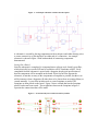
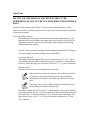
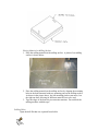
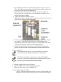
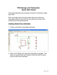
PCB Prototyping at Mississippi State:
From Idea to Fabrication
Rick King
Mississippi State University
2001 - 02
Table of Contents
Glossary .............................................................................................................................. 3
Overview............................................................................................................................. 4
Drawing a Schematic ...................................................................................................... 4
Laying Out a Board......................................................................................................... 5
Fabricating the PCB........................................................................................................ 6
Orcad Capture ..................................................................................................................... 7
Creating a Project............................................................................................................ 7
Creating New Parts Library ............................................................................................ 8
Creating a New Part ........................................................................................................ 8
Placing a Part .................................................................................................................. 9
Making Connections ..................................................................................................... 10
Generating a Layout Netlist .......................................................................................... 10
Orcad Layout .................................................................................................................... 11
Layers............................................................................................................................ 11
Importing a Netlist ........................................................................................................ 11
Component Placement .................................................................................................. 16
Component Keepouts.................................................................................................... 16
Routing.......................................................................................................................... 17
Exporting Gerber Files.................................................................................................. 18
IsoPro ................................................................................................................................ 20
QuickCam ......................................................................................................................... 23
Preparing Milling Material ........................................................................................... 23
Cutting the Material .................................................................................................. 23
Mounting Holes ........................................................................................................ 23
Placing Material on Milling Surface......................................................................... 24
Drilling Holes................................................................................................................ 24
Positioning the Design .............................................................................................. 25
Loading the Drill Bit................................................................................................. 25
Drilling the Design.................................................................................................... 26
Milling Isolations .......................................................................................................... 26
Loading Milling Tool................................................................................................ 26
Top Layer.................................................................................................................. 28
Bottom Layer ............................................................................................................ 28
Contour Routing............................................................................................................ 28
Loading the Contour Router ..................................................................................... 28
Cutting the Outline.................................................................................................... 29
Contour Routing Large Drill Holes .......................................................................... 29
Troubleshooting ................................................................................................................ 31
Glossary
Footprint:
A footprint is a physical specification of the interface between an
electrical component and the printed circuit board.
Printed Circuit
Board:
A printed circuit board is a thin plate on which chips and other
electronic components are placed.
Routing:
Routing is the process by which the connections specified in a
schematic are translated into the copper traces found on a printed
circuit board.
Schematic:
A schematic is a symbolic representation of a circuit design
containing the components that are to be used as well as the
connections that will be made.
Overview
A printed circuit board (PCB) is a thin plate on which chips and other electronic
components are placed. PCBs are found in computers, cell phones, microwaves, and just
about any other electronic device. The Electrical and Computer Engineering (ECE)
Department at Mississippi State University (MSU) owns equipment and software that
allows students to design and fabricate their own PCBs. There are three steps to the
process:
•
•
•
Drawing a Schematic
Laying Out a Board
Fabricating the PCB
This document will give an introduction to each of these three processes and their
associated tasks.
Drawing a Schematic
Orcad Capture can be used to draw a schematic and is available to all ECE
students at MSU. A schematic is a drawing consisting of the electrical components used
in the design and the connections made between the components. A schematic does not
contain any physical dimensions and has no impact on the placement of components on
the PCB. Capture includes a set of component libraries containing common components
such as resistors, capacitors, and logic gates. Capture also includes tools to create new
component libraries consisting of user-defined components.
Figure 1: An Example schematic created in Orcad Capture
A schematic is created by placing components on the workspace and either drawing wires
to create connectivity or placing labels on either end of a connection. An example
schematic is shown in figure 1 with both methods of connecting components
demonstrated.
Laying Out a Board
Once the schematic is completed, it is imported into a software tool, Orcad Layout Plus,
which physically lays out the PCB and is available to all ECE students at MSU. Each
component from the schematic is paired with a footprint, the physical specification of
how the component will be mounted on the board. When Layout Plus imports the
schematic, it matches as many of the components to footprints as possible, but there can
still be instances when a footprint will either have to be chosen from an existing library or
created manually. Layout Plus includes tools to create footprints as needed. The
footprints are then placed on the board. Figure 2 shows a board that has the footprints
placed, but has not been routed. The straight lines between the footprints in figure 2
represent the connections that will be made.
Figure 2: An unrouted layout created in Orcad Layout Plus
At MSU, we are limited to two layers of PCB development, top and bottom. The board is
routed with all the connections placed on the board in either of the two planes so that no
unwanted connections are created. Unless the routing needs to be exact, the autorouting
feature of Layout Plus can be used to route the PCB. Otherwise, Layout Plus includes the
tools to route manually the PCB. Figure 3 shows a board that has been routed. The top
and bottom layers as well as the drill holes are displayed in different colors to make
visualization easier.
Figure 3: A routed layout created in Orcad Layout Plus
Fabricating the PCB
After the PCB has been laid out, it is fabricated. At MSU, we have a T-Tech Quick
Circuit mechanical milling machine for PCB fabrication. The milling machine is located
in the ECE shop (Simrall 311) and is available to students upon request. The PCB
material used is simply a piece of fiberglass with copper plated onto one or both sides.
The layout is modified from showing where the copper should be to showing where the
copper should be removed. This modification is performed using the program IsoPro,
which is located on several computers in Simrall 329 and 331 or can be downloaded from
http://www.t-tech.com. Figure 4 shows the results of this operation on the layout from
figure 3.
Figure 4: An example isolation created by IsoPro
The new layout is taken to the milling machine where it controls the movement of the
milling head as the board is cut.
Orcad Capture
Orcad Capture is used to develop the schematic of a design. A schematic represents
symbolically all the parts and connections that will be made without getting bogged down
by physical issues such as size and position.
Creating a Project
The base for all work in Orcad Capture is a project. A project groups together the
components, libraries, and schematics associated with a design. The following
steps create a new project.
1. Under the “File” menu, select “New” and then “Project …”.
2. The new project window will appear as shown below. Fill in the name of the
project at the top.
Figure 5: Window for Creating a New Project
3. Under the name box is a selection labeled “Create a New Project Using”. For
this, select Schematic.
4. At the bottom, there is a box labeled location. Enter the working directory for
the schematic or find it using the browse button located to the right.
5. Once all the fields described above are filled in, press ok and the project will
be created.
Once the project is created, two windows will appear. The one in front will
be labeled “SCHEMATIC1: PAGE1”, while the window in the back will
have the same name as the project. The window in the back is the project
window. Certain functions are only available from the project window.
There are times when a necessary component is not included with the distribution of
Orcad Capture. The next two sections, “Creating a New Parts Library” and “Creating a
New Part”, explain how to work around this eventuality.
Do not add new parts to the standard libraries. If a new part is needed,
create a custom library and then add the new part to it.
Creating New Parts Library
1. Pull the project window to the foreground.
2. Under the “File” menu, select “New” and then Library.
3. This creates a new library with the default name “library1.olb”.
Creating a New Part
1. Locate the library that the new part will be added to.
2. Right-click on the library name and on the pop-up menu select “New Part”.
3. The new part window will come up. The figure below shows the window. It
takes some information on the part before the symbol is drawn.
Figure 6: Window for Creating a New Part
4. Enter the name at the top. This should be the name of the part.
5. The next box to complete is Part Reference Prefix. In the schematic, each
component receives a reference designator, which is composed of this prefix
and a number. Common prefixes are R for Resistor, C for Capacitor, and U
for Integrated Circuits. It is the designer’s choice as to what this prefix is.
6. Press ok.
7. The window that comes up allows the part to be drawn. The dotted box is the
border of the part. Clicking on one of the edges and dragging can adjust the
overall size of the part.
8. Pins can be placed next by using the new pin tool
. A window will come
up and ask for a name and number to associate with the pin. The shape and
type attributes can be changed as well, but for a basic pin they do not need to
be modified.
Avoid changing any of the pin types without first doing some
investigation. One problem can come from setting the pin type to
power. If this is done, the layout tool will assume that a power plane
exists (which we can’t do at MSU) and therefore those pins will not
be made available for routing.
9. After pressing ok, the mouse is set to place the pin. The pin will be placed
perpendicular to the border of the part. Once the pin is positioned, left click
the mouse and the pin will be placed.
10. Continue placing pins as described in steps 8 and 9 until all the necessary pins
have been placed. Resize the border of the part as necessary to fit all the pins.
11. Once all the pins have been placed, select the rectangle-drawing tool
and
draw a rectangle over the border of the part. The border does not show up in
schematics, so a rectangle is necessary to make the part look like a complete
symbol.
Parts can have a much more complicated symbol than a box. If it logically
follows that a part should have a shape other than a rectangle and you’re
feeling artistically incline, then by all means use the line, arc, and rectangle
tools to make a better looking symbol.
12. Under the “File” menu, select “Save”. If the library has not yet been saved, a
save as window will appear. Otherwise, the part will automatically save to the
selected library and will be available for use.
Placing a Part
1. Bring the schematic into focus by clicking on it.
2. To bring up the “Place Part” window, press ‘shift + p’ or go choose “Part” under
the “Place” menu.
3. Initially, there will only be user created libraries available. To access the standard
libraries, press the “Add Library” button on the right side of the window. Select
4.
5.
6.
7.
all the libraries desired using CTRL to allow multiple selections and then press ok
to return to the “Place Part” window.
Select the library of the desired part. This will bring up the list of all parts in the
library in the Part List.
Find the desired part in the list and left click on it.
Press OK. This will attach the part to the mouse for placement in the schematic.
Left click to place a part. The mouse continues to hold the part until the escape
key is pressed to allow for multiple instances of the same component type.
Making Connections
There are at least two ways to make connections in Orcad Capture. For more
information, visit http://www.orcad.com or look in the Capture help files.
• Wires
A wire can be drawn after the wire tool has been selected. The wire tool is
selected by pressing ‘Shift + w’. Left-clicking will start the wire and each
additional left-click will anchor the wire at that point on the schematic.
Press escape to end the wire. The wire will be ended at the last anchor
point.
• Labels
A label can be placed on a wire. If two wires have the same label, they are
considered to be the same wire by Orcad Capture. This allows for a much
less cluttered method of creating connectivity.
A label is created by pressing ‘Shift + n’ which will bring up the “Place
Net Alias” window. Enter the text of the label in the Alias box and press
ok. The mouse will carry this label around. Left clicking on the
schematic will place label.
Generating a Layout Netlist
A Layout Netlist is the file that is used to export a schematic into the layout phase
of design. The following steps create a layout netlist.
1. Bring up the project window.
2. Select the schematic that is being worked with.
3. Under the “Tools” menu, select “Create Netlist…” This will bring up the
“Create Netlist” window.
4. On the tabs across the top, select “Layout”.
5. The defaults should be correct for the filename to create and the
dimensions. Press ok to create the netlist.
This finishes the work in Orcad Capture. The next leg of the development process is to
work in Orcad Layout.
Orcad Layout
Orcad Layout is used to convert the symbolic schematic into the physical design that
includes the placement of components and the routing of connections. This is by no
means a complete manual on the uses of Orcad Layout. If there seems to be a better way
to do something, there probably is.
Layers
A printed circuit board is made up of layer(s) upon which components and traces
are placed. At Mississippi State, we are capable of producing one and two sided
boards, but not anything more. It is important to remember this when routing the
board and exporting gerber files.
Importing a Netlist
The best way to import a netlist is to create a new board design. The following steps
describe how to create a new printed circuit board.
1. Under the “File” menu, select “New”.
2. A window will pop up asking for a template file. Unless the PCB under
development has a specific form factor, choose the default template.
This may take a little looking to find. Try finding the root directory of
the Orcad installation. Then go to the directory “Layout_Plus\Data\”
and it should be located there.
3. The next window will ask for the layout netlist. Find the file that was created by
Orcad Capture and press ok.
4. The last window will ask what the board should be saved as. It will default to the
same name and the same directory as the netlist, but with a different extension.
(*.MAX)
5. Press ok and the Automatic Engineering Change Order (ECO) Utility will start.
This utility checks each component and tries to link it to a footprint. In the case
that it cannot, the utility will prompt for a resolution. There are two possible
resolutions to the problem.
a. Linking the part to an existing footprint
There are existing libraries of footprints that were shipped with Layout
Plus. If the component that was used was of a common footprint type, for
example a 28-pin Dual Inline Package (DIP), the footprint can be found
and linked. Otherwise, a new footprint will have to be created. To link an
existing footprint, follow these steps.
1. Press the “Link Existing Footprint” Button
2. Select the library of the footprint needed, or browse until it can
be found.
3. Select the specific footprint and press ok. Orcad will verify that
the footprint has the same number of pins as the schematic
symbol, so make sure to pick the right number of pins.
If a footprint is not correct, the rest of the design flow
will be carried out and an unusable board will be
developed. Pick the footprints carefully.
b. Creating a new footprint
In the case that a new footprint is needed, follow these steps.
1. Press the “Create or Modify Footprint” button. This brings up the
library manager.
2. Press the “Create New Footprint” button on the left towards the
bottom. This will bring up the “Create New Footprint” window.
3. At the window, enter the name of the footprint and the system of
measurement that will be used for specifying the footprint.
This document assumes the use of the English system.
A mil is not a millimeter. It is 0.001”.
4. Under the “Options” menu, select “System Settings…” This will
bring up a window where grid size and units can be specified.
5. In the System Settings Window, as shown below, set the Display
Units to Mils (m).
Figure 7: Window for editing environment settings
6. Set all the values under the Grids section to 5. This will give
0.005” resolution for placement of pins and text. Press ok.
These are not absolutes. These settings can be changed
to create a more desired work environment. Any less
than 5 though in the routing grid value will cause the
autorouter to thrash and will probably not route the
board.
7. There will be text that is generated automatically. The following
steps can remove the text.
a. Select the text tool by pressing the text tool button
.
b. Select the text to remove by clicking on it.
c. Remove the text by pressing the delete key.
d. Repeat steps b and c for all remaining text.
8. Pads are created in the following manner.
a. Under the “Tools” menu, select “Padstack” and then
“Select From Spreadsheet…”.
b. Press cancel at the window that appears.
c. Right click anywhere on the spreadsheet and select
“New…”
d. The “Add Padstack” window will appear as shown below.
Fill in the name of the pad in the Padstack entry field.
Figure 8: Window for creating a new pad
e. Under the “Pad Shape” area, select the shape of the pad.
f. At the bottom, fill in the values for “Pad Width” and “Pad
Height”.
g. This creates a general pad of the size that is needed. The
next thing to do is remove the layers that are not needed for
design at MSU. The following steps do that.
i. Select the layers that are not going to be used. All
that is needed at MSU are the top, bottom, and drill
layers.
ii. Right click on the spreadsheet and select
“Properties…”
iii. Change the Pad Shape to “Undefined” and press ok.
h. Select the drill layer, right click on it, and select
“Properties”. Make sure the pad shape is round. Adjust the
size of the drill hole so it is smaller than the pad size.
Drill sizes larger than the pad size create simple holes. If a
hole is all that is desired, make the top and bottom layers
undefined rather than smaller.
Make sure that the drill hole size is greater than 0.032” and
that the pad size is considerably (0.010”) larger than the
drill hole.
9. Pads are placed in the following manner.
a. Select the “Pin Tool”
from the top menu bar.
b. Right click on the workspace and select “New…” from the
pop-up window. A new default pad will appear ready for
placement.
c. Right click and select “Properties…” and the following
window will appear.
Figure 9: Properties window for a pad
d. Under “Padstack Name”, use the drop down list to select a
specific pad definition to use for this pin.
e. Under “Pad Name”, enter the number for this pin. This
should correspond with the pin numbers used in Orcad
Capture. Press ok to return to placement.
f. Using the mouse or the keyboard, move the pad to the
proper position. Current position is shown on the bottom
of the window and displays in the units that were specified
earlier.
10. Continue creating and placing pads until the footprint is fully
defined.
11. Press “Save” on the left side of the screen and the following “Save
Footprint As…” window will appear allowing the footprint to be
saved to a library.
12. Verify the name of the footprint is correct. If not, correct it.
13. Find the library to add this footprint to. If no library exists
presently, select “Create New Library…” and it will place this
footprint in the new library.
14. Press ok and the footprint is saved.
15. Tab back over to where “Create or modify footprint library…” was
selected.
16. Select “Link Existing footprint to component” and follow the
instructions on how to link part to existing footprint from above to
link the newly created footprint to the component.
Component Placement
a. Select the component tool
from the top menu bar.
b. Click on the component that will be placed.
c. Using the mouse or keyboard, move the footprint until it is in the desired
position and then either left-click the mouse or press the space bar.
Component Keepouts
After the footprints have been placed, component keepouts must be added to the
layout. To allow for easier soldering of the completed boards, it is best for all
traces to enter on the opposite side from the components. The router does not
know how to handle this on its own. The work-around comes through component
keepouts. The following steps will create a component keepout around a single
component. The steps should be repeated for all components on the board.
a. Select the obstacle tool
from the top menu bar.
b. Right click on the work area and select “New…”
c. Right click again and select “Properties…” and the “Edit Obstacle” window
will appear as shown below.
Figure 10: Properties window for an obstacle\
d. Under the Obstacle Type selection box, choose “Route-via keepout”. This
will prevent any traces from connecting to the pads on the layer the obstacle is
defined on.
e. Under the Obstacle Layer selection box, choose the layer this obstacle should
apply to. The most common value for this will be the top layer, but it can
vary depending on which side of the board the component will be mounted
upon.
f. Press ok to go back to the work area.
g. Click on a corner of the area that you want to prevent traces from entering.
h. Continue clicking on each corner of the outline until all corners have been
specified.
i. Press ‘f’ to finish the obstacle drawing
Routing
At this point, the board is ready to be routed. Routing is performed as follows.
a. Under the “Tool” menu, select “Layer” and then “Select From
Spreadsheet…”.
b. Set the top and bottom layer type to Routing Layer by double clicking and
changing the type in the window that appears.
c. Set the drill layer type to Drill Layer by double clicking and changing the type
in the window that appears.
d. Change all others layers to Unused Routing.
e. Close the layer spreadsheet.
f. Under the “Auto” menu, select “Autoroute” and then “Board”. This may take
a few minutes, but it should return a completely routed board.
Design Rule Check
Once the board has been routed, the design rules should be checked. The design
rules are a set of guidelines to make sure that all components are far enough apart
to allow the board to be milled reliably. Clicking on the DRC check icon on the
top menu bar checks the rules. Make sure that the design is DRC free (or the
violations are justified) before moving on.
Visual Verification
Look over the board prior to moving on. Make sure that all the connections have
been made that are expected. Power and ground on some pins may not appear if
their type was set to power, so watch out for this.
Exporting Gerber Files
The final step in Orcad Layout is to export Gerber files for use in fabrication. The
process for creating the Gerber files is detailed below.
a. Under the “Options” menu, select “Post Process Settings…” The Post Process
Window will pop up as shown below.
Figure 11: Post Process Setup Spreadsheet
b. Make sure that the top, bottom, and drill layers have the batch enabled field
set to “Yes”. If not, double click on the layer and check the “Enable for Post
Processing” box on the lower left of the window.
c. Close the spreadsheet.
d. Under the “Auto” menu, select “Run Post Processor”. This will create the
Gerber files that are needed for fabrication.
This completes the necessary work in Orcad Layout. There are many features available
that have not been described here in Orcad Layout. To learn about these, select the
”Help” menu and then “Learning Layout”.
IsoPro
IsoPro converts the standard Gerber files that were created in Orcad Layout into the
detailed design files that are needed to run the T-Tech milling machine. The steps in
IsoPro should be completed in the order listed below.
1. Import Gerber Files
a. Select the import tool
from the top menu bar.
b. At the file selection menu, choose all of the gerber files that were created
by Orcad Layout's post-processor and the drill file.
The drill file defaults to “thruhole.tap”. Gerber layers default to the
project name followed by a layer specific extension (e.g. the top layer
of project1 is named “project1.top”).
c. A “Gerber File Format” window will appear as shown below. Set the
integer value to 3 and the decimal value to 4 unless otherwise changed
when the files were created. All other values should remain the same.
d. Press import to finish each file.
2. Configure Layers
a.
b.
c.
d.
Select the layers tool
.
Make the type associated with the drill layer be “Drill” if it is not already.
Make any layers that belong on the top side be of type “Component”
Make any layers that belong on the bottom side be of type “Solder” and
have the “Mirror” check box marked.
e. Verify that all the imported layers are necessary for the design. With the
facilities at MSU, the solder mask and silk screen layers are not needed.
3. Create Board Outline
If the board outline was created as a global obstacle during the layout process, this
layer can simply be set to be of type “Isolation”. Otherwise, a new layer must by
created in IsoPro. This is accomplished in the following steps if necessary.
a.
b.
c.
d.
e.
f.
g.
Select the layers tool
.
Press “New” to create a new layer.
Click on the “Layer Name” field and name the outline field appropriately.
Press “View All” to change all layers into view mode.
Change the outline layer’s status field from view to edit mode.
Press “OK” to accept the changes and exit the Layer Table.
Select the “Create rectangles” tool
located on the bottom of the main
window.
h. Set the width of the rectangle lines to 0.062” by filling in the Width at the
bottom left of the screen with the value 62.
i. Draw a rectangle around the design.
4. Format Text (optional)
a.
b.
c.
d.
e.
f.
g.
h.
i.
j.
k.
5. Isolate
a.
b.
c.
Select the layers tool
.
Select the layer that contains text.
Press the copy layer button and rename the copied layer appropriately.
Press the view all button.
Press “OK” to accept the changes and exit the Layer Table.
Change the status of the text layer from view to edit.
Remove all non-text layout information.
Set the text layer back to view mode.
Set the source layer from view mode to edit mode.
Remove all text from this layer.
Set the source layer back to view mode.
Change all component and solder layers to edit mode.
Select the “Isolation” tool from the tool bar on the right.
Choose the top and bottom layers for isolation by clicking on each of them
using the CTRL key to select multiple layers.
There may be more layers than just the top and bottom layers,
but they should be all that need to be isolated.
d. Type in a value for tool width on the right side of the menu. Do not have
IsoPro expand the pads.
The default width for work at MSU is 0.010”.
e. Once the choices have been made, press the isolate button at the bottom of
the window. This action will create outlines of the pads and traces created
during layout. These isolation tell the milling machine where to cut.
6. Examine the isolations very closely. Verify that all the pads and traces are
isolated properly (will be cut out without changing the designed connectivity). If
the isolation is not correct, repeat with a smaller tool size. If a smaller tool size is
not possible, go back and re-layout the PCB.
7. Export QuickCAM Files
a. Under the “File” menu, select “Export” and then “QuickCAM Files”.
b. The pop-up menu will ask for layers to export. Choose the drill layer, all
isolations, the board outline, and any text that may be desired. Do not
export the original layers that the isolations were created from.
QuickCam
DO NOT USE THE MILLING MACHINE WITHOUT THE
PERMISSION OF ONE OF THE ECE SHOP EMPLOYEES OR RICK
KING.
QuickCam is the software provided by T-Tech to run the milling machine. Unless
otherwise noted in a section, the tasks to be executed in this section should be performed
in the order presented.
Preparing Milling Material
The milling material consists of both board material and backup material. The
board material is the fiberglass and copper that will be milled to create the PCB.
The backup material is used to prevent damage to the milling machine during
drilling and contour routing.
Caution: Do not operate the milling machine without backup material. Doing so
will cause damage to both the milling surface and drill bits.
Cutting the Material
The milling material bought at MSU comes in sheets that are 12” x 18”. The TTech milling machine cannot hold that large a piece of material. This problem is
solved by cutting the large piece in half to create two 12” x 9” pieces of material.
Mounting Holes
Once the material is cut, two mounting holes are needed.
If these holes are not placed correctly, a two-sided board will not
be possible, as the board will not flip correctly and therefore
milling on the second side will not line up with the preexisting
holes.
If too large a bit is used to drill these holes, the board may move
during milling causing the milling to fail.
Each hole is drilled with a T-Tech 0.125” carbide drill bit, which can be found in
the milling machine tool kit. The holes should be drilled exactly halfway between
each end in the 12” direction and about 5/8” in from the edge of the board. The
figure below shows a full 12” x 18” piece of material as shown in the T-Tech
User’s Manual.
Placing Material on Milling Surface
1. Place the milling material on the milling surface. A photo of our milling
surface is shown below.
2. Place the milling material on the milling surface by aligning the mounting
holes in the board material with two mounting pins on the milling surface.
As shown in the picture above, the left mounting pin does not move, but
the right one does allowing for different material sizes to be used.
3. Tape the edges of the board to prevent minor motions. Do not block the
milling machine with this tape.
Drilling Holes
Open the drill file that was exported from IsoPro.
If the data in IsoPro was not positioned within the box representing the milling table, an
error will be generated when you import the drill file.
Positioning the Design
To check where the design is positioned, left click on a drill hole and select
“Jump to Point” This will position the drill head over the material where the hole
will be drilled. The design should be completely positioned over unused milling
material, so in many cases it will need to be repositioned. Make sure to leave
some excess room around the edges of the PCB as a safety margin. To move the
design, select the “Offset” from the “Edit” menu. This tool allows the design to
be moved an integral number of mils in the x and/or y direction. The offset will
be retained until QuickCam is exited.
Loading the Drill Bit
The following steps are required to load each drill bit that is required by the
design.
Caution: The procedure for loading a drill bit is not the same as loading a
milling bit. Failure to follow the proper procedure will damage the
milling tools.
1. Under the “Options” menu, select “Tool Change.”
2. The milling head will move off of the milling surface to allow easy access.
Take a 1/16” Allen wrench, which can be found in the milling machine tool
kit, and loosen the nut that is holding the bit.
3. Insert the bit as far as possible. To verify the bit is completely inserted, place
the tip of the bit on your thumbnail and push up gently until the bit will go no
farther.
4. Tighten the nut that is holding the bit.
5. Adjust the top knob so that the drill bit does not hit the board material when it
moves back over the milling surface.
6. Click “Insert Tool” on the pop-up menu that came up when “Tool Change”
was selected. This will move the tool back over the milling surface.
7. Adjust the top knob so the bit is at most 1/16” off the table. This can be
measured using the Allen wrench used for changing the tool.
8. Adjust the pressure foot so the tip of the bit extends farther than the pressure
foot by the width of the board material and then a little bit more.
Drilling the Design
The drill file can be executed several times to help reduce the number of bit
changes. To run the drill file, perform the following steps.
Any drill hole sizes greater than or equal to 0.062” should be skipped
for now and router later using the contour router.
1. Under the “Mill” menu, select “Mill/Drill File.”
2. Follow the directions as to which drill bits to load.
If the milling machine tool kit does not have the requested bit, round
the size to closet bit size that is available.
Milling Isolations
Caution: The procedure for loading a milling tool is not the same as loading a
drill bit. Failure to follow the proper procedure will damage the milling tools.
Loading Milling Tool
1. Select the proper tool from the table in Appendix A based on the isolation
performed.
2. Once the tool is selected, the milling speed needs to be adjusted to prevent
tool damage. Under the “Configuration” menu, select the “Set Speed
Parameters” and change the milling speed based on the maximum speed value
given in Appendix A. Press OK to exit this menu.
3. Under the “Options” menu, select “Tool Change.”
4. The milling head will move off of the milling surface to allow easy access.
Take a 1/16” Allen wrench, which can be found in the milling machine tool
kit, and loosen the nut that is holding the milling tool.
5. Insert the milling tool as far as possible. To verify the bit is completely
inserted, place the tip of the bit on your thumbnail and push up gently until the
bit will go no farther.
6. Tighten the nut that is holding the milling tool.
7. Adjust the top knob so the drill bit does not hit the board material when it
moves back over the milling surface.
8. Adjust the pressure foot so that it is just past the end of the milling tool.
9. Click “Insert Tool” on the pop-up menu that came up when “Tool Change”
was selected. This will move the milling head back over the milling surface.
10. Adjust the top knob so the bit is at most 1/16” off the table. This can be
measured using the Allen wrench that was used for changing the tool.
11. Under the “Options” menu, select “Jog Milling Tool”. This will bring up a
control panel as shown below.
12. Position the milling head over an area of board material that will not be used
for any board design using the jog controls.
13. On the left side of the menu, there is a speed control slider. Move this toward
the bottom so the jog speed is 3-5 inches per minute.
14. Press the “Turn Spindle On” button.
15. Press the “Lower Tool” button.
16. Begin moving the milling tool in a straight line using the jog controls. As it
moves, slowly raise the pressure foot using the bottom knob until the milling
tool begins to cut the copper.
17. Once the copper is being cut, move the milling tool in the pattern of a small
rectangle. If the cut is deep enough, this will create a small piece of isolated
copper.
18. Using a multimeter, verify that no connection is present between the small
rectangle and the rest of the copper. If this is successful, the tool has been
loaded correctly.
Top Layer
1. Open the top layer isolation that was exported from IsoPro.
2. QuickCam will ask if the board material has been flipped. Answer no to this
question to allow the offset to be applied correctly.
3. QuickCam will ask if the current offset should be applied. Answer yes to this to
apply the offset.
4. To verify the positioning of the isolation, put the mouse in the middle of one of
the circles, left-click, and select “Jump to Point”. The milling head will move
directly over the point where that pad will be milled. If the design is positioned
correctly and this is a through-hole pin, there will be a drill hold under the
milling head.
5. Load the milling tool as specified above.
6. Under the Mill menu, select “Mill/Drill File.”
Bottom Layer
1. Flip the board material so the previous milling is on the bottom and the material
settles on the mounting pins.
2. Open the bottom layer isolation that was exported from IsoPro.
3. QuickCam will ask if the board material has been flipped. Answer yes to this
question to allow the offset to be applied correctly.
4. QuickCam will ask if the modified offset should be applied. Answer yes to this
to apply the offset.
5. To verify the positioning of the isolation, put the mouse in the middle of one of
the circles, left-click, and select move to cursor. The milling head will move
directly over the point where that pad will be milled. If the design is positioned
correctly, there will be a drill hold under the milling head.
6. Load the milling tool as specified above.
7. Under the “Mill” menu, select “Mill/Drill File.”
Contour Routing
Loading the Contour Router
Caution: The procedure for loading the contour router is not the same as
loading a milling bit. Failure to follow the proper procedure will damage
the milling tools.
1. Under the “Options” menu, select “Tool Change.”
2. The milling head will move off of the milling surface to allow easy access.
Take a 1/16” Allen wrench, which can be found in the milling machine tool
kit, and loosen the nut that is holding the bit.
3. Insert the router as far as possible. To verify the router is completely
inserted, place the tip of the router on your thumbnail and push up gently
until the bit will go no farther.
4. Tighten the nut that is holding the router.
5. Adjust the top knob so that the contour router does not hit the board material
when it moves back over the milling surface.
6. Click “Insert Tool” on the pop-up menu that came up when “Tool Change”
was selected. This will move the tool back over the milling surface.
7. Adjust the top knob so the router is at most 1/16” off the table. This can be
measured using the allen wrench used for changing the tool.
8. Adjust the bottom knob so the tip of the router extends farther than the
pressure foot by the width of the board material and then a little bit more.
Cutting the Outline
Always perform this step last. If not, the board will no longer be
mounted causing the drilling and milling to be misaligned.
If the PCB is small, place your finger on a corner of the board to
prevent the vacuum from sucking up the finished board. Make sure to
stay out of the routers path with you finger though.
1. Load the contour router as specified above.
2. Open the board outline that was exported from IsoPro.
3. Under the “Mill” menu, select “Mill/Drill File.”
Contour Routing Large Drill Holes
Caution: This task should be performed only once all other drilling and
milling have been performed. The pressure foot can fit into these larger
1.
2.
3.
4.
5.
6.
holes causing the milling tool to drive too far into the material. If this
happens, there can be damage to the milling equipment.
Load the contour router as specified above.
Open the drill file that was exported from IsoPro.
Under the “Mill” menu, select “Mill/Drill File.”
For all drill sizes smaller than 0.062”, select to skip as they have already been
drilled.
For all drill sizes greater or equal to 0.062”, select to contour route. The
contour router is 0.062” in diameter. Fill this in to the menu and then allow it
to go ahead and contour route the hole.
Repeat this for all other large hole-sizes.
Troubleshooting
Problem:
Solution:
Components cannot be placed as desired in Orcad Layout.
Turn off the Design Rule Checker (DRC) from the top menu. When the
DRC is on, there is a dotted rectangle marking the extents of the board.
Problem:
Solution:
A component is not listed when the place part option is selected.
There are two possible solutions as listed below.
1. Press “add library” and try to find the component in other libraries.
2. Follow the procedure for creating a new part as detailed earlier in
this manual.
This manual is an introductory manual to allow students at Mississippi State University
to get a start on developing printed circuit boards. To find more information, Orcad
Capture and Orcad Layout have extensive tutorials and help files.
Design Rules of Thumb
•
•
•
•
Wider is better. If there is room on the board for wider traces or larger pads, use
them. The more room that you give yourself on the board, the better.
Shorter is better. Shorter traces mean less resistance on the trace as well as less
routing required for the board. If all traces are minimized, the routing becomes
much less complicated.
Design with drill hole sizes of 0.032”, 0.040”, and 0.059” whenever possible as
these are the drill sizes available at present at Mississippi State University.
Minimize the use of vias if at all possible. We have a via tool available, but its
material costs the department money and it takes quite a bit of time to insert all
the vias for a board. Vias also add a level of complexity to populating the board
as there are more possible locations for the circuit to be broken.