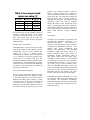
1
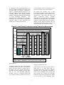
The focus of this paper is to discuss the low power features of the M•CORE architecture and describe a dual processor solution for a TDMA baseband transceiver which is currently in production. The key features of the 1.8 volt DSP56652 cellular baseband processor, currently designed into the iDEN i1000TM phone, will be discussed highlighting the integration of smart peripherals to reduce overall power consumption. Dual Core Architecture for Cellular Handsets David Ruimy Gonzales Senior Member of Technical Staff Motorola M-CORE Technology Center [email protected] Introduction Low Power Architecture The exponential growth of the wireless communications industry has created a multitude of new products with advanced features that allow users to stay in touch with every aspect of their lives wherever they may be. These new products are quite diverse, require more system performance with no exceptions to power conservation and have short product life cycles. Features such as video-teleconferencing, global positioning and internet access requires these systems to be flexible and capable of understanding a variety of digital wireless standards currently defined by the USA, Europe, Asia-Pacific and Japan. Motorola’s M•CORE architecture is designed specifically for sophisticated, yet low power, applications. It’s a fully static CMOS core that packs about 80,000 transistors in a 2.2-mm2 square of silicon in a 0.36 micron process. The architecture implements logic within portions of the core execution and control blocks to minimize power and reduce EMI. In addition to providing mechanisms to power down the processor and system logic, there is focus on minimizing dynamic power consumption when the system is active. The M•CORE architecture utilizes a streamlined execution engine that provides many of the same performance enhancements as mainstream RISC architectures. It is implemented with a fixed 16bit instruction length and 32-bit internal data path which meets the computational precision requirements of newer advanced products with the cost and power advantages previously available only with 16-bit architectures. Thus, increased code density accomplishes the goal of minimizing the overhead of memory system energy consumption. For example, there is a growing need for cellular baseband transceivers that accommodate GSM as well as CDMA standards at a low cost. In order to accomplish this, a micro-architecture that couples easily to DSPs, ASICs, standard peripherals and memory devices is needed. This micro-architecture must be programmable in C or C++, supported by the most popular real-time operating systems, and have a high instance of code re-usability for rapid prototype development with a rich development tool set. 1 DATA CALCULATION ADDRESS GENERATION Gen. Purpose Alternate Control Register File Register FileRegister File Address MUX 32-bits x 16 32-bits x 16 32-bits x 13 X Port Y Port MUX PC Incrementer Scale Sign Ext.. Address Bus Immediate Branch Adder Barrel Shifter Multiplier Divider MUX Instruction Pipeline MUX Adder/Logical iPriority Encoder/Zero Detect Result MUX Instruction Decode Writeback Bus H/W Accelerator Interface Bus Data Bus Figure 1: M•CORE Architecture [1] reducing external bus transients which consume power. A close examination of the M•CORE microRISC architecture, as illustrated in Figure 1, shows how it was designed for optimal performance and low power consumption. Key factors to consider are instruction set efficiency, memory utilization, special low power modes for static operation, power consumption during dynamic operation, and code density. Other important factors to consider during product design are the ease of interface to custom peripheral circuits and ASICS, on-chip JTAG/OnCETM emulation port and development tool support from third party vendors. The arithmetic unit contains a barrel shifter which provides fast multiply and signed or unsigned divides of integers, as well as special help in translation of incoming/outgoing data, such as single cycle bit reversal of a 32 bit word. Data movement is accomplished using load/stores of single or multiple registers in one instruction. This facilitates fast and efficient register utilization when entering/exiting subroutines and context switches between user and supervisor mode. Instruction Set Efficiency System-level power management Optimal instruction set efficiency is accomplished in the M•CORE architecture by implementation of a universal load-store RISC engine. The core contains a 16 entry, 32-bit general purpose register file, and processes instructions using an efficient four-stage execution pipeline. All computational activity takes place within the internal registers thus To provide optimal static power management for the overall system, the M•CORE architecture provides three instructions (stop, wait, and doze) that enable external logic to disable power to parts of the system. Execution of any of these instructions causes the processor to assert the LPMD1-0 output signals in the manner described in Table 1. 2 pipeline. The instruction pipeline recognizes which processor functions are required to execute a particular instruction. This enables it to ensure that data only transitions through the processor blocks that is actually needed to implement the instruction. For example, an add instruction would cause data to transition through the adder but not through the barrel shifter. By eliminating unnecessary transitions, the M•CORE architecture prevents switching of gates, loads, and wires in unused blocks, all of which would otherwise consume additional power. Table 1: Low power mode signal encoding [1] LPMD1 0 0 1 1 LPMD0 0 1 0 1 Mode STOP WAIT DOZE normal The external logic uses the LPMD1-0 inputs to determine exactly which parts of the overall system logic should be placed in a low-power state. The external logic can also place the processor in a low power mode by forcing the CLK input high. Code density Compilers were developed in conjunction with the M•CORE architecture instruction set to maximize code density. Code density is a measure of how many bytes of code are required to implement an application or function. Code density affects power consumption both statically and dynamically. The M•CORE architecture’s high code density results in a smaller executable image. This reduces an application’s memory requirements, which in turn reduces system cost and system power consumption. However, there is a second benefit to code density. Every time the processor fetches an instruction from memory, it must use a bus cycle. Bus cycles, of course, consume power. Since the M•CORE architecture’s dense code allows it to perform equivalent functionality with fewer bytes of code, a program executing on an M•CORE processor will consume less power because it will fetch fewer bytes from memory. Dynamic power consumption Although reducing a system’s static power usage achieves the greatest overall reduction in power consumption, a true low power solution must address the issue of dynamic power consumption. By dynamic power consumption, we are referring to the power required by the system when it is actually being used. The M•CORE architecture optimizes dynamic power consumption by both minimizing the power needed to execute an instruction and minimizing the number of bytes that need to be fetched to perform a given function. Power Aware instruction pipeline The low power instructions discussed earlier provide a mechanism to power down select parts of the system when not used. With processors themselves becoming more complex, a logical extension of this is to only power up the parts of a processor that are required to execute an instruction. The M•CORE architecture achieves this benefit through its advanced power aware Embedded and portable benchmarks were used to make design trade-offs in the architecture and the compiler. The Powerstone benchmarks, which include paging, automobile control, signal processing, imaging and fax applications, are detailed in Table 2. 3 Table 2: Powerstone Benchmark Suite [2] Benchmark auto bilv bilt compress crc des dhry engine fir_int g3fax Instr. Count 17374 21363 72416 322101 22805 510814 612713 986326 629166 2918109 g721 231706 jpeg 9973639 pocsag 131159 servo summin ucbqsort v42bits whet 41132 3463087 674165 8155159 3028736 Description Automobile control applications Shift, AND, OR operations Graphics application A Unix utility Cyclic redundancy check Data Encryption Standard Dhrystone Engine control application Integer FIR filter Group three fax decode (single level image decompression) Adaptive differential PCM for voice compression JPEG 24-bit image decompression standard POCSAG communication protocol for paging application Hard disc drive servo control Handwriting recognition U.C.B. Quick Sort Modem encoding/decoding Whetstone code density, the 16-bit instruction set provides a performance advantage over conventional RISC architectures in many low-cost applications. It is common for such applications to minimize cost through use of a 16-bit bus. Since conventional RISC architectures use 32-bit wide instructions, they have to perform two bus cycles to fetch an instruction, negatively impacting overall During initial analysis the M•CORE architecture instruction set was profiled by running the Powerstone benchmark suites on a cycle accurate C++ simulator. Table 3 shows the percentage of dynamic instructions utilizing the adder and barrel shifter, as well as the percentage of change of flow and load/store instructions. Table 3: Dynamic Instruction Percentages [2] Type Dynamic Instruction Percentage Adder Usage 50.23% Barrel shifter usage 9.68% a. Change of flow instructions 17.04% Load/store instructions 22.46% a. (83.5% of change of flow instructions are taken) instruction throughput. In contrast, the M•CORE architecture would only require a single bus Although the M•CORE architecture is 32-bits, it utilizes a 16-bit instruction set to achieve high cycle to perform an instruction fetch, enabling it code density. In addition, to providing improved to run at full speed even with a 16-bit bus. 4 A comparison to other popular architectures was made to evaluate instruction set efficiency and favorable results were realized as illustrated in Figure 2. Compiler efficiency played a key role in the code density comparisons especially when evaluating function call stacking, interrupt handlers, variable manipulation and the handling of if-else conditional statements. The implementation of conditional move, increment, decrement, and clear operations supplemented traditional change of flow instructions and helped improve compiler optimization. 16 general purpose registers, an alternate register file with 16 registers, and 5 scratch registers. The register file consumes 16% of total processor power and 42% of data path power due to the high utilization of the registers in the instruction set. Since loads and stores in a typical commercial RISC constitute approximately 23% of the dynamic instructions executed, the implementation of the alternate register file coupled with the ability to load/store multiple registers improved interrupt entry and exit latency and reduced memory accesses for instruction fetches and variable save/restore. Figure 2: Code Density Comparison using Powerstone Benchmarks 0.90 0.80 1.00 M•CORE Thumb Requires 47% more memory than M•CORE 1.00 1.07 Requires 49% more memory than M•CORE 1.10 Requires 42% more memory than M•CORE 1.20 V830 V850 SH2 SH3 Requires 46% more memory than M•CORE 1.30 ARM7 1.47 Requires 41% more memory than M•CORE Code Density significantly affects power consumption, runtime performance, and system cost 1.49 1.50 1.46 1.42 1.41 1.40 You r ac tua l fall Thum s in b Requires 9% more bet code we en. densi memory than M•CORE ty Code Size Relative To M•CORE 1.60 ARM9 (compressed ARM) StrongArm Compiled CompiledCCcode codeoptimized optimizedfor forcode codedensity. density. Compilers: Compilers:Diab Diab4.1, 4.1,ARM ARMSDK2.5, SDK2.5,Thumb Thumb1.04, 1.04,Green GreenHills Hills1.8, 1.8,Hitachi Hitachi3.0F. 3.0F. Rich register set Support for multiple data sizes To further minimize bus activity, the M•CORE architecture reduces the need to read and write data to and from memory. It achieves this by providing a rich set of registers that enables a program to keep data variables in registers while they are live. The M•CORE architecture provides a total of 37 32-bit data registers that are available to system programmers, one set of Some commonly used data types such as chars or shorts have 8- or 16-bit, rather than 32bit,representations. This provides an additional opportunity for the M•CORE architecture to reduce power consumption when fetching data from memory. For example, the M•CORE architecture would only toggle the 8 bits required to read or write a char, minimizing power 5 consumption by logic external to the processor core. To speed up memory copy and intitialization operations load multiple/load quadrant and store multiple/store quadrant instructions were added for block moves of registers to memory or memory to registers. This helped compiler resolution of variable alignment in memory. synthesis required 60% more transistors and 175% more area with an increase of 40% more power. Thus the data path was custom designed to reduce power and area. Further analysis showed that Clock power was 36% of the total processor power consumption. The M•CORE processor uses a single global clock with local generation of dual phase nonoverlapping clocks. Clock gating can be performed which allows for complete or partial clock tree disabling. The ability of clock gating permits specific data paths to be shut down during pipeline stalls thus saving power. This is quite important since the data path consumes 36% of total power while the remaining 28% is consumed by control logic. Low Voltage Since dynamic power consumption is proportional to the square of the supply voltage required, lowering the voltage provides a disproportionately large boost to battery life. M•CORE processors are designed to require only 1.8 volts to operate, with future versions planned to use as little as 0.9 volts. Interrupt latency was significantly improved by Figure 3: Cellular Handset Block Diagram [3] Telephone LCD Display Roam InUse PA NoSvc 1-800-555-1212 LoBatt Rchg 1 4 7 * 2 5 8 0 3 6 9 # Audio Codec RF/IF EEPROM Prot Timer QSPI Memory Shared Memory m•core UART Smartcard Timers Memory GPIO Baseband SerialAudio DSP56600 I/ O LEVEL TRANSLATORS FLASH Keypad Ext Mem I/F SRAM I/O LEVEL TRANSLATORS I/O LEVEL TRANSLATORS Debug Logic I/O LEVEL TRANSLATORS SmartCard the use of a 32 channel programmable interrupt controller. The 16 alternate registers improved interrupt latency entry and exit by eliminating the need to perform memory accesses for saving/restoring processor state. The use of a Find First One (FF1) instruction eliminated the need for interrupt priority scanning routines. This combination of special circuits realized a Processor Power Distribution Analysis of the architectural implementation showed that clock and data paths consumed a large portion of the power. This led to a critical decision on whether to synthesize or custom design the data path. Research showed that 6 37% improvement over the ARM processor with respect to interrupt service handling when performing a virtual DMA benchmark. Figure 3 where all signal processing functions such as speech coding/decoding, error correction, channel coding/decoding, equalization, Figure 4: DSP56652 Cellular Baseband Processor [5] CODEC ports for Baseband & Audio •Full duplex •Standard codec clock generation M·CORE MCU •20MHz @ 1.8V •32 bit architecture, fixed 16-bit instr •Architected for handheld applications •Best-in-class Code Density •Low Power, High Performance •Dual 16 entry / 32-bit register files •Efficient 4 stage pipeline •Single cycle execution for most instr •Byte, half-word, word access •Fast interrupt support Queued Serial Peripheral Interface •SPI compatible •Variable queue size •Full or half duplex Smartcard Interface Module •3V Smartcard interface •ISO7816 standard External MCU bus •22-bit address •16-bit data •Glueless system integration Protocol Timer •Radio Channel timing control •Frame number & position •Macro capability •8 outputs, 4 QSPI triggers •16 vectored DSP interrupts •DSP wakeup •Timing advance/retard •Frame table restart/swap Keypad Port •Up to 8x8 scan •Or GPIO Data RAM 13K x 16 DSP Debug 56600 Baseband CODEC Serial Port Audio CODEC Serial Port QSPI Serial Port SIM External Bus Interface DSP core PROM 48K x 24 DSP/MCU Interface 1024 x 16 M•CORE µRISC MCU core PRAM 512 x 24 Clocks/PLL uC Debug JTAG MUX RAM 512 x 32 Keypad Interface Protocol Timer Data ROM 18k x 16 ROM 4K x 32 Timer/PIT Watchdog UART GPT MCU General Purpose Timer •8-bit prescaler •Two 16-bit free-running counters •3 output compare/2 input capture •PWM capability for tone generation Periodic Timer / Watchdog •16-bit “set & forget” interrupts •Countdown or freerun •Watchdog hardware reset •Watchdog timeouts: 0.5 to 32 sec DSP56600 DSP Core •High performance: 60MHz @1.8V •1x engine 60MHz = 60 MIPS •16-bit data •Efficient 24-bit instruction set •16x16=40-bit multiply •GSM bit-exact arithmetic support •Fully static •Ultra low power modes •Special power management DSP Memory •On-chip DSP ROM •ROM patch capability •On-chip DSP RAM Flexible Clock Generator •16-60MHz PLL •Two clock inputs: •10-20 MHz or •32KHz MCU-DSP Interface (MDI) •1024 x 16-bit dual access •Polled or interrupt messaging OnCE Debug Ports • M·CORE&DSP56600 core debug •Non-intrusive examine/modify •Access via JTAG port JTAG Test Access Port •IEEE 1149.1 compliant •For system diagnostics •Access to M·CORE and DSP UART Serial Communication Port •Full Duplex •7- or 8-bit operation •Full 8 wire serial interface •IrDA standard support •robust receiver sampling/filtering •16-byte FIFO’s •Bit rates from 300 to 525Kbps •Low power wake-up modes modulation and encryption are all accomplished using a 60 MIPS DSP56600 core that executes one instruction every clock-cycle. DSP56652 Integrated Cellular Baseband Processor In this application the M•CORE processor performs all microcontroller functions associated with the phone user interface as well as protocol processing. Communication between the two cores is accomplished via a sophisticated MCUDSP interface (MDI) consisting of a 1K words dual-access memory (with read/write access for both processors) and a messaging unit, which features independent messaging logic and provides status and messaging control. Development of a Call-Processing Engine algorithm is easily accomplished using ANSI-C with in-line assembly language interrupt handlers. Tremendous progress has been made in reducing the parts count of the baseband functions of a wireless handset. This has been accomplished to meet cost, size, power and system performance requirements of the latest versions of cellular phones being marketed today. A key ingrediant for the increase of battery life in a cellular phone is component count reduction. By integrating an M•CORE processor with an advanced 16-bit Digital Signal Processor (DSP), operating at 1.8V, TDMA applications based on the IS-136 protocol can be accomplished with efficient battery power management to accomplish the baseband functions of a cellular phone excluding the front and backend analog blocks as illustrated in Figure 3. System partitioning is illustrated in Each core has a set of Input/Output peripherals for interfacing to the analog and RF sections of 7 the phone. A key peripheral, the dedicated protocol timer, offloads the task of maintaining handset to base station communication for both cores. Once programmed by the M•CORE processor, the timer is capable of coordinating all radio operations, including activation of the receiver, transmitter and frequency synthesizers. means for controlling the dual-core processor directly in the target system. Software and hardware breakpoint registers are provided along with a First-In-First-Out program counter trace buffer which stores change of flow addresses. Single-stepping opcodes with a 16 bit counter is available and the OnCETM registers are accessible while each core runs in real-time or is in reset. This interface is very useful for measuring static and dynamic power consumption and also allows analysis of code hot spots. Each core when put in the debug mode of operation will shut down clocks to the respective core as well as its peripherals. This allows distributed power analysis by shutting down one core and its peripherals while the other core may remain running in real-time. Specific hot spots in code of each processor may be analyzed with external power measuring tools that monitor current through the respective core’s power pins. It should be noted that power pins for each of the specific cores as well as their respective peripherals are isolated so they may be filtered and powered properly. The main goal of the protocol timer is to off-load compute intensive tasks such as event scheduling associated with the TDMA protocol. Software only needs to reprogram the timer once per frame. It is capable of generating timing signals, trigger signals and interrupts to the M•CORE processor and to the DSP. Sophisticated sets of tables interact for control of receive and transmit channel time intervals and number of frames per channel. Macro tables are utilized to reduce the programming of events that have fixed relationship between each other. [4] The production version of the iDEN i1000TM phone utilizes the DSP56652 ROM version in a 0.31 micron, triple-layer metal static CMOS process. This device consists of 8 Kbytes of ROM and 2 Kbytes of SRAM to support the M•CORE processor. The chip measures 7.4 mm on a side or 55 sq. mm. The part is packaged in a 196 plastic ball grid array (PBGA) and was designed for 16.8 MHz performance at 1.8v. This device when running out of internal SRAM consumes on average less than 9 ma at 1.8v, which translates into less than 16.2 mW at 16.8 MHz for the complete system. On average, this implementation of the M•CORE processor consumes 2.8 mA, which translates to a 0.30 mW/MHz rating. The part consumes less than 60 microamps in STOP mode. The M•CORE processor and DSP OnCE interface is currently supported by a Motorola Universal Command Converter (UCC), which communicates with a Software Development Systems (SDS) source level debugger. The SDS SingleStep debugger is tightly integrated into the Motorola Tool Suite through the UCC interface so that the dual-core system can be easily controlled using one common tool. C / C++ as well as assembly language programs compiled using a Diab Data M•CORE architecture cross-compiler can be quickly evaluated in this environment. Motorola also includes a DSP GNU C compiler, debugger, simulator, linker, assembler and DSP56652 evaluation board. DSP56652 Development Tools To accelerate system level integration and also provide a means for production and field testing of new product, a Motorola standard OnCETM block is available on the M•CORE processor as well as the DSP56600 processor. This block provides a dedicated emulation interface for rapid evaluation of the system hardware and software. Communication with the block is conducted via a 5 wire IEEE 1149 JTAG controller and provides direct access to each of the processors’ instruction registers so that opcodes may be fed directly to each instruction pipeline bypassing external accesses to memory. This mechanism provides a true non-intrusive Conclusion As the wireless communications industry progresses forward at lightning speed with new product designs, the issue of high performance with low-power consumption will present new challenges to wireless product designers. In order to design these new products in a timely manner a complete solution is of utmost importance for rapid delivery. Motorola’s new 8 M•CORE processor provides the architecture, advanced tools and technical support to solve these new challenges. It is recognized as a strategic corporate program within the company to provide a path for flexible yet re-usable technology for current and future designs. References [1] [2] [3] [4] [5] [6] Architectural Brief, M•CORE microRISC Engine, M•CORE 1/D, Motorola Inc., 1999 Jeff Scott, Lea Hwang Lee, John Arends, Bill Moyer, “Designing the Low-Power M•CORE Architecture”, Int’l Symp. On Computer Architecture Power Driven Microarchitecture Workshop, pp. 145-150, Barcelona, Spain, July 1998 Special thanks to Scott King of the Motorola Wireless Group, Austin Texas DSP56652 User’s Manual, Motorola Inc., 1999 Motorola Wireless Group Web Site, www.mot.com/SPS/WIRELESS, 1999 D. Gonzales, “Micro-RISC Architecture for The Wireless Market”, IEEE Micro, August 1999. Trademarks iDEN is a registered trademark of Motorola. i1000, M•CORE and OnCE are trademarks of Motorola. 9