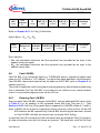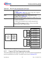
1
TLE986xQX BE
BootROM User Manual
Rev. 1.3, 2015-07-10
TLE986xQX BE BootROM
1
1.1
1.2
1.3
Introduction . . . . . . . . . . . . . . . . . . . . . . . . . . . . . . . . . . . . . . . . . . . . . . . .
Purpose . . . . . . . . . . . . . . . . . . . . . . . . . . . . . . . . . . . . . . . . . . . . . . . . . . . .
Scope . . . . . . . . . . . . . . . . . . . . . . . . . . . . . . . . . . . . . . . . . . . . . . . . . . . . . .
Abbreviations and special terms . . . . . . . . . . . . . . . . . . . . . . . . . . . . . . . . .
2
2.1
2.2
Overview . . . . . . . . . . . . . . . . . . . . . . . . . . . . . . . . . . . . . . . . . . . . . . . . . . . 7
Firmware architecture . . . . . . . . . . . . . . . . . . . . . . . . . . . . . . . . . . . . . . . . . 7
Program structure . . . . . . . . . . . . . . . . . . . . . . . . . . . . . . . . . . . . . . . . . . . . 8
3
3.1
3.1.1
3.1.2
3.1.3
3.1.4
3.1.5
3.1.6
3.1.7
3.1.8
3.1.8.1
Startup procedure . . . . . . . . . . . . . . . . . . . . . . . . . . . . . . . . . . . . . . . . . .
Program structure . . . . . . . . . . . . . . . . . . . . . . . . . . . . . . . . . . . . . . . . . . .
Test and initialisation of RAM . . . . . . . . . . . . . . . . . . . . . . . . . . . . . . . .
NVM initialisation routine . . . . . . . . . . . . . . . . . . . . . . . . . . . . . . . . . . . .
NVM MapRAM initialisation . . . . . . . . . . . . . . . . . . . . . . . . . . . . . . . . . .
Oscillator trimming and system clock selection . . . . . . . . . . . . . . . . . .
Analog module trimming . . . . . . . . . . . . . . . . . . . . . . . . . . . . . . . . . . . .
User configuration data initialization . . . . . . . . . . . . . . . . . . . . . . . . . . .
Debug support mode entry . . . . . . . . . . . . . . . . . . . . . . . . . . . . . . . . . .
User mode and BSL mode entry . . . . . . . . . . . . . . . . . . . . . . . . . . . . . .
NAC definition . . . . . . . . . . . . . . . . . . . . . . . . . . . . . . . . . . . . . . . . . .
10
10
11
11
11
12
12
12
13
13
14
4
4.1
4.2
4.3
4.3.1
4.3.2
4.4
4.4.1
4.4.2
4.4.3
4.4.3.1
4.4.3.2
4.4.4
4.4.4.1
4.4.4.2
4.4.4.3
4.4.4.4
4.4.4.5
4.4.4.6
4.5
4.5.1
4.5.2
4.5.2.1
LIN BSL mode . . . . . . . . . . . . . . . . . . . . . . . . . . . . . . . . . . . . . . . . . . . . .
LIN BSL features . . . . . . . . . . . . . . . . . . . . . . . . . . . . . . . . . . . . . . . . . . . .
LIN BSL mode overview . . . . . . . . . . . . . . . . . . . . . . . . . . . . . . . . . . . . . .
Phase I: Automatic synchronization to the host . . . . . . . . . . . . . . . . . . . . .
General description . . . . . . . . . . . . . . . . . . . . . . . . . . . . . . . . . . . . . . . .
Calculation of BR_VALUE and PRE values . . . . . . . . . . . . . . . . . . . . .
Phase II: LIN BSL communication protocol and the working modes . . . . .
Node Address for Diagnostic (NAD) . . . . . . . . . . . . . . . . . . . . . . . . . . .
Block type . . . . . . . . . . . . . . . . . . . . . . . . . . . . . . . . . . . . . . . . . . . . . . .
Checksum . . . . . . . . . . . . . . . . . . . . . . . . . . . . . . . . . . . . . . . . . . . . . . .
Classic / LIN checksum . . . . . . . . . . . . . . . . . . . . . . . . . . . . . . . . . . .
Programming checksum . . . . . . . . . . . . . . . . . . . . . . . . . . . . . . . . . .
LIN BSL Modes . . . . . . . . . . . . . . . . . . . . . . . . . . . . . . . . . . . . . . . . . . .
The Header Block . . . . . . . . . . . . . . . . . . . . . . . . . . . . . . . . . . . . . . .
Mode 0, 2 and 8 - Code/Data download to RAM or NVM . . . . . . . . .
Mode 1, 3 and 9 - Code execution inside RAM or NVM . . . . . . . . . .
Mode 4 - NVM erase . . . . . . . . . . . . . . . . . . . . . . . . . . . . . . . . . . . . .
Mode 6 - NVM protection . . . . . . . . . . . . . . . . . . . . . . . . . . . . . . . . . .
Mode A - Chip ID/Checksum read out . . . . . . . . . . . . . . . . . . . . . . . .
Phase III: Response protocol to the host . . . . . . . . . . . . . . . . . . . . . . . . . .
Acknowledgement response . . . . . . . . . . . . . . . . . . . . . . . . . . . . . . . . .
Error response . . . . . . . . . . . . . . . . . . . . . . . . . . . . . . . . . . . . . . . . . . . .
Block Type Error (FFH) . . . . . . . . . . . . . . . . . . . . . . . . . . . . . . . . . . .
17
17
18
20
20
21
23
23
24
24
24
24
25
25
25
29
29
31
32
34
35
35
35
User Manual
2
5
5
5
5
Rev. 1.3, 2015-07-10
TLE986xQX BE BootROM
4.5.2.2
4.5.2.3
4.5.2.4
4.5.3
4.6
4.6.1
4.7
4.8
4.8.1
4.9
Checksum Error (FEH) . . . . . . . . . . . . . . . . . . . . . . . . . . . . . . . . . . . .
Protection Error (FDH) . . . . . . . . . . . . . . . . . . . . . . . . . . . . . . . . . . . .
Response overview . . . . . . . . . . . . . . . . . . . . . . . . . . . . . . . . . . . . . .
Mode A response . . . . . . . . . . . . . . . . . . . . . . . . . . . . . . . . . . . . . . . . . .
Fast LIN BSL . . . . . . . . . . . . . . . . . . . . . . . . . . . . . . . . . . . . . . . . . . . . . . .
Entering Fast LIN BSL . . . . . . . . . . . . . . . . . . . . . . . . . . . . . . . . . . . . . .
After-Reset conditions . . . . . . . . . . . . . . . . . . . . . . . . . . . . . . . . . . . . . . . .
BSL Mode User Parameters – NAC/NAD . . . . . . . . . . . . . . . . . . . . . . . . .
Programming NAC and NAD . . . . . . . . . . . . . . . . . . . . . . . . . . . . . . . . .
WDT1 refreshing . . . . . . . . . . . . . . . . . . . . . . . . . . . . . . . . . . . . . . . . . . . .
35
35
36
37
38
38
40
41
41
42
5
5.1
5.1.1
5.1.2
5.2
5.2.1
5.2.1.1
5.2.1.2
5.2.1.3
5.2.1.4
5.2.2
5.2.2.1
5.2.2.2
5.2.2.3
5.2.2.4
5.2.2.5
5.2.2.6
5.2.2.7
5.2.2.8
5.2.3
5.3
FastLIN BSL Mode (UART BSL) . . . . . . . . . . . . . . . . . . . . . . . . . . . . . .
Phase I: Automatic serial synchronization to the host . . . . . . . . . . . . . . . .
General description . . . . . . . . . . . . . . . . . . . . . . . . . . . . . . . . . . . . . . . .
Calculation of BR_VALUE and PRE values . . . . . . . . . . . . . . . . . . . . .
Phase II: Serial communication protocol and the working modes . . . . . . .
Serial communication protocol . . . . . . . . . . . . . . . . . . . . . . . . . . . . . . . .
Transfer block structure . . . . . . . . . . . . . . . . . . . . . . . . . . . . . . . . . . .
Transfer block type . . . . . . . . . . . . . . . . . . . . . . . . . . . . . . . . . . . . . .
Response codes to the host . . . . . . . . . . . . . . . . . . . . . . . . . . . . . . .
Block response delay . . . . . . . . . . . . . . . . . . . . . . . . . . . . . . . . . . . . .
UART BSL Modes . . . . . . . . . . . . . . . . . . . . . . . . . . . . . . . . . . . . . . . . .
Header Block . . . . . . . . . . . . . . . . . . . . . . . . . . . . . . . . . . . . . . . . . . .
Mode 0 - Code/Data download to RAM/100TP . . . . . . . . . . . . . . . . .
Mode 1 - Code Execution inside RAM . . . . . . . . . . . . . . . . . . . . . . . .
Mode 2 - Code/Data download to NVM . . . . . . . . . . . . . . . . . . . . . . .
Mode 3 - Code Execution inside NVM . . . . . . . . . . . . . . . . . . . . . . . .
Mode 4 - NVM Erase . . . . . . . . . . . . . . . . . . . . . . . . . . . . . . . . . . . . .
Mode 6 - NVM Protection . . . . . . . . . . . . . . . . . . . . . . . . . . . . . . . . .
Mode A - NVM Readout, Chip ID, Checksum . . . . . . . . . . . . . . . . . .
16 bits inverted XOR checksum . . . . . . . . . . . . . . . . . . . . . . . . . . . . . .
WDT1 refreshing . . . . . . . . . . . . . . . . . . . . . . . . . . . . . . . . . . . . . . . . . . . .
43
43
44
44
45
45
46
46
47
50
52
52
52
55
55
60
60
62
63
68
68
6
6.1
6.1.1
6.2
6.2.1
6.2.2
6.3
6.3.1
6.3.2
6.3.3
6.3.4
NVM . . . . . . . . . . . . . . . . . . . . . . . . . . . . . . . . . . . . . . . . . . . . . . . . . . . . . .
NVM overview . . . . . . . . . . . . . . . . . . . . . . . . . . . . . . . . . . . . . . . . . . . . . .
NVM organisation . . . . . . . . . . . . . . . . . . . . . . . . . . . . . . . . . . . . . . . . .
NVM configuration sectors organisation . . . . . . . . . . . . . . . . . . . . . . . . . .
Chip ID definition . . . . . . . . . . . . . . . . . . . . . . . . . . . . . . . . . . . . . . . . . .
100 Time Programmable data . . . . . . . . . . . . . . . . . . . . . . . . . . . . . . . .
NVM user routines organisation . . . . . . . . . . . . . . . . . . . . . . . . . . . . . . . .
Opening assembly buffer routine . . . . . . . . . . . . . . . . . . . . . . . . . . . . . .
NVM programming routine . . . . . . . . . . . . . . . . . . . . . . . . . . . . . . . . . . .
NVM page erasing routine . . . . . . . . . . . . . . . . . . . . . . . . . . . . . . . . . . .
Abort NVM programming routine . . . . . . . . . . . . . . . . . . . . . . . . . . . . . .
69
69
70
74
74
77
83
86
87
90
91
User Manual
3
Rev. 1.3, 2015-07-10
TLE986xQX BE BootROM
6.3.5
6.3.6
6.3.7
6.3.8
6.3.9
6.3.10
6.3.11
6.3.12
6.3.13
6.3.14
6.3.15
6.3.16
6.4
6.4.1
6.4.2
6.4.3
6.4.3.1
6.4.3.2
6.4.3.3
6.4.4
6.4.4.1
6.4.4.2
6.4.4.3
6.4.4.4
6.4.5
Read NVM status routine . . . . . . . . . . . . . . . . . . . . . . . . . . . . . . . . . . . . 92
Read user calibration data . . . . . . . . . . . . . . . . . . . . . . . . . . . . . . . . . . . 92
Read NVM config status routine . . . . . . . . . . . . . . . . . . . . . . . . . . . . . . 93
Read NVM ECC2 address routine . . . . . . . . . . . . . . . . . . . . . . . . . . . . . 94
MapRAM initialization . . . . . . . . . . . . . . . . . . . . . . . . . . . . . . . . . . . . . . 95
Read 100 Time Programmable parameter data routine . . . . . . . . . . . . 96
Program 100 Time Programmable routine . . . . . . . . . . . . . . . . . . . . . . 97
Sector Erasing Routine . . . . . . . . . . . . . . . . . . . . . . . . . . . . . . . . . . . . . 99
NVMCLKFAC setting routine . . . . . . . . . . . . . . . . . . . . . . . . . . . . . . . . . 99
RAM MBIST starting routine . . . . . . . . . . . . . . . . . . . . . . . . . . . . . . . . . 99
NVM ECC check routines . . . . . . . . . . . . . . . . . . . . . . . . . . . . . . . . . . 100
NVM protection status change routines . . . . . . . . . . . . . . . . . . . . . . . . 102
NVM user applications . . . . . . . . . . . . . . . . . . . . . . . . . . . . . . . . . . . . . . . 107
NVM Data sector handling . . . . . . . . . . . . . . . . . . . . . . . . . . . . . . . . . . 107
Supporting Background NVM Operation . . . . . . . . . . . . . . . . . . . . . . . 114
Emergency operation handling . . . . . . . . . . . . . . . . . . . . . . . . . . . . . . 117
Emergency operation handling - Type 1 routines . . . . . . . . . . . . . . 117
Emergency operation handling - Type 2 routines . . . . . . . . . . . . . . 118
Emergency operation handling timing . . . . . . . . . . . . . . . . . . . . . . . 118
NVM user routines operation . . . . . . . . . . . . . . . . . . . . . . . . . . . . . . . . 119
NVM user programming operation . . . . . . . . . . . . . . . . . . . . . . . . . . 119
Tearing-safe Programming . . . . . . . . . . . . . . . . . . . . . . . . . . . . . . . 120
NVM user erase operation . . . . . . . . . . . . . . . . . . . . . . . . . . . . . . . . 120
NVM user programming abort operation . . . . . . . . . . . . . . . . . . . . . 121
NVM protection mechanism . . . . . . . . . . . . . . . . . . . . . . . . . . . . . . . . . 121
User Manual
4
Rev. 1.3, 2015-07-10
TLE986xQX BE BootROM
Introduction
1
Introduction
This document specifies the BootROM firmware behaviors for the TLE986xQX family.
The specification is organised into the following major sections:
•
•
•
•
BootROM Overview
Startup Procedure
LIN and UART BSL features
NVM structure and user routines description.
1.1
Purpose
The document describes the functionality of the BootROM firmware.
1.2
Scope
The BootROM firmware for the TLE986xQX family will provide the following features
•
•
•
•
Startup procedure for stable operation of TLE986xQX chip
Debugger connection for proper code debug
BSL mode for users to download and run code from NVM and RAM
NVM operation handling, e.g. program and erase
1.3Abbreviations and special terms
Table 1-1
Abbreviations and Terms
BSL
BootStrap Loader
CS
Configuration Sector
EOT
End of Transmission
EVR
Embedded Voltage Regulator
NAC
No Activity Count
NAD
Node address for diagnostic
NEA
NVM End Address
NLS
NVM Linear Size
NSA
NVM Starting Address
NVM
Non Volatile Memory
OCDS
On-Chip Debug Support
OSC
Oscillator
PEM
Program Execution Mode
User Manual
5
Rev. 1.3, 2015-07-10
TLE986xQX BE BootROM
Introduction
Table 1-1
Abbreviations and Terms (cont’d)
PLL
Phase-Locked Loop
SA
Service Algorithm
SCU
System Control Unit
SWD
Serial Wire Debug
VTOR
Vector Table Offset Register
WDT
WatchDog Timer
User Manual
6
Rev. 1.3, 2015-07-10
TLE986xQX BE BootROM
Overview
2
Overview
This specification includes the description of all firmware features including the
operations and tasks defined to support the general startup behaviour and various boot
options.
2.1
Firmware architecture
TLE986xQX on-chip BootROM consists of the startup procedure, the bootstrap loader
via LIN, the bootstrap loader via UART, NVM user routines and NVM integrity handling
routines.
The BootROM in TLE986xQX is located at 00000000H and so represents the standard
reset handler routine.
The startup procedure includes the EVR calibration, MapRAM initialisation, on-chip
oscillator configurations, NVM protection enabling and branching to the different modes.
The deciding factor will be on the latched values of TMS, P0.0 and P0.2 upon a reset.
During reset, these signals are latched at the rising edge of RESET pin and the latched
values are used to define which operation mode has to be entered.
There are generally 2 operation modes in the BootROM:
•
•
User / BSL mode
Debug Support mode
For user mode, it will execute the startup procedure, set the vector table position at the
beginning of the NVM in user accessible space (by proper setting of the VTOR register)
and jump to the user defined reset handler routine (jump to the location pointed by the
address 11000004H-11000007H) to execute the user program.
Note: The firmware will only set the VTOR to point at the beginning of the user
accessible NVM region but will not write any vector table. This is the responsibility
of the user to download a correct vector table.
Table 2-1 lists the boot options available in the TLE986xQX.
User Manual
7
Rev. 1.3, 2015-07-10
TLE986xQX BE BootROM
Overview
Table 2-1
TLE986xQX Boot options
TMS/DAP1
P0.0
/DAP0
P0.2
Mode / Comment
0
X
X
User mode / BSL mode 1)2)
1
0
X
Device test mode3)
1
1
0
Debug mode with SWD port
1
1
1
Device test mode3)
1)
On-chip OSC is selected as PLL input. System is running on LP_CLK until firmware switches to PLL output
before jumping to user code. Exception is with hardware reset where user settings are retained.
2)
Boot in user mode or BSL mode depends on the NAC word in user memory (NVM).
3)
Power up with special internal settings. At completion, device runs in endless loop. No NVM code execution
is performed.
Attention: The device test mode is not intended to be selected by the user. The
user shall ensure by external configuration of the pins (TMS, P0.0 and
P0.2) that no device test mode is entered.
2.2
Program structure
The different sections of the BootROM provide the following basic functionality.
Startup procedure
The startup procedure is the main control program in the BootROM. It is the first software
controlled operation that is executed after any reset.
The startup procedure will perform configuration sector verification, EVR calibration, onchip oscillator trimming, MapRAM initialisation, BootROM protection, NVM protection
and decode the pin-latched values of the TMS, P0.0 and P0.2 to determine which mode
it will jump to.
User mode
User mode is used to support user code execution in the NVM address space. However,
if the NVM memories are not protected and the Bytes at address 11000004H-11000007H
are erased (FFH), then device enters sleep mode. If a valid user reset vector was found
at 11000004H (values at 11000004H - 11000007H not equal to FFFFFFFFH) and a proper
NAC value is found then the BootROM proceeds into user mode. In case an invalid NAC
value is found, the device waits forever for a FastLIN BSL communication.
User Manual
8
Rev. 1.3, 2015-07-10
TLE986xQX BE BootROM
Overview
LIN BSL mode
It is used to support BSL via LIN like protocol. Downloading of code/data to RAM and
NVM related programming is supported in this mode.
UART BSL mode
It is used to support BSL via UART protocol. Downloading of code/data to RAM and NVM
related programming is supported in this mode.
User Manual
9
Rev. 1.3, 2015-07-10
TLE986xQX BE BootROM
Startup procedure
3
Startup procedure
This chapter describes the BootROM startup procedure in TLE986xQX.
The startup procedure is the first software-controlled operation in the BootROM that is
automatically started after every reset. Certain operations are skipped depending on the
type of reset. Refer to next section for further details.
3.1
Program structure
The first task executed by the startup firmware is the check of the reset source. For
power on, brown-out reset or wake-up from sleep mode reset, RAM test (optional) and
initialization (mandatory) are executed while they are skipped for the other resets.
In particular, the RAM test is always executed in case of power-on and brown-out reset.
For wake up reset, instead, the memory test execution is controlled by the MBIST_EN
bit in the SystemStartConfig register. The user can freely set the value of this bit and its
value is kept over wake up reset. If the bit is set to 0, the RAM test is not performed on
wake up. If the bit is set to 1 then the RAM test is performed even for wake up resets.
Firmware code uses part of the RAM for variable storage, literal pools and stack pointer.
The startup code anyhow only uses specific RAM region (the first 1kB mapped from
address 18000000H to 180003FFH), subset of the total available RAM address range.
The remaining region, not used by the FW, can be used by the user to store values to
be valid across reset for all reset sources different from power on reset, brown out reset
and wakeup reset. For these 3 reset sources, either a RAM test or a RAM clear is
executed thus destroying the previously stored values.
After that, depending on the reset source, the firmware will do NVM protection, NVM
MapRAM initialisation, on-chip oscillator trimming, PLL setting and analog module
trimming. It will decode the pin-latched values of the TMS, P0.0 and P0.2 to determine
which mode it will jump to.
If bootup mode is Debug Support mode, the WDT1 is disabled. For entry to user mode,
the WDT1 remains active. Next, the firmware will wait for NVM module to be ready.
For software, or internal watchdog reset (triggered by the WDT in the SCU), the following
steps are skipped:
•
•
•
•
•
•
RAM test and initialisation
NVM MapRAM initialisation and service algorithm
Setting of oscillator and PLL and switching system clock input to PLL output
Loading of analog modules trimming parameters from first 100TP page
Loading of user configuration data from 100TP page into the RAM
Clearing of NMI status before exit to user mode or Debug support mode
User Manual
10
Rev. 1.3, 2015-07-10
TLE986xQX BE BootROM
Startup procedure
3.1.1
Test and initialisation of RAM
A functional test sequence is executed on the entire RAM after power on reset and brown
out reset and can be executed after a wakeup reset (depending on the value stored in
the System Startup Configuration register). The test consists of a linear write/read
algorithm using alternating data. Once started, the firmware waits until the test is
completed before checking the result and continuing accordingly the start up sequence.
In case an error is detected the device is set to loop endlessly with WDT1 enabled.
Anyhow, in case of power-on reset, brown-out reset or wake-up reset from sleep mode
the start up procedure will continue with a complete RAM initialization by writing all the
RAM to zero with proper ECC status.This is needed to prevent an ECC error during user
code execution due to a write operation to an un-initialised location (with invalid ECC
code). Afterwards the Firmware proceeds checking the NVM status.
Note: The test sequence on the entire RAM takes 350 μs while the initialization of the
complete RAM takes 100 μs.
3.1.2
NVM initialisation routine
This routine will set the NVM protection according to the password in the configuration
sector (refer to Section 6.4.5 for further details on NVM protection and protection
password).
3.1.3
NVM MapRAM initialisation
After every power on reset, brown out reset, pin reset or wakeup reset the system
performs the MapRAM initialisation. This operation is triggered to restore the MapRAM
content. In case during the initialisation at least one error is detected, the service
algorithm routine is called to do the repair.
In case of mapping errors, the repair mechanism consists of erasing the wrong pages
(either faulty or double mapped pages). The repair step then requires the right of
modifying the NVM Data sector content, which can be in contrast to the NVM protection
settings user has provided. To avoid any risk of unwanted data loss, the user can control
via dedicated 100TP page parameter whether the SA is allowed to proceed to the repair
step in case NVM password protection for NVM Data sector is installed.
Detailed description of the MapRAM initialization and repair step can be found at
Section 6.4.1
User Manual
11
Rev. 1.3, 2015-07-10
TLE986xQX BE BootROM
Startup procedure
3.1.4
Oscillator trimming and system clock selection
After every power on reset, brown out reset, pin reset or wakeup from sleep reset the
system runs with an internal low precision clock (nominally 18 MHz). During the start up
procedure, the internal oscillator and PLL are trimmed to a fixed standard value of
20 MHz. In order to reduce the boot time, the start up procedure continues to run with
the low precision clock while the PLL is locking. System clock will be switched to PLL
output before jumping to user or BSL mode in case of successful lock. In case the PLL
does not lock the startup sequence proceeds further using the low precision clock as
system clock.
Once user mode is entered, user is allowed to set the final desired frequency by proper
register setting.
Note: After every power on reset, brown out reset, pin reset or wakeup reset the
user shall check whether the system is running on the low precision clock
or on the PLL output reading the SYSCON0 register.
3.1.5
Analog module trimming
In this routine, the trimming values of voltage regulators, LIN module, temperature
sensor, bridge driver and other analog modules are read from the configuration sector
and written into the respective SFR. For user mode or Debug Support mode, checksum
on 100TP page is evaluated. In case of error, default values are used. Refer to Table 611 for a list of user parameters in 100TP page.
3.1.6
User configuration data initialization
The firmware provides a routine to download data stored in user accessible configuration
sector pages (100TP) during the startup flow. In particular, the routine copies a specified
number of Bytes from a selected CS page (starting always from first Byte in the page)
into the RAM (starting at a given address). The routine is by default disabled and can be
enabled and controlled by proper programming of the Bytes stored in first 100TP page
as described in the Table 6-11. This routine is not performed after a software or
watchdog reset.
Relevant routine control parameters stored in the first 100TP page are:
• CS_USER_CAL_STARTUP_EN (offset=79H): When set to C3H it enables the user
data download from a 100TP page into the RAM during startup flow. All other values
will be ignored and the routine will not be executed at startup.
• CS_USER_CAL_XADDH: (offset=7AH): It defines the high Byte of the RAM starting
address where to copy data downloaded from CS. This Byte is ignored if the routine
is not enabled.
User Manual
12
Rev. 1.3, 2015-07-10
TLE986xQX BE BootROM
Startup procedure
• CS_USER_CAL_XADDL: (offset=7BH): It defines the low Byte of the RAM starting
address where to copy data downloaded from CS. This Byte is ignored if the routine
is not enabled.
• CS_USER_CAL_CS_PAGE: (offset=7CH): It defines the CS page where data has to
be downloaded from (refer to Figure 6-2). This Byte is ignored if the routine is not
enabled.
• CS_USER_CAL_NUM: (offset=7DH): It defines the number of Bytes to be
downloaded starting from the first Byte of the selected CS page. This Byte is ignored
if the routine is not enabled.
The RAM address where the user configuration data has to be copied to is stored as a
16-bit offset to the RAM start address (18000000H). This offset is defined by the
CS_USER_CAL_XADDL and CS_USER_CAL_XADDH parameters.
The routine has been developed to support downloading of the Customer_ID and the
ADC calibration parameters stored at the beginning of the first 100TP page (see
Table 6-11) into the RAM for an easy access but can be more generally used for all other
CS user parameters. If the routine is enabled, firmware will copy the data from config
sector into the RAM. Moreover, independent of startup setting, a similar routine is
provided as NVM user routine (refer to Section 6.3.6).
3.1.7
Debug support mode entry
Entry to Debug support mode is determined by pin setting at power up.
In case NVM address 11000004H-11000007H is not FFFFFFFFH, the firmware code
clears the RAM, waits for debugger to be connected, moves the VTOR to 11000000H
and jumps to user code.
3.1.8
User mode and BSL mode entry
Entry to user mode is determined by the No Activity Count (NAC) value which is defined
in the user code (refer to Chapter 3.1.8.1). After waiting the time defined by the current
NAC value, the startup procedure sets the VTOR register to point to the beginning of the
NVM (11000000H) and jumps to the reset handler.
If NVM double Bit error occurs when reading the NAC value, the system goes into
endless loop.
Before exiting to user mode, the system clock frequency is switched to PLL output
previously set by default to 20 MHz. In case PLL has not locked within 1 ms, the CPU
clock source LP_CLK (low precision clock running nominally at 18 MHz) will be used.
Note: User mode is entered jumping to the reset handler. This can happen directly from
startup routine, after a waiting time for possible BSL communication, or as a result
of BSL commands. In all these cases, jump to user mode will only occur either (1)
when NVM is not protected and NVM content at 11000004H-11000007H is not
User Manual
13
Rev. 1.3, 2015-07-10
TLE986xQX BE BootROM
Startup procedure
FFFFFFFFH or (2) when NVM is protected. In all other cases, firmware will put the
device in sleep mode.
3.1.8.1
NAC definition
The NAC value defines the time window after reset release in which the firmware is able
to receive BSL connection messages. The bits 3 to 0 define the duration of the time
window while the bits 6 and 7 of the NAC define which BSL interface is selected. Bit 5
and 4 are not used. If no BSL messages are received on the selected BSL interface
during the NAC window and NAC time has expired the firmware code proceeds to user
mode.
After ending the start up procedure, the program will detect any activities on the LIN/
UART for a period of time, determined by (((NAC & 3FH) -1H) * 5) ms reduced by the time
already spent to perform the start up procedure. When nothing is detected on the LIN/
UART and (((NAC & 3FH) -1H) * 5) ms is passed from reset going high, the
microcontroller will jump to user mode. If NAC is 1H, 41H, 81H or C1H the BSL window is
closed, no BSL connection is possible and the user mode is entered without delay.
The maximum NAC value is restricted to CH as the first open WDT1 window is worst
case 65 ms. In case a valid BSL command is detected during the BSL window the
firmware suspends the counting of the WDT1 in order to avoid that requested BSL
communication is broken by a WDT1 reset. The firmware will then re-enable the WDT1
before jumping to user code. If NAC is not valid, BootROM code will switch off the WDT1
and wait for a Fast LIN frame infinitely.
Table 3-1 gives an overview of the action of the microcontroller with respect to No
Activity Count (NAC) values and the Table 3-2 shows the selection of the BSL interface
depending on the NAC bits 7 and 6.
User Manual
14
Rev. 1.3, 2015-07-10
TLE986xQX BE BootROM
Startup procedure
Table 3-1
Type of action w.r.t. No Activity Count (NAC) values
NAC Value
Action
01H, 41H, 81H, C1H
0 ms delay. Jump to user mode immediately
02H, 42H, 82H, C2H
5 ms delay before jumping to user mode1)
03H, 43H, 83H, C3H
10 ms delay before jumping to user mode1)
04H, 44H, 84H, C4H
15 ms delay before jumping to user mode1)
05H, 45H, 85H, C5H
20 ms delay before jumping to user mode1)
06H, 46H, 86H, C6H
25 ms delay before jumping to user mode1)
07H, 47H, 87H, C7H
30 ms delay before jumping to user mode1)
08H, 48H, 88H, C8H
35 ms delay before jumping to user mode1)
09H, 49H, 89H, C9H
40 ms delay before jumping to user mode1)
0AH, 4AH, 8AH, CAH
45 ms delay before jumping to user mode1)
0BH, 4BH, 8BH, CBH
50 ms delay before jumping to user mode1)
0CH, 4CH, 8CH, CCH
55 ms delay before jumping to user mode1)
0DH - 3FH, 00H
Wait forever for the first LIN frame
4DH - 7FH, 40H, Invalid
Wait forever for the first FAST LIN frame
8DH - BFH, 80H
Wait forever for the first UART frame
CDH - FFH, C0H
Wait forever for the first UART frame
1)
If a LIN frame/UART frame is received within the delay period, the following actions occur; (1) the remaining
delay is ignored, (2) it will not enter user mode anymore (3) it will process the LIN / UART frame accordingly
Table 3-2
BSL interface selection
NAC(7)
NAC(6)
Selected BSL interface
0
0
LIN BSL
0
1
FAST LIN BSL
1
X
UART BSL
Note: LIN BSL will no longer be supported in future revisions of this product. All the LIN
BSL features will be supported by FastLIN BSL but with higher baudrate.
For each derivative, the NAC value is stored, together with the NAD value, in the last 4
Bytes of the linearly mapped NVM region. To ensure the parameter validity, the 2
parameters’ actual values and their inverted values are checked. In case the stored
value and inverted value are not consistent (value + inverted value + 1 not equal to 0)
User Manual
15
Rev. 1.3, 2015-07-10
TLE986xQX BE BootROM
Startup procedure
the parameter is considered to be invalid and the default value is used: The BSL window
will be open indefinitely and FastLIN is selected as BSL interface.
The Table 3-3 shows the addresses for all the available family devices. In the table NSA
stands for NVM Starting Address whose value is 11000000H for all derivatives and NLS
stands for NVM Linear Size, in Bytes, whose value is derivative dependent.
Table 3-3
NAC and NAD parameters details
Address
User Defined
Value
Criteria / Range
Default
NSA+(NLS-4)H
NAC
01H - 0CH for LIN BSL
81H - 8CH for UART BSL
7FH
NSA+(NLS-3)H
NAC
1’s complement
-
NSA+(NLS-2)H
NAD (for LIN BSL
only)
01H - FFH (00H is reserved)
7FH
NSA+(NLS-1)H
NAD (for LIN BSL
only)
1’s complement
-
For NSA and NLS values refer to Table 6-2.
User Manual
16
Rev. 1.3, 2015-07-10
TLE986xQX BE BootROM
LIN BSL mode
4
LIN BSL mode
Note: LIN BSL will no longer be supported in future revisions of this product. All the LIN
BSL features will be supported by FastLIN BSL but with higher baudrate.
LIN BSL is a LIN like protocol based on LIN 2.0 but for security reasons the checksum
is inverted for most of the supported modes. Standard LIN protocol can support a max.
baud rate of 20 kBaud. In order to support higher baudrates, a FastLIN BSL protocol has
been introduced. This is an enhanced feature implemented in TLE986xQX device that
supports baud rates of 20 kBaud to 57.6 kBaud and 115.2 kBaud via integrated LIN
transceiver using UART BSL protocol (See Section 4.6).
4.1
LIN BSL features
Features that are implemented include:
1. Re-synchronization to the transfer speed (baud rate) of the communication partner
upon receiving every frame
2. Using Diagnostic Frame (Master Request and Slave Response)
3. Usage of user values (NAD and NAC) stored in uppermost linearly mapped NVM
4. Non standard LIN checksum (Programming checksum, see Section 4.4.3.2)
5. Fast LIN BSL using UART protocol on integrated LIN transceiver
User Manual
17
Rev. 1.3, 2015-07-10
TLE986xQX BE BootROM
LIN BSL mode
4.2
LIN BSL mode overview
The LIN BSL mode consists of three functional phases described below:
• Phase I: To establish a connection with every frame (Master Request or Slave
Response frame) received by automatically synchronizing to the transfer speed (baud
rate) of the communication partner (host).
• Phase II: To execute the host specified command. In order to execute the commands,
host needs to send a Master Request Header first, followed by a Command frame
within the 8 byte payload of the Master Request Frame. The selected mode
information is embedded in the Command frame.
• The possible modes are:
– Mode 0 (00H): Transfer a user program from the host to RAM1)
– Mode 1 (01H): Execute a user program in the RAM2)
– Mode 2 (02H): Transfer a user program from the host to NVM1)
– Mode 3 (03H): Execute a user program in the NVM2)
– Mode 4 (04H): Erase NVM1)
– Mode 6 (06H): NVM Protection mode enabling/disabling Scheme2)
– Mode 8 (08H): Transfer a user program from the host to RAM using classic LIN
checksum3)
– Mode 9 (09H): Execute a user program in the RAM using classic LIN checksum4)
– Mode A (0AH): Get info (based on Option Byte)1)
LIN BSL supports Fast Programming through modes 0, 2 and 8 with the selection of Fast
Programming Option. Refer to Section 4.4.4.2 for more details.
• Phase III: To send microcontroller status to host. In order to receive the
microcontroller status, host needs to send a Slave Response Header first.
Re-synchronization and setup of baud rate (Phase I) are done at all times (before
Phases II and III). Thus, different baud rates can be supported. Phase II is entered when
its Master Request Header is received, otherwise Phase III is entered (Slave Response
Header). The Master Request Header has a Protected ID of 3CH while the Slave
Response Header has a Protected ID of 7DH. The Command and Response frames are
identified as Diagnostic LIN frame which has a standard 8 data Byte structure.
Figure 4-1 shows the relationship between the PC host and the microcontroller for the
3 phases, while Figure 4-2 shows the Master Request Header, Slave Response
Header, Command and Response frames.
1)
2)
3)
4)
The microcontroller returns to the beginning of Phase I/II and waits for the next command from the host
LIN BSL and serial communication are terminated.
Similar to mode 0, mode 8 uses classic LIN checksum instead of Programming checksum.
Similar to mode 1, mode 9 uses classic LIN checksum instead of Programming checksum.
User Manual
18
Rev. 1.3, 2015-07-10
TLE986xQX BE BootROM
LIN BSL mode
Host
TLE986 x
Phase I: Synchronize and
Setup Baud rate
Master Request Header
Command
Phase II: Selection of
Working Mode for valid
command
Slave Response Header
Phase I: Synchronize and
Setup baud rate
Phase III: Report its status to
the host
Response
Figure 4-1
Host
LIN mode - Phases I, II and III
Master Request Header
SYN Break
(At least 13
bit low)
SYN Char
55 H
Protected ID
3C H
TLE986x
Command
8 Data bytes for Command
Checksum
(1 byte)
Slave Response Header
SYN Break
(At least 13
bit low)
SYN Char
55H
Protected ID
7D H
Response
8 Data bytes for Response
Figure 4-2
Checksum
(1 byte)
LIN mode - Frames
For all modes’ entry, the Master Request Header is transmitted from host to
microcontroller, followed by the command, which is the header block. The Slave
Response Header is transmitted to check the status of the operation. For mode 0, 2 and
8, there is no need to send a Slave Response Header after every data block. The
microcontroller supports multiple data block transfers (up to 256 data blocks) without
Slave Response Headers in between, which saves overhead. As the commands are
sent one after another without waiting for any status indication, a certain delay is required
as shown in Figure 4-3 to ensure sufficient time is provided for the microcontroller to
execute the desired operations.
User Manual
19
Rev. 1.3, 2015-07-10
TLE986xQX BE BootROM
LIN BSL mode
Host
TLE986x
Master Request Header
Header Block* (Mode 0/2/8)
Delay1
TLE986x
HOST
Master Request Header
Slave Response Header
Header Block * (Mode 1/3/4/6/9/A)
Response Block * (Acknowledge )
Delay3
Master Request Header
Data Block * / **
Slave Response Header
Response Block * (Acknowledge )
Delay1
Master Request Header
Data Block * / **
Mode 1, 3, 4, 6, 9, A
Delay1
Master Request Header
*
EOT Block
Delay2
Slave Response Heade r
Response Block * (Acknowledge )
Mode 0, 2, 8
Figure 4-3
4.3
Delay is implemented to ensure that sufficient time is provided for the microcontroller to
execute the operations .
Delay1 is approximately 500 us (1 ms max).
Delay2 is approximately 500 us (1 ms max) for mode 0 and 8 while it is approximately 8
ms (15 ms max) for mode 2 (NVM programming time ).
Delay3 is approximately 500 us (1 ms max) for mode 1, 3 and 9 and it is max 50 ms for
Mode 4, 6 and A.
**The number of Data Blocks to be sent is indicated at No. of Data Blocks field in the
Header Block
* All blocks follow LIN BSL Protocol: 9 bytes of data, including a NAD and a checksum
Communication structure of the LIN BSL modes
Phase I: Automatic synchronization to the host
Upon entry to LIN mode, a connection is established. The transfer speed (baud rate) of
the device is automatically synchronized to the serial communication partner (host) in the
following steps:
STEP 1: Initialize LIN interface for reception and timer 2 for baud rate measurement
STEP 2: Wait for an incoming frame from host
STEP 3: Synchronize the baud rate to the host
STEP 4: Enter Phase II (for Master Request Frame) or Phase III (for Slave Response
Frame)
Note: Re-synchronization and setup of baud rate are always done for every Master
Request Header or Slave Response Header frame.
4.3.1
General description
The LIN baud rate detection feature provides the capability to detect the baud rate within
the LIN protocol using timer 2. Initialization consists of:
• Serial port of the microcontroller set to mode 1 (8-bit UART, variable baud rate) for
communication
User Manual
20
Rev. 1.3, 2015-07-10
TLE986xQX BE BootROM
LIN BSL mode
• baud rate range for detection, controlled by the field BGSEL of the BCON, set to
“5.5 to 166.7 kBaud”.
• Capture Timer 2 data register contents on negative transition at pin T2EX
• Timer 2 external events are enabled (EXF2 flag is set when a negative transition
occurs at pin T2EX)
• fT2 = fPCLK / 8 (T2PRE = 011B)
As shown in Figure 4-2, the LIN Header frame consists of the:
• synch Break (13 Bits time low)
• synch Byte (55H)
• Protected ID field
The Break is used to signal the beginning of a new frame and must be at least 13 Bits of
dominant value. When negative transition is detected at pin T2EX at the beginning of
Break, the Timer 2 External Start Enable Bit (T2MOD.T2RHEN) is set. This will
automatically start Timer 2 at the next negative transition of pin T2EX. Finally, the end of
synch Byte flag (LINST.EOFSYN) is polled. When this flag is set, Timer 2 is stopped. T2
Reload/Capture register (RC2H/L) is the time taken for 8 Bits. Then the LIN routine
calculates the actual baud rate, sets the PRE and BG values and activates baud Rate
Generator. The baud rate detection for LIN is shown in Figure 4-4
1st negative transition,
set T2RHEN bit
T2 automatically
starts
Last captured value of T 2
upon negative transition
EOFSYN bit is set,
T2 is stopped
Synch Char (55 H)
Synch Break
Start
Bit
00
Stop
Bit
01
02
03
04
Captured Value (8 bits)
Figure 4-4
4.3.2
LIN autobaud rate detection
Calculation of BR_VALUE and PRE values
To set up auto baud rate detection, the BG and PRE values must be calculated. As there
are two unknown values, two formulas are therefore needed. Firstly, the correlation
between the baud rate (baud) and the reload value BR_VALUE (stored in the registers
User Manual
21
Rev. 1.3, 2015-07-10
TLE986xQX BE BootROM
LIN BSL mode
BGL and BGH) and fractional divider (FDSEL) depends on the internal peripheral
frequency (fPCLK):
f PCLK
baud = ----------------------------------------------------------------------------------------------16 × PRE × ⎛ BR_VALUE + FDSEL
-------------------⎞
⎝
32 ⎠
[4.1]
Secondly, the relation between the baud rate (baud) and the captured value of Timer 2
(T2) depends on the T2 peripheral frequency (fT2) and the number of received Bits (Nb):
f T2 × N b
baud = -------------------T2
[4.2]
Combining Equation [4.1] and Equation [4.2] with Nb=8, fT2=fPCLK / 8 (T2PRE=011B)
results in the following:
f PCLK
--------------×8
f PCLK
8
------------------------------------------------------------------------------------------------ = ----------------------T2
FDSEL
16 × PRE × ⎛⎝ BR_VALUE + -------------------⎞⎠
32
[4.3]
By simplifying Equation [4.3], the following is obtained:
FDSEL
T2
PRE × ⎛⎝ BR_VALUE + -------------------⎞⎠ = ------32
16
[4.4]
After setting BR_VALUE, PRE and FDSEL, the baud rate generator will then be enabled,
and the subsequent Command frame or Response frame will follow this baud rate.
115.2 kBaud for FAST LIN
To support FAST LIN with baud rate 115.2 kBaud, fractional divider is enabled via a
predefined factor calculated and stored in the configuration sector. The detection of
115.2 kBaud is determined by the T2 timing. If T2H and T2L is less than 154H (i.e. baud
rate roughly above 70 kBaud), baud rate will be set to 115.2 kBaud.
As a consequence, the settings for 115.2 kBaud are:
• BR_VALUE = 13 (SFR BGL.BR_VALUE = 101B and SFR BGH = 1H)
• PRE (SFR BCON.BRPRE) = 000B
• Read FD_SEL value from configuration sector and store into SFR BGL. FD_SEL
User Manual
22
Rev. 1.3, 2015-07-10
TLE986xQX BE BootROM
LIN BSL mode
4.4
Phase II: LIN BSL communication protocol and the working
modes
Once successful synchronization to the host is completed (with a Master Request
Header), the routine enters Phase II. Here, the host communicates to the microcontroller
the desired working mode.
A simple protocol is defined for the communication between the host and TLE986xQX.
The protocol data is performed in information blocks. The information block follows a
specified block structure and is named transfer block. Each transfer block is 8 Bytes long
plus 1 checksum Byte (required to be compliant to the LIN frame structure). A transfer
block has the following structure:
NAD
(1 byte)
Block Type
(1 byte)
Data Area
(6 bytes)
Checksum
(1 byte)
• NAD: Node Address for Diagnostic, specifies the address of the active slave node.
See Section 4.4.1.
• Block Type: This field determines the type of the message (See Section 4.4.2).
• Data Area: This is the data of the block. The length is fixed at 6 Bytes.
• Checksum: This checksum is calculated based on the NAD, Block Type and Data
Area. See Section 4.4.3.
4.4.1
Node Address for Diagnostic (NAD)
The NAC value is stored similar to the NAC value inside the NVM. This field specifies the
address of the active slave node. Only slave nodes have an address. The NAD address
range supported in TLE986xQX is listed in Table 4-1.
Table 4-1
NAD address range
NAD Value
Description
00H
Invalid Slave Address
7FH
Default Address (NAD value is invalid or it is not programmed in NVM
linear area)
01H to 7EH
80H to FFH
Valid Slave Address
Note: LIN block with Broadcast NAD (7FH) is ignored if valid NAD value is programmed
in NVM linear area.
Note: For NAD address and details refer to Table 3-3.
User Manual
23
Rev. 1.3, 2015-07-10
TLE986xQX BE BootROM
LIN BSL mode
4.4.2
Block type
This field determines the types of transfer blocks. There are 3 transfer block types shown
in Table 4-2.
Table 4-2
Type of transfer block
Block Name
Block Type Description
Header block
00H
Special information is contained in the data area
of the block, which is used to select different
working modes.
Data block
01H
This block is used in working modes 0, 2 and 8 to
transfer a portion of program code. The program
code is in the data area of the block.
End of Transmission 02H
(EOT) block
This block is the last block in data transmission in
working modes 0, 2 and 8. The last program code
to be transferred is in the data area of the block.
4.4.3
Checksum
Diagnostic LIN frame always uses classic checksum where checksum calculation is over
the data Bytes only. The Checksum is the last field of Command and Response LIN
frames. For TLE986xQX, there are 2 types of checksum implemented, Classic (LIN) and
Programming checksum. Both Programming and LIN Checksum are supported and are
indicated in the respective modes.
4.4.3.1
Classic / LIN checksum
The classic checksum is a standard LIN checksum used for communication with LIN 2.0
slaves. The classic checksum contains the inverted eight Bits sum with carry1) over all
data Bytes.
4.4.3.2
Programming checksum
The programming checksum, or Inverted Classic checksum is a non-LIN standard
checksum. This is implemented in TLE986xQX to allow other slaves (not in TLE986xQX
BSL mode) on the LIN bus to ignore this Programming frame. The inversion of the classic
checksum yields the programming checksum.
An example of the calculation of the Programming checksum is provided in Table 4-3.
For this example, data of 4AH, 55H, 93H and E5H is considered. The calculated
1)
the checksum is calculated summing all values (8-bit sum with carry) and subtracting 255 every time the sum
is greater or equal to 256 (which is not the same as modulo-255 or modulo-256).
User Manual
24
Rev. 1.3, 2015-07-10
TLE986xQX BE BootROM
LIN BSL mode
programming checksum is 19H. The classic checksum is an inversion of the
programming checksum value (i.e. E6H).
Table 4-3
Programming checksum
Addition of data
HEX
Result
CARRY
Addition with CARRY
4AH
4AH
4AH
0
4AH
(4AH) + 55H
9FH
9FH
0
9FH
(9FH) + 93H
0132H
32H
1
33H
(33H) + E5H
0118H
18H
1
19H
4.4.4
LIN BSL Modes
When Phase II is entered, TLE986xQX waits for the Command frame and the header
block from the host containing indication about the desired mode to be selected.
4.4.4.1
The Header Block
The header block is always the first transfer block to be sent by the host during each data
communication process. It contains the mode number and special information on the
related mode (referred to as “Mode Data”). The general structure of a header block is
shown below.
Block Type
00H
(Header Block)
NAD
(1 byte)
Data Area
Mode
(1 byte)
Mode Data
(5 bytes)
Checksum
(1 byte)
Description:
•
•
•
•
•
NAD: Node Address for Diagnostic. See Section 4.4.1
Block Type 00H: The Block Type, which marks the block as a header block
Mode: The mode to be selected. The implemented modes are covered in Section 4.2
Mode Data: Five Bytes of special information to activate corresponding mode.
Checksum: The programming or LIN checksum of the header block.
Note: Mode 8 and mode 9 support LIN checksum, while mode 0 - 4, 6, and A support
Programming checksum.
4.4.4.2
Mode 0, 2 and 8 - Code/Data download to RAM or NVM
Mode 0, 2 and 8 are used to transfer a user program from host to microcontroller. Mode
0 and 8 allow RAM transfers, while mode 2 allows NVM transfers.
These modes are disabled in case NVM is protected by proper password and a
protection error is returned.
User Manual
25
Rev. 1.3, 2015-07-10
TLE986xQX BE BootROM
LIN BSL mode
The header block has the following structure:
The header block
NAD
(1 byte)
00H
(Header
Block)
00 H/02H/08H
(Mode 0/2/
8)
Mode Data ( 5 bytes)
Start
Addr
3
(MSB)
Start
Addr
2
Start
Addr
1
(LSB)
No of Data
Blocks
Used
(1 byte)
Fast_
Prog
(1 byte)
Checksum
(1 byte)
Mode Data Description:
Start Addr High, Low: 24-bit Start Address, which determines where to copy the
received program codes in the RAM/NVM1).
No. of data blocks used: Total number of data blocks to be sent, maximum 255 (FFH)
for mode 0 and 8 and maximum 21 (15H) for mode 2. Consistency between number of
data blocks declared in the header block and data blocks actually received is verified
when EOT block is received. If numbers do not match, microcontroller will send a Block
Type Error. PC host will then have to re-send the whole series of blocks (header, data
and EOT blocks).
Fast_Prog: Indication Byte to enter Fast LIN BSL2)
• 01H: Enter Fast LIN BSL
• Other values: Ignored. Fast LIN BSL is not entered.
Note: The programming of NVM in mode 2 will be started after 128 Bytes or EOT are
received. All Bytes sent during the program operation will be lost.
The start address provided with the header block has to be considered as a 24-bit offset
to be added to the standard RAM (18000000H) or NVM (11000000H) base address. For
mode 0 and 8, the most significant Byte of the start address is ignored.
When this Command frame (header block) is used for entering Fast LIN BSL, no other
Master Request Header and Command frames (for data block or EOT block) should be
sent. Instead, the microcontroller expects a Slave Response Header frame and sends a
Response frame to Acknowledge receiving correct header block to enter Fast LIN BSL
where UART BSL protocol is used. See Section 4.6
On successful receipt of the header block, the microcontroller enters mode 0/2/8,
whereby the program code is transmitted from the host to the microcontroller by data
block and EOT block, which are described below.
1)
NVM address should be aligned to the Page address (low Byte of the start address equal to 00H or 80H). If the
data starts in a non-page address, PC host should fill up the beginning vacancies with 00H and provide the
start address of that page address.
2)
In the case NVM is protected, entry to FastLIN BSL is not possible.
User Manual
26
Rev. 1.3, 2015-07-10
TLE986xQX BE BootROM
LIN BSL mode
The data block
NAD
(1 byte)
01H
(Data Block
1 byte)
Data Area ( 6 bytes)
Checksum
(1 byte)
Program Code
( 6 bytes)
Data area Description:
Program Code: The program code has a fixed length of 6 Bytes per data block.
The EOT block
NAD
(1 byte)
02H
(EOT Block
1 byte)
Data Area ( 6 bytes)
Last_Code
Program Code
Not Used
length
( Last_Codelength ( 6-1-Last_Codelength
( 1 byte)
bytes)
bytes)
Checksum
(1 byte)
Data area Description:
Last_Codelength: This Byte indicates the length of the program code in this EOT block.
Program Code: The last program code (valid data) to be sent to the microcontroller.
Not used: The length is (6 - 1 - Last_Codelength). These Bytes are not used and they
can be set to any value.
Note:
1. NVM programming needs to be performed in multiples of a page, 1 page is 128
Bytes. Host is expected to introduce a delay of 15 ms after 128 Bytes of program
code are sent. Refer to example given below on mode 2 downloading.
2. To prevent external access, once the NVM is protected, modes 0, 2 and 8 are not
accessible.
User Manual
27
Rev. 1.3, 2015-07-10
TLE986xQX BE BootROM
LIN BSL mode
Table 4-4
Example for 200 Bytes downloading using mode 0/8 and mode 2
Mode 0/8 - (RAM download)
Send Master Request Header
Send header block
• No of data blocks used = 33
• Start address (e.g. 000000H)
Delay
Send Slave Response Header
Check for Acknowledge
Send 33 times (Master Request Header +
data blocks)
(Delay after each data block required)
Send Master Request Header
Send EOT block
• Last_Codelength = 2
Delay
Send Slave Response Header
Check for Acknowledge
Mode 2 - (NVM download)
Send Master Request Header
Send header block
• No of data blocks used = 21
• Start address (e.g. 000100H)
Delay
Send Slave Response Header
Check for Acknowledge
Send 21 times (Master Request Header +
data blocks)
(Delay after each data block required)
Send Master Request Header
Send EOT Block
• Last_Codelength = 2
Delay
Send Slave Response Header
Check for Acknowledge
Send Master Request Header
Send header block
• No of data blocks used = 12
• Start address (e.g. 000180H)
Delay
Send Slave Response Header
Check for Acknowledge
Send 12 times (Master Request Header +
data blocks)
(Delay after each data block required)
Send Master Request Header
Send EOT block
• Last_Codelength = 0
Delay
Send Slave Response Header
Check for Acknowledge
33 blocks * 6 Bytes + 2 Bytes = 200 Bytes
User Manual
28
Rev. 1.3, 2015-07-10
TLE986xQX BE BootROM
LIN BSL mode
4.4.4.3
Mode 1, 3 and 9 - Code execution inside RAM or NVM
Mode 1, 3 and 9 are used to trigger execution of a user program by the microcontroller.
Mode 1 and 9 set the vector table in the RAM at the address 18000400H and trigger
execution of user program branching at address pointed by the standard reset handler
(18000404H). Mode 3 sets the vector table in the NVM at the address 11000000H and
triggers execution of user program branching at address pointed by the standard reset
handler (11000004H).The header block for this working mode has the following
structure:
The header block
NAD
(1 byte)
00H
(Header Block)
Mode Data
Not Used (5 bytes)
01H /03H /09H
(Mode 1/3/9)
Checksum
(1 byte)
Mode Data Description:
Not used: The five Bytes are not used and will be ignored in mode 1/3/9.
For modes 1, 3 and 9, the header block is the only transfer block to be sent by the host
followed by a Slave Response Header. The microcontroller will send a response block
(Acknowledgement code, 55H), exit the LIN BSL and jump to the RAM at the address
pointed by 18000404H (mode 1 and mode 9) or jump to NVM address at the address
pointed by 11000004H (mode 3) respectively.
Note: For mode 3, jump to NVM will only occur either (1) when NVM is not protected and
NVM content at 11000004H is not FFH or (2) when NVM is protected. In all other
cases, firmware will put the device in sleep mode.
4.4.4.4
Mode 4 - NVM erase
Mode 4 is used to erase the NVM. 3 different options are supported:
•
•
•
Option 00H: Page Erase
Option 40H: Sector Erase
Option C0H: Mass Erase
The header block for Option = 00H has the following structure:
User Manual
29
Rev. 1.3, 2015-07-10
TLE986xQX BE BootROM
LIN BSL mode
The header block for page erase (Option = 00H)
NAD
(1 byte)
00H
(Header
Block)
Mode Data (5 bytes)
04H
(Mode 4)
Start
Addr 4
(MSB)
Start
Addr 3
Start
Addr 2
Start
Addr 1
(LSB)
Option Checksum
(1 byte)
= 00 H
(1 byte)
Mode Data Description:
Start Addr 4 to 1: 32-bit address of the NVM page to be erased.
Option: set to 00H to enable page erase.
When the Option Byte is 00H, the NVM page selected by the address provided in the
Mode Data field is erased. The address should be aligned with the beginning of the
chosen page.
The header block for sector erase (Option = 40H)
The header block for Option = 40H has the following structure:
NAD
(1 byte)
00H
(Header
Block)
Mode Data (5 bytes)
04H
(Mode 4)
Start
Addr 4
(MSB)
Start
Addr 3
Start
Addr 2
Start
Addr 1
(LSB)
Option
= 40H
(1 byte)
Checksum
(1 byte)
Mode Data Description:
Start Addr 4 to 1: 32-bit address of the NVM sector to be erased.
Option: set to 40H to enable sector erase.
When the Option Byte = 40H, the NVM sector selected by the address provided in the
Mode Data field is erased. The address should be aligned with the beginning of the
chosen sector.
The Header for mass erase (Option = C0H)
The header block for Option = C0H has the following structure:
NAD
(1 byte)
00H
(Header
Block)
Mode Data (5 bytes)
04H
(Mode 4)
Not Used
(4 bytes)
Option
= C0H
(1 byte)
Checksum
(1 byte)
Mode Data Description:
Not used: This Byte is not used and will be ignored in mode 4.
User Manual
30
Rev. 1.3, 2015-07-10
TLE986xQX BE BootROM
LIN BSL mode
Option: set to C0H to enable mass erase.
When the Option Byte = C0H, mass erase on all the sectors in the NVM unit is performed.
Note: When NVM is protected, mode 4 is not accessible and so NVM cannot be erased.
4.4.4.5
Mode 6 - NVM protection
Mode 6 is used to enable or disable the NVM protection mode (read and write protection
of the Linearly and Non-Linearly mapped sectors) via the given user-password. The
header block for this working mode has the following structure:
The header block
NAD
(1 byte)
00H
(Header
Block)
06H
(Mode 6)
Mode Data (5 bytes)
User-password
(1 byte)
Checksum
(1 byte)
Not Used
(4 bytes)
Mode Data Description
User-password: This Byte is given by user to enable or disable NVM protection mode.
Not used: The four Bytes are not used and will be ignored in mode 6.
In mode 6, the header block is the only transfer block to be sent by the host. If device is
unprotected, the provided user-password will be set as NVM_PASSWORD and
internally stored. No further commands will be accepted until a power up or hardware
reset. Afterwards, protection mode will be enabled.
However, if the NVM is already protected, the microcontroller will deactivate the
Protection and erase the NVM if the user-password Byte matches the stored
NVM_PASSWORD Byte. If MSB of the NVM_PASSWORD is 0, only NVM Linearly
mapped sectors are erased. If the Bit is 1, both NVM Linearly and Non-linearly mapped
regions are erased. No further commands will be accepted until a power up or hardware
reset. Afterwards, protection mode will be disabled.
In case NVM is protected and the given user-password does not match the stored
NVM_PASSWORD, no actions will be triggered and a Protection Error Byte will be
returned instead of Acknowledge.
Note:
1. Password value has to be different from 00H and FFH. In case on an unprotected
device User-password is set to either 00H or FFH the protection will not be set and a
protection error (FDH) will be returned.
User Manual
31
Rev. 1.3, 2015-07-10
TLE986xQX BE BootROM
LIN BSL mode
2. When disabling NVM protection, together with NVM, the NAC and NAD values are
erased too. As a result, after next reset, default NAD will be used and chip waits
forever in FastLIN mode with 115.2 kBaud.
4.4.4.6
Mode A - Chip ID/Checksum read out
Mode A is used to get 4 Bytes Chip ID data, NVM page or CS page or mass NVM
checksum check info depending on the Option Byte value in the header block. The
header block for this mode has the following structure:
NAD
(1 byte)
00H
(Header
Block)
0AH
(Mode A)
Mode Data (5 bytes)
Input Data bytes
(4 bytes)
Option
(1 byte)
Checksum
(1 byte)
Different options are supported:
•
•
•
•
Option 00H: Get 4 Bytes Chip ID
Option 10H: NVM page checksum check
Option 18H: Mass NVM checksum check
Option 50H: Configuration sector page checksum check
The header block - Get 4 Bytes Chip ID (Option = 00H)
The header block for Option = 00H has the following structure:
NAD
(1 byte)
00H
(Header
Block)
Mode Data (5 bytes)
0AH
(Mode A)
Not Used
(4 bytes)
Option
= 00H
(1 byte)
Checksum
(1 byte)
Mode Data Description:
Not used: These Bytes are not used and will be ignored.
Option: set to 00H to enable getting 4 Bytes Chip ID info.
When the Option Byte = 00H, the 4 Byte Chip ID Number will be returned (see
Chapter 4.5.3).
The header block - NVM page checksum check (Option = 10H)
The header block for Option = 10H has the following structure:
User Manual
32
Rev. 1.3, 2015-07-10
TLE986xQX BE BootROM
LIN BSL mode
NAD
(1 byte)
00H
(Header
Block)
0AH
(Mode A)
Start
Addr
High
(1 byte)
Mode Data (5 bytes)
Start
Exp
Exp
Addr
CHKS
CHKS
Low
High
Low
(1 byte) (1 byte) (1 byte)
Option
= 10H
(1 byte)
Checksum
(1 byte)
Mode Data Description:
Start Addr High, Low: Address of the NVM page for checksum check. (Address should
be page aligned).
Exp. CHKS High, Low: Expected checksum High/Low Byte.
Option: set to 10H to enable NVM page checksum check.
Note: The start address provided with the header block has to be shifted by 7 bits to the
left and then added to the NVM start address to build the actual address, i.e. it is
calculated as follows in Mode A Option 10H: Actual address = 11000000H +
(StartAddrHigh << 15) + (StartAddrLow << 7).
This option will trigger a checksum calculation (16 bits inverted XOR) over the whole
page pointed by the address calculated form the offset provided in the header block and
the result will then be compared with the expected checksum (provided as well by the
user in the header frame). The response frame will then return an Acknowledge followed
by four data Bytes. These Bytes are, in sequential order, pass/fail indication (00H if the
calculated and expected checksum match, 80H if they differ), calculated checksum High
Byte, calculated checksum Low Byte, and a final Byte equal to 00H.
In case the provided address is not a valid NVM address, the microcontroller will return
a Block Type Error (FFH) instead of an Acknowledge (55H) followed by no further Bytes.
The header block - Mass NVM checksum check (Option = 18H)
The header block for Option = 18H has the following structure:
NAD
(1 byte)
00H
(Header
Block)
0AH
(Mode A)
Not
Used
(1 byte)
Mode Data (5 bytes)
Exp
Exp
CHKS
CHKS
High
Low
(1 byte) (1 byte)
Not
Used
(1 byte)
Option
= 18H
(1 byte)
Checksum
(1 byte)
Mode Data Description:
Not used: These Bytes are not used and will be ignored.
Exp. CHKS High, Low: Expected checksum High/Low Byte.
User Manual
33
Rev. 1.3, 2015-07-10
TLE986xQX BE BootROM
LIN BSL mode
Option: set to 18H to enable Mass NVM checksum check.
Checksum (16 Bits inverted XOR) on the whole linearly mapped sectors (configuration
sector pages and non-linearly mapped sectors not included) is calculated and then
compared with the expected values (provided as well as an input). The response frame
will then give back a pass or fail indication plus the calculated checksum.
The header block - Configuration sector page checksum check (Option = 50H)
The header block for Option = 50H has the following structure:
NAD
(1 byte)
00H
(Header
Block)
0AH
(Mode A)
CS
Page
(1 byte)
Mode Data (5 bytes)
Exp
Exp
Not
Option
CHKS CKSum
Used
= 50H
High
Low
(1 byte)
(1 byte)
(1 byte) (1 byte)
Checksum
(1 byte)
Mode Data Description:
CS Page: Selection of the CS Page to be checked (refer to Figure 6-2).
Not used: This Byte is not used and will be ignored.
Exp. CHKS High, Low: Expected checksum High/Low Byte.
Option: set to 50H to enable configuration sector page checksum check.
Checksum (16 Bits inverted XOR) on the selected configuration sector page is
calculated and then compared with the expected values (provided as well as an input).
The response frame will then give back a pass or fail indication plus the calculated
checksum. In case the provided CS address is not valid, the microcontroller will return a
Block Type Error (FFH) followed by no further Bytes.
For mode A, the header block is the only transfer block to be sent by the host followed
by a Slave Response Header. In case of valid header block, the microcontroller will send
a response block (Acknowledgement code, 55H) followed by the 4 Bytes data. The
response for mode A is described in Section 4.5.3.
4.5
Phase III: Response protocol to the host
The microcontroller status is sent to the host only when a Slave Response Header frame
is received. The microcontroller status is always sent in a transfer block of 9 Bytes.
User Manual
34
Rev. 1.3, 2015-07-10
TLE986xQX BE BootROM
LIN BSL mode
A typical transfer block consists of four parts:
NAD
(1 byte)
Response
(1 byte)
Response Data
(6 bytes)
Checksum
(1 byte)
• NAD: Node Address for Diagnostic, specifies the address of the active slave node.
• Response: Response code indicating Acknowledge or Error status. See Table 4-7.
• Response Data: These 6 Bytes are generally not used and set to 00H. An exception
is mode A response which is described in detail in Section 4.5.3.
• Checksum: The checksum is calculated based on NAD, Response and Response
Data Bytes. All responses sent by microcontroller will adopt classic checksum. See
Section 4.4.3.1.
4.5.1
Acknowledgement response
The Acknowledge response code (55H) is sent by microcontroller to host to indicate that
a block has been successfully received.
4.5.2
Error response
There are 3 error responses indicated by microcontroller.
4.5.2.1
Block Type Error (FFH)
This error can occur in the following conditions.
1. A Block Type other than the implemented ones was received. See Table 4-2.
2. An incorrect sequence of transfer blocks was received. For example, in mode 0
operation upon receiving a header block, a slave response request is expected.
However, if another header block is received, this will result in a Block Type Error.
4.5.2.2
Checksum Error (FEH)
This error occurs when the checksum comparison fails. Microcontroller will reject the
transfer block by sending back a Checksum Error code (FEH) to the host.
4.5.2.3
Protection Error (FDH)
This error occurs when selected NVM sectors, for programming or erasing, are
protected. As the selected NVM sectors are protected, no programming or erasing is
allowed. In this special error case, the LIN routine will abort current command and wait
for the next header block from the host again.
User Manual
35
Rev. 1.3, 2015-07-10
TLE986xQX BE BootROM
LIN BSL mode
4.5.2.4
Response overview
Table 4-5 shows a tabulated summary of the possible responses the device may
transmit following the reception of a header, data or EOT block.
Table 4-5
Possible responses for various block types
Mode
Header block
Data block
EOT block
0, 2, 8
Acknowledge, Block Type
Error, Checksum Error,
Protection Error
Acknowledge, Block
Acknowledge, Block
Type Error, Checksum Type Error,
Error
Checksum Error
1, 3, 9
Acknowledge, Block Type
Error, Checksum Error
4, 6
Acknowledge, Block Type
Error, Checksum Error,
Protection Error
A
Acknowledge, Block Type
Error, Checksum Error
The responses are defined in Table 4-6, which lists the possible reasons and/or
implications for error and suggests the possible corrective actions that the host can take
upon notification of the error.
Table 4-6
Definitions of responses
Response Value
Description
Block
Type
Acknowledge
55H
BSL
Mode
Header 1, 3, 9
EOT
Corrective
Action
The requested operation will
be performed once the
response is sent.
A
The requested operation has
been performed and is
successful. 4 Byte data
transmission follows.
6
The requested operation has
been performed and is
successful.
0, 2, 4,
8
All other
combinations
User Manual
Reasons / Implications
Reception of the Block is
successful. Ready to receive
the next block.
36
Rev. 1.3, 2015-07-10
TLE986xQX BE BootROM
LIN BSL mode
Table 4-6
Definitions of responses (cont’d)
Response Value
Description
Block
Type
Block
FFH
Type Error
BSL
Mode
Header 2, 4
All other
combinations
Reasons / Implications
Corrective
Action
NVM start address out of
range.
Retransmit a
valid header
block.
Either the block Type is
undefined or the flow is
invalid (see Figure 4-2).
Retransmit a
valid block
Checksum FEH
Error
All combinations There is a mismatch between Retransmit the
the calculated and the
block
received Checksum (see
Section 4.4.3).
Protection
Error
FDH
Header 0, 2, 4,
6, 8
Protection against external
access enabled, i.e.
NVM_PASSWORD is valid.
Disable
protection
FDH
Header 6
User-password invalid (set
either to 00H or FFH) on an
unprotected device.
Repeat
command with
valid password
Table 4-7 gives a summary of the response codes to be sent back to the host by the
microcontroller.
Table 4-7
Type of Response Code
Communication status
Response code to the host
Acknowledge (Success)
55H
Block Type Error
FFH
Checksum Error
FEH
Protection Error
FDH
4.5.3
Mode A response
This response frame is only applicable for mode A. The response frame depends on the
option Byte value used.
Option Byte = 00H:
User Manual
37
Rev. 1.3, 2015-07-10
TLE986xQX BE BootROM
LIN BSL mode
NAD
(1 byte)
ACK
Response
55 H
ID
CHIP_ID_2 CHIP_ID_1 CHIP_ID_0 Not Used
(1 bytes)
(1 bytes)
(1 bytes)
(1 bytes)
(2 bytes)
Checksum
(1 byte)
Refer to Chapter 6.2.1 for Chip_ID definition.
Option Byte = 10H, 18H, 50H:
NAD
(1 byte)
ACK
Response
55 H
Error
Calculated Calculated
Not Used
indicator CHKS High CHKS Low (3 bytes)
(1 bytes)
(1 bytes)
(1 bytes)
Checksum
(1 byte)
Error indicator:
• 00H: the calculated checksum and the expected one (provided as an input in the
header frame) are equal.
• 80H: the calculated checksum and the expected one (provided as an input in the
header frame) differ.
4.6
Fast LIN BSL
Fast LIN BSL is an enhanced feature in TLE986xQX device, supporting higher baud
rates up to 57.6 kBaud or 115.2 kBaud. To support this faster baudrate, once entered to
Fast LIN BSL, the protocol used will be the same as UART BSL (refer to Chapter 5 for
transfer protocol).
This mode is especially useful during back-end programming, where faster programming
time is desirable.The Fast LIN BSL is not meant to be used for in-car communication
since it is not protected against noise on the LIN line.
4.6.1
Entering Fast LIN BSL
User can enter Fast LIN BSL using an invalid NAC, using a dedicated NAC value (refer
to Table 3-1) or by sending a LIN command frame with Fast_Prog set to 1. (See
Section 4.4.4.2, the Fast_Prog option Byte is supported in LIN BSL modes 0, 2 and 8).
Note: LIN BSL will no longer be supported in future revisions of this product. All the LIN
BSL features will be supported by FastLIN BSL but with higher baudrate. Access
to Fast LIN BSL will then be ensured only via proper NAC setting.
In case the Fast LIN is entered via LIN command frame by setting the Fast_Prog option,
all other information sent with the frame are ignored. The baud rate, used for the Fast
User Manual
38
Rev. 1.3, 2015-07-10
TLE986xQX BE BootROM
LIN BSL mode
LIN BSL, is calculated based on the Master Request Header + Command LIN frame
received. The LIN transceiver slope mode is set to Flash mode, a specific setting of the
internal slew rate control that allows transmission up to 115.2 kBaud, and set the
baudrate according to the received LIN frame. The Fast LIN BSL entry is shown in
Figure 4-5.
In case, instead, the Fast LIN is entered directly via proper or invalid NAC, the protocol
is soon changed to UART. In this last case, the device still expects to receive a UART
test byte (80H) but the baudrate is not calculated based on the received test byte and is
instead by default set to 115.2 kBaud after having properly set the transceiver slope
mode to Flash mode.
The LIN transceiver slope mode is set back to normal mode before jumping to user code
via mode 1 or mode 3.
Host
Master Request Header
Synch
Break
(At least
13 bit low)
Synch
Char
55 H
Protected
ID
3C H
TLE986x
Command
8 Data bytes for Command
NAD, Header , Mode, ....., Fast _Prog
xx H,00H ,yy H,xxH,xxH ,xx H,xxH,01 H
Checksum
(1 byte)
yy = 00, 02, 08
Slave Response Header
Synch
Char
55H
LIN Mode
Synch
Break
(At least
13 bit low)
Protected
ID
7D H
Response
8 Data bytes for Command
NAD, Response (ACK),.....not used… Checksum
(1 byte)
xxH ,55 H,00 H,00 H,00H ,00 H ,00 H,00 H
Figure 4-5
User Manual
LIN Fast Mode
entered
<<<<<<<<<<<<<< UART BSL Mode protocol >>>>>>>>>>>>
Fast LIN BSL mode entry
39
Rev. 1.3, 2015-07-10
TLE986xQX BE BootROM
LIN BSL mode
4.7
After-Reset conditions
When more than one parameter in the transfer block is invalid, different actions are
performed. The different scenarios, and its consequent actions, are listed in Table 4-8.
Table 4-8
LIN BSL After-Reset conditions
Mode
Block
Type
(Header
only)
Action
Don’t
care
Don’t
care
Don’t
care
Save LIN Message to RAM1) and
jump to NVM 11000004H2)3).
Don’t
care
Don’t
care
Don’t
care
Message is ignored. Wait for next
frame.
N.A.
N.A.
N.A.
N.A.
Save LIN ID to RAM1) and jump to
NVM 11000004H2)3)
7DH
N.A.
N.A.
N.A.
N.A.
Reply if there is a previous valid
Master Request (Command
Frame) else wait for next frame
Yes
3CH
LIN
Don’t
care
Invalid
Valid4) Error flag is triggered. Wait for
Response frame to reflect error
Yes
3CH
LIN
Don’t
care
Don’t
care
4)
Yes
3CH
LIN
Valid
Valid
Valid4) Execute command
Yes
3CH
LIN
Invalid Valid
Valid4) Message is ignored. Wait for next
frame.
Yes
3CH
Prog
Invalid Don’t
care
Don’t
care
Yes
3CH
Prog
Valid
Invalid
Valid5) Error flag is triggered. Wait for
Response frame to reflect error
Yes
3CH
Prog
Valid
Valid
Invalid Error flag is triggered. Wait for
5)
Response frame to reflect error
Yes
3CH
Prog
Valid
Valid
Valid5) Execute command
Yes
3CH
Invalid Don’t
care
Don’t
care
Don’t
care
First
Frame
ID
Check NAD
sum
Yes
Invalid Don’t
care
No
Invalid Don’t
care
Yes
7DH
No
Invalid Save LIN message to RAM1) and
jump to NVM 11000004H2)3)
Message is ignored. Wait for next
frame.
Save LIN message to RAM1) and
jump to NVM 11000004H2)3)
1)
The LIN frame will be saved and dumped for debugging at RAM address 18000500H.
2)
Jump to user mode will only occur either (1) when NVM is not protected and NVM content at 11000004H is not
FFH or (2) when NVM is protected.
User Manual
40
Rev. 1.3, 2015-07-10
TLE986xQX BE BootROM
LIN BSL mode
3)
Up to max 10 Bytes are saved into the RAM. In case less than 10 Bytes are received, firmware proceeds to
user code after a time out of 35 ms.
4)
Valid modes for LIN checksum are mode 8 and mode 9. Other modes are considered invalid.
5)
Valid modes for programming checksum are mode 0-6 and A. Other modes are considered invalid.
4.8
BSL Mode User Parameters – NAC/NAD
There are 2 programmable parameters in the uppermost linearly mapped NVM Bank that
are used in LIN BSL. The parameter values are specified by the user:
1. No Activity Count (NAC): Defines the duration of BSL connection acceptance window
(in multiple of 5ms) starting from the reset release.
2. Node Address for Diagnostic (NAD): Specifies the node address used for the LIN BSL
communication.
Note: Timer 21 is initialized to have 5 ms overflow and is used to create the delay.
The BootROM will detect any activities on the LIN bus for a period of time, determined
by (((NAC & 3FH) -01H) * 5) ms. When nothing is detected on the LIN bus during this
time, it will jump to user mode.
Note: For FastLIN protocol any pulse on the LIN bus causes entering BSL mode. The
NAC counter will be stopped. The BootROM will even then stay in BSL mode if no
valid BSL command is received at all. This means, unexpected noise on the LIN
bus might cause unwanted entering of the BSL mode and therefore might prevent
normal user code execution. In order to overcome this behavior the BootROM
internal BSL mode shall be disabled by the user application by setting the NAC
value to X1h or by selecting LIN BSL protocol.
NAC value is restricted to 0CH as the first open WDT1 window is worst case 65 ms. The
firmware has to either refresh the WDT within the 65 ms or jump to user mode. If NAC
value is bigger than 0CH, BootROM code will refresh the WDT and wait for a LIN frame
indefinitely.
4.8.1
Programming NAC and NAD
User needs to program the NAC and NAD in the format listed in Table 3-3. To ensure
the parameter validity, the 2 parameters actual values and their inverted values are
checked.
If the NAD parameter is not valid nor within the range, the default value (7FH) is used in
the LIN BSL.
User Manual
41
Rev. 1.3, 2015-07-10
TLE986xQX BE BootROM
LIN BSL mode
4.9
WDT1 refreshing
After a reset the WDT1 is starting with a long open window. WDT1 keeps on running
while waiting for first LIN frame. In case during the LIN BSL waiting time, defined by NAC,
a LIN communication is detected, WTD1 is disabled and its status frozen.
Subsequently, before exiting to RAM or NVM in LIN BSL modes 1, 3 and 9 the watchdog
is re-enabled and starts from the previously frozen state. The WDT1 is then still in long
open window and the remaining valid time is equal to Long open window minus the time
between reset release and first LIN communication. User program needs to trigger the
WDT1 refresh accordingly.
User Manual
42
Rev. 1.3, 2015-07-10
TLE986xQX BE BootROM
FastLIN BSL Mode (UART BSL)
5
FastLIN BSL Mode (UART BSL)
This chapter describes the protocol used for the FAST LIN and UART BSL.
The protocol is based on the phases described following.
• Phase I: Establish a serial connection and automatically synchronize to the transfer
speed (baud rate) of the serial communication partner (host).
• Phase II: Perform the serial communication with the host. The host controls the
communication by sending special header information which selects one of the
working modes. These modes are:
– Mode 0 (00H): Transfer a user program from the host to RAM or write 100TP
pages1)
– Mode 1 (01H): Execute a user program in the RAM2)
– Mode 2 (02H): Transfer a user program from the host to NVM1)
– Mode 3 (03H): Execute a user program in the NVM2)
– Mode 4 (04H): Erase NVM1)
– Mode 6 (06H): NVM protection mode enabling/disabling Scheme2)
– Mode A (0AH): Get Info (based on Option Byte)1)
Except mode 1, mode 3 and mode 6, the microcontroller would return to the beginning
of Phase II and wait for the next command from the host after executing all other modes.
The serial communication, which is activated in Phase II, is performed via the integrated
LIN transceiver for FastLIN and via with the full-duplex serial interface (UART) of the
TLE986xQX for UART BSL.
The serial transfer is working in asynchronous mode with the serial parameters 8N1
(eight data Bits, no parity and one stop Bit). The host can vary the baud rate in a wide
range because the microcontroller does an automatic synchronization to the host in
Phase I.
The following section provides detailed information on these two UART BSL phases.
5.1
Phase I: Automatic serial synchronization to the host
Upon entering UART BSL mode, a serial connection is established and the transfer
speed (baud rate) of the serial communication partner (host) is automatically
synchronized in the following steps:
•
•
•
•
•
STEP 1: Initialize serial interface for reception and timer for baud rate measurement
STEP 2: Wait for test Byte (80H) from host
STEP 3: Synchronize the baud rate to the host
STEP 4: Send Acknowledge Byte (55H) to the host
STEP 5: Enter Phase II
1) The microcontroller returns to the beginning of phase II and waits for the next command from the host
2) UART BSL and serial communication are terminated.
User Manual
43
Rev. 1.3, 2015-07-10
TLE986xQX BE BootROM
FastLIN BSL Mode (UART BSL)
5.1.1
General description
The microcontroller will set the serial port to mode 1 (8-bit UART, variable baud rate) for
communication. Timer 2 will be set in auto-reload mode (16-bit timer) for baud rate
measurement. In the process of waiting for the test Byte (80H), microcontroller will start
the timer on reception of the start Bit (0) and stop it on reception of the last Bit of the test
Byte (1). Then the UART BSL routine calculates the actual baud rate, sets the PRE and
BR_VALUE values and activates baud rate generator. When the synchronization is
done, the microcontroller sends back the Acknowledge Byte (55H) to the host. If the
synchronization fails, the baud rates for the microcontroller and the host are different,
and the Acknowledge code from the microcontroller cannot be received properly by the
host. In this case, on the host side, the host software may give a message to the user,
e.g. asking the user to repeat the synchronization procedure. On the microcontroller
side, the UART BSL routine cannot judge whether the synchronization is correct or not.
It always enters phase II after sending the Acknowledge Byte. Therefore, if
synchronization fails, a reset of the microcontroller has to be invoked, to restart it for a
new synchronization attempt.
5.1.2
Calculation of BR_VALUE and PRE values
For the baud rate synchronization of the microcontroller to the fixed baud rate of the host,
the UART BSL routine waits for a test Byte (80H), which has to be sent by the host. By
polling the receive port of the serial interface (P1_DATA.4/RxD Pin), the Timer 2 is
started on the reception of the start Bit (0) and stopped on the reception of the last Bit of
the test Byte (1). Hence the time recorded is the receiving time of 8 Bits (1 start Bit plus
7 least significant Bits of the test Byte). The resulting timer value is 16-bit (T2). This value
is used to calculate the 11-bit auto-reload value (BR_VALUE stored in the BGH and BGL
SFRs), the fractional divider FDSEL and PRE, with T2PRE predefined as 011. This
calculation needs two formulas.
First, the correlation between the baud rate (baud) and the reload value (BG) depends
on the internal peripheral frequency (fPCLK)
f PCLK
baud = ----------------------------------------------------------------------------------------------16 × PRE × ⎛ BR_VALUE + FDSEL
-------------------⎞
⎝
32 ⎠
[5.1]
Second, the relation between the baud rate (baud) and the recording value of Timer 2
(T2) depends on the T2 peripheral frequency (fT2) and the number of received Bits
(fT2Nb)
f T2 × N b
baud = -------------------T2
User Manual
[5.2]
44
Rev. 1.3, 2015-07-10
TLE986xQX BE BootROM
FastLIN BSL Mode (UART BSL)
Combining Equation [5.1] and Equation [5.2] with Nb=8, fT2=fPCLK/ 8 (T2PRE=011),
f PCLK
--------------×8
f PCLK
8
------------------------------------------------------------------------------------------------ = ----------------------T2
16 × PRE × ⎛ BR_VALUE + FDSEL
-------------------⎞
⎝
32 ⎠
[5.3]
Simplifying Equation [5.3], we get
PRE × ⎛ BR_VALUE + FDSEL
-------------------⎞ = T2
------⎝
32 ⎠ 16
[5.4]
After setting BR_VALUE, FDSEL and PRE, the baud rate generator will then be enabled,
and the UART BSL routine sends an Acknowledge Byte (55H) to the host. If this Byte is
received correctly, it will be guaranteed that both serial interfaces are working with the
same baud rate.
5.2
Phase II: Serial communication protocol and the working modes
After the successful synchronization to the host, the UART BSL routine enters Phase II,
during which it communicates with the host to select the desired working modes. The
detailed communication protocol is explained as follows:
5.2.1
Serial communication protocol
The communication between the host and the UART BSL routine is done by a simple
transfer protocol. The information is sent from the host to the microcontroller in blocks.
All the blocks follow the specified block structure. The host is sending several transfer
blocks and the UART BSL routine is just confirming them by sending back single
Acknowledge or error Bytes. The microcontroller itself does not send any transfer blocks.
However, the above regulation does not apply to some modes where the microcontroller
might need to send the required data to the host besides the Acknowledge or error Byte
(e.g. mode A).
User Manual
45
Rev. 1.3, 2015-07-10
TLE986xQX BE BootROM
FastLIN BSL Mode (UART BSL)
5.2.1.1
Transfer block structure
A transfer block consists of three parts:
Block Type
(1 byte)
Data Area
(X bytes)
Checksum
(1 byte)
• Block Type: the type of block, which determines how the Bytes in the data area are
interpreted. Implemented block types are:
– 00H type “Header”
– 01H type “Data”
– 02H type “End of Transmission” (EOT)
• Data area: A list of Bytes, which represents the data of the block. The length of data
area cannot exceed 128 Bytes for mode 0 and 2. For mode 2, the length of data area
must always be 128 Bytes. This is due to the fact that NVM is written page-wise.
• Checksum: the XOR checksum of the Block Type and data area.
The host will decide the number of transfer blocks and their respective lengths during
one serial communication process. For safety purpose, the last Byte of each transfer
block is a simple checksum of the Block Type and data area. The host generates the
checksum by XOR-ing all the Bytes of the Block Type and data area. Every time the
UART BSL routine receives a transfer block, it recalculates the checksum of the received
Bytes (Block Type and data area) and compares it with the attached checksum.
Note: If there is less than one page to be programmed to NVM, the PC host will have to
fill up the vacancies with 00H, and transfer data in the length of 128 Bytes.
5.2.1.2
Transfer block type
There are three types of transfer blocks depending on the value of the Block Type.
Table 5-1 provides the general information on these block types. More details will be
described in the corresponding sections later.
User Manual
46
Rev. 1.3, 2015-07-10
TLE986xQX BE BootROM
FastLIN BSL Mode (UART BSL)
Table 5-1
Type of transfer block
Block Name
Block Type Description
Header block
00H
This block has a fixed length of 8 Bytes. Special
information is contained in the data area of the block,
which is used to select different working modes.
Data block
01H
This block length depends on the special information
given in the previous header block. This block is used in
working mode 0 and 2 to transfer a portion of program
code. The program code is contained in the data area of
the block.
EOT block
02H
This block length depends on the special information
given in the previous header block. This block is the last
block in data transmission in working mode 0 and 2. The
last program code to be transferred is in the data area of
the block.
5.2.1.3
Response codes to the host
The microcontroller communicates to the host whether a block has been successfully
received by sending out a response code. If a block is received correctly, an
Acknowledge Code (55H) is sent. In case of failure, an error code is returned. There are
two possible error codes, FFH or FEH, reflecting the two possible types of fail, Block Type
or Checksum Error. A Block Type Error occurs when either a not implemented Block
Type or transfer blocks in wrong sequence are received. For example, if in working mode
0 two consecutive header blocks are received a Block Type Error is detected and a Block
Type Error (FFH) indication is returned. A Checksum Error occurs when the checksum
comparison on a received block fails. In such a case, the transfer is rejected and a
Checksum Error (FEH) indication is returned. In both error cases the UART BSL routine
awaits the actual block from the host again.
When program and erase operation of NVM is restricted due to enabled NVM protection,
only modes 1, 3 and some options of mode A are allowed. All other modes are blocked
and a Protection Error code (FDH) will be sent to host. This will indicate that NVM is
protected and no programming and erasing are allowed. In this error case, the UART
BSL routine will wait for the next header block from the host again.
Table 5-2 gives a summary of the response codes to be sent back to the host by the
microcontroller after it receives a transfer block.
User Manual
47
Rev. 1.3, 2015-07-10
TLE986xQX BE BootROM
FastLIN BSL Mode (UART BSL)
Table 5-2
Type of response codes
Communication status
Response code to the host
Acknowledge (Success)
55H
Block Type Error
FFH
Checksum Error
FEH
Protection Error
FDH
Combined Offset Error
(COMBOFFSETFAULT)
0FBH only valid for Mode 0 option F0H
ID Offset Error
(IDOFFSETFAULT)
0FAH only valid for Mode 0 option F0H
In Page Offset Error
(INPAGEOFFSETFAULT)
0F9H only valid for Mode 0 option F0H
Table 5-3 shows a tabulated summary of the possible responses the device may
transmit following the reception of a header, data or EOT block.
Table 5-3
Possible responses for various block types
Mode
Header block
Data block
0
Acknowledge, Block Type
Error, Checksum Error,
Protection Error
Acknowledge, Block
Acknowledge, Block
Type Error, Checksum Type Error,
Error
Checksum Error,
Combined/ID/InPage
offset error
1
Acknowledge, Block Type
Error, Checksum Error
2
Acknowledge, Block Type
Error, Checksum Error,
Protection Error
3
Acknowledge, Block Type
Error, Checksum Error
4
Acknowledge, Block Type
Error, Checksum Error,
Protection Error
User Manual
EOT block
Acknowledge, Block
Acknowledge, Block
Type Error, Checksum Type Error,
Error
Checksum Error
48
Rev. 1.3, 2015-07-10
TLE986xQX BE BootROM
FastLIN BSL Mode (UART BSL)
Table 5-3
Possible responses for various block types (cont’d)
Mode
Header block
6
Acknowledge, Block Type
Error, Checksum Error,
Protection Error
Data block
A
Acknowledge, Block Type
Error, Checksum Error,
Protection Error
EOT block
The responses are defined in Table 5-4, which lists the possible reasons and/or
implications for error and suggests the possible corrective actions that the host can take
upon notification of the error.
Table 5-4
Definitions of responses
Response Value Description
Block
Type
Acknowledge
55H
Head
er
BSL Reasons / Implications
Mode
1, 3
The requested operation will
be performed once the
response is sent.
A
The requested operation has
been performed and was
successful. Requested data
transmission follows.
Corrective
Action
6
EOT
The requested operation has
been
performed and was
0, 2, 4
successful.
All other
combinations
Block
FFH
Type Error
Head
er
2, 4, A Start Address in Mode Data is Retransmit a valid
not within NVM address
header block.
range or invalid CS Page.
All other
combinations
Checksum FEH
Error
User Manual
Reception of the block was
successful. Ready to receive
the next block.
Either the Block Type is
Retransmit a valid
undefined or option is invalid block
or the flow is invalid.
All
There is a mismatch between Retransmit a valid
combinations the calculated and the
block
received Checksum.
49
Rev. 1.3, 2015-07-10
TLE986xQX BE BootROM
FastLIN BSL Mode (UART BSL)
Table 5-4
Definitions of responses (cont’d)
Response Value Description
Block
Type
BSL Reasons / Implications
Mode
Corrective
Action
Head
er
0, 2,
Protection against external
4, 6, A access enabled, i.e. userpassword is valid.
Disable protection
Combined FBH
Offset
Error Code
EOT
0
The operation is targeting
Check the Byte
100-TP page 1 and there is at offset.
least 1 Byte with a not in page
offset and 1 byte pointing to
the Customer_ID reserved
region.
ID Offset
FAH
Error Code
EOT
0
The operation is targeting
Check the Byte
100-TP page 1 and there is at offset.
least 1 Byte pointing to the
Customer_ID reserved
region.
Combined F9H
Offset
Error Code
EOT
0
There is at least 1 Byte with a Check the Byte
not in page offset.
offset.
Protection
Error
5.2.1.4
FDH
Block response delay
As described in Section 5.2.1.3, after receiving any block the microcontroller
communicates to the host whether the block was successfully received by sending out
a response code. If a block is received correctly, an Acknowledge Code (55H) is sent. In
case of failure, an error code is returned.
The response is transmitted with a delay that depends on the selected mode and on the
type of the block received.
The following Table 5-5 reports the maximum response delay for each mode and block
type.
User Manual
50
Rev. 1.3, 2015-07-10
TLE986xQX BE BootROM
FastLIN BSL Mode (UART BSL)
Table 5-5
Maximum Response Delay
Max Response Delay Table
Block Type
Mode
Option Description
Header
Data
EoT
Mode 0
0x00
Download Code/
Data to RAM
250 us
1 µs per Byte
1 µs per Byte
0xF0
Download data to
100TP pages
250 µs
1 µs per Byte
10 ms 1)
Mode 1
--
RAM code
execution
250 µs
--
--
Mode 2
--
Download Code/
Data to NVM
250 µs
10 ms 1)
10 ms 1)
Mode 3
--
NVM code
execution
250 µs
--
--
Mode 4
Mode 6
0x00
NVM page erase
4.5 ms
--
--
0x40
NVM sector erase
4.5 ms
--
--
0xC0
NVM mass erase
4.5 ms per
sector
--
--
--
NVM Protection set
10 ms 1)
--
--
--
NVM Protection
reset
4.5 ms + 4.5
ms per sector
--
--
Get Chip ID
250 µs
--
--
0x10
NVM Page
Checksum Check
250 µs
--
--
0x18
NVM Mass
checksum check
100 ms
--
--
0x50
100TP page
Checksum Check
250 µs
--
--
0xC0
NVM Page
250 µs
--
--
0xF0
100TP page
250 µs
--
--
Mode A 0x00
1)
Time needed for data collection, OpenAB, erasing old data (if required) and programming the data given
User Manual
51
Rev. 1.3, 2015-07-10
TLE986xQX BE BootROM
FastLIN BSL Mode (UART BSL)
5.2.2
UART BSL Modes
When the UART BSL routine enters Phase II, it first waits for an 8-byte long header block
from the host. The header block contains the information for the selection of the working
modes. Depending on this information, the UART BSL routine selects and activates the
desired working mode. If the microcontroller receives an incorrect header block, the
UART BSL routine sends, instead of an Acknowledge code, a Checksum or Block Type
Error code to the host and awaits the header block again. In this case the host may react
by re-sending the header block or by releasing a message to the user.
5.2.2.1
Header Block
The header block is always the first transfer block to be sent by the host during one data
communication process. It contains the working mode number and special information
on the related mode (referred to as “Mode Data”). The general structure of a header
block is shown below.
Block Type
00H
(Header Block)
Data Area
Mode
(1 byte)
Mode Data
(5 bytes)
Checksum
(1 byte)
Description:
• Block Type 00H: The Block Type, which marks the block as a header block
• Mode: The mode to be selected. The implemented modes are covered in Section 5
• Mode Data: Five Bytes of special information, which are necessary to activate
corresponding working mode.
• Checksum: The checksum of the header block.
5.2.2.2
Mode 0 - Code/Data download to RAM/100TP
Mode 0 is used to transfer a user program or data from the host to the RAM of the
microcontroller via serial interface. Selecting the proper mode option, this mode can be
used to transfer data into the user configuration sector pages. In this case, user has to
transfer data to the RAM in accordance with the format reported in the Table 6-12 and
after EOT block has been received, data is automatically copied with proper offset in the
target page. If NVM protection is installed, programming to RAM is not allowed.
Different options supported are:
•
•
Option 00H: RAM download
Option F0H: RAM download and Configuration sector page programming
The header block for this working mode has the following structure:
User Manual
52
Rev. 1.3, 2015-07-10
TLE986xQX BE BootROM
FastLIN BSL Mode (UART BSL)
The header block for RAM download (Option = 00H)
Mode Data ( 5 bytes)
00H
(Header
Block)
00H
(Mode 0 )
StartAddr
High
(1 byte)
StartAddr
Low
(1 byte)
Block
Length
(1 byte)
Not Used
( 1 byte)
Option
= 00H
(1 byte)
Checksum
(1 byte)
Mode Data Description:
Start Addr High, Low: 16-bit Start Address, which determines where to copy the
received program codes into the RAM.
Block Length: The length (number of Bytes) of the following data blocks or EOT block.
Not Used: this Byte is not used and will be ignored.
Option: Set to 00H for RAM download.
Note: RAM Address provided as input in mode 0 has to be considered as an offset to be
added to the standard RAM starting address of the TLE986xQX.
In option 00H start address can be each valid RAM offset address. Data sent in the
following data/ EOT blocks will be copied into the RAM at the specified address
(18000000H + StartAddr).
The header block for RAM download and CS page programming (Option = F0H)
Mode Data ( 5 bytes)
00H
(Header
Block)
00H
(Mode 0 )
StartAddr
High
(1 byte)
StartAddr
Low
(1 byte)
Block
Length
(1 byte)
CS Page
( 1 byte)
Option
= F0H
(1 byte)
Checksum
(1 byte)
Mode Data Description:
Start Addr High, Low: 16-bit Start Address, which determines where to copy the
received data in the RAM.
Block Length: The length of the following data blocks or EOT block.
CS Page: This Byte is used to select the desired user configuration sector page to be
programmed. This Byte is relevant only in case option F0H is used. CS page is selected
according to the addressing scheme reported in Figure 6-2.
Option: Set to F0H for RAM download and CS page programming
User Manual
53
Rev. 1.3, 2015-07-10
TLE986xQX BE BootROM
FastLIN BSL Mode (UART BSL)
Using this option, user can write data into the user CS pages (100TP pages). In this
case, data has to be sent to the RAM according to the Table 6-12 and therefore start
address has to be equal to 18000400H. In case a different starting address is provided,
the operation will result in a Block Type Error indication. When this option is selected a
proper CS page has to be provided.
Note: RAM Address provided as input in mode 0 has to be considered as an offset to be
added to the standard RAM starting address of the TLE986xQX. So, for option
F0H, the Start Addr parameter has to be set to 0400H.
All other options will be treated as option 00H.
Note: The Block Length refers to the whole length (Block Type, data area and
checksum) of the following transfer block (data block or EOT block).
After successfully receiving the header block, the microcontroller enters mode 0, during
which the program codes are transmitted from the host to the microcontroller by data
block and EOT block, which are described as below.
The data block
01H
(Data
Block)
Program Code
(((Block Length) - 2) bytes)
Checksum
(1 byte)
Description:
Program Code: The program code has a length of ((Block Length) - 2) Byte, where the
Block Length is provided in the previous header block.
The EOT block
02H
(EOT
Block)
Last
Codelength
(1 byte)
Program Code
(Last Codelength
bytes)
Not Used
(((Block Length) – 3 – (Last
Codelength)) bytes)
Checksum
(1 byte)
Description:
Last Codelength: This Byte indicates the length of the program code in this EOT block.
Program Code: The last program code to be sent to the microcontroller
Not used: The length is ((Block Length) - 3 - (Last Codelength)) Bytes.
User Manual
54
Rev. 1.3, 2015-07-10
TLE986xQX BE BootROM
FastLIN BSL Mode (UART BSL)
When trying to program config sector, some special error handling is provided.
In particular, in addition to the generic error code, the UART BSL Mode 0 option F0H may
return:
• BLOCKFAULT indication (FFH) in case of wrong config sector page selection
• INPAGEOFFSETFAULT indication (F9H) in case at least one byte has an offset >
7EH, i.e. has a not in page offset or is targeting the page counter (refer to Table 6-12).
In this case, the program for the valid Bytes is still performed.
• IDOFFSETFAULT indication (FAH) in case at least one byte is targeting the
Customer_ID reserved region when programming 100TP page 1. In this case, the
program for the valid Bytes is still performed.
• COMBOFFSETFAULT indication (FBH) in case at least one byte is targeting the
Customer_ID reserved region when programming 100TP page 1 and at least 1 Byte
has a not in page offset or is targeting the page counter. In this case, the program for
the valid Bytes is still performed.
5.2.2.3
Mode 1 - Code Execution inside RAM
Mode 1 is used to execute a user program in the RAM of the microcontroller at the
address pointed by the RAM location 18000404H. The header block for this working
mode has the following structure:
The header block
Mode Data ( 5 bytes)
00H
(Header
Block)
01H
(Mode 1 )
Checksum
(1 byte)
Not Used
Mode Data Description:
Not used: The five Bytes are not used and will be ignored in mode 1.
In working mode 1, the header block is the only transfer block to be sent by the host, no
further serial communication is necessary. The microcontroller will exit the UART BSL
mode, set the vector table in RAM at address 18000400H and branch to the address
pointed by the standard reset handler (18000404H).
5.2.2.4
Mode 2 - Code/Data download to NVM
Mode 2 is used to transfer a user program from the host to the NVM of the microcontroller
via serial interface. This mode is not accessible if NVM protection is installed.
The header block for this working mode has the following structure:
User Manual
55
Rev. 1.3, 2015-07-10
TLE986xQX BE BootROM
FastLIN BSL Mode (UART BSL)
The header block
Mode Data ( 5 bytes)
00H
(Header
Block)
02H
(Mode 2 )
StartAddr
4
(MSB)
StartAddr
3
StartAddr
2
StartAddr
1
(LSB)
Block
Length
(1 byte)
Checksum
(1 byte)
Mode Data Description:
Start Addr 4, 3, 2, and 1: 32-bit Start Address, which determines where to copy the
received program codes in the NVM. This address must be aligned to the page address.
Block Length: The length of the following data blocks or EOT block. If data blocks are
to be sent, the block length has to be 130 (128+2) Bytes. If only EOT block is sent, the
block length has to be 131 (128+3) Bytes. Other block length values than 130 (data
block) or 131 (EOT block) are not allowed.
Note: If the data starts in a non-page address, PC host must fill up the beginning
vacancies with 00H and provide the start address of that page. For e.g., if data
starts in 11000F82H, the PC host will fill up the addresses 11000F80H and
11000F81H with 00H and provide the Start Address 11000F80H to
microcontroller. Moreover, if data is only 8 Bytes, the PC host will also fill up the
remaining addresses with 00H and transfer 128 data Bytes.The Block Length
refers to the whole length (Block Type, data area and Checksum) of the following
transfer block (data block or EOT block).
After successfully receiving the header block, the microcontroller enters mode 2, during
which the program codes are transmitted from the host to the microcontroller by data
block and EOT block, which are described as below.
The data block
01H
(Data
Block)
Program Codes
(((Block Length) - 2) bytes)
Checksum
(1 byte)
Description:
Program Codes: The program codes have a length of ((Block Length) - 2) Bytes,
where Block Length is provided in the previous header block.
User Manual
56
Rev. 1.3, 2015-07-10
TLE986xQX BE BootROM
FastLIN BSL Mode (UART BSL)
The EOT block
02H
(EOT
Block)
Last
Codelength
(1 byte)
Program Code
(Last Codelength
bytes)
Not Used
(((Block Length) – 3 – (Last
Codelength)) bytes)
Checksum
(1 byte)
Description:
Last Codelength: This Byte indicates the number of program code bytes in this EOT
block.
Program Code: The last program code bytes to be sent to the microcontroller
Not used: The length is ((Block Length) - 3 - (Last Codelength)) Bytes.
The following Figures show examples of how to program one or several NVM pages
using working mode 2.
User Manual
57
Rev. 1.3, 2015-07-10
TLE986xQX BE BootROM
FastLIN BSL Mode (UART BSL)
Host
TLE98xx
Mode Data ( 5 bytes)
00H
(Header
Block)
02H
(Mode 2 )
11H
(StartAddr 4)
00H
(StartAddr 3)
00H
80H
83H
(StartAddr 2)
(StartAddr 1)
(Block Length )
Checksum
(1 byte)
Wait for Ack : Max waiting time 250 µs
55H
(Ack)
02H
(EOT
Block)
80H
(Last
CodelEngth)
Program Code
(128 bytes)
Checksum
(1 byte)
Wait for Ack: Max waiting time 10 ms
55H
(Ack)
Figure 5-1
User Manual
Single NVM Page program via working mode 2
58
Rev. 1.3, 2015-07-10
TLE986xQX BE BootROM
FastLIN BSL Mode (UART BSL)
Programming second, third and fourth page of the first Linear sector : NVM addresses 11000080H to 1100017FH
Host
TLE98xx
Mode Data ( 5 bytes)
00H
(Header
Block)
02H
(Mode 2 )
11H
(StartAddr 4 )
0 0H
(StartAddr 3 )
00H
80H
82H
(StartAddr 2 )
(StartAddr 1 )
(Block Length )
Checksum
(1 byte)
Wait for Ack : Max waiting time 250 µs
55H
(Ack)
01H
(Data
Block)
Program Codes for second page of first sector
(((Block Length) - 2) bytes) = 128 Bytes
Checksum
(1 byte)
Wait for Ack : Max waiting time 10 ms
55H
(Ack)
01H
(Data
Block)
Program Codes for third page of first sector
(((Block Length) - 2) bytes) = 128 Bytes
Checksum
(1 byte)
Wait for Ack : Max waiting time 10 ms
55H
(Ack)
01H
(Data
Block)
Program Codes for fourth page of first sector
(((Block Length) - 2) bytes) = 128 Bytes
Checksum
(1 byte )
Wait for Ack : Max waiting time 10 ms
55H
(Ack)
02H
(EOT
Block)
00H
(Last
C ode lEngth )
Not Used Byte
( 127 bytes)
Checksum
(1 byte)
Wait for Ack : Max waiting time 250 us
55H
(Ack)
Figure 5-2
User Manual
Multiple NVM Page program via working mode 2
59
Rev. 1.3, 2015-07-10
TLE986xQX BE BootROM
FastLIN BSL Mode (UART BSL)
5.2.2.5
Mode 3 - Code Execution inside NVM
Mode 3 is used to execute a user program in the NVM of the microcontroller at the
address pointed by the NVM location 11000004H. The header block for this working
mode has the following structure:
The header block
Mode Data ( 5 bytes)
00H
(Header
Block)
03H
(Mode 3 )
Checksum
(1 byte)
Not Used
Mode Data Description:
Not used: The five Bytes are not used and will be ignored in mode 3.
In working mode 3, the header block is the only transfer block to be sent by the host, no
further serial communication is necessary. The microcontroller will exit the UART BSL
mode, set the vector table in NVM at the address 11000000H and jump to the address
pointed by the NVM location 11000004H.
Note: Jump to NVM will only occur when either (1) NVM is not protected and NVM
content at 11000004H is not FFH or (2) when NVM is protected. In all other cases,
firmware will put the device in sleep mode.
5.2.2.6
Mode 4 - NVM Erase
Mode 4 is used to erase different areas of the NVM. It supports mass erase of all the
NVM sectors, individual erase of the sectors for linear area or for non-linear area and
single page erase. This is determined by the Option Byte. This mode is not accessible if
the NVM protection is enabled.
Different options supported are:
•
•
•
Option 00H : NVM page erase
Option 40H : NVM sector erase
Option C0H : NVM Mass erase
User Manual
60
Rev. 1.3, 2015-07-10
TLE986xQX BE BootROM
FastLIN BSL Mode (UART BSL)
The header block for NVM page erase (with Option = 00H)
Mode Data ( 5 bytes)
00H
(Header
Block)
04H
(Mode 4 )
StartAddr
4
(MSB)
StartAddr
3
StartAddr
2
StartAddr
1
(LSB
Option
=00 H
(1 byte)
Checksum
(1 byte)
Mode Data Description:
Start Addr High, Low: 32-bit Start Address, which determines which NVM page to be
erased. Address should be page aligned.
Option: Set to 00H for page erase
When the Option Byte = 00H, this mode performs an erase of the NVM page specified
by the provided address.
The header block for NVM sector erase: (with Option = 40H)
Mode Data ( 5 bytes)
00H
(Header
Block)
04H
(Mode 4 )
StartAddr
4
(MSB)
StartAddr
3
StartAddr
2
StartAddr
1
(LSB
Option
= 40 H
(1 byte)
Checksum
(1 byte)
Mode Data Description:
Start Addr High, Low: 32-bit Start Address, which determines which NVM sector to be
erased. Address should be sector aligned.
Option: Set to 40H for sector erase
When the Option Byte = 40H, this mode performs an erase of the NVM sector specified
by the provided address. The time taken to erase a sector is max 4.5 ms.
The header block for NVM mass erase: (with Option = C0H)
Mode Data ( 5 bytes)
00H
(Header
Block)
04H
(Mode 4 )
Not Used
(4 bytes)
Option
=C0H
(1 byte)
Checksum
(1 byte)
Mode Data Description:
Not used: The four Bytes are not used and will be ignored in option C0H.
User Manual
61
Rev. 1.3, 2015-07-10
TLE986xQX BE BootROM
FastLIN BSL Mode (UART BSL)
Option: Set to C0H for mass erase
When the Option Byte = C0H, this mode performs a mass erase of all the NVM sectors.
The time taken will be max. 4.5 ms * number of sectors, as the erase operation is done
sequentially.
Note:
1. In mode 4, a Block Type Error will be sent, if an invalid option Byte is received. Once
password is set, no access to mode 4 is allowed and Protection Error will be sent.
2. NAC and NAD values will also be erased and the device will no longer be accessible
in UART BSL, because NAC is invalid and default NAC will be used.
5.2.2.7
Mode 6 - NVM Protection
Mode 6 is used to enable or disable the NVM Protection Mode by the given userpassword. The header block for this working mode has the following structure:
The header block
Mode Data ( 5 bytes)
00H
(Header
Block)
06H
(Mode 6 )
Userpassword
(1 byte)
Checksum
(1 byte)
Not Used
(4 bytes)
Mode Data Description
User-password: This Byte is given by user to enable or disable NVM protection mode.
Not used: The four Bytes are not used and will be ignored in mode 6.
In mode 6, the header block is the only transfer block to be sent by the host. If device is
unprotected, the provided user-password will be set as NVM_PASSWORD and
internally stored. No further commands will be accepted until a power up or hardware
reset. Afterwards, protection mode will be enabled.
However, if the NVM is already protected, the microcontroller will deactivate the
Protection and erase the NVM if the user-password Byte matches the stored
NVM_PASSWORD Byte. If MSB of the NVM_PASSWORD is 0, only NVM Linearly
mapped sectors are erased. If the Bit is 1, both NVM Linearly and Non-linearly mapped
regions are erased. No further commands will be accepted until a power up or hardware
reset. Afterwards, protection mode will be disabled.
User Manual
62
Rev. 1.3, 2015-07-10
TLE986xQX BE BootROM
FastLIN BSL Mode (UART BSL)
In case NVM is protected and the given user-password does not match the stored
NVM_PASSWORD, no actions will be triggered and a Protection Error (FDH) will be
returned instead of Acknowledge.
Note:
1. Password value has to be different from 00H and FFH. If NVM_PASSWORD is set to
either 00H or FFH on an unprotected device, the protection will not be set and a
protection error (FDH) will be returned.
2. When disabling NVM protection, together with NVM, the NAC and NAD values are
erased too. As a result, after next reset, default NAD will be used and chip waits
forever for the first Fast LIN BSL frame.
Table 5-6
Erase NVM during unprotection
NVM_PASSWORD Bit 7
Description
0
Only linearly mapped NVM is erased.
1
Both linearly and non-linearly mapped NVM are erased.
5.2.2.8
Mode A - NVM Readout, Chip ID, Checksum
Mode A is used to get 4 Bytes Chip ID data, NVM or CS page read, NVM or CS page or
NVM mass checksum check depending on the Option Byte value in the header block.
Different options are supported:
•
•
•
•
•
•
Option 00H: Get 4 Bytes Chip ID
Option 10H: NVM page checksum check
Option 18H: Mass NVM checksum check
Option 50H: Configuration sector page checksum check
Option C0H: NVM page read
Option F0H: Configuration sector page read
The header block for Get 4 Byte Chip ID (Option = 00H)
Mode Data ( 5 bytes)
00H
(Header
Block)
0AH
(Mode A )
Not Used
(4 bytes)
Option
=00H
(1 byte)
Checksum
(1 byte)
Mode Data Description:
Not Used: These Bytes are not used and will be ignored for Option 00H.
User Manual
63
Rev. 1.3, 2015-07-10
TLE986xQX BE BootROM
FastLIN BSL Mode (UART BSL)
Option: Set to 00H for Get 4 Byte Chip ID.
If this command is successfully received, microcontroller will return an Acknowledge
followed by 4 data Bytes and a single byte checksum. The order of the 4 Bytes of data
are SFR ID, CHIP_ID2, CHIP_ID1 and CHIP_ID0. Refer to Chapter 6.2.1 for CHIP_ID
definition.
Note: The checksum is calculated on the acknowledge and the 4 data bytes.
The header block for NVM page checksum check (Option = 10H)
Data Area
00H
(Header
Block)
0AH
(Mode A )
StartAddr
High
(1 byte)
Expected
CHKSum
High
(1 byte)
StartAddr
Low
(1 byte)
Expected
CHKSum
Low
(1 byte)
Option
=10H
(1 byte)
Checksum
(1 byte)
Mode Data Description:
Start Addr High, Low: Address of the NVM page for checksum check. (Address should
be page aligned).
Expected CHKSum High, Low: Expected checksum High/Low Byte.
Option: set to 10H to enable NVM page checksum check.
Note: The start address provided with the header block has to be shifted by 7 bits to the
left and then added to the NVM start address to build the actual address, i.e. it is
calculated as follows in Mode A Option C0H: Actual address = 11000000H +
(StartAddrHigh << 15) + (StartAddrLow << 7).
This option will trigger a checksum calculation (16 bits inverted XOR, refer to
Chapter 5.2.3) over the whole page pointed by the address given in the header block
and the result will then be compared with the expected checksum (provided as well by
the user in the header frame). If the given address is a valid NVM address, the
microcontroller will return an Acknowledge followed by four data Bytes and a single byte
checksum. The Bytes are, in sequential order, pass/fail indication (00H if the calculated
and expected checksum match, 80H if they differ), calculated checksum High Byte,
calculated checksum Low Byte, and a final Byte equal to 00H.
Note: The checksum is calculated on the acknowledge and the 4 data bytes.
The input address should always be page aligned. In case it is not aligned, the address
will be internally changed to point to the beginning of the addressed page so that
checksum is always evaluated on a complete page.
User Manual
64
Rev. 1.3, 2015-07-10
TLE986xQX BE BootROM
FastLIN BSL Mode (UART BSL)
In case the provided address is not a valid NVM address, the microcontroller will return
a Block Type Error (FFH) instead of an Acknowledge (55H) followed by no further Bytes.
Note: In case the address is pointing to an erased non linearly mapped page, the
address is considered invalid and a Block Type Error (FFH) is returned.
The header block for Mass checksum check (Option = 18H)
Mode Data ( 5 bytes)
00H
(Header
Block)
0AH
(Mode A )
Not Used
(1 byte)
Not Used
(1 byte)
Expected
CHKSum
High
(1 byte)
Expected
CHKSum
Low
(1 byte)
Option
=18H
(1 byte)
Checksum
(1 byte)
Mode Data Description:
Not Used: These Bytes are not used and will be ignored for Option 18H.
Expected CHKSum High, Low: Expected checksum High/Low Byte.
Option: set to 18H to enable mass checksum check.
This option will trigger a checksum calculation (16 bits inverted XOR, refer to
Chapter 5.2.3) over all the linearly mapped sectors not including the not linearly mapped
sectors and CS pages. The result will then be compared with the expected checksum
(provided by the user in the header frame). The microcontroller will return an
Acknowledge followed by four data Bytes and a single byte checksum. The Bytes are, in
sequential order, pass/fail indication (00H if the calculated and expected checksum
match, 80H if they differ), calculated checksum High Byte, calculated checksum Low
Byte, and a final Byte equal to 00H.
Note: The checksum is calculated on the acknowledge and the 4 data bytes.
The header block for CS page checksum check (Option = 50H)
Mode Data ( 5 bytes)
00H
(Header
Block)
User Manual
0AH
(Mode A )
CS Page
(1 byte)
Expected
CHKSum
High
(1 byte)
Not Used
(1 byte)
65
Expected
CHKSum
Low
(1 byte)
Option
=50H
(1 byte)
Checksum
(1 byte)
Rev. 1.3, 2015-07-10
TLE986xQX BE BootROM
FastLIN BSL Mode (UART BSL)
Mode Data Description:
CS Page: Selection of the CS Page to be checked (refer to Figure 6-2).
Not Used: This Byte is not used and will be ignored for Option 50H.
Expected CHKSum High, Low: Expected checksum High/Low Byte.
Option: set to 50H to enable CS page checksum check.
This option will trigger a checksum calculation (16 bits inverted XOR, refer to
Chapter 5.2.3) over the whole CS page pointed by the address given in the header block
and the result will then be compared with the expected checksum (provided as well by
the user in the header frame). CS page address has to be in accordance with the
configuration sector address scheme described in the Figure 6-2. If the given address
is valid, the microcontroller will return an Acknowledge followed by four data Bytes and
a single byte checksum. The Bytes are, in sequential order, pass/fail indication (00H if
the calculated and expected checksum match, 80H if they differ), calculated checksum
High Byte, calculated checksum Low Byte, and a final Byte equal to 00H.
In case the provided address is not valid, the microcontroller will return a Block Type
Error (FFH) instead of an Acknowledge (55H) followed by no further Bytes.
Note: The checksum is calculated on the acknowledge and the 4 data bytes.
The header block for NVM page read (Option C0H)
Mode Data ( 5 bytes)
00H
(Header
Block)
0AH
(Mode A )
StartAddr
High
(1 byte)
StartAddr
Low
(1 byte)
Not Used
(1 byte)
Not Used
(1 byte)
Option
=C0H
(1 byte)
Checksum
(1 byte)
Mode Data Description:
Start Addr High, Low: Address of the NVM page to be read (Address should be page
aligned).
Not Used: These Bytes are not used and will be ignored for Option C0H.
Option: set to C0H to enable NVM page read.
Note: The start address provided with the header block has to be shifted by 7 bits to the
left and then added to the NVM start address to build the actual address, i.e. it is
calculated as follows in Mode A Option C0H: Actual address = 11000000H +
(StartAddrHigh << 15) + (StartAddrLow << 7).
User Manual
66
Rev. 1.3, 2015-07-10
TLE986xQX BE BootROM
FastLIN BSL Mode (UART BSL)
This option will trigger a read of the addressed NVM page. Microcontroller will return an
Acknowledge (55H) followed by the 128 NVM page data Bytes (starting from the least
significant Byte of the page).
The input address should always be aligned with a page. In case it is not aligned, the
address will be internally changed to point to the beginning of the addressed page so
that the page Bytes are always returned ordered from the least to the most significant
Byte.
In case the provided address is not a valid NVM address, the microcontroller will return
a Block Type Error (FFH) instead of an Acknowledge (55H) followed by no further Bytes.
To prevent user code to be read, this option is disabled if NVM is protected and only a
Protection Error Byte (FDH) will be returned.
Note: In case the address is pointing to an erased non linearly mapped page, the
address is considered invalid and a Block Type Error (FFH) is returned.
The header block for user configuration sector page read (Option = F0H)
Mode Data ( 5 bytes)
00H
(Header
Block)
0AH
(Mode A )
Not Used
(1 byte)
Not Used
(1 byte)
Not Used
(1 byte)
CS Page
(1 byte)
Option
=F0H
(1 byte)
Checksum
(1 byte)
Mode Data Description:
Not Used: These Bytes are not used and will be ignored for Option F0H.
CS Page: Selection of the CS Page to be checked (refer to Figure 6-2).
Option: set to F0H to enable configuration sector page read.
This option will trigger a read of the addressed configuration sector page. Microcontroller
will return an Acknowledge (55H) followed by the 128 CS page data Bytes (starting from
the least significant Byte of the page).
Configuration Sector page is selected by the CS Page Byte according to the scheme
shown in Figure 6-2.
In case an invalid CS page is selected the microcontroller will return a Block Type Error
(FFH) instead of an Acknowledge (55H) followed by no further Bytes.
To prevent user code to be read, this option is disabled if NVM is protected (NVM
password installed) and only a Protection Error Byte (FDH) will be returned.
User Manual
67
Rev. 1.3, 2015-07-10
TLE986xQX BE BootROM
FastLIN BSL Mode (UART BSL)
All other values for option Byte
Block Type Error indication (FFH) is sent back.
In mode A, the header block is the only transfer block to be sent by the host. The
microcontroller will return an Acknowledge followed by data Bytes if the header block is
received successfully. If an invalid option is received, the microcontroller will return a
Block Type Error indication (FFH) and no further Bytes.
5.2.3
16 bits inverted XOR checksum
This checksum structure is used in BSL Mode A options 10H, 18H, 50H as a fast data
integrity check. These modes will read the specified NVM range, calculate the checksum
and compare it against the expected one provided as command parameter.
To calculate this checksum, all Half-Words (16 bits) of the selected NVM region are
xored. The resulting value is then logically complemented (1´s complement).
The following figure shows the calculation algorithm.
Byte(0)
Byte(1)
Byte(2)
HalfWord(0)
Byte(3)
HalfWord(1)
Byte(4)
Byte(5)
HalfWord(2)
Byte(n-2)
Byte(n-1)
HalfWord((n-2)/2)
~( HW(0) xor HW(1) xor HW(2) xor ---------------------------------------- xor HW((n-2)/2) )
For a NVM page, n= 128 =>
~( HW(0) xor HW(1) xor HW(2) xor ----------------------------------------- xor HW(63) )
Figure 5-3
5.3
16 bits inverted XOR checksum calculation
WDT1 refreshing
After a reset the WDT1 is starting with a long open window. WDT1 keeps on running
while waiting for first UART frame. In case during the UART BSL waiting time, defined
by NAC, a UART communication is detected, WTD1 is disabled and its status frozen.
Subsequently, before exiting to RAM or NVM in UART BSL modes 1 and 3 the watchdog
is re-enabled and starts from the previously frozen state. The WDT1 is then still in long
open window and the remaining valid time is equal to long open window minus the time
between reset release and first UART communication. User program needs to trigger the
WDT1 refresh accordingly.
User Manual
68
Rev. 1.3, 2015-07-10
TLE986xQX BE BootROM
NVM
6
NVM
Non Volatile Memory (NVM) is the flash module of the TLE986xQX which partly supports
EEPROM emulation.
6.1
NVM overview
The NVM is a single block of NVM memory of up to 128 kBytes separated into Code and
Data space. The TLE986xQX device family provides products with different NVM sizes
all sharing the same architecture and features. The following table shows the NVM
address range.
Table 6-1
NVM address range
Address
Address Range
NSA to NEA
NVM memory
NSA and NEA values are shown in Table 6-2:
Table 6-2
NVM Size and Address Range
NVM Size NVM
(kB)
Starting
Address
(NSA)
NVM Linear
Size, NVM
CFLASH Size
(NLS)
NVM
DFLASH
Starting
Address
NVM
NVM DFLASH
DFLASH End Address,
Size
NVM FLASH
End Address
(NEA)
36
11000000H
8000H
11008000H
1000H
11008FFFH
64
11000000H
F000H
1100F000H
1000H
1100FFFFH
128
11000000H
1F000H
1101F000H
1000H
1101FFFFH
Note: An erased page is ECC-Clean and will not generate an ECC error.
Note: Reading an erased page in the Code space will return FFH and will not trigger any
error on the AHB Lite bus (HRESP1) = 00B).
Note: Reading an erased page in the Data space will return 00H and will trigger an error
on the AHB Lite bus (HRESP1) = 01B). This will also create an NVM Map Error
NMI, if enabled in NMICON, in addition to the hard fault. As a consequence, an
erased page in the Data space has to be written before it can be read without
triggering an error.
1)
refer to Cortex M3 Integration and Implementation Manual revision r2p1.
User Manual
69
Rev. 1.3, 2015-07-10
TLE986xQX BE BootROM
NVM
6.1.1
NVM organisation
The NVM has 2 types of memory configuration, Code and Data. It is organised in sectors.
Each NVM Sector is a block of 4 kBytes organised into blocks of 128 Bytes called Page.
The page is the minimum data granularity for NVM (code and data) write and erase so,
with this NVM structure, any NVM update, even when targeting only one byte, actually
involves 128 bytes. Table 6-3 shows the sector address organisation of 128 kBytes
NVM. Sector organization for other NVM sizes can be simply derived per extension of
the reported scheme. Table 6-4 shows the page address organisation of NVM Sector 1
and it can be used as a reference for page organization of any NVM Sector.
Table 6-3
NVM memory sector organisation
Address
NVM Sector Number
11000000H to
11000FFFH
1
11001000H to
11001FFFH
2
11002000H to
11002FFFH
3
11003000H to
11003FFFH
4
11004000H to
11004FFFH
5
11005000H to
11005FFFH
6
11006000H to
11006FFFH
7
11007000H to
11007FFFH
8
11008000H to
11008FFFH
9
11009000H to
11009FFFH
10
1100A000H to
1100AFFFH
11
1100B000H to
1100BFFFH
12
1100C000H to
1100CFFFH
13
User Manual
70
Rev. 1.3, 2015-07-10
TLE986xQX BE BootROM
NVM
Table 6-3
NVM memory sector organisation (cont’d)
Address
NVM Sector Number
1100D000H to
1100DFFFH
14
1100E000H to
1100EFFFH
15
1100F000H to
1100FFFFH
16
11010000H to
11010FFFH
17
11011000H to
11011FFFH
18
11012000H to
11012FFFH
19
11013000H to
11013FFFH
20
11004000H to
11004FFFH
21
11015000H to
11015FFFH
22
11016000H to
11016FFFH
23
11017000H to
11017FFFH
24
11018000H to
11018FFFH
25
11019000H to
11019FFFH
26
1101A000H to
1101AFFFH
27
1101B000H to
1101BFFFH
28
1101C000H to
1101CFFFH
29
1101D000H to
1101DFFFH
30
User Manual
71
Rev. 1.3, 2015-07-10
TLE986xQX BE BootROM
NVM
Table 6-3
NVM memory sector organisation (cont’d)
Address
NVM Sector Number
1101E000H to
1101EFFFH
31
1101F000H to
1101FFFFH
32
Table 6-4
NVM memory sector 1 page organisation
Address
Page Number of NVM Sector
11000000H to
1100007FH
0
11000080H to
110000FFH
1
11000100H to
1100017FH
2
11000180H to
110001FFH
3
11000200H to
1100027FH
4
11000280H to
110002FFH
5
11000300H to
1100037FH
6
11000380H to
110003FFH
7
11000400H to
1100047FH
8
11000480H to
110004FFH
9
11000500H to
1100057FH
10
11000580H to
110005FFH
11
11000600H to
1100067FH
12
User Manual
72
Rev. 1.3, 2015-07-10
TLE986xQX BE BootROM
NVM
Table 6-4
NVM memory sector 1 page organisation (cont’d)
Address
Page Number of NVM Sector
11000680H to
110006FFH
13
11000700H to
1100077FH
14
11000780H to
110007FFH
15
11000800H to
1100087FH
16
11000880H to
110008FFH
17
11000900H to
1100097FH
18
11000980H to
110009FFH
19
11000A00H to
11000A7FH
20
11000A80H to
11000AFFH
21
11000B00H to
11000B7FH
22
11000B80H to
11000BFFH
23
11000C00H to
11000C7FH
24
11000C80H to
11000CFFH
25
11000D00H to
11000D7FH
26
11000D80H to
11000DFFH
27
11000E00H to
11000E7FH
28
11000E80H to
11000EFFH
29
User Manual
73
Rev. 1.3, 2015-07-10
TLE986xQX BE BootROM
NVM
Table 6-4
NVM memory sector 1 page organisation (cont’d)
Address
Page Number of NVM Sector
11000F00H to
11000F7FH
30
11000F80H to
11000FFFH
31
6.2
NVM configuration sectors organisation
The configuration sector contains important user data needed for proper system
initialization.
6.2.1
Chip ID definition
The specific characteristics of the different variants of the product family are captured in
the definition of the CHIP_ID Bytes.
The Chip_ID bytes can be read via BSL mode A. When triggered, this mode replies
providing the 3 CHIP_ID Bytes plus the content of the Identification Register (ID).
Please refer to the following tables for CHIP_ID details. This is a variant specific
identification number. The unique device specific identification number is described in
Table 6-11.
Table 6-5
Res
Table 6-6
Chip ID Byte 0
MAX_FREQ
OP_AMP
Phases
DMA
Chip ID Byte 0 Bits Description
Field
Bits
Description
PKG_Type
[1:0]
Package Type
00 VQFN-48
01 Reserved
10 Reserved
11 Reserved
DMA
2
DMA
0 with DMA
1 without DMA
Phases
3
Bridge driver number of phases
0 2 phases
1 3 phases
User Manual
PKG Type
74
Rev. 1.3, 2015-07-10
TLE986xQX BE BootROM
NVM
Table 6-6
Chip ID Byte 0 Bits Description
Field
Bits
Description
OP_AMP
4
Op Amp
0 with Op Amp
1 without Op Amp
Max Freq
[6:5]
Maximum Frequency
00 reserved
01 20 MHz
10 24MHz
11 40 MHz
Res
7
Reserved
Table 6-7
Chip ID Byte 1
NVM_SIZE
User Manual
EEPROM_SIZE
75
Rev. 1.3, 2015-07-10
TLE986xQX BE BootROM
NVM
Table 6-8
Chip ID Byte 1 Bits Description
Field
Bits
Description
EEPROM_SIZE
[3:0]
EEPROM (Non-linearly Mapped NVM) Size
0000 0 Kbyte
0001 4 Kbyte
0010 8 Kbyte
0011 12 Kbyte
0100 16 Kbyte
0101 20 Kbyte
0110 24 Kbyte
0111 28 Kbyte
1000 32 Kbyte
1001 36 kByte
1010 40 Kbyte
1011 44 Kbyte
1100 48 Kbyte
1101 52 Kbyte
1110 56 Kbyte
1111 60 Kbyte
NVM_SIZE
[7:4]
Linearly Mapped NVM Size
0000 24 Kbyte
0001 28 Kbyte
0010 32 Kbyte
0011 36 Kbyte
0100 52 Kbyte
0101 56 Kbyte
0110 60 Kbyte
0111 64 Kbyte
1000 84 Kbyte
1001 88 kByte
1010 92 Kbyte
1011 96 Kbyte
1100 116 Kbyte
1101 120 Kbyte
1110 124 Kbyte
1111 128 Kbyte
Table 6-9
Res
User Manual
Chip ID Byte 2
RAM_ID
VARIANT_ID
76
Rev. 1.3, 2015-07-10
TLE986xQX BE BootROM
NVM
Table 6-10
Chip ID Byte 2 Bits Description
Field
Bits
Description
VARIANT_ID
[3:0]
Variant ID
RAM_ID
[5:4]
RAM ID
00 3kB
01 4kB
10 6kB
11 3kB
Res
[7:6]
Reserved
6.2.2
100 Time Programmable data
User has eight 100 time programmable pages. The first one is used to store user
configuration parameters for measurement interface and sense amplifier as well as
ADC1 calibration parameters. These parameters are usually determined in the user
application and might require several iterations before the best fit is found.
The values of the first page, from offset 10H to 63H, are automatically copied into the
dedicated SFR registers after every power on reset, brown out reset or wake-up reset
from sleep mode thus replacing the registers default reset values. The user can check
them by reading the dedicated SFRs or by reading directly the content of the page.
The first 4 Bytes of the first 100TP page are used to store a device ID that can be read
by the user. The content of these 4 bytes are preloaded prior to shipment and cannot be
modified by the user. In case the user tries to write these values via the 100TP page
writing features offered in BSL or via NVM user routine, an error is reported and the
original content of the bytes is preserved. The Customer_ID definition is described in
Figure 6-1.
The data stored in this first 100 time programmable page can be found in Table 6-11.
To read data stored in the 100TP pages, refer to Section 6.3.10.
To perform the programming of these pages, the user is required to preload the contents
to be programmed into the RAM as listed in Table 6-12. The offset entered for the
programming does not need to be in sequential order. Once a page has been
programmed 100 times, no further programming on that page is allowed. In the last Byte
of each 100TP page a program counter is stored (not changeable by user).
For further information regarding 100TP page program, refer to Section 6.3.11.
User Manual
77
Rev. 1.3, 2015-07-10
TLE986xQX BE BootROM
NVM
Table 6-11
100-Time Programmable Page 1
Data
Offset
SFR / Variable Name
Description
Default
Value
00H to
03H
CUSTOMER_ID
Device ID for user
Device ID
dependent
04H
GAIN_VS_10B
Calibration gain for supply voltage Chip
measurement
Individual
05H
OFFSET_VS_10B
Calibration offset for supply
voltage measurement
06H
GAIN_VBAT_SENSE_1
0B
Calibration gain for battery voltage Chip
measurement
Individual
07H
OFFSET_VBAT_SENSE Calibration offset for battery
_10B
voltage measurement
Chip
Individual
08H
GAIN_VMON_ATT_1_5
Chip
Individual
09H
OFFSET_VMON_ATT_1 Calibration offset for high voltage
_5
monitoring input voltage
measurement
Chip
Individual
0AH
CONFIG_VERS
Configuration Sector version
02H
0BH
Reserved
Reserved
00H
0CH to
0DH
CFLASH_PW
Linearly mapped region protection 0000H
removal password
0EH to
0FH
DFLASH_PW
Non-Linearly mapped region
protection removal password
0000H
10H to
13H
MEAS_ADC2_CTRL1
Measurement unit:
Control register 1
00000000H
14H to
17H
MEAS_ADC2_CTRL2
Measurement unit:
Control register 2
00000703H
18H to
1BH
MEAS_ADC2_SQ1_4
Channel controller:
29362837H
Measurement channel enable Bits
of cycle 1 to 4
1CH to
1FH
MEAS_ADC2_SQ5_8
Channel controller:
28372836H
Measurement channel enable Bits
of cycle 5 to 8
User Manual
Chip
Individual
Calibration gain for high voltage
monitoring input voltage
measurement
78
Rev. 1.3, 2015-07-10
TLE986xQX BE BootROM
NVM
Table 6-11
100-Time Programmable Page 1 (cont’d)
Data
Offset
SFR / Variable Name
Description
20H to
23H
MEAS_ADC2_SQ9_10
Channel controller:
00002936H
Measurement channel enable Bits
of cycle 9 to 10
24H to
27H
ADC2_CAL_CH0_1
Calibration unit:
Calibration of channel 0 and 1
Chip
Individual
28H to
2BH
ADC2_CAL_CH2_3
Calibration unit:
Calibration of channel 2 and 3
Chip
Individual
2CH to
2FH
ADC2_CAL_CH4_5
Calibration unit:
Calibration of channel 4 and 5
Chip
Individual
30H to
33H
ADC2_FILTCOEFF0_5
IIR filter:
00000AAAH
Filter coefficients of ADC channels
0 to 5
34H to
37H
ADC2_FILT_UP_CTRL
Postprocessing:
Upper threshold filter enable
00000F3FH
38H to
3BH
ADC2_FILT_LOW_CTR
L
Postprocessing:
Lower threshold filter enable
00000F3FH
3CH to
3FH
ADC2_TH0_3_LOWER
Postprocessing:
Lower comparator trigger level of
channels 0 to 3
182F423AH
40H to
43H
ADC2_TH4_5_LOWER
Postprocessing:
Lower comparator trigger level of
channels 4 to 5
00009A00H
44H to
47H
ADC2_TH6_9_LOWER
Postprocessing:
Lower comparator trigger level of
channels 6 to 9
C6D339CDH
48H to
4BH
ADC2_TH0_3_UPPER
Postprocessing:
Upper comparator trigger level of
channels 0 to 3
ABBDC5C0H
4CH to
4FH
ADC2_TH4_5_UPPER
Postprocessing:
Upper comparator trigger level of
channels 4 to 5
0000BC00H
50H to
53H
ADC2_CNT0_3_LOWE
R
Postprocessing:
Lower counter trigger level of
channels 0 to 3
12131312H
User Manual
79
Default
Value
Rev. 1.3, 2015-07-10
TLE986xQX BE BootROM
NVM
Table 6-11
100-Time Programmable Page 1 (cont’d)
Data
Offset
SFR / Variable Name
Description
Default
Value
54H to
57H
ADC2_CNT4_5_LOWE
R
Postprocessing:
Lower counter trigger level of
channels 4 to 5
00000A0AH
58H to
5BH
ADC2_CNT0_3_UPPER Postprocessing:
Upper counter trigger level of
channels 0 to 3
12131B1AH
5CH to
5FH
ADC2_CNT4_5_UPPER Postprocessing:
Upper counter trigger level of
channels 4 to 5
00001212H
60H to
63H
ADC2_MMODE0_5
Postprocessing:
Overvoltage measurement mode
of channels 0 to 5
00000000H
64H to
6BH
Reserved
Reserved
00H
6CH
CHIP_ID_BYTE_00
Chip Id Byte 001)
Chip
Individual
6DH
CHIP_ID_BYTE_01
Chip Id Byte 011)
Chip
Individual
6EH
CHIP_ID_BYTE_02
Chip Id Byte 021)
Chip
Individual
6FH
CHIP_ID_BYTE_03
Chip Id Byte 031)
Chip
Individual
70H
CHIP_ID_BYTE_04
Chip Id Byte 041)
Chip
Individual
71H
CHIP_ID_BYTE_05
Chip Id Byte 051)
Chip
Individual
72H
CHIP_ID_BYTE_06
Chip Id Byte 061)
Chip
Individual
73H
CHIP_ID_BYTE_07
Chip Id Byte 071)
Chip
Individual
74H
CHIP_ID_BYTE_08
Chip Id Byte 081)
Chip
Individual
75H
CHIP_ID_BYTE_09
Chip Id Byte 091)
Chip
Individual
User Manual
80
Rev. 1.3, 2015-07-10
TLE986xQX BE BootROM
NVM
Table 6-11
100-Time Programmable Page 1 (cont’d)
Data
Offset
SFR / Variable Name
Description
Default
Value
76H
CHIP_ID_BYTE_10
Chip Id Byte 101)
Chip
Individual
77H
CHIP_ID_BYTE_11
Chip Id Byte 111)
Chip
Individual
78H
CS_SA_WITH_PROT_E When set to A5H, enables Service 00H
N
Algorithm even on protected NVM
Data Sector.
79H
CS_USER_CAL_START Enable Byte for user calibration
UP_EN
data download during startup. If
value=0xC3 then the download is
enabled
00H
7AH
CS_USER_CAL_XADD
H
High Byte of the RAM starting
address where downloaded data
has to be stored(0xF0 for RAM
initial address)
00H
7BH
CS_USER_CAL_XADDL LOW Byte of the RAM starting
address where downloaded data
has to be stored(0x00 for RAM
initial address)
00H
7CH
CS_USER_CAL_CS_PA CS page where calibration data
GE
has to be downloaded from. By
default 100TP page1 should be
used (Value=0x11)
00H
7DH
CS_USER_CAL_NUM
Number of Bytes to be downloaded 00H
starting from the first Byte of the
selected CS page.
7EH
CHECKSUM_S0_P29
Checksum_S0_P29, XOR first 126 Chip
Bytes of page 29
Individual
7FH
PROG_TIMES_100TP_
P1
This reflects the number of times 00H
that this page has been
programmed. (Up to a maximum of
100 times.)
1)
This is a unique device specific identification number. The variant specific identification number is described
in Chapter 6.2.1.
User Manual
81
Rev. 1.3, 2015-07-10
TLE986xQX BE BootROM
NVM
Table 6-12
RAM preloading for 100 Time Programmable page programming
RAM Address
Function
18000400H
Number of Bytes to be programmed (i.e. N, up to a
maximum of 1271) Bytes)
18000401H
100TP offset 1
18000402H
100TP data 1 to be programmed
18000403H
100TP offset 2
18000404H
100TP data 2 to be programmed
.....
....
18000401H + ((N-1) x 2)
100TP offset N
18000402H + ((N-1) x 2)
100TP data N to be programmed
1)
The maximum number of bytes that the user can load into the 100TP pages is limited to 127 since last byte is
used as a program operation counter. To ensure that the page are not programmed more than 100 times, even
not by accident, the counter byte (last byte in the page) can be read but not overwritten by the user.
User Manual
82
Rev. 1.3, 2015-07-10
TLE986xQX BE BootROM
NVM
31
24 23
Family
20 19
16 15
Derivative
Sales code
Feature
12 11
8 7
Design step
Major no.
0
Reserved
Minor no.
Pack CLK
Family
Design Step (Major) Design Step (Minor)
(Hexl values)
[Decimal values)
A: Design Step A
B: Design Step B
C: Design Step C
Others: Reserved
0: Reserved
1: 2-phase (TLE986x)
2: 3-phase (TLE987x)
Others: Reserved
Derivative – Sales code
[Decimal values ]
(Hexl values)
A: Design Step A
B: Design Step B
C: Design Step C
D: Design Step D
E: Design Step E
F: Design Step F
Derivative – Feature – CLK
Derivative – Feature – Pack.
[Decimal values ]
[Decimal values ]
0: TLE98x0
1: TLE98x1
2: TLE98x2
3: TLE98x3:
4: TLE98x4
5: TLE98x5
6: TLE98x6
7: TLE98x7
8: TLE98x8
9: TLE98x9
others: Reserved
Figure 6-1
6.3
0: VQFN48QX
Others: Reserved:
0: 20 MHz
1: 24 MHz
2: 40 MHz
3: Reserved:
Customer_ID definition
NVM user routines organisation
The NVM user routines are BootROM routines called by user and placed from the
address 0000383DH to 00003925H. The complete list of NVM user routines can be found
in Table 6-13.
User Manual
83
Rev. 1.3, 2015-07-10
TLE986xQX BE BootROM
NVM
Table 6-13
NVM user routines list
Address
Routine
Description
00003925H
USER_CFLASH_WR_PROT_EN
To enable write protection on
the linearly mapped NVM
sectors.
0000391DH
USER_CFLASH_WR_PROT_DIS
To disable write protection on
the linearly mapped NVM
sectors.
00003915H
USER_CFLASH_RD_PROT_EN
To enable read protection on the
linearly mapped NVM sectors.
0000390DH
USER_CFLASH_RD_PROT_DIS
To disable read protection on
the linearly mapped NVM
sectors.
00003905H
USER_DFLASH_WR_PROT_EN
To enable write protection on
the non linearly mapped NVM
sectors.
000038FDH
USER_DFLASH_WR_PROT_DIS
To disable write protection on
the non linearly mapped NVM
sectors.
000038F5H
USER_DFLASH_RD_PROT_EN
To enable read protection on the
non linearly mapped NVM
sectors.
000038EDH
USER_DFLASH_RD_PROT_DIS
To disable read protection on
the non linearly mapped NVM
sectors.
000038E5H
USER_OPENAB
To open the assembly buffer for
writing
000038DDH
USER_PROG
To program the NVM
000038D5H
USER_ERASEPG
To erase an NVM page
000038CDH
USER_ABORTPROG
To abort the NVM programming
by closing the assembly buffer
000038C5H
USER_NVMRDY
To access if the NVM is in ready
to read status
000038BDH
USER_READ_CAL
To read the NVM calibration
data.
000038B5H
USER_NVM_CONFIG
To read the NVM configuration
status
User Manual
84
Rev. 1.3, 2015-07-10
TLE986xQX BE BootROM
NVM
Table 6-13
NVM user routines list (cont’d)
Address
Routine
Description
000038ADH
USER_NVM_ECC2ADDR
To read the NVM ECC2 address
0000389DH
USER_MAPRAM_INIT
To initialize MapRAM
00003875H
USER_READ_100TP
To read the NVM 100TP
parameter data
0000386DH
USER_100TP_PROG
To perform the 100TP program.
(This can be used 100 times per
100TP page)
00003865H
USER_ERASE_SECTOR
To erase an NVM Sector
00003855H
USER_NVMCLKFAC_SET
To set NVMCLKFAC Bit in
SYSCON0
0000384DH
USER_RAM_MBIST_START
To perform a sequential
checkerboard and inverted
checkerboard test on the RAM.
00003845H
USER_NVM_ECC_CHECK
To trigger a complete NVM read
and provide cumulated ECC
single bit error indication.
0000383DH
USER_ECC_CHECK
To provide cumulated ECC
single bit error indication since
last call of the function.
Table 6-14
NVM User Routines Maximum Stack Usage
Routine
Maximum Stack Usage
USER_CFLASH_WR_PROT_EN
0000H
USER_CFLASH_WR_PROT_DIS
0000H
USER_CFLASH_RD_PROT_EN
0000H
USER_CFLASH_RD_PROT_DIS
0000H
USER_DFLASH_WR_PROT_EN
0000H
USER_DFLASH_WR_PROT_DIS
0000H
USER_DFLASH_RD_PROT_EN
0000H
USER_DFLASH_RD_PROT_DIS
0000H
USER_OPENAB
0038H
USER_PROG
00B0H
USER_ERASEPG
0040H
User Manual
85
Rev. 1.3, 2015-07-10
TLE986xQX BE BootROM
NVM
Table 6-14
NVM User Routines Maximum Stack Usage (cont’d)
Routine
Maximum Stack Usage
USER_ABORTPROG
0010H
USER_NVMRDY
0000H
USER_READ_CAL
0030H
USER_NVM_CONFIG
000CH
USER_NVM_ECC2ADDR
000CH
USER_MAPRAM_INIT
0010H
USER_READ_100TP
0030H
USER_100TP_PROG
0084H
USER_ERASE_SECTOR
0030H
USER_SET_USER_CLK
0030H
USER_NVMCLKFAC_SET
0008H
USER_RAM_MBIST_START
01D0H
USER_NVM_ECC_CHECK
0020H
USER_ECC_CHECK
0020H
6.3.1
Opening assembly buffer routine
The NVM programming routine consists of two parts: The assembly buffer opening
routine, and the programming and verification routine.
The Open Assembly buffer routine reads the content of the physical page into a NVM
internal RAM memory block (Assembly Buffer). The address of the page to be read is
provided with the OpenAB function call. Once the OpenAB call has been executed
successfully the user can update the content of the Assembly Buffer (128 bytes) by
(over)writing the data starting from the address handed over to the OpenAB function.
In case the provided address targets the NVM data region, before copying the data, the
OpenAB routine will check to which physical page the provided address is linked to and
make the data of this physical page available into the Assembly Buffer.
Note: The assembly buffer opening routine needs to be executed successfully before
the NVM programming routine can be called.
User Manual
86
Rev. 1.3, 2015-07-10
TLE986xQX BE BootROM
NVM
Table 6-15
Opening assembly buffer subroutine
Subroutine
000038E5H: USER_OPENAB
Prototype:
char USER_OPENAB(unsigned int *address)
Input
*Address(integer pointer): pointer to the NVM address to be
programmed
Output
Return value (char):
Bit 0: Pass or fail
0 = Assembly Buffer is successfully opened
1 = Assembly Buffer cannot be opened.
Bit 7: Execution Pass/Fail status
0 = Pass: Routine was correctly executed.
1 = Fail: Routine was not executed
Possible reasons of failure:
- Corrupted NVM data sector.
- The range of the address is protected.
- The range of the address is incorrect.
Possible reason for execution fail:
- Routine called as nested call during the execution of another
NVM routine (e.g. via RAM branching)
- Assembly Buffer is already opened.
Once assembly buffer is opened, user must either proceed with the standard program
flow (refer to Figure 6-9) or close the assembly buffer using the dedicated abort
programming user routine (refer to Chapter 6.3.4). All other sequences are not allowed
and might lead to loss of data.
6.3.2
NVM programming routine
There are 2 types of programming available, Type 1 or Type 2 (Type 1 without or Type
2 with RAM background activity during NVM operation).
For Type 1 programming, the flow control is always kept by the BootROM NVM
programming routine. Consequently, no other operations can be run in parallel thus
avoiding making use of the NVM operation waiting time. In Type 2 programming, the
BootROM routine starts the write operation and then gives back control to the user
software by branching to the RAM address 18000400H. In this scenario, the user
software needs to reside in RAM because no access to the NVM is possible while
User Manual
87
Rev. 1.3, 2015-07-10
TLE986xQX BE BootROM
NVM
internal program sequence is on-going. The user software needs to hand back the
control to the NVM programming routine, which continues with polling the busy Bit.
A description of the BootROM programming routine is provided in the following Table 616. More information on the support for background activity during NVM operation can
be found in Section 6.4.2.
The program operation is executed on the page selected by the previously called
USER_OPENAB. In case the target page belongs to the NVM Data region, at the end of
a successful program operation, the USER_PROG routine properly updates the
MapRAM information mapping the page just written and randomly selects a proper spare
page between the available (not written and not faulty) pages. In case, for any reason, a
valid spare page cannot be found, the routine returns a proper error indication. In such
case all data previously written, including the page just written is still accessible (no data
loss).
Table 6-16
Programming subroutine
Subroutine
000038DDH: USER_PROG
Prototype:
char USER_PROG(char PROG_FLAG)
User Manual
88
Rev. 1.3, 2015-07-10
TLE986xQX BE BootROM
NVM
Table 6-16
Input
User Manual
Programming subroutine (cont’d)
PROG_FLAG (char): Byte for controlling the programing
routine.
Bit 0: RAM branching control bit
0 = RAM branching disabled
1 = RAM branching enabled
Bit 1: Corrective action (retry and disturb handling) control bit
0 = Corrective actions disabled
1 = Corrective actions enabled
Bit 2: Failing page erase control bit when addressing non
linearly mapped sector (refer to Chapter 6.4.4.2 for more
details)
0 = Failing page erase enabled. The programmed data are
erased in case of fail. If the page was already used, old
data are kept.
1 = Failing page erase disabled. Programmed data are not
erased in case of fail. If page was already used, old data
are not kept and the new failing data are accessible by
reading the target page.
89
Rev. 1.3, 2015-07-10
TLE986xQX BE BootROM
NVM
Table 6-16
Output
Programming subroutine (cont’d)
Return value (char):
Bit 0 Pass or Fail.This bit is the OR of the bits 4, 5, 6 and 7
0 = Programming completed successfully. No errors
occurred
1 = Programming failed. At least one error occurred
Bit 1-3: Reserved
Bit 4: Verify Pass/Fail
0 = Pass: The verification of the programmed data passed
1 = Fail: The verification of the programmed data failed
Bit 5: Emergency Operation Pass/Fail
0 = Pass: The normal flow of the program operation has not
been interrupted by an emergency operation request.
1 = Fail: The normal flow of the program operation has not
been completed due to a request of an emergency
operation
Bit 6: Spare page selection Pass/Fail (Valid only for operation
run on NVM Data pages)
0 = Pass: A new random spare page has been properly
selected
1 = Fail: The random spare page selection failed. No random
spare page selected
Bit 7: Execution Pass/Fail status
0 = Pass: Routine execution could be properly started
1 = Fail: Routine execution could not be properly started due
to missing required setting (Assembly Buffer not opened,
target region write protected, nested call execution)
Note: No NVM prog or erase routine can be called until this NVM
operation is completed.
6.3.3
NVM page erasing routine
Similarly, there are 2 types of erasing available, Type 1 or Type 2 (Type 1 without or Type
2 with RAM background activity during NVM operation). Details in the following table.
User Manual
90
Rev. 1.3, 2015-07-10
TLE986xQX BE BootROM
NVM
Table 6-17
Page erasing subroutine
Subroutine
000038D5H: USER_ERASEPG
Prototype:
char USER_ERASEPG(unsigned int *NVMPageAddr, char
RAM_RTNE_BRNCHNG)
Input
*NVMPageAddr (integer pointer): pointer to the NVM address
to be erased
RAM_RTNE_BRNCHNG (char): To enable or disable
background execution from RAM.
Bit 0: RAM branching control bit
0 = RAM branching disabled
1 = RAM branching enabled
Output
Return value (char):
Bit 0: Pass or Fail
0 = Erasing completed successfully.
1 = Erasing failed.
Bit 7: Execution Pass/Fail status
0 = Pass: Routine was correctly executed.
1 = Fail: Routine was not executed
Possible reasons of failure:
- The range of the address is incorrect.
- This is a protected range.
Possible reason for execution fail:
- Routine called as nested call during the execution of another
NVM routine (e.g. via RAM branching)
Note: No NVM prog or erase routine can be called until this NVM
operation is completed.
6.3.4
Abort NVM programming routine
This user routine aborts the NVM programming by closing an opened assembly buffer.
User Manual
91
Rev. 1.3, 2015-07-10
TLE986xQX BE BootROM
NVM
Table 6-18
Abort NVM programming subroutine
Subroutine
000038CDH: USER_ABORTPROG
Prototype:
bool USER_ABORTPROG(void)
Input
--
Output
Return value (bool): Pass or Fail
0 = Abort successfully, assembly buffer closed.
1 = Abort failed as programming already started.
Possible reason of failure:
- Programming already started.
- Routine called as nested call during the execution of another
NVM routine (e.g. via RAM branching)
6.3.5
Read NVM status routine
This user routine checks for the NVM status.
Table 6-19
Read NVM status subroutine
Subroutine
000038C5H: USER_NVMRDY
Prototype:
bool USER_NVMRDY(void)
Input
--
Output
Return value (bool): Pass or Fail
0 = NVM is not busy.
1 = NVM is busy now.
6.3.6
Read user calibration data
All data stored in user accessible config sector pages (100TP) can be downloaded into
the RAM using this routine. In particular, this routine has been developed to help user in
downloading the ADC1 calibration parameters stored at the beginning of 100TP page 1
(See Table 6-11) to an easily accessible data space (RAM). To download the data, the
user needs to provide the config sector page where data has to be read from, number of
Bytes to be copied, and the RAM address where data has to be copied to. The routine
will copy the specified number of Bytes from the selected page (starting always from first
Byte in the page) into the RAM (starting at the given address).
Note: The provided RAM address where data have to be copied is just an offset to the
device RAM start address (18000000H).
User Manual
92
Rev. 1.3, 2015-07-10
TLE986xQX BE BootROM
NVM
Table 6-20
Read user calibration data subroutine
Subroutine
000038BDH: USER_READ_CAL
Prototype:
char USER_READ_CAL(char NumOfBytes, char CSAddr,
short RAMAddr)
Input
NumOfBytes (char): Number of Bytes to be copied from config
sector into the RAM (allowed values are form 01H to 80H).
CSAddr (char): user CS page to take data from (refer to
Figure 6-2).
RAMAddr (short): RAM address offset to copy data to (03FFH
< RAMAddr < RAMAddr + NumOfBytes < RAM size).
RAM size:
3 kB RAM: 0BFFH
6 kB RAM: 17FFH
Output
Return value (char):
Bit 0: Pass or Fail
0 = Read is successful.
1 = Read is not successful due to invalid input values.
Bit 7: Execution Pass/Fail status
0 = Pass: Routine was correctly executed.
1 = Fail: Routine was not executed
Possible reasons of failure:
- The input parameters are incorrect.
Possible reason for execution fail:
- Routine called as nested call during the execution of another
NVM routine (e.g. via RAM branching)
6.3.7
Read NVM config status routine
This routine reads the NVM Configuration Status. Details in the following table.
User Manual
93
Rev. 1.3, 2015-07-10
TLE986xQX BE BootROM
NVM
Table 6-21
Read NVM config status subroutine
Subroutine
000038B5H: USER_NVM_CONFIG
Prototype:
bool USER_NVM_CONFIG(char *NVMSize, char
*MapRAMSize)
Input
--
Output
Return value (bool): Pass or fail
0 = Configuration read successfully.
1 = Configuration read failed.
NVMSize (char pointer): pointer to the RAM location where the
number of available sectors of the code area (4 kBytes each)
has to be saved
MapRAMSize (char pointer): pointer to the RAM location
where to store the number of available sectors of the data area
(4 kBytes each)
Possible reason of failure:
- NVM Linear sector is set as 00H.
6.3.8
Read NVM ECC2 address routine
This routine returns the result of the last NVM address accessed resulting in a double
ECC error. Details in the following table.
Table 6-22
Subroutine
User Manual
Read NVM ECC2 address subroutine
000038ADH: USER_NVM_ECC2ADDR
Prototype:
char USER_NVM_ECC2ADDR(unsigned int *ECC2Addr)
94
Rev. 1.3, 2015-07-10
TLE986xQX BE BootROM
NVM
Table 6-22
Read NVM ECC2 address subroutine (cont’d)
Input
ECC2Addr (unsigned short pointer): Pointer to the RAM
location where the last NVM address with ECC2 error shall be
stored
Output
Returned Value (char):
Bit 0: ECC2 error detection
0 = No NVM ECC2 detected
1 = NVM ECC2 address detected
Bit 7: Execution Pass/Fail status
0 = Pass: Routine was correctly executed.
1 = Fail: Routine was not executed
Possible reason for execution fail:
- Null pointer passed to the routine
- Routine called as nested call during the execution of another
NVM routine (e.g. via RAM branching)
The address reported as an output in the RAM location is passed as a pointer. The
returned value always provides the starting address of the 8 Byte section where the ECC
error happened.
6.3.9
MapRAM initialization
This routine is meant to be used to re-initialize the MapRAM. The routine performs a
complete MapRAM initialization by triggering a dedicated function of the NVM internal
Finite State Machine. When triggered, the state machine resets the whole MapRAM and
rebuilds information by reading the current logical to physical address information stored
directly into the NVM data sector. In case of mapping errors (double or multiple mapping
or faulty pages) the initialization of the MapRAM is stopped on the first error found and
the routine is exited reporting a proper error indication. In case of fail, the content of the
MapRAM might be only partial and the mapping information might be corrupted.
The routine can be used to try to restore a clean MapRAM status in case a MapRAM
error has been reported by the startup or by the program routine or in case some data
sector pages have been lost. In addition, this routine can be used to check whether the
mapped sector has a consistent status.
Note: In case an NVM operation on the Data region is interrupted (e.g. due to reset
events), the mapped sector might have an inconsistent status depending on
the moment in which the interruption occurred. In case of power-on reset,
brown-out reset, pin reset or wake-up reset the system performs the
MapRAM initialisation during the following startup and triggers the Service
Algorithm to try to repair mapping inconsistency, if required. The user shall
then check the status of the mapped region evaluating the information
User Manual
95
Rev. 1.3, 2015-07-10
TLE986xQX BE BootROM
NVM
reported on the MEMSTAT and SYS_STRTUP_STS registers. In case of
software reset (e.g. issued during a RAM branching) or internal watchdog
reset, the following startup sequence does not perform any check of the
mapped sector. In this case the user shall trigger the USER_MAPRAM_INIT
function in the application code before performing any other NVM operation
to check the presence of inconsistent mapping in the NVM Data region.
Table 6-23
MapRAM initialization subroutine
Subroutine
0000389DH: USER_MAPRAM_INIT
Prototype:
char USER_MAPRAM_INIT(void)
Input
--
Output
Return value (char):
Bit 0: Pass or Fail. It is the OR of the bits 5, 6 and 7
0 = MapRAM initialization pass
1 = MapRAM initialization fail
Bit 1 to 4: Reserved
Bit 5: Double mapping
0 = Pass: No double mapping found
1 = Fail: The initialization failed due to double mapping
Bit 6: Faulty page
0 = Pass: No faulty pages found
1 = Fail: The initialization failed due to faulty page
Bit 7: Execution Pass/Fail status
0 = Pass: Routine execution could be properly started
1 = Fail: Routine execution could not be properly started due
to missing required setting (e.g.: Opened Assembly
Buffer, nested call execution)
Note: No NVM prog or erase routine can be called until this NVM
operation is completed.
6.3.10
Read 100 Time Programmable parameter data routine
This routine reads the 100TP page content. For the 100TP page 1, the data offset range
is listed in Table 6-11. Details in the following table.
User Manual
96
Rev. 1.3, 2015-07-10
TLE986xQX BE BootROM
NVM
Table 6-24
Read 100 Time Programmable subroutine
Subroutine
00003875H: USER_READ_100TP
Prototype:
bool USER_READ_100TP(char 100TP_Page_Sel, unsigned
char DataOffset, int *HundredTPData)
Input
100TP_Page_Sel (char): 100TP page selection Byte
(CS_Byte, refer to Figure 6-2)
DataOffset (unsigned char): Data Offset in page (00H to 7FH)
Output
Returned value (bool): Pass or Fail
0 = Read is successful.
1 = Read is not successful due to invalid range selected.
HundredTPData (integer pointer) = Pointer to the RAM
location where 100TP Data is saved
Reserved
1
100TP page 1
2
100TP page 2
3
100TP page 3
4
100TP page 4
1
CS_Byte
High nibble:
100 TP
selection
CS_Byte
Low nibble :
Page
selection
Reserved
5
100TP page 5
6
100TP page 6
7
100TP page 7
8
100TP page 8
1
Reserved
Figure 6-2
6.3.11
User configuration sector pages address Byte description
Program 100 Time Programmable routine
This routine programs data into the 100TP pages. The 100TP content to be programmed
has to be preloaded into the RAM. The details can be found in Section 6.2.2.
User Manual
97
Rev. 1.3, 2015-07-10
TLE986xQX BE BootROM
NVM
Table 6-25
Program 100 Time Programmable subroutine
Subroutine
0000386DH: USER_100TP_PROG
Prototype:
char USER_100TP_PROG(char 100TP_Page_Sel)
Input
100TP_Page_Sel (char): 100TP page selection Byte
(CS_Byte, refer to Figure 6-2)
RAM preloaded with the 100TP data to be programmed.
Output
Returned value (char):
Bit 0: Program operation pass or fail flag
0 = Program completed successfully
1 = Program failed.
Bit 1: In page offset error flag
0 = All bytes have in page offset
1 = At least one byte has a not in page offset.
Note: not in page bytes are not programmed and do not result
in a program error on bit 0.
Note: Counter position is already considered out of range
Bit 2: ID protected region fail flag
0 = All bytes do not target the reserved Customer_ID region
1 = At least 1 Byte targets the reserved Customer_ID region
Note: Bytes targeting the Customer_ID region are not
programmed and do not result in a program fail error on bit 0
Bit 7: Execution Pass/Fail status
0 = Pass: Routine was correctly executed.
1 = Fail: Routine was not executed
Possible reasons of failure:
- The NVM code area is protected against programming.
- The 100TP page is already programmed to a maximum of 100
times.
Possible reason for execution fail:
- Routine called as nested call during the execution of another
NVM routine (e.g. via RAM branching)
Note: No NVM prog or erase routine can be called until this NVM
operation is completed.
User Manual
98
Rev. 1.3, 2015-07-10
TLE986xQX BE BootROM
NVM
6.3.12
Sector Erasing Routine
This routine is used to perform an erase of a NVM data sector.
Table 6-26
Sector Erasing Subroutine
Subroutine
00003865H: USER_ERASE_SECTOR
Prototype:
char USER_ERASE_SECTOR(unsigned int sectorAddress)
Input
SectorAddress (unsigned int): NVM Sector address
Output
Returned value (char):
Bit 0: Pass or Fail
0 = Erasing completed successfully.
1 = Erasing failed.
Bit 7: Execution Pass/Fail status
0 = Pass: Routine was correctly executed.
1 = Fail: Routine was not executed
Possible reason for execution fail:
- Routine called as nested call during the execution of another
NVM routine (e.g. via RAM branching)
Note: No NVM prog or erase routine can be called until this NVM
operation is completed.
6.3.13
NVMCLKFAC setting routine
This routine is used to write the NVMCLKFAC Bit in SYSCON0 register.
Table 6-27
NVMCLKFAC setting subroutine
Subroutine
00003855H: USER_NVMCLKFAC_SET
Prototype:
void USER_NVMCLKFAC_SET(char Value)
Input
Value (char): SYSCON0.NVMCLKFAC value to be written.
b
Output
--
6.3.14
RAM MBIST starting routine
This routine is used to perform a RAM test. A linear write/read algorithm using alternating
data is executed on a RAM range specified by the start and stop addresses given as
input parameters. When starting the MBIST test, standard RAM interface is disabled.
User Manual
99
Rev. 1.3, 2015-07-10
TLE986xQX BE BootROM
NVM
Therefore data stored into it will not be accessible and data stored in the memory range
under test will be cleared to zero. The standard interface will be re-enabled after
completion before the end of the routine execution.
Note: The start and stop address passed as parameter are offsets to be added to the
RAM start address (18000000H).
Table 6-28
RAM MBIST start subroutine
Subroutine
0000384DH: USER_RAM_MBIST_START
Prototype:
char USER_RAM_MBIST_START(unsigned short
RAM_MBIST_Stop_Addr, unsigned short
RAM_MBIST_Start_addr)
Input
RAM_MBIST_Stop_Addr (unsigned short): RAM offset of the
stop address of RAM range to be tested
RAM_MBIST_Start_addr (unsigned short): RAM offset of the
start address of RAM range to be tested
Output
Returned value (char): Pass or Fail
Bit 0: MBIST pass or fail
0 = MBIST test pass
1 = MBIST test fail
Bit 1: Address range fail
0 = test routine pass (address range valid)
1 = test routine fail (address range invalid)
Bit 7: Execution Pass/Fail status
0 = Pass: Routine was correctly executed
1 = Fail: Routine was not executed
Possible reason for execution fail:
- Routine called as nested during the execution of another NVM
routine (e.g. via RAM branching)
Note: While test is running, no RAM access should be attempted on the whole RAM.
6.3.15
NVM ECC check routines
The firmware provides 2 different routines to enable the user to check and monitor the
quality of the NVM cells upon shipment and/or over the lifetime of the device.
The first routine, USER_NVM_ECC_CHECK, provides an easy way for the user to
perform a quick check of the status of the whole NVM array. The routine performs a read
of the complete NVM returning the single and double bit ECC flags. This is meant to be
User Manual
100
Rev. 1.3, 2015-07-10
TLE986xQX BE BootROM
NVM
used as a quick check of the programming quality of the NVM Code region and the
mapped pages of the NVM Data region.
Table 6-29
NVM ECC check subroutine
Subroutine
00003845H: USER_NVM_ECC_CHECK
Prototype:
char USER_NVM_ECC_CHECK(void)
Input
--
Output
Returned value (char): ECC error indication
Bit 0: ECC1READ
0 = No single bit ECC error on the whole NVM read.
1 = At least one single bit ECC error on the whole NVM read
Bit 1: ECC2READ
0 = No double bit ECC error on the whole NVM read.
1 = At least one double bit ECC error on the whole NVM read
Bit 7: Execution Pass/Fail status
0 = Pass: Routine was correctly executed.
1 = Fail: Routine was not executed
Possible reason for execution fail:
- Routine called as nested call during the execution of another
NVM routine (e.g. via test is running, no RAM access should
be attempted on the whole RAM. branching)
Note: The USER_NVM_ECC_CHECK routine performs a read of the entire NVM
code region and of all the non-erased (mapped) pages of the Data region. All
logical pages of the Data NVM region not yet programmed and consequently
not mapped) are not checked since there is no link to a physical address. In
case the user needs to completely check the NVM Data region, a program of
all the logical pages of the sector has to be performed before calling the
USER_NVM_ECC_CHECK
The second routine, USER_ECC_CHECK, provides a way to check whether during code
execution any ECC error occurred. With its return value the routine indicates if a single
or a double bit error ECC error flag was set since last power-off (incl. Sleep Mode) of the
device, last call of this routine or since last call of a user routine for NVM operation,
whatever happened last. This routine is meant to be used over device life time to monitor
the occurrence of ECC errors. In addition, in case of EEC2 error, the routine will provide
as an output the address of the last ECC2 error occurred.
The address is reported as an output in the RAM location passed as a pointer. The
returned value always provides the starting address of the 8 Byte section where the ECC
error happened.
User Manual
101
Rev. 1.3, 2015-07-10
TLE986xQX BE BootROM
NVM
Table 6-30
ECC check subroutine
Subroutine
0000383DH: USER_ECC_CHECK
Prototype:
char USER_ECC_CHECK(unsigned int * ECC2Addr)
Input
ECC2Addr (unsigned int pointer): Pointer to the RAM location
where the last NVM address with ECC2 error shall be stored
Output
Returned value (char): ECC error indication
Bit 0: ECC1READ
0 = No single bit ECC error on the whole NVM read.
1 = At least one single bit ECC error on the whole NVM read
Bit 1: ECC2READ
0 = No double bit ECC error on the whole NVM read.
1 = At least one double bit ECC error on the whole NVM read
Bit 7: Execution Pass/Fail status
0 = Pass: Routine was correctly executed.
1 = Fail: Routine was not executed
Possible reason for execution fail:
- Routine called as nested call during the execution of another
NVM routine (e.g. via test is running, no RAM access should
be attempted on the whole RAM. branching)
Note: The ECC error flags, provided as output of the NVM ECC check routines, are a
copy of the ECC internal error flags registers. These registers are set when a read
access to the NVM results in a single and/or double bit error and are cleared only
in case of power-off (incl. Sleep Mode) or in the following cases:
1.
2.
3.
6.3.16
When programming or erasing a NVM page.
When calling the USER_NVM_ECC_CHECK routine before performing the
NVM complete read.
When calling the USER ECC check routine before returning to user code.
NVM protection status change routines
These routines allow to enable or disable the read or write protection individually on the
NVM Code Sectors (Linearly mapped NVM sectors) and on the NVM Data Sectors (Not
linearly mapped NVM sectors).
These routines control the protection status updating the value of the lower nibble of the
NVM_PROT_STS register. The status of the register will be anyhow restored according
User Manual
102
Rev. 1.3, 2015-07-10
TLE986xQX BE BootROM
NVM
to the NVM PASSWORD stored in the Configuration Sector at next reset. Please, refer
to User Manual for NVM_PROT_STS bits description.
Note: Each routine requires a password (16 bit) that shall be provided as an input to the
user routine call. The BootROM code will compare this password with the one
stored into the configuration sector 100TP page 1 (offset 0CH for the routines
addressing the linearly mapped region protection and offset 0EH for the routines
addressing the non linearly mapped region protection). Only in case the password
read out of the 100TP page 1 matches the password provided as input, the
requested protection status change is performed (refer to Table 6-11).
Table 6-31
NVM Code sectors (linearly mapped NVM sectors) write protection
enable subroutine
Subroutine
00003925H: USER_CFLASH_WR_PROT_EN
Prototype:
bool USER_CFLASH_WR_PROT_EN(unsigned short
CFLASH_PW)
Input
CFLASH_PW(unsigned short): Password to be compared to
the one stored in the 100TP page 1 (offset 0CH)
Output
Returned value (bool): Pass or Fail
0 = Operation completed successfully.
1 = Operation failed. (Password does not match)
This routine sets the bit NVM_PROT_STS(1) to 0.
Table 6-32
NVM Code sectors (linearly mapped NVM sectors) write protection
disable subroutine
Subroutine
0000391DH: USER_CFLASH_WR_PROT_DIS
Prototype:
bool USER_CFLASH_WR_PROT_DIS(unsigned short
CFLASH_PW)
Input
CFLASH_PW(unsigned short): Password to be compared to
the one stored in the 100TP page 1 (offset 0CH)
Output
Returned value (bool): Pass or Fail
0 = Operation completed successfully.
1 = Operation failed. (Password does not match)
User Manual
103
Rev. 1.3, 2015-07-10
TLE986xQX BE BootROM
NVM
This routine sets the bit NVM_PROT_STS(1) to 1.
Table 6-33
NVM Code sectors (linearly mapped NVM sectors) read protection
enable subroutine
Subroutine
00003915H: USER_CFLASH_RD_PROT_EN
Prototype:
bool USER_CFLASH_RD_PROT_EN(unsigned short
CFLASH_PW)
Input
CFLASH_PW(unsigned short): Password to be compared to
the one stored in the 100TP page 1 (offset 0CH)
Output
Returned value (bool): Pass or Fail
0 = Operation completed successfully.
1 = Operation failed. (Password does not match)
This routine sets the bit NVM_PROT_STS(3) to 0.
Table 6-34
NVM Code sectors (linearly mapped NVM sectors) read protection
disable subroutine
Subroutine
0000390DH: USER_CFLASH_RD_PROT_DIS
Prototype:
bool USER_CFLASH_RD_PROT_DIS(unsigned short
CFLASH_PW)
Input
CFLASH_PW(unsigned short): Password to be compared to
the one stored in the 100TP page 1 (offset 0CH)
Output
Returned value (bool): Pass or Fail
0 = Operation completed successfully.
1 = Operation failed. (Password does not match)
This routine sets the bit NVM_PROT_STS(3) to 1.
User Manual
104
Rev. 1.3, 2015-07-10
TLE986xQX BE BootROM
NVM
Table 6-35
NVM Data sectors (not linearly mapped NVM sectors) write
protection enable subroutine
Subroutine
00003905H: USER_DFLASH_WR_PROT_EN
Prototype:
bool USER_DFLASH_WR_PROT_EN(unsigned short
DFLASH_PW)
Input
DFLASH_PW(unsigned short): Password to be compared to
the one stored in the 100TP page 1 (offset 0EH)
Output
Returned value (bool): Pass or Fail
0 = Operation completed successfully.
1 = Operation failed. (Password does not match)
This routine sets the bit NVM_PROT_STS(0) to 0.
Table 6-36
NVM Data sectors (not linearly mapped NVM sectors) write
protection disable subroutine
Subroutine
000038FDH: USER_DFLASH_WR_PROT_DIS
Prototype:
bool USER_DFLASH_WR_PROT_DIS(unsigned short
DFLASH_PW)
Input
DFLASH_PW(unsigned short): Password to be compared to
the one stored in the 100TP page 1 (offset 0EH)
Output
Returned value (bool): Pass or Fail
0 = Operation completed successfully.
1 = Operation failed. (Password does not match)
This routine sets the bit NVM_PROT_STS(0) to 1.
User Manual
105
Rev. 1.3, 2015-07-10
TLE986xQX BE BootROM
NVM
Table 6-37
NVM Data sectors (not linearly mapped NVM sectors) read protection
enable subroutine
Subroutine
000038F5H: USER_DFLASH_RD_PROT_EN
Prototype:
bool USER_DFLASH_RD_PROT_EN(unsigned short
DFLASH_PW)
Input
DFLASH_PW(unsigned short): Password to be compared to
the one stored in the 100TP page 1 (offset 0EH)
Output
Returned value (bool): Pass or Fail
0 = Operation completed successfully.
1 = Operation failed. (Password does not match)
This routine sets the bit NVM_PROT_STS(2) to 0.
Table 6-38
NVM Data sectors (not linearly mapped NVM sectors) read protection
disable subroutine
Subroutine
000038EDH: USER_DFLASH_RD_PROT_DIS
Prototype:
bool USER_DFLASH_RD_PROT_DIS(unsigned short
DFLASH_PW)
Input
DFLASH_PW(unsigned short): Password to be compared to
the one stored in the 100TP page 1 (offset 0EH)
Output
Returned value (bool): Pass or Fail
0 = Operation completed successfully.
1 = Operation failed. (Password does not match)
This routine sets the bit NVM_PROT_STS(2) to 1.
For the NVM protection mechanism, user configuration sector pages (100TP) are
considered being part of the NVM code area.
Read protection does not block code fetching.
Note: Copying code from NVM to RAM requires a normal NVM read execution and so is
blocked in case NVM Read Protection is enabled.
Read protection is meant to protect user application code from hacking. Hence, even if
read protection is enabled on Code region, Data regions or both, the code executed from
User Manual
106
Rev. 1.3, 2015-07-10
TLE986xQX BE BootROM
NVM
Code NVM region can always read both NVM Code and Data regions. Please, refer to
the User Manual for more information about read and write protection mechanism.
6.4
NVM user applications
The NVM user routines application is described in this section.
6.4.1
NVM Data sector handling
The NVM provides a special sector for Data storage. Through a non-linear mapping of
the address space, the FW and the NVM module provides a special feature to increase
the maximum number of write-erase cycles a logical page can stand and to reduce the
risk of data loss in case of interrupted NVM operations (tearing events).
The handling of this special Data sector requires the usage of an NVM internal look-up
table (MapRAM) which is used to store and handle the link between logical and physical
addresses of the sector’s pages.
Since the MapRAM is a volatile memory, the firmware takes care to rebuild the MapRAM
content at each power up based on mapping information stored into a specific field of the
Data sectors pages (mapblock). This process is called Data sector initialization
(MapRAM initialization).
During this initialization phase, mapping errors induced by tearing events might be
found. This would then prevent the firmware from properly restoring the link between the
logical and physical addresses thus preventing proper usage of this sector. In this case,
the firmware provides a specific algorithm (Service Algorithm) to identify and solve these
errors. In particular, the Service Algorithm tries to repair bad pages created
unintentionally into the NVM Data region due to, for example, a NVM program or erase
operation interrupted by any reset or power loss (tearing events). The Service Algorithm
is triggered during the startup by the NVM data sector initialization in case mapping
issues are found.
The Service Algorithm provides proper analysis features to try to preserve the
integrity of the NVM Data region in case ongoing NVM operation (program or
erase) is unintentionally and unexpectedly aborted (e.g. due to power loss).
Anyhow, it is not meant to cover all possible scenarios that can be created by an
interrupted NVM operation. The user shall put in place proper action to avoid any
possible interruption of NVM operation (e.g. using proper capacitor on the power
supply).
The NVM data sector initialization and Service Algorithm flows are described below.
NVM Data sector initialization
Upon power on reset, brown out reset, pin reset, WDT1 reset or wake up from sleep
reset, as part of the start up, the firmware triggers a NVM initialization of the NVM data
User Manual
107
Rev. 1.3, 2015-07-10
TLE986xQX BE BootROM
NVM
sector. This initialization is performed by a hardware state machine which takes care to
restore the mapping information into the MapRAM reading specific bytes (called
mapblock) of the NVM data sector pages (see Figure 6-3). The state machine accesses
these bytes and, page by page, reads out the logical page to which the current physical
page has to be linked to, updating accordingly the dedicated MapRAM location.
In case a mapblock is read as erased, the physical page is not mapped. All the logical
pages for which no valid mapping is found are marked into the MapRAM as unmapped.
While reading out the info from the mapblock, the hardware state machine might find
incorrect mapping info. In particular, following scenarios might appear:
• more physical pages are mapped to the same logical page (double or higher mapping)
• the mapblock information cannot be read correctly due to ECC errors (faulty page)
In this case, the hardware state machine stops the initialization on the first incorrect
mapping and triggers the execution of the Service Algorithm (SA).
MAPRAM
Log Pg 0
Log Pg 1
Log Pg 2
Log Pg 3
Log Pg 4
Log Pg 5
Log Pg 27
Log Pg 28
Log Pg 29
Log Pg 30
Log Pg 31
Log Pg 32
Figure 6-3
User Manual
Mapblock
28
2
0
4
Data sector
Phys Pg 0
Phys Pg 1
PhysPg 2
Phys Pg 3
Phys Pg 4
Phys Pg 5
DM
4
0
ERR
Faulty page
Phys Pg 27
PhysPg 28
Phys Pg 29
Phys Pg 30
Phys Pg 31
Phys Pg 32
MapRAM and Mapblocks
108
Rev. 1.3, 2015-07-10
TLE986xQX BE BootROM
NVM
Good programmed page
Hard Read Level Programmed
Hard Read Level Erased
Soft Read Level Erased
Standard Read Level
Hard Read Level Programmed
Hard Read Level Erased
Soft Read Level Erased
Standard Read Level
Soft Read Level Programmed
Faulty page
Soft Read Level Programmed
Programmed Cells
Erased cells
Rev. 1.3, 2015-07-10
109
User Manual
Read levels and faulty page
Figure 6-4
Programmed Cells
Erased cells
TLE986xQX BE BootROM
NVM
NVM_MAPRAM_INIT
Restore MapRAM
info reading out
page by page
mapblocks using
standard read level
Incorrect mapping
info found?
No
Yes
SERVICE_ALGOR
MEMSTAT = 0x00
Check Mapping info
into mapblocks with
soft read level and
repair all faulty
pages and up to
one double
mapping
Update MEMSTAT
info
End
Figure 6-5
NVM data sector initialization flow
In order to detect pages whose mapblock is marginal towards the standard read level,
the NVM finite state machine that performs the mapping initialization is triggered three
times with three different read levels: standard read margin, soft read level erased and
soft read level programmed (refer to Figure 6-4). As soon as the first incorrect mapping
(faulty or multiple mapping) is detected by any of these three initialization sequences the
Service Algorithm is called.
At the end of the Service Algorithm execution, a new initialization of the Data sector is
needed to properly initialize the mapping info. This final initialization is again executed
by triggering the NVM Finite State Machine and is performed using only the standard
read level.
Note: The result of the last NVM Data sector initialization executed during the
startup flow is reported to the user via the bit 1 of the SYS_STRTUP_STS
register (MRMINITSTS). If this bit is set to 1 then the last initialization failed
and the mapping info might be corrupted. In this case, a reset (power on
reset, brown out reset, pin reset or wakeup reset) can be issued in order to
start the Service Algorithm to try to fix the integrity issue inside the Data
NVM. If the MRAMINITSTS is still flagged afterwards, the Data NVM sector
has to be re-initialized by performing a sector erase.
Service Algorithm
User Manual
110
Rev. 1.3, 2015-07-10
TLE986xQX BE BootROM
NVM
The Service Algorithm is called by the NVM Data sector initialization in case incorrect
mapping issues have been found. The Service Algorithm checks the data sector page
by page reading the mapblocks with soft read levels (refer to Figure 6-4).
At first, the Service Algorithm looks for faulty pages and tries to repair them by erasing
these pages. Following, the algorithm proceeds looking for double or higher mappings.
In case two or more double mappings or at least one triple or higher mapping were found
the SA stops execution and reports an error on the MEMSTAT register (MEMSTAT set
to A0H). In case, instead only one double mapping is found, the algorithm selects which
page has to be erased according to the following steps:
1. The SA checks the 2 pages linked to the double mapping with standard, soft and hard
read levels to detect which one has better quality (more margin towards the standard
read level, refer to Figure 6-4). The page with smaller margin is then erased.
2. In case both pages have same quality, the algorithm checks some specific bits of the
mapblock (called map counter) to check which of the pages has been programmed
last. In this case, the older one is erased.
In case both pages have same map counter value, the SA cannot decide which page has
to be erased and ends the flow reporting an error on the MEMSTAT register (MEMSTAT
set to A0H).
Whenever the SA is triggered, the addressed data sector number will be stored in
SECTORINFO (this is an indication that the SA was executed during the start up phase).
In addition, in case the SA cannot recover all incorrect mapped pages, the SA reports a
fail into the SASTATUS field of the MEMSTAT writing the value 10B. In such a case, the
user shall properly handle the reported mapping issue by either triggering a reset (Power
on reset, pin reset, WDT1 reset, brown out reset or wake up from sleep reset) in order
to trigger a new NVM initialisation or to erase the whole NVM data sector to reset the
mapping info.
Detailed description of the MEMSTAT register can be found in the following table
Table 6-39.
User Manual
111
Rev. 1.3, 2015-07-10
TLE986xQX BE BootROM
NVM
Table 6-39
MEMSTAT Register Status for NVM Integrity Handling
Field
Bits Description
SASTATUS
7:6
Service Algorithm Status
00
Depending on SECTORINFO, 2 possible outcomes.
For SECTORINFO = 00H: NVM initialisation
successful, no SA is executed.
For SECTORINFO = Otherwise: SA execution
successful. Only 1 mapping error fixed.
01
SA execution successful. At least 1 mapping error
fixed.
10
SA execution failed. Map error in data sector.
11
Reserved
SECTORINFO
5:0
Sector Information
01H to 20H representing the different sector addresses. For
values not within this range, the data will be considered
invalid. Once the SA has been executed, regardless of the
execution status, the last access sector information will be
stored here.
Note: The MEMSTAT register has a dual function. It is used to store the return
value of the SA as well as input value for the NVM operations to indicate the
Emergency Operation. For this reason, the user shall reset the MEMSTAT
register after every power on reset, brown out reset, pin reset or wake up
reset before the execution of any NVM operation.
During the repair phase, pages with incorrect mapping are erased. Each page erase
operation takes up to 4.5 ms.
User Manual
112
Rev. 1.3, 2015-07-10
TLE986xQX BE BootROM
NVM
Startup and Service Algorithm timing:
Single Faulty page
Startup
phase 1
(0.3 ms)
MAPRAM
INIT + SA
Mapping
check
(0.1 ms)
Faulty page Erase
(4.5 ms)
Startup
phase 2
(1 ms)
Startup and Service Algorithm timing: 3 Faulty pages and 1 Double Mapping
Startup
phase 1
(0.3 ms)
MAPRAM
INIT + SA
Mapping
check
(0.1 ms)
Figure 6-6
Faulty page 1 Erase
(4.5 ms)
Faulty page 2 Erase
(4.5 ms)
Faulty page 3 Erase
(4.5 ms)
Double Mapping Page Erase
(4.5 ms)
Startup
phase 2
(1 ms)
Service Algorithm: Timing examples
Due to the duration of the first WDT1 open window after reset (long open window), the
maximum number of pages that can be repaired in one Service Algorithm execution is
13.
The result of the Service Algorithm repair phase is reported in the MEMSTAT register.
At the end of the startup procedure, user shall evaluate the content of this register to
properly handle fails and clear the register before performing any NVM operation.
The value is only available after reset before any NVM operation (Program, Erase,
OpenAB) is started. The corresponding NVM address to the Sector Information read is
listed in Table 6-3.
Service Algorithm and NVM Protection
In case the Service Algorithm detects mapping issues, it tries to repair mapping by
erasing the wrong pages (either faulty or double mapped pages). Consequently, the
repair step can modify the NVM Data sector content. To avoid data loss, the SA checks
the NVM data sector protection and proceeds towards the repair step only if the
protection is not enabled.
In case protection is enabled, instead, the repair actions are not performed and a
warning is provided to the user by writing the value FEH in the MEMSTAT register.
Via a dedicated 100TP sector parameter the user can always allow Service Algorithm to
perform the repair step even in case the Data sector is protected. The control Byte for
this feature, CS_SA_WITH_PROT_EN, is stored into the first 100TP page (refer to
Table 6-11). When this parameter is set to the value A5H the repair step is executed
even in case protection is set. The repair flow saves the protection setting, removes
temporarily the protection on the data sector, performs the needed repair operation and
User Manual
113
Rev. 1.3, 2015-07-10
TLE986xQX BE BootROM
NVM
then restores the original protection settings. The temporary protection disabling is
performed at NVM protection register, no access or changes to the user defined NVM
protection password is performed. By default the CS_SA_WITH_PROT_EN parameter
is set to 00H (i.e. protection status is considered).
6.4.2
Supporting Background NVM Operation
There is only one NVM module present in TLE986xQX. When NVM is busy executing
internal operations (e.g. cells programming or erasing, data verify), no other activities
within NVM can be executed. Although the NVM programming or erasing is handled by
the NVM module, the user code cannot be read or executed as the NVM module is busy.
For this reason interrupts can only be serviced when the NVM is free if the interrupt
vector table or interrupt service routines are located in the NVM. A NVM program
operation can take from 500 us to 13.5 ms to be completed. Therefore there is a need to
support the user for critical activities.
To support other user activities while NVM is busy, the BootROM can redirect code
execution to RAM after triggering time consuming NVM operations like program and
erase. This type of background code execution is known as Type 2 NVM operations or
RAM branching. When RAM branching is active, the BootROM routines jump to the RAM
address 18000400H every time it has to wait for NVM internal operation to be completed.
In this way, the user can execute code from RAM while NVM is busy.
While executing user code from RAM due to RAM branching, if the ongoing internal NVM
operation is completed, the BootROM code execution is not automatically restarted and
the previously triggered BootROM user routine is suspended. The user needs to
explicitly re-trigger the user routine code execution by giving back control to the
BootROM via a return instruction (BX LR). In this way the suspended user routine
execution is resumed.
The USER_NVMRDY user routine (refer to Chapter 6.3.5) is provided to check whether
the internal on going NVM operation is finished. User can use this routine to poll the busy
status of the NVM to decide when to return control to the suspended user routine.
In case the user RAM code returns control to BootROM user routine while NMV is still
busy, the BootROM code waits till the internal operation is completed before continuing
with the normal user routine execution.
Table 6-40 shows RAM branching address and provides an example for the RAM code
exit point. Figure 6-7 shows how background programming can be supported during
calls to a NVM programming routine.
Note: The context switch between BootROM user routine and user RAM code in
NVM operation Type 2 is user responsibility. To avoid that RAM code
execution interferes with BootROM user code completion, the user must
save the content of the used resources (e.g. core registers) upon starting
User Manual
114
Rev. 1.3, 2015-07-10
TLE986xQX BE BootROM
NVM
the RAM code execution and restore them before jumping back to the
BootROM code. Under no circumstances shall the user return with modified
core registers, as proper resuming the BootROM function cannot be
ensured.
Note: During user RAM code execution in Type 2 NVM operations, no calls to NVM
user routine are allowed. Calling other NVM user routines can change
internal NVM registers content thus affecting the completion of the
suspended operation.
Table 6-40
RAM branch code structure
RAM Address
RAM content
18000400H
Start of user defined code. It can be directly code or jump to
some other RAM location
End of user defined
code location
BX LR (Return instruction)
User Manual
115
Rev. 1.3, 2015-07-10
TLE986xQX BE BootROM
NVM
BootROM User routine:
USER PROG on a already programmed page
in Data NVM Region
Typical task for RAM user code:
- Perform important user task
- Refresh watchdog window
- Poll LIN status
- RET to BootROM
User Prog
Page program
preparation
Note: CA1 is a fixed label at
RAM address (18000400 H).
Internal page program
NVM FSM started for
programming
RAM
Branching
enabled?
Yes
Call to RAM
routine @CA1
RAM Branching:
User code
Save the used resource
(e.g push registers on
stack)
User code execution
Call USER_NVMRDY
No
No
NVM Ready?
Yes
Restore used resources
NVM ready?
Yes
MapRAM update
Old page
NVM FSM started for
erase
RAM
Branching
enabled?
Yes
Call to RAM
routine @CA1
Save the used resource
(e.g push registers on
stack)
User code execution
Call USER_NVMRDY
No
No
NVM Ready?
Yes
Restore used resources
NVM ready?
Yes
MapRAM initialization
End
Figure 6-7
User Manual
Background NVM programming operation with jumps to RAM code
(example for non-linearly mapped sector)
116
Rev. 1.3, 2015-07-10
TLE986xQX BE BootROM
NVM
6.4.3
Emergency operation handling
Note: Emergency operation provides the possibility to exit an on-going NVM
operation in a faster way skipping some internal time consuming steps in
case high priority tasks are required. For this reason, leaving an NVM
operation via an emergency operation request might leave some
inconsistent data into the sector targeted by the interrupted operation.
When using this feature on Data NVM sector, the user is recommended,
soon after the completion of the execution of the high priority tasks, to issue
a pin reset or sleep entry-exit sequence to let the firmware to properly clean
the sector.
To ensure that NVM is functioning correctly, all NVM operations (i.e. program or erase)
are to be completed before a new NVM operation is started. In addition, corrective
activities such as retries and disturb handling are added in an NVM program routine and
could add additional time. In an emergency situation, where the system needs to save
important user data in the shortest time possible, this becomes critical. Therefore, a
mechanism to bypass these corrective activities as well as to inform that a new NVM
sequence will not be started, is needed. To support an emergency situation, the following
steps are recommended in the code whenever the NVM programming is called.
6.4.3.1
Emergency operation handling - Type 1 routines
For Type 1 routines (including both program and erase), an emergency programming
may only be handled with the interrupt enabled shown in Table 6-41.
Table 6-41
Step
Emergency operation handling in Type 1 routines
Description
1
User code enables interrupt and sets MEMSTAT.NVMPROP before calling
NVM (Program/Erase) routines.
2
While the NVM operation is on-going, an event occurs triggering an interrupt.
3
Interrupt subroutine (ISR) is serviced immediately when the NVM is free.
4
ISR has to check for the MEMSTAT.NVMPROP status. If this Bit is set,
MEMSTAT.EMPROP has to be set and ISR has to be exited.
5
With control returned to the BootROM, the NVM routines will be executed
bypassing the corrective activities. This ensures that the routines are
completed in the shortest time possible
6
Exiting the NVM routines, the user code checks the MEMSTAT.EMPROP.
Since it is set, the code can branch to execute a user defined emergency
sequence and clear the Bits MEMSTAT.NVMPROP and MEMSTAT.EMPROP.
These activities can include the programming of the critical data.
User Manual
117
Rev. 1.3, 2015-07-10
TLE986xQX BE BootROM
NVM
6.4.3.2
Emergency operation handling - Type 2 routines
For Type 2 routines (including both program and erase), an emergency programming
may be handled with or without the interrupt enabled. In the case with interrupt enabled,
it is similar to Type 1 Routines shown in Table 6-41. For the case without interrupt
enabled, it is shown in Table 6-42.
Table 6-42
Step
Emergency operation handling in Type 2 routines (No interrupt)
Description
1
User code sets MEMSTAT.NVMPROP before calling NVM (Program/Erase)
routines.
2
While the NVM operation is started, the BootROM jumps to execute a user
defined code in the RAM. Within this code, the user checks periodically for
critical events.
3
During the checking, an emergency event occurs. The code has to set
MEMSTAT.EMPROP and give back control to BootROM.
4
With control returned to the BootROM, the NVM routines will be executed
bypassing the corrective activities. This ensures that the routines are
completed in the shortest time possible
5
Exiting the NVM routines, the user code checks the MEMSTAT.EMPROP.
Since it is set, the code can branch to execute a user defined emergency
sequence and clear the Bits MEMSTAT.NVMPROP and MEMSTAT.EMPROP.
These activities can include the programming of the critical data.
6.4.3.3
Emergency operation handling timing
In this chapter some information about overall emergency operation worst case timing
is provided.
Table 6-43 describes the case in which user data has to be saved into the linear sector
due to an emergency event. Flow for programming the critical information in the not linearly mapped region of the NVM is similar (step 6 and 7 are inverted and a few µs have
to be added for MapRAM update) and overall worst case time is the same.
Table 6-43
Phase
Emergency operation handling in Type 1 routines
Description
1
User code enables interrupt and sets MEMSTAT.NVMPROP before calling
NVM (Program/Erase) routines.
2
While the NVM operation is on-going, an event occurs triggering an interrupt.
In the worst case interrupt comes soon after a new erase was started.
User Manual
118
Rev. 1.3, 2015-07-10
TLE986xQX BE BootROM
NVM
Table 6-43
Phase
Emergency operation handling in Type 1 routines (cont’d)
Description
3
Interrupt subroutine (ISR) is serviced immediately when the NVM is free.
4
With control returned to the BootROM, the NVM routines will be executed
bypassing the corrective activities. This ensures that the routines will end in
the shortest time possible even if a successful execution of the on going NVM
operation is not ensured.
5
Exiting the NVM routines, the user code checks the MEMSTAT.EMPROP.
Since it is set, the code can branch to execute a user defined emergency
sequence. First step is open AB and load user relevant data.
6
Before programming new data, if target page is already used, a preliminary
erase is performed.
7
User critical data are programmed in the target page.
The Table 6-43 refers to the type 1 routines but data are similar for type 2 routines as
well.
Interrupt
event
occurring
Waiting for NVM
available, erase just
started
4100 us
Phase 1
Figure 6-8
Phase 2
ISR
BootROM
routine
completion
Open AB
and load
critical data
Erasing
used page
Critical data
program
3000 us
x us
300 us
2000 us +
x us user
code
4100 us
Phase 3
Phase 4
Phase 5
Phase 6
Phase 7
Worst case emergency handling timing when linear sector is used
Worst case time, shown in Figure 6-8, is then 13.5 ms. This does not include time for
user code execution. It can be reduced by about 4.1 ms if the user ensures that the page
used for critical data saving is erased.
6.4.4
NVM user routines operation
This section describes the application of some NVM user routines.
6.4.4.1
NVM user programming operation
In TLE986xQX, the NVM supports programming of up to 128 Bytes of data at once. The
user can execute the following sequence illustrated in Figure 6-9 for NVM user
User Manual
119
Rev. 1.3, 2015-07-10
TLE986xQX BE BootROM
NVM
programming. Once the assembly buffer has been successfully opened, the user can
load the assembly buffer with the user defined contents. This can be achieved by a store
instruction targeting the selected byte in the NVM page opened with the OPEN_AB user
routine.
Start
User calls
“USER_OPENAB” Routine
Load the assembly buffer
User calls “USER_PROG”
Routine
End
Figure 6-9
6.4.4.2
NVM user program
Tearing-safe Programming
In TLE986xQX, the mapping mechanism of the non-linearly mapped sector is used like
a log-structured file system. When a page is programmed in this sector, the old values
are not physically overwritten, but a different physical page (spare page) in the same
sector is programmed. If the programming fails, the old values are still present in the
sector and user can decide, by means of a specific input parameter of the user
programming routine (refer to Table 6-16), whether the old values or the new failing
values should be physically kept in the sector.
When an erase or write procedure is interrupted by a power down, this is identified during
the reconstruction of the MapRAM content after the next reset. In this case, the service
algorithm routine is automatically started and repairs the NVM state exploiting the fact
that either the old or the new data (or both) are fully valid
6.4.4.3
NVM user erase operation
The user can execute the following sequence illustrated in Figure 6-10 for NVM user
erase.
User Manual
120
Rev. 1.3, 2015-07-10
TLE986xQX BE BootROM
NVM
Start
User calls
“USER_ERASEPG”
Routine
End
Figure 6-10 NVM user erase
6.4.4.4
NVM user programming abort operation
The user can execute the following sequence illustrated in Figure 6-11 for NVM user
programming abort.
Start
User calls
“USER_OPENAB” Routine
Load the assembly buffer
User calls
“USER_ABORTPROG”
Routine
End
Figure 6-11 NVM user abort program
6.4.5
NVM protection mechanism
User can use BSL mode 6 of LIN, FAST LIN or UART to control the NVM protection by
providing or deleting a dedicated password. (please refer to Section 4.4.4.5 and
Section 5.2.2.7 for more details regarding NVM password setting). Once a valid
password (different from 00000000H and FFFFFFFFH) is programmed, program and
read protection on both code and data NVM regions is enabled upon startup regardless
User Manual
121
Rev. 1.3, 2015-07-10
TLE986xQX BE BootROM
NVM
of reset source. During normal operation, if user wishes to program or read the NVM
memories, he can temporarily disable the NVM protection writing the desired protection
settings into the least significant nibble of the NVM_PROT_STS register by means of the
dedicated BootROM functions (refer to Section 6.3.16)
User Manual
122
Rev. 1.3, 2015-07-10
TLE986xQX BE- Step
Revision History:
2015-07-10
Previous Version:
First Version
Page
Subjects (major changes since last revision)
Rev. 1.3
TLE986xQX BE BootROM
User Manual
124
Rev. 1.3, 2015-07-10
Edition 2015-07-10
Published by
Infineon Technologies AG
81726 München, Germany
© Infineon Technologies AG 2015.
All Rights Reserved.
Legal Disclaimer
The information given in this document shall in no event be regarded as a guarantee of conditions or
characteristics (“Beschaffenheitsgarantie”). With respect to any examples or hints given herein, any typical values
stated herein and/or any information regarding the application of the device, Infineon Technologies hereby
disclaims any and all warranties and liabilities of any kind, including without limitation warranties of noninfringement of intellectual property rights of any third party.
Information
For further information on technology, delivery terms and conditions and prices please contact your nearest
Infineon Technologies Office (www.infineon.com).
Warnings
Due to technical requirements components may contain dangerous substances. For information on the types in
question please contact your nearest Infineon Technologies Office.
Infineon Technologies Components may only be used in life-support devices or systems with the express written
approval of Infineon Technologies, if a failure of such components can reasonably be expected to cause the failure
of that life-support device or system, or to affect the safety or effectiveness of that device or system. Life support
devices or systems are intended to be implanted in the human body, or to support and/or maintain and sustain
and/or protect human life. If they fail, it is reasonable to assume that the health of the user or other persons may
be endangered.
w w w . i n f i n e o n . c o m
Published by Infineon Technologies AG