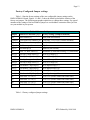
1
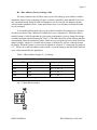
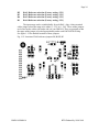
DM5414/DM6414
12-bit DAS-module
User's Manual
Real Time Devices Finland Oy
Hardware Release 2.0
Real Time Devices Finland Oy
Lepolantie 14
FIN-00660 Helsinki, Finland
Tel: (+358) 9 346 4538
Fax: (+358) 9 346 4539
Email: [email protected]
URL: www.rtdfinland.fi
DM5414/DM6414
RTD Finland Oy 1998-2001
ISO9001 and AS9100 Certified
Page 1
IMPORTANT
Although this information contained in this manual
has been carefully verified, RTD Finland Oy assumes
no responsibility for errors that may appear in this
manual, or for any damage to things or persons
resulting from improper use of this manual or of the
related software. RTD Finland Oy reserves the right
to change the contents and for of this manual, as
well as the features and specifications of this
product at any time, without notice.
Published by
Real Time Devices Finland Oy
Lepolantie 14
FIN-00660 Helsinki, Finland
Copyright © 1995/2001 by RTD Finland Oy
All rights reserved
Printed in Finland
DM5414/DM6414
RTD Finland Oy 1998-2001
Page 2
Table of Contents
===============================================================
INTRODUCTION
Analog-to-Digital conversion
Digital-to-Analog conversion
8254 Timer/Counter
Digital I/O
Mechanical description
Connector description
What comes with your board
Board accessories
Application software and drivers
Hardware accessories
Using this manual
When you need help
CHAPTER 1 - BOARD SETTINGS
Factory-Configured Jumper Settings
Base Address Jumpers
8254 Timer Counter Sources
Interrupt Channel select
External 5V Reference Type : Tracking (Ratiometric) / Absolute
D/A - converter range select (Channels 1,2 and 3,4)
D/A - converter channel polarity select (Channels 1,2 and 3,4)
Internal 2,5V / External Reference selection for A/D-converter
CHAPTER 2 - BOARD INSTALLATION
Board installation
External I/O connections
Primary 50-pin Analog Digital Expansion Connector
Secondary 50-pin Analog Digital Expansion Connector
Connecting the analog input pins
Connecting the analog outputs
Connecting the Timer/Counters and digital I/O
CHAPTER 3 - HARDWARE DESCRIPTION
A/D conversion circuitry
Reprint of LM12458 DAS-Chip datasheet
D/A conversion circuitry
Timer/Counters
Digital I/O, Advanced Bit Programmable Digital I/O
DM5414/DM6414
RTD Finland Oy 1998-2001
Page 3
CHAPTER 4 - BOARD OPERATION AND PROGRAMMING
Defining the I/O map
Onboard Peripherals
Base+20
Base+21
Base+22
Base+23
DAS chip enable
DAC chip enable/Load DAC's
Reserved
Software trigger
(write)
(write/read)
(write)
Overlay bit = 0
Base+24
Base+25
Base+26
Base+27
8254 Timer/Counter 0
8254 Timer/Counter 1
8254 Timer/Counter 2
8254 Timer/Counter Control byte
(write/read)
(write/read)
(write/read)
(write)
Overlay bit = 1
Base+24
Base+25
Base+26
Base+27
Port 0 Data
Port 1 Data
Port 0 Control byte
Digital Chip Control byte
(write/read)
(write/read)
(write/read)
(write)
Base+28
Base+29
Base+2A
Base+2B
DAC 1 Register
DAC 2 Register
DAC 3 Register
DAC 4 Register
(write)
(write)
(write)
(write)
Base+2C
Base+2D
Base+2E
Base+2F
Board Setup Register 1
Board Setup Register 2
16-bit digital I/O port
Reserved
(read)
(read)
(write/read)
DM5414/DM6414
RTD Finland Oy 1998-2001
Page 4
Each of the DAS Chips
RAM Pointer 00
Base+0
Instruction 0
Base+1
Parameter field for Instruction 0
Base+2
Instruction 1
Base+3
Parameter field for Instruction 1
Base+4
Instruction 2
Base+5
Parameter field for Instruction 2
.
Base+E
Instruction 15
Base+F
Parameter field for Instruction 15
RAM Pointer 01
Base+0
Base+1
Base+2
Base+3
.
Base+E
Base+F
1 Comparison Limit 0
1 Polarity of Comp intr/ Sign of Limit 0
1 Comparison Limit 1
1 Polarity of Comp intr/ Sign of Limit 1
1 Comparison Limit 15
1 Polarity of Comp intr/ Sign of Limit 15
RAM Pointer 10
Base+0
Base+1
Base+2
Base+3
.
Base+E
Base+F
2 Comparison Limit 0
2 Polarity of Comp intr/ Sign of Limit 0
2 Comparison Limit 1
2 Polarity of Comp intr/ Sign of Limit 1
Base+10
Base+11
Base+12
Base+13
Base+14
Base+15
Base+16
Base+17
Base+18
Base+19
Base+1A
Base+1B
DAS Configuration Register 1
DAS Configuration Register 2
DAS Interrupt mask Register 1
DAS Interrupt mask Register 2
DAS Interrupt Enable Register 1
DAS Interrupt Enable Register 2
DAS Timer Register 1
DAS Timer Register 2
DAS Conversion FIFO low Byte
DAS Conversion FIFO high Byte
DAS Limit 1 Status Register
DAS Limit 2 Status Register
DM5414/DM6414
2 Comparison Limit 15
2 Polarity of Comp intr/ Sign of Limit 15
RTD Finland Oy 1998-2001
Page 5
Programming the DM5414
Clearing and setting bits in a port
A/D conversions
Interrupts
What is an interrupt?
Interrupt request lines
8259 Programmable interrupt controller
Interrupt mask register (IMR)
End-Of-Interrupt (EOI) Command
What exactly happens when an interrupt occurs?
Using interrupts in your program
Writing an interrupt service routine (ISR)
Saving the startup IMR and interrupt vector
Common Interrupt mistakes
D/A Conversions
Timer/Counters
Digital I/O
APPENDIX A
DM5414/DM6414
DM5414/DM6414 Specifications
RTD Finland Oy 1998-2001
Page 6
List of Illustrations
===============================================================
DM5414/DM6414
RTD Finland Oy 1998-2001
Page 7
INTRODUCTION
===============================================================
DM5414/DM6414
RTD Finland Oy 1998-2001
Page 8
The DM6414 analog digital dataModule® will turn your PC/104 cpuModule™ or
other PC/104 computer into a low power multifunction high performance data acquisition and
control system. This user's manual describes the operation of the DM5414/DM6414 PC/104
Analog/Digital Interface board.
Some of the key properties of the DM5414/DM6414 include:
* 32 single ended or 16 differential analog input channels
* 4 independent 12-bit low power A/D chips with 87 ksample throughput
* 0-2.5V or 0-5V input ranges
* Each A/D chip features:
Data acquisition sequencer
32 sample conversion FIFO
16-bit Data acquisition timer
Window comparators
Auto calibration
* Software enabled interrupts
* SYNC in and SYNC out for parallel sampling of up to 4 channels per board
* 16 Digital I/O: 8 bit programmable direction, 8 port programmable direction
* 16 Digital I/O: latched 8 Out, 8 in
* Three 8254 based 16 bit Timer/Counters free for the user
* Four 12-bit D/A channels with dedicated grounds
* ±5V, ±10V, 0 − 5V, 0 − 10V Volt output ranges
* Single +5V operation
* Support for direct PC/104 interface with all RTD dataModules™ and front end boards.
* PC/104 compliant form factor
* DM5414 is XT bus, DM6414 is AT bus version
* RTD IDAN frame compatible
The following paragraphs briefly describe the major features of the DM5414. A more
detailed discussion is included in Chapter 3 (Hardware description) and in Chapter 4 (Board
operation and programming. The board setup is described in Chapter 1 (Board Settings).
Analog-to-Digital Conversion
The Analog-to-Digital circuitry consists of 4 independent 12-bit + sign integrated
A/D-converters. These converters function independently of each other and can have different
setups, acquisition speeds and input ranges. The analog input channels are divided between
two 50-pin expansion connectors. Channels 1-16 are located on the "Primary" connector (J3) ;
channels 17-32 are located on the "Secondary" connector (J4). The analog input channels
are dedicated to the 4 A/D converter chips called DAS1, DAS2, DAS3, DAS4.
DAS1
DAS2
DAS3
DAS4
DM5414/DM6414
Channels 1-8
Channels 9-16
Channels 17-24
Channels 25-32
RTD Finland Oy 1998-2001
Page 9
Any two channels on one DAS chip can be configured for a differential input configuration. This means Channels 1 and 31 cannot work together in differential mode , but 1 and 5
can.The input voltage ranges 0-2.5V and 0-5V can be selected for each DAS-chip. This setup
is done using "solder shorts" on the bottom side of the board (see Fig. 1-12). The 5V reference
can be selected with jumpers from two sources: 1) A 5,0V absolute reference or 2) The analog
5V supply of the chip. Option 2 will provide ratiometric operation of the DAS-chips. The 5V
source selection is global for all the DAS-chips (see Fig. 1-7).
The onboard DAS-chips can be software programmed for different resolutions: These
include: 9 or 12 bit + sign conversions. 9 bit conversions are much faster than 12 bit conversions.
The maximum conversion time for 9 bits is 4.2µ s and for 13 bits 8.8µ s maximum. The typical
throughput rate at 12 bits + sign is 100k samples / second.
Conversions are controlled by the Data acquisitions sequencers on the DAS-chips.
Each conversion can be configured independently and the sequencer program runs automatically
sampling data into the onchip FIFO's with no CPU interference. Conversion parameters include
window comparator monitoring, conversion resolution, acquisition delay etc. The features
available for controlling each conversion in random order provides very powerful data acquisition
performance.
The converted data can be transferred to PC-memory in two ways. Data can be transferred
using the programmed I/O mode or the interrupt mode. A special Interrupt mode using the REP
INS (Repeat Input String) instruction supports very fast throughput rates. By generating an
interrupt when the FIFO is half full, a REP INS instruction can be executed, transferring data to
the PC memory and emptying the DAS FIFO at maximum rate allowed on the data bus. The
mode of transfer is selected from software.
Digital-to-Analog Conversions
The Digial-to Analog (D/A) circuitry features four independent 12-bit analog output
channles with jumper selectable output ranges of 0V to 5V, 0V to 10V, ± 5V, ± 10V. Data is
programmed into the D/A converter by writing two 8 bit bytes, the LSB and the MSB. The LSB
contains the lower 8 data bits (0..7) and the MSB contains the higher data bits (8..11). The D/A
converter latches can be loaded (updated) in parallel with a "Load" command.
DM5414/DM6414
RTD Finland Oy 1998-2001
Page 10
8254 Timer/Counters
One 8254 programmable Timer/Counter provides three independent 16-bit timer counters,
to support a wide range of timing and counting functions. The source for the timer/counters can
be the onboard 8 MHz clock or an external oscillator. The timers T0 and T1 can be cascaded to
generate a synchronizing signal to clock all the DAS-chips in parallel, or the output of these
timers can be connected to an external IRQ-line. The 8254 timer / counter is not needed to set
the acquisition speed of the DAS-chips since they have internal 16-bit timer counters to do this.
Digital I/O
The DM5414 has 16 latched TTL/CMOS general purpose digital I/O available in the
secondary expansion connector J4. These ports have 8 outputs in "port C "- lines and 8 inputs in
"port A"- lines. The input port has onboard 47K pulldown resistors. These ports are not bit
addressable.
16 buffered TTL/CMOS lines are also available grouped as eight independent, bit
programmable lines in Port 0, and an 8-bit programmable port at Port 1. The bit-programmable
lines support RTD's two Advanced Digital Interrupt modes. An interrupt flag can be set when any
bit changes value (event interrupt) or when the lines match a programmed value (match interrupt).
For either mode masking can be used to monitor selected lines. Port 0 is pulled low with 47K
pulldown resistors.
Mechanical description
The DM5414 is designed on a PC/104 form factor. An easy mechanical interface to both
PC/104 and EUROCARD systems can be achieved. Stack your PC/104 compatible computer
directly on the DM5414 using the onboard mounting holes. DM5414 is XT bus, DM6414 is an
AT bus board version. The DM6414 also can be installed in the RTD IDAN modular aluminium
enclosure system either in a single or double high frame.
Connector description
There are two 50 pin analog/digital interface connectors on the DM5414 to directly
interface to I/O signals. The signal definition of these connectors is compatible with the analogdigital PC/104 dataModules™ manufactured by RTD.
DM5414/DM6414
RTD Finland Oy 1998-2001
Page 11
What comes with your board
You receive the following items in your DM5414 package:
* DM5414 interface module with stackthrough bus connector
* Software and diagnostics diskette with C source code
* User's manual
If any item is missing or damaged, please call Real Time Devices Finland Customer
Service Department at (+358) 9 346 4538.
Board accessories
In addition to the items included in your DM5414 delivery several software and
hardware accessories are available. Call your distributor for more information on these
accessories and for help in choosing the best items to support your instrumentation system.
* Application programs and drivers
* Hardware accessories
Real Time Devices can supply a complete set of accessories to your DM5414/DM6414
card. These include IDAN enclosures, power supplies, signal conditioning modules, terminal
boards and other interconnection systems.
Using this manual
This manual is intended to help you install your new DM5414 card and get it running
quickly, while also providing enough detail about the board and it's functions so that you can
enjoy maximum use of it's features even in the most demanding applications. We assume you
already have an understanding of basic data acquisition principles.
When you need help
This manual and all the example programs will provide you with enough information to
fully utilize all the features on this board. If you have any problems installing or using this board,
contact our Technical Support Department (+358) 9 346 4538 during European business hours,
or send a FAX requesting assistance to (+358) 9 346 4539. When sending a FAX request, please
include your company's name and address, your name, your telephone number, and a brief
description of the problem.
DM5414/DM6414
RTD Finland Oy 1998-2001
Page 12
CHAPTER 1 - BOARD SETTINGS
===============================================================
The DM5414 have jumper settings you can change if necessary to suit your
application. The module is factory-configured as listed in the table and shown on the
layout diagram in the beginning of this chapter. Should you need to change the module
settings, use these easy-to-follow instructions before you stack your module into your
PC/104 system.
DM5414/DM6414
RTD Finland Oy 1998-2001
Page 13
Factory-Configured Jumper settings
Table 1-1 lists the factory settings of the user configurable jumper settings on the
DM5414/DM6414 board. Figures 1-1 and 1-2 show the board layout and the location of the
factory-set jumpers. The following paragraphs explain how to change these settings. Pay special
attention to the settings of the base address jumpers to avoid address contention when you first
use your module in your system.
Table 1-1 Factory Settings
Jumper
Function Controlled (jmp#)
Factory Settings (Jumpers installed)
BA
Base Address (2)
1A0h (both not installed)
TIMERS Clock source for counters (11) CNT0 OSC, CNT1 OT0, (Timers cascaded)
IRQ #1
Timer/Counter Interrupt (4)
Disabled (Not selected)
IRQ #2
DAS Interrupt (4)
IRQ 5
IRQ #3
PPI Interrupt (4)
Disabled (Not selected)
B2
DAS +5V REF source (1)
Ratiometric (Connected to analog 5V, solder blob)
DA1_R
DA-chip 1 range select (2)
Set to 10V range (J7)
DA2_R
DA-chip 2 range select (2)
Set to 10V range (J8)
DA3_R
DA-chip 3 range select (2)
Set to 10V range (J5)
DA4_R
DA-chip 4 range select (2)
Set to 10V range (J6)
DA1_P
DA-channel 1 Bip/Unip (2)
Set to bipolar range (J7)
DA2_P
DA-channel 2 Bip/Unip (2)
Set to bipolar range (J8)
DA3_P
DA-channel 3 Bip/Unip (2)
Set to bipolar range (J5)
DA4_P
DA-channel 4 Bip/Unip (2)
Set to bipolar range (J6)
B5
DAS1 REF 2.5/5.0 (3)
Set to 2.5V (Solder connection bottom side)
B3
DAS2 REF 2.5/5.0 (3)
Set to 2.5V (Solder connection bottom side)
B6
DAS3 REF 2.5/5.0 (3)
Set to 2.5V (Solder connection bottom side)
B1
DAS4 REF 2.5/5.0 (3)
Set to 2.5V (Solder connection bottom side)
Table 1-1 Factory configured jumper settings
DM5414/DM6414
RTD Finland Oy 1998-2001
Page 14
Fig 1-1 DM6414 Board Layout showing Factory-Configured settings
DM5414/DM6414
RTD Finland Oy 1998-2001
Page 15
This page is left intentionally blank
DM5414/DM6414
RTD Finland Oy 1998-2001
Page 16
BA - Base Address (Factory Setting: 1A0h)
The most common cause of failure when you are first setting up your module is address
contention. Some of your computers I/O space is already occupied by other internal I/O devices
and expansion boards. When the DM5414 attempts to use it's reserved I/O addresses already
used by another peripheral device, erratic performance may occur and data read from the board
may be corrupted.
To avoid this problem make sure you set up the base address first using the two jumpers
which let you choose from 4 different I/O addresses in your computers I/O. Should the factory
installed setting of 1A0h be unusable for your system configuration, you may change this setting
to another using the options illustrated in Table 1-2. The table shows the switch settings and their
corresponding values in hexadecimal values. Make sure you verify the correct location of the base
address jumpers. Jumper #3 is located below jumper #4 with the PC/104 bus connector toward
the bottom. When the jumper is removed it corresponds to a logical "0", connecting the jumper to
a "1". When you set the base address of the module, record the setting in the table inside the back
cover of this manual after the Appendices.
Table 1-2 Base Address Jumper #3 , #4 settings
Table 1-2 Base Address Jumpers
Address in HEX
Address in Decimal
Jumpers
1A0h
416d
X3 = 0 , X4 = 0
280h
640d
X3 = 1 , X4 = 0
300h
768d
X3 = 0 , X4 = 1
380h
896d
X3 = 1 , X4 = 1
0 = Jumper removed, 1 = Jumper closed
Fig. 1-3 Base address jumpers
DM5414/DM6414
RTD Finland Oy 1998-2001
Page 17
TIMERS
Clock sources for Timer /Counters
(Factory settings: CLK0-OSC,CLK1-OT0,CLK2-OT2)
The jumpers shown in figure 1-4, let you select the clock sources for the 8254 based
timer/counters, TC0, TC1, and TC2. The factory setting cascades all the three counter/timers,
with the clock source for TC0 being the onboard 8 MHz oscillator, the output of TC0 providing
the clock for TC1, and the output of TC1 providing the clock for TC2. You can connect TC0
and TC2 clock sources to an external clock through the "Primary" external I/O-expansion
connector J3 or you can set TC0 and TC2 to be clocked by the onboard 8 MHz oscillator. Fig.
1-5 shows a block diagram of the counter/timer circuitry to help you with these connections.
The SYNC jumper field connects the source for the SYNC pins of the AD converter chips.
All the SYNC pins of the AD converters are connected together and selected with this jumper
field
NOTE: When installing jumpers on this header, make sure that only one jumper is
installed in each group of the CLK pins.
Fig. 1-4 8254 Counter/Timer Clock Source Jumpers, Labels are not present on
the board due to lack of space.
DM5414/DM6414
RTD Finland Oy 1998-2001
Page 18
Fig 1-5 User Timer/Counter Circuit diagram
IRQ#1
Timer Interrupt Channel select
(Factory settings: Interrupt Channel Disabled)
IRQ#2
DAS Interrupt Channel select
(Factory settings: Interrupt #5)
IRQ#3
Timer Interrupt Channel select
(Factory settings: Interrupt Channel Disabled)
The header connectors shown in Figure 1-6, lets you connect the output of board interrupt
sources to an interrupt channel. To activate a channel, you must install a jumper vertically across
the desired IRQ channel's pins.
To determine which DAS-chip has caused an interrupt and on what condition , you must
read the interrupt status registers (BASE+14 and BASE+15) of each DAS chip with enabled
interrupts. Reading these registers will clear all interrupt flags of the interrupt status register of
the DAS-chip. All the 4 DAS-chips are connected together to one external interrupt request line
with (positive) OR-logic. If any of the 4 chips has a active interrupt condition it's interrupt request
line will keep the global DAS-IRQ line active. This also means any of the chips may assert the
interrupt request. If you have enabled interrupts on multiple chips, you must read the interrupt
status registers of all the chips with enabled interrupts when a DAS- interrupt occurs. Failure to
DM5414/DM6414
RTD Finland Oy 1998-2001
Page 19
do so may keep the interrupt request line active (high) because one of the DAS chips may still
have a pending (non-serviced) interrupt condition.
Note: The IRQ lines are grouped as follows from left to right:
IRQ11, IRQ10, IRQ7, IRQ5
Fig. 1-6 Interrupt line factory setting, DAS interrupt set at IRQ5.
Other interrupts are disabled.
REF
DAS +5V Reference source selection
(Factory settings: Ratiometric)
The DAS chips 5V input voltage range can use two reference techniques:
1. Absolute reference, where a precision 5,00V reference is used at the Vref+
and GND to Vref-.
2. Ratiometric reference, where the analog supply (5V) is connected to the Vref+
and GND to Vref-.
In ratiometric systems, the analog input voltage is proportional to the one used for
the A/D - converters reference voltage. When this is the system analog power supply,
it relaxes the system reference requirements since the analog input voltage and the
A/D - converter reference voltage change together. This maintains the same input
code for the same conditions.
DM5414/DM6414
RTD Finland Oy 1998-2001
Page 20
Figure 1-7 shows the 5V reference source selection solder blob B2. This setting is
global for all the DAS-chips. And set to ratiometric factory installed.
D/A - converter range select (Channels 1,2 and 3,4)
DA1_R
DA2_R
DA3_R
DA4_R
DA-chip 1 range select
DA-chip 2 range select
DA-chip 3 range select
DA-chip 4 range select
DA1_R
DA2_R
D/A-converter Range selection (Factory settings: 10V)
D/A-converter Range selection (Factory settings: 10V)
The jumper field J7 configures D/A channel #1 while J8 configures channel #2.
These jumper blocks are located next to the primary expansion connector J3. Figure 1-8
illustrates the range jumper for D/A - channels 1 and 2.
Figure 1-8a Range jumper for D/A - channels #1 and #2 set for 10V range.
DM5414/DM6414
RTD Finland Oy 1998-2001
Page 21
Figure 1-8b Range jumper for D/A - channels #1 and #2 set for 5V range.
DA3_R
DA4_R
D/A-converter Range selection (Factory settings: 10V)
D/A-converter Range selection (Factory settings: 10V)
The jumper field J5 configures D/A channel #3 while J6 configures channel #4.
These jumper blocks are located next to the primary expansion connector J4. Figure 1-9
illustrates the range jumper for D/A - channels 3 and 4.
Figure 1-9a Range jumper for D/A - channels #3 and #4 set for 10V range.
DM5414/DM6414
RTD Finland Oy 1998-2001
Page 22
Figure 1-9b Range jumper for D/A - channels #3 and #4 set for 5V range.
D/A - converter channel polarity select (Channels 1,2 and 3,4)
DA1_P
DA2_P
DA3_P
DA4_P
DA-channel 1 Bip/Unip
DA-channel 2 Bip/Unip
DA-channel 3 Bip/Unip
DA-channel 4 Bip/Unip
DA1_P
DA2_P
D/A-converter channel 1 Polarity selection (Factory setting: bipolar)
D/A-converter channel 2 Polarity selection (Factory setting: bipolar)
The jumpers in jumper fields J7 and J8 select the polarity of the D/A converter channels
1 and 2. Available selections are unipolar or bipolar. For example if you have selected
the range to be 10V and you set the polarity to bipolar you will achieve a -10V to +10V
output range. Similarly if your range is set to 5V and you select unipolar you have a
0 to 5V output range.
Figure 1-10a Bipolar operation on D/A channels 1 and 2.
Figure 1-10b Unipolar operation on D/A channels 1 and 2
DM5414/DM6414
RTD Finland Oy 1998-2001
Page 23
DA3_P
DA4_P
D/A-converter channel 3 Polarity selection (Factory setting: bipolar)
D/A-converter channel 4 Polarity selection (Factory setting: bipolar)
The jumpers in jumper fields J5 and J6 select the polarity of the D/A converter channels
3 and 4. Available selections are unipolar or bipolar. For example if you have selected
the range to be 10V and you set the polarity to bipolar you will achieve a -10V to +10V
output range. Similarly if your range is set to 5V and you select unipolar you have a
0 to 5V output range.
Figure 1-11a Bipolar operation on D/A channels 3 and 4.
Figure 1-11b Unipolar operation on D/A channels 3 and 4
DM5414/DM6414
RTD Finland Oy 1998-2001
Page 24
B5
B3
B6
B1
DAS1 Reference selection (Factory setting: 2.5V)
DAS2 Reference selection (Factory setting: 2.5V)
DAS3 Reference selection (Factory setting: 2.5V)
DAS4 Reference selection (Factory setting: 2.5V)
The input range can be set individually for each DAS - chip. A three terminal
solder jumper selects the range to be either 0 - 2.5V or 0 - 5.0V. These solder jumpers
are located on the solder side (under side) of your DM5414. They are grouped so that
the range solder jumper is located approximately under each LM12458 DAS-chip.
See figure 1-12 for detailed locations of these jumpers.
Fig. 1-12 Location of DAS reference jumpers B1,B6,B3,B5
DM5414/DM6414
RTD Finland Oy 1998-2001
Page 25
This page is left intentionally blank
DM5414/DM6414
RTD Finland Oy 1998-2001
Page 26
CHAPTER 2 - BOARD INSTALLATION
==============================================================
The DM5414/DM6414 is easy to install in your cpuModule™ of other PC/104 based
system. This chapter tells you step-by-step how to connect your module into your stack.
After you have made all of your connections, you can turn on your computer and run
the diagnostic and test software to verify that your module is working.
DM5414/DM6414
RTD Finland Oy 1998-2001
Page 27
Board installation
Keep your board in its antistatic bag until you are ready to install it to your system!
When removing it from the bag, hold the board at the edges and do not touch the components
or connectors. Please handle the board in an antistatic environment and use a grounded
workbench for testing and handling of your hardware.
Before installing the board in your computer, check the jumper settings. Chapter 1
reviews the factory settings and how to change them. If you need to change any settings,
refer to the appropriate instructions in Chapter 1. Note that incompatible jumper settings
can result in unpredictable board operation and erratic response.
General installation guidelines:
1. Turn OFF the power to your computer
2. Touch the grounded metal housing of your computer to discharge any
antistatic buildup and then remove the board from its antistatic bag.
3. Select the appropriate standoffs for your application to secure the module
when you install it in your system.
4. Holding the module by it's edges, orient it so that the PC/104 bus connector
pin 1 lines up with pin 1 of the expansion connector onto which you are installing
the module.
5. After carefully positioning the module so that the card edge connector is resting
on the expansion connector, gently and evenly press down on the module until it
is secured on the connector.
Note: Do NOT force the module onto the connector. If the module does not slide into
place remove it and try again. Wiggling the module or exerting too much pressure on
the module can result in damage to the DM5414 or other boards in the stack.
6. After the module is installed, connect the cable or cables to the analog expansion
connectors J3 and J4. When making this connection , note that pin one is marked
with a square on the top side of the board. For twisted pair cables, pin 1 is the dark
brown wire; for standard 50 flat cables pin one is often marked in red.
7. Make sure all connections are secure.
DM5414/DM6414
RTD Finland Oy 1998-2001
Page 28
Fig. 2-1 DM5414 integrated with a PC/104 dataModule™ stack
3U rack or enclosure installation with a EUROCARD CPU with one DM5414.
The PC/104 system can easily be inserted into a 19" rack installation using the CPU as
a "form factor adapter". Assemble your PC/104 dataModules™ on a RTD single board
EUROCARD computer and install the system in a 19" enclosure. Multiple DM5414
boards can easily be connected to this system. See figure 2-2 for installation ideas.
Fig. 2-2 19" Eurocard rack installation with an integrated PC/104 dataModule™
and EUROCARD cpuModule™ computer system
DM5414/DM6414
RTD Finland Oy 1998-2001
Page 29
External I/O connections
Primary 50 Pin Analog Digital Expansion Connector
Figure 2-3 shows the DM5414 's J3 primary I/O connector pinout. Figure 2-4 shows
the DM5414 's J4 secondary I/O connector pinout. Refer to these diagrams when you are
making I/O connections. Note that +12V at pins #47 and -12V at pins #49 are only available if
your system bus supplies these voltages. These voltages are not generated by the DM5414.
AIN1
AIN2
AIN3
AIN4
AIN5
AIN6
AIN7
AIN8
AOUT1
AOUT2
AGND
PA7
PA6
PA5
PA4
PA3
PA2
PA1
PA0
TRIGGER IN
EXT GATE 1
SYNC IN/OUT
EXT CLOCK
+12V (VCC)
-12V (VSS)
*1
*3
*5
*7
*9
*11
*13
*15
*17
*19
*21
*23
*25
*27
*29
*31
*33
*35
*37
*39
*41
*43
*45
*47
*49
*2
*4
*6
*8
*10
*12
*14
*16
*18
*20
*22
*24
*26
*28
*30
*32
*34
*36
*38
*40
*42
*44
*46
*48
*50
AIN9
AIN10
AIN11
AIN12
AIN13
AIN14
AIN15
AIN16
AGND
AGND
AGND
PC7
PC6
PC5
PC4
PC3
PC2
PC1
PC0
DGND
T/C OUT 1
T/C OUT 2
EXT GATE 2
+5V
DGND
Fig. 2-3 Primary expansion connector pinout J3
NOTE:
Digital I/O ports PC[0..7] are port programmable inputs or outputs and
are derived from the advanced Digital Interface Chip. Port PA[0..7] is bit programmable
and has Advanced Masking Modes. Please refer to the more detailed discussion on the
functionality of the digital I/O in Chapter 3.
DM5414/DM6414
RTD Finland Oy 1998-2001
Page 30
Secondary 50 Pin Analog Digital Expansion Connector
AIN17
AIN18
AIN19
AIN20
AIN21
AIN22
AIN23
AIN24
AOUT3
AOUT4
AGND
IN7
IN6
IN5
IN4
IN3
IN2
IN1
IN0
EXT_SYNC IN
EXT GATE 1
SYNC IN/OUT
EXT CLOCK
+12V (VCC)
-12V (VSS)
*1
*3
*5
*7
*9
*11
*13
*15
*17
*19
*21
*23
*25
*27
*29
*31
*33
*35
*37
*39
*41
*43
*45
*47
*49
*2
*4
*6
*8
*10
*12
*14
*16
*18
*20
*22
*24
*26
*28
*30
*32
*34
*36
*38
*40
*42
*44
*46
*48
*50
AIN25
AIN26
AIN27
AIN28
AIN29
AIN30
AIN31
AIN32
AGND
AGND
AGND
OUT7
OUT6
OUT5
OUT4
OUT3
OUT2
OUT1
OUT0
DGND
T/C OUT 1
T/C OUT 2
EXT GATE 2
+5V
DGND
Fig. 2-4 Secondary expansion connector pinout J4
DM5414/DM6414
RTD Finland Oy 1998-2001
Page 31
Connecting the analog inputs
The analog inputs on this module can be set for single ended or differential operation. All
channels can be configured to work in a differential mode, but only those channels that are
grouped to one DAS chip can be differential i.e.. channels 1-8, 9-16, 16-24 and channels
25-32.
Single ended When the input channels are configured for single ended operation,
connect the high side of the signal to one of the analog input channels, AIN1 - AIN32.
Figure 2-5 shows how these connections are made.
Differential When operating in this mode, your signal source may or may not have a
separate ground reference. First connect the high side of the analog signal to the selected
analog input channel of the channel group you are using (see above), and connect the low
side of the signal to another analog input channel of the channel group you are using.
Then, for signal sources with a separate ground reference, connect the ground from the
signal source to one of the analog ground pins on the expansion connector you are using.
Figure 2-6 shows how these connections are made.
DM5414/DM6414
RTD Finland Oy 1998-2001
Page 32
Fig. 2-7 Differential Input Connection
DM5414/DM6414
RTD Finland Oy 1998-2001
Page 33
Connecting the Analog Outputs
For each of the four analog outputs, connect the high side of the device receiving
the output to the AOUT channel (J3-17, J3-19, J4-17, J4-19) and connect the low side of the
device to an ANALOG GROUND (J3-18, J3-20, J4-18, J4-20).
Connecting the Timer/Counters and Digital I/O
For all these connections, the high side of the signals are connected to the appropriate
signal pin on either the primary I/O connector J3 or the Secondary I/O connector J4. The low
side of the signal shall be connected to any digital ground (GND).
DM5414/DM6414
RTD Finland Oy 1998-2001
Page 34
CHAPTER 3 - HARDWARE DESCRIPTION
==============================================================
This Chapter describes the features of the DM5414 hardware. The major circuits
are the A/D-chips, the D/A converters, 8254-timer/counter, the digital I/O and the Advanced
Bit Programmable Digital I/O.
DM5414/DM6414
RTD Finland Oy 1998-2001
Page 35
The DM5414 has five major circuits, the four DAS-chips, the D/A-converter circuits,
the 8254 timer/counter, the 8+8 general purpose digital I/O an the Advanced Bit Programmable
Digital I/O. This chapter describes the hardware which makes up the major circuits. Figure
3-1 shows a general block diagram of the DM5414.
Fig. 3-1 DM5414 Block Diagram
A/D Conversion Circuitry
The DM5414 can interface to 32 single ended or 16 differential input channels with
a 0-2,5V or 0-5,0V input range. The conversion resolution and conversion rate are fully
software configurable. The DM5414 is designed using the highly integrated LM12458 low
power DAS-chip.
The A/D-chips are very flexible to program. The programming of the chips as well
as the hardware description of the A/D-chips is published as a datasheet reprint of the
LM12458 chips. Programming these chips is discussed in detail in Chapter 4, Module Operation
and Programming.
DM5414/DM6414
RTD Finland Oy 1998-2001
Page 36
Reprint of LM12458 DAS-Chip datasheet
DM5414/DM6414
RTD Finland Oy 1998-2001
Page 37
D/A Conversion Circuitry
Four 12-bit analog outputs are included on the DM5414. These four channels are
grouped as follows: Channels 1 and 2 are located in the primary connector, Channels 3 and 4
are located in the secondary connector. Each of the channel pairs can have independent range
settings. Each of the four channels can be set for bipolar or unipolar operation in the selected
range. The 10 volt ranges have a resolution of 2,44 millivolts and the 5 volt range has a
resolution of 1,22 millivolts.
Timer/Counters
An 8254 programmable interval timer provides three 16-bit, 8-Mhz timer / counters to
support a wide range of timing and counting functions. Two of the timer/counters TC0 and TC1,
are cascaded so that they can be used for the pacer clock. The pacer clock is described in
Chapter 4. Note, that each DAS-chip can use it's internal counter as a pacer clock freeing
counter/timers TC0 and TC1 for user applications. Timer TC2 is always free for the user. The
timers have different options for clock sources as well as gate signals. Figure 3-2 shows the
timer counter circuitry of the DM5414.
Fig. 3-2 8254 Timer/Counter Circuit Block Diagram
DM5414/DM6414
RTD Finland Oy 1998-2001
Page 38
Each Timer/Counter has two inputs, CLK in and GATE in, and one output, timer/counter
OUT. They can be programmed as binary or BCD down counters by writing the appropriate data
to the command word, as described in Chapter 4. The command word also lets you set up the
different modes of operation. The six programmable modes are:
Mode 0
Mode 1
Mode 2
Mode 3
Mode 4
Mode 5
Event Counter (Interrupt on Terminal Count)
Hardware-Retriggerable one-shot
Rate Generator
Square Wave Mode
Software-Triggered Strobe
Hardware Triggered Strobe (Retriggerable)
Digital I/O, Advanced Bit Programmable Digital I/O
Two separate digital I/O ports are available on the DM5414. The primary digital
I/O port consists of an 8-bit port programmable port and an 8-bit bit programmable port.
Each bit can be programmed independently to be input or output in this port. All the bit
programmable I/O lines are pulled down with a 10kohm resistor. The primary digital I/O
port is located in the primary Analog Digital I/O expansion connector J3.
The secondary general purpose digital I/O port has 8 latched TTL/CMOS compatible
outputs and 8 TTL/CMOS compatible inputs with 10kohm pulldown resistors. The direction
and configuration of the general purpose digital I/O-port is fixed to 8 outputs and 8 inputs. The
secondary digital I/O port is located in the secondary Analog Digital I/O expansion connector J4.
The internal Advanced Modes of the bit Programmable digital I/O port are discussed
in detail in Chapter 4.
DM5414/DM6414
RTD Finland Oy 1998-2001
Page 39
CHAPTER 4 - BOARD OPERATION AND PROGRAMMING
==============================================================
This chapter explains the I/O map of the DM5414 in detail and shows how
to program the onboard peripherals such as the LM12458 DAS-chips, the 8254 Timer
and the Digital I/O.
DM5414/DM6414
RTD Finland Oy 1998-2001
Page 40
Defining the I/O Map
The I/O map of the DM5414 is shown in Tables 4-1 and 4-2. As shown the board
occupies 48 consecutive I/O addresses.
To conserve the use of I/O space, the structure of the I/O map is such that some of
the registers control what peripherals are accessed in other addresses. The control registers at
addresses BA+20 and BA+21 select the active DAS- or D/A-chips and select either the
8254 timer of the Advanced Bit Programmable Digital I/O-chip. These functions can easily
be understood by reviewing the following pages.
The Base Address (designated as BA) can be selected by the two base address jumpers
as described in Chapter 1, Module Settings. These jumpers can be changed without removing
the module from the PC/104 stack. The following sections describe the register contents of each
address used in the I/O map.
Table 4-2 shows the I/O address locations for each DAS chip. The active DAS chip is
selected with the DAS selection register located in address BA+20.
DM5414/DM6414
RTD Finland Oy 1998-2001
Page 41
Table 4-1 DM5414 I/O Map Other Peripherals
Address
Description #1
Description #2
BA+20
Write only
DAS-chip selection register
BA+21
Read/Write
Rd->Load DACs, Wr-> DAC-chip select , Overlay bit
BA+22
Reserved
Reserved
BA+23
Write
Software trigger
BA+24
Read/Write
8254 Timer/Counter 0
BA+25
Read/Write
8254 Timer/Counter 1
BA+26
Read/Write
8254 Timer/Counter 2
BA+27
Write only
8254 Control byte
BA+24
Read/Write
Port 0 Data register
BA+25
Read/Write
Port 1 Data register
BA+26
Read/Write
Port 0 Control Byte
BA+27
Write only
Digital I/O-chip Control byte
BA+28
Write only
DAC #1 Register
BA+29
Write only
DAC #1 Register
BA+2A
Write only
DAC #1 Register
BA+2B
Write only
DAC #1 Register
BA+2C
Read only
Board setup register #1
BA+2D
Read only
Board setup register #2
BA+2E
Read/Write
Digital I/O (Connector J4)
BA+2F
Reserved
Reserved
Overlay = 0
Overlay = 1
BA = Base Address , Overlay bit is bit 2 in address BA+21
DM5414/DM6414
RTD Finland Oy 1998-2001
Page 42
Table 4-1 DM5414 I/O Map DAS-chips
Address
Description #1
Description #2
BA+0
RAM Pointer 00 (Program)
Sequencer Instruction #0
BA+1 ...
-"-
Parameter field for Instruction #0
BA+E
-"-
Sequencer Instruction #15
BA+F
-"-
Parameter field for Instruction #15
BA+0
RAM Pointer 01 (Cmp. low limit) Comparison low limit #0
BA+1 ...
-"-
Polarity of Cmp. intr/sign of low limit #0
BA+E
-"-
Comparison low limit#15
BA+F
-"-
Polarity of Cmp. intr/sign of low limit #15
BA+0
RAM Pointer 10 (Cmp. high limit) Comparison high limit #0
BA+1 ...
-"-
Polarity of Cmp. intr/sign of high limit #0
BA+E
-"-
Comparison high limit #15
BA+F
-"-
Polarity of Cmp. intr/sign of high limit #15
BA+10
Read/Write
DAS Configuration Register #1
BA+11
Read/Write
DAS Configuration Register #2
BA+12
Read/Write
DAS Interrupt Enable Register #1
BA+13
Read/Write
DAS Interrupt Enable Register #2
BA+14
Read/Write
DAS Interrupt Status Register #1
BA+15
Read/Write
DAS Interrupt Status Register #2
BA+16
Read/Write
DAS Acquisition Timer Register #1
BA+17
Read/Write
DAS Acquisition Timer Register #2
BA+18
Read/Write
DAS Conversion FIFO low byte
BA+19
Read/Write
DAS Conversion FIFO high byte
BA+1A
Read/Write
DAS low Limit Status Register
BA+1B
Read/Write
DAS high Limit Status Register
Identical I/O addressing for each DAS-chip, Chip selected in cnf. register BA+20
DM5414/DM6414
RTD Finland Oy 1998-2001
Page 43
DM5414 I/O Map Other Peripherals
BA+20 DAS-chip selection register
D3
D2
D1
D0
Write
Register bits
DAS-selected "1"
DAS1 DAS0
DAS3 DAS2
BA+21 DAC control register
D2
D1
D0
Write
Register bits
DAC Select "1"
Overlay "1" -> Dig. I/O
DAC1 DAC0 Overlay "0" -> Timer
OVERLAY
BA+21 DAC control register
Read
Performing a read to this address will load the D/A converters with the
output data written to the D/A-output registers.
DM5414/DM6414
RTD Finland Oy 1998-2001
Page 44
This page is left intentionally blank
DM5414/DM6414
RTD Finland Oy 1998-2001
Page 45
Overlay Bit = 0
BA+24
8254 Timer/Counter 0 Write/Read
A read to this address shows the current contents of the timer T0. A write to this address
reloads a new value to the timer. Counting begins as soon as the timer has bee loaded.
This timer is cascaded with timer T1 to form the 32-bit pacer clock on the DM5414.
BA+25
8254 Timer/Counter 1 Write/Read
A read to this address shows the current contents of the timer T1. A write to this address
reloads a new value to the timer. Counting begins as soon as the timer has bee loaded.
This timer is cascaded with timer T0 to form the 32-bit pacer clock on the DM5414.
BA+26
8254 Timer/Counter 2 Write/Read
A read to this address shows the current contents of the timer T0. A write to this address
reloads a new value to the timer. Counting begins as soon as the timer has bee loaded.
This timer is cascaded with timer T0 and T1 or used independently. The output of this
timer may be connected to the external trigger input of the DM5414.
BA+27
D7
8254 Control word
D6
D5
D4
D3
Write only
D2
D1
D0
BCD/BIN
0-BINARY
1-BCD
COUNTER MODE
READ/LOAD
COUNT SEL.
00-counter0
01-counter1
10-counter2
11-readback
DM5414/DM6414
00-Latching
01-RD/LD LSB only
10-RD/LD MSB only
11-RD/LD LSB+MSB
000-Mode0, event count
001-Mode1, programmable 1-shot
010-Mode2, rate generator
011-Mode3, sq. wave rate generator
100-Mode4, software triggered strobe
101-Mode5, hw. triggered strobe
RTD Finland Oy 1998-2001
Page 46
Overlay Bit = 1
BA+24
Digital I/O Port 0
D7
P0.7
D6
P0.6
D5
P0.5
D4
P0.4
D3
P0.3
Write/Read
D2
P0.2
D1
P0.1
D0
P0.0
This port transfers the 8-bit port 0 bit programmable digital I/O data between the
board and external devices. The bits are individually programmable as inputs or outputs
by writing to the Direction Control Register at BA+26. For all bits set as inputs, a read
reads the input values and a write operation is ignored. For all the bits set as outputs,
a read will return the last value written to the outputs and a write sends the value out.
Note: After a board reset all lines are set to inputs and their corresponding output
registers are cleared!
BA+25
Digital I/O Port 1
Write/Read
D7
D6
D5
D4
D3
D2
D1
D0
I/O.7
I/O.6
I/O.5
I/O.4
I/O.3
I/O.2
I/O.1
I/O.0
This port transfers the 8-bit port 1 bit programmable digital I/O data between the
board and external devices. The bits are individually programmable as inputs or outputs
by writing to the Direction Control Register at BA+26. For all bits set as inputs, a read
reads the input values and a write operation is ignored. For all the bits set as outputs,
a read will return the last value written to the outputs and a write sends the value out.
Note: After a board reset all lines are set to be inputs and their corresponding output
registers are cleared!
DM5414/DM6414
RTD Finland Oy 1998-2001
Page 47
BA+26
Port 0 Direction/Mask/Compare
D7
D6
D5
D4
D3
D2
D1
Write/Read
D0
Register data "Don't care"
BA+27
BITS 0-1
00
Performing a write to this address with BA+27 register bits 0,1 at 00 will clear the
digital chip from software. Performing a read will clear the interrupt status flag.
Direction Register
D7
P0.7
D6
P0.6
D5
P0.5
D4
P0.4
D3
P0.3
D2
P0.2
D1
P0.1
D0
P0.0
BA+27
BITS 0-1
01
0 -> INPUT , 1 -> OUTPUT
Mask Register
D7
P0.7
D6
P0.6
D5
P0.5
D4
P0.4
D3
P0.3
D2
P0.2
D1
P0.1
D0
P0.0
BA+27
BITS 0-1
10
0 -> INPUT , 1 -> OUTPUT
In the Advanced Interrupt modes, this register is used to mask out specific bits when
monitoring the bit pattern present at port 0 for interrupt generation. In normal operation
where the Advanced Interrupt feature is not being used, any bit which is masked by
writing "1" to that bit will not change state regardless of the data written to port 0. For
example, if you set the state of the bit o low and then mask this bit, the state will remain
low regardless of what you output at port 0. (An output of 1 will not change the state of
the output until the bit is unmasked.)
DM5414/DM6414
RTD Finland Oy 1998-2001
Page 48
BA+27 BITS 0-1 = 10
Compare Register
This register is used for the Advanced Digital Interrupt modes. In the match mode where
an interrupt is generated when the port 0 bits match a preloaded value, this register is used
to load the bit pattern to be matched at port 0. Bits can be selectively masked so that they
are ignored when making the match. Note: Make sure that bit 3 in BA+27 is set to 1,
selecting match mode, BEFORE writing to the Compare Register value at this address.
In the event mode where an interrupt is generated when any port 0 bit changes its current
state, the value which caused the interrupt is latched at this register and can be read from
it. Bits can also be selectively masked using the Mask Register so a change of state is
ignored on these lines in the event mode.
Read Digital IRQ Status/Program Digital Mode BA+27
Write/Read
A read shows you whether a digital interrupt has occurred (bit 6), whether a strobe has
occurred (bit 7), and lets you review the current state of bits 0-5
Read
D7
D6
D5
D4
D3
D2
D1
D0
BA+27 port 0 reg. select
Strobe status
0 = no, 1= yes
Digital IRQ status
0 = no interrupt
1 = dig. interrupt
D7
D6
Reserved bits
Digital Sample CLK
0 = 8 MHz system clock
1 = Programmable clock
Digital IRQ enable
0 = disabled
1 = enabled
DM5414/DM6414
Port 1 direction
Digital IRQ mode
Digital IRQ enable
Digital sample clock select
D5
D4
D3
D2
D1
D0
Write
BA+27 port 0 reg. select
00=clear mode
01=dir. register
Port 1 dir.
10=mask reg.
0 = input
11=comp reg.
1 = output
Digital IRQ mode
0 = event mode
1 = match mode
RTD Finland Oy 1998-2001
Page 49
Bits 0 and 1 Select the clear mode initiated by the read or write operation at BA+26
or the port 0 control register you talk to at BA+27 (Direction, Mask,
or Compare Register)
Bit 2
Sets the direction of Port 1 digital lines
Bit 3
Selects the digital interrupt mode: event (any Port 0 bits change state) or
match (port 0 match the preprogrammed value in the Compare Register at
address BA+27)
Bit 4
Disables/Enable digital interrupts
Bit 5
Sets the clock rate at which the digital lines are sampled when in the digital
interrupt mode. Available clock source is the 4 MHz system clock. When
a digital input line changes state, it must stay stable for two edges of the
clock pulse before it's recognized and before an interrupt can be generated.
This feature eliminated noise glitches that can cause a false state change on
an interrupt line and cause an unwanted interrupt.
Bit 6
Read only (digital IRQ status)
Bit 7
Read only (digital strobe status)
BA+28
BA+29
DAC channel 1 in selected chip, register low byte
DAC channel 1 in selected chip, register high byte
BA+2A
BA+2B
DAC channel 2 in selected chip, register low byte
DAC channel 2 in selected chip, register high byte
Writing to the register pairs will store the data into the currently enabled D/A
channels selected in the address BA+21 bits 0 and 1. These bits enable the D/A converter
chips as follows
BA+21 DAC chip enable bit definitions
BIT 1
BIT 0
D/A channels addressed
0
0
D/A converters are all disabled
0
1
channels 1 & 2 in DAC chip 1
1
0
channels 3 & 4 in DAC chip 2
1
1
Channels 1,2,3 and 4 in both chips
Example: Write data to DAC channel 3.
Step 1.
Enable DAC chip 2 by writing bit 1 to 1 and bit 0 to 0
Step 2.
Write low byte and high byte to BA + 29 and BA + 30
Step 3.
Load DAC storage registers to analog outputs by reading from BA+21.
NOTE: Writing to storage registers will not update the outputs!
DM5414/DM6414
RTD Finland Oy 1998-2001
Page 50
After the DAC storage registers are loaded you must perform a load to transfer
the data to the outputs. This is performed by reading from BA+21. The read
cycle will trigger the contents of the storage registers to the analog outputs.
BA+2C
Board setup register #1
Read only
This register returns the status of the internal control bits of the register in
BA+20 (DAS chip selection ) the DM5414.
D3
D2
D1
D0
Register bits
DAS-selected "0"
DAS1 DAS0
DAS3 DAS2
BA+2D
Board setup register #2
Read only
This register returns the status of the internal control bits of the
the DM5414; DAC selection bits and the overlay bit. Bit #3 is the interrupt
Status bit of the Advanced Digital I/O chip
D3
D2
D1
D0
Register bits
DAC-selected "0"
DAC1 DAC0
PPI_IRQ STAT
BA+2E
OVERLAY
Digital I/O register
Write/Read
The DM5414 features 16 general purpose digital I/O in two ports. One 8-bit
output port and an 8-bit input port. These ports are available at the secondary
I/O connector J4. The pinouts are described in figure 2-4. The input port has
47K pulldown resistors connected to each input line.
DM5414/DM6414
RTD Finland Oy 1998-2001
Page 51
D7
D6
D5
D4
D3
D2
D1
D0
Write
OUT7 OUT6 OUT5 OUT4 OUT3 OUT2 OUT1 OUT0
D7
IN7
D6
IN6
BA+2F
D5
IN5
D4
IN4
D3
IN3
D2
IN2
Board status register
D1
IN1
D0
Read
IN0
Read only
This register returns the board general status bits. This information may be used
to read back the hardware interrupt output states of the DAS chips.
D7
D6
D5
D4
RESERVED BITS
DM5414/DM6414
D3
D2
D1
D0
DAS3 DAS2 DAS1 DAS0
RTD Finland Oy 1998-2001
Page 52
LM12458 DAS Chip programming datasheet reprinted
This section describes the internal programmable functions of each
DAS chip. Make sure you enable the correct chips for programming
first by setting the DAS-enable bits in address BA+20!
DM5414/DM6414
RTD Finland Oy 1998-2001
Page 53
Programming the DM5414
This section gives you some general information about programming the DM5414 board,
and then walks you through the major programming functions of the DM5414. These descriptions
will help you as you use the example programs and function libraries included with this board.
All of the program descriptions use decimal values unless otherwise specified.
The DM5414 is programmed by writing to and reading from the correct I/O-port
addresses of the board. These I/O ports were described in the previous section of this chapter.
The following example shows how to perform a 8-bit read and write I/O port addresses using
"C"-syntax and assembly code:
Read:
Write:
"C"-syntax
var = inp(address);
outp(address,data);
Assembly
mov dx,address
in ax,dx
mov dx,address
mov ax,data
out dx,ax
8-bit operations must be performed to the DM5414 board to ensure correct operation.
Clearing and setting bits in an I/O port
When you clear or set bits in an I/O port you must be careful not to alter the status of
other bits. You can preserve the status of all the bits you do not wish to change by proper use of
the bitwise AND- and OR-operators. Using and or operators, single or multiple bits can easily
be set or cleared in one line operations.
1)
To clear a single bit in a port, AND the current value of the port with the value "B",
where B = 255 - 2 (exp) bit.
2)
To set a single bit in a port, OR the current value of the port with the value "B",
where B = 2 (exp) bit.
Bits are numbered from 0-7 for the low byte of a word and from 8-15 for the high byte
of a word. Setting and clearing of multiple bits in a bye or word is more complex.
3)
To clear multiple bits in a port, AND the current value of the port with the value "B",
where B = 255 - (the sum of the values of the bits to be cleared). Note that the bits do
not have to be consecutive.
4)
To set multiple bits in a port, OR the current value of the port with the value "B",
where B = (sum of the individual bits to be set).
DM5414/DM6414
RTD Finland Oy 1998-2001
Page 54
A/D conversions
The A/D converter chip data acquisition sequencers must first be programmed to
before A/D conversions can be made. Conversions can not be directly started from the
host program with a single command. A/D conversions are performed by the DAS chips
based on the data acquisition seqencer program. Conversion data is stored into the DAS
chip internal FIFO, where it can be retrieved by the host. Before the DAS chips can be
programmed they must be enabled by writing 1 to the correct DAS-enable bits of the
register located in address BA+20. After this you may program the internal data acquisition
sequencers to make conversions in the way you choose. Please refer to the component datasheet for more specific details on the different options and modes of conversions.
Interrupts
- What is an interrupt ?
An interrupt is an event that causes the processor in your computer to temporarily halt
its current process and execute another routine. Upon completion of the new routine, control is
returned to the original routine at the point where its execution was interrupted.
Interrupts are a very flexible way of dealing with asynchronous events. Keyboard activity
is a good example; your computer cannot predict when you might press a key and it would be a
waste of processor time to do nothing while waiting for a keystroke to occur. Thus the interrupt
scheme is used and the processor proceeds with other tasks. Then when a keystroke occurs, the
keyboard 'interrupts' the processor , and the processor gets the keyboard data, placed it into
memory, and then returns to what it was doing before the interrupt occurred. Other common
devices that use interrupts are network cards, serial ports etc.
Your DM5414 can interrupt the main processor when a DAS-chip generates an interrupt
or by the timer counter "Pacer clock". By using interrupts you can write powerful code to
interface DM5414 board.
-Interrupt request lines
To allow different peripheral devices to generate interrupts on the same computer, the PC
AT bus has interrupt request channels (IRQ's). A rising edge transition on one of these lines
will be latched into the interrupt controller. The interrupt controller checks to see if the interrupts
are to be acknowledged from that IRQ and, if another interrupt is being processed, it decides if
the new request should supersede the one in progress or if it has to wait until the one in progress
is done. The priority level of the interrupt is determined by the number of the IRQ; IRQ0 has the
highest priority IRQ15 the lowest. Many of the IRQ's are used by the standard system resources.
IRQ0 is dedicated for the internal timer, IRQ1 is dedicated to the keyboard input, IRQ3 for serial
port COM2 and IRQ4 for serial port COM1. Often interrupts 2,5 and 7 are free for the user.
DM5414/DM6414
RTD Finland Oy 1998-2001
Page 55
- 8259 Programmable Interrupt Controller
The chip responsible for handling interrupt requests in a PC is the 8259 Interrupt
Controller. To use interrupts you will need to know how to read and set the 8259's internal
interrupt mask register (IMR) and how to send the end-of-interrupt (EOI) command to
acknowledge the 8259 interrupt controller.
-Interrupt Mask Register (IMR)
Each bit in the interrupt mask register (IMR) contains the mask status of the interrupt line.
If a bit is set (equal to 1), then the corresponding IRQ is masked, and it will not generate an
interrupt. If a bit is cleared (equal to 0), then the corresponding IRQ is not masked, and it can
generate an interrupt. The interrupt mask register is programmed through port 21h.
-End-of-Interrupt (EOI) Command
After an interrupt service routine is complete, the 8259 Interrupt Controller must be
acknowledged by writing the value 20h to port 20h.
-What exactly happens when an interrupt occurs?
Understanding the sequence of events when an interrupt is triggered is necessary to
correctly write interrupt handlers. When an interrupt request line is driven high by a peripheral
device (such as the DM5414), the interrupt controller checks to see if interrupts are enabled for
that IRQ, and then checks to see if other interrupts are active or requested and determines which
interrupt has priority. The interrupt controller then interrupts the processor. The current code
segment (CS), instruction pointer (IP), and flags are pushed onto the system stack., and a new
set if CS and IP are loaded from the lowest 1024 bytes of memory.
This table is referred to as the interrupt vector table and each entry to this table is called an
interrupt vector. Once the new CS and IP are loaded from the interrupt vector table , the
processor starts to execute code from the new Code Segment (CS) and from the new
Instruction Pointer (IP). When the interrupt routine is completed the old CS and IP are popped
from the system stack and the program execution continues from the point it was interrupted.
-Using Interrupt in your Program
Adding interrupt support to your program is not as difficult as it may seem especially
when programming under DOS. The following discussion will cover programming under DOS.
Note, that even the smallest mistake in your interrupt program may cause the computer to hang
up and will only restart after a reboot. This can be frustrating and time-consuming.
-Writing an Interrupt Service Routine (ISR)
The first step in adding interrupts to your software is to write an interrupt service routine
DM5414/DM6414
RTD Finland Oy 1998-2001
Page 56
(ISR). This is the routine that will be executed automatically each time an interrupt request occurs
for the specified IRQ. An ISR is different from other subroutines or procedures. First,
on entrance the processor registers must be pushed onto the stack before anything else! Second,
just before exiting the routine , you must clear the interrupts on the DM5414 DAS chips, and
write the EOI command to the interrupt controller. Finally, when exiting the interrupt routine the
processor registers must be popped from the system stack and you must execute the IRET
assembly instruction. This instruction pops the CS, IP and processor flags from the system stack.
These were pushed onto the stack when entering the ISR.
Most compilers allow you to identify a function as an interrupt type and will automatically
add these instructions to your ISR with one exception: most compilers do not automatically add
the EOI command to the function, you must do it yourself. Other than this and a few exceptions
discussed below, you can write your ISR as any code routine. It can call other functions and
procedures in your program and it can access global data. If you are writing your first ISR, we
recommend you stick to the basics; just something that enables you to verify you have entered the
ISR and executed it successfully. For example: set a flag in your ISR and in your main program
check for the flag.
Note: If you choose to write your ISR in in-line Assembly , you must push and pop
registers correctly, and exit the routine with the IRET instruction instead of the RET instruction.
There are a few precautions you must consider when writing ISR's. The most important
is, do not use any DOS functions or functions that call DOS functions from an interrupt
routine. DOS is not reentrant; that is, a DOS function cannot call itself. In typical programming,
this will not happen because of the way DOS is written. But what about using interrupts? Then,
you could have the situation such as this in your program. If DOS function X is being executed
when an interrupt occurs and the interrupt routine makes a call to the DOS function X, then
function X is essentially being called while active. Such cases will cause the computer to crash.
DOS does not support such operation. A general rule is , that do not call any functions that use
the screen, read keyboard input and any file I/O routines should not be used in ISR's.
The same problem of reentrancy exists for many floating point emulators as well, meaning
you should avoid floating point mathematical operations in your ISR.
Note, that the problem of reentrancy exists, no matter what programming language you
use. Even, if you are writing your ISR in Assembly language, DOS and many floating point
emulators are not reentrant. Of course, there are ways to avoid this problem, such as those which
involve checking if any DOS functions are currently active when your ISR is called, but such
solutions are beyond the scope of this manual.
The second major concern when writing ISR's is to make them as short as possible in
term of execution time. Spending long times in interrupt service routines may mean that other
important interrupts are not serviced. Also, if you spend too long in your ISR, it may be called
again before you have exited. This will lead to your computer hanging up and will require
you to restart your computer.
DM5414/DM6414
RTD Finland Oy 1998-2001
Page 57
Your ISR should have the following structure:
Push any processor registers used in your ISR. Most C compiler do this automatically
Put the body of your routine here
Read interrupt status register of the DAS-chips on your DM5414 board
Issue the EOI command to the 8259 by writing 20h to address 20h
Pop all registers. Most C compilers do this automatically
The following C example shows what the shell of your ISR should be like:
/*------------------------------------------------------------------------------| Function:
new_IRQ_handler
| Inputs:
Nothing
| Returns:
Nothing
- Sets the interrupt flag for the EVENT.
|-------------------------------------------------------------------------------*/
void interrupt far new_IRQ_handler(void)
{
IRQ_flag = 1;
// Indicate to main process interrupt has occurred
{
// Your program code should be here
}
// Read interrupt status registers that
// clears interrupts in DAS chip NOTE: all active chips
// must be read since all DAS interrupts are connected together
outp(0x20, 0x20);
/* Acknowledge the interrupt controller. */
}
-Saving the Startup Interrupt Mask Register (IMR) and interrupt vector
The next step after writing the ISR is to save the startup state of the interrupt mask
register (IMR) and the original interrupt vector you are using. The IMR is located in address 21h.
The interrupt vector you will be using is located in the interrupt vector table which is an array of
4-byte pointers (addresses) and it is locate din the first 1024 bytes of the memory (Segment 0
offset 0). You can read this value directly, but it is a better practice to use DOS function 35h
(get interrupt vector) to do this. Most C compilers have a special function available for doing this.
The vectors for the hardware interrupts on the XT - bus are vectors 8-15., where IRQ0 uses
vector 8 and IRQ7 uses vector 15. Thus if your DM5414 is using IRQ5 it corresponds to vector
number 13.
DM5414/DM6414
RTD Finland Oy 1998-2001
Page 58
Before you install your ISR, temporarily mask out the IRQ you will be using. This
prevents the IRQ from requesting an interrupt while you are installing and initializing your ISR.
To mask the IRQ, read the current IMR at I/O port 21h, and set the bit that corresponds to
tout IRQ. The IMR is arranged so that bit 0 is for IRQ0 and bit 7 is for IRQ7. See the paragraph
entitled Interrupt Mask Register (IMR) earlier in this discussion for help in determining your
IRQ's bit. After setting the bit, write the new value to I/O port 21h.
with the startup IMR saved and the interrupts temporarily disabled, you can assign the
interrupt vector to point to your ISR. Again you can overwrite the appropriate entry in the vector
table with a direct memory write, but this is not recommended. Instead use the DOS function 25h
(Set Interrupt Vector) or, if your compiler provides it, the library routine for setting up interrupt
vectors. Remember , that interrupt vector 8 corresponds to IRQ0 , vector 9 for IRQ1 etc.
If you need to program the source of your interrupts, do that next. For example, if you
are using transmitted or received messages as an interrupt source , program it to do that.
Finally, clear the mask bit for your IRQ in the IMR. This will enable your IRQ.
-Common Interrupt mistakes
Remember, hardware interrupts are from 8-15, XT IRQ's are numbered 0-7
Forgetting to clear the IRQ mask bit in the IMR
Forgetting to send the EOI command after ISR code. Disables further interrupts.
Example on Interrupt vector table setup in C-code:
void far _interrupt new_IRQ1_handler(void );
/* ISR function prototype */
#define IRQ1_VECTOR
3
/* Name for IRQ */
void (interrupt far *old_IRQ1_dispatcher)
(es,ds,di,si,bp,sp,bx,dx,cx,ax,ip,cs,flags);
/* Variable to store old IRQ_Vector */
void far _interrupt new_IRQ1_handler(void );
/*---------------------------------------------------------------------| Function:
init_irq_handlers
| Inputs:
Nothing
| Purpose:
Set the pointers in the interrupt table to point to
|
our funtions ie. setup for ISR's.
|----------------------------------------------------------------------*/
void init_irq_handlers(void)
{
_disable();
old_IRQ1_handler = _dos_getvect(IRQ1_VECTOR + 8);
_dos_setvect(IRQ1_VECTOR + 8, new_IRQ1_handler);
Gi_old_mask = inp(0x21);
outp(0x21,Gi_old_mask & ~(1 << IRQ1_VECTOR));
_enable();
}
DM5414/DM6414
RTD Finland Oy 1998-2001
Page 59
D/A conversions
Two individual D/A converter chips with two channels each can be programmed
to convert 12-bit digital words to an analog output voltage. To write to the D/A channels
you must first enable the D/A converter chip by setting the correct D/A selection bit in
the D/A setup register located in address BA+21.
After the D/A chip is selected you may write your 12-bit data to the appropriate D/A
data storage register. Note that this register data will not appear at the outputs before you
issue a "load" instruction. This is performed by reading from address BA+21. After this the
data in the storage registers is transferred to the analog outputs. This feature enables
simultaneous updating of all the analog output channels.
Timer/Counters
An 8254 programmable interval timer provides three 16-bit, 8 MHz timer/counters
for timing and counting purposes such as frequency measurement, event counting, and interrupts.
Two of the timers can be cascaded to generate the "pacer clock". The remaining timer/counter
is available for other use. Figure 4-1 shows the timer counter circuitry.
Each timer/counter has two inputs, CLK in and GATE in, and one output,
timer/counter OUT. They can be programmed as either binary or BCD down counters by
writing the appropriate data to the 8254 Control word as described in the I/O map description
earlier in this chapter.
One of the two clock sources, the onboard 8 MHz crystal oscillator or the external
clock (J3 pin 45) can be selected as the clock input to TC0 or TC1. The diagram shows how
these clock sources are connected to the timer/counters.
Two gate sources are available at the I/O connector (J3 pin 41 and J3 pin 46). When
the gate is disconnected an onboard pull-up resistor automatically pulls the gate high, enabling
the timer/counters.
The output from timer/counter 1 is available at the T/C 1 OUT pin (J3 pin 42) and
the timer/counter 2's output is available at T/C 2 OUT (J3 pin 44), where they can be used
for interrupt generation, DAS triggers or for other counting purposes.
The timer/counters can be programmed to operate in one of six modes, depending on
your application. The following section briefly describes each mode.
DM5414/DM6414
RTD Finland Oy 1998-2001
Page 60
Fig. 4-1 Block diagram of the timer counter unit of your DM5414
Mode 0 Event Counter
This mode is typically used for event counting. While the timer/counter counts down,
the output is low, and when the count is complete, it goes high. The output stays high until a
new mode 0 control word is written to the timer/counter.
Mode 1 Hardware -Retriggerable one-shot
The output is initially high and goes low on the clock pulse following a trigger to
begin the one-shot pulse. The output remains low until the count reaches 0, and then goes
high and remains high until the clock pulse after the next trigger.
Mode 2 Rate generator
This mode functions like a divide-by-N counter and is typically used to generate a
real-time-clock interrupt. The output is initially high, and when the count decrements to 1,
the output goes low for one clock pulse. The output then goes high again, the counter
reloads the initial count, and the process is repeated. This sequence continues indefinitely.
DM5414/DM6414
RTD Finland Oy 1998-2001
Page 61
Mode 3 Square wave mode
Similar to mode 2 except for the duty cycle output, this mode is typically used for
baud-rate generation. The output is initially high, and when the counter decrements to one
half of its initial count the output goes low for the remainder of the count. The counter reloads
and the output goes high again. This process repeats indefinitely.
Mode 4 Software triggered strobe
The output is initially high. When the initial count expires, the output goes low for
one clock pulse and then goes high again. Counting is triggered by writing the initial count.
Mode 5 Hardware triggered strobe
The output is initially high. Counting is triggered by the rising edge of the gate signal.
When the initial count has expired, the output goes low for one clock pulse and goes high again.
Digital I/O
The Advanced Digital I/O chip digital I/O signals available in connector J3. are
programmed according to the discussion earlier on in this chapter. The standard 16 bit
general purpose digital I/O available in connector J4 is directly programmable using
standard input and output instructions.
DM5414/DM6414
RTD Finland Oy 1998-2001
Page 62
Example programs
This section will be completed later. See your DM5414 utility disk for
the selection of example programs in C-code.
DM5414/DM6414
RTD Finland Oy 1998-2001
Page 63
APPENDIX A
=====================================================================
DM5414/DM6414 Specifications
Host Interface
I/O mapped , occupies 32 bytes
Jumper-selectable base address, 4 options
8-bit data bus, 16 bit PC/104 bus connector
Jumper selectable interrupts XT and AT
Analog Interfaces
32 analog inputs
(For full specification please consult component specific datasheet
for the LM12458CIV A/D converter)
- 8-12 bit resolution, programmable
- 0 to 2,5V or 0- 5,0V input range
- Single ended or differential operation
- Interrupt support
4 analog outputs
- 12 bit resolution
- Simultaneously updated
- 4 output ranges , channel by channel configurable
0-5V, 0-10V, +-5V, +-10V
Digital I/O
Number of lines
16+16
- 16 register configured 8 inputs 8 outputs
- 8 bit programmable digital I/O lines
- 8 port programmable digital I/O lines with advanced modes
and Interrupt support
Timers
Number of timers 3 (8254 compatible)
- Clock sources include 8MHz oscillator or external source
- Counters cascadable
- External gating
- Interrupt support
DM5414/DM6414
RTD Finland Oy 1998-2001
Page 64
Connectors
Analog /Digital I/O's
Host bus
Header connectors 50-Pin
AT PC/104 bus
Electrical
Operating temperature range
Supply voltage
Power consuption
DM5414/DM6414
0 to 70C or -40 to +85 C
+5V only
1,5W
RTD Finland Oy 1998-2001