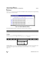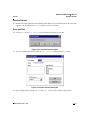
1
<<'/ 75'4 5/#07#. 7/&52 This page intentionally left blank Electrical Safeguards WARNING! Follow the precautions listed below to avoid permanent damage to the emulator. I. Always use a grounding strap to prevent damage resulting from electrostatic discharge (ESD). II. Power-Up Precautions. 1. 2. 3. 4. 5. III If the target application board has its own power, remove the U_VCC jumper, J12. Ensure that all power to the emulator and the target application (if any) is turned OFF. Connect the target pod to the target application (if any). Power up the emulator, then press the RESET button. Power up the target application (if any). Power-Down Precautions. When powering down, follow this procedure in the precise order shown below: 1. Power down the target application board (if any). 2. Remove the target pod. 3. Power down the emulator. 016'5 1. Refer to the “Precaution List” section of the Product Information sheet for additional operating precautions specific to various devices. 2. 3. Do not leave the emulator powered up with the RS-232C cable connected to a powered-down PC. Before inserting target pod into target application board, refer to Chapter 2 to determine appropriate jumper selections and options. © 1998 by ZiLOG, Inc. All rights reserved. No part of this document may be copied or reproduced in any form or by any means without the prior written consent of ZiLOG, Inc. The information in this document is subject to change without notice. Devices sold by ZiLOG, Inc. are covered by warranty and patent indemnification provisions appearing in ZiLOG, Inc. Terms and Conditions of Sale only. ZiLOG, Inc. makes no warranty, express, statutory, implied or by description, regarding the information set forth herein or regarding the freedom of the described devices from intellectual property infringement. ZiLOG, Inc. makes no warranty of merchantability or fitness for any purpose. The software described herein is provided on an as-is basis and without warranty. ZiLOG accepts no liability for incidental or consequential damages arising from use of the software. ZiLOG, Inc. shall not be responsible for any errors that may appear in this document. ZiLOG, Inc. makes no commitment to update or keep current the information contained in this document. ZiLOG's products are not authorized for use as critical components in life support devices or systems unless a specific written agreement pertaining to such intended use is executed between the customer and ZiLOG prior to use. Life support devices or systems are those which are intended for surgical implantation into the body, or which sustains life whose failure to perform, when properly used in accordance with instructions for use provided in the labeling, can be reasonably expected to result in significant injury to the user. =L/2*, Inc. 910 East Hamilton Ave., Suite 110 Campbell, CA 95008 Telephone: (408) 558-8500 FAX: (408) 558-8300 Internet: http://www.zilog.com <<'/75'4 5/#07#. 24'(#%' ABOUT THIS MANUAL We recommend that you read and understand everything in this manual before setting up and using the product. However, we recognize that users have different styles of learning. Therefore, we have designed this manual to be used either as a how-to procedural manual or a reference guide to important data. The following conventions have been adopted to provide clarity and ease of use: Courier Font For Executables Commands, variables, icon names, entry field names, selection buttons, code examples, and other executable items are distinguished by the use of the Courier font. Where the use of the font is not possible, like in the Index, the name of the entity is capitalized. For example, a procedure may contain an instruction which appears as: Click on File. However, an Index entry would appear as (+.'. Grouping of Actions Within A Procedure Step Actions in a procedure step are all performed on the same window or dialog box. Actions performed on different windows or dialog boxes appear in separate steps. Sequencing Words Within A Procedure Step When an item in a procedure contains a series of actions, the second action is preceded by the word WKHQ, and the third and subsequent actions are preceded by the word DQG. For example: Click on View, then Memory, and Z8 Code Memory. Unavailable menu items are presented in gray. 7/&52 K <<'/7UGT U/CPWCN 2TGHCEG =L/2* ADDITIONAL SOURCES OF INFORMATION In addition to this manual, you should have access to and be familiar with the following documentation: Z89321/371 Preliminary Product Specification The new emulator Graphical User Interface (GUI) software features many enhancements, including an improved context-sensitive on-line help facility that provides brief messages on keyboard, emulator commands, and various procedures on how to use the emulator. Refer to the README.TXT file on the DSP GUI diskette for detailed information. TRADEMARKS Windows is a registered trademark of the Microsoft Corporation. KK 7/&52 <<'/75'4 5/#07#. 6#$.'1(%106'065 %JCRVGT6KVNGCPF5WDUGEVKQPU 2CIG Chapter 1. Introduction Overview ..................................................................................................................................... Supported Devices ..................................................................................................................... GUI-Supported Compiler, Assembler Formats ........................................................................... Hardware Specifications ............................................................................................................. Operating Conditions ........................................................................................................... Dimensions .......................................................................................................................... Serial Interface ..................................................................................................................... Emulation Memory ............................................................................................................... Number of Breakpoints ........................................................................................................ Host Computer ........................................................................................................................... Minimum Requirements ....................................................................................................... Recommended ..................................................................................................................... Kit Contents ................................................................................................................................ 1-1 1-1 1-2 1-2 1-2 1-2 1-2 1-2 1-2 1-3 1-3 1-3 1-4 Chapter 2. Set-Up and Installation Software Installation ................................................................................................................... ZMASM/ZDS Installation ...................................................................................................... DSP ICEBOX GUI Installation ............................................................................................. Program Uninstallation ......................................................................................................... Hardware Installation .................................................................................................................. Installation Procedure .......................................................................................................... Power Up ............................................................................................................................. Power Down ......................................................................................................................... Emulator Operation .................................................................................................................... Resetting .............................................................................................................................. 7/&52 2-1 2-1 2-2 2-2 2-3 2-3 2-7 2-7 2-7 2-7 KKK <<'/7UGT U/CPWCN 6CDNGQH%QPVGPVU =L/2* %JCRVGT6KVNGCPF5WDUGEVKQPU 2CIG Chapter 3. Summary of Menus, Commands, and Operations Main Menu ................................................................................................................................. 3-1 File Menu .................................................................................................................................... 3-2 Open Session ...................................................................................................................... 3-3 Save Session ....................................................................................................................... 3-3 Download Application .......................................................................................................... 3-4 Download DSP RAM0 .......................................................................................................... 3-5 Download DSP RAM1 .......................................................................................................... 3-6 Download DSP Code Memory ............................................................................................. 3-7 Download DSP External Data Memory ................................................................................ 3-8 Load Symbol ........................................................................................................................ 3-8 Upload DSP RAM0 .............................................................................................................. 3-9 Upload DSP RAM1 ............................................................................................................ 3-10 Upload DSP Code Memory ................................................................................................ 3-11 Upload DSP External Data Memory .................................................................................. 3-12 Exit ..................................................................................................................................... 3-12 View Menu ................................................................................................................................ 3-13 Registers ............................................................................................................................ 3-13 RAM Bank0 ........................................................................................................................ 3-14 RAM Bank1 ........................................................................................................................ 3-20 DSP Code Memory ............................................................................................................ 3-23 Debug ................................................................................................................................ 3-25 OTP .......................................................................................................................................... 3-33 OTP ROM .......................................................................................................................... 3-34 Programming Options ........................................................................................................ 3-34 Command Status ............................................................................................................... 3-35 Device Serialization ........................................................................................................... 3-35 Configuration ............................................................................................................................ 3-36 Help .......................................................................................................................................... 3-37 Window Refreshing .................................................................................................................. 3-38 Emulator Operation .................................................................................................................. 3-38 Hardware Reset ................................................................................................................. 3-38 ROM Size ........................................................................................................................... 3-39 Breakpoint Implementation ................................................................................................ 3-39 EPROM/OTP Programmable Devices ............................................................................... 3-39 Running Multiple Emulators ...................................................................................................... 3-40 Evaluation Functions ................................................................................................................ 3-41 Peripheral Interfaces ................................................................................................................ 3-42 Initialization of Peripherals ................................................................................................. 3-42 External Data Memory ....................................................................................................... 3-42 KX 7/&52 =L/2* %JCRVGT6KVNGCPF5WDUGEVKQP <<'/7UGT U/CPWCN 6CDNGQH%QPVGPVU 2CIG Chapter 4. Sample Session DSP Emulator Sample Session .................................................................................................. 4-1 Starting the Application ............................................................................................................... 4-2 DSP Microcontroller Emulation ................................................................................................... 4-3 Monitoring/Modifying Registers ............................................................................................ 4-7 Tracing Code Using DSP Debug ....................................................................................... 4-16 Window Refresh ................................................................................................................. 4-25 Save and Quit .................................................................................................................... 4-25 Chapter 5. Troubleshooting Guide Introduction ................................................................................................................................. Initial Screen Does Not Appear .................................................................................................. XTAL Oscillator Contention. ....................................................................................................... “Can’t Open Windows” Message ................................................................................................ “Out of Synchronization with the Emulator” Message ................................................................ 5-1 5-1 5-2 5-2 5-2 Appendix A. Accessing the ZBBS/Internet Bulletin Board Information ......................................................................................................... A-1 How to Access the ZBBS .................................................................................................... A-1 ZiLOG On The Internet .............................................................................................................. A-1 Appendix B. Emulator Schematic Emulator Schematic .................................................................................................................. B-1 Appendix C. ASCII Character Set ASCII Character Set .................................................................................................................. C-1 Appendix D. Problem/Suggestion Report Form Problem/Suggestion Report Form ............................................................................................. D-1 7/&52 X This page intentionally left blank <<'/75'4 5/#07#. .+561((+)74'5 (KIWTG6KVNG 2CIG Chapter 2. Set-Up and Installation Figure 2-1. Hook-Up Diagram ................................................................................................... 2-4 Figure 2-2. Option Jumper Locations ........................................................................................ 2-5 Chapter 3. Summary of Menus, Commands, and Operations Figure 3-1. Open Session Dialog Box ....................................................................................... 3-3 Figure 3-2. ZiLOG ICEBOX (Save Session) Dialog Box ........................................................... 3-3 Figure 3-3. Download Application Dialog Box ........................................................................... 3-4 Figure 3-4. Download To DSP RAM0 Dialog Box ...................................................................... 3-5 Figure 3-5. Download To DSP RAM1 Dialog Box ...................................................................... 3-6 Figure 3-6. Download To DSP Code Memory Dialog Box ......................................................... 3-7 Figure 3-7. Download To External Data Memory Dialog Box .................................................... 3-8 Figure 3-8. Save DSP RAM0 Dialog Box .................................................................................. 3-9 Figure 3-9. Save DSP RAM1 Dialog Box ................................................................................ 3-10 Figure 3-10. Save DSP Memory Dialog Box ............................................................................ 3-11 Figure 3-11. Save DSP External Memory Dialog Box ............................................................. 3-12 Figure 3-12. Z89321 Registers Dialog Box ............................................................................. 3-13 Figure 3-13. Z89321 RAM Bank0 Window .............................................................................. 3-15 Figure 3-14. Memory Fill Dialog Box ....................................................................................... 3-16 Figure 3-15. Clear All Memory Confirmation Window ............................................................. 3-17 Figure 3-16. Address Dialog Box - Start Address .................................................................... 3-17 Figure 3-17. Address Dialog Box - Absolute Address ............................................................. 3-18 Figure 3-18. Tracking Pointer Register P0:0 ........................................................................... 3-18 Figure 3-19. Tracking Pointer Register P1:0 ........................................................................... 3-19 Figure 3-20. Tracking Pointer Register P2:0 ........................................................................... 3-19 Figure 3-21. Z89321 RAM Bank1 Window .............................................................................. 3-20 Figure 3-22. Tracking Pointer Register P0:1 ........................................................................... 3-21 Figure 3-23. Tracking Pointer Register P1:1 ........................................................................... 3-21 Figure 3-24. Tracking Pointer Register P2:1 ........................................................................... 3-22 7/&52 XKK <<'/7UGT U/CPWCN .KUVQH(KIWTGU =L/2* (KIWTG6KVNG 2CIG Chapter 3. Summary of Menus, Commands, and Operations (Continued) Figure 3-25. DSP Memory Window ......................................................................................... Figure 3-26. At Register Dialog Box ........................................................................................ Figure 3-27. Program Counter Window ................................................................................... Figure 3-28. Z89321 Debug Dialog Box .................................................................................. Figure 3-29. Z89321 Debug Fields .......................................................................................... Figure 3-30. Debug Log Window ............................................................................................. Figure 3-31. DSP Source Window ........................................................................................... Figure 3-32. Source Module Window ...................................................................................... Figure 3-33. Output Window .................................................................................................... Figure 3-34. OTP Window ....................................................................................................... Figure 3-35. Configuration Dialog Box .................................................................................... Figure 3-36. Multiple Emulator Operation Using 2 COM Ports ................................................ 3-23 3-24 3-24 3-25 3-26 3-30 3-31 3-32 3-32 3-33 3-37 3-40 Chapter 4. Sample Session Figure 4-1. ZiLOG ICEBOX Connect Dialog Box ...................................................................... 4-2 Figure 4-2. Configuration Dialog Box ........................................................................................ 4-3 Figure 4-3. Configuration Dialog Box With 64K ROM Size Selected ........................................ 4-4 Figure 4-4. Download Application Dialog Box ........................................................................... 4-5 Figure 4-5. Load File Browse Dialog Box .................................................................................. 4-5 Figure 4-6. Load File Browse Dialog Box With SUITE.LD File Selection .................................. 4-6 Figure 4-7. Download Application Dialog Box With SUITE.LD Selection .................................. 4-6 Figure 4-8. Z89321 Registers Dialog Box ................................................................................. 4-7 Figure 4-9. Z89321 RAM Bank0 Window .................................................................................. 4-8 Figure 4-10. Memory Fill Dialog Box ......................................................................................... 4-9 Figure 4-11. Z89321 RAM Bank0 Dialog Box With Memory Block 0020 - 00FF Zeroed ........... 4-9 Figure 4-12. Clear All Memory Window ................................................................................... 4-10 Figure 4-13. Z89321 RAM Bank0 Dialog Box With Zeroed Registers ..................................... 4-10 Figure 4-14. Z89321 Registers and Z89321 RAM Bank1 Windows ......................................... 4-11 Figure 4-15. RAM Bank1 With Value 00ADH At Location 09H ................................................ 4-12 Figure 4-16. Set Pointer P0:1 .................................................................................................. 4-12 Figure 4-17. Tracking Pointer P0:1 in RAM Bank1 .................................................................. 4-13 Figure 4-18. DSP Code Memory, Z89321 Registers, and Z89321 RAM Bank1 Windows ...... 4-14 Figure 4-19. The Z89321 Registers, RAM Bank1, and Z89321 DSP Memory Windows ........ 4-15 Figure 4-20. Z89321 Debug Dialog Box .................................................................................. 4-16 Figure 4-21. Debug Log Dialog Box ........................................................................................ 4-17 Figure 4-22. Z89321 Debug Window With Jump Input ............................................................ 4-18 Figure 4-23. Z89321 Debug Window After Jump .................................................................... 4-18 Figure 4-24. Z89321 Debug Window After RESET ................................................................. 4-19 Figure 4-25. Z89321 Debug Window With First Breakpoint Set .............................................. 4-19 Figure 4-26. Z89321 Debug Window At Breakpoint After GO ................................................. 4-20 Figure 4-27. Z89321 Debug Window With Two Breakpoints ................................................... 4-21 XKKK 7/&52 =L/2* <<'/7UGT U/CPWCN .KUVQH(KIWTGU Chapter 4. Sample Session (Continued) Figure 4-28. Z889321 Debug Window After GO ..................................................................... Figure 4-29. Z889321 Debug Window With Second Breakpoint Cleared ............................... Figure 4-30. Z89321 Debug Window With Original Breakpoint Cleared ................................. Figure 4-31. Z89321 Debug Window After HALT .................................................................... Figure 4-32. DSP Log File Sample .......................................................................................... Figure 4-33. Save Session Dialog Box .................................................................................... Figure 4-34. Open Session Dialog Box ................................................................................... 7/&52 4-21 4-22 4-22 4-23 4-24 4-25 4-25 KZ This page intentionally left blank <<'/75'4 5/#07#. %*#26'4 +0641&7%6+10 OVERVIEW Congratulations for selecting a fine development tool! The ZiLOG Z8932101ZEM Emulator is carefully engineered to provide the best balance between low-cost and useful features to shorten your development time for Z89321-based products. The DSP GUI Emulator graphical user interface (GUI) software runs under MS-Windows®, supporting selected ZiLOG devices. Also included is the ZiLOG Macro Cross Assembler (ZMASM), a full-featured assembler that runs under Windows. SUPPORTED DEVICES Table 1-1. Supported Devices Packages Emulation OTP Programming 40-Pin DIP 44-Pin PLCC 44-Pin QFP Z89321/371 Z89321/371 Z89371 Z89371 Z89371 N/A1 NOTES: 1. A third-party adapter tower is required for this configuration. Consult ZiLOG Customer Service for more information. 2. The complete, up-to-date list of all supported devices is specified in the ZiLOG Data Sheet (DS) document shipped with ZiLOG’s Order Acknowledgment form. The DS is also available from the ZiLOG Bulletin Board Service (ZBBS) and the home page at www.zilog.com (see Appendix A for additional information). 7/&52 <<'/7UGT U/CPWCN +PVTQFWEVKQP =L/2* GUI-SUPPORTED COMPILER, ASSEMBLER FORMATS The Emulator GUI supports object (binary or Intel hex) code files produced by the ZiLOG Macro Cross Assembler (ZMASM), Production Languages Corporation (PLC)1 assembler, 2500AD, and other third-party development tool companies. HARDWARE SPECIFICATIONS Operating Conditions Operating Temperature: 20°C ±10°C Emulation Speed: 1-MHz Internal Clock (Minimum) 20-MHz Internal Clock (Maximum) Operating Humidity: 10-90% RH (Noncondensing) Dimensions 0.5 in. (Height) x 4.875 in. (Width) x 7.125 in. (Length) Serial Interface RS-232C @ 9600, 19200 (Default), 28800, or 57600 Baud Rates Emulation Memory Maximum: 64K Words Number of Breakpoints Maximum: 256 1. .Production Languages Corporation (PLC) may be reached by telephone at (817) 367-6030 or online at [email protected]. 7/&52 =L/2* <<'/7UGT U/CPWCN +PVTQFWEVKQP HOST COMPUTER Minimum Requirements IBM PC (or 100-percent compatible) 486-Based Machine 33 MHz 4-MB RAM VGA Video Adapter Hard Disk Drive (3.0 MB free space) 3.5-inch, High-Density (HD) Floppy Disk Drive RS-232 COM Port Mouse or Pointing Device Microsoft Windows 3.1 Recommended The following changes to the Minimum Requirements are recommended for increased performance: 486- or Pentium-Based Machine 66 MHz (or Faster) 8 MB of RAM (or More) SVGA Video Adapter Color Monitor Printer Microsoft Windows 95 7/&52 <<'/7UGT U/CPWCN +PVTQFWEVKQP =L/2* KIT CONTENTS The emulator kit contains one of each of the following items: PC Assembly, Z8932102ZEM DSP Emulation Board Cable Assembly, 9-CKT, RS232, 6 Ft. Power Supply, AC MOD, 9VCD, 1.2A DSP Graphical User Interface (GUI) Software ZiLOG Macro Cross Assembler (ZMASM)/ZiLOG Developer System (ZDS) Software ZiLOG Macro Cross Assembler (ZMASM) User’s Manual ZiLOG Macro Cross Assembler (ZMASM) License Agreement Z8932102ZEM User’s Manual Product Information, ZDS For Windows 95 Pprogramming Adapter for 44-PLCC Progoramming Adapter for 44-PQFP Emulation Pod for 44-PLCC Emulation Pod for 40-DIP 7/&52 2 <<'/75'4 5/#07#. %*#26'4 5'672#0&+056#..#6+10 SOFTWARE INSTALLATION Software for the Emulator is stored on two sets of diskettes: 1. DSP GUI 2. ZiLOG Macro Cross Assembler (ZMASM) with ZiLOG Developer Studio (ZDS) NOTE: Refer to the README.TXT file on each diskette. Text (.TXT) files are easily accessed by using the Microsoft Windows Notepad program. The ZiLOG Macro Cross Assembler (ZMASM) ver. 2.10 is the basis for the ZiLOG 16-bit development environment for Windows 3.1. The ZiLOG Developer Studio (ZDS) version 1.00 is the 32-bit development environment which runs under Windows 95 and includes ZMASM version 2.10. The DSP GUI provides the interface screens that are customized for use with the Z8932102ZEM emulator. ZMASM/ZDS Installation If you are installing the ZiLOG Macro Cross Assembler (ZMASM) or ZiLOG Developer Studio (ZDS), run the installation program from the diskette EHIRUH installing the GUI diskette. You may choose to use another assembler, but the sample session assumes the ZiLOG assembler has been installed. ZDS is available only for the Windows 95 environment. Under Windows 95, a choice is offered to the user to install either ZDS, that includes ZMASM, or to install ZMASM only. NOTES: 1. The ZMASM/ZDS is a licensed product; it is not sold. Before opening the envelope containing the software, carefully read the Software License and Limited Warranty Agreement. 2. The installation procedure can be run before creating the installation directory. 3. To ensure that you receive proper notification of updates to this product, please fill out and return the enclosed ZiLOG Registration Card. 7/&52 <<'/7UGT U/CPWCN 5GVWRCPF+PUVCNNCVKQP =L/2* To install ZMASM/ZDS, perform the following steps: 1. Select the Run command from the File menu under Program Manager (Windows 3.1), or under the Start button (Windows 95). 2. 3. Insert the ZMASM 2.10 (w/ ZDS 1.00) Disk 1 into drive A (or drive B, if appropriate). Type a:\setup and press ENTER. (Type b:\setup if drive B is used.) A dialog box prompts you for the directory to install the software into. In Windows 3.1, the default path is C:\ZMASM_2.10. In Windows 95, the default path is C:\Program Files\ZDS_1.00 for ZDS. For the ZMASM-only installation, the default path is C:\Program Files\ZMASM_2.10. The setup program copies the files into the target directory. 4. Follow all on-screen instructions. In Windows 3.1, a ZMASM program group icon is placed on the desktop. In Windows 95, a ZiLOG Developer Studio entry is placed on the Programs menu under Start. 5. Remove the diskette and store in a safe place when installation is complete. DSP ICEBOX GUI Installation To install DSP ICEBOX™ GUI under Windows, perform the following steps: 1. Select the Run command from the File menu under Program Manager (Windows 3.1), or under Start (Windows 95). 2. 3. Insert the DSP GUI S/W Disk 1 into drive A (or drive B, if appropriate). Type a:\setup and press ENTER. (Type b:\setup if drive B is used.) A dialog box prompts you for the directory to install the software into. 4. Follow all on-screen instructions. The setup program copies the files into the target directory, creating a DSP ICEBOX GUI program group icon in the Windows environment. 5. Remove and store all diskettes in a safe place when installation is complete. Program Uninstallation Uninstaller facilities are created during the installation of ZMASM/ZDS and DSP ICEBOX GUI. In Windows 3.1, an Uninstall icon is a member of each program group. In Windows 95 an entry is created in the submenu under Programs. The Uninstall facility should be utilized when removing ZMASM/ZDS and DSP ICEBOX GUI from your PC to properly restore the Windows operating environment. 7/&52 <<'/7UGT U/CPWCN 5GVWRCPF+PUVCNNCVKQP =L/2* HARDWARE INSTALLATION Before installing the hardware, refer to Figure 2-1 for a view of the emulator; Figure 2–2 provides a diagram for connecting the emulator to your PC and power supply. NOTE: Proper functioning of the emulator depends upon proper installation and running of the GUI software on your PC. Installation Procedure This section provides the quick method of installing the hardware utilizing VDC wall-adaptor power supply. 1. Connect the serial cable to the PC. 2. 3. 4. 5. 6. If you are doing in-circuit emulation, connect the emulator to your target board. Set up the oscillator and option jumpers. Refer to the “Electrical Safeguards” page of this manual. Plug a 9.0 VDC 1.2 Amp Wall Adaptor to the P11 label +9.0V DC on the Z8932102ZEM. Set the power switch to ON. Serial Cable Connection Locate the serial cable. Connect the male end to the female connector, and the female end to either the COM1, COM2, COM3, or COM4 connector of your PC. 7/&52 <<'/7UGT U/CPWCN 5GVWRCPF+PUVCNNCVKQP =L/2* Target Board Emulator Figure 2-1. Hook-Up Diagram 7/&52 <<'/7UGT U/CPWCN 5GVWRCPF+PUVCNNCVKQP =L/2* +9 VDC S1 LEDS U12 P3 Z8949320GSE P1 J1 J2 J3 J4 P2 J6 J5 GND GND OTP RUN READY TP2 TP1 S1 Y1 RS-232C Power LED Reset VCC OTP Programming Socket GND VCC VPP EPM GND Jumper Locations TP4 Figure 2-2. Option Jumper Locations NOTE: Refer to the following tables for information on how to set up these jumpers for your specific emulator model before proceeding to the next installation steps. 7/&52 <<'/7UGT U/CPWCN 5GVWRCPF+PUVCNNCVKQP =L/2* Table 2-1. Jumper Option Settings Jumper Position Description J1 1-2 2–3 3-4 4-5* 5-6 FS0 drives the user’s target board. FS0 drives the on-board CODEC. Reserved FS1 drives the on-board CODEC. FS1 drives the user’s target board. J2 1-2 2-3* Transmit data is connected to the user’s target board. Transmit data is connected to the on-board CODEC. J3 1-2 2-3* Receive data is supplied by the user’s target board. Receive data is supplied by the on-board CODEC. J4 Open Closed* External Halt is Active. External Halt is Not Active. J5 Open* Closed External data bus is Enabled. External data bus is Disabled. J6 Open Closed* Break logic is Disabled. Break logic is Enabled (Emulation mode). J7 Open Closed* Emulation mode is Disabled. Emulation mode is Enabled. J8 Open* Closed Normal mode is Enabled. Reserved J9 1-2* 2–3 3-4 4-5 5-6 DSP clock source is the Oscillator, CLKI. Reserved Reserved DSP clock source is the Oscillator divided by 2, DSP_CLKII. DSP clock source is the User clock, U_CLK. J10 1-2 2-3* Oscillator input divided by 2 is VCC (not active - power save). Oscillator input divided by 2 is the 20-MHz Oscillator. J11 1-2 2-3* CODEC data format is A-law. CODEC data format is P-law. Closed The target board has its own VCC. The target board does not have its own VCC. WARNING J12 Open* Note: The * designates the default setting when shipped. 7/&52 <<'/7UGT U/CPWCN 5GVWRCPF+PUVCNNCVKQP =L/2* Option Jumpers Setup Selected option jumpers are accessible on top of the emulator board (see Figure 2-2). The option jumpers allow you to configure things like how the clock pin of the emulated DSP is connected. The clock for the emulated DSP can be provided from an oscillator in the emulator or from a TTL-level clock on your design. For electrical reasons, it cannot be provided from the oscillator on your design until you are done using the emulator and have done one of two things: 1) programmed an EPROM or OTP DSP and installed it in your design, or 2) installed a Masked-ROM DSP in your design. NOTE: Each emulator is shipped with a 20-MHz oscillator. If you want another rate, remove the oscillator and install a different one, within the frequency specifications of the device in use. ZiLOG, however, does not guarantee operation with oscillators other then the supplied model. Power Up If anything unusual (such as unexpected sounds and smells) occurs the first time you turn the power supply ON, quickly turn the power switch OFF, and check your connections. Check the 9V DC wall adapter, and ensure that the adapter has the rated 1.2A current. After power-up, press the RESET button to reset the Z89321-02 emulator. Pressing the RESET button avoids bus contention on the I/O lines. Power Down When powering down, perform the following steps: 1. Power down the target application board (if it has its own power supply). 2. Power down the emulator. NOTE: Refer to the complete “Electrical Safeguards” page of this manual. EMULATOR OPERATION Resetting Pressing the RESET button on the emulator resets the state of the target device and much of the status that you establish using the GUI. For example, it resets the emulated ROM size and clears all breakpoints. If your application board drives the RESET pin of the DSP socket Low, the target DSP is reset. For example, the Program Counter is set to the address set by the reset vector in the code, but most of the other GUI and emulator settings are not affected. 7/&52 <<'/7UGT U/CPWCN 5GVWRCPF+PUVCNNCVKQP NOTE: =L/2* After reset, you must wait until the Ready LED is OFF before starting the GUI software. (Refer to “LED Operation” section, which is later in this chapter. WARNING! You must always press the RESET button on the emulator before selecting the GUI icon or program entry. ROM Size The Z89321 emulator features selectable ROM sizing. Up to 64K of code memory is available for program development on the emulator. Then, during a later stage of project development, the user can shrink the program to fit in to the 4K of code memory on the chip. Breakpoint Implementation The emulator bases its breakpoint facility completely on addresses, rather than on inserting special Trap instructions into the program, which means you can set breakpoints in RAM on your target board. The emulator uses static RAM for each cycle emitted by the ICE chip during code execution to implement the breakpoint function in hardware. LED Operation Table 2-2. LED Assignments LED Indication Description Power On Off Power is ON. Power is OFF. Ready Off On Blink Communicating in Bisync Mode and waiting for command. Communicating in ASCII Mode or executing Bisync command. Emulator is self-testing. Run On Off Running user code. Not running user code. OTP On Off Programming OTP. Not programming OTP. 7/&52 <<'/75'4 5/#07#. %*#26'4 57//#4;1(/'075 %1//#0&5#0&12'4#6+105 MAIN MENU File View OTP! Configuration Help The Main Menu window of the emulator graphical user interface (GUI) is displayed after the GUI program is started. The following menu items can be accessed from this Main Menu: File View OTP! Configuration Help Each of these items, along with all windows, subset menus, menu items, commands, and operations, are summarized in the following sections of this chapter. NOTE: Consult =L/2*’s ZBBS or Internet site at www.zilog.com to obtain the latest released version of DSP GUI Emulator software. 7/&52 <<'/7UGT U/CPWCN 5WOOCT[QH/GPWU%QOOCPFUCPF1RGTCVKQPU =L/2* FILE MENU File View OTP! Configuration Help Open Session... Save Session... Download Application... Download DSP RAM0... Download DSP RAM1... Download DSP Code Memory... Download DSP External Memory... Load Symbol... Upload DSP RAM0... Upload DSP RAM1... Upload DSP Code Memory... Upload DSP External Data Memory... Exit Alt + F4 7/&52 <<'/7UGT U/CPWCN 5WOOCT[QH/GPWU%QOOCPFUCPF1RGTCVKQPU =L/2* Open Session The Open Session menu item provides a facility for loading a previously saved session. Figure 3-1. Open Session Dialog Box Save Session Selecting Save session saves the information about the position of the opened windows, downloaded code file, font size used, and debug flags such as Trace and Animation. Not all windows reappear upon reloading of a saved session. Figure 3-2. ZiLOG ICEBOX (Save Session) Dialog Box 7/&52 <<'/7UGT U/CPWCN 5WOOCT[QH/GPWU%QOOCPFUCPF1RGTCVKQPU =L/2* Download Application The Download Application menu item enables you to download an application object file to the Code Memory of the ICEBOX. Type the path and name or use the Browse button to locate and select your file. Two object formats are supported for output from ZMASM or the PLC compiler. In addition, memory can be cleared prior to downloading. Figure 3-3. Download Application Dialog Box 7/&52 <<'/7UGT U/CPWCN 5WOOCT[QH/GPWU%QOOCPFUCPF1RGTCVKQPU =L/2* Download DSP RAM0 The Download DSP RAM0 menu item enables memory to be filled with the values contained in an Intel hex or binary file. The Address Format section of the Download To DSP RAM0 window designates the format of the contents of the file being downloaded. Memory can also be padded with FFFFh or 0000h. Figure 3-4. Download To DSP RAM0 Dialog Box 7/&52 <<'/7UGT U/CPWCN 5WOOCT[QH/GPWU%QOOCPFUCPF1RGTCVKQPU =L/2* Download DSP RAM1 The Download DSP RAM1 menu item enables memory to be filled with the values contained in an Intel hex or binary file. The Address Format section of the Download To DSP RAM1 window designates the format of the contents of the file being downloaded. Memory can also be padded with FFFFh or 0000h. Figure 3-5. Download To DSP RAM1 Dialog Box 7/&52 <<'/7UGT U/CPWCN 5WOOCT[QH/GPWU%QOOCPFUCPF1RGTCVKQPU =L/2* Download DSP Code Memory The Download DSP Code Memory menu item enables you to download Intel hexadecimal (hex) or binary format code to Code Memory. The Address Format section of the Download to DSP Code Memory window designates the format of the contents of the file being downloaded. Memory can also be padded with FFFFh or 0000h. Figure 3-6. Download To DSP Code Memory Dialog Box 7/&52 <<'/7UGT U/CPWCN 5WOOCT[QH/GPWU%QOOCPFUCPF1RGTCVKQPU =L/2* Download DSP External Data Memory The Download to DSP External Data Memory menu item enables you to download Intel hexadecimal (hex) or binary format code to External Data Memory. The Address Format section of the Download To External Data Memory window designates the format of the contents of the file being downloaded. Memory can also be padded with FFFFh or 0000h. Figure 3-7. Download To External Data Memory Dialog Box Load Symbol The Load Symbol menu item enables the selection of a symbol during debugging. The value of corresponding labels and constants in your program code is displayed. This item is available only when the Z89321 Debug window is displayed. 7/&52 =L/2* <<'/7UGT U/CPWCN 5WOOCT[QH/GPWU%QOOCPFUCPF1RGTCVKQPU Upload DSP RAM0 The Upload DSP RAM0 menu item enables the contents of memory bank0 to be saved in an object file. Three formats are available for storing the data: binary, Intel hex, and disassembly. The entire contents of the bank are stored when the Save All button is activated. A portion of the contents is stored when numbers are entered in the Start Address and End Address fields, and the Save button is activated. Figure 3-8. Save DSP RAM0 Dialog Box 7/&52 <<'/7UGT U/CPWCN 5WOOCT[QH/GPWU%QOOCPFUCPF1RGTCVKQPU =L/2* Upload DSP RAM1 The Upload DSP RAM1 menu item enables the contents of memory bank1 to be saved in an object file. Three formats are available for storing the data: binary, Intel hex, and disassembly. The entire contents of the bank are stored when the Save All button is activated. A portion of the contents is stored when numbers are entered in the Start Address and End Address fields, and the Save button is activated. Figure 3-9. Save DSP RAM1 Dialog Box 7/&52 <<'/7UGT U/CPWCN 5WOOCT[QH/GPWU%QOOCPFUCPF1RGTCVKQPU =L/2* Upload DSP Code Memory The Upload DSP Code Memory menu item enables the contents of code memory to be saved in an object file. Three formats are available for storing the data: binary, Intel hex, and disassembly. The entire contents of code memory are stored when the Save All button is activated. A portion of the contents is stored when numbers are entered in the Start Address and End Address fields, and the Save button is activated. This function may be used for sessions involving patched code. Figure 3-10. Save DSP Memory Dialog Box 7/&52 <<'/7UGT U/CPWCN 5WOOCT[QH/GPWU%QOOCPFUCPF1RGTCVKQPU =L/2* Upload DSP External Data Memory The Upload DSP External Data Memory menu item enables the contents of external data memory to be saved in an object file. Three formats are available for storing the data: binary, Intel hex, and disassembly. The entire contents of external data memory are stored when the Save All button is activated. A portion of the contents is stored when numbers are entered in the Start Address and End Address fields, and the Save button is activated. Figure 3-11. Save DSP External Memory Dialog Box Exit The Exit menu item enables you to leave the emulator GUI. The ZiLOG ICEBOX confirmation window offers the message, “Save the Current Session?”, and the options Yes, No, and Cancel. 7/&52 <<'/7UGT U/CPWCN 5WOOCT[QH/GPWU%QOOCPFUCPF1RGTCVKQPU =L/2* VIEW MENU File View OTP! Configuration Help Registers RAM Bank0 RAM Bank1 DSP Code Memory DSP External Data Memory Debug Source Output Registers The Registers menu item initiates the display of the Z89321 Registers dialog box. That window contains the contents of all internal and external registers, RAM pointer registers, data registers, status registers and flags, and stacks. Figure 3-12. Z89321 Registers Dialog Box 7/&52 <<'/7UGT U/CPWCN 5WOOCT[QH/GPWU%QOOCPFUCPF1RGTCVKQPU =L/2* When the Z89321 Registers window is displayed, the following menu bar is displayed: File View OTP! Font Size Window Help Font Size You can choose from a number of font sizes: Point 6 to Point 12. File View OTP! FontSize Window Help Point 6 Point 8 Point 10 Point 12 Window File View OTP! FontSize Window Help Cascade Shift+F5 Tile Shift+F4 Arrange Icon Close All The Cascade, Tile, and Arrange Icon items perform standard Windows functions. Close All displays the ZiLOG ICEBOX confirmation window which offers the message, “Save the Current Session?”, and the options Yes, No, and Cancel (see Figure 3-2). RAM Bank0 The RAM Bank0 menu item activates the Z89321 RAM Bank0 window and enables the viewing and editing of the contents of internal data bank0. 7/&52 <<'/7UGT U/CPWCN 5WOOCT[QH/GPWU%QOOCPFUCPF1RGTCVKQPU =L/2* Figure 3-13. Z89321 RAM Bank0 Window When the Z89321 RAM Bank0 window is displayed, the following menu bar is displayed: File View OTP! Edit View OTP! Edit Tracking Font Size Window Help Edit File Tracking Font Size Window Help Fill... Clear All Start Address... 7/&52 <<'/7UGT U/CPWCN 5WOOCT[QH/GPWU%QOOCPFUCPF1RGTCVKQPU =L/2* Fill The Fill menu item enables you to assign a value to a specified range of memory addresses. The Memory Fill dialog box has entry fields for Start Address, End Address, and Fill Value. The Radix field specifies the format, hexadecimal or decimal, of the entry in the Fill Value field. Figure 3-14. Memory Fill Dialog Box Clear All The Clear All menu item provides the option of filling Z8 Code Memory with the 0000h or FFFFh value. To exit the choice list without any changes, press the Escape key. File View OTP! Edit Tracking Font Size Window Help Fill... Clear All With 0000 Start Address... With FFFF When the With 0000 or With FFFF menu item is selected, a confirmation window is displayed. 7/&52 <<'/7UGT U/CPWCN 5WOOCT[QH/GPWU%QOOCPFUCPF1RGTCVKQPU =L/2* Figure 3-15. Clear All Memory Confirmation Window Start Address The Start Address menu item provides a facility for jumping the cursor in the Z89321 RAM Bank0 window to the location entered in the Start Address field. The Radix field specifies the format, hexadecimal or decimal, of the entry in the Start Address field. Figure 3-16. Address Dialog Box - Start Address Tracking Selecting Tracking from the menu, displays the Absolute Address, Pointer Register P0:0, Pointer Register P1:0, and Pointer Register P2:0 menu items. File View OTP! Edit Tracking Font Size Window Help Absolute Address Pointer Register P0:0 Pointer Register P1:0 Pointer Register P2:0 7/&52 <<'/7UGT U/CPWCN 5WOOCT[QH/GPWU%QOOCPFUCPF1RGTCVKQPU =L/2* Absolute Address: You can track to a register by its absolute address by entering the absolute address value in the dialog box that appears when Absolute Address is selected from the Tracking menu. Figure 3-17. Address Dialog Box - Absolute Address Pointer Register P0:0: You can track to the contents of pointer register P0:0. Figure 3-18. Tracking Pointer Register P0:0 7/&52 <<'/7UGT U/CPWCN 5WOOCT[QH/GPWU%QOOCPFUCPF1RGTCVKQPU =L/2* Pointer Register P1:0: You can track to the contents of pointer register P1:0. Figure 3-19. Tracking Pointer Register P1:0 Pointer Register P2:0: You can track to the contents of pointer register P2:0. Figure 3-20. Tracking Pointer Register P2:0 When you right-click on your two-button mouse, the following items are displayed: Clear All... Fill... Tracking Absolute Address... Download DSP RAM0... Upload DSP RAM0... 7/&52 <<'/7UGT U/CPWCN 5WOOCT[QH/GPWU%QOOCPFUCPF1RGTCVKQPU =L/2* RAM Bank1 The RAM Bank1 menu item activates the Z89321 RAM Bank1 window and enables the viewing and editing of the contents of internal data bank1. Figure 3-21. Z89321 RAM Bank1 Window When the RAM Bank1 dialog box is displayed, the following menu bar is displayed: File View OTP! Edit Tracking Font Size Window Help Tracking Selecting Tracking from the menu, displays the Absolute Address, Pointer Register P0:1, Pointer Register P1:1, and Pointer Register P2:1 menu items. File View OTP! Edit Tracking Font Size Window Help Absolute Address Pointer Register P0:1 Pointer Register P1:1 Pointer Register P2:1 Absolute Address: You can track to a register by its absolute address by entering the absolute address value in the dialog box that appears when Absolute Address is selected from the Tracking menu (see Figure 3-17). 7/&52 =L/2* <<'/7UGT U/CPWCN 5WOOCT[QH/GPWU%QOOCPFUCPF1RGTCVKQPU Pointer Register P0:1: You can track to the contents of pointer register P0:1. Figure 3-22. Tracking Pointer Register P0:1 Pointer Register P1:1: You can track to the contents of pointer register P1:1. Figure 3-23. Tracking Pointer Register P1:1 7/&52 <<'/7UGT U/CPWCN 5WOOCT[QH/GPWU%QOOCPFUCPF1RGTCVKQPU =L/2* Pointer Register P2:1: You can track to the contents of pointer register P2:1. Figure 3-24. Tracking Pointer Register P2:1 When you right-click on your two-button mouse, the following items are displayed: Clear All... Fill... Tracking Absolute Address... Download DSP RAM1... Upload DSP RAM1... 7/&52 <<'/7UGT U/CPWCN 5WOOCT[QH/GPWU%QOOCPFUCPF1RGTCVKQPU =L/2* DSP Code Memory The Z89321 DSP Memory window provides a facility for tracking and changing the contents of the code memory registers. Figure 3-25. DSP Memory Window When the Z89321 DSP Memory dialog box is displayed, the following menu bar is displayed: File View OTP! Edit Tracking Font Size Window Help Window Help Tracking Selecting Tracking from the menu displays the following menu items: File View OTP! Edit Tracking Font Size Absolute Address @Register Program Counter @@ P0:0 @@ P1:0 @@ P2:0 @@ P0:1 @@ P1:1 @@ P2:1 7/&52 <<'/7UGT U/CPWCN 5WOOCT[QH/GPWU%QOOCPFUCPF1RGTCVKQPU =L/2* Absolute Address: You can track to a register by its absolute address by entering the absolute address value in the dialog box that appears when Absolute Address is selected from the Tracking menu (see Figure 3-17). @Register: You can indirectly track to a register (the contents of which are the address of another register) by entering the value in the At Register dialog box. Figure 3-26. At Register Dialog Box Program Counter: The Program Counter message window reports the current value of the program counter. Figure 3-27. Program Counter Window @@ P0:0: You can track the RAM pointer P0:0 to the DSP Code Memory window. @@ P1:0: You can track the RAM pointer P1:0 to the DSP Code Memory window. @@ P2:0: You can track the RAM pointer P2:0 to the DSP Code Memory window. @@ P0:1: You can track the RAM pointer P0:1 to the DSP Code Memory window. @@ P1:1: You can track the RAM pointer P1:1 to the DSP Code Memory window. 7/&52 <<'/7UGT U/CPWCN 5WOOCT[QH/GPWU%QOOCPFUCPF1RGTCVKQPU =L/2* @@ P2:1: You can track the RAM pointer P2:1 to the DSP Code Memory window. When you right-click on your two-button mouse, the following items are displayed: Clear All... Fill... Download Application... Download DSP Code Memory... Upload DSP Code Memory... Debug Figure 3-28. Z89321 Debug Dialog Box The Z89321 Debug window enables you to view the disassembled code, set break points, trace through the code, and perform other debug operations. 7/&52 <<'/7UGT U/CPWCN 5WOOCT[QH/GPWU%QOOCPFUCPF1RGTCVKQPU =L/2* Display and Input Fields 2 1 3 8 4 9 5 6 7 Figure 3-29. Z89321 Debug Fields The Z89321 Debug dialog box contains the several fields which are numbered for reference in the preceding figure: Table 3-1. Debug Display and Input Fields Number Name Description 1 Breakpoint List This display area contains a list of all addresses currently defined as breakpoints. 2 Set Breakpoint Input This field is an input area for setting a breakpoint. To set a new breakpoint, type the address in this field or click on a line of code in the Code List field (field 9), then click on the SET BRK button. After the button is activated, the address continues to be displayed in the field. The address then appears in the Breakpoint List (field 1). 7/&52 <<'/7UGT U/CPWCN 5WOOCT[QH/GPWU%QOOCPFUCPF1RGTCVKQPU =L/2* Table 3-1. Debug Display and Input Fields Number Name Description 3 Clear Breakpoint Input This field is an input area for deleting a breakpoint. To delete a breakpoint, type the address in this field or place the cursor on the address, then click on the CLEAR BRK button. After the button is activated, the address continues to be displayed in the field. The address is removed from the Breakpoint List (field 1). 4 Symbol Address This display area contains the address of the symbol to the right of the divider line. 5 Symbol Table This display area contains the list of currently defined symbols. The symbol table is loaded only when both of the following conditions are fulfilled: 1) A symbol file (.SYM) is loaded in code memory, and 2) The DSP Debug window is selected. 6 Jump This field is an input area for setting the program counter to the address of a specific line of source code. To jump to an address, type the address in the field, then click on the JUMP button. The address continues to be displayed in the field. The address and line of source code are displayed in the Trace Buffer (field 8) and Code List (field 9) fields. 7 Step Editing This field is an input area for the number of steps to advance the program counter. The default value is 1. The maximum value is 99999. To single-step through your code, set the value of this field to 1, then click on the STEP button, or click on the GO button. 8 Trace Buffer This display area contains the address of the line of code displayed on the same line in the Code List field (field 9). Use the vertical scroll bar to scroll up and down. 9 Code List The Code List contains the disassembled contents of code memory. The field scrolls with the Trace Buffer field. Use the vertical scroll bar to scroll up and down. Selection of a line of code causes the address of that line to be inserted into the SET BRK, CLEAR BRK, and JUMP fields. Code Memory can be change by entering the assembly code directly into the window line by line. After you input a line of assembly code, you must press the RETURN key. The assembled code is then written to Code Memory and immediately reflected in this field. NOTE: 7/&52 Be careful when replacing instructions to avoid corruption of the remaining assembly code. <<'/7UGT U/CPWCN 5WOOCT[QH/GPWU%QOOCPFUCPF1RGTCVKQPU =L/2* Buttons Several buttons are available in the Z89321 Debug window. Table 3-1. Debug Buttons Name Description CLEAR ALL Activation of this button clears all breakpoints. All addresses are then removed from the Breakpoint List (field 1). CLEAR BRK Activation of this button deletes a breakpoint at the address in the Clear Breakpoint Input field (field 3). The address is then removed from the Breakpoint List (field 1). GO Activation of this button starts execution of the DSP program. Execution stops when it hits a breakpoint. HALT Activation of this button terminates execution. JUMP Activation of this button sets the program counter to the address in the Jump field (field 6). The corresponding line of code is highlighted in the Trace Buffer (field 8) and Code List (field 9) fields. RESET Activation of this button causes a jump to the address located at the reset vector location in the code. SET BRK Activation of this button sets a breakpoint at the address in the Set Breakpoint Input field (field 2). The address is then added to the Breakpoint List (field 1). STEP Activation of this button advances the program counter the number of steps in the Step Editing field (field 7). When the value is set to 1, the STEP button single-steps through the code without causing a RESET. STEP OVER Activation of this button advances the program counter a single step. That is, one assembly instruction is executed. When the current instruction is a CALL instruction, subsequent code is executed in real time until the program returns from the subroutine. STEP OVER has the same effect as setting a breakpoint at the instruction immediately following the current one, and executing the GO command. When the Z89321Debug dialog box is displayed, the following menu is displayed: File View OTP! Run FontSize Window Help 7/&52 <<'/7UGT U/CPWCN 5WOOCT[QH/GPWU%QOOCPFUCPF1RGTCVKQPU =L/2* Run File View OTP! Run FontSize Window Help Trace Code Trace Call Animate Clear Trace Log Execution Log Options Trace Code: Provides a line-by-line trace capability for tracing all instructions while running the Debug program. When Trace Code is selected, Animate is also automatically selected and execution is running. See Chapter 4, “Sample Session”, for a sample of tracing activities. Trace Call: Provides the capability to trace only subroutine calls while running the Debug program. Traced code is displayed in the Code List field (field 9) of the Z89321 Debug window. When the STEP OVER button is activated and the current instruction is a CALL instruction, subsequent code is executed in real time until the program returns from the subroutine. When Trace Call is selected, Animate is also automatically selected and execution is simulated. Animate: Animation is a mode where the user can simulate single-step execution through the code. A GO command starts execution. The address and instruction of the current and last 99 executed lines of code are displayed in the Trace Buffer field (field 8) and the Trace Buffer field (field 9) of the Z89321 Debug window. NOTE: When Animation is activated, execution is not realtime. Single step execution is emulated. To execute code in real time, the Animation feature must be disabled. Clear Trace: Clears the contents of the Trace field and ends tracing activities. Log Execution: Enables or disables logging. When enabled, selected registers are logged to the specified file each time emulation is halted, such as at breakpoint or after single-step. See Chapter 4, “Sample Session”, for an example of trace logging. Log Options: Specifies the registers to log, the format in which to log them, and the name of the log file. Logging may be linear or circular. Linear logging treats the log file as a linear buffer with infinite capacity; circular logging treats the log file as a circular buffer with finite capacity. The circular buffer default capacity is 100 logging actions; however, the number is user-definable in the Maximum field. (See Figure 3-30.) 7/&52 <<'/7UGT U/CPWCN 5WOOCT[QH/GPWU%QOOCPFUCPF1RGTCVKQPU =L/2* Figure 3-30. Debug Log Window Resources to Log: The following items are available for logging. A - A Register (Accumulator) SR - Status Register PC - Program Counter P - P Register (Output of Multiplier, Read Only) X - X Register (X Multiplier Input) Y - Y Register (Y Multiplier Input) RAM Address Pointers (Pn:b) Data Pointers (Dn:b) External Registers (EXTn) For detailed information about these resources and registers, refer to the Z89321/371 16-Bit Digital Signal Processors Preliminary Product Specification (DS000500-MOD0698). 7/&52 <<'/7UGT U/CPWCN 5WOOCT[QH/GPWU%QOOCPFUCPF1RGTCVKQPU =L/2* Source The DSP Source dialog box displays the source code when you download a load (.LD) format file using the Download Application dialog box. Figure 3-31. DSP Source Window When the DSP Source window is displayed, the following menu bar is displayed: File View OTP! Options Window Help Options When the Options item is selected, the following item is displayed: File View OTP! Options Window Help Source Module... Source Module: The Source Module window displays the name of the source assembler module. 7/&52 <<'/7UGT U/CPWCN 5WOOCT[QH/GPWU%QOOCPFUCPF1RGTCVKQPU =L/2* Figure 3-32. Source Module Window Output The Output window displays the status at file load and at command execution, such as HALT and RESET. Figure 3-33. Output Window 7/&52 =L/2* <<'/7UGT U/CPWCN 5WOOCT[QH/GPWU%QOOCPFUCPF1RGTCVKQPU OTP This emulator provides OTP programming capabilities. Selecting the OTP! menu item displays the OTP window. Figure 3-34. OTP Window 7/&52 <<'/7UGT U/CPWCN 5WOOCT[QH/GPWU%QOOCPFUCPF1RGTCVKQPU =L/2* OTP ROM The OTP ROM section of the OTP window sets the method for bit significance in the registers. Three settings are available: Word High Low Programming Options Several OTP operations can be performed: Table 3-1. OTP Operations Functions Operations Functions Performed BLANK CHECK Checks whether the OTP device is blank. VERIFY Compares the contents of the Code Memory and the OTP device. EXAMINE Load the contents of the OTP device into Code Memory. PROGRAM Writes the contents of the Code Memory to the OTP device. OTP CHECKSUM Calculates the Checksum of the OTP device only and displays it on the screen. RAM CHECKSUM Calculates the Checksum of the RAM and displays it on the screen. ROM Protect Blocks read access to OTP programming code from external viewing and disables the following commands: LDC, LDCI, LDE, and LDEI. QUIT Quit OTP programming operations. NOTES: 1. To obtain a Data I/O (such as UniSite, 3900, or 2900) calculated Checksum, the user should first download the file with 00 padding option, then perform the OTP programming. Data I/O fills its memory with 00 after power up. 2. Checksum differences may occur. During user-program download, the memory is padded with code outside the user program memory if the user program is less than the emulation memory. The memory is padded with either 00, FF, or nothing according to user selection. This does not effect the user program; however, it does effect the calculation of the Checksum during the OTP programming because the Checksum is calculated through out the whole memory size of the OTP. 3. RAM is Code Memory space. 7/&52 =L/2* <<'/7UGT U/CPWCN 5WOOCT[QH/GPWU%QOOCPFUCPF1RGTCVKQPU Command Status This field contains a message display area and a progress bar that is activated when one of the OTP operations are performed. Device Serialization A user-specified serial number can be programmed into the OTP device. The serial number can be changed at any time before it is programmed into a device. The characteristics of the serial number are specified in the Device Serialization section of the OTP window. Method Three methods of creating a serial number are available: sequential, pseudorandom, or none. Sequential Mode - The serial number increments by one after each device is programmed. Pseudorandom Mode - The serial number is generated according to the following algorithm: r[i+1] = (a * r[i] + b) mod 2^N where r[i+1] is the new serial number r[i] is the last serial number a = 1909 b = 221571 N = number of bits in the serial number Example: Entering 1000 in the Address box, selecting 4-Bytes as the Serial Number Size, and entering 12345678 in the Serial Number box outputs to the screen as follows: %1000 = %12 %1001 = %34 %1002 = %56 %1003 = %78 None 7/&52 <<'/7UGT U/CPWCN 5WOOCT[QH/GPWU%QOOCPFUCPF1RGTCVKQPU =L/2* Serial Number Size The Serial Number Size field specifies length in number of bytes the serial number occupies in memory. This field is not available when Device Serialization is set to None. Serial Number Enter the exact serial number in the input field. Specify the format of the number as either hexadecimal or decimal. If a decimal number is input, the number is converted to hexadecimal for storage in memory. This field is not available when Device Serialization is set to None. Address Enter a four-digit hexadecimal number to be the address where the serial number is to be stored in memory. This field is not available when Device Serialization is set to None. CONFIGURATION At start-up, the user selects the appropriate ICEBOX entry. When the Configuration dialog box is shown on the screen, you can choose the processor and the ROM size you want to emulate. The code file you download to Code Memory is limited to the ROM size selected. Selected ports automatically reference port availability in the selected processor. Other information about the processor, such as the number of ports and extended register banks, can be observed but cannot be altered. Click the OK or CANCEL button to confirm or cancel the configuration. NOTE: To modify the configuration, you must first close all open windows; the Configuration command then reappears in the Main Menu. When the Configuration menu item is selected, the Configuration dialog box is displayed. 7/&52 <<'/7UGT U/CPWCN 5WOOCT[QH/GPWU%QOOCPFUCPF1RGTCVKQPU =L/2* Figure 3-35. Configuration Dialog Box HELP File View OTP! Configuration Help Index Keyboard Commands Glossary Procedure Using Help About ICEBOX The on-line Help program is available to provide brief help messages on various topics. The Help program features an index that easily references the emulator commands and procedures. Topics covered under Help include: Index of the Help Program Keyboard Commands 7/&52 <<'/7UGT U/CPWCN 5WOOCT[QH/GPWU%QOOCPFUCPF1RGTCVKQPU ICEBOX GUI Commands Procedures for Using the Emulator How to Use Help Version and Copyright Information =L/2* WINDOW REFRESHING When you make a change in the Code Memory window, the code view in the Debug window is updated automatically. When a program runs from the Debug window, the Status window is updated automatically at each step, Halt, or breakpoint. All other windows (Registers, Expanded Registers, Data Memory, and Code Memory) are not updated automatically as the program runs. To refresh the window display to reflect the current hardware values, double click the caption bar of each window. EMULATOR OPERATION Hardware Reset When you press the emulator RESET button (or power-down, then power-up), the initial screen and the ZiLOG logo are shown while the ICEBOX goes through the initialization sequence. Pressing the RESET button resets most of the settings that you establish using the GUI. For example, the emulated ROM size is reset to 4 KB, and all 64-KB breakpoint RAM is cleared. NOTE: After RESET, you must wait a minimum of 5 seconds (for completion of selftests) before starting the GUI software. Hardware Reset While GUI Is Running If you press the Hardware Reset while the GUI is running, a communication error dialog box appears with the following message: Out of synchronization with the emulator. This message appears when the power or RS-232C cable is removed, or whenever the ICEBOX emulator and the host PC have failed to properly communicate with each other. You have three responses to this message: Abort, Retry, or Ignore. 7/&52 <<'/7UGT U/CPWCN 5WOOCT[QH/GPWU%QOOCPFUCPF1RGTCVKQPU =L/2* Abort Quits the GUI. Retry Resets the GUI by reinitializing. You are returned to the initial purple screen with the =L/2* logo. Ignore Attempts to reestablish communication between the GUI and ICEBOX emulator without reinitializing. ROM Size The ICEBOX has the selectable ROM size of 4K to 64K. Breakpoint Implementation The emulator bases its breakpoint facility completely on addresses, rather than on inserting special TRAP instructions into the program, which enable the setting of breakpoints in Program Memory on your target board. The ICEBOX uses a 32Kx1 static RAM for each cycle emitted by the Z8 ICE chip during code execution to implement the breakpoint function in hardware. EPROM/OTP Programmable Devices Z89371 NOTE: Refer to the Data Sheet (DS) for exact OTP Programming requirements. 7/&52 <<'/7UGT U/CPWCN 5WOOCT[QH/GPWU%QOOCPFUCPF1RGTCVKQPU =L/2* RUNNING MULTIPLE EMULATORS The DSP ICE GUI allows several emulators to run at the same time, if your PC has more than one communication port. NOTE: Running multiple emulations (two or more emulators running simultaneously) requires more memory than single-emulation operation; therefore, we recommend using a PC with 8-MB RAM or 16-MB RAM for Windows 95. In addition, two or more communication ports are needed when running multiple instances. Ensure that there are no COM port interrupt conflicts if installing additional COM ports via an add-on board. Figure 3-36. Multiple Emulator Operation Using 2 COM Ports 7/&52 <<'/7UGT U/CPWCN 5WOOCT[QH/GPWU%QOOCPFUCPF1RGTCVKQPU =L/2* EVALUATION FUNCTIONS The Z8932102ZEM combines the advantages of an in-circuit emulator and evaluator in one device. As an incircuit emulator, it can trace user programs using an emulation pod to the target board. As an evaluator, it has extensive on-board periphery for quickly implementing and prototyping typical DSP systems. The Z8932102ZEM has the following peripheral devices on board: 64K External Data Memory 8 LEDs for Indicating Program Status 8 Buttons for Data Input Analog Interface Consisting of: – 1 Input Connector (IN0) and 2 Output Connectors (Linear Output and Speaker) – Output Buffer Amplifier These peripherals are mapped to the External device address map as follows: Table 3-2. External Device Address Map Designation Function Mode EXT 0 SRAM Address Write Only EXT 1 SRAM Data Read/Write EXT 2 LEDs Write Only Buttons Read Only EXT 3 Additional External Port Read/Write EXT 4-6 External Ports Write Only EXT3-6 do not access on-board peripherals. They are decoded by the Altera chip for accessing user peripherals. 7/&52 <<'/7UGT U/CPWCN 5WOOCT[QH/GPWU%QOOCPFUCPF1RGTCVKQPU =L/2* PERIPHERAL INTERFACES Initialization of Peripherals The periphery is shown on the schematic in Appendix B. The following recommended instructions appropriately initialize the peripherals: ld ext7,#15 ld ext3,#68h ; 0000 0000 0110 1000 ; 1 wait for: ; reading SRAM ; reading buttons ld ext7,#4 ld a,#0 ld ext2,a ; switch OFF all the LEDs Review any additional external ports used regarding the need for wait states. External Data Memory The external ports used for Data Memory include: Table 3-3. External Data Memory External Ports Designation Function Mode EXT 0 SRAM Address Write Only EXT 1 SRAM Data Read/Write This memory is primarily for array storage. Write the desired first address, then write or read data as many times as needed. Addresses increment automatically after each access to memory. This feature speeds up access to the array in most applications. If you want to read and write to the same address, you must write the address before each access. 7/&52 <+%'$1:75'4 5/#07#. %*#26'4 5#/2.'5'55+10 DSP EMULATOR SAMPLE SESSION This sample session is designed to introduce you to the features of the DSP graphical user interface (GUI) software and thoroughly acquaint you with the various GUI windows you will be using in this program. For best results, follow the steps in sequential order. Topic headings, such as “Using the Debug Window”, have been added so you can better locate how-to information. Additional information is available in Chapter 3, “Summary of Menus, Commands, and Operations” and in Chapter 5, “Troubleshooting Guide”. NOTES: 1. In order to properly demonstrate the program features, be prepared to import sample files in this session. A sample DSP source code file and sample assembly batch files have been included on the ZMASM Diskette; however, other sample files of your choice can be used. You can also download other sample files from ZiLOG's Bulletin Board Service (ZBBS) or Internet site. (Refer to Appendix A for information.) 2. Consult ZiLOG’s ZBBS or www.zilog.com to obtain the latest released version of DSP GUI software. 3. This sample session assumes the ZiLOG Macro Cross Assembler has been installed. 4. The screen images contained in this file are representative only. Your screen display may vary. 7/&52 <<'/7UGT U/CPWCN 5CORNG5GUUKQP =L/2* STARTING THE APPLICATION 1. Press the RESET button on the emulator after power up. 2. Double-click the DSPICE program icon. The ZiLOG ICEBOX Connect dialog box is displayed. Figure 4-1. ZiLOG ICEBOX Connect Dialog Box 7/&52 <<'/7UGT U/CPWCN 5CORNG5GUUKQP =L/2* 3. Select the Z8932102ZEM ICEBOX, the correct COM port, and the appropriate baud rate for the communication to the PC; then click on the Connect button and wait for the initialization procedure to complete. The Configuration dialog box is displayed. Figure 4-2. Configuration Dialog Box Changes to the emulator, COM port, and baud rate are saved and become the new default the next time the icon is activated. If the communication attempt between the PC and the emulator fails, check the connection or reset the emulator. (Refer to Chapter 5: “Troubleshooting Guide”.) DSP MICROCONTROLLER EMULATION 4. In the MicroController field (see Figure 4-2), select Z89321/371; then click on the 64K ROM Size option button, if it is not already selected (see Figure Figure 4-3); and click on the OK button (or press the ENTER key) to accept the configuration. The Main Menu is displayed. File View 7/&52 OTP! Configuration Help <<'/7UGT U/CPWCN 5CORNG5GUUKQP =L/2* Figure 4-3. Configuration Dialog Box With 64K ROM Size Selected Emulation ROM Size selection affects the size of the code file you can download. The Configuration dialog box is only accessible when no other window is open. NOTE: Refer to the Product Information Sheet for a complete list of precautions and limitations. 7/&52 =L/2* 5. <<'/7UGT U/CPWCN 5CORNG5GUUKQP Click on File, then Download Application. The Download Application window is displayed. Figure 4-4. Download Application Dialog Box 6. Click on Browse. The Load File Browse dialog box is displayed. Figure 4-5. Load File Browse Dialog Box 7. Change the current path to the ZiLOG Developer Studio, for example, c:\progra~1\zds_j2.00. The names of two subfolders are displayed. 8. Double click on the samples entry. Additional names of subfolders are displayed in the same area of the window. 7/&52 <<'/7UGT U/CPWCN 5CORNG5GUUKQP 9. =L/2* Double click on the entry 89c00. An entry, suite.ld, is displayed to the area on the left side of the window. Figure 4-6. Load File Browse Dialog Box With SUITE.LD File Selection 10. Double click on the entry suite.ld. The Download Application dialog box is displayed. Figure 4-7. Download Application Dialog Box With SUITE.LD Selection 7/&52 <<'/7UGT U/CPWCN 5CORNG5GUUKQP =L/2* 11. Click on the option Clear Program Memory Before Downloading, then click on OK. The contents of file suite.ld is loaded into memory, and the Main Menu is displayed. File View OTP! Configuration Help Monitoring/Modifying Registers 12. Click on View, then Registers. The Z89321 Registers dialog box is displayed. Figure 4-8. Z89321 Registers Dialog Box If the characters are either too small or too large, use the Font Size menu to select an appropriate font size. NOTES: 1. Be careful when modifying ports or read-only registers because the values of these registers are not editable. That is, they cannot be changed using this screen. 2. The values displayed for write-only registers may not represent the actual values. When the Z89321 Registers window is displayed, the following menu is displayed: File View OTP! 7/&52 Font Size Window Help <<'/7UGT U/CPWCN 5CORNG5GUUKQP =L/2* 13. Click on View, then RAM Bank0. The Z89321 RAM Bank0 window is displayed. Figure 4-9. Z89321 RAM Bank0 Window The following menu bar is displayed: File View OTP! Edit Tracking Font Size Window Help 7/&52 =L/2* <<'/7UGT U/CPWCN 5CORNG5GUUKQP 14. Click on Edit, then Fill. The Memory Fill dialog box is displayed. Figure 4-10. Memory Fill Dialog Box 15. Type 0020 in the Start Address field, then 0000 in the Fill Value field, and click on OK. The Z89321 RAM Bank0 window updates to reflect the new memory contents. Figure 4-11. Z89321 RAM Bank0 Dialog Box With Memory Block 0020 - 00FF Zeroed 7/&52 <<'/7UGT U/CPWCN 5CORNG5GUUKQP =L/2* 16. Click on the content of RAM Bank0, then right-click using your two-button mouse. The following items are made available: Clear All Fill... Tracking Absolute Address Download DSP RAM0... Upload DSP RAM0... Selection of any of these items results in the display of the corresponding Edit or Tracking menu items. 17. Select Clear All, then With 0000. The Clear All Memory window is displayed. Figure 4-12. Clear All Memory Window 18. Click on OK. The Z89321 RAM Bank0 window updates to reflect the new memory contents. Figure 4-13. Z89321 RAM Bank0 Dialog Box With Zeroed Registers 7/&52 <<'/7UGT U/CPWCN 5CORNG5GUUKQP =L/2* 19. Close the Z89321 RAM Bank0 dialog box. The Z89321 Registers window remains displayed. The following menu bar is displayed. File View OTP! Font Size Window Help 20. Click on View, then DSP RAM Bank1. The Z89321 RAM Bank1 window is displayed. Figure 4-14. Z89321 Registers and Z89321 RAM Bank1 Windows The following menu bar is displayed: File View OTP! 7/&52 Edit Tracking Font Size Window Help <<'/7UGT U/CPWCN 5CORNG5GUUKQP =L/2* 21. Type 00AD into the memory location highlighted, which is location row 0008 column 001. Figure 4-15. RAM Bank1 With Value 00ADH At Location 09H 22. In the P0:1 field of the RAM Pointer section of the Z89321 Registers window, type 9. Figure 4-16. Set Pointer P0:1 7/&52 <<'/7UGT U/CPWCN 5CORNG5GUUKQP =L/2* 23. Click on the Z89321 RAM Bank1 window, and Tracking, and Pointer Register P0:1. The cursor highlights the memory location at row 0008 column 001, and the following message is displayed at the bottom of the window: Tracking @P0:1, memory address = %9 Figure 4-17. Tracking Pointer P0:1 in RAM Bank1 7/&52 <<'/7UGT U/CPWCN 5CORNG5GUUKQP =L/2* 24. Click on View, then DSP Code Memory. The Z89321 DSP Memory window is displayed in addition to the Z89321 Registers and Z89321 RAM Bank1 windows. Figure 4-18. DSP Code Memory, Z89321 Registers, and Z89321 RAM Bank1 Windows 7/&52 =L/2* <<'/7UGT U/CPWCN 5CORNG5GUUKQP 25. Click on Tracking, then @@P0:1. The value 0000, the contents of row 00A8 column 0005, is highlighted. Figure 4-19. The Z89321 Registers, RAM Bank1, and Z89321 DSP Memory Windows 26. Close the Z89321 DSP Memory, Z89321 RAM Bank1, and Z89321 Registers windows by clicking on the X button in the upper right-hand corner of each window. 7/&52 <<'/7UGT U/CPWCN 5CORNG5GUUKQP =L/2* Tracing Code Using DSP Debug When downloading a hexadecimal file, the file size showing in the file downloading dialog box is the size of the memory the downloaded file will occupy, not the actual file size. 27. Click on View, then Debug. Figure 4-20. Z89321 Debug Dialog Box Notice that the following menu is displayed when the Z89321 Debug dialog box is displayed: File View OTP! Run FontSize Window Help 28. Click on Run. The following menu is displayed: File View OTP! Run FontSize Window Help Trace Code Trace Call Animate Clear Trace Log Execution Log Options... 7/&52 <<'/7UGT U/CPWCN 5CORNG5GUUKQP =L/2* 29. Click on Log Options. The Debug Log dialog box is displayed. Figure 4-21. Debug Log Dialog Box The default path and name for a log file are displayed in the Log Filename field. To change the name or path, type a new entry or use the Browse button. Resources can be selected or deselected. Logging Options can be selected for configuring your trace session. 30. Click on OK. The Z89321 Debug dialog box is displayed (see Figure 4-20). 31. Click on Run, then Trace Code. The menu closes. 32. Click on Run. Notice that the Trace Code and Animate items are checked. 33. Click on Run again to close the menu. 7/&52 <<'/7UGT U/CPWCN 5CORNG5GUUKQP =L/2* 34. Place your cursor in the JUMP field, then type 0008. Figure 4-22. Z89321 Debug Window With Jump Input 35. Click on the JUMP button. The current line in the code display section moves to address 0008h. Figure 4-23. Z89321 Debug Window After Jump 7/&52 <<'/7UGT U/CPWCN 5CORNG5GUUKQP =L/2* 36. Click on RESET to return the current line to the top of the code. Figure 4-24. Z89321 Debug Window After RESET 37. Click on Halt to stop execution. 38. Double click on the 000F in the Label section of the window to put the 000Fh address in the SET BRK field, then click on SET BRK. A breakpoint is set at address 000Fh. Figure 4-25. Z89321 Debug Window With First Breakpoint Set 7/&52 <<'/7UGT U/CPWCN 5CORNG5GUUKQP =L/2* 39. Click on Run, then Log Execution to enable capturing the data log file that was specified in the path C:\DSPICE_C3.12B\DSP.log. 40. Click on GO to resume execution. Figure 4-26. Z89321 Debug Window At Breakpoint After GO NOTES: 1. The mouse cursor is changed to an hourglass shape. The only action allowed after a GO is HALT. If no breakpoints are set, click on the HALT button to stop execution. 2. If the application inadvertently enters STOP mode, the way to halt the emulator execution is by doing a Stop-Mode Recovery (as defined by the user program). You may also reset the application using the RESET button on the emulator. 7/&52 <<'/7UGT U/CPWCN 5CORNG5GUUKQP =L/2* 41. Place your cursor in the SET BRK field, then change the value to 0018, and click on SET BRK. A second breakpoint is set at address 0018h. Figure 4-27. Z89321 Debug Window With Two Breakpoints 42. Click on RESET to return to the beginning of the code, then click on GO to begin execution. The program stops at address 000Fh, the first breakpoint. Figure 4-28. Z889321 Debug Window After GO 7/&52 <<'/7UGT U/CPWCN 5CORNG5GUUKQP =L/2* 43. Click on CLEAR BRK to remove the breakpoint at line 0018h. The breakpoint list window shows one breakpoint at line 000F. Figure 4-29. Z889321 Debug Window With Second Breakpoint Cleared 44. Click on RESET to return to the beginning of the code, then put your cursor in the CLEAR BRK field, and type 000F, and click on CLEAR BRK to remove the original breakpoint. Figure 4-30. Z89321 Debug Window With Original Breakpoint Cleared 7/&52 <<'/7UGT U/CPWCN 5CORNG5GUUKQP =L/2* 45. Click on GO to resume execution, then HALT to stop execution. Execution is halted but tracing continues. Figure 4-31. Z89321 Debug Window After HALT 46. Click on Run, then Clear Trace to end tracing. File View OTP! Run FontSize Window Help FontSize Window Help PTrace Code Trace Call PAnimate Clear Trace PLog Execution Log Options... The menu closes. File View OTP! 7/&52 Run <<'/7UGT U/CPWCN 5CORNG5GUUKQP =L/2* 47. Click on Run, then Log Execution. Log Execution is deselected and capturing of the data into the log is stopped. File View OTP! Run FontSize Window Help PTrace Code Trace Call PAnimate Clear Trace Log Execution Log Options... 48. Use any text editor, like WordPad or Word, then open your log file at the path C:\DSPICE_C3.12B\DSP.log to view the trace log. Figure 4-32. DSP Log File Sample 7/&52 =L/2* <<'/7UGT U/CPWCN 5CORNG5GUUKQP Window Refresh 49. Double-click on the caption bar of the DSP Registers dialog box to refresh it and check the value of the registers. You may also use the Window menu to activate a new window. Save and Quit 50. Click on File, then Save Session to save the current setting in a session file. Figure 4-33. Save Session Dialog Box 51. You can reload the last session by using the Open Session command on the File menu. Figure 4-34. Open Session Dialog Box 52. Quit the application by clicking on File, then Exit (or ALT+F4) to end this sample session. 7/&52 This page intentionally left blank <<'/75'4 5/#07#. %*#26'4 6417$.'5*116+0))7+&' INTRODUCTION Before contacting your ZiLOG representative or submitting a Problem Report, please follow these simple steps. Also, check the Precautions and Limitations sections in the Product Information document included with your emulator to eliminate other possible known problems. If a hardware failure is suspected, contact your local ZiLOG representative for assistance. INITIAL SCREEN DOES NOT APPEAR The initial ZiLOG screen does not appear after selecting a COM port, and a message is displayed that begins “Time-out while reading...” 1. Check the RS-232 cable connection or try another cable that is known to be good. 2. Check if transmit/receive signals need to be swapped. NOTE: On some DB9 connectors for the COM ports, the transmit/receive signal may be swapped and a Null Modem adapter may be required. 3. 4. 5. 6. 7. Verify that the power supply is connected and turned On, and that power is available. Verify that the power supply is set at the correct voltage. Check that the power supply can supply the required 1.2 Amp current to the emulator. Ensure that the correct crystal oscillator is installed. Check selected port using another application or select another COM port. 7/&52 <<'/7UGT U/CPWCN +PVTQFWEVKQP =L/2* XTAL OSCILLATOR CONTENTION. Ensure that J9 and J10 are set to the appropriate position. “CAN’T OPEN WINDOWS” MESSAGE If the “Can't Open Windows” message appears while attempting to open a window using the GUI software, there may not be enough memory within the Microsoft Windows environment to properly run the GUI software. Try closing the other active applications or exit and reenter the Microsoft Windows environment. “OUT OF SYNCHRONIZATION WITH THE EMULATOR” MESSAGE This message appears whenever communication between the emulator and the PC is interrupted. 1. Ensure that the power cable is connected. 2. 3. Ensure that the RS-232 cable is connected. Change the baud-rate setting. the default value is 19200. A lower setting usually improves communications reliability. The Emulator hardware RESET button was pressed while the GUI was running. There are three responses to the message: 4. Abort Quits the GUI altogether. Retry Resets the GUI by reinitializing. You are returned to the initial screen with the ZiLOG logo. IgnoreAttempts to reestablish communication between the GUI and emulator without reinitializing. 7/&52 <<'/75'4 5/#07#. #22'0&+:# #%%'55+0)6*'<$$5+06'40'6 BULLETIN BOARD INFORMATION The ZiLOG Bulletin Board Service (ZBBS) currently provides basic information on ZiLOG products and includes a ROM CODE upload area. In addition, the ZBBS provides valuable information on items of interest, such as ZiLOG specialty software and documentation. How to Access the ZBBS The ZBBS can be reached by dialing 1-408-558-8890. The ZBBS supports speeds up to 28.8K Baud with connections 8-N-1 (8 bits, No parity, 1 stop bit). We recommend that you use an ANSI/BBS terminal emulation setup. To preview information or download files, follow the on-screen instructions. The latest production released version of the DSP GUI software can be downloaded from this site. ZILOG ON THE INTERNET ZiLOG has a Home Page on the Internet. The Home Page address is: http://www.zilog.com The ZiLOG Home Page includes valuable information about hardware and software development tools. The latest production released version of the DSP GUI software can be downloaded from this site. 7/&52 # This page intentionally left blank <<'/75'4 5/#07#. #22'0&+:$ '/7.#6145%*'/#6+% The next page contains the schematic for the Z8932101ZEM board. 7/&52 $ This page intentionally left blank This is a dummy page for the Z8932102ZEM schematic. <<'/75'4 5/#07#. #22'0&+:% #5%++%*#4#%6'45'6 ASCII CHARACTER SET Table 5-1. ASCII Character Set Graphic Decimal Hexidecimal 0 0 Null 1 1 Start Of Heading 2 2 Start Of Text 3 3 End Of Text 4 4 End Or Transmission 5 5 Enquiry 6 6 Acknowledge 7 7 Bell 8 8 Backspace 9 9 Horizontal Tabulation 10 A Line Feed 11 B Vertical Tabulation 12 C Form Feed 13 D Carriage Return 14 E Shift Out 15 F Shift In 7/&52 Comments % <<'/7UGT U/CPWCN +PVTQFWEVKQP =L/2* Table 5-1. ASCII Character Set (Continued) Graphic % Decimal Hexidecimal Comments 16 10 Data Link Escape 17 11 Device Control 1 18 12 Device Control 2 19 13 Device Control 3 20 14 Device Control 4 21 15 Negative Acknowledge 22 16 Synchronous Idle 23 17 End Of Block 24 18 Cancel 25 19 End Of Medium 26 1A Substitute 27 1B Escape 28 1C File Separator 29 1D Group Separator 30 1E Record Separator 31 1F Unit Separator 32 20 Space ! 33 21 Exclamation Point " 34 22 Quotation Mark # 35 23 Number Sign $ 36 24 Dollar Sign % 37 25 Percent Sign & 38 26 Ampersand ’ 39 27 Apostrophe 7/&52 <<'/7UGT U/CPWCN +PVTQFWEVKQP =L/2* Table 5-1. ASCII Character Set (Continued) Graphic Decimal Hexidecimal ( 40 28 Opening (Left) Parenthesis ) 41 29 Closing (Right) Parenthesis * 42 2A Asterisk + 43 2B Plus , 44 2C Comma - 45 2D Hyphen (Minus) . 46 2E Period / 47 2F Slant 0 48 30 Zero 1 49 31 One 2 50 32 Two 3 51 33 Three 4 52 34 Four 5 53 35 Five 6 54 36 Six 7 55 37 Seven 8 56 38 Eight 9 57 39 Nine : 58 3A Colon ; 59 3B Semicolon < 60 3C Less Than = 61 3D Equals > 62 3E Greater Than ? 63 3F Question Mark 7/&52 Comments % <<'/7UGT U/CPWCN +PVTQFWEVKQP =L/2* Table 5-1. ASCII Character Set (Continued) Graphic Decimal Hexidecimal @ 64 40 Commercial At A 65 41 Uppercase A B 66 42 Uppercase B C 67 43 Uppercase C D 68 44 Uppercase D E 69 45 Uppercase E F 70 46 Uppercase F G 71 47 Uppercase G H 72 48 Uppercase H I 73 49 Uppercase I J 74 4A Uppercase J K 75 4B Uppercase K L 76 4C Uppercase L M 77 4D Uppercase M N 78 4E Uppercase N 0 79 4F Uppercase 0 P 80 50 Uppercase P Q 81 51 Uppercase Q R 82 52 Uppercase R S 83 53 Uppercase S T 84 54 Uppercase T U 85 55 Uppercase U V 86 56 Uppercase V W 87 57 Uppercase W % Comments 7/&52 <<'/7UGT U/CPWCN +PVTQFWEVKQP =L/2* Table 5-1. ASCII Character Set (Continued) Graphic Decimal Hexidecimal X 88 58 Uppercase X Y 89 59 Uppercase Y Z 90 5A Uppercase Z [ 91 5B Opening (Left) Bracket \ 92 5C Reverse Slant ] 93 5D Closing (Right) Bracket ^ 94 5E Circumflex _ 95 SF Underscore ‘ 96 60 Grave Accent a 97 61 Lowercase A b 98 62 Lowercase B c 99 63 Lowercase C d 100 64 Lowercase D e 101 65 Lowercase E f 102 66 Lowercase F g 103 67 Lowercase G h 104 68 Lowercase H i 105 69 Lowercase I j 106 6A Lowercase J k 107 6B Lowercase K 1 108 6C Lowercase L m 109 6D Lowercase M n 110 6E Lowercase N o 111 6F Lowercase O 7/&52 Comments % <<'/7UGT U/CPWCN +PVTQFWEVKQP =L/2* Table 5-1. ASCII Character Set (Continued) Graphic Decimal Hexidecimal p 112 70 Lowercase P q 113 71 Lowercase Q r 114 72 Lowercase R s 115 73 Lowercase S t 116 74 Lowercase T u 117 75 Lowercase U v 118 76 Lowercase V w 119 77 Lowercase W x 120 78 Lowercase X y 121 79 Lowercase Y z 122 7A Lowercase Z { 123 7B Opening (Left) Brace | 124 7C Vertical Line } 125 7D Closing (Right) Brace ~ 126 7E Tilde 127 7F Delete % Comments 7/&52 <<'/75'4 5/#07#. #22'0&+:& 241$.'/57))'56+104'2146(14/ If you experience any problems while operating this product, or if you note any inaccuracies while reading the User’s Manual, please copy this form, fill it out, then mail or fax it to =L/2* (see “Return Information”). We also welcome your suggestions! Customer Information Name Country Company Telephone Address Fax Number City/State/ZIP E-Mail Address Product Information Serial # or Board Fab #/Rev. # Return Information =L/2*, Inc. Software Version Support Products Director Manual Number 910 E. Hamilton Ave., Suite 110, MS 4-3 Host Computer Description/Type Campbell, CA 95008 Fax Number: (408) 558-8300 Email: [email protected] Problem Description or Suggestion Provide a complete description of the problem or your suggestion. If you are reporting a specific problem, include all steps leading up to the occurrence of the problem. Attach additional pages as necessary. ______________________________________________________________________________________ ______________________________________________________________________________________ ______________________________________________________________________________________ ______________________________________________________________________________________ 7/&52 & This page intentionally left blank