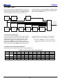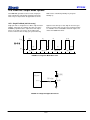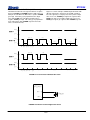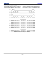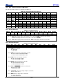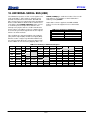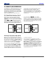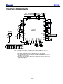
1
ST2205U Integrated Microcontroller
User’s Manual
ST2205UM
Rev. 1.0, 06/2005
ST2205U
CONTENTS
CONTENTS .......................................................................................................................................................................................... 2
1. GENERAL DESCRIPTION ............................................................................................................................................................... 3
2. FEATURES....................................................................................................................................................................................... 5
3. SIGNAL DESCRIPTIONS ................................................................................................................................................................ 6
4. PAD DIAGRAM ................................................................................................................................................................................ 8
5. DEVICE INFORMATION .................................................................................................................................................................. 9
6. CPU .................................................................................................................................................................................................11
7. MEMORY CONFIGURATION ......................................................................................................................................................... 12
7.1 Memory Map and Banking .................................................................................................................................................. 12
7.2 Control Registers................................................................................................................................................................. 14
7.3 Interrupt Bank Register ....................................................................................................................................................... 16
7.4 RAM .................................................................................................................................................................................... 17
8. INTERRUPT CONTROLLER ......................................................................................................................................................... 18
8.1 Interrupt Description ............................................................................................................................................................ 19
9. GPIO............................................................................................................................................................................................... 21
9.1 Port-A Transistion Interrupt.................................................................................................................................................. 23
9.1.1 Port-A Interrupt De-Bounce..................................................................................................................................... 23
9.2 External Interrupts ............................................................................................................................................................... 24
10. CHIP-SELECT LOGIC (CSL) ....................................................................................................................................................... 25
11. CLOCK GENERATOR.................................................................................................................................................................. 27
12. TIMER/EVENT COUNTER ........................................................................................................................................................... 31
12.1 Prescaler ........................................................................................................................................................................... 31
12.1.1 Function Description ............................................................................................................................................. 31
12.1.2 PRES .................................................................................................................................................................... 32
12.2 Base Timer ........................................................................................................................................................................ 33
12.2.1 Base Timer Operations ......................................................................................................................................... 33
12.2.2 Base Timer Control/Status Registers .................................................................................................................... 33
12.3 Timer ................................................................................................................................................................................. 35
12.3.1 Function Description ............................................................................................................................................. 35
12.3.2 Timer Clock Source Control .................................................................................................................................. 35
13. CLOCKING OUTPUTS................................................................................................................................................................. 37
14. PSG .............................................................................................................................................................................................. 38
14.1 Function Description.......................................................................................................................................................... 38
14.2 Tone Generator ................................................................................................................................................................. 40
14.3 PCM DAC.......................................................................................................................................................................... 40
14.4 ADPCM DAC ..................................................................................................................................................................... 40
14.5 PWM DAC Output Mode Options ...................................................................................................................................... 44
14.5.1 Single-Pin Mode (8-bit Accuracy).......................................................................................................................... 44
14.5.2 Two-Pin Two Ended Mode (8-bit Accuracy) .......................................................................................................... 45
14.5.3 Two-Pin Push Pull Mode (8-bit Accuracy) ............................................................................................................. 46
15. LCD .............................................................................................................................................................................................. 47
15.1 LCD Specific Signals ......................................................................................................................................................... 48
15.2 Mapping the Display Data ................................................................................................................................................. 49
15.3 LCD Interface Timing......................................................................................................................................................... 50
15.4 Control Registers............................................................................................................................................................... 51
15.4.1 LCD Screen Starting Address Register ................................................................................................................. 51
15.4.2 LCD Virtual Page Width Register.......................................................................................................................... 51
15.4.3 LCD Screen Width Register.................................................................................................................................. 51
15.4.4 LCD Screen Height Register................................................................................................................................. 51
15.4.5 LCD Panning Offset Register................................................................................................................................ 51
15.4.6 LCD Buffer Size Register...................................................................................................................................... 52
15.4.7 LCD Control Register............................................................................................................................................ 52
15.4.8 LCD Frame Rate Adjust Register.......................................................................................................................... 52
15.4.9 LCD Frame Rate Adjust Register.......................................................................................................................... 52
15.4.10 LCD AC Signal Rate Register ............................................................................................................................. 53
15.4.11 LCD PWM Contrast Control Register.................................................................................................................. 53
15.4.12 LCD Gray Level Palette ...................................................................................................................................... 54
16. SERIAL PERIPHERAL INTERFACE ........................................................................................................................................... 55
16.1 SPI Operations .................................................................................................................................................................. 55
2/87
ST2205U
16.1.1 Clock Phase and Polarity Controls ....................................................................................................................... 55
16.1.2 Transmit Buffer and Receive Buffer ...................................................................................................................... 56
16.1.3 Master, Slave Modes and The Shift Register........................................................................................................ 56
16.1.4 SPI Interrupts........................................................................................................................................................ 57
16.2 Interface Signals................................................................................................................................................................ 57
16.3 SPI Control/Status Registers ............................................................................................................................................. 58
16.3.1 SPI Data Registers ............................................................................................................................................... 58
16.3.2 SPI Control Register ............................................................................................................................................. 58
16.3.3 SPI Status Register............................................................................................................................................... 59
16.3.4 SPI IIS interface.................................................................................................................................................... 59
17. UNIVERSAL ASYNCHRONOUS RECEIVER/TRANSMITTER.................................................................................................... 60
17.2 UART Operations .............................................................................................................................................................. 60
17.2.1 NRZ mode ............................................................................................................................................................ 60
17.2.2 IrDA mode............................................................................................................................................................. 60
17.2.3 Transmitter Operation ........................................................................................................................................... 61
17.2.4 Receiver Operation............................................................................................................................................... 61
17.3 Interface Signals................................................................................................................................................................ 61
17.4 UART Control/Status Registers ......................................................................................................................................... 62
17.4.1 UART Control Register ......................................................................................................................................... 62
17.4.2 UART Status Control Register .............................................................................................................................. 63
17.4.3 IrDA Control Register............................................................................................................................................ 62
17.4.4 UART Data Register ............................................................................................................................................. 63
17.5 Settings For Standard Baud Rates .................................................................................................................................... 64
18. Universal Serial Bus (USB) ........................................................................................................................................................ 66
18.2 USB Control/Status Registers ........................................................................................................................................... 67
18.2.1 USB Control Register............................................................................................................................................ 67
18.2.2 USB Interrupt Control Register ............................................................................................................................. 67
18.2.3 USB Interrupt Request Register ........................................................................................................................... 68
18.2.4 USB Buffer Status Register................................................................................................................................... 68
18.2.5 Endpoint0 Control Register................................................................................................................................... 69
18.2.6 Endpoint0 OUT Buffer Data Length Register ........................................................................................................ 69
18.2.7 Bulk IN/OUT Endpoints Control Register .............................................................................................................. 69
18.2.8 Bulk OUT Endpoint Data Length Register............................................................................................................. 70
19. DIRECT MEMORY ACCESS (DMA) ............................................................................................................................................ 71
19.1 DMA Control Register........................................................................................................................................................ 71
19.1.1 DMA Pointer Register ........................................................................................................................................... 71
19.1.2 DMA Bank Register .............................................................................................................................................. 71
19.1.3 DMA Length Register............................................................................................................................................ 72
19.1.4 DMA Register Select Bits...................................................................................................................................... 72
19.1.5 DMA Mode Selection Register .............................................................................................................................. 72
20. Nand Flash Interface................................................................................................................................................................... 73
20.1 Nand Flash Interface, Port-F ............................................................................................................................................. 73
20.2 Error Correction Code (ECC) ............................................................................................................................................ 73
20.3 Nand Flash Interface Control Registers ............................................................................................................................ 74
21. POWER DOWN MODES.............................................................................................................................................................. 75
21.1 WAI-0 Mode: ..................................................................................................................................................................... 75
21.2 WAI-1 Mode: ..................................................................................................................................................................... 75
21.3 STP Mode: ........................................................................................................................................................................ 75
22. WATCHDOG TIMER..................................................................................................................................................................... 76
22.1 WDT Operations................................................................................................................................................................ 76
23. Real Time Clock .......................................................................................................................................................................... 77
24. LOW VOLTAGE DETECTOR (LVD)............................................................................................................................................. 78
25. LOW VOLTAGE RESET (LVR) .................................................................................................................................................... 80
26. ELECTRICAL CHARACTERISTICS ............................................................................................................................................ 81
26.1 Absolute Maximum Rations............................................................................................................................................... 81
26.2 DC Electrical Characteristics ............................................................................................................................................. 81
AC Electrical Characteristics ..................................................................................................................................................... 81
27. APPLICATION CIRCUITS ............................................................................................................................................................ 84
28. REVISIONS .................................................................................................................................................................................. 85
2/87
ST2205U
1. GENERAL DESCRIPTION
The ST2205U is a 8-bit integrated microcontroller designed
with CMOS silicon gate technology. The true static CPU core,
power down modes and dual oscillators design makes the
ST2205U suitable for power saving and long battery life
designs. The ST2205U integrates various logic to support
functions on-chip which are needed by system designers. This
is also important for lower system complexity, small board size
and, of course, shorter time to market and less cost.
and IrDA, with system components or other products such as
PC, Notebook, and popular PDA. Two clocking outputs can
produce synthesized PWM signals or high frequency carrier for
IR remote control. This helps products become more useful in
our daily life.
The ST2205U features the capacity of memory access of
maximum 44M bytes which is needed by products with large
data bases. Six chip selects are equipped for direct connection
to external ROM, SRAM, Flash memory or other devices.
Maximum one single device of 16M bytes is possible.
Two DMA channels make fast data transfer possible and easy.
Both source and destination pointers can refer to the whole
memory space with 15-bit pointers and bank registers. Besides
normal operation, two special modes are designed for double
transfer speed of Nand Flash memory and also fast graphic
operation between two display pictures.
Nand Flash is a low cost mass data storage solution for newly
design. The ST2205U equips a Nand flash interface to connect
both Nand and And Flash memories. Both ECC generating and
checking functions are supported. These are very important for
Flash data management.
The ST2205U has 56 I/Os grouped into 7 ports, Port-A ~ Port-F
and Port-L. Each pin can be programmed to input or output.
There are two options: pull-up/down for inputs of Port-C and
only pull-up for inputs of the other ports. In case of output,
there are open-drain/CMOS options for outputs of PortC and
only CMOS for other ports. Port-A is designed for keyboard
scan with de-bounce and transition triggered interrupt, while
Port-C/D/E/F/L are shared with other system functions. All the
properties of I/O pins are still programmable when they are
assigned to another function. This enlarges the flexibility of the
usage of function signals.
The internal 32K bytes RAM helps to drive large LCD panels
up to 160xRGBx120. Together with 16-graylevel support, the
ST2205U can rich display information and the diversity of
contents as well. This is done with no need of external display
RAM because of the special internal memory sharing design.
The variable display buffer technique also make large panel
size with small internal RAM possible. User may free major
internal RAM for temporary computing or access while keeping
the display content correct.
The ST2205U equips serial communication ports of one UART
and one SPI to perform different communications, ex.: RS-232
3/87
Communication with PC via USB is becoming more and more
popular. The ST2205U features one PLL, a 3.3V regulator, and
a USB 1.1 device engine to satisfy the strong demand of fast
data transfer from market. Both HID and Mass storage classes
are supported as well as the firmware libraries and the
Windows drivers.
The built-in four channels PSG and a 12-bit current DAC
provide a nice quality voice together with a 4-channel
wavetable melody in the background. Both voice and melody
functions have buffers to make program easier and well
structured, and also a 16x8 multiplier is to control the volumn of
each channel. Besides hardware, ADPCM algorithm and a
MIDI converter Windows software are also provided to speed
up the development. In addition to current DAC, two dedicated
pins with large driving capacity can drive a buzzer/speaker
directly for minimum cost.
The ST2205 has one Low Voltage Detector (LVD) for power
management. The status of internal or external power can be
detected and reported to the management software.
Power bouncing during power on is a major problem when
designing a reliable system. The ST2205U equips Low Voltage
Reset (LVR) function to keep whole system in reset status
when power is low. After the power backs to normal, the
system may recover its original states and keeps working
correctly. Besides LVR, Watch Dog Timer (WDT) is also built-in
and is an essential function for a good design.
Power consumption is another big issue for a battery-powered
device. The ST2205U has different power down modes and
clock switch scheme to make the consuming power as low as
possible. The built-in Real Time Clock (RTC) is not only for
keeping time correctly but also an alternative of software timer
with much lower working power.
The ST2205U equips an ICE debug interface for efficient
development flow. Besides hardware emulator, a software
simulator is also supported to save programmers setting up the
system and makes programming be at anywhere.
With these integrated functions inside, the ST2205U single chip
microcontroller is a right solution for PDA, translator, databank
and other consumer products.
SS /PC4
DATA_READY /PC5
WR
RD
CS0
CS5 ~ 1/PD4 ~ 0
CS6 /A23 /PD5
FWR /PD7
FRD /PD6
BLANK
POFF
FIGURE 1-1 ST2205U Block Diagram
ST2205U
2. FEATURES
Totally static 8-bit CPU
ROM: 16K x 8-bit(OTP)
RAM: 32K x 8-bit
Stack: Up to 128-level deep
Operation voltage: 2.4V ~ 3.6V
Operation frequency:
– [email protected](Min.)
– [email protected](Min.)
One 16x8 Signed Multiplier
Low Voltage Reset (LVR)
– Two levels of bonding options
Low Voltage Detector (LVD)
– Programmable 4 levels
– System power or external battery level can be detected.
Flash Memory Interface
– On the fly ECC code generation and detection
– Fast data transfer with dedicated DMA channel
– Nand and And type Flash supported
USB 1.1 device
– Integrate one PLL to produce 48Mhz clock
– Built-in 3.3V regulator for transceiver
– Mass storage class supported
– Double buffering and direct buffer access increase
throughput and ease real-time data transfer
Direct Memory Access (DMA)
– Two channels with special modes for Flash and display
– Three address generation modes
Memory configuration
– Four kinds of banks for bios, program, data, interrupt
and internal RAM
– 13-bit bank registers support up to 44M bytes
– Six programmable chip-selects with 4 modes
– Maximum single device of 16M bytes
General-Purpose I/O (GPIO) ports
– 56 multiplexed CMOS bit programmable I/Os
– Hardware de-bounce option for Port-A
– Bit programmable pull-up/down or open-drain/CMOS
Timer/Counter
– Four 12-bit and one 8-bit timers
– Seven fixed time bases
Watchdog Timer (WDT)
– Two selectable time bases
– Programmable WDT interrupt or reset
Real-time Clock (RTC)
– Full clock function, second/ minute/ hour and day, with
three counters and interrupts
– One programmable alarm
Three External Interrupt Sources
Three clocking outputs
– Clock sources including Timer0, OSCN clock, baud rate
generator
Prioritized interrupts with dedicated exception vectors
– External interrupts (x3) (edge triggered)
5/87
– PortA interrupt (transition triggered)
– LCD buffer interrupt
– Base timer interrupt (x8)
– Timer0~3 interrupts (x4)
– SPI interrupts (x2)
– UART interrupts (x2)
– USB interrupts (x6)
– PCM interrupt
– RTC interrupts (x4)
Dual clock sources with warm-up timer
– Low frequency crystal oscillator (OSCX)
····················································32768 Hz
– High frequency resistor or crystal/resonator oscillator
(OSC) selected by pin option .................. 455K~8M Hz
LCD Controller (LCDC)
– Programmable display size:
COM: 512 max. SEG: 1024 max.
Max. 160xRGBx120 color STN supported by internal
buffer
– Hardware 4/16 gray levels with 5-bit palette, up to 4096
colors supported
– Share system memory with display buffer and with no
loss of the CPU time
– Support 1-/4-/8-bit LCD data bus
– Diverse functions including virtual screen, panning,
scrolling, contrast control, alternating signal generator,
buffer switching and fast graphic data manipulation
Programmable Sound Generator (PSG)
– Four channels with three playing modes:
9-bit ADPCM, 8-bit PCM and 8-bit melody
– One 16-byte buffer and 6-bit volume control per channel
– Wavetable melody support
– Two dedicated PWM outputs for direct driving
12-bit current DAC with two 4-word buffer
Universal Asynchronous Receiver/Transmitter (UART)
– Full-duplex operation
– Baud rate generator with one digital PLL
– Standard baud rates of 600 bps to 115.2 kbps
– Both transmitter and receiver buffers supported
– Direct glueless support of IrDA physical layer protocol
– Two sets of I/Os (TX,RX) for two independent devices
Serial Peripheral Interface (SPI)
– Inter IC sound (IIS) supported
– Master and slave modes
– Five serial signals including enable and data-ready
– Both transmitter and receiver buffers supported
– Programmable data length from 7-bit to 16-bit
Three power down modes
– WAI0 mode
– WAI1 mode
– STP mode
On-chip ICE debug interface
ST2205U
3. SIGNAL DESCRIPTIONS
TABLE 3-1 Signal Function Groups
Function Group
Pad No.
Designation
Power
11,61,83,
84,100,
104,117
132
VDD, IOVDD,AVDD
PSGVDD, USBVDD
PLLVDD, VPP
Ground
10,40,85,
96,103,
105,114,
129
VSS,IOVSS,AVSS1
AVSS2,PSGVSS,
USBVSS,PLLVSS
System control
1,30,68,86
87,115,116
120,
124~128
RESET ,
TEST1/2/3,
ICE1/2/3/4/5/6,
MMD/ CS0 , LVRSEL
VIN
Clock
118,119,
121~123
XMD,
XIO,OSCI
OSCXO,OSCXI
External memory
bus signals
29,31
41~60,
62~64
32~39
PWM DAC
Current DAC
Keyboard scan
signal (return
line)
GPIO
130,131
WR , RD
A[22:0]
D[7:0]
PSGO/COUT,
PSGOB
106~113
PA7~0
2,88~95
PB7~0
PC0
Description
VDD: Power supply for internal core
IOVDD: Power supply for IO
AVDD: Power supply for analog blocks
PSGVDD: Power supply for PSGO and PSGOB
USBVDD: Power supply for USB circuit
PLLVDD: Power supply for PLL circuit
VPP: Power supply for programming OTP ROM
VSS: Power ground for internal core
IOVSS: Power ground for IO
AVSS: Power ground for analog blocks
PSGVSS: Power ground for PSGO and PSGOB
USBVSS: Power ground for USB circuit
PLLVSS: Power ground for PLL circuit
RESET : Active low system reset signal input
TEST1/2/3, ICE1/2/3/4/5/6: Leave them open when normal operation
MMD/CS0: Memory modes selection pin
Normal mode: Enable internal ROM.
MMD/ CS0 connects to GND.
Emulation mode: Disable internal ROM.
MMD/ CS0 connects to chip-select pin of external ROM. One
resistor should be added between VCC and this pin. After reset
cycles, MMD/ CS0 changes to be an output, and outputs signal
CS0 .
LVRSEL: LVR active level selection input
Low: LVR active level is 2.1V
High: LVR active level is 2.8V
VIN: Input voltage level for Low Voltage Detection
XMD: High frequency oscillator (OSC) mode selection input
Low: Crystal mode
One crystal or resonator should be connected between OSCI
and XIO
High: Resistor oscillator mode
One resistor should be connected between OSCI and VCC
OSCXI, OSCXO: Connect one 32768Hz crystal between these two
pins when using low frequency oscillator
External memory R/W control signals
External memory address bus
External memory data bus
PSGO/PSGOB: PSG outputs. Connect to one buzzer or speaker
COUT: Also 12-bit current DAC output by register control
I/O port A
I/O port B and PC0
6/87
ST2205U
TABLE 3-2 Signal Function Groups (continued)
Function Group
Pad No.
Flash Data Bus
65~67,
69~73
Flash read/write
signals
27,28
Chip selects
21~26
UART
8,9
27,28
SPI
3~7
Clocking output/
External clock
input or interrupt
sources
LCD control
signals
USB 1.1
13~15
Designation
FD7~0/PF7~0
RXD1/ FWR /PD7
TXD1/ FRD /PD6
CS5 ~ 1 /PD4~0,
CS6 /A23/PD5
RXD0/PC7,TXD0/PC
6, RXD1/ FWR /PD7
TXD1/ FRD /PD6
DATA_READY /PC5 ,
SS /PC4 , SDO/PC3 ,
SDI/PC2 , SCK/PC1
BCO/INTX2/PE2 ,
OSCN/INTX1//PE1
TCO0/INTX0//PE0
12,16~20,
74~82
FLM/PL7, LP1/PL6,
AC/PL5 , CP/PL4,
LD[3:0]/PL3~0,
LD[7:4]/PE6~3,
LP2/PE7,
POFF , BLANK ,
97~99,101
102
VBUS,
RPULL, VOUT3.3,
D+, D-
Description
Flash data bus
When function bits are set, and I/O direction is output, and FEN=1,
PD7/6 are flash control signals
I/O port D and chip-select outputs
UART signals and I/Os
SPI signals and I/Os
When function bits are set, and I/O direction is output, these three
can be clocking outputs.
When function bits are set, and I/O direction is input, these three
can be external clock inputs or external interrupt sources.
When function bits are cleared, they are three GPIOs.
LCD control signals
VBUS: Connect to USB bus power
D+,D-: USB differential signal pins
RPULL: Add a resistor of 1.5K between this pin and D+
VOUT3.3: 3.3V regulator output. Connect to USBVDD to supply
power for the analog transceiver of USB
7/87
ST2205U
4. PAD DIAGRAM
8/87
ST2205U
5. DEVICE INFORMATION
1.
2.
3.
Pad size: 90um x 90um
Substrate: GND
Chip size: 3490um x 4070um
PAD No.
Symbol
1
ICE6
X
PAD No.
Symbol
-1965.0
36
D3
1675.0
-1300.0
D2
1675.0
-1200.0
Y
-1465.1
X
Y
2
PC0
-1345.1
-1965.0
37
3
PC1
-1245.1
-1965.0
38
D1
1675.0
-1100.0
D0
1675.0
-1000.0
4
PC2
-1145.1
-1965.0
39
5
PC3
-1045.1
-1965.0
40
IOVSS
1675.0
-900.0
A0
1675.0
-800.0
6
PC4
-945.1
-1965.0
41
7
PC5
-845.1
-1965.0
42
A1
1675.0
-700.0
A2
1675.0
-600.0
8
PC6
-745.1
-1965.0
43
9
PC7
-645.1
-1965.0
44
A3
1675.0
-500.0
10
VSS
-545.1
-1965.0
45
A4
1675.0
-400.0
A5
1675.0
-300.0
11
VDD
-345.1
-1965.0
46
12
BLANK
-245.1
-1965.0
47
A6
1675.0
-200.0
A7
1675.0
-100.0
13
PE0
-145.1
-1965.0
48
14
PE1
-45.1
-1965.0
49
A17
1675.0
0.0
A18
1675.0
100.0
15
PE2
55.0
-1965.0
50
16
PE3
155.0
-1965.0
51
A19
1675.0
200.0
A20
1675.0
300.0
17
PE4
255.0
-1965.0
52
18
PE5
355.0
-1965.0
53
A21
1675.0
400.0
19
PE6
455.0
-1965.0
54
A22
1675.0
500.0
A8
1675.0
600.0
20
PE7
555.0
-1965.0
55
21
PD0
655.0
-1965.0
56
A9
1675.0
700.0
A10
1675.0
800.0
22
PD1
755.0
-1965.0
57
23
PD2
855.0
-1965.0
58
A11
1675.0
900.0
A12
1675.0
1000.0
24
PD3
955.0
-1965.0
59
25
PD4
1055.0
-1965.0
60
A13
1675.0
1100.0
IOVDD
1675.0
1200.0
26
PD5
1155.0
-1965.0
61
27
PD6
1255.0
-1965.0
62
A14
1675.0
1300.0
A15
1675.0
1400.0
28
PD7
1355.0
-1965.0
63
29
WR
MMD/ CS0
1475.0
-1965.0
64
A16
1675.0
1500.0
1675.0
-1940.0
65
PF0
1675.0
1600.0
1675.0
-1820.0
66
PF1
1675.0
1700.0
1675.0
-1700.0
67
PF2
1675.0
1820.0
TEST1
1675.0
1940.0
30
31
32
RD
D7
33
D6
1675.0
-1600.0
68
34
D5
1675.0
-1500.0
69
PF3
1475.0
1965.0
-1400.0
70
PF4
1355.0
1965.0
35
D4
1675.0
9/87
ST2205U
PAD No.
Symbol
X
Y
PAD No.
Symbol
71
PF5
1255.0
72
PF6
73
74
1965.0
106
PA0
-1675.0
747.1
1155.0
1965.0
107
PA1
-1675.0
647.1
PF7
1055.0
1965.0
108
PA2
-1675.0
547.1
PL0
955.0
1965.0
109
PA3
-1675.0
447.1
75
PL1
855.0
1965.0
110
PA4
-1675.0
347.1
76
PL2
755.0
1965.0
111
PA5
-1675.0
247.1
77
PL3
655.0
1965.0
112
PA6
-1675.0
147.1
78
PL4
555.0
1965.0
113
PA7
-1675.0
47.1
79
PL5
455.0
1965.0
114
AVSS1
-1675.0
-53.0
80
PL6
355.0
1965.0
115
VIN
-1675.0
-153.0
81
PL7
255.0
1965.0
116
LVRSEL
-1675.0
-253.0
82
POFF
155.0
1965.0
117
AVDD
-1675.0
-353.0
83
VPP
55.0
1965.0
118
OSCXI
-1675.0
-453.0
84
VDD
-45.0
1965.0
119
OSCXO
-1675.0
-553.0
85
VSS
-245.0
1965.0
120
RESET
-1675.0
-653.0
86
TEST2
-345.0
1965.0
121
OSCI
-1675.0
-753.0
87
TEST3
-445.0
1965.0
122
XIO
-1675.0
-853.0
88
PB0
-545.0
1965.0
123
XMD
-1675.0
-953.0
89
PB1
-645.0
1965.0
124
ICE3
-1675.0
-1053.0
90
PB2
-745.0
1965.0
125
ICE2
-1675.0
-1153.0
91
PB3
-845.0
1965.0
126
ICE1
-1675.0
-1253.0
92
PB4
-945.0
1965.0
127
ICE4
-1675.0
-1353.0
93
PB5
-1045.0
1965.0
128
ICE5
-1675.0
-1453.0
94
PB6
-1145.0
1965.0
129
PSGVSS
-1675.0
-1553.0
95
PB7
-1245.0
1965.0
130
PSBO
-1675.0
-1673.0
96
USBVSS
-1438.0
1965.0
131
PSGOB
-1675.0
-1793.0
97
RPULL
-1656.1
1965.0
132
PSGVDD
-1675.0
-1913.0
98
D+
-1675.0
1764.7
99
D-
-1675.0
1644.7
100
USBVDD
-1675.0
1532.7
101
VOUT3.3
-1675.0
1422.7
102
VBUS
-1675.0
1232.7
103
AVSS2
-1675.0
1075.8
104
PLLVDD
-1675.0
975.8
105
PLLVSS
-1675.0
875.8
10/87
X
Y
ST2205U
6. CPU
Register Model
7
7
1
Index Register X
0
PCL
7
Index Register Y
0
X
7
Accumulator A
0
Y
7
PCH
0
A
Program Counter PC
0
S
Stack Pointer S
Accumulator (A)
direction of either the program or interrupts (IRQ). The stack
allows simple implementation of nested subroutines and
multiple level interrupts. The stack pointer is initialized by the
user’s software.
Index Registers (X,Y)
The 16-bit Program Counter register provides the address,
which step the microprocessor through sequential program
instructions. Each time the microprocessor fetches and
instruction from program memory, the lower byte of the
program counter (PCL) is placed on the low-order bits of the
address bus and the higher byte of the program counter (PCH)
is placed on the high-order 8 bits. The counter is increment
each time an instruction or data is fetched from program
memory.
The Accumulator is a general-purpose 8-bit register that stores
the results of most arithmetic and logic operations. In addition,
the accumulator usually contains one of the two data words
used in these operations.
There are two 8-bit Index Registers (X and Y), which may be
used to count program steps or to provide and index value to
be used in generating an effective address. When executing an
instruction, which specifies indexed addressing, the CPU
fetches the OP code and the base address, and modifies the
address by adding the index register to it prior to performing
the desired operation. Pre or post-indexing of indirect
addresses is possible.
Status Register (P)
Stack Pointer (S)
The Stack Pointer is an 8-bit register, which is used to control
the addressing of the variable-length stack. It’s range from
100H to 1FFH total for 256 bytes (128 level deep). The stack
pointer is automatically increment and decrement under control
of the microprocessor to perform stack manipulations under
Bit 7
N
Bit 6
V
Program Counter (PC)
Bit 5
1
The 8-bit Processor Status Register contains seven status flags.
Some of these flags are controlled by program; others may be
also controlled by the CPU as well. The instruction set contains
a member of conditional branch instructions that are designed
to allow testing of these flags. Refer to TABLE 6-1
TABLE 6-1 Status Register (P)
Bit 7: N : Signed flag by arithmetic
1 = Negative
0 = Positive
Bit 6: V : Overflow of signed Arithmetic flag
1 = Negative
0 = Positive
Bit 4
B
Bit 3
D
Bit 4: B : BRK interrupt flag
1 = BRK interrupt occur
0 = Non BRK interrupt occur
11/87
Bit 2
I
Bit 1
Z
Bit 3: D : Decimal mode flag
1 = Decimal mode
0 = Binary mode
Bit 2: I : Interrupt disable flag
1 = Interrupt disable
0 = Interrupt enable
Bit 1: Z : Zero flag
1 = Zero
0 = Non zero
Bit 0: C : Carry flag
1 = Carry
0 = Non carry
Bit 0
C
ST2205U
7. MEMORY CONFIGURATION
7.1 Memory Map and Banking
$8000~$FFFF. These three bank registers can refer to a
maximum extended memory space of 48M bytes.
The logical memory space of ST2205U is divided into 4 parts:
$0000~$1FFF (8K), $2000~$3FFF (8K), $4000~$7FFF (16K),
and $8000~FFFF (32K). First is for control registers, stack, and
system memory. The rest are three banked areas for physical
memory space. The physical memory space here can refer to
two areas which are internal 32KB RAM area and extended
48MB memory area.
Note: Only 44M (28M when CSM0=”0”) bytes is
addressable by chip selects.
Besides extended memory, the internal 32KB RAM can also be
accessed by three bank registers by setting bit15 of each bank
register. With BRR[15]=1, 8KB internal RAM ($2000~$3FFF)
can be accessed. And with PRR[15]=1, 16KB internal RAM
($4000~$7FFF) can be accessed. Moreover, the whole 32KB
internal RAM ($8000~$FFFF) can be accessed by setting
DRR[15].
Logical address in banked areas combines one of three bank
registers, BRR, PRR and DRR, respectively and then be
mapped to a continuous 26bit wide physical address. BRR is a
13-bit Bios Program ROM Bank register and controls the 8KB
banked logical area in $2000~$3FFF. PRR is Program ROM
Bank Register and is 12-bit long, and its logical address is
$4000~$7FFF. The third one DRR is Data ROM Bank Register
of a length of 11 bits. DRR control the last logical area,
Address Name
$32
$33
$34
$35
$36
$37
PRRL
PRRH
DRRL
DRRH
BRRL
BRRH
Bit 7
R/W
R/W
R/W
R/W
R/W
R/W
Refer to TABLE 7-1 for three bank registers.
Refer to FIGURE 7-1 for memory mapping of ST2205U.
TABLE 7-1 Bank Registers and Logical Range
Bit 6
PRR[7] PRR[6]
PRR[11
DRR[7] DRR[6]
DRR[10]
BRR[7] BRR[6]
BRR[15]
-
Bit 5
Bit 4
PRR[5] PRR[4]
DRR[5] DRR[4]
BRR[5] BRR[4]
BRR[12]
Bit 3
Bit 2
Bit 1
Bit 0
Default
PRR[3]
PRR[11]
DRR[3]
BRR[3]
BRR[11]
PRR[2]
PRR[10]
DRR[2]
DRR[10]
BRR[2]
BRR[10]
PRR[1]
PRR[9]
DRR[1]
DRR[9]
BRR[1]
BRR[9]
PRR[0]
PRR[8]
DRR[0]
DRR[8]
BRR[0]
BRR[8]
0000 0000
0- - - 0000
0000 0000
0- - - -000
0000 0000
1- -0 0000
BRR[0:11] : 13-bit BRR bank register. Control logical banked area of $2000~$3FFF.
PRR[0:11] : 12-bit PRR bank register. Control logical banked area of $4000~$7FFF.
DRR[0:11] : 11-bit DRR bank register. Control logical banked area of $8000~$FFFF.
BRR[15]/PRR[15]/DRR[15] : Internal RAM mapping control
0 = Disable internal RAM mapping. Banked area refers to extended memory space.
1 = Enable respective internal RAM mapping of each banked area
12/87
ST2205U
FIGURE 7-1 Memory Mapping of ST2205U
13/87
ST2205U
7.2 Control Registers
Address $000~$07F is for control registers. Refer to TABLE 7-2 for the summary of all registers. There are more details of registers
in the related sections.
TABLE 7-2 Control Registers Summary
Address
$00
$01
$02
$03
$04
$05
$06
$07
$08
$09
$0A
$0B
$0C
$0D
$0E
$0F
$10
$11
$12
$13
$14
$15
$16
$17
$18
$19
$1A
$1B
$1C
$1D
$1E
$1F
$20
$21
$22
$23
$24
$25
$26
$27
$28
$29
$2A
$2B
$2C
$2D
Name R/W
PA(OUT) R/W
R
PA*(IN)
W
PB(OUT) R/W
R
PB*(IN)
W
PC(OUT) R/W
R
PC*(IN)
W
PD(OUT) R/W
R
PD*(IN)
W
PE(OUT) R/W
R
PE*(IN)
W
PF(OUT) R/W
R
PF*(IN)
W
PSC
R/W
PSE
R/W
PCA
R/W
PCB
R/W
PCC
R/W
PCD
R/W
PCE
R/W
PCF
R/W
PFC
R/W
PFD
R/W
PSG0A R/W
PSG0B R/W
PSG1A R/W
PSG1B R/W
PSG2A R/W
PSG2B R/W
PSG3A R/W
PSG3B R/W
VOL0
R/W
VOL1
R/W
VOL2
R/W
VOL3
R/W
VOLM0 R/W
VOLM1 R/W
PSGC
R/W
PSGM
R/W
T0CL
R/W
T0CH
R/W
T1CL
R/W
T1CH
R/W
T2CL
R/W
T2CH
R/W
T3CL
R/W
T3CH
R/W
TIEN
R/W
R
PRS*
W
BTEN
R/W
R
BTREQ*
W
BTC
R/W
T4C
R/W
Bit 7
PA[7]
PA[7]
PAPULL[7]
PB[7]
PB[7]
PBPULL[7]
PC[7]
PC[7]
PCPULL[7]
PD[7]
PD[7]
PDPULL[7]
PE[7]
PE[7]
PEPULL[7]
PF[7]
PF[7]
PFPULL[7]
PSC[7]
PSE[7]
PCA[7]
PCB[7]
PCC[7]
PCD[7]
PCE[7]
PCF[7]
RXD0
RXD1
PSG0A[7]
PSG0B[7]
PSG1A[7]
PSG1B[7]
PSG2A[7]
PSG2B[7]
PSG3A[7]
PSG3B[7]
VOLS0
VOLS1
VOLS2
VOLS3
P3EN
PMD3[1]
T0C[7]
LOAD
T1C[7]
LOAD
T2C[7]
LOAD
T3C[7]
LOAD
T4CK[2]
PRS[7]
SRES
BTEN7
BTREQ7
BTCLR7
BTC[7]
T4C[7]
Bit 6
PA[6]
PA[6]
PAPULL[6]
PB[6]
PB[6]
PBPULL[6]
PC[6]
PC[6]
PCPULL[6]
PD[6]
PD[6]
PDPULL[6]
PE[6]
PE[6]
PEPULL[6]
PF[6]
PF[6]
PFPULL[6]
PSC[6]
PSE[6]
PCA[6]
PCB[6]
PCC[6]
PCD[6]
PCE[6]
PCF[6]
TXD0
TXD1
PSG0A[6]
PSG0B[6]
PSG1A[6]
PSG1B[6]
PSG2A[6]
PSG2B[6]
PSG3A[6]
PSG3B[6]
CLIP
P2EN
PMD3[0]
T0C[6]
T0CK[2]
T1C[6]
T1CK[2]
T2C[6]
T2CK[2]
T3C[6]
T3CK[2]
T4CK[1]
PRS[6]
SENA
BTEN6
BTREQ6
BTCLR6
BTC[6]
T4C[6]
Bit 5
PA[5]
PA[5]
PAPULL[5]
PB[5]
PB[5]
PBPULL[5]
PC[5]
PC[5]
PCPULL[5]
PD[5]
PD[5]
PDPULL[5]
PE[5]
PE[5]
PEPULL[5]
PF[5]
PF[5]
PFPULL[5]
PSC[5]
PSE[5]
PCA[5]
PCB[5]
PCC[5]
PCD[5]
PCE[5]
PCF[5]
SRDY
CS6
PSG0A[5]
PSG0B[5]
PSG1A[5]
PSG1B[5]
PSG2A[5]
PSG2B[5]
PSG3A[5]
PSG3B[5]
VOL0[5]
VOL1[5]
VOL2[5]
VOL3[5]
VOLM0[5]
VOLM1[5]
P1EN
PMD2[1]
T0C[5]
T0CK[1]
T1C[5]
T1CK[1]
T2C[5]
T2CK[1]
T3C[5]
T3CK[1]
T4CK[0]
PRS[5]
BTEN5
BTREQ5
BTCLR5
BTC[5]
T4C[5]
Bit 4
PA[4]
PA[4]
PAPULL[4]
PB[4]
PB[4]
PBPULL[4]
PC[4]
PC[4]
PCPULL[4]
PD[4]
PD[4]
PDPULL[4]
PE[4]
PE[4]
PEPULL[4]
PF[4]
PF[4]
PFPULL[4]
PSC[4]
PSE[4]
PCA[4]
PCB[4]
PCC[4]
PCD[4]
PCE[4]
PCF[4]
SS
CS5
PSG0A[4]
PSG0B[4]
PSG1A[4]
PSG1B[4]
PSG2A[4]
PSG2B[4]
PSG3A[4]
PSG3B[4]
VOL0[4]
VOL1[4]
VOL2[4]
VOL3[4]
VOLM0[4]
VOLM1[4]
P0EN
PMD2[0]
T0C[4]
T0CK[0]
T1C[4]
T1CK[0]
T2C[4]
T2CK[0]
T3C[4]
T3CK[0]
T4EN
PRS[4]
BTEN4
BTREQ4
BTCLR4
BTC[4]
T4C[4]
14/87
Bit 3
PA[3]
PA[3]
PAPULL[3]
PB[3]
PB[3]
PBPULL[3]
PC[3]
PC[3]
PCPULL[3]
PD[3]
PD[3]
PDPULL[3]
PE[3]
PE[3]
PEPULL[3]
PF[3]
PF[3]
PFPULL[3]
PSC[3]
PSE[3]
PCA[3]
PCB[3]
PCC[3]
PCD[3]
PCE[3]
PCF[3]
MOSI
CS4
PSG0A[3]
PSG0B[3]
PSG1A[3]
PSG1B[3]
PSG2A[3]
PSG2B[3]
PSG3A[3]
PSG3B[3]
VOL0[3]
VOL1[3]
VOL2[3]
VOL3[3]
VOLM0[3]
VOLM1[3]
PCMEN
PMD1[1]
T0C[3]
T0C[11]
T1C[3]
T1C[11]
T2C[3]
T2C[11]
T3C[3]
T3C[11]
T3EN
PRS[3]
BTEN3
BTREQ3
BTCLR3
BTC[3]
T4C[3]
Bit 2
PA[2]
PA[2]
PAPULL[2]
PB[2]
PB[2]
PBPULL[2]
PC[2]
PC[2]
PCPULL[2]
PD[2]
PD[2]
PDPULL[2]
PE[2]
PE[2]
PEPULL[2]
PF[2]
PF[2]
PFPULL[2]
PSC[2]
PSE[2]
PCA[2]
PCB[2]
PCC[2]
PCD[2]
PCE[2]
PCF[2]
MISO
CS3
PSG0A[2]
PSG0B[2]
PSG1A[2]
PSG1B[2]
PSG2A[2]
PSG2B[2]
PSG3A[2]
PSG3B[2]
VOL0[2]
VOL1[2]
VOL2[2]
VOL3[2]
VOLM0[2]
VOLM1[2]
DACEN
PMD1[0]
T0C[2]
T0C[10]
T1C[2]
T1C[10]
T2C[2]
T2C[10]
T3C[2]
T3C[10]
T2EN
PRS[2]
BTEN2
BTREQ2
BTCLR2
BTC[2]
T4C[2]
Bit 1
PA[1]
PA[1]
PAPULL[1]
PB[1]
PB[1]
PBPULL[1]
PC[1]
PC[1]
PCPULL[1]
PD[1]
PD[1]
PDPULL[1]
PE[1]
PE[1]
PEPULL[1]
PF[1]
PF[1]
PFPULL[1]
PSC[1]
PSE[1]
PCA[1]
PCB[1]
PCC[1]
PCD[1]
PCE[1]
PCF[1]
SCK
CS2
PSG0A[1]
PSG0B[1]
PSG1A[1]
PSG1B[1]
PSG2A[1]
PSG2B[1]
PSG3A[1]
PSG3B[1]
VOL0[1]
VOL1[1]
VOL2[1]
VOL3[1]
VOLM0[1]
VOLM1[1]
PSGO[1]
PMD0[1]
T0C[1]
T0C[9]
T1C[1]
T1C[9]
T2C[1]
T2C[9]
T3C[1]
T3C[9]
T1EN
PRS[1]
BTEN1
BTREQ1
BTCLR1
BTC[1]
T4C[1]
Bit 0
PA[0]
PA[0]
PAPULL[0]
PB[0]
PB[0]
PBPULL[0]
PC[0]
PC[0]
PCPULL[0]
PD[0]
PD[0]
PDPULL[0]
PE[0]
PE[0]
PEPULL[0]
PF[0]
PF[0]
PFPULL[0]
PSC[0]
PSE[0]
PCA[0]
PCB[0]
PCC[0]
PCD[0]
PCE[0]
PCF[0]
CS1
PSG0A[0]
PSG0B[0]
PSG1A[0]
PSG1B[0]
PSG2A[0]
PSG2B[0]
PSG3A[0]
PSG3B[0]
VOL0[0]
VOL1[0]
VOL2[0]
VOL3[0]
VOLM0[0]
VOLM1[0]
PSGO[0]
PMD0[0]
T0C[0]
T0C[8]
T1C[0]
T1C[8]
T2C[0]
T2C[8]
T3C[0]
T3C[8]
T0EN
PRS[0]
BTEN0
BTREQ0
BTCLR0
BTC[0]
T4C[0]
Default
1111 1111
1111 1111
1111 1111
1111 1111
1111 1111
1111 1111
1111 1111
1111 1111
1111 1111
1111 1111
1111 1111
1111 1111
1111 1111
1111 1111
1111 1111
1111 1111
1111 1111
1111 1111
1111 1111
1111 1111
0000 0000
0000 0000
0000 0000
0000 0000
0000 0000
0000 0000
0000 0000000 0000
0000 0000
0000 0000
0000 0000
0000 0000
0000 0000
0000 0000
0000 0000
0000 0000
0-00 0000
0-00 0000
0-00 0000
0-00 0000
- -00 0000
-000 0000
0000 1000
0000 0000
0000 0000
0000 0000
0000 0000
0000 0000
0000 0000
0000 0000
0000 0000
0000 0000
0000 0000
0000 0000
00- - - - - 0000 0000
0000 0000
0000 0000
0000 0000
0000 0000
ST2205U
$2E
$2F
$30
$31
$32
$33
$34
$35
$36
$37
$38
$39
$3A
$3B
$3C
$3D
$3E
$3F
$40
$41
$42
$43
$44
$45
$46
$47
$48
$49
$4A
$4B
$4C
$4E
$4F
$50
$51
$52
$53
$54
$55
$57
$58
$59
$5A
$5B
$5C
$5D
$5E
$5F
$60
$61
$62
$63
$64
$66
$67
R
RSEL[2]
RSEL[1]
W
RTC
R/W
IRRL
R/W
IRR[7]
IRR[6]
IRRH
R/W IRR[15]
PRRL
R/W
PRR[7]
PRR[6]
PRRH
R/W PRR[15]
DRRL
R/W
DRR[7]
DRR[6]
DRRH
R/W DRR[15]
BRRL
R/W
BRR[7]
BRR[6]
BRRH
R/W BRR[15]
R/W
TEST
MISC
W
R
XSEL
SYS*
OSTP
W
XSEL
PMCR
W
PULL
PDBN
R
XREQ*
W
R
IRLCD
IRBT
IREQL*
W
CLRLCD
CLRBT
R
IRRTC
IRPCM
IREQH*
W
CLRRTC CLRPCM
IENAL
IELCD
IEBT
R/W
IENAH
R/W
IERTC
IEPCM
LSSAL*
W
SSA[7]
SSA[6]
LSSAH*
W
SSA[15]
SSA[14]
LVPW*
VP[7]
VP[6]
W
LXMAX R/W
XM[7]
XM[6]
LYMAX R/W
YM[7]
YM[6]
LPAN
R/W
LBUF
R/W LBUF[7]
LBUF[6]
LCTR
R/W
LPWR
BLNK
LCKR*
W
LFRA*
W
LAC
R/W
LPWM
R/W 4GPS[1]
4GPS[0]
LPAL
R/W
PL(OUT) R/W
PL[7]
PL[6]
R
PL[7]
PL[6]
PL(IN)*
W PLPULL[7] PLPULL[6]
PCL
R/W
PCL[7]
PCL[6]
SDATAL R/W
SD[7]
SD[6]
SDATAH R/W
SD[15]
SD[14]
SCTR
SPIEN
RXIEN
R/W
SCKR
R/W
SCK[2]
R
RXRDY
SSR*
W
SMOD
R/W
R
LVCTR
W
DPTRL R/W DPTR[7]
DPTR[6]
DPTRH R/W
DPTR[14]
DBKRL R/W DBKR[7]
DBKR[6]
DBKRH R/W DBKR[15]
DCNTL R/W DCNT[7]
DCNT[6]
DCNTH R/W
DCNT[14]
DSEL
R/W
DMOD
R/W
UCTR
R/W
R
FER
USR*
W
IRCTR
R/W
RXINV
TXINV
BCTR
R/W
TEST
UDATA R/W
UD[7]
UD[6]
BRS
R/W
BRS[7]
BRS[6]
BDIV
R/W BDIV[7]
BDIV[6]
RCTR*
RSEL[0]
RTC[5]
IRR[5]
PRR[5]
DRR[5]
BRR[5]
-
0
ALMIRQ
RTCCLR
ALMIEN
RTC[4]
RTC[3]
IRR[4]
IRR[3]
IRR[11]
PRR[4]
PRR[3]
PRR[11]
DRR[4]
DRR[3]
BRR[4]
BRR[3]
BRR[12]
BRR[11]
WDTEN
Reset WDT
DAYIRQ
DAYIEN
RTC[2]
IRR[2]
IRR[10]
PRR[2]
PRR[10]
DRR[2]
DRR[10]
BRR[2]
BRR[10]
WDTPS
HRIRQ
HRIEN
RTC[1]
IRR[1]
IRR[9]
PRR[1]
PRR[9]
DRR[1]
DRR[9]
BRR[1]
BRR[9]
TEST
MINIRQ
MINIEN
RTC[0]
IRR[0]
IRR[8]
PRR[0]
PRR[8]
DRR[0]
DRR[8]
BRR[0]
BRR[8]
TEST
0000 0000
0000 0000
- -00 0000
0000 0000
0- - - 0000
0000 0000
0- - - 0000
0000 0000
0- - - -000
0000 0000
1- -0 0000
- - - - 1100
0000 0000000 000INTEG
CSM1
CSM0
PFE[2]
PFE[1]
PFE[0]
1000 0000
XREQ2
XREQ1
XREQ0
- - - - -000
XCLR2
XCLR1
XCLR0
- - - - -000
IRPT
IRT3
IRT2
IRT1
IRT0
IRX
0000 0000
CLRPT
CLRT3
CLRT2
CLRT1
CLRT0
CLRX
0000 0000
IRUSB
IRURX
IRUTX
IRSRX
IRSTX
00 -0 0000
CLRUTX
CLRSRX CLRSTX 00 -0 0000
CLRUSB CLRURX
IEPT
IET3
IET2
IET1
IET0
IEX
0000 0000
IEUSB
IEURX
IEUTX
IESRX
IESTX
00 -0 0000
SSA[5]
SSA[4]
SSA[3]
SSA[2]
SSA[1]
SSA[0]
0000 0000
SSA[13]
SSA[12]
SSA[11]
SSA[10]
SSA[9]
SSA[8]
0000 0000
VP[5]
VP[4]
VP[3]
VP[2]
VP[1]
VP[0]
0000 0000
XM[5]
XM[4]
XM[3]
XM[2]
XM[1]
XM[0]
0000 0000
YM[5]
YM[4]
YM[3]
YM[2]
YM[1]
YM[0]
0000 0000
PAN[3]
PAN[2]
PAN[1]
PAN[0]
0000 0000
LBUF[5]
LBUF[4]
LBUF[3]
LBUF[2]
LBUF[1]
LBUF[0] 0000 0000
REV
GL[3]
GL[2]
GL[1]
GL[0]
100- 0000
LMOD[1]
LMOD[0]
LCK[3]
LCK[2]
LCK[1]
LCK[0]
- -00 0000
FRA[5]
FRA[4]
FRA[3]
FRA[2]
FRA[1]
FRA[0]
- -00 0000
AC[4]
AC[3]
AC[2]
AC[1]
AC[0]
- - -0 0000
LPWM[5]
LPWM[4] LPWM[3]
LPWM[2] LPWM[1] LPWM[0] - -00 0000
LPAL[4]
LPAL[3]
LPAL[2]
LPAL[1]
LPAL[0] 0000 0000
PL[5]
PL[4]
PL[3]
PL[2]
PL[1]
PL[0]
0000 0000
PL[5]
PL[4]
PL[3]
PL[2]
PL[1]
PL[0]
0000 0000
PLPULL[5] PLPULL[4] PLPULL[3] PLPULL[2] PLPULL[1] PLPULL[0] 0000 0000
PCL[5]
PCL[4]
PCL[3]
PCL[2]
PCL[1]
PCL[0]
1111 1111
SD[5]
SD[4]
SD[3]
SD[2]
SD[1]
SD[0]
???? ????
SD[13]
SD[12]
SD[11]
SD[10]
SD[9]
SD[8]
???? ????
ERIEN
MEREN
DRINV
POL
PHA
SMOD
0000 0000
SCK[1]
SCK[0]
BC[3]
BC[2]
BC[1]
BC[0]
0000 0000
TXEMP
SBZ
MDERR
OERR
BCERR
-000 -000
Write any value to clear SSR
REP
DELAY
TOGGLE ACTIVE 0000 0000
HIGH
- - - - - - -1
LVD[1]
LVD[0]
LVDS
LVDEN - - - - 0000
DPTR[5]
DPTR[4]
DPTR[3]
DPTR[2]
DPTR[1] DPTR[0] 0000 0000
DPTR[13] DPTR[12] DPTR[11] DPTR[10] DPTR[9] DPTR[8] -000 0000
DBKR[5]
DBKR[4]
DBKR[3]
DBKR[2]
DBKR[1] DBKR[0] 0000 0000
DBKR[10] DBKR[9] DBKR[8] 0- - - -000
DCNT[5]
DCNT[4]
DCNT[3]
DCNT[2]
DCNT[1] DCNT[0] 0000 0000
DCNT[13] DCNT[12] DCNT[11] DCNT[10] DCNT[9] DCNT[8] -000 0000
DMSEL[1] DMSEL[0] - - - - - -00
FUNC[1]
FUNC[0] DMDD[1]
DMDD[0] DMDS[1] DMDS[0] - -00 0000
RXEN
TXEN
PEN
PMOD
UMOD
BRK
- -00 0000
PER
OER
RXBZ
RXRDY
TXBZ
TXEMP -000 0000
Write any value to clear SSR
PW1
PW0
IREN
00- - -000
OSCN[1]
OSCN[0]
BSTR
BMOD
BGREN
0-00 -000
UD[5]
UD[4]
UD[3]
UD[2]
UD[1]
UD[0]
???? ????
BRS[5]
BRS[4]
BRS[3]
BRS[2]
BRS[1]
BRS[0]
???? ????
BDIV[5]
BDIV[4]
BDIV[3]
BDIV[2]
BDIV[1]
BDIV[0] ???? ????
XSTP
XBAK
15/87
WSKP
WAIT
IRREN
-
ST2205U
$68 FCTR
$69 ECCL
$6A ECCM
$6B ECCH
$6C PCML
$6D PCMH
$6E MULL
$6F MULH
$70 USBCON*
$71 USBIEN
$72 USBIRQ*
$73 USBBFS
$74 EP0CON
$75 EP0LEN
$76 BKCON
$77 BKOLEN
R
W
R/W
R/W
R/W
R
W
R
W
R/W
R/W
R
W
R/W
R
W
R/W
R
W
R/W
R/W
R/W
ECC[3]
ECC[11]
ECC[19]
OUTS[3]
PCM[3]
FIFOC[1]
PCM[11]
MUL[3]
MUL[11]
0
ECCCLR
ECC[2]
ECC[10]
ECC[18]
OUTS[2]
PCM[2]
FIFOC[0]
PCM[10]
MUL[2]
MUL[10]
FSR[1]
ECC[1]
ECC[9]
ECC[17]
OUTS[1]
PCM[1]
OUTS[9]
PCM[9]
MUL[1]
MUL[9]
FSR[0]
ECC[0]
ECC[8]
ECC[16]
OUTS[0]
PCM[0]
OUTS[8]
PCM[8]
MUL[0]
MUL[8]
PLL[0]
WAKE
PULL
-
-
-
BRIEN
BRIRQ
BRCLR
-
RESIEN
RESIRQ
RESCLR
-
STALL
FLUSH
TXZERO
-
STALL
-
FLUSH
LEN[6]
TXZERO
LEN[5]
LEN[4]
SUSIEN
SUSIRQ
SUSCLR
BKI
DIR
LEN[3]
STALL
LEN[3]
BKIIEN
BKIIRQ
BKICLR
BKO
SETUP
LEN[2]
FLUSH
LEN[2]
BKOIEN
BKOIRQ
BKOCLR
EP0IN
DRQ[1]
LEN[1]
LEN[1]
EP0IEN
EP0IRQ
EP0CLR
EP0OUT
DRQ[0]
LEN[0]
LEN[0]
FEN
TYPE
ECCEN
PFECC
ECCSEL
ECC[7]
ECC[15]
ECC[23]
OUTS[7]
PCM[7]
PFEM
MUL[7]
MUL[15]
ECC[5]
ECC[13]
ECC[21]
OUTS[5]
PCM[5]
FIFOC[3]
MUL[5]
MUL[13]
ECC[4]
ECC[12]
ECC[20]
OUTS[4]
PCM[4]
FIFOC[2]
MUL[4]
MUL[12]
PLL[1]
BUFEN
ECC[6]
ECC[14]
ECC[22]
OUTS[6]
PCM[6]
PFWA
MUL[6]
MUL[14]
PLLRDY
PLLEN
-
-
-
-
USBEN
0000 0000
0000 00- 0000 0000
0000 0000
0000 0000
0000 0000
0000 0000
0000 0000
0000 0000
0000 0000
0000 0000
0000 00- 0000 00- 0-10 0000
- -00 0000
- -00 0000
- - - - 1010
000- 0000
000- - - - - - - - 0000
000- 00- -000 0000
Note: 1. Undefined bytes and bits should not be used.
* Do not use read-modify-write instructions, RMBx and SMBx, to register bits with different functions of read and
write operations.
7.3 Interrupt Bank Register
Logical addresses of interrupt vectors are all in the banked
area of PRR. Usually several program banks share the same
interrupt routines. The IRR is another bank register which has
the same banked area of PRR and takes place of PRR when
an interrupt occurs. This replacement lasts until instruction RTI
TABLE 7-3 Bank Registers and Addressable Range
Address Name
$30
$31
IRRL
IRRH
is met. That is, the interrupt vectors and service routines will all
runs in an interrupt bank and then back to the original program
bank after current interrupt is finished. Operation of IRR is
controlled by IRREN of SYS. Like PRR does, IRR can also
refer to internal 16KB RAM by setting bit15.
R/W
R/W
Bit 7
Bit 6
Bit 5
Bit 4
Bit 3
Bit 2
Bit 1
Bit 0
Default
IRR[7]
IRR[15]
IRR[6]
-
IRR[5]
-
IRR[4]
-
IRR[3]
IRR[11]
IRR[2]
IRR[10]
IRR[1]
IRR[9]
IRR[0]
IRR[8]
0000 0000
0- - - 0000
Bit 0~11: IRR[0:11] : 12-bit IRR bank register
Bit 15: IRR[15] : Internal RAM mapping control
0 = IRR refers to banked area
1 = IRR refers to the internal 16kB RAM
Address Name
Bit 7
R
W
XSEL
XSEL
TABLE 7-4 System Control Register SYS
Bit 6
Bit 5
Bit 4
Bit 3
Bit 2
Bit 1
Bit 0
Default
OSTP
OSTP
XSTP
XSTP
XBAK
XBAK
WSKP
WSKP
WAIT
WAIT
IRREN
IRREN
HIGH
LVDEN
0000 0001
0000 0000
$030
SYS
Bit 1:
IRREN : Enable/Disable Bank register IRR
0 = Disable IRR
1 = Enable IRR
16/87
ST2205U
7.4 RAM
The internal 32KB static RAM can be divided into 3 parts in
function. First is the zero page memory ($0000~$00FF),
second is stack ($0100~$01FF), and third can be used as LCD
frame buffer ($0200~$7FFF) or for general purpose.
Zero Page Data RAM ($0080~$00FF)
Total 128 bytes of data RAM in zero page is very useful for
programmers. They provide short instruction codes and cycles.
Use zero page addressing mode on the variables in this area
usually speeds up the overall performance.
Stack RAM ($0100~$01FF)
The ST2205U has 256 bytes stack from $0100 to $01FF. It
provides a maximum of 128 levels for subroutines. By setting
stack pointer carefully, stack memory can also be used as data
17/87
memory.
User Memory ($0200~$7FFF)
All internal RAM can be used as LCD frame buffer or user
memory. The range of LCD frame buffer will be fixed after
initialization of LCD control registers. Memory beyond is user
memory. Read and write operations can be applied to LCD
frame buffer to maintain display content, and almost none of
the CPU time is affected. This is contributed by one special
memory transfer technique of display data from LCD frame
buffer to the LCD controller. Parts of the user memory can only
be accessed via memory banks. PRR can access the range
from $4000 to $7FFF and BRR can only access $2000~$3FFF,
while DRR can access the whole range, $0000~$7FFF.
ST2205U
8. INTERRUPT CONTROLLER
The ST2205U supports 16 hardware interrupts as well as one
software interrupt Brk. There are 17 exception vectors for these
interrupts and another one for reset. All interrupts are controlled
by interrupt disable flag “I” (bit2 of status register P). Hardware
interrupts are further controlled by interrupt enable register
IENA. Setting bits of IENA enables respective interrupts.
Once an interrupt event was enabled and then happens, the
CPU wakes up (if in either wait mode), and associated bit of
interrupt request register (IREQ) will be set. If “I” flag is cleared,
the related vector will be fetched and then the interrupt service
routine (ISR) will be executed. Interrupt request flag can be
cleared by two methods. One is to write “0” to IREQ, the other
is to initiate related interrupt service routine. Hardware will
automatically clear the Interrupt request flag. All interrupt
vectors are listed in TABLE 8-1.
The interrupt controller owns one priority arbitrator. When more
than one interrupts happen at the same time, the one with
lower priority number will be executed first. Refer to TABLE 8-1
for priorities of interrupts.
TABLE 8-1 Interrupt Vectors
Name
Signal Source
Vector Address
Priority
Description
BRK
Internal
$7FFF,$7FFE
1
Software BRK operation vector
RESET
External
$7FFD,$7FFC
0
Reset vector
-
-
$7FFB,$7FFA
-
Reserved
INTX
External
$7FF9,$7FF8
9
PE0/1/2 edge interrupt
T0
Internal/External
$7FF7,$7FF6
10
Timer0 interrupt
T1
Internal
$7FF5,$7FF4
11
Timer1 interrupt
T2
Internal/External
$7FF3,$7FF2
12
Timer2 interrupt
T3
Internal
$7FF1,$7FF0
13
Timer3 interrupt
PT
External
$7FEF,$7FEE
14
Port-A transition interrupt
BT
Internal
$7FED,$7FEC
15
Base Timer interrupt
LCD
Internal
$7FEB,$7FEA
16
LCD buffer interrupt
STX
External
$7FE9,$7FE8
1
SPI transmit buffer empty interrupt
SRX
External
$7FE7,$7FE6
2
SPI receive buffer ready interrupt
UTX
External
$7FE5,$7FE4
3
UART transmitter interrupt
URX
External
$7FE3,$7FE2
4
UART receiver interrupt
USB
External
$7FE1,$7FE0
5
USB interrupt
$7FDF,$7FDE
6
PCM
Internal
$7FDD,$7FDC
7
PCM interrupt
RTC
Internal
$7FDB,$7FDA
8
RTC interrupt
Reserved
Address Name
$03C
IREQL
$03D
IREQH
R/W
R
W
R
W
Bit 7/15
IRLCD
CLRLCD
IRRTC
CLRRTC
IRXXX: Interrupt request bit
(R) 1 = An interrupt occurred
(R) 0 = No interrupt occurred
Address Name
$03E IENAL
$03F IENAH
R/W
R/W
R/W
TABLE 8-2 Interrupt Request Register (IREQ)
Bit 6/14 Bit 5/13 Bit 4/12 Bit 3/11 Bit 2/10
IRBT
IRPT
IRT3
IRT2
IRT1
CLRBT CLRPT CLRT3 CLRT2 CLRT1
IRPCM
IRUSB IRURX IRUTX
CLRPCM
CLRUSB CLRURX CLRUTX
Bit 1/9 Bit 0/8
IRT0
IRX
CLRT0
CLRX
IRSRX IRSTX
CLRSRX CLRSTX
Default
0000 0000
0000 0000
00 -0 0000
00 -0 0000
CLRXXX: Clear interrupt request bit
(W) 1 = Do nothing
(W) 0 = Clear interrupt request bit
TABLE 8-3 Interrupt Enable Register (IENA)
Bit 7/15 Bit 6/14 Bit 5/13 Bit 4/12 Bit 3/11 Bit 2/10
IELCD
IEBT
IEPT
IET3
IET2
IET1
IERTC IEPCM
IEUSB IEURX IEUTX
18/87
Bit 1/9
IET0
IESRX
Bit 0/8
IEX
IESTX
Default
0000 0000
0- -0 0000
ST2205U
IEXXX: Interrupt ON/OFF control bit
1 = Enable respective interrupt
0 = Disable respective interrupt
8.1 Interrupt Description
Brk
Instruction ‘BRK’ will cause software interrupt when interrupt
disable flag (I) is cleared. Hardware will push ‘PC’, ‘P ’ registers
to stack and then sets interrupt disable flag (I). Program
counter will be loaded with the BRK vector from locations
$7FFE and $7FFF.
Reset
A positive transition of RESET pin will make an initialization
sequence to begin. After the system has been operating, one
low level signal on this line of at least two clock cycles will
cease ST2205U activity. When a positive edge is detected,
there is an initialization sequence lasting six clock cycles. Then
the interrupt disable flag is set, the decimal mode is cleared
and the program counter will be loaded with the reset vector
from locations $7FFC (low byte) and $7FFD (high byte). This is
the start location for program flow. This input should be high in
normal operation.
interrupt mask flag (I). Program counter will be loaded with the
T3 vector from locations $7FF0 and $7FF1.
PT Interrupt
The IRPT (Port-A interrupt request) flag will be set while Port-A
transition signal occurs. With IEPT (PT interrupt enable) being
set, the PT interrupt will be execute, and interrupt mask flag will
be cleared. Hardware will push ‘PC’, ‘P ’ Register to stack and
set interrupt mask flag (I). Program counter will be loaded with
the PT vector from locations $7FEE and $7FEF.
BT Interrupt
The IRBT (Base timer interrupt request) flag will be set when
Base Timer overflows. The BT interrupt will be executed once
the IEBT (BT interrupt enable) is set and the interrupt mask flag
is cleared. Hardware will push ‘PC’, ‘P ’ Register to stack and
set interrupt mask flag (I). Program counter will be loaded with
the BT vector from locations $7FEC and $7FED.
LCD Buffer Interrupt
INTX Interrupt
The IRX (INTX interrupt request) flag will be set while INTX
edge signal occurs. The INTX interrupt will be active when IEX
(INTX interrupt enable) is set, and interrupt disable flag is
cleared. Hardware will push ‘PC’, ‘P ’ registers to stack and
sets interrupt disable flag (I). Program counter will be loaded
with the INTX vector from locations $7FF8 and $7FF9.
T0 Interrupt
The IRT0 (TIMER0 interrupt request) flag will be set while
Timer0 overflows. With IET0 (TIMER0 interrupt enable) being
set, the T0 interrupt will execute, and interrupt mask flag will be
cleared. Hardware will push ‘PC’, ‘P ’ Register to stack and
set interrupt mask flag (I). Program counter will be loaded with
the T0 vector from locations $7FF6 and $7FF7.
T1 Interrupt
The IRT1 (TIMER1 interrupt request) flag will be set while T1
overflows. With IET1 (TIMER1 interrupt enable) being set, the
T1 interrupt will execute, and interrupt mask flag will be cleared.
Hardware will push ‘PC’, ‘P ’ Register to stack and set
interrupt mask flag (I). Program counter will be loaded with the
T1 vector from locations $7FF4 and $7FF5.
T2 Interrupt
The IRT2 (TIMER2 interrupt request) flag will be set while
Timer0 overflows. With IET0 (TIMER2 interrupt enable) being
set, the T2 interrupt will execute, and interrupt mask flag will be
cleared. Hardware will push ‘PC’, ‘P ’ Register to stack and
set interrupt mask flag (I). Program counter will be loaded with
the T2 vector from locations $7FF2 and $7FF3.
T3 Interrupt
The IRT3 (TIMER3 interrupt request) flag will be set while T3
overflows. With IET3 (TIMER3 interrupt enable) being set, the
T1 interrupt will execute, and interrupt mask flag will be cleared.
Hardware will push ‘PC’, ‘P ’ Register to stack and set
19/87
The IRLCD (LCD buffer interrupt request) flag will be set when
LCDC are scanning the first line of the LCD buffer. This
interrupt is very useful for software gray-level design and also
the flexible utilization of display memory. The LCD buffer
interrupt will be executed once the IELCD (LCD frame interrupt
enable) is set and the interrupt mask flag is cleared. Hardware
will push PC and P registers to stack and set interrupt disable
flag “I”. Program counter PC will be loaded with the LCD vector
from locations $7FEA and $7FEB.
SPI Interrupt
There are two interrupts for SPI transmitter and receiver
respectively. IRSTX (SPI transmitter interrupt request) flag will
be set when SPI transmit buffer is empty. IRSRX (SPI receiver
interrupt request) flag will be set when SPI completes one
receiving data and the receive buffer is ready. The SPI
interrupts will be executed once the related enable flag IESRX,
IESTX are set and the interrupt disable flag “I” is cleared.
Hardware will push ‘PC’, ‘P ’ registers to stack and set “I” flag.
Program counter will be loaded with the SPI vector from
locations $7FE7, $7FE6, and $7FE9, $7FE8.
UART Interrupts
There are 2 interrupts for UART: receiver interrupt (URX), and
transmitter interrupt (UTX). URX happens when receive-data is
ready and the receiver needs to be serviced. UTX happens
when current transmission is completed. Errors are indicated by
bits of UART status register (USTR). Other sequences of UART
interrupts are the same with those descriptions above.
USB Interrupts
There are 6 interrupts for USB: Bus Reset interrupt, Resume
interrupt, Suspend interrupt, Bulk-only IN interrupt, Bulk-only
OUT interrupt, and Endpoint0 interrupt. Write “1” to each
interrupt enable bit of register USBIEN to turn on interrupts and
read the request bits from USBIRQ. Other sequences of UART
ST2205U
interrupts are the same with those descriptions above.
the PCM vector from locations $7FDC and $7FDD.
PCM Interrupt
The IRPCM (PCM interrupt request) flag will be set while
reload signal of PCM timer occurs and data in 8X12bit FIFO is
less than 4 word. Then the PCM interrupt will be executed if
IEPCM (PCM interrupt enable) is set, and interrupt disable flag
is cleared. Hardware will push ‘PC’, ‘P ’ Register to stack and
set interrupt mask flag (I). Program counter will be loaded with
20/87
RTC Interrupts
There are 4 interrupts for RTC: Minute interrupt, Hour interrupt,
Day interrupt, and Alarm interrupt. Write “1” to each interrupt
enable bit of register RCTR to turn on interrupts and read the
request bits from the same register. Other sequences of UART
interrupts are the same with those descriptions above.
ST2205U
9. GPIO
Port data registers: PA~PF, PL
Port direction control registers: PCA~PCF, PCL
Port type select registers: PSC, PSE
Port function select registers: PFC, PFD
Port miscellaneous control register: PMCR
The ST2205U consists of 56 general-purpose I/O (GPIO) which
are divided into seven I/O ports: Port-A~F and Port-L. Control
registers of GPIO are shown as following and in TABLE 9-1.
TABLE 9-1 Summary Of Control Registers Of GPIO
Address
$00
$01
$02
$03
$04
$05
$06
$07
$08
$09
$0A
$0B
$0C
$0D
$0E
$0F
$3A
$4E
$4F
Name R/W
PA(OUT) R/W
R
PA*(IN)
W
PB(OUT) R/W
R
PB*(IN)
W
PC(OUT) R/W
R
PC*(IN)
W
PD(OUT) R/W
R
PD*(IN)
W
PE(OUT) R/W
R
PE*(IN)
W
PF(OUT) R/W
R
PF*(IN)
W
PSC
R/W
PSE
R/W
PCA
R/W
PCB
R/W
PCC
R/W
PCD
R/W
PCE
R/W
PCF
R/W
PFC
R/W
PFD
R/W
PMCR
R/W
PL(OUT) R/W
R
PL*(IN)
W
PCL
R/W
Bit 7
PA[7]
PA[7]
Bit 6
PA[6]
PA[6]
Bit 5
PA[5]
PA[5]
Bit 4
PA[4]
PA[4]
Bit 3
PA[3]
PA[3]
Bit 2
PA[2]
PA[2]
Bit 1
PA[1]
PA[1]
Bit 0
PA[0]
PA[0]
PAPULL[7]
PAPULL[6]
PAPULL[5]
PAPULL[4]
PAPULL[3]
PAPULL[2]
PAPULL[1]
PAPULL[0]
PB[7]
PB[7]
PB[6]
PB[6]
PB[5]
PB[5]
PB[4]
PB[4]
PB[3]
PB[3]
PB[2]
PB[2]
PB[1]
PB[1]
PB[0]
PB[0]
PBPULL[7]
PBPULL[6]
PBPULL[5]
PBPULL[4]
PBPULL[3]
PBPULL[2]
PBPULL[1]
PBPULL[0]
PC[7]
PC[7]
PC[6]
PC[6]
PC[5]
PC[5]
PC[4]
PC[4]
PC[3]
PC[3]
PC[2]
PC[2]
PC[1]
PC[1]
PC[0]
PC[0]
PCPULL[7]
PCPULL[6]
PCPULL[5]
PCPULL[4]
PCPULL[3]
PCPULL[2]
PCPULL[1]
PCPULL[0]
PD[7]
PD[7]
PD[6]
PD[6]
PD[5]
PD[5]
PD[4]
PD[4]
PD[3]
PD[3]
PD[2]
PD[2]
PD[1]
PD[1]
PD[0]
PD[0]
PDPULL[7]
PDPULL[6]
PDPULL[5]
PDPULL[4]
PDPULL[3]
PDPULL[2]
PDPULL[1]
PDPULL[0]
PE[7]
PE[7]
PE[6]
PE[6]
PE[5]
PE[5]
PE[4]
PE[4]
PE[3]
PE[3]
PE[2]
PE[2]
PE[1]
PE[1]
PE[0]
PE[0]
PEPULL[7]
PEPULL[6]
PEPULL[5]
PEPULL[4]
PEPULL[3]
PEPULL[2]
PEPULL[1]
PEPULL[0]
PF[7]
PF[7]
PF[6]
PF[6]
PF[5]
PF[5]
PF[4]
PF[4]
PF[3]
PF[3]
PF[2]
PF[2]
PF[1]
PF[1]
PF[0]
PF[0]
PFPULL[7]
PFPULL[6]
PFPULL[5]
PFPULL[4]
PFPULL[3]
PFPULL[2]
PFPULL[1]
PFPULL[0]
PSC[7]
PSE[7]
PCA[7]
PCB[7]
PCC[7]
PCD[7]
PCE[7]
PCF[7]
RXD0
RXD1
PULL
PL[7]
PL[7]
PSC[6]
PSE[6]
PCA[6]
PCB[6]
PCC[6]
PCD[6]
PCE[6]
PCF[6]
TXD0
TXD1
PDBN
PL[6]
PL[6]
PSC[5]
PSE[5]
PCA[5]
PCB[5]
PCC[5]
PCD[5]
PCE[5]
PCF[5]
SRDY
CS6
INTEG
PL[5]
PL[5]
PSC[4]
PSE[4]
PCA[4]
PCB[4]
PCC[4]
PCD[4]
PCE[4]
PCF[4]
SS
CS5
CSM1
PL[4]
PL[4]
PSC[3]
PSE[3]
PCA[3]
PCB[3]
PCC[3]
PCD[3]
PCE[3]
PCF[3]
MOSI
CS4
CSM0
PL[3]
PL[3]
PSC[2]
PSE[2]
PCA[2]
PCB[2]
PCC[2]
PCD[2]
PCE[2]
PCF[2]
MISO
CS3
PFE[2]
PL[2]
PL[2]
PSC[1]
PSE[1]
PCA[1]
PCB[1]
PCC[1]
PCD[1]
PCE[1]
PCF[1]
SCK
CS2
PFE[1]
PL[1]
PL[1]
PSC[0]
PSE[0]
PCA[0]
PCB[0]
PCC[0]
PCD[0]
PCE[0]
PCF[0]
CS1
PFE[0]
PL[0]
PL[0]
PLPULL[7]
PLPULL[6]
PLPULL[5]
PLPULL[4]
PLPULL[3]
PLPULL[2]
PLPULL[1]
PLPULL[0]
PCL[7]
PCL[6]
PCL[5]
PCL[4]
PCL[3]
PCL[2]
PCL[1]
PCL[0]
Each single pin can be programmed to be input or output. This
is controlled by port direction control registers PCx. Setting bit
of PCx makes respective pin to output, and clearing this bit for
input. There are two options: pull-up/down for inputs of
Port-C/E but only pull-up for inputs of the other ports. In case of
output, there are open-drain/CMOS options for outputs of
PortC/E but only CMOS for the other ports. Refer to TABLE
9-2.
TABLE 9-2 I/O Types Of GPIO Ports
I/O Types
I/O Mode
Port-A/B/D/F/L
Port-C/E
Input
Pull-up/Pure
Pull-up/Pull-down/Pure
Output
CMOS
Open-drain/CMOS
21/87
Input Mode
Default
1111 1111
1111 1111
1111 1111
1111 1111
1111 1111
1111 1111
1111 1111
1111 1111
1111 1111
1111 1111
1111 1111
1111 1111
1111 1111
1111 1111
1111 1111
1111 1111
1111 1111
1111 1111
1111 1111
1111 1111
0000 0000
0000 0000
0000 0000
0000 0000
0000 0000
0000 0000
0000 0000000 0000
1000 0000
0000 0000
0000 0000
0000 0000
1111 1111
In case of input function, port data registers Px reflect the
values on associated pins. Besides read instruction for data of
signals input, writing to register Px selects I/O types of pins,
pull-up or pull-down. Setting bits of all port data register Px to
select pull-up type. Clearing bits of only PC/PE to select
pull-down type for pins of Port-C/E. There are no pull-down
resistors for Port-A/B/D/F and Port-L, thereby no pull-down
resistors will be enabled if clearing bits of PA, PB, PD, PF and
PL. Pull-up resistors of Port-A/B/D/F/L are also controlled by
PULL bit (bit7 of port miscellaneous register PMCR), “0” is to
disable, while “1” is to enable them. The pull-up/pull-down
resistors of Port-C/E are further controlled by bits of port type
ST2205U
select registers PSC/PSE. They work in the same way with
PULL bit of PMCR but only on single pin, “0” is to disable, while
“1” is to enable.
FIGURE 9-2 Configuration of Port-C/E
FIGURE 9-1 Configuration of Port-A/B/D/F/L
Output Mode
In case of output function, wite to port data registers Px makes
pins to output desired value. This value can also be read back
by read instruction. Besides Port-C/E the output pins are
CMOS type. Port-C/E have two options of output types:
open-drain and CMOS, and is controlled by port type select
registers PSC/PSE. Clearing bits of registers PSC/PSE is for
disabling PMOS of output stage and left only NMOS, while
setting bits is for CMOS.
Port-A is designed for keyboard scan with de-bounce and
transition triggered interrupt, while Port-C/D/E/F are
multiplexed with other system functions, and are controlled by
PFC, PFD, FCTR and PMCR[2:0]. Port-L is shared with LCD
specific signals of LCDC. Turning off LCDC by setting LPWR
(LCTR[7]) reserves Port-L for GPIO.
Selecting respective pins to be GPIO or signals of system
function will not affect original settings of I/O directions and
types. This extends the flexibility of the usage of function
signals.
Note: All the properties of pins are still programmable
and must be ascertained before they are
assigned to system functions, especially the
direction of pins.
Address
$08~$0D / $4F
TABLE 9-3 Port Control Registers
Name
R/W Bit 7 Bit 6 Bit 5 Bit 4 Bit 3 Bit 2 Bit 1 Bit 0
Default
PCA~PCF, PCL R/W PCx[7] PCx[6] PCx[5] PCx[4] PCx[3] PCx[2] PCx[1] PCx[0] 0000 0000
Bit 7~0: PCx[7:0] : Port-x direction control bits
0 = Input mode
1 = Output mode
Address
$00~$05 / $04E
Name
PA~PF, PL
R/W
R/W
TABLE 9-4 Port Data Registers
Bit 7
Bit 6
Bit 5
Bit 4
Bit 3
Px[7]
Px[6]
Px[5]
Px[4]
Px[3]
Bit 2
Px[2]
Bit 1
Px[1]
Bit 0
Px[0]
Default
1111 1111
Bit 1
PSx[1]
Bit 0
PSx[0]
Default
1111 1111
Bit 7~0: Px[7:0] : Port data / pull-resistor control bits
R/W
Read
Write
Address
$06 / $07
I/O Modes
Input Mode
Input data
0 = Disable pull-up resistor
Select pull-down resistor (Port-C only)
1 = Select pull-up resistor
Name
PSC/PSE
R/W
R/W
Output Mode
Output data
TABLE 9-5 Port I/O Type Select Registers
Bit 7
Bit 6
Bit 5
Bit 4
Bit 3
Bit 2
PSx[7] PSx[6] PSx[5] PSx[4] PSx[3] PSx[2]
Bit 7~0: PSx[7:0] : Port I/O types selection bits
Input Mode
0 = Disable pull-up/down resisters
1 = Enable pull-up/down resisters
Output Mode
0 = Open-drain
1 = CMOS
22/87
ST2205U
Address Name
$0E
PFC
$0F
PFD
$3A
PMCR
R/W
R/W
R/W
R/W
Bit 7
RXD0
RXD1
PULL
TABLE 9-6 Port Function Select Registers
Bit 6
Bit 5
Bit 4
Bit 3
Bit 2
TXD0
SRDY
SS
MOSI
MISO
TXD1
CS6
CS5
CS4
CS3
PDBN
INTEG
CSM1
CSM0
PFE[2]
Bit 1
SCK
CS2
PFE[1]
Bit 0
CS1
PFE[0]
Default
0000 0000000 0000
1000 0000
TABLE 9-7 Port Miscellaneous Control Register (PMCR)
Bit 7
Bit 6
Bit 5
Bit 4
Bit 3
Bit 2
Bit 1
PULL
PDBN
INTEG
CSM1
CSM0
PFE[2] PFE[1]
Bit 0
PFE[0]
Default
1000 0000
Bit 7~0: PFC/D[7:0]/PFE[2:0] : Port function select bits
0 = GPIO
1 = Indicated function signal is connected
Address Name
$3A
PMCR
Bit 7:
R/W
R/W
PULL : Enable/disable all pull-up resisters of Port-A~F/L
1 = Enable pull-up resisters
0 = Disable pull-up resisters
9.1 Port-A Transistion Interrupt
Port-A is designed for the return line inputs of keyboard scan
with transition triggered interrupt and de-bounce option.
Difference between current value and the data kept previously
of Port-A will generate an interrupt request. The last state of
Port-A must be latched before transition, and this can be done
by one read instruction to Port-A. Steps and program example
are shown below.
Operate Port-A interrupt steps:
Example:
.
.
STZ
<PCA
LDA
#$FF
STA
<PA
LDA
<PA
RMB4 <IREQ
SMB4 <IENA
CLI
.
Interrupt subroutine
.
LDA
<PA
RTI
1.
2.
3.
4.
5.
6.
Set input mode.
Read Port-A.
Clear interrupt request flag (IRPT).
Set interrupt enable flag (IEPT).
Clear CPU interrupt disable flag (I).
Read Port-A before ‘RTI’ instruction in ISR
; Set input mode.
; PA be PULL-UP.
; Keep last state.
; Clear IRQ flag.
; Enable INT.
; Keep last state.
9.1.1 Port-A Interrupt De-Bounce
The ST2205U has a hardware de-bounce block for Port-A
interrupt. It is enabled with “1” and disable with “0” of PDBN
(PMCR[6]). The de-bounce function is activated after first
Port-A transition is detected. It uses OSCX as the sampling
Address Name
clock. The de-bounce time is OSCX x 512 cycles (about 15.6
ms). Data filtered by de-bounce presents a stable state, then
the interrupt can be issued.
R/W
TABLE 9-8 Port Miscellaneous Control Register (PMCR)
Bit 7
Bit 6
Bit 5
Bit 4
Bit 3
Bit 2
Bit 1
R/W
PULL
$3A
PMCR
Bit 6:
PDBN : Enable Port-A interrupt de-bounce
1 = De-bounce for Port-A interrupt
0 = No de-bounce for Port-A interrupt
PDBN
INTEG
CSM1
23/87
CSM0
PFE[2]
PFE[1]
Bit 0
Default
PFE[0]
1000 0000
ST2205U
9.2 External Interrupts
Input signals of PE0~2 play another function of external
edge-sensitive interrupt sources. PE0~2 should be set to inputs
and function bits of Port-F should be “1” before turning on
Address Name
external interrupts. Triggered by falling or rising edge is
controlled by INTEG(PMCR[5]). Steps and program example
are shown below.
R/W
TABLE 9-9 Port Miscellaneous Control Register (PMCR)
Bit 7
Bit 6
Bit 5
Bit 4
Bit 3
Bit 2
Bit 1
R/W
PULL
$3A
PMCR
Bit 5:
INTEG : Edge options of external interrupt
1 = External interrupt is rising edge triggered
0 = External interrupt is falling edge triggered
PDBN
INTEG
CSM1
CSM0
PFE[2]
PFE[1]
Bit 0
Default
PFE[0]
1000 0000
Bit 0
Default
XREQ0
XCLR0
- - - - -000
- - - - -000
Bit 2: PFE[2] : PE2 function select bits
0 = GPIO
(Output) 1 = Enable BCO function
(Input) 1 = Enable External interrupt source INTX2
Bit 1: PFE[1] : PE1 function select bits
0 = GPIO
(Output) 1 = Enable OSCN function
(Input) 1 = Enable External interrupt source INTX1
Bit 0: PFE[0] : PE0 function select bits
0 = GPIO
(Output) 1 = Enable TCO0 function
(Input) 1 = Enable External interrupt source INTX0
Address Name
$3B
XREQ*
R/W
R
W
TABLE 9-10 External Interrupt Request Register (XREQ)
Bit 7
Bit 6
Bit 5
Bit 4
Bit 3
Bit 2
Bit 1
-
-
-
-
Bit 2~0: XREQ[2:0] : External interrupt request bits
(R) 0 = No interrupt occurred
(R) 1 = An interrupt occurred
Bit 2~0: XREQ[2:0] : External interrupt request clear bits
(W) 0 = Do nothing
(W) 1 = Clear external interrupt request
24/87
-
XREQ2
XCLR2
XREQ1
XCLR1
ST2205U
10. CHIP-SELECT LOGIC (CSL)
The ST2205U builds in one chip-select signal ( CS0 ) for
embedded 16K bytes mask ROM and six chip-select signals
multiplexed with PD5~0 of Port-D which are used to select
devices on the external bus. There are two options for the first
16K bytes memory which are controlled by MMD pin. Tie MMD
to ground to select normal mode and enable internal ROM for
the first 16K bytes memory. Connect MMD to chip-select of an
external device to select emulation mode and disable internal
ROM. After reset cycles, MMD changes to an output and
outputs chip-select signal CS0 . Refer to FIGURE 10-1 for two
connections of different modes.
to be address signal A23 to make one single device of 16M
bytes at CS5 possible. The address range of CSx of higher
number follows the range of previous one of lower number.
Refer to TABLE 10-2 for configurations of all chip-selects in
different modes.
Note: Write “1” to bit of port direction control
register PCD, then to bit of port
function-select register PFD to activate the
designated chip-select signal.
Two bits CSM[1:0] of port miscellaneous register (PMCR)
select four modes of CSL which define the memory size of
each external chip-select. Chip-select signal CS6 can change
A. Normal Mode
B. Emulation Mode
FIGURE 10-1 Connections Of MMD/ CS0
TABLE 10-2 Memory Configurations Of Chip-selects
First 16K
CS0
$0000000~
$03FFFFF
(4Mbyte)
External
Chip-select
Modes
CSM[1:0]
00
01
Total Support
Memory Size
Memory Range and Size of Chip-selects
CS5
CS6 /A23
$1000000~ $1800000~
$17FFFFF $1FFFFFF
$0400000~ $0500000~ $0600000~ $0800000~ (8M bytes) (8M bytes)
$04FFFFF $05FFFFF $07FFFFF $0FFFFFF
(1M bytes) (1M bytes) (2M bytes) (8M bytes) $1000000~
$1FFFFFF
A23
(16Mbytes)
CS1
CS2
CS3
CS4
32M Bytes
$0000000~
$07FFFFF
(8Mbyte)
10
$0800000~ $0900000~ $0A00000~ $0C00000~ $1000000~
$08FFFFF $09FFFFF $0BFFFFF $0FFFFFF $1FFFFFF
(1M bytes) (1M bytes) (2M bytes) (4M bytes) (16Mbytes)
A23
32M Bytes
$0000000~
$0FFFFFF
(16Mbyte)
11
$1000000~ $1200000~ $1400000~ $1800000~ $2000000~
$11FFFFF $13FFFFF $17FFFFF $1FFFFFF $2FFFFFF
(2M bytes) (2M bytes) (4M bytes) (8M bytes) (16M bytes)
A23
48M Bytes
25/87
ST2205U
Address
$0F
Name
PFD
R/W
R/W
Bit 7
RX1
TABLE 10-3 Port Function Select Registers
Bit 6
Bit 5
Bit 4
Bit 3
Bit 2
TX1
CS6
CS5
CS4
CS3
Bit 1
CS2
Bit 0
CS1
Default
0000 0000
Bit 7~0: PFD[5:0] : Port function select bits
0 = GPIO
1 = Chip-select signal is connected
Address Name
$3A
PMCR
R/W
R/W
TABLE 10-4 Port Miscellaneous Control Register (PMCR)
Bit 7
Bit 6
Bit 5
Bit 4
Bit 3
Bit 2
Bit 1
PULL
PDBN
INTEG
CSM1
CSM0
PF[2]
PF[1]
Bit 1~0: CSM[1:0] : External chip-select mode selection bits
See TABLE 10-2 for more information
26/87
Bit 0
PF[0]
Default
1000 0000
ST2205U
11. CLOCK GENERATOR
The ST2205U has two oscillators OSC and OSCX for both
high and low frequency needed. In case of resistor mode,
XMD connects to high level, the high frequency oscillator
OSC adopts only one external resistor to generate a high
frequency clock OSCK which is used by almost every block
in chip. OSC can also change to be a resonator/crystal
oscillator by input low level to XMD.
Note: In case of crystal oscillator mode, OSCK
will be half the frequency of the output of
OSC. If 4Mhz is desired for OSCK and
SYSCK, then use a 8Mhz crystal for the
oscillation of OSC.
data mode selection bit LMOD(LCKR[4]). Refer to 0 for
settings of LCDCK.
PSGCK
PSGCK is the clock used by PSG and PWM DAC. It is
sourced from OSCK to make sure of one right and high
enough base frequency and to keep it unchanged. Bits of
PSGC[6:4] control the options of PSGCK.
BGRCK
The low frequency oscillator OSCX needs a 32768Hz
crystal and one capacitor to generator a precise frequency
CLK32 for Base timer, Timer1/3 and the reference clock of
baud rate generator (BGR). Two modes, heavy and normal
load are supported by the OCSX for different oscillation
gain. After power on, the default heavy load mode is
selected for shorter start-up time.
Note: After an average time of 1.5 second, then
CLK32 is stable. Please switch to normal
load mode for power saving.
The ST2204 equips a baud rate generator (BGR), which is
controlled by BGR control register BCTR, locked frequency
selection register BRS, and divider control register BDIV.
The BGR utilizes digital PLL technique to lock a high
frequency FHIGH around OSCK/2. This high frequency is
further scaled down via an integer divider to a desired
frequency BGRCK. The BGR uses CLK32 as reference
clock for the modulation of OSCK. There are two
modulation modes which can be selected by BMOD
(BCTR[1]). The modulation strength is also controllable by
setting or resetting BSTR (BCTR[2]).
The relation between locked frequency and BRS can be
found in the following equation.
FHIGH = CLK32 ⋅ BRS
Other clocks are sourced from either OSCK or CLK32 and
are listed below:
Equation9-1
OSCK and FHIGH are close related. Value of FHIGH limits
the frequency range of the OSCK applied, which is also the
locking range of BGR, and is given by the following
equation, where is the modulation strength coefficient.
System clock: SYSCK
LCD controller clock: LCDCK
PSG and PWM DAC clock: PSGCK
BGR output clock: BGRCK
SPI transmission clock: SPICK
Divided clock of OSC: OSCN
FHIGH ⋅
SYSCK
The system clock can be switched between OSCK and
CLK32 by resetting or setting XSEL (SYS[7]). After XSEL is
set (or reset), warm-up cycles will be initiated at the same
time. The original clock is still connected until the end of
warm-up cycles. Clock being used can be reported by
reading XSEL back.
Note: Test XSEL to confirm SYSCK is switched
over successfully before turning down the
original clock.
α
OSCK
α
≤
≤ FHIGH ⋅
α +1
2
α −1
Equation9-2
Although the locked frequency is limited to be around
OSCK, lower frequency can still be obtained by one 8-bit
integer divider, which is assigned by BDIV. Thus BGRCK
can be expressed by Equation9-3.
BGRCK =
FHIGH
BDIV
Equation9-3
SPICK
There are two options for warm-up cycles: 16 / 256 cycles,
which are controlled by WSKP (SYS[3]). Usually 16 cycles
are enough for OSC and OSCX.
LCDCK
The LCD controller has one four-bit divider to generate
LCDCK directly from OSCK for pixel clock and other
operations. This divider is controlled by LCKR[3:0] and the
27/87
The SPI block has one three-bit divider to generate SPICK
directly from OSCK for transmission and other operations.
This divider is controlled by SCKR[6:4]. Refer to TABLE
11-6 for settings of SPICK.
OSCN
If PFE[1] is set, and PE1 is output. A divided clock of OSC
is outputted from PE1, and the 2-bit divider is controlled by
OSCN[1:0](BCTR[5:4]).
ST2205U
BSR[7:0] / BCTR[2:0]
Integer
Divider
BGR
N
Target
IN
OUT
BGRCK
OUT
IN
CLK32*BRS/BDIV
REF
BDIV[7:0]
OSCK
4/6/8 Mhz
SPICK
Divider
IN
1 or 2
OUT
IN
PSGCK
Divider
PSGCK
OUT
OSTP(SYS[6])
XBAK(SYS[4])
XSTP(SYS[5])
OSCKx2,OSCK/2/4/8/16
CLK32
LCDCK
Divider
PSGC[6:4]
XMD
OSCK/2/4/8…/256
SCKR[6:4]
INA
INB
SPICK
OUT
OUT
IN
OSC
8/12/16Mhz
EN
LCDCK
OUT
OSCK,OSCK/2/4…/30
LCKR[4:0]
MUX2
SYSCK
IN0
Heavy OUT
Normal
OSCX
EN
IN1 SEL
Warm-up control
WSKP(SYS[3])
XSEL(SYS[7])
OSCK, CLK32
256 cycles
16 cycles
XSEL(SYS[7])
CLK32
PLL
IN
OSC Divider
IN
OUT
PLL[1:0]
OSCN[1:0]
FIGURE 11-1 Clock Generator Diagram
28/87
OUT
PLLCK
48Mhz
OSCN
OSC, OSC/2/3/4
ST2205U
Address Name
R/W
Bit 7
R
W
XSEL
XSEL
TABLE 11-2 System Control Register (SYS)
Bit 6
Bit 5
$039
SYS
Bit 7:
XSEL : Source of system clock selection bit
(R) 0 = Current system clock is OSC
(R) 1 = Current system clock is OSCX
(W) 0 = Select OSC to be system clock
(W) 1 = Select OSCX to be system clock
Bit 6:
OSTP : OSC stop control bit
0 = Enable OSC
1 = Disable OSC
Bit 5:
XSTP : OSCX stop control bit
0 = Enable OSCX
1 = Disable OSCX
Bit 4:
XBAK : OSCX driver heavy load bit
0 = OSCX heavy load
1 = OSCX normal load
Bit 3:
WSKP : System warm-up cycles selection bit
0 = 256 warm-up cycles(RC mode)
0 = 32768 warm-up cycles(Crystal mode)
1 = 16 warm-up cycles(RC mode)
1 = 8192 warm-up cycles(Crystal mode)
OSTP
XSTP
Bit 4
XBAK
Bit 3
WSKP
Bit 2
WAIT
Bit 1
IRREN
TABLE 11-3 LCD Clock Control Register (LCKR)
Address Name
R/W
Bit 7
Bit 6
Bit 5
Bit 4
Bit 3
Bit 2
Bit 1
$048 LCKR
W
LMOD[1] LMOD[0] LCK[3] LCK[2] LCK[1]
Bit 4: LMOD : LCD data bus mode selection
00 = 1-bit mode
01 = 4-bit mode
10 = 8-bit mode
11 = 1-bit mode (for LCD driver ST2101C)
Bit 3~0: LCKR[3:0] : LCD clock selection
LCKR[3:0]
0000
0001
0010
0011
0100
0101
0110
0111
1000
1001
1010
1011
1100
1101
1110
1111
1-bit mode
SYSCK/4
SYSCK/8
SYSCK/16
SYSCK/24
LCDCK
4-bit mode 8-bit mode
SYSCK
SYSCK /2
SYSCK /4
SYSCK /6
SYSCK /8
SYSCK /10
SYSCK /12
SYSCK /14
SYSCK /16
SYSCK /18
SYSCK /20
SYSCK /22
SYSCK /24
SYSCK /26
SYSCK /28
SYSCK /30
29/87
Bit 0
Default
-
0000 0000000 000-
Bit 0
LCK[0]
Default
- -00 0000
ST2205U
Address Name
$063 BCTR
R/W
R/W
TABLE 11-4 BGR Control Register (BCTR)
Bit 6
Bit 5
Bit 4
Bit 3
Bit 2
OSCN[1] OSCN[0]
BSTR
Bit 7
TEST
Bit 1
BMOD
Bit 0
BGREN
Default
0-00 -000
TABLE 11-5 BGR Configuration Registers (BRS/BDIV)
Bit 7
Bit 6
Bit 5
Bit 4
Bit 3
Bit 2
Bit 1
BRS[7] BRS[6] BRS[5] BRS[4] BRS[3] BRS[2] BRS[1]
BDIV[7] BDIV[6] BDIV[5] BDIV[4] BDIV[3] BDIV[2] BDIV[1]
Bit 0
BRS[0]
BDIV[0]
Default
???? ????
???? ????
Bit 7: TEST : Test bit, must be “0”
Bit 5,4: OSCN[1:0] : Two-bit divider for OSC clock output
00 : OSCN = OSC/1
01 : OSCN = OSC/2
10 : OSCN = OSC/3
11 : OSCN = OSC/4
Bit 2: BSTR : Modulation strength selection bit
0 = Full modulation strength (recommended)
1 = Half modulation strength
Bit 1: BMOD : Modulation mode selection bit
0 = Coarse modulation mode
1 = Fine modulation mode (recommended)
Bit 0: BGREN : BGR enable/disable bit
0 = Disable BGR
1 = Enable BGR
Address Name
$066 BRS
$067 BDIV
R/W
R/W
R/W
BGR output frequency settings. See Equation9-1 ~ 9-3
Address Name
$053
SCKR
R/W
R/W
Bit 7
-
TABLE 11-6 SPI Clock Control Register
Bit 6
Bit 5
Bit 4
Bit 3
Bit 2
SCK[2]
SCK[1]
SCK[0]
BC[3]
BC[2]
Bit 6~4: SCK[2:0] : SPI clock selection
SCK[2:0]
SPICK
000
SYSCK/2
001
SYSCK/4
010
SYSCK/8
011
SYSCK/16
100
SYSCK/32
101
SYSCK/64
110
SYSCK/128
111
SYSCK/256
30/87
Bit 1
BC[1]
Bit 0
BC[0]
Default
-000 0000
ST2205U
12. TIMER/EVENT COUNTER
12.1 Prescaler
12.1.1 Function Description
The ST2205U has four 12-bit timers, eight base timers with 7
fixed timer bases and one adjustable. There is a prescaler that
Address
$20
$21
$22
$23
$24
$25
$26
$27
$28
Name
T0CL
T0CH
T1CL
T1CH
T2CL
T2CH
T3CL
T3CH
TIEN
$29
PRS*
$2A
BTEN
$2B
BTREQ*
$2C
$2D
BTC
T4C
$3C
IREQL
$3E
$3F
IENAL
IENAH
R/W
R/W
R/W
R/W
R/W
R/W
R/W
R/W
R/W
R/W
R
W
R/W
R
W
R/W
R/W
R
W
R/W
R/W
Bit 7
T0C[7]
LOAD
T1C[7]
LOAD
T2C[7]
LOAD
T3C[7]
LOAD
T4CK[2]
PRS[7]
SRES
BTEN7
BTREQ7
BTCLR7
BTC[7]
T4C[7]
IRLCD
CLRLCD
IELCD
IERTC
generate 6 different clock soure to support the Timers counting
to interrupt . Refer to TABLE 12-1
TABLE 12-1 Summary of Timer Registers
Bit 6
Bit 5
Bit 4
Bit 3
Bit 2
T0C[6] T0C[5] T0C[4] T0C[3] T0C[2]
T0CK[2] T0CK[1] T0CK[0] T0C[11] T0C[10]
T1C[6] T1C[5] T1C[4] T1C[3] T1C[2]
T1CK[2] T1CK[1] T1CK[0] T1C[11] T1C[10]
T2C[6] T2C[5] T2C[4] T2C[3] T2C[2]
T2CK[2] T2CK[1] T2CK[0] T2C[11] T2C[10]
T3C[6] T3C[5] T3C[4] T3C[3] T3C[2]
T3CK[2] T3CK[1] T3CK[0] T3C[11] T3C[10]
T4CK[1] T4CK[0] T3EN
T3EN
T2EN
PRS[6] PRS[5] PRS[4] PRS[3] PRS[2]
SENA
BTEN6 BTEN5 BTEN4 BTEN3 BTEN2
BTREQ6 BTREQ5 BTREQ4 BTREQ3 BTREQ2
BTCLR6 BTCLR5 BTCLR4 BTCLR3 BTCLR2
BTC[6] BTC[5] BTC[4] BTC[3] BTC[2]
T4C[6] T4C[5] T4C[4] T4C[3] T4C[2]
IRBT
IRPT
IRT3
IRT2
IRT1
CLRBT CLRPT CLRT3 CLRT2 CLRT1
IEBT
IEPT
IET3
IET2
IET1
IEPCM
IEUSB IEURX IEUTX
FIGURE 12-1 Structure Of Two Prescalers
31/87
Bit 1
T0C[1]
T0C[9]
T1C[1]
T1C[9]
T2C[1]
T2C[9]
T3C[1]
T3C[9]
T1EN
PRS[1]
BTEN1
BTREQ1
BTCLR1
BTC[1]
T4C[1]
IRT0
CLRT0
IET0
IESRX
Bit 0
T0C[0]
T0C[8]
T1C[0]
T1C[8]
T2C[0]
T2C[8]
T3C[0]
T3C[8]
T0EN
PRS[0]
BTEN0
BTREQ0
BTCLR0
BTC[0]
T4C[0]
IRX
CLRX
IEX
IESTX
Default
0000 0000
0000 0000
0000 0000
0000 0000
0000 0000
0000 0000
0000 0000
0000 0000
0000 0000
0000 0000
00- - - - - 0000 0000
0000 0000
0000 0000
0000 0000
0000 0000
0000 0000
0000 0000
0000 0000
00 -0 0000
ST2205U
12.1.2 PRES
The prescaler PRES is an 8-bits counter as shown in FIGURE
12-1. Which provides six clock sources for 12bit up counting
timer. it is controlled by register PRS. The instruction read
toward PRS will bring out the content of PRES and the
Address Name
$29
PRS*
R/W
Bit 7
R
W
PRS[7]
SRES
TABLE 12-2 Prescaler Control Register (PRS)
Bit 6
Bit 5
Bit 4
Bit 3
Bit 2
Bit 1
Bit 0
Default
PRS[6]
SENA
PRS[5]
-
PRS[4]
-
PRS[3]
-
PRS[2]
-
PRS[1]
-
PRS[0]
-
0000 0000
00- - - - - -
READ
Bit 7~0: PRS[7~0] : Value of PRES counter
WRITE
Bit 7:
Bit 6:
Instruction write toward PRS will reset or enable PRES.
SRES : Prescaler Reset bit
Write “1” to reset the prescaler (PRS[7~0])
SENA : Prescaler enable bit
0 = Disable prescaler counting
1 = Enable prescaler counting
32/87
ST2205U
12.2 Base Timer
The base timer supports one interrupt, which occurs at seven
different fixed rates and one adjustable clock. Applications base
on the base timer interrupt can chose an appropriate interrupt
rate from eight time bases for their specific needs. These
real-time applications may include digitizer sampling, keyboard
debouncing, or communication polling. Block diagram of base
timer is shown in FIGURE 12-2.
FIGURE 12-2 Base Timer Block Diagram
12.2.1 Base Timer Operations
The base timer consists of eight sub-counters and one divider
to produce eight predefined rates. The connections between
overflow signals of these sub-counters and the base timer
interrupt are controlled by respective bit fields of base timer
enable register (BTEN). The enabled overflow signals are
ORed to generate the base timer interrupt request. Related bits
of base timer status register (BTSR) will show which rates of
interrupts should be serviced. Write “1” to each bit of the
register may clear each bit of the register respectively.
Note: Make sure BTSR is cleared after the interrupt
was serviced, so that the request can be set next
time.
12.2.2 Base Timer Control/Status Registers
Summary of base timer control/status registers is shown in TABLE 12-3.
Address Name
$2A
BTEN
$2B
BTREQ*
$2C
$3C
$3E
BTC
IREQL
IENAL
R/W
R/W
R
W
R/W
R/W
R/W
TABLE 12-3 Summary Of Base Timer Control Registers
Bit 7
Bit 6
Bit 5
Bit 4
Bit 3
Bit 2
Bit 1
BTEN7 BTEN6 BTEN5 BTEN4 BTEN3 BTEN2 BTEN1
BTREQ7 BTREQ6 BTREQ5 BTREQ4 BTREQ3 BTREQ2 BTREQ1
BTCLR7 BTCLR6 BTCLR5 BTCLR4 BTCLR3 BTCLR2 BTCLR1
BTC[7] BTC[6] BTC[5] BTC[4] BTC[3] BTC[2] BTC[1]
IRLCD
IRBT
IRPT
IRT3
IRT2
IRT1
IRT0
IELCD
IEBT
IEPT
IET3
IET2
IET1
IET0
33/87
Bit 0
BTEN0
BTREQ0
BTCLR0
BTC[0]
IRX
IEX
Default
0000 0000
0000 0000
0000 0000
0000 0000
0000 0000
0000 0000
Base Timer Control Register
Address Name
$2A
BTEN
R/W
R/W
Bit 7
BTEN7
ST2205U
TABLE 12-4 Base Timer Control Register (BTEN)
Bit 6
Bit 5
Bit 4
Bit 3
Bit 2
Bit 1
BTEN6 BTEN5 BTEN4 BTEN3 BTEN2 BTEN1
Bit 0
BTEN0
Default
0000 0000
Bit 0:
BTEN0 : 2 Hz interrupt control bit
0 = Disable 2 Hz interrupt
1 = Enable 2 Hz interrupt
Bit 4:
BTEN4 : 256 Hz interrupt control bit
0 = Disable 256 Hz interrupt
1 = Enable 256 Hz interrupt
Bit 1:
BTEN1 : 32 Hz interrupt control bit
0 = Disable 32 Hz interrupt
1 = Enable 32 Hz interrupt
Bit 5:
BTEN5 : 512 Hz interrupt control bit
0 = Disable 512 Hz interrupt
1 = Enable 512 Hz interrupt
Bit 2:
BTEN2 : 64 Hz interrupt control bit
0 = Disable 64 Hz interrupt
1 = Enable 64 Hz interrupt
Bit 6:
BTEN6 : 2048 Hz interrupt control bit
0 = Disable 2048 Hz interrupt
1 = Enable 2048 Hz interrupt
Bit 3:
BTEN3 : 128 Hz interrupt control bit
0 = Disable 256 Hz interrupt
1 = Enable 256 Hz interrupt
Bit 7:
BTEN7 : 8192 Hz / BTC interrupt control bit
0 = Disable 8192 Hz / BTC interrupt
1 = Enable 8192 Hz / BTC interrupt
Base Timer Status Register
R/W
R
W
TABLE 12-5 Base Timer Status Register (BTSR)
Bit 7
Bit 6
Bit 5
Bit 4
Bit 3
Bit 2
Bit 1
Bit 0
BTREQ7 BTREQ6 BTREQ5 BTREQ4 BTREQ3 BTREQ2 BTREQ1 BTREQ0
BTCLR7 BTCLR6 BTCLR5 BTCLR4 BTCLR3 BTCLR2 BTCLR1 BTCLR0
Address
Name
$2B
BTREQ*
Bit 0:
BTREQ0: 2 Hz interrupt status bit
0 = No 2 Hz interrupt occurred
1 = 2 Hz interrupt occurred
Write “1” to clear bit0 status bit
Bit 4:
BTREQ4: 256 Hz interrupt status bit
0 = No 256 Hz interrupt occurred
1 = 256 Hz interrupt occurred
Write “1” to clear bit4 status bit
Bit 1:
BTREQ1: 32 Hz interrupt status bit
0 = No 32 Hz interrupt occurred
1 = 32 Hz interrupt occurred
Write “1” to clear bit1 status bit
Bit 5:
BTREQ5: 512 Hz interrupt status bit
0 = No 512 Hz interrupt occurred
1 = 512 Hz interrupt occurred
Write “1” to clear bit5 status bit
Bit 2:
BTREQ2: 64 Hz interrupt status bit
0 = No 64 Hz interrupt occurred
1 = 64 Hz interrupt occurred
Write “1” to clear bit2 status bit
Bit 6:
BTREQ6: 2048 Hz interrupt status bit
0 = No 2048 Hz interrupt occurred
1 = 2048 Hz interrupt occurred
Write “1” to clear bit6 status bit
Bit 3:
BTREQ3: 128 Hz interrupt status bit
0 = No 128 Hz interrupt occurred
1 = 128 Hz interrupt occurred
Write “1” to clear bit3 status bit
Bit 7:
BTREQ7: 8192 Hz / BTC interrupt status bit
0 = No 8192 Hz / BTC interrupt occurred
1 = 8192 Hz / BTC interrupt occurred
Write “1” to clear bit7 status bit
Base Timer Divide
Address Name
$2C
BTC
R/W
R/W
Bit 7
BTC[7]
Bit 6
BTC[6]
TABLE 12-6 Base Timer Divide
Bit 5
Bit 4
Bit 3
Bit 2
BTC[5] BTC[4] BTC[3] BTC[2]
The interrupt time of BTEN[7] = 8192 Hz / BTC
34/87
Bit 1
BTC[1]
Bit 0
BTC[0]
Default
0000 0000
0000 0000
Default
0000 0000
ST2205U
12.3 Timer
12.3.1 Function Description
The Timer is a 12-bit up counter. The low nibble of TxCH and
TxCL is a real time read/write counter. When an overflow from
$FFF to $000, a timer interrupt request IRT0 will
be generated. Timer will stop counting when system clock
stops. Please refer to FIGURE 12-3.
FIGURE 12-3 Timer Structure
12.3.2 Timer Clock Source Control
Several clock sources can be chosen from for Timer. It’s very
important that Timer can keep counting as long as SYSCK
Address Name
$21
$23
$25
$27
T0CH
T1CH
T2CH
T3CH
stays active. Refer to TABLE 12-7.
TABLE 12-7 Timer Counter High Byte Register (TxCH)
R/W
Bit 7
Bit 6
Bit 5
Bit 4
Bit 3
Bit 2
Bit 1
Bit 0
Default
R/W
R/W
R/W
R/W
LOAD
LOAD
LOAD
LOAD
T0CK[2]
T1CK[2]
T2CK[2]
T3CK[2]
T0CK[1]
T1CK[1]
T2CK[1]
T3CK[1]
T0CK[0]
T1CK[0]
T2CK[0]
T3CK[0]
T0C[11]
T1C[11]
T2C[11]
T3C[11]
T0C[10]
T1C[10]
T2C[10]
T3C[10]
T0C[9]
T1C[9]
T2C[9]
T3C[9]
T0C[8]
T1C[8]
T2C[8]
T3C[8]
0000 0000
0000 0000
0000 0000
0000 0000
Bit 7:
LOAD : Automatic reload control bit.
0 : No auto reload.
1 : auto reload.
Bit[6~4]:
TxCK[2~0] : Clock Selection bit.
000 : SYSCK/2
001 : SYSCK/4
010 : SYSCK/8
011 : SYSCK/32
100 : SYSCK/1024
101 : SYSCK/4096
110 : BGRCK
111 : INTX(Timer0,2) / OSCX(Timer1,3)
Bit[3~0]:
TxC[11~8] : High byte of Timer counter
35/87
Address Name
$20
$22
$24
$26
$2D
Bit 7-0:
T0CL
T1CL
T2CL
T3CL
T4C
TABLE 12-8 Timer1 Register (T1C)
ST2205U
R/W
Bit 7
Bit 6
Bit 5
Bit 4
Bit 3
Bit 2
Bit 1
Bit 0
Default
R/W
R/W
R/W
R/W
R/W
T0C[7]
T1C[7]
T2C[7]
T3C[7]
T4C[7]
T0C[6]
T1C[6]
T2C[6]
T3C[6]
T4C[6]
T0C[5]
T1C[5]
T2C[5]
T3C[5]
T4C[5]
T0C[4]
T1C[4]
T2C[4]
T3C[4]
T4C[4]
T0C[3]
T1C[3]
T2C[3]
T3C[3]
T4C[3]
T0C[2]
T1C[2]
T2C[2]
T3C[2]
T4C[2]
T0C[1]
T1C[1]
T2C[1]
T3C[1]
T4C[1]
T0C[0]
T1C[0]
T2C[0]
T3C[0]
T4C[0]
0000 0000
0000 0000
0000 0000
0000 0000
0000 0000
TxC[7-0] : Low byte of Timer counter
Note: Timer activate only when this register be write.
Address Name
$28
TIEN
R/W
R/W
Bit 7
TABLE 12-9 Timer Counter Enable Control
Bit 6
Bit 5
T4CK[2] T4CK[1] T4CK[0]
Bit 7~5:
T4CK[2:0] : Timer4 clock selection bits
000 : Clock source is SYSCK/2
001 : Clock source is SYSCK/4
010 : Clock source is SYSCK/8
011 : Clock source is SYSCK/32
100 : Clock source is SYSCK/1024
101 : Clock source is SYSCK/4096
110 : Clock source is BGRCK
111 : Clock source is OSCK
Bit 4:
T4EN : Timer4 counter enable control bit
0 : Timer4 counter stop.
1 : Timer4 counter start.
Bit 3:
T3EN : Timer3 counter enable control bit
0 : Timer3 counter stop.
1 : Timer3 counter start.
Bit 2:
T2EN : Timer2 counter enable control bit
0 : Timer2 counter stop.
1 : Timer2 counter start.
Bit 1:
T1EN : Timer1 counter enable control bit
0 : Timer1 counter stop.
1 : Timer1 counter start.
Bit 0:
T0EN : Timer0 counter enable control bit
0 : Timer0 counter stop.
1 : Timer0 counter start.
Bit 4
Bit 3
Bit 2
Bit 1
Bit 0
Default
T4EN
T3EN
T2EN
T1EN
T0EN
0000 0000
36/87
ST2205U
13. CLOCKING OUTPUTS
Three clocking outputs PE0, PE1 and PE2 are supported by
the ST2205U. These signals are very useful for outputs of high
frequency, such as PWM base signal or carrier of remote
control. Timer0 overflow signal is the clock source of PE0 and
Clocking Output: PE0
The overflow signal of Timer0 will be connected to toggle data
of PE[0] when setting function selection bits TCO0(PMCR[0]).
Meanwhile PE0 outputs clocked data of half the frequency of
Timer0. After resetting TCO0, the toggle operation ceases.
Then PE0 return to the original logic level of PE[0].
Clocking Output: PE1
Oscillation output of OSC will be the input of a 2-bit divider and
then output to PE1 when PE1 function is on by setting PFE[1].
Address Name
$04
PE
$0C
PCE
$3A
PMCR
Address Name
$3A
PMCR
R/W
R/W
R/W
R/W
R/W
R/W
OSCN is for PE1, while BGRCK is for PE2. Clocking outputs
output specific signals when respective function bits are set,
and output original logic levels set by PE[x] after function bits
are cleared.
The 2-bit divider is controlled by OSCN[1:0](BCTR[5:4]). Refer
to TABLE 13-3 for settings of OSCN.
Clocking Output: PE2
BGRCK will output through PE2 when setting function selection
bit BCO(PMCR[2]). If BCO is cleared, PE2 returns to the
original logic level of PE[2].
Summary of clocking outputs registers is shown in TABLE 13-1.
The clocking outputs enable bits can be found in TABLE 13-2.
TABLE 13-1 Summary Of Clocking Outputs Registers
Bit 7
Bit 6
Bit 5
Bit 4
Bit 3
Bit 2
Bit 1
PE[7]
PE[6]
PE[5]
PE[4]
PE[3]
PE[2]
PE[1]
PCE[7] PCE[6] PCE[5] PCE[4] PCE[3] PCE[2] PCE[1]
PULL
PDBN
INTEG
CSM1
CSM0
PFE[2] PFE[1]
Bit 0
PE[0]
PCE[0]
PFE[0]
Default
1111 1111
0000 0000
1000 -000
TABLE 13-2 Port Miscellaneous Control Register (PMCR)
Bit 7
Bit 6
Bit 5
Bit 4
Bit 3
Bit 2
Bit 1
PULL
PDBN
INTEG
CSM1
CSM0
PFE[2] PFE[1]
Bit 0
PFE[0]
Default
1000 0000
Bit 0
BGREN
Default
0-00 -000
Bit 2:
PFE[2] : Clocking output BCO control bit (sourced from BGRCK)
0 = Disable clocking output of BCO
1 = Enable clocking output of BCO
Bit 1:
PFE[1] : Clocking output OSCN control bit (sourced from OSCN)
0 = Disable clocking output of OSCN
1 = Enable clocking output of OSCN
Bit 0:
PFE[0] : Clock signal output TCO2 control bit (sourced from Timer0)
0 = Disable clock signal output of TCO0
1 = Enable clock signal output of TCO0
Address Name
$063 BCTR
R/W
R/W
Bit 7
TEST
TABLE 13-3 BGR Control Register (BCTR)
Bit 6
Bit 5
Bit 4
Bit 3
Bit 2
OSCN[1] OSCN[0]
BSTR
Bit 5,4: OSCN[1:0] : Two-bit divider for OSC clock output
00 : OSCN = OSC/1
01 : OSCN = OSC/2
10 : OSCN = OSC/4
11 : OSCN = OSC/8
37/87
Bit 1
BMOD
ST2205U
14. P S G
14.1 Function Description
The built-in four channel Programmable Sound Generator
(PSG) is controlled by register file directly. Its flexibility makes it
useful in applications such as music synthesis, sound effects
generation, audible alarms and tone signaling. In order to
generate sound effects while allowing the processor to perform
other tasks, the PSG can continue to produce sound after the
initial commands have been given by the CPU. The structure of
PSG was shown in FIGURE 14-1 and FIGURE 14-2. Each
channel of PSG of the ST2205U has three playing type. One
for square type tone sound playing. Second for DAC PCM
playing. The third sound playing type is DAC ADPCM playing.
The three type can be applied in the four channels and mixed
to one output signal to make the PSG generates melody and
voice at the same time.
FIGURE 14-1 PSG One Channel Structure Block
FIGURE 14-2 PSG Four Channel Mixer Structure Block
38/87
Address Name R/W
$10
$11
$12
$13
$14
$15
$16
$17
$18
$19
$1A
$1B
$1C
$1D
$1E
$1F
$20
$21
$22
$23
$24
$25
$26
$27
$28
$29
$2D
$03C
$3E
$3F
$6C
$6D
$6E
$6F
PSG0A R/W
R
PSG0B
W
PSG1A R/W
R
PSG1B
W
PSG2A R/W
R
PSG2B
W
PSG3A R/W
R
PSG3B
W
VOL0 R/W
VOL1 R/W
VOL2 R/W
VOL3 R/W
VOLM0 R/W
VOLM1 R/W
PSGC R/W
PSGM R/W
T0CL
R/W
T0CH R/W
T1CL
R/W
T1CH R/W
T2CL
R/W
T2CH R/W
T3CL
R/W
T3CH R/W
TIEN
R/W
R
PRS*
W
T4C
R/W
R
IREQL
W
IENAL R/W
IENAH R/W
R
PCML
W
R
PCMH
W
MULL R/W
MULH R/W
Bit 7
PSG0A[7]
PSG0A[8]
PSG0B[7]
PSG1A[7]
PSG1A[8]
PSG1B[7]
PSG2A[7]
PSG2A[8]
PSG2B[7]
PSG3A[7]
PSG3A[8]
PSG3B[7]
VOLS0
VOLS1
VOLS2
VOLS3
P3EN
PMD3[1]
T0C[7]
LOAD
T1C[7]
LOAD
T2C[7]
LOAD
T3C[7]
LOAD
T4CK[2]
PRS[7]
SRES
T4C[7]
IRLCD
CLRLCD
IELCD
IERTC
OUTS[7]
PCM[7]
PFEM
MUL[7]
MUL[15]
TABLE 14-1 Summary Of DAC Registers
Bit 6
Bit 5
PSG0A[6] PSG0A[5]
FWRA
PSG0B[6] PSG0B[5]
PSG1A[6] PSG1A[5]
FWRA
PSG1B[6] PSG1B[5]
PSG2A[6] PSG2A[5]
FWRA
PSG2B[6] PSG2B[5]
PSG3A[6] PSG3A[5]
FWRA
PSG3B[6] PSG3B[5]
VOL0[5]
VOL1[5]
VOL2[5]
VOL3[5]
VOLM0[5]
VOLM1[5]
CLIP
P2EN
P1EN
PMD3[0] PMD2[1]
T0C[6]
T0C[5]
T0CK[2] T0CK[1]
T1C[6]
T1C[5]
T1CK[2] T1CK[1]
T2C[6]
T2C[5]
T2CK[2] T2CK[1]
T3C[6]
T3C[5]
T3CK[2] T3CK[1]
T4CK[1] T4CK[0]
PRS[6]
PRS[5]
SENA
T4C[6]
T4C[5]
IRBT
IRPT
CLRBT CLRPT
IEBT
IEPT
IEPCM
OUTS[6] OUTS[5]
PCM[6] PCM[5]
PFWA FIFOC[3]
MUL[6]
MUL[5]
MUL[14] MUL[13]
ST2205U
Bit 4
Bit 3
Bit 2
Bit 1
Bit 0
Default
PSG0A[4]
FIFOS[4]
PSG0B[4]
PSG1A[4]
FIFOS[4]
PSG1B[4]
PSG2A[4]
FIFOS[4]
PSG2B[4]
PSG3A[4]
FIFOS[4]
PSG3B[4]
VOL0[4]
VOL1[4]
VOL2[4]
VOL3[4]
PSG0A[3]
FIFOS[3]
PSG0B[3]
PSG1A[3]
FIFOS[3]
PSG1B[3]
PSG2A[3]
FIFOS[3]
PSG2B[3]
PSG3A[3]
FIFOS[3]
PSG3B[3]
VOL0[3]
VOL1[3]
VOL2[3]
VOL3[3]
PSG0A[2]
FIFOS[2]
PSG0B[2]
PSG1A[2]
FIFOS[2]
PSG1B[2]
PSG2A[2]
FIFOS[2]
PSG2B[2]
PSG3A[2]
FIFOS[2]
PSG3B[2]
VOL0[2]
VOL1[2]
VOL2[2]
VOL3[2]
PSG0A[1]
FIFOS[1]
PSG0B[1]
PSG1A[1]
FIFOS[1]
PSG1B[1]
PSG2A[1]
FIFOS[1]
PSG2B[1]
PSG3A[1]
FIFOS[1]
PSG3B[1]
VOL0[1]
VOL1[1]
VOL2[1]
VOL3[1]
PSG0A[0]
FIFOS[0]
PSG0B[0]
PSG1A[0]
FIFOS[0]
PSG1B[0]
PSG2A[0]
FIFOS[0]
PSG2B[0]
PSG3A[0]
FIFOS[0]
PSG3B[0]
VOL0[0]
VOL1[0]
VOL2[0]
VOL3[0]
0000 0000
0000 0000
0000 0000
0000 0000
0000 0000
0000 0000
0000 0000
0000 0000
0000 0000
0000 0000
0000 0000
0000 0000
0 -00 0000
0 -00 0000
0 -00 0000
0 -00 0000
- -00 0000
- 000 0000
0000 0000
0000 0000
0000 0000
0000 0000
0000 0000
0000 0000
0000 0000
0000 0000
0000 0000
0000 0000
0000 0000
0000 0000
00- - - - - 0000 0000
0000 0000
0000 0000
0000 0000
00 -0 0000
0000 0000
0000 0000
0000 0000
0000 0000
0000 0000
0000 0000
VOLM0[4] VOLM0[3] VOLM0[2] VOLM0[1] VOLM0[0]
VOLM1[4] VOLM1[3] VOLM1[2] VOLM1[1] VOLM1[0]
P0EN
PMD2[0]
T0C[4]
T0CK[0]
T1C[4]
T1CK[0]
T2C[4]
T2CK[0]
T3C[4]
T3CK[0]
T4EN
PRS[4]
T4C[4]
IRT3
CLRT3
IET3
IEUSB
OUTS[4]
PCM[4]
FIFOC[2]
MUL[4]
MUL[12]
39/87
PCMEN
PMD1[1]
T0C[3]
T0C[11]
T1C[3]
T1C[11]
T2C[3]
T2C[11]
T3C[3]
T3C[11]
T3EN
PRS[3]
T4C[3]
IRT2
CLRT2
IET2
IEURX
OUTS[3]
PCM[3]
FIFOC[1]
PCM[11]
MUL[3]
MUL[11]
PSGO[1]
PMD1[0]
T0C[2]
T0C[10]
T1C[2]
T1C[10]
T2C[2]
T2C[10]
T3C[2]
T3C[10]
T2EN
PRS[2]
T4C[2]
IRT1
CLRT1
IET1
IEUTX
OUTS[2]
PCM[2]
FIFOC[0]
PCM[10]
MUL[2]
MUL[10]
PSGO[0] MUTE
PMD0[1] PMD0[0]
T0C[1]
T0C[0]
T0C[9]
T0C[8]
T1C[1]
T1C[0]
T1C[9]
T1C[8]
T2C[1]
T2C[0]
T2C[9]
T2C[8]
T3C[1]
T3C[0]
T3C[9]
T3C[8]
T1EN
T0EN
PRS[1]
PRS[0]
T4C[1]
T4C[0]
IRT0
IRX
CLRT0
CLRX
IET0
IEX
IESRX
IESTX
OUTS[1] OUTS[0]
PCM[1] PCM[0]
OUTS[9] OUTS[8]
PCM[9] PCM[8]
MUL[1]
MUL[0]
MUL[9]
MUL[8]
ST2205U
14.2 Tone Generator
The tone frequency is decided by Timer and the volume is
controlled by DAC data output register (PSGxA).Besides
DAC data can be used to adjust volume, the two level
volume control(VOLx & VOLMx) are effective, too. So it’s
very flexible to generate any tone sound which you want.
For example: If the 1KHz tone sound want to be generated
on Channel0 and the volume is maximum. First, the Timer0
must be set up 2KHz and write FFH to DAC data (PSGA0).
Second, the two level volume control are adjusting to
maximum. Refer to TABLE 14-2, TABLE 14-5, TABLE 14-4,
TABLE 14-6 & TABLE 14-7.
14.3 PCM DAC
A built-in PWM DAC is for analog sampling data or voice
signals. There is an interrupt signal which is controlled by
Timer form DAC to CPU whenever DAC data update is
needed and the same signal will decide the sampling rate of
voice. Each channel has a 16 byte FIFO. When the FIFO
empty byte is more than 8, the Timer interrupt will be
triggered. Besides, There are two steps volume control to
adjust one channel integrate volume and a couple of
channels integrate volume. Refer to description of following
TABLE.
14.4 ADPCM DAC
ADPCM is a kind of encode of voice compression. The
compression data usually is an index. It’s through the index
to get an offset value of the present voice sample data. In
ADPCM DAC mode, we just store the offset value to
Address Name R/W
$10
$12
$14
$16
Bit 7~0:
PSG0A
PSG1A
PSG2A
PSG3A
R/W
R/W
R/W
R/W
register PSGxA to add to present voice sample data, or
store the offset value to register PSGxB to subtract to
present voice sample data.
TABLE 14-2 DAC Data Register (PSGxA)
Bit 7
Bit 6
Bit 5
Bit 4
Bit 3
Bit 2
Bit 1
Bit 0
Default
PSG0A[7]
PSG1A[7]
PSG2A[7]
PSG3A[7]
PSG0A[6]
PSG1A[6]
PSG2A[6]
PSG3A[6]
PSG0A[5]
PSG1A[5]
PSG2A[5]
PSG3A[5]
PSG0A[4]
PSG1A[4]
PSG2A[4]
PSG3A[4]
PSG0A[3]
PSG1A[3]
PSG2A[3]
PSG3A[3]
PSG0A[2]
PSG1A[2]
PSG2A[2]
PSG3A[2]
PSG0A[1]
PSG1A[1]
PSG2A[1]
PSG3A[1]
PSG0A[0]
PSG1A[0]
PSG2A[0]
PSG3A[0]
0000 0000
0000 0000
0000 0000
0000 0000
PSGxA [7~0] : DAC output data
In tone mode : This byte is a volume control.
In PCM DAC mode : This byte is normal DAC output data.
In ADPCM DAC mode : This byte is (+)offset value.
40/87
Address Name R/W
$11
PSG0B
$13
PSG1B
$15
PSG2B
$17
PSG3B
READ
Bit 7:
R
W
R
W
R
W
R
W
TABLE 14-3 FIFO status register
Bit 7
PSG0A[8]
PSG0B[7]
PSG1A[8]
PSG1B[7]
PSG2A[8]
PSG2B[7]
PSG3A[8]
PSG3B[7]
Bit 6
PSG0B[6]
PSG1B[6]
PSG2B[6]
PSG3B[6]
Bit 5
Bit 4
Bit 3
Bit 2
Bit 1
Bit 0
Default
FWRA
PSG0B[5]
FWRA
PSG1B[5]
FWRA
PSG2B[5]
FWRA
PSG3B[5]
FIFOS[4]
PSG0B[4]
FIFOS[4]
PSG1B[4]
FIFOS[4]
PSG2B[4]
FIFOS[4]
PSG3B[4]
FIFOS[3]
PSG0B[3]
FIFOS[3]
PSG1B[3]
FIFOS[3]
PSG2B[3]
FIFOS[3]
PSG3B[3]
FIFOS[2]
PSG0B[2]
FIFOS[2]
PSG1B[2]
FIFOS[2]
PSG2B[2]
FIFOS[2]
PSG3B[2]
FIFOS[1]
PSG0B[1]
FIFOS[1]
PSG1B[1]
FIFOS[1]
PSG2B[1]
FIFOS[1]
PSG3B[1]
FIFOS[0]
PSG0B[0]
FIFOS[0]
PSG1B[0]
FIFOS[0]
PSG2B[0]
FIFOS[0]
PSG3B[0]
0000 0000
0000 0000
0000 0000
0000 0000
0000 0000
0000 0000
0000 0000
0000 0000
PSGxA[8] : Bit 8 of the 9 bit FIFO register
Bit 5:
FWRA : FIFO write available.
1 = Empty byte of the FIFO are less than 8.
0 = Empty byte of the FIFO are more than 8.
Bit 4~0:
FIFOS [4~0] : The number of the filled byte of the FIFO
00000 = There is no data in FIFO.
00001 = There is 1 data in FIFO.
:
:
10000 = There are 16 data in FIFO. (FIFO is full.)
WRITE
Bit 7~0:
PSGxB [7~0] : ADPCM offset value
In ADPCM DAC mode : This byte is (-)offset value.
Address Name R/W
$1E
ST2205U
PSGC
R/W
Bit 7
P3EN
TABLE 14-4 DAC Control Register (PSGC)
Bit 6
Bit 5
Bit 4
P2EN
P1EN
P0EN
Bit 7~4:
PxEN : PSG channel enable bit
0 = Disable channel x.
1 = Enable channel x.
Bit 3:
PCMEN : Current DAC mode selection bit.
0 = Disable 12-bit PCM channel.
1 = Enable 12-bit PCM channel.
Bit 2~1:
PSGO[1~0] : PSG output mode selection bit
00 = Single-Pin mode
: 7 bit resolution
01 = Two-Pin Two Ended mode
: 8 bit resolution
10 = Two-Pin Push Pull mode
: 8 bit resolution
11 = Current DAC mode
Bit 0:
MUTE : PSG mute bit.
0 = PSG is not mute.
1 = PSG is mute.
41/87
Bit 3
Bit 2
Bit 1
PCMEN PSGO[1] PSGO[0]
Bit 0
Default
MUTE
0000 0000
Address Name R/W
$1F
PSGM
Bit 7
TABLE 14-5 PSG Mode Selection Register
Bit 6
PMD3 : Channel 3 signal mode.
Bit 5~4:
PMD2 : Channel 2 signal mode.
Bit 3~2:
PMD1 : Channel 1 signal mode.
Bit 1~0:
PMD0 : Channel 0 signal mode.
00 = PCM DAC mode.
01 = Tone mode.
11 = ADPCM DAC mode.
Address Name R/W
Bit 5~0:
VOL0
VOL1
VOL2
VOL3
R/W
R/W
R/W
R/W
Bit 2
Bit 1
Bit 0
TABLE 14-6 Volume Control Register 1
Default
0000 0000
Bit 7
Bit 6
Bit 5
Bit 4
Bit 3
Bit 2
Bit 1
Bit 0
Default
VOLS0
VOLS1
VOLS2
VOLS3
-
VOL0[5]
VOL1[5]
VOL2[5]
VOL3[5]
VOL0[4]
VOL1[4]
VOL2[4]
VOL3[4]
VOL0[3]
VOL1[3]
VOL2[3]
VOL3[3]
VOL0[2]
VOL1[2]
VOL2[2]
VOL3[2]
VOL0[1]
VOL1[1]
VOL2[1]
VOL3[1]
VOL0[0]
VOL1[0]
VOL2[0]
VOL3[0]
0 -00 0000
0 -00 0000
0 -00 0000
0 -00 0000
Bit 1
Bit 0
Default
Level 63
; Miximum
VOLSx : Volume value valid control
0 = New volume value is valid only when Timerx interrupt occur.
1 = New volume value is valid in time.
Address Name R/W
$1C
$1D
Bit 3
VOLx [5~0] : Channel x Volume Control
000000
Level 0 ; Minimum
000001
Level 1
111111
Bit 7:
Bit 4
R/W PMD3[1] PMD3[0] PMD2[1] PMD2[0] PMD1[1] PMD1[0] PMD0[1] PMD0[0]
Bit 7~6:
$18
$19
$1A
$1B
Bit 5
ST2205U
VOLM0 R/W
VOLM1 R/W
TABLE 14-7 Volume Control Register 2
Bit 7
Bit 6
-
CLIP
Bit 5
Bit 4
Bit 3
Bit 2
VOLM0[5] VOLM0[4] VOLM0[3] VOLM0[2] VOLM0[1] VOLM0[0] - 000 0000
VOLM1[5] VOLM1[4] VOLM1[3] VOLM1[2] VOLM1[1] VOLM1[0] - -00 0000
Bit 6:
CLIP : To amplify the mixed signal of 4 channel PSG.
0 = Disable amplify function.
1 = Enable amplify function.
Bit 5~0:
VOLM0 [5~0] : Volume control of mixed channel of Channel0 and Channel1.
VOLM1 [5~0] : Volume control of mixed channel of Channel2 and Channel3.
000000
000001
Level 0
Level 1
; Minimum
111111
Level 63
; Miximum
42/87
ST2205U
Multiplicator
ST2205U build-in a 16x8 multiplicator for wave-table
operation. We just write twice to “MULH” that first is
multiplicand low byte then high byte and “MULL” is
multiplier. After the multiplier is written and wait 6 OP cycle,
Address Name R/W
$6E
$6F
MULL
MULH
Bit 7~0:
Bit 7
the answer’s bit23~8 can be read from “MULH” and “MULL”,
the bit7~0 is ignored. Besides, the answer was reloaded to
multiplicand automatically when the answer has appeared.
TABLE 14-8 Multiplicator Control Register
Bit 6
MUL[6]
R/W MUL[7]
R/W MUL[15] MUL[14]
Bit 5
Bit 4
MUL[5]
MUL[4]
MUL[13] MUL[12]
Bit 3
Bit 2
Bit 1
Bit 0
Default
MUL[3]
MUL[11]
MUL[2]
MUL[10]
MUL[1]
MUL[9]
MUL[0]
MUL[8]
0000 0000
0000 0000
MULL [7~0] : The multiplier of multiplication.
MULH [7~0] : The multiplicand of multiplication.
*** While the multiplier is written, the function will be active and the answer will appear on “MULH” & “MULL” after 6 OP
cycle.
Address Name R/W
$6C
PCML
$6D
PCMH
READ :
R
W
R
W
Bit 7
TABLE 14-9 12-bit PCM FIFO Register
Bit 6
Bit 5
Bit 4
Bit 3
Bit 2
Bit 1
Bit 0
OUTS[7] OUTS[6] OUTS[5] OUTS[4] OUTS[3] OUTS[2] OUTS[1] OUTS[0]
PCM[7] PCM[6] PCM[5] PCM[4] PCM[3] PCM[2] PCM[1] PCM[0]
PFEM
PFWA FIFOC[3] FIFOC[2] FIFOC[1] FIFOC[0] OUTS[9] OUTS[8]
PCM[11] PCM[10] PCM[9] PCM[8]
PFEM: 8X12-bit PCM FIFO empty indication
0 = 8X12-bit PMC FIFO is not empty.
1 = 8X12-bit PCM FIFO is empty.
PFWA: 8X12-bit PCM FIFO write available.
1 = Empty byte of the FIFO are less than 4.
0 = Empty byte of the FIFO are more than 4.
FIFOC[3~0]: The number of the filled byte of the 8X12-bit PCM FIFO
0000 = There is no data in FIFO.
0001 = There is 1 data in FIFO.
:
:
1000 = There are 8 data in FIFO. (FIFO is full.)
OUTS[9~0]: The data that has mixed from each channel
WRITE :
PCM[11~0]: 12-bit PCM data input.
43/87
Default
0000 0000
0000 0000
0000 0000
0000 0000
ST2205U
14.5 PWM DAC Output Mode Options
The PWM DAC generator has three modes, Single-pin
mode, Two-pin two-ended mode and Two-pin push pull
mode. They are depended on the application used. The
DAC mode is controlled by PSGO[1~0] of register
PSGC[2~1]..
14.5.1 Single-Pin Mode (8-bit Accuracy)
Single-pin mode is designed for use with a single-transistor
amplifier. It has 8 bits of resolution. The duty cycle of the
PSGOB is proportional to the output value. If the output
value is 0, the duty cycle is 50%. As the output value
increases from 0 to 127, the duty cycle goes from being
high 50% of the time up to 100% high. As the value goes
from 0 to -128, the duty cycle decreases from 50% high to
0%. PSGO is inverse of PSGOB’s waveform. Figure 13-3
shows the PSGOB waveforms.
FIGURE 14-3 Single-Pin Mode Wave Form
FIGURE 14-4 Single-Pin Application Circuit
44/87
ST2205U
14.5.2 Two-Pin Two Ended Mode (8-bit Accuracy)
Two-Pin Two-Ended mode is designed for use with a single
transistor amplifier. It requires two pin that PSGO and
PSGOB. When the DAC value is positive, PSGOB goes
high with a duty cycle proportional to the output value, while
PSGO stays high. When the DAC value is negative, PSGO
goes low with a duty cycle proportional to the output value,
while PSGOB stays low. This mode offers a resolution of 8
bits.
Figure 13-5 shows examples of DAC output waveforms with
different output values. Each pulse of the DAC is divided
into 128 segments per sample period. For a positive output
value x=0 to 127, PSGOB goes high for X segments while
PSGO stays high. For a negative output value x=0 to -127,
PSGO goes low for |X| segments while PSGOB stays low.
FIGURE 14-5 Two-Pin Two Ended Mode Wave-Form
FIGURE 14-6 Two-Pin Two Ended mode Application Circuit
45/87
ST2205U
14.5.3 Two-Pin Push Pull Mode (8-bit Accuracy)
Two-Pin Push Pull mode is designed for buzzer. It requires
two pin that PSGO and PSGOB. When the DAC value is 0,
both pins are low. When the DAC value is positive, PSGOB
goes high with a duty cycle proportional to the output
value, while PSGO stays low. When the DAC value is
negative, PSGO goes high with a duty cycle proportional
to the output value, while PSGOB stays low. This mode
offers a resolution of 8 bits.
Figure 13-7 shows examples of DAC output waveforms with
different output values. Each pulse of the DAC is divided
into 128 segments per sample period. For a positive output
value x=0 to 127, PSGOB goes high for X segments while
PSGO stays low. For a negative output value x=0 to -127,
PSGO goes high for |X| segments while PSGOB stays low.
FIGURE 14-7 Two-Pin Push Pull Mode Wave Form
FIGURE 14-8 Two-Pin Push Pull Application Circuit
46/87
ST2205U
15. LCD
The LCD controller (LCDC) provides display data and
specific signals for external LCD drivers to drive the STN
LCD panels. The LCDC fetches display data directly from
internal display buffer through one unique memory bus. The
special designed internal bus shares almost none of the
CPU resources to make both fast display data process and
high speed CPU operation possible.
ST2205U support three display modes including
black-and-white, 4-gray-level and 16-gray-level and is
selected by GL[3:2] of control register LCTR. Further, it
through PWM + FRC technique that selected by GL[1~0] to
generate 31 gray levels and provides one palette
LPAL($4C) to choose 16 gray levels which make the
4-gray-level and 16-gray-level more smoothly than only
FRC.
The ST2205U builds in 32K bytes SRAM, so the maximum
panel size can be 640x400 for B/W, 400x320 for
4-gray-level and 160xRGBx120 for 16-gray-level mode.
Address
$40
$41
$42
$43
$44
$45
$46
$47
$48
$49
$4A
$4B
$4C
$4E
$4F
Name
LSSAL*
LSSAH*
LVPW*
LXMAX
LYMAX
LPAN
LBUF
LCTR
LCKR*
LFRA*
LAC
LPWM
LPAL*
PL*
PCL*
R/W
W
W
W
R/W
R/W
R/W
R/W
R/W
W
W
R/W
R/W
W
R/W
W
LCDCK is for LCDC to generate timings and the pixel clock.
Refer to 0 for frequency settings of LCDCK.
The ST2205U supports 1-bit, 4-bit and 8-bit data bus for the
compatibility of most popular LCD drivers. The LCD output
signals are shared with Port-L, and are controlled by LCD
power control bit LPWR (LCTL[7]) and data bus selection
bits LMOD[1:0]. In case of 1-bit mode, PL2~1 can still be
used for general purpose while only PL0 outputs LCD data.
Note:
A. The LCD signals will be disconnected and
Port-L will output values assigned by PL
after setting LPWR.
B. Set PL=”00h” to make Port-L output zeros
when LCDC is off.
Various functions are also supported to rich the display
information, including virtual screen, panning, scrolling,
contrast control and an alternating signal generator. Control
registers used by LCDC are listed below.
TABLE 15-1 Summary Of LCD Control Registers
Bit 7
Bit 6
Bit 5
Bit 4
Bit 3
Bit 2
SSA[7] SSA[6] SSA[5] SSA[4] SSA[3] SSA[2]
SSA[15] SSA[14] SSA[13] SSA[12] SSA[11] SSA[10]
VP[7]
VP[6]
VP[5]
VP[4]
VP[3]
VP[2]
XM[7]
XM[6]
XM[5]
XM[4]
XM[3]
XM[2]
YM[7]
YM[6]
YM[5]
YM[4]
YM[3]
YM[2]
PAN[2]
LBUF[7] LBUF[6] LBUF[5] LBUF[4] LBUF[3] LBUF[2]
LPWR
BLNK
REV
GL[3]
GL[2]
LMOD[1] LMOD[0] LCK[3] LCK[2]
FRA[5] FRA[4] FRA[3] FRA[2]
AC[4]
AC[3]
AC[2]
4GPS[1] 4GPS[0] LPWM[5] LPWM[4] LPWM[3] LPWM[2]
LPAL[4] LPAL[3] LPAL[2]
PL[7]
PL[6]
PL[5]
PL[4]
PL[3]
PL[2]
PCL[7] PCL[6] PCL[5] PCL[4] PCL[3] PCL[2]
47/87
Bit 1
SSA[1]
SSA[9]
VP[1]
XM[1]
YM[1]
PAN[1]
LBUF[1]
GL[1]
LCK[1]
FRA[1]
AC[1]
LPWM[1]
LPAL[1]
PL[1]
PCL[1]
Bit 0
SSA[0]
SSA[8]
VP[0]
XM[0]
YM[0]
PAN[0]
LBUF[0]
GL[0]
LCK[0]
FRA[0]
AC[0]
LPWM[0]
LPAL[0]
PL[0]
PCL[0]
Default
0000 0000
0000 0000
0000 0000
0000 0000
0000 0000
0000 0000
0000 0000
100- 0000
- -00 0000
- -00 0000
- - -0 0000
0000 0000
- - -0 0000
1111 1111
0000 0000
ST2205U
15.1 LCD Specific Signals
The following signals are generated by LCDC to connect
the ST2205U and an LCD module. Two of them are
dedicated output pins, while the rest 13 pins are shared
with Port-L and Port-E
FLM (PL7)
The LCD frame marker signal indicates the start of a new
display frame. FLM becomes active after the last line pulse
of the frame and remains active until the next line pulse, at
which point it de-asserts and remains inactive until the next
frame.
LP1 (PL6)
The LCD line pulse signal is used to latch a line of shifted
data to the segment drivers’ outputs and is also used to
shift the line enable signal of common driver. All the driver
outputs then control the liquid crystal to form the desired
frame on panel.
AC (PL5)
The LCD alternate signal toggles the polarity of liquid
crystal on the panel. This signal can be programmed to
toggle for a period of 1 to 31 lines or one frame. See
section TABLE 15-10 for register settings.
CP
The LCD shift clock pulse signal is the clock output to which
the output data to the LCD panel is synchronized. Data for
segment drivers is shifted into the internal line buffer at
each falling edge of CP.
POFF (Power control)
The LCD power control signal is used to turn on/off the
external DC-DC converter, which generates a high voltage
for driving liquid crystal. POFF outputs “1” when clearing
LPWR (LCTR), and outputs “0” by setting this bit, which is
also the default value.
BLANK (Contrast control)
The LCD blank signal is used to control the contrast of
display by setting contrast level in LPWM[5:0] with “00000”
(default) represents a maximum level and “11111” is for
minimum. The BLANK signal achieves this function by
outputting a PWM signal according to the settings of
contrast. Refer to section 15.4.11 for more information.
Besides contrast control, BLANK signal plays another role
of turning display off. This is controlled by register bit BLNK
(LCTR[6]). Setting BLNK will make BLANK signal to
output “0” to blank the display regardless of contrast control.
Setting BLNK bit will enable the PWM contrast control and
of course the BLANK signal. If LPWM[5:0] are all zeros,
BLANK signal will stay at high level with no PWM
modulation.
LD7~0 (PE6~3, PL3~0)
The LCD data bus lines transfer pixel data to the LCD panel
so that it can be displayed. Three kinds of data busses, 1- ,
4- and 8-bit, are supported and are controlled by LMOD[1:0]
(LCKR[5:4]). In case of 1-bit mode, LCDC uses only LD0 to
transfer data. LD3~1 can still be programmed to be normal
inputs or outputs. The output pixel data can be inverted
through programming. Setting REV (LCTR) will reverse the
output data on data bus.
LP2 (PE7)
When PWM gray-level function is enabled by setting
GL[1:0] (LCTR[4]), the PWM line pulse signal will be
outputted from this pin. When this function is off , LP2
outputs the identical signal with that of LP1.
48/87
ST2205U
15.2 Mapping the Display Data
The screen width and height of the LCD panel are
programmable through software. Although the maximum
screen size can be up to 1024x512, the actual supported
resolution is limited by the display buffer size, which is also
the internal RAM size, and is 32K bytes. Instead of screen
size specified by control registers, larger frame can also be
displayed via the Virtual Page Width setting. FIGURE 15-1
illustrates the relationship between the portion of a large
graphic to be displayed on the screen and the actual area
that can be seen.
Each one or two even four bits in the display memory
correspond to a pixel on the LCD panel. TABLE 15-2 shows
the mapping of the display data to the pixel on LCD. When
clear control bits GL[3~2] (LCTR[3~2]) and enable B/W
mode, every bit of display buffer represents one pixel on the
screen. In case of 4-gray-level mode, there needs two bits
to present each pixel on the screen. And there needs 4 bits
for 16-gray-level mode to display one pixel.
FIGURE 15-1 LCD Screen Format
Bit7
Pixel
[0,0]
:
Bit6
Pixel
[1,0]
:
TABLE 15-2 Mapping Memory Data on the Screen
A. 1-bit-per-pixel mode
Bit5
Bit4
Bit3
Bit2
Bit1
Bit0
Pixel
Pixel
Pixel
Pixel
Pixel
Pixel
[2,0]
[3,0]
[4,0]
[5,0]
[6,0]
[7,0]
:
:
:
:
:
:
Bit7
Bit6
Bit5
B.
Pixel
[0,0]
:
Bit7
Bit6
Pixel
[0,0]
:
Pixel
[1,0]
:
Bit4
Bit5
2-bit-per-pixel mode
Bit3
Bit2
Bit1
Bit0
Pixel
Pixel
[2,0]
[3,0]
:
:
C. 4-bit-per-pixel mode
Bit4
Bit3
49/87
Bit2
Pixel
[1,0]
:
Bit7
Pixel
8,0]
:
Bit7
Bit1
Pixel
[4,0]
:
Bit6
Pixel
[9,0]
:
…
Bit6
…
Bit0
…
…
…
…
…
…
…
ST2205U
15.3 LCD Interface Timing
The LCD controller continuously pumps the pixel data into
the LCD panel via the LCD data bus. The bus is timed by
the CP, LOAD, and FLM signals. Two kinds of data width, 1-
and 4-bit, are supported for most monochrome LCD panels.
Refer to FIGURE 15-2 for both 1- and 4-bit interface timing.
FIGURE 15-2 LCD Interface Timing for 1-/4-Bit Data
50/87
ST2205U
15.4 Control Registers
15.4.1 LCD Screen Starting Address Register
The LCD screen starting address register (LSSA) is used to inform the starting address of current display buffer. Different
LCD frames can be switched quickly by simply modifying content of LSSA. The LCD controller will start fetching pixel data
from system memory at this address.
Address Name R/W
$040 LSSAL W
$041 LSSAH W
Bit 15~0:
TABLE 15-3 LCD Screen Starting Address Register
Bit 7/15 Bit 6/14 Bit 5/13 Bit 4/12 Bit 3/11 Bit 2/10
SSA[7]
SSA[6]
SSA[5]
SSA[4]
SSA[3]
SSA[2]
SSA[15] SSA[14] SSA[13] SSA[12] SSA[11] SSA[10]
Bit 1/9
SSA[1]
SSA[9]
Bit 0/8
SSA[0]
SSA[8]
Default
0000 0000
0000 0000
LSSA[15:0] : 16-bit starting address of display buffer
***Attention: The LCD start byte must be set on even byte.
15.4.2 LCD Virtual Page Width Register
The LCD virtual page width register (LVPW) contains the width of a virtual screen that may be wider than real setting. This
field is used for calculating the starting point of next line.
Address Name
$042 LVPW
Bit 7~0:
R/W
W
Bit 7
VP[7]
TABLE 15-4 LCD Virtual Page Width Register
Bit 6
Bit 5
Bit 4
Bit 3
Bit 2
VP[6]
VP[5]
VP[4]
VP[3]
VP[2]
Bit 1
VP[1]
Bit 0
VP[0]
Default
0000 0000
VP[7:0] : Width of virtual page width
Virtual page with = LVPW * 16
15.4.3 LCD Screen Width Register
The LCD screen width register (LXMAX) is used to specify the width of the LCD panel in pixels. Every bit of display data
maps to one pixel of LCD panel. LXMAX represents number of data in byte of each line.
Address Name R/W
$043 LXMAX R/W
Bit 7~0:
Bit 7
XM[7]
TABLE 15-5 LCD Screen Width Register
Bit 6
Bit 5
Bit 4
Bit 3
Bit 2
XM[6]
XM[5]
XM[4]
XM[3]
XM[2]
Bit 1
XM[1]
Bit 0
XM[0]
Default
0000 0000
Bit 0
YM[0]
Default
0000 0000
XM[7:0] : LCD screen width
LCD screen width = LXMAX * 8
15.4.4 LCD Screen Height Register
The LCD screen height register (LYMAX) is used to specify the weight of the LCD panel in pixels.
Address Name R/W
$044 LYMAX R/W
Bit 7~0:
Bit 7
YM[7]
TABLE 15-6 LCD Screen Height Register
Bit 6
Bit 5
Bit 4
Bit 3
Bit 2
YM[6]
YM[5]
YM[4]
YM[3]
YM[2]
Bit 1
YM[1]
YM[7:0] : LCD screen height
LCD screen height = LYMAX * 2
15.4.5 LCD Panning Offset Register
The LCD panning offset register (LPAN) is used to control how many pixels the picture is shifted to the left. Values from 0 to 7
can be filled into this register to denote the offset, while 0 means no panning control.
Address Name
$045 LPAN
Bit 2~0:
R/W
R/W
Bit 7
-
TABLE 15-7 LCD Panning Offset Register
Bit 6
Bit 5
Bit 4
Bit 3
Bit 2
PAN[3]
PAN[2]
PAN[2:0] : LCD panning offset from zero to 15 pixels max.
51/87
Bit 1
PAN[1]
Bit 0
PAN[0]
Default
- - - - -000
ST2205U
15.4.6 LCD Buffer Size Register
The LCD buffer size register (LBUF) is used to specify how many lines of data is the display buffer.
Address Name
$046 LBUF
Bit 7~0:
R/W
R/W
Bit 7
LBUF[7]
TABLE 15-8 LCD Buffer Size Register
Bit 6
Bit 5
Bit 4
Bit 3
Bit 2
LBUF[6] LBUF[5] LBUF[4] LBUF[3] LBUF[2]
Bit 1
LBUF[1]
Bit 0
Default
LBUF[0] 0000 0000
LBUF[7:0] : LCD buffer size
LCD buffer size = LBUF * 2 * LCD screen width
15.4.7 LCD Control Register
The LCD control register (LCTR) controls the enabling switch of LCDC, display panel on/off or reverse and the PWM contrast
control block.
TABLE 15-9 LCD Control Register
Address Name R/W
Bit 7
Bit 6
Bit 5
Bit 4
Bit 3
Bit 2
Bit 1
Bit 0
Default
$047 LCTR
R/W LPWR
BLNK
REV
GL[3]
GL[2]
GL[1]
GL[0]
100- 0000
Bit 7:
LPWR : LCDC enable/disable bit
0 = Enable LCDC ( POFF signal outputs high level)
1 = Disable LCDC ( POFF signal outputs low level)
Bit 6:
BLNK : LCD display ON/OFF bit
0 = LCD display on ( BLANK signal outputs contrast control signal)
1 = LCD display off ( BLANK signal outputs low level)
Bit 5:
REV : LCD display reverse
0 = Normal display
1 = Reverse display
Bit 3~2:
GL[3:2] : LCD gray-level selection bit
00 = B/W.
01 = 4 gray
10 = 16gray
11 = reserved
Bit 1~0:
GL[1:0] : LCD gray-level selection bit
00 = FRC.
01 = FRC+PWM1
10 = FRC+PWM2
11 = FRC+PWM3
15.4.8 LCD Frame Rate Adjust Register
The LCD frame rate adjust register (LFRA) specifies the
extended time of each scan line. Thus the frame rate slows
down to be the desired value.
1-bit/4-bit/8-bit Mode
FRC mode
FrameRate =
Note: LFRA must be a number greater than 1.
The adjusted frame rate for 1- 4- and 8-bit modes can be
found in the following equation.
FRC+PWM mode
FrameRate =
LCDCK
(2LXMAX + 4LFRA+ 5) ⋅ 2LYMAX
Equation14-1
LCDCK
(2LXMAX + 4LFRA+ 5) ⋅ 4LYMAX
Equation 14-2
15.4.9 LCD Frame Rate Adjust Register
Address Name
$049 LFRA
Bit 5~0:
R/W
W
Bit 7
-
Bit 6
-
Bit 5
FRA[5]
Bit 4
FRA[4]
LFRA[5:0] : Extended time of each scan line
52/87
Bit 3
FRA[3]
Bit 2
FRA[2]
Bit 1
FRA[1]
Bit 0
FRA[0]
Default
- -00 0000
ST2205U
15.4.10 LCD AC Signal Rate Register
The LCD alternating signal rate register (LAC) specifies the time of horizontal lines the alternating signal toggles.
Address Name
$04A LAC
Bit 2~0:
R/W
R/W
Bit 7
-
TABLE 15-10 LCD AC Signal Rate Register
Bit 6
Bit 5
Bit 4
Bit 3
Bit 2
AC[4]
AC[3]
AC[2]
Bit 1
AC[1]
Bit 0
AC[0]
Default
- - -0 0000
AC[4:0] : Time of horizontal lines the AC signal toggles
AC[4:0]
AC signal
00000
Every frame
00001
Every 3 lines
00010
Every 5 lines
00011
Every 7 lines
:
:
11101
Every 59 lines
11110
Every 61 lines
11111
Every 63 lines
15.4.11 LCD PWM Contrast Control Register
The ST2205U achieves contrast control function by
outputting a PWM signal from BLANK . The duty ratio of
this PWM signal, also is the contrast level, is controlled by
LPWM[5:0] with up to 64 steps. PWM ratio for both 1-/4-bit
modes is shown in Equation14-3. If the PWM contrast
control function is supported by LCD drivers, the equivalent
duty of common waveforms may rise as the PWM ratio
decreases. This is show in Equation14-4. Higher duty than
the original number can lead to the contrast of LCD
becomes lower.
PWM Ratio = 1 −
(LPWM 2) + 1
LXMAX + LFRA + 1.5
Equation14-3
Equivalent Duty =
Original Duty
PWM Ratio
Equation14-4
TABLE 15-11 LCD PWM Contrast Control Register
Address Name R/W
Bit 7
Bit 6
Bit 5
Bit 4
Bit 3
Bit 2
Bit 1
Bit 0
Default
$4B LPWM R/W 4GPS[1] 4GPS[0] LPWM[5] LPWM[4] LPWM[3] LPWM[2] LPWM[1] LPWM[0] 0000 0000
Bit 7~6: 4GPS[1:0] : 4-gray-level palet selection
00 = 1~4 level of Palet
01 = 5~8 level of Palet
10 = 9~12 level of Palet
11 = 13~16 level of Palet
Bit 5~0:
LPWM[5~0] : LCD contrast control
LPWM[5:0]
Contrast Level
00000
64 (maximum)
00001
63
00010
62
:
:
11101
3
11110
2
11111
1 (minimum)
53/87
ST2205U
15.4.12 LCD Gray Level Palette
The gray level palette is a 16 x 5-bit array. It provides the
mapping of value of display data to the gray that is shown
on the screen. Display data makes an option of one gray
from the palette and then it is to be displayed on the screen.
It does not choose the gray we see directly, actually it
th
th
choose the N gray that is defined by N data filled into the
palette register sequentially.
In 16-gray-level mode, there are 16 grays need to be filled
in. The palette is defined by input proper values to the
palette register LPAL by 16 times. The LCDC may keep the
last enough number of values with the original order if more
are inputted.
In FRC mode, there are 16 grays produced by LCDC. This
means values of 0 to 15 can be put into the palette. And in
FRC+PWM mode, there can be 31 kinds of grays that can
be seen, but only 16 kinds in one frame at most. Values of
In 4-gray-level mode, there are still 16 grays need to be
filled in. These 16 grays will then be divided into 4 palettes.
The operational one is selected by register
4GPS[1:0](LPWM[7:6]).
Address Name
$4C LPAL*
Bit 4~0:
R/W
W
Bit 7
-
0~30 can be put into the palette in this mode.
TABLE 15-12 LCD Palet Register
Bit 6
Bit 5
Bit 4
Bit 3
Bit 2
LPAL[4] LPAL[3] LPAL[2]
LPAL[4:0] : Write to the register by 16 times to fill in the whole palette
54/87
Bit 1
LPAL[1]
Bit 0
LPAL[0]
Default
- - -0 0000
ST2205U
16. SERIAL PERIPHERAL INTERFACE
The ST2205U contains one serial peripheral interface (SPI)
module to interface with external devices, such as Flash
memory, analog-to-digital converter, and other peripherals,
including another ST2205U. The SPI consists of a masteror slave-configurable interface so that connections of both
master and slave devices are allowable. Five signals
multiplexed with Port-C are used by SPI. With equipped
DATA_READY and SS (slave-select) control signals and
transmit/receive buffers, faster data exchange with fewer
software interrupts is easy to be made. Data length is
widely supported from 7-bit up to 16-bit to satisfy various
applications. One clock generator is provided for the
synchronous communication clock SCK, which is sourced
from OSCK. FIGURE 16-1 illustrates the block diagram of
SPI.
DATA_READY
CPU Interface
16-bit Receive
Buffer
Interface
Control
16-bit Transmit
Buffer
SPICK
Clock
Generator
SS
SCK
OSCK
MISO
16-bit Shift Register
MOSI
(MSB First)
FIGURE 16-1 SPI Block Diagram
16.1 SPI Operations
The SPI contains one 16-bit shift register and two 16-bit
buffers for transmission and receiving respectively. Data
with variable length from 7-bit to 16-bit can be exchanged
with external devices through two data lines. Data length is
controlled by bit count register BC[3:0] (bit3~0 of SPI clock
control register SCKR). The current exchange will be over
while the exchanged bit number reaches bit count setting.
The synchronous communication clock SCK is used to
synchronize two devices and transfer data in and out of the
shift register. Data is clocked by SCK with a programmable
data rate, which is assigned by SCK[2:0] (bit6~4 of SPI
clock control register SCKR). Refer to TABLE 11-6 for all
clock rate settings.
The SPI block is controlled by SPIEN (SCTR[7]). Setting
SPIEN will enable SPI function and the clock divider. Then
the internal states of SPI will be reset to initial values. After
that, write data to SDATAL will initiate an exchange. While
exchanging, the busy flag will be set and is reported in SBZ
(bit 4 of SPI status register SSR).
A slave select signal SS (multiplexed with PC4) is used to
identify individual selection of a slave SPI device. Slave
devices that are not selected do not interfere with SPI bus
activities. For a master SPI device, SS can be used to
indicate a multiple-master bus contention which can be
reported in mode fault bit MDERR (bit3 of SPI status
register SSR).
16.1.1 Clock Phase and Polarity Controls
Four combinations of serial clock (SCK) phase and polarity
are selectable by two control bits PHA and POL (bit 2~1 of
SPI control register SCTR). FIGURE 16-2 and FIGURE
16-3 show the transmission format of two phase settings.
Transmission Format – PHA = 0
In this mode, both master and the communicating slave
should present MSB after the falling edge of SS . Then the
first edge of SCK will be the first capture strobe of input
data. If POL=0, this first edge is rising edge; if POL=1, it will
be a falling edge.
Note:
The clock settings should be identical for
master and the communicating slave device.
Transmission Format – PHA = 1
In this mode, both master and the communicating slave will
be ready after the falling edge of SS . The two output MSB
at the first edge of SCK. Then the second edge will be the
capture strobe. If POL=0, the first edge is rising edge; if
POL=1, it will be a falling one.
55/87
ST2205U
POL = 0
POL = 1
Output From Master
(MOSI)
Output From Slave
(MISO)
SS
MSB
MSB
BIT6
BIT5
BIT4
BIT3
BIT2
BIT1
LSB
BIT6
BIT5
BIT4
BIT3
BIT2
BIT1
LSB
From Master
FIGURE 16-2 Transmission Format (PHA = 0)
POL = 0
POL = 1
Output From Master
(MOSI)
MSB
BIT6
BIT5
BIT4
BIT3
BIT2
BIT1
Output From Slave
(MISO)
MSB
BIT6
BIT5
BIT4
BIT3
BIT2
BIT1
SS
LSB
LSB
From Master
FIGURE 16-3 Transmission Format (PHA = 1)
16.1.2 Transmit Buffer and Receive Buffer
Operations of transmit and receive buffers are discussed
below.
Transmit Buffer
The transmit buffer is 16-bit long, and is write-only. This
buffer is empty after the SPI was enabled at the beginning.
In the meantime, the transmit buffer empty flag TXEMP
(SSR[5]) will be set to indicate the status of buffer. Up to 16
bits of data can be filled with writes to SPI data registers
(SDATAL and SDATAH). TXEMP will be cleared after
SDATAL is wrote a value (Writing SDATAH will not affect
TXEMP). Once the shift register proceeds to exchange,
data in buffer will be loaded into shift register and TXEMP
will be set again. Meanwhile a SPI transmitter interrupt will
be issued and the transmit buffer can be filled with new
data for next transmission.
Receive Buffer
The receive buffer is 16-bit long, and is read-only. This
buffer is empty after the SPI was enabled first. In the
meantime, the receive buffer ready flag RXRDY (SSR[6])
will be cleared to indicate status of buffer. Two bytes of data
can be read from SDATAL and SDATAH. After completing
exchange, data in shift register will be loaded into receive
buffer, and then RXRDY will be set to indicate that the
received data is available. Next, RXRDY should be cleared
by one read instruction to SDATAL (Reading SDATAH will
not affect RXRDY). In case of master mode, if one
completed data is moving into receive buffer and RXRDY is
still set, the moving activity will no stop but the receive
buffer overrun flag OERR (SSR[1]) will be set to indicate
that an old data is overwrote. If it is in slave mode, the
receive buffer will not be overwrote while OERR equals “1”.
OERR can be cleared by reading SDATAL or by any write
to SSR.
16.1.3 Master, Slave Modes and The Shift Register
The SPI can operate in master or slave mode according to
SMOD (SCTR[0]). These two modes and operations of the
shift register for each are discussed below.
Master Mode
The SPI operates as a master device when setting SMOD.
In this mode, communication clock is provided by ST2205U
with SCK (PC1). If there may have more than one master
connected, bus contention can be detected by setting mode
fault detection bit MEREN (SCTR[4]). SS signal should be
input and pulled high temporarily during this detection.
Once SS inputs low level, a mode fault status can be
reported at MDERR (SSR[2]).
Some SPI devices have DATA_READY output to suspend
the incoming transmission. Setting SRDY (PFC[5]) may
include timing of DATA_READY , while clearing this bit to
discard it. Communication clock and data transmission only
starts after DATA_READY returns to low level. The active
level of DATA_READY can be inverted to be high level
active by setting inversion control bit DRINV (SCTR[3]).
When transmission, data in shift register will be shifted to
master data output MOSI (PC3) with most significant bit
(MSB) first, while data from serial data input MISO (PC2)
56/87
will be shifted in as well. After the exchanged bits reach bit
count setting, current data is complete and then moves to
receive buffer.
The exchange continues with auto reload function of shift
register if TXEMP is cleared. That is, MSB of next data will
be sent out and be received in right after the LSB of the
previous one with no pause.
After the exchange was triggered, the slave-select signal
SS (PC4) outputs low level to enable the external slave
device. It keeps at low level during exchanges of data and
data, and returns to high when exchanges cease.
Slave Mode
ST2205U
while DATA_READY (PC5) is not functional. The exchange
takes place only when SS inputs low level and ends when
it returns to high. On the falling edge of SS , the shift
register will be loaded with data in transmit buffer, and then
the exchange initiates. During exchanging, data is clocked
by external clock from SCK and is shifted in and out the
shift register. Exchanged data will be ready when the
exchanged bit number matches bit count setting. After data
is ready, data transfer between shift register and two buffers
will function automatically as it does in master mode. So
that the shift register can be ready for the succeeding clock
edge. If SS rises before enough data bits, current
exchange is over anyway, but the bit count violation flag
BERR (SSR[0]) will be set.
In slave mode, SS (PC5) and SCK (PC1) become input,
16.1.4 SPI Interrupts
Four interrupts are supported by SPI with two interrupt
vectors.
Transmit buffer empty interrupt happens when a data
exchange starts and the transmit buffer is empty. This
status can be read from status bit TXEMP (SSR[5]).
Receive buffer ready interrupt happens when a data
exchange completes and the receive buffer is filled with one
new data. This interrupt is enabled by setting control bit
RXIEN (SCTR[6]). The status is reported at status bit
RXRDY (SSR[6]).
The other two interrupts are error interrupts and are both
enabled by control bit ERIEN (SCTR[5]). Receive buffer
overrun interrupt and bit count violation interrupt share the
interrupt vector with receive buffer ready interrupt. These
three interrupts are “OR” together to generate an individual
vector. In master mode, receive buffer overrun interrupt
happens when moving new data from shift register to
receive buffer with RXRDY equals “1”. The overrun interrupt
is issued and the status bit OERR (SSR[1]) will be set. In
slave mode, old data in receive buffer will not be flushed
while other operations are the same with those in master
mode.
Bit count violation interrupt only happens in slave mode. If
SS input rises before enough data bits are reached,
current exchange is over anyway, but the bit count violation
flag BERR (SSR[0]) will be set and the interrupt is issued.
16.2 Interface Signals
Five multiplexed signals are used to interface with other SPI
devices. With setting related bits of port function select
register PFC, these signals can be activated. Direction and
function select bits should be ascertained before they are
used. Refer to section 9 for these settings.
SCK (PC1)
This is a bidirectional SPI synchronous clock I/O, which is
multiplexed with PC1. SCK is output in master mode and
input in slave mode.
MISO (PC2)
Master In/Slave Out bidirectional signal, which is
multiplexed with PC2. External data is inputted to this pin to
the shift register in master mode. In slave mode, it is an
output of shift register.
MOSI (PC3)
SS (PC4)
SS is a bidirectional slave-select signal, which is
multiplexed with PC4. In master mode, SS is output to
enable a slave device. In slave mode, SS is inputted a low
level to trigger the exchange.
DATA_READY (PC5)
DATA_READY is an input signal, which is multiplexed with
PC5. It is used only in master mode and can be a GPIO in
slave mode. The operation of DATA_READY can be
enabled by setting PFC[5]. The default active level is high,
and can be inverted by setting DRINV (SCTR[3]). Active
level is inputted to indicate that the communicating slave is
ready for data exchange.
Master Out/Slave In bidirectional signal, which is
multiplexed with PC3. Data in shift register is outputted from
this pin in master mode. In slave mode, it is an input of
external data to the shift register.
57/87
ST2205U
16.3 SPI Control/Status Registers
SPI control and status registers are summarized in TABLE 16-1.
Address
$50
$51
$52
$53
Name
SDATAL
SDATAH
SCTR
SCKR
$54
SSR
$55
$0A
$0E
SMOD
PCC
PFC
$3D
IREQH
$3F
IENAH
TABLE 16-2 Summary Of SPI Control Registers
Bit 7/15 Bit 6/14 Bit 5/13 Bit 4/12 Bit 3/11 Bit 2/10
SD[7]
SD[6]
SD[5]
SD[4]
SD[3]
SD[2]
SD[15] SD[14] SD[13] SD[12] SD[11] SD[10]
SPIEN RXIEN ERIEN MEREN DRINV
POL
SCK[2] SCK[1] SCK[0]
BC[3]
BC[2]
RXRDY TXEMP
SBZ
MDERR
R/W
R/W
R/W
R/W
R/W
R
W
R/W
R/W PCC[7] PCC[6]
R/W
RXD0
TXD0
R
CLRRTC
W CLRRTC
R/W
-
Write any value to reset SSR
PCC[5] PCC[4]
SRDY
SS
CLRUSB
CLRUSB
-
REP
PCC[3]
MOSI
CLRURX
CLRURX
IEURX
DELAY
PCC[2]
MISO
CLRUTX
CLRUTX
IEUTX
Bit 1/9
SD[1]
SD[9]
PHA
BC[1]
OERR
Bit 0/8
SD[0]
SD[8]
SMOD
BC[0]
BCERR
Default
???? ????
???? ????
0000 0000
-000 0000
-000 -000
TOGGLE
PCC[1]
SCK
CLRSRX
CLRSRX
IESRX
ACTIVE
PCC[0]
CLRSTX
CLRSTX
IESTX
- - - - 0000
0000 0000
0000 0000- -0 0000
0- -0 0000
- - - - 0000
16.3.1 SPI Data Registers
Address Name R/W
$050 SDATAL R/W
$051 SDATAH R/W
Bit 7/15
SD[7]
SD[15]
TABLE 16-3 SPI Data Registers
Bit 6/14 Bit 5/13 Bit 4/12 Bit 3/11
SD[6]
SD[5]
SD[4]
SD[3]
SD[14]
SD[13]
SD[12]
SD[11]
Bit 2/10
SD[2]
SD[10]
Bit 1/9
SD[1]
SD[9]
Bit 0/8
SD[0]
SD[8]
Default
0000 0000
0000 0000
Bit 7~0: Write: Write low byte data to transmit buffer / clear status bit TXEMP / trigger an data exchange
Read: Read low byte data from receive buffer / clear status bit RXRDY
Bit 15~8: Write: Write high byte data to transmit buffer / Read: Read high byte data from receive buffer
16.3.2 SPI Control Register
Address Name
$052 SCTR
R/W
R/W
Bit 7
SPIEN
TABLE 16-4 SPI Control Register
Bit 6
Bit 5
Bit 4
Bit 3
RXIEN
ERIEN MEREN DRINV
Bit 7: SPIEN : SPI control bit
0 = SPI disable
1 = SPI enable
Bit 6: RXIEN : Receive buffer ready interrupt control bit
0 = Receive buffer ready interrupt disable
1 = Receive buffer ready interrupt enable
Bit 5: ERIEN : Two error interrupts control bit
0 = Two error interrupts disable
1 = Two error interrupts enable
Bit 4: MEREN : Mode fault detection control bit
0 = Mode fault detection disable
1 = Mode fault detection enable
Bit 3: DRINV : DATA_READY active level selection bit
0 = Active level is high
1 = Active level is low
Bit 2~1: SPHA/SPOL : SPI clock polarity and phase control bits
Refer to section 16.1.1
Bit 0: SMOD : Master / Slave modes selection bit
0 = Select slave mode
1 = Select master mode
58/87
Bit 2
POL
Bit 1
PHA
Bit 0
SMOD
Default
0000 0000
ST2205U
16.3.3 SPI Status Register
Address Name
$054
SSR
R/W
R
W
Bit 7
-
TABLE 16-5 SPI Status Register
Bit 6
Bit 5
Bit 4
Bit 3
RXRDY TXEMP
SBZ
-
Bit 2
MDERR
Write any value to reset SSR
Bit 1
OERR
Bit 0
BCERR
Default
-000 -000
Bit 6: RXRDY : Receive buffer status flag
0 = Receive buffer is empty
1 = Receive buffer is filled with new data and is ready
Bit 5: TXEMP : Transmit buffer status flag
0 = Data in transmit buffer is waiting for exchanging
1 = Transmit buffer is empty
Bit 4: SBZ : SPI busy flag
0 = SPI is idle
1 = SPI is busy exchanging data
Bit 2: MDERR : Mode fault status flag
0 = SS signal is at high level and is normal
1 = SS signal inputs low level / a mode fault status detected
Bit 1: OERR : Receive buffer overrun error flag
0 = No receive buffer overrun error
1 = Receive buffer overrun error occurs
Bit 0: BERR : Bit count violation flag
0 = Exchanged data bit number matches bit count setting in slave mode
1 = Exchanged data bit number is less than bit count setting in slave mode
16.3.4 SPI IIS interface
Modify SS active level and types to support IIS.
Address Name
$055 SMOD
R/W
R/W
Bit 7
-
Bit 6
-
TABLE 16-6
Bit 5
Bit 4
-
Bit 3: REP : Repeat transmitting current data once
0 = Repeat mode is off.
1 = Repeat mode is on.
Bit 2: DELAY : SS level delay one bit mode control bit
0 = Delay mode is off.
1 = Delay mode is on.
Bit 1: TOGGLE : SS level toggle mode control bit
0 = Toggle mode is off.
1 = Toggle mode is on.
Bit 0: ACTIVE : SS active level select bit
0 = Active mode is off.
1 = Active mode is on.
59/87
Bit 3
REP
Bit 2
DELAY
Bit 1
Bit 0
Default
TOGGLE ACTIVE - - - - 0000
ST2205U
17. UNIVERSAL ASYNCHRONOUS RECEIVER/TRANSMITTER
The ST2205U integrates one universal asynchronous
receiver/transmitter (UART), which can be used to
communicate with external serial devices. Serial data is
transmitted and received at standard bit rates using the
internal baud rate generator (BGR), which is controlled by
BGR control register BCTR. Settings of clock output of
BGR (BGRCK) can be found in section 11. FIGURE 17-1
shows the block diagram of UART. Summary of UART
control registers is listed in TABLE 17-1.
CPU Interface
TXD1
RXD1
Transmitter
Receiver
8bit-Buffer
Serial
Interface
8bit-Buffer
IrDA
Interface
TXD0
RXD0
Baud Rate
Generator
FIGURE 17-1 UART Block Diagram
Address Name
$60
UCTR
$61
USR*
$062
$063
$064
$066
$067
$00A
$00B
$00D
$00E
IRCTR
BCTR
UDATA
BRS
BDIV
PCC
PCD
PFC
PFD
$03D
IREQH
$03F
IENAH
TABLE 17-1 Summary Of UART Control Registers
R/W
Bit 7
Bit 6
Bit 5
Bit 4
Bit 3
Bit 2
Bit 1
R/W
RXEN
TXEN
PEN
PMOD UMOD
R
FER
PER
OER
RXBZ RXRDY TXBZ
W
Write any value to clear USR
TXINV
PW1
PW0
R/W RXINV
R/W
TEST
BSTR
BMOD
R/W
UD[7]
UD[6]
UD[5]
UD[4]
UD[3]
UD[2]
UD[1]
R/W BRS[7] BRS[6] BRS[5] BRS[4] BRS[3] BRS[2] BRS[1]
R/W BDIV[7] BDIV[6] BDIV[5] BDIV[4] BDIV[3] BDIV[2] BDIV[1]
R/W PCC[7] PCC[6] PCC[5] PCC[4] PCC[3] PCC[2] PCC[1]
R/W PCD[7] PCD[6] PCD[5] PCD[4] PCD[3] PCD[2] PCD[1]
R/W
RXD0
TXD0
SRDY
SS
MOSI
MISO
SCK
R/W
RXD1
TXD1
CS6
CS5
CS4
CS3
CS2
R
IRRTC IRPCM
IRUSB IRURX IRUTX IRSRX
W CLRRTC CLRPCM
CLRUSB CLRURX CLRUTX CLRSRX
R/W IERTC
IEPCM
IEUSB IEURX IEUTX IESRX
Bit 0
BRK
TXEMP
Default
- -00 0000
-000 0001
IREN
BGREN
UD[0]
BRS[0]
BDIV[0]
PCC[0]
PCD[0]
CS1
IRSTX
CLRSTX
IESTX
00- - -000
0- - - -000
???? ????
???? ????
???? ????
0000 0000
0000 0000
0000 0000000 0000
00 -0 0000
00 -0 0000
00 -0 0000
17.2 UART Operations
The UART has two modes of operation, NRZ and IrDA,
which represent data in different ways for serial
communication protocols, RS-232 and IrDA.
17.2.1 NRZ mode
17.2.2 IrDA mode
The non-return to zero (NRZ) mode is primarily associated
with RS-232. Each character is transmitted as a frame
delimited by a start bit at the beginning and a stop bit at the
end. Data bits are transmitted least significant bit (LSB) first,
and each bit occupies a period of time equal to 1 full bit. If
parity is used, the parity bit is transmitted after the most
significant bit. Data settings including data length, stop bit
number and parity are controlled by bit fields in UCTR.
FIGURE 17-2 illustrates a character “S” in NRZ mode.
IrDA mode uses character frames as NRZ mode does, but,
instead of driving ones and zeros for a full bit-time period,
zeros are transmitted as three-sixteenth (or less) bit-time
pulses (which is selected by PW[1:0] (IRCTR[2:1]), and
ones remain low. The polarity of transmitted pulses and
expected receive pulses can be inverted so that a direct
connection can be made to external IrDA transceiver
modules that use active low pulses. This is controlled by
RXINV and TXINV (IRCTR[7:6]). IrDA mode is enabled by
control bit IREN (IRCTR[0]). FIGURE 17-3 illustrates a
character “S’ in IrDA mode.
60/87
Stop Bit
Parity Bit
Bit 7
6
5
4
3
2
1
FIGURE 17-3 IrDA ASCII “S” with Odd Parity
FIGURE 17-2 NRZ ASCII “S” with Odd Parity
Two kinds of character, 7-bit and 8-bit, are supported by
ST2205U. This is controlled by mode selection bit UMOD
(UCTR[1]). Parity options are controlled by parity enable bit
Bit 0
Start Bit
Stop Bit
Parity Bit
Bit 7
6
5
4
3
2
1
Bit 0
Start Bit
ST2205U
PEN (UCTR[3]) and parity mode selection bit PMOD
(UCTR[2]). Other operations for transmitter and receiver
are described below.
17.2.3 Transmitter Operation
Transmitter operation is controlled by control bit TXEN
(UCTR[4]). When transmitter is empty, IRUTX (IREQ[10])
will be set to issue the interrupt request. At this time, we
write a character to data register UDATA and transmitter
accepts a character from the CPU bus. Then this data is
fetched to output buffer and transmitted immediately, if the
output buffer is empty. At the moment, the transmitter is
empty again to wait next data. When a character is
available for transmission, the start, stop, and parity (if
enabled) bits are added into the character, and then it is
serially shifted (LSB first) at the selected bit rate. While
transmitter is busy, the busy status is reported at TXBZ
(USR[1]) with logic value “1”.
If the transmitter is empty, the transmitter outputs a
continuous idle (which is “1” for normal polarity). Moreover
a continuous “0” can also be outputted as a break character
by setting BRK bit (UCTR[0]).
.
17.2.4 Receiver Operation
Receiver operation is controlled by control bit RXEN
(USTR[5]). Once the receiver is enabled, it searches for a
start bit, qualifies it, and then samples the succeeding data
bits at the perceived bit center. Jitter tolerance and noise
immunity are provided by sampling 16 times per bit and
using a voting circuit to enhance sampling. While receiving,
the busy status of receiver can be read from RXBZ
(USTR[3]) with logic level “1”.
Receiving activity will be complete after the stop bit is
detected. Then this data is sent to receiver from input buffer
and input buffer will ready to receive next data. At this time,
receiver is not empty, and IRURX (IREQ[11]) will be set to
issue the interrupt request. The received data can be
obtained by reading data register UDATA. And receiver will
empty again to wait to receive next data from input buffer
after reading the data register.
Three kinds of errors may arise from illegal received data,
which are reported at 3 bits of status register USR[6:4] and
are discussed below.
1. Buffer Overrun Error
This error indicates that the receive trigger bit was not set
and the receiver overwrote data in receive buffer, i.e., the
previous character was lost. This also means the software
is not keeping up with the incoming data rate. Error is
updated and reported by reading OER (USR[4]) for current
received character.
2. Parity Error
If parity is enabled, the parity bit of current received
character is checked and the status is updated in register
bit PER (USR[5]).
3. Framing Error
This error indicates that a framing error is detected and
there may be corrupted data with missing stop bit. Error is
updated and reported by reading FER (USR[6]) for current
received character.
17.3 Interface Signals
Two sets of data lines can be enabled simultaneously for
communication, TXD0(PC6), RXD0(PC7) and the auxiliary
pins TXD1(PD6), RXD1(PD7). Data can inputs and outputs
from and to these pins. With setting related bits of port
function select registers (PFC and PFD), signals of the
external devices can be connected. Data in and from these
communication I/Os can be inverted by setting polarity
control bit RXINV and TXINV (IRCTR[7:6]). Direction
settings and function select bits should be ascertained
before using signals. Refer to section 9 for these settings.
TXD0 (PC6)/TXD1 (PD6)
The UART transmit data signal is output to one or both of
these two pins, which are multiplexed with PC6 and PD6.
These pins connect to standard RS-232 or infrared
transceiver modules.
61/87
ST2205U
RXD0 (PC7)/RXD1 (PD7)
The UART receive data signal is input from one or both of
these two pins, which are multiplexed with PC7 and PD7. If
RXD0 and RXD1 are enabled at a time, both signals will be
gated with AND logic to produce one single signal. These
pins also interface to standard RS-232 and infrared
transceiver modules.
17.4 UART Control/Status Registers
17.4.1 UART Control Register
Address Name
$60
UCTR
R/W
R/W
Bit 7
-
TABLE 17-2 UART Control Register
Bit 6
Bit 5
Bit 4
Bit 3
Bit 2
RXEN
TXEN
PEN
PMOD
Bit 1
UMOD
Bit 0
BRK
Default
- -00 0000
Bit 1
PW0
Bit 0
IREN
Default
00- - -000
Bit 5: RXEN : Receive enable control bit
0 = Disable receiver
1 = Enable receiver
Bit 4: TXEN : Parity control bit
0 = Disable transmitter
1 = Enable transmitter
Bit 3: PEN : Parity control bit
0 = Disable parity
1 = Enable parity
Bit 2: PMOD : Parity mode selection bit
0 = Even parity
1 = Odd parity
Bit 1: UMOD : 7-/8- bit mode selection bit
0 = 7- bit mode (the received data bit 7 will be set to zero)
1 = 8-bit mode
Bit 0: BRK : Break character
0 = Normal character
1 = Transmit break character
17.4.2 IrDA Control Register
Address Name
$062 IRCTR
R/W
R/W
Bit 7
RXINV
TABLE 17-3 IrDA Control Register
Bit 6
Bit 5
Bit 4
Bit 3
TXINV
-
Bit 7: RXINV : Receive data inversion bit
0 = Receive data is normal
1 = Receive data is inverted
Bit 6: TXINV : Transmit data inversion bit
0 = Transmit data is normal
1 = Transmit data is inverted
Bit 2~1: PW[1:0] : IrDA pulse width selection bits
PW[1:0]
Pulse Width
00
1/16
01
2/16
1x
3/16
Bit 0: IREN : IrDA mode control bit
0 = Normal mode (NRZ)
1 = IrDA mode
62/87
Bit 2
PW1
ST2205U
17.4.3 UART Status Control Register
Address Name
$61
USR*
R/W
R
W
Bit 7
-
TABLE 17-4 UART Status Control Register
Bit 6
Bit 5
Bit 4
Bit 3
Bit 2
FER
PER
OER
RXBZ
RXRDY
Write any value to clear USR
Bit 1
TXBZ
Bit 0
TXEMP
Default
-000 0001
Bit 1
UD[1]
Bit 0
UD[0]
Default
???? ????
Bit 6: FER : Received data frame error status bit
0 = Current received data is normal
1 = Frame error occurs
Bit 5: PER : Parity error status bit
0 = Current received data is normal
1 = Parity error occurs
Bit 4: OER : Overrun error status bit
0 = Current received data is normal
1 = Overrun occurs
Bit 3: RXBZ : Receiver busy bit
0 = Receiver is not busy
1 = Receiver is busy
Bit 2: RXRDY : Receiver ready control bit
0 = Receiver is not ready
1 = Receiver is ready
Bit 1: TXBZ : Transmitter busy bit
0 = Transmitter is not busy
1 = Transmitter is busy
Bit 0: TXEMP : Transmitter control bit
0 = Transmitter is not empty
1 = Transmitter is empty
17.4.4 UART Data Register
Address Name
$064 UDATA
R/W
R/W
Bit 7
UD[7]
TABLE 17-5 UART Data Register
Bit 6
Bit 5
Bit 4
Bit 3
UD[6]
UD[5]
UD[4]
UD[3]
Bit 2
UD[2]
Write: Write character data to transmitter / Read: Read character data from receiver
63/87
ST2205U
17.5 Settings For Standard Baud Rates
One clock of 16 times of the communication baud rate is
needed by the UART to perform data transmission/receiving,
synchronization, and parity/error operations. Settings of
BRS, BDIV, and OSCK ranges for standard baud rates are
listed in TABLE 17-6. Besides, fine modulation mode and
full modulation strength are suggested when using BGR to
generate clock for UART. Store value of $03 to BCTR to
select these two options.
Note:
Before each communication, detect OSCK and
make sure OSCK is in the legal range that
matches the settings of BRS and BDIV which is
listed in TABLE 17-6. If OSCK drifts due to power
becomes low, please chose another settings for
correct communication.
TABLE 17-6 Settings For Standard Baud Rates
Baud
Rate
600
1200
2400
4800
BRS
BDIV
19
21
23
27
30
34
37
42
47
49
55
61
68
19
21
24
27
30
33
37
42
47
49
55
61
68
19
21
23
26
29
33
37
42
47
49
55
61
68
19
21
23
26
29
65
72
82
92
102
116
126
143
106
167
188
208
232
32
36
41
46
51
58
63
72
80
84
94
104
116
16
18
20
22
25
28
32
36
40
42
47
52
58
8
9
10
11
12
OSCK (MHz)
Max.
1.33
1.47
1.68
1.89
2.10
2.38
2.60
2.95
3.30
3.44
3.86
4.28
4.77
1.33
1.47
1.68
1.89
2.10
2.38
2.60
2.95
3.30
3.44
3.86
4.28
4.77
1.33
1.47
1.61
1.82
2.03
2.31
2.60
2.95
3.30
3.44
3.86
4.28
4.77
1.33
1.47
1.61
1.82
2.03
Min.
1.16
1.28
1.46
1.65
1.83
2.07
2.26
2.56
2.86
2.99
3.35
3.72
4.14
1.16
1.28
1.46
1.65
1.83
2.07
2.26
2.56
2.86
2.99
3.35
3.72
4.14
1.16
1.28
1.40
1.59
1.77
2.01
2.26
2.56
2.86
2.99
3.35
3.72
4.14
1.16
1.28
1.40
1.59
1.77
Error
(%)
-0.23
-0.44
-0.10
0.17
0.39
0.05
0.23
0.05
0.27
0.15
-0.14
0.10
0.05
1.33
-0.44
-0.10
0.17
0.39
0.05
0.23
-0.44
0.27
-0.44
-0.14
0.10
0.05
1.33
-0.44
-1.87
0.85
-1.01
0.57
-1.33
-0.44
0.27
-0.44
-0.14
0.10
0.05
1.33
-0.44
-1.87
0.85
3.11
Baud
Rate
19200
28800
38400
64/87
BRS
BDIV
19
27
28
29
36
37
38
39
45
47
49
54
55
56
57
58
59
63
64
65
66
27
28
29
41
42
44
54
55
56
57
58
59
67
68
69
19
36
37
39
54
55
56
57
2
3
3
3
4
4
4
4
5
5
5
6
6
6
6
6
6
7
7
7
7
2
2
2
3
3
3
4
4
4
4
4
4
5
5
5
1
2
2
2
3
3
3
3
OSCK (MHz)
Max.
1.33
1.89
1.96
2.03
2.52
2.60
2.66
2.74
3.16
3.30
3.44
3.79
3.86
3.93
4.00
4.07
4.14
4.42
4.49
4.56
4.63
1.89
1.96
2.03
2.88
2.95
3.09
3.79
3.86
3.93
4.00
4.07
4.14
4.70
4.77
4.84
1.33
2.52
2.59
2.74
3.79
3.86
3.93
4.00
Min.
1.16
1.65
1.71
1.77
2.19
2.26
2.32
2.38
2.74
2.86
2.99
3.29
3.35
3.41
3.47
3.54
3.60
3.84
3.90
3.96
4.02
1.65
1.71
1.77
2.50
2.56
2.68
3.29
3.35
3.41
3.47
3.54
3.60
4.08
4.14
4.21
1.16
2.19
2.25
2.38
3.29
3.35
3.41
3.47
Error
(%)
1.33
-4.00
-0.44
3.11
-4.00
-1.33
1.33
4.00
-4.00
0.27
4.53
-4.00
-2.22
-0.44
1.33
3.11
4.89
-4.00
-2.48
-0.95
0.57
-4.00
-0.44
3.11
-2.81
-0.44
4.30
-4.00
-2.22
-0.44
1.33
3.11
4.89
-4.71
-3.29
-1.87
1.33
-4.00
-1.33
4.00
-4.00
-2.22
0.44
1.33
ST2205U
9600
33
37
42
47
51
56
61
68
19
23
24
27
28
29
33
37
42
47
51
56
61
66
14
16
18
20
22
24
26
29
4
5
5
6
6
6
7
8
9
10
11
12
13
14
2.31
2.60
2.95
3.30
3.58
3.93
4.28
4.77
1.33
1.61
1.68
1.89
1.96
2.03
2.31
2.60
2.95
3.30
3.58
3.93
4.28
4.63
2.01
2.26
2.56
2.86
3.11
3.41
3.72
4.14
1.16
1.40
1.46
1.65
1.71
1.77
2.01
2.26
2.56
2.86
3.11
3.41
3.72
4.02
0.57
-1.33
-0.44
0.27
-1.09
-0.44
0.10
0.05
1.33
-1.87
2.40
4.00
-0.44
3.11
0.57
-1.33
-0.44
0.27
-1.09
-0.44
0.10
0.57
57600
11520
0
58
59
72
27
28
29
54
55
56
57
58
59
54
55
56
57
58
59
3
3
4
1
1
1
2
2
2
2
2
2
1
1
1
1
1
1
4.07
4.14
5.05
1.89
1.96
2.03
3.79
3.86
3.93
4.00
4.07
4.14
3.79
3.86
3.93
4.00
4.07
4.14
3.54
3.60
4.39
1.65
1.71
1.77
3.29
3.35
3.41
3.47
3.54
3.60
3.29
3.35
3.41
3.47
3.54
3.60
3.11
4.89
-4.00
-4.00
0.44
3.11
-4.00
-2.22
-0.44
1.33
3.11
4.89
-4.00
-2.22
-0.44
1.33
3.11
4.89
Example:
In case of Baud Rate=115200, BRS=58, and BDIV=1,
the OSCK must be in the range of 4.07 to 3.54MHz.
65/87
ST2205U
18. UNIVERSAL SERIAL BUS (USB)
The ST2205U incorporates one PLL, a 3.3V regulator, and
a full speed USB 1.1 device engine to satisfy the strong
demand of fast data transfer from market. Both HID and
Mass storage classes are supported as well as the firmware
libraries and the Windows 98 driver. Whole USB function is
controlled by setting USBEN (USBCON[7]). After connects
to a USB host port, 6 interrupts which share the same
interrupt vector play the main role of USB communication.
Proper routines responding to every host command should
be executed to generate the right answer into the endpoint
buffers to be transferred back.
BUFEN (USBIEN[7]) to enable these buffers. There are still
total 144 bytes of user RAM to use when USB buffer is
hidden by clearing BUFEN.
Double buffer scheme is applied to both BKI and BKO
buffers to increase throughput and eases real-time data
transfer.
TABLE 18-1 Summary of USB Buffers
Buffer
BKO
BKI
EP0OUT
EP0OIN
Three endpoints are supported including control endpoint
(EP0), bulk-in endpoint (BKI) and bulk-out endpoint (BKO).
EP0 has a buffer of 8 bytes long while BKI and BKO each
has a 64 bytes buffer which three range from $200 to $28F.
Refer to TABLE 18-1 for the memory mapping. Write “1” to
Address
Name
$70
USBCON
$71
USBIEN
$72
USBIRQ
$73
USBBFS
$74
EP0CON
$75
$76
$77
EP0LEN
BKCON
BKOLEN
R/W
R
W
R/W
R
W
R/W
R
W
R/W
R/W
R/W
Bit 7
USBEN
BUFEN
STALL
STALL
-
Address
$200~$23F
$240~$27F
$280~$287
$288~$28F
TABLE 18-2 Summary of USB Control Register
Bit 6
Bit 5
Bit 4
Bit 3
Bit 2
Bit 1
Bit 0
Default
PLLRDY
0000 00- PLL[1]
PLL[0]
RWAKE
PULL
0000 00- PLLEN
BRIEN RESIEN SUSIEN BKIIEN BKOIEN EP0IEN 0-10 0000
BRIRQ RESIRQ SUSIRQ BKIIRQ BKOIRQ EP0IRQ - -00 0000
BRCLR RESCLR SUSCLR BKICLR BKOCLR EP0CLR - -00 0000
BKI
BKO
EP0IN EP0OUT - - - - 1010
DIR
SETUP DRQ[1] DRQ[0] 000- 0000
FLUSH TXZERO
000- - - - LEN[3]
LEN[2]
LEN[1]
LEN[0] - - - - 0000
FLUSH TXZERO
STALL
FLUSH
000- 00- LEN[6]
LEN[5]
LEN[4]
LEN[3]
LEN[2]
LEN[1]
LEN[0] -000 0000
66/87
ST2205U
18.2 USB Control/Status Registers
18.2.1 USB Control Register
Address
$70
TABLE 18-3 USB Control Register
R/W Bit 7
Bit 6
Bit 5
Bit 4
Bit 3
R
PLLRDY
USBCON
USBEN
PLL[1]
PLL[0]
RWAKE
W
PLLEN
Name
Bit 2
Bit 1
Bit 0
PULL
-
-
Default
0000 00- 0000 00- -
USBEN: USB enable control bit
0 = Disable
1 = Enable
Write 1 to reset whole USB SIE
PLLEN: PLL ON/OFF control bit
0 = Disable PLL
1 = Turn on PLL
PLLRDY: PLL clock status
0 = PLL clock is not stable
1 = PLL clock is stable
PLL[1:0]: Select input clock of PLL
00 = 4Mhz
01 = 6Mhz
10 = 8Mhz
11 = Reserved
RWAKE: Remote wake up control bit
0 = Keep in suspend state
1 = Device issues a remote wake up to host
PULL: D+ pull up resister control bit
0 = No pull up resister for D+
1 = Enable D+ pull up resister
18.2.2 USB Interrupt Control Register
Address Name
$71
USBIEN
R/W Bit 7
R/W BUFEN
TABLE 18-4 USB Interrupt Control Register
Bit 6
Bit 5
Bit 4
Bit 3
Bit 2
BRIEN RESIEN SUSIEN BKIIEN
BUFEN: USB buffer access control bit
0 = Turn off access to USB buffer. Turn on access to internal SRAM
1 = Turn on access to USB buffer. Turn off access to internal SRAM
BRIEN: USB bus reset interrupt control bit
RESIEN: USB resume interrupt control bit
SUSIEN: USB suspend interrupt control bit
BKIIEN: USB Bulk-In interrupt control bit
BKOIEN: USB Bulk-Out interrupt control bit
EP0IEN: USB Endpoint 0 interrupt control bit
67/87
Bit 1
Bit 0
BKOIEN EP0IEN
Default
0-10 0000
ST2205U
18.2.3 USB Interrupt Request Register
Address
$72
Name
USBIRQ
R/W
R
W
Bit 7
-
TABLE 18-5 USB Interrupt Request Register
Bit 6
Bit 5
Bit 4
Bit 3
Bit 2
Bit 1
Bit 0
Default
BRIRQ RESIRQ SUSIRQ BKIIRQ BKOIRQ EP0IRQ - -00 0000
BRCLR RESCLR SUSCLR BKICLR BKOCLR EP0CLR - -00 0000
BRIRQ: USB bus reset interrupt request bit
RESIRQ: USB resume interrupt request bit
SUSIRQ: USB suspend interrupt request bit
BKIIRQ: USB Bulk-In interrupt request bit
BKOIRQ: USB Bulk-Out interrupt request bit
EP0IRQ: USB Endpoint 0 interrupt request bit
BRCLR: USB bus reset interrupt clear bit
RESCLR: USB resume interrupt clear bit
SUSCLR: USB suspend interrupt clear bit
BKICLR: USB Bulk-In interrupt clear bit
BKOCLR: USB Bulk-Out interrupt clear bit
EP0CLR: USB Endpoint 0 interrupt clear bit
18.2.4 USB Buffer Status Register
Address Name R/W
$73
USBBFS R/W
Bit 7
-
TABLE 18-6 USB Buffer Status Register
Bit 6
Bit 5
Bit 4
Bit 3
Bit 2
BKI
BKO
BUFFER Status
BKI: BKI buffer status bit
0 = BKI buffer is full, no service is needed
1 = BKI buffer is empty, a service is needed
BKO: BKO buffer status bit
0 = BKO buffer is empty, no service is needed
1 = BKO buffer is full, a service is needed
EP0OUT: EP0OUT buffer status bit
0 = EP0OUT buffer is empty, no service is needed
1 = EP0OUT buffer is full, a service is needed
68/87
Bit 1
EP0IN
Bit 0
Default
EP0OUT - - - - 1010
ST2205U
18.2.5 Endpoint0 Control Register
Address
$74
Name
R/W Bit 7
R
EP0CON
STALL
W
TABLE 18-7 Endpoint0 Control Register
Bit 6
Bit 5
Bit 4
Bit 3
Bit 2
0
0
DIR
SETUP
FLUSH TXZERO
-
Bit 1
DRQ[1]
-
Bit 0
DRQ[0]
-
Default
000- 0000
000- - - - -
TABLE 18-8 Endpoint0 OUT Buffer Data Length Register
Bit 7
Bit 6
Bit 5
Bit 4
Bit 3
Bit 2
Bit 1
LEN[3]
LEN[2]
LEN[1]
Bit 0
LEN[0]
Default
- - - - 0000
Bit 0
-
Default
000- 00- -
STALL: Endpoint0 stall command bit
0 = Endpoint0 is normal
1 = Endpoint0 is stalled
FLUSH: Endpoint0 buffer flush command bit
Write “1” to flush endpoint0 IN and OUT buffers
TXZERO: Sending zero length data command bit
Write “1” make endpoint0 IN buffer to send zero length data
DIR: Endpoint0 OUT buffer direction bit
0 = OUT data received
1 = IN data received
SETUP: OUT package type flag
0 = Last OUT package is data package
1 = Last OUT package is setup package
DRQ[1:0]:
00 = A device descriptor received
01 = A configuration descriptor received
10 = A string descriptor received
11 = A non-standard descriptor received
18.2.6 Endpoint0 OUT Buffer Data Length Register
Address Name R/W
$75
EP0LEN R/W
LEN[3:0]: Received data length of Endpoint0 OUT buffer
0 = Zero data length
1 = Data is one byte long
:
16 = Data is 16 bytes long
18.2.7 Bulk IN/OUT Endpoints Control Register
Address Name
$76
BKCON
TABLE 18-9 Bulk IN/OUT Endpoints Control Register
R/W Bit 7
Bit 6
Bit 5
Bit 4
Bit 3
Bit 2
R/W STALL FLUSH TXZERO
STALL
FLUSH
STALL (BKCON[7/3]): Bulk IN/OUT Endpoints stall command bit
0 = Bulk IN/OUT is normal
1 = Bulk IN/OUT is stalled
FLUSH (BKCON[6/2]): Bulk IN/OUT buffer flush command bit
Write “1” to flush Bulk IN/OUT buffers
TXZERO: Sending zero length data command bit
Write “1” make Bulk IN endpoint to send zero length data
69/87
Bit 1
-
ST2205U
18.2.8 Bulk OUT Endpoint Data Length Register
Address Name R/W
$77
BKOLEN R/W
TABLE 18-10 Bulk OUT Endpoint Data Length Register
Bit 7
Bit 6
Bit 5
Bit 4
Bit 3
Bit 2
Bit 1
LEN[6]
LEN[5]
LEN[4]
LEN[3]
LEN[2]
LEN[1]
LEN[6:0]: Received data length of BKO buffer
0 = Zero data length
1 = Data is one byte long
:
64 = Data is 64 bytes long
70/87
Bit 0
LEN[0]
Default
-000 0000
ST2205U
19. DIRECT MEMORY ACCESS (DMA)
To speed up the data transfer, DMA works efficiently without
CPU involved and moves one byte of data in only two
SYSCK cycles. After a write to DCNTH, CPU pauses and
then DMA starts. Meanwhile the address and data bus is
freed for DMA job. In each transfer, up to 32KB data can be
moved. Only single instruction is needed for a repeated
transfer. It can the one of three as below: a. STZ zp (3
cycles) b. SMB7 zp (5 cycles) c. RMB7 zp (5 cycles)
DMA works only on the logical address of $8000~$FFFF,
combines with source and destination bank registers, all
physical memory can be accessed including whole 32KB
internal RAM if bit16 of bank register is set.
Note:
If bit16 of bank register is set, $8000~$807F will
refer to control registers
There are two DMA channels and are selected by
DMSEL[1](DCTR[1]). After selecting a channel, source or
destination registers are then chose by DMSEL[0](DCTR[0])
to make further register access correct.
Registers for each channel are listed below. Also refer to
Address
$58
$59
$5A
$5B
$5C
$5D
$5E
$5F
Name
DPTRL
DPTRH
DBKRL
DBKRH
DCNTL
DCNTH
DCTR
DMOD
R/W
R/W
R/W
R/W
R/W
R/W
R/W
R/W
R/W
Bit 7
DPTR[7]
DBKR[7]
DBKR[15
DCNT[7]
-
TABLE 19-1 for more.
15-bit source pointer: DPTR (DMSEL[0]=0)
15-bit destination pointer: DPTR (DMSEL[0]=1)
11-bit source bank register: DBKR (DMSEL[0]=0)
11-bit destination bank register: DBKR (DMSEL[0]=1)
15-bit data length register: DCNT
There are three modes for manipulation of both pointers: a.
Continue, b. Reload, and c. Fixed. Pointer increases one
after each transfer in continue mode, and becomes $8000
after $FFFF is reached. At this time, DBKR also increases
one to map to the next bank. Reload mode acts like
continue mode except pointer and bank registers will back
to their original values when each transfer stops. In case of
Fixed mode, pointer keeps the same value always.
Excepting normal operation, there is one special function
for each channel, and is controlled by
FUNC[1:0](DMOD[5:4]). DMA channel0 can help image
data operations. AND, OR and XOR logic operations can be
done between source and destination data being moved.
Regarding channel1, double data transfer speed is possible
while moving data from/to Nand Flash via port-F.
TABLE 19-1 DMA Control Registers
Bit 6
Bit 5
Bit 4
Bit 3
Bit 2
DPTR[6] DPTR[5] DPTR[4] DPTR[3] DPTR[2]
DPTR[14 DPTR[13 DPTR[12] DPTR[11] DPTR[10]
DBKR[6] DBKR[5] DBKR[4] DBKR[3] DBKR[2]
DBKR[10]
DCNT[6] DCNT[5] DCNT[4] DCNT[3] DCNT[2]
DCNT[14 DCNT[13] DCNT[12] DCNT[11] DCNT[10]
FUNC[1] FUNC[0] DMDD[1 DMDD[0
Bit 1
DPTR[1]
DPTR[9]
DBKR[1]
DBKR[9]
DCNT[1]
DCNT[9]
Bit 0
DPTR[0]
DPTR[8]
DBKR[0]
DBKR[8]
DCNT[0]
DCNT[8]
Default
0000 0000
-000 0000
0000 0000
0- - - -000
0000 0000
-000 0000
DMSEL[1 DMSEL[0] - - - - - -00
DMDS[1 DMDS[0 - -00 0000
19.1 DMA Control Register
19.1.1 DMA Pointer Register
The 15-bit pointer refer to the logical memory in the range of $8000~$FFFF,i.e., the internal pointer has its bit15 always
equals “1”
Address Name R/W
Bit 7
Bit 6
Bit 5
Bit 4
Bit 3
Bit 2
Bit 1
Bit 0
Default
$58
DPTRL R/W DPTR[7] DPTR[6] DPTR[5] DPTR[4] DPTR[3] DPTR[2] DPTR[1] DPTR[0] 0000 0000
$59
DPTRH R/W
DPTR[14 DPTR[13 DPTR[12] DPTR[11] DPTR[10] DPTR[9] DPTR[8] -000 0000
DPTR[14:0]: DMA pointer register
Read/write one of the four DMA pointer registers, which is selected by DMSEL[1:0]
19.1.2 DMA Bank Register
The DMA bank DBKR has the same logical memory range as that of bank DRR, and the banked size is also 32K bytes.
Besides mapping to physical memory, DBKR can also map to whole internal 32K bytes RAM including control registers.
Set DBKR[15] to select internal RAM and clear it to back to the original DMA bank. No push-pull instruction is needed.
Address Name R/W
Bit 7
Bit 6
Bit 5
Bit 4
Bit 3
Bit 2
Bit 1
Bit 0
Default
$5A DBKRL R/W DBKR[7] DBKR[6] DBKR[5] DBKR[4] DBKR[3] DBKR[2] DBKR[1] DBKR[0] 0000 0000
$5B DBKRH R/W DBKR[15
DBKR[10] DBKR[9] DBKR[8] 0- - - -000
71/87
ST2205U
DBKR[10:0]: DMA Bank register
Read/write one of the four DMA bank registers, which is selected by DMSEL[1:0]
DBKR[15]:
DMA Bank switch bit
0: DBKR maps to physical memory
1: DBKR maps to internal RAM, regardless of other bits
19.1.3 DMA Length Register
The DMA length register has 15 bits, therefore up to 32K bytes data can be moved in each transfer. A write to high byte,
DCNTH, may trigger DMA once. After DMA starts, (DCNT+1) bytes of data will be moved from source location to
destination. Since DCNTH is readable, two instructions, SMB7 and RMB7, can be used as the trigger instruction of
repeated transfers. If DCTN is less than 256, STZ DCNTH is another instruction to trigger.
Bit 7
Bit 6
Bit 5
Bit 4
Bit 3
Bit 2
Bit 1
Bit 0
Default
Address Name R/W
$5C DCNTL R/W DCNT[7] DCNT[6] DCNT[5] DCNT[4] DCNT[3] DCNT[2] DCNT[1] DCNT[0] 0000 0000
$5D DCNTH R/W
DCNT[14 DCNT[13] DCNT[12] DCNT[11] DCNT[10] DCNT[9] DCNT[8] -000 0000
DCNT[14:0]: DMA Length register
Read/write the 15-bit DMA length register
DMA starts after a write to DCNTH
19.1.4 DMA Register Select Bits
Address Name
$5E DCTR
R/W
R/W
Bit 7
Bit 6
-
-
Bit 5
Bit 4
Bit 3
-
Bit 2
-
Bit 1
Bit 0
Default
DMSEL[1 DMSEL[0] - - - - - -00
DMSEL[1]:
DMA channel select bit. Select also mode register, DMOD
0: Select channel0
1: Select channel1
DMSEL[0]:
DMA source/destination select bit
0: Select source pointer and bank registers
1: Select destination pointer and bank registers
19.1.5 DMA Mode Selection Register
There are two DMA mode registers for both channel which is selected by DMSEL[1]. Pointer modes and channel
functions are controlled by this register.
Address Name R/W
Bit 7
Bit 6
Bit 5
Bit 4
Bit 3
Bit 2
Bit 1
Bit 0
Default
$5F DMOD R/W
FUNC[1] FUNC[0] DMDD[1 DMDD[0 DMDS[1 DMDS[0 - -00 0000
DMDS[1:0] : DMA source pointer mode selection bit
00 = Continue mode. Source pointer continues when next DMA starts
01 = Reload mode. Source pointer restore its original value when next DMA starts
1x = Fixed mode. Source pointer is fixed
DMDD[1:0] : DMA destination pointer mode selection bit
00 = Continue mode. Destination pointer continues when next DMA starts
01 = Reload mode. Destination pointer restore its original value when next DMA starts
1x = Fixed mode. Destination pointer is fixed
FUNC: Function control for DMA channel 0/1
DMA0:
FUNC[1:0]: Three cycle mode enable
00: Normal mode
01: Enable DMA channel three cycle mode with XOR logic operation
10: Enable DMA channel three cycle mode with OR logic operation
11: Enable DMA channel three cycle mode with AND logic operation
DMA1:
FUNC[1:0]: Single cycle mode enable, either source or destination should be PF to make single cycle mode enable
0x: Normal mode
1x: Enable DMA channel Single cycle mode
72/87
ST2205U
20. NAND FLASH INTERFACE
The ST2205U has a simplified Nand Flash(Flash for short
in the following) interface for both And and Nand types
which only 9 or 10 specific signals are needed. Combine
other GPIOs, this serial interface carries commands and
data between MCU and Flash memory by CPU read/write
instructions or by DMA channel1.
Data moved by DMA channel1 may has ECC codes
generated at the same time. When data write to Flash is
performed, ECC codes will be ready at the end of
transmission, then they are to be written to Flash and
stored in the redundant area. In case of data read, ECC
codes calculated by MCU are to be compared with those in
redundant area and check if there is any bit error, even
correct this error.
20.1 Nand Flash Interface, Port-F
Flash memory is a serial accessed memory. Typical
interface signals for And and Nand types are listed in
FIGURE 20-1 as well as the connection with ST2205U. If
FEN(FCTR[7]) is set, port-F will be the 8-bit serial data bus
and PD7/ FWR , PD6/ FRD will play write/read signals,
while other control signals are controlled by GPIOs. The
And type flash interface needs only PD7 and further saves
PD6 for GPIO. Since Nand Flash interface has higher
priority, PD7/6 will be FWR / FRD signals if FEN=1,
regardless of settings of PFD. Port-F works the same way,
I/O directions will not be controlled by PCF but by read/write
access of data when Flash interface enabled. It is floating
when not being accessed, output when write to port-F and
is input when read from port-F.
FIGURE 20-1 Connecting Nand and And Flash Memories
20.2 Error Correction Code (ECC)
ECC code consists of 3 bytes per 256 bytes of data. The
XORed result of new and old ECC codes shows if there is a
bit error between two 256 bytes of data, even the location of
the error bit. Two sets of ECC codes, ECC0 and ECC1, are
supported and are selected by ECCSEL. So results of up to
512 bytes can be processed and stored. Three bytes of
each can be accessed at three registers ECCL/M/H.
There are two ways to trigger ECC calculation. First is
execute read/write to PF when ECCEN=1 and PFECC=1.
Second is moving Flash data via DMA channel1. ECC of
first 256 bytes will be calculated first in ECC0, and then
changes to ECC1 automatically for those after 256. The
calculation stops after 512 bytes are reached even there
are still more being moved.
Before Flash data transfer, clear ECC codes and the
counter by writing “1” to ECCCLR. After write of 512 bytes
is performed, control ECCSEL and get the results from
ECC0 and ECC1. In case of read transfer, after reading 512
bytes, retrieve two 3-byte ECC codes in the redundant area
and write them into ECC0/1 respectively. Each write to
ECCL/M/H will make a XOR operation between the original
data and the byte written into. After ECCH is wrote a byte,
ECC checking starts. The result will be reported at FSR[1:0]
in one SYSCK cycle. Meanwhile ECCL/M/H also report the
error bit position if there is one.
73/87
ST2205U
20.3 Nand Flash Interface Control Registers
Address Name
R/W
Bit 7
Bit 6
Bit 5
Bit 4
R
$68
FCTR
FEN
TYPE
ECCEN PFECC
W
$69
ECCL
ECC[6] ECC[5]
ECC[4]
R/W ECC[7]
$6A ECCM R/W ECC[15] ECC[14] ECC[13] ECC[12]
$6B ECCH
R/W ECC[23] ECC[22] ECC[21] ECC[20]
TYPE: Flash type selection
0 = Nand type Flash
1 = And type Flash
Bit 3
Bit 2
Bit 1
Bit 0
0
FSR[1]
FSR[0]
ECCSEL
ECCCLR
ECC[3]
ECC[2] ECC[1] ECC[0]
ECC[11] ECC[10] ECC[9] ECC[8]
ECC[19] ECC[18] ECC[17] ECC[16]
FEN: Flash Interface enable bit
0 = Disable Flash interface
1 = Enable Flash interface
ECCEN: ECC function enable bit
0 = Disable ECC generation and detection
1 = Enable ECC generation and detection
ECCSEL: ECC channel selection bit
0 = Select ECC0
1 = Select ECC1
PFECC: Port-F ECC function control bit
0 = Data of read/write instruction to port-F will not included by ECC function
1 = Data of read/write instruction to port-F will join the generation of ECC
ECCCLR: ECC buffer clear bit
(W) 0= No effect
(W) 1= Clear all bytes of ECC buffer and also the counter for ECC0/1 control.
FSR[1:0]:ECC generation enable bit
00 = No error
01 = Correctable error
10 = ECC code error
11 = Uncorrectable error
ECC[23:0]: 3-byte ECC buffer
W: Write to each register to make a XOR operation between the original data and the byte written into
Write to high byte, ECCH, also triggers the error detection operation
R: Read from these registers to retrieve error bit position
74/87
Default
0000 0000
0000 00- 0000 0000
0000 0000
0000 0000
ST2205U
21. POWER DOWN MODES
STP will enable STP mode in the same manner. WAI-0 and
WAI-1 modes can be waked up by interrupt. However, STP
mode can only be waked up by hardware reset.
ST2205U has three power down modes: WAI-0, WAI-1 and
STP. The instruction WAI will enable either WAI-0 or WAI-1,
which is controlled by WAIT (SYS[2]). And the instruction
Address Name
R/W
TABLE 21-1 System Control Register (SYS)
Bit 7
Bit 3
Bit 2
Bit 1
Bit 0
Default
R
XSEL
OSTP
XSTP
XBAK
WSKP
$030 SYS
W
XSEL
OSTP
XSTP
XBAK
WSKP
Bit 2: WAIT : WAI-0 / WAI-1mode select bit
0 = WAI instruction causes the chip to enter WAI-0 mode
1 = WAI instruction causes the chip to enter WAI-1 mode
Bit 6
Bit 5
Bit 4
WAIT
WAIT
IRREN
IRREN
HIGH
LVDEN
0000 0001
0000 0000
21.1 WAI-0 Mode:
If WAIT is cleared, WAI instruction makes MCU enter WAI-0
mode. In the mean time, the oscillator, interrupts,
timer/counter, and PSG are still working. On the other hand
CPU and the related instruction execution stop. All registers,
RAM, and I/O pins will retain the same states as those
before the MCU entered power down mode. WAI-0 mode
LDA
STA
WAI
#$00
<SYS
can be waked up by reset or interrupt request even If user
sets interrupt disable flag I. In that case MCU will be waked
up but not entering interrupt service routine. If interrupt
disable flag is cleared (I=’0’), the corresponding interrupt
vector will be fetched and the service routine will be
executed. The sample program is shown below:
; WAI 0 mode
21.2 WAI-1 Mode:
If WAIT is set, WAI instruction makes MCU enter WAI-1
mode. In this mode, CPU stops, but the PSG, timer/counter
keep running if their clock sources are from OSCX. The
LDA
STA
WAI
#$04
<SYS
wake-up procedure is the same as for WAI-0. The
difference is that the warm-up cycles occur when waking
from WAI-1. Sample program is shown as following:
; WAI 1 mode
21.3 STP Mode:
STP instruction will force MCU to enter stop mode. In this
mode, MCU stops, but PSG, timer/counter won’t stop if the
clock source is from OSCX. In power-down mode, MCU
SYSCK source is OSC:
can only be waked up by hardware reset, and the warm-up
cycles occur at the same time.
FIGURE 21-1 Status Under Power Down Modes
Mode
Timer0,1
SYSCK
LCD
OSC
WAI-0
WAI-1
STP
Stop
Stop
Stop
Stop
Stop
Stop
Stop
Stop
Base
Timer
OSCX
RAM
REG.
I/O
Retain
SYSCK source is OSCX:
Mode
Timer0,1
SYSCK
WAI-0
WAI-1
STP
Stop
Stop
Stop
Stop
OSC
OSCX
Reset, Any interrupt
Reset, Any interrupt
Reset
Retain
Retain
Base
RAM
Timer
Retain
Retain
Retain
75/87
REG.
Wake-up condition
I/O
LCD
Wake-up condition
Wrong Frame
Reset, Any interrupt
Reset, Any interrupt
Reset
Stop
Stop
ST2205U
22. WATCHDOG TIMER
The watchdog timer (WDT) is an added check that a
program is running and sequencing properly. When the
application software is running, it is responsible for keeping
the 2- or 8-second watchdog timer from timing out. If the
watchdog timer times out, it is an indication that the
software is no longer being executed in the intended
sequence. At this time the watchdog timer generates a
reset signal to the system.
22.1 WDT Operations
The WDT is enabled by setting the WDT enable flag
WDTEN (MISC[3]). Two time settings, 2 and 8 seconds,
are selectable with selection bit WDTPS (MISC[2]).WDT is
clocked by the 2Hz clock from the base timer and therefore
has 0.5-second resolution. It is recommended that the
watchdog timer be periodically cleared by software once it
is enabled. Otherwise, software reset will be generated
Address Name
$038
MISC
R/W
R
W
when the timer reached a binary value of 4 or 16.
Note:The WDT can be reset by writing any value
to MISC register.
After a system reset, WDTEN is cleared. Then the
WDT returns to be idle.
TABLE 22-1 System Miscellaneous Register (MISC)
Bit 7
Bit 6
Bit 5
Bit 4
Bit 3
Bit 2
Test
WDTEN WDTPS
Reset WDT
WDTPS: WDT period selection bit
0: Timer period is 72ms
1: Timer period is 2s
WDTEN: WDT enable bit
(W) 0: Disable WDT
(W) 1: Enable WDT
(R) 0: WDT reset did not occur
(R) 1: WDT reset occurred
Bit 7:
TEST : These two bits should be both zero in normal operation
Bit 1~0: TEST : These two bits should be both zero in normal operation
76/87
Bit 1
TEST
Bit 0
TEST
Default
- - - - 1100
ST2205U
23. REAL TIME CLOCK
Address Name
$2E
RCTR*
R/W
R
W
TABLE 23-1 Real Time Clock Control Register (RCTR)
Bit 7
Bit 6
Bit 5
Bit 4
Bit 3
Bit 2
Bit 1
0
ALMIRQ DAYIRQ HRIRQ
RSEL[2] RSEL[1] RSEL[0]
RTCCLR ALMIEN DAYIEN HRIEN
Bit 0
Default
MINIRQ 0000 0000
MINIEN 0000 0000
MINIEN: Minute interrupt
0 = Disable minute interrupt
1 = Enable minute interrupt
HRIEN: Hour interrupt
0 = Disable hour interrupt
1 = Enable hour interrupt
DAYIEN: 24-hour interrupt
0 = Disable 24-hour interrupt
1 = Enable 24-hour interrupt
ALMIEN: Alarm interrupt
0 = Disable alarm interrupt
1 = Enable alarm interrupt
MINIRQ: Minute interrupt request bit
0 = No minute interrupt occurred
1 = A minute interrupt occurred
HRIRQ: Hour interrupt request bit
0 = No hour interrupt occurred
1 = A hour interrupt occurred
DAYIRQ: 24-hour interrupt request bit
0 = No 24-hour interrupt occurred
1 = A 24-hour interrupt occurred
ALMIRQ: Alarm interrupt request bit
0 = No alarm interrupt occurred
1 = An alarm interrupt occurred
RTCCLR: Interrupt request clear bit
write 1 to clear all RTC interrupt requests
RSEL[2:0]: Select one of the three counters
000 = Select second counter
001 = Select minute counter
010 = Select hour counter
1x0 = Select alarm minute registers
1x1 = Select alarm hour registers
Address Name
$2F RTC
R/W
R/W
Bit 7
-
TABLE 23-2 Real Time Clock Data Register (RTC)
Bit 6
Bit 5
Bit 4
Bit 3
Bit 2
RTC[5]
RTC[4]
RTC[3]
RTC[2]
RTC[5:0]: Read current counter value or write to set counter
Second counter (RSEL=000) : counter = 0~59
Minute counter (RSEL=001) : counter = 0~59
Hour counter (RSEL=010) : counter = 0~23
Alarm minute counter (RSEL=1x0) : counter = 0~59
Alarm hour counter (RSEL=1x1) : counter = 0~23
77/87
Bit 1
RTC[1]
Bit 0
RTC[0]
Default
- -00 0000
ST2205U
24. LOW VOLTAGE DETECTOR (LVD)
ST2205U has a built-in low voltage detector for power
management. Two voltage signals can be selected by the
control bit LVDS (LVCTR[1]). First is the power applied to
ST2205U and has four detection levels can be selected by
LVD[1:0](LVCTR[3:2]). Second is the signal applied to
input pin VIN, and has four detection levels can be selected,
too. When LVDEN (LVCTR[0]) is set, LVD is enabled and
the detection result will be outputted at the same bit after
30us. Using read instruction twice can get this result: first
read will enable initial stableness control. Second read
equal '
0'represents '
low voltage'
. Once LVD is enabled, it
keeps on consuming power. So it is important to write “0” to
LVDEN and disable the detector after detection is
completed. In FIGURE 24-1 shows an application circuit for
detecting battery voltage applied to VIN(LVDS=1). Note
that the DC current of two external resistors can be cut off
by setting PC0 to open. Also add one capacitor to VIN to
minimize noise and narrow the low voltage detection range.
In FIGURE 24-2 shows another application circuit. It will
consume a constant current but save the delay time for VIN
to be stable. If LVDS=0 and detecting VDD, please leave
VIN pin open.
FIGURE 24-1 Application of LVD (1)
Example1:
If LVD[1:0](LVCTR[3:2])=00
The detection voltage for FIGURE 24-1 is:
Detection Voltage =
Rv1 + Rv 2
* 1 .2
Rv 2
FIGURE 24-2 Application of LVD (2)
Example2:
If LVD[1:0](LVCTR[3:2])=01
The detection voltage for FIGURE 24-2 is:
Equation22-1
Detection Voltage =
If Rv1=Rv2=100k , Cv1=0.1uF
Then the detection voltage is 2.4V
Initialize:
LDA
#11111111B
STA
<PCC
; Set I/O to output mode.
STZ
<PSC
; Set I/O to open drain.
Start:
LDA
#00h
STA
<PC
; turn on external bias
:
Wait 40ms
; wait VIN stable.
:
LDA
#00000011
STA
< LVCTR ; enable detector
:
; select detection source to VIN
:
; select detection level to 1.2V
Wait 30 µs
:
SEC
BBS0 < LVCTR,$+3
BBS0 < LVCTR,Normal_Voltage
Low_Voltage:
CLC
Normal_Voltage:
RMB0 < LVCTR ; disable detector
LDA
#01h
STA
<PC
; turn off external bias
Rv1 + Rv 2
* 1.3 Equation22-2
Rv 2
If Rv1=Rv2=1M , Cv1=0.1uF
Then the detection voltage is 2.6V
Start:
LDA
STA
#00000111
< LVCTR ; enable detector
:
; select detection source to VIN
:
; select detection level to 1.3V
Wait 30 µs
:
SEC
BBS0 < LVCTR,$+3
BBS0 < LVCTR,Normal_Voltage
Low_Voltage:
CLC
Normal_Voltage:
RMB0 < LVCTR ; disable detector
LDA
#01h
STA
<PC
; turn off external bias
78/87
ST2205U
Address Name
$57
LVCTR
R/W
W
R
TABLE 24-2 Low Voltage Detector Control Register (LVCTR)
Bit 7
Bit 6
Bit 5
Bit 4
Bit 3
Bit 2
Bit 1
Bit 0
Default
-
-
-
-
LVD[1]
-
LVD[0]
-
LVDS
-
LVDEN
HIGH
- - - - 0000
0000 0001
Bit 3~2: LVD[1:0] : Select detection level of LVD
If LVDS = 0:
LVD[1:0]=(0, 0): the detection level of LVD is VDD=2.4V
LVD[1:0]=(0, 1): the detection level of LVD is VDD=2.6V
LVD[1:0]=(1, 0): the detection level of LVD is VDD=2.8V
LVD[1:0]=(1, 1): the detection level of LVD is VDD=3.0V
If LVDS = 1:
LVD[1:0]=(0, 0): the detection level of LVD is VIN=1.2V
LVD[1:0]=(0, 1): the detection level of LVD is VIN=1.3V
LVD[1:0]=(1, 0): the detection level of LVD is VIN=1.4V
LVD[1:0]=(1, 1): the detection level of LVD is VIN=1.5V
Bit 1: LVDS : Low Voltage Detector input signal selection bit
0 = System power: VDD
1 = External input: VIN
Bit 0: LVDEN : Low voltage detector control bit
(W) 0 = Disable detector
(W) 1 = Enable detector
Bit 0: HIGH : Low voltage detector result
(R) 0 = Voltage is low
(R) 1 = Voltage is normal
***Note: Every step of LVD
79/87
ST2205U
25. LOW VOLTAGE RESET (LVR)
Power bouncing during power on is a major problem when
designing a reliable system. The ST2205U equips Low
Voltage Reset function to keep whole system in reset status
when power is not stable. Once low voltage status is
detected, an active low pulse will be output from pin
to normal, will output high and the system may recover its
original states and keeps working correctly.
The LVR circuit always works and it consumes very few
current.
RESET to perform this protection. After the power backs
80/87
ST2205U
26. ELECTRICAL CHARACTERISTICS
26.1 Absolute Maximum Rations
*Note: Stresses above those listed under "Absolute Maximum
DC Supply Voltage ---------------------------- -0.3V to +4.5V
Operating Ambient Temperature ---------- -10°C to +60°C
Storage Temperature ------------------------ -55°C to +125°C
Ratings" may cause permanent damage to the device. All the
ranges are stress ratings only. Functional operation of this
device at these or any other conditions above those indicated
in the operational sections of this specification is not implied or
intended. Exposed to the absolute maximum rating conditions
for extended periods may affect device reliability.
26.2 DC Electrical Characteristics
Standard operation conditions: VCC = 3.0V, GND = 0V, TA = 25°C, OSC = 8MHz (CPU clock=4MHz), unless otherwise
specified
Parameter
Operating Voltage
Operating
Frequency(OSC)
Operating
Frequency(OSC)
Symbo
l
Min.
VCC
2.4
Typ.
Max.
Unit
Condition
3.6
V
F1
12
MHz
VCC = 2.4V ~ 3.6V (CPU clock=6MHz)
F2
16
MHz
VCC = 3.0 ~ 3.6V (CPU clock=8MHz)
Operating Current
IOP
6.1
mA
All I/O port are input and pull-up, execute NOP
instruction, LCDC on
Standby Current
ISB0
1200
µA
All I/O port are input and pull-up, OSCX on, LCDC on
(WAIT0 mode) SEG=240, CP=SYS, LFRA=30
Standby Current
Standby Current
Standby Current
28
38
µA
All I/O port are input and pull-up, OSCX on, heavy
load, LCDC off (WAIT1 mode) LVR=2.8V
16
21
µA
All I/O port are input and pull-up, OSCX on, heavy
load, LCDC off (WAIT1 mode) LVR=2.1V
19
25
µA
All I/O port are input and pull-up, OSCX on, normal
load, LCDC off (WAIT1 mode) LVR=2.8V
7
10
µA
All I/O port are input and pull-up, OSCX on, normal
load, LCDC off (WAIT1 mode) LVR=2.1V
15
20
µA
All I/O port are input and pull-up, OSCX off, LCDC off
(WAIT1 mode) LVR=2.8V
3
5
µA
All I/O port are input and pull-up, OSCX off, LCDC off
(WAIT1 mode) LVR=2.1V
V
Port-A/B/C/D/E/L
0.3Vcc
V
Port-A/B/C/D/E/L
0.3Vcc
KΩ
V
V
ISB1
ISB2
ISB3
Input High Voltage
VIH
Input Low Voltage
VIL
0.7Vcc
Pull-up resistance
Output high voltage
Output low voltage
RIH
VOH1
VOL1
0.7Vcc
90
Output high voltage
VOH2
0.7Vcc
Output low voltage
VOL2
0.3Vcc
81/87
Port-A/B/C/D/E/L (input Voltage=0.7VCC)
Port-A/B/C/D/L (IOH =-4.5mA)
Port-A/B/C/D/E/L (IOL =6.5mA)
V
PSG/DAC, IOH = -40mA.
V
PSG/DAC, IOL = 40mA.
ST2205U
3
Iout
Low Voltage Reset level
VLVR1
1.8
1.9
2
V
Pin option LVRSEL=0
Low Voltage Reset level
Low Voltage Detect
current
Low Voltage Detect level
VLVR1
2.55
2.65
2.75
V
Pin option LVRSEL=1
38
60
µA
Total LVD circuit current consumption
VLVR1
2.2
2.4
2.6
Internal mode LVDS[1:0](LVCTR[3:2])=00
Low Voltage Detect level
VLVR2
2.4
2.6
2.8
Internal mode LVDS[1:0](LVCTR[3:2])=01
Low Voltage Detect level
VLVR3
2.6
2.8
3.0
Internal mode LVDS[1:0](LVCTR[3:2])=10
Low Voltage Detect level
VLVR4
2.8
3.0
3.2
Internal mode LVDS[1:0](LVCTR[3:2])=11
Low Voltage Detect level
VLVR5
1.1
1.2
1.3
External mode LVDS[1:0](LVCTR[3:2])=00
Low Voltage Detect level
VLVR6
1.2
1.3
1.4
External mode LVDS[1:0](LVCTR[3:2])=01
Low Voltage Detect level
VLVR7
1.3
1.4
1.5
External mode LVDS[1:0](LVCTR[3:2])=10
Low Voltage Detect level
VLVR8
1.4
1.5
1.6
External mode LVDS[1:0](LVCTR[3:2])=11
Warm up time
TWM1
Warm up time
Warm up time
ILVR
mA
th
Current DAC ouput
4095 step
0.3
S
32768 Crystal Heavy mode.
3
S
32768 Crystal Normal mode.
TWM2
8
12
mS
mS
Main frequency crystal 8192 warm-up cycle
Main frequency crystal 32768 warm-up cycle
TWM3
20
80
uS
uS
Main frequency R-OSC 16 warm-up cycle
Main frequency R-OSC 256 warm-up cycle
82/87
ST2205U
AC Electrical Characteristics
FIGURE 26-1 External Read Timing Diagram
FIGURE 26-2 External Write Timing Diagram
TABLE 26-1 Timing parameters for FIGURE 26-1 and FIGURE 26-2
Standard operation conditions: VCC = 3.0V, GND = 0V, TA = 25°C
Symbol
Characteristic
tSA
tHA
tWLC
tCLWL
tWHCH
tSDW
tHDW
Address setup time
Address hold time
CS “L” pulse width
CS asserted to WR asserted
CS negated after WR is negated
CS asserted to data-out is valid
Data-out hold time after WR is negated
tCLRL
tRHCH
tSDR
tHDR
tR
tF
CS asserted to RD asserted
CS negated after RD is negated
Data-in valid before RD is negated
Data-in hold time after RD is negated
Signal rise time
Signal fall time
83/87
Min.
—
0
166
—
10
—
20
—
10
30
10
—
—
Rating
Typ.
Max.
—
10
—
—
—
—
1/2 tWLC —
—
—
1/2 tWLC —
—
1/2 tWLC
—
—
—
20
10
—
—
—
—
—
—
Unit
ns
ns
ns
ns
ns
ns
ns
ns
ns
ns
ns
ns
ns
ST2205U
27. APPLICATION CIRCUITS
Note: 1. Keep the trace between oscillation resistor and the PCB pad as close as
possible for a more stable clock.
2. The OSCX can still work if remove CX1 and increase CX2 to 47pF.
3. The capacitors that connect to VOUT3.3, PLLVDD, USBVDD must as close as
possible to reduce noises.
4. Resister Rp and zenor diode ZD provide a solution for using host power when
USB cable plugged in.
84/87
ST2205U
28. OTP ROM PROGRAMMING INTERFACE
28.1 INTERFACE DESCRIPTION
In order to program OTP ROM, several pins have to be
reserved on the PCB which is bounding with ST20P64.
These totals are 34 pins that include following list TABLE
28-1. It just be used to connect writer to program OTP
ROM.
TABLE 28-1 PIN ASSIGNMENT OF INTERFACE
Pad Name
Pin Type
Description
VPP
Power
High Voltage Power Supply
1) OTP Program, Program Verify, Test modes. 9V
2) OTP Read: VPP need connect to VDD
VDD
VSS
RESETB
TEST2
PL6
PL5
PL4
PL3
PL[2:0]
Power
Power
Input
Input
Input
Input
Input
Input
Input
I/O
I/O
Input
Data[7:0]
Address[13:0]
85/87
ST2205U
29. REVISIONS
REVISION
DESCRIPTION
PAGE
DATE
1.0
Modify DC characteristics
81
2005/5/24
0.9
Add a new circuit in application circuit.
83
2005/5/23
Specify DC characteristics
81
Modify NAND Flash control pins configuration in FIGURE 20-1.
73
0.8
0.7
0.6
0.5
0.4
Modify UART description.
60~63
Modify LVR description.
80
Modify TABLE 8-1 T1 & T3 are internal only
18
Modify PSG block diagram FIGURE 14-2
38
Modify PSG output mode configuration in TABLE 14-4
41
Modify section24.
78
Modify LVD and power connect circuit.
83
Add section28 OTP information.
84
Modify LCDCK on TABLE 11-3
29
Add frame rate equation of FRC+PWM mode
52
2005/3/15
2005/3/2
Modify INTX interrupt input pin to PE0/1/2 on TABLE 8-1
18
Modify LCDCK on TABLE 11-3
29
Add Multiplicator description.
43
Add the LCD start byte setting attention on TABLE 15-3
51
Modify equation of LCD frame rate.
52
Modify names of ICE# and test#, relocate MMD/ CS0
8
2004/10/20
4,20,33
2004/10/14
Modify PE1 function output is OSCN clock
Add crystal mode warm up cycle in TABLE 11-2
Modify PCL initial value is “1111 1111”
2005/2/7
25
11
Modify register PCMH & PCML R/W function.
12,35
Add PCM interrupt.
14,15,39
0.3
Add chapters of DMA and Nand Flash interface
0.2a
Change ROM size from 512KB to 16KB
2004/6/5
0.1a
First release
2004/3/29
86/87
2004/8/30