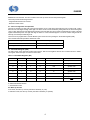
1
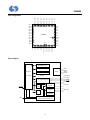
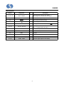
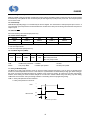
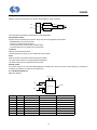
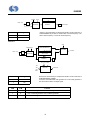
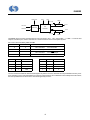
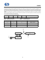
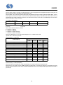
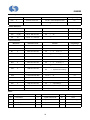
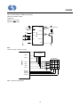
SH6605
4K 4-Bit Microcontroller with LCD Driver
Features
Built-in dual tone PSG with one noise generator
2 Clock sources
OSC: (code option select crystal or RC type)
- Crystal oscillator 32.768K
- RC oscillator: 262K
OSCX: (system register selected ceramic or RC type)
- Ceramic oscillator 455K
- RC oscillator 1.8M or 2M
Instruction cycle time:
- 122.07µs for 32.768 KHz crystal
- 15.27µs for 262 KHz RC
- 8.79µs for 455KHz ceramic
- 2.22µs for 1.8 MHz RC
- 2µs for 2.0 MHz RC
Two low power operation modes: HALT and STOP
Low power consumption
SH6610C-based single-chip 4-bit microcontroller
ROM: 4096 X 16 bits
RAM: 512 X 4 bits
Operation voltage: 2.4V - 6.0V
8 CMOS bi-directional I/O pins
4-Level subroutine nesting (include interrupts)
One 8-bit auto re-load timer/counter
Warm-up timer for power-on reset
Powerful interrupt sources:
- External interrupts ( INT0 )
- Internal interrupt (Timer0)
- Internal interrupt (Base Timer)
- Port's falling edge interrupt: PORTB ( INT1 )
8-bit Base timer
LCD driver:
136 dots (1/4 duty 1/3 bias)
LCD used as scan output
General Description
SH6605 is a single chip microcontroller integrated with SRAM, timer and dual-tone PSG, LCD driver, and I/O port. This chip
includes a built-in a dual-oscillator to enhance the total chip performance.
1
V2.0
SH6605
Pad Configuration
S
E
G
2
0
S
E
G
2
1
S
E
G
2
2
S
E
G
2
3
S
E
G
2
4
S
E
G
2
5
S
E
G
2
6
S
E
G
2
7
S
E
G
2
8
S
E
G
2
9
S
E
G
3
0
53
52
51
50
49
48
47
46
45
44
43
S
E
G
3
2
S
E
G
3
1
S
E
G
3
3
SEG 19
54
SEG 18
1
39
SEG34
SEG 17
2
38
COM 4
SEG 16
3
37
COM 3
SEG 15
4
36
COM 2
SEG 14
5
35
COM 1
SEG 13
6
34
OSC1
SEG 12
7
SEG 11
8
42
41
SH6605
40
33
GND
OSC0
PORTC0
32
SEG 10
9
31
OSCXO
SEG 9
10
30
OSCXI
SEG 8
11
VDD
29
PORTA0
SEG 7
12
21
28
PORTA1
27
PORTA2
13
14
S
E
G
6
S
E
G
5
15
S
E
G
4
16
17
18
19
20
S
E
G
3
S
E
G
2
S
E
G
1
P
T
E
S
T
P
R
E
S
E
T
B
22
23
24
P
O
R
T
B
3
P
O
R
T
B
2
P
O
R
T
B
1
P
O
R
T
C
1
25
26
P
O
R
T
B
0
P
O
R
T
A
3
Block Diagram
ROM (4096 X 16)
RAM (512 X 4)
OSCS
SH6610C
8-BIT TIMER0
CPU CORE
PORTB
PORTB [0:3]
PORTA & EXTERNAL INT
COMMON
LCD
RESET
DRIVER
RAM
SEGMENT
DRIVER
PSG
SCAN
REGISTER
GND
OSCI
OSCO
OSCXI
OSCXO
CPU OPERATING VOLTAGE
LCD VOLTAGE GENERATOR
2
PA.1 (PSG)
PA.0 (INT0 )
PA.2 (PSG)
PA.3
COM [1:4]
SEG [1:34]
SH6605
Pad Description
Pad No.
Designation
I/O
Description
1 - 18, 39 - 54
SEG1 - SEG34
O
Segment signal output for LCD display;
seg1-seg30 can be shared with scan output
19
TEST
I
Test pin (Internal pull-low). No connection for user
20
RESET
I
Reset input (No internal pull-up)
21
VDD
P
Power supply
22 - 25
Port B.3 - Port B.0
I/O
Bit programmable I/O, Vector interrupt ( INT1 )
26 - 29
Port A.3 - Port A.0
I/O
Bit programmable I/O, PA.0 shared with INT0
PA.1, PA.2shared with PSG output
30
OSCXI
I
Oscillator X input
31
OSCXO
O
Oscillator X output
32
GND
P
Ground
33
OSCO
O
Oscillator output
34
OSCI
I
Oscillator input
35 - 38
COM1 - COM4
O
Common signal output for LCD display
3
SH6605
Functional Description
1. CPU
The CPU core contains the following function blocks:
Program Counter, ALU, Carry Flag, Accumulator, Table
Branch Register (TBR), Data Pointer (INX, DPH, DPM and
DPL), and Stack.
Decimal adjustment for addition/subtraction (DAA, DAS),
Logic operations (AND, EOR, OR, ANDI, EORI, ORI)
Decision (BA0, BA1, BA2, BA3, BAZ, BC)
The Carry Flag (CY) holds the arithmetic operation ALU
overflow.
During interrupt or call instruction, carry is pushed into stack
and restored from stack by RTNI. It is unaffected by an
RTNW instruction.
1.1. PC (Program Counter)
The PC is used for ROM addressing consisting of 12-bits:
Page Register (PC11), and Ripple Carry Counter (PC10 PC0).
The program counter normally increases by one (+1) with
each execution of an instruction except in the following
cases:
(1) When executing a jump instruction (such as JMP, BA0,
BC),
(2) When executing a subroutine call instruction (CALL),
(3) When an interrupt occurs,
(4) When the chip is at INITIAL RESET.
The program counter is loaded with data corresponding to
each instruction. The unconditional jump instruction (JMP)
can be set at 1-bit page register for higher than 2K. Program
Counter can only address a 4K of program ROM.
1.3. Accumulator
The accumulator is a 4-bit register holding the results of the
arithmetic logic unit. In conjunction with the ALU, data
transfers between the accumulator and system register, LCD
RAM, or data memory can be performed.
1.4. Stack
This group of registers is used to save the contents of CY &
PC (11 - 0) sequentially with each subroutine call or interrupt.
It is organized 13 bits X 4 levels. The MSB is saved for CY.
Four levels are the maximum allowed for subroutine calls
and interrupts.
The contents of Stack are returned sequentially to the PC
with the return instructions (RTNI/RTNW). Stack is operated
on a first-in, last-out basis. This 4-level nesting includes both
subroutine calls and interrupt requests. Note that program
execution may enter an abnormal state if the number of calls
and interrupt requests exceeds 4, when then the bottom of
stack will be shifted out.
1.2. ALU and CY
The ALU performs arithmetic and logic operations.
It provides the following functions:
Binary addition/subtraction
(ADC, SBC, ADD, SUB, ADI, SBI)
2. ROM
SH6605 can address 4096 X 16 bit of program area $000 to $FFF. There is an area from addresses $000 through $004 that is
reserved for special interrupts service routines such as starting vector address.
Address
Instruction
Function
000H
JMP Instruction
Jump to RESET service routine
001H
JMP Instruction
Jump to INT0 service routine
002H
JMP Instruction
Jump to Timer0 service routine
003H
JMP Instruction
Jump to Base Timer service routine
004H
JMP Instruction
Jump to INT1 service routine
4
SH6605
3. RAM
The Built-in SRAM contains general-purpose data memory, LCD RAM, and system registers. They can be accessed by direct
addressing in one instruction.
The following is the memory allocation map:
$000 - $01F: System register and I/O;
$020 - $1FF: Data memory (480 X 4bits, partitioned into 4 banks).
$300 - $321, $350 - $36D: LCD RAM space (34 X 4 bits).
The Configuration of System Register
Address
Bit3
$00
IEX
$01
IRQX
$02
TM0.3
$03
BTM.3
$04
T0L.3
$05
T0H.3
$06 - $07
$08
PA.3
$09
PB.3
$0A
$0B
PACR.3
$0C
PBCR.3
$0D
$0E
TBR.3
$0F
INX.3
$10
DPL3
$11
$12
-
Bit2
Bit1
Bit0
IET0
IRQT0
TM0.2
BTM.2
T0L.2
T0H.2
PA.2
PB.2
PACR.2
PBCR.2
TBR.2
INX.2
DPL2
DPM.2
DPH.2
IEBT
IRQBT
TM0.1
BTM.1
T0L.1
T0H.1
PA.1
PB.1
PC.1
PACR.1
PBCR.1
TBR.1
INX1
DPL1
DPM.1
DPH.1
IEP
IRQP
TM0.0
BTM.0
T0L.0
T0H.0
PA.0
PB.0
PC.0
PACR.0
PBCR.0
TBR.0
INX.0
DPL0
DPM.0
DPH.0
$13
PPULL
PAM2
PAM1
HLM
$14
OXS
-
OXM
OXON
$15
LPS1
LPS0
LCDOFF
Should
Be
Set “1”
$16
LPD
O/S
-
-
$17
C1.3
C1.2
C1.1
C1.0
$18
OCT1
C1.6
C1.5
C1.4
$19
$1A
$1B
C2.3
C2.7
C2.11
C2.2
C2.6
C2.10
C2.1
C2.5
C2.9
C2.0
C2.4
C2.8
$1C
OCT2
C2.14
C2.13
C2.12
$1D
VOL1
VOL0
CH2EN
CH1EN
$1E
SEL1
SEL0
C2M
C1M
$1F
-
-
-
-
Function
Interrupt enable flags
Interrupt request flags
Timer0 mode register
Base timer mode register
Timer0 load/counter low nibble
Timer0 load/counter high nibble
Reserved
PORTA
PORTB
Bonding option
Set PORTA to be output port
Set PORTB to be output port
Reserved
Table branch register
Index register (INX)
Data pointer for INX low nibble
Data pointer for INX middle nibble
Data pointer for INX high nibble
Bit1, 2: PA.1 & PA.2 as PSG output or I/O PORT
Bit0: Heavy load mode
Bit3: Port pull-up control
Bit0: Turn on OSCX oscillator
Bit1: CPU clocks select (1:OSC X /0:OSC)
Bit3: OSCX type selection
Bit0: programmer should set “1”
Bit1: LCD off
Bit2, 3: LCD frequency control
Bit2: Set LCD segment as output
Bit3: LCD Power degrade
PSG channel 1 low nibble
PSG channel 1 high nibble
Bit3: channel 1 octave shift control
PSG channel 2 nibble 1 or alarm output
PSG channel 2 nibble 2
PSG channel 2 nibble 3
PSG channel 2 nibble 4
Bit3: channel 2 octave shift control
Bit0, Bit1: Channel 1, 2 enable
Bit2, Bit3: volume control
Bit0, 1: PSG1, PSG2 mode control
Bit2, 3: PSG1, PSG2 clock source selection
Reserved
System Register $00 - $12. (Please refer to SH6610C User’s manual)
5
Initial
Value
0000
0000
0000
0000
0000
0000
0000
0000
01 (default)
0000
0000
0000
0000
0000
0000
0000
R/W
R/W
R/W
R/W
R/W
R/W
R/W
R/W
R
W
W
R/W
R/W
R/W
R/W
R/W
0000
R/W
0000
R/W
0000
R/W
0000
R/W
0000
W
0000
W
0000
0000
0000
W
W
W
0000
W
0000
W
0000
W
-
-
R/W
SH6605
6
SH6605
4. Data Memory
The general purpose data memory is organized as 512 * 4 bits. Because of its static feature, the RAM can retain data after the
CPU enters STOP or HALT mode.
5. Oscillator Circuit
5.1. Circuit Configuration
SH6605 has two on-chip oscillation circuits OSC and OSCX.
OSC is a low frequency crystal (Typ. 32.768KHz) or RC (Typ.262KHz) determined by the code option. This is designed for low
frequency operation. OSCX also has two types: ceramic (Typ.455KHz) or RC (1.8M or 2MHz) to be determined by the software
option. It is designed for high frequency operation.
It is possible to select the high speed CPU processing by a high frequency clock and select low power operation by low
operation clock. At the start of reset initialization, the OSC starts oscillation and OSCX is turned off. Immediatly after reset
initialization, the OSC clock is automatically selected as the system clock input source.
Oscillator Block Diagram
OSCI
OSCO
Base Timer
Low Frequency
Clock Oscillator
System clock
Source Selector
& Switching control
OSCXI
OSCXO
High Frequency
Clock Oscillator
Timing of System Clock Switching
7
System clock
Generator
CPU
Clock
SH6605
5.2. OSC Oscillation
The OSC generates the basic clock pulses that provides the CPU and peripherals (Timer0, LCD) with an operating clock.
OSC Crystal oscillator type
CPU STOP
OSCI
TO CPU
32768Hz XTL
RF
RO
OSCO
5 - 6p
OSC RC oscillator type
RBIAS
CPU STOP
OSCI
RO
Ring
Oscllator
TO CPU
OSCO
5.3. OSCX Oscillation
OSCX has two clock oscillators. The software options selects the ceramic or RC as the CPU's subclock.
OSCX ceramic oscillator type
OX OFF
OSCXI
CPUSTOP
TO CPU
455KHz
Ceramic
RF
OSCXO
OSCX RC oscillator type
If the OSCX is not used, it must be masked as a ceramic resonator and the OSCXI must be connected to GND.
RBIAS
OX OFF
OSCI
CPUSTOP
RO
Ring
Oscllator
OSCO
8
TO CPU
SH6605
5.4. Control of Oscillator
The oscillator control register configuration is shown as follows:
Address
$14
Bit3
OXS
Bit2
-
Bit1
OXM
Bit0
OXON
OXON: OSCX oscillation on/off.
0: Turn-off OSCX oscillation
1: Turn-on OSCX oscillation
OXM: switching system clock.
0: select OSC as system clock
1: select OSCX as system clock
OXS: OSCX oscillator type selection
0: OSCX set as ceramic oscillator
1: OSCX set as RC oscillator
5.5. Programming Notes
It takes at least 5 ms for the OSCX oscillation circuit to turn on until the oscillation stabilizes. When switching the CPU system
clock from OSC to OSCX, the user must wait a minimum of 5ms until the OSCX oscillation is running. However, the start time
varies with respect to oscillator characteristics and the condition of use. Thus the wait time depends on the application. When
switching from OSCX to OSC, and turning off OSCX in one instruction, the OSCX turn off control will be delayed for one
instruction cycle automatically to prevent CPU operation error.
6. System Clock
The system clock varies as the clock source changes. The following table shows the instruction execution time according to
each frequency of the system clock source.
32.768 Xtal (OSC )
262K RC (OSC )
455K ceramic Xtal (OSCX)
1.8M RC (OSCX)
2M RC(OSCX)
122.07 µs
17.778 µs
8.79 µs
2.22 µs
2µs
Cycle time
7. I/O PORTs
The MCU provides 8bi-directional I/O pins. Each I/O pin contains pull-up MOS controllable through programming. When every
I/O is used as input, the PORT control register (PACR, PBCR) controls the ON/OFF of the output buffer.
7.1. PORTA - B
These ports contain 8bi-directional I/O ports.
The circuit configuration of PORTA - B is shown as:
PULLUP
PULL_UP
PMOS
PORT
CONTROL
REGISTER
PORTX
PORT
DATA
REGISTER
DATAINPUT
RD_INPUT
I/O ports of SH6605 can be accessed by the read/write system register.
Users can output any value to any I/O port bit at any time.
Memory map addresses are listed as follows:
Address
Bit3
Bit2
Bit1
Bit0
$08
PORTA.3
PORTA.2
PORTA.1
PORTA.0
$09
PORTB.3
PORTB.2
PORTB.1
PORTB.0
9
SH6605
7.2. Controlling the Pull-up MOS
PORTA, PORTB contain pull-up MOS controlled by program. Bit3 of the PMOD register controls the on/off of all pull-up MOS
simultaneously. Pull-up MOS are also controlled by the port data registers (PA, PB) of each port as well. Thus the pull-up MOS
can be turned on/off.
7.3. Port Interrupt
PORTB interrupt (falling edge) is not controlled by the Port I/O register. This means that if a interrupt request (IEx is set to 1 &
one port bit high goes low) has been touched therefore the condition is the other port bits are high level whenever the port bit is
output or input.
7.4. External INT0
PortA.0 is shared by external interrupts (active low).
7.5. Port I/O Control Register:
Address
$0B
Bit3
PACR.3
Bit2
PACR.2
Bit1
PACR.1
Bit0
PACR.0
$0C
PBCR.3
PBCR.2
PBCR.1
PBCR.0
I/O control register: PACR.X, PBCR.X (X = 0, 1, 2, 3)
1: Use as an output buffer.
0: Use as an input buffer (initial power-on).
7.6. Port Mode Register (PMOD)
Address
Bit3
Bit2
Bit1
Bit0
$13
PPULL
PAM2
PAM1
HLM
PAM1, PAM2:
HLM:
PPULL:
Please see the PSG
Enable heavy load mode
Port pull-up MOS
Function
Bit1, 2:Select PA.1, PA.2 as I/O port or PSG output
Bit0: Hevey load mode
Bit3: Port pull-up control
0: Disable
0: Disable pull-up MOS
R/W
1: Enable
1: Enable pull-up MOS
7.7. Heavy Load Mode (HLM)
The MCU has a heavy load protection circuit for when the battery load becomes heavy, such as when an external buzzer
sounds or an external speaker is turned on. In this mode, the crystal oscillator circuit has backup for high gain. When setting up
this mode, more power should be provided to an oscillator circuit. Unless it is nessary, be careful not to set this mode through
software, since entering the mode would be delayed for one instruction. Please activate heavy load driving only after setting
HLM at least one instruction wait cycle through software. The following shows the programming setting.
HLM: 0 = Heavy load protection mode is released
1 = Heavy load protection mode is set.
HLM
0
1
ON
HEAVYLOAD
OFF
1 Instruction Cycle Time
10
SH6605
8. Programmable Sound Generator (PSG)
PSG has channel1 and channel2. The function block diagram is shown as follows:
CHANNEL1
CH1 CLK
OSC
PSG
MIXER
MPX
OSCX
PSG
CH2 CLK
CHANNEL2
The PSG function provides four subfunctions for wide applications.
Programmable Sound
Program sound is created by two channels. Every channel can be programmed as follows:
- Enable/Disable every channel sounds.
- Select every channel sound frequency.
- Two channel sounds are mixed into one PSG output.
- The PSG output can be controlled at 4 volume levels.
Fine Noise
PSG can provide wide-band noise.
The wide-band noise volume can be controlled at 4 volume levels.
Alarm
PSG can provide many alarm functions through the software.
The alarm carrier frequency can be programmed individually.
The alarm volume can be controlled at 4 volume levels.
Remote Control
The remote control is the only expandable application for PSG sound. Since the remote control frequency is 56.13KHz or
37.92KHz, the software can select the sound frequency.
8.1. PSG Subblock Diagram
MPX block diagram
SEL0
OSC
SEL1
/2
CLK-SLECTOR
OSCX
PSG CLK
/16
SEL1
SEL0
Clk Source
OSC Clk
PSG Clk
0
0
OSC
0
1
OSC/2
1
0
OSCX
1
1
OSCX/16
OSC = 32.768K
OSC = 262K
OSC = 32.768K
OSC = 262K
OSCX = 1.8M
OSCX = 455K
OSCX = 1.8M
OSCX = 455K
32.768K
262K
16.384K
131K
1.8M
455K
112.5K
28.4K
The MPX block selects 4 clock sources as PSG clk that provides the two channel clk sources.
11
SH6605
Channel 1
CH1EN
OCT1
REGISTER C1.6 ~ C1.0
/8
PSG CLK
SELECTOR
OCT1
Scaling ratio
0
1
1
1/8
DIVIDER 1
/2
CH1 OUT
Channel 1 is constructed by a 7-bit pseudo random counter. Channel 1 is
enabled/disabled by CH1EN. It creates either a sound frequency or an
alarm carrier frequency or a remote carrier frequency.
Channel 2
C2M
CH2EN OCT2
PSG
NOISE GENERATOR
SELECTOR
C2.14 ~ C2.0
/8
CLK
CH2 OUT
REGISTER
C2.14 ~ C2.0
SELECTOR
C2.14 ~ C2.8
/2
DIVIDER 2
C2.3 ~ C2.0
C1M
1Hz
4Hz
ENVELOP
ENVELOP
8Hz
32Hz
OCT2
Scaling ratio
0
1
1
1/8
Channel 2 is constructed by a 15-bit pseudo random counter. Channel 2 is
enabled/disabled by CH2EN
It can be a 15-bit wide-band noise generator or a 7-bit sound generator. It
can also create an alarm envelope signal.
C2M
C1M
Function
0
0
CH1 is a Sound generator. CH2 is a Sound generator.
1
0
CH1 is a Sound generator. CH2 is a Noise generator.
x
1
CH1 is a Sound generator. CH2 is an Alarm mode register.
12
SH6605
Mixer
TIME SLOT
VOL0
VOL1
PAM1
PA.1 I/O
PSG
CH1 OUT
TIME SLOT
CH2 OUT
SELECTOR1
PA.1
SELECTOR2
PA.2
VOL
CONTROL
PSG
PA.2 I/O
PAM2
The MIXER mixes CH1-OUT and CH2-OUT into one tone output to PA.1、 PA.2, when PAM1 = 1、PAM2 = 1. Then the tone
output is controlled by the volume control bit into 4 volume levels and in the end outputted by PSG.
PA.1 & PA.2 are controlled by PAM1 & PAM2
PAM2
PAM1
Function
0
0
PA.1:I/O PORT
PA.2: I/O PORT
0
1
PA.1:PSG output
PA.2: I/O PORT
1
0
PA.1:I/O PORT
PA.2: PSG output
1
1
PA.1:PSG output
PA.2: PSG output
SEL1
SEL0
Vol. control
VOL1
VOL0
Vol. Level
0
0
NO
0
0
1
0
1
YES
0
1
2
1
0
YES
1
0
3
1
1
YES
1
1
4
Note:
The user should not enable two PSG channels together to produce one tone, otherwise some unpredictable errors may occur.
If it is necessary to use 2 channels together (ie: to play two channel melody), do not allow the score to always be the same tones,
then the unpredicted errors will not occur and can be ingored by the user.
13
SH6605
The Value N of Divider1 is Corresponding to The REG C1.6 - C1.0 or REG C2.14 - C2.8 As Shown in The Following Table:
LSFR
(C1.6 - C1.0)
(C2.14 - C2.8)
01
127
LSFR
(C1.6 - C1.0)
(C2.14 - C2.8)
16
95
LSFR
(C1.6 - C1.0)
(C2.14 - C2.8)
12
63
LSFR
(C1.6 - C1.0)
(C2.14 - C2.8)
4B
31
02
126
2C
94
24
62
17
30
04
125
59
93
49
61
2E
29
08
124
33
92
13
60
5D
28
10
123
67
91
26
59
3B
27
20
122
4E
90
4D
58
77
26
41
121
1D
89
1B
57
6E
25
03
120
3A
88
36
56
5C
24
06
119
75
87
6D
55
39
23
0C
118
6A
86
5A
54
73
22
18
117
54
85
35
53
66
21
30
116
29
84
6B
52
4C
20
61
115
53
83
56
51
19
19
42
114
27
82
2D
50
32
18
05
113
4F
81
5B
49
65
17
0A
112
1F
80
37
48
4A
16
14
111
3E
79
6F
47
15
15
28
110
7D
78
5E
46
2A
14
51
109
7A
77
3D
45
55
13
23
108
74
76
7B
44
2B
12
47
107
68
75
76
43
57
11
0F
106
50
74
6C
42
2F
10
1E
105
21
73
58
41
5F
9
3C
104
43
72
31
40
3F
8
19
103
07
71
63
39
7F
7
72
102
0E
70
46
38
7E
6
64
101
1C
69
0D
37
7C
5
48
100
38
68
1A
36
78
4
11
99
71
67
34
35
70
3
22
98
62
66
69
34
60
2
45
97
44
65
52
33
40
1
0B
96
09
64
25
32
N
N
14
N
N
SH6605
8.2. Function Description
PSG as sound generator
The programmable sound is one of the 4 working modes. The software designer can select up to 16 clock sourcees as PSG clk.
Then select the CH1 and CH2 frequency-divided value that is controlled by the value of REG C1.6 - C1.0 or
C2.14 - C2.8.The user can select the 4 volume level controlled by VOL0, VOL1. The music tone can output both PSG and
PSG . The user also can control the OCT1, OCT2 bit that shifts the music tone 3 octaves.
Example 1: CH1EN = CH2EN = 1
OSCX = 1.8M, SEL0 = SEL1 = 1
So PSG clk = 112kHz; Switch clk = 28kHz
Vol. Clk = 112kHz
Example 2: CH1EN = 0; CH2EN = 1
OSCX = 1.8M, SEL0 = SEL1 = 1
So PSG clk = 112kHz; Switch clk = 28kHz;
Vol. Clk = 112kHz
Example 3: CH1EN = CH2EN = 1
OSC = 32k, SEL0 = SEL1 = 0
So PSG clk = 32kHz; Switch clk = 32kHz
No vol. control, the VOL level is set to 4 by hardware, so software should set VOL0 = VOL1 = 1.
Note:
For 32KHz operations, the volume control cannot be used, since the PWM multiplexing frequency is not high enough to switch
sound! If a user wants to turn off the PSG completely, the software must disable both channels. The user should not turn off the
PSG by zero wave from output. Both the CH1EN and CH2EN should be set to "0" for the low power operation mode.
Example 4
If a software designer wants to create C2 (Channel 1) mixed with F5 (Channel 2) sound, VOL level = 3. (For the C2, F5 sound
frequency please refer to Music Table 1 and Music Table 2).Then the user can select the suggestion as follows:
(1) The user first selects CH1EN = CH2EN = 1, C1M = C2M = 0.
(2) The user can select OSCX = 1.8M and SEL0 = SEL1 = 1, so the PSG CLK = 112.5KHz.
(3) Then the user can select OCT1 = 1 and the value of channel 1 LSFR (C1.6 - C1.0) = 23, so that N = 108. Please see the
Music Table 1.So the channel 1 sound frequency = 112.5Khz/8/ (2 X 10⁸) = 64.10Hz ≒ the C2 sound frequency.
(4) Then the user can select OCT1 = 0 and the value of channel 1 LSFR (C1.6 - C1.0) = 4F, so that N = 81. Please refer to the
Music Table 1.So the channel 1 sound frequency = 112.5Khz/1/ (2 X 81) = 694.4Hz ≒ the F5 sound frequency .
(5) Lastly, the user should select the VOL1 = 1 and VOL0 = 0, so the VOL level = 3.
15
SH6605
Note:
The designer provides two crossing tables as an appendix if the designer prefers PSG clk = 32.768K or PSG
clk = 112.5K.
PSG As A Noise Generator
Fine noise is created by CH2. If the user wants to create a single noise, then make the CH1 music tone output. Otherwise, the
user can mix the wide-band noise and the CH1 music tone into one output through the MIXER. Lastly, the user can select 4
volume levels controlled by VOL0, VOL1.
PSG As An Alarm Generator
When PSG is in the alarm mode, the CH1 provides the alarm carrier frequency and the CH2 provides the alarm envelope signal.
Lastly the user can select 4 volume levels controlled by VOL0, VOL1. The channel 2 low nibble C2.0 - C2.3 will be the alarm
control register. Channel 1 output will modulate with an ALARM envelope control for 32KHz or 262KHz. The carrier frequency
can be programmed by PSG channel 1.In reading this alarm control register, the user can read the corresponding output
envelope frequency (the 1Hz, 4Hz, 8Hz, 32Hz).
Alarm Control Register (OSC = 32KHz or 262KHz)
$19
C2.3
C2.2
C2.1
C2.0
0
0
0
0
Alarm output control
DC envelop
X
X
X
1
1Hz output
X
X
1
X
4Hz output
X
1
X
X
8Hz output
1
X
X
X
32Hz output
Figture: Alarm modulation output for OSC = 32.768KHz or OSC = 262KHz.
PSG As Remote Control
The remote control is only an expandable application for PSG sound. The user can select the CH1 as tone output and CH2 will
create alarm frequency envelope signal.
When PSG channel is programmed in the ALARM mode, the programmer can set ALARM mode register to "0000B". Program
the adequate frequency output to PSG output. Then use PAM1 or PAM2 control the envelope of code. In this way, remote
control function can be implemented easily.
The Remote Frequency = 56.73KHz or 37.92KHz
The software should select OSCX = 455KHz, SEL = 1 and SEL0 = 0, so that the PSG CLK = 455KHz.
Then select channel 1 alarm mode (C1M = 1), and OCT1 = 0, C2.0 ~ C2.3 are set to 00H. VOL1, VOL2 = 1, 1.
Then select C1.6 - C1.0 = 7E, so that N = 6 and the PSG output frequency = 455KHz/1/ (2 X 6) = 37.92KHz.
Or select C1.6 - C1.0 = 78, so that N = 4 and the PSG output frequency = 455KHz/1/ (2 X 4) = 56.87KHz.
16
SH6605
9. Timer 0
SH6605 has one 8-bit timer. The timer consists of an 8-bit up counter and an 8-bit preload register.
The timers provide the following functions:
- Programmable internal timer function
- Read the counter values
9.1. Timer 0 Configuration and Operation
The timer 0 consists of an 8-bit write-only timer load register (TL0L, TL0H) and an 8-bit read-only timer counter (TC0L, TC0H).
Each has low order digits and high order digits. The timer counter can be initialized by writing data into the timer load register
(TL0L, TL0H). Write the low-order digit first and then the high-order digit. The timer counter is loaded with the content of the load
register automatically when the high order digit is written or counts overflow happens. The timer overflow will generate an
interrupt, if the interrupt enable flag is set.
The timer can be programmed in several different system clock sources by setting the Timer Mode register (TM0).
Timer 0 reads and writes operations follow these rules:
Write Operation
Read Operation
Low nibble first
High nibble first
High nibble to update the counter
Low nibble follows
9.2. Timer0 Mode Register (TM0)
The 8-bit counter counts prescaler overflow output pulses. TM0 are 4-bit registers used for timer control as shown in Table 1.
The register selects the input clock sources in the timer.
Table 1. Timer0 Mode Registers ($02)
TM0.3
TM0.2
TM0.1
TM0.0
Prescaler
Clock Source
0
0
0
0
/2048
System clock
0
0
0
1
/512
System clock
0
0
1
0
/128
System clock
0
0
1
1
/32
System clock
0
1
0
0
/8
System clock
0
1
0
1
/4
System clock
0
1
1
0
/2
System clock
0
1
1
1
External
INT0
TM0.3 control function:
0: without Auto-Reload function
1: Auto-Reload function
9.3. Warm-up Counter
7
In RC mode, the warm-up counter prescaler is divided by 2 (128).
15
In CRYSTAL mode, the warm-up counter prescaler is divided by 2
17
(65536).
SH6605
10. Base Timer
The MCU has a base timer that is shared with the warm-up timer and the clock source is OSC (Low frequency oscillation: X’Tal
32.768KHz or RC 262KHz). After MCU is reset, it counts at every clock-input signal. When it counts to $FF, right after next clock
input, the counter counts to $00 and generates an overflow This causes the interrupt of base timer interrupt request flag to
1.Therefore, the base timer can function as a periodical interval timer, generating overflow output as every 256th clock signal
output.
The timer accepts 4096Hz or 32KHz clock, and the base timer generates an accurate timing interrupt. This base time prescaler
can be reset by the program for accurate timing.
This clock-input source is selected by BTM register.
Address
Bit3
Bit2
Bit1
Bit0
Function
$03
BTM.3
BTM.2
BTM.1
BTM.0
Base timer mode register
BTM.3 = 0: Disable the base timer
BTM.2 = 0: Non reset the base timer
BTM.3 = 1: Enable the base timer
BTM.2 = 1: Reset the base timer
BTM.0
Prescaler Ratio
Clock source
0
0
/1
4096Hz or 32KHz
0
1
/4
4096Hz or 32KHz
1
0
/8
4096Hz or 32KHz
1
1
/16
4096Hz or 32KHz
BTM [3]
BTM.1
8 Bit base timer counter
reset
MPX
32k
or
262k
/8
4096/32K
/4
/8
/16
BTM [2]
/1
4Bit Scaler
18
SH6605
11. LCD Driver
The LCD driver contains a controller, a voltage generator, 4 common signal pins and 34 segment driver pins, 1/4 duty and 1/3
bias. The driving mode is controlled by the system register $15.
The LCD SEG1 - 30 can also be used as an output port. It is selected by bit 2 of the system register $16. When SEG1 - 30 is to
be an output port, data must be written to bit 0 of the same addresses (350H-36DH). LCD RAM can be used as data memory if
needed. When the "STOP" instruction is executed, the LCD will be turned off, but the data of LCD RAM keeps the same value
before executing the "STOP" instruction.
11.1. LCD Control Register
Address
Bit 3
Bit 2
Bit 1
$15
LPS1
LPS0
LCDOFF
Bit 0
Should be set “1”
LCDOFF: LCD on/off switch
0: LCD on
1: LCD off
LPS1, LPS0: LCD clock frequency control
0, 0: LCDCLK = OSC/64
0, 1: LCDCLK = OSC/512
1, 0: LCDCLK = System clock/512
1, 1: LCDCLK = System clock/4096
The bit 0 in initial state is “0”, the user should change it into “1” to realize 4-com mode.
*System clock = Instruction cycle time
Frame frequency = LCDCLK/16
CLK Frequency
LPS1, LPS0
0, 0
0, 1
1, 0
1, 1
OSC = 32kHz (#),
OSCX = 455kHz
32Hz
4Hz
1Hz
1/8Hz
OSC = 32kHz,
OSCX = 455kHz (#)
32Hz
4Hz
14Hz
1.7Hz
OSC = 32kHz (#),
OSCX = 1.8MHz
32Hz
4Hz
1Hz
1/8Hz
OSC = 32kHz,
OSCX = 1.8MHz (#)
32Hz
4Hz
55Hz
6.9Hz
OSC = 32kHz (#),
OSCX = 2MHz
32Hz
4Hz
1Hz
1/8Hz
OSC = 32kHz,
OSCX = 2MHz (#)
32Hz
4Hz
61Hz
7.6Hz
OSC = 262kHz (#), OSCX = 455kHz
256Hz
32Hz
8Hz
1Hz
OSC = 262kHz,
256Hz
32Hz
14Hz
1.7Hz
OSC = 262kHz (#), OSCX = 1.8MHz
256Hz
32Hz
8Hz
1Hz
OSC = 262kHz,
OSCX = 455kHz (#)
256Hz
32Hz
55Hz
6.9Hz
OSC = 262kHz (#), OSCX = 2MHz
OSCX = 1.8MHz (#)
256Hz
32Hz
8Hz
1Hz
OSC = 262kHz,
256Hz
32Hz
61Hz
7.6Hz
OSCX = 2MHz (#)
The clk before (#) is selected as CPU system clk.
Frame frequency = LCDCLK/16 (32Hz)
When the LCD is set to SCAN OUT, COMx are pulled high. It is easy to implement the keyboard scan.
When the CPU is in STOP mode, the COMx and SEGx are pulled low. It can easily be woken up by a keyboard scan (Port
interrupt). When the CPU is in HALT mode, the COMx and SEGx are normal. It can easily be woken up by base timer, timer0 or
port interrupt.
19
SH6605
11.2. LCD Power
LCDOFF
Power
Switch
LPD
LCD
com1
common
~
driver
com4
LCD
Power
Supply
Control
Circuit
LCD
seg1
segment
driver
~
DUTY
LPS0
SYSCLK/512
LPS1
OSC/64
1
MPX
0
MPX LCDCLK
/2
0 1
1
MPX
& scan
output
seg34
0
/1 /8
Scaler
Built-in special LCD power control for LCD power modulation.
Address
Bit 3
LPD
$16
Bit 2
O/S
Bit 1
-
Bit 0
-
O/S: Set LCD segment/common to be LCD segment output or output ports
0: LCD segment output
1: output ports.
When LPD is set to 1, the LCD voltage power will be degraded to about 0.5V, depending on the VDD level. It is designed to
reduce extra LCD contrast control output pins. Then the LCD can be fitted automatically for different voltage levels by the
software.
11.3. Configuration of LCD RAM
LCD 1/4 duty, 1/3 bias (COM1 - 4, SEG1 - 34)
Bit3
Bit2
Bit1
Bit0
COM4
COM3
COM2
COM1
300H
SEG1
SEG1
SEG1
SEG1
301H
SEG2
SEG2
SEG2
SEG2
302H
SEG3
SEG3
SEG3
303H
SEG4
SEG4
SEG4
304H
SEG5
SEG5
305H
SEG6
SEG6
306H
SEG7
307H
308H
Address
Bit3
Bit2
Bit1
Bit0
COM4
COM3
COM2
COM1
311H
SEG18
SEG18
SEG18
SEG18
312H
SEG19
SEG19
SEG19
SEG19
SEG3
313H
SEG20
SEG20
SEG20
SEG20
SEG4
314H
SEG21
SEG21
SEG21
SEG21
SEG5
SEG5
315H
SEG22
SEG22
SEG22
SEG22
SEG6
SEG6
316H
SEG23
SEG23
SEG23
SEG23
SEG7
SEG7
SEG7
317H
SEG24
SEG24
SEG24
SEG24
SEG8
SEG8
SEG8
SEG8
318H
SEG25
SEG25
SEG25
SEG25
SEG9
SEG9
SEG9
SEG9
319H
SEG26
SEG26
SEG26
SEG26
Address
309H
SEG10
SEG10
SEG10
SEG10
31AH
SEG27
SEG27
SEG27
SEG27
30AH
SEG11
SEG11
SEG11
SEG11
31BH
SEG28
SEG28
SEG28
SEG28
30BH
SEG12
SEG12
SEG12
SEG12
31CH
SEG29
SEG29
SEG29
SEG29
30CH
SEG13
SEG13
SEG13
SEG13
31DH
SEG30
SEG30
SEG30
SEG30
30DH
SEG14
SEG14
SEG14
SEG14
31EH
SEG31
SEG31
SEG31
SEG31
30EH
SEG15
SEG15
SEG15
SEG15
31FH
SEG32
SEG32
SEG32
SEG32
30FH
SEG16
SEG16
SEG16
SEG16
320H
SEG33
SEG33
SEG33
SEG33
310H
SEG17
SEG17
SEG17
SEG17
321H
SEG34
SEG34
SEG34
SEG34
20
SH6605
SEG1-30 is used as scan output port.
Address
Bit0
Address
Bit0
Address
Bit0
Address
Bit0
350H
SEG1
351H
SEG2
358H
SEG9
360H
SEG17
368H
SEG25
359H
SEG10
361H
SEG18
369H
SEG26
352H
353H
SEG3
35AH
SEG11
362H
SEG19
36AH
SEG27
SEG4
35BH
SEG12
363H
SEG20
36BH
SEG28
354H
SEG5
35CH
SEG13
364H
SEG21
36CH
SEG29
355H
SEG6
35DH
SEG14
365H
SEG22
36DH
SEG30
356H
SEG7
35EH
SEG15
366H
SEG23
357H
SEG8
35FH
SEG16
367H
SEG24
11.4. LCD Waveform
1/4 DUTY 1/3 BIAS
SELECT
UNSELECT
V1
V2
COM
V3
GND
SELECT
UNSELECT
V1
V2
SEG
V3
GND
21
SH6605
12. Interrupt
4 interrupt sources are available on SH6605:
- External interrupt ( INT0 )
- Timer0 interrupt
- Base timer interrupt
- Port's falling edge detection interrupt ( INT1 )
The configuration of system register $0:
Address
Bit 3
Bit 2
Bit 1
Bit 0
$00
IEX
IET0
IEBT
IEP
$01
IRQX
IRQT0
IRQBT
IRQP
Function
1: Enable / 0: Disable
1: Request / 0: No request
12.1. External Interrupt ( INT0 )
External interrupt is shared with the PA.0, falling edge active. When the bit 3 of the register $0 (IEX) is set to 1, the external
interrupt is enabled, writing a "0" to PA.0 will generate an external interrupt.
12.2. Timer 0 Interrupt, Base Timer Interrupt, Port Interrupt ( INT1 )
If IEX = 1 then all valid interrupt requests will cause an interrupt. The overflow of timer 0 will create the interrupt of timer 0.The
overflow of the Base timer will create the interrupt of the Base timer. The falling edge of every port in PORTB will create INT1
interrupt (The condition is that the other port must be input/output high level).
12.3. The Enable Flags and Request Flags
Both the Enable flags and Request flags can be read or written by the software.
However, the Request flags will be set to "1" by the hardware interrupt and the Enable flags will be reset by the hardware when
the interrupt service routine is entered.
12.4. Interrupt Servicing Sequence Diagram
In the SH6610C CPU interrupt services routine, the user can enable any interrupt enable flag before returning from an interrupt.
The frequently asked question is when the next interrupt will be serviced? Will the nesting interrupt occur? From the servicing
sequence timing diagram, if an interrupt request is ready and instruction execution N is IE enabld, then the interrupt can start
right after the next two instructions: instruction I1 or instruction I2 disable the interrupt request or enable flag, then interrupt
service sequence is terminated.
Inst. cycle
1
2
3
Instruction
Execution
N
Instruction
Execution
I1
Instruction
Execution
I2
Interrupt Generated
Interrupt Accepted
Vector Generated
Stacking
4
5
Fetch Vector address
Reset IE.X
Start at vector address
22
SH6605
13. Options
13.1. Bonding options
System register $0A is reserved for the user. It is available for system developer to select 2 bonding options, and selecting a
subprogram is programmed by the user.
$0A.1 (PC.1)
$0A.0 (PC.0)
0
0
goto subroutine 1
0
1
goto subroutine 2 (Default)
1
0
goto subroutine 3
1
1
goto subroutine 4
VDD
GND
PC.0
VDD
GND
PC.1
PC.0
PC.1
PCB
PC.0 = 1
PC.1 = 0
PC.0 = 1 PC.1 = 1
VDD
GND
PC.0
GND
PC.1
PC.0
VDD
PC.1
PCB
PC.0 = 0
PC.0 = 0 PC.1 = 1
PC.1 = 0
SH6605 Bonding Option
13.2. Code Option:
Addresses: $1000
Body data: 0110 0110 0000 0101 (6605)
Addresses: $1001
Data: C000 0000 0000 0000
C (Clock source)
0 = 32768 Crystal (default)
1 = 262K RC
23
SH6605
14. STOP/HALT Mode
STOP/HALT Mode
STOP
(STOP instruction)
Oscillator
CPU Core
OSC
OSCX
Hold
Stop
OSC
HALT
(HALT instruction)
OSCX
live
Hold
Wake Up
RST , INT0 ,
INT1
Executing After Wake Up
(a) If RST signal valid, system will reset
(b) If INT0 , INT1 signal valid, system will enter interrupt
subroutine, then execute the main program to continue
RST , INT0 , (a) If RST signal valid, system will reset
INT1 , T0INT (b) If INT0 , INT1 , T0INT or BTINT signal valid, system will
enter interrupt subroutine first, then execute the main
BTINT
program to continue
15. Instruction Set
All instructions are one cycle and one word instructions. The characteristic is memory-oriented operation.
Arithmetic and Logical Instructions are as follows.
Accumulator Type
Mnemonic
Instruction Code
Function
Flag Change
ADC
X (, B)
00000 0bbb xxx xxxx
AC
← Mx + Ac + CY
CY
ADCM
X (, B)
00000 1bbb xxx xxxx
AC, Mx ← Mx + Ac + CY
CY
ADD
X (, B)
00001 0bbb xxx xxxx
AC
← Mx + Ac
ADDM
X (, B)
00001 1bbb xxx xxxx
AC, Mx ← Mx + Ac
CY
CY
SBC
X (, B)
00010 0bbb xxx xxxx
AC
← Mx + -Ac + CY
CY
SBCM
X (, B)
00010 1bbb xxx xxxx
AC, Mx ← Mx + -Ac + CY
CY
SUB
X (, B)
00011 0bbb xxx xxxx
AC
SUBM
X (, B)
00011 1bbb xxx xxxx
AC, Mx ← Mx + -Ac + 1
EOR
X (, B)
00100 0bbb xxx xxxx
AC
EORM
X (, B)
00100 1bbb xxx xxxx
AC, Mx ← Mx ⊕ Ac
OR
X (, B)
00101 0bbb xxx xxxx
AC
← Mx | Ac
ORM
X (, B)
00101 1bbb xxx xxxx
AC, Mx
← Mx | Ac
AND
X (, B)
00110 0bbb xxx xxxx
AC
← Mx & Ac
ANDM
X (, B)
00110 1bbb xxx xxxx
AC, Mx
SHR
11110 0000 000 0000
← Mx + -Ac + 1
CY
CY
← Mx ⊕ Ac
← Mx & Ac
0 → AC [3] ; AC [0] → CY ;
AC shift right one bit
CY
Immediate Type
Mnemonic
ADI
X,I
Instruction Code
Function
Flag Change
01000 i i i i xxx xxxx
AC
← Mx + I
CY
ADIM
X,I
01001 i i i i xxx xxxx
AC, Mx ← Mx + I
CY
SBI
X,I
01010 i i i i xxx xxxx
AC
← Mx + -I + 1
CY
SBIM
X,I
01011 i i i i xxx xxxx
AC, Mx ← Mx + -I + 1
CY
EORIM
X,I
01100 i i i i xxx xxxx
AC, Mx ← Mx ⊕ I
ORIM
X,I
01101 i i i i xxx xxxx
AC, Mx ← Mx | I
ANDIM
X,I
01110 i i i i xxx xxxx
AC, Mx ← Mx & I
* In the assembler ASM66 V1.0, EORIM mnemonic is EORI. However, EORI an operation identical with EORIM. The same is
true for the ORIM with respect to ORI, and ANDIM with respect to ANDI.
24
SH6605
Decimal Adjust
Mnemonic
Instruction Code
Function
Flag Change
DAA
X
11001 0110 xxx xxxx
AC; Mx ←Decimal adjust for add.
CY
DAS
X
11001 1010 xxx xxxx
AC; Mx ←Decimal adjust for sub.
CY
Function
Flag Change
Transfer Instruction
Mnemonic
Instruction Code
LDA
X (, B)
00111 0bbb xxx xxxx
AC
← Mx
STA
X (, B)
00111 1bbb xxx xxxx
Mx
←
LDI
X, I
01111 i i i i xxx xxxx
AC, Mx ←
AC
I
Control Instruction
Mnemonic
Instruction Code
Function
Flag Change
BAZ
X
10010 xxxx xxx xxxx
PC
← X
if AC = 0
BNZ
X
10000 xxxx xxx xxxx
PC
← X
if AC ≠ 0
BC
X
10011 xxxx xxx xxxx
PC
← X
if CY = 1
BNC
X
10001 xxxx xxx xxxx
PC
← X
if CY ≠ 1
BA0
X
10100 xxxx xxx xxxx
PC
← X
if AC (0) = 1
BA1
X
10101 xxxx xxx xxxx
PC
← X
if AC (1) = 1
BA2
X
10110 xxxx xxx xxxx
PC
← X
if AC (2) = 1
BA3
X
10111 xxxx xxx xxxx
PC
← X
if AC (3) = 1
CALL
X
11000 xxxx xxx xxxx
ST
← CY ; PC + 1
PC
← X (Does not include p)
RTNW
H, L
11010 000h hhh l l l l
PC← ST; TBR← hhhh; AC←l l l l
RTNI
11010 1000 000 0000
CY; PC ← ST
HALT
11011 0000 000 0000
STOP
11011 1000 000 0000
CY
1110p xxxx xxx xxxx
PC
← X (Includes p)
TJMP
11110 1111 111 1111
PC
← (PC11-C8) (TBR) (AC)
NOP
11111 1111 111 1111
No Operation
JMP
X
Where
PC
Program counter
I
Immediate data
AC
Accumulator
⊕
Logical exclusive OR
-AC
Complement of accumulator
|
Logical OR
CY
Carry flag
&
Logical AND
Mx
Data memory
bbb
RAM bank = 000
25
p
ROM page = 0
ST
Stack
TBR
Table Branch Register
SH6605
Absolute Maximum Rating*
*Comments
DC Supply Voltage . . . . . . . . . . . . . . . -0.3V to + 7.0V
Stresses above those listed under "Absolute Maximum
Ratings" may cause permanent damage to this device.
These are stress ratings only. Functional operation of this
device at these or any other conditions above those indicated
in the operational sections of this specification is not implied
or intended. Exposure to the absolute maximum rating
conditions for extended periods may affect device reliability.
Input Voltage . . . . . . . . . . . . . . . -0.3V to VDD + 0.3V
Operating Ambient Temperature . . . . -10℃ to + 60℃
Storage Temperature . . . . . . . . . . . . -55℃ to + 125℃
DC Electrical Characteristics
(VDD = 3.0V, GND = 0V, TA = 25℃, FOSC = 32.768KHz, FOSCX is not used, unless otherwise specified)
Parameter
Symbol
Min.
Typ.
Max.
Unit
Conditions
Operating Voltage
VDD
2.4
3
6.0
V
Operating Current
IOP
-
10
20
µA
LCD Voltage Divider
Resistor
RLCD
-
275
-
KΩ
Standby Current
ISB1
-
2
4
µA
All output pins unload (HALT mode) excluding LCD
bias current
Standby Current
ISB2
-
-
1
µA
All output pins unload (STOP mode), LCD off
Input High Voltage
VIH
0.7 X VDD
0.85 X VDD
-
VDD + 0.3
VDD + 0.3
V
V
All output pins unload execute NOP instruction
excluding LCD bias current
PORTA, PORTB
INT0 , RESET
PORTA, PORTB
Input Low Voltage
VIL
-0.3
-
0.3 X VDD
0.15 X VDD
Drive-high
Resistance
ROH
-
300
-
KΩ
Output High Voltage
VOH1
0.7 X VDD
-
-
V
PORTA.0, PORTA.3, PORTB (IOH = -2mA)
Output Low Voltage
VOL1
-
-
0.8
V
PORTA.0, PORTA.3, PORTB (IOL = 2mA)
Output High Voltage
VOH2
0.7 X VDD
-
-
V
PORTA.1, PORTA.2 or PSG output, IOH = -5mA
Output Low Voltage
VOL2
-
-
0.8
V
PORTA.1, PORTA.2 or PSG output, IOL = 5mA
Output High Voltage
VOH3
2.8
-
-
V
SEGx, C = 50P, rise time < 1000ns
Output Low Voltage
VOL3
-
-
0.2
V
SEGx
Output High Voltage
VOH4
VDD - 0.6
-
-
V
SEG1 - 30to be output port, IOH = -1mA
Output Low Voltage
VOL4
-
-
0.8
V
SEG1 - 30to be output port, IOL = 1mA
Output High Voltage
VOH5
VDD - 1.0
-
-
V
COMx, IOH = -1mA
Output Low Voltage
VOL5
-
-
0.8
V
COMx, IOL = 1mA
LCD Lighting
ILCD
-
8
10
µA
VDD = 3V, excluding CPU core operation current
Operation frequency vs. ISB1
ISB1X = (Frequency/32.768KHz) X ISB1 X 0.8, (VDD = 3.0V)
Operation frequency vs. IOP
IOPX = (Frequency/32.768KHz) X IOP X 0.8, (VDD = 3.0V)
HLM vs. IOP, ISB1 and ISB2
If HLM = 1, IOPX = IOP X 2, ISB2X = ISB2 X 2
26
INT0 , RESET
PORTA, PORTB (IOH = -10µA, VOH = 0)
SH6605
DC Electrical Characteristics
(VDD = 5.0V, GND = 0V, TA = 25℃, FOSC = 32.768KHz, FOSCX is not used, unless otherwise specified)
Parameter
Symbol
Min.
Typ.
Max.
Unit
Conditions
Operating Voltage
VDD
2.4
5.0
6.0
V
Operating Current
IOP
-
20
40
µA
LCD Voltage Divider
Resistor
RLCD
-
275
-
KΩ
Standby Current
ISB1
-
5
10
µA
All output pins unload (HALT mode) excluding LCD
bias current
Standby Current
ISB2
-
-
1
µA
All output pins unload (STOP mode), LCD off
Input High Voltage
VIH
0.7 X VDD
0.85 X VDD
-
VDD + 0.3
VDD + 0.3
V
V
All output pins unload execute NOP instruction
excluding LCD bias current
PORTA, PORTB
INT0 , RESET
PORTA, PORTB
Input Low Voltage
VIL
-0.3
-
0.3 X VDD
0.15 X VDD
Drive-high Resistance
ROH
-
300
-
KΩ
Output High Voltage
VOH1
0.7 X VDD
-
-
V
PORTA.0, PORTA.3, PORTB (IOH = -3mA)
Output Low Voltage
VOL1
-
-
0.8
V
PORTA.0, PORTA.3, PORTB (IOL = 3mA)
Output High Voltage
VOH2
0.7 X VDD
-
-
V
PORTA.1, PORTA.2 or PSG output, IOH = -7mA
Output Low Voltage
VOL2
-
-
0.8
V
PORTA.1, PORTA.2 or PSG output, IOL = 7mA
Output High Voltage
VOH3
4.8
-
-
V
SEGx, C = 50P, rise time < 1000ns
Output Low Voltage
VOL3
-
-
0.2
V
SEGx
Output High Voltage
VOH4
VDD - 0.6
-
-
V
SEG1-30to be output port, IOH =-1mA
Output Low Voltage
VOL4
-
-
0.8
V
SEG1-30to be output port, IOL =1mA
Output High Voltage
VOH5
VDD - 1.0
-
-
V
COMx, IOH = -1mA
Output Low Voltage
VOL5
-
-
0.8
V
COMx, IOL = 1mA
LCD Lighting
ILCD
-
12
15
µA
VDD = 5.0V, excluding CPU core operation current
Operation frequency vs. ISB1
ISB1X = (Frequency / 32.768KHz) X ISB1 X 0.8, (VDD = 5.0V)
Operation frequency vs. IOP
IOPX = (Frequency / 32.768KHz) X IOP X 0.8, (VDD = 5.0V)
HLM vs. IOP, ISB1 and ISB2
If HLM = 1, IOPX = IOP X 2, ISB2X = ISB2 X 2
27
INT0 , RESET
PORTA, PORTB (IOH = -10µA, VOH = 0)
SH6605
AC Characteristics (VDD = 3.0V, GND = 0V, TA = 25℃, FOSC = 32.768KHz, unless otherwise specified)
Parameter
Symbol
Min.
Typ.
Max.
Unit
Oscillation Start Time
tSTT
-
2
5
s
|∆F|/F
-
-
1
PPM
Frequency Stability
Conditions
[F(3.0)-F(2.5)] /F (3.0), crystal oscillator
AC Characteristics (VDD = 5.0V, GND = 0V, TA = 25℃, FOSC = 32.768KHz, unless otherwise specified)
Parameter
Symbol
Min.
Typ.
Max.
Unit
Oscillation Start Time
tSTT
-
2
5
s
|∆F|/F
-
-
1
PPM
Frequency Stability
Conditions
[F(5.0)-F(4.5)] /F (5.0), crystal oscillator
AC Characteristics (VDD = 3.0V, GND = 0V, TA = 25℃, FOSC = 262KHz, FOSCX stop, unless otherwise specified)
Parameter
Symbol
Min.
Typ.
Max.
Unit
Oscillation Start Time
tSTT
-
-
100
µs
|∆F|/F
-
-
10
%
Frequency Stability
Conditions
[F(3.0)-F(2.5)] /F (3.0), Bias resistance
accuracy within 1%
AC Characteristics (VDD = 4.5V, GND = 0V, TA = 25℃, FOSC = 262KHz, FOSCX stop, unless otherwise specified)
Parameter
Frequency Stability
Symbol
Min.
Typ.
Max.
Unit
Conditions
|∆F|/F
-
-
10
%
[F(4.5)-F(3.6)] /F (4.5), Bias resistance
accuracy within 1%
28
SH6605
Typical RC Oscillator Resistor vs. VDD:
Typical RC Oscillator Frequency vs. VDD:
(Reference only)
(Reference only)
F = 262KHz
270
265
F (KHz)
R (MΩ)
1.07
1.05
1.03
260
255
250
1.01
2
3
4
2
5
R = 1.05MΩ
VDD (Volts)
F = 1.8MHz
4
5
VDD (Volts)
2000
150
1900
F (KHz)
)
3
130
W
110
1800
R (K
1700
90
2
3
4
5
2
R = 130KΩ
3
4
5
VDD (Volts)
VDD(Volts)
130
2300
120
2100
F (KHz)
R (KΩ)
F = 2.0MHz
110
100
90
1900
1700
2
3
4
5
2
R = 115KΩ
VDD (Volts)
29
3
VDD (Volts)
4
5
SH6605
Application Circuit (for reference only)
AP1:
OSC: Crystal oscillator 32.768KHz (mask option)
OSCX: Ceramic oscillator 455KHz
PORTB: I/O
PORTA.1, PORTA.2: ALARM output
LCD: Internal LCD 1/4 duty, 1/3 bias
4 X 34
1/4 duty 1/3 bias
20p
OSCXI
VDD
10KΩ
455KHz
RESET
OSCXO
PORTB
OSCO
SH6605
I/O
100Ω
PORTA.1
BUZZER
32768Hz
OSCI
PORTA.2
TEST
GND
12p
AP2:
OSC: RC oscillator 262KHz (mask option)
LCD: Internal LCD 1/4 duty, 1/3 bias
PORTA, PORTB: I/O
PORTA.0: External interrupt
4 X 34
1/4 duty 1/3 bias
OSCXI
VDD
10KΩ
RESET
OSCXO
PORTA
PORTB
OSCO
1.065MΩ
(VDD = 5v)
SH6605
I/O
PORTA.0
OSCI
GND
TEST
30
Ext.int
SH6605
AP3:
OSC: Crystal oscillator 32.768KHz (mask option)
OSCX: RC oscillator 1.8MHz
PORTB: I/O
PORTA.1: PSG output
PORTA.2: PSG output
VDD
10KΩ
OSCXI
RESET
SPEAKETR
115 - 145KΩ
(VDD = 3 - 5v)
OSCXO
PORTB
OSCO
32768Hz
SH6605
I/O
10KΩ
8050
PORTA.1
OSCI
PORTA.2
TEST
GND
12p
AP4:
Internal LCD bias.1/4 DUTY 1/3 bias
...
...
COM1
LCD PANNEL
COM4
KEY BOARD
...
...
SEG34
SH6605
SEG4
SEG3
SEG2
SEG1
PORTB0
PORTB1
PORTB2
PORTB3
SEG1 - SEG4 as SCAN outport
31
1
2
3
4
5
6
7
8
9
A
B
C
D
E
F
G
SH6605
Music Table 1.
Following is the music scale reference table for channel 1 (or channel 2) under OSCX = 1.8MHz. (Up to 6 octaves are possible)
Music scale data for 1.8M OSCX and SEL0 = SEL1 = 1
Note
Ideal
freq.
B1
61.73
LSFR
Real
OCT1
Error% Note
(C1.6~C1.0)
freq.
/OCT2
(C2.14~C2.8)
114
1
42
61.68 -0.08
B4
493.88
N
Ideal
freq.
LSFR
Real
OCT1/
Error%
(C1.6~C1.0)
freq.
OCT2
(C2.14~C2.8)
114
0
42
493.42 -0.09
N
C2
65.10
108
1
23
65.10
0.01
C5
523.25
108
0
23
520.83
-0.46
#C2
69.29
101
1
64
69.62
0.47
#C5
554.35
101
0
64
556.93
0.47
D2
73.42
96
1
0B
73.24
-0.24
D5
587.33
96
0
0B
585.94
-0.24
#D2
77.78
90
1
4E
78.13
0.44
#D5
622.24
90
0
4E
625.00
0.44
E2
82.41
85
1
54
82.72
0.38
E5
659.26
85
0
54
661.77
0.38
F2
87.31
81
1
4F
86.81
-0.58
F5
698.46
81
0
4F
694.44
-0.58
#F2
92.50
76
1
74
92.52
0.02
#F5
739.97
76
0
74
740.13
0.02
G2
98.00
72
1
43
97.66
-0.35
G5
783.99
72
0
43
781.25
-0.35
#G2 103.82
68
1
38
103.40
-0.40
#G5
830.59
68
0
38
827.21
-0.41
110.00
64
1
9
109.86
-0.13
A5
880.00
64
0
9
878.91
-0.12
#A2 116.54
60
1
13
117.19
0.56
#A5
932.31
60
0
13
937.50
0.56
B2
123.47
57
1
1B
123.36
-0.09
B5
987.77
57
0
1B
986.84
-0.09
C3
130.81
54
1
5A
130.21
-0.46
C6
1046.48
54
0
5A
1041.67
-0.46
A2
#C3 138.59
51
1
56
137.87
-0.52
#C6
1108.71
51
0
56
1102.94
-0.52
146.83
48
1
37
146.48
-0.24
D6
1174.63
48
0
37
1171.88
-0.24
#D3 155.56
45
1
3D
156.25
0.44
#D6
1244.48
45
0
3D
1250.00
0.44
164.81
43
1
76
163.52
-0.79
E6
1318.48
43
0
76
1308.14
-0.78
D3
E3
F3
174.61
40
1
31
175.78
0.67
F6
1396.88
40
0
31
1406.25
0.67
#F3
184.99
38
1
46
185.03
0.02
#F6
1479.95
38
0
46
1480.26
0.02
G3
196.00
36
1
1A
195.31
-0.35
G6
1567.95
36
0
1A
1562.50
-0.35
#G3 207.65
34
1
69
206.80
-0.41
#G6
1661.18
34
0
69
1654.41
-0.41
220.00
32
1
25
219.73
-0.12
A6
1759.96
32
0
25
1757.81
-0.12
#A3 233.08
30
1
17
234.38
0.56
#A6
1864.62
30
0
17
1875.00
0.56
B3
246.94
28
1
5D
251.12
1.69
B6
1975.49
28
0
5D
2008.93
1.69
C4
261.63
27
1
3B
260.42
-0.46
C7
2092.96
27
0
3B
2083.33
-0.46
A3
#C4 277.18
25
1
6E
281.25
1.47
#C7
2217.41
25
0
6E
2250.00
1.47
293.66
24
1
5C
292.97
-0.24
D7
2349.27
24
0
5C
2343.75
-0.24
#D4 311.12
23
1
39
305.71
-1.74
#D7
2488.96
23
0
39
2445.65
-1.74
E4
329.63
21
1
66
334.82
1.58
E7
2636.96
21
0
66
2678.57
1.58
F4
349.23
20
1
4C
351.56
0.67
F7
2793.77
20
0
4C
2812.50
0.67
#F4
369.99
19
1
19
370.07
0.02
#F7
2959.89
19
0
19
2960.53
0.02
G4
392.00
18
1
32
390.63
-0.35
G7
3135.90
18
0
32
3125.00
-0.35
#G4 415.30
17
1
65
413.60
-0.41
#G7
3322.37
17
0
65
3308.82
-0.41
440.00
16
1
4A
439.45
-0.12
A7
3519.93
16
0
4A
3515.63
-0.12
#A4 466.15
15
1
15
468.75
0.56
#A7
3729.23
15
0
15
3750.00
0.56
493.88
14
1
2A
502.23
1.69
B7
3950.98
14
0
2A
4017.86
1.69
D4
A4
B4
32
SH6605
Music Table 2.
Following is the music scale reference table for channel 1 (or channel 2) under OSC = 32.768KHz. (Up to 4 octaves are
possible) Music scale data for 32K OSC and SEL0 = SEL1 = 0
LSFR
OCT1
(C1.6~C1.0)
/OCT2
(C2.14~C2.8)
1
0D
Note
Ideal
freq.
N
A1
55.00
37
#A1
58.27
35
1
B1
61.73
33
C2
65.41
#C2
Real
freq.
Error% Note
Ideal
freq.
N
LSFR
Real
OCT1
Error%
(C1.6~C1.0)
freq.
/OCT2
(C2.14~C2.8)
0
12
260.06 -0.60
55.35
0.64
C4
261.63
63
34
58.51
0.42
#C4
277.18
59
0
26
277.70
0.19
1
52
62.06
0.54
D4
293.66
56
0
36
292.57
-0.37
31
1
4B
66.07
1.00
#D4
311.12
53
0
35
309.13
-0.64
69.29
30
1
17
68.27
-1.48
E4
329.63
50
0
2D
327.68
-0.59
D2
73.42
28
1
5D
73.14
-0.38
F4
349.23
47
0
6F
348.60
-0.18
#D2
77.78
26
1
77
78.77
1.27
#F4
369.99
44
0
7B
372.36
0.64
E2
82.41
25
1
6E
81.92
-0.60
G4
392.00
42
0
6C
390.10
-0.49
F2
87.31
23
1
39
89.04
1.99
#G4
415.30
39
0
63
420.10
1.16
#F2
92.50
22
1
73
93.09
0.64
A4
440.00
37
0
0D
442.81
0.64
G2
98.00
21
1
66
97.52
-0.49
#A4
466.15
35
0
34
468.11
0.42
#G2 103.82
20
1
4C
102.40
-1.37
B4
493.88
33
0
52
496.49
0.53
110.00
19
1
19
107.79
-2.01
C5
523.25
31
0
4B
528.52
1.01
#A2 116.54
18
1
32
113.78
-2.37
#C5
554.35
30
0
17
546.13
-1.48
B2
123.47
17
1
65
120.47
-2.43
D5
587.33
28
0
5D
585.14
-0.37
C3
130.81
16
1
4
128.00
-2.15
#D5
622.24
26
0
77
630.15
1.27
#C3 138.59
15
1
0C
136.53
-1.48
E5
659.26
25
0
6E
655.36
-0.59
D3
146.83
112
0
0A
146.29
-0.37
F5
698.46
23
0
39
712.35
1.99
#D3
155.56
105
0
1E
156.04
0.31
#F5
739.97
22
0
73
744.73
0.64
E3
164.81
99
0
11
165.50
0.42
G5
783.99
21
0
66
780.19
-0.49
F3
174.61
94
0
2C
174.30
-0.18
#G5
830.59
20
0
4C
819.20
-1.37
#F3
184.99
89
0
1D
184.09
-0.49
A5
880.00
19
0
19
862.32
-2.01
G3
196.00
84
0
29
195.05
-0.49
#A5
932.31
18
0
32
910.22
-2.37
#G3
207.65
79
0
3E
207.39
-0.12
B5
987.77
17
0
65
963.77
-2.43
A3
220.00
74
0
50
221.41
0.64
C6
1046.48
16
0
4A
1024.00
-2.15
#A3
233.08
70
0
0E
234.06
0.42
#C6 1108.71
15
0
15
1092.27
-1.48
B3
246.94
66
0
62
248.24
0.53
D6
1174.63
14
0
2A
1170.29
-0.37
A2
33
SH6605
Bonding Diagram
SEG 19
54
SEG 18
1
SEG 17
2
SEG 16
3
SEG 15
S
E
G
2
0
S
E
G
2
1
S
E
G
2
2
S
E
G
2
3
S
E
G
2
4
S
E
G
2
5
S
E
G
2
6
S
E
G
2
7
S
E
G
2
8
S
E
G
2
9
S
E
G
3
0
53
52
51
50
49
48
47
46
45
44
43
S
E
G
3
1
42
S
E
G
3
2
41
S
E
G
3
3
40
39
SEG34
38
COM 4
37
COM 3
4
36
COM 2
SEG 14
5
35
COM 1
SEG 13
6
34
OSC1
SEG 12
7
33
OSC0
SEG 11
8
SEG 10
9
31
OSCXO
SEG 9
10
30
OSCXI
SEG 8
11
VDD
29
PORTA0
SEG 7
12
21
28
PORTA1
27
PORTA2
SH6605
Y
X
`
GND
13
14
S
E
G
6
S
E
G
5
15
S
E
G
4
16
17
18
19
20
22
23
24
S
E
G
3
S
E
G
2
S
E
G
1
P P
R O
E R
S T
E C
T 1
B
1820um
P
O
R
T
B
3
P
O
R
T
B
2
P
O
R
T
B
1
P
T
E
S
T
25
P
O
R
T
B
0
PORTC0
32
26
1710um
P
O
R
T
A
3
Substrate connect to GND
Pad No.
Designation
X (µm)
Y (µm)
Pad No.
Designation
X (µm)
Y (µm)
1
2
3
4
5
6
7
8
9
10
11
12
13
14
15
16
17
18
19
20
21
Bonding Option
22
23
24
25
26
27
SEG[18]
SEG[17]
SEG[16]
SEG[15]
SEG[14]
SEG[13]
SEG[12]
SEG[11]
SEG[10]
SEG[9]
SEG[8]
SEG[7]
SEG[6]
SEG[5]
SEG[4]
SEG[3]
SEG[2]
SEG[1]
PTEST
PRESETB
VDD
PORTC[1]
PORTB[3]
PORTB[2]
PORTB[1]
PORTB[0]
PORTA[3]
PORTA[2]
-839.16
-839.16
-839.16
-839.16
-839.16
-839.16
-839.16
-839.16
-839.16
-839.16
-839.16
-839.16
-839.16
-709.29
-579.42
-459.54
-344.66
-229.77
-114.89
0
114.88
114.88
229.77
344.65
459.54
579.42
709.29
839.16
651.85
521.98
402.1
287.21
172.33
57.44
-57.44
-172.33
-287.21
-402.1
-521.98
-651.85
-781.72
-781.72
-781.72
-781.72
-781.72
-781.72
-781.72
-781.72
-687.81
-781.72
-781.72
-781.72
-781.72
-781.72
-781.72
-781.72
28
29
30
31
32
Bonding Option
33
34
35
36
37
38
39
40
41
42
43
44
45
46
47
48
49
50
51
52
53
54
PORTA[1]
PORTA[0]
OSCXI
OSCXO
GND
PORTC[0]
OSCO
OSCI
COM[1]
COM[2]
COM[3]
COM[4]
SEG[34]
SEG[33]
SEG[32]
SEG[31]
SEG[30]
SEG[29]
SEG[28]
SEG[27]
SEG[26]
SEG[25]
SEG[24]
SEG[23]
SEG[22]
SEG[21]
SEG[20]
SEG[19]
839.16
839.16
839.16
839.16
745.65
839.16
839.16
839.16
839.16
839.16
839.16
839.16
839.16
839.16
709.29
579.42
459.54
344.65
229.77
114.88
0
-114.89
-229.77
-344.66
-459.54
-579.42
-709.29
-839.16
-651.85
-521.98
-402.1
-287.21
-172.33
-172.33
-57.44
57.44
172.33
287.21
402.1
521.98
651.85
781.72
781.72
781.72
781.72
781.72
781.72
781.72
781.72
781.72
781.72
781.72
781.72
781.72
781.72
781.72
34
SH6605
Ordering Informations
Part No.
Package
Packing
SH6605H-yyxxx/000HR
Chip Form
Tray
SH6605F-yyxxx/100FR
QFP 100
Tray
Note:
(1) “-yyxxx”: “yy” means 2 bits option and “xxx” means 3 bits code seriary number. If the product is OTP type and in blank order,
those bits should be none.
(2) The data after mark “/” in Part No. block is the package and packing information for ordering.
(3) The size of those package types are showed in “Package Information” (Page35).
(4) Any other package or packing request, please refer to following table.
Package
Packing
D
DIP
R
Normal package size and in tray packing
F
QFP
U
Normal package size and in tube packing
H
CHIP
A
Normal package size and in tape & reel packing
J
CER-DIP
D
Larger package size and in tray packing
K
SKINNY
L
Larger package size and in tube packing
L
PLCC
B
Larger package size and in tape & reel packing
M
SOP
T
Smaller package size and in tray packing
N
OTHER
S
Smaller package size and in tube packing
Q
GOOD DIE ON WAFER
N
Smaller package size and in tape & reel packing
S
SOJ
T
TO92
V
VSOP/TSOP
W
WAFER
X
TSSOP
35
SH6605
QFP 100L Outline Dimensions
unit: inches/mm
HD
D
80
30
51
F
E
1
e
31
GE
81
HE
100
b 50
GD
~
~
y
A
L
A1
See Detail F
Seating Plane
D
A2
c
GD
L1
Detail F
Symbol
Dimensions in inches
Dimensions in mm
A
0.130 Max.
3.30 Max.
A1
0.004 Min.
0.10 Min.
A2
0.112 ± 0.005
2.85 ± 0.13
b
0.012 +0.004
-0.002
0.31 +0.10
-0.05
c
0.006 +0.004
-0.002
0.15 +0.10
-0.05
D
0.551 ± 0.005
14.00 ± 0.13
E
0.787 ± 0.005
20.00 ± 0.13
e
0.026 ± 0.006
0.65 ± 0.15
F
0.742 NOM.
18.85 NOM.
GD
0.693 NOM.
17.60 NOM.
GE
0.929 NOM.
23.60 NOM.
HD
0.740 ± 0.012
18.80 ± 0.31
HE
0.976 ± 0.012
24.79 ± 0.31
L
0.047 ± 0.008
1.19 ± 0.20
L1
0.095 ± 0.008
2.41 ± 0.20
y
0.006 Max.
0.15 Max.
θ
0° ~ 12°
0° ~ 12°
Notes:
1. Dimensions D&E do not include resin fins.
2. Dimensions GD & GE are for PC Board surface mount pad pitch
for design reference only.
36
SH6605
Data Sheet Revision History
Version
Content
Date
2.0
Add package and packing information in ordering information
Jul. 2004
1.0
Original
Mar. 2002
37