1
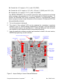
PE3342 EVALUATION KIT USER’S MANUAL 6175 Nancy Ridge Drive, San Diego, CA 92121 (858) 455-0660, Fax (858) 455-0770 http://www.peregrine-semi.com Peregrine Semiconductor Corportation 1 Doc. 79/0073~00C Table of Contents Introduction…………………………………………………………………………….. 4 Introduction…………………………………………………………………………..... 5 Applications Support…………………………………………………………………. 5 FCC Labeling Requirement………………………………………………………….. 5 Hardware Section……………………………………………………………………… 6 Evaluation Kit Contents & Requirements…………………………………………… 7 Evaluation Kit Configuration…………………………………………………………. 8 Evaluation Kit Setup………………………………………………………………….. 9 Software Section………………………………………………………………………. 11 Software Installation Instructions…………………………………………………..... 26-Wire PSC Universal LPT1 Interface Cable Configuration …………………... Evaluation Kit Configuration for EEPROM Programming ……………………….. Reprogramming the EEPROM………………………………………………………. Peregrine Semiconductor Corportation 2 12 13 13 14 Doc. 79/0073~00C © Copyright 2002 Peregrine Semiconductor Corp. All rights reserved. Printed in the United States of America. No part of this publication may be reproduced, photocopied, stored in a retrieval system, or transmitted by electronic, mechanical or any other means without prior written permission of Peregrine Semiconductor Corp. Peregrine Semiconductor Corp., the Peregrine logotype, and UTSi are registered trademarks of Peregrine Semiconductor Corp. PE3342 is a trademark of Peregrine Semiconductor Corp. Peregrine Semiconductor Corp. reserves the right to make improvements to the hardware, firmware or software described in this manual at any time and without notice. While the accompanying material has been carefully reviewed to insure the most accurate information possible, the data are not warranted for absolute accuracy or completeness and are subject to change without notification. Peregrine Semiconductor Corp. Life Support Policy Peregrine Semiconductor Corp. products are not intended for use in life-critical situations, or as critical components in life-support devices or systems. Life-support devices or systems are defined as devices or systems that are intended for surgical implant into the body, or that support or sustain life, and whose failure to perform when used in accordance with the instructions provided by the manufacturer, might result in injury to the user. FCC Compliance Statement This device is intended for use only in a research and development environment. It has not been tested for compliance with FCC regulations regarding interference with radio frequency energy. It might cause harmful interference with radio communications. The user assumes responsibility for any interference caused by this device. Peregrine Semiconductor Corportation 3 Doc. 79/0073~00C Introduction Peregrine Semiconductor Corportation 4 Doc. 79/0073~00C Introduction This Evaluation Kit is specifically designed for evaluating the PE3342 2.7 GHz Integer-N EEPROM PLL. The Evaluation Kit allows maximum flexibility for optimizing phase noise, spur, lock time and power performance for specific applications. Using the hardware and software provided in the Evaluation Kit, EEPROM mode programming can be demonstrated. Applications Support If you have a problem with your evaluation kit, software, or if you have applications questions call (858) 455-0660 and ask for applications support. You may also contact us by fax or e-mail: Fax: (858) 455-0770 E-Mail: [email protected] FCC Labeling Requirement This device complies with Part 15 of the FCC Rules. Operation is subject to the following two conditions: (1) this device may cause harmful interference, and (2) this device must accept any interference received including interference that may cause undesired operation. Peregrine Semiconductor Corportation 5 Doc. 79/0073~00C Hardware Section Peregrine Semiconductor Corportation 6 Doc. 79/0073~00C Evaluation Kit Contents & Requirements The Evaluation Kit includes all of the specific software and hardware required to evaluate the PE3342. Included in the Evaluation Kit are: 1 PE3342 Evaluation Board 1 PE3342 2.7 GHz Integer-N EEPROM PLL 1 Peregrine CD-ROM 4 Jumpers 1 26-Wire PSC Universal LPT1 Interface Cable 2 2-Wire Power Supply Cables 2 4-Wire Power Supply Cable 1 Set of Evaluation Kit Data Plots In order to program the part using EEPROM programming mode the evaluation kit software will need to be installed on a computer with the following minimum requirements: PC Compatible with Windows™ ’95/98/2000 Mouse Parallel Port HTML Browser to access CD contents CAUTION: The PE3342-EK circuit contains components that might be damaged by exposure to voltages in excess of the specified voltage, including voltages produced by electrostatic discharges. Handle the board in accordance with procedures for handling static-sensitive components. Avoid applying excessive voltages to the power supply terminals or signal inputs or outputs. Peregrine Semiconductor Corportation 7 Doc. 79/0073~00C Evaluation Kit Configuration The PE3342 Evaluation Board is configured with an on-board VCO, TCXO reference and a second order active loop filter. The VCO tuning range is approximately 190 MHz with middle frequency at 2610+/- 25 for a tuning voltage 0.5 to 4.5 volts. The reference oscillator is 20 MHz. The loop filter is designed for a 1 MHz comparison frequency and a 2600 MHz output frequency with unity gain crossover at 66 kHz, phase margin of 65 degrees and 1.2 dB of peaking. Unless noted, the data provided was measured in this configuration with the default jumper settings shown in Figure 1. Two jumpers (J5 & J6) configure the Evaluation Board to operate with either the onboard reference oscillator (TCXO) or an external reference applied to J7. Figure 1 shows the proper configuration for utilizing the on-board TCXO reference. J6 in the middle-to-right connection as shown connects the output of the TCXO to the PLL fr input, while J5 installed provides power to the TCXO. Do not connect any external reference to J7 if the on-board reference is selected. To use an external reference, place J6 in the middle-to-left connection which connects the PLL fr input to the J7 SMA connector and remove the jumper on J5 to power-down the TCXO. Figure 2 shows the configuration of using an external reference. The default jumper and switch settings are shown in Figure 1, which place the part into EEPROM mode utilizing the on-board reference. Peregrine Semiconductor recommends that the default settings be used initially to bring up the evaluation board and duplicate the enclosed measured data. Peregrine Semiconductor Corportation 8 Doc. 79/0073~00C DO NOT connect any extenal reference to J7 if the on-board reference is used SW1 Switch 1 "On" J6 center-to-right set to utilize onboard reference J2 Un-jumpered J5 on-board reference powered PLL power: J3-1 +3V J3-3 GND For normal operation, no connection is necessary for J1 or J9 + Opamp power: J3-7 +6V J3-9 & -11 GND J3-13 -2V + + - VCO power: J3-17 +5V J3-19 GND J8 center-to-right set to decativate EE programming VCO output Figure 1. Evaluation Kit Default Jumper & Switch Settings Using on-board Reference. Evaluation Kit Setup 1. Verify a jumper is placed on the connector J5 and REF Selector (J6) is positioned in the middle-to-right connection to select the on-board reference as shown in Figure 1. 2. Verify that no jumper is placed on the connector J2; Switch 1 of SW1 is at “ON” position and the rest of the switches are at “OFF” position. 3. Verify that the jumper is at center-to-right connection on the connector J8. This is to prevent VPP from being accidentally activated. 4. Connect power supply cable to the Evaluation Kit board as shown in Figure 1. Note that the red connector of the power cable is always the positive and the black connector is ground in a 2-wire cable or the negative in a 4-wire cable. Verify all supplies are turned off prior to connecting to evaluation board. Peregrine Semiconductor Corportation 9 Doc. 79/0073~00C Î Connect the +3 V supply to J3-1 (+) and J3-3 (GND) Î Connect the +6/-2 V supply to J3-7 (+6V), J3-9 and -11 (GND), and J3-13 (-2V) Î Connect the +5 V supply to J3-17 (+) and J3-19 (GND) The PE3342 EEPROM on the evaluation board has been programmed and tested before stocking. No connection to J1 or J9 is necessary for normal operation. To prevent the EEPROM from being accidentally erased or re-programmed, always place a jumper at center-to-right connection on the connector J8 to prevent VPP from being accidentally activated. 5. Turn on the powers to the board. 6. The output of the on-board VCO can be measured by connecting a spectrum analyzer to port J4. Before making modifications to the board, verify and duplicate the performance found in the included plots. Additional GND posts and test points are available on the Evaluation Board for measurement flexibility. 7. Using the application software provided and described in detail in the next section, EEPROM programming can be evaluated. Connect an extenal reference to J7 SW1 Switch 1 "On" J6 center-to-left set to utilize external reference J2 Un-jumpered J5 un-jumpered to decative onboard reference PLL power: J3-1 +3V J3-3 GND For normal operation, no connection is necessary for J1 or J9 + + - Opamp power: J3-7 +6V J3-9 & -11 GND J3-13 -2V + VCO power: J3-17 +5V J3-19 GND J8 center-to-right set to decativate EE programming VCO output Figure 2. Jumper Setting to Use an External Reference Peregrine Semiconductor Corportation 10 Doc. 79/0073~00C Software Section Peregrine Semiconductor Corportation 11 Doc. 79/0073~00C The follow sections are for reprogramming of the EEPROM register. For testing of the factory installed EEPROM setup, the software is not needed. Simply power the board and measure the VCO output on a spectrum analyzer (see “Evaluation Kit Setup” section). EEPROM Software Installation Instructions In order to evaluate the PE3342 EEPROM programming, an EEPROM programming software has to be installed in your computer. Follow the steps below to install the software. TM 1. Start Microsoft Windows ‘95/98/2000 2. If the software comes with a CD or floppy disks, insert the CD to CDROM drive. or the floppy disk 1 to the floppy disk drive. Search and double-click the “setup.exe” file and follow the on-screen instructions to finish installation. 3. If the software doesn’t come with a CD nor floppy disks, follow the steps below. 4. Go to the Peregrine PE3342 product page on our website at: http://www.peregrinesemi.com/prd_pll_PE3342.html. 5. Click on the “Software” button under the “Evaluation Kit Documentation” heading. 6. Choose the “Save” option and select where you want to save it on your computer’s hard drive. 7. Once downloaded, navigate to the directory in which you saved the file (it’s called: “Peregrine-EE-PLL-Software.zip”). Double click the file to open it in Winzip (if you don’t have Winzip, download the free version at: http://www.winzip.com/ddchomea.htm). 8. Double-click the “setup.exe” file and follow the on-screen instructions to finish installation. Peregrine Semiconductor Corportation 12 Doc. 79/0073~00C 26-Wire PSC Universal LPT1 Interface Cable Configuration The following graph shows the 26-Wire PSC Universal LPT1 Interface Cable configuration. Evaluation Kit Configuration for EEPROM Programming 1. Place a jumper on the connector J2 as shown in Figure 3. 2. Set all switches on SW1 to “OFF” position. 3. Connect one end of the 26-Wire PSC Universal LPT1 Interface Cable to the PC parallel port and the other end to the keyed connector J1 on the evaluation board. 4. Connect power supply cables to the Evaluation Kit board as shown in Figure 3. Note that the red connector of the power cable is always the positive and the black connector is ground in a 2-wire cable or the negative in a 4-wire cable. Verify all supplies are turned off prior to connecting to evaluation board. Î Connect the +3 V supply to J3-1 (+) and J3-3 (GND) Î Connect the +5 V supply to J3-17 (+) and J3-19 (GND) Î Connect the +6/-2 V supply to J3-7 (+6V), J3-9 and -11 (GND), and J3-13 (2V) Peregrine Semiconductor Corportation 13 Doc. 79/0073~00C Î Connect the +13/-9 power supply to J9-4 (+13V), J9-3 and J9-2 (GND), and J9-1 (-9 V) 5. Turn on powers to the board 6. Re-position the jumper on the connector J8 to the left-to-center position. DO NOT connect any extenal reference to J7 if the on-board reference is used SW1 All switches "Off" J2 Jumpered J6 center-to-right set to utilize on-board reference J5 on-board reference powered PLL power: J3-1 +3V J3-3 GND Key-pin J1, 26-pin interface connector + - J9, VPP power Pin 4, +13V Pins 3 & 2, GND Pin 1, -9V + - Opamp power: J3-7 +6V J3-9 & -11 GND J3-13 -2V + - VCO power: J3-17 +5V J3-19 GND + - J8 center-to-left set to access EE programming VCO output Figure 3. Jumper Setting for EEPROM Programming. Reprogramming the EEPROM With the EE Programming kit set up completed as described in the previous section, the follow steps are for programming of the EEPROM register. Step 1: Start the “Peregrine EE PLL Control Software” program. Figure 4 shows one example of the screen. Peregrine Semiconductor Corportation 14 Doc. 79/0073~00C Step 2: .Verify the “EEPROM Register” is displayed in the drop down menu in the middle section. Step 3: Enter reference frequency (crystal frequency) value in MHz into the Ref Freq box (marked by red dot at left) Î Light blue number boxes identify user defined program states and can be modified by utilizing the arrows next to the boxes or clicking into the box and typing the appropriate value. Either clicking on the light blue switches or typing the counter variable into the text box can program the registers. Î Programming of the secondary or EEPROM register is selected by the light blue pull down box. Note: EEPROM register is the default selection. Do not change it. Î The prescaler enabled or disabled can be selected by the light blue Prescaler switch. “Enable” is the default selection. Î The enhancement mode enable function is currently unavailable. Î Data is sent to the evaluation board by clicking the dark blue “SEND DATA” button. Figure 4. Example of EEPROM Programming Software Screen. Peregrine Semiconductor Corportation 15 Doc. 79/0073~00C Step 4: Set reference counter (R counter) to the desired value by entering it into the R Register box in the middle left side (marked by yellow dot at left). Note that the numbers in the orange boxes are computed values and cannot be directly typed in. Step 5: Verify “frequency step” (which is also called phase detector frequency) is at the desired value. Step 6: Verify that the Prescaler switch is in the default position “Enable” for a normal operation. Switch it to “Disable” position if the prescaler is to be bypassed (disabled). Step 7: Set the VCO frequency to the appropriate value by typing it into the “Out Freq (MHz)” box. Once the frequency value is entered into the box, the corresponded M and A register values are displayed in the “M Register” and “A Register” Boxes, respectively. Instead of entering the frequency value into the “Out Freq (MHz)” box, the frequency can also be changed by entering M register and A register values into the “M Register” and “A Register” boxes directly. Step 8: Click the “SEND DATA” button to send data to the PLL. Step 9: The program will automatically read back the R, M and A Register values and display them in the bottom section. If the EEPROM is programmed successfully, a message “Device Programmed Successfully!” with a green dot will display in the bottom section as shown in Fig. 4. Otherwise, if any of the read back values is different from the programmed value, a message “Device Programming Failed!” with a red dot will display as shown in Fig. 5. This feature can be used to read back the R, M and A Register values of a previous programmed part. To do this, just complete the previous section “Evaluation Kit Configuration for EEPROM Programming” and Steps 1 and 2 of this section and then click the “READ DATA” button in the right bottom corner. The “READ DATA” function will read back and display the R, M and A Register values of a previous programmed part without showing other message. Step 10: Once the EEPROM has been programmed, return jumper J8 to the center-toright position. This is to ensure that the EEPROM register data is not corrupted by an inadvertent load. Step 11: Remove jumper J2 to select EEPROM register. Step 12: Move Switch 1 of SW1 to the “On” position. Step 13: Verify on the spectrum analyzer that the part locks to the desired frequency (J1 and J9 can be disconnected from the cables or remained connected for this operation). Step 14: To exit the program, click the “QUIT” button. Peregrine Semiconductor Corportation 16 Doc. 79/0073~00C Figure 5. failed. Example of EEPROM Programming Software Screen when programming Peregrine Semiconductor Corportation 17 Doc. 79/0073~00C