1
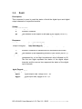
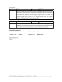
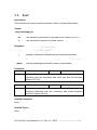
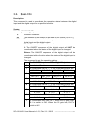
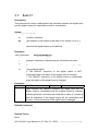
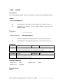
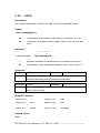
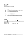
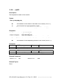
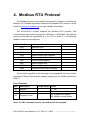
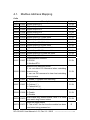
SC-4104-W1 User Manual Warranty All products manufactured by ICP DAS are under warranty regarding defective materials for a period of one year, beginning from the date of delivery to the original purchaser. Warning! ICP DAS assumes no liability for any damage resulting from the use of this product. ICP DAS reserves the right to change this manual at any time without notice. The information furnished by ICP DAS is believed to be accurate and reliable. However, no responsibility is assumed by ICP DAS for its use, nor for any infringements of patents or other rights of third parties resulting from its use. Copyright Copyright © 2014 ICP DAS Co., Ltd. All rights are reserved. Trademarks Names are used for identification purposes only and may be registered trademarks of their respective companies. SC-4104-W1 User Manual v1.01, Feb / 16 / 2015 ------------------------------ 1 Contents 1. 2. Introduction.............................................................................................4 Hardware Information.............................................................................6 2.1. IO Specifications ............................................................................6 2.2. System Specifications ....................................................................7 2.3. Pin Assignments.............................................................................8 2.4. Wire Connections...........................................................................9 2.5. DIP Switch and Rotary Switch Configuration ............................... 11 2.5.1. INIT Mode..........................................................................12 2.5.2. Hardware Configuration Mode...........................................13 2.5.3. Software Configuration Mode ............................................13 2.6. Software Configuration Tables .....................................................14 3. DCON Protocol......................................................................................15 3.1. %aannttccff ..................................................................................18 3.2. $aa2 .............................................................................................20 3.3. $aa5 .............................................................................................22 3.4. $aa6 .............................................................................................24 3.5. $aaF.............................................................................................26 3.6. $aaLC0n ......................................................................................27 3.7. $aaLC1 ........................................................................................30 3.8. $aaLC2nnnn ................................................................................31 3.9. $aaLC3 ........................................................................................33 3.10. $aaM ........................................................................................35 3.11. $aaP .........................................................................................36 3.12. $aaPc .......................................................................................38 3.13. #aa ...........................................................................................40 3.14. @aa..........................................................................................41 3.15. @aah........................................................................................43 3.16. @aaDI ......................................................................................44 3.17. @aaDOhh ................................................................................45 3.18. @aaA2CjToo ............................................................................46 3.19. @aaA3Cj ..................................................................................48 3.20. ~** ............................................................................................49 3.21. ~aa0 .........................................................................................50 3.22. ~aa1 .........................................................................................51 3.23. 3.24. 3.25. ~aa2 .........................................................................................52 ~aa3ehh ...................................................................................53 ~aa4 .........................................................................................54 SC-4104-W1 User Manual v1.01, Feb / 16 / 2015 ------------------------------ 2 3.26. 3.27. 3.28. 3.29. 3.30. 3.31. 3.32. 3.33. 3.34. 3.35. 4. ~aa4P .......................................................................................55 ~aa4S .......................................................................................56 ~aa5ppss..................................................................................57 ~aa5P .......................................................................................58 ~aa5S .......................................................................................59 ~aaD.........................................................................................60 ~aaDt........................................................................................61 ~aaRS ......................................................................................62 ~aaRD ......................................................................................63 ~aaRDhh ..................................................................................64 Modbus RTU Protocol ..........................................................................65 4.1. Modbus Address Mapping............................................................66 4.2. Function 01 - Read Coils..............................................................68 4.3. Function 02 - Read Discrete Inputs..............................................69 4.4. Function 03 - Read Multiple Registers .........................................70 4.5. Function 04 - Read Multiple Input Registers ................................71 4.6. Function 05 – Write Single Coil ....................................................72 4.7. Function 06 – Write Single Register.............................................73 4.8. Function 15 – Write Multiple Coils................................................74 4.9. Function 16 – Write Multiple Registers.........................................75 4.10. Function 70 – Read/Write Module Setting ................................76 4.10.1. Sub-function 00 – Read Module Name .............................77 4.10.2. Sub-function 04 – Write Module Address ..........................78 4.10.3. Sub-function 05 – Read Communication Setting...............79 4.10.4. Sub-function 06 – Write Communication Setting ...............80 4.10.5. Sub-function 32 – Read Firmware Version........................81 4.10.6. Sub-function 39 – Write Power-on Value...........................82 4.10.7. Sub-function 40 – Read Power-on Value ..........................83 4.10.8. Sub-function 53 – Set Response Delay Time ....................84 4.10.9. Sub-function 54 – Read Response Delay Time.................85 SC-4104-W1 User Manual v1.01, Feb / 16 / 2015 ------------------------------ 3 1. Introduction The SC-4104-W1 is an easy-to-use smart control module. It can be used in such as small FCU control system and small lighting control system. SC-4104-W1 requires no specialist skills to install and operate, and no software is needed in order to control the Digital Output channel. The SC-4104-W1 provides 1 channel for Digital Input (photocouple isolation), 4 channels for relay output and 1 channel for temperature sensor (thermistor). The output channel is 1 Form C type relay and 3 Form A type relay, while the input channel is based on a sink-type using a wire connection. The input channel can be used to directly control the 4 channels relay ON and OFF sequence without requiring a remote host controller. And the SC-4104-W1 support 7 kinds coordinated function for users select. 4 kV ESD protection and 5000 Vrms intra-module isolation are also provided. When required, communication with the SC-4104-W1 is programmable based on either the DCON or the Modbus RTU protocol, and an added benefit is that different addresses can be set for DCON or Modbus RTU communication via hardware or software configuration. Warning Do not use the SC-4104-W1 to connect to any device where the loading is greater than 160 W per channel, as this may cause the module to malfunction. SC-4104-W1 User Manual v1.01, Feb / 16 / 2015 ------------------------------ 4 Features z z z z z Cost-effective for small FCU control module Power Relay Outputs Isolated AC Digital Input Support 7 kinds AC DI Input Direct Control Relay ON/OFF Function 1 Channel Thermistor Temperature Sensor (-40℃ ~ +80℃) z z z z Easy installation Use fireproof materials (UL94-V0 Level) Low power consumption Support Modbus RTU and DCON Protocol z Two RJ-11 Connector (6P4C or 6P6C), Quick and easy wiring SC-4104-W1 User Manual v1.01, Feb / 16 / 2015 ------------------------------ 5 2. Hardware Information 2.1. IO Specifications Digital Input Input Channel 1 Type 90 ~ 240 VAC On Voltage Level 85 VAC Off Voltage Level 60 VAC Input Impedance 68 kΩ, 1 W Isolation 5000 Vrms Function Local and remote direct control relay ON/OFF and remote status monitoring. Digital Output Output Channel 4 Type Power Relay, 1 Form C, 3 Form A Operating Voltage 250 VAC or 30 VDC Max. Load Current 7 A (NO) / 5 A (NC) @ 250 VAC ( Recommend Working Current 1 A ) Operating Time Form C: 10 ms Max. Form A: 10 ms Max. Release Time Form C: 5 ms Max. Form A: 10 ms Max. Electrical Life (900 ops/hr) Form C: 100,000 ops Form A: 100,000 ops Mechanical Life (1800 ops/hr) Form C: 10,000,000 ops Form A: 5,000,000 ops Power-on & Safe Value Yes, Programmable Temperature Sensor Temperature Channel 1 Type Operating Temperature Range Thermistor -40℃ ~ +80℃ Temperature Tolerance ±1℃ SC-4104-W1 User Manual v1.01, Feb / 16 / 2015 ------------------------------ 6 2.2. System Specifications Communication Interface RS-485 Data Format N,8,1 / O,8,1 / E,8,1 / N,8,2 Baud Rate Hardware Configuration: Fixed 9600 bps Software Configuration: 1200 ~ 115200 bps Protocol Modbus RTU or DCON Node Address 128 ~ 159 for hardware configuration 0 ~ 255 for software configuration * For Modbus RTU, address 0 is auto become to 1 Connector RJ-11 / 4-pin screw terminal LED Indicators Power 1 LED as power indicator Digital Output 4 LED as digital output indicator EMS Protection ESD ±4 kV contact for each terminal EFT ±1 kV for power and communication Power Requirements Input Voltage Range +10 ~ +30 VDC Consumption 2.4 W Max. Connector RJ-11 (6P4C or 6P6C) / 4-pin screw terminal Mechanical Dimensions (W x L x H) 72 mm x 100 mm x 59 mm Installation DIN-Rail Environment Operating Temperature -25℃ ~ +75℃ Storage Temperature -30℃ ~ +80℃ Humidity 10 to 95% RH, Non-condensing SC-4104-W1 User Manual v1.01, Feb / 16 / 2015 ------------------------------ 7 2.3. Pin Assignments SC-4104-W1 User Manual v1.01, Feb / 16 / 2015 ------------------------------ 8 RJ11 Pin Assignment Pin Description 1 +VS Power Input (+10 ~ +30 VDC) 2 +VS Power Input (+10 ~ +30 VDC) 3 DATA+ RS-485 Interface (D+) 4 DATA- RS-485 Interface (D-) 5 GND Ground 6 GND Ground Terminal Block Assignment 2.4. Pin Description 1 DATA+ RS-485 Interface (D+) 2 DATA- RS-485 Interface (D-) 3 +VS Power Input (+10 ~ +30 VDC) 4 GND Ground Wire Connections DIO Wire Connections SC-4104-W1 User Manual v1.01, Feb / 16 / 2015 ------------------------------ 9 Power and Communication Connections Using Terminal Block Using RJ-11 Connector SC-4104-W1 User Manual v1.01, Feb / 16 / 2015 ------------------------------ 10 2.5. DIP Switch and Rotary Switch Configuration DIP Switch Description DIP 1 DIP 2 DIP 3 DIP 4 ON DCON Protocol OFF Modbus RTU Protocol ON Software Configuration OFF Hardware Configuration ON High Node Address OFF Low Node Address ON INIT Mode OFF Normal Mode Address Setting via Hardware Configuration Module Address 0 to F for Address 128 - 143 (Node Address - Low) 0 to F for Address 144 - 159 (Node Address High) Relay Test Button SW1 ~ SW4 are test push buttons that control Relay 1 ~ Relay 4 ON / OFF. RL1 ~ RL4 are LED Indicators to Relay 1 ~ Relay 4. When a relay is ON, the corresponding LED will be ON, too. SC-4104-W1 User Manual v1.01, Feb / 16 / 2015 ------------------------------ 11 2.5.1. INIT Mode When the SC-4104-W1 is powered on with DIP switch SW4 in the ON position, the module will be set to INIT Mode. In this mode, the position of DIP switches SW1-SW3 and the Address settings switch will be ignored and the SC-4104-W1 module will use the fixed configuration parameters listed below. Protocol: DCON Address: 00 Baud Rate: 9600 bps Data Format: N, 8, 1 In this mode, the relevant commands can be used to change the configuration, and the new settings will be saved to the EEPROM. SC-4104-W1 User Manual v1.01, Feb / 16 / 2015 ------------------------------ 12 2.5.2. Hardware Configuration Mode When the SC-4104-W1 is powered on with both the SW4 and the SW2 DIP switches in the OFF position, the module will be set to Hardware Configuration Mode. In this mode, the following configuration parameters are used. Protocol: Dependent on the position of DIP switch SW1 Address: Refer to the “Address Settings via Hardware Configuration” table above Baud Rate: Fixed at 9600 bps Data Format: Fixed to N,8,1 In this mode, any software command related to configuration will be ignored when using the Modbus RTU protocol, or will return an error when using the DCON protocol. 2.5.3. Software Configuration Mode When the SC-4104-W1 is powered on with DIP switch SW4 in the OFF position and DIP switch SW2 in the ON position, the module will be set to Software Configuration Mode. In this mode, the configuration parameters to be used will be retrieved from the EEPROM. The default configuration parameters stored in the EEPROM is: Protocol: Modbus RTU Address: 01 (0x01) Baud Rate: 9600 bps Data Format: N,8,1 In this mode, the relevant commands can be used to change the configuration parameters, and the new settings will be saved to the EEPROM. SC-4104-W1 User Manual v1.01, Feb / 16 / 2015 ------------------------------ 13 2.6. Software Configuration Tables Baud Rate Settings (CC) 7 6 5 Data Bit, Parity, Stop Bit 4 3 2 Reserved 1 0 Data Rate Data Rate (Bit 0 ~ Bit 3) Code 3 4 5 6 7 8 Baud 1200 2400 4800 9600 19200 38400 9 A 57600 115200 Data Bit, Parity and Stop Bit (Bit 6 ~ Bit 7) Code 0 1 2 3 Format 8, n, 1 8, n, 2 8, e, 1 8, o, 1 Type Code Settings (TT) For the SC-4104-W1, the Type Code is fixed to 40 and cannot be changed. Data Format Settings (FF) 7 6 Reserved CS 5 4 3 2 1 0 Reserved Key Description CS Checksum Setting 0: Disabled 1: Enabled Note: All Reserved bits should be zero. SC-4104-W1 User Manual v1.01, Feb / 16 / 2015 ------------------------------ 14 3. DCON Protocol All communication with the SC-4104-W1 consists of commands generated by the Host and responses transmitted by the SC-4104-W1 module. Each module has a unique ID number that is used for addressing purposes and is stored in non-volatile memory. The module ID number is set to 01 by default and can be changed by sending a user command. All commands to the modules contain the ID number as the address, meaning that only the addressed module will respond. Command Format: Delimiter Character Module Address Command Checksum CR Module Address Data Checksum CR Response Format: Delimiter Character CR = End of command character, carriage return (0x0D), used to end a frame. Note: 1. 2. All characters should be in upper case. There will be no response if the command syntax is incorrect, there is a communication error, or there is no module with the specified address. SC-4104-W1 User Manual v1.01, Feb / 16 / 2015 ------------------------------ 15 An Overview of the DCON Command Set General Command Set Command Response Description %aannttccff !aa Set configuration module of the $aa2 !aattccff Read configuration module of the $aa5 !aa Read reset status of the 3.3 module $aa6 !(data) Read all digital input/output 3.4 data $aaF !aa(data) Read firmware version of the 3.5 module !aa Coordinate the operation status between the digital 3.6 input and the digital output $aaLC1 !aan Read whether or not the operation status between the 3.7 digital input and the digital output is coordinated $aaLC2nnnn !aa Set the active delay time for 3.8 the digital output $aaLC3 !aannnn Read the active delay time for 3.9 the digital output $aaM !aa(data) Read module name $aaP !aasc Read communication protocol 3.11 information $aaPc !aa Set communication protocol 3.12 #aa >(data) Read all analog input data 3.13 @aa >(data) Read all digital input/output 3.14 data @aah > Set all digital output channels @aaDI !aasooii Read digital I/O and alarm 3.16 status @aaDOhh !aa Set digital output states 3.17 @AAA2CjT00 !aa Set Temperature Offset 3.18 @AAA3Cj !aaoo Get Temperature Offset 3.19 ~** None Host OK notification 3.20 $aaLC0n SC-4104-W1 User Manual v1.01, Feb / 16 / 2015 Section 3.1 3.2 3.10 3.15 ------------------------------ 16 ~aa0 !aass Read host watchdog status ~aa1 !aa Clear host watchdog timeout 3.22 state ~aa2 !aaehh Read host watchdog settings 3.23 ~aa3ehh !aa Set host watchdog settings 3.24 ~aa4 !aappss Read power-on and digital output values 3.25 ~aa4P !aa(data) Read the power-on digital 3.26 output value ~aa4S !aa(data) Read the safe digital output 3.27 value ~aa5ppss !aa Set power-on and safe digital 3.28 output values ~aa5P !aa ~aa5S !aa Set the current digital output 3.30 value as the safe value ~aaD !aat Read temperature scale 3.31 ~aaDt !aa Set temperature scale 3.32 ~aaRS !aard Read rotary and dip switch 3.33 ~aaRD !aahh Read response delay time 3.34 ~aaRDhh !aa Set response delay time 3.35 safe Set the current digital output value as the power-on value SC-4104-W1 User Manual v1.01, Feb / 16 / 2015 3.21 3.29 ------------------------------ 17 3.1. %aannttccff Description: This command is used to set the configuration of a specified module. Syntax: %aannttccff[CHKSUM](CR) % Delimiter character. aa The address of the module to be set in hex format (00 to FF). nn The new address of the module in hex format (00 to FF). tt The Type code, which should be set to 40 for DIO modules. cc The new Baud Rate, see section 2.6 for details. The module must boot up at INIT mode (section 2.5) in order to change Baud Rates. ff The command used to set the counter update direction and the checksum (section 2.6). The module must boot up at INIT mode (section 2.5) in order to change the checksum settings. Response: Valid Command: !aa[CHKSUM](CR) Invalid Command: ?aa[CHKSUM](CR) ! Delimiter character to indicate that the command was valid. ? Delimiter character to indicate that the command was invalid. If an attempt is made to change the Baud Rate or Checksum settings without first connecting the INIT* pin to the ground pin or without switching the rear slide switch to the INIT position, the module will return a response indicating that the command was invalid. aa The address of the responding module in hex format (00 to FF). SC-4104-W1 User Manual v1.01, Feb / 16 / 2015 ------------------------------ 18 Examples: Command: %0102400600 Response: !02 Changes the address of module 01 to 02. The module returns a response indicating that the command was valid and includes the new address of the module. Command: %0101400A00 Response: ?01 Changes the Baud Rate of module 01 to 115200bps. The module returns a response indicating that the command was invalid, because it is not in INIT mode. Command: %010140CA00 Response: !01 Changes the Baud Rate of module 01 to 115200bps with 8 o 1 format and the module is in INIT mode. The module returns a response indicating that the command was valid. Related Command: Section 3.2 $aa2 Related Topics: Section 2.5 DIP Switch and Rotary Switch Configuration Section 2.6 Software Configuration Tables Notes: Changes to the address settings take effect immediately after a valid command is received. Changes to the baud rate and checksum settings take effect on the next power-on reset. SC-4104-W1 User Manual v1.01, Feb / 16 / 2015 ------------------------------ 19 3.2. $aa2 Description: This command is used to read the configuration of a specified module. Syntax: $aa2[CHKSUM](CR) $ Delimiter character. aa The address of the module to be read in hex format (00 to FF). 2 The command to read the configuration of the module. Response: Valid Command: !aattccff[CHKSUM](CR) Invalid Command: ?aa[CHKSUM](CR) ! Delimiter character to indicate that the command was valid. ? Delimiter character to indicate that the command was invalid. aa The address of the responding module in hex format (00 to FF). tt The type code, it should be 40 for the module. cc The baud rate for the module. See section 2.6 for details. ff The checksum of the module. See section 2.6 for details. SC-4104-W1 User Manual v1.01, Feb / 16 / 2015 ------------------------------ 20 Examples: Command: $012 Response: !01400600 Read the configuration of module 01 and returns a response indicating that the command was valid, and showing that the Type code is set to 40, the Baud Rate is 9600 bps, the Checksum is Disabled and the counter update direction is Falling Edge. Command: $032 Response: ?03 Attempts to read the configuration of module 03, but returns a response indicating that the command was invalid because module 03 does not exist. Related Command: Section 3.1 %aannttccff Related Topics: Section 2.5 DIP Switch and Rotary Switch Configuration Section 2.6 Software Configuration Tables. SC-4104-W1 User Manual v1.01, Feb / 16 / 2015 ------------------------------ 21 3.3. $aa5 Description: This command is used to read the reset status for a specified module. Syntax: $aa5[CHKSUM](CR) $ Delimiter character. aa The address of the module to be read in hex format (00 to FF). 5 The command to read the reset status of the module. Response: Valid Command: !aaS[CHKSUM](CR) Invalid Command: ?aa[CHKSUM](CR) ! Delimiter character to indicate that the command was valid. ? Delimiter character to indicate that the command was invalid. aa The address of the responding module in hex format (00 to FF). 5 The reset status of the module: 0: This is NOT the first time the command has been sent since the module was powered on, which denotes that there has been no module reset since the last $AA5 command was sent. 1: This is the first time the $AA5 command has been sent since the module was powered on. SC-4104-W1 User Manual v1.01, Feb / 16 / 2015 ------------------------------ 22 Examples: Command: $015 Response: !011 Read the reset status for module 01 and returns a response indicating that the command was valid, and that it is the first time the $AA5 command has been sent since the module was powered on. Command: $015 Response: $010 Read the reset status for module 01 and returns a response indicating that the command was valid, and that there has been no module reset since the last $AA5 command was sent. Command: $035 Response: ?03 Attempts to read the reset status for module 03, but returns a response indicating that the command was invalid because module 03 does not exist. Related Command: None Related Topics: None SC-4104-W1 User Manual v1.01, Feb / 16 / 2015 ------------------------------ 23 3.4. $aa6 Description: This command is used to read the status of both the digital input and digital output channels of a specified module. Syntax: $aa6[CHKSUM](CR) $ Delimiter character. aa The address of the module to be read in hex format (00 to FF). 6 The command to read the status of the Digital I/O channels. Response: Valid Command: !(data)[CHKSUM](CR) Invalid Command: ?aa[CHKSUM](CR) ! Delimiter character to indicate that the command was valid. ? Delimiter character to indicate that the command was invalid. aa The address of the responding module in hex format (00 to FF). (data) The status of the digital output and digital input channels represented by a four-digit hexadecimal value followed by 00. The first two digits represent the status of the digital output channels and the second two represent the status of the digital input channels. (data) Format: (Byte 1)(Byte 2)00 Byte 1 Digital output data. Range is 00 ~ 0F. Byte 2 Digital input data. Range is 00 ~ 01. 00 Fix response end of the command. SC-4104-W1 User Manual v1.01, Feb / 16 / 2015 ------------------------------ 24 Examples: Command: $026 Response: !0F0100 Read the status of the digital output and digital input channels for module 02 and returns a response indicating that the command was valid and that the current digital output value is 0F and the current digital input value is 01 denoting that both the digital output and digital input channels are ON. Command: $036 Response: ?03 Attempts to read the status of the digital output and digital input channels for module 03 and returns a response indicating that the command was invalid because module 03 does not exist. Related Command: Section 3.14 @aa , Section 3.15 @aah Section 3.16 @aaDI , Section 3.17 @aaDOhh Related Topics: None SC-4104-W1 User Manual v1.01, Feb / 16 / 2015 ------------------------------ 25 3.5. $aaF Description: This command is used to read the firmware version of a specified module. Syntax: $aaF[CHKSUM](CR) $ Delimiter character. aa The address of the module to be read in hex format (00 to FF). F The command to read the firmware version. Response: Valid Command: !aa(data)[CHKSUM](CR) Invalid Command: ?aa[CHKSUM](CR) ! Delimiter character to indicate that the command was valid. ? Delimiter character to indicate that the command was invalid. aa The address of the responding module in hex format (00 to FF). (data) A string indicating the firmware version of the module. Examples: Command: $01F Response: !0101.00 Read the firmware version of module 01, and returns a response indicating that the command was valid, and that the firmware version is 01.00. Command: $03F Response: ?03 Attempts to read the firmware version of module 03 and returns a response indicating that the command was invalid because module 03 does not exist. Related Command: None Related Topics: None SC-4104-W1 User Manual v1.01, Feb / 16 / 2015 ------------------------------ 26 3.6. $aaLC0n Description: This command is used to coordinate the operation status between the digital input and the digital output for a specified module. Syntax: $aaLC0n[CHKSUM](CR) $ Delimiter character. aa The address of the module to be read in hex format (00 to FF). LC0 The command to coordinate the operation status between the digital input and the digital output. n The DI DO coordinated function number. 0: The ON/OFF sequence of the digital output will NOT be coordinated when the status of the digital input is changed. Others: The ON/OFF sequence of the digital output will be coordinated with n function when the status of the digital input is changed. The command to set the operating status: n The ON/OFF Sequence of The Digital Output 0 Coordinated Disable 1 DI coordinated with RL1 ~ 4, the 4 operating status are: NO 0 0 0 2 NC 0 0 1 NO 1 1 0 NO 1 1 1 NO 0 1 0 NO 0 0 1 X110 X111 DI coordinated with RL1 ~ 4, the 3 operating status are: X100 7 NC 0 1 0 DI coordinated with RL2 ~ 4, the 3 operating status are: X100 6 NC 1 0 0 DI coordinated with RL1 ~ 4, the 3 operating status are: NO 1 0 0 5 NO 1 1 1 DI coordinated with RL1 ~ 4, the 3 operating status are: NO 1 0 0 4 NO 1 1 0 DI coordinated with RL1 ~ 4, the 4 operating status are: NO 0 0 0 3 NO 1 0 0 X010 X001 DI coordinated only with RL1. When the DI gets high, RL1 is switch to NO. When the DI gets low, RL1 is switch to NC. SC-4104-W1 User Manual v1.01, Feb / 16 / 2015 ------------------------------ 27 The description of symbols of above list is below. NO : RL1 Normal Open NC : RL1 Normal Close 0 : DO Off 1 : DO On X : don’t care Response: Valid Command: >aa[CHKSUM](CR) Invalid Command: ?aa[CHKSUM](CR) > Delimiter character to indicate that the command was valid. ? Delimiter character to indicate that the command was invalid. aa The address of the responding module in hex format (00 to FF). SC-4104-W1 User Manual v1.01, Feb / 16 / 2015 ------------------------------ 28 Examples: Command: $01LC01 Response: !01 Coordinates the function 1 operation between the digital input and the digital output of module 01, and the module returns a response indicating that the command was valid. Related Command: Section 3.7 $aaLC1 Related Topics: None SC-4104-W1 User Manual v1.01, Feb / 16 / 2015 ------------------------------ 29 3.7. $aaLC1 Description: This command is used to read whether the operation between the digital input and the digital output for a specified module is coordinated. Syntax: $aaLC1[CHKSUM](CR) $ Delimiter character. aa The address of the module to be read in hex format (00 to FF). LC1 The command to read whether the operation between the digital input and the digital output is coordinated Response: Valid Command: !aan[CHKSUM](CR) Invalid Command: ?aa[CHKSUM](CR) ! Delimiter character to indicate that the command was valid. ? Delimiter character to indicate that the command was invalid. aa The address of the responding module in hex format (00 to FF). n The operation status: 0: The ON/OFF sequence of the digital output is NOT coordinated when the status of the digital input is changed 1: The ON/OFF sequence of the digital output is coordinated when the status of the digital input is changed Examples: Command: $01LC1 Response: !011 Read whether the operation between the digital input and the digital output is coordinated and the module returns a response indicating that the command was valid with a value of 1 meaning that the sequence of the digital output will be coordinated with function 1 when the status of the digital input is changed. Related Command: Section 3.6 $aaLC0n Related Topics: None SC-4104-W1 User Manual v1.01, Feb / 16 / 2015 ------------------------------ 30 3.8. $aaLC2nnnn Description: This command is used to set the active delay time for the digital output of a specified module. Syntax: $aaLC2nnnn[CHKSUM](CR) $ Delimiter character. aa The address of the module to be read in hex format (00 to FF). LC2 The command to set the active delay time for the digital output. nnnn A four-digit hexadecimal value representing the active delay time in milliseconds. The maximum delay time is 0x0BB8 (3000 milliseconds). Response: Valid Command: !aa[CHKSUM](CR) Invalid Command: ?aa[CHKSUM](CR) ! Delimiter character to indicate that the command was valid. ? Delimiter character to indicate that the command was invalid. aa The address of the responding module in hex format (00 to FF). SC-4104-W1 User Manual v1.01, Feb / 16 / 2015 ------------------------------ 31 Examples: Command: $01LC203E8 Response: !01 Set the active delay time for the digital output of module 01 to 0x03E8 (1000 milliseconds) and the module returns a response indicating that the command was valid. The digital output will be active 1000 milliseconds after the module is powered on. Command: $01LC20BB9 Response: ?01 Attempts to set the active delay time for the digital output of module 01 to 0x0BB9 (3001 milliseconds), but the module returns a response indicating that the command was invalid because the value for the active delay time was not within the valid range. Related Command: Section 3.9 $aaLC3 Related Topics: None SC-4104-W1 User Manual v1.01, Feb / 16 / 2015 ------------------------------ 32 3.9. $aaLC3 Description: This command is used to read the active delay time for the digital output of a specified module. Syntax: $aaLC3[CHKSUM](CR) $ Delimiter character. aa The address of the module to be read in hex format (00 to FF). LC3 The command to read the active delay time for the digital output. Response: Valid Command: !aannnn[CHKSUM](CR) Invalid Command: ?aa[CHKSUM](CR) ! Delimiter character to indicate that the command was valid. ? Delimiter character to indicate that the command was invalid. aa The address of the responding module in hex format (00 to FF). nnnn A four-digit hexadecimal value representing the active delay time in milliseconds SC-4104-W1 User Manual v1.01, Feb / 16 / 2015 ------------------------------ 33 Examples: Command: $01LC20BB8 Response: !01 Set the active delay time for the digital output of module 01 to 0x0BB8 (3000 milliseconds) and the module returns a response indicating that the command was valid. The digital output will be active 3000 milliseconds after the module is powered on. Command: $01LC3 Response: !010BBB Read the active delay time for the digital output of module 01 and returns a response indicating that the command was valid, with a value of 0BB8 meaning that the active delay time is 3000 milliseconds. Related Command: Section 3.8 $aaLC2nnn Related Topics: None SC-4104-W1 User Manual v1.01, Feb / 16 / 2015 ------------------------------ 34 3.10. $aaM Description: This command is used to read the name of a specified module. Syntax: $aaM[CHKSUM](CR) $ Delimiter character. aa The address of the module to be read in hex format (00 to FF). M The command to read the name of the module. Response: Valid Command: !aa(data)[CHKSUM](CR) Invalid Command: ?aa[CHKSUM](CR) ! Delimiter character to indicate that the command was valid. ? Delimiter character to indicate that the command was invalid. aa The address of the responding module in hex format (00 to FF). (data) A string indicating the name of the module. Examples: Command: $02M Response: !02SC4104 Read the name of module 02 and returns a response indicating that the command was valid, and that the name of the module is SC-4104-W1. Command: $03M Response: ?03 Attempts to read the name of module 03 and returns a response indicating that the command was invalid because module 03 does not exist. Related Command: None Related Topics: None SC-4104-W1 User Manual v1.01, Feb / 16 / 2015 ------------------------------ 35 3.11. $aaP Description: This command is used to read the communication protocol information for a specified module. Syntax: $aaP[CHKSUM](CR) $ Delimiter character. aa The address of the module to be read in hex format (00 to FF). P The command to read the communication protocol information. Response: Valid Command: !aasc[CHKSUM](CR) Invalid Command: ?aa[CHKSUM](CR) ! Delimiter character to indicate that the command was valid. ? Delimiter character to indicate that the command was invalid. aa The address of the responding module in hex format (00 to FF). s The protocols supported by the module: 0: Only the DCON protocol is supported. 1: Both the DCON and Modbus RTU protocols are supported. c The current protocol that is saved in the EEPROM that will be used at the next power-on reset: 0: The protocol saved in the EEPROM is DCON. 1: The protocol saved in the EEPROM is Modbus RTU. SC-4104-W1 User Manual v1.01, Feb / 16 / 2015 ------------------------------ 36 Examples: Command: $01P Response: !0110 Read the communication protocol information for module 01 returns a response indicating that the command was valid, with a value of 10, which denotes that the module supports both the DCON and Modbus RTU protocols and that the protocol that will be used at the next power-on reset is DCON. Command: $03P Response: ?03 Attempts to read the communication protocol information for module 03 and returns a response indicating that the command was invalid because module 03 does not exist. Related Command: Section 3.12 $aaPn Related Topics: None SC-4104-W1 User Manual v1.01, Feb / 16 / 2015 ------------------------------ 37 3.12. $aaPc Description: This command is used to set the communication protocol for a specified module. Syntax: $aaPc[CHKSUM](CR) $ Delimiter character. aa The address of the module to be read in hex format (00 to FF). P The command to set the communication protocol. c The protocol to be used: 0: DCON Protocol 1: Modbus RTU Protocol Note: Before using this command, the module must be boot up at INIT mode (section 2.5) if in DCON protocol mode. The new protocol information will be saved in the EEPROM and will become effective after the next power-on reset. Response: Valid Command: !aa[CHKSUM](CR) Invalid Command: ?aa[CHKSUM](CR) ! Delimiter character to indicate that the command was valid. ? Delimiter character to indicate that the command was invalid. aa The address of the responding module in hex format (00 to FF). SC-4104-W1 User Manual v1.01, Feb / 16 / 2015 ------------------------------ 38 Examples: Command: $01P1 Response: ?01 Attempts to set the communication protocol to be used for module 01 to Modbus RTU, but returns a response indicating that the command was invalid because the module is not in INIT mode. Command: $01P1 Response: !01 Set the communication protocol to be used for module 01 to Modbus RTU and returns a response indicating that the command was valid. Related Command: Section 3.11 $aaP Related Topics: Section 2.5 DIP Switch Configuration SC-4104-W1 User Manual v1.01, Feb / 16 / 2015 ------------------------------ 39 3.13. #aa Description: This command is used to read analog input data of the module. Syntax: #aa[CHKSUM](CR) # Delimiter character. aa The address of the module to be read in hex format (00 to FF). Response: Valid Command: >(data)[CHKSUM](CR) Invalid Command: ?aa[CHKSUM](CR) ! Delimiter character to indicate that the command was valid. ? Delimiter character to indicate that the command was invalid. aa The address of the responding module in hex format (00 to FF). (data) Analog input value in engineer unit format. Examples: Command: ~01D Response: !010 Read the temperature scale for module 01 returns a response indicating that the command was valid, with a value of 0, which denotes that the temperature scale is Celsius (℃). Command: #01 Response: >+026.40 Read the temperature analog value for module 01 returns a response indicating that the command was valid, with a value of +026.40, which denotes that the temperature sensor indicated now is 26.4℃. Related Command: Section 3.18 @aaA2CjToo Section 3.19 @aaA3Cj Section 3.31 ~aaD Section 3.32 ~aaDt Related Topics: None SC-4104-W1 User Manual v1.01, Feb / 16 / 2015 ------------------------------ 40 3.14. @aa Description: This command is used to read the status of both the digital output and digital input channels of a specified module. Syntax: @aa[CHKSUM](CR) @ Delimiter character. aa The address of the module to be read in hex format (00 to FF). Response: Valid Command: >(data)[CHKSUM](CR) Invalid Command: ?aa[CHKSUM](CR) ! Delimiter character to indicate that the command was valid. ? Delimiter character to indicate that the command was invalid. aa The address of the responding module in hex format (00 to FF). (data) The status of the digital output and digital input channels represented by a four-digit hexadecimal value. The first two digits represent the status of the digital output channels and the second two represent the status of the digital input channels. (data) Format: (Byte 1)(Byte 2) Byte 1 Digital output data. Range is 00 ~ 0F. Byte 2 Digital input data. Range is 00 ~ 01. SC-4104-W1 User Manual v1.01, Feb / 16 / 2015 ------------------------------ 41 Examples: Command: @02 Response: >0F01 Read the status of the digital output and digital input channels for module 02 and returns a response indicating that the command was valid and that the current digital output value is 0F and the current digital input value is 01 denoting that both the digital output and digital input channels are ON. Command: @03 Response: ?03 Attempts to read the status of the digital output and digital input channels for module 03 and returns a response indicating that the command was invalid because module 03 does not exist. Related Command: Section 3.4 $aa6 , Section 3.15 @aah Section 3.16 @aaDI , Section 3.17 @aaDOhh Related Topics: None SC-4104-W1 User Manual v1.01, Feb / 16 / 2015 ------------------------------ 42 3.15. @aah Description: This command is used to set the value for all digital output channels of a specified module. Syntax: @aah[CHKSUM](CR) @ Delimiter character. aa The address of the module to be read in hex format (00 to FF). h A single-digit hexadecimal value representing the data to be written to the digital output channels, where bit 0 ~ 3 of the value corresponds to channel RL1 ~ RL4. When the bit is 0, it denotes that the digital output channel is set to OFF, and 1 denotes that the digital output channel is set to ON. Response: Valid Command: >[CHKSUM](CR) Invalid Command: ?aa[CHKSUM](CR) Ignored Command:  > Delimiter character to indicate that the command was valid. ? Delimiter character to indicate that the command was invalid. ! Delimiter character to indicate that the command was ignored. The module is in host watchdog timeout mode, and the output is set to safe value. Examples: Command: @023 Response: > Set channels RL1 and RL2 of module 02 to ON, and the module returns a response indicating that the command was valid. Related Command: Section 3.4 $aa6 , Section 3.14 @aa Section 3.16 @aaDI , Section 3.17 @aaDOhh Related Topics: None SC-4104-W1 User Manual v1.01, Feb / 16 / 2015 ------------------------------ 43 3.16. @aaDI Description: This command is used to read the status of both the digital output and digital input channels and alarm status of a specified module. Syntax: @aaDI[CHKSUM](CR) @ Delimiter character. aa The address of the module to be read in hex format (00 to FF). DI The command to read the digital I/O and alarm status. Response: Valid Command: !aasooii[CHKSUM](CR) Invalid Command: ?aa[CHKSUM](CR) ! Delimiter character to indicate that the command was valid. ? Delimiter character to indicate that the command was invalid. aa The address of the responding module in hex format (00 to FF). s Alarm status. Now the parameter is reserved and got always 0. oo Digital output data. Range is 00 ~ 0F. ii Digital input data. Range is 00 ~ 01. Examples: Command: @01DI Response: !0100F01 Read the status of the digital output and digital input channels for module 01 and returns a response indicating that the command was valid and that the current digital output value is 0F and the current digital input value is 01 denoting that both the digital output and digital input channels are ON. Related Command: Section 3.4 $aa6 , Section 3.14 @aa Section 3.15 @aah , Section 3.17 @aaDOhh Related Topics: None SC-4104-W1 User Manual v1.01, Feb / 16 / 2015 ------------------------------ 44 3.17. @aaDOhh Description: This command is used to set the value for all digital output channels of a specified module. Syntax: @aaDOhh[CHKSUM](CR) @ Delimiter character. aa The address of the module to be read in hex format (00 to FF). DO The command to set the digital output of the module. hh A byte hexadecimal value representing the data to be written to the digital output channels, where bit 0 ~ 3 of the value corresponds to channel RL1 ~ RL4 and others bit must be 0. When the bit is 0, it denotes that the digital output channel is set to OFF, and 1 denotes that the digital output channel is set to ON. Response: Valid Command: !aa[CHKSUM](CR) Invalid Command: ?aa[CHKSUM](CR) ! Delimiter character to indicate that the command was valid. ? Delimiter character to indicate that the command was invalid. aa The address of the responding module in hex format (00 to FF). Examples: Command: @02DO0F Response: !aa Set channels RL1 ~ RL4 of module 02 to ON, and the module returns a response indicating that the command was valid. Related Command: Section 3.4 $aa6 , Section 3.14 @aa Section 3.15 @aah , Section 3.16 @aaDI Related Topics: None SC-4104-W1 User Manual v1.01, Feb / 16 / 2015 ------------------------------ 45 3.18. @aaA2CjToo Description: This command is used to set the temperature offset value of a specified module. Syntax: @aaA2CjToo[CHKSUM](CR) @ Delimiter character. aa The address of the module to be read in hex format (00 to FF). A2C The command to select temperature channel to set. j Temperature input channel. For SC-4104-W1 must be 0. T The command to set temperature offset value. oo Temperature offset value in Hex format. 00 ~ 7F is plus value (+0 ~ +127) and FF ~ 80 is minus value (-1 ~ -128). The offset temperature unit is 0.1. Response: Valid Command: !aa[CHKSUM](CR) Invalid Command: ?aa[CHKSUM](CR) ! Delimiter character to indicate that the command was valid. ? Delimiter character to indicate that the command was invalid. aa The address of the responding module in hex format (00 to FF). SC-4104-W1 User Manual v1.01, Feb / 16 / 2015 ------------------------------ 46 Examples: Command: ~01D Response: !010 Read the temperature scale for module 01 returns a response indicating that the command was valid, with a value of 0, which denotes that the temperature scale is Celsius (℃). Command: #01 Response: >+026.40 Read the temperature analog value for module 01 returns a response indicating that the command was valid, with a value of +026.40, which denotes that the temperature sensor indicated now is 26.4℃. Command: @01A2C0T06 Response: !01 Set the temperature offset to 06 and returns a response indicating that the command was valid. Command: #01 Response: >+027.00 Read the temperature analog value for module 01 returns a response indicating that the command was valid, with a value of +027.00, which denotes that the temperature sensor indicated now is 27℃ (26.4 + 0.6). Related Command: Section 3.13 #aa Section 3.19 @aaA3Cj Section 3.31 ~aaD Section 3.32 ~aaDt Related Topics: None SC-4104-W1 User Manual v1.01, Feb / 16 / 2015 ------------------------------ 47 3.19. @aaA3Cj Description: This command is used to read the temperature offset value of a specified module. Syntax: @aaA3Cj [CHKSUM](CR) @ Delimiter character. aa The address of the module to be read in hex format (00 to FF). A3C j The command to select temperature channel to read. Temperature input channel. For SC-4104-W1 must be 0. Response: Valid Command: !aaoo[CHKSUM](CR) Invalid Command: ?aa[CHKSUM](CR) ! Delimiter character to indicate that the command was valid. ? Delimiter character to indicate that the command was invalid. aa The address of the responding module in hex format (00 to FF). oo Temperature offset value in Hex format. 00 ~ 7F is plus value (+0 ~ +127) and FF ~ 80 is minus value (-1 ~ -128). The offset temperature unit is 0.1. Examples: Command: @01A3C0 Response: !0106 Read the temperature offset value for module 01 returns a response indication that the command was valid, with a value of 06, which demotes that the temperature offset is +0.6. Related Command: Section 3.13 #aa Section 3.18 @aaA2CjToo Section 3.31 ~aaD Section 3.32 ~aaDt Related Topics: None SC-4104-W1 User Manual v1.01, Feb / 16 / 2015 ------------------------------ 48 3.20. ~** Description: Host sends this command to all modules for broadcasting the information “Host OK”. If the module waits the command timeout when enable WDT function. The module will in host watchdog timeout mode, and the output is set to safe value. Syntax: ~** [CHKSUM](CR) ~ Delimiter character. ** Command for all modules. Response: None Examples: Command: ~** Response: No response Send “Host OK” to all modules. Related Command: Section 3.21 ~aa0 Section 3.22 ~aa1 Section 3.23 ~aa2 Section 3.24 ~aa3ehh Section 3.25 ~aa4 Section 3.27 ~aa4S Section 3.28 ~aa5ppss Section 3.30 ~aa5S Related Topics: None SC-4104-W1 User Manual v1.01, Feb / 16 / 2015 ------------------------------ 49 3.21. ~aa0 Description: Read host watchdog status of the module. Syntax: ~aa0 [CHKSUM](CR) ~ Delimiter character. aa The address of the module to be read in hex format (00 to FF). 0 The command to read host watchdog status. Response: Valid Command: !aass[CHKSUM](CR) Invalid Command: ?aa[CHKSUM](CR) ! Delimiter character to indicate that the command was valid. ? Delimiter character to indicate that the command was invalid. aa The address of the responding module in hex format (00 to FF). ss Host watchdog status. The status will store into flash and only may reset by the command ~aa1. 7 6 *1 5 4 3 Reserved 2 1 0 *2 Reserved *1: Host watchdog status, 0=disable, 1=enable *2: Host watchdog timeout flag, 0=clear, 1=set Examples: Command: ~010 Response: !0104 Read module 01 host watchdog status returns 04, host watchdog timeout flag is set. Related Command: Section 3.20 ~** Section 3.22 ~aa1 Section 3.23 ~aa2 Section 3.24 ~aa3ehh Section 3.25 ~aa4 Section 3.27 ~aa4S Section 3.28 ~aa5ppss Section 3.30 ~aa5S Related Topics: None SC-4104-W1 User Manual v1.01, Feb / 16 / 2015 ------------------------------ 50 3.22. ~aa1 Description: Reset host watchdog status of the module. Syntax: ~aa1 [CHKSUM](CR) ~ Delimiter character. aa The address of the module to be read in hex format (00 to FF). 1 The command to reset host watchdog status. Response: Valid Command: !aa[CHKSUM](CR) Invalid Command: ?aa[CHKSUM](CR) ! Delimiter character to indicate that the command was valid. ? Delimiter character to indicate that the command was invalid. aa The address of the responding module in hex format (00 to FF). Examples: Command: ~010 Response: !0104 Read module 01 host watchdog status returns 04, host watchdog timeout flag is set. Command: ~011 Response: !01 Reset module 01 host watchdog status returns success. Command: ~010 Response: !0100 Read module 01 host watchdog status returns 00, host watchdog timeout flag is clear. Related Command: Section 3.20 ~** Section 3.21 ~aa0 Section 3.23 ~aa2 Section 3.24 ~aa3ehh Section 3.25 ~aa4 Section 3.27 ~aa4S Section 3.28 ~aa5ppss Section 3.30 ~aa5S Related Topics: None SC-4104-W1 User Manual v1.01, Feb / 16 / 2015 ------------------------------ 51 3.23. ~aa2 Description: Read host watchdog activation and timeout interval. Syntax: ~aa2 [CHKSUM](CR) ~ Delimiter character. aa The address of the module to be read in hex format (00 to FF). 2 The command to read host watchdog activation and timeout interval. Response: Valid Command: !aaehh[CHKSUM](CR) Invalid Command: ?aa[CHKSUM](CR) ! Delimiter character to indicate that the command was valid. ? Delimiter character to indicate that the command was invalid. aa The address of the responding module in hex format (00 to FF). e Host watchdog activation, 0=disable, 1=enable. hh Timeout interval in Hex format, each count for 0.1 second, ex: 01 = 0.1 second and FF = 25.5 seconds. Examples: Command: ~012 Response: !011FF Read module 01 host watchdog activation and timeout interval returns 1FF, host watchdog is enabled now and timeout interval is 25.5 seconds. Related Command: Section 3.20 ~** Section 3.21 ~aa0 Section 3.22 ~aa1 Section 3.24 ~aa3ehh Section 3.25 ~aa4 Section 3.27 ~aa4S Section 3.28 ~aa5ppss Section 3.30 ~aa5S Related Topics: None SC-4104-W1 User Manual v1.01, Feb / 16 / 2015 ------------------------------ 52 3.24. ~aa3ehh Description: Set host watchdog activation and timeout interval. Syntax: ~aa3ehh [CHKSUM](CR) ~ Delimiter character. aa The address of the module to be read in hex format (00 to FF). 3 The command to set host watchdog activation and timeout interval. e Host watchdog activation, 0=disable, 1=enable. hh Timeout interval in Hex format, each count for 0.1 second, ex: 01 = 0.1 second and FF = 25.5 seconds. Response: Valid Command: !aa[CHKSUM](CR) Invalid Command: ?aa[CHKSUM](CR) ! Delimiter character to indicate that the command was valid. ? Delimiter character to indicate that the command was invalid. aa The address of the responding module in hex format (00 to FF). Examples: Command: ~013164 Response: !01 Set module 01 enable host watchdog and timeout interval is 64 (10.0 seconds), returns success. Related Command: Section 3.20 ~** Section 3.21 ~aa0 Section 3.22 ~aa1 Section 3.23 ~aa2 Section 3.25 ~aa4 Section 3.27 ~aa4S Section 3.28 ~aa5ppss Section 3.30 ~aa5S Related Topics: None SC-4104-W1 User Manual v1.01, Feb / 16 / 2015 ------------------------------ 53 3.25. ~aa4 Description: Read power-on value and safe value of digital output for a specified module. Syntax: ~aa4 [CHKSUM](CR) ~ Delimiter character. aa The address of the module to be read in hex format (00 to FF). 4 The command to read power-on value and safe value of digital output. Response: Valid Command: !aappss[CHKSUM](CR) Invalid Command: ?aa[CHKSUM](CR) ! Delimiter character to indicate that the command was valid. ? Delimiter character to indicate that the command was invalid. aa The address of the responding module in hex format (00 to FF). pp The digital output power-on value. ss The digital output safe value. Examples: Command: ~014 Response: !010F03 Read module 01 power-on and safe value returns power-on value is 0F, safe value is 03. Related Command: Section 3.20 ~** Section 3.21 ~aa0 Section 3.22 ~aa1 Section 3.23 ~aa2 Section 3.24 ~aa3ehh Section 3.26 ~aa4P Section 3.27 ~aa4S Section 3.28 ~aa5ppss Section 3.29 ~aa5P Section 3.30 ~aa5S Related Topics: None SC-4104-W1 User Manual v1.01, Feb / 16 / 2015 ------------------------------ 54 3.26. ~aa4P Description: Read power-on value of digital output for a specified module. Syntax: ~aa4P [CHKSUM](CR) ~ Delimiter character. aa The address of the module to be read in hex format (00 to FF). 4P The command to read power-on value of digital output. Response: Valid Command: !aa(data)[CHKSUM](CR) Invalid Command: ?aa[CHKSUM](CR) ! Delimiter character to indicate that the command was valid. ? Delimiter character to indicate that the command was invalid. aa The address of the responding module in hex format (00 to FF). (data) The digital output power-on value. Examples: Command: ~014P Response: !010F00 Read module 01 power-on value returns 0F. Related Command: Section 3.25 ~aa4 Section 3.29 ~aa5P Section 3.28 ~aa5ppss Related Topics: None SC-4104-W1 User Manual v1.01, Feb / 16 / 2015 ------------------------------ 55 3.27. ~aa4S Description: This command is used to read the digital output safe value for a specified module. Syntax: ~aa4S [CHKSUM](CR) ~ Delimiter character. aa The address of the module to be read in hex format (00 to FF). 4S The command to read safe value of digital output. Response: Valid Command: !aa(data)[CHKSUM](CR) Invalid Command: ?aa[CHKSUM](CR) ! Delimiter character to indicate that the command was valid. ? Delimiter character to indicate that the command was invalid. aa The address of the responding module in hex format (00 to FF). (data) The digital output safe value. Examples: Command: ~014S Response: !010300 Read module 01 safe value returns 03. Related Command: Section 3.20 ~** Section 3.21 ~aa0 Section 3.22 ~aa1 Section 3.23 ~aa2 Section 3.24 ~aa3ehh Section 3.25 ~aa4 Section 3.28 ~aa5ppss Section 3.30 ~aa5S Related Topics: None SC-4104-W1 User Manual v1.01, Feb / 16 / 2015 ------------------------------ 56 3.28. ~aa5ppss Description: Set power-on value and safe value of digital output to a specified module. Syntax: ~aa5ppss [CHKSUM](CR) ~ Delimiter character. aa The address of the module to be read in hex format (00 to FF). 5 The command to set power-on value and safe value of digital output. pp The digital output power-on value. ss The digital output safe value. Response: Valid Command: !aa[CHKSUM](CR) Invalid Command: ?aa[CHKSUM](CR) ! Delimiter character to indicate that the command was valid. ? Delimiter character to indicate that the command was invalid. aa The address of the responding module in hex format (00 to FF). Examples: Command: ~0150F03 Response: !01 Set module 01 power-on value to 0F and safe value to 03 and returns success. Related Command: Section 3.20 ~** Section 3.21 ~aa0 Section 3.22 ~aa1 Section 3.23 ~aa2 Section 3.24 ~aa3ehh Section 3.25 ~aa4 Section 3.26 ~aa4P Section 3.27 ~aa4S Section 3.29 ~aa5P Section 3.30 ~aa5S Related Topics: None SC-4104-W1 User Manual v1.01, Feb / 16 / 2015 ------------------------------ 57 3.29. ~aa5P Description: Set current digital output value as the power-on value for a specified module. Syntax: ~aa5P [CHKSUM](CR) ~ Delimiter character. aa The address of the module to be read in hex format (00 to FF). 5P Command for setting current digital output value as the power-on value. Response: Valid Command: !aa[CHKSUM](CR) Invalid Command: ?aa[CHKSUM](CR) ! Delimiter character to indicate that the command was valid. ? Delimiter character to indicate that the command was invalid. aa The address of the responding module in hex format (00 to FF). Examples: Command: @01F Response: > Set module 01 digital output value to F, and the module returns a response indicating that the command was valid. Command: ~015P Response: !01 Set current digital output value of module 01 as the power-on value and returns success. Related Command: Section 3.25 ~aa4 Section 3.28 ~aa5ppss Section 3.26 ~aa4P Related Topics: None SC-4104-W1 User Manual v1.01, Feb / 16 / 2015 ------------------------------ 58 3.30. ~aa5S Description: Set current digital output value as the safe value for a specified module. Syntax: ~aa5S [CHKSUM](CR) ~ Delimiter character. aa The address of the module to be read in hex format (00 to FF). 5S Command for setting current digital output value as the safe value. Response: Valid Command: !aa[CHKSUM](CR) Invalid Command: ?aa[CHKSUM](CR) ! Delimiter character to indicate that the command was valid. ? Delimiter character to indicate that the command was invalid. aa The address of the responding module in hex format (00 to FF). Examples: Command: @013 Response: > Set module 01 digital output value to 3, and the module returns a response indicating that the command was valid. Command: ~015S Response: !01 Set current digital output value of module 01 as the safe value and returns success. Related Command: Section 3.20 ~** Section 3.21 ~aa0 Section 3.22 ~aa1 Section 3.23 ~aa2 Section 3.24 ~aa3ehh Section 3.25 ~aa4 Section 3.27 ~aa4S Section 3.28 ~ aa5ppss Related Topics: None SC-4104-W1 User Manual v1.01, Feb / 16 / 2015 ------------------------------ 59 3.31. ~aaD Description: Read temperature scale of the module. Syntax: ~aaD [CHKSUM](CR) ~ Delimiter character. aa The address of the module to be read in hex format (00 to FF). D The command for read temperature scale. Response: Valid Command: !aat[CHKSUM](CR) Invalid Command: ?aa[CHKSUM](CR) ! Delimiter character to indicate that the command was valid. ? Delimiter character to indicate that the command was invalid. aa The address of the responding module in hex format (00 to FF). Temperature scale. C Æ Celsius (℃), F Æ Fahrenheit (℉) t Examples: Command: ~01D Response: !01C Read module 01 temperature scale returns C (℃). Related Command: Section 3.13 #aa Section 3.32 ~aaDt Related Topics: None SC-4104-W1 User Manual v1.01, Feb / 16 / 2015 ------------------------------ 60 3.32. ~aaDt Description: Set temperature scale to the module. Syntax: ~aaDt [CHKSUM](CR) ~ Delimiter character. aa The address of the module to be read in hex format (00 to FF). D The command for read temperature scale. Temperature scale. C Æ Celsius (℃), F Æ Fahrenheit (℉) t Response: Valid Command: !aa[CHKSUM](CR) Invalid Command: ?aa[CHKSUM](CR) ! Delimiter character to indicate that the command was valid. ? Delimiter character to indicate that the command was invalid. aa The address of the responding module in hex format (00 to FF). Examples: Command: ~01DF Response: !01 Set module 01 temperature scale to F (℉) and returns success. Command: ~01D Response: !01F Read module 01 temperature scale returns F (℉). Related Command: Section 3.13 #aa Section 3.31 ~aaD Related Topics: None SC-4104-W1 User Manual v1.01, Feb / 16 / 2015 ------------------------------ 61 3.33. ~aaRS Description: Read current rotary switch and DIP switch value of the module. Syntax: ~aaRS [CHKSUM](CR) ~ Delimiter character. aa The address of the module to be read in hex format (00 to FF). RS The command for read rotary switch and DIP switch value. Response: Valid Command: !aard[CHKSUM](CR) Invalid Command: ?aa[CHKSUM](CR) ! Delimiter character to indicate that the command was valid. ? Delimiter character to indicate that the command was invalid. aa The address of the responding module in hex format (00 to FF). r Rotary switch value, range is from 0 ~ F. d DIP switch value, range is from 0 ~ F. Examples: Command: ~03RS Response: !0331 Read module 03 switch value returns rotary switch value is 3 and DIP switch value is 1. Related Command: None Related Topics: Section 2.5 DIP Switch and Rotary Switch Configuration SC-4104-W1 User Manual v1.01, Feb / 16 / 2015 ------------------------------ 62 3.34. ~aaRD Description: This command is used to read the response delay time for a specified module. Syntax: ~aaRD [CHKSUM](CR) ~ Delimiter character. aa The address of the module to be read in hex format (00 to FF). RD The command to read the response delay time. Response: Valid Command: !aahh[CHKSUM](CR) Invalid Command: ?aa[CHKSUM](CR) ! Delimiter character to indicate that the command was valid. ? Delimiter character to indicate that the command was invalid. aa The address of the responding module in hex format (00 to FF). hh Response delay time, range is from 00 ~ 1E in 1 ms intervals. Examples: Command: ~03RD1E Response: !03 Set the response delay time for module 03 to 1E (30 ms), and returns a response indicating that the command was valid. Command: ~03RD Response: !031E Read the response delay time for module 03 and returns a response indicating that the command was valid, with a value of 1E (30 ms). Related Command: Section 3.35 ~aaRDhh Related Topics: None SC-4104-W1 User Manual v1.01, Feb / 16 / 2015 ------------------------------ 63 3.35. ~aaRDhh Description: This command is used to set the response delay time for a specified module. Syntax: ~aaRDhh [CHKSUM](CR) ~ Delimiter character. aa The address of the module to be read in hex format (00 to FF). RD The command to read the response delay time. hh Response delay time, range is from 00 ~ 1E in 1 ms intervals. Response: Valid Command: !aa[CHKSUM](CR) Invalid Command: ?aa[CHKSUM](CR) ! Delimiter character to indicate that the command was valid. ? Delimiter character to indicate that the command was invalid. aa The address of the responding module in hex format (00 to FF). Examples: Command: ~03RD1E Response: !03 Set the response delay time for module 03 to 1E (30 ms), and returns a response indicating that the command was valid. Command: ~03RD Response: !031E Read the response delay time for module 03 and returns a response indicating that the command was valid, with a value of 1E (30 ms). Related Command: Section 3.34 ~aaRD Related Topics: None SC-4104-W1 User Manual v1.01, Feb / 16 / 2015 ------------------------------ 64 4. Modbus RTU Protocol The Modbus protocol was originally developed for Modicon controllers by Modicon Inc. Detailed information related to the Modbus RTU protocol can be found at http://www.modbus.org for more valuable information. The SC-4104-W1 module supports the Modbus RTU protocol, with communication baud rates ranging from 1200 bps to 115200 bps. The data bits, parity and stop bits are supported 8 n 1, 8 n 2, 8 e 1 and 8 o 1. The following Modbus functions are supported. Function Code Description Section 0x01 Read the coils 0x02 Read the discrete inputs 0x03 Read multiple registers 0x04 Read multiple input registers 0x05 Write a single coil 0x06 Write a single register 0x0F Write multiple coils 0x10 Write multiple registers 0x46 Read/Write the module settings If the function specified in the message is not supported, then the module responds as below. Note that the address mapping for the Modbus protocol is Base 0. Error Response Byte Description Length (Byte) Value 00 Address 1 1 ~ 247 01 Function Code 1 Function Code + 0x80 02 Exception Code 1 02: Register not support 03: Modbus format invalid Note: If a CRC mismatch occurs, the module will not respond. SC-4104-W1 User Manual v1.01, Feb / 16 / 2015 ------------------------------ 65 4.1. Modbus Address Mapping Coils Address Description Attribute 00001 10001 Digital Output RL1 R/W 00002 10002 Digital Output RL2 R/W 00003 10003 Digital Output RL3 R/W 00004 10004 Digital Output RL4 R/W 10033 Digital Input Channel R 00129 10129 Digital Output RL1 Safe Value R/W 00130 10130 Digital Output RL2 Safe Value R/W 00131 10131 Digital Output RL3 Safe Value R/W 00132 10132 Digital Output RL4 Safe Value R/W 00161 10161 Digital Output RL1 Power-on Value R/W 00162 10162 Digital Output RL2 Power-on Value R/W 00163 10163 Digital Output RL3 Power-on Value R/W 00164 10164 Digital Output RL4 Power-on Value R/W Communication Protocol 00257 10257 0: DCON 1: Modbus RTU R/W Modbus host watchdog mode 0: do not allow DO command when watchdog 00260 10260 timeout occur 1: can use DO command to clear host watchdog timeout status R/W 00261 10261 1: enable, 0: disable host watchdog R/W Temperature Scale 00267 10267 0: Celsius (℃) 1: Fahrenheit (℉) R/W DCON Protocol Checksum 00268 10268 0: Enable 1: Disable R/W 00270 10270 Host watch dog timeout status, write 1 to clear host watch dog timeout status Read the Reset Status 00273 10273 0: This is NOT the first time the module has been read since being powered on SC-4104-W1 User Manual v1.01, Feb / 16 / 2015 R/W R ------------------------------ 66 1: This is the first time the module has been read since being powered on Coordinate the status between DI and DO 00274 10274 0: Enable 1: Disable R/W 10321 DIP Switch Bit 0 R 10322 DIP Switch Bit 1 R 10323 DIP Switch Bit 2 R 10324 DIP Switch Bit 3 R 10325 Rotary Switch Bit 0 R 10326 Rotary Switch Bit 1 R 10327 Rotary Switch Bit 2 R 10328 Rotary Switch Bit 3 R Register Address 30001 Description Attribute Temperature Analog Input Channel R 30274 40274 Coordinate Function 0 ~ 7 (refer to section 3.6) R/W 30289 40289 Temperature Offset (offset unit: 0.1) R/W 30481 Firmware Version (Low Word) R 30482 Firmware Version (High Word) Read 40482 and 40483 Response: 0x00 0x01 0x00 0x01 (version 1.01) R 30483 Module Name (Low Word) R 30484 Module Name (High Word) Read 40483 and 40484 Response: 0x41 0x04 0x53 0x43 (SC4104) R 30485 40485 Module Address Valid Range: 1 ~ 247 R/W 30486 40486 Module Baud Rate See Section 2.6 Software Configuration Table R/W 30488 40488 Modbus Response Delay Time ( ≤ 30ms) Valid Range: 0x0000 ~ 0x001E ms R/W 30489 40489 Host watchdog timeout value, 0 ~ 255, in 0.1s R/W 30492 40492 Host watchdog timeout count, write 0 to clear R/W 30498 40498 Module Boot Up Delay Time ( ≤ 3000ms) Valid Range: 0x0000 ~ 0x0BB8 ms SC-4104-W1 User Manual v1.01, Feb / 16 / 2015 R/W ------------------------------ 67 4.2. Function 01 - Read Coils This function code is used to read the value at addresses 0xxxx. Request Byte Description Value 00 Module ID 1 ~ 247 01 Function Code 0x01 02 – 03 Reference Address Refer to section 4.1 – Address 0xxxx 04 – 05 Bit Count Number of bit (B) to read Description Value 00 Module ID 1 ~ 247 01 Function Code 0x01 02 Byte Count Response data byte N = B/7 Response Byte 03 – (N+2) Bit Value Response bit data Error Response Byte Description Value 00 Module ID 1 ~ 247 01 Function Code 0x81 02 Exception Code Refer to section 4 – Error Response SC-4104-W1 User Manual v1.01, Feb / 16 / 2015 ------------------------------ 68 4.3. Function 02 - Read Discrete Inputs This function code is used to read the value at addresses 1xxxx. Request Byte Description Value 00 Module ID 1 ~ 247 01 Function Code 0x02 02 – 03 Reference Address Refer to section 4.1 – Address 1xxxx 04 – 05 Bit Count Number of bit (B) to read Description Value 00 Module ID 1 ~ 247 01 Function Code 0x02 02 Byte Count Response data byte N = B/7 Response Byte 03 – (N+2) Bit Value Response bit data Error Response Byte Description Value 00 Module ID 1 ~ 247 01 Function Code 0x82 02 Exception Code Refer to section 4 – Error Response SC-4104-W1 User Manual v1.01, Feb / 16 / 2015 ------------------------------ 69 4.4. Function 03 - Read Multiple Registers This function code is used to read the value at addresses 4xxxx. Request Byte Description Value 00 Module ID 1 ~ 247 01 Function Code 0x03 02 – 03 Reference Address Refer to section 4.1 – Address 4xxxx 04 – 05 Word Count Number of word (W) to read Description Value 00 Module ID 1 ~ 247 01 Function Code 0x03 02 Byte Count Response data byte N = W*2 Response Byte 03 – (N+2) Word Value Response word data Error Response Byte Description Value 00 Module ID 1 ~ 247 01 Function Code 0x83 02 Exception Code Refer to section 4 – Error Response SC-4104-W1 User Manual v1.01, Feb / 16 / 2015 ------------------------------ 70 4.5. Function 04 - Read Multiple Input Registers This function code is used to read the value at addresses 3xxxx. Request Byte Description Value 00 Module ID 1 ~ 247 01 Function Code 0x04 02 – 03 Reference Address Refer to section 4.1 – Address 3xxxx 04 – 05 Word Count Number of word (W) to read Description Value 00 Module ID 1 ~ 247 01 Function Code 0x04 02 Byte Count Response data byte N = W*2 Response Byte 03 – (N+2) Word Value Response word data Error Response Byte Description Value 00 Module ID 1 ~ 247 01 Function Code 0x84 02 Exception Code Refer to section 4 – Error Response SC-4104-W1 User Manual v1.01, Feb / 16 / 2015 ------------------------------ 71 4.6. Function 05 – Write Single Coil This function code is used to write a value to addresses 0xxxx. Request Byte Description Value 00 Module ID 1 ~ 247 01 Function Code 0x05 02 – 03 Reference Address Refer to section 4.1 – Address 0xxxx 04 – 05 Output Value Output ON: 0xFF00 Output OFF: 0x0000 Description Value 00 Module ID 1 ~ 247 01 Function Code 0x05 02 – 03 Reference Address The same as byte 02 – 03 of request 04 – 05 Output Value The same as byte 04 – 05 of request Response Byte Error Response Byte Description Value 00 Module ID 1 ~ 247 01 Function Code 0x85 02 Exception Code Refer to section 4 – Error Response SC-4104-W1 User Manual v1.01, Feb / 16 / 2015 ------------------------------ 72 4.7. Function 06 – Write Single Register This function code is used to write a value to addresses 4xxxx. Request Byte Description Value 00 Module ID 1 ~ 247 01 Function Code 0x06 02 – 03 Reference Address Refer to section 4.1 – Address 0xxxx 04 – 05 Output Value A word value Description Value 00 Module ID 1 ~ 247 01 Function Code 0x06 02 – 03 Reference Address The same as byte 02 – 03 of request 04 – 05 Output Value The same as byte 04 – 05 of request Response Byte Error Response Byte Description Value 00 Module ID 1 ~ 247 01 Function Code 0x86 02 Exception Code Refer to section 4 – Error Response SC-4104-W1 User Manual v1.01, Feb / 16 / 2015 ------------------------------ 73 4.8. Function 15 – Write Multiple Coils This function code is used to write values to addresses 0xxxx. Request Byte Description Value 00 Module ID 1 ~ 247 01 Function Code 0x0F 02 – 03 Reference Address Refer to section 4.1 – Address 0xxxx 04 – 05 Bit Count Number of bit (B) to write 06 Byte Count Byte number N = B/7 07 – (N+6) Write Data A bit corresponds to a channel. Output ON: The bit = 1 Output OFF: The bit = 0 Response Byte Description Value 00 Module ID 1 ~ 247 01 Function Code 0x0F 02 – 03 Reference Address The same as byte 02 – 03 of request 04 – 05 Output Value The same as byte 04 – 05 of request Error Response Byte Description Value 00 Module ID 1 ~ 247 01 Function Code 0x8F 02 Exception Code Refer to section 4 – Error Response SC-4104-W1 User Manual v1.01, Feb / 16 / 2015 ------------------------------ 74 4.9. Function 16 – Write Multiple Registers This function code is used to write values to addresses 4xxxx. Request Byte Description Value 00 Module ID 1 ~ 247 01 Function Code 0x10 02 – 03 Reference Address Refer to section 4.1 – Address 0xxxx 04 – 05 Word Count Number of word (W) to write 06 Byte Count Byte number N = W*2 07 – (N+6) Write Data Multiple word data Response Byte Description Value 00 Module ID 1 ~ 247 01 Function Code 0x10 02 – 03 Reference Address The same as byte 02 – 03 of request 04 – 05 Output Value The same as byte 04 – 05 of request Error Response Byte Description Value 00 Module ID 1 ~ 247 01 Function Code 0x90 02 Exception Code Refer to section 4 – Error Response SC-4104-W1 User Manual v1.01, Feb / 16 / 2015 ------------------------------ 75 4.10. Function 70 – Read/Write Module Setting This function code is used to read the configuration settings from the module or to change the settings for the module. The following sub-function codes are supported. Sub-function Code Description Section 00(0x00) Read the name of the module 4.10.1 04(0x04) Set the module address 4.10.2 05(0x05) Read the communication settings 4.10.3 06(0x06) Set the communication settings 4.10.4 32(0x20) Read the firmware version 4.10.5 39(0x27) Set the digital output power-on value 4.10.6 40(0x28) Read the digital output power-on value 4.10.7 53(0x35) Set the response delay time 4.10.8 54(0x36) Read the response delay time 4.10.9 If the module does not support the sub-function code specified in the message, then it will respond as follows: Error Response Byte Description Value 00 Module ID 1 ~ 247 01 Function Code 0xC6 02 Exception Code Refer to section 4 – Error Response SC-4104-W1 User Manual v1.01, Feb / 16 / 2015 ------------------------------ 76 4.10.1. Sub-function 00 – Read Module Name This sub-function code is used to read the name of the SC-4104-W1 module. Request Byte Description Value 00 Module ID 1 ~ 247 01 Function Code 0x46 02 Sub-function code 0x00 Description Value 00 Module ID 1 ~ 247 01 Function Code 0x46 02 Sub-function Code 0x00 03 – 06 Module Name 0x53 0x43 0x41 0x04 (SC-4104) Response Byte Error Response Byte Description Value 00 Module ID 1 ~ 247 01 Function Code 0xC6 02 Exception Code Refer to section 4 – Error Response SC-4104-W1 User Manual v1.01, Feb / 16 / 2015 ------------------------------ 77 4.10.2. Sub-function 04 – Write Module Address This sub-function code is used to set the address of the SC-4104-W1 module. Request Byte Description Value 00 Module ID 1 ~ 247 01 Function Code 0x46 02 Sub-function code 0x04 03 New Address 1 ~ 247 04 – 06 Reserved 0x00 0x00 0x00 Description Value 00 Module ID 1 ~ 247 01 Function Code 0x46 02 Sub-function Code 0x04 03 New Address 0: OK. Others: Error 04 – 06 Reserved 0x00 0x00 0x00 Response Byte Error Response Byte Description Value 00 Module ID 1 ~ 247 01 Function Code 0xC6 02 Exception Code Refer to section 4 – Error Response SC-4104-W1 User Manual v1.01, Feb / 16 / 2015 ------------------------------ 78 4.10.3. Sub-function 05 – Read Communication Setting This sub-function code is used to read the communication protocol settings for the SC-4104-W1 module. Request Byte Description Value 00 Module ID 1 ~ 247 01 Function Code 0x46 02 Sub-function code 0x05 03 Reserved 0x00 Description Value 00 Module ID 1 ~ 247 01 Function Code 0x46 02 Sub-function Code 0x05 03 Reserved 0x00 04 Baud Rate Refer to section 2.6 Baud Rate Setting 05 – 07 Reserved 0x00 08 Mode 0: DCON. 1: Modbus RTU 09 – 10 Reserved 0x00 0x00 Response Byte Note: This information is the data saved in the EEPROM and will be used for the next power-on reset. It is NOT the currently used settings Error Response Byte Description Value 00 Module ID 1 ~ 247 01 Function Code 0xC6 02 Exception Code Refer to section 4 – Error Response SC-4104-W1 User Manual v1.01, Feb / 16 / 2015 ------------------------------ 79 4.10.4. Sub-function 06 – Write Communication Setting This sub-function code is used to configure the communication protocol for the SC-4104-W1 module. Request Byte Description Value 00 Module ID 1 ~ 247 01 Function Code 0x46 02 Sub-function code 0x06 03 Reserved 0x00 04 Baud Rate Refer to section 2.6 Baud Rate Setting 05 – 07 Reserved 0x00 08 Mode 0: DCON. 1: Modbus RTU 09 – 10 Reserved 0x00 0x00 Description Value 00 Module ID 1 ~ 247 01 Function Code 0x46 02 Sub-function Code 0x06 03 Reserved 0x00 04 Baud Rate Refer to section 2.6 Baud Rate Setting 05 – 07 Reserved 0x00 08 Mode 0: DCON. 1: Modbus RTU 09 – 10 Reserved 0x00 0x00 Response Byte Note: This information is the data saved in the EEPROM and will be used for the next power-on reset. It is NOT the currently used settings Error Response Byte Description Value 00 Module ID 1 ~ 247 01 Function Code 0xC6 02 Exception Code Refer to section 4 – Error Response SC-4104-W1 User Manual v1.01, Feb / 16 / 2015 ------------------------------ 80 4.10.5. Sub-function 32 – Read Firmware Version This sub-function code is used to read the firmware version information for the SC-4104-W1 module. Request Byte Description Value 00 Module ID 1 ~ 247 01 Function Code 0x46 02 Sub-function code 0x20 Description Value 00 Module ID 1 ~ 247 01 Function Code 0x46 02 Sub-function Code 0x20 03 Major Version 0x00 – 0xFF 04 Minor Version 0x00 – 0xFF 05 Build Version 0x00 – 0xFF Response Byte Error Response Byte Description Value 00 Module ID 1 ~ 247 01 Function Code 0xC6 02 Exception Code Refer to section 4 – Error Response SC-4104-W1 User Manual v1.01, Feb / 16 / 2015 ------------------------------ 81 4.10.6. Sub-function 39 – Write Power-on Value This sub-function code is used to set the power-on value for the SC-4104-W1 module. Request Byte Description Value 00 Module ID 1 ~ 247 01 Function Code 0x46 02 Sub-function code 0x27 03 Power-on Value 0x00 ~ 0x0F Description Value 00 Module ID 1 ~ 247 01 Function Code 0x46 02 Sub-function Code 0x27 03 Power-on Value 0: OK. Others: Error Response Byte Error Response Byte Description Value 00 Module ID 1 ~ 247 01 Function Code 0xC6 02 Exception Code Refer to section 4 – Error Response SC-4104-W1 User Manual v1.01, Feb / 16 / 2015 ------------------------------ 82 4.10.7. Sub-function 40 – Read Power-on Value This sub-function code is used to read the power-on value for the SC-4104-W1 module. Request Byte Description Value 00 Module ID 1 ~ 247 01 Function Code 0x46 02 Sub-function code 0x28 Description Value 00 Module ID 1 ~ 247 01 Function Code 0x46 02 Sub-function Code 0x28 03 Power-on Value 0x00 ~ 0x0F Response Byte Error Response Byte Description Value 00 Module ID 1 ~ 247 01 Function Code 0xC6 02 Exception Code Refer to section 4 – Error Response SC-4104-W1 User Manual v1.01, Feb / 16 / 2015 ------------------------------ 83 4.10.8. Sub-function 53 – Set Response Delay Time This sub-function code is used to set the Modbus RTU response delay time for the SC-4104-W1 module. Request Byte Description Value 00 Module ID 1 ~ 247 01 Function Code 0x46 02 Sub-function code 0x35 03 Response Delay Time 0x00 ~ 0x1E (ms) Description Value 00 Module ID 1 ~ 247 01 Function Code 0x46 02 Sub-function Code 0x35 03 Response Delay Time 0: OK. Others: Error Response Byte Error Response Byte Description Value 00 Module ID 1 ~ 247 01 Function Code 0xC6 02 Exception Code Refer to section 4 – Error Response SC-4104-W1 User Manual v1.01, Feb / 16 / 2015 ------------------------------ 84 4.10.9. Sub-function 54 – Read Response Delay Time This sub-function code is used to read the Modbus RTU response delay time of the SC-4104-W1 module. Request Byte Description Value 00 Module ID 1 ~ 247 01 Function Code 0x46 02 Sub-function code 0x36 Description Value 00 Module ID 1 ~ 247 01 Function Code 0x46 02 Sub-function Code 0x36 03 Response Delay Time 0x00 ~ 0x1E (ms) Response Byte Error Response Byte Description Value 00 Module ID 1 ~ 247 01 Function Code 0xC6 02 Exception Code Refer to section 4 – Error Response SC-4104-W1 User Manual v1.01, Feb / 16 / 2015 ------------------------------ 85